DSD-Lab-Manual-Final.pdf - Tripura Institute Of Technology
63
Department of Electronics & Communication Engineering Tripura Institute of Technology Narsingarh, Tripura (West) Laboratory Manual for Digital System Design Laboratory (EC 407)
-
Upload
khangminh22 -
Category
Documents
-
view
2 -
download
0
Transcript of DSD-Lab-Manual-Final.pdf - Tripura Institute Of Technology

Department of Electronics & Communication Engineering
Tripura Institute of Technology
Narsingarh, Tripura (West)
Laboratory Manual for
Digital System Design Laboratory
(EC 407)

Digital System Design (EC 407) Laboratory Manual
1
Contents
Experiment No.
Name of the Experiment Page No.
1 Design of a 3-bit Synchronous Counters using ICs 3
2 Design of Moore’s State Machine using ICs 6
3 Design of Mealy’s State Machine using ICs 8
4 Design, Simulation and Implementation of AND, OR, NOT, NAND, NOR, XOR, XNOR logic Gates using VHDL on CPLD/FPGA platform.
12
5 Design, Simulation and Implementation of Half Adder, Full Adder, Parallel adder using VHDL on CPLD/FPGA platform.
19
6 Design, Simulation and Implementation of Half Subtractor, Full Subtractor, 4-bit Adder/Subtractor using VHDL on CPLD/FPGA platform.
25
7 Design, Simulation and Implementation of Multiplexers, De-multiplexers of different width using VHDL on CPLD/FPGA platform.
31
8 Design, Simulation and Implementation of Encoders, Decoders of different width using VHDL on CPLD/FPGA platform.
37
9 Design, Simulation and Implementation of Code converters, Magnitude Comparators using VHDL on CPLD/FPGA platform.
42
10 Design, Simulation and Implementation of Latch and Flip-flops, registers using VHDL on CPLD/FPGA platform.
48
11 Design, Simulation and Implementation of Counters, State machine design using VHDL on CPLD/FPGA platform.
54
12 Design, Simulation and Implementation of RAM, ROM using VHDL on CPLD/FPGA platform.
59

Digital System Design (EC 407) Laboratory Manual
2
Course Outcomes (COs)
After completing the course, the students will be able to-
EC 410.1 Able to demonstrate the design of Synchronous Counters using ICs.
EC 410.2 Able to demonstrate the design of Moore’s State Machine using ICs.
EC 410.3 Able to demonstrate the design of Mealy’s State Machine using ICs.
EC 410.4 Able to gather hands on experience of working on FPGA/CPLD platform.
EC 410.5 Able to design VHDL model of different combinational circuits.
EC 410.6 Able to design VHDL model of different sequential circuits.
Mapping of COs
Exp. No. Name of the Experiment Mapped CO
1 Design of a 3-bit Synchronous Counters using ICs CO-1
2 Design of Moore’s State Machine using ICs CO-2
3 Design of Mealy’s State Machine using ICs CO-3
4 Design, Simulation and Implementation of AND, OR, NOT, NAND, NOR, XOR, XNOR logic Gates using VHDL on CPLD/FPGA platform.
CO-4
5 Design, Simulation and Implementation of Half Adder, Full Adder, Parallel adder using VHDL on CPLD/FPGA platform.
CO-5
6 Design, Simulation and Implementation of Half Subtractor, Full Subtractor, 4-bit Adder/Subtractor using VHDL on CPLD/FPGA platform.
CO-5
7 Design, Simulation and Implementation of Multiplexers, De-multiplexers of different width using VHDL on CPLD/FPGA platform.
CO-5
8 Design, Simulation and Implementation of Encoders, Decoders of different width using VHDL on CPLD/FPGA platform.
CO-5
9 Design, Simulation and Implementation of Code converters, Magnitude Comparators using VHDL on CPLD/FPGA platform.
CO-5
10 Design, Simulation and Implementation of Latch and Flip-flops, registers using VHDL on CPLD/FPGA platform.
CO-6
11 Design, Simulation and Implementation of Counters, State machine design using VHDL on CPLD/FPGA platform.
CO-6
12 Design, Simulation and Implementation of RAM, ROM using VHDL on CPLD/FPGA platform.
CO-6
Digital System Design (EC 407) Laboratory Manual
3
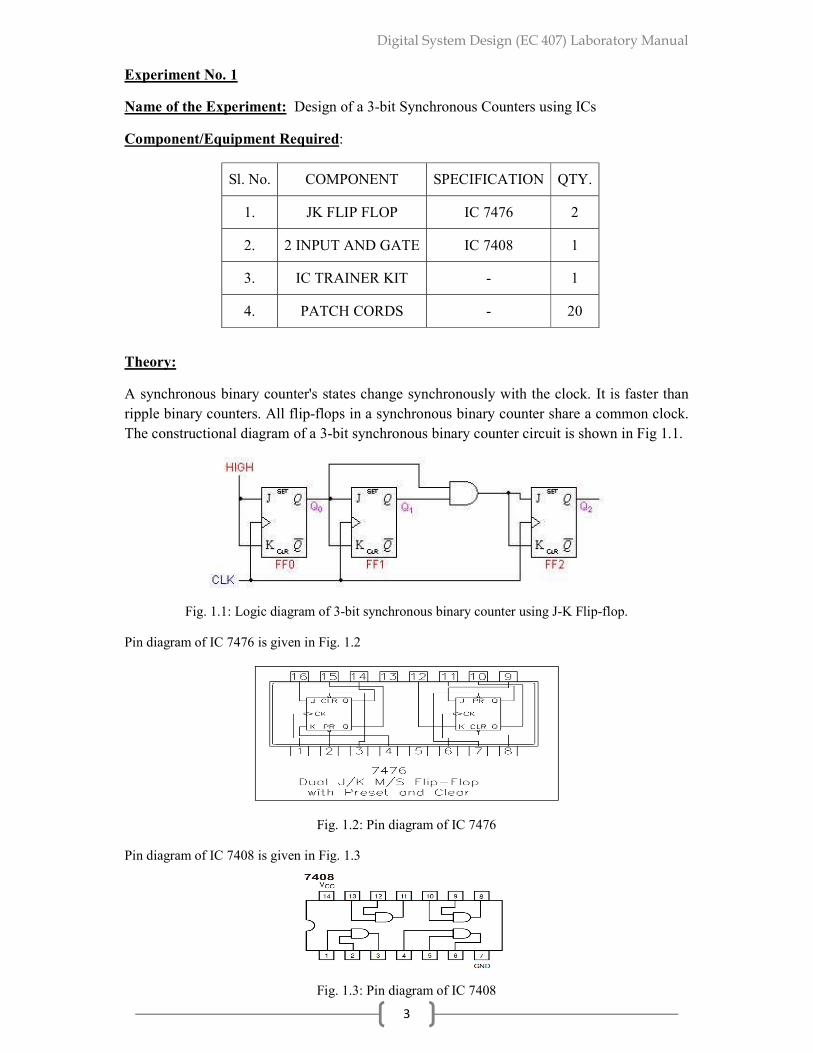
Experiment No. 1
Name of the Experiment: Design of a 3-bit Synchronous Counters using ICs
Component/Equipment Required:
Sl. No. COMPONENT SPECIFICATION QTY.
1. JK FLIP FLOP IC 7476 2
2. 2 INPUT AND GATE IC 7408 1
3. IC TRAINER KIT - 1
4. PATCH CORDS - 20
Theory:
A synchronous binary counter's states change synchronously with the clock. It is faster than ripple binary counters. All flip-flops in a synchronous binary counter share a common clock. The constructional diagram of a 3-bit synchronous binary counter circuit is shown in Fig 1.1.
Fig. 1.1: Logic diagram of 3-bit synchronous binary counter using J-K Flip-flop.
Pin diagram of IC 7476 is given in Fig. 1.2
Fig. 1.2: Pin diagram of IC 7476
Pin diagram of IC 7408 is given in Fig. 1.3
Fig. 1.3: Pin diagram of IC 7408

Digital System Design (EC 407) Laboratory Manual
4
State Diagram:
Fig. 1.3: State Diagram of 3-bit counter
Procedures: 1. Make connections as per the logic diagram shown in Fig. 1.1. 2. Connect the outputs to the LEDs of the trainer kit. 3. Connect the power supply and the function generator. 4. Verify the connections again. 5. Start the experiment by turning on the power of trainer kit. 6. Record the observation as per the observation table. Observation:
State of Counter Count Sequence
Q2 Q1 Q0
0
1
2
3
4
5
6
7
0

Digital System Design (EC 407) Laboratory Manual
5
Conclusion:
Summarize what you have learned by performing this experiment.
Questions:
1) Design a four bit synchronous counter and draw its logic diagram.

Digital System Design (EC 407) Laboratory Manual
6
Experiment No. 2
Name of the Experiment: Design of a Moore’s State Machine for 101 sequence detection using ICs.
Component/Equipment Required:
Sl. No. COMPONENT SPECIFICATION QTY.
1. D FLIP FLOP IC 7474 2
2. 2 INPUT OR GATE IC 7432 1
3. 2 INPUT AND GATE IC 7408 1
4. NOT GATE IC 7404 1
4. IC TRAINER KIT - 1
5. PATCH CORDS - 20
Theory:
A Moore Machine is a Finite State Machine (FSM) whose output depends only on the present state. The block diagram of a Moore FSM is shown in Fig. 2.1
Fig. 2.1: Block diagram of Moore State Machine
The logic diagram of 101 sequence detector is shown in Fig 2.2.
Fig. 2.2: Logic diagram of Moore machine for 2’s complement computation
X
CLK
DB QB
QB’
D
A Q
A
Y

Digital System Design (EC 407) Laboratory Manual
7
Pin diagram of IC 7474 is given in Fig. 2.3
Fig. 2.3: Pin diagram of IC 7474 (Dual D Flipflop with preset and clear)
Pin diagram of IC 7432 is given in Fig. 2.4
Fig. 2.4: Pin diagram of IC 7432 (two input OR Gate)
Pin diagram of IC 7408 is given in Fig. 2.5
Fig. 2.5: Pin diagram of IC 7408 (Two input AND Gate)
Pin diagram of IC 7404 is given in Fig. 2.6
Fig. 2.6: Pin diagram of IC 7404 (NOT gate)

Digital System Design (EC 407) Laboratory Manual
8
State Diagram
Fig. 2.7: State Diagram of 101 Sequence Detector
Procedures: 1. Make connections as per the logic diagram shown in Fig. 2.2. 2. Connect the input to the switch of the trainer kit. 3. Connect the output to the LEDs of the trainer kit. 4. Connect the power supply. 5. Verify the connections again. 6. Start the experiment by turning on the power of trainer kit. 7. Record the observation as per the observation table. Observation:
Input X Flip Flop Outputs Output Y
A B
Conclusion:
Summarize what you have learned by performing this experiment.
Questions:
1) Design a Moore machine for 1001 sequence detection.

Digital System Design (EC 407) Laboratory Manual
9
Experiment No. 3
Name of the Experiment: Design of a Mealy’s State Machine for serial 2’s complement using ICs.
Component/Equipment Required:
Sl. No. COMPONENT SPECIFICATION QTY.
1. D FLIP FLOP IC 7474 1
2. 2 INPUT OR GATE IC 7432 1
3. 2 INPUT XOR GATE IC 7486 1
4. IC TRAINER KIT - 1
5. PATCH CORDS - 20
Theory:
A Mealy Machine is a Finite State Machine (FSM) whose output depends on the present state as well as the present input. The block diagram representation is given in Fig. 3.1
Fig. 3.1: Block diagram of Mealy State Machine
The logic diagram of sequential 2’s complement is shown in Fig 3.2.
Fig. 3.2: Logic diagram of Mealy machine for 2’s complement computation

Digital System Design (EC 407) Laboratory Manual
10
Pin diagram of IC 7474 is given in Fig. 3.3
Fig. 3.3: Pin diagram of IC 7474
Pin diagram of IC 7432 is given in Fig. 3.4
Fig. 3.4: Pin diagram of IC 7432
Pin diagram of IC 7486 is given in Fig. 3.5
Fig. 3.5: Pin diagram of IC 7486
Procedures: 1. Make connections as per the logic diagram shown in Fig. 3.2. 2. Connect the input to the switch of the trainer kit. 3. Connect the output to the LEDs of the trainer kit. 4. Connect the power supply. 5. Verify the connections again. 6. Start the experiment by turning on the power of trainer kit. 7. Record the observation as per the observation table.

Digital System Design (EC 407) Laboratory Manual
11
Observation:
Input X Flip Flop Output Output Y
Conclusion:
Summarize what you have learned by performing this experiment.
Questions:
2) Design Mealy machine for 1’s complement.

Digital System Design (EC 407) Laboratory Manual
12
Experiment No. 4
Name of the Experiment: Design, Simulation and Implementation of AND, OR, NOT, NAND, NOR, XOR, XNOR logic Gates using VHDL on CPLD/FPGA platform. Component/Equipment/Software Required:
Sl. No.
COMPONENT SPECIFICATION QTY.
1. Desktop PC At least i3 PC with 4GB RAM 1
2. Quartus II/Prime
Software Latest version 1
3. Model Sim Software Latest version 1
4. FPGA Board DE2-115 with Cyclone IV
FPGA 1
5. Data Cable USB Blaster cable 1
6. Power Cord Power Adapter Cable 1
Theory:
AND Gate: An AND gate is a logic circuit whose output remains at logic ‘1’ when all the inputs are at logic ‘1’. Conversely, if any of the input is at logic ‘0’ the output will be at logic ‘0’. This gate has one output and many inputs. The symbol, Boolean expression and truth table of AND gate is as follows:
OR Gate: An OR gate is a logic circuit whose output remains at logic ‘1’ when any one or all of the inputs are at logic ‘1’. On the other hand, if all the inputs are at logic ‘0’ the output will be at logic ‘0’. This gate has one output and many inputs. The symbol, Boolean expression and truth table of OR gate is as follows:
A
B Y
Y = A.B or Y = AB
(a) Symbol
(b) Boolean expression
(c) Truth table Fig. 4.1 Symbol, Boolean expression and truth table of AND gate
A B Y 0 0 0
0 1 0
1 0 0
1 1 1

Digital System Design (EC 407) Laboratory Manual
13
NOT Gate: A NOT gate is a logic circuit whose output remains at logic ‘1’ when the input is at logic ‘0’ and vice versa. It is also known as inverter. This gate has one input and one output. The symbol, Boolean expression and truth table of NOT gate is as follows:
NAND Gate: NAND gate can also be obtained by connecting a NOT gate at the output of an AND gate. It is defined as a logic circuit whose output remains at logic ‘1’ if any or all the inputs are at logic ‘0’. Conversely, the output remains at logic ‘0’ if all the inputs are at logic ‘1’. This gate has one output and many inputs. The symbol, Boolean expression and truth table of NAND gate is as follows:
A
B Y Y = A + B
(a) Symbol
(b) Boolean expression
(c) Truth table
Fig. 4.2 Symbol, Boolean expression and truth table of OR gate
A B Y 0 0 0
0 1 1
1 0 1
1 1 1
A Y 0 1
1 0
𝑌 = �̅�
(a) Symbol
(b) Boolean expression
(c) Truth table
Fig. 4.3 Symbol, Boolean expression and truth table of NOT gate
A Y
𝑌 = 𝐴. 𝐵
(a) Symbol
(b) Boolean expression
(c) Truth table
Fi. 4.4 Symbol, Boolean expression and truth table of NAND gate
A Y
B
A B Y
0 0 1
0 1 1
1 0 1
1 1 0

Digital System Design (EC 407) Laboratory Manual
14
NOR Gate: NOR gate can also be obtained by connecting a NOT gate at the output of an OR gate. It is defined as a logic circuit whose output remains at logic ‘1’ if all the inputs are at logic ‘0’. Conversely, the output remains at logic ‘0’ if any or all the inputs are at logic ‘1’. This gate has one output and many inputs. The symbol, Boolean expression and truth table of NOR gate is as follows:
XOR Gate: The exclusive- OR (XOR) is a logic circuit whose output is at logic ‘1’when odd numbers of inputs are at logic‘1’. On the contrary, the output is at logic ‘0’ when either all the inputs are at logic ‘0’ or even number of inputs are at logic‘1’. It has two inputs and one output.
XNOR Gate: The exclusive- NOR (XNOR) is a logic circuit whose output is at logic ‘0’ when odd numbers of inputs are at logic‘1’. On the contrary, the output is at logic ‘1’ when either all the inputs are at logic ‘0’ or even number of inputs are at logic‘1’. XNOR gate can also be obtained by connecting a NOT gate at the output of an XOR gate. It has two inputs and one output.
𝑌 = 𝐴 + 𝐵
(a) Symbol
(b) Boolean expression
(c) Truth table
Fig. 4.5 Symbol, Boolean expression and truth table of NOR gate
A Y
B
A B Y
0 0 1
0 1 0
1 0 0
1 1 0
𝑌 = 𝐴⨁𝐵 = �̅�𝐵 + 𝐴𝐵
(a) Symbol (b) Boolean expression
(c) Truth table
Fig. 4.6 Symbol, Boolean expression and truth table of XOR gate
A
B Y
A B Y
0 0 0
0 1 1
1 0 1
1 1 0

Digital System Design (EC 407) Laboratory Manual
15
Procedures: 1. Open the Quartus II software and follow the instruction as follows: 2. To create a new project and specify a target device or device family, on the File menu, click New
Project Wizard.
3. Click Next on the Introduction window. Provide the name of destination of working directory for the project, Name of the project and entity name in the window Directory, Name, Top Level Entity. Press Next. In window for Family and Device Setting provide the appropriate device and family name of the FPGA board. Press Next, EDA tool setting window will appear. Select ModelSim-Altera as simulation software. Summary window will appear next. Press Finish.
4. Now select the Text Editor to create a Verilog HDL, VHDL, or Altera Hardware Description Language (AHDL) design. Go to File, click on New. From the New window select the appropriate text editor (VHDL). The interface will appear where you can write the program.
5. After completion of writing program, go to Processing and Start Compilation. Go through the compilation report. Check number of errors and warning. Make your program error free to proceed further.
6. Generate Register Transfer Level (RTL) view of your design. Click on Tools, Netlist
Viewer and then RTL Viewer. The RTL view will appear in the window.
𝑌 = 𝐴 ⊙ 𝐵
= 𝐴⨁𝐵 = 𝐴𝐵 + �̅�𝐵
A B Y
0 0 1
0 1 0
1 0 0
1 1 1
(b) Symbol (b) Boolean expression
(c) Truth table
Fig. 4.7 Symbol, Boolean expression and truth table of XNOR gate
A
B Y

Digital System Design (EC 407) Laboratory Manual
16
7. Verify the functionality of your design using Altera ModelSim Software. Go to Tools, Run Simulation Tool and Click on RTL Simulation.
8. On the Library tab, click the ’+’ icon next to the work library and you will see two design units.
You can also see their types (Modules, Entities, etc.) and the path to the underlying source files (scroll to the right if necessary).
9. The Objects pane shows the names and current values of data objects in the current region (selected
in the Workspace). Data objects include signals, nets, registers, constants and variables not declared in a process, generics, and parameters.
Object Pane Displays Design Objects
10. Add signals to the Wave window. a. In the Workspace pane, select the sim tab. b. Right-click file name to open a popup context menu. c. Select Add > To Wave > All items in region d. All signals in the design are added to the Wave window

Digital System Design (EC 407) Laboratory Manual
17
11. Click the Run icon in the Main or Wave window toolbar. The simulation runs for 100 ns (the default simulation length) and waves are drawn in the Wave window.
12. To implement the design on FPGA board follow the following steps:
i) Click on Assignment and Pin Planner. ii) Give the Pin Names in location column. Refer to Annex-I for pin nos. iii) Click on Tools and Programmer. iv) Click on Add File. The .sof file from the output folder is to be selected. v) Click on Start, the program will be downloaded on FPGA chip. vi) Test the design with input as switches and LED as outputs.
13. Record the observation as per the observation table. Program:
library ieee; use ieee.std_logic_1164.all; entity gates is port (a,b: in std_logic; y: out std_logic_vector(5 downto 0)); end gates; architecture behave of gates is begin y(0)<= a and b; y(1)<= a or b; y(2)<= not a; y(3)<= a xor b; y(4)<= a nand b; y(5)<= a nor b;
end behave;

Digital System Design (EC 407) Laboratory Manual
18
Observation: Record your observation as per the following table
Inputs Outputs
A B AND gate
OR gate NOT gate
NAND gate
NOR gate
XOR gate
XNOR gate
Conclusion:
Summarize what you have learned by performing this experiment.
Questions:
1) Implement NAND and NOR gate as universal gate using VHDL.

Digital System Design (EC 407) Laboratory Manual
19
Experiment No. 5
Name of the Experiment: Design, Simulation and Implementation of Half Adder, Full Adder, Parallel Adder using VHDL on CPLD/FPGA platform. Component/Equipment/Software Required:
Sl. No.
COMPONENT SPECIFICATION QTY.
1. Desktop PC At least i3 PC with 4GB RAM 1
2. Quartus II/Prime
Software Latest version 1
3. Model Sim Software Latest version 1
4. FPGA Board DE2-115 with Cyclone IV
FPGA 1
5. Data Cable USB Blaster cable 1
6. Power Cord Power Adapter Cable 1
Theory:
Half Adder:
A half adder is an arithmetic circuit which performs addition operation on two input bits and produces result as sum and carry in the output. It has two input and two output lines. It is usually used to add the first column of two binary numbers. The block diagram and truth table of the half adder circuit is shown in Fig. 5.1.
From the truth table, the Boolean expression for S and C can be written as
S = X ⊕ Y ; C = X Y
The implementation of the expressions for S and C using gates gives the circuit of half adder.
(a) Block diagram
(b) Truth table
Fig. 5.1 Block diagram and truth table of half adder
X
Y
HALF ADDER
S
C
X Y S C
0 0 0 0
0 1 1 0
1 0 1 0
1 1 0 1

Digital System Design (EC 407) Laboratory Manual
20
Full Adder
A full adder is an arithmetic circuit which performs addition operation on three input bits and produces result as sum and carry. It has three input and two output lines. Unlike, half adder, it can be used for addition of any column two binary numbers. The block diagram and truth table of the full adder circuit is shown in Fig. 5.3.
From the truth table, the Boolean expression for S and C can be written as
𝑆 = 𝑋𝑌𝑍 + 𝑋𝑌�̅� + 𝑋𝑌�̅� + 𝑋𝑌𝑍
= (𝑋𝑌 + 𝑋𝑌)𝑍 + (𝑋𝑌 + 𝑋𝑌)�̅�
= (𝑋⨁𝑌)𝑍 + (𝑋⨁𝑌)�̅�
= (𝑋⨁𝑌)⨁𝑍
= 𝑋⨁𝑌⨁𝑍
and
𝐶 = 𝑋𝑌𝑍 + 𝑋𝑌𝑍 + 𝑋𝑌�̅� + 𝑋𝑌𝑍
= 𝑋𝑌𝑍 + 𝑋𝑌𝑍 + 𝑋𝑌𝑍 + 𝑋𝑌𝑍 + 𝑋𝑌𝑍 + 𝑋𝑌�̅� (∵ 𝐴 + 𝐴 + 𝐴 = 𝐴)
= 𝑋𝑌(𝑍 + �̅�) + 𝑌𝑍(𝑋 + 𝑋) + 𝑋𝑍(𝑌 + 𝑌)
=𝑋𝑌 + 𝑌𝑍 + 𝑋𝑍
Fig. 5.2 Logic diagram of half adder
X
Y
C
S
(b) Block diagram
(b) Truth table Fig. 5.3 Block diagram and truth table of full adder
X
Y FULL
ADDER
S
C Z
X Y Z S C 0 0 0 0 0 0 0 1 1 0 0 1 0 1 0 0 1 1 0 1 1 0 0 1 0 1 0 1 0 1 1 1 0 0 1 1 1 1 1 1

Digital System Design (EC 407) Laboratory Manual
21
The implementation of expressions for S and C completes the design of full adder.
Parallel Adder: Parallel adders are digital circuits that compute the addition of two binary strings of equivalent or different size in parallel. The schematic diagram of a parallel adder is shown below in Fig. 5.5
Logic Diagram of Four Bit Parallel adder
Procedures: 1. Open the Quartus II software and follow the steps described in Exp. No. 4 2. Perform simulation and verify your design as per the steps described in Exp. No. 4 3. Implement the design on DE2-115 board as per the steps described in Exp. No. 4
Fig. 5.4 Logic diagram of full adder
X
Y
C
S
Z
Fig. 5.5 Block diagram parallel adder of width n-bit
Fig. 5.6 Logic diagram of 4-bit Parallel Adder

Digital System Design (EC 407) Laboratory Manual
22
Program: VHDL Program for Half Adder
VHDL Program for Full Adder
library ieee; use ieee.std_logic_1164.all; entity half_adder is port ( X : in std_logic; Y : in std_logic; S : out std_logic; C : out std_logic ); end half_adder; architecture rtl of half_adder is begin S <= X xor Y; C <= X and Y; end rtl;
library ieee; use ieee.std_logic_1164.all; entity full_adder is port ( X : in std_logic; Y : in std_logic; Z : in std_logic; S : out std_logic; C : out std_logic ); end full_adder; architecture rtl of full_adder is begin S <= X xor Y xor Z; C <= (X and Y) or (Y and Z) or (Z and X); end rtl;

Digital System Design (EC 407) Laboratory Manual
23
VHDL Program for Parallel Adder
library ieee; use ieee.std_logic_1164.all; entity parr_adder is port ( A : in std_logic_vector( 3 downto 0); B : in std_logic_vector( 3 downto 0); S : out std_logic_vector( 3 downto 0); C : out std_logic ); end parr_adder; architecture RTL of parr_adder is component FULL_ADDER is port( X : in std_logic; Y : in std_logic; Z : in std_logic; S : OUT std_logic; C : out std_logic); end component; signal p : std_logic_vector(2 downto 0) :="000"; begin FA0: FULL_ADDER port map( A(0), B(0), '0', S(0), p(0)); FA1: FULL_ADDER port map( A(1), B(1), p(0), S(1), p(1)); FA2: FULL_ADDER port map( A(2), B(2), p(1), S(2), p(2)); FA3: FULL_ADDER port map( A(3), B(3), p(2), S(3), C); end RTL; library ieee; use ieee.std_logic_1164.all; entity FULL_ADDER is port( X : in std_logic; Y : in std_logic; Z : in std_logic; S : OUT std_logic; C : out std_logic); end FULL_ADDER; architecture behav of FULL_ADDER is begin S <= X xor Y xor Z; C <= (Z and Y) or (Y and Z) or (Z and X); end behav;

Digital System Design (EC 407) Laboratory Manual
24
Observation: Record your observation as per the following tables
Table 1: Half Adder
Inputs Outputs
A B S C
Table 2: Full Adder
Inputs Outputs
X Y Z S C
Table 3: Parallel Adder
Inputs Outputs
A3 A2 A1 A0 B3 B2 B1 B0 S3 S2 S1 S0 C
Conclusion:
Summarize what you have learned by performing this experiment.
Questions:
1) Implement 8-bit Parallel adder.

Digital System Design (EC 407) Laboratory Manual
25
Experiment No. 6
Name of the Experiment: Design, Simulation and Implementation of Half Subtractor, Full Subtractor, 4-bit Adder/Subtractor using VHDL on CPLD/FPGA platform. Component/Equipment/Software Required:
Sl. No.
COMPONENT SPECIFICATION QTY.
1. Desktop PC At least i3 PC with 4GB RAM 1
2. Quartus II/Prime
Software Latest version 1
3. Model Sim Software Latest version 1
4. FPGA Board DE2-115 with Cyclone IV
FPGA 1
5. Data Cable USB Blaster cable 1
6. Power Cord Power Adapter Cable 1
Theory:
Half Subtractor
A half subtractor is an arithmetic circuit which performs subtraction operation on two input bits and produces result as difference and borrow in the output. It has two input and two output lines. It is usually used to subtract the first column of two binary numbers. The block diagram and truth table of the half adder circuit is shown in Fig. 6.1. Treat X as minuend and Y as subtrahend and the subtraction operation is designated by X - Y. During subtraction, if a borrow is taken, the output signal, B becomes ‘1’.
From the truth table, the Boolean expression for D and B can be written as
D = X ⊕ Y ; 𝐵 = 𝑋𝑌
The implementation of the expressions for D and B using gates gives the circuit of half subtractor.
(a) Block diagram
(b) Truth table
Fig. 6.1 Block diagram and truth table of half subtractor
X
Y
HALF SUBTRACTOR
D
B
X Y D B
0 0 0 0
0 1 1 1
1 0 1 0
1 1 0 0

Digital System Design (EC 407) Laboratory Manual
26
Full Subtractor
A full subtractor is an arithmetic circuit which performs subtraction operation between two input bits with consideration that a borrow has been taken by a column lower to it and produces result as difference and borrows. It has three input and two output lines. Unlike, half subtractor, it can be used for subtraction of any column two binary numbers. The block diagram and truth table of the full subtractor circuit is shown in Fig. 6.3. Treat X as minuend, Y as subtrahend and Z as previous borrow. The subtraction operation is designated by X - Y - Z.
From the truth table, the Boolean expression for D and B can be written as
𝐷 = 𝑋𝑌𝑍 + 𝑋𝑌�̅� + 𝑋𝑌�̅� + 𝑋𝑌𝑍
= (𝑋𝑌 + 𝑋𝑌)𝑍 + (𝑋𝑌 + 𝑋𝑌)�̅�
= (𝑋⨁𝑌)𝑍 + (𝑋⨁𝑌)�̅�
= (𝑋⨁𝑌)⨁𝑍
= 𝑋⨁𝑌⨁𝑍
and
𝐵 = 𝑋𝑌𝑍 + 𝑋𝑌�̅� + 𝑋𝑌𝑍 + 𝑋𝑌𝑍
= 𝑋𝑌𝑍 + 𝑋𝑌𝑍 + 𝑋𝑌𝑍 + 𝑋𝑌�̅� + 𝑋𝑌𝑍 + 𝑋𝑌𝑍(∵ 𝐴 + 𝐴 + 𝐴 = 𝐴)
= 𝑋𝑍(𝑌 + 𝑌) + 𝑋𝑌(𝑍 + �̅�) + 𝑌𝑍(𝑋 + 𝑋)
Fig. 6.2 Logic diagram of half subtractor
X
Y
B
D
(a)Block diagram
(b) Truth table
Fig. 6.3 Block diagram and truth table of full subtractor
X
Y FULL
SUBTRACTOR
D
B Z
X Y Z D B 0 0 0 0 0 0 0 1 1 1 0 1 0 1 1 0 1 1 0 1 1 0 0 1 0 1 0 1 0 0 1 1 0 0 0 1 1 1 1 1

Digital System Design (EC 407) Laboratory Manual
27
= 𝑋𝑌 + 𝑌𝑍 + 𝑋𝑍
The implementation of expressions for D and B completes the design of full subtractor.
Parallel Adder/Subtractor: Subtraction of binary numbers can be carried out by using the addition of 2’s complement of subtrahend to the minuend. In this operation if the MSB of addition is a ‘0’, then the answer is correct and if MSB is ‘1’, then answer is having negative sign. Hence, by using full adders subtraction can be carried out.
Logic Diagram of Four Bit Parallel adder/subtractor
Fig. 6.4 Logic diagram of full subtractor
X
Y
B
D
Z
Fig. 6.5 Block diagram 4-bit parallel adder/subtractor
Fig. 6.6 Logic diagram of 4-bit Parallel Adder

Digital System Design (EC 407) Laboratory Manual
28
Fig. 6.6 above shows the realization of 4 bit adder-subtractor. From the figure it can be seen that, the bits of the binary numbers are given to full adder through the XOR gates. The control input is controls the addition or subtraction operation.
When the SUBTRACTION input is logic ‘0’, the B3 B2 B1 B0 are passed to the full adders. Hence, the output of the full adders is the addition of the two numbers.
When the SUBTRACTION input is logic ‘1’, the B3 B2 B1 B0 are complemented. Further, the SUBTRACTION logic ‘1’ input is also work as Cin for the LSB full adder, due to which 2’s complement addition can be carried out. Hence, the outputs of the full adders in this case is the subtraction of two numbers.
Procedures: 1. Open the Quartus II software and follow the steps described in Exp. No. 4 2. Perform simulation and verify your design as per the steps described in Exp. No. 4 3. Implement the design on DE2-115 board as per the steps described in Exp. No. 4
Program: VHDL Program for Half Subtractor
VHDL Program for Full Subtractor
library ieee; use ieee.std_logic_1164.all; entity half_subtractor is port ( X : in std_logic; Y : in std_logic; D : out std_logic; B : out std_logic ); end half_subtractor; architecture rtl of half_subtractor is begin D <= X xor Y; B <= (not X) and Y; end rtl;
library ieee; use ieee.std_logic_1164.all; entity full_ subtractor is port ( X : in std_logic; Y : in std_logic; Z : in std_logic; D : out std_logic; B : out std_logic ); end full_subtractor; architecture rtl of full_subtractor is begin D <= X xor Y xor Z; B <= ((not X) and Y) or (Y and Z) or (Z and (not X)); end rtl;
Digital System Design (EC 407) Laboratory Manual
29
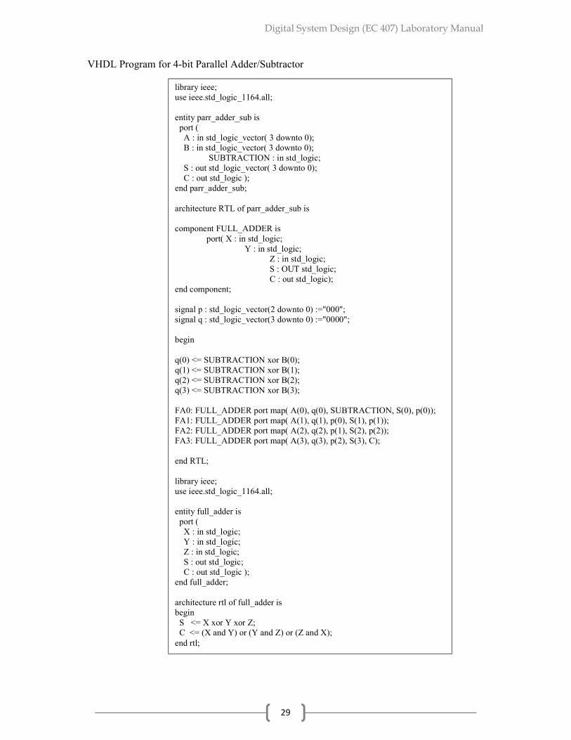
VHDL Program for 4-bit Parallel Adder/Subtractor
library ieee; use ieee.std_logic_1164.all; entity parr_adder_sub is port ( A : in std_logic_vector( 3 downto 0); B : in std_logic_vector( 3 downto 0); SUBTRACTION : in std_logic; S : out std_logic_vector( 3 downto 0); C : out std_logic ); end parr_adder_sub; architecture RTL of parr_adder_sub is component FULL_ADDER is port( X : in std_logic; Y : in std_logic; Z : in std_logic; S : OUT std_logic; C : out std_logic); end component; signal p : std_logic_vector(2 downto 0) :="000"; signal q : std_logic_vector(3 downto 0) :="0000"; begin q(0) <= SUBTRACTION xor B(0); q(1) <= SUBTRACTION xor B(1); q(2) <= SUBTRACTION xor B(2); q(3) <= SUBTRACTION xor B(3); FA0: FULL_ADDER port map( A(0), q(0), SUBTRACTION, S(0), p(0)); FA1: FULL_ADDER port map( A(1), q(1), p(0), S(1), p(1)); FA2: FULL_ADDER port map( A(2), q(2), p(1), S(2), p(2)); FA3: FULL_ADDER port map( A(3), q(3), p(2), S(3), C); end RTL; library ieee; use ieee.std_logic_1164.all; entity full_adder is port ( X : in std_logic; Y : in std_logic; Z : in std_logic; S : out std_logic; C : out std_logic ); end full_adder; architecture rtl of full_adder is begin S <= X xor Y xor Z; C <= (X and Y) or (Y and Z) or (Z and X); end rtl;

Digital System Design (EC 407) Laboratory Manual
30
Observation: Record your observation as per the following tables
Table 1: Half Subtractor
Inputs Outputs
X Y D B
Table 2: Full Subtractor
Inputs Outputs
X Y Z D B
Table 3: Parallel Adder/Subtractor
Inputs Outputs
A3 A2 A1 A0 B3 B2 B1 B0 SUBTRACTION S3 S2 S1 S0 C
Conclusion:
Summarize what you have learned by performing this experiment.
Questions:
1) Implement 8-bit Parallel adder/subtractor.
Digital System Design (EC 407) Laboratory Manual
31
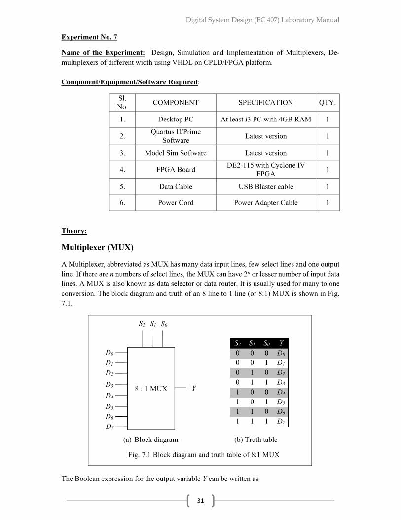
Experiment No. 7
Name of the Experiment: Design, Simulation and Implementation of Multiplexers, De-multiplexers of different width using VHDL on CPLD/FPGA platform. Component/Equipment/Software Required:
Sl. No.
COMPONENT SPECIFICATION QTY.
1. Desktop PC At least i3 PC with 4GB RAM 1
2. Quartus II/Prime
Software Latest version 1
3. Model Sim Software Latest version 1
4. FPGA Board DE2-115 with Cyclone IV
FPGA 1
5. Data Cable USB Blaster cable 1
6. Power Cord Power Adapter Cable 1
Theory:
Multiplexer (MUX)
A Multiplexer, abbreviated as MUX has many data input lines, few select lines and one output line. If there are n numbers of select lines, the MUX can have 2n or lesser number of input data lines. A MUX is also known as data selector or data router. It is usually used for many to one conversion. The block diagram and truth of an 8 line to 1 line (or 8:1) MUX is shown in Fig. 7.1.
The Boolean expression for the output variable Y can be written as
(a) Block diagram
(b) Truth table
Fig. 7.1 Block diagram and truth table of 8:1 MUX
D0
8 : 1 MUX Y
D1 D2
D3
D4
D5 D6 D7
S2 S1 S0
S2 S1 S0 Y 0 0 0 D0 0 0 1 D1 0 1 0 D2 0 1 1 D3 1 0 0 D4 1 0 1 D5 1 1 0 D6 1 1 1 D7

Digital System Design (EC 407) Laboratory Manual
32
𝑌 = 𝐷 𝑆 𝑆 𝑆 + 𝐷 𝑆 𝑆 𝑆 + 𝐷 𝑆 𝑆 𝑆 + 𝐷 𝑆 𝑆 𝑆 + 𝐷 𝑆 𝑆 𝑆 + 𝐷 𝑆 𝑆 𝑆 + 𝐷 𝑆 𝑆 𝑆 +
𝐷 𝑆 𝑆 𝑆
When this expression is implemented by digital logic gates we get structure as shown in Fig. 7.2.
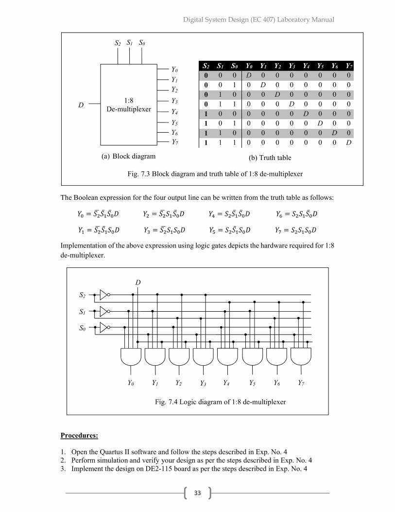
De-multiplexer (DEMUX)
A de-multiplexer is a combinational logic circuit, which has one data input line, few select lines and many output lines. If there are n numbers of select lines, the de-multiplexer can have 2n or lesser number of output lines. A de-multiplexer is also known as data distributor and performs the inverse function of that of a multiplexer. By applying appropriate value on the select line, the input signal can be steered into one of the output lines. It is usually used for one to many conversion. The block diagram and truth of a simple 1 line to 8 line (or 1:8) de-multiplexer is shown in Fig. 7.3
S2
Y Fig. 7.2 Logic diagram of 8 : 1 MUX
S1
S0
D0 D1 D2 D3 D4 D5 D6 D7
Digital System Design (EC 407) Laboratory Manual
33
The Boolean expression for the four output line can be written from the truth table as follows:
𝑌 = 𝑆 𝑆̅ 𝑆̅ 𝐷 𝑌 = 𝑆 𝑆 𝑆̅ 𝐷 𝑌 = 𝑆 𝑆̅ 𝑆̅ 𝐷 𝑌 = 𝑆 𝑆 𝑆̅ 𝐷
𝑌 = 𝑆 𝑆̅ 𝑆 𝐷 𝑌 = 𝑆 𝑆 𝑆 𝐷 𝑌 = 𝑆 𝑆̅ 𝑆 𝐷 𝑌 = 𝑆 𝑆 𝑆 𝐷
Implementation of the above expression using logic gates depicts the hardware required for 1:8 de-multiplexer.
Procedures: 1. Open the Quartus II software and follow the steps described in Exp. No. 4 2. Perform simulation and verify your design as per the steps described in Exp. No. 4 3. Implement the design on DE2-115 board as per the steps described in Exp. No. 4
S2 S1 S0 Y0 Y1 Y2 Y3 Y4 Y5 Y6 Y7 0 0 0 D 0 0 0 0 0 0 0 0 0 1 0 D 0 0 0 0 0 0 0 1 0 0 0 D 0 0 0 0 0 0 1 1 0 0 0 D 0 0 0 0 1 0 0 0 0 0 0 D 0 0 0 1 0 1 0 0 0 0 0 D 0 0 1 1 0 0 0 0 0 0 0 D 0 1 1 1 0 0 0 0 0 0 0 D
(a) Block diagram
(b) Truth table
Fig. 7.3 Block diagram and truth table of 1:8 de-multiplexer
Y0
1:8 De-multiplexer
Y1 Y2
Y3
Y4
Y5 Y6 Y7
D
S0 S1 S2
S2
Fig. 7.4 Logic diagram of 1:8 de-multiplexer
S1
S0
Y0 Y1 Y2 Y3 Y4 Y5 Y6 Y7
D

Digital System Design (EC 407) Laboratory Manual
34
Program: VHDL Program for 8:1 MUX
library ieee; use ieee.std_logic_1164.all; entity MUX_4_1 is port( I : in std_logic_vector(7 downto 0); SEL : in std_logic_vector(2 downto 0); Y : out std_logic); end MUX_4_1; architecture behav of MUX_4_1 is begin process(I, SEL) begin if (SEL ="000") THEN Y <= I(0); elsif (SEL ="001") THEN Y <= I(1); elsif (SEL ="010") THEN Y <= I(2); elsif (SEL ="011") THEN Y <= I(3); elsif (SEL ="100") THEN Y <= I(4); elsif (SEL ="101") THEN Y <= I(5); elsif (SEL ="110") THEN Y <= I(6); else Y <= I(7); end if; end process; end behav;
Digital System Design (EC 407) Laboratory Manual
35
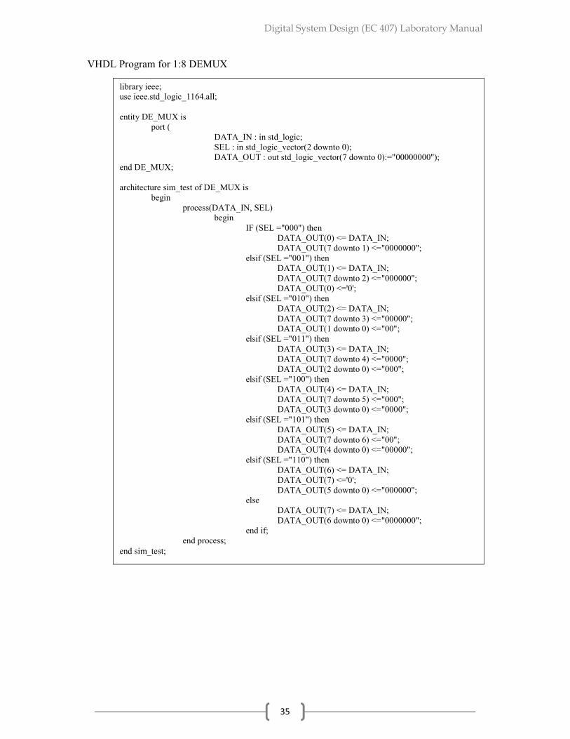
VHDL Program for 1:8 DEMUX
library ieee; use ieee.std_logic_1164.all; entity DE_MUX is port ( DATA_IN : in std_logic; SEL : in std_logic_vector(2 downto 0); DATA_OUT : out std_logic_vector(7 downto 0):="00000000"); end DE_MUX; architecture sim_test of DE_MUX is begin process(DATA_IN, SEL) begin IF (SEL ="000") then DATA_OUT(0) <= DATA_IN; DATA_OUT(7 downto 1) <="0000000"; elsif (SEL ="001") then DATA_OUT(1) <= DATA_IN; DATA_OUT(7 downto 2) <="000000"; DATA_OUT(0) <='0'; elsif (SEL ="010") then DATA_OUT(2) <= DATA_IN; DATA_OUT(7 downto 3) <="00000"; DATA_OUT(1 downto 0) <="00"; elsif (SEL ="011") then DATA_OUT(3) <= DATA_IN; DATA_OUT(7 downto 4) <="0000"; DATA_OUT(2 downto 0) <="000"; elsif (SEL ="100") then DATA_OUT(4) <= DATA_IN; DATA_OUT(7 downto 5) <="000"; DATA_OUT(3 downto 0) <="0000"; elsif (SEL ="101") then DATA_OUT(5) <= DATA_IN; DATA_OUT(7 downto 6) <="00"; DATA_OUT(4 downto 0) <="00000"; elsif (SEL ="110") then DATA_OUT(6) <= DATA_IN; DATA_OUT(7) <='0'; DATA_OUT(5 downto 0) <="000000"; else DATA_OUT(7) <= DATA_IN; DATA_OUT(6 downto 0) <="0000000"; end if; end process; end sim_test;

Digital System Design (EC 407) Laboratory Manual
36
Observation: Record your observation as per the following tables
Table 1: 8: 1 MUX
Data Input Select Input Output
I0 I1 I2 I3 I4 I5 I6 I7 S2 S1 S0 Y
Table 2: Full Subtractor
Data Input
Select Input Outputs
I S2 S1 S0 Y0 Y1 Y2 Y3 Y4 Y5 Y6 Y7
Conclusion:
Summarize what you have learned by performing this experiment.
Questions:
1) Implement 4-bit 8: 1 MUX 2) Implement 4-bit 1:8 DEMUX

Digital System Design (EC 407) Laboratory Manual
37
Experiment No. 8
Name of the Experiment: Design, Simulation and Implementation of Encoders, Decoders of different width using VHDL on CPLD/FPGA platform. Component/Equipment/Software Required:
Sl. No.
COMPONENT SPECIFICATION QTY.
1. Desktop PC At least i3 PC with 4GB RAM 1
2. Quartus II/Prime
Software Latest version 1
3. Model Sim Software Latest version 1
4. FPGA Board DE2-115 with Cyclone IV
FPGA 1
5. Data Cable USB Blaster cable 1
6. Power Cord Power Adapter Cable 1
Theory:
Encoder
An encoder is a combinational circuit which generates a coded output signal in response to an active input signal. If an encoder has n number of output lines, it can have 2n or lesser number of input lines. Encoders are typically used to convert a decimal keyboard, like that of a calculator into a binary or BCD output. Fig. 8.1 shows the block diagram and truth table of an 8 line to 3 line encoder which is also known as octal to binary encoder.
The Boolean expressions for the encoder can be determined by careful examination of the truth table. Output line Y2 is at logic ‘1’ when D4 or D5 or D6 or D7 is at logic ‘1’. Similarly we can determine the expressions for Y1 and Y0 as well and can be written as
(b) Block diagram
(b) Truth table
Fig. 8.1 Block diagram and truth table of 8 Line to 3 line Encoder
D0
8 Line to 3 Line Encoder
Y0
Y1
Y2
D1 D2
D3
D4
D5 D6 D7
D0 D1 D2 D3 D4 D5 D6 D7 Y2 Y1 Y0 1 0 0 0 0 0 0 0 0 0 0 0 1 0 0 0 0 0 0 0 0 1 0 0 1 0 0 0 0 0 0 1 0 0 0 0 1 0 0 0 0 0 1 1 0 0 0 0 1 0 0 0 1 0 0 0 0 0 0 0 1 0 0 1 0 1 0 0 0 0 0 0 1 0 1 1 0 0 0 0 0 0 0 0 1 1 1 1

Digital System Design (EC 407) Laboratory Manual
38
𝑌 = 𝐷 + 𝐷 + 𝐷 + 𝐷
𝑌 = 𝐷 + 𝐷 + 𝐷 + 𝐷
𝑌 = 𝐷 + 𝐷 + 𝐷 + 𝐷
Implementation of expression for Y2, Y1 and Y0 is shown in Fig. 8.2 which basically describes the octal to binary encoder.
Other popular encoders are 10 line to 4 line encoder (i.e. decimal to BCD encoder) and 16 line to 4 line encoder (i.e. hexadecimal to binary encoder).
Decoder
A decoder is a combinational circuit which generates 2n or lesser unique output lines from coded information received on n-bit input lines. It is used to decode the binary state contained in a piece of coded information. Decoders can be used in chip select logic of memory ICs, making one of the output line active at a time etc. Fig. 8.3 shows the block diagram and truth table of a 3 line to 8 line decoder (also known as binary to octal decoder).
Fig. 8.2 Logic diagram of 8:3 Encoder
D0 D1
D2 D3
D4
D5 D6 D7
Y2 Y1 Y0

Digital System Design (EC 407) Laboratory Manual
39
The Boolean expression for each output can be derived from the truth table and can be written as
𝑌 = �̅�𝐵𝐶̅ 𝑌 = �̅�𝐵𝐶̅ 𝑌 = 𝐴𝐵𝐶̅ 𝑌 = 𝐴𝐵�̅�
𝑌 = �̅�𝐵𝐶 𝑌 = �̅�𝐵𝐶 𝑌 = 𝐴𝐵𝐶 𝑌 = 𝐴𝐵𝐶
In order to implement the above expressions, we need the hardware shown in Fig. 8.4 and is termed as binary to octal decoder.
Procedures: 1. Open the Quartus II software and follow the steps described in Exp. No. 4 2. Perform simulation and verify your design as per the steps described in Exp. No. 4 3. Implement the design on DE2-115 board as per the steps described in Exp. No. 4
Program: VHDL Program for 8:3 ENCODER
(a) Block diagram (b) Truth table
Fig. 8.3 Block diagram and truth table of 3 line to 8 line decoder
Y0
3 Line to 8 Line Decoder
Y1 Y2
Y3
Y4
Y5 Y6 Y7
A
B
C
A B C Y0 Y1 Y2 Y3 Y4 Y5 Y6 Y7 0 0 0 1 0 0 0 0 0 0 0 0 0 1 0 1 0 0 0 0 0 0 0 1 0 0 0 1 0 0 0 0 0 0 1 1 0 0 0 1 0 0 0 0 1 0 0 0 0 0 0 1 0 0 0 1 0 1 0 0 0 0 0 1 0 0 1 1 0 0 0 0 0 0 0 1 0 1 1 1 0 0 0 0 0 0 0 1
A
B
C
Y0 Y1 Y2 Y3 Y4 Y5 Y6 Y7
Fig. 8.4 Logic diagram of binary to octal decoder

Digital System Design (EC 407) Laboratory Manual
40
VHDL Program for 3:8 Decoder
library ieee; use ieee.std_logic_1164.all; entity ENCODER is port ( DATA_IN : in std_logic_vector(7 downto 0); DATA_OUT : out std_logic_vector(2 downto 0)); end ENCODER;
architecture RTL of ENCODER is begin DATA_OUT(0) <= DATA_IN(1) OR DATA_IN(3) OR DATA_IN(5) OR DATA_IN(7); DATA_OUT(1) <= DATA_IN(2) OR DATA_IN(3) OR DATA_IN(6) OR DATA_IN(7); DATA_OUT(2) <= DATA_IN(4) OR DATA_IN(5) OR DATA_IN(6) OR DATA_IN(7); end RTL;
library ieee; use ieee.std_logic_1164.all;
entity DECODER is port ( DATA_IN : in std_logic_vector(2 downto 0); DATA_OUT : out std_logic_vector(7 downto 0)); end DECODER;
architecture RTL of DECODER is begin process(DATA_IN) begin IF (DATA_IN="000") then DATA_OUT(0) <= '1'; DATA_OUT(7 downto 1) <="0000000"; elsif (DATA_IN ="001") then DATA_OUT(1) <= '1'; DATA_OUT(7 downto 2) <="000000"; DATA_OUT(0) <='0'; elsif (DATA_IN ="010") then DATA_OUT(2) <= '1'; DATA_OUT(7 downto 3) <="00000"; DATA_OUT(1 downto 0) <="00"; elsif (DATA_IN ="011") then DATA_OUT(3) <= '1'; DATA_OUT(7 downto 4) <="0000"; DATA_OUT(2 downto 0) <="000"; elsif (DATA_IN ="100") then DATA_OUT(4) <= '1'; DATA_OUT(7 downto 5) <="000"; DATA_OUT(3 downto 0) <="0000"; elsif (DATA_IN ="101") then DATA_OUT(5) <= '1'; DATA_OUT(7 downto 6) <="00"; DATA_OUT(4 downto 0) <="00000"; elsif (DATA_IN ="110") then DATA_OUT(6) <= '1'; DATA_OUT(7) <='0'; DATA_OUT(5 downto 0) <="000000"; else DATA_OUT(7) <= '1'; DATA_OUT(6 downto 0) <="0000000"; end if; end process; end RTL;

Digital System Design (EC 407) Laboratory Manual
41
Observation: Record your observation as per the following tables
Table 1: 8: 3 Encoder
Data Input Output
D0 D1 D2 D3 D4 D5 D6 D7 Y2 Y1 Y0
Table 2: 3:8 Decoder
Data Input Outputs
A B C Y0 Y1 Y2 Y3 Y4 Y5 Y6 Y7
Conclusion:
Summarize what you have learned by performing this experiment.
Questions:
1) Implement Decimal to BCD Encoder 2) Implement BCD to Decimal Decoder

Digital System Design (EC 407) Laboratory Manual
42
Experiment No. 9
Name of the Experiment: Design, Simulation and Implementation of Code converters, Magnitude Comparators using VHDL on CPLD/FPGA platform. Component/Equipment/Software Required:
Sl. No.
COMPONENT SPECIFICATION QTY.
1. Desktop PC At least i3 PC with 4GB RAM 1
2. Quartus II/Prime
Software Latest version 1
3. Model Sim Software Latest version 1
4. FPGA Board DE2-115 with Cyclone IV
FPGA 1
5. Data Cable USB Blaster cable 1
6. Power Cord Power Adapter Cable 1
Theory:
Binary to Gray Code Converter
This type of converter is responsible to convert a four bit binary word into four bit equivalent gray code word. Accordingly it has four inputs and four outputs. The block diagram and truth table of binary to gray code converter is shown in Fig. 9.1

Digital System Design (EC 407) Laboratory Manual
43
The Boolean expression for the outputs of the converter can be obtained from the truth table using K-map as follows:
𝐺 = 𝐵 ; 𝐺 = 𝐵 ⨁𝐵 ; 𝐺 = 𝐵 ⨁𝐵 ; 𝐺 = 𝐵 ⨁𝐵
The logic diagram of binary to gray code converter is shown in Fig. 9.2
Magnitude Comparator
A comparator or magnitude comparator is a combinational logic circuit which compares two binary numbers, e.g. A and B, and produces result as A > B, A = B or A < B in the output. Let A and B are the two bit binary numbers and is represented as
B3 B2 B1 B0 G3 G2 G1 G0 0 0 0 0 0 0 0 0 0 0 0 1 0 0 0 1 0 0 1 0 0 0 1 1 0 0 1 1 0 0 1 0 0 1 0 0 0 1 1 0 0 1 0 1 0 1 1 1 0 1 1 0 0 1 0 1 0 1 1 1 0 1 0 0 1 0 0 0 1 1 0 0 1 0 0 1 1 1 0 1 1 0 1 0 1 1 1 1 1 0 1 1 1 1 1 0 1 1 0 0 1 0 0 1 1 1 0 1 1 0 1 0 1 1 1 0 1 0 0 1 1 1 1 1 1 0 0 0
(a) Block diagram
(b) Truth table Fig. 9.1 Block diagram and truth table of binary to gray code converter
B3
B2 Binary to Gray Code Converter
G3
B1
B0
G2
G1 G0
Fig. 9.2 Logic diagram of binary to gray code converter
B0
B1 B2
B3
G2 G1 G0 G3
Digital System Design (EC 407) Laboratory Manual
44
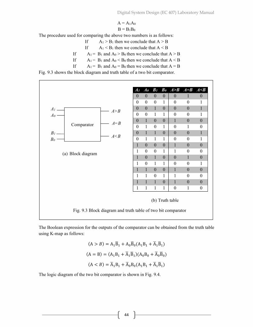
A = A1A0 B = B1B0
The procedure used for comparing the above two numbers is as follows: If A1 > B1 then we conclude that A > B If A1 < B1 then we conclude that A < B
If A1 = B1 and A0 > B0 then we conclude that A > B If A1 = B1 and A0 < B0 then we conclude that A < B If A1 = B1 and A0 = B0 then we conclude that A = B
Fig. 9.3 shows the block diagram and truth table of a two bit comparator.
The Boolean expression for the outputs of the comparator can be obtained from the truth table using K-map as follows:
(A > 𝐵) = A B + A B (A B + A B )
(A = B) = (A B + A B )(A B + A B )
(A < 𝐵) = A B + A B (A B + A B )
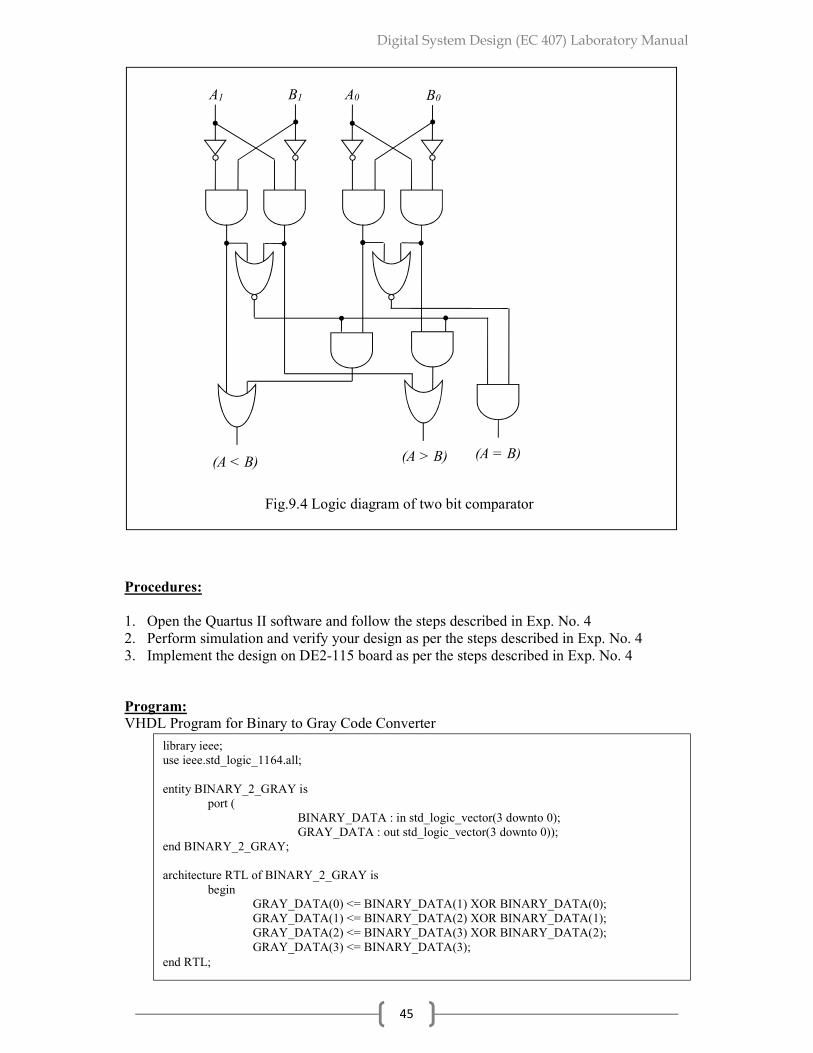
The logic diagram of the two bit comparator is shown in Fig. 9.4.
A1 A0 B1 B0 A>B A=B A<B 0 0 0 0 0 1 0 0 0 0 1 0 0 1 0 0 1 0 0 0 1 0 0 1 1 0 0 1 0 1 0 0 1 0 0 0 1 0 1 0 1 0 0 1 1 0 0 0 1 0 1 1 1 0 0 1 1 0 0 0 1 0 0 1 0 0 1 1 0 0 1 0 1 0 0 1 0 1 0 1 1 0 0 1 1 1 0 0 1 0 0 1 1 0 1 1 0 0 1 1 1 0 1 0 0 1 1 1 1 0 1 0
(a) Block diagram
(b) Truth table
Fig. 9.3 Block diagram and truth table of two bit comparator
A1 A0
Comparator A=B
B1 B0
A<B
A>B
Digital System Design (EC 407) Laboratory Manual
45
Procedures: 1. Open the Quartus II software and follow the steps described in Exp. No. 4 2. Perform simulation and verify your design as per the steps described in Exp. No. 4 3. Implement the design on DE2-115 board as per the steps described in Exp. No. 4
Program: VHDL Program for Binary to Gray Code Converter
Fig.9.4 Logic diagram of two bit comparator
B1 A1 A0 B0
(A < B) (A > B) (A = B)
library ieee; use ieee.std_logic_1164.all; entity BINARY_2_GRAY is port ( BINARY_DATA : in std_logic_vector(3 downto 0); GRAY_DATA : out std_logic_vector(3 downto 0)); end BINARY_2_GRAY; architecture RTL of BINARY_2_GRAY is begin GRAY_DATA(0) <= BINARY_DATA(1) XOR BINARY_DATA(0); GRAY_DATA(1) <= BINARY_DATA(2) XOR BINARY_DATA(1); GRAY_DATA(2) <= BINARY_DATA(3) XOR BINARY_DATA(2); GRAY_DATA(3) <= BINARY_DATA(3); end RTL;

Digital System Design (EC 407) Laboratory Manual
46
VHDL Program 2-bit Magnitude Comparator Observation: Record your observation as per the following tables
Table 1: Binary to Gray Code Converter
Binary Data Gray Data
B3 B2 B1 B0 G3 G2 G1 G0
Table 2: 2-Bit Magnitude Comparator
Input Data Output
A1 A0 B1 B0 (A>B) (A<B) (A=B)
Conclusion:
Summarize what you have learned by performing this experiment.
library ieee; use ieee.std_logic_1164.all; entity MAG_COMP is port ( A : in std_logic_vector(1 downto 0); B : in std_logic_vector(1 downto 0); A_GT_B : out std_logic; A_LT_B : out std_logic; A_EQ_B : out std_logic); end MAG_COMP; architecture RTL of MAG_COMP is begin A_GT_B <= (A(1) and not (B(1))) or ((A(0) and not (B(0)))and((A(1) and B(1))or (not(A(1)) and not(B(1))))); A_LT_B <= (not(A(1)) and B(1)) or ((not(A(0)) and B(0))and((A(1) and B(1))or (not(A(1)) and not(B(1))))); A_EQ_B <= ((A(1) and B(1)) or (not(A(1)) and not(B(1)))) and ((A(0) and B(0)) or (not(A(0)) and not(B(0)))); end RTL;

Digital System Design (EC 407) Laboratory Manual
47
Questions:
1) Implement Gray to Binary Converter
2) Implement BCD to Excess-3 Converter
3) Implement 4-bit Magnitude Comparator
Digital System Design (EC 407) Laboratory Manual
48
Experiment No. 10
Name of the Experiment: Design, Simulation and Implementation of Latch and Flip-flops, registers using VHDL on CPLD/FPGA platform. Component/Equipment/Software Required:
Sl. No.
COMPONENT SPECIFICATION QTY.
1. Desktop PC At least i3 PC with 4GB RAM 1
2. Quartus II/Prime
Software Latest version 1
3. Model Sim Software Latest version 1
4. FPGA Board DE2-115 with Cyclone IV
FPGA 1
5. Data Cable USB Blaster cable 1
6. Power Cord Power Adapter Cable 1
Theory:
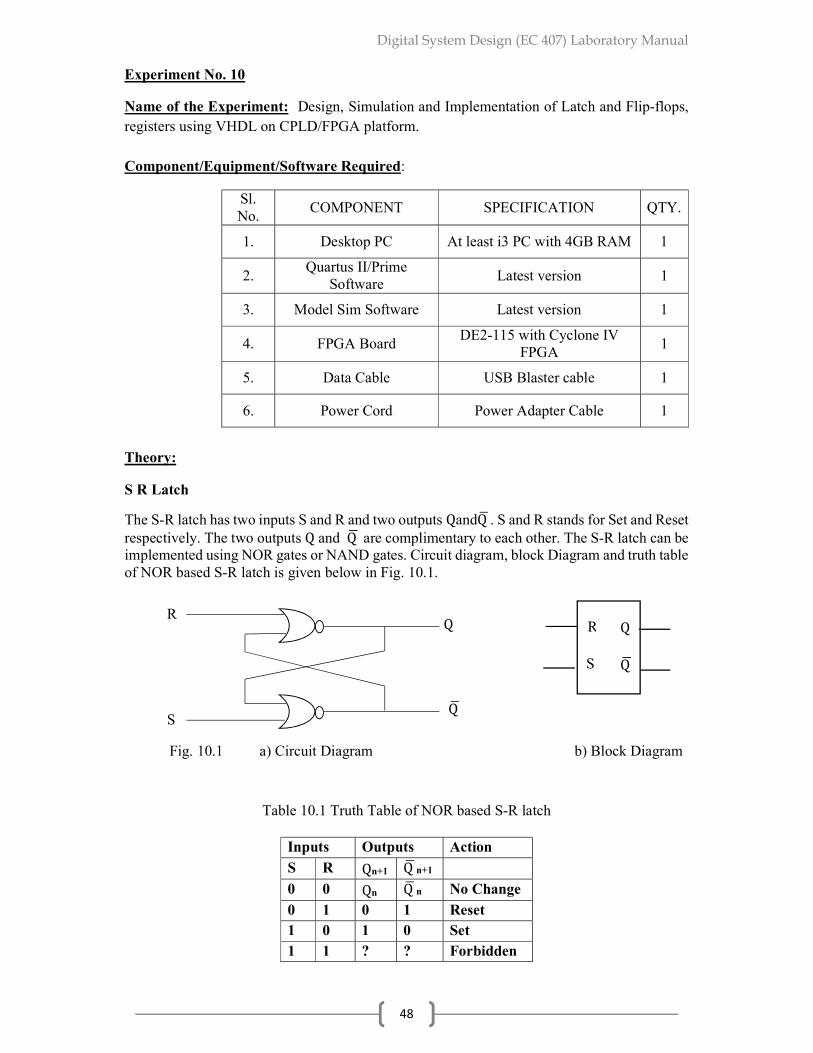
S R Latch
The S-R latch has two inputs S and R and two outputs QandQ . S and R stands for Set and Reset respectively. The two outputs Q and Q are complimentary to each other. The S-R latch can be implemented using NOR gates or NAND gates. Circuit diagram, block Diagram and truth table of NOR based S-R latch is given below in Fig. 10.1.
Fig. 10.1 a) Circuit Diagram b) Block Diagram
Table 10.1 Truth Table of NOR based S-R latch
Inputs Outputs Action
S R Qn+1 Q n+1
0 0 Qn Q n No Change
0 1 0 1 Reset 1 0 1 0 Set 1 1 ? ? Forbidden
R
S
Q
Q
Q
Q
R
S
Digital System Design (EC 407) Laboratory Manual
49
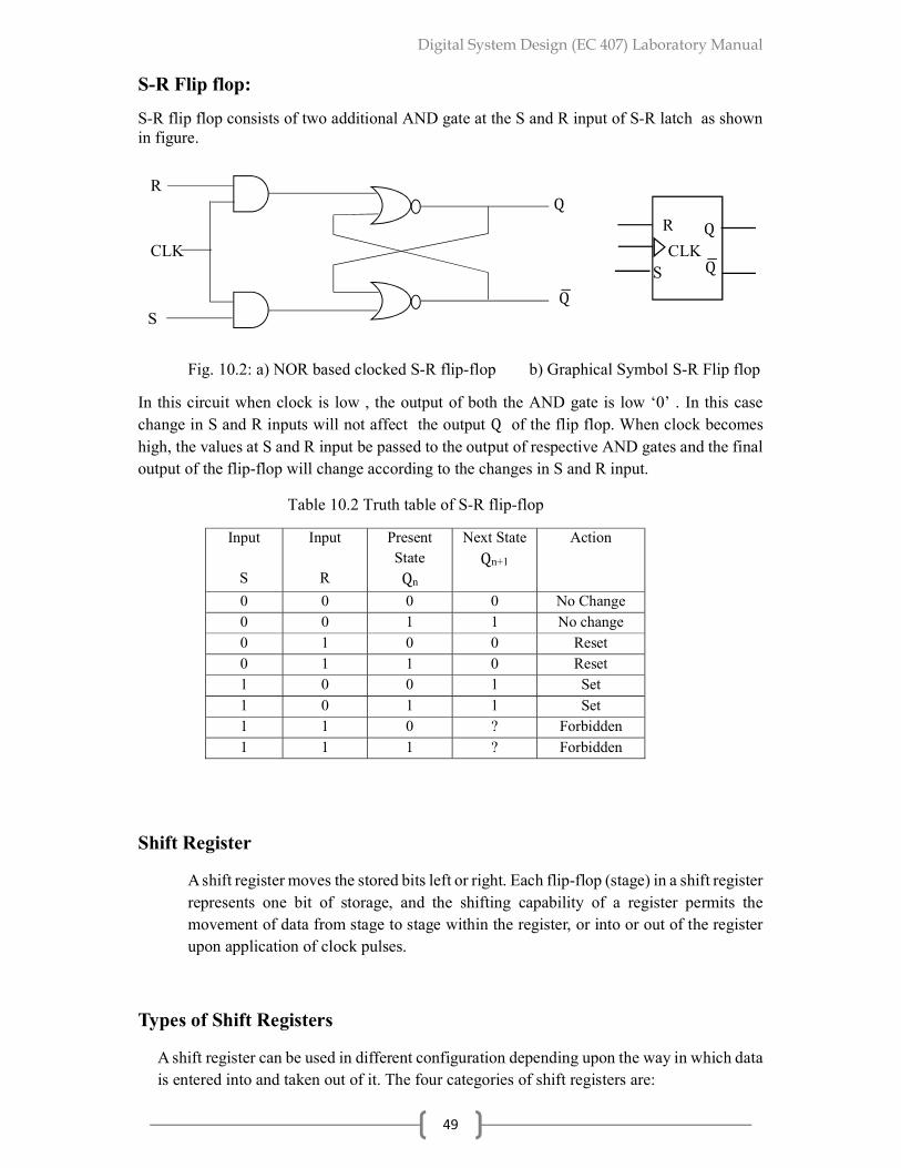
S-R Flip flop:
S-R flip flop consists of two additional AND gate at the S and R input of S-R latch as shown in figure.
Fig. 10.2: a) NOR based clocked S-R flip-flop b) Graphical Symbol S-R Flip flop
In this circuit when clock is low , the output of both the AND gate is low ‘0’ . In this case change in S and R inputs will not affect the output Q of the flip flop. When clock becomes high, the values at S and R input be passed to the output of respective AND gates and the final output of the flip-flop will change according to the changes in S and R input.
Table 10.2 Truth table of S-R flip-flop
Input
S
Input
R
Present State Qn
Next State
Qn+1
Action
0 0 0 0 No Change 0 0 1 1 No change 0 1 0 0 Reset 0 1 1 0 Reset 1 0 0 1 Set 1 0 1 1 Set 1 1 0 ? Forbidden 1 1 1 ? Forbidden
Shift Register
A shift register moves the stored bits left or right. Each flip-flop (stage) in a shift register represents one bit of storage, and the shifting capability of a register permits the movement of data from stage to stage within the register, or into or out of the register upon application of clock pulses.
Types of Shift Registers
A shift register can be used in different configuration depending upon the way in which data is entered into and taken out of it. The four categories of shift registers are:
CLK
Q
Q
R
S
R
S
Q
Q CLK

Digital System Design (EC 407) Laboratory Manual
50
1. Serial input, Serial output (SISO) 2. Parallel input, Serial output (PISO) 3. Serial input, Parallel output (SIPO) 4. Parallel input, Parallel output (PIPO)
Serial input, Serial output (SISO)
The data can be moved in and out of the register, one bit at a time. Fig. 10.3 shows that data is shifted right. Here arrow indicates serial movement of bits in right direction.
Fig. 10.3: Serial in Serial out
Circuit for shifting 3 bit data to the right and left using J-K flip-flop is shown in Fig. 10.4
Fig. 10.4 Serial in Serial out right shift register using J-K flip-flop
Procedures: 1. Open the Quartus II software and follow the steps described in Exp. No. 4 2. Perform simulation and verify your design as per the steps described in Exp. No. 4 3. Implement the design on DE2-115 board as per the steps described in Exp. No. 4
Data In Data Out
QB
Clock
J
K
Q Q
CLK J
K
Q Q
CLK Serial Input Data
Serial output Data
J
K Q
Q QA
Digital System Design (EC 407) Laboratory Manual
51
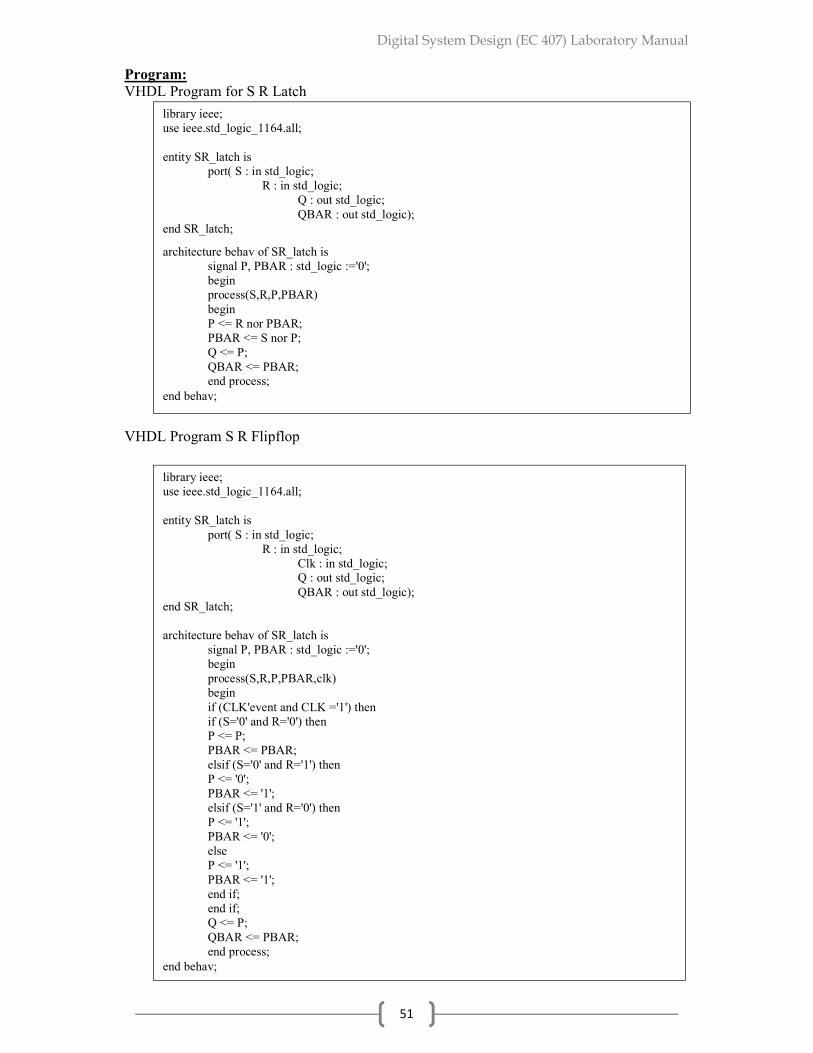
Program: VHDL Program for S R Latch
VHDL Program S R Flipflop
library ieee; use ieee.std_logic_1164.all; entity SR_latch is port( S : in std_logic; R : in std_logic; Q : out std_logic; QBAR : out std_logic); end SR_latch;
architecture behav of SR_latch is signal P, PBAR : std_logic :='0'; begin process(S,R,P,PBAR) begin P <= R nor PBAR; PBAR <= S nor P; Q <= P; QBAR <= PBAR; end process; end behav;
library ieee; use ieee.std_logic_1164.all; entity SR_latch is port( S : in std_logic; R : in std_logic; Clk : in std_logic; Q : out std_logic; QBAR : out std_logic); end SR_latch; architecture behav of SR_latch is signal P, PBAR : std_logic :='0'; begin process(S,R,P,PBAR,clk) begin if (CLK'event and CLK ='1') then if (S='0' and R='0') then P <= P; PBAR <= PBAR; elsif (S='0' and R='1') then P <= '0'; PBAR <= '1'; elsif (S='1' and R='0') then P <= '1'; PBAR <= '0'; else P <= '1'; PBAR <= '1'; end if; end if; Q <= P; QBAR <= PBAR; end process; end behav;
Digital System Design (EC 407) Laboratory Manual
52
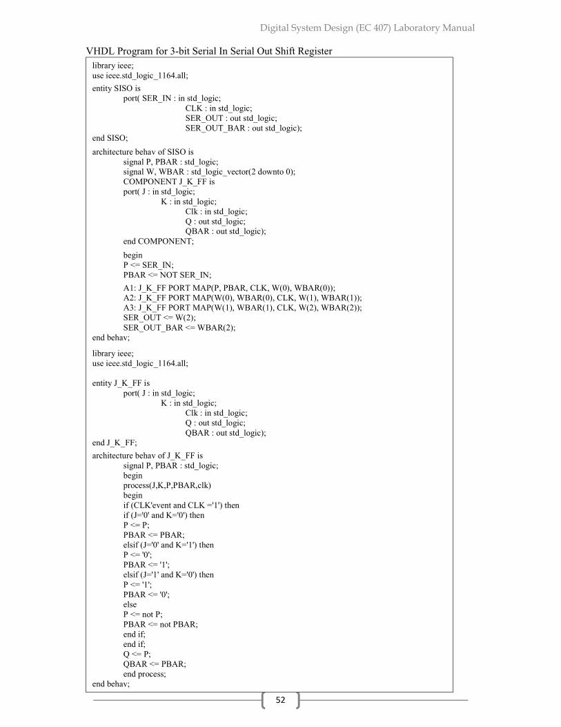
VHDL Program for 3-bit Serial In Serial Out Shift Register
library ieee; use ieee.std_logic_1164.all;
entity SISO is port( SER_IN : in std_logic; CLK : in std_logic; SER_OUT : out std_logic; SER_OUT_BAR : out std_logic); end SISO;
architecture behav of SISO is signal P, PBAR : std_logic; signal W, WBAR : std_logic_vector(2 downto 0); COMPONENT J_K_FF is port( J : in std_logic; K : in std_logic; Clk : in std_logic; Q : out std_logic; QBAR : out std_logic); end COMPONENT;
begin P <= SER_IN; PBAR <= NOT SER_IN;
A1: J_K_FF PORT MAP(P, PBAR, CLK, W(0), WBAR(0)); A2: J_K_FF PORT MAP(W(0), WBAR(0), CLK, W(1), WBAR(1)); A3: J_K_FF PORT MAP(W(1), WBAR(1), CLK, W(2), WBAR(2)); SER_OUT <= W(2); SER_OUT_BAR <= WBAR(2); end behav;
library ieee; use ieee.std_logic_1164.all; entity J_K_FF is port( J : in std_logic; K : in std_logic; Clk : in std_logic; Q : out std_logic; QBAR : out std_logic); end J_K_FF;
architecture behav of J_K_FF is signal P, PBAR : std_logic; begin process(J,K,P,PBAR,clk) begin if (CLK'event and CLK ='1') then if (J='0' and K='0') then P <= P; PBAR <= PBAR; elsif (J='0' and K='1') then P <= '0'; PBAR <= '1'; elsif (J='1' and K='0') then P <= '1'; PBAR <= '0'; else P <= not P; PBAR <= not PBAR; end if; end if; Q <= P; QBAR <= PBAR; end process; end behav;

Digital System Design (EC 407) Laboratory Manual
53
Observation:
Record your observation as per the following tables
Table 1: S R Latch
Input Output
S R Q QBAR
Table 2: S R Flip Flop
Input Output
CLK S R Q QBAR
Table 3: 3-bit SISO
Input Output
CLK SER_IN SER_OUT SER_OUT_BAR
Conclusion:
Summarize what you have learned by performing this experiment.
Questions:
1) Implement D Flipflop
2) Implement Serial In Serial Out Shift Register
3) Implement Parallel in Serial Out Shift Register.

Digital System Design (EC 407) Laboratory Manual
54
Experiment No. 11
Name of the Experiment: Design, Simulation and Implementation of Counters, State machine design using VHDL on CPLD/FPGA platform. Component/Equipment/Software Required:
Sl. No.
COMPONENT SPECIFICATION QTY.
1. Desktop PC At least i3 PC with 4GB RAM 1
2. Quartus II/Prime
Software Latest version 1
3. Model Sim Software Latest version 1
4. FPGA Board DE2-115 with Cyclone IV
FPGA 1
5. Data Cable USB Blaster cable 1
6. Power Cord Power Adapter Cable 1
Theory:
Counter:
Circuits for counting events are frequently used in computers and other digital systems. Counter is a special sequential circuit which is used to count the clock pulse. Since a counter circuit must remember its past states, it has to possess memory. Flip-flops are used to design the counter circuit. The number of flip-flops used and how they are connected determine the number of states and the sequence of the states that the counter goes through in each complete cycle. Modulus or mod of a counter is defined as the number of output states through which the counter progresses during counting. For example, a 3-bit counter can have maximum mod 8 (=23).
Counters are divided in two categories, these are:
1. Asynchronous (Ripple) Counters - the first flip-flop is clocked by the external clock pulse, and then each successive flip-flop is clocked by the Q or Q output of the previous flip-flop.
2. Synchronous (Parallel) Counters - all memory elements are simultaneously triggered by the same clock. Synchronous counters are also known as parallel counters.
Synchronous Counter is a counter in which same clock pulse is applied to all the flip-flops. Since all the flip-flops have clock simultaneously, the output of all flip-flop changes at the same time. Fig. 11.1 shows 3-bit synchronous counter.
Digital System Design (EC 407) Laboratory Manual
55
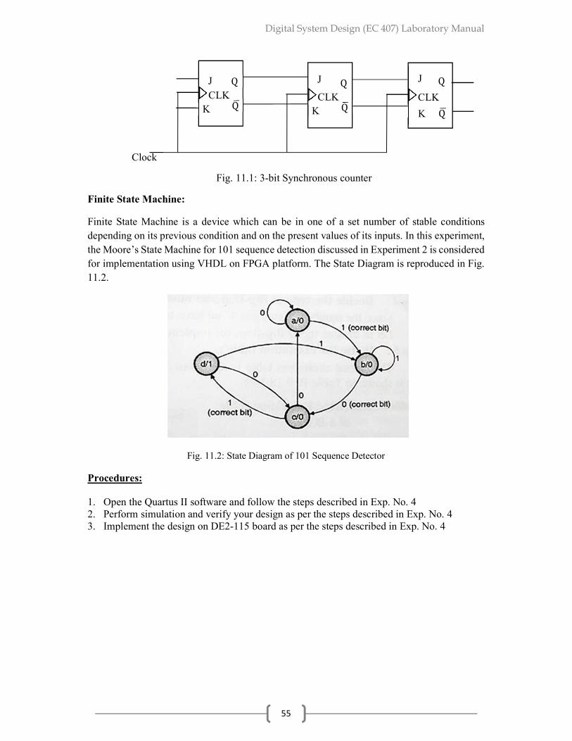
Fig. 11.1: 3-bit Synchronous counter
Finite State Machine:
Finite State Machine is a device which can be in one of a set number of stable conditions depending on its previous condition and on the present values of its inputs. In this experiment, the Moore’s State Machine for 101 sequence detection discussed in Experiment 2 is considered for implementation using VHDL on FPGA platform. The State Diagram is reproduced in Fig. 11.2.
Fig. 11.2: State Diagram of 101 Sequence Detector
Procedures: 1. Open the Quartus II software and follow the steps described in Exp. No. 4 2. Perform simulation and verify your design as per the steps described in Exp. No. 4 3. Implement the design on DE2-115 board as per the steps described in Exp. No. 4
J
K
Q
Q CLK
J
K
Q
Q CLK
CLK
Clock
J
K
Q
Q

Digital System Design (EC 407) Laboratory Manual
56
Program: VHDL Program for 3-bit Synchronous Counter
library ieee; use ieee.std_logic_1164.all; use ieee.std_logic_unsigned.all; entity COUNTER_3BIT is port( RESET : in std_logic; CLK : in std_logic; COUNT : out std_logic_vector(2 downto 0)); end COUNTER_3BIT; architecture behav of COUNTER_3BIT is signal P : std_logic_vector(2 downto 0) :="000"; begin process(RESET,CLK, P) begin if (RESET ='1') then P <="000"; elsif (CLK'event and CLK ='1') then P <= P + "001"; end if; COUNT <= P; end process; end behav;

Digital System Design (EC 407) Laboratory Manual
57
VHDL Program Sequence Detector State Machine
library ieee; use ieee.std_logic_1164.all;
entity Sequence_Detector is port (Reset : in std_logic; X : in std_logic; CLK : in std_logic; Y : out std_logic); end Sequence_Detector;
architecture Behav of Sequence_Detector is type FSM_State is (A, B, C, D); signal present_state, next_state : FSM_State; begin process(present_state, next_state, Reset, X) begin case present_state is when A => if (X = '0' or Reset ='1') then next_state <= A; Y <='0'; else next_state <= B; Y <='0'; end if; when B => if (X = '0') then next_state <= C; Y <='0'; else next_state <= B; Y <='0'; end if; when C => if (X = '0') then next_state <= A; Y <='0'; else next_state <= D; Y <='0'; end if; when others => if (X = '0') then next_state <= C; Y <='1'; else next_state <= B; Y <='1'; end if; end case; end process; process(present_state, next_state, CLK) begin if (CLK'event and CLK ='1') then present_state <= next_state; end if; end process; end Behav;

Digital System Design (EC 407) Laboratory Manual
58
Observation: Record your observation as per the following tables
Table 1: 3-bit Synchronous Counter
State of Counter Count Sequence
Q2 Q1 Q0
0
1
2
3
4
5
6
7
0
Table 2: Sequence Detector for 101
Input X Output Y
Conclusion:
Summarize what you have learned by performing this experiment.
Questions:
1) Implement 3-Bit Asynchronous counter
2) Implement 4-Bit Synchronous counter
3) Implement sequence detector for 11001.

Digital System Design (EC 407) Laboratory Manual
59
Experiment No. 12
Name of the Experiment: Design, Simulation and Implementation of RAM, ROM using VHDL on CPLD/FPGA platform.
Component/Equipment/Software Required:
Sl. No.
COMPONENT SPECIFICATION QTY.
1. Desktop PC At least i3 PC with 4GB RAM 1
2. Quartus II/Prime
Software Latest version 1
3. Model Sim Software Latest version 1
4. FPGA Board DE2-115 with Cyclone IV
FPGA 1
5. Data Cable USB Blaster cable 1
6. Power Cord Power Adapter Cable 1
Theory:
RAM
Fig. 12.1 shows a RAM of dimension 4x8-Bit. This module has 2 bits address, 8 bit data input and 8 bits data outputs. Read control signal used to retrieve the content of RAM. Similarly with the help of Write control signal data is stored in the RAM.
Fig. 12.1 Block Diagram of ROM
ROM
Fig. 12.2 shows the block diagram of a 4X8-Bit ROM. This module has 2 bits address and 8 bits data. Read is the control signal used to retrieve the content of ROM.
Fig. 12.2 Block Diagram of ROM
Data Out (8-bits)
Data In (8-bits)
Clock
Address (2-bits)
RAM (4x8-Bit)
Read Write
Clock
Address (2-bits)
ROM (4x8-Bit)
Read
Data Out (8-bits)

Digital System Design (EC 407) Laboratory Manual
60
Procedures: 1. Open the Quartus II software and follow the steps described in Exp. No. 4 2. Perform simulation and verify your design as per the steps described in Exp. No. 4 3. Implement the design on DE2-115 board as per the steps described in Exp. No. 4
Program: VHDL Program for 4X8-bit RAM
library ieee; use ieee.std_logic_1164.all; use ieee.std_logic_arith.all; use ieee.std_logic_unsigned.all; entity RAM is port(Clk : in std_logic; Read_in : in std_logic; Write_in : in std_logic; Data_in: in std_logic_vector(7 downto 0); Address : in std_logic_vector(1 downto 0); Data_out: out std_logic_vector(7 downto 0)); end RAM; architecture Behav of RAM is type RAM_type is array (0 to 3)of std_logic_vector(7 downto 0); signal tem_ram: RAM_type; begin process(Clk) begin if( Clk'event and Clk = '1' ) then if Write_in='1' then tem_ram(conv_integer(Address)) <= Data_In; Data_Out <= "ZZZZZZZZ"; elsif Read_in = '1' then Data_Out <= tem_ram(conv_integer(Address)); else Data_Out <= "ZZZZZZZZ"; end if; end if; end process; end Behav;
Digital System Design (EC 407) Laboratory Manual
61
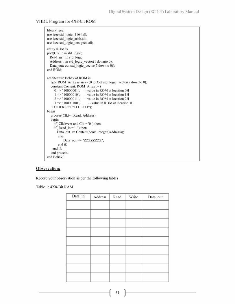
VHDL Program for 4X8-bit ROM
Observation: Record your observation as per the following tables
Table 1: 4X8-Bit RAM
Data_in Address Read Write Data_out
library ieee; use ieee.std_logic_1164.all; use ieee.std_logic_arith.all; use ieee.std_logic_unsigned.all;
entity ROM is port(Clk : in std_logic; Read_in : in std_logic; Address : in std_logic_vector(1 downto 0); Data_out: out std_logic_vector(7 downto 0)); end ROM; architecture Behav of ROM is type ROM_Array is array (0 to 3)of std_logic_vector(7 downto 0); constant Content: ROM_Array := ( 0 => "10000001", -- value in ROM at location 0H 1 => "10000010", -- value in ROM at location 1H 2 => "10000011", -- value in ROM at location 2H 3 => "10000100", -- value in ROM at location 3H OTHERS => "11111111"); begin process(Clk)--, Read, Address) begin if( Clk'event and Clk = '0' ) then if( Read_in = '1' ) then Data_out <= Content(conv_integer(Address)); else Data_out <= "ZZZZZZZZ"; end if; end if; end process; end Behav;

Digital System Design (EC 407) Laboratory Manual
62
Table 2: 4X8-Bit ROM
Address Read Data_out
Conclusion:
Summarize what you have learned by performing this experiment.
Questions:
1) Implement 256x8-Bit ROM
2) Implement 256x8-Bit RAM