Discrete Gate Sizing and Timing-Driven Detailed Placement ...
104
UNIVERSIDADE FEDERAL DO RIO GRANDE DO SUL INSTITUTO DE INFORM ´ ATICA PROGRAMA DE P ´ OS-GRADUAC ¸ ˜ AO EM MICROELETR ˆ ONICA GUILHERME AUGUSTO FLACH Discrete Gate Sizing and Timing-Driven Detailed Placement for the Design of Digital Circuits Thesis presented in partial fulfillment of the requirements for the degree of Doctor on Microelectronics Marcelo de Oliveira Johann Advisor Ricardo Augusto da Luz Reis Coadvisor Porto Alegre, December 2015
-
Upload
khangminh22 -
Category
Documents
-
view
2 -
download
0
Transcript of Discrete Gate Sizing and Timing-Driven Detailed Placement ...

UNIVERSIDADE FEDERAL DO RIO GRANDE DO SULINSTITUTO DE INFORMATICA
PROGRAMA DE POS-GRADUACAO EM MICROELETRONICA
GUILHERME AUGUSTO FLACH
Discrete Gate Sizing and Timing-DrivenDetailed Placement for the Design of Digital
Circuits
Thesis presented in partial fulfillmentof the requirements for the degree ofDoctor on Microelectronics
Marcelo de Oliveira JohannAdvisor
Ricardo Augusto da Luz ReisCoadvisor
Porto Alegre, December 2015

CIP – CATALOGING-IN-PUBLICATION
Flach, Guilherme Augusto
Discrete Gate Sizing and Timing-Driven Detailed Placementfor the Design of Digital Circuits / Guilherme Augusto Flach. –Porto Alegre: PGMICRO da UFRGS, 2015.
104 f.: il.
Thesis (Ph.D.) – Universidade Federal do Rio Grande do Sul.Programa de Pos-Graduacao em Microeletronica, Porto Alegre,BR–RS, 2015. Advisor: Marcelo de Oliveira Johann; Coadvisor:Ricardo Augusto da Luz Reis.
1. Discrete Gate Sizing. 2. Timing-Driven Detailed Place-ment. 3. Lagrangian Relaxation. 4. EDA. 5. Microelectronic.I. Johann, Marcelo de Oliveira. II. Reis, Ricardo Augusto da Luz.III. Tıtulo.
UNIVERSIDADE FEDERAL DO RIO GRANDE DO SULReitor: Prof. Carlos Alexandre NettoVice-Reitor: Prof. Rui Vicente OppermannPro-Reitor de Pos-Graduacao: Prof. Vladimir Pinheiro do NascimentoDiretor do Instituto de Informatica: Prof. Luıs da Cunha LambCoordenador do PGMICRO: Prof. Fernanda Gusmao de Lima KastensmidtBibliotecaria-chefe do Instituto de Informatica: Beatriz Regina Bastos Haro

ACKNOWLEDGMENTS
To my family...

In memoriam of Joao Felix

ABSTRACT
Electronic design automation (EDA) tools play a fundamental role in the increasinglycomplexity of digital circuit designs. They empower designers to create circuits with sev-eral order of magnitude more components than it would be possible by designing circuitsby hand as was done in the early days of microelectronics. In this work, two importantEDA problems are addressed: gate sizing and timing-driven detailed placement. Theyare studied and new techniques developed. For gate sizing, a new Lagrangian-relaxationmethodology is presented based on local timing information and sensitivity propagation.For timing-driven detailed placement, a set of cell movement methods are created usingdrive strength-aware optimal formulation to driver/sink load balancing. Our experimentalresults shows that those techniques are able to improve the current state-of-the-art.
Keywords: Discrete Gate Sizing, Timing-Driven Detailed Placement, Lagrangian Relax-ation, EDA, Microelectronic.


RESUMO
Dimensionamento de Portas Discreto e Posicionamento Detalhado Dirigido aDesempenho para o Projeto de Circuitos Digitais
Ferramentas de projeto de circuitos integrados (do ingles, electronic design automa-tion, ou simplesmente EDA) tem um papel fundamental na crescente complexidade dosprojetos de circuitos digitais. Elas permitem aos projetistas criar circuitos com um numerode componentes ordens de grandezas maior do que seria possıvel se os circuitos fossemprojetados a mao como nos dias iniciais da microeletronica. Neste trabalho, dois impor-tantes problemas em EDA serao abordados: dimensionamento de portas e posicionamentodetalhado dirigido a desempenho. Para dimensionamento de portas, uma nova metodo-logia de relaxacao Lagrangiana e apresentada baseada em informacao de temporarizacaolocais e propagacao de sensitividades. Para posicionamento detalhado dirigido a desem-penho, um conjunto de movimentos de celulas e criado usando uma formacao otima atentaa forca de alimentacao para o balanceamento de cargas. Nossos resultados experimentaismostram que tais tecnicas sao capazes de melhorar o atual estado-da-arte.
Palavras-chave: Dimensionamento de Portas Discreto, Posicionamento Detalhado Diri-gido a Desempenho, Relaxacao Lagrangiana, EDA, Microeletronica.


LIST OF ABBREVIATIONS AND ACRONYMS
ABU Average Bin Utilization
AWE Asymptotic Waveform Evaluation
CAD Computed-Aided Design
DP Dynamic Programming
EDA Electronic Design Automation
eTNS Total Negative Slack for Early Timing Mode
eWNS Worst Negative Slack for Early Timing Mode
HPWL Half-Perimeter Wirelength
ICCAD International Conference on Computer Aided Design
ISPD International Symposium in Physical Design
KKT Karush-Kuhn-Tucker
LCB Local Clock Buffer
LDP Lagrangian Dual Problem
LR Lagrangian Relaxation
LRS Lagrangian Relaxation Sub-Problem
lTNS Total Negative Slack for Late Timing Mode
lWNS Worst Negative Slack for Late Timing Mode
MOR Model Order Reduction
NP Nondeterministic Polynomial Time
PP Primal Problem
PRIMA Passive Reduced-order Interconnect Macromodeling Algorithm
QoR Quality of Results
QS Quality Score
RC Resistor (R) - Capacitor (C)
RLC Resistor (R) - Inductor (L) - Capacitor (C)
RTL Register Transfer Level

SA Simulated Annealing
SSTA Statistical Static Timing Analysis
STA Static Timing Analysis
StWL Steiner Tree Wirelength
TDDP Timing-Driven Detailed Placement
TDP Timing-Driven Placement
TNS Total Negative Slack
VLSI Very Large Scale Integration
WNS Worst Negative Slack

LIST OF SYMBOLS
f Femto
µ Micron/Mean
m Milli
n Nano
Ω Ohms
p Pico∑Summation
σ Standard deviation
Vth Threshold Voltage


LIST OF FIGURES
Figure 1.1: Design Flow of Digital Synchronous Circuits . . . . . . . . . . . . . 22Figure 1.2: Iterations over the Design Flow with Increasing Levels of Accuracy . 24
Figure 2.1: Static Timing Analysis in the Design Flow . . . . . . . . . . . . . . 25Figure 2.2: A combinational circuit and its timing graph. . . . . . . . . . . . . . 26Figure 2.3: Timing Sense . . . . . . . . . . . . . . . . . . . . . . . . . . . . . . 27Figure 2.4: D-type Register (Flip-Flop) . . . . . . . . . . . . . . . . . . . . . . 29Figure 2.5: Timing diagram for a positive edge-triggered register (flip-flop). . . . 30Figure 2.6: Lookup Table . . . . . . . . . . . . . . . . . . . . . . . . . . . . . . 30Figure 2.7: Timing characteristics of a timing arc. . . . . . . . . . . . . . . . . . 31Figure 2.8: A Simple RC Network . . . . . . . . . . . . . . . . . . . . . . . . . 32Figure 2.9: Model Order Reduction . . . . . . . . . . . . . . . . . . . . . . . . 33
Figure 3.1: Gate Sizing Problem . . . . . . . . . . . . . . . . . . . . . . . . . . 35Figure 3.2: Sources of Leakage Current . . . . . . . . . . . . . . . . . . . . . . 37
Figure 4.1: Basic algorithm to solve the Lagrangian dual problem. . . . . . . . . 46Figure 4.2: An example circuit. . . . . . . . . . . . . . . . . . . . . . . . . . . . 47
Figure 5.1: Gate Sizing in the Design Flow . . . . . . . . . . . . . . . . . . . . 50Figure 5.2: Local timing evaluation after a gate has been sized. . . . . . . . . . . 52Figure 5.3: High-level view of our gate selection flow. . . . . . . . . . . . . . . . 53Figure 5.4: Lambda-Delay Cost Computation . . . . . . . . . . . . . . . . . . . 57Figure 5.5: Delay Sensitivity Computation . . . . . . . . . . . . . . . . . . . . . 58Figure 5.6: Slack Compression . . . . . . . . . . . . . . . . . . . . . . . . . . . 68Figure 5.8: Sizes and Vth Changes . . . . . . . . . . . . . . . . . . . . . . . . . 69Figure 5.10: Runtime Breakdown . . . . . . . . . . . . . . . . . . . . . . . . . . 69
Figure 6.1: Influence of Placement on Wirelength . . . . . . . . . . . . . . . . . 73Figure 6.3: Main Steps of a Placement Stage . . . . . . . . . . . . . . . . . . . . 74
Figure 7.1: Timing-Driven Detailed Placement in the Design Flow . . . . . . . . 78Figure 7.2: Legalization via Nearest White Space Search . . . . . . . . . . . . . 80Figure 7.4: Buffer Balancing Technique aims to find a buffer position that mini-
mizes timing violation. . . . . . . . . . . . . . . . . . . . . . . . . . 81Figure 7.6: Buffer Balancing Technique Modeling . . . . . . . . . . . . . . . . . 81Figure 7.7: Cell Balancing Technique Modeling . . . . . . . . . . . . . . . . . . 82Figure 7.8: Load Reduction of critical nets. Non-critical sinks (gray cells) are
moved closer to their driver cell (D). . . . . . . . . . . . . . . . . . . 84

Figure 7.10: Useful Clock Skew Optimization by Moving Registers Closer to Lo-cal Clock Buffers. . . . . . . . . . . . . . . . . . . . . . . . . . . . 85
Figure 7.12: Iterative Spreading . . . . . . . . . . . . . . . . . . . . . . . . . . . 85Figure 7.13: Register Swap by Optimal Assignment . . . . . . . . . . . . . . . . 86Figure 7.14: Register-to-Register Early Violation Path Fix . . . . . . . . . . . . . 87Figure 7.15: Timing-Driven Detailed Placement Flow . . . . . . . . . . . . . . . 88Figure 7.16: Estimating the Driver Resistance of a Timing Arc (Cell) . . . . . . . 90Figure 7.17: Reference Slew Computation . . . . . . . . . . . . . . . . . . . . . 91

LIST OF TABLES
Table 2.1: Information provided by a STA tool for pins. . . . . . . . . . . . . . 28
Table 3.1: Sizing Classification . . . . . . . . . . . . . . . . . . . . . . . . . . 36Table 3.2: Summary of Works on Continuous Gate Sizing . . . . . . . . . . . . 42Table 3.3: Summary of Works on Discrete Gate Sizing . . . . . . . . . . . . . . 43
Table 5.1: Definitions of some terms used in this work. . . . . . . . . . . . . . . 52Table 5.2: Leakage power (W ) and runtime (min) results on ISPD 2012 bench-
marks suite. Hu (HU et al., 2012) and Li (LI et al., 2012) runtimesare taken from the corresponding papers. . . . . . . . . . . . . . . . 65
Table 5.3: Results of this flow when the slack filtering is disabled. . . . . . . . . 66Table 5.4: Results of this flow when lambda-delay sensitivity is disabled. . . . . 67Table 5.5: Leakage power improvement using lambda-delay sensitivity on final
results. . . . . . . . . . . . . . . . . . . . . . . . . . . . . . . . . . 67Table 5.6: Leakage power (W ), runtime (min) and clock period (ps) on ISPD
2013 benchmarks comparing the contest results and our new resultsusing accurate timing information in TR and PR algorithms. . . . . . 70
Table 7.1: Moves Developed in this Thesis . . . . . . . . . . . . . . . . . . . . 79Table 7.2: Configuration of the ICCAD 2015 Contest benchmarks. . . . . . . . 89Table 7.3: Comparison between the actual delay and the delay estimated via
driver resistance. . . . . . . . . . . . . . . . . . . . . . . . . . . . . 91Table 7.4: Improvement of this flow over the initial placement results for long
maximum displacement. . . . . . . . . . . . . . . . . . . . . . . . . 92Table 7.5: Improvement of this flow over the initial placement results for short
maximum displacement. . . . . . . . . . . . . . . . . . . . . . . . . 92Table 7.6: Comparison of this flow and results from the 1st place at ICCAD
2015 contest for long maximum displacement. . . . . . . . . . . . . 93Table 7.7: Comparison of this flow and results from the 1st place at ICCAD
2015 contest for short maximum displacement. . . . . . . . . . . . . 93Table 7.8: Average improvement on quality score per move type for long maxi-
mum displacement. . . . . . . . . . . . . . . . . . . . . . . . . . . . 94Table 7.9: Impact on results when pin importance (criticality and centrality) is
used in Cell Balancing. . . . . . . . . . . . . . . . . . . . . . . . . . 95Table 7.10: Impact on results when bad move filtering is disabled. . . . . . . . . 95


CONTENTS
1 INTRODUCTION . . . . . . . . . . . . . . . . . . . . . . . . . . . . . . 211.1 Design Flow of Digital Synchronous Circuits . . . . . . . . . . . . . . . . 221.1.1 Logic and Physical Synthesis Merging . . . . . . . . . . . . . . . . . . . 231.1.2 Design Flow Iterations . . . . . . . . . . . . . . . . . . . . . . . . . . . 231.2 Contributions and Scope of This Thesis . . . . . . . . . . . . . . . . . . 24
2 STATIC TIMING ANALYSIS (STA) . . . . . . . . . . . . . . . . . . . . . 252.1 Timing Graph . . . . . . . . . . . . . . . . . . . . . . . . . . . . . . . . . 262.2 Timing Mode . . . . . . . . . . . . . . . . . . . . . . . . . . . . . . . . . 262.2.1 Late (Max) . . . . . . . . . . . . . . . . . . . . . . . . . . . . . . . . . . 262.2.2 Early (Min) . . . . . . . . . . . . . . . . . . . . . . . . . . . . . . . . . 272.3 Timing Sense . . . . . . . . . . . . . . . . . . . . . . . . . . . . . . . . . 272.4 Timing Information . . . . . . . . . . . . . . . . . . . . . . . . . . . . . 272.5 Timing Propagation . . . . . . . . . . . . . . . . . . . . . . . . . . . . . 282.5.1 False Paths . . . . . . . . . . . . . . . . . . . . . . . . . . . . . . . . . . 292.6 Timing Tests . . . . . . . . . . . . . . . . . . . . . . . . . . . . . . . . . 292.7 Timing Models . . . . . . . . . . . . . . . . . . . . . . . . . . . . . . . . 302.7.1 Cells . . . . . . . . . . . . . . . . . . . . . . . . . . . . . . . . . . . . . 302.7.2 Interconnections . . . . . . . . . . . . . . . . . . . . . . . . . . . . . . . 31
3 GATE SIZING . . . . . . . . . . . . . . . . . . . . . . . . . . . . . . . . 353.1 Sizing Problem Classification . . . . . . . . . . . . . . . . . . . . . . . . 353.2 Sizing Formulation . . . . . . . . . . . . . . . . . . . . . . . . . . . . . . 363.3 Gate Sizing for Leakage Power Minimization . . . . . . . . . . . . . . . 363.4 Challenges . . . . . . . . . . . . . . . . . . . . . . . . . . . . . . . . . . . 383.5 Related Work . . . . . . . . . . . . . . . . . . . . . . . . . . . . . . . . . 383.5.1 Early Work . . . . . . . . . . . . . . . . . . . . . . . . . . . . . . . . . 393.5.2 State-of-the-Art . . . . . . . . . . . . . . . . . . . . . . . . . . . . . . . 413.5.3 Summary . . . . . . . . . . . . . . . . . . . . . . . . . . . . . . . . . . 42
4 GATE SIZING VIA LAGRANGIAN RELAXATION . . . . . . . . . . . . 454.1 Lagrangian Relaxation . . . . . . . . . . . . . . . . . . . . . . . . . . . . 454.1.1 Solving the Lagrangian Dual Problem . . . . . . . . . . . . . . . . . . . 464.2 Applying Lagrangian Relaxation in the Gate Sizing Problem . . . . . . 474.2.1 Lagrangian Relaxation . . . . . . . . . . . . . . . . . . . . . . . . . . . 484.2.2 Simplification of LRSλ . . . . . . . . . . . . . . . . . . . . . . . . . . . 48

5 NEW DISCRETE GATE SIZING AND VTH ASSIGNMENT FLOW US-ING LAGRANGIAN RELAXATION . . . . . . . . . . . . . . . . . . . . 49
5.1 Contributions . . . . . . . . . . . . . . . . . . . . . . . . . . . . . . . . . 495.2 Scope . . . . . . . . . . . . . . . . . . . . . . . . . . . . . . . . . . . . . 495.3 Background . . . . . . . . . . . . . . . . . . . . . . . . . . . . . . . . . . 505.4 Performance Optimization . . . . . . . . . . . . . . . . . . . . . . . . . . 515.5 Definitions . . . . . . . . . . . . . . . . . . . . . . . . . . . . . . . . . . . 525.6 Flow Overview . . . . . . . . . . . . . . . . . . . . . . . . . . . . . . . . 535.7 Lagrangian Relaxation . . . . . . . . . . . . . . . . . . . . . . . . . . . . 535.8 Solving LDP . . . . . . . . . . . . . . . . . . . . . . . . . . . . . . . . . . 555.9 Solving LRS/λ . . . . . . . . . . . . . . . . . . . . . . . . . . . . . . . . 565.9.1 Local Timing Update . . . . . . . . . . . . . . . . . . . . . . . . . . . . 565.9.2 Lambda-Delay Cost . . . . . . . . . . . . . . . . . . . . . . . . . . . . . 575.9.3 Lambda-Delay Sensitivity . . . . . . . . . . . . . . . . . . . . . . . . . . 585.9.4 Gate Version Selection . . . . . . . . . . . . . . . . . . . . . . . . . . . 605.9.5 Modeling Interconnections . . . . . . . . . . . . . . . . . . . . . . . . . 615.10 Improving the Lagrangian Relaxation Solution . . . . . . . . . . . . . . 625.10.1 Timing Recovery . . . . . . . . . . . . . . . . . . . . . . . . . . . . . . 625.10.2 Power Reduction . . . . . . . . . . . . . . . . . . . . . . . . . . . . . . 625.11 Experimental Setup . . . . . . . . . . . . . . . . . . . . . . . . . . . . . 645.11.1 Assumptions and Limitations . . . . . . . . . . . . . . . . . . . . . . . . 645.12 Results on ISPD 2012 Contest Benchmarks . . . . . . . . . . . . . . . . 645.12.1 Impact of Slack Filtering . . . . . . . . . . . . . . . . . . . . . . . . . . 655.12.2 Impact of Lambda-Delay Sensitivity . . . . . . . . . . . . . . . . . . . . 665.12.3 Slack Histogram and Slack Compression . . . . . . . . . . . . . . . . . . 665.12.4 Size and Vth Changes in Each Iteration . . . . . . . . . . . . . . . . . . . 665.12.5 Runtime Breakdown . . . . . . . . . . . . . . . . . . . . . . . . . . . . . 685.13 Results on ISPD 2013 Contest Benchmarks . . . . . . . . . . . . . . . . 695.14 Conclusions . . . . . . . . . . . . . . . . . . . . . . . . . . . . . . . . . . 70
6 PLACEMENT . . . . . . . . . . . . . . . . . . . . . . . . . . . . . . . . 736.1 Timing-Driven Detailed Placement . . . . . . . . . . . . . . . . . . . . . 746.2 Related Works . . . . . . . . . . . . . . . . . . . . . . . . . . . . . . . . 75
7 DRIVE STRENGTH AWARE CELL DISPLACEMENT FOR TIMING-DRIVEN DETAILED PLACEMENT . . . . . . . . . . . . . . . . . . . . 77
7.1 Contributions . . . . . . . . . . . . . . . . . . . . . . . . . . . . . . . . . 777.2 Scope . . . . . . . . . . . . . . . . . . . . . . . . . . . . . . . . . . . . . 777.3 Criticality and Centrality . . . . . . . . . . . . . . . . . . . . . . . . . . 787.4 Moves . . . . . . . . . . . . . . . . . . . . . . . . . . . . . . . . . . . . . 797.4.1 Legalization . . . . . . . . . . . . . . . . . . . . . . . . . . . . . . . . . 797.4.2 Filtering out Bad Moves . . . . . . . . . . . . . . . . . . . . . . . . . . . 797.5 Late Optimization . . . . . . . . . . . . . . . . . . . . . . . . . . . . . . 807.5.1 Buffer Balancing . . . . . . . . . . . . . . . . . . . . . . . . . . . . . . 807.5.2 Cell Balancing . . . . . . . . . . . . . . . . . . . . . . . . . . . . . . . . 827.5.3 Load Optimization . . . . . . . . . . . . . . . . . . . . . . . . . . . . . 837.6 Early Optimization . . . . . . . . . . . . . . . . . . . . . . . . . . . . . . 847.6.1 Skew Optimization . . . . . . . . . . . . . . . . . . . . . . . . . . . . . 84

7.6.2 Iterative Spreading . . . . . . . . . . . . . . . . . . . . . . . . . . . . . 857.6.3 Register Swap . . . . . . . . . . . . . . . . . . . . . . . . . . . . . . . . 857.6.4 Register-to-Register Path Fix . . . . . . . . . . . . . . . . . . . . . . . . 867.7 Flow . . . . . . . . . . . . . . . . . . . . . . . . . . . . . . . . . . . . . . 877.8 Experimental Setup . . . . . . . . . . . . . . . . . . . . . . . . . . . . . 887.8.1 Quality Score . . . . . . . . . . . . . . . . . . . . . . . . . . . . . . . . 897.8.2 Benchmarks . . . . . . . . . . . . . . . . . . . . . . . . . . . . . . . . . 897.8.3 Assumptions and Limitations . . . . . . . . . . . . . . . . . . . . . . . . 897.9 Library Characterization . . . . . . . . . . . . . . . . . . . . . . . . . . 907.9.1 Move Gains . . . . . . . . . . . . . . . . . . . . . . . . . . . . . . . . . 937.9.2 Impact of Pin Importance (Criticality and Centrality) . . . . . . . . . . . 947.9.3 Impact of Filtering Out Bad Moves . . . . . . . . . . . . . . . . . . . . . 947.10 Conclusions . . . . . . . . . . . . . . . . . . . . . . . . . . . . . . . . . . 95
8 FINAL REMARKS . . . . . . . . . . . . . . . . . . . . . . . . . . . . . . 97
REFERENCES . . . . . . . . . . . . . . . . . . . . . . . . . . . . . . . . . . 99


21
1 INTRODUCTION
During the 1950-70’s, humanity has experienced a shift from analog and mechanicalcomponents to digital in the mainstream technology. This change marks the beginningof the Digital Revolution, which, as the Agriculture and Industrial counterparts, broughtseveral improvements in the well-being of the mankind.
The digital technology allows much faster, reliable and cheap computation and com-munication. Digital signals are more tolerant to noise. Data can be sent through longdistances and even tolerate errors by sophisticated error-correcting methods. Moreoverby using only two discrete values to represent information, the systems are simplifiedmaking them easier to design, test and produce compared to an analog circuit with aboutthe same number of components.
Two technological breakthroughs can be pointed out as the main milestones in theDigital Revolution: the invention of transistor and the very-large scale integration (VLSI).
The transistor was invented in 1947 by American physicists John Bardeen, WalterBrattain, and William Shockley. It is a semiconductor device that can be used as a switchenabling fast, non-mechanical computation. It is the basic building-block of modern cir-cuits.
But was not until the late 60’s and early 70’s that the real impact of transistors tookplace as new technologies enabled several transistors and other components to be built outof the same block. From that point on, the number of components integrated into a samechip has been doubled approximately every two years, following Moore’s observationfrom 1975 referred to as Moore’s Law (MOORE, 1975).
As the number of components grew, the complexity of designing an integrated circuitalso increased. First designs were literally designed by hand, but this soon became a bot-tleneck and the first software to aided the circuit design were created in mid-1970’s. Inearly 1980’s, the idea of using programming languages and compiling them to hardwarestarted to consolidate (MEAD; CONWAY, 1979). This notion further pushed the devel-opment of computer-aided design (CAD) software for chip design, currently known asElectronic Design Automation (EDA) software. Today all digital circuit designs are doneusing EDA tools from the translation of high-level hardware description languages to theoutput file format used to fabricated them.
Several steps are required to design an integrated circuit, each step being composed byone or more EDA tools which are run in a sequential or iterative way. Other tools are alsoused to measure the circuit performance, power consumption among other characteristics.These steps and measurement tools compose the design flow of digital circuits.
In this work, new observations and techniques for gate sizing and timing-driven de-tailed placement steps of the design flow are presented. These techniques are implementedas stand-alone EDA tools and the results obtained are reported and analysed.

22
1.1 Design Flow of Digital Synchronous Circuits
The design flow is a set of steps performed to convert a design specification to a low-level description which is not just ready to be fabricated, but is optimized and meet therequirements from the specification.
A typical design flow for digital synchronous circuits using the standard cell method-ology is presented in Figure 1.1. Standard cell methodology, which is the dominant de-sign methodology, translates a design description to a description where pre-characterizedcomponents or cells from a library are used. Other methodologies do exists as full-customand library-free automatic generation, but they are out of scope of this work.
Figure 1.1: Design Flow of Digital Synchronous Circuits
Specs
HDL High-Level Synthesis
Logic Synthesis
Physical Synthesis
Optimizations
Technology IndependentOptimization
Mapping
Technology DependentOptimization
Floorplanning
Placement
Routing
Library
Analysis Tools
Timing
Power
Verification
…
Early Stage
sLate
Stages
Logi
cal O
ptim
izat
ion
Physical O
ptim
ization
GDSII
RTL
Mapped Design
Ready for Fabrication
Source: from author (2015)
It should be noted that the flow presented in Figure 1.1 is only a reference flow, theactual flow used by designers may vary, although the overall idea is the same.
The design flow is divided into three main phases – (1) high-level synthesis, (2) logicsynthesis and (3) physical synthesis – responsible to bring the design state gradually moreclosely to the optimized and low-level state required for fabrication.
In the high-level synthesis phase, the circuit specification is translated into a register-transfer level (RTL) abstraction. RLT represents the circuit as data and control signalsflowing through logical operations between storage elements (referred to as registers).This representation is closely related to the final design implementation in the sense thatit uses the two basic components of circuit designs: storage and logic elements.
Logic synthesis takes the RTL representation, optimizes it and create an implementabledesign representation by mapping the storage and logic elements to a library of standardelements previously built for the target technology. After mapping, more optimizationsare performed. Among the techniques used during logic synthesis are logic minimization,sizing, restructuring, retiming, buffering.
Finally, during the physical synthesis a floorplanning for the optimized and mappedcircuit is defined. After that, elements are placed and the interconnections between them

23
are generated.In general, each phase is broken down into steps, which may be further subdivided.
A step is composed by a core method responsible to achieve the specific goal of that stepcombined with calls to other more general optimization procedures.
Several optimization methods are available and used throughout the flow as structur-ing, re-time, gate sizing, buffer insertion, placement optimization, routing optimization.These methods can be called several times during the design flow and a typical flow mayhave several different implementation of each kind of optimization method applying dif-ferent strategies.
Measurement tools as timing analysis, power analysis, verification among others sup-port the steps and optimization techniques providing up-to-date information about thecurrent state of the design. Many methods use built-in analysis tools, though usuallythese built-in tools use more simplified models to trade-off accuracy and runtime.
1.1.1 Logic and Physical Synthesis Merging
In early days, logic synthesis and physical synthesis were two completely separatedphases. However this wall between them – as some authors referred it to – started tobe teared down due to the increase of interconnection importance to define the circuitcharacteristics in newer technologies.
This merge happened in both ways. Logic synthesis methods start to use more ac-curate interconnection and physical information and physical synthesis methods start tocall optimization methods that were only called during logic synthesis before. So, besidethe iterations, the flow itself is now designed in such a way to allow this kind of iterationbetween logic and physical synthesis.
1.1.2 Design Flow Iterations
The design of an integrated circuit usually takes several iterations over the design flowto be finished. An iteration happens any time the flow is restarted in an early stage to usemore precise or detailed data obtained in a later stage. This processes and the increase ofmodeling accuracy is depicted in Figure 1.2.

24
Figure 1.2: Iterations over the Design Flow with Increasing Levels of Accuracy
Accu
racy
Accu
racy
Accu
racy
Design Flow Iteration
High-Level Synthesis
Logic Synthesis
Physical Synthesis
Technology IndependentOptimization
Mapping
Technology DependentOptimization
Floorplanning
Placement
Routing
Library
RTL
Mapped Design
Specs
HDL
GDSII
Ready for Fabrication
Source: from author (2015)
1.2 Contributions and Scope of This Thesis
In this work the gate sizing and placement optimization method are studied and newtechniques are developed. They are developed intended to be used in early stages of thedesign flow, although they can be extended to work on more sophisticated models suitablefor late stages. Both method have an important impact on the timing closure of the design,playing a direct role to meet the timing requirements.

25
2 STATIC TIMING ANALYSIS (STA)
Static timing analysis (STA) is a fast method for asserting and verifying the timing ofa circuit independently of the stimulus applied to it. The analysis is called static as thetiming characteristics of elements are usually computed assuming that other signals arenot changing. STA computes the upper and lower bounds of the amount of time signalstake to propagate inside the circuit through its several elements and interconnections.These bounds are then used to guarantee that the circuit will work properly in the specifiedfrequency.
STA is generally available as a sign-off tool in the design flow as shows Figure 2.1,although some methods may implement their own simplified, built-in static timing anal-ysis for performance reasons. It is executed several times during the design flow usingdifferent levels of accuracy depending on the physical information available or the accu-racy required. It is not uncommon to perform a STA using simplified timing models evenif detailed timing information is already available to trade-off accuracy and runtime.
Figure 2.1: Static Timing Analysis in the Design Flow
Specs
HDL High-Level Synthesis
Logic Synthesis
Physical Synthesis
Optimizations
Technology IndependentOptimization
Mapping
Technology DependentOptimization
Floorplanning
Placement
Routing
Library
Analysis Tools
Timing
Power
Verification
…
Early Stage
sLate
Stages
Logi
cal O
ptim
izat
ion
Physical O
ptim
ization
GDSII
RTL
Mapped Design
Ready for Fabrication
Source: from author (2015)

26
2.1 Timing Graph
For the purpose of static timing analysis, a digital circuit is composed by combina-tional and sequential cells whose pins are connected via interconnections allowing signalsto propagate.
A static timing analysis is performed on a directed graph where nodes represent thecell pins and edges represent the path connecting such pins. A design and its respectivegraph model is exemplified in Figure 2.2.
Figure 2.2: A combinational circuit and its timing graph.
CK
D Q
CK
D Q …
…
…
…
Source: from author (2015)
Edges are also more commonly referred to as timing arcs and they are classified intwo categories depending on the element that the edge describes. If an edge connects twopins of a same cell, it is called a cell timing arc. On the other hand, if an edge connectstwo pins of different cells it is called a net timing arc.
2.2 Timing Mode
A static timing analysis is performed typically in two modes: late and early. Thesetwo modes compute the upper and lower propagation delay bounds representing the worstand best case scenarios respectively. Some other methods as Statistical Static TimingAnalysis (SSTA) (GULATI; KHATRI, 2009) may be used to compute the circuit delayusing variability ranges, but they are out of the scope of this work.
In general, different characterizations for cells and interconnections are used for eachtiming mode. For early mode, the interconnections and cells are supposed to work ontheir best case scenario, i.e, as fast as possible. On the other hand, for late mode, theinterconnections and elements are expected to work on their worst case scenario, i.e. asslow as possible.
2.2.1 Late (Max)
The late mode computes the worst case scenario returning the maximum time signalstake to propagate through the timing graph.
The late mode is used to verify the maximum frequency the circuit can operate – acentral goal in circuit design. That is why it is the most common mode and many timesduring the flow it is the only mode being asserted.

27
2.2.2 Early (Min)
The early mode compute the best case scenario returning the minimum time signalstake to propagate through the timing graph. This information is useful to eliminate somekind of timing violations caused when a pin changes its state before the storage elementhas time to store the value.
2.3 Timing Sense
Cell timing arcs have a timing sense, which indicates the direction of an output transi-tion w.r.t. the direction of the input transition assuming that the other inputs are constant.The direction of a transition can be either rising or falling. The timing senses are depictedin Figure 2.3.
Figure 2.3: Timing Sense
or
positive unate
negative unate
non-unate
Source: from author (2015)
A timing arc is positive unate if the direction of the signal is kept when propagatingthrough the arc. Timing arcs of non-inverting buffers, ORs, ANDs are positive unate.
A timing arc is negative unate if the direction of the signal is inverted when propagat-ing through the arc. Timing arcs of inverters, NORs, NANDs are negative unate.
The arc is called non-unate when it may be inverting or non-inverting depending onthe values of other inputs. Timing arcs of XOR, XNOR are non-unate. By definition,the timing arcs from clock to the data output of sequential elements are also marked asnon-unate as the signal does not actually propagates through them, but depends on thedata stored.
2.4 Timing Information
Typically a STA tool provides several information about pins and timing arcs thatdesigners and tools can made use of to identify violations and room for improvements.For timing arcs, the delay and slew are provided. Table 2.1 summarizes the typical dataprovided for pins.
By definition, the late and early slack at pin P are defined as in Equation (2.1) andEquation (2.2).

28
Table 2.1: Information provided by a STA tool for pins.
Data Symbol Descriptionarrival time atP The maximum (late mode) or minimum (early mode) time
a signal takes to reach the pin P .required time ratP The time a signal is required to reach pin P to avoid timing
violation.slack slackP Indicates the amount of time the signal reaching pin P can
be delayed (late mode) or sped up (early mode) withoutcausing violation. Negative values indicate the amount oftime required to fix the violation.
slew slewP Indicate the slew at pin P .
slackearlyP = atP − ratP (2.1)
slacklateP = ratP − atP (2.2)
2.5 Timing Propagation
The models used to define the timing characteristics of elements and hence the timingcharacteristics of timing arcs may vary, but the overall idea of timing propagation in STAis the same.
Starting from primary inputs, the delay is propagated through timing arcs by summingthe arrival time at the input pin of the timing arc with the timing arc delay. When multipletiming arcs converge to a same pin, the maximum delay for late mode or the minimum de-lay for early mode is propagated. Similarly, the largest slew for late mode or the smallestslew for early mode are propagated to a pin when multiple timing arcs converge. The ba-sic arrival time propagation method for static timing analysis for late mode can be writtenas in Algorithm 2.1.
Algorithm 2.1: Arrival Time Propagation1 set arrival time of path startpoints2 for each pin j in topological order do3 atj ← −∞4 for each timing arc i→ j do5 atj ← maxatj, ati + delayi→j
Then, from endpoints to startpoint, require times are propagated by subtracting thetiming arcs delays. Wherever two or more timing arcs converge to a same pin, the maxi-mum required time is propagated for early mode and the minimum required time is propa-gate for late mode. The basic required time propagation method for static timing analysisfor late mode can be written as in Algorithm 2.2.

29
Algorithm 2.2: Required Time Propagation1 set required time of path endpoints2 for each pin i in reverse topological order do3 ati ← +∞4 for each timing arc i→ j do5 rati ← minratj, rati − delayi→j
2.5.1 False Paths
Some paths represented in the timing graph may never be stimulated in the actualdesign. This may be caused due to logical contradictions or simply because the designdoes not use them. Such paths are called false paths. Usually STA tools allow designers todefine such paths by disabling some timing arcs so that signal does not propagate throughthem.
2.6 Timing Tests
Once the arrival times have been propagated through the timing graph, the slack atendpoints are verified. A timing violation occurs whenever the slack at an endpoint isnegative. For late mode, a timing violation occurs when the arrival time at an endpoint islarger than the required time at that same endpoint. Analogously, for early mode, a timingtest fails when the arrival time is smaller than the required time.
For the discussion in this work, a D-type register (flip-flop) as shown in Figure 2.4 isassumed where D is the input pin, CK is the clock pin and Q is the output pin. Othertypes of flip-flops can be handled in a similar way.
Figure 2.4: D-type Register (Flip-Flop)
CK
D Q
dCK->Q
Setup
Hold
Source: from author (2015)
In order to retain the data correctly, the data signal at D must be stable before andafter the clock signal reaches the storage element via CK pin as illustrated in Figure 2.5.The time required before is defined as the setup time (tsetup) and the time required after isdefined as the hold time (thold).
When the clock signal is received, the data stored by the register is not immediatelyavailable at its output pin. The time required to the data to be available after the clocksignal arrives is defined as dCK→Q (usually read as “clock to Q”). The CK → Q timingarc is modeled in the same way as the a non-unate combinational timing arc.
For sequential elements, in the late mode, the required time is defined as a specifiedclock period, T plus the clock signal latency to reach the sequential cell, learlyo , less thesetup time as in Equation (2.3).

30
Figure 2.5: Timing diagram for a positive edge-triggered register (flip-flop).
setup hold
clock
signal
D
Q
data stable
data stable
dCK->Q
Source: from author (2015)
ratsetupD = ratlateD = T + learlyo − tsetup (2.3)
In the early mode, the required time is defined as the clock latency, llateo , plus the holdtime as in Equation (2.4).
ratholdD = ratearlyD = llateo + thold (2.4)
2.7 Timing Models
STA can be used with several different timing models for cells and interconnections.In this section, some of the most common models are presented.
2.7.1 Cells
Cell delays can be modeled as simple as a constant value, linear equations or non-linear equations usually described by look-up tables. Look-up tables are the standardindustry model for synthesis. Basically it is a two-dimensional table containing severalsamples of a timing characteristic of a cell (i.e. delay, output slew). The data is generatedby accurate electrical simulation. The table is addressed by a load (capacitance) and aninput slew as shown in Figure 2.6.
Figure 2.6: Lookup Table
Load 1 Load 2 ... Load n
Slew 1
Slew 2
...
Slew m
Increasing
Source: from author (2015)

31
The timing characteristic of a timing arc are represented in Figure 2.7. Delay is mea-sured from the time the input signal reaches 50% of the logical-one voltage value to thetime the output signal reaches 50%. Slew is typically measured as the amount of timerequired for a signal to go from 10% to 90% (or 20% to 80%) and vice versa.
Figure 2.7: Timing characteristics of a timing arc.
Vmax
Vmin
Voltage
Time
50%
delay
slew
90%
10%
input outputinput output
Source: from author (2015)
2.7.2 Interconnections
The interconnection simulation for sophisticated models is the most timing consum-ing part of a STA. Several models may be used depending on the accuracy required orthe information available. Sophisticated models can handle several aspects of intercon-nections including crosstalk, noise and can fairly estimate the values from a full electricalsimulation.
2.7.2.1 Lumped
The lumped model is not actually a delay model as it represents the interconnectionby a single capacitance. This capacitance is summed to the load a cell is driving. Inspite of its simplicity and inaccuracy, it is used as a fast estimate of the delay due tointerconnection mainly in early stages of the design flow.
2.7.2.2 Elmore Delay
Electrical simulation is very timing consuming. Generally the timing information isrequired to be updated several times in the design flow, and therefore, for highly-iterativemethods, electrical simulation may be prohibitive.
The Elmore delay model (ELMORE, 1948) can be used as a fast, upper bound ap-proximation of the actual delay of an RC network.
For trees-like networks (acyclic networks), the Elmore delay,D(Pj), at a pin Pj can becomputed recursively as shown in Equation (2.5) where Ri→j is the resistance connectingPi to Pj and Cdown is the sum of all capacitances from Pi down to the tree leaves.
D(Pj) = D(Pi) +Ri→jCdown (2.5)
For mesh-like networks (cyclic networks), it can be computed throughout a nodalanalysis replacing capacitances by current sources of same magnitude and removing allvoltage sources (MUSTAFA CELIK LARRY PILEGGI, 2002). The node voltage is theElmore delay of the respective node.

32
Therefore we can find the Elmore delay for each RC network node, ~τ , by solving thelinear system presented in Equation (2.6) where G is the conductance matrix of the RCnetwork and ~c is the capacitance associated with each network node.
G~τ = ~c (2.6)
Since the Elmore delay is related to the RC value of nodes, we can write the Equation(2.6) in a more straightforward fashion. The inverse of G is the resistance matrix, R, sowe can write Equation (2.6) as in Equation (2.7).
G~τ = ~c→ ~τ = G−1~c→ ~τ = R~c (2.7)
For an RC network with n nodes, the conductance matrix G is an n × n symmetricmatrix, which is built as follow. Let rij be the resistance connecting node i to node j andri the resistance connecting node i to ground (drive resistance) so the conductance matrix,G = [gij], is defined by Equation (2.8).
gij =
− 1rij
i 6= j1ri
+∑n
k=1,k 6=i1rik
i = j(2.8)
Now we present a simple example on how to build the Elmore system for the RCnetwork shown in Figure 2.8. The corresponding linear system is shown in Equation(2.9).
Figure 2.8: A Simple RC Network
n0
n1 n2
Source: from author (2015)
1R0
+ 1R01
+ 1R02
− 1R01
− 1R02
− 1R01
1R1
+ 1R01
+ 1R12
− 1R12
− 1R02
− 1R12
1R2
+ 1R02
+ 1R12
τ0τ1τ2
=
c0c1c2
(2.9)
Since matrix G is sparse and positive semi-definite (BHATIA, 2006) we can use theIncomplete Cholesky Conjugate Gradient method (SHEWCHUK, 1994) to solve the lin-ear system in Equation (2.6).

33
2.7.2.3 Model Order Reduction (MOR)
Model order reduction works by creating a simplified (or reduced) model of the in-terconnection as exemplified in Figure 2.9. This reduced model is then simulated usingelectrical simulation.
Figure 2.9: Model Order ReductionDriver
Model
Reduced
Interconnection
Model
Sink
Model
Sink
Model
Sink
Model
response to input transition computed
Source: from author (2015)
MOR techniques can be classified into two types: (1) moment matching-based MORtechniques and (2) node elimination-based MOR techniques (KIM; KIM, 2009).
MOR techniques based on moment matching reduce an interconnection into a smallmodel by matching some of the interconnection moments. Some moment matching-basedMOR techniques are Asymptotic Waveform Evaluation (AWE) (PILLAGE; HUANG;ROHRER, 1989), Passive Reduced-order Interconnect Macromodeling Algorithm (PRIMA)(ODABASIOGLU; CELIK; PILEGGI, 1998), Pade via Lanczos (FELDMANN; FRE-UND, 1995). As the important moments are preserved, these techniques usually presenta good accuracy. However the macro-model does not represent directly a linear RLCinterconnection, which may be an issue for some applications.
Node elimination-based MOR techniques reduce an interconnection directly by re-moving less important nodes. The reduced model represent a linear RC interconnection.Although they are less accurate when compared with the moment matching techniques,these methods are more efficient. Some examples of node elimination-based MOR tech-niques are TICER (SHEEHAN, 1999) and R2-Power (CHE et al., 2009).

34

35
3 GATE SIZING
Gate sizing also referred as gate selection is a process where the sizes of the designcomponents are set as illustrated in Figure 3.1. It is a very effective way to tune the designto meet timing and reduce area and power consumption by selecting proper componentssizes as the component sizes define how fast the component will be and how much pow-er/area it will use.
Figure 3.1: Gate Sizing Problem
Library
1x 2x 4x 8x
1x1x1x
8x4x2x
Gate Sizing
delay = 10
delay = 5
Source: from author (2015)
Roughly speaking, the larger the component size, the faster it is at expense of morepower consumption and area occupied. However by just sizing all components to thelargest size one does not guarantee the fastest design as a larger component imposes alarger load to its driver, which then become slower. This dependency among componentdelays makes the gate sizing problem very challenging. A good gate sizing method mustunderstand this delay dependency and trade-off the components speeds with the energyor area consumed by them.
3.1 Sizing Problem Classification
Sizing can be divided into two categories: (1) transistor sizing and (2) gate sizing.Each category can be solved into two different domains: (1) continuous and (2) discrete.These combinations are summarized in Table 3.1.
Usually the continuous sizing is associated to the transistor sizing problem and the dis-crete sizing is associated to the gate sizing problem, but this is not mandatory. Moreoverthe continuous modeling is more suitable for the full-custom design methodology whereas
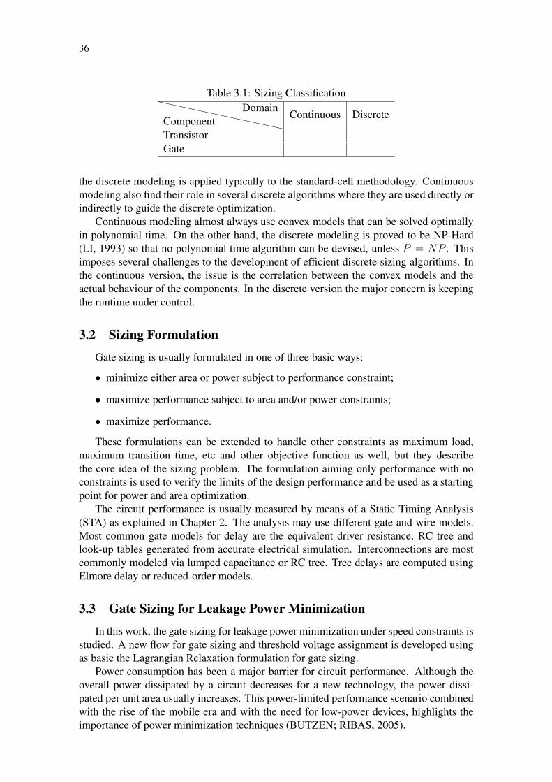
36
Table 3.1: Sizing Classification
ComponentDomain
Continuous Discrete
TransistorGate
the discrete modeling is applied typically to the standard-cell methodology. Continuousmodeling also find their role in several discrete algorithms where they are used directly orindirectly to guide the discrete optimization.
Continuous modeling almost always use convex models that can be solved optimallyin polynomial time. On the other hand, the discrete modeling is proved to be NP-Hard(LI, 1993) so that no polynomial time algorithm can be devised, unless P = NP . Thisimposes several challenges to the development of efficient discrete sizing algorithms. Inthe continuous version, the issue is the correlation between the convex models and theactual behaviour of the components. In the discrete version the major concern is keepingthe runtime under control.
3.2 Sizing Formulation
Gate sizing is usually formulated in one of three basic ways:
• minimize either area or power subject to performance constraint;
• maximize performance subject to area and/or power constraints;
• maximize performance.
These formulations can be extended to handle other constraints as maximum load,maximum transition time, etc and other objective function as well, but they describethe core idea of the sizing problem. The formulation aiming only performance with noconstraints is used to verify the limits of the design performance and be used as a startingpoint for power and area optimization.
The circuit performance is usually measured by means of a Static Timing Analysis(STA) as explained in Chapter 2. The analysis may use different gate and wire models.Most common gate models for delay are the equivalent driver resistance, RC tree andlook-up tables generated from accurate electrical simulation. Interconnections are mostcommonly modeled via lumped capacitance or RC tree. Tree delays are computed usingElmore delay or reduced-order models.
3.3 Gate Sizing for Leakage Power Minimization
In this work, the gate sizing for leakage power minimization under speed constraints isstudied. A new flow for gate sizing and threshold voltage assignment is developed usingas basic the Lagrangian Relaxation formulation for gate sizing.
Power consumption has been a major barrier for circuit performance. Although theoverall power dissipated by a circuit decreases for a new technology, the power dissi-pated per unit area usually increases. This power-limited performance scenario combinedwith the rise of the mobile era and with the need for low-power devices, highlights theimportance of power minimization techniques (BUTZEN; RIBAS, 2005).

37
The power consumed by components can be broken down into two components: dy-namic power and static power. Dynamic power is the power consumed by the componentswhen they are changing states. For instance, the output of a logic cell transitioning fromzero to one is causing dynamic power consumption. On the other hand, the static poweror leakage power is consumed constantly independent of state changes.
Leakage power has become a main concern in deep submicron process technologynodes (65nm and below), where it could account for 30-50% of the total design powerconsumption (SHIFREN, 2011). Leakage power is mainly caused by unwanted sub-threshold currents in the transistor channel when the transistor is turned off. Figure 3.2presents the sources of leakage power for a planar technology.
Figure 3.2: Sources of Leakage Current
Source: (BUTZEN; RIBAS, 2005)
Gate sizing is a standard and effective technique for power minimization and hencesuitable for addressing the aforementioned problems. For a standard-cell based designflow, the gate sizing task is to select the right versions for the gates available in a libraryso that the power is minimized while keeping the circuit performance within the specifi-cation. However, the gate selection problem was shown to be NP-Hard (LI, 1993), so thatno optimal, polynomial time algorithm can be designed unless P = NP . This combina-torial optimization problem becomes even more challenging as the designs get more andmore complex and the number of sizable components keep growing. Therefore efficientand effective heuristics need to be developed.
3.3.0.1 A Word on FinFet Technology
In recent years, the FinFET technology consolidated and is now in production mode.This technology brings more control over the leakage power and hence a significant re-duction in the leakage power consumption by up to 50% is achieved so that dynamicpower has become the main concern.
However, this does not mean the leakage power still has no impact on the total powerconsumption. Improvements on leakage power can still provide a good increase in batterylife of mobile devices. Moreover, not all designs have being converted to FitFET as thisdecision involves other factors, but ultimately the cost factor is the most prominent.
Although the focus of this method is leakage power, it can be extended to handledynamic power as well if switch activity is available. Therefore, although FinFET tech-nology may shadow the improvements brought by this work, the techniques and the flow

38
presented in this thesis still can provide power savings or be extended to handle dynamicpower and other objectives associated with transistor sizes.
3.4 Challenges
The challenges of the gate sizing for high performance designs can be summarized asfollows (OZDAL; BURNS; HU, 2011):
1. Discrete cell sizes: Standard-cell based-flow is the dominant methodology to de-sign digital circuits implying that only a limited number of gate types are available.The limited number of gate types rather than easing the problem, makes it combi-natorial in nature and hence hard to solve efficiently.
2. Cell timing models: Standard-cell delay is typically non-linear and non-convex sothat direct and efficient application of mathematical optimization as linear and con-vex programming is only possible on simplified delay models. Over simplificationmay lead to far from optimal results.
3. Complex timing constraints; In high-performance designs several timing constraintsmust be handled such as timing overrides, multi-cycle paths, transparent paths, mul-tiple clock events, false paths, etc. If the method does not take into account suchconstraints, it may become too inaccurate.
4. Interconnect timing models: Interconnect delay is a major contributor to the over-all design delay. Ignoring it or using simplified interconnect delay models such aslumped capacitance and Elmore delay may lead to incorrect timing information andto over designing as simplified model usually overestimates the actual interconnectdelay.
5. Many near-critical paths: In high performance design many paths are near-criticaldecreasing the efficiency of sizing methods that rely only on the optimization of thecritical path. In this case, when the critical path is fixed, other paths may start toviolate timing. Therefore sizing engines should handle many paths at same time toavoid dead-locks.
6. Large design sizes: Designs or even blocks in designs can easily reach the milliongates count so that the sizing engines must scale to handle such huge number ofcomponents. Methods that rely on frequent timing updates may not be suitable forsuch designs.
3.5 Related Work
In this chapter, some of the works on transistor and mainly gate sizing are reviewedand summarized. The early works on gate sizing focused on the continuous domainwhere individual transistors or gates can be set to any size within a lower and an upperlimit. Along with simplified models, a convex mathematical formulation can be devised(SCHEFFER; LAVAGNO; MARTIN, 2006), which can then be solved in some extentefficiently in polynomial time (BOYD; VANDENBERGHE, 2004). The continuous for-mulation was a straightforward fit for the full-custom methodology, which was the mainmethodology for the early days of circuit design.

39
Later on, methods for discrete gate sizing started to be developed as the standard-cellmethodology consolidated. In the discrete formulation, the gate sizing problem becomesan assignment problem where sizes or, more generally, implementations of the gates arepicked up from a library. Differently from the continuous counterpart, the discrete formu-lation is proved to be a NP-hard problem (LI, 1993).
Many discrete methods are inspirited by the continuous formulation or use it directlyto guide the optimization process. This is not surprising as the assumptions made in thecontinuous side can be seen as a relaxation of the discrete formulation.
Several different approaches for gate sizing have been used in the literature:
• simulated annealing;
• linear programming;
• network flow;
• convex optimization (including geometric programming);
• Lagrangian relaxation;
• sensitivity and
• slew budgeting.
Lagrangian relaxation, sensitivity and network flow based approaches seem to be themost suitable ones for current design sizes as they scaled well and can be used for thediscrete gate sizing problem.
Simulated annealing was successfully applied in the ISPD 2012 Gate Sizing Contest,but it suffers from scalability issues and do not seem to be an acceptable method forcurrent designs. Although the method won the contest, later works achieved much betterresults in much less time.
Convex optimization including geometric programming only works on simplified con-vex or posynomial models which may not capture the non-linear, non-convex nature ofthe gate delays. On the other hand, they guarantee the optimal solution (under the sim-plified model) and can be used in the early stages of the design flow or as guide for thediscrete gate sizing.
3.5.1 Early Work
One of the first works automating the gate sizing problem was developed by Ruehliet al.1 from IBM (RUEHLI; WOLFF; GOERTZEL, 1977) aiming power minimizationunder timing constraint. In that initial work, gate delay is proportional to the inverse ofthe gate size and the power is directly proportional to the size. Lumped capacitance isused to model the wires. The authors report gains of 3 up to 10 times in power whencompared to an unoptimized design that meets timing. The main drawback is that thetiming model does not consider that a change in a gate size changes the load capacitanceof its driver.
Almost a decade later, the transistor sizing method, TILOS, was published (FISH-BURN; DUNLOP, 1985). TILOS can operate in three modes (1) area minimization under
1Out of curiosity. The last author of the paper, Gerald Goertzel, had worked in the Manhattan Project.

40
timing constraint, (2) timing minimization under area constraint and (3) area-delay prod-uct minimization. Gate delay is modeled using RC networks and the authors show that thismodel leads to a convex delay model for the entire circuit. Even though the authors citethat the convex model can be solved by general purpose solvers, they indeed developed asensitivity-based heuristic to trade-off accuracy and runtime. The method works by siz-ing the transistor with the largest delay to size sensitivity on the most critical path. First,TILOS is used to generate a rough initial solution. Then, in the second phase, the siz-ing problem is converted to a mathematical optimization problem in a smaller parameterspace where a method of feasible directions is applied to find the optimal solution. TILOSwas chosen one of the best works of the 20 years of ICCAD conference (KUEHLMANN,2003).
In 1987, Aesop (HEDLUND, 1987) tool for transistor sizing using linear model ispresented. Berkelaar and Jess (BERKELAAR; JESS, 1990) present a method to powerminimization under timing constraint using linear programming. The non-linear gatedelay is broken into a piecewise linear function, which is suitable to formulate the problemas a linear program.
The first work to cope directly with discrete gate sizing was developed by Chan(CHAN, 1990) in 1990. Previous works only handled discrete gate sizing by roundingthe sizes obtained from continuous formulation. Chan, on the other hand, proposed atraverse algorithm to propagate timing constraints, then backward substitution applyingcell sizes available in a library. The proposed algorithm runs in pseudo-polynomial timefor tree structures. For non-tree structures, multiple-fanout cells are implicitly cloned tocreate a tree like structure where the algorithm for trees can be used. The algorithm doesnot depend on a specific gate delay model. Also the cost for a gate size is generic and canbe, for instance, the cell area or cell power. However, as the algorithm needs to propagatea list of possible gate sizes, it becomes impractical for large circuits.
In 1993, the tool ASAP (DUTTA; NAG; ROY, 1994) for transistor sizing using simu-lated annealing was presented using the Alpha-Power Law MOSFET Model (SAKNRAI;NEWTON, 1990). Also in 1993, different from previous approach, Sapatnekar et. al(SAPATNEKAR et al., 1993) took full advantage of the convex formulation by usingconvex programming to find an exact solution.
In 1996 (COUDERT, 1996) and 1997 (COUDERT, 1997), Oliver presented a greedyalgorithm for discrete gate sizing aiming industrial designs. Different from previousworks, Oliver used an accurate gate delay based on look-up tables. The greedy algo-rithm works by traversing the circuit, selecting new sizes for gates, but without resizingthem. Every size change is stored as a move. After all gates have been processed, themoves that minimize power keeping the circuit performance are selected.
A sequential quadratic programming (SQP) approach to concurrent gate and wire siz-ing was presented by Menezes in 1997 (MENEZES; BALDICK; PILEGGI, 1997). Intheir work, the authors present an efficient way to compute the sensitivities to feed theSQP.
Chen, et at. (CHEN; CHU; WONG, 1999), published a key work on gate sizing in1999. They presented a concise formulation for the gate sizing problem avoiding theexponential grow of path delay constraints. With this new formulation, the number ofconstraints grows linearly with the number of pins. Moreover, the authors shown how theLagrangian Relaxation formulation could be significantly reduced using Karush-Kuhn-Tucker (KKT) conditions. Then a fast and optimal algorithm was designed to solve thegate and wire sizing simultaneously.

41
In 2002, Tennakoon et at. (TENNAKOON; SECHEN, 2002) proposed a fast gradient-based pre-processing step for Lagrangian relaxation that provides an effective set of ini-tial Lagrange multipliers, which improved the runtime up to 200× compared to previousworks.
3.5.2 State-of-the-Art
The gate options are a combination of transistor widths and threshold voltages (Vth)available in a gate library. Some recent works (LIU; HU, 2010; OZDAL; BURNS;HU, 2011; RAHMAN; TENNAKOON; SECHEN, 2011) apply Lagrangian Relaxationto solve the discrete gate sizing problem using KKT conditions (CHEN; CHU; WONG,1999) to simplify the Lagrangian Relaxation Sub-problem (LRS). In our approach KKTconditions are also applied and combined with the proposed method.
A Lagrangian Relaxation based formulation for gate sizing and device parameter se-lection is presented in (OZDAL; BURNS; HU, 2011). The objective is to minimize leak-age power on high-performance industrial designs. Lagrangian Relaxation and DynamicProgramming (DP) are used to find the optimized solution. In the LR formulation, timingconstraints are introduced in the objective function. An accurate sign-off timer is used tocompute the slack values after each LR iteration. The LRS is modeled as a graph andthe discrete gate version characteristics are based on timing tables provided by the gatelibrary. A DP algorithm based on critical tree extraction is proposed to solve the LRSoptimization problem for discrete gates.
In (RAHMAN; SECHEN, 2012), a threshold voltage (Vth) assignment algorithm thatemploys a cost function which is globally aware of the entire circuit is presented. Theobjective of the post-synthesis algorithm is to minimize leakage power while solving thedelay constraints. Gates are swapped to a higher Vth to absorb the available slack inthe design without sacrificing delay. The delay constraint is iteratively pushed out by δtime units, each time enabling additional gates to have their threshold voltages increased.The leakage power is iteratively reduced to a minimum value and then starts to increasesubstantially. Gate upsizing is required to re-establish the original delay target.
In (REIMANN et al., 2013), (HU et al., 2012), (LI et al., 2012) and (LIVRAMENTOet al., 2013) the infrastructure based on the ISPD 2012 Gate Sizing Contest is used.(REIMANN et al., 2013) presents a flow composed by a set of heuristic algorithms toaddress the discrete gate sizing and Vt assignment problem. The proposed flow combinesthe Fanout-of-4 rule, the Logical Effort concept and uses Simulated Annealing (SA) asthe main engine. The solution achieved the second and first positions in the two rankingsof the ISPD Contest in 2012.
A sensitivity-guided meta-heuristic approach to gate sizing that integrates timing andpower optimization is presented in (HU et al., 2012). The proposed heuristic has twostages: Global Timing Recovery and Power Reduction with Feasible Timing. GlobalTiming Recovery seeks violation-free solutions, and then Power Reduction with Feasi-ble Timing iteratively reduces total leakage power of sizing solutions by local search. Ateach stage of the optimization flow, the space of sensitivity functions is parametrized andtransversed to find the best configurations of sensitivity by independent multistarts. Aftereach multistart, all obtained solutions are compared and the best/non-dominated solu-tions are retained. This is accomplished by adapting the go-with-the-winners (ALDOUS;VAZIRANI, 1994) meta-heuristic. The optimization is purely deterministic in that themultistart procedure begins with the small set of the best-seen solutions. Solutions aftereach stage are ensured to be feasible, which enables pruning of dominated solutions by

42
go-with-the-winners. The results are comparable to other works, but the method is slowcompared to (LI et al., 2012).
A framework for gate-version selection in modern high-performance low-power de-signs with library-based timing model is presented in (LI et al., 2012). The frameworkcan be divided into three stages. First, the best design performance with all possible gate-versions is achieved by a Minimum Clock Period Lagrangian Relaxation method, whichextends the traditional LR approach to control the difficulties in the discrete scenario.Upon a timing-valid design, the timing-constrained power optimization problem is solvedby min-cost network flow. Finally, a power pruning technique is used to take advantageof the residual slacks due to the conservative network flow construction. The techniqueproduces good power results, but worse than (HU et al., 2012), however in a faster waywith a linear empirical runtime.
(LIVRAMENTO et al., 2013) proposes a Lagrangian Relaxation formulation for leak-age power minimization that incorporates into the objective function the maximum gateinput slew and the maximum gate output capacitance constraints in addition to the usualtiming constraints. A fast topological greedy heuristic to solve the Lagrangian RelaxationSubproblem and a complementary procedure to fix the few remaining slew and capaci-tance violations is proposed. Despite all the improvements achieved by recent researchworks, there is still significant room for improvements. This can be observed as the bestresults for some of the benchmarks are found by different algorithms. They also differa lot in terms of runtime, and it is desirable to identify which operations are consumingcomputational effort without contributing to the solution.
3.5.3 Summary
In Table 3.2 the main characteristics of continuous sizing methods are shown. In Table3.3 the main characteristics of discrete sizing methods are shown.
Table 3.2: Summary of Works on Continuous Gate SizingWork Year Sizing Type Gate Model Net Model Optimization Methods
(RUEHLI; WOLFF; GOERTZEL, 1977) 1977 Gate Inverse of Size Lumped Capacitance Newton(FISHBURN; DUNLOP, 1985) 1985 Transistor RC N/A Sensitivity(BERKELAAR; JESS, 1990) 1990 Gate Pice-Wise Linear Linear Linear Programming(SAPATNEKAR et al., 1993) 1993 Transistor RC (Elmore De-
lay)N/A Convex Programming
(MENEZES; BALDICK; PILEGGI, 1997) 1997 Gate Driver Resistance RC Tree (Elmore) Sequential Quadratic Pro-gramming
(CHEN; CHU; WONG, 1999) 1999 Gate Driver Resistance RC Tree (Elmore) Lagrangian Relaxation(SRIVASTAVA; SYLVESTER; BLAAUW, 2004) 2000 Transistor Alpha-Power
Law MOSFETModel
N/A Sensitivity Based
(TENNAKOON; SECHEN, 2002) 2002 Gate Driver Resistance RC Tree (Elmore) Lagrangian Relaxation(BOYD et al., 2005) 2005 Gate Transistor RC RC Tree (Elmore) Geometric Programming
(POSSER et al., 2012) 2012 Transistor Driver Resistance RC Tree (Elmore) Geometric Programming(ALEGRETTI et al., 2013) 2013 Transistor Driver Resistance RC Tree (Elmore) Geometric Programming

43
Table 3.3: Summary of Works on Discrete Gate SizingWork Year Sizing Type Gate Model Net Model Optimization Methods
(CHAN, 1990) 1990 Gate [Generic] N/A Greedy(COUDERT, 1996) 1996 Gate Lookup Table N/A Multiple Moves(COUDERT, 1997) 1997 Gate Lookup Table N/A Multiple Moves
(NGUYEN et al., 2003) 2003 Gate Lookup Table N/A Sensitivity Linear Program-ming
(SHAH et al., 2005) 2005 Gate Equivalent DriverResistance (El-more)
N/A Geometric Programming
(CHOU; WANG; CHEN, 2005) 2005 Transistor Posynominal Ap-proximation
N/A Lagrangian Relaxation
(CHINNERY; KEUTZER, 2005) 2005 Gate Lookup Table Lumped Capacitance Sensitivity Linear Program-ming
(REN; DUTT, 2008) 2008 Gate Driver Resistance Lumped Capacitance Network Flow(LIU; HU, 2010) 2009 Gate Lookup Elmore Greedy
(HU; KETKAR; HU, 2009) 2009 Gate Elmore Delay N/A Dynamic Programming(OZDAL; BURNS; HU, 2011) 2011 Gate [Generic] [Generic] Dynamic Programming La-
grangian Relaxation(HUANG; HU; SHI, 2011) 2011 Gate RC (Elmore De-
lay)N/A Lagrangian Relaxation
(ZHOU et al., 2011) 2011 Gate Linear Fit RC Tree (Elmore) Dynamic Programming(RAHMAN; TENNAKOON; SECHEN, 2011) 2011 Gate Logical Effort Lumped Capacitance Lagrangian Relaxation
Branch-and-Bound(OZDAL; BURNS; HU, 2012) 2011 Gate [Generic] [Generic] Dynamic Programming La-
grangian Relaxation(RAHMAN; SECHEN, 2012) 2012 Gate Lookup RC Tree Greedy
(HU et al., 2012) 2012 Gate Lookup Lumped Capacitance Sensitivity(LIVRAMENTO et al., 2013) 2013 Gate Lookup Lumped Capacitance Lagrangian Relaxation
(REIMANN et al., 2013) 2013 Gate Lookup Lumped Capacitance Simulated Annealing

44

45
4 GATE SIZING VIA LAGRANGIAN RELAXATION
4.1 Lagrangian Relaxation
Lagrangian Relaxation is a useful mathematical technique to find or to approximatethe optimum solution of optimization (minimization or maximization) problems with hardconstraints. It has been successfully applied to solve several problems in EDA such asfloor-planning, placement, routing and gate sizing among others.
The main idea behind Lagrangian Relaxation is to rewrite the optimization problemin an easier version, removing the hard constraints and adjusting the objective function totake into account the constraint violations.
Given the optimization problem, also called the primal problem, in Equation (4.1),
minimize f(x)
subject to gi(x) ≤ 0 i = 1, 2, ..., nhj(x) = 0 j = 1, 2, ..., m
(4.1)
a simpler or relaxed problem is written moving the hard constraints to the objective asshown in Equation (4.2)
minimize L(x, λ, µ)
subject to λi ∈ <+ i = 1, 2, ..., nµj ∈ < j = 1, 2, ..., m
(4.2)
where
L(x, λ, µ) = f(x) +∑
λigi(x) +∑
µjhj(x) (4.3)
.The relaxed constraints are multiplied by the so called Lagrange multipliers, λi and
µj , which can be seen as a weight indicating how much that specific constraints is beingviolated. Not all constraints need to be moved to the objective and the choice of whichconstraints should be relaxed is problem dependent. However the relaxed version shouldbe easier to solve than the original problem.
The key property of the relaxed problem is that its solution is always a lower bound tothe solution of the original problem for any set λi, µj. That is,
L(x, λ, µ) ≤ f(x) (4.4)
where x is the optimal solution for the relaxed problem and x is the optimal solution ofthe original problem.

46
Considering this propriety, the main idea of Lagrangian relaxation is to find the max-imum lower bound, which may ultimately approach the optimal solution of the originalproblem. This leads to another optimization problem, called the dual problem, whichaims to find the largest lower bound as defined by Equation (4.5).
maximize min f(x) +∑
λigi(x) +∑
µjhj(x)
subject to λi ≥ 0 i = 1, 2, ..., nµj ∈ < j = 1, 2, ..., m
(4.5)
For convex problems, the maximum lower bound is equal to the optimal solution ofthe original problem. For non-convex problems, the maximum lower bound is only closeto the optimal solution and the difference between the maximum lower bound and theoptimal solution is called duality gap.
4.1.1 Solving the Lagrangian Dual Problem
Typically the dual problem is solved iteratively by interleaving Lagrangian multiplierupdate and solving the relaxed problem. Then the relaxed problem is solved assumingthe Lagrangian multipliers are fixed. The Lagrangian multipliers are updated so that thelower bound provided by the relaxed problem is increased w.r.t. the previous iteration.This basic procedure is depicted in Figure 4.1.
Figure 4.1: Basic algorithm to solve the Lagrangian dual problem.
Initialize Lagrange Multipliers
Solve Dual Problem
Update Lagrange Multipliers
Start
no
Converged
End
yes
Source: from author (2015)
The subgradient optimization algorithm (BEASLEY, 1993) is presented in Algorithm4.1 is a common method used to solve the dual problem. Note that it follows the recipepresented in the Figure 4.1.

47
Algorithm 4.1: Subgradient optimization algorithm.1 Initialize α ∈ (0, 2];2 Initialize λ = 0;3 Initialize ZUB with an appropriate upper bound;4 Initialize ZLB with the solution of LRS/λ (λ = 0);5 while N (v) ≤ ε do6 β = α(ZUB−ZLB)
N(v)2;
7 λ = λ+ βN (v);8 ZLB ← LRS/λ;
4.2 Applying Lagrangian Relaxation in the Gate Sizing Problem
For gate sizing, the design is described using an acyclic directed graph where nodesare the pins in the design and the edges are the timing arcs connecting the pins as exempli-fied in Figure 4.2. There are two types of timing arcs: (1) cell timing arcs which connectthe input pins to output pins of a cell and (2) net timing arcs which connect cells.
Figure 4.2: An example circuit.
CK
D Q
CK
D Q …
…
…
…
Source: from author (2015)
The gate sizing problem under clock frequency constraint can be formulate straight-forwardly as in Equation (4.6) where x is the vector of gate sizes (or types) and f(x) is ageneric objective function, usually power, area or performance.
minimizex
f(x)
subject to Di ≤ T, i ∈ Pathsxi ∈ Sizesi
(4.6)
However, imposing a constraint on the delay of each timing path explicitly is pro-hibitive as the number of paths grows exponentially with the number of cells in the de-sign. A more concise way to represent timing constraints is by imposing chronologicalconstraints on arrival times. In this case, arrival times are seen as variables by the opti-mization problem as shown in Equation (4.7).

48
PP :
minimizex,a
f(x)
subject to ai + di→j ≤ aj,∀i→ j ∈ Arcsai ≤ T,∀i ∈ Endpointsxi ∈ Sizesi
(4.7)
Chronological constraints ensure that the arrival time at a timing arc’s input pin plusthe timing arc delay will be less or equal to the arrival time at the timing arc’s outputpin. Note that for each timing arc a constraint of such kind must be set. An additionalconstraint is included for each path’s output node such that the arrival times at them willbe less or equal to the clock period.
4.2.1 Lagrangian Relaxation
By relaxing the arrival time constraints, the objective function can be rewritten as inEquation (4.8) where λi→j and λi are the Lagrange multipliers.
Lλ(x, a) = f(x) +∑∀i→j
λi→j (ai + di→j − aj) +∑∀i∈PO
λi (ai − T ) (4.8)
So that, the relaxed gate sizing version of PP can be defined as in Equation (4.9).
LRSλ :
minimizex,a
Lλ(x, a)
xi ∈ Sizesi
(4.9)
4.2.2 Simplification of LRSλChen et al (CHEN; CHU; WONG, 1999) shown that the LRSλ can be greatly sim-
plified by using the Karush–Kuhn–Tucker (KKT) conditions for optimality. The KKTconditions implies that ∂L/∂ak = 0 at the optimal solution of PP . The derivative of L isgiven by Equation (4.10).
∂L∂ak
=∑∀k→j
λk→jak −∑∀i→k
λi→kak (4.10)
Therefore the optimal solution has the property as shown in Equation (4.11), which im-plies that the sum of inwards Lagrange multipliers of a pin must be equal to the sum ofoutward ones. ∑
∀k→j
λk→jak =∑∀i→k
λi→kak (4.11)

49
5 NEW DISCRETE GATE SIZING AND VTH ASSIGNMENTFLOW USING LAGRANGIAN RELAXATION
Lagrangian formulation has been extensively used in the gate sizing and is the core ofmany methods present in the literature. Assuming convex delay models and continuoussizing, it can even efficiently provide an optimal solution. However, for the discrete case,many challenges emerge. The most prominent consequence is that the gate sizing prob-lem becomes NP-complete and, unless P = NP, this means that no efficient and optimalalgorithm can be designed for the general case.
Therefore, in discrete case, Lagrangian Relaxation is used as a heuristic to find goodsolutions rather than the optimal one. And, as most heuristics, several tricks and adapta-tions are required to make it work properly.
5.1 Contributions
In this thesis, the gate sizing method for timing minimization presented by Li Li et al(LI et al., 2012). is adapted and extended to handle leakage power minimization.
The underlying LR framework is similar to that one used by Li Li and also otherworks in the literature (OZDAL; BURNS; HU, 2011) (LIVRAMENTO et al., 2013), butthe overall flow presents some novelties in the way the LR is controlled to improve con-vergence to a good solution. The controllability is a main issue for any heuristic basedon LR, so much that Li Li et al. use LR only to improve timing with no regards to othermetrics as they say the constrained LR formulation is hard to control.
Even though other works have applied the Lagrangian Relaxation (LR) to solve thegate sizing problem before, it is still a complex task to use LR efficiently and effectivelyto solve the discrete gate sizing problem.
The main contributions for the gate sizing field of this thesis can be summarized asfollow.
• A local slack-based technique to filter out bad sizing and threshold voltage options,which improves the LR convergence.
• A sensitivity based method to estimate the global changes of the delay given achange on a cell implementation (i.e. size or threshold voltage).
5.2 Scope
The gate sizing techniques and the flow presented in this thesis aim on leakage powerminimization under timing constraints. The flow is developed to be executed during the

50
early stages of the design flow as after technology mapping or during and after placementas shown in Figure 5.1.
Figure 5.1: Gate Sizing in the Design Flow
Specs
HDL High-Level Synthesis
Logic Synthesis
Physical Synthesis
Optimizations
Technology Independent
Optimization
Mapping
Technology Dependent
Optimization
Floorplanning
Placement
Routing
Library
Analysis Tools
Timing
Power
Verification
…
Ea
rly S
tag
es
Late
Sta
ge
s
Log
ica
l Op
tim
iza
tio
n
Ph
ysica
l Op
timiza
tion
GDS
II
RTL
Mapped
Design
Ready for
Fabrication
Source: from author (2015)
At these stages precise timing and power information may not be available due to thelack of routing information so that simplified methods are typically used to estimate thosemetrics. However simplified methods can also be used for sake of runtime and as long asthey correlate well to the actual models, this does not invalidate the gains obtained at thisstage.
Although the scope was limited to the early stages, a subsequent work by Reimann(REIMANN; SZE; REIS, 2015) shown that this flow can be extended to work also in finalstages of the design cycle.
This flow can also be used during the exploration phase where the goal is to get aglimpse of a design characteristics as maximum frequency and power consumption.
In the gate sizing flow, only late violations are directly optimized. However, since theobjective is power minimization, this forces the non-critical late paths to become slower,which indirectly leads to a reduction in early violations.
5.3 Background
A typical standard cell library contains a few hundreds cells that implement a smallset of logical functions. Each different logical function is implemented by several cells,but with different timing, area and power characteristics. These different implementationsare used to trade-off the design performance with power consumption and area usage.
Besides different sizes, a cell library also contains different threshold voltage versionsfor same size cells. Different Vths (threshold voltages) for the same gate may be used asan efficient way to reduce leakage power. The relationship between speed and leakagecan be used to produce designs with the desired power/delay trade-off. Gates that are not

51
on the critical path often do not need the performance of high-leakage implementations,therefore slower and less leaky versions can be used instead (PANGRLE; KAPOOR, Jun.2005).
To optimize the leakage power in a circuit making use of the different available cellversions, a simultaneous gate sizing and Vth assignment method may be used. Assigningproperly the gate size and Vth for each gate has major influence on power consumption.Besides maintaining timing constraints, the gate sizing tool has also to consider otherdesign constraints, such as maximum gate fan-outs and transition times. The discretegate sizing problem is a combinatorial optimization problem and is proved to be NP-Hard(LI, 1993). Therefore, approximation and heuristic algorithms are essential to efficientlyaddress it.
In this chapter, an algorithm for discrete gate sizing and Vth assignment is presented.The core method is developed upon the Lagrangian Relaxation methodology, however, asnon-convex modeling functions are used, only the weak duality holds.
5.4 Performance Optimization
In its simpler version, the LR-based gate sizing formulation can be used to find thefastest implementation of a design. Although the final solution is likely to be prohibitivein terms of power consumption and area, it may be a good starting point for some methodsaiming to optimize power.
Li Li et al. presented a greedy method to solve the LRS/λ problem. The basic idea isto traverse the design in topological order and for each cell test all candidates keeping theone that provides the best gain in terms of delay.
When the implementation of a cell (i.e. its size or threshold voltage) is changed, theimpact on timing can propagate throughout many cells in the design due to slew depen-dency. One can rerun the timing analysis for each implementation change, but as severalchanges are tested for each cell, this soon becomes prohibitive in terms of runtime.
A common strategy to avoid the runtime penalty is to analyze the timing change onlylocally. Besides of being much faster than a global analysis, the fact that most of thetiming perturbation is absorbed in a few logic levels (OZDAL; BURNS; HU, 2011) alsomakes this strategy very attractive.
To compute the impact of an implementation change, Li Li et al. analyze the delaychange on the driver, side and sink timing arcs as shown in Figure 5.2.

52
Figure 5.2: Local timing evaluation after a gate has been sized.
Source: from author (2015)
5.5 Definitions
For the purpose of this work, a circuit is described by its logical and memory elementscalled gates or cells and the connections between them called nets. Only logical elementsare considered for sizing. Gates are attached to nets at specific points of the net topologynamed driver and sink nodes. A gate is composed by one or more timing arcs whichdescribe the timing characteristics of the gate. Table 5.1 summarizes the definitions andnotation used throughout this work.
Table 5.1: Definitions of some terms used in this work.T clock periodTNS total negative slackSTA static timing analysisi→ j timing arc from node i to node jdi→j delay of timing arc i→ jai arrival time at node iqi require time at node islewi slew at node iλ Lagrange Multiplier∆Di→j delay change given a change in input slew of arc i→ j∆Dn delay change given a change in slew of net nδdi→j
δslewidelay sensitivity to input slew of arc i→ j
δslewj
δslewioutput slew sensitivity to input slew of arc i→ j
φ cumulative back-propagated arc delay sensitivity
When connections are modeled using a simple lumped capacitance, timing informa-tion (arrival, required and slew) at sink nodes is equal to the values at the driver node. Inthis case, driver and sinks share the same name borrowed from the net which connectsthem.
Moreover, to keep notation clean, rise and fall transitions are not shown, but they areconsidered properly in the proposed method.

53
5.6 Flow Overview
Figure 5.3 depicts a high-level view of the flow developed in this work. It startsby setting all gates to the lowest leakage version. Load and slew violations are thenremoved without regarding to timing closure. This solution is passed to our LagrangianRelaxation method to optimize leakage power under performance constraints. Next, anytiming violations left are eliminated by a Timing Recovery method. Finally the leakagepower is further reduced by a Power Reduction algorithm.
Every method developed in this work has a linear complexity per iteration. The num-ber of iterations for each iterative method is hard to predict, but for most cases only a few(tens to hundreds) are required.
Figure 5.3: High-level view of our gate selection flow.
set all gates to smallest leakage
version
remove load and slew violations
power reduction
timing recovery
update λs LRS/λ solver
Lagrangian Relaxation
LDP solver
Source: from author (2015)
In order to improve convergence rate at the Lagrangian Relaxation step, load and slewviolations are removed from the initial minimum leakage solution. In this way our LRmethod may concentrate more on reducing leakage power and meeting timing constraints.
The removal is performed by means of the iterative method presented in (LI et al.,2012) (with α = 0.7). The procedure visits all gates, one at a time, from outputs toinputs. For each gate, the gate version with less leakage that respects both slew and loadconstraints is selected. In our implementation, as the gates are visited, timing is updatedonly locally as explained in Section 5.9.1.
The αL ∈ (0, 1] parameter is used to control the ratio between driver strength and theload capacitance. Smaller is the αL value, larger should be the driver strength. A smallervalue improves convergence as it tends to oversize gates. In this work we set αL = 0.7.
5.7 Lagrangian Relaxation
Lagrangian Relaxation is a useful mathematical technique to find or to approximatethe optimum solution of minimization problems with hard constraints.
The original problem, also called Primal Problem (PP), is simplified by removinghard constraints and incorporating them into the objective function. For each incorpo-

54
rated constraint, a weight – the Lagrange Multiplier (λ) – is assigned. Weights, whichmust be non-negative, may be interpreted as the penalties for not satisfying the respectiveconstraints. The simplified problem is called a Lagrangian Relaxed Subproblem (LRS)for each fixed set of λs, where the optimal solution for each LRS is a lower bound to thePrimal Problem (CHEN; CHU; WONG, 1999).
A corresponding maximization problem, the Lagrangian Dual Problem (LDP), is thenformulated where the goal is to maximize the solution of LRS instances by selectingappropriate sets of λs. This is commonly achieved iteratively by fixing λs, solving theLRS for the fixed set of λs (LRS/λ), updating λs, solving LRS/λ again and so on andso forth (OZDAL; BURNS; HU, 2011).
The concern in this work is leakage power minimization under timing constraints.However the ideas presented here can be easily adapted to handle different objective func-tions.
A concise way to represent timing constraints is by imposing chronological constraintson arrival times. In this case, arrival times are seen as variables by the optimizationproblem.
Chronological constraints ensure that the arrival time at a timing arc’s input node plusthe timing arc delay will be less or equal to the arrival time at the timing arc’s outputnode. Note that for each timing arc a constraint of such kind must be set. An additionalconstraint is included for each path’s output node such that the arrival times at them willbe less or equal to the clock period.
The gate selection problem for total leakage power minimization can be formulatedas shown in Equation (5.1).
Primal Problem (PP):
minimize leakage
subject to ai + di→j ≤ aj, for each timing arc i→ j
ak ≤ T, for each path output node k
(5.1)
By applying the Lagrangian Relaxation technique we obtain the LRS as in Equation(5.2).
LRS:
minimize leakage +∑λi→j(ai + di→j − aj) +∑λk(ak − T )
(5.2)
Chen et al. (CHEN; CHU; WONG, 1999) have shown that the problem in Equation(5.2) can be further simplified by applying the KKT conditions to optimality as shown inEquation (5.3).
LRS (simplified):
minimize leakage+∑
λi→jdi→j(5.3)
Hereafter the sum∑λi→jdi→j is referred to lambda-delay. So, the relaxed version
of the sizing problem can be viewed as the selection of gate versions which minimizesleakage plus lambda-delay with no explicit information about arrival times. Finally, LDPis simply the maximization of LRS where λ is also variable as shown in Equation (5.4).
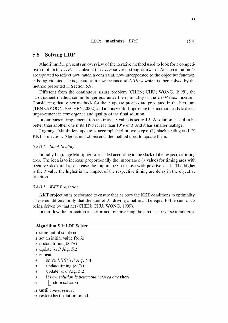
55
LDP: maximize LRS (5.4)
5.8 Solving LDP
Algorithm 5.1 presents an overview of the iterative method used to look for a competi-tive solution to LDP . The idea of the LDP solver is straightforward. At each iteration λsare updated to reflect how much a constraint, now incorporated to the objective function,is being violated. This generates a new instance of LRS/λ which is then solved by themethod presented in Section 5.9.
Different from the continuous sizing problem (CHEN; CHU; WONG, 1999), thesub-gradient method can no longer guarantee the optimality of the LDP maximization.Considering that, other methods for the λ update process are presented in the literature(TENNAKOON; SECHEN, 2002) and in this work. Improving this method leads to directimprovement in convergence and quality of the final solution.
In our current implementation the initial λ value is set to 12. A solution is said to bebetter than another one if its TNS is less than 10% of T and it has smaller leakage.
Lagrange Multipliers update is accomplished in two steps: (1) slack scaling and (2)KKT projection. Algorithm 5.2 presents the method used to update them.
5.8.0.1 Slack Scaling
Initially Lagrange Multipliers are scaled according to the slack of the respective timingarcs. The idea is to increase proportionally the importance (λ value) for timing arcs withnegative slack and to decrease the importance for those with positive slack. The higheris the λ value the higher is the impact of the respective timing arc delay in the objectivefunction.
5.8.0.2 KKT Projection
KKT projection is performed to ensure that λs obey the KKT conditions to optimality.These conditions imply that the sum of λs driving a net must be equal to the sum of λsbeing driven by that net (CHEN; CHU; WONG, 1999).
In our flow the projection is performed by traversing the circuit in reverse topological
Algorithm 5.1: LDP Solver1 store initial solution2 set an initial value for λs3 update timing (STA)4 update λs // Alg. 5.25 repeat6 solve LRS/λ // Alg. 5.47 update timing (STA)8 update λs // Alg. 5.29 if new solution is better than stored one then
10 store solution
11 until convergence;12 restore best solution found

56
Algorithm 5.2: Updating Lagrange Multipliers1 for each timing arc i→ j do2
λi→j ← λi→j ×
(1 +
aj−qjT
)+1/kaj ≥ qj(
1 +qj−ajT
)−kaj < qj
3 KKT projection
order distributing proportionally the sum of λs being driven by a net to the ones drivingthe net as outlined in Algorithm 5.3.
Algorithm 5.3: Update Lambdas KKT (CHEN; CHU; WONG, 1999)1 for each net n of the circuit do2 Compute sum of driver timing arc lambdas of net n3 Compute sum of sink timing arc lambdas of net n4 Update driver arcs5 for each edge (rise and fall) do6 if sum of driver timing arc lambdas > 0 then7 for each driver timing arc do8 λarc = sum sink lambdas ∗ λarc/sumλdrivers)
9 else10 for each driver timing arc do11 λarc = sumλsinks/num sinks
5.9 Solving LRS/λ
To find a solution for each LRS/λ instance the greedy method presented in Algorithm5.4 is employed. It works by traversing all gates in topological order trying to properlyselect a new version to each of them. The new selected version is the one which locallyminimizes leakage power and the lambda-delay.
Since a full STA would be required to compute the actual impact on lambda-delay, itwould be infeasible to use updated information every time a gate version is changed to getthe real impact of that change. So, the greedy method relies on local timing informationand global estimation to approximate the global impact on lambda-delay.
In most cases, the timing impact of a version change is absorbed within few logiclevels (OZDAL; BURNS; HU, 2011). And therefore the global impact on circuit timingcan be fairly estimated considering only local information. However, to deal with thecases where a local change greatly affects the overall timing – e.g.. a change in a criticalgate – a global sensitivity-based lambda-delay function is developed.
5.9.1 Local Timing Update
For this work, a local timing update comprises the timing update of a gate, its drivernets and arcs and its sink net in the same way a STA would perform, but without timing
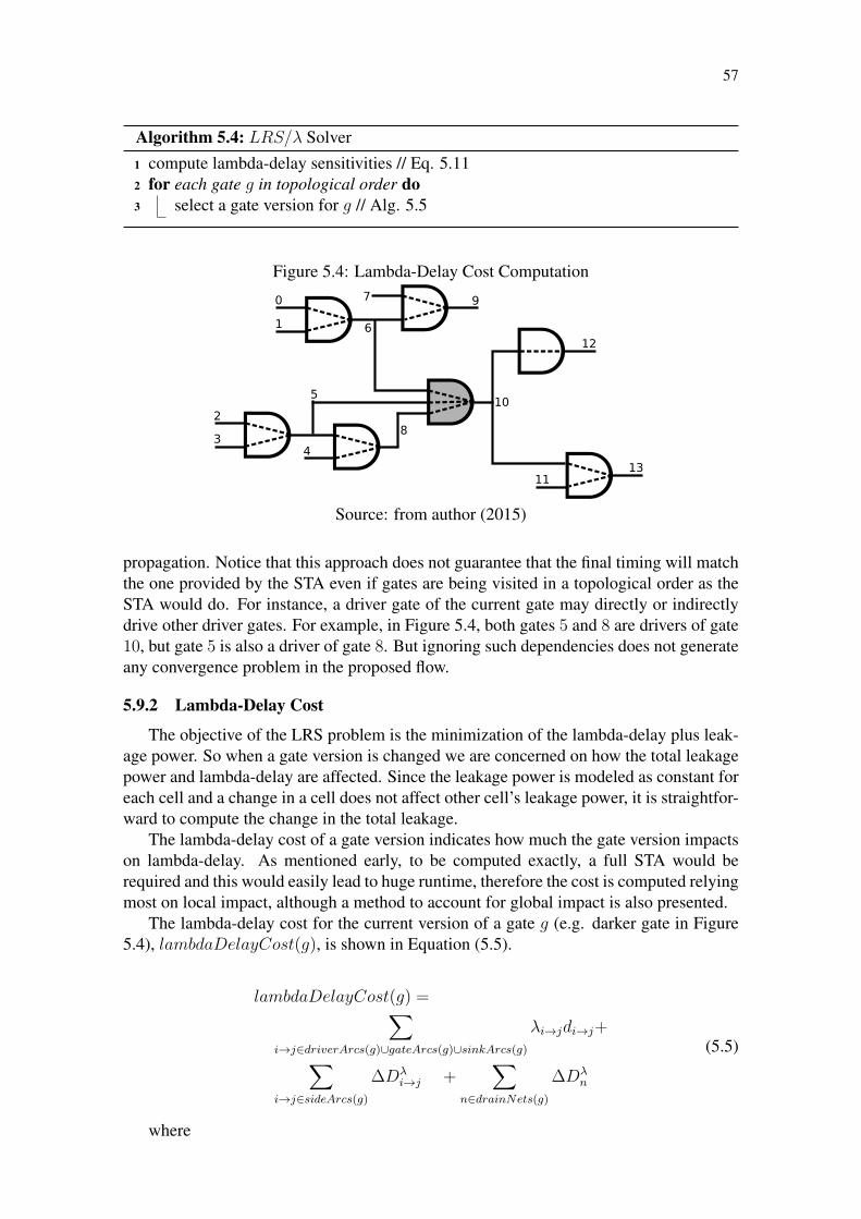
57
Algorithm 5.4: LRS/λ Solver1 compute lambda-delay sensitivities // Eq. 5.112 for each gate g in topological order do3 select a gate version for g // Alg. 5.5
Figure 5.4: Lambda-Delay Cost Computation
0
1
2
3
97
11
4
8
10
12
13
6
5
Source: from author (2015)
propagation. Notice that this approach does not guarantee that the final timing will matchthe one provided by the STA even if gates are being visited in a topological order as theSTA would do. For instance, a driver gate of the current gate may directly or indirectlydrive other driver gates. For example, in Figure 5.4, both gates 5 and 8 are drivers of gate10, but gate 5 is also a driver of gate 8. But ignoring such dependencies does not generateany convergence problem in the proposed flow.
5.9.2 Lambda-Delay Cost
The objective of the LRS problem is the minimization of the lambda-delay plus leak-age power. So when a gate version is changed we are concerned on how the total leakagepower and lambda-delay are affected. Since the leakage power is modeled as constant foreach cell and a change in a cell does not affect other cell’s leakage power, it is straightfor-ward to compute the change in the total leakage.
The lambda-delay cost of a gate version indicates how much the gate version impactson lambda-delay. As mentioned early, to be computed exactly, a full STA would berequired and this would easily lead to huge runtime, therefore the cost is computed relyingmost on local impact, although a method to account for global impact is also presented.
The lambda-delay cost for the current version of a gate g (e.g. darker gate in Figure5.4), lambdaDelayCost(g), is shown in Equation (5.5).
lambdaDelayCost(g) =∑i→j∈driverArcs(g)∪gateArcs(g)∪sinkArcs(g)
λi→jdi→j+∑i→j∈sideArcs(g)
∆Dλi→j +
∑n∈drainNets(g)
∆Dλn
(5.5)
where

58
Figure 5.5: Delay Sensitivity Computation
0 1 2 3
Source: from author (2015)
• driverArcs(g) is the set of arcs driving the driver nets of gate g (e.g. arcs 0, 1 → 6,2, 3 → 5 and 5, 4 → 8 in Figure 5.4);
• sinkArcs(g) is the set of arcs which are driven by gate g (e.g. arcs 10 → 12, 13 inFigure 5.4);
• sideArcs(g) is the set of arcs which are driven by gate g’s driver nets but which donot belong to g itself (e.g. arcs 6→ 9 and 5→ 8 in Figure 5.4);
• gateArcs(g) is the set of arcs which belong to gate g (e.g. arcs 6, 5, 8 → 10 in Figure5.4);
• drainNets(g) is the set of nets driven by sink gates of g (e.g. nets 12 and 13 in Figure5.4).
5.9.3 Lambda-Delay Sensitivity
In order to improve the accuracy of the cost computation, a method to account for thechanges in the fan-out cone of the current cell is designed. The aim of this method isto compute the timing arc sensitivities and combine them as the circuit is traversed fromoutputs to inputs. This aggregated sensitivity can be used then to fast estimate the changesin the delay of downstream arcs.
The timing arc sensitivity measures how the delay/slew of an arc changes given achange on its context (i.e. input slew, output load). It linearly approximates the delay/slewfrom the look-up table at around the current context. Sensitivities can be combined andpropagated back from path outputs to inputs. This allows, using a single operation, toconsider how a local change affects the whole logic cone timing.
The cumulative sensitivity of an arc estimates how the delay of the logical cone start-ing at such arc changes given a change on its input slew. For sensitivity computation, alumped capacitance interconnection model is assumed.
5.9.3.1 Example
Figure 5.5 is used to show how sensitivities are propagated back from path outputsto inputs. To simplify notation, in this example, λs are not shown, but they are easilyaccounted for just by multiplying each arc delay sensitivity to input slew by its respectiveLagrange Multiplier.
The delay change due to an input slew change of timing arc 2 → 3, is simply thetiming arc sensitivity itself times the input slew change, as in Equation (5.6).
∆D2→3 = ∆slew2δd2→3
δslew2
(5.6)
Similarly, for timing arc 1→ 2, the delay change is the input slew change times timingarc delay sensitivity plus the delay change for timing arc 2→ 3 as in Equation (5.7).

59
∆D1→2 = ∆slew1δd1→2
δslew1
+ ∆D2→3 (5.7)
Combining (5.6) and (5.7), and noting that Equation (5.8) holds
∆slew2 ≈ ∆slew1δslew2
δslew1
(5.8)
we end up with the Equation (5.9) that depends on only one unknown, ∆slew1.
∆D1→2 = ∆slew1
(δd1→2
δslew1
+δslew2
δslew1
δd2→3
δslew2
)(5.9)
Finally, the delay change for timing arc 0→ 1 is shown in Equation (5.10).
∆D0→1 = ∆slew0
[δd0→1
δslew0
+δslew1
δslew0
(δd1→2
δslew1
+δslew2
δslew1
δd2→3
δslew2
)] (5.10)
Note that such propagation could continue on for as many levels as necessary tillreaching the path input. Note also that D0→1 provides the whole path delay change dueto a change in the slew at net 0.
5.9.3.2 Generalization
In general terms, the back-propagate lambda-delay sensitivity of a timing arc i → jis defined by the recurrence Equation (5.11) for every timing arc i′ → j′ driven by arci → j. Note that, differently from the aforementioned example, the λ associate to thetiming arc is now being shown.
φi→j = λi→jδdi→jδslewi
+δslewjδslewi
∑φi′→j′ dominant arc0 otherwise (5.11)
To handle multiple fanout nets and in order to avoid counting multiple times the delaychange, only the arc with the worst slew rate – the dominant one – propagates back thecumulative sensitivity. The remaining arcs see the cumulative sensitivity as zero sincethey are likely dominated by the one with worst slew and hence, they should not affectthe timing of gates ahead.
The delay change of timing arc i→ j is then defined as in Equation (5.12).
∆Dλi→j = ∆slewiφi→j (5.12)
For a net, the delay change is equal to the sum of the delay change of all timing arcsdriven by it, as shown in Equation (5.13).
∆Dλn = ∆slewn
∑φi→j (5.13)

60
Algorithm 5.5: Gate Version Selection1 originalSlack ← computeLocalNegativeSlack(g)2 bestCandidate← version(g)3 bestCost← lambdaDelayCost(g) + leakage(g)4 for each gate version t ∈ versions(g) do5 version(g)← t6 if load violation has increased then7 go to the next version
8
9 update timing locally10
11 slack ← computeLocalNegativeSlack(g)12 if slack < γ ∗ originalSlack then13 go to the next version
14
15 cost← lambdaDelayCost(g) + leakage(g)16 if cost < bestCost then17 bestCandidate← t18 bestCost← cost
19 version(g)← bestCandidate20 update timing locally
5.9.4 Gate Version Selection
Algorithm 5.5 presents the method that selects a new gate version. In this method, allcandidate versions are tested.
To improve overall convergence and guide our flow to a good solution, there are twoconditions that a gate version should obey to be qualified to replace the current version:(1) not increase load violation and (2) not impact so much the local negative slack as weexplain below.
5.9.4.1 Load Violation
Most load violations lead to slew violations which are hard to keep track as they maybe generated at many logic levels ahead of the perturbation. They may be also propagatedthroughout the circuit. Prohibiting the increase of load violations avoids the method fromwandering through solutions with lots of slew violations which are difficult to recoverback.
Also, load violations may require extrapolation on timing calculations from the de-lay/slew look-up table. Extrapolations may generate exaggerated delay/slew values thataffect the overall convergence of the flow.
In order to replace the current version, the new one must not increase the load violation(line 12). As our flow starts with a solution with no load violations, this implies that noload violations should be ever generated.

61
Algorithm 5.6: RC Interconnection Model1 compute effective capacitance for driver node2 obtain delay and slew from look-up table for driver node using effective
capacitance3 for each node n (6= driver) in topological order do4 R← resistance connecting n to parent node C ← downstream capacitance
delayn ← delayparent +RC slewn ←√slew2
parent + 1.93 ∗ (RC)2
5.9.4.2 Local Negative Slack
Similarly to slew violations, timing violations generated due to a single perturbationmay spread out. This is more apparent when critical paths are passing through the vicinityof the current gate. To keep TNS under control, a gate version must not increase too muchthe local negative slack (line 12).
As keeping track of slack globally would require to run an incremental STA, ourmethod looks only at the slack perturbation in the vicinity of the current gate. Local neg-ative slack is defined simply as the sum of negative slacks (positive slacks are discarded)of the driver nets and the sink net of the current gate.
To allow some sort of ”hill climbing” like in stochastic methods, the local negativeslack is allowed to increase a small amount controlled by the parameter γ as defined inEquation (5.14). The idea is to allow larger changes at the first iterations when the timingviolations are likely to be high and to avoid them as the method converges to a low timingviolation solution.
γ = (−(min(0, worstSlack))/T + 1) (5.14)
The local negative slack constraint indirectly controls the balancing between leakageand lambda-delay in the objective function. It avoids choosing a version which reduceslocally the objective function but is likely to cause a large impact on timing violation.
5.9.5 Modeling Interconnections
Our interconnection modeling is based on Elmore delay (ELMORE, 1948; GUPTAet al., 1995) and is fast enough to be used several times during the optimization process.The method described in (QIAN; PULLELA; PILLAGE, 2006) is used to compute theeffective capacitance in the net driver node and the method presented in (PURI; KUNG;DRUMM, 2002) is used to calculate the delay and slew degradation. These methodswere selected as they are reasonably accurate and sufficiently fast to be used several timesduring the optimization process.
However, as the selected methods provide only a fairly estimation, extra post-processingTiming Recovery and Power Reduction method are added to the flow. Both methods workin the very same way to the ones presented in Section 5.10.1 and Section 5.10.2 respec-tively, but now using timing information provided by an external (e.g. commercial) tool.
It starts by computing the effective capacitance for the driver node of the net using themethod presented in (QIAN; PULLELA; PILLAGE, 2006). The effective capacitance isthen used to obtain delay and slew information from the look-up table. Next, delay andslew are propagated in topological order to the sink nodes. Algorithm 5.6 presents theinterconnection timing calculation.

62
In our current implementation, when interconnections are taken into account, lambda-delay sensitivities are dropped. Since there is slew degradation on the interconnectionsour sensitivity calculation should yet to be adapted to take into account these effects.
5.10 Improving the Lagrangian Relaxation Solution
The solution provided by using sensitivity combined with LR can be improved usingtwo other methods, Timing Recovery and Power Reduction.
5.10.1 Timing Recovery
The Timing Recovery step is executed only if the Total Negative Slack (TNS) is higherthan ε (ε = 1e-6), i.e., the solution has negative slack.
Algorithm 5.7 shows the Timing Recovery algorithm. The nets n are sorted in de-creasing order of the number of critical paths passing through n (timing endpoints withnegative slack). The algorithm tries to upsize the gate driver of n by changing the currentgate-version to the next larger gate size with the same Vth.
In this method, Vth decrease is not applied since it would lead to a high leakage powerincrease. At the same time, iteratively increasing gate sizes is efficient enough to solvesmall timing violations left by the LR while not increasing leakage power too much.
A gate g is upsizable if by changing the original gate version to another it does notgenerate slew and/or load violation. Moreover, TNS generated by this change must besmaller than the TNS using the previous gate size.
5.10.2 Power Reduction
To find a solution with the smallest leakage power, a greedy Power Reduction algo-rithm is also finally executed, as presented in Algorithm 5.8. For each gate g it tries toincrease the Vth of the gate c and/or to downsize the gate c.
Vth is increasable if the gate with new Vth does not generate slew and/or load violationand the TNS is smaller than or equal to previous TNS.

63
Algorithm 5.7: Timing Recovery1 g ← most critical gate2 while g do3 previousTNS ← TNS4 if g is upsizable then5 upsize g6 run incremental STA7 if TNS < previousTNS and no load/slew violations generated then8 previousTNS ← TNS9 re-sort gates
10 else11 undo
12 g ← next critical gate
Algorithm 5.8: Power Reduction1 repeat2 changedCounter ← 03 for each gate g of the circuit in topological order do4 if Vth of g is increasable then5 increase Vth of g6 update timing (STA)7 if TNS ≥ 0 and no load/slew violations generated then8 changedCounter + +9 else
10 undo
11 for each gate g of the circuit in topological order do12 if g is downsizable then13 downsize g14 update timing (STA)15 if TNS ≥ 0 and no load/slew violations generated then16 changedCounter + +17 else18 undo
19 until changedCounter = 0;

64
5.11 Experimental Setup
Our flow and techniques are empirically validated using the ISPD 2012 and 2013 gatesizing contest infrastructure.
5.11.1 Assumptions and Limitations
For these contests, an ideal clock distribution is assumed so that no skew is present atregisters. This kind of assumption is reasonable during the early stages of the optimizationprocesses where cells were not placed yet and/or a clock net was not routed. A way toaccount for clock skew is by tightening the target clock period.
For the 2012 contest, wires were modeled by a lumped capacitance. Again this is rea-sonable and a common practice before placement is performed. The lumped capacitancecan be estimated via wire load models, which define a load capacitance depending onthe number of pins in a net and if the net cross or not modules. The wire load model isprovided by foundries and it is built statistically by measuring the wire length and henceload of positioned designs.
The 2013 contest added the interconnection modeling via RC trees and the final timingevaluation is performed using the commercial tool PrimeTime. PrimeTime uses modelorder reduction (MOR) to accurately and quickly (compared to Spice simulation) computeinterconnection delay.
The main drawback of the contest infrastructure is the provided library, which is over-simplified although it tries to capture a more or less valid scenario. Moreover the delayfunctions are linear w.r.t. gain (ratio between the load and input capacitance). Logicaleffort theory success is based on this linear relation, but it typically only holds in approx-imate terms.
5.12 Results on ISPD 2012 Contest Benchmarks
First the results for the whole gate sizing flow are presented and analyzed. Next theimpact of the techniques developed in this thesis w.r.t. quality of results and convergenceis reported.
In this subsection, we evaluate our flow using the infrastructure and benchmarks fromISPD 2012 Discrete Gate Sizing Contest. The number of combinational gates in thosecircuits ranges from 23K to 861K gates as shown in Table 5.2.
Table 5.2 shows the outcome of this flow for the ISPD 2012 benchmark set and in-frastructure. As can be seen this flow finds the best results among all published workswith a 9.53% and 12.45% reduction on leakage power on average. The results are moreprominent for fast benchmarks where the clock period is tight and hence harder to opti-mize which more clearly indicate the superiority of this flow. For slow benchmarks, asthe clock period is not very tight, it easier to find a low power version that meets timingso that the gain of this flow over other published works are less significant.
For the 2012 contest, interconnections are modeled as simple lumped capacitance sothe RC interconnection model presented in Section 5.9.5 is not used. As the lambda-delaysensitivities technique is compatible with the lumped capacitance model, it is applied inthe experimental results presented in this subsection.
Leakage power results in watts (W ) are presented in Table 5.2. The results of thesebenchmarks are compared with recent works that are also based on the ISPD 2012 Con-test, (HU et al., 2012) and (LI et al., 2012). The proposed methods can find the best

65
Table 5.2: Leakage power (W ) and runtime (min) results on ISPD 2012 benchmarkssuite. Hu (HU et al., 2012) and Li (LI et al., 2012) runtimes are taken from the corre-sponding papers.
Benchmark# of Clock Leakage Power (W ) Power Saved (%) Runtime (min) Speedup (X)
Comb. Period Hu Li Ours Comp. Comp. Hu Li Ours Comp. Comp.Gates (ps) to Hu to Li to Hu to Li
DMA slow 23K 900 0.145 0.153 0.132 8.73 13.50 9.90 0.60 0.79 12.53 0.76DMA fast 23K 770 0.299 0.281 0.238 20.29 15.19 13.90 0.60 0.92 15.11 0.65pci bridge32 slow 30K 720 0.111 0.111 0.096 13.31 13.31 10.20 1.20 0.87 11.72 1.38pci bridge32 fast 30K 660 0.183 0.167 0.136 25.51 18.37 13.00 1.20 0.92 14.13 1.3des perf slow 102K 900 0.614 0.671 0.570 7.14 15.03 70.10 6.00 25.31 2.77 0.24des perf fast 102K 735 1.842 1.93 1.395 24.27 27.73 82.70 6.60 16.37 5.05 0.4vga lcd slow 148K 700 0.351 0.375 0.328 6.61 12.59 87.50 7.80 5.67 15.43 1.38vga lcd fast 148K 610 0.471 0.46 0.413 12.22 10.12 45.60 10.20 8.37 5.45 1.22b19 slow 213K 2500 0.583 0.604 0.564 3.28 6.64 213.90 10.20 9.15 23.38 1.11b19 fast 213K 2100 0.771 0.784 0.717 7.06 8.61 206.50 12.00 11.75 17.57 1.02leon3mp slow 540K 1800 1.341 1.4 1.334 0.53 4.72 1,274.00 43.80 38.98 32.68 1.12leon3mp fast 540K 1500 1.487 1.64 1.443 2.99 12.04 1,323.20 54.60 46.62 28.38 1.17netcard slow 861K 1200 1.77 1.78 1.763 0.41 0.97 299.90 48.00 34.39 8.72 1.40netcard fast 861K 1900 1.861 2.18 1.841 1.07 15.55 1,096.90 88.80 47.41 23.14 1.87Avg. - - 0.845 0.895 0.784 9.53 12.45 - - - - -Sum (h) - - - - - - - 79.12 4.86 4.13 19.18 1.18
(HU et al., 2012)(LI et al., 2012)
solution among all algorithms, i.e., the solution with smallest leakage power comparedwith the state-of-the-art works. Power saving of up to 27.73% can be obtained. Com-pared to (HU et al., 2012), our solution saves on average 9.53% in leakage power andcompared to (LI et al., 2012), our solution reduces leakage power by 12.45%, on average.
Considering the small circuits (DMA, pci bridge32, des perf and vga lcd), our ap-proach reduces leakage power by 14.76%, on average, compared to (HU et al., 2012) and15.73% compared to (LI et al., 2012). As (HU et al., 2012) stated, the timing constraintsfor larger circuits are tighter than for the smaller ones, and thus it is more difficult toreduce leakage power keeping a violation-free circuit in the former case.
Table 5.2 also shows the runtime results. Our solution is 19X faster than (HU et al.,2012) and 1.18X faster than (LI et al., 2012) considering the total runtime for all bench-marks. A fast timer based on Synopsys PrimeTime R© was developed and is used in ourapproach to speed up the timing updates during the gate selection execution. This fasttimer combined with local and incremental timing updates helps our method to achievethe presented runtime efficiency.
As we can see, the method described herein presents the best results for power andruntime compared with the state-of-the-art works.
5.12.1 Impact of Slack Filtering
The slack filtering technique proposed in this thesis was developed with the main goalof improving the convergence of the extended Lagrangian Relaxation formulation fromLi Li (LI et al., 2012).
Table 5.3 shows the impact on results for the ISPD 2012 benchmark set when theslack filtering technique is disabled. The results are taken after Lagrangian Relaxation andbefore timing and power recovery. Clearly there is a huge impact on convergence whereWNS and TNS are worsen by 2675.47% and 86735.41% respectively when compared tothe baseline flow at the same point. For most designs, however, TR is able to eliminatethose timing violations, but at cost of runtime spent in hundreds of iterations. A typicaltiming recovery on the baseline algorithm takes only a few dozen iterations.

66
Table 5.3: Results of this flow when the slack filtering is disabled.
Benchmark Leakage WNS TNS
DMA slow 1.42% 6794.90% 248295.59%pci bridge32 slow 4.02% 5853.70% 139380.54%
des perf slow 4.39% 762.84% 2573.43%vga lcd slow 1.15% 1291.01% 8319.48%
b19 slow 0.47% 4988.07% 107301.85%leon3mp slow 1.11% 2131.67% 1765.54%
netcard slow 1.01% -768.18% -100.00%DMA fast 5.37% 4957.89% 34337.63%
pci bridge32 fast 3.77% 3434.12% 300253.16%des perf fast 5.88% 1058.14% 7159.13%vga lcd fast 1.21% 1267.29% 22980.71%
b19 fast 0.91% 1466.42% 43869.79%leon3mp fast 2.76% 1309.09% 245862.04%
netcard fast 0.61% 2909.68% 52296.92%avg 2.43% 2675.47% 86735.41%
5.12.2 Impact of Lambda-Delay Sensitivity
The lambda-delay sensitivity technique proposed in this thesis was introduced to givea more global view of the effects of sizing a gate on the global timing. Since in this flowthe timing is updated only locally for sake of runtime. The main goal is to make a betterprediction of the actual timing change.
Table 5.4 shows the impact on results for ISPD 2012 benchmarks when the lambda-delay sensitivity is deactivated. The results are taken after Lagrangian Relaxation andbefore timing and power recovery. One can see that in fact this technique worsen sig-nificantly the WNS and TNS by 165.20% and 249.43% respectively on average and onlyprovided a small reduction of 0.81% on average for the leakage.
However, when one compares the final leakage power using lambda-delay sensitivityafter timing and power recovery, the gains on leakage power are kept as shown in Table5.5. For some designs, the leakage improvement can pass 3% and for all but one designsthere are gains in leakage power. It is important to note that these small gains are overalready very optimized designs. The impact on runtime of lambda-delay sensitivity isnegligible.
5.12.3 Slack Histogram and Slack Compression
The proposed flow has the desired property of compression the slacks at around thezero slack as shown Figure 5.6 for design DMA fast. This property indicates that this flowis not just reaching timing closure, but it is consuming the positive slack on non-criticalpaths to improve power.
5.12.4 Size and Vth Changes in Each Iteration
Figure 5.8 shows how the sizes and threshold voltages change between iterations ofLagrangian Relaxation method for DMA fast benchmark. Groups of bars represent sizechanges and within a group, bars represent threshold voltage changes. Each group has 5

67
Table 5.4: Results of this flow when lambda-delay sensitivity is disabled.
Benchmark Leakage WNS TNS
DMA slow -0.62% 4.26% -36.19%pci bridge32 slow -3.14% -44.33% -82.13%
des perf slow -0.79% 305.98% 445.36%vga lcd slow -0.47% 376.53% 752.82%
b19 slow -0.14% 93.41% 26.82%leon3mp slow -0.07% -19.71% 30.78%
netcard slow 0.00% 816.67% 1610.53%DMA fast -1.75% 78.13% 411.26%
pci bridge32 fast -1.71% 13.33% 27.49%des perf fast 0.10% 22.16% 8.92%vga lcd fast -0.99% 70.36% 83.16%
b19 fast -0.59% 693.28% 202.36%leon3mp fast -0.96% -16.77% -9.34%
netcard fast -0.19% -80.50% 20.18%avg -0.81% 165.20% 249.43%
Table 5.5: Leakage power improvement using lambda-delay sensitivity on final results.
Benchmark Sensitivities No sensitivities Improvement
DMA slow 0.136319 0.140711 3.22%pci bridge32 slow 0.13234 0.132975 0.48%
des perf slow 1.33391 1.33266 -0.09%vga lcd slow 1.44257 1.45093 0.58%
b19 slow 1.39488 1.39587 0.07%leon3mp slow 0.238322 0.242331 1.68%
netcard slow 0.413457 0.420279 1.65%DMA fast 0.0962305 0.099212 3.10%
pci bridge32 fast 0.570168 0.573817 0.64%des perf fast 0.563872 0.564284 0.07%vga lcd fast 1.84101 1.84476 0.20%
b19 fast 1.76276 1.76282 0.00%leon3mp fast 0.327798 0.329421 0.50%
netcard fast 0.716531 0.719399 0.40%avg 0.89%

68
Figure 5.6: Slack Compression
Iteration 1 Iteration 25
Iteration 50 Iteration 100Source: from author (2015)
bars corresponding to the possible changes in the threshold voltage:
• -2: low→ high
• -1: low→ standard or standard→ high
• 0: no change
• +1: high→ standard or standard→ low
• +2: high→ low
For instance, if a cell has its size decreased by 4 and threshold voltage changed from highto low it is accounted in the bar +2 in the group of bar at -4.
Analyzing the histogram, one can see that the sizes and threshold voltages changesdrastically in the first iterations, however after just few iterations, the changes start tobe restricted to neighbouring sizes, that is, cells are usually not increased or decrease bymore than a factor of 2. Also after initial iterations, the threshold voltages do not changea lot. This indicates that the method can be improved in terms of runtime by testing onlya few candidates without significant impact on the quality of results.
5.12.5 Runtime Breakdown
Figure 5.10 shows the runtime breakdown of this flow when averaging all the ISPD2012 benchmarks. As it can be seen, the Lagrangian Relaxation is the most timing con-suming step in this flow.

69
Figure 5.8: Sizes and Vth Changes
Iteration 1 Iteration 25
Iteration 50 Iteration 100Source: from author (2015)
Figure 5.10: Runtime Breakdown
Source: from author (2015)
5.13 Results on ISPD 2013 Contest Benchmarks
Table 5.6 shows the outcome of this flow for the ISPD 2013 benchmark set and in-frastructure. Again, this flow provides the best results in terms of leakage power for allbenchmarks when compared to the official results from the contest. Beside this work, thebest know-results for those benchmarks are generated by the 1st place team, which is a

70
previous version of the flow presented in this theses. On average this flow can provide onaverage a leakage power reduction of almost 10%.
For ISPD 2013, the lambda-delay sensitivity technique did not show any significantimprovement and the main reason it is because its was not devised to handle RC trees. Anextension to this idea is left as a future work
Table 5.6: Leakage power (W ), runtime (min) and clock period (ps) on ISPD 2013 bench-marks comparing the contest results and our new results using accurate timing informationin TR and PR algorithms.
Benchmark# of Clock Leakage Power (W ) Power Runtime (min) Speedup
Comb. Period Best ISPD Ours Ours Saved* Best ISPD Ours (X)Gates (ps) 2013 Contest New (No Runtime Limit) (%) 2013 Contest Newusb phy slow 510 450 0.0010745 0.0010740 0.0010685 0.05 0.58 0.49 1.18usb phy fast 510 300 0.0016080 0.0015540 0.0015335 3.36 0.58 0.42 1.38pci bridge32 slow 28K 1000 0.0578945 0.0569625 0.0569495 1.61 14.28 10.53 1.36pci bridge32 fast 28K 750 0.0965110 0.0854375 0.0850370 11.47 87.03 22.62 3.85fft slow 31K 1800 0.0903405 0.0866000 0.0865460 4.14 36.63 25.71 1.42fft fast 31K 1400 0.2262075 0.1943070 0.1939070 14.10 52.15 40.43 1.29cordic slow 42K 3000 0.3237910 0.2705140 0.2656670 16.45 94.70 69.04 1.37cordic fast 42K 2626 1.4305775 1.000994 0.9801770 30.03 94.81 117.08 0.81des perf slow 104K 1300 0.3530055 0.3304245 0.3272890 6.40 96.05 132.27 0.73des perf fast 104K 1140 0.7939960 0.6488235 0.6444955 18.18 280.94 347.87 0.81edit dist slow 121K 3600 0.4474025 0.4254925 0.4160390 4.90 116.23 123.90 0.94edit dist fast 121K 3000 0.5963225 0.5397870 0.5354735 9.48 185.50 352.96 0.53matrix mult slow 153K 2800 0.4697325 0.4442710 0.4429125 5.42 243.40 226.13 1.05matrix mult fast 153K 2200 2.1300790 1.6109320 1.5415690 24.37 416.52 395.96 1.05netcard slow 884K 2400 5.2456660 5.1552390 5.1548345 1.72 549.40 483.55 1.14netcard fast 884K 2000 5.3178395 5.2001545 5.1815870 2.21 613.25 400.89 1.53Avg.a 1860 9.62 180.13 171.87 1.28Avg.b 1677 14.15 216.35 209.78 1.41
* Our solution with runtime limit compared to ISPD 2013 Contest.a Considering all benchmarks.b Considering only the benchmarks with ”fast” constraints.
5.14 Conclusions
Gate sizing is a step of the digital circuit flow where the proper sizes for circuit com-ponents are defined so that it meets the desired performance and power consumption. Inits discrete incarnation, it becomes a NP-complete problem where one select the sizes orthreshold voltages from a library.
Lagrangian relaxation has been successfully applied to the gate sizing problem. Forcontinuous sizing and convex delay models, LR can even find the optimal solution. How-ever for the discrete case it can be only used as a heuristic to find good solutions.
Lagrangian Multipliers distributed according to the KKT optimality conditions emergeas an effective way to define which parts of the design need more attention.
This work presents a flow for simultaneous gate size selection and Vth assignmentbased on the Lagrangian relaxation formulation. The well-know LR formulation is usedto guide our greedy algorithm to escape from local minima. To avoid large runtime, onlylocal timing is updated to compute the impact of change a cell size or threshold voltage.However a method to propagate delay sensitivities is also proposed, so that the globalchange can also be estimated.
The flow initially attempts to produce a solution without slew and load violations.Then, the Lagrangian Relaxation guided greedy method using lambda-delay sensitivitiesis applied to reduce the leakage power and to meet the circuit performance constraints.After that, any remaining timing violations are handled by a path-based Timing Recovery

71
method algorithm. Finally a power reduction technique is executed to reduce the circuitpower consumption without degrading the circuit timing.
The power savings achieved with the changes in the proposed flow and algorithmsis on average 9.62% compared to the best solutions from the ISPD 2013 Discrete GateSizing Contest. The proposed approach is also the first to report violation-free solutionsfor all benchmark circuits provided in the Contest.
The power saved using our algorithms reaches 28% compared to the most recentworks. On average, our solution could improve power in 9.53% compared with (HUet al., 2012) and 12.45% compared with (LI et al., 2012). The method is, on average, 19xfaster than (HU et al., 2012) and 1.18x faster than (LI et al., 2012).
Though the contest formulation is simplified if one compare it with the requirementsat later stages of an industrial design flow, it still reflect the reality during early designflow steps where precise information may not be available.
Moreover, the general idea of the LR formulation and the techniques presented inthis thesis to control the problem are still valid if one use a more precise engine to gettiming and power information. This extensibility can be seen in the work (REIMANN;SZE; REIS, 2015) where authors extend and improve the flow presented here to handlean industrial environment.
Similar to the work of Mustafa et. at (OZDAL; BURNS; HU, 2011), this work can beextended with a few changes to use a sign-off timer which can then handle more complextiming as crosstalk, false paths, multiple clock domain, etc. Since most sign-off timersdo not provide a local timing update, an internal, probably simplified timer would be stillrequired to select the best candidate.
The main drawback of the current flow is its inability to perform incremental opti-mization. This means that it cannot take an already optimized solution and then furtheroptimize it. Defining “good” initial Lagrange multipliers so that the Lagrangian formu-lation does not perturb a lot the current solution, but take advantage of it, is still an openquestion. The authors of (REIMANN; SZE; REIS, 2015) explore this idea, but a moredetailed analysis is still required.
If the sizing is ran after placement, the placement needs to be adjusted if a cell isupsized and it does not fit the current space. In this work, such effects were ignoredand the integration between the sizing and placement needs to be explored. However,considering the large amount of white space left in the design to allow exactly this kind ofchanges, performing a legalization step after the sizing may have a non-significant impacto the quality of results. However this need to be further analyzed.
Lambda distribution can be further explored. Although KKT optimality conditionsimply a relation between the input and output lambdas of pin, it does not say how thislambda should be updated or distributed. An example can be seen in a buffer chain. Dueto KKT conditions, all lambdas must be the same and, as in the case of slack, they are notuseful to indicate which cell provides the best delay gain with the least amount of powerconsumption.

72

73
6 PLACEMENT
Placement is the stage where the positions of the design components are defined. Ithas a major impact on the design performance as it is the main responsible to define theinterconnection lengths, which nowadays play a major role in the definition of designperformance. Moreover a bad placement may lead to a design that cannot be routed asthe demand of interconnections surpass the available routing spaces. A bad and a goodplacement for the same small design are depicted in Figure 6.1. Clearly the bad solutionmay lead to much more congestion and delay than the good one where connected cellsare closer to each other.
Figure 6.1: Influence of Placement on Wirelength
E
G DF
M
H
L
J
I
A B
C
Bad Placement
BD C
IF
E
G JH
A
L
M
Good Placement
Source: from author (2015)
The placement step can be divided into three main sub-steps: (1) global placement; (2)legalization and (3) detailed placement. These phases and their outputs are represented inFigure 6.3.
Global placement roughly defines the component positions allowing some overlapamong them. The main goal is to minimize the wirelength, which indirectly improvestiming and congestion. However, as the timing information and congestion becomesavailable, the global placement uses this information to produce even better results al-ready aiming congestion and timing.
During legalization overlaps are removed and the components are moved to legal po-sitions. A typical goal of legalization is to minimize the total displacement of cells w.r.t.the non-legalized position. Although other metrics can be applied as wirelength mini-mization, minimizing the displacement is usually a good strategy as the initial placementcan be optimized not just for wirelength.
After legalization, detailed placement further improves the placement solution by ap-plying more local optimizations techniques keeping the circuit legalized. Different from aglobal placement only a few components are usually handled. Also more precise routing

74
Figure 6.3: Main Steps of a Placement Stage
BD C
IF
E
G JH
A
M
L
BD C
IF
E
G JH
A
M
L
BD C
IF
E
G JH
A
L
M
Legalization
Global Placement
Detailed Placement
Source: from author (2015)
or timing information is used to perform the optimization improving the correlation withthe final design solution.
6.1 Timing-Driven Detailed Placement
A timing-driven placement is any placement method that takes into account timinginformation. During global stages the timing information is usually used to increase theweight of critical nets or to add virtual nets to mimic critical paths (VISWANATHANet al., 2010). In detailed placement, since fewer cells are handled, one can rely on moresophisticated timing information.
Timing-driven detailed placement (TDDP) seeks to improve timing by moving somecells to new legal positions fine-tuning the design after global placement and legalization.A pure TDDP can improve timing by reducing the wirelength of critical paths and bal-ancing the loads of critical cells based on their drive strength. However the shortening ofan interconnection typically comes at the cost of increased wirelength on other intercon-nections. As many critical paths interact with each other by improving a path one mayworsen other paths so a TDDP should meticulously trade-off the wirelengths.
75
6.2 Related Works
Most of the timing-driven placement techniques are divided into 2 groups: net-based(KONG, 2002; TSAY; KOEHL, 1991; BURSTEIN; YOUSSEF, 1985) and path-basedapproaches (PAPA et al., 2008; WANG; LILLIS; SANYAL, 2005; WILLIAM SWARTZ,1995).
The former group prioritizes nets with timing violations by assigning them higherweights during global wirelength-driven placement or by assigning a max wirelength forthem. These techniques can deal with a lot of violations at the same time, keeping a globalview of the problem. However, while these nets are optimized, other violations may showup and, thereby, new constraints need to be created. At the end, the problem may be overconstrained, and the solution may be a local minima. Over constrained solutions also maylead to congestion and can affect routability.
On the other hand, path-based approaches focus on fixing a set of critical or nearcritical paths. The idea is to straighten the critical paths in order to reduce their length.The procedure can be done by heuristic local search or linear programing techniques.
ITOP (VISWANATHAN et al., 2010) proposes various techniques in order to achievetiming closure. The first one is a netlist transformation in which virtual 2-pin nets arecreated linking cells in critical paths to raise attraction between them in global placement.Furthermore, an incremental path smoothing algorithm locally moves critical modulestrying to achieve local improvements. Unlike most algorithms, after changing the solu-tion, small movements are performed to mitigate congestion and to ensure routability.Finally, the authors combine other techniques, like buffering and sizing (repowering), tofurther improve the solution quality.
A set of local search algorithms was proposed by (BOCK et al., 2015). Their workrely on two strategies: path straightening and clustering. The goals of clustered movementare to speed up the execution time and to escape from suboptimal solutions. The idea isto minimize the euclidean distance between the most critical upstream and downstreampins of a cluster.
A formulation using Lagrangian Relaxation to mitigate Timing-Driven Placement(TDP) timing violations was proposed by (GUTH et al., 2015). The proposed techniqueupdates dynamically net’s weights according to Lagrange multipliers.

76

77
7 DRIVE STRENGTH AWARE CELL DISPLACEMENT FORTIMING-DRIVEN DETAILED PLACEMENT
A timing-driven detailed placement takes an already legalized placement solution andtries to further improve it by applying small local changes keeping the placement legal-ized.
7.1 Contributions
In this thesis, several techniques for early and late timing violations are developed andintegrated into a flow to improve the overall design timing.
For late violations, the following new techniques are presented:
• drive strength aware single cell placement based on an analytical formulation tofind the optimal position to place a cell in order to minimize delay;
Although early violations may be best handled by other techniques as wire snaking,gate sizing or even retiming, some techniques for early violation reduction during detailedplacement are developed for completeness:
• register-to-register path fixing by optimal displacement among the input and outputregisters;
• register swapping by optimal assignment algorithm where registers driven by thesame local clock buffer are swapped to take advantage of useful skew.
Moreover a new way to weight the importance of pins and hence cells is devised. Thiscan be used to determine which cells are more import for timing closure. The importancefactor is also used to filter out bad perturbations caused by noise due to re-routing ormodel imprecision.
Although a timing-driven detailed placement flow is presented, the techniques can beindependently implemented in any timing-driven detailed placement flow.
7.2 Scope
The techniques developed in this thesis are designed to be executed just after thelegalization step, but prior to routing as illustrated by Figure 7.1.
Routing is estimated via minimum Steiner trees, which correlate well with the finalrouting (CHU; WONG, 2008). The Elmore delay is used to model the interconnectiondelays.

78
Figure 7.1: Timing-Driven Detailed Placement in the Design Flow
Specs
HDL High-Level Synthesis
Logic Synthesis
Physical Synthesis
Optimizations
Technology Independent
Optimization
Mapping
Technology Dependent
Optimization
Floorplanning
Placement
Routing
Library
Analysis Tools
Timing
Power
Verification
…
Ea
rly S
tag
es
Late
Sta
ge
s
Log
ica
l Op
tim
iza
tio
n
Ph
ysica
l Op
timiza
tion
GDS
II
RTL
Mapped
Design
Ready for
Fabrication
Source: from author (2015)
Since the Elmore model is just an upper bound of the actual delay, an optimizationof the Elmore delay may not be seen in the actual delay. However, as the Elmore delayprecision increases for small fanout nets and for short wires and those are goals of a designflow, the improvements on Elmore delay are likely to be reflected in the actual delay.
The empirical validation of the flow is also done before routing using the simplifiedinterconnection model based on Elmore delay. However, by the nature of techniquescreated, they can be seamlessly run on a more sophisticated timing engine making themsuitable even for later stages of the design flow.
7.3 Criticality and Centrality
The criticality ∈ [0, 1] of a pin is the negative slack of the pin divided by the worstnegative slack found in the design. The normalized centrality ∈ [0, 1] of a pin is a roughmeasure of how many critical endpoints are affected by the pin. It can be seen as theimportance of such pin to the Total Negative Slack (TNS). The importance of a pin p isthen defined as in Equation (7.1).
2× centrality(p) + criticality
3(7.1)
The centralities are computed by traversing the design in reverse topological order.By definition, the centrality at endpoints is set as the endpoint criticality. The centralityof an output pin is simply the sum of centralities of the pins it drives. The centrality ofthe output pin is then proportionally distributed among the input pins of the respectivecell according to the input pin criticalities. Centrality values can be seen as the endpointcriticalities flowing through the circuit, which is a standard technique used by timingdriven optimization methods based on Lagrangian Relaxation (AHUJA; MAGNANTI;ORLIN, 1993) to obey the KKT optimally conditions.
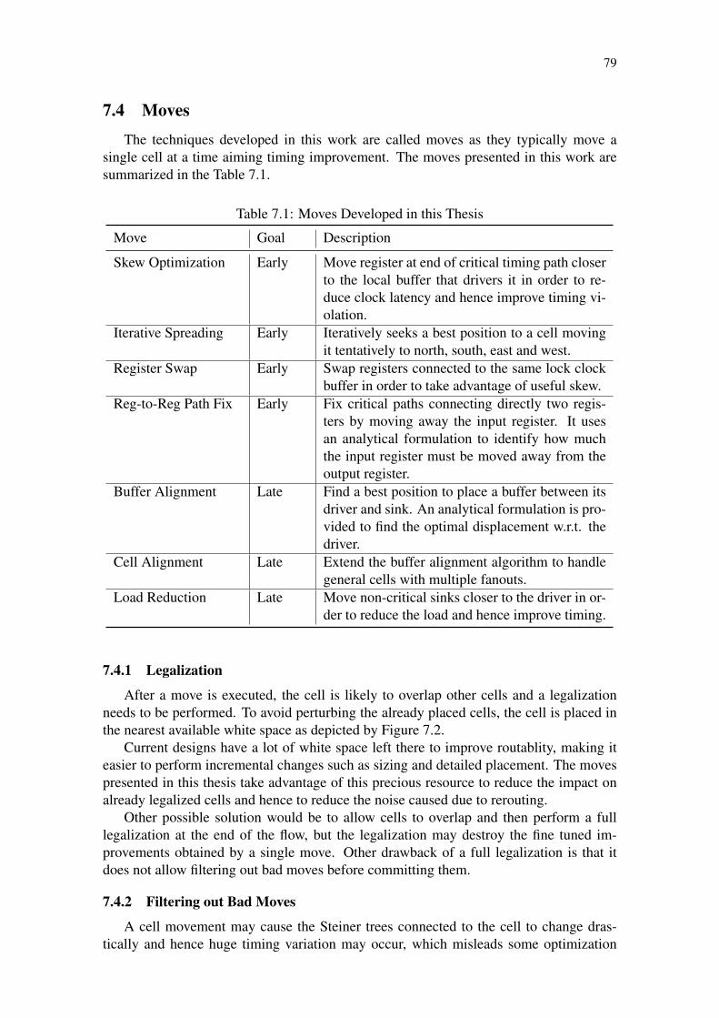
79
7.4 Moves
The techniques developed in this work are called moves as they typically move asingle cell at a time aiming timing improvement. The moves presented in this work aresummarized in the Table 7.1.
Table 7.1: Moves Developed in this Thesis
Move Goal Description
Skew Optimization Early Move register at end of critical timing path closerto the local buffer that drivers it in order to re-duce clock latency and hence improve timing vi-olation.
Iterative Spreading Early Iteratively seeks a best position to a cell movingit tentatively to north, south, east and west.
Register Swap Early Swap registers connected to the same lock clockbuffer in order to take advantage of useful skew.
Reg-to-Reg Path Fix Early Fix critical paths connecting directly two regis-ters by moving away the input register. It usesan analytical formulation to identify how muchthe input register must be moved away from theoutput register.
Buffer Alignment Late Find a best position to place a buffer between itsdriver and sink. An analytical formulation is pro-vided to find the optimal displacement w.r.t. thedriver.
Cell Alignment Late Extend the buffer alignment algorithm to handlegeneral cells with multiple fanouts.
Load Reduction Late Move non-critical sinks closer to the driver in or-der to reduce the load and hence improve timing.
7.4.1 Legalization
After a move is executed, the cell is likely to overlap other cells and a legalizationneeds to be performed. To avoid perturbing the already placed cells, the cell is placed inthe nearest available white space as depicted by Figure 7.2.
Current designs have a lot of white space left there to improve routablity, making iteasier to perform incremental changes such as sizing and detailed placement. The movespresented in this thesis take advantage of this precious resource to reduce the impact onalready legalized cells and hence to reduce the noise caused due to rerouting.
Other possible solution would be to allow cells to overlap and then perform a fulllegalization at the end of the flow, but the legalization may destroy the fine tuned im-provements obtained by a single move. Other drawback of a full legalization is that itdoes not allow filtering out bad moves before committing them.
7.4.2 Filtering out Bad Moves
A cell movement may cause the Steiner trees connected to the cell to change dras-tically and hence huge timing variation may occur, which misleads some optimization

80
Figure 7.2: Legalization via Nearest White Space Search
Before After
Source: from author (2015)
methods. To avoid timing degradation caused by such changes and also by legalizationnoise, local timing is evaluated and the move is optionally committed only if the localtiming does not degrade.
The degradation is computed as ∆cost where the cost is the sum of the weightedarrival times of the neighboring pins of the cell. In this work, the weight is set tocentrality+criticality, which gives more importance to TNS-critical pins. This weight-ing function also helps to avoid focusing too much on Worst Negative Slack (WNS) im-provement which may cause large degradation on TNS.
7.5 Late Optimization
In this section we present a set of techniques that targets to decrease wire load capac-itance and resistance of the critical nets. We also propose an analytical formulation toexplore driver strength in critical nets to reduce late violations. We obtain the optimumlocal position where the late timing violation is locally minimized.
7.5.1 Buffer Balancing
After buffer insertion, the circuit may contain several buffer chains. However place-ment is not always aware of the different driver strengths of cells that compose the chainincluding the initial and final possible non-buffer cells, which may degrade timing. Thegeneral idea of buffer balancing is shown in Figure 7.4 where the delay of the path seg-ment is reduced if the buffer is placed closer to its sink.
To find the displacement where the delay is minimum, an analytical formula is de-vised. This formula takes into account the cell strengths assuming that the interconnec-tion is modeled as an RC tree and its delay is computed via Elmore delay (ELMORE,1948). We assume the buffer’s driver and its sink are fixed while the buffer can freelymove between them. Moreover the driver is also assumed to drive only the buffer. Thisidea can be applied iteratively so that buffer chains with arbitrary number of buffers canbe handled. In our experiments, only a few iterations are necessary to align all the buffersin the design.
Figure 7.6 shows a single buffer chain, whose delay,D can be described as in Equation(7.2) using the Elmore delay model.

81
Figure 7.4: Buffer Balancing Technique aims to find a buffer position that minimizestiming violation.
Initial Position Optimized Position
Source: from author (2015)
Figure 7.6: Buffer Balancing Technique Modeling
Source: from author (2015)
D = R0 (C1 + d0Cw) + d0Rw
(C1 +
d0Cw2
)+ p0
+R1 (C2 + d1Cw) + d1Rw
(C2 +
d1Cw2
)+ p1
(7.2)
whereR0 is the resistance of the buffer’s driver, C1 is the input pin load capacitance of thebuffer, d0 is the wirelength from driver to buffer, Rw is the wire resistance per unit-length,Cw is the wire capacitance per unit-length,R1 is the buffer resistance, d1 is the wire lengthfrom the buffer to its sink, C2 is the load capacitance on the input sink pin, p0 and p1 areparasitic delay of the driver and buffer, respectively.
Considering that d = d0 + a + d1 where a is the distance of input and output bufferpins, the minimum delay is obtained by setting ∂D
∂d0= 0 as described by Equation (7.3),
which for practical purposes is clamped in the range [0, d].
d0 =Cw (R1 −R0) +Rw [C2 − C1 + Cw (d− a)]
2CwRw
(7.3)
Equation (7.4) defines the optimal displacement of the buffer w.r.t. its driver. As Manhat-

82
tan routing is commonly used, this may lead to multiple optimal positions. However byplacing the buffer on the straight line connecting the driver and sink may help straight-ening the path which is a very common way to improve delay. Therefore, the buffer isplaced on the straight line by setting its position to
Pb = Pd +d0d× (Ps − Pd) (7.4)
where Pb is the new buffer position, Pd is the driver position and Ps is the sink position.
7.5.2 Cell Balancing
In this section, we extend the formulation of buffer balancing to handle more generalcases, i.e, non-buffers cells with multiple input pins and driving multiple sinks. To do so,we first compute the cell position for each timing arc individually and then combine theresults to obtain the best cell position.
We restrict the region of a cell movement between the point it connects to its drivingtree, here called driver point, and the point it connects to the sink tree, sink point, as shownin Figure 7.7.
Figure 7.7: Cell Balancing Technique Modeling
driver point
sink point
Source: from author (2015)
Let Rup be the upstream resistance of the driver point (i.e. the sum of the resistancefrom the driver point up to the root of the tree, which includes the driver resistance). LetDup be the delay at the driver point when the branch from the driver point to the cellis removed. Let Cdown be the downstream capacitance of the sink point excluding anycapacitance added by the branch connecting the cell to the sink point (i.e. sum of allcapacitances from the sink point down to all leaf points including pin capacitances). Thenthe delay, D, from the driver cell being considered and the sink point is given by Equation(7.5)
D = D0 +D1 (7.5)

83
whereD0 =Dup +Rup (C1 + Cwd0)
+ d0Rw
(C1 +
d0Cw2
)+ p0
(7.6)
is the delay from the driver cell to the input of current cell and
D1 = R1 [Cdown + d1Cw] + d1Rw
[Cdown +
d1Cw2
]+ p1 (7.7)
is the delay from the current cell to the sink point, C1 is cell input pin capacitance, d0 isthe wirelength between the driver point and the cell, d1 is wirelength from the cell to thesink point, R1 is the cell resistance and p0 and p1 are the driver and cell parasitic delay,respectively.
To a reason that will be apparent later D0 and D1 are weighted by w0 and w1 respec-tively so that the weighted delay is given by Equation (7.8).
D = w0D0 + w1D1 (7.8)
Considering that d = d0 + a+ d1 where a is the distance of input and output cell pins,the minimum delay is obtained by setting ∂D
∂d0= 0 as described by Equation (7.9) which
for practical purposes is also clamped in the range [0, d].
d0 =w1CwR1 − w0RwC1 + w1Rw [Cw(d− a) + Cdown)]
RwCw(w0 + w1)
− w0RupCwRwCw(w0 + w1)
(7.9)
Note that Equation (7.9) reduces to Equation (7.3) for a single buffer chain. The finalposition is obtained in the same way as in the buffer alignment technique.
Since we may have several target positions, one for each input pin, they are combinedby their weighted average. Where the weight of each position is the importance of theinput pin.
The reason to weight the partial delays is due to the effect on the delay of side cells. Byminimizing the delay of a tuple driver-cell-sink we may degrade the delay of other cellsnearby. For instance, if the critical sink of the driver is not the cell we are handling andif the cell moves away from the driver it will probably increase the delay on the criticalcell due to the increased load capacitance. Here we use the driver’s output pin importanceas w0 and the cell’s output pin importance as w1. Note that if the driver is more criticalthan the sink, the cell will likely get close to the driver, reducing its load capacitance andhence improving its delay.
7.5.3 Load Optimization
For critical nets with more than two cells, the sink cells with no late violations (i.e.positive slack) are moved closer to their driver cells in order to improve timing as shownin Figure 7.8. The main idea behind this approach is to reduce the interconnection loadcapacitance of critical nets and therefore improve the delay of the driver cell. Since thesinks moved are non-critical, the paths passing through them are likely to not generatenew violations.
The movements are accepted only if they actually reduce timing violations in criticalnets and do not cause timing violation in the sink cells. Otherwise, non-critical sink cells
84
are kept in their initial position. To accomplish that, after routing trees are re-built, thetiming is updated locally.
Figure 7.8: Load Reduction of critical nets. Non-critical sinks (gray cells) are movedcloser to their driver cell (D).
CS
D
Initial
CS
D
OptimizedSource: from author (2015)
7.6 Early Optimization
In this section, techniques for early violation mitigation are presented. Let us considera timing path between two registers. The register at the beginning of the path is calledinput register and the register at the end, output register. The early slack in a register-to-register path is defined by Equation (7.10)
slackearlyD = atearlyD − ratearlyD
slackearlyD = learlyi + dearlypath − llateo − thold
(7.10)
where atearlyD and ratearlyD are the early arrival and required time respectively at the datainput pin of the input register, learlyi and llateo are the early and late clock latency at theclock pin of input and output registers respectively, dearlypath is the early delay among theregisters and thold is the hold time of the output register.
According to Equation (7.10), the early slack can be improved by (1) increasing thepath delay, (2) increasing the clock latency at the input register, (3) decreasing the clocklatency on the output register and (4) decreasing hold time. In this work, hold time isconsidered constant. The difference among the clock latencies is called clock skew.
In this section, techniques for early violation mitigation during the placement are alsopresented. We present four algorithms targeted to minimize early violations. The pro-posed algorithms explore wire load capacitance and resistance of the critical nets anduseful clock skew to minimize early timing violations.
7.6.1 Skew Optimization
The early slack can be improved by decreasing the clock latency on the output register.One way to achieve that is by moving the register closer to the clock source (e.g. a localclock buffer) as depicted in Figure 7.10.
Although the latency on the moved register is typically reduced, there might be sideeffects as latency changes on other registers and it can impact on other data path delay.

85
Figure 7.10: Useful Clock Skew Optimization by Moving Registers Closer to Local ClockBuffers.
LCB
Initial
LCB
OptimizedSource: from author (2015)
Also a register can be both the start and end point of different paths. So a reduction onthe latency may improve the slack on the incoming path, but may worsen the slack on theoutgoing path. However, our experimental results showed that this technique is effectiveto improve early slack, on average.
7.6.2 Iterative Spreading
The iterative cell spreading tentatively moves all cells with early timing violation tonorth, south, east and west as shown in Figure 7.12. If a better position is not found,the search area is increased. It is limited by maximum cell displacement. The cost ofa position is calculated updating timing locally and checking if the arrival time in theinvolved pins have increased.
Figure 7.12: Iterative Spreading
Source: from author (2015)
7.6.3 Register Swap
Register swap tries to avoid the side effect on clock latency present in useful clockskew optimization (Section 7.6.1). Assuming that the registers are all the same (e.g. samesize, Vth), by swapping the registers driven by a same clock source, the clock tree and itstiming characteristics will not change. Hence the latency on each tree endpoint can beseen as constant.

86
The register swap is modeled as an assignment problem similar to (HELD; SCHORR,2014), which can be optimally solved in polynomial time by the Hungarian algorithm(KUHN, 1955). The current register positions are seen as the slots to where the registershould be assigned as illustrated by Figure 7.13. The goal is to minimize the total cost ofthe assignment.
Figure 7.13: Register Swap by Optimal Assignment
LCB
3
2
7
4
1
6
5
8
LCB
C
B
G
D
A
F
E
H
LCB
8->C
7->B
2->G
5->D
6->A
4->F
1->E
3->H
C
B
G
D
A
F
E
H
1
2
3
4
5
6
7
8
6
7
8
5
1
4
2
3
.
.
.
Source: from author (2015)
The cost to assign a register i to a slot k is set as in Equation (7.11) where criticalityearlyD
and criticalityearlyCK are the criticality of the data and clock pins of the register, respec-tively. The maximum displacement constraint can be modeled by setting an infinity costwhenever an assignment violates the maximum allowed displacement.
cost(i, k) = llatecriticalityearlyD − learlycriticalityearlyCK (7.11)
The idea behind this cost function is as follows. When the register acts as the outputregister (path ends at the data pin), according to Equation (7.10), its clock latency shouldbe decreased to improve slack. In terms of assignment cost, a larger latency should implya larger cost (+llatecriticalityearlyD ). Similarly, when the register acts as the input register(path starts at the clock pin), its clock latency should be increased. From an assignmentcost point of view, a larger latency should imply a smaller cost (−learlycriticalityearlyCK ).The latencies are weighted by pin criticalities to optimize latency based on the influenceof registers on timing violations.
7.6.4 Register-to-Register Path Fix
A common source of hold violations is a path connecting directly two registers, i.e.no combinational logical cells between them, as show Figure 7.14.
Besides skew optimization, early (hold) violations can be fixed by increasing the tim-ing path delay. By setting the early slack to zero in Equation (7.10), the path delay thateliminates the violation is given by Equation (7.12).

87
Figure 7.14: Register-to-Register Early Violation Path Fix
LCB
Source: from author (2015)
dearlypath = llateo + thold − learlyi (7.12)
In the case of a direct path between registers, the timing path delay is simply composedby the cell delay plus the wire delay and it can be increased by moving the registers apart.Assuming that the cell delay is modeled via its driver resistance and the wire via Elmoredelay, Equation (7.12) can be rewritten as in Equation (7.13) where x is the distancebetween the input and output registers and K = llateo + thold − learlyi .
K = Ri (xCw + Co) + xRw
(xCw
2+ Co
)(7.13)
Assuming that the latencies do not change as the registers are moved apart and thatthe hold time is also constant (i.e. K is constant), Equation (7.13) can be solved w.r.t. xas in Equation (7.14).
x =
√2CwRwK + Co
2Rw2 + Cw
2Ri2 − CoRw − CwRi
CwRw
(7.14)
Once the optimum displacement is calculated, the input register is moved away fromthe output register following the straight line formed by the two registers.
7.7 Flow
The techniques presented in this thesis are combined in a flow for timing-driven de-tailed placement as shown in Figure 7.15. The diamond shape indicates that the steps arerun until the quality of the result is not improved. The circle shape indicates that the qual-ity of the result can degrade a certain number of times before exiting. The best solutionfound is restored.
Since the techniques are independent from each other, they can be combined in anyorder, although a specific combination may lead to better results than others. The partic-ular order used in this work was chosen empirically and intuitively so that techniques cancooperate, instead of compete with each other.
The flow is divided into two main phases: early optimization and late optimization.Usually after each optimization technique the quality of results is asserted; if it degradedthe current solution is discarded and the previous one recovered. This way we can filterbad results caused any imprecision in the present techniques. After each step, the routingand timing are updated incrementally.

88
Figure 7.15: Timing-Driven Detailed Placement Flow
Early Violation Optimization
Late Violation Optimization
Skew Optimization
Iterative Spreading
Register Swap
Register-to-Register Path Fix
Buffer Balancing
Cell Balancing
Load Optimization
Initial
Placement
Final
Placement
Source: from author (2015)
The first method during the early optimization is the iterative local search, which isthe only step allowed to degrade the quality of result. The rationale is that the clock skewhas a large influence on early violations which may introduce a large noise in the timingchange estimate. Experiments show that is better to allow degradation and keep trackof the best solution than to stop immediately when a degradation occurs. If the iterativelocal search was not able to remove all the early violations, the register swap and optimalshifting are executed.
Late optimization comprises a loop composed of one iteration of the three techniquesfor late violation presented in this thesis: buffer alignment, cell alignment and load opti-mization. The load optimization was defined to run last as it may get harder to a cell to bealigned if its non critical sink are placed next to it.
7.8 Experimental Setup
Our flow and techniques are empirically validated using the ICCAD 2015 timing-driven detailed placement contest infrastructure.

89
7.8.1 Quality Score
Quality score proposed by International Conference on Computer Aided Design (ICCAD)2014 Contest is used to evaluate our timing-driven detailed placement flow. The qualityscore of a placement solution is defined by the Equation (7.15)
Q = 100× wabu (abu′ − abu)
∑i∈tns, wns
wi Qi
(7.15)
where
Qwns =∑
j∈early, late
wj
(1−
WNS′jWNSj
)(7.16)
indicates how much the current WNS has improved from the initial WNS’ and
Qtns =∑
k∈early, late
wk
(1− TNS′k
TNSk
)(7.17)
indicates how much the current TNS has improved from the initial TNS’. In the infras-tructure of the ICCAD 2014 and 2015 contest (KIM; HUJ; VISWANATHAN, 2014;KIM; HU; VISWANATHAN, 2015), the weighting factors are defined as: wtns = 2.0,wwns = 1.0, wabu = 1.0, wearly = 1.0, and wlate = 5.0. The maximum quality score ob-tained from slack improvement is 1800 points when all timing violations are eliminated.
7.8.2 Benchmarks
In Table 7.2 the configuration of the circuits from ICCAD 2015 Contest is presented.The set of benchmarks is composed by eight circuits that have from 760K to 1.9M cells.The algorithms were evaluated for two maximum displacement (MaxDis). One of themis very restricted, less than 50µm, and the second one has more room to search for asolution, up to 500µm.
Table 7.2: Configuration of the ICCAD 2015 Contest benchmarks.Benchmarks Data Ratio of Timing Violations
Circuits #Gates Tclk(ns)
MaxDis(µm)
ABUPenalty
STWL(um)
MaxUtil.
Early (ps) Late (ps) Early (×10−3) Late
WNS TNS WNS TNS WNS/Tclk
TNS/Tclk
WNS/Tclk
TNS/Tclk
superblue16 768068 5.5 20-400 3.34E-2 9.33E+7 0.85 -10.65 -113.75 -4.58E+3 -7.76E+5 1.94 20.68 0.83 141.10superblue18 981559 7.0 30-400 4.01E-2 5.77E+7 0.85 -19.01 -283.00 -4.55E+3 -1.03E+6 2.72 40.43 0.65 147.83superblue4 795645 6.0 50-500 4.40E-2 7.15E+7 0.90 -12.55 -519.39 -6.22E+3 -3.48E+6 2.09 86.56 1.04 579.45
superblue10 1876103 10.0 20-400 4.17E-2 2.05E+8 0.87 -8.62 -620.95 -1.65E+4 -3.32E+7 0.86 62.10 1.65 3,315.28superblue7 1931639 5.5 50-400 2.97E-2 1.40E+8 0.90 -7.65 -1,985.85 -1.52E+4 -1.86E+6 1.39 361.06 2.77 337.71superblue1 1209716 9.5 40-500 5.37E-2 9.59E+7 0.80 -9.34 -317.44 -4.98E+3 -4.60E+5 0.98 33.41 0.52 48.39superblue3 1213253 10.0 40-400 2.87E-2 1.14E+8 0.87 -78.36 -1,458.78 -1.01E+4 -1.50E+6 7.84 145.88 1.01 150.28superblue5 1086888 9.0 30-400 2.08E-2 1.08E+8 0.85 -36.77 -591.42 -2.57E+4 -6.97E+6 4.09 65.71 2.86 773.91
7.8.3 Assumptions and Limitations
The main limitation of this thesis’ approach is the use of Elmore model to estimate theinterconnection timing characteristics. Although in absolute terms Elmore delay may notbe an accurate estimation of interconnection delay, still optimizing it will faithfully leadto the optimization of the actual interconnection delay.
Also Elmore delay is more accurate for short wires and nets with small number ofpins, which is the vast majority of nets in a design as big nets are usually buffered andwirelength minimization is a target during the flow optimization.

90
On the bright side, Elmore delay is fast to compute when compared to MOR and Spicesimulation. So, in spite of its inaccuracy, it allows more optimization transformations tobe done in the same amount of time.
The contest setup also imposes a hard constraint on the maximum displacement al-lowed to a cell. The main reason is to avoid large perturbations on the global solution,which may be optimized for other metrics as congestion and/or goals as power islands.However this also imposes an artificial bound on the achievable improvements, but, onthe other hand, allows one to identify which techniques work better for small or largedisplacements.
7.9 Library Characterization
The drive strength aware techniques proposed in this thesis use the switch gate levelto model each arc of cells. This model uses a single resistance, usually called driverresistance, to approximate the arc delay. The smaller this resistance, the larger the arcdrive strength (ability to draw current) and hence the faster it is.
Since arcs may have different drive strengths depending on the transition, a separatedrive resistance is computed for rise and fall transitions. However, for clarity, this ishidden in the following description.
To obtain the driver resistance, the arc delay is sampled for several loads and approx-imated by a linear function using least square fit as shown in Figure 7.16.
Figure 7.16: Estimating the Driver Resistance of a Timing Arc (Cell)
gain
delay
Source: from author (2015)
The arc delay is then described by Equation (7.18) where p is the intrinsic or parasiticdelay, Rdriver is the driver resistance and Cload is the load.
d = p+RdriverCload (7.18)
The delay samples are obtained directly from the 2D lookup-table that describe eachtiming arc in the Liberty file. As this table requires also an input slew besides the outputload, a reference slew is computed to characterize the common and expected slew in thedesign.
The reference slew is obtained from the output slew of the smallest inverter availablein the library driving itself until the slew converges at the output as shown in Figure 7.17.

91
Figure 7.17: Reference Slew Computation
Source: from author (2015)
Table 7.3 presents the actual delay from look-up table and the delay computed via theRC modeling for a cell in the library. As it can be seen, for the library used in the contestthe model predicts almost precisely the delay from library for the reference slew. Thisbehavior is also seen for other arcs in the library.
Table 7.3: Comparison between the actual delay and the delay estimated via driver resis-tance.
Gain Look-up Table Model Error (%)
1 22.9493 22.9431 -0.03%2 29.1893 29.193 0.01%4 41.6933 41.6928 0.00%8 66.6893 66.6924 0.00%
16 116.693 116.692 0.00%32 216.689 216.69 0.00%
The linear relation of delay with respect to the gain is a well-known and useful prop-erty as presented in the Logical Effort theory. Although the relation usually does not holdas precisely as in the library used for the ICCAD contest, it can still provide a fair estimateof cell delays. For this reason, this flow is expected to work with other libraries as well.
Table 7.4 presents the improvements of this flow w.r.t. the initial placement for thelong maximum displacement. As it can be seen this flow can provide on average 10.25%reduction on WNS and 32.8% on TNS for late timing mode with an impact of just 1.74%on wirelength and an increase of 11.66% on density as measured by ABU.
Table 7.5 presents the improvements of this flow w.r.t. the initial placement for theshort maximum displacement. As it can be seen this flow can provide on average 4.33%reduction on WNS and 13.23% on TNS for late timing mode with an impact of just 0.23%on wire length and an increase of 4.41% on density as measured by ABU.
Table 7.6 presents the comparison of this flow and the 1st place of ICCAD 2015 Con-test for long displacement. As it can be seen this flow provides a clear improvement overthe best contest results in terms of quality score of almost 60% on average. Most of qual-ity score gains however comes from improvements on early violations. On late violations,this flows can provide almost 2% improvement on WNS and almost 10% improvementon TNS on average. The gains on WNS are bounded as some cells on the critical paths ofbenchmarks are fixed reducing the room for improvement and flattening the improvementresults. This is more evident on the benchmark superblue7 where all cells in the criticalpath are fixed.

92
Table 7.4: Improvement of this flow over the initial placement results for long maximumdisplacement.
Benchmark ABU StWL eWNS eTNS lWNS lTNS QS
superblue16 16.92% 1.50% -100.00% -100.00% -18.61% -70.33% 1,090.21superblue18 2.28% 0.99% -100.00% -100.00% -17.46% -39.39% 780.46
superblue4 19.26% 4.78% -100.00% -100.00% -8.60% -32.10% 658.35superblue10 11.32% 2.43% -100.00% -100.00% -5.51% -15.79% 483.11
superblue7 1.68% 0.47% -9.40% -2.84% 0.00% -27.40% 288.90superblue1 22.33% 2.17% 0.00% -88.41% -10.65% -26.17% 485.83superblue3 7.22% 0.52% -83.77% -99.13% -17.09% -37.16% 737.50superblue5 12.28% 1.04% -100.00% -100.00% -4.10% -14.06% 459.96
avg 11.66% 1.74% -74.15% -86.30% -10.25% -32.80%
Table 7.5: Improvement of this flow over the initial placement results for short maximumdisplacement.
Benchmark ABU StWL eWNS eTNS lWNS lTNS QS
superblue16 8.95% 0.27% -92.13% -98.91% -4.94% -38.29% 695.41superblue18 0.61% 0.10% -17.88% -67.92% -8.91% -8.55% 283.70superblue4 3.55% 0.34% 6.24% -76.50% -3.80% -10.69% 272.25
superblue10 5.53% 0.26% -26.09% -57.62% -1.12% -3.69% 183.42superblue7 1.58% 0.14% -9.40% -2.86% 0.00% -14.21% 157.14superblue1 7.27% 0.42% 0.00% -85.07% -7.37% -17.01% 375.64superblue3 1.74% 0.09% -65.39% -72.03% -7.18% -9.89% 344.03superblue5 6.04% 0.20% -2.25% -50.05% -1.31% -3.54% 144.11
avg 4.41% 0.23% -25.86% -63.87% -4.33% -13.23%

93
A drawback of this flow is the increase of density as measured by ABU. The ABUmetric has a small impact on quality score, but this increase indicates that some regionsof the design are being over filled,which will lead to congestion issues. The main culpritof such increase is the load optimization technique, which moves non-critical sinks closerto its driver. Preliminary analysis show that this can be mitigated by scaling the totaldisplacement of the sinks the the importance of the driver. That is, the more critical thedriver, the more the sink is moved. Applying this simple scaling scheme, the impact onABU is reduced, but with negative impact on WNS e TNS, although the overall qualityscore is still better than the 1st place.
Table 7.6: Comparison of this flow and results from the 1st place at ICCAD 2015 contestfor long maximum displacement.
Benchmark ABU StWL eWNS eTNS lWNS lTNS QS
superblue16 -3.28% 1.07% -100.00% -100.00% -3.04% -13.31% 21.84%superblue18 -8.19% 0.78% -100.00% -100.00% -1.56% -19.16% 27.30%superblue4 8.79% 4.59% -100.00% -100.00% -1.32% -4.21% 29.77%
superblue10 7.26% 2.32% -100.00% -100.00% -3.09% -11.42% 166.42%superblue7 -3.86% 0.35% 2.58% -1.47% 0.00% -10.74% 43.93%superblue1 16.75% 1.99% -43.89% -54.52% -2.73% -3.36% 40.16%superblue3 -0.58% 0.32% -3.19% -94.06% -3.36% -18.59% 33.67%superblue5 10.48% 0.83% -100.00% -100.00% 1.47% 2.45% 156.21%
avg 3.42% 1.53% -68.06% -81.26% -1.70% -9.79% 64.91%
For short maximum displacement, as it can be seen in Table 7.7, this flow still providesthe best results on average in terms of quality score, but now the results are less expressive.Since cells are allowed to be moved, the maximum achievable improvements are expectedto be smaller.
Table 7.7: Comparison of this flow and results from the 1st place at ICCAD 2015 contestfor short maximum displacement.
Benchmark ABU StWL eWNS eTNS lWNS lTNS QS
superblue16 -10.33% 0.03% -89.99% -95.96% -0.20% -6.87% 32.53%superblue18 -5.55% 0.02% 310.12% 30.84% 0.58% 0.29% -22.33%
superblue4 1.14% 0.32% 119.35% -29.82% 0.70% -2.83% -5.32%superblue10 1.32% 0.19% -26.08% -27.12% 0.71% -1.80% 63.97%
superblue7 -2.94% 0.09% 2.58% -0.75% 0.00% -6.48% 59.56%superblue1 -0.70% 0.26% 144.18% 14.04% -1.28% 1.93% -16.07%superblue3 -5.09% -0.02% -58.74% -40.31% -0.20% -1.37% 41.47%superblue5 2.37% 0.16% -2.25% -49.57% 1.16% -0.90% 254.37%
avg -2.47% 0.13% 49.90% -24.83% 0.18% -2.26% 51.02%
7.9.1 Move Gains
In this section, the individual gains for each move are presented. These results aregenerated by applying each move directly on the initial solution. Note, however, that

94
the combined results for some moves may be dependent on the improvement of othermethods.
Table 7.8 shows the average improvement of each move and some variations on allICCAD 2015 benchmarks considering the long maximum displacement. As it can be seenthe most effective method for early mitigation is the Iterative Spreading which reduces onaverage 30.94% and 56.38% the early WNS and TNS respectively. For late mitigation theCell Balancing technique is the most effective one. Two versions are shown: Steiner andDriver-Sink. The Steiner version is the one used in the flow, where the reference pointsare the Steiner point of the driver and sink net. The Driver-Sink version uses the driverand sink pin as the reference points. The Steiner version has better performance on TNSreduction while the Driver-Sink has a better performance on WNS reduction.
Table 7.8: Average improvement on quality score per move type for long maximum dis-placement.
Move Goal QS ABU StWL eWNS eTNS lWNS lTNS
Iterative Spreading Early 143.70 -0.04% 0.01% -30.94% -56.38% 0.00% 0.00%Skew Optimization Early 132.39 -0.11% 0.01% -29.91% -51.24% 0.00% 0.00%
Register Swap Early 73.71 0.00% 0.04% -15.88% -28.99% 0.00% 0.01%Reg-to-Reg Path Fix Early 99.21 -0.04% 0.02% -9.82% -44.69% 0.00% 0.00%
Buffer Balancing Late 88.65 0.00% 0.01% 0.00% 0.00% -3.92% -6.90%Cell Balancing (Steiner) Late 212.27 -0.45% 0.17% 0.00% -0.01% -7.31% -17.57%
Cell Balancing (Driver-Sink) Late 205.81 -0.13% 0.19% 0.00% -0.01% -7.70% -16.73%Load Reduction (Driver) Late 115.40 7.65% 1.39% 0.00% -0.17% -2.41% -10.32%
Load Reduction (Steiner) Late 49.75 1.04% 0.18% 0.00% -0.04% -1.01% -4.46%
Two versions of Load Reduction are also presented. The Driver version is the oneused in the flow where the non-critical sink are moved towards the driver. The Steinerversion move non-critical sinks towards the Steiner points where they connect to. As itcan be seen the Driver reduction has a much more expressive gain in terms of TNS, butthis comes at a cost of a large increase in the placement density. Load Reduction is themain culprit of the large increase of density seen in the final results.
7.9.2 Impact of Pin Importance (Criticality and Centrality)
The importance of pins indicates how much it is important for the timing closure of thedesign. Two metrics are used to compound the pin importance: criticality and centrality.
Table 7.9 shows the improvements of this metric when used for weighting in the CellBalancing technique compared to the Cell Balancing without weighting. To generate suchresult, the Cell Balancing was executed 5× on the initial placement solution. Note thatby weighting the displacements by the pin importance one can improve quality score by13.72% on average, which comes from a reduction of 1.29% and 3.68% in late WNS andlate TNS respectively.
7.9.3 Impact of Filtering Out Bad Moves
After a move is executed it may be filtered out if the impact on local timing indicatesthat it may lead to a timing degradation. Even though moves are trying to optimize timing,noises caused by rerouting or imprecision in the modeling may lead to worse results. Thatis why after each move the time is checked locally to filter out potentially bad moves.
Table 7.10 shows the degradation in the quality score and other metrics when thefiltering is disabled. As it can be seen, if the filtering is disabled the quality score can be

95
Table 7.9: Impact on results when pin importance (criticality and centrality) is used inCell Balancing.
eWNS eTNS lWNS lTNS ABU QS StWL
superblue16 0.00% 0.00% -5.71% -16.28% -0.95% 22.79% 0.04%superblue18 0.00% 0.00% -0.20% -0.30% -0.30% 1.61% 0.01%superblue4 0.00% 0.00% -1.02% -1.57% 0.56% 6.22% 0.07%
superblue10 0.00% 0.00% -0.11% -0.33% 0.90% 2.60% 0.05%superblue7 0.00% 0.00% 0.00% -2.27% -0.30% 11.32% 0.01%superblue1 0.00% 0.00% -0.36% -4.96% -0.15% 15.50% 0.03%superblue3 0.00% 0.00% -2.94% -3.13% 0.14% 44.44% 0.01%superblue5 0.00% 0.00% 0.04% -0.59% -0.14% 5.24% 0.05%
avg 0.00% 0.00% -1.29% -3.68% -0.03% 13.72% 0.03%
reduced on average by 13.40%. This empirically shows the efficiency of filtering out badmoves.
Table 7.10: Impact on results when bad move filtering is disabled.
Benchmark QS ABU StWL eWNS eTNS lWNS lTNS
superblue16 -21.28% 8.98% 1.60% - - 2.15% 74.16%superblue18 -9.97% 0.36% 0.88% - - 2.29% 11.46%superblue4 -17.50% 6.40% 3.75% - - -7.79% 22.00%
superblue10 -8.43% 1.84% 2.59% - - 2.14% 3.62%superblue7 -44.05% 1.82% 0.37% 0.00% 0.00% 0.00% 16.98%superblue1 -20.60% 9.72% 1.80% 0.00% 0.00% 5.70% 10.47%superblue3 19.53% 5.31% 0.64% 0.00% 0.00% -10.77% -14.50%superblue5 -4.89% 8.75% 0.85% - - -0.65% 2.89%
avg -13.40% 5.40% 1.56% 0.00% 0.00% -0.87% 15.89%
7.10 Conclusions
Placement is the stage in the design flow where the component positions are defined.Usually it is divided into three major steps: global placement, legalization and detailedplacement. Detailed placement takes the current legal placement solution and tries to fur-ther improve it by applying local changes. A timing-driven detailed placement performslocal changes in order to improve the circuit timing.
In this thesis, several single cell move-based techniques were presented to early andlate negative slack mitigation. Although these techniques work on one cell at a time, iter-atively they can be applied to achieve a good overall result as the empirical experimentsshowed.
Results were empirically validated using the ICCAD 2015 timing-driven detailedplacement contest setup. Experimental results show that our flow can significantly re-duce the timing violation from the wirelength global placement and compared to the 1stplace in the ICCAD 2015 contest.
Similar to the ISPD gate sizing contest, the ICCAD contest simplifies the placement

96
formulation by using Elmore delay for interconnections, ignoring false paths, assumingan ideal clock network.
However such simplifications are used and assumed even in industrial design flows inearly stages for two main reasons: runtime and lack of precise information. Moreover thefiltering out of bad moves used in the flow presented in this thesis can be performed usinga more precise timing engine, making it suitable for late stage in the design flow, althoughat cost of runtime.
The validity of such simplifications can be seen in the division of placement in globaland detailed placement. A global placement usually use a more simplified routing es-timation than the detailed placement, but still the final solution of the global placementcorrelates well with the desired output of a detailed placement.

97
8 FINAL REMARKS
In this thesis new techniques for gate sizing and timing-driven detailed placementwere presented.
The Lagrangian Relaxation formulation is a well-known and very effective way tosolve the gate sizing problem and can even produce the optimal solution for the continuousgate sizing problem. However, for the discrete case, Lagrangian Relaxation only can beused as a heuristic to find good solutions and the optimality is not guaranteed anymore.
A great challenge when applying LR to the discrete gate sizing problem is to achieveconvergence. It is easy to implement a LR for timing minimization, but when other ob-jectives are taken into account as leakage power, the convergence becomes an issue. Tocope with that a slack filtering scheme was developed where candidate cells are prunedif they worsen significantly the slack on vicinity cells. Moreover a lambda-delay sensi-tivity was presented to estimate the global timing change caused by a change on a cellimplementation.
These techniques were combined in a flow which was empirically evaluated using theISPD 2012 and 2013 gate sizing contest benchmarks. In those set of benchmarks this flowwas able to improve significantly the results over other state-of-the-art methods.
New techniques for timing-driven detailed placement were also presented for mitigat-ing early and late timing violations. The main technique uses the drive strength of cellsto find the optimal placement of a cell with respect to its driver and sink so that the pathsegment delay is reduced.
These techniques were combined in a flow which was empirically validated using theICCAD 2015 timing-driven detailed placement contest. For those set of benchmarks, thisflow was able to improve significantly the results over the 1st place in that contest.

98

99
REFERENCES
AHUJA, R. K.; MAGNANTI, T. L.; ORLIN, J. B. Network Flows: theory, algorithms,and applications. Upper Saddle River, NJ, USA: Prentice-Hall, Inc., 1993.
ALDOUS, D.; VAZIRANI, U. Go with the Winners Algorithms. In: FOCS 1994. Pro-ceedings. . . [S.l.: s.n.], 1994. p.492–501.
ALEGRETTI, C. G. P. et al. Analytical logical effort formulation for minimum activearea under delay constraints. In: SBCCI. Proceedings. . . IEEE, 2013. p.1–6.
BEASLEY, J. E. Modern Heuristic Techniques for Combinatorial Problems. In:REEVES, C. R. (Ed.). . New York, NY, USA: John Wiley & Sons, Inc., 1993. p.243–303.
BERKELAAR, M. R. C. M.; JESS, J. A. G. Gate sizing in MOS digital circuits withlinear programming. In: EURO-DAC. Proceedings. . . IEEE Computer Society, 1990.p.217–221.
BHATIA, R. Positive Definite Matrices (Princeton Series in Applied Mathematics).[S.l.]: Princeton University Press, 2006.
BOCK, A. et al. Local Search Algorithms for Timing-driven Placement Under ArbitraryDelay Models. In: DESIGN AUTOMATION CONFERENCE, 52., New York, NY, USA.Proceedings. . . ACM, 2015. p.29:1–29:6. (DAC ’15).
BOYD, S. P. et al. Digital Circuit Optimization via Geometric Programming. OperationsResearch, [S.l.], v.53, p.899–932, 2005.
BOYD, S.; VANDENBERGHE, L. Convex Optimization. New York, NY, USA: Cam-bridge University Press, 2004.
BURSTEIN, M.; YOUSSEF, M. Timing Influenced Layout Design. In: DESIGN AU-TOMATION, 1985. 22ND CONFERENCE ON. Proceedings. . . [S.l.: s.n.], 1985. p.124–130.
BUTZEN, P. F.; RIBAS, R. P. Leakage Current in Sub-Micrometer CMOS Gates.[S.l.]: UFRGS, 2005.
CHAN, P. K. Algorithms for Library-Specific Sizing of Combinational Logic. In: DAC.Proceedings. . . [S.l.: s.n.], 1990. p.353–356.

100
CHE, H. B. et al. Realizable Reduction of RC Networks with Current Sources for Dy-namic IR-Drop Analysis of Power Networks of SoCs. IEICE Transactions, [S.l.], v.92-A, n.2, p.475–480, 2009.
CHEN, C.-P.; CHU, C. C. N.; WONG, M. D. F. Fast and exact simultaneous gate andwire sizing by Lagrangian relaxation. IEEE Trans. on CAD of Integrated Circuits andSystems, [S.l.], v.18, n.7, p.1014–1025, 1999.
CHINNERY, D. G.; KEUTZER, K. Linear programming for sizing, Vth and Vdd assign-ment. In: ISLPED. Proceedings. . . ACM, 2005. p.149–154.
CHOU, H.; WANG, Y.-H.; CHEN, C. C.-P. Fast and effective gate-sizing with multiple-Vt assignment using generalized Lagrangian Relaxation. In: ASP-DAC. Proceedings. . .ACM Press, 2005. p.381–386.
CHU, C.; WONG, Y.-C. FLUTE: fast lookup table based rectilinear steiner minimal treealgorithm for vlsi design. Computer-Aided Design of Integrated Circuits and Systems,IEEE Transactions on, [S.l.], v.27, n.1, p.70–83, Jan 2008.
COUDERT, O. Gate sizing: a general purpose optimization approach. In: EUROPEANDESIGN AND TEST CONFERENCE, 1996. ED&TC 96. PROCEEDINGS. Proceed-ings. . . [S.l.: s.n.], 1996. p.214–218.
COUDERT, O. Gate sizing for constrained delay/power/area optimization. IEEE Trans.VLSI Syst., [S.l.], v.5, n.4, p.465–472, 1997.
DUTTA, S.; NAG, S.; ROY, K. ASAP: a transistor sizing tool for speed area and poweroptimization of static cmos circuits. In: ISCAS. Proceedings. . . [S.l.: s.n.], 1994. p.61–64.
ELMORE, W. C. The Transient Response of Damped Linear Networks with ParticularRegard to Wideband Amplifiers. Journal of Applied Physics, [S.l.], v.19, n.1, p.55–63,Jan. 1948.
FELDMANN, P.; FREUND, R. W. Efficient linear circuit analysis by Pade approximationvia the Lanczos process. IEEE Trans. on CAD of Integrated Circuits and Systems,[S.l.], v.14, n.5, p.639–649, 1995.
FISHBURN, J. P.; DUNLOP, A. E. TILOS: a posynomial programming approach to tran-sistor sizing. In: INT. CONFERENCE ON COMPUTER AIDED DESIGN, Las Vegas,Nevada - USA. Proceedings. . . [S.l.: s.n.], 1985. p.326–328.
GULATI, K.; KHATRI, S. P. Accelerating Statistical Static Timing Analysis UsingGraphics Processing Units. In: ASIA AND SOUTH PACIFIC DESIGN AUTOMATIONCONFERENCE, 2009., Piscataway, NJ, USA. Proceedings. . . IEEE Press, 2009. p.260–265. (ASP-DAC ’09).
GUPTA, R. et al. The Elmore delay as bound for RC trees with generalized input sig-nals. In: DAC ’95: PROCEEDINGS OF THE 32ND ANNUAL ACM/IEEE DESIGNAUTOMATION CONFERENCE, New York, NY, USA. Proceedings. . . ACM, 1995.p.364–369.

101
GUTH, C. et al. Timing-Driven Placement Based on Dynamic Net-Weighting for Effi-cient Slack Histogram Compression. In: SYMPOSIUM ON INTERNATIONAL SYM-POSIUM ON PHYSICAL DESIGN, 2015., New York, NY, USA. Proceedings. . . ACM,2015. p.141–148. (ISPD ’15).
HEDLUND, K. S. Aesop: a tool for automated transistor sizing. In: DAC. Proceedings. . .[S.l.: s.n.], 1987. p.114–120.
HELD, S.; SCHORR, U. Post-Routing Latch Optimization for Timing Closure. In: DAC.Proceedings. . . ACM, 2014. p.7:1–7:6.
HU, J. et al. Sensitivity-guided metaheuristics for accurate discrete gate sizing. In: IC-CAD. Proceedings. . . IEEE, 2012. p.233–239.
HU, S.; KETKAR, M.; HU, J. Gate Sizing for Cell-Library-Based Designs. IEEE Trans.on CAD of Integrated Circuits and Systems, [S.l.], v.28, n.6, p.818–825, 2009.
HUANG, Y.-L.; HU, J.; SHI, W. Lagrangian relaxation for gate implementation selection.In: ISPD. Proceedings. . . ACM, 2011. p.167–174.
KIM, J.; KIM, Y. H. Comparison of Circuit Reduction Techniques for Power NetworkNoise Analysis. JOURNAL OF SEMICONDUCTOR TECHNOLOGY AND SCI-ENCE, [S.l.], v.9, n.4, p.216–224, 2009.
KIM, M.-C.; HU, J.; VISWANATHAN, N. ICCAD 2015 Contest at IncrementalTiming-driven Placement. 2015.
KIM, M.-C.; HUJ, J.; VISWANATHAN, N. ICCAD-2014 CAD contest in incrementaltiming-driven placement and benchmark suite: special session paper: cad contest. In:COMPUTER-AIDED DESIGN (ICCAD), 2014 IEEE/ACM INTERNATIONAL CON-FERENCE ON. Proceedings. . . [S.l.: s.n.], 2014. p.361–366.
KONG, T. A novel net weighting algorithm for timing-driven placement. In: COM-PUTER AIDED DESIGN, 2002. ICCAD 2002. IEEE/ACM INTERNATIONAL CON-FERENCE ON. Proceedings. . . [S.l.: s.n.], 2002. p.172–176.
KUEHLMANN, A. The Best of ICCAD: 20 years of excellence in computer-aided de-sign. [S.l.]: Springer Science & Business Media, 2003.
KUHN, H. W. The Hungarian method for the assignment problem. Naval Research Lo-gistics Quarterly, [S.l.], v.2, n.1-2, p.83–97, 1955.
LI, L. et al. An efficient algorithm for library-based cell-type selection in high-performance low-power designs. In: ICCAD. Proceedings. . . IEEE, 2012. p.226–232.
LI, W. N. Strongly NP-Hard Discrete Gate Sizing Problems. In: ICCD. Proceedings. . .[S.l.: s.n.], 1993. p.468–471.
LIU, Y.; HU, J. A New Algorithm for Simultaneous Gate Sizing and Threshold VoltageAssignment. IEEE Trans. on CAD of Integrated Circuits and Systems, [S.l.], v.29,n.2, p.223–234, 2010.

102
LIVRAMENTO, V. S. et al. Fast and efficient Lagrangian Relaxation-based DiscreteGate Sizing. In: DESIGN, AUTOMATION TEST IN EUROPE CONFERENCE EX-HIBITION (DATE), 2013. Proceedings. . . [S.l.: s.n.], 2013. p.1855–1860.
MEAD, C.; CONWAY, L. Introduction to VLSI Systems. Boston, MA, USA: Addison-Wesley Longman Publishing Co., Inc., 1979.
MENEZES, N.; BALDICK, R.; PILEGGI, L. T. A sequential quadratic programming ap-proach to concurrent gate and wire sizing. IEEE Trans. on CAD of Integrated Circuitsand Systems, [S.l.], v.16, n.8, p.867–881, 1997.
MOORE, G. E. Progress in digital integrated electronics. In: ELECTRON DEVICESMEETING, 1975 INTERNATIONAL. Proceedings. . . IEEE, 1975. v.21, p.11–13.
MUSTAFA CELIK LARRY PILEGGI, A. O. IC Interconnect Analysis. [S.l.]: Springer,2002.
NGUYEN, D. et al. Minimization of dynamic and static power through joint assignmentof threshold voltages and sizing optimization. In: ISLPED. Proceedings. . . ACM, 2003.p.158–163.
ODABASIOGLU, A.; CELIK, M.; PILEGGI, L. T. PRIMA: passive reduced-order inter-connect macromodeling algorithm. IEEE Trans. on CAD of Integrated Circuits andSystems, [S.l.], v.17, n.8, p.645–654, 1998.
OZDAL, M. M.; BURNS, S.; HU, J. Gate sizing and device technology selection algo-rithms for high-performance industrial designs. In: ICCAD. Proceedings. . . IEEE, 2011.p.724–731.
OZDAL, M. M.; BURNS, S. M.; HU, J. Algorithms for Gate Sizing and Device ParameterSelection for High-Performance Designs. IEEE Trans. on CAD of Integrated Circuitsand Systems, [S.l.], v.31, n.10, p.1558–1571, 2012.
PANGRLE, B.; KAPOOR, S. Leakage power at 90nm and below. Available:http://www.eetasia.com/ARTICLES/2005JUN/B/2005JUN01_POW_EDA_TA.pdf, EE Times-Asia Online.
PAPA, D. et al. RUMBLE: an incremental timing-driven physical-synthesis optimizationalgorithm. Computer-Aided Design of Integrated Circuits and Systems, IEEE Trans-actions on, [S.l.], v.27, n.12, p.2156–2168, Dec 2008.
PILLAGE, L. T.; HUANG, X.; ROHRER, R. A. AWEsim: asymptotic waveform evalua-tion for timing analysis. In: DAC. Proceedings. . . [S.l.: s.n.], 1989. p.634–637.
POSSER, G. et al. Gate Sizing Using Geometric Programming. Analog Integrated Cir-cuits and Signal Processing, [S.l.], v.73, n.3, p.831–840, 2012.
PURI, R.; KUNG, D. S.; DRUMM, A. D. Fast and accurate wire delay estimation forphysical synthesis of large ASICs. In: ACM GREAT LAKES SYMPOSIUM ON VLSI,12., New York, NY, USA. Proceedings. . . ACM, 2002. p.30–36. (GLSVLSI ’02).
QIAN, J.; PULLELA, S.; PILLAGE, L. Modeling the ”Effective capacitance” for the RCinterconnect of CMOS gates. Trans. Comp.-Aided Des. Integ. Cir. Sys., Piscataway, NJ,USA, v.13, n.12, p.1526–1535, Nov. 2006.

103
RAHMAN, M.; SECHEN, C. Post-synthesis leakage power minimization. In: DATE.Proceedings. . . IEEE, 2012. p.99–104.
RAHMAN, M.; TENNAKOON, H.; SECHEN, C. Power reduction via near-optimallibrary-based cell-size selection. In: DATE. Proceedings. . . IEEE, 2011. p.867–870.
REIMANN, T. et al. Simultaneous Gate Sizing and Vt Assignment Using Fanin/FanoutRatio and Simulated Annealing. In: IEEE INTERNATIONAL SYMPOSIUM ON CIR-CUITS AND SYSTEMS, ISCAS 2013, Beijing, China. Proceedings. . . [S.l.: s.n.], 2013.
REIMANN, T.; SZE, C.; REIS, R. Challenges of cell selection algorithms in industrialhigh performance microprocessor designs. Integration, the VLSI Journal, [S.l.], 2015.
REN, H.; DUTT, S. A Network-Flow Based Cell Sizing Algorithm. In: THE INTER-NATIONAL WORKSHOP ON LOGIC SYNTHESIS. Proceedings. . . [S.l.: s.n.], 2008.p.7–14.
RUEHLI, A. E.; WOLFF, P. K.; GOERTZEL, G. Analytical Power/Timing Optimiza-tion Technique for Digital System. In: DESIGN AUTOMATION CONFERENCE, 14.,Piscataway, NJ, USA. Proceedings. . . IEEE Press, 1977. p.142–146. (DAC ’77).
SAKNRAI, T.; NEWTON, R. An exact solution to the transistor sizing problem forCMOS circuits using convex optimization. IEEE Journal of Solid-Slate Circuits, [S.l.],v.25, p.584–593, 1990.
SAPATNEKAR, S. S. et al. An exact solution to the transistor sizing problem for CMOScircuits using convex optimization. IEEE Trans. on CAD of Integrated Circuits andSystems, [S.l.], v.12, n.11, p.1621–1634, 1993.
SCHEFFER, L.; LAVAGNO, L.; MARTIN, G. (Ed.). EDA for IC implementation, cir-cuit design, and process technology. Boca Raton, FL: Taylor & Francis, 2006. (Elec-tronic design automation for integrated circuits handbook).
SHAH, S. et al. Discrete Vt assignment and gate sizing using a self-snapping continuousformulation. In: ICCAD. Proceedings. . . IEEE Computer Society, 2005. p.705–712.
SHEEHAN, B. N. TICER: realizable reduction of extracted rc circuits. In: ICCAD. Pro-ceedings. . . IEEE, 1999. p.200–203.
SHEWCHUK, J. R. An Introduction to the Conjugate Gradient Method With-out the Agonizing Pain. Available from Internet: ¡http://www.cs.cmu.edu/\˜quake-papers/painless-conjugate-gradient.pdf¿. Cited 2010 Jul 5.
SHIFREN, L. Leakage power – it’s worse than you think. Available: http://www.eetimes.com/document.asp?doc_id=1264175, EE Times.
SRIVASTAVA, A.; SYLVESTER, D.; BLAAUW, D. Power Minimization Using Simul-taneous Gate Sizing, dual-Vdd and dual-Vth Assignment. In: ANNUAL DESIGN AU-TOMATION CONFERENCE, 41., New York, NY, USA. Proceedings. . . ACM, 2004.p.783–787. (DAC ’04).
TENNAKOON, H.; SECHEN, C. Gate sizing using Lagrangian relaxation combinedwith a fast gradient-based pre-processing step. In: ICCAD. Proceedings. . . ACM, 2002.p.395–402.

104
TSAY, R.-S.; KOEHL, J. An analytic net weighting approach for performance optimiza-tion in circuit placement. In: DESIGN AUTOMATION CONFERENCE, 1991. 28THACM/IEEE. Proceedings. . . [S.l.: s.n.], 1991. p.620–625.
VISWANATHAN, N. et al. ITOP: integrating timing optimization within placement. In:ISPD. Proceedings. . . ACM, 2010. p.83–90.
WANG, Q. B.; LILLIS, J.; SANYAL, S. An LP-based methodology for improvedtiming-driven placement. In: DESIGN AUTOMATION CONFERENCE, 2005. PRO-CEEDINGS OF THE ASP-DAC 2005. ASIA AND SOUTH PACIFIC. Proceedings. . .[S.l.: s.n.], 2005. v.2, p.1139–1143 Vol. 2.
WILLIAM SWARTZ, C. S. Timing Driven Placement for Large Standard Cell Circuits.In: DESIGN AUTOMATION, 1995. DAC ’95. 32ND CONFERENCE ON. Proceed-ings. . . [S.l.: s.n.], 1995. p.211–215.
ZHOU, S. et al. Minimization of Circuit Delay and Power through Gate Sizing andThreshold Voltage Assignment. In: ISVLSI. Proceedings. . . IEEE Computer Society,2011. p.212–217.