Development of a compact, low-cost wireless device for ...
207
Virginia Commonwealth University Virginia Commonwealth University VCU Scholars Compass VCU Scholars Compass Theses and Dissertations Graduate School 2014 Development of a compact, low-cost wireless device for Development of a compact, low-cost wireless device for biopotential acquisition biopotential acquisition Graham Kelly Virginia Commonwealth University Follow this and additional works at: https://scholarscompass.vcu.edu/etd Part of the Biomedical Engineering and Bioengineering Commons © The Author Downloaded from Downloaded from https://scholarscompass.vcu.edu/etd/3559 This Thesis is brought to you for free and open access by the Graduate School at VCU Scholars Compass. It has been accepted for inclusion in Theses and Dissertations by an authorized administrator of VCU Scholars Compass. For more information, please contact [email protected].
-
Upload
khangminh22 -
Category
Documents
-
view
2 -
download
0
Transcript of Development of a compact, low-cost wireless device for ...

Virginia Commonwealth University Virginia Commonwealth University
VCU Scholars Compass VCU Scholars Compass
Theses and Dissertations Graduate School
2014
Development of a compact, low-cost wireless device for Development of a compact, low-cost wireless device for
biopotential acquisition biopotential acquisition
Graham Kelly Virginia Commonwealth University
Follow this and additional works at: https://scholarscompass.vcu.edu/etd
Part of the Biomedical Engineering and Bioengineering Commons
© The Author
Downloaded from Downloaded from https://scholarscompass.vcu.edu/etd/3559
This Thesis is brought to you for free and open access by the Graduate School at VCU Scholars Compass. It has been accepted for inclusion in Theses and Dissertations by an authorized administrator of VCU Scholars Compass. For more information, please contact [email protected].

DEVELOPMENT OF A COMPACT, LOW-COST WIRELESS DEVICE FOR BIOPOTENTIAL ACQUISITION
A thesis submitted in partial fulfillment of the requirements for the degree of Master of Science at Virginia Commonwealth University
by
GRAHAM KELLY B.S., Virginia Commonwealth University, 2011
Director: OU BAI, PH.D. Assistant Professor, Department of Biomedical Engineering
Virginia Commonwealth University
Richmond, VA
August, 2014

ii
Acknowledgements
I want to thank my advisor, Dr. Ou Bai, for providing me with the opportunity to work on a subject that I enjoy, and for his good humor even when I made stupid PCB layout mistakes that rendered a batch of boards mostly useless (and I only wish that had just happened once). Thank you for being the jolliest advisor I could possibly have. I also want to thank Dr. Fei for providing the equipment and workspace for all my soldering needs. I also thank my parents, Charles Kelly and Logan Smith, for their love and support, and for letting me mooch off of them for 24 years and counting. Without their continuous input of effort and generosity, I would be either homeless and uneducated, or dead (probably both). Thanks also to my brother, Jared Kelly, for his invaluably entertaining company in the times I just wanted to hang out and completely forget about “doing science.” I would like to thank my friends and lab-mates (and former lab-mates) Tyler Ferro, Chris Hagerty-Hoff, Plamen Nikolov, Jay Freitas, Natalie Vazquez, and Tareq al-Shargabi, for their company and their valuable input. Thanks also to my girlfriend, Marissa Shaffer, for her encouragement and for keeping me on track. Finally, I would like to thank Charles Taylor, for his willingness to take me under his wing way back in my just-finished-undergrad days, and for teaching me so much about the practicalities of engineering. If it weren’t for him, I would never have developed my interest in electronics in the first place, nor would I have been introduced to the vast maker community that encourages me to continue growing that interest. I learned as much about hands-on engineering work during my year-long stay in the Artificial Heart Lab as I had in four years of undergraduate training, and there are no words or estimation for how valuable that time was.

iii
Table of Contents
List of Tables ................................................................................................................... v
List of Figures ..................................................................................................................vi
List of Abbreviations and Symbols ................................................................................. vii
Abstract ........................................................................................................................... x
Introduction ..................................................................................................................... 1
Background ..................................................................................................................... 3
EEG and its Origins ..................................................................................................... 3
EEG Signal Acquisition ................................................................................................ 4
Wireless EEG Acquisition Devices .............................................................................. 5
Design Process ............................................................................................................. 10
Considerations and Parameters ................................................................................ 10
Openness .................................................................................................................. 10
Beaglebone and Beaglebone Black ........................................................................... 12
Initial Component Selection and Evaluation .............................................................. 14
First Prototype: Brainboard R0 .................................................................................. 19
Assembly Process ..................................................................................................... 21
Software and Firmware .............................................................................................. 22
Discussion ................................................................................................................. 27
Second Prototype: Brainboard R1 ............................................................................. 28
Assembly Process ..................................................................................................... 30
Software and Firmware .............................................................................................. 31
Design Differentiation ................................................................................................ 37
Final Design: Brainboard LW ..................................................................................... 38

iv
Results and Discussion ............................................................................................. 41
Signal Quality ......................................................................................................... 41
Power Consumption ............................................................................................... 57
Appendices ................................................................................................................... 72

v
List of Tables
Table 1: Part selections for initial prototype ................................................................... 15
Table 2: ADS1299 command definitions ....................................................................... 23
Table 3: RMS error between Brainboard LW and Brain Products V-Amp 16. ............... 43
Table 4: 60-Hz noise comparison between Brainboard LW and V-Amp 16................... 44
Table 5: List of common device states and corresponding current consumption .......... 60
Table 6: Component bill of materials ............................................................................. 62

vi
List of Figures
Figure 1: Brainboard R0 ................................................................................................ 22
Figure 2: Brainboard R1 ................................................................................................ 31
Figure 3: bq24074 lithium-ion/polymer battery charger, typical charge cycle. VLOWV
indicates the battery voltage at which the constant-current fast charge phase begins; IO(CHG) is synonymous with the larger of ICHG and IIN(MAX). .............................................. 35
Figure 4: Battery management expansion board .......................................................... 37
Figure 5: LTC1998 configured as low battery threshold detection with hysteresis ........ 39
Figure 6: Brainboard LW ............................................................................................... 41
Figure 7: Magnitude response to swept sinusoidal input ............................................... 44
Figure 8: Noise spectrum for shorted inputs .................................................................. 45
Figure 9: Noise spectrum at ADS1299 specified range ................................................. 46
Figure 10: Unfiltered noise histogram ............................................................................ 47
Figure 11: Noise histogram after 0-65 Hz low-pass filter ............................................... 48
Figure 12: Channel 3 amplitude spectrum comparison ................................................. 49
Figure 13: Channel 4 amplitude spectrum comparison ................................................. 50
Figure 14: Channel 5 amplitude spectrum comparison ................................................. 51
Figure 15: Channel 6 amplitude spectrum comparison ................................................. 52
Figure 16: Channel 3 time-domain comparison ............................................................. 53
Figure 17: Channel 4 time-domain comparison ............................................................. 54
Figure 18: Channel 5 time-domain comparison ............................................................. 55
Figure 19: Channel 6 time-domain comparison ............................................................. 56

vii
List of Abbreviations and Symbols
ADC Analog-to-digital converter
AFE Analog front-end
ALS Amyotrophic lateral sclerosis
ASF Atmel Software Framework
ASIC Application-specific integrated circuit
BBB Beaglebone Black
BCI Brain-computer interface
BOM Bill of materials
CMOS Complementary metal-oxide-semiconductor
CAD Computer-aided design
DMA Direct memory access
DMM Digital multimeter
DSP Digital signal processing
ECG Electrocardiogram
EEG Electroencephalogram
EEPROM Electrically erasable programmable read-only memory
EMG Electromyogram
EOG Electrooculogram
ESD Electrostatic discharge
viii
FCC Federal Communications Commission
FIR Finite impulse response
FPGA Field-programmable gate array
GUI Graphical user interface
HDL Hardware description language
I2C Inter-Integrated Circuit
IC Integrated circuit
IC Integrated circuit
IDE Integrated development environment
JTAG Joint Test Action Group
LDO Low-dropout (linear regulator)
LVTTL Low-voltage transistor-transistor logic
MCU Microcontroller unit
MEMS Micro-electromechanical system
MS Multiple sclerosis
PCB Printed circuit board
PRUSS Programmable real-time unit sub-system
RAM Random access memory
RF Radio frequency
SPI Serial Peripheral Interface
SRAM Static random-access memory
TI Texas Instruments

ix
TVS Transient voltage suppression
TWI Two-Wire Interface
TWIM Two-Wire Interface Master
UART Universal asynchronous receiver/transmitter
VLSI Very-large-scale integration

Abstract
DEVELOPMENT OF A COMPACT, LOW-COST WIRELESS DEVICE FOR BIOPOTENTIAL ACQUISITION By Graham S. Kelly, B.S. A thesis submitted in partial fulfillment of the requirements for the degree of Master of Science at Virginia Commonwealth University.
Virginia Commonwealth University, 2014.
Major Director: Ou Bai, Ph.D., Assistant Professor, Department of Biomedical Engineering
A low-cost circuit board design is presented, which in one embodiment is smaller than a
credit card, for biopotential (EMG, ECG, or EEG) data acquisition, with a focus on EEG
for brain-computer interface applications. The device combines signal conditioning, low-
noise and high-resolution analog-to-digital conversion of biopotentials, user motion
detection via accelerometer and gyroscope, user-programmable digital pre-processing,
and data transmission via Bluetooth communications. The full development of the
device to date is presented, spanning three embodiments. The device is presented both
as a functional data acquisition system and as a template for further development based

on its publicly-available schematics and computer-aided design (CAD) files. The design
will be made available at the GitHub repository https://github.com/kellygs/eeg.

1
Introduction
A brain-computer interface, or BCI, is a modality for human-computer interaction
whereby a person may control an external device using brain signals without muscular
intervention. The brain signals of interest may be time-varying electrical potentials
generated by firing neurons, variations in the brain’s magnetic field, or changes in local
blood flow, all of which are correlated with different mental states. One of the most
widely used signals is the electroencephalogram (EEG), since it has excellent temporal
resolution, can be measured non-invasively, and is comparatively inexpensive and
simple to acquire.
BCIs are often the best, or even the only, option for a variety of diseases and
traumas. They are of the few options available for victims of so-called “locked-in
syndrome,” a state in which voluntary muscle control is lost over the entire body. This
can be a unique disease or a symptom of advanced amyotrophic lateral sclerosis (ALS).
It was estimated that approximately 30,000 Americans had ALS in 1999, with an annual
incidence rate of one or two cases per 100,000 people [1]. BCI is also a promising
avenue for prosthetic limb technologies, an area of particular interest to the U.S. military
due to the increasing problem of limb loss among troops returning from Iraq and
Afghanistan. For instance, according to the Armed Force Health Surveillance Center, in
2011, 240 deployed troops required upper or lower limb amputation, higher than any
year prior. Furthermore, the total number of amputations occurring during all Iraqi and

2
Afghan conflicts was reported at 1,599 as of May 3, 2012 [2]. Outside of battle, over 1.7
million Americans live with at least one lost limb [3]. One study examining the
prevalence of U.S. limb loss up to 2005 estimated that as many as one in 95 Americans
may have had an amputation by the year 2050 [3]. With such need, it is no wonder that
BCI is an area of active research.
In the following, I present background on the EEG, especially in forms suitable
for use as a practical BCI (i.e. wearable, wireless systems). I then move on to discuss
the design rationale behind the prototype device presented herein, along with its design
evolution over time and its performance metrics as compared to a commercial system. I
conclude with future directions for the project.

3
Background
EEG and its Origins
The first electroencephalogram acquired from a human being is attributed to
Hans Berger, a German psychiatrist, who in 1929 published his findings on electrical
activity of the brain recorded from the scalp [4]. Despite initial skepticism from the
scientific community, EEG has proven to be one of history’s most important
contributions to clinical electrophysiology. Analysis of the EEG allows for noninvasive
determination of a number of clinically relevant parameters, including seizure
localization and classification [5], but also the detection of drowsiness [6], certain
affective states [7], and motor imagery [8], among others. It has also become a tool for
neurofeedback, which has shown potential as a clinical tool for enhancing self-
regulation and inducing neuroplasticity [9].
The EEG originates from the formation of dipoles within the brain as the result of
neuronal ion flow. Changes in relative ion concentration, and thus in net charge,
between the intracellular and extracellular spaces generate electric fields whose
orientations are determined by the orientation and geometry of the neurons from which
they originate. These electric fields cause wavelike movement of charge, known as
volume conduction, through the cranial contents and the cranium itself, ultimately
resulting in a distribution of nonzero electrical potentials on the scalp. Although these
potentials are present, the varying orientations of the neuronal dipoles, the large

4
number of different signal patterns being generated, and the distance over which any
given signal must propagate through volume conduction to reach the scalp invariably
produce a greatly attenuated and spatially smeared representation of the brain’s
electrical activity. Despite this, sufficiently sensitive equipment can detect resultant
changes in voltage across the scalp, albeit with poor spatial resolution.
EEG Signal Acquisition
The EEG is acquired through the placement of electrodes on the scalp, which
follow the scalp’s change in electrical potential. The potential difference between
electrodes can then be amplified to a workable level, at which point it is typically
digitized and stored on a computer for analysis.
Because the EEG is a tiny signal on the order of microvolts in amplitude, owing
to the summing and blurring effects of volume conduction, acquisition of good-quality
EEG signals has stringent requirements on the electrical impedance of the body-
electrode contact and the noise resistance of the transmission line between the
electrode and the amplifier. Minimization of the scalp-electrode impedance is typically
acquired through mechanical abrasion to remove the stratum corneum, the high-
impedance upper layer of the epidermis consisting of dead skin cells, followed by
application of an ionic gel between the electrode and the skin. Hairy areas such as the
head pose a challenge to this impedance minimization process, usually necessitating
more gel than would otherwise be used; in cases where maximum signal quality is
required, the hair is typically shaved. Although research is ongoing into dry, through-hair

5
electrodes that match the interface impedance (and thus signal quality) of the traditional
type, and some have even made it to market, wet electrodes remain the gold standard
for clinical EEGs.
The amplifier itself must also contribute as little noise as possible. Although past
amplifiers and analog-to-digital converters (ADCs) tended to run on high-voltage
supplies—e.g. ±12V or ±5V—necessitating very high gain, modern amplifiers are
capable of rail-to-rail operation from a single-ended voltage supply as low as 5V, 3.3V,
or 1.8V, and digital logic levels continue to fall. As a result, much lower gains can be
used. This effect is compounded by the advent of ultra-low-noise amplifiers and modern
analog-to-digital (A/D) techniques that allow acquisition with up to 24-bit nominal
precision. Sigma-delta ADCs, for example, drastically oversample the acquired signal
and then use noise-shaping filters and decimation to produce a lower-rate signal with
high precision; their inherent low-pass filtering mean that analog anti-aliasing
requirements are far less strict than in traditional ADCs. These innovations, combined
with improvements in wireless communication technology, mean that EEG amplifiers—
once bulky and high-powered devices—can now be miniaturized to the point of being
wearable devices.
Wireless EEG Acquisition Devices
The benefits of a small, wireless EEG system are numerous, both medical and
non-medical. An ambulatory EEG device either with wireless connectivity to a host
computer or the Internet, or with sufficient local storage to record large amounts of data
in a home setting, would be extremely useful for clinicians in that they could learn about

6
a patient’s EEG activity in a natural setting, improving patient outcomes. For instance,
sleep activity could be monitored at home, or pre-ictal EEG could be analyzed for a
patient who experienced a seizure during their everyday routine rather than at a
hospital. A wearable EEG system could also enable a more practical non-invasive
brain-computer interface in disabled patients, such as those with ALS or MS, than the
traditional bulkier designs. On the other side of the coin, a wearable EEG system could
enable a wide array of recreational applications, from simple focusing games to
neurofeedback for relaxation or simply as a novel control method for external devices.
Such devices would need to be as easy as possible to use, which means light weight
and long battery life.
Some commercial devices are already available to meet this market. One is the
B-Alert X systems from Advanced Brain Monitoring [10], which feature 3, 9, or 23
channels of EEG and 1 auxiliary differential channel, along with an accelerometer for
head movement detection. The X10, the midline model with 10 channels, claims power
consumption of 40 mA at 3.7V, with a standard battery life of 12 hours and an optional
battery extension giving 24 hours of battery life. Advanced Brain Monitoring also sells
the Stat-X series with the same features as B-Alert X, but approved for clinical use. All
the devices use a proprietary 2.4 GHz RF link to a host computer, however, which limits
their interoperability or use for device control. They give no price on their website,
suggesting a very expensive system.
Another such commercial device is the EPOC from Emotiv [11], which uses 14
electrodes placed according to the international 10-20 system on an easily donned
headset, along with a MEMS gyroscope for head position information. The intent is to

7
interpret the EEG (transmitted to a host computer via proprietary 2.4 GHz RF) using a
suite of affective classification algorithms as a novel form of human-computer
interaction. The EPOC retails for only $299, making it one of the few affordable wireless
EEG systems on the market. By default, however, the raw EEG signals are not exposed
to the user; this requires purchasing a license and SDK to develop novel uses or do
research with the device. This costs an additional $451, making such activities a bit
further outside the reach of the average consumer. There is some question as to the
quality of the EPOC’s data compared to a medical-grade EEG system [12] but an
increasing number of researchers have used it for BCI experiments [13].
NeuroSky manufactures the MindWave Mobile headset, which centers around an
EEG application-specific integrated circuit (ASIC) that compactly acquires and interprets
EEG with low power consumption [14]. This ASIC, called TGAT, includes on-chip
bandpass filtering down to the EEG band, mains noise notch filtering, and individual
frequency band extraction. It also performs an unknown proprietary algorithm for
quantifying attention and relaxation. The headset is made easier to use by the fact that
it uses Bluetooth as its wireless protocol, and thus it is potentially more compatible with
existing wireless devices. However, the MindWave Mobile’s single dry electrode is
located on the forehead, resulting in extreme signal contamination by EMG, and the
frequency band output variation of the device was found in one instance to be the same
whether or not the headset was being worn [15].
Lin et al. conducted a survey of published work on wireless/wearable EEG
systems in 2010, with a focus on BCI applications [16]. They report a design published
in 2002 by Cheng et al. for acquiring EEG and transmitting it to a computer for BCI

8
applications, but they give no details on the implementation of their device, focusing
instead on the processing paradigm and its results [17]. In a 2007 paper, Matthews et
al. developed a low-power data acquisition system and wireless transceiver to operate
with an experimental capacitive dry electrode design [18]. They report that their design
operated off of two AA batteries for 72 hours. However, the design was proprietary (a
result of R&D by Quantum Applied Science and Research) and no details on its
construction, weight, or potential cost were given. Lin et al. reported in 2008 on their
embedded BCI that used a Texas Instruments applications processor including both an
ARM9 core and a 16-bit low-power DSP core [19]. Although they give a reasonable
amount of detail regarding what components went into their system, the processor
module on which it is based is no longer available from TI [20].
One notable aspect of all the wireless EEG systems observed in the Lin review,
as well as in the literature at large, is the lack of detailed descriptions of the devices,
their performance, and their construction. This is understandable, given the all-too-
certain desire of the authors to preserve their intellectual property for later lucrative
patenting. However, this tends to result in multiple concurrent efforts being expended
redundantly across multiple research teams; one need only examine the volume of
independent groups represented in a Google Scholar search of “wireless EEG BCI” to
ascertain this fact. This restricts progress to the teams with prior knowledge of how to
build these designs and/or the funds to quickly get up and running with outside
assistance. At the time this thesis was begun, only one EEG system was fully open, in
the sense that all hardware schematics, software, and firmware were freely available
online: openEEG [21]. This project, first released around 2002, allows one to build a

9
low-cost 2-channel desktop EEG system for $200-$400, depending on part sourcing
and whether or not electrodes are bought or made oneself. However, the system is not
at all wearable and has no wireless component. This is due in large part to the now-
antiquated electronics used in the design. This thesis thus set out to fill in the
wireless/wearable open-source EEG gap.
One note before continuing: in parallel with this thesis, a group planned and
successfully Kickstarted a very similar system known as OpenBCI [22]. This system
uses much of the very same hardware applied in this thesis, works as an add-on board
for the popular Arduino open-source microcontroller platform [23], and promises to be
very successful, given the amount of interest it has generated and the significant
funding it has behind it. Although OpenBCI in its current incarnation does not have
inbuilt wireless communications, the group states that they have a wireless and battery-
powered system in the works. It is very likely that OpenBCI will become the future
platform of choice for open-source EEG experiments and homebrew development.

10
Design Process
Considerations and Parameters
The initial design parameters were that the device should be wireless, to enable
user mobility; that it should be as small and lightweight as possible, implying a high level
of component integration and low power consumption to enable a relatively small
battery; and that it should be capable of performing at least some basic amount of
digital processing on the signal it acquires, such as band power extraction, to reduce or
eliminate the device’s dependency on a host computer and thus further enhance user
mobility. As will become clear over the course of this chapter, not all of these
parameters were met in a single design, resulting in differentiated designs separately
optimizing size and processing capability.
Openness
One aspect of this design that evolved over the course of reviewing the literature
was the importance of making the design specifications freely available. Although many
researchers have previously developed wireless EEG systems for BCI applications, and
some were even commercially available, no finished designs at the time this project was
begun had been made truly “open”—no circuit schematics, board layouts, or source

11
code were posted anywhere for general perusal. This made accurately assessing the
state of the art much more difficult, but presented a gap in the field that could be met.
Although the basic functionality of the final design isn’t completely novel, its near-
uniqueness lies in the fact that its hardware and software components are available for
free download by anybody. I made the decision to make my design as “open” as
possible in the following ways:
• Use only of off-the-shelf components that are openly documented and accessible
to hobbyists. This also means that programmable components (e.g.
microcontrollers) must have free or low-cost development tools. This has the
added benefit of making my own development process much cheaper and
easier, but its primary purpose was to ease collaborative modifications of the
design in the future.
• Publishing of the entire design—hardware schematics, board artwork, and
firmware—to a GitHub repository for public perusal. This would greatly increase
the potential value of the design simply by allowing more people to build upon it,
if they so choose.
Although use of VLSI hardware design (i.e. custom chip design) doesn’t strictly
preclude openness with regards to sharing results—the design could, for example, be
implemented on an FPGA and the HDL code could be made freely available—full-
featured FPGA development environments are quite expensive and not quite in the
spirit of “open source” design. It was thus determined that signal processing would take
place wholly in software, which necessitated selection of a suitable microprocessor, as
described in the following section.

12
Beaglebone and Beaglebone Black
To allow for sophisticated signal processing in software, it was desirable that a
high-speed microprocessor capable of running a full-featured operating system be
included in the design. With a desktop or laptop PC out of the equation due to the
requirement for mobility, some kind of embedded processor was desired. Smartphones
were considered as a platform, but ultimately rejected for a number of reasons:
• A smartphone platform excludes users who do not already own smartphones
(although this number is admittedly dwindling every day)
• A smartphone platform would most likely exclude iPhone users during early
development, since iOS presents relatively more obstacles versus Android to
app development and Bluetooth communications (excepting Bluetooth Low
Energy, which was much less mature at the time of initial design planning)
• A local, wired connection to the signal acquisition hardware would be ideal,
since it would contain all the components of a BCI system, minus the
electrodes, in a single package, and would save energy by eliminating
wireless data streaming
Since embedded processors and their associated memory chips are typically in
difficult-to-solder packages and can be difficult to work with, requiring close attention to
board layout for high-speed signals, a preexisting single-board computer was sought as
a host processor. Popular single-board computers included the Raspberry Pi [24] and
the Beaglebone (along with its upgrade, the Beaglebone Black, which was released

13
during design planning [25]). Although the Raspberry Pi was, and remains, the most
popular single-board computer within the maker community, it was outmatched in
compactness and expandability by the Beaglebone devices.
The Beaglebone Black (BBB) was ultimately selected as the computational
engine for the design. It is a 3.4” x 2.15” single-board computer with HDMI, USB host,
and Ethernet capability. Its processor is a 1 GHz ARM Cortex-A8 and it has 512 MB of
RAM, along with 4 GB of non-volatile flash memory and microSD card support. It has 92
I/O pins for external interfaces and is capable of interacting with devices that would
normally require a deterministic microcontroller, due to its two independent on-chip
Programmable Real-time Unit Subsystems (PRUSSs).
The Beaglebone and BBB are specifically meant to work with expansion boards,
called “capes,” which plug into their I/O sockets and provide additional functionality. For
example, there are capes containing Wi-Fi radios, motor control circuitry, and AA
battery slots [26]. Capes are recognized by the host using configuration settings loaded
onto an EEPROM chip, which is thus required for all capes. This project’s design could
therefore easily couple with the BBB simply by designing it as a cape.
The BBB’s current consumption, rated at a typical 210-460 mA depending on
activity, would pose an obstacle to wearability if battery life were to be maximized. Thus
a dual-mode PCB was envisioned: the device could have its own low-power
microcontroller onboard so that it was capable of operating standalone with limited or
absent processing of acquired data, or it could plug onto the BBB and gain additional
processing capacity at the expense of battery life.

14
It is important to note that, due to time constraints, BBB software was not
developed as part of this project, which instead focused on refining the standalone
aspect of the design (i.e., offloading the signal processing to a computer via wireless
communication). However since the BBB runs Linux, existing BCI or EEG acquisition
software may be adapted for this purpose. For example, BCI2000 [27] in its original
incarnation is known to work on a 1.4 GHz single-core machine with only 256 MB of
RAM [28]. Open Ephys, an open-source hardware/software solution for
electrophysiology experiments such as intracellular recordings, includes a lightweight
customizable GUI with built-in support for data processing blocks [29]. As part of a side
project, a rudimentary data engine was established by Jay Freitas for reading from the
BBB’s UART port and displaying 8 channels of data; however, it has not yet been
expanded upon, and the display GUI provides no means of bidirectional communication
with the ADS1299. Robust Beaglebone software would be a clear direction for further
development.
Initial Component Selection and Evaluation
Before any custom circuit design was attempted, the major individual
components had to be selected. Once these major components were known, evaluation
boards for each could be purchased and linked together to build a prototype system.
This process was carried out using the design criteria previously listed, as presented in
Table 1.

15
Function Part Selected Justification
Signal acquisition Texas Instruments ADS1299 analog front-end
Signal conditioning and ADC on single chip: eases design and consumes less board space than discrete solution
System control Atmel AT32UC3L064 32-bit AVR microcontroller
Low power consumption, high speed (up to 48 MHz), small package size, direct memory access engine for fast peripheral communications, native DSP instructions, free development environment (Atmel Studio)
Wireless communications
Microchip RN-42 Bluetooth module
Widely used and popular among hobbyists, simple interface, pre-certified by FCC, no RF design needed, Bluetooth protocol allows simple interface with common hardware like PCs and Android phones
Table 1: Part selections for initial prototype
The ADS1299 is an 8-channel, 24-bit, low-noise analog front-end for biopotential
measurements, specialized for scalp EEG applications. It provides both analog signal
conditioning (i.e. low-noise programmable-gain amplifiers) and analog-to-digital
conversion in a single package. All 8 channels are fully differential and sampled
simultaneously, and the device may be daisy-chained and synchronized with additional
ADS1299s to expand the number of channels almost arbitrarily. Its high bit resolution
gives it both precision and dynamic range, allowing it to capture signals as high as 4.5 V
and as low as 0.5 µV. This high input range means that it can easily be repurposed to
capture various electrophysiological signals other than EEG, such as EOG, EMG, or
ECG. It can also sample at rates from 250 Hz to 16 kHz and includes on-chip circuitry
for setting the patient bias voltage, along with lead-off/lead-impedance detection.
Finally, it incorporates a sophisticated multiplexer that allows for dynamic selection of

16
reference and bias electrodes in the event of lead-off or excessive lead impedance,
along with an array of diagnostic modes for (e.g.) measuring the bias voltage,
measuring the die temperature, or performing calibration and internal noise tests.
Although the ADS1299 is expensive ($58.14/chip in quantities below 10 from
Digi-Key), it more than makes up for this in board space reduction due to the sheer
amount of features. Only passive components and two external op amps per ADS1299
(if multiple AFEs are used) are necessary for buffering the reference electrode and
driving the cable shield, respectively, and single-package dual op amps are widely
available.
Selection of the system microprocessor/microcontroller was the most time-
consuming decision. The processor needed to consume as little power as possible and
yet have enough processing capability to handle, at the very least, real-time FIR filtering
of a reasonable-length signal. It also needed to be both reasonably easy to program
(high-level languages like C/C++ were a must) and inexpensive in both time and money
to develop for (low-cost or free development tools, freely available libraries for on-board
peripherals and, if possible, for signal processing).
The initial desire to make the design open-source led toward an Arduino-
compatible microcontroller, but the lack of computational power in the 8-bit Arduinos
and the excessive chip size and power consumption of the 32-bit Arduino Due ruled it
out as a useful candidate for a battery-powered wearable system. I leaned toward 32-bit
microcontrollers since they would be able to handle the 24-bit data from the ADS1299
more quickly. Of those I could find during my initial search, only Atmel’s 32-bit

17
microcontrollers had a completely free development environment. Atmel offered two
families of MCUs that had specialized DSP instructions: those with the AVR UC3 core,
and those with the ARM Cortex-M4 core. Of these, the former was older and more well-
established, which I assumed would be a benefit in terms of support and chip
availability.
It should be noted at the outset that the selected microcontroller may not have
been the best for a number of reasons. The AT32UC3L064 has only 16 KB of SRAM,
which limits the size of its data buffers and thus the amount of signal processing that
can be done on-chip. More importantly, however, its documentation and support (both
professional and from the user base) are lacking compared to comparable but more
popular chips such as the wide variety of ARM Cortex-M microcontrollers. Although I
initially supposed that the chips’ being slightly older than Atmel’s Cortex-M devices
would make them more established and thus give them a wider support base, this was
discovered after a long and frustrating period of development not to be the case.
Future modifications of this design should upgrade to something with a wider
following, perhaps something based on the Teensy 3.1 (a Cortex-M4 device with
support for the Arduino IDE). Although the Teensy designs are not completely open-
source, they are very popular within the hobbyist and open-source hardware community
due to their Arduino IDE support, and thus this drawback might be acceptable.
The RN-42 is a Bluetooth pre-certified module for drop-in replacement of serial
(RS-232) cables. Because it is pre-certified, it can be used in end devices without
additional certification by radio emissions regulatory bodies such as the FCC. It

18
interfaces with the Universal Asynchronous Receiver/Transmitter (UART) of a host
microcontroller and converts data bidirectionally between the wired CMOS/LVTTL-level
RS-232 protocol and the Bluetooth 2.1 SPP (Serial Port Protocol). The module contains
on-board flash memory for settings and Bluetooth stack storage, along with a Bluetooth
system-on-chip that executes the stack and interprets data from the UART. The RN-42
is a Bluetooth Class 2 device, meaning that it emits up to 2.5 mW of RF power and thus
has a typical range of about 10 meters. The device is well established within the
hobbyist community due to its ready availability on SparkFun, a popular DIY electronics
website.
Evaluation boards were purchased for each of the core parts. For the
microcontroller, the specific board selected was the UC3L Xplained, along with an AVR
Dragon programmer board for programming and debugging. The RN-42 was evaluated
using the popular BlueSMiRF Silver board from SparkFun. In the case of the ADS1299,
only the official evaluation module from TI was available, and so that was used. All
additional parts of the later custom-PCB prototypes (voltage regulators, passive
components, etc.) were selected using the reference schematics for these evaluation
boards, which greatly eased the design effort.
Because the device is coupled through a low-impedance path to the user’s scalp,
some measure of protection is needed to ensure user safety. In addition, the circuitry
should be protected against electrostatic discharge (ESD).
The device is battery-powered, which reduces the need for on-board protection
circuitry. For the initial prototype, the problem of user isolation during battery charging

19
was sidestepped by simply not using the device while the battery charges. To prevent
taking up extra room on the device’s PCB, isolation should ultimately be implemented
using an isolated USB cable. This type of cable contains integrated isolation circuitry.
All analog lines connecting to the user are current-limited as an inherent aspect
of the passive antialiasing filters. This provides two-way protection: both the user and
the device benefit from the limited current. However, ESD can generate voltages too
great to allow the use of current-limiting resistors alone for device protection, since
larger resistors produce more thermal noise and must be matched with impractical
precision between differential inputs. As an additional safeguard, ESD protection diodes
were used. In general, an ESD solution for precision analog circuitry should have the
lowest possible leakage current and capacitance in order to prevent signal distortion.
Texas Instruments’ TPD4E001 is a quad-channel ESD-protection diode array that
meets these requirements, with less than 1 nA of leakage current and 1.5 pF I/O
capacitance. It is available in a number of small packages, down to 1.6x1.6 mm. Their
layout causes excessive voltage spikes to be harmlessly redirected to one of the power
rails, where they are suppressed by a decoupling capacitor.
First Prototype: Brainboard R0
The first prototype, the Brainboard R0 (revision 0), was meant as a proof of
concept and also to test the feasibility of assembling a surface-mount PCB in-house. It
used the standard Beaglebone cape form factor, with the intention that it would be able
to operate in two modes: either as a standalone board capable of transmitting EEG data

20
over a Bluetooth link, or as a cape for the BBB capable of sending and receiving data
to/from that device over one UART link, then relaying commands from the BBB to the
Bluetooth module over a second UART.
The R0 was not intended as a finished design, and thus it did not include all the
necessary components to generate every power supply on-board. The ADS1299’s
analog circuitry was powered by an off-board 5V supply, which was post-regulated
using an LDO linear regulator to reduce switching noise that would be introduced from
the BBB. All digital circuitry, which comprised the remainder of the circuitry on the
board, was powered by an off-board 3.3V supply. Both of these supplies were broken
out on the BBB I/O headers, so the design was essentially dependent on either the BBB
or some other external power supply in order to run. All evaluation was done using a
bench-top power supply and jumper wire.
Initially, it was planned that schematic creation and PCB layout would be done in
Cadsoft’s EAGLE program, which is a program I was familiar with and which has a
freeware version that is very popular in the maker community. However, it quickly
became apparent that the complexity of this design and the requirement for proper
shielding of analog signals was going to require at least four copper layers, and
EAGLE’s freeware edition can only generate two. Since the non-freeware versions of
EAGLE that could be purchased by the university are expensive (the lower-cost
hobbyist version is for individual use only), an alternative had to be pursued. This came
in the form of KiCAD, an open-source suite of schematic capture and PCB layout
software.

21
One key decision that had to be made in this design was whether to break out
both the positive and negative inputs to the ADS1299 for every channel. Referencing all
the positive inputs to a single negative input (the “reference channel”) is standard
procedure for most EEG systems, and it would also greatly simplify board layout. This
was therefore the option chosen for R0.
The onboard microcontroller was to be programmed and debugged using a 10-
pin JTAG port. This would be connected to the AVR Dragon, which in turn would be
connected to a PC via USB cable.
Assembly Process
The PCBs were ordered from OSHPark, a low-cost board fabrication service.
Because the lab did not have a means of reflowing the surface-mount components, it
was necessary to affix them by hand using a soldering iron. Although this process was
time-consuming and error-prone (initial assembly, plus finding and repairing hidden
solder bridges and cold joints, took over a week) it was ultimate successful in producing
a functional, if aesthetically imperfect, board.

22
Figure 1: Brainboard R0
Software and Firmware Firmware was developed in C using the free Atmel Studio IDE, and
debugged/flashed onto the board using the AVR Dragon connected to the 10-pin JTAG

23
port. Atmel’s freely available set of libraries, known as the Atmel Studio Framework
(ASF), was used as much as possible in order to reduce development time and effort,
both for me and for future developers. Using the ASF was also an attempt to ensure
maximum cross-platform code compatibility with other Atmel products, in the event that
another microcontroller was used in a future revision. All firmware for the final design is
given in Error! Reference source not found. .
The ADS1299 is controlled via the SPI protocol and supports 10 commands.
These are given in Table 2, which is derived from page 35 of the device datasheet [30].
Command Description First Byte Second Byte
System Commands WAKEUP Wake up from standby mode 02h - STANDBY Enter standby mode 04h - RESET Reset the device 06h - START Start and restart (synchronize) conversions 08h - STOP Stop conversion 0Ah - Data Read Commands RDATAC Enable continuous data read mode 10h - SDATAC Disable continuous data read mode 11h - RDATA Read data by command 12h - Register Read Commands RREG Read from register(s) 2Rh 0Nh WREG Write to register(s) 4Rh 0Nh Table 2: ADS1299 command definitions
The register read commands differ from the rest. They are 2-byte commands; the
first byte signifies dataflow direction (read or write) with its 6th and 5th bits, while bits 4
through 0 (indicated by “R” in Table 2) indicate the register address of the first register
to be accessed. The second byte’s lower 5 bits then indicate how many registers to
access sequentially after the first register. In this way a single command can be used to
initiate multiple register reads/writes. The WREG command is always followed by at

24
least one more byte, which contains the data to be written to the selected register. The
firmware and software implemented in the Brainboard designs does not support multiple
register accesses in this fashion from the host computer; the maximum number of bytes
in a received command is 3. Writing or reading multiple sequential registers must be
done with separate WREG/RREG commands.
The code is entirely event-driven. On power-up, the MCU initializes its on-chip
peripherals (clocks, DMA controller, data and auxiliary UART, and SPI), and then
verifies that the ADS1299 is working properly by requesting its chip identifier byte, which
is specified in the device datasheet. If this byte is wrong, the MCU sends a message to
this effect on UART and goes into a low-power idle state. Otherwise, it initializes the
ADS1299 registers such that, upon receipt of the START command, it will begin
sending data continuously at a rate of 250 Hz. The MCU then goes to sleep and waits
for receipt of a three-byte sequence on the data UART, corresponding to the maximum
number of bytes in an ADS1299 SPI command. These three-byte commands come
from the controlling computer and are instantly relayed over the SPI bus, allowing the
computer to reprogram the ADS1299 if necessary. More importantly, the controlling
computer sends the START command to begin acquiring data.
Since the ADS1299 is put in continuous read mode, only one START command
needs to be sent. The MCU sleeps until the ADS1299 asserts its DRDY (data ready)
pin, which triggers an interrupt. After receiving this interrupt, the MCU reads a 3-byte
status word and eight 3-byte data words from the ADS1299, stores them in a buffer to
be transferred over the data UART, increments a counter, and then compares the
counter to a threshold. If the counter has reached the threshold, it initiates DMA transfer

25
of the buffer over the data UART and goes to sleep. Otherwise, it simply goes to sleep
and waits for the next DRDY assertion.
Importantly, the UART connection between the MCU and the RN-42 must use
some form of hardware flow control; otherwise, the RN-42 can quickly become
overwhelmed by data coming in at a baud rate greater than 9600. Hardware flow
control, in this and most cases, refers to the use of two out-of-band signals, designated
RTS and CTS, as the hardware layer of a handshaking protocol. These are crossed
over between endpoints, meaning that RTS of one endpoint connects to CTS of the
other, and vice versa. In the null state, each endpoint holds its CTS line low, meaning
that it is ready to receive data. When an endpoint’s input buffer is almost full, it asserts
its CTS line, which the other endpoint uses to gate its transmissions. Asserting CTS on
a completely full buffer is likely to drop data, since it is very possible for the other
endpoint to have sent some bytes at the same time the control signal was sent.
Transmission to the overwhelmed endpoint will thus halt until its buffer has cleared, at
which point it will again clear its CTS line. From the viewpoint of the microcontroller
communicating with the RN-42, the program must halt all transmissions upon assertion
of the MCU’s RTS line (connected to the RN-42’s CTS line), and then resume them
once RTS is cleared.
Since the MCU is much faster than the RN-42 at data handling, and since only
very small amounts of data move from the RN-42 to the MCU, unidirectional flow control
is all that is really needed. This is simpler to implement, since it doesn’t require an
estimation of what level constitutes an “almost full” UART buffer. This is a useful point to
keep in mind for implementation on simpler microcontrollers without hardware support

26
for RTS/CTS handshaking; however, the UC3L has such support, and thus all flow
control is handled transparently.
Data is transmitted in 42-byte packets, and the UART baud rate is the RN-42’s
default 115,200 bits/s. To minimize power consumption, data is sampled from the
ADS1299 at the minimum rate of 250 Hz. Although this can be increased up to 16 kHz,
doing so provides no clear advantage for BCI applications, since all the relevant
frequency bands are below 30 Hz, giving plenty of Nyquist headroom at even the
minimum data rate.
On the host computer side, the BCI2VR MATLAB program was used [31].
Acquisition in this environment consists of starting the Data Acquisition module and
loading a “setup file,” which is an m-file that contains the information needed to open a
connection with the Brainboard: the MAC and channel numbers for the RN-42 Bluetooth
module, the number of channels being used (up to 8), and the scaling factor to convert
the ADS1299 output integers to microvolts. An example setup file is given in Error!
Reference source not found. . Once the setup file is loaded, BCI2VR will attempt to
open a connection and program the ADS1299 with its default settings: gain of 24 and
250 Hz sampling rate. If this fails, an error message will be thrown and the process will
have to be restarted. Otherwise, the connection is opened and the user may proceed by
pressing the green triangle (“play”) button on the BCI2VR GUI, which begins display of
the data. Actual acquisition streaming is begun as soon as the connection is
successfully opened.
An additional button is presented in the GUI for turning on the ADS1299’s
internal calibration signal on all channels. This is a square wave of amplitude 1.875 mV

27
and frequency of approximately 1 Hz (2.048 MHz / 221). Since the signal is at known
amplitude and also is generated inside the chip, it can be used to simultaneously
calibrate the device and determine if a fault in the signal chain is rooted in firmware or in
a faulty hardware connection. Pressing this button once resets the ADS1299 and
programs the MUX bits for all channels such that they are internally connected to the
test signal generator; pressing it again resets the chip and returns it to normal operation.
The ADS1299 contains a huge array of other features that could be conveniently
controlled using the BCI2VR Data Acquisition GUI, such as lead-off detection and
impedance monitoring. Although these have not been fully implemented in the current
version, it would be trivial to do so using the calibration button implementation as a
reference.
Discussion
As a proof of concept, Brainboard R0 was successful. However, because it
lacked a way to power itself from a battery, it was incapable of running in standalone
mode without extra circuitry. This was done for the first prototype as a temporary
measure, so as to avoid designing a complex circuit that could coexist with the BBB’s
power management system (including battery detection and charging). The difficulty of
reconciling these two power management systems without introducing expensive
redundancy was a strong impetus for the later design differentiation (see Design
Differentiation below).
Furthermore, the design had a serious layout mistake that rendered the ESD
protection diodes useless. The particular package selected for these diodes was chosen

28
because it was the largest package with external leads, and thus it would be easiest to
work with. Unfortunately, the pinout differed from package to package, and when I
created the schematic symbol, I accidentally used the pinout from a similar-looking
package. As a result, the diodes were connected incorrectly to the remainder of the
circuit, with the effect that shorting all the signals together (as was done in the externally
shorted noise test) actually shorted the 5V power and ground rails together. This
destroyed most of the ICs on the board, and they had to be replaced. Further tests of
the board had to proceed with the diodes uninstalled.
Once basic functionality of the EEG acquisition system was confirmed, further
revisions were undertaken in order to correct the above issues.
Second Prototype: Brainboard R1
The second design improved on the layout issues from R0, and expanded its
functionality by adding inertial sensors in the form of the MPU-6050, a 16-bit, 6-axis
digital accelerometer/gyroscope with an I2C interface. It was further improved by altering
the way the ADS1299 inputs were broken out. Two of the channels were made
differential; i.e., for channels 1 and 2, both the positive and negative inputs were broken
out for electrode connection. The rest of the negative inputs were hard-wired to the
common reference electrode input pin, SRB1. This allowed the ADS1299 to be placed
in differential mode overall, producing the effect of two differential channels and six
single-ended channels. The two differential channels were for use as EOG electrodes,
which would allow simpler removal of eye-movement artifacts from recordings. If the

29
differential capability was undesired, the negative inputs could easily be overridden
simply by programming the ADS1299 to operate in single-ended mode.
The reason for including the MPU-6050 was to allow the device to track
head/body movements, both for primary measurement and for decorrelating the EEG
signals to eliminate motion artifacts. As primary measurements, linear and rotational
acceleration of the device could be used as additional inputs or as fallbacks when the
EEG signals could not be successfully analyzed, creating a hybrid BCI system.
This design also broke out the SPI signals (and the MPU-6050’s I2C signals) to
the BBB headers. This was done primarily for debugging reasons, but it also opened the
possibility of controlling those chips directly from the BBB without going through the
microcontroller. In this case, a board intended purely for use as a BBB cape could be
made cheaper by not populating the microcontroller.
The decision on how to reconcile the need for an independent power supply for
standalone mode with the BBB’s onboard power management unit and regulators was
to continue to leave off the power regulation from the R1, and develop a simple add-on
board with a battery charger and regulator. The 5V supply, previously taken from the
BBB’s 5V pins, was be replaced on the R1 by a 2.5V regulator, a switched-capacitor
voltage inverter, and a -2.5V regulator, producing a split ±2.5V supply for the ADS1299.
These are all derived from the 3.3V regulated supply generated off-board. This split-
supply configuration means that the mid-supply bias will keep the patient at zero
potential relative to the Brainboard’s electronics, adding an additional measure of safety
in comparison to the single-supply version’s 2.5V bias.

30
Assembly Process
Assembly of R1 was greatly accelerated with respect to R0 due to the availability
of a toaster oven, solder paste, and a paste stencil for the top side of the board. The
greatest difficulty came in aligning the stencil over the board’s exposed pads, since the
lack of a paste printing machine meant this alignment had to be made by hand. This
was still far easier than the hand-soldering process, and once the board was aligned, it
could be carefully taped in place under the stencil, making the paste application process
easy. Solder paste was scraped across the surface of the stencil using an old magnetic
keycard, then excess paste was scraped away and saved in a small storage container
for reuse. The wet paste could be easily wiped away with isopropyl alcohol and
replaced in the event of a mistake, although none occurred. Each component was hand-
placed onto the paste-covered pads, and then the board was heated at 450º F for
approximately 15 minutes, or until inspection revealed that the paste had silvered and
reflowed. Fine-pitch components like the UC3L and ADS1299 required some minor
touch-up work with the iron due to bridging, but overall this process was significantly
easier and faster than before.
The bottom side of the board contained only the TVS diodes and their attendant
capacitors, along with a few solder jumpers. It was thus not cost-effective to order a
stencil for this side, and it was soldered by hand in the same manner as R0. The larger
pitch of these components and their small number meant that this process took only a
few minutes.

31
Figure 2: Brainboard R1
Software and Firmware

32
Firmware development to accommodate the MPU-6050 in R1 was most easily
accomplished using Atmel’s TWI1 library for the UC3L, but this introduced some
setbacks. The library was hard-coded to use a blocking interrupt setup: TWI interrupts
would be enabled to priority level 1 at the beginning of each function in the library (and
initialized in its initialization function), and each function would wait for the interrupt to
trigger before returning. This meant firstly that any lower-priority interrupts would be
masked by the TWI functions, and secondly that any higher-priority interrupts would
themselves mask the TWI functions, causing them to hang as they waited for the
interrupt flag. This had to be avoided by (1) ensuring that higher-priority interrupt code
sections were rapidly executed entirely within their respective interrupt service routines,
and (2) setting no interrupts to any priority lower than 1.
Since inertial readings from the MPU-6050 need only be sampled at a low rate
relative to EEG signals (e.g. 10 Hz vs. 250+ Hz), it was unnecessary to code a separate
interrupt for the MPU-6050’s own “data ready” signal (INT). Instead, this signal is simply
polled at each ADS1299 DRDY interrupt. Incidentally, this made routing the INT signal
much simpler on the PCB, since it could connect to any general purpose I/O instead of
one of the UC3L’s limited number of external interrupt pins. This had the disadvantage
of preventing the inertial data from being read independently of EEG data; however, for
this application, such operation was considered unnecessary.
Battery Adapter Board
1 , TWI, or Two-Wire Interface, Atmel’s I2C-compatible bus protocol. Its modules are implemented as two discrete entities: TWIM, or Two-Wire Interface Master, and TWIS, or Two-Wire Interface Slave. In the Brainboard designs, the MCU functions as a TWI/I2C master device only.

33
Although there does exist a cape for adapting the Beaglebone and BBB to use 4
AA batteries, such a solution is not ideal in terms of size and weight. In order to
accommodate a prismatic lithium-polymer battery, a minimal second board was
designed. This board incorporated a battery charging IC (Texas Instruments bq24074),
3.3V linear regulator (Texas Instruments TPS73601 adjustable LDO with appropriate
feedback resistors), and pushbutton on/off controller (Linear Technology LTC2951-1). A
lithium-ion/polymer battery fuel gauge IC (Maxim Integrated MAX17048) was added to
the board layout, but not populated due to the relative priority of getting a functional
power supply versus writing firmware to detect the battery’s state of charge.
The bq24074 is a load-sharing battery charger, meaning that the device could
potentially be used while charging (although this would pose a shock risk unless an
isolated power supply was employed). It can be pin-configured to comply with USB
current limits (100 or 500 mA) and also includes resistor-programmable fast-charge
current, safety cutoff time, and input current limit for non-USB-compliant applications.
The equations for calculating the necessary resistor values are given below [32]:
RISET KISETICHG
RILIM KILIMIINMAX
RITERM ITERM RISET0.030
RTMR tMAXCHG10 KTMR

34
In the above, R terms represent resistances, I terms represent currents, and K
terms represent empirical constants given in the device datasheet. ISET indicates
variables related to the fast charge current ICHG, the highest current supplied to the
battery and the primary current used to return the battery to full charge; ILIM indicates
variables related to the input current limit IIN(MAX), the limit on the amount of current
drawn from the external power supply used to charge the battery, which supersedes
ICHG; ITERM indicates variables related to the charge termination current ITERM, the
current threshold below which the charger turns off during the constant-voltage phase of
charging, indicating charge completion; and TMR indicates variables related to the
safety cutoff time tMAXCHG, after which charging ceases even if the battery voltage hasn’t
been restored and/or charge current hasn’t yet fallen below ITERM. A typical charge cycle
is represented in Figure 3 below, taken from Figure 39 in the device datasheet [32].
35
Figure 3: bq24074 lithium-ion/polymer battery charger, typical charge cycle. VLOWV
indicates the battery voltage at which the constant-current fast charge phase begins; IO(CHG) is synonymous with the larger of ICHG and IIN(MAX).
The LTC2951 is designed to respond to a falling edge on its input, created by a
momentary pushbutton, in two different ways. On power-up, the device waits for a
single (debounced) falling edge on its input pin. This is considered the “power-on” press
and it causes the EN (enable) pin to go high-impedance; a pull-up resistor brings the
line high and enabled the system voltage regulator. When it detects a falling edge while
EN is high-impedance, the device waits for a given amount of time, determined by an
external capacitor (see below), and then checks the level of the input. If the input
remains low, then the LTC2951 sends an interrupt signal on its ~INT pin, which may be

36
connected to a microcontroller or back to the ~KILL pin on the LTC2951. Regardless of
the origin of the signal, a low level on the ~KILL pin causes the EN pin to switch back to
a low state, disabling the voltage regulator and powering down the system. The
equation for the external capacitor determining the amount of time the pushbutton must
be held to turn off the system is given below [33]:
COFFT 0.000156 µF/ms tOFFT ! 1 ms
The TPS73601 is an adjustable voltage regulator capable of sourcing up to 400
mA of current. The equation for determining the values of the external resistor network
for a given regulated voltage is given as [34]:
VOUT R1 $ R2R2
1.204
The resistance R1 is connected between the output voltage and the regulator’s
feedback (FB) pin, while the resistance R2 is connected from the FB pin to ground. The
reason for not simply using a 3.3V regulator was to allow the board to potentially supply
other voltages for different contexts besides the Brainboard R1 design.

37
Figure 4: Battery management expansion board
Design Differentiation
Although the BBB form factor is significantly smaller than most EEG amplifiers, it
still took up more space than necessary when the Brainboard was acting in a
standalone capacity. In order to miniaturize the design even further, the Brainboard was
differentiated into two separate versions: Brainboard R2, which was a pure BBB cape
with no on-board microcontroller or Bluetooth radio, instead relying on the BBB and a
Bluetooth dongle for these functions; and Brainboard LW (Lite-Wireless), which was
approximately 2/3 the size of the original but could no longer plug directly onto the BBB.
Since the lab’s work had become more focused at this point on developing the smallest
possible device, the remaining effort in this thesis focused on the Brainboard LW.
Validation of the Brainboard R2 will be left for future work.

38
Final Design: Brainboard LW
The original BBB cape form factor was modified to take up less space. Its original
3.4” length was reduced to 2.4”, and both the notch for the Ethernet jack and the side
headers were removed to allow more space for components. More components were
also placed on the bottom side of the PCB.
Since there was more room on the board now, battery charging circuitry originally
included on the battery adapter board was incorporated into LW. The pushbutton
controller and its associated power button were replaced with a slide switch, and the
fuel gauge replaced with a comparator (Linear Technology LTC1998), to simplify the
implementation and reduce component count. The LTC1998 is specifically designed for
low-battery detection on lithium-ion batteries and includes an on-chip reference voltage.
It uses an external resistor network to set threshold voltage and hysteresis as given
below [35]:
RTOTAL R1 $ R2 $ R3 4.2VIR
R1 RTOTAL ' 5VVBATT.Th $ VHYST
! 1+
R2 RTOTAL ' 5VVBATT.Th
! 1+ ! R1
R3 RTOTAL ! R1 ! R2

39
Figure 5: LTC1998 configured as low battery threshold detection with hysteresis
The network was designed such that the comparator had a threshold VBATT.Th of
3.1V with hysteresis VHYST of 100mV, giving an upper (rising) trigger level of 3.2V and a
lower (falling) trigger of 3.0V. The maximum allowable resistor current IR (which drains
the battery) was selected as 1 µA. Tripping the comparator causes its ~BATTLO pin to
sink current from an LED, providing a visual indication of the low battery status. At this
point the 3.3V regulator will already be sagging; however, all on-board devices support
operation down to 1.8V except for the RN-42. The 3.0V trigger provides adequate time
to plug in the device before battery voltage falls below the 3.0V minimum recommended
level for the RN-42 power supply. The ~BATTLO signal was also connected to an
external interrupt pin on the UC3L, providing the possibility of a controlled power-down
procedure or a message to the host computer indicating a low battery (however, this
was not implemented in firmware as of this writing).

40
One minor design change was changing the MPU-6050’s INT pin to an actual
interrupt-capable pin on the UC3L. Although not necessary for the application at hand, it
might prove useful in the future to rewrite the firmware such that the inertial
measurements can be taken independently from the EEG measurements (i.e., with the
ADS1299 powered down or otherwise not sampling).
This design necessitated double-sided reflow, which brought up concerns about
already-soldered parts falling off the board during the second pass, and I was prepared
to do repairs by hand after the reflow process was complete. However, the solder
surface tension was strong enough that these worries proved unfounded.

41
Figure 6: Brainboard LW
Results and Discussion
Signal Quality
The 0.1” pin socket electrode input to the Brainboard LW was broken out to 1.5
mm touch-proof connectors for compatibility with the lab’s electrodes. The electrodes
used for signal quality comparison with a professional amplifier were actiCAP active
electrodes (Brain Products GmbH, Munich, Germany), chosen to minimize potential
signal degradation effects due to electrode problems. Electrodes were placed onto the
subject’s scalp at positions Fz, Cz, Pz, Oz, C3, C4, and P3; however, inputs were
recorded simply as channels 1-7 and their actual scalp locations were not tracked for

42
subsequent data analysis, since the only analysis being done was on differential signal
quality between the two amplifiers.
EEG data were collected simultaneously with both the Brainboard LW and a
professional DC-coupled amplifier, the V-Amp 16 (Brain Products GmbH, Munich,
Germany) using a set of compatible signal splitters for the touch-proof connectors. The
V-Amp was connected via USB to a laptop running BCI2VR, while the Brainboard was
wirelessly connected to a separate desktop computer, also running BCI2VR. Due to
data collection problems with the V-Amp 16, only channels 3-6 were obtainable; the
remaining channels were inexplicably corrupted. The subject was instructed to relax,
blink his eyes, and close his eyes, so as to present eye movement artifacts and alpha
rhythm for comparison.
After collection, data were post-processed in MATLAB. The two signals, although
simultaneously recorded, were time-shifted relative to one another since the “record”
button could not be pressed simultaneously on both host PCs. This time shift was
empirically determined to be 31.2 ms and was corrected. The spectrum up to 100 Hz
(Welch’s modified periodogram, 600-point FFT with 600-sample windows and 50%
window overlap) was calculated for both records and compared. Next the mean value
was subtracted from each record to eliminate the effect of electrode bias and inherent
amplifier offset, which is expected to vary between any two amplifiers and electrode
setups. RMS error between the V-Amp and the Brainboard data was then calculated,
both with and without a 60-Hz notch filter (8th-order Butterworth, Q = 10). RMS errors for
each channel in the time and frequency domains are shown in Table 3. The quantified
level of 60-Hz noise pickup is given in Table 4.

43
The frequency response of the Brainboard LW was estimated by applying
sinusoids from 0 to 300 Hz at 9 mV peak-to-peak, sampled at 1000 Hz, and recording
the attenuation at the output. Output amplitude was converted to decibels referenced to
the 9 mV input. The plot shows a reasonably flat frequency response out to 50 Hz, with
a -3 dB point at approximately 153 Hz.
Board-level noise was measured by shorting the input pins together and
measuring for 10 seconds. From these data, RMS level was calculated, and then this
was converted to a peak-to-peak value using a conversion constant of 6.6 as given in
the ADS1299 datasheet. Input-referred noise levels were measured at a gain of 24, the
gain at which all other tests besides frequency response were performed. Mean Vrms
and Vpp for the Brainboard were 0.409 µV and 2.67 µV, respectively. These are higher
than the V-Amp’s reported specs of less than 1 µVpp noise [36], but not egregiously so.
The measured noise is likely dependent on ambient conditions, as well, and these were
not optimal in the lab, given the large number of active computers and other RF
radiators. The noise spectrum is shown below. A close-up of the 0-65 Hz range, which
is the range given in the ADS1299 datasheet for specified performance, is also shown.
The response is almost flat over this range, indicating acceptably low distortion of
acquired EEG.
Channel Unfiltered time -domain RMSE (µV)
Filtered time -domain RMSE (µV)
Frequency -domain RMSE (dB)
3 23.5 23.2 2.32e-11 4 12.6 10.4 2.32e-11 5 20.3 19.5 1.35e-11 6 26.7 25.9 8.68e-11
Table 3: RMS error between Brainboard LW and Brain Products V-Amp 16.

44
Device Channel Unfiltered 60 -Hz noise (dB) Brainboard LW 3 -106
4 -111 5 -108 6 -106
V-Amp 16 3 -134 4 -101 5 -104 6 -103
Table 4: 60-Hz noise comparison between Brainboard LW and V-Amp 16.
Figure 7: Magnitude response to swept sinusoidal input

45
Figure 8: Noise spectrum for shorted inputs

46
Figure 9: Noise spectrum at ADS1299 specified range

47
Figure 10: Unfiltered noise histogram

48
Figure 11: Noise histogram after 0-65 Hz low-pass filter

49
Figure 12: Channel 3 amplitude spectrum comparison

50
Figure 13: Channel 4 amplitude spectrum comparison

51
Figure 14: Channel 5 amplitude spectrum comparison

52
Figure 15: Channel 6 amplitude spectrum comparison

53
Figure 16: Channel 3 time-domain comparison

54
Figure 17: Channel 4 time-domain comparison

55
Figure 18: Channel 5 time-domain comparison
56
Figure 19: Channel 6 time-domain comparison
The Brainboard LW has identical performance to the V-Amp up to around 70 Hz,
at which point its attenuation drops off more shallowly. The V-Amp likely has sharper
analog filtering than the Brainboard, which only uses first-order anti-aliasing filters at 42
kHz. Mains pickup is comparable between the two devices. Noise performance might be
improved through design of an appropriate metal enclosure for the analog portion of the
device. It is unclear what caused the anomalously low 60-Hz power on the V-Amp’s
channel 3. It’s possible that the other values are in fact anomalously high and the
electrodes were poorly plugged into the amplifier, or that noise coupled between the
Brainboard and the V-Amp due to the simultaneous recording method.

57
The Brainboard’s noise is shown to have an approximately Gaussian distribution,
confirming the approximately constant power spectral density observed in the spectra
above.
Power Consumption
Current consumption was tested in different device states using a handheld DMM
placed in series with the battery through an intermediate plug and jack. This information
is shown in Results below. The maximum power consumption of 85 mA took place, as
expected, during continuous data streaming at 250 Hz. This figure would theoretically
allow just under 12 hours of run time on a 1000 mAh battery such as the one employed
for testing; however, this was not verified empirically due to the impracticality of
observing the device for such a long period of time. A 12-hour continuous run time
should far exceed what is needed for the lab’s experiments, but it isn’t quite sufficient
for, say, an all-day-wear prosthetic. Such an application would necessitate on-board
processing of some kind, whether data analysis or compression, in order to reduce the
radio’s transmission duty cycle.
Reducing the power consumption of the device is possible on multiple levels due
to the scalable operation of different components on the board. For example, the MPU-
6050 can power-off its gyroscope, its accelerometer, or both (although the
accelerometer consumes negligible power); the RN-42 may duty cycle its radio
operation according to the Bluetooth SNIFF protocol [37]; the ADS1299 can power-
down some of its channels or go into standby mode; the UC3L may go into a number of
software-controlled sleep modes. The applicability of these different power consumption
reduction methods depends on how the Brainboard is to be used: for example, a pure

58
data-streaming mode like what was evaluated in this thesis would likely require all of the
devices to be operating at full capacity except perhaps for the MPU-6050. Radio power
consumption could be reduced by implementing a compression algorithm, although at
the expense of some extra power consumed by the MCU. The MCU might also be
operated at a lower clock speed, although this might affect its ability to efficiently
perform the compression algorithm. One final suggestion is to keep the Bluetooth radio
in low-power sleep mode, buffer some of the data, and then send it in a burst
transmission over the Bluetooth link before returning to sleep.
As an investigation into the feasibility of this latter option, let us consider the
following. The RN-42 has two sleep modes: standard sleep, at which the module
consumes about 2 mA, and deep sleep, at which it consumes 300 µA. The module
consumes about 30 mA when connected and 45 mA when transmitting, so this is a
significant savings. There is a catch to the deep sleep, however: it has a 5 ms worst-
case wakeup time [38], corresponding to 1.25 sample periods at 250 Hz. The RN-42
then stays awake for exactly 1 second of inactivity before returning to deep sleep,
meaning that the microcontroller must buffer at least 1 second of data, or the module
will never return to sleep! Moreover, the RN-42 isn’t even asleep during this 1 second,
limiting our power savings to 15 mA. Since 1 second of 8-channel sampling
corresponds to 8000 bytes of 32-bit-encoded 24-bit data, already half the RAM on the
device, we will have to settle for the higher-power sleep mode.
Each packet of sent data consists of 18 non-EEG bytes, along with 24 EEG bytes
per sample (the current implementation, with no accumulation of samples in the buffer,
thus has 42 bytes per packet). Assuming no overhead and 115,200 bit/s transmission

59
rate to the RN-42, each packet will take 1.25 ms, plus 1.67 ms/sample, to offload. If only
one sample is sent, this will take 2.92 ms, which is already almost as long as the
sample period. The current consumption here is:
30 mA 1.08 ms $ 45 mA 2.92 ms4 ms 40.95 mA
Now let us presume that we keep the RN-42 asleep for 124 ms while buffering
31 samples, initiate wakeup and wait another 5 ms (buffering another sample in the
process), and then send data for (1.25 + 1.67 x 32 = 54.69 ms). This gives an average
current of
2 mA 124 ms $ 45 mA 59.69 ms183.69 ms 14.75 mA,
a 64% reduction in power.
Some common device states with their corresponding current draw from the
battery are shown in Table 5. Note that there is actually very little difference in power
draw between enabling and disabling the RN-42’s LED drivers. This is due to the
relatively large resistors placed in series with the LEDs (2.2kΩ). The driving voltage is
3.3V, resulting in only 1.5 mA of LED current.

60
ADS1299 Status # Active Channels
RN-42 Status RN-42 LEDs Gyro I (mA)
Power -down N/A Reset N/A Off 30.1 Standby N/A Idle Disabled Off 36.8
Normal, bias on 1 TX @ 250 Hz Disabled Off 71 Normal, bias on 8 TX @ 250 Hz Disabled Off 82 Normal, bias on 8 TX @ 250 Hz Disabled On 85 Normal, bias on 8 Idle Enabled On 56 Normal, bias on 8 TX @ 250 Hz Enabled On 86.5 Table 5: List of common device states and corresponding current consumption
Cost
The final cost of a single Brainboard LW board was $135.01 for components, $17
for the bare PCB, $10 for a stencil, and $12.95 for 50 grams of solder paste. Note that
this doesn’t include assembly costs (I assembled it myself) or the cost of an enclosure,
or electrode costs. These would add to the price of the final product if it were sold. The
component BOM is given below:
Item Value Quantity Manufacturer PN Distributor Ext Price
Capacitor 1nF 1 Kemet C0603C102K3RACTU DigiKey $ 0.10
Capacitor 2.2nF 1 Kemet C0603C222K5RACTU DigiKey $ 0.10
Capacitor 4.7nF 11 Kemet C0603C472K5RACTU DigiKey $ 0.33
Capacitor 0.01uF
4 Kemet C0603C103K5RACTU DigiKey $ 0.40
Capacitor 0.1uF 21 Kemet C0603C104K4RACTU DigiKey $ 0.46
Capacitor 1uF 12 Kemet C0603C105K8PACTU DigiKey $ 0.52
Capacitor 2.2uF 5 Kemet C0603C225K8PACTU DigiKey $ 0.95
Capacitor 10uF 7 Kemet C0805C106Z8VACTU DigiKey $ 1.12
Capacitor 100uF 1 Vishay Sprague TL8A0107M010C DigiKey $ 1.35
USB Mini -B connector
1 EDAC Inc 690-005-299-043 DigiKey $ 0.41
Zener diode 1 Littelfuse Inc SMAJ7.0A DigiKey $ 0.43
Battery -low LED 1 Kingbright Company LLC
APT1608SRCPRV DigiKey $ 0.17
Power -good LED
1 Kingbright Company LLC
APT1608SGC DigiKey $ 0.16
Charge LED 1 Kingbright Company LLC
APT1608SRCPRV DigiKey $ 0.17

61
Status LED 1 Kingbright Company LLC
APT1608SRCPRV DigiKey $ 0.17
Connected LED 1 Kingbright Company LLC
APT1608SGC DigiKey $ 0.16
Resettable Fuse 1 Bel-Fuse 0ZCA0050FF2G DigiKey $ 0.16
Battery connector
1 JST Sales America Inc
S2B-PH-SM4-TB(LF)(SN) DigiKey $ 0.56
Programming connector
1 FCI 95278-101B10LF Mouser $ 0.86
Electrode connector
1 Sullins Connector
SBH11-PBPC-D07-RA-BK DigiKey $ 0.87
Resistor 1.18k 1 Yageo 311-1.18KHRCT-ND DigiKey $ 0.10
Resistor 2.2k 6 Stackpole Electronics
RMCF0603JT2K20 DigiKey $ 0.12
Resistor 4.7k 2 Yageo 311-4.7KGRCT-ND DigiKey $ 0.20
Resistor 4.99K 12 Stackpole Electronics
RNCS0603BKE4K99 DigiKey $ 5.70
Resistor 10K 6 Stackpole Electronics
RMCF0603JT10K0 DigiKey $ 0.12
Resistor 51.1k 1 Rohm Semiconductor
RHM51.1KCFCT-ND DigiKey $ 0.10
Resistor 52.3k 1 Stackpole Electronics
RMCF0603FT52K3 DigiKey $ 0.04
Resistor 383k 1 Rohm Semiconductor
RHM383KCFCT-ND DigiKey $ 0.10
Resistor 499k 1 Stackpole Electronics
RNCS0805BKE499K DigiKey $ 0.77
Resistor 523k 1 Rohm Semiconductor
RHM523KCFCT-ND DigiKey $ 0.10
Power switch 1 C&K Components
JS202011AQN DigiKey $ 0.39
Thermistor 1 Vishay BC Components
NTCS0402E3103JLT DigiKey $ 0.25
MPU6050 1 InvenSense DigiKey $ 14.89
LTC1998 1 Linear Technology
DigiKey $ 2.50
BQ24074(T) 1 Texas Instruments
DigiKey $ 2.98
ATUC3L064 1 Atmel AT32UC3L064-AUT DigiKey $ 8.70
BLUETOOTH-RN42
1 Microchip Technology
RN42-I/RM DigiKey $ 18.32
OPA2376 1 Texas Instruments
OPA2376AIDGKR DigiKey $ 2.73
ADS1299 1 Texas Instruments
ADS1299IPAG DigiKey $ 56.70
TPS60403 1 Texas Instruments
DigiKey $ 1.13
TPS73233 1 Texas Instruments
DigiKey $ 1.79
TPS73225 1 Texas Instruments
DigiKey $ 1.79

62
TPS72325 1 Texas Instruments
DigiKey $ 3.24
TPD4E001DBV 3 Texas Instruments
DigiKey $ 2.80
Total: $ 135.01
Table 6: Component bill of materials

63
Conclusion and Future Work
The Brainboard is a functional EEG and acceleration/rotation acquisition board
with the advantage over commercial devices of being reprogrammable by anyone with a
free copy of Atmel Studio and an AVR Dragon ($49 directly from Atmel). Its
components, other than the microcontroller, are all popular among hobbyists and the
open-source hardware community and thus have a wide range of free application code
and use cases available on the Internet. Atmel provides free code libraries in the form of
the ASF, which eases use of the Brainboard’s microcontroller. However, it has a way to
go before it can achieve the ease of use and low cost needed to make it a widely
adopted device.
Outside of electronics development, one simple future project is a case for the
PCB. This could be manufactured quite simply using a 3D printer or laser cutter, both of
which are available in relatively inexpensive consumer forms.
Inclusion of a USB bootloader would vastly improve the ease of programming,
since no awkward cable would need to be plugged into the JTAG port, and no AVR
Dragon would need to be purchased. However, more importantly, I would recommend
that future development based on the Brainboard design begin with porting to a different
microcontroller. The UC3L, while capable of supporting the application for which it was
used, is underpowered in many respects, such as RAM and available libraries, not to
mention user support. Adoption of a microcontroller with Arduino IDE compatibility, or a

64
non-Arduino device with a large user support base such as the STM32 series, would be
a huge step in the right direction. Since most of the Arduino-compatible platforms are 8-
bit devices with drastically reduced memory capacity and clock speed versus the UC3L,
the latter option would be preferable (although the recently announced Arduino Zero,
which introduces support for an ARM Cortex-M0+ MCU running at up to 48 MHz and
having 32 KB of SRAM, would be an excellent candidate once it is released [39]. A
Cortex-M4 device, which has powerful DSP specializations and inherent support for
ARM’s own core-optimized DSP library, would be an even more attractive option; the
Teensy 3.1 is such a device, and it has support for Arduino-style programming and
almost all Arduino libraries, although it is a full PCB system rather than a chip and
requires a proprietary bootloader [40]. A possible option would be redesigning the
Brainboard as a Teensy expansion board. The Tiva microcontrollers from Texas
Instruments also have a strong hobbyist following thanks to TI’s low-cost ($12.99)
Launchpad development boards, and they can be programmed in an Arduino-like IDE
called Energia [41].
Further pursuing of the Beaglebone Black integration is another logical step,
since this would drastically improve the Brainboard’s BCI processing capability and
ease of software development. The first step should be software development so that
the already-existing R1 can interface with the BBB; this could come in the form of a
modification of BCI2000 or Open-Ephys’s GUI. The second step would be refining the
R1 into a more streamlined, lower-cost product. This step is already underway with the
design of the Brainboard R2, a stripped-down board meant to operate solely in
conjunction with the BBB and a Bluetooth dongle. Ultimately, given the fully open-

65
source nature of the BBB, I would like to develop a completely customized board
incorporating components from the Brainboard and BBB. This would also allow
bypassing the relative difficulty of running the BBB off of battery power, since unused
parts of that board could be removed in this custom design (e.g. Ethernet, USB host,
HDMI).
I envision the Brainboard eventually as a multi-embodiment ecosystem of
devices with varying capabilities, ranging from simple data streaming to complex BCI
processing. The simplest version could work with a basic 8-bit Arduino-compatible
MCU, while intermediate versions might have a Cortex-M4 device capable of mid-level
processing, and the most advanced ones would have a full-featured microprocessor like
the Cortex-A8 on the BBB. The cost to the user of these devices could be minimized by
making them interchangeable with a single sensor board containing the ADS1299 and
MPU-6050, or whatever their successors might be. These would all be in a form factor
small enough to allow them to be worn on the body.
The final roadblock toward mainstreaming EEG-based BCI systems is the
inconvenience of traditional wet electrodes. Dry electrodes that can operate through hair
remain expensive, and it is unclear whether or not they fully meet the wet gold standard.
This would be the final direction to take: research into a user-friendly, easily donned and
doffed electrode setup. Once this goal is reached, I believe EEG BCI will have finally
entered into its own.
Unfortunately in some respects and fortunately in others, this project was begun
on the eve of a flurry of activity regarding open-source neurophysiology and BCI
platforms. Such recent projects as OpenBCI and Open Ephys—the former of which

66
even uses the same ADS1299 chip and acts as an Arduino expansion board—have a
time-to-market and manpower advantage over Brainboard, but the success of
Brainboard is less important than the community interest it was intended to build. The
goal is commonplace, affordable brain-computer interfaces, and I believe this goal is not
too far away.

67
References
[1] A. D. Walling, “Amyotrophic lateral sclerosis: Lou Gehrig’s disease.,” Am. Fam. Physician, vol. 59, no. 6, pp. 1489–96, Mar. 1999.
[2] H. Fischer, “U.S. Military Casualty Statistics: Operation New Dawn, Operation Iraqi Freedom, and Operation Enduring Freedom,” 2012.
[3] K. Ziegler-Graham, E. J. MacKenzie, P. L. Ephraim, T. G. Travison, and R. Brookmeyer, “Estimating the prevalence of limb loss in the United States: 2005 to 2050.,” Arch. Phys. Med. Rehabil., vol. 89, no. 3, pp. 422–9, Mar. 2008.
[4] H. Berger, “Über das Elektrenkephalogramm des Menschen,” Arch. Psychiatr. Nervenkr., vol. 87, no. 1, pp. 527–570, Dec. 1929.
[5] A. Chancellor, “Electroencephalography: maturing gracefully.,” Pract. Neurol., vol. 9, no. 3, pp. 130–2, Jun. 2009.
[6] J. Santamaria and K. H. Chiappa, “The EEG of drowsiness in normal adults.,” J. Clin. Neurophysiol., vol. 4, no. 4, pp. 327–82, Oct. 1987.
[7] T. Musha, Y. Terasaki, H. A. Haque, and G. A. Ivamitsky, “Feature extraction from EEGs associated with emotions,” Artif. Life Robot., vol. 1, no. 1, pp. 15–19, Mar. 1997.
[8] G. Pfurtscheller, C. Brunner, A. Schlögl, and F. H. Lopes da Silva, “Mu rhythm (de)synchronization and EEG single-trial classification of different motor imagery tasks.,” Neuroimage, vol. 31, no. 1, pp. 153–9, May 2006.
[9] T. Ros, M. A. M. Munneke, D. Ruge, J. H. Gruzelier, and J. C. Rothwell, “Endogenous control of waking brain rhythms induces neuroplasticity in humans.,” Eur. J. Neurosci., vol. 31, no. 4, pp. 770–8, Feb. 2010.
[10] “B-Alert X-Series EEG Systems - Advanced Brain Monitoring,” 2014. [Online]. Available: http://advancedbrainmonitoring.com/xseries/. [Accessed: 29-May-2014].
[11] “Emotiv | EEG System | Electroencephalography.” [Online]. Available: http://emotiv.com/. [Accessed: 05-Aug-2014].

68
[12] M. Duvinage, T. Castermans, T. Dutoit, M. Petieau, T. Hoellinger, C. De Saedeleer, K. Seetharaman, and G. Cheron, “A P300-based Quantitative Comparison between the Emotiv Epoc Headset and a Medical EEG Device,” in Biomedical Engineering / 765: Telehealth / 766: Assistive Technologies, 2012.
[13] H. Ekanayake, “Research Use of Emotiv EPOC.” [Online]. Available: http://neurofeedback.visaduma.info/emotivresearch.htm. [Accessed: 05-Aug-2014].
[14] “EEG Biosensor Solutions | NeuroSky.” [Online]. Available: http://neurosky.com/products-markets/eeg-biosensors/. [Accessed: 05-Aug-2014].
[15] S. Kravitz, “Hackers in Residence - Hacking MindWave Mobile - SparkFun,” 2014. [Online]. Available: https://learn.sparkfun.com/tutorials/hackers-in-residence---hacking-mindwave-mobile/all . [Accessed: 01-Jul-2014].
[16] C.-T. Lin, L.-W. Ko, M.-H. Chang, J.-R. Duann, J.-Y. Chen, T.-P. Su, and T.-P. Jung, “Review of wireless and wearable electroencephalogram systems and brain-computer interfaces--a mini-review.,” Gerontology, vol. 56, no. 1, pp. 112–9, Jan. 2010.
[17] M. Cheng, X. Gao, S. Gao, and D. Xu, “Design and implementation of a brain-computer interface with high transfer rates,” IEEE Trans. Biomed. Eng., vol. 49, no. 10, pp. 1181–1186, Oct. 2002.
[18] J. M. P. Robert Matthews, Neil J. McDonald, Harini Anumula, Jamison Woodward, Peter J. Turner, Martin A. Steindorf, Kaichun Chang, “Novel hybrid bioelectrodes for ambulatory zero-prep EEG measurements using multi-channel wireless EEG system,” in Foundations of Augmented Cognition, L. M. R. Dylan D. Schmorrow, Ed. Springer Berlin Heidelberg, 2007, pp. 137–146.
[19] C.-T. Lin, L.-W. Ko, J.-C. Chiou, J.-R. Duann, R.-S. Huang, S.-F. Liang, T.-W. Chiu, and T.-P. Jung, “Noninvasive Neural Prostheses Using Mobile and Wireless EEG,” Proc. IEEE, vol. 96, no. 7, pp. 1167–1183, Jul. 2008.
[20] “Analog, Embedded Processing, Semiconductor Company, Texas Instruments - TI.com.” [Online]. Available: http://www.ti.com/. [Accessed: 05-Aug-2014].
[21] “The ModularEEG.” [Online]. Available: http://openeeg.sourceforge.net/doc/modeeg/modeeg.html. [Accessed: 05-Aug-2014].
[22] “OpenBCI.” [Online]. Available: http://www.openbci.com/. [Accessed: 05-Aug-2014].

69
[23] “Arduino - Home.” [Online]. Available: http://www.arduino.cc/. [Accessed: 05-Aug-2014].
[24] “Raspberry Pi.” [Online]. Available: http://www.raspberrypi.org/. [Accessed: 05-Aug-2014].
[25] “BeagleBoard.org - black.” [Online]. Available: http://beagleboard.org/black. [Accessed: 05-Aug-2014].
[26] “Beagleboard:BeagleBone Capes - eLinux.org.” [Online]. Available: http://elinux.org/Beagleboard:BeagleBone_Capes. [Accessed: 05-Aug-2014].
[27] “BCI2000 | Schalk Lab.” [Online]. Available: http://www.schalklab.org/research/bci2000. [Accessed: 05-Aug-2014].
[28] G. Schalk, D. J. McFarland, T. Hinterberger, N. Birbaumer, and J. R. Wolpaw, “BCI2000: a general-purpose brain-computer interface (BCI) system.,” IEEE Trans. Biomed. Eng., vol. 51, no. 6, pp. 1034–43, Jun. 2004.
[29] “Open Ephys — GUI.” [Online]. Available: http://open-ephys.org/#/gui/. [Accessed: 05-Aug-2014].
[30] Texas Instruments, “Low-Noise, 8-Channel, 24-Bit Analog Front-End for Biopotential Measurements.” 2012.
[31] M. Hallett, O. Bai, and C. Bonin, “Predicting Movement: When, Which and Where,” in 2007 IEEE/ICME International Conference on Complex Medical Engineering, 2007, pp. 5–7.
[32] Texas Instruments, “1.5A USB-FRIENDLY Li-Ion BATTERY CHARGER AND POWER-PATH MANAGEMENT IC.” 2008.
[33] Linear Technology, “Pushbutton On/Off Controller.” 2005.
[34] Texas Instruments, “Cap-Free, NMOS, 400mA Low-Dropout Regulator with Reverse Current Protection.” 2010.
[35] Linear Technology, “2.5µA, 1% Accurate SOT-23 Comparator and Voltage Reference for Battery Monitoring.” 2001.
[36] “Brain Products GmbH / Products & Applications / actiCAP.” [Online]. Available: http://www.brainproducts.com/productdetails.php?id=4. [Accessed: 05-Aug-2014].
[37] Roving Networks Technical Staff, “Bluetooth Data Module Command Reference & Advanced Information User’s Guide.” Roving Networks, 2013.

70
[38] Roving Networks, “RN42/RN42N Class 2 Bluetooth Module.” 2013.
[39] “Arduino - ArduinoBoardZero.” [Online]. Available: http://arduino.cc/en/Main/ArduinoBoardZero. [Accessed: 05-Aug-2014].
[40] PJRC, “Teensy 3.1,” 2014. [Online]. Available: https://www.pjrc.com/teensy/teensy31.html. [Accessed: 01-Jul-2014].
[41] “TI LaunchPad Evaluation Ecosystem.” [Online]. Available: http://www.ti.com/ww/en/launchpad/launchpad.html?DCMP=TIMDC_in&HQS=TIMDC-launchpad. [Accessed: 05-Aug-2014].

71
Vita
Graham Kelly was born on July 5, 1990 in Greensboro, NC, USA. He received
his Bachelor of Science degree in Biomedical Engineering from Virginia Commonwealth
University in May of 2011. Afterward, he began working as a lab technician in VCU’s
Artificial Heart Lab under Dr. Miller and Charles Taylor, where his work included
electronic control systems prototyping, mechanical component design and fabrication,
ECG signal processing, and image processing of fluid flow. It was in the Heart Lab that
Graham was first exposed to Maker culture and the DIY ethos. He joined VCU’s Master
of Science program in Biomedical Engineering under Dr. Ou Bai to pursue his longtime
interest in the brain and neural engineering. His research interests include brain-
computer interfaces for advanced prosthetics, wearable electronics, and the application
of nanosensors to real-time minimally invasive brain activity recording. He plans to enter
the medical device industry before returning to school to get his Ph.D.

72
Appendices

Appendix A
Circuit Schematics

Brainboard R0


Brainboard R1


Battery Board


Brainboard LW


Appendix B
Board Layouts

Brainboard R0

Top Silkscreen

Top Copper

Copper 2 (Ground)

Copper 3 (Power)

Bottom Copper

Bottom Silkscreen

Brainboard R1

Top Silkscreen

Top Copper

Copper 2 (Ground)

Copper 3 (Power)

Bottom Copper

Bottom Silkscreen

Battery Board

Top Silkscreen

Top Copper

Bottom Copper

Bottom Silkscreen

Brainboard LW

Top Silkscreen

Top Copper
Copper 2 (Ground)

Copper 3 (Power)

Bottom Copper
Bottom Silkscreen

Appendix C
Firmware Code

1C:\Documents and Settings\kellygs\My Documents\Atmel Studio\6.1\brainboard_fw\brainboard_fw\src\main.c
1 /**2 * \ file main . c3 *4 * \ brief Brainboard setup and main loop .5 * \ author Graham Kelly6 * \ version 1 . 07 * \ date August 20148 *9 * All Atmel Software Framework libraries used herein are copyright Atmel and 10 * subject to their appropriate licenses , which allow free redistribution with11 * some restrictions . These restrictions are listed in their appropriate files .12 *13 * \ page License14 *15 * Brainboard firmware code is placed under the MIT license16 * Copyright ( c ) 2014 Graham Kelly17 *18 * Permission is hereby granted , free of charge , to any person obtaining a copy19 * of this software and associated documentation files ( the " Software ") , to deal20 * in the Software without restriction , including without limitation the rights21 * to use , copy , modify , merge , publish , distribute , sublicense , and / or sell22 * copies of the Software , and to permit persons to whom the Software is23 * furnished to do so , subject to the following conditions :24 *25 * The above copyright notice and this permission notice shall be included in26 * all copies or substantial portions of the Software .27 *28 * THE SOFTWARE IS PROVIDED " AS IS " , WITHOUT WARRANTY OF ANY KIND , EXPRESS OR29 * IMPLIED , INCLUDING BUT NOT LIMITED TO THE WARRANTIES OF MERCHANTABILITY ,30 * FITNESS FOR A PARTICULAR PURPOSE AND NONINFRINGEMENT . IN NO EVENT SHALL THE31 * AUTHORS OR COPYRIGHT HOLDERS BE LIABLE FOR ANY CLAIM , DAMAGES OR OTHER32 * LIABILITY , WHETHER IN AN ACTION OF CONTRACT , TORT OR OTHERWISE , ARISING FROM ,33 * OUT OF OR IN CONNECTION WITH THE SOFTWARE OR THE USE OR OTHER DEALINGS IN34 * THE SOFTWARE .35 *36 */3738 # include < asf . h >39 # include " brainboard . h "40 # include " comms . h "41 # include " ads 1299 . h "42 # include " mpu 60 x 0 . h " 4344 # define FRAME _ SIZE 128 // Size of each
filtered segment ( frame )45 # define DSP _ PREBUFFER _ NB _ SAMPLES 256 // # samples buffered
between ADC and DSP engine46 # ifndef FILT _ COEFF _ LENGTH47 # define FILT _ COEFF _ LENGTH 65 48 # endif49 # define FILT _ OUTPUT _ SIZE ( FRAME _ SIZE ‐ FILT _ COEFF _ LENGTH + 1 ) // Size of filter
output vector50 # if (( FILT _ OUTPUT _ SIZE % 4 ) != 0 )51 # error Improper filter output buffer size /* Must ensure
FILT _ OUTPUT _ SIZE is divisible by 452 * to meet Atmel ' s optimized DSP library specs53 */54 # endif55 56 /* BCI state machine */57 /* Ultimately this should have more states for different paradigms */58 typedef enum 59 DATA _ STREAM = 0 ,60 DSP _ PROCESSING = 161 processing _ t ;62 processing _ t processing _ type ;

2C:\Documents and Settings\kellygs\My Documents\Atmel Studio\6.1\brainboard_fw\brainboard_fw\src\main.c
6364 /* Communication flags */65 volatile uint 32 _ t frame _ complete _ flag ;6667 /* Communication counters and buffer management */68 volatile uint 32 _ t usart _ tx _ buffer _ idx ;69 uint 32 _ t spi _ buf _ write _ idx , spi _ buf _ read _ idx ;7071 /* Buffers for data shuttling */72 volatile uint 8 _ t data _ usart _ rx _ dma _ buffer [ 3 ] ;73 volatile uint 32 _ t spi _ rx _ ads 1299 _ status ;74 volatile int 32 _ t spi _ rx _ data _ buffer [ DSP _ PREBUFFER _ NB _ SAMPLES ][ MAX _ EEG _ CHANNELS ] ;7576 /* Buffers for digital filtering : not currently implemented */77 __ attribute __ (( aligned ( 4 ))) dsp 16 _ t dsp _ filter _ input _ buffer [ FRAME _ SIZE ] ;78 __ attribute __ (( aligned ( 4 ))) dsp 16 _ t dsp _ filter _ output _ buffer [ FRAME _ SIZE ‐ FILT _ COEFF _ LENGTH + 1 ] ;79 /* Average value for mu frequency band : not currently implemented */80 dsp 32 _ t mu _ band _ avg ;8182 /* Data packet struct */83 bboard _ data 24 bit _ packet _ t data _ usart _ tx _ packet =84 85 . start = 0 xA 55 A ,86 . packetnum = 0 ,87 . eegstatus = 0 , 0 , 0 ,88 // . eegdata will be init with loop in main ()89 // . imudata will be init with loop in main ()90 ;9192 /* Function prototypes */93 void config _ gpios ( void ) ;94 void config _ eic ( void ) ;95 void config _ dma ( void ) ;96 void config _ spi ( void ) ;97 void config _ usart ( void ) ;98 status _ code _ t config _ twim ( void ) ;99 status _ code _ t config _ rn 42 ( volatile avr 32 _ usart _ t * , usart _ options _ t *) ;100 status _ code _ t ads 1299 _ check _ device _ id ( uint 8 _ t ) ;101102 __ attribute __ (( __ interrupt __ )) static void eic _ handler ( void )103 104 Disable _ global _ interrupt () ;105 eic _ clear _ interrupt _ line ( & AVR 32 _ EIC , ADS 1299 _ DRDY _ INT ) ;106 107 if ( processing _ type == DATA _ STREAM )108 /* If we ' re in data stream mode , there is no intermediate buffering , so write directly to USART TX
packet */109 110 /* Read back 24 ‐ bit status word and 8 channels of 24 ‐ bit data */111 ads 1299 _ rdata 24 _ packet ( SPI _ ADS 1299 _ MAIN _ CHIPNUM , usart _ tx _ buffer _ idx , & data _ usart _ tx _ packet ) ;112 if ( gpio _ get _ pin _ value ( MPU 6050 _ INT _ PIN ))113 114 /* Update inertial values Ax , Ay , Az , Gx , Gy , Gz */115 mpu 6050 _ rdata 16 _ packet ( MPU 6050 _ DEFAULT _ ADDRESS , usart _ tx _ buffer _ idx , & data _ usart _ tx _ packet )
;116 117 if (++ usart _ tx _ buffer _ idx == DATA _ USART _ TX _ BUFFER _ SIZE )118 119 usart _ tx _ buffer _ idx = 0 ;120 pdca _ enable ( DATA _ USART _ TX _ PDCA _ CHANNEL ) ;121 122 123 else124 /* We have to pre ‐ buffer the data for processing */125 126 /* Read back 24 ‐ bit status word and 8 channels of 24 ‐ bit data ; store in 32 ‐ bit ints */

3C:\Documents and Settings\kellygs\My Documents\Atmel Studio\6.1\brainboard_fw\brainboard_fw\src\main.c
127 ads 1299 _ rdata 32 _ generic ( SPI _ ADS 1299 _ MAIN _ CHIPNUM , spi _ buf _ write _ idx , spi _ rx _ ads 1299 _ status , spi _ rx _ data _ buffer ) ;
128 /* We could add a step to read the inertial data here , but since we ' re not processing it for this proof of
129 * concept , it will be omitted130 */ 131 spi _ buf _ write _ idx = ( spi _ buf _ write _ idx + 1 ) % DSP _ PREBUFFER _ NB _ SAMPLES ; 132 if ( spi _ buf _ write _ idx % FRAME _ SIZE == 0 )133 134 frame _ complete _ flag = 1 ;135 136 137 138139 __ attribute __ (( __ interrupt __ )) static void pdca _ data _ usart _ tx _ handler ( void )140 141 pdca _ disable ( DATA _ USART _ TX _ PDCA _ CHANNEL ) ;142 if ( processing _ type == DATA _ STREAM )143 144 pdca _ load _ channel ( DATA _ USART _ TX _ PDCA _ CHANNEL , ( void *) & data _ usart _ tx _ packet , sizeof
( data _ usart _ tx _ packet )) ;145 /* Circularly increment packet number */146 data _ usart _ tx _ packet . packetnum = ( data _ usart _ tx _ packet . packetnum + 1 ) % 128 ;147 148 else149 150 mu _ band _ avg = 0 ;151 pdca _ load _ channel ( DATA _ USART _ TX _ PDCA _ CHANNEL , ( void *) & mu _ band _ avg , sizeof ( mu _ band _ avg )) ;152 153 154155 __ attribute __ (( __ interrupt __ )) static void pdca _ data _ usart _ rx _ handler ( void )156 157 uint 8 _ t readback ;158 159 Disable _ global _ interrupt () ;160 161 DATA _ USART ‐ > cr = AVR 32 _ USART _ CR _ RTSDIS _ MASK ;162 163 /* To simplify DMA buffer implementation ( i . e . to prevent me from having to code a timeout ISR164 * when the user sends too few bytes to fill the buffer ) , multiple register reads / writes are not165 * currently supported . For the sake of compatibility with the MATLAB command format of the
previous166 * implementation on Arduino , RREG and WREG commands are still 3 bytes long , but the second byte is167 * ignored .168 *169 * !!!! For the following code to work , all commands MUST be 3 bytes long !!!!170 */171 172 /* Code would go here to parse command switching between data streaming and frequency band
extraction173 * modes . Make sure value of this command is not included in set of ADS 1299 commands .174 */175 176 switch ( data _ usart _ rx _ dma _ buffer [ 0 ] & 0 xE 0 )177 178 case 0 x 40 : // WREG179 ads 1299 _ wreg ( SPI _ ADS 1299 _ MAIN _ CHIPNUM , data _ usart _ rx _ dma _ buffer [ 0 ] & 0 x 1 F ,
data _ usart _ rx _ dma _ buffer [ 2 ]) ;180 break ;181 case 0 x 20 : // RREG182 ads 1299 _ rreg ( SPI _ ADS 1299 _ MAIN _ CHIPNUM , data _ usart _ rx _ dma _ buffer [ 0 ] & 0 x 1 F , & readback ) ;183 usart _ putchar ( DATA _ USART , ( int ) readback ) ;184 while (! usart _ tx _ empty ( DATA _ USART )) ;185 break ;186 default :

4C:\Documents and Settings\kellygs\My Documents\Atmel Studio\6.1\brainboard_fw\brainboard_fw\src\main.c
187 ads 1299 _ send _ byte ( SPI _ ADS 1299 _ MAIN _ CHIPNUM , data _ usart _ rx _ dma _ buffer [ 0 ]) ;188 break ;189 190 if ( data _ usart _ rx _ dma _ buffer [ 0 ] == ADS 1299 _ OPC _ STOP )191 192 usart _ tx _ buffer _ idx = 0 ;193 pdca _ disable ( DATA _ USART _ TX _ PDCA _ CHANNEL ) ;194 195 pdca _ load _ channel ( DATA _ USART _ RX _ PDCA _ CHANNEL , ( void *) data _ usart _ rx _ dma _ buffer , 3 ) ;196 DATA _ USART ‐ > cr = AVR 32 _ USART _ CR _ RTSEN _ MASK ;197 198 Enable _ global _ interrupt () ;199 200201 void config _ dma ( void )202 203 /* DMA configuration options for USART 3 ( RN ‐ 42 Bluetooth ) data transmission .204 * RN ‐ 42 is connected to USART 3 on the UC 3 . The USART operates in byte mode , so transfer size must
be BYTE .205 */206 const pdca _ channel _ options _ t pdca _ data _ usart _ tx _ opt = 207 208 . pid = DATA _ USART _ TX _ PDCA _ PID ,209 . transfer _ size = PDCA _ TRANSFER _ SIZE _ BYTE ,210 . r _ addr = NULL ,211 . r _ size = 0212 ;213 214 /* DMA configuration options for USART 3 ( RN ‐ 42 Bluetooth ) data receipt .215 * RN ‐ 42 is connected to USART 3 on the UC 3 . The USART operates in byte mode , so transfer size must
be BYTE .216 */217 const pdca _ channel _ options _ t pdca _ data _ usart _ rx _ opt =218 219 . pid = DATA _ USART _ RX _ PDCA _ PID ,220 . transfer _ size = PDCA _ TRANSFER _ SIZE _ BYTE ,221 . addr = ( void *) data _ usart _ rx _ dma _ buffer ,222 . size = 3 ,223 . r _ addr = NULL ,224 . r _ size = 0225 ;226 227 bool global _ irq _ enabled = cpu _ irq _ is _ enabled () ;228 if ( global _ irq _ enabled ) 229 /* Turn off interrupts while we set stuff up */230 Disable _ global _ interrupt () ;231 232 233 /* Init PDCA and register corresponding interrupts */234 /* USART 3 receipt */235 pdca _ init _ channel ( DATA _ USART _ RX _ PDCA _ CHANNEL , & pdca _ data _ usart _ rx _ opt ) ;236 INTC _ register _ interrupt (( __ int _ handler ) & pdca _ data _ usart _ rx _ handler , AVR 32 _ PDCA _ IRQ _ 0 +
DATA _ USART _ RX _ PDCA _ CHANNEL , AVR 32 _ INTC _ INT 3 ) ;237 pdca _ enable _ interrupt _ transfer _ complete ( DATA _ USART _ RX _ PDCA _ CHANNEL ) ;238 239 /* USART 3 transmission */240 pdca _ init _ channel ( DATA _ USART _ TX _ PDCA _ CHANNEL , & pdca _ data _ usart _ tx _ opt ) ;241 INTC _ register _ interrupt (( __ int _ handler ) & pdca _ data _ usart _ tx _ handler , AVR 32 _ PDCA _ IRQ _ 0 +
DATA _ USART _ TX _ PDCA _ CHANNEL , AVR 32 _ INTC _ INT 2 ) ;242 pdca _ load _ channel ( DATA _ USART _ TX _ PDCA _ CHANNEL , ( void *) & data _ usart _ tx _ packet , sizeof
( data _ usart _ tx _ packet )) ;243 pdca _ enable _ interrupt _ transfer _ complete ( DATA _ USART _ TX _ PDCA _ CHANNEL ) ; 244 245 if ( global _ irq _ enabled ) 246 /* Enable all interrupts */247 Enable _ global _ interrupt () ;

5C:\Documents and Settings\kellygs\My Documents\Atmel Studio\6.1\brainboard_fw\brainboard_fw\src\main.c
248 249 250251 void config _ eic ( void )252 253254 const eic _ options _ t eic _ drdy _ opt =255 256 . eic _ mode = EIC _ MODE _ EDGE _ TRIGGERED ,257 . eic _ level = EIC _ EDGE _ FALLING _ EDGE ,258 . eic _ filter = EIC _ FILTER _ DISABLED ,259 . eic _ async = EIC _ ASYNCH _ MODE ,260 . eic _ line = ADS 1299 _ DRDY _ INT261 ;262 263 bool global _ irq _ enabled = cpu _ irq _ is _ enabled () ;264 if ( global _ irq _ enabled ) 265 Disable _ global _ interrupt () ;266 267 268 /* Register external DRDY interrupt */269 INTC _ register _ interrupt (( __ int _ handler ) & eic _ handler , ADS 1299 _ DRDY _ IRQ , AVR 32 _ INTC _ INT 0 ) ;270 eic _ init ( & AVR 32 _ EIC , & eic _ drdy _ opt , 1 ) ;271 eic _ enable _ line ( & AVR 32 _ EIC , eic _ drdy _ opt . eic _ line ) ;272 eic _ enable _ interrupt _ line ( & AVR 32 _ EIC , eic _ drdy _ opt . eic _ line ) ;273 274 if ( global _ irq _ enabled ) 275 Enable _ global _ interrupt () ;276 277 278279 void config _ spi ( void )280 281 const spi _ options _ t spi _ opt =282 283 . reg = SPI _ ADS 1299 _ MAIN _ CHIPNUM , // " Master " ADS 1299 when daisy ‐ chaining :
connected to CS 0284 . baudrate = 1000000 , // 1 MHz preferred baudrate285 . bits = 8 , // 8 bits per character ( range is 8 to 16 )286 . spck _ delay = 0 , // Delay before first clock pulse after
selecting slave ( in PBA clock periods )287 . trans _ delay = 0 , // Delay between each transfer / character ( in
PBA clock periods )288 . stay _ act = true , // Sets this chip to stay active after last
transfer to it289 . spi _ mode = SPI _ MODE _ 1 , // Which SPI mode to use ( ADS 1299 is mode 1 )290 . modfdis = true // Disable the mode fault detection291 ;292 293 /* Init SPI module as master */294 spi _ initMaster ( SPI _ ADDRESS , & spi _ opt ) ;295 296 /* Setup configuration for chip connected to CS 0 */297 spi _ setupChipReg ( SPI _ ADDRESS , & spi _ opt , sysclk _ get _ pba _ hz ()) ;298 299 /* Allow the module to transfer data */300 spi _ enable ( SPI _ ADDRESS ) ;301 302303 void config _ gpios ( void )304 305 /* Debug / timing pin for oscilloscope */306 // gpio _ enable _ gpio _ pin ( AVR 32 _ PIN _ PA 11 ) ;307 308 # if ( BRAINBOARD _ REV > 0 )309 /* Config GPIOs for I 2 C / TWI comms with inertial measurement unit */
6C:\Documents and Settings\kellygs\My Documents\Atmel Studio\6.1\brainboard_fw\brainboard_fw\src\main.c
310 /* First we apparently have to assign the default TWIM pins as something so that we can311 * use different ones . Stupid . Tore my hair out before I got this one ...312 */313 gpio _ enable _ gpio _ pin ( AVR 32 _ PIN _ PB 05 ) ; // Default
TWIMS 0 TWCK314 gpio _ enable _ gpio _ pin ( AVR 32 _ PIN _ PA 21 ) ; // Default
TWIMS 0 TWD315 gpio _ enable _ module _ pin ( AVR 32 _ TWIMS 0 _ TWCK _ 0 _ 0 _ PIN , AVR 32 _ TWIMS 0 _ TWCK _ 0 _ 0 _ FUNCTION ) ; // PA 04316 gpio _ enable _ module _ pin ( AVR 32 _ TWIMS 0 _ TWD _ 0 _ 2 _ PIN , AVR 32 _ TWIMS 0 _ TWD _ 0 _ 2 _ FUNCTION ) ; // PA 05317 318 /* MPU 6050 interrupt pin : polled at each ADS 1299 DRDY */319 gpio _ enable _ gpio _ pin ( MPU 6050 _ INT _ PIN ) ; // PA 10320 gpio _ configure _ pin ( MPU 6050 _ INT _ PIN , GPIO _ DIR _ INPUT ) ;321 # endif322 323 /* Config GPIOs for USART 2 ( wired data ) */324 gpio _ enable _ module _ pin ( AVR 32 _ USART 2 _ TXD _ 0 _ 1 _ PIN , AVR 32 _ USART 2 _ TXD _ 0 _ 1 _ FUNCTION ) ; // PA 06325 gpio _ enable _ pin _ pull _ up ( AVR 32 _ USART 2 _ TXD _ 0 _ 1 _ PIN ) ;326 gpio _ enable _ module _ pin ( AVR 32 _ USART 2 _ RXD _ 0 _ 1 _ PIN , AVR 32 _ USART 2 _ RXD _ 0 _ 1 _ FUNCTION ) ; // PA 07327328 /* Config GPIOs for USART 3 ( RN ‐ 42 Bluetooth data ) */329 gpio _ enable _ module _ pin ( AVR 32 _ USART 3 _ TXD _ 0 _ 1 _ PIN , AVR 32 _ USART 3 _ TXD _ 0 _ 1 _ FUNCTION ) ; // PB 06330 gpio _ enable _ pin _ pull _ up ( AVR 32 _ USART 3 _ TXD _ 0 _ 1 _ PIN ) ;331 gpio _ enable _ module _ pin ( AVR 32 _ USART 3 _ RXD _ 0 _ 1 _ PIN , AVR 32 _ USART 3 _ RXD _ 0 _ 1 _ FUNCTION ) ; // PB 07332 gpio _ enable _ module _ pin ( AVR 32 _ USART 3 _ RTS _ 0 _ 1 _ PIN , AVR 32 _ USART 3 _ RTS _ 0 _ 1 _ FUNCTION ) ; // PB 08333 gpio _ enable _ module _ pin ( AVR 32 _ USART 3 _ CTS _ 0 _ 1 _ PIN , AVR 32 _ USART 3 _ CTS _ 0 _ 1 _ FUNCTION ) ; // PB 09334 335 /* Config GPIOs for SPI */336 gpio _ enable _ module _ pin ( AVR 32 _ SPI _ MISO _ 0 _ 1 _ PIN , AVR 32 _ SPI _ MISO _ 0 _ 1 _ FUNCTION ) ; // PB 02337 gpio _ enable _ module _ pin ( AVR 32 _ SPI _ MOSI _ 0 _ 1 _ PIN , AVR 32 _ SPI _ MOSI _ 0 _ 1 _ FUNCTION ) ; // PB 03338 gpio _ enable _ module _ pin ( AVR 32 _ SPI _ SCK _ 0 _ 1 _ PIN , AVR 32 _ SPI _ SCK _ 0 _ 1 _ FUNCTION ) ; // PB 01339 gpio _ enable _ module _ pin ( AVR 32 _ SPI _ NPCS _ 0 _ 1 _ PIN , AVR 32 _ SPI _ NPCS _ 0 _ 1 _ FUNCTION ) ; // PB 00340 341 /* RN ‐ 42 hardware reset pin */342 gpio _ enable _ gpio _ pin ( BT _ RESET _ PIN ) ; // PB 11343 gpio _ configure _ pin ( BT _ RESET _ PIN , GPIO _ DIR _ OUTPUT ) ;344 345 /* ADS 1299 control pins */346 # if ( BRAINBOARD _ REV == 0 )347 /* BrainBoard R 1 doesn ' t connect START and RESET pins , uses software commands instead */348 gpio _ enable _ gpio _ pin ( ADS 1299 _ PIN _ START ) ; // PA 17 349 gpio _ configure _ pin ( ADS 1299 _ PIN _ START , GPIO _ DIR _ OUTPUT ) ;350 gpio _ enable _ gpio _ pin ( ADS 1299 _ PIN _ RESET ) ; // PB 04351 gpio _ configure _ pin ( ADS 1299 _ PIN _ RESET , GPIO _ DIR _ OUTPUT ) ;352 # endif353 gpio _ enable _ gpio _ pin ( ADS 1299 _ PIN _ PWDN ) ; // PA 09354 gpio _ configure _ pin ( ADS 1299 _ PIN _ PWDN , GPIO _ DIR _ OUTPUT ) ;355 /* ADS 1299 DRDY interrupt pin */ 356 gpio _ enable _ module _ pin ( ADS 1299 _ PIN _ DRDY , ADS 1299 _ DRDY _ INT _ FN ) ; // PA 18357 358359 status _ code _ t config _ twim ( void )360 361 twim _ options _ t twim _ opt =362 363 . speed = I 2 C _ MASTER _ SPEED _ HZ ,364 . chip = MPU 6050 _ DEFAULT _ ADDRESS ,365 . pba _ hz = sysclk _ get _ pba _ hz () ,366 . smbus = false 367 ;368 369 sysclk _ enable _ peripheral _ clock ( I 2 C _ MODULE ) ; 370 return twim _ master _ init ( I 2 C _ MODULE , ( const twim _ options _ t *) & twim _ opt ) ;371 372373 void config _ usart ( void )

7C:\Documents and Settings\kellygs\My Documents\Atmel Studio\6.1\brainboard_fw\brainboard_fw\src\main.c
374 375376 // const usart _ options _ t usartuc _ opt =377 // 378 // . baudrate = USARTUC _ BAUDRATE ,379 // . channelmode = USART _ NORMAL _ CHMODE ,380 // . charlength = 8 ,381 // . paritytype = USART _ NO _ PARITY ,382 // . stopbits = USART _ 1 _ STOPBIT383 // ;384 385 usart _ options _ t usartbt _ opt =386 387 . baudrate = USARTBT _ DEFAULT _ BAUDRATE ,388 . channelmode = USART _ NORMAL _ CHMODE ,389 . charlength = 8 ,390 . paritytype = USART _ NO _ PARITY ,391 . stopbits = USART _ 1 _ STOPBIT392 393 ;394 395 /* Configure and enable USART module for inter ‐ processor comms */396 // sysclk _ enable _ peripheral _ clock ( USARTUC _ MODULE ) ;397 // usart _ init _ rs 232 ( USARTUC _ MODULE , & usartuc _ opt , sysclk _ get _ pba _ hz ()) ;398 399 /* Enable USART for Bluetooth module comms */400 sysclk _ enable _ peripheral _ clock ( USARTBT _ MODULE ) ;401 usart _ init _ hw _ handshaking ( USARTBT _ MODULE , & usartbt _ opt , sysclk _ get _ pba _ hz ()) ;402 403 /* Configure RN ‐ 42 Bluetooth module */404 config _ rn 42 ( USARTBT _ MODULE , & usartbt _ opt ) ;405 406407 status _ code _ t config _ rn 42 ( volatile avr 32 _ usart _ t * usart , usart _ options _ t * opt )408 409 410 /* Reset ‐ cycle RN ‐ 42 Bluetooth module */411 gpio _ clr _ gpio _ pin ( BT _ RESET _ PIN ) ;412 delay _ us ( 100 ) ;413 gpio _ set _ gpio _ pin ( BT _ RESET _ PIN ) ;414 delay _ ms ( 100 ) ;415 416 /* Configure RN ‐ 42 */417 /* Enter command mode */418 usart _ write _ line ( usart , " $$$ ") ;419 while (! usart _ tx _ ready ( usart )) ;420 delay _ ms ( 15 ) ;421 422 /* Reduce window for accepting device discovery requests ( inquiry ) to 80 ms . Default423 * window is 160 ms ( 0 x 0100 ).424 * The 16 ‐ bit hex value is multiplied by 0 . 625 ms to determine the interval . The minimum is425 * 0 x 0012 ( 11 . 25 ms ).426 */427 usart _ write _ line ( usart , " SI , 0080 \ r \ n ") ;428 while (! usart _ tx _ ready ( usart )) ;429 delay _ ms ( 50 ) ;430431 /* Enable SNIFF mode with interval of 25 ms .432 * In this mode , the RN ‐ 42 wakes up every [ interval ] to send / receive data . Data to transmit433 * is buffered by the RN ‐ 42 , so it shouldn ' t be lost ( depending on buffer size ). This saves434 * a good amount of power .435 * The 16 ‐ bit hex value is multiplied by 0 . 625 ms to determine the interval . Maximum is436 * 0 x 7 FFF , or about 20 s .437 */438 usart _ write _ line ( usart , " SW , 0028 \ r \ n ") ;439 while (! usart _ tx _ ready ( usart )) ;

8C:\Documents and Settings\kellygs\My Documents\Atmel Studio\6.1\brainboard_fw\brainboard_fw\src\main.c
440 delay _ ms ( 50 ) ;441 442 /* Set all GPIO pins on RN ‐ 42 as inputs , reducing power .443 *444 * 16 ‐ bit hex value ; first byte is mask to specify the GPIO number , second is command445 * value , where 0 = input , 1 = output :446 *447 * PARAMETER [ 15 : 0 ] = MASK [ 7 .. 0 ] << 8 | VALUE [ 7 .. 0 ]448 * e . g . to set GPIO 5 ( bit 5 of MASK ) as an output , write 0 b 0010000000100000 = 0 x 2020449 * to set it as an input , write 0 b 0010000000000000 = 0 x 2000450 *451 * Sending 0 x 1000 sets ALL GPIOs to inputs ( since GPIO 4 is used for factory reset and452 * isn ' t user ‐ controllable ).453 * 454 * Here the STATUS and CONN LEDs are connected to GPIO 5 and GPIO 2 , respectively .455 * We may want to disable them to conserve power .456 *457 * Quick reference : 0 x 2424 sets GPIO 5 and GPIO 2 to outputs . 0 x 2400 sets them to inputs .458 *459 * NOTE : the S % command is stored on the flash , and GPIOs retain these settings on460 * power cycle or reset . To make the change temporary , use S @ with the same argument .461 * This change will be lost on a reboot , so it will need to be moved to after the next462 * next command .463 */464 usart _ write _ line ( usart , " S % , 2424 \ r \ n ") ;465 while (! usart _ tx _ ready ( usart )) ;466 delay _ ms ( 50 ) ;467468 /* Reboot RN ‐ 42 */469 usart _ write _ line ( usart , " R , 1 \ r \ n ") ;470 while (! usart _ tx _ ready ( usart )) ;471 delay _ ms ( 15 ) ;472 473 return STATUS _ OK ;474 475476 status _ code _ t ads 1299 _ check _ device _ id ( uint 8 _ t chipselect )477 478 uint 8 _ t id ;479 480 ads 1299 _ rreg ( chipselect , ADS 1299 _ REGADDR _ ID , & id ) ;481 /* ADS 1299 should return ID of 0 bXXXX 1110 */482 if ( ( id & 0 xF ) != ADS 1299 _ DEVICE _ ID ) 483 return ERR _ IO _ ERROR ;484 485 else 486 return STATUS _ OK ;487 488 489490 int main ( void )491 492 volatile uint 32 _ t k , n , m ;493494 usart _ tx _ buffer _ idx = 0 ;495 spi _ buf _ write _ idx = 0 ;496 spi _ buf _ read _ idx = 0 ;497 mu _ band _ avg = 0 ;498 499 frame _ complete _ flag = 0 ;500 501 /* Initialize in data streaming mode ; host computer may change later */502 processing _ type = DATA _ STREAM ;503 504 /* Set up basic functions : clocks , GPIOs , sleep settings */505 sysclk _ init () ;

9C:\Documents and Settings\kellygs\My Documents\Atmel Studio\6.1\brainboard_fw\brainboard_fw\src\main.c
506 sleepmgr _ init () ;507 config _ gpios () ;508 509 /* Initialize packet data arrays */510 for ( m = 0 ; m < DATA _ USART _ TX _ BUFFER _ SIZE ; m ++) 511 for ( n = 0 ; n < MAX _ EEG _ CHANNELS ; n ++) 512 data _ usart _ tx _ packet . eegdata [ n ][ m ][ 0 ] = 0 ;513 data _ usart _ tx _ packet . eegdata [ n ][ m ][ 1 ] = 0 ;514 data _ usart _ tx _ packet . eegdata [ n ][ m ][ 2 ] = 0 ;515 516 for ( n = 0 ; n < MAX _ IMU _ DOF ; n ++) 517 data _ usart _ tx _ packet . imudata [ n ][ m ] = 0 ;518 519 520 521 /* Initialize SPI input buffer */522 for ( m = 0 ; m < DSP _ PREBUFFER _ NB _ SAMPLES ; m ++) 523 for ( n = 0 ; n < MAX _ EEG _ CHANNELS ; n ++) 524 spi _ rx _ data _ buffer [ m ][ n ] = 0 ;525 526 527 528 /* Set up peripheral modules other than TWI , which needs INTC first */529 config _ usart () ;530 config _ spi () ; 531 532 /* Verify ADS 1299 device ID */533 usart _ write _ line ( AUX _ USART , " Checking ADS 1299 device ID ... \ r \ n ") ;534 if ( ads 1299 _ check _ device _ id ( SPI _ ADS 1299 _ MAIN _ CHIPNUM ) == STATUS _ OK ) 535 usart _ write _ line ( AUX _ USART , " Device ID verified . \ r \ n ") ;536 537 else 538 usart _ write _ line ( AUX _ USART , " Invalid ID . Possible SPI error . \ r \ n ") ;539 while ( 1 ) cpu _ relax () ; 540 541 542 /* Configure global interrupt controller */543 Disable _ global _ interrupt () ;544 INTC _ init _ interrupts () ;545 546 # if ( BRAINBOARD _ REV > 0 )547 /* Init TWI */548 config _ twim () ;549 550 /* Initialize the MPU 6050 IMU */551 usart _ write _ line ( AUX _ USART , " Initializing IMU ... \ r \ n ") ;552 if ( mpu 6050 _ initialize _ normal ( MPU 6050 _ DEFAULT _ ADDRESS ) == STATUS _ OK ) 553 usart _ write _ line ( AUX _ USART , " IMU successfully initialized . \ r \ n ") ;554 555 else 556 usart _ write _ line ( AUX _ USART , " IMU failed to initialize . \ r \ n ") ;557 while ( 1 ) cpu _ relax () ; 558 559 # endif560 561 /* Configure DRDY interrupt */562 config _ eic () ;563 564 /* Set up DMA for SPI / USART communications */565 config _ dma () ;566 567 Enable _ global _ interrupt () ;568 569 /* Enable receipt of USART commands */570 pdca _ enable ( DATA _ USART _ RX _ PDCA _ CHANNEL ) ;571

10C:\Documents and Settings\kellygs\My Documents\...Studio\6.1\brainboard_fw\brainboard_fw\src\main.c
572 /* Begin A / D conversion on the ADS 1299 */573 /* Comment out to allow host computer to initiate data collection */574 // ads 1299 _ device _ init ( SPI _ ADS 1299 _ MAIN _ CHIPNUM ) ;575 // ads 1299 _ send _ byte ( SPI _ ADS 1299 _ MAIN _ CHIPNUM , ADS 1299 _ OPC _ RDATAC ) ; 576 // ads 1299 _ soft _ start _ conversion ( SPI _ ADS 1299 _ MAIN _ CHIPNUM ) ;577 578 while ( 1 )579 580 if ( frame _ complete _ flag ) 581 582 Disable _ global _ interrupt () ;583 /* DSP stuff on current frame */584 for ( n = 0 ; n < MAX _ EEG _ CHANNELS ; n ++)585 586 k = spi _ buf _ read _ idx ;587 for ( m = 0 ; m < FRAME _ SIZE ; m ++)588 589 /* Casting to 16 ‐ bit signed data type ( dsp 16 _ t ) will narrow the dynamic590 * range to +/‐ ( 2 15 ‐ 1 )* LSB , or +/‐ 17 . 58 mV .591 * It ' s possible we could increase the dynamic range by eliminating 592 * some of the lower bits through right ‐ shifting before the cast , but 593 * this should be sufficient for well ‐ conditioned EEG electrodes .594 */595 596 dsp _ filter _ input _ buffer [ m ] = ( dsp 16 _ t ) ( spi _ rx _ data _ buffer [ k ][ n ]) ;597 k = ( k + 1 ) % DSP _ PREBUFFER _ NB _ SAMPLES ;598 599 600 /* Execute filter and / or other operations */601602 603 spi _ buf _ read _ idx = k ;604 605 606 else 607 608 /* Go to IDLE and wait for DRDY interrupt */609 AVR 32 _ INTC . ipr [ 0 ] ; // Dummy read in case any PB write operations are incomplete610 SLEEP ( AVR 32 _ PM _ SMODE _ IDLE ) ;611 612 613 614

1C:\Documents and Settings\kellygs\My Documents\...\6.1\brainboard_fw\brainboard_fw\src\mpu60x0.c
1 /**2 * \ file mpu 60 x 0 . c3 * \ brief Configuration settings , register definitions , and function prototypes for using the MPU ‐ 60 X 0
inertial sensors from InvenSense .4 * \ author Graham Kelly5 * \ version 1 . 06 * \ date August 20147 * 8 * Header file mpu 60 x 0 . h borrows heavily from the MPU ‐ 6050 I 2 Cdev library by9 * Jeff Rowberg , released under the MIT license .10 *11 * All Atmel Software Framework libraries used herein are copyright Atmel and12 * subject to their appropriate licenses , which allow free redistribution with13 * some restrictions . These restrictions are listed in their appropriate files .14 *15 * \ page License16 *17 * Brainboard firmware code is placed under the MIT license18 * Copyright ( c ) 2014 Graham Kelly19 *20 * Permission is hereby granted , free of charge , to any person obtaining a copy21 * of this software and associated documentation files ( the " Software ") , to deal22 * in the Software without restriction , including without limitation the rights23 * to use , copy , modify , merge , publish , distribute , sublicense , and / or sell24 * copies of the Software , and to permit persons to whom the Software is25 * furnished to do so , subject to the following conditions :26 *27 * The above copyright notice and this permission notice shall be included in28 * all copies or substantial portions of the Software .29 *30 * THE SOFTWARE IS PROVIDED " AS IS " , WITHOUT WARRANTY OF ANY KIND , EXPRESS OR31 * IMPLIED , INCLUDING BUT NOT LIMITED TO THE WARRANTIES OF MERCHANTABILITY ,32 * FITNESS FOR A PARTICULAR PURPOSE AND NONINFRINGEMENT . IN NO EVENT SHALL THE33 * AUTHORS OR COPYRIGHT HOLDERS BE LIABLE FOR ANY CLAIM , DAMAGES OR OTHER34 * LIABILITY , WHETHER IN AN ACTION OF CONTRACT , TORT OR OTHERWISE , ARISING FROM ,35 * OUT OF OR IN CONNECTION WITH THE SOFTWARE OR THE USE OR OTHER DEALINGS IN36 * THE SOFTWARE .37 *38 */3940 # include " mpu 60 x 0 . h "4142 uint 8 _ t mpu 6050 _ tx _ buffer [ 1 ] ;43 uint 8 _ t mpu 6050 _ rx _ buffer [ 14 ] ;4445 status _ code _ t mpu 6050 _ initialize _ normal ( uint 32 _ t saddr )46 47 status _ code _ t status ; 48 twim _ package _ t init _ package =49 50 . chip = MPU 6050 _ DEFAULT _ ADDRESS ,51 . addr _ length = 1 ,52 . buffer = ( void *) mpu 6050 _ tx _ buffer ,53 . length = 154 ;55 56 status = STATUS _ OK ;57 58 /* Disable temperature sensor , source the MPU 6050 ' s clock from the X gyro oscillator , leave SLEEP *
/59 init _ package . addr [ 0 ] = MPU 6050 _ RA _ PWR _ MGMT _ 1 ;60 mpu 6050 _ tx _ buffer [ 0 ] = ( ( 1 << MPU 6050 _ PWR 1 _ TEMP _ DIS _ BIT )61 | ( 0 << MPU 6050 _ PWR 1 _ SLEEP _ BIT ) 62 | MPU 6050 _ CLOCK _ PLL _ XGYRO ) ;63 status = twim _ write _ packet ( I 2 C _ MODULE , ( const twim _ package _ t *) & init _ package ) ;64

2C:\Documents and Settings\kellygs\My Documents\...\6.1\brainboard_fw\brainboard_fw\src\mpu60x0.c
65 /* Sanity check : read back that register */66 // twim _ read _ packet ( I 2 C _ MODULE , ( const twim _ package _ t *) & verify _ package ) ;67 68 /* Set desired sample rate */69 init _ package . addr [ 0 ] = MPU 6050 _ RA _ SMPLRT _ DIV ;70 mpu 6050 _ tx _ buffer [ 0 ] = ( uint 8 _ t )(( MPU 6050 _ GYRO _ OUTPUT _ RATE _ HZ / MPU 6050 _ SAMPLING _ RATE _ HZ )‐ 1 ) ;71 status = twim _ write _ packet ( I 2 C _ MODULE , ( const twim _ package _ t *) & init _ package ) ;72 73 /* Configure LPF for 256 Hz bandwidth */74 init _ package . addr [ 0 ] = MPU 6050 _ RA _ CONFIG ;75 mpu 6050 _ tx _ buffer [ 0 ] = MPU 6050 _ DLPF _ BW ;76 status = twim _ write _ packet ( I 2 C _ MODULE , ( const twim _ package _ t *) & init _ package ) ;77 78 /* Gyro full ‐ scale at +/‐ 250 deg / s */79 init _ package . addr [ 0 ] = MPU 6050 _ RA _ GYRO _ CONFIG ;80 mpu 6050 _ tx _ buffer [ 0 ] = ( MPU 6050 _ GYRO _ FS _ 250 << MPU 6050 _ GCONFIG _ FS _ SEL _ BIT ) ;81 status = twim _ write _ packet ( I 2 C _ MODULE , ( const twim _ package _ t *) & init _ package ) ;82 83 /* Accelerometer full ‐ scale at +/‐ 2 g */84 init _ package . addr [ 0 ] = MPU 6050 _ RA _ ACCEL _ CONFIG ;85 mpu 6050 _ tx _ buffer [ 0 ] = ( MPU 6050 _ ACCEL _ FS _ 2 << MPU 6050 _ ACONFIG _ AFS _ SEL _ BIT ) ;86 status = twim _ write _ packet ( I 2 C _ MODULE , ( const twim _ package _ t *) & init _ package ) ;87 88 /* INT pin active high , push ‐ pull , latched until any register read ; FSYNC disabled */89 init _ package . addr [ 0 ] = MPU 6050 _ RA _ INT _ PIN _ CFG ;90 mpu 6050 _ tx _ buffer [ 0 ] = ( ( MPU 6050 _ INTMODE _ ACTIVEHIGH << MPU 6050 _ INTCFG _ INT _ LEVEL _ BIT ) 91 | ( MPU 6050 _ INTDRV _ PUSHPULL << MPU 6050 _ INTCFG _ INT _ OPEN _ BIT )92 | ( MPU 6050 _ INTLATCH _ WAITCLEAR << MPU 6050 _ INTCFG _ LATCH _ INT _ EN _ BIT )93 | ( MPU 6050 _ INTCLEAR _ ANYREAD << MPU 6050 _ INTCFG _ INT _ RD _ CLEAR _ BIT ) ) ;94 status = twim _ write _ packet ( I 2 C _ MODULE , ( const twim _ package _ t *) & init _ package ) ;95 96 /* Enable FIFO for X , Y , Z gyro and accelerometers , disable for temperature */97 /* Data registers are arranged as ACCEL [ X , Y , Z ] , TEMP , GYRO [ X , Y , Z ] with 2 bytes each ( 14 total ).98 * They are loaded into the FIFO in that order , from ACCEL _ XOUT to GYRO _ ZOUT .99 */100 // init _ package . addr [ 0 ] = MPU 6050 _ RA _ FIFO _ EN ;101 // mpu 6050 _ tx _ buffer [ 0 ] = ( ( 1 << MPU 6050 _ XG _ FIFO _ EN _ BIT )102 // | ( 1 << MPU 6050 _ YG _ FIFO _ EN _ BIT )103 // | ( 1 << MPU 6050 _ ZG _ FIFO _ EN _ BIT )104 // | ( 1 << MPU 6050 _ ACCEL _ FIFO _ EN _ BIT ) 105 // | ( 0 << MPU 6050 _ TEMP _ FIFO _ EN _ BIT ) ) ;106 // status = twim _ write _ packet ( I 2 C _ MODULE , ( const twim _ package _ t *) & init _ package ) ;107 108 /* Enable FIFO operations */109 // init _ package . addr [ 0 ] = MPU 6050 _ RA _ USER _ CTRL ;110 // mpu 6050 _ tx _ buffer [ 0 ] = 0 x 02 ;111 // status = twim _ write _ packet ( I 2 C _ MODULE , ( const twim _ package _ t *) & init _ package ) ;112 // mpu 6050 _ tx _ buffer [ 0 ] = ( 1 << MPU 6050 _ USERCTRL _ FIFO _ EN _ BIT ) ;113 // status = twim _ write _ packet ( I 2 C _ MODULE , ( const twim _ package _ t *) & init _ package ) ;114 115 /* Enable INT pin assertion upon entering DATA _ RDY state */116 init _ package . addr [ 0 ] = MPU 6050 _ RA _ INT _ ENABLE ;117 mpu 6050 _ tx _ buffer [ 0 ] = ( 1 << MPU 6050 _ INTERRUPT _ DATA _ RDY _ BIT ) ;118 status = twim _ write _ packet ( I 2 C _ MODULE , ( const twim _ package _ t *) & init _ package ) ;119 120 if ( status != STATUS _ OK ) 121 return ERR _ IO _ ERROR ;122 123 return STATUS _ OK ;124 125126127128 status _ code _ t mpu 6050 _ initialize _ lowpower ( uint 32 _ t saddr )129 130 status _ code _ t status ;

3C:\Documents and Settings\kellygs\My Documents\...\6.1\brainboard_fw\brainboard_fw\src\mpu60x0.c
131 twim _ package _ t init _ package =132 133 . chip = MPU 6050 _ DEFAULT _ ADDRESS ,134 . addr _ length = 1 ,135 . buffer = ( void *) mpu 6050 _ tx _ buffer ,136 . length = 1137 ;138 139 status = STATUS _ OK ;140 141 /* Disable temperature sensor , enter cycle mode :142 * wakeup at fixed interval to read accelerometer only143 */144 /* CORRECTION : you may enable cycle mode , but it would be good to code a145 * separate interrupt for the MPU ‐ 6050 in this case : tend to lose samples146 * otherwise . No cycle mode for now .147 */148 init _ package . addr [ 0 ] = MPU 6050 _ RA _ PWR _ MGMT _ 1 ;149 mpu 6050 _ tx _ buffer [ 0 ] = ( ( 1 << MPU 6050 _ PWR 1 _ TEMP _ DIS _ BIT )150 // | ( 1 << MPU 6050 _ PWR 1 _ CYCLE _ BIT ) 151 | ( 0 << MPU 6050 _ PWR 1 _ SLEEP _ BIT )) ;152 status = twim _ write _ packet ( I 2 C _ MODULE , ( const twim _ package _ t *) & init _ package ) ;153 154 /* Put gyros in standby , set wakeup rate to 10 Hz */155 init _ package . addr [ 0 ] = MPU 6050 _ RA _ PWR _ MGMT _ 2 ;156 mpu 6050 _ tx _ buffer [ 0 ] = ( ( MPU 6050 _ WAKE _ FREQ _ 10 << 6 )157 | ( 1 << MPU 6050 _ PWR 2 _ STBY _ XG _ BIT )158 | ( 1 << MPU 6050 _ PWR 2 _ STBY _ YG _ BIT )159 | ( 1 << MPU 6050 _ PWR 2 _ STBY _ ZG _ BIT )) ;160 status = twim _ write _ packet ( I 2 C _ MODULE , ( const twim _ package _ t *) & init _ package ) ;
161 162 /* Sanity check : read back that register */163 // twim _ read _ packet ( I 2 C _ MODULE , ( const twim _ package _ t *) & verify _ package ) ;164 165 /* Set desired sample rate */166 init _ package . addr [ 0 ] = MPU 6050 _ RA _ SMPLRT _ DIV ;167 mpu 6050 _ tx _ buffer [ 0 ] = ( uint 8 _ t )(( MPU 6050 _ GYRO _ OUTPUT _ RATE _ HZ / MPU 6050 _ SAMPLING _ RATE _ HZ )‐ 1 ) ;168 status = twim _ write _ packet ( I 2 C _ MODULE , ( const twim _ package _ t *) & init _ package ) ;169 170 /* Configure LPF for 256 Hz bandwidth */171 init _ package . addr [ 0 ] = MPU 6050 _ RA _ CONFIG ;172 mpu 6050 _ tx _ buffer [ 0 ] = MPU 6050 _ DLPF _ BW ;173 status = twim _ write _ packet ( I 2 C _ MODULE , ( const twim _ package _ t *) & init _ package ) ;174 175 /* Accelerometer full ‐ scale at +/‐ 2 g */176 init _ package . addr [ 0 ] = MPU 6050 _ RA _ ACCEL _ CONFIG ;177 mpu 6050 _ tx _ buffer [ 0 ] = ( MPU 6050 _ ACCEL _ FS _ 2 << MPU 6050 _ ACONFIG _ AFS _ SEL _ BIT ) ;178 status = twim _ write _ packet ( I 2 C _ MODULE , ( const twim _ package _ t *) & init _ package ) ;179 180 /* INT pin active high , push ‐ pull , latched until any register read ; FSYNC disabled */181 init _ package . addr [ 0 ] = MPU 6050 _ RA _ INT _ PIN _ CFG ;182 mpu 6050 _ tx _ buffer [ 0 ] = ( ( MPU 6050 _ INTMODE _ ACTIVEHIGH << MPU 6050 _ INTCFG _ INT _ LEVEL _ BIT ) 183 | ( MPU 6050 _ INTDRV _ PUSHPULL << MPU 6050 _ INTCFG _ INT _ OPEN _ BIT )184 | ( MPU 6050 _ INTLATCH _ WAITCLEAR << MPU 6050 _ INTCFG _ LATCH _ INT _ EN _ BIT )185 | ( MPU 6050 _ INTCLEAR _ ANYREAD << MPU 6050 _ INTCFG _ INT _ RD _ CLEAR _ BIT ) ) ;186 status = twim _ write _ packet ( I 2 C _ MODULE , ( const twim _ package _ t *) & init _ package ) ;187 188 /* Enable FIFO for X , Y , Z gyro and accelerometers , disable for temperature */189 /* Data registers are arranged as ACCEL [ X , Y , Z ] , TEMP , GYRO [ X , Y , Z ] with 2 bytes each ( 14 total ).190 * They are loaded into the FIFO in that order , from ACCEL _ XOUT to GYRO _ ZOUT .191 */192 // init _ package . addr [ 0 ] = MPU 6050 _ RA _ FIFO _ EN ;193 // mpu 6050 _ tx _ buffer [ 0 ] = ( ( 1 << MPU 6050 _ XG _ FIFO _ EN _ BIT )194 // | ( 1 << MPU 6050 _ YG _ FIFO _ EN _ BIT )195 // | ( 1 << MPU 6050 _ ZG _ FIFO _ EN _ BIT )

4C:\Documents and Settings\kellygs\My Documents\...\6.1\brainboard_fw\brainboard_fw\src\mpu60x0.c
196 // | ( 1 << MPU 6050 _ ACCEL _ FIFO _ EN _ BIT ) 197 // | ( 0 << MPU 6050 _ TEMP _ FIFO _ EN _ BIT ) ) ;198 // status = twim _ write _ packet ( I 2 C _ MODULE , ( const twim _ package _ t *) & init _ package ) ;199 200 /* Enable FIFO operations */201 // init _ package . addr [ 0 ] = MPU 6050 _ RA _ USER _ CTRL ;202 // mpu 6050 _ tx _ buffer [ 0 ] = 0 x 02 ;203 // status = twim _ write _ packet ( I 2 C _ MODULE , ( const twim _ package _ t *) & init _ package ) ;204 // mpu 6050 _ tx _ buffer [ 0 ] = ( 1 << MPU 6050 _ USERCTRL _ FIFO _ EN _ BIT ) ;205 // status = twim _ write _ packet ( I 2 C _ MODULE , ( const twim _ package _ t *) & init _ package ) ;206 207 /* Enable INT pin assertion upon entering DATA _ RDY state */208 init _ package . addr [ 0 ] = MPU 6050 _ RA _ INT _ ENABLE ;209 mpu 6050 _ tx _ buffer [ 0 ] = ( 1 << MPU 6050 _ INTERRUPT _ DATA _ RDY _ BIT ) ;210 status = twim _ write _ packet ( I 2 C _ MODULE , ( const twim _ package _ t *) & init _ package ) ;211 212 if ( status != STATUS _ OK ) 213 return ERR _ IO _ ERROR ;214 215 return STATUS _ OK ;216 217218 status _ code _ t mpu 6050 _ rdata 16 _ packet ( uint 32 _ t saddr , volatile uint 32 _ t sample _ idx , data _ packet _ t *
packet )219 220 status _ code _ t status ;221 int 16 _ t data [ 7 ] ;222 const twim _ package _ t twim _ package =223 224 . chip = saddr ,225 . addr [ 0 ] = MPU 6050 _ RA _ ACCEL _ XOUT _ H ,226 . addr _ length = 1 ,227 . buffer = ( void *) data ,228 . length = 14229 ;230 231 status = twim _ read _ packet ( I 2 C _ MODULE , & twim _ package ) ;232 /* Accelerometer data */233 packet ‐ > imudata [ sample _ idx ][ 0 ] = data [ 0 ] ;234 packet ‐ > imudata [ sample _ idx ][ 1 ] = data [ 1 ] ;235 packet ‐ > imudata [ sample _ idx ][ 2 ] = data [ 2 ] ;236 /* Skip temperature data */237 /* Gyro data */238 packet ‐ > imudata [ sample _ idx ][ 3 ] = data [ 4 ] ;239 packet ‐ > imudata [ sample _ idx ][ 4 ] = data [ 5 ] ;240 packet ‐ > imudata [ sample _ idx ][ 5 ] = data [ 6 ] ;241 242 return status ;243 244245 status _ code _ t mpu 6050 _ rdata 16 _ fifo ( uint 32 _ t saddr , volatile uint 32 _ t sample _ idx , data _ packet _ t * packet )246 247 status _ code _ t status ;248 uint 8 _ t fifo _ count _ lo , fifo _ count _ hi ;249 uint 16 _ t fifo _ count ;250 twim _ package _ t twim _ package =251 252 . chip = saddr ,253 . addr [ 0 ] = MPU 6050 _ RA _ FIFO _ COUNTH ,254 . addr _ length = 1 ,255 . buffer = ( void *) & fifo _ count _ hi ,256 . length = 1257 ;258259 fifo _ count _ hi = 0 ;260 fifo _ count _ lo = 0 ;

5C:\Documents and Settings\kellygs\My Documents\...\6.1\brainboard_fw\brainboard_fw\src\mpu60x0.c
261 262 /* First check how many samples are in the FIFO */263 /* TWIM packet was initialized to read the FIFO _ COUNT high byte first , so read now */264 status = twim _ read _ packet ( I 2 C _ MODULE , ( const twim _ package _ t *) & twim _ package ) ;265 /* Now read the low byte */266 twim _ package . buffer = ( void *) & fifo _ count _ lo ;267 status = twim _ read _ packet ( I 2 C _ MODULE , ( const twim _ package _ t *) & twim _ package ) ;268 /* Concatenate */269 fifo _ count = fifo _ count _ lo | (( uint 16 _ t ) fifo _ count _ hi << 8 ) ;270 /* Read the FIFO if there ' s enough data */271 if ( fifo _ count > = 2 * MAX _ IMU _ DOF ) 272 twim _ package . addr [ 0 ] = MPU 6050 _ RA _ FIFO _ R _ W ;273 twim _ package . buffer = ( void *) packet ‐ > imudata [ sample _ idx ] ;274 twim _ package . length = 2 * MAX _ IMU _ DOF ;275 status = twim _ read _ packet ( I 2 C _ MODULE , ( const twim _ package _ t *) & twim _ package ) ;276 277 else return ERR _ BUSY ;278 return status ;279 280
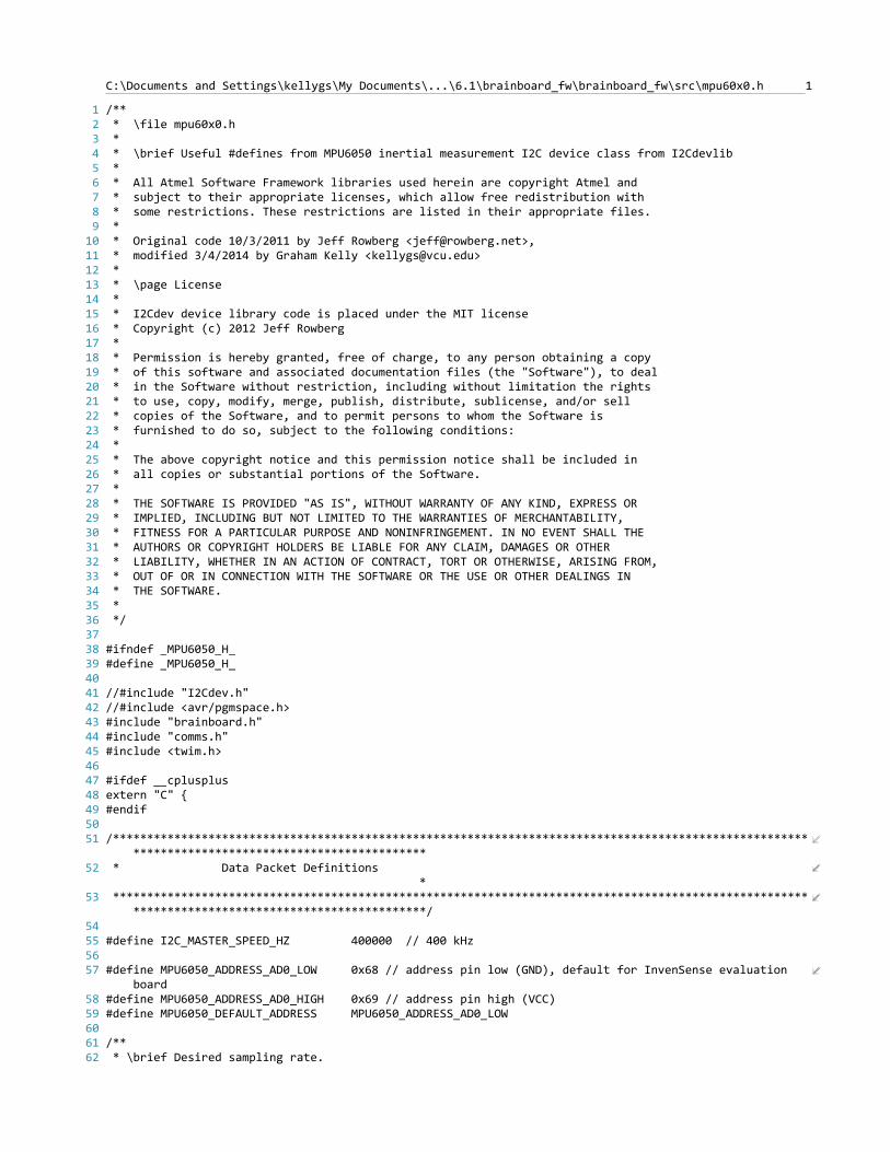
1C:\Documents and Settings\kellygs\My Documents\...\6.1\brainboard_fw\brainboard_fw\src\mpu60x0.h
1 /**2 * \ file mpu 60 x 0 . h3 *4 * \ brief Useful # defines from MPU 6050 inertial measurement I 2 C device class from I 2 Cdevlib5 *6 * All Atmel Software Framework libraries used herein are copyright Atmel and7 * subject to their appropriate licenses , which allow free redistribution with8 * some restrictions . These restrictions are listed in their appropriate files .9 *10 * Original code 10 / 3 / 2011 by Jeff Rowberg < jeff @ rowberg . net >,11 * modified 3 / 4 / 2014 by Graham Kelly < kellygs @ vcu . edu >12 *13 * \ page License14 * 15 * I 2 Cdev device library code is placed under the MIT license16 * Copyright ( c ) 2012 Jeff Rowberg17 * 18 * Permission is hereby granted , free of charge , to any person obtaining a copy19 * of this software and associated documentation files ( the " Software ") , to deal20 * in the Software without restriction , including without limitation the rights21 * to use , copy , modify , merge , publish , distribute , sublicense , and / or sell22 * copies of the Software , and to permit persons to whom the Software is23 * furnished to do so , subject to the following conditions :24 *25 * The above copyright notice and this permission notice shall be included in26 * all copies or substantial portions of the Software .27 *28 * THE SOFTWARE IS PROVIDED " AS IS " , WITHOUT WARRANTY OF ANY KIND , EXPRESS OR29 * IMPLIED , INCLUDING BUT NOT LIMITED TO THE WARRANTIES OF MERCHANTABILITY ,30 * FITNESS FOR A PARTICULAR PURPOSE AND NONINFRINGEMENT . IN NO EVENT SHALL THE31 * AUTHORS OR COPYRIGHT HOLDERS BE LIABLE FOR ANY CLAIM , DAMAGES OR OTHER32 * LIABILITY , WHETHER IN AN ACTION OF CONTRACT , TORT OR OTHERWISE , ARISING FROM ,33 * OUT OF OR IN CONNECTION WITH THE SOFTWARE OR THE USE OR OTHER DEALINGS IN34 * THE SOFTWARE .35 *36 */3738 # ifndef _ MPU 6050 _ H _39 # define _ MPU 6050 _ H _4041 // # include " I 2 Cdev . h "42 // # include < avr / pgmspace . h >43 # include " brainboard . h "44 # include " comms . h "45 # include < twim . h >4647 # ifdef __ cplusplus48 extern " C " 49 # endif5051 /******************************************************************************************************
*******************************************52 * Data Packet Definitions
*53 ******************************************************************************************************
*******************************************/5455 # define I 2 C _ MASTER _ SPEED _ HZ 400000 // 400 kHz5657 # define MPU 6050 _ ADDRESS _ AD 0 _ LOW 0 x 68 // address pin low ( GND ) , default for InvenSense evaluation
board58 # define MPU 6050 _ ADDRESS _ AD 0 _ HIGH 0 x 69 // address pin high ( VCC )59 # define MPU 6050 _ DEFAULT _ ADDRESS MPU 6050 _ ADDRESS _ AD 0 _ LOW6061 /** 62 * \ brief Desired sampling rate .

2C:\Documents and Settings\kellygs\My Documents\...\6.1\brainboard_fw\brainboard_fw\src\mpu60x0.h
63 *64 * Determines SMPLRT _ DIV register value :65 * SMPLRT _ DIV = ( Gyroscope output rate )/( Desired sampling rate ) ‐ 166 */67 # define MPU 6050 _ SAMPLING _ RATE _ HZ 106869 /** 70 * \ brief Digital low ‐ pass filter setting for MPU ‐ 6050 .71 *72 */73 # define MPU 6050 _ DLPF _ BW MPU 6050 _ DLPF _ BW _ 2567475 /* Gyro updates at full speed only if DLPF is off ( i . e . BW = 256 Hz ). */76 # if ( MPU 6050 _ DLPF _ BW == MPU 6050 _ DLPF _ BW _ 256 )77 # define MPU 6050 _ GYRO _ OUTPUT _ RATE _ HZ 800078 # else79 # define MPU 6050 _ GYRO _ OUTPUT _ RATE _ HZ 100080 # endif8182 /**83 * \ brief MPU 6050 register addresses .84 *85 * Consult the MPU 6050 register map document for more information .86 */87 # define MPU 6050 _ RA _ XG _ OFFS _ TC 0 x 00 //[ 7 ] PWR _ MODE , [ 6 : 1 ] XG _ OFFS _ TC , [ 0 ] OTP _ BNK _ VLD88 # define MPU 6050 _ RA _ YG _ OFFS _ TC 0 x 01 //[ 7 ] PWR _ MODE , [ 6 : 1 ] YG _ OFFS _ TC , [ 0 ] OTP _ BNK _ VLD89 # define MPU 6050 _ RA _ ZG _ OFFS _ TC 0 x 02 //[ 7 ] PWR _ MODE , [ 6 : 1 ] ZG _ OFFS _ TC , [ 0 ] OTP _ BNK _ VLD90 # define MPU 6050 _ RA _ X _ FINE _ GAIN 0 x 03 //[ 7 : 0 ] X _ FINE _ GAIN91 # define MPU 6050 _ RA _ Y _ FINE _ GAIN 0 x 04 //[ 7 : 0 ] Y _ FINE _ GAIN92 # define MPU 6050 _ RA _ Z _ FINE _ GAIN 0 x 05 //[ 7 : 0 ] Z _ FINE _ GAIN93 # define MPU 6050 _ RA _ XA _ OFFS _ H 0 x 06 //[ 15 : 0 ] XA _ OFFS94 # define MPU 6050 _ RA _ XA _ OFFS _ L _ TC 0 x 0795 # define MPU 6050 _ RA _ YA _ OFFS _ H 0 x 08 //[ 15 : 0 ] YA _ OFFS96 # define MPU 6050 _ RA _ YA _ OFFS _ L _ TC 0 x 0997 # define MPU 6050 _ RA _ ZA _ OFFS _ H 0 x 0 A //[ 15 : 0 ] ZA _ OFFS98 # define MPU 6050 _ RA _ ZA _ OFFS _ L _ TC 0 x 0 B99 # define MPU 6050 _ RA _ XG _ OFFS _ USRH 0 x 13 //[ 15 : 0 ] XG _ OFFS _ USR100 # define MPU 6050 _ RA _ XG _ OFFS _ USRL 0 x 14101 # define MPU 6050 _ RA _ YG _ OFFS _ USRH 0 x 15 //[ 15 : 0 ] YG _ OFFS _ USR102 # define MPU 6050 _ RA _ YG _ OFFS _ USRL 0 x 16103 # define MPU 6050 _ RA _ ZG _ OFFS _ USRH 0 x 17 //[ 15 : 0 ] ZG _ OFFS _ USR104 # define MPU 6050 _ RA _ ZG _ OFFS _ USRL 0 x 18105 # define MPU 6050 _ RA _ SMPLRT _ DIV 0 x 19106 # define MPU 6050 _ RA _ CONFIG 0 x 1 A107 # define MPU 6050 _ RA _ GYRO _ CONFIG 0 x 1 B108 # define MPU 6050 _ RA _ ACCEL _ CONFIG 0 x 1 C109 # define MPU 6050 _ RA _ FF _ THR 0 x 1 D110 # define MPU 6050 _ RA _ FF _ DUR 0 x 1 E111 # define MPU 6050 _ RA _ MOT _ THR 0 x 1 F112 # define MPU 6050 _ RA _ MOT _ DUR 0 x 20113 # define MPU 6050 _ RA _ ZRMOT _ THR 0 x 21114 # define MPU 6050 _ RA _ ZRMOT _ DUR 0 x 22115 # define MPU 6050 _ RA _ FIFO _ EN 0 x 23116 # define MPU 6050 _ RA _ I 2 C _ MST _ CTRL 0 x 24117 # define MPU 6050 _ RA _ I 2 C _ SLV 0 _ ADDR 0 x 25118 # define MPU 6050 _ RA _ I 2 C _ SLV 0 _ REG 0 x 26119 # define MPU 6050 _ RA _ I 2 C _ SLV 0 _ CTRL 0 x 27120 # define MPU 6050 _ RA _ I 2 C _ SLV 1 _ ADDR 0 x 28121 # define MPU 6050 _ RA _ I 2 C _ SLV 1 _ REG 0 x 29122 # define MPU 6050 _ RA _ I 2 C _ SLV 1 _ CTRL 0 x 2 A123 # define MPU 6050 _ RA _ I 2 C _ SLV 2 _ ADDR 0 x 2 B124 # define MPU 6050 _ RA _ I 2 C _ SLV 2 _ REG 0 x 2 C125 # define MPU 6050 _ RA _ I 2 C _ SLV 2 _ CTRL 0 x 2 D126 # define MPU 6050 _ RA _ I 2 C _ SLV 3 _ ADDR 0 x 2 E127 # define MPU 6050 _ RA _ I 2 C _ SLV 3 _ REG 0 x 2 F128 # define MPU 6050 _ RA _ I 2 C _ SLV 3 _ CTRL 0 x 30

3C:\Documents and Settings\kellygs\My Documents\...\6.1\brainboard_fw\brainboard_fw\src\mpu60x0.h
129 # define MPU 6050 _ RA _ I 2 C _ SLV 4 _ ADDR 0 x 31130 # define MPU 6050 _ RA _ I 2 C _ SLV 4 _ REG 0 x 32131 # define MPU 6050 _ RA _ I 2 C _ SLV 4 _ DO 0 x 33132 # define MPU 6050 _ RA _ I 2 C _ SLV 4 _ CTRL 0 x 34133 # define MPU 6050 _ RA _ I 2 C _ SLV 4 _ DI 0 x 35134 # define MPU 6050 _ RA _ I 2 C _ MST _ STATUS 0 x 36135 # define MPU 6050 _ RA _ INT _ PIN _ CFG 0 x 37136 # define MPU 6050 _ RA _ INT _ ENABLE 0 x 38137 # define MPU 6050 _ RA _ DMP _ INT _ STATUS 0 x 39138 # define MPU 6050 _ RA _ INT _ STATUS 0 x 3 A139 # define MPU 6050 _ RA _ ACCEL _ XOUT _ H 0 x 3 B140 # define MPU 6050 _ RA _ ACCEL _ XOUT _ L 0 x 3 C141 # define MPU 6050 _ RA _ ACCEL _ YOUT _ H 0 x 3 D142 # define MPU 6050 _ RA _ ACCEL _ YOUT _ L 0 x 3 E143 # define MPU 6050 _ RA _ ACCEL _ ZOUT _ H 0 x 3 F144 # define MPU 6050 _ RA _ ACCEL _ ZOUT _ L 0 x 40145 # define MPU 6050 _ RA _ TEMP _ OUT _ H 0 x 41146 # define MPU 6050 _ RA _ TEMP _ OUT _ L 0 x 42147 # define MPU 6050 _ RA _ GYRO _ XOUT _ H 0 x 43148 # define MPU 6050 _ RA _ GYRO _ XOUT _ L 0 x 44149 # define MPU 6050 _ RA _ GYRO _ YOUT _ H 0 x 45150 # define MPU 6050 _ RA _ GYRO _ YOUT _ L 0 x 46151 # define MPU 6050 _ RA _ GYRO _ ZOUT _ H 0 x 47152 # define MPU 6050 _ RA _ GYRO _ ZOUT _ L 0 x 48153 # define MPU 6050 _ RA _ EXT _ SENS _ DATA _ 00 0 x 49154 # define MPU 6050 _ RA _ EXT _ SENS _ DATA _ 01 0 x 4 A155 # define MPU 6050 _ RA _ EXT _ SENS _ DATA _ 02 0 x 4 B156 # define MPU 6050 _ RA _ EXT _ SENS _ DATA _ 03 0 x 4 C157 # define MPU 6050 _ RA _ EXT _ SENS _ DATA _ 04 0 x 4 D158 # define MPU 6050 _ RA _ EXT _ SENS _ DATA _ 05 0 x 4 E159 # define MPU 6050 _ RA _ EXT _ SENS _ DATA _ 06 0 x 4 F160 # define MPU 6050 _ RA _ EXT _ SENS _ DATA _ 07 0 x 50161 # define MPU 6050 _ RA _ EXT _ SENS _ DATA _ 08 0 x 51162 # define MPU 6050 _ RA _ EXT _ SENS _ DATA _ 09 0 x 52163 # define MPU 6050 _ RA _ EXT _ SENS _ DATA _ 10 0 x 53164 # define MPU 6050 _ RA _ EXT _ SENS _ DATA _ 11 0 x 54165 # define MPU 6050 _ RA _ EXT _ SENS _ DATA _ 12 0 x 55166 # define MPU 6050 _ RA _ EXT _ SENS _ DATA _ 13 0 x 56167 # define MPU 6050 _ RA _ EXT _ SENS _ DATA _ 14 0 x 57168 # define MPU 6050 _ RA _ EXT _ SENS _ DATA _ 15 0 x 58169 # define MPU 6050 _ RA _ EXT _ SENS _ DATA _ 16 0 x 59170 # define MPU 6050 _ RA _ EXT _ SENS _ DATA _ 17 0 x 5 A171 # define MPU 6050 _ RA _ EXT _ SENS _ DATA _ 18 0 x 5 B172 # define MPU 6050 _ RA _ EXT _ SENS _ DATA _ 19 0 x 5 C173 # define MPU 6050 _ RA _ EXT _ SENS _ DATA _ 20 0 x 5 D174 # define MPU 6050 _ RA _ EXT _ SENS _ DATA _ 21 0 x 5 E175 # define MPU 6050 _ RA _ EXT _ SENS _ DATA _ 22 0 x 5 F176 # define MPU 6050 _ RA _ EXT _ SENS _ DATA _ 23 0 x 60177 # define MPU 6050 _ RA _ MOT _ DETECT _ STATUS 0 x 61178 # define MPU 6050 _ RA _ I 2 C _ SLV 0 _ DO 0 x 63179 # define MPU 6050 _ RA _ I 2 C _ SLV 1 _ DO 0 x 64180 # define MPU 6050 _ RA _ I 2 C _ SLV 2 _ DO 0 x 65181 # define MPU 6050 _ RA _ I 2 C _ SLV 3 _ DO 0 x 66182 # define MPU 6050 _ RA _ I 2 C _ MST _ DELAY _ CTRL 0 x 67183 # define MPU 6050 _ RA _ SIGNAL _ PATH _ RESET 0 x 68184 # define MPU 6050 _ RA _ MOT _ DETECT _ CTRL 0 x 69185 # define MPU 6050 _ RA _ USER _ CTRL 0 x 6 A186 # define MPU 6050 _ RA _ PWR _ MGMT _ 1 0 x 6 B187 # define MPU 6050 _ RA _ PWR _ MGMT _ 2 0 x 6 C188 # define MPU 6050 _ RA _ BANK _ SEL 0 x 6 D189 # define MPU 6050 _ RA _ MEM _ START _ ADDR 0 x 6 E190 # define MPU 6050 _ RA _ MEM _ R _ W 0 x 6 F191 # define MPU 6050 _ RA _ DMP _ CFG _ 1 0 x 70192 # define MPU 6050 _ RA _ DMP _ CFG _ 2 0 x 71193 # define MPU 6050 _ RA _ FIFO _ COUNTH 0 x 72194 # define MPU 6050 _ RA _ FIFO _ COUNTL 0 x 73

4C:\Documents and Settings\kellygs\My Documents\...\6.1\brainboard_fw\brainboard_fw\src\mpu60x0.h
195 # define MPU 6050 _ RA _ FIFO _ R _ W 0 x 74196 # define MPU 6050 _ RA _ WHO _ AM _ I 0 x 75197198 # define MPU 6050 _ TC _ PWR _ MODE _ BIT 7199 # define MPU 6050 _ TC _ OFFSET _ BIT 6200 # define MPU 6050 _ TC _ OFFSET _ LENGTH 6201 # define MPU 6050 _ TC _ OTP _ BNK _ VLD _ BIT 0202203 # define MPU 6050 _ VDDIO _ LEVEL _ VLOGIC 0204 # define MPU 6050 _ VDDIO _ LEVEL _ VDD 1205206 # define MPU 6050 _ CFG _ EXT _ SYNC _ SET _ BIT 5207 # define MPU 6050 _ CFG _ EXT _ SYNC _ SET _ LENGTH 3208 # define MPU 6050 _ CFG _ DLPF _ CFG _ BIT 2209 # define MPU 6050 _ CFG _ DLPF _ CFG _ LENGTH 3210211 # define MPU 6050 _ EXT _ SYNC _ DISABLED 0 x 0212 # define MPU 6050 _ EXT _ SYNC _ TEMP _ OUT _ L 0 x 1213 # define MPU 6050 _ EXT _ SYNC _ GYRO _ XOUT _ L 0 x 2214 # define MPU 6050 _ EXT _ SYNC _ GYRO _ YOUT _ L 0 x 3215 # define MPU 6050 _ EXT _ SYNC _ GYRO _ ZOUT _ L 0 x 4216 # define MPU 6050 _ EXT _ SYNC _ ACCEL _ XOUT _ L 0 x 5217 # define MPU 6050 _ EXT _ SYNC _ ACCEL _ YOUT _ L 0 x 6218 # define MPU 6050 _ EXT _ SYNC _ ACCEL _ ZOUT _ L 0 x 7219220 # define MPU 6050 _ DLPF _ BW _ 256 0 x 00221 # define MPU 6050 _ DLPF _ BW _ 188 0 x 01222 # define MPU 6050 _ DLPF _ BW _ 98 0 x 02223 # define MPU 6050 _ DLPF _ BW _ 42 0 x 03224 # define MPU 6050 _ DLPF _ BW _ 20 0 x 04225 # define MPU 6050 _ DLPF _ BW _ 10 0 x 05226 # define MPU 6050 _ DLPF _ BW _ 5 0 x 06227228 # define MPU 6050 _ GCONFIG _ FS _ SEL _ BIT 4229 # define MPU 6050 _ GCONFIG _ FS _ SEL _ LENGTH 2230231 # define MPU 6050 _ GYRO _ FS _ 250 0 x 00232 # define MPU 6050 _ GYRO _ FS _ 500 0 x 01233 # define MPU 6050 _ GYRO _ FS _ 1000 0 x 02234 # define MPU 6050 _ GYRO _ FS _ 2000 0 x 03235236 # define MPU 6050 _ ACONFIG _ XA _ ST _ BIT 7237 # define MPU 6050 _ ACONFIG _ YA _ ST _ BIT 6238 # define MPU 6050 _ ACONFIG _ ZA _ ST _ BIT 5239 # define MPU 6050 _ ACONFIG _ AFS _ SEL _ BIT 4240 # define MPU 6050 _ ACONFIG _ AFS _ SEL _ LENGTH 2241 # define MPU 6050 _ ACONFIG _ ACCEL _ HPF _ BIT 2242 # define MPU 6050 _ ACONFIG _ ACCEL _ HPF _ LENGTH 3243244 # define MPU 6050 _ ACCEL _ FS _ 2 0 x 00245 # define MPU 6050 _ ACCEL _ FS _ 4 0 x 01246 # define MPU 6050 _ ACCEL _ FS _ 8 0 x 02247 # define MPU 6050 _ ACCEL _ FS _ 16 0 x 03248249 # define MPU 6050 _ DHPF _ RESET 0 x 00250 # define MPU 6050 _ DHPF _ 5 0 x 01251 # define MPU 6050 _ DHPF _ 2 P 5 0 x 02252 # define MPU 6050 _ DHPF _ 1 P 25 0 x 03253 # define MPU 6050 _ DHPF _ 0 P 63 0 x 04254 # define MPU 6050 _ DHPF _ HOLD 0 x 07255256 # define MPU 6050 _ TEMP _ FIFO _ EN _ BIT 7257 # define MPU 6050 _ XG _ FIFO _ EN _ BIT 6258 # define MPU 6050 _ YG _ FIFO _ EN _ BIT 5259 # define MPU 6050 _ ZG _ FIFO _ EN _ BIT 4260 # define MPU 6050 _ ACCEL _ FIFO _ EN _ BIT 3

5C:\Documents and Settings\kellygs\My Documents\...\6.1\brainboard_fw\brainboard_fw\src\mpu60x0.h
261 # define MPU 6050 _ SLV 2 _ FIFO _ EN _ BIT 2262 # define MPU 6050 _ SLV 1 _ FIFO _ EN _ BIT 1263 # define MPU 6050 _ SLV 0 _ FIFO _ EN _ BIT 0264265 # define MPU 6050 _ MULT _ MST _ EN _ BIT 7266 # define MPU 6050 _ WAIT _ FOR _ ES _ BIT 6267 # define MPU 6050 _ SLV _ 3 _ FIFO _ EN _ BIT 5268 # define MPU 6050 _ I 2 C _ MST _ P _ NSR _ BIT 4269 # define MPU 6050 _ I 2 C _ MST _ CLK _ BIT 3270 # define MPU 6050 _ I 2 C _ MST _ CLK _ LENGTH 4271272 # define MPU 6050 _ CLOCK _ DIV _ 348 0 x 0273 # define MPU 6050 _ CLOCK _ DIV _ 333 0 x 1274 # define MPU 6050 _ CLOCK _ DIV _ 320 0 x 2275 # define MPU 6050 _ CLOCK _ DIV _ 308 0 x 3276 # define MPU 6050 _ CLOCK _ DIV _ 296 0 x 4277 # define MPU 6050 _ CLOCK _ DIV _ 286 0 x 5278 # define MPU 6050 _ CLOCK _ DIV _ 276 0 x 6279 # define MPU 6050 _ CLOCK _ DIV _ 267 0 x 7280 # define MPU 6050 _ CLOCK _ DIV _ 258 0 x 8281 # define MPU 6050 _ CLOCK _ DIV _ 500 0 x 9282 # define MPU 6050 _ CLOCK _ DIV _ 471 0 xA283 # define MPU 6050 _ CLOCK _ DIV _ 444 0 xB284 # define MPU 6050 _ CLOCK _ DIV _ 421 0 xC285 # define MPU 6050 _ CLOCK _ DIV _ 400 0 xD286 # define MPU 6050 _ CLOCK _ DIV _ 381 0 xE287 # define MPU 6050 _ CLOCK _ DIV _ 364 0 xF288289 # define MPU 6050 _ I 2 C _ SLV _ RW _ BIT 7290 # define MPU 6050 _ I 2 C _ SLV _ ADDR _ BIT 6291 # define MPU 6050 _ I 2 C _ SLV _ ADDR _ LENGTH 7292 # define MPU 6050 _ I 2 C _ SLV _ EN _ BIT 7293 # define MPU 6050 _ I 2 C _ SLV _ BYTE _ SW _ BIT 6294 # define MPU 6050 _ I 2 C _ SLV _ REG _ DIS _ BIT 5295 # define MPU 6050 _ I 2 C _ SLV _ GRP _ BIT 4296 # define MPU 6050 _ I 2 C _ SLV _ LEN _ BIT 3297 # define MPU 6050 _ I 2 C _ SLV _ LEN _ LENGTH 4298299 # define MPU 6050 _ I 2 C _ SLV 4 _ RW _ BIT 7300 # define MPU 6050 _ I 2 C _ SLV 4 _ ADDR _ BIT 6301 # define MPU 6050 _ I 2 C _ SLV 4 _ ADDR _ LENGTH 7302 # define MPU 6050 _ I 2 C _ SLV 4 _ EN _ BIT 7303 # define MPU 6050 _ I 2 C _ SLV 4 _ INT _ EN _ BIT 6304 # define MPU 6050 _ I 2 C _ SLV 4 _ REG _ DIS _ BIT 5305 # define MPU 6050 _ I 2 C _ SLV 4 _ MST _ DLY _ BIT 4306 # define MPU 6050 _ I 2 C _ SLV 4 _ MST _ DLY _ LENGTH 5307308 # define MPU 6050 _ MST _ PASS _ THROUGH _ BIT 7309 # define MPU 6050 _ MST _ I 2 C _ SLV 4 _ DONE _ BIT 6310 # define MPU 6050 _ MST _ I 2 C _ LOST _ ARB _ BIT 5311 # define MPU 6050 _ MST _ I 2 C _ SLV 4 _ NACK _ BIT 4312 # define MPU 6050 _ MST _ I 2 C _ SLV 3 _ NACK _ BIT 3313 # define MPU 6050 _ MST _ I 2 C _ SLV 2 _ NACK _ BIT 2314 # define MPU 6050 _ MST _ I 2 C _ SLV 1 _ NACK _ BIT 1315 # define MPU 6050 _ MST _ I 2 C _ SLV 0 _ NACK _ BIT 0316317 # define MPU 6050 _ INTCFG _ INT _ LEVEL _ BIT 7318 # define MPU 6050 _ INTCFG _ INT _ OPEN _ BIT 6319 # define MPU 6050 _ INTCFG _ LATCH _ INT _ EN _ BIT 5320 # define MPU 6050 _ INTCFG _ INT _ RD _ CLEAR _ BIT 4321 # define MPU 6050 _ INTCFG _ FSYNC _ INT _ LEVEL _ BIT 3322 # define MPU 6050 _ INTCFG _ FSYNC _ INT _ EN _ BIT 2323 # define MPU 6050 _ INTCFG _ I 2 C _ BYPASS _ EN _ BIT 1324 # define MPU 6050 _ INTCFG _ CLKOUT _ EN _ BIT 0325326 # define MPU 6050 _ INTMODE _ ACTIVEHIGH 0 x 00

6C:\Documents and Settings\kellygs\My Documents\...\6.1\brainboard_fw\brainboard_fw\src\mpu60x0.h
327 # define MPU 6050 _ INTMODE _ ACTIVELOW 0 x 01328329 # define MPU 6050 _ INTDRV _ PUSHPULL 0 x 00330 # define MPU 6050 _ INTDRV _ OPENDRAIN 0 x 01331332 # define MPU 6050 _ INTLATCH _ 50 USPULSE 0 x 00333 # define MPU 6050 _ INTLATCH _ WAITCLEAR 0 x 01334335 # define MPU 6050 _ INTCLEAR _ STATUSREAD 0 x 00336 # define MPU 6050 _ INTCLEAR _ ANYREAD 0 x 01337338 # define MPU 6050 _ INTERRUPT _ FF _ BIT 7339 # define MPU 6050 _ INTERRUPT _ MOT _ BIT 6340 # define MPU 6050 _ INTERRUPT _ ZMOT _ BIT 5341 # define MPU 6050 _ INTERRUPT _ FIFO _ OFLOW _ BIT 4342 # define MPU 6050 _ INTERRUPT _ I 2 C _ MST _ INT _ BIT 3343 # define MPU 6050 _ INTERRUPT _ PLL _ RDY _ INT _ BIT 2344 # define MPU 6050 _ INTERRUPT _ DMP _ INT _ BIT 1345 # define MPU 6050 _ INTERRUPT _ DATA _ RDY _ BIT 0346347 // TODO : figure out what these actually do348 // UMPL source code is not very obivous349 # define MPU 6050 _ DMPINT _ 5 _ BIT 5350 # define MPU 6050 _ DMPINT _ 4 _ BIT 4351 # define MPU 6050 _ DMPINT _ 3 _ BIT 3352 # define MPU 6050 _ DMPINT _ 2 _ BIT 2353 # define MPU 6050 _ DMPINT _ 1 _ BIT 1354 # define MPU 6050 _ DMPINT _ 0 _ BIT 0355356 # define MPU 6050 _ MOTION _ MOT _ XNEG _ BIT 7357 # define MPU 6050 _ MOTION _ MOT _ XPOS _ BIT 6358 # define MPU 6050 _ MOTION _ MOT _ YNEG _ BIT 5359 # define MPU 6050 _ MOTION _ MOT _ YPOS _ BIT 4360 # define MPU 6050 _ MOTION _ MOT _ ZNEG _ BIT 3361 # define MPU 6050 _ MOTION _ MOT _ ZPOS _ BIT 2362 # define MPU 6050 _ MOTION _ MOT _ ZRMOT _ BIT 0363364 # define MPU 6050 _ DELAYCTRL _ DELAY _ ES _ SHADOW _ BIT 7365 # define MPU 6050 _ DELAYCTRL _ I 2 C _ SLV 4 _ DLY _ EN _ BIT 4366 # define MPU 6050 _ DELAYCTRL _ I 2 C _ SLV 3 _ DLY _ EN _ BIT 3367 # define MPU 6050 _ DELAYCTRL _ I 2 C _ SLV 2 _ DLY _ EN _ BIT 2368 # define MPU 6050 _ DELAYCTRL _ I 2 C _ SLV 1 _ DLY _ EN _ BIT 1369 # define MPU 6050 _ DELAYCTRL _ I 2 C _ SLV 0 _ DLY _ EN _ BIT 0370371 # define MPU 6050 _ PATHRESET _ GYRO _ RESET _ BIT 2372 # define MPU 6050 _ PATHRESET _ ACCEL _ RESET _ BIT 1373 # define MPU 6050 _ PATHRESET _ TEMP _ RESET _ BIT 0374375 # define MPU 6050 _ DETECT _ ACCEL _ ON _ DELAY _ BIT 5376 # define MPU 6050 _ DETECT _ ACCEL _ ON _ DELAY _ LENGTH 2377 # define MPU 6050 _ DETECT _ FF _ COUNT _ BIT 3378 # define MPU 6050 _ DETECT _ FF _ COUNT _ LENGTH 2379 # define MPU 6050 _ DETECT _ MOT _ COUNT _ BIT 1380 # define MPU 6050 _ DETECT _ MOT _ COUNT _ LENGTH 2381382 # define MPU 6050 _ DETECT _ DECREMENT _ RESET 0 x 0383 # define MPU 6050 _ DETECT _ DECREMENT _ 1 0 x 1384 # define MPU 6050 _ DETECT _ DECREMENT _ 2 0 x 2385 # define MPU 6050 _ DETECT _ DECREMENT _ 4 0 x 3386387 # define MPU 6050 _ USERCTRL _ DMP _ EN _ BIT 7388 # define MPU 6050 _ USERCTRL _ FIFO _ EN _ BIT 6389 # define MPU 6050 _ USERCTRL _ I 2 C _ MST _ EN _ BIT 5390 # define MPU 6050 _ USERCTRL _ I 2 C _ IF _ DIS _ BIT 4391 # define MPU 6050 _ USERCTRL _ DMP _ RESET _ BIT 3392 # define MPU 6050 _ USERCTRL _ FIFO _ RESET _ BIT 2

7C:\Documents and Settings\kellygs\My Documents\...\6.1\brainboard_fw\brainboard_fw\src\mpu60x0.h
393 # define MPU 6050 _ USERCTRL _ I 2 C _ MST _ RESET _ BIT 1394 # define MPU 6050 _ USERCTRL _ SIG _ COND _ RESET _ BIT 0395396 # define MPU 6050 _ PWR 1 _ DEVICE _ RESET _ BIT 7397 # define MPU 6050 _ PWR 1 _ SLEEP _ BIT 6398 # define MPU 6050 _ PWR 1 _ CYCLE _ BIT 5399 # define MPU 6050 _ PWR 1 _ TEMP _ DIS _ BIT 3400 # define MPU 6050 _ PWR 1 _ CLKSEL _ BIT 2401 # define MPU 6050 _ PWR 1 _ CLKSEL _ LENGTH 3402403 # define MPU 6050 _ CLOCK _ INTERNAL 0 x 00404 # define MPU 6050 _ CLOCK _ PLL _ XGYRO 0 x 01405 # define MPU 6050 _ CLOCK _ PLL _ YGYRO 0 x 02406 # define MPU 6050 _ CLOCK _ PLL _ ZGYRO 0 x 03407 # define MPU 6050 _ CLOCK _ PLL _ EXT 32 K 0 x 04408 # define MPU 6050 _ CLOCK _ PLL _ EXT 19 M 0 x 05409 # define MPU 6050 _ CLOCK _ KEEP _ RESET 0 x 07410411 # define MPU 6050 _ PWR 2 _ LP _ WAKE _ CTRL _ BIT 7412 # define MPU 6050 _ PWR 2 _ LP _ WAKE _ CTRL _ LENGTH 2413 # define MPU 6050 _ PWR 2 _ STBY _ XA _ BIT 5414 # define MPU 6050 _ PWR 2 _ STBY _ YA _ BIT 4415 # define MPU 6050 _ PWR 2 _ STBY _ ZA _ BIT 3416 # define MPU 6050 _ PWR 2 _ STBY _ XG _ BIT 2417 # define MPU 6050 _ PWR 2 _ STBY _ YG _ BIT 1418 # define MPU 6050 _ PWR 2 _ STBY _ ZG _ BIT 0419420 # define MPU 6050 _ WAKE _ FREQ _ 1 P 25 0 x 0421 # define MPU 6050 _ WAKE _ FREQ _ 2 P 5 0 x 1422 # define MPU 6050 _ WAKE _ FREQ _ 5 0 x 2423 # define MPU 6050 _ WAKE _ FREQ _ 10 0 x 3424425 # define MPU 6050 _ BANKSEL _ PRFTCH _ EN _ BIT 6426 # define MPU 6050 _ BANKSEL _ CFG _ USER _ BANK _ BIT 5427 # define MPU 6050 _ BANKSEL _ MEM _ SEL _ BIT 4428 # define MPU 6050 _ BANKSEL _ MEM _ SEL _ LENGTH 5429430 # define MPU 6050 _ WHO _ AM _ I _ BIT 6431 # define MPU 6050 _ WHO _ AM _ I _ LENGTH 6432433 # define MPU 6050 _ DMP _ MEMORY _ BANKS 8434 # define MPU 6050 _ DMP _ MEMORY _ BANK _ SIZE 256435 # define MPU 6050 _ DMP _ MEMORY _ CHUNK _ SIZE 16436437 status _ code _ t mpu 6050 _ initialize _ normal ( uint 32 _ t ) ;438 status _ code _ t mpu 6050 _ initialize _ lowpower ( uint 32 _ t ) ;439 status _ code _ t mpu 6050 _ rdata 16 _ packet ( uint 32 _ t , volatile uint 32 _ t , data _ packet _ t *) ;440 status _ code _ t mpu 6050 _ rdata 16 _ fifo ( uint 32 _ t , volatile uint 32 _ t , data _ packet _ t *) ;441442 # ifdef __ cplusplus443 444 # endif445446 # endif /* # ifndef _ MPU 6050 _ H _ */

1C:\Documents and Settings\kellygs\My Documents\...\6.1\brainboard_fw\brainboard_fw\src\ads1299.c
1 /** 2 * \ file ads 1299 . c3 * \ brief Some useful functions for using the ADS 1299 EEG analog front ‐ end from Texas Instruments .4 * \ details The ADS 1299 is an SPI slave device . Communication with it requires at least one SPI master
module on the host .5 * \ author Graham Kelly6 * \ version 1 . 07 * \ date August 20148 *9 * All Atmel Software Framework libraries used herein are copyright Atmel and10 * subject to their appropriate licenses , which allow free redistribution with11 * some restrictions . These restrictions are listed in their appropriate files .12 *13 * \ page License14 *15 * Brainboard firmware code is placed under the MIT license16 * Copyright ( c ) 2014 Graham Kelly17 *18 * Permission is hereby granted , free of charge , to any person obtaining a copy19 * of this software and associated documentation files ( the " Software ") , to deal20 * in the Software without restriction , including without limitation the rights21 * to use , copy , modify , merge , publish , distribute , sublicense , and / or sell22 * copies of the Software , and to permit persons to whom the Software is23 * furnished to do so , subject to the following conditions :24 *25 * The above copyright notice and this permission notice shall be included in26 * all copies or substantial portions of the Software .27 *28 * THE SOFTWARE IS PROVIDED " AS IS " , WITHOUT WARRANTY OF ANY KIND , EXPRESS OR29 * IMPLIED , INCLUDING BUT NOT LIMITED TO THE WARRANTIES OF MERCHANTABILITY ,30 * FITNESS FOR A PARTICULAR PURPOSE AND NONINFRINGEMENT . IN NO EVENT SHALL THE31 * AUTHORS OR COPYRIGHT HOLDERS BE LIABLE FOR ANY CLAIM , DAMAGES OR OTHER32 * LIABILITY , WHETHER IN AN ACTION OF CONTRACT , TORT OR OTHERWISE , ARISING FROM ,33 * OUT OF OR IN CONNECTION WITH THE SOFTWARE OR THE USE OR OTHER DEALINGS IN34 * THE SOFTWARE .35 *36 */3738 # ifdef __ cplusplus39 extern " C " 40 # endif4142 # include " ads 1299 . h "4344 /******************************************************************************************************
********************************************45 * Function Definitions
*46 *******************************************************************************************************
*******************************************/4748 /* SYSTEM CONTROL FUNCTIONS ***************************************************************************
*******************************************/4950 ads 1299 _ error _ t ads 1299 _ device _ init ( uint 8 _ t chip _ select )51 52 # if UC 353 /* Power cycle ADS 1299 */54 gpio _ clr _ gpio _ pin ( ADS 1299 _ PIN _ PWDN ) ;55 delay _ us ( 20 ) ;56 gpio _ set _ gpio _ pin ( ADS 1299 _ PIN _ PWDN ) ;57 58 /* Allow oscillator warm ‐ up */59 delay _ ms ( 1000 ) ;60 61 /* Tell chip to exit continuous data mode */

2C:\Documents and Settings\kellygs\My Documents\...\6.1\brainboard_fw\brainboard_fw\src\ads1299.c
62 ads 1299 _ send _ byte ( chip _ select , ADS 1299 _ OPC _ SDATAC ) ;63 /* Stop taking conversions ; apparently not done automatically */64 ads 1299 _ send _ byte ( chip _ select , ADS 1299 _ OPC _ STOP ) ;65 66 /* Write to GPIO register , set all pins to driven ‐ low output */67 ads 1299 _ wreg ( chip _ select , ADS 1299 _ REGADDR _ GPIO , ADS 1299 _ REG _ GPIO _ GPIOC 4 _ OUTPUT |68 ADS 1299 _ REG _ GPIO _ GPIOD 4 _ LOW |69 ADS 1299 _ REG _ GPIO _ GPIOC 3 _ OUTPUT |70 ADS 1299 _ REG _ GPIO _ GPIOD 3 _ LOW |71 ADS 1299 _ REG _ GPIO _ GPIOC 2 _ OUTPUT |72 ADS 1299 _ REG _ GPIO _ GPIOD 2 _ LOW |73 ADS 1299 _ REG _ GPIO _ GPIOC 1 _ OUTPUT |74 ADS 1299 _ REG _ GPIO _ GPIOD 1 _ LOW ) ;75 76 /* Write to CONFIG 1 , set data rate to 250 Hz */77 ads 1299 _ wreg ( chip _ select , ADS 1299 _ REGADDR _ CONFIG 1 , ADS 1299 _ REG _ CONFIG 1 _ RESERVED _ VALUE |78 ADS 1299 _ REG _ CONFIG 1 _ FMOD _ DIV _ BY _ 4096 ) ;79 /* Write to CONFIG 2 register , generate test signal internally */80 ads 1299 _ wreg ( chip _ select , ADS 1299 _ REGADDR _ CONFIG 2 , ADS 1299 _ REG _ CONFIG 2 _ RESERVED _ VALUE | 81 ADS 1299 _ REG _ CONFIG 2 _ CAL _ INT |82 ADS 1299 _ REG _ CONFIG 2 _ CAL _ PULSE _ FCLK _ DIV _ 2 _ 21 ) ;83 84 /* Write to CONFIG 3 , enable internal reference buffer , bias internally generated , bias buffer
enabled */85 ads 1299 _ wreg ( chip _ select , ADS 1299 _ REGADDR _ CONFIG 3 , ADS 1299 _ REG _ CONFIG 3 _ REFBUF _ ENABLED |86 ADS 1299 _ REG _ CONFIG 3 _ BIASREF _ INT |87 ADS 1299 _ REG _ CONFIG 3 _ BIASBUF _ ENABLED ) ;88 /* Reference settling time */89 delay _ ms ( 150 ) ;90 91 /* Write to CH 1 settings register , set as normal input , gain 24 */92 ads 1299 _ wreg ( chip _ select , ADS 1299 _ REGADDR _ CH 1 SET , ADS 1299 _ REG _ CHNSET _ CHANNEL _ ON |93 ADS 1299 _ REG _ CHNSET _ GAIN _ 24 |94 ADS 1299 _ REG _ CHNSET _ SRB 2 _ DISCONNECTED |95 ADS 1299 _ REG _ CHNSET _ NORMAL _ ELECTRODE ) ;96 /* Write to CH 2 settings register , set as normal input , gain 24 */97 ads 1299 _ wreg ( chip _ select , ADS 1299 _ REGADDR _ CH 2 SET , ADS 1299 _ REG _ CHNSET _ CHANNEL _ ON |98 ADS 1299 _ REG _ CHNSET _ GAIN _ 24 |99 ADS 1299 _ REG _ CHNSET _ SRB 2 _ DISCONNECTED |100 ADS 1299 _ REG _ CHNSET _ NORMAL _ ELECTRODE ) ;101 /* Write to CH 3 settings register , set as normal input , gain 24 */102 ads 1299 _ wreg ( chip _ select , ADS 1299 _ REGADDR _ CH 3 SET , ADS 1299 _ REG _ CHNSET _ CHANNEL _ ON |103 ADS 1299 _ REG _ CHNSET _ GAIN _ 24 |104 ADS 1299 _ REG _ CHNSET _ SRB 2 _ DISCONNECTED |105 ADS 1299 _ REG _ CHNSET _ NORMAL _ ELECTRODE ) ;106 /* Write to CH 4 settings register , set as normal input , gain 24 */107 ads 1299 _ wreg ( chip _ select , ADS 1299 _ REGADDR _ CH 4 SET , ADS 1299 _ REG _ CHNSET _ CHANNEL _ ON |108 ADS 1299 _ REG _ CHNSET _ GAIN _ 24 |109 ADS 1299 _ REG _ CHNSET _ SRB 2 _ DISCONNECTED |110 ADS 1299 _ REG _ CHNSET _ NORMAL _ ELECTRODE ) ;111 /* Write to CH 5 settings register , set as normal input , gain 24 */112 ads 1299 _ wreg ( chip _ select , ADS 1299 _ REGADDR _ CH 5 SET , ADS 1299 _ REG _ CHNSET _ CHANNEL _ ON |113 ADS 1299 _ REG _ CHNSET _ GAIN _ 24 |114 ADS 1299 _ REG _ CHNSET _ SRB 2 _ DISCONNECTED |115 ADS 1299 _ REG _ CHNSET _ NORMAL _ ELECTRODE ) ;116 /* Write to CH 6 settings register , set as normal input , gain 24 */117 ads 1299 _ wreg ( chip _ select , ADS 1299 _ REGADDR _ CH 6 SET , ADS 1299 _ REG _ CHNSET _ CHANNEL _ ON |118 ADS 1299 _ REG _ CHNSET _ GAIN _ 24 |119 ADS 1299 _ REG _ CHNSET _ SRB 2 _ DISCONNECTED |120 ADS 1299 _ REG _ CHNSET _ NORMAL _ ELECTRODE ) ;121 /* Write to CH 5 settings register , set as normal input , gain 24 */122 ads 1299 _ wreg ( chip _ select , ADS 1299 _ REGADDR _ CH 7 SET , ADS 1299 _ REG _ CHNSET _ CHANNEL _ ON |123 ADS 1299 _ REG _ CHNSET _ GAIN _ 24 |124 ADS 1299 _ REG _ CHNSET _ SRB 2 _ DISCONNECTED |125 ADS 1299 _ REG _ CHNSET _ NORMAL _ ELECTRODE ) ;126 /* Write to CH 6 settings register , set as normal input , gain 24 */

3C:\Documents and Settings\kellygs\My Documents\...\6.1\brainboard_fw\brainboard_fw\src\ads1299.c
127 ads 1299 _ wreg ( chip _ select , ADS 1299 _ REGADDR _ CH 8 SET , ADS 1299 _ REG _ CHNSET _ CHANNEL _ ON |128 ADS 1299 _ REG _ CHNSET _ GAIN _ 24 |129 ADS 1299 _ REG _ CHNSET _ SRB 2 _ DISCONNECTED |130 ADS 1299 _ REG _ CHNSET _ NORMAL _ ELECTRODE ) ;131 132 /* Write to MISC 1 register , SRB 1 on ( ref electrode ) */133 ads 1299 _ wreg ( chip _ select , ADS 1299 _ REGADDR _ MISC 1 , ADS 1299 _ REG _ MISC 1 _ SRB 1 _ ON ) ;134 135 return ADS 1299 _ STATUS _ OK ;136 # else137 # endif /* # if UC 3 */138 139140141142 /* REGISTER READ / WRITE FUNCTIONS **********************************************************************
*******************************************/143144 ads 1299 _ error _ t ads 1299 _ rreg ( uint 8 _ t chip _ select , uint 8 _ t reg _ addr , uint 8 _ t * read _ reg _ val _ ptr )145 146 # if UC 3147 uint 16 _ t read _ data ;148 149 spi _ selectChip ( SPI _ ADDRESS , chip _ select ) ;150 151 /* First byte : read command for specified register */152 ads 1299 _ send _ byte _ no _ cs ( ADS 1299 _ OPC _ RREG | reg _ addr ) ;153 154 /* Second byte : Read only 1 register ( send n ‐ 1 , where n is number of registers to read ) */155 ads 1299 _ send _ byte _ no _ cs ( 0 x 00 ) ;156 157 /* Dummy byte to clock in data */158 ads 1299 _ send _ byte _ no _ cs ( DUMMY _ BYTE ) ;159 160 delay _ us ( 10 ) ;161 spi _ unselectChip ( SPI _ ADDRESS , chip _ select ) ;162 163 /* Read SPI RX register */164 read _ data = spi _ get ( SPI _ ADDRESS ) ;165 * read _ reg _ val _ ptr = ( uint 8 _ t ) read _ data ; 166 167 return ADS 1299 _ STATUS _ OK ;168 # else169 # endif /* # if UC 3 */170 171172 ads 1299 _ error _ t ads 1299 _ wreg ( uint 8 _ t chip _ select , uint 8 _ t reg _ addr , uint 8 _ t reg _ val _ to _ write )173 174 # if UC 3175 spi _ selectChip ( SPI _ ADDRESS , chip _ select ) ;176 177 /* First byte : write command for specified register */178 ads 1299 _ send _ byte _ no _ cs ( ADS 1299 _ OPC _ WREG | reg _ addr ) ;179 180 /* Second byte : number of registers to write ( 1 ) */181 ads 1299 _ send _ byte _ no _ cs ( 0 x 00 ) ;182 183 /* Third byte : write register value */184 ads 1299 _ send _ byte _ no _ cs ( reg _ val _ to _ write ) ;185 186 spi _ unselectChip ( SPI _ ADDRESS , chip _ select ) ;187 188 return ADS 1299 _ STATUS _ OK ;189 # else190 # endif /* # if UC 3 */191

4C:\Documents and Settings\kellygs\My Documents\...\6.1\brainboard_fw\brainboard_fw\src\ads1299.c
192193 /* DATA RETRIEVAL FUNCTIONS ***************************************************************************
*******************************************/194195 ads 1299 _ error _ t ads 1299 _ rdata 32 _ packet ( uint 8 _ t chip _ select , volatile uint 32 _ t sample _ idx ,
bboard _ data 32 bit _ packet _ t * packet _ ptr )196 197 # if UC 3198 volatile uint 8 _ t channel _ idx ; 199 union 200 uint 32 _ t raw ;201 uint 8 _ t status [ 4 ] ;202 __ attribute __ (( packed )) statustemp ; 203 union 204 int 32 _ t raw ;205 uint 8 _ t data [ 4 ] ;206 __ attribute __ (( packed )) sigtemp ;207 statustemp . raw = 0 ;208 sigtemp . raw = 0 ;209 210 /* Begin SPI comms */211 spi _ selectChip ( SPI _ ADDRESS , chip _ select ) ;212 213 /* Function assumes we ' ve already sent RDATA command or are in RDATAC mode */214 215 /* Read in status word first ( 24 bits ) */216 spi _ read _ packet ( SPI _ ADDRESS , & statustemp . status [ 1 ] , 3 ) ;217 packet _ ptr ‐ > eegstatus = statustemp . raw ;218 219 /* Begin reading in data */ 220 for ( channel _ idx = 0 ; channel _ idx < MAX _ EEG _ CHANNELS ; channel _ idx ++)221 222 spi _ read _ packet ( SPI _ ADDRESS , & sigtemp . data [ 1 ] , 3 ) ; 223 packet _ ptr ‐ > eegdata [ sample _ idx ][ channel _ idx ] = SIGN _ EXT _ 24 ( sigtemp . raw ) ;224 225 226 spi _ unselectChip ( SPI _ ADDRESS , chip _ select ) ;227 228 # else229 # endif /* # if UC 3 */230 return ADS 1299 _ STATUS _ OK ;231 232233 ads 1299 _ error _ t ads 1299 _ rdata 24 _ packet ( uint 8 _ t chip _ select , volatile uint 32 _ t sample _ idx ,
bboard _ data 24 bit _ packet _ t * packet _ ptr )234 235 # if UC 3236 volatile uint 8 _ t channel _ idx ;237 238 uint 8 _ t temp [ 3 ] ;239 240 /* Begin SPI comms */241 spi _ selectChip ( SPI _ ADDRESS , chip _ select ) ;242 243 /* Function assumes we ' ve already sent RDATA command or are in RDATAC mode */244 245 /* Read in status word first ( 24 bits ) */246 spi _ read _ packet ( SPI _ ADDRESS , temp , 3 ) ;247 packet _ ptr ‐ > eegstatus [ 0 ] = temp [ 0 ] ;248 packet _ ptr ‐ > eegstatus [ 1 ] = temp [ 1 ] ;249 packet _ ptr ‐ > eegstatus [ 2 ] = temp [ 2 ] ;250 251 /* Begin reading in data */252 for ( channel _ idx = 0 ; channel _ idx < MAX _ EEG _ CHANNELS ; channel _ idx ++)253 254 spi _ read _ packet ( SPI _ ADDRESS , temp , 3 ) ;

5C:\Documents and Settings\kellygs\My Documents\...\6.1\brainboard_fw\brainboard_fw\src\ads1299.c
255 packet _ ptr ‐ > eegdata [ sample _ idx ][ channel _ idx ][ 0 ] = temp [ 0 ] ;256 packet _ ptr ‐ > eegdata [ sample _ idx ][ channel _ idx ][ 1 ] = temp [ 1 ] ;257 packet _ ptr ‐ > eegdata [ sample _ idx ][ channel _ idx ][ 2 ] = temp [ 2 ] ;258 259 260 spi _ unselectChip ( SPI _ ADDRESS , chip _ select ) ;261 262 # else263 # endif /* # if UC 3 */264 return ADS 1299 _ STATUS _ OK ;265 266267 ads 1299 _ error _ t ads 1299 _ rdata 24 _ generic ( uint 8 _ t chip _ select , volatile uint 32 _ t sample _ idx , volatile
uint 8 _ t status _ array [] , volatile uint 8 _ t data _ array [][ MAX _ EEG _ CHANNELS ][ 3 ])268 269 # if UC 3270 volatile uint 8 _ t channel _ idx ;271 uint 8 _ t sigtemp [ 3 ] ;272 273 /* Begin SPI comms */274 spi _ selectChip ( SPI _ ADDRESS , chip _ select ) ;275 276 /* Function assumes we ' ve already sent RDATA command or are in RDATAC mode */277 278 /* Read in status word first ( 24 bits ) */279 spi _ read _ packet ( SPI _ ADDRESS , ( uint 8 _ t *) status _ array , 3 ) ;280 281 /* Begin reading in data */282 for ( channel _ idx = 0 ; channel _ idx < MAX _ EEG _ CHANNELS ; channel _ idx ++)283 284 spi _ read _ packet ( SPI _ ADDRESS , sigtemp , 3 ) ;285 data _ array [ sample _ idx ][ channel _ idx ][ 0 ] = sigtemp [ 0 ] ;286 data _ array [ sample _ idx ][ channel _ idx ][ 1 ] = sigtemp [ 1 ] ;287 data _ array [ sample _ idx ][ channel _ idx ][ 2 ] = sigtemp [ 2 ] ;288 289 290 spi _ unselectChip ( SPI _ ADDRESS , chip _ select ) ;291 292 # else293 # endif /* # if UC 3 */294 return ADS 1299 _ STATUS _ OK ;295 296297 ads 1299 _ error _ t ads 1299 _ rdata 32 _ generic ( uint 8 _ t chip _ select , volatile uint 32 _ t sample _ idx , volatile
uint 32 _ t status , volatile int 32 _ t data _ array [][ MAX _ EEG _ CHANNELS ])298 299 # if UC 3300 volatile uint 8 _ t channel _ idx ;301 union 302 uint 32 _ t raw ;303 uint 8 _ t status [ 4 ] ;304 __ attribute __ (( packed )) statustemp ;305 union 306 int 32 _ t raw ;307 uint 8 _ t data [ 4 ] ;308 __ attribute __ (( packed )) sigtemp ;309 statustemp . raw = 0 ;310 sigtemp . raw = 0 ;311 312 /* Begin SPI comms */313 spi _ selectChip ( SPI _ ADDRESS , chip _ select ) ;314 315 /* Function assumes we ' ve already sent RDATA command or are in RDATAC mode */316 317 /* Read in status word first ( 24 bits ) */318 spi _ read _ packet ( SPI _ ADDRESS , & statustemp . status [ 1 ] , 3 ) ;

6C:\Documents and Settings\kellygs\My Documents\...\6.1\brainboard_fw\brainboard_fw\src\ads1299.c
319 status = statustemp . raw ;320 321 /* Begin reading in data */322 /* Begin reading in data */323 for ( channel _ idx = 0 ; channel _ idx < MAX _ EEG _ CHANNELS ; channel _ idx ++)324 325 spi _ read _ packet ( SPI _ ADDRESS , & sigtemp . data [ 1 ] , 3 ) ;326 data _ array [ sample _ idx ][ channel _ idx ] = SIGN _ EXT _ 24 ( sigtemp . raw ) ;327 328 329 spi _ unselectChip ( SPI _ ADDRESS , chip _ select ) ;330 331 # else332 # endif /* # if UC 3 */333 return ADS 1299 _ STATUS _ OK ;334 335336 # ifdef __ cplusplus337 338 # endif

1C:\Documents and Settings\kellygs\My Documents\...\6.1\brainboard_fw\brainboard_fw\src\ads1299.h
1 /**2 * \ file ads 1299 . h3 * \ brief Configuration settings , register definitions , and function prototypes for using the ADS 1299
EEG analog front ‐ end from Texas Instruments .4 * \ author Graham Kelly5 * \ version 1 . 06 * \ date August 20147 *8 * All Atmel Software Framework libraries used herein are copyright Atmel and9 * subject to their appropriate licenses , which allow free redistribution with10 * some restrictions . These restrictions are listed in their appropriate files .11 *12 * \ page License13 *14 * Brainboard firmware code is placed under the MIT license15 * Copyright ( c ) 2014 Graham Kelly16 *17 * Permission is hereby granted , free of charge , to any person obtaining a copy18 * of this software and associated documentation files ( the " Software ") , to deal19 * in the Software without restriction , including without limitation the rights20 * to use , copy , modify , merge , publish , distribute , sublicense , and / or sell21 * copies of the Software , and to permit persons to whom the Software is22 * furnished to do so , subject to the following conditions :23 *24 * The above copyright notice and this permission notice shall be included in25 * all copies or substantial portions of the Software .26 *27 * THE SOFTWARE IS PROVIDED " AS IS " , WITHOUT WARRANTY OF ANY KIND , EXPRESS OR28 * IMPLIED , INCLUDING BUT NOT LIMITED TO THE WARRANTIES OF MERCHANTABILITY ,29 * FITNESS FOR A PARTICULAR PURPOSE AND NONINFRINGEMENT . IN NO EVENT SHALL THE30 * AUTHORS OR COPYRIGHT HOLDERS BE LIABLE FOR ANY CLAIM , DAMAGES OR OTHER31 * LIABILITY , WHETHER IN AN ACTION OF CONTRACT , TORT OR OTHERWISE , ARISING FROM ,32 * OUT OF OR IN CONNECTION WITH THE SOFTWARE OR THE USE OR OTHER DEALINGS IN33 * THE SOFTWARE .34 *35 */3637 # ifndef _ ADS 1299 _ H _38 # define _ ADS 1299 _ H _3940 # ifdef __ cplusplus41 extern " C " 42 # endif4344 # include " brainboard . h "45 # include " comms . h "46 # include < spi _ master . h >47 # include < gpio . h >48 # include < delay . h >4950 /******************************************************************************************************
*******************************************51 * Sampling Config
*52 ******************************************************************************************************
*******************************************/5354 /**55 * \ brief Default data rate from the ADS 1299 .56 *57 * To monitor electrode impedance continuously , an AC current is pulsed through each electrode and the
corresponding58 * voltage perturbation observed in the measured signal . This signal will not be easily separable from
the EEG if it59 * is within the typical 0 ‐ 100 Hz EEG bandwidth ; since the fastest possible AC excitation rate the
ADS 1299 can

2C:\Documents and Settings\kellygs\My Documents\...\6.1\brainboard_fw\brainboard_fw\src\ads1299.h
60 * generate is ( data rate )/ 4 , the lowest recommended data rate that allows continuous impedance monitoring is 1000 Hz .
61 * Using a 500 Hz data rate will generate an AC excitation at 125 Hz , which is dangerously close to , if not in ,
62 * the EEG band .63 */64 # define DEFAULT _ SAMPLE _ RATE 250656667 /******************************************************************************************************
********************************************68 * Other Useful Definitions
*69 *******************************************************************************************************
*******************************************/707172 # define SIGN _ EXT _ 24 ( VAL ) (( int 32 _ t )(( uint 32 _ t )( VAL ) ( 1 UL << ( 23 ))) ‐ ( 1 L << ( 23 )))7374 /* Default register values */75 # define ADS 1299 _ REGDEFAULT _ ID ADS 1299 _ DEVICE _ ID76 # define ADS 1299 _ REGDEFAULT _ CONFIG 1 0 x 96 /// < Multiple readback mode , OSC output
disabled , DR = FMOD / 409677 # define ADS 1299 _ REGDEFAULT _ CONFIG 2 0 xD 0 /// < Test signal sourced internally , low ‐
amplitude test signal pulsed at FCLK /( 2 21 )78 # define ADS 1299 _ REGDEFAULT _ CONFIG 3 0 x 68 /// < Ref buffer off , bias measurement off ,
internal bias ref , bias buffer off , bias sense disabled79 # define ADS 1299 _ REGDEFAULT _ LOFF 0 x 00 /// < 95 %/ 5 % LOFF comparator threshold , DC lead ‐
off at 6 nA 80 # define ADS 1299 _ REGDEFAULT _ CHNSET 0 xE 0 /// < Channel off , gain 24 , SRB 2 disconnected ,
normal electrode input81 # define ADS 1299 _ REGDEFAULT _ BIAS _ SENSP 0 x 00 /// < All BIAS channels disconnected from
positive leads82 # define ADS 1299 _ REGDEFAULT _ BIAS _ SENSN 0 x 00 /// < All BIAS channels disconnected from
negative leads83 # define ADS 1299 _ REGDEFAULT _ LOFF _ SENSP 0 x 00 /// < All LOFF channels disconnected from
positive leads84 # define ADS 1299 _ REGDEFAULT _ LOFF _ SENSN 0 x 00 /// < All LOFF channels disconnected from
negative leads85 # define ADS 1299 _ REGDEFAULT _ LOFF _ FLIP 0 x 00 /// < No flipping in this house ; source / pull ‐ up
at INP , sink / pull ‐ down at INN86 # define ADS 1299 _ REGDEFAULT _ LOFF _ STATP 0 x 00 /// < This is a read ‐ only register ; reset value
is 0 x 0087 # define ADS 1299 _ REGDEFAULT _ LOFF _ STATN 0 x 00 /// < This is a read ‐ only register ; reset value
is 0 x 0088 # define ADS 1299 _ REGDEFAULT _ GPIO 0 x 0 F /// < All GPIO set to inputs89 # define ADS 1299 _ REGDEFAULT _ MISC 1 0 x 00 /// < SRB 1 disconnected90 # define ADS 1299 _ REGDEFAULT _ MISC 2 0 x 00 /// < Register not used in this silicon ; should
stay at 0 x 0091 # define ADS 1299 _ REGDEFAULT _ CONFIG 4 0 x 00 /// < Continuous conversion , LOFF comparator
powered down 92 9394 /******************************************************************************************************
********************************************95 * Typedefs and Struct Declarations / Definitions
*96 *******************************************************************************************************
*******************************************/9798 /**99 * \ brief Error codes for interacting with the ADS 1299 .100 *101 */102 typedef enum103

3C:\Documents and Settings\kellygs\My Documents\...\6.1\brainboard_fw\brainboard_fw\src\ads1299.h
104 ADS 1299 _ STATUS _ OK = 0 , /// < No error .105 ADS 1299 _ ERROR _ SPI _ TIMEOUT = 1 , /// < SPI timed out . Check SPI configuration and
hardware connections .106 /* Expand with other codes if desired */107 ads 1299 _ error _ t ;108109 /**110 * \ brief ADS 1299 register addresses .111 *112 * Consult the ADS 1299 datasheet and user ' s guide for more information .113 */114 # define ADS 1299 _ REGADDR _ ID 0 x 00 /// < Chip ID register . Read ‐ only . ID [ 4 : 0 ] should be
11110 .115 # define ADS 1299 _ REGADDR _ CONFIG 1 0 x 01 /// < Configuration register 1 . Controls daisy ‐ chain
mode ; clock output ; and data rate .116 # define ADS 1299 _ REGADDR _ CONFIG 2 0 x 02 /// < Configuration register 2 . Controls calibration
signal source , amplitude , and frequency .117 # define ADS 1299 _ REGADDR _ CONFIG 3 0 x 03 /// < Configuration register 3 . Controls reference
buffer power and the bias functionality .118 # define ADS 1299 _ REGADDR _ LOFF 0 x 04 /// < Lead ‐ off control register . Controls lead ‐ off
frequency , magnitude , and threshold .119 # define ADS 1299 _ REGADDR _ CH 1 SET 0 x 05 /// < Channel 1 settings register . Controls channel
1 input mux , SRB 2 switch , gain , and power ‐ down .120 # define ADS 1299 _ REGADDR _ CH 2 SET 0 x 06 /// < Channel 2 settings register . Controls channel
2 input mux , SRB 2 switch , gain , and power ‐ down .121 # define ADS 1299 _ REGADDR _ CH 3 SET 0 x 07 /// < Channel 3 settings register . Controls channel
3 input mux , SRB 2 switch , gain , and power ‐ down .122 # define ADS 1299 _ REGADDR _ CH 4 SET 0 x 08 /// < Channel 4 settings register . Controls channel
4 input mux , SRB 2 switch , gain , and power ‐ down .123 # define ADS 1299 _ REGADDR _ CH 5 SET 0 x 09 /// < Channel 5 settings register . Controls channel
5 input mux , SRB 2 switch , gain , and power ‐ down .124 # define ADS 1299 _ REGADDR _ CH 6 SET 0 x 0 A /// < Channel 6 settings register . Controls channel
6 input mux , SRB 2 switch , gain , and power ‐ down .125 # define ADS 1299 _ REGADDR _ CH 7 SET 0 x 0 B /// < Channel 7 settings register . Controls channel
7 input mux , SRB 2 switch , gain , and power ‐ down .126 # define ADS 1299 _ REGADDR _ CH 8 SET 0 x 0 C /// < Channel 8 settings register . Controls channel
8 input mux , SRB 2 switch , gain , and power ‐ down .127 # define ADS 1299 _ REGADDR _ BIAS _ SENSP 0 x 0 D /// < Bias drive positive sense selection . Selects
channels for bias drive derivation ( positive side ).128 # define ADS 1299 _ REGADDR _ BIAS _ SENSN 0 x 0 E /// < Bias drive negative sense selection . Selects
channels for bias drive derivation ( negative side ).129 # define ADS 1299 _ REGADDR _ LOFF _ SENSP 0 x 0 F /// < Lead ‐ off positive sense selection . Selects
channels that will use lead ‐ off detection ( positive side ).130 # define ADS 1299 _ REGADDR _ LOFF _ SENSN 0 x 10 /// < Lead ‐ off negative sense selection . Selects
channels that will use lead ‐ off detection ( negative side ).131 # define ADS 1299 _ REGADDR _ LOFF _ FLIP 0 x 11 /// < 1 : Swaps lead ‐ off current source and sink on
the corresponding channel . See datasheet .132 # define ADS 1299 _ REGADDR _ LOFF _ STATP 0 x 12 /// < Lead ‐ off positive side status register . Read ‐
only . 0 : lead on , 1 : lead off .133 # define ADS 1299 _ REGADDR _ LOFF _ STATN 0 x 13 /// < Lead ‐ off negative side status register . Read ‐
only . 0 : lead on , 1 : lead off .134 # define ADS 1299 _ REGADDR _ GPIO 0 x 14 /// < GPIO register . Controls state and direction of
the ADS 1299 GPIO pins .135 # define ADS 1299 _ REGADDR _ MISC 1 0 x 15 /// < Miscellaneous 1 . Connects / disconnects SRB 1 to
all channels ' inverting inputs .136 # define ADS 1299 _ REGADDR _ MISC 2 0 x 16 /// < Miscellaneous 2 . No functionality in current
revision of ADS 1299 .137 # define ADS 1299 _ REGADDR _ CONFIG 4 0 x 17 /// < Configuration register 4 . Enables / disables
single ‐ shot mode and controls lead ‐ off comparator power .138139 /**140 * \ brief ADS 1299 SPI communication opcodes .141 * 142 * Consult the ADS 1299 datasheet and user ' s guide for more information .143 * For RREG and WREG opcodes , the first byte ( opcode ) must be ORed with the address of the register to
be read / written .

4C:\Documents and Settings\kellygs\My Documents\...\6.1\brainboard_fw\brainboard_fw\src\ads1299.h
144 * The command is completed with a second byte 000 n nnnn , where n nnnn is ( # registers to read ) ‐ 1 .145 */146 # define ADS 1299 _ OPC _ WAKEUP 0 x 02 /// < Wake up from standby .147 # define ADS 1299 _ OPC _ STANDBY 0 x 04 /// < Enter standby .148 # define ADS 1299 _ OPC _ RESET 0 x 06 /// < Reset all registers . 149 # define ADS 1299 _ OPC _ START 0 x 08 /// < Start data conversions .150 # define ADS 1299 _ OPC _ STOP 0 x 0 A /// < Stop data conversions .151 152 # define ADS 1299 _ OPC _ RDATAC 0 x 10 /// < Read data continuously ( registers cannot be read
or written in this mode ).153 # define ADS 1299 _ OPC _ SDATAC 0 x 11 /// < Stop continuous data read .154 # define ADS 1299 _ OPC _ RDATA 0 x 12 /// < Read single data value .155 156 # define ADS 1299 _ OPC _ RREG 0 x 20 /// < Read register value .157 # define ADS 1299 _ OPC _ WREG 0 x 40 /// < Write register value .158159 /* ID REGISTER ****************************************************************************************
*******************************************/160161 /**162 * \ brief Factory ‐ programmed device ID for ADS 1299 , stored in ID [ 3 : 0 ].163 */ 164 // Factory ‐ programmed device ID for ADS 1299 . Stored in ID [ 3 : 0 ].165 # define ADS 1299 _ DEVICE _ ID 0 b 1110166167 /* CONFIG 1 REGISTER ***********************************************************************************
*******************************************/168169 /**170 * \ brief Bit location and size definitions for CONFIG 1 . CLK _ EN bit ( oscillator output on CLK pin en /
disabled ).171 *172 * Consult the ADS 1299 datasheet , page 40 , for more information .173 */174 # define ADS 1299 _ REG _ CONFIG 1 _ CLOCK _ OUTPUT _ DISABLED ( 0 << 5 )175 # define ADS 1299 _ REG _ CONFIG 1 _ CLOCK _ OUTPUT _ ENABLED ( 1 << 5 )176177 /**178 * \ brief Bit location and size definitions for CONFIG 1 . DAISY _ EN bit .179 *180 * Consult the ADS 1299 datasheet , pp . 40 and 31 ‐ 34 , for more information .181 */182 # define ADS 1299 _ REG _ CONFIG 1 _ DAISY _ CHAIN _ MODE ( 0 << 6 )183 # define ADS 1299 _ REG _ CONFIG 1 _ MULTI _ READBACK _ MODE ( 1 << 6 )184185 /**186 * \ brief Bit mask definitions for CONFIG 1 . DR ( data rate ).187 *188 * FMOD = FCLK / 2 , where FCLK is the clock frequency of the ADS 1299 . This is normally 2 . 048 MHz .189 */190 # define ADS 1299 _ REG _ CONFIG 1 _ FMOD _ DIV _ BY _ 64 0 /// < Data is output at FMOD / 64 , or 16 kHz
at 2 . 048 MHz .191 # define ADS 1299 _ REG _ CONFIG 1 _ FMOD _ DIV _ BY _ 128 1 /// < Data is output at FMOD / 128 , or 8 kHz
at 2 . 048 MHz .192 # define ADS 1299 _ REG _ CONFIG 1 _ FMOD _ DIV _ BY _ 256 2 /// < Data is output at FMOD / 256 , or 4 kHz
at 2 . 048 MHz .193 # define ADS 1299 _ REG _ CONFIG 1 _ FMOD _ DIV _ BY _ 512 3 /// < Data is output at FMOD / 512 , or 2 kHz
at 2 . 048 MHz .194 # define ADS 1299 _ REG _ CONFIG 1 _ FMOD _ DIV _ BY _ 1024 4 /// < Data is output at FMOD / 1024 , or 1 kHz
at 2 . 048 MHz .195 # define ADS 1299 _ REG _ CONFIG 1 _ FMOD _ DIV _ BY _ 2048 5 /// < Data is output at FMOD / 2048 , or 500 Hz
at 2 . 048 MHz .196 # define ADS 1299 _ REG _ CONFIG 1 _ FMOD _ DIV _ BY _ 4096 6 /// < Data is output at FMOD / 4096 , or 250 Hz
at 2 . 048 MHz .197198 /**

5C:\Documents and Settings\kellygs\My Documents\...\6.1\brainboard_fw\brainboard_fw\src\ads1299.h
199 * \ brief Combined value of reserved bits in CONFIG 1 register .200 *201 * Consult the ADS 1299 datasheet , page 40 , for more information .202 */203 # define ADS 1299 _ REG _ CONFIG 1 _ RESERVED _ VALUE ( 1 << 7 ) | ( 1 << 4 )204205 /* CONFIG 2 REGISTER ***********************************************************************************
*******************************************/206207 /**208 * \ brief Bit mask definitions for CONFIG 2 . CAL _ FREQ ( calibration signal frequency ).209 *210 * FCLK is the clock frequency of the ADS 1299 . This is normally 2 . 048 MHz .211 */212 # define ADS 1299 _ REG _ CONFIG 2 _ CAL _ PULSE _ FCLK _ DIV _ 2 _ 21 0 /// < Calibration signal pulsed at FCLK /
2 21 , or approx . 1 Hz at 2 . 048 MHz .213 # define ADS 1299 _ REG _ CONFIG 2 _ CAL _ PULSE _ FCLK _ DIV _ 2 _ 20 1 /// < Calibration signal pulsed at FCLK /
2 20 , or approx . 2 Hz at 2 . 048 MHz .214 # define ADS 1299 _ REG _ CONFIG 2 _ CAL _ DC 3 /// < Calibration signal is not pulsed .215216217 /**218 * \ brief Bit mask definitions for CONFIG 2 . CAL _ AMP 0 ( calibration signal amplitude ).219 */220 # define ADS 1299 _ REG _ CONFIG 2 _ CAL _ AMP _ VREF _ DIV _ 2 _ 4 _ MV ( 0 << 2 ) /// < Calibration signal amplitude
is 1 x ( VREFP ‐ VREFN )/( 2 . 4 mV ).221 # define ADS 1299 _ REG _ CONFIG 2 _ CAL _ AMP _ 2 VREF _ DIV _ 2 _ 4 _ MV ( 1 << 2 ) /// < Calibration signal amplitude
is 2 x ( VREFP ‐ VREFN )/( 2 . 4 mV ).222223 /**224 * \ brief Bit mask definitions for CONFIG 2 . INT _ CAL ( calibration signal source ).225 */226 # define ADS 1299 _ REG _ CONFIG 2 _ CAL _ EXT ( 0 << 4 ) /// < Calibration signal is driven
externally .227 # define ADS 1299 _ REG _ CONFIG 2 _ CAL _ INT ( 1 << 4 ) /// < Calibration signal is driven
internally .228229 /**230 * \ brief Combined value of reserved bits in CONFIG 2 register .231 *232 * Consult the ADS 1299 datasheet , page 41 , for more information .233 */234 # define ADS 1299 _ REG _ CONFIG 2 _ RESERVED _ VALUE ( 6 << 5 )235236237 /* CONFIG 3 REGISTER ***********************************************************************************
*******************************************/238239 /**240 * \ brief Bit mask definitions for CONFIG 3 . PD _ REFBUF ( internal voltage reference buffer enable /
disable ).241 *242 * Note that disabling the buffer for the internal voltage reference requires that a reference voltage243 * must be externally applied on VREFP for proper operation . This is not related to the reference
ELECTRODE244 * buffer , which is an external op ‐ amp on the PCB . Brainboard does not apply a voltage to VREFP , and
thus245 * the buffer must be enabled .246 */247 # define ADS 1299 _ REG _ CONFIG 3 _ REFBUF _ DISABLED ( 0 << 7 )248 # define ADS 1299 _ REG _ CONFIG 3 _ REFBUF _ ENABLED ( 1 << 7 )249250 /**251 * \ brief Bit mask definitions for CONFIG 3 . BIAS _ MEAS ( enable or disable bias measurement through
BIASIN pin ).252 */

6C:\Documents and Settings\kellygs\My Documents\...\6.1\brainboard_fw\brainboard_fw\src\ads1299.h
253 # define ADS 1299 _ REG _ CONFIG 3 _ BIAS _ MEAS _ DISABLED ( 0 << 4 )254 # define ADS 1299 _ REG _ CONFIG 3 _ BIAS _ MEAS _ ENABLED ( 1 << 4 )255256 /**257 * \ brief Bit mask definitions for CONFIG 3 . BIASREF _ INT ( bias reference internally or externally
generated ).258 */259 # define ADS 1299 _ REG _ CONFIG 3 _ BIASREF _ EXT ( 0 << 3 )260 # define ADS 1299 _ REG _ CONFIG 3 _ BIASREF _ INT ( 1 << 3 )261262 /**263 * \ brief Bit mask definitions for CONFIG 3 . PD _ BIAS ( power ‐ down or enable bias buffer amplifier ).264 */265 # define ADS 1299 _ REG _ CONFIG 3 _ BIASBUF _ DISABLED ( 0 << 2 )266 # define ADS 1299 _ REG _ CONFIG 3 _ BIASBUF _ ENABLED ( 1 << 2 )267268 /**269 * \ brief Bit mask definitions for CONFIG 3 . BIAS _ LOFF _ SENS ( detection of bias lead ‐ off en / disable ).270 */271 # define ADS 1299 _ REG _ CONFIG 3 _ BIAS _ LOFF _ SENSE _ DISABLED ( 0 << 1 )272 # define ADS 1299 _ REG _ CONFIG 3 _ BIAS _ LOFF _ SENSE _ ENABLED ( 1 << 1 )273274 /**275 * \ brief Combined value of reserved bits in CONFIG 3 register .276 *277 * Consult the ADS 1299 datasheet , page 42 , for more information .278 */279 # define ADS 1299 _ REG _ CONFIG 3 _ RESERVED _ VALUE ( 3 << 5 )280281 /* CONFIG 4 REGISTER ***********************************************************************************
*******************************************/282283 /**284 * \ brief Bit mask definitions for CONFIG 4 . SINGLE _ SHOT ( single ‐ shot or continuous conversion setting ).285 *286 * This can more easily be set with the RDATAC / SDATAC opcodes .287 */288 # define ADS 1299 _ REG _ CONFIG 4 _ CONTINUOUS _ CONVERSION _ MODE ( 0 << 3 )289 # define ADS 1299 _ REG _ CONFIG 4 _ SINGLE _ SHOT _ MODE ( 1 << 3 )290291 /**292 * \ brief Bit mask definitions for CONFIG 4 . PD _ LOFF _ COMP ( power ‐ down lead ‐ off comparators ).293 *294 */295 # define ADS 1299 _ REG _ CONFIG 4 _ LEAD _ OFF _ DISABLED ( 0 << 1 )296 # define ADS 1299 _ REG _ CONFIG 4 _ LEAD _ OFF _ ENABLED ( 1 << 1 )297298 /**299 * \ brief Combined value of reserved bits in CONFIG 4 register .300 *301 * Consult the ADS 1299 datasheet , page 47 , for more information .302 */303 # define ADS 1299 _ REG _ CONFIG 4 _ RESERVED _ VALUE 0304305 /* LOFF REGISTER **************************************************************************************
*******************************************/ 306307 /**308 * \ brief Bit mask definitions for LOFF . COMP _ TH ( lead ‐ off comparator threshold ).309 *310 * Definition names are for the positive side ( LOFFP ). The corresponding LOFFN thresholds311 * are the difference between these thresholds and 100 %. Default value is _ 95 _ PERCENT .312 */313 # define ADS 1299 _ REG _ LOFF _ 95 _ PERCENT ( 0 << 5 )314 # define ADS 1299 _ REG _ LOFF _ 92 _ 5 _ PERCENT ( 1 << 5 )315 # define ADS 1299 _ REG _ LOFF _ 90 _ PERCENT ( 2 << 5 )

7C:\Documents and Settings\kellygs\My Documents\...\6.1\brainboard_fw\brainboard_fw\src\ads1299.h
316 # define ADS 1299 _ REG _ LOFF _ 87 _ 5 _ PERCENT ( 3 << 5 )317 # define ADS 1299 _ REG _ LOFF _ 85 _ PERCENT ( 4 << 5 )318 # define ADS 1299 _ REG _ LOFF _ 80 _ PERCENT ( 5 << 5 )319 # define ADS 1299 _ REG _ LOFF _ 75 _ PERCENT ( 6 << 5 )320 # define ADS 1299 _ REG _ LOFF _ 70 _ PERCENT ( 7 << 5 ) 321322 /**323 * \ brief Bit mask definitions for LOFF . ILEAD _ OFF ( lead ‐ off current magnitude ).324 *325 * This should be as small as possible for continuous lead ‐ off detection , so as not to noticeably alter326 * the acquired signal . Default is _ 6 _ NA .327 */328 # define ADS 1299 _ REG _ LOFF _ 6 _ NA ( 0 << 2 ) /// < 6 nA lead ‐ off current .329 # define ADS 1299 _ REG _ LOFF _ 24 _ NA ( 1 << 2 ) /// < 24 nA lead ‐ off current .330 # define ADS 1299 _ REG _ LOFF _ 6 _ UA ( 2 << 2 ) /// < 6 uA lead ‐ off current .331 # define ADS 1299 _ REG _ LOFF _ 24 _ UA ( 3 << 2 ) /// < 24 uA lead ‐ off current .
332333 /**334 * \ brief Bit mask definitions for LOFF . FLEAD _ OFF ( lead ‐ off current frequency ).335 *336 * This should be as large as possible for continuous AC lead ‐ off detection to ensure that it is out337 * of the EEG frequency band ( approx . 0 ‐ 100 Hz for most applications ). The excitation signal can then 338 * be filtered out of the acquired overall signal , and its voltage amplitude measured in order to
determine 339 * the electrode impedance .340 * FCLK is the clock frequency of the ADS 1299 . This is normally 2 . 048 MHz .341 * FDR is the output data rate . With the default clock , this must be at least 1 kHz in order to use342 * continuous AC impedance monitoring , since the excitation frequency of FDR / 4 = 250 Hz is the lowest343 * possible frequency outside of the EEG band . If only a specific band is needed and it is lower than344 * 62 . 5 Hz or 125 Hz , the 250 / 500 Hz settings may be used .345 */346 # define ADS 1299 _ REG _ LOFF _ DC _ LEAD _ OFF 0 /// < Lead ‐ off current is at DC .347 # define ADS 1299 _ REG _ LOFF _ AC _ LEAD _ OFF _ FCLK _ DIV _ 2 _ 18 1 /// < Lead ‐ off current is at FCLK / 2 18 , or 7
. 8125 Hz at 2 . 048 MHz .348 # define ADS 1299 _ REG _ LOFF _ AC _ LEAD _ OFF _ FCLK _ DIV _ 2 _ 16 2 /// < Lead ‐ off current is at FCLK / 2 16 , or
31 . 25 Hz at 2 . 048 MHz .349 # define ADS 1299 _ REG _ LOFF _ AC _ LEAD _ OFF _ FDR _ DIV _ 4 3 /// < Lead ‐ off current is at FDR / 4 .350351 /**352 * \ brief Combined value of reserved bits in LOFF register .353 *354 */355 # define ADS 1299 _ REG _ LOFF _ RESERVED _ VALUE 0356357 /* CHnSET REGISTERS ***********************************************************************************
*******************************************/358359 /**360 * \ brief Bit mask definitions for CHnSET . PD ( channel power ‐ down ).361 */362 # define ADS 1299 _ REG _ CHNSET _ CHANNEL _ ON ( 0 << 7 )363 # define ADS 1299 _ REG _ CHNSET _ CHANNEL _ OFF ( 1 << 7 )364365 /**366 * \ brief Bit mask definitions for CHnSET . GAIN ( channel PGA gain ).367 *368 * Take care to ensure that the gain is appropriate for the common ‐ mode level of the device inputs .369 * Higher gain settings have lower input ‐ referred noise .370 * Consult the ADS 1299 datasheet , pages 6 ‐ 7 and 19 ‐ 20 , for more information .371 */372 # define ADS 1299 _ REG _ CHNSET _ GAIN _ 1 ( 0 << 4 ) /// < PGA gain = 1 .373 # define ADS 1299 _ REG _ CHNSET _ GAIN _ 2 ( 1 << 4 ) /// < PGA gain = 2 .374 # define ADS 1299 _ REG _ CHNSET _ GAIN _ 4 ( 2 << 4 ) /// < PGA gain = 4 .375 # define ADS 1299 _ REG _ CHNSET _ GAIN _ 6 ( 3 << 4 ) /// < PGA gain = 6 .376 # define ADS 1299 _ REG _ CHNSET _ GAIN _ 8 ( 4 << 4 ) /// < PGA gain = 8 .

8C:\Documents and Settings\kellygs\My Documents\...\6.1\brainboard_fw\brainboard_fw\src\ads1299.h
377 # define ADS 1299 _ REG _ CHNSET _ GAIN _ 12 ( 5 << 4 ) /// < PGA gain = 12 .378 # define ADS 1299 _ REG _ CHNSET _ GAIN _ 24 ( 6 << 4 ) /// < PGA gain = 24 .379380 /**381 * \ brief Bit mask definitions for CHnSET . SRB 2 ( channel internal connection to SRB 2 pin ).382 */383 # define ADS 1299 _ REG _ CHNSET _ SRB 2 _ DISCONNECTED ( 0 << 3 )384 # define ADS 1299 _ REG _ CHNSET _ SRB 2 _ CONNECTED ( 1 << 3 )385386 /**387 * \ brief Bit mask definitions for CHnSET . MUX ( channel mux setting ).388 *389 * Controls the channel multiplexing on the ADS 1299 .390 * Consult the ADS 1299 datasheet , pages 16 ‐ 17 , for more information .391 */392 # define ADS 1299 _ REG _ CHNSET _ NORMAL _ ELECTRODE 0 /// < Channel is connected to the
corresponding positive and negative input pins .393 # define ADS 1299 _ REG _ CHNSET _ INPUT _ SHORTED 1 /// < Channel inputs are shorted together .
Used for offset and noise measurements .394 # define ADS 1299 _ REG _ CHNSET _ BIAS _ MEASUREMENT 2 /// < Used with CONFIG 3 . BIAS _ MEAS for bias
measurement . See ADS 1299 datasheet , pp . 53 ‐ 54 .395 # define ADS 1299 _ REG _ CHNSET _ MVDD _ SUPPLY 3 /// < Used for measuring analog and digital
supplies . See ADS 1299 datasheet , p . 17 .396 # define ADS 1299 _ REG _ CHNSET _ TEMPERATURE _ SENSOR 4 /// < Measures device temperature . See
ADS 1299 datasheet , p . 17 .397 # define ADS 1299 _ REG _ CHNSET _ TEST _ SIGNAL 5 /// < Measures calibration signal . See
ADS 1299 datasheet , pp . 17 and 41 .398 # define ADS 1299 _ REG _ CHNSET _ BIAS _ DRIVE _ P 6 /// < Connects positive side of channel to
bias drive output .399 # define ADS 1299 _ REG _ CHNSET _ BIAS _ DRIVE _ N 7 /// < Connects negative side of channel to
bias drive output .400401 /**402 * \ brief Combined value of reserved bits in CHnSET registers .403 *404 */405 # define ADS 1299 _ REG _ CHNSET _ RESERVED _ VALUE 0406407 /* BIAS _ SENSP REGISTER ********************************************************************************
********************************************/408409 /**410 * \ brief Bit mask definitions for BIAS _ SENSP register ( read ‐ only ).411 *412 * Consult the ADS 1299 datasheet , page 44 , for more information .413 */414 # define ADS 1299 _ REG _ BIAS _ SENSP _ BIASP 8 ( 1 << 7 )415 # define ADS 1299 _ REG _ BIAS _ SENSP _ BIASP 7 ( 1 << 6 )416 # define ADS 1299 _ REG _ BIAS _ SENSP _ BIASP 6 ( 1 << 5 )417 # define ADS 1299 _ REG _ BIAS _ SENSP _ BIASP 5 ( 1 << 4 )418 # define ADS 1299 _ REG _ BIAS _ SENSP _ BIASP 4 ( 1 << 3 )419 # define ADS 1299 _ REG _ BIAS _ SENSP _ BIASP 3 ( 1 << 2 )420 # define ADS 1299 _ REG _ BIAS _ SENSP _ BIASP 2 ( 1 << 1 )421 # define ADS 1299 _ REG _ BIAS _ SENSP _ BIASP 1 ( 1 << 0 )422423424 /* BIAS _ SENSN REGISTER ********************************************************************************
********************************************/425426 /**427 * \ brief Bit mask definitions for BIAS _ SENSN register ( read ‐ only ).428 *429 * Consult the ADS 1299 datasheet , page 44 , for more information .430 */431 # define ADS 1299 _ REG _ BIAS _ SENSN _ BIASN 8 ( 1 << 7 )432 # define ADS 1299 _ REG _ BIAS _ SENSN _ BIASN 7 ( 1 << 6 )

9C:\Documents and Settings\kellygs\My Documents\...\6.1\brainboard_fw\brainboard_fw\src\ads1299.h
433 # define ADS 1299 _ REG _ BIAS _ SENSN _ BIASN 6 ( 1 << 5 )434 # define ADS 1299 _ REG _ BIAS _ SENSN _ BIASN 5 ( 1 << 4 )435 # define ADS 1299 _ REG _ BIAS _ SENSN _ BIASN 4 ( 1 << 3 )436 # define ADS 1299 _ REG _ BIAS _ SENSN _ BIASN 3 ( 1 << 2 )437 # define ADS 1299 _ REG _ BIAS _ SENSN _ BIASN 2 ( 1 << 1 )438 # define ADS 1299 _ REG _ BIAS _ SENSN _ BIASN 1 ( 1 << 0 )439440 /* LOFF _ SENSP REGISTER ********************************************************************************
********************************************/441442 /**443 * \ brief Bit mask definitions for LOFF _ SENSP register ( read ‐ only ).444 *445 * Consult the ADS 1299 datasheet , page 45 , for more information .446 */447 # define ADS 1299 _ REG _ LOFF _ SENSP _ LOFFP 8 ( 1 << 7 )448 # define ADS 1299 _ REG _ LOFF _ SENSP _ LOFFP 7 ( 1 << 6 )449 # define ADS 1299 _ REG _ LOFF _ SENSP _ LOFFP 6 ( 1 << 5 )450 # define ADS 1299 _ REG _ LOFF _ SENSP _ LOFFP 5 ( 1 << 4 )451 # define ADS 1299 _ REG _ LOFF _ SENSP _ LOFFP 4 ( 1 << 3 )452 # define ADS 1299 _ REG _ LOFF _ SENSP _ LOFFP 3 ( 1 << 2 )453 # define ADS 1299 _ REG _ LOFF _ SENSP _ LOFFP 2 ( 1 << 1 )454 # define ADS 1299 _ REG _ LOFF _ SENSP _ LOFFP 1 ( 1 << 0 )455456457 /* LOFF _ SENSN REGISTER ********************************************************************************
********************************************/458459 /**460 * \ brief Bit mask definitions for LOFF _ SENSN register ( read ‐ only ).461 *462 * Consult the ADS 1299 datasheet , page 45 , for more information .463 */464 # define ADS 1299 _ REG _ LOFF _ SENSN _ LOFFN 8 ( 1 << 7 )465 # define ADS 1299 _ REG _ LOFF _ SENSN _ LOFFN 7 ( 1 << 6 )466 # define ADS 1299 _ REG _ LOFF _ SENSN _ LOFFN 6 ( 1 << 5 )467 # define ADS 1299 _ REG _ LOFF _ SENSN _ LOFFN 5 ( 1 << 4 )468 # define ADS 1299 _ REG _ LOFF _ SENSN _ LOFFN 4 ( 1 << 3 )469 # define ADS 1299 _ REG _ LOFF _ SENSN _ LOFFN 3 ( 1 << 2 )470 # define ADS 1299 _ REG _ LOFF _ SENSN _ LOFFN 2 ( 1 << 1 )471 # define ADS 1299 _ REG _ LOFF _ SENSN _ LOFFN 1 ( 1 << 0 )472473 /* LOFF _ FLIP REGISTER *********************************************************************************
*******************************************/474475 /**476 * \ brief Bit mask definitions for LOFF _ FLIP register ( read ‐ only ).477 *478 * Consult the ADS 1299 datasheet , page 45 , for more information .479 */480 # define ADS 1299 _ REG _ LOFF _ FLIP _ LOFF _ FLIP 8 ( 1 << 7 )481 # define ADS 1299 _ REG _ LOFF _ FLIP _ LOFF _ FLIP 7 ( 1 << 6 )482 # define ADS 1299 _ REG _ LOFF _ FLIP _ LOFF _ FLIP 6 ( 1 << 5 )483 # define ADS 1299 _ REG _ LOFF _ FLIP _ LOFF _ FLIP 5 ( 1 << 4 )484 # define ADS 1299 _ REG _ LOFF _ FLIP _ LOFF _ FLIP 4 ( 1 << 3 )485 # define ADS 1299 _ REG _ LOFF _ FLIP _ LOFF _ FLIP 3 ( 1 << 2 )486 # define ADS 1299 _ REG _ LOFF _ FLIP _ LOFF _ FLIP 2 ( 1 << 1 )487 # define ADS 1299 _ REG _ LOFF _ FLIP _ LOFF _ FLIP 1 ( 1 << 0 )488489490 /* LOFF _ STATP REGISTER ********************************************************************************
*******************************************/491492 /**493 * \ brief Bit mask definitions for LOFF _ STATP register ( read ‐ only ).494 *

10C:\Documents and Settings\kellygs\My Documents\...\6.1\brainboard_fw\brainboard_fw\src\ads1299.h
495 * Consult the ADS 1299 datasheet , page 45 , for more information .496 */497 # define ADS 1299 _ REG _ LOFF _ STATP _ IN 8 P _ OFF ( 1 << 7 )498 # define ADS 1299 _ REG _ LOFF _ STATP _ IN 7 P _ OFF ( 1 << 6 )499 # define ADS 1299 _ REG _ LOFF _ STATP _ IN 6 P _ OFF ( 1 << 5 )500 # define ADS 1299 _ REG _ LOFF _ STATP _ IN 5 P _ OFF ( 1 << 4 )501 # define ADS 1299 _ REG _ LOFF _ STATP _ IN 4 P _ OFF ( 1 << 3 )502 # define ADS 1299 _ REG _ LOFF _ STATP _ IN 3 P _ OFF ( 1 << 2 )503 # define ADS 1299 _ REG _ LOFF _ STATP _ IN 2 P _ OFF ( 1 << 1 )504 # define ADS 1299 _ REG _ LOFF _ STATP _ IN 1 P _ OFF ( 1 << 0 )505506 /* LOFF _ STATN REGISTER ********************************************************************************
*******************************************/507508 /**509 * \ brief Bit mask definitions for LOFF _ STATN register ( read ‐ only ).510 *511 * Consult the ADS 1299 datasheet , page 45 , for more information .512 */513 # define ADS 1299 _ REG _ LOFF _ STATN _ IN 8 N _ OFF ( 1 << 7 )514 # define ADS 1299 _ REG _ LOFF _ STATN _ IN 7 N _ OFF ( 1 << 6 )515 # define ADS 1299 _ REG _ LOFF _ STATN _ IN 6 N _ OFF ( 1 << 5 )516 # define ADS 1299 _ REG _ LOFF _ STATN _ IN 5 N _ OFF ( 1 << 4 )517 # define ADS 1299 _ REG _ LOFF _ STATN _ IN 4 N _ OFF ( 1 << 3 )518 # define ADS 1299 _ REG _ LOFF _ STATN _ IN 3 N _ OFF ( 1 << 2 )519 # define ADS 1299 _ REG _ LOFF _ STATN _ IN 2 N _ OFF ( 1 << 1 )520 # define ADS 1299 _ REG _ LOFF _ STATN _ IN 1 N _ OFF ( 1 << 0 )521522 /* GPIO REGISTER **************************************************************************************
*******************************************/523524 /**525 * \ brief Bit mask definitions for GPIO . GPIODn ( GPIO direction bits ).526 *527 * The ADS 1299 has 4 GPIO pins that can be manipulated via the SPI bus if there are not enough528 * GPIO pins available on the host .529 * GPIOD [ 4 : 1 ] controls the logic levels on GPIO pins 4 : 1 .530 *531 * Consult the ADS 1299 datasheet , page 46 , for more information .532 */533 # define ADS 1299 _ REG _ GPIO _ GPIOD 4 _ LOW ( 0 << 7 )534 # define ADS 1299 _ REG _ GPIO _ GPIOD 4 _ HIGH ( 1 << 7 )535 # define ADS 1299 _ REG _ GPIO _ GPIOD 3 _ LOW ( 0 << 6 )536 # define ADS 1299 _ REG _ GPIO _ GPIOD 3 _ HIGH ( 1 << 6 )537 # define ADS 1299 _ REG _ GPIO _ GPIOD 2 _ LOW ( 0 << 5 )538 # define ADS 1299 _ REG _ GPIO _ GPIOD 2 _ HIGH ( 1 << 5 )539 # define ADS 1299 _ REG _ GPIO _ GPIOD 1 _ LOW ( 0 << 4 )540 # define ADS 1299 _ REG _ GPIO _ GPIOD 1 _ HIGH ( 1 << 4 )541542 /**543 * \ brief Bit mask definitions for GPIO . GPIOCn ( GPIO level ).544 *545 * The ADS 1299 has 4 GPIO pins that can be manipulated via the SPI bus if there are not enough546 * GPIO pins available on the host .547 * GPIOC [ 4 : 1 ] controls the pin direction on GPIO pins 4 : 1 .548 *549 * Consult the ADS 1299 datasheet , page 46 , for more information .550 */551 # define ADS 1299 _ REG _ GPIO _ GPIOC 4 _ OUTPUT ( 0 << 3 )552 # define ADS 1299 _ REG _ GPIO _ GPIOC 4 _ INPUT ( 1 << 3 )553 # define ADS 1299 _ REG _ GPIO _ GPIOC 3 _ OUTPUT ( 0 << 2 )554 # define ADS 1299 _ REG _ GPIO _ GPIOC 3 _ INPUT ( 1 << 2 )555 # define ADS 1299 _ REG _ GPIO _ GPIOC 2 _ OUTPUT ( 0 << 1 )556 # define ADS 1299 _ REG _ GPIO _ GPIOC 2 _ INPUT ( 1 << 1 )557 # define ADS 1299 _ REG _ GPIO _ GPIOC 1 _ OUTPUT ( 0 << 0 )558 # define ADS 1299 _ REG _ GPIO _ GPIOC 1 _ INPUT ( 1 << 0 )

11C:\Documents and Settings\kellygs\My Documents\...\6.1\brainboard_fw\brainboard_fw\src\ads1299.h
559560 /**561 * \ brief Combined value of reserved bits in GPIO register .562 *563 */564 # define ADS 1299 _ REG _ GPIO _ RESERVED _ VALUE 0565566 /* MISC 1 REGISTER *************************************************************************************
*******************************************/567568 /**569 * \ brief Bit mask definitions for MISC 1 . SRB 1 ( SRB 1 internal connection ).570 */571 # define ADS 1299 _ REG _ MISC 1 _ SRB 1 _ OFF ( 0 << 5 ) /// < Stim / ref / bias 1 turned off .572 # define ADS 1299 _ REG _ MISC 1 _ SRB 1 _ ON ( 1 << 5 ) /// < Stim / ref / bias 1 connected to all channel
inverting inputs .573574 /**575 * \ brief Combined value of reserved bits in MISC 1 register .576 *577 */578 # define ADS 1299 _ REG _ MISC 1 _ RESERVED _ VALUE 0579580581 /* MISC 2 REGISTER *************************************************************************************
*******************************************/582583 /**584 * \ brief Combined value of reserved bits in MISC 2 register .585 *586 * MISC 2 don ' t do nothin ' right now !587 * Consult the ADS 1299 user ' s guide , page 46 , for more information .588 */589 # define ADS 1299 _ REG _ MISC 2 _ RESERVED _ VALUE 0590591592 /******************************************************************************************************
********************************************593 * Prototypes
*594 *******************************************************************************************************
*******************************************/595596 /**597 * \ brief Initialize the ADS 1299 .598 *599 * This function performs the power ‐ on reset and initialization procedure documented on page 58 of the600 * ADS 1299 datasheet , up to " Send SDATAC Command ."601 *602 * \ pre Requires spi . h from the Atmel Software Framework and ads 1299 _ spi _ adapt . h .603 * \ param chip _ select The chip select number of the ADS 1299 to be initialized .604 * \ return Zero if successful , or an error code if unsuccessful .605 */606 ads 1299 _ error _ t ads 1299 _ device _ init ( uint 8 _ t ) ;607608 /**609 * \ brief Read a single register from the ADS 1299 .610 *611 * This function sends the RREG opcode , logical OR ' d with the specified register address , and612 * writes the obtained register value to a variable . This command will have no effect if the 613 * device is in continuous read mode .614 *615 * \ pre Requires spi . h from the Atmel Software Framework and ads 1299 _ spi _ adapt . h .616 * \ param chip _ select The chip select number of the ADS 1299 to be initialized .617 * \ param reg _ addr The register address of the register to be read .618 * \ param read _ reg _ val _ ptr Pointer to the variable to store the read register value .

12C:\Documents and Settings\kellygs\My Documents\...\6.1\brainboard_fw\brainboard_fw\src\ads1299.h
619 * \ return Zero if successful , or an error code if unsuccessful .620 */621 ads 1299 _ error _ t ads 1299 _ rreg ( uint 8 _ t , uint 8 _ t , uint 8 _ t *) ;622623 /**624 * \ brief Write a single register on the ADS 1299 .625 *626 * This function sends the WREG opcode , logical OR ' d with the specified register address , and627 * then writes the specified value to that register . This command will have no effect if the 628 * device is in continuous read mode .629 *630 * \ pre Requires spi . h from the Atmel Software Framework and ads 1299 _ spi _ adapt . h .631 * \ param chip _ select The chip select number of the ADS 1299 to be initialized .632 * \ param reg _ addr The register address of the register to be written .633 * \ param reg _ val _ to _ write The value to be written to the specified register .634 * \ return Zero if successful , or an error code if unsuccessful .635 */636 ads 1299 _ error _ t ads 1299 _ wreg ( uint 8 _ t , uint 8 _ t , uint 8 _ t ) ;637638 /**639 * \ brief Read a single 24 ‐ bit data sample for each enabled channel .640 *641 * This function reads back the 24 ‐ bit status word and 8 channels of 24 ‐ bit data .642 * These 24 ‐ bit values are stored right ‐ aligned in 32 ‐ bit integers .643 *644 * \ param chip _ select The chip select number of the ADS 1299 to be initialized .645 * \ param sample _ idx The index within each channel array of the sample to be acquired .646 * \ param packet _ ptr Pointer to EEG data packet structure .647 * \ return Zero if successful , or an error code if unsuccessful .648 */649 ads 1299 _ error _ t ads 1299 _ rdata 32 _ packet ( uint 8 _ t , volatile uint 32 _ t , bboard _ data 32 bit _ packet _ t *) ;650651 /**652 * \ brief Read a single 24 ‐ bit data sample for each enabled channel .653 *654 * This function reads back the 24 ‐ bit status word and 8 channels of 24 ‐ bit data .655 * These 24 ‐ bit values are stored right ‐ aligned in 32 ‐ bit integers .656 *657 * \ param chip _ select The chip select number of the ADS 1299 to be initialized .658 * \ param sample _ idx The index within each channel array of the sample to be acquired .659 * \ param status ADS 1299 status word .660 * \ param data _ array Array of 32 ‐ bit signed ints ( dsp 32 _ t from the ASF is equivalent ) for storing EEG
channel data .661 * \ return Zero if successful , or an error code if unsuccessful .662 */663 ads 1299 _ error _ t ads 1299 _ rdata 32 _ generic ( uint 8 _ t , volatile uint 32 _ t , volatile uint 32 _ t , volatile int 32 _ t
[][ MAX _ EEG _ CHANNELS ]) ;664665 /**666 * \ brief Read a single 24 ‐ bit data sample for each enabled channel into a specified packet structure .667 *668 * This function reads back the 24 ‐ bit status word and 8 channels of 24 ‐ bit data .669 * These 24 ‐ bit values are stored in two arrays : one 3 ‐ byte array for the status670 * word , and a 24 ‐ byte array for the data .671 *672 * \ param chip _ select The chip select number of the ADS 1299 to be initialized .673 * \ param sample _ idx The index within each channel array of the sample to be acquired .674 * \ param packet _ ptr Pointer to EEG data packet structure .675 * \ return Zero if successful , or an error code if unsuccessful .676 */677 ads 1299 _ error _ t ads 1299 _ rdata 24 _ packet ( uint 8 _ t , volatile uint 32 _ t , bboard _ data 24 bit _ packet _ t *) ;678679 /**680 * \ brief Read a single 24 ‐ bit data sample for each enabled channel into an array of channels .681 *682 * This function reads back the 24 ‐ bit status word and 8 channels of 24 ‐ bit data .

13C:\Documents and Settings\kellygs\My Documents\...\6.1\brainboard_fw\brainboard_fw\src\ads1299.h
683 * These 24 ‐ bit values are stored in two arrays : one 3 ‐ byte array for the status684 * word , and a 24 ‐ byte array for the data .685 *686 * \ param chip _ select The chip select number of the ADS 1299 to be initialized .687 * \ param sample _ idx The index within each channel array of the sample to be acquired .688 * \ param status _ array Array of 3 bytes representing the 24 ‐ bit status word .689 * \ param data _ array Array of dimensions [ BUFFERSIZE ][ EEG _ CHANNELS ][ 3 ] representing EEG data .690 * \ return Zero if successful , or an error code if unsuccessful .691 */692 ads 1299 _ error _ t ads 1299 _ rdata 24 _ generic ( uint 8 _ t , volatile uint 32 _ t , volatile uint 8 _ t [] , volatile
uint 8 _ t [][ MAX _ EEG _ CHANNELS ][ 3 ]) ;693694 /* INLINE FUNCTIONS ***********************************************************************************
*******************************************/695696 /**697 * \ brief Send a single byte to the ADS 1299 without manipulating chip select .698 *699 * Use this function when multiple bytes need to be sent and you want the chip to remain selected700 * throughout the process .701 *702 * \ pre Requires spi . h from the Atmel Software Framework and ads 1299 _ spi _ adapt . h .703 * \ param opcode The opcode to send .704 * \ return Zero if successful , or an error code if unsuccessful .705 */706 static inline ads 1299 _ error _ t ads 1299 _ send _ byte _ no _ cs ( uint 8 _ t opcode )707 708 while (! spi _ is _ tx _ ready ( SPI _ ADDRESS )) ;709 spi _ put ( SPI _ ADDRESS , opcode ) ;710 while (! spi _ is _ tx _ empty ( SPI _ ADDRESS )) ;711 712 return ADS 1299 _ STATUS _ OK ;713 714715 /**716 * \ brief Send a single opcode to the ADS 1299 .717 *718 * This function sends the specified byte to the ADS 1299 . Chip select is cleared ( activated ) and set719 * ( inactivated ) within the function .720 *721 * \ pre Requires spi . h from the Atmel Software Framework and ads 1299 _ spi _ adapt . h .722 * \ param chip _ select The chip select number of the ADS 1299 to be initialized .723 * \ param opcode The opcode to send .724 * \ return Zero if successful , or an error code if unsuccessful .725 */726 static inline ads 1299 _ error _ t ads 1299 _ send _ byte ( uint 8 _ t chip _ select , uint 8 _ t opcode )727 728 // # if UC 3729 spi _ selectChip ( SPI _ ADDRESS , chip _ select ) ;730 731 ads 1299 _ send _ byte _ no _ cs ( opcode ) ;732 733 spi _ unselectChip ( SPI _ ADDRESS , chip _ select ) ;734 735 return ADS 1299 _ STATUS _ OK ;736 // # else737 // # endif738 739740 /**741 * \ brief Put the ADS 1299 in standby mode .742 *743 * This function sends the STANDBY opcode to the ADS 1299 . This places the device in a low ‐ power mode by744 * shutting down all parts of the circuit except for the reference section . Return from standby using 745 * ads 1299 _ wake (). Do not send any other commands during standby mode .746 *

14C:\Documents and Settings\kellygs\My Documents\...\6.1\brainboard_fw\brainboard_fw\src\ads1299.h
747 * \ pre Requires spi . h from the Atmel Software Framework and ads 1299 _ spi _ adapt . h .748 * \ param chip _ select The chip select number of the ADS 1299 to be initialized .749 * \ return Zero if successful , or an error code if unsuccessful .750 */751 static inline ads 1299 _ error _ t ads 1299 _ standby ( uint 8 _ t chip _ select )752 753 // # if UC 3754 ads 1299 _ send _ byte ( chip _ select , ADS 1299 _ OPC _ STANDBY ) ;755 756 return ADS 1299 _ STATUS _ OK ;757 // # else758 // # endif759 760761 /**762 * \ brief Wake the ADS 1299 from standby mode .763 *764 * This function sends the WAKEUP opcode to the ADS 1299 . This returns the device to normal operation 765 * after entering standby mode using ads 1299 _ standby (). The host must wait 4 ADS 1299 clock cycles766 * ( approximately 2 us at 2 . 048 MHz ) after sending this opcode to allow the device to wake up . 767 *768 * \ pre Requires spi . h from the Atmel Software Framework and ads 1299 _ spi _ adapt . h .769 * \ param chip _ select The chip select number of the ADS 1299 to be initialized .770 * \ return Zero if successful , or an error code if unsuccessful .771 */772 static inline ads 1299 _ error _ t ads 1299 _ wake ( uint 8 _ t chip _ select )773 774 // # if UC 3775 ads 1299 _ send _ byte ( chip _ select , ADS 1299 _ OPC _ WAKEUP ) ;776 777 return ADS 1299 _ STATUS _ OK ;778 // # else779 // # endif780 781782 /**783 * \ brief Start analog ‐ to ‐ digital conversion on the ADS 1299 by setting the START pin .784 *785 * This function pulls the START pin high , which begins analog ‐ to ‐ digital conversion on the ADS 1299 .786 * If conversions are already in progress , this has no effect . Pulling the START pin low 787 * ads 1299 _ hard _ stop _ conversion () must follow this command by at least 4 ADS 1299 clock cycles 788 * ( approximately 2 us at 2 . 048 MHz ). This command should not be used if ads 1299 _ soft _ start _ conversion
() 789 * has been used but has not yet been followed by ads 1299 _ soft _ stop _ conversion ().790 * The START pin is defined at the top of ads 1299 . h with the macro ADS 1299 _ PIN _ START .791 */792 static inline void ads 1299 _ hard _ start _ conversion ( void )793 794 // # if UC 3795 # ifdef ADS 1299 _ PIN _ START796 gpio _ set _ gpio _ pin ( ADS 1299 _ PIN _ START ) ;797 # endif798 // # else799 // # endif800 801802 /**803 * \ brief Stop analog ‐ to ‐ digital conversion on the ADS 1299 by clearing the START pin .804 *805 * This function pulls the START pin low , which halts analog ‐ to ‐ digital conversion on the ADS 1299 .806 * This command must follow pulling the START pin high ads 1299 _ hard _ start _ conversion () by at least 807 * 4 ADS 1299 clock cycles ( approximately 2 us at 2 . 048 MHz ).808 * The START pin is defined at the top of ads 1299 . h with the macro ADS 1299 _ PIN _ START .809 */810 static inline void ads 1299 _ hard _ stop _ conversion ( void )811

15C:\Documents and Settings\kellygs\My Documents\...\6.1\brainboard_fw\brainboard_fw\src\ads1299.h
812 // # if UC 3813 # ifdef ADS 1299 _ PIN _ START814 gpio _ clr _ gpio _ pin ( ADS 1299 _ PIN _ START ) ;815 # endif816 // # else817 // # endif818 819820 /**821 * \ brief Start analog ‐ to ‐ digital conversion on the ADS 1299 using the START opcode .822 *823 * This function sends the START opcode , which begins analog ‐ to ‐ digital conversion on the ADS 1299 .824 * It is provided in case the START pin is not available for use in the user application .825 * If conversions are already in progress , this has no effect . The STOP command
ads 1299 _ soft _ stop _ conversion ()826 * must follow this command by at least 4 ADS 1299 clock cycles ( approximately 2 us at 2 . 048 MHz ). 827 * This command should not be used if ads 1299 _ hard _ start _ conversion () has not yet been followed by 828 * ads 1299 _ hard _ stop _ conversion ().829 *830 * \ pre Requires spi . h from the Atmel Software Framework and ads 1299 _ spi _ adapt . h .831 * \ param chip _ select The chip select number of the ADS 1299 to be initialized .832 * \ return Zero if successful , or an error code if unsuccessful .833 */834 static inline ads 1299 _ error _ t ads 1299 _ soft _ start _ conversion ( uint 8 _ t chip _ select )835 836 // # if UC 3837 ads 1299 _ send _ byte ( chip _ select , ADS 1299 _ OPC _ START ) ;838 839 return ADS 1299 _ STATUS _ OK ;840 // # else841 // # endif842 843844 /**845 * \ brief Stop analog ‐ to ‐ digital conversion on the ADS 1299 using the STOP opcode .846 *847 * This function sends the STOP opcode , which halts analog ‐ to ‐ digital conversion on the ADS 1299 .848 * It is provided in case the START pin is not available for use in the user application .849 * This command must follow a START opcode ads 1299 _ soft _ start _ conversion () by at least 4 ADS 1299850 * clock cycles ( approximately 2 us at 2 . 048 MHz ). This command should not be used if 851 * ads 1299 _ hard _ start _ conversion () has not yet been followed by ads 1299 _ hard _ stop _ conversion ().852 *853 * \ pre Requires spi . h from the Atmel Software Framework and ads 1299 _ spi _ adapt . h .854 * \ param chip _ select The chip select number of the ADS 1299 to be initialized .855 * \ return Zero if successful , or an error code if unsuccessful .856 */857 static inline ads 1299 _ error _ t ads 1299 _ soft _ stop _ conversion ( uint 8 _ t chip _ select )858 859 // # if UC 3860 ads 1299 _ send _ byte ( chip _ select , ADS 1299 _ OPC _ STOP ) ;861 862 return ADS 1299 _ STATUS _ OK ;863 // # else864 // # endif865 866867 /**868 * \ brief Enable continuous data output .869 *870 * This function sends the RDATAC opcode , which makes conversion data immediately available871 * to the host as soon as the DRDY pin goes low . The host need only send SCLKs to retrieve872 * the data , rather than starting with a RDATA command . Registers cannot be read or written873 * ( RREG or WREG ) in this mode . Cancel continuous read mode using ads 1299 _ stop _ rdatac ().874 *875 * \ pre Requires spi . h from the Atmel Software Framework and ads 1299 _ spi _ adapt . h .876 * \ param chip _ select The chip select number of the ADS 1299 to be initialized .

16C:\Documents and Settings\kellygs\My Documents\...\6.1\brainboard_fw\brainboard_fw\src\ads1299.h
877 * \ return Zero if successful , or an error code if unsuccessful .878 */879 static inline ads 1299 _ error _ t ads 1299 _ start _ rdatac ( uint 8 _ t chip _ select )880 881 // # if UC 3882 ads 1299 _ send _ byte ( chip _ select , ADS 1299 _ OPC _ RDATAC ) ;883 884 return ADS 1299 _ STATUS _ OK ;885 // # else886 // # endif887 888889 /**890 * \ brief Disable continuous data output .891 *892 * This function sends the SDATAC opcode , which exits the continuous data mode .893 *894 * \ pre Requires spi . h from the Atmel Software Framework and ads 1299 _ spi _ adapt . h .895 * \ param chip _ select The chip select number of the ADS 1299 to be initialized .896 * \ return Zero if successful , or an error code if unsuccessful .897 */898 static inline ads 1299 _ error _ t ads 1299 _ stop _ rdatac ( uint 8 _ t chip _ select )899 900 // # if UC 3901 ads 1299 _ send _ byte ( chip _ select , ADS 1299 _ OPC _ SDATAC ) ;902 903 return ADS 1299 _ STATUS _ OK ;904 // # else905 // # endif906 907908 static inline ads 1299 _ error _ t ads 1299 _ powerdn ( void )909 910 // # if UC 3911 gpio _ clr _ gpio _ pin ( ADS 1299 _ PIN _ PWDN ) ;912 return ADS 1299 _ STATUS _ OK ;913 // # else914 // # endif915 916917 static inline ads 1299 _ error _ t ads 1299 _ powerup ( void )918 919 // # if UC 3920 gpio _ set _ gpio _ pin ( ADS 1299 _ PIN _ PWDN ) ;921 return ADS 1299 _ STATUS _ OK ;922 // # else923 // # endif924 925926 static inline ads 1299 _ error _ t ads 1299 _ hard _ reset ( void )927 928 # if ( BRAINBOARD _ REV == 0 )929 gpio _ clr _ gpio _ pin ( ADS 1299 _ PIN _ RESET ) ;930 delay _ us ( 1 ) ;931 gpio _ set _ gpio _ pin ( ADS 1299 _ PIN _ RESET ) ;932 delay _ us ( 10 ) ;933 # endif934 return ADS 1299 _ STATUS _ OK ;935 936937 static inline ads 1299 _ error _ t ads 1299 _ soft _ reset ( uint 8 _ t chip _ select )938 939 ads 1299 _ send _ byte ( chip _ select , ADS 1299 _ OPC _ RESET ) ;940 delay _ us ( 9 ) ;941 return ADS 1299 _ STATUS _ OK ;942

17C:\Documents and Settings\kellygs\My Documents\...\6.1\brainboard_fw\brainboard_fw\src\ads1299.h
943944 # ifdef __ cplusplus945 946 # endif947948 # endif // # ifndef _ ADS 1299 _ H949

1C:\Documents and Settings\kellygs\My Documents\...\6.1\brainboard_fw\brainboard_fw\src\brainboard.h
1 /** 2 * \ file brainboard . h3 * \ brief Board ‐ specific definitions for current Brainboard revision .4 * \ author Graham Kelly5 * \ version 1 . 06 * \ date August 20147 *8 * All Atmel Software Framework libraries used herein are copyright Atmel and9 * subject to their appropriate licenses , which allow free redistribution with10 * some restrictions . These restrictions are listed in their appropriate files .11 *12 * \ page License13 *14 * Brainboard firmware code is placed under the MIT license15 * Copyright ( c ) 2014 Graham Kelly16 *17 * Permission is hereby granted , free of charge , to any person obtaining a copy18 * of this software and associated documentation files ( the " Software ") , to deal19 * in the Software without restriction , including without limitation the rights20 * to use , copy , modify , merge , publish , distribute , sublicense , and / or sell21 * copies of the Software , and to permit persons to whom the Software is22 * furnished to do so , subject to the following conditions :23 *24 * The above copyright notice and this permission notice shall be included in25 * all copies or substantial portions of the Software .26 *27 * THE SOFTWARE IS PROVIDED " AS IS " , WITHOUT WARRANTY OF ANY KIND , EXPRESS OR28 * IMPLIED , INCLUDING BUT NOT LIMITED TO THE WARRANTIES OF MERCHANTABILITY ,29 * FITNESS FOR A PARTICULAR PURPOSE AND NONINFRINGEMENT . IN NO EVENT SHALL THE30 * AUTHORS OR COPYRIGHT HOLDERS BE LIABLE FOR ANY CLAIM , DAMAGES OR OTHER31 * LIABILITY , WHETHER IN AN ACTION OF CONTRACT , TORT OR OTHERWISE , ARISING FROM ,32 * OUT OF OR IN CONNECTION WITH THE SOFTWARE OR THE USE OR OTHER DEALINGS IN33 * THE SOFTWARE .34 *35 */3637 # ifndef _ BRAINBOARD _ H _38 # define _ BRAINBOARD _ H _3940 # include < compiler . h >4142 # define BRAINBOARD _ REV 2 4344 /* For the below values , clocks are derived from the uC ' s digital frequency ‐ locked loop ( DFLL ) ,45 * divided by various clock dividers */46 # define FCPU _ HZ ( DFLL _ FREQ _ HZ >> CONFIG _ SYSCLK _ CPU _ DIV ) // CPU frequency in Hz47 # define FPBA _ HZ ( DFLL _ FREQ _ HZ >> CONFIG _ SYSCLK _ PBA _ DIV ) // Peripheral Bus A freq
in Hz48 # define FPBB _ HZ ( DFLL _ FREQ _ HZ >> CONFIG _ SYSCLK _ PBB _ DIV ) // Peripheral Bus B freq
in Hz4950 /*******************************************************************************************************
******************************************51 * Host Pin Config Definitions
*52 *******************************************************************************************************
******************************************/5354 # if ( BRAINBOARD _ REV == 0 )5556 /**57 * \ brief Defines the host processor pin assigned to the RESET pin on the ADS 1299 .58 */59 # define ADS 1299 _ PIN _ RESET AVR 32 _ PIN _ PB 046061 /**

2C:\Documents and Settings\kellygs\My Documents\...\6.1\brainboard_fw\brainboard_fw\src\brainboard.h
62 * \ brief Defines the host processor pin assigned to the START pin on the ADS 1299 .63 */64 # define ADS 1299 _ PIN _ START AVR 32 _ PIN _ PA 176566 # endif6768 /**69 * \ brief Defines the host processor pin assigned to the DRDY pin on the ADS 1299 .70 */71 # define ADS 1299 _ PIN _ DRDY AVR 32 _ PIN _ PA 1872 # define ADS 1299 _ DRDY _ INT 573 # define ADS 1299 _ DRDY _ PRIORITY AVR 32 _ INTC _ INT 374 # define ADS 1299 _ DRDY _ IRQ AVR 32 _ EIC _ IRQ _ 575 # define ADS 1299 _ DRDY _ INT _ FN AVR 32 _ EIC _ EXTINT _ 5 _ 0 _ FUNCTION 7677 /**78 * \ brief Defines the host processor pin assigned to the PWDN pin on the ADS 1299 .79 */80 # define ADS 1299 _ PIN _ PWDN AVR 32 _ PIN _ PA 09 8182 /**83 * \ brief Defines the host processor pin assigned to the RESET pin on the RN ‐ 42 .84 */85 # define BT _ RESET _ PIN AVR 32 _ PIN _ PB 118687 /**88 * \ brief Defines the host processor pin assigned to the INT pin on the MPU ‐ 6050 .89 */90 # if ( BRAINBOARD _ REV == 2 )91 # define MPU 6050 _ INT _ PIN AVR 32 _ PIN _ PA 0792 # elif ( BRAINBOARD _ REV < 2 )93 # define MPU 6050 _ INT _ PIN AVR 32 _ PIN _ PA 1094 # endif9596 # endif /* # ifndef _ BRAINBOARD _ H _ */

1C:\Documents and Settings\kellygs\My Documents\...Studio\6.1\brainboard_fw\brainboard_fw\src\comms.h
1 /** 2 * \ file comms . h3 * \ brief Defines channel counts , communication packets , and data rates for Brainboard .4 * \ author Graham Kelly5 * \ version 1 . 06 * \ date August 20147 *8 * All Atmel Software Framework libraries used herein are copyright Atmel and9 * subject to their appropriate licenses , which allow free redistribution with10 * some restrictions . These restrictions are listed in their appropriate files .11 *12 * \ page License13 *14 * Brainboard firmware code is placed under the MIT license15 * Copyright ( c ) 2014 Graham Kelly16 *17 * Permission is hereby granted , free of charge , to any person obtaining a copy18 * of this software and associated documentation files ( the " Software ") , to deal19 * in the Software without restriction , including without limitation the rights20 * to use , copy , modify , merge , publish , distribute , sublicense , and / or sell21 * copies of the Software , and to permit persons to whom the Software is22 * furnished to do so , subject to the following conditions :23 *24 * The above copyright notice and this permission notice shall be included in25 * all copies or substantial portions of the Software .26 *27 * THE SOFTWARE IS PROVIDED " AS IS " , WITHOUT WARRANTY OF ANY KIND , EXPRESS OR28 * IMPLIED , INCLUDING BUT NOT LIMITED TO THE WARRANTIES OF MERCHANTABILITY ,29 * FITNESS FOR A PARTICULAR PURPOSE AND NONINFRINGEMENT . IN NO EVENT SHALL THE30 * AUTHORS OR COPYRIGHT HOLDERS BE LIABLE FOR ANY CLAIM , DAMAGES OR OTHER31 * LIABILITY , WHETHER IN AN ACTION OF CONTRACT , TORT OR OTHERWISE , ARISING FROM ,32 * OUT OF OR IN CONNECTION WITH THE SOFTWARE OR THE USE OR OTHER DEALINGS IN33 * THE SOFTWARE .34 *35 */36 */3738 # ifndef _ COMMS _ H _39 # define _ COMMS _ H _4041 # include < compiler . h >4243 # ifdef __ cplusplus44 extern " C " 45 # endif4647 # define SPI _ ADDRESS ( & AVR 32 _ SPI )48 # define DUMMY _ BYTE 0 x 004950 # define SPI _ ADS 1299 _ MAIN _ CHIPNUM 051 # define SPI _ ADS 1299 _ DAISY _ CHIPNUM 25253 /* For primary USART communicating with RN ‐ 42 Bluetooth module */54 # define USARTBT _ MODULE ( & AVR 32 _ USART 3 )55 # define USARTBT _ DEFAULT _ BAUDRATE 11520056 /* For secondary USART communicating with Beaglebone ( if applicable ; R 0 and R 1 only ) */57 # define USARTUC _ MODULE ( & AVR 32 _ USART 2 )58 # define USARTUC _ BAUDRATE 92160059 # define I 2 C _ MODULE ( & AVR 32 _ TWIM 0 )6061 /* Define which USART is used for data streaming and which is used for auxiliary communications62 * ( R 0 and R 1 only ) 63 */64 # define DATA _ USART USARTBT _ MODULE65 // # define DATA _ USART USARTUC _ MODULE66 # define AUX _ USART USARTBT _ MODULE

2C:\Documents and Settings\kellygs\My Documents\...Studio\6.1\brainboard_fw\brainboard_fw\src\comms.h
67 // # define AUX _ USART USARTUC _ MODULE6869 /* DMA / PDCA definitions */70 # define DATA _ USART _ TX _ PDCA _ CHANNEL 071 # define DATA _ USART _ TX _ PDCA _ PID AVR 32 _ PDCA _ PID _ USART 3 _ TX72 # define DATA _ USART _ RX _ PDCA _ CHANNEL 173 # define DATA _ USART _ RX _ PDCA _ PID AVR 32 _ PDCA _ PID _ USART 3 _ RX7475 /**76 * \ brief Defines the size of the signal portion of transmitted data packets .77 */78 # define DATA _ USART _ TX _ BUFFER _ SIZE 17980 /**81 * \ brief Defines the maximum number of EEG input channels available .82 *83 * The maximum number of channels for a single ADS 1299 is 8 . MAX _ CHANNELS may be decreased if this
many channels 84 * are not desired . Increasing the number to support multiple ADCs is not currently supported .85 */86 # define MAX _ EEG _ CHANNELS 88788 /**89 * \ brief Defines the maximum number of degrees of freedom from the inertial measurement chip .90 *91 * The maximum number of channels supported for a single chip is 6 ( 3 acceleration and 3 rotation ).92 * Increasing the number to support multiple IMUs is not currently supported .93 */94 # define MAX _ IMU _ DOF 69596 /**97 * \ brief PADDED Brainboard packet structure for communicating 24 ‐ bit EEG and inertial data .98 *99 * This packet type pre ‐ pads 24 ‐ bit data to 32 bits . Easy to work with but least efficient for
transmission .100 */101 typedef struct 102 103 uint 16 _ t start ;104 uint 8 _ t packetnum ;105 volatile uint 32 _ t eegstatus ;106 volatile int 32 _ t eegdata [ DATA _ USART _ TX _ BUFFER _ SIZE ][ MAX _ EEG _ CHANNELS ] ;107 volatile int 16 _ t imudata [ DATA _ USART _ TX _ BUFFER _ SIZE ][ MAX _ IMU _ DOF ] ;108 __ attribute __ (( packed )) bboard _ data 32 bit _ packet _ t ;109110 /**111 * \ brief PACKED Brainboard packet structure for communicating 24 ‐ bit EEG and inertial data .112 *113 * This packet type stores EEG data as raw bytes . Most compact .114 */115 typedef struct 116 117 uint 16 _ t start ;118 uint 8 _ t packetnum ;119 volatile uint 8 _ t eegstatus [ 3 ] ;120 volatile uint 8 _ t eegdata [ DATA _ USART _ TX _ BUFFER _ SIZE ][ MAX _ EEG _ CHANNELS ][ 3 ] ;121 volatile int 16 _ t imudata [ DATA _ USART _ TX _ BUFFER _ SIZE ][ MAX _ IMU _ DOF ] ;122 __ attribute __ (( packed )) bboard _ data 24 bit _ packet _ t ;123124 /**125 * \ brief Brainboard packet structure for communicating 16 ‐ bit EEG and inertial data .126 *127 * This packet type truncates the EEG signal data , which trades packet size for precision . May lose
information this way .128 */129 typedef struct
3C:\Documents and Settings\kellygs\My Documents\...Studio\6.1\brainboard_fw\brainboard_fw\src\comms.h
130 131 uint 16 _ t start ;132 uint 8 _ t packetnum ;133 volatile uint 32 _ t eegstatus ;134 volatile int 16 _ t eegdata [ DATA _ USART _ TX _ BUFFER _ SIZE ][ MAX _ EEG _ CHANNELS ] ;135 volatile int 16 _ t imudata [ DATA _ USART _ TX _ BUFFER _ SIZE ][ MAX _ IMU _ DOF ] ;136 __ attribute __ (( packed )) bboard _ data 16 bit _ packet _ t ;137138 // # define data _ packet _ t bboard _ data 32 bit _ packet _ t139 // # define TX _ PACKET _ SIZE ( 7 + DATA _ USART _ TX _ BUFFER _ SIZE *( 4 * MAX _ EEG _ CHANNELS + 2 * MAX _ IMU _ DOF ))140141 # define data _ packet _ t bboard _ data 24 bit _ packet _ t142 # define TX _ PACKET _ SIZE ( 6 + DATA _ USART _ TX _ BUFFER _ SIZE *( 3 * MAX _ EEG _ CHANNELS + 2 * MAX _ IMU _ DOF ))143144 // # define data _ packet _ t bboard _ data 16 bit _ packet _ t145 // # define TX _ PACKET _ SIZE ( 7 + DATA _ USART _ TX _ BUFFER _ SIZE *( 2 * MAX _ EEG _ CHANNELS + 2 * MAX _ IMU _ DOF ))146147148 /**149 * \ brief Compile ‐ time assertion macros for checking packet struct sizes .150 * 151 * ct _ assert will give a negative array size error if it evaluates false .152 */153 # define ASSERT _ CONCAT _ ( a , b ) a ## b154 # define ASSERT _ CONCAT ( a , b ) ASSERT _ CONCAT _ ( a , b )155 # define ct _ assert ( e ) extern char (* ct _ assert ( void )) [ sizeof ( char [ 1 ‐ 2 *!( e )])]156157 /* If this line gives a compile ‐ time error , byte alignment / packing differs from the intended158 * implementation on the selected platform and may cause runtime errors .159 */160 ct _ assert ( sizeof ( data _ packet _ t ) == TX _ PACKET _ SIZE ) ;161162 # ifdef __ cplusplus163 164 # endif165166 # endif /* # ifndef _ COMMS _ H _ */

Appendix D
BCI2VR Data Acquisition Source Code (MATLAB)

Brainboard Setup File:
function out=brainBoardBt_btv_daq_settings
% Brain-Computer Interface to Virtual reality (BCI2VR)
% Example Setup for EEG amplifier using ADS1299 and MPU6050 accelerometer/gyro via Bluetooth
% Ver. 1.0 02/25/2013 Copyright by Ou Bai
% You may add new variables, but you should not change the current variable names.
out.subject.Name = 'BCI2VR';
out.subject.DateOfBirth = '01-Jan-2014';
out.subject.Sex = 'M';
out.subject.Handness = 'Right';
out.subject.Investigator = 'BCI2VR Boy';
out.subject.Physician = 'VCU';
out.subject.DateOfRecording = date;
out.daq.HardwareName = 'brainBoardBt'; %% For
ads1299-based device only
out.daq.DeviceSerials = 1; %% how
many serial ports (currently only 1 is supported)
out.daq.Ports1 = 1:14; %% Check
firmware: 8 for one ADS1299, 6 for one MPU6050
out.daq.Channels1 = 1:length(out.daq.Ports1); %% Signal
channels
out.daq.UsedChannels1 = logical([1 1 1 1 1 1 1 1 1 1 1 1 1 1]); %% Used
signal channels for each device: default 1; 0 will be turned off
out.daq.ChannelGain1 = 24*ones(1,length(out.daq.Ports1)); %% Gain
for each ads1299 channel: 1,2,4,6,8,12,24(default)
out.daq.ElectrodeMontage = 'differential'; %%
'singleEnded' or 'Differential'
out.daq.bbBt.RemoteName = 'RNBT-B312'; %% Bluetooth
device name, leave it empty if don't know 'RNBT-2427'
out.daq.bbBt.RemoteID = '0006666AB312'; %% The
Mac no. CHeck your Bluetooth device; If you know the Bluetooth device name, you may leave this
empty '000666662427'
out.daq.bbBt.BtChannel = 1; %% You
may use matlab function instrhwinfo to check this
out.daq.bbBt.InputBufferSize = 4096; %% must
be larger than PacketLen * daq.SamplesAcquiredFcnCount
out.daq.bbBt.Headers = [165 90]; %% Check
firmwire: ads device has 3 status types starting with the two headers and one byte of packet
index
out.daq.bbBt.PacketLen = 42; %% Check
firmwire: 2 header bytes + 1 packet Number + 3 status bytes + 8 (eegChannel) * 3 bytes (24 bits)
+ 6 (ax, ay, az, gx, gy, gz) * 2 bytes
out.daq.bbBt.bitResolution = [(4.5/(2^23-1))*(ones(1,8)/24) 3.3/(2^15-1)*ones(1,6)];
%% V_REF/(Analog_gain*(2^(ADC_bits-1)-1)) for each channel
out.chan.locs = btv_readlocs( 'brainBoardBt_14Ch.loc' ); %% Must
be a loc file

out.chan.Calibration = ones(14,1); %% Always
1 for open EEG interface (Hardware has adjusted channel difference), may change in the future
out.daq.SamplingRate = 250; %%
ads1299 sampling at 250Hz; only 250 Hz is supported
out.daq.SamplesAcquiredFcnCount = 20; %% Buffer
update when 2000/125 (ads Sampling Rate/minmal sampling rate output) bytes available
out.buf.BufferLength = 5000; %% Must
be larger than 10*max(xscale)*SamplingRate, a large number will significant affect the processing
speed
out.buf.cntDataLength = 60*60*out.daq.SamplingRate; %%
Reserve space for save continuous data
out.view.UpdateTimeInterval = 0.5; %% in
second, too short may cause delay for online calculation
out.view.LineColor = ['m';'r';'b';'k']; %% 'k'
will be black color for all channels
out.view.Channels = 1:14; %%
Combine channels in multiple amplifiers, must be in avaible signal channels
out.view.XScaleUnit = 1; %%
Horizontal view: initial view range
out.view.xscale = [0.01:0.01:0.09 0.1:0.1:0.9 1.0:1.0:5.0]; %%
Horizontal view: adjustable range for offline use only
out.view.YUnit = [10^6*ones(1,8) 10^2*ones(1,6)]; %%
Convert to uV, length MUST be the same as view.Channels
out.view.ChannelYAxis = 200; %% Set Y
axis range
out.trigger.DetectTimeInterval = 0.1; %%
Detection Interval for Triggers from Stim/VR/Daq
out.daq.NotchFilter.bandStopFreq = []; %%
bandstop Frequency range (frequency component removal); [] for none.
out.daq.NotchFilter.order = 2; %%
Butterworth filter order
out.daq.LowpassFilter.Freq = []; %%
Lowpass frequency; [] for none
out.daq.LowpassFilter.order = 2; %%
Butterworth filter order;
out.daq.HighpassFilter.Freq = []; %% High
pass frequency; [] for none.
out.daq.HighpassFilter.order = 2; %%
Butterworth filter order
return
Published with MATLAB® R2013a

Brainboard Control Functions:
function btv_brainBoardBtFun(varargin)
% Brain-Computer Interface to Virtual reality (BCI2VR)
% Functions for interfacing with Brainboard LW
% (ADS1299 + MPU6050 Bluetooth device)
% Ver. 1.1 12-18-2013 Copyright by Ou Bai
global btv;
if btv.flag.daq~=1,
errordlg('You must open DAQ interface before initializing data acquisition objects.');
return
end
if nargin == 0,
elseif ischar(varargin1) % INVOKE NAMED SUBFUNCTION OR CALLBACK
% try
eval([ 'feval(' varargin: ');']);
% catch
% errordlg(lasterr,['BCI2VR: ' mfilename]);
% daq_stop;
% end
end
return
GUI and ADS1299 initialization
function deviceInit %#ok<DEFNU>
global btv;
[~,~,endian] = computer;
btv.daq.settings.daq.endian = endian;
ADS1299 constants list:
btv.daq.settings.daq.adsOpc.ID = uint8(hex2dec('00')); %% Device ID
btv.daq.settings.daq.adsOpc.RESET = uint8(hex2dec('06'));
btv.daq.settings.daq.adsOpc.START = uint8(hex2dec('08'));
btv.daq.settings.daq.adsOpc.STOP = uint8(hex2dec('0a'));
btv.daq.settings.daq.adsOpc.SDATAC = uint8(hex2dec('11'));
btv.daq.settings.daq.adsOpc.RDATAC = uint8(hex2dec('10'));
% CONFIG1 register
btv.daq.settings.daq.adsOpc.CONFIG1 = uint8(hex2dec('01'));
btv.daq.settings.daq.adsOpc.CONFIG1_const = uint8(hex2dec('90')); %a
btv.daq.settings.daq.adsOpc.DAISY_EN = uint8(hex2dec('40')); %a
btv.daq.settings.daq.adsOpc.CLK_EN = uint8(hex2dec('20')); %a
btv.daq.settings.daq.adsOpc.DR2 = uint8(hex2dec('04'));
btv.daq.settings.daq.adsOpc.DR1 = uint8(hex2dec('02'));
btv.daq.settings.daq.adsOpc.DR0 = uint8(hex2dec('01'));
btv.daq.settings.daq.adsOpc.RES_16k_SPS = uint8(btv.daq.settings.daq.adsOpc.CONFIG1_const); %a

btv.daq.settings.daq.adsOpc.RES_8k_SPS = uint8(btv.daq.settings.daq.adsOpc.CONFIG1_const+
btv.daq.settings.daq.adsOpc.DR0); %a
btv.daq.settings.daq.adsOpc.RES_4k_SPS = uint8(btv.daq.settings.daq.adsOpc.CONFIG1_const+
btv.daq.settings.daq.adsOpc.DR1); %a
btv.daq.settings.daq.adsOpc.RES_2k_SPS = uint8(btv.daq.settings.daq.adsOpc.CONFIG1_const+
btv.daq.settings.daq.adsOpc.DR1+ btv.daq.settings.daq.adsOpc.DR0); %a
btv.daq.settings.daq.adsOpc.RES_1k_SPS = uint8(btv.daq.settings.daq.adsOpc.CONFIG1_const+
btv.daq.settings.daq.adsOpc.DR2); %a
btv.daq.settings.daq.adsOpc.RES_500_SPS = uint8(btv.daq.settings.daq.adsOpc.CONFIG1_const+
btv.daq.settings.daq.adsOpc.DR2+ btv.daq.settings.daq.adsOpc.DR0); %a
btv.daq.settings.daq.adsOpc.RES_250_SPS = uint8(btv.daq.settings.daq.adsOpc.CONFIG1_const+
btv.daq.settings.daq.adsOpc.DR2+ btv.daq.settings.daq.adsOpc.DR1); %a
% CONFIG2 register
btv.daq.settings.daq.adsOpc.CONFIG2 = uint8(hex2dec('02'));
btv.daq.settings.daq.adsOpc.CONFIG_const = uint8(hex2dec('C0'));
btv.daq.settings.daq.adsOpc.INT_TEST = uint8(hex2dec('10')); %a
btv.daq.settings.daq.adsOpc.TEST_AMP = uint8(hex2dec('04')); %double amplitude of test signal to
2 x -(VREFP-VREFN)/2.4 mV
btv.daq.settings.daq.adsOpc.TEST_FREQ1 = uint8(hex2dec('02'));
btv.daq.settings.daq.adsOpc.TEST_FREQ0 = uint8(hex2dec('01'));
btv.daq.settings.daq.adsOpc.INT_TEST_4HZ_AMP = uint8(btv.daq.settings.daq.adsOpc.CONFIG_const +
btv.daq.settings.daq.adsOpc.INT_TEST + btv.daq.settings.daq.adsOpc.TEST_AMP); %Pulsed at 1Hz
(0.98) %a
btv.daq.settings.daq.adsOpc.INT_TEST_8HZ_AMP = uint8(btv.daq.settings.daq.adsOpc.CONFIG_const +
btv.daq.settings.daq.adsOpc.INT_TEST + btv.daq.settings.daq.adsOpc.TEST_FREQ1 +
btv.daq.settings.daq.adsOpc.TEST_AMP); %Pulsed at 2 Hz (1.95) %a
btv.daq.settings.daq.adsOpc.INT_TEST_DC_AMP = uint8(btv.daq.settings.daq.adsOpc.CONFIG_const +
btv.daq.settings.daq.adsOpc.INT_TEST + + btv.daq.settings.daq.adsOpc.TEST_FREQ1 +
btv.daq.settings.daq.adsOpc.TEST_FREQ0 + btv.daq.settings.daq.adsOpc.TEST_AMP); %Pulsed at 2 Hz
(1.95) %a
% CONFIG3 register
btv.daq.settings.daq.adsOpc.CONFIG3 = uint8(hex2dec('03'));
btv.daq.settings.daq.adsOpc.CONFIG3_const = uint8(hex2dec('60'));
btv.daq.settings.daq.adsOpc.PD_REFBUF = uint8(hex2dec('80'));
btv.daq.settings.daq.adsOpc.BIASREF_INT = uint8(hex2dec('08'));
btv.daq.settings.daq.adsOpc.PD_BIAS = uint8(hex2dec('04'));
btv.daq.settings.daq.adsOpc.BIAS_LOFF_SENS = uint8(hex2dec('02'));
btv.daq.settings.daq.adsOpc.EXT_REF_EXT_BIAS = uint8(btv.daq.settings.daq.adsOpc.CONFIG3_const);
% LOFF (lead-off) register
btv.daq.settings.daq.adsOpc.CONFIGLEADOFF = uint8(hex2dec('04'));
btv.daq.settings.daq.adsOpc.LEADOFF_const = uint8(hex2dec('00'));
btv.daq.settings.daq.adsOpc.COMP_TH2 = uint8(hex2dec('80'));
btv.daq.settings.daq.adsOpc.COMP_TH1 = uint8(hex2dec('40'));
btv.daq.settings.daq.adsOpc.COMP_TH0 = uint8(hex2dec('20'));
btv.daq.settings.daq.adsOpc.VLEAD_OFF_EN = uint8(hex2dec('10'));
btv.daq.settings.daq.adsOpc.ILEAD_OFF1 = uint8(hex2dec('08'));
btv.daq.settings.daq.adsOpc.ILEAD_OFF0 = uint8(hex2dec('04'));
btv.daq.settings.daq.adsOpc.FLEAD_OFF1 = uint8(hex2dec('02'));
btv.daq.settings.daq.adsOpc.FLEAD_OFF0 = uint8(hex2dec('01'));
btv.daq.settings.daq.adsOpc.COMP_TH_95 = uint8(hex2dec('00'));
btv.daq.settings.daq.adsOpc.COMP_TH_92_5 = btv.daq.settings.daq.adsOpc.COMP_TH0;
btv.daq.settings.daq.adsOpc.COMP_TH_90 = btv.daq.settings.daq.adsOpc.COMP_TH1;
btv.daq.settings.daq.adsOpc.COMP_TH_87_5 = (btv.daq.settings.daq.adsOpc.COMP_TH1 +
btv.daq.settings.daq.adsOpc.COMP_TH0);
btv.daq.settings.daq.adsOpc.COMP_TH_85 = btv.daq.settings.daq.adsOpc.COMP_TH2;
btv.daq.settings.daq.adsOpc.COMP_TH_80 = (btv.daq.settings.daq.adsOpc.COMP_TH2 +
btv.daq.settings.daq.adsOpc.COMP_TH0);
btv.daq.settings.daq.adsOpc.COMP_TH_75 = (btv.daq.settings.daq.adsOpc.COMP_TH2 +
btv.daq.settings.daq.adsOpc.COMP_TH1);
btv.daq.settings.daq.adsOpc.COMP_TH_70 = (btv.daq.settings.daq.adsOpc.COMP_TH2 +
btv.daq.settings.daq.adsOpc.COMP_TH1 + btv.daq.settings.daq.adsOpc.COMP_TH0);
btv.daq.settings.daq.adsOpc.ILEAD_OFF_6nA = uint8(hex2dec('00'));
btv.daq.settings.daq.adsOpc.ILEAD_OFF_12nA = btv.daq.settings.daq.adsOpc.ILEAD_OFF0;
btv.daq.settings.daq.adsOpc.ILEAD_OFF_18nA = btv.daq.settings.daq.adsOpc.ILEAD_OFF1;
btv.daq.settings.daq.adsOpc.ILEAD_OFF_24nA = (btv.daq.settings.daq.adsOpc.ILEAD_OFF1 +
btv.daq.settings.daq.adsOpc.ILEAD_OFF0);
btv.daq.settings.daq.adsOpc.FLEAD_OFF_AC = btv.daq.settings.daq.adsOpc.FLEAD_OFF0;
btv.daq.settings.daq.adsOpc.FLEAD_OFF_DC = (btv.daq.settings.daq.adsOpc.FLEAD_OFF1 +
btv.daq.settings.daq.adsOpc.FLEAD_OFF0);
% CHnSET individual channel settings (n = 1:8)
% Address = 05h to 0Ch
btv.daq.settings.daq.adsOpc.CONFIGCHnSET = uint8(hex2dec('05'));
btv.daq.settings.daq.adsOpc.PDn = uint8(hex2dec('80')); %power down amplifier
btv.daq.settings.daq.adsOpc.GAINn2 = uint8(hex2dec('40'));
btv.daq.settings.daq.adsOpc.GAINn1 = uint8(hex2dec('20'));
btv.daq.settings.daq.adsOpc.GAINn0 = uint8(hex2dec('10'));
btv.daq.settings.daq.adsOpc.GAIN_1X = uint8(hex2dec('00'));
btv.daq.settings.daq.adsOpc.GAIN_2X = uint8(btv.daq.settings.daq.adsOpc.GAINn0);
btv.daq.settings.daq.adsOpc.GAIN_4X = uint8(btv.daq.settings.daq.adsOpc.GAINn1);
btv.daq.settings.daq.adsOpc.GAIN_6X = uint8(btv.daq.settings.daq.adsOpc.GAINn1+
btv.daq.settings.daq.adsOpc.GAINn0);
btv.daq.settings.daq.adsOpc.GAIN_8X = uint8(btv.daq.settings.daq.adsOpc.GAINn2);
btv.daq.settings.daq.adsOpc.GAIN_12X = uint8(btv.daq.settings.daq.adsOpc.GAINn2+
btv.daq.settings.daq.adsOpc.GAINn0);
btv.daq.settings.daq.adsOpc.GAIN_24X = uint8(btv.daq.settings.daq.adsOpc.GAINn2+
btv.daq.settings.daq.adsOpc.GAINn1);
btv.daq.settings.daq.adsOpc.MUXn2 = uint8(hex2dec('04'));
btv.daq.settings.daq.adsOpc.MUXn1 = uint8(hex2dec('02'));
btv.daq.settings.daq.adsOpc.MUXn0 = uint8(hex2dec('01'));
btv.daq.settings.daq.adsOpc.TEST_SIGNAL = uint8(btv.daq.settings.daq.adsOpc.MUXn2+
btv.daq.settings.daq.adsOpc.MUXn0);
btv.daq.settings.daq.adsOpc.ELECTRODE_INPUT = uint8(hex2dec('00'));
btv.daq.settings.daq.adsOpc.SHORTED = uint8(btv.daq.settings.daq.adsOpc.MUXn0);
% BIAS_SENSP: Bias Drive Positive Sense Selection
btv.daq.settings.daq.adsOpc.CONFIGBIAS_SENSP = uint8(hex2dec('0D'));
btv.daq.settings.daq.adsOpc.BIAS_SENSP_const = uint8(hex2dec('00'));
btv.daq.settings.daq.adsOpc.BIAS8P = uint8(hex2dec('80'));
btv.daq.settings.daq.adsOpc.BIAS7P = uint8(hex2dec('40'));
btv.daq.settings.daq.adsOpc.BIAS6P = uint8(hex2dec('20'));
btv.daq.settings.daq.adsOpc.BIAS5P = uint8(hex2dec('10'));
btv.daq.settings.daq.adsOpc.BIAS4P = uint8(hex2dec('08'));
btv.daq.settings.daq.adsOpc.BIAS3P = uint8(hex2dec('04'));
btv.daq.settings.daq.adsOpc.BIAS2P = uint8(hex2dec('02'));
btv.daq.settings.daq.adsOpc.BIAS1P = uint8(hex2dec('01'));
% BIAS_SENSN: Bias Drive Negative Sense Selection
btv.daq.settings.daq.adsOpc.CONFIGBIAS_SENSN = uint8(hex2dec('0E'));

btv.daq.settings.daq.adsOpc.BIAS_SENSN_const = uint8(hex2dec('00'));
btv.daq.settings.daq.adsOpc.BIAS8N = uint8(hex2dec('80'));
btv.daq.settings.daq.adsOpc.BIAS7N = uint8(hex2dec('40'));
btv.daq.settings.daq.adsOpc.BIAS6N = uint8(hex2dec('20'));
btv.daq.settings.daq.adsOpc.BIAS5N = uint8(hex2dec('10'));
btv.daq.settings.daq.adsOpc.BIAS4N = uint8(hex2dec('08'));
btv.daq.settings.daq.adsOpc.BIAS3N = uint8(hex2dec('04'));
btv.daq.settings.daq.adsOpc.BIAS2N = uint8(hex2dec('02'));
btv.daq.settings.daq.adsOpc.BIAS1N = uint8(hex2dec('01'));
% LOFF_SENSP: Lead Off Positive Sense Selection
btv.daq.settings.daq.adsOpc.CONFIGLOFF_SENSP = uint8(hex2dec('0F'));
btv.daq.settings.daq.adsOpc.LOFF_SENSP_const = uint8(hex2dec('00'));
btv.daq.settings.daq.adsOpc.LOFF8P = uint8(hex2dec('80'));
btv.daq.settings.daq.adsOpc.LOFF7P = uint8(hex2dec('40'));
btv.daq.settings.daq.adsOpc.LOFF6P = uint8(hex2dec('20'));
btv.daq.settings.daq.adsOpc.LOFF5P = uint8(hex2dec('10'));
btv.daq.settings.daq.adsOpc.LOFF4P = uint8(hex2dec('08'));
btv.daq.settings.daq.adsOpc.LOFF3P = uint8(hex2dec('04'));
btv.daq.settings.daq.adsOpc.LOFF2P = uint8(hex2dec('02'));
btv.daq.settings.daq.adsOpc.LOFF1P = uint8(hex2dec('01'));
% LOFF_SENSN: Lead Off Negative Sense Selection
btv.daq.settings.daq.adsOpc.CONFIGLOFF_SENSN = uint8(hex2dec('10'));
btv.daq.settings.daq.adsOpc.LOFF_SENSN_const = uint8(hex2dec('00'));
btv.daq.settings.daq.adsOpc.LOFF8N = uint8(hex2dec('80'));
btv.daq.settings.daq.adsOpc.LOFF7N = uint8(hex2dec('40'));
btv.daq.settings.daq.adsOpc.LOFF6N = uint8(hex2dec('20'));
btv.daq.settings.daq.adsOpc.LOFF5N = uint8(hex2dec('10'));
btv.daq.settings.daq.adsOpc.LOFF4N = uint8(hex2dec('08'));
btv.daq.settings.daq.adsOpc.LOFF3N = uint8(hex2dec('04'));
btv.daq.settings.daq.adsOpc.LOFF2N = uint8(hex2dec('02'));
btv.daq.settings.daq.adsOpc.LOFF1N = uint8(hex2dec('01'));
% LOFF_FLIP: Lead Off Current Direction Control
btv.daq.settings.daq.adsOpc.CONFIGLOFF_FLIP = uint8(hex2dec('11'));
btv.daq.settings.daq.adsOpc.LOFF_FLIP_const = uint8(hex2dec('00'));
btv.daq.settings.daq.adsOpc.LOFF_FLIP8 = uint8(hex2dec('80'));
btv.daq.settings.daq.adsOpc.LOFF_FLIP7 = uint8(hex2dec('40'));
btv.daq.settings.daq.adsOpc.LOFF_FLIP6 = uint8(hex2dec('20'));
btv.daq.settings.daq.adsOpc.LOFF_FLIP5 = uint8(hex2dec('10'));
btv.daq.settings.daq.adsOpc.LOFF_FLIP4 = uint8(hex2dec('08'));
btv.daq.settings.daq.adsOpc.LOFF_FLIP3 = uint8(hex2dec('04'));
btv.daq.settings.daq.adsOpc.LOFF_FLIP2 = uint8(hex2dec('02'));
btv.daq.settings.daq.adsOpc.LOFF_FLIP1 = uint8(hex2dec('01'));
% LOFF_STATP: Lead-Off Positive Input Status (read only)
btv.daq.settings.daq.adsOpc.CONFIGLOFF_STATP = uint8(hex2dec('12'));
% LOFF_STATN: Lead-Off Negative Input Status (read only)
btv.daq.settings.daq.adsOpc.CONFIGLOFF_STATN = uint8(hex2dec('13'));
% GPIO: General-Purpose I/O Register
btv.daq.settings.daq.adsOpc.CONFIGGPIO = uint8(hex2dec('14')); %% For GPIO settting
btv.daq.settings.daq.adsOpc.GPIO_const = uint8(hex2dec('00'));
btv.daq.settings.daq.adsOpc.GPIOD4 = uint8(hex2dec('80'));
btv.daq.settings.daq.adsOpc.GPIOD3 = uint8(hex2dec('40'));
btv.daq.settings.daq.adsOpc.GPIOD2 = uint8(hex2dec('20'));
btv.daq.settings.daq.adsOpc.GPIOD1 = uint8(hex2dec('10'));

btv.daq.settings.daq.adsOpc.GPIOC4 = uint8(hex2dec('08'));
btv.daq.settings.daq.adsOpc.GPIOC3 = uint8(hex2dec('04'));
btv.daq.settings.daq.adsOpc.GPIOC2 = uint8(hex2dec('02'));
btv.daq.settings.daq.adsOpc.GPIOC1 = uint8(hex2dec('01'));
% MISC1: Miscellaneous 1
btv.daq.settings.daq.adsOpc.CONFIGMISC1 = uint8(hex2dec('15'));
btv.daq.settings.daq.adsOpc.MISC1_const = uint8(hex2dec('00'));
btv.daq.settings.daq.adsOpc.SRB1 = uint8(hex2dec('20'));
% MISC2: Miscellaneous 2 (must be 0)
btv.daq.settings.daq.adsOpc.CONFIGMISC2 = uint8(hex2dec('16'));
btv.daq.settings.daq.adsOpc.MISC2_const = uint8(hex2dec('00'));
% CONFIG4: Configuration Register 4
btv.daq.settings.daq.adsOpc.CONFIG4 = uint8(hex2dec('17'));
btv.daq.settings.daq.adsOpc.CONFIG4_const = uint8(hex2dec('00'));
btv.daq.settings.daq.adsOpc.SINGLE_SHOT = uint8(hex2dec('08'));
btv.daq.settings.daq.adsOpc.PD_LOFF_COMP = uint8(hex2dec('02'));
Create and open Bluetooth connection
instrVer=ver('instrument');
if ~isempty(instrVer)
if str2double(instrVer.Version) < 3.0
errordlg('The MATLAB Instrument Control Toolbox version must be 3.0 (MATLAB 2011b) or
later.');
return
end
else
errordlg('The MATLAB Instrument Control Toolbox is required!');
return
end
hdl=waitbar(0,'Connecting Bluetooth device, please wait...','Name','BCI2VR');
drawnow;
if ~isempty(btv.daq.settings.daq.bbBt.RemoteName)
btv.hdl.daq.bbBt=Bluetooth(btv.daq.settings.daq.bbBt.RemoteName,btv.daq.settings.daq.bbBt.BtChann
el);
elseif ~isempty(btv.daq.settings.daq.bbBt.RemoteID)
btv.hdl.daq.bbBt=Bluetooth(['btspp://'
btv.daq.settings.daq.bbBt.RemoteID],btv.daq.settings.daq.bbBt.BtChannel);
end
waitbar(1/3);
if isempty(btv.hdl.daq.bbBt)
close(hdl);
error('The assigned device is NOT found!');
end
%
set(btv.hdl.daq.bbBt,'InputBufferSize',btv.daq.settings.daq.bbBt.InputBufferSize);
set(btv.hdl.daq.bbBt,'ReadAsyncMode','continuous'); % the serial port object continuously queries

the device to determine if data is available to be read
set(btv.hdl.daq.bbBt,'BytesAvailableFcnCount',btv.daq.settings.daq.SamplesAcquiredFcnCount*btv.da
q.settings.daq.bbBt.PacketLen);
set(btv.hdl.daq.bbBt,'BytesAvailableFcnMode','Byte','BytesAvailableFcn',[mfilename
'(''@btvBufUpdate'')']);
waitbar(2/3);
try
fopen(btv.hdl.daq.bbBt);
waitbar(3/3);
close(hdl);
hdl = waitbar(0,'Configuring data acquisition...','Name','BCI2VR');
catch errCode
close(hdl);
errordlg(errCode.message,'BCI2VR');
return
end
while get(btv.hdl.daq.bbBt,'BytesAvailable') > 0, %Flush serial input buffer
fread(btv.hdl.daq.bbBt,get(btv.hdl.daq.bbBt,'BytesAvailable'));
end
Set up ADS1299 device
deviceStop; %stop ADS1299 sampling
pause(0.1); %delay probably not required, but we need to be in SDATAC to change setup
adsWriteReg(btv.daq.settings.daq.adsOpc.CONFIGGPIO, uint8(hex2dec('00')));
waitbar(1/15);
% Register CONFIG1 sets sample rate, daisy-chain, resolution (high vs power saving) and CLK
connection
switch btv.daq.settings.daq.SamplingRate
% case 16000
%
adsWriteReg(btv.daq.settings.daq.adsOpc.CONFIG1,btv.daq.settings.daq.adsOpc.RES_16k_SPS);
% case 8000
%
adsWriteReg(btv.daq.settings.daq.adsOpc.CONFIG1,btv.daq.settings.daq.adsOpc.RES_8k_SPS);
% case 4000
%
adsWriteReg(btv.daq.settings.daq.adsOpc.CONFIG1,btv.daq.settings.daq.adsOpc.RES_4k_SPS);
% case 2000
%
adsWriteReg(btv.daq.settings.daq.adsOpc.CONFIG1,btv.daq.settings.daq.adsOpc.RES_2k_SPS);
% case 1000
%
adsWriteReg(btv.daq.settings.daq.adsOpc.CONFIG1,btv.daq.settings.daq.adsOpc.RES_1k_SPS);
% case 500
%
adsWriteReg(btv.daq.settings.daq.adsOpc.CONFIG1,btv.daq.settings.daq.adsOpc.RES_500_SPS);
case 250
adsWriteReg(btv.daq.settings.daq.adsOpc.CONFIG1,btv.daq.settings.daq.adsOpc.RES_250_SPS);

%Default for wired data acquisition
otherwise
close(hdl);
errordlg('Currently only 250 Hz data rate is supported.');
deviceClose;
return
end
waitbar(2/15);
% Register CONFIG2 sets internal/external test signal, test amplifier and test frequency
adsWriteReg(btv.daq.settings.daq.adsOpc.CONFIG2,
uint8(btv.daq.settings.daq.adsOpc.INT_TEST_4HZ_AMP)); % generate internal test signals
waitbar(3/15);
% You would also specify which channels to use for BIAS
adsWriteReg(btv.daq.settings.daq.adsOpc.CONFIGBIAS_SENSP, uint8(hex2dec('FF'))); % Use all input
channels IN1P-IN8P and IN1N-IN8N
waitbar(4/15);
adsWriteReg(btv.daq.settings.daq.adsOpc.CONFIGBIAS_SENSN, uint8(hex2dec('FF')));
waitbar(5/15);
% Register CONFIG3 sets bias operation: Power up the internal bias reference and wait for it to
settle
adsWriteReg(btv.daq.settings.daq.adsOpc.CONFIG3,uint8(btv.daq.settings.daq.adsOpc.CONFIG3_const +
btv.daq.settings.daq.adsOpc.PD_REFBUF + btv.daq.settings.daq.adsOpc.BIASREF_INT +
btv.daq.settings.daq.adsOpc.PD_BIAS )); %PD_REFBUF used for test signal
waitbar(6/15);
% Set single-ended or differential operation
if strcmpi(btv.daq.settings.daq.ElectrodeMontage,'singleEnded')
adsWriteReg(btv.daq.settings.daq.adsOpc.CONFIGMISC1,uint8(btv.daq.settings.daq.adsOpc.MISC1_const
+ btv.daq.settings.daq.adsOpc.SRB1));
else
adsWriteReg(btv.daq.settings.daq.adsOpc.CONFIGMISC1,uint8(btv.daq.settings.daq.adsOpc.MISC1_const
));
end
waitbar(7/15);
% Channel registers
for i=1:8 % Only one ADS1299 device is supported and Ports is always 1:8
switch btv.daq.settings.daq.ChannelGain1(i)
case 1
adsWriteReg(uint8(btv.daq.settings.daq.adsOpc.CONFIGCHnSET + i-1),
uint8(btv.daq.settings.daq.adsOpc.ELECTRODE_INPUT+ btv.daq.settings.daq.adsOpc.GAIN_1X));
case 2
adsWriteReg(uint8(btv.daq.settings.daq.adsOpc.CONFIGCHnSET + i-1),
uint8(btv.daq.settings.daq.adsOpc.ELECTRODE_INPUT+ btv.daq.settings.daq.adsOpc.GAIN_2X));
case 4
adsWriteReg(uint8(btv.daq.settings.daq.adsOpc.CONFIGCHnSET + i-1),
uint8(btv.daq.settings.daq.adsOpc.ELECTRODE_INPUT+ btv.daq.settings.daq.adsOpc.GAIN_4X));
case 6
adsWriteReg(uint8(btv.daq.settings.daq.adsOpc.CONFIGCHnSET + i-1),
uint8(btv.daq.settings.daq.adsOpc.ELECTRODE_INPUT+ btv.daq.settings.daq.adsOpc.GAIN_6X));
case 8
adsWriteReg(uint8(btv.daq.settings.daq.adsOpc.CONFIGCHnSET + i-1),
uint8(btv.daq.settings.daq.adsOpc.ELECTRODE_INPUT+ btv.daq.settings.daq.adsOpc.GAIN_8X));

case 12
adsWriteReg(uint8(btv.daq.settings.daq.adsOpc.CONFIGCHnSET + i-1),
uint8(btv.daq.settings.daq.adsOpc.ELECTRODE_INPUT+ btv.daq.settings.daq.adsOpc.GAIN_12X));
case 24
adsWriteReg(uint8(btv.daq.settings.daq.adsOpc.CONFIGCHnSET + i-1),
uint8(btv.daq.settings.daq.adsOpc.ELECTRODE_INPUT+ btv.daq.settings.daq.adsOpc.GAIN_24X));
otherwise
close(hdl);
errordlg('ADS1299 programmable gain is one of 1, 2, 4, 6, 8, 12 and 24.');
deviceClose;
return
end
if btv.daq.settings.daq.UsedChannels1(i) == 0, % %turn off unused channels
adsWriteReg(uint8(btv.daq.settings.daq.adsOpc.CONFIGCHnSET + i-1),
uint8(btv.daq.settings.daq.adsOpc.PDn+ btv.daq.settings.daq.adsOpc.SHORTED));
end
waitbar((7+i)/15);
end
close(hdl);
hdl = waitbar(0,'Configuring filter parameters...','Name','BCI2VR');
Set up digital filter
btv.daq.buf.Filter.zeros=[];
btv.daq.buf.Filter.poles=[];
btv.daq.buf.Filter.gains=1;
numChan=0;
for i=1:length(btv.daq.settings.daq.DeviceSerials)
numChan=numChan+length(btv.daq.settings.daq.Portsi);
end
waitbar(1/5);
if isfield(btv.daq.settings.daq,'NotchFilter') &&
~isempty(btv.daq.settings.daq.NotchFilter.bandStopFreq)
[btv.daq.buf.NotchFilter.b,btv.daq.buf.NotchFilter.a]=butter(btv.daq.settings.daq.NotchFilter.ord
er,...
btv.daq.settings.daq.NotchFilter.bandStopFreq/(btv.daq.settings.daq.SamplingRate/2),'stop');
[btv.daq.buf.NotchFilter.zeros,btv.daq.buf.NotchFilter.poles,btv.daq.buf.NotchFilter.gain]=tf2zp(
btv.daq.buf.NotchFilter.b,btv.daq.buf.NotchFilter.a);
btv.daq.buf.Filter.zeros=[btv.daq.buf.Filter.zeros;btv.daq.buf.NotchFilter.zeros];
btv.daq.buf.Filter.poles=[btv.daq.buf.Filter.poles;btv.daq.buf.NotchFilter.poles];
btv.daq.buf.Filter.gains=btv.daq.buf.Filter.gains*btv.daq.buf.NotchFilter.gain;
end
waitbar(2/5);
if isfield(btv.daq.settings.daq,'LowpassFilter') &&
~isempty(btv.daq.settings.daq.LowpassFilter.Freq)
[btv.daq.buf.LowpassFilter.b,btv.daq.buf.LowpassFilter.a]=butter(btv.daq.settings.daq.LowpassFilt
er.order,...
btv.daq.settings.daq.LowpassFilter.Freq/(btv.daq.settings.daq.SamplingRate/2),'low');

[btv.daq.buf.LowpassFilter.zeros,btv.daq.buf.LowpassFilter.poles,btv.daq.buf.LowpassFilter.gain]=
tf2zp(btv.daq.buf.LowpassFilter.b,btv.daq.buf.LowpassFilter.a);
btv.daq.buf.Filter.zeros=[btv.daq.buf.Filter.zeros;btv.daq.buf.LowpassFilter.zeros];
btv.daq.buf.Filter.poles=[btv.daq.buf.Filter.poles;btv.daq.buf.LowpassFilter.poles];
btv.daq.buf.Filter.gains=btv.daq.buf.Filter.gains*btv.daq.buf.LowpassFilter.gain;
end
waitbar(3/5);
if isfield(btv.daq.settings.daq,'NotchFilter') &&
~isempty(btv.daq.settings.daq.HighpassFilter.Freq)
[btv.daq.buf.HighpassFilter.b,btv.daq.buf.HighpassFilter.a]=butter(btv.daq.settings.daq.HighpassF
ilter.order,...
btv.daq.settings.daq.HighpassFilter.Freq/(btv.daq.settings.daq.SamplingRate/2),'high');
[btv.daq.buf.HighpassFilter.zeros,btv.daq.buf.HighpassFilter.poles,btv.daq.buf.HighpassFilter.gai
n]=tf2zp(btv.daq.buf.HighpassFilter.b,btv.daq.buf.HighpassFilter.a);
btv.daq.buf.Filter.zeros=[btv.daq.buf.Filter.zeros;btv.daq.buf.HighpassFilter.zeros];
btv.daq.buf.Filter.poles=[btv.daq.buf.Filter.poles;btv.daq.buf.HighpassFilter.poles];
btv.daq.buf.Filter.gains=btv.daq.buf.Filter.gains*btv.daq.buf.HighpassFilter.gain;
end
waitbar(4/5);
if ~isempty(btv.daq.buf.Filter.zeros)
[btv.daq.buf.Filter.b,btv.daq.buf.Filter.a]=zp2tf(btv.daq.buf.Filter.zeros,btv.daq.buf.Filter.pol
es,btv.daq.buf.Filter.gains);
btv.daq.buf.Filter.Zf=zeros(max(length(btv.daq.buf.Filter.b),length(btv.daq.buf.Filter.a))-
1,numChan);
else
btv.daq.buf.Filter=[];
end
Add toolbar on daq monitor
btv.hdl.daq.tb1.calibration=uitoggletool(btv.hdl.daq.toolbar1,'separator','on','CData',image2icon
data('calibration.gif'),'state','off',...
'TooltipString','Calibration','ClickedCallback',[mfilename '(''@adsCalibration'')']);
btv.hdl.daq.tb1.checkImpedance=uipushtool(btv.hdl.daq.toolbar1,'CData',image2icondata('checkImped
ance.gif'),...
'TooltipString','Check Impedance','ClickedCallback',[mfilename '(''@adsImpedancePanel'')']);
waitbar(1,hdl,'Configuration complete.');
pause(0.5);
close(hdl);
Start acquiring data
function deviceStart
global btv;
% Start data streaming
pause(.5);
btv.daq.buf.adsResidual=[];

btv.daq.buf.packetNumberRead=[];
adsSendCommand(btv.daq.settings.daq.adsOpc.RDATAC); %restart streaming
adsSendCommand(btv.daq.settings.daq.adsOpc.START);
Update data buffer
function btvBufUpdate %#ok<DEFNU> % Consider to move into btv_daq
global btv;
% Updating data buffer using FIFO
updatedData = adsStream;
if ~isempty(updatedData)
btv.daq.buf.currentTimePoint=btv.daq.buf.currentTimePoint+size(updatedData,1); %% For using
getdata
btv.daq.buf.dataTimePoints=(btv.daq.buf.currentTimePoint-
btv.daq.settings.buf.BufferLength+1:btv.daq.buf.currentTimePoint)';
% Apply digital filters
if isfield(btv.daq.buf,'Filter')
if ~isempty(btv.daq.buf.Filter)
[updatedData,btv.daq.buf.Filter.Zf] = filter(btv.daq.buf.Filter.b,
btv.daq.buf.Filter.a, updatedData, btv.daq.buf.Filter.Zf, 1);
end
end
btv.daq.buf.data=[btv.daq.buf.data;updatedData];
btv.daq.buf.data(1:end-btv.daq.settings.buf.BufferLength,:)=[];
if btv.daq.flag.scopeon == 1, btv.daq.buf.viewUpdate=[btv.daq.buf.viewUpdate;updatedData];
end
btv.daq.buf.socketRDA=updatedData;
if btv.daq.flag.tcpip == 1,
if btv.hdl.daq.conRDA == -1,
btv.hdl.daq.conRDA=pnet(btv.hdl.daq.sockconRDA,'tcplisten');
if btv.hdl.daq.conRDA~=-1
pnet(btv.hdl.daq.conRDA,'setwritetimeout',.1);
btv.daq.buf.nBlock=0;
end
end
if btv.hdl.daq.conRDA ~= -1,
if pnet(btv.hdl.daq.conRDA,'status') <= 0, %% Remote client is disconnected
pnet(btv.hdl.daq.conRDA,'close');
btv.hdl.daq.conRDA=-1;
elseif ~isempty(btv.daq.buf.socketRDA),
writeRDAPort;
end
end
end
end
Begin recording data to disk
function deviceRecord %#ok<DEFNU>

global btv;
% Stop data streaming
deviceStop;
% Flush serial input buffer
while get(btv.hdl.daq.bbBt,'BytesAvailable') > 0, %there is often some latency with USB
communications
fread(btv.hdl.daq.bbBt,get(btv.hdl.daq.bbBt,'BytesAvailable'));
pause(0.01);
end
[tempname,temppath] = uiputfile('*_bb.bin';'*_bb.txt','Save data to...');
if isequal(tempname,0) || isequal(temppath,0), return; end
[spath,sname,sext]=fileparts(fullfile(temppath,tempname));
btv.daq.settings.data.datasavingpathname=spath;
btv.daq.settings.data.datasavingext=sext;
aa=strfind(sname,'_bb');
if ~isempty(aa)
btv.daq.settings.datasavingfilename=sname(1:aa-1);
else
btv.daq.settings.datasavingfilename=sname;
end
btv.daq.settings.datasavingfilename=[btv.daq.settings.datasavingfilename '_bb'];
switch btv.daq.settings.data.datasavingext
case '.bin'
fid=fopen(fullfile(btv.daq.settings.data.datasavingpathname,...
[btv.daq.settings.datasavingfilename
btv.daq.settings.data.datasavingext]),'w+','ieee-le');
case '.txt'
fid = fopen(fullfile(btv.daq.settings.data.datasavingpathname,...
[btv.daq.settings.datasavingfilename btv.daq.settings.data.datasavingext]),'w+');
fprintf(fid,'Recording started on %s\r\n',datestr(clock));
fprintf(fid,'Device: %s\r\n',btv.daq.settings.daq.HardwareName);
fprintf(fid,'Sampling Rate: %d Hz\r\n',btv.daq.settings.daq.SamplingRate);
channels = btv.daq.settings.daq.Ports1;
usedChannels = channels(btv.daq.settings.daq.UsedChannels1);
fprintf(fid,'CH%d\t',usedChannels(1:end-1));
fprintf(fid,'CH%d\r\n',usedChannels(end));
end
if fid < 0,
errordlg('BCI2VR can''t open the file to save data');
deviceClose;
return
end
fclose(fid);
deviceStart;
Stop recording to disk
function deviceRecordOff %#ok<DEFNU>
global btv;
btv.daq.flag.recordon=0;

Stop acquiring data
function deviceStop
global btv;
% Stop data streaming
adsSendCommand(btv.daq.settings.daq.adsOpc.SDATAC);
adsSendCommand(btv.daq.settings.daq.adsOpc.STOP);
% Flush serial input buffer
while get(btv.hdl.daq.bbBt,'BytesAvailable') > 0,
fread(btv.hdl.daq.bbBt,get(btv.hdl.daq.bbBt,'BytesAvailable'));
pause(0.01);
end
Close Bluetooth connection
function deviceClose
global btv;
deviceStop;
pause(0.1);
fclose(btv.hdl.daq.bbBt);
delete(btv.hdl.daq.bbBt);
Send command to the ADS1299
function adsSendCommand(cmd)
global btv;
pause(0.1);
% MCU has 3-byte DMA buffer for USART RX; need to fill it to
% trigger an interrupt
fwrite(btv.hdl.daq.bbBt,[cmd 0 0]);
pause(0.1);
Write to ADS1299 register
function adsWriteReg(reg, val)
global btv;
pause(0.1);
fwrite(btv.hdl.daq.bbBt,[64+reg,0,val]);
pause(0.5);
readval = adsReadReg(reg);
if val ~= readval
disp(['Wrote ' int2str(val) ' to register ' int2str(reg) ', read back ' int2str(readval)
'.']);
errordlg('ADS1299 register read/write error! Please try again.');
deviceClose;
return
end

Read ADS1299 register
function [val] = adsReadReg(reg)
global btv;
val = -1;
% flush buffer
while get(btv.hdl.daq.bbBt,'BytesAvailable') > 0
fread(btv.hdl.daq.bbBt,get(btv.hdl.daq.bbBt,'BytesAvailable'));
pause(0.01);
end
% MCU has 3-byte DMA buffer for USART RX; need to fill it to
% trigger an interrupt
fwrite(btv.hdl.daq.bbBt,[32+reg,0,0]);
pause(0.1);
loop=1;
while (get(btv.hdl.daq.bbBt,'BytesAvailable') < 1) && (loop < 100),
fwrite(btv.hdl.daq.bbBt,[32+reg,0,0]);
loop=loop+1;
pause(0.1);
end
if get(btv.hdl.daq.bbBt,'BytesAvailable') > 0
[data,~] = fread(btv.hdl.daq.bbBt,get(btv.hdl.daq.bbBt,'BytesAvailable'),'uchar');
val = data(1);
end
Streaming data transmission
function EEGData=adsStream % Potentially lossy; data only but fast
global btv;
if get(btv.hdl.daq.bbBt,'BytesAvailable') > 0,
aa=fread(btv.hdl.daq.bbBt,get(btv.hdl.daq.bbBt,'BytesAvailable'),'uchar');
else
EEGData=[];
return
end
aa=[btv.daq.buf.adsResidual; aa];
pos=1;
samples=0;
len=length(aa);
OKpos = 0;
chanData=zeros(length(btv.daq.settings.daq.Ports1),1);
while (len-pos+1) >= btv.daq.settings.daq.bbBt.PacketLen
if (aa(pos) == btv.daq.settings.daq.bbBt.Headers(1)) && (aa(pos+1) ==
btv.daq.settings.daq.bbBt.Headers(2)) %header byte
samples = samples + 1;
if ~isempty(btv.daq.buf.packetNumberRead)
if aa(pos+2) ~= mod(btv.daq.buf.packetNumberRead+1,128)
disp('Warning: missing packet.');
disp(['Expected ',num2str(mod(btv.daq.buf.packetNumberRead+1,4)),'; read
',num2str(aa(pos+2)),'.']);
end
end

btv.daq.buf.packetNumberRead=aa(pos+2);
%Process channel data; assumes incoming data is
%big-endian
for i=1:8
cc = aa(pos+3+(i*3))*(2^16) + aa(pos+4+(i*3))*(2^8) + aa(pos+5+(i*3));
if cc >= 8388608, cc = cc - 16777216; end
chanData(i,samples) = cc * btv.daq.settings.daq.bbBt.bitResolution(i); % Convert to
[V]
end
for i=9:14
cc = aa(pos+30+(i-9)*2)*(2^8) + aa(pos+30+(i-9)*2+1); % Accel/gyro sensor using uint16
if cc >= 32768, cc = cc - 65536; end
chanData(i,samples) = cc * btv.daq.settings.daq.bbBt.bitResolution(i); % Convert to
[V]
end
pos = pos + btv.daq.settings.daq.bbBt.PacketLen;
OKpos = pos - 1;%last valid byte
else
pos = pos + 1;
end %if command else data end
end
if (OKpos < len)
btv.daq.buf.adsResidual = aa((OKpos+1):end); % retain left over bytes
else
btv.daq.buf.adsResidual = [];
end
if btv.daq.flag.recordon == 1, % % save data when needed
fid=fopen(fullfile(btv.daq.settings.data.datasavingpathname,...
[btv.daq.settings.datasavingfilename btv.daq.settings.data.datasavingext]),'a+');
switch btv.daq.settings.data.datasavingext
case '.bin'
fwrite(fid,chanData(:),'double');
case '.txt'
fprintf(fid,'%+1.6e\t%+1.6e\t%+1.6e\t%+1.6e\t%+1.6e\t%+1.6e\t%+1.6e\t%+1.6e\t%+1.6e\t%+1.6e\t%+1.
6e\t%+1.6e\t%+1.6e\t%+1.6e\r\n',chanData);
end
fclose(fid);
end
EEGData=chanData';
Enable calibration mode
function adsCalibration %#ok<DEFNU>
global btv;
%
hdl=msgbox('Reset device...wait','BCI2VR');
drawnow;
% Turn of continuous data logging to set channel register
deviceStop;
for i=1:8 % Only one ADS1299 device is supported; only 8 channels available

if strcmpi(get(btv.hdl.daq.tb1.calibration,'State'),'on')
switch btv.daq.settings.daq.ChannelGain1(i)
case 1
adsWriteReg(uint8(btv.daq.settings.daq.adsOpc.CONFIGCHnSET + i-1),
uint8(btv.daq.settings.daq.adsOpc.TEST_SIGNAL+ btv.daq.settings.daq.adsOpc.GAIN_1X));
case 2
adsWriteReg(uint8(btv.daq.settings.daq.adsOpc.CONFIGCHnSET + i-1),
uint8(btv.daq.settings.daq.adsOpc.TEST_SIGNAL+ btv.daq.settings.daq.adsOpc.GAIN_2X));
case 4
adsWriteReg(uint8(btv.daq.settings.daq.adsOpc.CONFIGCHnSET + i-1),
uint8(btv.daq.settings.daq.adsOpc.TEST_SIGNAL+ btv.daq.settings.daq.adsOpc.GAIN_4X));
case 6
adsWriteReg(uint8(btv.daq.settings.daq.adsOpc.CONFIGCHnSET + i-1),
uint8(btv.daq.settings.daq.adsOpc.TEST_SIGNAL+ btv.daq.settings.daq.adsOpc.GAIN_6X));
case 8
adsWriteReg(uint8(btv.daq.settings.daq.adsOpc.CONFIGCHnSET + i-1),
uint8(btv.daq.settings.daq.adsOpc.TEST_SIGNAL+ btv.daq.settings.daq.adsOpc.GAIN_8X));
case 12
adsWriteReg(uint8(btv.daq.settings.daq.adsOpc.CONFIGCHnSET + i-1),
uint8(btv.daq.settings.daq.adsOpc.TEST_SIGNAL+ btv.daq.settings.daq.adsOpc.GAIN_12X));
case 24
adsWriteReg(uint8(btv.daq.settings.daq.adsOpc.CONFIGCHnSET + i-1),
uint8(btv.daq.settings.daq.adsOpc.TEST_SIGNAL+ btv.daq.settings.daq.adsOpc.GAIN_24X));
otherwise
close(hdl);
errordlg('ADS1299 programmable gain is one of 1, 2, 4, 6, 8, 12 and 24.');
deviceClose;
return
end
else
switch btv.daq.settings.daq.ChannelGain1(i)
case 1
adsWriteReg(uint8(btv.daq.settings.daq.adsOpc.CONFIGCHnSET + i-1),
uint8(btv.daq.settings.daq.adsOpc.ELECTRODE_INPUT+ btv.daq.settings.daq.adsOpc.GAIN_1X));
case 2
adsWriteReg(uint8(btv.daq.settings.daq.adsOpc.CONFIGCHnSET + i-1),
uint8(btv.daq.settings.daq.adsOpc.ELECTRODE_INPUT+ btv.daq.settings.daq.adsOpc.GAIN_2X));
case 4
adsWriteReg(uint8(btv.daq.settings.daq.adsOpc.CONFIGCHnSET + i-1),
uint8(btv.daq.settings.daq.adsOpc.ELECTRODE_INPUT+ btv.daq.settings.daq.adsOpc.GAIN_4X));
case 6
adsWriteReg(uint8(btv.daq.settings.daq.adsOpc.CONFIGCHnSET + i-1),
uint8(btv.daq.settings.daq.adsOpc.ELECTRODE_INPUT+ btv.daq.settings.daq.adsOpc.GAIN_6X));
case 8
adsWriteReg(uint8(btv.daq.settings.daq.adsOpc.CONFIGCHnSET + i-1),
uint8(btv.daq.settings.daq.adsOpc.ELECTRODE_INPUT+ btv.daq.settings.daq.adsOpc.GAIN_8X));
case 12
adsWriteReg(uint8(btv.daq.settings.daq.adsOpc.CONFIGCHnSET + i-1),
uint8(btv.daq.settings.daq.adsOpc.ELECTRODE_INPUT+ btv.daq.settings.daq.adsOpc.GAIN_12X));
case 24
adsWriteReg(uint8(btv.daq.settings.daq.adsOpc.CONFIGCHnSET + i-1),
uint8(btv.daq.settings.daq.adsOpc.ELECTRODE_INPUT+ btv.daq.settings.daq.adsOpc.GAIN_24X));
otherwise

close(hdl);
errordlg('ADS1299 programmable gain is one of 1, 2, 4, 6, 8, 12 and 24.');
deviceClose;
return
end
if btv.daq.settings.daq.UsedChannels1(i) == 0, % %turn off unused channels
adsWriteReg(uint8(btv.daq.settings.daq.adsOpc.CONFIGCHnSET + i-1),
uint8(btv.daq.settings.daq.adsOpc.PDn+ btv.daq.settings.daq.adsOpc.SHORTED));
end
end
end
deviceStart;
close(hdl);
Published with MATLAB® R2013a