Design Planning Trends And Challenges - International ...
37
Design Planning Trends And Challenges Neeraj Kaul Group Director, R&D Synopsys Inc. [email protected]
-
Upload
khangminh22 -
Category
Documents
-
view
1 -
download
0
Transcript of Design Planning Trends And Challenges - International ...

2
Design Planning: What and Why
Design Trends
Design Planning Challenges
New Trends
Discussion
Agenda

3
What Is Design Planning?A Process To Create Chip Floorplan And Constraints
Assess routing, timing, power feasibility. Create input for implementation. Drive architectural decisions.
#TOP.Vmodule top ( … )…endmodule
# TOP.sdcset_input_delayset_output_delayset_false_path
Design Planning
#PIN Constraints
#BLK1.sdcset_input_delayset_output_delayset_false_path
Floorplan
Constraints
Netlist
SDC
Ref Libs

4
• Prototyping– Exploration of implementation strategies– Identify and address gross implementation issues– Feedback to RTL designs/synthesis– Architectural exploration
• Detailed Planning– Prepare best input/constraints for detailed implementation– Maximize QoR and Minimize runtimes for implementation
Key Aspects Of Design PlanningFor Flat And Hierarchical Methodologies

5
Hierarchical Design Methodologies
Design Planning…
Top Level Assembly
…
Block-Level Block-Level
Synopsys Confidential
GDS-II
RTL RTL
Block-LevelDesign Planning/Implementation
RTL
Block-LevelDesign Planning/Implementation
Top LevelPlanning& Assembly
…
GDS-II
Top Down Bottom Up

6
Traditional Floorplanning ProblemObjective
• Produce overlap free block placement
• Minimize• Area, Wirelength• White space
• Other considerations• Chip Area, Aspect ratio• IO PADs• Buss Driven
T-C Chen et. al., TCAD 2006S.N. Adya et. al. , ICCD 2001H. Xiang et. al., ICCAD 2003

7
Full Chip Virtual Flat Floorplanning
• Full netlist available
• Quick flat placement• Wirelength minimization• Congestion, timing
• Block placement, shapes• Cover standard cell, Macro areas

8
Design Planning: What and Why
Design Trends
Design Planning Complexities
New Trends
Discussion
Agenda
9
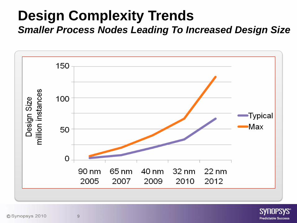
Design Complexity TrendsSmaller Process Nodes Leading To Increased Design Size

10
Chip Size Trends
McClean Report, 2009 Edition, IC Insights

11
Roadmap For Die Area Partitioning1999 To 2017
Semiconductor Intellectual Property: Continuing On The Path Toward Growth, 2008, SEMICO Research Corp

12
Power Trends
Power Management Technologies, 2009, IBS

13
Design Planning: What and Why
Design Trends
Design Planning Challenges
New Trends
Discussion
Agenda
14
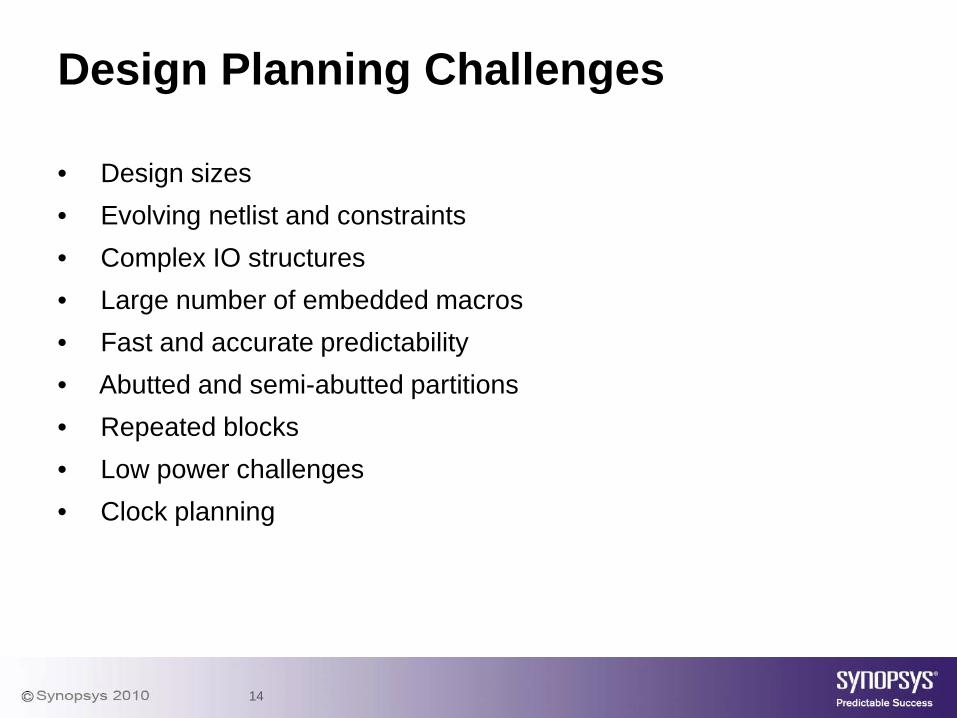
• Design sizes• Evolving netlist and constraints• Complex IO structures• Large number of embedded macros• Fast and accurate predictability• Abutted and semi-abutted partitions• Repeated blocks• Low power challenges• Clock planning
Design Planning Challenges

15
Increasing Design Sizes
• Full-chip design planning
• Large netlists: 20-40M instances– Load essential data– Levels of abstraction– Partial netlist planning
• Large die sizesBlock BBlock A
interfaceinterface interface
black box
completenetlist
not needed for interblock timing

16
physical implementation milestones
Evolving Netlists And Constraints
• Parallel RTL and physical design
• Constant netlist changes
• Incomplete netlist, libraries
• Inconsistent and mismatched data/netlist
• Incomplete constraints
• Missing clocks
netlist 1
netlist 2
netlist 3
netlist …
final netlist tape out
eco 1
eco 2
eco…
time
early netlist drops final layout

17
Complex IO Structures
• Multi-ring IO PADs
• Multi-height IO PADs
• Mixed Macros and PADs
• Mixed IOs and pins
• Multi-VDD PADs
• Rectilinear boundariesIO voltage group 1
IO voltage group 2 IO voltage group 3
IO voltage group 4
Corner cell IO strip Core IO Macro

18
Large Number Of Embedded MacrosConsiderations
• Large percentage of die area
• Varying sizes/shapes/rectilinear
• Place and route blockages
• Relative constraints
• Macro orientations
• Fragmented SC areas
• Channels

19
Large Number Of Embedded MacrosObjectives
• Produce legal placement– Non overlapping macros
• Minimize– Wirelength, timing, congestion– Displacement from initial
placement
• Maximize– Contiguous routing areas
H-C, Chen et. al., ICCAD 2008T-C Chen et. al., TCAD 20008T. Gao, DAC 1992
TCG Based MP-Tree based

20
Large Number Of Embedded MacrosSub-problems
• Channel sizing– Routing estimation– Power for std. cells
• Blockage creation– Avoid edge and corner
congestionmacro macro
blockages
cells
power trunk
channelH-C, Chen et. al., ICCCAD 2008T-C Chen et. al., TCAD 20008T. Gao, DAC 1992

21
Fast and Accurate Predictability
• Quick assessment of floorplanfeasibility
• Routability– Fast congestion estimation– Dirty floorplans
• Channel and block congestion
prediction actual
congested channels

22
Fast and Accurate Predictability
• Timing predictability– Virtual timing estimation– Quick buffering– Estimated timing models– Dirty constraints
• Area assessment– Estimated buffer count
and cell area– Die area– Block areaslack
timin
g en
dpoi
nts
23
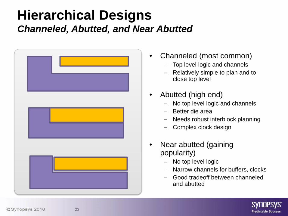
Hierarchical DesignsChanneled, Abutted, and Near Abutted
• Channeled (most common)– Top level logic and channels– Relatively simple to plan and to
close top level
• Abutted (high end)– No top level logic and channels – Better die area– Needs robust interblock planning– Complex clock design
• Near abutted (gaining popularity)
– No top level logic– Narrow channels for buffers, clocks – Good tradeoff between channeled
and abutted

24
Repeated Blocks
• Functionally identical blocks layed out identically
• Bottom up design– Simple, sub-optimal
• Top down in-context design– Automatic identical shapes, pins,
constraints– Rotations, mirroring
A
B
C
D

25
Low Power Planning
• Power domains/voltage areas– Physical locations/shapes– Congestion/timing
• Shutdown regions– Switch cell planning
• Area/Power/performance tradeoff
– Turn-on sequence
• Buffer islands in voltage areas
voltage area 1
voltage area 2
default voltage
buffer island
H-S Won et. al., ISLPED 2003C-Y Yeh et. al., SOCC 2007
Switch cells
voltage area 2

26
Clock PlanningTop Level Clock Tree
PLL
block level clock latency estimation
clock pin locations
estimated resources
uncertain register locations

27
Clock Mesh Planning
• Plan mesh– Skew constraint– Minimize Mesh size +
stub/twig routes– Layers
• Mesh drivers– Number, size, location
• Mesh Analysis– Multi-driver analysis
A. Rajaram et. al., DAC 2008.

28
3D Visualization of Clock Mesh Simulation
ns
Microns
Register Sinks
Pre-Mesh Drivers
Pre-Mesh Tree

29
Design Planning: What and Why
Design Trends
Design Planning Challenges
New Trends
Discussion
Agenda

30
• 3D chip planning
• Multi-level hierarchical planning– For increasing design sizes
• Design Planning and Logic Synthesis
New Trends

31
3D Chip Design PlanningObjectives
• Overlap-free placement of the design blocks
• Minimize wirelength(performance)
– 3D within and between blocks
• Minimize power– Reduce IOs or use weaker ones– Minimize wirelength– Design each layer in its optimal
technology node
• Minimize area

32
3D Chip Design PlanningSub-problems
• Multi-die partitioning and floorplanning
– Timing, power density – Through-silicon via planning
• Optimal through silicon via assignments• Through-Si VIA and pin assignment
– 3D visualization
S.Fujita et al. “Perspectives and Issues in 3D-IC from Designer’s Point of View”, IEEE International Symposium on Circuits and Systems, 2009.Xu He, et. al., SLIP 2009.

33
Multi-Level Hierarchical Design
Top Design Planning
MegaBlock Implementation
Design Exploration
Top-level Assembly
MegaBlock Planning
…SubBlock SubBlock
MegaBlock Assembly
SubBlocksMegaBlocksChip Level

34
Design Planning and Logic Synthesis
• Floorplanning and logic synthesis impact each other
• Solving timing/congestion problems need synthesis and floorplanning solutions
• Enabling architectural decisions
• There is a need to bring logic synthesis and design planning closer
Design Planning
Synthesis
Synthesis with
Design Planning

35
Design Planning and Logic Synthesis
IdentifyCongestion
ModifyFloorplan
Congestion Fixed
36
• Bringing design planning earlier into design flows is key to productivity and convergence– RTL design and synthesis with design planning– Handling evolving designs, constraints
• Traditional design planning to deal with emerging complexities in low power, design size, 3D chips.
Discussion

37
• Jamil Kawa, Group Director R&D, Synopsys Inc.• Dwight Hill, Principal Engineer, Synopsys Inc.
• Steve Kister, TMM, Synopsys Inc.
Acknowledgements