Design, Implementation and Application of Nanostructure ...
128
F RIEDRICH -S CHILLER -U NIVERSITÄT J ENA Design, Implementation and Application of Nanostructure-enhanced Optical Fibers Dissertation zur Erlangung des akademischen Grades doctor rerum naturalium (Dr. rer. nat.) vorgelegt dem Rat der Physikalisch-Astronomischen Fakultät der Friedrich-Schiller-Universität Jena von M.Eng Ning Wang geboren am 18.08.1989 in Xintai, China
-
Upload
khangminh22 -
Category
Documents
-
view
1 -
download
0
Transcript of Design, Implementation and Application of Nanostructure ...

FRIEDRICH-SCHILLER-UNIVERSITÄT JENA
Design, Implementation andApplication of
Nanostructure-enhanced OpticalFibers
Dissertation
zur Erlangung des akademischen Gradesdoctor rerum naturalium (Dr. rer. nat.)
vorgelegt dem Rat der Physikalisch-Astronomischen Fakultätder Friedrich-Schiller-Universität Jena
von M.Eng Ning Wang
geboren am 18.08.1989 in Xintai, China

ii
Gutachter:
1. Prof. Dr. Markus A. SCHMIDT, Friedrich Schiller University of Jena
2. Prof. Dr. Bert HECHT, Julius Maximilian University of Würzburg
3. Jun. Prof. Dr. Isabelle STAUDE, Friedrich Schiller University of Jena
Tag der Disputation: 24.09.2019

iii
FRIEDRICH-SCHILLER-UNIVERSITÄT JENA
Abstract
This thesis covers the research topic of nano-plasmonics as well as fiber opticswith a study focus on design and implementation of a functional optical fibertip by integrating nanoscale resonance structure on its facet. Accordingly,the research background and state-of-the-art are generally discussed at thebeginning. Since this work is highly related to two distinct optic areas, thefundamentals of both fields would be given in the following sections.
The subsequent chapters are concerned with design, characterization, andimplementation of plasmonic nanostructure on fiber end-faces. In particu-lar, we illustrate the diverse spectral evolution of the closely-packed nan-otrimer array, which offers a new degree of freedom to design artificial nano-components and -devices. Furthermore, we employ electron beam lithogra-phy to fabricate nanostructures on fiber facet by planarizing fibers surface ina specially-designed can-like holder. This technique represents a significantstep forward in the research field of fiber functionalization and opens up thefield of nanoengineering for fiber optics.
At last, we demonstrate potential applications of nanostructure-enhancedfibers by examples of a high-precision refractive index sensor and a light sig-nal detector. These fiber-substrated prototypes presented here provide oneof the first investigations into how to employ nanostructure-modified op-tical fibers as short-cut tools for a number of important implications of fu-ture practice, including but limited to bioanalytics, telecommunications, andquantum technologies.
Overall, the studies contribute in several ways to understand complexoptical response of nanostrucutures mediated by the geometrical distributionand provide a new degree to finely tailor plasmonic resonances of nanoanten-nas. The electron beam lithography-based fabrication approach also estab-lishes a solid framework towards ’lab-on-fiber’ enabled by functional nanos-tructures. We hope this thesis could offer valuable insights into design andprototyping of the nanoplasmonic-inspired optical devices.

iv
Zusammenfassung
Diese Arbeit beschäftigt sich mit dem Forschungsthema Nanoplasmoniksowie Faseroptik mit einem Schwerpunkt auf dem Design und der Imple-mentierung einer funktionalen Glasfaserspitze durch Integration der nano-skaligen Resonanzstruktur auf ihrer Facette. Dementsprechend werden derForschungshintergrund und der Stand der Technik in der Regel zu Beginndiskutiert. Da diese Arbeit in hohem Maße mit zwei verschiedenen optis-chen Bereichen zusammenhängt, werden die Grundlagen beider Bereiche inden folgenden Abschnitten erläutert.
Die folgenden Kapitel befassen sich mit dem Design, der Charakterisie-rung und der Implementierung der plasmonischen Nanostruktur auf Faseren-den. Insbesondere veranschaulichen wir die unterschiedliche spektrale En-twicklung des dicht gepackten Nanotrimer-Arrays, das ein neues Maß anFreiheit bei der Entwicklung künstlicher Nanokomponenten und -geräte bi-etet. Darüber hinaus verwenden wir Elektronenstrahllithographie, um Nano-strukturen auf Faserfacetten herzustellen, indem wir die Faseroberfläche ineinem speziell entwickelten, dosenartigen Halter planarisieren. Diese Tech-nik stellt einen bedeutenden Fortschritt auf dem Gebiet der Faserfunktional-isierung dar und eröffnet das Feld des Nanoengineerings für Glasfasern.
Schließlich zeigen wir die Einsatzmöglichkeiten von nanostrukturverstärk-ten Fasern am Beispiel eines hochpräzisen Brechungsindex-Sensors und einesLichtsignaldetektors. Diese hier vorgestellten faserverstärkten Prototypenstellen eine der ersten Untersuchungen dar, wie man nanostrukturmodifizierteGlasfasern als Abkürzungswerkzeuge für eine Reihe wichtiger Implikatio-nen der zukünftigen Praxis einsetzen kann, einschließlich, aber nicht beschränktauf Bioanalytik, Telekommunikation und Quantentechnologien.
Insgesamt tragen die Studien in mehrfacher Hinsicht dazu bei, die kom-plexe optische Reaktion von Nanostrukturen zu verstehen, die durch diegeometrische Verteilung vermittelt wird, und bieten einen neuen Grad, umplasmonische Resonanzen von Nanoantennen zu optimieren. Der auf Elek-tronenstrahl Lithographie basierende Fertigungsansatz etabliert auch ein solidesGrundgerüst in Richtung "Lab-on-Fiber", das durch funktionale Nanostruk-turen ermöglicht wird. Wir hoffen, dass diese Arbeit wertvolle Einblickein das Design und Prototyping der nanoplasmonisch inspirierten optischenGeräte geben kann.

v
Contents
Abstract iii
1 Introduction 11.1 Background and motivation . . . . . . . . . . . . . . . . . . . . 11.2 The state-of-art of this research . . . . . . . . . . . . . . . . . . 41.3 Arrangement of the thesis . . . . . . . . . . . . . . . . . . . . . 5
2 Fundamentals of plasmonics and fiber optics 82.1 Fundamentals . . . . . . . . . . . . . . . . . . . . . . . . . . . . 9
2.1.1 Maxwell’s equations . . . . . . . . . . . . . . . . . . . . 92.1.2 Optical properties of metals and glasses . . . . . . . . . 10
2.2 Plasmonic resonance at the nanoscale . . . . . . . . . . . . . . 132.2.1 Surface plasmons . . . . . . . . . . . . . . . . . . . . . . 132.2.2 Geometry/size dependence . . . . . . . . . . . . . . . . 192.2.3 Near-field coupling . . . . . . . . . . . . . . . . . . . . . 202.2.4 Fano resonance . . . . . . . . . . . . . . . . . . . . . . . 24
2.3 Fiber optics . . . . . . . . . . . . . . . . . . . . . . . . . . . . . . 262.3.1 Fiber characteristics . . . . . . . . . . . . . . . . . . . . 262.3.2 Advancements in fiber optics . . . . . . . . . . . . . . . 30
2.4 Studies methods . . . . . . . . . . . . . . . . . . . . . . . . . . . 302.5 Chapter summary . . . . . . . . . . . . . . . . . . . . . . . . . . 33
3 Nanostructures designed for fiber applications 343.1 Benefits and challenges of fiber substrates . . . . . . . . . . . . 35
3.1.1 Planar substrate in plasmonics research . . . . . . . . . 353.1.2 Fiber matters . . . . . . . . . . . . . . . . . . . . . . . . 36
3.2 Nanodisk spectral evolution: shifting resonance to the NIRregime . . . . . . . . . . . . . . . . . . . . . . . . . . . . . . . . 383.2.1 Theoretical model analysis . . . . . . . . . . . . . . . . 383.2.2 Experimental verification . . . . . . . . . . . . . . . . . 39
3.3 Symmetric trimer array with Fano resonances . . . . . . . . . 423.3.1 Background studies . . . . . . . . . . . . . . . . . . . . 42

vi
3.3.2 Trimers optical response with increasing dot diameter 463.3.3 Spectral polarization dependence of trimers . . . . . . 493.3.4 Electric and magnetic Fano resonances in a trimer array 503.3.5 Trimer optical response with modification of the unit cell 533.3.6 Summary of optical properties of trimer arrays . . . . . 58
3.4 Chapter summary . . . . . . . . . . . . . . . . . . . . . . . . . . 59
4 Implementation of nanostructures on optical fiber facets 614.1 Overview of current fabrication techniques for fiber tips . . . 624.2 Working process of e-beam lithography on fiber facets . . . . . 634.3 Fabricated fiber-substrate nanostructures . . . . . . . . . . . . 654.4 Chapter summary . . . . . . . . . . . . . . . . . . . . . . . . . . 67
5 Characterization & application of nanostructured fibers 685.1 Characterization of nanotrimer-enhanced fibers . . . . . . . . 695.2 Nanotrimer-based fibers for RI sensing . . . . . . . . . . . . . . 74
5.2.1 Introduction of LSPR-based sensing . . . . . . . . . . . 745.2.2 RI sensing of nanotrimers on a planar substrate . . . . 755.2.3 Nanotrimer-enhanced fiber-based RI sensor . . . . . . 77
5.3 Nanodisk-assisted fiber probe for light collection . . . . . . . . 785.3.1 Weak signal detection at wide angles . . . . . . . . . . 785.3.2 Concept of nanodisk-enhanced light collection . . . . . 795.3.3 Theoretical and numerical calculations . . . . . . . . . 825.3.4 Experimental performance . . . . . . . . . . . . . . . . 885.3.5 Further investigations to improve fiber NA . . . . . . . 91
5.4 Chapter summary . . . . . . . . . . . . . . . . . . . . . . . . . . 92
6 Summary and outlook 946.1 Summary of the thesis . . . . . . . . . . . . . . . . . . . . . . . 946.2 Outlook of future work . . . . . . . . . . . . . . . . . . . . . . . 95
Bibliography 99
Acknowledgements 116
Publications 117
Ehrenwörtliche Erklärung 118

vii
List of Abbreviations
ALD Atomic layer depositionEBL Electron beam lithographyFEM Finite element methodFDTD Finite difference time domainFIB Focused ion beamFWHM Full width at half maximumGIF Graded index fiberIR InfraredLSPR Localized surface plasmon resonanceMLWA Modified long wavelength approximationMMF Multi mode fiberNA Numerical apertureNIR Near infraredOSA Optical spectrum analyzerPAMF Pressure-assisted melt-fillingPCF Photonic crystal fiberPDMS PolydimethylsiloxanePMMA Poly(methyl methacrylate)RI Refractive indexRIU Refractive index unitSEM Scanning electron microscopeSIF Step index fiberSLR Surface lattice resonanceSMF Single mode fiberSNOM Scanning near field optical microscopeSPP Surface plasmon polaritonTIR Total internal reflectionTPIP Two photon excited photoluminescenceTPL Two photon induced luminescenceVIS Visible

viii
List of Symbols
α Polarizabilityβ Propagation constantε Relative permittivityη Fiber light-coupling efficiencyθ Incident angleθc Critical angleλ Wavelengthµ Relative permeabilityΛ Periodical constanta Fiber core radiusc Light speed constantk Wavenumbern Refractive indexne f f Effective indexnco Refractive index of fiber corencl Refractive index of fiber claddingCsca Scattering cross-sectionCabs Absorption cross-sectionCext Extinction cross-sectionD Nanodot diameterG Particle edge-to-edge distance (gap)H Nanodot heightQsca Scattering coefficientQabs Absorption coefficientQext Extinction coefficientQ-factor Resonance factorR2 Coefficient of determination∆Tc Transmission contrastT Transmission

ix
To my dearest grandpa . . .


1
Chapter 1
Introduction
1.1 Background and motivation
Owing to its extremely low signal loss [1, 2], optical fiber has revolutionizedmodern telecommunication technology and industry [3]. The pioneeringwork of Charles K. Kao won the Noble Prize in Physics in 2009 for "ground-breaking achievements concerning the transmission of light in fibers for op-tical communication" [4]. Today, optical fiber research still represents a majorscientific field [5–7] within the optics/photonics community, with an appli-cation range not limited to communications. For example, fibers can also beemployed as highly efficient sensor devices [8] or used in broad spectrumlasers [9].
However, the improvement of fiber optical properties relies on the mod-ification of the fiber geometry (e.g., polarization-maintaining fibers obtainedby adding stress rods along the core [10]) and/or the use of composite mate-rials (e.g., a high NA fiber with core and cladding composed of high index-contrast materials [11]). The innovations in fabrications of specialty fiberschallenge the drawing technology and improper process improvements couldinduce product problems such as deformations of fiber cross-section andstructure collapse [12].
Meanwhile, nanophotonics has been regarded as one of the hottest re-search fields over the last two decades [13, 14]. Owing to advancementsin nanofabrication technology (such as focused ion beam (FIB) and electronbeam lithography (EBL)), nanoscale artificial metallic/dielectric structurescan manipulate light propagation [15, 16], providing an innovative platformfor studying light-matter interactions. Based on surface plasmons, novel con-cepts such as metasurfaces [15, 17] have been developed for a wide range ofapplications, including, but not limited to, beam shaping [18], molecular de-tection [19] and quantum communication [20].

2 Chapter 1. Introduction
Hence, these functional nanostructures provide an alternative way to con-trol light on demand and inspire novel design approaches to modify fiberproperties. Here, we propose and demonstrate the concept of nanostructure-enhanced fibers, in which plasmonic nanostructures are integrated on fiberfacets by means of EBL. Placing nanostructures on fibers could relax strictfabrication requirements during fiber drawing process and additionally en-dow fibers with more functionalities (e.g., signal multiplexing [21]). This con-cept also serves to meet the urgent demands of precise light delivery and/orcollection, which are of particular interest in the field of biophotonics.
A nanostructure-enhanced fiber is schematically depicted in Fig. 1.1 (a).In general, such a fiber consists of two major components, an optical fibersubstrate and functional nanostructures. Here, the horizontally oriented cylin-der represents an optical fiber, where the light and dark gray denote the fibercore and cladding, respectively. For illustration, we take an array of hexag-onally distributed nanodisks (in orange color) as an example of a nanostruc-ture, which is placed on the end face of this fiber. Under laser excitation(indicated by the multicolor arrow), the optical response of the fiber shouldbe modified due to the presence of the nanodisks.
Apparently, there are certain ’incompatibility’ problems between a fibersubstrate and functional nanostructures. On the one hand, the majority ofsubwavelength structures are implemented on flat substrates and may thusnot best suit fiber facets. On the other hand, even though there is a wideselection of fibers, none of them is probably specially designed as a substrateto support these nanoscale structures. Hence, an essential issue that needsto be discussed beforehand is which component should be altered (either thefiber substrate or nanostructure) to satisfy certain requirements for the otherpart.
This prerequisite issue (the modification priority) is described in Fig. 1.1(b). As indicated by the arrow going from the optical fiber (light-blue back-ground) section to the nanophotonics (light-magenta block) part, the first so-lution is to alter the fiber geometry and optical property to enable the use ofnanostructures. Correspondingly, another approach is to develop speciallydesigned subwavelength structures to meet the requirements of fibers (illus-trated by the bottom arrow with the label 2).
Within this work, the second approach (designing and modifying nanos-tructures to fit fibers) is selected considering the disadvantages of designingnew fibers, such as the high costs in terms of time and budget throughoutthe implementation (the fiber development duration can be a couple of years,

1.1. Background and motivation 3
FIGURE 1.1(a) Schematic showing the concept of nanostructure-enhancedoptical fibers. Here, the gray cylinder and orange dots repre-sent an optical fiber and a nanostructure, respectively. (b) Twomain research strategies of this work. Label 1 indicates modi-fying the fiber geometry and optical properties in order to sup-port a nanostructure. Alternatively, a nanostructure can be par-ticularly designed for usage with a fiber (label 2).
and the manufacturing process demands tremendous efforts as well).Currently, there is a broad range of fibers available in the research field
and on the market. Among these fibers, single-mode fiber 28 (SMF-28) [22] ischosen as the substrate based on the following benefits.
• Fiber representative
SMF-28 is the most commonly used fiber in telecommunications. It iscommercially available at an extremely low cost ( 1 e/m).
• Solid fiber facet
SMF-28 consists of a solid silica core and cladding, which can physicallysupport nanostructures. Some microstructured fibers (i.e., hollow core fibers)obviously fail to meet this criterion and thus cannot be used in this project.
• Mode profile

4 Chapter 1. Introduction
Operating in the IR regime, the fundamental HE11 mode of SMF-28 re-sembles a Gaussian beam profile [2]. Hence, there is no need to adjust themode excitation.
In summary, the aim of this study is to investigate and design novel plas-monic nanostructures for fiber application, and SMF-28 (Corning Inc. [22]) isselected as the substrate based on the above advantages.
1.2 The state-of-art of this research
We summarize some recently published major achievements in nanostructure-enhanced fibers in Table 1.1 (see page 7) for reference. As seen from this table,a variety of nanostructures (from single monopole [23] to layer-stacked hy-brid nanostructure [24]) can be fabricated on different fibers (e.g., SMF-28[25], photonic crystal fiber (PCF) [26]) via several fabrication schemes (in-cluding EBL [27], FIB [28], template transfer [29], etc.). Additionally, thesereferences demonstrate that nanostructure-enhanced fibers benefit multiplefields as a novel platform for chemical and biological sensing [30], beamshaping [28], signal modulations [31], etc.
From the fabrication aspect, Table 1-1 presents two main techniques -FIB and EBL. Some comparative studies [32, 33] have revealed that EBL canproduce higher quality nanoantennas (stronger plasmonic response and lowcontamination) compared to FIB. For fabricating a larger nanoarray pattern,EBL also requires less time than FIB. Hence, we adopt EBL to directly createnanopatterns on fiber facets. In addition, other techniques such as pressure-assisted melt-filling (PAMF) [34], template transfer [29] and EBL-based hy-brid method [24]), can also be considered.
Here, we would like to highlight our work in this field [35]. One majorcontribution is that the proposed EBL-based method could realize parallelfabrication of complex nanoarrays (nanotrimers, nanodot arrays, metasur-faces, etc.; further discussions are provided in chapter 4) on several fiber endfaces [25]. This method allows fibers that are meters long to be obtained,which is not typical for the samples in Table 1-1 (fibers are often limited to1 cm due to the machine confinements). Further modifications of the im-plementation procedure may also allow fibers to be made of other materials(such as polymers or elastomers).
Furthermore, we carried out in-depth studies on the optical response ofnanostructures in close-packed arrays. With this compact distribution, we

1.3. Arrangement of the thesis 5
demonstrate the strong spectral tunability of nanostructures by modifyingtheir periodic constants. This phenomenon could greatly help in tailoringthe desired optical response and further assist in the on-demand design ofnanostructures.
1.3 Arrangement of the thesis
The main purpose of this thesis is to present the complete research process fordeveloping nanostructure-enhanced fibers. To fulfill this purpose, the thesisis arranged as follows:
In the current chapter, we have presented the concept of nanostructure-enhanced fibers, in which a well-defined plasmonic nanoantenna array isintegrated on the end face of an SMF-28 fiber for applications in telecommu-nications, remote sensing, fiber endoscopy, novel optical component design,etc. The background, motivation and state-of-art related to this project havebeen introduced.
In chapter 2, the research background of nanoplasmonics and optical fibersis explicitly illustrated. We introduce basic concepts in nanophotonic andthe working mechanisms of plasmonic effects (e.g., dipole resonance [13],Fano resonance [45]). Since this project concentrates on localized surfaceplasmon resonance (LSPR), fundamentals related to this optical effect (e.g.,resonance condition [14] and near-field dipole-dipole interactions) are pre-sented in great detail. We also provide the basics of fiber optics, such as modecalculations and profiles, to understand the fiber optical properties. It is alsonecessary to illustrate the major study methods used in this thesis, which areparticularly presented in the last section of this chapter.
In chapter 3, from theoretical and experimental perspectives, the designprocedures for metallic nanostructures for usage with step-index fibers aredemonstrated. Based on the characteristics of SMF-28, we propose three re-quirements for plasmonic nanostructures. In general, the desired nanoanten-nas should exhibit a narrow spectral lineshape in the infrared (IR) regime.Here, we mainly investigate a closely packed nanotrimer array, which is fur-ther patterned on the end face of fibers. In addition to a dolmen-like electricFano resonance, this specific nanotrimer arrangement (square-shaped unitcell) breaks the three-fold symmetry of the isolated trimer and induces amagnetic Fano resonance. These unique spectral features (working in theIR regime and asymmetric lineshape) enable experimental characterizationof nanotrimer-modified optical fibers.

6 Chapter 1. Introduction
In chapter 4, we show the nanoengineering process of patterning a trimerarray on the facet of fibers by means of electron beam lithography. Throughplanarization of the fiber surface in a custom can-like holder [25], the fibersubstrate can be treated as a planar wafer. The manufacturing workflow forpatterning nanostructures can be found in this section. In addition to thenanotrimer array, we also fabricated nanobar-based metasurfaces, nanodotarrays and cross-like four-dot antennas on the end face of optical fibers toverify the reliability and reproducibility of the fabrication techniques.
In chapter 5, we demonstrate the characterization of nanotrimer-basedfibers by measuring the transmission contrast. The trimers on a fiber sub-strate exhibit high spectral similarities with the trimers on a flat silica sub-strate, where a major dip located at approximately 1.6 µm is captured in bothcontrast spectra. This result strongly proves that the optical response of thefiber has been modified by the nanostructures. In addition, we employ thenanotrimer-enhanced fiber tip as a refractive index (RI) sensor, which showsa sensitivity of 390 nm/RIU, more than two times higher than those of pre-viously reported LSPR-based fiber sensors [37, 46]. At the end of this chap-ter, we demonstrate a significant enhancement of the light-collecting abilityof nanostructured fibers at oblique incident angles. The nanodot-modifiedfiber tip displays amplitude improvements of several orders of magnitudecompared to bare fibers (without any nanostructure). The significant per-formance enhancements are further examined with a toy model as well asnumerical simulations.
In the last chapter, the results and data obtained in this work are summa-rized. Improvements of this work and an overview of potential applicationsare also given.

1.3. Arrangement of the thesis 7
TAB
LE
1.1
Sum
mar
yof
vari
ous
nano
stru
ctur
eson
fiber
end-
face
Ref
s.N
anos
truc
ture
type
Nan
ostr
uctu
rem
ater
ial
Fibe
rty
peA
pplic
atio
nsFa
bric
atio
nte
chni
ques
[23]
Mon
opol
ean
tenn
aA
lum
inum
SMF
at63
3nm
Sing
lem
olec
ule
fluor
esce
nce
FIB
[26]
Nan
oslo
tmet
asur
face
Gol
dPC
FBe
amsh
apin
gFI
B[2
8]Ph
ase-
grad
ient
met
asur
face
Gol
dSM
F-28
Beam
shap
ing
and
sens
ing
FIB
[36]
1Ddi
ffra
ctio
ngr
atin
gSi
3N4/
SiO
2Si
lica
fiber
Opt
ode
and
sens
ing
FIB
[31]
Split
ring
aper
ture
sG
old
Silic
afib
erSi
gnal
mod
ulat
ion
FIB
[30]
Phas
edi
ffra
ctiv
eel
emen
tPM
MA
SMF-
28Be
amsh
apin
gEB
L[2
7]N
ano-
gird
/gra
ting
Gol
dSM
F-28
Fibe
rin
line
pola
rize
rEB
L[3
7–40
]N
anod
isks
arra
yG
old
SMF
at63
3nm
Biol
ogic
alse
nsin
gEB
L[4
1]C
once
ntri
cri
nggr
atin
gG
old
MM
FSe
nsor
EBL
[25]
Trim
ers
arra
yG
old
SMF-
28In
dex
sens
orEB
L[3
4]Sp
ike-
like
tip
Gol
dN
ano-
bore
fiber
End-
fire
coup
ling
PAM
F[2
9,42
]N
anoh
ole
arra
yG
old
Larg
e-co
refib
erBi
omol
ecul
arse
nsin
gTe
mpl
ate
tran
sfer
[24,
43]
Hyb
rid
met
allo
-die
lect
ric
Die
lect
ric
met
allic
SMF-
28C
hem
ical
and
biol
ogic
alse
nsin
gEB
L-ba
sed
hybr
idm
etho
d
[44]
Cre
scen
ts,r
ings
,sp
litri
ngs,
coax
ialc
ylin
ders
,na
now
ire
grat
ing
Met
allic
MM
FSu
rfac
e-en
hanc
edR
aman
spec
tros
copy
Nan
oski
ving
-bas
edte
mpl
ate
tran
fer

8
Chapter 2
Fundamentals of plasmonics andfiber optics
Nanophotonics is a general subject related to many scientific and engineer-ing fields, such as optical engineering, nanofabrication in the silicon industry,and quantum computing, to name but a few. With a focus on light-matter in-teractions at the nanoscale, the rapid development of nanooptics has enabledfictional concepts (e.g., invisibility cloaks [47, 48]), led to fruitful results (e.g.,metasurfaces [49]) and greatly benefited human beings (e.g., cancer diagnos-tics and treatment by nanoshells [50]).
Plasmonics, being a major part of nanophotonics, mainly investigates theoptical physics of ordered and/or disordered metallic nanoparticles and hasbeen extended to nanostructures consisting of dielectrics [51], graphene [52]and so on. Twenty-one years ago, the pioneering work of T. W. Ebbesenon extraordinary light transmission through a nanohole array in a gold thinfilm [53] led to a new phase in the study of nanoplasmonics. Currently,plasmonic-related nanooptics is still a flourishing and extremely active sci-entific topic.
On the other hand, fiber optics remains one of the ’hottest’ fields, eventhough it has been intensively studied for more than half a century [4]. In thiswork, we aim to transfer plasmonic nanostructures to fiber facets. To gain acomprehensive understanding, this chapter aims to provide basic conceptsand theoretical foundations in the areas of plasmonics and fiber optics.
Starting from Maxwell’s equations, we first present elementary equationsof classical electromagnetism. Then, two optical effects - localized surfaceplasmon resonance (LSPR) and surface plasmon polariton (SPP) - will be ad-dressed in detail. In particular, LSPR represents the major working princi-ple of the entire project, and thus, we emphasize this effect. The Fröhlichresonance conditions, coupling between localized plasmons and Fano reso-nance are given in this section. Furthermore, we examine the fundamentals

2.1. Fundamentals 9
of fiber optics from aspects such as the geometric arrangement, mode profile,and dispersion. Here, we take SMF-28 as a specific example for the overalldemonstration. Additionally, the recent advancements in optical fibers willbe briefly reviewed. Finally, we summarize commonly used research meth-ods in the field of nanophotonics. With a focus on the spectral behaviors offunctional nanostructures, we mainly adopt numerical simulations and ex-perimental spectral measurements to design and optimize ordered nanopar-ticles for usage with SMF-28.
2.1 Fundamentals
2.1.1 Maxwell’s equations
Maxwell’s equations are fundamental to understanding how electromagneticfields are generated and modified by charges, currents, and changes in thefields. This set of functions (consisting of four partial differential equations)bears the name of physicist James Clerk Maxwell for his early and preemi-nent work in electromagnetism.
Now, we first present Maxwell’s equations in free space (without any ex-ternal source) in the presence of external charge ρext and current density Jext,which are given in the following forms [14]:
∇·D = ρext (2.1a)
∇·B = 0 (2.1b)
∇× E = −∂B∂t
(2.1c)
∇×H =∂D∂t
+ Jext (2.1d)
Maxwell’s equations include Gauss’s laws (Eq. 2.1 a and b), Faraday’s law(Eq. 2.1 c), and Ampère’s law with Maxwell’s addition (Eq. 2.1 d). Here, theelectric field E(r, t) = E(r)e−iωt and the magnetic field H(r, t) = H(r)e−iωt
are both vector functions of positions r and time t. D and B indicate thedielectric displacement and the magnetic induction, respectively. ∇· and∇× are the divergence and curl operations, denoted by the nabla symbol∇. Note that external (ρext, Jext) and internal (ρ, J) are separated, such that

10 Chapter 2. Fundamentals of plasmonics and fiber optics
ρtot = ρext + ρ and Jtot = Jext + J. By introducing polarization P and magne-tization M, we obtain the subsequent relations:
D = ε0E + P (2.2a)
H =1µ0
B−M (2.2b)
Here, the vacuum electric permittivity constant is represented by ε0, witha value ≈ 8.854× 10⁻¹²F/m, and the magnetic permeability µ0 is ≈ 1.257×10⁻⁶H/m. Henceforth, we only consider a linear, isotropic and nonmagneticmedium. Accordingly, Eq. 2.2 can be modified as follows [14]:
D = ε0εE (2.3a)
B = µ0µH (2.3b)
where ε and µ are the relative permittivity and relative permeability, respec-tively (in a nonmagnetic medium µ = 1). Alternatively, Eq. 2.3 can be de-fined by the electric susceptibility χe and magnetic susceptibility χm, whichleads to
P = ε0χeE (2.4a)
M = χmH (2.4b)
Hence the refractive index (RI) can be expressed as n =√
ε =√
1 + χe,indicating that RI (n) is the square root of ε, and the light speed constant infree space can be obtained by c0 = 1/
√ε0µ0.
2.1.2 Optical properties of metals and glasses
Dielectric function of metals
The optical property of metals can be analyzed by a plasma model assum-ing that a gas of free electrons moves against a fixed background of positiveion cores. The electrons would oscillate corresponding to the applied elec-tromagnetic field, and their motions are damped due to collisions, which isfurther indicated by a characteristic collision frequency γ = 1/τ (τ is the re-laxation time of the free electron gas). Thereby, the dielectric function of freeelectron gas can be defined as follows [14]:

2.1. Fundamentals 11
ε(ω) = 1−ω2
p
ω2 + iγω(2.5)
where ωp is the metal plasma frequency, which corresponds to the eigenfre-quency of the electronic oscillation.
Hence, the real and imaginary parts of the complex dielectric function(ε(ω) = ε1(ω) + i· ε2(ω)) are given by
ε1(ω) = 1−ω2
pτ2
1 + ω2τ2 (2.6a)
ε2(ω) =ω2
pτ
ω(1 + ω2τ2)(2.6b)
Qualitatively, two different mechanisms [54] (Drude model and Lorentzmodel) contribute to ε(ω) in metals (i.e., ε = εDrude + εLorentz + ...).
• Drude-Sommerfeld contribution εDrude(ω)
ε(ω) = ε∞ −ω2
p
ω2 + iγω(2.7)
where ε∞ is the residual polarization, with a value of 1 ≤ ε∞ ≤ 10.
• Drude-Lorentz contribution εLorentz(ω)
The effect of electronic inter-band transitions can be taken into accountin ε(ω) by means of a Lorentz-modified item:
ε(ω)Lorentz =∆εΩ2
p
Ω2p −ω2 − iΓω
(2.8)
where Ωp and Γ are the plasma and damping frequencies for the boundelectrons, respectively, in analogy to Eq. 2.7, and ∆ε weights the contri-bution of the given interband transition to the dielectric function.
In Fig. 2.1, the measured data of the real (ε1) and imaginary (ε2) compo-nents of the permittivity of gold and silver within a wavelength range from200 nm to 1900 nm are separately plotted in (a) and (b). These experimen-tal data are obtained from refs. [55, 56]. Comparing the two noble metals,they exhibit a high similarity, where ε is governed by the large negative realpart ε1, especially for wavelength > 550 nm. In addition, considering thetheoretical model (see an example in this ref. [14]), the Drude contributionswell fit the measured data at a larger wavelength range (roughtly λ > 400

12 Chapter 2. Fundamentals of plasmonics and fiber optics
FIGURE 2.1Dielectric function of gold (a) and silver (b). Re[ε] and Im[ε]represent ε1(ω) and ε2(ω), respectively.
nm), whereas they cannot reproduce the increase of metal absorption lossesat short wavelengths. This mismatch can be amended by adding Lorentzianterms to the Drude model.
Sellmeier equation and optical loss of SiO2
The rapidly development of fiber optics has benefited from low-loss glassymaterial. Among these glasses, fused silica (amorphous silicon dioxide, SiO2)is the dominating material in fiber optics, especially for optical telecommuni-cations [57]. Therefore, in this section, we would like to briefly introduce theoptical properties of this transparent medium, whose refractive index can beapproximated by the Sellmeier equation. The Sellmeier equation is an empir-ical relationship used to determine the frequency-depended refractive index.In general, the Sellmeier equation can be expressed as [58]
n2(λ) = 1 +n
∑k=1
Bkλ2
λ2 − Ck(2.9)

2.2. Plasmonic resonance at the nanoscale 13
where n and λ are the refractive index and vacuum wavelength, respectively.Bk and Ck are Sellmeier coefficients obtained from experimental measure-ment. For instance, the RI of fused silica is given by [59]
n2silica(λ) = 1 +
0.6961663λ2
λ2 − 0.06840432 +0.4079426λ2
λ2 − 0.11624142 +0.8974794λ2
λ2 − 9.8961612 (2.10)
Note that in this thesis, due to the small RI variations of fused silica (fromVIS to NIR region), εsilica (= n2
silica) in numerical simulation models (a simu-lated example is given in chapter 3) is often fixed at 2.09 for convenience.
Finally, we can review the intrinsic losses of fused silica (an example forthe loss spectrum in ref. [57]). Overall, the optical loss is below 1 dB/kmwithin the wavelength ranging from 1 µm to 1.8 µm. At shorter wavelengths(from 1 µm to 1.4 µm), Rayleigh scattering (∝ λ−4) is the main reason forthe optical loss, further increasing the value to a few dB/km in the visibleregime. The infrared absorption related to multiphonon absorption (vibra-tional resonances) dominantly contributes to the loss at longer wavelengths(from approximately 1.65 µm to 1.8 µm). At 1.55 µm, the loss reaches a mini-mum value of 0.1 dB/km, which is located at telecommunication C band(1530-1565 nm). In addition, there are five more communication bands inthis regime including O band (1260-1360 nm), E band (1360-1460 nm), S band(1460-1530 nm), L band (1565-1625 nm), and U band (1625-1675 nm).
2.2 Plasmonic resonance at the nanoscale
2.2.1 Surface plasmons
Plasmonics is the study of physical phenomena induced by and closely as-sociated with surface plasmons [60–62]. Currently, an increasing number ofstudies (over 6000 related publications in 2011 [63]) have intensively focusedon two types of surface plasmon effects. One (sketch in Fig. 2.2 (a)) is thepropagating surface waves named surface plasmon polaritons (SPPs), andthe other (Fig. 2.2 (b)) is a ’nonpropagating’ excitation called localized sur-face plasmon resonances (LSPRs).
Surface plasmon polaritons
Surface plasmon polaritons represent an optical phenomenon in whichan electromagnetic wave propagates along the interface (along x axis in Fig.

14 Chapter 2. Fundamentals of plasmonics and fiber optics
FIGURE 2.2Sketches of surface plasmon polaritons (a) and localized surfaceplasmon resonances (b).
2.2 (a)) between a metal and a dielectric (or air) with the maximum intensityalong this surface while the electric field exponentially decaying perpendic-ular to this interface (along z axis in (a)) [14, 64–66]. The electromagneticsurface waves are associated with the collective oscillation of the free elec-trons in the metal.
Schematically shown in Fig. 2.2 (a), a flat and smooth gold film (orangebackground, relative permittivity ε1) sustains a travelling electric field (redcurves and arrows) confined between this thin film and air (relative permit-tivity ε2). We define β as the propagation constant of the traveling waves ofSPPs (k0 is the wave number of light wave in vacuum). Hence, the physicalmodel of SPPs can be given by the following equation [14]:
β = k0
√ε1ε2
ε1 + ε2(2.11)
Eq. 2.11 is named as the dispersion relation of SPPs. Note that SPPs onlyexist for TM polarization [14].
To excite SPPs, additional phase matching techniques are employed withthe help of a coupling medium such as a prism or a grating [14]. For in-stance, the commonly used Kretschmann configuration involves placing a

2.2. Plasmonic resonance at the nanoscale 15
prism against a thin metal film. The light passes through the prism and il-luminate the film at an incidence angle greater than the critical angle of totalinternal reflection (TIR).
Due to the energy loss of metals [56], SPPs cannot travel a long distance.An example of the calculated propagating length is close to 1080 µm at thewavelength of 1.5 µm assuming a silver/air interface [14]. A general con-clusion is that stronger electromagnetic field confinement leads to a shorterpropagation length.
From a practical application perspective, SPPs are widely used for novelplasmonic waveguides [67, 68], light concentrator [69], plasmonic sensors[70], plasmonic circuits [71, 72]. Particularly, by filling the air channel of mi-crostructured fibers (e.g., photonic crystal fiber [6] and nano-bore fiber [73])with metallic nanowires, SPPs are also demonstrated within optical fibersframework [7, 74]. These in-fiber SPPs open new possibilities for fiber-basedconcentrators [75], near-field detectors [76], and miniaturized nonlinear de-vices [77].
Localized surface plasmon resonances
FIGURE 2.3A schematics of a sphere (ε(ω)) inserted a medium (εm) withelectrostatic field E0. This image is inspired from ref. [14].
Unlike SPPs, LSPRs are nonpropagating excitations [54, 78] and can beexcited by direct light illuminations without any assistance from a phase-matching technique [79, 80]. The mechanism of LSPRs is illustrated in Fig.2.2 (b). Here, light (in the form of an electric field, red curve) interacts withgold spheres (two yellow circles) whose diameters are much smaller than

16 Chapter 2. Fundamentals of plasmonics and fiber optics
the incident wavelength. The interplay (indicated by the grey arrows) be-tween subwavelength nanoparticles and light leads to a plasmon that oscil-lates locally around the gold nanospheres. The free conduction electrons inthe metal nanoparticle are driven into oscillation (resonance) [81].
Now we would like to present the Fröhlich resonance condition in thecase of a sphere (ε(ω), radius: a) embedded in a medium (εm, isotropic andnon-absorbing material) under quasi-static approximation (a λ, sketchshown in Fig. 2.3.). The general solutions of potentials Φin (inside the sphere)and Φout (outside the sphere) based on this model can be written as [14]
Φin = − 3εm
ε(ω) + 2εmE0r cos θ (2.12a)
Φout = −E0r cos θ +ε(ω)− εm
ε(ω) + 2εmE0a3 cos θ
r2 (2.12b)
Here θ denotes the angle between the position vector r (at point p) and thez-axis (see Fig. 2.3). Eq. 2.12 (b) can be generally interpreted as the E-fieldsuperposition of applied field E0 and a dipole field p situated at the spherecenter. By introducing the dipole moment p, we rewrite Eq. 2.12 (b) in thefollowing form [14].
Φout = −E0r cos θ +p· r
4πε0εmr3 (2.13a)
p = 4πε0εma3 ε(ω)− εm
ε(ω) + 2εmE0 (2.13b)
Now, we arrive at the conclusion that the applied E-field induces a dipolemoment with a value proportional to |E0| according to Eq. 2.13.
By substituting the polarizability α via p = ε0εmαE0, we can obtain theformula of Fröhlich resonance condition [14].
α = 4πa3 ε(ω)− εm
ε(ω) + 2εm(2.14)
To enhance the dipole moment supported by this sphere, the polarizabil-ity α is set to the maximum value provided that ε(ω) + 2εm is sufficientlysmall. Therefore, under the case of small or slowly varying Im [ε(ω)], theFröhlich resonance condition requires Re[ε(ω)] = −2εm. For gold and silvernano-spheres, the Fröhlich resonance wavelengths are located in the visibleregion. As a consequence, a bright color (scattered from these nanoscale par-ticles) can be observed when they are illuminated by light under resonanceconditions.

2.2. Plasmonic resonance at the nanoscale 17
In addition, the Fröhlich resonance condition illustrate that the resonancefrequence ω can be altered due to the presence of a host medium εm. Inchapter 5, we further explore resonance-induced redshift of gold trimers byincreasing the refractive index of surrounding medium.
To evaluate the sphere behaviour regarding light, scattering (Csca), ab-sorption (Cabs), and extinction (Cext) cross-sections are commonly employed.In general, Cabs determines the particle’s capacity to absorb light, while Csca
measures how strongly the particle can scatter light. The correspondingcross-sections can be calculated via the Poynting vector. For a sphere withvolume of V (V = 4
3 πa3 for the sphere in Fig. 2.3) and permittivity ε(ω) =
ε1 + iε2, these cross-sections can be expressed as [14]
Csca =k4
6π|α|2 =
8π
3k4a6
∣∣∣∣ ε(ω)− εm
ε(ω) + 2εm
∣∣∣∣2 (2.15a)
Cabs = kIm[α] = 4πka3 Im[
ε(ω)− εm
ε(ω) + 2εm
](2.15b)
Cext = Cabs + Csca = 9ω
cε3/2
m Vε2
[ε1 + 2εm] + ε22
(2.15c)
The scattering coefficient (Qsca), absorption coefficient (Qabs), and extinc-tion coefficient (Qext) correspond cross-sections normalized to the geometricsize (πa2) of the particle.
Qsca =Csca
πa2 , Qabs =Cabsπa2 , Qext =
Cext
πa2 (2.16)
From an experimental prospective, we assume that the ordered and/ordisordered nanoparticles are assembled on a planar surface within a certainarea (each particle has a size of s in average). To measure the optical spec-trum, some of particles (excited number N) are illuminated by a beam withspot size of S. Once transmission (T) of plasmonic particles is determined,the extinction spectrum, extinction cross-section and extinction coefficientcan be obtained by the subsequent formulas.
Extinction = 1− T (2.17a)
Cext = S(1− T) (2.17b)
Qext = S(1− T)/(N· s) (2.17c)
Corresponding transmission (T) and extinction spectral measurements

18 Chapter 2. Fundamentals of plasmonics and fiber optics
are further demonstrated in chapter 3, where the optical setup and experi-mental procedures are shown in great detail.
FIGURE 2.4(a) A typical experimental configuration for excitation ofLSPRs. A gold nanodisk fabricated on the surface of a silicasubstrate is illuminated by normal incident light. (b) A coloredmap showing the correlation of the E-field and nanodisk di-ameter. The E-field, indicated by the dashed white line in (a),is distributed along the center of resonance pattern. (c) Dipoleresonance electromagnetic field generated by the gold nanodisk(located at center). (d) Measured extinction spectrum (1-T) ofan array of nanodots (diameter: 200 nm). The Lorenz-like spec-tral lineshape shows a central resonance wavelength at approx-imately 800 nm.
E-field amplification and confinement are major consequences of LSPRs.To give an impression of the E-field enhancement, we illustrate the LSPReffect by plotting the near-field patterns of a gold nanodisk together with itsoptical spectrum in Fig. 2.4 (a). This gold nonodisk (orange, indicated by thelabel ’nanoparticle’ with a diameter of D) is placed on a flat silica substrate(εsubstrate = 2.09) and exposed to air (εair = 1). Excited by a normal incidentbeam (colored arrow at the bottom), the gold nanodisk can generate a dipoleresonance pattern (at a plane of 10 nm height above the top surface of thisnanodisk), where the E-fields around the edges of the dot is significantly

2.2. Plasmonic resonance at the nanoscale 19
enhanced. The dipole resonance pattern is further displayed in Fig. 2.4 (c).The central black circle here is the projected contour of the nanodisk.
Now, we can determine the resonance spectral span by inspecting theE-field enhancement and far-field extinction (or transmission or scattering)spectrum. Here, we plot near-field distributions and present the extinctionof gold nanodots in Fig. 2.4 (b) and (d), respectively. Obtained by FEM-based commercial software (COMSOL Multiphysics 4.3 a; the details of thesimulation model are shown in chapter 3), the electromagnetic fields alongthe central line of the resonance patterns (indicated by a white dashed line in(a)) are plotted for examination.
Here, two dashed white lines in (b) indicate the nanodisk diameter andits position. According to the E-field enhancements shown in (b), the centralresonance wavelengths are located at approximately 800 nm in the air-glassmedia configuration. This wavelength matches the extinction spectrum (ob-tained by 1-T) in Fig. 2.4 (d), which exhibits a symmetrical lineshape.
In next sessions, we focus on how to manipulate the resonance lineshape,e.g., to shift the resonance central wavelength using the particle geometry.This information is of great interest for the design of nanostructures for usagewith optical fibers.
2.2.2 Geometry/size dependence
Generally, the spectral lineshape of LSPRs can be altered by many parame-ters, included, but not limited to, the nanoparticle size, geometry and envi-ronments [54]. Here three main factors of modifying resonance behaviourswould be discussed in detail. These are listed in following sections as ge-ometry/size dependence (e.g., particle length), near-field coupling (e.g., theedge-to-edge distance of a nanodot pair), and Fano-like resonance.
In this section, we will explore particle geometry influence on spectralresponse [82]. We first assume a physical background similar to the arrange-ment in Fig. 2.3. However, this time, the sphere is replaced by an ellipsoidwith semi-axes (a1 ≤ a2 ≤ a3). The polarizabilities αi along the principle axes

20 Chapter 2. Fundamentals of plasmonics and fiber optics
(i.e., i = 1, 2, 3) can be expressed as [14]
αi = 4πa1a2a3ε(ω)− εm
3εm + 3Li(ε(ω)− εm)(2.18a)
Li =a1a2a3
2
∫ ∞
0
1(a2
i + q) f (q)dq (2.18b)
f (q) =√(q + a2
1)(q + a22)(q + a2
3) (2.18c)
where Li is the geometric factor.The geometry (i.e., a1, a2, and a3) of a metallic ellipsoid can affect po-
larizability α, which further affects the dipole moment via p = ε0εmαE0.This means that the nanoparticle geometry can influence the LSPR resonancewavelength under the assumption that particle radius a is less than wave-length λ. We will further explore geometry dependence under the conditionthat the nano-particle size approaches the illumination wavelength in chap-ter 3.
In addition, theoretical studies (such as Mie theory [83]) have predictedthe spectra of nanoparticles. For instance, Kuwata et al. illustrated an em-pirical analytical formula for gold and silver spherical particles, which wasfurther verified by experimental data [84]. For more information, we encour-age readers to examine these references [85–87].
Perhaps the most intuitive way to understand the surface plasmon ge-ometry/size dependency is to observe vibrant colors scattered from metal-lic nanostructure [88, 89]. In general, these different colors represent reso-nance wavelengths corresponding to freely dispersed nanoparticles in liq-uids [90]. Based on this mechanism, several reports have recently employedthese plasmonic nanoparticles in novel color display technology. For exam-ple, Xiaoyuan Duan et al. demonstrated a scanning plasmonic color gener-ation scheme that could be switched on/off through directional hydrogena-tion/dehydrogenation [91].
2.2.3 Near-field coupling
The second factor that can modify optical response of a metallic nanoscalestructure is the electromagnetic interactions between the local plasmon modes.Here, we address this issue within a scheme of dipole-to-dipole coupling (i.e.,higher order mode interactions are beyond the scope of this thesis).
For a proper introduction, we will demonstrate near-field coupling effectsusing gold nanoparticles from the aspects of (i) a one-dimensional chain, (ii)

2.2. Plasmonic resonance at the nanoscale 21
FIGURE 2.5Near-field coupling of localized plasmons along the vertical di-rection (a) and horizontal direction (b). This sketch is inspiredfrom ref. [14].
two-dimensional coupled pairs, and (iii) a closely-packed lattice. Note that insecond case, Au pairs are distributed in sparse unit cell (the interactions be-tween cells can be ignored), while diffractive couplings of unit cells becomesstrong in the third situation (lattice resonance).
Spectral shift in a 1D plasmonic chain
The physical background to address this near-field coupling issue is aone-dimensional plasmonic chain formed by evenly distributed gold parti-cles, in which particles’ edge-to-edge distance d is much smaller than inci-dent wavelength λ. As depicted in Fig. 2.5, a gold nanoparticle chain is ex-cited by 90 and 0 polarized light, resulting in the vertical (a) and horizontalcouplings (b), respectively.
The direction of the spectral shift of the LSPR position is determined bythe near-field coupling circumstance, where Coulomb forces among particlesinteract along different axis [14]. Therefore, the restoring force acting on theoscillating electrons of each particle is either decreased or increased by the

22 Chapter 2. Fundamentals of plasmonics and fiber optics
charge distribution of neighbouring particles, leading to a blueshift for lon-gitudinal modes (a) and a redshift of transverse modes (b). The resonancespectral shifts are demonstrated in Fig. 2.6. Here, λ0 is the original resonancecentral wavelength, while λ1 and λ2 are the shifted spectral positions.
FIGURE 2.6A sketch showing spectral redshift and blueshift induced bynear-field coupling. The spectra are obtained from simulations.
Note that under this closely spaced arrangement (d λ in particle chains),the near-field interaction with a distance dependence of d−3 dominates, whilethe dipolar coupling with a distance dependence of d−1 dominates in the farfield for the case of larger particle separations. [14]
Resonance evolution of 2D coupled nanoparticle pairs
For the next topic, we would like to discuss spectral evolution of thecoupled Au nanodisk pairs under a geometric distribution in which twonanoparticles come into close contact. This is a good example for under-standing the spectral evolution of complex nanostructures in two-dimensionaldistributions. As illustrated in Fig. 2.7, d and D represent the interparticleedge-to-edge separation and the particle diameter, respectively.
In general, excited by 0 or 90 polarized light, the Au pairs exhibit spec-tral behaviour akin to the plasmonic chain [92, 93]. Under parallel polariza-tion illumination (0, magenta), the plasmon resonance strongly transits to alonger wavelength (redshift, from λ0 to λ1 in Fig. 2.6) as the interparticle gapd is reduced. In contrast, there is a very slight blueshift (from λ0 to λ2) fororthogonal (90, blue) polarization with decreasing gap d.
Based on this spectral behaviour, several studies proposed the plasmonruler [94], which is intended to measure nanoscale distances within chemical

2.2. Plasmonic resonance at the nanoscale 23
or biological species via a simple exponential function. Here, a valid con-figuration [95] of a plasmon ruler requires that the separation distance d beat least less than two particle diameters D. For further information, pleasecheck these references [95–97].
FIGURE 2.7Coupled Au pair excited by 0 (magenta) and 90 (blue) polar-ized light.
Lattice resonances in an ordered array
As discussed in Fig. 2.7, Au pairs are distributed a lattice configurationwhere the periodical constant is not at same scale as the particle size. Underthis arrangement, the near-field pair-to-pair coupling is much weaker due tothe sufficient geometric distance. However, when the LSPR wavelength ofparticle is commensurate with the periodicity of the array, electromagneticcoupling between unit cells occurs, leading to the emergence of so-called lat-tice resonance.
Lattice resonance has been intensively discussed as surface lattice reso-nance (SLR) [98, 99] in the plamonics community. The spectral position of thesharp transmission dip caused by SLRs can be modified by tuning the corre-sponding geometric parameters (e.g., increasing the pitch imposes a spectralredshift [98]). Since first experimental SLR demonstration with a nanorodarray [98], various structures, such as arrays of nanodots [100–104], disksdimers [105, 106], and split-ring resonators [107], have been investigated toexplore the fundamentals of this collective resonance along with its applica-tions, such as an ultra-narrow absorber [108], fluorescent emission shaping[109] and organic molecule excitation [110].
Here, we introduce a general formula [102] predicting spectrum lineshapemediated by the SLR effect. Assuming that identical nanoparticles are placed

24 Chapter 2. Fundamentals of plasmonics and fiber optics
in an array, the polarizability α of a single isolated nanoparticle is introducedas α∗ by inserting an array factor S.
α∗ =1
1/α− S(2.19)
S is given by
S = ∑j
exp(ikrj)
[(1− ikrj)(3 cos2 θj − 1)
r3j
+k2 sin2 θj
rj
](2.20)
where rj is the distance from the central particle to particle j and θj is theangle between ~rj and the dipole moment j.
Hence, the extinction cross-section Cext of SLR in densely packed arraysof plasmonic particles is rewritten as
Cext = Cabs + Cscat (2.21a)
Cabs = 4πkIm(α∗) (2.21b)
Csca =83
πk4|α∗|2 (2.21c)
2.2.4 Fano resonance
In a work [111] published in 1961, Ugo Fano derived an analytical formula(known as Fano formula) for an asymmetric spectral lineshape for the quan-tum mechanical study of the autoionizing states of atoms. Nowadays, multi-ple researches [45, 112–114] have revealed that the microscopic origin of Fanoresonance is the constructive or destructive interference of a narrow discretedark resonance with a broad spectral line or continuum.
Now, we focus on the Fano resonance supported by an individual plas-monic nanostructure. The fundamental criterion for this type of resonanceis the spectral overlap between a broad bright resonance and a narrow darkresonance [115]. We depict the working principle in Fig. 2.8. Here, the brightmode is excited by external electromagnetic excitation, and the dark modecan be triggered by near-field coupling. Destructive or constructive inter-ference between these two modes leads to a spectrum with an asymmetriclineshape. The lineshape of the dark mode (σa(ω)) can be illustrated as [115]
σa(ω) =
(ω2−ω2
a2Waωa
+ q)2
+ b(ω2−ω2
a2Waωa
)2+ 1
(2.22)

2.2. Plasmonic resonance at the nanoscale 25
FIGURE 2.8Working principle of Fano resonances in a plasmonic nanos-tructure. The constructive or destructive interference betweena bright mode and a dark mode would introduce Fano reso-nances such that the scattering spectrum becomes asymmetric.
where ωa is the dark mode resonance central position (frequency), Wa esti-mates the spectral width (Wa ωa), q is the asymmetry factor, and b is themodulation damping parameter.
The bright mode σs(ω) is as follows: [115]
σs(ω) =a2(
ω2−ω2s
2Wsωs
)2+ 1
(2.23)
where a is the maximum resonance amplitude, ωs is bright mode resonancefrequency, and Ws gives an approximation of the spectral width under theassumption of Ws ωs. Hence, the interference of the bright mode anddark mode leads to
σt(ω) = σs(ω) · σa(ω) (2.24)
In most situations, this analytical function σt(ω) can describe theoreticalor experimental spectra such as reflectance, transmission, absorbing, or ex-tinction cross-section [115]. In addition to Eq. 2.24, there are also varioustheories to analyze Fano resonance in plasmonic nanostructure. For moredetailed studies, please examine these corresponding references [114, 116–118]. We will continue to study the so-called electric- and magnetic-basedFano resonances supported by gold trimer arrays in chapter 3.

26 Chapter 2. Fundamentals of plasmonics and fiber optics
2.3 Fiber optics
2.3.1 Fiber characteristics
An optical fiber is intended to guide light over hundreds of kilometer. Thereare numerous advantages [119] making fiber the ideal platform for use inthe modern telecommunication industry, including ultralow loss, large band-width, immunity to external interference (e.g., electromagnetic interference),small size, and light weight.
FIGURE 2.9Cross-section view (a) and top view (b) of a short piece of fiber.This fiber consists of a core (light grey, RI of nco) and a cladding(dark grey, RI of ncl). θc stands for the critical angle of totalinternal reflection. The refractive index profile (magenta step-like curve, nco > ncl) is demonstrated in (b) together with ameasured HE11 mode image in (c) (obtained from an SMF-28fiber). Here, a represents fiber core radius.
As the cross-section sketched in Fig. 2.9, an optical fiber is typically com-posed of a core (light grey), a cladding (dark grey), and a coating (outsidelayer, not shown in this figure) [120]. The fiber core is the region where themajority of light intensity is confined. Typically, for the widely used telecom-munication fiber, the core is made of silica or doped silica with a higher RI

2.3. Fiber optics 27
than the cladding (nco > ncl). The cladding (diameter of 125 µm for SMF-28)is an outer layer around the core and is also made of silica or doped sil-ica. The coating is an additional non-optical layer around the cladding. Inaddition, for real-world applications, optical fibers are commonly packed ascables (similar to electrical cables) containing single or multiple fibers. In thiscase, there are more mechanical layers (an outer jacket, strength members, abuffer, etc.) for protection.
From geometric ray optics aspect, total internal reflection (TIR) (owing tothe RI difference) is the fundamental working mechanism for optical fibers[2, 121]. Fig. 2.9. (a) describes TIR when the propagating light (green lines)reaches the interface between the fiber core and cladding. If the incidenceangle is greater than a certain degree (the angle is defined with respect to thenormal to the core-cladding interface, i.e., θc in Fig. 2.9 (a)), the light will bereflected back to the fiber core [122]. Here, this critical angle θc is given by
θc = sin−1(nclnco
) (2.25)
Correspondingly, the numerical aperture (NA) of a fiber is defined as asine function of the angle θ (labeled in Fig.2.9 (a), namely, acceptance angle)at which TIR occurs.
NA f iber = sin θ =√
n2co − n2
cl (2.26)
Note that NA f iber is a key parameter to evaluate fiber light-gathering abil-ity, indicating how ’easy’ it is to couple a beam into the fiber. NA f iber is com-monly determined by measuring the far-field beam profile emerging froma cleaved fiber tip [119]. Coupled with an LED or a laser source, the out-put light from a fiber is projected onto a screen. Once the beam spot radiusR (commonly measured from the spot center with Imax to 5% power levelImax/20 [123]) and the distance D (from the fiber to the screen) are quanti-fied, the acceptance angle θ and NA f iber can be acquired by the followingequations.
θ = arctan(R/D) (2.27a)
NA f iber = sin θ =R√
R2 + D2(2.27b)
We will continue to discuss the fiber light-collecting ability in chapter 5and demonstrate the significant improvement in the fiber in-coupling effi-ciency obtained by integrating plasmonic nanostructures.

28 Chapter 2. Fundamentals of plasmonics and fiber optics
According to its structure and index distribution, an optical fiber can begenerally classified as a step-index fiber (SIF) and a graded-index fiber (GIF)[119]. Within this chapter, we focus on the SMF-28 (a typical SIF) to presentfundamentals of fiber optics. We plot an RI profile of SIF in Fig. 2.9 (b) to-gether with an image (c) displaying HE11 mode (the profile is obtained froman SMF-28 fiber). Resembling a step-like function, a uniform index of nco
with a higher value is distributed within the core area, while the index de-creases in the cladding to ncl.
From the perspective of electromagnetic theory, the light propagating alongz-axis in the fiber geometry is generally described as
E(t, z) = E0 exp [−αz/2 + j(β jz−ωt)] (2.28)
where α is the attenuation coefficient and β j = ne f f 2π/λ = ne f f k0 is thepropagation constant of different modes in fiber.
We first examine fiber loss in terms of the attenuation coefficient α. Ingeneral, the optical loss of commonly used fibers is below 1 dB/km withinthe wavelength range from 1 µm to 1.8 µm [22, 119]. There is an additionalloss peak near 1.4 µm with a value above 1 dB/km (a measured GeO2-SiO2
fiber is shown in ref. [124]). This loss peak is caused by the overtones of OHion absorption (fundamental vibrational absorption peak at around 2.73 µm),which is inevitably introduced during the fiber fabrication process. Nev-ertheless, advanced development of fiber manufacturing techniques can re-duce this value to < 0.5 dB, ensuring a low loss over a broad communicationrange (1.3 µm to 1.7 µm).
Note that in this project, the length of nanostructure-enhanced fibers islimited to several meters. Hence, transmission loss and any spectral featurescaused by the fiber substrate can be neglected (e.g., the lineshape of a bareSMF-28 fiber is regarded as flat in single mode regime).
Now we focus on the propagation constant β j. The mode remains guidedprovided that β j satisfies the condition ncok0 > β j > nclk0. Here, we intro-duce a key dimensionless fiber parameter V, which is given by [119]
V = k0 · a · NA f iber = k0 · a · nco · (2∆)1/2 = k0 · a · nco · sin θc (2.29)
where ∆ = (n2co − n2
cl)/2n2co = sin2θc/2 is the fiber profile height parameter.

2.3. Fiber optics 29
To analyze the fiber modes, two model parameters Uj and Wj for the coreand cladding are given as
Uj = a(k20n2
co − β2j )
1/2 (2.30a)
Wj = a(β2j − k2
0n2cl)
1/2 (2.30b)
where the wave-guide parameter (V) and modal parameters (Uj and Wj) areconnected by
V2 = U2j + W2
j (2.31)
The eigenvalue equation of HEvm mode and EHvm mode for the step-index fiber can be expressed as [2]
J′v(U)
UJv(U)+
K′v(W)
WKv(W)
J′v(U)
UJv(U)+
n2cl
n2co
K′v(W)
WKv(W)
=
(vβ
knco
)2( VUW
)4
(2.32)
where Jv(U) is the Bessel functions of the first kind (v denotes the functionorder) and Kv(W) is the modified Bessel functions of the second kind. Notethat each mode is labelled by two subscripts. The subscript v denotes modeorder, and m is the mth root of the eigenvalue equation.
FIGURE 2.10Dispersion relation of a step-index fiber. The effective index offundamental HE11 mode (green curve) is obtained from analyt-ical data using Eq. 2.32.
The measured HE11 mode image is displayed in Fig. 2.9 (c). The intensitydistribution of HE11 mode can be approximated by a Gaussian function (i.e.,E ∝ exp(−x2/w2)) [119]. In fact, the mode section is larger than actual core

30 Chapter 2. Fundamentals of plasmonics and fiber optics
section. For instance, the mode diameter of an SMF-28 is about 10.4 µm at1550 nm, while the core diameter is approximately 8.2 µm [22].
The dispersion of fundamental mode for SMF-28 in the wavelength rangefrom 1.35 µm to 2.0 µm is plotted in Fig. 2.10, obtained by solving eigenvalueequation (Eq. 2.32). Here nco and ncl are fitted by Sellmeier equation to imi-tate the SIF arrangement. The effective index (green curve) of the HE11 modeis distributed between nco and ncl and can thus be guided in this fiber geom-etry.
2.3.2 Advancements in fiber optics
Recent developments (such as rare-earth-doped fibers [125, 126], polariza-tion maintaining fibers [10] and microstructured fibers [6, 127]) dramaticallyenrich fiber types and expand fiber applications for endoscopy [128], remotesensing [121], lightening [129], to name just a few. Among these innovations,photonic crystal fibers (PCFs) [5, 6] are regarded as having initiated renewedinterest in optical fibers studies. By applying a periodic array of microscopicair holes in a cladding, a PCF can guide light, relying on the modified to-tal internal reflection. Compared to the well-developed SIF, a major benefitof PCF is the considerable design freedom to achieve a variety of particularproperties (e.g., a high nonlinear effect and controllable dispersion character-istics).
More recently, a new direction of fiber studies has emerged, which is toadd more and more functionality into the fiber. With the integration of ma-terials such as metals, semiconductors, and metamaterials, the concept ofhybrid fibers [130] has drawn increasing attention and has become an inno-vative platform for studies on light-matter interactions. Based on this con-cept, a wide range of fundamental research as well as practical applicationshave been conducted and achieved, e.g., monolithic fiber probes [34] andnano-objective in-fiber tracking [131].
2.4 Studies methods
In the last section, we present the approaches used to analyze optical proper-ties (mainly the optical spectral response) of nanoscale functional structures.As generally summarized in Fig. 2.11, a set of methods is illustrated fromthe aspects of theoretical methods and experimental characterizations. Here,

2.4. Studies methods 31
we briefly review the approaches specifically used for probing nanostructurespectral behaviour.
FIGURE 2.11Commonly used methods in nanophotonics to study the opticalspectral response from theoretical and experimental perspec-tives. In this study, we employ finite element method numericalsimulations to design appropriate nanostructures and charac-terize nanostructure-enhanced fibers through experimental far-field transmission/extinction spectra.
Theoretical methods
• Analytical models
The cornerstone of artificial nanoantennas is metallic nanosized particles.For the analytically modelling of metallic nanoparticles, we refer readersthese reviews [85, 86] for more detailed discussions.
To understand the complex properties of nanoantennas, a set of theoret-ical analysis methods (e.g., electronic structure method [132] to imitate elec-trical network) have been proposed. Among these approaches, plasmon hy-brid theory [133] is one of the most widely used models and can be used toinvestigate the nature of coupled nanostructure system. In chapter 3, we will

32 Chapter 2. Fundamentals of plasmonics and fiber optics
employ plasmon hybrid theory to inspect optical properties of nanotrimers[134].
• Numerical simulations
Numerical simulation software relies on solving Maxwell’S equations byanalysis technique such as finite-element-method (FEM) or finite-difference-time-domain (FDTD). Almost any arbitrary nanostucture can be modelledby appropriately configurating the geometric distributions, boundary condi-tions, and excitation. Currently, there are several commercial available 2Dand/or 3D software programs (e.g., COMSOL Multiphysics [135], LumericalFDTD Solutions [136] and CST Studio Suite [137]). Alternatively, some open-source tools (such as Meep [138], MNPBEM Toolbox [139], and DDSCAT[140]) can be considered for electromagnetics simulations.
In this work, we use FEM-based numerical simulations (COMSOL Mul-tiphysics) to design nanostructures for usage with SMF-28. The workingmechanism of the FEM is to solve complex partial differential equations [141].Instead of obtaining accurate solutions, this method aims to approximatevalues of these functions. The FEM has been intensively employed to an-alyze scientific problems and engineering applications. Currently, the FEMis a dominating technique for solving solid-mechanics problems, and mostcomputer-aided design software integrates this method for mechanical per-formance evaluations. A simulation example is demonstrated in chapter 3(Fig. 3.4).
Experimental methods
• Near-field probing
Mode mapping is an effective method to visualize electromagnetic fielddistributions. To ‘see’ resonance patterns, two-photon induced luminescence(TPL) [142] or two-photon excited photoluminescence (TPIP) [143] imagingcan be used. These mode-mapping techniques require high-resolution mi-croscopes, such as scanning electron microscope (SEM) or scanning near-field optical microscope (SNOM). Other advanced spectroscopic techniques(e.g., electron energy loss spectroscopy [144] and cathodoluminescence spec-troscopy [145]) can also be employed for near-field imaging of nanoantennas.
• Far-field measurements
Far-field spectrum characterization is perhaps the most straightforwardmethod to connect theoretical predictions to experimental results. These

2.5. Chapter summary 33
measurements include, but are not limit to, the transmission (T), extinction(1− T), scattering, absorptance, etc. Other alternative measurements, suchas extinction cross-section and scattering efficiency, can be classified in thiscategory.
Here, we mainly employ far-field spectral measurements to characterizeon-demand nanostructures and compare them with simulation results. Thehome-built optical setup (see the example in chapter 3, Fig. 3.2 (b)) allows usto obtain desired optical spectra over a broad wavelength range. With thehelp of additional components (e.g., waveplates and high-definition cam-eras), more advanced measurements (such as mode imaging) can be per-formed.
2.5 Chapter summary
In this chapter, we briefly introduce the fundamentals of plasmonics as wellas fiber optics. Starting from Maxwell’s equations, the dielectric functions ofgold and silver are shown. The focus of this chapter is LSPRs supported bymetallic nanoparticles. We illustrate the LSPR-related physical background,working principle, and spectral behavior through examples of gold nan-odots. Furthermore, Fano resonance is generally introduced, which can mod-ify the spectral lineshape to a highly asymmetric curve.
Additionally, the basics of optical fibers are presented in detail. We showa quasi-analytic model of step-index fibers together with dispersion relations.The measured HE11 mode image of an SMF-28 fiber exhibits a Gaussian-likebeam profile. Finally, we concisely state the current research approach foranalyzing nanostructures from the aspects of theoretical methods and exper-imental characterizations.
By illustrating the fundamental knowledge and study methods, we hopethat readers can grasp the basic principles behind this project and thus gaina better understanding of the following sections of this thesis.

34
Chapter 3
Nanostructures designed for fiberapplications
As discussed in chapter 2, intensive investigations on light-matter interac-tions at the nanoscale have revolutionized the field of nanooptics. Thesefunctional nanostructures are commonly fabricated on planar substrates, suchas silica wafers and polydimethylsiloxane (PDMS). However, such planarsubstrates are not ideal for many situations requiring a flexible and remotedelivery platform (e.g., remote sensing and in vivo endoscopy). Hence, pat-terning specially designed nanostructure at the end face of a flexible probe(i.e., optical fibers) would particularly benefit the fields of bioanalytics andmedicine.
As the first step towards fiber-integrated plasmonic devices, designingspecific types of nanostructures is a solid foundation. In this chapter, we il-lustrate the design and optimization procedures of metallic nanostructuresfor usage with fibers. As a conclusion, a trimer array is eventually deter-mined to be patterned on a fiber facet based on analytical mode analysis,FEM-based numerical simulations, and experimental measurements.
This chapter is organized as follows. First, we compare the benefits andshortcomings of two types of substrates: optical fibers and flat silica glass.We propose the required optical responses of nanostructures (e.g., spectrallineshape) for usage with SMF-28. Second, through theoretical analysis andexperimental measurements, we examine the optical properties of a gold dotarray to determine if the spectral features can be shifted to the IR regime(the single mode regime of an SMF-28 fiber). Finally, we deeply analyze theoptical response of a densely packed trimer array by modifying the unit cellarrangement within its distribution.
One of the particular striking effects of the trimer array is that it can sup-port electric and magnetic Fano resonances, which arise from the destructiveinterference of a monomer-like mode and a dimer-like mode. Together with

3.1. Benefits and challenges of fiber substrates 35
the strong polarization dependence, these spectral features make the trimerarray a potential candidate for patterning on fiber facets.
3.1 Benefits and challenges of fiber substrates
Initially, we would like to generally discuss the substrates used in functionalnanostructure studies and why we try to transfer these nanostructures fromflat substrates to fiber facets.
3.1.1 Planar substrate in plasmonics research
Perhaps the most commonly used substrate in photonics research is the silicawafer. This flat transparent substrate is compatible with current nanoengi-neering devices (e.g., lithography machines), and the stable chemical prop-erties prevent it from interacting with well-defined nanostructures.
FIGURE 3.1Comparison of a flat silica substrate and an optical fiber sub-strate. (a) Overview of a square-shaped silica substrate pat-terned with nanostructures. (b) A curved optical fiber (yellowcoating). The top SEM image shows the facet of this SMF-28fiber. (c) and (d) Typical experimental configurations for a flatsubstrate and an optical fiber, respectively.
One example of a silica substrate is shown in Fig. 3.1. (a), where goldnanostructures are patterned on its surface. The colors at the center of the

36 Chapter 3. Nanostructures designed for fiber applications
plate, which are caused by plasmonic resonances, indicate the nanopatternsites. Image (c) of Fig. 3.1 demonstrates the experimental configuration foroptical spectrum characterization. Normally, the sample is fixed on a 3-axisstage (to finely control the sample position) and further placed between twooptical objectives/lenses. Using high-resolution cameras (see the setup inFig. 3.2 (b)), the nanoantennas and beam spots can be clearly observed.
For optical measurements, the procedures are straightforward. For in-stance, the transmitted spectrum (I, the beam on the nanostructure) and thereference spectrum (I0, the beam on the bare substrate) can be separatelyrecorded to obtain the transmission (defined as I/I0). Here, the data errorscaused by light coupling to substrates can be eliminated by ensuring iden-tical experimental arrangements. During two spectra measurements (I andI0), only the relative position of the silica substrate is slightly altered by usingthe 3-dimensional stage (see Fig. 3.1 (c)).
3.1.2 Fiber matters
Benefits:
In comparison to the planar arrangement, an optical fiber provides addi-tional advantages as a substrate. It allows very precise control over the exci-tation conditions (in terms of the propagation constant, spatial mode patternand polarization), i.e., the optical mode reaching the nanostructures, whichis not a typical case for free beam excitation.
An optical fiber is also an ideal platform to deliver light on demand. Ma-nipulating light propagation in free space requires additional components(e.g., mirrors) to reflect/diffract the beam at certain positions. Adjustment ofthe light path and alignment of these components takes tremendous effects.As a flexible waveguide, an optical fiber is a ’short-cut’ tool for transmittingbeams without supplemental assistance from bulky mirrors.
The fiber geometry (small cross-section) and the light weight are partic-ularly helpful for space-constrained situations such as surgical operations[146] and spaceships [147]. In addition, an optical fiber is a versatile platformfor cross-disciplinary studies, including those on optofluidics [131], glassymaterials [148], etc.
Challenges:
Owing to the extremely high aspect ratio, an optical fiber induces twomajor challenges from fabrication [149] (e.g., implementing nanostructures

3.1. Benefits and challenges of fiber substrates 37
on its facet) and characterization (e.g., experimental spectral measurements)aspects. The former problem will be in-depth illustrated in chapter 4 (usinga homemade container designed for electron beam lithography [25]), and thelatter will be further properly solved in chapter 5 (by measuring the trans-mission contrast to reduce fiber coupling errors).
Here, we would like to emphasize the unique geometry of the fiber sub-strate. Fig. 3.1 (b) and (d) shows a 50-cm-long SMF-28 fiber along with anSEM image of the cross-section (inserted graphic at the top right corner),demonstrating the fiber shape and experimental configuration. This specialgeometry of fibers produces a severe light coupling problem in experiments.
The small core section and low NA of fibers could cause massive technicalproblems, especially when guiding an incident beam into fibers. One majorconsequence is the varied light in-coupling conditions between a referencebare fiber (I0) and a nanostructured fiber (I). In this case, the transmissionspectral features of nanostructures can be completely covered by the dataerrors caused by light coupling to the fibers.
The experimental errors induced by the fiber substrate mainly originatefrom two aspects. One is random surface variations (e.g., micrometer scalegrooves) on the fiber core (induced by mechanical striping and cleaving).Another is the optical path misalignment that arises when substituting fibersand adjusting optical components (e.g., objectives and 3D stages). From theexperimental setup in Fig. 3.1 (d), we can clearly observe the fiber couplingdifficulty. To reduce the influence of the fiber in-coupling problem, the ex-perimental method and procedure need to be carefully considered.
Required profound spectral response as fiber platform
The transmission lineshape of a bare SMF-28 (meters long) is much flat(single mode range, from 1.3 µm onward) with an amplitude approachingto unity in the decibel scale. As for the functional fibers with applicationsin fields such as sensing, the typical lineshape features of the fibers (e.g.,transmission dips) should exhibit a considerable amplitude (e.g., > 3 dB) witha relatively narrow width (e.g., < 300 nm). These characteristics make the dip‘visible’ (easier to detect and capture).
Hence, the shallow plasmonic responses (percentage scale) on flat sub-strates are not ideal for fiber application (dB scale). The spectral variations ofnanostructures may not be detected on the fiber end face. This substrate sub-stitution (from flat glass to fibers) requires a more intense optical responsefor experimental characterization.

38 Chapter 3. Nanostructures designed for fiber applications
Based on the above discussions, we propose three design criteria of nanos-tructures for usage with SMF-28.
• The optical spectral features (e.g., transmission dips) of nanostructuresshould be located in the NIR regime, roughly above 1300 nm, in orderto match single mode regime of an SMF-28 fiber.
• The nanostructure should manifest strong and sharp optical responses(e.g., resonance amplitude > 30%, FWHM < 200 nm) even though theworking area is confined to about 10×10 µm2 (SMF-28 core section).
• Spectral polarization dependence is preferred. Here, polarization de-pendence denotes that different polarization of an incident beam couldlead to different spectral features of the nanostructures. Therefore, mea-surement of relative spectral characteristics (instead of the transmissionspectrum) can be conducted on a nanostructured fiber by merely chang-ing the polarization. In this case, the perturbation caused by fiber cou-pling can be reduced as much as possible compared to reference fiberreplacement.
3.2 Nanodisk spectral evolution: shifting resonance
to the NIR regime
3.2.1 Theoretical model analysis
Now, we examine the first design principle - the possibility of shifting plas-monic resonance to the IR wavelength. As discussed in chapter 2, one of thekey nanoantennas used in the project is the gold nanodisk. A sketch describ-ing its geometry is shown in Fig. 3.2 (a). Here, D stands for the disk diameter,and H represents the disk height. We first address this resonance shift issueusing an analytical model [150] and then carry out experiments to verify thetheoretical model.
Under the assumption of a resonance spheroid in a homogeneous medium(vacuum), the polarizability (α(ω), discussed in chapter 2) of an oblate spheroidin the quasistatic limit can be written as [150]:
α(ω) =4πa2b
3ε(ω)− 1
1 + L · [ε(ω)− 1](3.1)

3.2. Nanodisk spectral evolution: shifting resonance to the NIR regime 39
where a and b are the length of long and short axis of the spheroid, respec-tively, and L corresponds to the geometric factor of this spheroid. Using thedielectric function of metals in the form of Drude ε(ω) = 1−ω2
p/ω(ω + iγ)(ωp is the plasmon frequency of the metal and γ is the damping term, morediscussions in chapter 2), the polarizability of a spheroid becomes
α(ω) =4πa2b
3×
ω2p
Lω2p −ω2 − iωγ
(3.2)
The the general form of modified long wavelength approximation (MLWA)formalism is given as (where c is the light speed constant)
α(ω)MLWA =α(ω)
1− ω2
4πc2a α(ω)− i ω3
6πc3 α(ω)(3.3)
Combining Eq. 3.2 and Eq. 3.3, we obtain following equation:
α(ω)MLWA =4πa2b
3×
ω2p[
Lω2p −ω2
(1 +
ω2p
3c2 ab)]− iω
(γ +
2ω2pω2
9c3 a2b) (3.4)
Now we focus on the correction of plasmonic resonance frequency ωLSP
in the large particle assumption, which is indicated by the pole of the realpart of Eq. 3.4.
ωLSP2 = Lω2
p/(abω2
p
3c2 ) = L3c2/ab (3.5)
Translating this general equation to nanodot used in following exper-iments, we can define a = D/2 and b = H/2. The geometry factor Lcan be approximated as L ≈ (π/4) × (H/D), and resonance wavelengthλLSP(µm) ≈ 1.24/ωLSP(eV). Therefore, we obtain the following linear re-lationship: λLSP ∝ D. This strongly supports the first design principle ofshifting resonance features to the IR regime.
3.2.2 Experimental verification
Now, we can examine this formula (Eq. 3.5) from an experimental perspec-tive. Before any optical tests, the first step is to acquire these nanostructures.Here, a concise fabrication process [134, 151, 152] for metallic nanodisk arraysis presented:
The sample fabrication starts with a fused silica chip (10×10 mm2, 1 mmthick, see Fig. 3.1 (a)). Applying Caro’s acid (peroxymonosulfuric acid) and

40 Chapter 3. Nanostructures designed for fiber applications
FIGURE 3.2Gold nanodisk spectral behavior. (a) Nanodisk geometry andcorresponding SEM image. (b) Experimental setup. (c) Opticaltransmission spectra of nanodisks with increasing diameter. (d)Resonance spectral shift (blue dots). The dashed green line isthe linear fit of this spectral shift.
oxygen-plasma cleaning, the surface of the substrate can be properly cleaned.Afterwards, a 3-nm-thick titanium film is vapor deposited on this chip sur-face as an adhesive layer. Then, a 40-nm-thick gold layer (Roth&Rau Mi-crosys 600) together with 130-nm-thick negative e-beam resist (micro resisttechnology GmbH) is coated on the titanium film.
The vital step is to pattern the nanodot array on the resist layer by elec-tron beam lithography (Vistec 350 OS). Equipped with the character projec-tion technique, the lithography machine allows fast quasi-parallel exposureof nanopatterns on large areas. Here, the nanostructure size (dot diameterfrom 200 nm to 510 nm) is finely tuned by the electron dose. Further de-velopment of the resist is conducted with the AZ MIF-736 developer. Thenext step is to etch the nanodot array into the gold film using Ar+ ion beametching (IBE, tool: Multiplas II from 4-TEC).
After the key step of e-beam lithography, the residues are wet chemically

3.2. Nanodisk spectral evolution: shifting resonance to the NIR regime 41
removed, followed by oxygen plasma cleaning (50 W, 1 min). Finally, a 10nm alumina film is deposited on the entire chip surface using an atomic layerdeposition process (plasma enhanced ALD, tool: “Oxford Opal”). This alu-mina film serves as a mechanical protection layer for the following opticalmeasurements.
Each fabricated nanodot array has a size of approximately 100× 100 µm2,which completely covers the beam spot of the 20× objective used in the op-tical experiment. In Fig. 3.2 (a), we show an SEM image of one sample (diskdiameter: 510 nm). The gold nanodisks are distributed in a hexagonal latticewhere the pitch is chosen to be 1.7 µm, which is sufficiently large to reducethe diffractive dot-to-dot coupling.
Once these nanostructures are created, the corresponding optical charac-terization can be carried out. Fig. 3.2 (b) depicts the experimental setup fortransmission/extinction spectrum measurements. The nanodisk sample isplaced on a two-axis stage with normal incident light from a supercontin-uum laser (NKT Photonics SuperK Compact) covering a wavelength rangefrom the visible to the infrared regime. A notch filter (Thorlabs Inc.) workingat 1064 nm is used to eliminate the laser source pump wavelength. The lowerbeam splitter (Thorlabs Inc.) couples illumination light (660 nm LED) to thesample and is additionally used for camera imaging. Note that this beamsplitter needs to be removed when recording spectra. Two 20× objectives(Olympus Corp.) are employed to obtain a focused beam with a spot diame-ter of approximately 10 µm. The transmitted light is recorded by the opticalspectrum analyzer (Instrument Systems SP330-134). The transmission curveis acquired based on the power ratio of two spectra, with one beam on thenanostructures and the other beam passing through a bare silica substrate. Areal-time spectral measurement configuration is shown in Fig. 3.1. (c).
For resonance spectral behavior studies, five types of nanodisks are madeby gradually increasing their diameter from 220 nm to 350 nm, 400 nm, 450nm and 510 nm. Note that the dot height (H) is fixed at 40 nm based on pre-vious fabrication experience. The measured transmission data are presentedin Fig. 3.2 (c).
Generally, all the nanodot spectra exhibit symmetric lineshapes, and theresonance wavelength (transmission dip) shifts from approximately 850 nmto 1400 nm as the dot diameter increases. We extract the resonance wave-length of each curve and plot these data (blue dots) in Fig. 3.2 (d). Clearly,the spectral redshift induced by increasing the dot diameter is well fitted bya linear function (green dashed line, coefficient of determination R2 = 96.4%).

42 Chapter 3. Nanostructures designed for fiber applications
Based on the theoretical model calculation and experimental observa-tions, shifting the resonance features of gold nanodots to the telecommu-nication band (1.3 µm to 1.6 µm) is feasible, which can be realized by prop-erly modifying the nanoparticle geometry. However, the transmission dipsof these nanodots are still too shallow to be used for fiber application. Com-pared to the typical fiber spectrum, the amplitude of the plasmonic resonanceis less than 3 dB, while the FWHM is greater than 300 nm. This dip featurecould be completely overlapped by the noise induced by the fiber couplingproblem.
3.3 Symmetric trimer array with Fano resonances
3.3.1 Background studies
In the last section, we have achieved the first target of designing nanos-tructures for fiber applications. However, the spectrum of the sparsely dis-tributed nanodot array is not the best candidate for further fiber-based exper-imental characterization due to its shallow features. As discussed in chapter2, Fano resonance is an optical effect that generates narrow spectral features[45]. Hence, nanostructures that can support Fano resonance are ideal can-didates for patterning on fiber facets. For the following discussions (section3.3), most of the data have been published in the literature [134].
Generally, Fano resonances arise from the interference between a broad-band bright mode and a spectrally sharp dark mode. This modal interac-tion dramatically changes the lineshape of the scattered light by introducinga narrow dip or peak into the extinction/scattering spectrum. To achievethis unique effect, numerous nanostructures, such as single split nanodots[153, 154], nanocavities [155], nanosphere dimers [156], dolmen-like nanos-tructures [155, 157], plasmonic clusters [158] and oligomers [159–161], havebeen employed.
Among all these nanostructures, trimers consisting of three close-packednanoparticles exhibit a strong magnetic resonance, which was first experi-mentally demonstrated in 2010 [162]. Therefore, the trimer system representsa potential design for realizing Fano resonance, especially when the magneticresonance is the dark mode. Since then, several studies [163–166] have triedto obtain this magnetic-based Fano resonance in trimers by the symmetry-breaking method.

3.3. Symmetric trimer array with Fano resonances 43
For the majority of Fano resonances mentioned above, distributions ofnanostructures in which the periodic constants are commensurate with theresonance wavelength have been avoided. In such dense configurations, lat-tice collective resonances [98, 99] (e.g., surface lattice resonances), originatingfrom the diffractive coupling of localized plasmons, could strongly modifythe optical properties, leading to complicated lineshapes.
The near-field interactions among neighboring elements are strong andfurther result in more sophisticated effects. For instance, Chen Yan et al.demonstrated how near-field coupling of unit cells can impact the opticalresponse of dolmen-like Fano resonance arrays [157]. By varying the period-icity along the horizontal or vertical axis, the far-field response of the plas-monic system can evolve into a tight-binding regime [157]. However, thesecomplex optical responses mediated by the diffractive coupling of adjacentresonance elements have not yet been widely discussed.
In this section, gold trimers consisting of three identical nanodisks areselected for observing electric and magnetic Fano resonances. As shown inFig. 3.3 (a), a schematic of trimer arrays with relevant geometric parametersis presented in detail. In general, symmetric trimers, where the dot-to-dotgaps G1 all have the same value, are distributed in a rectangular unit cellwith two periodic constants Λx and Λy (the coordinates at the right corner).The value of the trimer height (thickness of gold film: 40 nm) is mostly basedon preliminary fabrication experiences, where this thickness gave the bestnanostructures.
For the specific samples used in the characterizations, the two pitches arechosen to be 1.1 µm, resulting in a square unit cell (Λx = Λy = 1.1 µm). Notethat only normal incident light with linear polarization along the x direc-tion is considered for the excitation of the trimer electric and magnetic Fanoresonances. In addition, we need to emphasize the tight distribution of thetrimers, which distinguishes this research from previous reports [167–169].Within the close-packed array, the coupling of neighboring unit cells cannotbe neglected, which further leads to the strong hybridization of multiple ef-fects, e.g., trimer-to-trimer interactions and lattice resonance. The SEM imagebelow the sketch clearly demonstrates the compactness of the trimer array.
Now, we briefly introduce two main methods used for analyzing trimerproperties (both are generally discussed in chapter 2). The first is plasmonichybridization theory, and the second is numerical FEM simulations. First, thetrimer resonance can be interpreted as the interference between a dipole anda quadrupole based on hybridization theory [133, 170]. As shown in Fig. 3.3

44 Chapter 3. Nanostructures designed for fiber applications
FIGURE 3.3(a) Details of the symmetric trimer geometry (top) with corre-sponding SEM image (bottom). The symmetric trimer sharesthe same interparticle gap distances G1 between all three nan-odisks. For this example, the pitch Λx and Λy (distance to ad-jacent unit cell along x- and y- axis respectively) are both setat 1.1 µm. G2 is the edge-to-edge distance of lower neighbor-ing trimer dots. Here G1 and G2 are named as intra-trimergap and inter-trimer gap, respectively for simplification. (b)Trimer hybridization diagram. The interaction of a dipole anda quadrupole results in two types of Fano resonances.
(b), a dipole resonance, supported by the upper dot of an isolated trimer, caninteract with a quadrupolar-like resonance (two lower dots). Note that thequadrupole is often regarded as a dark mode, which can be triggered by near-field coupling instead of an external electromagnetic field. The interactionyields two different charge distributions, which resemble an electric Fano-like mode (top case) and a magnetic Fano-like mode (bottom case). Multiplestudies have revealed that a wide range of nanostructures (e.g., dolmen-likenanobars) can support either electric [155, 157] or magnetic [164–166] Fanoresonance, while there is still no strong experimental evidence of excitationof both types of Fano modes by the same nanostructure.
We use FEM-based simulation software to probe the details of the trimerarray by analyzing the electromagnetic near-field distribution and transmis-sion/extinction spectra. Here, we present a simulation example (Fig. 3.4) ofa 3D trimer model using the RF (radio frequency) module [135] of COMSOLMultiphysics.
Based on the FEM, COMSOL Multiphysics is a powerful tool to studymultiple interacting physical properties. For optical studies, electromagnetic

3.3. Symmetric trimer array with Fano resonances 45
FIGURE 3.4Simulation model of trimers in Fig. 3.3 (a). The RF module inComsol Multiphysics is employed for 3D nanostructure simu-lations.
modules such as RF, wave optics and ray optics are commonly used. A typ-ical simulation procedure includes building the geometry of the nanostruc-tures, modifying properties of the materials and embedded environments,defining the physics (e.g., excitation and boundary conditions), meshing thesystem, defining details of the study (e.g., spectral analysis), and data post-processing (e.g., exporting E-field distributions).
For this specific demonstration of COMSOL Multiphysics, we arrange atrimer (D: 400 nm, H: 40 nm, G1: 100 nm, pitch: 1100 nm) on the surfaceof a substrate. Based on actual experimental configurations, the surround-ing medium can be either air or an index-matched environment (using sim-ilar index liquids to approach the index of glass substrates). The heights ofthe medium and the substrate are set to 500 nm. For the purpose of imitat-ing the real trimer distributions, periodical boundary conditions of the RFmodule are selected and applied to faces of this cube. Accordingly, periodicports (consisting of excitation and output ports) are employed to obtain thetransmission curve. Only the 0th diffraction order is recorded by using theS-parameter (S21 for transmission and S11 for reflection). The permittivity ofgold is taken from the experimental data of ref [56]. The permittivities of themedium and substrate in this example are fixed at 1.0 and 2.09, respectively,since there is only a slight variation of the refractive index in the measuredspectrum range.
To obtain high simulation accuracy, the dots need to be finely meshed.Here, the maximum mesh value is 5 nm. The ’parameter sweep’ function

46 Chapter 3. Nanostructures designed for fiber applications
is used for the spectrum simulation, covering a range from 500 nm to 2100nm (depending on the actual demands). In this specific example (Fig. 3.4),the electromagnetic field distribution of the trimer lattice at a wavelength of1480 nm shows that the two lower dots resonate in oppose directions (i.e.,magnetic-based Fano resonance).
3.3.2 Trimers optical response with increasing dot diameter
As a first step, the spectral distribution of the transmission of different typesof symmetric trimers is measured with polarization resolution and comparedto numerical simulations. Generally, the inter- and intra-trimer couplingstrength of the investigated trimer arrays can be gradually increased by mod-ifying the geometric parameters D, G1 and G2. Specifically, the diameter ofthe trimer dots varies from 200 nm to 250 nm, 300 nm, 350 nm, 375 nm and425 nm, whereas the center-to-center distance between two dots is fixed at500 nm. As the diameter of the dots increases, the intra-trimer gap G1 andinter-trimer gap G2 decrease to 300 nm, 250 nm, 200 nm, 150 nm, 125 nm, and75 nm and to 400 nm, 350 nm, 250 nm, 225 nm, and 175 nm, respectively. Inshort, the trimer units change from an isolated particle status to a system ofstrongly coupled nanodisks.
The measured transmission spectra of symmetric trimers are shown inFig. 3.5 (a), with corresponding SEM images in (b) (lower column numbersindicate the dot diameter of the trimers). Overall, the LSPR dips of varioussize trimers shift to longer wavelengths with increasing nanodisk diameter.This result can be intuitively understood based on the well-known relationbetween the plasmonic resonance spectral position and the size of nanoparti-cles (see discussions in chapter 2), which is also experimentally demonstratedin Fig. 3.2 (c).
However, the spectral lineshape of the trimers becomes increasingly asym-metric for larger disk sizes. For the first two cases (diameters of 200 and 250nm), only one pronounced dip near 800 nm is observed. Here, the two spec-tra show a high similarity to that of single isolated nanodots in Fig. 3.2 (c).However, in the remaining four cases (diameters from 300 nm to 425 nm),two other dips are observed, which are close to 1100 nm and 1700 nm, re-spectively. Consequently, a narrow transmission maximum emerges at ap-proximately 1600 nm.
Note that for the trimer with a diameter of 425 nm, there is another small

3.3. Symmetric trimer array with Fano resonances 47
FIGURE 3.5Measured transmission spectra of various symmetric trimers,with the corresponding geometry shown in the bottom SEMimages. The polarization of incident light is parallel to the axisof the bottom two dots (x direction), indicated by the doubleheaded arrow. Note that in all SEM images, the scale bar is 500nm. The frame colors of SEM images correspond to the mea-sured curve colors. (b) Corresponding simulated data. Thepositions and amplitudes of dips and peaks are generally ingood agreement with the experimental curves. Here, (i) with alight orange background and (ii) with a light green backgroundrepresent the diffraction orders in air and the substrate, respec-tively. (c) Illustration of different scattering fields induced bythe air-silica environmental configuration.
transmission peak at approximately 1800 nm. Although this peak is less vis-ible in air-substrate index-mismatched measurements, it becomes more pro-nounced in homogeneous surroundings (see Fig. 3.7 (a)). In depth studieson the formation of this peak are presented in sections 3.3.4 and 3.3.5.
Corresponding simulations (Fig. 3.5 (b)) by COMSOL Multiphysics matchthe experimental curves, where the peaks at approximately 1600 nm are fullyreproduced. Comparing the two sets of spectra, the features (peaks and dips)

48 Chapter 3. Nanostructures designed for fiber applications
in the simulations are narrower and blueshifted compared to their experi-mental counterparts. This result partly occurs because of the higher losses inthe real materials (i.e., larger imaginary part of the permittivity), which leadto broadened resonances. Moreover, the simulations assume a plane waveat normal incidence, while a focused Gaussian beam with a nonzero angularspectrum is used in the experiments.
Henceforth, we concentrate on the narrow spectral features of trimers(nanodot diameter > 300 nm) and analyze their formation based on simu-lation results. In the simulated spectra of Fig. 3.5 (b), these characteristicfeatures are located at wavelengths of 1100 nm and 1600 nm (indicated byorange and green stripes), which can be attributed to the onset of the firstdiffraction order in air (nair = 1.0, λair = Λ× nair = 1100 nm) and in the sub-strate (nsub = 1.45, λsub = Λ× nsub = 1595 nm). Highlighted by the coloredbackgrounds (i) and (ii), the step-like spectral behavior originates from thepower decrease of the transmitted 0th order of light at the diffraction wave-lengths. Here, the excitation of a trimer by the waves scattered from neigh-boring trimers is in phase with the external field, leading to a transmissionminimum. This effect becomes stronger with larger disk diameter.
The experiments and simulations presented here involve different sub-strate and superstrate RIs (air-cladding and substrate in Fig. 3.5 (c)), withthe result that the two different media result in two scattered waves with dif-ferent wavelengths. The distribution of the scattered energy into two wavesof different wavelengths yields weaker spectral features than the strong onesachieved in the case of a homogeneous environment. This result can be foundin the next section (Fig. 3.7 (a)), where the measurement under the index-matched situation presents stronger spectral characteristics than the currentresults.
Based on the aforementioned discussions on Fig. 3.5, we find that theclosely arranged trimer array meets the second nanostructure design require-ment (narrow spectral features in the IR) better than sparse nanodot arrays(Fig. 3.2 (c)). In particular, for a trimer array with a dot diameter > 350 nm,these types of nanoantennas show narrow spectral features at approximately1700 nm (i.e., the relative amplitude contrast of this dip > 20%, FWHM < 300nm).

3.3. Symmetric trimer array with Fano resonances 49
3.3.3 Spectral polarization dependence of trimers
We further inspect the trimers response under different polarization excita-tions. Here the transmission spectra of trimers (diameter: 400 nm, G1: 100nm, pitch: 1100 nm) are experimentally obtained by rotating the incidentlight polarization from 0 to 90. The measured transmission spectra from1400 nm to 2000 nm are shown in Fig. 3.6. The polarization angle is definedrelative to the line connecting the centers of the lower two dots (i.e., the x-axis). In detail, the trimers are illuminated under the normal incident lightwith polarization angles of 0, 15, 30, 45, 60, 75, and 90.
FIGURE 3.6Transmission spectra of the trimer array with a nanodisk diam-eter of 400 nm for different input polarization angles (from 0
to 90 in steps of 15). Remarkably, at approximately 1650 nm,the peak gradually changes from a peak to a pronounced dip.An illustration of different polarization directions with respectto the trimer array geometry is shown at the right. Note that allthe measurements are carried out in air-silica RI configurations.
Intensive research [167–169] on trimers (isolated case or sparsely distributed)has illustrated that changes in the incident light polarization cannot induceany major spectral modification, while the spectra of the close-packed trimerarray contradict these observations, as the spectra can be dramatically al-tered by changing the incident light polarization (see Fig. 3.6). We believethat this polarization dependence of the trimer array is caused by symme-try breaking, where the square distribution of unit cells breaks the geometricsymmetry of trimers. For the isolated symmetric trimers, three identical nan-odisks are situated at three vertices of an equilateral triangle. Obviously, thetrimers have a six-fold symmetry regarding normal incident light polariza-tion. Hence, rotating the excitation E-field by 60 should result in an identical

50 Chapter 3. Nanostructures designed for fiber applications
optical response where the spectral features match at the same wavelength.However, the square-shaped unit cell used here breaks this 60 symmetry ofindividual trimers. The trimer array is two-fold symmetric with two mainaxes (0 and 90, corresponding to the x- and y-axes). All other polarizationdirection responses can be described by a superposition of the effects alongthe main axes.
We would like to conclude that the closely arranged trimer array is anideal nanostructure for usage with fibers according to Fig. 3.5 and Fig. 3.6.For trimer arrays with a dot diameter > 400 nm distributed in square-shapedunit cells, this nanoantenna meets all three requirements proposed in section3.1. Exhibiting narrow spectral features (i.e., relative dip amplitudes > 30%,FWHM < 300 nm) in the telecommunication band (e.g., a transmission dipat approximately 1600 nm), trimers in tight distributions (i.e., pitch of 1.1µm) are more suitable for an SMF-28 fiber (the fiber core diameter is merely 8µm). Here, we highlight the strong polarization dependence (Fig. 3.6), whichis a valuable property for the subsequent characterization of nanotrimer-enhanced fibers (see chapter 5). In the following sections, we study the for-mation of two transmission peaks (at 1700 nm and 1800 nm, respectively, inFig. 3.5 (a)) supported by the trimers with a dot diameter of 425 nm.
3.3.4 Electric and magnetic Fano resonances in a trimer array
Henceforth, all experimental characterization and numerical simulations arecarried out in a homogeneous environment to achieve a higher signal-to-noise ratio. Please note that in the remaining parts, we present extinctionspectra (obtained by 1-T), which are more commonly used in nanophotonicsresearch.
We focus on the dipolar resonance range (approximately above 1600 nm)for the trimer geometry (D: 425 nm, H: 40 nm, G1: 75 nm) with a fixed pitch(1100 nm, G2: 175 nm). The extinction of the trimer array (Fig. 3.7 (a)) isobtained with the trimers immersed in an analytical liquid (RI = 1.45). A cor-responding numerical calculation (Fig. 3.7 (b)) is also conducted for index-matched configurations by setting the medium index to 1.45. Fig. 3.7 (c)shows the simulated electric and magnetic field distribution within two cutplanes together with the electric polarizations (arrows) at the central surfaceof each disk. In particular, the plots show the out-of-plane electric field com-ponent (Ez) in a plane 1 nm above the disks (z = 41 nm) and the normalizedvalue of the magnetic field (|H| at z = 50 nm). The former indicates the

3.3. Symmetric trimer array with Fano resonances 51
charge distribution at the disk surfaces, whereas the latter allows visualiza-tion of the out-of-plane magnetic moment.
FIGURE 3.7Experimental extinction spectrum (a) and numerical simula-tion (b) of the trimer array (dot diameter of 425 nm) with se-lected electromagnetic field distributions in (c). Polarization di-rections (arrows) and the out-of-plane (along the z-direction)E-field component Ez (colored contours, indicating the chargedistribution) are shown in the upper row of (c) together withthe normalized magnetic field distributions in the lower row.The number labels of (c) correspond to the wavelengths in (b).
Comparing the two extinction curves (Fig. 3.7 (a) and (b)), the experimen-tal spectrum coincides very well with the numerical simulation, in which thetwo minima are both captured (one is near 1850 nm, and the other one isclose to 1950 nm), even though the features in the simulation are slightlyredshifted.
Generally, a transition from a monomer-like resonance pattern (case 1 inFig. 3.7 (c)) to a dimer-like pattern (case 4 in Fig. 3.7 (c)) can be found forthe trimer array when the wavelength increases from 1600 nm to 2100 nm.The former case exhibits a strong dipole moment supported by the upper

52 Chapter 3. Nanostructures designed for fiber applications
disk (the two lower dots show a relatively weak dipole moment) at 1600nm, whereas the latter case exhibits a strong dimer-like resonance pattern,indicated by the in-phase oscillation of the two lower dots at 2100 nm. Thistransition process is schematically depicted in Fig. 3.7 (b).
Between these two wavelengths, the spectral lineshape becomes highlyasymmetric. Two extinction minima (cases 2 and 3 in Fig. 3.7 (c)) are ob-served, corresponding to different Fano resonance modes. In particular, atthe wavelength of 1860 nm, the polarization of the upper dot is parallel tothe applied incident light polarization (along the x-axis), while the two lowerdots are polarized mainly in the y-direction with opposite polarities. Thispolarization and charge distribution resemble a dolmen-like Fano pattern,which is widely discussed as the electric Fano resonance. In these references[155, 157], the dolmen-like Fano resonance is commonly supported by indi-vidual nanostructures, while the trimer-based electric Fano resonance here isgenerated in a close-packed nanostructure array.
It is of great interest to observe the loop-like polarization (named mag-netic Fano resonance in Fig. 3.7 (c)) situated at the extinction dip near 1970nm. In particular, the magnetic field (case 3 in Fig. 3.7 (c) bottom row) atthis wavelength is highly confined within the inner section of the three dots,which cannot be found at the other three wavelengths. Numerous studies[164–166] refer to this specific pattern as a magnetic-based coil-type Fano res-onance. Here, the bright mode, formed by the three individual dipole modesbeing in electric resonance, couples to the magnetic resonance, resulting in acircle-like polarization distribution. Therefore, the destructive interference ofthe bright electric mode and the dark magnetic mode results in an extinctiondip.
Several reports have revealed that the excitation of this magnetic Fanoresonance requires additional symmetry breaking (modifying the interparti-cle gaps [163] or geometry of trimer dots [164], etc.). This mode is assumed tobe forbidden for a single equilateral trimer since the electric dipole and mag-netic dipole modes belong to different symmetry groups and thus cannotinteract. However, in the symmetric trimer array presented here, we exper-imentally observe magnetic Fano mode spectral features and mode profiles,which cannot be found in sparsely distributed trimers. This result indicatesthat the diffractive coupling of units may lead to magnetic-based Fano reso-nance generation. In the following sections, we will explore how trimer-to-trimer coupling can influence mode behavior.
To the best of our knowledge, the trimer array used here may represent

3.3. Symmetric trimer array with Fano resonances 53
the first experimental demonstration of a nanostructure that supports bothelectric and magnetic Fano resonance. Although there are several reportsclaiming the so-called ‘double Fano resonance’ [171, 172], the dark modes inall of these systems are still electric resonances rather than magnetic modes.For example, Alp Artar et al. demonstrated directional double Fano reso-nance with a compact hetero-oligomer [171]. According to the charge dis-tribution diagram, both dark modes still rely on the electric resonances (thepolarizations in the nanostructures are in opposite directions) instead of theenhanced magnetic resonances in trimers.
3.3.5 Trimer optical response with modification of the unit
cell
In this section, we study the adjacent unit coupling influence on the trimerspectra by altering the unit cell geometry. For the following numerical simu-lations, the trimer dot diameter (D), height (H) and intra-trimer gap (G1) arefixed at 425 nm, 40 nm, and 75 nm, respectively. Again, by applying a ho-mogeneous environment and periodic boundary conditions, simulated dataare obtained, as presented in Fig. 3.8 and Fig. 3.9. For simplification, thehorizontal and vertical lengths of the rectangular unit cell are named Λx andΛy, respectively.
We first inspect the trimer spectra and mode profiles by merely extendingΛx from 1000 nm to 1600 nm (G2 from 75 nm to 675 nm) while fixing Λy at1100 nm. The simulated data are presented in Fig. 3.8 with a sketch show-ing how the unit cell is modified (left corner). Overall, two major modes,namely, a monomer-like mode (extinction minima, blue dashed line) and adimer-like mode (extinction maxima, orange dashed line), can be found forall trimer geometric arrangements. In particular, the two modes almost re-main at the same wavelength when Λx > 1200 nm (monomer mode: approx-imately 1900 nm, dimer mode: approximately 1950 nm). From case 3 to 7,the inter-trimer gap G2 is greater than 275 nm, nearly four times larger thanthe intra-trimer gap G1 (75 nm). For such large horizontal pitches, the diffrac-tive trimer-to-trimer coupling should be weaker than the ‘internal’ dot-to-dotcoupling. Hence, trimers behave like an individual element, and the interac-tion between the monomer mode and dimer mode is less pronounced.
Highlighted by the blue dashed line in Fig. 3.8 (a), a mode transitionfrom the monomer-liker mode (cases 7 to 3) to the electric Fano mode (cases2 and 1) is clearly observed at the same spectral feature (extinction dip) with

54 Chapter 3. Nanostructures designed for fiber applications
FIGURE 3.8(a) Dependence of the extinction spectra of trimer arrays onthe pitch along the horizontal direction (x-axis). The schematicin the top left corner illustrates how the unit cell is modified.The vertical pitch Λy is set to 1100 nm, and Λx varies from1000 nm to 1600 nm. (b) Simulated resonance patterns at theselected wavelengths corresponding to the same color dashedlines in (a). The designated number and the value of Λx con-nect the spectral features and near-field patterns. Note that inthe blue frame, a mode transition from the monomer-like pat-tern to the electric Fano resonance pattern is clearly observedwith decreasing Λx. The vertical dashed-dotted gray lines indi-cate the onset of the < 1, 0 > diffraction order. The experimentalconfiguration of unit cells in case 2 is highlighted.
decreasing Λx. In the case of Λx < 1100 nm, the hybridization of the monomermode and dimer mode becomes stronger due to improved adjacent couplingalong the horizontal axis. Now, the value of G2 (75 nm for case 1 and 175 nmfor case 2) is comparable to that of G1 (75 nm). The interaction of the twomodes leads to an additional extinction dip, highlighted by the dashed red

3.3. Symmetric trimer array with Fano resonances 55
line in Fig. 3.8 (a). The simulated mode profiles (red framed images in Fig.3.8 (b)) correspond to the magnetic Fano resonance patterns where a loop-like polarization is generated within a trimer unit. Especially for the caseof Λx = 1000 nm, the identical values of G1 and G2 (both 75 nm) denote anevenly distributed plasmonic chain formed by the bottom two dots. Here,the magnetic Fano mode becomes prominent, with a complete closed loop-like polarization, and the extinction minimum is most remarkable among allthe spectra. It can be predicted that the coupling along the x-axis can befurther improved by reducing G2, and the magnetic Fano resonance shouldbe consequently enhanced.
Now, let us consider vertical trimer coupling influences on the mode per-formance. Here, the trimer lattice is calculated as a rectangular cell in whichG1 and G2 are assigned as 75 nm and 175 nm, respectively. By varying thepitch Λy, we obtain the set of extinction spectra shown in Fig. 3.9 (a), accom-panied by the E-field distributions shown in (b). The evaluations of trimerspectra become more complicated and the spectra become highly asymmet-ric due to the additional strong modification of < 0, 1 > diffraction. Never-theless, a dimer-like pattern (orange dashed line) can be detected in cases 1to 6, and this feature shifts towards longer wavelengths with increasing Λy.For cases 2 to 5, the magnetic Fano resonance is represented by the extinctionminimum along the red dashed curve in Fig. 3.9 (a). Inspecting the near-fieldpatterns (red frame) in (b), the resonance of the two bottom dots becomes lessvisible while the top dot gradually exhibits strong resonance as Λy increases.Once the vertical pitch is > 1500 nm, the extinction becomes much flatter, andthe magnetic Fano resonance cannot be observed anymore.
It is interesting to note that enhanced trimer-to-trimer couplings alongdifferent axes (x- or y-direction) lead to distinct optical responses in thisclose-packed array. For instance, the unit cell configuration of Λx = 1000nm and Λy = 1100 nm results in a pronounced magnetic Fano mode (case 1,Fig. 3.9), while this mode is strongly suppressed for Λy = 1000 nm and Λx =1100 nm (case 1, Fig. 3.10). This underlying mechanism remains unclear andshould be further investigated.
Finally, we discuss the impact of the intra-trimer gap (G1) and inter-trimergap (G2) on the trimer spectra under a square-shaped unit cell. The trimergeometry remains the same as in Fig. 3.8 and Fig. 3.9 (D: 425 nm, H: 40nm). For convenience, we focus our study on the periodic constant (pitch)Λ instead of the inter-trimer gap G2 (Λ = 2×D + G1 + G2). In detail, thespectral distributions of the extinction for various pitches Λ between 1000

56 Chapter 3. Nanostructures designed for fiber applications
FIGURE 3.9(a) Dependence of the extinction spectra on the pitch along thevertical direction (y-axis, schematic in the top left corner). Λyvaries from 1000 nm to 1600 nm, while the horizontal pitch Λxis set at 1100 nm. (b) Corresponding simulated electric field pat-terns and polarizations at the wavelengths highlighted by thevarious dashed lines in (a). The designated number togetherwith the horizontal pitch Λy connects the spectral features andnear-field patterns. The dashed colored lines are guides to theeye showing the spectral shift of the respective feature. The ver-tical dashed-dotted gray lines indicate the onset of the < 0, 1 >diffraction order for the respective pitch. The experimentallyinvestigated configuration is highlighted by the framed box.
nm and 1700 nm at a step of 50 nm (G2: 75 nm to 775 nm, G1 is fixed at 75nm) are presented in Fig. 3.10 (a). Fig. 3.10 (b) displays the extinction spectraobtained by modifying the intra-trimer gap G1 from 12.5 nm to 137.5 nm(step size of 12.5 nm). Both calculations are carried out in the index-matchedconfiguration under x-polarized incident light, and the white dashed lineindicates the < 1, 0 > diffraction order in this configuration.
Electric and magnetic Fano resonances can be manipulated by varying

3.3. Symmetric trimer array with Fano resonances 57
FIGURE 3.10Trimer spectra behavior in the square-shaped unit cell. (a) Ex-tinctions of trimer arrays as the pitch Λ increases from 1000 nmto 1700 nm. The white dashed line is the < 1, 0 > diffraction inthe index-matched environment. The modification of the unitcell is schematically depicted at the right corner. More sophis-ticated lattice modes are greyed out. (b) Extinction spectra oftrimer array with increasing intra-trimer gap (G1) while Λ isfixed at 1100 nm. (c) Schematics of two types of Fano reso-nances. Two patterns are represented as short dashed and longdashed lines in (a) and (b).
the inter- and intra-trimer gaps. In Fig. 3.10 (a), two modes are located at thepitch range from 1000 nm to 1400 nm and are suppressed by the first diffrac-tion order. Within this pitch range, the trimer-to-trimer coupling distanceG2 is gradually varied, whereas the trimer internal dot-to-dot interactionsshould remain the same (G1 is fixed at 75 nm). Noticeably, both patternsmove towards longer wavelengths, indicating that the mode behavior can bemodified by external (inter-trimer) coupling, i.e., G2 plays a more importantrole than G1. Once the pitch is greater than 1400 nm, the extinctions onlyexhibit a step-like lineshape along the diffraction order, while the two typesof Fano resonances cannot be detected anymore. More sophisticated latticemodes at the left corner are grayed out since they are beyond the scope of

58 Chapter 3. Nanostructures designed for fiber applications
this thesis.Furthermore, let us consider a complex coupling configuration in which
the intra-trimer gap G1 and the inter-trimer gap G2 are both adjusted. Fig.3.10 (b) displays simulated extinctions by varying the intra-trimer gaps G1
(from 12.5 nm to 137.5 nm) at a fixed pitch (Λ = 1100 nm). In this case gapG2 is inevitably altered from 237.5 nm to 112.5 nm. Surprisingly, the centralposition of the electric Fano mode remains at approximately 1850 nm, whilemagnetic Fano pattern shifts from about 2100 nm to 1970 nm. This spectralblueshift with increased separation agrees with the discussion in ref. [162],which is attributed to the reduced capacitive couplings.
It can be summarized that the magnetic Fano resonance strongly relies onthe neighboring unit cell coupling. In Fig. 3.10 (a), the Fano spectral featureis most evident at the pitch condition of 1000 nm, where G2 reaches the min-imum value of 75 nm (G1 is always 75 nm). This amplitude enhancement ofthe Fano mode can also be observed in Fig. 3.10 (b) with decreasing G2. Inparticular, at the minimum value of G2, the trimer array is so closely packedthat it cannot be divided into unit cells of individual trimers because G2 isless than G1 (G2 of 112.5 nm and G1 of 137.5 nm).
3.3.6 Summary of optical properties of trimer arrays
Now, we would like to present a conclusion about the impact of near-fieldcoupling on the formation of magnetic Fano resonance based on the plasmonmode performance in Figs. 3.8, 3.9, and 3.10.
First, the distribution of trimers matters. According to the group the-ory analysis of trimer eigenmodes [163, 168, 173], the magnetic Fano reso-nance of the equilateral trimer cannot be excited by in-plane excitation sincea nonzero net dipole moment requires additional symmetry breaking. How-ever, in densely packed symmetric trimers, magnetic-based Fano resonanceis generated. The excitation of magnetic resonance can still be attributed tothe symmetry-breaking approach, which is induced by the geometry of theunit cell rather than the trimer itself. Here, the square-shaped unit cell breaksthe six-fold symmetry of an individual trimer and changes the trimer arraysymmetry to two-fold symmetry. Hence, the interaction of magnetic andelectric modes becomes active.
Second, this system symmetry breaking only works under certain con-ditions (e.g., geometric distribution, wavelength and incident light polariza-tion). For instance, according to the square-shaped unit cell studied in Fig.

3.4. Chapter summary 59
3.10 (a), the edge length should not exceed 1400 nm to trigger magnetic Fanoresonance. Under such distribution configurations, the diffraction order po-sition can be shifted to below the working wavelength, while the adjacentunit cell coupling will still be effective.
Finally, we would like to emphasize that the external trimer-to-trimercoupling plays a more important role in magnetic Fano resonance genera-tion than the internal dot-to-dot interaction within a trimer unit. This phe-nomenon can be found in Fig. 3.8 (a) and Fig. 3.10 (b), where a completeloop-like polarization is gradually formed by decreasing the inter-trimer gapG2.
3.4 Chapter summary
In this chapter, we have mainly studied the optical properties of a sparselyarranged gold nanodot array and close-packed gold trimer lattices using atheoretical model and numerical simulations as well as experimental charac-terizations to fulfill the proposed three design principles of nanostructuresfor fiber application.
Initially, a resonance spectral redshift is observed in both types of nanos-tructures with increasing nanoparticle diameter. In particular, a single nan-odisk with diameter > 400 nm exhibits a transmission dip at the telecom-munication band (Fig. 3.2). This phenomenon meets the first demand -to transfer the spectral features to the IR regime. Second, the asymmetriclineshape generated by the trimer lattice (Fig. 3.5) satisfies the second re-quirement, where a major narrow peak (at approximately 1700 nm) emergeswithin the broad transmission dip (from 700 nm to 2100 nm). The detailed in-vestigations reveal that the close-packed trimer array can excite electric andmagnetic Fano resonances owing to the near-field coupling (Figs. 3.7, 3.8,3.9 and 3.10). Furthermore, the strong polarization dependency (Fig. 3.6)of the trimer spectra fulfills the third principle of nanostructure design. Thisspectral feature is of great help in identifying nanostructure-enhanced opticalfibers (see the characterization in chapter 5).
Throughout the entire chapter, the principal goal is to obtain the desiredoptical response of nanostructures, in particular, narrow spectral featuresin the telecommunication band. The prediction of the optical spectrum isa time-consuming process that requires not only a good understanding ofplasmonic fundamentals but also numerical modeling as well as hands-on

60 Chapter 3. Nanostructures designed for fiber applications
experimental ability. Recently, several references have demonstrated that ar-tificial intelligence [174] can address these challenging tasks in nanophotonicimaging, design and characterization.

61
Chapter 4
Implementation of nanostructureson optical fiber facets
In this chapter, the nanofabrication techniques used for creating nanostruc-tures on a fiber end face will be presented. In particular, fiber-substrate elec-tron beam lithography (EBL) (typical length: tens of centimeters) is the man-ufacturing method used in this work, where we successfully employed EBLto produce nanostructure-modified fibers [25]. Here, we take the trimer ar-ray as a specific example to illustrate the fabrication process. The detaileddiscussions in chapter 3 reveal that a densely packed trimer array is an idealcandidate for fiber application due to its narrow spectral features in the IRregime and strong polarization dependence.
The commonly used nanoengineering methods were originally designedfor wafer-based substrates. These approaches cannot be applied to an opticalfiber in a straightforward way owing to the small cross-section of the fiberfacet (diameter < 300 µm) and the extremely large aspect ratio. For instance,a typical ‘problem’ of lithography is the operating space of machines, whichallows a maximum thickness of the substrate < 2 centimeters. This geometricconfinement makes the fabrication of 2D nanostructures on optical fiber sur-faces challenging [149]. One approach is to customize the fiber length (i.e., tocut fibers into short pieces) to fit individual lithography machines. However,sacrificing fiber length obviously brings many disadvantages as well (e.g.,the cladding mode is inevitably excited).
In this chapter, we introduce the EBL-based fabrication method relyingon planarizing fiber surfaces in a can-like holder. In this way, fiber substratesbecome compatible with planar fabrication technology (i.e., the optical fiberscan be treated in the same way as typical wafers).

62 Chapter 4. Implementation of nanostructures on optical fiber facets
4.1 Overview of current fabrication techniques for
fiber tips
FIGURE 4.1Currently reported nanofabrication techniques modified forfiber substrates.
First, we briefly review current fabrication methods for micro- and nanos-tructures modified for fiber application. As shown in Fig. 4.1, these ap-proaches can be generally classified as chemical, physical and hybrid tech-niques. These approaches are well summarized in refs [149, 175].
To demonstrate the implementation of nanostructures on fiber end faces,we chose electron beam lithography as the fabrication method because ofits wide usage in nanostructure creation and extensive team experience inLeibniz-IPHT. A major advantage of this approach is that any type of nanos-tructure implemented with EBL could be well transferred onto fiber facets[27, 37–39, 41, 46]. Additionally, further modifications of the implementationprocedure may allow not only silica fibers but also fibers made from othermaterials (such as polymers or elastomers) to be used.
We need to note that before being patterned on fiber facets, these nanos-tructures are first created on planar chips for the purpose of optimizing themanufacturing parameters as well as for performance comparison with fibersubstrates.

4.2. Working process of e-beam lithography on fiber facets 63
4.2 Working process of e-beam lithography on fiber
facets
FIGURE 4.2Fabrication workflow for obtaining a fiber-substrate nanostruc-ture by means of electron beam lithography. The planarizedfiber end face goes through various steps, including layer de-position, e-beam lithography, ion-beam etching, and resist re-moval.
The fabrication procedure [25, 152] of nanostructure patterning on a fiberend face is illustrated as follows (Fig. 4.2):
• Prestep:
Seven fibers are glued within silica capillaries and then inserted into aglass tube (See an image of the fiber bundle in Fig. 4.3 (a)). For protection,the fiber bundles are positioned inside an aluminum support carrier.
• Fiber preparation:
A premise of fabrication is polishing the fiber facet to a flat and smoothsurface. Otherwise, any cracks or corrugations may ruin the well-definednanostructures.
• Layer deposition:
A 40-nm-thick gold film together with 130-nm-thick negative photoresistis placed on the fiber surface by vapor deposition and spin coating (microresist technology GmbH).

64 Chapter 4. Implementation of nanostructures on optical fiber facets
• E-beam lithography and ion-beam etching:
Nanotrimers are written into the photoresist by EBL. Subsequently, theremaining gold (except for the nanotrimers) is removed by ion-beam etching.
• Resist removal:
The photoresist residues are chemically removed. An additional aluminafilm (thickness of 10 nm) is deposited on the surface by atomic layer deposi-tion (plasma enhanced ALD, tool: Oxford Opal) for the purpose of mechani-cal protection.
Now, some fabrication details are presented in the following sections.First, we examine the development procedure for the fiber substrate. Mi-croscope images of the fiber end face before and after polishing and cleaningare compared in Fig. 4.3. Obviously, after this step, the surface of the seven-fiber bundle becomes much smoother. Through inspection by the naked eyeand a microscope, it is necessary to ensure that no cracks or corrugation re-main visible on the facets. To obtain such flat surfaces, the sandpaper (Fig.4.3 (c)) of the fiber polisher has to be substituted by smaller grit sandpaper.
FIGURE 4.3Fiber preparation. (a) and (b) Fiber end faces before and afterpolishing. (c) The fiber facet polisher. (type: Buehler fibermetoptical fiber polisher)
After fiber preparation, the bundle can be inserted into the housing holder,as shown in Fig. 4.4. Based on the specific type of e-beam lithography ma-chine used (here, a Vistech 350OS), the custom holder (shown in Fig. 4.4(a)) is a flat metallic cylinder with a diameter of approximately 75 mm and aheight of approximately 10 mm. In general, the metallic holder is composedof a cover (left round part in Fig. 4.4 (a), with a hole included to match thefiber bundles) and a base (right ring-like part in Fig. 4.4 (a)). The fibers (me-ters long) are packed along the inner circular ‘wall’ of the holder. Finally,the cover and the base can be closed to protect fibers from potential externaldamage during EBL.

4.3. Fabricated fiber-substrate nanostructures 65
FIGURE 4.4(a) A custom can-like holder designed for fibers. (b) Ion-beametching process on the fiber facet.
Note that the holder is designed to only expose fiber facets during thenanoengineering process. An overview of the holder is displayed in Fig. 4.4(b), where the fiber facets are positioned relative to the ion beam.
4.3 Fabricated fiber-substrate nanostructures
FIGURE 4.5Images of nanotrimer arrays on fiber end faces. (a) and (b)Seven-fiber bundle facets before and after nanostructuring. (c)A typical fiber bundle composed of seven 50-cm-long fibers.(d) Microscope image showing the array of nanostructures. (e)SEM image of four trimer units on the fiber facet. (f) Image ofthe output beam spot when white light is coupled into the un-structured fiber tip.
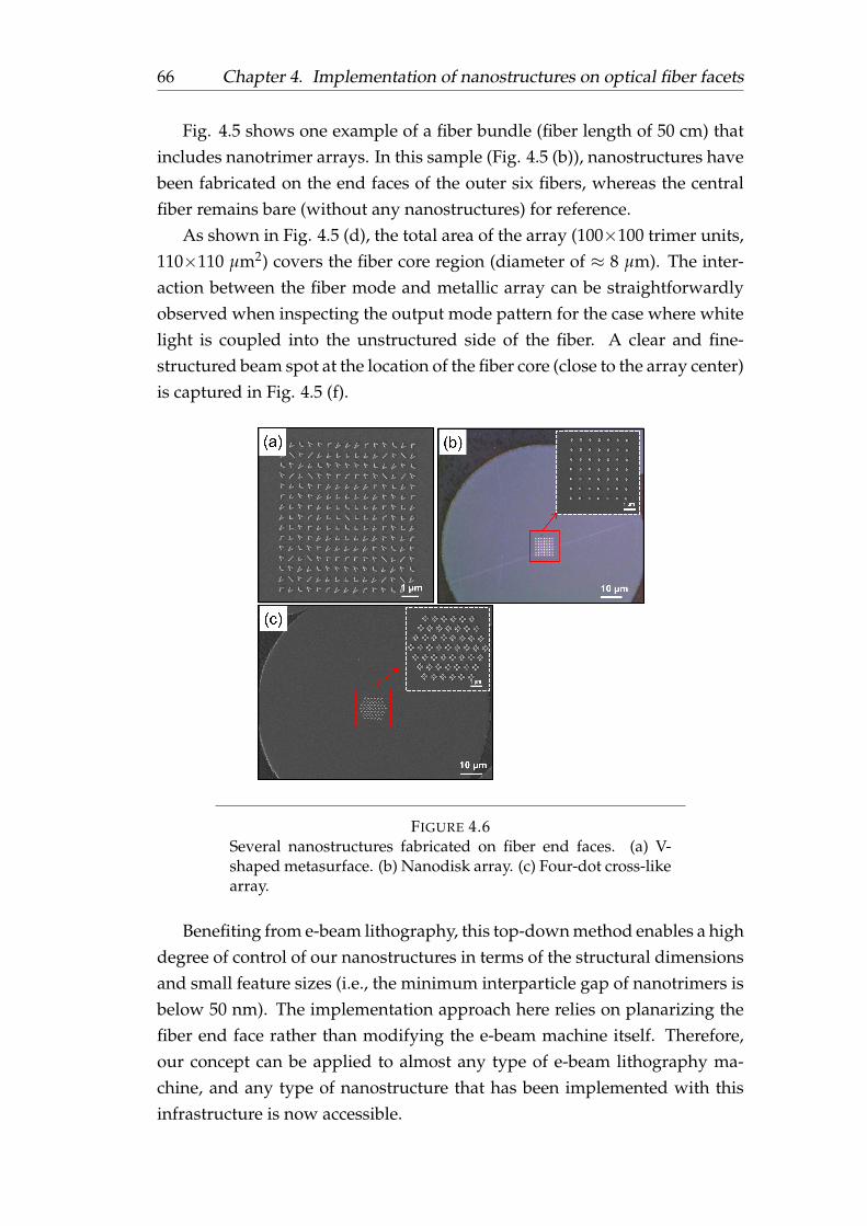
66 Chapter 4. Implementation of nanostructures on optical fiber facets
Fig. 4.5 shows one example of a fiber bundle (fiber length of 50 cm) thatincludes nanotrimer arrays. In this sample (Fig. 4.5 (b)), nanostructures havebeen fabricated on the end faces of the outer six fibers, whereas the centralfiber remains bare (without any nanostructures) for reference.
As shown in Fig. 4.5 (d), the total area of the array (100×100 trimer units,110×110 µm2) covers the fiber core region (diameter of ≈ 8 µm). The inter-action between the fiber mode and metallic array can be straightforwardlyobserved when inspecting the output mode pattern for the case where whitelight is coupled into the unstructured side of the fiber. A clear and fine-structured beam spot at the location of the fiber core (close to the array center)is captured in Fig. 4.5 (f).
FIGURE 4.6Several nanostructures fabricated on fiber end faces. (a) V-shaped metasurface. (b) Nanodisk array. (c) Four-dot cross-likearray.
Benefiting from e-beam lithography, this top-down method enables a highdegree of control of our nanostructures in terms of the structural dimensionsand small feature sizes (i.e., the minimum interparticle gap of nanotrimers isbelow 50 nm). The implementation approach here relies on planarizing thefiber end face rather than modifying the e-beam machine itself. Therefore,our concept can be applied to almost any type of e-beam lithography ma-chine, and any type of nanostructure that has been implemented with thisinfrastructure is now accessible.

4.4. Chapter summary 67
To prove this point, we also produced other nanostructures on fiber endfaces. These are displayed in Fig. 4.6 together with corresponding SEM im-ages. From (a) to (c), the plasmonic nanostructures are V-shaped nanobars (ametasurface [16]), single nanodot arrays and four-dot cross-like nanoanten-nas. These samples strongly confirm the reliability and reproducibility of ourfabrication method.
4.4 Chapter summary
Here, we have discussed a fabrication approach for patterning plasmonicnanostructures on the end face of optical fibers. Utilizing a can-like customholder, the fibers can be planarized to match EBL prerequisites. By adaptingthis high-precision manufacturing method, we anticipate that nanostructure-enhanced fibers will have a number of important applications, such as inbioanalytics, telecommunications, nonlinear photonics, optical trapping andbeam shaping.

68
Chapter 5
Characterization & application ofnanostructured fibers
We have explicitly illustrated the nanostructure design process and deeplystudied the optical properties of nanotrimer arrays in chapter 3. In conclu-sion, the densely packed trimer array has been made to be patterned on anSMF-28 facet by electron beam lithography, where the fabrication process isdemonstrated in chapter 4.
In this chapter, we present the characterization of nanostructure-enhancedoptical fibers at the beginning of this section. Instead of transmission mea-surement (corresponding spectral features are covered by measurement er-rors and noise), we propose to employ the spectral contrast as a key perfor-mance factor using the polarization dependence of the nanotrimer array. Thedefinition and measurement procedures for transmission contrast will be ex-plained in section 5.1.
As illustrated in chapter 1, the goal of this study is to implement a func-tional nanostructure-based optical fiber probe for applications in the fields ofsensing, beam shaping, telecommunication, etc. Here, we demonstrate twomain uses of nanostructured fibers, as an environmental index sensor and alight detection probe, in sections 5.2 and 5.3, respectively. The first applica-tion involves using a nanotrimer-modified fiber as an RI sensor because ofthe high resonance factor (Q-factor). In the second application, the nanodotarray can significantly enhance the light-collecting ability of fibers, especiallyat a large incident angle. This phenomenon can further be utilized to realize afiber-based signal probe within the application fields of green photonics andquantum technologies.
Through this chapter, we demonstrate that fiber-integrated functional nanos-tructures may enrich the ‘lab-on-fiber’ framework. Please note that some ofthe results and data have been published in these references [25, 134, 176].

5.1. Characterization of nanotrimer-enhanced fibers 69
5.1 Characterization of nanotrimer-enhanced fibers
First, let us review the concept of a nanotrimer-enhanced fiber tip (a sketch isshown in Fig. 5.1). Generally, the concept of nanostructure-enhanced fibersaims to realize functional fiber probes by patterning well-defined plasmonicnanoantennas on the facet. Here, we illustrate this idea by integrating adensely packed arrays of gold nanotrimers onto an SMF-28 fiber.
In this specific example (shown in Fig. 5.1), the trimers are arranged ina square lattice (unit cell pitch Λ: 1.1 µm), with the dot diameter (D), height(H) and interparticle gap (G) given by 375 nm, 40 nm, and 75 nm, respec-tively. An SEM image of the trimer array is shown in Fig. 5.1. (b). Note thatthe trimer arrangement is slightly different from those studied in chapter 3.The diameter of the nanodots and the intratrimer gap G are both smallerthan those of the trimers presented in section 3.3. The reason for utilizingsuch a geometry is to enhance the electric Fano resonance (see the conclu-sion regarding Fig. 3.10) to create a stronger asymmetric spectral lineshape.Additionally, the plasmonic resonance of the nanotrimers overlaps the sin-gle mode regime of SMF-28 (above 1310 nm). More importantly, this type ofnanostructure satisfies all three requirements demonstrated in chapter 3.
The working principle of the nanostructure-enhanced fiber is as follows:Light (working wavelength in the IR regime), which is coupled into the un-structured side of the fiber by a lens or an objective, propagates along the coreand reaches the nanostructured tip (patterned with the trimer array here).The plasmonic resonances of the gold nanostructures are excited by the fun-damental HE11 mode, and the overall fiber optical response should be modi-fied by these nanostructures. As seen from the SEM image in Fig. 5.1 (b), thegeometries of the fabricated trimers have good consistency.
First, the optical properties of nanotrimers implemented on planar sub-strates are studied in depth. Note that the arrays share the same geometryas those created on the fiber end faces (D = 375 nm, H = 40 nm, G = 75 nm,Λ = 1100 nm). The polarization of normal incident light is set as 0 and90, where the polarization degree refers to the acute angle between the in-cident light polarization and the axis of the two lower dots (illustrated bythe inserted sketch in Fig. 5.2.(a)). A supercontinuum source (NKT Photon-ics SuperK Compact) provides broadband incident light, and a spectrometer(Instrument Systems SP320-124) is used to record transmitted light for spec-tral analysis.
The measured transmission spectra under 0 and 90 polarization are

70 Chapter 5. Characterization & application of nanostructured fibers
FIGURE 5.1The concept of a nanotrimer-enhanced optical fiber. (a)Schematic showing an SMF-28 fiber with a trimer array inte-grated on its end face. (b) Nanotrimer array geometric arrange-ment. Here, D is the diameter of the nanodots, and G is theedge-to-edge distance between two nanodots. The value Λ de-notes the periodic constant (pitch) of the square unit cell. At theright, an SEM image gives an overview of the entire array. Inthis example, D, G, and Λ are fixed at 375 nm, 75 nm and 1100nm, respectively.
shown in Fig. 5.2 (a) as the green and magenta curves, respectively. No-ticeably, a major transmission dip at approximately 1625 nm is observed for0 polarization, while a weak but wide dip located at approximately 1580nm is found when the polarization is rotated to 90. The transmission of thetrimer array shows strong polarization dependence, and the lineshapes arehighly asymmetric, especially for the 0 polarization. The spectral minima(near 1600 nm) are both located close to the first diffraction order of the glasssubstrate (1595 nm, calculated as Λ×nglass = 1100×1.45). The formation ofthese spectral characteristics have been intensively investigated in chapter 3.
To further analyze the trimer properties, numerical simulations based onCOMSOL Multiphysics are conducted using the periodic boundary condi-tion. The simulated spectra are displayed in Fig. 5.2 (b) with a green line for0 polarization and a magenta line for 90 polarization. Overall, the simu-lated spectra fit the measurements well, where the two dips at 1600 nm arefully reproduced. The spectral differences between Fig. 5.2 (a) and (b) are

5.1. Characterization of nanotrimer-enhanced fibers 71
FIGURE 5.2Measured (a) and simulated (b) transmission spectrum (from1200 nm to 2000 nm) of nanotrimers on a planar silica substrate.Note that two sets of spectra are obtained in the air-silica envi-ronment. The trimer array is illuminated under 0 (dark green)and 90 (dark pink) polarized incident light, where the polar-ization degree is illustrated in the lower inset of (a). Measured(c) and simulated (d) transmission contrast based on the datafrom (a) and (b), respectively.
partly attributed to the excitation configuration. In the simulation model, aplane wave (by periodic ports) is used for excitation, while a Gaussian beam(generated by an objective) is launched onto nanotrimers in the actual exper-imental setup.
Now, we would like to introduce the transmission contrast defined bytwo spectra obtained under two orthogonally polarized incident beams. Thiscontrast is particularly relevant for the analysis of nanostructures on fiberend faces since an SMF-28 fiber is not polarization maintaining, i.e., the polar-ization state that reaches the nanostructures is not the same as the input po-larization state. In principle, for one contrast curve, two transmission spectraneed to be obtained under identical experimental configurations with varied

72 Chapter 5. Characterization & application of nanostructured fibers
polarization excitations (i.e., 0 and 90).It is essential that the nanostructures exhibit different spectral features
over a certain wavelength range under varied excitation. Otherwise, the con-trast curve would be rather flat without any ‘visible’ features. For instance,in the case of the trimer array presented in Fig. 5.2, the positions and ampli-tudes of two dips distinctly depend on the polarization. This difference al-lows straightforward extraction of highly polarization sensitive features fromthe spectral distribution measurements of nanostructures.
Hereby, the transmission contrast (∆Tc) is defined by the following equa-tion:
∆Tc =T(0)− T(90)T(0) + T(90)
(5.1)
with T(0) and T(90) being the transmission spectra excited by 0 and 90
polarized light, respectively.Here, we introduce two main methods to acquire ∆Tc. The first one is
to measure every single transmission at the corresponding polarization andthen calculate the spectral contrast based on Eq. 5.1. The second approachonly requires altering the incident light polarization. The transmitted spec-trum can be continuously recorded, and thus, a reference fiber is not neces-sary.
In this work, we adopt the first method for contrast measurement on aplanar substrate and the second one for corresponding tests on a fiber endface. Fig. 5.2 (c) and (d) show the measured and simulated transmissioncontrast of the trimer array on the planar substrate, respectively. Both spectradisplay high similarities, where dips and peaks are captured at a wavelengthof approximately 1600 nm.
Now, we focus on fiber facets patterned with nanotrimers. The experi-mental setup for contrast quantification is shown in Fig. 5.3 (a). The lightfrom a supercontinuum laser goes through a linear polarizer (Codixx) andis coupled into the bare tip by a 20× objective (Olympus). The light outputfrom the nanostructured fiber facet is guided into an optical spectral analyzerusing a multimode fiber (Thorlabs custom fiber). Here, we use this large corefiber (diameter of core: 1 mm) to collect as much output intensity as possiblesince the signal is very weak (fiber coupling loss > 3 dB).
The polarization of incident light before reaching the fiber is graduallychanged from 0 to 180 at a step of 10, where the initial polarization an-gle (0) is arbitrarily chosen. Note that in addition to rotating the polarizer

5.1. Characterization of nanotrimer-enhanced fibers 73
FIGURE 5.3Transmission contrast measurement on a fiber substrate. (a)Experimental setup. The nanostructured facet of the fiber isfacing the incident light in order to observe the nanostruc-ture state. During the measurement process, only the polarizer(highlighted by the red rectangle) is manipulated, and no refer-ence fiber is needed for contrast qualification. (b) Experimentalresults of bare fiber (green) and nanotrimers on a flat substrate(orange) and fibers (yellow). (c) The array damage due to long-term exposure to the laser.
(highlighted in a red rectangle in Fig. 5.3 (a)), the coupling objective alsoneeds to be slightly altered to compensate for power loss due to misalign-ment (induced by the rotation of the polarizer).
Therefore, 19 spectra (representing different polarizations 0 to 180) areobtained. Nine transmission contrasts of the fiber substrate are computedbased on Eq. 5.1. Since the ’correct’ ∆Tc for planar glass is demonstratedin Fig. 5.2, we can identify the corresponding contrast curve of the fibersubstrate based on the spectral feature at approximately 1.65 µm.
Fig. 5.3 (b) compares the measured optical transmission contrasts. Theorange curve represents the trimers on planar glass, and the yellow curveindicates the same nanostructure on the fiber end face. The dip positions(approximately 1.65 µm) of the two spectra match well, even though the datavariations for the fiber are much larger than those for the planar substrate.
74 Chapter 5. Characterization & application of nanostructured fibers
The spectral mismatch between the two substrates may result from thefollowing factors. First, the experimental error of the incident light polariza-tion is ±10. Second, bending of the fiber can reduce the unwanted claddingmode, but it also introduces birefringence. The spectral variance also partlyoriginates from the experimental configuration differences between fibersand glass substrates. Furthermore, geometric variations of trimers and post-processing of data may also cause spectral inconsistency. In addition, nanos-tructure damage could also induce data errors. As shown in Fig. 5.3 (c), thetrimers located in the fiber core area (highlighted by the red circle) are dam-aged due to the long-term exposure of the nanostructures to the laser (i.e.,thermal ablation).
Nevertheless, the nanostructure-enhanced fiber exhibits a unique spec-trum lineshape compared to the bare fiber (the green curve in Fig. 5.3 (b)),which is flat and slightly varies from -0.15 to 0. This result strongly confirmsthat the optical response of the nanotrimer-enhanced fiber is modified by theapplied nanostructure.
5.2 Nanotrimer-based fibers for RI sensing
5.2.1 Introduction of LSPR-based sensing
Effective detection of refractive index variation is of key importance for mul-tiple fields such as optofluidics and single molecule sensing, representing a’hot’ subject intensively addressed by the optics community [177–181]. Interms of RI detection, the working mechanism of plasmonic sensing is theinteraction between surface plasmons and the analyte liquid. Conventionalthin film SPP sensing is a very mature technique that has been studied formore than three decades [182]. Commercial instrumentation based on thinfilm sensing has had a considerable impact on bioanalytics research.
Different from the well-studied SPP sensing, LSPR sensing has the ma-jor advantage of straightforward plasmon excitation. The former approachrequires an additional optical component (e.g., the Kretschmann configura-tion demands a glass prism, see discussions in chapter 2), while the latter canwork without assistant elements. This relaxed excitation demand of LSPR-based sensing enables a compact and portable detection device [183–185].
Owing to the significant enhancements and highly confined electromag-netic fields, two-dimensional LSPR-based sensors are capable of detectingsmall index changes. Benefiting from the nanoscale geometry of metallic

5.2. Nanotrimer-based fibers for RI sensing 75
and/or dielectric structures, these sensors can still actively work even whenpacked in a tiny volume. This fact is of great help for remote detection inlittle analyte amounts and space-constrained environments.
Fundamentally, LSPR-based RI sensing relies on the spectral shift due toan index change of the surrounding medium. It is well-studied that the res-onance lineshape can be adjusted by modifying the refractive index of thedielectric medium. Here, we concentrate on the spectral evolution mediatedby the environmental RI.
5.2.2 RI sensing of nanotrimers on a planar substrate
Owing to the asymmetrical lineshape and narrow features, Fano resonancesexhibit a higher resonance factor (Q-factor) compared to LSPRs of isolatednanodisks, which suggests the use of an array of coupled trimers as a plas-monic RI sensor. Apart from the improved Q-factor (value up to 7), thereis another advantage of the trimer array (nanodisk diameter of 400 nm) thatneeds to be noted, which is the unique transmission spectrum with a singlesharp peak, leading to a FWHM of ≈ 200 nm.
Experimentally, the spectral distributions of the transmission of the trimerarray illuminated at a 0 polarization angle have been determined for fivedifferent RI liquids (n = 1.33 to 1.73) to study the impact of the environmenton the optical response of the trimer array. The measured spectra are shownin Fig. 5.4 (a), and the spectral shift is further analyzed in (b).
The experimental arrangements for RI sensing are demonstrated in Fig.5.4 (c). A sticky foil (orange thin slice with a thickness of 1 mm) is placedon the surface of the planar substrate. There is a central hole in this foil toreserve a space for nanostructures. Analyte liquids with different RIs areinjected into this small chamber, after which the top opening is sealed bya transparent glass slide during the experiments. One issue that has to beparticularly considered is to avoid bubbles when dealing with these liquids.
In general, the original resonance spectral position (near 1600 nm) of thenanotrimer array for the media arrangement of air-superstrate shifts towardslonger wavelengths as the RI of the liquid increases. This spectral redshift ishighlighted by the dashed red line in Fig. 5.4 (a). All Fano resonance wave-lengths are plotted in Fig. 5.4 (b) (black squares, left axis) along with thecorresponding calculated Q-factors (orange squares, right axis). The spec-tral positions and FWHM of the transmission peaks are acquired by fittinga Lorentz function within a certain spectral bandwidth (approximately 400

76 Chapter 5. Characterization & application of nanostructured fibers
FIGURE 5.4(a) Transmissions of a nanotrimer array located on a planarglass substrate (n = 1.45) immersed in analyte liquids of dif-ferent refractive indices. Here, each curve refers to one mea-surement, and the upper numbers indicate the correspondingrefractive index value. (b) Resonance wavelength (red dashedline in (a)) as a function of the analyte refractive index, corre-sponding to the wavelength of the peaks (black dots). The or-ange squares indicate the corresponding resonator quality fac-tors (Q-factors). (c) Experimental configuration for RI sensingusing nanotrimers on a flat glass substrate.
nm). The resonance wavelength can be well fitted by a linear function (greendashed line), which shows an RI sensitivity of 510 nm/RIU (coefficient ofdetermination R2 = 98.8%).
The trimer array offers sensitivity on the same order of magnitude as ran-domly distributed gold nanodisks (RI sensitivity≈ 180 nm/RIU [37, 46]) andtrimer lattices (≈ 170 nm/RIU in VIS [186], ≈ 370 nm/RIU in IR [186]). Thetrimer array sensitivity also exceeds the sensitivity of other reported Fanoresonance structures (approximately 300 nm/RIU in nanohole quadrumers[187] and heptamer cluster [188]). Together with the large Q-factors (all above5), the results clearly suggest that the trimer array is an alternative platformfor high-precision RI sensing.
One additional advantage of our trimer array is that the working area

5.2. Nanotrimer-based fibers for RI sensing 77
can be minimized to several µm2 in size due to the dense geometric con-figuration. In the next section, we will show the sensing performance of atrimer-modified fiber sensor where the total size of the sensing area is ap-proximately 80 µm2 (fiber core section), which would be difficult if the arraywas very dispersed.
5.2.3 Nanotrimer-enhanced fiber-based RI sensor
Now let us focus on the RI sensing performance of nanostructure-enhancedfibers. To demonstrate its potential, the spectral distribution of the transmis-sion contrast of the nanotrimer-based fiber has been measured in the situa-tion where the nanostructures are immersed in an aqueous analyte. For thesemeasurements, a glass slide is placed close to the nanostructures (distancebetween fiber end face and glass slide: 1 mm, see the similar configurationshown in Fig. 5.4 (c)), and the gap is filled with analyte refractive liquid (n =1.33).
The measured spectra (Fig. 5.5) clearly reveal that the main dip originallylocated at approximately 1650 nm (dark green points) shifts to approximately1800 nm as the RI increases from 1.0 (air) to 1.33. The resulting RI sensitivityis approximately 390 nm/RIU, which is about two times higher than that forthe reported LSPR fiber tip sensors (≈ 190 nm/RIU [37, 46]).
FIGURE 5.5RI sensing with a nanotrimer-based fiber tip by measuring itstransmission contrast spectra. The red arrow indicates the spec-tral redshift of the main dip.
Unfortunately, the weak adhesive force between the nanostructure andfiber surface cannot sustain more tests after cleaning. The nanotrimer array

78 Chapter 5. Characterization & application of nanostructured fibers
on the fiber core is ablated and completely removed (see the damaged exam-ple in Fig. 5.3 (c)). However, based on the result of Fig. 5.4, we believe that ananotrimer array on a fiber end face would show identical behavior, e.g., thedip will redshift following a linear relationship with the surrounding RI.
5.3 Nanodisk-assisted fiber probe for light collec-
tion
5.3.1 Weak signal detection at wide angles
To effectively collect light, optical lenses and sophisticated optical systemshave been systematically studied [189]. For free-space objectives, the keyparameter to evaluate the light-gathering capacity is the numerical aperture(NA), which is defined as NAobj = n× sin θ. Here, n refers to the refractiveindex of the medium, and θ denotes the maximum reception angle. Cur-rently, commercial objectives reach a maximum NA of 0.96 (in air) [190], cor-responding to a collection angle θ of ≈ 73.
Due to the internal multilens systems, well-designed optical objectivesnormally have a relatively bulky geometry with limited working wavelengthrange and a submillimeter focusing length [191]. These disadvantages inhibithigh NA objective applications in space-constrained situations. A commonalternative method to improve the NA is to increase the RI of the surroundingmedium, e.g., by using water (n = 1.33), glycerin (n = 1.47), or immersion oil(n = 1.51). However, it is not practical to fill free space with these liquidsunder dry working conditions.
Let us return to the optical fiber aspect. As illustrated in the introduc-tion chapter, fibers are commonly used in the modern telecommunication in-dustry and can transport optical signals over hundreds of kilometers withextremely low loss. Hence, the use of optical fibers to collect and trans-port weak optical information would benefit numerous applications such aswide-field fiber endoscopy [192] and green photonics (e.g., photovoltaics).
However, commonly used step-index fibers have a very weak light gath-ering ability. For instance, the NA of SMF-28 is only 0.16 at the wavelengthof 1550 nm. This small NA value is a result of the slight RI variation (∆n =
4× 10⁻³) between fiber core (nco) and cladding (ncl). More information canbe found in the discussion of chapter 2.
To enhance the fiber light-collecting ability, several studies have suggestedusing microstructured fibers [11, 193] to increase ∆n. For instance, William

5.3. Nanodisk-assisted fiber probe for light collection 79
J. W. et al. developed two types of double-clad air-silica optical fibers to de-crease the RI of the cladding [193]. The suspending webs (width of 230 nm,located at the additional outer cladding) are filled with air (n = 1.0), and thus,∆n becomes much larger than that of SMF-28, yielding NA > 0.9 at the wave-length of 1.54 µm.
Alternatively, the material of the core and cladding can be carefully se-lected to increase the index difference [11, 194]. For example, a commercialhigh NA multimode fiber [123] has a hard polymer cladding (ncl ≈ 1.365,nco ≈ 1.458), resulting in an NA of 0.50 at 589 nm. However, these methodschange either the fiber structures or materials and thus cannot be directlyapplied to an SMF-28 fiber.
In addition, another approach is to place miniature lenses on standardfiber facets [195–197]. In this way, the optical fiber can remain intact, whilethe light-gathering improvement is limited by the lens performance.
5.3.2 Concept of nanodisk-enhanced light collection
Due to the rapid development of nanophotonics in the last decade, the ma-nipulation of light at the nanoscale has become a reality. Based on resonantelements such as nanobars [15, 16, 198], nanodisks [199] and nanopillars[18], a metasurface is artificially designed to tailor light propagation by in-troducing an additional phase gradient [15, 200]. Several works [201–203]have demonstrated that nanostructure-based metalenses exhibit extraordi-nary light collection performance (NA close to 1) with a subwavelength ge-ometry.
Here, we apply plasmonic resonance structures on the facet of a standardstep index fiber to boost its light-collecting ability. Although the nanodotarray may not be the ideal nanostructure, we still observe significant im-provement of the fiber in-coupling performance compared to bare fibers. Inaddition, instead of fiber NA measurement, actual coupling experiments atdifferent incident angles (0 (normal incidence) to 80) are conducted to eval-uate the fiber light-gathering performance.
The working principle of the nanodot-based fibers for improving lightcollection is schematically illustrated in Fig. 5.6. A gold nanodot array isfabricated on the facet of a fiber by means of EBL. When incident light islaunched at this nanostructure-enhanced tip at an angle of incidence θ, someof the light will be reflected into the air, and some could excite plasmonic

80 Chapter 5. Characterization & application of nanostructured fibers
FIGURE 5.6Overview (a) and side view (b) of a nanodot-based fiber tip forenhanced light-collecting ability. The incident light (green ar-row) impinges on the facet of the fiber at an angle of θ andexcites plasmon resonance of gold nanodots. The red arrowsand curves denote the scattered electromagnetic fields that arecoupled to the fundamental HE11 mode of the fiber used. Thepurple arrows and blue dots in (b) illustrate the incident lightpolarization state. Here, points A and B are the positions usedto determine the coupling efficiency η.
resonances due to the presence of gold particles. The radiation fields of in-dividual nanodots could be coupled into the core and thus improve the fiberlight-collecting ability. Additionally, the grating-like distribution formed bythe periodically arranged nanodisks could diffract some of the light into thefiber. We will further explore these two optical effects using a toy model andnumerical simulations in subsequent studies.
Note that a key parameter to evaluate the fiber light-gathering ability -the coupling efficiency η - is defined as the power ratio at positions B and Ain Fig. 5.6 (b), i.e., η = PB/PA. In the subsequent sections, the parameters(including periodic constants of the array, incident light wavelength and po-larization) related to the fiber coupling efficiency are investigated in-depthby experimental measurements and compared to numerical calculations.
As the first step, we examine the optical properties assuming the nanodotlattice at the end face of an SMF-28. After the procedures of layer deposition,e-beam lithography, ion-beam etching and resist removal, an array of goldnanodisks (D: 480 nm, thickness: 40 nm) are successfully patterned on the

5.3. Nanodisk-assisted fiber probe for light collection 81
FIGURE 5.7SEM image (a) of a nanodot array (on a fiber facet) togetherwith its optical transmission spectrum (b) (measured on a pla-nar substrate). D stands for the diameter of the nanodisks. Λ1and Λ2 are the two periodic constants (pitch) along the respec-tive lattice axes. The three dashed red lines indicate the experi-mental wavelengths of 1310 nm, 1400 nm and 1560 nm, respec-tively.
facet of long fibers (length of approximately 50 cm; more fabrication detailscan be found in chapter 4). Note that the area of the nanodots should spanthe fiber core section (diameter of 10 µm). To address this issue, the total sizeof patterned nanodisks is 50×50 µm2, which is approximately 30 times largerthan the core section size.
As shown in Fig. 5.7 (a), these gold nanodisks are arranged in a hexagonalunit cell with two periodic constants Λ1 = 1.9 µm and Λ2= 1.7 µm). In Fig.5.7 (b), we present the transmission spectrum of the dot array on a planarsilica substrate (same nanodisk geometry as for the fiber sample). Clearly,the LSPR wavelength of the dot array ranges from approximately 1100 nm to1600 nm, overlapping the telecommunication band (blue background) andSMF-28 single mode regime. Due to the sufficient interparticle distance (atleast two times larger than the dot diameter), the lattice resonance arisingfrom the dot-to-dot diffractive coupling should be suppressed at this specificwavelength, which is confirmed by the symmetric transmission lineshape.

82 Chapter 5. Characterization & application of nanostructured fibers
5.3.3 Theoretical and numerical calculations
Now, we investigate the fiber in-coupling problem starting with a bare fiber(without nanostructures) illuminated by a Gaussian beam. In general, thefiber coupling efficiency can be calculated using the surface overlap integralbetween the field amplitudes of the fiber mode and the incident light on thefacet. Here, only the HE11 mode of an SMF-28 fiber is considered, where themode profile can be approximately interpreted as E ∝ exp(−x2/w2) in onedimension.
In fact, there are multiple factors that influence the coupling efficiency,such as optical aberrations, mismatch of the incident beam, and misalign-ment of the optical fiber (defocusing, lateral displacement, and angle devia-tion in the arrangement of the fiber) [204]. To simplify the model, we assumea well-cleaved fiber tip excited by a Gaussian beam (wavelength λ) at theincident angle of θ, which is schematically illustrated in Fig. 5.8 (a).
FIGURE 5.8Analytical model calculations of the coupling efficiency for abare fiber tip. (a) Model background. (b) Coupling efficienciescomputed at wavelengths of 1310 nm (green), 1400 nm (blue),and 1560 nm (orange).
Here, W1 and W0 are the incident beam spot waist and fiber core radius,respectively. X0 is the lateral misalignment between the beam waist and thefiber facet, and Z is the distance from the beam center to the fiber facet. As-suming no displacement Z, the coupling efficiency η is calculated by the fol-lowing equation [204]:

5.3. Nanodisk-assisted fiber probe for light collection 83
η = κ0 exp[−
2X20
W21 + W2
0−
2π2θ2W21 W2
0
λ2(W21 + W2
0 )
](5.2)
where κ0 = 4(W0/W1+W1/W0)2 .
The fiber coupling efficiency η can be further simplified provided that thelateral mismatch X0 is 0:
η = κ0 exp[−
2π2θ2W21 W2
0
λ2(W21 + W2
0 )
](5.3)
Equation 5.3 demonstrates that η is primarily related to the angle of in-cidence θ once the parameters of the fiber and incident beam are given. Tovisualize the correlation between η and θ, we calculate the coupling efficiencyat three wavelengths (green: 1310 nm, blue: 1400 nm, and orange: 1560 nm;these three wavelengths are used in the following experiments) and plot thecorresponding data in Fig. 5.8 (b) (all necessary parameters of the light beamand fiber are obtained from the experimental configurations in Fig. 5.13).
This diagram clearly suggests that the fiber coupling efficiency η dropssignificantly as the angle of incidence increases. In particular, when θ exceedsapproximately 35, the amplitude is less than 10−20. Such a small value can-not possibly be detected in actual experiments. We also observe that the threecurves slightly diverge at large angles (> 20), where the efficiency tends tobe smaller at longer wavelengths.
As mentioned in Fig. 5.6, there are two major contributions (the gratingeffect and plasmonic resonance) to the enhancement of the fiber couplingefficiency. Now, we employ a toy model [2, 205] to investigate the metallicgrating effect on the enhancement of the fiber light-collecting ability.
As depicted in Fig. 5.9, the toy model describes the physical backgroundin which the Gaussian-like fiber fundamental mode is excited by a planewave k0. At an angle of incidence θ, the plane wave exhibits a lateral (alongthe x-direction, indicated by the green arrow in the right corner) phase varia-tion (namely, the oscillating factor), which is proportional to exp(ikxx). Here,kx is the x-component of the wavevector, i.e., kx = k0 sin θ. Hence, the definedcoupling strength Cb(θ) is proportional to the following quantity:
Cb(θ) ∝ cos θ ·∣∣∣∣ ∫ ∞
−∞e−x2/w2
eikxxdx∣∣∣∣2 (5.4)
We further establish a relative bare-fiber coupling efficiency ηb(θ) by nor-malizing Cb(θ) to the perpendicular incidence value (θ = 0, Cb(0)), i.e.,

84 Chapter 5. Characterization & application of nanostructured fibers
FIGURE 5.9A toy model to evaluate the grating-mediated fiber couplingefficiency. (a) The toy model background. (b) Calculated cou-pling efficiency of a bare fiber (orange line, overlapped withtwo other curves) and fibers with nanostructures (green: pitchΛ1 of 1.9 µm, magenta: pitch Λ2 of 1.7 µm).
ηb(θ) = Cb(θ)/Cb(0). Represented by the orange curve in Fig. 5.9 (b), themaximum fiber coupling efficiency of the bare fiber occurs under an incidentangle θ of 0 (i.e., kx=0), and this value decreases dramatically for θ > 0 dueto the presence of oscillating factor exp(ikxx).
However, in a configuration where a periodic grating (periodic constantΛ) is placed on the fiber facet, the lateral wavenumber is modified as (kx +
N · G), in which G = 2π/Λ and N is any integer. Correspondingly, thegrating-modified oscillating factor becomes exp(i(kx + N · G)x), which canbe less than the original value (without a grating) for a negative N. Therefore,the coupling efficiency is additionally enhanced when the oscillating factorbecomes unity (e0 = 1), e.g., kx + N · G = 0. Here, considering only the caseof N = -1, this results in the grating-assisted Cg(θ):
Cg(θ) ∝ cosθ ·∣∣∣∣ ∫ ∞
−∞e−x2/w2
(a0eikxx + a−1ei(kx−G)x)dx∣∣∣∣2 (5.5)
where a0 and a−1 are the relative amplitudes of the diffraction orders (a20 +
a2−1 = 1). Again, the grating-configured fiber relative coupling efficiency
defined as ηg(θ) = Cg(θ)/Cg(0).The relative grating-modified fiber-coupling efficiencies are presented in
Fig. 5.9 (b) (green: Λ1 = 1.9 µm, magenta: Λ2 = 1.7 µm, a0 = 0.99, a−1 =

5.3. Nanodisk-assisted fiber probe for light collection 85
0.01; the value of a−1 are chosen to be small to demonstrate that even a tinyimprovement of a−1 could significantly enhance the light-gathering ability.).Overall, amplitude enhancement of the nanostructure-modified fiber can beobserved within the incident angle range from 25 to 80.
In particular, we find the additional enhancement (highlighted by the ver-tical dashed lines) located at around 55 for Λ1 = 1.9 µm and 65 for Λ2 = 1.7µm. The angle position of additional enhancement corresponds to the peri-odical constants of the used gratings, which could be directly computed byθ = arcsin (λ/Λ) [122]. Using this simplified formula, the predicted anglesare 55 (Λ = 1.9 µm) and 66 (Λ = 1.7 µm), matching theoretical model calcu-lations.
Furthermore, we calculate the integral coupling efficiency Cint(∆θ) of ∆θ
from 0 to 90 (defined as ∆θ = 90 − θ indicated in Fig.5.9 (b)), which isa key parameter to evaluate the probe working performance (computed asCint(∆θ) =
∫ ∆θ0 η(∆θ)d∆θ). Based on the result in Fig. 5.10, significant im-
provements in the grating-mediated light coupling efficiency (magenta andblue curves) are observed, especially at ∆θ angles from 0 to 65, where thebare fiber (orange curve) fails to detect any signal.
FIGURE 5.10Integral coupling efficiency at large angle interval of ∆θ.
It should be noted that the experimental setup for fiber coupling is muchmore sophisticated than the analytical model. Instead of plane wave excita-tion, a focused Gaussian beam is utilized (generated by an aspherical lens)in the actual optical configuration. Therefore, the fiber coupling efficiency

86 Chapter 5. Characterization & application of nanostructured fibers
could be further improved by an appropriate selection of lenses and opti-mization of the optical system. However, here, we focus on the fiber cou-pling enhancements enabled by plasmonic nanostructures. Under identicalexperimental configurations, the coupling efficiency of nanostructure-basedfibers is improved by several orders of magnitude compared to bare fibers(experimental data presented in the next section), which cannot be achievedby merely adjusting the optical path.
Regarding the second major contribution to fiber coupling enhancements,numerical simulations (COMSOL Multiphysics) are conducted. To decreasesimulation difficulties, nanodots distributed in a square-shaped unit cell (pe-riodic constant: Λ) are adopted. This simplified model is schematically de-picted in Fig. 5.11 (a) and (b), together with the model images in (c), (d), and(e).
FIGURE 5.11Numerical simulation model of nanodisk-based fiber coupling.Overview (a) and top view (b) of a sketch showing the simu-lation 3D geometry. (c) Simulated fiber model exhibiting thefundamental HE11 mode profile. (d) Nanodisk resonance pat-tern in a square-shaped unit cell. (e) Coupling of the nanodiskresonance electromagnetic field to a fiber.
Here, the incidence plane (green background) is set to be parallel to the

5.3. Nanodisk-assisted fiber probe for light collection 87
grating (periodic constant Λ), and incident light beams with two types of po-larization (p- and s-polarization, purple arrow and blue dot in (a)) are con-sidered (p- and s-polarization are separately simulated). The fiber couplingefficiencies as a function of incident angle (0 to 80 in a step of 5) and pitch(1600 nm to 2600 nm at a step of 100 nm) are numerically calculated andpresented in the color maps of Fig. 5.12 (a) and (b).
FIGURE 5.12Simulated fiber coupling efficiency as a function of incident an-gle and pitch for p- and s-polarized input light. In (a) and(b), the two white dashed lines indicate the additional enhance-ment of the coupling efficiency, which is related to the periodicconstant. (c) and (d) Correlation between the incident angleθ and the pitch Λ. The blue dots represent the additional en-hancement values obtained from numerical calculations, andthe green line is acquired based on the analytical model equa-tion θ = arcsin (λ/Λ).
Here, the fiber coupling efficiencies for the two polarizations show strongsimilarities. Overall, the maximum coupling efficiency occurs at the normalincident angle (0) as predicted by the toy model, where the additional en-hancements (indicated by the two white dashed lines) are both located at

88 Chapter 5. Characterization & application of nanostructured fibers
nearly the same incident angles (from approximately 40 to 80). The posi-tions of these enhancements shift to a larger angle as the pitch is reduced.
The incident angles corresponding to the additional enhancement undervarious pitch configurations and polarizations are examined in Fig. 5.12 (c)and (d). Using the simplified grating equation θ = arcsin (λ/Λ), the pro-jected angle positions (green dots) match very well with the numerical calcu-lations. Obviously, as the pitch increases, the secondary improvements grad-ually shift to smaller incident angles, which also agrees with the toy modelcalculations.
5.3.4 Experimental performance
FIGURE 5.13Schematic (a) and real experimental setup (b) for fiber couplingefficiency measurement. In (b), the angle of incidence is set at80, and the power meter reads a measured output value of 2.45nW. The red frame highlights the nanodot-based fiber tip.
In the experimental setup (Fig. 5.13), we use a supercontinuum laser(NKT Photonics) and several bandpass filters (Thorlabs, 1310 nm, 1400 nm,and 1560 nm) plus an IR polarizer (Codixx) to obtain the needed incidentlight states. A focused Gaussian beam is generated by an aspherical lens

5.3. Nanodisk-assisted fiber probe for light collection 89
(Thorlabs C560TME-C) and further coupled to the nanostructured tip. Theoutput power is analyzed by a power meter (Thorlabs PM100) and an IRcamera (ABS GmbH). Fig. 5.13 (b) provides a real-time measurement of thefiber coupling efficiency. The nanostructured fiber tip is placed on a rota-tion stage (labeled ’stage ii’ in Fig. 5.13 (b)), which can be used to adjust theincident angle from 0 to 90. The seven-fiber bundle is bent to reduce theimpact of the cladding mode. Although the facet is set almost parallel to theincident light (θ = 80), the nanodisk-modified fiber tip can still collect a cer-tain amount of light, showing 2.45 nW on the power meter screen (see thedisplayed value in Fig. 5.13 (b)).
FIGURE 5.14Measured coupling efficiency of the nanodisk-enhanced fibertip at the wavelengths of 1310 nm (a), 1400 nm (b), and 1560nm (c). The green backgrounds highlight the secondary am-plitude enhancement. (d) Nanodot-based fiber mode imagesobtained from an unpatterned tip (measured at 1400 nm). Allmode images at the four selected incident angles (0, 20, 40,and 75).
The coupling efficiency (green dots) of nanodisk-based fibers at wave-lengths of 1310 nm, 1400 nm, and 1560 nm are shown in Fig. 5.14 (a), (b), and(c), respectively. During the measurements, the incidence plane is aligned

90 Chapter 5. Characterization & application of nanostructured fibers
with the lattice axis with the periodic constant of Λ1 (1.9 µm). For compara-tive studies, bare fiber tip (orange dots) and analytical mode (magenta line)calculations are also shown in the corresponding diagrams.
Overall, the bare fiber exhibits the best coupling efficiencies from 0 to20. The lower efficiency of the nanostructure-modified fiber can be attributedto the energy loss within the metallic array. According to the spectrum of Fig.5.7 (b), the transmission loss of the gold nanodot array reaches 25% at normalincidence.
However, above 20, the performance of the nanostructure-functionalizedfiber (the amplitudes are all above 10−6 at the three wavelengths) remarkablysurpasses that of the bare fiber. Particularly, when the incident angle is > 30,the coupling efficiency of the bare fiber cannot be characterized due to the ex-tremely small values (less than 10−8, absolute measured value < 1 nW), whilethe nanodot-modified fiber can still effectively collect light even at an angleof 80. These measurements strongly confirm that the fiber light-gatheringability is improved by several orders of magnitude due to the presence of thenanodot array.
It is of great interest to investigate the secondary amplitude improve-ment of the coupling efficiency (highlighted by the green background in Fig.5.14 (b) to (d)) at approximately 30 to 45 in all nanostructured fiber mea-surements, which slightly shifts to larger angles with increasing wavelength.These local enhancements match the toy model and numerical simulationresults, showing that a small value of the diffraction coefficient a−1 can sub-stantially boost the fiber light-collecting performance.
The photographs in Fig. 5.14 (d) are the mode images of nanostructuredfibers at incident angles of 0, 20, 40 and 75. All images display a Gaussianbeam profile corresponding to the fundamental HE11 mode of SMF-28. Asthe incident angle increases, the mode profiles become smaller and weaker,which is consistent with the measured data tendency.
Finally, we present the experimental results of the fiber coupling effi-ciency for various incident polarizations and array periodic constants. Themeasured data (incident wavelength of 1560 nm) are shown in Fig. 5.15 (a)and (b). Here, the coupling efficiencies of the bare fiber are also tested andshown by the green dots, with no light signal detected at θ > 30.
Generally, for the nanodisk-enhanced fiber, there is no major efficiencydifference between the s- and p-polarizations provided that the incidence

5.3. Nanodisk-assisted fiber probe for light collection 91
FIGURE 5.15Fiber coupling efficiency at the wavelength of 1560 nm underp- and s-polarization. The red and green background colorshighlight the additional enhancements for the correspondingexperimental configurations.
plane is set along the same pitch direction, while the position of the addi-tional enhancement (colored stripes) varies depending on the periodic con-stant. This pitch-induced efficiency difference is more distinct for s-polarizedlight in terms of the experimental data. As displayed in Fig. 5.15 (b), thered dots represent the fiber coupling along pitch Λ1 (1.9 µm) and the greendots indicate measurements along pitch Λ2 (1.7 µm). For the large pitch con-figuration, the secondary enhancement is located at approximately 40 (redbackground), while the small pitch enhancement shifts to approximately 55
(green background) with reduced amplitude. This experimental observationof pitch-induced efficiency variations is in accordance with the toy modeland numerical calculations.
5.3.5 Further investigations to improve fiber NA
The simple nanodot array on fiber end face has proved that several ordersimprovement of light-coupling ability can be achieved owing to the plamonicresonance and grating-like structures. The next step should concentrate onthe new design of nanostructures in order to further enhance light-collectionperformance. Probably starting from a single nano-particle (material is notlimited to metallic, dielectic, graphene, etc.) could inspire these new designs.For example, assuming that merely one isolated gold particle is situated atthe fiber core, deep investigations on its coupling efficiency (under wide-angle excitation) will be helpful to further design suitable nanostructures forreal applications.

92 Chapter 5. Characterization & application of nanostructured fibers
Even though the coupling efficiency of nanodots-enhanced fiber achievesa value on the order of 10−4 to 10−5, it remains relative low to satisfy theurgent demands of many applications. As an example, in-vivo Raman imag-ing [206] commonly requires increasing coupling efficiency to levels such as10−1 to 10−2. The toy model suggests that such level improvement (espe-cially at the incident angle from 40 to 80) demands increasing the value ofthe diffraction efficiency a−1 in present case.
To reach such a high amplitude, the actively studied metalens may be abetter candidate to be considered. Here, we summarize some of the recentlydemonstrated metalenses in Table 5.1.
TABLE 5.1Potential structures to improve fiber light-collecting ability
Ref. Material Type NA Wavelength [nm]
[201] Silicon Dimer array 0.99 715[202] TiO2 Nanopillars 0.94 500-650[203] TiO2 Nanopillars 0.8 405, 532, 660[207] Silicon Nanobricks 0.98(air), 1.48(noil=1.512) 532[208] Silicon Nanoposts 0.97 1550
Based on these advancements, the fiber light-gathering capacity can befurther boosted by applying an appropriate nanostructure, which will be anissue for further research.
5.4 Chapter summary
To verify the concept of a nanostructure-enhanced fiber, this chapter illus-trates its optical characterization process and potential applications. We firstexamine the fundamental spectral response of a nanotrimer-modified SMF-28 fiber obtained using EBL. Comparative studies of a planar silica substrateand the optical fiber reveal the high spectral similarity of the two transmis-sion contrasts, where a major dip is captured in both at approximately 1600nm. This result proves that the property of the nanostructured fiber has beenmodified by the nanotrimer array, especially compared to the flat lineshapeof a bare fiber.
We demonstrate two major applications of nanostructure-modified fibers,RI sensing and light collection. We employ a nanotrimer-enhanced fiber todetect surrounding index changes. The measured sensitivity reaches 390

5.4. Chapter summary 93
nm/RIU, representing the highest value of the reported LSPR-based fibersensors thus far [25].
In addition, a nanodisk-based fiber exhibits a several orders of magnitudeimprovement compared to the bare fiber in terms of the light-collecting effi-ciency at an incident angle from 30 to 80. Further patterning with metalens-like nanostructures may enable real-world applications, such as random sig-nal gathering, green photonics and endoscopy imaging.
Finally, we need to note that the concept of a nanostructure-enhancedfiber is not limited to either an SMF-28 fiber or metallic nanoantennas. In fact,this concept can apply to any type of fibers integrated with 2D or even 3Dfunctional dielectric/metallic/hybrid structures. Therefore, a single-functionstandard fiber can be modified to be a versatile platform, be a short-cut toolfor studying light-matter interaction and be used in real-world applications.

94
Chapter 6
Summary and outlook
6.1 Summary of the thesis
The study object of this thesis is nanostructure-enhanced fibers realized byelectron beam lithography. This concept involves two principle research ar-eas: plasmonics and fiber optics. The majority of the work is devoted todesigning and characterizing subwavelength metallic structures. In partic-ular, we study a closely distributed trimer array by numerical simulationsand experimental characterizations. We observe a highly asymmetric line-shape with narrow transmission features situated at approximately 1600 nm.By inspecting simulated E-fields, we find that the formations of these fea-tures result from electric- and magnetic-based Fano resonances, in which amonomer-like mode interferes with a dimer-like mode. Furthermore, thetrimer lattice exhibits a strong polarization dependence where a transmissiondip can be changed into a peak at nearly the same wavelength by rotating theincident polarization from 0 to 90. These advantages make the trimer arrayan ideal candidate for usage with SMF-28.
During experimental characterization of nanostructure-enhanced fibers,a main challenge (light-coupling to fibers) appears, which originates fromthe unique fiber substrate. In detail, this coupling problem is induced bythe beam coupling from an objective/lens to bare fiber tips, which furtherleads to experimental condition mismatch between a reference fiber and ananostructure-modified fiber. Owing to the coupling difficulty, the measuredtransmission spectrum cannot correctly represent the optical response, wherethe data error completely covers the true spectral features. Instead of trans-mission measurement, here, we propose to examine the spectral contrast (de-fined by two spectra obtained under two orthogonally polarized incidentlight beams) in order to reduce the measurement errors caused by the fibercoupling problem.

6.2. Outlook of future work 95
We also successfully demonstrate the fabrication of nanostructures onfiber facets. Another major challenge occurs since the fiber cannot match cur-rent EBL-based devices owing to its small cross-section and high aspect ratio.Therefore, we develop a flat metallic can-like holder to place fiber facets onits top surface. In this way, we can planarize the fiber surface. The fabricatedwell-defined nanostructures on the fiber end face strongly confirm the reli-ability and reproducibility of this manufacturing technique. This approachcan also be applied to almost any type of e-beam lithography machine andany type of nanostructure that has been implemented with this infrastruc-ture, opening up the entire field of nanotechnology for fiber optics.
Finally, we demonstrate that nanostructure-enhanced fibers can be em-ployed as an RI sensor and a large-angle light signal detector. The formerrepresents the state-of-the-art in terms of LSPR-based fiber RI sensitivity (ap-proximately 390 nm/RIU), and the latter allows gathering light at incidentangles up to 80, where bare fibers fail to operate. Two application examplesillustrate the enormous potential of nanostructure-functionalized fiber tipsfor real-world usage.
Through the entire thesis, we hope to provide an explicit research pro-cess from the perspectives of a fundamental understanding (plasmonics andfiber optics) and the implementation of metallic nanostructures towards thedemonstration of practical usage of nanostructure-enhanced fibers. In con-clusion, the studies of plasmonic-structure-modified optical fibers pave anew way to realize in-fiber optical devices.
6.2 Outlook of future work
In the last section of this thesis, perspectives on nanostructure-enhanced fibersare presented from the aspects of (1) nanostructure design, (2) nanofabrica-tion on fibers and (3) potential applications. Here, we hope to provide ageneral blueprint of the project and welcome any feedback on this study.
• Nanostructure design and optimization
Design acceleration by deep learning
As summarized above, a major challenge of this project is to design nanos-tructures with the desired spectral response (asymmetric lineshape with highpolarization sensitivity). To obtain an accurate far-field optical response,time-consuming numerical simulations based on the FEM are adopted in this

96 Chapter 6. Summary and outlook
work. In these simulation models, a common working process is to solve thefull set of Maxwell’s equations at selected wavelengths. To match the true ar-ray arrangement, the excitation and boundary conditions need to be carefullyconsidered. Further optimization of nanostructures repeats this procedure,and comparative experimental studies are also necessary.
Recently, several studies [174, 209] have revealed a novel plasmonic nanos-tructure design and characterization method using artificial intelligence (com-puter science). Specifically, deep neural networks can be utilized to predictand optimize the spectral behavior of metasurface-based nanoelements [174].Therefore, deep learning could provide an alternative and time-efficient ap-proach for designing nanostructures with a targeted optical response to sat-isfy application requirements.
Inverse-design of nanostructures/metasurface
As illustrated in chapter 3, the design of a nanostructure with the de-sired optical response (e.g., asymmetric spectral lineshape) is an iterative andtime-consuming process. Normally, the workflow involves guessing a struc-ture, solving Maxwell’s equations, characterizing the optical properties andrepeating these procedures until the structure meets the demands of real ap-plications.
Recently, the first ’inverse-design’ software for optical metamaterial de-sign was released [210]. The inverse design lets users start by inputting thedesired optical response, and the computer will take over the ’guesswork’with the help of an installed nanostructure library. Finally, the software willproduce corresponding nanoantennas for fabrication. This inverse designprocess reduces the numerous efforts and time to enable urgent prototypingof nanostructure-inspired components.
• Fabrication techniques on fibers
Optical/laser printing
Optical printing can realize single nanoparticle manipulations with a fo-cused Gaussian beam [211, 212]. Generally, the optical/laser printing processemploys optical forces (∝ ∇|E|2) to trap and move nanoparticles. At the tar-get position, this process can place and fix particles by van der Waals attrac-tion forces. The latest demonstrations show that this approach can be usedto assemble spherical gold nanoparticles [211], nanorods [213], and bipyra-mids [214]. There is no limitation on extending this method to nonmetallicnanoparticles. Compared with EBL, the major advantages of optical printing

6.2. Outlook of future work 97
are the low-cost instruments and the loose environmental requirements (e.g.,no hard request of clean rooms).
Here, we suggest using optical printing for fiber-substrate nanoparticleassembly. Since there are fewer geometric limitations of the substrates, thismethod can be directly applied to the fiber facet.
• Potential applications
Mode-selective fibers for telecommunication
Optical fiber plays an extremely important role in the modern telecom-munication industry. Over the past half century, fundamental studies andtechnological breakthroughs have increased the fiber data-transporting ca-pacity approximately tenfold every four years [215].
However, the maximum data transmission capacity (approximately 100Tbit/s) of SMFs in worldwide communication networks is estimated to reachthe upper limit in the foreseeable future [215]. To solve this bottleneck, nextgeneration techniques suggest using multimode fibers or few-mode fibers(FMFs) to realize mode-division multiplexing (MDM) or space-division mul-tiplexing (SDM) [215, 216]. Generally, MDM refers to establishing severalspatially distinguishable or mode-based data paths through a fiber to satisfythe exponential growth in capacity demand.
Here, we propose a mode-selective metasurface-modified fiber for MDMusage. The concept is to implement mode-converter metasurfaces [217] onthe facet of MMFs/FMFs for data transport. This type of metasurface em-ploys elliptical cross-section silicon nanopillars as resonance elements to ma-nipulate the incident light phase. By carefully arranging the nanopillar dis-tribution, the functionalized interface can convert a Gaussian-like incidentbeam to the desired fiber mode (e.g., LP11 mode) [217]. The latest studies[218, 219] on dielectric metasurfaces, in which the metasurface is fabricatedon a silica substrate, demonstrate the high working efficiency (> 90%) andpotential applications in free space communication. Apparently, the mode-selective fiber should support several modes, indicating that SMF-28 is notan ideal candidate.
Bioanalytics: Endoscopy-like imaging
Currently, optical fiber-based devices are increasingly being used for hu-man health monitoring due to their numerous advantages, such as flexibility,adjustable length and small diameter [220]. The wide-field endoscopic imag-ing enabled by fibers is regarded as a promising application in biophotonics

98 Chapter 6. Summary and outlook
since it is free of electronic interference and fiber small volume can reducethe surgery operation space in human bodies [206].
Here, we propose to place a metalens on SMFs or MMFs for remote imag-ing. For instance, Amir Arbabi et al. demonstrated a dielectric metalens witha maximum working efficiency of 97% [18]. Based on elliptical nanoposts,complete control of the light phase and polarization can be achieved. By pat-terning fibers with this type of metalens, fiber-based in vivo disease diagnosisshould be achievable.

99
Bibliography
1. Agrawal, G. P. Fiber-optic communication systems (John Wiley & Sons,2012).
2. Snyder, A. W. & Love, J. Optical waveguide theory (Springer Science &Business Media, 2012).
3. Gambling, W. The rise and rise of optical fibers. IEEE Journal of SelectedTopics in Quantum Electronics 6, 1084–1093 (2000).
4. NobelPrize.org. The Nobel Prize in Physics 2009 Last accessed Mon. 4Feb 2019. 2009. https://www.nobelprize.org/prizes/physics/2009/summary/.
5. Birks, T. A., Knight, J. C. & Russell, P. S. J. Endlessly single-mode pho-tonic crystal fiber. Optics Letters 22, 961–963 (1997).
6. Russell, P. Photonic crystal fibers. Science 299, 358–362 (2003).
7. Schmidt, M. A., Alexander, A. & Fabien, S. Hybrid optical fibers- an In-novative platform for in-Fiber photonic devices. Advanced Optical Ma-terials 4, 13–36 (2016).
8. Doherty, B. et al. Nanoparticle functionalised small-core suspended-core fibre–a novel platform for efficient sensing. Biomedical Optics Ex-press 8, 790–799 (2017).
9. Chemnitz, M. et al. Hybrid soliton dynamics in liquid-core fibres. Na-ture Communications 8, 42 (2017).
10. Noda, J., Okamoto, K. & Sasaki, Y. Polarization-maintaining fibers andtheir applications. Journal of Lightwave Technology 4, 1071–1089 (1986).
11. Leite, I. T. et al. Three-dimensional holographic optical manipulationthrough a high-numerical-aperture soft-glass multimode fibre. NaturePhotonics 12, 33 (2018).
12. Buczynski, R. et al. Optical fibers with gradient index nanostructuredcore. Optics Express 23, 25588–25596 (2015).
13. Novotny, L. & Hecht, B. Principles of nano-optics (Cambridge UniversityPress, 2012).

100 Bibliography
14. Maier, S. A. Plasmonics: fundamentals and applications (Springer Science& Business Media, 2007).
15. Yu, N. et al. Light propagation with phase discontinuities: generalizedlaws of reflection and refraction. Science 334, 333–337 (2011).
16. Zeisberger, M., Schneidewind, H., Huebner, U., Popp, J. & Schmidt,M. A. Nanoboomerang-based inverse metasurfaces — a promising pathtowards ultrathin photonic devices for transmission operation. APLPhotonics 2, 036102 (2017).
17. Meinzer, N., Barnes, W. L. & Hooper, I. R. Plasmonic meta-atoms andmetasurfaces. Nature Photonics 8, 889 (2014).
18. Arbabi, A., Horie, Y., Bagheri, M. & Faraon, A. Dielectric metasur-faces for complete control of phase and polarization with subwave-length spatial resolution and high transmission. Nature Nanotechnology10, 937–943 (2015).
19. Tittl, A. et al. Imaging-based molecular barcoding with pixelated di-electric metasurfaces. Science 360, 1105–1109 (2018).
20. Wang, K. et al. Quantum metasurface for multiphoton interference andstate reconstruction. Science 361, 1104–1108 (2018).
21. Nazemosadat, E. et al. Dielectric broadband metasurfaces for fiber mode-multiplexed communications. Advanced Optical Materials, 1801679 (2019).
22. Inc., C. Product Information of Corning SMF-28 Last accessed Mon. 4Feb 2019. 2014. https://www.corning.com/media/worldwide/coc/documents/Fiber/PI1424_11-14.pdf.
23. Taminiau, T. H., Moerland, R. J., Segerink, F. B., Kuipers, L. & vanHulst, N. F. λ/4 resonance of an optical monopole antenna probed bysingle molecule fluorescence. Nano Letters 7, 28–33 (2007).
24. Consales, M. et al. Lab-on-fiber technology: toward multifunctional op-tical nanoprobes. ACS Nano 6, 3163–3170 (2012).
25. Wang, N., Zeisberger, M., Hübner, U. & Schmidt, M. A. Nanotrimerenhanced optical fiber tips implemented by electron beam lithography.Optical Materials Express 8, 2246–2255 (2018).
26. Yang, J. et al. Photonic crystal fiber metalens. Nanophotonics 8, 443–449(2019).

Bibliography 101
27. Lin, Y., Guo, J. & Lindquist, R. G. Demonstration of an ultra-widebandoptical fiber inline polarizer with metal nano-grid on the fiber tip. Op-tics Express 17, 17849–17854 (2009).
28. Principe, M. et al. Optical fiber meta-tips. Light: Science & Applications6, e16226 (2017).
29. Jia, P., Yang, Z., Yang, J. & Ebendorff-Heidepriem, H. Quasiperiodicnanohole arrays on optical fibers as plasmonic sensors: Fabrication andsensitivity determination. ACS Sensors 1, 1078–1083 (2016).
30. Prasciolu, M. et al. Design and fabrication of on-fiber diffractive ele-ments for fiber-waveguide coupling by means of e-beam lithography.Microelectronic Engineering 67, 169–174 (2003).
31. Xomalis, A. et al. Fibre-optic metadevice for all-optical signal modula-tion based on coherent absorption. Nature Communications 9, 182 (2018).
32. Horák, M. et al. Comparative study of plasmonic antennas fabricatedby electron beam and focused ion beam lithography. Scientific Reports8, 9640 (2018).
33. Bruchhaus, L. et al. Comparison of technologies for nano device pro-totyping with a special focus on ion beams: a review. Applied PhysicsReviews 4, 011302 (2017).
34. Tuniz, A., Chemnitz, M., Dellith, J., Weidlich, S. & Schmidt, M. A. Hybrid-mode-assisted long-distance excitation of short-range surface plasmonsin a nanotip-enhanced step-index fiber. Nano Letters 17, 631–637 (2017).
35. Publication, O. OSA Spotlight on Optics Last accessed Mon. 4 Feb 2019.2019. https://www.osapublishing.org/spotlight/summary.cfm?id=395430.
36. Scaravilli, M. et al. Excitation of bloch surface waves on an optical fibertip. Advanced Optical Materials 6, 1800477 (2018).
37. Lin, Y., Zou, Y., Mo, Y., Guo, J. & Lindquist, R. G. E-beam patternedgold nanodot arrays on optical fiber tips for localized surface plasmonresonance biochemical sensing. Sensors 10, 9397–9406 (2010).
38. Wei, J., Zeng, Z. & Lin, Y. Localized surface plasmon resonance (LSPR)-coupled fiber-optic nanoprobe for the detection of protein biomarkers.Biosensors and Biodetection: Methods and Protocols Volume 1: Optical-BasedDetectors, 1–14 (2017).

102 Bibliography
39. Sanders, M., Lin, Y., Wei, J., Bono, T. & Lindquist, R. G. An enhancedLSPR fiber-optic nanoprobe for ultrasensitive detection of protein biomark-ers. Biosensors and Bioelectronics 61, 95–101 (2014).
40. Kaye, S. et al. Label-free detection of DNA hybridization with a com-pact LSPR-based fiber-optic sensor. Analyst 142, 1974–1981 (2017).
41. Feng, S., Darmawi, S., Henning, T., Klar, P. J. & Zhang, X. A miniatur-ized sensor consisting of concentric metallic nanorings on the end facetof an optical fiber. Small 8, 1937–1944 (2012).
42. Jia, P. & Yang, J. A plasmonic optical fiber patterned by template trans-fer as a high-performance flexible nanoprobe for real-time biosensing.Nanoscale 6, 8836–8843 (2014).
43. Ricciardi, A. et al. Versatile optical fiber nanoprobes: from plasmonicbiosensors to polarization-sensitive devices. ACS Photonics 1, 69–78 (2013).
44. Lipomi, D. J. et al. Patterning the tips of optical fibers with metallicnanostructures using nanoskiving. Nano Letters 11, 632–636 (2010).
45. Luk’yanchuk, B. et al. The Fano resonance in plasmonic nanostructuresand metamaterials. Nature Materials 9, 707 (2010).
46. Lin, Y., Zou, Y. & Lindquist, R. G. A reflection-based localized surfaceplasmon resonance fiber-optic probe for biochemical sensing. Biomedi-cal Optics Express 2, 478–484 (2011).
47. Zhu, X., Feng, L., Zhang, P., Yin, X. & Zhang, X. One-way invisiblecloak using parity-time symmetric transformation optics. Optics Letters38, 2821–2824 (2013).
48. Valentine, J., Li, J., Zentgraf, T., Bartal, G. & Zhang, X. An optical cloakmade of dielectrics. Nature Materials 8, 568 (2009).
49. Lin, D., Fan, P., Hasman, E. & Brongersma, M. L. Dielectric gradientmetasurface optical elements. Science 345, 298–302 (2014).
50. Kennedy, L. C. et al. A new era for cancer treatment: gold-nanoparticle-mediated thermal therapies. Small 7, 169–183 (2011).
51. Wang, L. et al. Grayscale transparent metasurface holograms. Optica 3,1504–1505 (2016).
52. Grigorenko, A., Polini, M. & Novoselov, K. Graphene plasmonics. Na-ture Photonics 6, 749 (2012).

Bibliography 103
53. Ebbesen, T. W., Lezec, H. J., Ghaemi, H., Thio, T. & Wolff, P. Extraordi-nary optical transmission through sub-wavelength hole arrays. Nature391, 667 (1998).
54. Giannini, V., Fernández-Domínguez, A. I., Heck, S. C. & Maier, S. A.Plasmonic nanoantennas: fundamentals and their use in controllingthe radiative properties of nanoemitters. Chemical Reviews 111, 3888–3912 (2011).
55. Johnson, P. B. & Christy, R.-W. Optical constants of the noble metals.Physical Review B 6, 4370 (1972).
56. Rakic, A. D., Djurišic, A. B., Elazar, J. M. & Majewski, M. L. Opticalproperties of metallic films for vertical-cavity optoelectronic devices.Applied Optics 37, 5271–5283 (1998).
57. Encyclopedia, R. P. Silica Fibers Last accessed Mon. 4 Feb 2019. 2019.https://www.rp-photonics.com/silica_fibers.html.
58. Sellmeier, W. Zur Erkarung der abnormen Farbenfolge im Spectrumeiniger. Substanzen. Annalen der Physik und Chemie 219, 272–282 (1871).
59. RefractiveIndex.INFO. Optical constants of Fused silica (fused quartz) Lastaccessed Mon. 4 Feb 2019. 2019. https://refractiveindex.info/?shelf=glass&book=fused_silica&page=Malitson.
60. Kirchain, R. & Kimerling, L. A roadmap for nanophotonics. Nature Pho-tonics 1, 303 (2007).
61. Stockman, M. I. et al. Roadmap on plasmonics. Journal of Optics 20,043001 (2018).
62. Kauranen, M. & Zayats, A. V. Nonlinear plasmonics. Nature Photonics6, 737 (2012).
63. Pile, D. & Krenn, J. Perspective on plasmonics 2012.
64. Törmä, P. & Barnes, W. L. Strong coupling between surface plasmonpolaritons and emitters: a review. Reports on Progress in Physics 78, 013901(2014).
65. Barnes, W. L., Dereux, A. & Ebbesen, T. W. Surface plasmon subwave-length optics. Nature 424, 824 (2003).
66. Kawata, S., Inouye, Y. & Verma, P. Plasmonics for near-field nano-imagingand superlensing. Nature Photonics 3, 388 (2009).

104 Bibliography
67. Oulton, R. F., Sorger, V. J., Genov, D., Pile, D. & Zhang, X. A hybridplasmonic waveguide for subwavelength confinement and long-rangepropagation. Nature Photonics 2, 496 (2008).
68. Stockman, M. I. Nanofocusing of optical energy in tapered plasmonicwaveguides. Physical Review Letters 93, 137404 (2004).
69. Schuller, J. A. et al. Plasmonics for extreme light concentration and ma-nipulation. Nature Materials 9, 193 (2010).
70. Pang, L., Hwang, G. M., Slutsky, B. & Fainman, Y. Spectral sensitivity oftwo-dimensional nanohole array surface plasmon polariton resonancesensor. Applied Physics Letters 91, 123112 (2007).
71. Guo, X. et al. Direct coupling of plasmonic and photonic nanowires forhybrid nanophotonic components and circuits. Nano Letters 9, 4515–4519 (2009).
72. Dai, W.-H., Lin, F.-C., Huang, C.-B. & Huang, J.-S. Mode conversion inhigh-definition plasmonic optical nanocircuits. Nano Letters 14, 3881–3886 (2014).
73. Schneidewind, H., Zeisberger, M., Plidschun, M., Weidlich, S. & Schmidt,M. A. Photonic candle - focusing light using nano-bore optical fibers.Optics Express 26, 31706–31716 (2018).
74. Lee, H. et al. Pressure-assisted melt-filling and optical characterizationof Au nano-wires in microstructured fibers. Optics Express 19, 12180–12189 (2011).
75. Tuniz, A. & Schmidt, M. A. Interfacing optical fibers with plasmonicnanoconcentrators. Nanophotonics.
76. Uebel, P., Bauerschmidt, S. T., Schmidt, M. A. & St. J. Russell, P. A gold-nanotip optical fiber for plasmon-enhanced near-field detection. Ap-plied Physics Letters 103, 021101 (2013).
77. Marini, A. et al. Ultrafast nonlinear dynamics of surface plasmon po-laritons in gold nanowires due to the intrinsic nonlinearity of metals.New Journal of Physics 15, 013033 (2013).
78. Mayer, K. M. & Hafner, J. H. Localized surface plasmon resonance sen-sors. Chemical Reviews 111, 3828–3857 (2011).
79. Brongersma, M. L. & Kik, P. G. Surface plasmon nanophotonics (Springer,2007).

Bibliography 105
80. Shalaev, V. M. & Kawata, S. Nanophotonics with surface plasmons (Else-vier, 2006).
81. Willets, K. A. & Van Duyne, R. P. Localized surface plasmon resonancespectroscopy and sensing. Annual Review of Physical Chemistry 58, 267–297 (2007).
82. Mock, J., Barbic, M., Smith, D., Schultz, D. & Schultz, S. Shape effectsin plasmon resonance of individual colloidal silver nanoparticles. TheJournal of Chemical Physics 116, 6755–6759 (2002).
83. Mie, G. Beiträge zur Optik trüber Medien, speziell kolloidaler Metallö-sungen. Annalen der Physik 330, 377–445 (1908).
84. Kuwata, H., Tamaru, H., Esumi, K. & Miyano, K. Resonant light scat-tering from metal nanoparticles: Practical analysis beyond Rayleighapproximation. Applied Physics Letters 83, 4625–4627 (2003).
85. Yu, R., Liz-Marzán, L. M. & de Abajo, F. J. G. Universal analytical mod-eling of plasmonic nanoparticles. Chemical Society Reviews 46, 6710–6724 (2017).
86. Amendola, V., Pilot, R., Frasconi, M., Marago, O. M. & Iati, M. A. Sur-face plasmon resonance in gold nanoparticles: a review. Journal of Physics:Condensed Matter 29, 203002 (2017).
87. Hulst, H. C. & van de Hulst, H. C. Light scattering by small particles(Courier Corporation, 1981).
88. Tan, S. J. et al. Plasmonic color palettes for photorealistic printing withaluminum nanostructures. Nano Letters 14, 4023–4029 (2014).
89. Olson, J. et al. Vivid, full-color aluminum plasmonic pixels. Proceedingsof the National Academy of Sciences 111, 14348–14353 (2014).
90. Sun, Y. & Xia, Y. Gold and silver nanoparticles: a class of chromophoreswith colors tunable in the range from 400 to 750 nm. Analyst 128, 686–691 (2003).
91. Duan, X. & Liu, N. Scanning plasmonic color display. ACS Nano 12,8817–8823 (2018).
92. Rechberger, W. et al. Optical properties of two interacting gold nanopar-ticles. Optics Communications 220, 137–141 (2003).
93. Huang, W., Qian, W., Jain, P. K. & El-Sayed, M. A. The effect of plas-mon field on the coherent lattice phonon oscillation in electron-beamfabricated gold nanoparticle pairs. Nano Letters 7, 3227–3234 (2007).

106 Bibliography
94. Jain, P. K., Huang, W. & El-Sayed, M. A. On the universal scaling be-havior of the distance decay of plasmon coupling in metal nanoparticlepairs: a plasmon ruler equation. Nano Letters 7, 2080–2088 (2007).
95. Tabor, C., Murali, R., Mahmoud, M. & El-Sayed, M. A. On the use ofplasmonic nanoparticle pairs as a plasmon ruler: the dependence of thenear-field dipole plasmon coupling on nanoparticle size and shape. TheJournal of Physical Chemistry A 113, 1946–1953 (2008).
96. Liu, N., Hentschel, M., Weiss, T., Alivisatos, A. P. & Giessen, H. Three-dimensional plasmon rulers. Science 332, 1407–1410 (2011).
97. Ben, X. & Park, H. S. Size dependence of the plasmon ruler equationfor two-dimensional metal nanosphere arrays. The Journal of PhysicalChemistry C 115, 15915–15926 (2011).
98. Auguié, B. & Barnes, W. L. Collective resonances in gold nanoparticlearrays. Physical Review Letters 101, 143902 (2008).
99. Rodriguez, S. R. K. et al. Coupling bright and dark plasmonic latticeresonances. Physical Review X 1, 021019 (2011).
100. Kravets, V., Schedin, F. & Grigorenko, A. Extremely narrow plasmonresonances based on diffraction coupling of localized plasmons in ar-rays of metallic nanoparticles. Physical Review Letters 101, 087403 (2008).
101. Guo, R., Hakala, T. K. & Törmä, P. Geometry dependence of surfacelattice resonances in plasmonic nanoparticle arrays. Physical Review B95, 155423 (2017).
102. Humphrey, A. D. & Barnes, W. L. Plasmonic surface lattice resonanceson arrays of different lattice symmetry. Physical Review B 90, 075404(2014).
103. Wang, D., Yang, A., Hryn, A. J., Schatz, G. C. & Odom, T. W. Superlat-tice plasmons in hierarchical Au nanoparticle arrays. ACS Photonics 2,1789–1794 (2015).
104. Kataja, M. et al. Surface lattice resonances and magneto-optical responsein magnetic nanoparticle arrays. Nature Communications 6, 7072 (2015).
105. Humphrey, A. & Barnes, W. Plasmonic surface lattice resonances in ar-rays of metallic nanoparticle dimers. Journal of Optics 18, 035005 (2016).
106. Humphrey, A. D., Meinzer, N., Starkey, T. A. & Barnes, W. L. Surfacelattice resonances in plasmonic arrays of asymmetric disc dimers. ACSPhotonics 3, 634–639 (2016).

Bibliography 107
107. Michaeli, L., Keren-Zur, S., Avayu, O., Suchowski, H. & Ellenbogen, T.Nonlinear surface lattice resonance in plasmonic nanoparticle arrays.Physical Review Letters 118, 243904 (2017).
108. Li, Z., Butun, S. & Aydin, K. Ultranarrow band absorbers based onsurface lattice resonances in nanostructured metal surfaces. ACS Nano8, 8242–8248 (2014).
109. Vecchi, G., Giannini, V. & Rivas, J. G. Shaping the fluorescent emissionby lattice resonances in plasmonic crystals of nanoantennas. PhysicalReview Letters 102, 146807 (2009).
110. Shi, L. et al. Spatial coherence properties of organic molecules coupledto plasmonic surface lattice resonances in the weak and strong cou-pling regimes. Physical Review Letters 112, 153002 (2014).
111. Fano, U. Effects of configuration interaction on intensities and phaseshifts. Physical Review 124, 1866 (1961).
112. Limonov, M. F., Rybin, M. V., Poddubny, A. N. & Kivshar, Y. S. Fanoresonances in photonics. Nature Photonics 11, 543 (2017).
113. Miroshnichenko, A. E., Flach, S. & Kivshar, Y. S. Fano resonances innanoscale structures. Reviews of Modern Physics 82, 2257 (2010).
114. Francescato, Y., Giannini, V. & Maier, S. A. Plasmonic systems unveiledby Fano resonances. ACS Nano 6, 1830–1838 (2012).
115. Gallinet, B. & Martin, O. J. Influence of electromagnetic interactions onthe line shape of plasmonic Fano resonances. ACS Nano 5, 8999–9008(2011).
116. Giannini, V., Francescato, Y., Amrania, H., Phillips, C. C. & Maier, S. A.Fano resonances in nanoscale plasmonic systems: a parameter-free mod-eling approach. Nano Letters 11, 2835–2840 (2011).
117. Lovera, A., Gallinet, B., Nordlander, P. & Martin, O. J. Mechanisms ofFano resonances in coupled plasmonic systems. ACS Nano 7, 4527–4536(2013).
118. Lassiter, J. B. et al. Designing and deconstructing the Fano lineshape inplasmonic nanoclusters. Nano Letters 12, 1058–1062 (2012).
119. Ghatak, A. & Thyagarajan, K. An introduction to fiber optics (Cambridgeuniversity press, 1998).
120. Inc., N. Fiber optic basics Last accessed Mon. 4 Feb 2019. 2019. https://www.newport.com/t/fiber-optic-basics.

108 Bibliography
121. Krohn, D. A., MacDougall, T. & Mendez, A. Fiber optic sensors: funda-mentals and applications (Spie Press Bellingham, WA, 2014).
122. Saleh, B. E., Teich, M. C. & Saleh, B. E. Fundamentals of photonics (WileyNew York, 1991).
123. Inc., T. Multimode fiber tutorial Last accessed Mon. 4 Feb 2019. 2019.https://www.thorlabs.com/newgrouppage9.cfm?objectgroup_id=
10417.
124. Buck, J. A. Fundamentals of optical fibers (John Wiley & Sons, 2004).
125. Digonnet, M. J. et al. Rare-earth-doped fiber lasers and amplifiers (2001).
126. Desurvire, E. Erbium-doped fiber amplifiers: principles and applications (Wi-ley New York, 1994).
127. Doherty, B. et al. Plasmonic nanoparticle-functionalized exposed-corefiber—An optofluidic refractive index sensing platform. Optics Letters42, 4395–4398 (2017).
128. Saar, B. G., Johnston, R. S., Freudiger, C. W., Xie, X. S. & Seibel, E. J. Co-herent Raman scanning fiber endoscopy. Optics Letters 36, 2396–2398(2011).
129. Kay, G. N. Fiber optics in architectural lighting: methods, design, and appli-cations (McGraw-Hill New York, NY, 1999).
130. Schmidt, M. A., Lei, D. Y., Wondraczek, L., Nazabal, V. & Maier, S. A.Hybrid nanoparticle–microcavity-based plasmonic nanosensors withimproved detection resolution and extended remote-sensing ability.Nature Communications 3, 1108 (2012).
131. Faez, S. et al. Fast, label-free tracking of single viruses and weakly scat-tering nanoparticles in a nanofluidic optical fiber. ACS Nano 9, 12349–12357 (2015).
132. Morton, S. M., Silverstein, D. W. & Jensen, L. Theoretical studies ofplasmonics using electronic structure methods. Chemical Reviews 111,3962–3994 (2011).
133. Prodan, E., Radloff, C., Halas, N. J. & Nordlander, P. A hybridizationmodel for the plasmon response of complex nanostructures. Science302, 419–422 (2003).
134. Wang, N., Zeisberger, M., Hübner, U., Giannini, V. & Schmidt, M. A.Symmetry-breaking induced magnetic Fano resonances in densely packedarrays of symmetric nanotrimers. Scientific Reports 9, 2873 (2019).

Bibliography 109
135. Inc., C. Create RF, Microwave, and Millimeter-Wave Designs with the RFModule Last accessed Mon. 4 Feb 2019. 2019. www.comsol.com/rf-module.
136. Inc., L. High-Performance Nanophotonic Simulation Software Last accessedMon. 4 Feb 2019. 2019. https://www.lumerical.com/.
137. GmbH, D. S. D. CST MICROWAVE STUDIO 3D EM Simulation Soft-ware Last accessed Mon. 15 April 2019. 2019. https://www.cst.com/products.
138. MeepFDTD. Manual - MEEP Documentation Last accessed Mon. 4 Feb2019. 2019. https://meep.readthedocs.io/en/latest/.
139. Toolbox, M. MNPBEM Toolbox Last accessed Mon. 4 Feb 2019. 2019.http://physik.uni-graz.at/~uxh/mnpbem/html/mnpbem_product_
page.html.
140. DDSCAT. DDSCAT Last accessed Mon. 4 Feb 2019. 2019. http : / /ddscat.wikidot.com/.
141. Zienkiewicz, O. C., Taylor, R. L., Zienkiewicz, O. C. & Taylor, R. L. Thefinite element method (McGraw-hill London, 1977).
142. Imura, K., Nagahara, T. & Okamoto, H. Near-field two-photon-inducedphotoluminescence from single gold nanorods and imaging of plas-mon modes. The Journal of Physical Chemistry B 109, 13214–13220 (2005).
143. Park, J. et al. Two-photon-induced photoluminescence imaging of tu-mors using near-infrared excited gold nanoshells. Optics Express 16,1590–1599 (2008).
144. Hohenester, U., Ditlbacher, H. & Krenn, J. R. Electron-energy-loss spec-tra of plasmonic nanoparticles. Physical Review Letters 103, 106801 (2009).
145. Vesseur, E. J. R., de Waele, R., Kuttge, M. & Polman, A. Direct ob-servation of plasmonic modes in Au nanowires using high-resolutioncathodoluminescence spectroscopy. Nano Letters 7, 2843–2846 (2007).
146. Poeggel, S. et al. Optical fibre pressure sensors in medical applications.Sensors 15, 17115–17148 (2015).
147. Ecke, W., Latka, I., Willsch, R., Reutlinger, A. & Graue, R. Fibre opticsensor network for spacecraft health monitoring. Measurement Scienceand Technology 12, 974 (2001).

110 Bibliography
148. Barták, J. et al. Analysis of viscosity data in As2Se3, Se and Se95Te5chalcogenide melts using the pressure assisted melt filling technique.Journal of Non-Crystalline Solids 511, 100–108 (2019).
149. Kostovski, G., Stoddart, P. R. & Mitchell, A. The optical fiber tip: an in-herently light-Coupled microscopic platform for micro-and nanotech-nologies. Advanced Materials 26, 3798–3820 (2014).
150. Zoric, I., Zäch, M., Kasemo, B. & Langhammer, C. Gold, platinum, andaluminum nanodisk plasmons: material independence, subradiance,and damping mechanisms. ACS Nano 5, 2535–2546 (2011).
151. Sinzinger, S. & Jahns, J. Microoptics (John Wiley & Sons, 2006).
152. Huebner, U. et al. Multi-stencil character projection e-beam lithography: afast and flexible way for high quality optical metamaterials in 30th EuropeanMask and Lithography Conference 9231 (2014), 92310E.
153. Fang, Z. et al. Removing a wedge from a metallic nanodisk reveals aFano resonance. Nano Letters 11, 4475–4479 (2011).
154. Zhang, S. et al. Pronounced Fano resonance in single gold split nan-odisks with 15 nm split gaps for intensive second harmonic generation.ACS Nano 10, 11105–11114 (2016).
155. Verellen, N. et al. Fano resonances in individual coherent plasmonicnanocavities. Nano Letters 9, 1663–1667 (2009).
156. Yan, J. et al. Directional Fano resonance in a silicon nanosphere dimer.ACS Nano 9, 2968–2980 (2015).
157. Yan, C. & Martin, O. J. Periodicity-induced symmetry breaking in afano lattice: hybridization and tight-binding regimes. ACS Nano 8, 11860–11868 (2014).
158. Fan, J. A. et al. Fano-like interference in self-assembled plasmonic quadrumerclusters. Nano Letters 10, 4680–4685 (2010).
159. Hentschel, M. et al. Transition from isolated to collective modes in plas-monic oligomers. Nano Letters 10, 2721–2726 (2010).
160. Hentschel, M., Dregely, D., Vogelgesang, R., Giessen, H. & Liu, N. Plas-monic oligomers: the role of individual particles in collective behavior.ACS Nano 5, 2042–2050 (2011).
161. Miroshnichenko, A. E. & Kivshar, Y. S. Fano resonances in all-dielectricoligomers. Nano Letters 12, 6459–6463 (2012).

Bibliography 111
162. Fan, J. A. et al. Self-assembled plasmonic nanoparticle clusters. Science328, 1135–1138 (2010).
163. Sheikholeslami, S. N., García-Etxarri, A. & Dionne, J. A. Controllingthe interplay of electric and magnetic modes via Fano-like plasmonresonances. Nano Letters 11, 3927–3934 (2011).
164. Nazir, A. et al. Fano coil-type resonance for magnetic hot-spot genera-tion. Nano Letters 14, 3166–3171 (2014).
165. Panaro, S. et al. Plasmonic moon: a Fano-like approach for squeezingthe magnetic field in the infrared. Nano Letters 15, 6128–6134 (2015).
166. Yang, D.-J. et al. Magnetic Fano resonance-induced second-harmonicgeneration enhancement in plasmonic metamolecule rings. Nanoscale9, 6068–6075 (2017).
167. Alegret, J. et al. Plasmonic properties of silver trimers with trigonalsymmetry fabricated by electron-beam lithography. The Journal of Phys-ical Chemistry C 112, 14313–14317 (2008).
168. Chuntonov, L. & Haran, G. Trimeric plasmonic molecules: the role ofsymmetry. Nano Letters 11, 2440–2445 (2011).
169. Chuntonov, L. & Haran, G. Effect of symmetry breaking on the modestructure of trimeric plasmonic molecules. The Journal of Physical Chem-istry C 115, 19488–19495 (2011).
170. Abasahl, B., Santschi, C. & Martin, O. J. Quantitative extraction of equiv-alent lumped circuit elements for complex plasmonic nanostructures.ACS Photonics 1, 403–407 (2014).
171. Artar, A., Yanik, A. A. & Altug, H. Directional double Fano resonancesin plasmonic hetero-oligomers. Nano Letters 11, 3694–3700 (2011).
172. Liu, Z. & Ye, J. Highly controllable double Fano resonances in plas-monic metasurfaces. Nanoscale 8, 17665–17674 (2016).
173. Brandl, D. W., Mirin, N. A. & Nordlander, P. Plasmon modes of nanospheretrimers and quadrumers. The Journal of Physical Chemistry B 110, 12302–12310 (2006).
174. Malkiel, I. et al. Plasmonic nanostructure design and characterizationvia Deep Learning. Light: Science & Applications 7, 60 (2018).
175. Galeotti, F., Pisco, M. & Cusano, A. Self-assembly on optical fibers: apowerful nanofabrication tool for next generation “lab-on-fiber” op-trodes. Nanoscale 10, 22673–22700 (2018).

112 Bibliography
176. Wang, N., Zeisberger, M., Huebner, U. & Schmidt, M. A. Boosting lightcollection efficiency of optical fibers using metallic nanostructures. ACSPhotonics (2019).
177. Sreekanth, K. V. et al. Extreme sensitivity biosensing platform based onhyperbolic metamaterials. Nature Materials 15, 621 (2016).
178. Kravets, V. et al. Singular phase nano-optics in plasmonic metamate-rials for label-free single-molecule detection. Nature Materials 12, 304(2013).
179. Kravets, V., Schedin, F., Kabashin, A. & Grigorenko, A. Sensitivity ofcollective plasmon modes of gold nanoresonators to local environment.Optics Letters 35, 956–958 (2010).
180. Thackray, B. D. et al. Narrow collective plasmon resonances in nanos-tructure arrays observed at normal light incidence for simplified sens-ing in asymmetric air and water environments. ACS Photonics 1, 1116–1126 (2014).
181. Danilov, A. et al. Ultra-narrow surface lattice resonances in plasmonicmetamaterial arrays for biosensing applications. Biosensors and Bioelec-tronics 104, 102–112 (2018).
182. Raether, H. in Surface plasmons on smooth and rough surfaces and on grat-ings 4–39 (Springer, 1988).
183. Stewart, M. E. et al. Nanostructured plasmonic sensors. Chemical Re-views 108, 494–521 (2008).
184. Li, M., Cushing, S. K. & Wu, N. Plasmon-enhanced optical sensors: areview. Analyst 140, 386–406 (2015).
185. Choi, I. & Choi, Y. Plasmonic nanosensors: Review and prospect. IEEEJournal of Selected Topics in Quantum Electronics 18, 1110–1121 (2012).
186. Lin, V. K. et al. Dual wavelength sensing based on interacting gold nan-odisk trimers. Nanotechnology 21, 305501 (2010).
187. Zhan, Y., Lei, D. Y., Li, X. & Maier, S. A. Plasmonic Fano resonancesin nanohole quadrumers for ultra-sensitive refractive index sensing.Nanoscale 6, 4705–4715 (2014).
188. Lassiter, J. B. et al. Fano resonances in plasmonic nanoclusters: geomet-rical and chemical tunability. Nano Letters 10, 3184–3189 (2010).
189. Gross, H., Singer, W., Totzeck, M., Blechinger, F. & Achtner, B. Handbookof optical systems (Wiley-Vch Weinheim, 2005).

Bibliography 113
190. Optics, S. Objectives Special Optics Last accessed Mon. 4 Feb 2019. 2019.https://specialoptics.com/products/microscope- objectives/
pre-engineered-high-na-objectives/objectives/.
191. Robens, C. et al. High numerical aperture (NA= 0.92) objective lensfor imaging and addressing of cold atoms. Optics Letters 42, 1043–1046(2017).
192. Choi, Y. et al. Scanner-free and wide-field endoscopic imaging by us-ing a single multimode optical fiber. Physical Review Letters 109, 203901(2012).
193. Wadsworth, W. J. et al. Very high numerical aperture fibers. IEEE Pho-tonics Technology Letters 16, 843–845 (2004).
194. Jain, C. et al. Silver metaphosphate glass wires inside silica fibers—anew approach for hybrid optical fibers. Optics Express 24, 3258–3267(2016).
195. Gilsdorf, R. W. & Palais, J. C. Single-mode fiber coupling efficiencywith graded-index rod lenses. Applied Optics 33, 3440–3445 (1994).
196. Yuan, S. & Riza, N. A. General formula for coupling-loss characteri-zation of single-mode fiber collimators by use of gradient-index rodlenses. Applied Optics 38, 3214–3222 (1999).
197. Gomez-Reino, C., Perez, M. V., Bao, C. & Flores-Arias, M. T. Designof GRIN optical components for coupling and interconnects. Laser &Photonics Reviews 2, 203–215 (2008).
198. Chen, X. et al. Dual-polarity plasmonic metalens for visible light. Na-ture Communications 3, 1198 (2012).
199. Decker, M. et al. High-efficiency dielectric Huygens’ surfaces. AdvancedOptical Materials 3, 813–820 (2015).
200. Yu, N. & Capasso, F. Flat optics with designer metasurfaces. NatureMaterials 13, 139 (2014).
201. Paniagua-Dominguez, R. et al. A metalens with a near-unity numericalaperture. Nano Letters 18, 2124–2132 (2018).
202. Byrnes, S. J., Lenef, A., Aieta, F. & Capasso, F. Designing large, high-efficiency, high-numerical-aperture, transmissive meta-lenses for visi-ble light. Optics Express 24, 5110–5124 (2016).
203. Khorasaninejad, M. et al. Polarization-insensitive metalenses at visiblewavelengths. Nano Letters 16, 7229–7234 (2016).

114 Bibliography
204. Saruwatari, M. & Nawata, K. Semiconductor laser to single-mode fibercoupler. Applied Optics 18, 1847–1856 (1979).
205. Kataoka, K. Estimation of coupling efficiency of optical fiber by far-field method. Optical Review 17, 476–480 (2010).
206. Cordero, E., Latka, I., Matthäus, C., Schie, I. W. & Popp, J. In-vivo Ra-man spectroscopy: from basics to applications. Journal of Biomedical Op-tics 23, 071210 (2018).
207. Liang, H. et al. Ultrahigh numerical aperture metalens at visible wave-lengths. Nano Letters 18, 4460–4466 (2018).
208. Arbabi, A., Horie, Y., Ball, A. J., Bagheri, M. & Faraon, A. Subwavelength-thick lenses with high numerical apertures and large efficiency basedon high-contrast transmitarrays. Nature Communications 6, 7069 (2015).
209. Malkiel, I. et al. Deep learning for the design of nano-photonic structures inComputational Photography (ICCP), 2018 IEEE International Conference on(2018), 1–14.
210. Laboratories, S. N. Sandia National Laboratories News Releases Miragesoftware automates design of optical metamaterials Last accessed Mon. 15April 2019. 2019. https://share-ng.sandia.gov/news/resources/news_releases/optical_metamaterials/.
211. Urban, A. S., Lutich, A. A., Stefani, F. D. & Feldmann, J. Laser printingsingle gold nanoparticles. Nano Letters 10, 4794–4798 (2010).
212. Gargiulo, J., Cerrota, S., Cortés, E., Violi, I. L. & Stefani, F. D. Connect-ing metallic nanoparticles by optical printing. Nano Letters 16, 1224–1229 (2016).
213. Do, J., Fedoruk, M., Jäckel, F. & Feldmann, J. Two-color laser printingof individual gold nanorods. Nano Letters 13, 4164–4168 (2013).
214. Guffey, M. J., Miller, R. L., Gray, S. K. & Scherer, N. F. Plasmon-drivenselective deposition of au bipyramidal nanoparticles. Nano Letters 11,4058–4066 (2011).
215. Richardson, D., Fini, J. & Nelson, L. E. Space-division multiplexing inoptical fibres. Nature Photonics 7, 354 (2013).
216. Li, G., Bai, N., Zhao, N. & Xia, C. Space-division multiplexing: the nextfrontier in optical communication. Advances in Optics and Photonics 6,413–487 (2014).

Bibliography 115
217. Kruk, S. et al. Transparent dielectric metasurfaces for spatial mode mul-tiplexing. Laser & Photonics Reviews 12, 1800031 (2018).
218. Kruk, S. & Kivshar, Y. Functional meta-optics and nanophotonics gov-erned by Mie resonances. ACS Photonics 4, 2638–2649 (2017).
219. Kruk, S. et al. Invited Article: Broadband highly efficient dielectric metade-vices for polarization control. APL Photonics 1, 030801 (2016).
220. Li, J. et al. Perspective: Biomedical sensing and imaging with opticalfibers—Innovation through convergence of science disciplines. APLPhotonics 3, 100902 (2018).

116
Acknowledgements
Here, I would like to express my very greatest appreciation to my supervisorProf. Dr. Markus A. Schmidt for his patient guidance, enthusiastic encour-agement and constructive suggestions during the planning and developmentof my PhD work. Thanks for offering this precious opportunity of pursuinga PhD degree in Jena where the story of modern optics starts.
I would like to thank Dr. Matthias Zeisberger for his constant assistancein numerical simulations and theoretical analysis in this work. I benefit alot from your inspiring instructions and enjoy intensive discussions on thiswork. I wish to thank various people for their contributions to this project;Dr. Uwe Hüebner, Mr. Albrecht Graf, Dr. Henrik Schneidewind and Dr.Ondrej Stranik, for their valuable technical support on sample fabrication,SEM images and experimental setup configurations; Dr. Vincenzo Giannini,for his helpful discussion on the optical properties of nanostructures.
My grateful thanks are also extended to Dr. Alessandro Tuniz, Dr. MarioChemnitz and Dr. Chhavi Jain for their kindly help in experimental char-acterizations and data analysis. Special thanks to my colleges Dr. JiangboZhao, Tilman Lüder, Shiqi Jiang and Bumjoon Jang who help me on correc-tion of this thesis. I would also like to extend my thanks to the group mem-bers of hybrid fiber in Leibniz-IPHT: Guangrui Li, Brenda Doherty, MaltePlidschun, Kay Schaarschmidt, Torsten Wieduwilt, Ramona Scheibinger,Mona Nissen, Dr. Xue Qi.
At last, I wish to thank my family for their support and encouragementthroughout my study. And thank you my dearest grandpa. We always loveyou.

117
PublicationsPeer-reviewed journals
1. Ning, Wang, Matthias Zeisberger, Uwe Hübner, and Markus A. Schmidt."Nanotrimer enhanced optical fiber tips implemented by electron beamlithography." Optical Materials Express 8, no. 8 (2018): 2246-2255.
highlight in OSA ’Spotlight on Optics’
2. Ning, Wang, Matthias Zeisberger, Uwe Huebner, Vincenzo Giannini,and Markus A. Schmidt. "Symmetry-breaking induced magnetic Fanoresonances in densely packed arrays of symmetric nanotrimers." Scien-tific Reports 9, no. 1 (2019): 2873.
3. Ning, Wang, Matthias Zeisberger, Uwe Huebner, and Markus A. Schmidt."Boosting light collection efficiency of optical fibers using metallic nanos-tructures." ACS Photonics (2019).
Conference proceedings
1. Ning, Wang, Matthias Zeisberger, Uwe Hübner, and Markus Schmidt."Nanostructured optical fiber tips implemented by e-beam lithography."Photonics West, SPIE. San Francisco, US. (2019)
2. Ning, Wang, Matthias Zeisberger, Uwe Hübner, and Markus Schmidt."Boosting large-angle coupling efficiencies via nanostructures on op-tical fiber end faces implemented by e-beam lithography." Optics andOptoelectronics, SPIE. Prague, Czech Republic. (2019)
Poster contributions
1. Ning, Wang et al.. "Functional plasmonic fiber tip" International sym-posium 20 years nano-optics, Erlangen, Germany. (2017)
2. Ning, Wang et al.. "Simulation and realization of a fiber-based plas-monic trapping structure" Doctoral Conference on Optics DoKDoK, Op-purg, Germany. (2016)
1st of best poster award

118
Ehrenwörtliche Erklärung
Ich erkläre hiermit ehrenwörtlich, dass ich die vorliegende Arbeit selbständig,ohne unzulässige Hilfe Dritter und ohne Benutzung anderer als der angegebe-nen Hilfsmittel und Literatur angefertigt habe. Die aus anderen Quellen di-rekt oder indirekt übernommenen Daten und Konzepte sind unter Angabeder Quelle gekennzeichnet.
Bei der Auswahl und Auswertung folgenden Materials haben mir die nach-stehend aufgeführten Personen in der jeweils beschriebenen Weise unent-geltlich geholfen:
1. Alle SEM-Bilder stammen von Dr. Uwe Hüebner und Dr. HenrikSchneidewind.
Weitere Personen waren an der inhaltlich-materiellen Erstellung der vorliegen-den Arbeit nicht beteiligt. Insbesondere habe ich hierfür nicht die entgeltlicheHilfe von Vermittlungs- bzw. Beratungsdiensten (Promotionsberater oderandere Personen) in Anspruch genommen. Niemand hat von mir unmittel-bar oder mittelbar geldwerte Leistungen für Arbeiten erhalten, die im Zusam-menhang mit dem Inhalt der vorgelegten Dissertation stehen.
Die Arbeit wurde bisher weder im In- noch im Ausland in gleicher oder ähn-licher Form einer anderen Prüfungsbehörde vorgelegt.
Die geltende Promotionsordnung der Physikalisch-Astronomischen Fakultätist mir bekannt.
Ich versichere ehrenwörtlich, dass ich nach bestem Wissen die reine Wahrheitgesagt und nichts verschwiegen habe.
Ort, Datum Unterschrift d. Verfassers