Calibration and performance of the AMS-02 time of flight detector in space
Upload
khangminh22Category
view
3download
0
~
c I
~
1' i '
N A T I O N A L A E R O N A U T I C S A N D S P A C E A D M I N I S T R A T I O N
Technical Report No. 32-979
Design, Development, Testing and Flight Performance of Mariner Mars
Planetary Scan System
Robert Y. Wong
ET P R O P U L S I O N L A B O R A T O R Y C A L I F O R N I A 1 N S T l T U T E OF TECHNOLOGY
PASADENA, CALIFORNIA
July 1, 1966

N A T I O N A L A E R O N A U T I C S A N D S P A C E A D M I N I S T R A T I O N
Technical Report No. 32-919
Design, Development, Testing and Flight Performance of Mariner Mars
Planetary Scan System
Robed Y. Wong
K. W. Linnes, Manager Space Instruments Systems Section
J E T PROPULSION L A B O R A T O R Y C A L I F O R N I A I N S T I T U T E OF TECHNOLOGY
PASADENA. CALIFORNIA
July 1, 1966

Copyright @ 1966 Jet Propulsion Laboratory
California Institute of Technology
Prepared Under Contract No. NAS 7-100 National Aeronautics & Space Administration

JPL TECHNICAL REPORT NO . 32-919
CONTENTS
1 . Introduction . . . . . . . . . . . . . . . . . . . . . 1
II . System Requirements . . . . . . . . . . . . . . . . . 2
111 . System Design . . . . . . . . . . . . . . . . . . . . 2 A . Determination of System Configuration . . . . . . . . . . . 2
4 1 . System Stability . . . . . . . . . . . . . . . . . . 4
B . System Design Analysis . . . . . . . . . . . . . . . . .
2 . Degree of Stability . . . . . . . . . . . . . . . . . 6 C . System Description . . . . . . . . . . . . . . . . . . 8
1 . Planet Searching . . . . . . . . . . . . . . . . . . 8 2 . Planet Detection . . . . . . . . . . . . . . . . . . 9 3 . Planet Tracking . . . . . . . . . . . . . . . . . . 9 4 . ScanInhibit . . . . . . . . . . . . . . . . . . . . 9
IV . Detailed Design and System Development . . . . . . . . . A . Radiation Detector and Optics . . . . . . . . . . . . . .
1 . Carrier Collection and Spectral Response . . . . . . . . . 2 . Physical Description and Detector Output Characteristics . . . .
B . Electronics . . . . . . . . . . . . . . . . . . . . .
2 . Preamplifiers . . . . . . . . . . . . . . . . . . .
3 . OpticalSystem . . . . . . . . . . . . . . . . . . .
1 . Signal Modulation . . . . . . . . . . . . . . . . .
3 . x-& Amplifier . . . . . . . . . . . . . . . . . . 4 . Signal Demodulation and Phase Compensation 5 . 400-cps Phase Detection 6 . Motor Driver and Driver Amplifier . . . . . . . . . . . 7 . Logic and Control Circuits . . . . . . . . . . . . . . 8 . y-Axis Signal Amplifier 9 . Scan Inhibit Electronic Circuitry
10 . Power Supply . . . . . . . . . . . . . . . . . . .
12 . System Interconnections . . . . . . . . . . . . . . . 13 . System Operational Failure Protection
. . . . . . . . . . . . . . . . . . . . . .
. . . . . . . . . . . . . . . . . . . . . . . . . . .
11 . Multiplexer and Analog-to-Pulse-Width Converter . . . . . .
. . . . . . . . . . . . . . . . . . . . . . . . . . . . . C . Motor Assembly
D . Theoretical Planet Tracking Accuracy Evaluation . . . . . . . 1 . Error Due to Variation in Responsivity of the Detector
Quadrants as a Function of Temperature . . . . . . . . . 2 . Error Due to the System Dead Zone . . . . . . . . . . . 3 . Error Due to the Drift in the Photomodulator . . . . . . . .
10 10 10 12 14 15 15 15 17 17 19 20 23 25 25 21 27 27 28 28 28
29 29 29

JPL TECHNICAL REPORT NO . 32-919
CONTENTS (Cont’d)
4 . Error Due to Offset in the Demodulator. Phase Detector
5 . Error Due to Radiant Density Gradient of the and System Operating Failure Biasing . . . . . . . . . . 30
Planet Quadrants . . . . . . . . . . . . . . . . . . 30
V . Mechanical Design and System Fabrication . . . . . . . . 31 A . Preamplifier. Optics and Detector Assembly (31A1) . . . . . . .
1 . OpticalSystem . . . . . . . . . . . . . . . . . . . 32 31
2 . Detector Fabrication and Mounting . . . . . . . . . . . 32 3 . Photomodulator Housing . . . . . . . . . . . . . . . 33
B . Electronic Assemblies (31A2 and 31A3) . . . . . . . . . . . 34 4 . Assembly Packaging . . . . . . . . . . . . . . . . . . 33
C . Motor Assembly (31A4) . . . . . . . . . . . . . . . . 35
VI . System Performance . . . . . . . . . . . . A . Optical System Performance Evaluation . . . . . B . Planet Acquisition Range and Acquisition Probability C . y-Axis Output and Radiant Energy Experiment . . D . Offsetting of Planet Tracking Angle . . . . . . E . Test Experiences . . . . . . . . . . . . .
1 . Bench Tests and Calibration . . . . . . . . 2 . Type Approval Tests . . . . . . . . . . . 3 . Flight Acceptance Tests . . . . . . . . . 4 . IntegratedSpacecraft SystemTests . . . . . . 5 . Life Tests . . . . . . . . . . . . . . 6 . Radiation Tests . . . . . . . . . . . .
1 . Operational Sequence . . . . . . . . . . 2 . Telemetry Channels . . . . . . . . . . . 3 . Prelaunch Calibrations . . . . . . . . . .
G . Flight System Performance . . . . . . . . . 1 . Performance of System MC-2 . . . . . . . . 2 . Performance of System MC-4 . . . . . . . .
F . Flight System Operations . . . . . . . . .
. . . . . . 37 . . . . . . 37 . . . . . . 37 . . . . . . 39 . . . . . . 40 . . . . . . 40 . . . . . . 42 . . . . . . 42 . . . . . . 43 . . . . . . 43 . . . . . . 43 . . . . . . 45 . . . . . . 46 . . . . . . 46 . . . . . . 46 . . . . . . 46 . . . . . . 46 . . . . . . 46 . . . . . . 46
TABLES
1 . Power supply requirements . . . . . . . . . . . . . . . . 27
2 . System performance summary. life tests . . . . . . . . . . . . 45
3 . System telemetry data channel . . . . . . . . . . . . . . . 46
cover drop sequence. February 12. 1965 . . . . . . . . . . . . 47 4 . Summary of system performance during early science
5 . Mariner IV planetary scan system flight performance summary . . . . 49

JPL TECHNICAL REPORT N O . 32-919
FIGURES
I -
1 . System basic block diagram
3 . System compensating network
4 . Control and correction signal
. . . . . . . . . . . . . . 2 . Characteristics of on-and-off element . . . . . . . . . .
. . . . . . . . . . . . . . . . . . . . . . . . . . .
5 . Frequency and amplitude loci diagram . . . . . . . . . . 6 . Diagram for determination of M, and up . . . . . . . . . . 7 . M, and up vs . C, for system relative stability determination . . . 8 . System functional block diagram . . . . . . . . . . . . 9 . Detector collection efficiency as a function of wavelength . . . .
10 . P (X)/f (Mand 9 (A) as a function of wavelength . . . . . . . 11 . Detector output resistive matrix . . . . . . . . . . . . . 12 . Calculated detector output a s a function of planet angular position
13 . Optical transmission efficiency as a function of wavelength . . . 14 . Optical vignetting effect . . . . . . . . . . . . . . . 15 . Preamplifier . . . . . . . . . . . . . . . . . . . . 16 . x-Axis signal amplifier
17 . x-Axis signal amplifier band pass filter characteristics
. . . . . . . . . . . . . . . . . . . .
18 . Synchronous detector. filter and phase-lead compensation network
19 . Phase detector and 90-deg phase shift circuit . . . . . . . . 20 . Double emitter transistor base current as a function of
saturation resistance . . . . . . . . . . . . . . . . . 21 . Motor driver and driver amplifier
22 . Threshold and noise discrimination logic circuits . . . . . . . 23 . Planet-in-view logic waveform
24 . y-Axis signal amplifier
25 . Scan inhibit circuit . . . . . . . . . . . . . . . . . . 26 . Detector responsivity as a function of operating temperature . . 27 . Planet tracking error due to temperature variation of
. . . . . . . . . . . .
. . . . . . . . . . . . . . . . . . . . . . . . . . . . .
responsivity of individual detector quadrants . . . . . . . . . . . . . . . . . . . . . . . . . 28 Scan platform assembly
29 Optical lens in stainless steel housing
30 . Detector and mount . . . . . . . . . . . . . . . . . . . . . . . . . . . . .
31 . Detector. opticand preamplifierassembly31Al
32 . logic modules . . . . . . . . . . . . . . . . . . . . . . . . . .
. . 3
. . 3
. . 5
. . 5
. . 7
. . 7
. . 8
. . 8
. . 12
. . 13
. . 13
. . 15
. . 15
. . 15
. . 16
. . 18
. . 18
. . 19
. . 19
. . 20
. . 21
. . 22
. . 25
. . 26
. . 26
. . 29
. . 30
. . 31
. . 32
. . 33
. . 34
. . 35
V

JPL TECHNICAL REPORT NO. 32-919
VI
FIGURES (Cont’d)
33. Electronic and power supply assembly 31A2 . . . . . . . . . 35
34. Electronic assembly 31A3 . . . . . . . . . . . . . . . . 36
35. Motor assembly 31A4 . . , . . . . . . . . . . . . . . 36
36. Planet acquisition probability as a function of normalized acquisition range . . . . . . . . . . . . . . . . . . . . 38
37. Planet acquisition probability as a function of acquisition distance . . 39
38. y-Axis output as a function of planet angular position . . . . . . 39
39. Scan traces with and without offsetting of planet tracking angle . . . 40
40. Martian area covered by the various scan traces . . . . . . . . 41
41. System test console . . . . . . . . . . . . . . . . . . . 42 42. System life testing . . . . . . . . . . . . . . . . . . . . 44
43. y-Axis output vs. flight time, GMT, July 15, 1965. . . . . . . . . 48

I JPL TECHNICAL REPORT NO. 32-919
ABSTRACT
The planetary scan system was designed and developed to sup- port the planetary encounter activities of the Mariner Mars 1964 mission. Its primary functions are to search for, acquire and track the planet Mars in order to orient the television camera properly during the period immediately preceding the TV picture-recording sequence. This Report describes the design, development, fabrication, testing and performance of the system.
The system was designed to scan an instrument platform 180 deg in the process of searching for the planet. The scanning provides motion in one direction while the moving spacecraft on its trajectory provides motion approximately perpendicular to the scanning plane. Limit switch action produces signals to reverse the scan direction at the end of each 180-deg sweep. Planet acquisition and tracking are accom- plished by a radiation detector with optics having a 50-deg circular field of view. This detector is used to detect the presence of the planet and to sense the position of the planet relative to the spacecraft, When the planet comes into the detector’s field of view, the system switches to planet-tracking operation and proceeds such that the desired por- tion of the planet is used as the nulling plane for the servo system. A 4OO-cps motor is used for the searching and tracking. To indicate that the planet has been acquired, a planet-in-view signal is generated and telemetered to Earth in real time. This signal is also used to switch the spacecraft data mode to planet encounter format. Upon receiving a scan inhibit signal from the spacecraft, the scanning and tracking motion of the system ceases.
The Mariner N spacecraft was successfully launched from Launch Complex 12, Air Force Eastern Test Range at Cape Kennedy, Florida, on November 5,1964. The planetary scan system in this spacecraft was energized three times throughout the fight. It was energized the first time on February 12, 1965, during the early science cover drop se- quence, the second time during the 9-hr planet encounter period on July 14, 1965, and the third time during the television dark encounter (calibration) sequence on August 30, 1965. The system operated prop- erly in each of the sequences. The system flight performances in each of these sequences are also included in this Report.

I JPL TECHNICAL REPORT NO. 32-919 I
1. INTRODUCTION
One of the primary objectives of the Mariner Mars 1964 mission was to obtain close-up television pictures of the surface of Mars. To assist in achieving this objective, a planetary scan system was required. This system operated during the period immediately preceding the TV picture recording sequence. Its primary functions are to search for, acquire and track the planet Mars in order to orient the TV camera properly.
The TV camera is mounted on a scan platform which rotates about the spacecraft roll axis. The scan system drives the platform back and forth through 180 deg of arc searching for the planet. This scanning provides motion in one direction while the motion of the space- craft on its trajectory provides the motion approximately perpendicular to the scanning plane. Limit switches are used to actuate scan reversals when the platform reaches the end of its travel.
Mounted on the platform and bore-sighted with the TV camera is a wide angle planet detector. This detector is used to detect the presence of the planet and to sense the position of the planet relative to the spacecraft.
When the planet comes into the detector’s view, the sys- tem proceeds to track the planet such that the TV camera is pointing at the desired portion of the planet. When the spacecraft is in the proper position for picture taking, a scan inhibit signal is initiated by the TV camera, Earth- based ground command or narrow angle Mars gate which is also mounted on the platform. This signal is used to indicate that the planet is in the TV field of view and is used to stop the planet tracking motion prior to the picture recording sequence. The scan trace after the plat- form has stopped is therefore controlled by the tracking angle at the time of scan inhibit and the motion of the spacecraft as it sweeps across the surface of the planet.
1
J P L TECHNICAL REPORT NO. 32-919
II. SYSTEM REQUIREMENTS
To design and develop a system capable of accomplish- ing the mission objectives, the major system requirements must be established as design objectives. These are:
1. The system planet tracking range is chosen to be 9ooo to 60,OOO km from the planet center. This range is selected based on the considerations of the trajectory requirements, With the established aiming point of approximately 25,000 km from planet center and a 30 rms target error of 15,000 km, the distance at planet encounter can be anywhere in the range of 10,OOO to 40,000 km. If it is assumed that the detector has a 50-deg field of view, the detection and acquisition of the planet at 60,OOO km provides the system 20 min to 1% hr of planet tracking prior to the television picture recording sequence.
2. The planet searching and tracking speed is depen- dent on the speed of the traveling spacecraft rela- tive to the planet and the spacecraft stability with respect to its roll axis during the encounter period. It was anticipated that the spacecraft would be traveling at a speed of about 0.02 deg/sec with respect to the planet and that spacecraft roll rate is not more than 0.03 deg/sec. The searching and tracking speed of 0.5 deg/sec is selected to satisfy these requirements.
to meet the television mission requirements. 3. A planet tracking accuracy of +1 deg is specified
4. The system is required to have an operating tem- perature range of -40 to f75OC.
The mission restraints and the effects of space en- vironments impose severe requirements on the design of the system. As a guide to the system design, the various requirements were established in the following speci- fications:
1. Functional Specification, Mariner C Spacecraft
2. Design Specification, Mariner C Flight Equipment,
3. Design Specification, Mariner C Flight Equipment,
Flight Equipment, Planetary Scan
Planetary Scan Subsystem
Planetary Scan System, Power Supply Unit
To obtain a system with a high probability of accom- plishing its mission, the following major guidelines are also established in the system design:
1. Simplify the design by the incorporation of devices with minimum number of components consistent with the design requirements.
2. Perform positive logical decisions and identification prior to each critical operational execution.
3. Incorporate systemal redundancies to improve the system reliability.
111. SYSTEM DESIGN
A. Determination of System Configuration
The concept of planetary scan originated on previous Mariner programs and a system (Ref. 1) was designed. In this system, the planet-oriented experiment instruments were mounted on a platform which was attached to a boomlike structure. Digital servo systems were used to control the platform position about two scan axes. This system was designed to operate in a spacecraft where weight and power could be amply allocated to the system. Because of the limited weight and power allowed, a new
2
system was designed and developed to be compatible with the Mariner Mars 1964 mission requirements.
For the system, a split phase, synchronous, ac motor was selected as a prime mover to rotate the instrument plat- form. The ac motor was chosen because of its simple con- struction, light weight and small volume and because it can be operated reliably in space environment as indi- cated by past experiences. Power required to operate this motor is much less than that for the digital and other

JPL TECHNICAL REPORT NO. 32-919
CONTROL SIGNAL
C * gC
&es of motors. An electrooptical system is designed to drive the motor and control the direction of the motor drive during planet searching and tracking operations. Since the motor operates at a fixed constant speed, cor- rection of error in platform positioning is done by dis- continuous or “driving or not driving” operation. The use of an on-and-off system is particularly attractive since the full output power is produced at the lowest correctable error after the no-correction dead zone is exceeded. Out- put power is required at only a few constant levels; there- fore only a relatively simple source of power is needed. By eliminating proportional amplifying devices at high power levels, a lighter and simpler control system can be designed. It is seen that an on-and-off system possesses
CORRECTION SIGNAL OUTPUT SIGNAL * gS - D 00
gD
advantages in size and simplicity over a system designed to do the same task on a linear basis.
Figure 1 shows the basic block diagram of the system. The system is divided into the position error measuring device, compensating network, on-and-off element and servomotor and output load as shown. A positioning error signal & is obtained by comparing the actual controlled position variable 8, at the output to the reference position input ei. The compensating network transforms the error signal & to a control signal C. The characteristics of the on-and-off element are shown in Fig. 2a. The element initiates either positive or negative correction depending on the algebraic sign of the control signal C. In the
POSITION ERROR MEASURING DEVICE r
n n I
A --
Fig. 1. System basic block diagram
CORRECTION
S I G N A L D
+ I
CONTROL c S I G N A L A +-
2
- I
CORRECT I ON S I G N A L D
C O N T R O L S I G N A L
Fig. 2. Characteristics of on-and-off element
3

JPL TECHNICAL REPORT NO. 32-919
inactive or dead zone A, no corrective action is taken and the correction signal D is zero. The inactive zone is incorporated to improve the system dynamic stability necessary for the on-and-off operation.
To show that the on-and-off control system is suitable for the application and to determine the various system parameters required to meet the design objectives, the system is analyzed in terms of system stability and the degree of stability.
B. System Design Analysis 1. System Stability
It can be assumed that all the devices except the on- and-off element are linear and a linear transfer function is obtainable for each device. Because of its nonlinear characteristic, the on-and-off element cannot be repre- sented directly by a linear transfer function and the usual linear design technique cannot be used. The frequency response method using a describing function approach in dealing with nonlinear systems has been employed by Johnson and Kochenburger (Refs. 2 and 3). This method approximates the resulting response of the nonlinear ele- ment to a sinusoidal input by its fundamental Fourier component. A describing function is used to represent the amplitude and phase angle of the fundamental com- ponent.
The transfer function of the servomotor and output load as shown in Fig. 1 is g,q (S):
where
Bo (S) = Laplace transform of the output B o
D (S) = Laplace transform of the correction signal D R = Motor constant output speed
T = Motor and load time constant
S = io = j2nf
The characteristics of two of the commonly employed compensating networks are shown in Figs. 3a and 3b and can be expressed in terms of transfer functions g, (S):
C(S) 1 t j W T a
1 +io--
g,(S) = - = for Fig. 3a (2)
a Ta (S)
where
C (S) = Laplace transform of the control signal C
G (S) = Laplace transform of the error signal &
T,, = RIC,
L, R,
T z = -
Since g, (S) and g, (S) are linear and dependent on the applied frequency (S = i o ) , they can be combined to form a frequency variant loop transfer function g (S)
To simplify the analysis, a dimensionless notation is used as employed by Kochenburger. A convenient base quality such as time base t b seconds is selected. The varia- bles having the same dimensions are divided by the base quality to form a dimensionless value such as + = t / t b .
The transfer functions in terms of the dimensionless quality become:
g8 ( i 4 = + iupa for network in Fig. 3a 1 + j u p " a
g8 ( i 4 = + iupa for network in Fig. 3a 1 + j u p " a
4

JPL TECHNICAL REPORT NO. 32-919
RO -
(a 1
t .-- '-
ERROR SIGNAL Rl
8
where
- t
CONTROL SIGNAL
:! C
i
tb = T = Time base
-
B = RT = Signal base
t--LDI
u = O T
FIRST HARMONIC / DI cos (u+ + L D I )
/ \ /
ERROR SIGNAL
8
- li\ 2 \ 1
CONTROL SIGNAL
C
- ,/*
'.\\, /'
( b )
Fig. 3. System compensating network
The characteristics of the motor are such that the con- trol signal required to initiate correction is greater than that necessary to cease correction, and a hysteresis effect is produced. Such hysteresis effect affects the dynamic stability of the system and must be included. The char- acteristic of the on-and-off element as shown in Fig. 2a is revised to include a hysteresis zone h as shown in Fig. 2b. Figure 4a shows the sinusoidal input control signal C with C , as the average component and C, as the maximum amplitude. Figure 4b shows the resultant correction signal D with Zp, as the width of the positive pulse and 2p2 as the width of the negative pulse; a, and a2 are the phase lags associated with 2p, and 2p2. The on-and-off element will start a positive correction when C = A/2 + h/Z, stop correction when C = A/2 - h/2; start a negative correction when C = -A/2 - h/2 and stop correction when C = -412 + h/2.
The correction signal D can be represented by a dc average term, first harmonic component and higher order harmonic components. Since the contribution of higher order harmonics is small, the correction signal D is repre- sented only by the dc average term Do and first harmonic component D,.
D = Do + D,cos(u+ + LD,)
CONTROL SIGNAL C
( 0 ) SINUSOIDAL CONTROL SIGNAL AT INPUT OF ON-AND-OFF ELEMENT
where
sin al sin p1 + sin a2 sin p2 COS al sin p1 + COS a2 sin pz LD, = - tan-'
5

JPL TECHNICAL REPORT NO. 32-919
To determine the relative stability of the system, only the steady-state response needs to be considered here. Under the steady-state condition D,, = 0, p1 = p2, ( Y ~ = as, D, = ( 4 / ~ ) sin p1 and LD, = L - a,. The describing func- tion of the nonlinear element gn as indicated in Ref. 4 is
where
(7)
+ cos-I ~
A - h
The system is now considered containing all linear com- ponents and the linear design technique can now be used.
where
$ = e i / B = Input position signal in dimensionless
u = O,/B = Output position signal in dimension-
form
less form
To determine the system stability, polar plots of g' (iu) and -go are constructed and the intersection of these two plots determines the conditions of stability. To show whether the system is stable without having to use a compensating network, the calculations are made by set- ting g, (ju) = 1. For the motor under consideration, the output speed is R = 0.5 deg/sec. The motor and load time constant is T = 0.8 sec. Since the inactive zone is the range in which no corrective action is made, it should be selected so that its value is compatible with the ulti- mate planet tracking accuracy. A value of % deg is selected for the design. The characteristics of the motor are such that the control signal must decrease to zero volt before corrective action ceases. Therefore, the hysteresis of the system is also h = A = $6 deg.
With the numerical values of all the variables now selected, g- ' ( iu) as a function of the frequency u and -gu as a function of the control signal amplitude C , are calculated, plotted on Fig. 5. The loci of the two curves
6
intersect at C, = 0.55. According to the Nyquist systeh stability criteria, operation on the amplitudes Cl > 0.55 is stable. Unstable operation with oscillation of increasing amplitude occurs when C , < 0.55. Operation at C, = 0.55, a self-sustained oscillation at a frequency of u = 1.25, is maintained since operation at the intersection corresponds to the borderline condition of stability. The frequency of oscillation is f = u/277T = 0.25 cps (for u = 1.25 and T = 0.8 sec) at the intersection.
To improve the system stability, a compensating net- work as shown in Fig. 3a is now included in the system. The numerical value of the attenuation factor (Y must now be selected; (Y must have a relatively high value in order to become effective as .a phase-lead network. However, a high value of transmits high-frequency noise, there- fore practical compromise must be made. Plotting loci curves of various trial values indicated that (Y = 7.25 and p. = 0.59 provides the system with good stability char- acteristics. Figure 5 shows the loci with the compensating network included. It is seen that the g-' (ju) and -go loci no longer intersect and self-sustained oscillations would not occur.
2. Degree of Stability
With the compensated network incorporated, the sys- tem was found to be stable. However, an indication of stability alone is inadequate since any transient oscilla- tion following the correction of the disturbance should involve sufficient damping. The degree of stability is im- portant in determining the system performance. For the degree of stability, the peak value M,, of the output-to- input ratio must now be determined
In Fig. 6, go is represented by the vector QO, g" (iu) by the vector OP and g-' (ju) + go by QO + OP = QP. For a given value of C, the length of QO is constant and the maximum value of hf or hf, over the frequency range is
The minimum length of QP is found by drawing an arc of shortest possible radius tangent to the frequency re- sponse locus. The values of M,, and up as functions of C,
I
i I I I
I I
1 i I
I I

JPL TECHNICAL REPORT NO. 32-919
I
1
I I .
40°
30°
200
30°
REAL AXIS
Fig. 5. Frequency and amplitude loci diagram
60' 900
7
I
I
I JPL TECHNICAL REPORT NO. 32-919
provide an indication of the degree of stability. It was found that (for the type of system considered) M , hav- ing a numerical value of 2 to 3 near the cutoff point and 1.3 for higher values of C , provides a satisfactory degree of stability.
The values of M , and up as a function of C, were cal- culated and plotted as shown in Fig. 7; M , was found
4.0
3.0
$ 2.0
I .o
0
up = FREQUENCY AT Mp
lo 0.5 I .o 1.5 2 .o 2.5
CONTROL SIGNAL AMPLITUDE CI
Fig. 7. M, and up vs. C, for system relative stability determination
to be 2.5 at cutoff and 1.20 at C, = 1.0. Based on criteri'a discussed, the system with the compensated network incorporated should be adequately stabilized.
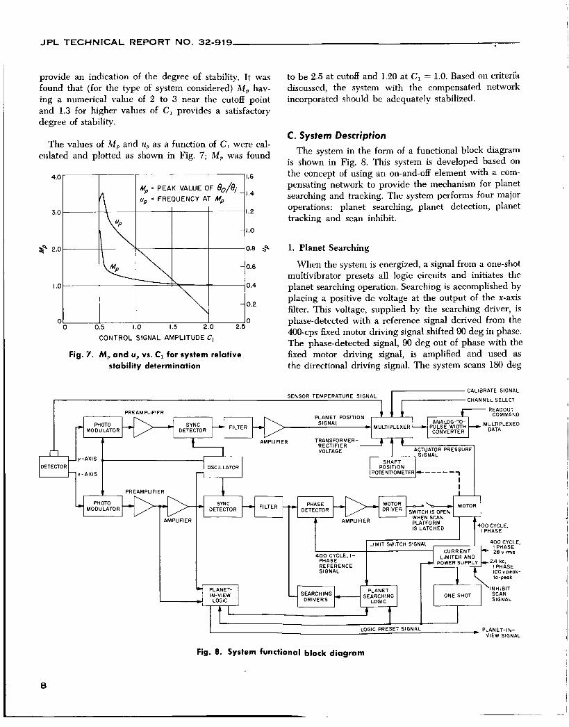
C. System Description
The system in the form of a functional block diagram is shown in Fig. 8. This system is developed based on the concept of using an on-and-off element with a com- pensating network to provide the mechanism for planet searching and tracking. The system performs four major operations: planet searching, planet detection, planet tracking and scan inhibit.
1. Planet Searching
When the system is energized, a signal from a one-shot multivibrator presets all logic circuits and initiates the planet searching operation. Searching is accomplished by placing a positive dc voltage at the output of the x-axis filter. This voltage, supplied by the searching driver, is phase-detected with a reference signal derived from the 400-cps fixed motor driving signal shifted 90 deg in phase. The phase-detected signal, 90 deg out of phase with the fixed motor driving signal, is amplified and used as the directional driving signal. The system scans 180 deg
~ CALIBRATE SIGNAL
CHANNEL SELECT SENSOR TEMPERATURE SIGNAL
MODULATOR
AMPLIFIER TRANSFORMER-
I
IN-VIEW
1 b y i O T 0 l i !PHASE DETECTOR SWITCH IS OPEN
WHEN SCAN
IS LATCHED I
400 CYCLE, I AMPLIFIER PLATFORM
I LIMIT SWITCH SIGNAL 400 CYCLE,
400 CYCLE, I - PHASE REFERENCE SIGNAL
1 PLANET
SEARCHING zFt2AL ONE SHOT SEARCHING DRIVERS LOGIC
I + 1 LOGIC PRESET SIGNAL ~ PLANET-IN-
VIEW SIGNAL
Fig. 8. System functional block diagram
8

JPL TECHNICAL REPORT NO. 32-919
in the process of searching for the planet. Upon com- pletion of each 180-deg search, the motor drive is re- versed by the following steps:
a. The planet searching logic is reset by a wave-shaped and noise-filtered signal initiated by limit switch action.
b. A dc voltage of proper polarity is applied to the x-axis filter by the searching driver. A positive dc voltage is used for counterclockwise motor drive and a negative dc voltage is used for clockwise drive.
c. The dc voltage is converted to an ac signal, the phase of which is dependent upon the polarity of the dc voltage. A positive dc voltage is converted to an ac signal which is 90 deg out of phase with the ref- erence signal, and a negative dc voltage is converted to an ac signal which is 270 deg out of phase with the reference signal. The ac signal is then amplified and applied to the motor as the directional drive signal.
2. Planet Detection
A radiation detector is used to detect thc presence and location of the planet. When the planet is in view of the detector, a pair of signals is generated to indicate the location of the planet with respect to the spacecraft. The x-axis output is used as the error signal for planet tracking while the y-axis output determines the angular position of the planet with respect to the detector mount. Both signals are modulated by a pair of oscillator-driven mod- ulators prior to entering the preamplifier and amplifier. A pair of synchronous detectors are used to demodulate these signals before filtering. At the output of the preamplifier, the x-axis signal is sampled by the planet-in- view logic where noise filtering and planet signal iden- tification are performed. A planet-in-view signal for the purpose of data mode switching is delivered to the data automation system for processing and at the same time
the searching driver is inhibited, thus changing the sys- tem from searching to tracking mode.
3. Planet Tracking
The x-axis output after demodulation, filtering and phase-lead compensation is used as a platform positioning error signal to initiate motor driving action. The magni- tude and polarity of the positioning error signal are dependent upon the planet position relative to the line-of- sight of the wide angle detector and TV camera optics. When this signal exceeds the inactive zone limits, platform motion is initiated to track the planet and to minimize the positioning error to within the required planet track- ing accuracy. The motor driver and associated circuits, being commonly employed in both searching and track- ing operations, perform the same functions while tracking.
The filtered y-axis output signal is amplified and con- verted from a bipolar to a unipolar signal. This signal, together with the platform position output and other signals, is time-multiplexed and analog-to-pulse-width- converted before transmission to the data automation system for processing.
4. Scan Inhibit
A scan inhibit signal is initiated either by ground command, the TV camera or the narrow angle Mars gate which is mounted on the platform. The signal indicating that the planet is in the field of view of the television is used to stop the scanning and tracking motion of the plat- form prior to television picture data recording. The scan trace across the planet after planet tracking motion has stopped is dependent upon the tracking angle at the time of scan inhibit and upon the relative motion of the space- craft on its trajectory as it sweeps across the surface of the planet.
To implement the design, a system was developed con- sisting of three basic types of equipment: (1) the radia- tion detector and optics, (2) the electronics and (3) the motor assembly and its associated scan platform.
9

JPL TECHNICAL REPORT NO. 32-919
IV. DETAILED DESIGN AND SYSTEM DEVELOPMENT
A. Radiation Detector and Optics
The presence and relative position of the planet is to be detected by a radiation detector. The detector senses radiation from the planet and transforms the radiant energy into an electrical signal indicating the planet position as well as the amount of radiation received. The requirements imposed on the detector are:
1. A definite spectral range of sensitivity corresponding to the assumed spectral radiance characteristics of the planet
2. The achievement of a high radiant-to-electrical energy conversion efficiency through the proper combination of characteristics of the optical system and detector
3. A definite relationship between the detector elec- trical output and the magnitude and relative posi- tion of the radiation source
The planet can be detected through the sensing of either the planet's black-body radiation in the far infrared spectrum range of 10 to 40 p or the planet's reflected solar energy in the visible and near infrared spectrum range of 0.4 to 2.0 p. A detector sensitive in the far infrared region can be utilized for this purpose, but pre- detection modulation of the infrared signal (usually by mechanical chopping) is required for effective detector operation. At present, infrared detectors of practical application also require active cooling to achieve the desired responsivity. Detectors of the photoconductive type can be used to detect radiation in the visible and
infrared regions. For precision planet position and inten- sity indications, such detectors require highly regulated power supplies to provide bias for their operation. Thermocouple detectors with the proper filters can also be used to sense radiation in the visible and infrared regions. Complications arise in the design of the elec- tronic circuitry required to handle an extremely small output signal from the thermocouple.
To overcome some of these difficulties, a p-n junction silicon detector was chosen. Since the reflected solar radiation from the planet contains 95% of its energy at wavelength shorter than 2 p, silicon with an absorption edge at 1.8 p is considered suitable for the application. The output of this detector is self-generating and no bias supply is required. Without bias, the output is obtained with zero volt as reference and predetection chopping of the incoming radiation is not needed as compared with a biased detector which requires signal chopping to separate the signal from the bias voltage.
1. Carrier Collection and Spectral Response
It is known that the performance characteristics of a p n junction detector are dependent upon its fabrication material, physical geometry, and electronic parameters. An analysis of the effects of these parameters (Ref. 5 ) showed that the carrier collection efficiency and relative spectral response of the detector, ql . (A) , can be obtained by
where
v,, (A) = p-layer efficiency
vp ( A ) = n-layer efficiency
1 0

JPL TECHNICAL REPORT NO. 32-919
e x p [ - h ( ~ ) a ] - [8 + h ( ~ ) ] y11 =
L, = DifEusion length of free electronics, cm
Lp = Dihsion length of free holes, cm
S , = Surface recombination rate, cm-sec'
h (A) = Absorption co&cient as a function of incident wavelength A (Ref. 4)
pLn = Mobility of electrons, cm2-v-1-sec-1
p p = Mobility of holes, cm2-v-'-sec-'
I = n-layer thickness, cm
a = player thickness, cm
K = Boltzmann constant
T = Temperature, OK e = Electronic charge
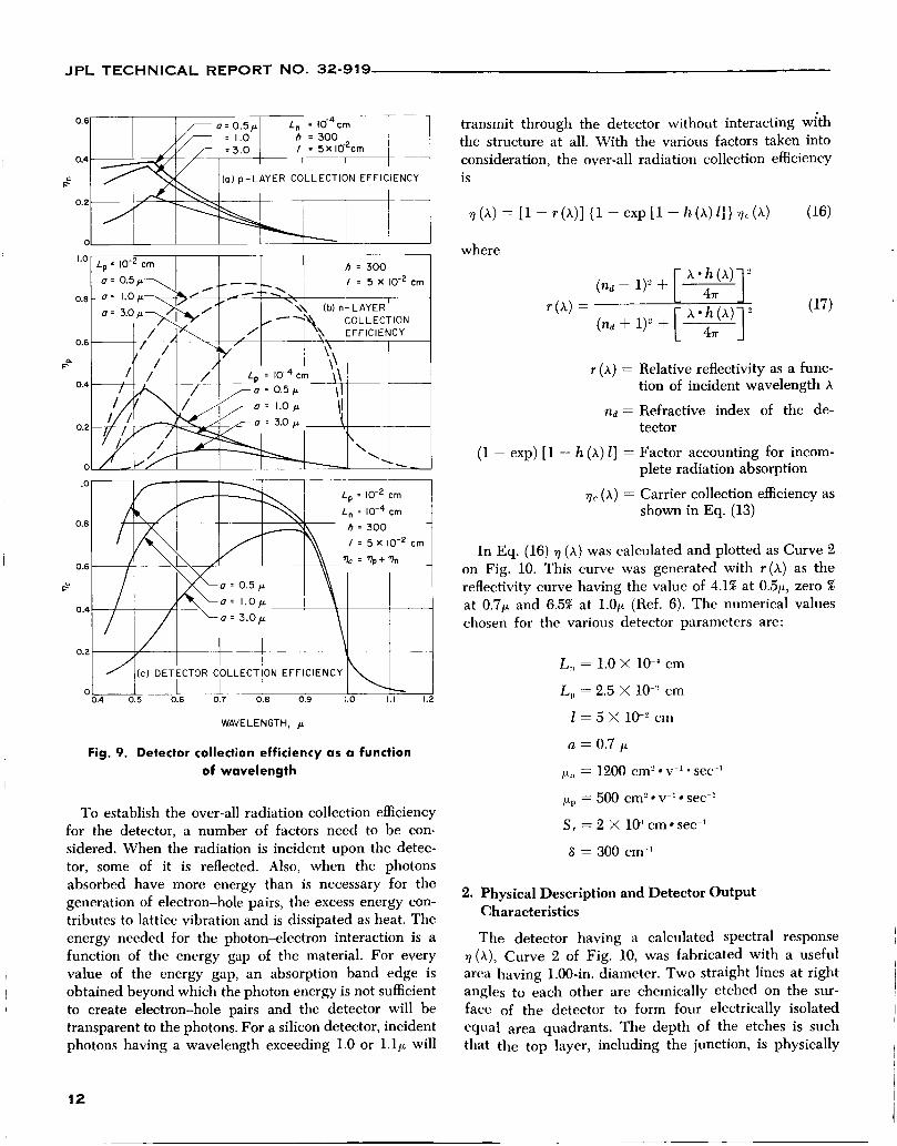
It is seen from Eqs. (13), (14) and (15) that proper values for the various parameters can be selected reason- ably to match the spectral response of the detector to that of the radiation source. Such a detector is considered capable of converting the incident energy to electrical signal efficiency. To select the proper values for the various parameters, Eq. (13) was solved for a number of cases using an IBM 7094 Computer. Figures 9a and 9b show the resultant p-layer collection efficiency v n ( A )
and n-layer collection efficiency vp(h) for a detector having a thickness of 5 X 10⁻² cm with the various junc- tion depths as the parameters. It is seen that 7n(A) starts
to rise at longer wavelengths for a deep junction than for a shallow junction. Therefore, a detector with a deep junction uses the infrared radiation more efficiently. However, the over-all efficiency decreases as the junction depth increases. For a deep junction, a considerable percentage of electron-hole pairs are generated near the surface and away from the junction. These minority car- riers are not capable of contributing to the junction cur- rent because of the recombination process taking place at the surface and inside the p-layer. The p-layer should be made as thin as possible for high collection efficiency in the short and medium wavelength regions. However, the series resistance of the p-layer increases as the junction depth decreases, resulting in a reduction in the efficiency improvement.
Figure 9b shows that quite a large number of carriers are generated in the n-layer by radiation penetrated through the p-layer. To see the effects of the difhsion length and lifetime of the carrier on the n-layer collec- tion efficiency, the dotted line curves in Fig. 9b were generated by assuming the dihsion length of the holes to be cm instead of le2 cm. It is seen that the col- lection efficiency is considerably reduced because of the decrease in dihsion length. To obtain high collection efficiency, therefore, the diffusion length of the n-layer must have a relatively high value. Figure 9c shows the detector collection efficiency v C (A).
JPL TECHNICAL REPORT NO. 32-919
0.6
0.4
& 0.2
0
WAVELENGTH, p
Fig. 9. Detector collection efficiency a s a function of wavelength
To establish the over-all radiation collection efficiency for the detector, a number of factors need to be con- sidered. When the radiation is incident upon the detec- tor, some of it is reflected. Also, when the photons absorbed have more energy than is necessary for the generation of electron-hole pairs, the excess energy con- tributes to lattice vibration and is dissipated as heat. The energy needed for the photon-electron interaction is a function of the energy gap of the material. For every value of the energy gap, an absorption band edge is obtained beyond which the photon energy is not sufficient to create electron-hole pairs and the detector will be transparent to the photons. For a silicon detector, incident photons having a wavelength exceeding 1.0 or l . lp will
transmit through the detector without interacting with the structure at all. With the various factors taken into consideration, the over-all radiation collection efficiency is
where
T (A) = Relative reflectivity as a func- tion of incident wavelength A
n d = Refractive index of the de- tector
(1 - exp) [ l - h (A) 13 = Factor accounting for incom- plete radiation absorption
qc (A) = Carrier collection efficiency as shown in Eq. (13)
In Eq. (16) 9 ( A ) was calculated and plotted as Curve 2 on Fig. 10. This curve was generated with r ( h ) as the reflectivity curve having the value of 4.1% at OSp, zero % at 0 . 7 ~ and 6.5% at 1 . 0 ~ (Ref. 6). The numerical values chosen for the various detector parameters are:
L,, = 1.0 X lo-' cm
L,, = 2.5 X lo-' cm
1 = 5 X le' cm
u = 0.7 p
p,, = 1200 cm' v-' sec ' pP = 500 cm' v-' sec-'
S, = 2 X 10' cm sec-'
6 = 300 cm-'
2. Physical Description and Detector Output Characteristics
The detector having a calculated spectral response v ( A ) , Curve 2 of Fig. 10, was fabricated with a useful area having 1.00-in. diameter. Two straight lines at right angles to each other are chemically etched on the sur- face of the detector to form four electrically isolated equal area quadrants. The depth of the etches is such that the top layer, including the junction, is physically
12

~~
I I
JPL TECHNICAL REPORT NO. 32-919
01 I
separated from the bottom layer. The two output differ- ential voltage pairs, each formed by taking the outputs of the adjacent quadrants through a resistor matrix, are shown as e, and e, in Fig. 11.
The operational concept of the detector is such that the planet image is bisected by the adjacent quadrants and a null point is indicated when each quadrant receives equal energy and the detector outputs are nulled to zero
-e,,-' '-+e,,
"LS + - *Y
Fig. 11. Detector output resistive matrix
volt. Since the signals of the adjacent pairs are balanced out, the differential signal indicates the angular deviation of the planet position from the null axis.
The detector output voltages ez and e, are related to the various parameters as follows:
R (e ) is the Fresnel coefficient of reflection for unpolarized incident energy as a function of incident angle e
1 J (e, p, +) = - [ k: COS-' (Q/&) + ~ 0 s - l (k - Q) - 2 COS-' k2] x
1 - -[9 (k: - 4')s + (k, - Q)] [l - (k - Q)']% - 2kz (1 - kz)M
x
J (e , /3, +) is the factor relating planet angular semidiameter 8, optical angular half field of view + and planet position angle e
13

JPL TECHNICAL REPORT NO. 32-919
6 ( e ) = [ l - sin281
6 ( e ) = Factor due to vignetting effect of the optics
H = Detector responsivity
The input energy E (d, a, A) from the planet can be calculated by assuming the planet has the spectral radiance prop- erty P (A)/f (A) as shown on Curve 1 of Fig. 10:
where
E,. = 1.52 X lo-" watt-cm2-p-' = monochromatic energy flux at A = 0.55 p corresponding to visual albedos
(Y = Phase angle (Sun-planet-system angle)
= 0 deg, A = 1, d = 1
+ (a) = Phase function = 0.406 when = 60 deg
A = Aperture area of the optics = Td/4 = 1.32 cm2 for d = 1.3 cm
T (A) = Transmission efficiency of the optics
K (a) = Illuminated fraction of the planet at phase angle a = M (1 + COS a)
d = Distance from planet to the system, A.U.
A = Mean distance from planet to Sun, 1.524 A.U.
P (A) = Assumed planet spectral reflectivity
f (A) = Spectral energy function of solar energy
AI, As = Cutoff wavelengths of the system
7 (A) = Spectral response of the radiation detector as calculated by Eq. (16)
Then e,, e , as a function of the planet position 0 with the planet angular semidiameter as the parameter was calculated and plotted in Fig. 12. It is seen that the magnitude and polarity of e=, e, can be used to determine the position of the planet image with respect to the detector axis, and the magnitude of e, and e, can be used to determine the amount of energy received at a distance at which the planet is considered to have an apparent semidiameter of ,8. Subsequently, e, was used to indicate the planet position while e, was used as error signal for planet tracking.
3. Optical System
The planet angular diameter, when viewed at the closest operating distance of 9,OOO km, is approximately 41 deg. To accommodate a full field of view of the planet,
1 4
the optical system must have an optical view of greater than 41 deg. An optical system having an f number of f/2.3, a focal length of 30 mm and a circular field of view of 50 deg was chosen. This optical system, when operating at a distance of 9,000 km, formed a planet image of 0.89 in. in diameter. Therefore, the detector, having a sensitive area of 1.000-in. diameter and an over- all diameter of 1.125 in., was chosen to accommodate the full field of view of the planet over the entire operating distance range.
The measured transmission efficiency of the lens T (A) as a function of the incident wavelength is shown in Fig. 13. The vignetting effect was calculated and is shown in Fig. 14. As a comparison, the measured vignetting curve of the lens is also shown in the same figure.

JPL TECHNICAL REPORT NO. 32-919
Fig. 12. Calculated detector output a s a function of planet angular position
WAVELENGTH A, p
Fig. 13. Optical transmission efficiency as a function of wavelength
B. Electronics
1. Signal Modulation
To simplify the design requirements of the electronic amplification circuitry, the dc outputs of the detector are converted to ac signals by a pair of photomodulators, each consisting of a pair of small neon lamps and a matched pair of cadmium selenide photocells. Then,
CURVE B OPTICAL SYSTEM o 8 - VIGNETTING INCLUDING
b- 0 W
W
0
01 I I I I I I I 1
ANGULAR POSITION e. deg 40 30 20 10 0 -10 -20 -30 -40
Fig. 14. Optical vignetting effect
amplifying the resultant signal with high-gain, low-noise ac amplifiers can be more readily accomplished. This method of modulation was chosen for its simplicity and reliable operation. It also produces extremely low offset voltages over the required temperature range. Because the photocell's dark-to-light resistance ratio is very high, the photomodulator provides high modulation efficiency. Each pair of lamps is connected in parallel for redun- dancy and an oscillator is used to provide signals to drive the lamps.
The oscillator frequency was selected to satisfy two conditions: (1) simplicity of amplifier design sets a low- frequency limit, and (2) the photocell time constants impose a high-frequency limit. Based on these considera- tions, a value of 24 cps was chosen as the oscillator frequency to satisfy both conditions. It is well known that higher than nominal breakdown voltage is required to fire the neon lamp in darkness or after long duration in the nonconducting state in darkness, because the time required for the gas ionization increases when the lamps are pulse fired in the dark. The ionization time can be reduced through the use of a radioactive additive. To further insure proper operation, an applied voltage in excess of the static breakdown voltage was used to fire the lamps.
2. Preamplifiers
The modulated r- and y-axis outputs were amplified by a pair of four-stage ac preamplifiers of identical design. The preamplifier was designed to have a relatively high input impedance to match the operating conditions of the photomodulators. A field-effect transistor was used in the first stage. The input impedance of this transistor is essentially that of a reverse-biased junction and is there- fore very high. For the remaining three amplification
1 5

J P L TECHNICAL REPORT NO. 32-919 .
- -
stages, 2N930 and 2N1132 transistors were used to take advantage of the transistor’s low-noise characteristics. The final design of the preamplifier circuit is shown in
where
Fig. 15a, and its equivalent circuit is shown in Fig. 15b. hgm R,
1 + R,,gm - R,
A, = The preamplifier having an input impedance of 3 meg- ohms is determined primarily by input resistor R , since the input impedance to the field-effect transistor is much greater than the resistive value of R,. The closed loop voltage gain of the preamplifier is ZS
R, + Z, - ~ Ri + 2% z;
A’,
(20) = ( R, + R, + z, - R, + Z, A,& 1 + AiA,P,
A,. =
RIOI:62K - -
I I -
1729 $5. I K
3 3
( a ) CIRCUIT SCHEMATIC
( b ) EQUIVALENT CIRCUIT
Fig. 15. Preamplifier
16

JPL TECHNICAL REPORT NO. 32-919
- A, = Closed loop voltage gain of the preamplifier
A, = Voltage gain of the first stage
A, = Closed loop voltage gain of last three stages
A: = Open loop voltage gain of last three stages
1 R, - i y
- ' 0 L g /3f = Preamplifier feedback factor
Z, = R, - i-
R, 1
W C ,
With the proper values of the various parameters as shown in Fig. 15a substituted into Eq. (20), the gain of the Preamplifier was calculated to be
A, = 8300L5.96"
for
R , = 15 kohms
R , = 500 ohms
g , = 2750 pmhos
A:=--
f = 24 cps
The actual voltage gain of the preamplifier when mea- sured over the operating temperature of -30 to +70°C is 8000 +2.5% as compared to the calculated gain of 8300.
3. x-Axis Amplifier
The x-axis output is bandpass-filtered and further amplified by a three-stage, zener-coupled ac amplifier. The incorporation of zener diodes as the coupling ele- ments has the advantages of minimizing the loss of gain, elimination of the need for large coupling or bypass capacitors and providing stable operation over a wide temperature range due to the temperature-compensating effects of the diodes. Figure 16a shows the amplifier circuit and bandpass filter, and Fig. 16b shows the equiv- alent circuit. The bandpass filter was designed to attenu- ate noise having frequencies higher and lower than the center frequency of the 24 cps signal. Figure 17 shows the noise discrimination characteristics of the filter. The voltage gain of the amplifier is:
where
A, = Closed loop gain of the amplifier including the
A!, = Open loop gain of the amplifier
Af = Attenuation factor of the filter as shown in
filter attenuation
Fig. 17. Z, = R,, - i wc, 1
With the values of the various parameters as shown in Fig. 16a substituted into Eq. (21), the gain of the ampli- fier was calculated to be
A:, = 1040 L6.2O
for
A; = 15,000
Af = 0.78
f = % c p s
4. Signal Demodulation and Phase Compensation
The 24-cps x- and y-axis signals are then separately demodulated, filtered and converted to dc signals by the use of the synchronous detectors and three-stage RC filter networks. A simple synchronous detector using a field-effect transistor as chopping element is as shown in Fig. 18 together with a three-stage RC filter network. A signal derived from the oscillator is utilized as the gate driving voltage so that the demodulated dc output has the same polarity as the detector output signal. The ac-to- dc conversion gain of the demodulator is 0.48 v dc/v rms.
Factors affecting and contributing to the offset of a field-effect transistor have been analyzed in Ref. 7. The offset voltage V,(T), as a function of the operating temperature and other parameters, can be determined by
(22)
where R D is the input resistance to the demodulator as shown in Fig. 18; R d n (T) is the drain-to-source resistance as a function of the operating temperature; (T) is the gate reverse current as a function of temperature and v n is the chopping efficiency. For transistor 2N2498 operating at a drain current of 100 pa, &, (T) has a numerical value of 400 ohms at -40°C, 800 ohms at
1 7

J P L TECHNICAL REPORT NO. 32-919
( a ) CIRCUIT SCHEMATIC
0 RlO
0
I" i" p' Tc4
(b ) EQUIVALENT CIRCUIT 4 Fig. 16. x-Axis signal amplifier
INPUT FREOUENCY.cps
Fig. 17. x-Axis signal amplifier band pass filter characteristics
+25OC and 1.12 kohms at f75OC. The gate cutoff cur- rent los when the transistor is operating at a gate-to- source voltage of 10 v has a value of 0.0001 pa at -4OoC,
R1%oo
220 5"
0.005 pa at 25OC and 0.05 pa at +75OC. The chopping efficiency is 35% for a sine wave gate drive and better than 90% for a square wave gate drive. Since the demodulator is driven by a square wave, qo is assumed to be 0.90. With the various numerical values substituted into Eq. (22) , the offset voltage was calculated to be
V, ( T ) -- 0.61 pv
V, ( T ) = 3.28 pv
at T = -4OOC
at T = +25OC
V, ( T ) = 346 p~ at T = t 7S°C
The effect of the demodulator offset voltage on the planet tracking accuracy is negligibly small since the signal level required for motor actuation at this point is 2.65 v.
18

JPL TECHNICAL REPORT NO. 32-919
- =I Rl *2
CP-- -- GATE DRIVE 2 N 2 4 9 8
SIGNAL DERIVED FROM THE OSCILLATOR
v - 7
*3 *4 4 7 K
*5
Rg :: 7.5K c3- - c4-- 3.5 - - 2 S ' - 2 . 5
A a
Fig. 18. Synchronous detector, filter and phase-lead compensation network
-
System design analysis in Section I11 indicated that 5. 4ooCps Phase Detection
-
without the phase compensation the system is unstable when operating under the condition of C , > 0.55. With the phase lead compensating network incorporated in the system, the loci of g-'(iu) and g D no longer intersect and the system is stable. The numerical values of the attenuation factor a = 7.25 and pa = 0.59 were required for this compensation. To meet these requirements the electrical constants of the network as shown in Fig. 3a are selected as R,, = 0 ohm, R, = 47 kohms, R, = 7.5 kohms, C , = 10 pf. Based on these electrical values and T = 0.8 see, po and a are
A chopping element is used as the phase detector to convert a positive dc signal to an ac signal. A double emitter transistor (integrated chopper transistor) is se- lected as the chopping element. This transistor has a low offset voltage V,. The double emitter transistor consists of a pair of transistors constructed as a single unit. The transistor pair is used in the inverted configuration to obtain low offset voltage. The two transistors in the pair are also closely matched in offset characteristics so that the offset voltages of the pair cancel each other to further reduce the offset.
= 0.587 Figure 19 shows the phase detector. To select the proper operating parameters for the transistor, the offset voltage V, is analyzed in terms of the base current Zb. The offset voltage V, is a function of the transistor satura- tion resistance Ra, and Rb in turn is dependent upon the transistor base driving current I b . The base current Zb must be sdcient ly large to drive the transistor so that
T a - RIC, P a = T - ~
= 7.26 R, R, + R ,
a = l +
The signal attenuation in the compensating network is l/a or 0.138.
3 N 70
3.3 K 2.7K
R2
C2 0.22 Cl 0.15
PS-520M
0 0
SIGNAL DERIVED FROM MOTOR DRIVING SIGNAL ein = 50 v
- NI = TRANSFORMER RATIO = 2
N2
Fig. 19. Phase detector and 90-deg phase shift circuit
1 9

I JPL TECHNICAL REPORT NO. 32-919
Rb is at a low value as shown in Fig. 20. When operating with I b = 4 ma, Rb is 14 ohms and is sufficiently low in value to produce an offset of 250 k40 pv over the tem- perature range of +80 to -25OC. The amount of planet tracking error introduced by the offset voltage when operating with ZI, = 4 ma is extremely small since the
signal amplitude required for motor actuation is 60 mv at this stage.
A phase shift network as shown in Fig. 19 is in- corporated. This network is used to supply 11, having the proper phase and amplitude to drive the phase detector. The amount of phase shift can be determined by
where
e, -- - Ratio of the network output to input eilL
R i , = Input impedance of the phase detector = 140 ohms
N , - = Transformer ratio Ni
4 6 8 0 2
BASE CURRENT Ib, m a
Fig. 20. Double emitter transistor base current as a function of saturation resistance
With the values of the various parameters selected as shown in Fig. 19, the amount of phase shift and network attenuation calculated by Eq. (23) is
- 10.194L-85.2' e" ei,
The phase shift of 85.2 deg together with the shift of 5 deg in the motor driving signal amplifiers provides the required 90-deg shift for the phase detector operation. The base current I,, obtained to drive the phase detector is
With the input voltage ei, derived from the fixed motor driving signal and having an amplitude of 50 v, the base current Z b calculated by Eq. (24) is Z b = 4.25 ma.
6. Motor Driver and Driver Amplifier
The phase detected signal is further amplified by a i four-stage driver amplifier with a pair of transistors in a complementary push-pull configuration at its output. The output of this amplifier is then transformer-coupled to a motor drive circuit consisting of a pair of power transistors 2N1050B in a push-pull configuration.
The motor driver and driver amplifier are shown in Fig. 21a. Figure 21b shows the equivalent circuit of the driver amplifier the voltage gain of which can be calcu- lated by Eq. (25):
20

JPL TECHNICAL REPORT NO. 32-919
330 PP 300 I 1
c314
FIXED MOTOR 7 DRIVING SIGNAL
1N649(4 )
DIRECTIONAL MOTOR DRIVING SIGNAL
c2$o.1 j @
( 0 ) CIRCUIT SCHEMATIC
T ' I O -L
0 - - I 0
( b ) EOUIVALENT CIRCUIT
Fig. 21. Motor driver and driver amplifier
where The gain of the driver amplifier when calculated by Eq. (S), with the values of the various parameters as shown in Fig. 21a, is
A, = 288 L- 2.5O
A: = 25,OOO
for f = 400 cps
A: = Open loop voltage gain of the amplifier
A, = Closed loop voltage gain of the amplifier
The measured gain of the actual circuit was 275. The motor driver was also determined to have a gain of 4 with a phase shift of approximately 2.5 deg.
21

JPL TECHNICAL REPORT NO. 32-919
t
t;' I I D
N I I;
t .- 0 C '0 E 0
22

JPL TECHNICAL REPORT NO. 32-919
7: Logic and Control Circuits
The planet searching and planet-in-view logic circuits are shown in Fig. 22. Planet searching and tracking oper- ations are controlled by flip-flop C. When the power to the system is applied, a positive going signal from the one-shot circuit presets all the flip-flops to the initiate planet searching operation. This preset signal has a pulse width of 6 sec as determined primarily by the time constant of R,, and C,. The preset pulse with a relatively long pulse width of 6 sec is used to preset the logics and to hold the preset action for the duration of the pulse so that any noise associated with system power turn-on will have no effect on the preset operation. The clockwise and counterclockwise planet searching operations are con- trolled by flip-flop s. The tlip-flop S is in turn being set and reset by the wave-shaped and noise-filtered signals initiated by limit switch action.
When the limit switch is actuated, a negative going pulse having an amplitude of approximately 5.5 v is generated to set or reset flip-flop S. At the same time, a positive going pulse Q as shown in Fig. 22 with an ampli- tude of about 5.5 v is also generated to set flip-flop C to the pianet sectilclihg stztc. Si@ 9 is 1wed to assure that the system is always operating in the planet searching mode immediately after each scan reversal. To provide redundancy, two limit switches connected in parallel and operated in series are incorporated in each of the two scan reversal limits. Each backup switch is located 2 angular degrees behind the primary switch so that in event the primary switch failed to initiate a scan reversal, the backup switch would be actuated when the scan platform has completed 2 additional angular degrees of travel.
Logic equations for the searching operation are
E = cs B = S + C
A = C B = c(S + 6)
A = S + C
A = C s
clockwise drive = AB
= CS(S + C) = cs
counterclockwise drive = 25 = ( S + E ) (CS)
= cs
Logics A and B as a function of C and S are used to control the search drivers. For a clockwise motor drive, a negative dc voltage having an amplitude of 5 v is generated by the search drivers and applied to the x-axis filter. For a counterclockwise motor drive, a positive dc voltage with an amplitude of 5 v is similarly generated by the searcli diivei.5 an2 qy!ied tn t h ~ y-axis filter.
The planet-in-view logic consists of a signal threshold and noise discrimination logic circuits as shown in Fig. 22. A band pass filter and a Schmitt trigger were used for signal threshold discrimination. The planet signal is bandwidth-limited by the filter and threshold-detected by the Schmitt trigger. A potentiometer R, is incorporated to adjust the trigger threshold level. The filter has the char- acteristics of:
where
eo/ei, = Ratio of output to input
T I = C,R,
23
JPL TECHNICAL REPORT NO. 32-919
Z,, is the input impedance of the Schmitt trigger and is related to the circuit components, the input impedance Z,, of transistor Q2 and the h-parameters of the transistor by Eq. (27). The upper and lower 3-db frequencies, f l and f z , of the network can be determined from Eq. (26) by letting I e , /e i , I equal 0.707 of its value at mid-frequency :
A f = f l - f z = Bandwidth of the filter
It is possible to calculate Af = 120 cps by Eq. (29) with the numerical values of the various parameters shown in hfe = 15. The input level Vi, at which the Schmitt Fig. 23 and h i , = 1800 ohms, hoe = 100 pmhos, h,, = 2.68 X
circuit responds can be determined by
where
(hi, - he) - Rho, 1 + h,, + (Ri + RL2) hop
A . = I
V,, = Power supply voltage to the Schmitt trigger
Vbrl = Base-to-emitter voltage of transistor Q,
The input impedance Z,,l of transistor (IL as a function of the circuit components and h-parameters of transistor QL can be obtained by the use of Eq. (27) with the substitution of R,,, in place of R,,, on the right hand side of Eq. (27). The proper threshold level is set b y adjust- ing potentiometer R , such that the dc biasing level plus noise is less than V,,,, a condition at which the noise evokes no response from the circuit. The dc biasing level can be determined by the following equation
24
where Edc is the biasing level, y is the normalized thresh- old level as a function of planet detection probability and V,, is the noise level at the filter input. V I , , with a value of 1.31 v can be calculated by Eq. (30) for h , , = 1800 ohms, hf, = 15, hoe = 100 pmhos, h,, = 2.68 X lo-' and Vhrl = 0.5 v. This calculated value compared favor- ably with the measured value of 1.27 v.
The noise discrimination logic consists of a number of flip-flops and gates. A signal from the oscillator having the same frequency as, and either in or 180 deg out of phase with, the modulated x-axis signal is frequency- divided by eight through the use of flip-flops L, M and N. This frequency-divided signal is utilized to control the sampling period with the frequency of 3 cps (f = 24/8). Flip-flops X and W are used to count the pulses passing through the Schmitt trigger during each sampling period. If four or more consecutive pulses having the proper spacing are gated per period, flip-flop C changes its state to indicate a planet acquisition. If fewer than four pulses having the proper spacing are gated, flip-flops x and W are reset by the reset pulse

~~
JPL TECHNICAL REPORT NO. 32-919
N
0
0 X r I r X
P I 0 C
0 SIGNAL T FROM SCHMlTT TR!GGER WHEN SENSOR SIGNAL IS POSITIVE
@ SIGNAL 7 FROM SCHMlTT TRIGGER WHEN SENSOR SIGNAL IS NEGATIVE
@ SIGNAL pXw FROM GATE 4 USED TO RESET FLIP-FLOP X AND W - -
Pxw= N+L; P,,=LN
@ CORRESPOND TO T, CHANGE STATE WHEN Pxw IS I AND CP CHANGE FROM 0 TO I
8 CORRESPOND TO T, CHANGE STATE WHEN Pxw IS I AND CP CHANGE FROM 0 TO 1
8 CORRESPOND TO T 0 CORRESPOND TO 7
Fig. 23. Planet-in-view logic waveform
from Gate 4 at the end of each period and the gating resumes in the next period. Figure 23 shows the wave form at the outputs of the various flip-flops and gates.
Logic equations for acquisition operation are
Acquisition mode = AB = (S + C) ( S + E) = (SC + sc + E ) = E ( S + S + l ) -
= C
The system switches from planet searching to track- ing operation when flip-flop C changes its state from C to e. This is accomplished by removing the search driver's output from the x-axis filter so that the planet signal can now be used to drive the platform. A 2.4-kc
planet-in-view signal is also produced by Gate 3 and is delivered to the data automation system for data mode switching.
8. y-Axis Signal Amplifier
The demodulated y-axis output is amplified by a dc- coupled difference amplifier as shown in Fig. 24. The y-axis signal is amplified and inverted from a bipolar signal to a unipolar signal by the difference amplifier. An adjustable negative dc feedback from the amplifier output to the detector y-axis output is employed to con- vert the wide range of the energy input to a voltage indication over the entire system operating range. The voltage gain of the amplifier as a function of the tran- sistor h-parameters and the various circuit components is
where
Ah = hiehoe - hrehfe
With the numerical values of the various parameters as shown in Fig. 24 and with hi, = 1800 ohms, hoe = 100 mhos, h,, = 2.68 X lo-' and hi, = 15, the gain of amplifier determined by Eq. (32) is
A, = 21.8
The actual measured voltage gain of the amplifier is 20 and the amplifier was designed such that the voltage amplification is linear within 2% of the measured value over the entire operating range.
9. Scan Inhibit Electronic Circuitry
The scan inhibit signal is initiated by the TV camera, Earth-based ground command or narrow angle Mars gate and is routed to the system through the data auto- mation system. The signal in the form of a 50-msec pulse with an amplitude of 6.0 to 8.0 v is used to operate a relay to disconnect the 400-cps fixed motor driving sig- nal to the motor. To assure that the 400-cps fixed motor driving signal is available to drive the motor when the system is recycled, the 6-sec preset pulse generated by the one-shot circuit is used to drive a relay driver cir- cuit to close the relay connection each time the system is energized. The scan inhibit circuitry is shown in Fig. 25.
25

JPL TECHNICAL REPORT NO. 32-919
+I2 v
Rg 2 . 7 K i
.I
+ 6 v
i
.t - 6 v
Fig. 24. y-Axis signal amplifier
4 0 0 - c p s FIXED MOTOR DRIVING SIGNAL
- SCAN INHIBIT
SIGNAL
f"
y - AXIS SIGNAL FEEDBACK
Q , , Q 2 = 2 N 9 1 0
PRESET SIGNAL FROM ONE-SHOT CIRCUIT
-12 v
Fig. 25. Scan inhibit circuit
26

JPL TECHNICAL REPORT NO. 32-919
2 1
10. Power Supply
Preamplifiers and amplifiers are designed to operate on +12 v dc and control circuits on 2 6 v dc. In addition, a 130-v dc power supply is required to operate the photo- modulator, and an 8-v dc supply to operate the motor relay. The various requirements of the power supplies are
1
listed in Table 1.
Table 1. Power supply requirements
Maximum
current,
- 12
+ 6
- 6
+ 6
$- 130
+ 8 40
Ragulo- I Ripplo 1 Spikes (paak (peak to (peak to
to Yk" peak), X peak), X
2
2
2
2
0.001 /'C
10
20
1
1
1
1
0.1
2
2
1
1
1
1
0.5
1
1
Load variation.
X
soto 100
50 to 100
50 to 100
50 to 100
50 to 100
90 to 100
5010 100
5010 100
To protect the spacecraft power system from overioaa- ing, current limiting capability is provided to limit the dc and 400 cps motor drive load currents to a specified limit. The supplies are designed to operate on a single- phase, 2.4-kc spacecraft power having the following characteristics :
a. lnput Voltage 100 v peak-to-peak square wave Voltage regulation 25%
5 v, 2 psec, normal, 5 psec maximum
2.4 kc, stability 2 2 % Rise and fall time: 5 psec 2 4 p e c Source impedance: 2 ohms maximum
b. Spikes (Ouershoot)
c. Frequency
The power used to drive the motor is a single-phase square wave, 400 cps with a frequency stability of I%, 28 v rms with 5% regulation and a rise time of 9 psec maximum. The power supply is also required to limit the dc current to 150% of the rated current and the 4 0 0 - c ~ ~ current to 160 ma rms.
11. Multiplexer and Analog-to-Pulse-Width Converter
Six channels of data are required for system perfor- mance evaluation during ground tests and in flight. These
channels are: scan platform position, y-axis output, cali- bration voltage, detector temperature, motor assembly pressure and transformer-rectifier (T-R) voltage. Each of the signals has an amplitude range of 0 to 6 v. Before routing to the Data Automation System for processing, the signals are time-multiplexed by a multiplexer. The multiplexer consists of six sets of switching coils and magnetically operated reed switches incorporated as commutating elements. The coil and reed switch assembly is selected for this application because of its low operat- ing power requirement. When open, the assembly has a high open circuit resistance and when closed, it has a low closed circuit resistance. Each coil was designed to have approximately 32,000 turns of wire, requires 17.5 ampere-turns of 9 mw of power at 17.5 v to operate. Open circuit resistance of the switch is in excess of los ohms and the closed contact resistance including lead resistance is 90 milliohms. Each assembly has a life expectancy of 100 million operations and is tested for 1.3 million success- ful operations prior to acceptance as a flight unit.
An analog-to-pulse-width converter is used to process the multiplexed data. The converter is capable of con- verting an analog signal of 0 to + 6 v to a pulse width signal wtii tine wiclilli laiigc c;f 3 t:: S?!N :-r hetween marking pulses having 5 to 7 v of pulse amplitude and 8 to 12 p e c pulse width. The converter was designed to have an accuracy of 0.5% of full input scale when operating over the temperature range of - 10 to + 80OC.
12. System Interconnections
For proper system operation, electrical interfaces be- tween the planetary scan system and other systems in the spacecraft are required. Depending on the charac- teristics of signals, twisted pairs and shielded twisted pair conductors are used to transmit these signals to minimize signal interferences. Each of the signals is ac-coupled and isolated by means of transformers or coils to avoid alternate conducting paths for circuit return currents.
Inputs and outputs required for proper system opera- tion are as follows:
a. lnputs
1. 28 v rms (-t5%), 400 cps, single-phase, square wave power from the power system
2. 50 v rms (+5%), 2400 cps, single-phase, square wave power from the power system
27
JPL TECHNICAL REPORT NO. 32-919 --
3. Inhibit scan signal, 6.0 v minimum, 50 msec, from the DAS
4. Seven data channel select signals for the data multiplexer operation, each 20 v, 50 msec, from the DAS
5. Analog-to-pulse-width converter readout com- mand, 6.0 v, from the DAS
b. Outputs
1. Planet-in-view signal, 3.0 to 6.0 v, peak-to-peak,
2. Pulse width data signal with the width range of 3 to 9200 psec between marking pulses having 5 to 7 v of pulse amplitude and 8 to 12 psec pulse width to the DAS; the data signal is time- multiplexed and contains the six channels of data required for system performance evaluation dur- ing tests and in flight
2400 cps, single-phase, to the DAS
3. Eight channels of dc signals monitored by the operational support equipment (OSE): + 130 v,
No. 1 and -12 v No. 2 f 1 2 V, +8 V, $6 v NO. 1, $6 v NO. 2, -12 v
4. Four channels of ac signals monitored by the OSE: 400-cps motor drive signal, 400-cps motor directional drive signal, photomodulator drive and planet-in-view signal
13. System Operational Failure Protection
As mentioned in Section IV-B-7, planet searching and tracking operations are controlled by flip-flop C, and flip-flop C is in turn controlled by the planet-in-view logic. To prevent a system operational failure due to a false switching of flip-flop C to planet tracking operation by abnormal occurrences such as disturbances in the logic power supply, a small dc signal of sufficient magnitude for motor actuation is continuously applied to the out- put of the x-axis filter. This signal is used to drive the motor in a fixed direction in the absence of a planet sig- nal at the x-axis filter during tracking mode operation. Upon actuation of the limit switch, then, the system auto- matically switches back to the planet searching mode opcration to continuc to scarch for thc, planet.
C. Motor Assembly
A motor assembly having a maximum torque loading capability of 100 in.-lb is used to drive the platform. This motor assembly consists of a Size 8, 8000-rpm, 4OO-cps, split phase, synchronous motor, reduction gearing, a shaft
position potentiometer and scan limit switches. The 8000-rpm synchronous motor drives an integral gearhead to reduce the output speed to 8.16 rpm. Further reduction gearing is used to reduce the assembly output speed to 0.5 deg/sec. A clutch assembly is provided so that driving slippage occurs when a torque load is equal to or in excess of 40 in.-lb. The clutch assembly is incorporated to protect the motor and the platform from damage in the event the platform is driving against any mechanical obstacles during ground testing. The clutch is adjusted to slip at a torque load of 40 in.-lb, which is twice the actual torque load of the platform.
A shaft position potentiometer geared to the output shaft of the assembly is used to indicate the platform angular position. The potentiometer has a resistance of 5 kohms &0.5%. The linearity of the potentiometer is 0.15%. Input voltage to the potentiometer is selected to be 6 v to provide an incremental output change of 32 mv per degree of wiper arm travel. With the output properly calibrated for nonlinearity, temnerature effects and input voltage changes, the ~ o ~ i t i o n indication at the output of the analog-to-pulse-width converter is accurate to 'A deg.
Two limit switches connected in parallel and operated in a series are incorporated at each of the two scan re- versal limits. The two primary switches are installed 180+0.1 deg apart. Each backup switch is located 2 deg behind the primary switch.
The motor assembly is designed to operate in vacuum and space environments. To further increase its operating reliability, the entire assembly is housed in a sealed con- tainer and pressurized at 15 p i g . A pressure transducer is installed in the container for the motor assembly pres- sure measurement.
D. Theoretical Planet Tracking Accuracy €valuation
To determine the planet tracking accuracy of the sys- tem, a theoretical planet tracking error analysis was made in which all major sources of error were considcred. These were:
1. Error due to variation in responsivity of detcctor quadrants as a function of temperature, AO,
2. Error due to the system dead zone, AH,
3. Error due to drift in the photomodulator, A 8 ,
4. Error due to offset in the demodulator, phase detec- tor and system operational failure prevention bias- ing, AB,
28

JPL TECHNICAL REPORT NO. 32-919
* 5. Error due to radiant density gradient of the planet quadrants, AB,
1. Error Due to Variation in Responsivity of the Detector Quadrants as a Function of Temperature
The operational concept of the detector is such that the planet image is bisected by the adjacent quadrants. A null point is indicated when each quadrant receives equal energy and the detector output is nulled to zero volt by the action of the servo system. The signals of the adjacent quadrants balanced out only when each quad- rant received equal amounts of radiant energy and the energy-to-electrical signal conversion efficiency of each quadrant was equal. Since the properties of the semicon- ductor material and the behavior of the p n junction are temperature-dependent, the detector's conversion efficiency or responsivity is a function of the operating temperature. Unless the responsivity of the adjacent quadrants are perfectly matched over the entire operating temperature range, a planet tracking error is introduced and the error magnitude is dependent upon the amount of mismatch in responsivity of the adjacent quadrants.
- A 1 -. r igure LO ~ V W S thc r.c:szred c2tpit nf each of the four detector quadrants plotted as a function of the oper- ating temperature for a constant energy input. The values of the load resistors in the detector output resistor matrix (as shown in Fig. 11) are selected such that all quadrants have the same output when operating at 20°C. As the operating temperature increases beyond 2OoC, the de- tector output decreases, indicating a decrease in responsiv- ity. On the other hand, when the operating temperature
0.61 I I I I I I 1 -60 -40 -20 0 +20 +40 t60 tOO
OPERATING TEMPERATURE, deq C
Fig. 26. Detector responsivity as a function of operating temperature
decreases below 2OoC, the detector output increases to a maximum at -5OC, below which the detector output begins to reduce as the temperature is further decreased.
The behavior of the detector at temperature below -5OC is interesting and contrary to the normally antici- pated behavior of increasing in output as the operating temperature decreases (Ref. 8). At low temperature, the electron and hole carrier densities are low relative to those at room temperature and recombination rate of the electron-hole pair is reduced, resulting in a higher output. The actual detector behavior is, however, more in line with the analysis made in Ref. 6, indicating that when operating in a particular configuration, the detector's short circuit current actually decreases with temperature, re- sulting in a decrease in output with temperature.
Figure 26 shows that the outputs of the individual quadrants are not equal when operating over the entire temperature range. At a temperature other than 20°C, a planet tracking error is introduced because a null point is now obtained only when one quadrant receives more energy than the adjacent quadrant, resulting in a shift in the iiiicking posilicr?. The magnitude of this shift is
iuiic:iez zf the diEermtia1 n u i p t A e between the adjacent quadrants, where
A e = e, - e,
e, = Output of one quadrant
e, = Output of adjacent quadrant
As shown in Fig. 26, iie is 9% at 75OC, OX at 2OoC and 6.9% at -4OOC. The equivalent tracking error in degrees can be calculated from the planet position and geometry with respect to the detector and determined to be 0.01758 at 75OC, O.OOO8 at 20°C, and 0.0148 at -4OoC, where 8 is the planet angular diameter. Figure 27 shows the track- ing error Ad, as a function of the detector-to-planet distance with the detector operating temperature as a parameter.
2. Error Due to the System Dead Zone ~8~
This is the tracking inactive zone error and is a design characteristic of the servo system. Since the system was designed with a dead zone error of 0.2 deg, ~0~ is assumed to have a magnitude of 0.2 deg.
3. Error Due to the Drift in the Photomodulator A8,
This error is introduced because of the drift in the photomodulator offset voltage when operating over the
29

JPL TECHNICAL REPORT NO. 32-919
0 al U
0
(L
2 0.6
a
0.4 W (3
Y w 0.2 z
?? 0 0 10 20 30 40 50 60 70
OPERATING RANGE x IO3 km
Fig. 27. Planet tracking error due to temperature variation of responsivity of individual
detector quadrants
required temperature range. The photomodulation method of signal modulation was selected because of its high reliability, low noise level and low offset voltage. There- fore, it is anticipated that this error would be small. The drift characteristics of the photomodulator were analyzed and tests were performed at the temperatures of +75, f 2 5 and -4OOC with a simulated input signal to the photomodulator. The long-term variation in the offset over a period of 24 hr at a given operating temperature was measured to be t 0 . 5 pv. The amount of drift in offset over the temperature range was 20.30 pv.
Figure 12 shows the detector output as a function of the planet angular position with the system operating range as parameter. The detector output when operating at the extreme condition of 60,000 km has a value of 1.0 mv per angular degree tilt from the null. The angular equivalent of the drift errors of +0.5 and 20.3 pv is indeed very small and its contribution to the over-all system error is negligible.
4. Error Due to Offset in the Demodulator, Phase Detector and System Operating Failure Biasing AB4
A field-effect transistor was used as the chopping device in the demodulator and a double-emitter transistor was used in the phase detector circuit. Both transistors were selected for the applications because of their ability to produce low offset voltage when operated over the re- quired temperature range. calculations in Section IV-B-4 indicated that the offsets produced b y the demodulator and phase detector were 346 and 290 pv, respectively. The amount of planet tracking error introduced by these offsets is extremely small, since the signal amplitudes
required for motor actuation are 2.65 v and 60 mv aP the respective circuits. The amplitude values of 2.65 v and 60 mv represent the dead zone limit of 0.2 deg; there- fore, the angular equivalents of the 346 and 290 pv of offsets are indeed small and can be neglected in the planet tracking accuracy evaluation.
To prevent a system operational failure when the system is inadvertently operating in the planet tracking mode in absence of the planet, a small dc signal was con- tinuously applied to the output of the x-axis filter. This signal was used to drive the motor in a fixed direction in the absence of a planet signal. The system automatically switches back to the planet searching when either of the scan limits is reached. During the normal planet tracking operation, however, a tracking error is introduced because of the dc biasing. This biasing signal was selected to have a magnitude just sufficient to actuate the motor and its angular equivalent is equal to the system dead zone limit of 0.2 deg.
5. Error Due to Radiant Density Gradient of the Planet Quadrants l o 5 This error is due to the fact that all portions of the
planet surface do not reflect equal amounts of solar en- ergy. The tracking position is therefore referenced to the integrated radiation bisector rather than the planet’s geometrical center line. The geometrical location of the radiation bisector is dependent upon the specific angle from which the planet is viewed, the planet seasons and the type of trajectory used. Since these factors can not be specified precisely in advance, this error has not been taken into consideration and all portions of the planet surface are assumed to have the same radiant density for the purpose of error calculation.
With the various major sources of error taken into consideration, a theoretical planet tracking error of the system A@ as a function of operating temperature and tracking distance can now be calculated:
(33)
where AB,, is an individual source of error wlicm the system is operating at a particular temperature and tracking dis- tance. The system planet tracking error a0 a s a function of tracking distance at the various operating temperatures was calculated by Eq. (33) and the results indicated that the system has a maximum tracking error of 0.776 deg. This error occurs when the system is operating at a track- ing distance of go00 km and a temperature of 75OC.
30

JPL TECHNICAL REPORT NO. 32-919
V. MECHANICAL DESIGN AND SYSTEM FABRICATION
The effects of space environments impose severe re- quirements on the selection of material, component fabrication techniques and mechanical design of the system. The system must be capable of operating for prolonged periods in a space environment over a wide range of temperature with minimum degradation in performance. In addition, the system must be capable of surviving the mechanical shocks and vibration en- countered during spacecraft launching.
A total of 576 electronic components is required for the fabrication of each system. Of the 576 components, 141 are active elements, either transistors or diodes. Wherever possible, components having a high reliability history were chosen, tested and screened to the existing
JPL specifications. Components designed and constructed for performing special tasks were also tested and screened to specifications written for that purpose. The system is fabricated and packaged in four units: 31Al-preamplifier, optics and detector assembly; 31A2-power supply and electronics; 31A3-electronics; and 31A4-motor assembly.
A. Preamplifier, Optics and Detector Assembly 13 I A I J
Unit 31Al is designed and packaged for mounting on the scan platform which is suspended beneath the space- craft as shown in Fig. 28. The assembly consists of a !ens barrel with optics, detector housing, two preamplifiers and two photomodulators.
Fig. 28. Scan platform assembly
3 1

JPL TECHNICAL REPORT NO. 32-919
1. Optical System
The design of the system was such that a standard lens is utilized to serve as the image-forming device. The lens selected is a standard commercial item having a focal length of 30 mm, field of view of 50 deg and f-number of 2.3. In addition to meeting all the design requirements, this lens was selected because of its light weight, its small volume and its availability as a standard item. The lens has a resolution of 170 lineslmm on the axis and 80 linesimm at the extreme field of view.
Being a standard commercial item, this lens is not designed mechanically for space application. Therefore, only the optical elements were acquired and these ele- ments were then mounted in a metal housing. Because of the operating requirements, the material selected for this housing must be capable of meeting the following requirements in addition to those normally required for space applications: (1) thermal coefficient of expansion to be compatible with the optical element; (2) high strength-to-weight ratio; and (3) minimum magnetic field.
A logical choice would be a high-strength aluminum alloy such as alloy 6061T6 because of its low density and nonmagnetic property. An investigation, however, indi- cated that this alloy has a thermal coefficient of expansion of 24 X 10-lb per degree C , whereas that of the optical element is 9 X 10 " per degree C. This large difference in thermal coefficients is undesirable in view of the wide operating temperature range. Stainless steel such as AIS1 303 is nonmagnetic, with a thermal coefficient of expansion of 14 X per degree C . Although the weight of the lens assembly with the stainless steel mount will be higher than that with aluminum alloy, the gain in mechanical strength is worthy of consideration. Since the lens assembly is small in volume, the difference in weight is also small. Figure 29 shows the lens in a stainless steel housing.
2. Detector Fabrication and Mounting
The p-n junction of the detector was formed by diffus- ing boron atoms into the top layer of the n-type silicon bulk material to form a player. To obtain the required planet tracking accuracy, the detector's responsivity must be uniform across the surface. Performance evaluations of the early fabricated detectors indicated that the de- tector's responsivity was not uniform across the surface. This was believed to be due to a nonuniform distribution of the impurity across the surface. The impurity gradient towards the junction was also belicved to be nonuniform across the surface, thus producing a nonuniform drift
Fig. 29. Optical lens in stainless steel housing
field to speed the minority carriers toward the junction. In addition, the detector had a fragile structure, making mechanical mounting difficult. The fragility was deter- mined to have been caused by cooling the detector too rapidly during the fabrication process. This created excessive thermal stresses because of the difference in mechanical properties between the top and bottom layers.
Various techniques of fabrication were developed to overcome these difficulties. The flight detectors, fabricated by a technique which permitted diffusing of the impurity more uniformly across the surface, were cooled in a closely controlled temperature environment. The local responsivity of these detectors was found to be fairly uniform. To obtain detectors of superior quality, units having superior characteristics were selected from the fabricated lots with a yield of approximatc~ly 15%.
To minimize the planet tracking error due to mechanical misalignment, the detector must be carefully positioned on the mount. Therefore, the fragile detector must be carefully mounted to the detector housing SO that it can survive the spacecraft launch vibration without causing excess misalignment with respect to the mount. An
32

JPL TECHNICAL REPORT NO. 32-9f9
adhesive having the proper characteristics for space application is used to mount the detector. I t is well known that adhesive compounds tend to lose weight in a vacuum due to sublimation and breakdown of the compound. Extensive studies have been made on the behavior of the various compounds in space environment by JPL (Ref. 9) and the various space agencies (Ref. 10). Since the optical lens is located in the vicinity of the mounted detector, contamination of the optical elements by the sublimated material will have serious effects on the optical properties of the lens. Therefore, the adhesive selected must have a low rate of weight loss.
Because of its wide operating temperature range and luw wigassing proi;erties, C-energ! E!ertrir RT\'-40 com- pound is used as adhesive for mounting the detector. The detector is mounted on a holder of aluminum alloy 6061T6, black-anodized. An insulation level between the detector negative lead and the holder in excess of 100 mcgohms v;zs a!so nhtiine? hwaiise of the high insula- tion property of the compound. In addition to serving as an adhesive, RT\'-40 is also used to provide mechanical and thermal shock absorption for the detector. The mounted detector is shown in Fig. 30.
3. Photomodulator Housing
The neon lamps and photocells are mounted in a light- tight housing made of aluminum 6061T6. Each pair of photocells and its associated neon lamps are mounted in a separate housing. To increase the amount of light available to the photocells, the interior of the housing is polished to a mirror finish for high reflection of light. Depending on the physical arrangement of the lamps and photocells, a fine mesh metal screen may be needed to shield the photocells from the lamps to minimize the electrostatic coupling between the high-voltage lamp firing signal and the low-level modulated sicpal. In this application, however, the shielding is not incorporated since the amount of electrostatic coupling is negligibly small. The mesh metal screen shielding, if it were used, nmdd reduce the amount of light received by the photo- cells, thus decreasing the signal modulation efficiency.
The lamps and photocells are mounted to the aluminum housing with a silicone compound of RT\'-lO2 manu- factured by General Electric Company as an adhesi\.e. This compound has a bonding peel strength in excess of 20 Ib in. and a bonding shear strength in excess of 200 Ib in.' In addition to its \vide operating temperature' range and low outgassing property, the silicone compound has an elongation of 500%. and can also be used as a
Fig. 30. Detector and mount
mechanical absorber for the frail glass envelopes of the lamps and pliotocells. The photomodulator housing is mounted on and electrically grounded to the preamplifier subchassis.
4. Assembly Packaging
The x- and y-axis preamplifier circuitries are mounted on each of the two sides of the subchassis as shown in Fig. 31a (with the preamplifier cover removed). To con- serve weight, the noncritical parts of Unit 31A1, such as the lens barrel and detector housing, were fabricated from aluminum alloy 6061T6. -4 critical part such as the lens mount was fabricated from stainless steel AIS1 303. .A further reduction in weight was achiel-ed by the remo\-al of all escess metal which would not in any way weaken the structure strength of the assembly.
The fabricated lens barrel is 2 in. in diameter and 3 in. in length and the detector housing measures 2.7 X 2.2 X 1.0 in. The electronic housing is 2 X 2 X 3'; in. The total assembly weighs 1.00 Ib. The completed assembly is shown in Fig. 31b. All internal surfaces of the optical sub- assembly and the external surfaces of the preamplifier cover are black-anodized. All other external surfaces of the assembly are aluminum-polished so that proper operating temperature can be maintained on tht. \ jars trajectory by passive thcrmal control methods.
33

JPL TECHNICAL REPORT NO. 32-919
( o f 31AI WI1
de* (b) 31AI WITH COVER
Fig. 31. Detector, optic and preamplifier assembly 31A1
6. Electronic Assemblies (3 J A2 and 3 I A31 The remaining electronic components of the system
are mounted on two Mariner Mars basic subchassis to form Units 31A2 and 31A3. These two units are to be located in Electronic Assembly I11 for scientific equip- ment in thc. octagonal instrumcwt comp.1 r t ment.
The subchassis made of magnesium alloy has an over- all dimension of 6 X 6 X 1% in. Each subchassis is divided into two compartments by a center web so that two circuit
34
boards can be mounted on each side of the subchassis. Electronic components are mounted on the copper-clad laminated printed circuit boards, YP~ in. thick. Each circuit board, together with an epoxy fiberglass insulating board 8 mils thick, is mounted to the subchassis using Eccobond 55 compound as adhesive. All large components and cable bundles are spot-bonded to the printed circuit boards and subchassis by a casting resin, Stycast 1090. The mounted circuitry is then conformal-coated with the Solitbane 113 compound 5 to 10 mils thick. The conformal coating is applied to provide electrical insulation, pre- venting possible short-circuit conditions resulting from conductive foreign material. It also provides moisture protection and secures the small components to the circuit boards.
The stud-mounted transistors, 2N1050B, are used in the motor driver and power regulating circuits. To realize the full power handling capabilities, these transistors are mounted on the center web, thus using the subchassis as a heat sink to remove the heat dissipated. The transistor mounting thermal resistance is minimized b y using thin layers of silicon grease on each side of the mounting mica washers.
To conserve weight, voluine and power consumption without sacrificing reliability, the SN510 and SN515 microelectronic integrated circuits nianufactured by Texas Instruments, Inc., were used a s flip-flops and gates in the searching, tracking and planet-in-view logic circuits. These integrated circuits along with the other logic electronic components are packaged in wclded modules in order to take advantage of their small, flat pack dimensions. Figure 32 shows the two modules con- taining these logic circuits. Module No. 1, having di- mensions of 1.20 X 0.57 X 0.40 in., contains 5 flip-flops, 2 nor gates, 2 resistors and 2, capacitors, Module No. 2, with dimensions of 1.50 X 0.47 X 0.40 in., consists of 3 flip-flops, 4 nor gates, 5 diodes and 3 resistors.
To conserve power, switching coils and magnetically operated reed switches were used as the commutating elements for the data multiplexing. The coil was con- structed such that an electrically insulated metal spool was used to contain the wire-wound coil with the spool as a part of the shield. Signal leads were found to bc. shorted to the grounding shield when operating at high temperatures because of the differences in the thermal coefficient of expansion of the various parts. The fabri- cation method was modified hv the use of a removable spool, thus enabling sufficient insulation to be placed between the coil and the grounding shield.

JPL TECHNICAL REPORT NO. 32-919
Fig. 32. logic modules
Unit 31A2, the power supply and electronic assembly, weighs 1.95 lb and is shown in Fig. 33. The electronic assembly, Unit 31A3, weighs 1.45 Ib and is shown in Fig. 34.
C. Motor Assembly 137A4) The motor assembly is encased in a cylindrical housing
3 in. in diameter and 5.75 in. in length. The assembly is mounted on top of a central torque tube which rotates
(a) 3lA2-TB I
the spacecraft’s platform. This torque tube assembly is supported by the spacecraft’s basic octagonal structure and is mounted on the center line of the spacecraft.
All shafts and gearings in the assembly are constructed of stainless steel AIS1 303. Output and potentiometer gears are made of aluminum alloy 2024-T4, phenolic- bonded with MoS,. hlagnesium alloy AZ-3 is used to construct the gear train support and other supporting numbers.
The four micro-limit switches are stack-mounted on an adjustment plate with a switching cam incorporated to operate the switches. The cam and plate are mounted such that the two primary switclies are i;roper!y !ocsted with respect to the position of the potentiometer shaft. To avoid brinelling damages that can occur in ball bearings subjected to vibration, a teflon compound bush- ing is used on the output shaft. All aluminum oxide ball beanngs with plitfidic scparatcrs .re vxwnm- impregnated with silicone oil.
The entire motor assembly is housed in a hermetically sealed cylindrical container of magnesium alloy AZ-3 and pressurized to 15 psig with nitrogen gas. The as- sembly weighs 2.1 Ib and is as shown in Fig. 35. The external surface of the housing is black-anodized to maintain the proper operating temperature by passive thermal control methods.
Fig. 33. Electronic and power supply assembly 31A2
35

J P L TECHNICAL REPORT NO. 32-919
Fig. 34. Electronic assembly 31A3
--- & ' -
Fig. 35. Motor assembly 31A4
36

JPL TECHNICAL REPORT NO. 32-919
VI. SYSTEM PERFORMANCE
A. Optical System Performance Evaluation
The optical elements of standard design were mounted in a stainless steel housing. Prior to integrating the lens into the system, tests were performed to determine the optical performance and mechanical integrity under a simulated space environment.
To determine the effects of the spacecraft launch vibra- tion and operating temperature cycling on the optical performance, the resolution of the lens was tested prior to and after the thermal and mechanical vibration tests. An NBS high contrast, 1952 target was placed at a dis- tance of 149 in. from the lens. The image was formed on a Geatner microscope with an objective lens of 10 power magnification and an eyepiece of 6.7 power magnification. The horizontal and vertical resolutions were measured and calculated for on-axis and off-axis positions. It was deterrrined that the on-axis resolution was about 170 lines/mm and that of the off-axis was about 80 lines/mm. An energy source with a known spectral distribution was
the lens. Spectral distribution of the source energy after it passed through the lens was measured. The results of the transmission e.fEciency as a function of wavelength including losses due to lens surface reflections are shown in Fig. 13.
-.'. ' * ' - L - - : - - +-nnrmirriOn pharacteristics of UtlI lLeu L U u c L G 1 1 1 1 ~ 1 1 ~ -1- c1u- _--_-___.
Mechanical shock and vibration tests in three planes, in accordance with JPL type approval test requirements, were performed on the lens. Upon completion of these tests, the lens was tested under thermal and vacuum conditions in accordance with the type approval temper- ature cycling and thermal shock test requirements. This lens was then carefully inspected for possible mechan- ical damages and resolution and transmission efficiency tests were repeated for possible degradation in optical performances. Inspection and tests indicated that the lens elements were not contaminated by gas sublimated from the lens and mounting material under prolonged exposure to vacuum. No apparent degradation was detected in the over-all optical performances.
B. Planet Acquisition Range and Acquisition Probability
A criterion for the effectiveness with which the system accomplishes its mission is the range at which the system has a high probability of detecting the planet. The maxi- mum range at which the planet can be detected and ac-
quired primarily depends upon whether the planet can be distinguished from the noise appearing with the planet signal. If the noise amplitudes are high, the chance of mistaking a noise pulse for a signal in the absence of the planet is appreciable.
An analysis employing statistical methods (Ref. 11) was used to relate planet distance to the acquisition prob- ability with the design parameters of the planet-in-view circuits taken into consideration. The planet is considered to be detected when the signal-plus-noise voltage to the Schmitt trigger circuit plus the circuit dc bias voltage exceed the triggering level of Vi, in Eq. (30). Planet acquisition is said to have occurred when a planet-in-view signal is generated by the change of logic state of F/F C as shown in Fig. 22. The probability P,, that the threshold of the Schmitt trigger is not exceeded in a time t,, with t, as the false alarm time, can be determined by
where
pn = The probability that a noise pulse exceeds the threshold
peak threshold voltage rms noise voltage y = Normalized threshold =
n = Number of noise pulses per false alarm time t ,
The probability (p) that at least one signal-plus-noise pulse exceeds the threshold in a planet detection time t d is
p = 1 - (1 - Po)" (36)
where
37

JPL TECHNICAL REPORT NO. 32-919
5 = Normalized signal level
peak signal voltage - - V, rms noise voltage V,
- - -
rn = Number of signal pulses per detection t d
p. = The probability that signal-plus-noise pulse exceeds the threshold
The peak planet signal V,, at a particular planet acquisition distance d is determined by the detector out- put signal and the voltage gain of the preamplifier
V, = A, e, where
A, = Voltage gain of the preamplifier
e, = Detector x-axis output as shown in Eq. (18).
Equations (18) and (19) indicated that the detector output voltage is an inverse square function of the planet acquisition distance. If acquisition distance is normalized by defining d,, as the acquisition distance at which the signal-to-noise ratio is 1, S / N = V,,/V, = 1, the acquisition distance d as related to d,, is
The relation of the acquisition distance to the probability that the signal-plus-noise voltage exceeds the threshold according to Eq. (36) is given by
As described in Section IV-B-7, the planet-in-view logic circuit is used to detect the presence of the planet signal against noise. The planet signal is sampled by the circuit with a sampling signal having a frequency of 3 cps. The detection time t d and false alarm time t , are therefore equal to the sampling period, t d = t l = l/f = 0.333 sec. The detector must receive incident energy throughout a complete sampling period to obtain a planet-in-view signal; therefore, the number of signal pulses per t d is rn = 1. Because of the filtering action prior to threshold discrimination, the noise bandwidth has reduced to 120 cps as calculated by Eq. (29) and the number of noise pulses per t , is n = Af t , = 40.
The probability of acquiring the planet as a function of the normalized planet acquisition distance d / d , was
calculated using Eq. (36) and (37) with m = 1 and n = 40. Figure 36 shows the results of the calculations; p o is assumed to be 0.8 prior to noise discrimination. Assum- ing p o = 0.8 implies that, statistically, 80% of the noise pulses do not exceed the threshold. The value of p o is, however, increased to near unity through the use of the noise discrimination logic circuitry. The system, when operating under these conditions, requires a threshold level of y = 2.68. The required value for y was calculated by the use of Eq. (34) and (35). The proper threshold setting can be accomplished by adjustment of the Schmitt trigger level according to Eq. (38).
E d c = 1.31 - 2.68 (V,) (38)
NORMALIZED ACQUISITION RANGE d/do
Fig. 36. Planet acquisition probability as a function of normalized acquisition range
where 1.31 v is the trigger level of the Schmitt circuit, 2.68 is the normalized threshold level and V, is the long- term rms noise level at the filter input. The responsivity of the detector (Fig. 26) and the circuit noise are func- tions of the operating temperature. The Schmitt trigger level, therefore, must be adjusted at the upper operating temperature limit when the system is operating at its worst-case conditions of low responsivity and high noise. The adjustment of the trigger level according to Eq. (38) at the worst-case conditions assures that the system is operating at a normalized threshold level of y h 2 . 6 8 over the entire temperature range.
The numerical value of the planet acquisition range at which the normalized distance equals 1 (Fig. 36) can be determined from the operating conditions of the system (i.e., the planet-to-system distance at which S / N at the
38

-
JPL TECHNICAL REPORT NO. 32-919
i iput of the threshold stage equals 1 at an operating temperature of 75OC). Figure 37 shows the probability of planet acquisition as a function of acquisition distance. The acquisition probability when the system is operating at the various temperatures is also shown in Fig. 37.
PULSE/DETECTION TIME =I
PULSE/FALSE ALARM T IME = 40
m 0 [L a
0 20 40 60 80 100 120 4
140
ACQUISITION RANGE x IO3 km
Fig. 37. Planet acquisition probability a s a function of acquisition distance
C. y-Axis Output and Radiant Energy Experiment
As design data, the amount of solar energy reflected from the planet and incident at the detector was cal- culated by Eq. (19). To verify the validity of the cal- culated values, experiments will be performed during the planet encounter to determine the magnitude of the integrated energy in the spectral range of 0.5 to 1.1 p. Since the output of the detector as a function of the planet position is shown in Fig. 12, the y-axis output can be used to determine both the angular position of the planet, with respect to the detector mount, and the amount of radiation energy received. Figure 38 shows the y-axis output as a function of the various variables. These curves were generated by multiplying y-axis de- tector output e, in Eq. (18) by the loop amplification factor of the y-axis circuitries. It should be noted that this signal has been converted from bipolar to unipolar by the dc-coupled difference amplSer.
For comparison, tests were performed on the system using a planetary simulator (Ref. 12). This simulator consists of an illuminated disk having a radius of 6.0 cm, an incandescent lamp source, filters, and an iris diaphragm mounted in a metal housing. The transmission characteristics of the filters are such that only energy
SEMI DIAMETER
eu =CALCULATED DETECTOR OUTPUT, EP. (6)
40 30 20 10 0 -10 -20 -30 -4 PLANET ANGULAR POSITION 8, deg
Fig. 38. y-Axis output a s a function of planet angular position
having a spectrum and distribution approximately that of the assumed spectral reflectivity curve of the planet as shown in Fig. 10 is allowed to reach <he disk. An iris diaphragm is used to adjust the output energy without altering its spectrum. The output energy is measured by means of a thermopile. Figure 38 shows the measured V, as a solid line when the system was operating at the various conditions. It is seen from these curves that by holding the flyby distance fixed, the y-axis output can be used to determine the relative position of the planet and the amount of radiant energy received. A number of sets of these calibration curves are required to interpret the flight data since the y-axis output is a function of the planet-to-detector distance as well as of the planet angular position in an actual flight trajectory.
Figure 26 shows that the detector output voltage is a function of the operating temperature. This temperature- dependence factor can be taken into consideration by either calculating the y-axis output with Eq. (18) using the proper value for responsivity at the respective operat- ing temperature or by generating additional sets of mea- sured calibration curves at various temperatures.
Additional information can be derived from these curves. As the planet image approaches along the x-axis and becomes centered on the origin, the y-axis output decreases to a value equal to output value with zero energy input and then decreases further as the image passes beyond the origin along the -x-axis. The slope
39

JPL T E C H N I C A L REPORT NO. 32-919
of the curves at the point e = 0 is a function of the planet angular diameter. Since the planet angular diameter is related to the planet-to-detector distance by the known geometry of the optical system, the approximate flyby distance can be calculated from the observed numerical value of the slope at 8 = 0 or
D. Offsetting of Planet Tracking Angle
One of the objectives of the Mariner Mars mission is to take approximately twenty photographs of the Martian surface from the limb to the terminator. The surface photographed must contain both the lighted and dark areas to secure contrasting details of the Martian surface. In order for the television camera to be properly oriented, the output of the detector must be baised such that the TV will be looking at the desired region of the planet sur- face which is located a few degrees below the radiant energy bisector. Since planet tracking motion ceases prior to initiation of the picture-recording sequence, the tele- vision picture scan trace is dependent upon the motion of the spacecraft relative to the planet as the spacecraft sweeps across the planet on its trajectory.
To show the effects of the offset on the tracking angle, Fig. 39 depicts the scan trace without the offset. On the same figure are the various scan traces with different offsets in tracking angle. Figure 40 shows the planet sur- face covered by the various scan traces for a particular predetermined trajectory. Physically, the offset is accom- plished by selecting the proper resistive values for the resistors R , and R, in the detector output resistive matrix as shown in Fig. 11. The resistive values are selected such that the voltage outputs of the adjacent detector quad- rants are at a proper ratio when each quadrant receives equal amounts of energy from the planet image. To obtain the proper TV coverage, Trace B as shown in Fig. 39 is selected and the tracking angle is biased at the voltage output ratio of 3.3. Based on this biased arrangement, the planet tracking error due to the temperaturc-dependence of the detector responsivity is determined to be 0.0068 at 75%, 0.000e at 2OoC and 0.0038 with 8 as the angular diameter of the planet.
Since the detector output is electrically biased, the magnitude of the angular offset is a function of the planet angular diameter, thus the planet-to-spacecraft distance. Figures 39 and 40 are generated by assuming this distance to be 12,000 km at closest approach.
40
PLAN E T -,’ . EQUATOR
I Ka = S P A C E C R A F T i CLOCK ANGLE
Fig. 39. Scan traces with and without offsetting of planet tracking angle
E. Test Experiences
Six systems were fabricated in accordance with the mission requirements. The systems were designated as the type approval system (TA), proof test model system (PTM), three flight systems (MC-2, MC-3 and MC-4) and a spare parts system (MC-5). Prior to testing, each assembly of the systems was mechanically inspected through the aid of a 6Ox magnification microscope for proper workmanship (mechanical defects, etc). When required, rework was performed on the assembly to correct minor defects. The assemblies were individually examined and tested for correctness in electrical con- nections and electrical continuity prior to assembly into the systems for further testing.
A test program was established so that each system was subjected to an orderly and appropriate test pro- gram. The various test requirements were established and intended to verify the system design, capability and performances at various environmental levels under sim- ulated flight environments. Test procedures were written for the various types of testing.
1. Bench tests and calibration
2. TA tests

J P L TECHNICAL REPORT NO. 32-919
7
0 0 c)
0 r. N
x
0 CD
4
0
4 1

JPL TECHNICAL REPORT NO. 32-919
3. Flight acceptance (FA) tests
4. Integrated spacecraft tests
5. Life tests
6. Radiation tests
Each system was required to pass the various required tests with the performance within the limits specified by the design requirements. Each system must be without any indication of degradation in performance as results of the tests.
1. Bench Tests and Calibration
Prior to assembly as a system, each assembly was checked for electrical continuity, and the power supply was energized and tested using simulated dummy loads over the operating temperature limits. Each of the de- tectors was tested for uniformity in local responsivity. Each system was then assembled and tested for compli- ance with the design requirements over the operating temperature limits. A complete system operation was per- formed at each of the four operating temperatures of + S O , +25, 0 and -4OOC. Figure 41 shows the system test console designed and fabricated for the system testing.
For each system, a set calibration curve was generated. These curves included the y-axis output V, as a function of the planet angular position with planet-to-spacecraft distance and operating temperature as parameters. The detector temperature and actuator pressure voltage out- puts from the analog-to-pulse-width converter were cali- brated as functions of operating temperature. To obtain an accurate indication of the scan platform position, the shaft position potentiometer output of each system as a function of platform position angle was also measured and calibrated with the nonlinearity of the potentiometer taken into consideration.
Each systrm upon completion of the TA or FA tests was bench-tested for possible performance degradation as the result of the system tests.
2. Type Approval Tests
The TA tests were performed to verify the system’s capability to operate satisfactorily in an environment which is in C X C ~ S S of that nornially cxprctetl a t liiunch and in flight. The margin of cxccss was iiscd to providc a safety factor in the design adcqriacy. The tests were to be performed on the TA system and consist of the mechanical shocks and vibration, magnetic field mea-
Fig. 41. System test console
surements, explosive, humidity, radio frequency inter- ference measurements, thermal vacuum and thermal shock tests. Upon completion of the mechanical testing, all assemblies were carefully inspected for possible me- chanical damages. The thermal vacuum tests were divided into test cycles at +75 and - 4 O O C .
The system successfully passed all tests and the pcr- formance was within the limit specified. Thc bench tests
42
JPL TECHNICAL REPORT NO. 32-919
after the TA testing indicated the system sde red no performance degradation. The following minor problems were encountered in TA tests.
During the first cycle of the high-temperature vacuum test, two scan reversals without actuating the limit switches were observed. These occurrences were deter- mined to have been caused by transient noise introduced by monitor switching of the test equipment. The switch- ing functions were then minimized and no subsequent occurrences were observed during the second cycle of the high-temperature vacuum test. Noise isolation arrange- ments were later incorporated in the test equipment to keep these external interferences to a minimum.
3. Flight Acceptance Tests
The FA tests were performed to confirm the system capability and performances as a flight system meeting the mission requirements. These tests were performed at a level more consistent with normal flight conditions. The PTM and all flight systems were subjected to these tests which consisted of mechanical shock and vibration, LiiiigGcti: Ee!d mpawrements and thermal vacuum tests. The thermal vacuum tests were divided into test cycies at +55 and OOC.
The test results indicated that all systems had success- fully passed the tests with the performances meeting the specified limits. Bench evaluations of a system perform- ance upon completion of the flight acceptance tests indi- cated, however, that the responsivity of the detector incorporated in the MC-4 unit had decreased and was unstable. Since these tests were used to venfy the ulti- mate detector stability, the detector was replaced and applicable portions of the tests were repeated.
4. Integrated Spacecraft System Tests
The system tests were performed on the PTM system integrated into a complete spacecraft in a flight con- figuration. This PTM spacecraft was constructed and subjected to an extensive series of testing consisting of full-scale vibration, shock, acoustic, space simulated and thermal vacuum tests. These tests were performed to verify the system functional integrity and operational compatibility with the other spacecraft systems. A num- ber of minor design changes had been incorporated in the system as a result of these tests. Similarly, each of the three FA tested flight systems was integrated into the flight spacecraft. These spacecraft were subjected to tests at a reduced level compatible with the normal flight conditions. For the system tests, the spacecraft were
operating through an entire simulated mission from on- pad tests to planetary encounter under thermal vacuum conditions.
All systems operated successfully without failure in the system tests with the following single exception. A 140 msec interruption of the planet-in-view signal was experienced during a spacecraft system test using the flight system MC-3. Extensive analysis and tests were made on this unit to determine the cause of this behavior, but no conclusive test evidence was secured to indicate any system operational abnormality. Investigations were subsequently initiated in an attempt to locate a cause external to the system and results were equally incon- clusive. Consequently, the MC-3 unit was designated as a flight spare rather than a prime flight unit.
5. Life Tests
The purpose of the life test was to determine the sys- tem’s operational capability under prolonged exposure to a vacuum environment. The TA system was used in the system life testing. A total of 531 operating hours had been accumulated by this system before life testing. This conslsteci of 272 of T-4 tnst;_ng, 171 hr of space- craft system testing, 62 hr of bench testing and calibration and 26 hr of new test equipment checkout.
A simulated scan platform was used to mount the pre- amplifier detector-and-optic assembly and the motor assembly. The platform assembly, together with the other assembly of the system, was mounted in a thermal-vacuum chamber as shown in Fig. 42. The life test was performed in a vacuum equal to or less than le3 mm Hg and at a temperature of 25 k5OC. The scanning area was free of obstacles so that the system had a clear field of view with an instantaneous scan circular field of view of 50 deg when scanned through 180 deg of arc during planet searching operation. The planetary simulator was used in the planet tracking test. Its position with respect to the detector simulated a flyby distance of 25,OOO km.
Life testing consisted of the following operational sequences repeated throughout the test:
a. Planet searching mode, operating for 24 hr
b. Planet tracking mode, operating for 24 hr
c. False planet acquisition “failure” mode
d. Scan platform inhibit
e. Between sequences power off for 24 hr
43

J P L TECHNICAL REPORT NO. 32-919
_ -
Fig. 42. System life testing
a. Plunet searching operation. The following opera- tional characteristics were checked during each planet
(5) Scan position output curves, as continuously re- cordcd, must be within specified linearity limits
searching period: (6) Scan y-axis output must have the proper value, indi-
cating the detector has no input (1) Internal logic: initial direction of scan motion must
be correct after power-on (7) Scan calibration and transformer-rectifier voltages, temperature signal and pressure output must be within the specified limits (2) Motor operation: scan reversals must occur at pri-
mary limit switches
(3) Systeln must remain in Mod(, 2 operation (search In addition, a total of eight dc and two ac voltage sig- nals were monitored and recorded during each operation. mode)
(4) Planet-in-view signal must not be indicated on con- b. Plunet tracking mode. When power to the planetary simulator was on and the simulator was within the field- tinuously recorded data
44

1 JPL TECHNICAL REPORT NO. 32-919
i of-view of the detector, the system was required to track the simulator. The following conditions had to be met:
(1) Planet-in-view must be indicated I
I
I
I
1 1
(2) System must be switching to Mode 3 (Tracking Operation)
(3) System must have the required tracking accuracy as indicated by the tracking position recording
(4) All other signals must be within the specified limits
c. False Planet Acquisition “Failure” Mode Operation. Upon completion of the planet tracking test, the power to the simulator was turned off to simulate either a loss of the planet or a false planet acquisition. The system was required to scan in a clockwise direction and revert to planet search operation when the limit switch was actuated.
d. Scan p ld form inhibit. This operation was performed to verify ground command capability of stopping the scan motion.
System life testing was initiated on August 2.5, 1964, and concluded on July 4, 1965. A total of 3194 operating hours, including 531 hr of operation prior to life test- ing, was accumulated. A failure was experienced on October 2, 1964, after 1061 hr of operation. The system failed to track properly. Failure analysis indicated that the 180-deg neon lamps of the photomodulator operated intermittently and that higher than nominal voltage was required for positive firing. Since this system had been used to check out a new system checkout console, exces- sive current was believed to have been drawn through these lamps accidentally during the equipment checkout. TO verify the cause of this failure, further testing was performed by drawing excessive currents of various amounts and durations through a number of new neon lamps. Test results indicated that the firing voltage of these lamps increased after exposure to the over currents. The magnitude of the firing voltage was found to be proportional to the amount and duration of the excessive current drawn. The damaged lamps, which had accumu- lated 1061 operating hours, were subsequently replaced and life testing was resumed.
A second life test interruption was experienced on February 12, 1965, after 2400 operating hours. The neon lamps were known to have limited life and for reliable operation, replacement was required after 500 hr of opera- tion for flight units and 2000 hr for other units as
specified. The 0-deg lamps were replaced and life testing resumed on February 16, 1965.
The test results indicate that a total of 9450 search cycles had been performed during the life tests with each of the search cycles operating properly. Except for the events listed above, the system operated normally and within the specified limits at all times. The planet tracking accuracy was within e1 deg throughout the tests. The range over which the monitored parameters varied during the life test is summarized in Table 2.
Table 2. System performance summary, life tests
Signal
+13ov
+ 12v
+ 0 v
4- 6 v ( l )
4- 6 v ( 2 )
6 v
- 1 2 v l l l
- 12v(2)
400-cpr supply
-
400-cps motor
y-nxir output with n o inpu
Cnlibrote rignc
T/R voltage
drive
31.0
12.0
9.69
5.80
6.03
6.01
11.92
12.13
20.00
tlemnce
f 0.25 vdc 12.15
f 2.0 v rmr 28.50
20.00 I & 2.0 v rmr 1 28.80
2.91 f 0.30 v dc 2.96 l l 0.965 f 0 . 0 3 0 ~ dc 0.99
4.780 I f 0.050 v dc I 4.06
12.12 v d c l t 0 . U vac
26.40 vrm -1.60 v
26.00 vrms -2.00 v
rms
rmr
2.89 v dc 4-0.05 v dc ! 6. Radiation Tests
To determine the effects of radiation on the perform- ances of the system, the TA system was subjected to a series of electron radiation tests. The system was bom- barded by electron radiation having an energy range of 0.5 to 1.5 mev and flux levels of 10; tolOIn electrons/cm’- sec. The system operated properly at flux levels up to and including 10” electrons/cm‘-sec throughout the elec- tron energy test range. Improper operation was observed at various flux levels above 2 X IO9 electrons;cm?-sec. It was observed that the system noise level increased with the electron 0ux level and an erroneous signal was pro- duced at the detector output. This signal, when super- imposed on a planet signal, caused the system to track erroneously. As the flux level increased to 4 X lo9 e1ectronsjcm‘-sec, the radiation-induced signal from the detector had a sufficiently large amplitude to cause the system to switch falsely to planet tracking operation
45

JPL TECHNICAL REPORT NO. 32-919
in the absence of a planet simulation. The system re- covered and operated properly each time the radiation beam was removed.
F. System Flight Performance
1. Operational Sequence
The operational sequence of the system is as follows. Approximately 9% hr before television picture recording, the power to the system and other planet encounter in- struments is turned on by either the on-board central computer and sequencer function MT-7 or the Earth command DC-25. The planetary scan system enters into a planet-searching operation by driving the plat- form back and forth through 180 deg of arc searching for the planet at a rate of 0.5 deg/sec. When the planet comes into the detector’s 50-deg field of view, the system generates a planet-in-view (PIV) signal and orients the TV toward the desired portion of the planet. The PIV signal is also routed to the data automation system (DAS) to switch the data format from Data Mode 2 to Data Mode 3. When the spacecraft reaches the proper position for picture taking, a scan inhibit signal is initiated by either the narrow angle Mars gate, which was also mounted on the platform, or by the television system itself. This signal indicates that the planet is in the TV field of view, stops the platform motion, and initiates the picture-recording sequence.
2. Telemetry Channels
Six channels of data were available for system perform- ance evaluation in flight. These data were time-multiplexed and telemetered back to Earth in near real time. The various data channels together with their functions and DAS channel allocation are shown on Table 3. The planetary scan system operates under two data modes: Data Mode 2 and Data Mode 3. During Data Mode 2 (planet searching operation) only the Scan Position No. 1 data (DAS Channel No. 21) is available. In Data Mode 3 (planet tracking operation) all six channels of data are received.
3. Prelaunch Calibration
Two launches were provided in the Mariner Mars 1964 program. The planetary scan system MC-2 was incor- porated in the Mariner 111 spacecraft and System MC-4 was installed in the Mariner IV spacecraft. Just prior to launch, a final calibration verification was performed on each system. Tests were performed to verify the proper
Table 3. System telemetry data channel +
Channel
Scan position No. 1
y-axis output
Calibration signal
Detector tempera- ture and scan actuator pressure
T / R voltage
Scan position No. 2
DAS channel No.
21
29
36
37
40
42
Functions
Indicates pointing direction of
Indicates brightness and relative
For calibration of scan position
platform
position of planet
data and for indicating proper operation of electronic power
Indicate temperature and pressure
supply
in alternate data frames
For calibration of scan position data and for indicating proper operation of electronic power supply
Indicates pointing direction of Dlatform
alignment of the system optics to the television and nar- row angle Mars gate. The prelaunch scan platform stowed position of each spacecraft in terms of the spacecraft clock angle was also accurately measured and was later used as data for system flight performance analysis.
G. Flight System Performance
1. Performance of System MC-2
The Mariner Ill spacecraft was launched from Launch Complex 13, Eastern Test Range (ETR) at Cape Kennedy, Florida, at 19:22:05 GMT, November 5, 1964. The nose cone failed to eject from the spacecraft and prevented the solar panel from deploying. A ground command, DC-25, was initiated at 23:21:30 GMT to turn on power to the planetary scan system and other planet encounter instru- ments. Upon receiving the command, the system initiated a planet searching operation and a platform scan motion of 2 deg was observed. Because of a narrow angle acquisi- tion received soon after DC-25, the platform was inhibited and no further scan motion was observed. The data format remained in Mode 2 and the information from the other five channels was not received. Command DC-26 was initiated at 23:29:05 GMT to turn off power to the sys- tem and other encounter instruments.
2. Performance of System MC-4
The Mariner IV spacecraft was successfully launched from Launch Complex 12, ETR, on November 28, 1964. This system was energized three times throughout the flight. It was energized the first time on February 12, 1965,
46

JPL TECHNICAL REPORT NO. 32-919 7
ddring the early science cover drop sequence, the second time during the 9-hr planet encounter period on July 14, 1965, and the third time during the television dark en- counter sequence on August 30, 1965.
The first block of system flight performance data was obtained during the early science cover drop sequence on February 12, 1965,76 days after launch. The scan system responded properly to the Encounter Science Power On Command (DC-25) by immediately entering the search mode. The correct initial search direction was obtained and the system made a total of ten search cycles. Analysis of the received data indicated the system was operating under the following conditions:
a. All scan reversals were actuated by the primary switches since each of the reversals occurred at the proper limiting positions. The redundant or backup switches were not used.
b. All searching logic, including the microelectronic integrated circuits, operated properly and there were no premature scan reversals due to improper logic stare d ~ ~ g e s .
c. The average searching time had decreased by 4 sec per search cycle from the prelaunch scan period of 717 sec per cycle.
d. The pressure readout indicated that the motor was operating under full pressure with an insignificant amount of change over the prelaunch value of 30 psia.
e. The detector and optics operated at a temperature of -3OC as compared to the operating temperature of O°C for the neighboring instrument, the TV optics assembly.
The y-axis output indicated that no objects having radiation energy of 1.0 pw or greater in the integrated spectral range of 0.5 to 1.1 microns were observed by the detector. The numerical value of this output remained constant at a value corresponding to no significant input.
At that time, it was decided to time the Scan Inhibit Command (DC-24) to stop the scan motion. This opera- tion was performed for two reasons: (1) to determine whether the platform could be stopped accurately at a predetermined position, and (2) to stop the platform at a position which would ensure the attainment of at least some television pictures of Mars in the event of any later
spacecraft failure which would prevent platform motion at encounter. Accordingly, the time for the initiation of DC-24 was calculated, based on the desired TV pointing direction, in terms of spacecraft clock angle, and the scan speed calculated from the data received for the first six scan cycles. The command time was projected for four scan cycles ahead to allow for calculation time, the various transmission delays and time for command pro- cessing. Upon receiving DC-24, the platform stopped 0.72 deg away from the desired position.
The success of this platform positioning operation via ground command led to the consideration of using this method as another means of positioning the TV camera. Subsequent tests with the PTM spacecraft indicated that it was possible to preposition the scan platform over a simulated communication range of 135 million miles with a positioning accuracy of 1 deg. The performance of the scan system during the early science cover drop sequence is summarized in Table 4.
Table 4. Summary of system performance during early science cover drop sequence,
Febieaii !2, !%5
Function
Average scan search time
Desired platform inhibit
per cycle, sec
position, deg
Actual platform inhibit position, deg
Calibrate signal, v
T/R voltage, v
Detector temperature, "C
Motor pressure, psia
y-axis output with no input, v
~ ~~
'IDN) i s Data Number repreren 00 = O.Oo0 v and 511 6.N
Prelaunch or predicted value -
IDNI' Engineer-
ing quantity
717.0
-
-
0.998
4.896
30
3.064
ictual doto rwdoul in flight
Engineer- ing
quantity
71 2.9
177.19
177.94
0.998
4.896
-3.0 30 3.064
leering measurement in number of
On July 14, 1965, 228 days after launch, the scan sys- tem responded to the Encounter Science Power On Command DC-25 by initiating a planet searching opera- tion at 14:40:33 GMT at the spacecraft. The system began its search in the correct direction. To evaluate the planet searching performance, a graph of the platform position as a function of search time was generated based on the received real time flight data. Analysis of the graph
47
JPL TECHNICAL REPORT NO. 32-919 ,
indicated that the system was operating properly under the following conditions:
a. The scan reversals occurred at the predicted position as indicated by the magnitude of the position output voltage. Each of the reversals was actuated by a pri- mary switch.
b. The linearity of scan platform position as a function of search time and the position output voltages at the reversal points were within the specified limits. Therefore, no corrections were required on the established conversion table of scan position voltage to scan position in terms of spacecraft clock angle.
c. All searching logic, including the microelectronic integrated circuits, operated properly and there were no premature scan reversals due to improper logic state changes.
d. The average searching time per cycle was withh % sec of the rate calculated during the early science cover drop sequence.
e. The pressure readout indicated that the actuator was operating a t a pressure of about 26 psia or a decrease of 4 psi after some 7.6 months of space travel.
f. The system detector and optics operated at a tem- perature of -8.5"C.
Because of the occultation experiment, the final pre- launch trajectory change was such that the scientific value of TV pictures with automatic planet tracking was not optimum. The original encounter operating plan was revised such that with the operational and scan system conditions permitting, the Scan Inhibit Command DC-24 would be used to preposition the platform. The command
I .2 I I I I SCAN PLATFORM STOPPED AT 178.5 deg, CLOCK ANGLE
A: MEASURED
0.8 B: CALCULATED
00:30 FLIGHT TIME, GMT
Fig. 43. y-Axis output vs. flight time, GMT, July 15, 1965
01100

~~
JPL TECHNICAL REPORT NO. 32-919
Data read- out during
planet encounter
idtiation time was calculated to stop the platform at a position for optimum pictures.
Data read- out during
d o h encounter
The automatic planet tracking sequence was to be used as the backup operation in the event the prepositioning could not be exercised or failed to produce the intended results.
713.4
179.19
178.45
0.998 (85)
4.896 (417)
- 8.5 (351)
26 (187)
3.076 (262)
Accordingly, a command initiation time was calculated based on the desired TV pointing direction, the calculated scan search speed averaged over the first seven search cycles, the communication transmission delay and the command processing time. The initiation time of DC-24, projected seven scan cycles ahead, was calculated to be 17: 10: 18 GMT for a desired inhibit position of 179.19 deg in clock angle. The calculation was based on the follow- ing selected parameters:
a. Average scan search time per cycle, 713.4 sec
b. Communication transmission delay time for the last frame of scan data used in the command time cal- culation, 11 min, 59.8 sec
command initiabon, 12 miu, G6.C sec c. Communication transmission delay time at time of
d. Command processing time, 37.3 sec
e. Motor coastdown time, 0.2 sec
713.5
148.80
140.43
0.998 (85)
4.896 (417)
- 11 .O (371
26 (192)
3.076 (262)
Upon receipt of DC-24, the scan platform motion was inhibited at a clock angle of 178.45 deg, or 0.72 deg away from the desired position. This positioning was considered acceptable since the Tv pictures at the actual inhibited position would have essentially the same value as pictures taken at the desired pointing position.
At 23:42:00 GMT at the spacecraft, the detector de- tected the edge of the planet and generated a wide angle PIV signal. Twenty-three minutes later, the planet came into the television camera field of view. The y-axis out- put, as the planet entered and swept across the detector's field of view, varied in accordance with the relative planet/spacecraft position and the amount of radiant energy received. Figure 43 shows the actual y-axis output as a function of GMT (Curve A) along with the calculated y-axis output based on the pre-encounter trajectory data (Curve B). Because of the y-axis amplifier feedback ad- justment, the y-axis output was saturated part of the time; the y-axis output curve has been expanded through ex- trapolations and calculations. It is seen in Fig. 43 that Curve B is located to the left of Curve A, indicating that the planet entered the detector field of view about 5 min earlier than expected. This deviation is partially due to an
error in the prediction of the spacecraft arrival time and partially due to error in the y-axis output calculation based on the predicted trajectory. Comparison of Curves A and B indicated that the detector received 20 to 301 more energy than expected. Therefore, the calculated energy level and the data used in the energy calculations must be modified for use in designing future systems.
The performances of the scan system during the planet encounter period are summarized in Table 5.
Table 5. Mariner IV planetary scan system flight performance summary
Function
Average scan tim per cycle, rec
Desired platform inhibit position. de9
Actuol platform .-m.:I.:. ..,..;,;nn ..... .-.. r-- . , deg
Calibration signa
r/R voltage, v
Detector ?em pera
V
ture, 'C
Motor pressure, pria
y-axis output wit1 no input, v
Number of searcl cycle performed
Prelounch )r predicted
value
717.0
-
-
0.998 (85)"
4.896 (417)
- 1O'C for encounter operation
30 (143)
3.064 (261)
Data read- out during
early science
cover drop
712.9
177.19
177.94
0.998 (85)
4.896 (417)
-3.0 (3181
30 (146)
3.064 (261)
10 14 I 1 1
UNumber enclosed by parentheses indicates the data number.
To provide the calibration data for the 21 television pic- tures of the planet Mars, a TV dark encounter sequence was performed on August 8, 1965. In this sequence, pic- tures of the dark space were taken and the data was telemetered back to Earth.
The system operated properly throughout the sequence. Upon the receipt of encounter science power resulting from DC-25, the system responded by initiating a planet searching operation in the correct search direction. Eleven search cycles were performed; each reversal was actuated by the primary limit switches. During this time, the system sensor and optics assembly was operating at a temperature of -ll.O°C as compared to -8.5OC at
49

JPL TECHNICAL REPORT NO. 32-919
planet encounter. The y-axis output remained constant at a numerical value corresponding to no significant input, i.e., the y-axis output indicated that no objects having radiation energy of 1.0 pw or greater in the integrated spectral range of 0.5 to 1.1 p were observed by the wide angle detector. All other signals were well within the specified and predicted limits.
The initiation time for the scan inhibit command DC-24 was based on the flight data received for the first four scan cycles and a one-way communication delay time of
a
A
A f
A"
A!,
AI
A,
A:
A:,
15 min, 18.3 sec. The average searching time per cycle was 713.5 sec, or 0.1 sec longer than that calculated dur- ing the planet encounter sequence on July 14, 1965. The calculated initiation time for DC-24, projected seven scan cycles ahead, was 22:48:33 GMT for a desired inhibit clock angle of 148.80 deg. Upon receipt of DC-24, the scan platform motion was inhibited at a clock angle of 148.43 deg, 0.37 deg from the desired position.
The performance of the system during the dark en- counter sequence is summarized in Table 5.
NOMENCLATURE
p-layer thickness, cm
Aperture area of optics
Attenuation factor of filter
Closed loop voltage gain of preamplifier
Voltage gain of y-axis signal amplifier
Voltage gain of first stage of preamplifier
Closed loop voltage gain of first three stages of preamplifier
Open loop voltage gain of last three stages of preamplifier
Closed loop voltage gain of amplifier includ- ing filter attenuation
Open loop voltage gain of amplifier
Closed loop voltage gain of equivalent cir- cuit of driver amplifier
Open loop voltage gain of equivalent circuit of driver amplifier
Signal base RT
Sinusoidal input control signal
Average component of C
Maximum amplitude of C
Laplace transform of C
Distance from planet to system in A.U.
d,, Planet acquisition distance at which signal- to-noise ratio is 1
d/d, Normalized planet acquisition distance
D Correction signal
D,,
D,
D (S)
Average dc component of D
First harmonic component of D Laplace transform of D
e Electronic charge
edc dc biasing level
ei, Network input
e, Network output
e, Detector output differential voltage along x-axis
Detector output differential voltage along y-axis
e,,
e , Output of one quadrant
e, Output of adjacent quadrant
E,. Monochromatic energy flux at h = 0.55 p corresponding to visual albedos a = 0 deg, ~ = l , d = l
Input energy from planet E (d, a, A)
6 Positioning error signal
Laplace transform of G C< (S)
50

JPL TECHNICAL REPORT NO. 32-919
NOMENCLATURE (Cont'd)
Frequency of oscillation U / ~ X T
Ratio of diameter of effective diaphragm aperture to focal length of optics
Spectral energy function of solar energy
Describing function of nonlinear element
Frequency variant loop transfer function
Transfer function of compensating networks
Transfer function of servomotor and output load
Hysteresis zone
Forward current transfer ratio
Input impedance
Output admittance
Reverse voltage transfer ratio
ALJV~~JLIUGZ CG&!%PT?~ 9 s a fiinction of in- cident wavelength A
Detector responsivity
Transistor base driving current
Gate reverse current as a function of tem- perature
Boltzmann constant
Illuminated fraction of planet at phase angle a
n-layer thickness, cm
DifFusion length of free electrons, cm
Diffusion length of free holes, cm
Number of signal pulses per detection time t a
Ratio O , / O ,
Peak value of output-to-input ratio
Number of noise pulses per false alarm time t f Refractive index of detector
Transformer ratio
Probability that a noise pulse exceeds threshold
Probability that signal-plus-noise pulse ex- ceeds threshold
Probability that threshold of Schmitt trigger is not exceeded in time t f
Assumed planet spectral reflectivity
Signal which assures that system is always operating in planet searching mode immedi- ately after each scan reversal
Relative reflectivity as a function of incident wavelength A
Motor constant output speed
Transistor saturation resistance
Drain-to-source resistance as a function of operating temperature
Input resistance to demodulator
Input impedance of phase detector
Fresnei cv&i&~t zf reflertina fnr un- polarized incident energy as a function of incident angle 0
io = 2 4
Surface recombination rate, cm-sec-'
Signal-to-noise ratio
Time base
Planet detection time
False alarm time
Temperature, OK
W T
Peak threshold voltage
Base to emitter voltage of transistor Q,
Input level at which Schmitt circuit re- sponds
Noise level at filter input
Offset voltages as a function of operating temperature
Peak planet signal voltage at a particular planet acquisition distance d
y-axis output
51

JPL TECHNICAL REPORT N O . 32-919
NOMENCLATURE (Con t 'd)
Axis of error signal for planet tracking
Axis of angular position of planet with re- spect to detector mount
Phase angle (Sun-planet-system angle)
Planet semidiameter
Preamplifier feedback factor
Half-width of positive pulse D
Half-width of negative pulse of D
Normalized threshold V,/V,
Factor due to vignetting effect of optics
Inactive or dead zone; also, mean distance from planet to Sun, 1.524 A.U.
Differential output between adjacent quad- rants
Bandwidth of filter f l - f 2
Theoretical planet tracking error of system as a function of operating temperature and tracking distance
Individual source of error when system is operating at a particular temperature and tracking distance
Error due to variation in responsivity of de- tector quadrants as a function of tempera- ture
Error due to system dead zone
Error due to drift in photomodulator
Error due to offset in demodulator, phase detector and system operational failure pre- vention biasing
Error due to radiant density gradient of planet quadrants
Normalized signal level V,/V,
Demodulator chopping efficiency
Spectral response of radiation detector
Carrier collection efficiency
p-layer efficiency
n-layer efficiency
Planet position angle or angular diameter of planet
Reference position input
Actual controlled position variable at output
Laplace transform of output
1 Cutoff wavelength of system
Mobility of electrons, cm,-v-'-sec-'
Mobility of holes, cm'-v-'-sec-'
T a / 7
Output position signal in dimensionless form, e,/B
f
Motor and load time constant
Transmission efficiency of lens
Optical angular half field-of-view; also phase function
Input position signal in dimensionless form, ei/B

JPL TECHNICAL REPORT NO. 32-919
1. Nicklas, J. C., Analysis, Design and Testing of a Position Servo Utilizing a Stepper Motor, Technical Report No. 32-206, Jet Propulsion Laboratory, Pasadena, Cali- fornia, January 25, 1962.
2. Johnson, E. C., "Sinusoidal Analysis of Feedback-Control System Containing Nonlinear Elements," AlEE Transactions, Vol. 72, 1952, pp. 169-1 8 1.
3. Kochenburger, R. J., "A Frequency Response Method for Analyzing and Synthesiz- ing Contractor Servomechanisms," AlEE Transactions, Vol. 69, 1950, pp. 1079- 1088.
4. Sridhar, R., "A General Method for Deriving the Describing Functions for a Certain Class of Nonlinearities," IRE Transactions, Vol. AC-5, June 1960, pp. 135- 141.
5. Wong, R. Y., "Carrier Collection and Spectral Response of Radiation Detector," Space Programs Summary No. 32-27, Vol. IV, Jet Propulsion Laboratory, Pasadena, California, June 30, 1964, pp. 92-97.
6. Prince, M. B. and M. Wolf, "New Developments in Silicon Photovoltaic Devices," Journal of British IRE, October i 9 S , pp. 5G3- 5%-
7. Shipley, M., "FET Low-Level Choppers," Electronic Equipment Engineering, February 1964, pp. 63-65.
8. Wysocki, J. J. and P. Rappaport, "Effect of Temperature on Photovoltaic Solar Conversion," Journal of Applied Physics, Vol. 15, No. 3, March 1960, pp. 571-578.
9. Jaffe, L. 0. and 1. B. Rittenhouse, Behavior of Materials in Space Environment, Technical Report No. 32-1 50, Jet Propulsion Laboratory, Pasadena, California, November 1 96 1.
10. Material, Research and Development Technical Handbook, Space/Aeronautics, July 1963.
1 1. Wong, R. Y., "Planet-Acquisition-Range Prediction of a Planetary Scan System," Space Programs Summary No. 37-28, Vol. IV, Jet Propulsion Laboratory, Pasadena, California, August 1964, pp. 101-1 08.
1 2. "Planetary Simulation for Mariner C Planetary Scan Subsystem," Space Programs Summary No. 37-25, Vol. VI, Jet Propulsion Laboratory, Pasadena, California, January 1964, pp. 56-58.
53
JPL TECHNICAL REPORT NO. 32-919
ACKNOWLEDGMENTS The planetary scan system was designed and developed at JPL.
The author wishes to express appreciation to the many at JPL who have contributed to the work presented in this Report. J. Collier, R. Denning, W. Hodges and G. Osborn participated in the design and development of the system. The motor subassembly was designed and developed under the cognizance of E. L. Floyd. System component screening and testing were handled by W. Powell. J. Jodele furnished leadership in the electronic packaging. J. Collier, R. Denning, W. L. Momsen and G. Osborii participated in the system performance evalu- ation and testing.
Thanks are due the manufacturers who made contributions toward the completion of the system. Dynamics Instrumentation Company, Monterey Park, California, fabricated the electronics. Fairchild Space and Defense System, Los Angeles, California, mounted the lens and fabricated the optics and detector housings. Design, development and fabrication of the power supply was done by Glentronics, Inc., Glendora, California. Hoffman Semiconductor Division, El Monte, California, developed and fabricated the detectors, and Wems, Inc., Hawthorne, California, performed the packaging design and fabri- cation of the logic modules.
Thanks are also due W. G. Fawcett and F. L. Schutz of JPL who were responsible for integration of the scan system into the scientific subsystem of the Mariner spacecraft.
54
-
Copyright © 2022 FDOKUMEN