DESIGN AND SIMULATION OF BUILDING BLOCKS OF A ...
14
TRANSMISI : JURNAL ILMIAH TEKNIK ELEKTRO, 24, (1), JANUARI 2022 p-ISSN 1411-0814 e-ISSN 2407-6422 https://ejournal.undip.ac.id/index.php/transmisi DOI : 10.14710/transmisi.24.1.9-22 | Hal. 9 DESIGN AND SIMULATION OF BUILDING BLOCKS OF A LOW-DROPOUT VOLTAGE REGULATOR Arief Wisnu Wardhana *) , Azis Wisnu Widhi Nugraha, Eko Murdyantoro AM, Ari Fadli Department of Electrical Engineering, Faculty of Engineering, Universitas Jenderal Soedirman, Purwokerto Jl. Mayjend. Sungkono Km 5, Blater, Kalimanah, Purbalingga 53371, Indonesia *) E-mail: [email protected] Abstrak Regulator Low Dropout (LDO) adalah sebuah cara yang sederhana dan murah untuk mengatur sebuah tegangan keluaran yang diberi daya dari suatu masukan yang lebih tinggi tegangan nya. Regulator LDO adalah sebuah pengatur tegangan DC linear yang bisa meregulasi besarnya tegangan keluaran bahkan ketika tegangan suplai nya berubah turun menjadi sangat mendekati tegangan keluaran tersebut. Pada artikel penelitian ini, dijelaskan secara detail tentang cara untuk mendesain setiap blok penyusun suatu regulator tegangan drop-out rendah berbasis CMOS. Semua blok penyusun kemudian digabung untuk membentuk piranti LDO tersebut. Hasil desain kemudian disimulasikan menggunakan Multisim LIVE, yang merupakan sebuah simulator rangkaian online. Berbasis pada hasil simulasi, beberapa spesifikasi dari LDO yang sudah didesain kemudian diberikan. Spesifikasi tersebut diantara nya adalah besarnya tegangan dropout LDO, arus quiescent, besarnya regulasi beban, dan besarnya regulasi line. Pada hasil akhir proses desain, pada saat pengetesan dapat ditunjukkan bahwa LDO ini menghasilkan tegangan dropout sebesar 200 mV pada arus beban 200 mA yang merupakan suatu tegangan dropout yang kecil. Proses desain juga menghasilkan arus quiescent sebesar 300 , regulasi beban sebesar 0.000042 , dan regulasi line sebesar 336. Kata kunci: regulator tegangan, tegangan dropout, arus quiescent, regulasi beban, regulasi line Abstract Low dropout regulators (LDOs) are a simple and inexpensive way to regulate an output voltage that is powered from a higher voltage input [1]. An LDO regulator is a DC linear voltage regulator that can regulate the magnitude of the output voltage even when the supply voltage is very close to the output voltage. In this research paper, various building blocks of a CMOS-based low-dropout voltage regulator were designed and simulated using Multisim LIVE, an online circuit simulator. All of the building blocks were then combined to form the device. Based on the results of the simulation, several spesifications of the LDO were determined. Those are the LDO’s dropout voltage, its quiescent current, its load regulation, and its line regulation. At the end of the design process, during testing it can be shown that this LDO resulted in a dropout voltage of magnitude 200 mV at 200 mA load current which is quite a low dropout voltage. The design has a quiescent current of magnitude 300 , a load regulation of magnitude 0.000042 , and a line regulation of magnitude 336. Keywords: voltage regulator, dropout voltage, quiescent current, load regulation, line regulation 1. Introduction Nearly all electronic circuits, from simple transistor and op-amp circuits up to elaborate digital and microprocessor systems, require one or more sources of stable DC voltage. Also, there are increasing number of portable applications that need to maintain the required system voltage, independently of the state of battery charge. Not to mention the equipment that needs constant and stable voltage, while minimizing the upstream supply (or working with wide fluctuations in upstream supply). Typical examples include circuitry with digital and RF loads. In essence, we need a mean to produce voltage with a constant and stable magnitude. Such voltage will be used by various digital and analog circuit and a ranges of application. A device known as voltage regulator will do this task. A voltage regulator is a system designed to automatically maintain a constant voltage level. One type of voltage regulator are linear regulators, also called series regulators. It is called linear because it linearly modulates the conductance of a series pass switch connected between an input dc supply and the regulated output. While the term
-
Upload
khangminh22 -
Category
Documents
-
view
1 -
download
0
Transcript of DESIGN AND SIMULATION OF BUILDING BLOCKS OF A ...
TRANSMISI : JURNAL ILMIAH TEKNIK ELEKTRO, 24, (1), JANUARI 2022
p-ISSN 1411-0814 e-ISSN 2407-6422
https://ejournal.undip.ac.id/index.php/transmisi DOI : 10.14710/transmisi.24.1.9-22 | Hal. 9
DESIGN AND SIMULATION OF BUILDING BLOCKS OF
A LOW-DROPOUT VOLTAGE REGULATOR
Arief Wisnu Wardhana*), Azis Wisnu Widhi Nugraha, Eko Murdyantoro AM, Ari Fadli
Department of Electrical Engineering, Faculty of Engineering, Universitas Jenderal Soedirman, Purwokerto
Jl. Mayjend. Sungkono Km 5, Blater, Kalimanah, Purbalingga 53371, Indonesia
*)E-mail: [email protected]
Abstrak
Regulator Low Dropout (LDO) adalah sebuah cara yang sederhana dan murah untuk mengatur sebuah tegangan keluaran
yang diberi daya dari suatu masukan yang lebih tinggi tegangan nya. Regulator LDO adalah sebuah pengatur tegangan
DC linear yang bisa meregulasi besarnya tegangan keluaran bahkan ketika tegangan suplai nya berubah turun menjadi
sangat mendekati tegangan keluaran tersebut. Pada artikel penelitian ini, dijelaskan secara detail tentang cara untuk
mendesain setiap blok penyusun suatu regulator tegangan drop-out rendah berbasis CMOS. Semua blok penyusun
kemudian digabung untuk membentuk piranti LDO tersebut. Hasil desain kemudian disimulasikan menggunakan
Multisim LIVE, yang merupakan sebuah simulator rangkaian online. Berbasis pada hasil simulasi, beberapa spesifikasi
dari LDO yang sudah didesain kemudian diberikan. Spesifikasi tersebut diantara nya adalah besarnya tegangan dropout
LDO, arus quiescent, besarnya regulasi beban, dan besarnya regulasi line. Pada hasil akhir proses desain, pada saat
pengetesan dapat ditunjukkan bahwa LDO ini menghasilkan tegangan dropout sebesar 200 mV pada arus beban 200 mA
yang merupakan suatu tegangan dropout yang kecil. Proses desain juga menghasilkan arus quiescent sebesar 300 𝜇𝐴,
regulasi beban sebesar 0.000042 𝑉
𝑚𝐴, dan regulasi line sebesar 336.
Kata kunci: regulator tegangan, tegangan dropout, arus quiescent, regulasi beban, regulasi line
Abstract
Low dropout regulators (LDOs) are a simple and inexpensive way to regulate an output voltage that is powered from a
higher voltage input [1]. An LDO regulator is a DC linear voltage regulator that can regulate the magnitude of the output
voltage even when the supply voltage is very close to the output voltage. In this research paper, various building blocks
of a CMOS-based low-dropout voltage regulator were designed and simulated using Multisim LIVE, an online circuit
simulator. All of the building blocks were then combined to form the device. Based on the results of the simulation,
several spesifications of the LDO were determined. Those are the LDO’s dropout voltage, its quiescent current, its load
regulation, and its line regulation. At the end of the design process, during testing it can be shown that this LDO resulted
in a dropout voltage of magnitude 200 mV at 200 mA load current which is quite a low dropout voltage. The design has
a quiescent current of magnitude 300 𝜇𝐴, a load regulation of magnitude 0.000042 𝑉
𝑚𝐴, and a line regulation of
magnitude 336.
Keywords: voltage regulator, dropout voltage, quiescent current, load regulation, line regulation
1. Introduction
Nearly all electronic circuits, from simple transistor and
op-amp circuits up to elaborate digital and microprocessor
systems, require one or more sources of stable DC voltage.
Also, there are increasing number of portable applications
that need to maintain the required system voltage,
independently of the state of battery charge. Not to mention
the equipment that needs constant and stable voltage, while
minimizing the upstream supply (or working with wide
fluctuations in upstream supply). Typical examples include
circuitry with digital and RF loads.
In essence, we need a mean to produce voltage with a
constant and stable magnitude. Such voltage will be used
by various digital and analog circuit and a ranges of
application.
A device known as voltage regulator will do this task. A
voltage regulator is a system designed to automatically
maintain a constant voltage level. One type of voltage
regulator are linear regulators, also called series regulators.
It is called linear because it linearly modulates the
conductance of a series pass switch connected between an
input dc supply and the regulated output. While the term

TRANSMISI : JURNAL ILMIAH TEKNIK ELEKTRO, 24, (1), JANUARI 2022
p-ISSN 1411-0814 e-ISSN 2407-6422
https://ejournal.undip.ac.id/index.php/transmisi DOI : 10.14710/transmisi.24.1.9-22 | Hal. 10
“series” refers to the pass element (or switch device) that
is in series with the unregulated supply and the load.
There are two types of linear regulators: standard linear
regulators or high-dropout linear regulators (HDOs) and
low-dropout linear regulators (LDOs). The difference
between the two is in the pass element and the amount of
dropout voltage required to maintain a regulated output
voltage. Dropout voltage refers to the minimum voltage
dropped across the circuit, or in other words, the minimum
voltage difference between the unregulated input supply
and the regulated output voltage. The dropout voltage will
determine the minimum voltage required at the device’s
input to maintain regulation. For example, a 3.3 V linear
regulator that has 1 V of dropout requires the input voltage
to be at least 4.3 V. Linear regulators with dropout voltages
below 600 mV belong to this low-dropout class, but typical
dropout voltages are between 200 and 300 mV
Typical standard linear regulators (HDOs) have voltage
drops as high as 2 V which are acceptable for applications
with large input-to-output voltage difference such as
generating 2.5 V from a 5 V input. There are however some
applications in which we have to generate an output of 3.3
V from a 3.6 V Li-Ion battery which means requiring a
much lower dropout voltage (less than 300 mV). These
applications require the use of this low-dropout to achieve
this lower dropout voltage.
Figure 1. Typical Input-Output Voltage Characteristics of a
Linear Regulator [2]
Figure 1 above illustrates the three regions of operation of
a linear regulator: linear, dropout, and off regions [2].
Figure 2. Linear Regulator Functional Diagram [3]
A linear regulator operates by using a voltage-controlled
current source to force a fixed voltage to appear at the
regulator output terminal (see Fig. 2). The control circuitry
must monitor (sense) the output voltage, and adjust the
current source (as required by the load) to hold the output
voltage at the desired value [3].
Figure 3 shows an LDO block diagram in its most basic
form. The input voltage is applied to a pass element, which
is typically an N-channel or P-channel MOSFET, but can
also be an NPN or PNP transistor. The pass element
operates in the linear region in order to drop the input
voltage down to the desired output voltage. The resulting
output voltage is then sensed by the error amplifier and
compared to a reference voltage. In the figure, the two
resistors shown are say 𝑅1 and 𝑅2 (𝑅1 is for the one
connected to pass element’s drain, and 𝑅2 is for the one
connected to ground). The error amplifier drives the pass
element’s gate to the appropriate operating point to ensure
that the output is at the correct voltage. As the operating
current or input voltage changes, the error amplifier
modulates the pass element (or more precisely the pass
element’s resistance) to maintain a constant output voltage.
Figure 3. Low Dropout Voltage Regulator Block Diagram [1]
Quintessential characteristic of a low-dropout regulator
(LDO) thus has to be the dropout voltage. After all, that is
the source of its name and acronym. Other than the dropout
voltage, an LDO is also characterized by its quiescent
current, load regulation, line regulation, maximum current
(which is decided by the size of the pass transistor), speed
(how fast it can respond as the load varies), voltage
variations in the output because of sudden transients in the
load current, output capacitor and its equivalent series
resistance.
Some research about this low dropout voltage regulator can
be mention here. First there is a research conducted by A
Sharma et al. titled “Design of Low Dropout Voltage
Regulator for Battery Operated Devices” discussed about
an LDO design which is very useful in various battery
operated applications, which aims at portability and low
power [4]. Secondly, there was also a research done by
Saina Asefi et al. titled “Low-Quiescent Current Class-AB
CMOS LDO Voltage Regulator” which discussed about a
low-quiescent current output-capacitorless class-AB
CMOS low-dropout voltage regulator (LDO) capable to
source/sink current to/from the load, which is suitable for
hybrid or linear-assisted structures utilized in envelope
elimination and restoration (EER) applications [5]. And

TRANSMISI : JURNAL ILMIAH TEKNIK ELEKTRO, 24, (1), JANUARI 2022
p-ISSN 1411-0814 e-ISSN 2407-6422
https://ejournal.undip.ac.id/index.php/transmisi DOI : 10.14710/transmisi.24.1.9-22 | Hal. 11
third, there is a research conducted by J. Pérez-Bailón et al.
titled “An all-MOS low-power fast-transient 1.2 V LDO
regulator” which presents about a fully integrated low-
power 0.18 μm CMOS Low-Dropout (LDO) voltage
regulator for battery-operated portable devices [6].
In this research various building blocks of a Low-Dropout
voltage regulator was designed and simulated. The design
involves calculating the parameter value of various
transistors to meet the requirement for the LDO
specificatins.
In the end, The performance of LDO voltage regulator was
verified by the dropout voltage, line regulation, load
regulation, and the quiescent current [7].
2. Building Blocks of a Low-Dropout
Voltage Regulator
From the explanation of how the device works, a typical
“linear” series voltage regulator (see again Fig. 3) thus
consists of four main components. The first component is
a reference voltage (shown as 𝑉𝑅𝐸𝐹). The second
component is a mean for scaling the output voltage 𝑉𝑂𝑈𝑇
and comparing it to the reference (shown as the two scaling
resistors, say 𝑅1 and 𝑅2). The third component is a
feedback amplifier (shown as an error amplifier). One
input of the error amplifier monitors the fraction of the
output determined by the resistor ratio of 𝑅1 and 𝑅2. The
other input of this error amplifier comes from a stable
voltage reference (a bandgap voltage reference will be
used). Finally, the last component is a series pass transistor,
which is a bipolar or a MOSFET (shown as a N-type
MOSFET), whose voltage drop is controlled by the error
amplifier to maintain the output voltage 𝑉𝑜𝑢𝑡 at the
required value [8].
2.1. Voltage Reference
As stated above, one input of the error amplifier, the input
(+), is a constant voltage produced by a voltage reference
𝑉𝑅𝐸𝐹 . This voltage reference will generate a stable voltage
that is ideally independent of changes in temperature and
other external factors. One way to achieve this stable
voltage is by using a band-gap voltage reference.
2.2. Scaling the Output Voltage
This second part uses two resistors 𝑅1 and 𝑅2 to form a
resistive feedback network, consisting of a voltage divider.
It will provide a scaled output voltage. The magnitude of
the scaled output voltage must be equal to the reference
voltage 𝑉𝑅𝐸𝐹 .
2.3. Error Amplifier
The third part is an error amplifier. This error amplifier will
constantly compares the reference voltage 𝑉𝑅𝐸𝐹 with the
feedback voltage (voltage provided by the voltage divider).
An error amplifier configuration is the most widely used
building block in analog integrated-circuit design. Error
amplifier is most commonly encountered in feedback
unidirectional voltage control circuits, where the sampled
output voltage of the circuit under control (shown here as
𝑉𝑂𝑈𝑇), is fed back and compared to a stable reference
voltage (shown here as 𝑉𝑅𝐸𝐹). Any difference between the
two generates a compensating error voltage which tends to
move the output voltage towards the design specification.
2.4. Series Pass Transistor
A MOS transistor is used for the pass transistor. Because a
MOS transistor is an excellent switching device, it is
possible to connect this transistor in series with a logical
signal to either pass or inhibit the signal [9].
A MOS transistor connected in this way is called a pass
transistor or transmision gate because it passes or transmits
signals under control of its gate terminal. Hence its name.
It is shown in Fig. 3 that the pass transistor will pass or
inhibit a current pass through it from 𝑉𝐼𝑁 to 𝑉𝑂𝑈𝑇 (known
as 𝑖𝐷 current).
In addition to passing or inhibit the signal, the other
function of this series pass transistor is to create a voltage
drop. This pass element transitor will operates in its linear
region to drop the input voltage down to the desired output
voltage.
3. More Details on Building Blocks
This section will explain in more detail about the various
parts of a Low-Dropout Voltage Regulator
3.1. Reference Voltage
The voltage reference used here is an improved band-gap
reference voltage, which is a temperature independent
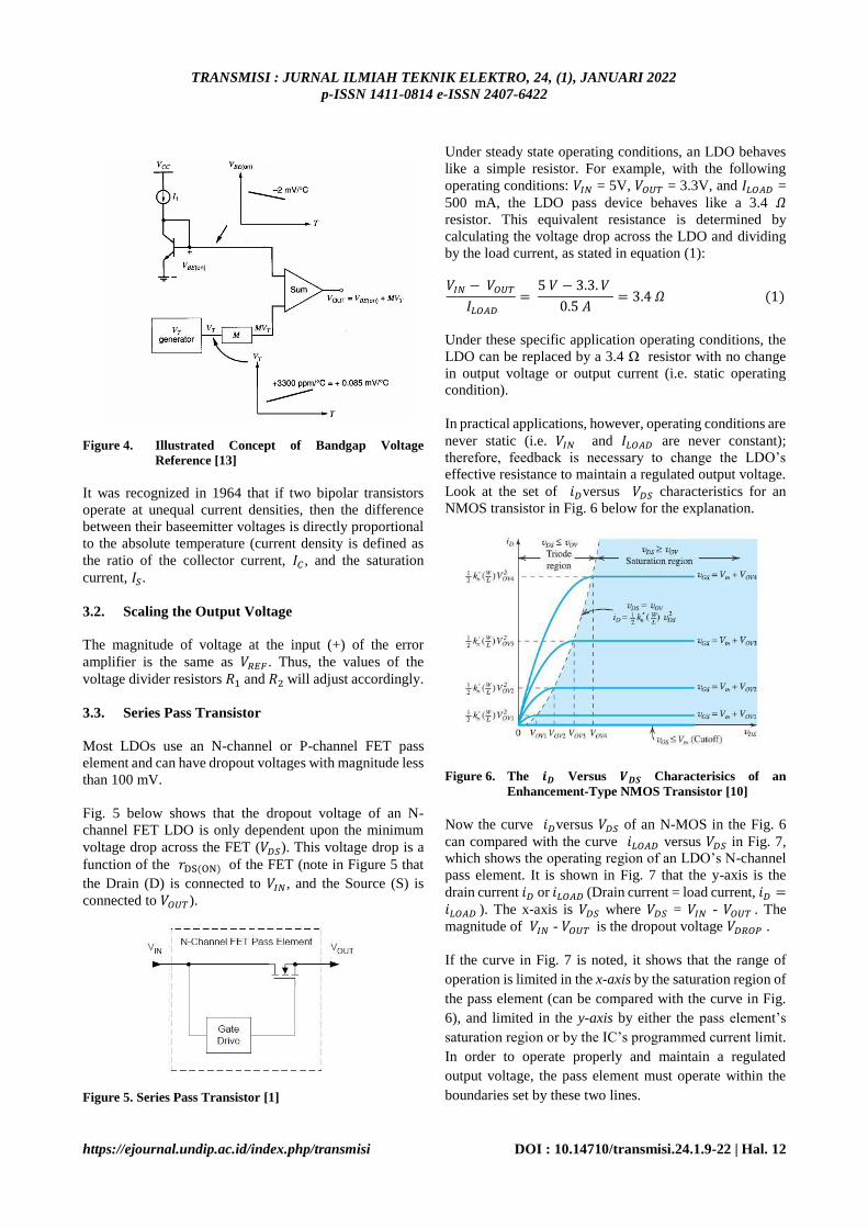
references voltage. Its concept is shown in Fig. 4 below.
The base-emitter voltage of a BJT transistor is a linear
function of the absolute temperature and exhibits a
temperature coefficient of about -2 mV/°C. If a voltage
that is a linear function of the absolute temperature and has
a positive temperature coefficient of also 2 mV/°C (i.e. +2
mV/°C) can be generated, then the variations introduced by
the base-emitter junction may be able to be compensated
for.
TRANSMISI : JURNAL ILMIAH TEKNIK ELEKTRO, 24, (1), JANUARI 2022
p-ISSN 1411-0814 e-ISSN 2407-6422
https://ejournal.undip.ac.id/index.php/transmisi DOI : 10.14710/transmisi.24.1.9-22 | Hal. 12
Figure 4. Illustrated Concept of Bandgap Voltage
Reference [13]
It was recognized in 1964 that if two bipolar transistors
operate at unequal current densities, then the difference
between their baseemitter voltages is directly proportional
to the absolute temperature (current density is defined as
the ratio of the collector current, 𝐼𝐶 , and the saturation
current, 𝐼𝑆.
3.2. Scaling the Output Voltage
The magnitude of voltage at the input (+) of the error
amplifier is the same as 𝑉𝑅𝐸𝐹 . Thus, the values of the
voltage divider resistors 𝑅1 and 𝑅2 will adjust accordingly.
3.3. Series Pass Transistor
Most LDOs use an N-channel or P-channel FET pass
element and can have dropout voltages with magnitude less
than 100 mV.
Fig. 5 below shows that the dropout voltage of an N-
channel FET LDO is only dependent upon the minimum
voltage drop across the FET (𝑉𝐷𝑆). This voltage drop is a
function of the 𝑟DS(ON) of the FET (note in Figure 5 that
the Drain (D) is connected to 𝑉𝐼𝑁, and the Source (S) is
connected to 𝑉𝑂𝑈𝑇).
Figure 5. Series Pass Transistor [1]
Under steady state operating conditions, an LDO behaves
like a simple resistor. For example, with the following
operating conditions: 𝑉𝐼𝑁 = 5V, 𝑉𝑂𝑈𝑇 = 3.3V, and 𝐼𝐿𝑂𝐴𝐷 =
500 mA, the LDO pass device behaves like a 3.4 𝛺
resistor. This equivalent resistance is determined by
calculating the voltage drop across the LDO and dividing
by the load current, as stated in equation (1):
𝑉𝐼𝑁 − 𝑉𝑂𝑈𝑇
𝐼𝐿𝑂𝐴𝐷
= 5 𝑉 − 3.3. 𝑉
0.5 𝐴= 3.4 𝛺 (1)
Under these specific application operating conditions, the
LDO can be replaced by a 3.4 Ω resistor with no change
in output voltage or output current (i.e. static operating
condition).
In practical applications, however, operating conditions are
never static (i.e. 𝑉𝐼𝑁 and 𝐼𝐿𝑂𝐴𝐷 are never constant);
therefore, feedback is necessary to change the LDO’s
effective resistance to maintain a regulated output voltage.
Look at the set of 𝑖𝐷versus 𝑉𝐷𝑆 characteristics for an
NMOS transistor in Fig. 6 below for the explanation.
Figure 6. The 𝒊𝑫 Versus 𝑽𝑫𝑺 Characterisics of an
Enhancement-Type NMOS Transistor [10]
Now the curve 𝑖𝐷versus 𝑉𝐷𝑆 of an N-MOS in the Fig. 6
can compared with the curve 𝑖𝐿𝑂𝐴𝐷 versus 𝑉𝐷𝑆 in Fig. 7,
which shows the operating region of an LDO’s N-channel
pass element. It is shown in Fig. 7 that the y-axis is the
drain current 𝑖𝐷 or 𝑖𝐿𝑂𝐴𝐷 (Drain current = load current, 𝑖𝐷 =
𝑖𝐿𝑂𝐴𝐷 ). The x-axis is 𝑉𝐷𝑆 where 𝑉𝐷𝑆 = 𝑉𝐼𝑁 - 𝑉𝑂𝑈𝑇 . The
magnitude of 𝑉𝐼𝑁 - 𝑉𝑂𝑈𝑇 is the dropout voltage 𝑉𝐷𝑅𝑂𝑃 .
If the curve in Fig. 7 is noted, it shows that the range of
operation is limited in the x-axis by the saturation region of
the pass element (can be compared with the curve in Fig.
6), and limited in the y-axis by either the pass element’s
saturation region or by the IC’s programmed current limit.
In order to operate properly and maintain a regulated
output voltage, the pass element must operate within the
boundaries set by these two lines.
TRANSMISI : JURNAL ILMIAH TEKNIK ELEKTRO, 24, (1), JANUARI 2022
p-ISSN 1411-0814 e-ISSN 2407-6422
https://ejournal.undip.ac.id/index.php/transmisi DOI : 10.14710/transmisi.24.1.9-22 | Hal. 13
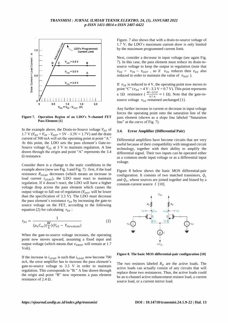
Figure 7. Operation Region of an LDO’s N-channel FET
Pass Element [1]
In the example above, the Drain-to-Source voltage 𝑉𝐷𝑆 of
1.7 V (𝑉𝐷𝑆 = 𝑉𝐼𝑁 - 𝑉𝑂𝑈𝑇 = 5V - 3.3V = 1.7V) and the drain
current of 500 mA will set the operating point at point “A.”
At this point, the LDO sets the pass element’s Gate-to-
Source voltage 𝑉𝐺𝑆 at 3 V to maintain regulation. A line
drawn through the origin and point “A” represents the 3.4
Ω resistance.
Consider there is a change to the static conditions in the
example above (now see Fig. 3 and Fig. 7) : first, if the load
resistance 𝑅𝐿𝑂𝐴𝐷 decreases (which means an increase in
load current 𝑖𝐿𝑂𝐴𝐷), the LDO must react to maintain
regulation. If it doesn’t react, the LDO will have a higher
voltage drop across the pass element which causes the
output voltage to fall out of regulation (𝑉𝑂𝑈𝑇 will be lower
than the specification of 3.3 V). The LDO must decrease
the pass element’s resistance 𝑟𝐷𝑆 by increasing the gate-to
source voltage on the FET, according to the following
equation (2) for calculating 𝑟𝐷𝑆 :
𝑟𝐷𝑆 = 1
(𝜇𝑛𝐶𝑜𝑥)(𝑊𝐿
)(𝑉𝐺𝑆 − 𝑉𝑡ℎ𝑟𝑒𝑠ℎ𝑜𝑙𝑑) (2)
When the gate-to-source voltage increases, the operating
point now moves upward, assuming a fixed input and
output voltage (which means that 𝑣𝐷𝑅𝑂𝑃 will remain at 1.7
Volt).
If the increase in 𝑖𝐿𝑂𝐴𝐷 is such that 𝑖𝐿𝑂𝐴𝐷 now become 700
mA, the error amplifier has to increase the pass element’s
gate-to-source voltage to 3.5 V in order to maintain
regulation. This corresponds to “B.” A line drawn through
the origin and point “B” now represents a pass element
resistance of 2.4 Ω .
Figure. 7 also shows that with a drain-to-source voltage of
1.7 V, the LDO’s maximum current draw is only limited
by the maximum programmed current limit.
Next, consider a decrease in input voltage (see again Fig.
7). In this case, the pass element must reduce its drain-to-
source voltage to keep the output in regulation (note that
𝑣𝐷𝑆 = 𝑣𝐼𝑁 − 𝑣𝑂𝑈𝑇 , so if 𝑣𝐼𝑁 reduces then 𝑣𝐷𝑆 also
reduced in order to maintain the value of 𝑣𝑂𝑈𝑇 ).
If 𝑣𝐼𝑁 is reduced to 4 V, the operating point now moves to
point “C” (𝑣𝐷𝑆 = 4 V - 3.3 V = 0.7 V). This point represents
a 1Ω resistance ( 4𝑉−3.3 𝑉
0.7 𝐴= 1 Ω). Note that the gate-to-
source voltage 𝑣𝐺𝑆 remained unchanged [1].
Any further increase in current or decrease in input voltage
forces the operating point onto the saturation line of the
pass element (shown as a slope line labeled “Saturation
line” at the curve of Fig. 7).
3.4. Error Amplifier (Differential Pair)
Differential amplifiers have become circuits that are very
useful because of their compatibility with integrated circuit
technology, together with their ability to amplify the
differential signal. Their two inputs can be operated either
as a common mode input voltage or as a differential input
voltage.
Figure 8 below shows the basic MOS differential-pair
configuration. It consists of two matched transistors, 𝑄1
and 𝑄2, whose sources are joined together and biased by a
constant-current source I [10].
Figure 8. The basic MOS differential-pair configuration [10]
The two resistors labeled 𝑅𝐷 are the active loads. The
active loads can actually consist of any circuits that will
replace those two resistances. Thus, the active loads could
be an n-channel active enhancement resistor load, a current
source load, or a current mirror load.

TRANSMISI : JURNAL ILMIAH TEKNIK ELEKTRO, 24, (1), JANUARI 2022
p-ISSN 1411-0814 e-ISSN 2407-6422
https://ejournal.undip.ac.id/index.php/transmisi DOI : 10.14710/transmisi.24.1.9-22 | Hal. 14
The last method (i.e. current mirror load) uses a current
mirror to form the load devices. The advantage of this
configuration is that the differential output signal is
converted to a single ended output signal with no extra
components required. The output is taken between one of
the drains and ground rather than between the two drains
and ground. Here, there is a conversion from differential to
single-ended. This differential pair configuration built here
makes use of this current mirror load configuration [9].
Shown at the bottom-middle of Fig. 8 is a constant current
source I. This part is usually implemented by a MOSFET
circuit of the type basic MOSFET constant-current source.
3.4.1. The Current-Mirror-Loaded MOS Differential
Pair
An example of a current-mirror-loaded MOS differential
pair configuration is shown in circuit diagram of Figure 9.
In that figure, the MOS differential pair is formed by
transistors 𝑄1 and 𝑄2, which is loaded by a current mirror
formed by transistors 𝑄3 and 𝑄4.
Figure 9. The current-mirror-loaded MOS differential pair
[10]
To see how this circuit operates, consider first the quiescent
or equilibrium state with the two input terminals connected
to a dc voltage equal to the common-mode equilibrium
value, in this case 0 V, as shown in Fig. 10.
Figure 10. The circuit at equilibrium assuming perfect
matching [10]
Assuming perfect matching, the bias current I divides
equally between 𝑄1 and 𝑄2. The drain current of 𝑄1, 𝐼
2 , is
fed to the input transistor of the mirror, 𝑄3. Thus, a replica
of this current is provided by the output transistor of the
mirror, 𝑄4. Observe that at the output node the two currents 𝐼
2 balance each other out, leaving a zero current to flow out
to the next stage or to a load (not shown). Further, if 𝑄4 is
perfectly matched to 𝑄3, its drain voltage will track the
voltage at the drain of 𝑄3; thus in equilibrium the voltage
at the output will be 𝑉𝐷𝐷 - 𝑉𝑆𝐺3.
An imbalance in the drain currents of 𝑄1 and 𝑄2 will cause
the output of the diff-amp to swing either towards 𝑉𝐷𝐷 or
towards ground. The minimum input common mode
voltage is given by equation (3)
𝑉𝐶𝑀_𝑀𝐼𝑁 = 𝑉𝐺𝑆1,2 + 𝑉𝐷𝑆,𝑠𝑎𝑡 (3)
where the minimum voltage across the current source is
assumed to be 𝑉𝐷𝑆,𝑠𝑎𝑡 . The maximum input common mode
voltage is determined knowing that the drain voltage of 𝑄2
is the same as the drain voltage of 𝑄1 (when both diff-amp
inputs are the same potential), that is, 𝑉𝐷𝐷 - 𝑉𝑆𝐺3 of the
PMOS. We can therefore write equation (4)
𝑉𝐷𝑆 ≥ 𝑉𝐺𝑆 − 𝑉𝑇𝐻𝑁 → 𝑉𝐷 ≥ 𝑉𝐺 − 𝑉𝑇𝐻𝑁
→ 𝑉𝐺 = 𝑉𝐷 + 𝑉𝑇𝐻𝑁 (4)
→ 𝑉𝐶𝐶_𝑀𝐴𝑋 = (𝑉𝐷𝐷 − 𝑉𝐺𝑆) + 𝑉𝑇𝐻𝑁
The voltage output swing can be determined by noting that
the magnitude of maximum output voltage is limited by
keeping 𝑄4 in saturation. Therefore, equation (5),
𝑉𝑂𝑈𝑇_𝑀𝐴𝑋 = 𝑉𝐷𝐷 − 𝑉𝑆𝐷,𝑠𝑎𝑡 (5)
The magnitude of minimum output voltage is determined
by the voltage on the gate of 𝑄2 (𝑄2 must remain in
saturation). As shown in equation (6).
𝑉𝐷 ≥ 𝑉𝐺 − 𝑉𝑇𝐻𝑁 → 𝑉𝑂𝑈𝑇 𝑀𝐼𝑁 = 𝑉𝐺2− 𝑉𝑇𝐻𝑁 (6)
4. Results of the Design
The design process for all of the building blocks of this
Low Dropout Voltage Regulator was performed by using
the Multisim Live Online Circuit Simulator.
Multisim Live Simulator allows users to take the same
simulation technology used in academic institutions and
industrial research today, and use it anywhere, anytime, on
any device.
Multisim Live offers an intuitive schematic layout
experience in a web browser. With the familiar Multisim
interface, component library and interactive features
ensures we can capture our design with no difficulty.
TRANSMISI : JURNAL ILMIAH TEKNIK ELEKTRO, 24, (1), JANUARI 2022
p-ISSN 1411-0814 e-ISSN 2407-6422
https://ejournal.undip.ac.id/index.php/transmisi DOI : 10.14710/transmisi.24.1.9-22 | Hal. 15
Schematics can be accessed on any computing or mobile
device and shared from any supported browser.
This tool also allows for testing the behavior of a circuit,
demonstrate the application of a design, or illustrate
concepts to students. With Multisim Live, we can easily
share interactive simulations with no need to install any
application software [11].
The incoming sub-sections shows the design of each of
building block of this LDO by using the Multisim Live
Simulator.
4.1. Improved Bandgap Reference Voltage
To compensate the variations introduced by the base-
emitter junction, a thermal voltage is used. Thermal voltage
(𝑉𝑇) given by the following equation is a linear function of
the absolute temperature, equation (7):
𝑉𝑇 = 𝑘𝑇
𝑞 (7)
where k is the Boltzmann constant, q is the charge carried
by a single electron, and T is temperature in Kelvin. Thus,
temperature coefficient of the thermal voltage 𝑘
𝑞 is of
magnitude ≅ +0.085 𝑚𝑉
°𝐶 . This temperature coefficient is
positive but it is much less than the desired value of +2 𝑚𝑉
°𝐶.
To solve this problem, the temperature coefficient of
thermal voltage 𝑘
𝑞 was amplified by a temperature
independent constant 𝑀 such that 𝑀𝑘
𝑞 is equal to about 2
𝑚𝑉
°𝐶 . The temperature independent constant needed is
therefore 2 𝑚𝑉
0:085 mV= 23.5.
In Fig. 4, it is shown that the thermal voltage is produced
by a“𝑉𝑇 generator” block. When the output of the thermal
voltage 𝑉𝑇 is multiplied by temperature independent
constant 𝑀 and then added to the 𝑉BE(on), a reference
voltage 𝑉𝑅𝐸𝐹 is obtained given by the following
expression (8):
𝑉𝑅𝐸𝐹 = 𝑉𝐵𝐸 (𝑜𝑛) + 𝑀𝑉𝑇 (8)
At ambient room temperature of 300 °K, equation (8) will
produce a reference voltage of 1.26 V assuming 𝑉𝐵𝐸 (𝑜𝑛) is
0.65 V. That is, 1.26 V ≅ 0.65 + 23.5(0.000085 ×300) 𝑉.
Practical realizations of band-gap references in bipolar
technologies can take on several forms. One form is
illustrated in Fig. 11. It is a self-biased band-gap reference
circuit. This improved band-gap is developed using an op-
amp. The advantage of the op-amp is to remove the
dependence of the currents upon the power supply. The
method by which this is done is to force the relationship
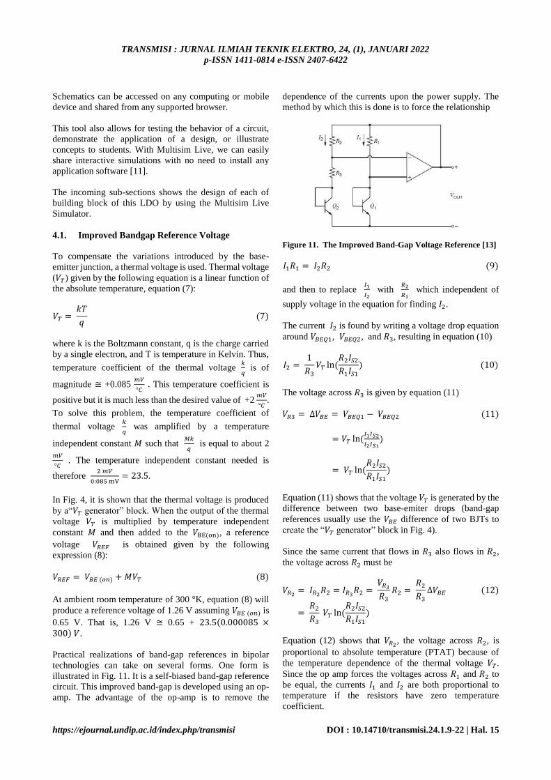
Figure 11. The Improved Band-Gap Voltage Reference [13]
𝐼1𝑅1 = 𝐼2𝑅2 (9)
and then to replace 𝐼1
𝐼2 with
𝑅2
𝑅1 which independent of
supply voltage in the equation for finding 𝐼2.
The current 𝐼2 is found by writing a voltage drop equation
around 𝑉𝐵𝐸𝑄1, 𝑉𝐵𝐸𝑄2, and 𝑅3, resulting in equation (10)
𝐼2 = 1
𝑅3
𝑉𝑇 ln(𝑅2𝐼𝑆2
𝑅1𝐼𝑆1
) (10)
The voltage across 𝑅3 is given by equation (11)
𝑉𝑅3 = ∆𝑉𝐵𝐸 = 𝑉𝐵𝐸𝑄1 − 𝑉𝐵𝐸𝑄2 (11)
= 𝑉𝑇 ln(𝐼1𝐼𝑆2
𝐼2𝐼𝑆1)
= 𝑉𝑇 ln(𝑅2𝐼𝑆2
𝑅1𝐼𝑆1
)
Equation (11) shows that the voltage 𝑉𝑇 is generated by the
difference between two base-emiter drops (band-gap
references usually use the 𝑉𝐵𝐸 difference of two BJTs to
create the “𝑉𝑇 generator” block in Fig. 4).
Since the same current that flows in 𝑅3 also flows in 𝑅2,
the voltage across 𝑅2 must be
𝑉𝑅2= 𝐼𝑅2
𝑅2 = 𝐼𝑅3𝑅2 =
𝑉𝑅3
𝑅3
𝑅2 = 𝑅2
𝑅3
∆𝑉𝐵𝐸 (12)
= 𝑅2
𝑅3
𝑉𝑇 ln(𝑅2𝐼𝑆2
𝑅1𝐼𝑆1
)
Equation (12) shows that 𝑉𝑅2, the voltage across 𝑅2, is
proportional to absolute temperature (PTAT) because of
the temperature dependence of the thermal voltage 𝑉𝑇.
Since the op amp forces the voltages across 𝑅1 and 𝑅2 to
be equal, the currents 𝐼1 and 𝐼2 are both proportional to
temperature if the resistors have zero temperature
coefficient.
TRANSMISI : JURNAL ILMIAH TEKNIK ELEKTRO, 24, (1), JANUARI 2022
p-ISSN 1411-0814 e-ISSN 2407-6422
https://ejournal.undip.ac.id/index.php/transmisi DOI : 10.14710/transmisi.24.1.9-22 | Hal. 16
Now, the output voltage (the reference voltage) is the sum
of the voltage across 𝑄2, 𝑅3, and 𝑅2:
𝑉𝑂𝑈𝑇 = 𝑉𝑅𝐸𝐹 = 𝑉𝐵𝐸𝑄2 + 𝑉𝑅3+ 𝑉𝑅2
(13)
= 𝑉𝐵𝐸𝑄2 + ∆𝑉𝐵𝐸 + 𝑅2
𝑅3
∆𝑉𝐵𝐸
= 𝑉𝐵𝐸𝑄2 + (1 +𝑅2
𝑅3
) ∆𝑉𝐵𝐸
= 𝑉𝐵𝐸𝑄2 + (1 +𝑅2
𝑅3
) 𝑉𝑇 ln(𝑅2𝐼𝑆2
𝑅1𝐼𝑆1
)
= 𝑉𝐵𝐸𝑄2 + (1 +𝑅2
𝑅3
) ln(𝑅2𝐼𝑆2
𝑅1𝐼𝑆1
)𝑉𝑇
= 𝑉𝐵𝐸𝑄2 + 𝑀𝑉𝑇
Equation (13) is in the same form as (8). The circuit thus
behaves as a band-gap reference, with the value of 𝑀 set
by the ratios of 𝑅2
𝑅3,
𝑅2
𝑅1, and
𝐼𝑆2
𝐼𝑆1 .
The areas of the emitters of transistors 𝑄1 and 𝑄2 are used
to scale the argument of the algorithm. For example, if
Area𝐸𝑚𝑖𝑡𝑡𝑒𝑟𝑄2= 10Area𝐸𝑚𝑖𝑡𝑡𝑒𝑟𝑄1
, then 𝐼𝑆2 = 10𝐼𝑆1 and
for zero temperature coefficient we find that 𝑅2
𝑅3= 10.2 if
𝑅2
𝑅1= 1.
Figure 12. Result of the Improved Band-gap Voltage
Reference
The design result of the Improved Band-gap Voltage
Reference is shown in Fig. 12 above. Resistors with values
of 𝑅2 = 𝑅1 = 10.2 kΩ and 𝑅3 = 1 kΩ are used. It is shown
in those figure the magnitude of the currents that pass
through 𝑅2 dan 𝑅1, and also the voltage 𝑉𝑅𝐸𝐹 produced. A
voltage 𝑉𝑅𝐸𝐹 of approximately 1.30 V is produced. This
𝑉𝑅𝐸𝐹 is the voltage that will be fed to the input (+) of the
error amplifier (see Fig. 3).
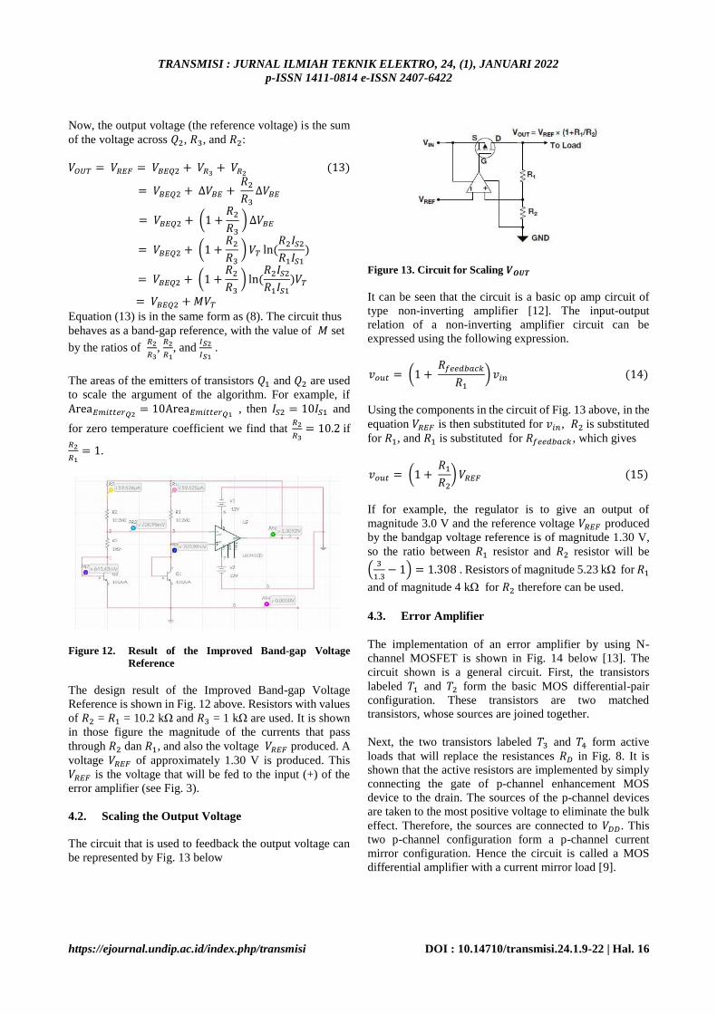
4.2. Scaling the Output Voltage
The circuit that is used to feedback the output voltage can
be represented by Fig. 13 below
Figure 13. Circuit for Scaling 𝑽𝑶𝑼𝑻
It can be seen that the circuit is a basic op amp circuit of
type non-inverting amplifier [12]. The input-output
relation of a non-inverting amplifier circuit can be
expressed using the following expression.
𝑣𝑜𝑢𝑡 = (1 + 𝑅𝑓𝑒𝑒𝑑𝑏𝑎𝑐𝑘
𝑅1
) 𝑣𝑖𝑛 (14)
Using the components in the circuit of Fig. 13 above, in the
equation 𝑉𝑅𝐸𝐹 is then substituted for 𝑣𝑖𝑛, 𝑅2 is substituted
for 𝑅1, and 𝑅1 is substituted for 𝑅𝑓𝑒𝑒𝑑𝑏𝑎𝑐𝑘 , which gives
𝑣𝑜𝑢𝑡 = (1 + 𝑅1
𝑅2
) 𝑉𝑅𝐸𝐹 (15)
If for example, the regulator is to give an output of
magnitude 3.0 V and the reference voltage 𝑉𝑅𝐸𝐹 produced
by the bandgap voltage reference is of magnitude 1.30 V,
so the ratio between 𝑅1 resistor and 𝑅2 resistor will be
(3
1.3− 1) = 1.308 . Resistors of magnitude 5.23 kΩ for 𝑅1
and of magnitude 4 kΩ for 𝑅2 therefore can be used.
4.3. Error Amplifier
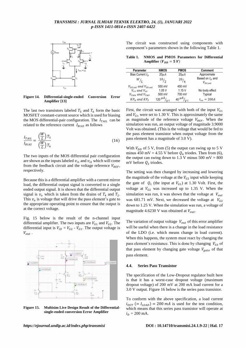
The implementation of an error amplifier by using N-
channel MOSFET is shown in Fig. 14 below [13]. The
circuit shown is a general circuit. First, the transistors
labeled 𝑇1 and 𝑇2 form the basic MOS differential-pair
configuration. These transistors are two matched
transistors, whose sources are joined together.
Next, the two transistors labeled 𝑇3 and 𝑇4 form active
loads that will replace the resistances 𝑅𝐷 in Fig. 8. It is
shown that the active resistors are implemented by simply
connecting the gate of p-channel enhancement MOS
device to the drain. The sources of the p-channel devices
are taken to the most positive voltage to eliminate the bulk
effect. Therefore, the sources are connected to 𝑉𝐷𝐷. This
two p-channel configuration form a p-channel current
mirror configuration. Hence the circuit is called a MOS
differential amplifier with a current mirror load [9].
TRANSMISI : JURNAL ILMIAH TEKNIK ELEKTRO, 24, (1), JANUARI 2022
p-ISSN 1411-0814 e-ISSN 2407-6422
https://ejournal.undip.ac.id/index.php/transmisi DOI : 10.14710/transmisi.24.1.9-22 | Hal. 17
Figure 14. Differential-single-ended Conversion Error
Amplifier [13]
The last two transistors labeled 𝑇5 and 𝑇6 form the basic
MOSFET constant-current source which is used for biasing
the MOS differential-pair configuration. The 𝐼𝑇𝐴𝐼𝐿 can be
related to the reference current 𝐼𝐵𝐼𝐴𝑆 as follows
𝐼𝑇𝐴𝐼𝐿
𝐼𝐵𝐼𝐴𝑆
= (
𝑊𝐿
) 𝑇5
(𝑊𝐿
) 𝑇6
(16)
The two inputs of the MOS differential pair configuration
are shown as the inputs labeled 𝑣𝑖1 and 𝑣𝑖2 which will come
from the feedback circuit and the voltage reference 𝑉𝑅𝐸𝐹 ,
respectively.
Because this is a differential amplifier with a current mirror
load, the differential output signal is converted to a single
ended output signal. It is shown that the differential output
signal is 𝑣𝑜 which is taken from the drains of 𝑇4 and 𝑇2.
This 𝑣𝑜 is voltage that will drive the pass element’s gate to
the appropriate operating point to ensure that the output is
at the correct voltage.
Fig. 15 below is the result of the n-channel input
differential amplifier. The two inputs are 𝑉𝐺1 and 𝑉𝐺2. The
differential input is 𝑉𝐼𝐷 = 𝑉𝐺2 - 𝑉𝐺1. The output voltage is
𝑉𝑜𝑢𝑡 .
Figure 15. Multisim Live Design Result of the Differential-
single-ended conversion Error Amplifier
The circuit was constructed using components with
component’s parameters shown in the following Table 1.
Table 1. NMOS and PMOS Parameters for Differential
Amplifier (𝑽𝑫𝑫 = 𝟓 𝑽)
Parameter NMOS PMOS Comment
Bias Current 𝐼𝐷 20𝜇𝐴 20𝜇𝐴 Approximate
𝑊𝐿⁄ 10
2⁄ 204⁄
Based on 𝐼𝐷 and 𝑉𝐷𝑆,𝑠𝑎𝑡
𝑉𝐷𝑆,𝑠𝑎𝑡 𝑎𝑛𝑑 𝑉𝑆𝐷,𝑠𝑎𝑡 550 mV 450 mV
𝑉𝐺𝑆 𝑎𝑛𝑑 𝑉𝑆𝐺 1.05 V 1.15 V No body effect
𝑉𝑇𝐻𝑁 𝑎𝑛𝑑 𝑉𝑇𝐻𝑃 500 mV 700 mV Typical
𝐾𝑃𝑁 𝑎𝑛𝑑 𝐾𝑃𝑃 120 𝜇𝐴
𝑉2⁄ 40 𝜇𝐴
𝑉2⁄ 𝑡𝑜𝑥 = 200𝐴
First, the circuit was arranged with both of the input 𝑉𝐺1
and 𝑉𝐺1 were set to 1.30 V. This is approximately the same
as magnitude of the reference voltage 𝑉𝑅𝐸𝐹 . When the
simulation was run, an output voltage of magnitude 3.9000
Volt was obtained. (This is the voltage that would be fed to
the pass element transistor when output voltage from the
pass element has a magnitude of 3.0 V).
With 𝑉𝐷𝐷 of 5 V, from (5) the output can swing up to 5 V
minus 450 mV = 4.55 V before 𝑄4 triodes. Then from (6),
the output can swing down to 1.3 V minus 500 mV = 800
mV before 𝑄2 triodes.
The setting was then changed by increasing and lowering
the magnitude of the voltage at the 𝑉𝐺2 input while keeping
the gate of 𝑄1 (the input at 𝑉𝐺1) at 1.30 Volt. First, the
voltage at 𝑉𝐺2 was increased up to 1.35 V. When the
simulation was run, it was shown that the voltage at 𝑉𝑜𝑢𝑡
was 681.71 mV. Next, we decreased the voltage at 𝑉𝐺2
down to 1.25 V. When the simulation was run, a voltage of
magnitude 4.6230 V was obtained at 𝑉𝑜𝑢𝑡.
The variation of output voltage 𝑉𝑜𝑢𝑡 of this error amplifier
will be useful when there is a change in the load resistance
of the LDO (i.e. which means change in load current).
When this happens, the system must react by changing the
pass element’s resistance. This is done by changing 𝑉𝐺𝑆 of
that pass element by changing gate voltage 𝑉𝑔𝑎𝑡𝑒 of that
pass element.
4.4. Series Pass Transistor
The specification of the Low-Dropout regulator built here
is that it has a worst-case dropout voltage (maximum
dropout voltage) of 200 mV at 200 mA load current for a
3.0 V output. Figure 16 below is the series pass transistor.
To conform with the above specification, a load current
𝑖𝑂𝑈𝑇 (= 𝐼𝐿𝑂𝐴𝐷) = 200 𝑚𝐴 is used for the test condition,
which means that this series pass transistor will operate at
𝑖𝐷 = 200 mA.
TRANSMISI : JURNAL ILMIAH TEKNIK ELEKTRO, 24, (1), JANUARI 2022
p-ISSN 1411-0814 e-ISSN 2407-6422
https://ejournal.undip.ac.id/index.php/transmisi DOI : 10.14710/transmisi.24.1.9-22 | Hal. 18
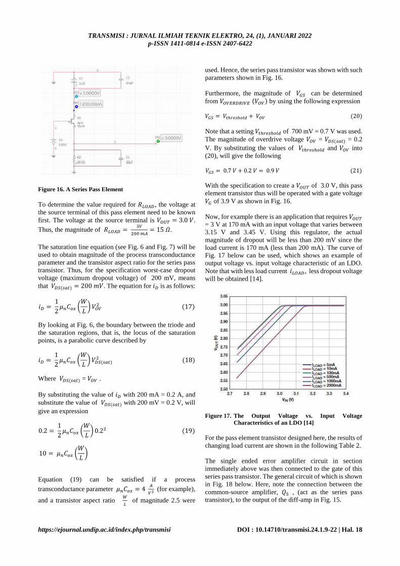
Figure 16. A Series Pass Element
To determine the value required for 𝑅𝐿𝑂𝐴𝐷 , the voltage at
the source terminal of this pass element need to be known
first. The voltage at the source terminal is 𝑉𝑂𝑈𝑇 = 3.0 𝑉.
Thus, the magnitude of 𝑅𝐿𝑂𝐴𝐷 = 3𝑉
200 𝑚𝐴= 15 𝛺.
The saturation line equation (see Fig. 6 and Fig. 7) will be
used to obtain magnitude of the process transconductance
parameter and the transistor aspect ratio for the series pass
transistor. Thus, for the specification worst-case dropout
voltage (maximum dropout voltage) of 200 mV, means
that 𝑉𝐷𝑆(𝑠𝑎𝑡) = 200 𝑚𝑉. The equation for 𝑖𝐷 is as follows:
𝑖𝐷 = 1
2𝜇𝑛𝐶𝑜𝑥 (
𝑊
𝐿) 𝑉𝑂𝑉
2 (17)
By looking at Fig. 6, the boundary between the triode and
the saturation regions, that is, the locus of the saturation
points, is a parabolic curve described by
𝑖𝐷 = 1
2𝜇𝑛𝐶𝑜𝑥 (
𝑊
𝐿) 𝑉𝐷𝑆(𝑠𝑎𝑡)
2 (18)
Where 𝑉𝐷𝑆(𝑠𝑎𝑡) = 𝑉𝑂𝑉 .
By substituting the value of 𝑖𝐷 with 200 mA = 0.2 A, and
substitute the value of 𝑉𝐷𝑆(𝑠𝑎𝑡) with 200 mV = 0.2 V, will
give an expression
0.2 = 1
2𝜇𝑛𝐶𝑜𝑥 (
𝑊
𝐿) 0.22 (19)
10 = 𝜇𝑛𝐶𝑜𝑥 (𝑊
𝐿)
Equation (19) can be satisfied if a process
transconductance parameter 𝜇𝑛𝐶𝑜𝑥 = 4 𝐴
𝑉2 (for example),
and a transistor aspect ratio 𝑊
𝐿 of magnitude 2.5 were
used. Hence, the series pass transistor was shown with such
parameters shown in Fig. 16.
Furthermore, the magnitude of 𝑉𝐺𝑆 can be determined
from 𝑉𝑂𝑉𝐸𝑅𝐷𝑅𝐼𝑉𝐸 (𝑉𝑂𝑉) by using the following expression 𝑉𝐺𝑆 = 𝑉𝑡ℎ𝑟𝑒𝑠ℎ𝑜𝑙𝑑 + 𝑉𝑂𝑉 (20)
Note that a setting 𝑉𝑡ℎ𝑟𝑒𝑠ℎ𝑜𝑙𝑑 of 700 mV = 0.7 V was used.
The magnitude of overdrive voltage 𝑉𝑂𝑉 = 𝑉𝐷𝑆(𝑠𝑎𝑡) = 0.2
V. By substituting the values of 𝑉𝑡ℎ𝑟𝑒𝑠ℎ𝑜𝑙𝑑 and 𝑉𝑂𝑉 into
(20), will give the following 𝑉𝐺𝑆 = 0.7 𝑉 + 0.2 𝑉 = 0.9 𝑉 (21)
With the specification to create a 𝑉𝑂𝑈𝑇 of 3.0 V, this pass
element transistor thus will be operated with a gate voltage
𝑉𝐺 of 3.9 V as shown in Fig. 16.
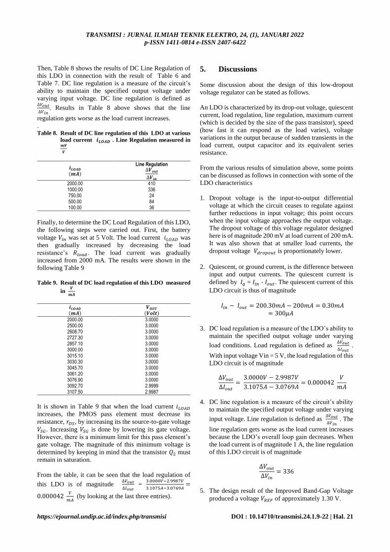
Now, for example there is an application that requires 𝑉𝑂𝑈𝑇
= 3 V at 170 mA with an input voltage that varies between
3.15 V and 3.45 V. Using this regulator, the actual
magnitude of dropout will be less than 200 mV since the
load current is 170 mA (less than 200 mA). The curve of
Fig. 17 below can be used, which shows an example of
output voltage vs. input voltage characteristic of an LDO.
Note that with less load current 𝑖𝐿𝑂𝐴𝐷, less dropout voltage
will be obtained [14].
Figure 17. The Output Voltage vs. Input Voltage
Characteristics of an LDO [14]
For the pass element transistor designed here, the results of
changing load current are shown in the following Table 2.
The single ended error amplifier circuit in section
immediately above was then connected to the gate of this
series pass transistor. The general circuit of which is shown
in Fig. 18 below. Here, note the connection between the
common-source amplifier, 𝑄5 , (act as the series pass
transistor), to the output of the diff-amp in Fig. 15.
TRANSMISI : JURNAL ILMIAH TEKNIK ELEKTRO, 24, (1), JANUARI 2022
p-ISSN 1411-0814 e-ISSN 2407-6422
https://ejournal.undip.ac.id/index.php/transmisi DOI : 10.14710/transmisi.24.1.9-22 | Hal. 19
Table 2. Results Obtained for Various Load Current 𝑰𝑳𝑶𝑨𝑫
passing through the Pass Element
𝐼𝐿𝑂𝐴𝐷(𝑚𝐴)
𝑉𝑜𝑢𝑡 (𝑉𝑜𝑙𝑡)
𝑉𝒊𝒏 𝒎𝒊𝒏𝒊𝒎𝒖𝒎 (𝑉𝑜𝑙𝑡)
𝑉𝑑𝑟𝑜𝑝𝑜𝑢𝑡
(𝑚𝑉)
𝑉𝐺𝑎𝑡𝑒 (𝑉𝑜𝑙𝑡)
200.00 3.0000 3.2000 200.0 3.90 176.59 3.0021 3.1900 187.9 3.89 150.33 3.0066 3.1800 173.4 3.88 125.08 3.0018 3.1600 158.2 3.86 98.673 3.0095 3.1500 140.5 3.85
When the inputs to the diff-amp are at the same potential,
the currents that flow in 𝑄3 and 𝑄4 are equal (= 𝐼1
2 ). The
drain of 𝑄3 is then at the same potential as its gate. This
means, for biasing purposes, that the gate of 𝑄5 can be
treated as if it were tied to the gate of 𝑄4 (𝑄3). Thus, 𝑄5
are now being biased from the Current Mirror Load [15].
In this design, a 𝑉𝑡ℎ𝑟𝑒𝑠ℎ𝑜𝑙𝑑 setting of 0.3 Volt was used for
the pass element.
Figure 18. Using an Error Amplifier to Bias a Next Stage
Circuit
The overall design result of this connection between the
error amplifier and the transistor pass element can be seen
at Fig. 19. It is shown in those figure, the pass element was
set with channel width W = 10 𝜇𝑚 and channel length L =
4𝜇𝑚, so resulting in a transistor aspect ratio 𝑊
𝐿 = 2.5.
At the simulation, the following results were obtained. At
the beginning, when the load in series with the series pass
transistor was of magnitude 15.0 Ω, a load current of 200
mA was obtained, and the voltage at the source terminal of
the series pass transistor was of magnitude 3.0000 V. At
the gate of the pass transistor, a voltage of 3.9001 V was
obtained. The gate to source voltage 𝑉𝐺𝑆 is equal to 0.9001
V.
Next, consider there is a change to the static operating
condition when there is a decreasing load resistance (i.e.
which mean an increase in load current). For example,
when the series load was changed to 10 Ω, a load current
of 300 mA was obtained (not 200 mA anymore). The
voltage at the gate terminal of the pass transistor is now
3.9451 V. This new gate’s voltage maintains the voltage at
the source terminal of the pass transistor at 3.0 V. The gate
to source voltage 𝑉𝐺𝑆 is now increase to 0.9451 Volt.
Figure 19. Series Pass Transistor Biased with an Error
Amplifier
The same also applies when the load resistance increases.
For example, when the series load resistance was changed
to 20 Ω, a load current of 150.00 mA was obtained. The
voltage at the gate terminal of the pass transistor is now
3.8734 V. This new gate’s voltage maintains the voltage at
the source terminal of the pass transistor at 3.0 V. The gate
to source voltage 𝑉𝐺𝑆 is now decrease to 0.8734 Volt. For
the other results obtained for varying the load current are
tabulated in Table 3.
Table 3. Results Obtained at Pass Transistor’s Terminals
for Various Load Current 𝑰𝑳𝑶𝑨𝑫
𝐼𝐿𝑂𝐴𝐷(𝑚𝐴)
𝑉𝐺𝑎𝑡𝑒(𝑉𝑜𝑙𝑡)
𝑉𝑺𝒐𝒖𝒓𝒄𝒆 (𝑉𝑜𝑙𝑡)
𝑉𝐺𝑆 (𝑉𝑜𝑙𝑡)
600.00 4.0465 3.0000 1046.5 300.00 3.9451 3.0000 945.1 200.00 3.9002 3.0000 900.2 150.00 3.8734 3.0000 873.4 120.00 3.8551 3.0000 855.1 100.00 3.8416 3.0000 841.6 50.00 3.8003 3.0000 800.3
Now, consider a decrease in input voltage 𝑉𝐼𝑁. This time,
the pass element transistor must reduce its drain-to-source
voltage 𝑉𝐷𝑆 in order to keep the output stay in regulation.
Consider first when the load current 𝐼𝑙𝑜𝑎𝑑 is at magnitude
200 mA. The experiment was started with 𝑉𝐼𝑁 of 6 V and
then slowly reduce it. It turns out that the load current
remains at 200 mA and the output remains at 3.0000 V,
until 𝑉𝐼𝑁 reach 4.30 V. When 𝑉𝐼𝑁 is less than 4.30 V, the
load current and the output voltage begin to drop. Next,
other magnitude of the load current (less load current) were
used and different results were obtained. The results of
reducing 𝑉𝐼𝑁 at various load currents were tabulated in
Table 4.
TRANSMISI : JURNAL ILMIAH TEKNIK ELEKTRO, 24, (1), JANUARI 2022
p-ISSN 1411-0814 e-ISSN 2407-6422
https://ejournal.undip.ac.id/index.php/transmisi DOI : 10.14710/transmisi.24.1.9-22 | Hal. 20
Table 4. Results of Reducing Battery Voltage 𝑽𝒊𝒏 at Various
Load Current 𝑰𝑳𝑶𝑨𝑫
𝑰𝑳𝑶𝑨𝑫(𝒎𝑨)
𝑽𝒐𝒖𝒕 (𝑽𝒐𝒍𝒕)
𝑽𝒊𝒏 𝒎𝒊𝒏𝒊𝒎𝒖𝒎 (𝑽𝒐𝒍𝒕)
𝑽𝒅𝒓𝒐𝒑𝒐𝒖𝒕
(𝑽𝒐𝒍𝒕)
𝑽𝑮𝑺 (𝑽𝒐𝒍𝒕)
200.00 3.0000 4.30 1.30 3.90 150.00 3.0000 4.27 1.27 3.87 100.00 3.0000 4.24 1.24 3.84 50.00 3.0000 4.20 1.20 3.80
With the NMOS pass element transistor, as 𝑉𝑖𝑛 approaches
𝑉𝑜𝑢𝑡(𝑛𝑜𝑚𝑖𝑛𝑎𝑙) the error amplifier will increase 𝑉𝐺𝑆 in order
to lower the 𝑟𝐷𝑆 and maintain regulation. This presents a
problem though, because as 𝑉𝑖𝑛 continues to approaches
𝑉𝑜𝑢𝑡(𝑛𝑜𝑚𝑖𝑛𝑎𝑙), the output voltage from error amplifier (i.e.
the gate voltage of the pass transistor, 𝑉𝐺𝑎𝑡𝑒) will also
decrease, instead of increase. This is because the PMOS
transistor of error-amplifier, 𝑄4, will saturate (remember
that 𝑉𝑆𝐷(𝑠𝑎𝑡) of those 𝑄4 is 450 mV). This prevents ultra-
low dropout.
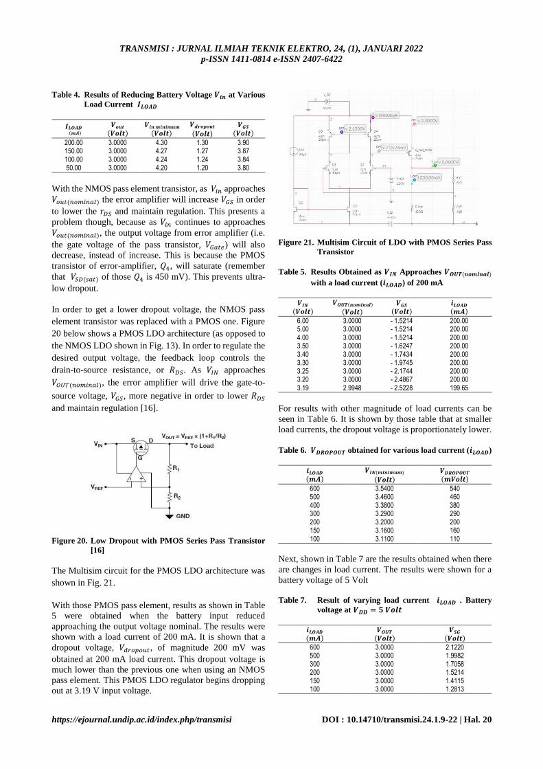
In order to get a lower dropout voltage, the NMOS pass
element transistor was replaced with a PMOS one. Figure
20 below shows a PMOS LDO architecture (as opposed to
the NMOS LDO shown in Fig. 13). In order to regulate the
desired output voltage, the feedback loop controls the
drain-to-source resistance, or 𝑅𝐷𝑆. As 𝑉𝐼𝑁 approaches
𝑉𝑂𝑈𝑇(𝑛𝑜𝑚𝑖𝑛𝑎𝑙), the error amplifier will drive the gate-to-
source voltage, 𝑉𝐺𝑆, more negative in order to lower 𝑅𝐷𝑆
and maintain regulation [16].
Figure 20. Low Dropout with PMOS Series Pass Transistor
[16]
The Multisim circuit for the PMOS LDO architecture was
shown in Fig. 21.
With those PMOS pass element, results as shown in Table
5 were obtained when the battery input reduced
approaching the output voltage nominal. The results were
shown with a load current of 200 mA. It is shown that a
dropout voltage, 𝑉𝑑𝑟𝑜𝑝𝑜𝑢𝑡, of magnitude 200 mV was
obtained at 200 mA load current. This dropout voltage is
much lower than the previous one when using an NMOS
pass element. This PMOS LDO regulator begins dropping
out at 3.19 V input voltage.
Figure 21. Multisim Circuit of LDO with PMOS Series Pass
Transistor
Table 5. Results Obtained as 𝑽𝑰𝑵 Approaches 𝑽𝑶𝑼𝑻(𝒏𝒐𝒎𝒊𝒏𝒂𝒍)
with a load current (𝒊𝑳𝑶𝑨𝑫) of 200 mA
𝑽𝑰𝑵
(𝑽𝒐𝒍𝒕)
𝑽𝑶𝑼𝑻(𝒏𝒐𝒎𝒊𝒏𝒂𝒍)
(𝑽𝒐𝒍𝒕)
𝑽𝑮𝑺 (𝑽𝒐𝒍𝒕)
𝒊𝑳𝑶𝑨𝑫 (𝒎𝑨)
6.00 3.0000 - 1.5214 200.00 5.00 3.0000 - 1.5214 200.00 4.00 3.0000 - 1.5214 200.00 3.50 3.0000 - 1.6247 200.00 3.40 3.0000 - 1.7434 200.00 3.30 3.0000 - 1.9745 200.00 3.25 3.0000 - 2.1744 200.00 3.20 3.0000 - 2.4867 200.00 3.19 2.9948 - 2.5228 199.65
For results with other magnitude of load currents can be
seen in Table 6. It is shown by those table that at smaller
load currents, the dropout voltage is proportionately lower.
Table 6. 𝑽𝑫𝑹𝑶𝑷𝑶𝑼𝑻 obtained for various load current (𝒊𝑳𝑶𝑨𝑫)
𝒊𝑳𝑶𝑨𝑫 (𝒎𝑨)
𝑽𝑰𝑵(𝒎𝒊𝒏𝒊𝒎𝒖𝒎)
(𝑽𝒐𝒍𝒕)
𝑽𝑫𝑹𝑶𝑷𝑶𝑼𝑻 (𝒎𝑽𝒐𝒍𝒕)
600 3.5400 540 500 3.4600 460 400 3.3800 380 300 3.2900 290 200 3.2000 200 150 3.1600 160 100 3.1100 110
Next, shown in Table 7 are the results obtained when there
are changes in load current. The results were shown for a
battery voltage of 5 Volt Table 7. Result of varying load current 𝒊𝑳𝑶𝑨𝑫 . Battery
voltage at 𝑽𝑫𝑫 = 𝟓 𝑽𝒐𝒍𝒕
𝒊𝑳𝑶𝑨𝑫 (𝒎𝑨)
𝑽𝑶𝑼𝑻 (𝑽𝒐𝒍𝒕)
𝑽𝑺𝑮 (𝑽𝒐𝒍𝒕)
600 3.0000 2.1220 500 3.0000 1.9982 300 3.0000 1.7058 200 3.0000 1.5214 150 3.0000 1.4115 100 3.0000 1.2813
TRANSMISI : JURNAL ILMIAH TEKNIK ELEKTRO, 24, (1), JANUARI 2022
p-ISSN 1411-0814 e-ISSN 2407-6422
https://ejournal.undip.ac.id/index.php/transmisi DOI : 10.14710/transmisi.24.1.9-22 | Hal. 21
Then, Table 8 shows the results of DC Line Regulation of
this LDO in connection with the result of Table 6 and
Table 7. DC line regulation is a measure of the circuit’s
ability to maintain the specified output voltage under
varying input voltage. DC line regulation is defined as ∆𝑉𝑜𝑢𝑡
∆𝑉𝑖𝑛. Results in Table 8 above shows that the line
regulation gets worse as the load current increases.
. Table 8. Result of DC line regulation of this LDO at various
load current 𝒊𝑳𝑶𝑨𝑫 . Line Regulation measured in 𝒎𝑽
𝑽
𝒊𝑳𝑶𝑨𝑫 (𝒎𝑨)
Line Regulation ∆𝑽𝒐𝒖𝒕
∆𝑽𝒊𝒏
2000.00 410 1000.00 336 750.00 24 500.00 84 100.00 36
Finally, to determine the DC Load Regulation of this LDO,
the following steps were carried out. First, the battery
voltage 𝑉𝑖𝑛 was set at 5 Volt. The load current 𝑖𝐿𝑂𝐴𝐷 was
then gradually increased by decreasing the load
resistance’s 𝑅𝑙𝑜𝑎𝑑 . The load current was gradually
increased from 2000 mA. The results were shown in the
following Table 9
Table 9. Result of DC load regulation of this LDO measured
in 𝑽
𝒎𝑨
𝒊𝑳𝑶𝑨𝑫 (𝒎𝑨)
𝑽𝑶𝑼𝑻 (𝑽𝒐𝒍𝒕)
2000.00 3.0000 2500.00 3.0000 2608.70 3.0000 2727.30 3.0000 2857.10 3.0000 3000.00 3.0000 3015.10 3.0000 3030.30 3.0000 3045.70 3.0000 3061.20 3.0000 3076.90 3.0000 3092.70 2.9999 3107.50 2.9987
It is shown in Table 9 that when the load current 𝑖𝐿𝑂𝐴𝐷
increases, the PMOS pass element must decrease its
resistance, 𝑟𝐷𝑆, by increasing its the source-to-gate voltage
𝑉𝑆𝐺. Increasing 𝑉𝑆𝐺 is done by lowering its gate voltage.
However, there is a minimum limit for this pass element’s
gate voltage. The magnitude of this minimum voltage is
determined by keeping in mind that the transistor 𝑄2 must
remain in saturation.
From the table, it can be seen that the load regulation of
this LDO is of magnitude ∆𝑉𝑜𝑢𝑡
∆𝐼𝑜𝑢𝑡 =
3.0000𝑉−2.9987𝑉
3.1075𝐴−3.0769𝐴=
0.000042 𝑉
𝑚𝐴 (by looking at the last three entries).
5. Discussions
Some discussion about the design of this low-dropout
voltage regulator can be stated as follows.
An LDO is characterized by its drop-out voltage, quiescent
current, load regulation, line regulation, maximum current
(which is decided by the size of the pass transistor), speed
(how fast it can respond as the load varies), voltage
variations in the output because of sudden transients in the
load current, output capacitor and its equivalent series
resistance.
From the various results of simulation above, some points
can be discussed as follows in connection with some of the
LDO characteristics
1. Dropout voltage is the input-to-output differential
voltage at which the circuit ceases to regulate against
further reductions in input voltage; this point occurs
when the input voltage approaches the output voltage.
The dropout voltage of this voltage regulator designed
here is of magnitude 200 mV at load current of 200 mA.
It was also shown that at smaller load currents, the
dropout voltage 𝑉𝑑𝑟𝑜𝑝𝑜𝑢𝑡 is proportionately lower.
2. Quiescent, or ground current, is the difference between
input and output currents. The quiescent current is
defined by 𝐼𝑞 = 𝐼𝑖𝑛 - 𝐼𝑜𝑢𝑡 . The quiescent current of this
LDO circuit is thus of magnitude
𝐼𝑖𝑛 − 𝐼𝑜𝑢𝑡 = 200.30𝑚𝐴 − 200𝑚𝐴 = 0.30𝑚𝐴= 300𝜇𝐴
3. DC load regulation is a measure of the LDO’s ability to
maintain the specified output voltage under varying
load conditions. Load regulation is defined as ∆𝑉𝑜𝑢𝑡
∆𝐼𝑜𝑢𝑡 .
With input voltage Vin = 5 V, the load regulation of this
LDO circuit is of magnitude
∆𝑉𝑜𝑢𝑡
∆𝐼𝑜𝑢𝑡
= 3.0000𝑉 − 2.9987𝑉
3.1075𝐴 − 3.0769𝐴= 0.000042
𝑉
𝑚𝐴
4. DC line regulation is a measure of the circuit’s ability
to maintain the specified output voltage under varying
input voltage. Line regulation is defined as ∆𝑉𝑜𝑢𝑡
∆𝑉𝑖𝑛 . The
line regulation gets worse as the load current increases
because the LDO’s overall loop gain decreases. When
the load current is of magnitude 1 A, the line regulation
of this LDO circuit is of magnitude
∆𝑉𝑜𝑢𝑡
∆𝑉𝑖𝑛
= 336
5. The design result of the Improved Band-Gap Voltage
produced a voltage 𝑉𝑅𝐸𝐹 of approximately 1.30 V.
TRANSMISI : JURNAL ILMIAH TEKNIK ELEKTRO, 24, (1), JANUARI 2022
p-ISSN 1411-0814 e-ISSN 2407-6422
https://ejournal.undip.ac.id/index.php/transmisi DOI : 10.14710/transmisi.24.1.9-22 | Hal. 22
6. Conclusions
From this research, it can be concluded that a standard Low
Drop Out (LDO) can be built from four parts, which are a
reference voltage, a circuit for scaling the output voltage,
an error amplifier, and a series pass transistor. A low
dropout voltage can be obtained by using a PMOS for the
pass element. Quiescent current, DC load regulation, and
DC line regulation can be inferred from the experiment
results.
References
[1]. Michael Day. Understanding Low Drop Out (LDO)
Regulators. Texas Instrument. Application Notes. Report
number: SLUP239A. 2019. [2]. Gabriel Alfonso Rincon-Mora. Analog IC Design with
Low-Dropout Regulators. 2nd Edition. Atlanta, Georgia:
McGraw-Hill Education. 2014: 16 - 17. [3]. Chester Simpson. Linear and Switching Voltage
Regulator Fundamentals. Texas Instrument - National
Semiconductor – Power Management Applications.
Literature Number: SNVA558. 2011. [4]. A. Sharma, S. S. Chhaukar, K. B. R. Teja and K. Kandpal,
"Design of Low Dropout Voltage Regulator for Battery
Operated Devices," 2018 15th IEEE India Council
International Conference (INDICON), 2018, pp. 1-5, doi:
10.1109/INDICON45594.2018.8986999.
[5]. S. Asefi, A. Saberkari, H. Martinez-Garcia and E.
Alarcon, "Low-Quiescent Current Class-AB CMOS LDO
Voltage Regulator," 2018 IEEE International Symposium
on Circuits and Systems (ISCAS), 2018, pp. 1-4, doi:
10.1109/ISCAS.2018.8351006.
[6]. J. Pérez-Bailón, A. Márquez, B. Calvo and N. Medrano,
"An all-MOS low-power fast-transient 1.2 V LDO
regulator," 2017 13th Conference on Ph.D. Research in
Microelectronics and Electronics (PRIME), 2017, pp.
337-340, doi: 10.1109/PRIME.2017.7974176.
[7]. S. A. Z. Murad, A. Harun, M. N. M. Isa, S. N. Mohyar,
R. Sapawi, and J. Karim. Design of CMOS Low-Dropout
Voltage Regulator for Power Management Integrated
Circuit in 0.18-𝜇m Technology. The 2nd International
Conference on Applied Photonics and Electronics
(InCAPE 2019). Putrajaya Malaysia. 2019: 226-232.
[8]. Jerome Patoux. Ask The Applications Engineer—37 Low-
Dropout Regulators. Analog Dialogue Volume 41
Number: 2. 2021.
[9]. Noel R. Strader, Phillip E. Allen, Randal L. Geiger. VLSI
Design Techniques for Analog and Digital Circuits
International Edition. Singapore: McGraw-Hill Series in
Electrical Engineering. 1990 : 302 – 305, 436 – 439, 558
- 559.
[10]. Adel S. Sedra, Kenneth C. Smith. Microelectronic
Circuits. 7th Edition. Oxford: Oxford University Press.
2015: 596 -597.
[11]. National Instrument Corp. MultisimLive – Features.
National Instrument Corp. 2021.
[12]. William H. Hayt, Jr., Jack E. Kemmerly, Steven M.
Durbin. Engineering Circuit Analysis. 8th Edition. New
York: McGraw-Hill 2012: 178 - 180.
[13]. Paul J. Hurst, Paul R. Gray, Robert G. Meyer, and
Stephen H. Lewis. Analysis and Design of Analog
Integrated Circuits. Fifth Edition. New Jersey: John
Wiley & Sons. 2009: 292-293. [14]. Glenn Morita. Understand Low-Dropout Regulator
(LDO) Concepts to Achieve Optimal Designs. Analog
Devices. Analog Dialogue. Application Notes. Report
number: Volume 48. 2014
[15]. R. Jacob Baker. CMOS Circuit Design, Layout, and
Simulation. Third Edition. New Jersey: IEEE Series on
Microelectronic Systems WILEY IEEE Press. 2010: 715
- 717. [16]. Aaron Paxton. LDO Basics – Dropout. Texas Instrument.
Application Notes. Number: SLYY151A. 2018: 3 - 4