Design and Optimization of Three-Phase Dual-Active-Bridge ...
17
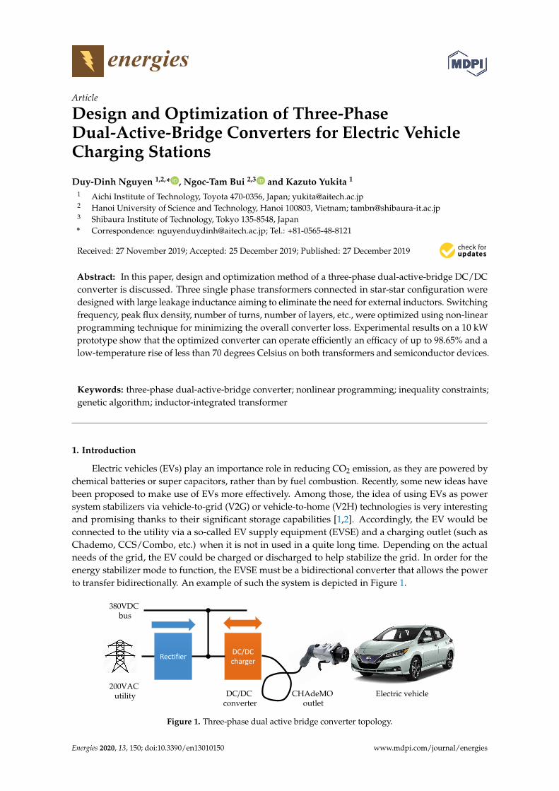
energies Article Design and Optimization of Three-Phase Dual-Active-Bridge Converters for Electric Vehicle Charging Stations Duy-Dinh Nguyen 1,2, * , Ngoc-Tam Bui 2,3 and Kazuto Yukita 1 1 Aichi Institute of Technology, Toyota 470-0356, Japan; [email protected] 2 Hanoi University of Science and Technology, Hanoi 100803, Vietnam; [email protected] 3 Shibaura Institute of Technology, Tokyo 135-8548, Japan * Correspondence: [email protected]; Tel.: +81-0565-48-8121 Received: 27 November 2019; Accepted: 25 December 2019; Published: 27 December 2019 Abstract: In this paper, design and optimization method of a three-phase dual-active-bridge DC/DC converter is discussed. Three single phase transformers connected in star-star configuration were designed with large leakage inductance aiming to eliminate the need for external inductors. Switching frequency, peak flux density, number of turns, number of layers, etc., were optimized using non-linear programming technique for minimizing the overall converter loss. Experimental results on a 10 kW prototype show that the optimized converter can operate efficiently an efficacy of up to 98.65% and a low-temperature rise of less than 70 degrees Celsius on both transformers and semiconductor devices. Keywords: three-phase dual-active-bridge converter; nonlinear programming; inequality constraints; genetic algorithm; inductor-integrated transformer 1. Introduction Electric vehicles (EVs) play an importance role in reducing CO 2 emission, as they are powered by chemical batteries or super capacitors, rather than by fuel combustion. Recently, some new ideas have been proposed to make use of EVs more effectively. Among those, the idea of using EVs as power system stabilizers via vehicle-to-grid (V2G) or vehicle-to-home (V2H) technologies is very interesting and promising thanks to their significant storage capabilities [1,2]. Accordingly, the EV would be connected to the utility via a so-called EV supply equipment (EVSE) and a charging outlet (such as Chademo, CCS/Combo, etc.) when it is not in used in a quite long time. Depending on the actual needs of the grid, the EV could be charged or discharged to help stabilize the grid. In order for the energy stabilizer mode to function, the EVSE must be a bidirectional converter that allows the power to transfer bidirectionally. An example of such the system is depicted in Figure 1. Electric vehicle DC/DC charger Rectifier CHAdeMO outlet DC/DC converter 380VDC bus 200VAC utility Figure 1. Three-phase dual active bridge converter topology. Energies 2020, 13, 150; doi:10.3390/en13010150 www.mdpi.com/journal/energies
-
Upload
khangminh22 -
Category
Documents
-
view
1 -
download
0
Transcript of Design and Optimization of Three-Phase Dual-Active-Bridge ...
energies
Article
Design and Optimization of Three-PhaseDual-Active-Bridge Converters for Electric VehicleCharging Stations
Duy-Dinh Nguyen 1,2,* , Ngoc-Tam Bui 2,3 and Kazuto Yukita 1
1 Aichi Institute of Technology, Toyota 470-0356, Japan; [email protected] Hanoi University of Science and Technology, Hanoi 100803, Vietnam; [email protected] Shibaura Institute of Technology, Tokyo 135-8548, Japan* Correspondence: [email protected]; Tel.: +81-0565-48-8121
Received: 27 November 2019; Accepted: 25 December 2019; Published: 27 December 2019
Abstract: In this paper, design and optimization method of a three-phase dual-active-bridge DC/DCconverter is discussed. Three single phase transformers connected in star-star configuration weredesigned with large leakage inductance aiming to eliminate the need for external inductors. Switchingfrequency, peak flux density, number of turns, number of layers, etc., were optimized using non-linearprogramming technique for minimizing the overall converter loss. Experimental results on a 10 kWprototype show that the optimized converter can operate efficiently an efficacy of up to 98.65% and alow-temperature rise of less than 70 degrees Celsius on both transformers and semiconductor devices.
Keywords: three-phase dual-active-bridge converter; nonlinear programming; inequality constraints;genetic algorithm; inductor-integrated transformer
1. Introduction
Electric vehicles (EVs) play an importance role in reducing CO2 emission, as they are powered bychemical batteries or super capacitors, rather than by fuel combustion. Recently, some new ideas havebeen proposed to make use of EVs more effectively. Among those, the idea of using EVs as powersystem stabilizers via vehicle-to-grid (V2G) or vehicle-to-home (V2H) technologies is very interestingand promising thanks to their significant storage capabilities [1,2]. Accordingly, the EV would beconnected to the utility via a so-called EV supply equipment (EVSE) and a charging outlet (such asChademo, CCS/Combo, etc.) when it is not in used in a quite long time. Depending on the actualneeds of the grid, the EV could be charged or discharged to help stabilize the grid. In order for theenergy stabilizer mode to function, the EVSE must be a bidirectional converter that allows the powerto transfer bidirectionally. An example of such the system is depicted in Figure 1.
Electric vehicle
DC/DC charger
Rectifier
CHAdeMOoutlet
DC/DC converter
380VDC bus
200VAC utility
Figure 1. Three-phase dual active bridge converter topology.
Energies 2020, 13, 150; doi:10.3390/en13010150 www.mdpi.com/journal/energies

Energies 2020, 13, 150 2 of 17
The EVSE in Figure 1 consists of two parts: a unidirectional rectifier and a bidirectional DC/DCcharger. The output of the rectifier is tied to a 380 V DC bus of a DC micro-grid, from whichthe bidirectional DC/DC converter charges the electric vehicle via a CHAdeMO outlet. When thevehicle is left unused, the outlet remains connected for charging or for reversing the power back to theDC bus. Thanks to that, the DC micro-grid can be stabilized. This paper focuses on designing andoptimization of the bidirectional DC/DC converter of such an EVSE (from now on, the DC charger).
From another aspect, according to [3], high frequency current ripple causes negative effect onthe battery lifetime. Therefore, it is necessary to design a DC charger with low output current ripple.It should also have high power density, high efficiency, be galvanic isolated, and be bidirectional.Among many DC/DC converter topologies, dual-active-bridge (DAB) has been found to be the mostappropriate choice for this application [4–6].
There are two popular types of DAB converter: single-phase and three-phase, both havinginherent soft-switching, bidirectional, and isolation characteristics. Unlike the single-phase counterpart, the three-phase structure can triple the effective frequency and reduce the amplitude of the ripple.Hence, input and output filters can be downsized; the transformer RMS current is also lower and powerdensity is higher than that of the single-phase version. Up till now, numerous studies on three-phaseDAB converter have been published [6–10] regarding various topics, including modulation and controlto system design and optimization, etc. While many discussions on designing and optimizing thesingle-phase DAB can be found in the literature, only a few are available for three-phase topology.
Of course, the design and optimization procedures that are applied for single-phase DAB convertercan be applicable for three-phase DAB. For example, the typical approach is starting from loss modeling,formulating the optimization problem, and then solving the problem by using some techniques, suchas that reported in [11]. However, in [11], an external inductor was used, and it is preferable to integratethe inductor into the transformer for better space saving and more efficient performance. Moreover,the switching frequency was fixed in that research; only the number of turns and the inductance wereoptimized. The conduction loss model used in that research did not address the dependency of ACresistance of winding on the proximity effect, which varies correspondingly to the number of turnsand layers [12].
In [13], the inductor-integrated transformer in a single-phase DAB converter was designed andoptimized by using the particle swarm optimization method. The skin and proximity effects wereregarded in loss modeling. However, conduction loss and switching loss of semiconductor devices werenot considered. Therefore, the overall converter system was not optimized; only transformers were.The research reported in [14] modeled both electronics loss and transformer loss. The transformerused shell-type winding for better integration of leakage inductance. However, only the controlvariables (phase shift, switching frequency) were optimized. The transformer structure was fixed andnot optimized.
Design and optimization of three-phase DAB converter for DC charging applications are resolvedin this paper. Both transformer structure and operation parameters are optimized. Inductors areintegrated into the transformers for better space and cost saving. The value of leakage inductance,number of turns, number of layers, etc., are also optimized. For better accuracy, skin and proximityeffects are also addressed in modeling the copper loss of transformers. A nonlinear programmingtechnique was employed to find the optimal parameter set. Due to certain facts, including thatthe window area of the transformer is limited, the semiconductor devices have a certain switchingcapability, the operating temperature needs to be handled as well, etc., some inequality constraintswere considered for the optimization problems. Afterward, the optimized transformer was verified bya finite element method magnetic (FEMM) analysis and by an experimental study.
This paper is actually an improved version of that reported in [15]. The converter was modeledwith consideration that number of turns and number of layers are integers. That makes the optimizingfunction discontinuous and non-differentiable. Therefore, a nonlinear programming method basedon gradient, such as the Newton–Raphson, becomes inapplicable. Besides, in order to find the global

Energies 2020, 13, 150 3 of 17
optima, the Global Optimization Toolbox of MATLAB & Simulink from Mathworks incorporation wasemployed. Furthermore, operation in the whole power range was examined in this improved version.The paper is structured as follows: analysis in the steady state is presented in Section 2; transformerdesign method is described in Section 3; the loss model can be found in Section 4; the optimizationalgorithm is narrated in Section 5; the optimization, simulation, and experimental results are providedin Section 6; and finally, some conclusions are given in Section 7.
2. Steady State Analysis
Figure 2 describes the circuit diagram of a three-phase dual-active-bridge (from now on, DAB3)converter. Three single phase high-frequency transformers are employed for easier fabrication andimplementation of the system. It assumes that all transformers have the same leakage inductance ofLk and the same winding ratio of n : 1. According to [8], among some transformer configurations,the Y–Y topology requires smaller leakage inductance to send a specific amount of power. That alsomeans a smaller number of turns of transformer winding is required, resulting in smaller windingresistance. Therefore, in this study, the Y–Y connection is used aiming for performance optimization.Notes here that, delta-type transformer structures can be transformed into star connection by using thefollowing transformation:
LYa =LDbLDc
LDa + LDb + LDc.
𝑄1 𝑄3 𝑄5
𝑄4 𝑄6 𝑄2
𝑆1 𝑆3 𝑆5
𝑆4 𝑆6 𝑆2
𝐿𝑘
𝐿𝑘
𝐿𝑘
𝑉1 𝑉2
𝑛: 1
𝑛: 1
𝑛: 1
Figure 2. Three-phase dual active bridge converter topology.
Two three-phase inverters are located at two sides of the transformers. The conventional phaseshift modulation and 180-degree-conduction-mode are used to control the converter. The switchingfrequency is fs which needs to be optimized. Voltages at the two DC terminals are V1 and V2,respectively. The voltages across the transformer winding have the four-level form and are ψ degreesshifted from each other as shown in Figure 3, where ψ is the phase shift control angle.
Assuming that the phase shift ψ is smaller thanπ
3for better reactive power reduction, according
to [8], the transition current I0 to I5 at the steady state can be calculated by (1):
I0 = −IM
(2(1−M) +
3Mψ
π
)I1 = IM
(−2(1−M) +
3ψ
π
)I2 = IM
(−(1−M) +
3Mψ
π
)I3 = IM
(−(1−M) +
6ψ
π
)I4 = IM
((1−M) +
6Mψ
π
)I5 = IM
((1−M) +
3ψ
π
)(1)

Energies 2020, 13, 150 4 of 17
where IM =V1
18 fsLk; M is the voltage conversion ratio, M =
nV2
V1; and ψ is the phase shift, ψ <
π
3.
𝐼0
𝐼1 𝐼2
𝐼3
𝐼4
𝐼5
𝐼6
0𝜃1 𝜃2 𝜃3 𝜃4 𝜃5 𝜋 2𝜋
𝜔𝑠𝑡
𝜔𝑠𝑡
𝜓
𝑄1𝑄3𝑄5𝑆1𝑆3𝑆5
𝑣𝑝, 𝑣𝑠
𝑉1/3
2𝑉1/3
2𝑉2/3
𝑉2/3
Figure 3. Theoretical voltage and current waveforms.
The root-mean-squared (rms) transformer current, rms switch currents, peak flux density(obtained by calculating the volt-second product of each conducting interval and assuming a balancedvolt-second distribution of transformers), and output power are calculated by equations from (2) to (6)as follows:
Ipri,rms =IM√
33
√5(1−M)2 + 27
(2− ψ
π
)(ψ
π
)2M (2)
IQx,rms =Ipri,rms√
2(3)
ISx,rms =IQx,rms
n(4)
Bpk =V1
18 fsN1 Ac
(1 + M
(1− 3ψ
2π
))(5)
Pout =3MV1 IM
2ψ
(4− 3ψ
π
), (6)
where N1 is the number of turns of the primary winding; Ac is the cross section area of the center limbof the magnetic core, assuming that E core is used.
3. Transformer Design
At the first step, some preliminary parameters must be determined:
• Maximum output power;• Nominal input and output voltages;• Current density (J = 6−10 A/mm2);• Window utilization factor (Ku = 0.2−0.4 for transformer);• Initial switching frequency and flux density.

Energies 2020, 13, 150 5 of 17
After that, from (2), (5) and (6), the core size and winding wire size can be selected according to Apor Kg methods [16]. Here, in order to reduce the skin and proximity effects, Litz wire is preferable.Three transformers with the traditional core-typed winding structure, as depicted in Figure 4, weredesigned. There are only two windings in each transformer, primary and secondary; no interleaving.The centralized wounding technique was used. The insulation between two windings was made thickfor leakage inductance integration purpose. The insulation thickness is, thus, a variable for tuning theleakage inductance.
𝑏1 𝑏2𝑐
𝑊
𝑎Insulation
Primary winding
Secondary winding
Bobbin
𝐻
Figure 4. Transformer with thick insulation configuration.
According to [16], the leakage inductance can be calculated by:
Lk =µ0(MLT)N2
1a
(c +
b1 + b2
3
), (7)
where µ0 is the permeability of vacuum, µ0 = 4π× 10−7; MLT is the mean-length-turn of the core; a isthe winding height; b1 and b2 are the windings’ thicknesses; c is the insulation thickness; and N1 is thenumber of turns of primary winding, from (5). N1 can be derived as (8):
N1 = ceil
(V1
18 fsBpk Ac
(1 + M
(1− 3ψ
2π
)))(8)
where ceil() is the ceiling (round-up) function.Now, let m1 and m2 be the number of layers of primary and secondary windings; the winding
dimension will be:
a = OD1 ×N1
m1(9)
b1 + b2 = OD1m1 + OD2m2, (10)
where OD1 and OD2 are the outer dimensions of winding wires. Let H be the window height of thebobbin. The winding height a must be smaller than H. From (9), we get:
N1 ≤H
OD1m1. (11)

Energies 2020, 13, 150 6 of 17
Due to the round shape of the wire and the necessary space for creepage and clearance distance,the whole core height cannot be used for winding. Therefore, by denoting kc1 as the utilization factorof the core height, kc1 ≤ 0.9, m1 and m2 can be determined by:
m1 =ceil(
N1OD1
kc1 H
)(12)
m2 =ceil(
N2OD2
kc1 H
). (13)
Since b1 and b2 depend on the chosen current density J, and have less effect on leakage inductancevalue, as formulated in (7), the tuning parameter for Lk is the insulation thickness c. Note thatthe summation (b1 + b2 + c) must be smaller than the total window width W of the bobbin. The leakageinductance is highest at c = cmax:
c ≤ cmax = W − (b1 + b2). (14)
From (7)–(14), the maximum achievable leakage inductance for a given core is determined by:
Lk ≤ Lk,max =µ0(MLT)H
OD1m2
1
(W
OD1− 2
3
(m1 +
OD2
OD1m2
)). (15)
The leakage inductance is minimum when there is no insulation between the two windings(c = 0):
Lk ≥ Lk,min =µ0(MLT)N1m1
3
(m1 +
OD2
OD1m2
). (16)
From (6), for a given output power of Pm, the maximum phase shift is calculated by:
ψm =2π
3
(1−
√1− fs
fs,max
), (17)
where fs,max =MV2
19LkPm
. Obviously, in order for (17) to be valid, the switching frequency must be less
than the maximum value of fs,max:
fs ≤ fs,max =MV2
19LkPm
. (18)
From (8), (17) and (18), we have:
fs ≥V1
18N1 AcBpk
(1 + M
√1− fs
fs,max
). (19)
Solving (19) for fs, the lower boundary of switching frequency is:
fs ≥ fs,min = λ fs,max
1− λ
2M2 + M
√1− λ +
λ2
4M2
, (20)
where λ =P
2MV1× Lk
N1 AcBpk.

Energies 2020, 13, 150 7 of 17
4. Power Loss Modeling
4.1. Power Electronics Loss
Assuming that zero-voltage transition is achieved, turn-on loss can thus be ignored. The overallpower dissipation on the Silicon-Carbide Metal–Oxide–Semiconductor Field-Effect Transistor(SiC-MOSFETs) can be estimated by:
∆Ppe = ∆Pcond + ∆Psw, (21)
where ∆Pcond and ∆Psw are conduction loss and turn-off loss respectively:
∆Pcond = 6Rds,ON(I2Qx,rms + n2 I2
Sx,rms)
∆Psw = 3V1(I0 + MI1)t f fs
with Rds,ON and t f being the ON resistance and the falling time of the MOSFET; both are given inthe device data-sheet; I0 and I1 are the transition currents given in (1); IQx,rms and ISx,rms are the rmscurrents flowing through primary and secondary switches, which are given in (3) and (4), respectively.
4.2. Transformer Loss
Transformer loss includes copper loss dissipating on windings and ferrite loss on the magneticcore as follows:
∆Ptr = ∆PCu + ∆PFe, (22)
where ∆PCu and ∆PFe are the winding loss (or copper loss) and core loss (ferrite loss). Using theSteimetz equation, the core loss can be estimated by:
∆PFe = 3kc f αs Bβ
pkg, (23)
where Bpk is the peak flux density, and g is the weight of two core halves. kc, a and b are the Steimetzcoefficients: kc = 0.00004855, α = 1.62, and β = 2.63 [16].
The copper loss is determined by (24):
∆PCu = 3Rac I2pri,rms, (24)
where Rac is the primary-referred AC resistance. Note that the AC resistance depends strongly on theswitching frequency and the winding geometry by the skin and proximity effects. According to [12],the AC resistance can be estimated for Litz wire as follows:
Rac = Rdc Astr
(sinh 2Astr + sin 2Astr
cosh 2Astr − cos 2Astr+
23
(m2nstr − 1
) sinh Astr − sin Astr
cosh Astr + cos Astr
), (25)
where Astr =1δ
(π
4
)0.75√
d3b
dw; δ is the skin depth, δ =
6.62× 10⁻²√fs
; db and dw are the bare and outer
diameters of a single strand of the Litz wire; m is the number of layers; nstr is the number of strands;Rdc is the DC resistance of the winding:
Rdc = (MLT)Nrstr
nstr,
where N is the number of turns (i.e., N1 for primary winding and N2 for secondary winding); rstr isthe resistance density of a strand; and MLT is the mean-length-turn of the magnetic core.

Energies 2020, 13, 150 8 of 17
4.3. Capacitor Loss
Since there is ripple in the input and output currents of the converter, the ripple will be filtered outby the input and output capacitors and dissipate some power on the series resistance of the capacitors.The capacitor loss is determined by:
∆Pcap = rcin I2cin,rms + rcout I2
cout,rms, (26)
where rcin and rcout are the series resistances of capacitors; Icin,rms and Icout,rms are the input and outputrms capacitor currents which can be easily derived from (1).
Finally, the total power dissipation of the converter is derived as:
∆Ptot = ∆Ppe + ∆Ptr + ∆Pcap. (27)
5. Optimization
In order to maximize system efficiency, the overall power dissipation should be minimized.The analysis above shows that the four most basic parameters that affect all others are the switchingfrequency fs, the peak flux density Bpk, the voltage conversion ratio M, and the leakage inductance Lk.When fs, Bpk, M, and Lk are known, all other parameters can be easily derived.
Here, some additional constraints are considered. First, after designing the transformer, accordingto [16], one can estimate the temperature rise of the core by (28).
∆Ttr = 450(
∆Ptr
3At
)0.826, (28)
where At is the total surface of the transformer; At can be calculated without difficulty when the coredimensions are known.
The temperature rise of power electronics devices can also be estimated if the thermal resistanceof the heatsink Rhs is given. Assuming that the heat generated from semiconductor devices is evenlydistributed on the heatsink, then the temperature rise is:
∆Tpe = ∆PpeRhs. (29)
The maximum temperature rise should not be greater than a certain allowable value of ∆Tmax.
max
∆Ttr, ∆Tpe≥ ∆Tmax. (30)
It is also worth noticing that all analyses above are conducted under the assumption thatsoft-switching is achieved. According to [8] and considering the required deadtime Td in modulation,the lowest soft-switching boundary when ψ < π/3 is:
ψ ≥ ψmin =2π
3(1−M) + 2π fsTd.
At that operational point, the transferred power is:
Pmin =MV2
112 fsLk
ψmin
(4− 3
πψmin
). (31)
The rated power P should be greater than Pmin at least kp times for a soft-switching range of kp:1as (32):
P ≥ kpPmin. (32)
Eventually, the optimization problem is defined as follows:
Energies 2020, 13, 150 9 of 17
*) Minimization problem:Find a set of
(fs, Bpk, Lk, M
)to minimize the total converter loss:
f(
fs, Bpk, Lk, M)= ∆Ptot → min (33)
subject to:
g1
(fs, Bpk, Lk, M
)= Fs,min − fs ≤ 0
g2
(fs, Bpk, Lk, M
)= fs − Fs,max ≤ 0
g3
(fs, Bpk, Lk, M
)= Lk − Lk,max ≤ 0
g4
(fs, Bpk, Lk, M
)= Lk,min − Lk ≤ 0
g5
(fs, Bpk, Lk, M
)= max
∆Ttr, ∆Tpe
− ∆Tmax ≤ 0
g6
(fs, Bpk, Lk, M
)= kpPmin − P ≤ 0,
(34)
where kp : 1 is the power range of the converter, kp should be as great as possible. In this paper, kp ischosen as 5 for a power range of 5:1.
*) Solution:In order to solve the above optimization problem, there are numerous of available methods.
However, note here that the optimizing function is non-continuous and non-differentiable, as itincludes a round-up (ceiling) function. Therefore, explicit methods based on gradient are not applicable;instead, heuristic techniques such as the genetic algorithm (GA), differential evolution (DE), particleswarm optimization (PSO), etc., are preferred [17]. In this paper, GA is selected due to its simplicityand feasibility.
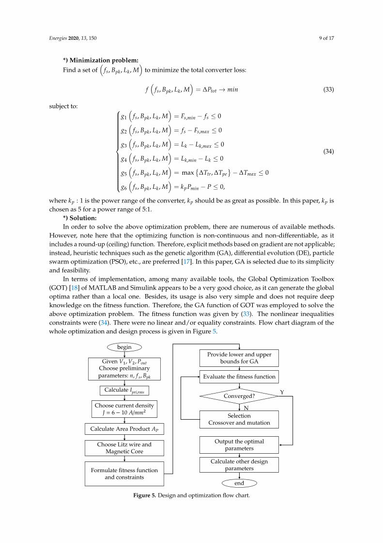
In terms of implementation, among many available tools, the Global Optimization Toolbox(GOT) [18] of MATLAB and Simulink appears to be a very good choice, as it can generate the globaloptima rather than a local one. Besides, its usage is also very simple and does not require deepknowledge on the fitness function. Therefore, the GA function of GOT was employed to solve theabove optimization problem. The fitness function was given by (33). The nonlinear inequalitiesconstraints were (34). There were no linear and/or equality constraints. Flow chart diagram of thewhole optimization and design process is given in Figure 5.
Given 𝑉1, 𝑉2, 𝑃𝑜𝑢𝑡Choose preliminary
parameters: 𝑛, 𝑓𝑠, 𝐵𝑝𝑘
Calculate 𝐼𝑝𝑟𝑖,𝑟𝑚𝑠
Choose current density 𝐽 = 6− 10 𝐴/𝑚𝑚2
Calculate Area Product 𝐴𝑃
Choose Litz wire and Magnetic Core
Formulate fitness function and constraints
Provide lower and upper bounds for GA
Evaluate the fitness function
Converged?Y
SelectionCrossover and mutation
N
Calculate other design parameters
end
begin
Output the optimal parameters
Figure 5. Design and optimization flow chart.

Energies 2020, 13, 150 10 of 17
6. Results and Discussion
6.1. Optimization Results
The proposed design and optimization strategy was applied to design a 10 kW, three-phasedual-active-bridge (DAB) converter for battery charging application. From (2), the primary current canbe calculated with a preliminary phase shift angle. Afterward, the current density J is chosen to be,for example, 9 A/mm2. Then, the magnetic core of ETD54/28/19 from TDK corporation is selected.The specification and preliminary parameters of the required converter are given in Table 1.
Table 1. Specification and preliminary parameters.
Parameter Symbol Value
Input voltage V1 380 VOutput voltage V2 240−480 V
Nominal output voltage V2,nom 380 VRated power P 10 kW
Maximum temperature rise ∆T 70 CPreliminary frequency fs 50 kHzPreliminary phase shift ψ 30 degrees
Preliminary peak flux density Bpk 250 mTCalculated inductance Lk 15.56 µH
Desired current density J 9 A/mm2
Selected wire Litz 1050AWG44Selected ferrite core ETD54/28/19 (N87)
SiC MOSFET CREE C2M0040120D
Lower and upper bounds of optimizing variables are given in Table 2. Running the aboveoptimization algorithm, optimization progress is shown in Figure 6. The optimal loss is 210.02W, achieved at the switching frequency of 72.71 kHz, the peak flux density of 137.6 mT, the leakageinductance of 5.05 mT, and the voltage conversion ratio of 1:1. The best efficiency was obtained as 97.9%at the rated power of 10 kW. The temperature rise of transformer was calculated as 70 degrees—justright—equal to the maximum allowable value given in Table 1. Other parameters are listed in Table 3.
0 50 100 150 200 250 300 350 400
Generation
100
200
300
400
500
600
700
Fitn
ess
valu
e
Best: 200.142 Mean: 210.173
Best fitnessMean fitness
Figure 6. Optimization process using genetic algorithm.

Energies 2020, 13, 150 11 of 17
Table 2. Lower and upper bounds for genetic algorithm.
Parameter Symbol Lower Bound Upper Bound
Switching frequency fs 50 kHz 300 kHzPeak flux density Bpk 50 mT 250 mT
Leakage inductance Lk 1 µH 10 µHVoltage conversion ratio M 0.5 2
Since 72.71 kHz is not suitable for programming, it was round-up to 75 kHz. This causes a slightlydeviation in the total loss and efficiency of the converter compared to the optimal value. However, thatdeviation is insignificant and can be ignored. The modified optimal parameters and all other designparameters are described in Table 3.
Also listed in Table 3 is the competing parameter set. For the same transformer design, weoperated the system at a different switching frequency (and thus, different phase shift), and thencompared the performance to confirm whether or not the optimized parameters are better. It wasnot possible to lower switching frequency, or the control range constraint would have been violated.Therefore, the competing switching frequency was 100 kHz.
Table 3. Optimal and modified parameters.
Parameter Symbol Optimized Value Modified Value Competing Value Unit
Switching frequency fs 72.71 75 100 kHzPeak flux density Bpk 137.6 133.13 97.68 mT
Leakage inductance Lk 5.05 5.05 5.05 µHConversion ratio M 1 1 1Number of turns N1:N2 15:15 15:15 15:15Phase shift angle ψ 13.1 13.54 18.46 degrees
AC resistance RAC 31.86 31.99 33.61 mΩTransformer temperature rise ∆Ttr 70.0 69.75 69.15 C
Heatsink temperature rise ∆Tpe 40.7 41.44 49.73 CPower electronics loss ∆Ppe 162.80 165.76 198.93 W
Transformer loss ∆Ptr 42.97 42.78 42.34 WTotal loss ∆Ptot 210.02 212.94 247.24 W
Efficiency@Prated η 97.9% 97.87% 97.53%
Figure 7 illustrates the calculated efficiency and temperature curves obtained by the optimized andcompeting parameters using the model in the previous sections when varying the phase shift from theminimum value to the nominal one. As shown in Figure 7a, the minimum power was calculated at theminimum phase shift, which is equivalent to the dead-time period. Maximum efficiency of near 98.5%was achieved at around 4 kW. The expected efficiency at the rated power was 97.87%, as mentionedabove. The plotted temperature curve indicates the trend of the greater value between temperatureof transformers and power electronics devices with the assumption that the ambient temperature is15 degree Celsius. At the rated power, the hottest spot was about 85 degree Celsius. Note that thiscalculation assumes there is no forced air cooling for both transformers and semiconductors, onlypassive cooling. The characteristics are same when considering the competing parameter set. However,the efficiency is expected to be slightly lower while temperature rise is a little bit less than that whenapplying the optimized parameter set (due to smaller transformer loss), as can be seen in Figure 7b.

Energies 2020, 13, 150 12 of 17
(a) (b)
Figure 7. Calculated efficiency and temperature obtained by: (a) optimized parameters;(b) competing parameters.
6.2. Simulation and Experimental Results
Before conducting experiments, a finite-element analysis (FEA) using the Finite-Element-Method-magnetic (FEMM) version 4.2 [19] was carried out to validate the designed transformers. The fluxdensity obtained by the FEA is illustrated in Figure 8. The flux has higher density at the two outerlimbs then at the center one. The peak flux density is 150 mT, which is 12.5% greater than the estimationvalue. Except for that, other parameters including leakage inductance, AC resistance, and copper andferrite losses are almost identical to the designed values. Therefore, it is reasonable to fabricate threetransformers, namely, Y1, Y2, and Y3, according to the designed parameters. The complete prototype ofthe converter is shown in Figure 9.
Figure 8. Finite-element-analysis using FEMM 4.2.

Energies 2020, 13, 150 13 of 17
Inverter 1 Inverter 2YY transformer
Figure 9. A 10 kW, three-phase DAB converter prototype.
A detailed comparison between calculations, Finite-element analysis (FEA) results, andmeasurements is given in Table 4. It can be seen that measurements matched calculation and FEAresults very well. The simulated leakage inductance was 4.87 µH, while the expected value was 5.05 µH,only 3.5% different. The prediction of transformer loss was also very close to the FEA simulationresults. However, the simulated peak flux density was about 13% higher than expected. That is becausethe FEMM simulation is 2D, so two outer limbs of the core are treated as rectangular (while in fact,two outer limbs of the ETD core do not have rectangular shapes), making the effective cross-sectionarea (Ac) slightly smaller than the real parameter. On the other hand, the center limb which hascylinder shape in deed is also treated as rectangular, and thus, the flux density in the center limb inFEA simulation is smaller than expected. Anyhow, the difference of peak flux density contributes onlyto the difference on core loss, which is not significant in this design. Since the transformer designedcan be confirmed by FEA simulation, three single phase transformers were built accordingly. However,there are small differences between the actual transformers. This distinction may lead to unevenlyloss and heat distributions among phases. It is also worth noting that the measured AC resistanceswere slightly greater than expected due to the non-ideal winding arrangement. In reality, the actualtransformer losses would be slightly higher than estimated. Nevertheless, it can be confirmed herethat the converter models and optimization strategy presented in the previous sections are reasonable.
Table 4. Design validation.
Parameter Symbol Calculation FEA Measurement UnitY1 Y2 Y3
Leakage inductance Lk 5.05 4.87 4.92 4.9 4.82 µHMagnetizing inductance Lm 1.2 1.17 1.33 1.13 1.24 mHAC resistance @ fs,opt RAC 31.99 30.81 36.5 36.5 35.2 mΩPeak flux density Bpk 133.13 149.9 - - - mTCopper loss ∆PCu 10.8057 10.19 - - - WCore loss ∆PFe 3.4555 3.03 - - - W
As the transformers were validated, two inverters made of SiC MOSFET C2M0040120D fromCREE incorporation were placed at primary and secondary sides. A TMS320F28335 control cardis employed to generate pulse-width-modulation (PWM) signals. A programmable power supplyconnects to the input side of Inverter 1, whereas a DC electronic load connects to the DC side ofInverter 2. The experiment system is depicted in Figure 10.

Energies 2020, 13, 150 14 of 17
Figure 10. A 10 kW, three-phase DAB converter prototype.
Dead-time was fixed at 100 ns (equivalent to about 2.7 electrical degrees). The input voltagewas set at 380 V. The DC electronics load was configured to operate in the constant resistance modewhose resistance was changed in an open-loop manner to keep the input and output voltage equal.The phase shift was then increased gradually from ψmin until reaching the maximum power. At eachstep, efficiency and temperature were recorded. Drain-source voltage of a primary switch and phasecurrent waveform at 9.3 kW are demonstrated in Figure 11. As shown, soft-switching was achieved;both waveforms are smooth as there are no ringings or spikes.
𝑉𝑑𝑠 𝑄1𝐼𝑎
200 V/div10 A/div2 𝜇s/div
Figure 11. Voltage and current waveforms at 9.3 kW.
Efficiency in the whole power range at unity voltage conversion ratio when using the optimizedparameter set is shown in Figure 12. Due to the current limitation of the power supply, the maximumpower that can be investigated is only 9.3 kW. The maximum efficiency of 98.65% is obtained at around3.6 kW, and the average efficiency over the whole power range is 97.91%, as shown in Figure 12a.The measured results match well with the calculations in the low and mid-power ranges. Whenthe power increases, the converter performance is, however, not as good as expected. For example,the estimated efficiency at 9.3 kW is 97.9% but the measured result shows only 97.15%; in otherwords, there is a 0.75% error in the determination of the efficiency. The reason may be due to theincrement of drain-source resistance of MOSFETs when temperature changes, which was not regardedin the loss model above. Another reason is the mismatch of actual parameters of the real, hand-made

Energies 2020, 13, 150 15 of 17
transformers when compared to the ideal values. Voltage drops on cables connecting input andoutput of the converter to the power supply and load also contribute to the error between modelingand experiment. Note that at 10 kW, a 1 V drop on one cable may lead to a 0.25% reduction in theoverall efficiency.
(a) (b)
(c) (d)
Figure 12. Performance in the soft-switching range. (a) Efficiency when using the optimal parameterset; (b) efficiency when using the competing parameter set; (c) temperature when using the optimalparameter set; (d) temperature when using the competing parameter set.
The measured temperature also matches well with calculation in the mid and high-power range,as can be seen in Figure 12c. In the low-power range, the temperature was overestimated in calculations,as the measurement values were about 5 degrees cooler than expected. Notes here that the plottedtemperatures are the hottest spots on the converter regardless of transformers or inverters beingmeasured. And note also that there is no forced air cooling on either heatsinks or transformers, onlypassive cooling. For example, as illustrated in Figure 13, the temperature measurement at 8.2 kWusing a FLIR camera shows that the hot spots on the transformer and inverter were 71 and 63 degreesCelsius, respectively, whereas the expected value was 70.7 degrees. These results indicate that theconverter loss and heat model, and the optimized strategy, are reliable. Furthermore, if the converterhas forced-air cooling, it can perform even better.
It is also worth paying attention to Figure 13b. The loss appears to not be distributed evenlyamong three legs. The temperature of leg c of the secondary inverter seems to be hotter than the others.That is comprehensible, since the three transformers are not identical, as described in Table 4. A slightdifference in transformer parameters leads to uneven loss and heat distribution, as shown in Figure 13b.In order to avoid this phenomenon, better transformer fabrication is preferable. An alternative method

Energies 2020, 13, 150 16 of 17
is to modify the modulation strategy for evenly current distribution between phases. However, thistopic is beyond the scope of this paper.
A
B
C
a
b
c
(a)
a
b
c
(b)
Figure 13. Temperature at 9.3 kW: (a) transformer and (b) secondary inverter.
As expected, when using the competing parameter set, the efficiency was not as high as thatwhen switching the converter at the optimized frequency (see Figure 12b). The best performancewas only 98.3%, around 4 kW. When increasing the power, the efficiency drops rapidly. At 6.5 kW,the converter can transfer only 97.2% of the input power, while that value is 97.9% when using theoptimized switching frequency. However, the system is cooler, as predicted above, when the measuredtemperature at 6.5 kW is about 58.9 degrees Celsius compared to 60 degrees of the previous case(Figure 12d). Hence, in terms of efficacy, it can be concluded that the converter with the optimizedparameters performs better.
7. Conclusions
This paper presented the detail and accurate loss modeling for three-phase, dual-active-bridgeDC/DC converters with inductor-integrated transformers. After that, an optimization strategy wasproposed to minimize the converter loss. Several nonlinear inequality constraints were regarded.There are four variables that were optimized, including switching frequency, peak flux density, leakageinductance, and the voltage conversion ratio. Due to the highly nonlinear optimizing function, thegenetic algorithm was employed to optimize the converter. Finite-element-analysis showed thatthe converter model is reliable. Experimental results confirmed that the optimized design of theconverter had the maximum efficiency of 98.65% and average efficiency in the power range of 97.91%.
Author Contributions: D.-D.N. proposed the main idea, built and performed experiments; N.-T.B. designed theGenetic Algorithm; K.Y. provides supporting ideas, comments and funding; all members contributed significantlyin writing and revising the paper. All authors have read and agreed to the published version of the manuscript.
Funding: Knowledge base Aichi Research and development base that supports high value-addedmanufacturing-Project ID: PI6.
Conflicts of Interest: The authors declare no conflict of interest.

Energies 2020, 13, 150 17 of 17
References
1. Kempton, W.; Tomic, J. Vehicle-to-grid power implementation: From stabilizing the grid to supportinglarge-scale renewable energy. J. Power Sources 2005, 144, 280–294. [CrossRef]
2. Ota, Y.; Taniguchi, H.; Nakajima, T.; Liyanage, K.M.; Baba, J.; Yokoyama, A. Autonomous distributed V2G(vehicle-to-grid) satisfying scheduled charging. IEEE Trans. Smart Grid 2011, 3, 559–564. [CrossRef]
3. Uddin, K.; Moore, A.D.; Barai, A.; Marco, J. The effects of high frequency current ripple on electric vehiclebattery performance. Appl. Energy 2016, 178, 142–154. [CrossRef]
4. He, P.; Khaligh, A. Comprehensive analyses and comparison of 1 kW isolated DC–DC converters forbidirectional EV charging systems. IEEE Trans. Transp. Electrif. 2016, 3, 147–156. [CrossRef]
5. Zhu, L.; Taylor, A.R.; Liu, G.; Bai, K. A Multiple-Phase-Shift Control for a SiC-Based EV Charger to Optimizethe Light-Load Efficiency, Current Stress, and Power Quality. IEEE J. Emerg. Sel. Top. Power Electron.2018, 6, 2262–2272. [CrossRef]
6. Haghbin, S.; Alatalo, M.; Yazdani, F.; Thiringer, T.; Karlsson, R. The design and construction of transformersfor a 50 kW three-phase dual active bridge dc/dc converter. In Proceedings of the 2017 IEEE Vehicle Powerand Propulsion Conference (VPPC), Belfort, France, 11–14 December 2017; pp. 1–5.
7. van Hoek, H.; Neubert, M.; De Doncker, R.W. Enhanced modulation strategy for a three-phase dual activebridge—Boosting efficiency of an electric vehicle converter. IEEE Trans. Power Electron. 2013, 28, 5499–5507.[CrossRef]
8. Baars, N.H.; Everts, J.; Wijnands, C.G.; Lomonova, E.A. Performance evaluation of a three-phase dual activebridge dc–dc converter with different transformer winding configurations. IEEE Trans. Power Electron.2016, 31, 6814–6823. [CrossRef]
9. Segaran, D.; Holmes, D.; McGrath, B. Comparative analysis of single-and three-phase dual active bridgebidirectional dc-dc converters. Aust. J. Electr. Electron. Eng. 2009, 6, 329–337. [CrossRef]
10. Mainali, K.; Tripathi, A.; Madhusoodhanan, S.; Kadavelugu, A.; Patel, D.; Hazra, S.; Hatua, K.;Bhattacharya, S. A Transformerless Intelligent Power Substation: A three-phase SST enabled by a 15-kV SiCIGBT. IEEE Power Electron. Mag. 2015, 2, 31–43. [CrossRef]
11. Iyer, V.M.; Gulur, S.; Bhattacharya, S. Optimal design methodology for dual active bridge converter underwide voltage variation. In Proceedings of the 2017 IEEE Transportation Electrification Conference and Expo(ITEC), Chicago, IL, USA, 22–24 June 2017; pp. 413–420.
12. Wojda, R.; Kazimierczuk, M. Winding resistance of litz-wire and multi-strand inductors. IET Power Electron.2012, 5, 257–268. [CrossRef]
13. Qin, H.; Kimball, J.W.; Venayagamoorthy, G.K. Particle swarm optimization of high-frequency transformer.In Proceedings of the IECON 2010-36th Annual Conference on IEEE Industrial Electronics Society,Glendale, AZ, USA, 7–10 November 2010; pp. 2914–2919.
14. Jauch, F.; Biela, J. Generalized modeling and optimization of a bidirectional dual active bridge DC-DCconverter including frequency variation. IEEJ J. Ind. Appl. 2015, 4, 593–601. [CrossRef]
15. Nguyen, D.D.; Kazuto, Y.; Katou, A.; Yoshida, S. Design optimization of a three-phase Dual-Active-Bridgeconverter for charging stations. In IEEE Vehicle Power and Propulsion Conference—VPPC 2019; IEEE: Hanoi,Vietnam, 2019; in process.
16. McLyman, C.W.T. Transformer and Inductor Design Handbook; CRC Press: Boca Raton, FL, USA, 2016.17. Kachitvichyanukul, V. Comparison of three evolutionary algorithms: GA, PSO, and DE. Ind. Eng. Manag. Syst.
2012, 11, 215–223. [CrossRef]18. Global Optimization Toolbox. Available online: https://www.mathworks.com/products/global-
optimization.html (accessed on 20 November 2019) .19. Finite Element Method Magnetics 4.2. Available online: http://www.femm.info/wiki/HomePage (accessed
on 20 November 2019) .
c© 2019 by the authors. Licensee MDPI, Basel, Switzerland. This article is an open accessarticle distributed under the terms and conditions of the Creative Commons Attribution(CC BY) license (http://creativecommons.org/licenses/by/4.0/).