Design and Implementation of 150 W AC/DC LED Driver with ...
22
electronics Article Design and Implementation of 150 W AC/DC LED Driver with Unity Power Factor, Low THD, and Dimming Capability Ngo Thanh Tung 1 , Nguyen Dinh Tuyen 2 , Nguyen Minh Huy 2 , Nguyen Hoai Phong 3 , Ngo Cao Cuong 4 and Le Minh Phuong 2, * 1 Department of Telecommunication Operation, Telecommunication University, Nha Trang City 650000, Vietnam; [email protected] 2 Faculty of Electrical and Electronics Engineering, Hochiminh City University of Technology—VNU-HCM, Hochiminh City 700000, Vietnam; [email protected] (N.D.T.), [email protected] (N.M.H.) 3 Faculty of Electrical Engineering Technology, Industrial University of Hochiminh City, Hochiminh City 700000, Vietnam; [email protected] 4 Department of Science and Technology, University of Economics and Finance, Hochiminh City 700000, Vietnam; [email protected] * Correspondence: [email protected]; Tel.: +84-988572177 Received: 30 November 2019; Accepted: 26 December 2019; Published: 29 December 2019 Abstract: This paper presents the implementation of a two-stage light-emitting diode (LED) driver based on commercial integrated circuits (IC). The presented LED driver circuit topology, which is designed to drive a 150 W LED module, consists of two stages: AC-DC power factor correction (PFC) stage and DC/DC power converter stage. The implementation of the PFC stage uses IC NCP1608, which uses the critical conduction mode to guarantee a unity input power factor with a wide range of input voltages. The DC/DC power converter with soft-switching characteristics for the entire load range uses IC FLS2100XS. Furthermore, the design of an electromagnetic interference (EMI) filter for the LED driver and the dimming control circuit are discussed in detail. The hardware prototype, an LED lighting system, with a rated power of 150 W/32 V from a nominal 220 V/50 Hz AC voltage supply was tested to show the effectiveness of the design. The presented LED driver was tested for street lighting, and the experimental results show that the power factor (PF) was higher than 0.97, the total harmonics distortion (THD) was lower than 7%, and the efficiency was 91.7% at full load. The results prove that the performance of the presented LED driver complies with the standards: IEC61000-3-2 and CIRSP 15:2009. Keywords: LED driver; LLC resonant converter; EMI filter; power factor correction 1. Introduction As compared to conventional lighting solutions, the most important advantage of LEDs is their long lifespan. Furthermore, LEDs provide some more advantages such as energy efficiency, improved safety, and a great color rendering index. In addition, LEDs are gaining popularity as a green solution. Recently, with the rapid development of LED technology, LEDs are widely used in automotive electronics [1], street lighting [2], and LCD backlighting [3]. Recently, medium- and high-power LEDs have been used to replace traditional high-pressure sodium (HPS) lamps for street lighting applications. The use of LEDs for street lighting applications is a good solution to save electric energy, and the LED driver has become an attractive topic for much research [4]. In recent years, there have been some issues that researchers have concentrated on, to develop LED drivers for street lighting applications to improve input performance [5–7], reduce the size [8], and improve the system efficiency [9]. Electronics 2020, 9, 52; doi:10.3390/electronics9010052 www.mdpi.com/journal/electronics
-
Upload
khangminh22 -
Category
Documents
-
view
0 -
download
0
Transcript of Design and Implementation of 150 W AC/DC LED Driver with ...

electronics
Article
Design and Implementation of 150 W AC/DC LEDDriver with Unity Power Factor, Low THD, andDimming Capability
Ngo Thanh Tung 1, Nguyen Dinh Tuyen 2 , Nguyen Minh Huy 2, Nguyen Hoai Phong 3,Ngo Cao Cuong 4 and Le Minh Phuong 2,*
1 Department of Telecommunication Operation, Telecommunication University, NhaTrang City 650000, Vietnam; [email protected]
2 Faculty of Electrical and Electronics Engineering, Hochiminh City University of Technology—VNU-HCM,Hochiminh City 700000, Vietnam; [email protected] (N.D.T.), [email protected] (N.M.H.)
3 Faculty of Electrical Engineering Technology, Industrial University of Hochiminh City,Hochiminh City 700000, Vietnam; [email protected]
4 Department of Science and Technology, University of Economics and Finance,Hochiminh City 700000, Vietnam; [email protected]
* Correspondence: [email protected]; Tel.: +84-988572177
Received: 30 November 2019; Accepted: 26 December 2019; Published: 29 December 2019
Abstract: This paper presents the implementation of a two-stage light-emitting diode (LED) driverbased on commercial integrated circuits (IC). The presented LED driver circuit topology, which isdesigned to drive a 150 W LED module, consists of two stages: AC-DC power factor correction (PFC)stage and DC/DC power converter stage. The implementation of the PFC stage uses IC NCP1608,which uses the critical conduction mode to guarantee a unity input power factor with a wide range ofinput voltages. The DC/DC power converter with soft-switching characteristics for the entire loadrange uses IC FLS2100XS. Furthermore, the design of an electromagnetic interference (EMI) filter forthe LED driver and the dimming control circuit are discussed in detail. The hardware prototype,an LED lighting system, with a rated power of 150 W/32 V from a nominal 220 V/50 Hz AC voltagesupply was tested to show the effectiveness of the design. The presented LED driver was tested forstreet lighting, and the experimental results show that the power factor (PF) was higher than 0.97,the total harmonics distortion (THD) was lower than 7%, and the efficiency was 91.7% at full load.The results prove that the performance of the presented LED driver complies with the standards:IEC61000-3-2 and CIRSP 15:2009.
Keywords: LED driver; LLC resonant converter; EMI filter; power factor correction
1. Introduction
As compared to conventional lighting solutions, the most important advantage of LEDs is theirlong lifespan. Furthermore, LEDs provide some more advantages such as energy efficiency, improvedsafety, and a great color rendering index. In addition, LEDs are gaining popularity as a green solution.Recently, with the rapid development of LED technology, LEDs are widely used in automotiveelectronics [1], street lighting [2], and LCD backlighting [3]. Recently, medium- and high-power LEDshave been used to replace traditional high-pressure sodium (HPS) lamps for street lighting applications.The use of LEDs for street lighting applications is a good solution to save electric energy, and the LEDdriver has become an attractive topic for much research [4]. In recent years, there have been someissues that researchers have concentrated on, to develop LED drivers for street lighting applications toimprove input performance [5–7], reduce the size [8], and improve the system efficiency [9].
Electronics 2020, 9, 52; doi:10.3390/electronics9010052 www.mdpi.com/journal/electronics

Electronics 2020, 9, 52 2 of 22
There are three types of LED driver systems: Single-stage [10,11], two-stage [12–14], and integratedLED drivers [15,16]. The single-stage LED driver is an AC/DC converter that provides a constantoutput current for the LED and a unity power factor. The two-stage system consists of two separatestages, an AC/DC power factor correction (PFC) converter and a DC/DC converter. Recently, someintegrated topologies were introduced in order to reduce the size and cost. Single-stage and integratedsolutions have some advantages such as low-cost designs and high efficiency due to only one energyconversion. However, the PFC of these topologies causes a high-output voltage ripple due to theabsence of electrolytic capacitors. Hence, the low-frequency current ripple makes LEDs flicker. Thesesingle-stage and integrated solutions are not suitable LED street lighting systems and are insteadused for LED-based replacement lamps where small-size converters are needed. Furthermore, thebridgeless topologies usually generate high electromagnetic interference (EMI) due to large dv/dt anddi/dt. The two-stage topology is the most popular topology for LED drivers above 100 W [17]. In thetwo-stage LED driver, the constant output current regulation is more easily implemented due to thebus voltage. Additionally, an isolated DC-DC stage is needed in the LED driver in order to ensureconstant current control.
Recently, there have been several commercial analog integrated circuits (ICs) available on themarket that are recommended for a high power factor and low cost with a high efficiency. Thesecommercial ICs fulfil the IEC 1000-3-2 Class C, but the total harmonics distortion (THD) is higher than20% [18]. In reference [19], a resonant controller IC L6598 is used to control a single-stage AC-DCconverter with the rated power of 100 W for a street lighting system. The experimental results in [19]show that the power factor (PF) is 0.95 and the THD is 20.5%.
In this paper, a 150 W two-stage LED driver solution and its complete design for street lightingapplications using commercial ICs NCP1608 and FLS2100XS are presented. The unity power factor isachieved by a boost converter with PFC while galvanic isolation is provided by an isolated transformerin an LLC resonant DC–DC stage. This topology of the LED driver can be selected according torequirements, including PF, THD, galvanic isolation, efficiency, and dimmable control. Furthermore, inthis paper, the design of the EMI filter is based on the measurement and analysis of the conducted EMIin the LED driver in the GHz frequency range. The high-frequency content of the current generatedby the boost PFC converter and DC-DC converter may be beyond some EMC standards limits suchas CISPR 15:2009 [20–22]. In order to validate the presented design, the performance of the driver istested under full and light load conditions for a universal AC power supply.
The rest of this paper is organized as follows: The operating LED driver is presented briefly inSection 2. In Section 3, the design guideline of a two-stage converter and EMI filter are presented indetail. The LED dimming is implemented and presented in Section 3. Experimental results and someconclusions are provided in Sections 4 and 5, respectively.
2. Principle Operation of Two-Stage LED Driver
The presented converter for the high-power LED is based on two power stages, namely, a boostPFC AC/DC converter and an LLC resonant converter, depicted in Figure 1. The function of the LEDdriver is to provide a constant current to the LED load. As illustrated in Figure 1, the system consists ofan EMI filter, a PFC circuit for improving the input PF, and a half-bridge DC/DC converter for buildingoutput voltage. There are five blocks in this LED driver topology.
Electronics 2020, 9, 52 3 of 22
Electronics 2019, 8, x FOR PEER REVIEW 3 of 22
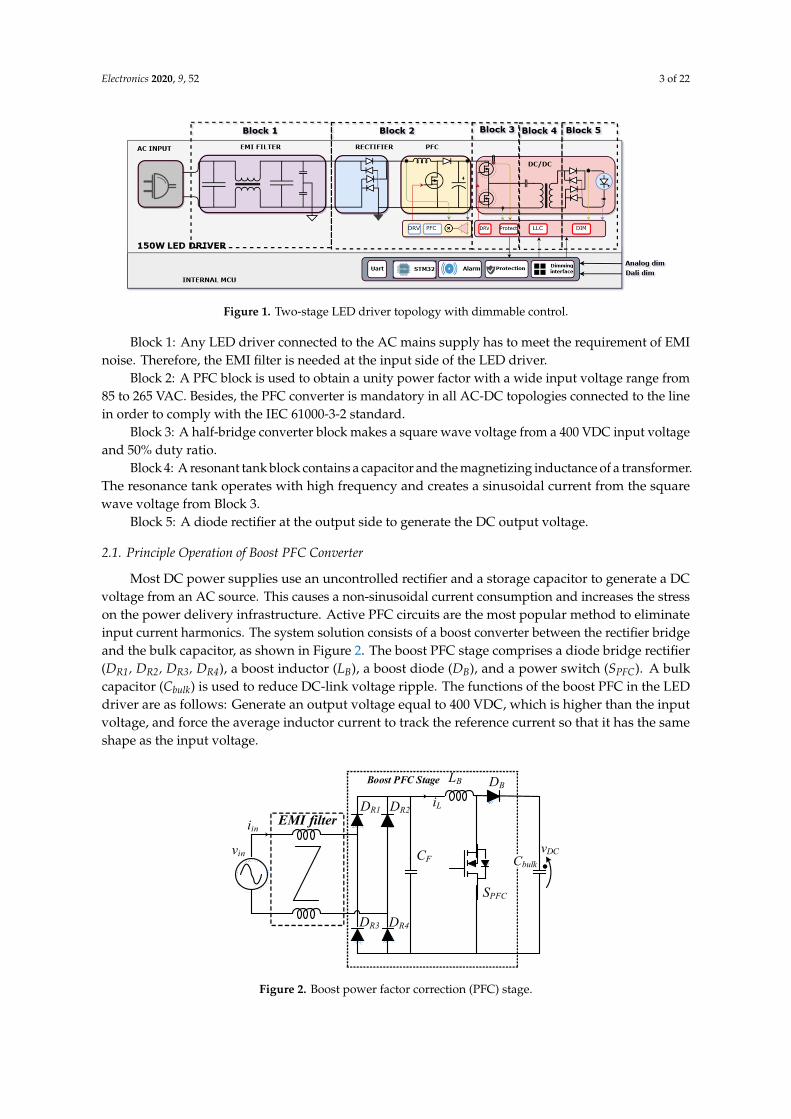
Figure 1. Two‐stage LED driver topology with dimmable control.
Block 1: Any LED driver connected to the AC mains supply has to meet the requirement of EMI
noise. Therefore, the EMI filter is needed at the input side of the LED driver.
Block 2: A PFC block is used to obtain a unity power factor with a wide input voltage range from
85 to 265 VAC. Besides, the PFC converter is mandatory in all AC‐DC topologies connected to the
line in order to comply with the IEC 61000‐3‐2 standard.
Block 3: A half‐bridge converter block makes a square wave voltage from a 400 VDC input
voltage and 50% duty ratio.
Block 4: A resonant tank block contains a capacitor and the magnetizing inductance of a
transformer. The resonance tank operates with high frequency and creates a sinusoidal current from
the square wave voltage from Block 3.
Block 5: A diode rectifier at the output side to generate the DC output voltage.
2.1. Principle Operation of Boost PFC Converter
Most DC power supplies use an uncontrolled rectifier and a storage capacitor to generate a DC
voltage from an AC source. This causes a non‐sinusoidal current consumption and increases the
stress on the power delivery infrastructure. Active PFC circuits are the most popular method to
eliminate input current harmonics. The system solution consists of a boost converter between the
rectifier bridge and the bulk capacitor, as shown in Figure 2. The boost PFC stage comprises a diode
bridge rectifier (DR1, DR2, DR3, DR4), a boost inductor (LB), a boost diode (DB), and a power switch (SPFC).
A bulk capacitor (Cbulk) is used to reduce DC‐link voltage ripple. The functions of the boost PFC in the
LED driver are as follows: Generate an output voltage equal to 400 VDC, which is higher than the
input voltage, and force the average inductor current to track the reference current so that it has the
same shape as the input voltage.
vin
DR1 DR2
DR3 DR4
Boost PFC Stage
SPFC
CF
DBLB
Cbulk
vDC
EMI filteriin
iL
Figure 2. Boost power factor correction (PFC) stage.
Although the PFC can be achieved by several topologies, the boost converter, as shown in Figure
2, is the most popular topology, for the following reasons: The line voltage varies from zero to some
peak value, typically 375 VDC (corresponding to maximum input voltage of 265 VAC); hence, a step‐
Figure 1. Two-stage LED driver topology with dimmable control.
Block 1: Any LED driver connected to the AC mains supply has to meet the requirement of EMInoise. Therefore, the EMI filter is needed at the input side of the LED driver.
Block 2: A PFC block is used to obtain a unity power factor with a wide input voltage range from85 to 265 VAC. Besides, the PFC converter is mandatory in all AC-DC topologies connected to the linein order to comply with the IEC 61000-3-2 standard.
Block 3: A half-bridge converter block makes a square wave voltage from a 400 VDC input voltageand 50% duty ratio.
Block 4: A resonant tank block contains a capacitor and the magnetizing inductance of a transformer.The resonance tank operates with high frequency and creates a sinusoidal current from the squarewave voltage from Block 3.
Block 5: A diode rectifier at the output side to generate the DC output voltage.
2.1. Principle Operation of Boost PFC Converter
Most DC power supplies use an uncontrolled rectifier and a storage capacitor to generate a DCvoltage from an AC source. This causes a non-sinusoidal current consumption and increases the stresson the power delivery infrastructure. Active PFC circuits are the most popular method to eliminateinput current harmonics. The system solution consists of a boost converter between the rectifier bridgeand the bulk capacitor, as shown in Figure 2. The boost PFC stage comprises a diode bridge rectifier(DR1, DR2, DR3, DR4), a boost inductor (LB), a boost diode (DB), and a power switch (SPFC). A bulkcapacitor (Cbulk) is used to reduce DC-link voltage ripple. The functions of the boost PFC in the LEDdriver are as follows: Generate an output voltage equal to 400 VDC, which is higher than the inputvoltage, and force the average inductor current to track the reference current so that it has the sameshape as the input voltage.
Electronics 2019, 8, x FOR PEER REVIEW 3 of 22
Figure 1. Two‐stage LED driver topology with dimmable control.
Block 1: Any LED driver connected to the AC mains supply has to meet the requirement of EMI
noise. Therefore, the EMI filter is needed at the input side of the LED driver.
Block 2: A PFC block is used to obtain a unity power factor with a wide input voltage range from
85 to 265 VAC. Besides, the PFC converter is mandatory in all AC‐DC topologies connected to the
line in order to comply with the IEC 61000‐3‐2 standard.
Block 3: A half‐bridge converter block makes a square wave voltage from a 400 VDC input
voltage and 50% duty ratio.
Block 4: A resonant tank block contains a capacitor and the magnetizing inductance of a
transformer. The resonance tank operates with high frequency and creates a sinusoidal current from
the square wave voltage from Block 3.
Block 5: A diode rectifier at the output side to generate the DC output voltage.
2.1. Principle Operation of Boost PFC Converter
Most DC power supplies use an uncontrolled rectifier and a storage capacitor to generate a DC
voltage from an AC source. This causes a non‐sinusoidal current consumption and increases the
stress on the power delivery infrastructure. Active PFC circuits are the most popular method to
eliminate input current harmonics. The system solution consists of a boost converter between the
rectifier bridge and the bulk capacitor, as shown in Figure 2. The boost PFC stage comprises a diode
bridge rectifier (DR1, DR2, DR3, DR4), a boost inductor (LB), a boost diode (DB), and a power switch (SPFC).
A bulk capacitor (Cbulk) is used to reduce DC‐link voltage ripple. The functions of the boost PFC in the
LED driver are as follows: Generate an output voltage equal to 400 VDC, which is higher than the
input voltage, and force the average inductor current to track the reference current so that it has the
same shape as the input voltage.
vin
DR1 DR2
DR3 DR4
Boost PFC Stage
SPFC
CF
DBLB
Cbulk
vDC
EMI filteriin
iL
Figure 2. Boost power factor correction (PFC) stage.
Although the PFC can be achieved by several topologies, the boost converter, as shown in Figure
2, is the most popular topology, for the following reasons: The line voltage varies from zero to some
peak value, typically 375 VDC (corresponding to maximum input voltage of 265 VAC); hence, a step‐
Figure 2. Boost power factor correction (PFC) stage.

Electronics 2020, 9, 52 4 of 22
Although the PFC can be achieved by several topologies, the boost converter, as shown in Figure 2,is the most popular topology, for the following reasons: The line voltage varies from zero to some peakvalue, typically 375 VDC (corresponding to maximum input voltage of 265 VAC); hence, a step-upconverter is needed to generate a DC output voltage (VDC) of 400 VDC. The boost converter has afilter inductor on the input side, which provides a smooth continuous input current waveform. Acontinuous input current is much easier to filter, which is a major advantage of this design due tothe low cost. The boost converter can operate in three modes: Continuous conduction mode (CCM),discontinuous conduction mode (DCM), and critical conduction mode (CrCM). By comparing theDCM among the others, DCM operation seems simpler than that of the CrCM, as it may operate inconstant frequency operation; however, the DCM has the disadvantage that it has the highest peakcurrent compared to the CrCM and also to the CCM, without any performance advantage compared tothe CrCM. For that reason, the CrCM is more a common practical design than the DCM.
Figure 3 shows the key waveforms of the boost PFC converter in the case of the CrCM. To obtain aunity power factor, the AC input voltage (vin) is measured to provide a reference for inductor current.In the CrCM mode, the inductor current ripple (IL(peak)) is twice the sinusoidal input current (iin), andthe switching frequency of the power switch is variable with constant on-time (TON), as shown inFigure 3.
Electronics 2019, 8, x FOR PEER REVIEW 4 of 22
up converter is needed to generate a DC output voltage (VDC) of 400 VDC. The boost converter has a
filter inductor on the input side, which provides a smooth continuous input current waveform. A
continuous input current is much easier to filter, which is a major advantage of this design due to the
low cost. The boost converter can operate in three modes: Continuous conduction mode (CCM),
discontinuous conduction mode (DCM), and critical conduction mode (CrCM). By comparing the
DCM among the others, DCM operation seems simpler than that of the CrCM, as it may operate in
constant frequency operation; however, the DCM has the disadvantage that it has the highest peak
current compared to the CrCM and also to the CCM, without any performance advantage compared
to the CrCM. For that reason, the CrCM is more a common practical design than the DCM.
Figure 3 shows the key waveforms of the boost PFC converter in the case of the CrCM. To obtain
a unity power factor, the AC input voltage (vin) is measured to provide a reference for inductor
current. In the CrCM mode, the inductor current ripple (IL(peak)) is twice the sinusoidal input current
(iin), and the switching frequency of the power switch is variable with constant on‐time (TON), as
shown in Figure 3.
Vin(peak)
IL(peak)
MOSFETSPFC
vin
iL
iin
Ton
Figure 3. Key waveforms of the input voltage (vin), input current (iin), and inductor current (iL) of the
boost PFC.
2.2. Principle Operation of LLC Resonant Converter
Resonant DC/DC converters, which were first introduced in the 1980s [23], provide a low
switching loss due to the enabling of resonant topologies to operate at high switching frequency. A
half‐bridge resonant converter has many advantages, such as high efficiency, high power density,
and low EMI. In general, the LLC resonant converter consists of three blocks, which are a square‐
wave generator, resonant network, and rectifier network. The LLC resonant converter is shown in
Figure 4, where LM is the magnetizing inductance that acts as a shunt inductor, LR is the series
resonant inductor, and CR is the resonant capacitor. The rectifier network includes a transformer and
two diodes, D1 and D2. The square‐wave generator produces a square‐wave voltage (VSQ) from the
DC power supply VDC by driving switches S1 and S2. The duty cycle of the two switches is 50%. In
order to avoid the short circuit in the half‐bridge converter, a dead‐time is inserted in the switching
state of S1 and S2. In this circuit, only the fundamental component of the current is allowed to flow
through the resonant network.
Figure 3. Key waveforms of the input voltage (vin), input current (iin), and inductor current (iL) of theboost PFC.
2.2. Principle Operation of LLC Resonant Converter
Resonant DC/DC converters, which were first introduced in the 1980s [23], provide a low switchingloss due to the enabling of resonant topologies to operate at high switching frequency. A half-bridgeresonant converter has many advantages, such as high efficiency, high power density, and low EMI.In general, the LLC resonant converter consists of three blocks, which are a square-wave generator,resonant network, and rectifier network. The LLC resonant converter is shown in Figure 4, where LMis the magnetizing inductance that acts as a shunt inductor, LR is the series resonant inductor, and CRis the resonant capacitor. The rectifier network includes a transformer and two diodes, D1 and D2.The square-wave generator produces a square-wave voltage (VSQ) from the DC power supply VDC bydriving switches S1 and S2. The duty cycle of the two switches is 50%. In order to avoid the short circuitin the half-bridge converter, a dead-time is inserted in the switching state of S1 and S2. In this circuit,only the fundamental component of the current is allowed to flow through the resonant network.

Electronics 2020, 9, 52 5 of 22Electronics 2019, 8, x FOR PEER REVIEW 5 of 22
S1
S2
CR LR
LM np
ns
ns
D1
D2
COvLED
VDC
Square‐wave Generator
Resonant Network Rectifier Network
VSQ
Figure 4. Half‐bridge LLC resonant converter topology.
Figure 5 shows the equivalent circuit of the LLC half‐bridge converter based on the first‐
harmonic approximation (FHA) method, where RAC is the equivalent load resistance. There are two
resonant frequencies (fr1, fr2), as shown in Equations (1) and (2), for the LLC half‐bridge converter [24]:
1
1
2r
R R
fL C
, (1)
2
1
2r
R M R
fL L C
. (2)
The AC‐equivalent load resistance (RAC) can be expressed by Equation (3) [25]:
2
2
8AC LED
nR R
, (3)
where p
s
nn
n is the transformer ratio (np and ns are the number of turns of the primary and
secondary coil, respectively) and RLED is the LED load.
LRCR
RACLMVSQ Vout
Figure 5. Simplified converter circuit of the LLC half‐bridge converter.
From the equivalent model, as shown in Figure 5, the well‐known voltage gain of the circuit is
described by Equation (4) [25–27]:
2
2 21 1 1 1out M AC n
SQ n n nM AC R
R
V j L R m fM
V m f j f f Q mj L R j Lj C
P
P
, (4)
Figure 4. Half-bridge LLC resonant converter topology.
Figure 5 shows the equivalent circuit of the LLC half-bridge converter based on the first-harmonicapproximation (FHA) method, where RAC is the equivalent load resistance. There are two resonantfrequencies (fr1, fr2), as shown in Equations (1) and (2), for the LLC half-bridge converter [24]:
fr1 =1
2π√
LRCR, (1)
fr2 =1
2π√(LR + LM)CR
. (2)
Electronics 2019, 8, x FOR PEER REVIEW 5 of 22
S1
S2
CR LR
LM np
ns
ns
D1
D2
COvLED
VDC
Square‐wave Generator
Resonant Network Rectifier Network
VSQ
Figure 4. Half‐bridge LLC resonant converter topology.
Figure 5 shows the equivalent circuit of the LLC half‐bridge converter based on the first‐
harmonic approximation (FHA) method, where RAC is the equivalent load resistance. There are two
resonant frequencies (fr1, fr2), as shown in Equations (1) and (2), for the LLC half‐bridge converter [24]:
1
1
2r
R R
fL C
, (1)
2
1
2r
R M R
fL L C
. (2)
The AC‐equivalent load resistance (RAC) can be expressed by Equation (3) [25]:
2
2
8AC LED
nR R
, (3)
where p
s
nn
n is the transformer ratio (np and ns are the number of turns of the primary and
secondary coil, respectively) and RLED is the LED load.
LRCR
RACLMVSQ Vout
Figure 5. Simplified converter circuit of the LLC half‐bridge converter.
From the equivalent model, as shown in Figure 5, the well‐known voltage gain of the circuit is
described by Equation (4) [25–27]:
2
2 21 1 1 1out M AC n
SQ n n nM AC R
R
V j L R m fM
V m f j f f Q mj L R j Lj C
P
P
, (4)
Figure 5. Simplified converter circuit of the LLC half-bridge converter.
The AC-equivalent load resistance (RAC) can be expressed by Equation (3) [25]:
RAC =8n2
π2 RLED, (3)
where n =npns
is the transformer ratio (np and ns are the number of turns of the primary and secondarycoil, respectively) and RLED is the LED load.
From the equivalent model, as shown in Figure 5, the well-known voltage gain of the circuit isdescribed by Equation (4) [25–27]:
M =Vout
VSQ=
∣∣∣∣∣∣∣ jωLM ‖ RAC
jωLM ‖ RAC + jωLR + 1jωCR
∣∣∣∣∣∣∣ =∣∣∣∣∣∣∣ m · f 2
n[(m + 1) · f 2
n − 1]+ j
[(f 2n − 1
)· fn ·Q ·m
] ∣∣∣∣∣∣∣, (4)
where m = LMLR
is the ratio of magnetizing inductance and leakage inductance, Q =
√LR/CRRAC
is the
quality factor, fn =fswf0
is the ratio of the switching frequency and resonant frequency, and ω is theangular frequency.
Electronics 2020, 9, 52 6 of 22
The output voltage of the LLC half-bridge converter is achieved as follows:
VLED = Mns
np
VDC2
. (5)
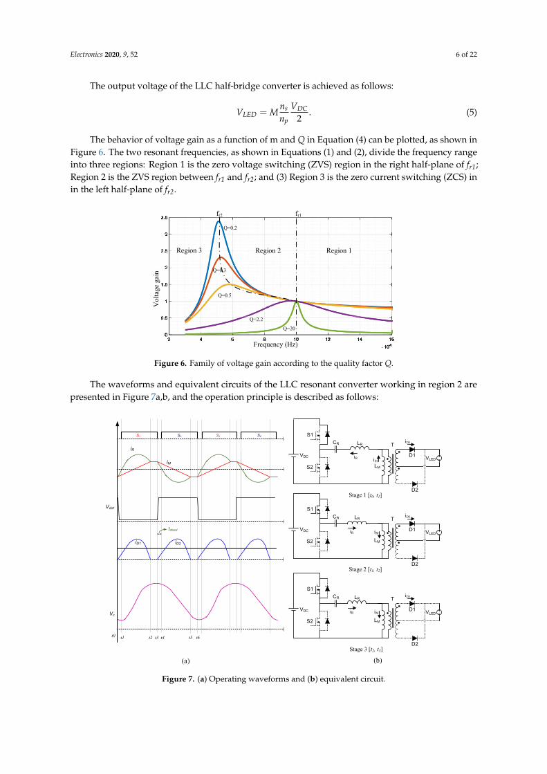
The behavior of voltage gain as a function of m and Q in Equation (4) can be plotted, as shown inFigure 6. The two resonant frequencies, as shown in Equations (1) and (2), divide the frequency rangeinto three regions: Region 1 is the zero voltage switching (ZVS) region in the right half-plane of fr1;Region 2 is the ZVS region between fr1 and fr2; and (3) Region 3 is the zero current switching (ZCS) inin the left half-plane of fr2.
Electronics 2019, 8, x FOR PEER REVIEW 6 of 22
where M
R
Lm
L is the ratio of magnetizing inductance and leakage inductance,
R R
AC
L CQ
R is
the quality factor, 0
swn
ff
f is the ratio of the switching frequency and resonant frequency, and
is the angular frequency.
The output voltage of the LLC half‐bridge converter is achieved as follows:
2s DC
LEDp
n VV M
n . (5)
The behavior of voltage gain as a function of m and Q in Equation (4) can be plotted, as shown
in Figure 6. The two resonant frequencies, as shown in Equations (1) and (2), divide the frequency
range into three regions: Region 1 is the zero voltage switching (ZVS) region in the right half‐plane
of fr1; Region 2 is the ZVS region between fr1 and fr2; and (3) Region 3 is the zero current switching
(ZCS) in in the left half‐plane of fr2.
Vol
tage
gai
n
Frequency (Hz)
Q=0.2
Q=0.3
Q=0.5
Q=2.2
Q=20
fr2 fr1
Region 3 Region 2 Region 1
Figure 6. Family of voltage gain according to the quality factor Q.
The waveforms and equivalent circuits of the LLC resonant converter working in region 2 are
presented in Figure 7a,b, and the operation principle is described as follows:
Stage 1 [t0 – t1]: This stage begins when both the two switches S1 and S2 are in the off state at time
t0, and the resonant current discharges the parasitic capacitor and then flows through the free‐
wheeling diode of S1. The input power does not transfer to the output side, and the output rectifier
diode, D1, continues to transfer power to the load by the output capacitor. In this stage, CR and LR
resonate because the voltage across LM is clamped at the reflected output voltage.
Stage 2 [t1 – t2]: This stage begins when S1 is turned on at t1, and S2 is still in the off state. S1 turns
on with the ZVS condition. The current drops to 0 A before reversing and flowing through the switch,
S1. The inductor LM is clamped by the secondary voltage and does not engage resonance, and the
magnetizing current IM linearly increases. The load current is proportional to the difference between
the resonant current, iR and iM.
Stage 3 [t2 – t3]: This mode begins when the resonant current iR becomes positive. At t2, the load
current drops to zero due to the resonant current, iR, equaling iM, and causes D1 to turn off. As the
switching period is bigger than the LR∙CR resonant period, S1 continues to conduct until t3.
Figure 6. Family of voltage gain according to the quality factor Q.
The waveforms and equivalent circuits of the LLC resonant converter working in region 2 arepresented in Figure 7a,b, and the operation principle is described as follows:Electronics 2019, 8, x FOR PEER REVIEW 7 of 22
t0 t1 t2 t3
iR
iM
Vds1
Vc
t4 t5 t6
iD1 iD2
S1 S2 S1 S2
tdead
Stage 1 [t0, t1]
S1
VDC
D2
D1 VLED
iD1
iM
LM
iR
S2
T
Stage 2 [t1, t2]
S1
VDC
D2
D1 VLED
iD1
iM
LM
iR
S2
T
Stage 3 [t2, t3]
S1
VDC
D2
D1 VLED
iD1
iM
LM
iR
S2
T
(a) (b)
LRCR
LRCR
LRCR
Figure 7. (a) Operating waveforms and (b) equivalent circuit.
3. Design Procedure of the Two‐Stage LED Driver
In order to verify the correction of the previous analysis in section 2, a two‐stage LED driver is
implemented by a combination between the boost PFC converter, as shown in Figure 2, and the LLC
resonant half‐bridge converter, as shown in Figure 4. The driver is designed for driving a 150 W LED
with output voltage 32 VDC. Detailed calculation of the AC/DC and DC/DC stages, EMI filter, and
dimming control module are presented as follows.
3.1. Boost‐PFC Stage Design
In this paper, the boost PFC is implemented using a NCP1608BDR2G controller [28]. The
advantages of this IC are a near‐unity power factor, wide control range, for high‐power application,
and no input voltage sensing requirement. Furthermore, it works safely due to it providing over
voltage, over current, and under voltage protection. This IC operates in the critical conduction mode
to ensure a near‐unity power factor across a wide range of input voltages and output power. It is also
an active power factor correction controller specifically designed for a medium power converter. The
design specification of the boost PFC converter is shown in Table 1.
Table 1. Parameters of boost PFC stage.
Boost PFC Design Parameters
Input voltage 220 V Vin
Frequency 50 Hz fin
Output voltage 400 V VDC
Input power 150 W P
Minimum Efficiency 92% min
Minimum switching frequency 40 kHz fsw(min)
The boost inductor LB is designed to be operated in the CrCM. Here, VDC is the DC‐bus voltage,
Vin is the input voltage, and fsw is the switching period of the power switch SPFC.
Figure 7. (a) Operating waveforms and (b) equivalent circuit.
Electronics 2020, 9, 52 7 of 22
Stage 1 [t0 – t1]: This stage begins when both the two switches S1 and S2 are in the off state at timet0, and the resonant current discharges the parasitic capacitor and then flows through the free-wheelingdiode of S1. The input power does not transfer to the output side, and the output rectifier diode, D1,continues to transfer power to the load by the output capacitor. In this stage, CR and LR resonatebecause the voltage across LM is clamped at the reflected output voltage.
Stage 2 [t1 – t2]: This stage begins when S1 is turned on at t1, and S2 is still in the off state. S1 turnson with the ZVS condition. The current drops to 0 A before reversing and flowing through the switch,S1. The inductor LM is clamped by the secondary voltage and does not engage resonance, and themagnetizing current IM linearly increases. The load current is proportional to the difference betweenthe resonant current, iR and iM.
Stage 3 [t2 – t3]: This mode begins when the resonant current iR becomes positive. At t2, the loadcurrent drops to zero due to the resonant current, iR, equaling iM, and causes D1 to turn off. As theswitching period is bigger than the LR·CR resonant period, S1 continues to conduct until t3.
3. Design Procedure of the Two-Stage LED Driver
In order to verify the correction of the previous analysis in Section 2, a two-stage LED driver isimplemented by a combination between the boost PFC converter, as shown in Figure 2, and the LLCresonant half-bridge converter, as shown in Figure 4. The driver is designed for driving a 150 W LEDwith output voltage 32 VDC. Detailed calculation of the AC/DC and DC/DC stages, EMI filter, anddimming control module are presented as follows.
3.1. Boost-PFC Stage Design
In this paper, the boost PFC is implemented using a NCP1608BDR2G controller [28]. Theadvantages of this IC are a near-unity power factor, wide control range, for high-power application,and no input voltage sensing requirement. Furthermore, it works safely due to it providing overvoltage, over current, and under voltage protection. This IC operates in the critical conduction modeto ensure a near-unity power factor across a wide range of input voltages and output power. It is alsoan active power factor correction controller specifically designed for a medium power converter. Thedesign specification of the boost PFC converter is shown in Table 1.
Table 1. Parameters of boost PFC stage.
Boost PFC Design Parameters
Input voltage 220 V VinFrequency 50 Hz fin
Output voltage 400 V VDCInput power 150 W P
Minimum Efficiency 92% ηminMinimum switching frequency 40 kHz fsw(min)
The boost inductor LB is designed to be operated in the CrCM. Here, VDC is the DC-bus voltage,Vin is the input voltage, and fsw is the switching period of the power switch SPFC.
LB =V2
in ·
(VDC√
2−Vin
)· ηmin
√2 ·VDC · P · fsw(min)
. (6)
The inductor value of the LB at maximum input voltage (265 V) is calculated as
LB =2652
·
(400√
2− 265
)· 0.92
√2 · 400 · 150 · 40 · 103
= 339 µH. (7)

Electronics 2020, 9, 52 8 of 22
In order to guarantee that the switching frequency is higher than 40 kHz, the boost inductor ischosen at 250 µH. Due to the tolerance of the inductor, the maximum inductance of the boost inductoris 300 µH. The minimum frequency at full load is
fsw(min) =V2
in · ηmin
2 · LBmax · P·
(1−
√2·Vin
Vout
)=
2652· 0.92
2 · 300 · 10−6 · 150·
(1−
√2·265400
)= 45.3 kHz. (8)
The IC NCP1608 has the over voltage function to prevent the output from exceeding a safe voltage.The threshold voltage for over voltage detection is 421 V. Therefore, the bulk capacitor is designed toensure that the ripple of the DC-bus voltage is smaller than 42 V.
Hence,
Cbulk ≥Pout
2 ·π ·Vripple · fin(min) ·Vout=
1502 ·π · 42 · 47 · 400
= 30 µF. (9)
In this design, the value of the bulk capacitor is selected at 100 µF.Table 2 summarizes the device list of the boost PFC stage.
Table 2. Device list of boost PFC stage.
Boost PFC Design Specification
Diode Rectifier(DR1, DR2, DR3, DR4) TS15P05GC2 (Taiwan Semiconductor)
Boost Inductor LB 300 µ (Core PQ2625)Mosfet SPFC STF13NM60N (STMicroelectronics)
Boost Diode DB STTH15R06FP (STMicroelectronics)Cbulk 100µF/450V (Nichion)
IC NCP1608BDR2G (Onsemi)
3.2. LLC Resonant DC-DC Converter Design
In this section, the step-by-step consideration of the design of the LLC resonant converter willbe discussed. The design of the LLC resonant converter implemented based on IC FLS2100XS [29] isdescribed as follows:
Step 1: Define the converter design specification. The LLC converter electrical specifications aregiven in Table 3.
Table 3. Parameters of LLC resonant DC-DC converter.
LLC Resonant Half-Bridge Design Parameters
Half-bridge input voltage 390–410 V VDCSwitching frequency 100–120 kHz fsw
Output voltage 32 V VLEDOutput current 4.7 A ILED
Step 2: Determine the transformer turns ratio. The transformer turns ratio is determined byEquation (10):
M =2nVLED
Vin⇒ n = M
Vin/2VLED
. (10)
To achieve a high operating efficiency, the switching frequency is chosen at near the resonantfrequency. The voltage gain of the LLC converter is chosen from 1 to 1.4. From Equation (10), the turnsratio is n = 6.3→ 8.96. Therefore, we choose the transformer turns ratio n as 8.75 (35:4:4), which isavailable in [30].

Electronics 2020, 9, 52 9 of 22
Step 3: Choose the transformer. In this research, the transformer core type is chosen as ETD-34 ofWurth Elektronik. The primary inductance and the leakage inductance of this transformer are
LP = 600 µH, LR = 100 µH, LM = 500 µH. (11)
Step 4: Determine the equivalent load resistance:
RAC =8n2
π2 RLED = 291.2 Ω. (12)
Step 5: Calculate the inductance ratio. From step 3, the inductance ratio m is determined as
m =LP
LR= 6. (13)
Step 6: Calculate the resonant circuit parameters. As introduced in Section 2, the workingfrequency fs must be lower than the resonant frequency in order to keep the converter working inregion 2. In this design, the switching frequency is chosen from 100 to 150 kHz and the resonantfrequency is set to be fr = 150 kHz.
CR =1
2πQ frRAC=
14π2 · f 2
r · LR= 11.2 nF. (14)
Therefore, the resonant capacitor is selected as CR = 10 nF.
Q =
√LR/CR
RAC= 0.32. (15)
Step 7: Verify the resonant-circuit design.From the above selected parameters, the resonant frequency is recalculated as
fr =1
2π√
LRCR= 159 kHz. (16)
Figure 8 shows the voltage gain characteristics of the LLC converter according to the differentquality factor Q in the case of m = 6 and resonant frequency fr = 159 kHz. It can be seen that, withthe switching frequency of 100 kHz and the quality factor Q = 0.32, the voltage gain is 1.4. FromEquation (10), the output voltage of the power converter is verified as Equation (17).
VLED =MVin
2n=
1.4 · 4002 · 8.75
= 32 V. (17)
Electronics 2020, 9, 52 10 of 22Electronics 2019, 8, x FOR PEER REVIEW 10 of 22
Voltage gain (M)
Frequency (Hz)
Resonant frequency
Switching frequency
Q=0.2
Q=0.32
Q=0.4
Q=1.4
Q=0.6
Figure 8. Voltage gain characteristics of the LLC resonant converter with the resonance frequency of
159 kHz, inductance ratio m = 6.
Table 4. Device list in the LLC resonant DC‐DC converter.
LLC Resonant Half‐Bridge Design Parameters
Transformer ETD 34 (35:4:4)
Switching frequency 100–120 kHz
Resonant Inductor LR 100 μH
Magnetizing Inductor LM 500 μH
Resonant Capacitor 10 nF
Didoe D1, D2 STPS30H60CFP
Mosfet S1, S2 and Driver IC FLS2100XS
Feedback Isolation Optocoupler PC817
3.3. EMI Design
Due to the high‐frequency switching noise current and voltage, EMI is a serious concern for the
LED driver. Inserting the EMI filter between the AC power supply and the diode rectifier is necessary
to comply with the EMC standards and to ensure a correct operation [31].
The LED power supply generally uses a two‐stage EMI filter, including a common mode choke
and a filter capacitor. Figure 9 is a conventional LED power filter. The differential‐mode filter is built
from an inductor LDM and two capacitors Cx1, Cx2. When common‐mode interference occurs, the
common‐mode choke LCM and the Y‐capacitors Cy1, Cy2 are used for dampening. The additional
capacitors Cy‐f1, Cy‐f2, Cy‐f3 connect the ground to the line and neutral for high pulsating voltages. Based
on the different current flows through the coupling capacitors Cy‐fi, the windings of the current
compensated choke Lcom must also be somewhat unbalanced. The two‐stage EMI filter shown in
Figure 10 is suitable for the boost PFC, which operates in critical mode. In this paper, the EMI filters
are designed based on the analysis of the conducted EMI and the use of a spectrum analyzer.
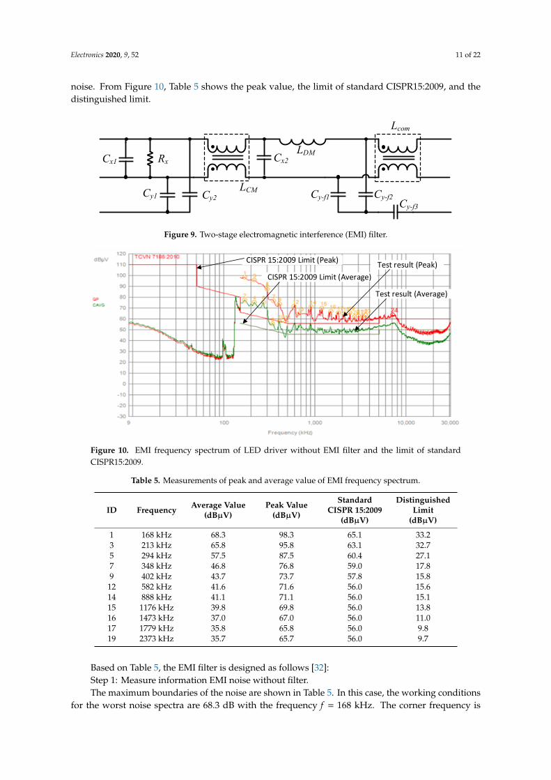
According to the CISPR 16‐1 standard, the peak and the average value of the EMI noise are measured.
Figure 10 shows the peak and average value of conduction noise of the LED driver without using
EMI noise. From Figure 10, Table 5 shows the peak value, the limit of standard CISPR15:2009, and
the distinguished limit.
Figure 8. Voltage gain characteristics of the LLC resonant converter with the resonance frequency of159 kHz, inductance ratio m = 6.
Table 4 shows the transformer information, switching frequency and the device lists which areused to implement DC/DC converter.
Table 4. Device list in the LLC resonant DC-DC converter.
LLC Resonant Half-Bridge Design Parameters
Transformer ETD 34 (35:4:4)Switching frequency 100–120 kHzResonant Inductor LR 100 µH
Magnetizing Inductor LM 500 µHResonant Capacitor 10 nF
Didoe D1, D2 STPS30H60CFPMosfet S1, S2 and Driver IC FLS2100XS
Feedback Isolation Optocoupler PC817
3.3. EMI Design
Due to the high-frequency switching noise current and voltage, EMI is a serious concern for theLED driver. Inserting the EMI filter between the AC power supply and the diode rectifier is necessaryto comply with the EMC standards and to ensure a correct operation [31].
The LED power supply generally uses a two-stage EMI filter, including a common mode chokeand a filter capacitor. Figure 9 is a conventional LED power filter. The differential-mode filter isbuilt from an inductor LDM and two capacitors Cx1, Cx2. When common-mode interference occurs,the common-mode choke LCM and the Y-capacitors Cy1, Cy2 are used for dampening. The additionalcapacitors Cy-f1, Cy-f2, Cy-f3 connect the ground to the line and neutral for high pulsating voltages.Based on the different current flows through the coupling capacitors Cy-fi, the windings of the currentcompensated choke Lcom must also be somewhat unbalanced. The two-stage EMI filter shown inFigure 10 is suitable for the boost PFC, which operates in critical mode. In this paper, the EMIfilters are designed based on the analysis of the conducted EMI and the use of a spectrum analyzer.According to the CISPR 16-1 standard, the peak and the average value of the EMI noise are measured.Figure 10 shows the peak and average value of conduction noise of the LED driver without using EMI
Electronics 2020, 9, 52 11 of 22
noise. From Figure 10, Table 5 shows the peak value, the limit of standard CISPR15:2009, and thedistinguished limit.Electronics 2019, 8, x FOR PEER REVIEW 11 of 22
Cy2Cy1LCM
Cx2LDM
Cx1 Rx
Cy-f2Cy-f1Cy-f3
Lcom
Figure 9. Two‐stage electromagnetic interference (EMI) filter.
CISPR 15:2009 Limit (Peak)
CISPR 15:2009 Limit (Average)
Test result (Peak)
Test result (Average)
Figure 10. EMI frequency spectrum of LED driver without EMI filter and the limit of standard
CISPR15:2009.
Table 5. Measurements of peak and average value of EMI frequency spectrum.
ID Frequency
Average
Value
(dBμV)
Peak Value
(dBμV)
Standard
CISPR
15:2009
(dBμV)
Distinguished
Limit
(dBμV)
1 168 kHz 68.3 98.3 65.1 33.2
3 213 kHz 65.8 95.8 63.1 32.7
5 294 kHz 57.5 87.5 60.4 27.1
7 348 kHz 46.8 76.8 59.0 17.8
9 402 kHz 43.7 73.7 57.8 15.8
12 582 kHz 41.6 71.6 56.0 15.6
14 888 kHz 41.1 71.1 56.0 15.1
15 1176 kHz 39.8 69.8 56.0 13.8
16 1473 kHz 37.0 67.0 56.0 11.0
17 1779 kHz 35.8 65.8 56.0 9.8
19 2373 kHz 35.7 65.7 56.0 9.7
Figure 9. Two-stage electromagnetic interference (EMI) filter.
Electronics 2019, 8, x FOR PEER REVIEW 11 of 22
Cy2Cy1
LCM
Cx2
LDMCx1 Rx
Cy-f2Cy-f1Cy-f3
Lcom
Figure 9. Two-stage electromagnetic interference (EMI) filter.
CISPR 15:2009 Limit (Peak)
CISPR 15:2009 Limit (Average)
Test result (Peak)
Test result (Average)
Figure 10. EMI frequency spectrum of LED driver without EMI filter and the limit of standard
CISPR15:2009.
Table 5. Measurements of peak and average value of EMI frequency spectrum.
ID Frequency Average
Value (dBµV)
Peak Value
(dBµV)
Standard
CISPR
15:2009
(dBµV)
Distinguished
Limit
(dBµV)
1 168 kHz 68.3 98.3 65.1 33.2
3 213 kHz 65.8 95.8 63.1 32.7
5 294 kHz 57.5 87.5 60.4 27.1
7 348 kHz 46.8 76.8 59.0 17.8
9 402 kHz 43.7 73.7 57.8 15.8
12 582 kHz 41.6 71.6 56.0 15.6
14 888 kHz 41.1 71.1 56.0 15.1
15 1176 kHz 39.8 69.8 56.0 13.8
16 1473 kHz 37.0 67.0 56.0 11.0
17 1779 kHz 35.8 65.8 56.0 9.8
19 2373 kHz 35.7 65.7 56.0 9.7
Figure 10. EMI frequency spectrum of LED driver without EMI filter and the limit of standardCISPR15:2009.
Table 5. Measurements of peak and average value of EMI frequency spectrum.
ID Frequency Average Value(dBµV)
Peak Value(dBµV)
StandardCISPR 15:2009
(dBµV)
DistinguishedLimit
(dBµV)
1 168 kHz 68.3 98.3 65.1 33.23 213 kHz 65.8 95.8 63.1 32.75 294 kHz 57.5 87.5 60.4 27.17 348 kHz 46.8 76.8 59.0 17.89 402 kHz 43.7 73.7 57.8 15.8
12 582 kHz 41.6 71.6 56.0 15.614 888 kHz 41.1 71.1 56.0 15.115 1176 kHz 39.8 69.8 56.0 13.816 1473 kHz 37.0 67.0 56.0 11.017 1779 kHz 35.8 65.8 56.0 9.819 2373 kHz 35.7 65.7 56.0 9.7
Based on Table 5, the EMI filter is designed as follows [32]:Step 1: Measure information EMI noise without filter.The maximum boundaries of the noise are shown in Table 5. In this case, the working conditions
for the worst noise spectra are 68.3 dB with the frequency f = 168 kHz. The corner frequency is

Electronics 2020, 9, 52 12 of 22
calculated by using the frequency of the first highest interference amplitude point of CM interference.The corner frequency is determined by the following equation.
fc =fsw
10∆Vnoise−Vlimit
40
, (18)
where fc is the corner frequency (cut-off frequency) and (∆Vnoise – Vlimit) is the attenuation.Step 2: Determine filter attenuation requirement.For a proper margin, a limit under 6 dB is used in the design, and the attenuation requirement is
calculated asVreq,dB = VdB −Vlimit,dB + 6dB, (19)
where VdB is obtained from the EMI noise without a filter, Vlimit,dB is the conducted EMI limit specifiedby the CISPR 15:2009 standard, and +6 dB is reserved for safety.
Step 3: Determine filter corner frequency.From Table 5, and Equations (18) and (19), the corner frequency is determined as
fc =fsw
10VNOISE−VLIMIT+6dB
40
=168.103
1033.2dB+6dB
40
= 17.6 kHz. (20)
Step 4: Determine filter component values.Based on standard EN 60335-1, the maximum capacitance connected to the ground cannot exceed
about 4700 pF on each phase for 250 VAC 50 Hz mains to meet the safety leakage current requirement.In this design, the Y-capacitors (Cy1, Cy2) are chosen at 1000 pF.
The LCM and Y-capacitor should have a resonant frequency of fc obtained in Step 3. Therefore, theinductor LCM is calculated as follows:
LCM =1
(2π fc)2× 2Cy
=1
(2π× 17.6× 103)2× 2× 10−9
= 41 mH. (21)
For the differential-mode component, there is a freedom in choosing the differential mode inductorLDM and X-capacitor capacitance. Hence, LDM and Cx1, Cx2 are decided according to Equation (22).
LDM =1
(2π fc)2×Cx
. (22)
In this design, CX1, Cx2 are chosen at 0.47µF, which is commonly available. Thus, LDM was obtained:
LDM =1
(2π fc)2×Cx
=1
(2π× 17.6× 103)2× 470× 10−9
= 174 µH. (23)
The parameters of the two-stage EMI filter are given in Table 6.
Table 6. Parameters of the input EMI filter.
Component Values
Cy1, Cy2 1 nF/400 VCy-f1, Cy-f2, Cy-f3 1 nF/400 V
Cx1, Cx2 470 nF/240 VLCM 40 mHLDM 170 µHLcom 20 mH

Electronics 2020, 9, 52 13 of 22
For the filter, as shown in Figure 9, there are the two discrete components: LDM and LCM. Ascalculated in Equation (23), the inductance of the LDM is small. Therefore, two discrete componentsLCM and LDM can be integrated into one inductive component LC, as shown in Figure 11, where theleakage of the Lc is LDM. The leakage inductance of the LC is used as a series inductance, whichrepresents a differential-mode filter component.
Electronics 2019, 8, x FOR PEER REVIEW 13 of 22
Lcom 20 mH
For the filter, as shown in Figure 9, there are the two discrete components: LDM and LCM. As
calculated in Equation (23), the inductance of the LDM is small. Therefore, two discrete components
LCM and LDM can be integrated into one inductive component LC, as shown in Figure 11, where the
leakage of the Lc is LDM. The leakage inductance of the LC is used as a series inductance, which
represents a differential‐mode filter component.
Cy2Cy1LC
Cx2Cx1 Rx
Cy-f2Cy-f1 Cy-f3
Lcom
Figure 11. EMI filter with the combination LCM and LDM.
3.4. Dimming Control
LED lighting loads have very similar electrical characteristics to a diode, which is a constant‐
current source. The brightness of the LED light is dimmed by controlling the current. The load current
is controlled by adjusting the switching frequency of the LLC resonant half‐bridge converter. In this
paper, the IC FLS2100XS is used for controlling the LLC resonant half‐bridge converter. Figure 12
shows the typical circuit configuration for the RT pin of FLS2100XS, where an opto‐coupler transistor
is connected to the RT pin to control the switching frequency.
The LED dimming is implemented as shown in Figure 13, which is described as the error
between the reference value and feedback value, and is the input of the analog proportional–integral
(PI) controller. In addition, the output of the PI controller is used to feed the opto‐coupler, which is
connected to the RT pin of IC FLS2100XS to adjust the switching frequency.
Figure 12. Typical circuit configuration for RT pin of IC FLS2100XS.
Figure 11. EMI filter with the combination LCM and LDM.
3.4. Dimming Control
LED lighting loads have very similar electrical characteristics to a diode, which is a constant-currentsource. The brightness of the LED light is dimmed by controlling the current. The load current iscontrolled by adjusting the switching frequency of the LLC resonant half-bridge converter. In thispaper, the IC FLS2100XS is used for controlling the LLC resonant half-bridge converter. Figure 12shows the typical circuit configuration for the RT pin of FLS2100XS, where an opto-coupler transistoris connected to the RT pin to control the switching frequency.
Electronics 2019, 8, x FOR PEER REVIEW 13 of 22
Lcom 20 mH
For the filter, as shown in Figure 9, there are the two discrete components: LDM and LCM. As
calculated in Equation (23), the inductance of the LDM is small. Therefore, two discrete components
LCM and LDM can be integrated into one inductive component LC, as shown in Figure 11, where the
leakage of the Lc is LDM. The leakage inductance of the LC is used as a series inductance, which
represents a differential‐mode filter component.
Cy2Cy1LC
Cx2Cx1 Rx
Cy-f2Cy-f1 Cy-f3
Lcom
Figure 11. EMI filter with the combination LCM and LDM.
3.4. Dimming Control
LED lighting loads have very similar electrical characteristics to a diode, which is a constant‐
current source. The brightness of the LED light is dimmed by controlling the current. The load current
is controlled by adjusting the switching frequency of the LLC resonant half‐bridge converter. In this
paper, the IC FLS2100XS is used for controlling the LLC resonant half‐bridge converter. Figure 12
shows the typical circuit configuration for the RT pin of FLS2100XS, where an opto‐coupler transistor
is connected to the RT pin to control the switching frequency.
The LED dimming is implemented as shown in Figure 13, which is described as the error
between the reference value and feedback value, and is the input of the analog proportional–integral
(PI) controller. In addition, the output of the PI controller is used to feed the opto‐coupler, which is
connected to the RT pin of IC FLS2100XS to adjust the switching frequency.
Figure 12. Typical circuit configuration for RT pin of IC FLS2100XS. Figure 12. Typical circuit configuration for RT pin of IC FLS2100XS.
The LED dimming is implemented as shown in Figure 13, which is described as the error betweenthe reference value and feedback value, and is the input of the analog proportional–integral (PI)controller. In addition, the output of the PI controller is used to feed the opto-coupler, which isconnected to the RT pin of IC FLS2100XS to adjust the switching frequency.

Electronics 2020, 9, 52 14 of 22
Electronics 2019, 8, x FOR PEER REVIEW 14 of 22
+
PI Controller
LLCConverter
Dimming
Reference
Analog PI Power stage LED Load
+‐
Feedback
Figure 13. Principle of LED light dimming.
The schematic circuit diagram of the analog PI controller is presented in Figure 14. The analog
PI controller is implemented by using op‐amp LM358. First, the load current is measured by using
the shunt resistor and feedback to the analog PI controller circuit through the variable resistor VR1.
Second, the reference voltage is generated by using IC TL431, and it is set at 2.5 V. Hence, the 0–10 V
or PWM dimmer is connected to R1 and the LC filter (R1, C1) generating the DC voltage. The
feedback current and the dimming current signals are added and compared to the reference current
signal. In addition, the error signal is fed into the analog PI controller, as shown in Figure 13.
Figure 14. Schematic circuit diagram of the analog proportional–integral (PI) controller.
4. Hardware Prototype and Experimental Results
In this paper, a hardware implementation of the dimmable 150 W LED driver for street lighting
application was carried out in laboratory, as shown in Figure 15. The specification and key
components of the two‐stage LED driver are presented in detail in Tables 2, 4, and 6. In this research,
the experimental results are measured by using a Fluke 437 Power Quality and Energy Analyzer, and
the waveforms are captured by using the Tektronix TDS 2024B.
Figure 13. Principle of LED light dimming.
The schematic circuit diagram of the analog PI controller is presented in Figure 14. The analogPI controller is implemented by using op-amp LM358. First, the load current is measured by usingthe shunt resistor and feedback to the analog PI controller circuit through the variable resistor VR1.Second, the reference voltage is generated by using IC TL431, and it is set at 2.5 V. Hence, the 0–10 V orPWM dimmer is connected to R1 and the LC filter (R1, C1) generating the DC voltage. The feedbackcurrent and the dimming current signals are added and compared to the reference current signal. Inaddition, the error signal is fed into the analog PI controller, as shown in Figure 13.
Electronics 2019, 8, x FOR PEER REVIEW 14 of 22
+
PI Controller
LLCConverter
Dimming
Reference
Analog PI Power stage LED Load
+‐
Feedback
Figure 13. Principle of LED light dimming.
The schematic circuit diagram of the analog PI controller is presented in Figure 14. The analog
PI controller is implemented by using op‐amp LM358. First, the load current is measured by using
the shunt resistor and feedback to the analog PI controller circuit through the variable resistor VR1.
Second, the reference voltage is generated by using IC TL431, and it is set at 2.5 V. Hence, the 0–10 V
or PWM dimmer is connected to R1 and the LC filter (R1, C1) generating the DC voltage. The
feedback current and the dimming current signals are added and compared to the reference current
signal. In addition, the error signal is fed into the analog PI controller, as shown in Figure 13.
Figure 14. Schematic circuit diagram of the analog proportional–integral (PI) controller.
4. Hardware Prototype and Experimental Results
In this paper, a hardware implementation of the dimmable 150 W LED driver for street lighting
application was carried out in laboratory, as shown in Figure 15. The specification and key
components of the two‐stage LED driver are presented in detail in Tables 2, 4, and 6. In this research,
the experimental results are measured by using a Fluke 437 Power Quality and Energy Analyzer, and
the waveforms are captured by using the Tektronix TDS 2024B.
Figure 14. Schematic circuit diagram of the analog proportional–integral (PI) controller.
4. Hardware Prototype and Experimental Results
In this paper, a hardware implementation of the dimmable 150 W LED driver for street lightingapplication was carried out in laboratory, as shown in Figure 15. The specification and key componentsof the two-stage LED driver are presented in detail in Table 2, Table 4, and Table 6. In this research, theexperimental results are measured by using a Fluke 437 Power Quality and Energy Analyzer, and thewaveforms are captured by using the Tektronix TDS 2024B.
Electronics 2020, 9, 52 15 of 22
Electronics 2019, 8, x FOR PEER REVIEW 15 of 22
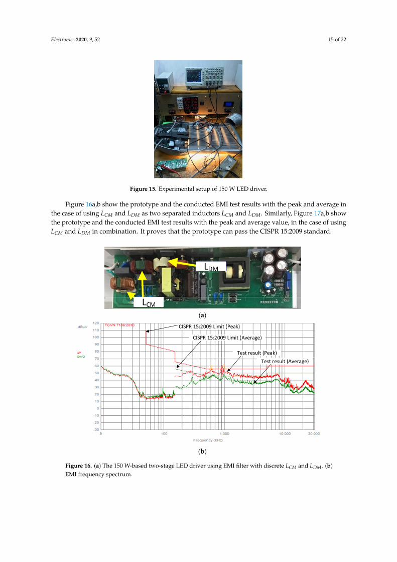
Figure 15. Experimental setup of 150 W LED driver.
Figure 16a,b show the prototype and the conducted EMI test results with the peak and average
in the case of using LCM and LDM as two separated inductors LCM and LDM. Similarly, Figure 17a,b show
the prototype and the conducted EMI test results with the peak and average value, in the case of
using LCM and LDM in combination. It proves that the prototype can pass the CISPR 15:2009 standard.
LDM
LCM
(a)
CISPR 15:2009 Limit (Peak)
CISPR 15:2009 Limit (Average)
Test result (Peak)
Test result (Average)
(b)
Figure 16. (a) The 150 W‐based two‐stage LED driver using EMI filter with discrete LCM and LDM. (b)
EMI frequency spectrum.
Figure 15. Experimental setup of 150 W LED driver.
Figure 16a,b show the prototype and the conducted EMI test results with the peak and average inthe case of using LCM and LDM as two separated inductors LCM and LDM. Similarly, Figure 17a,b showthe prototype and the conducted EMI test results with the peak and average value, in the case of usingLCM and LDM in combination. It proves that the prototype can pass the CISPR 15:2009 standard.
Electronics 2019, 8, x FOR PEER REVIEW 15 of 22
Figure 15. Experimental setup of 150 W LED driver.
Figure 16a,b show the prototype and the conducted EMI test results with the peak and average
in the case of using LCM and LDM as two separated inductors LCM and LDM. Similarly, Figure 17a,b show
the prototype and the conducted EMI test results with the peak and average value, in the case of
using LCM and LDM in combination. It proves that the prototype can pass the CISPR 15:2009 standard.
LDM
LCM
(a)
CISPR 15:2009 Limit (Peak)
CISPR 15:2009 Limit (Average)
Test result (Peak)
Test result (Average)
(b)
Figure 16. (a) The 150 W‐based two‐stage LED driver using EMI filter with discrete LCM and LDM. (b)
EMI frequency spectrum. Figure 16. (a) The 150 W-based two-stage LED driver using EMI filter with discrete LCM and LDM. (b)EMI frequency spectrum.

Electronics 2020, 9, 52 16 of 22
Electronics 2019, 8, x FOR PEER REVIEW 16 of 22
Integrated LCM
(a)
CISPR 15:2009 Limit (Peak)
CISPR 15:2009 Limit (Average)
Test result (Peak)
Test result (Average)
(b)
Figure 17. (a) The 150 W‐based two‐stage LED driver with combined LCM and LDM. (b) EMI frequency
spectrum.
Figure 18a,b show the current/voltage waveforms in the PFC stage. In Figure 18a, experimental
results of the input voltage vin and input current iin are shown, and it can be seen that the obtained
power factor is nearly unity. The inductor current and the full‐bridge rectifier voltage are shown in
Figure 18b. It can be seen that the peak value of the inductor current is proportional to a full‐wave
rectified waveform. Figure 19 shows the waveforms of the input voltage and output voltage of the
PFC stage. The data obtained from experimental results show that the average voltage is 405 V, which
is higher than the nominal value (400 V), and its ripple is around 20 V, which corresponds to
approximately 5%.
Figure 20 shows experimental results of output voltage (VLED) and output current (ILED). The load
voltage is 31.3 V, and the current is 4.9 A. This means that the power is 150 W. The voltage ripple is
lower than 1 V, and the current ripple is about 150 mA. Table 7 presents the results of the input
current, efficiency, PF, THD, with variation of the input voltage. With the nominal value, 220 Vrms,
the PF is higher than 0.98, the THD is lower than 7%, and the efficiency is higher than 91.6%. As
expected, this converter is suitable for a wide range of input voltages, and it achieved a good
performance for the THD and PF, as well as efficiency. Figure 21 depicts the input current spectrum,
and the THD is 6.4%. The results show that all input harmonics are in accordance with the IEC 61000‐
3‐2.
Figure 22a–c show the values of the input power factor, THD, and system efficiency according
to the variation in load: From 10% to full load. The efficiency is always higher than 90% and the
system power factor (PF) remains more than 0.97 when the load changes from 70% to 100%.
Furthermore, the THD is smaller than 20% with 10% load and will decrease to 5.2% at full load.
Figure 17. (a) The 150 W-based two-stage LED driver with combined LCM and LDM. (b) EMIfrequency spectrum.
Figure 18a,b show the current/voltage waveforms in the PFC stage. In Figure 18a, experimentalresults of the input voltage vin and input current iin are shown, and it can be seen that the obtainedpower factor is nearly unity. The inductor current and the full-bridge rectifier voltage are shown inFigure 18b. It can be seen that the peak value of the inductor current is proportional to a full-waverectified waveform. Figure 19 shows the waveforms of the input voltage and output voltage of thePFC stage. The data obtained from experimental results show that the average voltage is 405 V,which is higher than the nominal value (400 V), and its ripple is around 20 V, which corresponds toapproximately 5%.

Electronics 2020, 9, 52 17 of 22
Electronics 2019, 8, x FOR PEER REVIEW 17 of 22
Figure 23a,b show the curves of the system PF and THD with changing input voltage. As shown
in these figures, when the input voltage changes between 150 and 220 Vrms, the system THD is
always lower than 10%, and the PF remains greater than 0.965. From Figures 22 and 23, the system
THD always satisfies the IEC 61000‐3‐2 standard.
(a)
(b)
Figure 18. (a) Experimental results of input voltage/current, and (b) experimental results of full‐bridge
rectifier voltage and inductor current of boost PFC.
Figure 19. Experimental results of input voltage and DC‐bus voltage.
Figure 18. (a) Experimental results of input voltage/current, and (b) experimental results of full-bridgerectifier voltage and inductor current of boost PFC.
Electronics 2019, 8, x FOR PEER REVIEW 17 of 22
Figure 23a,b show the curves of the system PF and THD with changing input voltage. As shown
in these figures, when the input voltage changes between 150 and 220 Vrms, the system THD is
always lower than 10%, and the PF remains greater than 0.965. From Figures 22 and 23, the system
THD always satisfies the IEC 61000‐3‐2 standard.
(a)
(b)
Figure 18. (a) Experimental results of input voltage/current, and (b) experimental results of full‐bridge
rectifier voltage and inductor current of boost PFC.
Figure 19. Experimental results of input voltage and DC‐bus voltage. Figure 19. Experimental results of input voltage and DC-bus voltage.
Figure 20 shows experimental results of output voltage (VLED) and output current (ILED). Theload voltage is 31.3 V, and the current is 4.9 A. This means that the power is 150 W. The voltage ripple islower than 1 V, and the current ripple is about 150 mA. Table 7 presents the results of the input current,efficiency, PF, THD, with variation of the input voltage. With the nominal value, 220 Vrms, the PF is
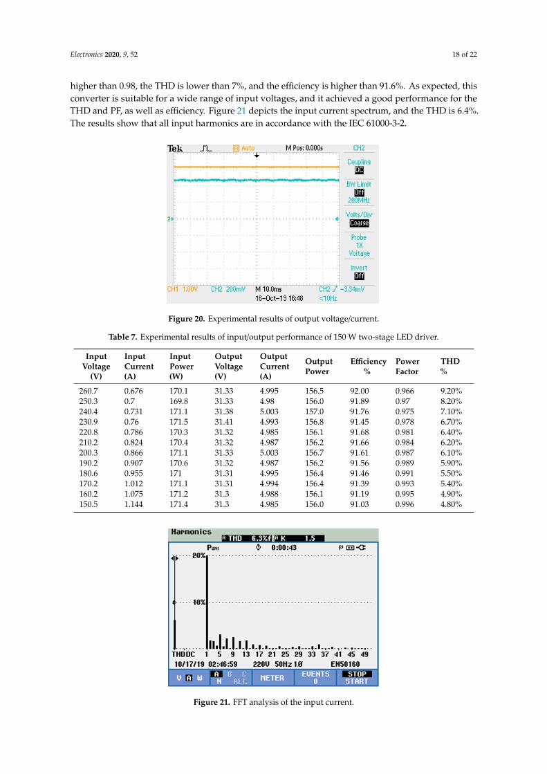
Electronics 2020, 9, 52 18 of 22
higher than 0.98, the THD is lower than 7%, and the efficiency is higher than 91.6%. As expected, thisconverter is suitable for a wide range of input voltages, and it achieved a good performance for theTHD and PF, as well as efficiency. Figure 21 depicts the input current spectrum, and the THD is 6.4%.The results show that all input harmonics are in accordance with the IEC 61000-3-2.Electronics 2019, 8, x FOR PEER REVIEW 18 of 22
Figure 20. Experimental results of output voltage/current.
Figure 21. FFT analysis of the input current.
Table 7. Experimental results of input/output performance of 150 W two‐stage LED driver.
Input
Voltage
(V)
Input
Current
(A)
Input
Power
(W)
Output
Voltage
(V)
Output
Current
(A)
Output
Power
Efficiency
%
Power
Factor
THD
%
260.7 0.676 170.1 31.33 4.995 156.5 92.00 0.966 9.20%
250.3 0.7 169.8 31.33 4.98 156.0 91.89 0.97 8.20%
240.4 0.731 171.1 31.38 5.003 157.0 91.76 0.975 7.10%
230.9 0.76 171.5 31.41 4.993 156.8 91.45 0.978 6.70%
220.8 0.786 170.3 31.32 4.985 156.1 91.68 0.981 6.40%
210.2 0.824 170.4 31.32 4.987 156.2 91.66 0.984 6.20%
200.3 0.866 171.1 31.33 5.003 156.7 91.61 0.987 6.10%
190.2 0.907 170.6 31.32 4.987 156.2 91.56 0.989 5.90%
180.6 0.955 171 31.31 4.995 156.4 91.46 0.991 5.50%
170.2 1.012 171.1 31.31 4.994 156.4 91.39 0.993 5.40%
160.2 1.075 171.2 31.3 4.988 156.1 91.19 0.995 4.90%
150.5 1.144 171.4 31.3 4.985 156.0 91.03 0.996 4.80%
Figure 20. Experimental results of output voltage/current.
Table 7. Experimental results of input/output performance of 150 W two-stage LED driver.
InputVoltage
(V)
InputCurrent(A)
InputPower(W)
OutputVoltage(V)
OutputCurrent(A)
OutputPower
Efficiency%
PowerFactor
THD%
260.7 0.676 170.1 31.33 4.995 156.5 92.00 0.966 9.20%250.3 0.7 169.8 31.33 4.98 156.0 91.89 0.97 8.20%240.4 0.731 171.1 31.38 5.003 157.0 91.76 0.975 7.10%230.9 0.76 171.5 31.41 4.993 156.8 91.45 0.978 6.70%220.8 0.786 170.3 31.32 4.985 156.1 91.68 0.981 6.40%210.2 0.824 170.4 31.32 4.987 156.2 91.66 0.984 6.20%200.3 0.866 171.1 31.33 5.003 156.7 91.61 0.987 6.10%190.2 0.907 170.6 31.32 4.987 156.2 91.56 0.989 5.90%180.6 0.955 171 31.31 4.995 156.4 91.46 0.991 5.50%170.2 1.012 171.1 31.31 4.994 156.4 91.39 0.993 5.40%160.2 1.075 171.2 31.3 4.988 156.1 91.19 0.995 4.90%150.5 1.144 171.4 31.3 4.985 156.0 91.03 0.996 4.80%
Electronics 2019, 8, x FOR PEER REVIEW 18 of 22
Figure 20. Experimental results of output voltage/current.
Figure 21. FFT analysis of the input current.
Table 7. Experimental results of input/output performance of 150 W two‐stage LED driver.
Input
Voltage
(V)
Input
Current
(A)
Input
Power
(W)
Output
Voltage
(V)
Output
Current
(A)
Output
Power
Efficiency
%
Power
Factor
THD
%
260.7 0.676 170.1 31.33 4.995 156.5 92.00 0.966 9.20%
250.3 0.7 169.8 31.33 4.98 156.0 91.89 0.97 8.20%
240.4 0.731 171.1 31.38 5.003 157.0 91.76 0.975 7.10%
230.9 0.76 171.5 31.41 4.993 156.8 91.45 0.978 6.70%
220.8 0.786 170.3 31.32 4.985 156.1 91.68 0.981 6.40%
210.2 0.824 170.4 31.32 4.987 156.2 91.66 0.984 6.20%
200.3 0.866 171.1 31.33 5.003 156.7 91.61 0.987 6.10%
190.2 0.907 170.6 31.32 4.987 156.2 91.56 0.989 5.90%
180.6 0.955 171 31.31 4.995 156.4 91.46 0.991 5.50%
170.2 1.012 171.1 31.31 4.994 156.4 91.39 0.993 5.40%
160.2 1.075 171.2 31.3 4.988 156.1 91.19 0.995 4.90%
150.5 1.144 171.4 31.3 4.985 156.0 91.03 0.996 4.80%
Figure 21. FFT analysis of the input current.

Electronics 2020, 9, 52 19 of 22
Figure 22a–c show the values of the input power factor, THD, and system efficiency according tothe variation in load: From 10% to full load. The efficiency is always higher than 90% and the systempower factor (PF) remains more than 0.97 when the load changes from 70% to 100%. Furthermore, theTHD is smaller than 20% with 10% load and will decrease to 5.2% at full load.Electronics 2019, 8, x FOR PEER REVIEW 19 of 22
(a)
(b)
(c)
Figure 22. Experimental results of (a) PF and (b) total harmonics distortion (THD). (c) Efficiency with
changing power load.
0.70
0.75
0.80
0.85
0.90
0.95
1.00
21 41 61 82 103 125 146 156
PF
Output Power (W)
0
5
10
15
20
25
21 41 61 82 103 125 146 156
THD (%)
Output Power (W)
70.00
75.00
80.00
85.00
90.00
95.00
21 41 61 82 103 125 146 156
Efficien
cy (%)
Output Power (W)
Figure 22. Experimental results of (a) PF and (b) total harmonics distortion (THD). (c) Efficiency withchanging power load.

Electronics 2020, 9, 52 20 of 22
Figure 23a,b show the curves of the system PF and THD with changing input voltage. As shownin these figures, when the input voltage changes between 150 and 220 Vrms, the system THD is alwayslower than 10%, and the PF remains greater than 0.965. From Figures 22 and 23, the system THDalways satisfies the IEC 61000-3-2 standard.Electronics 2019, 8, x FOR PEER REVIEW 20 of 22
(a)
(b)
Figure 23. Experimental results of (a) PF and (b) THD with changing input voltage.
5. Conclusions
In this paper, the implementation of a 150 W LED driver, which was built from the combination
between a boost PFC circuit and half‐bridge‐type LLC resonant circuit, was presented. An IC
NCP1608 manufactured by ON Semiconductor was used to drive the switches in the boost converter,
and an IC FLS2100XS was used in the LLC resonant half‐bridge converter. The design of the AC/DC
and DC/DC converter was analyzed and presented in detail. Furthermore, the optimization of the
EMI filter has been presented, and discrete inductances were combined in order to make the filter
smaller and cheaper. The output power has been tested from 10% to full load to show the
effectiveness of the dimmable control. A prototype was built in the laboratory and some experimental
results were shown to demonstrate a PF as high as 0.981, THD lower than 6.5%, efficiency as high as
91.8%, and bus voltage as low as 400 V. The EMI and THD test results show that the driver complies
with CIRSP 15:2009 and IEC 61000‐3‐2.
Author Contributions: L.M.P. and N.D.T. designed the methodology and wrote the manuscript. N.T.T. and
N.M.H. conceived and designed the hardware. N.D.T. and N.H.P. implemented the experiments and collected
data. N.C.C. provided validation and editing. L.M.P. provided supervision and revised the manuscript. All
authors have read and agreed to the published version of the manuscript.
0.00
1.00
2.00
3.00
4.00
5.00
6.00
7.00
8.00
9.00
10.00
150 160 170 180 190 200 210 220 230 240 250 260
THD (%)
Input voltage (Vrms)
0.950
0.955
0.960
0.965
0.970
0.975
0.980
0.985
0.990
0.995
1.000
150 160 170 180 190 200 210 220 230 240 250 260
PF
Input voltage (Vrms)
Figure 23. Experimental results of (a) PF and (b) THD with changing input voltage.
5. Conclusions
In this paper, the implementation of a 150 W LED driver, which was built from the combinationbetween a boost PFC circuit and half-bridge-type LLC resonant circuit, was presented. An IC NCP1608manufactured by ON Semiconductor was used to drive the switches in the boost converter, and anIC FLS2100XS was used in the LLC resonant half-bridge converter. The design of the AC/DC andDC/DC converter was analyzed and presented in detail. Furthermore, the optimization of the EMIfilter has been presented, and discrete inductances were combined in order to make the filter smallerand cheaper. The output power has been tested from 10% to full load to show the effectiveness ofthe dimmable control. A prototype was built in the laboratory and some experimental results were

Electronics 2020, 9, 52 21 of 22
shown to demonstrate a PF as high as 0.981, THD lower than 6.5%, efficiency as high as 91.8%, andbus voltage as low as 400 V. The EMI and THD test results show that the driver complies with CIRSP15:2009 and IEC 61000-3-2.
Author Contributions: L.M.P. and N.D.T. designed the methodology and wrote the manuscript. N.T.T. andN.M.H. conceived and designed the hardware. N.D.T. and N.H.P. implemented the experiments and collecteddata. N.C.C. provided validation and editing. L.M.P. provided supervision and revised the manuscript. Allauthors have read and agreed to the published version of the manuscript.
Funding: This research is funded by Hochiminh City University of Technology, VNU-HCM under grant numberT-ĐĐT-2018-78.
Conflicts of Interest: The authors declare no conflict of interest.
References
1. Uddin, S.; Shareef, H.; Mohamed, A.; Hannan, M.A.; Mohamed, K. LEDs as energy efficient lighting systems:A detail review. In Proceedings of the 2011 IEEE Student Conference on Research and Development,Cyberjaya, Malaysia, 19–20 December 2011; pp. 468–472.
2. Jin, H.; Jin, S.; Chen, L.; Cen, S.; Yuan, K. Research on the Lighting Performance of LED Street Lights withDifferent Color Temperatures. IEEE Photonics J. 2015, 7, 1–9. [CrossRef]
3. Wu, C.-Y.; Wu, T.-F.; Tsai, J.-R.; Chen, Y.-M.; Chen, C.-C. Multistring LED Backlight Driving System for LCDPanels with Color Sequential Display and Area Control. IEEE Trans. Ind. Electron. 2008, 55, 3791–3800.
4. Wang, Y.; Alonso, J.M.; Ruan, X. A Review of LED Drivers and Related Technologies. IEEE Trans. Ind.Electron. 2017, 64, 5754–5765. [CrossRef]
5. Cheng, C.-A.; Cheng, H.-L.; Chung, T.-Y. A Novel Single-Stage High-Power-Factor LED Street-LightingDriver with Coupled Inductors. IEEE Trans. Ind. Appl. 2014, 50, 3037–3045. [CrossRef]
6. Mangkalajan, S.; Ekkaravarodome, C.; Jirasereeamornkul, K.; Thounthong, P.; Higuchi, K.; Kazimierczuk, M.K.A Single-Stage LED Driver Based on ZCDS Class-E Current-Driven Rectifier as a PFC for Street-LightingApplications. IEEE Trans. Power Electron. 2018, 33, 8710–8727. [CrossRef]
7. Cheng, C.-A.; Chang, C.-H.; Chung, T.-Y.; Yang, F.-L. Design and Implementation of a Single-Stage Driver forSupplying an LED Street-Lighting Module with Power Factor Corrections. IEEE Trans. Power Electron. 2015,30, 956–966. [CrossRef]
8. Camponogara, D.; Ferreira, G.F.; Campos, A.; Costa, M.A.D.; Garcia, J. Offline LED Driver for Street Lightingwith an Optimized Cascade Structure. IEEE Trans. Ind. Appl. 2013, 49, 2437–2443. [CrossRef]
9. Lee, E.S.; Choi, B.H.; Nguyen, D.T.; Choi, B.G.; Rim, C.T. Static Regulated Multistage Semiactive LED Driversfor High-Efficiency Applications. IEEE Trans. Power Electron. 2015, 31, 6543–6552. [CrossRef]
10. Lin, W.; Chen, H.; Ke, S. Research on a single-stage Flyback/boost LED driver with lower output ripple.In Proceedings of the 2016 IEEE 2nd Annual Southern Power Electronics Conference (SPEC), Auckland,New Zealand, 5–8 December 2016; pp. 1–5.
11. Guo, Y.; Li, S.; Lee, A.T.L.; Tan, S.-C.; Lee, C.K.; Hui, S.Y.R. Single-Stage AC/DC Single-InductorMultiple-Output LED Drivers. IEEE Trans. Power Electron. 2015, 31, 5837–5850. [CrossRef]
12. Wang, Y.; Guan, Y.; Xu, D.; Wang, W. A CLCL Resonant DC/DC Converter for Two-Stage LED Driver System.IEEE Trans. Ind. Electron. 2015, 63, 2883–2891. [CrossRef]
13. Athalye, P.; Harris, M.; Negley, G. A two-stage LED driver for high-performance high-voltage LED fixtures. InProceedings of the 2012 Twenty-Seventh Annual IEEE Applied Power Electronics Conference and Exposition(APEC), Orlando, FL, USA, 5–9 February 2012; pp. 2385–2391.
14. Xie, X.; Ye, M.; Cai, Y.; Wu, J. An optocouplerless two-stage high power factor LED driver. In Proceedings ofthe 2011 Twenty-Sixth Annual IEEE Applied Power Electronics Conference and Exposition (APEC), FortWorth, TX, USA, 6–11 March 2011; pp. 2078–2083.
15. Lin, W.; Yuzhen, X.; Zheng, Q.L. A high efficiency integrated step-down Cuk and flyback converter for LEDpower driver. In Proceedings of the 2015 9th International Conference on Power Electronics and ECCE Asia(ICPE-ECCE Asia), Seoul, Korea, 1–5 June 2015; pp. 60–64.
16. Lee, S.-W.; Do, H.-L. Boost-Integrated Two-Switch Forward AC–DC LED Driver with High Power Factorand Ripple-Free Output Inductor Current. IEEE Trans. Ind. Electron. 2017, 64, 5789–5796. [CrossRef]

Electronics 2020, 9, 52 22 of 22
17. Wang, Y.; Deng, X.; Wang, Y.; Xu, D. Single-Stage Bridgeless LED Driver Based on a CLCL Resonant Converter.IEEE Trans. Ind. Appl. 2018, 54, 1832–1841. [CrossRef]
18. Zuo, L.; Qin, H.; Ma, L.; Fang, T. Design and implementation of LLC Half-bridge LED driver based onNCP1396. In Proceedings of the 2011 International Conference on Electrical and Control Engineering,Yichang, China, 16–18 September 2011; pp. 4424–4426.
19. Zawawi, N.A.; Iqbal, S.; Jamil, M.K.M. Implementation of a single-stage LED driver using resonant controller.In Proceedings of the 2016 6th International Conference on Intelligent and Advanced Systems (ICIAS), KualaLumpur, Malaysia, 15–17 August 2016; pp. 1–6.
20. Deng, C.; Chen, M.; Chen, P.; Hu, C.; Zhang, W.; Xu, D. A PFC Converter with Novel Integration of Both theEMI Filter and Boost Inductor. IEEE Trans. Power Electron. 2014, 29, 4485–4489. [CrossRef]
21. Majid, A.; Saleem, J.; Kotte, H.B.; Ambatipudi, R.; Bertilsson, K. Design and implementation of EMI filter forhigh frequency (MHz) power converters. In Proceedings of the International Symposium on ElectromagneticCompatibility—EMC EUROPE, Rome, Italy, 17–21 September 2012; pp. 1–4.
22. Fan, J.W.; Chow, J.P.-W.; Chan, W.-T.; Zhang, K.; Relekar, A.; Ho, K.-W.; Tung, C.-P.; Wang, K.-W.;Chung, H.S.-H. Modeling and Experimental Assessment of the EMI Characteristics of Switching Converterswith Power Semiconductor Filters. IEEE Trans. Power Electron. 2020, 35, 2519–2533. [CrossRef]
23. King, R.; Stuart, T. A Normalized Model for the Half-Bridge Series Resonant Converter. IEEE Trans. Aerosp.Electron. Syst. 1981, 17, 190–198. [CrossRef]
24. Shrivastava, A.; Singh, B. LLC series resonant converter-based LED lamp driver with ZVS. In Proceedings ofthe 2012 IEEE Fifth Power India Conference, Murthal, India, 19–22 December 2012; pp. 1–5.
25. Ma, J.; Wei, X.; Hu, L.; Zhang, J. LED Driver Based on Boost Circuit and LLC Converter. IEEE Access 2018, 6,49588–49600. [CrossRef]
26. Wang, Y.; Guan, Y.; Ren, K.; Wang, W.; Xu, D.; Yueshi, G. A Single-Stage LED Driver Based on BCM BoostCircuit and LLC Converter for Street Lighting System. IEEE Trans. Ind. Electron. 2015, 62, 5446–5457.[CrossRef]
27. Cheng, C.-A.; Chang, C.-H.; Cheng, H.-L.; Chang, E.-C.; Chung, T.-Y.; Chang, M.-T. A Single-Stage LEDStreetlight Driver with Soft-Switching and Interleaved PFC Features. Electronics 2019, 8, 911. [CrossRef]
28. Available online: https://www.onsemi.com/pub/Collateral/NCP1608-D.PDF (accessed on 18 December 2019).29. Available online: https://www.onsemi.com/products/power-management/led-drivers/ac-dc-led-drivers/
fls2100xs (accessed on 18 December 2019).30. Available online: https://katalog.we-online.de/pbs/datasheet/760895441.pdf (accessed on 18 December 2019).31. Nassary, M.; Orabi, M.; Arias, M.; Ahmed, E.M.; Hasaneen, E.-S. Analysis and Control of Electrolytic
Capacitor-Less LED Driver Based on Harmonic Injection Technique. Energies 2018, 11, 3030. [CrossRef]32. Zhai, L.; Zhang, T.; Cao, Y.; Yang, S.; Kavuma, S.; Feng, H. Conducted EMI Prediction and Mitigation Strategy
Based on Transfer Function for a High-Low Voltage DC-DC Converter in Electric Vehicle. Energies 2018,11, 1028. [CrossRef]
© 2019 by the authors. Licensee MDPI, Basel, Switzerland. This article is an open accessarticle distributed under the terms and conditions of the Creative Commons Attribution(CC BY) license (http://creativecommons.org/licenses/by/4.0/).