Design and experimental verification of backward-wave propagation in periodic waveguide structures
7
IEEE TRANSACTIONS ON MICROWAVE THEORY AND TECHNIQUES, VOL. 54, NO. 4, APRIL 2006 1527 Design and Experimental Verification of Backward-Wave Propagation in Periodic Waveguide Structures Jorge Carbonell, Member, IEEE, Luis J. Roglá, Student Member, IEEE, Vicente E. Boria, Senior Member, IEEE, and Didier Lippens Abstract—Experimental results for the demonstration of back- ward-wave or double-negative (DNG) propagation in waveguide technology combining inductive windows and split-ring resonators are presented and discussed in depth. A novel segmented proto- type has been designed, fabricated, and measured, thus allowing the analysis and discussion of different length structures. The ex- perimental characterization proves the DNG nature of the devices by comparing the phase of the transmission coefficient for dif- ferent length structures. Dielectric and metallic losses linked to the resonators also limit the transmission levels of these very compact structures in the longitudinal dimension, and the sources of such losses are interpreted through the comparison of measured results with full-wave electromagnetic simulations. Index Terms—Double-negative media (DNGM), evanescent waveguides, metamaterials, periodic structures, split-ring res- onators (SRRs). I. INTRODUCTION D OUBLE-NEGATIVE (DNG) materials have received much attention over the last years due to the first experi- mental demonstration of a negative refraction effect [1], which confirmed the predictions of a very early theoretical paper al- ready published in the late 1960s [2]. A number of studies were developed following the research of Pendry et al. on artificial magnetism [3], who proved that a periodic arrangement of resonant particles, much smaller than the electrical wavelength, could behave as an equivalent effective medium with unusual electromagnetic (EM) properties. These resonant particles are commonly referred to as split-ring resonators (SRRs) and have been extensively investigated [4], [5]. The combination of a negative permeability, synthesized via the SRR particles, with a negative permittivity in artificial materials (also called metamaterials) leads to the generation of several characteristics originally not found in nature, such as backward waves, inverse Snell’s law, inverse Doppler shift, and others. Manuscript received September 6, 2005; revised December 12, 2005. This work was supported by the Ministerio de Educación y Ciencia, Spanish Gov- ernment under a Ramón y Cajal Contract, under Research Project TEC-2004- 04313-C02-01, and by the European Commission under FEDER funds. J. Carbonell, L. J. Roglá, and V. E. Boria are with the Departamento de Comu- nicaciones, Universidad Politécnica de Valencia, 46022 Valencia, Spain (e-mail: [email protected]; [email protected]). D. Lippens is with the Institut d’Electronique, de Microélectronique et de Nanotechnologie, 59652 Villeneuve d’Ascq Cedex, France. Digital Object Identifier 10.1109/TMTT.2006.871364 In this DNG materials context, it is possible to obtain back- ward-wave propagation not only by means of SRRs since trans- mission lines loaded with series capacitances and shunt induc- tances can have a similar behavior [6], [7]. Nevertheless, the ge- ometrical scalability of the SRRs makes them good candidates for synthesizing a negative permeability at different frequency ranges, in addition to the compactness achieved with respect to the operation frequency. Several realizations have recently been proposed in different types of technologies: open, planar, or waveguide (see, e.g., [8]). Among them, several waveguide- based configurations have been proposed recently in order to produce a DNG medium [9]–[11], most based on evanescent waveguides. Potential applications of this type of technology can be of interest according to the very compact longitudinal size of the structures achieved. Compactness of the devices is, in turn, based on a sub-wavelength operation regime, as com- pared with classic cavities. In this study, a new metamaterial waveguide concept, based on the combination of inductive win- dows and SRRs recently proposed in a theoretical study [12], is fully validated and extended by means of an experimental pro- totype. This paper is organized as follows. Section II reviews the de- sign and fabrication considerations of the novel prototype struc- tures. Section III shows the experimental results obtained on different length measured devices. The results in terms of -pa- rameters and loss contributions are then analyzed and discussed in depth in Section IV, which is followed by a conclusion in Section V. II. DESIGN AND FABRICATION A. DNG Metamaterial Waveguide In this study, and taking benefit from a negative permeability synthesized by means of SRRs, it is possible to design a DNG medium if the resonators are combined inside a hollow rectan- gular waveguide with inductive windows. In this case, the term “medium” refers only to the one-dimensional periodic structure, and it is employed referred to the commonly used “effective medium” approach, where macroscopic variables, like permit- tivity or permeability, can characterize a certain type of “meta- material.” The inductive windows produce a one-dimensional evanescent medium, which can be characterized by an equiv- alent negative effective permittivity. The analyzed structure is shown in Fig. 1 and is a periodic combination of inductive win- dows and SRRs in a WR-90 waveguide (22.86 mm 10.16 mm) designed to operate in the -band. Scalability of the devices 0018-9480/$20.00 © 2006 IEEE
Transcript of Design and experimental verification of backward-wave propagation in periodic waveguide structures

IEEE TRANSACTIONS ON MICROWAVE THEORY AND TECHNIQUES, VOL. 54, NO. 4, APRIL 2006 1527
Design and Experimental Verificationof Backward-Wave Propagation in
Periodic Waveguide StructuresJorge Carbonell, Member, IEEE, Luis J. Roglá, Student Member, IEEE, Vicente E. Boria, Senior Member, IEEE,
and Didier Lippens
Abstract—Experimental results for the demonstration of back-ward-wave or double-negative (DNG) propagation in waveguidetechnology combining inductive windows and split-ring resonatorsare presented and discussed in depth. A novel segmented proto-type has been designed, fabricated, and measured, thus allowingthe analysis and discussion of different length structures. The ex-perimental characterization proves the DNG nature of the devicesby comparing the phase of the transmission coefficient 21 for dif-ferent length structures. Dielectric and metallic losses linked to theresonators also limit the transmission levels of these very compactstructures in the longitudinal dimension, and the sources of suchlosses are interpreted through the comparison of measured resultswith full-wave electromagnetic simulations.
Index Terms—Double-negative media (DNGM), evanescentwaveguides, metamaterials, periodic structures, split-ring res-onators (SRRs).
I. INTRODUCTION
DOUBLE-NEGATIVE (DNG) materials have receivedmuch attention over the last years due to the first experi-
mental demonstration of a negative refraction effect [1], whichconfirmed the predictions of a very early theoretical paper al-ready published in the late 1960s [2]. A number of studies weredeveloped following the research of Pendry et al. on artificialmagnetism [3], who proved that a periodic arrangement ofresonant particles, much smaller than the electrical wavelength,could behave as an equivalent effective medium with unusualelectromagnetic (EM) properties. These resonant particlesare commonly referred to as split-ring resonators (SRRs) andhave been extensively investigated [4], [5]. The combinationof a negative permeability, synthesized via the SRR particles,with a negative permittivity in artificial materials (also calledmetamaterials) leads to the generation of several characteristicsoriginally not found in nature, such as backward waves, inverseSnell’s law, inverse Doppler shift, and others.
Manuscript received September 6, 2005; revised December 12, 2005. Thiswork was supported by the Ministerio de Educación y Ciencia, Spanish Gov-ernment under a Ramón y Cajal Contract, under Research Project TEC-2004-04313-C02-01, and by the European Commission under FEDER funds.
J. Carbonell, L. J. Roglá, and V. E. Boria are with the Departamento de Comu-nicaciones, Universidad Politécnica de Valencia, 46022 Valencia, Spain (e-mail:[email protected]; [email protected]).
D. Lippens is with the Institut d’Electronique, de Microélectronique et deNanotechnologie, 59652 Villeneuve d’Ascq Cedex, France.
Digital Object Identifier 10.1109/TMTT.2006.871364
In this DNG materials context, it is possible to obtain back-ward-wave propagation not only by means of SRRs since trans-mission lines loaded with series capacitances and shunt induc-tances can have a similar behavior [6], [7]. Nevertheless, the ge-ometrical scalability of the SRRs makes them good candidatesfor synthesizing a negative permeability at different frequencyranges, in addition to the compactness achieved with respectto the operation frequency. Several realizations have recentlybeen proposed in different types of technologies: open, planar,or waveguide (see, e.g., [8]). Among them, several waveguide-based configurations have been proposed recently in order toproduce a DNG medium [9]–[11], most based on evanescentwaveguides. Potential applications of this type of technologycan be of interest according to the very compact longitudinalsize of the structures achieved. Compactness of the devices is,in turn, based on a sub-wavelength operation regime, as com-pared with classic cavities. In this study, a new metamaterialwaveguide concept, based on the combination of inductive win-dows and SRRs recently proposed in a theoretical study [12], isfully validated and extended by means of an experimental pro-totype.
This paper is organized as follows. Section II reviews the de-sign and fabrication considerations of the novel prototype struc-tures. Section III shows the experimental results obtained ondifferent length measured devices. The results in terms of -pa-rameters and loss contributions are then analyzed and discussedin depth in Section IV, which is followed by a conclusion inSection V.
II. DESIGN AND FABRICATION
A. DNG Metamaterial Waveguide
In this study, and taking benefit from a negative permeabilitysynthesized by means of SRRs, it is possible to design a DNGmedium if the resonators are combined inside a hollow rectan-gular waveguide with inductive windows. In this case, the term“medium” refers only to the one-dimensional periodic structure,and it is employed referred to the commonly used “effectivemedium” approach, where macroscopic variables, like permit-tivity or permeability, can characterize a certain type of “meta-material.” The inductive windows produce a one-dimensionalevanescent medium, which can be characterized by an equiv-alent negative effective permittivity. The analyzed structure isshown in Fig. 1 and is a periodic combination of inductive win-dows and SRRs in a WR-90 waveguide (22.86 mm 10.16 mm)designed to operate in the -band. Scalability of the devices
0018-9480/$20.00 © 2006 IEEE

1528 IEEE TRANSACTIONS ON MICROWAVE THEORY AND TECHNIQUES, VOL. 54, NO. 4, APRIL 2006
Fig. 1. DNG structure in waveguide technology with three SRR-filled cavitiesand four inductive windows producing a medium with simultaneous " < 0
and � < 0.
permits a direct design adaptation from the -band structure in[12] to the -band fabricated prototype. The SRRs are broad-side coupled (BC SRR), thus avoiding unwanted bi-anisotropy(cf. [13]). They are centered in the waveguide with respect to itstransverse dimension. This location gives maximum excitationof the SRRs since the -field reaches maximum values in thecenter of the waveguide. With this configuration, the periodicstructure is excited by the dominant mode of the wave-guide. For this EM-mode field pattern, the -field is parallelto the axis of the resonators producing a magnetic electric ex-citation of the particle. Furthermore, the SRRs are located inthe center of the cavity formed by two consecutive windows sothat excitation of the resonator is not reduced by the evanes-cent effect of the inductive window. BC SRRs are printed on alow-permittivity substrate ( , thickness mm)and their relevant dimensions are external radius mmand strip width mm. This structure has a periodicity of
mm. The inductive windows have a thickness of 1 mm,and the aperture over the transversal plane is 6.56-mm wide.
B. Fabrication Procedure
The structure in Fig. 1 has been built by means of two parallelprocesses: one for the waveguide body with the inductive win-dows and another for the dielectric plate holding the SRRs. Thewaveguide aluminum body has been built by using several in-dependent elements, each consisting of a piece of waveguide ofthe same length as the periodicity (4 mm). In each element, aninductive window is machined according to the design dimen-sions with a 1-mm thickness. Each individual piece representstwo halves of consecutive cavities on each side of a central in-ductive window (Fig. 2).
In order to ensure the correct positioning of the dielectricplate, where the SRRs are engraved, in the center of the wave-guide structure, a pair of slits has been etched through everywaveguide element so it can serve as a track to properly “guide”and vertically hold the laminate (see Fig. 2). An EM in-houseanalysis code (see [14]) demonstrates that the perturbation ofthese slits in the waveguide can be neglected, and it only shiftsthe cutoff frequency of the slightly altered WR-90 waveguide
Fig. 2. Single element of the segmented prototype modeling one inductivewindow (left) and a hollow waveguide for bandstop behavior test (right). Notethe presence in both elements of a longitudinal slit to position and hold the di-electric laminate vertically and centered in the waveguide section.
Fig. 3. Set of four connected inductive window elements forming a triple-cavity structure, filled with three SRRs (left) and a hollow waveguide element(right).
by 0.04%. To the authors’ knowledge, this segmentation andalignment procedures have not been reported in previous wave-guide-based metamaterial studies.
The dielectric plate has been fabricated with a conventionalmechanical milling machine (LPKF Protomat 93 s). The se-lected material is Neltec NY9220 from Nelco, Melville, NY,with the corresponding values presented in Section II-A and aloss tangent . An example of the manufacturedprototypes is shown in Fig. 3.
A critical step when using this type of equipment is the correctmilling depth calibration. The plates employed have a 35- mcopper thickness on each side, but this RF substrate materialcan be considered quite soft compared to others. The geomet-rical dimensions of the resonators are selected in order to havea resonance frequency of around 10 GHz.
III. EXPERIMENTAL RESULTS
The fabricated prototypes have been characterized by meansof an HP8517C Network Analyzer in the -band (8–12 GHz).A thru-reflect-line (TRL) standard calibration has been per-formed at the output planes of the coaxial-to-waveguidetransition so that the measured parameters correspond only tothe waveguide device-under-test.

CARBONELL et al.: DESIGN AND EXPERIMENTAL VERIFICATION OF BW PROPAGATION IN PERIODIC WAVEGUIDE STRUCTURES 1529
Fig. 4. Measurement test fixture and zoomed view of a prototype with a four-cell structure connected through coaxial-to-WR-90 waveguide transitions.
Fig. 5. Measured magnitude of the transmission coefficient S for structureswith different lengths.
A picture of the test fixture for a four SRR device, with fivewaveguide elements, is shown in Fig. 4. The total length of thisdevice is 20 mm, virtually at the resonance frequency.
As explained in Section II, the fact of using a variable numberof elements easily permits characterizing structures with dif-ferent lengths and number of resonators, which will be used toprove the DNG behavior of the prototype.
In Fig. 5, the magnitude of the transmission coefficientshows a measured passband in the range of 9.8–10.2 GHz. Thepassband is wider for the longer structures, but shows a cer-tain “ripple.” Also, out-of-band rejection levels are variable de-pending on the number of cells of the structure.
Fig. 6 shows the unwrapped phase of the transmission coef-ficient (in radians) for different length structures. As sug-gested in [15], it is possible to observe that, within the pass-band of the structures, the phase of the transmission coefficientis smaller for the shorter lines, which is a clue for having anequivalent negative refractive index. In the measured frequencyrange from 9.6 to 9.8 GHz, i.e., just below the DNG band, theunwrapped phase of increases with frequency; this effect
Fig. 6. Measured unwrapped phase of the transmission coefficient S forstructures with different lengths.
being caused by a negative value of the group delay of the lines(see also [15]). The negative group velocity is associated in thiscase, and as opposed to the results from [12], to the fact ofhaving losses in the measured results. Lossless simulations donot show this region where a negative group delay is formed.The backward band then extends from 9.8 to 10.3 GHz. Finally,it is also possible to observe that in the low part of the measuredband (8–9.6 GHz), and as the transmitted level becomes weaker,the phase of is “noisier” with high oscillations somehowmeaningless for the lower transmission levels (as compared toFig. 5).
IV. ANALYSIS AND DISCUSSION
A. DNG Behavior of the Effective Medium
The DNG behavior of this type of structure is due to the com-bination of a negative permittivity synthesized with the induc-tive windows and a negative permeability synthesized with theSRRs in the waveguide, as was first shown theoretically in [12].
Even though a very low-permittivity substrate has been em-ployed for these prototypes, the electrical length of one unit cellof the periodic structure is still small and is approximately equalto ( mm, mm at 10 GHz for themode of the WR-90). This ratio can be sufficient to consider thestructure as an effective medium and, hence, be able to charac-terize it by means of effective EM parameters like permittivityand permeability.
To this aim, negative effective permittivity, which is syn-thesized by the inductive windows in the waveguide, can beassessed through the measurement of the empty cavity struc-ture. As shown in Fig. 7, as the number of windows increasesin the empty cavity structure, the evanescent effect is morepronounced. This type of periodic structure/medium presentsa “plasma-type” frequency of around 22 GHz, which approxi-mately corresponds to the matching of a half-wavelength to theaperture of the inductive window.
This evanescent effect can be interpreted as deriving from anegative effective permittivity associated to the periodic struc-ture. This effective permittivity can be extracted from the mea-sured -parameters, employing a transmission-line equivalentmodel for the periodic structure [16].
1530 IEEE TRANSACTIONS ON MICROWAVE THEORY AND TECHNIQUES, VOL. 54, NO. 4, APRIL 2006
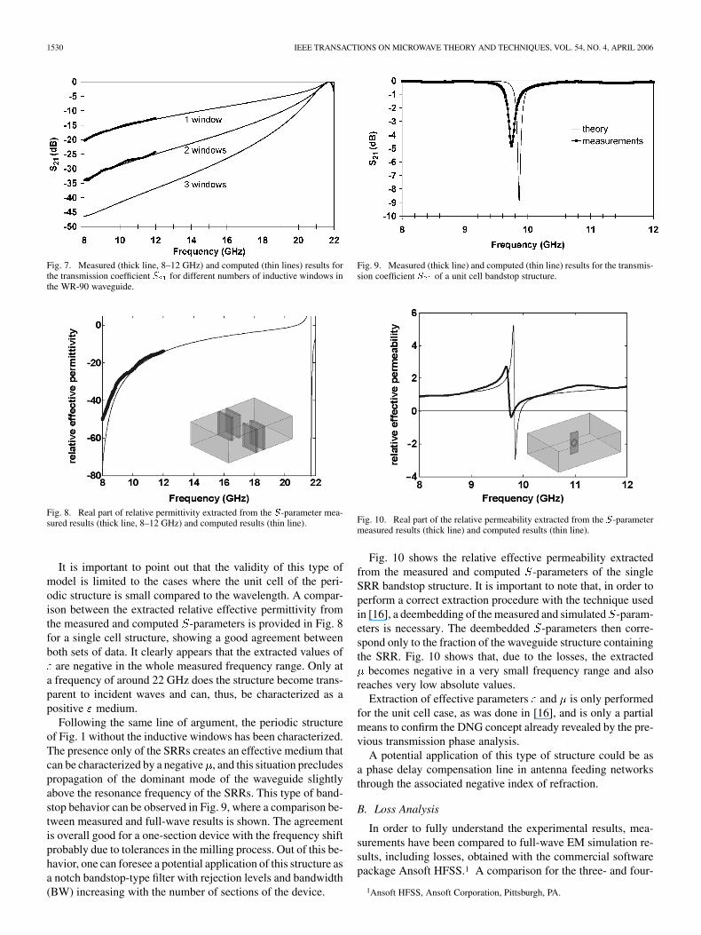
Fig. 7. Measured (thick line, 8–12 GHz) and computed (thin lines) results forthe transmission coefficient S for different numbers of inductive windows inthe WR-90 waveguide.
Fig. 8. Real part of relative permittivity extracted from the S-parameter mea-sured results (thick line, 8–12 GHz) and computed results (thin line).
It is important to point out that the validity of this type ofmodel is limited to the cases where the unit cell of the peri-odic structure is small compared to the wavelength. A compar-ison between the extracted relative effective permittivity fromthe measured and computed -parameters is provided in Fig. 8for a single cell structure, showing a good agreement betweenboth sets of data. It clearly appears that the extracted values of
are negative in the whole measured frequency range. Only ata frequency of around 22 GHz does the structure become trans-parent to incident waves and can, thus, be characterized as apositive medium.
Following the same line of argument, the periodic structureof Fig. 1 without the inductive windows has been characterized.The presence only of the SRRs creates an effective medium thatcan be characterized by a negative , and this situation precludespropagation of the dominant mode of the waveguide slightlyabove the resonance frequency of the SRRs. This type of band-stop behavior can be observed in Fig. 9, where a comparison be-tween measured and full-wave results is shown. The agreementis overall good for a one-section device with the frequency shiftprobably due to tolerances in the milling process. Out of this be-havior, one can foresee a potential application of this structure asa notch bandstop-type filter with rejection levels and bandwidth(BW) increasing with the number of sections of the device.
Fig. 9. Measured (thick line) and computed (thin line) results for the transmis-sion coefficient S of a unit cell bandstop structure.
Fig. 10. Real part of the relative permeability extracted from the S-parametermeasured results (thick line) and computed results (thin line).
Fig. 10 shows the relative effective permeability extractedfrom the measured and computed -parameters of the singleSRR bandstop structure. It is important to note that, in order toperform a correct extraction procedure with the technique usedin [16], a deembedding of the measured and simulated -param-eters is necessary. The deembedded -parameters then corre-spond only to the fraction of the waveguide structure containingthe SRR. Fig. 10 shows that, due to the losses, the extracted
becomes negative in a very small frequency range and alsoreaches very low absolute values.
Extraction of effective parameters and is only performedfor the unit cell case, as was done in [16], and is only a partialmeans to confirm the DNG concept already revealed by the pre-vious transmission phase analysis.
A potential application of this type of structure could be asa phase delay compensation line in antenna feeding networksthrough the associated negative index of refraction.
B. Loss Analysis
In order to fully understand the experimental results, mea-surements have been compared to full-wave EM simulation re-sults, including losses, obtained with the commercial softwarepackage Ansoft HFSS.1 A comparison for the three- and four-
1Ansoft HFSS, Ansoft Corporation, Pittsburgh, PA.

CARBONELL et al.: DESIGN AND EXPERIMENTAL VERIFICATION OF BW PROPAGATION IN PERIODIC WAVEGUIDE STRUCTURES 1531
Fig. 11. S-parameter magnitude comparison between full-wave simulation andmeasured results for three- and four-cell structures.
Fig. 12. S -parameter phase comparison between full-wave simulation andmeasured results for three- and four-cell structures.
cell structures is shown in Figs. 11 and 12. Results for the com-parison of the transmission coefficient, both in magnitude andphase, are displayed. There is a good agreement between the-oretical and experimental results. Nevertheless, it is possibleto observe a slight frequency shift in the transmission band.This shift, in the order of 0.2 GHz, can be explained becauseof the fabrication tolerances of the milling process of the di-electric laminate, which is done in-house. Actually, it is be-lieved that because of the milling process, part of the dielec-tric substrate has been removed since the NY9220 is a mechan-ically soft dielectric substrate. A careful inspection of the sam-ples has proven this. An EM simulation of a device with an“over-milled” dielectric substrate also tends to confirm this ef-fect (increased resonance frequency). Moreover, the passbandshows a ripple caused by the fact of having finite-length struc-tures. In this sense, lossless numerical simulations show thatthe number of transmission maximums is equal to the numberof resonators. This effect can be interpreted in several ways,and notably with an effective medium theory for a finite lengthstructure. Nevertheless, in terms of equivalent circuits, and asoutlined in [12], the distinct resonant peaks can be explainedbecause of the coupling effects between consecutive sections.These couplings tend to modify the intrinsic equivalent induc-tance and equivalent capacitance of a single SRR resonator.Consecutive broadside coupled SRRs have basically magnetic
Fig. 13. Measured intrinsic loss levels (linear units) for different length de-vices.
Fig. 14. Simulated loss contributions to the transmission coefficient S for athree-SRR structure compared to the measured prototype.
mutual couplings, which, in turn, cause the generation of distincttransmission maxima. Transmission losses make this selectiveeffect less apparent in the measured and simulated (if losses areincluded) results, as can be observed in Fig. 11.
Nevertheless, in practice, losses reduce the transmissionlevels for all the devices with total loss dependent on thephysical length of the periodical structure, as can be observedin Fig. 5. In order to confirm this argument, intrinsic lossesof the structure have also been extracted from the measured
-parameters. Intrinsic losses of the structure are definedhere from the following equation:
(1)
Fig. 13 shows the measured intrinsic losses for differentlength structures. It is possible to observe that the loss levelincreases with the number of resonators of the structure. Thepassband in the transmission coefficient (Fig. 5) coincideswith high loss-level frequency ranges in Fig. 13. This behaviormakes apparent that these types of losses are intrinsically due tothe resonators. The width of the frequency range where intrinsiclosses are produced increases with the number of stages of thestructure.
Losses in the passband can be explained by several factors.In Fig. 14, the most relevant loss simulated contributions are

1532 IEEE TRANSACTIONS ON MICROWAVE THEORY AND TECHNIQUES, VOL. 54, NO. 4, APRIL 2006
plotted and compared to the measured results. In this case, theideal lossless structure has three maxima, for a three-cell struc-ture, where there is full transmission (9.79, 9.87, and 9.97 GHz).
These maxima have a very high selectivity due to the rapidvariation of the equivalent impedance of the structure in the SRRresonance region, and only at these three individual frequenciesis the structure completely matched. This situation involves acertain amount of mismatch losses for other frequencies.
One can then observe that, even with a low loss composite,the dielectric material dissipates some energy, almost up to 5 dBwith respect to the ideal case in the transmission peaks. More-over, the main contribution can be associated with the losses inthe conductors forming the SRRs, which can be relatively im-portant since the resonators strongly concentrate energy at theresonance frequency. Copper conductivity has been taken forthe simulations equal to S/m.
In the three-SRR structure, the transmission level is reduced8 dB with respect to the dielectric-only curve. These two ef-fects should be responsible for the increasing loss levels in thepassband, as the number of cells in the structure grows. Thesimulated level considering these two loss contributions is quitesimilar to the measured transmission level in the passband fre-quency range. In addition to these effects, and probably not neg-ligible, there is another contribution related to the positioningof the dielectric laminate. The procedure employed for the po-sitioning of the SRR substrate over the transverse dimension ofthe waveguide is exact with the use of the slits. However, the po-sitioning of the SRR substrate over the longitudinal dimensionhas a possible uncertainty because it is performed manually. Ifthe SRR is not exactly centered within the cavity created by thesuccessive windows, the excitation of the resonator will not beoptimal (i.e., with the maximum -field parallel to the axis ofthe SRRs). The evanescence effects caused by the inductive win-dows will degrade the transmission characteristic throughout thestructure, and produce coupling losses in the passband. Simu-lated results for these positioning inaccuracies show that theycan reach up to 2 dB in the case of the SRR centered in an in-ductive window.
V. CONCLUSION
An experimental verification of the backward-wave propaga-tion behavior through a composite periodic waveguide structurehas been carried out by extracting the relative permittivity andpermeability as effective medium parameters. Measured resultsin terms of the phase of the transmission coefficient also provethis abnormal propagation scheme in a narrow frequency band.
If compactness of the designed and fabricated devices inthe longitudinal dimension is undoubtedly a clear advantageof this type of technology, allowing potential applications asreferenced above, different types of losses may counterbalancesuch size reduction. A careful analysis of the different losssources has been performed through the test of the contributionsadded by the dielectric and conductive materials, as well asthose due to the couplings inside the structure. Prospectivemeans of reducing losses in the resonators are currently beinginvestigated.
ACKNOWLEDGMENT
The authors are grateful to J. M. González Arbesú, Univer-sidad Politécnica de Cataluña, Cataluña, Spain, for useful dis-cussions on the prototype fabrication.
REFERENCES
[1] R. A. Shelby, D. R. Smith, and S. Schultz, “Experimental verificationof a negative index of refraction,” Science, vol. 292, pp. 77–79, Apr. 6,2001.
[2] V. G. Veselago, “The electrodynamics of substances with simultane-ously negative values of " and �,” Sov. Phys.—Usp., vol. 10, no. 4, pp.509–514, 1968.
[3] J. B. Pendry, A. J. Holden, D. J. Robbins, and W. J. Stewart, “Mag-netism from conductors and enhanced nonlinear phenomena,” IEEETrans. Microw. Theory Tech., vol. 47, no. 11, pp. 2075–2084, Nov.1999.
[4] T. Koschny, M. Kafesaky, E. N. Economou, and C. M. Soukoulis, “Ef-fective medium theory of lefthanded materials,” Phys. Rev. Lett., vol.93, no. 10, pp. 107 402-1–107 402-4, Sep. 2004.
[5] R. Marqués, F. Mesa, J. Martel, and F. Medina, “Comparative analysisof edge- and broadside-coupled split ring resonators for metamaterialdesign-theory and experiments,” IEEE Trans. Antennas Propag., vol.51, no. 10, pp. 2572–2581, Oct. 2003.
[6] A. Lai, C. Caloz, and T. Itoh, “Composite right/left-handed transmis-sion line metamaterials,” IEEE Micro, vol. 5, no. 3, pp. 34–50, Sep.2004.
[7] G. V. Eleftheriades, A. Iyer, and P. Kremer, “Planar negative refractiveindex media using periodically loaded transmission lines,” IEEE Trans.Microw. Theory Tech., vol. 50, no. 12, pp. 2702–2712, Dec. 2002.
[8] IEEE Trans. Microw. Theory Tech. (Special Issue), vol. 51, no. 4, Apr.2005.
[9] R. Marqués, J. Martel, F. Mesa, and F. Medina, “Left-handed-mediasimulation and transmission of EM waves in sub-wavelength split-ringresonator loaded metallic waveguides,” Phys. Rev. Lett., vol. 89, no. 18,Oct. 28, 2002.
[10] T. Decoopman, O. Vanbésien, and D. Lippens, “Demonstration of abackward wave in a single split ring resonator and wire loaded finline,”IEEE Microw. Wireless Compon. Lett., vol. 14, no. 11, pp. 507–509,Nov. 2004.
[11] I. A. Eshrah, A. A. Kishk, A. B. Yakolev, and A. W. Glisson, “Evanes-cent rectangular waveguide with corrugated walls: A composite right/left-handed metaguide,” in IEEE MTT-S Int. Microw. Symp. Dig., LongBeach, CA, Jun. 2005, pp. 1745–1748.
[12] J. Carbonell, L. J. Roglá, and V. E. Boria, “Left handed behavior ofSRR filled waveguides,” in IEEE MTT-S Int. Microw. Symp. Dig., LongBeach, CA, Jun. 2005, pp. 1749–1752.
[13] R. Marqués, F. Medina, and R. Rafii-El-Idrissi, “Role of bianisotropyin negative permeability and left-handed metamaterials,” Phys. Rev. B,Condens. Matter, vol. 65, pp. 144 440(1)–14 440(6), 2002.
[14] S. Cogollos, S. Marini, V. E. Boria, P. Soto, A. Vidal, H. Esteban, J. V.Morro, and B. Gimeno, “Efficient modal analysis of arbitrarily shapedwaveguides composed of linear, circular, and elliptical arcs using theBI-RME method,” IEEE Trans. Microw. Theory Tech., vol. 51, no. 12,pp. 2378–2390, Dec. 2003.
[15] O. F. Siddiqui, M. Mojahedi, and G. V. Eleftheriades, “Periodicallyloaded transmission line with effective negative refractive index andnegative group velocity,” IEEE Trans. Antennas Propag., vol. 51, no.10, pp. 2619–2625, Oct. 2003.
[16] C. Y. Cheng and R. W. Ziokolwsky, “Tailoring double-negative meta-material responses to achieve anomalous propagation effects along mi-crostrip transmission lines,” IEEE Trans. Microw. Theory Tech., vol.51, no. 12, pp. 2306–2314, Dec. 2003.
Jorge Carbonell (M’02) was born in Valencia,Spain, in 1971. He received the Telecoms Engineerdegree from the Universidad Politécnica de Valencia,Valencia, Spain, in 1995, and the Ph.D. degree inelectrical engineering (European Label with Honors)from the University of Lille, Lille, France, in 1998.
From 1996 to 1998, he was with the Institutd’Electronique et de Microélectronique du Nord.From 1999 to 2003, he worked within the wirelessindustry with Ericsson, Siemens, Retevisión Móvil,and Telefónica Móviles, during which time he was
involved with second- and third-generation wireless communication systems,

CARBONELL et al.: DESIGN AND EXPERIMENTAL VERIFICATION OF BW PROPAGATION IN PERIODIC WAVEGUIDE STRUCTURES 1533
and mainly focused on radio engineering. Since January 2004, he holds aRamón y Cajal tenure-track research position with the Universidad Politécnicade Valencia. His research activity have included EM analysis of active andpassive devices for space applications, in particular photonic-bandgap mate-rials. His current research activity concerns the analysis and design of passiveperiodic structures and metamaterials.
Dr. Carbonell was the recipient of a Human Capital and Mobility Fellowship.
Luis J. Roglá (S’02) was born in Valencia, Spain, in1979. He received the M.Sc. degree in telecommuni-cation engineering from the Universidad Politécnicade Valencia, Valencia, Spain, in 2004, and is currentlyworking toward the Ph.D. degree at the UniversidadPolitécnica de Valencia.
During 2004, he was with the Passive MicrowavesDepartment, Alcatel Espacio, where he was involvedwith the research and development of new dielectricresonator filters. He then joined the MicrowaveApplications Group, Universidad Politécnica de
Valencia. His current research interests include EM metamaterials, theirapplications in microwave and millimeter-wave technologies, as well as thedevelopment of new design techniques for these novel devices.
Vicente E. Boria (S’91–A’99–SM’02) was born inValencia, Spain, on May 18, 1970. He received the In-geniero de Telecomunicación degree (with first-classhonors) and Doctor Ingeniero de Telecomunicacióndegree from the Universidad Politécnica de Valencia,Valencia, Spain, in 1993 and 1997, respectively.
In 1993, he joined the Departamento de Co-municaciones, Universidad Politécnica de Va-lencia, where he has been an Assistant Lecturer(1993–1995), Lecturer (1996–1997), AssociateProfessor (1998–2002), and Full Professor (since
2003). In 1995 and 1996, he held a Spanish Trainee position with the EuropeanSpace Research and Technology Centre (ESTEC)–European Space Agency(ESA), Noordwijk, The Netherlands, where he was involved in the area ofEM analysis and design of passive waveguide devices. He has authored orcoauthored five chapters in technical textbooks, 30 papers in refereed inter-
national technical journals, and over 100 papers in international conferenceproceedings. His current research interests include numerical methods for theanalysis of waveguide and scattering structures, automated design of waveguidecomponents, radiating systems, measurement techniques, and power effects inpassive waveguide systems. Since 2003, he has served on the Editorial Boardsof the Proceedings of the IEE (Microwaves, Antennas, and Propagation) andRadio Science.
Dr. Boria is a member of the IEEE Microwave Theory and Techniques So-ciety (IEEE MTT-S) and the IEEE Antennas and Propagation Society (IEEEAP-S) since 1992. Since 2003, he has served on the Editorial Board of theIEEE TRANSACTIONS ON MICROWAVE THEORY AND TECHNIQUES. He is alsoa member of the Technical Committees of the IEEE-MTT International Mi-crowave Symposium and of the European Microwave Conference. He was therecipient of the 1993 Spanish Ministerio de Educación y Ciencia and the 1993First National Prize of Telecommunication Engineering Studies for his out-standing student record. He was also the recipient of the 2001 Social Councilof Universidad Politécnica de Valencia First Research Prize for his outstandingactivity during 1995–2000.
Didier Lippens received the Master of Sciencedegree in electronics engineering, Ph.D. degree, andDoctor ès Sciences degree from the Université desSciences et Technologies de Lille, Lille, France, in1975, 1978, and 1984, respectively.
From 1980 to 1981, he was a Research Engineerwith Thomson CSF. He led the Quantum andTerahertz Devices Team until 2001. He currentlyheads the Quantum Opto and Micro ElectronicDevice Group (DOME), Institut d’Electronique deMicroélectronique et de Nanotechnologie (IEMN),
Université des Sciences et Technologies de Lille. He is currently a Professorof electrical engineering with the Université des Sciences et Technologies deLille, where his main interests are nanotechnology and nanosciences. He hasbeen involved with molecular dynamics in liquid crystals and with semicon-ductors physics, and is currently more involved with nonlinear electronics andopto-electronics along with electromagnetism in artificial media. He has under-taken pioneering research on resonant tunnelling devices and, more generally,on heterostructure semiconductor devices. His current interests are terahertzsources, most notably quantum cascade lasers (QCLs), photomixers andheterostructure barrier varactors, photonic bandgaps, and metamaterials-basedpassive and active devices.