
Dear authors, Thank you very much for your contribution to Chinese ...
17
home | Authors | Referees | Browse | Announcement | Download | Subscription | Contact us | CPS Journals | Chinese Dear authors, Thank you very much for your contribution to Chinese Physics B. Your paper has been published in Chinese Physics B, 2013, Vol.22, No.11. Attached is the PDF offprint of your published article, which will be convenient and helpful for your communication with peers and coworkers. Readers can download your published article through our website http://www.iop.org/cpb or http://cpb.iphy.ac.cn What follows is a list of related articles published recently in Chinese Physics B. ------------------------------------------------------------------------------------------------------------------------------------------------------ Optoelectronic characteristics of CuO nanorods Xie De-Hua, Wang Fei-Fei, Lü Hao, Du Min-Yong, Xu Wen-Jie Chin. Phys. B . 2013, 22(5): 058103. Full Text: PDF (368KB) Low-voltage antimony-doped SnO 2 nanowire transparent transistors gated by microporous SiO 2 -based proton conductors Xuan Rui-Jie, Liu Hui-Xuan Chin. Phys. B . 2012, 21(8): 088104. Full Text: PDF (3444KB) Slow-rise and fast-drop current feature of ultraviolet response spectra for ZnO-nanowire film modulated by water molecules Ren Shou-Tian,Wang Qiang,Zhao Feng,Qu Shi-Liang Chin. Phys. B . 2012, 21(3): 038104. Full Text: PDF (297KB) -----------------------------------------------------------------------------------------------------
-
Upload
khangminh22 -
Category
Documents
-
view
0 -
download
0
Transcript of Dear authors, Thank you very much for your contribution to Chinese ...

home | Authors | Referees | Browse | Announcement | Download | Subscription | Contact us | CPS Journals | Chinese
Dear authors,
Thank you very much for your contribution to Chinese Physics B. Your paper has been published in Chinese Physics B, 2013, Vol.22, No.11. Attached is the PDF offprint of your published article, which will be convenient
and helpful for your communication with peers and coworkers. Readers can download your published article through our website
http://www.iop.org/cpb or http://cpb.iphy.ac.cn What follows is a list of related articles published recently in Chinese Physics B. ------------------------------------------------------------------------------------------------------------------------------------------------------
Optoelectronic characteristics of CuO nanorods
Xie De-Hua, Wang Fei-Fei, Lü Hao, Du Min-Yong, Xu Wen-Jie
Chin. Phys. B . 2013, 22(5): 058103. Full Text: PDF (368KB)
Low-voltage antimony-doped SnO2 nanowire transparent transistors gated by microporous SiO2-based proton conductors
Xuan Rui-Jie, Liu Hui-Xuan
Chin. Phys. B . 2012, 21(8): 088104. Full Text: PDF (3444KB)
Slow-rise and fast-drop current feature of ultraviolet response spectra for ZnO-nanowire film modulated by water molecules
Ren Shou-Tian,Wang Qiang,Zhao Feng,Qu Shi-Liang
Chin. Phys. B . 2012, 21(3): 038104. Full Text: PDF (297KB)
-----------------------------------------------------------------------------------------------------


Chinese Physics B ( First published in 1992 )
Published monthly in hard copy by the Chinese Physical Society and online by IOP Publishing, Temple
Circus, Temple Way, Bristol BS1 6HG, UKInstitutional subscription information: 2013 volume
For all countries, except the United States, Canada and Central and South America, the subscription rate is
£977 per annual volume.
Single-issue price £97. Delivery is by air-speeded mail from the United Kingdom.
Orders to:
Journals Subscription Fulfilment, IOP Publishing, Temple Circus, Temple Way, Bristol BS1 6HG, UKFor the United States, Canada and Central and South America, the subscription rate is US$1930 per annual
volume. Single-issue price US$194. Delivery is by transatlantic airfreight and onward mailing.
Orders to:
IOP Publishing, PO Box 320, Congers, NY 10920-0320, USAc⃝ 2013 Chinese Physical Society and IOP Publishing Ltd
All rights reserved. No part of this publication may be reproduced, stored in a retrieval system, or
transmitted in any form or by any means, electronic, mechanical, photocopying, recording or otherwise,
without the prior written permission of the copyright owner.
Supported by the National Natural Science Foundation of China, the China Association for Science and
Technology, and the Science Publication Foundation, Chinese Academy of SciencesEditorial Office: Institute of Physics, Chinese Academy of Sciences, PO Box 603, Beijing 100190, China
Tel: (86 – 10) 82649026 or 82649519, Fax: (86 – 10) 82649027, E-mail: [email protected]主管单位: 中国科学院
主办单位: 中国物理学会和中国科学院物理研究所
承办单位: 中国科学院物理研究所
主 编:欧阳钟灿
出 版:中国物理学会
印刷装订:北京科信印刷厂
编 辑: Chinese Physics B 编辑部
国内发行: Chinese Physics B 出版发行部
国外发行: IOP Publishing Ltd
发行范围: 公开发行
国际统一刊号: ISSN 1674–1056
国内统一刊号: CN 11–5639/O4
广告经营许可证:京海工商广字第0335号
编辑部地址: 北京 中关村 中国科学院物理研究所内
通 讯 地 址: 100190 北京 603信箱
Chinese Physics B 编辑部
电 话: (010) 82649026, 82649519
传 真: (010) 82649027
E-mail: [email protected]
“Chinese Physics B”网址:
http://cpb.iphy.ac.cn(编辑部)
http://iopscience.iop.org/cpb (IOP)
Published by the Chinese Physical Society
顾顾顾问问问 Advisory Board
陈佳洱 教授, 院士北京大学物理学院, 北京 100871
Prof. Academician Chen Jia-ErSchool of Physics, Peking University, Beijing 100871, China
冯 端 教授, 院士南京大学物理系, 南京 210093
Prof. Academician Feng DuanDepartment of Physics, Nanjing University, Nanjing 210093, China
黄祖洽 教授, 院士北京师范大学低能核物理研究所,北京 100875
Prof. Academician Huang Zu-QiaInstitute of Low Energy Nuclear Physics, Beijing Normal University, Beijing100875, China
李政道 教授, 院士 Prof. Academician T. D. LeeDepartment of Physics, Columbia University, New York, NY 10027, USA
李荫远 研究员, 院士中国科学院物理研究所, 北京 100190
Prof. Academician Li Yin-YuanInstitute of Physics, Chinese Academy of Sciences, Beijing 100190, China
丁肇中 教授, 院士 Prof. Academician Samuel C. C. TingLEP3, CERN, CH-1211, Geneva 23, Switzerland
杨振宁 教授, 院士 Prof. Academician C. N. YangInstitute for Theoretical Physics, State University of New York, USA
杨福家 教授, 院士复旦大学物理二系, 上海 200433
Prof. Academician Yang Fu-JiaDepartment of Nuclear Physics, Fudan University, Shanghai 200433, China
周光召 研究员, 院士中国科学技术协会, 北京 100863
Prof. Academician Zhou Guang-Zhao (Chou Kuang-Chao)China Association for Science and Technology, Beijing 100863, China
王乃彦 研究员, 院士中国原子能科学研究院, 北京 102413
Prof. Academician Wang Nai-YanChina Institute of Atomic Energy, Beijing 102413, China
梁敬魁 研究员, 院士中国科学院物理研究所, 北京 100190
Prof. Academician Liang Jing-KuiInstitute of Physics, Chinese Academy of Sciences, Beijing 100190, China
(Continued )

Chin. Phys. B Vol. 22, No. 11 (2013) 118102
Physical model for the exotic ultraviolet photo-conductivity ofZnO nanowire films∗
Pan Yue-Wu(潘跃武)a), Ren Shou-Tian(任守田)b), Qu Shi-Liang(曲士良)b), and Wang Qiang(王 强)b)†
a)Mathematics and Physical Sciences Technology, Xuzhou Institute of Technology, Xuzhou 221008, Chinab)Department of Optoelectronic Science, Harbin Institute of Technology at Weihai, Weihai 264209, China
(Received 18 May 2013; revised manuscript received 8 July 2013)
Employing a simple and efficient method of electro-chemical anodization, ZnO nanowire films are fabricated on Znfoil, and an ultraviolet (UV) sensor prototype is formed for investigating the electronic transport through back-to-backdouble junctions. The UV (365 nm) responses of surface-contacted ZnO film are provided by I–V measurement, alongwith the current evolution process by on/off of UV illumination. In this paper, the back-to-back metal–seconductor–metal(M–S–M) model is used to explain the electronic transport of a ZnO nanowire film based structure. A thermionic-fieldelectron emission mechanism is employed to fit and explain the as-observed UV sensitive electronic transport properties ofZnO film with surface-modulation by oxygen and water molecular coverage.
Keywords: ZnO nanowires, metal–semiconductor–metal contact, water modulated surface barrier,thermionic-field electron emission
PACS: 81.16.Be, 81.07.Gf, 72.10.–d DOI: 10.1088/1674-1056/22/11/118102
1. Introduction
Low-dimensional materials and physics have drawn in-tensive attention in recent years. One-dimensional (1D) semi-conductor nanomaterials have been especially of concern be-cause of their promising applications in nanoscale electronicand optoelectronic devices, such as field effect transistors,[1,2]
gas and chemical sensors,[3,4] and photodetectors.[5,6] How-ever, the metal/semiconductor contact (Ohomic or Schottkycontact) emerges as a pivotal problem for the performances ofabove-mentioned electronic devices, owing to the much exac-erbated accumulating of surface states for a nanomaterial.[7–9]
An Ohmic contact is obligatory for the fabrication of somephtoto-sensors (e.g. silicon sensors), while a Schottky contactis particularly required to form light and gas sensors with highand quick response for metal oxide nanomaterials such as ZnOand TiO2.[10,11] As far as we know, the sensitivity and stabilityof ultraviolet (UV) sensors based on metal oxide nanomate-rials still need to be further improved, and the study of sens-ing mechanisms is therefore rather urgently needed. However,there is a scarcity in this research trend.
As reported previously,[7,12,13] the underlying UV sens-ing mechanism of metal oxides is that the surface states ofnanostructured metal oxides can be greatly modulated by ad-sorbed oxygen and water species, and the density of surfacetrapped electric charges can be efficiently and reversibly mod-ified by photo exposure, introducing large and reversibly quickmodulation of surface barrier. As is well known, studies haveseldom been conducted to systematically figure out the rela-
tion between surface state evolutions of nanostructured metaloxides using UV light, hence the corresponding work is ur-gently required to guide the fabrication of high performanceUV sensors.
In this paper, ZnO nanowire films are fabricated onZn foil by following a typical electro-chemical method, anda high-sensitivity UV sensor prototype is formed. Thethermionic-field electron emission mechanism is used to fitand explain the as-observed UV sensitive properties of ZnOfilm with a surface coverage of water molecular and oxygenspecies. As should be noted, the thermionic-field electronemission mechanism is a compromised theory between thethermionic emission model and the barrier-tunneling model,which is an effective formalism for treating complicated elec-tronic transport processes through a metal–semiconductorbarrier.
2. ExperimentZnO nanowire film was grown on Zinc foil by follow-
ing a standard anodization process in a home-made electro-chemical cell. Zinc foil (99.999% purity) with a thickness of0.5 mm was used as an anode. The single-side surface areaof the anode was 2×3 cm2. The cathode was a graphite platewith an area of 2×4 cm2, which was placed just below thezinc foil with an inter-electrode distance of 10 cm. The liq-uid/air interface region of the Zinc foil was protected by resincoating, which is critical for preventing the interface-reactiontherein and thus converging the etching current between par-
∗Project supported by the National Natural Science Foundation of China (Grant Nos. 11274082 and 51172194) and the Excellent Young Scientist ResearchAward Fund of Shandong Province, China (Grant No. BS2011CL002).
†Corresponding author. E-mail: [email protected]© 2013 Chinese Physical Society and IOP Publishing Ltd http://iopscience.iop.org/cpb http://cpb.iphy.ac.cn
118102-1

Chin. Phys. B Vol. 22, No. 11 (2013) 118102
allel inter-electrode regions. As we see, it is important to formhigh-quality ZnO nanowires. Finally, final products with whitecolor and shaggy morphology were obtained. Other experi-mental details are similar to those described in our previouspaper.[14]
In the anodization process, both chemical and electro-chemical processes were used to etch the zinc foil. At a highvoltage of 10 V in our experiment, the electrochemical etch-ing dominates the whole anodization process. Reactions tookplace during the anodization of Zn and can be represented asfollows: at the cathode,
2H++2e−→ H2 (gas), (1)
at the anode,
Zn−2e−→ Zn2+, (2)
Zn2++2OH−→ Zn(OH)2 (solid), (3)
Zn(OH)2 +2OH−→ Zn(OH)−24 . (4)
At the initial stage, Zn(OH)−24 was formed and the surface of
the zinc foil became uneven due to both chemical and electro-chemical etching. The uneven zinc surface leads to the non-uniform electric field distribution and formation of dense “hotspots”, which have a greater opportunity to absorb the nega-tively charged Zn(OH)−2
4 . In the anodization process, that neg-atively charged Zn(OH)−2
4 products congregated at the “hotspots” on the surface of zinc foil, and formed nanowires. Af-ter annealing in air, zinc hydroxide on the surface of the foildecomposed into crystalline nanopraticles arranged in a line-like structure to form the as-observed ZnO nanowire.
Field emission scanning electron microscope (FE-SEM)and transmission electron microscopy (TEM) were used to
characterize the surface morphologies and structural featuresof the nano-structured ZnO film. Photoluminescence (PL) andRaman spectra were used to investigate the optical and crys-tallographic properties of the ZnO film. A standard electri-cal measurement setup was used to obtain current–voltage (I–V ) curves and current evolution spectra at UV illumination.UV photo-response measurements were obtained with a 6-Wxenon arc lamp light source (365 nm). A variant humiditysource was obtained by employing several saturated salt solu-tions as described in our previous paper.[15]
3. Results and discussion3.1. Morphological characterization
After anodization and annealing, the anodized zinc foilwas covered with a layer of white product. The morphol-ogy of the product was examined by using an FE-SEM anda TEM. The SEM image of the as-synthesized ZnO is givenin Fig. 1(a), which reveals a large quantity of nanowires withuniform diameter. The lengths of the nanowires are tens of mi-crons, and can be controlled by varying the reaction time. Thedetailed structures of ZnO nanowires were characterized usinga TEM. Figure 1(b) shows a typical TEM image of the ZnOnanowires. The diameter of single nanowire is about 150 nm.The nanowire is covered with many nano-crevices, which in-crease the effective surface area for oxygen and water adsorp-tion. A sponge-like structure is observed in Fig. 1(b), indicat-ing that the ZnO nanowire is actually composed of nanocrys-tals. The sponge-like structure may be the plausible key reasonfor the high oxygen and water adsorption ability in the follow-ing discussion.
(a) (b)
200 nm2 mm
Fig. 1. Morphologies of the as-anodized zinc foils. (a) SEM image of the ZnO nanowires. (b) TEM image of the ZnO nanowire.
4. Photoluminescence and Raman spectraThe PL spectrum of the synthesized ZnO is shown in
Fig. 2(a). Compositions of Gaussian line shapes are used to fit
the PL spectrum for the peak position. Three peaks are iden-
tified at 386 nm (ultraviolet band), 556 nm (green band), and
629 nm (orange band). The UV near-band emission is usu-
118102-2

Chin. Phys. B Vol. 22, No. 11 (2013) 118102
ally described as the direct inter-band recombination of photo-generated charge carriers. The green emission (556 nm) is as-sociated with emissions from deep levels caused by the struc-tural defects such as oxygen vacancies, interstitial oxygen, andinterstitial oxygen generated in the anodization process.[16]
The orange emission (629 nm) arises from optical transitionsin the single negatively charged interstitial oxygen ions (O−i )inside the grain. O−i is formed when some oxygen ions enterinto the interstitial sites of the ZnO crystal lattice. The or-ange emission is attributed to the radiative recombination ofa delocalized electron to the conduction band with a deeplytrapped hole in O−i centers.[17] The above results indicate theexistence of oxygen-related defects, which is favorable for thefollowing explanation of the oxygen-related UV response ofZnO nanowires.
Figure 2(b) shows the Raman spectrum of ZnO nanowirefilm at room temperature. A sharp peak at 438. 8 cm−1 is ob-served, which is the characteristic band of the Raman-activeE2 mode of wurtzite hexagonal ZnO. Four weak peaks at333.5, 380.8, 584.3, and 661.4 cm−1 corresponding to the2E2, A1(TO), E1(LO), and A1 vibration modes respectively,are observed in the low wave-number region. In the largewave-number region from 1000 to 1350 cm−1, a strong peak at1096 cm−1 is observed, corresponding to A1 + E2 mode. Theexistence of the E1(LO) mode is associated with lattice de-fects, such as oxygen vacancy and zinc interstitial.[18] Latticedefects are confirmed by PL and Raman spectra. It should bementioned that lattice defects make ZnO film more effectiveto adsorb oxygen and water molecules.
450 600 750 9000
2000
4000
6000
300 900 1500
0
2000
4000
6000
8000
PL inte
nsity
/arb
. units
Wavelength/nm
(a) (b)
A1+E2
E2 (H)
Ram
an inte
nsity
/arb
. units
Wavenumber/cm-1
2E
2A
1 (TO
)
A1
E1 (LO
)
Fig. 2. (color online) (a) PL and (b) Raman spectra of zinc foil anodizedat 10 V for 4 h, followed by annealing at 250 ◦C for 60 min in air.
4.1. UV sensitive electronic transport properties of theZnO M–S–M structure
Current–voltage (I–V ) characteristics of the ZnOnanowire films in the dark and upon UV illumination are
shown in Fig. 3. A schematic of the circuit used for measur-ing UV and humidity responses is illustrated in the inset ofFig. 3(a). I–V plots of the ZnO film are neither linear norrectifying, instead they have a little asymmetrical nonlinearbehavior, indicating the existence of asymmetrical barriersbetween the ZnO film and Cu leads. It is noticeable that thecurrent is greatly enhanced by UV illumination.
-20 -10 0 10 20
-15
-10
-5
0
5
10
-20 -10 0 10 20
-10000
-5000
0
5000
10000
Dark
curr
ent/
nA
Voltage/V
(a)
Photo
curr
ent/
nA
Voltage/V
(b)
Cu ZnO film Cu
Zn
Fig. 3. I–V plots of ZnO film measured (a) in dark and (b) under UVillumination.
According to the work of Peng et al.[17] and Liao etal.,[18,19] especially our previous work on the electronic trans-port of individual graphitic fiber,[20] a back-to-back doublediode model can be employed to explain the electronic trans-port properties of ZnO nanowire film modulated by humidityand ultraviolet illumination. The schematic diagrams of theback-to-back double diodes model and relevant energy bandare shown in Fig. 4.
Figure 4(a) is the schematic diagram of back-to-back dou-ble metal–semiconductor (MS) junctions of ZnO nanowiresfilm. Figures 4(b) and 4(c) illustrate the energy band diagramsof the junctions for zero, positive bias, respectively. It willbe clarified subsequently that ZnO semi-conducting film be-haves as a normal resistor with constant resistance, as long asthe contact effect and electrical heating effect are neglected.The nonlinear I–V plot is the manifestation that MS junctionsdominate electronic transport in this system, especially for thereversely biased junction. Owing to the high density of sur-face states via the absorption of oxygen molecules on the ZnO
118102-3
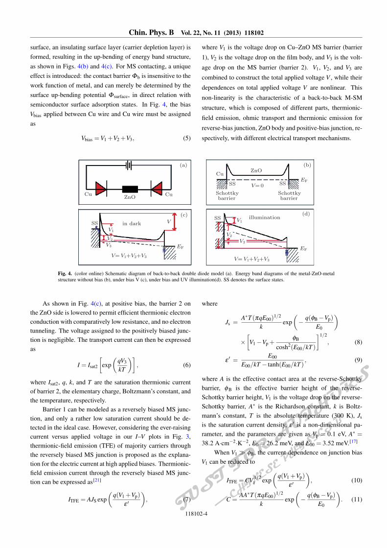
Chin. Phys. B Vol. 22, No. 11 (2013) 118102
surface, an insulating surface layer (carrier depletion layer) isformed, resulting in the up-bending of energy band structure,as shown in Figs. 4(b) and 4(c). For MS contacting, a uniqueeffect is introduced: the contact barrier Φb is insensitive to thework function of metal, and can merely be determined by thesurface up-bending potential Φ surface, in direct relation withsemiconductor surface adsorption states. In Fig. 4, the biasVbias applied between Cu wire and Cu wire must be assignedas
Vbias =V1 +V2 +V3, (5)
where V1 is the voltage drop on Cu–ZnO MS barrier (barrier
1), V2 is the voltage drop on the film body, and V3 is the volt-
age drop on the MS barrier (barrier 2). V1, V2, and V3 are
combined to construct the total applied voltage V , while their
dependences on total applied voltage V are nonlinear. This
non-linearity is the characteristic of a back-to-back M-SM
structure, which is composed of different parts, thermionic-
field emission, ohmic transport and thermionic emission for
reverse-bias junction, ZnO body and positive-bias junction, re-
spectively, with different electrical transport mechanisms.
(a) (b)
Cu Cu
Cu
ZnO
ZnO
V/SS SSEF
EF EF
Schottkybarrier
Schottkybarrier
SS in dark V
V1
V2
V3
SS illuminationV1
V2
V3
V/V1⇁V2⇁V3V/V1⇁V2⇁V3
(d)(c)
Fig. 4. (color online) Schematic diagram of back-to-back double diode model (a). Energy band diagrams of the metal-ZnO-metalstructure without bias (b), under bias V (c), under bias and UV illumination(d). SS denotes the surface states.
As shown in Fig. 4(c), at positive bias, the barrier 2 onthe ZnO side is lowered to permit efficient thermionic electronconduction with comparatively low resistance, and no electrontunneling. The voltage assigned to the positively biased junc-tion is negligible. The transport current can then be expressedas
I = Isat2
[exp
(qV3
kT
)], (6)
where Isat2, q, k, and T are the saturation thermionic currentof barrier 2, the elementary charge, Boltzmann’s constant, andthe temperature, respectively.
Barrier 1 can be modeled as a reversely biased MS junc-tion, and only a rather low saturation current should be de-tected in the ideal case. However, considering the ever-raisingcurrent versus applied voltage in our I–V plots in Fig. 3,thermionic-field emission (TFE) of majority carriers throughthe reversely biased MS junction is proposed as the explana-tion for the electric current at high applied biases. Thermionic-field emission current through the reversely biased MS junc-tion can be expressed as[21]
ITFE = AJS exp(
q(V1 +Vp)
ε ′
), (7)
where
Js =A∗T (πqE00)
1/2
kexp
(−
q(φB−Vp)
E0
)×[V1−Vp +
φB
cosh2(E00/kT )
]1/2
, (8)
ε′ =
E00
E00/kT − tanh(E00/kT ), (9)
where A is the effective contact area at the reverse-Schottkybarrier, φ B is the effective barrier height of the reverse-Schottky barrier height, V1 is the voltage drop on the reverse-Schottky barrier, A∗ is the Richardson constant, k is Boltz-mann’s constant, T is the absolute temperature (300 K), Js
is the saturation current density, ε ′ is a non-dimensional pa-rameter, and the parameters are given as Vp = 0.1 eV, A∗ =38.2 A·cm−2·K−2, E0 = 26.2 meV, and E00 = 3.52 meV.[17]
When V1 � φB, the current dependence on junction biasV1 can be reduced to
ITFE =CV 1/21 exp
(q(V1 +Vp)
ε ′
), (10)
C =AA∗T (πqE00)
1/2
kexp
(−
q(φB−Vp)
E0
). (11)
118102-4

Chin. Phys. B Vol. 22, No. 11 (2013) 118102
Thus, we can deduce that
lnITFE
V 1/2 ∝ V1. (12)
For the current through the ZnO film, it certainly follows theOhmic law: I =V2/RZnO.
Since the current through the three devices connected inseries should be equal, another restriction among the three bi-ases is obtained as
I = AJS exp(
q(V1 +Vp)
ε ′
)= Isat2
[exp
(qV3
kT
)]=
V2
RZnO. (13)
Equation (12) shows that ln(I/V 1/2) is proportional to thevoltage drop V1 on the reverse-Schottky barrier. As shownin Fig. 5, in the dark, ln(I/V 1/2) is proportional to the biasV at large positive and negative bias from 11 to 20 V. Un-der UV illumination, ln(I/V 1/2) becomes proportional to thebias V at large positive and negative bias (absolute value ) of8 V<V< 14 V. As the positive or negative bias V (absolutevalue) exceeds 14 V, ln(I/V 1/2) is no longer proportional tobias V , instead it shows somehow current saturated character-istics. We propose that the current saturation phenomenon isprobably due to a large injection effect, while the exact ex-planation is still under study. Both ln(I/V 1/2)–V plots showderivations from linear properties at relatively low bias, whichindicates that the derivation originates from the approximationcondition V1� φB.
-20 0 20-1.5
-1.0
-0.5
0
0.5
1.0
1.5
-20 0 20
5
6
7
8
ln(I/V1/2)
ln(I/V1/2)
Voltage/V Voltage/V
(a) (b)
Fig. 5. (color online) ln(I/V 1/2)–V plots (a) in dark and (b) under UVillumination. The solid curves represent experimental results obtainedfrom I–V plots in Fig. 3, and the dotted lines denote the fitted results.
The above results indicate that in the dark the bias V ap-plied between the electrodes is dropped mostly on the largereverse-Schottky barrier, so Vbias is almost equal to V1. WhenUV light is on, the Schottky barrier is efficiently lowered bythe desorption of oxygen molecules as suggested in our previ-ous paper.[14] As applied voltage V is increased, V1 becomes
progressively smaller than the bias V , because part of bias Vis applied on ZnO film, which explains the saturation charac-teristics of ln(I/V 1/2) at the higher bias V .
In UV photo-response characterization, photo-conductivity gain G is an important parameter. The full ex-pression of photo-conductivity gain G, a non-dimensionalparameter, as a function of applied voltage V , is modeled as
G(V ) =Ne−p
Nph=
hυ
Pq∆I(V ) ∝ ∆I(V ), (14)
where Ne−p is the number of electrons collected per unit time,Nph is the number of absorbed photons per unit time, P is theincident UV light power at the sensing area, q is the elemen-tary charge, ν is the incident light frequency, and ∆I(V ) isthe difference between photo-current and dark current. Thesensing area is difficult to determine, so the incident UV lightpower is unknown. Quantitative gain G(V ) cannot be ob-tained. The linear relationship between G(V ) and I(V ), ∆I–Vrelation can be used to explain the G(V )–V relation.
∆I–V relation is illustrated in Fig. 6. At sufficiently highvoltage above 14 V, ∆I (also G) shows linear dependence onapplied voltage, indicating e–p generation and transport inZnO dominate the UV response process, which is in good con-sistence with the discussion above. The linear ∆I–V relationillustrates the intrinsic photo-response of ZnO UV detector,and well follows the standard rule:[22]
G(V )≈ 1L2 ητµV ∝ V. (15)
-20 -10 0 10 20
0
2
4
6
8
10
12
DI/10
3 n
A
Voltage/V
Fig. 6. (color online) ∆I–V relation obtained from I–V plots in the darkand under UV illumination.
At lower voltage, the nonlinear ∆I–V relation deviatesfrom the standard rule, which can be certainly ascribed tothe disturbance of voltage drop on the reverse M-S junction.At lower bias V , photo-current increases slowly as bias V in-creases. Thus, an essential conclusion is drawn: the existenceof an M–S junction is detrimental to obtaining a high transportcurrent, but the lowering of the M–S junction by desorptionof O2 species can enhance the photo-response. The detailedUV photoresponse of ZnO nanowire film at different bias volt-ages was studied in our previous work.[14] The combined ef-fect of surface potential lowering from O−2 species desorption
118102-5

Chin. Phys. B Vol. 22, No. 11 (2013) 118102
and conductivity enhancement from electron–hole generationis employed to explain the as-observed UV photoresponse ofZnO nanowire film, which is also applicable for our presentstudy. The interaction between H2O and ZnO is a complexprocess. There is currently no other experimental report onsuch a study. However, our study in this paper is similar toNowotny et al.’s result on the interaction between H2O andTiO2 to explain the photocatalysis process.[23]
5. Conclusion
In this paper, ZnO nanowire films are fabricated by usinga simple electro-chemical anodization method. The UV photo-responses of surface-contacted ZnO film are characterized us-ing I–V plots and the current evolution process by turning UVillumination on/off. A back-to-back double diode model isemployed to explain the as-observed UV sensitive electronictransport properties. The thermionic-field electron emissionmechanism is employed to fit and explain the as-observed UVsensitive electronic transport properties. As the applied biasV increases, photo-conductivity gain is increased, which fol-lows the typical characteristics of an M–S junction dominatedphoto-detector. Surface O−2 species desorption, along withthe photo-catalytic hydrolysis of water molecules plays a keyrole in the as-observed UV response of ZnO films. Consider-ing the simple experimental conditions, the anodizing methodprovides a simple but powerful way to fabricate low-cost UVdetectors.
References[1] Mubeen S and Moskovits M 2011 Adv. Mater. 23 2306[2] Fan Z, Wang D W, Chang P C, Tseng W Y and Lu J G 2004 Appl. Phys.
Lett. 85 5923[3] Ramgir N S, Yang Y and Zacharias M 2010 Small 6 1705[4] Huang J X, Virji S, Weiller B H and Kaner R B 2003 J. Am. Chem. Soc.
125 314[5] Hu L F, Yan J, Liao M Y, Wu M and Fang X S 2011 Small 7 1012[6] Li Y B, Valle F D, Simonnet M, Yamada I and Delaunay J J 2009 Nan-
otechnology 20 045501[7] Cheng G, Wu X H, Liu B, Li B, Zhang X T and Du Z L 2011 Appl.
Phys. Lett. 99 203105[8] Hu Y F, Zhou J, Yeh P H, Li Z, Wei T Y and Wang Z L 2010 Adv.
Mater. 22 3327[9] Li C, Bando Y, Liao M Y, Koide Y and Golberg D 2010 Appl. Phys.
Lett. 97 161102[10] Wang S J, Lu W J, Cheng G, Cheng K, Jiang X H and Du Z L 2009
Appl. Phys. Lett. 94 263106[11] Mor G K, Shankar K, Paulose M, Varghese O K and Grimes C A 2006
Nano Lett. 6 215[12] Huang J and Wan Q 2009 Sensor 9 9903[13] Pearton S J and Ren F 2013 Nanomater. Nanotechnol. 3 1[14] Ren S T, Wang Q, Zhao F and Qu S L 2012 Chin. Phys. B 21 038104[15] Wang Q, Pan Y Z, Huang S S, Ren S T, Li P and Li J J 2011 Nanotech-
nology 22 025501[16] Liu Y, Wang S, Zhang Z Y and Peng L M 2008 Appl. Phys. Lett. 92
033102[17] Zhang Z Y, Jin C H, Liang X L, Chen Q and Peng L M 2006 Appl.
Phys. Lett. 88 073102[18] Liao Z M, Liu K J, Zhang J M, Xu J and Yu D P 2007 Phys. Lett. A 367
207[19] Liao Z M, Hou C, Zhou Y B, Xu J, Zhang J M and Yu D P 2009 J.
Chem. Phys. 130 084708[20] Wang Q, Gao R X, Qu S L, Li J J and Gu C Z 2009 Nanotechnology 20
145201[21] Liao M Y, Wang X, Teraji T, Koizumi S and Koide Y 2010 Phys. Rev.
B 81 033304[22] Fabrega C, Hernandez-Ramırez F, Prades J D, Jimenez-Dıaz R, Andreu
T and Morante J R 2010 Nanotechnology 21 445703[23] Nowotny M K, Sheppard L R, Bak T and Nowotny J 2008 J. Phys.
Chem. C 112 5275
118102-6

Chinese Physics BVolume 22 Number 11 November 2013
TOPICAL REVIEW — Magnetism, magnetic materials, and interdisciplinary research
116803 High-mobility two-dimensional electron gases at oxide interfaces: Origin and opportunities
Chen Yun-Zhong, Nini Pryds, Sun Ji-Rong, Shen Bao-Gen and Søren Linderoth
117504 Development and application of ferrite materials for low temperature co-fired ceramic technology
Zhang Huai-Wu, Li Jie, Su Hua, Zhou Ting-Chuan, Long Yang and Zheng Zong-Liang
118505 Recent progress in perpendicularly magnetized Mn-based binary alloy films
Zhu Li-Jun, Nie Shuai-Hua and Zhao Jian-Hua
TOPICAL REVIEW — Quantum information
110310 Towards quantum-enhanced precision measurements: Promise and challenges
Zhang Li-Jian and Xiao Min
110311 Quantum cloning machines and their implementation in physical systems
Wu Tao, Fang Bao-Long and Ye Liu
110312 Disorder and decoherence in coined quantum walks
Zhang Rong, Qin Hao, Tang Bao and Xue Peng
110313 Progress in superconducting qubits from the perspective of coherence and readout
Zhong You-Peng, Li Chun-Yan, Wang Hao-Hua and Chen Yu
110601 Quantum metrology
Xiang Guo-Yong and Guo Guang-Can
114213 Review of cavity optomechanical cooling
Liu Yong-Chun, Hu Yu-Wen, Wong Chee Wei and Xiao Yun-Feng
116106 Graphene-like physics in optical lattices
Mei Feng, Zhang Dan-Wei and Zhu Shi-Liang
RAPID COMMUNICATION
114212 High-speed and broad optical bandwidth silicon modulator
Xu Hao, Li Xian-Yao, Xiao Xi, Li Zhi-Yong, Yu Yu-De and Yu Jin-Zhong
117312 Coupling-matrix approach to the Chern number calculation in disordered systems
Zhang Yi-Fu, Yang Yun-You, Ju Yan, Sheng Li, Shen Rui, Sheng Dong-Ning and Xing Ding-Yu
GENERAL
110201 New homotopy analysis transform method for solving the discontinued problems arising in nanotechnol-
ogy
M. M. Khader, Sunil Kumar and S. Abbasbandy
(Continued on the Bookbinding Inside Back Cover)

110202 Exact solutions of nonlinear fractional differential equations by (𝐺′/𝐺)-expansion method
Ahmet Bekir and Ozkan Guner
110203 Invariance of Painleve property for some reduced (1+1)-dimensional equations
Zhi Hong-Yan and Chang Hui
110204 Finite-time consensus for leader-following multi-agent systems over switching network topologies
Sun Feng-Lan and Zhu Wei
110205 Stochastic responses of Duffing–Van der Pol vibro-impact system under additive colored noise excitation
Li Chao, Xu Wei, Wang Liang and Li Dong-Xi
110301 Exact solution of Schrodinger equation with q-deformed quantum potentials using Nikiforov–Uvarov
method
Falaye B. J., Oyewumi K. J. and Abbas M.
110302 Minimum detection efficiency for the loophole-free confirmation of quantum contextuality
Xiang Yang and Hong Fang-Yu
110303 Efficient electronic entanglement concentration assisted by single mobile electrons
Sheng Yu-Bo and Zhou Lan
110304 Deterministic assisted clone of an unknown four-particle entangled cluster-type state
Ma Song-Ya, Luo Ming-Xing and Sun Ying
110305 Implementation of quantum partial search with superconducting quantum interference device qudits in
cavity QED
Li Hong-Yi, Wu Chun-Wang, Chen Yu-Bo, Lin Yuan-Gen, Chen Ping-Xing and Li Cheng-Zu
110306 Novel exact solutions of coupled nonlinear Schrodinger equations with time–space modulation
Chen Jun-Chao, Li Biao and Chen Yong
110307 Effects of effective attractive multi-body interaction on quantum phase and transport dynamics of a
strongly correlated bosonic gas across the superfluid to Mott insulator transition
Sun Jian-Fang, Cui Guo-Dong, Jiang Bo-Nan, Qian Jun and Wang Yu-Zhu
110308 Skyrmion crystals in pseudo-spin-1/2 Bose–Einstein condensates
Zhang Cong, Guo Wen-An, Feng Shi-Ping and Yang Shi-Jie
110309 Quantum phase transitions of fermionic atoms in an anisotropic triangular optical lattice
Bao An, Chen Yao-Hua and Zhang Xiao-Zhong
110401 Invariant expression for tunneling rate under canonical transformations
Ren Jun, Jia Meng-Wen and Wei Yi-Huan
110501 Symmetrical dynamical characteristic of peak and valley current-mode controlled single-phase H-bridge
inverter
Liu Hong-Chen, Li Fei, Su Zhen-Xia and Sun Li-Shan
110502 Existence of heteroclinic orbits in a novel three-order dynamical system
Hu Yu, Min Le-Quan and Zhen Ping
110503 A secure key agreement protocol based on chaotic maps
Wang Xing-Yuan and Luan Da-Peng
(Continued on the Bookbinding Inside Back Cover)

110504 H∞ synchronization of chaotic neural networks with time-varying delays
O. M. Kwon, M. J. Park, Ju H. Park, S. M. Lee and E. J. Cha
110505 Bounded consensus tracking of second-order multi-agent systems with sampling delay under directed
networks
Li Li and Fang Hua-Jing
110506 Analyses of the endoreversible Carnot cycle with entropy theory and entransy theory
Wang Wen-Hua, Cheng Xue-Tao and Liang Xin-Gang
ATOMIC AND MOLECULAR PHYSICS
113301 Quantitative analysis of the self-absorption and reemission effects on the emission spectrum of photolu-
minescence in right-angle excitation–detection configuration
Wang Zhen-Hua, Wu Yu-E, Zhang Xin-Zheng, Yun Zhi-Qiang, Li Wei and Xu Jing-Jun
113401 Product polarization and mechanism of Li + HF (v = 0v = 0v = 0, j = 0j = 0j = 0)→ LiF (v′v′v′, j′j′j′) + H collision reaction
Yue Xian-Fang
113402 Charge state effect on the K-shell ionization of iron by xenon ions near the Bohr velocity
Zhou Xian-Ming, Zhao Yong-Tao, Ren Jie-Ru, Cheng Rui, Lei Yu, Sun Yuan-Bo, Xu Ge, Wang Yu-Yu, Liu
Shi-Dong and Xiao Guo-Qing
ELECTROMAGNETISM, OPTICS, ACOUSTICS, HEAT TRANSFER, CLASSICAL MECHANICS,
AND FLUID DYNAMICS
114201 Enhanced optical transmission by V-shaped nanoslit in metal film
He Meng-Dong, Ma Wang-Guo and Wang Xin-Jun
114202 A new near-field phase-correction method for superlens
Wang Ying-Qi, Ye Jia-Sheng, Liu Shu-Tian and Zhang Yan
114203 Slow light via four-wave mixing in a hot rubidium vapour
Ding Dong-Sheng, Zhou Zhi-Yuan and Shi Bao-Sen
114204 Enhanced Kerr nonlinearity in a left-handed three-level atomic system driven by a bichromatic field
Yang Xiao-Yu and Jiang Yong-Yuan
114205 Dynamics of Rabi model under second-order Born Oppenheimer approximation
Wang Zhi-Hai and Zhou Duan-Lu
114206 Quantum interferometer with two-mode squeezed vacuum: S2z measurement
Zhang Yuan-Ming, Li Xin-Wei and Jin Guang-Ri
114207 Energy transfer in solid-state dye lasers based on methyl methacrylate co-doped with sulforhodamine B
and crystal violet
R. G. Geethu Mani and M. Basheer Ahamed
114208 Theoretical study of power amplification in tapered fiber with multi-seed parallel injection
Xiao Qi-Rong, Ren Hai-Cui, Li Dan, Gong Ma-Li and Yan Ping
(Continued on the Bookbinding Inside Back Cover)

114209 Physical origin of observed nonlinearities in Poly (1-naphthyl methacrylate): Using a single transistor–
transistor logic modulated laser beam
Qusay M. A. Hassan, Hussain A. Badran, Alaa Y. AL-Ahmad and Chassib A. Emshary
114210 Ultrafast population transfer in a Λ-configuration level system driven by few-cycle laser pulses
Zhang Wen-Jing, Xie Xiao-Tao, Jin Lu-Ling and Bai Jin-Tao
114211 Six-bit all-optical quantization using photonic crystal fiber with soliton self-frequency shift and pre-chirp
spectral compression techniques
Kang Zhe, Yuan Jin-Hui, Li Sha, Xie Song-Lin, Yan Bin-Bin, Sang Xin-Zhu and Yu Chong-Xiu
114301 Acoustic beam splitting in a sonic crystal around a directional band gap
Ahmet Cicek, Olgun Adem Kaya and Bulent Ulug
114701 Exact solutions for the flow of Casson fluid over a stretching surface with transpiration and heat transfer
effects
Swati Mukhopadhyay, Krishnendu Bhattacharyya and Tasawar Hayat
114702 Effects of thermal radiation on Casson fluid flow and heat transfer over an unsteady stretching surface
subjected to suction/blowing
Swati Mukhopadhyay
114703 Imaging of supersonic flow over a double elliptic surface
Zhang Qing-Hu, Yi Shi-He, He Lin, Zhu Yang-Zhu and Chen Zhi
114704 Multi-relaxation time lattice Boltzmann simulation of inertial secondary flow in a curved microchannel
Sun Dong-Ke, Xiang Nan, Jiang Di, Chen Ke, Yi Hong and Ni Zhong-Hua
PHYSICS OF GASES, PLASMAS, AND ELECTRIC DISCHARGES
115201 Nonlinear Landau damping of high frequency waves in non-Maxwellian plasmas
M. N. S. Qureshi, Sumbul Sehar, J. K. Shi and H. A. Shah
115202 Effects of bi-kappa distributed electrons on dust-ion-acoustic shock waves in dusty superthermal plasmas
M. S. Alam, M. M. Masud and A. A. Mamun115203 Drift-wave fluctuation in an inviscid tokamak plasma
Yang Jian-Rong, Mao Jie-Jian and Tang Xiao-Yan
115204 Diagnostic technique for measuring fusion reaction rate for inertial confinement fusion experiments at
Shen Guang-III prototype laser facility
Wang Feng, Peng Xiao-Shi, Kang Dong-Guo, Liu Shen-Ye and Xu Tao
115205 Changes of the electron dynamics in hydrogen inductively coupled plasma
Gao Fei, Liu Wei, Zhao Shu-Xia, Zhang Yu-Ru, Sun Chang-Sen and Wang You-Nian
115206 Three different low-temperature plasma-based methods for hydrophilicity improvement of polyethylene
films at atmospheric pressure
Chen Guang-Liang, Zheng Xu, Huang Jun, Si Xiao-Lei, Chen Zhi-Li, Xue Fei and Sylvain Massey
(Continued on the Bookbinding Inside Back Cover)

CONDENSED MATTER: STRUCTURAL, MECHANICAL, AND THERMAL PROPERTIES
116101 Generalized 2D problem of icosahedral quasicrystals containing an elliptic hole
Li Lian-He116102 Misfit-layered compound PbTiS3 with incommensurate modulation: Transmission electron microscopy
analysis and transport properties
Shen Xi, Cheng Dan, Zhao Hao-Fei, Yao Yuan, Liu Xiao-Yang and Yu Ri-Cheng
116103 Critical size of iron nanoparticles on liquid substrates
Lu Neng, Pan Qi-Fa, Cheng Yi, Yang Bo and Ye Gao-Xiang
116104 Ground-state structure determination and mechanical properties of palladium seminitride
Zhang Gang-Tai, Bai Ting-Ting, Zhao Ya-Ru and Lu Cheng
116105 Micro-track structure analysis for 100 MeV Si ions in CR-39 by using atomic force microscopy
Fang Mei-Hua, Wei Zhi-Yong, Zhang Zi-Xia, Zhu Li, Fu Yu, Shi Miao, Li Guang-Wu and Guo Gang
116201 Pressure-induced phase transitions in single-crystalline Cu4Bi4S9 nanoribbons
Hu Jing-Yu, Li Jing, Zhang Si-Jia, Zhao Hao-Fei, Zhang Qing-Hua, Yao Yuan, Zhao Qing, Shi Li-Jie, Zou
Bing-Suo, Li Yan-Chun, Li Xiao-Dong, Liu Jing, Zhu Ke, Liu Yu-Long, Jin Chang-Qing and Yu Ri-Cheng
116401 Effects of the trimodal random field on the magnetic properties of a spin-1 Ising nanotube
H. Magoussi, A. Zaim and M. Kerouad
116801 Improved light extraction of organic light emitting diodes with a nanopillar pattering structure
Gao Zhi-Xiang, Wang Hua, Hao Yu-Ying, Miao Yan-Qin and Xu Bing-She
116802 Simple statistical model for predicting thermal atom diffusion on crystal surfaces
Yu Wei-Feng, Lin Zheng-Zhe and Ning Xi-Jing
116804 Effects of high temperature rapid thermal annealing on Ge films grown on Si(001) substrate
Liu Zhi, Cheng Bu-Wen, Li Ya-Ming, Li Chuan-Bo, Xue Chun-Lai and Wang Qi-Ming
116805 Effect of buoyancy-driven convection on steady state dendritic growth in a binary alloy
Chen Ming-Wen, Wang Bao and Wang Zi-Dong
CONDENSED MATTER: ELECTRONIC STRUCTURE, ELECTRICAL, MAGNETIC, AND OPTI-
CAL PROPERTIES
117101 A comparison study on the electronic structures, lattice dynamics and thermoelectric properties of bulk
silicon and silicon nanotubes
Lu Peng-Xian, Qu Ling-Bo and Cheng Qiao-Huan
117102 Energy transfer between two aggregates in light-harvesting complexes
Wang Xiao-Lian, Li Hong-Rong, Zhang Pei and Li Fu-Li
117103 Electronic structure and optical properties of Al and Mg co-doped GaN
Ji Yan-Jun, Du Yu-Jie and Wang Mei-Shan
117301 Interfacial electronic structure at a metal–phthalocyanine/graphene interface: Copper–phthalocyanine
versus iron–phthalocyanine
Ye Wei-Guo, Liu Dan, Peng Xiao-Feng and Dou Wei-Dong
(Continued on the Bookbinding Inside Back Cover)

117302 Near-field optical observations of surface plasmon wave interference at subwavelength hole arrays per-
forated in Au film
Li Jiang-Yan, Gan Lin and Li Zhi-Yuan
117303 Thermoelectric transport through a quantum dot with a magnetic impurity
Yu Zhen, Guo Yu, Zheng Jun and Chi Feng
117304 Coupling strength effect on shot noise in boron devices
Li Gui-Qin and Guo Yong
117305 Transition from the Kondo effect to a Coulomb blockade in an electron shuttle
Zhang Rong, Chu Wei-Dong, Duan Su-Qing and Yang Ning
117306 Electric field driven plasmon dispersion in AlGaN/GaN high electron mobility transistors
Tan Ren-Bing, Qin Hua, Zhang Xiao-Yu and Xu Wen
117307 Influence of a drain field plate on the forward blocking characteristics of an AlGaN/GaN high electron
mobility transistor
Zhao Sheng-Lei, Chen Wei-Wei, Yue Tong, Wang Yi, Luo Jun, Mao Wei, Ma Xiao-Hua and Hao Yue
117308 Low voltage program-erasable Pd-Al2O3-Si capacitors with Ru nanocrystals for nonvolatile memory
application
Lan Lan, Gou Hong-Yan, Ding Shi-Jin and Zhang Wei
117309 A high performance HfSiON/TaN NMOSFET fabricated using a gate-last process
Xu Gao-Bo, Xu Qiu-Xia, Yin Hua-Xiang, Zhou Hua-Jie, Yang Tao, Niu Jie-Bin, Yu Jia-Han, Li Jun-Feng and
Zhao Chao117310 Temperature-dependent dielectric properties of Au/Si3N4/n-Si (metal insulator semiconductor) struc-
tures
T. Ataseven and A. Tataroglu
117311 Effects of stress conditions on the generation of negative bias temperature instability-associated interface
traps
Zhang Yue, Pu Shi, Lei Xiao-Yi, Chen Qing, Ma Xiao-Hua and Hao Yue
117313 Simulation of the magnetoresistance of Heisenberg spin lattices using the resistor network model
Lin Ling-Fang, Huang Xin and Dong Shuai
117314 Reversible alternation between bipolar and unipolar resistive switching in La-SrTiO3 thin films
Xu Ding-Lin, Xiong Ying, Tang Ming-Hua, Zeng Bai-Wen, Xiao Yong-Guang and Wang Zi-Ping
117401 Paraconductivity study in ErBa2Cu3−x𝑀xO7−δ (𝑀 = Zn, Fe) superconductors
A. Sedky and S. B. Mohamed
117501 Analytical thermodynamical properties of a two-dimensional electron gas in a magnetic field
Chen Jin-Wang and Pan Xiao-Yin
117502 A quantum explanation of the magnetic properties of Mn-doped graphene
Lei Tian-Min, Liu Jia-Jia, Zhang Yu-Ming, Guo Hui and Zhang Zhi-Yong
117503 Thermal activation of magnetization in Pr2Fe14B ribbons
Li Zhu-Bai, Shen Bao-Gen, Niu E, Liu Rong-Ming, Zhang Ming and Sun Ji-Rong
(Continued on the Bookbinding Inside Back Cover)

117701 Effects of charge and dipole on flatband voltage in an MOS device with a Gd-doped HfO2 dielectric
Han Kai, Wang Xiao-Lei, Yang Hong and Wang Wen-Wu
117801 Optical study of Ba(MnxxxTi(1−x)(1−x)(1−x)O333) thin films by spectroscopic ellipsometry
Zhang Ting, Yin Jiang, Ding Ling-Hong and Zhang Wei-Feng
117802 Nonlinear optical characterization of phosphate glasses based on ZnO using the Z-scan technique
Masoumeh Shokati Mojdehi, Wan Mahmood Mat Yunus, Khor Shing Fhan, Zainal Abidin Talib and N. Tam-
chek117803 The subwavelength tuned magneto-optical Kerr effect in L10-FePt films with perpendicular magnetic
anisotropy
Zhang Xia, Shi Lei, Li Jing, Xia Yun-Jie, Shi Zhong and Zhou Shi-Ming
117804 Degradation behaviors of high power GaN-based blue light emitting diodes
Zhong Can-Tao, Yu Tong-Jun, Yan Jian, Chen Zhi-Zhong and Zhang Guo-Yi
117805 Optimisation of a poly(p-phenylene benzobisoxazole)-based light-emitting device with a complex cathode
structure
Zhang Xiao-Jin, He Zhi-Qun, Wang Jing, Mu Lin-Ping, Zhao Huan, Liang Chun-Jun, Zhuang Qi-Xin and Han
Zhe-Wen117806 Polarization characteristics of chiral photonic crystal fibers with an elliptical hollow core
Li She, Li Jun-Qing and Cao Yu-Sheng
117807 Optical total reflection and transmission with mode control in a dielectric subwavelength nanorod chain
Li Hao, Li Wei, Du Jun-Jie, Wu Ai-Min, Qiu Chao, Sheng Zhen, Wang Xi, Zou Shi-Chang and Gan Fu-Wan
117901 Suppressing the mechanical quadrature error of a quartz double-H gyroscope through laser trimming
Zhao Ke, Feng Li-Hui, Wang Qian-Qian, Liu Ming-Zhi, Wang Ben-Guo, Cui Fang and Sun Yu-Nan
INTERDISCIPLINARY PHYSICS AND RELATED AREAS OF SCIENCE AND TECHNOLOGY
118101 Aluminium phthalocyanine chloride thin films for temperature sensing
Muhammad Tariq Saeed Chani, Abdullah M. Asiri, Kh. S. Karimov, Atif Khan Niaz, Sher Bhadar Khan and
Khalid. A. Alamry
118102 Physical model for the exotic ultraviolet photo-conductivity of ZnO nanowire films
Pan Yue-Wu, Ren Shou-Tian, Qu Shi-Liang and Wang Qiang
118501 Scaling effects of single-event gate rupture in thin oxides
Ding Li-Li, Chen Wei, Guo Hong-Xia, Yan Yi-Hua, Guo Xiao-Qiang and Fan Ru-Yu
118502 High-voltage SOI lateral MOSFET with a dual vertical field plate
Fan Jie, Zhang Bo, Luo Xiao-Rong and Li Zhao-Ji
118503 High bandwidth surface-illuminated InGaAs/InP uni-travelling-carrier photodetector
Li Chong, Xue Chun-Lai, Li Chuan-Bo, Liu Zhi, Cheng Bu-Wen and Wang Qi-Ming
118504 Efficiency enhancement of an InGaN light-emitting diode with a p-AlGaN/GaN superlattice last quan-
tum barrier
Xiong Jian-Yong, Zhao Fang, Fan Guang-Han, Xu Yi-Qin, Liu Xiao-Ping, Song Jing-Jing, Ding Bin-Bin,
Zhang Tao and Zheng Shu-Wen
(Continued on the Bookbinding Inside Back Cover)

118701 Monitoring the reaction between AlCl3 and o-xylene by using terahertz spectroscopy
Jin Wu-Jun, Li Tao, Zhao Kun and Zhao Hui118801 Effects of annealing rate and morphology of sol–gel derived ZnO on the performance of inverted polymer
solar cells
Yu Xuan, Hu Zi-Yang, Huang Zhen-Hua, Yu Xiao-Ming, Zhang Jian-Jun, Zhao Geng-Shen and Zhao Ying