Crosslinking of porous SiOCH films involving Si-O-C bonds: Impact of deposition and curing
9
Crosslinking of porous SiOCH films involving Si–O–C bonds: Impact of deposition and curing O. Gourhant, 1,2,3 G. Gerbaud, 4,a A. Zenasni, 1 L. Favennec, 2 P. Gonon, 3 and V. Jousseaume 1,b 1 CEA-LETI-Minatec, 17 rue des Martyrs, 38054 Grenoble Cedex 9, France 2 STMicroelectronics, 850 rue Jean Monnet, 38390 Crolles, France 3 CEA/LETI/D2NT/LTM, 17 Avenue des Martyrs, 38054 Grenoble Cedex 9, France 4 CEA-INAC, 17 rue des Martyrs, 38054 Grenoble Cedex 9, France Received 27 August 2010; accepted 23 October 2010; published online 20 December 2010 This paper focuses on the properties of nanoporous SiOCH thin films deposited using a porogen approach by plasma enhanced chemical vapor deposition. The impact of deposition temperature, porogen loading and porogen removal treatment is investigated using Fourier transform infrared spectroscopy, solid-state nuclear magnetic resonance analysis, and electrical and mechanical measurements. This work shows that a higher deposition temperature allows limiting the film shrinkage during the porogen removal treatment and leads to the best compromise in term of electrical and mechanical properties. Beside, the effect of Si–O–C bonds on the enhancement of mechanical properties is promoted since a typical crosslinking mechanism is highlighted in case of ultraviolet curing. © 2010 American Institute of Physics. doi:10.1063/1.3518512 I. INTRODUCTION The introduction of porous dielectric in advanced inter- connects is becoming a reality in the microelectronic indus- try. Some manufacturers have introduced these ultralow k ULK, k 2.7 in production from the 65 nm node. 1 Among all different techniques to deposit porous SiOCH dielectrics, the plasma-enhanced-chemical-vapor-deposition PECVD using a porogen approach is the most used. This approach consists in a deposition step with two different precursors to generate a hybrid material. This hybrid is a SiOCH matrix containing organic inclusions. Afterward, a thermal anneal- ing in most cases assisted with ultraviolet UV radiation is performed leading to organic inclusions removal and poros- ity generation. 2–5 This post-treatment allows also the strengthening of the SiOCH skeleton by different chemical reactions crosslinking and shrinkage. 6–8 Since the first work published by Grill et al. in 2001, several studies were conducted in order to optimize this po- rogen approach. Different matrix precursors were investi- gated cyclic 2,3 or linear 3,4,9 and the use of diethoxy-methyl- silane DEMS gradually became the standard. In the same way, different porogen precursors were studied, mainly hy- drocarbons such as saturated cycles like terpinene or norbornene 4,9–11 or molecules with strained rings like cy- cloalkene oxide. 2,3,12 However, the impact of deposition con- ditions of the hybrid films is poorly discussed in the litera- ture. The effect of deposition temperature on the film structure and properties was mainly studied for octamethyl- cyclotetrasiloxane as matrix precursor. 12,13 These works showed that the films deposited at lower temperature can shrink more during the post-treatment and have a larger k value after curing. In the case of DEMS, Favennec et al. 3 mainly studied the impact of addition of a small amount of O 2 in the plasma gas feed on the films properties. They showed that the presence of SiCH 3 2 is detrimental to the porogen approach though the impact of deposition tempera- ture was not investigated. Moreover, there are only few stud- ies related to the extension of the porogen approach in order to perform high porosity materials and investigate whether some process parameters may limit or not the increase in the porosity rate. Previous works shown that the PECVD poro- gen approach does not allow to perform materials with a porosity higher than 33%. 2,9 Indeed, above a porogen loading threshold, the film collapses during the post-treatment lead- ing to a decrease in the total film porosity. 3 In this work, the impact of hybrid deposition tempera- ture on the porous film properties is investigated using DEMS as matrix precursor. Hybrid films with different po- rogen loading were synthesized and analyzed using Fourier transform infrared spectroscopy FTIR and solid-state nuclear magnetic resonance SSNMR analysis. These films were then cured using a thermally assisted UV treatment in order to remove the porogen phase and create porosity. In this paper, the bonding structure and crosslinking mecha- nisms after curing are revisited in order to highlight the role of Si–O–C bonds. A specific attention is paid to the extension of this porogen approach in order to get a high porosity material. Finally, the impact of bonding structure and poros- ity on the elastic properties is discussed. II. EXPERIMENT ULK materials were deposited on 300 mm silicon sub- strates using an industrial tool consisting of two chambers dedicated, respectively, to the hybrid elaboration and the post-treatment. The deposition of the organic-inorganic thin film called hybrid material, was carried out in the first a Present address: CNRS–UPR 9036, Laboratoire de Bioénergétique et In- génierie des Protéines, Campus Joseph Aiguier, F-13402 Marseille Cedex 20, France. b Electronic mail: [email protected]. JOURNAL OF APPLIED PHYSICS 108, 124105 2010 0021-8979/2010/10812/124105/9/$30.00 © 2010 American Institute of Physics 108, 124105-1
-
Upload
independent -
Category
Documents
-
view
0 -
download
0
Transcript of Crosslinking of porous SiOCH films involving Si-O-C bonds: Impact of deposition and curing
Crosslinking of porous SiOCH films involving Si–O–C bonds:Impact of deposition and curing
O. Gourhant,1,2,3 G. Gerbaud,4,a� A. Zenasni,1 L. Favennec,2 P. Gonon,3 andV. Jousseaume1,b�
1CEA-LETI-Minatec, 17 rue des Martyrs, 38054 Grenoble Cedex 9, France2STMicroelectronics, 850 rue Jean Monnet, 38390 Crolles, France3CEA/LETI/D2NT/LTM, 17 Avenue des Martyrs, 38054 Grenoble Cedex 9, France4CEA-INAC, 17 rue des Martyrs, 38054 Grenoble Cedex 9, France
�Received 27 August 2010; accepted 23 October 2010; published online 20 December 2010�
This paper focuses on the properties of nanoporous SiOCH thin films deposited using a porogenapproach by plasma enhanced chemical vapor deposition. The impact of deposition temperature,porogen loading and porogen removal treatment is investigated using Fourier transform infraredspectroscopy, solid-state nuclear magnetic resonance analysis, and electrical and mechanicalmeasurements. This work shows that a higher deposition temperature allows limiting the filmshrinkage during the porogen removal treatment and leads to the best compromise in term ofelectrical and mechanical properties. Beside, the effect of Si–O–C bonds on the enhancement ofmechanical properties is promoted since a typical crosslinking mechanism is highlighted in case ofultraviolet curing. © 2010 American Institute of Physics. �doi:10.1063/1.3518512�
I. INTRODUCTION
The introduction of porous dielectric in advanced inter-connects is becoming a reality in the microelectronic indus-try. Some manufacturers have introduced these ultralow k�ULK, k�2.7� in production from the 65 nm node.1 Amongall different techniques to deposit porous SiOCH dielectrics,the plasma-enhanced-chemical-vapor-deposition �PECVD�using a porogen approach is the most used. This approachconsists in a deposition step with two different precursors togenerate a hybrid material. This hybrid is a SiOCH matrixcontaining organic inclusions. Afterward, a thermal anneal-ing �in most cases assisted with ultraviolet �UV� radiation� isperformed leading to organic inclusions removal and poros-ity generation.2–5 This post-treatment allows also thestrengthening of the SiOCH skeleton by different chemicalreactions �crosslinking and shrinkage�.6–8
Since the first work published by Grill et al. in 2001,several studies were conducted in order to optimize this po-rogen approach. Different matrix precursors were investi-gated �cyclic2,3 or linear3,4,9� and the use of diethoxy-methyl-silane �DEMS� gradually became the standard. In the sameway, different porogen precursors were studied, mainly hy-drocarbons such as saturated cycles like terpinene ornorbornene4,9–11 or molecules with strained rings like cy-cloalkene oxide.2,3,12 However, the impact of deposition con-ditions of the hybrid films is poorly discussed in the litera-ture. The effect of deposition temperature on the filmstructure and properties was mainly studied for octamethyl-cyclotetrasiloxane as matrix precursor.12,13 These worksshowed that the films deposited at lower temperature canshrink more during the post-treatment and have a larger k
value after curing. In the case of DEMS, Favennec et al.3
mainly studied the impact of addition of a small amount ofO2 in the plasma gas feed on the films properties. Theyshowed that the presence of Si�CH3�2 is detrimental to theporogen approach though the impact of deposition tempera-ture was not investigated. Moreover, there are only few stud-ies related to the extension of the porogen approach in orderto perform high porosity materials and investigate whethersome process parameters may limit or not the increase in theporosity rate. Previous works shown that the PECVD poro-gen approach does not allow to perform materials with aporosity higher than 33%.2,9 Indeed, above a porogen loadingthreshold, the film collapses during the post-treatment lead-ing to a decrease in the total film porosity.3
In this work, the impact of hybrid deposition tempera-ture on the porous film properties is investigated usingDEMS as matrix precursor. Hybrid films with different po-rogen loading were synthesized and analyzed using Fouriertransform infrared spectroscopy �FTIR� and solid-statenuclear magnetic resonance �SSNMR� analysis. These filmswere then cured using a thermally assisted UV treatment inorder to remove the porogen phase and create porosity. Inthis paper, the bonding structure and crosslinking mecha-nisms after curing are revisited in order to highlight the roleof Si–O–C bonds. A specific attention is paid to the extensionof this porogen approach in order to get a high porositymaterial. Finally, the impact of bonding structure and poros-ity on the elastic properties is discussed.
II. EXPERIMENT
ULK materials were deposited on 300 mm silicon sub-strates using an industrial tool consisting of two chambersdedicated, respectively, to the hybrid elaboration and thepost-treatment. The deposition of the organic-inorganic thinfilm �called hybrid material�, was carried out in the first
a�Present address: CNRS–UPR 9036, Laboratoire de Bioénergétique et In-génierie des Protéines, Campus Joseph Aiguier, F-13402 Marseille Cedex20, France.
b�Electronic mail: [email protected].
JOURNAL OF APPLIED PHYSICS 108, 124105 �2010�
0021-8979/2010/108�12�/124105/9/$30.00 © 2010 American Institute of Physics108, 124105-1
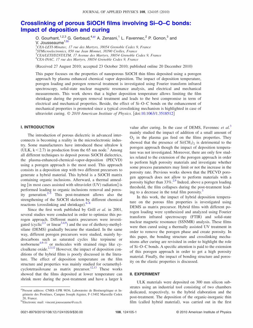
chamber by PECVD: DEMS was used as organosilicon pre-cursor for the matrix and norbornadiene �NBD� was used asorganic precursor, for the labile phase �Fig. 1�. Both precur-sors were injected simultaneously in a capacitive coupledparallel plate reactor using a 13.56 MHz radio-frequency ex-citation. Several deposition temperatures were tested be-tween 200 and 310 °C by varying chuck heating. In the sec-ond chamber, two kinds of post-treatments were performedin order to remove the porogen phase. UV curing was real-ized onto a hotplate at 400 °C, under a broadband UV lampexposition and under He atmosphere. The optimal treatmenttime was determined according to our previous studies.8 Athermal treatment, performed on a hotplate at 450 °C underN2 atmosphere, was also studied as a comparison to UVcuring.
FTIR analysis was performed on a Biorad QS3300 spec-trometer in transmission mode with a normal incidence.Spectra were recorded using a resolution of 2 cm−1 and av-eraged over 32 scans. Refractive index at 633 nm and filmthickness were measured on a Rudolph ellipsometer. The di-electric constant of the porous film was calculated thanks tocapacitance in accumulation mode at 0.1 MHz in the metal-insulator-semiconductor structure formed by a mercury dropon the stack ULK-silicon. To determine the network structureof thin films, SSNMR was performed with a BrukerAVANCE 400 using 9.4 T static magnetic field, which de-fines resonant frequency at 100.61 MHz for 13C, 79.49 MHzfor 29Si, and 400.13 MHz for 1H. High-resolution SSNMRspectra were obtained thanks to the combination of cross-polarization �CP�, magic-angle spinning �MAS�, and highpower decoupling. Dried powders were put in 4 mm �92 �l�diameter cylindrical double-bearing rotors, made of zirconia.The chemical shift values were indirectly calibrated usingthe 13C glycine carbonyl signal set to 176.03 ppm relative totetramethylsilane �TMS�. The calibration of 29Si chemicalshift was based on the most upfield signal �Si�OSi�4, Q4 site�of Q8M8 �Si��CH3�3�8Si8O20� set to �109.7 ppm relative toTMS. The MAS speed was set to 12 kHz for 13C spectra and
5 kHz for 29Si spectra. A 1H radio-frequency field strength of100 kHz was used for proton pulses �90° pulse duration of2.5 �s� and for dipolar decoupling. The 13C and 29Si fieldstrength were set to match the Hartman–Hahn condition dur-ing CP. For each spectrum, 5000–16 000 transients were ac-cumulated with a CP contact time of 2 ms for the 13C spec-tra, of 3.5 ms for the 29Si spectra. A recycle delay of 5 s wasused for both nuclei. Porosity experiments were carried outin the visible range on an EP12 ellipsometric porosimeterfrom SOPRALAB using toluene as solvent. Nanoindentationmeasurements were carried out using MTS indenter XPW-300 with a Berkovitch tip. Continuous stiffness method, con-sisting in 2 nm oscillations at 45 Hz superimposed to thelinear loading-unloading movement of the tip, enabled mea-surement of hardness and reduced modulus.14 Each measure-ment was repeated 18 times.
III. RESULTS AND DISCUSSION
A. Influence of deposition temperature and porogenloading
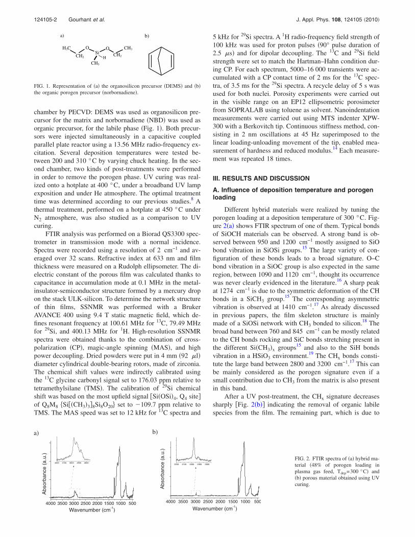
Different hybrid materials were realized by tuning theporogen loading at a deposition temperature of 300 °C. Fig-ure 2�a� shows FTIR spectrum of one of them. Typical bondsof SiOCH materials can be observed. A strong band is ob-served between 950 and 1200 cm−1 mostly assigned to SiObond vibration in SiOSi groups.15 The large variety of con-figuration of these bonds leads to a broad signature. O–Cbond vibration in a SiOC group is also expected in the sameregion, between 1090 and 1120 cm−1, thought its occurrencewas never clearly evidenced in the literature.16 A sharp peakat 1274 cm−1 is due to the symmetric deformation of the CHbonds in a SiCH3 group.15 The corresponding asymmetricvibration is observed at 1410 cm−1.17 As already discussedin previous papers, the film skeleton structure is mainlymade of a SiOSi network with CH3 bonded to silicon.18 Thebroad band between 760 and 845 cm−1 can be mostly relatedto the CH bonds rocking and SiC bonds stretching present inthe different Si�CH3�x groups15 and also to the SiH bondsvibration in a HSiO3 environment.19 The CHx bonds consti-tute the large band between 2800 and 3200 cm−1.17 This canbe mainly considered as the porogen signature even if asmall contribution due to CH3 from the matrix is also presentin this band.
After a UV post-treatment, the CHx signature decreasessharply �Fig. 2�b�� indicating the removal of organic labilespecies from the film. The remaining part, which is due to
a) b)
CH2 H
CH3
SiOH3C
CH2
O CH3
FIG. 1. Representation of �a� the organosilicon precursor �DEMS� and �b�the organic porogen precursor �norbornadiene�.
4000 3500 3000 2500 2000 1500 1000 500
3200 3100 3000 2900 2800
Ab
sorb
ance
(a.u
.)
Wavenumber (cm-1)
a)
4000 3500 3000 2500 2000 1500 1000 500
3200 3100 3000 2900 2800
Ab
so
rban
ce
(a.u
.)
Wavenumber (cm-1)
b)
FIG. 2. FTIR spectra of �a� hybrid ma-terial �48% of porogen loading inplasma gas feed, Tdep=300 °C� and�b� porous material obtained using UVcuring.
124105-2 Gourhant et al. J. Appl. Phys. 108, 124105 �2010�
the SiOCH matrix, is mainly composed by a peak at2960 cm−1 which is related to the presence of C–H bonds inCH3 groups, in agreement with the presence of the peak at1274 cm−1 due to Si–C bonds in Si–CH3 groups. All theseresults are consistent with previous data already published byseveral groups.3,5,20
The amount of porogen in the hybrid film can be quali-tatively appreciated thanks to FTIR analysis through theevaluation of a parameter P defined below:
P =Area2800–3200 cm−1
Area980–1350 cm−1�
�CHx��SiOSi�
. �1�
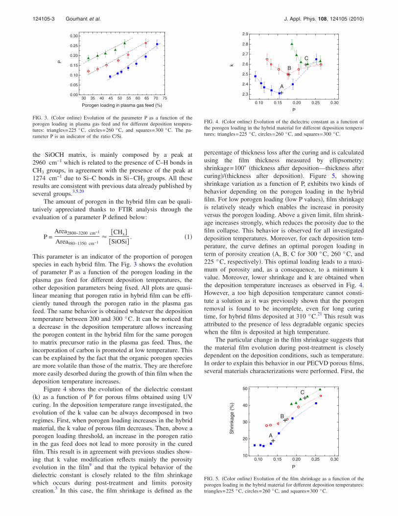
This parameter is an indicator of the proportion of porogenspecies in each hybrid film. The Fig. 3 shows the evolutionof parameter P as a function of the porogen loading in theplasma gas feed for different deposition temperatures, theother deposition parameters being fixed. All plots are quasi-linear meaning that porogen ratio in hybrid film can be effi-ciently tuned through the porogen ratio in the plasma gasfeed. The same behavior is obtained whatever the depositiontemperature between 200 and 300 °C. It can be noticed thata decrease in the deposition temperature allows increasingthe porogen content in the hybrid film for the same porogento matrix precursor ratio in the plasma gas feed. Thus, theincorporation of carbon is promoted at low temperature. Thiscan be explained by the fact that the organic porogen speciesare more volatile than those of the matrix. They are thereforemore easily desorbed during the growth of thin film when thedeposition temperature increases.
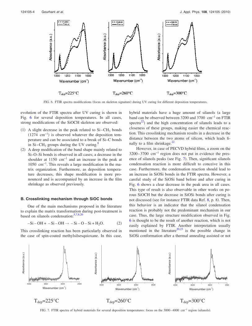
Figure 4 shows the evolution of the dielectric constant�k� as a function of P for porous films obtained using UVcuring. In the deposition temperature range investigated, theevolution of the k value can be always decomposed in tworegimes. First, when porogen loading increases in the hybridmaterial, the k value of porous film decreases. Then, above aporogen loading threshold, an increase in the porogen ratioin the gas feed does not lead to more porosity in the curedfilm. This result is in agreement with previous studies show-ing that k value modification reflects mainly the porosityevolution in the film9 and that the typical behavior of thedielectric constant is closely related to the film shrinkagewhich occurs during post-treatment and limits porositycreation.3 In this case, the film shrinkage is defined as the
percentage of thickness loss after the curing and is calculatedusing the film thickness measured by ellipsometry:shrinkage=100� �thickness after deposition—thickness aftercuring�/�thickness after deposition�. Figure 5, showingshrinkage variation as a function of P, exhibits two kinds ofbehavior depending on the porogen loading in the hybridfilm. For low porogen loading �low P values�, film shrinkageis relatively steady which enables the increase in porosityversus the porogen loading. Above a given limit, film shrink-age increases strongly, which reduces the porosity due to thefilm collapse. This behavior is observed for all investigateddeposition temperatures. Moreover, for each deposition tem-perature, the curve defines an optimal porogen loading interm of porosity creation �A, B, C for 300 °C, 260 °C, and225 °C, respectively�. This optimal loading leads to a maxi-mum of porosity and, as a consequence, to a minimum kvalue. Moreover, lower shrinkage and k are obtained whenthe deposition temperature increases as observed in Fig. 4.However, a too high deposition temperature cannot consti-tute a solution as it was previously shown that the porogenremoval is found to be incomplete, even for long curingtime, for hybrid films deposited at 310 °C.21 This result wasattributed to the presence of less degradable organic specieswhen the film is deposited at high temperature.
The particular change in the film shrinkage suggests thatthe material film evolution during post-treatment is closelydependent on the deposition conditions, such as temperature.In order to explain this behavior in our PECVD porous films,several materials characterizations were performed. First, the
30 35 40 45 50 55 60 65 70 750.00
0.05
0.10
0.15
0.20
0.25
0.30
P
Porogen loading in plasma gas feed (%)
FIG. 3. �Color online� Evolution of the parameter P as a function of theporogen loading in plasma gas feed and for different deposition tempera-tures: triangles=225 °C, circles=260 °C, and squares=300 °C. The pa-rameter P is an indicator of the ratio C/Si.
0.10 0.15 0.20 0.25 0.30
2.3
2.4
2.5
2.6
2.7
2.8
2.9
k
P
+A
+B
+C
FIG. 4. �Color online� Evolution of the dielectric constant as a function ofthe porogen loading in the hybrid material for different deposition tempera-tures: triangles=225 °C, circles=260 °C, and squares=300 °C.
0.10 0.15 0.20 0.25 0.3010
20
30
40
50
A
+
Shrinkage
(%)
P
+
B
+C
FIG. 5. �Color online� Evolution of the film shrinkage as a function of theporogen loading in the hybrid material for different deposition temperatures:triangles=225 °C, circles=260 °C, and squares=300 °C.
124105-3 Gourhant et al. J. Appl. Phys. 108, 124105 �2010�
evolution of the FTIR spectra after UV curing is shown inFig. 6 for several deposition temperatures. In all cases,strong modifications of the SiOCH skeleton are observed:
�1� A slight decrease in the peak related to Si–CH3 bonds�1274 cm−1� is observed whatever the deposition tem-perature and can be associated to a break of Si–C bondsin Si–CH3 groups during the UV curing.8
�2� A deep modification of the band shape mainly related toSi–O–Si bonds is observed in all cases; a decrease in theshoulder at 1150 cm−1 and an increase in the peak at1050 cm−1. This reveals a large modification in the ma-trix organization. Furthermore, as deposition tempera-ture decreases, this shape modification is more pro-nounced and is accompanied by an increase in the filmshrinkage as observed previously.
B. Crosslinking mechanism through SiOC bonds
One of the main mechanisms proposed in the literatureto explain the matrix transformation during post-treatment isbased on silanols condensation:5,7,8,20
–Si – OH + – Si – OH → – Si – O – Si + H2O. �2�
This crosslinking reaction has been particularly observed inthe case of spin-coated methylsilsesquioxane. In this case,
hybrid materials have a huge amount of silanols �a largeband can be observed between 3200 and 3700 cm−1 on FTIRspectra22� and the high concentration of silanols leads to acloseness of these groups, making easier the chemical reac-tion. This crosslinking mechanism results in a decrease in thedistance between the two atoms of silicon, which leads fi-nally to a film shrinkage.22
However, in case of PECVD hybrid films, a zoom on the3200–3700 cm−1 region does not put in evidence the pres-ence of silanols peaks �see Fig. 7�. Then, significant silanolscondensation reaction is more difficult to conceive in thiscase. Furthermore, the condensation reaction should lead toan increase in SiOSi bonds in the FTIR spectra. However, acareful study of the SiOSi band before and after curing inFig. 6 shows a clear decrease in the peak area in all cases.This type of result is also observable in other works on po-rous SiOCH but the decrease in SiOSi bonds after curing isnot discussed �see for instance FTIR data Ref. 8, p. 8�. Then,this behavior is an indicator that the silanol condensationreaction is probably not the predominant mechanism in ourcase. Thus, the large structure modification observed in Fig.6 is thought to be the result of another reaction, which is noteasily explained by FTIR. Another interpretation usuallymentioned in the literature20,23 is the possible change inSiOSi conformation after a thermal annealing assisted or not
FIG. 6. FTIR spectra modifications �focus on skeleton signature� during UV curing for different deposition temperatures.
4000 3500 3000 2500
Ab
sorb
an
ce
(a.u
.)
Wavenumber (cm-1)
4000 3500 3000 2500
Ab
sorb
ance
(a.u
.)
Wavenumber (cm-1)
4000 3500 3000 2500
Ab
sorb
an
ce
(a.u
.)
Wavenumber (cm-1)
Tdep=225°C Tdep=260°C Tdep=300°C
FIG. 7. FTIR spectra of hybrid materials for several deposition temperatures: focus on the 3000–4000 cm−1 region �silanols�.
124105-4 Gourhant et al. J. Appl. Phys. 108, 124105 �2010�
by UV. Most of the FTIR data are in general interpretedusing the decomposition of the SiOSi band in three peaksassigned, respectively, to SiOSi suboxide, SiOSi network,and SiOSi cage like structures.20 However, even if a restruc-turation of the SiOSi bonds is expected upon curing, itshould not lead to such significant decrease in the SiOSiFTIR band area after curing �because this explanation doesnot imply the destruction or creation of SiOSi links�. Then,this interpretation, even if probable, remains difficult to dem-onstrate and is not sufficient to explain our results.
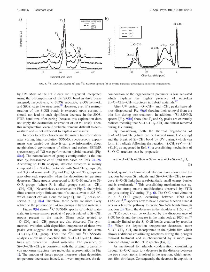
In order to better characterize the matrix transformationsafter curing, high-resolution SSNMR spectroscopy experi-ments was carried out since it can give information aboutneighborhood environment of silicon and carbon. SSNMRspectroscopy of 29Si was performed on hybrid materials �Fig.8�a��. The nomenclature of group’s configuration is the oneused by Jousseaume et al.7 and was based on Refs. 24–26.According to FTIR analysis, skeleton structure is mainlycomposed of a Si–O–Si network with Si–CH3 groups �D2
and T3� and some Si–H �TH and DH�. Q3 and T2 groups arealso observed, especially when the deposition temperaturedecreases. These groups correspond to Si–O–H and/or to Si–O–R groups �where R is alkyl groups such as –CH3,–CH2–CH3�. Nevertheless, as observed in Fig. 7, the hybridfilms contain only a little amount of silanols, even at 225 °C,which cannot explain alone the large Q3 and T2 peaks ob-served in Fig. 8�a�. Therefore, those peaks are more likelyrelated to the presence of Si–O–R groups in hybrid materials.
Figure 8�b� shows 13C SSNMR spectra of hybrid mate-rials. An intense narrow peak at –5 ppm is related to Si–CH3
groups present in the matrix. Sharp peaks related to–O–CH2– and –CH3 groups are also observed. The sym-metrical evolution with deposition temperature of these twopeaks can suggest that they are involved in the same–O–CH2–CH3 group. Then, the 29Si and 13C SSNMRanalyses allow us to conclude that Si–O–CH2–CH3 struc-tures are present in hybrid materials. The presence ofSi–O–CH2–CH3 is consistent with the original organosili-con monomer structure �see molecular representation in Fig.1�. The amount of theses groups increases when depositiontemperature decreases: Indeed, at lower temperature, the de-
composition of the organosilicon precursor is less activatedwhich explains the higher presence of unbrokenSi–O–CH2–CH3 structures in hybrid materials.27
After UV curing, –O–CH2– and –CH3 peaks have al-most disappeared �Fig. 9�a�� showing their removal from thethin film during post-treatment. In addition, 29Si SSNMRspectra �Fig. 9�b�� show that T2 and Q3 peaks are extremelyreduced meaning that Si–O–CH2–CH3 are almost removedduring UV curing.
By considering both the thermal degradation ofSi–O–CH2–CH3 �which can be favored using UV curing�and the break of Si–CH3 bond by UV curing �which canform Si· radicals following the reaction –SiCH3+eV→ –Si·
+CwHx as suggested in Ref. 8�, a crosslinking mechanism ofSi–O–C structures can be proposed:
–Si – O – CH2 – CH3 + – Si· → – Si – O – Si – + CyHz.
�3�
Indeed, quantum chemical calculations have shown that thereaction between Si radicals and Si–O–CH2–CH3 to pro-duce Si–O–Si links has a substantially small energy barrierand is exothermic.28 This crosslinking mechanism can ex-plain the strong matrix modifications observed by FTIRanalysis during UV curing �Fig. 6�. The O–C bond vibrationin a Si–O–C group, occurring between 1090 and1120 cm−1,16 appears now to have a crucial function since itacts as a feasible pathway to create Si–O–Si bonds throughreaction �3�. Then, the decrease in the shoulder at 1150 cm−1
on FTIR spectra can be explained by the disappearance ofSiOC bonds and the increase in the main peak at 1050 cm−1
is mainly linked to the Si–O–Si bonds creation by reaction�3�. When the deposition temperature decreases, moreSi–O–CH2–CH3 are incorporated in the hybrid film whichallows additional crosslinking reactions during the porogenremoval treatment and is characterized by a more pro-nounced change in the FTIR spectra �Fig. 6�.
As mentioned for silanols condensation, crosslinkingthrough Si–O–C leads to a decrease in the distance betweenthe two silicon atoms involved in the reaction, which gener-ates film shrinkage. Consequently, the decrease in deposition
300°C
260°C
225°C
Deposition temperature:
-150-100-500
Inte
nsity
(a.u.)
D2
T2
TH
Q3Q4
*DH *
T3
Chemical shift (ppm)
300°C
260°C
225°C
050100150
Inte
nsity
(a.u.)
Deposition temperature:
Chemical shift (ppm)
-CH2- -CH3
-O-CH2-
C=C
C=CH-
Si-CH3
a) b)
FIG. 8. 29Si SSNMR spectra �a� and 13C SSNMR spectra �b� of hybrid materials deposited at different temperatures.
124105-5 Gourhant et al. J. Appl. Phys. 108, 124105 �2010�
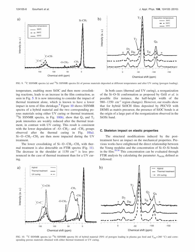
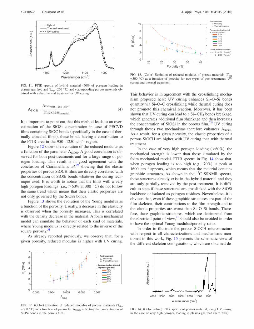
temperature, enabling more SiOC and then more crosslink-ing reactions, leads to an increase in the film contraction, asseen in Fig. 5. It is now interesting to consider the impact ofthermal treatment alone, which is known to have a lowerimpact in term of film shrinkage.8 Figure 10 shows SSNMRspectra of a hybrid material and the two corresponding po-rous materials using either UV curing or thermal treatment.29Si SSNMR spectra, in Fig. 10�b�, show that Q3 and T2
peak intensities are weakly reduced after the thermal treat-ment, in contrast with UV curing. This result is consistentwith the lower degradation of –O–CH2– and –CH3 groupsobserved after the thermal curing in Fig. 10�a�.Si–O–CH2–CH3 are then more impacted during the UVtreatment.
The lower crosslinking of Si–O–CH2–CH3 with ther-mal treatment is also detectable on FTIR spectra �Fig. 11�.The decrease in the shoulder at 1150 cm−1 is less pro-nounced in the case of thermal treatment than for a UV cur-ing.
In both cases �thermal and UV curing�, a reorganizationof the Si–O–Si conformation as proposed by Grill et al. ispossible �for instance, the half-height width of the980–1350 cm−1 region changes�. However, our results showthat for hybrid SiOCH films deposited by PECVD withDEMS as matrix precursor, the presence of SiOC bonds is atthe origin of a large part of the reorganization observed in theSiOSi band.
C. Skeleton impact on elastic properties
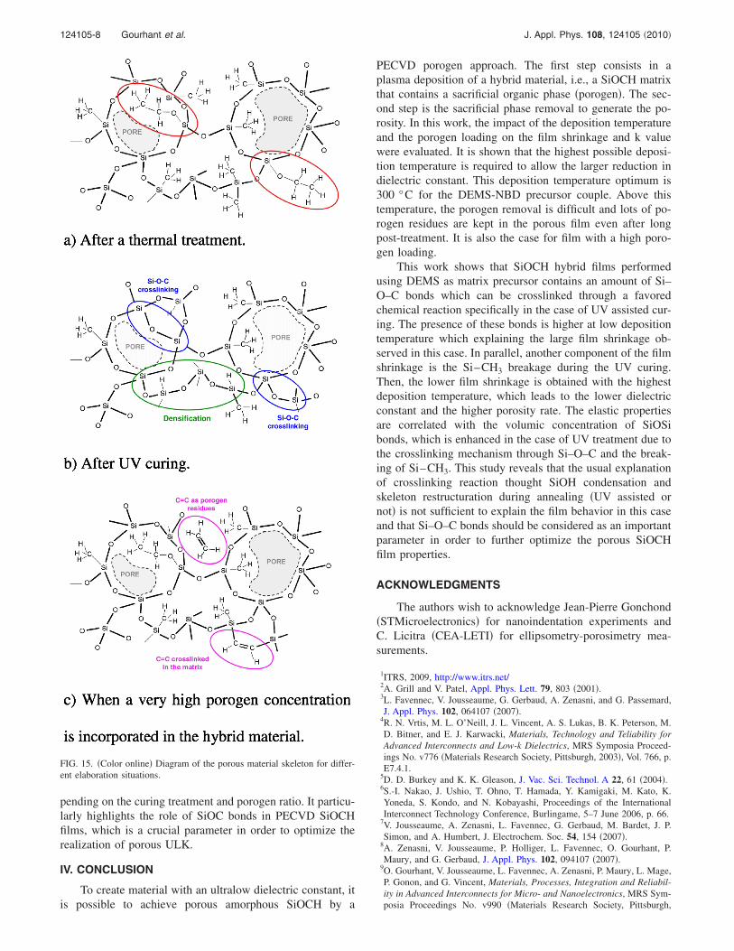
The structural modifications induced by the post-treatment have an impact on the mechanical properties. Pre-vious works have enlightened the direct relationship betweenthe Young modulus and the concentration of Si–O–Si bondsin the film.29,30 This concentration can be evaluated throughFTIR analysis by calculating the parameter ASiOSi defined asfollowed:
-150-100-500
300°C
260°C
225°C
Inte
nsity
(a.u.)
* *
D2DH
T2Q4
TH
050100150
300°C
260°C
225°C
Deposition temperature:
Inte
nsity
(a.u.)
Chemical shift (ppm)
C=CH-
C=C-O-CH2- -CH3
Si-CH3a) b) Deposition temperature:
Chemical shift (ppm)
T3
FIG. 9. 13C SSNMR spectra �a� and 29Si SSNMR spectra �b� of porous materials deposited at different temperatures and after UV curing �porogen loading�.
UV curing
Hybrid
Thermal treatment
-150-100-500
Chemical shift (ppm)
* *
D2
T2
DHTH
Q4Q3
050100150
UV curing
Thermal treatment
Inte
nsity
(a.u.)
Chemical shift (ppm)
Hybrid
C=CH-
C=C
-CH3
-O-CH2-
-CH2
a) b)
FIG. 10. 13C SSNMR spectra �a� 29Si SSNMR spectra �b� of hybrid material �50% of porogen loading in plasma gas feed and Tdep=260 °C� and corre-sponding porous materials obtained with either thermal treatment or UV curing.
124105-6 Gourhant et al. J. Appl. Phys. 108, 124105 �2010�
ASiOSi =Area980–1250 cm−1
Thicknessmaterial. �4�
It is important to point out that this method leads to an over-estimation of the SiOSi concentration in case of PECVDfilms containing SiOC bonds �specifically in the case of ther-mally annealed films�, these bonds having a contribution tothe FTIR area in the 950–1250 cm−1 region.
Figure 12 shows the evolution of the reduced modulus asa function of the parameter ASiOSi. A good correlation is ob-served for both post-treatments and for a large range of po-rogen loading. This result is in good agreement with theconclusion of Ciaramella et al.29 showing that the elasticproperties of porous SiOCH films are directly correlated withthe concentration of SiOSi bonds whatever the curing tech-nique used. It is worth to notice that the films with a veryhigh porogen loadings �i.e., �60% at 300 °C� do not followthe same trend which means that their elastic properties arenot only governed by the SiOSi bonds.
Figure 13 shows the evolution of the Young modulus asa function of the porosity. Usually, a decrease in the elasticityis observed when the porosity increases. This is correlatedwith the density decrease in the material. A foam mechanicalmodel can simulate the behavior of each kind of materials,where Young modulus is directly related to the inverse of thesquare porosity.31
As already reported previously, we observe that, for agiven porosity, reduced modulus is higher with UV curing.
This behavior is in agreement with the crosslinking mecha-nism proposed here: UV curing enhances Si–O–Si bondsquantity via Si–O–C crosslinking while thermal curing doesnot promote this chemical reaction. Moreover, it has beenshown that UV curing can lead to a Si–CH3 bonds breakage,which generates additional film shrinkage and then increasesthe concentration of SiOSi in the porous film.7,8 UV curingthrough theses two mechanisms therefore enhances ASiOSi.As a result, for a given porosity, the elastic properties of aporous SiOCH are higher with UV curing than with thermaltreatment.
In the case of very high porogen loading ��60%�, themechanical strength is lower than those simulated by thefoam mechanical model. FTIR spectra in Fig. 14 show that,when porogen loading is too high �e.g., 70%�, a peak at1600 cm−1 appears, which means that the material containsgraphitic structures. As shown in the 13C SSNMR spectra,these structures already exist in the hybrid material and theyare only partially removed by the post-treatment. It is diffi-cult to state if these structures are crosslinked with the SiOSibackbone or isolated as porogen residues. Nevertheless, it isobvious that, even if these graphitic structures are part of thefilm skeleton, their contributions to the film strength and tothe elastic properties are worst than Si–O–Si bonds. There-fore, these graphitic structures, which are detrimental fromthe electrical point of view,21 should also be avoided in orderto have the optimal Young modulus/porosity ratio.
In order to illustrate the porous SiOCH microstructurewith respect to all characterizations and mechanisms men-tioned in this work, Fig. 15 presents the schematic view ofthe different skeleton configurations, which are obtained de-
1300 1200 1100 1000
HybridThermal treatmentUV curing
Abs
orba
nce
(a.u
.)
Wavenumber (cm-1)
FIG. 11. FTIR spectra of hybrid material �50% of porogen loading inplasma gas feed and Tdep=260 °C� and corresponding porous materials ob-tained with either thermal treatment or UV curing.
0.003 0.004 0.005 0.006 0.0070
1
2
3
4
5
6
7
Post-treatment:
Thermal treatment
Porogen loading injected
in plasma gas feed:
45%
48%
51%
55%59%
70%
Er(G
Pa)
ASiOSi
UV curing
FIG. 12. �Color� Evolution of reduced modulus of porous materials �Tdep
=300 °C� as a function of parameter ASiOSi reflecting the concentration ofSiOSi bonds in the porous film.
FIG. 13. �Color� Evolution of reduced modulus of porous materials �Tdep
=300 °C� as a function of porosity for two types of post-treatments: UVcuring and thermal treatment.
4000 3500 3000 2500 2000 1500 1000
Absorb
ance
(a.u
.)
Wavenumber (cm-1)
FIG. 14. �Color online� FTIR spectra of porous material, using UV curing,in the case of very high porogen loading in plasma gas feed �here 70%�.
124105-7 Gourhant et al. J. Appl. Phys. 108, 124105 �2010�
pending on the curing treatment and porogen ratio. It particu-larly highlights the role of SiOC bonds in PECVD SiOCHfilms, which is a crucial parameter in order to optimize therealization of porous ULK.
IV. CONCLUSION
To create material with an ultralow dielectric constant, itis possible to achieve porous amorphous SiOCH by a
PECVD porogen approach. The first step consists in aplasma deposition of a hybrid material, i.e., a SiOCH matrixthat contains a sacrificial organic phase �porogen�. The sec-ond step is the sacrificial phase removal to generate the po-rosity. In this work, the impact of the deposition temperatureand the porogen loading on the film shrinkage and k valuewere evaluated. It is shown that the highest possible deposi-tion temperature is required to allow the larger reduction indielectric constant. This deposition temperature optimum is300 °C for the DEMS-NBD precursor couple. Above thistemperature, the porogen removal is difficult and lots of po-rogen residues are kept in the porous film even after longpost-treatment. It is also the case for film with a high poro-gen loading.
This work shows that SiOCH hybrid films performedusing DEMS as matrix precursor contains an amount of Si–O–C bonds which can be crosslinked through a favoredchemical reaction specifically in the case of UV assisted cur-ing. The presence of these bonds is higher at low depositiontemperature which explaining the large film shrinkage ob-served in this case. In parallel, another component of the filmshrinkage is the Si–CH3 breakage during the UV curing.Then, the lower film shrinkage is obtained with the highestdeposition temperature, which leads to the lower dielectricconstant and the higher porosity rate. The elastic propertiesare correlated with the volumic concentration of SiOSibonds, which is enhanced in the case of UV treatment due tothe crosslinking mechanism through Si–O–C and the break-ing of Si–CH3. This study reveals that the usual explanationof crosslinking reaction thought SiOH condensation andskeleton restructuration during annealing �UV assisted ornot� is not sufficient to explain the film behavior in this caseand that Si–O–C bonds should be considered as an importantparameter in order to further optimize the porous SiOCHfilm properties.
ACKNOWLEDGMENTS
The authors wish to acknowledge Jean-Pierre Gonchond�STMicroelectronics� for nanoindentation experiments andC. Licitra �CEA-LETI� for ellipsometry-porosimetry mea-surements.
1ITRS, 2009, http://www.itrs.net/2A. Grill and V. Patel, Appl. Phys. Lett. 79, 803 �2001�.3L. Favennec, V. Jousseaume, G. Gerbaud, A. Zenasni, and G. Passemard,J. Appl. Phys. 102, 064107 �2007�.
4R. N. Vrtis, M. L. O’Neill, J. L. Vincent, A. S. Lukas, B. K. Peterson, M.D. Bitner, and E. J. Karwacki, Materials, Technology and Teliability forAdvanced Interconnects and Low-k Dielectrics, MRS Symposia Proceed-ings No. v776 �Materials Research Society, Pittsburgh, 2003�, Vol. 766, p.E7.4.1.
5D. D. Burkey and K. K. Gleason, J. Vac. Sci. Technol. A 22, 61 �2004�.6S.-I. Nakao, J. Ushio, T. Ohno, T. Hamada, Y. Kamigaki, M. Kato, K.Yoneda, S. Kondo, and N. Kobayashi, Proceedings of the InternationalInterconnect Technology Conference, Burlingame, 5–7 June 2006, p. 66.
7V. Jousseaume, A. Zenasni, L. Favennec, G. Gerbaud, M. Bardet, J. P.Simon, and A. Humbert, J. Electrochem. Soc. 54, 154 �2007�.
8A. Zenasni, V. Jousseaume, P. Holliger, L. Favennec, O. Gourhant, P.Maury, and G. Gerbaud, J. Appl. Phys. 102, 094107 �2007�.
9O. Gourhant, V. Jousseaume, L. Favennec, A. Zenasni, P. Maury, L. Mage,P. Gonon, and G. Vincent, Materials, Processes, Integration and Reliabil-ity in Advanced Interconnects for Micro- and Nanoelectronics, MRS Sym-posia Proceedings No. v990 �Materials Research Society, Pittsburgh,
FIG. 15. �Color online� Diagram of the porous material skeleton for differ-ent elaboration situations.
124105-8 Gourhant et al. J. Appl. Phys. 108, 124105 �2010�
2007�, Vol. 990, p. B03.10S. M. Gates, D. A. Neumayer, M. H. Sherwood, A. Grill, X. Wang, and M.
Sankarapandian, J. Appl. Phys. 101, 094103 �2007�.11Y. Zheng, W. Zhu, T. Huang, S. Nemani, K. S. Yim, H. Am, L.-Q. Xia,
and H. M’Saad, Proceedings of Advanced Metallization Conference�AMC 2004�, San Diego, 19–21 October 2004, p. 543.
12A. Grill and V. Patel, J. Appl. Phys. 104, 024113 �2008�.13S. M. Gates, G. Dubois, E. T. Ryan, A. Grill, M. Liu, and D. Gidley, J.
Electrochem. Soc. 156, G156 �2009�.14X. Li and B. Bhushman, Mater. Charact. 48, 11 �2002�.15D. R. Anderson, in Analysis of Silicones, edited by A. L. Smith �Wiley,
New York, 1974�, Chap. 10.16S. P. Mukherjee and P. E. Evans, Thin Solid Films 14, 105 �1972�.17C. Rau and W. Kulish, Thin Solid Films 249, 28 �1994�.18V. Jousseaume, C. Le Cornec, F. Ciaramella, L. Favennec, A. Zenasni, G.
Simon, J.-P. Simon, G. Gerbaud, and G. Passermard, Materials, Technol-ogy and Reliability of Low-k Dielectrics and Copper Interconnects, MRSSymposia Proceedings No. v914 �Materials Research Society, Pittsburgh,2006�, Vol. 914, p. F04.
19C. Marcolli and G. Calzaferri, J. Phys. Chem. B 101, 4925 �1997�.20A. Grill and D. Neumayer, J. Appl. Phys. 94, 6697 �2003�.21O. Gourhant, V. Jousseaume, L. Favennec, A. Zenasni, P. Gonon, and G.
Vincent, Proceedings of the Advanced Metallization Conference �AMC2008�, San Diego, 23–25 September 2008, p. 537.
22A. Zenasni, F. Ciaramella, V. Jousseaume, C. Le Cornec, and G. Passe-mard, J. Electrochem. Soc. 154, G6 �2007�.
23F. Iacopi, Y. Travaly, B. Eyckens, C. Walfried, T. Abell, E. P. Guyer, D. M.Gage, R. H. Dauskardt, T. Sajavaara, K. Houthoofd, P. Grobet, P. Jacobs,and K. Maex, J. Appl. Phys. 99, 053511 �2006�.
24M. P. J. Peeters, W. J. J. Wakelkamp, and A. P. M. Kentgens, J. Non-Cryst.Solids 189, 77 �1995�.
25E. A. Williams, Annu. Rep. Nucl. Magn. Reson. Spectrosc. 15, 235�1984�.
26S. K. Young, W. L. Jarrett, and K. A. Mauritz, Polymer 43, 2311 �2002�.27A. Castex, Ph.D. thesis, INP Grenoble, 2005.28N. Tajima, Y. Ohashi, S. Nagano, Y. Xu, S. Matsumoto, T. Kada, and T.
Ohno, Proceedings of the International Interconnect Technology Confer-ence, Burlingame, 1–3 June 2009, p. 116.
29F. Ciaramella, V. Jousseaume, S. Maitrejean, M. Verdier, B. Remiat, A.Zenasni, and G. Passemard, Thin Solid Films 495, 124 �2006�.
30V. Jousseaume, L. Favennec, A. Zenasni, and O. Gourhant, Surf. Coat.Technol. 201, 9248 �2007�.
31L. Gibson and M. Ashby, Cellular Solids: Structure and Properties �Cam-bridge University Press, Cambridge, 1997�.
124105-9 Gourhant et al. J. Appl. Phys. 108, 124105 �2010�