
Agnes Smedley – the fellow-traveller's tales - HKU Scholars Hub
Upload
khangminh22Category
view
8download
0
ARTICLE
One-step synthesis of single-site vanadiumsubstitution in 1T-WS2 monolayers for enhancedhydrogen evolution catalysisAli Han1,2,9, Xiaofeng Zhou1,3,9, Xijun Wang 4,9, Sheng Liu5, Qihua Xiong 5,6, Qinghua Zhang7, Lin Gu7,
Zechao Zhuang2, Wenjing Zhang8, Fanxing Li 4, Dingsheng Wang 2✉, Lain-Jong Li 1✉ & Yadong Li2
Metallic tungsten disulfide (WS2) monolayers have been demonstrated as promising elec-
trocatalysts for hydrogen evolution reaction (HER) induced by the high intrinsic conductivity,
however, the key challenges to maximize the catalytic activity are achieving the metallic WS2with high concentration and increasing the density of the active sites. In this work, single-
atom-V catalysts (V SACs) substitutions in 1T-WS2 monolayers (91% phase purity) are
fabricated to significantly enhance the HER performance via a one-step chemical vapor
deposition strategy. Atomic-resolution scanning transmission electron microscopy (STEM)
imaging together with Raman spectroscopy confirm the atomic dispersion of V species on the
1T-WS2 monolayers instead of energetically favorable 2H-WS2 monolayers. The growth
mechanism of V SACs@1T-WS2 monolayers is experimentally and theoretically demon-
strated. Density functional theory (DFT) calculations demonstrate that the activated V-atom
sites play vital important role in enhancing the HER activity. In this work, it opens a novel path
to directly synthesize atomically dispersed single-metal catalysts on metastable materials as
efficient and robust electrocatalysts.
https://doi.org/10.1038/s41467-021-20951-9 OPEN
1 Physical Sciences and Engineering Divison, King Abdullah University of Science and Technology, Thuwal 23955-6900, Kingdom of Saudi Arabia.2 Department of Chemistry, Tsinghua University, Beijing 100084, China. 3 Shenzhen Chang Long Technology Co., Ltd, Shenzhen 518117, China. 4 Departmentof Chemical and Biomolecular Engineering, North Carolina State University, Raleigh, NC 27606, USA. 5Division of Physics and Applied Physics, School ofPhysical and Mathematical Sciences, Nanyang Technological University, Nanyang Ave, Singapore 637371, Singapore. 6 State Key Laboratory of Low-Dimensional Quantum Physics and Department of Physics, Tsinghua University, Beijing 100084, China. 7 Beijing National Laboratory for Condensed MatterPhysics, Institute of Physics, Chinese Academy of Sciences, Beijing 100190, China. 8 SZU-NUS Collaborative Innovation Center for Optoelectronic Science &Technology, Key Laboratory of Optoelectronic Devices and Systems of Ministry of Education and Guangdong Province, College of OptoelectronicEngineering, Shenzhen University, Shenzhen 518060, China. 9These authors contributed equally: Ali Han, Xiaofeng Zhou, Xijun Wang.✉email: [email protected]; [email protected]
NATURE COMMUNICATIONS | (2021) 12:709 | https://doi.org/10.1038/s41467-021-20951-9 | www.nature.com/naturecommunications 1
1234
5678
90():,;

Hydrogen fuel generation from water splitting is one of themost promising ways to replace conventional fossil fuelsand solve the energy crisis1,2. Recently, various strategies
have been developed to realize the highly efficient catalysts forhydrogen evolution reaction (HER), including semiconductor-basedphotocatalytic HER (polymer g-C3N4
3, Ag/semiconductor4, etc.),photoelectrochemically catalytic HER5, and metal-based electro-catalytic HER (metal sulfides1,6,7, metal carbides8,9, etc.). Commer-cially, noble metals from the Pt group are utilized to reduce theoverpotential of HER and boost the kinetics with unrivaled activities,however, they usually suffer from scarcity, high-cost, and long-terminstability. Hence, it is highly desirable to explore robust and efficientHER alternative catalysts with earth-abundant elements to realize thehydrogen economy.
Transition metal dichalcogenides (TMDs) from Group VI ele-ments have recently kindled tremendous investigation as efficientPt substitutes for HER catalysis because of the catalytically active Satoms on edge sites10. Unfortunately, the high proportion ofinactive basal plane of MX2 (M=Mo or W, X= S or Se) sig-nificantly limits the catalytic performance because of the lowelectronic transfer capability, leading to the sluggish electro-catalytic kinetics1. Two key factors are worthy of being consideredto maximize HER activity. One is to increase the metallic phaseproportion of MX2, thus improving the intrinsic conductivity ofMX2 and boosting HER activity2,6,11. However, it is still challen-ging to directly synthesize a highly pure metallic phase, especiallyfor 1T-WS2, owing to the highest formation energy of 1T-WS2(0.89 eV per formula) among all the polymorphs of MX2 (Sup-plementary Fig. 1)12. Recently, the phase-engineered syntheses ofmetallic MX2 from the 2H phase have been widely developed viawet-chemistry or exfoliated methods, however, the as-producedmetallic MX2 domains were usually found with 1T(1T′)/2Hmixed-phase and unstable after long-time air-exposure1,2,6,7,13–22.The other important factor is increasing the density of active sitesof MX2. The field of single atomic catalysts (SACs) comprisingisolated metal atoms on the varied supports gives new opportu-nities for the development of MX2 with increased active sites dueto the high atom utilization of SACs23–25. However, to the best of
our knowledge, the reports on the direct one-step vapor-phasesynthesis of SACs on the highly pure metallic MX2 have not beenexplored.
Here, we show highly dispersed single vanadium atoms on the1T-WS2 monolayers (denoted as V SACs@1T-WS2), which aresynthesized through a one-step chemical vapor deposition (CVD)via controlling the introduction of VCl3. By using VCl3 as the co-precursor, the metallic tungsten disulfide (WS2) monolayers showan ultrahigh 1T concentration of 91%, which is the highest 1Tratio achieved by CVD so far (Supplementary Table 1).Remarkably, the V SACs@1T-WS2 monolayers show superiorHER activity comparable to their 2H counterparts, with a lowTafel slope of 61 mV/dec and high turnover frequency (TOF) of3.01 s−1 at 100 mV, and a remarkable long-term catalytic stabi-lity. We also demonstrate that the highly active single-atom Vsites play a vital role in enhancing the HER activity of intrinsic1T-WS2 monolayers.
ResultsCharacterization of V SACs@1T-WS2 monolayers. Figure 1shows the scheme for the growth of V SACs@1T-WS2 mono-layers using WO3, sulphur, and VCl3 as the co-precursors. Forcomparison, 2H-WS2 monolayers were prepared without usingthe VCl3 co-precursor at the same condition and the growthprocess has been reported elsewhere26–33. Strikingly, a black filmof V2O3 (Fig. 2a and Supplementary Fig. 2) was observed on thesapphire surface during the V SACs@1T-WS2 monolayersgrowth, while no V2O3 film appeared for the 2H-WS2 monolayersgrowth. The optical micrographs of fresh sapphire and V2O3 filmwere also provided here for comparison, as seen in Supplemen-tary Fig. 3a, b. In sharp contrast to the triangular morphology of2H-WS2 (Fig. 2b), the V SACs@1T-WS2 monolayers show auniformly circular morphology with a lateral size of 30 μm(Fig. 2b and Supplementary Fig. 3c).
The atomic structure of V SACs@1T-WS2 monolayers wasinvestigated by the aberration-corrected STEM, as provided inFig. 2c, d, showing that the evident Z-contrast intensity sites are
Fig. 1 Schematic illustration of the synthetic process for V SACs@1T-WS2 monolayers. I V2O3 formation in the early growth stage. II V SACs@1T-WS2monolayers formed on the V2O3 film.
ARTICLE NATURE COMMUNICATIONS | https://doi.org/10.1038/s41467-021-20951-9
2 NATURE COMMUNICATIONS | (2021) 12:709 | https://doi.org/10.1038/s41467-021-20951-9 | www.nature.com/naturecommunications
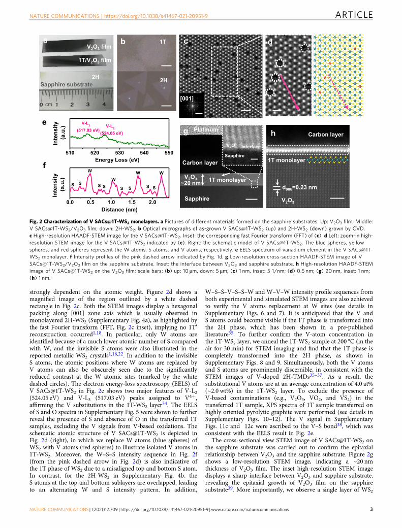
strongly dependent on the atomic weight. Figure 2d shows amagnified image of the region outlined by a white dashedrectangle in Fig. 2c. Both the STEM images display a hexagonalpacking along [001] zone axis which is usually observed inmonolayered 2H-WS2 (Supplementary Fig. 4a), as highlighted bythe fast Fourier transform (FFT, Fig. 2c inset), implying no 1T′reconstruction occurred1,18. In particular, only W atoms areidentified because of a much lower atomic number of S comparedwith W, and the invisible S atoms were also illustrated in thereported metallic WS2 crystals1,16,22. In addition to the invisibleS atoms, the atomic positions where W atoms are replaced byV atoms can also be obscurely seen due to the significantlyreduced contrast at the W atomic sites (marked by the whitedashed circles). The electron energy-loss spectroscopy (EELS) ofV SACs@1T-WS2 in Fig. 2e shows two major features of V-L2(524.05 eV) and V-L3 (517.03 eV) peaks assigned to V4+,affirming the V substitutions in the 1T-WS2 layer34. The EELSof S and O spectra in Supplementary Fig. 5 were shown to furtherreveal the presence of S and absence of O in the transferred 1Tsamples, excluding the V signals from V-based oxidations. Theschematic atomic structure of V SACs@1T-WS2 is depicted inFig. 2d (right), in which we replace W atoms (blue spheres) ofWS2 with V atoms (red spheres) to illustrate isolated V atoms in1T-WS2. Moreover, the W–S–S intensity sequence in Fig. 2f(from the pink dashed arrow in Fig. 2d) is also indicative ofthe 1T phase of WS2 due to a misaligned top and bottom S atom.In contrast, for the 2H-WS2 in Supplementary Fig. 4b, theS atoms at the top and bottom sublayers are overlapped, leadingto an alternating W and S intensity pattern. In addition,
W–S–S–V–S–S–W and W–V–W intensity profile sequences fromboth experimental and simulated STEM images are also achievedto verify the V atoms replacement at W sites (see details inSupplementary Figs. 6 and 7). It is anticipated that the V andS atoms could become visible if the 1T phase is transformed intothe 2H phase, which has been shown in a pre-publishedliterature35. To further confirm the V-atom concentration inthe 1T-WS2 layer, we anneal the 1T-WS2 sample at 200 °C (in theair for 30 min) for STEM imaging and find that the 1T phase iscompletely transformed into the 2H phase, as shown inSupplementary Figs. 8 and 9. Simultaneously, both the V atomsand S atoms are prominently discernible, in consistent with theSTEM images of V-doped 2H-TMDs35–37. As a result, thesubstitutional V atoms are at an average concentration of 4.0 at%(~2.0 wt%) in the 1T-WS2 layer. To exclude the presence ofV-based contaminations (e.g., V2O3, VO2, and VS2) in thetransferred 1T sample, XPS spectra of 1T sample transferred onhighly oriented pyrolytic graphite were performed (see details inSupplementary Figs. 10–12). The V signal in SupplementaryFigs. 11c and 12c were ascribed to the V–S bond38, which wasconsistent with the EELS result in Fig. 2e.
The cross-sectional view STEM image of V SACs@1T-WS2 onthe sapphire substrate was carried out to confirm the epitaxialrelationship between V2O3 and the sapphire substrate. Figure 2gshows a low-resolution STEM image, indicating a ~20 nmthickness of V2O3 film. The inset high-resolution STEM imagedisplays a sharp interface between V2O3 and sapphire substrate,revealing the epitaxial growth of V2O3 film on the sapphiresubstrate39. More importantly, we observe a single layer of WS2
510 520 530 540 550
0.0 0.5 1.0 1.5 2.0
V-L2
(524.05 eV)
Energy Loss (eV)
V-L3
(517.03 eV)
SSSSS S S
WWW
S
Inte
nsity
(a
.u.)
W
Inte
nsity
(a.u
.)
Distance (nm)
e
f
aV2O3 film
1T/V2O3 film
2HSapphire substrate
b 1T
2H
c
[001]
V2O3
Sapphire
Carbon layer
Platinum
1T monolayer
V2O3
Sapphire
Interface
g
~20 nm
V2O3
Carbon layer
1T monolayer
h
d006=0.23 nm
d
Fig. 2 Characterization of V SACs@1T-WS2 monolayers. a Pictures of different materials formed on the sapphire substrates. Up: V2O3 film; Middle:V SACs@1T-WS2/V2O3 film; down: 2H-WS2. b Optical micrographs of as-grown V SACs@1T-WS2 (up) and 2H-WS2 (down) grown by CVD.c High-resolution HAADF-STEM image for the V SACs@1T-WS2. Inset: the corresponding fast Fourier transform (FFT) of (c). d Left: zoom-in high-resolution STEM image for the V SACs@1T-WS2 indicated by (c). Right: the schematic model of V SACs@1T-WS2. The blue spheres, yellowspheres, and red spheres represent the W atoms, S atoms, and V atoms, respectively. e EELS spectrum of vanadium element in the V SACs@1T-WS2 monolayer. f Intensity profiles of the pink dashed arrow indicated by Fig. 1d. g Low-resolution cross-section HAADF-STEM image of VSACs@1T-WS2/V2O3 film on the sapphire substrate. Inset: the interface between V2O3 and sapphire substrate. h High-resolution HAADF-STEMimage of V SACs@1T-WS2 on the V2O3 film; scale bars: (b) up: 10 µm, down: 5 µm; (c) 1 nm, inset: 5 1/nm; (d) 0.5 nm; (g) 20 nm, inset: 1 nm;(h) 1 nm.
NATURE COMMUNICATIONS | https://doi.org/10.1038/s41467-021-20951-9 ARTICLE
NATURE COMMUNICATIONS | (2021) 12:709 | https://doi.org/10.1038/s41467-021-20951-9 | www.nature.com/naturecommunications 3
from the sharp interface between V SACs@1T-WS2 and V2O3
(Fig. 2h). The lattice spacing of V2O3 measured in the STEMimage is ~0.23 nm, in correspondence with the (006) plane ofV2O3 obtained from the XRD diffraction pattern in Supplemen-tary Fig. 239. In addition, the monolayer thickness of V SACs@1T-WS2 (before and after transferring) is also verified by atomic forcemicroscope (AFM), as shown in Supplementary Fig. 13. Second-harmonic generation and angle-resolved-polarization Ramanspectra (ARPRS) are commonly used to probe the symmetryand isotropic/anisotropic lattice structure of TMDs11,40,41. There-fore, the high symmetry and isotropic nature of V SACs@1T-WS2have also been discussed in Supplementary Figs. 14 and 15.
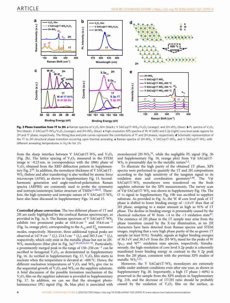
Controlled phase conversion. The two different phases of 1T and2H are easily highlighted by the confocal Raman spectroscopy, asprovided in Fig. 3a, b. The Raman spectrum of V SACs@1T-WS2exhibits two prominent peaks at 418.4 cm−1 and 354.6 cm−1
(Fig. 3a, orange plot), corresponding to the A1g and E12g resonance
modes, respectively. Moreover, three additional typical peaks areobserved at 147.9 cm−1 (J1), 214.5 cm−1 (J2), and 385.3 cm−1 (J3),respectively, which only exist in the metallic phase but not in 2H-WS2 monolayers (blue plot in Fig. 3a)1,16,18,22,42–45. Particularly,a prominently merged peak in the range of 150–250 cm−1 can beascribed to hexagonal V2O3, as demonstrated in SupplementaryFig. 16. As verified in Supplementary Fig. 17, V2O3 film starts tonucleate when the temperature is elevated at ~600 °C. Hence, thedifferent nucleation temperatures of V2O3 and WS2 give rise tothe sequential growth of V2O3 and WS2 on the sapphire substrate.A brief discussion of the possible formation mechanism of theV2O3 film on the sapphire substrate is provided in SupplementaryFig. 17. In addition, we can see that the strongest photo-luminescence (PL) signal (Fig. 3b, blue plot) is associated with
monolayered 2H-WS231, while the negligible PL signal (Fig. 3band Supplementary Fig. 18, orange plot) from V@ SACs@1T-WS2 is presumably due to the metallic nature1,2.
To illustrate the high purity of the obtained 1T phase, XPSspectra were performed to quantify the 1T and 2H compositionsaccording to the high sensitivity of the tungsten signal to itsoxidation state and coordination geometry1,46. The V@SACs@1T-WS2 monolayers were transferred on the freshsapphire substrate for the XPS measurements. The survey scanof V@ SACs@1T-WS2 was shown in Supplementary Fig. 19a. TheO 1s signal in Supplementary Fig. 19b was ascribed to sapphiresubstrate. As provided in Fig. 3c, the W 4f core level peak of 1Tphase is shifted to lower binding energy of ~1.0 eV than that of2H phase, assigning to a major amount as high as 91% of 1Tphase. The decline in binding energy is presumably caused by thechemical reduction of W from +4 to the +3 oxidation state47.The existence of 2H phase in the 1T sample may arise from thephase transition caused by the X-ray illumination, as no 2Hcharacters have been detected from Raman spectra and STEMimages, implying that a very high phase purity of the as-grown 1Tsample (at least 91%). Notably, signals at higher binding energiesof 36.3 eV and 38.5 eV from the 2H-WS2 stand for the peaks of W5p3/2 and W6+ oxidation state species, respectively. Simulta-neously, the high-resolution of core level S 2p peaks is coherentlymanifested lower binding energy in contrast to the S 2p peakfrom the 2H phase, consistent with the previous XPS studies ofmetallic WS21,22.
Moreover, the V SACs@1T-WS2 monolayers are extremelystable under ambient conditions even after one year, as shown inSupplementary Fig. 20. Importantly, a high 1T phase (~60%) ispreserved in the sample from the XPS analysis in SupplementaryFig. 21b, and the decrease of 1T/2H ratio should be probablycaused by the oxidation of V2O3 film on the surface, as
Fig. 3 Phase transition from 1T to 2H. a Raman spectra of V2O3 film (black), V SACs@1T-WS2/V2O3 (orange), and 2H-WS2 (blue). b PL spectra of V2O3
film (black), V SACs@1T-WS2/V2O3 (orange), and 2H-WS2 (blue). c High-resolution XPS spectra of W 4f (left) and S 2p (right) core level peak regions for2H and 1T phase, respectively. The fitting blue and pink curves represent the contributions of 1T and 2H phases, respectively. d Schematic representation ofthe 1T to 2H structural phase transition occurring upon thermal annealing. e Raman spectra of 2H-WS2, V SACs@1T-WS2, and V SACs@1T-WS2 withdifferent annealing temperatures in H2/Ar for 2 h.
ARTICLE NATURE COMMUNICATIONS | https://doi.org/10.1038/s41467-021-20951-9
4 NATURE COMMUNICATIONS | (2021) 12:709 | https://doi.org/10.1038/s41467-021-20951-9 | www.nature.com/naturecommunications
demonstrated in Supplementary Fig. 21d. In addition, uponannealing at different temperatures (200 °C, 300 °C, and 400 °C,respectively) in H2/Ar condition, the 1T phase is partiallytransformed into a 2H phase. The schematic structure of phasetransition from 1T to 2H is shown in Fig. 3d. From the XPSspectra recorded in Supplementary Fig. 22, despite gradualshrinkage of W 4f and S 2p peaks from 1T phase with the elevatedtemperature ≥300 °C, a very high amount of 1T phase is stillpreserved even after annealing at 400 °C (~49%). The differentratios of 1T/2H (W 4f) under different annealing temperatureswere summarized in Supplementary Table 2. Raman spectra inFig. 3e reveal that the enhanced intensities of E12g/A1g areassociated with the decreasing 1T phase. Remarkably, character-istic peaks assigned to the 1T phase are still observed afterannealing at 400 °C. Interestingly, as the increasing temperature,the PL intensity in Supplementary Fig. 23 was enhanced andlargely blue-shifted, which was ascribed to the variation of theband-structure caused by the pronounced ratio of 2H phase in the1T sample, in consistent with the previously reported metallicTMDs22.
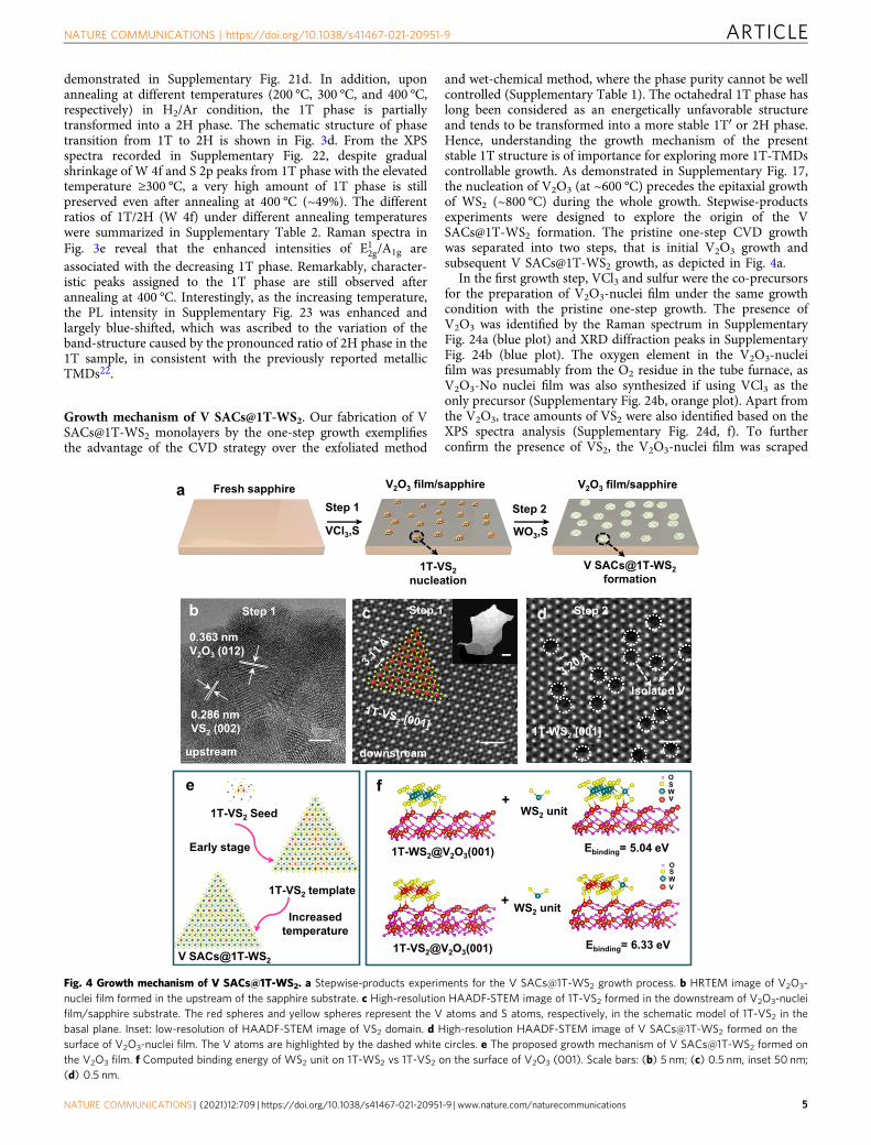
Growth mechanism of V SACs@1T-WS2. Our fabrication of VSACs@1T-WS2 monolayers by the one-step growth exemplifiesthe advantage of the CVD strategy over the exfoliated method
and wet-chemical method, where the phase purity cannot be wellcontrolled (Supplementary Table 1). The octahedral 1T phase haslong been considered as an energetically unfavorable structureand tends to be transformed into a more stable 1T′ or 2H phase.Hence, understanding the growth mechanism of the presentstable 1T structure is of importance for exploring more 1T-TMDscontrollable growth. As demonstrated in Supplementary Fig. 17,the nucleation of V2O3 (at ~600 °C) precedes the epitaxial growthof WS2 (~800 °C) during the whole growth. Stepwise-productsexperiments were designed to explore the origin of the VSACs@1T-WS2 formation. The pristine one-step CVD growthwas separated into two steps, that is initial V2O3 growth andsubsequent V SACs@1T-WS2 growth, as depicted in Fig. 4a.
In the first growth step, VCl3 and sulfur were the co-precursorsfor the preparation of V2O3-nuclei film under the same growthcondition with the pristine one-step growth. The presence ofV2O3 was identified by the Raman spectrum in SupplementaryFig. 24a (blue plot) and XRD diffraction peaks in SupplementaryFig. 24b (blue plot). The oxygen element in the V2O3-nucleifilm was presumably from the O2 residue in the tube furnace, asV2O3-No nuclei film was also synthesized if using VCl3 as theonly precursor (Supplementary Fig. 24b, orange plot). Apart fromthe V2O3, trace amounts of VS2 were also identified based on theXPS spectra analysis (Supplementary Fig. 24d, f). To furtherconfirm the presence of VS2, the V2O3-nuclei film was scraped
Fig. 4 Growth mechanism of V SACs@1T-WS2. a Stepwise-products experiments for the V SACs@1T-WS2 growth process. b HRTEM image of V2O3-nuclei film formed in the upstream of the sapphire substrate. c High-resolution HAADF-STEM image of 1T-VS2 formed in the downstream of V2O3-nucleifilm/sapphire substrate. The red spheres and yellow spheres represent the V atoms and S atoms, respectively, in the schematic model of 1T-VS2 in thebasal plane. Inset: low-resolution of HAADF-STEM image of VS2 domain. d High-resolution HAADF-STEM image of V SACs@1T-WS2 formed on thesurface of V2O3-nuclei film. The V atoms are highlighted by the dashed white circles. e The proposed growth mechanism of V SACs@1T-WS2 formed onthe V2O3 film. f Computed binding energy of WS2 unit on 1T-WS2 vs 1T-VS2 on the surface of V2O3 (001). Scale bars: (b) 5 nm; (c) 0.5 nm, inset 50 nm;(d) 0.5 nm.
NATURE COMMUNICATIONS | https://doi.org/10.1038/s41467-021-20951-9 ARTICLE
NATURE COMMUNICATIONS | (2021) 12:709 | https://doi.org/10.1038/s41467-021-20951-9 | www.nature.com/naturecommunications 5
from the sapphire substrate for the HRTEM measurement, asshown in Fig. 4b. In addition to the lattice spacing of 0.363 nmfrom V2O3, the other measured lattice spacing of ~0.286 nm canbe well indexed with the (002) plane of 1T-VS2. Elementalmapping from the same region showed the uniform distributionsof V, O, and S elements (Supplementary Fig. 25) in the V2O3-nuclei film, which was coincident with the analysis of the XPSsurvey spectrum in Supplementary Fig. 24c. More interestingly,1T-VS2 nanocrystals were found on the surface of V2O3-nucleifilm further downstream (Supplementary Fig. 26b, c, lowergrowth temperature zone, ~620 °C). In contrast to the traceamounts of VS2 nuclei found in the upstream (the hot centergrowth zone, ~860 °C), the VS2 nanocrystals downstream can beeasily transferred from the V2O3-nuclei film using a standardtransfer method for STEM imaging (Fig. 4c). The image showed ahexagonal atomic structure of 1T-VS2 in the [001] basal plane48,which was solid evidence that the VS2 intermediates werenucleated on the surface of V2O3 during the growth.
In the second step, the as-produced V2O3-nuclei film/sapphiresubstrate was put back into a fresh CVD process to collect thefinal product using WO3 and sulfur as the co-precursors.Intriguingly, it was found that smaller 1T domains of WS2 wereformed on the surface of the film (Fig. 4d, SupplementaryFig. 27a, e), whereas 2H-WS2 domains were achieved if usingV2O3-No nuclei film (Supplementary Fig. 27b, e, f) as thecollecting substrate. Notably, nothing could be found if usingcommercial V2O3 (001) film (Supplementary Fig. 27c, d, and g),because that the rough surface and the low-quality of thecommercial V2O3 were not in favor of the VS2 and WS2nucleation on the surface. The 1T- or 2H-WS2 domains were alsoconfirmed by the Raman mapping in Supplementary Figs. 28 and29. As a result, these experimental observations imply that boththe VS2 nucleation and the V2O3 film are very requisite for the VSACs@1T-WS2 growth and VS2 intermediates play the mostimportant role in determining the 1T phase growth of WS2. Theproposed growth mechanism is shown in Fig. 4e, in which the
1T-VS2 nuclei formed in the early growth stage serve as the 1Tstructure template and significantly strengthen the binding ofWS2 unit (Fig. 4f, from 5.04 eV to 6.33 eV) on the V2O3 film,thereby triggering the epitaxial growth of the 1T phase nucleus.Such an epitaxially grown WS2 layer should be the 1T phaseinstead of the 2H phase due to the much higher binding energy of1T-VS2/1T-WS2 (6.09 eV) than 1T-VS2/2H-WS2 (4.19 eV) (Sup-plementary Fig. 30). The computed lattice parameters of 2H-WS2,V SACs@2H-WS2, and V SACs@1T-WS2 are shown in Supple-mentary Table 3. In addition, it was also demonstrated that theamount of VCl3 could significantly affect the controllable phasegrowth of WS2 (see details in Supplementary Figs. 31–34). Theinfluence of heating temperature on the synthesis of 1T-WS2 hasalso been investigated, as displayed in Supplementary Figs. 35–37.Moreover, vanadocene precursors were also investigated to enrichthe growth method of 1T-WS2 monolayers (SupplementaryFig. 38).
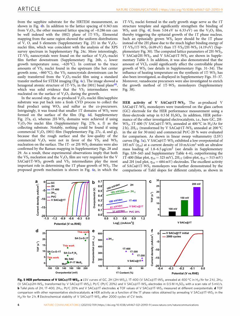
HER activity of V SACs@1T-WS2. The as-produced VSACs@1T-WS2 monolayers were transferred on the glass carbon(GC) electrode for the HER performance measurement using athree-electrode setup in 0.5M H2SO4. In addition, HER perfor-mance of the other investigated electrocatalysts, i.e., bare GC, 2H-WS2, 1T-400 (V SACs@1T-WS2 annealed at 400 °C in H2/Ar for2 h), 2H1T (transformed by V SACs@1T-WS2 annealed at 200 °Cin the air for 30min) and commercial Pt/C-20 % were evaluatedfor comparison. As shown in linear sweep voltammetry (LSV)curves (Fig. 5a), V SACs@1T-WS2 exhibited a low overpotential of185mV (η10) at a current density of 10 mA/cm2 with an ultralowmass loading of 1.8–6.5 μg/cm2 (see details in SupplementaryFigs. S39–S45 and Supplementary Table 4–6), outperforming the1T-400 (blue plot, η10= 325mV), 2H1T (olive plot, η10= 515mV)and 2H (red plot, η10= 684mV) electrodes. The excellent activityof SACs@1T-WS2 monolayers was further demonstrated by thecomparisons of Tafel slopes for different catalysts, as shown in
Fig. 5 HER performance of V SACs@1T-WS2. a LSV curves of GC, 2H (2H-WS2), 1T-400 (V SACs@1T-WS2 annealed at 400 °C in H2/Ar for 2 h), 2H1T
(V SACs@2H-WS2, transformed by V SACs@1T-WS2), Pt/C (Pt/C 20%) and V SACs@1T-WS2 electrodes in 0.5M H2SO4 with a scan rate of 5 mV/s.b Tafel plots of 2H, 1T-400, 2H1T, Pt/C 20% and V SACs@1T electrodes. c TOF values of V SACs@1T-WS2 measured at different overpotentials. d TOFcomparison with other representative electrocatalysts. e HER activity as a function of the 1T phase ratios obtained by annealing V SACs@1T-WS2 in theH2/Ar for 2 h. f Electrochemical stability of V SACs@1T-WS2 after 2000 cycles of CV tests.
ARTICLE NATURE COMMUNICATIONS | https://doi.org/10.1038/s41467-021-20951-9
6 NATURE COMMUNICATIONS | (2021) 12:709 | https://doi.org/10.1038/s41467-021-20951-9 | www.nature.com/naturecommunications

Fig. 5b. The Tafel slope for V SACs@1T-WS2 was 61mV/dec(Fig. 5c), which is much lower than that of 1T-400 (100mV/dec),2H1T (103mV/dec), and 2H-WS2 (194mV/dec). Please note thatmass loading of electrocatalysts has a great impact on the mea-sured activities; hence, it has generally used as catalyst perfor-mance metrics7. Although the mass loading of SACs@1T-WS2 wasmuch lower than most of the non-precious electrocatalysts(Supplementary Fig. 46), the HER performance was still com-parable to that of strained 1T′-WS2 nanosheets (NSs)1, 1T′-MoS2NSs2, 1T′-MoS2 monolayers11, and better than that of 2H-1Tboundaries MoS2 monolayers49, 1T′ WSe2 NSs7 and PE-CVD 1T-WS2 film15. The electrochemical surface area (ECSA) was calcu-lated as an important factor to affect the catalytic activity ofelectrocatalysts50–52. The calculated details were shown in theexperimental section and Supplementary Fig. 47. Double-layercapacitance (Cdl) and ECSA values were 139.5 μF/cm2 and3.49 cm2 for V SACs@1T-WS2 and 61.7 μF/cm2 and 1.54 cm2 for2H-WS2, suggesting the critical contributions of V atom sites andhigh purity of 1T-WS2. The TOF values of the SACs@1T-WS2(Fig. 5c) were obtained according to the precious reports23,53 andcalculated to be 3.01 s−1, 12.78 s−1, and 24.15 s−1 at overpotentialsof 100mV, 150mV, and 200mV, respectively, which were muchhigher than those recently representative electrocatalysts listed inFig. 5d and Supplementary Table 7.
As the V SACs@1T-WS2 monolayers contain a high concen-tration of 1T phase, to investigate the influence of 1T content onthe catalytic performance, the V SACs@1T-WS2 electrode wasgradually annealed at different temperatures and the HER activityafter each annealing treatment was performed, ensuring that theidentical dimensions and geometrical areas to evaluate thecatalytic properties. Remarkably, the HER activities were stronglyrelated to the 1T phase content as demonstrated by a gradualdecrease in the η10 with decreasing 1T ratios (Fig. 5e).Remarkably, negligible activity degradation can be observed inthe reproducible polarization curve of V SACs@1T-WS2 in Fig. 5feven after 2000 continuous cycling, indicative of a good HERperformance stability. The stability test was conducted at currentdensities higher than 10 mA/cm2 in 0.5 M H2SO4 electrolyte for100 h. As revealed by the chronoamperometric curve of V SACs1T-WS2 electrocatalyst in Supplementary Fig. 48, the currentdensity for the V SACs 1T-WS2 electrocatalyst displayed a slightcurrent decay of 1.0 mA cm−2 after 24 h and 3.4 mA cm−2 after100 h, indicating high stability of V SACs 1T-WS2 catalyst. Themetallic properties of V SACs 1T-WS2 catalyst after stability testwere also investigated by Raman spectroscopy (Supplementary
Fig. 49a), which showed obvious metallic peaks (J1, J2, J3) in theRaman spectrum (red plot). Moreover, the STEM image showedin Supplementary Fig. 49b confirmed the V SACs 1T-WS2structure after the stability test. Both the Raman spectrum andSTEM image indicated the robust 1T structure of V SACs1T-WS2 catalyst after HER test.
V SACs enhancing the HER activity of 1T-WS2. Especially, theHER performance of 2H-WS2, V SACs@2H-WS2, and VSACs@1T-WS2 was further studied using DFT considering bothbasal plane (Supplementary Fig. 50) and edge sites (Supplemen-tary Figs. 51–53) as the active sites. Our calculations show that theV SACs could significantly influence the free energy of Hadsorption (ΔGH) on the edge sites of 1T-WS2, as summarized inSupplementary Table 8. Please note that the |ΔGH| of VSACs@1T-WS2 at the basal plane is 0.4 eV, which is approximateto the |ΔGH| of intrinsic 1T-WS2 at 0.28 eV1, implying that thesingle-atom V sites have a negligible influence on the HER per-formance of 1T-WS2 in the basal plane. Compared to the 2H-WS2 and V SACs@2H-WS2, V SACs@1T-WS2 exhibits the lowest|ΔGH| (0.05 eV) at V-atom sites (Fig. 6a), indicating that theisolated V atoms are catalytically active in the layer of 1T-WS2.The charge depletion at the active sites has been proven to play anessential role in improving the electrochemical activity of thecatalysts13,54. To acquire a deeper understanding of how single Vatoms enhanced the activity of 1T-WS2, the charge redistributionof V SACs@1T-WS2 was studied. As shown in the inset image inFig. 6b, we can clearly see that when one W atom was substitutedby a V atom, there was more charge depletion generated at theV-atom site. Such variations in the local electronic structure canalso be well described using the d-band theory55. A linear inversecorrelation between |ΔGH| and the d-band center at the mostactive edge sites were revealed, indicating that a more negatived-band center corresponds to more occupation of the antibond-ing states, resulting in weaker H adsorption of V SACs@1T-WS2comparable to their 2H counterparts.
DiscussionIn summary, we have demonstrated a direct synthesis of single-atomV sites on the high purity 1T-WS2 monolayers via a one-step CVDstrategy through introducing VCl3 as a co-precursor, with muchbetter HER performance than the 2H counterparts. The step-wiseexperimental findings together with DFT results shed light on theunderstanding of the CVD-grown V SACs@1T-WS2 monolayers,that is the 1T-VS2 nuclei initially act as the 1T template structures for
Fig. 6 HER activity mechanism of V SACs@1T-WS2. a The Gibbs free energy of H adsorption (ΔGH*) of 2H-WS2, V SACs@2H-WS2, and V SACs@1T-WS2on the V and S edge sites. b Relationship between |ΔGH*| and the d-band center of adjacent W/V ions at the most active edge sites of 2H-WS2,V SACs@2H-WS2, and V SACs@1T-WS2.
NATURE COMMUNICATIONS | https://doi.org/10.1038/s41467-021-20951-9 ARTICLE
NATURE COMMUNICATIONS | (2021) 12:709 | https://doi.org/10.1038/s41467-021-20951-9 | www.nature.com/naturecommunications 7
the follow-up V SACs@1T-WS2 growth on the V2O3 film. The HERperformance of intrinsic 1T-WS2 was remarkably boosted after themodification of isolated V atoms. DFT calculations highlight that thehighly activated V-atom sites primarily account for the excellent HERactivity of V SACs@1T-WS2 monolayers. Our findings could fill thegap of SACs grown via a one-step CVD strategy and pave the way todesign more efficient and robust electrocatalysts for applications inwater splitting.
MethodsThe growth of V SACs@1T-WS2 monolayers, 2H-WS2 monolayers, V2O3 film.In the growth of monolayer V SACs@1T-WS2, sulfur (Sigma-Aldrich, 99%),tungsten trioxide (WO3, Sigma-Aldrich, 99.99%), and vanadium (III) chloride(VCl3, Sigma-Aldrich, 99%,) were used as the growth precursors. Two quartz boatswith 0.03 g of VCl3 powder (in the hot center) and 0.30 g WO3 powder (the upstreamof VCl3) were placed sequentially in the hot center of the furnace. And a freshsapphire (c-plane) substrate (1 cm× 2 cm) was placed face-down of the quartz boat tocollect the final product. The heating temperature was kept at 860 °C. The S powderwas placed in a separate quartz boat at the upper stream side of the cold zone and thetemperature was maintained at 160 °C during the reaction. The gas flow has consistedof an ultrapure mixed Ar/H2 (Ar= 80 sccm, H2= 20 sccm), and the chamberpressure was controlled at 10 Torr. After reaching the desired growth temperature of860 °C, the heating zone was kept for 15min and the furnace was then naturallycooled down to room temperature. The V2O3 film was simultaneously formed duringthe V SACs@1T-WS2 growth. The commercial V2O3 (001) film on the c-planesapphire was purchased from Xi’an Qiyue Biotechnology Co., Ltd. To obtained2H-WS2 monolayers, we usedWO3 and suffer as the precursors with the same growthcondition with V SACs@1T-WS2. To obtain V2O3-No nuclei film, we used the onlyVCl3 as the precursors with the same growth condition. To obtain V2O3-nuclei film,we used only VCl3 and sulfur as the precursors with the same growth condition.
V2O3 film growth mechanism and characterization. According to the latticeparameters of V2O3 and sapphire (V2O3: hexagonal, a= 0.492 nm, c= 1.397 nm;α-Al2O3: hexagonal, a= 0.475 nm, c= 1.297 nm), hexagonal V2O3 shares the samelattice-type and similar lattice parameters with α-Al2O3; thus, it is expected toepitaxially grow on α-Al2O3 with the relationship V2O3 (001)[100]//α-Al2O3
(001)[100]39,56–58.To investigate the growth mechanism of V2O3 film, we prepared V2O3-No
nuclei film under different temperatures, as exhibited in Supplementary Fig. 17a. Itcan be observed that V2O3 film could be formed at ≥600 °C during thetemperature-dependent controllable experiments. Particularly, a merged peak inthe range of 150–250 cm−1 was observed in the Raman spectrum and the peak wascorrelated to both monoclinic A1g and hexagonal V2O3 A1g symmetry, indicativeof a mixed phase. However, the additional peaks of low intensity at 300 cm−1 and500 cm−1 were solely attributable to hexagonal V2O3
59,60, indicating the hexagonalstructure of the as-grown V2O3 film. Under the temperature of 600 °C, low-qualityfilm or nothing will be formed on the sapphire substrate. Simultaneously, wemeasured the Raman spectra of the powders from the VCl3 quarts boat after eachgrowth reaction with different growth temperatures, as shown in SupplementaryFig. 17b. VO2 (B) will be evidently formed after the decomposition of VCl361
(see Eqs. (1) and (2) in Supplementary Fig. 17).
Transfer process of V SACs@1T-WS2, 2H-WS2, V2O3-nuclei film. The as-grownsamples were transferred onto arbitrary substrates, such as fresh sapphire, SiO2/Si, GC,and holy-carbon nickel TEM Grid using a modified method in our lab. First, poly(methyl methacrylate) (PMMA) was spin-coated onto the samples followed by 120 °Cbaking for 10min, and then etched by 5% HF solution for 2–3min. The PMMA/sample was gently peeled off by the tweezers and deposited onto the targeted substrates.PMMA/sample/targeted substrate was baked for 1 h at 120 °C in air. The PMMA wasremoved by acetone and cleaned with isopropyl alcohol. The V2O3-nuclei film wasscratched by tweezers and ultrasonic the V2O3/sapphire sample in the ethanol solutionfor 15min for the HRTEM measurement. The sample was prepared by dropping thesolution onto the holy-carbon nickel TEM grid.
For the STEM measurements samples, the extra annealing process wasnecessary to remove the residual PMMA. For the 2H-WS2 sample annealing, thesample was located in a vacuum container (less than 10−6 Torr) at 350 °Covernight. For the V SACs@1T-WS2 sample annealing, the sample was located in avacuum container (less than 10−6 Torr) at 200 °C for 2 h. For the XPS and Ramanspectra of V SACs@1T-WS2 annealed at different temperatures, the V SACs@1T-WS2 monolayers were transferred on the fresh sapphire substrates and annealed inH2/Ar condition with different temperatures.
Characterization. Optical spectroscopy is collected under a Witec alpha 300 Rconfocal Raman microscopic system. Gratings of 1800 lg/mm and 300 lg/mm areselected for the high-resolution Raman spectrum and wide range PL spectrum,respectively. The TMDs are excited by 532 nm laser with a power of 1 mW and
spot size of 0.5 μm and emitted Raman signal is collected by 100× objective(N.A= 0.9) from a Carl Zeiss Microscopy. ARPRS are conducted on a triple-grating micro-Raman spectrometer (Horiba-JY T64000) with a 532 nm laser undera backscattering configuration. The polarization is resolved by rotating sampleorientation on the normal axis of the basal plane. The emitted Raman signal iscollected through a 100× objective, dispersed with 1800 lg/mm grating, anddetected by a charge-coupled device.
An AFM (Cypher ES environmental AFM) was utilized to obtain themorphology images and the height profile of V SACs@WS2 monolayers. Thecrystalline of the different samples was probed using a Bruker D8 advance powderXRD with Cu Ka radiation. X-ray photoelectron spectroscopy (XPS) studies werecarried out in a Kratos Axis Ultra DLD spectrometer equipped with a monochromaticAl Kα X-ray source (hν= 1486.6 eV) under a vacuum of 1 × 10⁻⁹ mbar. The spectrawere collected at fixed analyzer pass energies of 160 eV and 20 eV. The bindingenergies in XPS analysis were corrected by referencing C 1s line at 284.8 eV. STEMand TEM images were performed by Titan 40-300 Themis Z TEM from ThermoFisher, USA (former FEI Co) equipped with a double Cs corrector, an electronmonochromator, and a Gatan imaging filter quantum 966. The microscope wasoperated at 80 kV to minimize electron beam induced. Probe semi convergence anglewas tuned to 30mrad and probe current to 50 pA. For high-angle annular dark-field(HAADF) STEM images the inner collection angle was about 80mrad. Radial wienerfilter was carried out to enhance the visibility of atoms
Computational details. First-principles simulations were performed at the DFT levelimplemented by the Vienna ab initio simulation package62–65 with the all-electronprojector augmented wave model66 and Perdew–Burke–Ernzerhof functions67. TheDFT-D3 method was applied to include vdW interaction corrections68. A kineticenergy cutoff of 400 eV was used for the plane-wave expansion of the electronic wavefunction. The convergence criteria of force and energy were set as 0.01 eVÅ−1 and10−5 eV, respectively. Gaussian smearing of 0.1 eV was applied for optimization. A k-point grid with a 4 × 4 × 1 gamma-centered mesh was used for the WS2 unit cell. Forsupercells that contain a larger number of vanadium and oxygen atoms, a corre-sponding number of k-points were used to keep the k-mesh spacing constant acrossdifferent structures. The climbing image nudged elastic band was applied for tran-sition state optimization69.
The free energy of the adsorption atomic hydrogen (ΔGH) is obtained byΔGH= ΔEH+ ΔEZPE− TΔSH. ΔEH is the adsorption energy defined by ΔEH=Esur−H− Esur+½ EH2. According to previous reports, ΔGH can be written asΔGH= ΔEH+ 0.25, where 0.25 eV is the contribution from ZPE and entropy at298 K70.
Electrochemical measurements. Electrochemical measurements were carried in aPGSTAT 302N Autolab Potentiostat/Galvanostat (Metrohm) at room temperature.Graphite rod and Ag/AgCl (in a saturated KCl solution) electrodes were employedas the counter and reference electrodes, respectively. The V SACs@1T-WS2 and2H-WS2 were transferred onto the GC electrodes as the working electrodes anddried. Nafion solution (0.5%) was drop-cast to protect WS2 film. The V SACs@1T-400 electrode was prepared by annealing the V SACs@1T-WS2 electrode at 400 °Cin H2/Ar for 2 h. The 2H1T electrode was prepared by annealing the V SACs@1T-WS2 electrode at 200 °C in the air for 30 min. The HER activities of differentsamples were evaluated by measuring polarization curves with LSV at a scan rate of0.5 mV/s in 0.5 M H2SO4 solutions. Potentials were referenced to a reversiblehydrogen electrode (RHE). The commercial Pt/C (20 wt% Pt on Vulcan carbonblack) supported by GC was prepared by mixing the Pt/C, nafion, and isopropanol,sonicating for 30 min, and drop-casting on the GC. The mass loading of Pt/C was500 μg/cm2. The potential cycling was performed between 0.197 and −0.6 V vsRHE at 5 mV s−1. All data have been corrected for a small ohmic drop based onimpedance spectroscopy. ECSA and Cdl are determined by cyclic voltammogramsat various scan rates (10, 30, 50, 70, 90, 110. 130, 150, 170, 190, and 210 mV/s) inthe potential range (0.15–0.35 V vs. RHE). The capacitive currents (ΔJ) are plottedas a function of scan rate and Cdl is equal to half of the slope. The reference specificcapacitance (Cs) of 40 μF/cm2 is used in this work. The ECSA for the differentcatalysts are achieved based on the following equation
ECSA ¼ Cdl
Cs
Calculation of turnover frequency. The TOF calculation details were specified asbelow, which was reported elsewhere23,53.
TOF ¼ Total hygrogen turnovers per geometric areaactive sites per geometric area
The total hydrogen turnovers were calculated from the current density in theLSV polarization curve according to the equation as below:
Total hydrogen turnovers ¼ jj jmAcm2
� �1C=s
1000 mA
� �1 mol e�
96485 C
� �1 mol
2 mol e�
� � ð6:022 ´ 1023moleculars H2Þ1 mol H2
ARTICLE NATURE COMMUNICATIONS | https://doi.org/10.1038/s41467-021-20951-9
8 NATURE COMMUNICATIONS | (2021) 12:709 | https://doi.org/10.1038/s41467-021-20951-9 | www.nature.com/naturecommunications

The number of active sites in the V SACs@1T-WS2 catalyst was obtained fromthe mass loading on the glass carbon electrode.
Active sites ¼ electrocatalyst loading per geometric area gcm2
� �´Vwt%
VMWg
mol
� � !
6:022 ´ 1023V atoms1 mol V
� �
Data availabilityThe data that support the findings of this study are available from the correspondingauthor upon request.
Received: 25 May 2020; Accepted: 5 January 2021;
References1. Voiry, D. et al. Enhanced catalytic activity in strained chemically exfoliated
WS2 nanosheets for hydrogen evolution. Nat. Mater. 12, 850–855 (2013).2. Yu, Y. et al. High phase-purity 1T′-MoS2- and 1T′-MoSe2-layered crystals.
Nat. Chem. 10, 638–643 (2018).3. Liao, G. et al. Semiconductor polymeric graphitic carbon nitride
photocatalysts: the “holy grail” for the photocatalytic hydrogen evolutionreaction under visible light. Energy Environ. Sci. 12, 2080–2147 (2019).
4. Liao, G. et al. Ag-based nanocomposites: synthesis and applications incatalysis. Nanoscale 11, 7062–7096 (2019).
5. Thalluri, S. M. et al. Inverted pyramid textured p-silicon covered with Co2P asan efficient and stable solar hydrogen evolution photocathode. ACS EnergyLett. 4, 1755–1762 (2019).
6. Chen, X. et al. High phase-purity 1T-MoS2 ultrathin nanosheets by a spatiallyconfined template. Angrew. Chem. Int. Ed. 58, 17621 (2019).
7. Sokolikova, M. S., Sherrell, P. C., Palczynski, P., Bemmer, V. L. & Mattevi, C.Direct solution-phase synthesis of 1T′ WSe2 nanosheets. Nat. Commun. 10,712 (2019).
8. Kuznetsov, D. A. et al. Single site cobalt substitution in 2D molybdenumcarbide (MXene) enhances catalytic activity in the hydrogen evolutionreaction. J. Am. Chem. Soc. 141, 17809–17816 (2019).
9. Fu, W. et al. Epitaxial growth of graphene on V8C7 nanomeshs for highlyefficient and stable hydrogen evolution reaction. J. Catal. 369, 47–53 (2019).
10. Jaramillo, T. F. et al. Identification of active edge sites for electrochemical H2
evolution from MoS2 nanocatalysts. Science 317, 100–102 (2007).11. Liu, L. et al. Phase-selective synthesis of 1T′ MoS2 monolayers and
heterophase bilayers. Nat. Mater. 17, 1108–1114 (2018).12. Duerloo, K.-A. N., Li, Y. & Reed, E. J. Structural phase transitions in two-
dimensional Mo-and W-dichalcogenide monolayers. Nat. Commun. 5, 4214(2014).
13. Deng, S. et al. Synergistic doping and intercalation: realizing deep phasemodulation on MoS2 arrays for high-efficiency hydrogen evolution reaction.Angew. Chem. Int. Ed. 58, 16289–16296 (2019).
14. Enyashin, A. N. et al. New route for stabilization of 1T-WS2 and MoS2 phases.J. Phys. Chem. C 115, 24586–24591 (2011).
15. Kim, H.-U. et al. Wafer-scale and low-temperature growth of 1T-WS2 film forefficient and stable hydrogen evolution reaction. Small 16, 1905000 (2020).
16. Liu, Q. et al. Stable metallic 1T-WS2 nanoribbons intercalated with ammoniaIons: the correlation between structure and electrical/optical properties. Adv.Mater. 27, 4837–4844 (2015).
17. Lukowski, M. A. et al. Enhanced hydrogen evolution catalysis from chemicallyexfoliated metallic MoS2 nanosheets. J. Am. Chem. Soc. 135, 10274–10277 (2013).
18. Mahler, B., Hoepfner, V., Liao, K. & Ozin, G. A. Colloidal synthesis of 1T-WS2and 2H-WS2 nanosheets: applications for photocatalytic hydrogen evolution.J. Am. Chem. Soc. 136, 14121–14127 (2014).
19. Park, J. C. et al. Phase-engineered synthesis of centimeter-scale 1T′- and 2H-molybdenum ditelluride thin films. ACS Nano 9, 6548–6554 (2015).
20. Voiry, D. et al. Conducting MoS2 nanosheets as catalysts for hydrogenevolution reaction. Nano Lett. 13, 6222–6227 (2013).
21. Yin, Y. et al. Contributions of phase, sulfur vacancies, and edges to thehydrogen evolution reaction catalytic activity of porous molybdenum disulfidenanosheets. J. Am. Chem. Soc. 138, 7965–7972 (2016).
22. Zhao, X., Ma, X., Sun, J., Li, D. & Yang, X. Enhanced catalytic activities ofsurfactant-assisted exfoliated WS2 nanodots for hydrogen evolution. ACSNano 10, 2159–2166 (2016).
23. Qi, K. et al. Single-atom cobalt array bound to distorted 1T MoS2 withensemble effect for hydrogen evolution catalysis. Nat. Commun. 10, 5231(2019).
24. Zhang, H., Yu, L., Chen, T., Zhou, W. & Lou, X. W. Surface modulation ofhierarchical MoS2 nanosheets by Ni single atoms for enhanced electrocatalytichydrogen evolution. Adv. Funct. Mater. 28, 1807086 (2018).
25. Deng, J. et al. Triggering the electrocatalytic hydrogen evolution activity of theinert two-dimensional MoS2 surface via single-atom metal doping. EnergyEnviron. Sci. 8, 1594–1601 (2015).
26. Chow, P. K. et al. Wetting of mono and few-layered WS2 and MoS2 filmssupported on Si/SiO2 substrates. ACS Nano 9, 3023–3031 (2015).
27. Elías, A. L. et al. Controlled synthesis and transfer of large-area WS2 sheets:from single layer to few layers. ACS Nano 7, 5235–5242 (2013).
28. Gutiérrez, H. R. et al. Extraordinary room-temperature photoluminescence intriangular WS2 monolayers. Nano Lett. 13, 3447–3454 (2013).
29. Perea-López, N. et al. Photosensor device based on few-layered WS2 films.Adv. Funct. Mater. 23, 5511–5517 (2013).
30. Cui, Y. et al. High-performance monolayer WS2 field-effect transistors onhigh-k dielectrics. Adv. Mater. 27, 5230–5234 (2015).
31. Gao, Y. et al. Large-area synthesis of high-quality and uniform monolayerWS2 on reusable Au foils. Nat. Commun. 6, 8569 (2015).
32. Yang, W. et al. Electrically tunable valley-light emitting diode (vLED) basedon CVD-grown monolayer WS2. Nano Lett. 16, 1560–1567 (2016).
33. Jeong, H. Y. et al. Heterogeneous defect domains in single-crystallinehexagonal WS2. Adv. Mater. 29, 1605043 (2017).
34. Laffont, L. et al. High resolution EELS of Cu–V oxides: application to batteriesmaterials. Micron 37, 459–464 (2006).
35. Zhang, F. et al. Monolayer vanadium-doped tungsten disulfide: a room-temperature dilute magnetic semiconductor. Adv. Sci. 7, 2001174 (2020).
36. Pham, Y. T. H. et al. Tunable ferromagnetism and thermally induced spin flipin vanadium-doped tungsten diselenide monolayers at room temperature.Adv. Mater. 32, 2003607 (2020).
37. Yun, S. J. et al. Ferromagnetic order at room temperature in monolayer WSe2semiconductor via vanadium dopant. Adv. Sci. 7, 1903076 (2020).
38. Yu, S. H. et al. In situ hybridizing MoS2 microflowers on VS2 microflakes in aone-pot CVD process for electrolytic hydrogen evolution reaction. ACS Appl.Energy Mater. 2, 5799–5808 (2019).
39. Sun, G., Cao, X., Long, S., Li, R. & Jin, P. Optical and electrical performance ofthermochromic V2O3 thin film fabricated by magnetron sputtering. Appl.Phys. Lett. 111, 053901 (2017).
40. Beams, R. et al. Characterization of few-layer 1T′ MoTe2 by polarization-resolved second harmonic generation and Raman scattering. ACS Nano 10,9626–9636 (2016).
41. Wang, Y. et al. Structural phase transition in monolayer MoTe2 driven byelectrostatic doping. Nature 550, 487 (2017).
42. Loh, T. A. & Chua, D. H. Origin of hybrid 1T-and 2H-WS2 ultrathin layers bypulsed laser deposition. J. Phys. Chem. 119, 27496–27504 (2015).
43. Loh, T. A. J., Chua, D. H. C. & Wee, A. T. S. One-step synthesis of few-layerWS2 by pulsed laser deposition. Sci. Rep. 5, 18116 (2015).
44. Tan, S. J. et al. Chemical stabilization of 1T′ phase transition metaldichalcogenides with giant optical Kerr nonlinearity. J. Am. Chem. Soc. 139,2504–2511 (2017).
45. Tsai, H.-L., Heising, J., Schindler, J. L., Kannewurf, C. R. & Kanatzidis, M. G.Exfoliated−restacked phase of WS2. Chem. Mater. 9, 879–882 (1997).
46. Chen, W. et al. Quantum dots of 1T phase transitional metal dichalcogenidesgenerated via electrochemical Li intercalation. ACS Nano 12, 308–316 (2018).
47. Kappera, R. et al. Phase-engineered low-resistance contacts for ultrathin MoS2transistors. Nat. Mater. 13, 1128 (2014).
48. Yuan, J. et al. Facile synthesis of single crystal vanadium disulfide nanosheetsby chemical vapor deposition for efficient hydrogen evolution reaction. Adv.Mater. 27, 5605–5609 (2015).
49. Zhu, J. et al. Boundary activated hydrogen evolution reaction on monolayerMoS2. Nat. Commun. 10, 1348 (2019).
50. Anjum, M. A. R., Jeong, H. Y., Lee, M. H., Shin, H. S. & Lee, J. S. Efficienthydrogen evolution reaction catalysis in alkaline media by all-in-one MoS2with multifunctional active sites. Adv. Mater. 30, 1707105 (2018).
51. McCrory, C. C. L. et al. Benchmarking hydrogen evolving reaction and oxygenevolving reaction electrocatalysts for solar water splitting devices. J. Am.Chem. Soc. 137, 4347–4357 (2015).
52. Voiry, D. et al. Best practices for reporting electrocatalytic performance ofnanomaterials. ACS Nano 12, 9635–9638 (2018).
53. Wan, J. et al. In situ phosphatizing of triphenylphosphine encapsulated withinmetal–organic frameworks to design atomic Co1-P1N3 interfacial structure forpromoting catalytic performance. J. Am. Chem. Soc. 142, 8431–8439 (2020).
54. Zhao, Z., Li, M., Zhang, L., Dai, L. & Xia, Z. Design principles for heteroatom-doped carbon nanomaterials as highly efficient catalysts for fuel cells andmetal-air batteries. Adv. Mater. 27, 6834–6840 (2015).
55. Chen, H. et al. Promoting subordinate, efficient ruthenium sites withinterstitial silicon for Pt-Like electrocatalytic activity. Angew. Chem. Int. Ed.58, 11409–11413 (2019).
56. Ji, Y. D. et al. Epitaxial growth and metal-insulator transition of vanadiumoxide thin films with controllable phases. Appl. Phys. Lett. 101, 071902 (2012).
57. Allimi, B. S. et al. Growth of V2O3 thin films on a-plane (110) and c-plane(001) sapphire via pulsed-laser deposition. J. Mater. Res. 22, 2825–2831 (2007).
NATURE COMMUNICATIONS | https://doi.org/10.1038/s41467-021-20951-9 ARTICLE
NATURE COMMUNICATIONS | (2021) 12:709 | https://doi.org/10.1038/s41467-021-20951-9 | www.nature.com/naturecommunications 9

58. Sakai, J., Limelette, P. & Funakubo, H. Transport properties and c/a ratio ofV2O3 thin films grown on C- and R- plane sapphire substrates by pulsed laserdeposition. Appl. Phys. Lett. 107, 241901 (2015).
59. Kafizas, A., Hyett, G. & Parkin, I. P. Combinatorial atmospheric pressurechemical vapour deposition (cAPCVD) of a mixed vanadium oxideand vanadium oxynitride thin film. J. Mater. Chem. 19, 1399–1408(2009).
60. Kuroda, N. & Fan, H. Y. Raman scattering and phase transitions of V2O3.Phys. Rev. B 16, 5003–5008 (1977).
61. Xu, H. F., Liu, Y., Wei, N. & Jin, S. W. From VO2(B) to VO2(A) nanorods:hydrothermal synthesis, evolution and optical properties in V2O5H2C2O4H2Osystem. Optik 125, 6078–6081 (2014).
62. Kresse, G. & Furthmüller, J. Efficiency of ab-initio total energy calculations formetals and semiconductors using a plane-wave basis set. Comput. Mater. Sci.6, 15–50 (1996).
63. Kresse, G. & Furthmüller, J. Efficient iterative schemes for ab initio total-energy calculations using a plane-wave basis set. Phys. Rev. B 54, 11169–11186(1996).
64. Kresse, G. & Hafner, J. Ab initio molecular dynamics for liquid metals. Phys.Rev. B 47, 558–561 (1993).
65. Kresse, G. & Hafner, J. Ab initio molecular-dynamics simulation of the liquid-metal–amorphous-semiconductor transition in germanium. Phys. Rev. B 49,14251–14269 (1994).
66. Blöchl, P. E. Projector augmented-wave method. Phys. Rev. B 50, 17953–17979(1994).
67. Perdew, J. P., Burke, K. & Ernzerhof, M. Generalized gradient approximationmade simple. Phys. Rev. B 77, 3865–3868 (1996).
68. Grimme, S., Antony, J., Ehrlich, S. & Krieg, H. A consistent and accurate abinitio parametrization of density functional dispersion correction (DFT-D) forthe 94 elements H–Pu. J. Chem. Phys. 132, 154104 (2010).
69. Henkelman, G., Uberuaga, B. P. & Jónsson, H. A climbing image nudgedelastic band method for finding saddle points and minimum energy paths. J.Chem. Phys. 113, 9901–9904 (2000).
70. Tang, Q. & Jiang, D.-E Mechanism of hydrogen evolution reaction on 1T-MoS2 from first principles. ACS Catal. 6, 4953–4961 (2016).
AcknowledgementsL.L. acknowledges support from King Abdullah University of Science andTechnology (Saudi Arabia). Y.L. and D.W. acknowledge support from the NationalKey R&D Program of China (2018YFA0702003) and the National Natural ScienceFoundation of China (21890383, 21671117, 21871159). W.Z. acknowledgessupport from the Educational Commission of Guangdong Province project(No.2015KGJHZ006).
Author contributionsY.L., L.L., and D.W. conceived the idea and designed the research project. A.H. designedthe synthesis and performance experiments, collected and analyzed the data, and wrotethe manuscript. X.Z. contributed to the characterizations of samples and wrote themanuscript. X.W. contributed to the computational results and wrote the manuscript.S.L. designed the optical characterizations experiments, analyzed the data, and wrote themanuscript. L.G. and Q.Z. designed the simulation STEM analyzes. Q.X., Z.Z., F.L., W.Z.contributed to revising the manuscript. All the authors commented on the manuscriptand have given approval to the final version of the manuscript.
Competing interestsThe authors declare no competing interests.
Additional informationSupplementary information is available for this paper at https://doi.org/10.1038/s41467-021-20951-9.
Correspondence and requests for materials should be addressed to D.W. or L.-J.L.
Peer review information Nature Communications thanks Baizeng Fang, Shaojun Guo,and other, anonymous reviewers for their contributions to the peer review of this work.Peer review reports are available.
Reprints and permission information is available at http://www.nature.com/reprints
Publisher’s note Springer Nature remains neutral with regard to jurisdictional claims inpublished maps and institutional affiliations.
Open Access This article is licensed under a Creative CommonsAttribution 4.0 International License, which permits use, sharing,
adaptation, distribution and reproduction in any medium or format, as long as you giveappropriate credit to the original author(s) and the source, provide a link to the CreativeCommons license, and indicate if changes were made. The images or other third partymaterial in this article are included in the article’s Creative Commons license, unlessindicated otherwise in a credit line to the material. If material is not included in thearticle’s Creative Commons license and your intended use is not permitted by statutoryregulation or exceeds the permitted use, you will need to obtain permission directly fromthe copyright holder. To view a copy of this license, visit http://creativecommons.org/licenses/by/4.0/.
© The Author(s) 2021
ARTICLE NATURE COMMUNICATIONS | https://doi.org/10.1038/s41467-021-20951-9
10 NATURE COMMUNICATIONS | (2021) 12:709 | https://doi.org/10.1038/s41467-021-20951-9 | www.nature.com/naturecommunications
Copyright © 2022 FDOKUMEN