Component design and testing for a miniaturised autonomous sensor based on a nanowire materials...
18
1 3 Microsyst Technol DOI 10.1007/s00542-014-2100-4 TECHNICAL PAPER Component design and testing for a miniaturised autonomous sensor based on a nanowire materials platform Giorgos Fagas · Michael Nolan · Yordan M. Georgiev · Ran Yu · Olan Lotty · Nikolay Petkov · Justin D. Holmes · Guobin Jia · Björn Eisenhawer · Annett Gawlik · Fritz Falk · Naser Khosropour · Elizabeth Buitrago · Montserrat Fernández‑Bolaños Badia · Francois Krummenacher · Adrian M. Ionescu · Maher Kayal · Adrian M. Nightingale · John C. de Mello · Erik Puik · Franc van der Bent · Rik Lafeber · Rajesh Ramaneti · Hien Duy Tong · Cees van Rijn Received: 16 August 2013 / Accepted: 24 January 2014 © Springer-Verlag Berlin Heidelberg 2014 sensing microsystem augmented with a 6 mAh rechargea- ble battery allows for less than 20 μW power consumption and 425 h sensor operation even without energy harvesting. 1 Introduction The continuous development of portable devices in terms of complexity and functionality, in ever decreasing volumes is inciting a new technological revolution. Miniaturised devices that communicate wirelessly and are self-powered, that is, autonomous, thereby removing the burden of bat- tery replacement and reducing installation and maintenance costs, will drive this revolution. Many autonomous wire- less sensor networks (WSN) solutions have been deployed in various applications, including health and lifestyle, auto- motive, smart buildings, predictive maintenance (e.g., of machines and infrastructure), and active RFID tags (Vullers et al. 2010; Ó Mathúna et al. 2008; Barton et al. 2008). The WSN platforms face the main technological challenges of miniaturization, autonomy and manufacturing cost (Penders et al. 2008). To achieve long lifetime and small form factors, the emerging autonomous sensors have to maintain ultra-low power (ULP) duty cycles and incorporate an energy har- vesting source, an energy storage device and electronic circuits for power management, sensing and commu- nication into mm-scale systems. Also, enabling chemi- cal sensing of a variety of (bio-)molecules will enlarge the range of commercial applications in environmental, security and health monitoring. To this end, the authors have been working together within the European Union funded SiNAPS project (SiNAPS (2013)) to develop state of the art miniaturised components for an autonomous mote. The SiNAPS mote is based on a common “materials Abstract We present the design considerations of an autonomous wireless sensor and discuss the fabrication and testing of the various components including the energy har- vester, the active sensing devices and the power manage- ment and sensor interface circuits. A common materials platform, namely, nanowires, enables us to fabricate state- of-the-art components at reduced volume and show chemi- cal sensing within the available energy budget. We demon- strate a photovoltaic mini-module made of silicon nanowire solar cells, each of 0.5 mm 2 area, which delivers a power of 260 μW and an open circuit voltage of 2 V at one sun illu- mination. Using nanowire platforms two sensing applica- tions are presented. Combining functionalised suspended Si nanowires with a novel microfluidic fluid delivery system, fully integrated microfluidic–sensor devices are examined as sensors for streptavidin and pH, whereas, using a micro- chip modified with Pd nanowires provides a power efficient and fast early hydrogen gas detection method. Finally, an ultra-low power, efficient solar energy harvesting and G. Fagas (*) · M. Nolan · Y. M. Georgiev · R. Yu · O. Lotty · N. Petkov · J. D. Holmes Tyndall National Institute, University College Cork, Cork, Ireland e-mail: [email protected] G. Jia · B. Eisenhawer · A. Gawlik · F. Falk Institute of Photonic Technology, Jena, Germany N. Khosropour · E. Buitrago · M. F.-B. Badia · F. Krummenacher · A. M. Ionescu · M. Kayal Ecole Polytechnique Federal Lausanne, Lausanne, Switzerland A. M. Nightingale · J. C. de Mello Imperial College London, London, UK E. Puik · F. van der Bent · R. Lafeber · R. Ramaneti · H. D. Tong · C. van Rijn Nanosens BV, Berkelkade 11, 7201 JE Zutphen, The Netherlands
Transcript of Component design and testing for a miniaturised autonomous sensor based on a nanowire materials...

1 3
Microsyst TechnolDOI 10.1007/s00542-014-2100-4
TechnIcal PaPer
Component design and testing for a miniaturised autonomous sensor based on a nanowire materials platform
Giorgos Fagas · Michael Nolan · Yordan M. Georgiev · Ran Yu · Olan Lotty · Nikolay Petkov · Justin D. Holmes · Guobin Jia · Björn Eisenhawer · Annett Gawlik · Fritz Falk · Naser Khosropour · Elizabeth Buitrago · Montserrat Fernández‑Bolaños Badia · Francois Krummenacher · Adrian M. Ionescu · Maher Kayal · Adrian M. Nightingale · John C. de Mello · Erik Puik · Franc van der Bent · Rik Lafeber · Rajesh Ramaneti · Hien Duy Tong · Cees van Rijn
received: 16 august 2013 / accepted: 24 January 2014 © Springer-Verlag Berlin heidelberg 2014
sensing microsystem augmented with a 6 mah rechargea-ble battery allows for less than 20 μW power consumption and 425 h sensor operation even without energy harvesting.
1 Introduction
The continuous development of portable devices in terms of complexity and functionality, in ever decreasing volumes is inciting a new technological revolution. Miniaturised devices that communicate wirelessly and are self-powered, that is, autonomous, thereby removing the burden of bat-tery replacement and reducing installation and maintenance costs, will drive this revolution. Many autonomous wire-less sensor networks (WSn) solutions have been deployed in various applications, including health and lifestyle, auto-motive, smart buildings, predictive maintenance (e.g., of machines and infrastructure), and active rFID tags (Vullers et al. 2010; Ó Mathúna et al. 2008; Barton et al. 2008). The WSn platforms face the main technological challenges of miniaturization, autonomy and manufacturing cost (Penders et al. 2008).
To achieve long lifetime and small form factors, the emerging autonomous sensors have to maintain ultra-low power (UlP) duty cycles and incorporate an energy har-vesting source, an energy storage device and electronic circuits for power management, sensing and commu-nication into mm-scale systems. also, enabling chemi-cal sensing of a variety of (bio-)molecules will enlarge the range of commercial applications in environmental, security and health monitoring. To this end, the authors have been working together within the european Union funded SinaPS project (SinaPS (2013)) to develop state of the art miniaturised components for an autonomous mote. The SinaPS mote is based on a common “materials
Abstract We present the design considerations of an autonomous wireless sensor and discuss the fabrication and testing of the various components including the energy har-vester, the active sensing devices and the power manage-ment and sensor interface circuits. a common materials platform, namely, nanowires, enables us to fabricate state-of-the-art components at reduced volume and show chemi-cal sensing within the available energy budget. We demon-strate a photovoltaic mini-module made of silicon nanowire solar cells, each of 0.5 mm2 area, which delivers a power of 260 μW and an open circuit voltage of 2 V at one sun illu-mination. Using nanowire platforms two sensing applica-tions are presented. combining functionalised suspended Si nanowires with a novel microfluidic fluid delivery system, fully integrated microfluidic–sensor devices are examined as sensors for streptavidin and ph, whereas, using a micro-chip modified with Pd nanowires provides a power efficient and fast early hydrogen gas detection method. Finally, an ultra-low power, efficient solar energy harvesting and
G. Fagas (*) · M. nolan · Y. M. Georgiev · r. Yu · O. lotty · n. Petkov · J. D. holmes Tyndall national Institute, University college cork, cork, Irelande-mail: [email protected]
G. Jia · B. eisenhawer · a. Gawlik · F. Falk Institute of Photonic Technology, Jena, Germany
n. Khosropour · e. Buitrago · M. F.-B. Badia · F. Krummenacher · a. M. Ionescu · M. Kayal ecole Polytechnique Federal lausanne, lausanne, Switzerland
a. M. nightingale · J. c. de Mello Imperial college london, london, UK
e. Puik · F. van der Bent · r. lafeber · r. ramaneti · h. D. Tong · c. van rijn nanosens BV, Berkelkade 11, 7201 Je Zutphen, The netherlands

Microsyst Technol
1 3
platform” that is, using high aspect ratio nanowires in multiple components. nanowires allow: (1) reducing the volume of individual active devices while following low-cost processing and device integration strategies compat-ible with complementary metal–oxide–semiconductor (cMOS) processes, and (2) the demonstration of (bio-)chemical sensing while keeping the power consumption within the available energy budget. a preliminary account of this work was presented at the SPIe Microtechnologies 2013 (Kohsro Pour et al. 2013a). In this paper, we discuss in more detail our results on optimising and miniaturiz-ing the individual components of the SinaPS mote, that is (1) the nanowire solar energy harvester, (2) the nanow-ire sensing and (3) the cMOS electronics for the power management unit and the sensor interface. We present first results for proof-of-principle of two sensing applications enabled by nanowire platforms: biosensing using func-tionalised silicon nanowires and microfluidic delivery and h2 gas detection in the low ppm and broad temperature ranges using Pd nanowires.
Within the SinaPS mote a solar minimodule was developed based on silicon nanowire solar cells. Solar energy is the most abundant and practical form of ambi-ent energy. In outdoor applications, the source power can reach 100 mW/cm2, while for indoor applications, illumi-nation levels are on the order of 100 μW/cm2. Thanks to high efficiencies, solar cells are good energy sources for autonomous wireless sensor nodes and nanowires can be a low-cost photovoltaic (PV) material, also enabling minia-turisation. Today’s major PV technology is based on crys-talline silicon (generation I) with a market share of 90 %. Generation II uses thin film technology to produce solar cells at lower cost in €/W, but to date these suffer from lower module efficiency, around 7 % for a-Si and up to 12 % for cdTe, cIGS or Si-tandem. Much effort is now focused on new, potentially lower cost solutions based on nanotechnology (conibeer 2007; Peng and lee 2011) including nanocrystals, nanorods, and nanowires. efficien-cies competitive with generation II PV technologies have been obtained from materials based on the radial core/shell nanoarchitecture of Si nanowires (SinWs) (Peng and lee 2011; Jia et al. 2013; Steglich et al. 2012; Song et al. 2012; Green et al. 2012). Si nanowires can be grown by well known techniques, namely metal assisted wet chemical etching on a silicon wafer (Peng et al. 2001), vapour–liq-uid–solid (VlS) and chemical vapour deposition (cVD). apart from more cost effective processing methods, using nanostructures allows scaling down the device thickness to the micrometre scale and below, and separating more efficiently the charge carriers. The required solar cell area depends on the power needed by the sensor device but the volume and the weight of the device can be rather low if it can be made rather thin.
Given an energy harvester, there is the key question of using the available energy efficiently. Presently, complex wireless sensor platforms, e.g. iMote (Imote2 Datasheet 2009), are realized on printed circuit boards (PcB) and cannot be used for mm-scale sensors (Barton et al. 2008). Bulky batteries are needed to provide the required peak and average power during sensing and data transmission. addi-tionally, many standard wireless transmission protocols, e.g. Zigbee transceivers (Gislason 2008), require cm-scale antennas. To replace the bulky batteries with miniatur-ized storage options, e.g. thin film li-ion batteries, strin-gent UlP requirements need to be met by proper circuit design of all power-hungry components such as the wire-less transceiver and the sensor interface unit (SIU). also, the energy harvester circuit must be designed for high effi-ciency energy transfer from energy source to storage. Dif-ferent architectures are possible, including inductor-based Dc–Dc converters (Qiu et al. 2011) and switched capaci-tor Dc–Dc converters (chen et al. 2011). Due to the small target size (on the order of mm3) the harvested energy is a few hundred microwatts and this limited power budget affects the system level solution. Theoretically, inductor-based Dc–Dc converters have the highest efficiency but their power consumption is normally the total power budget of the mote. In the SinaPS mote design, direct charging is implemented using a PV mini-module that provides the matched voltage to the battery leading to the highest overall efficiency.
For miniaturised biosensors, SinWs boast excel-lent electrical and mechanical properties which, com-bined with their high surface area to volume ratio, make them attractive candidates for applications such as field effect transistors (FeTs) (Fasoli and Milne 2012; cui and lieber 2001) and sensing devices (cui et al. 2001; Patolsky et al. 2006). chemically grown nWs have been used as FeT sensors (cui et al. 2001). These nWs can be fabricated in large quantities but their device integra-tion is non-trivial. The simpler approach of producing the nWs in situ using “top-down” fabrication is employed here. This also allows increased control over nW length, width, thickness, number, and crystallographic orienta-tion, all of which are important parameters for sensing applications (Buitrago et al. 2013a; nair and alam 2007; Park et al. 2007, 2010). as a demonstration of the micro-fluidic channel implementation and the functionalisation methods, the SinW platform is characterised for ph and streptavidin sensing. Streptavidin is the prototype target protein for biosensing.
For the gas sensing application platform, palladium nanowires are used as the sensing element as Pd is strongly selective to h2. hydrogen sensing is important due to the increased need for reliable, inexpensive and low power hydrogen sensors for applications such as the
Microsyst Technol
1 3
hydrogen leak detection in the future hydrogen economy. hughes and Schubert (1992) demonstrated the first prac-tical device using a 50 nm thick Pd–ni alloy thin film. nanowire-based devices are seen as the next generation of sensors with shorter response times and higher sensitiv-ity due to their large surface-to-volume ratio. There have been a number of approaches to PdnW growth. Top down micro-fabrication processes, combined with patterning using UV-DUV photolithography and/or combined with nanolithography (e-beam) or focused-ion-beam (FIB) can be realized down to a few nanometers. The princi-ple of Pd h2 sensing is based on detecting directly the change in resistivity or the electrostatic coupling via FeTs (lundstrom et al. 1975; hughes and Schubert 1992; hübert et al. 2011). The resistivity change upon exposure to hydrogen is attributed to the formation of Pd hydride (Von lewis 1967; Flanagan and Oates 1991). In the case of FeT-based sensors the Pd layer interacts with the gas phase and the result of this interaction, a dipole layer for-mation at the Pd-oxide interface, is measured in terms of the changes in drain current/threshold voltage of source-drain channel. The Pd h2 sensor in SinaPS uses the change in resistivity for h2 detection.
2 System and component fabrication and experimental methods
2.1 nanowire PV cell fabrication
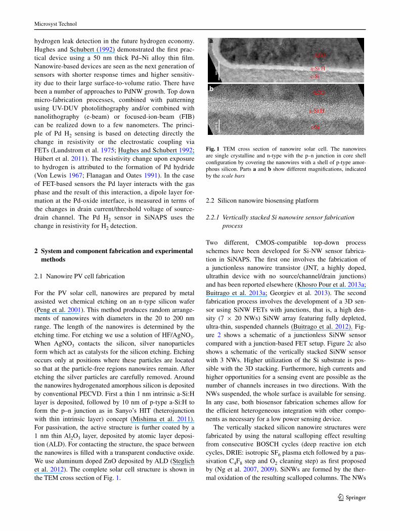
For the PV solar cell, nanowires are prepared by metal assisted wet chemical etching on an n-type silicon wafer (Peng et al. 2001). This method produces random arrange-ments of nanowires with diameters in the 20 to 200 nm range. The length of the nanowires is determined by the etching time. For etching we use a solution of hF/agnO3. When agnO3 contacts the silicon, silver nanoparticles form which act as catalysts for the silicon etching. etching occurs only at positions where these particles are located so that at the particle-free regions nanowires remain. after etching the silver particles are carefully removed. around the nanowires hydrogenated amorphous silicon is deposited by conventional PecVD. First a thin 1 nm intrinsic a-Si:h layer is deposited, followed by 10 nm of p-type a-Si:h to form the p–n junction as in Sanyo’s hIT (heterojunction with thin intrinsic layer) concept (Mishima et al. 2011). For passivation, the active structure is further coated by a 1 nm thin al2O3 layer, deposited by atomic layer deposi-tion (alD). For contacting the structure, the space between the nanowires is filled with a transparent conductive oxide. We use aluminum doped ZnO deposited by alD (Steglich et al. 2012). The complete solar cell structure is shown in the TeM cross section of Fig. 1.
2.2 Silicon nanowire biosensing platform
2.2.1 Vertically stacked Si nanowire sensor fabrication process
Two different, cMOS-compatible top-down process schemes have been developed for Si-nW sensor fabrica-tion in SinaPS. The first one involves the fabrication of a junctionless nanowire transistor (JnT, a highly doped, ultrathin device with no source/channel/drain junctions) and has been reported elsewhere (Khosro Pour et al. 2013a; Buitrago et al. 2013a; Georgiev et al. 2013). The second fabrication process involves the development of a 3D sen-sor using SinW FeTs with junctions, that is, a high den-sity (7 × 20 nWs) SinW array featuring fully depleted, ultra-thin, suspended channels (Buitrago et al. 2012). Fig-ure 2 shows a schematic of a junctionless SinW sensor compared with a junction-based FeT setup. Figure 2c also shows a schematic of the vertically stacked SinW sensor with 3 nWs. higher utilization of the Si substrate is pos-sible with the 3D stacking. Furthermore, high currents and higher opportunities for a sensing event are possible as the number of channels increases in two directions. With the nWs suspended, the whole surface is available for sensing. In any case, both biosensor fabrication schemes allow for the efficient heterogeneous integration with other compo-nents as necessary for a low power sensing device.
The vertically stacked silicon nanowire structures were fabricated by using the natural scalloping effect resulting from consecutive BOSch cycles (deep reactive ion etch cycles, DrIe: isotropic SF6 plasma etch followed by a pas-sivation c4F8 step and O2 cleaning step) as first proposed by (ng et al. 2007, 2009). SinWs are formed by the ther-mal oxidation of the resulting scalloped columns. The nWs
Fig. 1 TeM cross section of nanowire solar cell. The nanowires are single crystalline and n-type with the p–n junction in core shell configuration by covering the nanowires with a shell of p-type amor-phous silicon. Parts a and b show different magnifications, indicated by the scale bars

Microsyst Technol
1 3
Fig. 2 Schematic of SinW sensor structure based on a junctionless SinWs, b junction based SinW FeTs, and c verti-cally stacked SinW FeTs with junctions (3 nWs)
Fig. 3 a SeM top side tilted view of structure after BOSch, b cross section view of scal-loped columns, c SinWs after thermal oxidation, d top side tilted view of structure with implant mask openings, e top side view of structure after metallization, f suspended SinWs after BhF bath, g close-up view of suspended SinWs, and h top view of finished structure

Microsyst Technol
1 3
form at the intersection of two consecutive cycles. This approach is inexpensive and utilizes conventional semi-conductor and micro electromechanical system (MeMS) fabrication processes (Buitrago et al. 2012). SOI wafers with a BOX and device layer thickness of 1 μm each, p-type boron, and resistivity between 1–10 Ωcm were uti-lised. Images of the structure after various process steps are shown in Fig. 3.
chemical modification of the sensors is used to ren-der them sensitive towards specific targeted analytes. For the streptavidin sensing experiments described here, the sensors were chemically modified with a surface coating of biotin which irreversibly binds to the nanowires. This was achieved using a two stage process. Firstly samples were functionalised with 3-(aminopropyl)triethoxysilane (aPTeS) by immersion in a 50 °c solution of 5 v/v % aPTeS in anhydrous toluene for 3 h. They were then rinsed with anhydrous toluene, deionised water and dried under nitrogen. In the second stage, the aminosilanised devices (Si-aPTeS) were immersed in 2 ml phosphate buffered silane (PBS, ph 7.5) and 100 μl of e, Z link-nhS-lc-Bio-tin in DMF (1 mg/ml) was added. The samples were left to react for 3 h at room temperature. Surfaces were rinsed with PBS and deionised water and dried under nitrogen.
2.2.2 Microfluidic delivery and sensing experiments
Microfluidic channels attached to the device allow delivery of a fluid analyte directly to the SinW sensors, with only a small quantity (μls) of analyte required for analysis. The propulsion of the fluid through the channel can either be achieved by pas-sive delivery via capillary action or using external pumping equipment. While the former option is far preferable for the
final applications (e.g., point-of-care health diagnostics) the latter method is convenient for laboratory testing in a probe-station, allowing for easy filling and cleaning of the channels during sensing measurements. as such, hydrodynamic flow was deemed to be a more appropriate method of fluid deliv-ery during experiments. The inlet/outlets of the microfluidic stamp were connected to lengths of polytetrafluoroethylene (PTFe) tubing so that fluid could be administered and col-lected from the outside of the probe station.
Figure 4 shows the suspended Si-nW chip layout and the microfluidic channel design applied to it. The layout consists of two parallel lines of devices can be seen. access to the sensor structures is possible through small windows on the SU8 isolation layer at the centre. contact access is possible on the outer sides of the chip. Fluid delivery to the sensor structures is enabled by bonding a polydimethylsi-loxane (PDMS) stamp composed of two separate 150 μm wide channels to the top of the chip, as shown in Fig. 5. access holes with diameters ~400 μm were drilled on the top and sides of the stamp to link the channel to external tubing. Figure 6 shows the cross section schematic of the vertically stacked structure with a microfluidic channel sit-ting on top of the device.
The microfluidic stamps were fabricated using stand-ard procedures (Duffy et al. 1998). The stamps were attached to the devices using the “stamp and stick” tech-nique (Satyanarayana et al. 2005) in which a thin layer of uncured-wet PDMS is added to the underside of the stamp before it is positioned on the device. Positioning of the devices uses a custom-made micrometer-controlled posi-tioning rig. curing at 60 °c for 2 h produces a strong but non-permanent bond to realize the integrated fluid delivery/sensing system (Fig. 5).
Fig. 4 Schematic showing the layout of the microfluidic chan-nel geometry used to supply the sensors with fluid for the vertically stacked nW structure. The width of each microfluidic channel is 150 μm
Fig. 5 a Picture showing the PDMS microfluidic stamp attached to a sensor device. b Microscope image showing the microfluidic channel (positioned top to bottom) above a sensor window

Microsyst Technol
1 3
With the microfluidic stamp attached, liquid analyte can be delivered directly to the sensors. For the streptavidin sensing experiments, small quantities of streptavidin were introduced within a continuous stream of buffer solution. PBS solution was delivered to the sensor by an external pump at a rate of 200 μl/min from a syringe (BD Plasti-pak, 10 ml) propelled by a pump (harvard, Pump 11+). From the syringe, the flow passed through polyethylene (Pe) tubing (ID 0.4 mm, OD 1.0 mm). Inside the probe sta-tion (Fig. 7a), the tubing was downsized (OD 0.4 mm ID 0.1 mm PTFe tubing) using interconnect junctions fabri-cated in-house from PDMS. commercially available inter-connects can also be used (e.g., from Upchurch Scientific). The smaller tubing was required to interface to the PDMS stamp by inserting into the pre-drilled holes, but could not be used for the entire length of the fluid supply lines due to excessive back-pressure.
The analyte solution can be injected separately into the main channel solution by the use of a T-junction located about 10 cm away from the syringe exit (Fig. 7b). From the T-junction, the flow continued along the Pe tubing (~1 m)
into the probe station. Standard fittings from Upchurch Sci-entific were used for all connections. electrical measure-ments of devices as well as the sensing experiments were done using cascade manual probe station and agilent semi-conductor analyser B1500.
2.3 Palladium nanowire hydrogen-sensing platform
While e-beam and FIB allow nm-scale Pd nanowire fab-rication, they cannot be scaled up for industrial scale pro-cesses; alternatives including nanoimprint lithography or nanostencils are compromised regarding lateral dimensions and reproducibility. Our solution to improve dimensional control is to precisely define a cavity that permits con-trolled removal of part of the metal layer with an angled wafer level ion beam etch that resembles a nanostencil structure patterned directly on the wafer service, which minimizes the lateral spread of the deposited metal (Tong et al. 2009). This process is indicated schematically in Fig. 8. The generic process of deposition and etching at an angle (Dea) is applied here to fabricate Pd nanowires on thermal SiO2/Si based silicon substrates and the patterned devices can be addressed individually or in a array using two point contacts (Tong et al. 2009).
a typical layout of the sensing device is shown in Fig. 9 (Van der Bent and Van rijn 2010). For testing this component, a typical measurement consists of using a source measure unit (Keithley 2400) with a voltage bias applied between 50–800 mV and controlled remotely via GBIP interface. The recorded signal (real time cur-rent/resistance change) can be used to do current–voltage sweeps under different operating conditions. a tempera-ture controller enables temperature dependent measure-ment. noise spectra from the devices are measured and analysed using the agilent 35665a dynamic signal ana-lyzer. The measurement resolution is determined by the noise level from the nanowires and that of the readout electronics. Measurements of the inherent noise levels from nanowires and the noise spectrum of single nanow-ires for different bias currents (1–180 µa) have been made to estimate the low frequency resistor noise. The
Fig. 6 cross section schematic of vertically stacked SinW structure with microfluidic channel on top of device
Fig. 7 a Image showing an integrated device within the probe station before testing. The device is connected to tub-ing ready for fluid delivery. b Image showing the syringes and syringe pump used to deliver fluid for the streptavidin sensing experimentation

Microsyst Technol
1 3
nanowire noise spectrum shows 1/f behavior, from which the measurement resolution was determined to be 0.03 % of the nanowire resistance (r ~ 7 kΩ). The integration of the nanowires into a one chip solution will decrease the resolution to approximately 1–2 %, which is still suffi-cient for our purposes.
In the present work, a Pd nanowire chip was fabricated using Deposition and etching under an angle (Tong et al. 2010). Two identical nanowires with a width of 200 nm, a height of 20 nm, and a length of 50 μm were selected, giving a wire resistance of approximately 8,300 Ω for each nanowire (293 K, <1 ppm). The tolerance on the resist-ance of the wires was less than 100 Ω. The chip was wire-bonded directly to an interface board for testing and initial measurements showed a resistance of 8,300 Ω with a var-iation of approximately 12 Ω ± 2 Ω at a hydrogen con-centration of 900 ppm. The error in measurement is due to
wire resistance and cable noise in the connection from the source meter to the nanowires.
The Pd nanowire resistance changes upon absorbing hydrogen and from thermal expansion in the Pd nanow-ire. Therefore, accurate hydrogen sensing cannot be done without a temperature compensation arrangement. This was implemented, using a drop forge technique, to cover one of the two identical nanowires with a low-permeable h2 coat-ing consisting of a UV curable polymer. This is referred to as the secondary nanowire, the uncoated nanowire being primary. The semi-crystalline coating on the secondary nanowire acts as a passivation layer and hinders hydrogen from reaching the wire itself. Due to the low e-modulus of the coating material, the compound remains flexible to allow the wire to expand and recover by the influence of temperature changes. In time, but with a considerably higher time constant, hydrogen will reach the secondary
Fig. 8 The microfabrication process of Pd nanowire devices adapted from (Tong et al. 2009)
Fig. 9 layout of the PdnW sensing device with a magni-fied SeM image of a single nanowire

Microsyst Technol
1 3
wire causing it to respond to the diffusion of hydrogen in the palladium wire. Before this process takes place how-ever, the secondary nanowire can be applied as an adequate temperature reference for the primary nanowire, respond-ing to temperature changes in the exact same manner and as such enabling accurate temperature compensation. Measurements were performed for verification of the tem-perature compensation mechanism using a temperature sensor located closely to the Pd chip further referred to as the nearby-temperature-sensor.
2.4 low power cMOS electronics
2.4.1 System level design
The system level design starts with selecting an energy harvesting source and an energy storage device. newly designed energy harvester and sensor interface circuits were developed within SinaPS. To realize mm-size autonomous sensors, the size and power consumption of the sensor and the wireless data transceiver should be minimized, and the power delivered to the sensor should be maximized. The PV module should have high efficiency to provide enough power at its maximum power point, MPP (Pmpp), while open circuit voltage, VOc, and short circuit current, ISc, affect the over-all efficiency. Since the harvested energy is intermittent, it must be stored in a rechargeable battery or supercapacitor, with enough capacity to provide energy for a few hours sen-sor operation without energy harvesting. We chose an niMh battery, namely the Varta V6hr microbattery, with a nomi-nal voltage of 1.2 V and a peak discharge current of 18 ma, which is suitable for the SinaPS mote thanks to its lower nominal voltage than a thin film li battery. This battery has a nominal capacity of 6.2 mah, with a diameter and height of 6.8 and 2.15 mm, respectively (Varta V6hr Datasheet 2013). all electronic circuits, including the external wireless transceiver, can work with a sub-1.2 V supply voltage, so that additional step-down or step-up circuits are not required.
The block diagram of the SinaPS electronics circuit, including the required external components and the main blocks of the proposed solar energy harvester, is depicted in Fig. 10. Four miniaturized (~1 mm2) nanowire solar cells con-nected in series are sufficient to match the battery voltage. at present the SIU is configured for hydrogen sensing, measur-ing h2 concentration and temperature. The Pd nanowire grid described in Sect. 2.3 (Van der Bent and Van rijn 2010) is used. The SIU measures the conductance change of the sens-ing nanowires in comparison to the reference nanowires. This eliminates the effects of temperature and gives a higher accu-racy by using the conductance ratio instead of absolute val-ues. The measurement results are sent to an external wireless transceiver through an embedded serial peripheral interface (SPI). The transceiver can communicate the measurement
results with other sensors through a wireless link. In micro-power energy harvesting applications a low peak power in the transceiver ensures that a miniaturized battery with limited peak discharge current can be used to power up the circuit. Ultra-low standby current guarantees that the average power consumption of the sensor can be minimized for heavy duty cycling of data transmission. The ultra-low power wireless transceivers with sub-1.2 V voltage, such as TZ1053 (Toumaz 2012) or Zl70250 (Zarlink 2012), are well suited to the SinaPS mote. These transceivers operate at sub-1 Ghz fre-quency bands and have lower peak-power and standby power, compared to 2.4 Ghz transceivers.
2.4.2 Energy harvesting and power management
The energy harvesting scheme is based on the direct charg-ing scheme connecting the battery to the PV module with a PMOS switch. Since the Dc voltage from a PV module can differ from the voltage of the target battery, there are different Dc–Dc converters to harvest PV energy to charge a battery, e.g. switched-capacitor (Sc) (chen et al. 2011) and inductive Dc–Dc converters (Qiu et al. 2011). how-ever, under reduced illumination when harvested power is a few micro-watts, direct charging achieves higher efficien-cies (Khosro Pour et al. 2012) and is implemented here. a dynamic comparator compares Vbat with Vpv to avoid discharge of the battery through the PV module when Vpv is less than Vbat. In direct charging, as Vpv always follows Vbat, only the design time component matching (DTcM) approach can be used for maximum power point tracking (MPPT) (lu et al. 2010). To match the battery voltage four miniaturized (~1 mm2) nanowire solar cells are connected in series as the energy harvesting source. although Pmpp and ISc of the PV module change considerably in different lighting conditions, VOc of the PV module does not signifi-cantly change, so that the PV module always operates close to its Vmpp giving a high efficiency.
Fig. 10 Block diagram of the SinaPS electronic circuit

Microsyst Technol
1 3
The second task of the power management circuit is reconfiguring the power consumption and speed of the sen-sor, based on the harvested energy. Since under reduced light intensity the power delivered by the PV module may be lower than the average power consumption of the sensor, the energy harvester circuit reduces the power consump-tion of the sensor to avoid complete discharge of the battery, allowing the sensor to continue autonomous operation at a lower speed (Khosro Pour et al. 2013b). The circuit detects Vbat during wireless transmission to accurately estimate the energy stored in the battery and the power-performance of the sensor is reconfigured to guarantee autonomous sensor operation. a switched-capacitor voltage level detector (lD) is used to detect the battery voltage level between VeOD of 0.9 V up to VeOc of 1.5 V. The power management circuit measures Vbat and estimates the energy stored in the battery, reconfiguring the power-performance of the microsystem where required (Khosro Pour et al. 2013b). If Vbat is suf-ficiently high the power management and sensor interface circuits work at their highest speed, and the measurement results are sent to the base station every 15 s. If Vbat is not sufficiently high, the power consumption of the sensor is reduced by operating at a lower clock frequency. The power consumption of the digital circuits is reduced by scaling down the operating frequency and activating the transceiver by a lower duty cycle. a digital control unit (DcU) activates the comparator and lD blocks in a timely manner. as nei-ther Vbat nor Vpv change rapidly, these blocks are activated every few seconds by the DcU. The power consumption of DcU is determined by the low frequency 20-bits counter that activates the comparator and lD.
2.4.3 Low power sensor interface circuit
The system level block diagram of the new sensor inter-face circuit is depicted in Fig. 11. The SIU measures the
conductance change of the sensing nanowires (nWsense) in comparison to the reference nanowires (nWref), eliminat-ing the first order temperature dependence. The nanow-ires that are denoted by nWref and nWsense in Fig. 2 are biased with a minimum voltage of 50 mV for 10 s using a 7 μa current source, before measuring their conductiv-ity change upon hydrogen exposure. The conductance of nWsense may change by 20 % in comparison with nWref as h2 concentration varies from zero to 30 % (Offermans et al. 2009). In order to measure this conductance change, the voltage around the sensing nanowire (V2) is used as the input voltage, while the voltage around the reference nanowire (VR = V1 − V2) is used as the reference voltage for the following incremental aDc (Markus et al. 2004). aDc converts (V2/Vr) to a digital value to measure h2 concentration.
To eliminate second order effects the temperature is measured after measuring h2 concentration to be used for further calibration of the sensor. In the integrated tempera-ture sensor, absolute temperature (Vptat) and temperature-independent reference (Vref) voltages. Temperature is measured by converting (Vptat/Vref) to a digital value. The low power temperature sensor can achieve ±1 °c accuracy by calibrating c2 and ITemp at room temperature (Khosro Pour et al. 2013b). When the whole system operates at a lower frequency, a lower bias current is applied to reduce the average power consumption of the temperature sensor.
The long conversion time of the aDc increases the energy per conversion, with a total conversion time of 2n cycles for n-bit resolution. In our SIU, analog residues of the first order incremental aDc (Markus et al. 2004) are sent to the Sar aDc to extract additional bits. By using an additional Sar aDc besides the initial first order incre-mental aDc, energy consumption per conversion of the aDc has been improved considerably. This aDc can be an ideal candidate for sensing applications as it achieves
Fig. 11 circuit diagram of the sensor interface

Microsyst Technol
1 3
high accuracy (close to delta-sigma and dual-slope aDcs) and low energy per conversion. The die area is reduced by scaling down the capacitors thanks to oversampling. In the SinaPS Sar aDc, two sub-Dacs, each with 4-bit resolution and a fractional bridge capacitor has been used to implement an 8-bit Dac. This Sar aDc consumes 5.9 μW operating at 1 Mhz clock frequency.
3 Results and discussion
3.1 Silicon nanowire solar cells
The properties of the silicon nanowires, the solar cells, and the first modules (made by wire bonding) have been characterized by measuring optical properties, I–V curves, eQe (external quantum efficiency), light intensity depend-ence, and so on. To verify the light trapping properties of the nanowires, we have compared the optical properties of a wafer before and after nanowire etching. Figure 12a shows the reflection, transmission and absorption spectra measured by an integrating sphere of a nanowire array on a silicon wafer together with the data of the wafer without nanowires.
The nanowires strongly reduce the reflection as com-pared to the bare wafer. In the wavelength region below 1,000 nm, that is for photon energies above the silicon band gap, the transmission is nearly zero. To clarify how much of the light is absorbed by the nanowires alone, we have prepared the nanowires on thin crystalline silicon films on glass. Figure 12b shows the reflection, transmis-sion and absorption of such an array with a wire length of ~1.2 μm on a 1.5 μm thick film together with the data of the bare film. These results show that absorption is greatly enhanced due to the nanowire array through reduction of transmission and reflection. The enhancement of absorp-tion is explained by the light scattering due to the nanow-ires which leads to an increased light path in the nanowire array. So we can conclude that in the above mentioned case
of nanowires on wafer, most of the light will be absorbed already in the nanowires.
To improve the final nanowire solar cell, we have devel-oped an ultrathin passivating tunnel al2O3 layer between the aZO and the a-Si:h emitter. Figure 13 shows the eQe of nanowire solar cells on a wafer with (black) or with-out (red) al2O3 passivation layer. The ultrathin al2O3 layer increases the eQe significantly, and the efficiency can be increased by up to 1 % (absolute value) (Jia et al. 2013). The low eQe in the short wavelength region (400 to 600 nm) can be attributed to parasitic absorption due to the a-Si:h emitter and the TcO. The parasitic absorption is enhanced due to light trapping in the structure.
By incorporating the 1.2 nm ultrathin al2O3 passivat-ing tunnel layer to fabricate multiple core–shell nanowire solar cells, an efficiency of 10 % has been reached, which is by far the highest value on a nanowire array prepared by metal assisted wet chemical etching. Figure 14 shows the I–V curves of our best nanowire solar cell measured in the dark and under aM1.5 illumination. The solar cell has a VOc of 517 mV, a short circuit current density (JSc) of 26.46 ma/cm2, a fill factor (FF) of 73.4 %, and a conver-sion efficiency (η) of ~10 %. Shunt and series resistance are estimated to be 25.3 kΩ and 89.5 Ω respectively.
Figure 15 shows the I–V curves (left image) of a solar cell module consisting of 8 cells (with an active area of a single cell ~1 mm2) connected in series by wire bonding (right image). The curves refer to a single cell (black), two cells connected in series (red), three cells (green), and so on. The rightmost curve applies to the complete module. as is obvious from this curve, the module delivers an open cir-cuit voltage of 2.4 V. The maximum output power is about 190 μW at VMPP of 1.83 V.
The behaviour of the nanowire solar cells under low light conditions was tested by I–V measurements under differ-ent light intensities by reducing the aM1.5 spectrum with neutral density filters (nD filter). Figure 16 shows the cor-responding I–V curves of the solar cell under these light
Fig. 12 a reflection (green), transmission (black) and absorption (red) spectra measured by an integrating sphere of a silicon wafer (thin lines) and those after nanowire etching (bold lines). b reflec-tion (green), transmission (black), and absorption (red) of a 1.5 μm thick crystalline silicon thin film on glass in the virgin state (thin lines) and after nanowire etching (bold lines)

Microsyst Technol
1 3
intensities, relative to aM1.5. Figure 17 shows the depend-encies of the current density as well as of the open circuit voltage on the light intensity. JSc depends almost linearly on the light intensity, whereas the open circuit voltage depends logarithmic on light intensity. as a result, a SinaPS solar cell module with a total active area of 3 mm2, consisting of four cells (VOc of 500 mV, JSc of 25 ma/cm2, FF of 70 % per cell) connected in series, delivers a power of 260 μW under aM1.5 illumination. It will still provide the required voltage of 1.4 V for battery charging at an illumination intensity of 1 % of aM1.5. The drawback is that the current is just about 1 % of that determined at aM 1.5 illumination.
3.2 nanowire sensing platforms
3.2.1 Vertically stacked Si nanowire biosensor
here we present results describing the application of the suspended SinW FeT devices to sensor applications. The
main goal of the work to date has been to show proof-of-principle operation and demonstrate that the microfluidic analyte delivery and analyte-specific device functionalisa-tion methods are appropriate for purpose. Before sensing experiments were performed, electrical characterisation of the devices was carried out in order to check that the functionalisation procedure and subsequent attachment of the microfluidic stamp had no adverse effect of device per-formance. Figure 18 shows the typical Id–VSG curves for a device with 7 × 20 nWs, 2 μm, d = 15–30 nm at low
Fig. 13 The eQe of two types of solar cells is shown. Red cell with-out al2O3. Black cell with ultrathin al2O3 layer
Fig. 14 I–V curves in the dark and under aM1.5 illumination of the best nanowire solar cell prepared on a Si wafer
Fig. 15 I–V characteristics (left) of the solar module (right) consist-ing of 8 cells connected in series by wire bonding
Fig. 16 I–V curves of nanowire solar cells under reduced light con-ditions. 100 % corresponds to aM1.5

Microsyst Technol
1 3
drain bias potentials (Vd = 50 mV) when liquid gated (PBS ph = 7.4) by the use of a single side gate. The SiO2 sur-face of the device had been modified by biotin and a PDMS stamp had been attached to facilitate fluid delivery. The measurements were performed under PBS flow (at a steady 150 μl/min) to examine how the device performs with a fluid. The steep transfer characteristics with high Ion/Ioff ratios of 5–6 orders of magnitude, high subthreshold slopes and reasonable reproducibility of the measurements dem-onstrate the very good control of the 3D transistor channels (3D SinW arrays) by the side gate. We note that the Id–VSG curves are somewhat noisy. This is due to the instability of the potential applied through a quasi-reference electrode such as Pt which affects the stability of any sensing meas-urements. consequently, full characterization of the sens-ing capabilities of the structures in the future will include the use of a reference electrode flow cell. Importantly, the FeT characteristic behaviour indicates that the functionali-sation and stamp attachment did not harm the device struc-ture or performance.
The functionalisation of the SinW sensors with covalent attachment of aPTeS (to allow covalent attachment of bio-tin) was performed to test aPTeS functionalised sensors
(chen et al. 2006) for their response to ph. Figure 19a shows the typical Id–VSG curves for a device with 7 × 10 nWs, length l = 2 μm, diameter d = 15–30 nm at low drain bias potentials (Vd = 50 mV) for an aPTeS function-alised SiO2 surface device after administering different ph buffer solutions. The threshold voltage is seen to rise with an increase in the ph value, typical for an n-type device. This measureable change demonstrates how the devices could be applied to ph sensing. Furthermore, it shows how, by tailoring the surface chemistry of the devices to the desired application, the SinW devices can be applied to different sensing applications.
Since the functionalisation and stamp attachment did not compromise the performance of the devices, we proceeded to test the response of biotin modified SinWs to streptavi-din. For initial testing, and given the observed fluctuations experienced when carrying out measurements under fluid, it was decided to ascertain whether any response could be seen from a large administration of streptavidin. Fig-ure 19b shows the typical Id–VSG curves for a biotin-modi-fied Si-nW device with 7 × 10 nWs, l = 2 μm, diameter d = 15–30 nm at low drain bias potentials (Vd = 50 mV) after administration of 0.1 ml of a 0.02 mg/ml (0.4 μM) streptavidin solution followed by a flow of PBS (steady state flow of 150 μl/min). The threshold voltage has shifted to the right, consistent with the negative charge associated with the streptavidin as it binds to the probe biotin proteins functionalized on the surface of the nWs.
The drain current Id was subsequently measured as a function of time t (Id − t) for a device with 7 × 20 nWs, l = 2 μm, d = 15–30 nm and SiO2 biotinated surface at low drive voltages (Vd = 50 mV) operated in the sub-threshold region VGS = 1.6 V under particular conditions (Buitrago et al. 2013b). Since the response of the device
Fig. 17 a Short circuit current density and b open circuit voltage of a nanowire solar cell at varying illumination intensity. The latter is normalised to 1, corresponding to aM1.5 illumination
Fig. 18 Id–Vsg curves of a side-gated device at low drive voltages, following biotin functionalisation and microfluidic stamp attachment

Microsyst Technol
1 3
in static conditions did not suffer from the fluctuations observed under fluid flow, the channels were cleared using a syringe of air at given points to obtain a steady response. The results of an experiment to study the response of the sensor to a particular concentration of streptavidin are shown in Fig. 20; here we point out that this experiment shows the functionality of nanowire sensor for the detec-tion of streptavidin and further work is being undertaken to study the sensing response under different streptavi-din concentrations. a steady stream (150 μl/min) of PBS was first injected into the dry microfluidic channel, which yielded a fluctuating signal on the order of a few μa. Dry-ing the channel (the device still wet) with an injection of air at t ≈ 10 min gave a smooth signal of approximately 0.3 μa. Flowing PBS again gave a fluctuating signal and subsequent administration of air gave a smooth response of approximately 1 μa. having seen the signal response under PBS and air, 0.1 ml of a 0.02 mg/ml (0.4 μM) solu-tion of streptavidin in PBS was administered, followed by a flow of PBS which removed any unbound streptavidin. Under the flushing flow of PBS there was no discernible
change in signal magnitude or fluctuation compared to before streptavidin administration. On addition of air, how-ever, the signal decreased sharply down to na levels. These observations were repeated with another subsequent PBS and air administration. comparison of the response under air before and after streptavidin shows a difference in sig-nal response of over two orders of magnitude, which indi-cates a positive and definite change following streptavidin administration.
3.2.2 Hydrogen sensing using Pd nanowires
To test the temperature response time-constant of the nearby temperature sensor compared to the time-constant of the secondary nanowire, we exposed the sensor to a pre-defined temperature fluctuation sequence in the test cham-ber. The temperature sequence had a sine profile with a maximum of 28.0 °c and a minimum of 20.0 °c. The sine profile was chosen to ensure a good mixture of faster and slower temperature transients. The wire responds to the temperature change as seen in left chart of Fig. 21, which shows the nanowire response and the temperature of the chamber (middle curve, scale to the right). as can be seen in the chart, the output of the primary nanowire shows a strong positive correlation with the temperature change. at this time scale, the permeability of the coating, and the obstruction of changes in wire shape may be considered to be minimal, since influences of these parameters would inevitably lead to distortions in the correlation between the primary and the secondary wire. First indications of the correlation between the temperature of the chamber and the nearby-temperature-sensor are also good, but we intend investigating the behaviour at higher temperature change gradients.
The right part of Fig. 21 shows the compensated output of the primary nanowire. In this first test, no hydrogen was inserted in the test chamber yet, so the output should be steady. The measurement confirms this expectation; note that
Fig. 19 Id–Vsg curves of a side-gated device at low drive voltages (Vd = 50 mV) with 7 × 10 nWs, 2 μm length, diameter d = 15–30 nm and for: a aPTeS functionalized SiO2 surface at different ph solutions and b SiO2 surface following streptavidin injection
Fig. 20 Id − t measurements for streptavidin administration when VSG = 1.6 V, Vd = 50 mV for a device with 7 × 20 nWs, 2 μm length, diameter d = 15–30 nm and SiO2 biotinated surface

Microsyst Technol
1 3
the scale of the graph has been expanded by a factor 150. at this time initial tests with inserting hydrogen in the test chamber show sufficient response of the primary nanowire and a delayed response of the secondary nanowire as shown in Fig. 22. an algorithm is under development to apply the nearby-temperature-sensor and the primary nanowire output to optimize the accuracy of the system in realistic environ-ments, from almost steady to rapidly changing.
3.3 autonomous operation of the sensor
The newly designed SinaPS electronics have been imple-mented in a 0.18 μm cMOS process with 0.25 mm2 total die area, see Fig. 23. The main blocks, including the digital blocks and the analog blocks of the solar energy harvester and the sensor interface circuits, have been specified sepa-rately. Table 1 presents the die area and power consumption of individual blocks, operating at 1 Mhz clock frequency. The simulated total power consumption of the energy har-vester is less than 300 nW and is determined primarily by the clock generator, bias circuit and DcU blocks, which are always active. although comparator and lD blocks con-sume considerable power during their active time the fact
that they are activated every 15 s means that their average power consumption is less than 1 nW. The final task of the energy harvester circuit is protecting the battery against overcharge and overdischarge, which reduce the cycle life of the battery. To this end, VeOc and VeOD voltages are detected and when Vbat reaches the VeOc limit, the battery is disconnected from the PV module to avoid overcharge. conversely, when Vbat reaches the VeOD limit, the sensor interface circuit and the wireless transceiver are deactivated temporarily to avoid overdischarge.
In actual use we define four operating modes accord-ing to the remaining charge of the battery. Table 2 presents
Fig. 21 The left chart shows the temperature sequence with the Pd nanowires responses. The right chart shows the nanowire response compensated by each other
Fig. 22 compensated nanowire response and h2 detection at inlet of 1,200 ppm
Fig. 23 circuit layout of the whole microsystem
Table 1 Die area and consumed power of main blocks in the solar energy harvester circuit
Block Die area (μm2)
active power (nW)
average power (nW)
clock generator 14,400 165 165
Digital control unit (DcU) 38,115 90 90
Bias circuit (10 na) 2,832 35 35
comparator 759 55 <1
level detector 31,960 520 <1
ScBM 6,300 640 <1

Microsyst Technol
1 3
simulation results for power consumption of the power management and the sensor interface circuits in differ-ent system operation modes, denoted Sl3 to Sl0. Vbat is detected when the battery is discharged by a high current during wireless data transmission. The remaining bat-tery charge is determined from the battery discharge curve (Varta V6hr Datasheet 2013).
In Sl3 mode, with the highest Vbat, the system operates at 1 Mhz and the wireless transceiver sends the meas-urement results for h2 concentration and temperature to a base station every 15 s. In this operating mode, the average power consumption of the energy harvester is less than 300 nW. Upon detection of a lower battery volt-age, the system switches to a lower clock frequency; for example, in Sl0 mode the circuit operates at 125 khz fre-quency and the average power consumption of the energy harvester drops to less than 110 nW thanks to reducing the power consumption of the clock generation and DcU blocks; the simulated power consumption of the clock generator and the DcU is reduced linearly with operating frequency, reaching 23 and 13 nW, at 125 khz (Khosro Pour et al. 2013b). The average power consumption of the incremental and Sar aDc is reduced almost linearly as seen in Table 2. Finally, in this mode measurement results are sent every 120 s.
as another example, 330 nW is used for biasing the bipolar junction transistors in the integrated temperature sensor and generating VcM common mode voltage for aDc in Sl3 mode, which is reduced to 176 nW in Sl0 mode. as a resistive divider has been used to generate VcM, the power consumption of the VcM generator is almost constant; how-ever as a frequency-proportional current source has been used to bias the BJT transistors in the temperature sensor, the power consumption is reduced in Sl0 mode.
To estimate the total power consumption of the sensor, the average power consumption of the sensor biasing circuit and the wireless transceiver are required. Before measuring the h2 concentration, the Pd nanowires are biased with a 7 μa bias current for 10 s; since the aDc conversion takes less than 1 ms, the total power consumption of the sensor interface circuit is determined by the sensor bias circuit. The TZ1053 transceiver consumes 5 μa during standby and 3.3 ma in 20 ms to send data with the minimum pay-load size of 55 bytes (Toumaz 2012). In Sl3 mode, the average current consumption of the Pd nanowires and the wireless transceiver are 4.67 and 9.4 μa, respectively. By sending the samples every 120 s in Sl0 mode, these values will be reduced to 0.58 and 5.6 μa, respectively. The aver-age current consumption of the whole sensor is 14.1 μa in Sl3 mode and in Sl0 mode this is reduced to 6.2 μa.
To evaluate the autonomous operation of the sensor, the power delivered to the battery by the PV module can be simulated with an equivalent circuit model. The 4 mm2 area PV module can provide a maximum power of 319.5 μW at its Vmpp under aM1.5 illumination level. Figure 24 shows that under simulated 10 % of aM 1.5 illumination, the PV module delivers an average power of 24.45 μW to the battery and efficiency is 90.7 %. When the battery is almost fully discharged, the system operates in Sl0 mode and 21.05 μW is delivered to the battery with 78.1 % effi-ciency (Fig. 24), while the average current consumption of the complete system is only 6.2 μa. as a result the battery gets charged and Vbat increases gradually. By increasing the battery voltage, efficiency is improved and more power is delivered to the battery. Therefore, even at 10 % light inten-sity, the harvested energy is enough for autonomous opera-tion of the complete system. Finally, as the whole sensor consumes 14.1 μa for sensing and data transmission, the
Table 2 System performance and power consumption in different system operation modes
System operation modes Sl3 Sl2 Sl1 Sl0
Main characteristics Detected Vbat during 5ca discharge (mV) 1,104 1,051 1,002 947
remaining charge of the battery (%) >80 % >50 % >35 % >25 %
Battery threshold voltage (V) 1.114 1.055 1.003 0.955
Operating clock frequency (Khz) 980 502 257 132
Time interval of sensing and data transmission (s) 15 30 60 120
average power consumption (nW): PM circuit clock generator 165 85 44 23
Digital control unit 90 46 24 13
Whole PM circuit 293 169 106 74
average power consumption (nW): SI circuit Temperature sensor and VcM generator 330 243 198 176
First order incremental aDc 1,030 545 295 180
Sar aDc 5,900 2,840 1,510 790
average current consumption (μa): whole system Sensor bias circuit 4.67 2.34 1.17 0.58
Wireless transceiver 9.4 7.7 6.6 5.55
complete system 14.1 10.1 7.8 6.2

Microsyst Technol
1 3
target 6 mah battery can provide enough power for approx-imately 425 h continuous operation, even without energy harvesting.
4 Concluding remarks
In summary we prepared a photovoltaic mini-module con-sisting of silicon nanowire solar cells, each of 0.5 mm2 area. The efficiency of the module reaches 10 % and it delivers a power of 260 μW and an open circuit voltage of 2 V at one sun illumination. at 1 % of one sun illumination, the PV module delivers 1.4 V, which makes this Si nanow-ire based solar cell module useful as an energy harvester for charging the battery in the SinaPS mote.
We have tested fully integrated microfluidic–sensor devices, combining functionalized suspended SinWs with a novel microfluidic fluid delivery system to examine their potential as sensors for streptavidin and ph. In this inte-grated device, analyte solutions are delivered to the nW sensor via microfluidics and the electrical response noted. For the streptavidin sensing, nWs are functionalized with biotin and after addition of a 0.4 μM solution of strepta-vidin, the current drop by over two orders of magnitude. For ph sensing, aPTeS-modified nW devices were used. On adding different buffered solutions (ph 4, 7 and 10) the current reproducibly shifts, with the direction of the shift correlating to the ph of the buffer.
an ultra-low power, efficient solar energy harvesting and sensing microsystem has been proposed. an area- and power-efficient solar energy harvester stores energy har-vested from the PV module in an MiMh microbattery. This circuit also scales the power consumption and perfor-mance of the complete system for autonomous operation of the sensor at low battery charge. a fully integrated sensor
interface circuit measures h2 concentration by measuring the conductance changes of a miniaturised Pd nanowire sensor and temperature measurement allows sensor cali-bration. a new incremental aDc converts measurement data to 13-bit digital values, that are transmitted to a base station. even 10 % light intensity is sufficient for the sys-tem to operate autonomously. The target 6 mah battery provides power for 425 h sensor operation even without energy harvesting.
a power efficient and fast early hydrogen detection method has been presented. This is achieved by employ-ing a microchip with two Pd nanowires and demonstrat-ing sensing under varying temperature in a test chamber, with controlled h2 concentration. The dual Pd nanowire, in which one acts as h2 sensor and the other as a temperature sensor, is found to be the best choice as input for an ade-quate temperature compensation algorithm. Selective and fast detection over a wide temperature range is attainable if the relevant temperature time constraints of the different components are met. a detection limit of 100 ppm h2 has been demonstrated under temperature fluctuations.
Acknowledgments We acknowledge support from the euro-pean commission Framework 7 IcT-FeT-Proactive funded project SinaPS (contract number 257856) for financial support of this work.
References
Barton J, harte S, Jung e (2008) Distributed, embedded sensor and actuator platforms. In: Delaney K (ed) augmented materials and smart objects: building ambient intelligence through microsys-tems technology. Springer Science + Business Media, new York, pp 105–129
Von lewis Fa (1967) The palladium hydrogen system. academic Press, london-new York. 1. aufl., XII, 178S., zahlr. abb., geb. 45 s
Fig. 24 Power delivered to the battery under simulated 10 % of aM1.5 illumination
Microsyst Technol
1 3
Buitrago e, Fernández-Bolaños M, Ionescu aM (2012) Vertically stacked Si nanostructures for biosensing applications. Microelec-tron eng 97:345–348
Buitrago e, Fagas G, Badia MF-B, Georgiev YM, Berthomé M, Ionescu aM (2013a) Junctionless silicon nanowire transistors for the tunable operation of a highly sensitive, low power sensor. Sens actuators B 183:1–10
Buitrago e, Badia MF-B, Georgiev YM, Yu r, lotty O, holmes JD, nightingale aM, Ionescu aM (2013b) Functionalised 3D 7×20 array of vertically stacked SinW FeTs for streptavidin sensing. In: 71st annual device research conference (Drc), notre Dame, In
chen Y, Wang X, erramilli S, Mohanty P, Kalinowski a (2006) Sili-con based nanoelectronic field-effect ph sensor with local gate control. appl Phys lett 89(22):223512/1–223512/3
chen G, Ghaed h, haque r, Wieckowski M, Yejoong K, Gyouho K, Fick D, Daeyeon K, Mingoo S, Wise K, Blaauw D, Sylvester D (2011) a cubic-millimeter energy-autonomous wireless intraocu-lar pressure monitor. In: Proceedings of the Ieee international solid-state circuits conference, San Francisco, ca, USa, pp 310–312
conibeer G (2007) Third-generation photovoltaics. Mater Today 10(11):42–50
cui Y, lieber cM (2001) Functional nanoscale electronic devices assembled using silicon nanowire building blocks. Science 291(5505):851–853
cui Y, Wei Q, Park h, lieber c (2001) nanowire nanosensors for highly sensitive and selective detection of biological and chemi-cal species. Science 293(5533):1289–1292
Duffy Dc, McDonald Jc, Schueller OJa, Whitesides GM (1998) rapid prototyping of microfluidic systems in poly(dimethylsiloxane). anal chem 70(23):4974–4984
Fasoli a, Milne WI (2012) Overview and status of bottom-up silicon nanowire electronics. Mat Sci Sem Proc 15(6):601–614
Flanagan TB, Oates Wa (1991) The palladium-hydrogen system. annu rev Mater Sci 21(1):269–304
Georgiev YM, Yu r, Petkov n, lotty O, nightingale aM, deMello Jc, Duffy r, holmes JD (2013) Silicon and germanium junction-less nanowire transistors for sensing and digital electronics appli-cations. In: nazarov a, Balestra F, Flandre D, Kilchytska V (eds) Functional nanomaterials and devices for electronics, sensors and energy harvesting. Springer, Berlin
Gislason D (2008) ZigBee wireless networking. newnes Publications, london
Green Ma, emery K, hishikawa Y, Warta W, Dunlop eD (2012) Solar cell efficiency tables. Prog Photovolt res appl 20(5):606–614
hübert T, Boon-Brett l, Black G, Banach U (2011) hydrogen sen-sors—a review. Sens actuators B chem 157(2):329–352
hughes rc, Schubert WK (1992) Thin films of Pd/ni alloys for detec-tion of high hydrogen concentrations. J appl Phys 71(1):542–544
Imote2 Datasheet (2009) high-performance wireless sensor network node. http://www.xbow.com. accessed 25 Dec 2012
Jia G, eisenhawer B, Dellith J, Falk F, Thøgersen a, Ulyashin a (2013) Multiple core-shell silicon nanowire-based heterojunction solar cells. J Phys chem c 117(2):1091–1096
Khosro Pour n, Krummenacher F, Kayal M (2012) Fully integrated ultra-low power management system for micro-power solar energy harvesting applications. electron lett 48(6):338–339
Khosro Pour n, Kayal M, Jia G, eisenhawer B, Falk F, nightingale a, DeMello Jc, Georgiev YM, Petkov n, holmes JD, nolan M, Fagas G (2013a) a miniaturised autonomous sensor based on nanowire materials platform: the SinaPS mote. SPIe Proc 8763. doi:10.1117/12.2017520
Khosro Pour n, Krummenacher F, Kayal M (2013b) Fully integrated solar energy harvester and sensor interface circuits for energy-efficient wireless sensing applications. J low Power electron appl 3(1):9–26
lu c, raghunathan V, roy K (2010) Maximum power point consid-erations in micro-scale solar energy harvesting systems. In: Pro-ceedings of Ieee international symposium on circuits and sys-tems (IScaS), Paris, France, pp 273–276
lundstrom KI, Shivaraman MS, Svensson cM (1975) a hydrogen-sensitive Pd-gate MOS transistor. J appl Phys 46(9):3876–3881
Markus J, Silva J, Temes Gc (2004) Theory and applications of incre-mental ΔΣ converters. Ieee Trans circuits Syst I regul Pap 51(4):678–690
Mishima T, Taguchi M, Sakata h, Maruyama e (2011) Development status of high-efficiency hIT solar cells. Sol energy Mater Sol cells 95:18–21
nair Pr, alam Ma (2007) Design considerations of silicon nanowire biosensors. Ieee Trans electron Device 54(12):3400–3408
ng rMY, Tao W, Mansun c (2007) a new approach to fabricate ver-tically stacked single-crystalline silicon nanowires. In: electron devices and solid-state circuits eDSSc, Tainan, pp 133–136
ng rMY, Wang T, liu F, Zuo X, he J, chan MS (2009) Vertically stacked silicon nanowire transistors fabricated by inductive plasma etching and stress-limited oxidation. Ieee electron Device lett 30(5):520–522
Ó Mathúna c, O’Donnell T, Martinez-catala rV, rohan J, O’Flynn B (2008) energy scavenging for long-term deployable wireless sen-sor networks. Talanta 75(3):613–623
Offermans P, Tong hD, Van rijn cJM, Merken P, Brongersma Sh, crego-calama M (2009) Ultralow-power hydrogen sensing with single palladium nanowires. appl Phys lett 94(22):223110/1–223110/3
Park I, li Z, li X, Pisano aP, Williams rS (2007) Towards the silicon nanowire-based sensor for intracellular biochemical detection. Biosens Bioelectron 22(9–10):2065–2070
Park I, li Z, Pisano aP, Williams rS (2010) Top-down fabricated sili-con nanowire sensors for real-time chemical detection. nanotech-nology 21(1):015501/1–015501/9
Patolsky F, Zheng G, lieber cM (2006) Fabrication of silicon nanow-ire devices for ultrasensitive, label-free, real-time detection of biological and chemical species. nat Protoc 1(4):1711–1724
Penders J, Gyselinckx B, Vullers r, De nil M, nimmala S, Van de Molengraft J, Yazicioglu r, Torfs T, leonov V, Merken P, Van hoof c (2008) human++: from technology to emerging health monitoring concepts. In: Proceedings of the 5th international work-shop wearable and implantable body sensor networks, pp 94–98
Peng K-Q, lee S-T (2011) Silicon nanowires for photovoltaic solar energy conversion. adv Mater 23(2):198–215
Peng KQ, Yan YJ, Gao S-P, Zhu J (2001) Synthesis of large-area sili-con nanowire arrays via self-assembling nanoelectrochemistry. adv Mater 14(16):1164–1167
Qiu Y, liempd cV, Veld BOh, Blanken PG, hoof cV (2011) 5 μW-to-10 mW input power range inductive boost converter for indoor photovoltaic energy harvesting with integrated maximum power point tracking algorithm. In: Proceedings of the Ieee international solid-state circuits conference, San Francisco, USa, pp 118–120
Satyanarayana S, Karnik rn, Majumdar a (2005) Stamp-and-stick room-temperature bonding technique for microdevices. J Micro-electromech Syst 14(2):392–399
SinaPS, Semiconducting nanowire Platform for autonomous Sen-sor. https://www.sinaps-fet.eu. accessed 29 Mar 2013
Song T, lee S-T, Sun B (2012) Silicon nanowires for photovol-taic applications: the progress and challenge. nano energy 1(5):654–673
Steglich M, Bingel a, Jia G, Falk F (2012) atomic layer deposited ZnO:al for nanostructured silicon heterojunction solar cells. Sol energy Mater Sol cells 103:62–68
Tong hD, chen S, van der Wiel WG, carlen eT, van den Berg a (2009) novel top-down wafer-scale fabrication of single crystal silicon nanowires. nano lett 9(3):1015–1022

Microsyst Technol
1 3
Tong hD, Tran PD, Pham XTT, Pham VB, le TTT, Dang Mc, Van rijn cJM (2010) The nanofabrication of Pt nanowire arrays at the wafer scale and its application in glucose detection. adv nat Sci nanosci nanotechnol 1(1):015011/1–015011/4
Toumaz TZ1053 Datasheet. http://www.toumaz.com/page.php?page= telran. 25 December 2012
Van der Bent JF, Van rijn cJM (2010) Ultra low power temperature compensation method for palladium nanowire grid. Procedia eng 5:184–187
Vullers rJM, Schaijk rV, Visser hJ, Penders J, hoof cV (2010) energy harvesting for autonomous wireless sensor networks. Ieee Solid State circuit Mag 2(2):29–38
Varta V6hr Datasheet. available online: http://www.varta-microbattery.com. accessed 10 Mar 2013
Zarlink Zl70250 Datasheet. http://www.zarlink.com/zarlink. 25 December 2012