COMe-cTL6 - Kontron
106
USER GUIDE www.kontron.com // 1 COMe-cTL6 User Guide Rev. 1.6 Doc. ID: 1068-0490
-
Upload
khangminh22 -
Category
Documents
-
view
2 -
download
0
Transcript of COMe-cTL6 - Kontron

USER GUIDE
www.kontron.com // 1
COMe-cTL6 User Guide Rev. 1.6
Doc. ID: 1068-0490

COMe-cTL6 – User Guide Rev. 1.6
www.kontron.com // 2
This page has been intentionally left blank

COMe-cTL6 – User Guide Rev. 1.6
www.kontron.com // 3
COME-CTL6 – USER GUIDE
Disclaimer Kontron would like to point out that the information contained in this user guide may be subject to alteration, particularly as a result of the constant upgrading of Kontron products. This document does not entail any guarantee on the part of Kontron with respect to technical processes described in the user guide or any product characteristics set out in the user guide. Kontron assumes no responsibility or liability for the use of the described product(s), conveys no license or title under any patent, copyright or mask work rights to these products and makes no representations or warranties that these products are free from patent, copyright or mask work right infringement unless otherwise specified. Applications that are described in this user guide are for illustration purposes only. Kontron makes no representation or warranty that such application will be suitable for the specified use without further testing or modification. Kontron expressly informs the user that this user guide only contains a general description of processes and instructions which may not be applicable in every individual case. In cases of doubt, please contact Kontron.
This user guide is protected by copyright. All rights are reserved by Kontron. No part of this document may be reproduced, transmitted, transcribed, stored in a retrieval system, or translated into any language or computer language, in any form or by any means (electronic, mechanical, photocopying, recording, or otherwise), without the express written permission of Kontron. Kontron points out that the information contained in this user guide is constantly being updated in line with the technical alterations and improvements made by Kontron to the products and thus this user guide only reflects the technical status of the products by Kontron at the time of publishing.
Brand and product names are trademarks or registered trademarks of their respective owners.
©2022 by Kontron Europe GmbH
Kontron Europe GmbH
Gutenbergstraße 2 85737 Ismaning, Germany Germany www.kontron.com
COMe-cTL6 – User Guide Rev. 1.6
www.kontron.com // 4
Intended Use THIS DEVICE AND ASSOCIATED SOFTWARE ARE NOT DESIGNED, MANUFACTURED OR INTENDED FOR USE OR RESALE FOR THE OPERATION OF NUCLEAR FACILITIES, THE NAVIGATION, CONTROL OR COMMUNICATION SYSTEMS FOR AIRCRAFT OR OTHER TRANSPORTATION, AIR TRAFFIC CONTROL, LIFE SUPPORT OR LIFE SUSTAINING APPLICATIONS, WEAPONS SYSTEMS, OR ANY OTHER APPLICATION IN A HAZARDOUS ENVIRONMENT, OR REQUIRING FAIL-SAFE PERFORMANCE, OR IN WHICH THE FAILURE OF PRODUCTS COULD LEAD DIRECTLY TO DEATH, PERSONAL INJURY, OR SEVERE PHYSICAL OR ENVIRONMENTAL DAMAGE (COLLECTIVELY, "HIGH RISK APPLICATIONS").
You understand and agree that your use of Kontron devices as a component in High Risk Applications is entirely at your risk. To minimize the risks associated with your products and applications, you should provide adequate design and operating safeguards. You are solely responsible for compliance with all legal, regulatory, safety, and security related requirements concerning your products. You are responsible to ensure that your systems (and any Kontron hardware or software components incorporated in your systems) meet all applicable requirements. Unless otherwise stated in the product documentation, the Kontron device is not provided with error-tolerance capabilities and cannot therefore be deemed as being engineered, manufactured or setup to be compliant for implementation or for resale as device in High Risk Applications. All application and safety related information in this document (including application descriptions, suggested safety measures, suggested Kontron products, and other materials) is provided for reference only.
Handling and operation of the product is permitted only for trained personnel within a work place that is access controlled. Please follow the “General Safety Instructions” supplied with the system.
You find the most recent version of the “General Safety Instructions“ online in the download area of this product.
This product is not suited for storage or operation in corrosive environments, in particular under exposure to sulfur and chlorine and their compounds. For information on how to harden electronics and mechanics against these stress conditions, contact Kontron Support.
COMe-cTL6 – User Guide Rev. 1.6
www.kontron.com // 5
Revision History
Revision Brief Description of Changes Date of Issue Author
1.0 Initial version 2021-Sept-17 hjs
1.1 RTC range updated 2022-Jan-04 hjs
1.2 UART0 notice moved to 6.4.3 2022-Jan-31 hjs
1.3 BIOS Update 2022-Mar-18 CW
1.4 TDP parameter in Table 9 modified 2022-Apr-27 hjs
1.5 New coolers in Table 6: General Accessories 2022-May-19 hjs
1.6 I2C pin numbering changed Ch 4.1 2022-May-20 CW
Terms and Conditions Kontron warrants products in accordance with defined regional warranty periods. For more information about warranty compliance and conformity, and the warranty period in your region, visit http://www.kontron.com/terms-and-conditions.
Kontron sells products worldwide and declares regional General Terms & Conditions of Sale, and Purchase Order Terms & Conditions. Visit http://www.kontron.com/terms-and-conditions.
For contact information, refer to the corporate offices contact information on the last page of this user guide or visit our website CONTACT US.
Customer Support Find Kontron contacts by visiting: https://www.kontron.de/support-and-services.
Customer Service As a trusted technology innovator and global solutions provider, Kontron extends its embedded market strengths into a services portfolio allowing companies to break the barriers of traditional product lifecycles. Proven product expertise coupled with collaborative and highly-experienced support enables Kontron to provide exceptional peace of mind to build and maintain successful products.
For more details on Kontron’s service offerings such as: enhanced repair services, extended warranty, Kontron training academy, and more visit https://www.kontron.com/support-and-services.
Customer Comments If you have any difficulties using this user guide, discover an error, or just want to provide some feedback, contact Kontron support. Detail any errors you find. We will correct the errors or problems as soon as possible and post the revised user guide on our website.

COMe-cTL6 – User Guide Rev. 1.6
www.kontron.com // 6
Symbols The following symbols may be used in this user guide
DANGER indicates a hazardous situation which, if not avoided, will result in death or serious injury.
WARNING indicates a hazardous situation which, if not avoided, could result in death or serious injury.
NOTICE indicates a property damage message.
CAUTION indicates a hazardous situation which, if not avoided, may result in minor or moderate injury.
Electric Shock!
This symbol and title warn of hazards due to electrical shocks (> 60 V) when touching products or parts of products. Failure to observe the precautions indicated and/or prescribed by the law may endanger your life/health and/or result in damage to your material.
ESD Sensitive Device!
This symbol and title inform that the electronic boards and their components are sensitive to static electricity. Care must therefore be taken during all handling operations and inspections of this product in order to ensure product integrity at all times.
HOT Surface!
Do NOT touch! Allow to cool before servicing.
Laser!
This symbol informs of the risk of exposure to laser beam and light emitting devices (LEDs) from an electrical device. Eye protection per manufacturer notice shall review before servicing.
This symbol indicates general information about the product and the user guide.
This symbol also indicates detail information about the specific product configuration.
This symbol precedes helpful hints and tips for daily use.

COMe-cTL6 – User Guide Rev. 1.6
www.kontron.com // 7
For Your Safety Your new Kontron product was developed and tested carefully to provide all features necessary to ensure its compliance with electrical safety requirements. It was also designed for a long fault-free life. However, the life expectancy of your product can be drastically reduced by improper treatment during unpacking and installation. Therefore, in the interest of your own safety and of the correct operation of your new Kontron product, you are requested to conform with the following guidelines.
High Voltage Safety Instructions
As a precaution and in case of danger, the power connector must be easily accessible. The power connector is the product’s main disconnect device.
Warning
All operations on this product must be carried out by sufficiently skilled personnel only.
Electric Shock!
Before installing a non hot-swappable Kontron product into a system always ensure that your mains power is switched off. This also applies to the installation of piggybacks. Serious electrical shock hazards can exist during all installation, repair, and maintenance operations on this product. Therefore, always unplug the power cable and any other cables which provide external voltages before performing any work on this product.
Earth ground connection to vehicle’s chassis or a central grounding point shall remain connected. The earth ground cable shall be the last cable to be disconnected or the first cable to be connected when performing installation or removal procedures on this product.
Special Handling and Unpacking Instruction
ESD Sensitive Device!
Electronic boards and their components are sensitive to static electricity. Therefore, care must be taken during all handling operations and inspections of this product, in order to ensure product integrity at all times.
Do not handle this product out of its protective enclosure while it is not used for operational purposes unless it is otherwise protected.
Whenever possible, unpack or pack this product only at EOS/ESD safe work stations. Where a safe work station is not guaranteed, it is important for the user to be electrically discharged before touching the product with his/her hands or tools. This is most easily done by touching a metal part of your system housing.
It is particularly important to observe standard anti-static precautions when changing piggybacks, ROM devices, jumper settings etc. If the product contains batteries for RTC or memory backup, ensure that the product is not placed on conductive surfaces, including anti-static plastics or sponges. They can cause short circuits and damage the batteries or conductive circuits on the product.
COMe-cTL6 – User Guide Rev. 1.6
www.kontron.com // 8
Lithium Battery Precautions
If your product is equipped with a lithium battery, take the following precautions when replacing the battery.
Danger of explosion if the battery is replaced incorrectly.
Replace only with same or equivalent battery type recommended by the manufacturer.
Dispose of used batteries according to the manufacturer’s instructions.
General Instructions on Usage In order to maintain Kontron’s product warranty, this product must not be altered or modified in any way. Changes or modifications to the product, that are not explicitly approved by Kontron and described in this user guide or received from Kontron Support as a special handling instruction, will void your warranty. This product should only be installed in or connected to systems that fulfill all necessary technical and specific environmental requirements. This also applies to the operational temperature range of the specific board version that must not be exceeded. If batteries are present, their temperature restrictions must be taken into account. In performing all necessary installation and application operations, only follow the instructions supplied by the present user guide. Keep all the original packaging material for future storage or warranty shipments. If it is necessary to store or ship the product then re-pack it in the same manner as it was delivered. Special care is necessary when handling or unpacking the product. See Special Handling and Unpacking Instruction.
Quality and Environmental Management Kontron aims to deliver reliable high-end products designed and built for quality, and aims to complying with environmental laws, regulations, and other environmentally oriented requirements. For more information regarding Kontron’s quality and environmental responsibilities, visit http://www.kontron.com/about-kontron/corporate-responsibility/quality-management.
Disposal and Recycling
Kontron’s products are manufactured to satisfy environmental protection requirements where possible. Many of the components used are capable of being recycled. Final disposal of this product after its service life must be accomplished in accordance with applicable country, state, or local laws or regulations.
WEEE Compliance
The Waste Electrical and Electronic Equipment (WEEE) Directive aims to:
Reduce waste arising from electrical and electronic equipment (EEE) Make producers of EEE responsible for the environmental impact of their products, especially when the
product become waste Encourage separate collection and subsequent treatment, reuse, recovery, recycling and sound
environmental disposal of EEE Improve the environmental performance of all those involved during the lifecycle of EEE
Environmental protection is a high priority with Kontron.
Kontron follows the WEEE directive
You are encouraged to return our products for proper disposal.
COMe-cTL6 – User Guide Rev. 1.6
www.kontron.com // 9
Table of Contents Symbols ................................................................................................................................................................................................................. 6 For Your Safety .................................................................................................................................................................................................... 7 High Voltage Safety Instructions .................................................................................................................................................................. 7 Special Handling and Unpacking Instruction ............................................................................................................................................ 7 Lithium Battery Precautions .......................................................................................................................................................................... 8 General Instructions on Usage...................................................................................................................................................................... 8 Quality and Environmental Management ................................................................................................................................................. 8 Disposal and Recycling .................................................................................................................................................................................... 8 WEEE Compliance.............................................................................................................................................................................................. 8 Table of Contents ............................................................................................................................................................................................... 9 List of Tables ...................................................................................................................................................................................................... 11 List of Figures .................................................................................................................................................................................................... 13 1/ Introduction .......................................................................................................................................................................................... 14 1.1. Product Description................................................................................................................................................................................... 14 1.2. Product Naming Clarification ................................................................................................................................................................ 15 1.3. COM Express® Documentation ............................................................................................................................................................. 15 1.4. COM Express® Functionality ................................................................................................................................................................. 15 1.5. COM Express® Benefits ........................................................................................................................................................................... 16 2/ Product Specification ........................................................................................................................................................................ 17 2.1. Module Variants ........................................................................................................................................................................................ 17 2.1.1. Commercial Grade Modules (0°C to +60°C) ................................................................................................................................... 17 2.1.2. Extended Temperature Grade Modules (E1, -25°C to 75°C) ..................................................................................................... 17 2.1.3. E2 Modules (E2, -40°C to +85°C) ...................................................................................................................................................... 18 2.2. Accessories ................................................................................................................................................................................................. 18 2.3. Functional Specification ........................................................................................................................................................................ 20 2.3.1. Technical Data ....................................................................................................................................................................................... 20 2.3.2. Block Diagram ........................................................................................................................................................................................ 21 2.3.3. Front View .............................................................................................................................................................................................. 22 2.3.4. Rear View ................................................................................................................................................................................................ 23 2.3.5. Processors .............................................................................................................................................................................................. 24 2.3.6. System Memory ................................................................................................................................................................................... 25 2.3.7. Graphics ................................................................................................................................................................................................... 26 2.3.8. HD Audio.................................................................................................................................................................................................. 28 2.3.9. General Purpose PCI Express 3.0 .................................................................................................................................................... 28 2.3.10. PCI Express Reference Clock .......................................................................................................................................................... 28 2.3.11. Universal Serial Bus (USB) ............................................................................................................................................................... 29 2.3.12. SATA 3.0 ................................................................................................................................................................................................. 29 2.3.13. Gigabit Ethernet .................................................................................................................................................................................. 29 2.3.14. Storage .................................................................................................................................................................................................. 30 2.3.15. COMe Features .................................................................................................................................................................................... 30 2.3.16. Kontron Features................................................................................................................................................................................ 30 2.3.17. LPC ............................................................................................................................................................................................................ 31 2.3.18. I2C Bus .................................................................................................................................................................................................... 31 2.3.19. SMBus .................................................................................................................................................................................................... 32 2.3.20. Wake Signals ....................................................................................................................................................................................... 32 2.3.21. Suspend Control ................................................................................................................................................................................. 32 2.3.22. Power Good (PWR_OK) .................................................................................................................................................................... 32

COMe-cTL6 – User Guide Rev. 1.6
www.kontron.com // 10
2.3.23. Carrier Board Reset (CB_RESET#) ............................................................................................................................................... 33 2.3.24. System Reset (SYS_RESET#) ........................................................................................................................................................ 33 2.3.25. Power Button (PWRBTN#) ............................................................................................................................................................. 33 2.3.26. Batlow ................................................................................................................................................................................................... 33 2.3.27. LID Switch (LID#) ............................................................................................................................................................................... 33 2.3.28. Sleep Button (SLEEP#) .................................................................................................................................................................... 33 2.3.29. External SPI/GSPI Support ............................................................................................................................................................. 34 2.3.30. Speaker Out (SPKR) ........................................................................................................................................................................... 34 2.3.31. Watchdog Timeout (WDT) ............................................................................................................................................................... 34 2.3.32. General Purpose IOs ......................................................................................................................................................................... 35 2.3.33. External Fan support ........................................................................................................................................................................ 35 2.3.34. UART Serial Ports .............................................................................................................................................................................. 35 2.3.35. Hardware Monitor (HWM) .............................................................................................................................................................. 35 2.3.36. Trusted Platform Module (TPM) .................................................................................................................................................. 36 2.3.37. Embedded Controller (CPLD) ......................................................................................................................................................... 36 2.3.38. SPI BIOS Memory ............................................................................................................................................................................... 36 2.4. Electrical Specification .......................................................................................................................................................................... 37 2.4.1. Power Supply Specifications ............................................................................................................................................................ 37 2.4.2. Power Management ........................................................................................................................................................................... 38 2.4.3. Power Supply Control Settings ....................................................................................................................................................... 38 2.4.4. Power Supply Modes .......................................................................................................................................................................... 39 2.4.5. Single Supply Mode ............................................................................................................................................................................. 40 2.5. Thermal Management ............................................................................................................................................................................ 41 2.5.1. Heatspreader and Active or Passive Cooling Solutions ............................................................................................................ 41 2.5.2. Active or Passive Cooling Solutions ................................................................................................................................................ 41 2.5.3. Operating with Kontron Heatspreader Plate (HSP) Assembly............................................................................................... 41 2.5.4. Operating without Kontron Heatspreader Plate (HSP) Assembly ........................................................................................ 41 2.5.5. Temperature Sensors ......................................................................................................................................................................... 42 2.5.6. Onboard Fan Connector ..................................................................................................................................................................... 43 2.6. Environmental Specification................................................................................................................................................................ 44 2.7. Compliance ................................................................................................................................................................................................ 44 2.7.1. MTBF ......................................................................................................................................................................................................... 45 2.8. Mechanical Specification ...................................................................................................................................................................... 47 2.8.1. Dimensions ............................................................................................................................................................................................. 47 2.8.2. Height ....................................................................................................................................................................................................... 48 2.8.3. Heatspreader Dimension .................................................................................................................................................................. 48 3/ Features and Interfaces .................................................................................................................................................................. 49 3.1. Fast I2C ........................................................................................................................................................................................................ 49 3.2. GPIO .............................................................................................................................................................................................................. 49 3.3. Kontron Security Solution ..................................................................................................................................................................... 49 3.4. LPC ................................................................................................................................................................................................................ 49 3.5. Real Time Clock (RTC) ............................................................................................................................................................................ 50 3.6. Serial Peripheral Interface (SPI) .......................................................................................................................................................... 50 3.6.1. SPI Boot .................................................................................................................................................................................................... 50 3.7. Trusted Platform Module (TPM 2.0) .................................................................................................................................................. 51 3.8. UART ............................................................................................................................................................................................................. 51 3.9. Watchdog Timer (WTD) Dual Stage ................................................................................................................................................... 51 3.9.1. WDT Signal .............................................................................................................................................................................................. 52 4/ System Resources ............................................................................................................................................................................. 53

COMe-cTL6 – User Guide Rev. 1.6
www.kontron.com // 11
4.1. I2C Bus ......................................................................................................................................................................................................... 53 4.2. System Management (SM) Bus .......................................................................................................................................................... 53 5/ COMe Interface Connectors (X1A and X1B) ............................................................................................................................... 54 5.1. Connecting COMe Interface Connector to Carrier Board ............................................................................................................ 54 5.2. X1A and X1B Signals ................................................................................................................................................................................ 55 5.3. X1A and X1B Pin Assignment ................................................................................................................................................................ 55 5.3.1. Connector X1A Row A1 – A110............................................................................................................................................................ 56 5.3.2. Connector X1A Row B 1 - B 110 .......................................................................................................................................................... 61 5.3.3. Connector X1B Row C 1 - C 110 .......................................................................................................................................................... 65 5.3.4. Connector X1B Row D 1 - D 110 ......................................................................................................................................................... 68 5.4. Bootstrap Signals ..................................................................................................................................................................................... 71 6/ UEFI BIOS .............................................................................................................................................................................................. 72 6.1. Starting the UEFI BIOS ............................................................................................................................................................................ 72 6.2. The UEFI Shell ........................................................................................................................................................................................... 73 6.2.1. Basic Operation of the UEFI Shell .................................................................................................................................................... 73 6.3. UEFI Shell Scripting ................................................................................................................................................................................. 74 6.3.1. Startup Scripting ................................................................................................................................................................................... 74 6.3.2. Create a Startup Script ....................................................................................................................................................................... 74 6.3.3. Examples of Startup Scripts ............................................................................................................................................................. 74 6.4. Setup Menus ............................................................................................................................................................................................. 74 6.4.1. Main Setup Menu ................................................................................................................................................................................... 75 6.4.2. Advanced Setup Menu ........................................................................................................................................................................ 77 6.4.3. Chipset Menu......................................................................................................................................................................................... 89 6.4.4. Security Setup Menu .......................................................................................................................................................................... 98 6.4.5. Boot Menu ............................................................................................................................................................................................ 100 6.4.6. Save and Exit Setup Menu ............................................................................................................................................................... 101 7/ Technical Support ........................................................................................................................................................................... 102 7.1. Warranty ................................................................................................................................................................................................... 102 7.2. Returning Defective Merchandise.................................................................................................................................................... 103 Appendix A: List of Acronyms .................................................................................................................................................................... 104 About Kontron – Member of the S&T Group ........................................................................................................................................ 106
List of Tables Table 1: IOs of Type 6 and COMe-cTL6 ...................................................................................................................................................... 15 Table 2: Commercial Grade Modules (0°C to +60°C) ............................................................................................................................ 17 Table 3: E2 Modules (E2, -40°C to +85°C operating) ............................................................................................................................ 18 Table 4: Product Accessories ....................................................................................................................................................................... 18 Table 5: COMe Type 6 Specific Accessories ............................................................................................................................................. 18 Table 6: General Accessories........................................................................................................................................................................ 19 Table 7: Memory ............................................................................................................................................................................................... 19 Table 8: Technical Data ................................................................................................................................................................................. 20 Table 9: 11th Generation Intel® Processor Specifications .................................................................................................................. 25 Table 10: System Memory ............................................................................................................................................................................ 25 Table 11: Display Resolution ......................................................................................................................................................................... 26 Table 12: Display Interfaces ......................................................................................................................................................................... 26 Table 13: DDI1 Interfaces ............................................................................................................................................................................... 26 Table 14: DDI2 Interfaces .............................................................................................................................................................................. 27 Table 15: DDI3 Interfaces............................................................................................................................................................................... 27 Table 16: LVDS Bridge ..................................................................................................................................................................................... 27 Table 17: Audio .................................................................................................................................................................................................. 28

COMe-cTL6 – User Guide Rev. 1.6
www.kontron.com // 12
Table 18: General Purpose PCI Express 3.0 ............................................................................................................................................. 28 Table 19: PCI Express Graphics 4.0 (PEG) ................................................................................................................................................ 28 Table 20: PCI Express Reference Clock .................................................................................................................................................... 28 Table 21: USB ..................................................................................................................................................................................................... 29 Table 22: USB Overcurrent ........................................................................................................................................................................... 29 Table 23: SATA .................................................................................................................................................................................................. 29 Table 24: Ethernet ........................................................................................................................................................................................... 30 Table 25: COM Features ................................................................................................................................................................................ 30 Table 26: Kontron Features .......................................................................................................................................................................... 30 Table 27: LPC ...................................................................................................................................................................................................... 31 Table 28: External user-accessible I2C (I2C_EXT) ................................................................................................................................ 31 Table 29: Internal I2C (I2C_INT) ................................................................................................................................................................... 31 Table 30: SMBus .............................................................................................................................................................................................. 32 Table 31: SMB Alert ......................................................................................................................................................................................... 32 Table 32: Wake Signals .................................................................................................................................................................................. 32 Table 33: Suspend Control ........................................................................................................................................................................... 32 Table 34: Carrier Board Reset (CB_RESET#) .......................................................................................................................................... 33 Table 35: System Reset (SYS_RESET#) ................................................................................................................................................... 33 Table 36: Power Button (PWRBTN#) ........................................................................................................................................................ 33 Table 37: Batlow .............................................................................................................................................................................................. 33 Table 38: LID Switch (LID#) .......................................................................................................................................................................... 33 Table 39: Sleep Button (SLEEP#) ............................................................................................................................................................... 33 Table 40: External SPI/GSPI Support ........................................................................................................................................................ 34 Table 41: External BIOS ROM Support ...................................................................................................................................................... 34 Table 42: Speaker Out (SPKR) ..................................................................................................................................................................... 34 Table 43: Watchdog Timeout (WDT) ........................................................................................................................................................ 34 Table 44: General Purpose IOs .................................................................................................................................................................... 35 Table 45: External Fan Control ................................................................................................................................................................... 35 Table 46: UART Serial Ports ......................................................................................................................................................................... 35 Table 47: Power Supply Control Settings ................................................................................................................................................ 38 Table 48: ATX mode settings....................................................................................................................................................................... 39 Table 49: Single Supply Mode Settings .................................................................................................................................................... 40 Table 50: Heatspreader Test Temperature Specifications................................................................................................................. 41 Table 51: Onboard Fan Connector .............................................................................................................................................................. 43 Table 52: Standards Compliance ................................................................................................................................................................ 44 Table 53: MTBF ................................................................................................................................................................................................. 45 Table 54: Supported BIOS Features........................................................................................................................................................... 50 Table 55: SPI Boot Pin Configuration ......................................................................................................................................................... 50 Table 56: Supported SPI Boot Flash Types for 8-SOIC Package ....................................................................................................... 51 Table 57: Dual Stage Watchdog Timer- Time-out Events ................................................................................................................. 52 Table 58: I2C Bus Port Address ................................................................................................................................................................... 53 Table 59: SMBus Address ............................................................................................................................................................................. 53 Table 60: General Signal Description ........................................................................................................................................................ 55 Table 61: Connector X1A Row A Pin Assignment (A1- A110) ............................................................................................................... 56 Table 62: Connector X1A Row B Pin Assignment (B1-B110) ................................................................................................................ 61 Table 63: Connector X1B Row C Pin Assignment (C1-C110)................................................................................................................ 65 Table 64: Connector X1B Row D Pin Assignment (D1-D110) .............................................................................................................. 68 Table 65: Bootstrap Signals .......................................................................................................................................................................... 71 Table 66: Navigation Hot Keys Available in the Legend Bar.............................................................................................................. 72 Table 67: Main Setup Menu Sub-screens ................................................................................................................................................. 75 Table 68: Advanced Setup menu Sub-screens and Functions .......................................................................................................... 77 Table 69: Chipset menu Sub-screens and Functions .......................................................................................................................... 90 Table 70: Chipset PCH-IO Configuration .................................................................................................................................................. 94 Table 71: Security Setup Menu Functions ................................................................................................................................................ 98 Table 72: Boot Menu Functions ................................................................................................................................................................ 100 Table 73: Save and Exit Setup Menu Functions .................................................................................................................................... 101

COMe-cTL6 – User Guide Rev. 1.6
www.kontron.com // 13
Table 74: List of Acronyms ......................................................................................................................................................................... 104
List of Figures Figure 1: COMe-cTL6 ........................................................................................................................................................................................ 14 Figure 2: Block Diagram COMe-cTL6.......................................................................................................................................................... 21 Figure 3: Front View COMe-cTL6 ................................................................................................................................................................ 22 Figure 4: Rear View COMe-cTL6 ................................................................................................................................................................. 23 Figure 5: Block Diagram 11th Generation processor (Source: Intel) ................................................................................................ 24 Figure 6: Temperature Sensor #1 Location: CPU ................................................................................................................................... 42 Figure 7: Temperature Sensor #2 Location: HW-Monitor ................................................................................................................. 42 Figure 8: Fan Connector 3-Pin ..................................................................................................................................................................... 43 Figure 9: MTBF De-rating Values (Reliability report article number 36030-0000-18-2) ....................................................... 45 Figure 10: MTBF De-rating Values (Reliability report article number 36031-1600-18-7) ....................................................... 46 Figure 11: Module Dimensions ..................................................................................................................................................................... 47 Figure 12: Module Height ............................................................................................................................................................................... 48 Figure 13: Heatspreader Location and Dimensions .............................................................................................................................. 48 Figure 14: X1A and X1B COMe Interface Connectors ............................................................................................................................ 54 Figure 15: Main Setup Menu .......................................................................................................................................................................... 75 Figure 16: Advanced Setup Menu ................................................................................................................................................................ 77 Figure 17: Chipset Menu Initial Screen ...................................................................................................................................................... 89 Figure 18: Chipset> System Agent (SA) Configuration Setup Menu Initial Screen ..................................................................... 90 Figure 19: Chipset PCH-IO Configuration Setup menu Initial Screen .............................................................................................. 94 Figure 20: Security Setup Menu Initial Screen ....................................................................................................................................... 98 Figure 21: Boot Screen .................................................................................................................................................................................. 100 Figure 22: Save and Exit Setup Menu Initial Screen ............................................................................................................................ 101

COMe-cTL6 – User Guide Rev. 1.6
www.kontron.com // 14
1/ Introduction
1.1. Product Description
The COMe-cTL6 (E2) deliver high-performance, feature-rich Computer-on-Modules based on the standardized COM Express® compact form factor and Intel`s single package BGA1449 System-on-Chip (SoC). The SoCs are containing Intel® 11th Generation Core™/Celeron family. Through the use of COM Express connectors, the COMe-cTL6 is easily exchangeable and offers the most flexibility for customers designing it into their embedded devices based on individual carrier boards.
The Kontron COMe-cTL6 (E2) modules allow up to 48 GB of DDR4 memory. The board is also suited for harsh operating conditions in industrial environments. For example, rugged modules are available that can be used within a temperature range from -40°C to +85°C. The option with a soldered main memory (memory down) of up to 16 GB DDR4 ensures even more robustness.
The COMe-cTL6 is ideally suited as a powerful successor for existing solutions, as it takes over their pin assignment and feature implementation. Typical applications include communication, digital signage, professional gaming and entertainment, medical imaging, surveillance and security, industrial edge computing as well as industrial plant-, machine- and robot-control at the shop floor level and from the control room.
Basic COMe-cTL6 features are:
Dual/Quad -Core CPU on COM Express® compact form factor (Pin-out Type 6 compliant)
Based on 11th Gen Intel® Core™ technology
Up to 48 GB DDR4 non-ECC memory via 1x SO-DIMM socket (for up to 32 GB memory modules) + up to 16 GB non-ECC memory down (on 2nd channel, optional)
Intel® Iris®Xe Graphics with up to four independent display support with 4K resolutions (up to 8K)
LVDS/eDP support
Up to 2.5Gb Ethernet, TSN support, WOL support
SATA 6 Gb/s & USB 3.1 Gen2 support
Support for Audio and common features (SPI, LPC, SMB)
TPM support
Optional vPro support
Optional NVMe SSD onboard
E2 versions for industrial grade temp. range (-40°C up to +85°C)
Figure 1: COMe-cTL6

COMe-cTL6 – User Guide Rev. 1.6
www.kontron.com // 15
1.2. Product Naming Clarification
COM Express® defines a Computer-On-Module, or COM, with all the components necessary for a bootable host computer, packaged as a super component. The product names for Kontron COM Express® Computer-on-Modules consist of:
Short form of the industry standard
COMe-cTL6
Module form factor
b=basic (125 mm x 95 mm)
c=compact (95mm x 95 mm)
m=mini (84 mm x 55 mm)
Processor code name
TL = Tiger Lake Pinout type
Type 6
Available temperature variants
Extended (E1)
Industrial by design (E2)
Processor Identifier
Chipset identifier (if chipset assembled)
Memory size
Memory Down
1.3. COM Express® Documentation
The COM Express® specification defines the COM Express® module form factor, pinout and signals. The COM Express document is available at the PICMG® website.
1.4. COM Express® Functionality
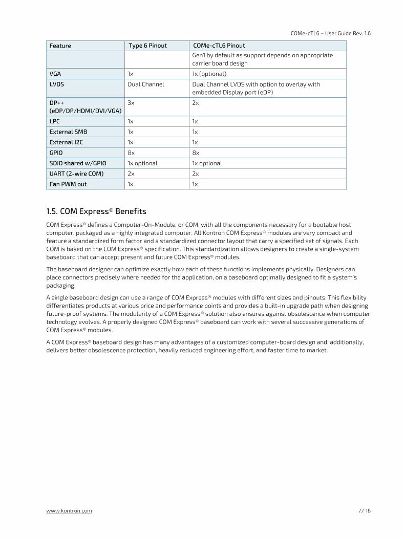
All Kontron COM Express® basic and compact modules contain two 220-pin connectors. Each connector has two rows called Row A & B on primary connector and Row C & D on secondary connector. COM Express® Computer-On-Modules feature the following maximum amount of interfaces according to the PICMG module pinout type:
Table 1: IOs of Type 6 and COMe-cTL6
Feature Type 6 Pinout COMe-cTL6 Pinout
HD Audio 1x 1x
Gb Ethernet 1x 1x
Serial ATA 4x 2x
PCI Express x 1 8x 5x PCIe 3.0 (On request: 6x without Ethernet, up to 8x without Ethernet & SATA)
PCI Express x16 (PEG) 1x 4x PCIe 3.0 on PEG Lanes #0-3
USB 4x USB 3.0 (incl. USB 2.0) + 4x USB 2.0
4x USB 3.1 Gen 2 (Incl. USB 2.0) + 4x USB 2.0 Corresponding USB ports are configured to USB 3.1
COMe-cTL6 – User Guide Rev. 1.6
www.kontron.com // 16
Feature Type 6 Pinout COMe-cTL6 Pinout
Gen1 by default as support depends on appropriate carrier board design
VGA 1x 1x (optional)
LVDS Dual Channel Dual Channel LVDS with option to overlay with embedded Display port (eDP)
DP++ (eDP/DP/HDMI/DVI/VGA)
3x 2x
LPC 1x 1x
External SMB 1x 1x
External I2C 1x 1x
GPIO 8x 8x
SDIO shared w/GPIO 1x optional 1x optional
UART (2-wire COM) 2x 2x
Fan PWM out 1x 1x
1.5. COM Express® Benefits
COM Express® defines a Computer-On-Module, or COM, with all the components necessary for a bootable host computer, packaged as a highly integrated computer. All Kontron COM Express® modules are very compact and feature a standardized form factor and a standardized connector layout that carry a specified set of signals. Each COM is based on the COM Express® specification. This standardization allows designers to create a single-system baseboard that can accept present and future COM Express® modules.
The baseboard designer can optimize exactly how each of these functions implements physically. Designers can place connectors precisely where needed for the application, on a baseboard optimally designed to fit a system’s packaging.
A single baseboard design can use a range of COM Express® modules with different sizes and pinouts. This flexibility differentiates products at various price and performance points and provides a built-in upgrade path when designing future-proof systems. The modularity of a COM Express® solution also ensures against obsolescence when computer technology evolves. A properly designed COM Express® baseboard can work with several successive generations of COM Express® modules.
A COM Express® baseboard design has many advantages of a customized computer-board design and, additionally, delivers better obsolescence protection, heavily reduced engineering effort, and faster time to market.

COMe-cTL6 – User Guide Rev. 1.6
www.kontron.com // 17
2/ Product Specification
2.1. Module Variants
The COMe-cTL6 is available in different processor and temperature variants to cover demands in performance, price and power.
2.1.1. Commercial Grade Modules (0°C to +60°C)
Commercial Grade Modules (0°C to +60°C) are available as a standard product number.
Table 2: Commercial Grade Modules (0°C to +60°C)
Product Number Product Name Description
36030-1610-18-7 COMe-cTL6 i7-1185G7E 16 GB/1 TB
COM Express® compact pin-out type 6 Computer-on-Module with Intel® Core™ i7-1185G7E, 4x 1.8 GHz, 16 GB memory down, DDR4 SO DIMM Socket, 1024 GB NVMe
36030-1600-18-7 COMe-cTL6 i7-1185G7E 16 GB COM Express® compact pin-out type 6 Computer-on-Module with Intel® Core™ i7-1185G7E, 4x 1.8 GHz, 16 GB memory down, DDR4 SO DIMM Socket
36030-0000-18-7 COMe-cTL6 i7-1185G7E COM Express® compact pin-out type 6 Computer-on-Module with Intel® Core™ i7-1185G7E, 4x 1.8 GHz, DDR4 SO DIMM Socket
36030-8000-15-5 COMe-cTL6 i5-1145G7E 8 GB COM Express® compact pin-out type 6 Computer-on-Module with Intel® Core™ i5-1145G7E, 4x 1.5 GHz, 8 GB memory down, DDR4 SO DIMM Socket
36030-0000-15-5 COMe-cTL6 i5-1145G7E COM Express® compact pin-out type 6 Computer-on-Module with Intel® Core™ i5-1145G7E, 4x 1.5 GHz, DDR4 SO DIMM Socket
36030-0000-22-3 COMe-cTL6 i3-1115G4E COM Express® compact pin-out type 6 Computer-on-Module with Intel® Core™ i3-1115G4E, 2x 2.2 GHz, DDR4 SO DIMM Socket
36030-0000-18-2 COMe-cTL6 6305E COM Express® compact pin-out type 6 Computer-on-Module with Intel® Celeron® 6305E, 2x 1.8 GHz, DDR4 SO DIMM Socket
2.1.2. Extended Temperature Grade Modules (E1, -25°C to 75°C)
Extended Temperature grade modules (E1, -25°C to 75°C) are available as a standard product number, on request. For further information, contact your local Kontron sales representative or Kontron Inside Sales.
COMe-cTL6 – User Guide Rev. 1.6
www.kontron.com // 18
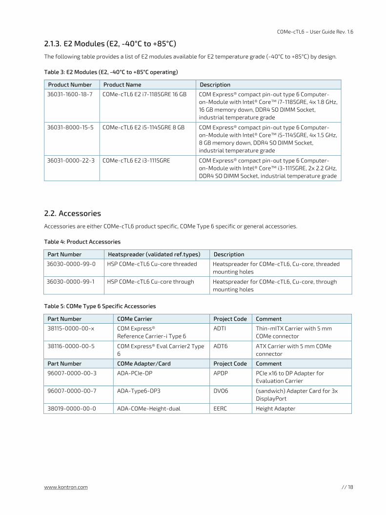
2.1.3. E2 Modules (E2, -40°C to +85°C)
The following table provides a list of E2 modules available for E2 temperature grade (-40°C to +85°C) by design.
Table 3: E2 Modules (E2, -40°C to +85°C operating)
Product Number Product Name Description
36031-1600-18-7 COMe-cTL6 E2 i7-1185GRE 16 GB COM Express® compact pin-out type 6 Computer-on-Module with Intel® Core™ i7-1185GRE, 4x 1.8 GHz, 16 GB memory down, DDR4 SO DIMM Socket, industrial temperature grade
36031-8000-15-5 COMe-cTL6 E2 i5-1145GRE 8 GB COM Express® compact pin-out type 6 Computer-on-Module with Intel® Core™ i5-1145GRE, 4x 1.5 GHz, 8 GB memory down, DDR4 SO DIMM Socket, industrial temperature grade
36031-0000-22-3 COMe-cTL6 E2 i3-1115GRE COM Express® compact pin-out type 6 Computer-on-Module with Intel® Core™ i3-1115GRE, 2x 2.2 GHz, DDR4 SO DIMM Socket, industrial temperature grade
2.2. Accessories
Accessories are either COMe-cTL6 product specific, COMe Type 6 specific or general accessories.
Table 4: Product Accessories
Part Number Heatspreader (validated ref.types) Description
36030-0000-99-0 HSP COMe-cTL6 Cu-core threaded Heatspreader for COMe-cTL6, Cu-core, threaded mounting holes
36030-0000-99-1 HSP COMe-cTL6 Cu-core through Heatspreader for COMe-cTL6, Cu-core, through mounting holes
Table 5: COMe Type 6 Specific Accessories
Part Number COMe Carrier Project Code Comment
38115-0000-00-x COM Express® Reference Carrier-i Type 6
ADTI Thin-mITX Carrier with 5 mm COMe connector
38116-0000-00-5 COM Express® Eval Carrier2 Type 6
ADT6 ATX Carrier with 5 mm COMe connector
Part Number COMe Adapter/Card Project Code Comment
96007-0000-00-3 ADA-PCIe-DP APDP PCIe x16 to DP Adapter for Evaluation Carrier
96007-0000-00-7 ADA-Type6-DP3 DVO6 (sandwich) Adapter Card for 3x DisplayPort
38019-0000-00-0 ADA-COMe-Height-dual EERC Height Adapter

COMe-cTL6 – User Guide Rev. 1.6
www.kontron.com // 19
Table 6: General Accessories
Part Number Cooling Solutions Comments
36099-0000-99-4 COMe Active Uni Cooler2 (w/o HSP)
COM Express® Universal Active Cooler for Heatspreader Mounting (95x95x14.3) - 90° turnable
36099-0000-99-5 COMe Passive Uni Cooler2 (w/o HSP)
COM Express® Universal Passive Cooler for Heatspreader Mounting (95x95x14.3) - 90° turnable
Part Number Mounting Comments
38017-0000-00-5 COMe Mount KIT 5 mm 1 set Mount. Kit for 1 module + screws for 5 mm conn.
38017-0100-00-5 COMe Mount KIT 5 mm 100 sets Mount. Kit for 100 module + screws for 5 mm conn.
38017-0000-00-0 COMe Mount KIT 8 mm 1 set Mount. Kit for 1 module + screws for 8 mm conn.
38017-0100-00-0 COMe Mount KIT 8 mm 100 sets Mount. Kit for 100 module + screws for 8 mm conn.
Part Number Display Adapter Comment
96006-0000-00-8 ADA-DP-LVDS DP to LVDS adapter
96082-0000-00-0 KAB-ADAPT-DP-DVI DP to DVI adapter cable
96083-0000-00-0 KAB-ADAPT-DP-VGA DP to VGA adapter cable
96084-0000-00-0 KAB-ADAPT-DP-HDMI DP to HDMI adapter cable
Part Number Cables Comment
96079-0000-00-0 KAB-HSP 200mm Cable adapter to connect FAN to module (COMe basic/compact)
96079-0000-00-2 KAB-HSP 40 mm Cable adapter to connect FAN to module (COMe basic/compact)
Table 7: Memory
Part Number Memory Description
97020-3232-CTL6 DDR4-3200 SODIMM 32GB_CTL6 Memory for Computer-on-Module COMe-cTL6; min. specification: DDR4-3200, 32 GB, 260P, 1600 MHz, PC4-3200 SODIMM; validated for: COMe-cTL6
97020-1632-CTL6 DDR4-3200 SODIMM 16GB_CTL6 Memory for Computer-on-Module COMe-cTL6; min. specification: DDR4-3200, 16 GB, 260P, 1600 MHz, PC4-3200 SODIMM; validated for: COMe-cTL6
97020-0832-CTL6 DDR4-3200 SODIMM 8GB_CTL6 Memory for Computer-on-Module COMe-cTL6; min. specification: DDR4-3200, 8 GB, 260P, 1600 MHz, PC4-3200 SODIMM; validated for: COMe-cTL6
97020-0432-CTL6 DDR4-3200 SODIMM 4GB_CTL6 Memory for Computer-on-Module COMe-cTL6; min. specification: DDR4-3200, 4 GB, 260P, 1600 MHz, PC4-3200 SODIMM; validated for: COMe-cTL6
97021-3232-CTL6 DDR4-3200 SODIMM 32GB E2_CTL6 Memory for Computer-on-Module COMe-cTL6; min. specification: DDR4-3200, 32 GB, 260P, 1600 MHz, PC4-3200 SODIMM; validated for: COMe-cTL6 E2
97021-1632-CTL6 DDR4-3200 SODIMM 16GB E2_CTL6 Memory for Computer-on-Module COMe-cTL6; min. specification: DDR4-3200, 16 GB, 260P, 1600 MHz, PC4-3200 SODIMM; validated for: COMe-cTL6 E2
97021-0832-CTL6 DDR4-3200 SODIMM 8GB E2_CTL6 Memory for Computer-on-Module COMe-cTL6; min. specification: DDR4-3200, 8 GB, 260P, 1600 MHz, PC4-3200 SODIMM; validated for: COMe-cTL6 E2
97021-0432-CTL6 DDR4-3200 SODIMM 4GB E2_CTL6 Memory for Computer-on-Module COMe-cTL6; min. specification: DDR4-3200, 4 GB, 260P, 1600 MHz, PC4-3200 SODIMM; validated for: COMe-cTL6 E2
COMe-cTL6 – User Guide Rev. 1.6
www.kontron.com // 20
2.3. Functional Specification
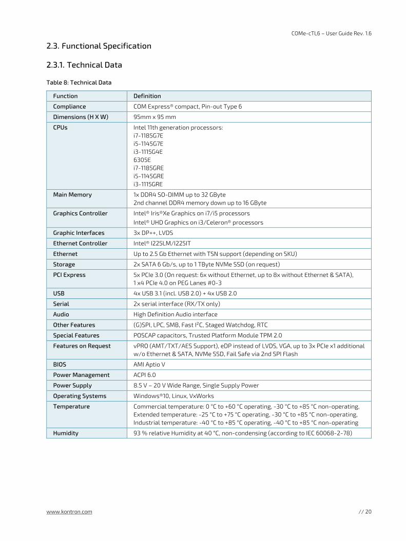
2.3.1. Technical Data
Table 8: Technical Data
Function Definition
Compliance COM Express® compact, Pin-out Type 6
Dimensions (H X W) 95mm x 95 mm
CPUs Intel 11th generation processors: i7-1185G7E i5-1145G7E i3-1115G4E 6305E i7-1185GRE i5-1145GRE i3-1115GRE
Main Memory 1x DDR4 SO-DIMM up to 32 GByte 2nd channel DDR4 memory down up to 16 GByte
Graphics Controller Intel® Iris®Xe Graphics on i7/i5 processors Intel® UHD Graphics on i3/Celeron® processors
Graphic Interfaces 3x DP++, LVDS
Ethernet Controller Intel® I225LM/I225IT
Ethernet Up to 2.5 Gb Ethernet with TSN support (depending on SKU)
Storage 2x SATA 6 Gb/s, up to 1 TByte NVMe SSD (on request)
PCI Express 5x PCIe 3.0 (On request: 6x without Ethernet, up to 8x without Ethernet & SATA), 1 x4 PCIe 4.0 on PEG Lanes #0-3
USB 4x USB 3.1 (incl. USB 2.0) + 4x USB 2.0
Serial 2x serial interface (RX/TX only)
Audio High Definition Audio interface
Other Features (G)SPI, LPC, SMB, Fast I²C, Staged Watchdog, RTC
Special Features POSCAP capacitors, Trusted Platform Module TPM 2.0
Features on Request vPRO (AMT/TXT/AES Support), eDP instead of LVDS, VGA, up to 3x PCIe x1 additional w/o Ethernet & SATA, NVMe SSD, Fail Safe via 2nd SPI Flash
BIOS AMI Aptio V
Power Management ACPI 6.0
Power Supply 8.5 V – 20 V Wide Range, Single Supply Power
Operating Systems Windows®10, Linux, VxWorks
Temperature Commercial temperature: 0 °C to +60 °C operating, -30 °C to +85 °C non-operating, Extended temperature: -25 °C to +75 °C operating, -30 °C to +85 °C non-operating, Industrial temperature: -40 °C to +85 °C operating, -40 °C to +85 °C non-operating
Humidity 93 % relative Humidity at 40 °C, non-condensing (according to IEC 60068-2-78)
COMe-cTL6 – User Guide Rev. 1.6
www.kontron.com // 21
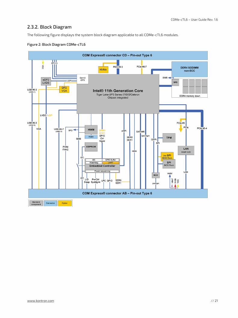
2.3.2. Block Diagram
The following figure displays the system block diagram applicable to all COMe-cTL6 modules.
Figure 2: Block Diagram COMe-cTL6

COMe-cTL6 – User Guide Rev. 1.6
www.kontron.com // 22
2.3.3. Front View
Figure 3: Front View COMe-cTL6
1. SoC Processor 2. DDR4 memory down 3. 1xS0-DIMM DDR4 slot 4. Embedded Controller 5. NVME Mass Storage 6. Ethernet MAC/PHY Intel I255 7. eDP-to-LVDS bridge 8. Temp. Sensor #1 CPU
5
6
7
3
4
2
8
1
COMe-cTL6 – User Guide Rev. 1.6
www.kontron.com // 23
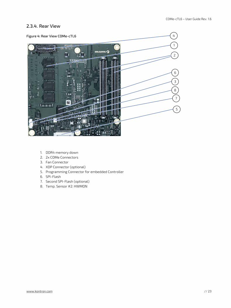
2.3.4. Rear View
Figure 4: Rear View COMe-cTL6
1. DDR4 memory down 2. 2x COMe Connectors 3. Fan Connector 4. XDP Connector (optional) 5. Programming Connector for embedded Controller 6. SPI-Flash 7. Second SPI-Flash (optional) 8. Temp. Sensor #2: HWMON
2
6
8
3
7
5
1
4

COMe-cTL6 – User Guide Rev. 1.6
www.kontron.com // 24
2.3.5. Processors
11th Gen Intel® Core™ processors come in two classes – embedded and industrial – to provide a foundation for durable, long-life equipment. Temperature ranges of the industrial SoC are from -40°C to 100°C and Embedded SoCs have a temperature range from 0° to 100°C.
Figure 5: Block Diagram 11th Generation processor (Source: Intel)
Key Benefits are:
Third-generation, Intel® 10 nm microarchitecture, up to four processing cores, up to 96 graphics execution units
Supports DDR4 and LPDDR4x, with optional In-Band ECC
Configurable 12/15/28 watt thermal design points, in a single SKU
Up to 96 graphics execution units, four independent display pipes, capable of up to two channels of 8K60 or four channels of 4K60
Up to two VD Boxes process up to 40 1080p 30 fps video streams
Integrated MACs to support one 1 GbE port, plus one 2.5 GbE port with Time-Sensitive Networking (on selected SKUs)
Gigabit (1.73 Gbps) Wi-Fi, Bluetooth 5
Discrete 2.5GbE MAC/PHY LAN, Intel® Ethernet Controller I225LM/IT (code name Foxville)
Four Thunderbolt™ 4/USB4 ports
Four PCIe 4.0 lanes and 12 PCIe 3.0 lanes
COMe-cTL6 – User Guide Rev. 1.6
www.kontron.com // 25
Table 9: 11th Generation Intel® Processor Specifications
Processor i7-1185G7E i5-1145G7E i3-1115G4E 6305E i7-1185GRE i5-1145GRE i3-1115GRE
Classification Embedded[1] (0°C to 100°C) Industrial[2] (-40°C to 100°C)
# of Cores/ Threads 4/8 4/8 2/4 2 4/8 4/8 2/4
Processor Base/Turbo Frequency
1.8/4.4 GHz
1.5/4.1 GHz 2.2/3.9 GHz
1.8/- GHz 1.8/4.4 GHz
1.5/4.1 GHz 2.2/3.9 GHz
Thermal Design Power (TDP)
15 W 15 W 15 W 15 W 15 W 15 W 15 W
Cache 12 MByte 8 MByte 6 MByte 4 MByte 12 MByte 8 MByte 6 MByte
IBECC [3] no no no no yes yes yes
TCC/TSN no no no no yes yes yes
Graphics/Media/ Display
Intel® Iris® Xe Graphics 96 EU 4x4k or 2x8k Displays 2 VDBOX
Intel® Iris® Xe Graphics 80 EU 4x4k or 2x8k Displays 2 VDBOX
Intel® UHD Graphics 48EU 4x4k or 1x8k Displays 1 VDBOX
Intel® UHD Graphics 48 EU 4x Displays
Intel® Iris® Xe Graphics 96 EU 4x4k or 2x8k Displays 2 VDBOX
Intel® Iris® Xe Graphics 80 EU 4x4k or 2x8k Displays 2 VDBOX
Intel® UHD Graphics 48 EU 4x4k or 1x8k Displays 1 VDBOX
Max Memory Size 64 GB 64 GB 64 GB 64 GB 64 GB 64 GB 64 GB
[1] within Tjunction limits the max temperature range during operation is +-70°C, starting from boot time temperature
[2] within Tjunction limits the max temperature range during operation is +-90°C, starting from boot time temperature
The behavior is described in Intel document #608377 as DTR = Dynamic Temperature Range. For more information, contact Kontron Support
[3] IBECC is disabled by default; if IBECC in combination with memory down and SODIMM memory is needed, please contact the technical support
2.3.6. System Memory
The system memory supports a dual-channel 64-bit DDR4-3200. ECC memory is not available. One DIMM per channel offer 48 GB total. Following setups are considerable:
Channel 1: One SO-DIMM DDR4, max 32 GB non-ECC Channel 2: Memory Down DDR4, max 16 GB non-ECC
Table 10: System Memory
Socket Dual-channel 64-bit DDR4-3200
Memory Type DDR4-3200 without ECC
Max Memory Module Size 32 GByte
Bandwidth up to 25.6 GB/s
COMe-cTL6 – User Guide Rev. 1.6
www.kontron.com // 26
In general, memory modules have a much lower longevity than embedded motherboards, and therefore the EOL of the memory modules may occur several times during the lifetime of the module. Kontron guarantees to maintain memory modules by replacing EOL memory module with another qualified similar module.
As a minimum, it is recommended to use Kontron memory modules for prototype system(s) in order to prove the stability of the system and as a reference. In order to qualify the RAM it is recommend to configure three systems running a RAM Stress Test program in a heat chamber at 60°C, for a minimum of 24 hours.
For a list of Kontron memory modules, see Table 7.
2.3.7. Graphics
2.3.7.1. Display Resolution
The following table lists the maximum display resolutions at a set frequency and bit per pixel (bpp) for the supported display interfaces.
Table 11: Display Resolution
Display Interfaces Maximum Resolution (Pixel)
eDP 4096x2304@60 Hz
DP 7680x4320@60 Hz
HDMI 1.4 4096x2304@60 Hz
4K Support Yes, at 60 Hz
8K Support Yes, at 60 Hz
2.3.7.2. Graphics Interfaces
The processor graphics is based on Generation 12 graphics core Architecture. Gen 12 architecture supports up to 96 Execution Units (EUs) depending on the processor SKU.
Table 12: Display Interfaces
TGL Port COMe Port
DDIA LVDS eDP (option)
TCP0 DDI1 (DP++)
TCP1 DDI2 (DP++)
TCP2 DDI3 (DP++)
TCP3 DP2VGA Converter (optional)
Table 13: DDI1 Interfaces
COMe Connector PCH Description
DDI1_PAIR[0:3] TCP0_TX[0:3]
DDI1_PAIR[4:6] -
DDI1_CTRLCLK_AUX+ TCP0_AUX_P (CPU) DDP1_CTRLCLK
DDI1_CTRLDATA_AUX- TCP0_AUX_N (CPU) DDP1_CTRLDATA

COMe-cTL6 – User Guide Rev. 1.6
www.kontron.com // 27
COMe Connector PCH Description
DDI1_DDC_AUX_SEL - Connected to DP++-AUX Conversion
DDI1_HPD DDSP_HPD1
Table 14: DDI2 Interfaces
COMe Connector PCH Description
DDI2_PAIR[0:3] TCP1_TX[0:3]
DDI2_CTRLCLK_AUX+ TCP1_AUX_P/DDP2_CTRLCLK
DDI2_CTRLDATA_AUX- TCP1_AUX_N/DDP2_CTRLDATA
DDI2_DDC_AUX_SEL - Connected to DP++ AUX Conversion
DDI2_HPD DDSP_HPD2
Table 15: DDI3 Interfaces
COMe Connector PCH Description
DDI3_PAIR[0:3] TCP2_TX[0:3]
DDI3_CTRLCLK_AUX+ TCP2_AUX_P/DDP3_CTRLCLK
DDI3_CTRLDATA_AUX- TCP2_AUX_N/DDP3_CTRLDATA
DDI3_DDC_AUX_SEL - Connected to DP++ AUX Conversion
DDI3_HPD DDSP_HPD3
2.3.7.3. LVDS (with option to overlay eDP)
LVDS is implemented by NXP PTN3460 eDP to LVDS bridge chip:
Input: Two eDP Lanes from CPU. Output: up to Dual channel LVDS interface (up to 1 pixel per clock) with up to 24 bit color.
The LVDS channel and control signals are pin shared with eDP signals.
Table 16: LVDS Bridge
COMe Connector PTN3460 Description
LVDS_A* LVS*O Pin order according to COMe spec
LVDS_B* LVS*E
LVDS_I2C_CK - connected to I2C_INT module bus
LVDS_I2C_DAT - connected to I2C_INT module bus
LVDS_VDD_EN PVCCEN
LVDS_BKLT_EN BKLTEN
LVDS_BKLT_CTRL - connected to EDP_BKLTCTL at SoC
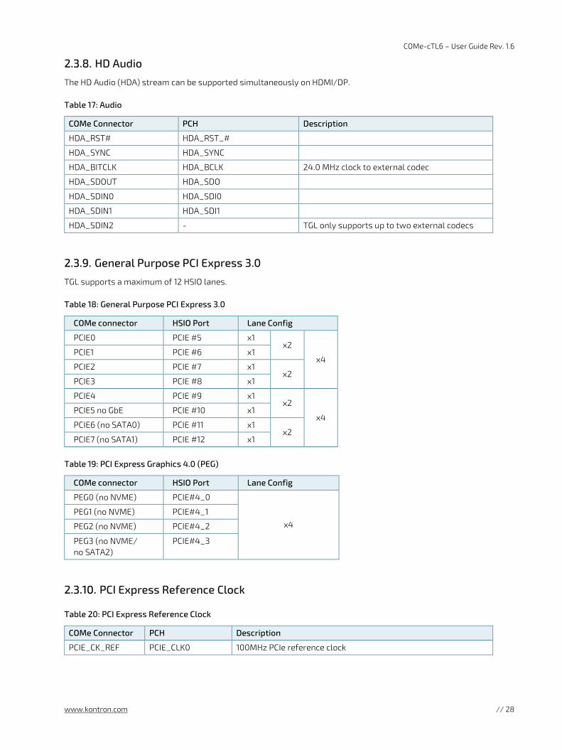
COMe-cTL6 – User Guide Rev. 1.6
www.kontron.com // 28
2.3.8. HD Audio
The HD Audio (HDA) stream can be supported simultaneously on HDMI/DP.
Table 17: Audio
COMe Connector PCH Description
HDA_RST# HDA_RST_#
HDA_SYNC HDA_SYNC
HDA_BITCLK HDA_BCLK 24.0 MHz clock to external codec
HDA_SDOUT HDA_SDO
HDA_SDIN0 HDA_SDI0
HDA_SDIN1 HDA_SDI1
HDA_SDIN2 - TGL only supports up to two external codecs
2.3.9. General Purpose PCI Express 3.0
TGL supports a maximum of 12 HSIO lanes.
Table 18: General Purpose PCI Express 3.0
COMe connector HSIO Port Lane Config
PCIE0 PCIE #5 x1 x2
x4 PCIE1 PCIE #6 x1
PCIE2 PCIE #7 x1 x2
PCIE3 PCIE #8 x1
PCIE4 PCIE #9 x1 x2
x4 PCIE5 no GbE PCIE #10 x1
PCIE6 (no SATA0) PCIE #11 x1 x2
PCIE7 (no SATA1) PCIE #12 x1
Table 19: PCI Express Graphics 4.0 (PEG)
COMe connector HSIO Port Lane Config
PEG0 (no NVME) PCIE#4_0
x4
PEG1 (no NVME) PCIE#4_1
PEG2 (no NVME) PCIE#4_2
PEG3 (no NVME/ no SATA2)
PCIE#4_3
2.3.10. PCI Express Reference Clock
Table 20: PCI Express Reference Clock
COMe Connector PCH Description
PCIE_CK_REF PCIE_CLK0 100MHz PCIe reference clock
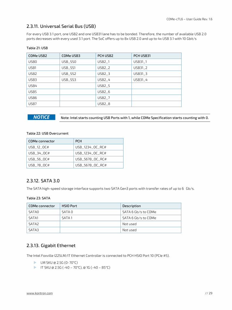
COMe-cTL6 – User Guide Rev. 1.6
www.kontron.com // 29
2.3.11. Universal Serial Bus (USB)
For every USB 3.1 port, one USB2 and one USB31 lane has to be bonded. Therefore, the number of available USB 2.0 ports decreases with every used 3.1 port. The SoC offers up to 8x USB 2.0 and up to 4x USB 3.1 with 10 Gbit/s
Table 21: USB
COMe USB2 COMe USB3 PCH USB2 PCH USB31
USB0 USB_SS0 USB2_1 USB31_1
USB1 USB_SS1 USB2_2 USB31_2
USB2 USB_SS2 USB2_3 USB31_3
USB3 USB_SS3 USB2_4 USB31_4
USB4 USB2_5
USB5 USB2_6
USB6 USB2_7
USB7 USB2_8
Note: Intel starts counting USB Ports with 1, while COMe Specification starts counting with 0.
Table 22: USB Overcurrent
COMe connector PCH
USB_12_OC# USB_1234_OC_RC#
USB_34_OC# USB_1234_OC_RC#
USB_56_OC# USB_5678_OC_RC#
USB_78_OC# USB_5678_OC_RC#
2.3.12. SATA 3.0
The SATA high-speed storage interface supports two SATA Gen3 ports with transfer rates of up to 6 Gb/s.
Table 23: SATA
COMe connector HSIO Port Description
SATA0 SATA 0 SATA 6 Gb/s to COMe
SATA1 SATA 1 SATA 6 Gb/s to COMe
SATA2 Not used
SATA3 Not used
2.3.13. Gigabit Ethernet
The Intel Foxville I225LM/IT Ethernet Controller is connected to PCH HSIO Port 10 (PCIe #5).
LM SKU @ 2.5G (0-70°C) IT SKU @ 2.5G (-40 – 70°C), @ 1G (-40 – 85°C)

COMe-cTL6 – User Guide Rev. 1.6
www.kontron.com // 30
Table 24: Ethernet
Ethernet 10 Base-T, 100 Base-TX and 1000 Base-T
Ethernet Controller Intel® I225LM/IT Ethernet Controller
2.3.14. Storage
2.3.14.1. NVMe – Mass Strorage
As option, a M.2 1620 (BGA) NVMe SDD can be connected instead of PEG lanes 0-3. Power Rails are SSD vendor dependent.
2.3.14.2. Embedded EEPROM (EeeP)
The content of the Embedded EEPROM, formerly known as JIDA EEPROM, is defined in the PICMG COM Express companion document specification. The module EEPROM device (24C32) is attached to the I2C bus (I2C_EXT) from the CPLD, that’s available on the baseboard, too. By default, the EEPROM is available on address 0Ah.
2.3.15. COMe Features
The following table lists the supported COM Express® features.
Table 25: COM Features
SPI Boot from an external SPI
LPC Supported
UART 2x UART (RX/TX)
LID Signals Supported
Sleep Signals Supported
Audio HD Audio for external HDA codecs
SMBus Supported
2.3.16. Kontron Features
The following table lists the supported Kontron specific product features.
Table 26: Kontron Features
External I2C Bus Fast I2C, 100 KHz - 400 kHz, MultiMaster capable
Embedded API KEAPI3
Custom BIOS Settings/Flash Backup
Supported
Watchdog Support Dual staged
External SIO Supported on the base board
GPIO 8x GPIO shared with SDIO, configurable in BIOS setup options
Rapid Shutdown Not supported

COMe-cTL6 – User Guide Rev. 1.6
www.kontron.com // 31
2.3.17. LPC
The Module LPC and eSPI interfaces share connector pins. As TGL MCP does not provide an LPC interface any more, CTL6 onboard CPLD will implement an eSPI-to-LPC bridge. The CTL6 supports just LPC at the COMe connector.
Table 27: LPC
COMe Connector Pin LPC Mode Connection
B[4:7] LPC_AD[0:3]
B3 LPC_FRAME#
B10 LPC_CLK
B[8:9] LPC_DRQ[0:1]
A50 LPC_SERIRQ
2.3.18. I2C Bus
Two I2C Buses are generated by the on-board FPGA internal kCPLD block. or more details For more details, see kCPLD specification 2.8.
2.3.18.1. External user-accessible I2C (I2C_EXT)
Devices connected to the external I2C:
A0h: Module Embedded EEPROM (JIDA EEPROM) AEh: carrier EEPROM (optional) 64h: external RTC (optional)
This I2C bus is available at COMe pins I2C_CLK (Pin B33), I2C_DAT (Pin B34).
Table 28: External user-accessible I2C (I2C_EXT)
8bit 7bit Description
A0h 50h Module Embedded EEPROM (JIDA EEPROM)
AEh 57h Carrier EEPROM (optional)
64h 32h External RTC (optional)
2.3.18.2. Internal I2C (I2C_INT)
The second I2C bus is used for configuration of on-board devices only.
Table 29: Internal I2C (I2C_INT)
8bit 7bit Description
C0h 60h LVDS bridge
A0h 50h external LVDS EEPROM
40h 20h IMVP9 VR (optional)
An external LVDS EEPROM can be connected to the LVDS-I2C-bus at pins A83 and A84. Don´t connect other devices to this bus.

COMe-cTL6 – User Guide Rev. 1.6
www.kontron.com // 32
2.3.19. SMBus
SMBbus on COMe connector (B13, B14) is shared with onboard devices, so special care must be taken while selecting addresses for carrier devices. SMBus clock and data lines are divided into multiple voltage domains by discrete FET switches.
Table 30: SMBus
8bit 7bit Description
A0h 50h DDR4 Channel A SPD EEPROM (SO-DIMM)
A4h 52h DDR4 Channel B SPD EEPROM (memory down)
30h 18h DDR4 Channel A optional temperature sensor (SO-DIMM)
5Ch 2Eh Hardware monitor
ACh 06h HW-Mon reserved
Another FET switch disconnects the module SMB from the carrier during boot up. After BIOS has finished configuration of the on-board devices, it asserts EN_SMB_EXT# to close the switch.
Table 31: SMB Alert
Signal PCH Pin Description
SMB_ALERT# GP_C02/SMB_ALERT_#
SMB Alert# connects directly to COMe.
2.3.20. Wake Signals
Table 32: Wake Signals
COMe Signal PCH Pin Description
WAKE0# WAKE# passed through CPLD
WAKE1# GPP_E16/ISH_GP7 passed through CPLD
2.3.21. Suspend Control
Table 33: Suspend Control
COMe Signal PCH
SUS_STAT# From CPLD
SUS_S3# GPD4/PM_SLP_S3#
SUS_S4# GPD5/PM_SLP_S4#
SUS_S5# GPD10/PM_SLP_S5#
2.3.22. Power Good (PWR_OK)
Low level will prevent the module to enter S0 state. A falling edge during S0 will cause a direct switch to S5 (power failure).
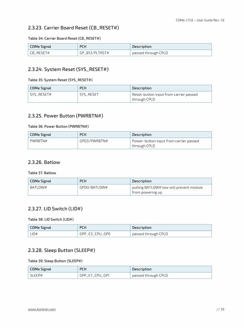
COMe-cTL6 – User Guide Rev. 1.6
www.kontron.com // 33
2.3.23. Carrier Board Reset (CB_RESET#)
Table 34: Carrier Board Reset (CB_RESET#)
COMe Signal PCH Description
CB_RESET# GP_B13/PLTRST# passed through CPLD
2.3.24. System Reset (SYS_RESET#)
Table 35: System Reset (SYS_RESET#)
COMe Signal PCH Description
SYS_RESET# SYS_RESET Reset-button input from carrier passed through CPLD
2.3.25. Power Button (PWRBTN#)
Table 36: Power Button (PWRBTN#)
COMe Signal PCH Description
PWRBTN# GPD3/PWRBTN# Power-button input from carrier passed through CPLD
2.3.26. Batlow
Table 37: Batlow
COMe Signal PCH Description
BATLOW# GPD0/BATLOW# pulling BATLOW# low will prevent module from powering up.
2.3.27. LID Switch (LID#)
Table 38: LID Switch (LID#)
COMe Signal PCH Description
LID# GPP_E3_CPU_GP0 passed through CPLD
2.3.28. Sleep Button (SLEEP#)
Table 39: Sleep Button (SLEEP#)
COMe Signal PCH Description
SLEEP# GPP_E7_CPU_GP1 passed through CPLD
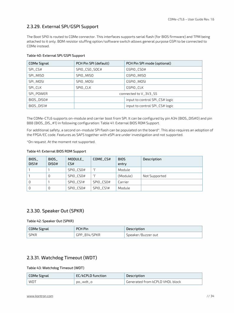
COMe-cTL6 – User Guide Rev. 1.6
www.kontron.com // 34
2.3.29. External SPI/GSPI Support
The Boot SPI0 is routed to COMe connector. This interfaces supports serial flash (for BIOS firmware) and TPM being attached to it only. BOM resistor stuffing option/software switch allows general purpose GSPI to be connected to COMe instead.
Table 40: External SPI/GSPI Support
COMe Signal PCH Pin SPI (default) PCH Pin SPI mode (optional)
SPI_CS# SPI0_CS0_SOC# GSPI0_CS0#
SPI_MISO SPI0_MISO GSPI0_MISO
SPI_MOSI SPI0_MOSI GSPI0_MOSI
SPI_CLK SPI0_CLK GSPI0_CLK
SPI_POWER connected to V_3V3_S5
BIOS_DIS0# input to control SPI_CS# logic
BIOS_DIS1# input to control SPI_CS# logic
The COMe-CTL6 supports on-module and carrier boot from SPI. It can be configured by pin A34 (BIOS_DIS#0) and pin B88 (BIOS_DIS_#1) in following configuration: Table 41: External BIOS ROM Support.
For additional safety, a second on-module SPI flash can be populated on the board*. This also requires an adoption of the FPGA/EC code. Features as SAFS together with eSPI are under investigation and not supported.
*On request. At the moment not supported.
Table 41: External BIOS ROM Support
BIOS_ DIS1#
BIOS_ DIS0#
MODULE_ CS#
COME_CS# BIOS entry
Description
1 1 SPI0_CS0# ‘1’ Module
1 0 SPI0_CS0# ‘1’ (Module) Not Supported
0 1 SPI0_CS1# SPI0_CS0# Carrier
0 0 SPI0_CS0# SPI0_CS1# Module
2.3.30. Speaker Out (SPKR)
Table 42: Speaker Out (SPKR)
COMe Signal PCH Pin Description
SPKR GPP_B14/SPKR Speaker/Buzzer out
2.3.31. Watchdog Timeout (WDT)
Table 43: Watchdog Timeout (WDT)
COMe Signal EC/kCPLD function Description
WDT po_wdt_o Generated from kCPLD VHDL block

COMe-cTL6 – User Guide Rev. 1.6
www.kontron.com // 35
2.3.32. General Purpose IOs
In addition to COMe spec kCPLD implementation supports input and output functionality on all COMe GPIx and GPOx signals. Configuration has to be done by the OS driver.
Table 44: General Purpose IOs
COMe Signal EC/kCPLD function (option GPIO)
GPI0 pio_gpio[0]
GPI1 pio_gpio[1]
GPI2 pio_gpio[2]
GPI3 pio_gpio[3]
GPO0 pio_gpio[4]
GPO1 pio_gpio[5]
GPO2 pio_gpio[6]
GPO3 pio_gpio[7]
2.3.33. External Fan support
Table 45: External Fan Control
COMe Signal HWM Pin Description
FAN_PWMOUT FANCTL2 Gated by CPLD signal FAN_PWM_ENABLE to disconnect in states other than S0
FAN_TACHIN FANIN2
2.3.34. UART Serial Ports
By default, both serial ports are provided by the SoC. Optionally it is possible that SER0/1 are generated by the CPLD. However, this requires a hardware modification (changed resistor placement and a more powerful CPLD), which leads to a chargeable customer variant.
Table 46: UART Serial Ports
COMe Signal
SER0_TX
SER0_RX
SER1_TX
SER1_RX
2.3.35. Hardware Monitor (HWM)
Hardware is Nuvoton NCT7802Y, SM-Bus Address is 5C.

COMe-cTL6 – User Guide Rev. 1.6
www.kontron.com // 36
2.3.36. Trusted Platform Module (TPM)
Chip is Infineon SLB9670XQ2.0 (TPM 2.0), connected to FSPI (dedicated SPI interface from PCH for TPM and BIOS EEPROM).
2.3.37. Embedded Controller (CPLD)
Altera MAX10 10M02SCU169I7 (FPGA MAX 10 UBGA169 Industrial range) or pin compatible part can be assembled. EC implements Kontron COMe CPLD Specification 2.8 VHDL block (KCPLD).
KCPLD is connected to TGL eSPI interface to provide several features to the module/carrier:
LPC Bus
I2C
UART (optional)
GPIO
Watchdog
Moreover, the EC is responsible for platform power sequence and reset control for all components.
2.3.38. SPI BIOS Memory
A 64 MB SPI Flash supporting SFDP (Serial Flash Discovery Parameter) is attached to PCH FSPI interface (dedicated SPI for TPM and flash memory). Flash Descriptor, BIOS, converged security engine as well as platform data are stored within the SPI flash.

COMe-cTL6 – User Guide Rev. 1.6
www.kontron.com // 37
2.4. Electrical Specification
The module powers on by connecting to a carrier board via the COMe interface connector. Before connecting the module to the carrier board, ensure that the carrier board is switch off and disconnected from the main power supply at the time of connection. Failure to disconnect the main power supply from the carrier board could result in personal injury and damage to the module and/or carrier board. The COMe interface connector pins on the module limits the amount of power received.
The module powers on by connecting to the carrier board using the Interface connector. Before connecting the module’s interface connector to the carrier board’s corresponding connector, ensure that the carrier board is switch off and disconnected from the main power supply. Failure to disconnect the main power supply could result in personal injury and damage to the module and/or carrier board.
Observe that only trained personnel aware of the associated dangers connect the module,
within an access controlled ESD-safe workplace.
2.4.1. Power Supply Specifications
The COMe-cTL6 supports operation in both single supply power supply mode and ATX power supply mode.
Industrial temperature grade modules are validated for 12 V power supply only.
Commercial temperature grade modules support the wide range 8.5 V to 20 V power supply.
5 V Standby voltage is not mandatory for operation.
The following table lists the power supply specifications.
Supply Voltage Range (VCC) 8.5 V to 20 V
Supply Voltage (VCC) 12 V
Standby Voltage 5 V ± 5%
RTC 2.5 V to 3.3 V
Only connect to an external power supply delivering the specified input rating and
complying with the requirements of Safety Extra Low Voltage (SELV) and Limited Power Source (LPS) of UL/IEC 60950-1 or (PS2) of UL/IEC 62368-1.
To protect external power lines of peripheral devices, make sure that the wires have the
right diameter to withstand the maximum available current and the enclosure of the peripheral device fulfils the fire-protection requirements of IEC/EN 62368-1.
If any of the supply voltages drops below the allowed operating level longer than the specified hold-up time, all the supply voltages should be shut down and left OFF for a time long enough to allow the internal board voltages to discharge sufficiently.
If the OFF time is not observed, parts of the board or attached peripherals may work incorrectly or even suffer a reduction of MTBF. The minimum OFF time depends on the implemented PSU model and other electrical factors and must be measured individually for each case.
COMe-cTL6 – User Guide Rev. 1.6
www.kontron.com // 38
2.4.1.1. Power Supply Rise Time
The input voltage rise time is 0.1 ms to 20 ms from input voltage ≤10% to nominal VCC. To comply with the ATX specification there must be a smooth and continuous ramp of each DC input voltage from 10% to 90% of the DC input voltage final set point.
2.4.1.2. Power Supply Voltage Ripple
The maximum power supply voltage ripple is 100 mV peak-to-peak at 0 MHz – 20 MHz.
2.4.2. Power Management
Power management options are available within the BIOS setup.
ACPI Settings ACPI 6.0
Miscellaneous Power Management
Supported in BIOS setup menu
2.4.2.1. Suspend States
If power is removed, 5 V can be applied to the V_5V_STBY pins to support the ACPI suspend-states:
Suspend to RAM (S3)
Suspend-to-Disk (S4)
Soft-off state (S5)
The Wake-Up event (S0) requires VCC power, as the board is running.
The type of sleep states that the system supports can be determined by the setup option ‘Advanced -> ACPI Settings ->Low Power S0 Idle Capability’. If this option is disabled, then the system will support S3 and S4 states as usual. When enabling this option then the system will apply S0iX state instead of S3 and S4. This technology achieves energy savings through processor measures. The amount of savings is determined by the whole system layout and might differ on differently equipped systems. Note that when using S0iX the power button will not work as expected under Windows 10. It will not trigger any action as set in Windows system manager while the system is running. It will however be fully functional for switching the system on.
2.4.3. Power Supply Control Settings
The power Supply control settings are set in the BIOS and enable the module to shut down, rest and wake from standby properly.
The following table lists the implemented power supply control settings.
Table 47: Power Supply Control Settings
COMe Signal Pin Description
Power Button (PWRBTN#)
Pin B12
To start the module using the power button, the PWRBTN# signal must be at least 50 ms (50 ms ≤ t < 4 s, typical 400 ms) at low level (Power Button Event). Pressing the power button for at least four seconds turns off power to the module (Power Button Override).
Power Good (PWR_OK)
Pin B24
PWR_OK is internally pulled up to 3.3 V and must be at the high level to power on the module. This can be driven low to hold the module from powering up as long as needed. The carrier needs to release the signal when ready.

COMe-cTL6 – User Guide Rev. 1.6
www.kontron.com // 39
COMe Signal Pin Description
Low level prevents the module from entering the S0 state. A falling edge during S0 will cause a direct switch to S5 (Power Failure).
Reset Button (SYS_RESET#)
Pin B49
When the SYS_RESET# pin is detected active (falling edge triggered), it allows the processor to perform a “graceful” reset, by waiting up to 25 ms for the SMBus to go idle before forcing a reset, even though activity is still occurring. Once the reset is asserted, it remains asserted for 5 ms to 6 ms regardless of whether the SYS_RESET# input remains asserted or not.
SM-Bus Alert (SMB_ALERT#)
Pin B15
With an external battery manager present and SMB_ALERT #connected, the module always powers on even if the BIOS switch “After Power Fail” is set to “Stay Off”.
2.4.4. Power Supply Modes
Setting the power supply controls enables the COMe-cTL6 to operating in either ATX power mode or in single power supply mode.
2.4.4.1. ATX Mode
To start the module in ATX mode, connect VCC and 5V Standby from a ATX PSU. As soon as the standby rail ramped up the PCH enters S5 state and starts the transition to S0. SUS_S3# (usually connected to PSU PS_ON#) turns on the main power rail (VCC). As soon as the PSU indicates that the power supply is stable (PWR_OK high) the PCH continues transition to S0. The input voltage must always be higher than 5V standby (VCC>5VSB) for modules supporting a wide input voltage range down to 8.5V.
The input voltage must always be higher than 5 V standby (VCC>5VSB) for modules supporting a wide input voltage range down to 8.5 V.
Table 48: ATX mode settings
State PWRBTN# PWR_OK V5_StdBy PS_ON# VCC
G3 x x 0V x 0 V
S5 high low 5V high 0 V
S5 → S0 PWRBTN Event low → high 5V high → low 0 V→ VCC
S0 high high 5V low VCC
x – Signals are not relevant for the specific power state. It makes no difference if the signal is connected or open.
COMe-cTL6 – User Guide Rev. 1.6
www.kontron.com // 40
2.4.5. Single Supply Mode
To start the module in single power supply mode, connect VCC power and open PWR_OK at the high level. VCC can be 8.5 V to 20 V. To power on the module from S5 state, press the power button or reconnect VCC.
Suspend/Standby states are not supported in single power supply mode.
Table 49: Single Supply Mode Settings
State PWRBTN# PWR_OK V5_StdBy VCC
G3 x/0 V x/0 V x/0 V 0 V
G3 → S0 high open/high open connecting VCC
S5 high open/high open VCC
S5 → S0 PWRBTN Event open/high open reconnecting VCC
x – Signals are not relevant for the specific power state. It makes no difference if the signal is connected or open.
All ground pins must be connected to the carrier board’s ground plane.
If any of the supply voltages drops below the allowed operating level longer than the specified hold-up time, all the supply voltages should be shut down and left OFF for a time long enough to allow the internal board voltages to discharge sufficiently. If the OFF time is not observed, parts of the board or attached peripherals may work incorrectly or even suffer a reduction of MTBF. The minimum OFF time depends on the implemented PSU model and other electrical factors and needs to be measured individually for each case.

COMe-cTL6 – User Guide Rev. 1.6
www.kontron.com // 41
2.5. Thermal Management
2.5.1. Heatspreader and Active or Passive Cooling Solutions
A heatspreader plate assembly is available from Kontron for the COMe-cTL6. The heatspreader plate assembly is NOT a heat sink. The heatspreader works as a COM Express® standard thermal interface to be use with a heat sink or external cooling devices.
External cooling must be provided to maintain the heatspreader plate at proper operating temperatures. Under worst-case conditions, the cooling mechanism must maintain an ambient air and heatspreader plate temperature on any spot of the heatspreader's surface according to the module specifications:
60°C for commercial temperature grade modules
75°C for extended temperature grade modules (E1)
85°C for industrial temperature grade modules by design (E2)
2.5.2. Active or Passive Cooling Solutions
Both active and passive thermal management approaches can be used with heatspreader plates. The optimum cooling solution varies, depending on the COM Express® application and environmental conditions. Active or passive cooling solutions provided from Kontron for the COMe-cTL6 are usually designed to cover the power and thermal dissipation for a commercial temperature range used in housing with proper airflow.
.
2.5.3. Operating with Kontron Heatspreader Plate (HSP) Assembly
The operating temperature defines two requirements:
Maximum ambient temperature with ambient being the air surrounding the module
Maximum measurable temperature on any spot on the heatspreader's surface
The heatspreader is tested for the following temperature specifications.
Table 50: Heatspreader Test Temperature Specifications
Temperature Specification Validation Requirements
Commercial Grade at 60°C HSP temperature the CPU @ 100% load needs to run at nominal frequency
Extended Grade (E1) at 75°C HSP temperature the CPU @ 75% load is allowed to start speedstepping for thermal protection
Industrial Grade by design (E2) at 85°C HSP temperature the CPU @ 50% load is allowed to start throttling for thermal protection
2.5.4. Operating without Kontron Heatspreader Plate (HSP) Assembly
The operating temperature is the maximum measurable temperature on any spot on the module's surface.

COMe-cTL6 – User Guide Rev. 1.6
www.kontron.com // 42
2.5.5. Temperature Sensors
There are some temperature sensors available:
temperature sensor in HW-Monitor
temperature sensor in CPU, can be read out from HW-monitor via Platform Environment Control Interface (PECI)
temperature sensor in NVMe (can be read out from OS)
optional temperature sensor in SO-DIMM depends on type
Figure 6: Temperature Sensor #1 Location: CPU
1. Temp. Sensor #1 :CPU
Figure 7: Temperature Sensor #2 Location: HW-Monitor
2. Temp. Sensor #2: HWMON
1
2
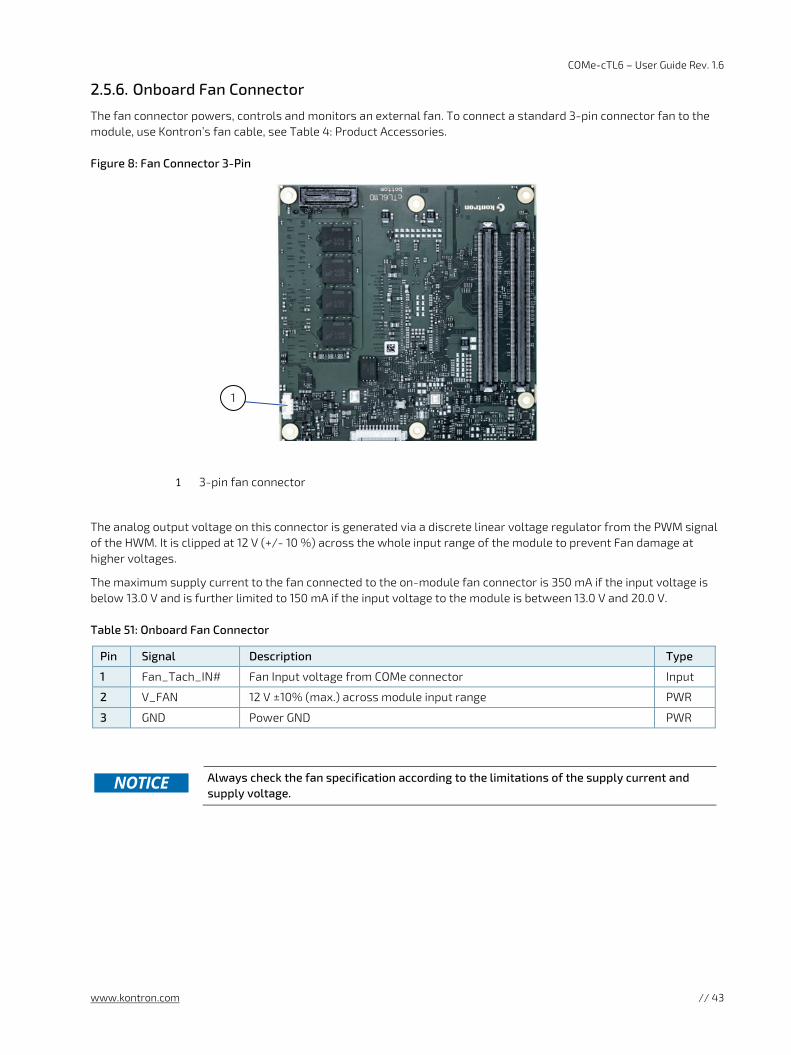
COMe-cTL6 – User Guide Rev. 1.6
www.kontron.com // 43
2.5.6. Onboard Fan Connector
The fan connector powers, controls and monitors an external fan. To connect a standard 3-pin connector fan to the module, use Kontron’s fan cable, see Table 4: Product Accessories.
Figure 8: Fan Connector 3-Pin
1 3-pin fan connector
The analog output voltage on this connector is generated via a discrete linear voltage regulator from the PWM signal of the HWM. It is clipped at 12 V (+/- 10 %) across the whole input range of the module to prevent Fan damage at higher voltages.
The maximum supply current to the fan connected to the on-module fan connector is 350 mA if the input voltage is below 13.0 V and is further limited to 150 mA if the input voltage to the module is between 13.0 V and 20.0 V.
Table 51: Onboard Fan Connector
Pin Signal Description Type
1 Fan_Tach_IN# Fan Input voltage from COMe connector Input
2 V_FAN 12 V ±10% (max.) across module input range PWR
3 GND Power GND PWR
Always check the fan specification according to the limitations of the supply current and
supply voltage.
1

COMe-cTL6 – User Guide Rev. 1.6
www.kontron.com // 44
2.6. Environmental Specification
2.7. Compliance
The COMe-cTL6 complies with the following standards. If modified, the prerequisites for specific approvals may no longer apply. For more information, contact Kontron Support.
Table 52: Standards Compliance
Standard Definition
Operating Temperature
0°C to 60°C (for COMe-cTL6 variants) -40°C to 85°C (by design for COMe-cTL6 E2 variants) (PCB and components should selected and designed accordingly)
Storage Temperature
-30°C to 85°C (for COMe- cTL6 (E1) variants) -40°C to 85°C (for COMe- cTL6 E2 variants)
Humidity 93% relative Humidity at 40°C, non-condensing (acc. to IEC 60068-2-78)
Emission (EMC) EN55032: 2015 Electromagnetic compatibility of multimedia equipment- Emission Requirements
Immunity (EMI) EN 61000-6-2: 2005: Electromagnetic compatibility (EMC) Part 6-2: Generic standards - Immunity standard for industrial environments
Safety (Europe)
EN 62368-1:2014 Audio/video, information and communication technology equipment - Part 1: Safety requirements
Saftey (USA/ Canada)
UL 62368-1/CSA 62368-1 (Component Recognition) Recognized by Underwriters Laboratories Inc. Representative samples of this component have been evaluated by UL and meet applicable UL requirements. UL listings: AZOT2.E147705 AZOT8.E147705
Shock IEC/EN 60068-2-27 Non-operating shock – (half-sinusoidal, 11 ms, 15 g)
Vibration IEC/EN 60068-2-6 Non-operating vibration – (sinusoidal, 10 Hz – 4000 Hz, +/- 0.15 mm, 2 g)
RoHS II Directive 2011/65/EU Restriction of the use of certain hazardous substances in electrical and electronic equipment

COMe-cTL6 – User Guide Rev. 1.6
www.kontron.com // 45
2.7.1. MTBF
The following MTBF (Mean Time Before Failure) values were calculated using a combination of manufacturer’s test data, if the data was available, and the Telcordia (Bellcore) issue 2 calculation for the remaining parts.
The Telcordia calculation used is “Method 1 Case 3” in a ground benign, controlled environment (GB,GC). This particular method takes into account varying temperature and stress data and the system is assumed to have not been burned in.
Table 53: MTBF
MTBF
System MTBF (hours) = 521724h @ 40°C for COMe-cTL6 6305E Reliability report article number 36030-0000-18-2
System MTBF (hours) = 504068h @ 40°C for COMe-cTL6 E2 i7-1185GRE Reliability report article number: 36031-1600-18-7
The MTBF estimates values assume no fan, but a passive heat sinking arrangement. Estimated RTC battery life (as opposed to battery failures) is not accounted for and needs to be considered separately. Battery life depends on both temperature and operating conditions. When the Kontron unit has external power, the only battery drain is from leakage paths.
The figures below shows the MTBF de-rating for the different temperature range in an office or telecommunications environment. Other environmental stresses (such as extreme altitude, vibration, salt-water exposure) lower MTBF values.
Figure 9: MTBF De-rating Values (Reliability report article number 36030-0000-18-2)

COMe-cTL6 – User Guide Rev. 1.6
www.kontron.com // 46
Figure 10: MTBF De-rating Values (Reliability report article number 36031-1600-18-7)

COMe-cTL6 – User Guide Rev. 1.6
www.kontron.com // 47
2.8. Mechanical Specification
2.8.1. Dimensions
The dimensions of the module are:
95.0 mm x 95.0 mm (3.75” x 3.75“)
Figure 11: Module Dimensions
All dimensions shown in mm.

COMe-cTL6 – User Guide Rev. 1.6
www.kontron.com // 48
2.8.2. Height
The height of the module depends on the height of the implemented cooling solution. The height of the cooling solution is not specified in the COM Express® specification.
The COM Express® specification defines a module height of approximately 13 mm from module PCB bottom to heatspreader top.
Figure 12: Module Height
1 Heatspreader
2 Heatspreaader standoff(s)
3 Module PCB
4 Carrier Board PCB
5 Connector standoff(s) 5 or 8 mm
6 13 mm +/- 0.65 mm
2.8.3. Heatspreader Dimension
The following figure shows the heatspreader’s dimensions and location on the module.
Figure 13: Heatspreader Location and Dimensions
All dimensions shown in mm.
2
3
4 5
6
1

COMe-cTL6 – User Guide Rev. 1.6
www.kontron.com // 49
3/ Features and Interfaces
3.1. Fast I2C
Fast I2C supports transfer between components on the same board. The COMe-cTL6 features an onboard I2C controller connected to the LPC Bus.
The I2C controller supports:
Multimaster transfers
Clock stretching
Collision detection
Interruption on completion of an operation
3.2. GPIO
Eight GPIO pins are available, with four pins for the in-direction (pin A54 for GPI0, pin A63 for GPI1, pin A67 for GPI2 and pin A85 for GPI3) and four pins for the out-direction (pin A93 for GPO0, pin B54 for GPO1, pin B57 for GPO2 and pin B63 for GPO3). The type of termination resistor on the module sets the direction of the GPIO where GPIs are terminated with pull-up resistors and GPOs are terminated with pull-down resistors.
Due to, the fact that both the pull-up and pull-down termination resistors are weak, it is possible to override the termination resistors using external pull-ups, pull-downs or IOs. Overriding the termination resistors means that the eight GPIO pins can be considered as bi-directional since there are no restrictions whether you use the available GPIO pins in the in-direction or out-direction.
3.3. Kontron Security Solution
Kontron Security Solution is a combined hardware and software solution that includes an embedded hardware security module and a software framework to provide full protection for your application.
The COMe-cTL6 includes an integrated security module connected to USB2 port 9, supporting the following features:
Copy protection
IP protection
License model enforcement
If required customers can customize the solution to meet specific needs. For more information, contact Kontron Support.
3.4. LPC
The Low Pin Count (LPC) interface signals are connected to the LPC bus bridge located in the CPU or chipset. The LPC low speed interface can be used for peripheral circuits such as an external Super I/O controller that typically combines legacy-device support into a single IC. The implementation of this subsystem complies with the COM Express® specification. The COM Express® Design Guide maintained by PICMG provides implementation information or refer to the official PICMG documentation for more information.
The LPC bus does not support DMA (Direct Memory Access). When more than one device is used on LPC, a zero delay clock buffer is required. This leads to limitations for ISA bus and SIO (standard I/O(s) like floppy or LPT interfaces) implementations.
All Kontron COM Express® Computer-On-Modules imply BIOS support for the following external baseboard LPC Super I/O controller features for the Winbond/Nuvoton NCT7802Y.

COMe-cTL6 – User Guide Rev. 1.6
www.kontron.com // 50
Table 54: Supported BIOS Features
Winbond/Nuvoton 3.3V 83627DHG-P AMI EFI APTIO V
PS/2 Not supported
COM1/COM2 Supported
LPT Not supported
HWM Not supported
Floppy Not supported
GPIO Not supported
Features marked as not supported do not exclude OS support (e.g., HWM is accessible via SMB). If any other LPC Super I/O additional BIOS implementations are necessary then contact Kontron Support.
3.5. Real Time Clock (RTC)
The RTC keeps track of the current time accurately. The RTC’s low power consumption means that the RTC can be powered from an alternate source of power enabling the RTC to continue to keep time while the primary source of power is off or unavailable.
The RTC battery voltage range is 2.5 V to 3.3 V. A typical RTC voltage is 3 V with a current of >6 μA. If the module is powered by the mains supply the RTC voltage is generated by on-module regulators to reduce the RTC current draw.
3.6. Serial Peripheral Interface (SPI)
The Serial Peripheral Interface Bus (SPI bus) is a synchronous serial data link standard. Devices communicate in master/slave mode, where the master device initiates the data frame. Multiple slave devices are allowed with individual slave select (chip select) lines. SPI is sometimes called a four-wire serial bus, contrasting with three, two and one-wire serial buses.
The SPI interface can only be used with a SPI flash device to boot from the external BIOS on the carrier board.
3.6.1. SPI Boot
The COMe-cTL6 supports boot from an external SPI Flash. Pin A34 (BIOS_DIS0#) and pin B88 (BIOS_DIS1#) configure the SPI Flash as follows:
Table 55: SPI Boot Pin Configuration
Configuration BIOS_DIS0# BIOS_DIS1# Function
1 open open Boot on module BIOS
2 GND open Not supported
3 open GND Boot on baseboard SPI
4 GND GND Not supported

COMe-cTL6 – User Guide Rev. 1.6
www.kontron.com // 51
BIOS does not support being split between two chips. Booting takes place either from the module SPI or from the baseboard SPI.
Table 56: Supported SPI Boot Flash Types for 8-SOIC Package
Size Manufacturer Part Number Device ID
8 MB Macronix MX25L6406E 20h
3.7. Trusted Platform Module (TPM 2.0)
A Trusted Platform Module (TPM) stores RSA encryption keys specific to the host system for hardware authentication. The term TPM refers to the set of specifications applicable to TPM chips. The LPC bus connects the TPM chip to the CPU.
Each TPM chip contains an RSA key pair called the Endorsement Key (EK). The pair is maintained inside the chip and cannot be accessed by software. The Storage Root Key (SRK) is created when a user or administrator takes ownership of the system. This key pair is generated by the TPM based on the Endorsement Key and an owner-specified password.
A second key, called an Attestation Identity Key (AIK) protects the device against unauthorized firmware and software modification by hashing critical sections of firmware and software before they are executed. When the system attempts to connect to the network, the hashes are sent to a server that verifies that they match the expected values. If any of the hashed components have been modified since the last start, the match fails, and the system cannot gain entry to the network.
3.8. UART
The UART implements an interface for serial communications and supports up to two serial RX/TX ports defined in the COM Express® specification on pins A98 (SERO_TX) /A99 (SERO_RX) for UART0 and pins A101 (SER1_TX)/A102 (SER1_RX) for UART1. The UART controller is fully 16550A compatible.
Features of the UART are:
On-Chip bit rate (baud rate) generator
No handshake lines
Interrupt function to the host
FIFO buffer for incoming and outgoing data
3.9. Watchdog Timer (WTD) Dual Stage
A watchdog timer or (computer operating properly (COP) timer) is a computer hardware or software timer. If there is a fault condition in the main program, the watchdog triggers a system reset or other corrective actions. The intention is to bring the system back from the non-responsive state to normal operation.
Possible fault conditions are a hang or neglecting to service the watchdog regularly. Such as writing a “service pulse” to it, also referred to as “kicking the dog”, “petting the dog”, “feeding the watchdog” or “triggering the watchdog”).
The COMe-cTL6 offers a watchdog that works with two stages that can be programmed independently and used stage by stage.
COMe-cTL6 – User Guide Rev. 1.6
www.kontron.com // 52
Table 57: Dual Stage Watchdog Timer- Time-out Events
Status Events Definition
0000b No action The stage is off and will be skipped.
0001b Reset A reset restarts the module and starts a new POST and operating system.
0010b NMI A non-maskable interrupt (NMI) is a computer processor interrupt that cannot be ignored by standard interrupt masking techniques in the system. It is used typically to signal attention for non-recoverable hardware errors.
0011b SMI A system management interrupt (SMI) makes the processor entering the system management mode (SMM). As such, specific BIOS code handles the interrupt. The current BIOS handler for the watchdog SMI currently does nothing. For special requirements, contact Kontron Support.
0100b SCI A system control interrupt (SCI) is a OS-visible interrupt to be handled by the OS using AML code.
0101b Delay -> No action*
Might be necessary when an operating system must be started and the time for the first trigger pulse must be extended. Only available in the first stage.
1000b WDT Only This setting triggers the WDT pin on the baseboard connector (COM Express® pin B27) only.
1001b Reset + WDT
1010b NMI + WDT
1011b SMI + WDT
1100b SCI + WDT
1101b DELAY + WDT -> No action*
3.9.1. WDT Signal
Watchdog time-out event (pin B27) on COM Express® connector offers a signal that can be asserted when a watchdog timer has not been triggered with a set time. The WDT signal is configurable to any of the two stages. After reset, the signal is automatically deasserted. If deassertion is necessary during runtime, ask Kontron Support for further help.

COMe-cTL6 – User Guide Rev. 1.6
www.kontron.com // 53
4/ System Resources
4.1. I2C Bus
The following table specifies the devices connected to the accessible I2C bus including the I2C address. The I2C bus is available at the COM Express® connector pin B33, I2C_CK and pin B34, I2C_DAT.
Table 58: I2C Bus Port Address
8-bit Address 7-bit Address Used For Available
A0h 50h Module embedded EEPROM (Eeep) YES
AEh 57h Carrier board EEPROM Option
64h 32h External RTC Option
4.2. System Management (SM) Bus
The 8-bit SMBus address uses the LSB (bit 0) for the direction of the device.
Bit0 = 0 defines the write address
Bit0 = 1 defines the read address
The following table specifies the 8-bit and 7-bit SMBus write address for all devices.
Table 59: SMBus Address
8-bit Address 7-bit Address Device Description
A0h 50h DDR4 Channel A SPD EEPROM (SO-DIMM)
A4h 52h DDR4 Channel B SPD EEPROM (memory down)
30h 18h DDR4 Channel A optional temperature sensor (SO-DIMM)
5Ch 2Eh Hardware monitor
ACh 06h HW-Mon reserved
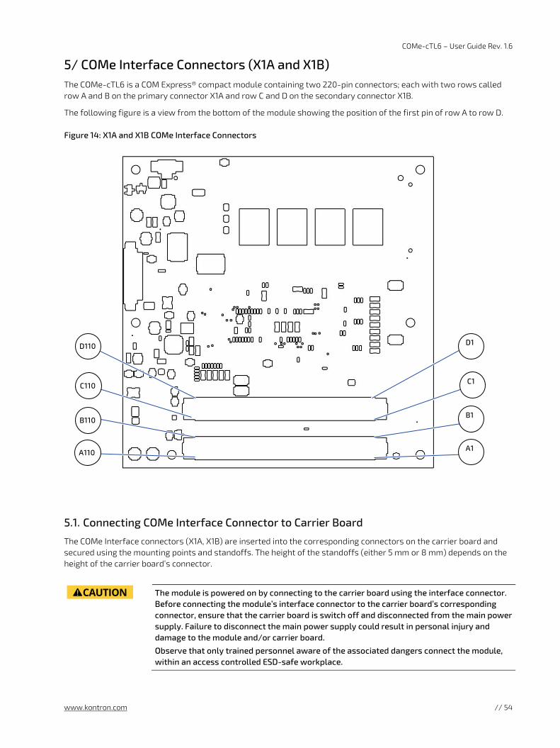
COMe-cTL6 – User Guide Rev. 1.6
www.kontron.com // 54
5/ COMe Interface Connectors (X1A and X1B) The COMe-cTL6 is a COM Express® compact module containing two 220-pin connectors; each with two rows called row A and B on the primary connector X1A and row C and D on the secondary connector X1B.
The following figure is a view from the bottom of the module showing the position of the first pin of row A to row D.
Figure 14: X1A and X1B COMe Interface Connectors
5.1. Connecting COMe Interface Connector to Carrier Board
The COMe Interface connectors (X1A, X1B) are inserted into the corresponding connectors on the carrier board and secured using the mounting points and standoffs. The height of the standoffs (either 5 mm or 8 mm) depends on the height of the carrier board’s connector.
The module is powered on by connecting to the carrier board using the interface connector. Before connecting the module’s interface connector to the carrier board’s corresponding connector, ensure that the carrier board is switch off and disconnected from the main power supply. Failure to disconnect the main power supply could result in personal injury and damage to the module and/or carrier board.
Observe that only trained personnel aware of the associated dangers connect the module, within an access controlled ESD-safe workplace.
D1
A1
C1
B1
B110
C110
A110
D110

COMe-cTL6 – User Guide Rev. 1.6
www.kontron.com // 55
To protect external power lines of peripheral devices, make sure that: the wires have the right diameter to withstand the maximum available current. The enclosure of the peripheral device fulfills the fire-protection requirements of IEC/EN 62368
5.2. X1A and X1B Signals
For a description of the terms used in the X1A and X1B pin assignment tables, see Table 60: General Signal Description or Appendix A, List of Acronyms. If a more detailed pin assignment description is required, refer to the PICMG specification COMe Rev 3.0 Type 6 standard.
The information provided under type, module terminations and comments is complimentary to the COM.0 Rev 3.0 Type 6 standard. For more information, contact Kontron Support.
Table 60: General Signal Description
Type Description Type Description
NC Not Connected (on this product) O-1,8 1.8 V Output
I/O-3,3 Bi-directional 3.3 V I/O-Signal O-3,3 3.3 V Output
I/O-5T Bi-dir. 3.3 V I/O (5 V Tolerance) O-5 5 V Output
I/O-5 Bi-directional 5V I/O-Signal DP-I/O Differential Pair Input/Output
I-3,3 3.3 V Input DP-I Differential Pair Input
I/OD Bi-directional Input/Output Open Drain
DP-O Differential Pair Output
I-5T 3.3 V Input (5 V tolerance) PU Pull-Up Resistor
OA Output Analog PWR Power Connection
OD Output Open Drain + and - Differential Pair
To protect external power lines of peripheral devices, make sure that: the wires have the right diameter to withstand the maximum available current.
The enclosure of the peripheral device fulfills the fire-protection requirements of IEC/EN60950.
5.3. X1A and X1B Pin Assignment
For more information regarding the pin assignment of connector X1A (Row A and Row B) and connector X1B (Row C and Row D), see the pin assignment tables:
1. Table 61: Connector X1A Row A Pin Assignment (A1- A110)
2. Table 62: Connector X1A Row B Pin Assignment (B1-B110)
3. Table 63: Connector X1B Row C Pin Assignment (C1-C110)
4. Table 64: Connector X1B Row D Pin Assignment (D1-D110)

COMe-cTL6 – User Guide Rev. 1.6
www.kontron.com // 56
5.3.1. Connector X1A Row A1 – A110
The following section describes the signals found on COM Express™ Type 6 connectors used for Kontron modules. The pinout of the modules complies with COM Express Type 6 Rev. 3.0. The table below describes the terminology used in this section. The PU/PD column indicates if a COM Express™ module pull-up or pull-down resistor has been used. If the field entry area in this column for the signal is empty, then no pull-up or pull-down resistor has been implemented by Kontron.
The “#” symbol at the end of the signal name indicates that the active or asserted state occurs when the signal is at a low voltage level. When “#” is not present, the signal is asserted when at a high voltage level.
The Signal Description tables list all internal pull-ups or pull-downs implemented by the chip vendors.
Table 61: Connector X1A Row A Pin Assignment (A1- A110)
Pin Signal Description Type Termination Comment
A1 GND Power Ground PWR GND --- ---
A2 GBE0_MDI3- Ethernet Media Dependent Interface 3 -
DP-I/O --- ---
A3 GBE0_MDI3+ Ethernet Media Dependent Interface 3 +
DP-I/O --- ---
A4 GBE0_LINK100# Ethernet Speed LED OD --- ---
A5 GBE0_LINK1000# Ethernet Speed LED OD --- ---
A6 GBE0_MDI2- Ethernet Media Dependent Interface 2 -
DP-I/O --- ---
A7 GBE0_MDI2+ Ethernet Media Dependent Interface 2 +
DP-I/O --- ---
A8 GBE0_LINK# LAN Link LED OD --- ---
A9 GBE0_MDI1- Ethernet Media Dependent Interface 1 -
DP-I/O --- ---
A10 GBE0_MDI1+ Ethernet Media Dependent Interface 1 +
DP-I/O --- ---
A11 GND Power Ground PWR GND --- ---
A12 GBE0_MDI0- Ethernet Media Dependent Interface 0 -
DP-I/O --- ---
A13 GBE0_MDI0+ Ethernet Media Dependent Interface 0 +
DP-I/O --- ---
A14 GBE0_CTREF Center Tab Reference Voltage O --- 100 nF capacitor to GND
A15 SUS_S3# Suspend To RAM (or deeper) Indicator
O-3.3 PD 100k ---
A16 SATA0_TX+ SATA Transmit Pair 0 + DP-O --- ---
A17 SATA0_TX- SATA Transmit Pair 0 - DP-O --- ---
A18 SUS_S4# Suspend To Disk (or deeper) Indicator
O-3.3 PD 100k ---
A19 SATA0_RX+ SATA Receive Pair 0 + DP-I --- ---

COMe-cTL6 – User Guide Rev. 1.6
www.kontron.com // 57
Pin Signal Description Type Termination Comment
A20 SATA0_RX- SATA Receive Pair 0 - DP-I --- ---
A21 GND Power Ground PWR GND --- ---
A22 SATA2_TX+ SATA Transmit Pair 2 + DP-O --- ---
A23 SATA2_TX- SATA Transmit Pair 2 - DP-O --- ---
A24 SUS_S5# Soft Off Indicator O-3.3 --- ---
A25 SATA2_RX+ SATA Receive Pair 2 + DP-I --- ---
A26 SATA2_RX- SATA Receive Pair 2 - DP-I --- ---
A27 BATLOW# Battery Low I-3.3 PU 10k 3.3V (S5)
assertion will prevent wake from S3-S5 state
A28 (S)ATA_ACT# Serial ATA activity LED OD-3.3 PU 10k 3.3V (S0)
can sink 15mA
A29 HDA_SYNC HD Audio Sync O-3.3 PD 100k ---
A30 HDA_RST# HD Audio Reset O-3.3 PD 100k ---
A31 GND Power Ground PWR GND --- ---
A32 HDA_CLK HD Audio Bit Clock Output O-3.3 PD 20k in PCH
---
A33 HDA_SDOUT HD Audio Serial Data Out O-3.3 PD 20k in PCH
---
A34 BIOS_DIS0#/ESPI_SAFS
BIOS Selection Strap 0 I-3.3 PU 10k 3.3V (S5)
---
A35 THRMTRIP# Thermal Trip O-3.3 PU 10k 3.3V (S0)
Thermal Trip Event, transition to S5 indicator
A36 USB6- USB 2.0 Data Pair Port 6 – DP-I/O PD 14.25k to 24.8k in PCH
---
A37 USB6+ USB 2.0 Data Pair Port 6 + DP-I/O PD 14.25k to 24.8k in PCH
---
A38 USB_6_7_OC# USB Overcurrent Indicator Port 6/7 I-3.3 PU 10k 3.3V (S5)
---
A39 USB4- USB 2.0 Data Pair Port 4 - DP-I/O PD 14.25k to 24.8k in PCH
---
A40 USB4+ USB 2.0 Data Pair Port 4 + DP-I/O PD 14.25k to 24.8k in PCH
---
A41 GND Power Ground PWR GND --- ---
A42 USB2- USB 2.0 Data Pair Port 2 – DP-I/O PD 14.25k to 24.8k in PCH
---
A43 USB2+ USB 2.0 Data Pair Port 2 + DP-I/O PD 14.25k to 24.8k in PCH
---
A44 USB_2_3_OC# USB Overcurrent Indicator Port 2/3 I-3.3 PU 10k 3.3V (S5)
---
A45 USB0– USB 2.0 Data Pair Port 0 – DP-I/O PD 14.25k to 24.8k in PCH
---
A46 USB0+ USB 2.0 Data Pair Port 0 + DP-I/O PD 14.25k to 24.8k in PCH
---
A47 VCC_RTC Real-Time Clock Circuit Power Input PWR 3V --- voltage range 2.5 to 3.3 V

COMe-cTL6 – User Guide Rev. 1.6
www.kontron.com // 58
Pin Signal Description Type Termination Comment
A48 RSVD Reserved for future use nc --- ---
A49 GBE0_SDP Gigabit Ethernet Controller 0 Software-Definable Pin
I/O-3.3 --- ---
A50 LPC_SERIRQ/ESPI_CS1#
Serial Interrupt Request/eSPI Master Chip Select 1
I/OD-3.3/O-1,8
PU 8k2 3.3V (S0)
---
A51 GND Power Ground PWR GND --- ---
A52 PCIE_TX5+ PCI Express Lane 5 Transmit + DP-O --- ---
A53 PCIE_TX5- PCI Express Lane 5 Transmit - DP-O --- ---
A54 GPI0 General Purpose Input 0 I-3.3 PU 100k 3.3V (S0)
---
A55 PCIE_TX4+ PCI Express Lane 4 Transmit + DP-O --- ---
A56 PCIE_TX4- PCI Express Lane 4 Transmit - DP-O --- ---
A57 GND Power Ground PWR GND --- ---
A58 PCIE_TX3+ PCI Express Lane 3 Transmit + DP-O --- ---
A59 PCIE_TX3- PCI Express Lane 3 Transmit - DP-O --- ---
A60 GND Power Ground PWR GND --- ---
A61 PCIE_TX2+ PCI Express Lane 2 Transmit + DP-O --- ---
A62 PCIE_TX2- PCI Express Lane 2 Transmit - DP-O --- ---
A63 GPI1 General Purpose Input 1 I-3.3 PU 100k 3.3V (S0)
---
A64 PCIE_TX1+ PCI Express Lane 1 Transmit + DP-O --- ---
A65 PCIE_TX1- PCI Express Lane 1 Transmit - DP-O --- ---
A66 GND Power Ground PWR GND --- ---
A67 GPI2 General Purpose Input 2 I-3.3 PU 100k 3.3V (S0)
---
A68 PCIE_TX0+ PCI Express Lane 0 Transmit + DP-O --- ---
A69 PCIE_TX0- PCI Express Lane 0 Transmit - DP-O --- ---
A70 GND Power Ground PWR GND --- ---
A71 LVDS_A0+ LVDS Channel A DAT0+/EDP Lane 2 Transmit +
DP-O --- ---
A72 LVDS_A0- LVDS Channel A DAT0-/EDP Lane 2 Transmit -
DP-O --- ---
A73 LVDS_A1+ LVDS Channel A DAT1+/EDP Lane 1 Transmit +
DP-O --- ---
A74 LVDS_A1- LVDS Channel A DAT1-/EDP Lane 1 Transmit -
DP-O --- ---
A75 LVDS_A2+ LVDS Channel A DAT2+/EDP Lane 0 Transmit +
DP-O --- ---
A76 LVDS_A2- LVDS Channel A DAT2-/EDP Lane 0 Transmit -
DP-O --- ---
A77 LVDS_VDD_EN LVDS/EDP Panel Power Control O-3.3 PD 100k ---
A78 LVDS_A3+ LVDS Channel A DAT3+ DP-O --- ---
A79 LVDS_A3- LVDS Channel A DAT3- DP-O --- ---
A80 GND Power Ground PWR GND --- ---

COMe-cTL6 – User Guide Rev. 1.6
www.kontron.com // 59
Pin Signal Description Type Termination Comment
A81 LVDS_A_CK+ LVDS Channel A Clock+/EDP Lane 3 Transmit +
DP-O --- Clock: 20-80MHz
A82 LVDS_A_CK- LVDS Channel A Clock-/EDP Lane 3 Transmit -
DP-O --- Clock: 20-80MHz
A83 LVDS_I2C_CK LVDS I2C Clock (DDC)/EDP AUX + I/O-3.3 PU 2k2 3.3V (S0)
---
A84 LVDS_I2C_DAT LVDS I2C Data (DDC)/EDP AUX - I/O-3.3 PU 2k2 3.3V (S0)
---
A85 GPI3 General Purpose Input 3 I-3.3 PU 100k 3.3V (S0)
---
A86 RSVD Reserved for future use nc --- ---
A87 eDP_HPD EDP Hot Plug Detect I-3.3 PD 400k LVDS/100k EDP
---
A88 PCIE_CLK_REF+ Reference PCI Express Clock + DP-O --- 100MHz
A89 PCIE_CLK_REF- Reference PCI Express Clock - DP-O --- 100MHz
A90 GND Power Ground PWR GND --- ---
A91 SPI_POWER 3.3V Power Output Pin for external SPI flash
O-3.3 --- 100mA (max.)
A92 SPI_MISO SPI Master IN Slave OUT I-3.3 PU 20k +/-30% in PCH (S5)
All SPI signals are tri-stated until reset is deasserted
A93 GPO0 General Purpose Output 0 O-3.3 PD 100k ---
A94 SPI_CLK SPI Clock O-3.3 PU 20k +/-30% in PCH (S5)
All SPI signals are tri-stated with 20k ohm CPU internal weak pull-up until reset is deasserted
A95 SPI_MOSI SPI Master Out Slave In O-3.3 PU 20k +/-30% in PCH (S5)
All SPI signals are tri-stated with 20k ohm CPU internal weak pull-up until reset is deasserted
A96 TPM_PP TPM Physical Presence I-3.3 PD 10k TPM does not use this functionality
A97 TYPE10# Indicates TYPE10# to carrier board nc --- ---
A98 SER0_TX Serial Port 0 TXD O-3.3 --- 20V protection circuit implemented on module, PD on carrier board needed for proper operation

COMe-cTL6 – User Guide Rev. 1.6
www.kontron.com // 60
Pin Signal Description Type Termination Comment
A99 SER0_RX Serial Port 0 RXD I-5T PU 10k 3.3V (S0)
20V protection circuit implemented on module
A100 GND Power Ground PWR GND --- ---
A101 SER1_TX Serial Port 1 TXD O-3.3 --- 20V protection circuit implemented on module, PD on carrier board needed for proper operation
A102 SER1_RX Serial Port 1 RXD I-5T PU 10k 3.3V (S0)
20V protection circuit implemented on module
A103 LID# LID Switch Input I-3.3 PU 47k 3.3V (S5)
20V protection circuit implemented on module
A104 VCC_12V Main Input Voltage (4.75-20V) PWR 4.75- 20V
--- ---
A105 VCC_12V Main Input Voltage (4.75-20V) PWR 4.75-20V
--- ---
A106 VCC_12V Main Input Voltage (4.75-20V) PWR 4.75- 20V
--- ---
A107 VCC_12V Main Input Voltage (4.75-20V) PWR 4.75- 20V
--- ---
A108 VCC_12V Main Input Voltage (4.75-20V) PWR 4.75- 20V
--- ---
A109 VCC_12V Main Input Voltage (4.75-20V) PWR 4.75- 20V
--- ---
A110 GND Power Ground PWR GND --- --- + and - Differential pair differentiator

COMe-cTL6 – User Guide Rev. 1.6
www.kontron.com // 61
5.3.2. Connector X1A Row B 1 - B 110
Table 62: Connector X1A Row B Pin Assignment (B1-B110)
Pin Signal Description Type Termination Comment
B1 GND Power Ground PWR GND --- ---
B2 GBE0_ACT# Ethernet Activity LED OD --- ---
B3 LPC_FRAME#/ ESPI_CS0
LPC Frame Indicator/eSPI Master Chip Select 0
O-3.3/eSPI O- 1.8
--- ---
B4 LPC_AD0/ ESPI_IO_0
LPC Multiplexed Command, Address & Data 0/eSPI Master Data I/O 0
I/O-3.3/eSPI I/O- 1.8
PU 20k 3.3V (S0)
---
B5 LPC_AD1/ ESPI_IO_1
LPC Multiplexed Command, Address & Data 1/eSPI Master Data I/O 1
I/O-3. 3/eSPI I/O- 1.8
PU 20k 3.3V (S0)
---
B6 LPC_AD2/ ESPI_IO_2
LPC Multiplexed Command, Address & Data 2/eSPI Master Data I/O 2
I/O-3. 3/eSPI I/O- 1.8
PU 20k 3.3V (S0)
---
B7 LPC_AD3/ ESPI_IO_3
LPC Multiplexed Command, Address & Data 3/eSPI Master Data I/O 3
I/O-3. 3/eSPI I/O- 1.8
PU 20k 3.3V (S0)
---
B8 LPC_DRQ0#/ ESPI_ALERT0#
LPC Serial DMA/Master Request 0 / eSPI Alert 0
I-3.3/eSPI I-1.8
PU 10k 3.3V (S0)
---
B9 LPC_DRQ1#/ ESPI_ALERT1#
LPC Serial DMA/Master Request 1 / eSPI Alert 1
I-3.3/eSPI I-1.8
PU 10k 3.3V (S0)
---
B10 LPC_CLK/ ESPI_CK 24MHz LPC clock O-3.3/eSPI O- 1.8
B11 GND Power Ground PWR GND --- ---
B12 PWRBTN# Power Button I-3.3 PU 3k32 3.3V (S5)
B13 SMB_CLK SMBUS Clock O-3.3 PU 3k9 3.3V (S5)
---
B14 SMB_DAT SMBUS Data I/O-3.3 PU 3k9 3.3V (S5)
---
B15 SMB_ALERT# SMBUS Alert I/O-3.3 PU 2k26 3.3V (S5)
---
B16 SATA1_TX+ SATA 1 Transmit Pair + DP-O --- ---
B17 SATA1_TX- SATA 1 Transmit Pair - DP-O --- ---
B18 SUS_STAT#/ ESPI_RESET#
Suspend Status/eSPI Reset O-3.3/O- 1.8
--- ---
B19 SATA1_RX+ SATA 1 Receive Pair + DP-I --- ---
B20 SATA1_RX- SATA 1 Receive Pair - DP-I --- ---
B21 GND Power Ground PWR GND --- ---
B22 SATA3_TX+ SATA 3 Transmit Pair + nc --- ---
B23 SATA3_TX- SATA 3 Transmit Pair - nc --- ---
B24 PWR_OK Power OK I-5T PU 51k 3.3V (S5)
20V protection circuit implemented on module

COMe-cTL6 – User Guide Rev. 1.6
www.kontron.com // 62
Pin Signal Description Type Termination Comment
B25 SATA3_RX+ SATA 3 Receive Pair + nc --- ---
B26 SATA3_RX- SATA 3 Receive Pair - nc --- ---
B27 WDT Watch Dog Time-Out event O-3.3 PD 10K ---
B28 HDA_SDIN2 Not Connected nc --- not supported
B29 HDA_SDIN1 Audio Codec Serial Data in 1 I-3.3 PD 20k in PCH
---
B30 HDA_SDIN0 Audio Codec Serial Data in 0 I-3.3 PD 20k in PCH
---
B31 GND Power Ground PWR GND --- ---
B32 SPKR Speaker O-3.3 PD 20k +/-30% in PCH
PD is enabled until reset is deasserted
B33 I2C_CK I2C Clock O-3.3 PU 2k21 3.3V (S5)
---
B34 I2C_DAT I2C Data I/O-3.3 PU 2k21 3.3V (S5)
---
B35 THRM# Over Temperature Input I-3.3 PU 10k 3.3V (S0)
no function implemented
B36 USB7- USB 2.0 Data Pair Port 7 – DP-I/O PD 14.25k to 24.8k in PCH
---
B37 USB7+ USB 2.0 Data Pair Port 7 + DP-I/O PD 14.25k to 24.8k in PCH
---
B38 USB_4_5_OC# USB Overcurrent Indicator Port 4/5 I-3.3 PU 10k 3.3V (S5)
---
B39 USB5- USB 2.0 Data Pair Port 5 – DP-I/O PD 14.25k to 24.8k in PCH
---
B40 USB5+ USB 2.0 Data Pair Port 5 + DP-I/O PD 14.25k to 24.8k in PCH
---
B41 GND Power Ground PWR GND --- ---
B42 USB3- USB 2.0 Data Pair Port 3 – DP-I/O PD 14.25k to 24.8k in PCH
---
B43 USB3+ USB 2.0 Data Pair Port 3 + DP-I/O PD 14.25k to 24.8k in PCH
---
B44 USB_0_1_OC# USB Overcurrent Indicator Port 0/1 I-3.3 PU 10k 3.3V (S5)
---
B45 USB1- USB 2.0 Data Pair Port 1 – DP-I/O PD 14.25k to 24.8k in PCH
---
B46 USB1+ USB 2.0 Data Pair Port 1 + DP-I/O PD 14.25k to 24.8k in PCH
---
B47 ESPI_EN# [Enable/Disable] ESPI- Mode/LPC-Mode
I-3.3 PU 10k 1.8V (S5)
---
B48 USB_HOST_PRSNT
USB Host Detection I-3.3 --- ---
B49 SYS_RESET# Reset Button Input I-3.3 PU 3k32 3.3V (S5)
---
B50 CB_RESET# Carrier Board Reset O-3.3 PD 10k ---
B51 GND Power Ground PWR GND --- ---
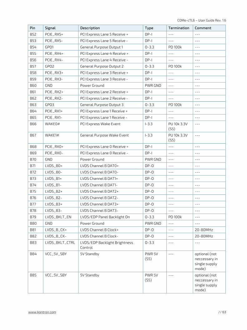
COMe-cTL6 – User Guide Rev. 1.6
www.kontron.com // 63
Pin Signal Description Type Termination Comment
B52 PCIE_RX5+ PCI Express Lane 5 Receive + DP-I --- ---
B53 PCIE_RX5- PCI Express Lane 5 Receive - DP-I --- ---
B54 GPO1 General Purpose Output 1 O-3.3 PD 100k ---
B55 PCIE_RX4+ PCI Express Lane 4 Receive + DP-I --- ---
B56 PCIE_RX4- PCI Express Lane 4 Receive - DP-I --- ---
B57 GPO2 General Purpose Output 2 O-3.3 PD 100k ---
B58 PCIE_RX3+ PCI Express Lane 3 Receive + DP-I --- ---
B59 PCIE_RX3- PCI Express Lane 3 Receive - DP-I --- ---
B60 GND Power Ground PWR GND --- ---
B61 PCIE_RX2+ PCI Express Lane 2 Receive + DP-I --- ---
B62 PCIE_RX2- PCI Express Lane 2 Receive - DP-I --- ---
B63 GPO3 General Purpose Output 3 O-3.3 PD 100k ---
B64 PCIE_RX1+ PCI Express Lane 1 Receive + DP-I --- ---
B65 PCIE_RX1- PCI Express Lane 1 Receive - DP-I --- ---
B66 WAKE0# PCI Express Wake Event I-3.3 PU 10k 3.3V (S5)
---
B67 WAKE1# General Purpose Wake Event I-3.3 PU 10k 3.3V (S5)
---
B68 PCIE_RX0+ PCI Express Lane 0 Receive + DP-I --- ---
B69 PCIE_RX0- PCI Express Lane 0 Receive - DP-I --- ---
B70 GND Power Ground PWR GND --- ---
B71 LVDS_B0+ LVDS Channel B DAT0+ DP-O --- ---
B72 LVDS_B0- LVDS Channel B DAT0- DP-O --- ---
B73 LVDS_B1+ LVDS Channel B DAT1+ DP-O --- ---
B74 LVDS_B1- LVDS Channel B DAT1- DP-O --- ---
B75 LVDS_B2+ LVDS Channel B DAT2+ DP-O --- ---
B76 LVDS_B2- LVDS Channel B DAT2- DP-O --- ---
B77 LVDS_B3+ LVDS Channel B DAT3+ DP-O --- ---
B78 LVDS_B3- LVDS Channel B DAT3- DP-O --- ---
B79 LVDS_BKLT_EN LVDS/EDP Panel Backlight On O-3.3 PD 100k ---
B80 GND Power Ground PWR GND --- ---
B81 LVDS_B_CK+ LVDS Channel B Clock+ DP-O --- 20-80MHz
B82 LVDS_B_CK- LVDS Channel B Clock- DP-O --- 20-80MHz
B83 LVDS_BKLT_CTRL LVDS/EDP Backlight Brightness Control
O-3.3 --- ---
B84 VCC_5V_SBY 5V Standby PWR 5V (S5)
--- optional (not neccessary in single supply mode)
B85 VCC_5V_SBY 5V Standby PWR 5V (S5)
--- optional (not neccessary in single supply mode)

COMe-cTL6 – User Guide Rev. 1.6
www.kontron.com // 64
Pin Signal Description Type Termination Comment
B86 VCC_5V_SBY 5V Standby PWR 5V (S5)
--- optional (not neccessary in single supply mode)
B87 VCC_5V_SBY 5V Standby PWR 5V (S5)
--- optional (not neccessary in single supply mode)
B88 BIOS_DIS1# BIOS Selection Strap 1 I-3.3 PU 10k 3.3V (S0)
PU might be powered during suspend
B89 VGA_RED Analog Video RGB-RED nc --- ---
B90 GND Power Ground PWR GND --- ---
B91 VGA_GREEN Analog Video RGB-GREEN nc --- ---
B92 VGA_BLUE Analog Video RGB-BLUE nc --- ---
B93 VGA_HSYNC Analog Video H-Sync nc --- ---
B94 VGA_VSYNC Analog Video V-Sync nc --- ---
B95 VGA_I2C_CLK Display Data Channel Clock nc --- ---
B96 VGA_I2C_DATA Display Data Channel Data nc --- ---
B97 SPI_CS# SPI Chip Select O-3.3 --- ---
B98 RSVD Reserved for future use nc --- ---
B99 RSVD Reserved for future use nc --- ---
B100 GND Power Ground PWR GND --- ---
B101 FAN_PWMOUT Fan PWM Output O-3.3 --- 20V protection circuit implemented on module, PD on carrier board needed for proper operation
B102 FAN_TACHIN Fan Tach Input I-3.3 PU 47k 3.3V (S0)
20V protection circuit implemented on module
B103 SLEEP# Sleep Button Input I-3.3 PU 47k 3.3V (S5)
20V protection circuit implemented on module
B104 VCC_12V Main Input Voltage (4.75-20V) PWR 4.75-20V
--- ---
B105 VCC_12V Main Input Voltage (4.75-20V) PWR 4.75-20V
--- ---
B106 VCC_12V Main Input Voltage (4.75-20V) PWR 4.75-20V
--- ---
B107 VCC_12V Main Input Voltage (4.75-20V) PWR 4.75-20V
--- ---
B108 VCC_12V Main Input Voltage (4.75-20V) PWR 4.75-20V
--- ---
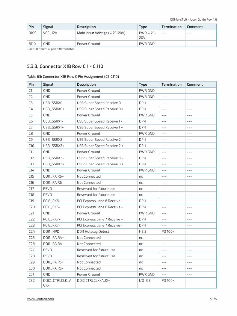
COMe-cTL6 – User Guide Rev. 1.6
www.kontron.com // 65
Pin Signal Description Type Termination Comment
B109 VCC_12V Main Input Voltage (4.75-20V) PWR 4.75-20V
--- ---
B110 GND Power Ground PWR GND --- --- + and -Differential pair differentiator
5.3.3. Connector X1B Row C 1 - C 110
Table 63: Connector X1B Row C Pin Assignment (C1-C110)
Pin Signal Description Type Termination Comment
C1 GND Power Ground PWR GND --- ---
C2 GND Power Ground PWR GND --- ---
C3 USB_SSRX0- USB Super Speed Receive 0 - DP-I --- ---
C4 USB_SSRX0+ USB Super Speed Receive 0 + DP-I --- ---
C5 GND Power Ground PWR GND --- ---
C6 USB_SSRX1- USB Super Speed Receive 1 - DP-I --- ---
C7 USB_SSRX1+ USB Super Speed Receive 1 + DP-I --- ---
C8 GND Power Ground PWR GND --- ---
C9 USB_SSRX2- USB Super Speed Receive 2 - DP-I --- ---
C10 USB_SSRX2+ USB Super Speed Receive 2 + DP-I --- ---
C11 GND Power Ground PWR GND --- ---
C12 USB_SSRX3- USB Super Speed Receive 3 - DP-I --- ---
C13 USB_SSRX3+ USB Super Speed Receive 3 + DP-I --- ---
C14 GND Power Ground PWR GND --- ---
C15 DDI1_PAIR6+ Not Connected nc --- ---
C16 DDI1_PAIR6- Not Connected nc --- ---
C17 RSVD Reserved for future use nc --- ---
C18 RSVD Reserved for future use nc --- ---
C19 PCIE_RX6+ PCI Express Lane 6 Receive + DP-I --- ---
C20 PCIE_RX6- PCI Express Lane 6 Receive - DP-I --- ---
C21 GND Power Ground PWR GND --- ---
C22 PCIE_RX7+ PCI Express Lane 7 Receive + DP-I --- ---
C23 PCIE_RX7- PCI Express Lane 7 Receive - DP-I --- ---
C24 DDI1_HPD DDI1 Hotplug Detect I-3.3 PD 100k
C25 DDI1_PAIR4+ Not Connected nc --- ---
C26 DDI1_PAIR4- Not Connected nc --- ---
C27 RSVD Reserved for future use nc --- ---
C28 RSVD Reserved for future use nc --- ---
C29 DDI1_PAIR5+ Not Connected nc --- ---
C30 DDI1_PAIR5- Not Connected nc --- ---
C31 GND Power Ground PWR GND --- ---
C32 DDI2_CTRLCLK_AUX+
DDI2 CTRLCLK/AUX+ I/O-3.3 PD 100k ---

COMe-cTL6 – User Guide Rev. 1.6
www.kontron.com // 66
Pin Signal Description Type Termination Comment
C33 DDI2_CTRLDATA_AUX-
DDI2 CTRLDATA/AUX- I/O-3.3 PU 100k 3.3V (S0)
---
C34 DDI2_DDC_AUX_SEL
DDI2 DDC/AUX select I-3.3 PD 1M ---
C35 RSVD Reserved for future use nc --- ---
C36 DDI3_CTRLCLK_AUX+
DDI3 CTRLCLK/AUX+ I/O-3.3 PD 100k ---
C37 DDI3_CTRLDATA_AUX-
DDI3 CTRLDATA/AUX- I/O-3.3 PU 100k 3.3V (S0)
---
C38 DDI3_DDC_AUX_SEL
DDI3 DDC/AUX select I-3.3 PD 1M ---
C39 DDI3_PAIR0+ DDI3 Pair 0 + DP-O --- ---
C40 DDI3_PAIR0- DDI3 Pair 0 - DP-O --- ---
C41 GND Power Ground PWR GND --- ---
C42 DDI3_PAIR1+ DDI3 Pair 1 + DP-O --- ---
C43 DDI3_PAIR1- DDI3 Pair 1 - DP-O --- ---
C44 DDI3_HPD DDI3 Hotplug Detect I-3.3 PD 100k ---
C45 RSVD Reserved for future use nc --- ---
C46 DDI3_PAIR2+ DDI3 Pair 2 + DP-O --- ---
C47 DDI3_PAIR2- DDI3 Pair 2 - DP-O --- ---
C48 RSVD Reserved for future use nc --- ---
C49 DDI3_PAIR3+ DDI3 Pair 3 + DP-O --- ---
C50 DDI3_PAIR3- DDI3 Pair 3 - DP-O --- ---
C51 GND Power Ground PWR GND --- ---
C52 PEG_RX0+ PEG Lane 0 Receive + DP-I --- ---
C53 PEG_RX0- PEG Lane 0 Receive - DP-I --- ---
C54 TYPE0# nc for type 6 module nc --- ---
C55 PEG_RX1+ PEG Lane 1 Receive + DP-I --- ---
C56 PEG_RX1- PEG Lane 1 Receive - DP-I --- ---
C57 TYPE1# nc for type 6 module nc --- ---
C58 PEG_RX2+ PEG Lane 2 Receive + DP-I --- ---
C59 PEG_RX2- PEG Lane 2 Receive - DP-I --- ---
C60 GND Power Ground PWR GND --- ---
C61 PEG_RX3+ PEG Lane 3 Receive + DP-I --- ---
C62 PEG_RX3- PEG Lane 3 Receive - DP-I --- ---
C63 RSVD Reserved for future use nc --- ---
C64 RSVD Reserved for future use nc --- ---
C65 PEG_RX4+ PEG Lane 4 Receive + nc --- ---
C66 PEG_RX4- PEG Lane 4 Receive - nc --- ---
C67 RAPID_SHUTDOWN
Rapid Shutdown Trigger Input nc --- ---
C68 PEG_RX5+ PEG Lane 5 Receive + nc --- ---
C69 PEG_RX5- PEG Lane 5 Receive - nc --- ---
C70 GND Power Ground PWR GND --- ---

COMe-cTL6 – User Guide Rev. 1.6
www.kontron.com // 67
Pin Signal Description Type Termination Comment
C71 PEG_RX6+ PEG Lane 6 Receive + nc --- ---
C72 PEG_RX6- PEG Lane 6 Receive - nc --- ---
C73 GND Power Ground PWR GND --- ---
C74 PEG_RX7+ PEG Lane 7 Receive + nc --- ---
C75 PEG_RX7- PEG Lane 7 Receive - nc --- ---
C76 GND Power Ground PWR GND --- ---
C77 RSVD Reserved for future use nc --- ---
C78 PEG_RX8+ PEG Lane 8 Receive + nc --- ---
C79 PEG_RX8- PEG Lane 8 Receive - nc --- ---
C80 GND Power Ground PWR GND --- ---
C81 PEG_RX9+ PEG Lane 9 Receive + nc --- ---
C82 PEG_RX9- PEG Lane 9 Receive - nc --- ---
C83 RSVD Reserved for future use nc --- ---
C84 GND Power Ground PWR GND --- ---
C85 PEG_RX10+ PEG Lane 10 Receive + nc --- ---
C86 PEG_RX10- PEG Lane 10 Receive - nc --- ---
C87 GND Power Ground PWR GND --- ---
C88 PEG_RX11+ PEG Lane 11 Receive + nc --- ---
C89 PEG_RX11- PEG Lane 11 Receive - nc --- ---
C90 GND Power Ground PWR GND --- ---
C91 PEG_RX12+ PEG Lane 12 Receive + nc --- ---
C92 PEG_RX12- PEG Lane 12 Receive - nc --- ---
C93 GND Power Ground PWR GND --- ---
C94 PEG_RX13+ PEG Lane 13 Receive + nc --- ---
C95 PEG_RX13- PEG Lane 13 Receive - nc --- ---
C96 GND Power Ground PWR GND --- ---
C97 RSVD Reserved for future use nc --- ---
C98 PEG_RX14+ PEG Lane 14 Receive + nc --- ---
C99 PEG_RX14- PEG Lane 14 Receive - nc --- ---
C100 GND Power Ground PWR GND --- ---
C101 PEG_RX15+ PEG Lane 15 Receive + nc --- ---
C102 PEG_RX15- PEG Lane 15 Receive - nc --- ---
C103 GND Power Ground PWR GND --- ---
C104 VCC_12V Main Input Voltage (4.75-20V) PWR 4.75- 20V
--- ---
C105 VCC_12V Main Input Voltage (4.75-20V) PWR 4.75- 20V
--- ---
C106 VCC_12V Main Input Voltage (4.75-20V) PWR 4.75- 20V
--- ---
C107 VCC_12V Main Input Voltage (4.75-20V) PWR 4.75- 20V
--- ---
C108 VCC_12V Main Input Voltage (4.75-20V) PWR 4.75- 20V
--- ---

COMe-cTL6 – User Guide Rev. 1.6
www.kontron.com // 68
Pin Signal Description Type Termination Comment
C109 VCC_12V Main Input Voltage (4.75-20V) PWR 4.75- 20V
--- ---
C110 GND Power Ground PWR GND --- ---
+ and - Differential pair differentiator
5.3.4. Connector X1B Row D 1 - D 110
Table 64: Connector X1B Row D Pin Assignment (D1-D110)
Pin Signal Description Type Termination Comment
D1 GND Power Ground PWR GND --- ---
D2 GND Power Ground PWR GND --- ---
D3 USB_SSTX0- USB Super Speed Transmit 0 - DP-O --- ---
D4 USB_SSTX0+ USB Super Speed Transmit 0 + DP-O --- ---
D5 GND Power Ground PWR GND --- ---
D6 USB_SSTX1- USB Super Speed Transmit 1 - DP-O --- ---
D7 USB_SSTX1+ USB Super Speed Transmit 1 + DP-O --- ---
D8 GND Power Ground PWR GND --- ---
D9 USB_SSTX2- USB Super Speed Transmit 2 - DP-O --- ---
D10 USB_SSTX2+ USB Super Speed Transmit 2 + DP-O --- ---
D11 GND Power Ground PWR GND --- ---
D12 USB_SSTX3- USB Super Speed Transmit 3 - DP-O --- ---
D13 USB_SSTX3+ USB Super Speed Transmit 3 + DP-O --- ---
D14 GND Power Ground PWR GND --- ---
D15 DDI1_CTRLCLK_AUX+
DDI1 CTRLCLK/AUX+ I/O-3.3 PD 100k ---
D16 DDI1_CTRLDATA_AUX-
DDI1 CTRLDATA/AUX- I/O-3.3 PU 100k 3.3V (S0)
---
D17 RSVD Reserved for future use nc --- ---
D18 RSVD Reserved for future use nc --- ---
D19 PCIE_TX6+ PCI Express Lane 6 Transmit + DP-O --- ---
D20 PCIE_TX6- PCI Express Lane 6 Transmit - DP-O --- ---
D21 GND Power Ground PWR GND --- ---
D22 PCIE_TX7+ PCI Express Lane 7 Transmit + DP-O --- ---
D23 PCIE_TX7- PCI Express Lane 7 Transmit - DP-O --- ---
D24 RSVD Reserved for future use nc --- ---
D25 RSVD Reserved for future use nc --- ---
D26 DDI1_PAIR0+ DDI1 Pair 0 + DP-O --- ---
D27 DDI1_PAIR0- DDI1 Pair 0 - DP-O --- ---
D28 RSVD Reserved for future use nc --- ---
D29 DDI1_PAIR1+ DDI1 Pair 1 + DP-O --- ---
D30 DDI1_PAIR1- DDI1 Pair 1 - DP-O --- ---
D31 GND Power Ground PWR GND --- ---
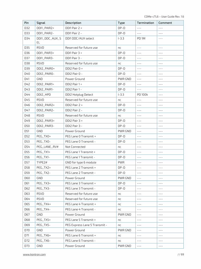
COMe-cTL6 – User Guide Rev. 1.6
www.kontron.com // 69
Pin Signal Description Type Termination Comment
D32 DDI1_PAIR2+ DDI1 Pair 2 + DP-O --- ---
D33 DDI1_PAIR2- DDI1 Pair 2 - DP-O --- ---
D34 DDI1_DDC_AUX_SEL
DDI1 DDC/AUX select I-3.3 PD 1M ---
D35 RSVD Reserved for future use nc --- ---
D36 DDI1_PAIR3+ DDI1 Pair 3 + DP-O --- ---
D37 DDI1_PAIR3- DDI1 Pair 3 - DP-O --- ---
D38 RSVD Reserved for future use nc --- ---
D39 DDI2_PAIR0+ DDI2 Pair 0 + DP-O --- ---
D40 DDI2_PAIR0- DDI2 Pair 0 - DP-O --- ---
D41 GND Power Ground PWR GND --- ---
D42 DDI2_PAIR1+ DDI2 Pair 1 + DP-O --- ---
D43 DDI2_PAIR1- DDI2 Pair 1 - DP-O --- ---
D44 DDI2_HPD DDI2 Hotplug Detect I-3.3 PD 100k ---
D45 RSVD Reserved for future use nc --- ---
D46 DDI2_PAIR2+ DDI2 Pair 2 + DP-O --- ---
D47 DDI2_PAIR2- DDI2 Pair 2 - DP-O --- ---
D48 RSVD Reserved for future use nc --- ---
D49 DDI2_PAIR3+ DDI2 Pair 3 + DP-O --- ---
D50 DDI2_PAIR3- DDI2 Pair 3 - DP-O --- ---
D51 GND Power Ground PWR GND --- ---
D52 PEG_TX0+ PEG Lane 0 Transmit + DP-O --- ---
D53 PEG_TX0- PEG Lane 0 Transmit - DP-O --- ---
D54 PEG_LANE_RV# Not Connected nc --- ---
D55 PEG_TX1+ PEG Lane 1 Transmit + DP-O --- ---
D56 PEG_TX1- PEG Lane 1 Transmit - DP-O --- ---
D57 TYPE2# GND for type 6 module PWR --- ---
D58 PEG_TX2+ PEG Lane 2 Transmit + DP-O --- ---
D59 PEG_TX2- PEG Lane 2 Transmit - DP-O --- ---
D60 GND Power Ground PWR GND --- ---
D61 PEG_TX3+ PEG Lane 3 Transmit + DP-O --- ---
D62 PEG_TX3- PEG Lane 3 Transmit - DP-O --- ---
D63 RSVD Reserved for future use nc --- ---
D64 RSVD Reserved for future use nc --- ---
D65 PEG_TX4+ PEG Lane 4 Transmit + nc --- ---
D66 PEG_TX4- PEG Lane 4 Transmit - nc --- ---
D67 GND Power Ground PWR GND --- ---
D68 PEG_TX5+ PEG Lane 5 Transmit + nc --- ---
D69 PEG_TX5- PEG Express Lane 5 Transmit - nc --- ---
D70 GND Power Ground PWR GND --- ---
D71 PEG_TX6+ PEG Lane 6 Transmit + nc --- ---
D72 PEG_TX6- PEG Lane 6 Transmit - nc --- ---
D73 GND Power Ground PWR GND --- ---

COMe-cTL6 – User Guide Rev. 1.6
www.kontron.com // 70
Pin Signal Description Type Termination Comment
D74 PEG_TX7+ PEG Lane 7 Transmit + nc --- ---
D75 PEG_TX7- PEG Lane 7 Transmit - nc --- ---
D76 GND Power Ground PWR GND --- ---
D77 RSVD Reserved for future use nc --- ---
D78 PEG_TX8+ PEG Lane 8 Transmit + nc --- ---
D79 PEG_TX8- PEG Lane 8 Transmit - nc --- ---
D80 GND Power Ground PWR GND --- ---
D81 PEG_TX9+ PEG Lane 9 Transmit + nc --- ---
D82 PEG_TX9- PEG Lane 9 Transmit - nc --- ---
D83 RSVD Reserved for future use nc --- ---
D84 GND Power Ground PWR GND --- ---
D85 PEG_TX10+ PEG Lane 10 Transmit + nc --- ---
D86 PEG_TX10- PEG Lane 10 Transmit - nc --- ---
D87 GND Power Ground PWR GND --- ---
D88 PEG_TX11+ PEG Lane 11 Transmit + nc --- ---
D89 PEG_TX11- PEG Lane 11 Transmit - nc --- ---
D90 GND Power Ground PWR GND --- ---
D91 PEG_TX12+ PEG Lane 12 Transmit + nc --- ---
D92 PEG_TX12- PEG Lane 12 Transmit - nc --- ---
D93 GND Power Ground PWR GND --- ---
D94 PEG_TX13+ PEG Lane 13 Transmit + nc --- ---
D95 PEG_TX13- PEG Lane 13 Transmit - nc --- ---
D96 GND Power Ground PWR GND --- ---
D97 RSVD Reserved for future use nc --- ---
D98 PEG_TX14+ PEG Lane 14 Transmit + nc --- ---
D99 PEG_TX14- PEG Lane 14 Transmit - nc --- ---
D100 GND Power Ground PWR GND --- ---
D101 PEG_TX15+ PEG Lane 15 Transmit + nc --- ---
D102 PEG_TX15- PEG Lane 15 Transmit - nc --- ---
D103 GND Power Ground PWR GND --- ---
D104 VCC_12V Main Input Voltage (4.75-20V) PWR 4.75- 20V
--- ---
D105 VCC_12V Main Input Voltage (4.75-20V) PWR 4.75- 20V
--- ---
D106 VCC_12V Main Input Voltage (4.75-20V) PWR 4.75- 20V
--- ---
D107 VCC_12V Main Input Voltage (4.75-20V) PWR 4.75- 20V
--- ---
D108 VCC_12V Main Input Voltage (4.75-20V) PWR 4.75- 20V
--- ---
D109 VCC_12V Main Input Voltage (4.75-20V) PWR 4.75- 20V
--- ---
D110 GND Power Ground PWR GND --- ---
+ and - Differential pair differentiator

COMe-cTL6 – User Guide Rev. 1.6
www.kontron.com // 71
5.4. Bootstrap Signals
Table 65: Bootstrap Signals
Pin Signal Description Type Termination Comment
A95 SPI_MOSI SPI Master Out Slave In O–3.3 PU 4k7 The internal PU is disabled during reset
B15 SMB_ALERT# SMBus Alert I/O–3.3 PU 2k26
B32 HDA_SPKR Speaker O–3.3 PD 20k +/-30% in PCH
PD is enabled until reset is deasserted
A33 HDA SDOUT HD Audio Serial Data Out O–3.3 PD 20k in PCH
Flash Descriptor
B47 ESPI_UN# [Enable/Disable] ESPI-Mode I–3.3
A34 BIOS_DIS0#/ESPI_SAFS
BIOS Selection Strap 0 I–3.3 PU 10k 3.3 V (S5)
B88 BIOS_DIS1# BIOS Selection Strap 1 I–3.3 PU 10k 3.3 V (S0)
PU might be powered during suspend
Bootstrap signals are often used as a configuration strap for the modules chipset. They should not be connected to a pull-up or pull-down resistor, which could overwrite the internal chipset and result in a malfunction of the module.

COMe-cTL6 – User Guide Rev. 1.6
www.kontron.com // 72
6/ UEFI BIOS
6.1. Starting the UEFI BIOS
The COMe-cTL6 uses a Kontron-customized, pre-installed and configured version of Aptio ® V UEFI BIOS based on the Unified Extensible Firmware Interface (UEFI) specification.
The BIOS version covered in this document might not be the latest version. The latest version might have certain differences to the BIOS options and features described in this chapter.
Register for the EMD Customer Section to get access to BIOS downloads and PCN service.
The UEFI BIOS comes with a Setup program that provides quick and easy access to the individual function settings for control or modification of the UEFI BIOS configuration. The Setup program allows for access to various menus that provide functions or access to sub-menus with further specific functions of their own.
To start the UEFI BIOS Setup program, follow the steps below:
1. Power on the board.
2. Wait until the first characters appear on the screen (POST messages or splash screen).
3. Press the <DEL> key.
4. If the UEFI BIOS is password-protected, a request for password will appear. Enter either the User Password or Supervisor Password press <RETURN>, and proceed with step 5.
5. A Setup menu appears.
The COMe-cTL6 UEFI BIOS Setup program uses a hot key navigation system. The hot key legend bar is located at the bottom of the Setup screens. The following table provides a list of navigation hot keys available in the legend bar.
Table 66: Navigation Hot Keys Available in the Legend Bar
Sub-screen Description
<F1> <F1> key invokes the General Help window
<-> <Minus> key selects the next lower value within a field
<+> <Plus> key selects the next higher value within a field
<F2> <F2> key loads previous values
<F3> <F3> key loads optimized defaults
<F4> <F4> key Saves and Exits
<→> or <←> <Left/Right> arrows selects major Setup menus on menu bar, for example, Main or Advanced
<↑> or <↓> <Up/Down> arrows select fields in the current menu, for example, Setup function or sub-screen
<ESC> <ESC> key exits a major Setup menu and enters the Exit Setup menu Pressing the <ESC> key in a sub-menu displays the next higher menu level
<RETURN> <RETURN> key executes a command or selects a submenu

COMe-cTL6 – User Guide Rev. 1.6
www.kontron.com // 73
6.2. The UEFI Shell
The Kontron UEFI BIOS features a built-in and enhanced version of the UEFI Shell. For a detailed description of the available standard shell scripting, refer to the EFI Shell User Guide. For a detailed description of the available standard shell commands, refer to the EFI Shell Command Manual. Both documents can be downloaded from the EFI and Framework Open Source Community homepage (http://sourceforge.net/projects/efi-shell/files/documents/).
Kontron UEFI BIOS does not provide all shell commands described in the EFI Shell Command Manual.
6.2.1. Basic Operation of the UEFI Shell
The UEFI Shell forms an entry into the UEFI boot order and is the first boot option by default.
6.2.1.1. Entering the UEFI Shell
To enter the UEFI Shell, follow the steps below:
1. Power on the board.
1. Press the <F7> key (instead of <DEL>) to display a choice of boot devices.
2. Choose ‘UEFI: Built-in EFI shell’.
EFI Shell version 2.40 [5.11] Current running mode 1.1.2 Device mapping table Fs0 :HardDisk - Alias hd33b0b0b fs0 Acpi(PNP0A03,0)/Pci(1D|7)/Usb(1, 0)/Usb(1, 0)/HD(Part1,Sig17731773)
Press the ESC key within 5 seconds to skip startup.nsh, and any other key to continue.
3. The output produced by the device-mapping table can vary depending on the board’s configuration.
4. If the ESC key is pressed before the 5 second timeout elapses, the shell prompt is shown:
Shell>
6.2.1.2. Exiting the UEFI Shell
To exit the UEFI Shell, follow one of the steps below:
1. Use the exit UEFI Shell command to select the boot device, in the Boot menu, that the OS will boot from.
2. Reset the board using the reset UEFI Shell command.
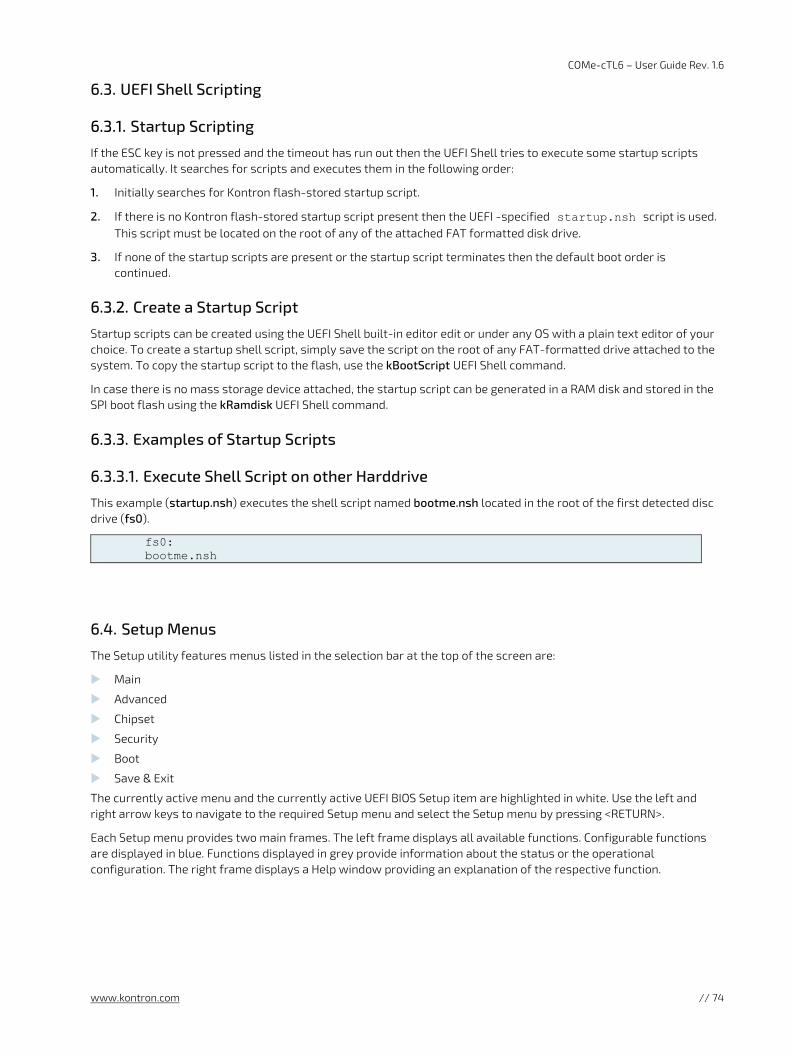
COMe-cTL6 – User Guide Rev. 1.6
www.kontron.com // 74
6.3. UEFI Shell Scripting
6.3.1. Startup Scripting
If the ESC key is not pressed and the timeout has run out then the UEFI Shell tries to execute some startup scripts automatically. It searches for scripts and executes them in the following order:
1. Initially searches for Kontron flash-stored startup script.
2. If there is no Kontron flash-stored startup script present then the UEFI -specified startup.nsh script is used. This script must be located on the root of any of the attached FAT formatted disk drive.
3. If none of the startup scripts are present or the startup script terminates then the default boot order is continued.
6.3.2. Create a Startup Script
Startup scripts can be created using the UEFI Shell built-in editor edit or under any OS with a plain text editor of your choice. To create a startup shell script, simply save the script on the root of any FAT-formatted drive attached to the system. To copy the startup script to the flash, use the kBootScript UEFI Shell command.
In case there is no mass storage device attached, the startup script can be generated in a RAM disk and stored in the SPI boot flash using the kRamdisk UEFI Shell command.
6.3.3. Examples of Startup Scripts
6.3.3.1. Execute Shell Script on other Harddrive
This example (startup.nsh) executes the shell script named bootme.nsh located in the root of the first detected disc drive (fs0).
fs0: bootme.nsh
6.4. Setup Menus
The Setup utility features menus listed in the selection bar at the top of the screen are:
Main
Advanced
Chipset
Security
Boot
Save & Exit
The currently active menu and the currently active UEFI BIOS Setup item are highlighted in white. Use the left and right arrow keys to navigate to the required Setup menu and select the Setup menu by pressing <RETURN>.
Each Setup menu provides two main frames. The left frame displays all available functions. Configurable functions are displayed in blue. Functions displayed in grey provide information about the status or the operational configuration. The right frame displays a Help window providing an explanation of the respective function.

COMe-cTL6 – User Guide Rev. 1.6
www.kontron.com // 75
6.4.1. Main Setup Menu
On entering the UEFI BIOS the Setup program displays the Main Setup menu. This screen lists the Main Setup menu sub-screens and provides basic system information as well as functions for setting the system language, time and date.
Figure 15: Main Setup Menu
The following table shows the Main Menu sub-screens and functions and describes the content. Default options are displayed bold. Some functions include additional information.
Table 67: Main Setup Menu Sub-screens
Sub-Screen Description
BIOS Information
Read only field Displays BIOS Information: BIOS vendor, Core version, Compliancy, Kontron BIOS Version and Access level
FSP Information
Read only field Displays FSP Information: FSP Version, Build Date, FSP Mode
Processor Information
Read only field Displays Processor Information: Name, Type, Speed, ID, Stepping, Package, Numberof Processors, Microcode Revision, GT Info, eDRAM Size IGFX GOP Version, PCIe GEN4 Dekel FW Version, Memory RC Version, Total Memory, Memory Speed
PCH Information
Read only field Displays PCH Information: Name, SKU, Stepping, Base Revision, OEM Revision, Package, TXT Capability, Production Type, ME FW Version, ME Firmware SKU, PMC FW Version
System Language
Chooses the System default language [English]

COMe-cTL6 – User Guide Rev. 1.6
www.kontron.com // 76
Sub-Screen Description
Platform Information
Read only field Displays Module Information Product Name, Revision, Serial # ‚MAC Address, Boot Counter, and CPLD Rev
Additional information for MAC Address The MAC address entry is the value used by the Ethernet controller and may contain the entry’ Inactive’ - Ethernet chip is inactive. Activate the Ethernet chip by setting the following to ‘enable’. Advanced > Network Stack Configuration > Network Stack > Enable
System Date Displays the system date [Day mm/dd/yyyy]
System Time Displays the system time [hh:mm:ss]

COMe-cTL6 – User Guide Rev. 1.6
www.kontron.com // 77
6.4.2. Advanced Setup Menu
The Advanced Setup menu provides sub-screens and second level sub-screens with functions for advanced configuration.
Setting items, on this screen, to incorrect values may cause system malfunctions.
Figure 16: Advanced Setup Menu
The following table shows the Advanced sub-screen and describes the function. Default settings are in bold.
Table 68: Advanced Setup menu Sub-screens and Functions
Sub-Screen Function Second level Sub-Screen/Description
CPU Configuration>
Read only field CPU Information : Type, ID, Speed, L1 Data Cache, L1 Instruction Cache, L2 Cache, L3 Cache, L4 Cache, VMX, SMX/TXT
C6DRAM Moving DRAM contents to PRM memory when CPU is in C6 state [Enabled, Disabled]
CPU Flex Ratio Override CPU Flex Ratio Programming [Enabled, Disabled]
CPU Flex Settings 26
Intel (VMX) Virtual Technology
When enabled VMM can utilize the additional hardware capabilities provided by Vanderpool Technology [Enabled, Disabled]
Active Processor Cores Number of cores to enable in each processor package [All, 1, 2, 3]
Hyper Threading [Enabled, Disabled]
BIST [Enabled, Disabled]

COMe-cTL6 – User Guide Rev. 1.6
www.kontron.com // 78
Sub-Screen Function Second level Sub-Screen/Description
CPU Configuration>
AES [Enabled, Disabled]
RaceConditionResponse Policy
[Enabled, Disabled]
Power & Performance>
CPU Power Management Control>
Boot performance mode
[Max Battery, Max Non-Turbo Performance, Turbo Performance]
Intel SpeedStep ™ Allows more than two frequency ranges to be supported. [Enabled, Disabled]
Intel Speed Shift Technology
Enable exposes CPPC v2 interface to allow for hardware controlled p-states. [Enabled, Disabled]
Per Core P State OS control mode
Disable set Bit 31 =1 command 0x06. When set the highest core request is used for all other core requests. [Enabled, Disabled]
HwP Autonomous Per Core P State
Disable requests the same value for all cores all the time. [Enabled, Disabled]
HwP Autonomous EPP Grouping
Autonomous will not necessarily request same values for all cores with same EPP. [Enable, Disabled]
EPB override over PECI
Enable by sending pcode command 0x2b, subcommand 0x3 to 1. This allows OOB EPB PECI override control. [Enable, Disabled]
HwP Fast MSR Support
Support for IA32_HWP_REQUEST MSR [Enabled, Disabled]
Turbo Mode Note: Requires EMTTM to be enabled. AUTO means enabled. [Enabled, Disabled]
View/Configure Turbo Options>
Read only field Current Turbo Settings: Max Turbo Power Limit, Min Turbo Power Limit, Package TDP Limit, Power Limit 1 / 2 and 1 to 64 Core Turbo Ratio Limit Ratio. (TRLR).
Energy Efficient P-State
[Enabled, Disabled]
Package Power Limit MSR
Enable to lock. A reset is required to unlock the register. [Enabled, Disabled]
1-Core Turbo Ratio Limit Ration (TRLR) Override [41]
2-Core Turbo Ratio Limit Ration (TRLR) Override [41]
3-Core Turbo Ratio Limit Ration (TRLR) Override [39]

COMe-cTL6 – User Guide Rev. 1.6
www.kontron.com // 79
Sub-Screen Function Second level Sub-Screen/Description
Power & Performance>
CPU Power Management Control>
View/Configure Turbo Options>
4-Core Turbo Ratio Limit Ration (TRLR) Override [39]
Energy Efficient Turbo
Lowers turbo frequency to increase efficiency. [Enabled, Disabled]
Config TDP Configurations>
Enable Configurable TDP
[Applies to non-cTDP, Applies to cTDP]
Configurable TDP Boot Mode
[Nominal, Down, Up, Deactivate]
Configurable TDP Lock
[Enabled, Disabled]
Custom settings Nominal ConfigTDP Nominal Ratio: 26, TAR: 25, PL1:28.0W
Power Limit 1/2
[0]
Power Limit 1Time Window
[0]
ConfigTDP Turbo Activation
[0]
Custom settings Down ConfigTDP Level1 Ratio: 11, TAR: 14, PL1:15.0W
Power Limit 1/2 [0]
Power Limit 1 Time Window
[0]
ConfigTDP Turbo Activation
[0]
Custom settings Up ConfigTDP Level2 Ratio: 15 TAR: 14 PL1:15.0W
Power Limit 1/2
[0]
Power Limit 1 Time Window
[0]
Platform PL1 PL1 value defines the CPU’s average TDP mode consumption power; when disabled CPU uses default PL1 values. [Enabled, Disabled]
Platform PL2 PL2 value defines the CPU’s average TDP mode consumption power; when disabled CPU uses default PL2 values. [Enabled, Disabled]
Platform PL4 Override
PL4 defines the overall peak consumption power (ICCmax) of the CPU. If disabled CPU uses default PL4 values. [Enabled, Disabled]

COMe-cTL6 – User Guide Rev. 1.6
www.kontron.com // 80
Sub-Screen Function Second level Sub-Screen/Description
Power & Performance>
CPU Power Management Control>
C States CPU power management. Allows CPU to enter C states when not 100% utilized. Values beyond the range clipped to min/max supported by SKU. [Enabled, Disabled]
Package C State Limit
Maximum C State limit setting, where AUTO initializes to deepest available package C State limit. [Auto, CPU Default, C0/C1, C2,….…C10]
GT Power Management Control>
RC6 (Render Standby)
Check to enable render standby support. [Enabled, Disabled]
Maximum GT frequency
Values beyond the range clipped to min/max supported by SKU. [Default Max Frequency, 100 MHz, 150 MHz, …1200 MHz]
Prevent Turbo on GT frequency
Enable to disable the Turbo GT when disabled GT frequency is not limited. [Enabled, Disabled]
PCH-FW Configuration>
Firmware Update Configuration>
Me FW Image Re-Flash
[Enabled, Disabled]
FW Update [Enabled]
PTT Configuration> TPM Device Selection
[dTPM]
Extended CSME Measuremnet to TPM_PCR>
[Disable]
Thermal Configuration>
Use Generic Thermal Functions>
[Enable/Disable]
CPU Thermal Configuration>
DTS SMM Disabled: uses HWM reported temperature values Enabled: uses DTS SMM mechanism to obtain CPU temperature values Out of spec: uses HWM and DTS SMM [Disabled, Enabled, Critical Temp Reporting (out of Spec)]
TCC Activation Offset
Sets temperature at which TCC must be activated (range: 0 to 63). [0]
Disable PROCHOT# Output
[Enabled, Disabled]
Platform Thermal Configuration>
Critical Trip Point The point at which the OS begins to shut the system off. [130 C, 119 C (POR)…15 C]
Passive Trip Point The point at which the OS begins to throttling the processor. [119 C (POR), 95 C, …15 C, Disabled]
Passive TC1 value TC1 value for ACPI passive cooling formula (range: 1 to 16). [1]

COMe-cTL6 – User Guide Rev. 1.6
www.kontron.com // 81
Sub-Screen Function Second level Sub-Screen/Description
Thermal Configuration>
Platform Thermal Configuration>
Passive TC2 value TC2 value for ACPI passive cooling formula (range: 1 to 16) [5]
Passive TSP value Sets TSP value for ACPI passive cooling formula (range: 2 to 32). Represent in tenths of second how often the temperature is read when passive cooling is enabled. [10]
Passive Trip Points
[Enabled, Disabled]
Critical Trip Point [Enabled, Disabled]
Boot DTS Read Read PCH, CPU DTS Temperature and Publish via SMBIOS table
Platform Settings>
iPCM Mode Sets where the power date is read from. [Disabled, Dongle Mode. Online PCH Mode, Online ISH Mode]
Firmware Configuration [Ignore Policy Update, Production, Test]
PS2 Keyboard and Mouse [Enabled, Disabled]
Power Loss Notification Feature
[Enabled, Disabled]
Intel Trusted Device Setup Boot
[Enabled, Disabled]
PMC Fast Boot [Enabled, Disabled]
AMT Configuration>
USB Provisioning of AMT [Enabled, Disabled]
MAC Pass Through [Enabled, Disabled]
CIRA Configuration> Activate Remote Assistance Process
Triggers CIRA boot. Note: First access must be activated from MEBX setup. [Enabled, Disabled]
CIRA Timeout 0
ASF Configuration> PET progress [Enabled, Disabled]
Watchdog [Enabled, Disabled]
OS Timer 0
BIOS Timer 0
ASF Sensors Table Adds ASF sensor table into ASF ACPI Table. [Enabled, Disabled]
Secure Erase Configuration>
Secure Erase Mode Changes Secure Erase Module behavior, where Simulate performs SE flow without erasing SSD and Real: erases SSD. [Simulate, Real]
Force Secure Erase Force Secure Erase on next boot. [Enabled, Disabled]
OEM Flag Settings>
MEBx hotkey Pressed
OEM Flag Bit 1 enables automatics MEBx hotkey. [Enabled, Disabled]

COMe-cTL6 – User Guide Rev. 1.6
www.kontron.com // 82
Sub-Screen Function Second level Sub-Screen/Description
AMT Configuration>
OEM Flag Settings> MEBx Selection Screen
OEM Flag Bit 2 enables MEBx selection screen with two options: (1) To enter ME Configuration Screen (2) Initiate remote connection. Note: Network access must be activated from MEBx setup for this screen to be displayed. [Enabled, Disabled]
Hide Unconfigure ME Confirmation Prompt
OEM Flag Bit 6: Hides the prompt when attempting ME unconfiguration. [Enabled, Disabled]
MEBx OEM D ebug Menu Enable
OEM flag Bit 14, Enable OEM debug manu in MBEX. [Enabled, Disabled]
Unconfigure ME OEM Flag Bit 15: Unconfigure ME with resetting MEBx password to default [Enabled, Disabled]
MEBx Resolution Settings>
Non-UI Mode Resolution
[Auto, 80x25, 100x31]
UI Mode Resolution
[Auto, 80x25, 100x31]
Graphics Mode Resolution
[Auto, 640x480, 800x600, 1024x768]
BCLK Configuration>
BCLK Source Config Selects which BCLK configuration to use. [CPU BCLK, PCH BCLK]
BCLK RFI Frequency SAGV Low
Frequency in 10 KHz increments (range: 0 MHz to 98-100 MHz) [0]
BCLK RFI Frequency SAGV Mid
Frequency in 10 KHz increments (range: 0 MHz to 98-100 MHz) [0]
BCLK RFI Frequency SAGV High
Frequency in 10 KHz increments (range: 0 MHz to 98-100 MHz) [0]
BCLK RFI Frequency SAGV Max
Frequency in 10 KHz increments (range: 0 MHz to 98-100 MHz) [0]
BCLK Spread When enabled BCKL frequency runs at a non-configurable fixed spread percentage. [Enabled, Disabled]
Intel® Time Coordinated Computing>
#AC Split Lock Enable asserts #AC when atomic operation has operand crossing two cache lines [Enabled, Disabled]
IFU State Enable allows instruction prefetch to the cache. [Enabled, Disabled]
Software SRAM Enable allocates one way of LLC. If cache configuration sub-region is available, it allocates based on sub-region. Enabled, Disabled]
Data Streams Optimizer Enable utilizes DSO sub-region to tune system. [Enabled, Disabled]

COMe-cTL6 – User Guide Rev. 1.6
www.kontron.com // 83
Sub-Screen Function Second level Sub-Screen/Description
Intel® Time Coordinated Computing>
Error Log Enable logs errors related to Intel® TCC and saves to memory. [Enabled, Disabled]
Intel® TCC Authentication Menu>
Intel® TCC Authentication
Determines key to be used, non-OEM enrolled key can be added by user. [Disabled, Non-OEM Enrolled Key, OEM Enrolled Key]
Intel® TCC Mode Enable modifies setting to improve real-time performance. [Enabled, Disabled]
Intel® TCC Mode Affected Settings
IO Fabric Low Latency Turns off some power management in PCH IO fabrics. S3 state is not supported. [Enabled, Disabled]
GT Loss Enable reduces Gfx LCC allocation to minimize impact of Gfx workload on LLC. [Enabled, Disabled]
OPIO Recentering Enable or disable Opio recentering to improves PCIe latency. [Enabled, Disabled]
C States Enable allows CPU to enter c states when it is no 100% utilized. [Enabled, Disabled]
Intel Speed ShiftTechnology
Enable exposes CPPC V2 interface to allow for hardware controlled P-states. [Enabled, Disabled]
Intel SpeedStep ™ Enable allows more than two frequency ranges to be supported. [Enabled, Disabled]
Hyper-Threading Enables or disables the Hyper-Threading Technology. [Enabled, Disabled]
ACPI D3Cold Support ACPI D3Cold support to be executed on D3 entry and exit. [Enabled, Disabled]
Low Power S0 Idle Capability
Chooses the power saving states the system uses in ACPI OS. ACPI Energy save option: S3/S4 (Disabled) und S0iX (Enabled). [Enabled, Disabled]
WRC Feature Enable supports IO devices allocated onto the ring and into LLC. [Enabled, Disabled]
vCRt mapping to PEG Enables VCRt mapping to PRG. [Enabled, Disabled]
Page Close Idle Timeout Page Close Idle Timeout Control
Power Down Mode CKE Power Down Mode Control
RC6 (Render Standby) [Enabled, Disabled]
DMI Link ASPM Control See Chipset> PCI Express Configuration
PCI Express Clock Gating See Chipset> PCI Express Configuration
Legacy IO Low Latency Enable sets low latency of legacy IO [Enabled, Disabled]
CPU PCI Express Configuration>
PCI Express Root Port 1>
ASPM [Disabled, L1]
L1 Substates [Disabled, L1.1, L1.1 & L1.2]
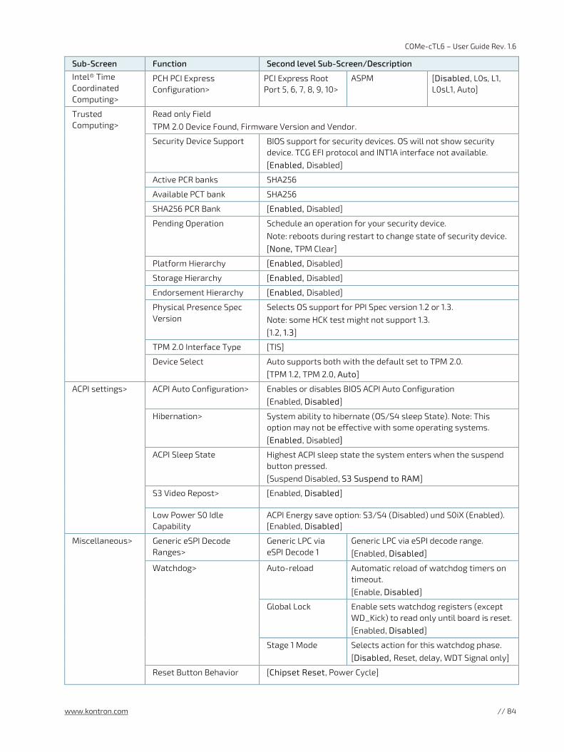
COMe-cTL6 – User Guide Rev. 1.6
www.kontron.com // 84
Sub-Screen Function Second level Sub-Screen/Description
Intel® Time Coordinated Computing>
PCH PCI Express Configuration>
PCI Express Root Port 5, 6, 7, 8, 9, 10>
ASPM [Disabled, L0s, L1, L0sL1, Auto]
Trusted Computing>
Read only Field TPM 2.0 Device Found, Firmware Version and Vendor.
Security Device Support BIOS support for security devices. OS will not show security device. TCG EFI protocol and INT1A interface not available. [Enabled, Disabled]
Active PCR banks SHA256
Available PCT bank SHA256
SHA256 PCR Bank [Enabled, Disabled]
Pending Operation Schedule an operation for your security device. Note: reboots during restart to change state of security device. [None, TPM Clear]
Platform Hierarchy [Enabled, Disabled]
Storage Hierarchy [Enabled, Disabled]
Endorsement Hierarchy [Enabled, Disabled]
Physical Presence Spec Version
Selects OS support for PPI Spec version 1.2 or 1.3. Note: some HCK test might not support 1.3. [1.2, 1.3]
TPM 2.0 Interface Type [TIS]
Device Select Auto supports both with the default set to TPM 2.0. [TPM 1.2, TPM 2.0, Auto]
ACPI settings>
ACPI Auto Configuration> Enables or disables BIOS ACPI Auto Configuration [Enabled, Disabled]
Hibernation> System ability to hibernate (OS/S4 sleep State). Note: This option may not be effective with some operating systems. [Enabled, Disabled]
ACPI Sleep State Highest ACPI sleep state the system enters when the suspend button pressed. [Suspend Disabled, S3 Suspend to RAM]
S3 Video Repost> [Enabled, Disabled]
Low Power S0 Idle Capability
ACPI Energy save option: S3/S4 (Disabled) und S0iX (Enabled). [Enabled, Disabled]
Miscellaneous>
Generic eSPI Decode Ranges>
Generic LPC via eSPI Decode 1
Generic LPC via eSPI decode range. [Enabled, Disabled]
Watchdog> Auto-reload Automatic reload of watchdog timers on timeout. [Enable, Disabled]
Global Lock Enable sets watchdog registers (except WD_Kick) to read only until board is reset. [Enabled, Disabled]
Stage 1 Mode Selects action for this watchdog phase. [Disabled, Reset, delay, WDT Signal only]
Reset Button Behavior [Chipset Reset, Power Cycle]
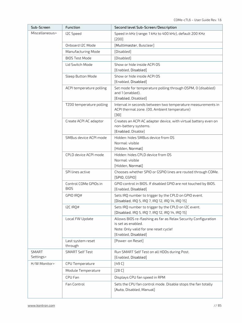
COMe-cTL6 – User Guide Rev. 1.6
www.kontron.com // 85
Sub-Screen Function Second level Sub-Screen/Description
Miscellaneous> I2C Speed Speed in kHz (range: 1 kHz to 400 kHz), default 200 KHz [200]
Onboard I2C Mode [Multimaster, Busclear]
Manufacturing Mode [Disabled]
BIOS Test Mode [Disabled]
Lid Switch Mode Show or hide inside ACPI OS [Enabled, Disabled]
Sleep Button Mode Show or hide inside ACPI OS [Enabled, Disabled]
ACPI temperature polling Set mode for temperature polling through OSPM, 0 (disabled) and 1 (enabled). [Enabled, Disabled]
TZ00 temperature polling Interval in seconds between two temperature measurements in ACPI thermal zone. (00, Ambient temperature) [30]
Create ACPI AC adaptor Creates an ACPI AC adapter device, with virtual battery even on non-battery systems. [Enabled, Disable]
SMBus device ACPI mode Hidden: hides SMBus device from OS Normal: visible [Hidden, Normal]
CPLD device ACPI mode Hidden: hides CPLD device from OS Normal: visible [Hidden, Normal]
SPI lines active Chooses whether SPIO or GSPIO lines are routed through COMe. [SPIO, GSPIO]
Control COMe GPIOs in BIOS
GPIO control in BIOS. If disabled GPIO are not touched by BIOS. [Enabled, Disabled]
GPIO IRQ# Sets IRQ number to trigger by the CPLD on GPIO event. [Disabled, IRQ 5, IRQ 7, IRQ 12, IRQ 14, IRQ 15]
I2C IRQ# Sets IRQ number to trigger by the CPLD on I2C event. [Disabled, IRQ 5, IRQ 7, IRQ 12, IRQ 14, IRQ 15]
Local FW Update Allows BIOS re-flashing as far as Relax Security Configuration is set as enabled. Note: Only valid for one reset cycle! [Enabled, Disabled]
Last system reset through
[Power-on Reset]
SMART Settings>
SMART Self Test Run SMART Self Test on all HDDs during Post. [Enabled, Disabled]
H/W Monitor>
CPU Temperature [49 C]
Module Temperature [28 C]
CPU Fan Displays CPU fan speed in RPM
Fan Control Sets the CPU fan control mode. Disable stops the fan totally [Auto, Disabled, Manual]
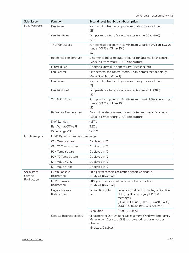
COMe-cTL6 – User Guide Rev. 1.6
www.kontron.com // 86
Sub-Screen Function Second level Sub-Screen/Description
H/W Monitor>
Fan Pulse Number of pulse the fan produces during one revolution [2]
Fan Trip Point Temperature where fan accelerates (range: 20 to 80 C) [50]
Trip Point Speed Fan speed at trip point in %. Minimum value is 30%. Fan always runs at 100% at TJmax 10 C. [50]
Reference Temperature Determines the temperature source for automatic fan control. [Module Temperature, CPU Temperature]
External Fan Displays External Fan speed RPM (If connected)
Fan Control Sets external fan control mode. Disable stops the fan totally [Auto, Disabled, Manual]
Fan Pulse Number of pulse the fan produces during one revolution [2]
Fan Trip Point Temperature where fan accelerates (range: 20 to 80 C) [50]
Trip Point Speed Fan speed at trip point in %. Minimum value is 30%. Fan always runs at 100% at TJmax 10 C. [50]
Reference Temperature Determines the temperature source for automatic fan control. [Module Temperature, CPU Temperature]
5.0V Standby 4.57 V
Batt Volt at COMe Pin 2.92 V
Widerrange VCC 12.01 V
DTR Manager> Intel® Dynamic Temperature Range
CPU Temperature Displayed in °C
CPU T0 Temperature Displayed in °C
PCH Temperature Displayed in °C
PCH T0 Temperature Displayed in °C
DTR value / CPU Displayed in °C
DTR value / PCH Displayed in °C
Serial Port Console Redirection>
COM0 Console Redirection
COM port 0 console redirection enable or disable. [Enabled, Disabled]
COM1 Console Redirection
COM port 1 console redirection enable or disable. [Enabled, Disabled]
Legacy Console Redirection>
Redirection COM Port
Selects a COM port to display redirection of legacy OS and Legacy OPROM messages [COM0 (PCI Bus0, Dev30, Func0, Port1), COM1 (PCI Bus0, Dev30, Func1, Port1]
Resolution [80x24, 80x25]
Console Redirection EMS Serial port for Out-Of-Band Management Windows Emergency Management Services (EMS) console redirection enable or disable. [Enabled, Disabled]

COMe-cTL6 – User Guide Rev. 1.6
www.kontron.com // 87
Sub-Screen Function Second level Sub-Screen/Description
Intel TXT Information>
Read only field Chipset, BiosAcm. Chipset Txt, CPU Txt, Error code, Class code, Major code and Minor code
Switchable Graphics>
SG Mode Select Muxless
PCI Subsystem Settings
PCI Settings Common for all Devices
Re-Size BAR Support If Resizable BAR capable PCIe deviecs are present, this option enables or disables Resizable BAR Support. [Enabled, Disabled]
BME DMA Mitigation Re-enables Bus Master Attribute disabled during PCI enumeration for PCI Bridges after SMM Locked. [Enabled, Disabled]
Warning: Changing PCI Device(s) settings may have unwanted side effects! System may HANG! PROCEED WITH CAUTON
USB Configuration>
Read Only Field USB Configuration: USB Module Version, USB Controllers (2 XHCIs) USB Devices (drives, keyboard, mouse, hub)
Legacy USB Support Enables legacy USB support. Auto disables legacy support if no USB devices are connected. Disable keeps USB devices available only for EFI applications. [Enabled, Disabled, Auto]
XHCI Hand-off Known work around for OSes without XHCI hand-off support. The XHCI ownership change should be claimed by XHCI driver. [Enabled, Disabled]
USB Mass Storage Driver Support
[Enabled, Disabled]
USB hardware delays and time-outs:
USB transfer time-out Time out value for Control, Bulk and Interrupt. [1 sec, 5 sec, 10 sec, 20 sec]
Device reset time-out USB mass storage device Start Unit command time-out. [1 sec, 5 sec, 10 sec, 20 sec]
Device power-up delay Maximum time device takes before reporting to the host controller properly. Auto uses default value (for a root port 100 ms and for a Hub port the delay is taken from hub descriptor). [Auto, Manual]
Mass Storage Devices:
Pi-KVM CD-ROM Drive 0510
Mass storage device emulation type. Auto enumerates devices according to their media format. Optical drives are emulated as CDROM, drives with no media will be emulated according to drive type. [Auto, Floppy, Forced FDD, Hard Disk, CD-Rom]
Network Stack Configuration >
Network Stack UEFI Network Stack [Enabled, Disabled]
CSM Configuration>
CSM Support Enables or disables CSM Support. [Enabled, Disabled]

COMe-cTL6 – User Guide Rev. 1.6
www.kontron.com // 88
Sub-Screen Function Second level Sub-Screen/Description
NVMe Configuration>
Depends on hardware configuration.
TLS Auth Configuration>
Server CA Configuration> Enroll Cert> Enroll Cert Using File
Cert Guide> Input digital character
Commit Changes and Exit
Discard Changes and exit
Delete Cert>
Client Cert Configuration
RAM Disk Configuration>
Disk Memory Type Specifies type of memory to use from available memory pool in system to create a disk. [Boot Service Data, Reserved]
Create raw> Size (Hex)
The valid RAM disk size should be multiples of the RAM disk block size.
Create & Exit Create a new RAM disk with the given starting and ending address.
Discard & Exit
Create from file Create a RAM from a given file
Created RAM disk list:
Remove selected RAM disk(s)
Removes selected RAM disk(s)
Driver Health> Intel® Gigabit 0.9.03 Provides health status for the drivers/controllers [Healthy]

COMe-cTL6 – User Guide Rev. 1.6
www.kontron.com // 89
6.4.3. Chipset Menu
Setting items, on this screen, to incorrect values may cause system malfunctions.
UART0 will not be disabled for usage in an operating system because it uses a PCI root function, which would cause all serial interfaces to disappear if being disabled. So though being set to 'disabled' it will be available in any operating system after boot. All other devices in the screen can be disabled for usage in BIOS and OS.
Figure 17: Chipset Menu Initial Screen

COMe-cTL6 – User Guide Rev. 1.6
www.kontron.com // 90
6.4.3.1. Chipset System Agent (SA) Configuration Menu
Figure 18: Chipset> System Agent (SA) Configuration Setup Menu Initial Screen
The following table shows the Chipset System Agent (SA) Configuration sub-screen and describes the function. Default settings are in bold.
Table 69: Chipset menu Sub-screens and Functions
Function Second level Sub-Screen/Description
VT-d Supported
Memory Configuration>
Read only field Memory Configuration: Memory RC Version, Memory Speed, Memory Timings, for Controller #-Channel #-Slot #: Size, Number of Ranks and Manufacturer.
Override Performance Downgrade for Mixed Memory
Enable override to remove performance limitation when mixed memory modules are populated. [Enabled, Disabled]
Memory Test on Warm Boot
Base memory test run in warm boot. [Enabled, Disabled]
Maximum Memory Frequency
Selects maximum memory frequency in MHz [Auto, 1067, 1200, …8400]
HOB Buffer Size Selects size of HOB Buffer. [Auto, 1B, 1KB, Max(assuming 63 KB total HOB size)]
Max TOLUD Maximum value of TOULD. Dynamic adjusts TOULD automatically based on largest MMIO length of installed graphic controller. [Dynamic, 1 GB, 1.25 GB,…. 3.5 GB]

COMe-cTL6 – User Guide Rev. 1.6
www.kontron.com // 91
Function Second level Sub-Screen/Description
Memory Configuration>
In-Band ECC Support
Enables or disables In-Band ECC. Either IBECC or the TME can be enabled. [Enabled, Disabled]
Fast Boot Fast path through the MRC [Enabled, Disabled]
Graphics Configuration>
Skip Scanning Slots for External Gfx
Enable will not scan for external Gfx cards on PEG and PCH PCIe ports.
[Enabled, Disabled]
Primary Display Selects which graphics device is the primary display. Hybrid Gfx (HG) can be chosen alternatively. [Auto, IGFX, PEG Slot, PCH PCI, Hybrid Gfx]
Select PCIE Card Selects the card used on the platform. [Auto, Elk Creek 4, PEG Eval]
External Gfx Card Primary Display Configuration
(Depends on hardware configuration.)
Internal Graphics Keep IGfx based on the setup option. [Auto, Disabled, Enabled]
GTT Size Selects the GTT Size. [2 MB, 4 MB, 8 MB]
Aperture Size Selects the Aperture Size. Note: above 4GB MMIO BIOS assignment is automatically enabled when selecting 2048 MB aperture. To use this feature disable CSM Support. [128 MB, 256 MB, 512 MB, 1024 MB]
DVMT Pre-Allocated
Select DVMT 5.0 pre-allocated (fixed) Graphics Memory size used by the Internal Graphics device. [0 M, 32 M, …60 M]
DVMT Total Gfx Mem
Select DVMT 5.0 Total Graphics Memory size used by the Internal Graphics device. [128 M, 256 M, MAX]
IGD Configuration>
Read only field IGD Managed by, Intel® GOP Driver, LVDS EEPROM Data, Data Format, Resolution, Color Depth, Channel Count
IGD Boot Type Selects the video device activated during POST. This has no effect if external graphics are present. [Auto, LFP, LFP2, DP0, DP1, DP2, DP3]
LFD Panel Type [LVDS, eDP]
Panel Color Depth [18 Bit, 24 Bit VESA, 24 Bit oLDI]
Panel Channel Mode [Auto, Single, Dual]
Backlight Control [None/External, PWM, PWM Inverted, I2C, I2C Inverted]
PWM Frequency [200 Hz, 400 Hz, ….40 kHz]

COMe-cTL6 – User Guide Rev. 1.6
www.kontron.com // 92
Function Second level Sub-Screen/Description
Graphics Configuration>
IGD Configuration>
Backlight Value Sets LCD backlight brightness (0-255) [128]
LVDS Clock Center Spreading
[No Spreading, 0.5%, 1.0%, 1.5%, 2.0%, 2.5%]]
EFP3(DP0) Type [DP with HDMI/DVI]
EFP4(DP1) Type [DP with HDMI/DVI]
EFP5(DP2) Type [DP with HDMI/DVI]
EFP6(DP3) Type [DisplayPort Only]
PCIe Gen4 Lane Order
PCIe Gen4 Lane Order
Allows for reverse lanes for SystemAgents based PCIe Gen4 port (x4) [Normal, Reversed]
VMD Setup Menu
VMD controller [Disabled]
PCI Express Configuration
PCIe 4.0 Slot Select>
Select the PCIe M2 or CEMx4 slot [M2, CEMx4 slot]
PCIe Gen4 RP1 (PEG60)>
PCI Expr. Root Port 1> Control the PCIe 4.0 Root port. [Enabled, Disabled]
Connection Type Selects the connection type to the root port. [Built-in, Slot]
ASPM4 Sets the ASPM level. [Disabled, L1]
L1 Substates PCI Express L1 Substates settings. L1SS cannot be enabled when CLKREQMSG is disabled. [Disabled, L1.1, L1.1 & L1.2]
PCIe 4.0 Speed Configure PCIE 4.0 interface speed [Auto, Gen1, Gen2, Gen3, Gen4]]
IOTG Mode [Enabled, Disabled]
Transmitter half swing [Enabled, Disabled]
Detect Timeout The number of msec the reference code will wait for link to exit Detect State for enabled port before assuming there is no device and potentially disabling the port. 0
P2P Support Program P2P support registers according to setup option. [Enabled, Disabled]
Stop Grant Configuration
[Auto, Manual]
VT-d [Enabled, Disabled]
X2APIC Opt Out [Enabled, Disabled]
DMA Control Guarantee
[Enabled, Disabled]

COMe-cTL6 – User Guide Rev. 1.6
www.kontron.com // 93
Function Second level Sub-Screen/Description
Thermal Device (B0:D4:F0)
SA Thermal Device is always enabled for ICL A0 stepping. [Enabled, Disabled]
CPU Crashlog (Device 10)
[Enabled, Disabled]
GNA Device (B0:D8:F0)
SystemAgent Gaussian Network Accelerator (GNA) Device. [Enabled, Disabled]
CRID Support SystemAgent CRID and TCSS CRID control for Intel SIPP. [Enabled, Disabled]
WRC Feature SystemAgent WRC (write cache) features on IOP. When enabled supports IO devices allocating onto the ring and into LLC. [Enabled, Disabled]
VCRt mapping to PEG
[Enabled, Disabled]
Above 4GB MMIO BIOS Assignment
Above 4 GB memory mapping IO BIOS assignment. Note: Enabled automatically when aperture size is set to 2048 MB [Enabled, Disabled]

COMe-cTL6 – User Guide Rev. 1.6
www.kontron.com // 94
6.4.3.2. Chipset PCH-IO Configuration Setup Menu
Figure 19: Chipset PCH-IO Configuration Setup menu Initial Screen
The following table shows the Chipset PCH-IO Configuration sub-screens and describes the functions. Default settings are in bold.
Table 70: Chipset PCH-IO Configuration
Function Second level Sub-Screen/Description
PCI Express Configuration>
COMe PCIe mapping scheme 5x1 (Standard)
Port8xh Decode PCI Express Port 8xh Decode [Enabled, Disabled]
PCIe Root Port 1, 2, 3, 4, 11, 12>(USB/SATA) PCIe Root Port 5> (COMe Lane 0) PCIe Root Port 6> (COMe Lane 1) PCIe Root Port 7> (COMe Lane 2) PCIe Root Port 8> (COMe Lane 3) PCIe Root Port 9> (COMe Lane 4) PCIe Root Port 10> (on-module Ethernet)
PCI Expr. Root Port #
Control the PCIe 4.0 Root port. [Enabled, Disabled]
Connection Type
Selects the connection type to root port. [Built-in, Slot]
ASPM Sets the ASPM level: [Disabled, L0s, L1, L0sL1, Auto]
PME SCI [Enabled, Disabled]
Hot Plug [Enabled, Disabled]
PCIe Speed Configure PCIe Speed [Auto, Gen1, Gen2, Gen3]

COMe-cTL6 – User Guide Rev. 1.6
www.kontron.com // 95
Function Second level Sub-Screen/Description
PCI Express Configuration>
PCIe Root Port 1, 2, 3, 4, 11, 12>(USB/SATA) PCIe Root Port 5> (COMe Lane 0) PCIe Root Port 6> (COMe Lane 1) PCIe Root Port 7> (COMe Lane 2) PCIe Root Port 8> (COMe Lane 3) PCIe Root Port 9> (COMe Lane 4) PCIe Root Port 10> (on-module Ethernet)
Detect Timeout
Value in msec the reference code waits for link to exit Detect State for enabled port before assuming there is no device and potentially disabling the port. 0
Extra Bus Reserved
Extra Bus Reserved (0-7) for bridges behind this Root Bridge. 0
Reserved Memory
Reserved memory for this Root Bridge (1-20) MB 10
Reserved I/O
Reserved I/O (4K/8K/12K/16K/20K) Range for this Root bridge 4
SATA and RST Configuration>
SATA Controller [Enabled, Disabled]
SATA Mode Selection [AHCI]
SATA Speed Limit [Auto, 1.5 Gb/s, 3.0 Gb/s, 6 Gb/s]
Software Feature Mask Configuration> HDD Unlock
Enable indicates the HDD password unlock in the OS is enabled. [Enabled, Disabled]
LED Locate Enable indicates that LED/SGPIO hardware is attached and ping to locate feature is enabled on OS. [Enabled, Disabled]
Serial ATA Port 0, 1> Port 0, 1 [Enabled, Disabled]
External Marks the port as external. [Enabled, Disabled]
Spin Up Device
Staggered Spin Up performed and only on drives with this option enabled spin up at boot. Otherwise all drives spin up at boot. [Enabled, Disabled]
SATA Device Type
Identifies connected device. [Hard Disk Drive, Solid State Drive]
USB Configuration>
xDCI Support Enables or disables xDCI (USB OTG device) [Enabled, Disabled]
USB2 PHY Sus Well Power Gating Enable SUS Well PG for USB2 PHY. This option has no effect on PCH-H. [Enabled, Disabled]
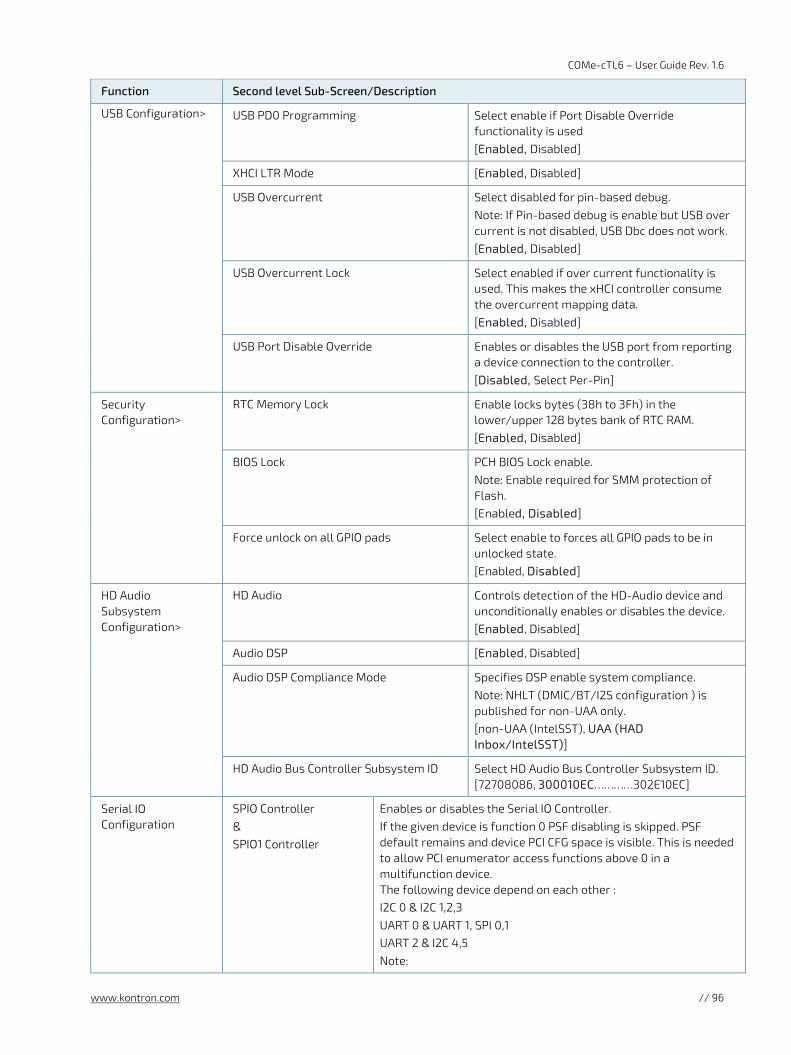
COMe-cTL6 – User Guide Rev. 1.6
www.kontron.com // 96
Function Second level Sub-Screen/Description
USB Configuration> USB PD0 Programming Select enable if Port Disable Override functionality is used [Enabled, Disabled]
XHCI LTR Mode [Enabled, Disabled]
USB Overcurrent Select disabled for pin-based debug. Note: If Pin-based debug is enable but USB over current is not disabled, USB Dbc does not work. [Enabled, Disabled]
USB Overcurrent Lock Select enabled if over current functionality is used. This makes the xHCI controller consume the overcurrent mapping data. [Enabled, Disabled]
USB Port Disable Override Enables or disables the USB port from reporting a device connection to the controller. [Disabled, Select Per-Pin]
Security Configuration>
RTC Memory Lock Enable locks bytes (38h to 3Fh) in the lower/upper 128 bytes bank of RTC RAM. [Enabled, Disabled]
BIOS Lock PCH BIOS Lock enable. Note: Enable required for SMM protection of Flash. [Enabled, Disabled]
Force unlock on all GPIO pads Select enable to forces all GPIO pads to be in unlocked state. [Enabled, Disabled]
HD Audio Subsystem Configuration>
HD Audio Controls detection of the HD-Audio device and unconditionally enables or disables the device. [Enabled, Disabled]
Audio DSP [Enabled, Disabled]
Audio DSP Compliance Mode Specifies DSP enable system compliance. Note: NHLT (DMIC/BT/I2S configuration ) is published for non-UAA only. [non-UAA (IntelSST), UAA (HAD Inbox/IntelSST)]
HD Audio Bus Controller Subsystem ID Select HD Audio Bus Controller Subsystem ID. [72708086, 300010EC…………302E10EC]
Serial IO Configuration
SPIO Controller & SPIO1 Controller
Enables or disables the Serial IO Controller. If the given device is function 0 PSF disabling is skipped. PSF default remains and device PCI CFG space is visible. This is needed to allow PCI enumerator access functions above 0 in a multifunction device. The following device depend on each other : I2C 0 & I2C 1,2,3 UART 0 & UART 1, SPI 0,1 UART 2 & I2C 4,5 Note:

COMe-cTL6 – User Guide Rev. 1.6
www.kontron.com // 97
Function Second level Sub-Screen/Description
Serial IO Configuration
SPIO Controller & SPIO1 Controller
UART0 (00:30:00) cannot be disabled when child device is enabled like CNVi Bluetooth (\_SB.PC00.UA00.BTH=) UART0 (00:30:00) cannot be enabled when I2S Audio codec is enabled (\SB.PC00.I2C0.HDAC) [Enabled, Disabled]
UART0 Controller [Enabled]
UART1 Controller [Enabled]
UART2 Controller [Disabled]
Serial IO SPI1 Settings> ChipSelect 0 polarity
Sets initial polarity of ChipSelect signal. Initial low is with initial idle polarity of low. [Active Low, Active High]
ChipSelect 1 polarity
Serial IO UART0 Settings>
Hardware Flow Control
[Disabled]
Timing parameters disabled
Serial IO UART1 Settings>
Hardware Flow Control
[Disabled]
Timing parameters disabled
State after G3 Specifies the state to go to when power is reapplied after a power failure (G3 state). [S0 State, S5 State]
Port 80h Redirection
Controls where the port 80h cycles are sent. [LPC Bus, PCIE Bus]
Enhance Port 80h LPC Decoding
Supports the word/dword decoding of port 80h behind LPC. [Enabled, Disabled]
Legacy IO Low Latency
Sets to enable low latency of legacy IO. Note: Some system requires lower IO latency irrespective of power. This is a tradeoff between power and IO latency. [Enabled, Disabled]
Timed GPIO0 Enables or disables Timed GPIO0 Note: disabled will disable cross time stamp time-synchronization as extension of Hammock Harbor time synchronization. [Enabled, Disabled]
Timed GPIO1 Enables or disables Timed GPIO1 Note: disabled will disable cross time stamp time-synchronization as extension of Hammock Harbor time synchronization. [Enabled, Disabled]
PCIe Ref PLL SSCEN PCIe Ref PLL SC percentage. Range (0% to 5%) Auto = keep hardware default [Auto, 0.0%, 0.1%, 0.2%, 0.3%, 0.4%, 0.5%]
SPD Write Lock or release SPD write capability. For security recommendations, SPD write lock must be set. [Locked, Released]
Extended BIOS Range Decoder
Enable causes memory cycles falling in a specific area to be redirected to a SPI flash controller. [Enabled, Disabled]

COMe-cTL6 – User Guide Rev. 1.6
www.kontron.com // 98
6.4.4. Security Setup Menu The Security Setup menu provides information about the passwords and functions for specifying the security settings. The passwords are case-sensitive.
Figure 20: Security Setup Menu Initial Screen
The following table shows the Security set up sub-screens and functions, and describes the content.
Table 71: Security Setup Menu Functions
Function Description
Administrator Password Sets administrator password
User Password Sets user password
Secure Boot
Secure Boot When enabled Platform key (PK) is enrolled and the system is in user mode. The mode change requires platform reset. [Enabled, Disabled]
Secure Boot Mode In Custom mode, Secure Boot Policy variables can be configured by a physically present user without full authentication. [Custom, Standard]
Restore Factory Keys Force system to user mode. Install factory default secure Boot key databases. [Yes, No]
Reset to Setup Mode
Key Management>
Factory Key Provision [Enabled, Disabled]
Restore Factor Keys [Yes, No]
Enroll Efi Image [OK]
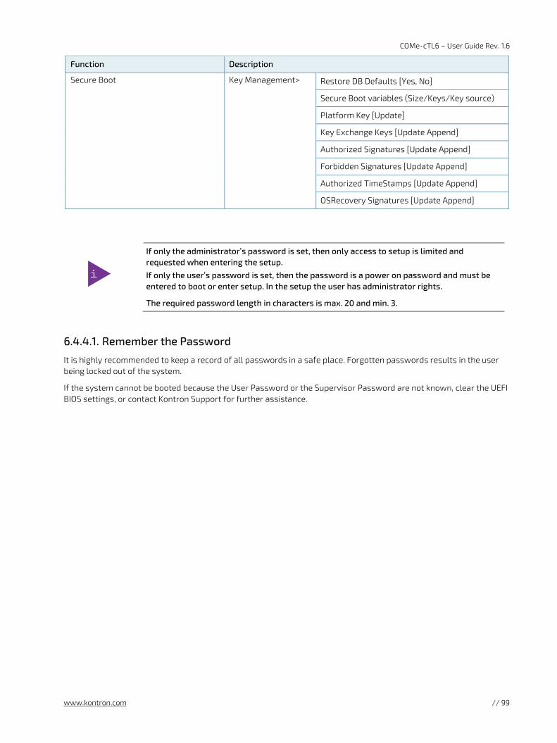
COMe-cTL6 – User Guide Rev. 1.6
www.kontron.com // 99
Function Description
Secure Boot Key Management> Restore DB Defaults [Yes, No]
Secure Boot variables (Size/Keys/Key source)
Platform Key [Update]
Key Exchange Keys [Update Append]
Authorized Signatures [Update Append]
Forbidden Signatures [Update Append]
Authorized TimeStamps [Update Append]
OSRecovery Signatures [Update Append]
If only the administrator’s password is set, then only access to setup is limited and requested when entering the setup.
If only the user’s password is set, then the password is a power on password and must be entered to boot or enter setup. In the setup the user has administrator rights.
The required password length in characters is max. 20 and min. 3.
6.4.4.1. Remember the Password
It is highly recommended to keep a record of all passwords in a safe place. Forgotten passwords results in the user being locked out of the system.
If the system cannot be booted because the User Password or the Supervisor Password are not known, clear the UEFI BIOS settings, or contact Kontron Support for further assistance.

COMe-cTL6 – User Guide Rev. 1.6
www.kontron.com // 100
6.4.5. Boot Menu
The Boot menu provides functions for booting up the setup program.
Figure 21: Boot Screen
Table 72: Boot Menu Functions
Function Description
Boot Configuration
Setup Prompt Timeout Number of seconds to wait for setup activation key. 65535 (0xFFFF) means indefinite waiting. 1
Bootup NumLock State [On, Off]
Quiet Boot [Enabled, Disabled]
Boot Option Priorities
Boot Option #1 Set the system boot order [UEFI: Built-in EFI Shell, Disabled]
Fast Boot [Enabled, Disable]

COMe-cTL6 – User Guide Rev. 1.6
www.kontron.com // 101
6.4.6. Save and Exit Setup Menu
The Save and Exit setup menu provides functions for handling changes made to the UEFI BIOS settings and exiting the setup program.
Figure 22: Save and Exit Setup Menu Initial Screen
Table 73: Save and Exit Setup Menu Functions
Function Description
Save Changes and Exit Exits system after saving changes
Discard Changes and Exit Exits system setup without saving changes
Save Changes and Reset Resets system after saving changes
Discard Changes and Reset Resets system setup without saving changes
Save Changes Saves changes made so far for any setup options
Discard Changes Discards changes made so far for any setup options
Restore Defaults Restores/loads standard default values for all setup options
Save as User Defaults Saves changes made so far as user defaults
Restore User Defaults Restores user defaults to all setup options
Boot Override Attempts to launch the built-in EFI Shell

COMe-cTL6 – User Guide Rev. 1.6
www.kontron.com // 102
7/ Technical Support For technical support, contact our Support department:
E-mail: [email protected]
Phone: +49-821-4086-888
Make sure you have the following information available when you call:
Product ID Number (PN),
Serial Number (SN)
Module’s revision
Operating System and Kernel/Build version
Software modifications
Addition connected hardware/full description of hardware set up
The serial number can be found on the Type Label, located on the product’s rear side.
Be ready to explain the nature of your problem to the service technician.
7.1. Warranty
Due to their limited service life, parts that by their nature are subject to a particularly high degree of wear (wearing parts) are excluded from the warranty beyond that provided by law. This applies to the CMOS battery, for example.
If there is a protection label on your product, then the warranty is lost if the product is opened.
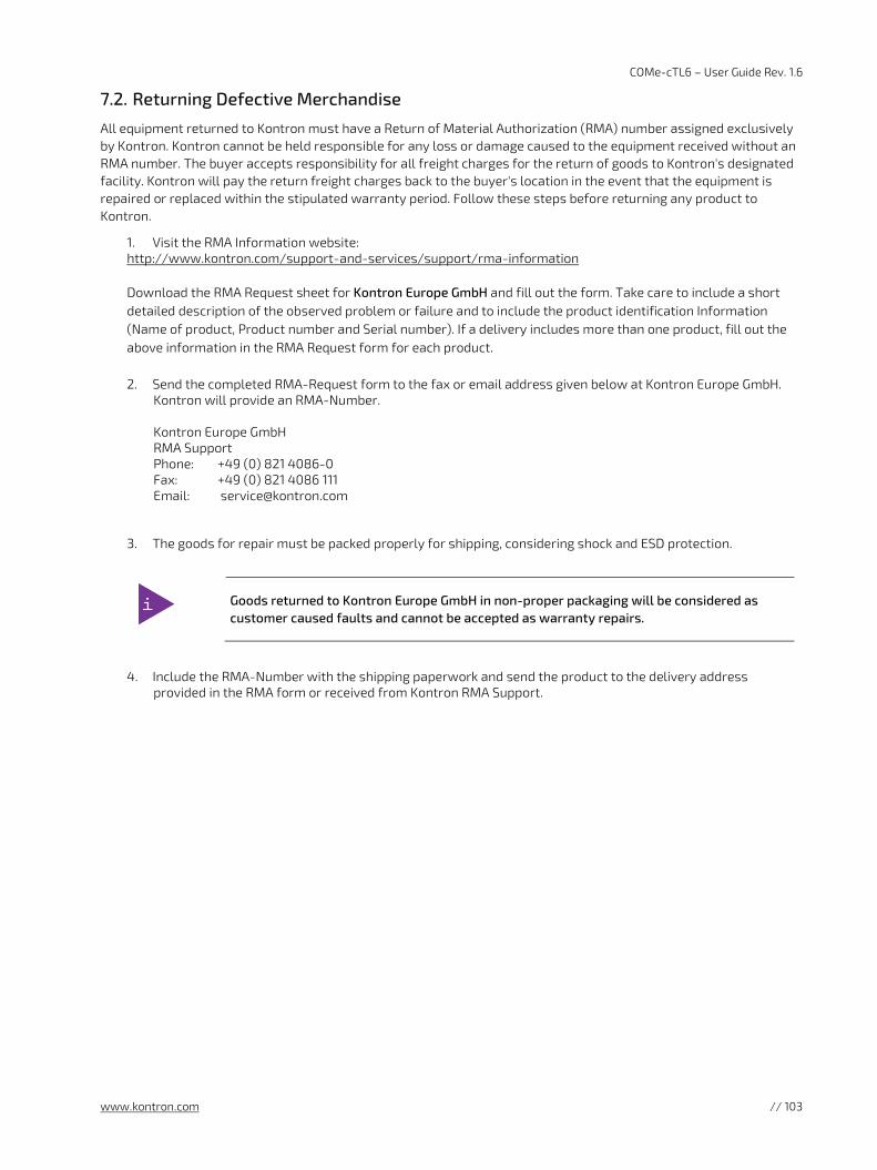
COMe-cTL6 – User Guide Rev. 1.6
www.kontron.com // 103
7.2. Returning Defective Merchandise
All equipment returned to Kontron must have a Return of Material Authorization (RMA) number assigned exclusively by Kontron. Kontron cannot be held responsible for any loss or damage caused to the equipment received without an RMA number. The buyer accepts responsibility for all freight charges for the return of goods to Kontron's designated facility. Kontron will pay the return freight charges back to the buyer's location in the event that the equipment is repaired or replaced within the stipulated warranty period. Follow these steps before returning any product to Kontron.
1. Visit the RMA Information website: http://www.kontron.com/support-and-services/support/rma-information
Download the RMA Request sheet for Kontron Europe GmbH and fill out the form. Take care to include a short detailed description of the observed problem or failure and to include the product identification Information (Name of product, Product number and Serial number). If a delivery includes more than one product, fill out the above information in the RMA Request form for each product. 2. Send the completed RMA-Request form to the fax or email address given below at Kontron Europe GmbH.
Kontron will provide an RMA-Number.
Kontron Europe GmbH RMA Support Phone: +49 (0) 821 4086-0 Fax: +49 (0) 821 4086 111 Email: [email protected]
3. The goods for repair must be packed properly for shipping, considering shock and ESD protection.
Goods returned to Kontron Europe GmbH in non-proper packaging will be considered as customer caused faults and cannot be accepted as warranty repairs.
4. Include the RMA-Number with the shipping paperwork and send the product to the delivery address provided in the RMA form or received from Kontron RMA Support.

COMe-cTL6 – User Guide Rev. 1.6
www.kontron.com // 104
Appendix A: List of Acronyms
Table 74: List of Acronyms
ACPI Advanced Configuration Power Interface
API Application Programming Interface
Basic Module
COM Express® 125 x 95 Module form factor
BIOS Basic Input Output System
BMC Base Management Controller
BSP Board Support Package
BPP Bit Per Pixel
CAN Controller-area network
Carrier Board
Application specific circuit board that accepts a COM Express ® module
COM Computer-on-Module
Compact Module
COM Express® 95x95 Module form factor
CNTG Computer Network Transaction Group
DDC Display Data Control
DDI Digital Display Interface –
DIMM Dual In-line Memory Module
Display Port
DisplayPort (digital display interface standard)
DMA Direct Memory Access
DRAM Dynamic Random Access Memory
DVI Digital Visual Interface
EAPI Embedded Application Programming Interface
ECC Error Checking and Correction
EEPROM Electrically Erasable Programmable Read-Only Memory
eDP Embedded Display Port
EMC Electromagnetic Compatibility (EMC)
ESD Electro Sensitive Device
Extended Module
COM Express® 155mm x 110mm Module form factor.
FIFO First In First Out
FRU Field Replaceable Unit
Gb Gigabit
GBE Gigabit Ethernet
GPI General Purpose Input
GPIO General Purpose Input Output
GPO General Purpose Output
GPU Graphics Processing Unit
HBR2 High Bitrate 2
HDA High Definition Audio (HD Audio)
HD/HDD Hard Disk /Drive
HDMI High Definition Multimedia Interface
HPM PICMG Hardware Platform Management specification family
I2C Inter integrated Circuit Communications
IOL IPMI-Over-LAN
IOT Internet of Things
IPMI Intelligent Platform Management Interface
KCS Keyboard Controller Style
KVM Keyboard Video Mouse
LAN Local Area Network
LPC Low Pin-Count Interface:
LVDS Low Voltage Differential Signaling
M.A.R.S. Mobile Application for Rechargeable Systems
MDI Media Dependent Interface
MEI Management Engine Interface
Mini Module
COM Express® 84x55mm Module form factor
MTBF Mean Time Before Failure
NA Not Available
NC Not Connected
NCSI Network Communications Services Interface
PATA Parallel AT Attachment
PCI Peripheral Component Interface
PCIe PCI-Express
PECI Platform Environment Control Interface
PEG PCI Express Graphics
PICMG® PCI Industrial Computer Manufacturers Group
PHY Ethernet controller physical layer device
Pin-out Type
COM Express® definitions for signals on COM Express® Module connector pins.
PS2 Personal System 2 ( keyboard & mouse)
PSU Power Supply Unit
RoHS Restriction of Hazardous Substances
RTC Real Time Clock

COMe-cTL6 – User Guide Rev. 1.6
www.kontron.com // 105
SAS Serial Attached SCSI – high speed serial version of SCSI
SATA Serial AT Attachment:
SCSI Small Computer System Interface
SEL System Event Log
ShMC Shelf Management Controller
SMBus System Management Bus
SO-DIMM Small Outline Dual in-line Memory Module
SOIC Small Outline Integrated Circuit
SOL Serial Over LAN
SPI Serial Peripheral Interface
SSH Secure Shell
TPM Trusted Platform Module
UART Universal Asynchronous Receiver Transmitter
UEFI Unified Extensible Firmware Interface
UHD Ultra High Definition
ULP Ultra Low Power
USB Universal Serial Bus
VGA Video Graphics Adapter
VLP Very Low Profile
WDT Watch Dog Timer
WEEE Waste Electrical and Electronic Equipment ( directive)
COMe-cTL6 – User Guide Rev. 1.6
www.kontron.com // 106
About Kontron – Member of the S&T Group
Kontron is a global leader in IoT/Embedded Computing Technology (ECT). As a part of technology group S&T, Kontron offers a combined portfolio of secure hardware, middleware and services for Internet of Things (IoT) and Industry 4.0 applications. With its standard products and tailor-made solutions based on highly reliable state-of-the-art embedded technologies, Kontron provides secure and innovative applications for a variety of industries. As a result, customers benefit from accelerated time-to-market, reduced total cost of ownership, product longevity and the best fully integrated applications overall.
For more information, please visit: www.kontron.com
GLOBAL HEADQUARTERS
Kontron Europe GmbH Gutenbergstraße 2 85737 Ismaning, Germany Tel.: + 49 821 4086-0 Fax: + 49 821 4086-111 [email protected]