CMOS Magnetic Particle Flow Cytometer - UC Berkeley EECS
76
CMOS Magnetic Particle Flow Cytometer Pramod Murali Electrical Engineering and Computer Sciences University of California at Berkeley Technical Report No. UCB/EECS-2017-175 http://www2.eecs.berkeley.edu/Pubs/TechRpts/2017/EECS-2017-175.html December 1, 2017
-
Upload
khangminh22 -
Category
Documents
-
view
2 -
download
0
Transcript of CMOS Magnetic Particle Flow Cytometer - UC Berkeley EECS
CMOS Magnetic Particle Flow Cytometer
Pramod Murali
Electrical Engineering and Computer SciencesUniversity of California at Berkeley
Technical Report No. UCB/EECS-2017-175http://www2.eecs.berkeley.edu/Pubs/TechRpts/2017/EECS-2017-175.html
December 1, 2017
Copyright © 2017, by the author(s).All rights reserved.
Permission to make digital or hard copies of all or part of this work forpersonal or classroom use is granted without fee provided that copies arenot made or distributed for profit or commercial advantage and that copiesbear this notice and the full citation on the first page. To copy otherwise, torepublish, to post on servers or to redistribute to lists, requires prior specificpermission.
Acknowledgement
I would like to express gratitude to my family, teachers and friends for theirsupport, guidance and sacrifice. In particular, I thank my advisor Prof.Bernhard Boser for his constructive feedback and support. I also thank Prof.Ali Niknejad, Prof. Michel Maharbiz, Prof. Luke Lee, Prof. David Allstot fortheir valuable time and guidance. I thank the staff of BSAC, Swarm Lab, BWRC, ERSO, IRIS of UC Berkeleyparticularly Abdelrahman Elhadi, Alejandro Luna, Brian Richards, Kim Ly,Mila MacBain, Patrick Hernan, Richard Lossing, Shelley Kim, ShirleySolanio,Winthrop Williams for their efficient administrative and lab support. I thankTSMC University Shuttle program for fabricating the CMOS chip. Chipfabrication by TSMC is gratefully acknowledged.
CMOS Magnetic Particle Flow Cytometer
by
Pramod Murali
A dissertation submitted in partial satisfaction of the
requirements for the degree of
Doctor of Philosophy
in
Engineering - Electrical Engineering and Computer Sciences
in the
Graduate Division
of the
University of California, Berkeley
Committee in charge:
Professor Bernhard E. Boser, ChairProfessor Ali M. Niknejad
Professor Luke P. Lee
Fall 2015
CMOS Magnetic Particle Flow Cytometer
Copyright 2015
by
Pramod Murali

1
Abstract
CMOS Magnetic Particle Flow Cytometer
by
Pramod Murali
Doctor of Philosophy in Engineering - Electrical Engineering and Computer Sciences
University of California, Berkeley
Professor Bernhard E. Boser, Chair
Neutrophils, a class of white blood cells, are our bodys first line of defense against invading
pathogens. When the number of neutrophils in blood drops to 200cells/µL, it leads to a
critical clinical condition called neutropenia. Currently, optical flow cytometry is the most
common and powerful technique used to diagnose neutropenia, but the centralized nature of
the test, time-consuming sample preparation and high cost prevent real-time modification
of treatment regimens.
In this thesis, we propose an approach of using magnetic labels to tag and detect cells that
allows us to design a low cost point-of-care flow cytometer to diagnose neutropenia. The
cytometer cartridge integrates a gravity driven microfluidic channel with a CMOS sensor
chip that detects magnetically labeled cells as they flow over it.
The sensor combines an on-chip excitation coil that magnetizes the labels and a pick-up
coil that detects them. The high frequency RF signal from the sensor is down-converted and
amplified by on-chip receiver circuitry, which has been optimized to maximize the signal to
noise ratio. The functionality of the cytometer is demonstrated with SKBR3 cancer cells
labeled with 1µm magnetic labels using streptavidin-biotin chemistry. The SKBR3 cells are
used in lieu of neutrophils as they can be cultured in a laboratory setting and pose minimal
bio-hazard. Furthermore, the high frequency operation of the sensor enables classification of
two types of magnetic labels, which is necessary to obtain absolute cell-counts.

i
To my grandmother: Rangamma Narasappa

ii
Contents
Contents ii
List of Figures iii
List of Tables v
1 Introduction 1
2 Application 52.1 Neutrophil counting . . . . . . . . . . . . . . . . . . . . . . . . . . . . . . . . 52.2 System specifications . . . . . . . . . . . . . . . . . . . . . . . . . . . . . . . 72.3 Summary . . . . . . . . . . . . . . . . . . . . . . . . . . . . . . . . . . . . . 12
3 CMOS Cytometer Design 133.1 Understanding magnetic labels . . . . . . . . . . . . . . . . . . . . . . . . . . 133.2 Sensor . . . . . . . . . . . . . . . . . . . . . . . . . . . . . . . . . . . . . . . 183.3 Receiver design specifications . . . . . . . . . . . . . . . . . . . . . . . . . . 253.4 Multi-frequency label detection . . . . . . . . . . . . . . . . . . . . . . . . . 323.5 Circuit implementation . . . . . . . . . . . . . . . . . . . . . . . . . . . . . . 333.6 CMOS microfluidics integration . . . . . . . . . . . . . . . . . . . . . . . . . 393.7 Measurement results . . . . . . . . . . . . . . . . . . . . . . . . . . . . . . . 45
4 Conclusion 51
A Gravity Driven Flow 52
B Noise Analysis of Direct Down Conversion Receiver 54B.1 SNR for Receiver Chain . . . . . . . . . . . . . . . . . . . . . . . . . . . . . 54
Bibliography 62

iii
List of Figures
1.1 (A) Sample preparation steps for fluorescent labeling. (B) Schematic of an opticalflow cytometer. . . . . . . . . . . . . . . . . . . . . . . . . . . . . . . . . . . . . 1
1.2 (A) Sample preparation steps for magnetic labeling. (B) Schematic of magneticlabel. (C) Schematic of an optical flow cytometer. . . . . . . . . . . . . . . . . . 2
2.1 Different types of cells in blood [8]. . . . . . . . . . . . . . . . . . . . . . . . . . 52.2 (A) Data from a flow cytometer performing blood count. (B) A typical complete
blood count scatter plot from the cytometer. The Fraction of neutrophils is ob-tained from this scatter plot and the neutrophil count is calculated using Eqn. 2.1[10]. . . . . . . . . . . . . . . . . . . . . . . . . . . . . . . . . . . . . . . . . . . 7
2.3 Flow chart to determine design requirments of a flow cytometer . . . . . . . . . 82.4 (A) Time of flight (Tp) measurement of Dynabeads. (B) Distribution of Tp. . . . 102.5 Schematic of flow cytometer receive chain. . . . . . . . . . . . . . . . . . . . . . 112.6 Background Rate vs threshold level relative to RMS noise (SNR) for the receiver
shown in Fig. 2.5. . . . . . . . . . . . . . . . . . . . . . . . . . . . . . . . . . . . 12
3.1 (A) CPW setup for measuring complex susceptibility. (B) Zoomed in image ofthe spiral inductor sensor wire-bonded to CPW. . . . . . . . . . . . . . . . . . . 14
3.2 SEM images of ferrite labels with typical size of 400 nm used for label character-ization experiments. . . . . . . . . . . . . . . . . . . . . . . . . . . . . . . . . . 16
3.3 (A) Complex susceptibility plot for iron oxide nano-particles. (B) Phase of com-plex susceptibility of different magnetic materials. . . . . . . . . . . . . . . . . . 17
3.4 Phase plots of different titrations of magnetic nano-particles. . . . . . . . . . . . 173.5 Variation of susceptibility with external DC magnetic field. . . . . . . . . . . . . 183.6 Model of the spiral transformer. . . . . . . . . . . . . . . . . . . . . . . . . . . . 193.7 Noise source in a spiral sensor and its equivalent model. . . . . . . . . . . . . . . 203.8 Magnetic moment of the labelled cell as a function of excitation coil diameter. . 213.9 Effect of number of turns in the pick-up coil on the SNR. . . . . . . . . . . . . . 223.10 Effect of spacing between turns in the pick-up coil on the SNR. . . . . . . . . . 223.11 Effect of width of the turns in the pick-up coil on the SNR. . . . . . . . . . . . . 233.12 Frequency vs. complex permittivity ε = εr + jεi for 1x PBS saline solution [21]. 24

iv
3.13 De-Qing of pick up coil in the presence of 1x PBS solution. . . . . . . . . . . . . 253.14 Schematic of the sensor. . . . . . . . . . . . . . . . . . . . . . . . . . . . . . . . 263.15 Schematic of different blocks with the receiver chain. . . . . . . . . . . . . . . . 273.16 Sensor connected to the front end with input noise referred sources i2r and v2r . . . 283.17 Noise model for MOSFET. . . . . . . . . . . . . . . . . . . . . . . . . . . . . . . 283.18 Noise sources in a direct conversion receiver. . . . . . . . . . . . . . . . . . . . . 293.19 Effect of phase noise of the oscillator and divider on base-band output due to self
mixing. . . . . . . . . . . . . . . . . . . . . . . . . . . . . . . . . . . . . . . . . 313.20 Comparison of measured and simulated input referred noise spectrum. The fil-
tering of the measured noise after 100KHz is from the off-chip anti-alias filtering.. . . . . . . . . . . . . . . . . . . . . . . . . . . . . . . . . . . . . . . . . . . . . 32
3.21 Architecture of the chip which includes the sensor, down-conversion receiver cir-cuits and an LC oscillator. . . . . . . . . . . . . . . . . . . . . . . . . . . . . . 33
3.22 Circuit schematic of oscillator. . . . . . . . . . . . . . . . . . . . . . . . . . . . 343.23 Frequency divider using toggle flip-flops (T-FF) to generate in-phase (0 and
180) and quadrature phase (90 and 270) LO clock signals. . . . . . . . . . . . 353.24 Drive circuit for excitation coil. . . . . . . . . . . . . . . . . . . . . . . . . . . . 353.25 Front end amplifier circuit. . . . . . . . . . . . . . . . . . . . . . . . . . . . . . . 373.26 Schematic of passive mixer. . . . . . . . . . . . . . . . . . . . . . . . . . . . . . 373.27 Circuit schematic of TIA and two stage differential opamp. . . . . . . . . . . . 393.28 Photograph of the chip. . . . . . . . . . . . . . . . . . . . . . . . . . . . . . . . 403.29 (A) Process steps for CMOS microfluidics and integration. (B) SEM image show-
ing the interface between the CMOS chip and polystyrene. (C) Surface profilescan across the CMOS chip including the PCB and polystyrene. . . . . . . . . 41
3.30 (A) CAD model of the mold showing cavities for wire-bonds. (B) 3D printedmold used for PDMS micro-channel soft-lithography. . . . . . . . . . . . . . . . 42
3.31 (A) Schematic of CMOS integrated with microfluidics. (B) Fabricated flow cy-tometer. . . . . . . . . . . . . . . . . . . . . . . . . . . . . . . . . . . . . . . . 43
3.32 Experimental setup used for measurements. . . . . . . . . . . . . . . . . . . . . 443.33 Focusing of Dynabead by magnetophoresis. . . . . . . . . . . . . . . . . . . . . . 453.34 Detection of Dynabeads by two frequency channels. . . . . . . . . . . . . . . . 463.35 (A) Magnetic labeling of SKBR3 cells. (B) Detection of magnetically labeled cells
by the cytometer. . . . . . . . . . . . . . . . . . . . . . . . . . . . . . . . . . . . 473.36 Classification of three label classes by the flow cytometer. . . . . . . . . . . . . 48
A.1 Simplified schematic of a microchannel driven by gravity. . . . . . . . . . . . . . 52
B.1 Modeling of source noise of the receiver. . . . . . . . . . . . . . . . . . . . . . . 56B.2 Modeling of noise from the switches. . . . . . . . . . . . . . . . . . . . . . . . . 58B.3 Modeling of base-band noise sources of the receiver. . . . . . . . . . . . . . . . 60
v
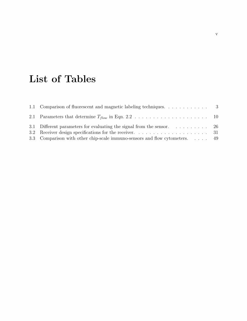
List of Tables
1.1 Comparison of fluorescent and magnetic labeling techniques. . . . . . . . . . . . 3
2.1 Parameters that determine Tflow in Eqn. 2.2 . . . . . . . . . . . . . . . . . . . . 10
3.1 Different parameters for evaluating the signal from the sensor. . . . . . . . . . 263.2 Receiver design specifications for the receiver. . . . . . . . . . . . . . . . . . . . 313.3 Comparison with other chip-scale immuno-sensors and flow cytometers. . . . . 49

vi
Acknowledgments
Meaning: One cannot guess what a person is going to do. One cannot understand or
appreciate a persons advice or the importance of the task as emphasised by him/her. Only
after people (someone like me) see the fruits as a result of doing such a task then one recog-
nises such a persons greatness, who can rightly be called a Pandit, a person esteemed for his
wisdom (an advisor).
I would like to express gratitude to my family, teachers and friends for their support,
guidance and sacrifice. In particular, I thank my advisor Prof. Bernhard Boser for his
constructive feedback and support. I also thank Prof. Ali Niknejad, Prof. Michel Maharbiz,
Prof. Luke Lee, Prof. David Allstot for their valuable time and guidance.
I thank my friends Adrien Pierre, Aamod Shanker, Andrew Townley, Arka Bhatacharya,
Behnam Behroozpour, Burak Eminoglu, Chintan Thakkar, Daniel Cohen, Daniel Gerber,
Efthymios Papageoriou, Filip Maksimovic, Greg Lacaille, Hao-Yen Tang, Igor Izyumin,
Jacobo Paredes, Jaeduk Han, Jiashu Chen, Jun-Chau Chien, Kosta Trotskovsky, Lingkai
Kong, Liyin Chen, Lucas Calderin, Marc Cooligan, Matthias Auf der Mauer, Maysamreza
Chamanzar, Mervin John, Michael Lorek, Mitchell Kline, Nathan Narevsky, Nihar Shah,
Nitesh Mor, Octavian Florescu, Oleg Izyumin, Paul Keselman, Po-Ling Loh, Prasanth Mo-
han, Rashmi K V, Richie Przybyla, Sameet Ramakrishnan, Sandeep Prabhu, Simone Gam-
bini, Siva Thyagarajan, Sriram Venugoplan, Steven Callendar, Travis Massey, Varun Jog,
Venkatesan Ekambaram, Vijay Kamble, Vikram Iyer, Yida Duan for making my graduate
student life at Berkeley a memorable one.
I thank the staff of BSAC, Swarm Lab, BWRC, ERSO, IRIS of UC Berkeley particularly
Abdelrahman Elhadi, Alejandro Luna, Brian Richards, Kim Ly, Mila MacBain, Patrick
Hernan, Richard Lossing, Shelley Kim, Shirley Solanio, Winthrop Williams for their efficient
administrative and lab support.
1
Chapter 1
Introduction
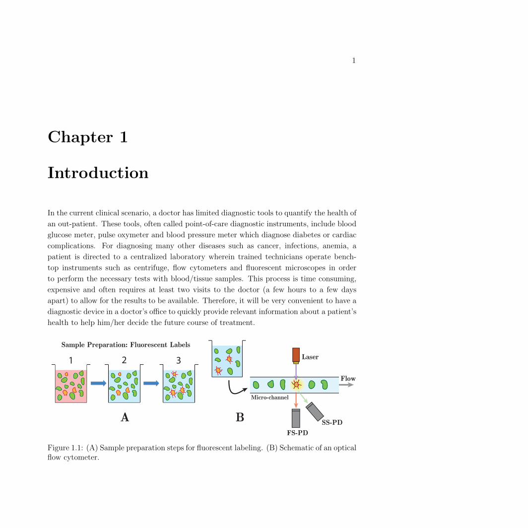
In the current clinical scenario, a doctor has limited diagnostic tools to quantify the health of
an out-patient. These tools, often called point-of-care diagnostic instruments, include blood
glucose meter, pulse oxymeter and blood pressure meter which diagnose diabetes or cardiac
complications. For diagnosing many other diseases such as cancer, infections, anemia, a
patient is directed to a centralized laboratory wherein trained technicians operate bench-
top instruments such as centrifuge, flow cytometers and fluorescent microscopes in order
to perform the necessary tests with blood/tissue samples. This process is time consuming,
expensive and often requires at least two visits to the doctor (a few hours to a few days
apart) to allow for the results to be available. Therefore, it will be very convenient to have a
diagnostic device in a doctor’s office to quickly provide relevant information about a patient’s
health to help him/her decide the future course of treatment.
Laser
Flow
Micro-channel
FS-PD
SS-PD
1 32
A B
Sample Preparation: Fluorescent Labels
Figure 1.1: (A) Sample preparation steps for fluorescent labeling. (B) Schematic of an opticalflow cytometer.

CHAPTER 1. INTRODUCTION 2
0.2μm<Φ<4μm
Antibody
MagneticNanoparticle
Polymer/GlassMatrix
Magnetic sensor
MagneticField Source
Flow
Micro-channel
BA
C
Sample Preparation: Magnetic Labels
Figure 1.2: (A) Sample preparation steps for magnetic labeling. (B) Schematic of magneticlabel. (C) Schematic of an optical flow cytometer.
Such a point-of-care diagnostic device should be reliable, low cost, disposable and should
integrate both sensing and data processing capabilities. In this direction, CMOS and mi-
crofluidics technology, when integrated together, offers complex signal processing and sensing
capabilities to meet the above requirements. Over the last thirty years, the research in CMOS
bio-sensors has focused on using techniques such as impedance spectroscopy [1], capacitance
change [2], magnetic Hall effect sensors [3] and cyclic voltametry [4] for detection of bio-
molecules such as cardiac bio-markers, DNA, glucose, lactose among many other analytes.
In addition, the study of structure, number and function of specific cell types in the body
is also vital for diagnosing patients. In this work, our goal is to realize a point-of-care flow
cytometer to count specific cells by leveraging the advances of micro-fabrication and CMOS
technology.
Current approach to flow cytometry involves (1) collection of blood sample from a patient,
(2) treatment of the sample with an anti-coagulant followed by dilution, (3) labelling of
the cells of interest with fluorescent molecules or staining agents and running the sample
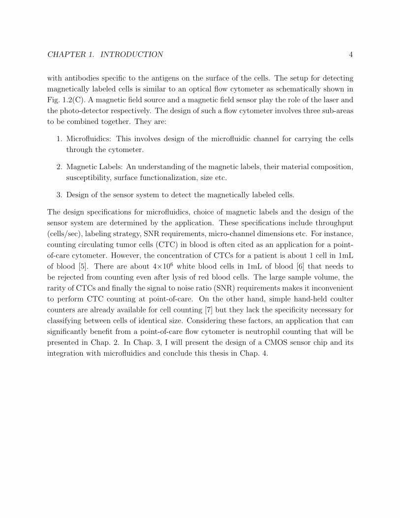
CHAPTER 1. INTRODUCTION 3
Fluorescent Labeling Magnetic LabelingOptical background noise from
unlabeled cellsNo magnetic background noise
from the sampleRequires calibration of the flow
cytometerNo calibration required
Red blood cells have to by lysedand white blood cells have to be
isolated from the sample
Measurement can be performed inwhole blood
Requires trained users incentralized lab facilities
Enables point-of-care diagnosis
Table 1.1: Comparison of fluorescent and magnetic labeling techniques.
through a flow cytometer as shown in Fig. 1.1(A). The instrument, schematically shown in
Fig. 1.1(B) contains one or more lasers that excite the fluorophors on the cells as they flow
through the laser beam in a carrier fluid. The scattered and fluorescent light is amplified
by photo-multipliers and eventually detected by photo-detectors. The intensity of the side
scattered (SS) light depends on the granularity of the cell while the intensity of forward
scattered (FS) light depends on its size and the expression of antigens on the cell surface.
The nucleus of the cell is also often tagged with a fluoroscent molecules such as DAPI (4’,6-
diamidino-2-phenylindole) to distinguish them from dead cell debri. The acquired data from
the photo-detectors is subsequently processed on a computer. A limitation of this approach
is that the use of fluorescent molecules requires elaborate sample preparation such as lysing
for red blood cells (RBCs). This step is necessary because the RBCs will auto-fluoresce and
interfere with optical measurement. An unlabeled sample of white blood cells is also used
as a control to calibrate the instrument and to set the threshold for the photo-detectors to
prevent false detection.
In this work, we propose to replace the fluorescent labels with magnetic labels to enable
us to realize a point-of-care flow cytometer. Basically, a biological sample has insignificant
susceptibility (χ ≈ 10−5) compared to magnetic labels (χ ≈0.1-1) which will mitigate any
background effects. In addition, the magnetic labeling process can be done in a single step
as shown in Fig. 1.2(A), ie. adding labels directly to anti-coagulated whole blood unlike
most fluorescent labeling process which involves a minimum of three steps: centrifugation,
washing of cells to remove free bio-molecules and finally labeling with fluorescent molecules.
Tab. 1.1 compares the optical and magnetic labeling approaches.
Briefly, the magnetic labels shown in Fig. 1.2(B) are made of nano-particles of magnetic
materials embedded in epoxy or glass martix. The surface of the labels are functionalized
CHAPTER 1. INTRODUCTION 4
with antibodies specific to the antigens on the surface of the cells. The setup for detecting
magnetically labeled cells is similar to an optical flow cytometer as schematically shown in
Fig. 1.2(C). A magnetic field source and a magnetic field sensor play the role of the laser and
the photo-detector respectively. The design of such a flow cytometer involves three sub-areas
to be combined together. They are:
1. Microfluidics: This involves design of the microfluidic channel for carrying the cells
through the cytometer.
2. Magnetic Labels: An understanding of the magnetic labels, their material composition,
susceptibility, surface functionalization, size etc.
3. Design of the sensor system to detect the magnetically labeled cells.
The design specifications for microfluidics, choice of magnetic labels and the design of the
sensor system are determined by the application. These specifications include throughput
(cells/sec), labeling strategy, SNR requirements, micro-channel dimensions etc. For instance,
counting circulating tumor cells (CTC) in blood is often cited as an application for a point-
of-care cytometer. However, the concentration of CTCs for a patient is about 1 cell in 1mL
of blood [5]. There are about 4×10⁶ white blood cells in 1mL of blood [6] that needs to
be rejected from counting even after lysis of red blood cells. The large sample volume, the
rarity of CTCs and finally the signal to noise ratio (SNR) requirements makes it inconvenient
to perform CTC counting at point-of-care. On the other hand, simple hand-held coulter
counters are already available for cell counting [7] but they lack the specificity necessary for
classifying between cells of identical size. Considering these factors, an application that can
significantly benefit from a point-of-care flow cytometer is neutrophil counting that will be
presented in Chap. 2. In Chap. 3, I will present the design of a CMOS sensor chip and its
integration with microfluidics and conclude this thesis in Chap. 4.

5
Chapter 2
Application
2.1 Neutrophil counting
About neutrophils
About 60% volume of human blood is composed of plasma and the rest of it is a mix of
white blood cells (WBCs, leucocytes), red blood cells (erythrocytes) and platelets [9] as
shown in Fig. 2.1 [8]. The red blood cells are responsible for carrying oxygen to different
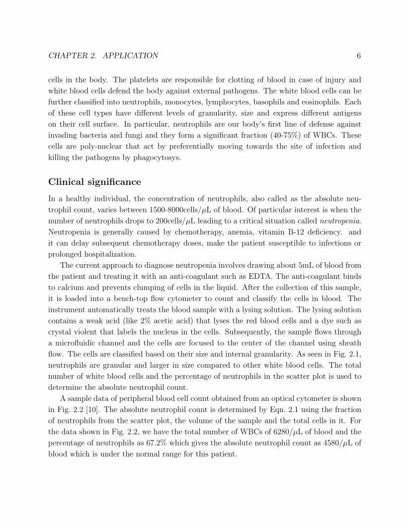
Figure 2.1: Different types of cells in blood [8].
CHAPTER 2. APPLICATION 6
cells in the body. The platelets are responsible for clotting of blood in case of injury and
white blood cells defend the body against external pathogens. The white blood cells can be
further classified into neutrophils, monocytes, lymphocytes, basophils and eosinophils. Each
of these cell types have different levels of granularity, size and express different antigens
on their cell surface. In particular, neutrophils are our body’s first line of defense against
invading bacteria and fungi and they form a significant fraction (40-75%) of WBCs. These
cells are poly-nuclear that act by preferentially moving towards the site of infection and
killing the pathogens by phagocytosys.
Clinical significance
In a healthy individual, the concentration of neutrophils, also called as the absolute neu-
trophil count, varies between 1500-8000cells/µL of blood. Of particular interest is when the
number of neutrophils drops to 200cells/µL leading to a critical situation called neutropenia.
Neutropenia is generally caused by chemotherapy, anemia, vitamin B-12 deficiency. and
it can delay subsequent chemotherapy doses, make the patient susceptible to infections or
prolonged hospitalization.
The current approach to diagnose neutropenia involves drawing about 5mL of blood from
the patient and treating it with an anti-coagulant such as EDTA. The anti-coagulant binds
to calcium and prevents clumping of cells in the liquid. After the collection of this sample,
it is loaded into a bench-top flow cytometer to count and classify the cells in blood. The
instrument automatically treats the blood sample with a lysing solution. The lysing solution
contains a weak acid (like 2% acetic acid) that lyses the red blood cells and a dye such as
crystal violent that labels the nucleus in the cells. Subsequently, the sample flows through
a microfluidic channel and the cells are focused to the center of the channel using sheath
flow. The cells are classified based on their size and internal granularity. As seen in Fig. 2.1,
neutrophils are granular and larger in size compared to other white blood cells. The total
number of white blood cells and the percentage of neutrophils in the scatter plot is used to
determine the absolute neutrophil count.
A sample data of peripheral blood cell count obtained from an optical cytometer is shown
in Fig. 2.2 [10]. The absolute neutrophil count is determined by Eqn. 2.1 using the fraction
of neutrophils from the scatter plot, the volume of the sample and the total cells in it. For
the data shown in Fig. 2.2, we have the total number of WBCs of 6280/µL of blood and the
percentage of neutrophils as 67.2% which gives the absolute neutrophil count as 4580/µL of
blood which is under the normal range for this patient.
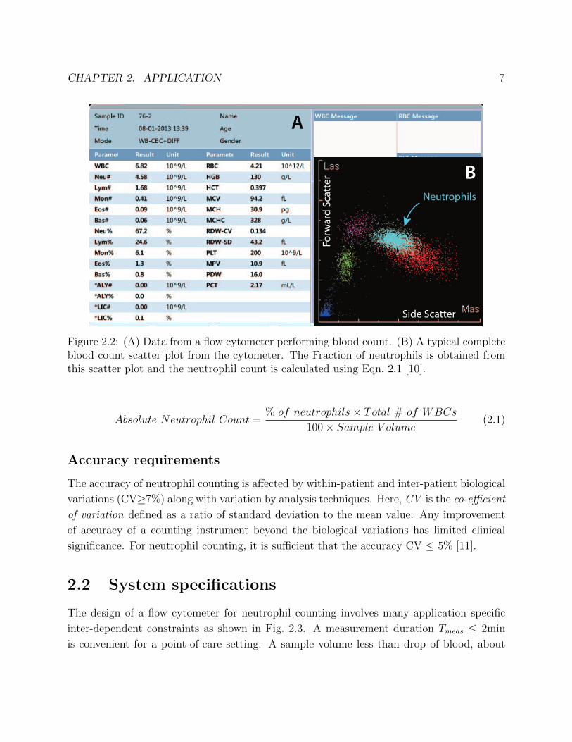
CHAPTER 2. APPLICATION 7
Fo
rwa
rd S
catt
er
Side Scatter
Neutrophils
A
B
Figure 2.2: (A) Data from a flow cytometer performing blood count. (B) A typical completeblood count scatter plot from the cytometer. The Fraction of neutrophils is obtained fromthis scatter plot and the neutrophil count is calculated using Eqn. 2.1 [10].
Absolute Neutrophil Count =% of neutrophils× Total # of WBCs
100× Sample V olume(2.1)
Accuracy requirements
The accuracy of neutrophil counting is affected by within-patient and inter-patient biological
variations (CV≥7%) along with variation by analysis techniques. Here, CV is the co-efficient
of variation defined as a ratio of standard deviation to the mean value. Any improvement
of accuracy of a counting instrument beyond the biological variations has limited clinical
significance. For neutrophil counting, it is sufficient that the accuracy CV ≤ 5% [11].
2.2 System specifications
The design of a flow cytometer for neutrophil counting involves many application specific
inter-dependent constraints as shown in Fig. 2.3. A measurement duration Tmeas ≤ 2min
is convenient for a point-of-care setting. A sample volume less than drop of blood, about

CHAPTER 2. APPLICATION 8
Assay Requirements
System
Analysis
Design Specs.
Measurement Duration
Tmeas
≤ 2min
Sample volume
5μL
Critical Low
conc. of Cells
200 cells/μL
Min. # of cells
available for
counting
Accuracy
CV = σ/μ < 5%
Maximum allowed
Background counts
Background count
rate
SNR
Flow rate
Microchannel
Design
Max ow speed
1000
300
2.5/s
8.6dB
Figure 2.3: Flow chart to determine design requirments of a flow cytometer
5µL can be collected from a finger prick and this sample contains a minimum of NS=1000
neutrophils that needs to be counted with an accuracy 4-5%.
Design of microfluidics
Microfluidics is used to carry the cells through the cytometer over the sensor. The following
challenges need to be addressed for a point-of-care flow cytometer.
1. Electrical isolation: The microfluidic channel should isolate the electrical connects to
the sensor system from the conducting saline sample.
2. Leakage: The interface between the microfluidic channel and the sensor surface should
be leak proof to prevent any loss of the sample.
3. Micro-channel shape: The commonly used technique to realize a micro-channel is by
soft-lithography techniques to realize a micro-channel (typically 100×200µm2 in size)
CHAPTER 2. APPLICATION 9
in PDMS using SU-8 mold. The inlet and outlet (typically 1mm wide) is punched
in the PDMS perpendicular to the micro-channel. In such a case, the presence of
abrupt changes in the micro-channel cross-section and the transition from vertical to
horizontal flow can cause the cells to settle and clog the micro-channel. A solution to
this problem is to place the channel vertically with smooth transition from the inlet
to the micro-channel. This can be achieved using 3D printed molds instead of SU-8
molds.
4. Fluid driving force: The driving force for the flow of sample through the microfluidic
channel is typically provided by using a syringe pump. However, this approach requires
that the sample is loaded to the microfluidic channel without any air bubbles to prevent
flow rate fluctuations. Further, a syringe pump is bulky and consumes high power
(≈50W) making it inconvenient at the point-of-care. Instead the flow through the
micro-channel can be driven by gravity, obviating the need for a syringe pump. The
flow rate can be controlled by suitable design of micro-channel dimensions and the
channel filling rate can be minimized by surface treatment of the micro-channel. We
have used gravity driven vertical flow for the design of the micro-channel considering
these benefits.
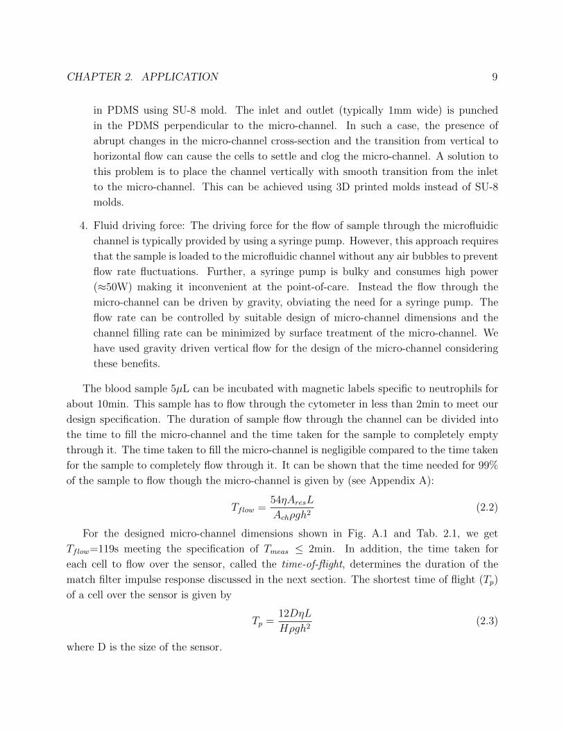
The blood sample 5µL can be incubated with magnetic labels specific to neutrophils for
about 10min. This sample has to flow through the cytometer in less than 2min to meet our
design specification. The duration of sample flow through the channel can be divided into
the time to fill the micro-channel and the time taken for the sample to completely empty
through it. The time taken to fill the micro-channel is negligible compared to the time taken
for the sample to completely flow through it. It can be shown that the time needed for 99%
of the sample to flow though the micro-channel is given by (see Appendix A):
Tflow =54ηAresL
Achρgh2(2.2)
For the designed micro-channel dimensions shown in Fig. A.1 and Tab. 2.1, we get
Tflow=119s meeting the specification of Tmeas ≤ 2min. In addition, the time taken for
each cell to flow over the sensor, called the time-of-flight, determines the duration of the
match filter impulse response discussed in the next section. The shortest time of flight (Tp)
of a cell over the sensor is given by
Tp =12DηL
Hρgh2(2.3)
where D is the size of the sensor.
CHAPTER 2. APPLICATION 10
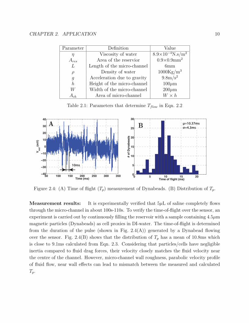
Parameter Definition Valueη Viscosity of water 8.9×10⁻⁴N.s/m2
Ares Area of the reservior 0.9×0.9mm2
L Length of the micro-channel 6mmρ Density of water 1000Kg/m3
g Acceleration due to gravity 9.8m/s2
h Height of the micro-channel 100µmW Width of the micro-channel 200µmAch Area of micro-channel W × h
Table 2.1: Parameters that determine Tflow in Eqn. 2.2
0 5 10 15 200
5
10
15
20
25
30
Time of flight (ms)
# o
f D
yn
ab
ea
ds
50 100 150 200 250 300 350−40
−30
−20
−10
0
10
20
30
40
Time (ms)
Vo
ut (
mV
)
10ms
μ=10.37ms
σ=4.3msA B
Figure 2.4: (A) Time of flight (Tp) measurement of Dynabeads. (B) Distribution of Tp.
Measurement results: It is experimentally verified that 5µL of saline completely flows
through the micro-channel in about 100s-110s. To verify the time-of-flight over the sensor, an
experiment is carried out by continuously filling the reservoir with a sample containing 4.5µm
magnetic particles (Dynabeads) as cell proxies in DI-water. The time-of-flight is determined
from the duration of the pulse (shown in Fig. 2.4(A)) generated by a Dynabead flowing
over the sensor. Fig. 2.4(B) shows that the distribution of Tp has a mean of 10.8ms which
is close to 9.1ms calculated from Eqn. 2.3. Considering that particles/cells have negligible
inertia compared to fluid drag forces, their velocity closely matches the fluid velocity near
the centre of the channel. However, micro-channel wall roughness, parabolic velocity profile
of fluid flow, near wall effects can lead to mismatch between the measured and calculated
Tp.

CHAPTER 2. APPLICATION 11
t=0
Sensor
Pulse(t)
t
+
Receiver
NoiseLabeled cell
arrives
Receiver
BW
A(f )
f
vout
t
Matched
Filter
t
Tp
Cell
Detected>
Detection
Threshold
Threshold
t
Figure 2.5: Schematic of flow cytometer receive chain.
Background count and detection threshold
To obtain the SNR requirements for the cytometer, we need to look at the complete signal
path as shown in Fig. 2.5. The flow of a cell over the sensor produces a bipolar pulse at the
sensor output. The pulse is then amplified by the receiver also adding undesirable noise. To
maximize the SNR, the receiver output is convolved (or auto-correlated) with the expected
pulse shape using a matched filter (whose impulse response is identical to the shape of the
pulse from the sensor). We eventually conclude that a magnetically labeled neutrophil is
detected if the match filter output exceeds a certain threshold. However, the presence of noise
leads to false positives or background counts. Counting statistics from radiation detection
theory can be used to determine the appropriate threshold or the minimum SNR required
to meet the accuracy requirements [12].
Assume that a background count (NB) is repeatedly measured for a fixed duration Tmeasin the absence of any flowing cells for a certain threshold setting. Here threshold is defined
(in dB) relative to rms noise at the match filter output. The count will be Poisson distributed
with mean NB and σNB=√NB. Now, if we repeat the experiment in the presence of cells
flowing over the sensor, we will count both the background as well as the cells to obtain a
total count (NT ) and σNT=√NT . NT and NB can then be used to determine the actual
number of cells (NS).
NS = NT −NB (2.4)
σNS=
√σ2NT
+ σ2NB
=√NS + 2NB (2.5)

CHAPTER 2. APPLICATION 12
5 6 7 8 9 10 11 1210
−2
10−1
100
101
102
Detection SNR (dB)
Background Rate (s−1)
Measured
Simulated
2.5/s
8.6dB
Figure 2.6: Background Rate vs threshold level relative to RMS noise (SNR) for the receivershown in Fig. 2.5.
CV =σNS
NS
=
√NS + 2NB
NS
(2.6)
For CV=4%, we can determine the maximum background count as NB=300 or a count rate
of 2.5/s (using Tmeas=2min) for Ns=103 neutrophils in the sample. Using the background
count rate vs. threshold plot for our system shown in Fig. 2.6, we need SNR greater than
8.6dB (threshold) from the labeled neutrophils to meet the accuracy requirements.
2.3 Summary
In this chapter, we have understood the importance of neutrophils in defending our body
against infections and the need for a point-of-care flow cytometer for diagnosing neutropenia.
The system level specifications are used to design the microfluidics and to determine the SNR
requirements of the receiver. The next chapter will describe the design of a CMOS sensor
and receiver chip to meet the SNR requirements and also present the measured results of
detecting magnetically labelled SKBR3 cells, used as proxies for neutrophils.

13
Chapter 3
CMOS Cytometer Design
Different sensing technologies such as magneto-resistors, superconducting quantum inter-
ference devices (SQUIDs) and Hall effect sensors are currently available for detecting small
magnetic fields generated by magnetically labeled cells. Giant magneto-resistive (GMR) sen-
sors [13] and µHall sensors [14], fabricated in non-standard processes, have been successfully
demonstrated for magnetic flow cytometers. However, the use of CMOS technology offers
the advantage of integrating the sensor with signal processing blocks such as amplifiers, A/D
converters, memory within the chip at a very low cost. CMOS based Hall sensors [15] or LC
tank oscillator [16] sensors either require post-processing or do not offer sufficient sensitivity
necessary for a cytometer. In this chapter, we present a chip scale CMOS magnetic flow
cytometer that requires no post-processing or external magnets and meets the sensitivity
requirements for neutrophil counting. The sensor is a spiral transformer that detects the
labels at frequencies beyond 900MHz. Therefore, it is necessary to understand their mag-
netic susceptibility at such high frequencies. In Sec. 3.1 we present a spiral-inductor based
characterization technique to measure the susceptibility. The design of the spiral transformer
sensor is presented in Sec. 3.2 and the design of the receiver for down-converting the sensor
signal to base-band is presented in Sec. 3.3. Finally, experimental results are presented in
Sec. 3.6.
3.1 Understanding magnetic labels
The magnetic labels are made of single domain (5-20nm) ferro-magnetic nano-particles.
The thermal energy at room temperature is sufficient to randomize the net direction of
magnetic moment which manifests itself as super-paramagnetic behavior. The magnetic
moment within these particles aligns with the applied external magnetic field.

CHAPTER 3. CMOS CYTOMETER DESIGN 14
A A’ B’ B
Tleft
Tright
TDUT
Wirebond
Spiral
CPW T-line
SMA
Connector
A B
Figure 3.1: (A) CPW setup for measuring complex susceptibility. (B) Zoomed in image ofthe spiral inductor sensor wire-bonded to CPW.
The susceptibility χ = χ′− jχ′′ of these magnetic labels is frequency and material depen-
dent complex number [17]. Our approach to characterize the susceptibility is to use a spiral
inductor sensor and measure the change in inductance when it is immersed in these labels.
Experimental setup A 50Ω coplanar waveguide (CPW) shown in Fig. 3.1(A) is designed
on a Duroid-4350 substrate. Spiral inductors fabricated on quartz substrate with nominal
inductance of 4.5nH (from Piconics Inc.) are wire bonded to the transmission line as shown in
Fig. 3.1(B). A vector network analyzer (E5071C, Agilent Technologies) is used for measuring
the s-parameters between 500 MHz to 6GHz with 100MHz steps after performing open-short-
load calibration (using C4691 ECal kit) and SMA port-extension. The IF bandwidth is set to
10 Hz and averaging factor of 16 to minimize the noise. Two port s-parameters are initially
measured without the nano-particles and then 100 ng of nano-particles are dispensed on the
sensor before repeating the measurements.
CHAPTER 3. CMOS CYTOMETER DESIGN 15
De-embedding and χ(ω) extraction The waveguide has to be de-embedded from the
spiral to accurately determine χ(ω). Firstly the measured two port S-parameters (S) are
transformed to T parameters are follows.
T11 =−||S||S21
T12 =S11
S21
T21 =−S22
S21
T22 =1
S21
The measured T-parameters and the simulated T-parameters of half-sections AA′ (Tleft)
and BB′ (Tright) are used to find the T-parameters of the spiral inductor sensor (Tspiral) as
follows:
Tmeas = Tleft ∗ Tspiral ∗ TrightTspiral = T−1left ∗ Tmeas ∗ T
−1right (3.1)
Tspiral can be transformed to Y-parameters and Z21 = 1/Y21 can be modeled as a resistor
in series with an inductor ie. Z21 = Rs+jωL. With the nano-particles on the spiral inductor,
the Z21,nano is given by:
Z21,nano = Rs + jωL(1 + χ′ − jχ′′)= Rs + ωLχ′′ + jωL(1 + χ′) (3.2)
From Z21,nano and Z21, the susceptibility can be obtained as follows:
χ′ ==Z21,nano − Z21
=Z21(3.3)
χ′′ =<Z21,nano − Z21
=Z21(3.4)
Absolute value of susceptibility: The magnetic labels cover the top surface of the
spiral inductor and its inductance change depends on the amount of magnetic material
(thickness) used. Therefore, this characterization technique can provide reliable frequency
vs. normalized susceptibility data rather than the absolute susceptibility. The low frequency
susceptibility measured from a different technique such as vibrating sample magnetometry
[18] can be used to scale the normalized susceptibility appropriately.

CHAPTER 3. CMOS CYTOMETER DESIGN 16
Figure 3.2: SEM images of ferrite labels with typical size of 400 nm used for label charac-terization experiments.
Measurement results: Five different types of magnetic nano-particles ie. ferrites of
cobalt, nickle, manganese, zinc and the most commonly used iron-oxide nano-particles
(Fig. 3.2) were obtained from OceanNanotech and used in our experiments. A plot of com-
plex susceptibility of iron oxide nano-particles is shown in Fig. 3.3(A) and Fig. 3.3(B) shows
a plot of the phase of the susceptibility for different types of nano-particles. The phase dif-
ference between the labels can be used for classifying as explained in Sec. 3.3. The peaking
in the imaginary component of susceptibility (χ′′) is due to phenomena of ferromagnetic res-
onance [17] and the corresponding frequency is a weak function of the size of nano-particles.
This is unlike the Neel’s relaxation phenomenon observed at lower frequencies (≈5-100KHz)
where χ(ω) is an exponential function of the size of the nano-particles. Therefore, label
classification at lower frequency using Neel’s relaxation phenomenon is almost impractical
considering the wide distribution of nano-particle sizes due to fabrication process variations.
We also carried out measurements of different titrations of manganese ferrite and cobalt
ferrite nano-particles. The phase plot of the mixtures are shown in Fig. 3.4. We see that the
phase interpolates well between the phase plots of 100% of each type of nano-particles.
Verification of ferro-magnetic resonance The frequency of peaking (fpeak) of the imag-
inary component of the susceptibility increases with the increase of external applied DC
magnetic field. This measurement is important to verify that the extracted susceptibility

CHAPTER 3. CMOS CYTOMETER DESIGN 17
1 2 3 4 5 60
0.005
0.01
0.015
0.02
0.025
0.03
0.035
Frequency (GHz)
χ (
A.U
)
real(χ)
imag(χ)A
1 2 3 4 5 60
20
40
60
80
100
120
Frequency (GHz)
an
gle
(χ)
(de
g)
CoFe2O
4
MnFe2O
4
NiFe2O
4
Fe3O
4
ZnFeO4
B
Figure 3.3: (A) Complex susceptibility plot for iron oxide nano-particles. (B) Phase ofcomplex susceptibility of different magnetic materials.
1 2 3 4 5 60
20
40
60
80
100
120
an
gle
(χ)
(de
g)
Frequency (GHz)
100% Co
80% Co
Cobalt Ferrite Fractions in Manganese Ferrite
60% Co
50% Co
40% Co
0% Co &100% Mn
20%Co
Figure 3.4: Phase plots of different titrations of magnetic nano-particles.
CHAPTER 3. CMOS CYTOMETER DESIGN 18
1 2 3 4 5 6−0.06
−0.04
−0.02
0
0.02
0.04
0.06
0.08
Frequency (GHz)
χ(ω
,B)/
χ(ω
,B =
0T
) Increasing magneticfield (0:20:180 mT)
Figure 3.5: Variation of susceptibility with external DC magnetic field.
is indeed the magnetic property of the material and not a consequence of dielectric change
around the spiral inductor sensor. The setup is modified to have a helmholtz coil with ~B
directed in the plane of the spiral. Fig. 3.5 shows variation of imaginary component of the
susceptibility for different external fields | ~B|. It can be seen that the magnitude of sus-
ceptibility and the corresponding frequency of peaking increases with increasing external
magnetic field thus, verifying that our susceptibility is indeed the magnetic property of the
material.
3.2 Sensor
Sensor modeling
The sensor incorporates a magnetizing coil (L1) to magnetize the labels on the cell and a
pick up coil (L2) to sense the magnetic moment induced in the labels as schematically shown
in Fig. 3.6. For our initial analysis, we use modified Wheeler expressions [19] to obtain the
values spiral inductors (L1,2). The metal conductivity and skin effect is used to determine

CHAPTER 3. CMOS CYTOMETER DESIGN 19
Vs
Rs
L1
L2
R2
M
R1
Receiver
Yin
Figure 3.6: Model of the spiral transformer.
the corresponding series resistance (R1,2) [20]. The mutual inductance (M) arises from the
magnetic coupling through the labels and it can be determined as follows. The magnetic
field that magnetizes the labels when the cell is located at the center of excitation spiral (L1)
can be approximated by:−−→Hexc = N1
2√
2 · I1πd1
k (3.5)
where, I1 is the current in L1 and N1 is the number of metal layers, d1 is the diameter of the
loop, k is normal to plane of the spiral. Magnetic labels, each of volume V and susceptibility
(χ) when magnetized by−−→Hexc, will have a moment (~m = χV
−−→Hexc) and they generate a
magnetic field intensity (−−→B(r)) in the space around them.
−−→B(r) =
µ0
4π|r|3(3(~m.r)r − ~m) (3.6)
−−→B(r) couples to the pick up coil (L2) and the mutual inductance can be calculated as:
M =φ2
I1(3.7)
where,
φ2 =
N2∑j=1
P∑i=1
∫Aj
−−→B(r) ·
−→dS
Aj is the area of each loop of the N2 loops in the pick up coil and P is the number of particles
on a cell,−→dS is the area element in k direction.
CHAPTER 3. CMOS CYTOMETER DESIGN 20
v2s
R1
v2n1
L1L2
R2
v2n2
Excitation coil Pick-up coil
Ysi2s
M
Yin Yin
i2i
Figure 3.7: Noise source in a spiral sensor and its equivalent model.
Design considerations
Our goal is to maximize the SNR from the sensor by appropriate design of inductances L1,2
and mutual inductance M . Fig. 3.7 shows the different noise sources in the sensor, vns is the
thermal noise generated by the buffers driving the excitation coil L1 and vn1,n2 is thermal
noise from the resistance R1,2. It will be convenient to combine all the noise sources into isand equivalent source admittance YS. It can be shown that:
is =jωM(vns + vn1) + vn2(R1 + jωL1)
(R1 + jωL1)(R2 + jωL2) + ω2M2(3.8)
Ys =(R1 + jωL1)
(R1 + jωL1)(R2 + jωL2) + ω2M2(3.9)
The sensor will be connected to a receiver front-end having input admittance Yin as shown
in Fig. 3.7.
For simplicity, if we assume that the Q of excitation and pick up coils are large, using
Eqn. 3.8, Eqn. 3.9, the noise (i2i,noise) to signal (i2i,sig) ratio is given by:
N
S=i2i,noise
i2i,sig=
L1
k2cL2
v2n2
v2sig+v2ns + v2n1
v2sig(3.10)
where kc = M/√L1L2 is the coupling co-efficient, v2sig is the voltage source that drives the
excitation coil. The following observations can be made from Eqn. 3.10:
• From the first term in Eqn. 3.10, we can see that a higher coupling coefficient (kc) im-
proves the SNR. The coupling co-efficient depends on the amount of magnetic material
on the cell, the susceptibility and the separation of the cell from the excitation/pick
up coil.

CHAPTER 3. CMOS CYTOMETER DESIGN 21
0 10 20 30 40 50 600
2
4
6
8
10
12
14
Pick up coil size: S (μm)
Mag
net
ic m
omen
t (f
A.m
2 )
MagneticallyLabeled Cell
LabelB
I
15 μm
φ=S
Excitation Coil
Figure 3.8: Magnetic moment of the labelled cell as a function of excitation coil diameter.
• Further, smaller excitation coil inductance (L1) leads to a higher current through it
and therefore a larger magnetic field will be generated to magnetize the labels.
• A large pick up coil inductance (L2) increases the induced voltage for a given magnetic
field from the labels. However, v2n2 also increases due to increase in the series resistance.
• Finally, the noise from the excitation source v2ns and excitation coil resistance v2n1 has
a direct impact on the SNR.
Other sensor design considerations
Excitation coil size: From Eqn. 3.5 we see that the magnetic field strength increases by
reducing the size of excitation coil. However, if the size is significantly smaller than the size
of the cell, not all the magnetic labels get magnetized. Fig. 3.8 shows the total magnetic
moment induced in a cell decorated with 12 of 1µm labels (χ=0.1) due to the magnetic field
generated by a current carrying loop (100mA) as a function of its size. It can be seen that
the optimum size to maximize the moment is to choose the sensor diameter close to the size
of a cell, which is 15µm for neutrophils.
CHAPTER 3. CMOS CYTOMETER DESIGN 22
0 2 4 6 8 10 12 14−4
−3
−2
−1
0
# Turns
Norm
alizedSNR
(dB)
0 2 4 6 8 10 12 140
2.5
5
7.5
10
Q
Figure 3.9: Effect of number of turns in the pick-up coil on the SNR.
3 4 5 6 7 8 9 10−3.5
−3
−2.5
−2
−1.5
−1
−0.5
0
Width (µm)
Norm
alizedSNR
(dB)
3 4 5 6 7 8 9 104.2
4.3
4.4
4.5
4.6
4.7
4.8
4.9
Q
Figure 3.10: Effect of spacing between turns in the pick-up coil on the SNR.
CHAPTER 3. CMOS CYTOMETER DESIGN 23
5 10 15 20 25 30−1.5
−1
−0.5
0
Width (µm)
Norm
alizedSNR
(dB)
5 10 15 20 25 300
10
20
30
Q
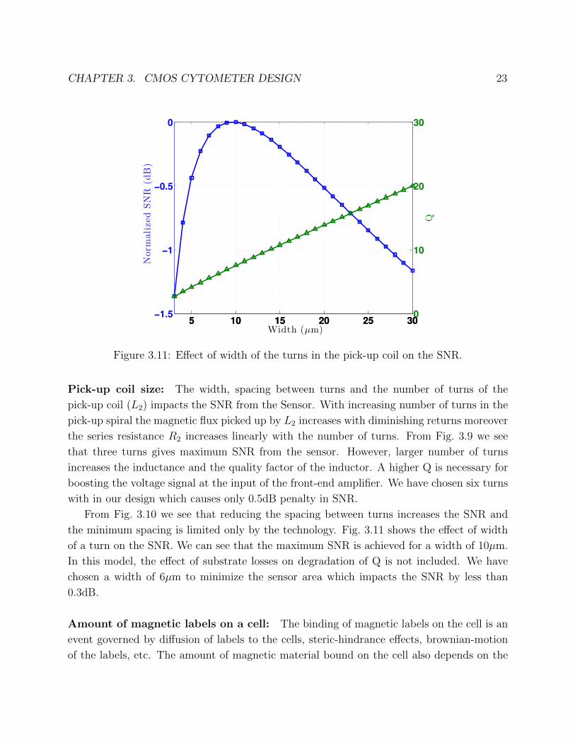
Figure 3.11: Effect of width of the turns in the pick-up coil on the SNR.
Pick-up coil size: The width, spacing between turns and the number of turns of the
pick-up coil (L2) impacts the SNR from the Sensor. With increasing number of turns in the
pick-up spiral the magnetic flux picked up by L2 increases with diminishing returns moreover
the series resistance R2 increases linearly with the number of turns. From Fig. 3.9 we see
that three turns gives maximum SNR from the sensor. However, larger number of turns
increases the inductance and the quality factor of the inductor. A higher Q is necessary for
boosting the voltage signal at the input of the front-end amplifier. We have chosen six turns
with in our design which causes only 0.5dB penalty in SNR.
From Fig. 3.10 we see that reducing the spacing between turns increases the SNR and
the minimum spacing is limited only by the technology. Fig. 3.11 shows the effect of width
of a turn on the SNR. We can see that the maximum SNR is achieved for a width of 10µm.
In this model, the effect of substrate losses on degradation of Q is not included. We have
chosen a width of 6µm to minimize the sensor area which impacts the SNR by less than
0.3dB.
Amount of magnetic labels on a cell: The binding of magnetic labels on the cell is an
event governed by diffusion of labels to the cells, steric-hindrance effects, brownian-motion
of the labels, etc. The amount of magnetic material bound on the cell also depends on the

CHAPTER 3. CMOS CYTOMETER DESIGN 24
1 2 3 4 572
74
76
78
80
Frequency (GHz)
εr
1 2 3 4 515
20
25
30
35
εi
εr
εi
Figure 3.12: Frequency vs. complex permittivity ε = εr + jεi for 1x PBS saline solution [21].
antigen expression, cell culture conditions, pH of the labeling buffer solution, temperature
etc. The variability in the labeling process coupled with the uncertainty in the absolute
value of the susceptibility (see Sec. 3.1) makes it challenging to estimate the value of mutual
inductance (M). Assumptions, such as the number of labels bound to a cell or the approxi-
mate value of susceptibility are inevitably made in order to determine the mutual inductance
and consequently the SNR from the sensor.
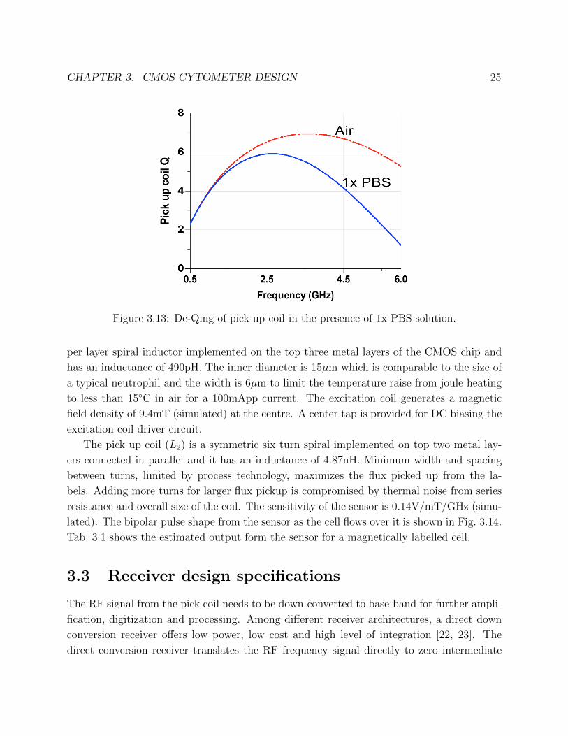
Loss from saline at high frequencies: The cells are carried over the sensor in a saline
solution also called the phosphate buffered saline (PBS). The presence of dissolved salts
causes high frequency loss and de-Qing of the spiral inductors. We have modeled the di-
electric properties of saline using semi-empirical expressions in [21] and Fig. 3.12 shows the
frequency vs. complex permittivity ε = εr + jεi for 1x PBS solution used in our cell exper-
iments. Fig. 3.13 shows the effect (simulated in HFSS) of saline solution on the Q of the
pick-up coil.
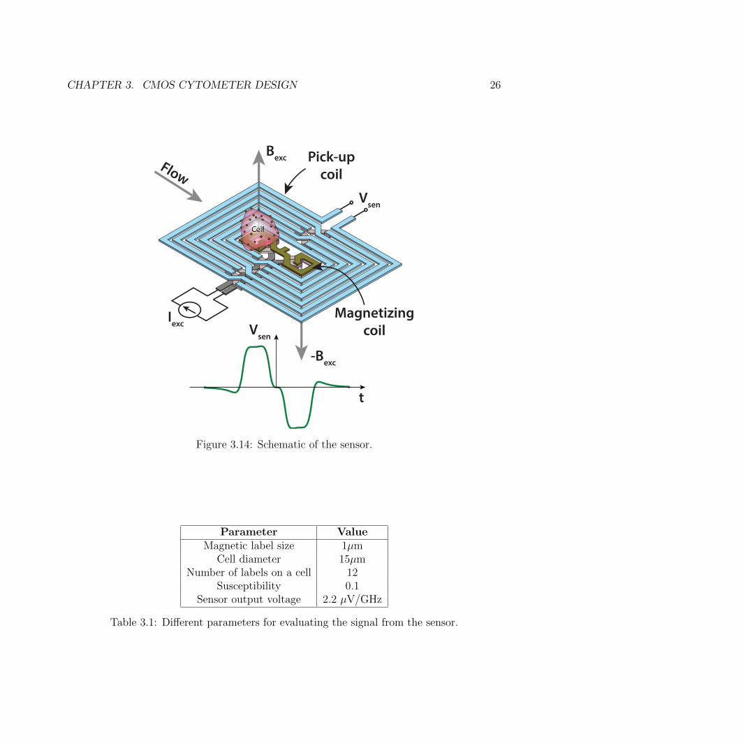
Sensor implementation
Using the insights gained from the analytical models described in previous sections, a spiral
sensor is implemented as shown in Fig. 3.14. It consists of a differential magnetizing coil
(L1) embedded within a pick up coil (L2). The magnetizing coil is a three-layer, single turn
CHAPTER 3. CMOS CYTOMETER DESIGN 25
Figure 3.13: De-Qing of pick up coil in the presence of 1x PBS solution.
per layer spiral inductor implemented on the top three metal layers of the CMOS chip and
has an inductance of 490pH. The inner diameter is 15µm which is comparable to the size of
a typical neutrophil and the width is 6µm to limit the temperature raise from joule heating
to less than 15C in air for a 100mApp current. The excitation coil generates a magnetic
field density of 9.4mT (simulated) at the centre. A center tap is provided for DC biasing the
excitation coil driver circuit.
The pick up coil (L2) is a symmetric six turn spiral implemented on top two metal lay-
ers connected in parallel and it has an inductance of 4.87nH. Minimum width and spacing
between turns, limited by process technology, maximizes the flux picked up from the la-
bels. Adding more turns for larger flux pickup is compromised by thermal noise from series
resistance and overall size of the coil. The sensitivity of the sensor is 0.14V/mT/GHz (simu-
lated). The bipolar pulse shape from the sensor as the cell flows over it is shown in Fig. 3.14.
Tab. 3.1 shows the estimated output form the sensor for a magnetically labelled cell.
3.3 Receiver design specifications
The RF signal from the pick coil needs to be down-converted to base-band for further ampli-
fication, digitization and processing. Among different receiver architectures, a direct down
conversion receiver offers low power, low cost and high level of integration [22, 23]. The
direct conversion receiver translates the RF frequency signal directly to zero intermediate
CHAPTER 3. CMOS CYTOMETER DESIGN 26
Bexc
-Bexc
Vsen
Iexc
Pick-up
coilFlow
Vsen
t
Magnetizing
coil
Cell
Figure 3.14: Schematic of the sensor.
Parameter ValueMagnetic label size 1µm
Cell diameter 15µmNumber of labels on a cell 12
Susceptibility 0.1Sensor output voltage 2.2 µV/GHz
Table 3.1: Different parameters for evaluating the signal from the sensor.

CHAPTER 3. CMOS CYTOMETER DESIGN 27
Sensort=-Tp/2
-asig
asig
Cell Arrivest
Sensorsignal: s(t)
NoiseMatching
LNA
MixerBase-bandAmplifier
Off-chipGain
Aoff,chipADC
Matched Filter
+
t1
-1
h(t)SNR > 8.6dB
N0,in
Tp/2
-Tp/2
LO
SVon
Conversion Gain
On-chip
Off-chip
t
Figure 3.15: Schematic of different blocks with the receiver chain.
frequency. In our application, since the strength of the signal from the sensor is mainly
determined by the small amount of magnetic material that can bind to a cell, the main focus
of this work is to optimize the receiver noise performance. The complete signal chain from
the sensor to the matched filter for a direct down conversion receiver is shown in Fig. 3.15.
For the purpose of analysis, the signal pulse shape can be approximated by a bipolar
rectangular pulse as shown in Fig. 3.15. For a signal amplitude asig at the output of the
sensor and an input referred single sided thermal noise spectral density N0,in, it can be show
that the SNR at the output of the matched filter is given by (see Appendix. B):
SNR =asig√
0.693N0,infc(3.11)
where fc is the flicker noise corner frequency of the noise spectrum. From Sec. 3.2, for
a signal as = 2µV at 0.9GHz, we get an SNR of 24.5dB for input referred noise spectral
density of N0,in=(1.43nV/√Hz)2 and flicker noise corner of 10KHz. However, the undesired
capacitive coupling between the excitation coil and pick up coil increases the flicker noise
corner to 100KHz and thermal noise floor to 2.77nV/√Hz (discussed later) lowering the
SNR to 9.1dB.
The effect of ADC quantization noise is minimized by appropriate design of off-chip gain
(Aoff,chip). The phase difference between the excitation signal and signal from the sensor
signal (due to the complex susceptibility) necessitates an I/Q down-conversion receiver to
fully recover the signal (not shown in Fig. 3.15).

CHAPTER 3. CMOS CYTOMETER DESIGN 28
Front endSensor
Ys ir
vr
Yin
ii
isig
Figure 3.16: Sensor connected to the front end with input noise referred sources i2r and v2r .
+
-
vgs Cgs ro i2dgm
G
S
D
i2d = 4kBTgmγα
γ = 1.5 & α = 1
Figure 3.17: Noise model for MOSFET.
Front end noise matching
We have looked at the different noise sources of the sensor in Sec. 3.2. Here, let us consider
the noise of the receiver front-end as shown in Fig. 3.16. The goal is to minimize the noise
contribution from the front end circuit. Here i2r and v2r are correlated noise sources of the
receiver such that ir = Ycvr where Yc is the correlation coefficient. The noise to signal ratio
at the input of the front end will be:
N
S=i2i,noisei2i,sig
=v2r
i2sig|Yc + Ys|2 (3.12)
From Eqn. 3.12, we can improve the SNR by either reducing v2r which translates to increasing
the power consumption in the front end amplifier or by reducing |Yc+Ys|2 as discussed below.
To find Yc, consider the MOSFET front end with a simple noise model as shown in
Fig. 3.17. Using the instantaneous noise currents from the MOSFET (id) we get,
CHAPTER 3. CMOS CYTOMETER DESIGN 29
-
+
+
-
+
-
RF
RF
v2on
v2RF
v2RF
v2amp
v2amp
RSW
RSW
S
S
S
S
ZL
ZL
Av
i2ns
i2ns
v2RSW
v2RSW
Figure 3.18: Noise sources in a direct conversion receiver.
ir =jωCgsgm
id
vr =idgm
Yc =irvr
= jωCgs (3.13)
From Eqn. 3.13 we see that Yc is a small capacitive admittance (positive). However,
from Eqn. 3.12, we want to reduce |Yc + Ys|2 for improving the SNR (Ys is the inductive
admittance (negative) of the pick up coil). We can do this by increasing YC by adding a
capacitor (Cadd) in parallel to Cgs such that the pick up coil will resonate with the total
capacitance (Cgs + Cadd) at the frequency of operation. In other words, this additional
capacitance will effectively Q boost the voltage induced in the pick up coil at gate of the
front end transistors.
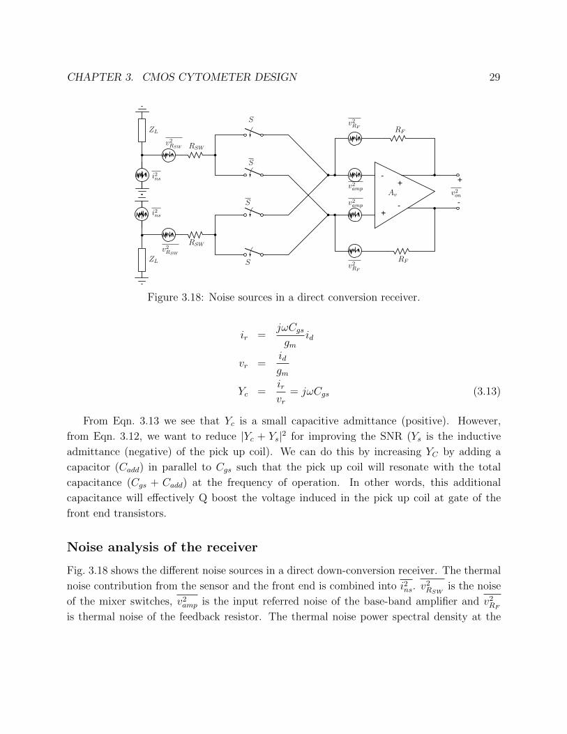
Noise analysis of the receiver
Fig. 3.18 shows the different noise sources in a direct down-conversion receiver. The thermal
noise contribution from the sensor and the front end is combined into i2ns. v2RSW
is the noise
of the mixer switches, v2amp is the input referred noise of the base-band amplifier and v2RF
is thermal noise of the feedback resistor. The thermal noise power spectral density at the

CHAPTER 3. CMOS CYTOMETER DESIGN 30
output of the receiver is given by (see Appendix. B):
Svon = 2v2RF+ 2
(1 +
RF
ZL +RSW
)2
v2amp (3.14)
+
∣∣∣∣ 2RF
ZL +RSW +RF/Av
∣∣∣∣2(1
4+
2
π2
)v2RSW
+
∣∣∣∣ 2RFZLZL +RSW +RF/Av
∣∣∣∣2( 2
π
)2
i2ns
From Eqn. 3.14, we can make the following observations.
• The noise from the feedback resistor RF directly adds to the output.
• The ratio of RF and ZL+RSW determine the contribution of base-band amplifier noise
(v2amp) to the output. It is desirable that the output impedance (ZL) of the front end
amplifier (voltage to current converter) is high. However, ZL is dominated by the drain
node parasitic capacitance and output resistance (r0) of the transistors.
• The contribution of noise from the switch resistance (v2RSW) is also determined by ratio
of RF and ZL +RSW .
• i2ns is commonly the most dominant source of noise, therefore, it is essential to minimize
the noise contribution from the front end low noise amplifier.
The input referred thermal noise spectral density can be determined using the conversion
gain as follows:
N0,in =Svon
(Conv. Gain)2(3.15)
where,
Conv. Gain =
(2
π
)(RFZLgm
ZL +RSW +RF/Av
)Ys
Ys + Yin(3.16)
gm is the trans-conductance of the front end amplifier. For the design parameters shown in
Tab. 3.2, the input referred noise floor from Eqn. 3.15 with excitation coil off (1.27nV/√Hz)
compares well with the device level SPICE simulations (1.43V/√Hz). However, the noise
floor will increase when the excitation coil is turned ON as discussed in the next section.
Self mixing and sensor non-ideality
The presence of undesirable capacitive coupling between the excitation coil or the LO path
and the pick up coil causes degradation of SNR. For simplicity, let us suppose that the local
oscillator is a sinusoidal signal (sLO(t)) with phase noise (φn(t)), the phase noise can arise
from oscillator and the divider circuits.
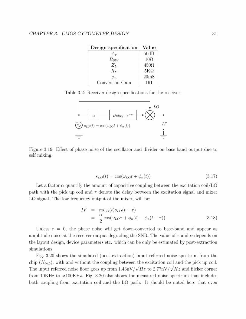
CHAPTER 3. CMOS CYTOMETER DESIGN 31
Design specification ValueAv 50dBRSW 10ΩZL 450ΩRF 5KΩgm 20mS
Conversion Gain 161
Table 3.2: Receiver design specifications for the receiver.
sLO(t) = cos(ωLOt+ φn(t))
α Delay : e−sτ
IF
LO
Figure 3.19: Effect of phase noise of the oscillator and divider on base-band output due toself mixing.
sLO(t) = cos(ωLOt+ φn(t)) (3.17)
Let a factor α quantify the amount of capacitive coupling between the excitation coil/LO
path with the pick up coil and τ denote the delay between the excitation signal and mixer
LO signal. The low frequency output of the mixer, will be:
IF = αsLO(t)sLO(t− τ)
=α
2cos(ωLOτ + φn(t)− φn(t− τ)) (3.18)
Unless τ = 0, the phase noise will get down-converted to base-band and appear as
amplitude noise at the receiver output degrading the SNR. The value of τ and α depends on
the layout design, device parameters etc. which can be only be estimated by post-extraction
simulations.
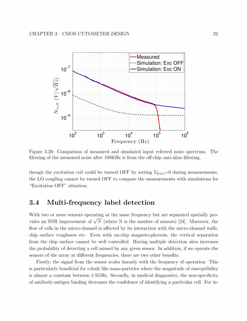
Fig. 3.20 shows the simulated (post extraction) input referred noise spectrum from the
chip (Nin,0), with and without the coupling between the excitation coil and the pick up coil.
The input referred noise floor goes up from 1.43nV/√Hz to 2.77nV/
√Hz and flicker corner
from 10KHz to ≈100KHz. Fig. 3.20 also shows the measured noise spectrum that includes
both coupling from excitation coil and the LO path. It should be noted here that even
CHAPTER 3. CMOS CYTOMETER DESIGN 32
102
103
104
105
106
10−9
10−8
10−7
Frequency (Hz)
Nin
,0(V
/√
Hz)
Measured
Simulation: Exc OFF
Simulation: Exc ON
Figure 3.20: Comparison of measured and simulated input referred noise spectrum. Thefiltering of the measured noise after 100KHz is from the off-chip anti-alias filtering.
though the excitation coil could be turned OFF by setting Vdrive=0 during measurements,
the LO coupling cannot be turned OFF to compare the measurements with simulations for
“Excitation OFF” situation.
3.4 Multi-frequency label detection
With two or more sensors operating at the same frequency but are separated spatially pro-
vides an SNR improvement of√N (where N is the number of sensors) [24]. Moreover, the
flow of cells in the micro-channel is affected by its interaction with the micro-channel walls,
chip surface roughness etc. Even with on-chip magneto-phoresis, the vertical separation
from the chip surface cannot be well controlled. Having multiple detection sites increases
the probability of detecting a cell missed by any given sensor. In addition, if we operate the
sensors of the array at different frequencies, there are two other benefits.
Firstly, the signal from the sensor scales linearly with the frequency of operation. This
is particularly beneficial for cobalt like nano-particles where the magnitude of susceptibility
is almost a constant between 1-5GHz. Secondly, in medical diagnostics, the non-specificity
of antibody-antigen binding decreases the confidence of identifying a particular cell. For in-

CHAPTER 3. CMOS CYTOMETER DESIGN 33
On Chip
÷22fLO
00
900
1800
2700
00
1800
00
900
1800
2700
GM
TIAPassivemixer
GM G=20
INAV-I
converter
G=205 KΩ
5 KΩ
VI
VQ
DS
P o
n F
PG
A
Vsen
ADC
ADC
VCO
16 MHz
16 MHz
Sensor
L3/2
C1
L2
C2
Iexc
L3/2
L1
1.2VDC
Figure 3.21: Architecture of the chip which includes the sensor, down-conversion receivercircuits and an LC oscillator.
stance, CD15 and CD16 antigens are strongly expressed by neutrophils [25], however the cor-
responding antibodies anti-CD15 or anti-CD16 can non-specifically bind to B-cells or T-cells.
Therefore, cobalt ferrite functionalized with anti-CD15 and manganese-ferrite functionalized
with anti-CD16 can be used to identify neutrophils with a higher confidence compared to
using a single antibody. The phase data shown in Fig. 3.4 can be used to determine the
relative expression of CD15 and CD16 thereby increasing the confidence in concluding that
the detected cell is indeed a neutrophil. From Fig. 3.4 we can also see that the maximum
phase difference between magnetic particles occurs between 2.5-3.5GHz which is appropriate
frequency to operate one of the sensors. In our experiments, we have used two of the four
available frequency channels ie. 0.9GHz and 2.6GHz.
3.5 Circuit implementation
The complete architecture of the receiver is shown in Fig. 3.21. The oscillator, sensor and
receiver are integrated within the chip. Each of the individual blocks are described in the
following sections.
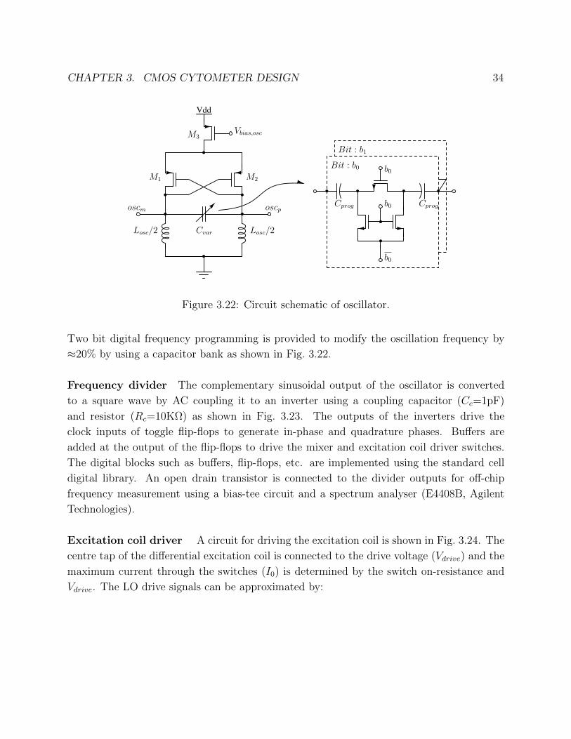
Oscillator The oscillator is implemented using an LC tank connected to a pmos based
negative transconductance stage as shown in Fig. 3.22. The oscillator runs at twice the LO
frequency. The inductor and transistors sizes are designed using the Matlab toolbox [26].
CHAPTER 3. CMOS CYTOMETER DESIGN 34
Vdd
Vbias,osc
Losc/2Losc/2
M3
M1 M2
oscposcmb0
Cvar
b0
b0
Cprog Cprog
Bit : b0
Bit : b1
Figure 3.22: Circuit schematic of oscillator.
Two bit digital frequency programming is provided to modify the oscillation frequency by
≈20% by using a capacitor bank as shown in Fig. 3.22.
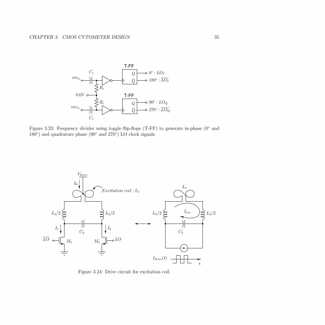
Frequency divider The complementary sinusoidal output of the oscillator is converted
to a square wave by AC coupling it to an inverter using a coupling capacitor (Cc=1pF)
and resistor (Rc=10KΩ) as shown in Fig. 3.23. The outputs of the inverters drive the
clock inputs of toggle flip-flops to generate in-phase and quadrature phases. Buffers are
added at the output of the flip-flops to drive the mixer and excitation coil driver switches.
The digital blocks such as buffers, flip-flops, etc. are implemented using the standard cell
digital library. An open drain transistor is connected to the divider outputs for off-chip
frequency measurement using a bias-tee circuit and a spectrum analyser (E4408B, Agilent
Technologies).
Excitation coil driver A circuit for driving the excitation coil is shown in Fig. 3.24. The
centre tap of the differential excitation coil is connected to the drive voltage (Vdrive) and the
maximum current through the switches (I0) is determined by the switch on-resistance and
Vdrive. The LO drive signals can be approximated by:
CHAPTER 3. CMOS CYTOMETER DESIGN 35
T-FF
T-FF
oscp
oscm
Cc
Cc
Q
Q
Q
Q
0 : LOI
180 : LOI
90 : LOQ
270 : LOQ
0.6V
Rc
Rc
Figure 3.23: Frequency divider using toggle flip-flops (T-FF) to generate in-phase (0 and180) and quadrature phase (90 and 270) LO clock signals.
Vdrive
Excitation coil : L1
L3/2 L3/2
C3
LOLO
L3/2 L3/2
C3
I1 I2
I0
Idrive(t)
Iexc
t
M1 M2
L1
Figure 3.24: Drive circuit for excitation coil.
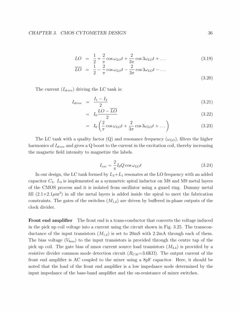
CHAPTER 3. CMOS CYTOMETER DESIGN 36
LO =1
2+
2
πcosωLOt+
2
3πcos 3ωLOt+ . . . (3.19)
LO =1
2− 2
πcosωLOt−
2
3πcos 3ωLOt− . . .
(3.20)
The current (Idrive) driving the LC tank is:
Idrive =I1 − I2
2(3.21)
= I0LO − LO
2(3.22)
= I0
(2
πcosωLOt+
2
3πcos 3ωLOt+ . . .
)(3.23)
The LC tank with a quality factor (Q) and resonance frequency (ωLO), filters the higher
harmonics of Idrive and gives a Q boost to the current in the excitation coil, thereby increasing
the magnetic field intensity to magnetize the labels.
Iexc =2
πI0Q cosωLOt (3.24)
In our design, the LC tank formed by L3+L1 resonates at the LO frequency with an added
capacitor C3. L3 is implemented as a symmetric spiral inductor on M8 and M9 metal layers
of the CMOS process and it is isolated from oscillator using a guard ring. Dummy metal
fill (2.1×2.1µm2) in all the metal layers is added inside the spiral to meet the fabrication
constraints. The gates of the switches (M1,2) are driven by buffered in-phase outputs of the
clock divider.
Front end amplifier The front end is a trans-conductor that converts the voltage induced
in the pick up coil voltage into a current using the circuit shown in Fig. 3.25. The transcon-
ductance of the input transistors (M1,2) is set to 20mS with 2.2mA through each of them.
The bias voltage (Vbias) to the input transistors is provided through the centre tap of the
pick up coil. The gate bias of nmos current source load transistors (M3,4) is provided by a
resistive divider common mode detection circuit (RCM=3.6KΩ). The output current of the
front end amplifier is AC coupled to the mixer using a 8pF capacitor. Here, it should be
noted that the load of the front end amplifier is a low impedance node determined by the
input impedance of the base-band amplifier and the on-resistance of mixer switches.

CHAPTER 3. CMOS CYTOMETER DESIGN 37
Vdd
Rtail
M1 M2
RCMvomvop
Vbias
vip
vim
vsen,p
vsen,m
vom
vopRCM
M4M3
vsen,p vsen,m
Pick − up coil : L2
Figure 3.25: Front end amplifier circuit.
LOLO
LOLO
IF IF
RF
RF
M1 M2
M3 M4
LO
0
Vdd
0
Vdd
Vdd Vdd
t t
LO
Figure 3.26: Schematic of passive mixer.
CHAPTER 3. CMOS CYTOMETER DESIGN 38
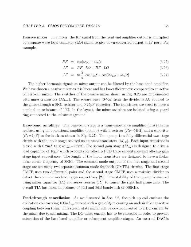
Passive mixer In a mixer, the RF signal from the front end amplifier output is multiplied
by a square wave local oscillator (LO) signal to give down-converted output at IF port. For
example,
RF = cos(ωLO + ωm)t (3.25)
IF = RF · LO +RF · LO (3.26)
IF = ≈ 2
π[cosωmt+ cos(2ωLO + ωm)t] (3.27)
The higher harmonic signals at mixer output can be filtered by the base-band amplifier.
We have chosen a passive mixer as it is linear and has lower flicker noise compared to an active
Gilbert-cell mixer. The switches of the passive mixer shown in Fig. 3.26 are implemented
with nmos transistors (M1−4). The square wave (0-Vdd) from the divider is AC coupled to
the gates through a 8KΩ resistor and 0.25pF capacitor. The transistors are sized to have a
nominal on-resistance of 10Ω. In the layout, the mixer switches are isolated using a guard
ring connected to the substrate/ground.
Base-band amplifier The base-band stage is a trans-impedance amplifier (TIA) that is
realized using an operational amplifier (opamp) with a resistor (RF=5KΩ) and a capacitor
(CF=2pF) in feedback as shown in Fig. 3.27. The opamp is a fully differential two stage
circuit with the input stage realized using nmos transistors (M1,2). Each input transistor is
biased with 0.2mA to give gm=2.2mS. The second gain stage (M6,7) is designed to drive a
load capacitor of 10pF which accounts for off-chip PCB trace capacitance and off-chip gain
stage input capacitance. The length of the input transistors are designed to have a flicker
noise corner frequency of 8KHz. The common mode outputs of the first stage and second
stage are set using two separate common-mode feedback (CMFB) circuits. The first stage
CMFB uses two differential pairs and the second stage CMFB uses a resistive divider to
detect the common mode voltages respectively [27]. The stability of the opamp is ensured
using miller capacitor (Cc) and series resistor (Rz) to cancel the right half plane zero. The
overall TIA has input impedance of 34Ω and 3dB bandwidth of 660KHz.
Feed-through cancellation As we discussed in Sec. 3.2, the pick up coil encloses the
excitation coil carrying 100mApp current with a gap of 3µm causing an undesirable capacitive
coupling between them. This steady state signal will be down-converted to a DC current by
the mixer due to self mixing. The DC offset current has to be cancelled in order to prevent
saturation of the base-band amplifier or subsequent amplifier stages. An external DAC is
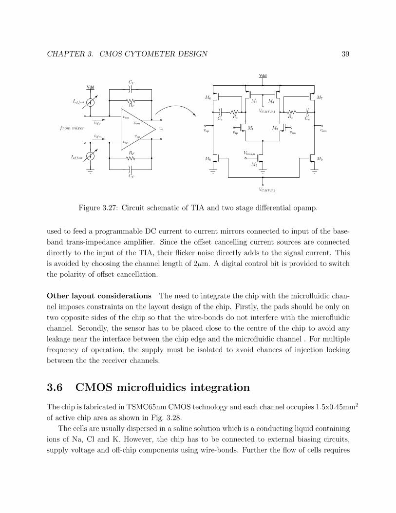
CHAPTER 3. CMOS CYTOMETER DESIGN 39
Vdd
Vdd
Vbias,n
vip vimvomvop
VCMFB,1
VCMFB,2
Rz RzCc Cc
M2M1
M4M3
M5
M6 M7
M9M8
vop
vomvo
vim
vip
RF
RF
CF
CF
from mixer
iifp
iifm
Ioffset
Ioffset
Figure 3.27: Circuit schematic of TIA and two stage differential opamp.
used to feed a programmable DC current to current mirrors connected to input of the base-
band trans-impedance amplifier. Since the offset cancelling current sources are connected
directly to the input of the TIA, their flicker noise directly adds to the signal current. This
is avoided by choosing the channel length of 2µm. A digital control bit is provided to switch
the polarity of offset cancellation.
Other layout considerations The need to integrate the chip with the microfluidic chan-
nel imposes constraints on the layout design of the chip. Firstly, the pads should be only on
two opposite sides of the chip so that the wire-bonds do not interfere with the microfluidic
channel. Secondly, the sensor has to be placed close to the centre of the chip to avoid any
leakage near the interface between the chip edge and the microfluidic channel . For multiple
frequency of operation, the supply must be isolated to avoid chances of injection locking
between the the receiver channels.
3.6 CMOS microfluidics integration
The chip is fabricated in TSMC65nm CMOS technology and each channel occupies 1.5x0.45mm2
of active chip area as shown in Fig. 3.28.
The cells are usually dispersed in a saline solution which is a conducting liquid containing
ions of Na, Cl and K. However, the chip has to be connected to external biasing circuits,
supply voltage and off-chip components using wire-bonds. Further the flow of cells requires
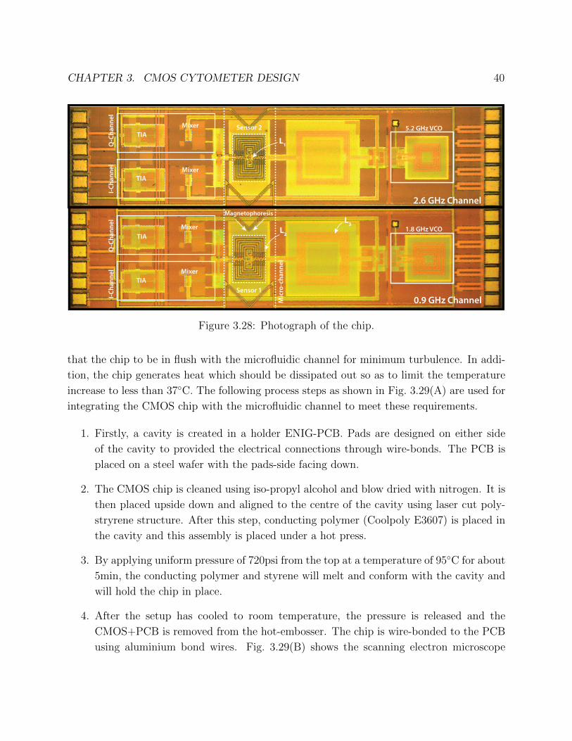
CHAPTER 3. CMOS CYTOMETER DESIGN 40
1.8 GHz VCO
Mic
ro-c
ha
nn
el
Magnetophoresis
Sensor 1
TIA
TIA
Mixer
Mixer
5.2 GHz VCO
2.6 GHz Channel
0.9 GHz Channel
Sensor 2
I-C
ha
nn
el
Q-C
ha
nn
el
TIA
TIA
Mixer
Mixer
I-C
ha
nn
el
Q-C
ha
nn
el L
3
L1
L2
Figure 3.28: Photograph of the chip.
that the chip to be in flush with the microfluidic channel for minimum turbulence. In addi-
tion, the chip generates heat which should be dissipated out so as to limit the temperature
increase to less than 37C. The following process steps as shown in Fig. 3.29(A) are used for
integrating the CMOS chip with the microfluidic channel to meet these requirements.
1. Firstly, a cavity is created in a holder ENIG-PCB. Pads are designed on either side
of the cavity to provided the electrical connections through wire-bonds. The PCB is
placed on a steel wafer with the pads-side facing down.
2. The CMOS chip is cleaned using iso-propyl alcohol and blow dried with nitrogen. It is
then placed upside down and aligned to the centre of the cavity using laser cut poly-
stryrene structure. After this step, conducting polymer (Coolpoly E3607) is placed in
the cavity and this assembly is placed under a hot press.
3. By applying uniform pressure of 720psi from the top at a temperature of 95C for about
5min, the conducting polymer and styrene will melt and conform with the cavity and
will hold the chip in place.
4. After the setup has cooled to room temperature, the pressure is released and the
CMOS+PCB is removed from the hot-embosser. The chip is wire-bonded to the PCB
using aluminium bond wires. Fig. 3.29(B) shows the scanning electron microscope
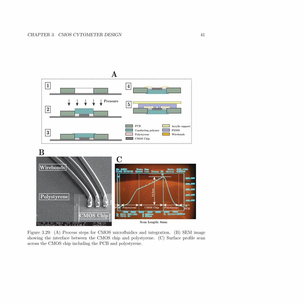
CHAPTER 3. CMOS CYTOMETER DESIGN 41
PCB
Conducting polymer
Polystyrene
CMOS Chip
Acrylic support
PDMS
Wirebonds
1
2
3
4
5Pressure
A
B
Polystyrene
CMOS Chip
Wirebonds
C
PCBCMOS Chip PolystyrenePolystyrene
Scan Length: 8mm
54.
3μm
PCB
Figure 3.29: (A) Process steps for CMOS microfluidics and integration. (B) SEM imageshowing the interface between the CMOS chip and polystyrene. (C) Surface profile scanacross the CMOS chip including the PCB and polystyrene.
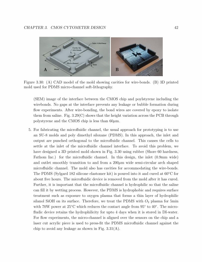
CHAPTER 3. CMOS CYTOMETER DESIGN 42
40mm
36mm
5mm
Inlet: 0.9x0.9mm
Cavity forwire-bonds
Micro-channel
A B
Figure 3.30: (A) CAD model of the mold showing cavities for wire-bonds. (B) 3D printedmold used for PDMS micro-channel soft-lithography.
(SEM) image of the interface between the CMOS chip and poylstyrene including the
wirebonds. No gaps at the interface prevents any leakage or bubble formation during
flow experiments. After wire-bonding, the bond wires are covered by epoxy to isolate
them from saline. Fig. 3.29(C) shows that the height variation across the PCB through
polystyrene and the CMOS chip is less than 60µm.
5. For fabricating the microfluidic channel, the usual approach for prototyping is to use
an SU-8 molds and poly dimethyl siloxane (PDMS). In this approach, the inlet and
output are punched orthogonal to the microfluidic channel. This causes the cells to
settle at the inlet of the microfluidic channel interface. To avoid this problem, we
have designed a 3D printed mold shown in Fig. 3.30 using rubber (Shore 60 hardness,
Fathom Inc.) for the microfluidic channel. In this design, the inlet (0.9mm wide)
and outlet smoothly transition to and from a 200µm wide semi-circular arch shaped
microfluidic channel. The mold also has cavities for accommodating the wire-bonds.
The PDMS (Sylgard 182 silicone elastomer kit) is poured into it and cured at 60C for
about five hours. The microfluidic device is removed from the mold after it has cured.
Further, it is important that the microfluidic channel is hydrophilic so that the saline
can fill it by wetting process. However, the PDMS is hydrophobic and requires surface
treatment such as exposure to oxygen plasma that forms a thin layer of hydrophilic
silanol SiOH on its surface. Therefore, we treat the PDMS with O2 plasma for 5min
with 70W power at 25C which reduces the contact angle from 95 to 40. The micro-
fludic device retains the hydrophilicity for upto 4 days when it is stored in DI-water.
For flow experiments, the micro-channel is aligned over the sensors on the chip and a
laser cut acrylic piece is used to press-fit the PDMS microfluidic channel against the
chip to avoid any leakage as shown in Fig. 3.31(A).
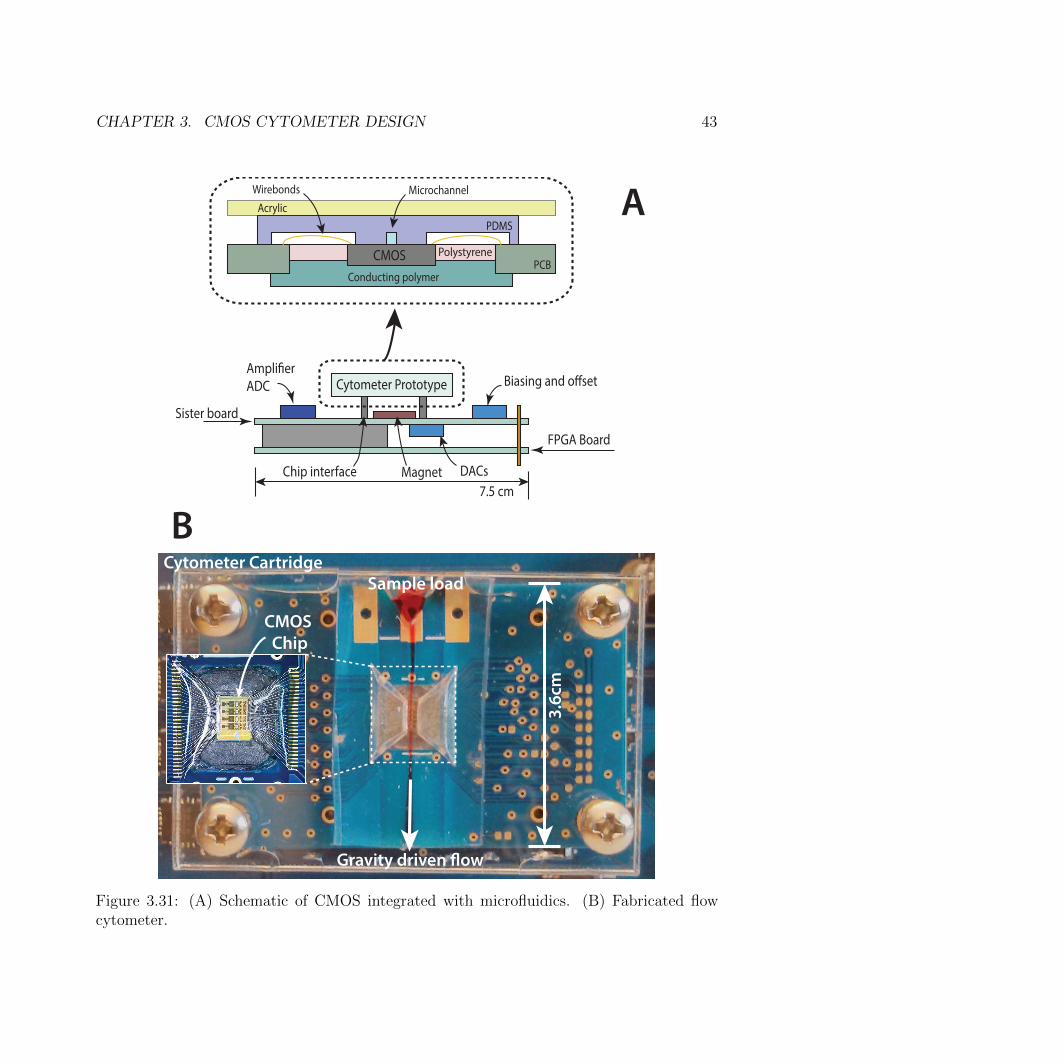
CHAPTER 3. CMOS CYTOMETER DESIGN 43
PCBPolystyrene
Conducting polymer
PDMS
Acrylic
MicrochannelWirebonds
CMOS
Sister board
Ampli!er
ADC Biasing and o"set
FPGA Board
Chip interface DACs
7.5 cm
Cytometer Prototype
Cytometer Cartridge
Gravity driven !ow
Sample load3
.6cm
Magnet
A
B
CMOS
Chip
Figure 3.31: (A) Schematic of CMOS integrated with microfluidics. (B) Fabricated flowcytometer.

CHAPTER 3. CMOS CYTOMETER DESIGN 44
Computer
Microscope
CytometerCartridgeFPGA
Board
Clamp
USB5V
Figure 3.32: Experimental setup used for measurements.
The complete cytometer prototype is connected to a sister PCB to provide DC bias,
off-chip gain, anti-alias filtering and digitization by differential ADC and data acquisition
through a FPGA (OpalKelly XEM6010-LX45). A simple digital controller is implemented
on the FPGA to handle DAC programming used for offset cancellation, ADC initialization.
The FPGA is programmed to transfer the data to a computer through an USB port. Voltage
regulators mounted on the sister PCB generate 3.3V for power the off-chip gain stages and
ADCs, 1.5V for powering the CMOS chip and 1.2V for the excitation coil. A python script
running on the computer acquires and saves the data from the FPGA board which is subse-
quently processed in Matlab. The complete experimental setup is shown in Fig. 3.32. The
cytometer cartridge is firmly mounted on a clamp and powered with a 5V DC supply. The
supply is shared between the OpalKelly FPGA board and the sister PCB. A USB micro-
scope is used to visualize the flow through the micro-channel. Flow cytometry experiments
are carried out by placing a drop of sample at inlet of the cytometer and it is vertically
driven through the microfluidic channel by gravity. The fabricated flow cytometer is shown
in Fig. 3.31(B).

CHAPTER 3. CMOS CYTOMETER DESIGN 45
1 2
34
μ-c
han
nel
Flowt=
0
t=0.
34s
t=0.
43s
t=0.
55s
FlowFlow
Flow
Figure 3.33: Focusing of Dynabead by magnetophoresis.
Magnetophoresis
Although a wide microfluidic channel (200×100µm2) avoids clogging, the signal strength
drops as 1/r3 with the particle vertically separated from the sensor by r. Additional sheath
flow, a commonly used technique for focusing [28], requires well-controlled flow rates by use
of external syringe pumps. The availability of magnetic labels in this application enables 3D
focusing using magnetic field gradients generated from current carrying wires [29]. The force
on a magnetically labeled cell with magnetic moment ~m by a wire carrying a is given by:
~Fmag = (~m · ∇) ~B (3.28)
The direction of the force always points towards the wire ie. in the direction of increasing
magnetic field gradient. We have used 3µ wide wires (shown in Fig. 3.33) each carrying
3.5mA, implemented on top metal layer with 45 angles. An external DC magnetic field of
5mT is used to magnetize the labels. A detailed analysis of the effect of microfluidic channel
dimensions, cell diameter, liquid viscosity on the focusing efficiency of these structures will
be presented in [30].
3.7 Measurement results
The receiver is powered at 1.5V supply, higher than 1.2V, which is necessary to overcome de-
Qing of the oscillator LC tank due to undesired layout parasitics that were inadvertently not
accounted for during simulations. The front end and opamp consumes 18mA. The excitation
coil is powered at Vdrive=1.2V supply and consumes 38mA.

CHAPTER 3. CMOS CYTOMETER DESIGN 46
14.3 14.4 14.5 14.6 14.7 14.8−10
0
10
20
Time (s)
Q-channel (A.U)
14.3 14.4 14.5 14.6 14.7 14.8 14.9−10
−5
0
5
10
15
Time (s)
I−channel (A.U)
2.6GHz
0.9GHz
Missed
1 2
Detected
4 53
10ms
1 2 4 53
Figure 3.34: Detection of Dynabeads by two frequency channels.
Dynabead detection
Dynabeads are used for benchmarking the cytometer. Dynabeads have an average diameter
of 4.5µm with well characterized magnetic properties [31]. For this experiment, these beads
are dispersed in de-ionized (DI) water with a concentration of 8×10⁶/mL. 50µL of DI water
is loaded at the inlet of the vertically held microfluidic channel of the cytometer and the
offset cancellation is performed using the external DAC as the DI water flows through the
cytometer. Next, about 50µL of the Dynabead sample is loaded at the inlet and data
is acquired as the particles flow over the sensor. Fig. 3.34 shows the detection of 4.5µm
Dynabeads with an average SNR of 21.3dB for 0.9GHz channel and 19.9dB for 2.6GHz
channel (n=100 particles) after matched filtering. Further, it can be seen that a particle
missed on the 2.6GHz channel was picked up on the 0.9GHz channel.

CHAPTER 3. CMOS CYTOMETER DESIGN 47
9.6 9.7 9.8 9.9−10
−5
0
5
8.5
15
Time (s)
Match Filter (A.U.)
5 10 15 20−20
−10
0
10
20
Time (s)
Match Filter (A.U.)
Cell surfa
ce
1 μm
EpCAM
Biotin-
anti-EpCAM
Magnetic
beadCancer Cell
(SKBR3)
15 μm
Detection Treshold SNR = 11dB
A B
Figure 3.35: (A) Magnetic labeling of SKBR3 cells. (B) Detection of magnetically labeledcells by the cytometer.
Magnetic labelling of cells and detection
Although the design of flow cytometer is presented for neutrophil counting, the cytometer
is demonstrated for detection of breast cancer cells (see Fig. 3.35(A)) as they pose minimal
bio-safety hazard for handling them. Moreover, the detection of cells by the cytometer
is independent of choice of cells or antibodies used for magnetic labeling as long as the
SNR requirements are met. We have chosen SKBR3 breast cancer cells which over-express
EpCAM antigen and have a typical diameter of 15µm.
Biotin-streptavidin interaction is the strongest non-covalent interaction found in nature
and this labeling method is routinely used in cell experiments. The labeling of cells is carried
out in a two step process. Firstly, the EpCAM antigen on the cell surface is conjugated with
biotinylated anti-EpCAM (CD326) antibody. The biotin is subsequently conjugated with
magnetic labels coated with streptavidin.
We start with a petri dish containing about 5×10⁶ SKBR3 cells. A solution buffer is
prepared by mixing 2mL of 7.5% bovin serum albumin with 28mL PBS. About 2mL of
0.25% trypsing is mixed with 8mL of PBS of which 3mL is used to wash the cells and rest of
it is added to the cell plate. After incubation at 37C for 5min until most cells have detached

CHAPTER 3. CMOS CYTOMETER DESIGN 48
−40 −20 0 20 40 60−20
0
20
40
60
80
100
120
140
Phase at 0.9 GHz (deg)
Phase a
t 2.6
GH
z (
deg
)
CoFe2O
4
MnFe2O
4
Fe3O
4
Figure 3.36: Classification of three label classes by the flow cytometer.
from the plate and the cells are transferred to a tube for centrifugation. Subsequently, the
cell palette is re-suspended in a mix of 1.5µL of stock biotinylated anti-EpCAM antibody and
0.6mL of buffer solution and incubated for 20min at 37C with gentle mixing. Now, most of
the EpCAM antigens on the cell have been conjugated with biotinylated antibody. The final
step of magnetic labeling is carried out my adding 15µL of 10mg/mL streptavidin coated
MnFe2O4 magnetic labels of size 800nm-1µm (from OceanNanotech Inc.) and incubated for
another 20min with gentle mixing. The cells are then used for flow cytometry experiments
within 2hours. The cells are carried over the sensor in 1x phosphate buffered saline solution
driven by gravity. The digital data provided by the cytometer is match filtered with a pulse of
10ms duration (Tp) in Matlab. Fig. 3.35(B) shows the match filtered output. The detection
threshold is set to 11dB to achieve a CV=3.2%.
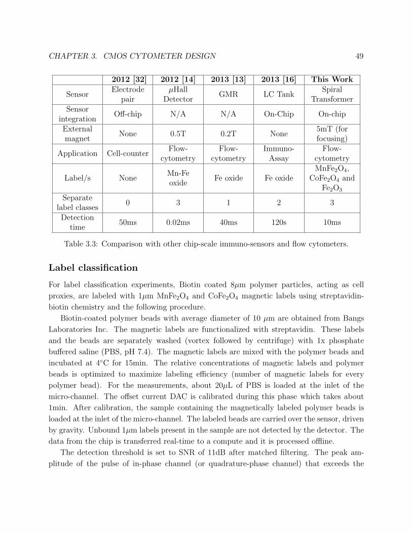
CHAPTER 3. CMOS CYTOMETER DESIGN 49
2012 [32] 2012 [14] 2013 [13] 2013 [16] This Work
SensorElectrode
pairµHall
DetectorGMR LC Tank
SpiralTransformer
Sensorintegration
Off-chip N/A N/A On-Chip On-chip
Externalmagnet
None 0.5T 0.2T None5mT (forfocusing)
Application Cell-counterFlow-
cytometryFlow-
cytometryImmuno-
AssayFlow-
cytometry
Label/s NoneMn-Feoxide
Fe oxide Fe oxideMnFe2O4,
CoFe2O4 andFe2O3
Separatelabel classes
0 3 1 2 3
Detectiontime
50ms 0.02ms 40ms 120s 10ms
Table 3.3: Comparison with other chip-scale immuno-sensors and flow cytometers.
Label classification
For label classification experiments, Biotin coated 8µm polymer particles, acting as cell
proxies, are labeled with 1µm MnFe2O4 and CoFe2O4 magnetic labels using streptavidin-
biotin chemistry and the following procedure.
Biotin-coated polymer beads with average diameter of 10 µm are obtained from Bangs
Laboratories Inc. The magnetic labels are functionalized with streptavidin. These labels
and the beads are separately washed (vortex followed by centrifuge) with 1x phosphate
buffered saline (PBS, pH 7.4). The magnetic labels are mixed with the polymer beads and
incubated at 4C for 15min. The relative concentrations of magnetic labels and polymer
beads is optimized to maximize labeling efficiency (number of magnetic labels for every
polymer bead). For the measurements, about 20µL of PBS is loaded at the inlet of the
micro-channel. The offset current DAC is calibrated during this phase which takes about
1min. After calibration, the sample containing the magnetically labeled polymer beads is
loaded at the inlet of the micro-channel. The labeled beads are carried over the sensor, driven
by gravity. Unbound 1µm labels present in the sample are not detected by the detector. The
data from the chip is transferred real-time to a compute and it is processed offline.
The detection threshold is set to SNR of 11dB after matched filtering. The peak am-
plitude of the pulse of in-phase channel (or quadrature-phase channel) that exceeds the

CHAPTER 3. CMOS CYTOMETER DESIGN 50
detection threshold is used along with the corresponding amplitude of quadrature-phase
channel (or in-phase channel) to determine the phase of the signal at a particular frequency
(either 0.9GHz or 2.6GHz). Fig. 3.36 shows the phase response obtained for the magnetic
labels at both the frequencies. Also shown is the phase of Dynabeads beads (Fe2O3). Us-
ing equal prior probabilities of magnetic labels, we get classification accuracy of 74% using
phase data at 2.6GHz (with linear discriminator). However, the accuracy improves to 87%
by using phase data at both 0.9GHz and 2.6GHz (with a quadratic discriminator). Finally,
Tab. 3.3 compares the presented flow cytometer with other chip-scale immuno-sensors and
flow cytometers.

51
Chapter 4
Conclusion
In conclusion, we have described the need for point-of-care counting of neutrophils and the
design of a CMOS sensor chip for detection of magnetically labeled cells that meets the
specifications. The chip uses a spiral transformer sensor that is optimized for maximizing
the SNR and the signal from it is processed using direct down-conversion receiver circuits.
Two channels, operating at 0.9GHz and 2.6GHz are used to improve the SNR and classifi-
cation accuracy. The CMOS chip has been successfully integrated into microfluidics using
hot-embossing technique. Magneto-phoresis is used for focusing the cells onto the sensor.
Dynabeads are used for benchmarking the cytometer since these magnetic particles have
uniform size and magnetic properties. Cell detection is demonstrated with SKBR3 cells
labeled with MnFe2O4 magnetic labels and EpCAM cell surface bio-markers. The cells are
detected using the cytometer with SNR of 11dB to give 3.2% CV. Further, 87% classification
accuracy is achieved for three magnetic label classes.

52
Appendix A
Gravity Driven Flow
A simplified model of the micro-channel connected to a sample reservoir is shown in Fig. A.1.
The goal is to determine the time taken for the complete sample to empty through the micro-
channel as a function of microchannel dimensions and surface properties.
The time of flow through the microchannel can be split into the time taken to fill (Tfill)
the channel and the time taken for the liquid to flow through (Tflow). Tfill depends on micro-
channel dimensions, the contact angle between the saline and the micro-channel, viscosity
etc. and it is given by [33]:
H
Ares
L
h
W
Ares
: Cross-sectional area of reservoir
L : Length of micro-channel
W : Width of micro-channel
H : Height of the saline in reservior
h : Height of micro-channel
Reservoir
Microchannel
Gravity Driven Flow
Flo
w
yx
Figure A.1: Simplified schematic of a microchannel driven by gravity.

APPENDIX A. GRAVITY DRIVEN FLOW 53
Tfill =6ηL2
h2ρgH + 2σh cos θ(A.1)
where, η is viscosity, σ is surface tension and θ is the contact angle of saline with the
microfluidic channel, g is acceleration due to gravity and the remaining dimensions are shown
in Fig. A.1.
Once the channel is filled, the flow is governed only by the hydrostatic pressure of the
sample in the reservoir. Using the Navier-Stokes equation for the micro-channel,
∂2u
∂y2=
1
η
∂P
∂x(A.2)
where ∂P/∂x is the pressure gradient, u(y) is the velocity profile given by:
u(y) =1
2η
(−∂P∂x
)(h2
4− y2
)
u =1
h
h/2∫−h/2
u(y)dy =h2
12η
(−∂P∂x
)(A.3)
Considering only the pressure gradient generated by the reservoir to drive the flow, we
get
u =h2
12η
(−ρgH(t)
L
)(A.4)
Using conservation of mass and the area of channel Ach = W × h we have,
dVresdt
= −Achu
AresdH(t)
dt= −Achu (A.5)
Using Eqn. A.4 and Eqn. A.5 we get,
H(t) = H0e−t/β β =
12ηLAresAchρgh2
(A.6)
Where H0 is the initial height of the reservoir when sample is loaded. We need Tflow = 4.5β
for 99% of the sample to flow through the micro-channel.
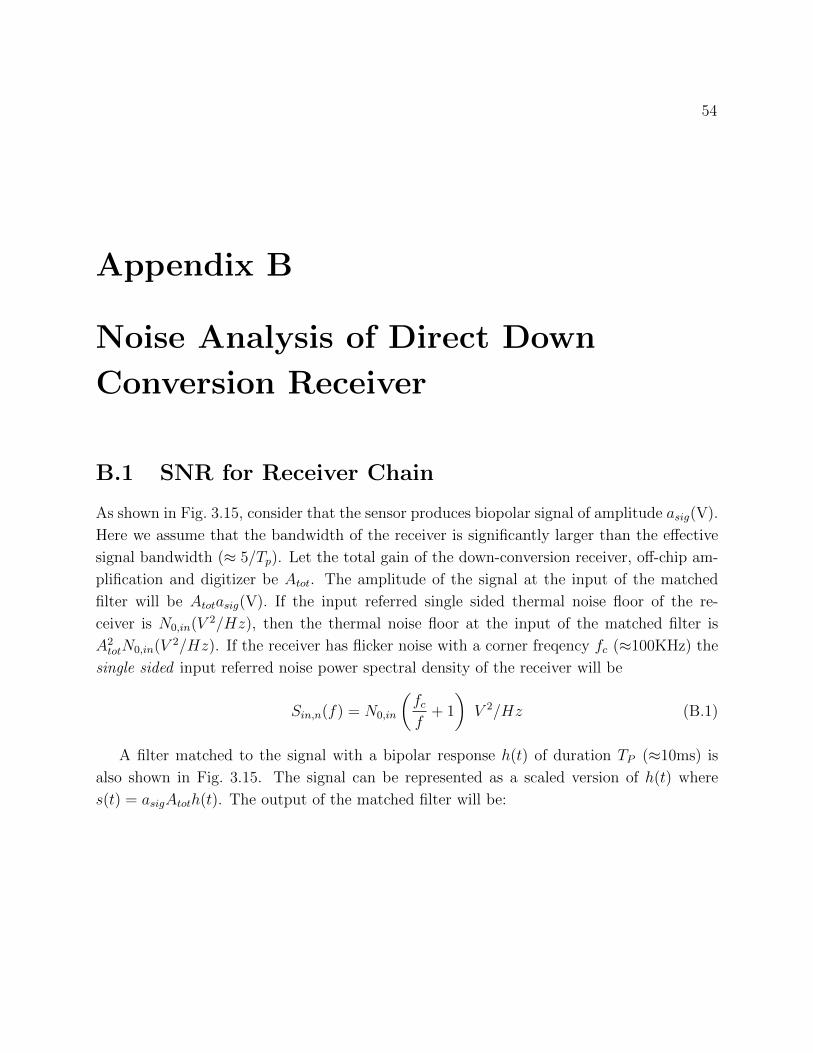
54
Appendix B
Noise Analysis of Direct Down
Conversion Receiver
B.1 SNR for Receiver Chain
As shown in Fig. 3.15, consider that the sensor produces biopolar signal of amplitude asig(V).
Here we assume that the bandwidth of the receiver is significantly larger than the effective
signal bandwidth (≈ 5/Tp). Let the total gain of the down-conversion receiver, off-chip am-
plification and digitizer be Atot. The amplitude of the signal at the input of the matched
filter will be Atotasig(V). If the input referred single sided thermal noise floor of the re-
ceiver is N0,in(V 2/Hz), then the thermal noise floor at the input of the matched filter is
A2totN0,in(V 2/Hz). If the receiver has flicker noise with a corner freqency fc (≈100KHz) the
single sided input referred noise power spectral density of the receiver will be
Sin,n(f) = N0,in
(fcf
+ 1
)V 2/Hz (B.1)
A filter matched to the signal with a bipolar response h(t) of duration TP (≈10ms) is
also shown in Fig. 3.15. The signal can be represented as a scaled version of h(t) where
s(t) = asigAtoth(t). The output of the matched filter will be:
APPENDIX B. NOISE ANALYSIS OF DIRECT DOWN CONVERSION RECEIVER 55
y(t) = s(t) ∗ h(t)
=
∞∫−∞
s(τ)h(t− τ)dτ
= asig
∞∫−∞
h(τ)h(t− τ)dτ
maxy(t) =
Tp/2∫−Tp/2
h2(τ)dτ
maxy(t) = asigAtotTp (B.2)
Let H(f) be the fourier transform for h(t) define as follows:
H(f) =
∞∫−∞
h(t)e−2πftdt (B.3)
For the given h(t), it can be shown that:
H(f) =2
jπfsin2
(πfTp
2
)(B.4)
Using Eqn. B.4 and Eqn. B.1, the variance of noise at the match filter output can be calcu-
lated as follows:
σ2n =
∞∫−∞
A2totSin,n(f)
2|H(f)|2df
= A2totN0,in
∞∫0
∣∣∣∣ 2
jπfsin2
(πfTp
2
)∣∣∣∣2 · (fcf + 1
)df
= A2totN0,inTp(0.693fcTp + 0.5) (B.5)
Using Eqn. B.2 and Eqn. B.5 and noting that fcTp 1 the SNR can be approximated
as:
SNR =maxy(t)
σn=
AtotTpasig√(0.693)A2
totN0,infcT 2p
=asig√
(0.693)N0,infc(B.6)

APPENDIX B. NOISE ANALYSIS OF DIRECT DOWN CONVERSION RECEIVER 56
RSW
RSW
S
S
S
S
ZL
ZL
in2
in1
v2RSW
ZBB
ZBB
vifp
vifp
A
B
vxp
vxm
ixp
ixm
Figure B.1: Modeling of source noise of the receiver.
Receiver Noise Analysis
In this section, our goal is to evaluate the effect of different noise sources shown in Fig. 3.15,
on the receiver noise performance. The passive mixer analysis presented in [34] is simplified
for our narrow band receiver. Contribution of each of these noise sources to the output noise
is considered in the following sections.
Noise from Front-End
Fig. B.1 shows only the noise from front end current to voltage converter (i2n). ZBB is the
input impedance of the transimpedance amplifier (TIA).
ZBB ≈ RF/Av
where, RF is the feedback resistance of the TIA and Av is the differential voltage gain of
the operational amplifier. S, S are ideal complementary square wave (0-1) driving the mixer
switches at ωLO. RSW is the resistance of passive mixer switches. ZL = 1/YL is evaluated
at the LO frequency (0.9GHz) and it is assumed to be constant across the bandwidth of the
sensor signal (±100KHz). Writing the KCL at nodes A and B,
in1 + YL(vxp + ixpRSW ) + ixp = 0
in2 + YL(vxm + ixmRSW ) + ixm = 0

APPENDIX B. NOISE ANALYSIS OF DIRECT DOWN CONVERSION RECEIVER 57
From above equations we get,
(vxp − vxm)YL + (ixp − ixm)(RSWYL + 1) + in1 − in2 = 0 (B.7)
Also,
vxp = vifpS + vifmS
vxm = vifpS + vifmS
vxp − vxm = (vifp − vifm)(S − S
)(B.8)
Substituting Eqn. B.8 in Eqn. B.7 we get:
ixp − ixm = −[
(in1 − in2 − (vifp − vifm)(S − S)YL(1 +RSWYL
](B.9)
Further,
iifp = ixpS + ixmS
iifm = ixpS + ixmS
iif =iifp − iifm
2
iif (t) =1
2(ixp − ixm)(S − S) (B.10)
From Eqn. B.9 and Eqn. B.10 and since (S − S)2 = 1 we get:
iif (t) = −1
2
[(in1 − in2)(S − S + YL(vifp − vifm)
1 +RSWYL
](B.11)
In the frequency domain (S − S ↔ S(ω)),
Vifp(ω)− Vifm(ω) = 2ZBBIif (ω)
Vifp(ω)− Vifm(ω) = − ZBB1 +RSWYL
[(In1(ω)− In2(ω)) ∗ S(ω) + YL(Vifp(ω)− Vifm(ω))]
Vifp(ω)− Vifm(ω) = − ZBB1 + ZBBYL +RSWYL
(In1(ω)− In2(ω)) ∗ S(ω) (B.12)
Substituting Eqn. B.12 in Eqn. B.11 and after further simplification we get,
IIF (ω) = −1
2
[ZL
ZL +RSW + ZBB
]Int(ω) (B.13)
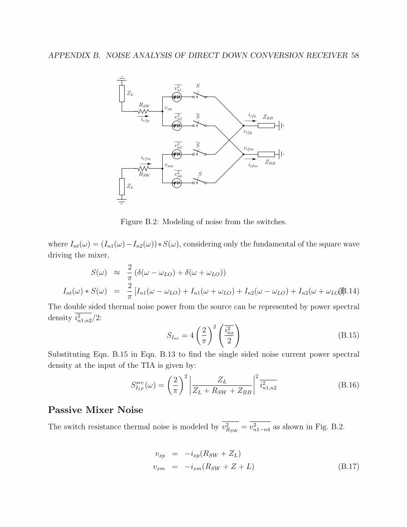
APPENDIX B. NOISE ANALYSIS OF DIRECT DOWN CONVERSION RECEIVER 58
RSW
RSW
S
S
S
S
ZL
ZL
v2n1
v2n2
v2n3
v2n4
ZBB
ZBBiifm
iifp
vxp
vxm
vifp
vifm
irfp
irfm
Figure B.2: Modeling of noise from the switches.
where Int(ω) = (In1(ω)−In2(ω))∗S(ω), considering only the fundamental of the square wave
driving the mixer,
S(ω) ≈ 2
π(δ(ω − ωLO) + δ(ω + ωLO))
Int(ω) ∗ S(ω) =2
π[In1(ω − ωLO) + In1(ω + ωLO) + In2(ω − ωLO) + In2(ω + ωLO)](B.14)
The double sided thermal noise power from the source can be represented by power spectral
density i2n1,n2/2:
SInt = 4
(2
π
)2(i2ns2
)(B.15)
Substituting Eqn. B.15 in Eqn. B.13 to find the single sided noise current power spectral
density at the input of the TIA is given by:
SsrcIIF(ω) =
(2
π
)2 ∣∣∣∣ ZLZL +RSW + ZBB
∣∣∣∣2 i2n1,n2 (B.16)
Passive Mixer Noise
The switch resistance thermal noise is modeled by v2RSW= v2n1−n4 as shown in Fig. B.2.
vxp = −ixp(RSW + ZL)
vxm = −ixm(RSW + Z + L) (B.17)

APPENDIX B. NOISE ANALYSIS OF DIRECT DOWN CONVERSION RECEIVER 59
Also,
iifp = ixpS + ixmS
iifm = = ixmS + ixpS
iif =iifp − iifm
2=ixp − ixm
2(S − S) (B.18)
Using Eqn. B.17 in Eqn. B.18, we get
iif (t) = −1
2
1
RSW + ZL(vxp − vxm)(S − S) (B.19)
Now,
vxp = (vifp + vn1)S + (vifm + vn2)S
vxm = (vifp + vn3)S + (vifm + vn3)S
vxp − vxm = (vifp − vifm)(S − S) + (vn1 − vn4)S + (vn2 − vn3)S (B.20)
Substituting Eqn. B.20 in Eqn. B.19 and since (S − S)2 = 1 we get,
iif (t) = −1
2
1
ZL +RSW
[(vifp − vifm) + (vn1 − vn4)(S2 − SS) + (vn2 − vn3)(S
2 − SS)]
(B.21)
We know that SS = 0 and S2 = S and S2
= S, the above equation simplifies to:
iif (t) = −1
2
1
ZL +RSW
[(vifp − vifm) + (vn1 − vn4)S + (vn2 − vn3)S
](B.22)
A square wave for S (0 to 1) can be represented as,
S =1
2+
2
πcosωLOt+
2
3πcos 3ωLOt+ . . . (B.23)
S =1
2−(
2
πcosωLOt+
2
3πcos 3ωLOt+ . . .
)(B.24)
Considering only the fundamental of the square wave, we can represent S, S in freqency
domain as:
S(ω) =1
2+
1
π[δ(ω − ωLO) + δ(ω + ωLO)] (B.25)
S(ω) =1
2− 1
π[δ(ω − ωLO) + δ(ω + ωLO)] (B.26)
(B.27)

APPENDIX B. NOISE ANALYSIS OF DIRECT DOWN CONVERSION RECEIVER 60
-
+
+
-
+
-
RF
RF
v2on
v2RF
v2RF
v2amp
v2amp
RSW
RSW
ZL
ZL
ZL
Figure B.3: Modeling of base-band noise sources of the receiver.
Further,
Vifp(ω)− Vifm(ω) = 2ZBBIIF (ω) (B.28)
Using frequency domain form of Eqn. B.22 in Eqn. B.28 we get:
Iif (ω) = −1
2
1
ZL +RSW + ZBB
[(Vn1(ω)− Vn4(ω)) ∗ S(ω) + ((Vn2(ω)− Vn3(ω)) ∗ S(ω))
]Iif (ω) = −1
2
1
ZL +RSW + ZBBVn(ω)
SRSWIIF
(ω) =1
4
∣∣∣∣ 1
ZL +RSW + ZBB
∣∣∣∣2 SVn(ω) (B.29)
where,

APPENDIX B. NOISE ANALYSIS OF DIRECT DOWN CONVERSION RECEIVER 61
Vn(ω) =[(Vn1(ω)− Vn4(ω)) ∗ S(ω) + ((Vn2(ω)− Vn3(ω)) ∗ S(ω))
]= (Vn1(ω)− Vn4(ω)) ∗
[1
2+
1
π(δ(ω − ωLO) + δ(ω + ωLO))
]+(Vn2(ω)− Vn3(ω)) ∗
[1
2− 1
π(δ(ω − ωLO) + δ(ω + ωLO))
]=
1
2(Vn1(ω)− Vn4(ω) + Vn2(ω)− Vn3(ω))
+1
π[Vn1(ω − ωLO) + Vn1(ω + ωLO)− Vn4(ω − ωLO)− Vn4(ω + ωLO)]
− 1
π[Vn1(ω − ωLO) + Vn1(ω + ωLO)− Vn4(ω − ωLO)− Vn4(ω + ωLO)]
SVn(ω) = 4
(1
2
)2
(2kBTRSW ) + 8
(1
π
)2
(2kBTRSW ) (B.30)
Using Eqn. B.30 in Eqn. B.29, the single sided noise spectral density from the switch
resistance is:
SRSWIIF
(ω) =
∣∣∣∣ 1
ZL +RSW + ZBB
∣∣∣∣2( 1
22+
2
π2
)vR2
SW(B.31)
where vR2SW
= 4kBTRSW .
Base-band Noise
Either of the switches S or S will be ON at any given time, therefore the receiver can be
modeled as shown in Fig. B.3.
v2RFis the noise from the feedback resistor RF and v2amp is the input referred noise from
operation amplifier. From circuit analysis, assuming Av to be large, it can be shown that:
SBBvon (ω) = 2v2RF+ 2
∣∣∣∣1 +RF
ZL +RSW
∣∣∣∣ v2amp (B.32)
Combining Eqn. B.16, Eqn. B.31 and Eqn. B.32, the total output noise spectral density
of the receiver is:
Svon = SBBvon + (2RF )2[SsrcIIF+ SRSW
IIF] (B.33)

62
Bibliography
[1] Arun Manickam et al. “A CMOS electrochemical impedance spectroscopy (EIS) biosen-
sor array”. In: Biomedical Circuits and Systems, IEEE Transactions on 4.6 (2010),
pp. 379–390.
[2] Kang-Ho Lee et al. “CMOS capacitive biosensor with enhanced sensitivity for label-
free DNA detection”. In: Solid-State Circuits Conference Digest of Technical Papers
(ISSCC), 2012 IEEE International. IEEE. 2012, pp. 120–122.
[3] Turgut Aytur et al. “A novel magnetic bead bioassay platform using a microchip-
based sensor for infectious disease diagnosis”. In: Journal of immunological methods
314.1 (2006), pp. 21–29.
[4] Flavio Heer et al. “CMOS electro-chemical DNA-detection array with on-chip ADC”.
In: Solid-State Circuits Conference, 2008. ISSCC 2008. Digest of Technical Papers.
IEEE International. IEEE. 2008, pp. 168–604.
[5] David T Miyamoto, Lecia V Sequist, and Richard J Lee. “Circulating tumour cells
[mdash] monitoring treatment response in prostate cancer”. In: Nature Reviews Clinical
Oncology (2014).
[6] Frequencies of Cell Types in Human Peripheral Blood. http://www.stemcell.com/
~/media/Files/wallchart_CellTypes_WEB.pdf. Accessed: 2015-11-15.
[7] Scepter 2.0 Handheld Automated Cell Counter. https://www.emdmillipore.com/US/
en/life-science-research/cell-analysis/scepter-cell-counter/w2ib.qB.
Ly4AAAE_Pc1kifKu,nav. Accessed: 2015-11-15.
[8] When Physiology Shapes Anatomy, Lifespan of Body Parts. http://www.medicalsciencenavigator.
com/physiology-of-self-renewal. Accessed: 2015-11-21.
[9] Frances Talaska Fischbach and Marshall Barnett Dunning. A manual of laboratory and
diagnostic tests. Lippincott Williams & Wilkins, 2009.

BIBLIOGRAPHY 63
[10] BC-5000 Auto Hematology Analyzer. http://www.mindray.com/en/products/BC-
5000.html. Accessed: 2015-12-11.
[11] Mauro Buttarello. “Quality specification in haematology: the automated blood cell
count”. In: Clinica Chimica Acta 346.1 (2004), pp. 45–54.
[12] Lloyd A Currie. “Limits for qualitative detection and quantitative determination. Ap-
plication to radiochemistry”. In: Analytical chemistry 40.3 (1968), pp. 586–593.
[13] Michael Helou et al. “Time-of-flight magnetic flow cytometry in whole blood with
integrated sample preparation”. In: Lab on a Chip 13.6 (2013), pp. 1035–1038.
[14] David Issadore et al. “Ultrasensitive clinical enumeration of rare cells ex vivo using a
micro-hall detector”. In: Science translational medicine 4.141 (2012), 141ra92–141ra92.
[15] Simone Gambini et al. “A CMOS 10kpixel baseline-free magnetic bead detector with
column-parallel readout for miniaturized immunoassays”. In: Solid-State Circuits Con-
ference Digest of Technical Papers (ISSCC), 2012 IEEE International. IEEE. 2012,
pp. 126–128.
[16] Constantine Sideris and Ali Hajimiri. “An integrated magnetic spectrometer for mul-
tiplexed biosensing”. In: Solid-State Circuits Conference Digest of Technical Papers
(ISSCC), 2013 IEEE International. IEEE. 2013, pp. 300–301.
[17] PC Fannin. “Wideband measurement and analysis techniques for the determination of
the frequency-dependent, complex susceptibility of magnetic fluids”. In: Advances in
chemical physics 104 (1998), pp. 181–292.
[18] Charles J O’Connor. “Magnetic-Susceptibility Measurement Techniques”. In: ACS
Symposium Series. Vol. 644. 1996, pp. 44–66.
[19] Sunderarajan S Mohan et al. “Simple accurate expressions for planar spiral induc-
tances”. In: Solid-State Circuits, IEEE Journal of 34.10 (1999), pp. 1419–1424.
[20] C Patrick Yue and S Simon Wong. “Physical modeling of spiral inductors on silicon”.
In: Electron Devices, IEEE Transactions on 47.3 (2000), pp. 560–568.
[21] A Stogryn. “Equations for calculating the dielectric constant of saline water (correspon-
dence)”. In: IEEE transactions on microwave theory and Techniques (1971), pp. 733–
736.
[22] Asad Abidi et al. “Direct-conversion radio transceivers for digital communications”.
In: Solid-State Circuits, IEEE Journal of 30.12 (1995), pp. 1399–1410.

BIBLIOGRAPHY 64
[23] Behzad Razavi. “Design considerations for direct-conversion receivers”. In: Circuits and
Systems II: Analog and Digital Signal Processing, IEEE Transactions on 44.6 (1997),
pp. 428–435.
[24] Richard Przybyla. “Ultrasonic 3D Rangefinder on a Chip”. PhD thesis. EECS De-
partment, University of California, Berkeley, May 2015. url: http://www.eecs.
berkeley.edu/Pubs/TechRpts/2015/EECS-2015-27.html.
[25] Essential Markers. http://www.biolegend.com/essential_markers. Accessed:
2015-10-25.
[26] Stephen Boyd, Seung Jean Kim, and S Mohan. “Geometric programming and its ap-
plications to EDA problems”. In: date tutorial (2005).
[27] Paul R Gray et al. Analysis and design of analog integrated circuits. Wiley, 2001.
[28] Chien Jun-Chau et al. “A 6.5/11/17.5/30-GHz high throughput interferometer-based
reactance sensors using injection-locked oscillators and ping-pong nested chopping”.
In: VLSI Circuits Digest of Technical Papers, 2014 Symposium on. IEEE. 2014, pp. 1–
2.
[29] V Iyer et al. “Encapsulation of integrated circuits in plastic microfluidic systems using
hot embossing”. In: Solid-State Sensors, Actuators and Microsystems (TRANSDUC-
ERS), 2015 Transducers-2015 18th International Conference on. IEEE. 2015, pp. 1822–
1825.
[30] Matthias Auf der Mauer. “Magento-phoresis in Microfluidic Devices”. MA thesis.
Switzerland: Eidgenoessische Technische Hochschule Zurich, 2016.
[31] Geir Fonnum et al. “Characterisation of Dynabeads by magnetization measurements
and Mossbauer spectroscopy”. In: Journal of Magnetism and Magnetic Materials 293.1
(2005), pp. 41–47.
[32] Kang-Ho Lee et al. “A CMOS impedance cytometer for 3D flowing single-cell real-
time analysis with ∆-Σ error correction”. In: Solid-State Circuits Conference Digest of
Technical Papers (ISSCC), 2012 IEEE International. IEEE. 2012, pp. 304–306.
[33] WR Jong et al. “Flows in rectangular microchannels driven by capillary force and
gravity”. In: International Communications in heat and Mass transfer 34.2 (2007),
pp. 186–196.

BIBLIOGRAPHY 65
[34] Siva Thyagarajan. “Millimeter-wave/terahertz circuits and systems for wireless com-
munication”. PhD thesis. EECS Department, University of California, Berkeley, May
2014. url: http : / / www . eecs . berkeley . edu / Pubs / Dissertations / Faculty /
niknejad.html.