Chemically modified electrodesPart VII. Covalent bonding of a reversible electrode reactant to Pt...
10
,.1. Electroanal. Chem., 81 (1977) 309--318 © Elsevier Sequoia S.A., Lausanne -- Printed in The Netherlands 309 CHEMICALLY MODIFIED ELECTRODES PART IV. EVIDENCE FOR FORMATION OF MONOLAYERS OF BONDED ORGANOSILANE REAGENTS D.F. UNTEREKER *, JOHN C. LENNOX, L.M. WIER, P.R. MOSES and ROYCE W. MURRAY Kenan Laboratories of Chemistry, University of North Carolina, Chapel Hill, N.C. 27514 (U.S.A.) (Received 16th August 1976; in revised form 1st October 1976) ABSTRACT Organosilane reagents have been used under anhydrous reaction conditions to modify chemically the surfaces of SnO2, TiO 2 and glassy carbon electrodes, and soft glass. Measure- ments of thickness of the resultant chemically bonded organosilane layers by E.S.C.A. in- tensity comparisons, and of coverage (mol cm -2) by electrochemical and optical experi- ments, are compatible with considering the bonded layers as primarily monomolecular as opposed to a multilayer surface polymer. As part of the study, the escape depth of Si 2p photoelectrons in an organosilane matrix was measured and compared to a theoretical pre- diction. INTRODUCTION The kinetics and mechanism of electrochemical reactions are frequently determined by the surface properties of the electrode material. Thus, the no- tion of chemically modifying electrode surfaces, by binding of selected chem- ical reagents, to synthesize new surfaces with predictive and perhaps useful properties, is appealing. Over the past year, covalent binding of chemical rea- gents to the surfaces of carbon [1--3], SnO2 [4--9], and TiO2 [9] electrodes has been described. One binding method is based on reaction of organosilane reagents with surface --OH groups. Assuming a three bond linkage, the sur- face modification reaction is represented as ~ ON OH + X3SiR 014 (1) * Present address: Medtronic, Inc., Minneapolis, Minn., U.S.A.
-
Upload
independent -
Category
Documents
-
view
2 -
download
0
Transcript of Chemically modified electrodesPart VII. Covalent bonding of a reversible electrode reactant to Pt...
,.1. Electroanal. Chem., 81 (1977) 309--318 © Elsevier Sequoia S.A., Lausanne -- Printed in The Netherlands
309
CHEMICALLY MODIFIED ELECTRODES
PART IV. EVIDENCE FOR FORMATION OF MONOLAYERS OF BONDED ORGANOSILANE REAGENTS
D.F. UNTEREKER *, JOHN C. LENNOX, L.M. WIER, P.R. MOSES and ROYCE W. MURRAY
Kenan Laboratories of Chemistry, University of North Carolina, Chapel Hill, N.C. 27514 (U.S.A.)
(Received 16th August 1976; in revised form 1st October 1976)
ABSTRACT
Organosilane reagents have been used under anhydrous reaction conditions to modify chemically the surfaces of SnO2, TiO 2 and glassy carbon electrodes, and soft glass. Measure- ments of thickness of the resultant chemically bonded organosilane layers by E.S.C.A. in- tensity comparisons, and of coverage (mol cm -2 ) by electrochemical and optical experi- ments, are compatible with considering the bonded layers as primarily monomolecular as opposed to a multilayer surface polymer. As part of the study, the escape depth of Si 2p photoelectrons in an organosilane matrix was measured and compared to a theoretical pre- diction.
INTRODUCTION
The kinetics and mechanism of electrochemical reactions are frequently determined by the surface properties of the electrode material. Thus, the no- tion of chemically modifying electrode surfaces, by binding of selected chem- ical reagents, to synthesize new surfaces with predictive and perhaps useful properties, is appealing. Over the past year, covalent binding of chemical rea- gents to the surfaces of carbon [1--3], SnO2 [4--9], and TiO2 [9] electrodes has been described. One binding method is based on reaction of organosilane reagents with surface --OH groups. Assuming a three bond linkage, the sur- face modification reaction is represented as
~ ON
OH + X3SiR
014
(1)
* Present address: Medtronic, Inc., Minneapolis, Minn., U.S.A.
310
where X is chloride or alkoxyl and R is a carbon chain which can bear func- tionalities such as amine or pyridyl and which can be subsequently synthetical- ly modified so as to incorporate an electrochemically reactive grouping into the surface bound reagent. The electrochemical reduction of immobilized methylpyridinium thus prepared has been observed [9].
o\ ~ O--SiC FI2CH2~ " X- (2)
It is well known that the presence of moisture produces hydrolyt ic side re- actions during the use of organosilane reagents for surface silanizations. Hydrol- ysis of an XSiR3 reagent is of no consequence to the surface coverage ob- tained, but partial hydrolysis of a polyfunctional X3SiR (or X2SiR2) reagent, either before or after formation of a surface bond, can lead to surface-bonded polymer structures such as
o s i - - o s I I ° o / \ o ~i- -o (3)
Electron transfer between an electrode and an immobilized redox group such as (2) is a novel electrochemical situation. One working model for electron transfer presumes a necessary close approach of the redox group to the elec- trode (via flexing of the connecting chain). To investigate this model, and to use immobilized redox groups for electrocatalytic purposes, a monolayer form of surface bonding such as (1) is desirable, and polymer structures such as (3) are to be avoided. Accordingly, we have adopted the experimental procedure of conducting the surface silanization reaction under anhydrous conditions in order to a t tempt to limit the surface coverage to a monolayer.
This report presents and compares data on electrode surface coverage in reac- t ion (1) as measured in a variety of ways on the different electrode materials. The objective is to assess the extent to which we are able to constrain reaction (1) to monolayer or submonolayer coverages. The data are drawn from three categories; (a) determination of thickness of the chemically bound layer via X-ray photoelectron spectral (E.S.C.A.) band intensities, (b) determination of coverage (mol cm -2 ) from Faradaic charges for electrochemical reactions and from optical absorbances of bound chromophores, and (c) effects a t tendant to reaction conditions. The substrate electrode surfaces include SnO2 films on glass, TiO2 films on Ti, and glassy (vitreous) carbon. Some data are also given for flat soft glass surfaces.
Extensive literature exists on reactions of X2SiR 2 and X3SiR organosilanes with surfaces, primarily silica-based, through interests in "bonded phases" for liquid and gas chromatography and in enzyme immobilization. However, in most of these applications of organosilane reagents, surface polymerization is deliber- ately invoked by the addition of moisture, since the chemical and physical stab-
311
ility of structures such as (3) are chromatographically desirable. This is made clear in recent reviews [10--12] and the original literature [13--19]. In enzyme immobilization on controlled pore glass, an area pioneered by Weetall and co- workers, silanization procedures using X~SiR reagents were initially conducted in organic solvents [20,21], and the surface product was referred to as polymeric [21]. More recent procedures conduct these reactions in aqueous media [22-- 24], where polymerization seems more certain. Longer-wearing surfaces result [22]. Aqueous media were also used in recent silanizations of fiberglass [25] and silica gel [26] for trace metal scavenging studies.
Thus, prior uses of X3SiR and X2SiR 2 surface silanizations have not been concerned with avoiding surface polymer formation. Moreover, the experiments conducted and reported to characterize these silanized surfaces were not especi- ally geared to determine the extent of monolayer and polymer formation. The extent of constraint of reaction (1) to monolayer coverage can be viewed as an unresolved question, and we regarded particular at tention to this quest ion as es- sential to our studies of systems such as (2).
E X P E R I M E N T A L
Organosilane surface reactions
The SnO2 [4], TiO2 [9], glassy carbon [3], and glass [27] surfaces were pre- pared for reaction as previously described. Careful at tention was paid through- out to maintaining anhydrous conditions during both the organosilane reaction with the surface and the thorough washing of excess reagent from the surface. The reaction procedures fall into the following general categories: Method A. Electrode specimens are reacted in 2--10% organosilane solutions in refluxing benzene or xylene under N2 for a few hours up to overnight. Excess reagent is removed with a dry benzene wash. Method B. The specimen is reacted with neat organosilane in a sealed tube at 90°C for 12 h, and subsequently washed with dry benzene. Method C. The specimen is reacted under a 1--5% organosilane so- lution in benzene at room temperature for 15 min, then washed with benzene. This experiment is ordinarily conducted in a glove box (Vacuum Atmospheres). Method D. The specimen is reacted in a 1% organosilane solution in benzene at 6°C under Ar for ~ 10 s and then washed with methanol.
The organosilane reagents employed are 7-aminopropyltr iethoxysilane (PrNH 2 silane), 3-(2-aminoethylamino)propyltr imethoxysilane (en silane), and fi-trichlor- osilyl-2-ethylpyridine (Py silane).
Sn02 electrodes~ Method A was employed for all organosilanes in our earlier sur- face modification work [4]. Method B has also been found to be satisfactory for S n O 2. However, we have found that these harsh reaction conditions are unneces- sary as the SnO2 surfaces in fact react very rapidly. Method C is currently used for the Py silane, and either C or D for the en and PrNH 2 silanes.
TiO 2 electrodes. Method C is used for the Py and en silanes.
Glassy carbon electrodes. Method A was previously employed [3] and still is pre- ferred for glassy carbon. The benzene solvent is dried by distillation from sodium
312
and stored over molecular sieves. The reaction is conducted for 4 h in 2--5% or- ganosilane solutions. Use of the specially dried solvent appears to promote more stably bound surfaces. Method B has been observed [3] to be unsatisfactory for carbon.
Glass. Gold Seal microscope slide glass was silanized via Method B. Method A gave erratic results. (A suitable procedure is dependent upon the type of glass as the milder Method C is satisfactory for the borosilicate Coming Code 7740 glass.)
E.S.C.A.
We employ E.S.C.A. as a routine tool to detect surface modification reactions. The operating characteristics of our instrument (Dupont 650B electron spectrom- eter, Mg anode) have been reported [4]. Band intensities are reported here as peak areas, integrated using a planimeter and a linear baseline extrapolation un- der the peak wings. Because the electrode specimens are necessarily exposed dur- ing their synthesis to the laboratory atmosphere, a carbon C ls contaminant peak is ubiquitous. Since the C :s contaminant intensity in a typical series of electrode specimens is fairly constant, any contaminant film attenuation of electrode pho- toelectrons involves a constant factor which cancels in the relative electrode in- tensity comparisons made below.
R E S U L T S A N D D I S C U S S I O N
Sn 3d5/2 and Ti 2p3/2 E.S.C.A. intensities on chemically modified Sn02 and Ti02
Bonding of an organosilane layer to an electrode causes a diminution of the native photoelectron intensities of the electrode elements due to electron inter- actions with organosilane. The appropriate relation is [28]
I / I u n r e a c t e d = exp(--d/~) (4)
where d is the average organosilane layer thickness and ~ is the escape depth of the electrode element photoelectron through it. We previously determined [4] an average I / I u n r e a c t e d = 0.38 for a collection of SnO2 electrodes modified with an silane by Method A, which gives d/k = 0.96. The band used was Sn 3d5/2 (photoelectron kinetic energy 766 eV), and estimating k = 11 £ from a "uni- versal" escape depth plot [29], d ~ 11 £ was calculated for the organosilane layer.
Penn [30,31] has since presented theory allowing calculation of k values in free-electron-like materials. For photoelectrons of kinetic energy KE
krE = KE/a[ln(KE + b)] (5)
where a and b are calculable constants which depend most sensitively on the valence electron concentration (he) of the material and to a lesser extent on the scattering contributions of core electrons. The form of eqn. (5) applies to all materials but the accuracy of the calculations of a and b applied to non-free- electron-like materials is unassessed [31]. Application of Penn's theory to scat- tering of Sn 3d~/2 photoelectrons by a bonded en silane layer (ne = 2.5 × 10²s
313
cm -3 assuming a bulk silane density) gives ~ = 16 A. Using this revised k value, d ~ 15 A for the earlier en silane data. Both values of d compare well with the model-estimated 10 A thickness of a bonded monomolecular en silane layer.
We have also conducted new measurements of I / Iunreac te d for Sn 3d5/2 bands on SnO2 electrodes modified with the en sfiane using Method D for reaction times ranging from 5 s to 6 min. In several experimental series using these very mild reaction conditions, the scatter in band intensities (~10%) was much less than in the previous data [4], and [ / Iunreacte d averaged about 0.80 from which d z 4 h using k766 = 16 h . These very stable chemically modified electrode sur- faces may be covered at submonolayer levels and clearly are free of extensive sur- face polymer formation. In a sputtering experiment with 1.5 keV Ar + ions, the N ls band of the en silane completely disappears in ~15 s.
Our experimental studies with chemically modified TiO 2 electrodes are less extensive than with SnO2, but the available data follow the same pattern in that the Ti 2p3/2 band intensity is at tenuated by the organosilane surface reaction. For TiO2 surfaces modified with a variety of organosilanes (7 specimens) using Method C, I / Iunreac te d = 0.47 with a scatter of ~ 50%. Differently obtained but equivalent data result from Py silane-modified electrodes in which the Ti 2p3/2 band is measured, the organosilane layer removed by Ar + sputtering (N ls van- ishes promptly, a small residual Si 2p band remains), and the Ti band remeasured. For these I/Isputtere d = 0.44 + 0.05. Application of eqn. (5) for Ti 2P3/2 photo- electrons scattered by Py silane yields ~793 = 17 A, and using this and eqn. (4), d ~ 14 A is obtained for the thickness of the Py silane layer. This result can be compared with the estimated 11 A length of a bonded monomolecular Py silane.
Si 2p E.S.C.A. intensities on chemically modified glassy carbon
The electrode substrate approach of eqn. (4) is not useful for chemically modi- fied carbon electrodes due to interference from the C ls band of the organosilane and contaminant carbon. An alternative approach involves comparison of the in- tensity of an elemental component of the organosilane layer with that observed for an "infinitely thick" (d > > ~) organosilane, and use of the relation [28]
I/I~o = 1 -- exp(--d/h) (6)
This comparison has been made using the Si 2p band (unresolved doublet) of the en silane. The " th in" specimens were prepared on glassy carbon using Meth- od A. The data obtained have a substantial scatter associated with a Si back- ground correction amounting to - 4 0 % of the total intensity. (The Si blank ap- patently originates in an embedded residue of SiC particles from the early stages of the electrode polishing procedure which is quite difficult to remove.) The "infinitely thick" specimens of en silane were prepared by thermal polymeriza- tion of a drop of en silane reagent on a carbon electrode. The thick layer is alter- natively prepared, with similar Si 2p results, by a Method A reaction deliberately contaminated with water. (Although we cannot experimentally prove that these reference layers on carbon are "infinitely thick", in identical experiments on SnO2 electrodes the Sn 3d bands become unobservable.) The I/I~ data thus ac- quired yield d/h values ranging from 0.4 to 0.8. From Penn's relations, the es- cape depth of 1152 eV Si 2p photoelectrons in an en silane matrix is 22 A, from
314
which we estimate using eqn. (6), d = 9--17 A, in the same range as results on SnO2 and TiO2 electrodes. (Even ignoring the Si background correction yields a worst case thickness of 31 A.)
Measurement o f Si 2p escape depth in organosilanes
The accuracy of the preceding determinations of bonded organosilane layer thicknesses depends directly on the employed value for escape depth of photo- electrons through the organosilane. To obtain experimental evidence validating the escape depths employed, we have measured the relative intensities of the Si 2p band from prepared organosilane polymers and from elemental Si °. From re- lations in ref. 28, the relative escape depth of Si 2p photoelectrons in organo- silane and Si ° is
~silane/~Si0 = I s i l aneDsi0 / I s ioDsi lane (7)
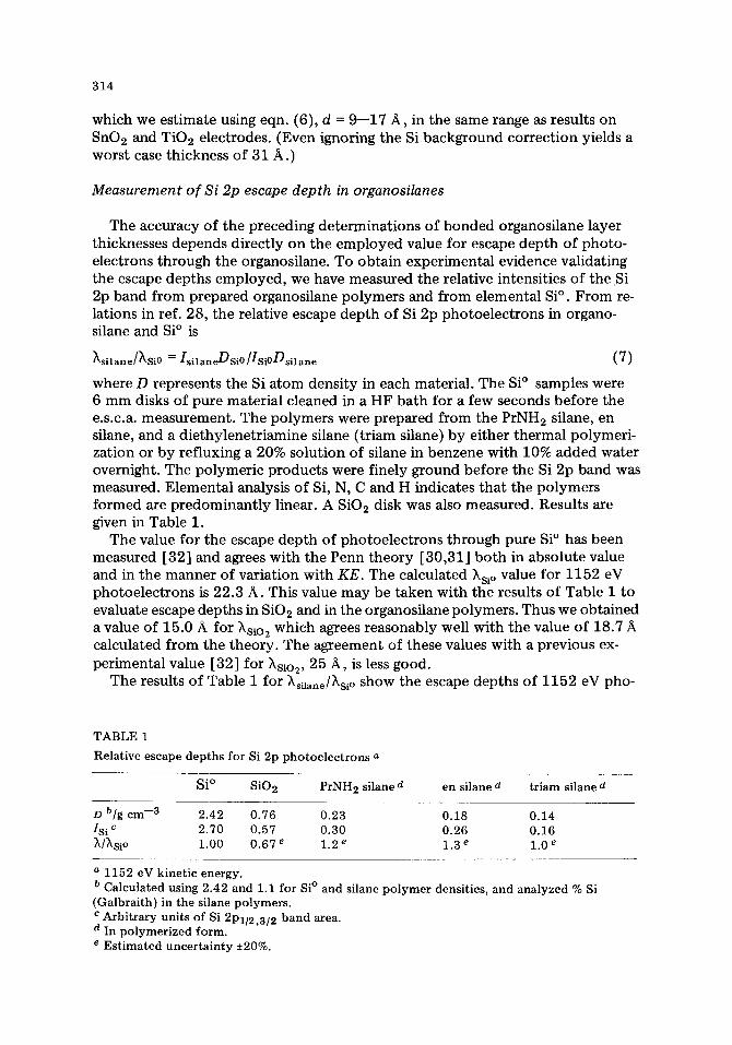
where D represents the Si atom density in each material. The Si ° samples were 6 mm disks of pure material cleaned in a HF bath for a few seconds before the e.s.c.a, measurement. The polymers were prepared from the PrNH 2 silane, en silane, and a diethylenetriamine silane (triam silane) by either thermal polymeri- zation or by refluxing a 20% solution of silane in benzene with 10% added water overnight. The polymeric products were finely ground before the Si 2p band was measured. Elemental analysis of Si, N, C and H indicates that the polymers formed are predominantly linear. A SiO2 disk was also measured. Results are given in Table 1.
The value for the escape depth of photoelectrons through pure Si ° has been measured [32] and agrees with the Penn theory [30,31] both in absolute value and in the manner of variation with KE. The calculated ksio value for 1152 eV photoelectrons is 22.3 •. This value may be taken with the results of Table 1 to evaluate escape depths in SiO2 and in the organosilane polymers. Thus we obtained a value of 15.0 A for ksio2 which agrees reasonably well with the value of 18.7 A calculated from the theory. The agreement of these values with a previous ex- perimental value [32] for Xsio2, 25 A, is less good.
The results of Table 1 for ~silane/~SiO show the escape depths of 1152 eV pho-
TABLE 1
Relative escape dep ths for Si 2p p h o t o e l e c t r o n s a
Si ° SiO 2 PrNH 2 silane d en silane d tr iam silane d
D big cm--3 2.42 0.76 0.23 0.18 0.14 Isic 2.70 0.57 0.30 0.26 0.16 ~[kSi o 1.00 0.67 e 1.2 e 1.3 e 1.0 e
a 1152 eV kinet ic energy. b Calculated using 2.42 and 1.1 for Si ° and silane p o l y mer densit ies, and analyzed % Si (Galbrai th) in the silane polymers . c Arbi t rary units o f Si 2Pl/2,3/2 band area. d In po lymer ized form. e Es t ima ted uncer ta in ty +-20%.
315
toelectrons through the various organosilanes are within experimental error about the same as through elemental Si °. Such similarity in escape depth be- tween Si ° and the organosilanes is predicted by eqn. (5), from which we calcu- late ksio = 22.3 and h e n silane ---- 22.0 •. The similarity in the predicted values is largely traceable to the similar valence electron densities in the two materials, which is the anticipated controlling factor in the extent of scattering in these matrices. This agreement of theory and experiment indicates that the thickness measurement made in the preceding section for en silane bonded to glassy car- bon is not seriously in error due to our choice of a theoretically obtained h. Ad- ditionally, since photoelectron scattering is a function of the organosilane layer and not of the substrate a tom from which the photoelectron is derived (except for the dependency on KE of eqn. 5) the escape depth values employed in the thickness estimates o n S n O 2 and T i O 2 electrodes are also reasonable.
Previous escape depth measurements in organic films, summarized by Powell [33], have suggested that the range of photoelectrons in such materials can be quite large (50--100 A ). The large experimental values are not anticipated by either Penn's theory [30,31] or in earlier calculations by Powell [33]. The organ- ic film measurements have involved oriented molecular layers of long chain molecules prepared by Langmuir trough techniques. Powell has speculated that such films could be anisotropic in photoelectron scattering properties with scat- tering less for photoelectrons traveling parallel to the oriented molecules. If this is true, then the much smaller escape depths determined in Table 1 for randomly oriented bulk organosilane polymers are less surprising. This leads to the ques- tion of whether thin organosilane films bonded to SnO2, TiO2, and carbon are also randomly oriented, or have an anisotropic molecular arrangement. We have no direct experimental data on this. We have indirect evidence that, in contact with solutions, considerable disorder can exist in chain orientation. The electro- chemical reactivity of bonded structures such as (2) suggests that chain flexing can occur at high frequency. The finding [27] that optical properties of a bonded chromophore are similar to those of the analogous solution chromophore also suggests the absence of a highly ordered structure.
Measurement o f optical absorption o f a chromophore bonded to glases
Using Method B, we have bonded the PrNH2 silane to a glass surface. A series of surface synthetic reactions was then carried out to assemble the following chromophoric system on the glass surface
S OS CH2CH2CH NHC N=" N CH3)2 (8) / 1 1
The electronic absorption spectra of this surface are quite similar to those of an analogous solution chromophore. Details of these experiments are described else- where [27]. Making the reasonable assumption that the molar extinction coeffi- cients of solution and surface chromophores are the same, a molecular coverage of (8) could be calculated from the spectral data. From eight measurements F = 1.12(+0.14) X 10 -1° mol cm -2 , which corresponds to an average area per
316
molecule of 148 A 2. The area requirements of a model of the surface molecule, depending on the assumed orientation, range from 50--120 A 2. The experimen- tal coverage is thus compatible with the presumption that the prepared surface molecule is present as a monomolecular layer, or less.
In several experiments, highly colored glass surfaces were obtained, giving ap- parent coverages much larger than those above. It is thought that in these ex- periments, adventitious water was present during the silanization step, allowing subsequent preparation of a multi-layer version of (8).
Measurements based on electrochemical reactions on chemically modified Sn02 and Ti02 electrodes
Electrochemically reactive groupings such as (2) prepared subsequent to the organosilane surface modification allow yet another approach to a coverage es- timate. On a TiO2 electrode surface, (2) yields an electrochemical reduction wave at the same potential (--1.35 V vs. SCE, in acetonitrile solvent) as the solu- tion methylpyridinium species [9 ]. Taking this plus E .S.C .A. N ls observations as evidence that the electrochemical reduction products are the same in the two si- tuations (e.g., n = 1), the integrated charge from the electrochemical reduction wave for (2) has been used to estimate its surface population as 2.6 × 10 -1° mol c m - 2 . This translates to an average molecular area of 64 h 2. The molecular area required in a model of (2) with ring parallel to the surface is ~42 A 2.
Similar results are obtained [9] for (2) on a SnO2 surface. The coverage esti- mate there is 0.8 X 10 -1° mol c m - 2 .
Several factors associated with the electrochemical estimate should be men- tioned. First, the assumption that n = 1 (one electron per molecule) may not be correct for the total surface population of (2). Secondly, in the preparation of (2), by methylat ion of a surface first reacted with the Py silane (Method C), the N ls E.S.C.A. shows that roughly 50% of the originally present Py silane (Method C), the does not methylate. Thus, actual coverage by Py silane could be double that in- dicated by the electrochemical result. We do not know the reason for the incom- plete methylation. It could be explained by patches of impermeable polymer, but at this point equally plausible explanations include a surface electrostatic ef- fect on the methylat ion and a base-inactivating surface side reaction we have identified for the amine organosilanes under certain conditions [34]. In any event, even an error of 2× in the coverage estimate of (2) is compatible with a molecular monolayer or submonolayer picture. Lastly, we have not accounted for surface roughness in our calculations. This would lead to an overestimation of coverage, counterbalancing the factor discussed above.
A different set of electrochemical observations germane to the distinction be- tween surface monolayer and polymers is based on electrochemical reactions of model solution species at organosilane-reacted SnO2 [4] and carbon [3] elec- trodes. For example, on electrodes modified with PrNH2, en, or Py silanes, the electrochemical oxidation of Fe(CN)64- proceeds quite normally by cyclic voltammetric criteria. The implied accessibility of the electrode surface to a solution reactant would be unlikely on a surface coated with an organosilane polymer layer. In fact, S n O 2 and carbon electrodes modified with the highly re- active 3-chloropropylsilane reagent (Method A) gave Fe(CN)s 4- electrochemical
317
data indicative of a restricted electrode area. We believe these latter electrodes, which were prepared in a period when our experiment procedures were less well developed, bore some surface polymer.
Observations based on reaction condi t ions
In addition to the numerical coverage determination discussed above, it is in- structive to note certain experiences with varied reaction conditions. The most striking point is that on SnO2, reaction Methods A--D have all been employed with the en silane at various times over a two year period with generally no more than a 2--3× variation in the absolute intensities of the Sn 3d, N ls, and Si 2p bands observed on the modified electrodes. At least some of this variation is as ascribable to variations in our electron spectrometer's sensitivity over periods of time. The reaction conditions employed vary from extremely mild (Method D) to quite forcing (Method B). It appears that the organosilane reaction, at least with the en silane, occurs extremely rapidly to cover a portion of the surface, and then more slowly, requiring more activating conditions, to bind some further silane. Then, as long as moisture is absent, the reaction halts as the electrode's surface functional groups are exhausted.
On many occasions, some deliberate and other accidental, we have observed the effects of water and consequent polymer formation upon examining modi- fied specimens by E.S.C.A. The severe diminution of Sn 3d bands on SnO2 elec- trodes has been the most reliable indication of this. For instance, in using the Py silane with Method A, a suspension of polymer particles sometimes forms (from adventitious water). As judged by Sn 3d E.S.C.A., the SnO2 electrode can some times be cleansed of adhering polymer by a thorough washing with benzene or methanol. On other occasions, Sn 3d intensity remains abnormally low and the electrode is discarded.
CONCLUSIONS
The different measurements presented above on coverage of SnO2, TiO2, glassy carbon, and glass surfaces by organosilane reagents under anhydrous reac- tion conditions are compatible with coverage predictions based on monolayer models of molecular length and area. The E.S.C.A.-based layer thickness (d) mea- surements fall within the extremes of 4--17 A. Comparison of the E.S.C.A. thick- ness data with the coverage (mol cm -2) results of the electrochemical and opti- cal experiments involves a mass density conversion factor. If the density of the molecular layers (2) and (8) is assumed to be unity, then d values of 4.2 A and 3.8 A are calculated for (2) on TiO2 and (8) on glass, respectively. Given the diversity of the methods employed to measure coverage, the agreement between these values and the E.S.C.A. data is gratifying. Collectively, the coverage values demonstrate that the organosilane surface modification process can be largely constrained to a monomolecular layer-bonding reaction. Our data on coverage, however, are not sufficiently precise to confirm an "exac t" monolayer, or to rule out the presence of some surface polymer. An average coverage of 1.5 mo- lecular layer could be accommodated within some of the data. A general coating of the electrode surfaces with polymer multilayers can on the other hand be
3 1 8
ruled out. This statement only applies to reactions conducted under anhydrous conditions; our experience is that surface polymers otherwise form quite readily.
A consideration of the populat ion of surface hydroxyl groupings available for reaction (1) on the various materials adds little to the above picture. Kirkov [35] estimates 2.23 × 10¹⁵ Sn-O sites cm - 2 on (cassiterite) SnO2. If these are fully hydroxyla ted and reaction (1) forms three SnOSi linkages as shown (both being assumptions), the maximum conceivable monolayer coverage by silane would be 1.2 × 10 - 9 mol cm -2 . This "Fsaturation" exceeds all of the experimen- tally measured coverages, which simply means there is no conflict be tween this analysis of the substrate reactivity and our view of the monolayer coverages achieved in the organosilane reaction.
ACKNOWLEDGMENTS
This research was facilitated by National Science Foundat ion grants MPS73- 08758 and MPS75-07863 and by the U.N.C. Materials Research Center under Defense Advanced Research Projects Agency grant DAHC-15-73-G-9.
REFERENCES
1 B.F . W a t k i n s , J . R . Beh l ing , E. K a r i v a n d L .L . Miller , J . A m e r . C h e m . Soc . , 9 7 ( 1 9 7 5 ) 3 5 4 9 . 2 L .L . Miller, 1 4 9 t h E l e c t r o c h e m i c a l S o c i e t y Mee t ing , W a s h i n g t o n , D.C. , M a y , 1 9 7 6 , A b s t r a c t 304 . 3 C.M. E n i o t t a n d R.W. M u r r a y , Ana l . C h e m . , 4 8 ( 1 9 7 6 ) 1 2 4 7 . 4 P .R . Moses , L. Wier a n d R.W. M u r r a y , Ana l . C h e m . , 4 7 ( 1 9 7 5 ) 1 8 8 2 . 5 P .R . Moses , C.M. E l l io t t , L. Wier a n d R.W. M u r r a y , 1s t C h e m i c a l C o n g r e s s o f t h e N o r t h A m e r i c a n Con-
t i n e n t , M e x i c o C i ty , D e c e m b e r 1 9 7 5 . 6 N .R . A r m s t r o n g , M.E. H e n n e , T. K u w a n a a n d G. R o y e r , 1s t C h e m i c a l C o n g r e s s o f t h e N o r t h A m e r i c a n
C o n t i n e n t , M e x i c o C i t y , D e c e m b e r 1 9 7 5 . 7 N . R . A r m s t r o n g , A.W.C. L in , M. Fu j ih ixa a n d T. K u w a n a , A n a l . C h e m . , 4 8 ( 1 9 7 6 ) 741 . 8 D .F . U n t e r e k e r , R.W. M u r r a y , P .R . Moses , L.M. Wier a n d C.M. E l l io t t , 1 4 9 t h E l e c t r o c h e m i c a l So-
c i e t y Mee t ing , W a s h i n g t o n , D.C. , M a y 1 9 7 6 , A b s t r a c t 349 . 9 P.R. Moses a n d R.W. M u r r a y , J . A m e r . C h e m . Soc . , 9 8 ( 1 9 7 6 ) 7 4 3 5 .
10 H .F . W a l t o n , Ana l . C h e m . , 4 8 ( 1 9 7 6 ) 5 2 R . 11 E. G r u s h k a (Ed . ) , B o n d e d S t a t i o n a r y Phase s in C h r o m a t o g r a p h y , A n n A r b o r Sc i ence Pub l . , A n n
A r b o r , Mich , 1 9 7 4 . 12 D.C. L o c k e , J . C h r o m a t o g r . Sci . , 11 ( 1 9 7 3 ) 120 . 13 W.A. A u e a n d C .R . Has t i ngs , J . C h r o m a t o g r . , 4 2 ( 1 9 6 9 ) 319 . 14 C.R. Has t i ngs , W.A. A u e a n d J .M. Aug l , J. C h r o m a t o g r . , 53 ( 1 9 7 0 ) 4 8 7 . 15 C.R. Has t i ngs , W.A. A u e a n d F .E . L a r s e n , J . C h r o m a t o g r . , 6 0 ( 1 9 7 1 ) 3 2 9 . 16 J . J . K i r k l a n d a n d J .J . D e S t a f a n o , J . C h r o m a t o g r . Sci . , 8 ( 1 9 7 0 ) 3 0 9 . 17 J . J . K i r k l a n d , J . C h r o m a t o g r . Sci . , 9 ( 1 9 7 1 ) 2 0 6 . 18 J .J . D e S t a f a n o a n d J .J . K i r k l a n d , J . C h r o m a t o g r . Sci . , 12 ( 1 9 7 4 ) 3 3 7 . 19 R .E . Ma jo r s a n d M.J . H o p p e r , J . C h r o m a t o g r . Sci. 12 ( 1 9 7 4 ) 767 . 20 H .H . Weeta l l , Sc ience , 1 6 0 ( 1 9 6 9 ) 6 1 5 . 21 H .H . Wee ta l l a n d L.S. H a r s h , B i o c h i m . B i o p h y s . A c t a , 2 0 6 ( 1 9 7 0 ) 54 . 2 2 H.H. Wee ta l l a n d N.B. H a v e w a l a in L.B. W i n g a r d (Ed . ) , E n z y m e E n g i n e e r i n g , Vol . 3 , Wi ley , N e w Y o r k ,
1 9 7 2 , p. 2 4 1 . 23 N.B. H a v e w a l a a n d W.H. P i t c h e r in E .K. P y e a n d L.B. W i n g a r d (Eds . ) , E n z y m e E n g i n e e r i n g , Vol . 2,
P l e n u m , N e w Y o r k , 1 9 7 4 , p . 3 1 5 . 2 4 H .H . WeetaU, S e p a r a t i o n a n d P u r i f i c a t i o n M e t h o d s , 2 ( 1 9 7 3 ) 1 9 9 . 2 5 D.M. He rcu l e s , L.E. C o x , S. On i s i ck , G .D. N i c h o l s a n d J .C. Carver , Ana l . C h e m . , 4 5 ( 1 9 7 3 ) 1 9 7 3 . 26 D.E. L e y d e n a n d G .H . L u t t r e l l , Ana l . C h e m . , 4 7 ( 1 9 7 5 ) 1 6 1 2 . 27 L .T. M i m m s , M.A. M c K n i g h t a n d R.W. M u r r a y , Ana l . C h i m . A e t a , in p ress . 28 T .A. C a r l s o n a n d G.E . M c G u i r e , J . E l e c t r o n S p e c t r o s c . , 1 ( 1 9 7 2 1 7 3 ) 1 6 1 . 29 P.W. P a m b e r g , Ana l . C h e m . , 4 5 ( 1 9 7 3 ) 5 4 9 A . 30 D .R . P e n n , J . Vac . Sci. T e c h n o l . , 13 ( 1 9 7 6 ) 2 2 1 . 31 D .R . P e n n , J . E l e c t r o n S p e c t r o s c . Re l a t . P h e n o m . , 9 ( 1 9 7 6 ) 29 . 32 R . F l i t s c h a n d S.I . R a i d e r , J . Vac . Sci. T e c h n o l . , 12 ( 1 9 7 5 ) 3 0 5 . 33 C.F . Powel l , Su r f . ScL, 4 4 ( 1 9 7 4 ) 29 . 3 4 P .R. Moses , J . L e n n o x , L. Wier a n d R.W. M u r r a y , u n p u b l i s h e d resu l t s , 1 9 7 5 . 3 5 P. K i r k o v , E l e c t r o c h i m . A c t a , 17 ( 1 9 7 2 ) 519 .