Charge-Modulated Extended Gate Organic Field Effect ...
263
Charge-Modulated Extended Gate Organic Field Effect Transistor for Biosensing Applications Ahmed Ben Khaial Doctor of Philosophy University of York Electronic Engineering December 2017
-
Upload
khangminh22 -
Category
Documents
-
view
2 -
download
0
Transcript of Charge-Modulated Extended Gate Organic Field Effect ...
Charge-Modulated Extended Gate Organic
Field Effect Transistor for Biosensing
Applications
Ahmed Ben Khaial
Doctor of Philosophy
University of York
Electronic Engineering
December 2017
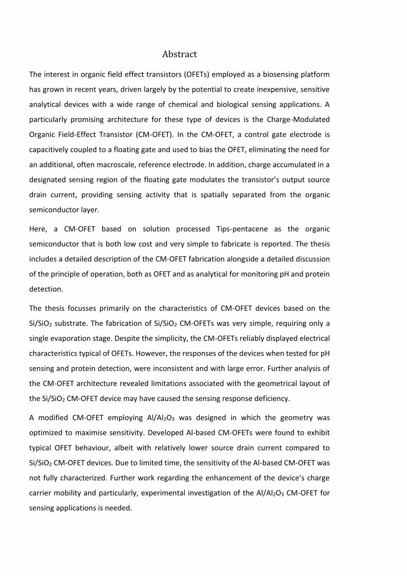
Abstract
The interest in organic field effect transistors (OFETs) employed as a biosensing platform
has grown in recent years, driven largely by the potential to create inexpensive, sensitive
analytical devices with a wide range of chemical and biological sensing applications. A
particularly promising architecture for these type of devices is the Charge-Modulated
Organic Field-Effect Transistor (CM-OFET). In the CM-OFET, a control gate electrode is
capacitively coupled to a floating gate and used to bias the OFET, eliminating the need for
an additional, often macroscale, reference electrode. In addition, charge accumulated in a
designated sensing region of the floating gate modulates the transistor’s output source
drain current, providing sensing activity that is spatially separated from the organic
semiconductor layer.
Here, a CM-OFET based on solution processed Tips-pentacene as the organic
semiconductor that is both low cost and very simple to fabricate is reported. The thesis
includes a detailed description of the CM-OFET fabrication alongside a detailed discussion
of the principle of operation, both as OFET and as analytical for monitoring pH and protein
detection.
The thesis focusses primarily on the characteristics of CM-OFET devices based on the
Si/SiO2 substrate. The fabrication of Si/SiO2 CM-OFETs was very simple, requiring only a
single evaporation stage. Despite the simplicity, the CM-OFETs reliably displayed electrical
characteristics typical of OFETs. However, the responses of the devices when tested for pH
sensing and protein detection, were inconsistent and with large error. Further analysis of
the CM-OFET architecture revealed limitations associated with the geometrical layout of
the Si/SiO2 CM-OFET device may have caused the sensing response deficiency.
A modified CM-OFET employing Al/Al2O3 was designed in which the geometry was
optimized to maximise sensitivity. Developed Al-based CM-OFETs were found to exhibit
typical OFET behaviour, albeit with relatively lower source drain current compared to
Si/SiO2 CM-OFET devices. Due to limited time, the sensitivity of the Al-based CM-OFET was
not fully characterized. Further work regarding the enhancement of the device’s charge
carrier mobility and particularly, experimental investigation of the Al/Al2O3 CM-OFET for
sensing applications is needed.
Table of Contents
Abstract ………………………………………………………………………………………………………………………………… ii
Table of Contents……………………………………………………………………………………………………………….…. iv
List of Tables …………………………………………………………………………………………………………………………. ix
List of Figures …………………………………………………………………………………………………………………………. x
List of Abbreviations ………………………………………………..…………………………………………………………. xxiv
Acknowledgments ………………………………………………………………………………………………………………xxvii
Declaration …………………………………………………………………………………………………………………………xxix
Chapter 1: Introduction ………………………………………………………………………………………………………….1
1.1 Biosensors……………………………………………………………………………………………………………………….1
1.1.1 Exemplar Biosensors: ELISA and SPR-based biosensors…………………………………4
1.1.1.1 Enzyme-linked immunosorbent assay…………………………………………….4
1.1.1.2 Surface plasmon resonance based biosensors……………………………..…5
1.1.1.2.1 Label-free biosensors for real-time measurements of
biomolecular interactions……………………………………………………………………..7
1.1.2 Next generation biosensors ……………………………………………………………………….11
1.2 Organic Electronic Devices………………………………………………………………………….………….…12
1.3 Conductivity in organic materials………………………………………………………………………………14
1.3.1 Intra-molecular charge transport……………………………………………..………………..15
1.3.1.1 Band gap, conjugation and semiconducting behaviour …………………18
1.3.2 Inter-molecular charge transport in organic semiconductor films………………19
1.3.3 Approaches to improve intermolecular charge transport…………………….….…21
1.4 OTFT Operation and fundamental Layers…………………………………………………………….…..22
1.5 Organic thin film transistors for chemical and biological sensing………………………………24
1.5.1 Types of OTFTs used for biosensing……………………………………………………………24
1.5.1.1 The Dual Gate OFET (DG-OFET) biosensor……………………………………28
1.5.1.2 Extended Gate OFET biosensor…………………………………………………….28
1.6 Summary and thesis outline……………………………………………………………………………….…….30
1.7 References…………………………………………………………………………………………………………..……32
Chapter 2: Materials and fabrication of the CM-OFET ………………………………………………………..45
2.1 Substrate, Gate electrode and Gate Dielectric …………………………………………………………..45
2.1.1 Si/SiO2 approach ………………………………………………….……………………………………46
2.1.2 Al/Al2O3 approach ………………………………………………….…………………………………48
2.1.3: Effective sensitivity (ΔID/ΔVTH) of the Al/Al2O3 and Si/SiO2 devices …………..49
2.2 Source/Drain S/D contacts ………………………………………………….……………………………………50
2.3 Organic Semiconductor OSC ………………………………………………….…………………………………51
2.4 Sensing area functionalization (with 3-aminopropyltri-ethoxysilane APTES) ………….…53
2.5 Polydimethylsiloxane (PDMS) microfluidic chamber ………………………….………………………55
2.6 OFET-Sensor Fabrication………………………………………………….………………………………………..57
2.6.1 Si/SiO2 Devices ………………………………………….…….…………………………………………57
2.6.1.1 Substrate Preparation and Cleaning ……………………………………..….…57
2.6.1.2 Sensing area fabrication …………………………………….…….…………………58
2.6.1.3 Fabrication of source, drain and control gate electrodes ……….……59
2.6.1.4 OSC deposition ……………………………………………….……………………………60
2.6.1.5 Functionalizing the surface of the sensing region and microfluidic
integration ………………………………………..…….…………………………………………………………62
2.6.1.6 PDMS microfluidic chamber fabrication ………………………………………64
2.6.2 Al/Al2O3 Devices ………………………………………….…….………………………………………65
2.6.2.1 Substrate Preparation and Cleaning ………………………………………….…65
2.6.2.2 Al gate deposition ………………………………………….….…………………………66
2.6.2.3 Al2O3 gate dielectric deposition…………………………………………..….……68
2.6.2.4 Contact fabrication ………………………………………….….………………………70
2.6.2.5 OSC deposition ………………………………………….…….………………………….71
2.6.2.6 Fabrication of the sensing area ………………………………………….…….…71
2.6.2.7 Sensing area functionalizing and Microfluidic integration……………..72
2.7 References ………………………………………….…….……………………………………………………………..74
Chapter 3: Electrical characterization of the CM-OFET device ……………………………………………….82
3.1 Electrical characterization of the fabricated devices ……………….………………….…….……….82
3.1.1 Electrical measurement setup ………………………………….…….……………………………….83
3.1.2 Electrical characterization of the OFET devices ………………………………………….………84
3.1.3 Electrical characterization of the CM-OFET devices ……………………………….………..90
3.2 Quantification of the CM-OFET sensing response …………………………………………………….94
3.2.1 Maximum source drain current ISDMax ………………………………………………….….94
3.3 Environmental considerations ………………………………………………………………………………….96
3.3.1 Electrical noise ……………………………………………………………….………………………….96
3.3.2 Temperature ………………………………………………………………….………………………….97
3.3.2.1 Self device heating ………………………………………………………………………97
3.3.3 Light …………………………………………………………………………………………………………..99
3.4 Conclusions ………………………………………….………………………………………………………………..105
3.5 References ……………………………………………………………………………………………………………..107
Chapter 4: CM-OFET Device as pH sensor …………………………………………………………………… 110
4.1 Architecture of the pH CM-OFET charge sensor ……………………………………………………….110
4.2 Surface chemistry and surface engineering for pH sensitivity …………………………………..111
4.2.1 Combined pH sensitivity of a NH2 and Si – OH terminated silicon surface….113

4.2.2 The CM-OFET pH sensor containing both NH2 and Si-OH surface groups….115
4.3 APTES surface analysis ……………………………………………………………………………………………116
4.3.1 APTES SAM XPS Spectra ………………………………………………………………………116
4.3.1.1 XPS: Experimental Procedure ……………………………………………………117
4.3.1.2 Detailed spectra of Si XPS peaks …………………………………………………119
4.3.1.3 Detailed spectra N 1s XPS peaks …………………………………………………120
4.3.1.4 Detailed spectra C 1s Peaks …………………………………………….…………121
4.4 pH CM-OFET: Results and discussion ………………………………………………………………………123
4.4.1 Surface modification of Si floating gate using APTES and its effect on the OSC
layer …………………………………………………………………………………………………………………………….123
4.4.2 Experimental consideration for CM-OFET testing; the influence of light……. 128
4.4.3 pH sensing using the CM-OFET …………………………………………………………………132
4.4.3.1 pH sensing using the CM-OFET: Transfer characteristics ……………133
4.4.3.2 CM-OFET pH sensor: Time domain measurements …………………….145
4.5 Conclusion ………………………………………………………………………………………………………….….150
4.6 References ……………………………………………………………………………………………………………..151
Chapter 5: Protein Detection Using the CM-OFET Device……………………………..…………….156
5.1 Biotin, Avidin and their interaction………………………………………………………………………….156
5.1.1 Biotin ……………………………………………………………………………………………………….156
5.1.2 Avidin ………………………………………………………………………………………………………157
5.1.3 Biotin-Avidin interactions for surface functionalization …………………………...158
5.1.3.1 Biotin-Avidin stacking on Si …………………………………………………….…159
5.1.3.2 Biotin-Avidin immobilizing protocol on Si ……………………………….…152
5.2 Quartz Crystal Microbalance with Dissipation Monitoring (QCM-D) ………………….……163
5.3 Results and discussion ……………………………………………………………………………………………167

5.3.1 QCM-D results ………………………………………………………………………………………167
5.3.1 .1 Experimental protocol ……………………………………………..………………167
5.3.1.2 QCM-D measurement ………………………………………………………………..168
5.3.2 CM-OFET results ………………………………………………………………………………………173
5.3.2.1 Specific binding of avidin to biotinylated CM-OFET devices ……….174
5.3.2.2 Nonspecific avidin binding test using CM-OFET devices ……………..181
5.4 Discussion of the Si/SiO2 CM-OFET biosensor ……………………………………………………….…185
5.5 Gating by the control gate; the effect of device geometry ……………………………………….186
5.6 Device geometry and sensitivity ………………………………………………………………………………195
5.7 The trade-offs of the design ……………………………………………………………………………………196
5.8 The modified Al/Al2O3 CM-OFET device behaviour as a transistor …………………………….196
5.9 Conclusions ……………………………………………………………………………………………………….……198
5.10 References ………………………………………………………………………………….………………………..200
Chapter 6: Conclusions and Future Works ……………………………………………………….….……..205
6.1 Conclusions ………………………………………………………………………………….………………….…….205
6.2 Future Works ………………………………………………………………………………………….………..…..208
Appendix A…………………………………………………………………………………………………….…………….211
Appendix B…………………………………………………………………………………………………….…………….220
Appendix C…………………………………………………………………………………………………….…………….223
Appendix D…………………………………………………………………………………………………….…………….230
Appendix E…………………………………………………………………………………………………….…………….233
List of Tables
Table 1.1: The main differences between organic and inorganic semiconductors…………..14
Table 1.2: Electrons distribution on carbon’s atomic orbitals…………………………………………..15
Table 3.1: Average estimated values of figures of merit for characterized OFET devices…90
Table 4.1: the extracted values of τ and β from the fitting of equation 4.6 to ISD decay for
six CM-OFET devices…………………………………………………………………………………………………….129
Table 4.2: The percentage change in the measured maximum source drain current, ISDMax,
during a 7 hours period in the dark compare to ISDMax in light………………………………………130
Table 4.3: Mixing table for making 50ml of citric and Mcilvaine buffer solutions and the
measured pH of prepared buffer solutions compare to the targeted pH…………………………133
Table 5.1: Summary of QCM-D experiment stages………………………………………………………..168
Table 5.2: Estimated avidin mass adsorbed to each of the 4 investigated sensors…………172
Table 5.3: Average percentage change in maximum source drain current after avidin
deposition relative to the maximum source drain current before avidin deposition for nine,
biotinylated CM-OFET devices. …………………………………………………………………………………….180
Table 5.4: Average percentage change in maximum source drain current after avidin
deposition relative to the maximum source drain current before avidin deposition for the
non-biotinylated, silanized CM-OFET biosensors. ……………………………………………………..…184
List of Figures
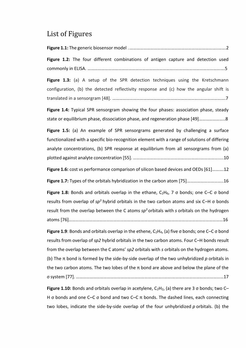
Figure 1.1: The generic biosensor model ..…………………………………………………………………..…….2
Figure 1.2: The four different combinations of antigen capture and detection used
commonly in ELISA. …………………………………………………………………..…………………………………….5
Figure 1.3: (a) A setup of the SPR detection techniques using the Kretschmann
configuration, (b) the detected reflectivity response and (c) how the angular shift is
translated in a sensorgram [48]. …………………………………………………………………..………………….7
Figure 1.4: Typical SPR sensorgram showing the four phases: association phase, steady
state or equilibrium phase, dissociation phase, and regeneration phase [49]…………………..8
Figure 1.5: (a) An example of SPR sensorgrams generated by challenging a surface
functionalized with a specific bio-recognition element with a range of solutions of differing
analyte concentrations, (b) SPR response at equilibrium from all sensorgrams from (a)
plotted against analyte concentration [55]. …………………………………………………..………………..10
Figure 1.6: cost vs performance comparison of silicon based devices and OEDs [61]……….12
Figure 1.7: Types of the orbitals hybridization in the carbon atom [75]…………………………..16
Figure 1.8: Bonds and orbitals overlap in the ethane, C2H6, 7 σ bonds; one C–C σ bond
results from overlap of sp3 hybrid orbitals in the two carbon atoms and six C–H σ bonds
result from the overlap between the C atoms sp3 orbitals with s orbitals on the hydrogen
atoms [76]………………………………………………………………………………………………………………………16
Figure 1.9: Bonds and orbitals overlap in the ethene, C2H4, (a) five σ bonds; one C–C σ bond
results from overlap of sp2 hybrid orbitals in the two carbon atoms. Four C–H bonds result
from the overlap between the C atoms’ sp2 orbitals with s orbitals on the hydrogen atoms.
(b) The π bond is formed by the side-by-side overlap of the two unhybridized p orbitals in
the two carbon atoms. The two lobes of the π bond are above and below the plane of the
σ system [77]. …………………………………………………………………..…….………………………………………17
Figure 1.10: Bonds and orbitals overlap in acetylene, C2H2, (a) there are 3 σ bonds; two C–
H σ bonds and one C–C σ bond and two C–C π bonds. The dashed lines, each connecting
two lobes, indicate the side-by-side overlap of the four unhybridized p orbitals. (b) the
overall outline of the bonds in C2H2. The two lobes of each of the π bonds are positioned
across from each other around the line of the C–C σ bond [77]…………………………………………17
Figure 1.11: Schematic of energy-level in alkenes with increasing conjugation length,
highlighting the energy gap between HOMO to LUMO. The bandgap of polyacetylene
depends on the number of monomers n in the polymer. Arrows represent spin-paired
electrons [84]. …………………………………………………………………..……………………………………………19
Figure 1.12: Typical architectures of OTFTs (a) Bottom contact, (b) Top contact, (c) Top gate-
Bottom contact and (d) Top gate-Top contact. S: Source, D: Drain, G: Gate, and OSC: organic
semiconductor. …………………………………………………………………..…………………………………………23
Figure 1.13: The schematic structure of a typical (a) organic field effect transistor (OFET)
biosensor and (b) organic electrochemical transistor (OECT) biosensor…………………………..25
Figure 1.14: Schematic diagram of the ion-sensitive organic field effect transistors
(ISOFET)………………………………………………………………………………………………………………………….26
Figure 1.15: Schematic diagram of the electrical double layers formed in the electrolyte-
gated organic field effect transistor (EGOFET). ………………………………………………………………..27
Figure 1.16: schematic structure of (a) DG-OFET, and (b) the DG-OFET configured as a
biosensor. …………………………………………………………………..……………………………………………….…28
Figure 1.17: OFET with Extended Gate, Charge Modulated OFET (CM-OFET)……………………30
Figure 2.1: Illustrate the effect of 1V gate shift on the current-voltage response for low and
high operating voltage range (simulated date for two devices with same mobility and
electrode dimensions but different gate dielectric layers)………………………………………………47
Figure 2.2: Delamination of the Al layer during anodization process………………………………48
Figure 2.3: Energy barrier between Metal work function and HOMO / LUMO of OSC. h+ and
e- are holes and electrons respectively. ……………………………………………………………….………….50
Figure 2.4: Chemical structure of (a) Pentacene (b) Tips-pentacene………………………………..51
Figure 2.5: Schematic diagram showing the three phases of Tips-pentacene/PαMS after
separation. …………………………………………………………………..……………………………..…………………53
Figure 2.6: APTES chemical structure and Optimal APTES Silanization process on Si
substrate [54]. …………………………………………………………………..……………………………………………54
Figure 2.7: Polymerization of PDMS when mixing oligomer base (1) and curing agent (2)
[64]. …………………………………………………………………..…………………………………………………………..56
Figure 2.8: PDMS oxygen plasma surface treatment and bonding to silica substrate
[69,74]….…………………………………………………………………..…………………………………….……………..57
Figure 2.9: Clean Si/SiO2 substrate (a) Top view (b) Cross section………………………….……….58
Figure 2.10: etched SiO2 sensing region of Si/SiO2 substrate (a) Top view (b) Cross section..
…………………………………………………………………..…………………………………………………………………..59
Figure 2.11: Deposition of device contacts on Si/SiO2 substrate (a) Top view (b) Cross
section. …………………………………………………………………..…………………………………………….……….60
Figure 2.12: OSC deposition on S/D contacts of the device (a) Top view (b) Cross section.
…………………………………………………………………..…………………………………………………………………..61
Figure 2.13: Optical microscope image of the source/drain electrodes (a) before and (b)
after Tips-pentacene deposition. Images were captured using a 5x objective lens……………62
Figure 2.14: Complete Si/SiO2 CM-OFET sensor (a) Top view (b) Cross section………..……..64
Figure 2.15: Making of a PDMS replica mold. …………………………………………………………………65
Figure 2.16: PDMS Microfluidic chamber with an inlet and an outlet…………..…………………65
Figure 2.17: Clean Si/SiO2 substrate (a) Top view (b) Cross section…………………………………66
Figure 2.18: Deposition of Al gate layer on the entire substrate (a) Top view (b) Cross
section, and pattern Al gate layer (c) Top view (d) Cross section………………………………………67
Figure 2.19: PE-ALD cycle for Al2O3 deposition [78]……………………………………………..…………69
Figure 2.20: ALD Al2O3 layer deposition on Al gate (a) Top view (b) Cross section…………..70
Figure 2.21: Deposition of device contacts on top of Al2O3 layer (a) Top view (b) Cross
section……………………………………………………………………………………………………………………………70
Figure 2.22: OSC deposition on S/D contacts of the device (a) Top view (b) Cross
section.................................................................................................................................71
Figure 2.23: Etched Al2O3 sensing region of Al/Al2O3 bilayer (a) Top view (b) Cross
section……………………………………………………………………………………………………………………………72
Figure 2.24: Complete Al/Al2O3 CM-OFET sensor (a) Top view (b) Cross section………..…..73
Figure 3.1: Electrical characterization measurement setup. ………………………………………..…84
Figure 3.2: A photograph of four OFETs fabricated on a Si/SiO2 substrate. Here, the gold
source and drain electrodes were fabricated by photolithography before Tips-pentacene
was drop cast over the substrate surface. Contact to the degenerately doped Si gate was
achieved by mechanical removal of the 300 nm thick SiO2 gate dielectric ……………………..85
Figure 3.3: Measured output characteristics of one of the fabricated OFETs, the channel
length of the device is 60 µm and the thermally grown SiO2 gate dielectric has a thickness
of 300 nm. …………………………………………………………………..…………………………………………………86
Figure 3.4: Measured transfer characteristics of one of the fabricated OFETs at VSD = -40V,
the channel length of the device is 60µm and the thermally grown SiO2 gate dielectric has
a thickness of 300nm. …………………………………………………………………..……………………………… 86
Figure 3.5: Optical microscope image of the formation of Tips-pentacene crystals that
assemble on and between source and drain following drop casting. Images were captured
using a 5x objective lens. (a) Situation where crystals bridge the S/D contacts and (b) no
crystals in the channel between the S/D contacts. …………………………………………………………87
Figure 3.6 Transfer characteristics for four nominally identical OFETs (T1 – 4) fabricated
on the same Si/ SiO2 substrate at VSD = -40 V. Here, the channel length (spacing between
source and drain electrodes) is 60 µm and the thermally grown SiO2 gate dielectric has a
thickness of 300 nm. ………………………………………………………………………………………………………88
Figure 3.7: The range of maximum source drain current, ISDMax, for all working OFET
devices (total = 131). Here ISDMax is defined as the source drain current flowing between
source and drain contacts at VSD = -40 V and VG = -40 V. …………………………………………….…89
Figure 3.8: The range of ON/OFF ratio for all working OFET devices (total = 131). ………...89
Figure 3.9: A photograph of four CM-OFETs fabricated on a Si/SiO2 substrate. Here, the
gold source, drain and control gate electrodes were fabricated by shadow masking before
S D D

Tips-pentacene was drop cast over the substrate surface. The gate dielectric layer SiO2
thickness is 300 nm thick. ………………………………………………..…………………………………………….91
Figure 3.10: Measured output characteristics of one of the fabricated CM-OFETs, the
channel length of the device is 60 µm and the thermally grown SiO2 gate dielectric has a
thickness of 300 nm. ……………………………………………………………………………………………………….92
Figure 3.11: Measured transfer characteristics of one of the fabricated CM-OFETs at VSD =
-40V, the channel length of the device is 60µm and the thermally grown SiO2 gate dielectric
has a thickness of 300nm. …………………………………………………………………..…………………..………93
Figure 3.12: The range of maximum source drain current, ISDMax, for characterized CM-
OFET devices (total = 27). Here ISDMax is defined as the source drain current flowing
between source and drain contacts at VSD = -40 V and VG = -40 V. …………………………………….94
Figure 3.13: Effect of ±1V gate voltage range shift on the ISD of a transfer characteristic,
(inset) shows the difference between ISDMax. (simulated curves for Si/SiO2 CM-OFET device
with W = 0.1 cm, L = 60 X 10-4 cm, Ci = 11.51nF/cm2 and µ = 1 X 10⁻³ cm2 V-1 S-1). ……………….96
Figure 3.14: Power consumed during a transfer characteristics measurement of one CM-
OFET device…………………………………………………………………………………………………………………….99
Figure 3.15: spectrum of laboratory fluorescent light measured at the position of the tested
CM-OFET devices. …………………………………………………………………..…………………………………….100
Figure 3.16: The change in ISDMax periodically measured for 5 CM-OFET under light and
dark conditions. …………………………………………………………………..……………………………………….101
Figure 3.17: The change in ISD periodically measured for a CM-OFET under light and dark
conditions at VG = -10, -20, -30 and -40V. ……………………………………………………………………….102
Figure 4.1: Schematic diagram of the CM-OFET sensor showing the two key components of
the device; the OFET and the sensing region which can be exposed to an analyte through a
PDMS microfluidic manifold. Coupling between the two components is achieved via the
floating gate. The control gate, Cg, is used to bias the OFET without the need for applying a
potential directly to the floating gate. Here, the schematic shows a CM-OFET responsive to
pH where the pH sensitivity arises from amine groups introduced on the surface of the
sensing region by the APTES self-assembled monolayer. ……………………………………………….111
Figure 4.2: ionization states of silanol groups at the interface between the native silica
formed on silicon substrate and an aqueous electrolyte as a function of solution pH [4]..112
Figure 4.3: Schematic plot of the Henderson-Hasselbalch relationship of the amine group
……………………………………………………………………………………………………………………………………..114
Figure 4.4: A representative XPS survey scan showing the elemental composition of the
surfaces of (a) APTES modified Si substrate, (b) reference Si substrate. The APTES modified
Si sample spectrum has a reduced intensity compared to the reference sample. This is
because a smaller aperture was used to reduce artefacts associated with photoelectrons
generate from the sample plate. ………………………………………………………………………………..…118
Figure 4.5: Experimental XPS spectra for Si (2s & 2p) peaks for the (a and c) APTES modified
Si substrate and (b and d) for the unmodified reference Si substrate. …………………………….119
Figure 4.6: XPS spectra for N (1s) on (a) APTES modified Si substrate, and (b) reference Si
substrate. …………………………………………………………………………………………………………………….120
Figure 4.7: Detailed XPS spectra for N (1s) peaks for APTES modified Si substrate. Peak
fitting reveals two peaks associated with the neutral (NH2) and protonated (NH3+) binding
energies. All deconvoluted fitted peaks are Gaussian functions ……………………….……………121
Figure 4.8: Detailed XPS spectra for C (1s) peaks on (a) APTES modified Si substrate and (b)
reference Si substrate. ………………………………………………………………………………………………….122
Figure 4.9: Detailed XPS spectra for C (1s) peaks for (a) APTES modified Si substrate and (b)
reference Si substrate. Peak fitting reveals three peaks associated with binding energies of
C – C ∼284.4 eV (peak 1), C – N ∼286.2 eV (peak 2) and C = O ∼288 eV (peak 3). All
deconvoluted fitted peaks are Gaussian functions………………………………………………………...123
Figure 4.10: The two fabrication sequences implemented for fabricating the CM-OFET
devices. ………………………………………………………………………………………………………………………..124
Figure 4.11: Transfer characteristics of a CM-OFET before and after functionalization of the
Si sensing region with 5% APTES in IPA. Here, VSD = -40 V. ………………………………………………125
Figure 4.12: Transfer characteristics of a device before and after APTES functionalization
using approach 2 and after exposing the device to APTES vapour (VSD=-40V). ………………..126
Figure 4.13: Effect of immersion in (APTES-Toluene) and (APTES-IPA) solutions on PDMS
chamber, (a) before (b) after immersion in (APTES-Toluene) solution, (c) before (d) after
immersion in (APTES-IPA) solution. ……………………………………………………………………………….127
Figure 4.14: Time dependence of the maximum source drain current for a CM-OFET device
due to shielding from ambient light. Here, the Tips-pentacene layer is covered by black tape
and the transfer characteristics were measured every 25 minutes for 7 hours and ISD is the
maximum source drain current recorded at VG = -40 V. ………………………………………………….129
Figure 4.15: The percentage of change in the measured maximum source drain current
ISDMax for six CM-OFETs. …………………………………………………………………………………………….. 131
Figure 4.16: comparison of the RSD between recorded ISDMax at different periods of the
experiment for six CM-OFETs. ……………………………………………………………………………………….131
Figure 4.17: Experimental results of pH sensing using CM-OFET device 1. (a) Percentage
change in ISDMax for three independent measurements over the full pH range. Here, the
transfer characteristics were measured 25 mins after introduction of the test pH solution.
(b) The average change in ISDMax for the three independent measurements (25min
measurement). (c) Percentage change in ISDMax for two independent measurements over
the full pH range. Here, the transfer characteristics were measured immediately after
introduction of the test pH solution. (d) The average change in ISDMax for the two
independent measurements (immediate measurement). Error bars are ±SD ……….……….136
Figure 4.18: Experimental results of pH sensing using CM-OFET device 2. (a) Percentage
change in ISDMax for three independent measurements over the full pH range. Here, the
transfer characteristics were measured 25 mins after introduction of the test pH solution.
(b) The average change in ISDMax for the three independent measurements (25min
measurement). (c) Percentage change in ISDMax for two independent measurements over
the full pH range. Here, the transfer characteristics were measured immediately after
introduction of the test pH solution. (d) The average change in ISDMax for the two
independent measurements (immediate measurement). Error bars are ±SD ……………….137
Figure 4.19: Experimental results of pH sensing using CM-OFET device 3. (a) Percentage
change in ISDMax for three independent measurements over the full pH range. Here, the
transfer characteristics were measured 25 mins after introduction of the test pH solution.
(b) The average change in ISDMax for the three independent measurements (25min
measurement). (c) Percentage change in ISDMax for two independent measurements over
the full pH range. Here, the transfer characteristics were measured immediately after
introduction of the test pH solution. (d) The average change in ISDMax for the two
independent measurements (immediate measurement). Error bars are ±SD ……….……….138
Figure 4.20: Experimental results of pH sensing using CM-OFET device 4. (a) Percentage
change in ISDMax for three independent measurements over the full pH range. Here, the
transfer characteristics were measured 25 mins after introduction of the test pH solution.
(b) The average change in ISDMax for the three independent measurements (25min
measurement). (c) Percentage change in ISDMax for two independent measurements over
the full pH range. Here, the transfer characteristics were measured immediately after
introduction of the test pH solution. (d) The average change in ISDMax for the two
independent measurements (immediate measurement). Error bars are ±SD ……….……….139
Figure 4.21: Experimental results of pH sensing using CM-OFET device 5. (a) Percentage
change in ISDMax for three independent measurements over the full pH range. Here, the
transfer characteristics were measured 25 mins after introduction of the test pH solution.
(b) The average change in ISDMax for the three independent measurements (25min
measurement). (c) Percentage change in ISDMax for two independent measurements over
the full pH range. Here, the transfer characteristics were measured immediately after
introduction of the test pH solution. (d) The average change in ISDMax for the two
independent measurements (immediate measurement). Error bars are ±SD ……….……….140
Figure 4.22: Experimental results of pH sensing using CM-OFET device 6. (a) Percentage
change in ISDMax for three independent measurements over the full pH range. Here, the
transfer characteristics were measured 25 mins after introduction of the test pH solution.
(b) The average change in ISDMax for the three independent measurements (25min
measurement). (c) Percentage change in ISDMax for two independent measurements over
the full pH range. Here, the transfer characteristics were measured immediately after
introduction of the test pH solution. (d) The average change in ISDMax for the two
independent measurements (immediate measurement). Error bars are ±SD …….………….141
Figure 4.23: Experimental results of pH sensing using CM-OFET device 7. (a) Percentage
change in ISDMax for three independent measurements over the full pH range. Here, the
transfer characteristics were measured 25 mins after introduction of the test pH solution.
(b) The average change in ISDMax for the three independent measurements (25min
measurement). (c) Percentage change in ISDMax for two independent measurements over
the full pH range. Here, the transfer characteristics were measured immediately after
introduction of the test pH solution. (d) The average change in ISDMax for the two
independent measurements (immediate measurement). Error bars are ±SD ….…………….142
Figure 4.24: Experimental results of pH sensing using CM-OFET device 8. (a) Percentage
change in ISDMax for three independent measurements over the full pH range. Here, the
transfer characteristics were measured 25 mins after introduction of the test pH solution.
(b) The average change in ISDMax for the three independent measurements (25min
measurement). (c) Percentage change in ISDMax for two independent measurements over
the full pH range. Here, the transfer characteristics were measured immediately after
introduction of the test pH solution. (d) The average change in ISDMax for the two
independent measurements (immediate measurement). Error bars are ±SD ……….……….143
Figure 4.25: The average of [(ISDMax (pH)- ISDMax (citric))/ ISDMax (citric) %] change for each
investigated pH level across all tested CM-OFET devices (25min measurement). Error bars
are ±SD …………………………………………………………………………………………………………….…………..145
Figure 4.26: Source drain current decay over time due to bias stress effect for a CM-OFET
device. …………………………………………………………………………………………………………………………146
Figure 4.27: Normalized real time source drain current as a function of solution pH for CM-
OFET device 1. The data has been smoothed using a 200s averaging period. Here, air was
injected into the PDMS chamber prior to the injection of each buffer. ………………………..…147
Figure 4.28: Normalized real time source drain current as a function of solution pH for CM-
OFET device 2. The data has been smoothed using a 200s averaging period. Here, air was
injected into the PDMS chamber prior to the injection of each buffer. ………………………..…147
Figure 4.29: Normalized real time source drain current as a function of solution pH for CM-
OFET device 3. The data has been smoothed using a 200s averaging period. Here, air was
injected into the PDMS chamber prior to the injection of each buffer. ………………………..…148
Figure 4.30: Normalized real time source drain current as a function of solution pH for CM-
OFET device 4. The data has been smoothed using a 200s averaging period. Here, air was
injected into the PDMS chamber prior to the injection of each buffer. ………………………..…148
Figure 4.31: Normalized real time source drain current as a function of solution pH for CM-
OFET device 5. The data has been smoothed using a 200s averaging period. ……………….…148
Figure 4.32: Normalized real time source drain current as a function of solution pH for CM-
OFET device 6. The data has been smoothed using a 200s averaging period. ……………….…149
Figure 4.33: Normalized real time source drain current as a function of solution pH for CM-
OFET device 7. The data has been smoothed using a 200s averaging period. ….…………..…149
Figure 5.1: Chemical structure of biotin molecule. ………………………………………………………..157
Figure 5.2: A ribbon representation of the avidin tetrameric arrangement [12]. ……………158
Figure 5.3: Schematic representation of the two methods utilizing biotin-avidin conjugation
to bind targeted biomolecules to sensor surface. In a) the surface is first chemically
modified for conjugation to biotin. In contrast, the approach shown schematically in b)
employs physisorption of avidin to the solid support. …………………………………………..……….159
Figure 5.4: Si surface functionalization, biotinylation and Avidin binding process, from left
to right, a hydroxylated Si surface was first silanized with APTES, then biotinylated and
finally avidin binds to the biotinylated surface [19]. ………………………………………………………160
Figure 5.5: Schematic diagram of (a) QCM quartz crystal sensor with drive electrodes, (b)
initial geometry of the crystal before applying the AC drive voltage and (c) oscillation of the
crystal upon applying AC voltage. …………………….…………………………………………………………..163
Figure 5.6: Representation of the fundamental resonant frequency (n=1) and the first two
harmonics (n=2 and 3) produced by crystal oscillation [30]. …………………………………………..164
Figure 5.7: Illustration of the difference in frequency and dissipation response in a QCM-D
system for rigid and soft films [36]. ……………………………………………………………………………….166
Figure 5.8: QCM-D Δf and D vs time response for the 3rd overtone to the layer by layer
adsorption on the SiO2 coated crystal for sensor 1. ……………………………………………………….169
Figure 5.9: QCM-D Δf and D vs time response for the 3rd overtone to the layer by layer
adsorption on the SiO2 coated crystal for a non-biotinylated surface (sensor 3). ……………170
Figure 5.10: QCM-D Δf vs time response for the 3rd overtone to the layer by layer adsorption
on the 4 crystal sensors. ……………………………………………………………………………………………….171
Figure 5.11: QCM-D D vs time response for the 3rd overtone to the layer by layer adsorption
on the 4 crystal sensors. ………………………………………………………………………………………………171
Figure 5.12: Estimated avidin mass adsorbed to each of the 4 investigated sensors and the
effect of 1 hour rinse in SPB solution. ……………………………………………………………………………172
Figure 5.13: The average calculated final avidin mass adsorbed in the carried-out
measurement for specific and nonspecific binding to the QCM-D sensors. Error bars are ±SD
……………………………………………………………………………………………………………………………..……...173
Figure 5.14: The raw data of the three measurements after biotinylation of the sensing
region of one CM-OFET device and three measurements after avidin binding. ………………175
Figure 5.15: The average measured ISDMax for CM-OFET device 1 for (a) The three
measured transfer characteristics with SPB pH8 solution on the biotinylated sensing surface
and (b) The three measured transfer characteristics with SPB pH8 solution on the avidin
covered sensing surface. Error bars are ±SD …………………………………….……………………………175
Figure 5.16: The average measured ISDMax for CM-OFET device 2 for (a) The three
measured transfer characteristics with SPB pH8 solution on the biotinylated sensing surface
and (b) The three measured transfer characteristics with SPB pH8 solution on the avidin
covered sensing surface. Error bars are ±SD ………………………………………….………………………176
Figure 5.17: The average measured ISDMax for CM-OFET device 3 for (a) The three
measured transfer characteristics with SPB pH8 solution on the biotinylated sensing surface
and (b) The three measured transfer characteristics with SPB pH8 solution on the avidin
covered sensing surface. Error bars are ±SD ………………………………………………….………………176
Figure 5.18: The average measured ISDMax for CM-OFET device 4 for (a) The three
measured transfer characteristics with SPB pH8 solution on the biotinylated sensing surface
and (b) The three measured transfer characteristics with SPB pH8 solution on the avidin
covered sensing surface. Error bars are ±SD ………………………………………….………………………177
Figure 5.19: The average measured ISDMax for CM-OFET device 5 for (a) The three
measured transfer characteristics with SPB pH8 solution on the biotinylated sensing surface
and (b) The three measured transfer characteristics with SPB pH8 solution on the avidin
covered sensing surface. Error bars are ±SD ………………………………….………………………………177
Figure 5.20: The average measured ISDMax for CM-OFET device 6 for (a) Three measured
transfer characteristics with SPB pH8 solution on the biotinylated sensing surface and (b)
The three measured transfer characteristics with SPB pH8 solution on the avidin covered
sensing surface. Error bars are ±SD …………………………………….…………………………………………178
Figure 5.21: The average measured ISDMax for CM-OFET device 7 for (a) The single
measured transfer characteristics with SPB pH8 solution on the biotinylated sensing surface
and (b) The three measured transfer characteristics with SPB pH8 solution on the avidin
covered sensing surface. Error bars are ±SD ……………………………………….…………………………178
Figure 5.22: The average measured ISDMax for CM-OFET device 8 for (a) The single
measured transfer characteristics with SPB pH8 solution on the biotinylated sensing surface
and (b) The three measured transfer characteristics with SPB pH8 solution on the avidin
covered sensing surface. Error bars are ±SD ……………………………………….…………………………179
Figure 5.23: The average measured ISDMax for CM-OFET device 9 for (a) The single
measured transfer characteristics with SPB pH8 solution on the biotinylated sensing surface
and (b) The three measured transfer characteristics with SPB pH8 solution on the avidin
covered sensing surface. Error bars are ±SD …………………………….……………………………………179
Figure 5.24: Comparison of average percentage change in ISDMax after avidin deposition
ISDMax (Av) relative to the ISDMax (Biotin) before avidin deposition for the nine biotinylated
CM-OFET devices. …………………………………………………………………………………………………………181
Figure 5.25: The average measured ISDMax for CM-OFET device 1 for (a) The last three
transfer characteristics recorded with SPB solution on silanized sensing surface, (b) The
three measured transfer characteristics with SPB pH8 solution on nonspecific avidin
covered sensing surface. Error bars are ±SD ……………………….…………………………………………182
Figure 5.26: The average measured ISDMax for CM-OFET device 2 for (a) The last three
transfer characteristics recorded with SPB solution on silanized sensing surface, (b) The
three measured transfer characteristics with SPB pH8 solution on nonspecific avidin
covered sensing surface. Error bars are ±SD …………………….……………………………………………182
Figure 5.27: The average measured ISDMax for CM-OFET device 3 for (a) The last three
transfer characteristics recorded with SPB solution on silanized sensing surface, (b) The
three measured transfer characteristics with SPB pH8 solution on nonspecific avidin
covered sensing surface. Error bars are ±SD ………….………………………………………………………183
Figure 5.28: The average measured ISDMax for CM-OFET device 4 for (a) The last three
transfer characteristics recorded with SPB solution on silanized sensing surface, (b) The
three measured transfer characteristics with SPB pH8 solution on nonspecific avidin
covered sensing surface. Error bars are ±SD ………………………………….………………………………183
Figure 5.29: Average percentage change in ISDMax after avidin deposition ISDMax (Av)
relative to ISDMax before avidin deposition for the non-biotinylated, silanized CM-OFET
biosensors. Error bars are ±SD ……………………………….……………………..………………………………184
Figure 5.30: (a) Cross section of CM-OFET device proposed by Lai et.al [43]; the employed
materials are reported in the palette; (b) the layout of the device. ………………………………..186
Figure 5.31: Capacitive coupling in the CM-OFET device and simplified equivalent circuit
considering only capacitive contributions. …………………………………………………………………….187
Figure 5.32: Charge distribution and charge conservation in floating gate. ……………………188
Figure 5.33: Electrodes geometrical dimensions and the Si/SiO2 CM-OFET device general
layout. …………………………………………………………………………………………….……………………………189
Figure 5.34: The relationship between the control gate and drain area ratio and the
contribution of each one in biasing the floating gate. ……………………………………………………190
Figure 5.35: Al/Al2O3 CM-OFET device with modified electrodes’ layout. ………………………190
Figure 5.36: An example of an output characteristics of a Si/SiO2 CM-OFET device. ……….192
Figure 5.37: An example of an output characteristics of an Al/Al2O3 CM-OFET device. …..192
Figure 5.38: An example of a transfer characteristics of a Si/SiO2 CM-OFET device (transistor
on from start). ………………………………………………………………………………………………………………193
Figure 5.39: An example of a transfer characteristics of a Si/SiO2 CM-OFET device (transistor
turn on in the positive gate voltage region). ………………………………………………………………….194
Figure 5.40: An example of a transfer characteristics of an Al/Al2O3 CM-OFET device. ……194
Figure 5.41: Comparison between the effective S/D areas AS/AD in the CM-OFET Si/SiO2 and
Al/Al2O3 devices (W=1mm and LS=LD=10.5mm for Si/SiO2 devices and W=1mm and
LS=LD=1.5mm for Al/Al2O3 devices). ………………………………………………………………………………197
Figure 6.1: Experimental results of pH sensing using an Al/Al2O3 CM-OFET device, the figure
shows the percentage change in ISDMax for three independent measurements (at 3
different pH levels). Here, the transfer characteristics of the device were measured 25 mins
after introduction of the test pH solution. …………………………………………………………………….208
Figure 6.2: Theoretical effect of mobility on maximum source drain current change per unit
gate voltage shift for Al/Al2O3 CM-OFET (Al2O3 40nm). ………………………………………………….209
List of abbreviations
π bond Pi bond
σ bond Sigma bond
a-Si:H Hydrogenated amorphous silicon
ALD Atomic layer deposition
APTES 3-aminopropyltriethoxysilane
BGD Bässler’s Gaussian disorder model
CM-OFET Charge Modulated-organic field effect transistor
D Drain electrode
DG-OFET Dual Gate-organic field effect transistor
DNA Deoxyribonucleic acid
EDL Electrical Double Layers
EGOFET Electrolyte-gated organic field effect transistor
ELISA Enzyme-linked immunosorbent assay
G Gate electrode
GOx Glucose Oxidase
HOMO Highest occupied molecular orbital
IPA Isopropyl alcohol
ISOFET Ion-Sensitive Organic Field Effect Transistor
LCAO Linear Combination of Atomic Orbitals
LCD Liquid-crystal display
LOC Lab-on-chip
LOD Limit of detection
LUMO Lowest unoccupied molecular orbital
MTR Multiple trap and release
NHS N-hydroxysulfosuccinimide
OE Organic electronic
OECT Organic Electrochemical Transistor
OED Organic electronic device
OFET Organic field effect transistor
OLED Organic Light-Emitting Diode
OPV Organic Photovoltaic Devices
OSC Organic semiconductor
OTFT Organic thin film transistor
OTS Octadecyltrichlorosilane
PDMS Polydimethylsiloxane
PE-ALD Plasma enhanced- Atomic layer deposition
PER Percolation model
PαMS Poly(α-methyl styrene)
QCM Quartz crystal microbalance
QCM-D Quartz crystal microbalance with dissipation
RFID Radio frequency identification
RNA Ribonucleic acid
rpm Revolutions per minute
S Source/Sub-threshold slope
SAM Self-assembled monolayer
SMU Source-measurement unit
SPB Sodium phosphate buffer
SPR Surface plasmon resonance

Tips-pentacene 6,13-Bis(triisopropylsilylethynyl)-pentacene
TMA Trimethyl Aluminium
UV Ultraviolet
VRH Variable range hopping
XPS x-ray photoelectron spectroscopy

Acknowledgements
First and foremost, I praise Allah the Almighty for giving me the power, patience and
strength of mind to complete this thesis.
“He who does not thank people, does not thank Allah”, so for that, I would like to take this
opportunity to extend my thanks to all the people whom have contributed to the
completion of my thesis.
I would like to express my gratitude to my supervisor Dr. Steven Johnson for his scientific
support, help and patience throughout this doctorate research, thank you for all your
insightful feedbacks.
My heartful gratitude to Professor Mohamed El Gomati for all his valuable advices and my
thanks extends to his family whom have been all but supportive for me and my wife during
our study years.
Thank you to Dr. Alison Parkin for her discussion and thoughts on the research.
I would like to thank all the present and past group members of the Bio-inspired Lab, special
thanks to Pepe for his generous help and encouragement throughout the PhD years. My
thanks also to Elena for her assistance during the research work.
Huge thanks goes to Louis Fry-Bouriaux for his generous time to perform the ALD
deposition, I really enjoyed the fruitful conversations we had every time I come over to
Leeds.
I should not forget to thank the experimental officers for their support to my research
activities, particularly, late Jonathan Creamer, sadly we could not celebrate my degree
together. Thank you to Ian and Charan as well.
Thanks to Camilla and Helen in the postgraduate office for taking care of all the
administrative support and services.
A big thank you to all the department personnel whom helped to complete this project in
any shape or form.

I cannot thank enough my lovely wife, who has stood by me through all the ups and downs
of my research. You were an exceptional companion, without your help, support, sacrifices
and presence this thesis would not have been completed.
Deep thank you to my family, Dad, stepmother, brother and my sister and her family for
their encouragement and passionate support all the way.
My sincere gratitude goes out to all my in-law family uncle Monsef, aunt Halima,
Mohammed, Marwan, Osama and Yosef, your prayers, concerns and encouragement was
priceless.
My big thanks to all the Libyan families in York whom we had share good times with.

Declaration
I declare that the work presented in this thesis, if not otherwise stated, is my own. Some
of the material presented within this thesis has previously been published in the following
conference:
Ben Khaial, A. and Johnson, S. (2017), Charge-modulated field-effect transistor biosensors
based on solution processed TIPS-pentacene, Biodetection & Biosensors Conference,
Cambridge, UK
Chapter 1: Introduction
1.1 Biosensors
From identifying contaminants and toxins to ensure food product safety, to detecting
biomarkers of disease and monitoring pollutants in the environment, technologies for
detection and quantification of chemical and biological molecules are today an integral part
of the modern world. A broad range of technologies, generally known as biosensors, have
been demonstrated to meet these analytical challenges, and the innovation of novel
biosensors with improved sensitivity, speed and applicability remains a significant research
activity. For example, in 2018 alone, a total of 1,570 articles were published containing the
word biosensor in the title (data from Google scholar).
The term “biosensor” is believed to have been coined by Cammann in 1977 [1-2], however,
it is widely accepted that the first biosensor can be traced back to 1962 to the work of
Leyland C. Clark, the inventor of Clark Oxygen Electrode [3-6]. His concept, which earned
him the title of the father of the biosensor, involved electrochemical reduction of oxygen
as a method of quantifying dissolved oxygen content. This approach laid the foundation for
one of the most commercially important biosensors; the electrochemical glucose biosensor
which provides an approach for the diagnosis and management of diabetes through the
detection and quantification of glucose using glucose oxidase (GOx) enzyme immobilized
on an electrode [3,5,7]. Today, biosensor technologies have become a multi-billion dollars
market [8-10] and the development of novel biosensors continues to be a major research
activity that spans the scientific disciplines and impacts on a wide range of application areas
including clinical and medical diagnosis, food safety, environmental monitoring, precision
agricultural, industrial monitoring, homeland security and defence [3-6,11-13].
Generally, biosensors are analytical devices that combine a biological or biologicaly derived
recognition element with a physicochemical detector element commonly referred to as
“transducer” [3-4,11-12]. The role of the transducer is to convert a specific interaction
between the recognition element and a target analyte into a measurable signal that can be
quantified to provide a measure of analyte concentration [3-5,12]. Specificity to the
required analyte is provided by the biological recognition element.
Although multiple recognition elements and transducer mechanisms have been
demonstrated, the fundamentals of a biosensor remain the same and can be modelled by
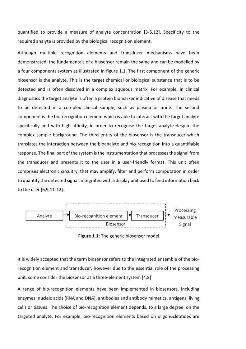
a four components system as illustrated in figure 1.1. The first component of the generic
biosensor is the analyte. This is the target chemical or biological substance that is to be
detected and is often dissolved in a complex aqueous matrix. For example, in clinical
diagnostics the target analyte is often a protein biomarker indicative of disease that needs
to be detected in a complex clinical sample, such as plasma or urine. The second
component is the bio-recognition element which is able to interact with the target analyte
specifically and with high affinity, in order to recognise the target analyte despite the
complex sample background. The third entity of the biosensor is the transducer which
translates the interaction between the bioanalyte and bio-recognition into a quantifiable
response. The final part of the system is the instrumentation that processes the signal from
the transducer and presents it to the user in a user-friendly format. This unit often
comprises electronic circuitry, that may amplify, filter and perform computation in order
to quantify the detected signal, integrated with a display unit used to feed information back
to the user [6,9,11-12].
Figure 1.1: The generic biosensor model.
It is widely accepted that the term biosensor refers to the integrated ensemble of the bio-
recognition element and transducer, however due to the essential role of the processing
unit, some consider the biosensor as a three-element system [4,8]
A range of bio-recognition elements have been implemented in biosensors, including
enzymes, nucleic acids (RNA and DNA), antibodies and antibody mimetics, antigens, living
cells or tissues. The choice of bio-recognition element depends, to a large degree, on the
targeted analyte. For example, bio-recognition elements based on oligonucleotides are
Bio-recognition element Transducer Analyte Processing
measurable
Signal Biosensor

best suited for the detection of DNA and RNA biomarkers while the selectivity and
specificity of antibodies are ideally suited to the detection of protein biomarkers [12,15-
16]. Similarly, a wide range of transduction elements have been demonstrated each
sensitive to a different physiochemical change that occur following the specific interaction
between the target analyte and its associated bio-recognition element. These include
transducers sensitive to a change in electric current/potential, conductance, refractive
index, mass, viscosity or temperature [3,5-6,11,14]. The choice of transducer is often based
on the physiochemical parameter(s) that change as a result of the interaction between the
targeted analyte and the bio-recognition element.
A key consideration for biosensor engineering is the method of integrating the bio-
recognition element with the transducer, a process often referred to as “immobilization”.
The process of immobilization is critical to ensure the functionality of the bio-recognition
element is preserved following integration and that the transducer remains sensitive to
interactions between the analyte and bio-recognition element [5-6,17-18]. The most
common immobilization methods are physical adsorption [19], covalent binding [20],
matrix entrapment [21], cross-linking [22] and encapsulation [23].
The analytical performance of a biosensor is typically quantified through a number of
attributes or figures of merit. For example, biosensor linearity quantifies the accuracy with
which the measured response shifts proportionally, i.e. linearly, with analyte
concentration. [17-24]. Perhaps the most important figure of merit is biosensor sensitivity,
also known as the limit of detection (LOD), which quantifies the minimum concentration of
target analyte that can be detected with statistical confidence [25-28]. In addition to
technical attributes, a biosensor should ideally also meet a number of more performance
related requirements. For example, repeatability or reproducibility is a measure of the
ability of a biosensor to yield identical responses in duplicate assays i.e. provide the same
measure of analyte concentration when challenged with identical samples [24].
Repeatability is a basic requirement for biosensors whether the sample investigated is
simple (i.e. contains only the target analyte) or the target analyte is dissolved in a complex
sample matrix. In complex sample matrices where the target analyte is present within a
background of other molecular species, it is crucial that the sensor only interacts with the
analyte of interest. This ability to detect a specific analyte within a complex sample matrix

is known as specificity [17-24]. High specificity is a major challenge to biosensors,
particularly those used in clinical applications where a clinical sample (such as serum) is a
highly complex mixture of biological molecules. Here, complete specificity is often
unachievable as the transducer is often also sensitive to interference and non-specific
interactions from other substances in the sample matrix, complicating the biosensor
response. Typically, a compromise is often sought, where interference and non-specific
interactions are minimized and sensitivity to the targeted analyte in the sample is
maximized; this is known as selectivity [11,24-25,29]. It should be noted that this distinction
between the selectivity and specificity is not always considered and the two terms are more
often used interchangeably. For biosensor commercialisation, a range of other attributes
need also to be considered, which often relate to the specific application, including
response time, size, durability, amenability for mass manufacturing and cost [3,5-6,30].
1.1.1 Exemplar Biosensors: ELISA and SPR-based biosensors
Two of the most commercial successful stories of biosensor that have been applied widely
to detect numerous biomolecules are the enzyme-linked immunosorbent assay (ELISA) and
biosensors based on surface plasmon resonance (SPR) technology.
1.1.1.1 Enzyme-linked immunosorbent assay
In the simplest format of ELISA, an antigen is detected using its associated antibody which
is linked to a reporter molecule, typically an enzyme hence the name ELISA, that is capable
of producing a colorimetric response. Typical ELISA assays are performed in microwell
plates and the basic process comprises two phases; the capture phase, where the target
antigen is captured and immobilized to the plate, followed by the detection phase where
the captured antigen is labelled via a specific antibody to enable detection (see figure 1.2).
The capture phase can either be direct or indirect (also referred to as a “sandwich” assay).
In direct capturing, the target antigen is directly immobilized to the assay plate. In contrast,
indirect capturing employs an antibody specific to the target antigen that is first coated to
the surface of the microwell plate. Subsequent binding of the target antigen to the
immobilised antibody allows the antigen to be tethered to the surface. Once immobilised,
detection and quantification of the target analyte is achieved using an enzyme-labelled,
analyte-specific antibody. Again, the detection phase can be direct or indirect. In direct
detection, the captured antigen is complexed with an antibody that is linked to an enzyme,
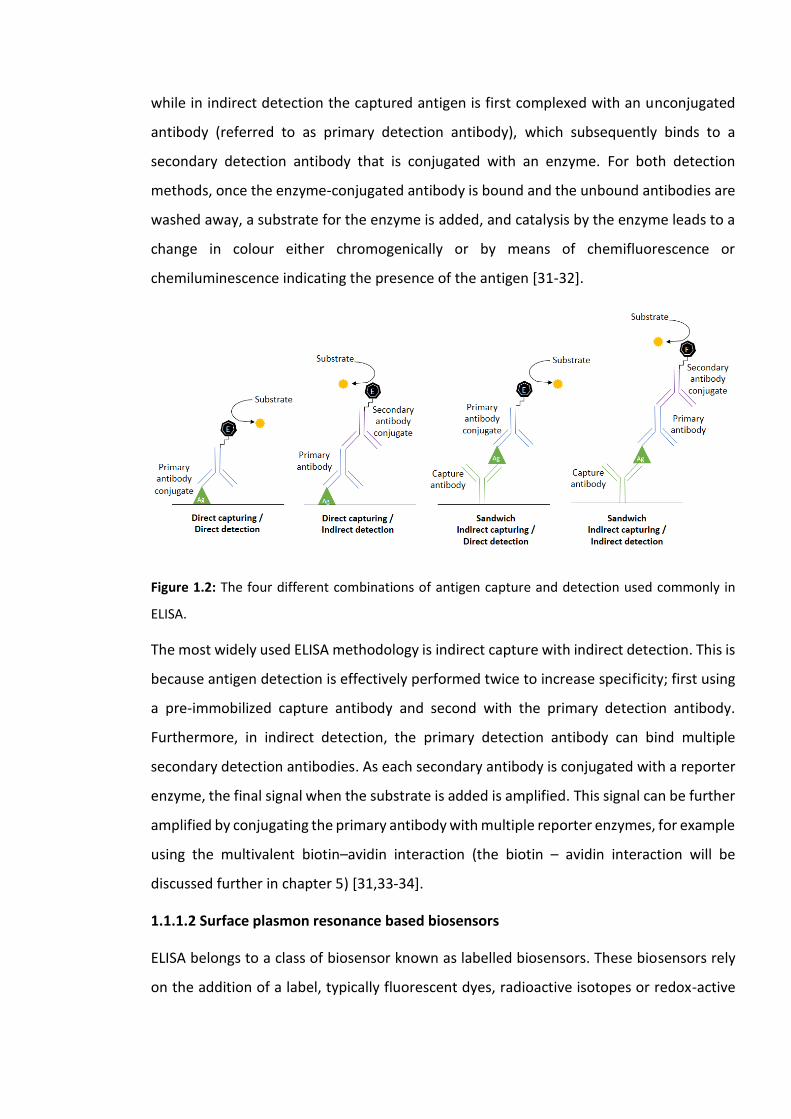
while in indirect detection the captured antigen is first complexed with an unconjugated
antibody (referred to as primary detection antibody), which subsequently binds to a
secondary detection antibody that is conjugated with an enzyme. For both detection
methods, once the enzyme-conjugated antibody is bound and the unbound antibodies are
washed away, a substrate for the enzyme is added, and catalysis by the enzyme leads to a
change in colour either chromogenically or by means of chemifluorescence or
chemiluminescence indicating the presence of the antigen [31-32].
Figure 1.2: The four different combinations of antigen capture and detection used commonly in
ELISA.
The most widely used ELISA methodology is indirect capture with indirect detection. This is
because antigen detection is effectively performed twice to increase specificity; first using
a pre-immobilized capture antibody and second with the primary detection antibody.
Furthermore, in indirect detection, the primary detection antibody can bind multiple
secondary detection antibodies. As each secondary antibody is conjugated with a reporter
enzyme, the final signal when the substrate is added is amplified. This signal can be further
amplified by conjugating the primary antibody with multiple reporter enzymes, for example
using the multivalent biotin–avidin interaction (the biotin – avidin interaction will be
discussed further in chapter 5) [31,33-34].
1.1.1.2 Surface plasmon resonance based biosensors
ELISA belongs to a class of biosensor known as labelled biosensors. These biosensors rely
on the addition of a label, typically fluorescent dyes, radioactive isotopes or redox-active
labels (conjugated enzymes), to quantify detection [11,35]. Although generally considered
robust, label-based biosensors have fundamental shortcomings. The labelling process itself
can impede the antibody-antigen interaction, for example through changes in molecular
conformation, a reduction in the bioactivity and mobility of labelled molecules, blocking of
active binding sites and an increase in steric hindrance. The labelling process is also costly
and can take a considerable amount of time, making real-time measurement impractical
[36-39]. Label-free biosensors on the other hand essentially eliminate complexity, time,
and cost associated with labelling techniques. Label-free biosensors detection requires the
use of a transducer that is sensitive to changes in physicochemical properties that occur
inherently following biochemical binding [9,36-38,40]. For example, surface plasmon
resonance (SPR) detects local changes in refractive index that occur following binding of an
analyte to a surface-immobilized bio-recognition element.
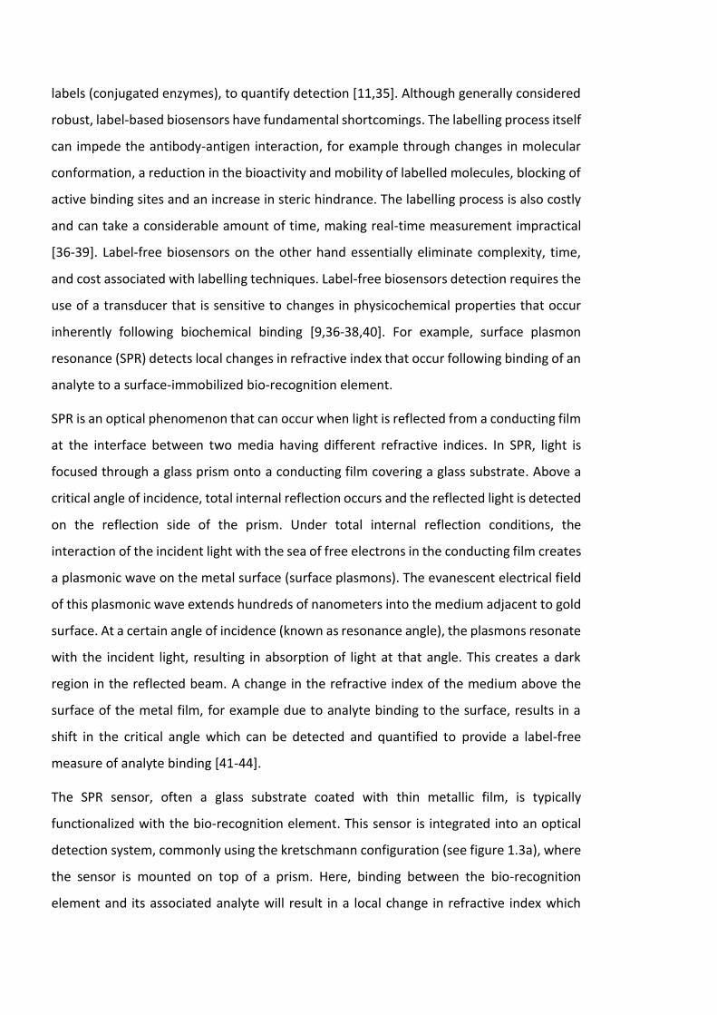
SPR is an optical phenomenon that can occur when light is reflected from a conducting film
at the interface between two media having different refractive indices. In SPR, light is
focused through a glass prism onto a conducting film covering a glass substrate. Above a
critical angle of incidence, total internal reflection occurs and the reflected light is detected
on the reflection side of the prism. Under total internal reflection conditions, the
interaction of the incident light with the sea of free electrons in the conducting film creates
a plasmonic wave on the metal surface (surface plasmons). The evanescent electrical field
of this plasmonic wave extends hundreds of nanometers into the medium adjacent to gold
surface. At a certain angle of incidence (known as resonance angle), the plasmons resonate
with the incident light, resulting in absorption of light at that angle. This creates a dark
region in the reflected beam. A change in the refractive index of the medium above the
surface of the metal film, for example due to analyte binding to the surface, results in a
shift in the critical angle which can be detected and quantified to provide a label-free
measure of analyte binding [41-44].
The SPR sensor, often a glass substrate coated with thin metallic film, is typically
functionalized with the bio-recognition element. This sensor is integrated into an optical
detection system, commonly using the kretschmann configuration (see figure 1.3a), where
the sensor is mounted on top of a prism. Here, binding between the bio-recognition
element and its associated analyte will result in a local change in refractive index which
leads, in turn, to a shift in the resonance angle [41-42,45-47]. The local change in refractive
index and consequently the resonance angular shift is observed by the shift in the
characteristic reflectivity curve measured at the light detector (see figure 1.3b). The
magnitude of the angular shift provides information regarding the surface concentration
of analyte, while monitoring the reflectivity curve as a function of time during the course
of the interaction provides information regarding the kinetics of a biomolecular binding
event, as shown schematically in figure 1.3c.
1.1.1.2.1 Label-free biosensors for real-time measurements of biomolecular interactions
The change in SPR reflectivity can be plotted as a function of time can to produce a
sensorgram that provides information regarding the kinetics of a biomolecular interaction
and allows the different stages of a binding event to be visualized and evaluated. A typical
sensorgram is displayed in figure 1.4 it comprises of an association phase, equilibrium
phase, dissociation phase and finally a regeneration phase.
Figure 1.3: (a) A setup of the SPR detection techniques using the Kretschmann configuration, (b)
the detected reflectivity response and (c) how the angular shift is translated in a sensorgram [48].
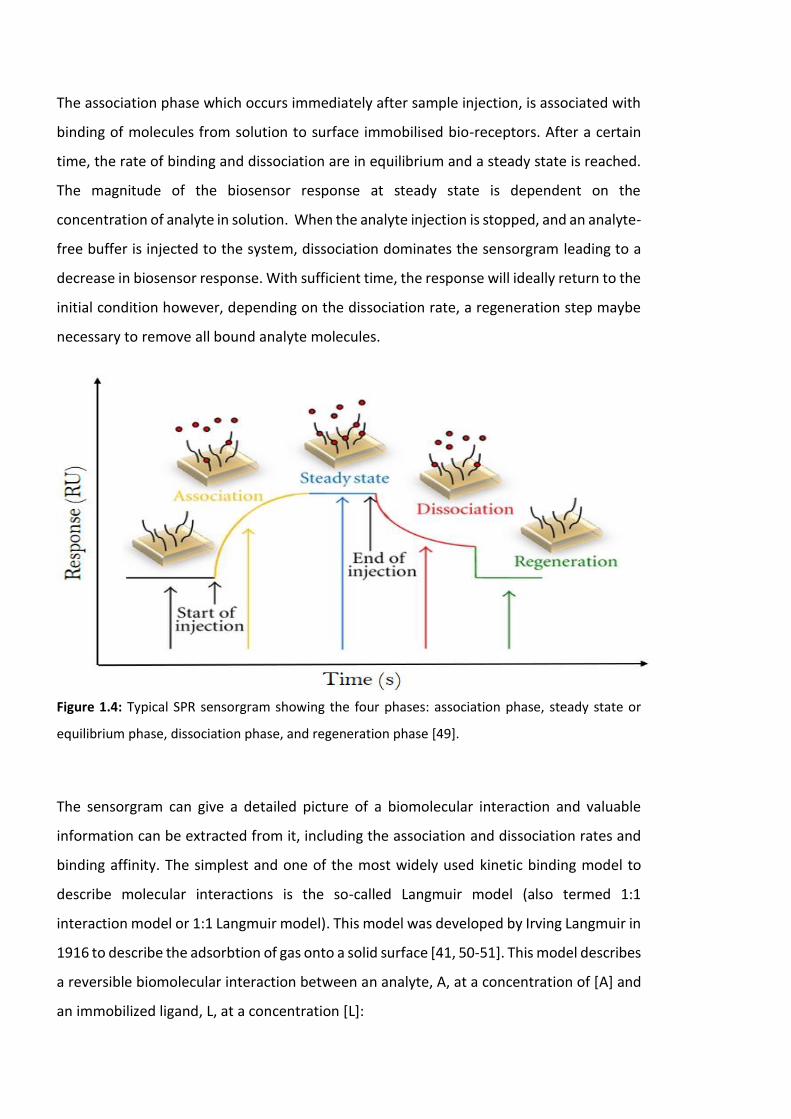
The association phase which occurs immediately after sample injection, is associated with
binding of molecules from solution to surface immobilised bio-receptors. After a certain
time, the rate of binding and dissociation are in equilibrium and a steady state is reached.
The magnitude of the biosensor response at steady state is dependent on the
concentration of analyte in solution. When the analyte injection is stopped, and an analyte-
free buffer is injected to the system, dissociation dominates the sensorgram leading to a
decrease in biosensor response. With sufficient time, the response will ideally return to the
initial condition however, depending on the dissociation rate, a regeneration step maybe
necessary to remove all bound analyte molecules.
Figure 1.4: Typical SPR sensorgram showing the four phases: association phase, steady state or
equilibrium phase, dissociation phase, and regeneration phase [49].
The sensorgram can give a detailed picture of a biomolecular interaction and valuable
information can be extracted from it, including the association and dissociation rates and
binding affinity. The simplest and one of the most widely used kinetic binding model to
describe molecular interactions is the so-called Langmuir model (also termed 1:1
interaction model or 1:1 Langmuir model). This model was developed by Irving Langmuir in
1916 to describe the adsorbtion of gas onto a solid surface [41, 50-51]. This model describes
a reversible biomolecular interaction between an analyte, A, at a concentration of [A] and
an immobilized ligand, L, at a concentration [L]:
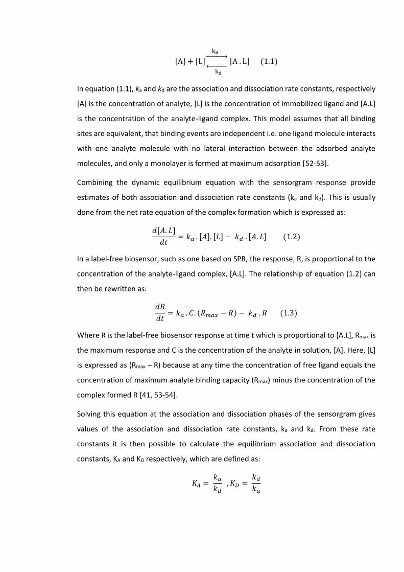
[A] + [L]
ka →
kd ←
[A . L] (1.1)
In equation (1.1), ka and kd are the association and dissociation rate constants, respectively
[A] is the concentration of analyte, [L] is the concentration of immobilized ligand and [A.L]
is the concentration of the analyte-ligand complex. This model assumes that all binding
sites are equivalent, that binding events are independent i.e. one ligand molecule interacts
with one analyte molecule with no lateral interaction between the adsorbed analyte
molecules, and only a monolayer is formed at maximum adsorption [52-53].
Combining the dynamic equilibrium equation with the sensorgram response provide
estimates of both association and dissociation rate constants (ka and kd). This is usually
done from the net rate equation of the complex formation which is expressed as:
𝑑[𝐴. 𝐿]
𝑑𝑡= 𝑘𝑎 . [𝐴]. [𝐿] − 𝑘𝑑 . [𝐴. 𝐿] (1.2)
In a label-free biosensor, such as one based on SPR, the response, R, is proportional to the
concentration of the analyte-ligand complex, [A.L]. The relationship of equation (1.2) can
then be rewritten as:
𝑑𝑅
𝑑𝑡= 𝑘𝑎 . 𝐶. (𝑅𝑚𝑎𝑥 − 𝑅) − 𝑘𝑑 . 𝑅 (1.3)
Where R is the label-free biosensor response at time t which is proportional to [A.L], Rmax is
the maximum response and C is the concentration of the analyte in solution, [A]. Here, [L]
is expressed as (Rmax – R) because at any time the concentration of free ligand equals the
concentration of maximum analyte binding capacity (Rmax) minus the concentration of the
complex formed R [41, 53-54].
Solving this equation at the association and dissociation phases of the sensorgram gives
values of the association and dissociation rate constants, ka and kd. From these rate
constants it is then possible to calculate the equilibrium association and dissociation
constants, KA and KD respectively, which are defined as:
𝐾𝐴 = 𝑘𝑎𝑘𝑑 , 𝐾𝐷 =
𝑘𝑑𝑘𝑎
These two equilibrium constants are the characteristic of the affinity between two
biomolecules i.e. the strength of the interaction. More detail will be provided in chapter 5.
This approach to quantifying biomolecular interactions is commonly referred to as kinetic
analysis where the kinetics of the interaction can be measured. For time-independent
measurements, such as those performed in ELISA, an alternative approach known as
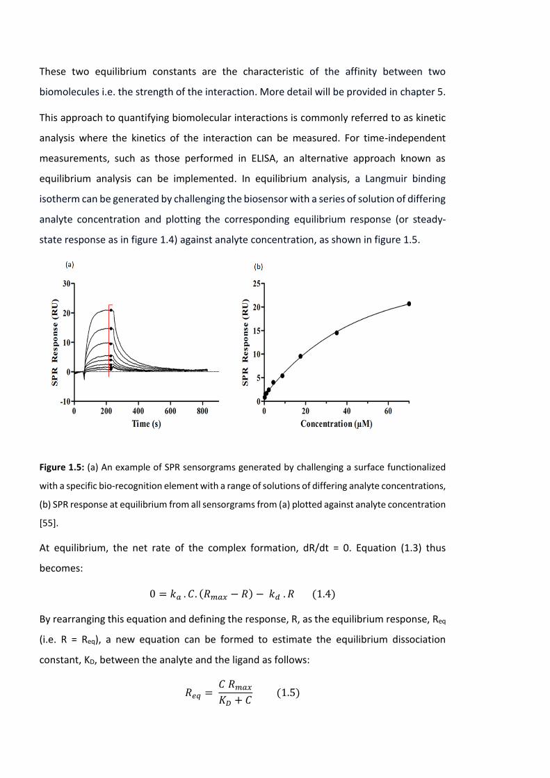
equilibrium analysis can be implemented. In equilibrium analysis, a Langmuir binding
isotherm can be generated by challenging the biosensor with a series of solution of differing
analyte concentration and plotting the corresponding equilibrium response (or steady-
state response as in figure 1.4) against analyte concentration, as shown in figure 1.5.
Figure 1.5: (a) An example of SPR sensorgrams generated by challenging a surface functionalized
with a specific bio-recognition element with a range of solutions of differing analyte concentrations,
(b) SPR response at equilibrium from all sensorgrams from (a) plotted against analyte concentration
[55].
At equilibrium, the net rate of the complex formation, dR/dt = 0. Equation (1.3) thus
becomes:
0 = 𝑘𝑎 . 𝐶. (𝑅𝑚𝑎𝑥 − 𝑅) − 𝑘𝑑 . 𝑅 (1.4)
By rearranging this equation and defining the response, R, as the equilibrium response, Req
(i.e. R = Req), a new equation can be formed to estimate the equilibrium dissociation
constant, KD, between the analyte and the ligand as follows:
𝑅𝑒𝑞 = 𝐶 𝑅𝑚𝑎𝑥
𝐾𝐷 + 𝐶 (1.5)
It can be seen that in this equation when the concentration of the analyte is equal to KD (C
= KD), then Req/Rmax = ½. Therefore, the KD value can be easily estimated from a plot of
equilibrium response against analyte concentration (Req vs C), as the concentration that
yields half the maximum response.
1.1.2 Next generation biosensors
The label-free nature of SPR provides significant advantages to traditional labelled
approaches such as ELISA. These include a reduction in laborious sample processing steps,
lower reagent costs and reduced sample volumes. Moreover, the ability to monitor
biomolecular interactions in real time allows the determination of binding kinetics and not
just binding affinity as in ELISA. Despite these advantages, SPR equipment is significantly
more costly than the equipment required for ELISA. For example, commercial SPR
instruments such as Biacore models costs hundreds of thousands of dollars, moreover, they
require consumable sensor chips which each cost tens of dollars. ELISA and SPR also require
trained personnel to perform the assay. There is thus significant interest in alternative,
label-free biosensor technologies that reduce the complexity and cost of existing,
commercial biosensors.
Many new technologies are being explored and exploited for the development of each
component of the biosensing system, from the bio-recognition element and associated
transducer to the processing part with the aim of identifying innovative solutions to current
limitations in the field of biosensing. However, despite significant research effort into
innovative label-free biosensors, it is striking that so few have penetrated the commercial
market. Much of this can be explained by the challenges associated with manufacturing
biosensors in a cost-effective way. [8,56-57].
Printing technology and microfluidics among others are at the forefront of technologies
that are shaping and advancing the modern biosensor field and that have the potential to
reduce manufacturing costs [8,58]. Printing technology enables mass production and
microfluidics integration allows the use of low sample and reagent volumes and lower
power consumption offering significant cost reduction [4,12]. One of the devices that can
be made using printing technologies and can be integrated with microfluidic technologies
is organic electronic devices (OEDs). The next section provides a general overview of OEDs
before proceeding to discuss a specific family of OEDs, namely organic thin film transistors,
and their application in biosensing.
1.2 Organic Electronic Devices
Organic electronic devices (OEDs) are electronic devices that have one or more of its
fundamental layers (semiconducting, conducting or insulating) made of organic materials
[59]. Although organic materials have been used in the electronic industry for many years
either as an insulator or a sacrificial layer, e.g. photoresist [60-61], the discovery of organic
materials that exhibit electrical conductivity, transformed the role of organic materials in
the fabrication of electronic devices. Early organic electronic (OE) materials exhibited very
low electrical conductivity and, as a result, much of the early work into OEDs was limited
to academic research. Since then, improvements in the electronic properties of OE
materials have led to the demonstration of many OEDs, from both industry and academia
alike [61-62]. While the performance of OEDs remained below that of more traditional,
inorganic electronics (largely dominated by silicon), industrial interest in OEDs was
motivated by the possibility of manufacturing devices at significantly lower costs, as
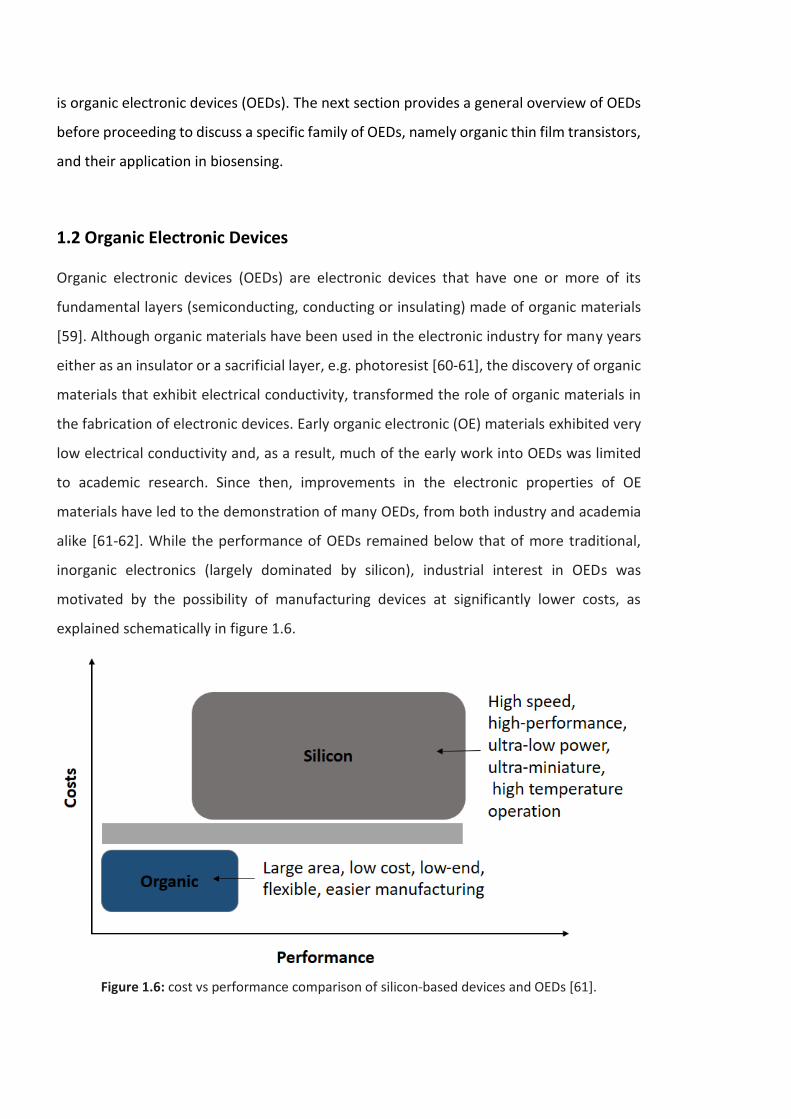
explained schematically in figure 1.6.
Figure 1.6: cost vs performance comparison of silicon-based devices and OEDs [61].
Currently OEDs have found widespread use in the low resolution, low speed, mass
production electronics market such as for smart cards and labels, flat, flexible and large
displays, logic for radio-frequency identification (RFID) tags and sensors [61,63-65].
From a solid-state perspective, organic semiconductors (OSCs) are very different to their
inorganic counterparts. This is because they are formed from organic molecules which are
bound together by relatively weak van der Waals interactions, in contrast to the covalent
bonding between atoms observed in inorganic semiconductors. Consequently, the band
structure and charge transport mechanisms are fundamentally different. Specifically, the
weak intermolecular electronic coupling in OSC, typically results in movement of charge
carriers via an inefficient process of ‘hopping’ between molecules. This leads to a reduction
in the electron and hole mobility compared to that observed in inorganic semiconductors,
where the periodic structure associated with covalent bonding results in an energy band
where charge carriers can diffuse freely with limited scattering, hence feature relatively
high mobility [60,66-68].
From the manufacturing and commercial perspectives, organic semiconductors offer some
very appealing advantages over inorganic semiconductors. Unlike inorganic
semiconductors, which are highly crystalline and require extremely high purity and rigorous
processing under highly controlled conditions, organic semiconductors are generally much
less expensive, and their synthesis involve inexpensive reactants and reaction conditions.
Manufacturing of electronic devices based on inorganic semiconductor requires high-
temperature, high-vacuum deposition, and costly patterning procedures. In contrast,
processing temperatures for organic semiconductors are typically low (generally less < 100
°C), enabling the fabrication of electronic devices on plastic and flexible substrates.
Moreover, many organic semiconductors are soluble in common solvents which allows
processing directly from solution using low cost technologies such as roll-to-roll and inkjet
printing. This allows the production of OEDs on large scales and at a fraction of the cost. It
is worth noting that fabrication processes for inorganic semiconductor-based devices are
standardized which is of great importance from the manufacturing point of view. At least
for now, such standardization has not been applied to organic semiconductor-based
devices. Finally, advances in synthetic chemistry make it possible to tailor the electronic
and optical properties of organic semiconductors such that they can be engineered for a

specific application. [69-70]. Table 1.1 summarizes some of the main differences between
organic and inorganic semiconductors.
Table 1.1: The main differences between organic and inorganic semiconductors.
Organic semiconductors Inorganic semiconductors
Bonding van der Waals interaction between molecules
covalent
Charge transport Hopping transport Band transport
Charge carrier mobility low high
Mechanically Flexible Inflexible
Fabrication and processing Simple and cheap Complicated and expensive (but standardize)
The main active OEDs that have seen significant investigation and investment are. 1)
Organic Light-Emitting Diodes (OLEDs) which are now sufficiently advanced that they are
widely used in the electronics market. 2) Organic Photovoltaic Devices, (OPVs), which,
despite having efficiencies lower than their inorganic counterpart, are constantly
improving, and with the advantage of low cost materials and processes, soon the balance
of efficiency and cost may shift towards OPVs especially for large solar panels [66,71]. 3)
Organic Thin-Film Transistors (OTFTs) which exhibit performances competing with that of
transistors based on amorphous silicon (a-Si:H), making them a competitive replacement
in liquid crystal displays and similar applications [61,66].
Another application for low-cost OTFTs that has recently gained attention, is the use of
OTFTs in chemical and biological sensing applications. Here, the relatively low charge
carrier mobility associated with organic semiconductors is not critical, as detection can take
place over tens or even hundreds of seconds [72]. Before discussing the merits of OTFT
based sensors, it is worth appreciating the interesting conduction mechanisms of organic
materials which make their conductivity distinct from the conventional inorganic
counterpart.
1.3 Conductivity in organic materials
The bulk conductivity of organic materials arises from two charge transport mechanisms;
intra-chain where charge transport occurs within a single molecule or chain and inter-chain
which describes charge transport between molecules or chains.
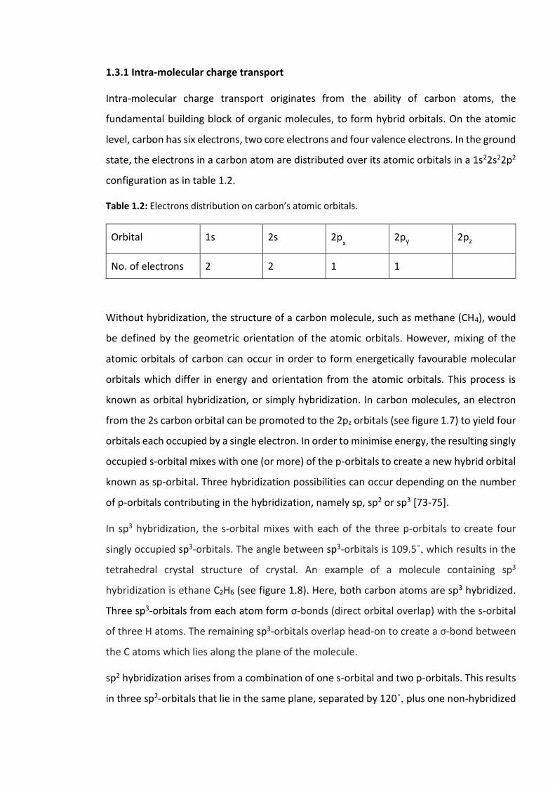
1.3.1 Intra-molecular charge transport
Intra-molecular charge transport originates from the ability of carbon atoms, the
fundamental building block of organic molecules, to form hybrid orbitals. On the atomic
level, carbon has six electrons, two core electrons and four valence electrons. In the ground
state, the electrons in a carbon atom are distributed over its atomic orbitals in a 1s22s22p2
configuration as in table 1.2.
Table 1.2: Electrons distribution on carbon’s atomic orbitals.
Orbital 1s 2s 2px 2py 2pz
No. of electrons 2 2 1 1
Without hybridization, the structure of a carbon molecule, such as methane (CH4), would
be defined by the geometric orientation of the atomic orbitals. However, mixing of the
atomic orbitals of carbon can occur in order to form energetically favourable molecular
orbitals which differ in energy and orientation from the atomic orbitals. This process is
known as orbital hybridization, or simply hybridization. In carbon molecules, an electron
from the 2s carbon orbital can be promoted to the 2pz orbitals (see figure 1.7) to yield four
orbitals each occupied by a single electron. In order to minimise energy, the resulting singly
occupied s-orbital mixes with one (or more) of the p-orbitals to create a new hybrid orbital
known as sp-orbital. Three hybridization possibilities can occur depending on the number
of p-orbitals contributing in the hybridization, namely sp, sp2 or sp3 [73-75].
In sp3 hybridization, the s-orbital mixes with each of the three p-orbitals to create four
singly occupied sp3-orbitals. The angle between sp3-orbitals is 109.5˚, which results in the
tetrahedral crystal structure of crystal. An example of a molecule containing sp3
hybridization is ethane C2H6 (see figure 1.8). Here, both carbon atoms are sp3 hybridized.
Three sp3-orbitals from each atom form σ-bonds (direct orbital overlap) with the s-orbital
of three H atoms. The remaining sp3-orbitals overlap head-on to create a σ-bond between
the C atoms which lies along the plane of the molecule.
sp2 hybridization arises from a combination of one s-orbital and two p-orbitals. This results
in three sp2-orbitals that lie in the same plane, separated by 120˚, plus one non-hybridized
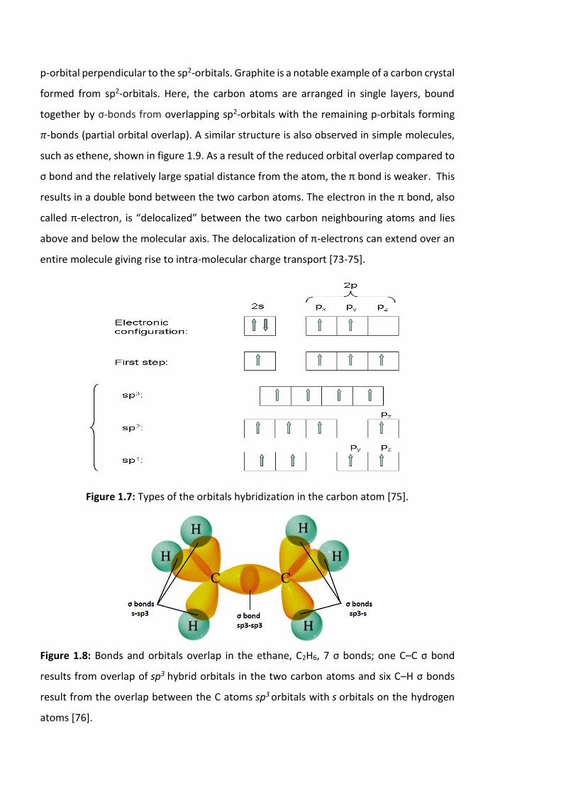
p-orbital perpendicular to the sp2-orbitals. Graphite is a notable example of a carbon crystal
formed from sp2-orbitals. Here, the carbon atoms are arranged in single layers, bound
together by σ-bonds from overlapping sp2-orbitals with the remaining p-orbitals forming
𝜋-bonds (partial orbital overlap). A similar structure is also observed in simple molecules,
such as ethene, shown in figure 1.9. As a result of the reduced orbital overlap compared to
σ bond and the relatively large spatial distance from the atom, the π bond is weaker. This
results in a double bond between the two carbon atoms. The electron in the π bond, also
called π-electron, is “delocalized” between the two carbon neighbouring atoms and lies
above and below the molecular axis. The delocalization of π-electrons can extend over an
entire molecule giving rise to intra-molecular charge transport [73-75].
Figure 1.7: Types of the orbitals hybridization in the carbon atom [75].
Figure 1.8: Bonds and orbitals overlap in the ethane, C2H6, 7 σ bonds; one C–C σ bond
results from overlap of sp3 hybrid orbitals in the two carbon atoms and six C–H σ bonds
result from the overlap between the C atoms sp3 orbitals with s orbitals on the hydrogen
atoms [76].
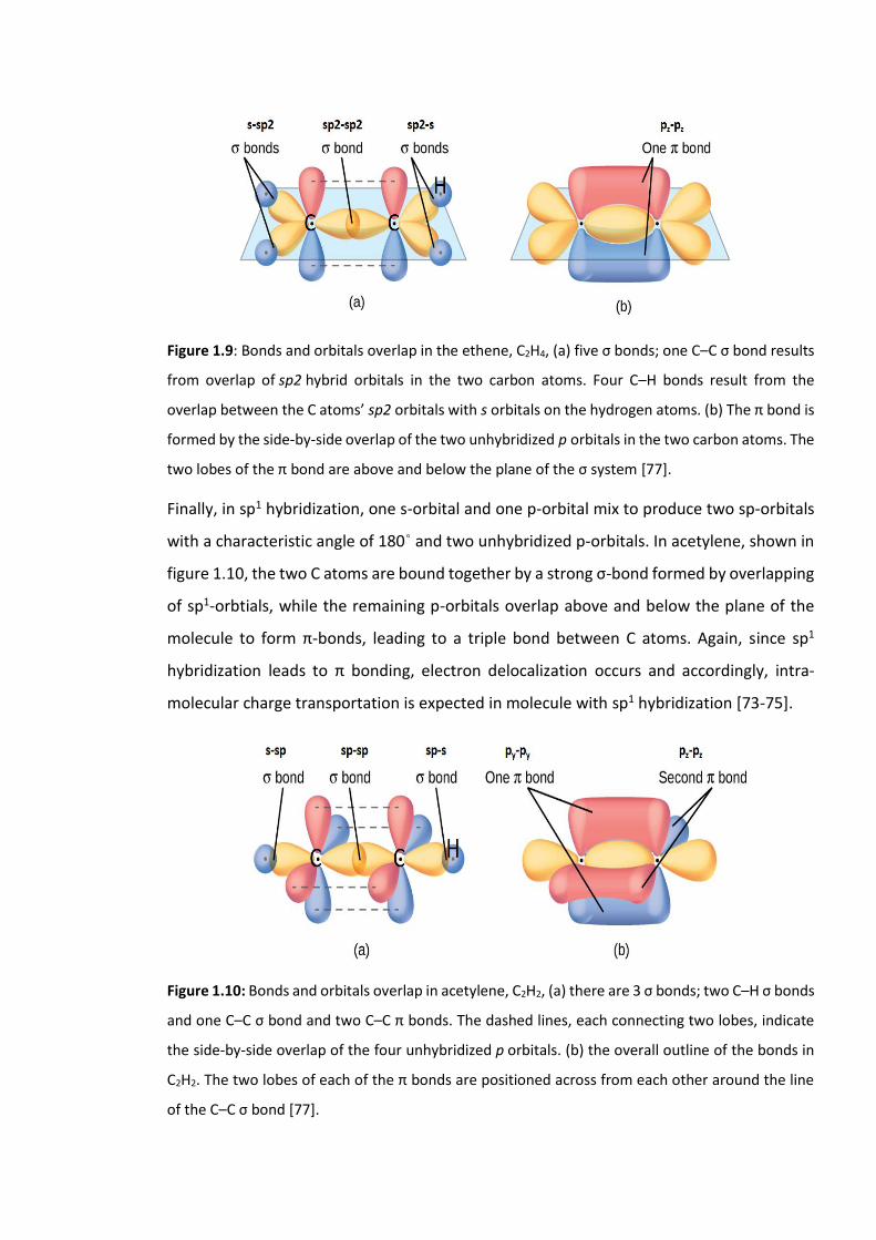
Figure 1.9: Bonds and orbitals overlap in the ethene, C2H4, (a) five σ bonds; one C–C σ bond results
from overlap of sp2 hybrid orbitals in the two carbon atoms. Four C–H bonds result from the
overlap between the C atoms’ sp2 orbitals with s orbitals on the hydrogen atoms. (b) The π bond is
formed by the side-by-side overlap of the two unhybridized p orbitals in the two carbon atoms. The
two lobes of the π bond are above and below the plane of the σ system [77].
Finally, in sp1 hybridization, one s-orbital and one p-orbital mix to produce two sp-orbitals
with a characteristic angle of 180˚ and two unhybridized p-orbitals. In acetylene, shown in
figure 1.10, the two C atoms are bound together by a strong σ-bond formed by overlapping
of sp1-orbtials, while the remaining p-orbitals overlap above and below the plane of the
molecule to form π-bonds, leading to a triple bond between C atoms. Again, since sp1
hybridization leads to π bonding, electron delocalization occurs and accordingly, intra-
molecular charge transportation is expected in molecule with sp1 hybridization [73-75].
Figure 1.10: Bonds and orbitals overlap in acetylene, C2H2, (a) there are 3 σ bonds; two C–H σ bonds
and one C–C σ bond and two C–C π bonds. The dashed lines, each connecting two lobes, indicate
the side-by-side overlap of the four unhybridized p orbitals. (b) the overall outline of the bonds in
C2H2. The two lobes of each of the π bonds are positioned across from each other around the line
of the C–C σ bond [77].
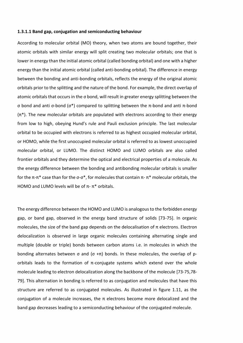
1.3.1.1 Band gap, conjugation and semiconducting behaviour
According to molecular orbital (MO) theory, when two atoms are bound together, their
atomic orbitals with similar energy will split creating two molecular orbitals; one that is
lower in energy than the initial atomic orbital (called bonding orbital) and one with a higher
energy than the initial atomic orbital (called anti-bonding orbital). The difference in energy
between the bonding and anti-bonding orbitals, reflects the energy of the original atomic
orbitals prior to the splitting and the nature of the bond. For example, the direct overlap of
atomic orbitals that occurs in the σ bond, will result in greater energy splitting between the
σ bond and anti σ-bond (σ*) compared to splitting between the π-bond and anti π-bond
(π*). The new molecular orbitals are populated with electrons according to their energy
from low to high, obeying Hund’s rule and Pauli exclusion principle. The last molecular
orbital to be occupied with electrons is referred to as highest occupied molecular orbital,
or HOMO, while the first unoccupied molecular orbital is referred to as lowest unoccupied
molecular orbital, or LUMO. The distinct HOMO and LUMO orbitals are also called
frontier orbitals and they determine the optical and electrical properties of a molecule. As
the energy difference between the bonding and antibonding molecular orbitals is smaller
for the π-π* case than for the σ-σ*, for molecules that contain π- π* molecular orbitals, the
HOMO and LUMO levels will be of π- π* orbitals.
The energy difference between the HOMO and LUMO is analogous to the forbidden energy
gap, or band gap, observed in the energy band structure of solids [73-75]. In organic
molecules, the size of the band gap depends on the delocalisation of π electrons. Electron
delocalization is observed in large organic molecules containing alternating single and
multiple (double or triple) bonds between carbon atoms i.e. in molecules in which the
bonding alternates between σ and (σ +π) bonds. In these molecules, the overlap of p-
orbitals leads to the formation of π-conjugate systems which extend over the whole
molecule leading to electron delocalization along the backbone of the molecule [73-75,78-
79]. This alternation in bonding is referred to as conjugation and molecules that have this
structure are referred to as conjugated molecules. As illustrated in figure 1.11, as the
conjugation of a molecule increases, the π electrons become more delocalized and the
band gap decreases leading to a semiconducting behaviour of the conjugated molecule.
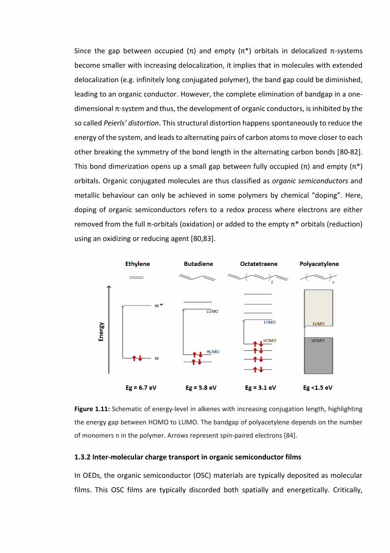
Since the gap between occupied (π) and empty (π*) orbitals in delocalized π-systems
become smaller with increasing delocalization, it implies that in molecules with extended
delocalization (e.g. infinitely long conjugated polymer), the band gap could be diminished,
leading to an organic conductor. However, the complete elimination of bandgap in a one-
dimensional π-system and thus, the development of organic conductors, is inhibited by the
so called Peierls’ distortion. This structural distortion happens spontaneously to reduce the
energy of the system, and leads to alternating pairs of carbon atoms to move closer to each
other breaking the symmetry of the bond length in the alternating carbon bonds [80-82].
This bond dimerization opens up a small gap between fully occupied (π) and empty (π*)
orbitals. Organic conjugated molecules are thus classified as organic semiconductors and
metallic behaviour can only be achieved in some polymers by chemical “doping”. Here,
doping of organic semiconductors refers to a redox process where electrons are either
removed from the full π-orbitals (oxidation) or added to the empty π* orbitals (reduction)
using an oxidizing or reducing agent [80,83].
Figure 1.11: Schematic of energy-level in alkenes with increasing conjugation length, highlighting
the energy gap between HOMO to LUMO. The bandgap of polyacetylene depends on the number
of monomers n in the polymer. Arrows represent spin-paired electrons [84].
1.3.2 Inter-molecular charge transport in organic semiconductor films
In OEDs, the organic semiconductor (OSC) materials are typically deposited as molecular
films. This OSC films are typically discorded both spatially and energetically. Critically,
localized states can be generated within the band gap at the grain boundaries between
molecules, which act to trap the delocalized, mobile charge carriers. For a charge to
transport from one molecule to another, it is thus necessary to excite charge carriers from
the trap states typically through a thermally activated process known as hopping [85-90].
Many models have been proposed to describe the microscopic motion of charge carriers in
organic semiconductor materials. Since the microstructure of the organic material plays a
significant role in charge hopping, transport models will vary depending on the degree of
disorder in the OSC film. In highly ordered, molecular single crystals, charge transport can
be considered to occur through a band-like transport mechanism. On the other hand, for
amorphous films, the variable range hopping (VRH) model is the widely used to describe
charge transport. Other models, such as Bässler’s Gaussian disorder (BGD) model and the
percolation (PER) model have also been proposed for amorphous and highly disordered
semiconductors [91].
Polycrystalline organic semiconductors, such as the OSC chosen for this PhD research, lie
between these two extremes (i.e. single crystal and amorphous films). Charge transport in
these materials is widely considered to be properly described by the multiple trapping and
release (MTR) model. This model considers two conducting mediums; crystalline ordered
grains which are separated from each other by disordered amorphous grain boundaries.
Inside the grains, carriers are delocalized while at the grain boundaries, carriers become
trapped in localized states and they require thermal assistance to transport to another
delocalized region [89,92-93]. The main assumption of the MTR model is that charge
carriers arriving at grain boundary are trapped instantaneously with a probability close to
1. The release of trapped carriers is controlled by a thermally-activated process. The key
parameters that govern the charge transport through these OSC films are thus the density
of trap states and the energy levels of those traps. The effective mobility, µeff, can be related
to the delocalized band mobility, μ0, by the following mobility – temperature, T,
relationship:
𝜇𝑒𝑓𝑓 = 𝜇0 𝛼 exp [−𝐸𝑇
𝐾𝐵𝑇] (1.6)
where μ0 is the mobility at the band edge (delocalized mobility inside grain), α is the ratio
between the effective density of states at the transport band edge and the density of traps,
and ET is the energy of the trap state [94].
1.3.3 Approaches to improve intermolecular charge transport
Due to the complex nature of intermolecular charge transport in OSC, a lot of effort has
been put into regulating and modifying the environment surrounding the OSC material to
enhance intermolecular charge transport conditions. In an extensive review on charge
transport in organic semiconductors, Coropceanu et.al [95] discussed 8 factors that
influence charge mobility namely molecular packing, disorder, temperature, electric field,
impurities, pressure, charge-carrier density and size/molecular weight [95-96]. In general,
the fundamental concept is to increase the organization and arrangement of OSC
molecules, in order to minimize the density of traps generated at grain boundaries between
the OSC molecules [97-98]. Two key factors are normally considered. Firstly, controlling the
OSC chemical structure and processing conditions during the material deposition. For
example, during synthesis, the molecular weight, side chain chemistry and regioregularity
of the OSC can be controlled alongside regulation of the film thickness and deposition
method. In the case of material deposited from solution, this includes consideration of the
solvent selection and subsequent thermal annealing temperature and deposition
environment [61]. The purity of the OSC material can also impact the charge transport due
to additional traps associated with impurities [97,99].
The second main factor is control over the surface on which the OSC will assemble. In the
OTFT context for example, whatever the arrangement of the transistor (presented in
section 1.4), the OSC will always make two interfaces; one with source and drain contacts
and the second with the gate dielectric surface. The first interface determines charge
injection to the OSC while the second dictates charge transport [61]. A common technique
used to improve molecular ordering of the OSC at the OSC/gate dielectric interface is the
use of self-assembled monolayers SAMs (silane SAMs in particular). Modifying the interface
with a SAM provides a uniform and controllable intermediate layer that promotes
alignment of the OSC molecules by dictating the nucleation and growth of the OSC films
[61, 100-101].
It is worth noting that high mobility is of particular concern to those developing high
performance devices. While high mobility is advantageous for sensor applications, the
stability of the OSC is of higher significance for sensor performance.
1.4 OTFT Operation and fundamental Layers
A thin film transistor (TFT) consists of thin film fundamental layers deposited on a
supporting substrate. The organic TFT (OTFT), first proposed by A. Tsumura, H. Koezuka and
T. Ando in 1986 is a special case where the semiconductor layer is an organic film, although
since then OTFTs with both OSC and organic dielectric films and an all organic based OTFTs
have also been reported [102-109]. OTFTs are commonly field effect transistors, FETs, and
their basic operation can be described by the modulation of a conducting channel inside an
OSC layer assembled between two contacts, known as the source, S, and drain, D,
electrodes by an electric-field generated at a third contact, the gate electrode, G. It also
can be modelled as a parallel plate capacitor, where one plate is the gate electrode and the
other plate is the S/OSC/D assembly, separated by the gate dielectric. OTFTs have been
demonstrated in various architectures, depending on the arrangement of the gate, source
and drain contacts with respect to the organic semiconductor OSC layer [61,106]. The most
common device architectures are presented in figure 1.12. Regardless of the OTFT
structure, three fundamental layers and the interfaces between these layers determine the
OTFT performance; the active OSC layer, S/D contacts and gate dielectric layer. Specifically,
the interface between the OSC and gate dielectric strongly influence the field effect
mobility, µFET, (or simply mobility, µ) while the contact resistance, RC, is regulated by the
OSC layer and source and drain interface [61,106,110].
OFETs normally operate in accumulation mode where charge accumulates in the OSC upon
application of an electric field, creating a conducting channel between S and D. Typically,
the source contact is held at ground potential and the accumulation channel is controlled
by the bias applied to the drain and gate contact. With no gate voltage, the flow of charge
carriers between S and D is dominated by the intrinsic conductivity of the OSC, which is
typically low in organic films due to the high density of trap states from grain boundaries.
This is the OFF state of the transistor. Upon application of a voltage to the gate electrode,
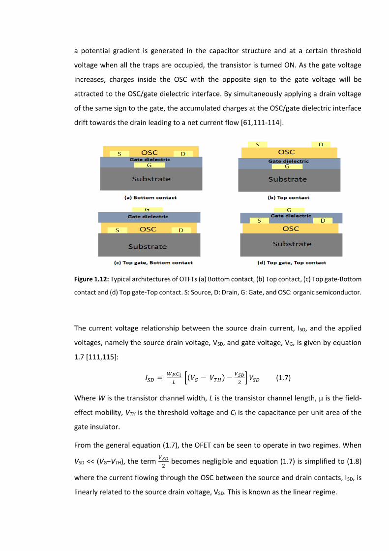
a potential gradient is generated in the capacitor structure and at a certain threshold
voltage when all the traps are occupied, the transistor is turned ON. As the gate voltage
increases, charges inside the OSC with the opposite sign to the gate voltage will be
attracted to the OSC/gate dielectric interface. By simultaneously applying a drain voltage
of the same sign to the gate, the accumulated charges at the OSC/gate dielectric interface
drift towards the drain leading to a net current flow [61,111-114].
Figure 1.12: Typical architectures of OTFTs (a) Bottom contact, (b) Top contact, (c) Top gate-Bottom
contact and (d) Top gate-Top contact. S: Source, D: Drain, G: Gate, and OSC: organic semiconductor.
The current voltage relationship between the source drain current, ISD, and the applied
voltages, namely the source drain voltage, VSD, and gate voltage, VG, is given by equation
1.7 [111,115]:
𝐼𝑆𝐷 = 𝑊𝜇𝐶𝑖
𝐿 [(𝑉𝐺 − 𝑉𝑇𝐻) −
𝑉𝑆𝐷
2] 𝑉𝑆𝐷 (1.7)
Where W is the transistor channel width, L is the transistor channel length, µ is the field-
effect mobility, VTH is the threshold voltage and Ci is the capacitance per unit area of the
gate insulator.
From the general equation (1.7), the OFET can be seen to operate in two regimes. When
VSD << (VG−VTH), the term 𝑉𝑆𝐷
2 becomes negligible and equation (1.7) is simplified to (1.8)
where the current flowing through the OSC between the source and drain contacts, ISD, is
linearly related to the source drain voltage, VSD. This is known as the linear regime.
𝐼𝑆𝐷 = 𝑊𝜇𝐶𝑖
𝐿 (𝑉𝐺 − 𝑉𝑇𝐻) 𝑉𝑆𝐷 (1.8)
In the second regime VSD > (VG−VTH). Here, VD becomes comparable to VG creating a
depletion region near the drain electrode (due to the absence of potential difference)
leading to saturation of ISD. In this regime equation (1.7) is approximated to (1.9).
𝐼𝑆𝐷 = 𝑊𝜇𝐶𝑖
2𝐿 (𝑉𝐺 − 𝑉𝑇𝐻)
2 (1.9)
These equations, particularly equation (1.9) are used estimate the mobility of the OSC and
the threshold, VTH, of the OFET device, which are two important features in describing the
characteristic behaviour of the OFET device. When used in sensing applications, the change
in ISD can be related to changes in the sensing region, as will be explain in later chapters.
1.5 Organic thin film transistors for chemical and biological sensing
Chemical and biological sensors based on OTFTs can potentially benefit from the
distinguishing features of organic semiconductor materials. Firstly, the powerful transistor-
based sensor which have inherent signal amplification can be made at low cost and can be
exploited to create commercially viable, single use sensors. Being carbon based, OSCs are
compatible with the integration of selective biological recognition elements. For example,
a recent review by Feron et.al [116] demonstrated the ability to culture cells on various
OSC layers in cell-based OTFT biosensors. Furthermore, the synthetic freedom of organic
chemistry can be exploited to modify OSCs, for example by adding functional groups (in the
form of side chains) to the organic semiconductor backbone for directly integrating bio-
recognition elements. In addition, the low temperature processing conditions used in the
fabrication of OTFTs is compatible with biological molecules, such as enzymes which
denature at the high temperatures associated with processing of traditional electronic
materials. Finally, the mechanical flexibility of OSCs make them good candidates for
fabricating implantable or wearable sensors [117-123].
1.5.1 Types of OTFTs used for biosensing
The two main classes of OTFTs used for biosensing applications are organic electrochemical
transistors (OECT) and organic field effect transistors (OFET). These are shown in Figure
1.13. The main difference between these two devices is that the OECT does not contain a
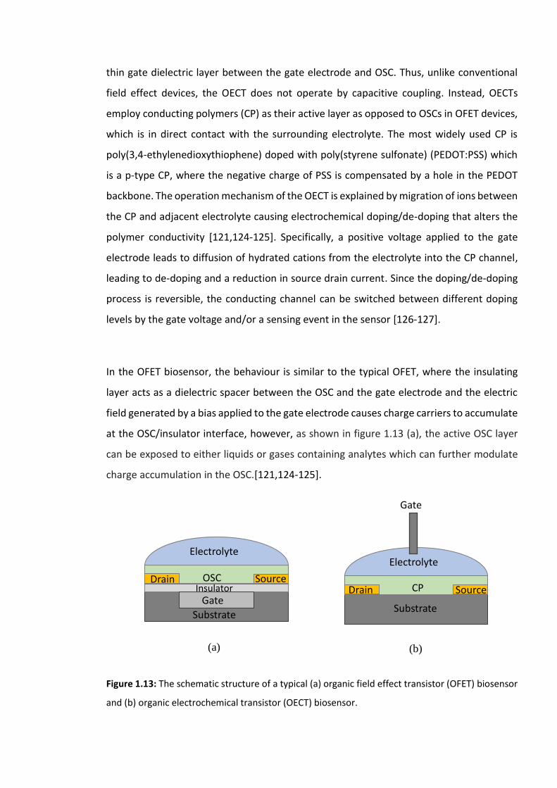
thin gate dielectric layer between the gate electrode and OSC. Thus, unlike conventional
field effect devices, the OECT does not operate by capacitive coupling. Instead, OECTs
employ conducting polymers (CP) as their active layer as opposed to OSCs in OFET devices,
which is in direct contact with the surrounding electrolyte. The most widely used CP is
poly(3,4-ethylenedioxythiophene) doped with poly(styrene sulfonate) (PEDOT:PSS) which
is a p-type CP, where the negative charge of PSS is compensated by a hole in the PEDOT
backbone. The operation mechanism of the OECT is explained by migration of ions between
the CP and adjacent electrolyte causing electrochemical doping/de-doping that alters the
polymer conductivity [121,124-125]. Specifically, a positive voltage applied to the gate
electrode leads to diffusion of hydrated cations from the electrolyte into the CP channel,
leading to de-doping and a reduction in source drain current. Since the doping/de-doping
process is reversible, the conducting channel can be switched between different doping
levels by the gate voltage and/or a sensing event in the sensor [126-127].
In the OFET biosensor, the behaviour is similar to the typical OFET, where the insulating
layer acts as a dielectric spacer between the OSC and the gate electrode and the electric
field generated by a bias applied to the gate electrode causes charge carriers to accumulate
at the OSC/insulator interface, however, as shown in figure 1.13 (a), the active OSC layer
can be exposed to either liquids or gases containing analytes which can further modulate
charge accumulation in the OSC.[121,124-125].
Figure 1.13: The schematic structure of a typical (a) organic field effect transistor (OFET) biosensor
and (b) organic electrochemical transistor (OECT) biosensor.
Electrolyte
Drain Source
Gate Insulator
OSC
Substrate
Electrolyte
Drain Source
Substrate
CP
Gate
(a) (b)
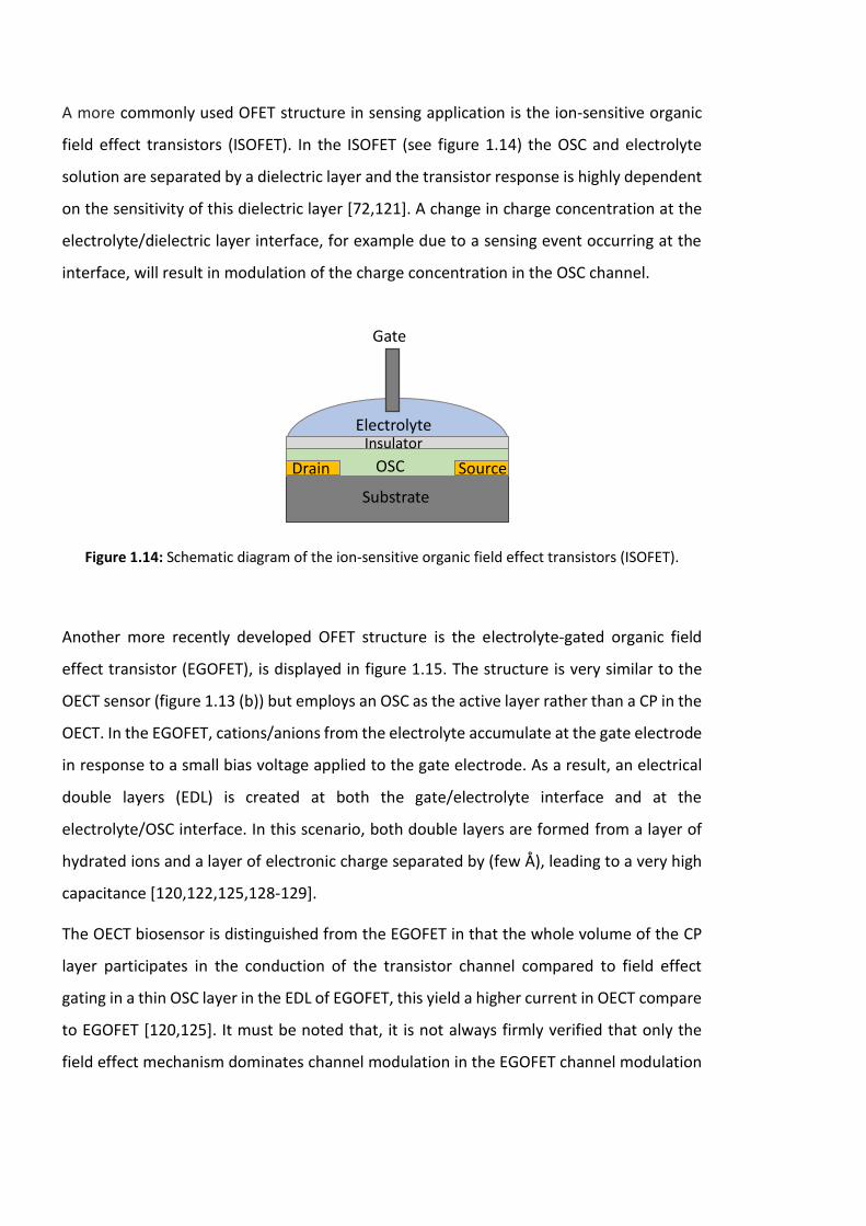
A more commonly used OFET structure in sensing application is the ion-sensitive organic
field effect transistors (ISOFET). In the ISOFET (see figure 1.14) the OSC and electrolyte
solution are separated by a dielectric layer and the transistor response is highly dependent
on the sensitivity of this dielectric layer [72,121]. A change in charge concentration at the
electrolyte/dielectric layer interface, for example due to a sensing event occurring at the
interface, will result in modulation of the charge concentration in the OSC channel.
Figure 1.14: Schematic diagram of the ion-sensitive organic field effect transistors (ISOFET).
Another more recently developed OFET structure is the electrolyte-gated organic field
effect transistor (EGOFET), is displayed in figure 1.15. The structure is very similar to the
OECT sensor (figure 1.13 (b)) but employs an OSC as the active layer rather than a CP in the
OECT. In the EGOFET, cations/anions from the electrolyte accumulate at the gate electrode
in response to a small bias voltage applied to the gate electrode. As a result, an electrical
double layers (EDL) is created at both the gate/electrolyte interface and at the
electrolyte/OSC interface. In this scenario, both double layers are formed from a layer of
hydrated ions and a layer of electronic charge separated by (few Å), leading to a very high
capacitance [120,122,125,128-129].
The OECT biosensor is distinguished from the EGOFET in that the whole volume of the CP
layer participates in the conduction of the transistor channel compared to field effect
gating in a thin OSC layer in the EDL of EGOFET, this yield a higher current in OECT compare
to EGOFET [120,125]. It must be noted that, it is not always firmly verified that only the
field effect mechanism dominates channel modulation in the EGOFET channel modulation
Electrolyte
Drain Source
Substrate
OSC
Gate
Insulator
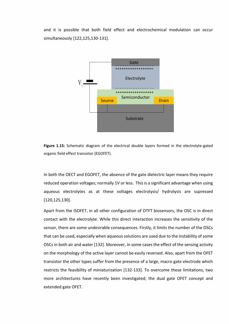
and it is possible that both field effect and electrochemical modulation can occur
simultaneously [122,125,130-131].
Figure 1.15: Schematic diagram of the electrical double layers formed in the electrolyte-gated
organic field effect transistor (EGOFET).
In both the OECT and EGOFET, the absence of the gate dielectric layer means they require
reduced operation voltages; normally 1V or less. This is a significant advantage when using
aqueous electrolytes as at these voltages electrolysis/ hydrolysis are supressed
[120,125,130].
Apart from the ISOFET, in all other configuration of OTFT biosensors, the OSC is in direct
contact with the electrolyte. While this direct interaction increases the sensitivity of the
sensor, there are some undesirable consequences. Firstly, it limits the number of the OSCs
that can be used, especially when aqueous solutions are used due to the instability of some
OSCs in both air and water [132]. Moreover, in some cases the effect of the sensing activity
on the morphology of the active layer cannot be easily reversed. Also, apart from the OFET
transistor the other types suffer from the presence of a large, macro gate electrode which
restricts the feasibility of miniaturization [132-133]. To overcome these limitations, two
more architectures have recently been investigated; the dual gate OFET concept and
extended gate OFET.
++++++++++++++++++
- - - - - - - - - - - - - - - - -
- - - - - - - - - - - - - - - - -
++++++++++++++++++
Gate
Drain Source Semiconductor
VG
Substrate
Electrolyte
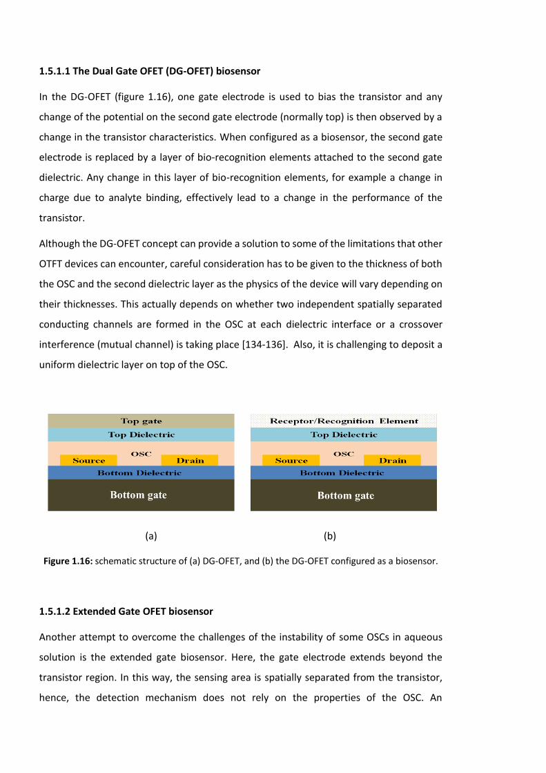
1.5.1.1 The Dual Gate OFET (DG-OFET) biosensor
In the DG-OFET (figure 1.16), one gate electrode is used to bias the transistor and any
change of the potential on the second gate electrode (normally top) is then observed by a
change in the transistor characteristics. When configured as a biosensor, the second gate
electrode is replaced by a layer of bio-recognition elements attached to the second gate
dielectric. Any change in this layer of bio-recognition elements, for example a change in
charge due to analyte binding, effectively lead to a change in the performance of the
transistor.
Although the DG-OFET concept can provide a solution to some of the limitations that other
OTFT devices can encounter, careful consideration has to be given to the thickness of both
the OSC and the second dielectric layer as the physics of the device will vary depending on
their thicknesses. This actually depends on whether two independent spatially separated
conducting channels are formed in the OSC at each dielectric interface or a crossover
interference (mutual channel) is taking place [134-136]. Also, it is challenging to deposit a
uniform dielectric layer on top of the OSC.
(a) (b)
Figure 1.16: schematic structure of (a) DG-OFET, and (b) the DG-OFET configured as a biosensor.
1.5.1.2 Extended Gate OFET biosensor
Another attempt to overcome the challenges of the instability of some OSCs in aqueous
solution is the extended gate biosensor. Here, the gate electrode extends beyond the
transistor region. In this way, the sensing area is spatially separated from the transistor,
hence, the detection mechanism does not rely on the properties of the OSC. An
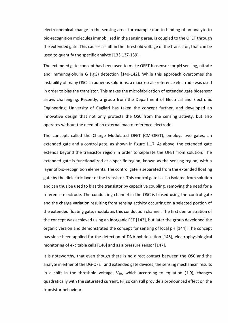
electrochemical change in the sensing area, for example due to binding of an analyte to
bio-recognition molecules immobilised in the sensing area, is coupled to the OFET through
the extended gate. This causes a shift in the threshold voltage of the transistor, that can be
used to quantify the specific analyte [133,137-139].
The extended gate concept has been used to make OFET biosensor for pH sensing, nitrate
and immunoglobulin G (IgG) detection [140-142]. While this approach overcomes the
instability of many OSCs in aqueous solutions, a macro-scale reference electrode was used
in order to bias the transistor. This makes the microfabrication of extended gate biosensor
arrays challenging. Recently, a group from the Department of Electrical and Electronic
Engineering, University of Cagliari has taken the concept further, and developed an
innovative design that not only protects the OSC from the sensing activity, but also
operates without the need of an external macro reference electrode.
The concept, called the Charge Modulated OFET (CM-OFET), employs two gates; an
extended gate and a control gate, as shown in figure 1.17. As above, the extended gate
extends beyond the transistor region in order to separate the OFET from solution. The
extended gate is functionalized at a specific region, known as the sensing region, with a
layer of bio-recognition elements. The control gate is separated from the extended floating
gate by the dielectric layer of the transistor. This control gate is also isolated from solution
and can thus be used to bias the transistor by capacitive coupling, removing the need for a
reference electrode. The conducting channel in the OSC is biased using the control gate
and the charge variation resulting from sensing activity occurring on a selected portion of
the extended floating gate, modulates this conduction channel. The first demonstration of
the concept was achieved using an inorganic FET [143], but later the group developed the
organic version and demonstrated the concept for sensing of local pH [144]. The concept
has since been applied for the detection of DNA hybridization [145], electrophysiological
monitoring of excitable cells [146] and as a pressure sensor [147].
It is noteworthy, that even though there is no direct contact between the OSC and the
analyte in either of the DG-OFET and extended gate devices, the sensing mechanism results
in a shift in the threshold voltage, VTH, which according to equation (1.9), changes
quadratically with the saturated current, ISD, so can still provide a pronounced effect on the
transistor behaviour.
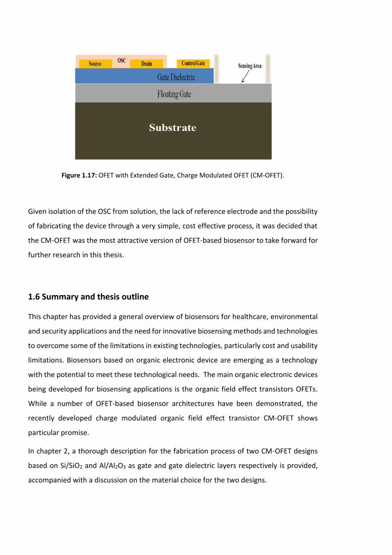
Figure 1.17: OFET with Extended Gate, Charge Modulated OFET (CM-OFET).
Given isolation of the OSC from solution, the lack of reference electrode and the possibility
of fabricating the device through a very simple, cost effective process, it was decided that
the CM-OFET was the most attractive version of OFET-based biosensor to take forward for
further research in this thesis.
1.6 Summary and thesis outline
This chapter has provided a general overview of biosensors for healthcare, environmental
and security applications and the need for innovative biosensing methods and technologies
to overcome some of the limitations in existing technologies, particularly cost and usability
limitations. Biosensors based on organic electronic device are emerging as a technology
with the potential to meet these technological needs. The main organic electronic devices
being developed for biosensing applications is the organic field effect transistors OFETs.
While a number of OFET-based biosensor architectures have been demonstrated, the
recently developed charge modulated organic field effect transistor CM-OFET shows
particular promise.
In chapter 2, a thorough description for the fabrication process of two CM-OFET designs
based on Si/SiO2 and Al/Al2O3 as gate and gate dielectric layers respectively is provided,
accompanied with a discussion on the material choice for the two designs.
In chapter 3, the experimental setup for device testing, experimental considerations and
methods for characterization of the CM-OFET device is discussed.
Chapter 4 presents an investigation into the Si/SiO2 CM-OFET biosensor for pH sensing. The
chapter includes discussion on the sensing mechanism including surface functionalization
of the floating gate to improve sensitivity as well as surface analysis of the functionalized
sensing surface. The chapter is concluded with electrical characterization of the fabricated
CM-OFET devices.
Chapter 5 looks at the use of the Si/SiO2 based CM-OFET device for protein detection, here
exploiting the well-defined avidin-biotin interaction. The chapter presents results of a
quartz crystal microbalance with dissipation study to verify the surface biotinylation
protocol for avidin binding. Experimental results and investigation of the CM-OFET for the
detection of avidin binding to a biotinylated extended gate are discussed and analysed.
Finally, major shortcomings in the Si/SiO2 CM-OFET device are highlighted and a new
modified CM-OFET device based on a new design with Al/Al2O3 as gate and gate dielectric
layers respectively is introduced.
Finally, chapter 6 concludes with final remarks on the research programme and suggests
some future work to optimize the device performance.

1.7 References
[1] Mehrotra, P. (2016). Biosensors and their applications–A review. Journal of oral biology
and craniofacial research, 6(2), 153-159.
[2] Cammann, K. (1977). Bio-sensors based on ion-selective electrodes. Fresenius'
Zeitschrift für Analytische Chemie, 287(1), 1-9.
[3] Yasmin, J., Ahmed, M. R., & Cho, B. K. (2016). Biosensors and their Applications in Food
Safety: A Review. Journal of Biosystems Engineering, 41(3), 240-254.
[4] Perumal, V., & Hashim, U. (2014). Advances in biosensors: Principle, architecture and
applications. Journal of Applied Biomedicine, 12(1), 1-15.
[5] Monošík, R., Streďanský, M., & Šturdík, E. (2012). Biosensors-classification,
characterization and new trends. Acta Chimica Slovaca, 5(1), 109-120.
[6] Ali J, Najeeb J, Ali MA, Aslam MF, Raza A (2017) Biosensors: Their Fundamentals,
Designs, Types and Most Recent Impactful Applications: A Review. J Biosens Bioelectron 8:
235. doi: 10.4172/2155-6210.1000235
[7] Clark, L. C., & Lyons, C. (1962). Electrode systems for continuous monitoring in
cardiovascular surgery. Annals of the New York Academy of sciences, 102(1), 29-45.
[8] Goode, J. A., Rushworth, J. V. H., & Millner, P. A. (2014). Biosensor regeneration: a
review of common techniques and outcomes. Langmuir, 31(23), 6267-6276.
[9] Li, H., Liu, X., Li, L., Mu, X., Genov, R., & Mason, A. J. (2016). CMOS Electrochemical
Instrumentation for Biosensor Microsystems: A Review. Sensors, 17(1), 74.
[10] Turner, A. P. (2013). Biosensors: sense and sensibility. Chemical Society Reviews, 42(8),
3184-3196.
[11] Sang, S., Zhang, W., & Zhao, Y. (2013). Review on the design art of biosensors. In State
of the Art in Biosensors-General Aspects. InTech.
[12] Luka, G., Ahmadi, A., Najjaran, H., Alocilja, E., DeRosa, M., Wolthers, K., Malki, A, Aziz,
H, Althani, A & Hoorfar, M. (2015). Microfluidics integrated biosensors: a leading
technology towards lab-on-a-chip and sensing applications. Sensors, 15(12), 30011-30031.
[13] Luong, J. H., Male, K. B., & Glennon, J. D. (2008). Biosensor technology: technology
push versus market pull. Biotechnology advances, 26(5), 492-500.
[14] Mohanty, S. P., & Kougianos, E. (2006). Biosensors: a tutorial review. Ieee
Potentials, 25(2), 35-40.
[15] Geddes, C. & Lakowicz, J. (2006), Glucose Sensing. Springer. DOI 10.1007/0-387-33015-
1
[16] Economou, A., del Campo, J., Reddy, S. M., Lunte, S., Thompson, M., Kranz, C.,& JinLee,
H. (2015). Electrochemical strategies in detection science. Royal Society of Chemistry.
[17] Lee, Y. H., & Mutharasan, R. (2005). Biosensors. Sensor Technology Handbook, 161-
180
[18] Touhami, A. (2014). Biosensors and Nanobiosensors: Design and
Applications. Nanomedicine, 374-400.
[19] Nanduri, V., Sorokulova, I. B., Samoylov, A. M., Simonian, A. L., Petrenko, V. A., &
Vodyanoy, V. (2007). Phage as a molecular recognition element in biosensors immobilized
by physical adsorption. Biosensors and Bioelectronics, 22(6), 986-992.
[20] Schuhmann, W., Lammert, R., Uhe, B., & Schmidt, H. L. (1990). Polypyrrole, a new
possibility for covalent binding of oxidoreductases to electrode surfaces as a base for stable
biosensors. Sensors and Actuators B: Chemical, 1(1-6), 537-541.
[21] Gupta, R., & Chaudhury, N. K. (2007). Entrapment of biomolecules in sol–gel matrix for
applications in biosensors: Problems and future prospects. Biosensors and
Bioelectronics, 22(11), 2387-2399.
[22] Nenkova, R., Ivanova, D., Vladimirova, J., & Godjevargova, T. (2010). New
amperometric glucose biosensor based on cross-linking of glucose oxidase on silica
gel/multiwalled carbon nanotubes/polyacrylonitrile nanocomposite film. Sensors and
Actuators B: Chemical, 148(1), 59-65.
[23] Iso, M., Shirahase, T., Hanamura, S. I., Urushiyama, S., & Omi, S. (1989). Immobilization
of enzyme by microencapsulation and application of the encapsulated enzyme in the
catalysis. Journal of microencapsulation, 6(2),165-176.
[24] Cahn, T. M. (1993). Biosensors (Vol. 1). Springer Science & Business Media.
[25] Bhalla, N., Jolly, P., Formisano, N., & Estrela, P. (2016). Introduction to
biosensors. Essays in biochemistry, 60(1), 1-8.
[26] Rajan, N. K., Brower, K., Duan, X., & Reed, M. A. (2014). Limit of detection of field effect
transistor biosensors: Effects of surface modification and size dependence. Applied Physics
Letters, 104(8), 084106.
[27] O’Hare, D. (2014). Biosensors and Sensor Systems. In Body Sensor Networks (pp. 55-
115). Springer London.
[28] PerkinElmer. (2011). Sensitivity Versus Detection Limit. Available at:
https://www.perkinelmer.com/lab-
solutions/resources/docs/AASensitivityvsDetectionLimitTechNote.pdf [Accessed
30/07/17]
[29] Vessman, J. (1996). Selectivity or specificity? Validation of analytical methods from the
perspective of an analytical chemist in the pharmaceutical industry. Journal of
pharmaceutical and biomedical analysis, 14(8-10), 867-869.
[30] Arugula, M. A., & Simonian, A. (2014). Novel trends in affinity biosensors: current
challenges and perspectives. Measurement Science and Technology, 25(3), 032001.
[31] Scientific, T. (2010). Elisa technical guide and protocols. Manual, 747, 815.
[32] Sakamoto, S., Putalun, W., Vimolmangkang, S., Phoolcharoen, W., Shoyama, Y.,
Tanaka, H., & Morimoto, S. (2018). Enzyme-linked immunosorbent assay for the
quantitative/qualitative analysis of plant secondary metabolites. Journal of natural
medicines, 72(1), 32-42.
[33] Bio-Rad, (2018), Introduction to ELISA, URL: https://www.bio-rad-
antibodies.com/elisa-types-direct-indirect-sandwich-competition-elisa-formats.html [last
access 20/02/2019]
[34] Ferri, G. L., Gaudio, R. M., Castello, F. I., Tirolo, C., & Chiolerio, F. (1999). Multiple
biotin-avidin amplification for multiple immunostaining. Applied Immunohistochemistry &
Molecular Morphology, 7(1), 73-80.
[35] Thorp, H. H. (1998). Cutting out the middleman: DNA biosensors based on
electrochemical oxidation. Trends in Biotechnology, 16(3), 117-121.
[36] Cooper, M. A. (Ed.). (2009). Label-free biosensors: techniques and applications.
Cambridge University Press.
[37] Cunningham, B. T., & Laing, L. (2006). Microplate-based, label-free detection of
biomolecular interactions: applications in proteomics. Expert review of proteomics, 3(3),
271-281.
[38] Berggren, C., Bjarnason, B., & Johansson, G. (2001). Capacitive
biosensors. Electroanalysis, 13(3), 173-180.
[39] Ramachandran, N., Larson, D. N., Stark, P. R., Hainsworth, E., & LaBaer, J. (2005).
Emerging tools for real‐time label‐free detection of interactions on functional protein
microarrays. The FEBS journal, 272(21), 5412-5425.
[40] Hitt, E. (2004). Label-free methods are not problem free. Drug Discov. Devel, 7(9), 34-
42.
[41] Hodnik, V., & Anderluh, G. (2013). Surface plasmon resonance for measuring
interactions of proteins with lipid membranes. In Lipid-Protein Interactions (pp. 23-36).
Humana Press, Totowa, NJ.
[42] GE Healthcare Life Sciences, (2019), Surface plasmon resonance, URL:
https://www.gelifesciences.com/ja/jp/solutions/protein-research/knowledge-
center/surface-plasmon-resonance/surface-plasmon-resonance [Last access: 09/03/19]
[43] Tang, Y., Zeng, X., & Liang, J. (2010). Surface plasmon resonance: an introduction to a
surface spectroscopy technique. Journal of chemical education, 87(7), 742-746.
[44] Drescher, D. G., Selvakumar, D., & Drescher, M. J. (2018). Analysis of protein
interactions by surface plasmon resonance. In Advances in protein chemistry and
structural biology (Vol. 110, pp. 1-30). Academic Press.
[45] Nguyen, H., Park, J., Kang, S., & Kim, M. (2015). Surface plasmon resonance: a
versatile technique for biosensor applications. Sensors, 15(5), 10481-10510.
[46] Van Der Merwe, P. A. (2001). Surface plasmon resonance. Protein-ligand interactions:
hydrodynamics and calorimetry, 1, 137-170.
[47] Heinrich, L., Tissot, N., Hartmann, D. J., & Cohen, R. (2010). Comparison of the results
obtained by ELISA and surface plasmon resonance for the determination of antibody
affinity. Journal of immunological methods, 352(1-2), 13-22.
[48] Cheng Research Lab,The University of California, (2016), Surface Plasmon Resonance
Spectroscopy and Imaging, URL: https://chenglab.ucr.edu/spr.html [last access 10/03/19]
[49] Ritzefeld, M., & Sewald, N. (2012). Real-time analysis of specific protein-DNA
interactions with surface plasmon resonance. Journal of amino acids, 2012.
[50] Langmuir, I. (1916). The constitution and fundamental properties of solids and
liquids. Part I. Solids. Journal of the American chemical society, 38(11), 2221-2295.
[51] Langmuir, I. (1918). The adsorption of gases on plane surfaces of glass, mica and
platinum. Journal of the American Chemical society, 40(9), 1361-1403.
[52] Leontiou, C., Lightowlers, R., Lakey, J. H., & Austin, C. A. (2003). Kinetic analysis of
human topoisomerase IIα and β DNA binding by surface plasmon resonance. FEBS
letters, 554(1-2), 206-210.
[53] GE Healthcare, (2019) Basic theory of kinetics, URL:
https://www.biacore.com/lifesciences/help/basic_theory_of_kinetics/index.html [Last
access: 09/03/19]
[54] Sahu, A., Soulika, A. M., Morikis, D., Spruce, L., Moore, W. T., & Lambris, J. D. (2000).
Binding kinetics, structure-activity relationship, and biotransformation of the complement
inhibitor compstatin. The Journal of Immunology, 165(5), 2491-2499.
[55] Memczak, H., Lauster, D., Kar, P., Di Lella, S., Volkmer, R., Knecht, V., ... & Stöcklein,
W. F. (2016). Anti-hemagglutinin antibody derived lead peptides for inhibitors of influenza
virus binding. PloS one, 11(7), e0159074.
[56] Kissinger, P. T. (2005). Biosensors—a perspective. Biosensors and
Bioelectronics, 20(12), 2512-2516.
[57] Lee, T. M. H. (2008). Over-the-counter biosensors: Past, present, and
future. Sensors, 8(9), 5535-5559.
[58] Arduini, F., Cinti, S., Scognamiglio, V., Moscone, D., & Palleschi, G. (2017). How cutting-
edge technologies impact the design of electrochemical (bio) sensors for environmental
analysis. A review. Analytica Chimica Acta.
[59] DeFranco, J. A., Schmidt, B. S., Lipson, M., & Malliaras, G. G., “Photolithographic
patterning of organic electronic materials”. Organic Electronics, 7(1), 2006, 22-28.
[60] Shaw, J. M., & Seidler, P. F. , “Organic electronics: introduction”. IBM Journal of
Research and Development, 45(1), 2001, 3-9.
[61] Li, F., Nathan, A., Wu, Y., & Ong, B. S., Organic Thin Film Transistor Integration: A Hybrid
Approach. 2013. John Wiley & Sons.
[62] Facchetti, A., “Organic Electronics”, Materials, Manufacturing and Applications. Edited
by Hagen Klauk, Angewandte Chemie, 46( 9), 2007, 1367–1368.
[63] Lim, S. C., Kim, S. H., Chu, H. Y., Lee, J. H., Lee, J. I., Oh, J. Y., ... & Zyung, T., “New
Method of Driving an OLED with an OTFT”. Synthetic metals, 151(3), 2005, 197-201.
[64] Jang, J., & Han, S. H., “High-performance OTFT and its application”. Current Applied
Physics, 6, 2006, e17-e21.
[65] Shinar, R., & Shinar, J., Organic electronics in sensors and biotechnology. 2009.
McGraw-Hill, Inc.
[66] Jain, S. C., Willander, M., & Kumar, V., Conducting organic materials and devices (Vol.
81). 2011. Newnes.
[67] Tarver, J., & Loo, Y. (2010). Organic Electronic Devices with Water-Dispersible
Conducting Polymers. Handbook of Nanoscale Optics and Electronics, 107.
[68] Solanki, C. S. (2015). Solar photovoltaics: fundamentals, technologies and applications. PHI Learning Pvt. Ltd..
[69] Schöll, A., & Schreiber, F. (2018). Thin Films of Organic Molecules: Interfaces and Epitaxial Growth. In Molecular Beam Epitaxy (pp. 551-570). Elsevier.
[70] Zhao, X., Chaudhry, S. T., & Mei, J. (2017). Heterocyclic Building Blocks for Organic Semiconductors. In Advances in Heterocyclic Chemistry (Vol. 121, pp. 133-171). Academic Press.
[71] Zang, Ling, Energy Efficiency and Renewable Energy through Nanotechnology. Berlin:
Springer, 2011.
[72] Elkington, D., Cooling, N., Belcher, W., Dastoor, P. C., & Zhou, X. “Organic Thin-Film
Transistor (OTFT)-Based Sensors”. Electronics, 3(2), 2014, 234-254.
[73] Majewski, L. (2011), supplementary teaching material, Organic Electronics, Nano
Electronics, University of Manchester.
[74] Menke, T., “Molecular Doping of Organic Semiconductors: A Conductivity and Seebeck
Study”, 2013.
[75] Stella, M., Study of Organic Semiconductors for Device Applications, doctoral thesis,
University of De Barcelona. 2010.
[76] Lower, S, (2018), The Hybrid Orbital Model II, URL: https://bit.ly/2TCmET8 [last
access 10/03/19]
[77] OpenStax, Chemistry. OpenStax CNX. Jun 20, 2016
http://cnx.org/contents/[email protected].
[78] Shinar, R., & Shinar, J. Organic electronics in sensors and biotechnology. McGraw-Hill,
Inc. 2009.
[79] Brédas, J. L., Calbert, J. P., da Silva Filho, D. A., & Cornil, J., “Organic semiconductors:
A theoretical characterization of the basic parameters governing charge transport”.
Proceedings of the National Academy of Sciences, 99(9), 2002. 5804-5809.
[80] Majewski, L. A. (2006). Alternative Gate Insulators for Organic Field-Effect
Transistors (Doctoral dissertation, University of Sheffield, Department of Physics and
Astronomy).
[81] Bässler, H., & Köhler, A. (2011). Charge transport in organic semiconductors.
In Unimolecular and supramolecular electronics I (pp. 1-65). Springer, Berlin, Heidelberg.
[82] Chen, C. H., & Shih, I. (2006). Hybrid organic on inorganic semiconductor
heterojunction. Journal of Materials Science: Materials in Electronics, 17(12), 1047-1053.
[83] Malhotra, B. D. (2017). Biosensors: Fundamentals and Applications. Smithers Rapra.
[84] University of Cambridge,(2019), Optoelectronics, Organic Semiconductors, URL:
https://www.oe.phy.cam.ac.uk/research/materials/osemiconductors [last access
10/03/19]
[85] Bässler, H., & Köhler, A., “Charge transport in organic semiconductors”. In
Unimolecular and Supramolecular Electronics I Springer Berlin Heidelberg. 2012, 1-65.
[86] Li, L., Meller, G., & Kosina, H., “Temperature and field-dependence of hopping
conduction in organic semiconductors”, Microelectronics journal, 38(1), 2007,47-51.
[87] Li, L., Meller, G., & Kosina, H., “Influence of traps on charge transport in organic
semiconductors”. Solid-state electronics, 51(3), 2007, 445-448.
[88] Locci, S., Modeling of physical and electrical characteristics of organic thin film
transistors. 2009

[89] Guo, D., Miyadera, T., Ikeda, S., Shimada, T., & Saiki, K., “Analysis of charge transport
in a polycrystalline pentacene thin film transistor by temperature and gate bias dependent
mobility and conductance”. Journal of Applied Physics, 102(2), 2007, 023706.
[90] Fishchuk, I. I., Kadashchuk, A., Hoffmann, S. T., Athanasopoulos, S., Genoe, J., Bässler,
H., & Köhler, A., “Analytic model of hopping transport in organic semiconductors including
both energetic disorder and polaronic contributions”. In 15th International Conference on
Transport in Interacting Disordered Systems (Tids15) 1610 (1), 2014, August, 47-52. Aip
Publishing.
[91] Liu, C., Huang, K., Park, W. T., Li, M., Yang, T., Liu, X., & Noh, Y. Y. (2017). A unified
understanding of charge transport in organic semiconductors: the importance of
attenuated delocalization for the carriers. Materials Horizons.
[92] Olivier, Y., Lemaur, V., Brédas, J. L., & Cornil, J., “Charge hopping in organic
semiconductors: Influence of molecular parameters on macroscopic mobilities in model
one-dimensional stacks”. The Journal of Physical Chemistry A, 110(19), 2006, 6356-6364.
[93] Jouili, A., Mansouri, S., Al-Ghamdi, A. A., El Mir, L., Farooq, W. A., & Yakuphanoglu, F.
(2017). Characterization and Modeling of Nano-organic Thin Film Phototransistors Based
on 6, 13 (Triisopropylsilylethynyl)-Pentacene: Photovoltaic Effect. Journal of Electronic
Materials, 46(4), 2221-2231.
[94] Bao, Z., & Locklin, J. (Eds.). (2007). Organic field-effect transistors. CRC press.
[95] Coropceanu, V., Cornil, J., da Silva Filho, D. A., Olivier, Y., Silbey, R., & Brédas, J. L.
“Charge transport in organic semiconductors.” Chemical reviews, 107(4), 2007, 926-952..
[96] Yoann Olivier, Charge Transport in Organic Conjugated Materials: From the Molecular
Picture to the Macroscopic Properties, Université de Mons-Hainaut Faculté des Sciences,
Laboratoire de Chimie des Matériaux Nouveaux, 2008.
[97] Wang, C., Dong, H., Hu, W., Liu, Y., & Zhu, D., “Semiconducting π-conjugated systems
in field-effect transistors: a material odyssey of organic electronics.”, Chemical reviews,
112(4), 2011, 2208-2267.
[98] Botiz, I., & Stingelin, N., “Influence of Molecular Conformations and Microstructure on
the Optoelectronic Properties of Conjugated Polymers.” Materials, 7(3), 2014, 2273-2300.
[99] Kaake, L. G., Barbara, P. F., & Zhu, X. Y, “Intrinsic charge trapping in organic and
polymeric semiconductors: a physical chemistry perspective.” The Journal of Physical
Chemistry Letters, 1(3), 2010, 628-635.
[100] Goldmann, C., Krellner, C., Pernstich, K. P., Haas, S., Gundlach, D. J., & Batlogg, B.,
“Determination of the interface trap density of rubrene single-crystal field-effect
transistors and comparison to the bulk trap density.” Journal of applied physics, 99(3),
2006, 034507.
[101] Bao, Z., “Organic materials for thin film transistors.”, Material Matters, 2(3), 2007, 4-
6.
[102] Tomas G. Ba¨cklund, et al., ,Towards all-polymer field-effect transistors with solution
processable materials, Synthetic Metals 148, 2005, 87–91, Elsevier.
[103] Myung Sub Lee, et al., Flexible all-polymer field effect transistors with optical
transparency using electrically conducting polymers, Thin Solid Films 477 (2005), 169– 173,
Elsevier.
[104] Henning Rost, et al., Air-stable all-polymer field-effect transistors with organic
electrodes, Synthetic Metals 145, (2004), 83–85, Elsevier.
[105] Hamadani, B., Electronic Charge Injection and Transport in Organic Field-Effect
Transistors, Houston, Texas. (January 2007),
[106] Gordon Yip, Development of Al2O3 Gate Dielectrics for Organic Thin-film Transistors,
University of Toronto, 2008.
[107] Mang Mang Ling and Zhenan Bao, ,Thin Film Deposition, Patterning, and Printing in
Organic Thin Film Transistors, Chem. Mater., 16 (23), (2004), 4824-4840, American
Chemical Society.
[108] Globerman, O., Lateral and Vertical Organic Thin Film Transistors, the Senate of the
Technion-Israel Institute of technology. April 2006
[109] A. Tsumura, H. Koezuka and T. Ando, Macromolecular electronic device: Fieldeffect
transistor with a polythiophene thin film. Appl. Phys. Lett. 49, (1986), 1210
[110] Chung-Chen Kuo, High Performance Small-Molecule Organic Thin Film Transistors,
the Pennsylvania State University. December 2005.
[111] Katz, Howard E., and Jia Huang. "Thin-film organic electronic devices." Annual Review
of Materials Research 39 ,2009, 71-92.
[112] DiBenedetto, Sara A., Antonio Facchetti, Mark A. Ratner, and Tobin J. Marks.
"Molecular Self‐Assembled Monolayers and Multilayers for Organic and Unconventional
Inorganic Thin‐Film Transistor Applications." Advanced materials 21(14‐15), 2009, 1407-
1433.
[113] Facchetti, Antonio, M‐H. Yoon, and Tobin J. Marks. "Gate dielectrics for organic field‐
effect transistors: new opportunities for organic electronics."Advanced Materials 17( 14 ),
2005, 1705-1725.
[114] Perkinson, Joy C. "Organic field-effect transistors, 2007." Available at:
http://web.mit.edu/joyp/Public/OFET%20Term%20Paper.pdf [Last access 27/11/14]
[115] Newman, Christopher R., C. Daniel Frisbie, Demetrio A. da Silva Filho, Jean-Luc
Brédas, Paul C. Ewbank, and Kent R. Mann. "Introduction to organic thin film transistors
and design of n-channel organic semiconductors." Chemistry of materials 16( 23) ,2004,
4436-4451.
[116] Feron, K., Lim, R., Sherwood, C., Keynes, A., Brichta, A., & Dastoor, P. (2018). Organic Bioelectronics: Materials and Biocompatibility. International journal of molecular sciences, 19(8), 2382.
[117] Logothetidis, S., “Flexible organic electronic devices: Materials, process and
applications”. Materials Science and Engineering: B, 152(1), 2008, 96-104.
[118] Nam, S., Jang, J., Park, J. J., Kim, S. W., Park, C. E., & Kim, J. M. “High-performance
low-voltage organic field-effect transistors prepared on electro-polished aluminum
wires”. ACS applied materials & interfaces, 4(1), 2011, 6-10.
[119] Richter, S., Ploetner, M., Fischer, W. J., Schneider, M., Nguyen, P. T., Plieth, W., ... &
Adler, H. J., “Development of organic thin film transistors based on flexible
substrates”. Thin solid films, 477(1), 2005, 140-147.
[120] Cramer, T., Campana, A., Leonardi, F., Casalini, S., Kyndiah, A., Murgia, M., & Biscarini,
F. “Water-gated organic field effect transistors–opportunities for biochemical sensing and
extracellular signal transduction”. Journal of Materials Chemistry B, 1(31), 2013, 3728-
3741.
[121] Mabeck, J. T., & Malliaras, G. G., “Chemical and biological sensors based on organic
thin-film transistors”. Analytical and bioanalytical chemistry, 384(2), 2006, 343-353.
[122] Kergoat, L., Piro, B., Berggren, M., Horowitz, G., & Pham, M. C. , “Advances in organic
transistor-based biosensors: from organic electrochemical transistors to electrolyte-gated
organic field-effect transistors”. Analytical and bioanalytical chemistry, 402(5), (2012),
1813-1826.
[123] Roberts, M. E., Mannsfeld, S. C., Queraltó, N., Reese, C., Locklin, J., Knoll, W., & Bao,
Z. “Water-stable organic transistors and their application in chemical and biological
sensors”. Proceedings of the National Academy of Sciences, 105(34), 2008, 12134-12139.
[124] Lin, P., & Yan, F. “Organic Thin‐Film Transistors for Chemical and Biological
Sensing”. Advanced materials, 24(1), 2012, 34-51
[125] Caizhi Liao & Feng Yan, “Organic Semiconductors in Organic Thin-Film Transistor-
Based Chemical and Biological Sensors”, Polymer Reviews, 53(3), 2013, 352-406.
[126] Yeung, S. Y., Gu, X., Tsang, C. M., Tsao, S. W., & Hsing, I. M. (2019). Engineering organic
electrochemical transistor (OECT) to be sensitive cell-based biosensor through tuning of
channel area. Sensors and Actuators A: Physical, 287, 185-193.
[127] Strakosas, X., Bongo, M., & Owens, R. M. (2015). The organic electrochemical
transistor for biological applications. Journal of Applied Polymer Science, 132(15).
[128] H. Sinno, S. Fabiano, X. Crispin, M. Berggren, and I. Engquist, “Bias stress effect in
polyelectrolyte-gated organic field-effect transistors”, Appl. Phys. Lett., 2013, 102, 113306.
[129] Loïg Kergoat, Lars Herlogsson, Benoit Piro, Minh Chau Pham, Gilles Horowitz, Xavier
Crispin, and Magnus Berggren, “Tuning the threshold voltage in electrolyte-gated organic
field-effect transistors”, PNAS, , 109(22), 2012, 8394–8399.
[130] Peter Andersson Ersman, David Nilsson, Jun Kawahara, Goran Gustafsson and
Magnus Berggren, “Fast-switching all-printed organic electrochemical transistors”, Organic
electronics, 14(5), 2013, 1276-1280.
[131] Loig Kergoat, Lars Herlogsson, Daniele Braga, Benoit Piro, Minh-Chau Pham, Xavier
Crispin, Magnus Berggren, and Gilles Horowitz, “A Water-Gate Organic Field-Effect
Transistor”, Adv. Mater., 22, 2010, 2565–2569.

[132] Torres, T., & Bottari, G. Organic nanomaterials: synthesis, characterization, and
device applications. John Wiley & Sons. 2013
[133] Lai, S., Demelas, M., Casula, G., Cosseddu, P., Barbaro, M., & Bonfiglio, A. “Ultralow
Voltage, OTFT‐Based Sensor for Label‐Free DNA Detection” .Advanced Materials, 25(1),
2013, 103-107.
[134] Brondijk, J. J., Spijkman, M., Torricelli, F., Blom, P. W. M., & De Leeuw, D. M. “Charge
transport in dual-gate organic field-effect transistors”. Applied Physics Letters, 100(2),
2012, 023308.
[135] Maddalena, F. Organic Field-effect Transistors for Sensing Applications. Doctoral
dissertation, University of Groningen, The Zernike Institute for Advanced Materials. 2011
[136] Göllner, M. Double-Gate Pentacene Thin Film Transistors for Biosensing, Doctoral
dissertation, der Ludwig–Maximilians–Universit¨at M¨unchen. 2012
[137] Caboni, A., Cambarau, W., Orgiu, E., Barbaro, M., & Bonfiglio, A. “A flexible floating-
gate organic thin-film transistor for detection of chemical species”. In Sensors, IEEE 2008,
859-862.
[138] Caboni, A., Orgiu, E., Barbaro, M., & Bonfiglio, A. “Flexible organic Thin-Film
transistors for pH monitoring”. Sensors Journal, IEEE, 9(12), 2009, 1963-1970.
[139] Demelas, M., Lai, S., Casula, G., Scavetta, E., Barbaro, M., & Bonfiglio, A. “An organic,
charge-modulated field effect transistor for DNA detection” Sensors and Actuators B:
Chemical, 171, 2012, 198-203.
[140] Nguyen, T. N. T., Seol, Y. G., & Lee, N. E. (2011). Organic field-effect transistor with
extended indium tin oxide gate structure for selective pH sensing. Organic
Electronics, 12(11), 1815-1821.
[141] Minamiki, T., Minami, T., Kurita, R., Niwa, O., Wakida, S. I., Fukuda, K., ... & Tokito, S.
(2014). A label-free immunosensor for IgG based on an extended-gate type organic field
effect transistor. Materials, 7(9), 6843-6852.
[142] Minami, T., Sasaki, Y., Minamiki, T., Wakida, S. I., Kurita, R., Niwa, O., & Tokito, S.
(2016). Selective nitrate detection by an enzymatic sensor based on an extended-gate type
organic field-effect transistor. Biosensors and Bioelectronics, 81, 87-91.
[143] Barbaro, M., Bonfiglio, A., & Raffo, L. (2006). A charge-modulated FET for detection
of biomolecular processes: conception, modeling, and simulation. IEEE Transactions on
Electron Devices, 53(1), 158-166.
[144] Alessandra Caboni, Emanuele Orgiu, Massimo Barbaro, Member, IEEE, and Annalisa
Bonfiglio, Flexible Organic Thin-Film Transistors for pH Monitoring, Sensors Journal, IEEE
(Volume:9 , Issue: 12 ), 1963 – 1970 (2009)
[145] Demelas, M., Lai, S., Barbaro, M., & Bonfiglio, A. (2011, October). DNA hybridization
detection based on an Organic charge modulated Field Effect Transistor. In Sensors, 2011
IEEE (pp. 1917-1920). IEEE
[146] Spanu, A., Lai, S., Cosseddu, P., Tedesco, M., Martinoia, S., & Bonfiglio, A. (2015). An
organic transistor-based system for reference-less electrophysiological monitoring of
excitable cells. Scientific reports, 5.
[147] Lai, S., Cosseddu, P., Bonfiglio, A., & Barbaro, M. (2013). Ultralow voltage pressure
sensors based on organic FETs and compressible capacitors. IEEE Electron Device Letters,
34(6), 801-803.
Chapter 2
Materials and fabrication of the CM-OFET
After introducing the concept of a sensor based on the CM-OFET concept in chapter 1, this
chapter will introduce the structure and fabrication of the CM-OFECT. The first part of the
chapter will discuss the material choice for each layer of the device, while the second part
will discuss the fabrication steps followed to build the CM-OFET device.
2.1 Substrate, Gate electrode and Gate Dielectric
The main requirement for gate electrode selection is to be conductive to produce an
effective electric field to attract charge carriers to the transistor conducting channel,
secondary to that, is the compatibility with the layer in contact (i.e. gate dielectric). In a
bottom gate configuration, the morphology of the gate electrode surface also needs to be
considered as this impacts the quality of the subsequent layers [1].
As for the gate dielectric material, the requirements to be fulfilled are, first, the layer should
be free of pinholes to minimize (ideally completely prevent) leakage current. Secondly,
because of the low intrinsic conductivity/mobility of OSC, a relatively high gate voltage
(compared to devices based on inorganic SC) is often required to gate the device
sufficiently, hence the gate dielectric has to have a high breakdown voltage [1-4]. Metal
oxides and organic materials are commonly used as gate dielectrics providing they fulfil the
above-mentioned conditions. The choice typically depends on the application and the
device requirements. For example, in flexible displays when plastic substrates are used,
organic gate dielectric layer are preferable due to the thermal expansion matching [5-6].
Two material systems were adopted for the substrate, gate electrode and gate dielectric
materials for the CM-OFET. The first approach, based on Si/SiO2 materials, provides a
reliable, simple and inexpensive approach to device fabrication. The second approach
based on Al/Al2O3, requires relatively more complex fabrication processes but offers lower
power consumption and increases in what can be referred to as the effective sensitivity of
the CM-OFET sensor (to be discussed in Section 2.1.3).
2.1.1 Si/SiO2 approach
The combination of Si/SiO2 is a conventional choice for bottom-gate architecture OFET
devices (as employed in the CM-OFET) that has been used for the fabrication of transistors
for decades. Because silicon technology is so well established, Si wafers with thermally
grown silicon dioxide are widely available in high quality which contributes to reproducible
device fabrication and performance [7-9]. Furthermore, the manufacture of OFETs on
Si/SiO2 is very simple requiring only two stages of fabrication; contact formation and OSC
deposition.
In the Si/SiO2 architecture, the Si substrate plays a dual role; mechanical support for the
whole device and a conductive substrate that acts as the gate electrode. In order for the Si
to act as an efficient gate, it is typical to use a substrate that is degenerately doped such
that it acts like a metal [7-8]. The silicon dioxide layer produced by direct thermal oxidation
of Si wafers acts as the gate dielectric layer and provides effective electrical insulation
between the gate electrode and OSC layer with low leakage. The oxide surface is also
smooth providing a favourable base for the deposition of subsequent layers [7,9].
Although this approach is simple and reliable, Si/SiO2 OFETs suffer from a fundamental
shortcoming associated with the large operating voltage required to operate the device.
This requirement for large operating voltages has two consequences. First, is the high
power consumption which is normally perceived as a major disadvantage for any electronic
device. However, the fact that the sensing measurement is normally completed in a short
time, may make this problem less of an issue for the CM-OFET. The second consequence of
the large operating voltage is related to the sensing response of the device. Based on the
working principle of our device, the sensing activity results in an effective shift in the
threshold voltage, VTH. This shift is translated into a change in the source-drain current, ISD,
which is reflected in the current-voltage relationship curve. The ratio of the change in
source-drain current, ΔISD, to the shift in threshold voltage change, ΔVTH, is what was
referred to as the effective sensitivity (ΔISD/ΔVTH).
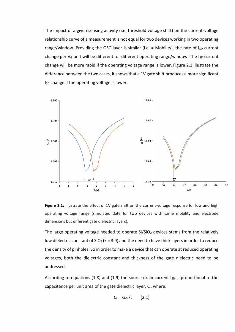
The impact of a given sensing activity (i.e. threshold voltage shift) on the current-voltage
relationship curve of a measurement is not equal for two devices working in two operating
range/window. Providing the OSC layer is similar (i.e. ≈ Mobility), the rate of ISD current
change per VG unit will be different for different operating range/window. The ISD current
change will be more rapid if the operating voltage range is lower. Figure 2.1 illustrate the
difference between the two cases, it shows that a 1V gate shift produces a more significant
ISD change if the operating voltage is lower.
Figure 2.1: Illustrate the effect of 1V gate shift on the current-voltage response for low and high
operating voltage range (simulated date for two devices with same mobility and electrode
dimensions but different gate dielectric layers).
The large operating voltage needed to operate Si/SiO2 devices stems from the relatively
low dielectric constant of SiO2 (k = 3.9) and the need to have thick layers in order to reduce
the density of pinholes. So in order to make a device that can operate at reduced operating
voltages, both the dielectric constant and thickness of the gate dielectric need to be
addressed.
According to equations (1.8) and (1.9) the source drain current ISD is proportional to the
capacitance per unit area of the gate dielectric layer, Ci, where:
Ci = kε0 /t (2.1)
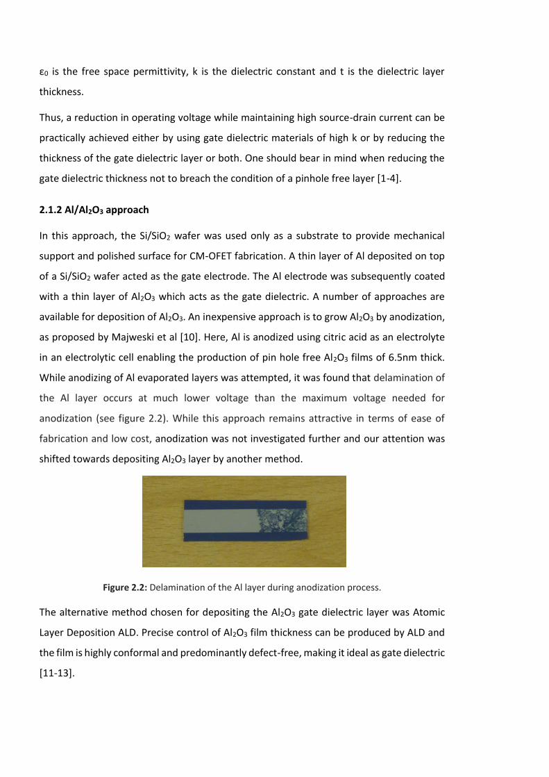
ε0 is the free space permittivity, k is the dielectric constant and t is the dielectric layer
thickness.
Thus, a reduction in operating voltage while maintaining high source-drain current can be
practically achieved either by using gate dielectric materials of high k or by reducing the
thickness of the gate dielectric layer or both. One should bear in mind when reducing the
gate dielectric thickness not to breach the condition of a pinhole free layer [1-4].
2.1.2 Al/Al2O3 approach
In this approach, the Si/SiO2 wafer was used only as a substrate to provide mechanical
support and polished surface for CM-OFET fabrication. A thin layer of Al deposited on top
of a Si/SiO2 wafer acted as the gate electrode. The Al electrode was subsequently coated
with a thin layer of Al2O3 which acts as the gate dielectric. A number of approaches are
available for deposition of Al2O3. An inexpensive approach is to grow Al2O3 by anodization,
as proposed by Majweski et al [10]. Here, Al is anodized using citric acid as an electrolyte
in an electrolytic cell enabling the production of pin hole free Al2O3 films of 6.5nm thick.
While anodizing of Al evaporated layers was attempted, it was found that delamination of
the Al layer occurs at much lower voltage than the maximum voltage needed for
anodization (see figure 2.2). While this approach remains attractive in terms of ease of
fabrication and low cost, anodization was not investigated further and our attention was
shifted towards depositing Al2O3 layer by another method.
Figure 2.2: Delamination of the Al layer during anodization process.
The alternative method chosen for depositing the Al2O3 gate dielectric layer was Atomic
Layer Deposition ALD. Precise control of Al2O3 film thickness can be produced by ALD and
the film is highly conformal and predominantly defect-free, making it ideal as gate dielectric
[11-13].
From the source drain current equation 2.2, for two nominally identical devices in terms of
geometry and charge mobility, the capacitance per unit area of the gate dielectric layer, Ci,
determines the operating voltage of the device.
𝐼𝐷𝑆 = 𝑊𝜇𝐶𝑖
2𝐿 (𝑉𝐺 − 𝑉𝑇)
2 (2.2)
Thus, Ci for an Al2O3 gate dielectric will be 2.5 times higher than the capacitance of a SiO2
dielectric (assuming a constant thickness) owing to the dielectric constant of 9-10 for Al2O3
compared to 3.9 for SiO2.
As the ALD deposited layer is almost defect free, this enables the deposition of very thin
gate dielectric layer, thus enabled us to reduced the thickness of the Al2O3 gate dielectric
layer to only 40nm compared to 300nm for SiO2. This in principle should reduce the
operating voltage as the source drain current is enhanced by a factor of 7.5, which makes
the combined effect of higher Al2O3 dielectric constant and reduced gate dielectric
thickness nearly a factor of 15.
This simplification is however far from accurate, and as will explained (in chapter 5 section
5.8) that another factor (surface energy of the gate dielectric layer) plays a vital role in
determining the drain current and hence the operating voltage required. Nevertheless,
lower operating voltage compare to Si/SiO2 devices was achieved.
2.1.3: Effective sensitivity (ΔID/ΔVTH) of the Al/Al2O3 and Si/SiO2 devices
In principle ΔID/ΔVTH should be higher for Al/Al2O3 based devices compare to Si/SiO2 based
on the following valid assumptions:
1- For the same given sensing event, the charge accumulated in the sensing area for
both devices should be the same. The resulting shift in threshold voltage, ΔVTH, will
thus be the same for both devices.
2- For the same OSC (i.e. same mobility) and identical geometry, a similar ISD transfer
characteristic curve can be drawn by smaller gate voltage range for Al/Al2O3 device
compare to Si/SiO2. This in turns means that for the same gate voltage change the
corresponding change in the magnitude of ISD will be different as follows:
ΔVG (Al/Al2O3) = ΔVG (Si/SiO2) then
ΔID (Al/Al2O3) > ΔID (Si/SiO2)
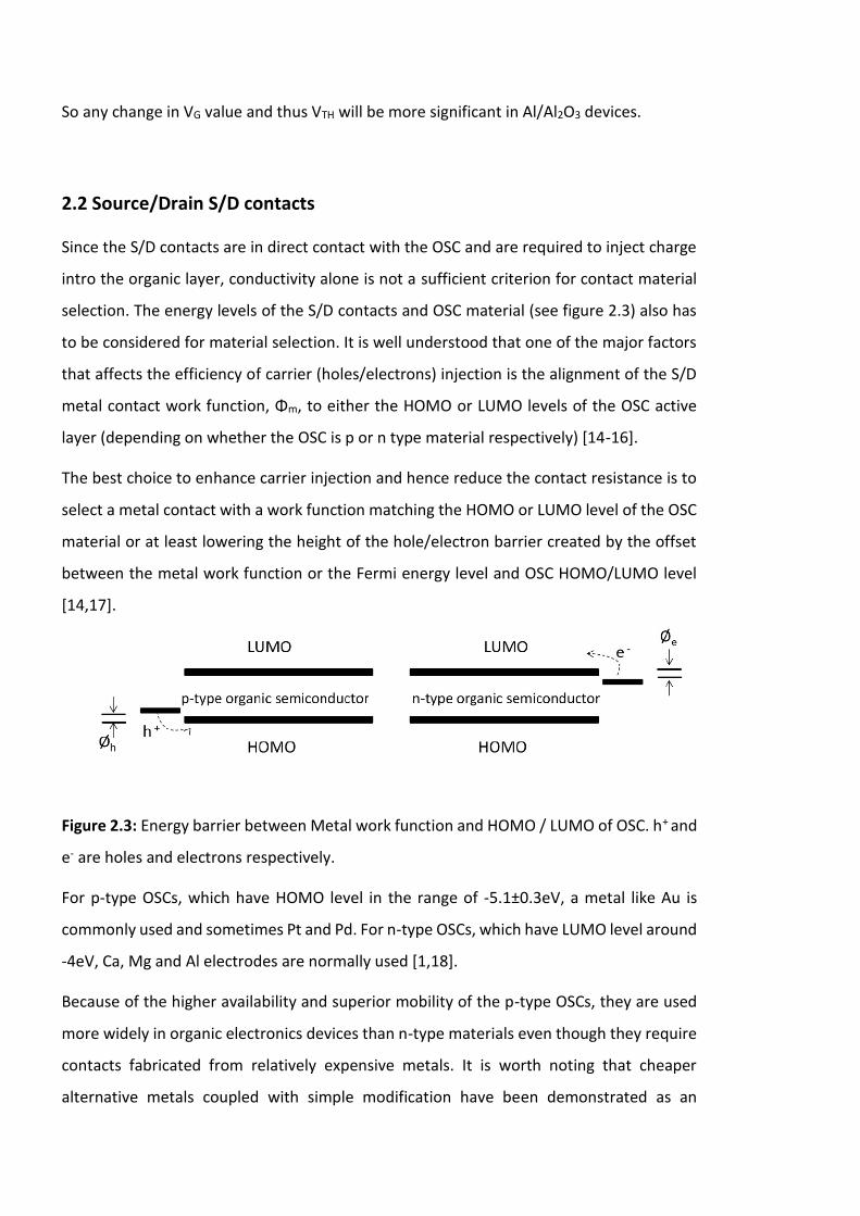
So any change in VG value and thus VTH will be more significant in Al/Al2O3 devices.
2.2 Source/Drain S/D contacts
Since the S/D contacts are in direct contact with the OSC and are required to inject charge
intro the organic layer, conductivity alone is not a sufficient criterion for contact material
selection. The energy levels of the S/D contacts and OSC material (see figure 2.3) also has
to be considered for material selection. It is well understood that one of the major factors
that affects the efficiency of carrier (holes/electrons) injection is the alignment of the S/D
metal contact work function, Φm, to either the HOMO or LUMO levels of the OSC active
layer (depending on whether the OSC is p or n type material respectively) [14-16].
The best choice to enhance carrier injection and hence reduce the contact resistance is to
select a metal contact with a work function matching the HOMO or LUMO level of the OSC
material or at least lowering the height of the hole/electron barrier created by the offset
between the metal work function or the Fermi energy level and OSC HOMO/LUMO level
[14,17].
Figure 2.3: Energy barrier between Metal work function and HOMO / LUMO of OSC. h+ and
e- are holes and electrons respectively.
For p-type OSCs, which have HOMO level in the range of -5.1±0.3eV, a metal like Au is
commonly used and sometimes Pt and Pd. For n-type OSCs, which have LUMO level around
-4eV, Ca, Mg and Al electrodes are normally used [1,18].
Because of the higher availability and superior mobility of the p-type OSCs, they are used
more widely in organic electronics devices than n-type materials even though they require
contacts fabricated from relatively expensive metals. It is worth noting that cheaper
alternative metals coupled with simple modification have been demonstrated as an
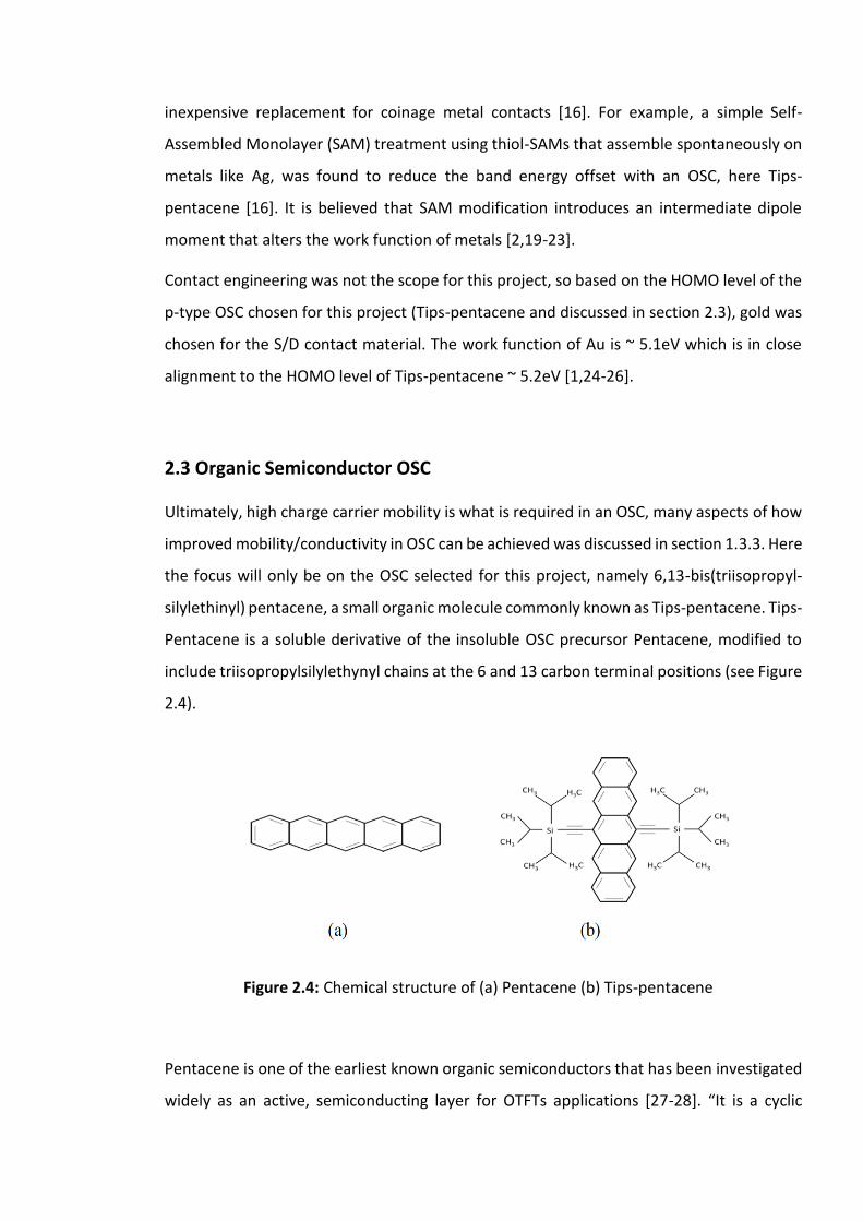
inexpensive replacement for coinage metal contacts [16]. For example, a simple Self-
Assembled Monolayer (SAM) treatment using thiol-SAMs that assemble spontaneously on
metals like Ag, was found to reduce the band energy offset with an OSC, here Tips-
pentacene [16]. It is believed that SAM modification introduces an intermediate dipole
moment that alters the work function of metals [2,19-23].
Contact engineering was not the scope for this project, so based on the HOMO level of the
p-type OSC chosen for this project (Tips-pentacene and discussed in section 2.3), gold was
chosen for the S/D contact material. The work function of Au is ~ 5.1eV which is in close
alignment to the HOMO level of Tips-pentacene ~ 5.2eV [1,24-26].
2.3 Organic Semiconductor OSC
Ultimately, high charge carrier mobility is what is required in an OSC, many aspects of how
improved mobility/conductivity in OSC can be achieved was discussed in section 1.3.3. Here
the focus will only be on the OSC selected for this project, namely 6,13-bis(triisopropyl-
silylethinyl) pentacene, a small organic molecule commonly known as Tips-pentacene. Tips-
Pentacene is a soluble derivative of the insoluble OSC precursor Pentacene, modified to
include triisopropylsilylethynyl chains at the 6 and 13 carbon terminal positions (see Figure
2.4).
Figure 2.4: Chemical structure of (a) Pentacene (b) Tips-pentacene
Pentacene is one of the earliest known organic semiconductors that has been investigated
widely as an active, semiconducting layer for OTFTs applications [27-28]. “It is a cyclic
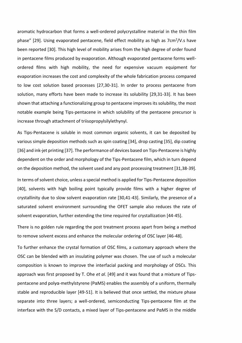
aromatic hydrocarbon that forms a well-ordered polycrystalline material in the thin film
phase” [29]. Using evaporated pentacene, field effect mobility as high as 7cm2/V.s have
been reported [30]. This high level of mobility arises from the high degree of order found
in pentacene films produced by evaporation. Although evaporated pentacene forms well-
ordered films with high mobility, the need for expensive vacuum equipment for
evaporation increases the cost and complexity of the whole fabrication process compared
to low cost solution based processes [27,30-31]. In order to process pentacene from
solution, many efforts have been made to increase its solubility [29,31-33]. It has been
shown that attaching a functionalizing group to pentacene improves its solubility, the most
notable example being Tips-pentacene in which solubility of the pentacene precursor is
increase through attachment of triisopropylsilylethynyl.
As Tips-Pentacene is soluble in most common organic solvents, it can be deposited by
various simple deposition methods such as spin coating [34], drop casting [35], dip coating
[36] and ink-jet printing [37]. The performance of devices based on Tips-Pentacene is highly
dependent on the order and morphology of the Tips-Pentacene film, which in turn depend
on the deposition method, the solvent used and any post processing treatment [31,38-39].
In terms of solvent choice, unless a special method is applied for Tips-Pentacene deposition
[40], solvents with high boiling point typically provide films with a higher degree of
crystallinity due to slow solvent evaporation rate [30,41-43]. Similarly, the presence of a
saturated solvent environment surrounding the OFET sample also reduces the rate of
solvent evaporation, further extending the time required for crystallization [44-45].
There is no golden rule regarding the post treatment process apart from being a method
to remove solvent excess and enhance the molecular ordering of OSC layer [46-48].
To further enhance the crystal formation of OSC films, a customary approach where the
OSC can be blended with an insulating polymer was chosen. The use of such a molecular
composition is known to improve the interfacial packing and morphology of OSCs. This
approach was first proposed by T. Ohe et al. [49] and it was found that a mixture of Tips-
pentacene and polyα-methylstyrene (PαMS) enables the assembly of a uniform, thermally
stable and reproducible layer [49-51]. It is believed that once settled, the mixture phase
separate into three layers; a well-ordered, semiconducting Tips-pentacene film at the
interface with the S/D contacts, a mixed layer of Tips-pentacene and PαMS in the middle
that provides extra protection for the active Tips–pentacene layer and finally a second Tips-
pentacene layer at the surface. This layer does not contact the S/D electrodes and thus not
does contribute to the operation of the device [49-51]. This is shown schematically in figure
2.5.
Figure 2.5: Schematic diagram showing the three phases of Tips-pentacene/PαMS after
separation.
The materials discussed above are the materials for the fundamental components of an
organic transistor. Two further materials are needed to transform the transistor to a CM-
OFET sensor; the first concerns the functionalization of a portion of the gate electrode
surface to make it sensitive to the analyte of interest, the second is the material used to
form a fluidic chamber incorporated to the transistor for analyte solution delivery.
2.4 Sensing area functionalization (with 3-aminopropyltri-ethoxysilane
APTES)
The formation of organosilane (derivatives of silane with at least one carbon-silicon bond
in their structure) monolayers on a substrate surface is typically referred to as silanization
[52-53]. Silanization is commonly achieved via self-assembly of the organosilane either
from the vapor or liquid phase [53-54]. In the process, shown in figure 2.6, the presence of
moisture or water traces catalyses the hydrolysis of alkoxy groups in the organosilane
molecule to form silanol groups (Si–O–H) which reacts with free hydroxyl groups (OH) on

the surface, leading to the formation of a covalent Si-O-Si which tethers the organosilane
molecules to the surface [52,55-56]. Once immobilized by the head group of the
organosilane self-assembled monolayer, the opposite end of the SAMs molecules, the tail
group, will be the new dominant surface chemical species [53-54,57].
One of the most common uses of surfaces modified with organosilane monolayers is to be
used as an intermediate layer in biosensors for subsequent protein and biomolecule
immobilization. Among the most frequently used organosilane SAMs for this application is
3-aminopropyltri-ethoxysilane (APTES) [55-56,58], in which the tail group is the chemically
reactive amine group that can be used subsequently for attaching biomolecules.
In the CM-OFET device, the sensing region was modified with APTES where in principle the
immobilizing mechanism should be that the three ethoxy groups in the APTES hydrolysis to
react with hydroxyl groups (OH) on the Si or Al surfaces to form (Si-O-Si) and (Si-O-Al) bonds
respectively to assemble on the surface, leaving the amine group (NH2) on the other end of
the APTES SAM to be the new electroactive surface of the region.
Figure 2.6: APTES chemical structure and Optimal APTES Silanization process on Si substrate,
adapted with permission from [54]. Copyright 2012.
The functional amine group terminal was utilized for two fundamental roles in the CM-
OFET at two different phases in the project.
1- To examine the working principle of the device as a pH sensor. Here, the sensitivity
of the amine group to the local concentration of H+ was exploited to modify the
response of the CM-OFET to different pH solutions where the amine group undergo
de/protonation based on the pH level of the analyte solution (discussed in chapter
4).
2- The amine group was employed as an anchoring site for subsequent biomolecule
attachment via a biotinylation process (discussed in chapter 5).
2.5 Polydimethylsiloxane (PDMS) microfluidic chamber
Polydimethylsiloxane (PDMS) is a malleable organosilicon polymer [59]. PDMS can be
readily manipulated to form variety of passive and active components of a microfluidic
system, making it very much the material of choice for most microfluidic based platform
applications as it can be handy in making various microfluidic prototypes [60].
As well as being simple to use, easy to process and commercially available at low cost [61-
62], PDMS offers a number of favourable physical and chemical properties that make it a
favourable material for microfluidics. On the physical side, PDMS has relatively low
viscosity enabling it to diffuse through small patterns of a master template (down to
microscale features) [63]. Another key physical property, is that the polymerization
(process of cross-linking shown in figure 2.7) of liquid (un-cured) PDMS can be performed
at low to moderate temperatures, making it compatible with other various fabrication
processes [63].
Commercial PDMS comes in a kit of two liquid bottles, one for the oligomer base and one
for curing agent. The crosslinked PDMS elastomer is produced by mixing the two
components at a specific ratio. The chemistry of the crosslinking process is explained in
detail in [64]. Briefly, as can be seen in figure 2.7, crosslinking occurs through a
hydrosilylation process, where in the presence of platinum catalyst, hydrosilanes (Si–H) in
the curing agent 2 reacts with vinyl groups (CH=CH2) in the oligomer base 1. In the reaction,
hydrosilation of the double bonds occurs and Si–CH2–CH2–Si linkages are formed [64-67].
Typically making microfluidics using PDMS is realized by soft-lithography techniques. The
fabrication of PDMS microfluidic devices using soft-lithography is simply achieved by
pouring un-cured PDMS on a master template before the PDMS is cured by curing process
normally involve heating. Once cured, the PDMS will contain a replica imprint structure of
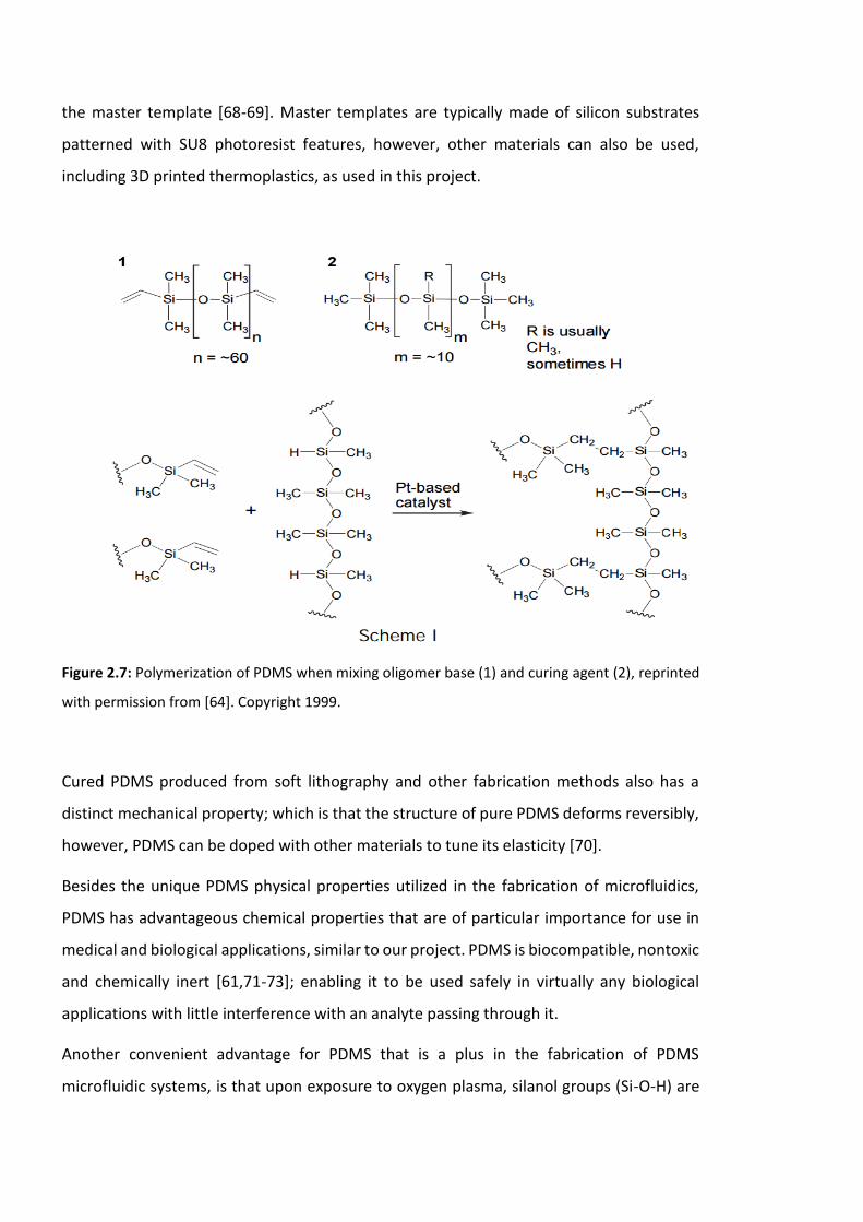
the master template [68-69]. Master templates are typically made of silicon substrates
patterned with SU8 photoresist features, however, other materials can also be used,
including 3D printed thermoplastics, as used in this project.
Figure 2.7: Polymerization of PDMS when mixing oligomer base (1) and curing agent (2), reprinted
with permission from [64]. Copyright 1999.
Cured PDMS produced from soft lithography and other fabrication methods also has a
distinct mechanical property; which is that the structure of pure PDMS deforms reversibly,
however, PDMS can be doped with other materials to tune its elasticity [70].
Besides the unique PDMS physical properties utilized in the fabrication of microfluidics,
PDMS has advantageous chemical properties that are of particular importance for use in
medical and biological applications, similar to our project. PDMS is biocompatible, nontoxic
and chemically inert [61,71-73]; enabling it to be used safely in virtually any biological
applications with little interference with an analyte passing through it.
Another convenient advantage for PDMS that is a plus in the fabrication of PDMS
microfluidic systems, is that upon exposure to oxygen plasma, silanol groups (Si-O-H) are
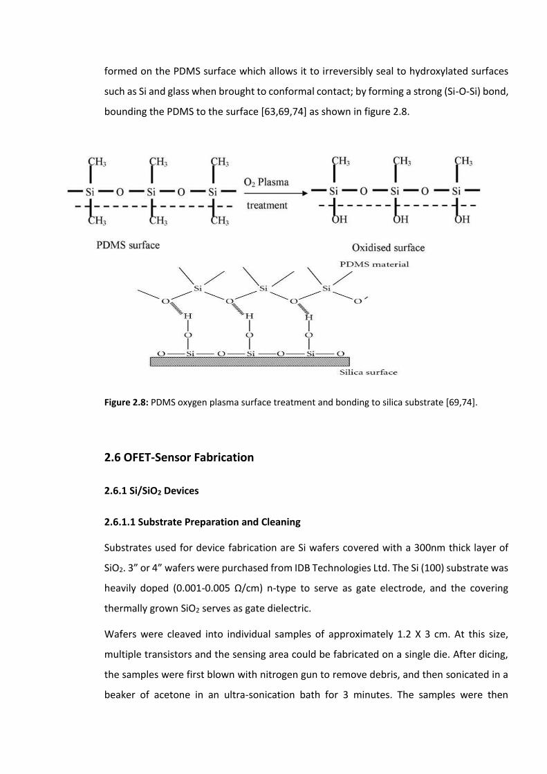
formed on the PDMS surface which allows it to irreversibly seal to hydroxylated surfaces
such as Si and glass when brought to conformal contact; by forming a strong (Si-O-Si) bond,
bounding the PDMS to the surface [63,69,74] as shown in figure 2.8.
Figure 2.8: PDMS oxygen plasma surface treatment and bonding to silica substrate [69,74].
2.6 OFET-Sensor Fabrication
2.6.1 Si/SiO2 Devices
2.6.1.1 Substrate Preparation and Cleaning
Substrates used for device fabrication are Si wafers covered with a 300nm thick layer of
SiO2. 3” or 4” wafers were purchased from IDB Technologies Ltd. The Si (100) substrate was
heavily doped (0.001-0.005 Ω/cm) n-type to serve as gate electrode, and the covering
thermally grown SiO2 serves as gate dielectric.
Wafers were cleaved into individual samples of approximately 1.2 X 3 cm. At this size,
multiple transistors and the sensing area could be fabricated on a single die. After dicing,
the samples were first blown with nitrogen gun to remove debris, and then sonicated in a
beaker of acetone in an ultra-sonication bath for 3 minutes. The samples were then
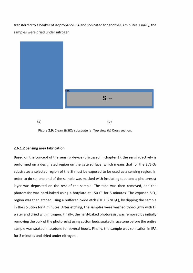
transferred to a beaker of isopropanol IPA and sonicated for another 3 minutes. Finally, the
samples were dried under nitrogen.
(a) (b)
Figure 2.9: Clean Si/SiO2 substrate (a) Top view (b) Cross section.
2.6.1.2 Sensing area fabrication
Based on the concept of the sensing device (discussed in chapter 1), the sensing activity is
performed on a designated region on the gate surface; which means that for the Si/SiO2
substrates a selected region of the Si must be exposed to be used as a sensing region. In
order to do so, one end of the sample was masked with insulating tape and a photoresist
layer was deposited on the rest of the sample. The tape was then removed, and the
photoresist was hard-baked using a hotplate at 150 C° for 5 minutes. The exposed SiO2
region was then etched using a buffered oxide etch (HF 1:6 NH4F), by dipping the sample
in the solution for 4 minutes. After etching, the samples were washed thoroughly with DI
water and dried with nitrogen. Finally, the hard-baked photoresist was removed by initially
removing the bulk of the photoresist using cotton buds soaked in acetone before the entire
sample was soaked in acetone for several hours. Finally, the sample was sonication in IPA
for 3 minutes and dried under nitrogen.
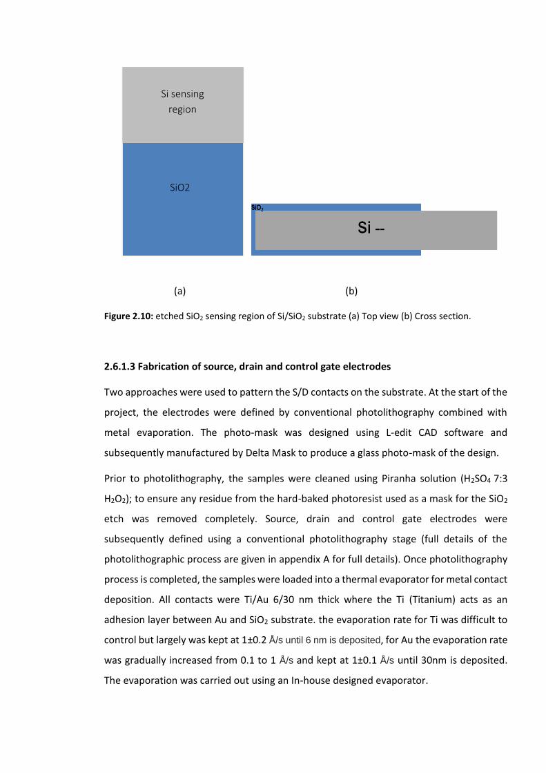
(a) (b)
Figure 2.10: etched SiO2 sensing region of Si/SiO2 substrate (a) Top view (b) Cross section.
2.6.1.3 Fabrication of source, drain and control gate electrodes
Two approaches were used to pattern the S/D contacts on the substrate. At the start of the
project, the electrodes were defined by conventional photolithography combined with
metal evaporation. The photo-mask was designed using L-edit CAD software and
subsequently manufactured by Delta Mask to produce a glass photo-mask of the design.
Prior to photolithography, the samples were cleaned using Piranha solution (H2SO4 7:3
H2O2); to ensure any residue from the hard-baked photoresist used as a mask for the SiO2
etch was removed completely. Source, drain and control gate electrodes were
subsequently defined using a conventional photolithography stage (full details of the
photolithographic process are given in appendix A for full details). Once photolithography
process is completed, the samples were loaded into a thermal evaporator for metal contact
deposition. All contacts were Ti/Au 6/30 nm thick where the Ti (Titanium) acts as an
adhesion layer between Au and SiO2 substrate. the evaporation rate for Ti was difficult to
control but largely was kept at 1±0.2 Å/s until 6 nm is deposited, for Au the evaporation rate
was gradually increased from 0.1 to 1 Å/s and kept at 1±0.1 Å/s until 30nm is deposited.
The evaporation was carried out using an In-house designed evaporator.
Si sensing
region
SiO2
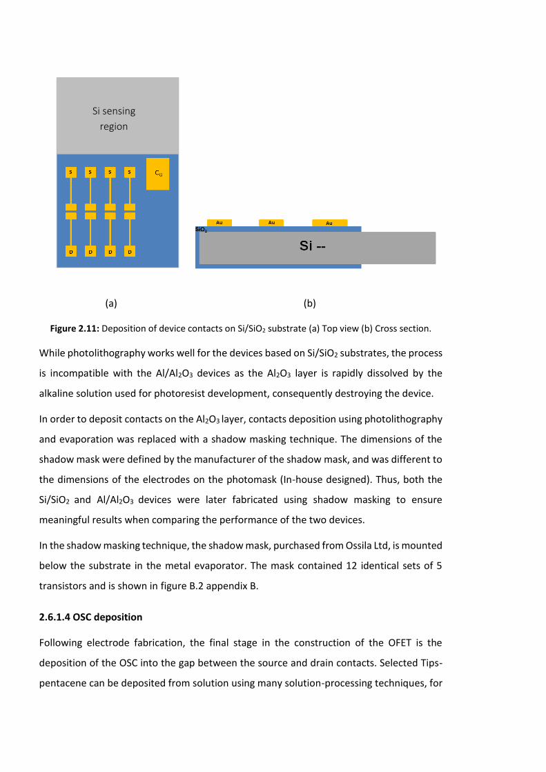
(a) (b)
Figure 2.11: Deposition of device contacts on Si/SiO2 substrate (a) Top view (b) Cross section.
While photolithography works well for the devices based on Si/SiO2 substrates, the process
is incompatible with the Al/Al2O3 devices as the Al2O3 layer is rapidly dissolved by the
alkaline solution used for photoresist development, consequently destroying the device.
In order to deposit contacts on the Al2O3 layer, contacts deposition using photolithography
and evaporation was replaced with a shadow masking technique. The dimensions of the
shadow mask were defined by the manufacturer of the shadow mask, and was different to
the dimensions of the electrodes on the photomask (In-house designed). Thus, both the
Si/SiO2 and Al/Al2O3 devices were later fabricated using shadow masking to ensure
meaningful results when comparing the performance of the two devices.
In the shadow masking technique, the shadow mask, purchased from Ossila Ltd, is mounted
below the substrate in the metal evaporator. The mask contained 12 identical sets of 5
transistors and is shown in figure B.2 appendix B.
2.6.1.4 OSC deposition
Following electrode fabrication, the final stage in the construction of the OFET is the
deposition of the OSC into the gap between the source and drain contacts. Selected Tips-
pentacene can be deposited from solution using many solution-processing techniques, for
Si sensing
region
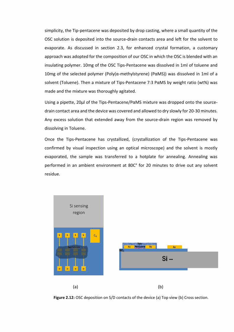
simplicity, the Tip-pentacene was deposited by drop casting, where a small quantity of the
OSC solution is deposited into the source-drain contacts area and left for the solvent to
evaporate. As discussed in section 2.3, for enhanced crystal formation, a customary
approach was adopted for the composition of our OSC in which the OSC is blended with an
insulating polymer. 10mg of the OSC Tips-Pentacene was dissolved in 1ml of toluene and
10mg of the selected polymer (Poly(α-methylstyrene) (PαMS)) was dissolved in 1ml of a
solvent (Toluene). Then a mixture of Tips-Pentacene 7:3 PαMS by weight ratio (wt%) was
made and the mixture was thoroughly agitated.
Using a pipette, 20µl of the Tips-Pentacene/PαMS mixture was dropped onto the source-
drain contact area and the device was covered and allowed to dry slowly for 20-30 minutes.
Any excess solution that extended away from the source-drain region was removed by
dissolving in Toluene.
Once the Tips-Pentacene has crystallized, (crystallization of the Tips-Pentacene was
confirmed by visual inspection using an optical microscope) and the solvent is mostly
evaporated, the sample was transferred to a hotplate for annealing. Annealing was
performed in an ambient environment at 80C° for 20 minutes to drive out any solvent
residue.
(a) (b)
Figure 2.12: OSC deposition on S/D contacts of the device (a) Top view (b) Cross section.
Si sensing
region

Figure 2.13 shows how the Tips-pentacene crystals form on the source/drain electrodes.
(a) (b)
Figure 2.13: Optical microscope image of the source/drain electrodes (a) before and (b) after Tips-
pentacene deposition. Images were captured using a 5x objective lens.
2.6.1.5 Functionalizing the surface of the sensing region and microfluidic integration
In the final stages of fabrication where the transistor is actually transformed into a sensor,
the sensing region exposed by the SiO2 etching stage is functionalized with a sensing
recognition element in order to control the sensitivity of the exposed Si gate to the selected
analyte. The completed device also needs to be integrated with a microfluidic reservoir
mounted onto the sensing region to control the delivery of solutions and analytes.
As been discussed earlier in this chapter (section 2.4), the organic functionalizing molecule
opted for was (3-aminopropyltriethoxysilane APTES), this molecule can be used in the
various stages/applications set to be tackled for the fabricated sensor in this thesis.
The two complementary steps (sensing area functionalisation and microfluidic integration)
can take place at two different stages of the fabrication process; either before or after the
OSC deposition step. Regardless of the order of this step, the exposed Si region is first

cleaned using Piranha solution (H2SO4 7:3 H2O2) for approximately 5 minutes, then
depending on whether this step is performed before or after OSC deposition step, the order
of completing the functionalizing and Microfluidic integration steps can interchange.
Functionalization before the deposition of the OSC
When the functionalization was performed before OSC deposition, the whole sample was
first cleaned in Piranha solution for 5 minutes followed by Ozone cleaning for another 5
minutes. The cleaned sample was then immersed in 5% APTES solution in IPA such that only
the sensing area was covered by the solution. The sample was left in the solution overnight
for approximately 18 hours. The sample was then thoroughly cleaned using IPA to remove
excess APTES and finally dried with nitrogen gun. This process allows for the self-assembly
of the APTES monolayer on the surface of the sensing region. Immediately afterwards, a
pre-prepared microfluidic chamber made from polydimethylsiloxane (PDMS) was mounted
to the sensing region and sealed by pouring liquid PDMS around the perimeter of the
chamber and solidifying it on a hotplate at 90C° for 20 minutes.
Functionalization after the deposition of the OSC
If the process of surface functionalization is performed after the deposition of the OSC,
then the procedure has to be modified in order to protect the OSC from damage or change
in characteristics that might be caused by the functionalizing solution or vapour.
After OSC deposition, the sample was wrapped with clean Parafilm to protect all regions
other that the sensing region. The sensing region was then immersed in Piranha cleaning
solution for 3-5 minutes (depending on surface wettability) before being rinsed thoroughly
in water and dried under nitrogen. Immediately afterwards, the Parafilm was removed and
the sample was transferred to a hotplate where a PDMS microfluidic chamber was
mounted to the sensing region and sealed by pouring liquid PDMS around the perimeter of
the chamber and solidifying it on the hotplate at 90C° for 20 minutes. Once the chamber
was sealed, fluidic tubes were connected to the inlet and outlet of the chamber and a 5%
APTES solution in IPA was injected over the sensing region. The functionalizing solution was
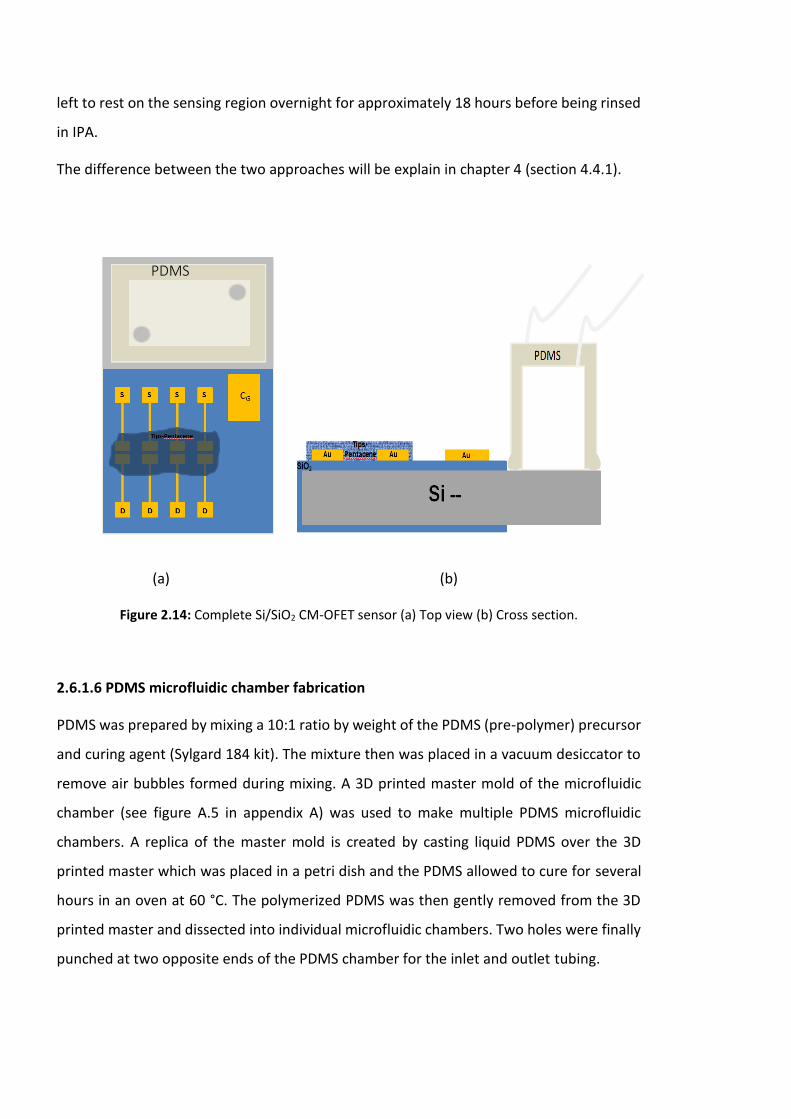
left to rest on the sensing region overnight for approximately 18 hours before being rinsed
in IPA.
The difference between the two approaches will be explain in chapter 4 (section 4.4.1).
(a) (b)
Figure 2.14: Complete Si/SiO2 CM-OFET sensor (a) Top view (b) Cross section.
2.6.1.6 PDMS microfluidic chamber fabrication
PDMS was prepared by mixing a 10:1 ratio by weight of the PDMS (pre-polymer) precursor
and curing agent (Sylgard 184 kit). The mixture then was placed in a vacuum desiccator to
remove air bubbles formed during mixing. A 3D printed master mold of the microfluidic
chamber (see figure A.5 in appendix A) was used to make multiple PDMS microfluidic
chambers. A replica of the master mold is created by casting liquid PDMS over the 3D
printed master which was placed in a petri dish and the PDMS allowed to cure for several
hours in an oven at 60 °C. The polymerized PDMS was then gently removed from the 3D
printed master and dissected into individual microfluidic chambers. Two holes were finally
punched at two opposite ends of the PDMS chamber for the inlet and outlet tubing.
PDMS
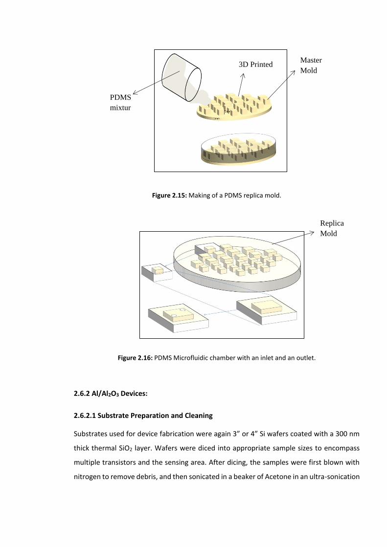
Figure 2.15: Making of a PDMS replica mold.
Figure 2.16: PDMS Microfluidic chamber with an inlet and an outlet.
2.6.2 Al/Al2O3 Devices:
2.6.2.1 Substrate Preparation and Cleaning
Substrates used for device fabrication were again 3” or 4” Si wafers coated with a 300 nm
thick thermal SiO2 layer. Wafers were diced into appropriate sample sizes to encompass
multiple transistors and the sensing area. After dicing, the samples were first blown with
nitrogen to remove debris, and then sonicated in a beaker of Acetone in an ultra-sonication
Replica
Mold
Master
Mold
PDMS
mixtur
e
3D Printed
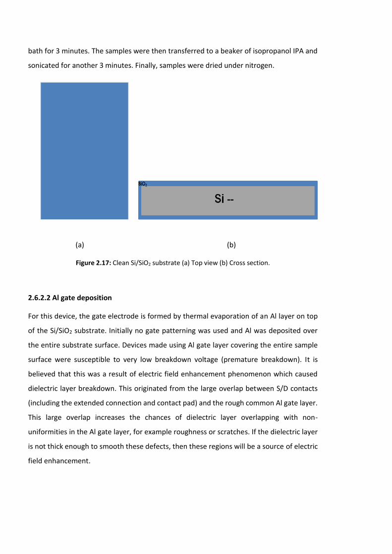
bath for 3 minutes. The samples were then transferred to a beaker of isopropanol IPA and
sonicated for another 3 minutes. Finally, samples were dried under nitrogen.
(a) (b)
Figure 2.17: Clean Si/SiO2 substrate (a) Top view (b) Cross section.
2.6.2.2 Al gate deposition
For this device, the gate electrode is formed by thermal evaporation of an Al layer on top
of the Si/SiO2 substrate. Initially no gate patterning was used and Al was deposited over
the entire substrate surface. Devices made using Al gate layer covering the entire sample
surface were susceptible to very low breakdown voltage (premature breakdown). It is
believed that this was a result of electric field enhancement phenomenon which caused
dielectric layer breakdown. This originated from the large overlap between S/D contacts
(including the extended connection and contact pad) and the rough common Al gate layer.
This large overlap increases the chances of dielectric layer overlapping with non-
uniformities in the Al gate layer, for example roughness or scratches. If the dielectric layer
is not thick enough to smooth these defects, then these regions will be a source of electric
field enhancement.

(a) (b)
(c) (d)
Figure 2.18: Deposition of Al gate layer on the entire substrate (a) Top view (b) Cross section, and
pattern Al gate layer (c) Top view (d) Cross section
The gate design was revised and the choice of having all surface coverage gate was
discarded and was replaced by pattern gate (see figure 2.18c). Pattern gate layer helped
the new design to fully comply with the working principle of the CM-OFET device (to be
discussed in chapter 5) and it appears to eliminate premature breakdown as a result of
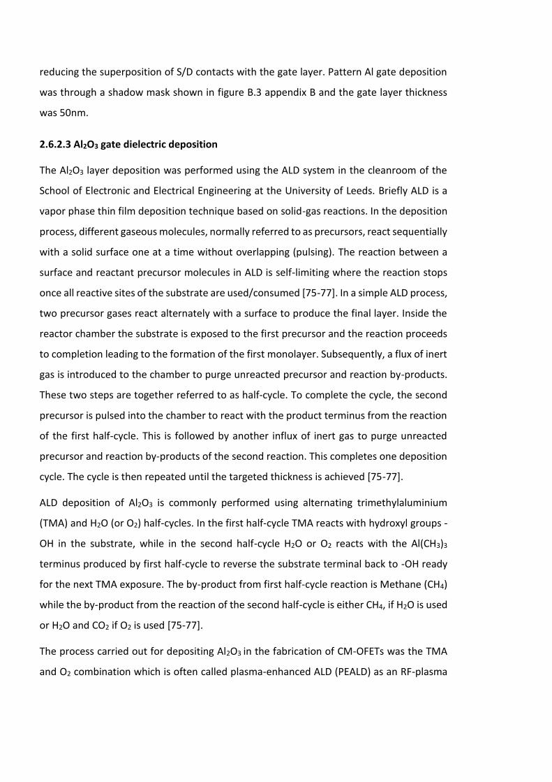
reducing the superposition of S/D contacts with the gate layer. Pattern Al gate deposition
was through a shadow mask shown in figure B.3 appendix B and the gate layer thickness
was 50nm.
2.6.2.3 Al2O3 gate dielectric deposition
The Al2O3 layer deposition was performed using the ALD system in the cleanroom of the
School of Electronic and Electrical Engineering at the University of Leeds. Briefly ALD is a
vapor phase thin film deposition technique based on solid-gas reactions. In the deposition
process, different gaseous molecules, normally referred to as precursors, react sequentially
with a solid surface one at a time without overlapping (pulsing). The reaction between a
surface and reactant precursor molecules in ALD is self-limiting where the reaction stops
once all reactive sites of the substrate are used/consumed [75-77]. In a simple ALD process,
two precursor gases react alternately with a surface to produce the final layer. Inside the
reactor chamber the substrate is exposed to the first precursor and the reaction proceeds
to completion leading to the formation of the first monolayer. Subsequently, a flux of inert
gas is introduced to the chamber to purge unreacted precursor and reaction by-products.
These two steps are together referred to as half-cycle. To complete the cycle, the second
precursor is pulsed into the chamber to react with the product terminus from the reaction
of the first half-cycle. This is followed by another influx of inert gas to purge unreacted
precursor and reaction by-products of the second reaction. This completes one deposition
cycle. The cycle is then repeated until the targeted thickness is achieved [75-77].
ALD deposition of Al2O3 is commonly performed using alternating trimethylaluminium
(TMA) and H2O (or O2) half-cycles. In the first half-cycle TMA reacts with hydroxyl groups -
OH in the substrate, while in the second half-cycle H2O or O2 reacts with the Al(CH3)3
terminus produced by first half-cycle to reverse the substrate terminal back to -OH ready
for the next TMA exposure. The by-product from first half-cycle reaction is Methane (CH4)
while the by-product from the reaction of the second half-cycle is either CH4, if H2O is used
or H2O and CO2 if O2 is used [75-77].
The process carried out for depositing Al2O3 in the fabrication of CM-OFETs was the TMA
and O2 combination which is often called plasma-enhanced ALD (PEALD) as an RF-plasma
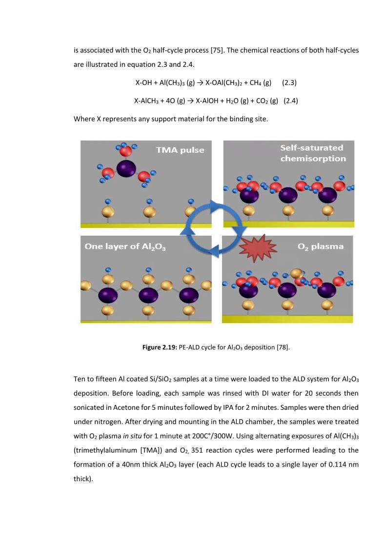
is associated with the O2 half-cycle process [75]. The chemical reactions of both half-cycles
are illustrated in equation 2.3 and 2.4.
X-OH + Al(CH3)3 (g) → X-OAl(CH3)2 + CH4 (g) (2.3)
X-AlCH3 + 4O (g) → X-AlOH + H2O (g) + CO2 (g) (2.4)
Where X represents any support material for the binding site.
Figure 2.19: PE-ALD cycle for Al2O3 deposition [78].
Ten to fifteen Al coated Si/SiO2 samples at a time were loaded to the ALD system for Al2O3
deposition. Before loading, each sample was rinsed with DI water for 20 seconds then
sonicated in Acetone for 5 minutes followed by IPA for 2 minutes. Samples were then dried
under nitrogen. After drying and mounting in the ALD chamber, the samples were treated
with O2 plasma in situ for 1 minute at 200C°/300W. Using alternating exposures of Al(CH3)3
(trimethylaluminum [TMA]) and O2, 351 reaction cycles were performed leading to the
formation of a 40nm thick Al2O3 layer (each ALD cycle leads to a single layer of 0.114 nm
thick).
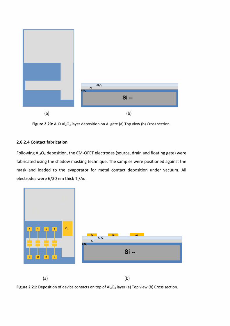
(a) (b)
Figure 2.20: ALD Al2O3 layer deposition on Al gate (a) Top view (b) Cross section.
2.6.2.4 Contact fabrication
Following Al2O3 deposition, the CM-OFET electrodes (source, drain and floating gate) were
fabricated using the shadow masking technique. The samples were positioned against the
mask and loaded to the evaporator for metal contact deposition under vacuum. All
electrodes were 6/30 nm thick Ti/Au.
(a) (b)
Figure 2.21: Deposition of device contacts on top of Al2O3 layer (a) Top view (b) Cross section.
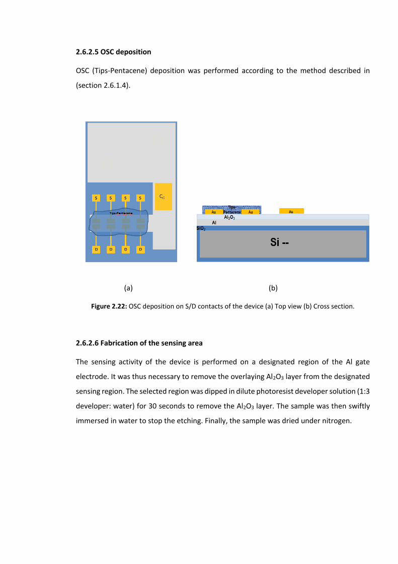
2.6.2.5 OSC deposition
OSC (Tips-Pentacene) deposition was performed according to the method described in
(section 2.6.1.4).
(a) (b)
Figure 2.22: OSC deposition on S/D contacts of the device (a) Top view (b) Cross section.
2.6.2.6 Fabrication of the sensing area
The sensing activity of the device is performed on a designated region of the Al gate
electrode. It was thus necessary to remove the overlaying Al2O3 layer from the designated
sensing region. The selected region was dipped in dilute photoresist developer solution (1:3
developer: water) for 30 seconds to remove the Al2O3 layer. The sample was then swiftly
immersed in water to stop the etching. Finally, the sample was dried under nitrogen.
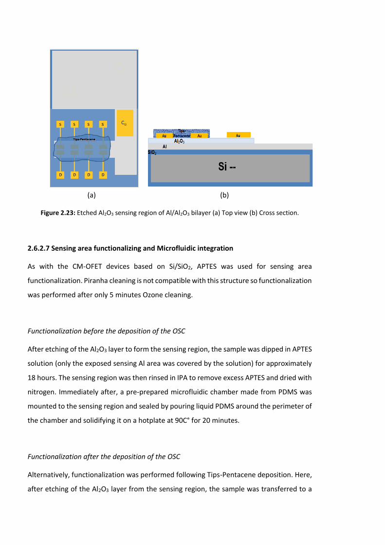
(a) (b)
Figure 2.23: Etched Al2O3 sensing region of Al/Al2O3 bilayer (a) Top view (b) Cross section.
2.6.2.7 Sensing area functionalizing and Microfluidic integration
As with the CM-OFET devices based on Si/SiO2, APTES was used for sensing area
functionalization. Piranha cleaning is not compatible with this structure so functionalization
was performed after only 5 minutes Ozone cleaning.
Functionalization before the deposition of the OSC
After etching of the Al2O3 layer to form the sensing region, the sample was dipped in APTES
solution (only the exposed sensing Al area was covered by the solution) for approximately
18 hours. The sensing region was then rinsed in IPA to remove excess APTES and dried with
nitrogen. Immediately after, a pre-prepared microfluidic chamber made from PDMS was
mounted to the sensing region and sealed by pouring liquid PDMS around the perimeter of
the chamber and solidifying it on a hotplate at 90C° for 20 minutes.
Functionalization after the deposition of the OSC
Alternatively, functionalization was performed following Tips-Pentacene deposition. Here,
after etching of the Al2O3 layer from the sensing region, the sample was transferred to a
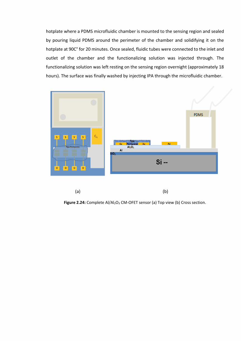
hotplate where a PDMS microfluidic chamber is mounted to the sensing region and sealed
by pouring liquid PDMS around the perimeter of the chamber and solidifying it on the
hotplate at 90C° for 20 minutes. Once sealed, fluidic tubes were connected to the inlet and
outlet of the chamber and the functionalizing solution was injected through. The
functionalizing solution was left resting on the sensing region overnight (approximately 18
hours). The surface was finally washed by injecting IPA through the microfluidic chamber.
(a) (b)
Figure 2.24: Complete Al/Al2O3 CM-OFET sensor (a) Top view (b) Cross section.
2.7 References
[1] Li, F., Nathan, A., Wu, Y., & Ong, B. S., Organic Thin Film Transistor Integration: A Hybrid
Approach. 2013. John Wiley & Sons.
[2] DiBenedetto, Sara A., Antonio Facchetti, Mark A. Ratner, and Tobin J. Marks. "Molecular
Self‐Assembled Monolayers and Multilayers for Organic and Unconventional Inorganic
Thin‐Film Transistor Applications." Advanced materials 21(14‐15), 2009, 1407-1433.
[3] Facchetti, Antonio, M‐H. Yoon, and Tobin J. Marks. "Gate dielectrics for organic field‐
effect transistors: new opportunities for organic electronics."Advanced Materials 17, no.
14 (2005): 1705-1725.
[4] Su, Yaorong, Chengliang Wang, Weiguang Xie, Fangyan Xie, Jian Chen, Ni Zhao, and
Jianbin Xu. "Low-Voltage Organic Field-Effect Transistors (OFETs) with Solution-Processed
Metal-Oxide as Gate Dielectric." ACS applied materials & interfaces 3(12) , 2011, 4662-
4667.
[5] Choi, Myeon-Cheon, Youngkyoo Kim, and Chang-Sik Ha. "Polymers for flexible displays:
from material selection to device applications." Progress in Polymer Science 33(6), 2008,
581-630.
[6] Jang, Jin, and Seung Hoon Han. "High-performance OTFT and its application."Current
Applied Physics 6 (2006): e17-e21.
[7] Miozzo, L., Yassar, A., & Horowitz, G. (2010). Surface engineering for high performance
organic electronic devices: the chemical approach. Journal of Materials Chemistry, 20(13),
2513-2538.
[8] Puri, M. (2014). Solution Processable Novel Organic Electronic Devices for New
Generation Biomedical Applications.
[9] Zeng, J., & Jensen, P. B. (2013). Organic light-emitting transistors with optimized gate
dielectric.
[10] L A Majewski1, R Schroeder and M Grell, Flexible high capacitance gate insulators for
organic field effect transistors, Journal of Physics D: Applied Physics. 37 (2004) 21–24
[11] Koo, J. B., Lim, J. W., Kim, S. H., Yun, S. J., Ku, C. H., Lim, S. C., & Lee, J. H. (2007).
Pentacene thin-film transistors and inverters with plasma-enhanced atomic-layer-
deposited Al 2 O 3 gate dielectric. Thin solid films, 515(5), 3132-3137.
[12] Jakschik, S., Schroeder, U., Hecht, T., Gutsche, M., Seidl, H., & Bartha, J. W. (2003).
Crystallization behavior of thin ALD-Al 2 O 3 films. Thin Solid Films, 425(1), 216-220.
[13] Zhang, X. H., Domercq, B., Wang, X., Yoo, S., Kondo, T., Wang, Z. L., & Kippelen, B.
(2007). High-performance pentacene field-effect transistors using Al 2 O 3 gate dielectrics
prepared by atomic layer deposition (ALD). Organic Electronics, 8(6), 718-726.
[14] Gordon Yip, Development of Al2O3 Gate Dielectrics for Organic Thin-film Transistors,
University of Toronto, 2008.
[15] Chung-Chen Kuo, High Performance Small-Molecule Organic Thin Film Transistors, the
Pennsylvania State University. December 2005.
[16] Hong, J. P., Park, A. Y., Lee, S., Kang, J., Shin, N., & Yoon, D. Y. (2008). Tuning of Ag work
functions by self-assembled monolayers of aromatic thiols for an efficient hole injection for
solution processed triisopropylsilylethynyl pentacene organic thin film transistors. Applied
Physics Letters, 92(14), 131.
[17] Boudinet, D., Benwadih, M., Qi, Y., Altazin, S., Verilhac, J. M., Kroger, M., ... & Kahn, A.
(2010). Modification of gold source and drain electrodes by self-assembled monolayer in
staggered n-and p-channel organic thin film transistors. Organic Electronics, 11(2), 227-
237.
[18] Hu, W., Bai, F., Gong, X., Zhan, X., Fu, H., & Bjornholm, T., “Organic optoelectronics”,
John Wiley & Sons. 2012
[19] Patrick Marmont, et al., Improving charge injection in organic thin-film transistors with
thiol-based self-assembled monolayers, Organic Electronics 9, 2008, 419–424, Elsevier.
[20] Majewski, L., Modification of substrate surfaces: self-assembled monolayers (SAMs),
Organic Electronics, Nano Electronics, University of Manchester. 2011
[21] Yang, X., Characterization of Self-assembled Monolayers by Low Energy Reactive Ion
Scattering Spectrometry: Influence of Terminal Group Composition and Structures, USA.
ProQuest. 2007
[22] Genzer, J., Soft Matter Gradient Surfaces: Methods and Applications, John Wiley &
Sons. 2012
[23] Yun, D., Lee, D., Jeon, H. and Rhee, S., Contact resistance between pentacene and
indium–tin oxide (ITO) electrode with surface treatment, Organic Electronics 8, 2007, 690–
694, Elsevier
[24] Li, H., Zheng, R., & Shi, Q. (2012). Theoretical study of charge carrier transport in
organic semiconductors of tetrathiafulvalene derivatives. The Journal of Physical Chemistry
C, 116(22), 11886-11894.
[25] Sherman, J. B., Moncino, K., Baruah, T., Wu, G., Parkin, S. R., Purushothaman, B., ... &
Chabinyc, M. L. (2015). Crystalline Alloys of Organic Donors and Acceptors Based on TIPS-
Pentacene. The Journal of Physical Chemistry C, 119(36), 20823-20832.
[26] Davis, R. J., Lloyd, M. T., Ferreira, S. R., Bruzek, M. J., Watkins, S. E., Lindell, L., ... & Hsu,
J. W. (2011). Determination of energy level alignment at interfaces of hybrid and organic
solar cells under ambient environment. Journal of Materials Chemistry, 21(6), 1721-1729.
[27] Kyoseung Sim, et al., Soluble pentacene thin-film transistor using a high solvent and
heat resistive polymeric dielectric with low-temperature processability and its long-term
stability, Organic Electronics 10, 2009, 506–510
[28] Stewart, Z. (2013). Organic Thin-Film Transistors and TIPS-Pentacene.
[29] Muller, E., Electric Force Microscopy of Charge Trapping In Thin-Film Pentacene
Transistors, Cornell University, August 2005
[30] Kwang Nam Choi, et al., Solvent Effect on the Electrical Properties of
Triisopropylsilylethynyl (TIPS) Pentacene Organic Thin-Film Transistors, IEEE Transactions
On Device And Materials Reliability, 9 (3) September 2009
[31] Park, S. K., Jackson, T. N., Anthony, J. E. & Mourey, D. A., High mobility solution
processed 6,13-bis(triisopropyl-silylethynyl)pentacene organic thin film transistors. Appl.
Phys. Lett. 91, 2007, 063514.
[32] Hamadani, B., Electronic Charge Injection and Transport in Organic Field-Effect
Transistors, Houston, Texas. (January 2007).
[33]Youngjun, Y., Pentacene Based Organic Electronic Devices, Durham University, 2010.
[34] Bharti, D., & Tiwari, S. P. (2015, July). Improved alignment and crystallinity of TIPS-
Pentacene thin films by off-center spin coating. In Nanotechnology (IEEE-NANO), 2015 IEEE
15th International Conference on (pp. 432-435). IEEE.
[35] Gupta, D., Jeon, N., & Yoo, S. (2008). Modeling the electrical characteristics of TIPS-
pentacene thin-film transistors: Effect of contact barrier, field-dependent mobility, and
traps. Organic electronics, 9(6), 1026-1031.
[36] Sele, C. W., Kjellander, B. K., Niesen, B., Thornton, M. J., Van der Putten, J. B. P. H.,
Myny, K., ... & van Aerle, N. (2009). Controlled deposition of highly ordered soluble acene
thin films: effect of morphology and crystal orientation on transistor
performance. Advanced Materials, 21(48), 4926-4931.
[37] Kim, Y. H., & Park, S. K. (2011). Morphology control of inkjet-printed small-molecule
organic thin-film transistors with bank structures. Journal of Information Display, 12(4),
199-203.
[38] J. A. Lim, H. S. Lee, W. H. Lee, K. Cho, Control of the Morphology and Structural
Development of Solution-Processed Functionalized Acenes for High-Performance Organic
Transistors, Adv. Funct. Mater., 19, 2009, 1515-1525.
[39] Basiricò, L, “Inkjet printing of organic transistor devices”, Doctoral dissertation,
Electronic and Computer Engineering Department, University of Cagliari, 2012.
[40] Yajun Su, Xiang Gao, Jiangang Liu, Rubo Xing and Yanchun Han, Uniaxial alignment of
triisopropylsilylethynyl pentacene via zone-casting technique, Phys.Chem. Chem. Phys., 15,
2013, 14396.
[41] Kim, J., Jeong, J., Cho, H. D., Lee, C., Kim, S. O., Kwon, S. K., & Hong, Y., “All-solution-
processed bottom-gate organic thin-film transistor with improved subthreshold behaviour
using functionalized pentacene active layer” .Journal of Physics D: Applied Physics, 42(11),
2009, 115107.
[42] Sang-Il Shin, Jae-Hong Kwon, Hochul Kang and Byeong-Kwon Ju, “Solution-processed
6, 13-bis(triisopropylsilylethynyl) (TIPS) pentacene thin-film transistors with a polymer
dielectric on a flexible substrate”, Semicond. Sci. Technol., 23, 2008, 085009.
[43] Kim, Y. H., Lee, J. H., Han, M. K., & Han, J. I., “Electrical properties of triisopropylsilyl
pentacene organic thin-film transistors by ink-jet method”. In Proc. of ASID 6, 2006, 430-
443.
[44] Park, S. K., Anthony, J. E., & Jackson, T. N., “Solution-processed TIPS-pentacene organic
thin-film-transistor circuits”. Electron Device Letters, IEEE, 28(10), 2007, 877-879.
[45] Jaquith, M. J., Anthony, J. E., & Marohn, J. A., “Long-lived charge traps in functionalized
pentacene and anthradithiophene studied by time-resolved electric force
microscopy”. Journal of Materials Chemistry, 19(34), 2009, 6116-6123.
[46] Chung-Chen Kuo, High Performance Small-Molecule Organic Thin Film Transistors, the
Pennsylvania State University. December 2005.
[47] Jae-Hong Kwon, et al., “A flexible organic thin-film transistor with 6, 13-bis
(triisopropylsilylethynyl) pentacene and a methyl-siloxane-based dielectric”, Solid-State
Electronics 53, 2009, 266–270, Elsevier.
[48] Myung-Hoon Lim, et al., “Leakage current reduction in pentacene-based thin film
transistor using asymmetric source/drain electrodes”, Organic Electronics 13, 2012, 1056–
1059, Elsevier.
[49] Takahiro Ohe, et al., (2008), Solution-processed organic thin-film transistors with
vertical nanophase separation, Applied Physics Letters 93, 053303 DOI: 10.1063/1.2966350
[50] Byoungchoo Park, et al., (2012), High-performance organic thin-film transistors with
polymer-blended small-molecular semiconductor films, fabricated using a pre-metered
coating process, Journal of Materials Chemistry 22, 5641–5646
[51] Zhengran He ,etal., (2011), Enhanced Performance Consistency in Nanoparticle/TIPS
Pentacene-Based Organic Thin Film Transistors, Advanced Functional Material Journal 21,
3617–3623
[52] Materne, T., de Buyl, F., & Witucki, G. L. (2012). Organosilane technology in coating
applications: review and perspectives. Dow Corning Corporation., AGP11933, Form No.
[53] Glass, N. R., Tjeung, R., Chan, P., Yeo, L. Y., & Friend, J. R. (2011). Organosilane
deposition for microfluidic applications. Biomicrofluidics, 5(3), 036501.
[54] Acres, R. G., Ellis, A. V., Alvino, J., Lenahan, C. E., Khodakov, D. A., Metha, G. F., &
Andersson, G. G. (2012). Molecular structure of 3-aminopropyltriethoxysilane layers
formed on silanol-terminated silicon surfaces. The Journal of Physical Chemistry C, 116(10),
6289-6297.
[55] Howarter, J. A., & Youngblood, J. P. (2006). Optimization of silica silanization by 3-
aminopropyltriethoxysilane. Langmuir, 22(26), 11142-11147.
[56] Klug, J., Pérez, L. A., Coronado, E. A., & Lacconi, G. I. (2013). Chemical and
electrochemical oxidation of silicon surfaces functionalized with APTES: the role of surface
roughness in the AuNPs anchoring kinetics. The Journal of Physical Chemistry C, 117(21),
11317-11327.
[57] Wu, Z., Xiang, H., Kim, T., Chun, M. S., & Lee, K. (2006). Surface properties of
submicrometer silica spheres modified with aminopropyltriethoxysilane and
phenyltriethoxysilane. Journal of colloid and interface science, 304(1), 119-124.
[58] Lessel, M., Bäumchen, O., Klos, M., Hähl, H., Fetzer, R., Seemann, R., & Jacobs, K.
(2012). Self-assembled silane monolayers: A step-by-step high speed recipe for high-
quality, low energy surfaces. arXiv preprint arXiv:1212.0998.
[59] Zitka, J., Heger, Z., Zitka, O., Adam, V., & Kizek, R. Technical concept of 3D printed
fluidic biosensor with polydimethylsiloxane chip based on fluorescence detection system.
[60] Xiong, L., Chen, P., & Zhou, Q. (2014). Adhesion promotion between PDMS and glass
by oxygen plasma pre-treatment. Journal of Adhesion Science and Technology, 28(11),
1046-1054.
[61] Tarbague, H., Lachaud, J. L., Destor, S., Velutini, L., Pillot, J. P., Bennetau, B., ... &
Dejous, C. (2009). PDMS (polydimethylsiloxane) microfluidic chip molding for Love wave
biosensor. ECS Transactions, 23(1), 319-325.
[62] Engavale and Deshmukh (2015), Fabrication of Microfluidic Biosensor, IOSR Journal of
Pharmacy and Biological Sciences, PP 05-08
[63] Dhruv, H. D. (2009). Controlling nonspecific adsorption of proteins at bio-interfaces for
biosensor and biomedical applications.
[64] Lisensky, G. C., Campbell, D. J., Beckman, K. J., Calderon, C. E., Doolan, P. W., Ottosen,
R. M., & Ellis, A. B. (1999). Replication and compression of surface structures with
polydimethylsiloxane elastomer. J. Chem. Educ, 76(4), 537.
[65] Stafie, N., Stamatialis, D. F., & Wessling, M. (2005). Effect of PDMS cross-linking degree
on the permeation performance of PAN/PDMS composite nanofiltration
membranes. Separation and purification technology, 45(3), 220-231.
[66] Ouyang, G., Wang, K., & Chen, X. Y. (2012). TiO2 nanoparticles modified
polydimethylsiloxane with fast response time and increased dielectric constant. Journal of
Micromechanics and Microengineering, 22(7), 074002.
[67] Bosq, N., Guigo, N., Persello, J., & Sbirrazzuoli, N. (2014). Melt and glass crystallization
of PDMS and PDMS silica nanocomposites. Physical Chemistry Chemical Physics, 16(17),
7830-7840.
[68] Melin, J. (2006). Single-Molecule Detection and Optical Scanning in Miniaturized
Formats (Doctoral dissertation, Acta Universitatis Upsaliensis).
[69] Pasirayi, G., Auger, V., M Scott, S., KSM Rahman, P., Islam, M., O'Hare, L., & Ali, Z.
(2011). Microfluidic bioreactors for cell culturing: a review. Micro and Nanosystems, 3(2),
137-160.
[70] Tang, S. K., & Whitesides, G. M. (2010). Basic microfluidic and soft lithographic
techniques. Optofluidics: Fundamentals, Devices and Applications, 7-32.
[71] McDonald, J. C., & Whitesides, G. M. (2002). Poly (dimethylsiloxane) as a material for
fabricating microfluidic devices. Accounts of chemical research, 35(7), 491-499.
[72] Sang, S., & Witte, H. (2010). A novel PDMS micro membrane biosensor based on the
analysis of surface stress. Biosensors and Bioelectronics, 25(11), 2420-2424.
[73] Wu, J., Wang, R., Yu, H., Li, G., Xu, K., Tien, N. C., ... & Li, D. (2015). Inkjet-printed
microelectrodes on PDMS as biosensors for functionalized microfluidic systems. Lab on a
Chip, 15(3), 690-695.
[74] Sanchez, J. B., Schmitt, A., Berger, F., & Mavon, C. (2010). Silicon-micromachined gas
chromatographic columns for the development of portable detection device. Journal of
Sensors, 2010.

[75] Fry-Bouriaux, L. (2017). Towards the Mass Fabrication of Single Electron Transistors for
Biosensing Applications(Doctoral dissertation, University of Leeds).
[76] Johnson, R. W., Hultqvist, A., & Bent, S. F. (2014). A brief review of atomic layer
deposition: from fundamentals to applications. Materials today, 17(5), 236-246.
[77] Zhang, X. (2009). Device engineering of organic field-effect transistors toward
complementary circuits. Georgia Institute of Technology.
[78] Rampelberg, G., Cremers, V., Longrie, D., Deduytsche, D., Haemers, J., Detavernier, C.
(2016), Thermal and Plasma Enhanced Atomic Layer Deposition on Powders and Particles,
Belgian Physical SocietyGeneral Scientific Meeting. [Last access 12 Dec. 17] URL:
http://slideplayer.com/slide/10797197/

Chapter 3
Electrical characterization of the CM-OFET device
The electrical behaviour of any type of OFET device is typically characterized by two
experimental measurements; the output and transfer characteristics. Together, these
measurements enable quantification of the relationship between the two transistor output
variables (source drain current and source drain voltage) and the input variable (gate
voltage) from which fundamental parameters of the device can be extracted. The output
characteristic allows the relationship between the two output variables to be examined,
while keeping the input fixed. In contrast, the transfer characteristic curve describes the
relationship between the source drain current and the gate voltage while the second
output variable (source drain voltage) is held constant (i.e. probes the transfer of the input
function on the observed output response).
This chapter will focus on experimental characterization of the fabricated CM-OFET
devices. This includes a detailed description of the experimental measurement setup, the
measurement considerations taken into account as well as how the sensing response of
the device was quantified.
3.1 Electrical characterization of the fabricated devices
Characterization of the fabricated OFET transistor is essential prior to use in any sensing
application. This is required not only to provide a rigorous understanding of the device
characteristics and performance but also to inform device future application as a sensor.
Understanding the device’s characteristics, helps distinguish between changes in the
device’s response related to the sensing activity (state of the transistor during or after the
sensing event), from any changes in the device behaviour due to other phenomenon, for
example current drifts, or possible malfunction.
Characterization of the fabricated transistors was performed using the typical output and
transfer characteristics field effect measurements. The output characteristics are obtained
by measuring the source drain current, ISD, while sweeping the source drain voltage, VSD,
within a certain voltage window, at a number of fixed DC gate voltages, VG. The resulting
output characteristics are plotted to generate a set of standard ISD against VSD curves. The
transfer characteristics are recorded by measuring the source drain current, ISD, as a
function of the gate voltage, VG, at a fixed DC source-drain voltage. The resulting data is
subsequently graphed by plotting ISD against VG. As is typical, the transfer characteristics
were recorded with the transistor operating in the saturation regime (i.e. at very high VSD).
These two characteristics were used as a benchmark during the whole project and only
those transistors that exhibited typical characteristics (characteristics displaying ON/OFF
and saturation behaviour) were taken forward for use as a biosensor.
3.1.1 Electrical measurement setup
In order to acquire the output and transfer characteristics to analyse the electrical
performance of the fabricated device, an Agilent B1500a parameter analyser was used to
perform electrical measurements. All measurements were obtained using the
experimental setup shown in figure 3.1.
In the setup, each electrode is connected to an independent source-measurement unit
(SMU) within the parameter analyser. Each SMU is responsible for applying the allocated
voltage to each electrode and for measuring the current drawn from the SMU by the
device. Connections from the SMUs to the device were made through test probes and
coaxial cables. The test probes were either fixed directly to the electrode or fixed on
contact pads extended from the electrode. All measurements were automated and
controlled by the interface of Keysight EasyEXPERT software embedded in the Agilent
B1500a. Built-in functions that define the output and transfer characteristic measurements
were imported from the EasyEXPERT Library and configured to the customized test
conditions. Measurement data were exported in CSV format and later processed for
graphing and data analysis using Origin and Microsoft Excel.
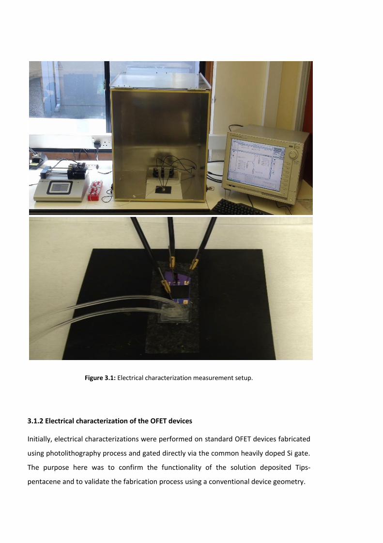
Figure 3.1: Electrical characterization measurement setup.
3.1.2 Electrical characterization of the OFET devices
Initially, electrical characterizations were performed on standard OFET devices fabricated
using photolithography process and gated directly via the common heavily doped Si gate.
The purpose here was to confirm the functionality of the solution deposited Tips-
pentacene and to validate the fabrication process using a conventional device geometry.
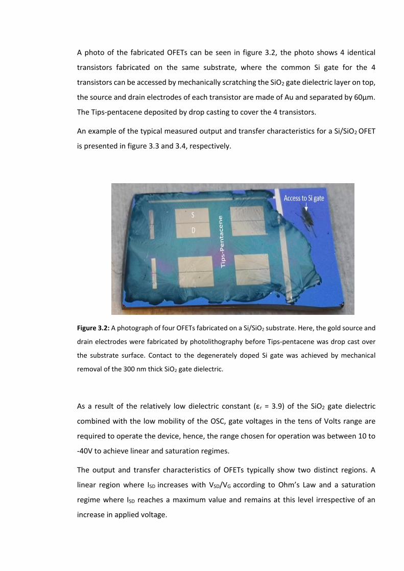
A photo of the fabricated OFETs can be seen in figure 3.2, the photo shows 4 identical
transistors fabricated on the same substrate, where the common Si gate for the 4
transistors can be accessed by mechanically scratching the SiO2 gate dielectric layer on top,
the source and drain electrodes of each transistor are made of Au and separated by 60µm.
The Tips-pentacene deposited by drop casting to cover the 4 transistors.
An example of the typical measured output and transfer characteristics for a Si/SiO2 OFET
is presented in figure 3.3 and 3.4, respectively.
Figure 3.2: A photograph of four OFETs fabricated on a Si/SiO2 substrate. Here, the gold source and
drain electrodes were fabricated by photolithography before Tips-pentacene was drop cast over
the substrate surface. Contact to the degenerately doped Si gate was achieved by mechanical
removal of the 300 nm thick SiO2 gate dielectric.
As a result of the relatively low dielectric constant (εr = 3.9) of the SiO2 gate dielectric
combined with the low mobility of the OSC, gate voltages in the tens of Volts range are
required to operate the device, hence, the range chosen for operation was between 10 to
-40V to achieve linear and saturation regimes.
The output and transfer characteristics of OFETs typically show two distinct regions. A
linear region where ISD increases with VSD/VG according to Ohm’s Law and a saturation
regime where ISD reaches a maximum value and remains at this level irrespective of an
increase in applied voltage.
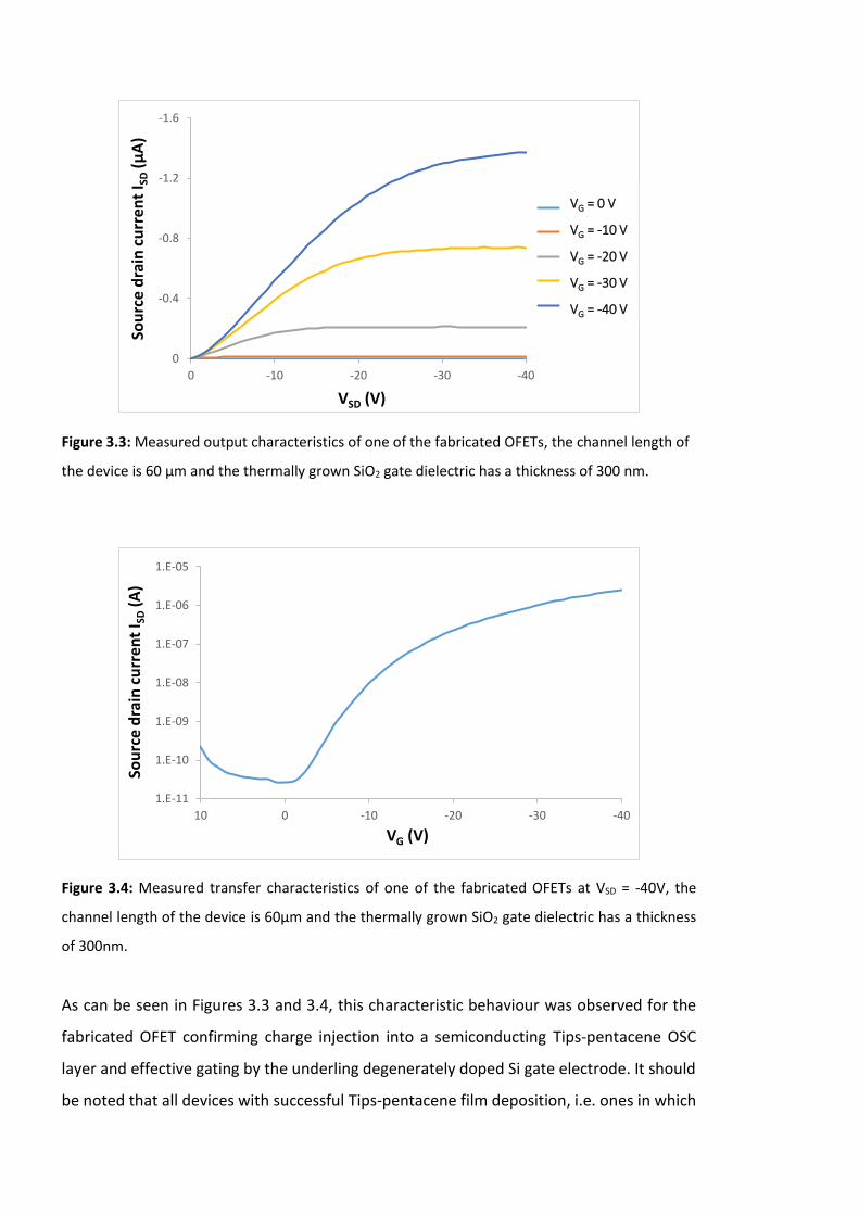
Figure 3.3: Measured output characteristics of one of the fabricated OFETs, the channel length of
the device is 60 µm and the thermally grown SiO2 gate dielectric has a thickness of 300 nm.
Figure 3.4: Measured transfer characteristics of one of the fabricated OFETs at VSD = -40V, the
channel length of the device is 60µm and the thermally grown SiO2 gate dielectric has a thickness
of 300nm.
As can be seen in Figures 3.3 and 3.4, this characteristic behaviour was observed for the
fabricated OFET confirming charge injection into a semiconducting Tips-pentacene OSC
layer and effective gating by the underling degenerately doped Si gate electrode. It should
be noted that all devices with successful Tips-pentacene film deposition, i.e. ones in which
-1.6
-1.2
-0.8
-0.4
0
-40-30-20-100
Sou
rce
dra
in c
urr
ent
I SD
(µA
)
VSD (V)
VG = 0 V
VG = -10 V
VG = -20 V
VG = -30 V
VG = -40 V
VG = 0 V
VG = -10 V
VG = -20 V
VG = -30 V
VG = -40 V
1.E-11
1.E-10
1.E-09
1.E-08
1.E-07
1.E-06
1.E-05
-40-30-20-10010
Sou
rce
dra
in c
urr
ent
I SD
(A)
VG (V)
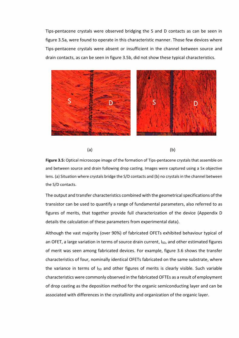
Tips-pentacene crystals were observed bridging the S and D contacts as can be seen in
figure 3.5a, were found to operate in this characteristic manner. Those few devices where
Tips-pentacene crystals were absent or insufficient in the channel between source and
drain contacts, as can be seen in figure 3.5b, did not show these typical characteristics.
(a) (b)
Figure 3.5: Optical microscope image of the formation of Tips-pentacene crystals that assemble on
and between source and drain following drop casting. Images were captured using a 5x objective
lens. (a) Situation where crystals bridge the S/D contacts and (b) no crystals in the channel between
the S/D contacts.
The output and transfer characteristics combined with the geometrical specifications of the
transistor can be used to quantify a range of fundamental parameters, also referred to as
figures of merits, that together provide full characterization of the device (Appendix D
details the calculation of these parameters from experimental data).
Although the vast majority (over 90%) of fabricated OFETs exhibited behaviour typical of
an OFET, a large variation in terms of source drain current, ISD, and other estimated figures
of merit was seen among fabricated devices. For example, figure 3.6 shows the transfer
characteristics of four, nominally identical OFETs fabricated on the same substrate, where
the variance in terms of ISD and other figures of merits is clearly visible. Such variable
characteristics were commonly observed in the fabricated OFTEs as a result of employment
of drop casting as the deposition method for the organic semiconducting layer and can be
associated with differences in the crystallinity and organization of the organic layer.
S S D D
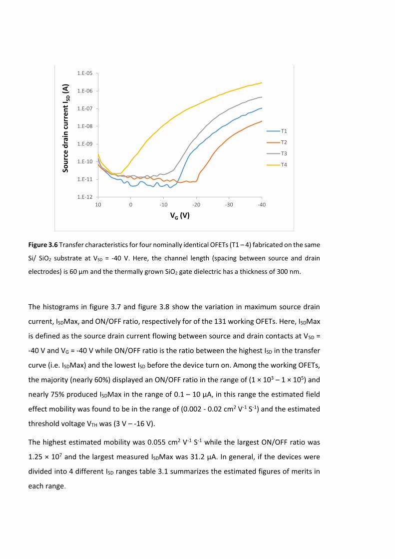
Figure 3.6 Transfer characteristics for four nominally identical OFETs (T1 – 4) fabricated on the same
Si/ SiO2 substrate at VSD = -40 V. Here, the channel length (spacing between source and drain
electrodes) is 60 µm and the thermally grown SiO2 gate dielectric has a thickness of 300 nm.
The histograms in figure 3.7 and figure 3.8 show the variation in maximum source drain
current, ISDMax, and ON/OFF ratio, respectively for of the 131 working OFETs. Here, ISDMax
is defined as the source drain current flowing between source and drain contacts at VSD =
-40 V and VG = -40 V while ON/OFF ratio is the ratio between the highest ISD in the transfer
curve (i.e. ISDMax) and the lowest ISD before the device turn on. Among the working OFETs,
the majority (nearly 60%) displayed an ON/OFF ratio in the range of (1 × 10³ – 1 × 10⁵) and
nearly 75% produced ISDMax in the range of 0.1 – 10 µA, in this range the estimated field
effect mobility was found to be in the range of (0.002 - 0.02 cm2 V-1 S-1) and the estimated
threshold voltage VTH was (3 V – -16 V).
The highest estimated mobility was 0.055 cm2 V-1 S-1 while the largest ON/OFF ratio was
1.25 × 10⁷ and the largest measured ISDMax was 31.2 µA. In general, if the devices were
divided into 4 different ISD ranges table 3.1 summarizes the estimated figures of merits in
each range.
1.E-12
1.E-11
1.E-10
1.E-09
1.E-08
1.E-07
1.E-06
1.E-05
-40-30-20-10010
Sou
rce
dra
in c
urr
ent
I SD
(A)
VG (V)
T1
T2
T3
T4
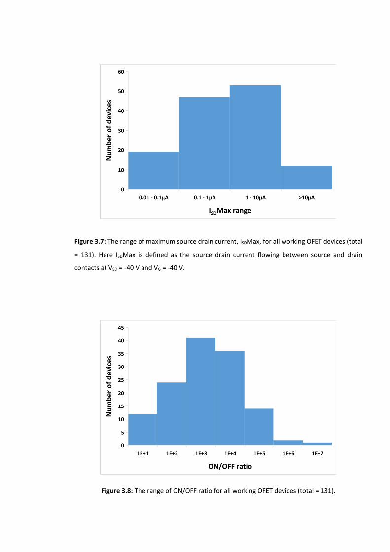
Figure 3.7: The range of maximum source drain current, ISDMax, for all working OFET devices (total
= 131). Here ISDMax is defined as the source drain current flowing between source and drain
contacts at VSD = -40 V and VG = -40 V.
Figure 3.8: The range of ON/OFF ratio for all working OFET devices (total = 131).
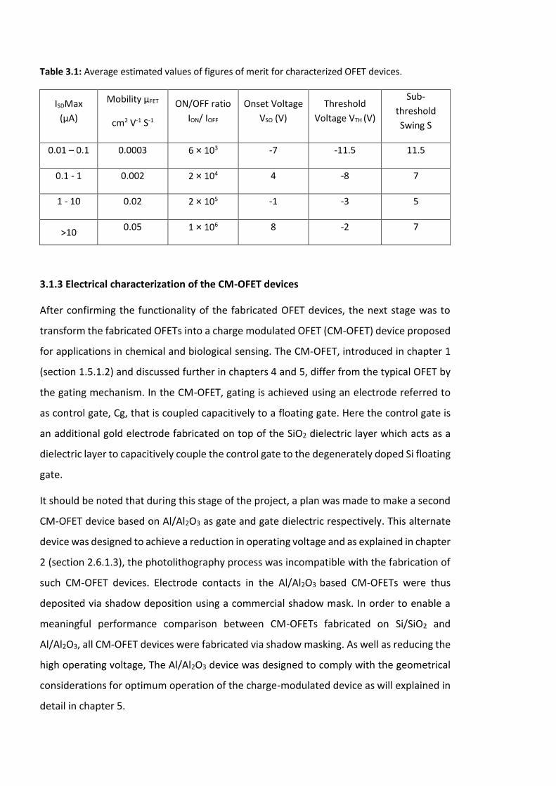
Table 3.1: Average estimated values of figures of merit for characterized OFET devices.
ISDMax
(µA)
Mobility µFET
cm2 V-1 S-1
ON/OFF ratio
ION/ IOFF
Onset Voltage
VSO (V)
Threshold
Voltage VTH (V)
Sub-
threshold
Swing S
0.01 – 0.1 0.0003 6 × 10³ -7 -11.5 11.5
0.1 - 1 0.002 2 × 10⁴ 4 -8 7
1 - 10 0.02 2 × 10⁵ -1 -3 5
>10 0.05 1 × 10⁶ 8 -2 7
3.1.3 Electrical characterization of the CM-OFET devices
After confirming the functionality of the fabricated OFET devices, the next stage was to
transform the fabricated OFETs into a charge modulated OFET (CM-OFET) device proposed
for applications in chemical and biological sensing. The CM-OFET, introduced in chapter 1
(section 1.5.1.2) and discussed further in chapters 4 and 5, differ from the typical OFET by
the gating mechanism. In the CM-OFET, gating is achieved using an electrode referred to
as control gate, Cg, that is coupled capacitively to a floating gate. Here the control gate is
an additional gold electrode fabricated on top of the SiO2 dielectric layer which acts as a
dielectric layer to capacitively couple the control gate to the degenerately doped Si floating
gate.
It should be noted that during this stage of the project, a plan was made to make a second
CM-OFET device based on Al/Al2O3 as gate and gate dielectric respectively. This alternate
device was designed to achieve a reduction in operating voltage and as explained in chapter
2 (section 2.6.1.3), the photolithography process was incompatible with the fabrication of
such CM-OFET devices. Electrode contacts in the Al/Al2O3 based CM-OFETs were thus
deposited via shadow deposition using a commercial shadow mask. In order to enable a
meaningful performance comparison between CM-OFETs fabricated on Si/SiO2 and
Al/Al2O3, all CM-OFET devices were fabricated via shadow masking. As well as reducing the
high operating voltage, The Al/Al2O3 device was designed to comply with the geometrical
considerations for optimum operation of the charge-modulated device as will explained in
detail in chapter 5.
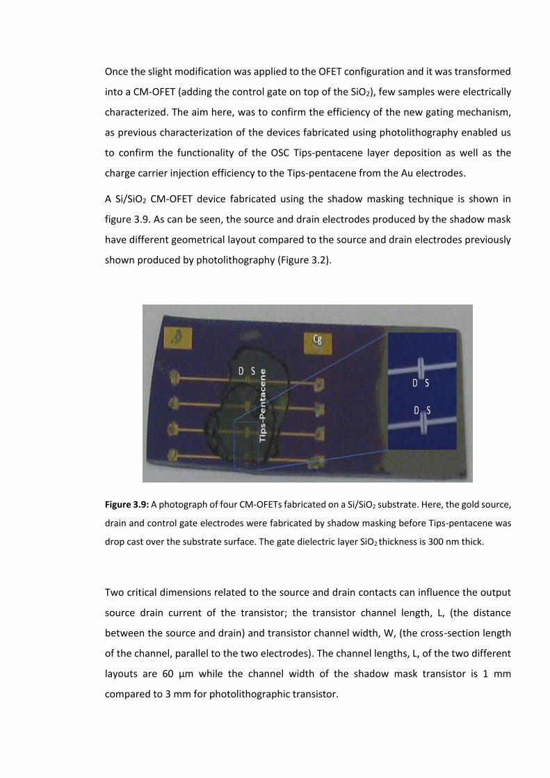
Once the slight modification was applied to the OFET configuration and it was transformed
into a CM-OFET (adding the control gate on top of the SiO2), few samples were electrically
characterized. The aim here, was to confirm the efficiency of the new gating mechanism,
as previous characterization of the devices fabricated using photolithography enabled us
to confirm the functionality of the OSC Tips-pentacene layer deposition as well as the
charge carrier injection efficiency to the Tips-pentacene from the Au electrodes.
A Si/SiO2 CM-OFET device fabricated using the shadow masking technique is shown in
figure 3.9. As can be seen, the source and drain electrodes produced by the shadow mask
have different geometrical layout compared to the source and drain electrodes previously
shown produced by photolithography (Figure 3.2).
Figure 3.9: A photograph of four CM-OFETs fabricated on a Si/SiO2 substrate. Here, the gold source,
drain and control gate electrodes were fabricated by shadow masking before Tips-pentacene was
drop cast over the substrate surface. The gate dielectric layer SiO2 thickness is 300 nm thick.
Two critical dimensions related to the source and drain contacts can influence the output
source drain current of the transistor; the transistor channel length, L, (the distance
between the source and drain) and transistor channel width, W, (the cross-section length
of the channel, parallel to the two electrodes). The channel lengths, L, of the two different
layouts are 60 µm while the channel width of the shadow mask transistor is 1 mm
compared to 3 mm for photolithographic transistor.
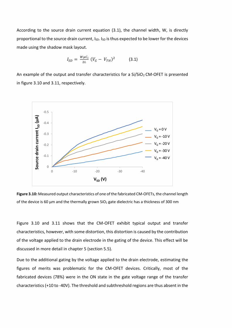
According to the source drain current equation (3.1), the channel width, W, is directly
proportional to the source drain current, ISD. ISD is thus expected to be lower for the devices
made using the shadow mask layout.
𝐼𝑆𝐷 = 𝑊𝜇𝐶𝑖
2𝐿 (𝑉𝐺 − 𝑉𝑇𝐻)
2 (3.1)
An example of the output and transfer characteristics for a Si/SiO2 CM-OFET is presented
in figure 3.10 and 3.11, respectively.
Figure 3.10: Measured output characteristics of one of the fabricated CM-OFETs, the channel length
of the device is 60 µm and the thermally grown SiO2 gate dielectric has a thickness of 300 nm
Figure 3.10 and 3.11 shows that the CM-OFET exhibit typical output and transfer
characteristics, however, with some distortion, this distortion is caused by the contribution
of the voltage applied to the drain electrode in the gating of the device. This effect will be
discussed in more detail in chapter 5 (section 5.5).
Due to the additional gating by the voltage applied to the drain electrode, estimating the
figures of merits was problematic for the CM-OFET devices. Critically, most of the
fabricated devices (78%) were in the ON state in the gate voltage range of the transfer
characteristics (+10 to -40V). The threshold and subthreshold regions are thus absent in the
-0.5
-0.4
-0.3
-0.2
-0.1
0
-40-30-20-100
Sou
rce
dra
in c
urr
ent
I SD
(µA
)
VSD (V)
VG = 0 V
VG = -10 V
VG = -20 V
VG = -30 V
VG = -40 V
VG = 0 V
VG = -10 V
VG = -20 V
VG = -30 V
VG = -40 V

operating window of the transfer characteristics and hence the estimation of the figures of
merits will be imprecise.
Figure 3.11: Measured transfer characteristics of one of the fabricated CM-OFETs at VSD = -40V, the
channel length of the device is 60µm and the thermally grown SiO2 gate dielectric has a thickness
of 300nm.
For the Characterized CM-OFET devices, the range of maximum source drain current ISDMax
achieved is illustrated in figure 3.12. If the lowest ISD current from the transfer
characteristics for tested devices was considered as the OFF ISD current (here normally the
first point in the transfer characteristic curve), then the estimated range of ON/OFF ratio
for the tested CM-OFET devices is between 2 × 101 to 2.6 × 10⁴ and the mobility range is
0.0002 to 0.014 cm2 V-1 S-1. However, these figures are not accurate.
Due to the difficulty in estimating the figures of merits for the CM-OFET device, it is clear
that these calculated values would not be an accurate method of quantifying the sensing
activity of the CM-OFETs. Despite this difficulty, the response of the device to sensing
activities that will be investigated in next chapters can be demonstrated in terms of the
change in the source drain current, this in fact could be more reliable as the response is
quantified by real measured values rather than estimated ones. Moreover, the change in
measured source drain current can be related to the change in the threshold voltage which
is the figure of interest as will be explained next section.
1.E-08
1.E-07
1.E-06
-40-30-20-10010
Sou
rce
dra
in c
urr
ent
I SD
(A)
VG (V)
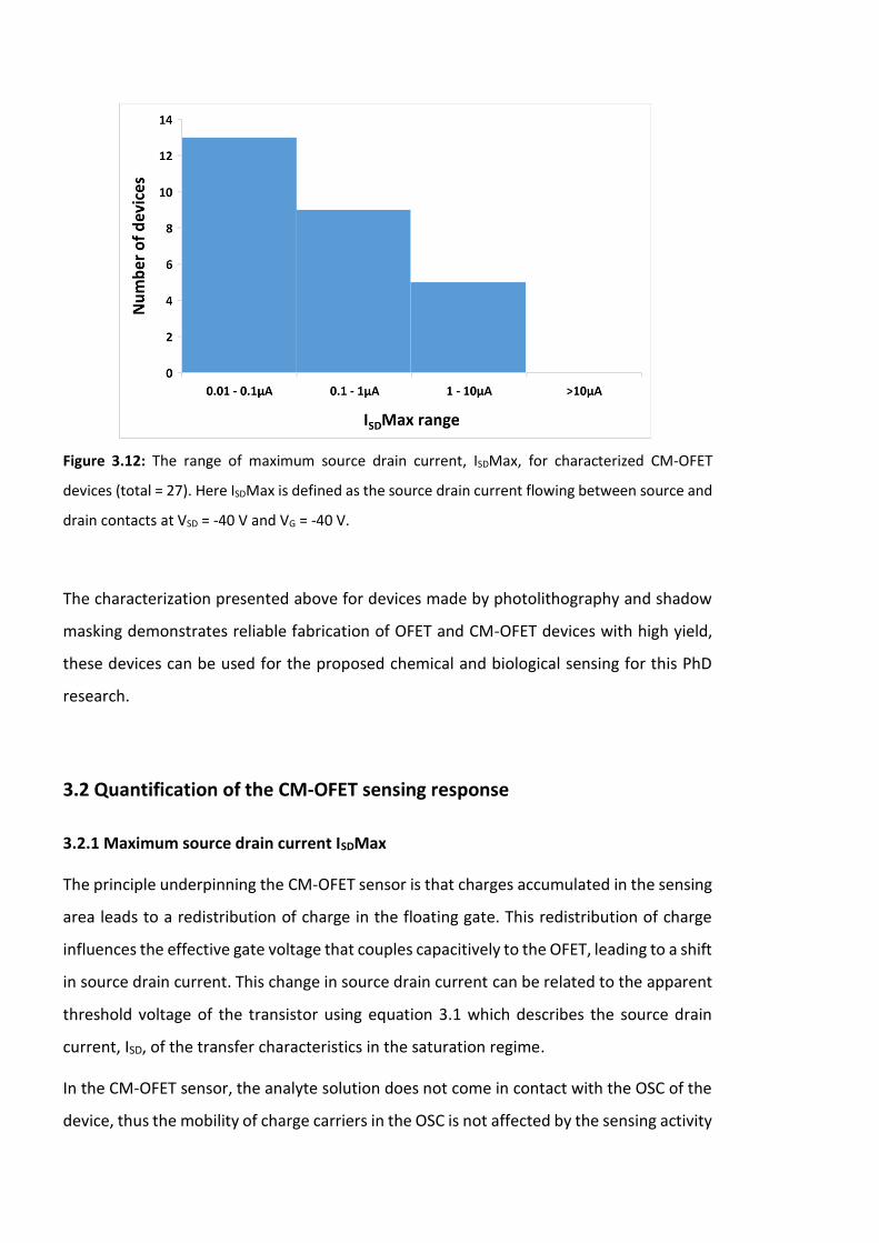
Figure 3.12: The range of maximum source drain current, ISDMax, for characterized CM-OFET
devices (total = 27). Here ISDMax is defined as the source drain current flowing between source and
drain contacts at VSD = -40 V and VG = -40 V.
The characterization presented above for devices made by photolithography and shadow
masking demonstrates reliable fabrication of OFET and CM-OFET devices with high yield,
these devices can be used for the proposed chemical and biological sensing for this PhD
research.
3.2 Quantification of the CM-OFET sensing response
3.2.1 Maximum source drain current ISDMax
The principle underpinning the CM-OFET sensor is that charges accumulated in the sensing
area leads to a redistribution of charge in the floating gate. This redistribution of charge
influences the effective gate voltage that couples capacitively to the OFET, leading to a shift
in source drain current. This change in source drain current can be related to the apparent
threshold voltage of the transistor using equation 3.1 which describes the source drain
current, ISD, of the transfer characteristics in the saturation regime.
In the CM-OFET sensor, the analyte solution does not come in contact with the OSC of the
device, thus the mobility of charge carriers in the OSC is not affected by the sensing activity
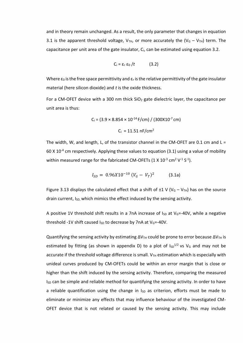
and in theory remain unchanged. As a result, the only parameter that changes in equation
3.1 is the apparent threshold voltage, VTH, or more accurately the (VG – VTH) term. The
capacitance per unit area of the gate insulator, Ci, can be estimated using equation 3.2.
Ci = εr ε0 /t (3.2)
Where ε0 is the free space permittivity and εr is the relative permittivity of the gate insulator
material (here silicon dioxide) and t is the oxide thickness.
For a CM-OFET device with a 300 nm thick SiO2 gate dielectric layer, the capacitance per
unit area is thus:
Ci = (3.9 × 8.854 × 10-14 F/cm) / (300X10-7 cm)
Ci = 11.51 nF/cm2
The width, W, and length, L, of the transistor channel in the CM-OFET are 0.1 cm and L =
60 X 10-4 cm respectively. Applying these values to equation (3.1) using a value of mobility
within measured range for the fabricated CM-OFETs (1 X 10⁻³ cm2 V-1 S-1).
𝐼𝑆𝐷 = 0.96𝑋10−10 (𝑉𝐺 − 𝑉𝑇)2 (3.1a)
Figure 3.13 displays the calculated effect that a shift of ±1 V (VG – VTH) has on the source
drain current, ISD, which mimics the effect induced by the sensing activity.
A positive 1V threshold shift results in a 7nA increase of ISD at VG=-40V, while a negative
threshold -1V shift caused ISD to decrease by 7nA at VG=-40V.
Quantifying the sensing activity by estimating ΔVTH could be prone to error because ΔVTH is
estimated by fitting (as shown in appendix D) to a plot of ISD1/2
vs VG and may not be
accurate if the threshold voltage difference is small. VTH estimation which is especially with
unideal curves produced by CM-OFETs could be within an error margin that is close or
higher than the shift induced by the sensing activity. Therefore, comparing the measured
ISD can be simple and reliable method for quantifying the sensing activity. In order to have
a reliable quantification using the change in ISD as criterion, efforts must be made to
eliminate or minimize any effects that may influence behaviour of the investigated CM-
OFET device that is not related or caused by the sensing activity. This may include
environmental conditions in which the measurement is carried out in as will be explained
in the following section.
Figure 3.13: Effect of ±1V gate voltage range shift on the ISD of a transfer characteristic, (inset) shows
the difference between ISDMax. (simulated curves for Si/SiO2 CM-OFET device with W = 0.1 cm, L =
60 X 10-4 cm, Ci = 11.51nF/cm2 and µ = 1 X 10⁻³ cm2 V-1 S-1).
3.3 Environmental considerations
All electrical measurements to characterize fabricated CM-OFETs were performed in
ambient conditions, however, some measures were taken in order to minimise external
interference and to ensure that the devices are not influenced by undesirable effects during
measurements.
3.3.1 Electrical noise:
In order to reduce electrical interference due to electrostatic and electromagnetic fields
generated from surrounding equipment in the laboratory, all measurements were
conducted inside a grounded Faraday cage, as can be seen in the setup of figure 3.1.
3.3.2 Temperature:
The mobility of charge carriers in OSCs, including those in Tips-pentacene, is known to be
temperature dependant [1-4] since carrier transport occurs through hopping between
localized states in the OSC which can be thermally activated. However, depending on the
type of OSC film the temperature dependency of mobility may differ. For example, some
OSCs exhibit an Arrhenius dependency (µ α exp(-1/T)), while others show a non-Arrhenius
behaviour (for example µ α exp(-1/T2)). For polycrystalline films like Tips-pentacene films,
the mobility is widely considered to exhibit an Arrhenius temperature dependency [3,5].
Nonetheless, in order to minimize the effect of temperature on the CM-OFETs, all
measurements were performed in a laboratory environment in which the room
temperature was regulated at 20 ± 1 °C.
3.3.2.1 Self device heating
Device heating during measurement is generally considered tolerable during short term,
discrete I-V measurements of organic transistors. The so-called self-heating or joule-
heating effect is normally only investigated for long-term device operation when
performing continuous scanning or prolong transistor biasing. However, recent
enhancements in organic semiconductor mobilities means that self-heating levels similar
to those observed in inorganic electronics might be reached even for short term operation,
particularly if a large operating voltage is used.
A recent study by Nikiforov et.al. [6] investigated real-time temperature evolution in the
channel region of Tips-pentacene transistor during I-V scans. Using a platinum (Pt)
resistance temperature sensor they monitored the channel temperature during I-V
measurements under various conditions. Although the experiment was conducted in low
to near room temperatures, these measurements confirmed that the extent of self-heating
depends on the substrate material of the transistor. For example, a significant amount of
self-heating could develop during I-V measurements at large fields on high mobility Tips-
pentacene OFTs if substrates with low thermal conductivity such as glass or polymer are
used. However, the use of a more heat conducting substrate such as doped silicon can
largely minimize the heating effect and hence self-heating becomes negligible. According
to their study, even at 278 K base temperature the transistor channel temperature
increased by less than 3 K at VSD -40 V and VG = -40 V and at room temperature no significant
Joule heating induced current is observed for Tips-pentacene devices on Si/SiO2 substrates.
It must be noted that the mobility in the devices they have fabricated was 0.9 cm2 V-1 S-1
which is much higher than the mobility achieved in our fabricated devices, therefore joules
heating effect on our fabricated devices is expected to be insignificant.
In fact, the amount of temperature increase in the OSC Tips-pentacene channel for
fabricated CM-OFET devices can be estimated using Nikiforov et.al. Current-Induced Joule
Heating model. In the model they derived an equation (3.3) describing the dissipated
power-heating relationship in the transistor. The equation clearly show the significant
influence of the thermal conductivities and thicknesses of both the OSC layer (Tips-
pentacene) and the substrate on the transistor channel heating.
𝐻 = 𝛥𝑇 (3
8 𝑑2𝑇𝑖𝑝𝑠
𝜅𝑇𝑖𝑝𝑠+
𝑑𝑇𝑖𝑝𝑠𝑑𝑠𝑢𝑏
𝜅𝑠𝑢𝑏)
−1
(3.3)
Where 𝛥T = (T[dTips/2] - Tsub) , T[dTips/2] is temperature in the middle of the Tips-pentacene
layer and Tsub = substrate temperature (approximately the room temperature). dTips and
dsub are the Tips-pentacene and substrate thicknesses, respectively, 𝜅Tips and 𝜅sub are
thermal conductivities of Tips-pentacene and the substrate, respectively, and H is the
dissipated power per unit volume and is calculated by:
𝐻 = 𝐼𝑆𝐷𝑉𝑆𝐷𝑊𝐿𝑑𝑇𝑖𝑝𝑠
(3.4)
Considering 𝜅Tips = 0.1±0.009 W.m-1.K-1 [7] and 𝜅sub (Si) = 149 ×10-2 W.cm-1.K-1 [6], feeding
the known parameters’ values for the fabricated CM-OFETs dsub = 525 µm, L= 60 µm, W = 1
mm and the Tips-pentacene thickness dTips is expected to be 0.1 - 1 µm combined with the
measured power enable the estimation of heating for any of the fabricated devices.
Figure 3.14 shows the power dissipated during an I-V measurement of one of the fabricated
CM-OFET devices (defined as ISD × VSD), the power consumed ranges from 0.07 to 85µW
across the transfer curve and the total accumulated dissipated power during the whole
measurement was 1.64 mW. Therefore utilizing equation 3.3 and 3.4 for dTips 0.1 -1 µm, the
rise in temperature 𝛥T is only ≈ 0.11 – 0.2 K which is insignificant particularly considering
that the margin of environment temperature change is ± 1 degree.
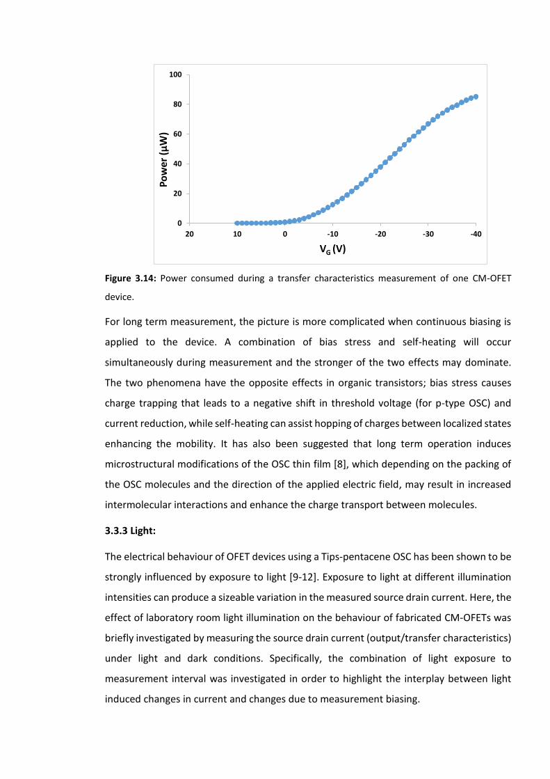
Figure 3.14: Power consumed during a transfer characteristics measurement of one CM-OFET
device.
For long term measurement, the picture is more complicated when continuous biasing is
applied to the device. A combination of bias stress and self-heating will occur
simultaneously during measurement and the stronger of the two effects may dominate.
The two phenomena have the opposite effects in organic transistors; bias stress causes
charge trapping that leads to a negative shift in threshold voltage (for p-type OSC) and
current reduction, while self-heating can assist hopping of charges between localized states
enhancing the mobility. It has also been suggested that long term operation induces
microstructural modifications of the OSC thin film [8], which depending on the packing of
the OSC molecules and the direction of the applied electric field, may result in increased
intermolecular interactions and enhance the charge transport between molecules.
3.3.3 Light:
The electrical behaviour of OFET devices using a Tips-pentacene OSC has been shown to be
strongly influenced by exposure to light [9-12]. Exposure to light at different illumination
intensities can produce a sizeable variation in the measured source drain current. Here, the
effect of laboratory room light illumination on the behaviour of fabricated CM-OFETs was
briefly investigated by measuring the source drain current (output/transfer characteristics)
under light and dark conditions. Specifically, the combination of light exposure to
measurement interval was investigated in order to highlight the interplay between light
induced changes in current and changes due to measurement biasing.
0
20
40
60
80
100
-40-30-20-1001020
Po
wer
(µ
W)
VG (V)

Here, the laboratory room light consists of fluorescent illumination. Unlike incandescent
light which gives a continuous spectrum, fluorescent light gives discrete lines typical of the
combined spectrum of mercury and phosphor. The spectrum of light differs depending on
the type phosphor material used however, peaks in light intensity are typically observed in
the blue region of the spectrum, with less at green and red wavelengths. The decorative
plastic covers covering the lamp may also affect the spectrum. The spectrum of the
laboratory fluorescent lights is shown in figure 3.15, with large spikes at 436 nm (violet)
and 546 nm (green) which correspond to 2.84 eV and 2.27 eV respectively and two smaller
peaks one at 404 nm (violet) and 577 nm (yellow), corresponding to 3.07 eV and 2.15 eV
respectively, all these energies are higher than the energy band gap between the HOMO
and LUMO levels reported for Tips-pentacene (<2 eV) [13-14].
It must be mentioned that while the intensity of the light was low, the effect on the CM-
OFET behaviour was evident as will be discussed in the next experiment.
Figure 3.15: spectrum of laboratory fluorescent light measured at the position of the tested CM-
OFET devices.
For each of the tested CM-OFET devices, the source drain current was measured
periodically under transition from light to dark and back to light. The effect of the transition
between light and dark on the source drain current was examined by recording the transfer
characteristics first every 25 minutes between successive measurement and then with a 5
minute interval.
-0.005
0.005
0.015
0.025
0.035
320 360 400 440 480 520 560 600 640 680 720 760 800
Po
wer
(a.
u.)
Wavelength (nm)
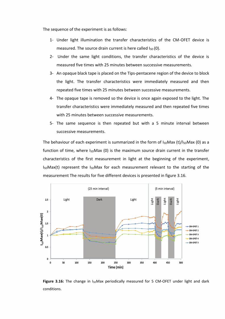
The sequence of the experiment is as follows:
1- Under light illumination the transfer characteristics of the CM-OFET device is
measured. The source drain current is here called ISD (0).
2- Under the same light conditions, the transfer characteristics of the device is
measured five times with 25 minutes between successive measurements.
3- An opaque black tape is placed on the Tips-pentacene region of the device to block
the light. The transfer characteristics were immediately measured and then
repeated five times with 25 minutes between successive measurements.
4- The opaque tape is removed so the device is once again exposed to the light. The
transfer characteristics were immediately measured and then repeated five times
with 25 minutes between successive measurements.
5- The same sequence is then repeated but with a 5 minute interval between
successive measurements.
The behaviour of each experiment is summarized in the form of ISDMax (t)/ISDMax (0) as a
function of time, where ISDMax (0) is the maximum source drain current in the transfer
characteristics of the first measurement in light at the beginning of the experiment,
ISDMax(t) represent the ISDMax for each measurement relevant to the starting of the
measurement The results for five different devices is presented in figure 3.16.
Figure 3.16: The change in ISDMax periodically measured for 5 CM-OFET under light and dark
conditions.
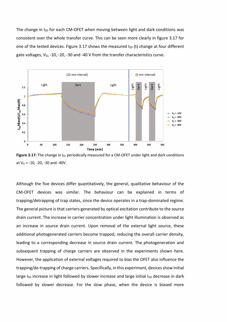
The change in ISD for each CM-OFET when moving between light and dark conditions was
consistent over the whole transfer curve. This can be seen more clearly in figure 3.17 for
one of the tested devices. Figure 3.17 shows the measured ISD (t) change at four different
gate voltages, VG, -10, -20, -30 and -40 V from the transfer characteristics curve.
Figure 3.17: The change in ISD periodically measured for a CM-OFET under light and dark conditions
at VG = -10, -20, -30 and -40V.
Although the five devices differ quantitatively, the general, qualitative behaviour of the
CM-OFET devices was similar. The behaviour can be explained in terms of
trapping/detrapping of trap states, since the device operates in a trap-dominated regime.
The general picture is that carriers generated by optical excitation contribute to the source
drain current. The increase in carrier concentration under light illumination is observed as
an increase in source drain current. Upon removal of the external light source, these
additional photogenerated carriers become trapped, reducing the overall carrier density,
leading to a corresponding decrease in source drain current. The photogeneration and
subsequent trapping of charge carriers are observed in the experiments shown here.
However, the application of external voltages required to bias the OFET also influence the
trapping/de-trapping of charge carriers. Specifically, in this experiment, devices show Initial
large ISD increase in light followed by slower increase and large initial ISD decrease in dark
followed by slower decrease. For the slow phase, when the device is biased more
frequently (short intervals between measurements), the rate of change in ISD
(increase/decrease) is smaller than when there is a long interval between measurements.
The influence of optical excitation and bias on carrier concentration is discussed in detail
below.
Under illumination (light):
Electrons and holes are photogenerated rapidly within the OSC layer upon exposure to an
external optical source. With an electric field applied (i.e. with the transistor biased), the
electrons and holes will separate and, because of the direction of the source-drain electric
field (here, negative drain voltage), the holes drift through the OSC and contribute to the
charge transport while the electrons are thought to accumulate at the OSC/gate dielectric
interface where they become trapped. With a SiO2 dielectric layer, the electrons are
trapped by hydroxyl groups on the SiO2 surface. These traps are believed to be deep (i.e.
the energy required to release them is much greater than the thermal energy) such
electrons remain trapped for a sufficiently long time to influence subsequent
measurements [15-20].
Initially, the space charge electric field associated with the trapped electrons can reduce
the injection barrier at the source electrode. This reduction in barrier height accounts for
the large increase in ISD. However, if the device remains under photoexcitation, these
trapped electrons can play additional roles that modulate the source drain current. For
example, the trapped electrons can restrain the release of additional holes, it can also
increase the extraction barrier at the drain electrode. This latter effect is caused by the
accumulation of excess holes at the drain electrode, where holes can experience Coulomb
repulsion or increased recombination before extraction. As a result, the increase in source
drain current reduces between successive measurements [18,21-23].
The reduced source drain current increment under continuous optical excitation (after the
initial large increment) is more pronounced when the time interval between
measurements reduces, as can be seen in figure 3.16 where the increase in ISD between
measurements performed every 5 minutes is smaller than the case where measurements
are performed every 25 minutes. The possible explanation is that with less time between
measurement, lesser number of holes experience trapping when they are injected by the
source electrode in the following measurement and therefore, rapid higher holes
concentration near the drain electrode can be expected and higher probability of Coulomb
repulsion or recombination.
Without illumination (dark):
The current decay following removal of direct illumination is generally explained by a
combination of fast and slow trapping of free holes. Fast trapping of free holes occurs at
deep trap states located at grain boundaries. These trapped holes reduce the trapping rate
of remaining free holes, evidenced by a slow decay in ISD after an initial large decay.
Another phenomenon that can contribute to the slow decay in ISD, is the slow release of
trapped electrons that have accumulated at the OSC/dielectric interface during light
exposure. This can lead to a reduction in the trapping of injected holes due to the electric
field associated with remaining trapped electrons [18-19,21,23-27]. Furthermore, it is also
possible that the when transistor is biased, holes injected into the OSC may form excitons
by coulombic attraction to the trapped electrons. These generated excitons may exhibit a
long lifetime and can thus influence charge transport in subsequent measurements. The
combination of these effects contributes to the observed slow decay of the source drain
current.
With a long duration between successive measurements (i.e. with infrequent biasing of the
transistor), it is thus expected there will be an increase in trapping of free holes generated
during the previous measurement alongside an increase in the number of electrons
released from the interfacial trap states. Both of these effects will lead to a reduction in
free holes, and thus a large decrease in source drain current between successive
measurements.
In contrast, as the time interval between successive measurements reduces, fewer
electrons are released from trap states, leading to a reduction in trapping of the current
carrying free hole (i.e. there will be a higher density of holes that can contribute to ISD).
As for holes, It can be said that the rate of trapping decreases with time, this is because,
when traps with shorter time constants are filled, the time constants associated with the
remaining empty traps becomes longer, therefore, frequently filling trap states by injected
carriers (generated by the electric field applied during measurements) can further increase
the time constant related to trapping free charges. Therefore, the current decay is slower
when the time interval between measurements is shorter and vice versa.
The results shown in figure 3.16 indicate that influence of photoexcited charge carriers
(either free or trapped) must be considered when operating the CM-OFET device for
sensing applications. Furthermore, the influence of these free and trapped carriers can last
for a significant time after a change in light conditions, for example after placing in the dark.
This residual effect needs to be minimized, or ideally eliminated before using the device for
any sensing application. As has been shown, the rate at which the CM-OFET current reaches
steady state upon moving to different illumination conditions depends on the frequency
with which the transistor is biased. Furthermore, the relative difference in the decay in ISD
upon removal of external illumination between nominally identical devices can be
attributed to the randomness of Tips-pentacene formation in drop casting deposition. It
may thus be necessary that the minimization of the effect of light on the CM-OFETs needs
to be considered for each device individually. This will be discussed further in chapter 4
section (4.4.2).
3.4 Conclusions
This chapter has presented experimental characterization of the fabricated CM-OFET
devices, focussing on electrical characterization using the conventional output and transfer
characteristics. Preliminary characterization was performed on OFET-like structure devices
produced by photolithography in which gating of the OFET was achieved through the silicon
bottom-gate. To assess and optimize the fabrication protocol and to validate the efficiency
of the charge injection to the Tips-pentacene, a large number of OFET devices were
fabricated and characterized and the results demonstrate successful fabrication of working
OFETs with over 90% yield, however, with large variations between devices. For example,
a wide range of charge carrier mobility was achieved across devices (0.0002 - 0.055 cm2 V-
1 S-1). Variations between devices is related to the drop-casting method employed for
deposition of the Tips-pentacene layer. Following successful fabrication of OFET devices,
the fabrication CM-OFET devices was demonstrated in which gating is achieved through a
capacitively coupled control gate. Here, fabrication was performed using a shadow masking
technique. Electrical characterization of a number of CM-OFETs showed that while they
exhibited transistor-like behaviour, a distortion in the output and transfer characteristics
was observed that was attributed to the contribution of the drain voltage on the gating of
the CM-OFET devices. Again, it was demonstrated that the approach adopted for
fabrication of the CM-OFET devices was effective. Variation between nominally identical
CM-OFETs was also observed, with the saturation current varying between 18nA and 3.9µA
for functioning devices, variations are ascribed to differences in the OSC layer as a result of
the drop-casting deposition method as well. Despite the distortion in the output and
transfer characteristics of CM-OFET devices, it was demonstrated that such devices can be
employed for sensing application and the sensing activity can be quantified by the change
in the source drain current at the maximum point in the transfer characteristics curve.
Finally, the chapter highlighted several factors relating to the measurement environment
that must be considered for reliable and consistent operation of the CM-OFET. Critically,
the influence of light on the behaviour of the CM-OFET was discussed in detail, highlighting
the importance of controlling ambient light in order to minimize its effect on the CM-OFET.
3.5 References
[1] Meneau, A. Y., Olivier, Y., Backlund, T., James, M., Breiby, D. W., Andreasen, J. W., &
Sirringhaus, H. (2016). Temperature Dependence of Charge Localization in High‐Mobility,
Solution‐Crystallized Small Molecule Semiconductors Studied by Charge Modulation
Spectroscopy. Advanced Functional Materials, 26(14), 2326-2333.
[2] Worne, J. H., Anthony, J. E., & Natelson, D. (2010). Transport in organic semiconductors
in large electric fields: From thermal activation to field emission. Applied physics
letters, 96(5), 24.
[3] Coropceanu, V., Cornil, J., da Silva Filho, D. A., Olivier, Y., Silbey, R., & Brédas, J. L. (2007).
Charge transport in organic semiconductors. Chemical reviews, 107(4), 926-952
[4] Zhu, M., Liang, G., Cui, T., & Varahramyan, K. (2005). Temperature and field dependent
mobility in pentacene-based thin film transistors. Solid-state electronics, 49(6), 884-888.
[5] Craciun, N. I., Wildeman, J., & Blom, P. W. M. (2008). Universal Arrhenius temperature
activated charge transport in diodes from disordered organic semiconductors. Physical
review letters, 100(5), 056601.
[6] Nikiforov, G. O., Venkateshvaran, D., Mooser, S., Meneau, A., Strobel, T., Kronemeijer,
A., ... & Sirringhaus, H. (2016). Current‐Induced Joule Heating and Electrical Field Effects in
Low Temperature Measurements on TIPS Pentacene Thin Film Transistors. Advanced
Electronic Materials, 2(12), 1600163.
[7] Yao, Y., Shahi, M., Payne, M. M., Anthony, J. E., & Brill, J. W. (2016). Thermal
resistances of thin films of small molecule organic semiconductors. Journal of Materials
Chemistry C, 4(37), 8817-8821.
[8] Cheng, H. L., Chou, W. Y., Kuo, C. W., Wang, Y. W., Mai, Y. S., Tang, F. C., & Chu, S. W.
(2008). Influence of Electric Field on Microstructures of Pentacene Thin‐Films in Field‐Effect
Transistors. Advanced Functional Materials, 18(2), 285-293.
[9] Bharti, D., Raghuwanshi, V., Varun, I., Mahato, A. K., & Tiwari, S. P. (2017). Photo-
Response of Low Voltage Flexible Tips-pentacene Organic Field-Effect Transistors. IEEE
Sensors Journal, 17(12), 3689-3697.
[10] Park, J., Kim, D. W., Lee, B. K., Jeong, Y. S., Petty, M., Choi, J. S., & Do, L. M. (2013).
Light-Exposure Effects on Electrical Characteristics of 6, 13-Bis (triisopropylsilylethynyl)
Pentacene/CdTe Composite Thin-Film Transistors. Japanese Journal of Applied
Physics, 52(5S1), 05DC12.
[11] Jouili, A., Mansouri, S., Al-Ghamdi, A., El Mir, L., & Yakuphanoglu, F. (2016). Controlling
of DOS of TFTs based 6, 13-bis (triisopropylsilylethynyl) pentacene by solar light
illumination. Synthetic Metals, 220, 591-598.
[12] Park, J. G., Vasic, R., Brooks, J. S., & Anthony, J. E. (2005). Functionalized pentacene
field-effect transistors with logic circuit applications. arXiv preprint cond-mat/0510317.
[13] Griffith, O. L., Anthony, J. E., Jones, A. G., & Lichtenberger, D. L. (2009). Electronic
properties of pentacene versus triisopropylsilylethynyl-substituted pentacene:
Environment-dependent effects of the silyl substituent. Journal of the American Chemical
Society, 132(2), 580-586.
[14] Gunduz, B., & Yakuphanoglu, F. (2012). Effects of UV and white light illuminations on
photosensing properties of the 6, 13-bis (triisopropylsilylethynyl) pentacene thin film
transistor. Sensors and Actuators A: Physical, 178, 141-153.
[15] Han, T., Liu, L., Wei, M., Wang, C., Wu, X., Xie, Z., & Ma, Y. (2017). Light-activated
electric bistability for evaporated silver nanoparticles in organic field-effect
transistors. Physical Chemistry Chemical Physics, 19(27), 17653-17660.
[16] Ostroverkhova, O., Platt, A. D., & Shepherd, W. E. (2010). Optical, Photoluminescent,
and Photoconductive Properties of Novel High-Performance Organic Semiconductors.
In Advances in Lasers and Electro Optics. IntechOpen.
[17] Plugaru, R., Anghel, C., & Ionescu, A. M. (2007). Charge carriers photogeneration in
pentacene field effect transistors. SCIENCE AND TECHNOLOGY, 10(3), 233-241.
[18] Zhou, T. C., Chen, G., Liao, R. J., & Xu, Z. (2011). Charge trapping and detrapping in
polymeric materials: Trapping parameters. Journal of Applied Physics, 110(4), 043724.
[19] Noh, Y. Y., Ghim, J., Kang, S. J., Baeg, K. J., Kim, D. Y., & Yase, K. (2006). Effect of light
irradiation on the characteristics of organic field-effect transistors. Journal of applied
physics, 100(9), 094501.
[20] Liguori, R. (2014). A Study on Defects in Organic Semiconductors for Field Effect
Transistors.
[21] Häusermann, R. (2013). Fast and slow charge trapping and transport in organic
semicondutors (Doctoral dissertation, ETH Zurich).
[22] Liu, B., Xu, F., Zhang, X., Yan, D., & Lu, D. (2015). Influence of extraction barrier on the
loss process of photogenerated charge carrier in polymer bulk heterojunction solar
cells. Chemical Research in Chinese Universities, 31(5), 809-813.
[23] Mansouri, S., Jouili, A., El Mir, L., Al-Ghamdi, A. A., & Yakuphanoglu, F. (2015). Studies
of photosensitivity and photo-induced negative differential resistance (NDR) of Tips-
pentacene-poly (3-hexyl) thiophene blend organic thin film transistor. Synthetic
Metals, 207, 1-12.
[24] Ostroverkhova, O. (Ed.). (2013). Handbook of organic materials for optical and (opto)
electronic devices: properties and applications. Elsevier.
[25] Ostroverkhova, O., Platt, A. D., Shepherd, W. E., Day, J., & Anthony, J. E. (2009, August).
Optical and electronic properties of functionalized pentacene and anthradithiophene
derivatives. In Linear and Nonlinear Optics of Organic Materials IX (Vol. 7413, p. 74130A).
International Society for Optics and Photonics.
[26] Ryu, K. K., Nausieda, I., Da He, D., Akinwande, A. I., Bulovic, V., & Sodini, C. G. (2010).
Bias-stress effect in pentacene organic thin-film transistors. IEEE Transactions on Electron
Devices, 57(5), 1003-1008.
[27] Miyadera, T., Minari, T., Wang, S. D., & Tsukagoshi, K. (2008). Dynamic bias stress
current instability caused by charge trapping and detrapping in pentacene thin film
transistors. Applied Physics Letters, 93(21), 428.
Chapter 4
CM-OFET Device as pH sensor
This chapter will discuss the possibility of using the charge modulated OFET device
described previously and shown in figure 4.1, as a sensor for local pH. Here, the sensitivity
of the CM-OFET to charge was exploited in order to detect changes in the local
concentration to protons (strictly, the hydronium ion H3O+ ions), and thus able to operate
as a pH sensor. In order to provide sensitivity to proton concentration, the designated
sensing region of the CM-OFET was functionalized with molecular species able to change
charge as a function of local concentration of H3O+ ions. The chapter first provides a
comprehensive explanation of the operating principle of the CM-OFET pH sensor, before
experimental measurements of the CM-OFET pH sensor are discussed.
4.1 Architecture of the pH CM-OFET charge sensor
The charge modulated OFET developed in this project is shown in figure 4.1. The device
comprises an OFET coupled to a sensing region that extends away from the organic
semiconductor layer, thus isolating the sensing function from the transistor. Coupling
between the sensing region and the OFET is achieved via the floating gate, which
capacitively couples the charge stored in the sensing region to the transistor. Any change
in the charge local to the surface of the sensing region leads to a corresponding change in
the transistor behaviour (i.e. modulation of the transistor output source drain current), that
is proportional to the charge accumulated in the sensing area. For example, a change in
charge density on the surface of the floating gate in the sensing region due to a chemical
reaction between an aqueous solution and active sites on the floating gate surface or due
to binding of a charged biomolecule to the surface, will change the charge distribution in
the floating gate. This, in turn, effectively changes the gate potential at the conducting
channel of the OSC. Given that the sensing ability arises from a change in charge density at
the surface of the floating gate, it is necessary to understand and engineer this surface in
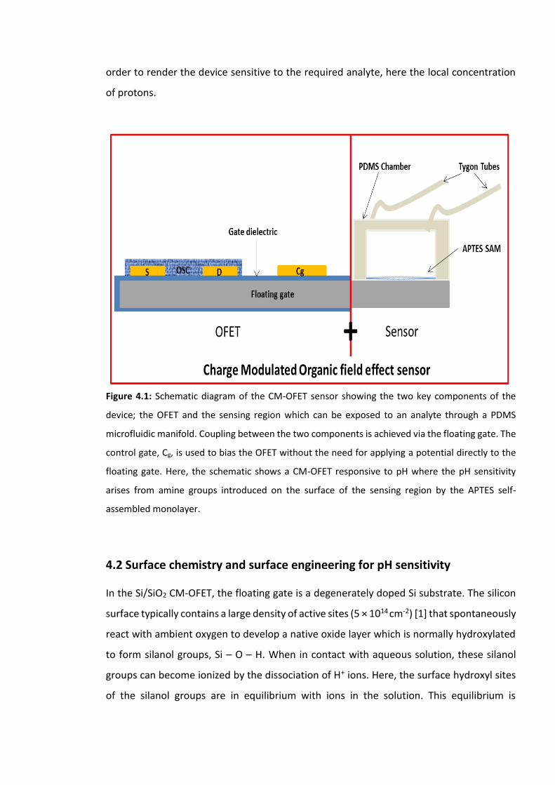
order to render the device sensitive to the required analyte, here the local concentration
of protons.
Figure 4.1: Schematic diagram of the CM-OFET sensor showing the two key components of the
device; the OFET and the sensing region which can be exposed to an analyte through a PDMS
microfluidic manifold. Coupling between the two components is achieved via the floating gate. The
control gate, Cg, is used to bias the OFET without the need for applying a potential directly to the
floating gate. Here, the schematic shows a CM-OFET responsive to pH where the pH sensitivity
arises from amine groups introduced on the surface of the sensing region by the APTES self-
assembled monolayer.
4.2 Surface chemistry and surface engineering for pH sensitivity
In the Si/SiO2 CM-OFET, the floating gate is a degenerately doped Si substrate. The silicon
surface typically contains a large density of active sites (5 × 1014 cm-2) [1] that spontaneously
react with ambient oxygen to develop a native oxide layer which is normally hydroxylated
to form silanol groups, Si – O – H. When in contact with aqueous solution, these silanol
groups can become ionized by the dissociation of H+ ions. Here, the surface hydroxyl sites
of the silanol groups are in equilibrium with ions in the solution. This equilibrium is
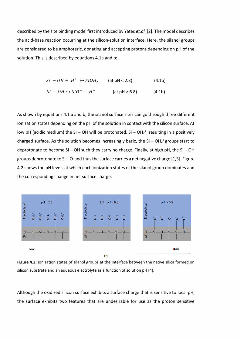
described by the site binding model first introduced by Yates et.al. [2]. The model describes
the acid-base reaction occurring at the silicon-solution interface. Here, the silanol groups
are considered to be amphoteric, donating and accepting protons depending on pH of the
solution. This is described by equations 4.1a and b:
𝑆𝑖 − 𝑂𝐻 + 𝐻+ ↔ 𝑆𝑖𝑂𝐻2+ (at pH < 2.3) (4.1a)
𝑆𝑖 − 𝑂𝐻 ↔ 𝑆𝑖𝑂− + 𝐻+ (at pH > 6.8) (4.1b)
As shown by equations 4.1 a and b, the silanol surface sites can go through three different
ionization states depending on the pH of the solution in contact with the silicon surface. At
low pH (acidic medium) the Si – OH will be protonated, Si – OH2+, resulting in a positively
charged surface. As the solution becomes increasingly basic, the Si – OH2+
groups start to
deprotonate to become Si – OH such they carry no charge. Finally, at high pH, the Si – OH
groups deprotonate to Si – O- and thus the surface carries a net negative charge [1,3]. Figure
4.2 shows the pH levels at which each ionization states of the silanol group dominates and
the corresponding change in net surface charge.
Figure 4.2: ionization states of silanol groups at the interface between the native silica formed on
silicon substrate and an aqueous electrolyte as a function of solution pH [4].
Although the oxidized silicon surface exhibits a surface charge that is sensitive to local pH,
the surface exhibits two features that are undesirable for use as the proton sensitive
surface in a pH sensor. First, buried oxide sites respond slower to a change in solution pH
than those sites located directly on the silica surface due to slow ion diffusion. This rate
dependence leads to a drift in the response of silicon oxide based pH sensors [1,5].
Secondly, the response is not linear over a wide range of pH. Instead, the silicon surface
shows two characteristic linear regimes of pH dependency. In the range pH 2 – 6, where
the silanol groups carry no charge, there is little response of the Si – OH due to solution pH
i.e. the surface charge remains effectively constant. In contrast, at higher pH (in the range
pH 6 – 9), the rate of change of the surface is high [6-8]. Finally, it is worth noting that it is
difficult to control the surface density of silanol groups which could lead to significant
variation in pH sensitivity between nominally identical devices.
Rather than simply exploit the pH dependency of the bare silicon surface, it was therefore
decided to chemically modify the silica with a self-assembled monolayer (SAM) in order to
provide a more repeatable, controlled and reliable pH sensitive surface. For silica surfaces,
modification with an amine terminated SAM, such as 3-aminoproyltrimethoxysilane
(APTES) has been reported to enhance the performance of ISFET pH sensors, particularly in
acidic solutions [6,9-11]. APTES functionalized silica yields a surface with two pH responsive
receptor groups; amine groups, NH2, and naturally occurring silanol groups (Si – OH). Both
these chemical groups act as hydrogen ion receptors. Critically, however the receptor
groups undergo protonation and deprotonation at different pH ranges leading to a
combined response that increases the linearity of the sensor response over what can be
achieved with a silica surface only [12-15].
4.2.1 Combined pH sensitivity of a NH2 and Si – OH terminated silicon surface
As discussed in section 4.2, silanol groups have three different ionization states depending
on the pH level of the solution in contact with the surface. In contrast, amine groups only
have two ionization states described by equation 4.2:
𝑁𝐻3+ ↔ 𝑁𝐻2 + 𝐻+ (4.2)
At equilibrium, where the surface density of protonated (NH3+) and unprotonated groups
(NH2) are equal, the equilibrium constant, known as the acid dissociation constant, Ka, is
expressed as:
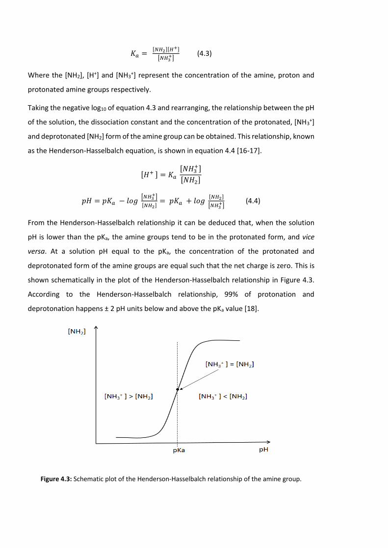
𝐾𝑎 = [𝑁𝐻2][𝐻
+]
[𝑁𝐻3+]
(4.3)
Where the [NH2], [H+] and [NH3+] represent the concentration of the amine, proton and
protonated amine groups respectively.
Taking the negative log10 of equation 4.3 and rearranging, the relationship between the pH
of the solution, the dissociation constant and the concentration of the protonated, [NH3+]
and deprotonated [NH2] form of the amine group can be obtained. This relationship, known
as the Henderson-Hasselbalch equation, is shown in equation 4.4 [16-17].
[𝐻+ ] = 𝐾𝑎 [𝑁𝐻3
+]
[𝑁𝐻2]
𝑝𝐻 = 𝑝𝐾𝑎 − 𝑙𝑜𝑔 [𝑁𝐻3
+]
[𝑁𝐻2]= 𝑝𝐾𝑎 + 𝑙𝑜𝑔
[𝑁𝐻2]
[𝑁𝐻3+]
(4.4)
From the Henderson-Hasselbalch relationship it can be deduced that, when the solution
pH is lower than the pKa, the amine groups tend to be in the protonated form, and vice
versa. At a solution pH equal to the pKa, the concentration of the protonated and
deprotonated form of the amine groups are equal such that the net charge is zero. This is
shown schematically in the plot of the Henderson-Hasselbalch relationship in Figure 4.3.
According to the Henderson-Hasselbalch relationship, 99% of protonation and
deprotonation happens ± 2 pH units below and above the pKa value [18].
Figure 4.3: Schematic plot of the Henderson-Hasselbalch relationship of the amine group.
The precise pKa of an amine group depends on the specific molecule and position of the
amine within that molecule. However, for most molecules containing an amine terminal
group, the pKa is typically greater than pH 9 in bulk solution [9,19]. However, when grafted
onto a surface, the amine pKa is typically reported to be much lower than in solution [17,20-
21]. For example, a pKa as low as 3.9 was reported for an APTES monolayer [22] where the
significant reduction in pKa was assumed to be related to the very hydrophobic
environment around the terminal groups. The reduced pKa associated with surface
immobilised amines explains the improvement in pH response of the APTES modified silica
surface compared to the pure silica surface. Specifically, within the range pH 2 – 6, where
the silanol groups of the silica surface are only weakly responsive to pH, the amine groups
of APTES will be in the high sensitivity range around the pKa (i.e. pKa ±2 pH units) where
99% protonation and deprotonation happens. Outside of this range (particularly the upper
side of the range > pH 6.8), where the amine groups are either fully protonated or
deprotonated, the silanol groups will be more responsive to pH change. The combined
acidic and basic response provided by the amine and silanol groups enhances the linearity
of the modified surface response to pH over a wider pH range.
4.2.2 The CM-OFET pH sensor containing both NH2 and Si-OH surface groups.
Here the improved pH response of APTES functionalized silica surfaces is exploited to create
a CM-OFET pH sensor. The silica surface within the sensing region is functionalized with an
APTES SAM in order to introduce amine groups. At low pH (i.e. a pH below the pKa of APTES:
pKa ≈ 4 – 5), the surface silanol groups will be neutral while the amine groups will be
predominantly protonated (NH3+). As a result, the surface of the sensing region will be
positively charged. This will, in turn, result in accumulation of negative charge in the
floating gate underneath the sensing region. The corresponding redistribution of charge
within the floating gate will effectively cause a negative shift in the apparent gate voltage,
leading to a decrease in the source drain current, ISD. Conversely, as the pH increases
towards the pKa of APTES, the amine groups become increasingly deprotonated, leading to
a reduction in the net positive charge in the sensing region, in turn causing a slight positive
gate voltage shift. Increasing the pH further, leads to deprotonation of the silanol groups
(from Si – OH to Si – O-), further increasing the positive gate voltage shift and hence, the
increase in ISD.
4.3 APTES surface analysis
Before proceeding to characterise the electrical performance of the fabricated CM-OFET
pH sensor, the surface of APTES functionalized sensing region was first characterised. Here,
x-ray photoelectron spectroscopy (XPS), a standard surface analytical technique, was used
to characterize APTES films assembled on a silicon surface.
4.3.1 APTES SAM XPS Spectra
XPS is a standard tool for surface characterization that can provide a quantitative analysis
of the elemental composition and chemical state of the surface. In XPS, a surface is
irradiated with x-rays (commonly Al Kα or Mg Kα x-ray photons equivalent to 1486.6 eV
and 1254.6 eV respectively) in an ultrahigh vacuum environment. The energetic incident x-
ray photons cause ejection of core-level electrons from the surface atoms [23-24]. These
characteristic electrons are subsequently collected, and their kinetic energy and number
are measured using an electron energy analyser. The kinetic energy, EK, of an emitted
electron is related to its binding energy, EB, by equation 4.5:
𝐸𝑘 = ℎ𝑣 − 𝐸𝐵 − 𝜙𝑠𝑝𝑒𝑐 (4.5)
Where hv is the energy of the incident x-ray photons (h is Planck's constant and v is the x-
ray frequency), and Φspec is the work function of the spectrometer [23].
By mapping the number of electrons against the binding energy, it is possible to generate
an XPS spectra consisting of multiple peaks that occur at specific energies. Each peak within
this spectra is related to a specific element in the sample under study and the intensity of
the peaks is related to the concentration of that element.
4.3.1.1 XPS: Experimental Procedure
Two Si substrates were prepared for XPS characterization. The reference sample was a bare
silicon surface with a native oxide but without APTES functionalization. The second sample
was a bare silicon surface with a native oxide and functionalized with APTES by self-
assembly. In self-assemble monolayer, initial monolayer coverage can be achieved very fast
(within seconds to minutes), however, the surface coverage from the monolayer formed
within this time scale is quite low and contains conformational disordering, allowing longer
assembly time (typically >12 hours up to days) increases adsorbates packing and reordering
and reduces inter-separation leading to a more organised and compact monolayer [25-28].
To deposit/assemble APTES layer on Si and other surfaces, APTES concentration lower than
10% in various solvents (typically 5% or less) is used [29-32]. Here, 5% APTES in IPA and 18
hours were chosen.
Both Si samples (reference bare Si substrate and APTES functionalized Si substrate) were
initially cleaned in Piranha solution for 5 minutes followed by 5 minutes of UV ozone
cleaning. The reference substrate was then immersed in IPA solution while the second
substrate was immersed in 5% APTES in IPA. Both samples were left immersed in their
respective solutions for approximately 18 hours. Both samples were rinsed with IPA and
dried with nitrogen before immediately being transferred to the XPS specimen chamber
and placed under vacuum for scanning.
The X-ray source was an Al anode on a dual anode X-ray source (Al Kα = 1486 eV). The
chamber base pressure was 2.5 × 10⁻⁹ mbar. A wide survey scan for binding energies 0-1200
eV was first taken to get an overview of the elements present on the sample surface. The
survey scans, shown in figure 4.4, for both the APTES modified and un-modified Si
substrates showed distinct emission peaks for Si 2s, Si 2p, C 1s and O 1s peaks [33]. No
other elements show a strong signal in these scans.
The survey scans also showed a more intense C peak for the APTES modified Si compared
to the reference unmodified Si. This is as expected, owing the greater C content introduced
by the APTES-modified surface. In order to investigate the origin of this carbon content in
more detail, scans for C 1s, Si 2s, and Si 2p regions were performed, along with the N 1s
region to look for the presence of nitrogen.
(a)
(b)
Figure 4.4: A representative XPS survey scan showing the elemental composition of the surfaces of
(a) APTES modified Si substrate, (b) reference Si substrate. The APTES modified Si sample spectrum
has a reduced intensity compared to the reference sample. This is because a smaller aperture was
used to reduce artefacts associated with photoelectrons generate from the sample plate.
4.3.1.2 Detailed spectra of Si XPS peaks
(a) (b)
(c) (d)
Figure 4.5: Experimental XPS spectra for Si (2s & 2p) peaks for the (a and c) APTES modified Si
substrate and (b and d) for the unmodified reference Si substrate.
XPS spectra of the Si 2s and 2p peaks for both the APTES modified Si and unmodified Si
surfaces are shown in Figure 4.5. Critically, both the APTES modified and reference samples
revealed two peaks for both the Si 2s and 2p photoelectrons, separated by 3 – 4 eV. The
dominant peaks at 99 eV and 151 eV both correspond to the Si – Si bond while the smaller
peaks are associated with Si – O [34-37]. Comparing the peaks between the APTES modified
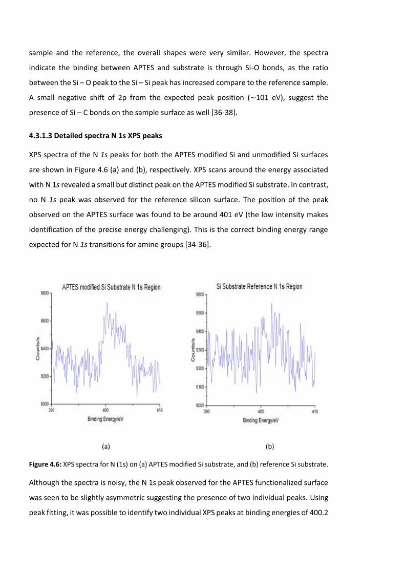
sample and the reference, the overall shapes were very similar. However, the spectra
indicate the binding between APTES and substrate is through Si-O bonds, as the ratio
between the Si – O peak to the Si – Si peak has increased compare to the reference sample.
A small negative shift of 2p from the expected peak position (∼101 eV), suggest the
presence of Si – C bonds on the sample surface as well [36-38].
4.3.1.3 Detailed spectra N 1s XPS peaks
XPS spectra of the N 1s peaks for both the APTES modified Si and unmodified Si surfaces
are shown in Figure 4.6 (a) and (b), respectively. XPS scans around the energy associated
with N 1s revealed a small but distinct peak on the APTES modified Si substrate. In contrast,
no N 1s peak was observed for the reference silicon surface. The position of the peak
observed on the APTES surface was found to be around 401 eV (the low intensity makes
identification of the precise energy challenging). This is the correct binding energy range
expected for N 1s transitions for amine groups [34-36].
(a) (b)
Figure 4.6: XPS spectra for N (1s) on (a) APTES modified Si substrate, and (b) reference Si substrate.
Although the spectra is noisy, the N 1s peak observed for the APTES functionalized surface
was seen to be slightly asymmetric suggesting the presence of two individual peaks. Using
peak fitting, it was possible to identify two individual XPS peaks at binding energies of 400.2
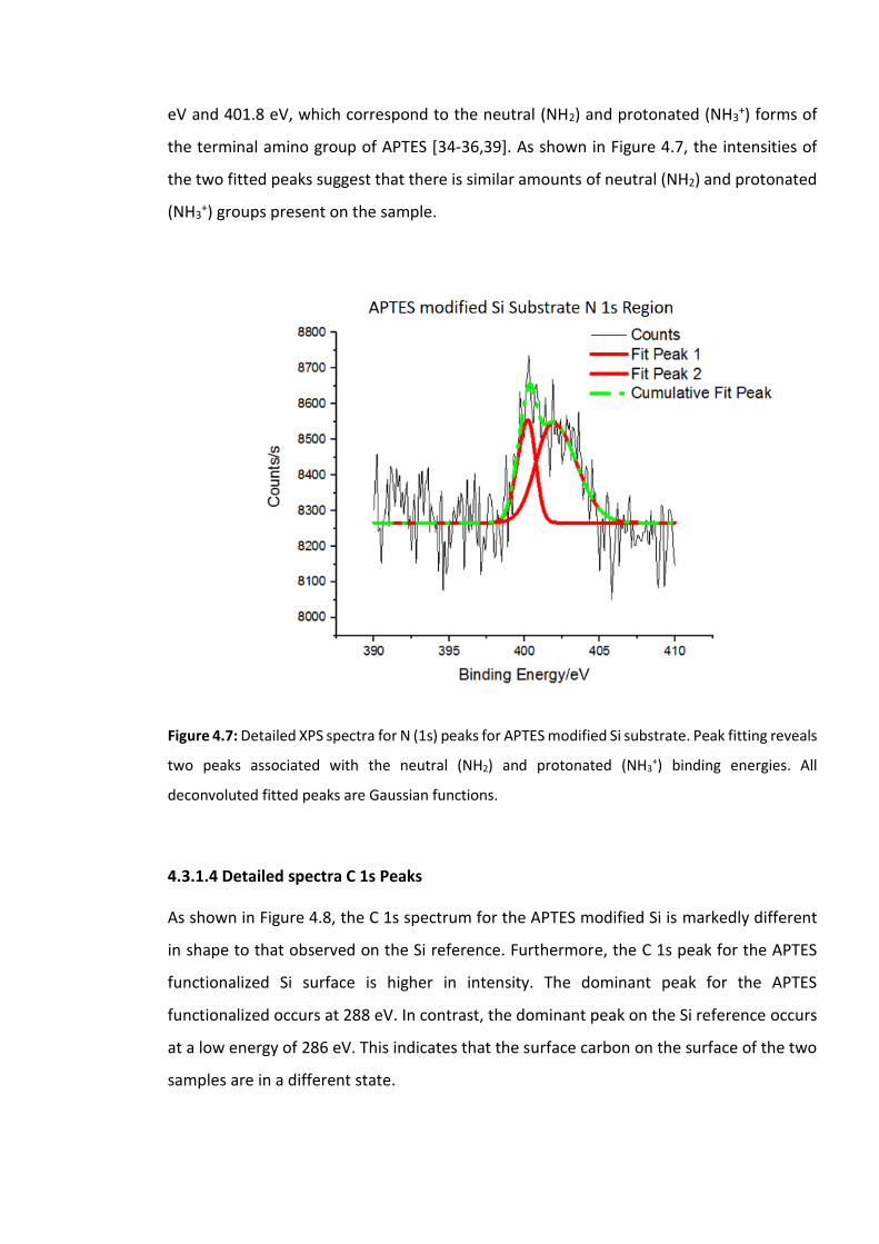
eV and 401.8 eV, which correspond to the neutral (NH2) and protonated (NH3+) forms of
the terminal amino group of APTES [34-36,39]. As shown in Figure 4.7, the intensities of
the two fitted peaks suggest that there is similar amounts of neutral (NH2) and protonated
(NH3+) groups present on the sample.
Figure 4.7: Detailed XPS spectra for N (1s) peaks for APTES modified Si substrate. Peak fitting reveals
two peaks associated with the neutral (NH2) and protonated (NH3+) binding energies. All
deconvoluted fitted peaks are Gaussian functions.
4.3.1.4 Detailed spectra C 1s Peaks
As shown in Figure 4.8, the C 1s spectrum for the APTES modified Si is markedly different
in shape to that observed on the Si reference. Furthermore, the C 1s peak for the APTES
functionalized Si surface is higher in intensity. The dominant peak for the APTES
functionalized occurs at 288 eV. In contrast, the dominant peak on the Si reference occurs
at a low energy of 286 eV. This indicates that the surface carbon on the surface of the two
samples are in a different state.
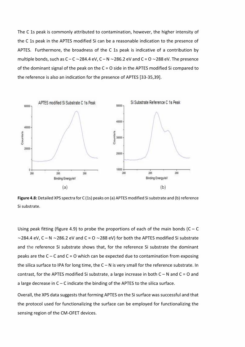
The C 1s peak is commonly attributed to contamination, however, the higher intensity of
the C 1s peak in the APTES modified Si can be a reasonable indication to the presence of
APTES. Furthermore, the broadness of the C 1s peak is indicative of a contribution by
multiple bonds, such as C – C ∼284.4 eV, C – N ∼286.2 eV and C = O ∼288 eV. The presence
of the dominant signal of the peak on the C = O side in the APTES modified Si compared to
the reference is also an indication for the presence of APTES [33-35,39].
(a) (b)
Figure 4.8: Detailed XPS spectra for C (1s) peaks on (a) APTES modified Si substrate and (b) reference
Si substrate.
Using peak fitting (figure 4.9) to probe the proportions of each of the main bonds (C – C
∼284.4 eV, C – N ∼286.2 eV and C = O ∼288 eV) for both the APTES modified Si substrate
and the reference Si substrate shows that, for the reference Si substrate the dominant
peaks are the C – C and C = O which can be expected due to contamination from exposing
the silica surface to IPA for long time, the C – N is very small for the reference substrate. In
contrast, for the APTES modified Si substrate, a large increase in both C – N and C = O and
a large decrease in C – C indicate the binding of the APTES to the silica surface.
Overall, the XPS data suggests that forming APTES on the Si surface was successful and that
the protocol used for functionalizing the surface can be employed for functionalizing the
sensing region of the CM-OFET devices.
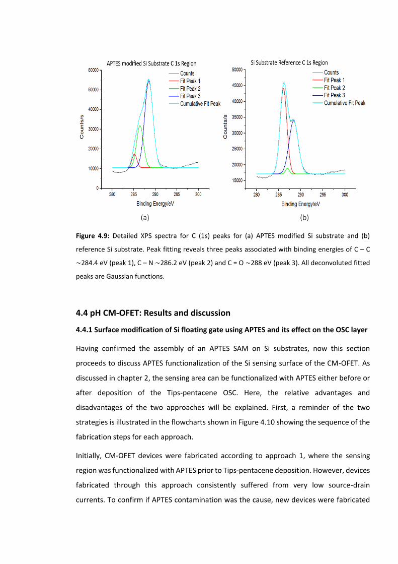
(a) (b)
Figure 4.9: Detailed XPS spectra for C (1s) peaks for (a) APTES modified Si substrate and (b)
reference Si substrate. Peak fitting reveals three peaks associated with binding energies of C – C
∼284.4 eV (peak 1), C – N ∼286.2 eV (peak 2) and C = O ∼288 eV (peak 3). All deconvoluted fitted
peaks are Gaussian functions.
4.4 pH CM-OFET: Results and discussion
4.4.1 Surface modification of Si floating gate using APTES and its effect on the OSC layer
Having confirmed the assembly of an APTES SAM on Si substrates, now this section
proceeds to discuss APTES functionalization of the Si sensing surface of the CM-OFET. As
discussed in chapter 2, the sensing area can be functionalized with APTES either before or
after deposition of the Tips-pentacene OSC. Here, the relative advantages and
disadvantages of the two approaches will be explained. First, a reminder of the two
strategies is illustrated in the flowcharts shown in Figure 4.10 showing the sequence of the
fabrication steps for each approach.
Initially, CM-OFET devices were fabricated according to approach 1, where the sensing
region was functionalized with APTES prior to Tips-pentacene deposition. However, devices
fabricated through this approach consistently suffered from very low source-drain
currents. To confirm if APTES contamination was the cause, new devices were fabricated
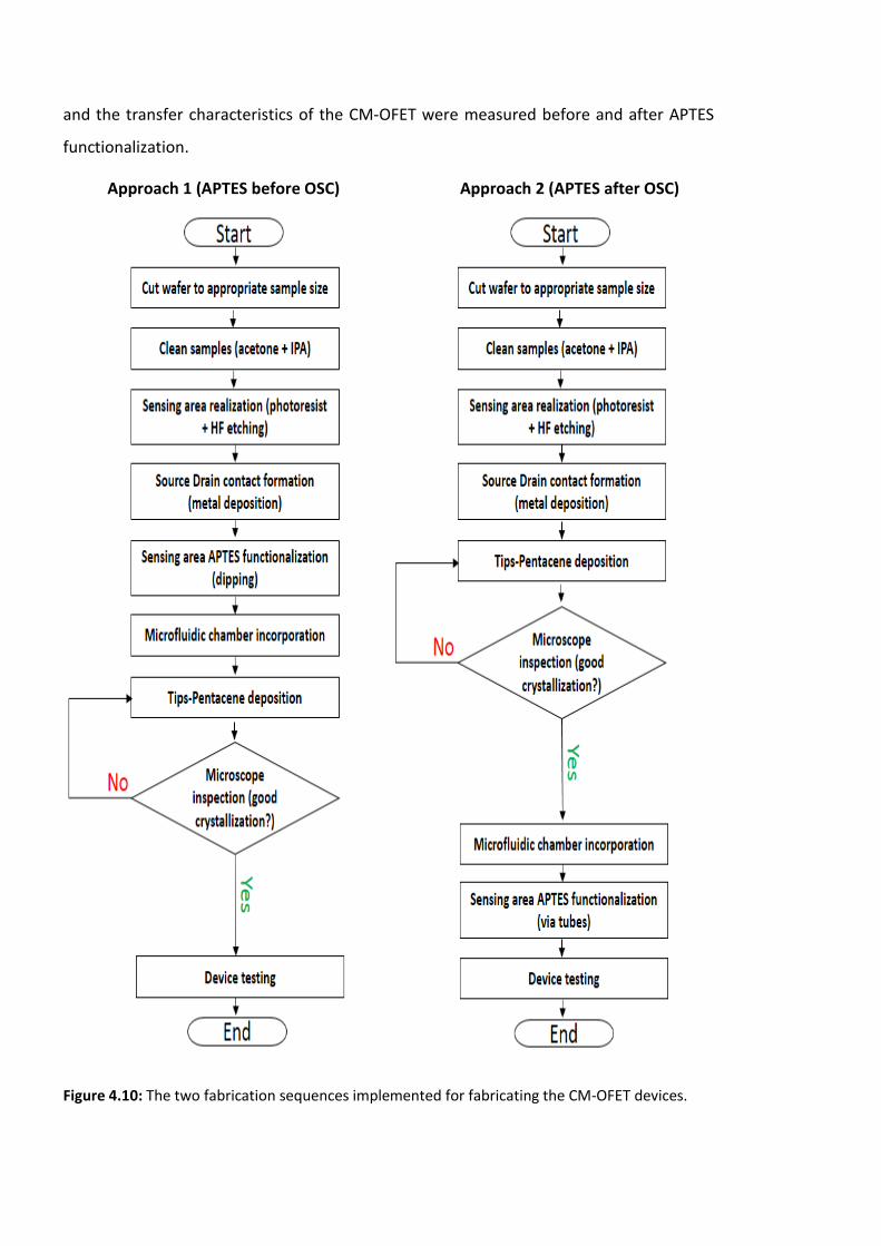
and the transfer characteristics of the CM-OFET were measured before and after APTES
functionalization.
Approach 1 (APTES before OSC) Approach 2 (APTES after OSC)
Figure 4.10: The two fabrication sequences implemented for fabricating the CM-OFET devices.
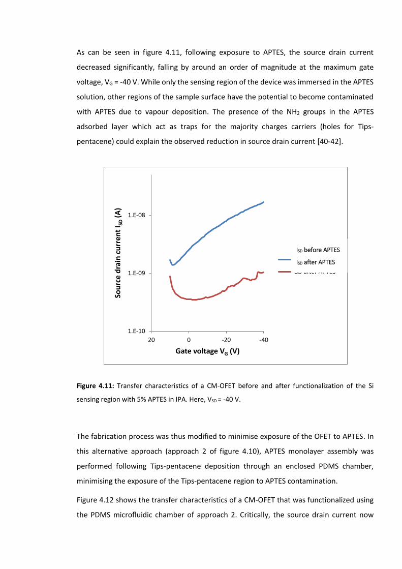
As can be seen in figure 4.11, following exposure to APTES, the source drain current
decreased significantly, falling by around an order of magnitude at the maximum gate
voltage, VG = -40 V. While only the sensing region of the device was immersed in the APTES
solution, other regions of the sample surface have the potential to become contaminated
with APTES due to vapour deposition. The presence of the NH2 groups in the APTES
adsorbed layer which act as traps for the majority charges carriers (holes for Tips-
pentacene) could explain the observed reduction in source drain current [40-42].
Figure 4.11: Transfer characteristics of a CM-OFET before and after functionalization of the Si
sensing region with 5% APTES in IPA. Here, VSD = -40 V.
The fabrication process was thus modified to minimise exposure of the OFET to APTES. In
this alternative approach (approach 2 of figure 4.10), APTES monolayer assembly was
performed following Tips-pentacene deposition through an enclosed PDMS chamber,
minimising the exposure of the Tips-pentacene region to APTES contamination.
Figure 4.12 shows the transfer characteristics of a CM-OFET that was functionalized using
the PDMS microfluidic chamber of approach 2. Critically, the source drain current now
1.E-10
1.E-09
1.E-08
-40-20020
Sou
rce
dra
in c
urr
ent
I SD
(A)
Gate voltage VG (V)
ISD before APTES
ISD after APTES
ISD before APTES
ISD after APTES
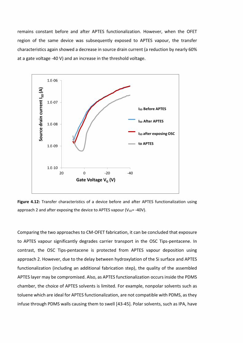
remains constant before and after APTES functionalization. However, when the OFET
region of the same device was subsequently exposed to APTES vapour, the transfer
characteristics again showed a decrease in source drain current (a reduction by nearly 60%
at a gate voltage -40 V) and an increase in the threshold voltage.
Figure 4.12: Transfer characteristics of a device before and after APTES functionalization using
approach 2 and after exposing the device to APTES vapour (VSD= -40V).
Comparing the two approaches to CM-OFET fabrication, it can be concluded that exposure
to APTES vapour significantly degrades carrier transport in the OSC Tips-pentacene. In
contrast, the OSC Tips-pentacene is protected from APTES vapour deposition using
approach 2. However, due to the delay between hydroxylation of the Si surface and APTES
functionalization (including an additional fabrication step), the quality of the assembled
APTES layer may be compromised. Also, as APTES functionalization occurs inside the PDMS
chamber, the choice of APTES solvents is limited. For example, nonpolar solvents such as
toluene which are ideal for APTES functionalization, are not compatible with PDMS, as they
infuse through PDMS walls causing them to swell [43-45]. Polar solvents, such as IPA, have
1.E-10
1.E-09
1.E-08
1.E-07
1.E-06
-40-20020
Sou
rce
dra
in c
urr
ent
I SD
(A)
Gate Voltage VG (V)
ISD Before APTES
ISD After APTES
ISD after exposing OSCto APTES
ISD Before APTES
ISD After APTES
ISD after exposing OSC
to APTES
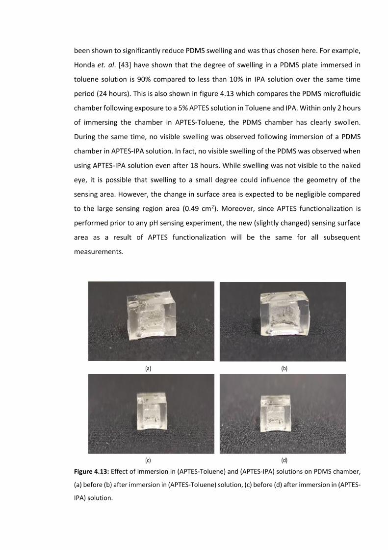
been shown to significantly reduce PDMS swelling and was thus chosen here. For example,
Honda et. al. [43] have shown that the degree of swelling in a PDMS plate immersed in
toluene solution is 90% compared to less than 10% in IPA solution over the same time
period (24 hours). This is also shown in figure 4.13 which compares the PDMS microfluidic
chamber following exposure to a 5% APTES solution in Toluene and IPA. Within only 2 hours
of immersing the chamber in APTES-Toluene, the PDMS chamber has clearly swollen.
During the same time, no visible swelling was observed following immersion of a PDMS
chamber in APTES-IPA solution. In fact, no visible swelling of the PDMS was observed when
using APTES-IPA solution even after 18 hours. While swelling was not visible to the naked
eye, it is possible that swelling to a small degree could influence the geometry of the
sensing area. However, the change in surface area is expected to be negligible compared
to the large sensing region area (0.49 cm2). Moreover, since APTES functionalization is
performed prior to any pH sensing experiment, the new (slightly changed) sensing surface
area as a result of APTES functionalization will be the same for all subsequent
measurements.
Figure 4.13: Effect of immersion in (APTES-Toluene) and (APTES-IPA) solutions on PDMS chamber,
(a) before (b) after immersion in (APTES-Toluene) solution, (c) before (d) after immersion in (APTES-
IPA) solution.
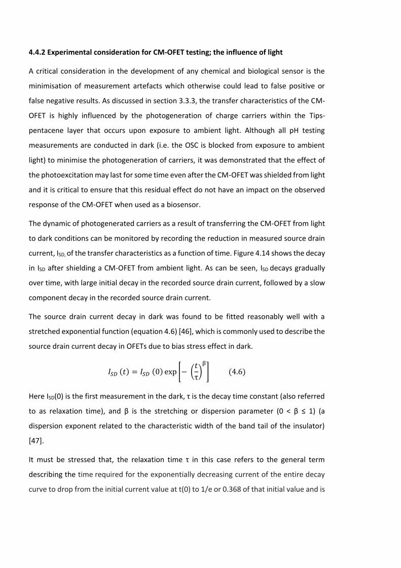
4.4.2 Experimental consideration for CM-OFET testing; the influence of light
A critical consideration in the development of any chemical and biological sensor is the
minimisation of measurement artefacts which otherwise could lead to false positive or
false negative results. As discussed in section 3.3.3, the transfer characteristics of the CM-
OFET is highly influenced by the photogeneration of charge carriers within the Tips-
pentacene layer that occurs upon exposure to ambient light. Although all pH testing
measurements are conducted in dark (i.e. the OSC is blocked from exposure to ambient
light) to minimise the photogeneration of carriers, it was demonstrated that the effect of
the photoexcitation may last for some time even after the CM-OFET was shielded from light
and it is critical to ensure that this residual effect do not have an impact on the observed
response of the CM-OFET when used as a biosensor.
The dynamic of photogenerated carriers as a result of transferring the CM-OFET from light
to dark conditions can be monitored by recording the reduction in measured source drain
current, ISD, of the transfer characteristics as a function of time. Figure 4.14 shows the decay
in ISD after shielding a CM-OFET from ambient light. As can be seen, ISD decays gradually
over time, with large initial decay in the recorded source drain current, followed by a slow
component decay in the recorded source drain current.
The source drain current decay in dark was found to be fitted reasonably well with a
stretched exponential function (equation 4.6) [46], which is commonly used to describe the
source drain current decay in OFETs due to bias stress effect in dark.
𝐼𝑆𝐷 (𝑡) = 𝐼𝑆𝐷 (0) exp [− (𝑡
τ)β
] (4.6)
Here ISD(0) is the first measurement in the dark, τ is the decay time constant (also referred
to as relaxation time), and β is the stretching or dispersion parameter (0 < β ≤ 1) (a
dispersion exponent related to the characteristic width of the band tail of the insulator)
[47].
It must be stressed that, the relaxation time τ in this case refers to the general term
describing the time required for the exponentially decreasing current of the entire decay
curve to drop from the initial current value at t(0) to 1/e or 0.368 of that initial value and is
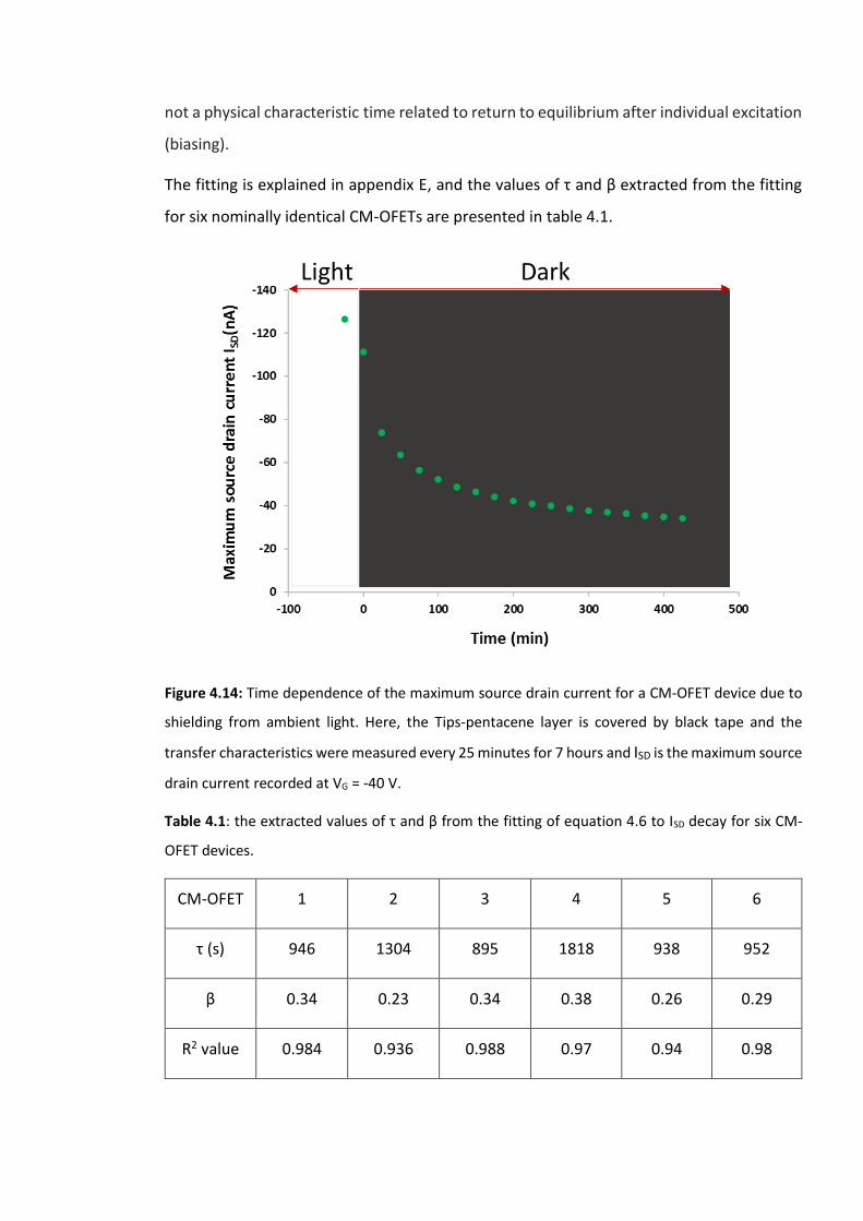
not a physical characteristic time related to return to equilibrium after individual excitation
(biasing).
The fitting is explained in appendix E, and the values of τ and β extracted from the fitting
for six nominally identical CM-OFETs are presented in table 4.1.
Figure 4.14: Time dependence of the maximum source drain current for a CM-OFET device due to
shielding from ambient light. Here, the Tips-pentacene layer is covered by black tape and the
transfer characteristics were measured every 25 minutes for 7 hours and ISD is the maximum source
drain current recorded at VG = -40 V.
Table 4.1: the extracted values of τ and β from the fitting of equation 4.6 to ISD decay for six CM-
OFET devices.
CM-OFET 1 2 3 4 5 6
τ (s) 946 1304 895 1818 938 952
β 0.34 0.23 0.34 0.38 0.26 0.29
R2 value 0.984 0.936 0.988 0.97 0.94 0.98
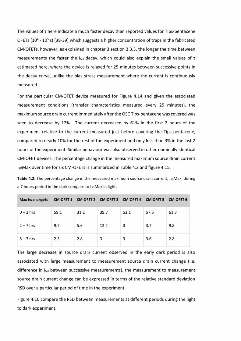
The values of τ here indicate a much faster decay than reported values for Tips-pentacene
OFETs (104 - 105 s) [38-39] which suggests a higher concentration of traps in the fabricated
CM-OFETs, however, as explained in chapter 3 section 3.3.3, the longer the time between
measurements the faster the ISD decay, which could also explain the small values of τ
estimated here, where the device is relaxed for 25 minutes between successive points in
the decay curve, unlike the bias stress measurement where the current is continuously
measured.
For the particular CM-OFET device measured for Figure 4.14 and given the associated
measurement conditions (transfer characteristics measured every 25 minutes), the
maximum source drain current immediately after the OSC Tips-pentacene was covered was
seen to decrease by 12%. The current decreased by 61% in the first 2 hours of the
experiment relative to the current measured just before covering the Tips-pentacene,
compared to nearly 10% for the rest of the experiment and only less than 3% in the last 2
hours of the experiment. Similar behaviour was also observed in other nominally identical
CM-OFET devices. The percentage change in the measured maximum source drain current
ISDMax over time for six CM-OFETs is summarized in Table 4.2 and figure 4.15.
Table 4.2: The percentage change in the measured maximum source drain current, ISDMax, during
a 7 hours period in the dark compare to ISDMax in light.
Max ISD change% CM-OFET 1 CM-OFET 2 CM-OFET 3 CM-OFET 4 CM-OFET 5 CM-OFET 6
0 – 2 hrs 59.1 31.2 39.7 52.1 57.6 61.3
2 – 7 hrs 9.7 5.6 12.4 3 3.7 9.8
5 – 7 hrs 2.3 2.8 3 3 3.6 2.8
The large decrease in source drain current observed in the early dark period is also
associated with large measurement to measurement source drain current change (i.e.
difference in ISD between successive measurements), the measurement to measurement
source drain current change can be expressed in terms of the relative standard deviation
RSD over a particular period of time in the experiment.
Figure 4.16 compare the RSD between measurements at different periods during the light
to dark experiment.
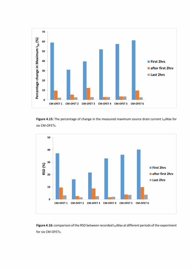
Figure 4.15: The percentage of change in the measured maximum source drain current ISDMax for
six CM-OFETs.
Figure 4.16: comparison of the RSD between recorded ISDMax at different periods of the experiment
for six CM-OFETs.
0
10
20
30
40
50
CM-OFET 1 CM-OFET 2 CM-OFET 3 CM-OFET 4 CM-OFET 5 CM-OFET 6
RSD
(%
)
First 2hrs
after first 2hrs
Last 2hrs
0
10
20
30
40
50
60
70
CM-OFET 1 CM-OFET 2 CM-OFET 3 CM-OFET 4 CM-OFET 5 CM-OFET 6
Per
cen
tage
ch
ange
in M
axim
um
ISD
(%)
First 2hrs
after first 2hrs
Last 2hrs
Figure 4.16 clearly shows that in the first period under dark condition the measurement to
measurement change every 25 minutes is far greater compare than that in later stages in
the dark. This observation is of great importance when sensing activity is to be investigate,
where the measured ISD is compared before and after the sensing activity. If the sensing
activity is studied shortly after the CM-OFET device was put in dark condition, the likelihood
is that the effect of sensing activity will be dominated by the stronger photogenerated
charge carrier releasing process and hence, any sensing interpretation and subsequent
drawn conclusion within this period will be inaccurate and may be misleading. Therefore,
it was important to ensure that the influence of photogenerated carriers was greatly
reduced for all tested devices before any pH sensing measurement was conducted.
4.4.3 pH sensing using the CM-OFET
To demonstrate the functionality of the fabricated CM-OFET operating as a chemical
sensor, the performance of the fabricated CM-OFET devices was assessed for monitoring
pH. In order to test the pH response of a CM-OFET device, the sensing region was first
functionalized with APTES and exposed to a set of buffer solutions of different pH. The pH
solutions that were used for testing the fabricated devices were based on Mcilvaine’s
buffer solutions [48]. Mcilvaine buffer solutions are prepared by mixing stock solutions of
0.2 M disodium phosphate and 0.1 M citric acid at different concentrations. The pH range
covered by Mcilvaine buffer is from 2.2 to 8 and the relative ratios and associated pH level
used are illustrated in table 4.3. Experimentally, the different pH buffer solutions were
made using the ratios provided in table 4.3 and pH of each made solution was subsequently
measured using a pH meter (METTLER TOLEDO – FiveEasy F20). The table shows the
measured pH of each solution compared to the target pH level.
According to the mechanism described in section 4.2, the charge density of the APTES
functionalized Si surface in the sensing area will change depending on the pH of the
solution. This change in surface charge density will in turn lead to a redistribution of charge
in the floating gate and hence, modulate the charge carrier density inside the channel of
the transistor. Effectively, a charge equal in magnitude but opposite in sign to that
accumulated in sensing area of the floating gate, will be distributed over the three,
transistor electrodes (source, drain and control gate), causing a shift in the gate voltage
applied to the transistor. Assuming everything else remains constant apart from the pH of
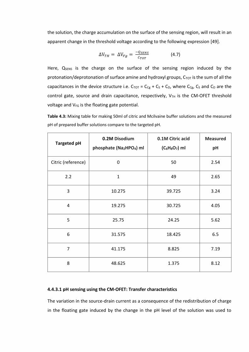
the solution, the charge accumulation on the surface of the sensing region, will result in an
apparent change in the threshold voltage according to the following expression [49].
ΔV𝑇𝐻 = ΔV𝐹𝑔 = −𝑄𝑆𝐸𝑁𝑆
𝐶𝑇𝑂𝑇 (4.7)
Here, QSENS is the charge on the surface of the sensing region induced by the
protonation/deprotonation of surface amine and hydroxyl groups, CTOT is the sum of all the
capacitances in the device structure i.e. CTOT = CCg + CS + CD, where CCg, CS and CD are the
control gate, source and drain capacitance, respectively, VTH is the CM-OFET threshold
voltage and VFG is the floating gate potential.
Table 4.3: Mixing table for making 50ml of citric and Mcilvaine buffer solutions and the measured
pH of prepared buffer solutions compare to the targeted pH.
Targeted pH 0.2M Disodium
phosphate (Na2HPO4) ml
0.1M Citric acid
(C6H8O7) ml
Measured
pH
Citric (reference) 0 50 2.54
2.2 1 49 2.65
3 10.275 39.725 3.24
4 19.275 30.725 4.05
5 25.75 24.25 5.62
6 31.575 18.425 6.5
7 41.175 8.825 7.19
8 48.625 1.375 8.12
4.4.3.1 pH sensing using the CM-OFET: Transfer characteristics
The variation in the source-drain current as a consequence of the redistribution of charge
in the floating gate induced by the change in the pH level of the solution was used to
confirm the sensing capabilities of the CM-OFET. Specifically, the maximum drain-source
current, ISDMax, from the transfer characteristics of the device measurements was used to
compare the response of the device to each pH solution. ISDMax on the transfer
characteristics curve is at a gate voltage (applied through the control gate) VG = -40 V while
the drain voltage was held constant at -40 V.
The measurement was performed using the following protocol:
(1) A reference pH solution, here citric acid (pH 2.54) was first introduced to the sensing
region of the CM-OFET sensor via the PDMS chamber and the transfer characteristics of the
device measured. This provided a baseline measurement against which the test solution
was measured.
(2) The reference pH solution was replaced by a test pH buffer solution and the transfer
characteristics of the CM-OFET measured. This process was repeated for each pH buffer
solution in the range pH 2.2 – 8. The percentage change in ISDMax between the test pH
solution and the previous citric acid reference pH solution was calculated using equation
4.8 and used to compare the response of the device to different pH test solutions:
△ 𝐼𝑆𝐷𝑀𝑎𝑥% = (𝐼𝑆𝐷Max(𝑝𝐻)−𝐼𝑆𝐷Max(𝑐𝑖𝑡𝑟𝑖𝑐)
𝐼𝑆𝐷Max(𝑐𝑖𝑡𝑟𝑖𝑐)% (4.8)
Here, ISDMax (pH) is the maximum source-drain current of the test pH solution and ISDMax
(citric) is the maximum source drain current measured for the citric acid reference pH
solution.
At different pH levels, the amine and silanol groups on the surface of the sensing region are
expected to change ionization states, thus the surface charge density will vary in the
sensing region accordingly. In the pH sensing experiment described above, each time the
citric acid solution is replaced by a given buffer solution, the surface charge of the sensing
region is expected to change where the amount of change is dependent on the difference
in pH between the citric acid reference and the test solution. For example, replacing the
citric acid solution with a buffer solution of pH 8 will result in the silanol groups changing
from Si – OH2+ or Si – OH in acidic conditions (citric acid) to Si – O- at pH 8. At the same time
the surface amines initially protonated in citric acid will become deprotonated at pH 8. As
a result, the surface changes from being predominantly positively charged to a surface with
a large negative charged density. Ultimately, this is expected to be translated to a large
positive shift in apparent gate voltage and thus an increase in ISDMax . In contrast, replacing
the citric acid with a low pH 2.6 buffer solution, means that the surface groups will remain
largely unchanged (with similar ionization states). Correspondingly, small to negligible
change in the magnitude and sign of the surface charge is expected.
Two types of responses maybe observed in the investigated CM-OFET devices based on the
quality of the APTES layer in the sensing region.
1) Devices with a dense APTES monolayer assembled in the sensing region, should
exhibit a linear pH sensitivity response over the investigated pH range (pH 2.2 – 8),
as a result of the combined pH response of both amine and silanol groups as
explained in section 4.2. Here, the linearity should be observed as a linear increase
in the percentage change in the maximum source drain current as the pH increase.
2) In devices with poor quality APTES layer, the density of amine groups is significantly
reduced such that the pH sensitivity of the CM-OFET is dominated by silanol groups
on the silica surface. As discussed in section 4.2, these Si-OH groups are known to
exhibit a weak response to pH change between pH 2.3 and 6.8, hence, the change
in ISDMax is expected to be minimal in this range.
A total of eight, nominally identical CM-OFET devices were tested for pH sensing. Each
device was challenged with the seven pH solutions presented in table 4.3 before the
transfer characteristics of each device was measured. Each device was tested three times
over the full pH range (pH 2.2 - 8). In two of the three tests, the transfer characteristics
were recorded immediately after the solution was introduced to the sensing area and 25
minutes after being introduced (referred to as the 25min measurement). In the third test,
the pH solutions were measured only after 25 minutes of it being introduced to the sensing
area. The latter test was done to investigate if reducing the biasing stress that is generated
from immediate measurement affects the pH response.
Experimental results of the eight devices are shown in figures 4.17 to 4.24. Each figure
displays for a particular CM-OFET device (a) the percentage change in the maximum source
drain current between each pH buffer solution and the reference citric solution (calculated
using equation 4.8) for three independent measurements when the transfer characteristics
were measured 25 minutes after the introduction of the pH buffer solution. (b) the average
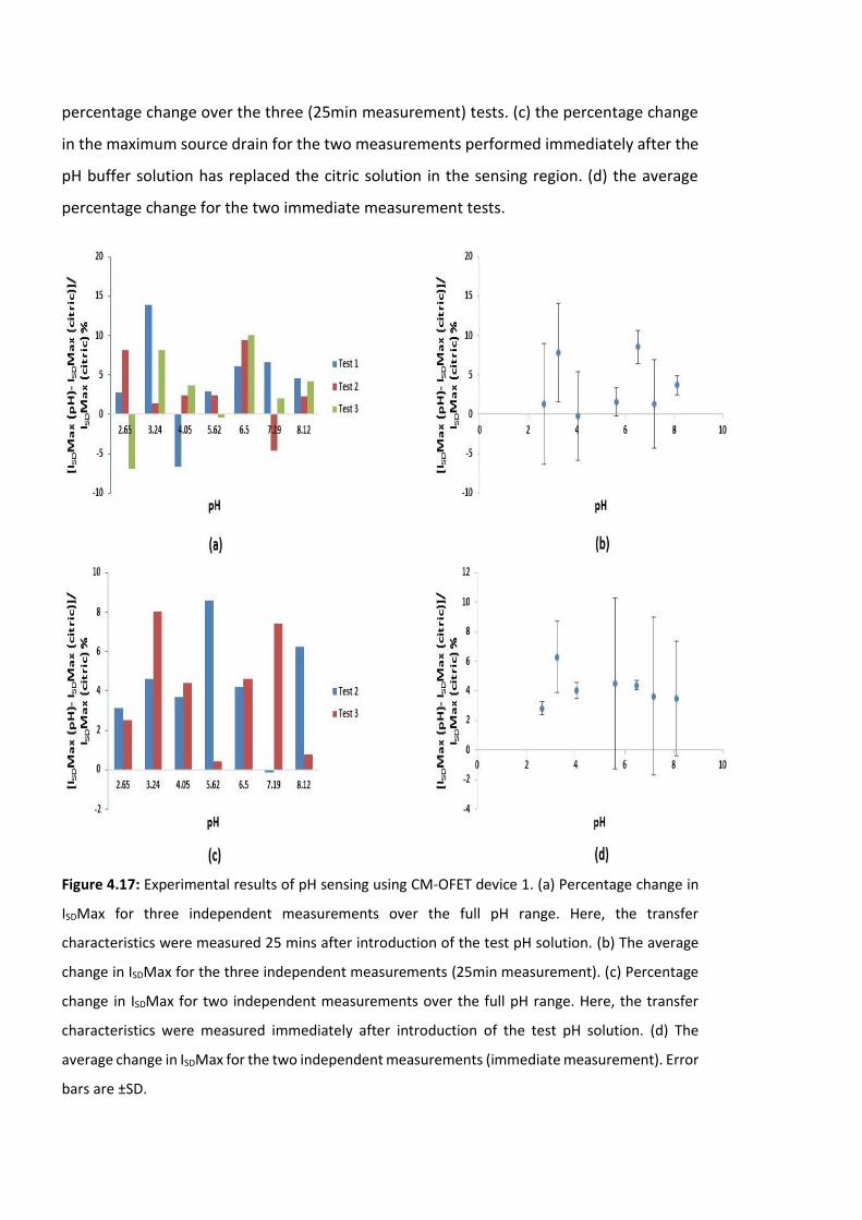
percentage change over the three (25min measurement) tests. (c) the percentage change
in the maximum source drain for the two measurements performed immediately after the
pH buffer solution has replaced the citric solution in the sensing region. (d) the average
percentage change for the two immediate measurement tests.
Figure 4.17: Experimental results of pH sensing using CM-OFET device 1. (a) Percentage change in
ISDMax for three independent measurements over the full pH range. Here, the transfer
characteristics were measured 25 mins after introduction of the test pH solution. (b) The average
change in ISDMax for the three independent measurements (25min measurement). (c) Percentage
change in ISDMax for two independent measurements over the full pH range. Here, the transfer
characteristics were measured immediately after introduction of the test pH solution. (d) The
average change in ISDMax for the two independent measurements (immediate measurement). Error
bars are ±SD.
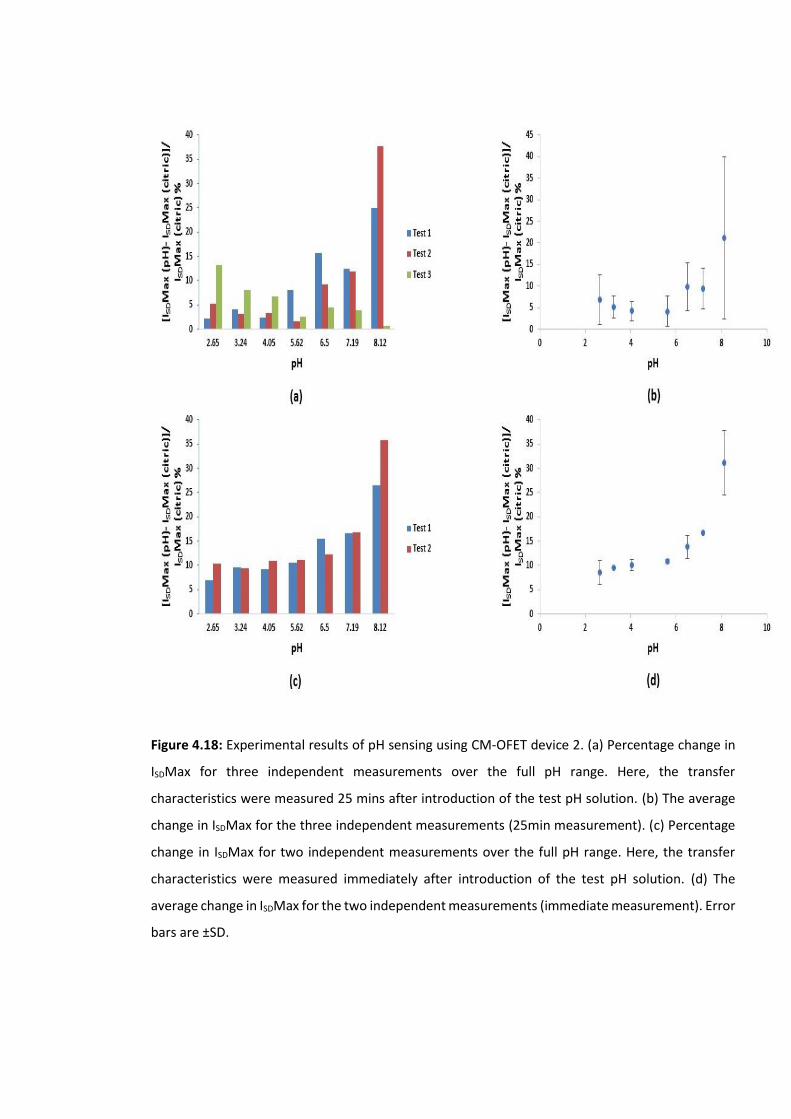
Figure 4.18: Experimental results of pH sensing using CM-OFET device 2. (a) Percentage change in
ISDMax for three independent measurements over the full pH range. Here, the transfer
characteristics were measured 25 mins after introduction of the test pH solution. (b) The average
change in ISDMax for the three independent measurements (25min measurement). (c) Percentage
change in ISDMax for two independent measurements over the full pH range. Here, the transfer
characteristics were measured immediately after introduction of the test pH solution. (d) The
average change in ISDMax for the two independent measurements (immediate measurement). Error
bars are ±SD.
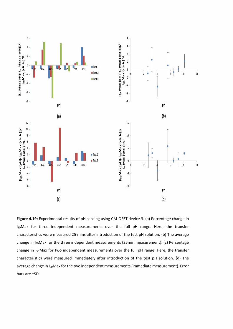
Figure 4.19: Experimental results of pH sensing using CM-OFET device 3. (a) Percentage change in
ISDMax for three independent measurements over the full pH range. Here, the transfer
characteristics were measured 25 mins after introduction of the test pH solution. (b) The average
change in ISDMax for the three independent measurements (25min measurement). (c) Percentage
change in ISDMax for two independent measurements over the full pH range. Here, the transfer
characteristics were measured immediately after introduction of the test pH solution. (d) The
average change in ISDMax for the two independent measurements (immediate measurement). Error
bars are ±SD.
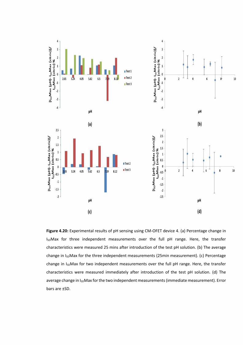
Figure 4.20: Experimental results of pH sensing using CM-OFET device 4. (a) Percentage change in
ISDMax for three independent measurements over the full pH range. Here, the transfer
characteristics were measured 25 mins after introduction of the test pH solution. (b) The average
change in ISDMax for the three independent measurements (25min measurement). (c) Percentage
change in ISDMax for two independent measurements over the full pH range. Here, the transfer
characteristics were measured immediately after introduction of the test pH solution. (d) The
average change in ISDMax for the two independent measurements (immediate measurement). Error
bars are ±SD.
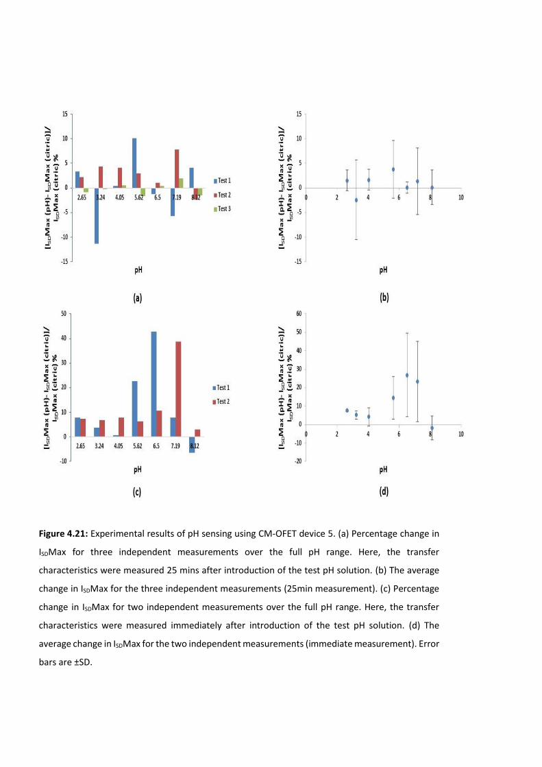
Figure 4.21: Experimental results of pH sensing using CM-OFET device 5. (a) Percentage change in
ISDMax for three independent measurements over the full pH range. Here, the transfer
characteristics were measured 25 mins after introduction of the test pH solution. (b) The average
change in ISDMax for the three independent measurements (25min measurement). (c) Percentage
change in ISDMax for two independent measurements over the full pH range. Here, the transfer
characteristics were measured immediately after introduction of the test pH solution. (d) The
average change in ISDMax for the two independent measurements (immediate measurement). Error
bars are ±SD.
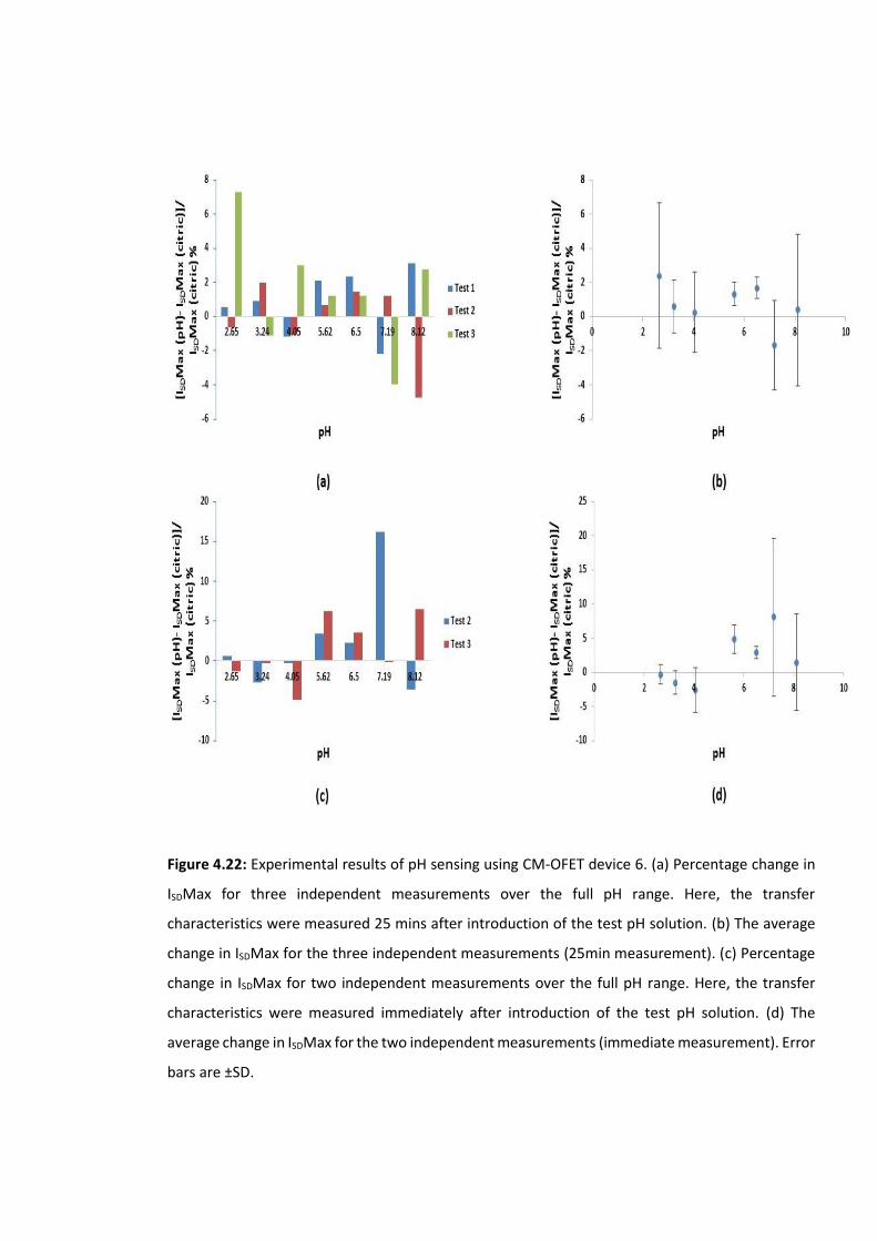
Figure 4.22: Experimental results of pH sensing using CM-OFET device 6. (a) Percentage change in
ISDMax for three independent measurements over the full pH range. Here, the transfer
characteristics were measured 25 mins after introduction of the test pH solution. (b) The average
change in ISDMax for the three independent measurements (25min measurement). (c) Percentage
change in ISDMax for two independent measurements over the full pH range. Here, the transfer
characteristics were measured immediately after introduction of the test pH solution. (d) The
average change in ISDMax for the two independent measurements (immediate measurement). Error
bars are ±SD.

Figure 4.23: Experimental results of pH sensing using CM-OFET device 7. (a) Percentage change in
ISDMax for three independent measurements over the full pH range. Here, the transfer
characteristics were measured 25 mins after introduction of the test pH solution. (b) The average
change in ISDMax for the three independent measurements (25min measurement). (c) Percentage
change in ISDMax for two independent measurements over the full pH range. Here, the transfer
characteristics were measured immediately after introduction of the test pH solution. (d) The
average change in ISDMax for the two independent measurements (immediate measurement). Error
bars are ±SD.
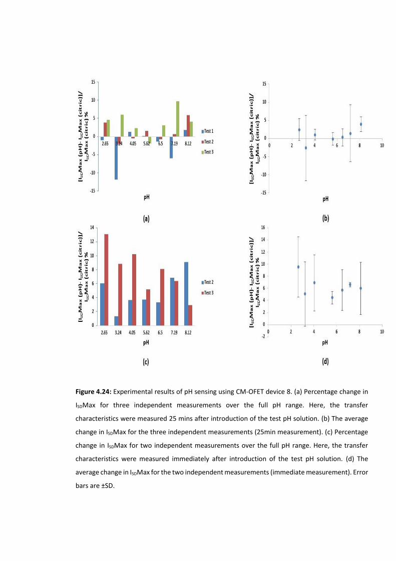
Figure 4.24: Experimental results of pH sensing using CM-OFET device 8. (a) Percentage change in
ISDMax for three independent measurements over the full pH range. Here, the transfer
characteristics were measured 25 mins after introduction of the test pH solution. (b) The average
change in ISDMax for the three independent measurements (25min measurement). (c) Percentage
change in ISDMax for two independent measurements over the full pH range. Here, the transfer
characteristics were measured immediately after introduction of the test pH solution. (d) The
average change in ISDMax for the two independent measurements (immediate measurement). Error
bars are ±SD.

The results obtained for the eight CM-OFET devices tested for pH sensing showed:
1) The responses of the eight nominally identical devices to pH test solutions was
inconsistent. Similarly, repeat measurements of identical devices also show
inconsistent responses.
2) None of the devices displayed the expected response to the pH solutions.
Specifically, none of the devices showed the linear response (linear increase in
source drain current with pH) expected for CM-OFETs functionalized with a good
quality APTES layer in the sensing area, nor a response with nonlinear current
increase in the middle of the pH range for devices with a poor APTES layer where
the silanol groups would dominate pH response.
3) No repeatable or distinguishable trend can be extracted from experimental data of
the pH response for the eight devices.
4) There was no clear effect of excluding the immediate measurement on the pH
response behaviour of the examined CM-OFET devices.
5) Overall, in almost 70% of measurements, the source drain current was found to
increase after replacement of the citric acid solutions with a test pH buffer.
6) The change in ISDMax between the citric acid solution and the test pH solution was
routinely very small. Specifically, in almost 90% of measurements ISDMax(pH)
changed less than 10% relative to ISD(citric).
The average change in ∆ISDMax across all devices for each pH buffer is shown in figure 4.25
and it concur with the above-mentioned conclusions, particularly, the error margins for the
detection was high and the change in ∆ISDMax was largely within the noise range of the
devices.
From these experimental results, it is clear that there is no consistent, predictable or
distinguishable response for CM-OFET when challenged with buffers of changing pH. Also,
except in limited cases (7.7% of the times), the change in maximum source drain current of
the investigated pH buffer solution ISDMax(pH) relative to the source drain current of the
corresponding citric solution ISDMax(citric) was below 10%. This is comparable to the shifts
in maximum source drain current, ISDMax, due to the inherent behaviour of the OSC. In the
following section, an alternative test was performed in which the source drain current was
recorded as a function of time while the bias voltages remain constant.
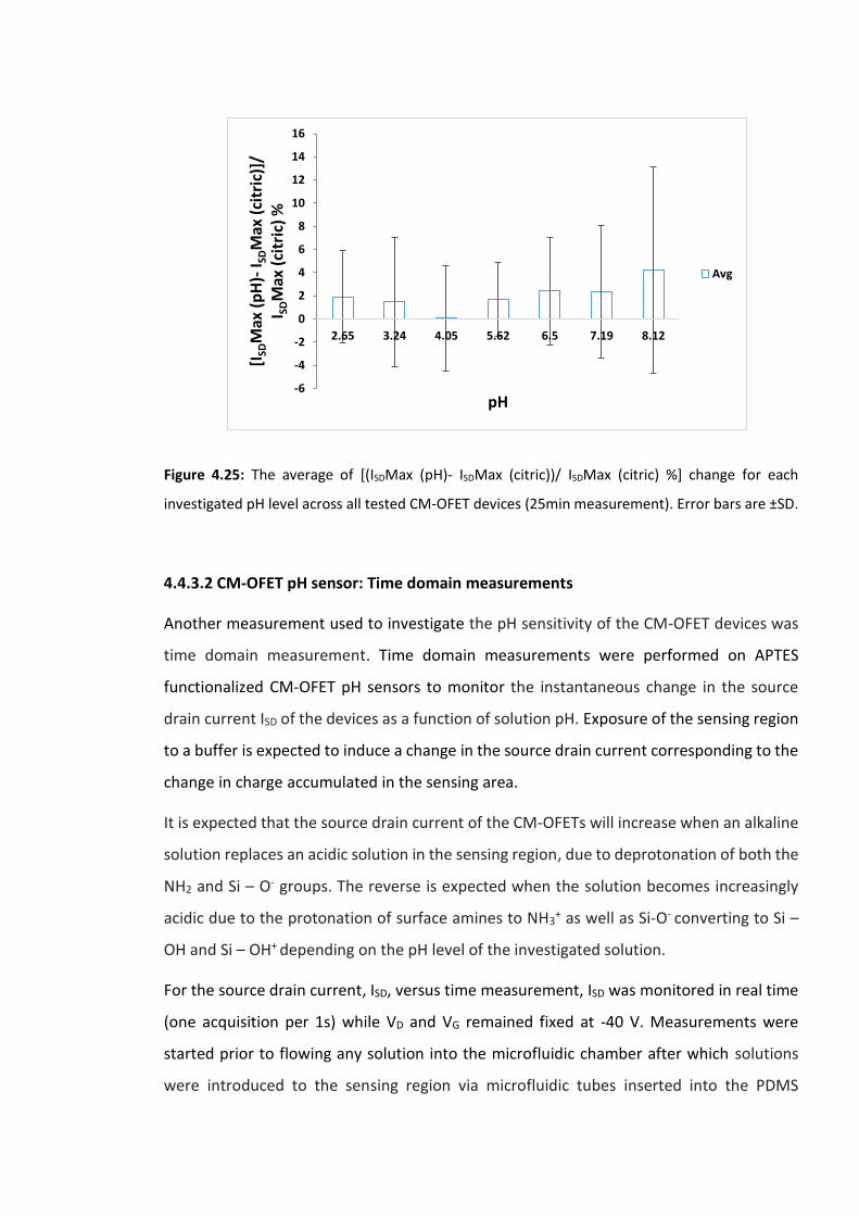
Figure 4.25: The average of [(ISDMax (pH)- ISDMax (citric))/ ISDMax (citric) %] change for each
investigated pH level across all tested CM-OFET devices (25min measurement). Error bars are ±SD.
4.4.3.2 CM-OFET pH sensor: Time domain measurements
Another measurement used to investigate the pH sensitivity of the CM-OFET devices was
time domain measurement. Time domain measurements were performed on APTES
functionalized CM-OFET pH sensors to monitor the instantaneous change in the source
drain current ISD of the devices as a function of solution pH. Exposure of the sensing region
to a buffer is expected to induce a change in the source drain current corresponding to the
change in charge accumulated in the sensing area.
It is expected that the source drain current of the CM-OFETs will increase when an alkaline
solution replaces an acidic solution in the sensing region, due to deprotonation of both the
NH2 and Si – O- groups. The reverse is expected when the solution becomes increasingly
acidic due to the protonation of surface amines to NH3+ as well as Si-O- converting to Si –
OH and Si – OH+ depending on the pH level of the investigated solution.
For the source drain current, ISD, versus time measurement, ISD was monitored in real time
(one acquisition per 1s) while VD and VG remained fixed at -40 V. Measurements were
started prior to flowing any solution into the microfluidic chamber after which solutions
were introduced to the sensing region via microfluidic tubes inserted into the PDMS
-6
-4
-2
0
2
4
6
8
10
12
14
16
2.65 3.24 4.05 5.62 6.5 7.19 8.12
[ISD
Max
(p
H)-
I SDM
ax (
citr
ic)]
/ I S
DM
ax (
citr
ic)
%
pH
Avg
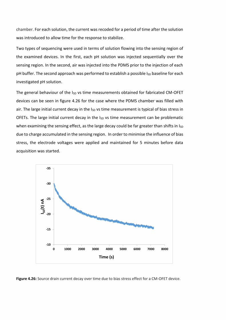
chamber. For each solution, the current was recoded for a period of time after the solution
was introduced to allow time for the response to stabilize.
Two types of sequencing were used in terms of solution flowing into the sensing region of
the examined devices. In the first, each pH solution was injected sequentially over the
sensing region. In the second, air was injected into the PDMS prior to the injection of each
pH buffer. The second approach was performed to establish a possible ISD baseline for each
investigated pH solution.
The general behaviour of the ISD vs time measurements obtained for fabricated CM-OFET
devices can be seen in figure 4.26 for the case where the PDMS chamber was filled with
air. The large initial current decay in the ISD vs time measurement is typical of bias stress in
OFETs. The large initial current decay in the ISD vs time measurement can be problematic
when examining the sensing effect, as the large decay could be far greater than shifts in ISD
due to charge accumulated in the sensing region. In order to minimise the influence of bias
stress, the electrode voltages were applied and maintained for 5 minutes before data
acquisition was started.
Figure 4.26: Source drain current decay over time due to bias stress effect for a CM-OFET device.
-35
-30
-25
-20
-15
-10
0 1000 2000 3000 4000 5000 6000 7000 8000
I SD(t
) n
A
Time (s)
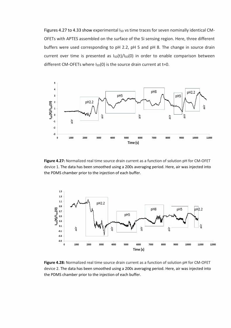
Figures 4.27 to 4.33 show experimental ISD vs time traces for seven nominally identical CM-
OFETs with APTES assembled on the surface of the Si sensing region. Here, three different
buffers were used corresponding to pH 2.2, pH 5 and pH 8. The change in source drain
current over time is presented as ISD(t)/ISD(0) in order to enable comparison between
different CM-OFETs where ISD(0) is the source drain current at t=0.
Figure 4.27: Normalized real time source drain current as a function of solution pH for CM-OFET
device 1. The data has been smoothed using a 200s averaging period. Here, air was injected into
the PDMS chamber prior to the injection of each buffer.
Figure 4.28: Normalized real time source drain current as a function of solution pH for CM-OFET
device 2. The data has been smoothed using a 200s averaging period. Here, air was injected into
the PDMS chamber prior to the injection of each buffer.
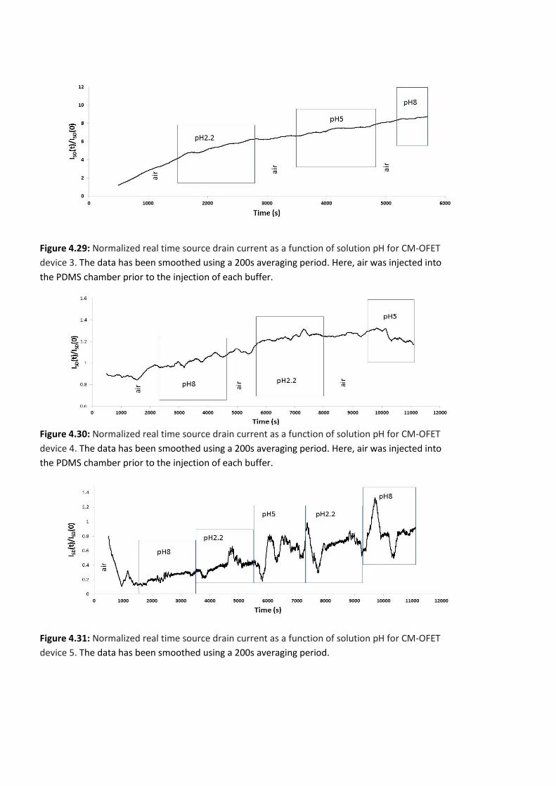
Figure 4.29: Normalized real time source drain current as a function of solution pH for CM-OFET
device 3. The data has been smoothed using a 200s averaging period. Here, air was injected into
the PDMS chamber prior to the injection of each buffer.
Figure 4.30: Normalized real time source drain current as a function of solution pH for CM-OFET
device 4. The data has been smoothed using a 200s averaging period. Here, air was injected into
the PDMS chamber prior to the injection of each buffer.
Figure 4.31: Normalized real time source drain current as a function of solution pH for CM-OFET
device 5. The data has been smoothed using a 200s averaging period.
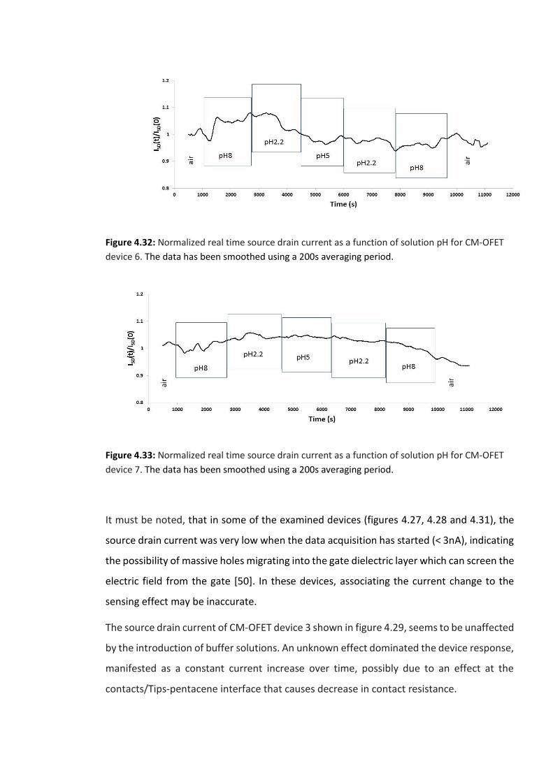
Figure 4.32: Normalized real time source drain current as a function of solution pH for CM-OFET
device 6. The data has been smoothed using a 200s averaging period.
Figure 4.33: Normalized real time source drain current as a function of solution pH for CM-OFET
device 7. The data has been smoothed using a 200s averaging period.
It must be noted, that in some of the examined devices (figures 4.27, 4.28 and 4.31), the
source drain current was very low when the data acquisition has started (< 3nA), indicating
the possibility of massive holes migrating into the gate dielectric layer which can screen the
electric field from the gate [50]. In these devices, associating the current change to the
sensing effect may be inaccurate.
The source drain current of CM-OFET device 3 shown in figure 4.29, seems to be unaffected
by the introduction of buffer solutions. An unknown effect dominated the device response,
manifested as a constant current increase over time, possibly due to an effect at the
contacts/Tips-pentacene interface that causes decrease in contact resistance.
The remaining devices (associated with figures 4.30, 4.32 and 4.33), did not show a
repeatable behaviour with solution pH. Instead, the CM-OFET response is dominated by
current fluctuations which make it difficult to make accurate judgement on what can be
considered increase or decrease within the timeframe each pH solution was present in the
sensing region. It should be noted that if migration of holes into the gate dielectric is indeed
happening during bias stress, then it is expected that the longer the measurement runs the
higher the accumulation of holes in the gate dielectric and the weaker the charge sensing
effect will be on the modulation of ISD. Therefore, the relative change in current due to a
change in charge density in the sensing region is expected to reduce with time.
4.5 Conclusion
Using a simple fabrication process, an OFET structure was transformed into a CM-OFET
device and explored as pH a sensor. Here, the CM-OFET sensor exploits modulation in
charge on the surface of the sensing region due to a change in pH. Specifically, the silicon
surface of the sensing region naturally contains silanol groups, which can become
protonated and deprotonated as a function of local pH. The associated change in surface
charge couples capacitively to the OFET leading to a change in the source drain current,
seen either in the transfer characteristics or time domain measurements. Due to the
limited range of pH over which the silanol groups are expected to change charge, the
surface was further modified using silane chemistry to introduce amine groups at the
surface. These amine groups were introduced to the Si floating gate surface by assembly
with a 3-aminoproyltrimethoxysilane self-assembled monolayer which was characterized
by x-ray photoelectron spectroscopy (XPS) to confirm the assembly of the layer and
successful functionalization with amine groups. Characterization of pH-sensitive CM-OFET
devices using both transfer characteristics and time domain measurements, did not
demonstrate a consistent response to pH changes in the sensing region of the devices.
Specifically, the changes in source drain current observed following changing of solution
pH were unrepeatable between and within devices and typically comparable in magnitude
to the changes in current inherent to the OFET. The final section of Chapter 5 will address
the sensitivity limitation of the proposed CM-OFET device that may have led to the deficient
performance.
4.6 References
[1] Misra, D., Worhoff, K., & Mascher, P. (2003). Dielectrics in Emerging Fields. In D. Misra,
K. Worhoff, & P. Mascher (Eds.), Dielectrics in Emerging Fields (pp. -). Pennington, New
Jersey: The Electrochemical Society Inc..
[2] Yates, D. E., Levine, S., & Healy, T. W. (1974). Site-binding model of the electrical double
layer at the oxide/water interface. Journal of the Chemical Society, Faraday Transactions 1:
Physical Chemistry in Condensed Phases, 70, 1807-1818.
[3] Yang, X., Frensley, W. R., Zhou, D., & Hu, W. (2012). Performance analysis of Si nanowire
biosensor by numerical modeling for charge sensing. IEEE Transactions on
Nanotechnology, 11(3), 501-512.
[4] Moretto, L. M., & Kalcher, K. (2014). Environmental analysis by electrochemical sensors
and biosensors. New York: Springer.
[5] Bousse, L., & Bergveld, P. (1984). The role of buried OH sites in the response mechanism
of inorganic-gate pH-sensitive ISFETs. Sensors and Actuators, 6(1), 65-78.
[6] Cui, Y., Wei, Q., Park, H., & Lieber, C. M. (2001). Nanowire nanosensors for highly
sensitive and selective detection of biological and chemical species. Science, 293(5533),
1289-1292.
[7] Patolsky, F., & Lieber, C. M. (2005). Nanowire nanosensors. Materials today, 8(4), 20-
28.
[8] Tian, R., Regonda, S., Gao, J., Liu, Y., & Hu, W. (2011). Ultrasensitive protein detection
using lithographically defined Si multi-nanowire field effect transistors. Lab on a
Chip, 11(11), 1952-1961.
[9] Chen, S., Bomer, J. G., Carlen, E. T., & van den Berg, A. (2011). Al2O3/silicon nanoISFET
with near ideal Nernstian response. Nano letters, 11(6), 2334-2341.
[10] Cheng, Y., Xiong, P., Yun, C. S., Strouse, G. F., Zheng, J. P., Yang, R. S., & Wang, Z. L.
(2008). Mechanism and optimization of pH sensing using SnO2 nanobelt field effect
transistors. Nano letters, 8(12), 4179.
[11] Kumar, N., Kumar, J., & Panda, S. (2015). Sensitivity enhancement mechanisms in
textured dielectric based electrolyte-insulator-semiconductor (EIS) sensors. ECS Journal of
Solid State Science and Technology, 4(3), N18-N23.
[12] Chen, Y., Wang, X., Erramilli, S., Mohanty, P., & Kalinowski, A. (2006). Silicon-based
nanoelectronic field-effect p H sensor with local gate control. Applied physics
letters, 89(22), 223512.
[13] Zang, P., Liang, Y., Spurgin, L., & Hu, W. (2013, August). pH sensing comparison of vapor
and solution APTES coated Si nanograting FETs. In Nanotechnology (IEEE-NANO), 2013 13th
IEEE Conference on (pp. 301-304). IEEE.
[14] Bhushan, B. (Ed.). (2010). Springer handbook of nanotechnology. Springer Science &
Business Media.
[15] Coffer, J. L. (Ed.). (2014). Semiconducting Silicon Nanowires for Biomedical
Applications. Elsevier.
[16] Wipf, M. (2010). Dual-gated field effect transistor for sensing applications (Doctoral
dissertation, Master’s thesis, University of Basel).
[17] Caboni, A., Orgiu, E., Barbaro, M., & Bonfiglio, A. (2009). Flexible organic thin-film
transistors for pH monitoring. IEEE Sensors Journal, 9(12), 1963-1970.
[18] van der Maaden, K., Tomar, J., Jiskoot, W., & Bouwstra, J. (2014). Chemical
Modifications of Silicon Surfaces for the Generation of a Tunable Surface Isoelectric
Point. Langmuir, 30(7), 1812-1819.
[19] Harris, D. C. (2007). Quantitative chemical analysis. W. H. Freeman and Company.
[20] Abiman, P., Wildgoose, G. G., Crossley, A., Jones, J. H., & Compton, R. G. (2007).
Contrasting pKa of Protonated Bis (3‐aminopropyl)‐Terminated Polyethylene Glycol
“Jeffamine” and the Associated Thermodynamic Parameters in Solution and Covalently
Attached to Graphite Surfaces. Chemistry–A European Journal, 13(34), 9663-9667.
[21] Mengistu, T. Z., Goel, V., Horton, J. H., & Morin, S. (2006). Chemical force titrations of
functionalized Si (111) surfaces. Langmuir, 22(12), 5301-5307.
[22] Vezenov, D. V., Noy, A., Rozsnyai, L. F., & Lieber, C. M. (1997). Force titrations and
ionization state sensitive imaging of functional groups in aqueous solutions by chemical
force microscopy. Journal of the American Chemical Society, 119(8), 2006-2015.
[23] Wang, H., & Linford, M. R. (2015). X-ray Photoelectron Spectroscopy and Auger
Electron Spectroscopy: Comparison and Basic Principles. Vacuum Technology & Coating.
[24] Watts, J. F. (1994). X-ray photoelectron spectroscopy. Vacuum, 45(6-7), 653-671.
[25] Boeckl, M., & Graham, D. (2006). Self-assembled monolayers: Advantages of pure
alkanethiols. Material matters, 1(2), 3-5.
[26] Prashar, D. (2012). Self assembled monolayers-a review. Int J ChemTech Res, 4(1),
258-265.
[27] Celestin, M., Krishnan, S., Bhansali, S., Stefanakos, E., & Goswami, D. Y. (2014). A
review of self-assembled monolayers as potential terahertz frequency tunnel
diodes. Nano Research, 7(5), 589-625.
[28] Bensebaa, F., Voicu, R., Huron, L., Ellis, T. H., & Kruus, E. (1997). Kinetics of formation
of long-chain n-alkanethiolate monolayers on polycrystalline gold. Langmuir, 13(20),
5335-5340.
[29] Khuat, T. T. H., Liang, L., Phan, T. T., Mizutani, G., & Rutt, H. N. (2019). Sum frequency
generation study of immobilized 3‐aminopropyltriethoxysilane self‐assembled layer on Si
(111) substrates. Surface and Interface Analysis, 51(1), 120-125.
[30] Gammoudi, H., Belkhiria, F., Helali, S., Assaker, I. B., Gammoudi, I., Morote, F., ... &
Chtourou, R. (2017). Chemically grafted of single-walled carbon nanotubes onto a
functionalized silicon surface. Journal of Alloys and Compounds, 694, 1036-1044.
[31] Ghorbanpour, M. (2016). Amine accessibility and chemical stability of silver SPR chips
silanised with APTES via vapour phase deposition method. Journal of Physical
Science, 27(1), 39.
[32] Li, S. Y., Ma, W., Zhou, Y., Chen, X., Ma, M., Xu, Y., ... & Wu, X. (2013). 3-
aminopropyltriethoxysilanes modified porous silicon as a voltammetric sensor for
determination of silver ion. Int. J. Electrochem. Sci, 8, 1802-1812.
[33] Zhang, F., Sautter, K., Larsen, A. M., Findley, D. A., Davis, R. C., Samha, H., & Linford,
M. R. (2010). Chemical vapor deposition of three aminosilanes on silicon dioxide: surface
characterization, stability, effects of silane concentration, and cyanine dye
adsorption. Langmuir, 26(18), 14648-14654.
[34] Lecoq, E., Duday, D., Bulou, S., Frache, G., Hilt, F., Maurau, R., & Choquet, P. (2013).
Plasma polymerization of APTES to elaborate nitrogen containing organosilicon thin films:
influence of process parameters and discussion about the growing mechanisms. Plasma
Processes and Polymers, 10(3), 250-261.
[35] Landoulsi, J., Genet, M. J., El Kirat, K., Richard, C., Pulvin, S., & Rouxhet, P. G. (2011).
Silanization with APTES for controlling the interactions between stainless steel and
biocomponents: reality vs expectation. In Biomaterials-Physics and Chemistry. InTech.
[36] Haddada, M. B., Blanchard, J., Casale, S., Krafft, J. M., Vallée, A., Méthivier, C., &
Boujday, S. (2013). Optimizing the immobilization of gold nanoparticles on functionalized
silicon surfaces: amine-vs thiol-terminated silane. Gold Bulletin, 46(4), 335-341.
[37] Paredes, V., Salvagni, E., Rodríguez‐Castellon, E., Gil, F. J., & Manero, J. M. (2015). Study
on the use of 3‐aminopropyltriethoxysilane and 3‐chloropropyltriethoxysilane to surface
biochemical modification of a novel low elastic modulus Ti–Nb–Hf alloy. Journal of
Biomedical Materials Research Part B: Applied Biomaterials, 103(3), 495-502.
[38] Williams, E. H., Davydov, A. V., Motayed, A., Sundaresan, S. G., Bocchini, P., Richter, L.
J., ... & Rao, M. V. (2012). Immobilization of streptavidin on 4H–SiC for biosensor
development. Applied surface science, 258(16), 6056-6063.
[39] Kyaw, H. H., Al-Harthi, S. H., Sellai, A., & Dutta, J. (2015). Self-organization of gold
nanoparticles on silanated surfaces. Beilstein journal of nanotechnology, 6, 2345.
[40] Gholamrezaie, F., Andringa, A. M., Roelofs, W. S., Neuhold, A., Kemerink, M., Blom, P.
W., & de Leeuw, D. M. (2012). Charge Trapping by Self‐Assembled Monolayers as the Origin
of the Threshold Voltage Shift in Organic Field‐Effect Transistors. Small, 8(2), 241-245.
[41] Yu, J., Yu, X., Zhang, L., & Zeng, H. (2012). Ammonia gas sensor based on pentacene
organic field-effect transistor. Sensors and Actuators B: Chemical, 173, 133-138.
[42] Chuan-ling Wu & Hsiao-Wen Zan (2008). Functional Group Modification on Dielectric
Interface of Pentacene-Based OTFTs for Ammonia Sensor (Doctoral thesis), Institute of
Electro-Optical Engineering, National Chiao Tung University.
[43] Honda, T., Miyazaki, M., Nakamura, H., & Maeda, H. (2005). Controllable
polymerization of N-carboxy anhydrides in a microreaction system. Lab on a Chip, 5(8),
812-818.
[44] Lee, J. N., Park, C., & Whitesides, G. M. (2003). Solvent compatibility of poly
(dimethylsiloxane)-based microfluidic devices. Analytical chemistry, 75(23), 6544-6554.
[45] Rumens, C. V., Ziai, M. A., Belsey, K. E., Batchelor, J. C., & Holder, S. J. (2015). Swelling
of PDMS networks in solvent vapours; applications for passive RFID wireless
sensors. Journal of Materials Chemistry C, 3(39), 10091-10098.
[46] Obaidulla, S. M., Singh, S., Mohapatra, Y. N., & Giri, P. K. (2017). Ambient condition
bias stress stability of vanadium (IV) oxide phthalocyanine based p-channel organic field-
effect transistors. Journal of Physics D: Applied Physics, 51(1), 015110.
[47] Lee, B., Wan, A., Mastrogiovanni, D., Anthony, J. E., Garfunkel, E., & Podzorov, V.
(2010). Origin of the bias stress instability in single-crystal organic field-effect
transistors. Physical Review B, 82(8), 085302.
[48] McIlvaine, T. C. (1921). A buffer solution for colorimetric comparison. Journal of
Biological Chemistry, 49(1), 183-186.
[49] Spanu, A., Lai, S., Cosseddu, P., Tedesco, M., Martinoia, S., & Bonfiglio, A. (2015). An
organic transistor-based system for reference-less electrophysiological monitoring of
excitable cells. Scientific reports, 5.
[50] Lee, B., Wan, A., Mastrogiovanni, D., Anthony, J. E., Garfunkel, E., & Podzorov, V.
(2010). Origin of the bias stress instability in single-crystal organic field-effect
transistors. Physical Review B, 82(8), 085302.
Chapter 5
Protein Detection Using the CM-OFET Device
In the previous chapter the CM-OFET was configured for pH monitoring, where changes in
pH were detected by the corresponding change in charge of a molecular monolayer
immobilised on the surface of the CM-OFET sensing region. In this chapter, the charge
sensing capability of the device is explored to detect biomolecular interactions occurring at
the sensing surface of the device. The ability to detect and quantify specific biomarkers is
central to next generation clinical diagnostics. The label-free CM-OFET biosensor presented
in this chapter has the potential to address this challenge. The biosensor is investigated
here for monitoring one of the strongest non-covalent interactions, the binding of biotin to
avidin. The combination of this biologically active protein (avidin) and the small
biomolecule biotin is widely used as a model for biorecognition studies.
In the chapter, firstly a brief overview on both biotin and avidin and their interactions is
given. Then a study of quartz crystal microbalance with dissipation (QCM-D) that were used
to assess a protocol for biotinylation of the sensing surface and confirm the immobilisation
of avidin is presented. Finally, the use of CM-OFET device for label-free detection avidin is
discussed.
5.1 Biotin, Avidin and their interaction
5.1.1 Biotin
Biotin (chemical structure shown in figure 5.1), sometimes called vitamin B7, vitamin H,
and also known as coenzyme R as it a co-factor for five biotin-dependent carboxylase
enzymes [1-2] is a water-soluble vitamin necessary for metabolising carbohydrates. Despite
its importance to human health, this vitamin is not naturally produced by the human body
but rather is extracted from food or synthesized by bacteria found in the human intestine
[2-3].
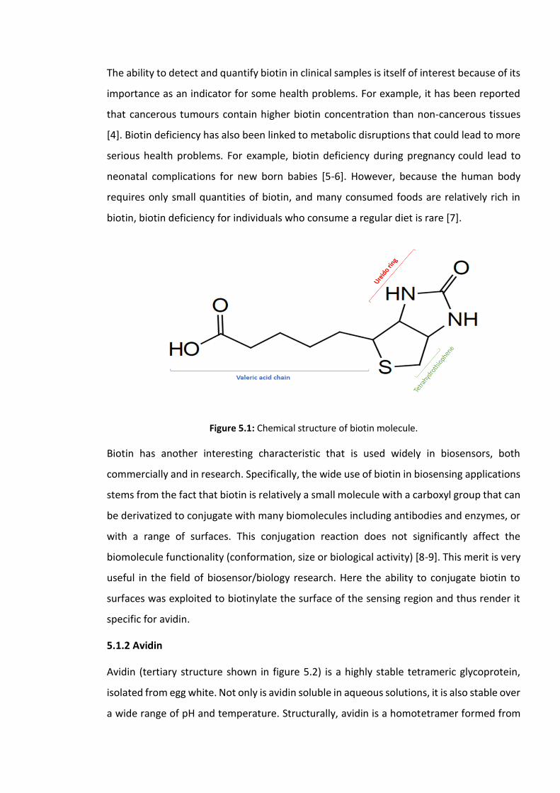
The ability to detect and quantify biotin in clinical samples is itself of interest because of its
importance as an indicator for some health problems. For example, it has been reported
that cancerous tumours contain higher biotin concentration than non-cancerous tissues
[4]. Biotin deficiency has also been linked to metabolic disruptions that could lead to more
serious health problems. For example, biotin deficiency during pregnancy could lead to
neonatal complications for new born babies [5-6]. However, because the human body
requires only small quantities of biotin, and many consumed foods are relatively rich in
biotin, biotin deficiency for individuals who consume a regular diet is rare [7].
Figure 5.1: Chemical structure of biotin molecule.
Biotin has another interesting characteristic that is used widely in biosensors, both
commercially and in research. Specifically, the wide use of biotin in biosensing applications
stems from the fact that biotin is relatively a small molecule with a carboxyl group that can
be derivatized to conjugate with many biomolecules including antibodies and enzymes, or
with a range of surfaces. This conjugation reaction does not significantly affect the
biomolecule functionality (conformation, size or biological activity) [8-9]. This merit is very
useful in the field of biosensor/biology research. Here the ability to conjugate biotin to
surfaces was exploited to biotinylate the surface of the sensing region and thus render it
specific for avidin.
5.1.2 Avidin
Avidin (tertiary structure shown in figure 5.2) is a highly stable tetrameric glycoprotein,
isolated from egg white. Not only is avidin soluble in aqueous solutions, it is also stable over
a wide range of pH and temperature. Structurally, avidin is a homotetramer formed from
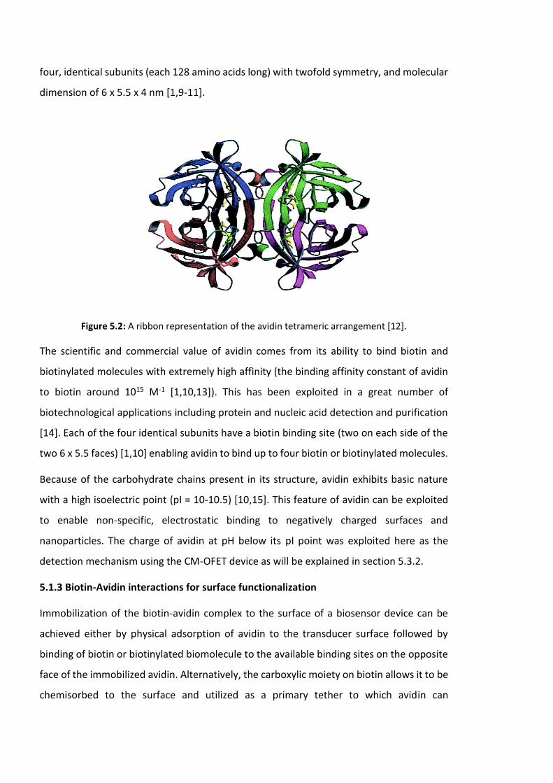
four, identical subunits (each 128 amino acids long) with twofold symmetry, and molecular
dimension of 6 x 5.5 x 4 nm [1,9-11].
Figure 5.2: A ribbon representation of the avidin tetrameric arrangement [12].
The scientific and commercial value of avidin comes from its ability to bind biotin and
biotinylated molecules with extremely high affinity (the binding affinity constant of avidin
to biotin around 1015 M-1 [1,10,13]). This has been exploited in a great number of
biotechnological applications including protein and nucleic acid detection and purification
[14]. Each of the four identical subunits have a biotin binding site (two on each side of the
two 6 x 5.5 faces) [1,10] enabling avidin to bind up to four biotin or biotinylated molecules.
Because of the carbohydrate chains present in its structure, avidin exhibits basic nature
with a high isoelectric point (pI = 10-10.5) [10,15]. This feature of avidin can be exploited
to enable non-specific, electrostatic binding to negatively charged surfaces and
nanoparticles. The charge of avidin at pH below its pI point was exploited here as the
detection mechanism using the CM-OFET device as will be explained in section 5.3.2.
5.1.3 Biotin-Avidin interactions for surface functionalization
Immobilization of the biotin-avidin complex to the surface of a biosensor device can be
achieved either by physical adsorption of avidin to the transducer surface followed by
binding of biotin or biotinylated biomolecule to the available binding sites on the opposite
face of the immobilized avidin. Alternatively, the carboxylic moiety on biotin allows it to be
chemisorbed to the surface and utilized as a primary tether to which avidin can
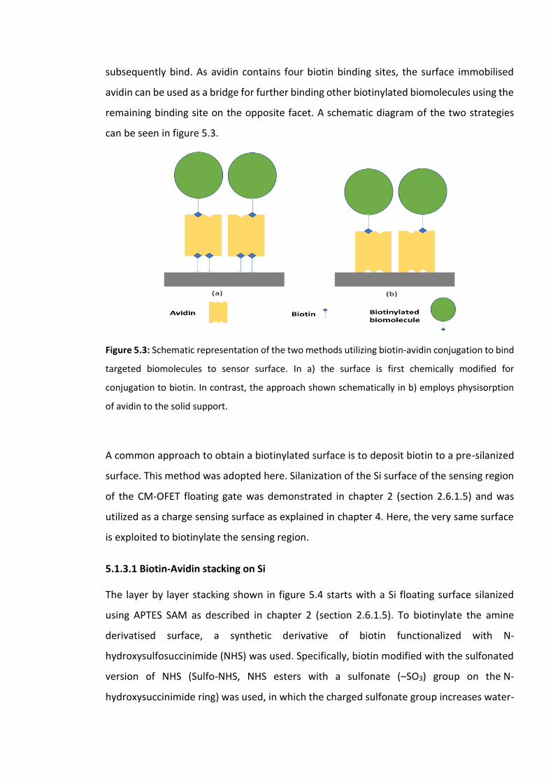
subsequently bind. As avidin contains four biotin binding sites, the surface immobilised
avidin can be used as a bridge for further binding other biotinylated biomolecules using the
remaining binding site on the opposite facet. A schematic diagram of the two strategies
can be seen in figure 5.3.
Figure 5.3: Schematic representation of the two methods utilizing biotin-avidin conjugation to bind
targeted biomolecules to sensor surface. In a) the surface is first chemically modified for
conjugation to biotin. In contrast, the approach shown schematically in b) employs physisorption
of avidin to the solid support.
A common approach to obtain a biotinylated surface is to deposit biotin to a pre-silanized
surface. This method was adopted here. Silanization of the Si surface of the sensing region
of the CM-OFET floating gate was demonstrated in chapter 2 (section 2.6.1.5) and was
utilized as a charge sensing surface as explained in chapter 4. Here, the very same surface
is exploited to biotinylate the sensing region.
5.1.3.1 Biotin-Avidin stacking on Si
The layer by layer stacking shown in figure 5.4 starts with a Si floating surface silanized
using APTES SAM as described in chapter 2 (section 2.6.1.5). To biotinylate the amine
derivatised surface, a synthetic derivative of biotin functionalized with N-
hydroxysulfosuccinimide (NHS) was used. Specifically, biotin modified with the sulfonated
version of NHS (Sulfo-NHS, NHS esters with a sulfonate (–SO3) group on the N-
hydroxysuccinimide ring) was used, in which the charged sulfonate group increases water-
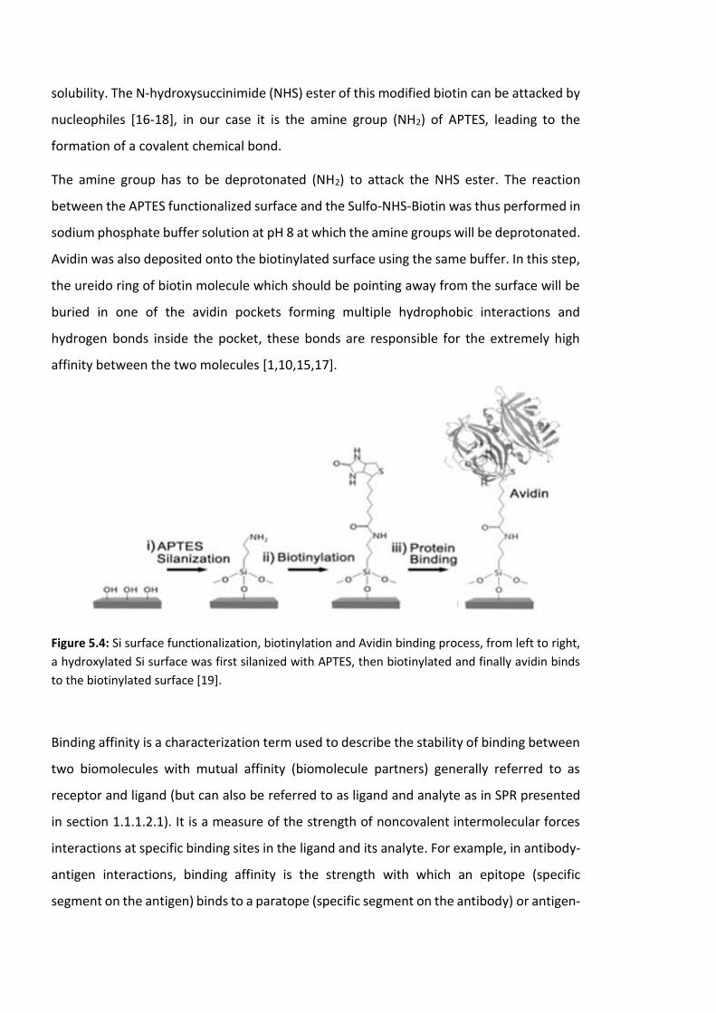
solubility. The N-hydroxysuccinimide (NHS) ester of this modified biotin can be attacked by
nucleophiles [16-18], in our case it is the amine group (NH2) of APTES, leading to the
formation of a covalent chemical bond.
The amine group has to be deprotonated (NH2) to attack the NHS ester. The reaction
between the APTES functionalized surface and the Sulfo-NHS-Biotin was thus performed in
sodium phosphate buffer solution at pH 8 at which the amine groups will be deprotonated.
Avidin was also deposited onto the biotinylated surface using the same buffer. In this step,
the ureido ring of biotin molecule which should be pointing away from the surface will be
buried in one of the avidin pockets forming multiple hydrophobic interactions and
hydrogen bonds inside the pocket, these bonds are responsible for the extremely high
affinity between the two molecules [1,10,15,17].
Figure 5.4: Si surface functionalization, biotinylation and Avidin binding process, from left to right,
a hydroxylated Si surface was first silanized with APTES, then biotinylated and finally avidin binds
to the biotinylated surface [19].
Binding affinity is a characterization term used to describe the stability of binding between
two biomolecules with mutual affinity (biomolecule partners) generally referred to as
receptor and ligand (but can also be referred to as ligand and analyte as in SPR presented
in section 1.1.1.2.1). It is a measure of the strength of noncovalent intermolecular forces
interactions at specific binding sites in the ligand and its analyte. For example, in antibody-
antigen interactions, binding affinity is the strength with which an epitope (specific
segment on the antigen) binds to a paratope (specific segment on the antibody) or antigen-

binding site on the antibody. This means, the greater intermolecular force between an
analyte and its ligand the higher the binding affinity and vice versa [20-22].
In reality, the binding process between a ligand and an analyte involves a combination
of noncovalent interactions such as hydrogen bonds, hydrophobic interactions,
electrostatic and van der Waals forces between the binding sites on both the ligand
and the analyte. This interaction is dynamic, which means that the relationship
between the concentration of free analyte, ligand and the analyte-ligand complex
exists in a dynamic equilibrium govern by basic reversible biomolecular interaction
expressed as:
[A] + [L]
ka →
kd ←
[A . L] (5.1)
Where ka (also referred to as kon or k1) and kd (also referred to as koff or k2) are the rate
constants for the association and dissociation reaction, respectively and [A], [L], and [A.L]
are the concentrations of free analytes, free ligands, and analyte–ligand complexes at
equilibrium, respectively.
The concentration of analyte-ligand complex at equilibrium can be calculated by the so-
called association constant, KA, or its reciprocal, the dissociation constant, KD, by:
KA = konkoff
= [A . L]
[A][L]=
1
KD (5.2)
The association constant, KA, (with units of M-1) and its reciprocal, the dissociation
constant, KD, (units M) are used widely to quantify the strength of a ligand receptor affinity
interaction. The higher the magnitude of KA (or conversely, the lower the value of KD), the
higher the affinity of ligand-analyte.
In practical terms, as was introduced in section (1.1.1.2.1), KD is defined as the
concentration of analyte that leads to 50% occupancy of the ligand’s binding site or in other
words, the concentration of analyte at which the concentration of analyte-ligand complex
equals the concentration of ligand with no analyte bound. This means that a system with
low KD requires a lower analyte concentration to achieve 50% occupancy.
On the noncovalent binding affinity scale, the biotin–avidin complex investigated in this
chapter comes at the higher end with very strong affinity (around 1015 M-1) comparable to
the strength of weak covalent bonds. Typical antibody-antigen interactions have a binding
affinity in the range of 107 to 1011 M-1 [23-24].
5.1.3.2 Biotin-Avidin immobilizing protocol on Si
Once the sensing region of the Si floating gate of the CM-OFET device is silanized,
biotinylation was performed inside the PDMS chamber of the CM-OFET device. 1 mg of
Sulfo-NHS biotin was dissolved in 0.1 M sodium phosphate buffer solution (SPB) at pH8 and
was injected over the pre-silanized Si surface through the PDMS fluidic channel. After 25
minutes, the biotinylated Si surface was washed with a stream of the SPB (pH8) for several
minutes to remove excess unreacted biotin. The biotinylated Si surface was then exposed
to 0.1 mg of avidin in 0.1 M sodium phosphate buffer solution SPB (pH8) through the PDMS
chamber and left to incubate on the biotinylated Si surface for 25 minutes. Finally, excess
avidin was washed from the surface with SPB (pH8).
The SPB concentration (0.1 M) was selected to ensure that the molecular stack of APTES +
Biotin + Avidin is shorter than the Debye length, λD, and the molecular charges on the avidin
surface are thus not fully screened by free ions in the buffer solution. The Debye length
was calculated using equation 5.3 [25].
𝜆𝐷 = √ ε𝑟 ε0 𝑘𝑇
2𝑁𝐴 𝑞2𝐼 (5.3)
Where ε0 is the electrical permittivity of the vacuum, εr is the relative dielectric constant of
the solution, k the Boltzmann constant, T the absolute temperature, NA is Avogadro’s
number, q the elementary charge and I the ionic strength of the solution.
At room temperature, this can be reduced to
𝜆𝐷 = 1.085 × 10⁻⁹√ ε𝑟𝐼
𝜆𝐷 = 1.085 √ ε𝑟𝐼 𝑛𝑚
The relative dielectric constant for SPB was εr ≈ 80 [26] while I was calculated using
equation 5.4:
I =1
2∑ 𝑐𝑖𝑛𝑖=1 𝑧𝑖
2 (5.4)
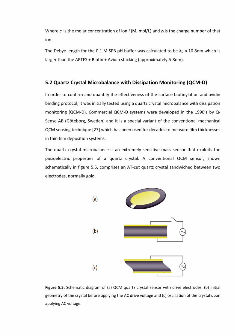
Where ci is the molar concentration of ion i (M, mol/L) and zi is the charge number of that
ion.
The Debye length for the 0.1 M SPB pH buffer was calculated to be λD ≈ 10.8nm which is
larger than the APTES + Biotin + Avidin stacking (approximately 6-8nm).
5.2 Quartz Crystal Microbalance with Dissipation Monitoring (QCM-D)
In order to confirm and quantify the effectiveness of the surface biotinylation and avidin
binding protocol, it was initially tested using a quartz crystal microbalance with dissipation
monitoring (QCM-D). Commercial QCM-D systems were developed in the 1990’s by Q-
Sense AB (Göteborg, Sweden) and it is a special variant of the conventional mechanical
QCM sensing technique [27] which has been used for decades to measure film thicknesses
in thin film deposition systems.
The quartz crystal microbalance is an extremely sensitive mass sensor that exploits the
piezoelectric properties of a quartz crystal. A conventional QCM sensor, shown
schematically in figure 5.5, comprises an AT-cut quartz crystal sandwiched between two
electrodes, normally gold.
Figure 5.5: Schematic diagram of (a) QCM quartz crystal sensor with drive electrodes, (b) initial
geometry of the crystal before applying the AC drive voltage and (c) oscillation of the crystal upon
applying AC voltage.
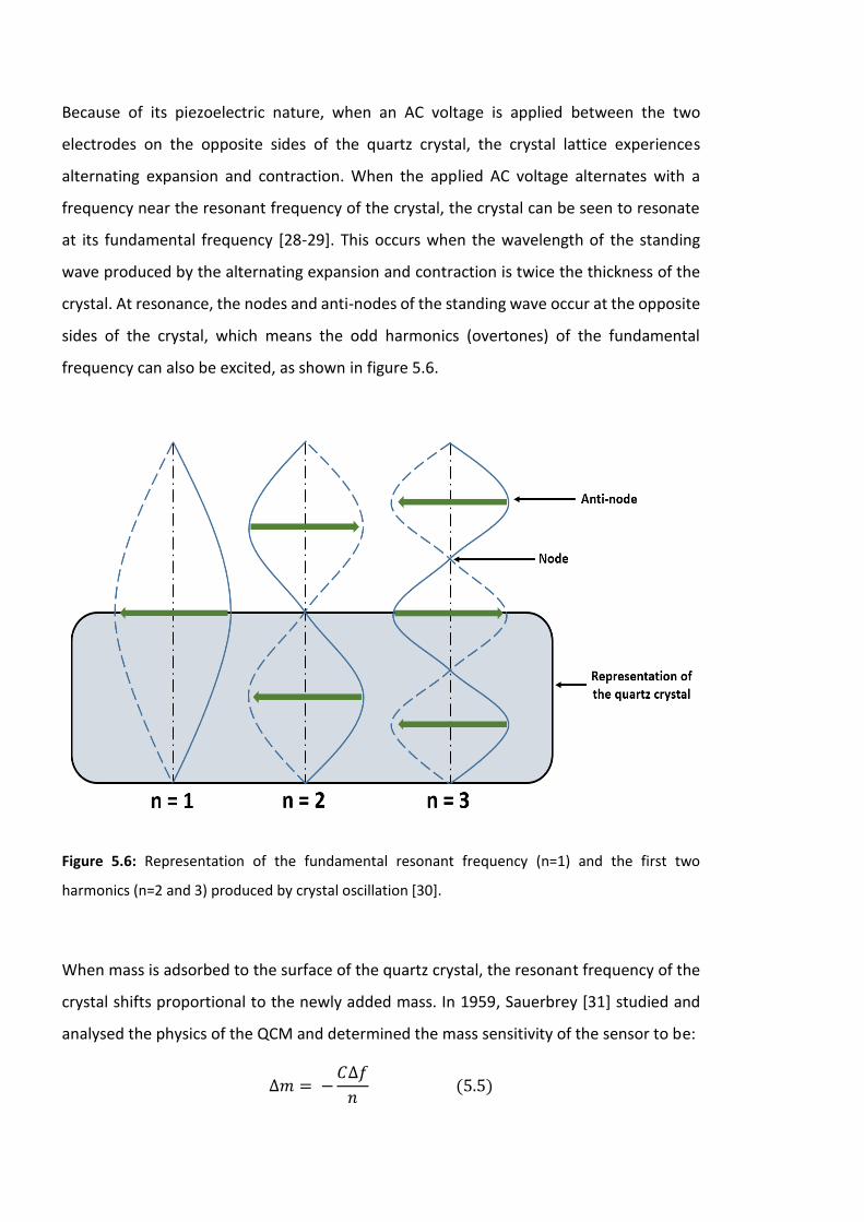
Because of its piezoelectric nature, when an AC voltage is applied between the two
electrodes on the opposite sides of the quartz crystal, the crystal lattice experiences
alternating expansion and contraction. When the applied AC voltage alternates with a
frequency near the resonant frequency of the crystal, the crystal can be seen to resonate
at its fundamental frequency [28-29]. This occurs when the wavelength of the standing
wave produced by the alternating expansion and contraction is twice the thickness of the
crystal. At resonance, the nodes and anti-nodes of the standing wave occur at the opposite
sides of the crystal, which means the odd harmonics (overtones) of the fundamental
frequency can also be excited, as shown in figure 5.6.
Figure 5.6: Representation of the fundamental resonant frequency (n=1) and the first two
harmonics (n=2 and 3) produced by crystal oscillation [30].
When mass is adsorbed to the surface of the quartz crystal, the resonant frequency of the
crystal shifts proportional to the newly added mass. In 1959, Sauerbrey [31] studied and
analysed the physics of the QCM and determined the mass sensitivity of the sensor to be:
∆𝑚 = −𝐶∆𝑓
𝑛 (5.5)
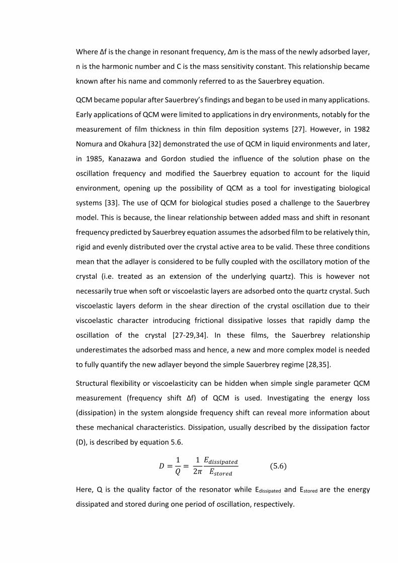
Where Δf is the change in resonant frequency, Δm is the mass of the newly adsorbed layer,
n is the harmonic number and C is the mass sensitivity constant. This relationship became
known after his name and commonly referred to as the Sauerbrey equation.
QCM became popular after Sauerbrey’s findings and began to be used in many applications.
Early applications of QCM were limited to applications in dry environments, notably for the
measurement of film thickness in thin film deposition systems [27]. However, in 1982
Nomura and Okahura [32] demonstrated the use of QCM in liquid environments and later,
in 1985, Kanazawa and Gordon studied the influence of the solution phase on the
oscillation frequency and modified the Sauerbrey equation to account for the liquid
environment, opening up the possibility of QCM as a tool for investigating biological
systems [33]. The use of QCM for biological studies posed a challenge to the Sauerbrey
model. This is because, the linear relationship between added mass and shift in resonant
frequency predicted by Sauerbrey equation assumes the adsorbed film to be relatively thin,
rigid and evenly distributed over the crystal active area to be valid. These three conditions
mean that the adlayer is considered to be fully coupled with the oscillatory motion of the
crystal (i.e. treated as an extension of the underlying quartz). This is however not
necessarily true when soft or viscoelastic layers are adsorbed onto the quartz crystal. Such
viscoelastic layers deform in the shear direction of the crystal oscillation due to their
viscoelastic character introducing frictional dissipative losses that rapidly damp the
oscillation of the crystal [27-29,34]. In these films, the Sauerbrey relationship
underestimates the adsorbed mass and hence, a new and more complex model is needed
to fully quantify the new adlayer beyond the simple Sauerbrey regime [28,35].
Structural flexibility or viscoelasticity can be hidden when simple single parameter QCM
measurement (frequency shift Δf) of QCM is used. Investigating the energy loss
(dissipation) in the system alongside frequency shift can reveal more information about
these mechanical characteristics. Dissipation, usually described by the dissipation factor
(D), is described by equation 5.6.
𝐷 =1
𝑄=
1
2𝜋
𝐸𝑑𝑖𝑠𝑠𝑖𝑝𝑎𝑡𝑒𝑑
𝐸𝑠𝑡𝑜𝑟𝑒𝑑 (5.6)
Here, Q is the quality factor of the resonator while Edissipated and Estored are the energy
dissipated and stored during one period of oscillation, respectively.
In QCM-D, dissipation is measured by exciting the crystal with a voltage pulse i.e.
periodically switching on and off the driving voltage. The time taken for the oscillation to
decay is recorded during the off state and is related to the energy dissipated in the system
as described in equation 5.7:
𝐷 = 2
𝜔𝜏 (5.7)
Here τ is the decay time and ω is the angular frequency of the oscillation [28,34].
Dissipation in rigid and viscoelastic layers unfolds differently; the energy in viscoelastic
systems dissipates faster than for rigid layers, as shown schematically in figure 5.7.
Figure 5.7: Illustration of the difference in frequency and dissipation response in a QCM-D system
for rigid and soft films [36].
Combining information from the shift in resonant frequency, Δf, with energy dissipated, D,
can provide a finger print of the characteristics of the adsorbed layer, and measurements
of both parameters can be utilized in a comprehensive model that take into account the
viscoelastic properties of the adsorbed layer. The Voigt model (sometimes called Kevin-
Voigt model) is one of the most widely used QCM-D models used to analyse viscoelastic
and soft films [37-38]. In the Voight model, the viscoelastic properties of the adsorbed film
including the density, viscosity, elasticity, and thickness are correlated with the measured
Δf and D, so when they are recorded for multiple overtones these parameters can be
estimated (some valid assumptions are needed as the Voigt model deal with multi-
unknown parameters) [37,39].
5.3 Results and discussion
5.3.1 QCM-D results
QCM-D was used to monitor surface biotinylation and subsequent binding of avidin to the
biotinylated silicon oxide surface. Measurements were performed using a Q-sense E4
instrument (Q-Sense, Biolin Scientific, Sweden) with SiO2 coated quartz crystal sensors (QSX
303). The frequency and dissipation responses were recorded at the fundamental resonant
frequency (5 MHz) and several overtones (harmonics), n = 3, 5, 7, 9, 11 and 13. For clarity,
only the frequency shift, Δf, and the dissipation shift, D, for the 3rd overtone is presented.
The measurements were conducted at 21°C maintained by a Peltier within the fluidic
chamber.
Four measurements were performed simultaneously, two replicates designed to quantify
the specific binding of avidin to biotinylated crystal (sensors 1 and 2) and two replicates to
investigate the degree of non-specific binding of avidin to a silanized, non-biotinylated
crystal (sensors 3 and 4).
5.3.1.1 Experimental protocol
- Four, SiO2-coated QCM-D sensors were immersed in a 5% APTES IPA solution
overnight (approximately 18 hours) to form an APTES SAM layer. The sensors were
then washed in IPA and dried under nitrogen before being loaded into the four,
independent QCM-D flow chambers.
- After loading the sensors into the QCM-D system, sodium phosphate buffer (SPB at
pH8) was first pumped over both crystal resonators at 20 µl/min and left running
until the frequency and dissipation response curves were stable (Δf < ±0.5 Hz).
- After a stable baseline was obtained, sensors 1 and 2 were biotinylated by exposure
to Sulfo-NHS Biotin (1 mg/mL in SPB, pH8 at 20 µl/min) for 48 mins. Simultaneously,
sensors 3 and 4 (control measurement) were left with SPB (pH8) running through
the system.
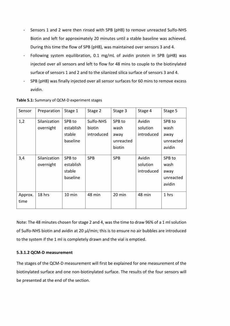
- Sensors 1 and 2 were then rinsed with SPB (pH8) to remove unreacted Sulfo-NHS
Biotin and left for approximately 20 minutes until a stable baseline was achieved.
During this time the flow of SPB (pH8), was maintained over sensors 3 and 4.
- Following system equilibration, 0.1 mg/mL of avidin protein in SPB (pH8) was
injected over all sensors and left to flow for 48 mins to couple to the biotinylated
surface of sensors 1 and 2 and to the silanized silica surface of sensors 3 and 4.
- SPB (pH8) was finally injected over all sensor surfaces for 60 mins to remove excess
avidin.
Table 5.1: Summary of QCM-D experiment stages
Sensor Preparation Stage 1 Stage 2 Stage 3 Stage 4 Stage 5
1,2 Silanization
overnight
SPB to
establish
stable
baseline
Sulfo-NHS
biotin
introduced
SPB to
wash
away
unreacted
biotin
Avidin
solution
introduced
SPB to
wash
away
unreacted
avidin
3,4 Silanization
overnight
SPB to
establish
stable
baseline
SPB SPB Avidin
solution
introduced
SPB to
wash
away
unreacted
avidin
Approx.
time
18 hrs 10 min 48 min 20 min 48 min 1 hrs
Note: The 48 minutes chosen for stage 2 and 4, was the time to draw 96% of a 1 ml solution
of Sulfo-NHS biotin and avidin at 20 µl/min; this is to ensure no air bubbles are introduced
to the system if the 1 ml is completely drawn and the vial is emptied.
5.3.1.2 QCM-D measurement
The stages of the QCM-D measurement will first be explained for one measurement of the
biotinylated surface and one non-biotinylated surface. The results of the four sensors will
be presented at the end of the section.
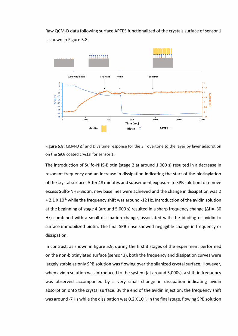
Raw QCM-D data following surface APTES functionalized of the crystals surface of sensor 1
is shown in Figure 5.8.
Figure 5.8: QCM-D Δf and D vs time response for the 3rd overtone to the layer by layer adsorption
on the SiO2 coated crystal for sensor 1.
The introduction of Sulfo-NHS-Biotin (stage 2 at around 1,000 s) resulted in a decrease in
resonant frequency and an increase in dissipation indicating the start of the biotinylation
of the crystal surface. After 48 minutes and subsequent exposure to SPB solution to remove
excess Sulfo-NHS-Biotin, new baselines were achieved and the change in dissipation was D
≈ 2.1 X 10⁻⁶ while the frequency shift was around -12 Hz. Introduction of the avidin solution
at the beginning of stage 4 (around 5,000 s) resulted in a sharp frequency change (∆f ≈ -30
Hz) combined with a small dissipation change, associated with the binding of avidin to
surface immobilized biotin. The final SPB rinse showed negligible change in frequency or
dissipation.
In contrast, as shown in figure 5.9, during the first 3 stages of the experiment performed
on the non-biotinylated surface (sensor 3), both the frequency and dissipation curves were
largely stable as only SPB solution was flowing over the silanized crystal surface. However,
when avidin solution was introduced to the system (at around 5,000s), a shift in frequency
was observed accompanied by a very small change in dissipation indicating avidin
absorption onto the crystal surface. By the end of the avidin injection, the frequency shift
was around -7 Hz while the dissipation was 0.2 X 10⁻⁶. In the final stage, flowing SPB solution
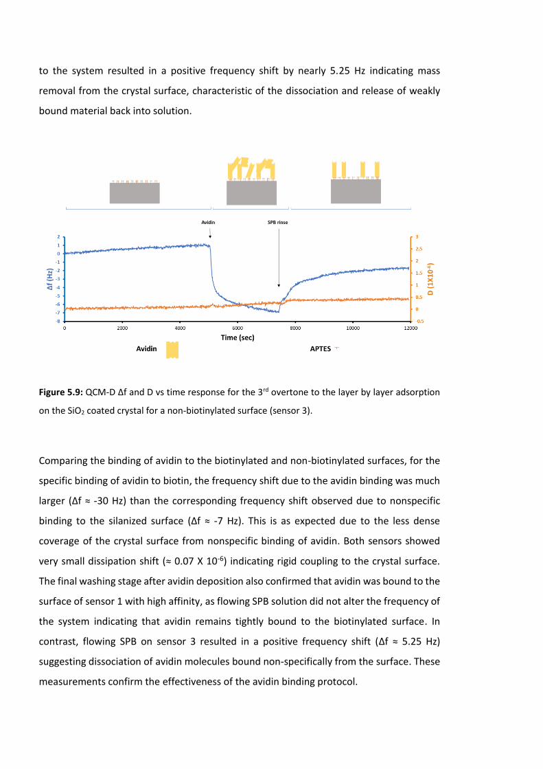
to the system resulted in a positive frequency shift by nearly 5.25 Hz indicating mass
removal from the crystal surface, characteristic of the dissociation and release of weakly
bound material back into solution.
Figure 5.9: QCM-D Δf and D vs time response for the 3rd overtone to the layer by layer adsorption
on the SiO2 coated crystal for a non-biotinylated surface (sensor 3).
Comparing the binding of avidin to the biotinylated and non-biotinylated surfaces, for the
specific binding of avidin to biotin, the frequency shift due to the avidin binding was much
larger (∆f ≈ -30 Hz) than the corresponding frequency shift observed due to nonspecific
binding to the silanized surface (∆f ≈ -7 Hz). This is as expected due to the less dense
coverage of the crystal surface from nonspecific binding of avidin. Both sensors showed
very small dissipation shift (≈ 0.07 X 10⁻⁶) indicating rigid coupling to the crystal surface.
The final washing stage after avidin deposition also confirmed that avidin was bound to the
surface of sensor 1 with high affinity, as flowing SPB solution did not alter the frequency of
the system indicating that avidin remains tightly bound to the biotinylated surface. In
contrast, flowing SPB on sensor 3 resulted in a positive frequency shift (∆f ≈ 5.25 Hz)
suggesting dissociation of avidin molecules bound non-specifically from the surface. These
measurements confirm the effectiveness of the avidin binding protocol.
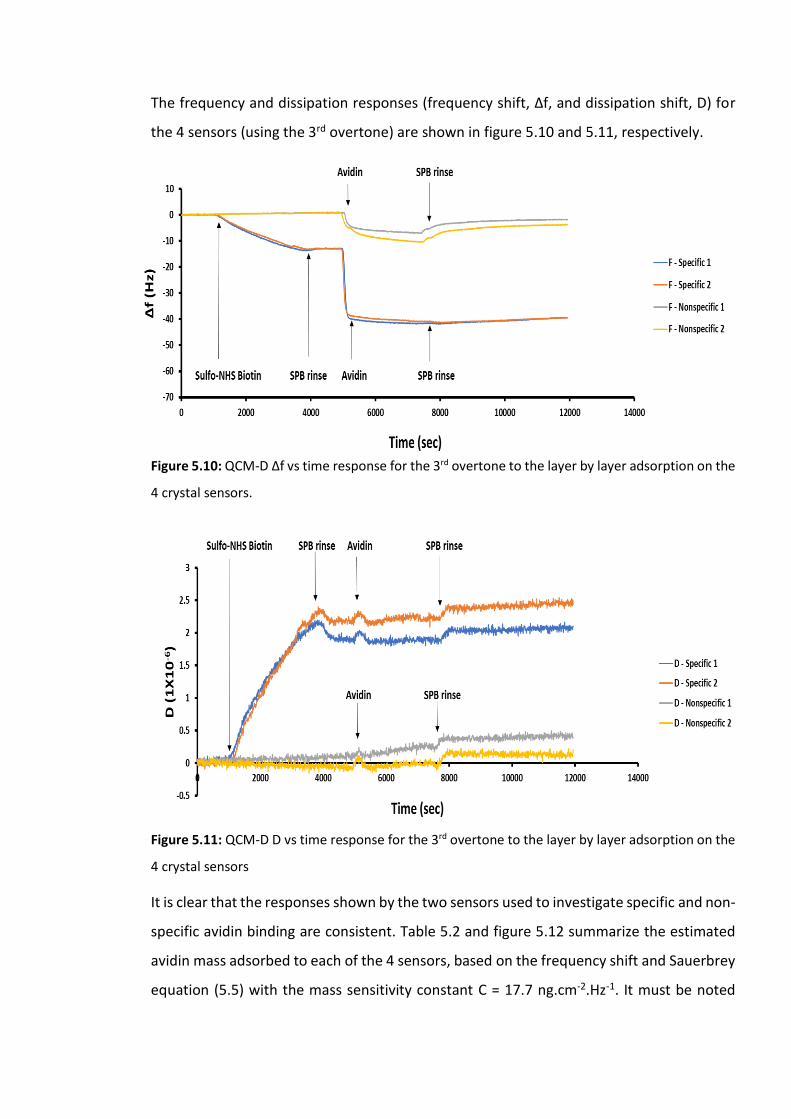
The frequency and dissipation responses (frequency shift, Δf, and dissipation shift, D) for
the 4 sensors (using the 3rd overtone) are shown in figure 5.10 and 5.11, respectively.
Figure 5.10: QCM-D Δf vs time response for the 3rd overtone to the layer by layer adsorption on the
4 crystal sensors.
Figure 5.11: QCM-D D vs time response for the 3rd overtone to the layer by layer adsorption on the
4 crystal sensors
It is clear that the responses shown by the two sensors used to investigate specific and non-
specific avidin binding are consistent. Table 5.2 and figure 5.12 summarize the estimated
avidin mass adsorbed to each of the 4 sensors, based on the frequency shift and Sauerbrey
equation (5.5) with the mass sensitivity constant C = 17.7 ng.cm-2.Hz-1. It must be noted
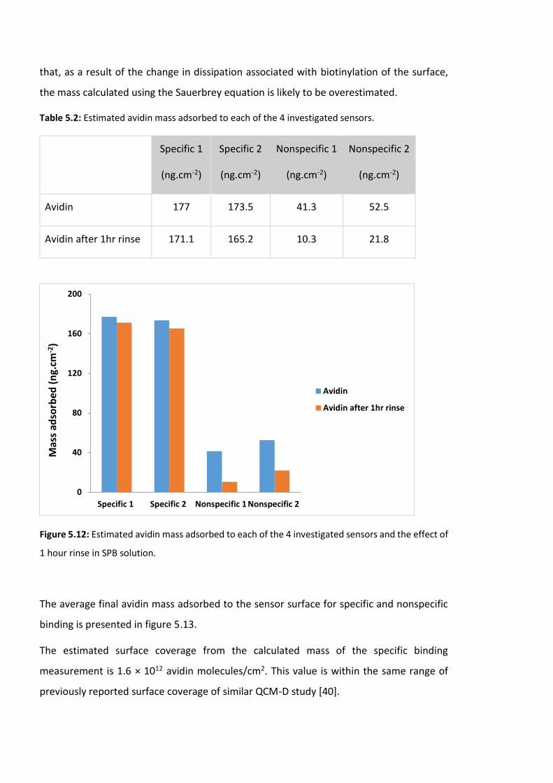
that, as a result of the change in dissipation associated with biotinylation of the surface,
the mass calculated using the Sauerbrey equation is likely to be overestimated.
Table 5.2: Estimated avidin mass adsorbed to each of the 4 investigated sensors.
Specific 1
(ng.cm-2)
Specific 2
(ng.cm-2)
Nonspecific 1
(ng.cm-2)
Nonspecific 2
(ng.cm-2)
Avidin 177 173.5 41.3 52.5
Avidin after 1hr rinse 171.1 165.2 10.3 21.8
Figure 5.12: Estimated avidin mass adsorbed to each of the 4 investigated sensors and the effect of
1 hour rinse in SPB solution.
The average final avidin mass adsorbed to the sensor surface for specific and nonspecific
binding is presented in figure 5.13.
The estimated surface coverage from the calculated mass of the specific binding
measurement is 1.6 × 10¹² avidin molecules/cm2. This value is within the same range of
previously reported surface coverage of similar QCM-D study [40].
0
40
80
120
160
200
Specific 1 Specific 2 Nonspecific 1 Nonspecific 2
Mas
s ad
sorb
ed (
ng.
cm-2
)
Avidin
Avidin after 1hr rinse
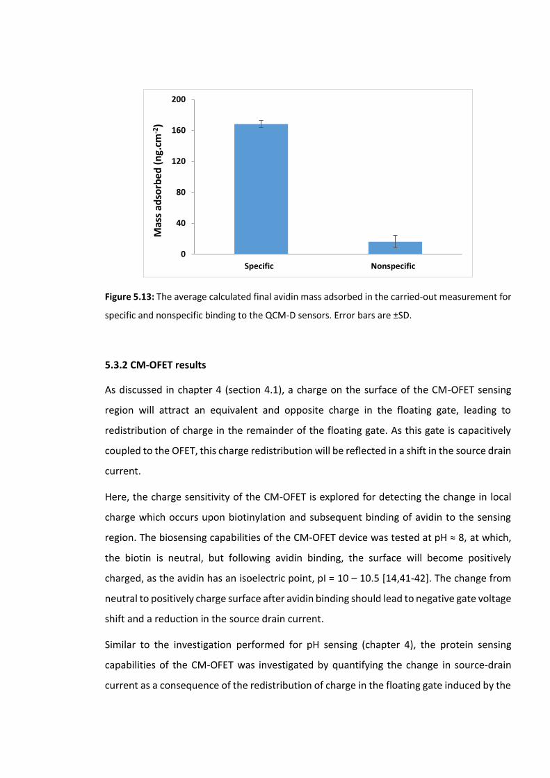
Figure 5.13: The average calculated final avidin mass adsorbed in the carried-out measurement for
specific and nonspecific binding to the QCM-D sensors. Error bars are ±SD.
5.3.2 CM-OFET results
As discussed in chapter 4 (section 4.1), a charge on the surface of the CM-OFET sensing
region will attract an equivalent and opposite charge in the floating gate, leading to
redistribution of charge in the remainder of the floating gate. As this gate is capacitively
coupled to the OFET, this charge redistribution will be reflected in a shift in the source drain
current.
Here, the charge sensitivity of the CM-OFET is explored for detecting the change in local
charge which occurs upon biotinylation and subsequent binding of avidin to the sensing
region. The biosensing capabilities of the CM-OFET device was tested at pH ≈ 8, at which,
the biotin is neutral, but following avidin binding, the surface will become positively
charged, as the avidin has an isoelectric point, pI = 10 – 10.5 [14,41-42]. The change from
neutral to positively charge surface after avidin binding should lead to negative gate voltage
shift and a reduction in the source drain current.
Similar to the investigation performed for pH sensing (chapter 4), the protein sensing
capabilities of the CM-OFET was investigated by quantifying the change in source-drain
current as a consequence of the redistribution of charge in the floating gate induced by the
0
40
80
120
160
200
Specific Nonspecific
Mas
s ad
sorb
ed (
ng.
cm-2
)
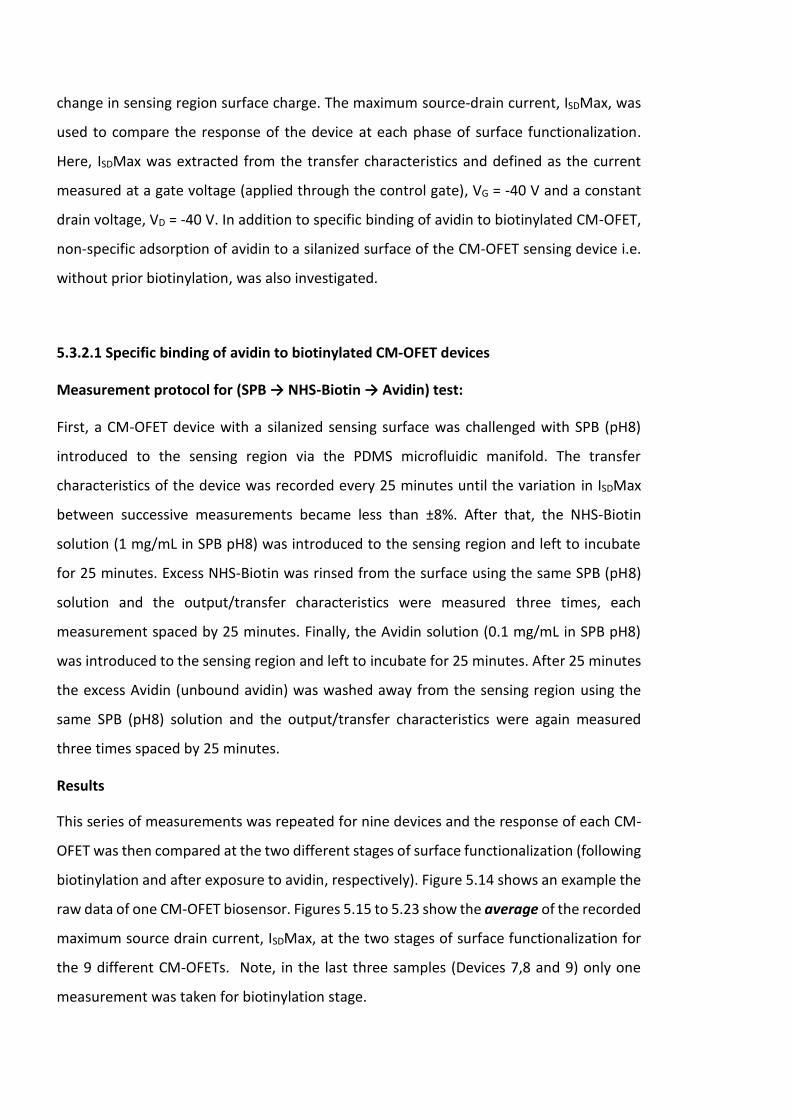
change in sensing region surface charge. The maximum source-drain current, ISDMax, was
used to compare the response of the device at each phase of surface functionalization.
Here, ISDMax was extracted from the transfer characteristics and defined as the current
measured at a gate voltage (applied through the control gate), VG = -40 V and a constant
drain voltage, VD = -40 V. In addition to specific binding of avidin to biotinylated CM-OFET,
non-specific adsorption of avidin to a silanized surface of the CM-OFET sensing device i.e.
without prior biotinylation, was also investigated.
5.3.2.1 Specific binding of avidin to biotinylated CM-OFET devices
Measurement protocol for (SPB → NHS-Biotin → Avidin) test:
First, a CM-OFET device with a silanized sensing surface was challenged with SPB (pH8)
introduced to the sensing region via the PDMS microfluidic manifold. The transfer
characteristics of the device was recorded every 25 minutes until the variation in ISDMax
between successive measurements became less than ±8%. After that, the NHS-Biotin
solution (1 mg/mL in SPB pH8) was introduced to the sensing region and left to incubate
for 25 minutes. Excess NHS-Biotin was rinsed from the surface using the same SPB (pH8)
solution and the output/transfer characteristics were measured three times, each
measurement spaced by 25 minutes. Finally, the Avidin solution (0.1 mg/mL in SPB pH8)
was introduced to the sensing region and left to incubate for 25 minutes. After 25 minutes
the excess Avidin (unbound avidin) was washed away from the sensing region using the
same SPB (pH8) solution and the output/transfer characteristics were again measured
three times spaced by 25 minutes.
Results
This series of measurements was repeated for nine devices and the response of each CM-
OFET was then compared at the two different stages of surface functionalization (following
biotinylation and after exposure to avidin, respectively). Figure 5.14 shows an example the
raw data of one CM-OFET biosensor. Figures 5.15 to 5.23 show the average of the recorded
maximum source drain current, ISDMax, at the two stages of surface functionalization for
the 9 different CM-OFETs. Note, in the last three samples (Devices 7,8 and 9) only one
measurement was taken for biotinylation stage.
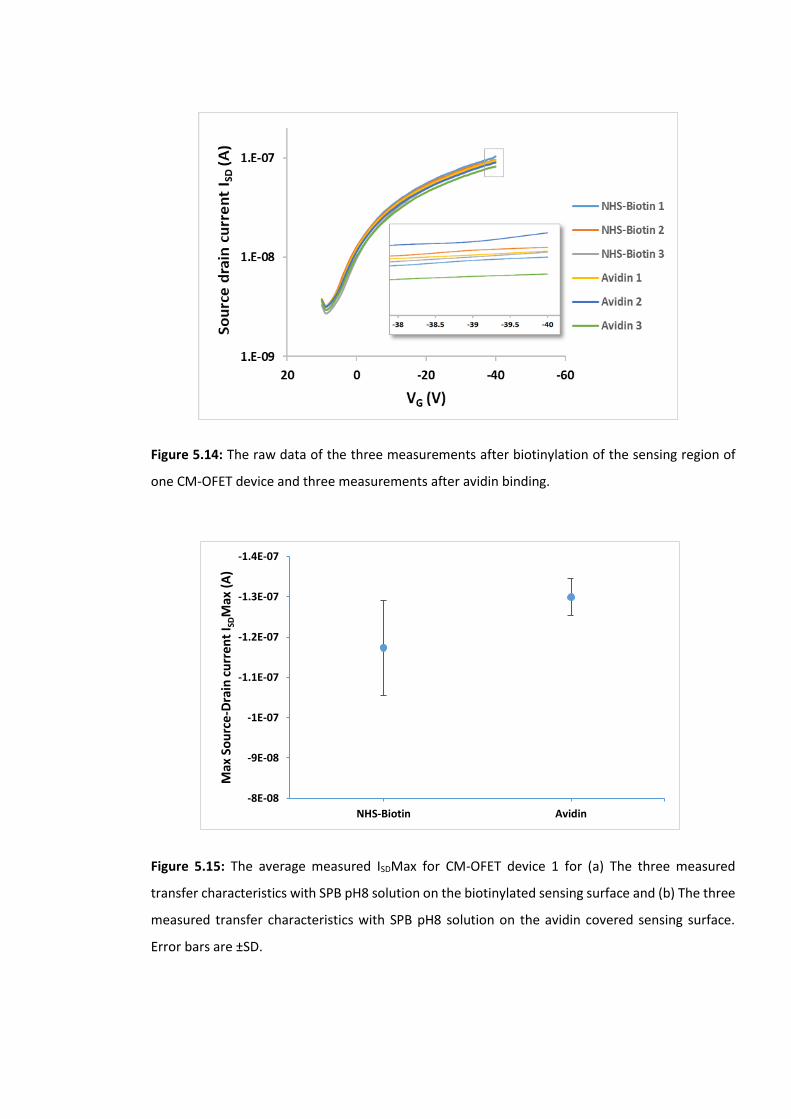
Figure 5.14: The raw data of the three measurements after biotinylation of the sensing region of
one CM-OFET device and three measurements after avidin binding.
Figure 5.15: The average measured ISDMax for CM-OFET device 1 for (a) The three measured
transfer characteristics with SPB pH8 solution on the biotinylated sensing surface and (b) The three
measured transfer characteristics with SPB pH8 solution on the avidin covered sensing surface.
Error bars are ±SD.
-1.4E-07
-1.3E-07
-1.2E-07
-1.1E-07
-1E-07
-9E-08
-8E-08
NHS-Biotin Avidin
Max
So
urc
e-D
rain
cu
rren
t I S
DM
ax (
A)
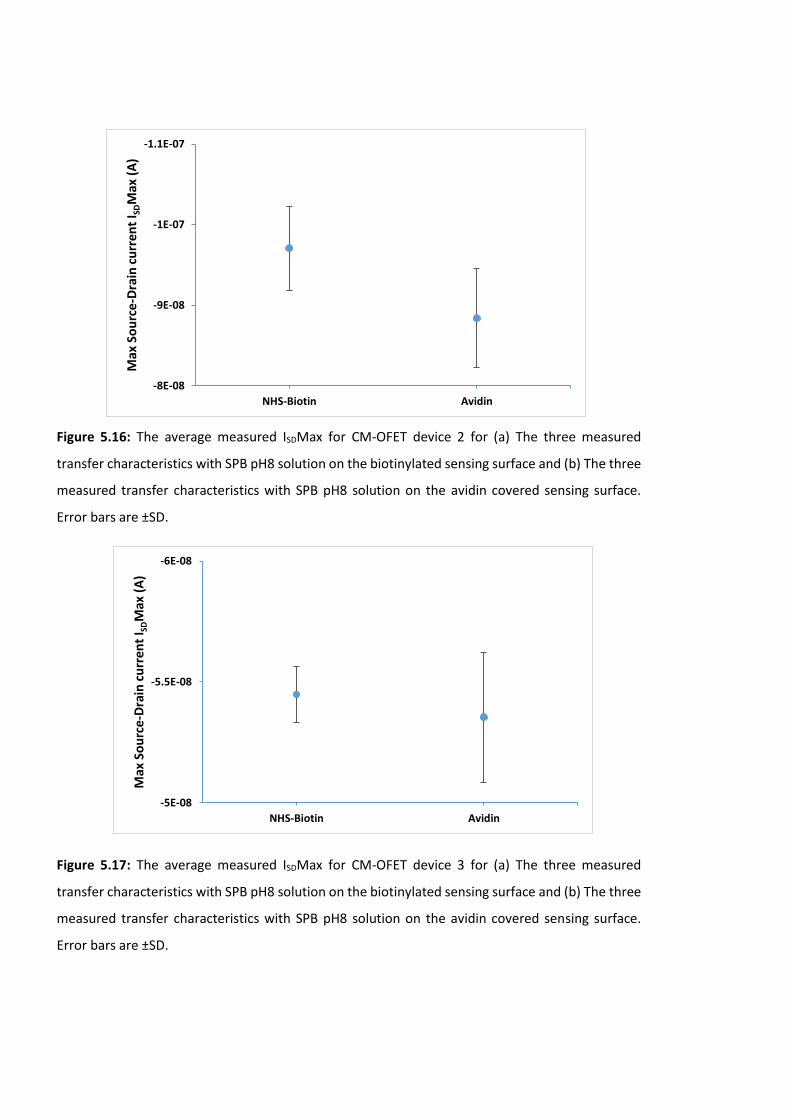
Figure 5.16: The average measured ISDMax for CM-OFET device 2 for (a) The three measured
transfer characteristics with SPB pH8 solution on the biotinylated sensing surface and (b) The three
measured transfer characteristics with SPB pH8 solution on the avidin covered sensing surface.
Error bars are ±SD.
Figure 5.17: The average measured ISDMax for CM-OFET device 3 for (a) The three measured
transfer characteristics with SPB pH8 solution on the biotinylated sensing surface and (b) The three
measured transfer characteristics with SPB pH8 solution on the avidin covered sensing surface.
Error bars are ±SD.
-1.1E-07
-1E-07
-9E-08
-8E-08
NHS-Biotin Avidin
Max
So
urc
e-D
rain
cu
rren
t I S
DM
ax (
A)
-6E-08
-5.5E-08
-5E-08
NHS-Biotin Avidin
Max
So
urc
e-D
rain
cu
rren
t I S
DM
ax (
A)
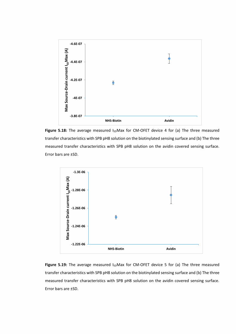
Figure 5.18: The average measured ISDMax for CM-OFET device 4 for (a) The three measured
transfer characteristics with SPB pH8 solution on the biotinylated sensing surface and (b) The three
measured transfer characteristics with SPB pH8 solution on the avidin covered sensing surface.
Error bars are ±SD.
Figure 5.19: The average measured ISDMax for CM-OFET device 5 for (a) The three measured
transfer characteristics with SPB pH8 solution on the biotinylated sensing surface and (b) The three
measured transfer characteristics with SPB pH8 solution on the avidin covered sensing surface.
Error bars are ±SD.
-4.6E-07
-4.4E-07
-4.2E-07
-4E-07
-3.8E-07
NHS-Biotin Avidin
Max
So
urc
e-D
rain
cu
rren
t I S
DM
ax (
A)
-1.3E-06
-1.28E-06
-1.26E-06
-1.24E-06
-1.22E-06
NHS-Biotin Avidin
Max
So
urc
e-D
rain
cu
rren
t I S
DM
ax (
A)
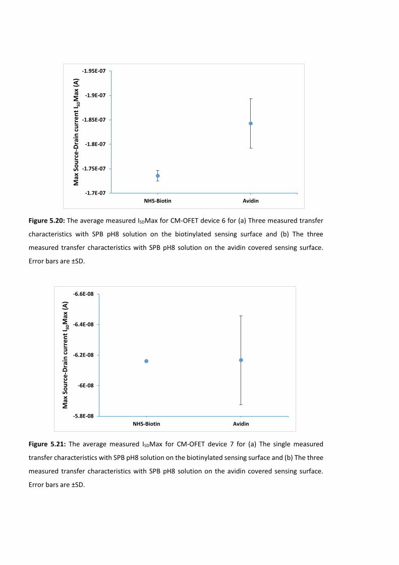
Figure 5.20: The average measured ISDMax for CM-OFET device 6 for (a) Three measured transfer
characteristics with SPB pH8 solution on the biotinylated sensing surface and (b) The three
measured transfer characteristics with SPB pH8 solution on the avidin covered sensing surface.
Error bars are ±SD.
Figure 5.21: The average measured ISDMax for CM-OFET device 7 for (a) The single measured
transfer characteristics with SPB pH8 solution on the biotinylated sensing surface and (b) The three
measured transfer characteristics with SPB pH8 solution on the avidin covered sensing surface.
Error bars are ±SD.
-1.95E-07
-1.9E-07
-1.85E-07
-1.8E-07
-1.75E-07
-1.7E-07
NHS-Biotin Avidin
Max
So
urc
e-D
rain
cu
rren
t I S
DM
ax (
A)
-6.6E-08
-6.4E-08
-6.2E-08
-6E-08
-5.8E-08
NHS-Biotin Avidin
Max
So
urc
e-D
rain
cu
rren
t I S
DM
ax (
A)
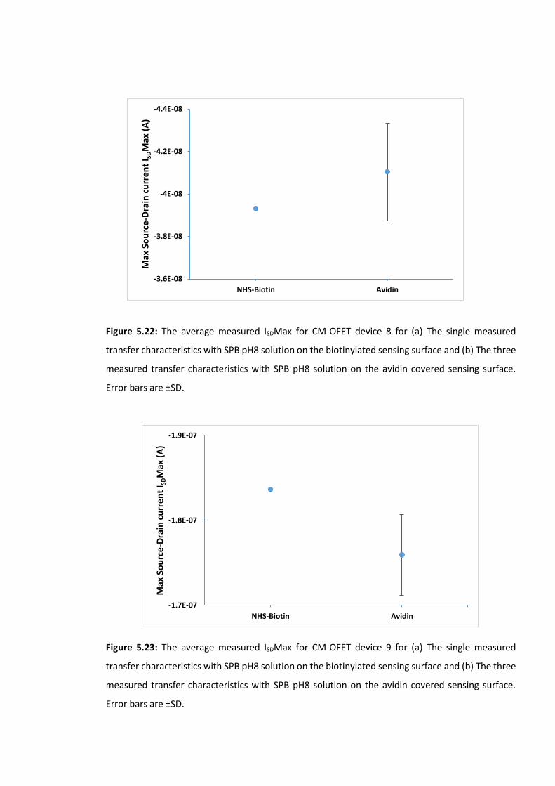
Figure 5.22: The average measured ISDMax for CM-OFET device 8 for (a) The single measured
transfer characteristics with SPB pH8 solution on the biotinylated sensing surface and (b) The three
measured transfer characteristics with SPB pH8 solution on the avidin covered sensing surface.
Error bars are ±SD.
Figure 5.23: The average measured ISDMax for CM-OFET device 9 for (a) The single measured
transfer characteristics with SPB pH8 solution on the biotinylated sensing surface and (b) The three
measured transfer characteristics with SPB pH8 solution on the avidin covered sensing surface.
Error bars are ±SD.
-4.4E-08
-4.2E-08
-4E-08
-3.8E-08
-3.6E-08
NHS-Biotin Avidin
Max
So
urc
e-D
rain
cu
rren
t I S
DM
ax (
A)
-1.9E-07
-1.8E-07
-1.7E-07
NHS-Biotin Avidin
Max
So
urc
e-D
rain
cu
rren
t I S
DM
ax (
A)
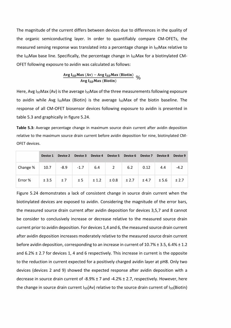
The magnitude of the current differs between devices due to differences in the quality of
the organic semiconducting layer. In order to quantifiably compare CM-OFETs, the
measured sensing response was translated into a percentage change in ISDMax relative to
the ISDMax base line. Specifically, the percentage change in ISDMax for a biotinylated CM-
OFET following exposure to avidin was calculated as follows:
𝐀𝐯𝐠 𝐈𝑺𝑫𝐌𝐚𝐱 (𝐀𝐯) − 𝐀𝐯𝐠 𝐈𝑺𝑫𝐌𝐚𝐱 (𝐁𝐢𝐨𝐭𝐢𝐧)
𝐀𝐯𝐠 𝐈𝑺𝑫𝐌𝐚𝐱 (𝐁𝐢𝐨𝐭𝐢𝐧) %
Here, Avg ISDMax (Av) is the average ISDMax of the three measurements following exposure
to avidin while Avg ISDMax (Biotin) is the average ISDMax of the biotin baseline. The
response of all CM-OFET biosensor devices following exposure to avidin is presented in
table 5.3 and graphically in figure 5.24.
Table 5.3: Average percentage change in maximum source drain current after avidin deposition
relative to the maximum source drain current before avidin deposition for nine, biotinylated CM-
OFET devices.
Device 1 Device 2 Device 3 Device 4 Device 5 Device 6 Device 7 Device 8 Device 9
Change % 10.7 -8.9 -1.7 6.4 2 6.2 0.12 4.4 -4.2
Error % ± 3.5 ± 7 ± 5 ± 1.2 ± 0.8 ± 2.7 ± 4.7 ± 5.6 ± 2.7
Figure 5.24 demonstrates a lack of consistent change in source drain current when the
biotinylated devices are exposed to avidin. Considering the magnitude of the error bars,
the measured source drain current after avidin deposition for devices 3,5,7 and 8 cannot
be consider to conclusively increase or decrease relative to the measured source drain
current prior to avidin deposition. For devices 1,4 and 6, the measured source drain current
after avidin deposition increases moderately relative to the measured source drain current
before avidin deposition, corresponding to an increase in current of 10.7% ± 3.5, 6.4% ± 1.2
and 6.2% ± 2.7 for devices 1, 4 and 6 respectively. This increase in current is the opposite
to the reduction in current expected for a positively charged avidin layer at pH8. Only two
devices (devices 2 and 9) showed the expected response after avidin deposition with a
decrease in source drain current of -8.9% ± 7 and -4.2% ± 2.7, respectively. However, here
the change in source drain current ISD(Av) relative to the source drain current of ISD(Biotin)
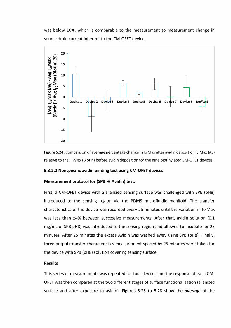
was below 10%, which is comparable to the measurement to measurement change in
source drain current inherent to the CM-OFET device.
Figure 5.24: Comparison of average percentage change in ISDMax after avidin deposition ISDMax (Av)
relative to the ISDMax (Biotin) before avidin deposition for the nine biotinylated CM-OFET devices.
5.3.2.2 Nonspecific avidin binding test using CM-OFET devices
Measurement protocol for (SPB → Avidin) test:
First, a CM-OFET device with a silanized sensing surface was challenged with SPB (pH8)
introduced to the sensing region via the PDMS microfluidic manifold. The transfer
characteristics of the device was recorded every 25 minutes until the variation in ISDMax
was less than ±4% between successive measurements. After that, avidin solution (0.1
mg/mL of SPB pH8) was introduced to the sensing region and allowed to incubate for 25
minutes. After 25 minutes the excess Avidin was washed away using SPB (pH8). Finally,
three output/transfer characteristics measurement spaced by 25 minutes were taken for
the device with SPB (pH8) solution covering sensing surface.
Results
This series of measurements was repeated for four devices and the response of each CM-
OFET was then compared at the two different stages of surface functionalization (silanized
surface and after exposure to avidin). Figures 5.25 to 5.28 show the average of the
-20
-15
-10
-5
0
5
10
15
20
Device 1 Device 2 Device 3 Device 4 Device 5 Device 6 Device 7 Device 8 Device 9
[Avg
I SDM
ax (
Av)
-A
vg I
SDM
ax
(Bio
tin
)]/
Avg
I SDM
ax (
Bio
tin
) (%
)
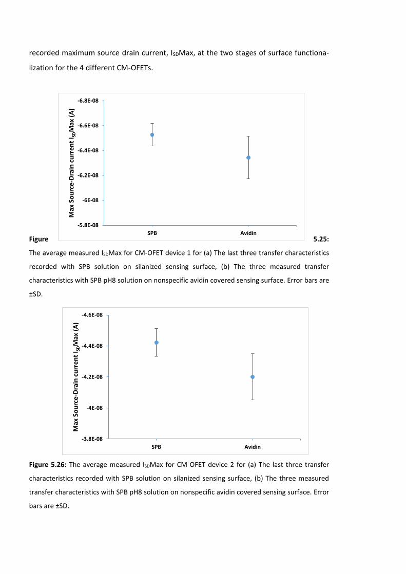
recorded maximum source drain current, ISDMax, at the two stages of surface functiona-
lization for the 4 different CM-OFETs.
Figure 5.25:
The average measured ISDMax for CM-OFET device 1 for (a) The last three transfer characteristics
recorded with SPB solution on silanized sensing surface, (b) The three measured transfer
characteristics with SPB pH8 solution on nonspecific avidin covered sensing surface. Error bars are
±SD.
Figure 5.26: The average measured ISDMax for CM-OFET device 2 for (a) The last three transfer
characteristics recorded with SPB solution on silanized sensing surface, (b) The three measured
transfer characteristics with SPB pH8 solution on nonspecific avidin covered sensing surface. Error
bars are ±SD.
-6.8E-08
-6.6E-08
-6.4E-08
-6.2E-08
-6E-08
-5.8E-08
SPB Avidin
Max
So
urc
e-D
rain
cu
rren
t I S
DM
ax (
A)
-4.6E-08
-4.4E-08
-4.2E-08
-4E-08
-3.8E-08
SPB Avidin
Max
So
urc
e-D
rain
cu
rren
t I S
DM
ax (
A)
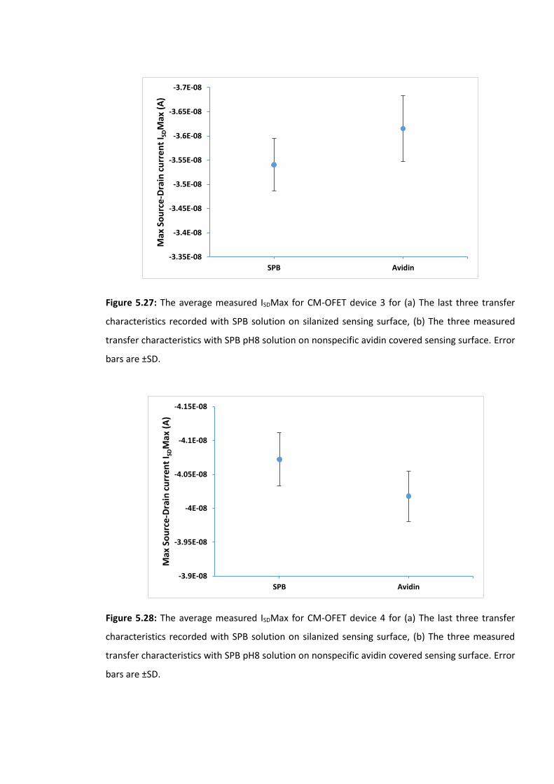
Figure 5.27: The average measured ISDMax for CM-OFET device 3 for (a) The last three transfer
characteristics recorded with SPB solution on silanized sensing surface, (b) The three measured
transfer characteristics with SPB pH8 solution on nonspecific avidin covered sensing surface. Error
bars are ±SD.
Figure 5.28: The average measured ISDMax for CM-OFET device 4 for (a) The last three transfer
characteristics recorded with SPB solution on silanized sensing surface, (b) The three measured
transfer characteristics with SPB pH8 solution on nonspecific avidin covered sensing surface. Error
bars are ±SD.
-3.7E-08
-3.65E-08
-3.6E-08
-3.55E-08
-3.5E-08
-3.45E-08
-3.4E-08
-3.35E-08
SPB Avidin
Max
So
urc
e-D
rain
cu
rren
t I S
DM
ax (
A)
-4.15E-08
-4.1E-08
-4.05E-08
-4E-08
-3.95E-08
-3.9E-08
SPB Avidin
Max
So
urc
e-D
rain
cu
rren
t I S
DM
ax (
A)
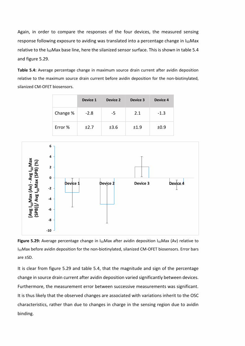
Again, in order to compare the responses of the four devices, the measured sensing
response following exposure to aviding was translated into a percentage change in ISDMax
relative to the ISDMax base line, here the silanized sensor surface. This is shown in table 5.4
and figure 5.29.
Table 5.4: Average percentage change in maximum source drain current after avidin deposition
relative to the maximum source drain current before avidin deposition for the non-biotinylated,
silanized CM-OFET biosensors.
Device 1 Device 2 Device 3 Device 4
Change % -2.8 -5 2.1 -1.3
Error % ±2.7 ±3.6 ±1.9 ±0.9
Figure 5.29: Average percentage change in ISDMax after avidin deposition ISDMax (Av) relative to
ISDMax before avidin deposition for the non-biotinylated, silanized CM-OFET biosensors. Error bars
are ±SD.
It is clear from figure 5.29 and table 5.4, that the magnitude and sign of the percentage
change in source drain current after avidin deposition varied significantly between devices.
Furthermore, the measurement error between successive measurements was significant.
It is thus likely that the observed changes are associated with variations inherit to the OSC
characteristics, rather than due to changes in charge in the sensing region due to avidin
binding.
-10
-8
-6
-4
-2
0
2
4
6
Device 1 Device 2 Device 3 Device 4
[Avg
I SDM
ax (
Av)
-A
vg I S
DM
ax
(SP
B)]
/ A
vg I S
DM
ax (
SPB
) (%
)
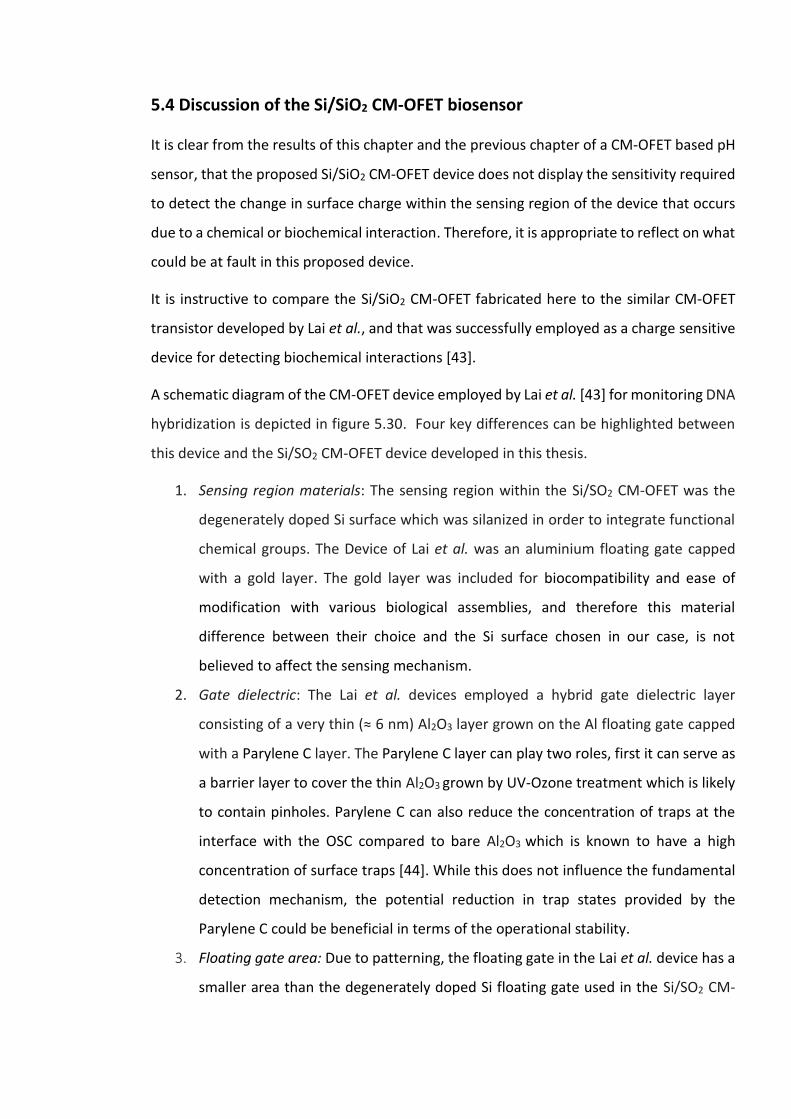
5.4 Discussion of the Si/SiO2 CM-OFET biosensor
It is clear from the results of this chapter and the previous chapter of a CM-OFET based pH
sensor, that the proposed Si/SiO2 CM-OFET device does not display the sensitivity required
to detect the change in surface charge within the sensing region of the device that occurs
due to a chemical or biochemical interaction. Therefore, it is appropriate to reflect on what
could be at fault in this proposed device.
It is instructive to compare the Si/SiO2 CM-OFET fabricated here to the similar CM-OFET
transistor developed by Lai et al., and that was successfully employed as a charge sensitive
device for detecting biochemical interactions [43].
A schematic diagram of the CM-OFET device employed by Lai et al. [43] for monitoring DNA
hybridization is depicted in figure 5.30. Four key differences can be highlighted between
this device and the Si/SO2 CM-OFET device developed in this thesis.
1. Sensing region materials: The sensing region within the Si/SO2 CM-OFET was the
degenerately doped Si surface which was silanized in order to integrate functional
chemical groups. The Device of Lai et al. was an aluminium floating gate capped
with a gold layer. The gold layer was included for biocompatibility and ease of
modification with various biological assemblies, and therefore this material
difference between their choice and the Si surface chosen in our case, is not
believed to affect the sensing mechanism.
2. Gate dielectric: The Lai et al. devices employed a hybrid gate dielectric layer
consisting of a very thin (≈ 6 nm) Al2O3 layer grown on the Al floating gate capped
with a Parylene C layer. The Parylene C layer can play two roles, first it can serve as
a barrier layer to cover the thin Al2O3 grown by UV-Ozone treatment which is likely
to contain pinholes. Parylene C can also reduce the concentration of traps at the
interface with the OSC compared to bare Al2O3 which is known to have a high
concentration of surface traps [44]. While this does not influence the fundamental
detection mechanism, the potential reduction in trap states provided by the
Parylene C could be beneficial in terms of the operational stability.
3. Floating gate area: Due to patterning, the floating gate in the Lai et al. device has a
smaller area than the degenerately doped Si floating gate used in the Si/SO2 CM-
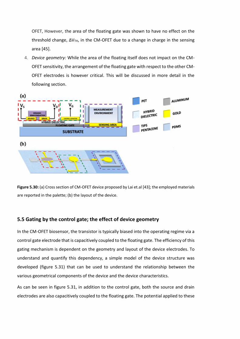
OFET, However, the area of the floating gate was shown to have no effect on the
threshold change, ΔVTH, in the CM-OFET due to a change in charge in the sensing
area [45].
4. Device geometry: While the area of the floating itself does not impact on the CM-
OFET sensitivity, the arrangement of the floating gate with respect to the other CM-
OFET electrodes is however critical. This will be discussed in more detail in the
following section.
Figure 5.30: (a) Cross section of CM-OFET device proposed by Lai et.al [43]; the employed materials
are reported in the palette; (b) the layout of the device.
5.5 Gating by the control gate; the effect of device geometry
In the CM-OFET biosensor, the transistor is typically biased into the operating regime via a
control gate electrode that is capacitively coupled to the floating gate. The efficiency of this
gating mechanism is dependent on the geometry and layout of the device electrodes. To
understand and quantify this dependency, a simple model of the device structure was
developed (figure 5.31) that can be used to understand the relationship between the
various geometrical components of the device and the device characteristics.
As can be seen in figure 5.31, in addition to the control gate, both the source and drain
electrodes are also capacitively coupled to the floating gate. The potential applied to these
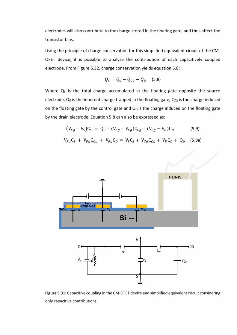
electrodes will also contribute to the charge stored in the floating gate, and thus affect the
transistor bias.
Using the principle of charge conservation for this simplified equivalent circuit of the CM-
OFET device, it is possible to analyse the contribution of each capacitively coupled
electrode. From Figure 5.32, charge conservation yields equation 5.8:
𝑄𝑆 = 𝑄0 − 𝑄𝐶𝑔 − 𝑄𝐷 (5.8)
Where QS is the total charge accumulated in the floating gate opposite the source
electrode, Q0 is the inherent charge trapped in the floating gate, QCg is the charge induced
on the floating gate by the control gate and QD is the charge induced on the floating gate
by the drain electrode. Equation 5.8 can also be expressed as:
(V𝐹𝑔 – V𝑆)C𝑆 = Q0 – (V𝐹𝑔 – V𝐶𝑔)C𝐶𝑔 – (V𝐹𝑔 − V𝐷)C𝐷 (5.9)
V𝐹𝑔C𝑆 + V𝐹𝑔C𝐶𝑔 + V𝐹𝑔C𝐷 = V𝑆C𝑆 + V𝐶𝑔C𝐶𝑔 + V𝐷C𝐷 + Q0 (5.9a)
Figure 5.31: Capacitive coupling in the CM-OFET device and simplified equivalent circuit considering
only capacitive contributions.
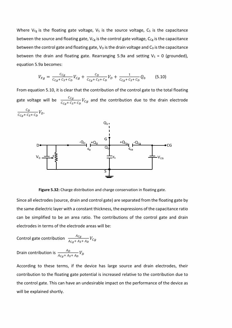
Where VFg is the floating gate voltage, VS is the source voltage, CS is the capacitance
between the source and floating gate, VCg is the control gate voltage, CCg is the capacitance
between the control gate and floating gate, VD is the drain voltage and CD is the capacitance
between the drain and floating gate. Rearranging 5.9a and setting VS = 0 (grounded),
equation 5.9a becomes:
𝑉𝐹𝑔 = 𝐶𝐶𝑔
𝐶𝐶𝑔+ 𝐶𝑆+ 𝐶𝐷𝑉𝐶𝑔 +
𝐶𝐷
𝐶𝐶𝑔+ 𝐶𝑆+ 𝐶𝐷𝑉𝐷 +
1
𝐶𝐶𝑔+ 𝐶𝑆+ 𝐶𝐷𝑄0 (5.10)
From equation 5.10, it is clear that the contribution of the control gate to the total floating
gate voltage will be 𝐶𝐶𝑔
𝐶𝐶𝑔+ 𝐶𝑆+ 𝐶𝐷𝑉𝐶𝑔 and the contribution due to the drain electrode
𝐶𝐷
𝐶𝐶𝑔+ 𝐶𝑆+ 𝐶𝐷𝑉𝐷.
Figure 5.32: Charge distribution and charge conservation in floating gate.
Since all electrodes (source, drain and control gate) are separated from the floating gate by
the same dielectric layer with a constant thickness, the expressions of the capacitance ratio
can be simplified to be an area ratio. The contributions of the control gate and drain
electrodes in terms of the electrode areas will be:
Control gate contribution 𝐴𝐶𝑔
𝐴𝐶𝑔+ 𝐴𝑆+ 𝐴𝐷𝑉𝐶𝑔
Drain contribution is 𝐴𝐷
𝐴𝐶𝑔+ 𝐴𝑆+ 𝐴𝐷𝑉𝐷
According to these terms, if the device has large source and drain electrodes, their
contribution to the floating gate potential is increased relative to the contribution due to
the control gate. This can have an undesirable impact on the performance of the device as
will be explained shortly.
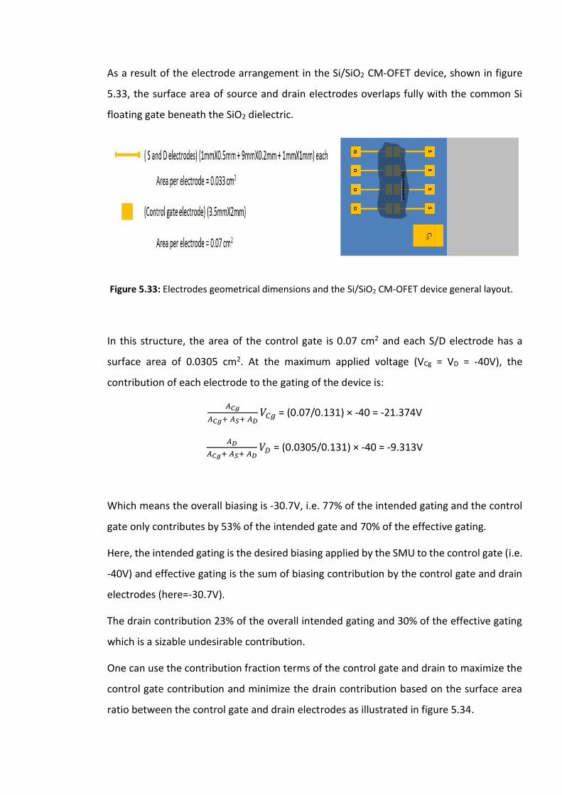
As a result of the electrode arrangement in the Si/SiO2 CM-OFET device, shown in figure
5.33, the surface area of source and drain electrodes overlaps fully with the common Si
floating gate beneath the SiO2 dielectric.
Figure 5.33: Electrodes geometrical dimensions and the Si/SiO2 CM-OFET device general layout.
In this structure, the area of the control gate is 0.07 cm2 and each S/D electrode has a
surface area of 0.0305 cm2. At the maximum applied voltage (VCg = VD = -40V), the
contribution of each electrode to the gating of the device is:
𝐴𝐶𝑔
𝐴𝐶𝑔+ 𝐴𝑆+ 𝐴𝐷𝑉𝐶𝑔 = (0.07/0.131) × -40 = -21.374V
𝐴𝐷
𝐴𝐶𝑔+ 𝐴𝑆+ 𝐴𝐷𝑉𝐷 = (0.0305/0.131) × -40 = -9.313V
Which means the overall biasing is -30.7V, i.e. 77% of the intended gating and the control
gate only contributes by 53% of the intended gate and 70% of the effective gating.
Here, the intended gating is the desired biasing applied by the SMU to the control gate (i.e.
-40V) and effective gating is the sum of biasing contribution by the control gate and drain
electrodes (here=-30.7V).
The drain contribution 23% of the overall intended gating and 30% of the effective gating
which is a sizable undesirable contribution.
One can use the contribution fraction terms of the control gate and drain to maximize the
control gate contribution and minimize the drain contribution based on the surface area
ratio between the control gate and drain electrodes as illustrated in figure 5.34.
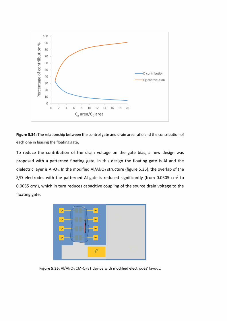
Figure 5.34: The relationship between the control gate and drain area ratio and the contribution of
each one in biasing the floating gate.
To reduce the contribution of the drain voltage on the gate bias, a new design was
proposed with a patterned floating gate, in this design the floating gate is Al and the
dielectric layer is Al2O3. In the modified Al/Al2O3 structure (figure 5.35), the overlap of the
S/D electrodes with the patterned Al gate is reduced significantly (from 0.0305 cm2 to
0.0055 cm2), which in turn reduces capacitive coupling of the source drain voltage to the
floating gate.
Figure 5.35: Al/Al2O3 CM-OFET device with modified electrodes’ layout.
0
10
20
30
40
50
60
70
80
90
100
0 2 4 6 8 10 12 14 16 18 20
Perc
enta
ge o
f co
ntr
iibu
tio
n %
Cg area/CD area
D contribution
Cg contribution

Furthermore, due to the large dielectric constant of the Al2O3, the maximum required
applied voltage in the transfer characteristics is significantly reduced from -40 V to -5 V.
Due to the reduced overlap between S/D electrodes and the floating gate, the contribution
of the control gate will be (0.07/0.081) × -5 = -4.32 V and the drain contribution is
(0.0055/0.081) × -5 = -0.34 V.
Which means that the overall biasing is -4.66V, 93% of the intended gating out of which the
control gate contributes by 86% of the intended gate and 93% of the effective gating. The
drain contribution is only 6% of the overall intended gating and 7% of the effective gating.
It is clear from the previous calculations that the implication of having a large overlap
between the S/D electrodes and the floating gate electrode is that the device will have
smaller overall biasing and reduced control on the biasing by the control gate, moreover,
due to the contribution of the drain electrode to the gate voltage, the conducting channel
in the OSC will be turned ON even with 0 V applied to the control gate, making the
estimation of VTH difficult.
The effect of having relatively large source and drain electrodes can be observed in both
the output and transfer characteristics of the Si/SiO2 CM-OFET. The difference in the
behaviour of the output characteristics for the Si/SiO2 device and the modified Al/Al2O3
device are displayed in figure 5.36 and 5.37, respectively where the effect of reducing the
effective source and drain areas can be seen.
In the output characteristics of the Si/SiO2 device, the large contribution of the drain
electrode in the biasing of the device causes bending in the output curves. For example, at
0 V gate voltage, only a very low current is expected to be drawn from the device, due to
the low intrinsic conductivity of the OSC and the high trapping probability that the charge
carriers may experience while participating in the OSC conducting channel. However, the
gating effect of the drain voltage in the Si/SiO2 CM-OFET is considerable, leading to a linear
increase in source drain current with drain voltage (highlighted by the red rectangle in
figure 5.36). By reducing the source and drain areas this effect is minimized as can be seen
from the output curves of the modified Al/Al2O3 device in figure 5.37.
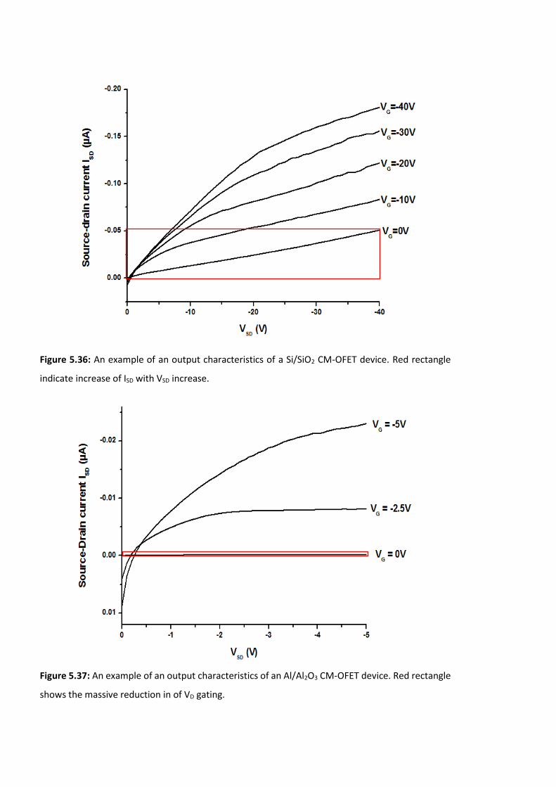
Figure 5.36: An example of an output characteristics of a Si/SiO2 CM-OFET device. Red rectangle
indicate increase of ISD with VSD increase.
Figure 5.37: An example of an output characteristics of an Al/Al2O3 CM-OFET device. Red rectangle
shows the massive reduction in of VD gating.
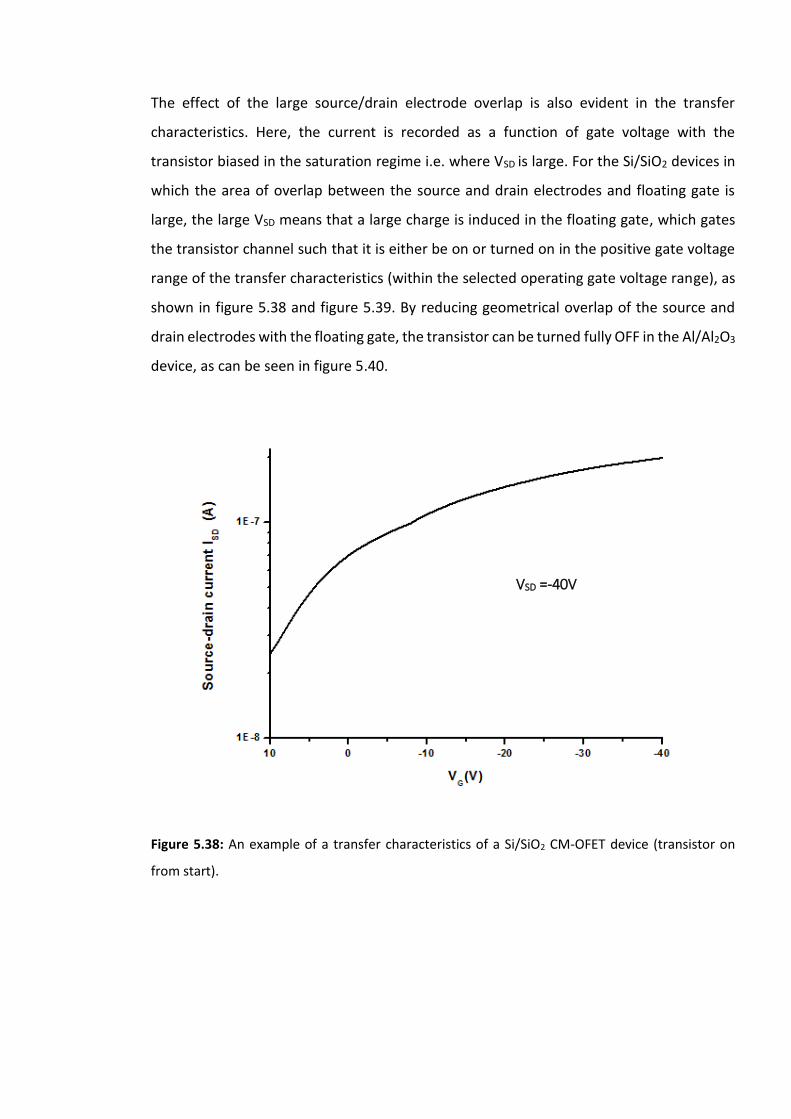
The effect of the large source/drain electrode overlap is also evident in the transfer
characteristics. Here, the current is recorded as a function of gate voltage with the
transistor biased in the saturation regime i.e. where VSD is large. For the Si/SiO2 devices in
which the area of overlap between the source and drain electrodes and floating gate is
large, the large VSD means that a large charge is induced in the floating gate, which gates
the transistor channel such that it is either be on or turned on in the positive gate voltage
range of the transfer characteristics (within the selected operating gate voltage range), as
shown in figure 5.38 and figure 5.39. By reducing geometrical overlap of the source and
drain electrodes with the floating gate, the transistor can be turned fully OFF in the Al/Al2O3
device, as can be seen in figure 5.40.
Figure 5.38: An example of a transfer characteristics of a Si/SiO2 CM-OFET device (transistor on
from start).
VSD =-40V
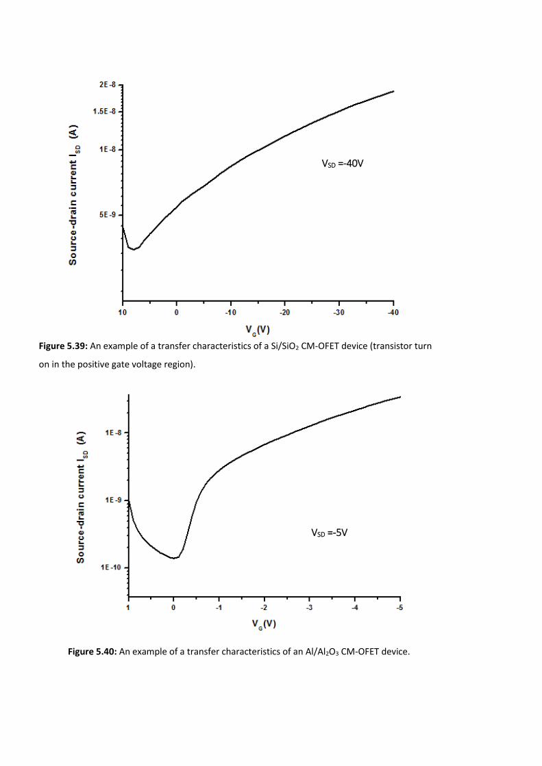
Figure 5.39: An example of a transfer characteristics of a Si/SiO2 CM-OFET device (transistor turn
on in the positive gate voltage region).
Figure 5.40: An example of a transfer characteristics of an Al/Al2O3 CM-OFET device.
VSD =-5V
VSD =-40V
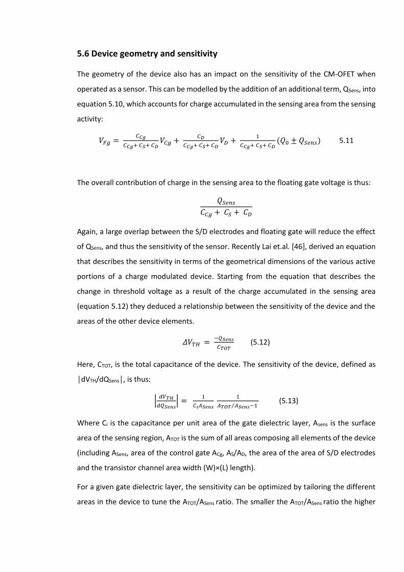
5.6 Device geometry and sensitivity
The geometry of the device also has an impact on the sensitivity of the CM-OFET when
operated as a sensor. This can be modelled by the addition of an additional term, QSens, into
equation 5.10, which accounts for charge accumulated in the sensing area from the sensing
activity:
𝑉𝐹𝑔 = 𝐶𝐶𝑔
𝐶𝐶𝑔+ 𝐶𝑆+ 𝐶𝐷𝑉𝐶𝑔 +
𝐶𝐷
𝐶𝐶𝑔+ 𝐶𝑆+ 𝐶𝐷𝑉𝐷 +
1
𝐶𝐶𝑔+ 𝐶𝑆+ 𝐶𝐷(𝑄0 ± 𝑄𝑆𝑒𝑛𝑠) 5.11
The overall contribution of charge in the sensing area to the floating gate voltage is thus:
𝑄𝑆𝑒𝑛𝑠𝐶𝐶𝑔 + 𝐶𝑆 + 𝐶𝐷
Again, a large overlap between the S/D electrodes and floating gate will reduce the effect
of QSens, and thus the sensitivity of the sensor. Recently Lai et.al. [46], derived an equation
that describes the sensitivity in terms of the geometrical dimensions of the various active
portions of a charge modulated device. Starting from the equation that describes the
change in threshold voltage as a result of the charge accumulated in the sensing area
(equation 5.12) they deduced a relationship between the sensitivity of the device and the
areas of the other device elements.
𝛥𝑉𝑇𝐻 = −𝑄𝑆𝑒𝑛𝑠
𝐶𝑇𝑂𝑇 (5.12)
Here, CTOT, is the total capacitance of the device. The sensitivity of the device, defined as
│dVTH/dQSens│, is thus:
|𝑑𝑉𝑇𝐻
𝑑𝑄𝑆𝑒𝑛𝑠| =
1
𝐶𝑖𝐴𝑆𝑒𝑛𝑠
1
𝐴𝑇𝑂𝑇 𝐴𝑆𝑒𝑛𝑠⁄ −1 (5.13)
Where Ci is the capacitance per unit area of the gate dielectric layer, Asens is the surface
area of the sensing region, ATOT is the sum of all areas composing all elements of the device
(including ASens, area of the control gate ACg, AS/AD, the area of the area of S/D electrodes
and the transistor channel area width (W)×(L) length).
For a given gate dielectric layer, the sensitivity can be optimized by tailoring the different
areas in the device to tune the ATOT/ASens ratio. The smaller the ATOT/ASens ratio the higher
the sensitivity. In the Si/SiO2 device the ATOT/ASens ratio = 9.184 while in the modified
Al/Al2O3 CM-OFET, the ATOT/ASens ratio = 5.51.
5.7 The trade-offs of the design
1- The sensitivity of the charge modulated device can be tuned by the ATOT/ASens ratio;
increasing sensitivity can be achieved by decreasing this ratio. This can be achieved
by having a large sensing area that comprises the largest surface area of the sensor.
However, according to the sensitivity equation (5.13), the sensing area is also
inversely proportional to the sensitivity so reducing the areas of other elements in
the sensor device is a more rational approach.
2- Other areas that can be reduced to reduce the total area of the sensor device
include the control gate area ACg, the areas of the S/D electrodes, AS and AD, and
the transistor channel area. While these can be reduced, care must be taken to
ensure the area of the control gate electrode, ACg, is considerably larger than AS and
AD to ensure proper control over biasing of the device.
3- Reducing the surface area of the source and drain electrodes relative to the control
gate area, ACg, and the sensing area, ASens, must be performed with care as these
also influence the output source-drain current. According to the ISD equation (see
chapter 1, equation 1.9), ISD is directly proportional to the transistor channel width,
W, which corresponds to one of the S/D electrodes dimensions, so reducing this
dimension will reduce the measured source-drain current, ISD.
In the modified Al/Al2O3 CM-OFET, the transistor channel width W was maintained while
the length of the overlap between the source and drain electrodes and the floating gate, LS
and LD, respectively were reduced, as in figure 5.41.
5.8 The modified Al/Al2O3 CM-OFET device behaviour as a transistor
In the modified device, the dielectric constant for Al2O3 is 9-10; nearly 2.5 times higher than
that of the SiO2. Moreover, due to the uniformity and defect free nature of ALD deposited
layers, it was possible to reduce the thickness of the Al2O3 gate dielectric layer to only 40
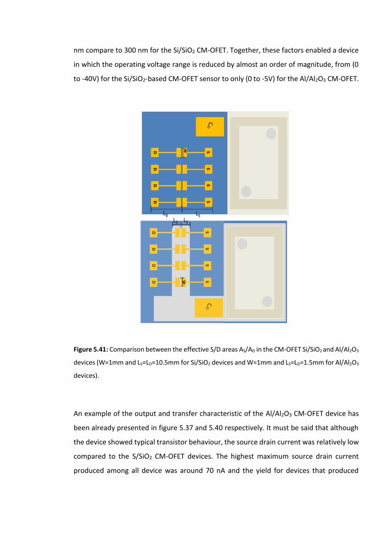
nm compare to 300 nm for the Si/SiO2 CM-OFET. Together, these factors enabled a device
in which the operating voltage range is reduced by almost an order of magnitude, from (0
to -40V) for the Si/SiO2-based CM-OFET sensor to only (0 to -5V) for the Al/Al2O3 CM-OFET.
Figure 5.41: Comparison between the effective S/D areas AS/AD in the CM-OFET Si/SiO2 and Al/Al2O3
devices (W=1mm and LS=LD=10.5mm for Si/SiO2 devices and W=1mm and LS=LD=1.5mm for Al/Al2O3
devices).
An example of the output and transfer characteristic of the Al/Al2O3 CM-OFET device has
been already presented in figure 5.37 and 5.40 respectively. It must be said that although
the device showed typical transistor behaviour, the source drain current was relatively low
compared to the S/SiO2 CM-OFET devices. The highest maximum source drain current
produced among all device was around 70 nA and the yield for devices that produced
maximum source drain current above 10 nA was low 40%. The mobility of devices was in
the range from 0.0004 to 0.001 cm2V-1S-1 and the ON/OFF current ratio was 109±68.
The interface of the Al2O3 with the OSC is believed to be the cause for the reduced source
drain current and low mobility. High k dielectrics such as Al2O3 are more polar compared to
SiO2 and that can increase the energetic disorder at the interface with the OSC, which
results in a higher localization of the charge carriers and reduced field-effect mobility. A
simple solution to reduce this effect is the formation of a self-assembled monolayer (SAM)
on the Al2O3 surface prior to OSC deposition [47-49].
Fumagalli et.al. [50] studied the effect of different SAMs (differing in the polar head group
and alkyl chain length) on the electrical properties of transistors with an ALD Al2O3 gate
dielectric. They concluded that the length of the SAM is the most important parameter in
improving transistor performance. A long chain SAM, such as n-octadecyltrichlorosilane
(OTS), moves the active channel of the OSC away from the disordered surface dipoles
present on the surface of Al2O3. The improvement is attributed to the combination of
reduction of the broadness of the density of states and the improvement of the effective
wavefunction overlap compare to the bare Al2O3. Critically, SAM modification is simple and
does not required chemical vapor deposition (CVD) instrument to produce as in Parylene C
layer.
5.9 Conclusions
This chapter discussed the use of the Si/SiO2 CM-OFET device for protein detection. Avidin
protein binding to a biotinylated sensing region surface was chosen to examine the device
sensitivity. In the chapter, the protocol used for biotinylating the sensing region of the CM-
OFET device and subsequent avidin binding was presented. The effectiveness of the
protocol was confirmed using QCM-D measurement which validated both the specific
avidin binding to the biotinylated surface and minimal nonspecific avidin binding to a
silanized surface.
Using the CM-OFET device, the binding of avidin to the biotinylated Si gate surface was
investigated. Experimental results on a nine, nominally identical biotinylated CM-OFETs
showed significant variation between devices and no clear indication of sensitivity to the
change in charge accumulated in the sensing region following avidin binding.
This chapter then discussed and analysed the shortcomings of the Si/SiO2 CM-OFET sensor
and proposed a modified CM-OFET sensor based on Al/Al2O3 as gate and gate dielectric
layers. The shortcomings of the geometrical arrangement of the Si/SiO2 CM-OFET sensor
were discussed and solutions to overcoming some of the Si/SiO2 CM-OFET limitations were
proposed for implementation in the design of new modified Al/Al2O3 CM-OFET sensor.
Practical trade-offs in the design of the modified CM-OFET device were also investigated.
Finally, measurements of the Al/Al2O3 CM-OFET as a transistor have shown typical
transistor behaviour, validating the design and fabrication approach. While the measured
source drain current was low, suggestions to improve charge mobility of the OSC were
given.
It must be mentioned that, although geometrical considerations have been employed in
the modified Al/Al2O3 CM-OFET layout, the inherent measurement/current noise level seen
in tested fabricated Si/SiO2 CM-OFET devices attributed to the Tips-pentacene deposition
method is considerably high (largely within ±10%), and could still presents a sensitivity issue
for the modified Al/Al2O3 CM-OFET. The improved sensitivity response that can be achieved
by the new geometrical layout optimization may still be hampered by the existing noise
associated with the current fabrication (particularly the OSC deposition method).
Therefore, this needs to be addressed in order to produce a functioning CM-OFET.
5.10 References
[1] Banica, F. G. (2012). Chemical sensors and biosensors: fundamentals and applications.
John Wiley & Sons
[2] Martín-Yerga, D., Carrasco-Rodríguez, J., Alonso, F. J. G., & Costa-García, A. (2017).
Competitive electrochemical biosensing of biotin using cadmium-modified titanium
phosphate nanoparticles and 8-channel screen-printed disposable electrodes. Analytical
Methods.
[3] Nollet, L. M., & Toldrá, F. (Eds.). (2015). Handbook of Food Analysis, -Two Volume Set.
CRC Press.
[4] Zourob, M., Elwary, S., & Turner, A. P. (Eds.). (2008). Principles of bacterial detection:
biosensors, recognition receptors and microsystems. Springer Science & Business Media.
[5] Shils, M. E., & Shike, M. (Eds.). (2006). Modern nutrition in health and disease. Lippincott
Williams & Wilkins.
[6] Deng, T., Li, J. S., Huan, S. Y., Yang, H. F., Wang, H., Shen, G. L., & Yu, R. Q. (2006). Quartz
crystal microbalance bioaffinity sensor for biotin based on mixed self-assembled
monolayers and metastable molecular complex receptor. Biosensors and
Bioelectronics, 21(8), 1545-1552.
[7] Brehm, B. (2015). Nutrition: Science, Issues, and Applications. ABC-CLIO, Denver,
Colorado.
[8] Trindade, T., & da Silva, A. L. D. (Eds.). (2011). Nanocomposite particles for bio-
applications: materials and bio-interfaces. CRC Press.
[9] Huangxian, J.; Guosong, L.; and Feng, Y. (2017). Immunosensing for Detection of Protein
Biomarkers. Elsevier.
[10] Yang, V. C., & Ngo, T. T. (Eds.). (2012). Biosensors and their Applications. Springer
Science & Business Media.
[11] Anzai, J. I., Hoshi, T., & Osa, T. (2000). Avidin—Biotin Mediated Biosensors.
In Biosensors and Their Applications (pp. 35-46). Springer, Boston, MA.
[12] Pazy, Y., Kulik, T., Bayer, E. A., Wilchek, M., & Livnah, O. (2002). Ligand Exchange
between Proteins EXCHANGE OF BIOTIN AND BIOTIN DERIVATIVES BETWEEN AVIDIN AND
STREPTAVIDIN. Journal of Biological Chemistry, 277(34), 30892-30900.
[13] Suspène, C., Piro, B., Reisberg, S., Pham, M. C., Toss, H., Berggren, M., ... & Horowitz,
G. (2013). Copolythiophene-based water-gated organic field-effect transistors for
biosensing. Journal of Materials Chemistry B, 1(15), 2090-2097.
[14] Hood, E. E., & Howard, J. A. (2014). Commercial plant-produced recombinant avidin.
In Commercial Plant-Produced Recombinant Protein Products (pp. 15-25). Springer Berlin
Heidelberg.
[15] Scientific, T. (2009). Avidin-Biotin Technical Handbook. Text available@ http://www.
piercenet. com/files/1601675_AvBi_HB_INTL. pdf.
[16] Zourob, M., Elwary, S., & Turner, A. P. (Eds.). (2008). Principles of bacterial detection:
biosensors, recognition receptors and microsystems. Springer Science & Business Media.
[17] Torchilin, V. P. (1995). Handbook of targeted delivery of imaging agents (Vol. 26). CRC
Press.
[18] Williams, E. H., Davydov, A. V., Motayed, A., Sundaresan, S. G., Bocchini, P., Richter, L.
J., ... & Rao, M. V. (2012). Immobilization of streptavidin on 4H–SiC for biosensor
development. Applied surface science, 258(16), 6056-6063.
[19] Jeong, C. K., Jin, H. M., Ahn, J. H., Park, T. J., Yoo, H. G., Koo, M., ... & Lee, K. J. (2014).
Electrical biomolecule detection using nanopatterned silicon via block copolymer
lithography. small, 10(2), 337-343.
[20] Brownlee, J. (2007). Antigen-antibody interaction. Melbourne, Australia: Complex
Intelligent Systems Laboratory, Centre for Information Technology Research, Faculty of
Information and Communication Technologies, Swinburne University of Technology.
[21] Bongrand, P. (1999). Ligand-receptor interactions. Reports on Progress in
Physics, 62(6), 921.
[22] Zhang, H., Williams, P. S., Zborowski, M., & Chalmers, J. J. (2006). Binding
affinities/avidities of antibody–antigen interactions: Quantification and scale‐up
implications. Biotechnology and bioengineering, 95(5), 812-829.
[23] Landry, J. P., Fei, Y., & Zhu, X. (2012). Simultaneous measurement of 10,000 protein-
ligand affinity constants using microarray-based kinetic constant assays. Assay and drug
development technologies, 10(3), 250-259.
[24] Malaspina, D. C., Longo, G., & Szleifer, I. (2017). Behavior of ligand binding assays with
crowded surfaces: Molecular model of antigen capture by antibody-conjugated
nanoparticles. PloS one, 12(9), e0185518.
[25] Lloret, N., Frederiksen, R. S., Møller, T. C., Rieben, N. I., Upadhyay, S., De Vico, L., ... &
Martinez, K. L. (2012). Effects of buffer composition and dilution on nanowire field-effect
biosensors. Nanotechnology, 24(3), 035501.
[26] Yogo, T., Urano, Y., Mizushima, A., Sunahara, H., Inoue, T., Hirose, K., ... & Nagano, T.
(2008). Selective photoinactivation of protein function through environment-sensitive
switching of singlet oxygen generation by photosensitizer. Proceedings of the National
Academy of Sciences, 105(1), 28-32.
[27] Nicu, L. and Leïchlé, T. (2014) Micro-and Nanoelectromechanical Biosensors. John
Wiley & Sons. USA
[28] Dixon, M. C. (2008). Quartz crystal microbalance with dissipation monitoring: enabling
real-time characterization of biological materials and their interactions. Journal of
biomolecular techniques: JBT, 19(3), 151.
[29] Höök, F., Rodahl, M., Brzezinski, P., & Kasemo, B. (1998). Energy dissipation kinetics
for protein and antibody− antigen adsorption under shear oscillation on a quartz crystal
microbalance. Langmuir, 14(4), 729-734.
[30] Lehner, C. (2015). Quartz Crystal Microbalance Studies on Friction Modifiers for
Lubricant Applications.
[31] Sauerbrey, G. (1959). Verwendung von Schwingquarzen zur Wägung dünner Schichten
und zur Mikrowägung. Zeitschrift für Physik A Hadrons and Nuclei, 155(2), 206-222.
[32] Nomura, T., & Okuhara, M. (1982). Frequency shifts of piezoelectric quartz crystals
immersed in organic liquids. Analytica Chimica Acta, 142, 281-284.
[33] Kanazawa, K. K., & Gordon, J. G. (1985). Frequency of a quartz microbalance in contact
with liquid. Analytical Chemistry, 57(8), 1770-1771.
[34] Hook, F., Rodahl, M., Keller, C., Glasmastar, K., Fredriksson, C., Dahiqvist, P., & Kasemo,
B. (1999). The dissipative QCM-D technique: interfacial phenomena and sensor applications
for proteins, biomembranes, living cells and polymers. In Frequency and Time Forum, 1999
and the IEEE International Frequency Control Symposium, 1999., Proceedings of the 1999
Joint Meeting of the European (Vol. 2, pp. 966-972). IEEE.
[35] Jordan, J. L., & Fernandez, E. J. (2008). QCM‐D sensitivity to protein adsorption
reversibility. Biotechnology and bioengineering, 101(4), 837-842.
[36] BiolinScientific.com (2017) QCM- D Measurements,
URL: http://www.biolinscientific.com/measurements/qcm-d [Last access 24 Dec. 17]
[37] Liu, S. X., & Kim, J. T. (2009). Application of Kevin—Voigt model in quantifying whey
protein adsorption on polyethersulfone using QCM-D. JALA: Journal of the Association for
Laboratory Automation, 14(4), 213-220.
[38] Voinova, M. V., Rodahl, M., Jonson, M., & Kasemo, B. (1999). Viscoelastic acoustic
response of layered polymer films at fluid-solid interfaces: continuum mechanics
approach. Physica Scripta, 59(5), 391.
[39] Höök, F., Kasemo, B., Nylander, T., Fant, C., Sott, K., & Elwing, H. (2001). Variations in
coupled water, viscoelastic properties, and film thickness of a Mefp-1 protein film during
adsorption and cross-linking: a quartz crystal microbalance with dissipation monitoring,
ellipsometry, and surface plasmon resonance study. Analytical chemistry, 73(24), 5796-
5804.
[40] Koutsoumpeli, E., Murray, J., Langford, D., Bon, R. S., & Johnson, S. (2015). Probing
molecular interactions with methylene blue derivatized self-assembled
monolayers. Sensing and bio-sensing research, 6, 1-6.
[41] Takahashi, S., Sato, K., & Anzai, J. I. (2012). Layer-by-layer construction of protein
architectures through avidin–biotin and lectin–sugar interactions for biosensor
applications. Analytical and bioanalytical chemistry, 402(5), 1749-1758.
[42] Knoglinger, C., Zich, A., Traxler, L., Poslední, K., Friedl, G., Ruttmann, B., ... & Gruber,
H. J. (2018). Regenerative biosensor for use with biotinylated bait molecules. Biosensors
and Bioelectronics, 99, 684-690.
[43] Lai, S., Demelas, M., Casula, G., Cosseddu, P., Barbaro, M., & Bonfiglio, A. (2013).
Ultralow voltage, OTFT‐based sensor for label‐free DNA detection. Advanced
Materials, 25(1), 103-107.
[44] Cosseddu, P., Lai, S., Barbaro, M., & Bonfiglio, A. (2012). Ultra-low voltage, organic thin
film transistors fabricated on plastic substrates by a highly reproducible process. Applied
Physics Letters, 100(9), 61.
[45] Viola, F. A., Spanu, A., Ricci, P. C., Bonfiglio, A., & Cosseddu, P. (2018). Ultrathin, flexible
and multimodal tactile sensors based on organic field-effect transistors. Scientific
reports, 8(1), 8073.
[46] Lai, S., Barbaro, M., & Bonfiglio, A. (2016). Tailoring the sensing performances of an
OFET-based biosensor. Sensors and Actuators B: Chemical, 233, 314-319.
[47] Veres, J., Ogier, S., Lloyd, G., & De Leeuw, D. (2004). Gate insulators in organic field-
effect transistors. Chemistry of Materials, 16(23), 4543-4555.
[48] Veres, J., Ogier, S. D., Leeming, S. W., Cupertino, D. C., & Mohialdin Khaffaf, S. (2003).
Low‐k insulators as the choice of dielectrics in organic field‐effect transistors. Advanced
Functional Materials, 13(3), 199-204.

[49] Majewski, L. A., Schroeder, R., & Grell, M. (2003). Flexible high capacitance gate
insulators for organic field effect transistors. Journal of Physics D: Applied Physics, 37(1),
21.
[50] Fumagalli, L., Natali, D., Sampietro, M., Peron, E., Perissinotti, F., Tallarida, G., & Ferrari,
S. (2008). Al2O3 as gate dielectric for organic transistors: Charge transport phenomena in
poly-(3-hexylthiophene) based devices. Organic Electronics, 9(2), 198-208.
Chapter 6
Conclusions and Future Works
6.1 Conclusions
Despite the scale of research and potential opportunities for innovative biosensors, the
majority of these technologies have had very limited market success. This is partly due to
the challenges associated with translating innovative technology, particularly when
developed for applications in healthcare. Furthermore, many of the novel technologies
discussed in the academic literature are often too expensive to use or manufacture, limiting
their widespread use, or require laboratories and trained people to operate. This reality
will continue to motivate researchers to innovate and develop new biosensor technologies
that are inexpensive, easy to fabricate and use-friendly alternatives.
A potential candidate for such new technologies are biosensors based on organic electronic
devices. These devices are easy to fabricate, employing the mass fabrication technologies
established within the microelectronics industry, employ inexpensive organic materials,
amenable for miniaturization, opening up the possibility of portable analysis, and
compatible with microfluidic system integration.
This thesis has presented a study into the fabrication, characterisation and application of
such an organic biosensing device based on the recently developed charge-modulated
organic field effect transistor (CM-OFET). This device architecture is very much in its
infancy; to the best of our knowledge this concept has been investigated by a single group
from the Department of Electrical and Electronic Engineering (DIEE), University of Cagliari.
This device has two key features that make it an attractive option for the fabrication of
biosensors. 1) the biosensing activity occurs in a region that is spatially separated from the
organic FET. This enables the use of a wide variety of organic semiconductor layers that
otherwise could degrade in contact with an aqueous sample. 2) the device is biased through
a capacitively coupled control gate which again is spatially separated from aqueous
electrolyte. This removes the need for an external reference electrode which are difficult
to microfabricate reliably. Academic literature on the CM-OFET is to date very limited and
the concept has yet to be widely explored, particularly alternative approaches for
fabrication and application of the technology for protein sensing.
The thesis has primarily investigated the characteristics of a CM-OFET biosensor that was
based on widely available Si/SiO2 substrate. Here, the degenerately doped silicon substrate
forms the gate electrode while the silica layer acts as the gate dielectric on which the
organic semiconductor layer is assembled between metallic electrodes. This fabrication
approach was adopted due to its simplicity, requiring minimal fabrication steps, and
compatibility with conventional microfabrication technology. Despite the simplicity,
limitations associated with the geometrical layout and high voltage operation associated
with the thickness of the dielectric layer led to a modified design. This second design
employed Al/Al2O3 as gate and gate dielectric layers and was designed to comply with the
geometrical considerations for optimum operation of the charge-modulated device.
Chapter 3 presented rigorous electrical characterisation of the CM-OFET operating as a
transistor biased using both the Si gate and the capacitively coupled control gate electrode.
The chapter also investigate how environmental effects, such as electrical noise,
temperature and light, influence the CM-OFET and thus how they are controlled so they do
not influence the interpretation of the measured results. This detailed characterisation
confirmed the possibility of a fabricating a functioning Si/SiO2 CM-OFET. Critically, the yield
for working devices showing transistor-like behaviour with maximum source drain current
> 10nA was more than 90%.
In chapter 4, the application of the CM-OFET device based on Si/SiO2 as a sensor for
monitoring pH was explored. In the chapter, the sensing mechanism was thoroughly
explained, including how to render the surface of the floating gate within the sensing region
sensitive to local pH by functionalizing the sensing region of the device with 3-
aminoproyltrimethoxy-silane (APTES) SAM. This functionalization was confirmed using
standard surface analytical technique, namely XPS. Finally, electrical measurements of the
CM-OFET devices were presented and discussed. Measured results demonstrated that the
response of the CM-OFETs to pH change was inconsistent. In particular, the response of the
device to change in local pH was found to show no trend across all devices and the
percentage of source drain current change (apart from very limited cases) was comparable
to the fluctuation in source drain current change due to inherent behaviour of the device.
Chapter 5 focussed on the application of the Si/SiO2 CM-OFET device for protein detection,
here the model biotin-avidin system. The same APTES coated surface used for pH detection
was also used here to provide a chemical reactive amine group for immobilization of biotin
modified with a reactive NHS ester. The biotinylation protocol was verified using QCM-D
measurements which confirmed biotinylation of the silanized QCMD crystal and specific
binding between avidin and biotinylated sensor surface. The chapter then moved on to
discuss the sensing mechanism by which the avidin binding can be detected in the
fabricated CM-OFET device. Here, sensing exploits the charge sensitivity of the CM-OFET to
detect the change in surface charge between biotin and avidin. Specifically, the local
increase in positive surface charge upon avidin binding to the biotinylated surface of the
CM-OFET sensing region, should lead to a reduction in the source drain current. Again,
experimental results for avidin detection were inconsistent and comparable to the inherent
device noise.
Reflecting on the performance of the CM-OFET device both for pH sensing and avidin
binding detection, an alternative design was presented to account for the effects of device
geometry on the CM-OFET biosensor sensitivity. This alternative design was based on an
Al/Al2O3 material system. The change from Si/SiO2 to Al/Al2O3 addresses two major
shortcomings in the Si/SiO2 device. Firstly, the high operating voltage required for Si/SiO2
due to the low dielectric constant of SiO2 and the large oxide thickness. Al2O3 has nearly
2.5 times higher dielectric constant which enabled a significant reduction in the operating
voltage. The second limitation of the Si/SiO2 CM-OFET was the device geometry. Optimum
performance for the CM-OFET device requires careful consideration of the electrode
geometry, and in particular the overlap between source and drain electrodes with the
control gate. The alternative Al/Al2O3 CM-OFET presented in chapter 5 was designed to
account for these geometrical effects. Finally, the Al/Al2O3 CM-OFET was tested and was
shown to exhibit behaviour typical of an organic transistor. Furthermore, modification to
the electrode geometry was shown to improve the device characteristics, specifically
minimising the unwanted gating effects of the drain electrodes. However, the source drain
current in this device was rather low due to a low carrier mobility attributed to the high
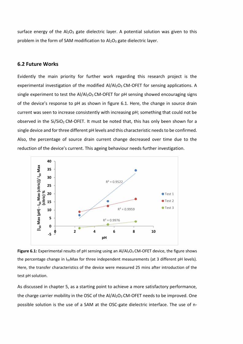
surface energy of the Al2O3 gate dielectric layer. A potential solution was given to this
problem in the form of SAM modification to Al2O3 gate dielectric layer.
6.2 Future Works
Evidently the main priority for further work regarding this research project is the
experimental investigation of the modified Al/Al2O3 CM-OFET for sensing applications. A
single experiment to test the Al/Al2O3 CM-OFET for pH sensing showed encouraging signs
of the device’s response to pH as shown in figure 6.1. Here, the change in source drain
current was seen to increase consistently with increasing pH; something that could not be
observed in the Si/SiO2 CM-OFET. It must be noted that, this has only been shown for a
single device and for three different pH levels and this characteristic needs to be confirmed.
Also, the percentage of source drain current change decreased over time due to the
reduction of the device’s current. This ageing behaviour needs further investigation.
Figure 6.1: Experimental results of pH sensing using an Al/Al2O3 CM-OFET device, the figure shows
the percentage change in ISDMax for three independent measurements (at 3 different pH levels).
Here, the transfer characteristics of the device were measured 25 mins after introduction of the
test pH solution.
As discussed in chapter 5, as a starting point to achieve a more satisfactory performance,
the charge carrier mobility in the OSC of the Al/Al2O3 CM-OFET needs to be improved. One
possible solution is the use of a SAM at the OSC-gate dielectric interface. The use of n-
R² = 0.9522
R² = 0.9959
R² = 0.9976
-5
0
5
10
15
20
25
30
35
40
0 2 4 6 8 10[ISD
Max
(p
H)
-I S
DM
ax (
citr
ic)]
/ I S
DM
ax
(cit
ric)
%
pH
Test 1
Test 2
Test 3
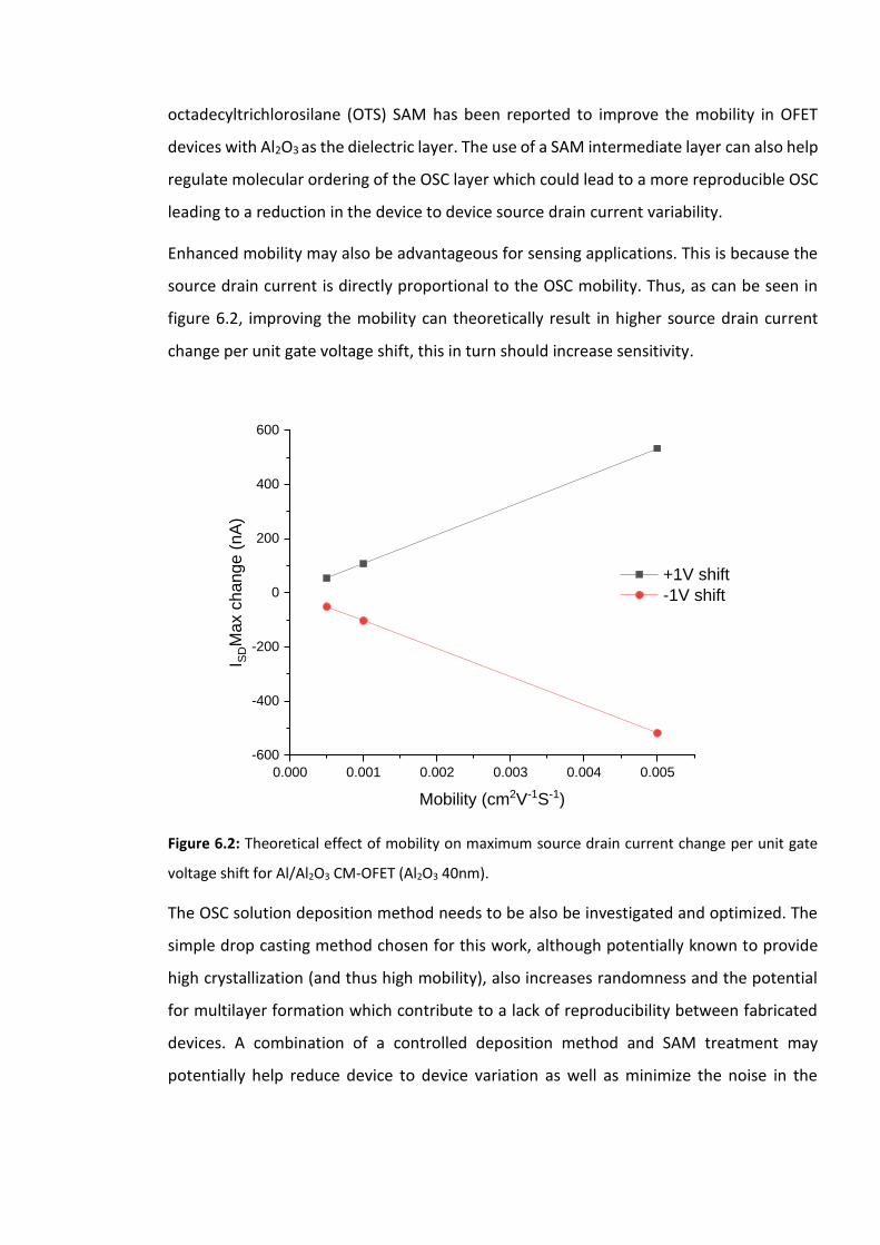
octadecyltrichlorosilane (OTS) SAM has been reported to improve the mobility in OFET
devices with Al2O3 as the dielectric layer. The use of a SAM intermediate layer can also help
regulate molecular ordering of the OSC layer which could lead to a more reproducible OSC
leading to a reduction in the device to device source drain current variability.
Enhanced mobility may also be advantageous for sensing applications. This is because the
source drain current is directly proportional to the OSC mobility. Thus, as can be seen in
figure 6.2, improving the mobility can theoretically result in higher source drain current
change per unit gate voltage shift, this in turn should increase sensitivity.
Figure 6.2: Theoretical effect of mobility on maximum source drain current change per unit gate
voltage shift for Al/Al2O3 CM-OFET (Al2O3 40nm).
The OSC solution deposition method needs to be also be investigated and optimized. The
simple drop casting method chosen for this work, although potentially known to provide
high crystallization (and thus high mobility), also increases randomness and the potential
for multilayer formation which contribute to a lack of reproducibility between fabricated
devices. A combination of a controlled deposition method and SAM treatment may
potentially help reduce device to device variation as well as minimize the noise in the
0.000 0.001 0.002 0.003 0.004 0.005
-600
-400
-200
0
200
400
600
I SDM
ax c
han
ge
(n
A)
Mobility (cm2V-1S-1)
+1V shift
-1V shift
fabricated devices (source drain current fluctuations due to randomness in crystallization
of the OSC).
Addressing the OSC solution deposition method is very important as it is very likely that
only the combination of reducing the inherent current fluctuation (by an optimized
deposition method) and the improved geometrical layout design can produce a functioning
CM-OFET.
From a technological point of view, for the Al/Al2O3 based device, anodization of the Al
layer, rather than deposition via ALD, is a concept worth revisiting. Such a process greatly
simplifies device fabrication and reduces fabrication cost. The use of substrates with a high
surface roughness, such as Mylar plastic sheet could be a good starting choice.
A final suggestion regards the time domain measurement, ISD vs time. Results presented in
chapter 4 showed that the response of the CM-OFET in this type of measurement was
largely dominated by noise and bias stress effect, which affected the interpretation of the
data. Bias stress can be reduced if continuous biasing is replaced by biasing using voltage
pulsing. Reducing the bias stress effect could enable measurements and quantification of
the time dependent variations in the source drain current.
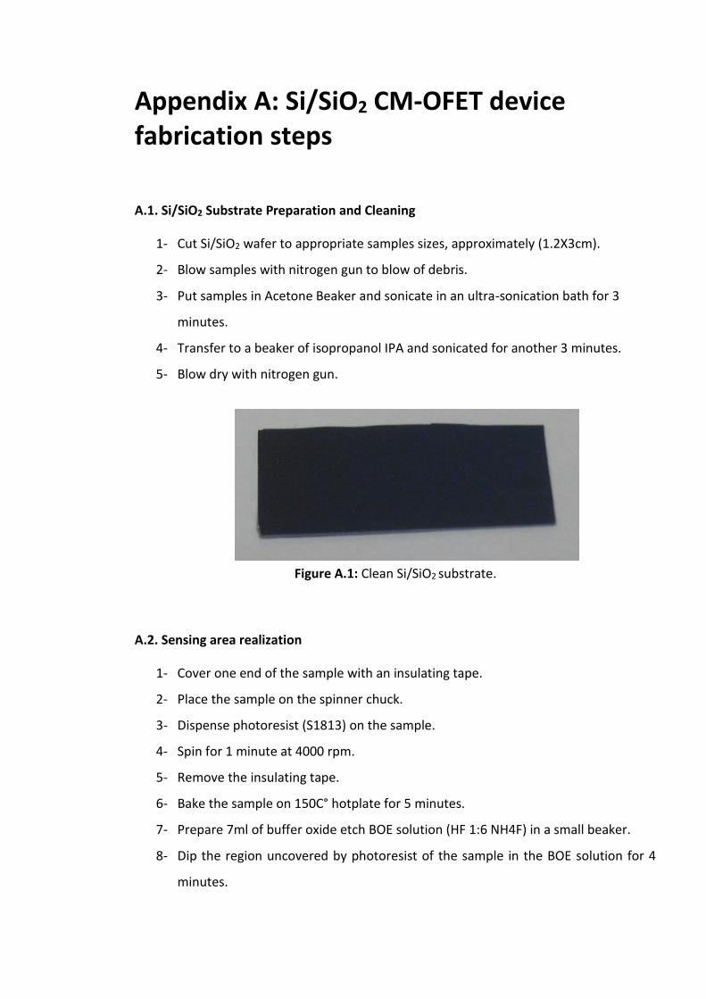
Appendix A: Si/SiO2 CM-OFET device fabrication steps
A.1. Si/SiO2 Substrate Preparation and Cleaning
1- Cut Si/SiO2 wafer to appropriate samples sizes, approximately (1.2X3cm).
2- Blow samples with nitrogen gun to blow of debris.
3- Put samples in Acetone Beaker and sonicate in an ultra-sonication bath for 3
minutes.
4- Transfer to a beaker of isopropanol IPA and sonicated for another 3 minutes.
5- Blow dry with nitrogen gun.
Figure A.1: Clean Si/SiO2 substrate.
A.2. Sensing area realization
1- Cover one end of the sample with an insulating tape.
2- Place the sample on the spinner chuck.
3- Dispense photoresist (S1813) on the sample.
4- Spin for 1 minute at 4000 rpm.
5- Remove the insulating tape.
6- Bake the sample on 150C° hotplate for 5 minutes.
7- Prepare 7ml of buffer oxide etch BOE solution (HF 1:6 NH4F) in a small beaker.
8- Dip the region uncovered by photoresist of the sample in the BOE solution for 4
minutes.

9- Dip the whole sample in a large beaker of DI water to remove the majority of the
etchant residue.
10- Immerse the sample in a second beaker of DI water for 3 minutes, and then rinse
the samples by refilling the beaker with DI water for 30 seconds.
11- Dry the sample with nitrogen gun.
12- Soak a cotton bud in acetone and use it to remove the bulk of the hard-baked
photoresist.
13- Soak the sample in Acetone beaker for several hours.
14- Transfer sample to IPA beaker and sonicate for 3 minutes.
Figure A.2: Si/SiO2 substrate covered with photoresist with one end exposed.
A.3 Contacts formation
a- Photolithography and metal deposition
Photolithography
1- Clean sample in Piranha solution (H2SO4 7:3 H2O2) for 5 minutes.
2- Dip the sample in a large beaker of DI water to remove the majority of the Piranha
residue.
3- Immerse the sample in a second beaker of DI water for 3 minutes, and then rinse
the samples by refilling the beaker with DI water for 30 seconds.
4- Blow dry sample with nitrogen gun.
5- Heat the sample on 110C° hotplate for 1 minute.
6- Place the sample on the spinner chuck.
7- Dispense Primer solution (Hexamethyldisilazane HMDS) on the sample.

8- Spin for 30 seconds at 4000 rpm.
9- Bake the sample on 190C° hotplate for 1 minute.
10- Place the sample back on the spinner chuck.
11- Dispense photoresist (S1813) on the sample.
12- Spin for 1 minute at 5000 rpm.
13- Bake the sample on 110C° hotplate for 3 minutes.
14- Transfer and load the sample to the chuck of the Mask-Aligner machine.
15- Load the sample against the desire region in the photomask.
16- Expose the sample through the photomask to UV light (Dose 22mW/cm2) for 5
seconds.
17- Unload the sample and transfer it to a beaker of photoresist developer (351
microposit).
18- Develop the sample for one minute while shaking the developer solution.
19- Quickly take the sample to a beaker of DI water to stop the developing process.
20- Dry with nitrogen gun.
21- Check the sample under the optical microscope and return to developer solution if
features are underdeveloped.
Table A.1: Photolithography recipe
Spin Speed Time Temperature Notes
Primer (HMDS) 4000 rpm 30 sec Room temperature
Primer bake 1 min 190 C°
Photoresist
(S1813)
5000 rpm 1 min Room temperature
Soft bake 3 min 110 C°
Exposure 5 sec Dose (22mW/cm2)
Developer (351
microposit)
1 min Room temperature shake

Metal deposition
1- Mount two Tungsten Evaporation boats in place in the evaporation machine.
2- Load one Ti pellet in one boat and one Au pellet in the second boat.
3- Lay the samples on a holder 10-15cm above the Ti/Au evaporation sources (facing
down towards evaporation sources).
4- Seal the evaporation chamber and pump it down for 2+ hours.
5- Once the evaporation chamber pressure is below 1X10⁻⁵ mbar start evaporation
process.
6- Using a manual Dial start heating the Ti source by feeding a high current across
the resistive evaporation boat of the Ti source (keep the Ti source shuttered).
7- Slowly increase current until Ti pellet start to melt.
8- Open shutter until 6nm is deposited (thickness monitor reading) and then close
the shutter, turn off the current supply and let boat cool down.
9- After 5-10 minutes (when pressure is back to 1X10⁻⁵ mbar) turn on heating on the
Au source.
10- Slowly increase current until Au pellet start to melt.
11- Open shutter and adjust deposition rate to be approximately 1A°/sec.
12- Leave shutter open until 30nm is deposited (thickness monitor reading) and then
close the shutter, turn off the current supply and let boat cool down.
13- After 20+ minutes vent the vacuum chamber and collect the samples.
Lift-off
1- Soak the sample in Acetone for 15 minutes.
2- Sonicate for 5-30 seconds (until majority of photoresist is removed).
3- Transfer to fresh Acetone beaker and leave for 15 minutes.
4- Sonicate for 0.5 to 5 minutes (depending on the cleanness of the channel between
S and D electrodes).
5- Transfer sample to IPA beaker.
6- Sonicate for 30-90 seconds (depending on the adhesion of Au).
7- Dry with Nitrogen.
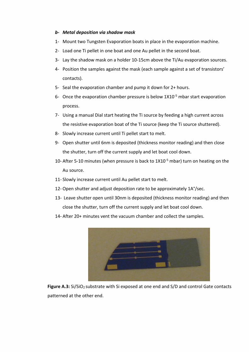
b- Metal deposition via shadow mask
1- Mount two Tungsten Evaporation boats in place in the evaporation machine.
2- Load one Ti pellet in one boat and one Au pellet in the second boat.
3- Lay the shadow mask on a holder 10-15cm above the Ti/Au evaporation sources.
4- Position the samples against the mask (each sample against a set of transistors’
contacts).
5- Seal the evaporation chamber and pump it down for 2+ hours.
6- Once the evaporation chamber pressure is below 1X10⁻⁵ mbar start evaporation
process.
7- Using a manual Dial start heating the Ti source by feeding a high current across
the resistive evaporation boat of the Ti source (keep the Ti source shuttered).
8- Slowly increase current until Ti pellet start to melt.
9- Open shutter until 6nm is deposited (thickness monitor reading) and then close
the shutter, turn off the current supply and let boat cool down.
10- After 5-10 minutes (when pressure is back to 1X10⁻⁵ mbar) turn on heating on the
Au source.
11- Slowly increase current until Au pellet start to melt.
12- Open shutter and adjust deposition rate to be approximately 1A°/sec.
13- Leave shutter open until 30nm is deposited (thickness monitor reading) and then
close the shutter, turn off the current supply and let boat cool down.
14- After 20+ minutes vent the vacuum chamber and collect the samples.
Figure A.3: Si/SiO2 substrate with Si exposed at one end and S/D and control Gate contacts
patterned at the other end.
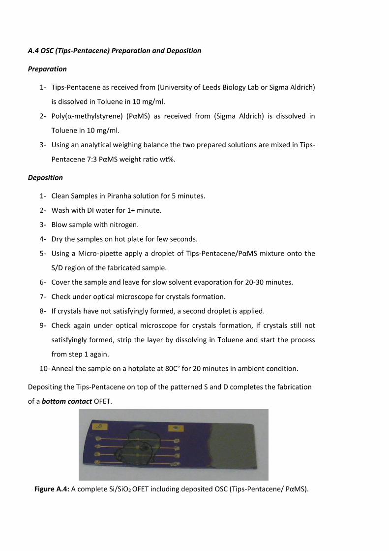
A.4 OSC (Tips-Pentacene) Preparation and Deposition
Preparation
1- Tips-Pentacene as received from (University of Leeds Biology Lab or Sigma Aldrich)
is dissolved in Toluene in 10 mg/ml.
2- Poly(α-methylstyrene) (PαMS) as received from (Sigma Aldrich) is dissolved in
Toluene in 10 mg/ml.
3- Using an analytical weighing balance the two prepared solutions are mixed in Tips-
Pentacene 7:3 PαMS weight ratio wt%.
Deposition
1- Clean Samples in Piranha solution for 5 minutes.
2- Wash with DI water for 1+ minute.
3- Blow sample with nitrogen.
4- Dry the samples on hot plate for few seconds.
5- Using a Micro-pipette apply a droplet of Tips-Pentacene/PαMS mixture onto the
S/D region of the fabricated sample.
6- Cover the sample and leave for slow solvent evaporation for 20-30 minutes.
7- Check under optical microscope for crystals formation.
8- If crystals have not satisfyingly formed, a second droplet is applied.
9- Check again under optical microscope for crystals formation, if crystals still not
satisfyingly formed, strip the layer by dissolving in Toluene and start the process
from step 1 again.
10- Anneal the sample on a hotplate at 80C° for 20 minutes in ambient condition.
Depositing the Tips-Pentacene on top of the patterned S and D completes the fabrication
of a bottom contact OFET.
Figure A.4: A complete Si/SiO2 OFET including deposited OSC (Tips-Pentacene/ PαMS).
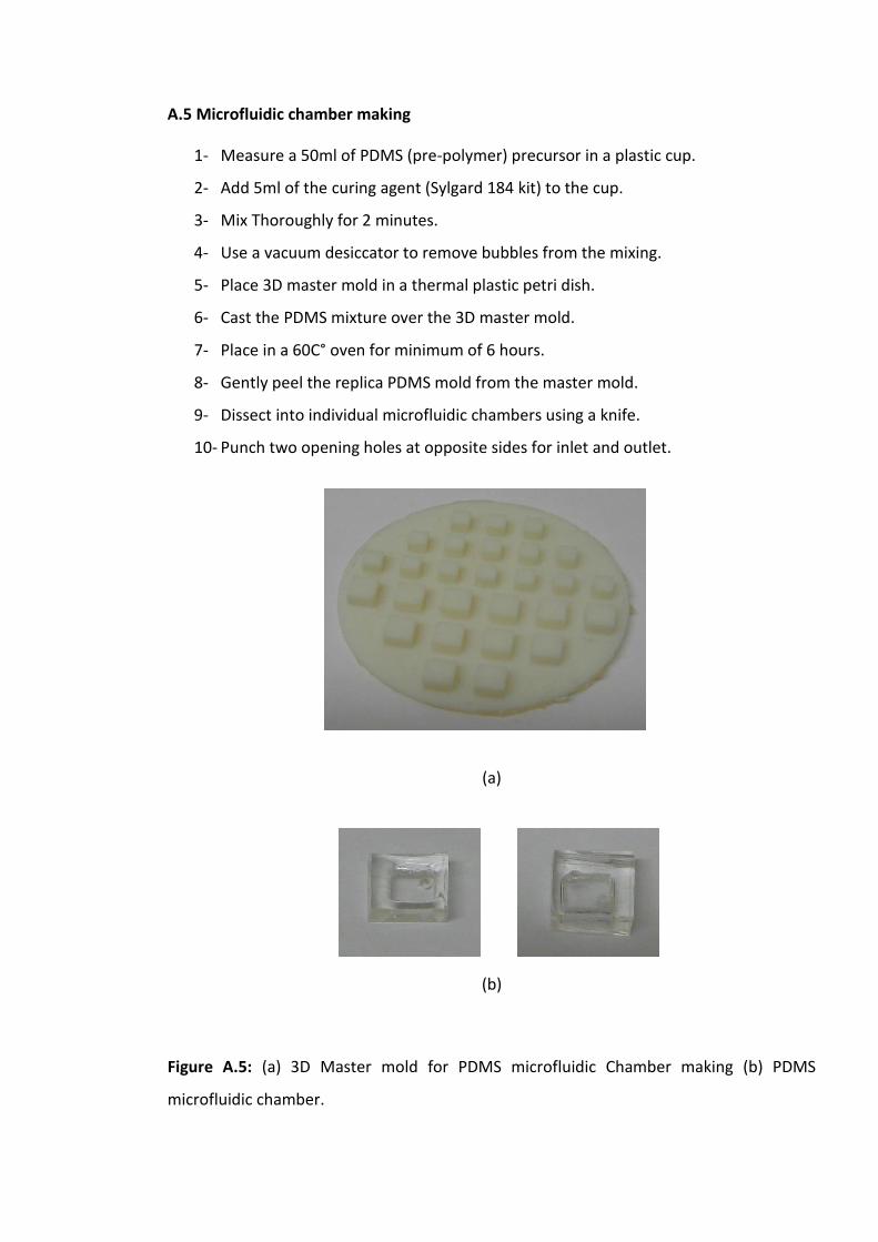
A.5 Microfluidic chamber making
1- Measure a 50ml of PDMS (pre-polymer) precursor in a plastic cup.
2- Add 5ml of the curing agent (Sylgard 184 kit) to the cup.
3- Mix Thoroughly for 2 minutes.
4- Use a vacuum desiccator to remove bubbles from the mixing.
5- Place 3D master mold in a thermal plastic petri dish.
6- Cast the PDMS mixture over the 3D master mold.
7- Place in a 60C° oven for minimum of 6 hours.
8- Gently peel the replica PDMS mold from the master mold.
9- Dissect into individual microfluidic chambers using a knife.
10- Punch two opening holes at opposite sides for inlet and outlet.
(a)
(b)
Figure A.5: (a) 3D Master mold for PDMS microfluidic Chamber making (b) PDMS
microfluidic chamber.

A.6 Gate sensing region functionalization and fluidic chamber integration
If performed before OSC deposition
1- Clean sample in Piranha solution (H2SO4 7:3 H2O2) for 5 minutes.
2- Dip the sample in a large beaker of DI water to remove the majority of the Piranha
residue.
3- Immerse the sample in a second beaker of DI water for 3 minutes, and then rinse
the samples by refilling the beaker with DI water for 30 seconds.
4- Blow dry sample with nitrogen gun.
5- Heat the sample on 110C° hotplate for 1 minute.
6- Load the sample in a UV-Ozone cleaner for 5 minutes treatment.
7- Prepare 5ml of 5% APTES solution in IPA by volume in a 50ml centrifuge tube.
8- Immerse the cleaned sample uprightly in the 5%APTES solution, covering only the
sensing region.
9- Leave the sample immersed in the functionalizing solution overnight
(approximately 18 hours).
10- Remove the sample from the functionalizing solution and immersed in a beaker of
IPA and shake for 1-2 minutes.
11- Remove the sample from the IPA beaker and give it a quick rinse with IPA.
12- Dry with nitrogen gun.
13- Put a pre-prepared PDMS chamber in an IPA beaker and sonicate for 3 minutes.
14- Remove PDMS chamber from IPA and dry with nitrogen gun.
15- Load the PDMS chamber to the UV-Ozone cleaner and turn on the UV light source
for 5 minutes to activate the silanol groups on the PDMS surface.
16- Mount the PDMS chamber to the sensing region of the sample.
17- Transfer the sample to a 90C° hotplate.
18- Pour liquid PDMS around the corner of the PDMS chamber.
19- Leave PDMS to cure for 20 minutes.
If performed after OSC deposition
1- Cover the contacts and OSC region with para-film.
2- Dip the sensing region (exposed Si) of the sample in Piranha solution (H2SO4 7:3
H2O2) for 3-5 minutes.
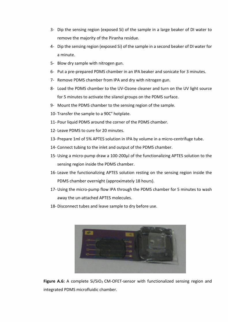
3- Dip the sensing region (exposed Si) of the sample in a large beaker of DI water to
remove the majority of the Piranha residue.
4- Dip the sensing region (exposed Si) of the sample in a second beaker of DI water for
a minute.
5- Blow dry sample with nitrogen gun.
6- Put a pre-prepared PDMS chamber in an IPA beaker and sonicate for 3 minutes.
7- Remove PDMS chamber from IPA and dry with nitrogen gun.
8- Load the PDMS chamber to the UV-Ozone cleaner and turn on the UV light source
for 5 minutes to activate the silanol groups on the PDMS surface.
9- Mount the PDMS chamber to the sensing region of the sample.
10- Transfer the sample to a 90C° hotplate.
11- Pour liquid PDMS around the corner of the PDMS chamber.
12- Leave PDMS to cure for 20 minutes.
13- Prepare 1ml of 5% APTES solution in IPA by volume in a micro-centrifuge tube.
14- Connect tubing to the inlet and output of the PDMS chamber.
15- Using a micro-pump draw a 100-200µl of the functionalizing APTES solution to the
sensing region inside the PDMS chamber.
16- Leave the functionalizing APTES solution resting on the sensing region inside the
PDMS chamber overnight (approximately 18 hours).
17- Using the micro-pump flow IPA through the PDMS chamber for 5 minutes to wash
away the un-attached APTES molecules.
18- Disconnect tubes and leave sample to dry before use.
Figure A.6: A complete Si/SiO2 CM-OFET-sensor with functionalized sensing region and
integrated PDMS microfluidic chamber.
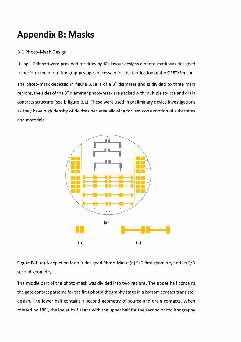
Appendix B: Masks
B.1 Photo-Mask Design
Using L-Edit software provided for drawing ICs layout designs a photo-mask was designed
to perform the photolithography stages necessary for the fabrication of the OFET/Sensor.
The photo-mask depicted in figure B.1a is of a 3” diameter and is divided to three main
regions, the sides of the 3” diameter photo-mask are packed with multiple source and drain
contacts structure (see b figure B.1). These were used in preliminary device investigations
as they have high density of devices per area allowing for less consumption of substrates
and materials.
(a)
(b) (c)
Figure B.1: (a) A depiction for our designed Photo-Mask, (b) S/D first geometry and (c) S/D
second geometry.
The middle part of the photo-mask was divided into two regions. The upper half contains
the gate contact patterns for the first photolithography stage in a bottom contact transistor
design. The lower half contains a second geometry of source and drain contacts. When
rotated by 180°, the lower half aligns with the upper half for the second photolithography
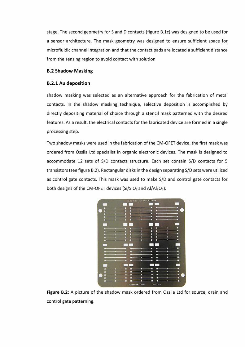
stage. The second geometry for S and D contacts (figure B.1c) was designed to be used for
a sensor architecture. The mask geometry was designed to ensure sufficient space for
microfluidic channel integration and that the contact pads are located a sufficient distance
from the sensing region to avoid contact with solution
B.2 Shadow Masking
B.2.1 Au deposition
shadow masking was selected as an alternative approach for the fabrication of metal
contacts. In the shadow masking technique, selective deposition is accomplished by
directly depositing material of choice through a stencil mask patterned with the desired
features. As a result, the electrical contacts for the fabricated device are formed in a single
processing step.
Two shadow masks were used in the fabrication of the CM-OFET device, the first mask was
ordered from Ossila Ltd specialist in organic electronic devices. The mask is designed to
accommodate 12 sets of S/D contacts structure. Each set contain S/D contacts for 5
transistors (see figure B.2). Rectangular disks in the design separating S/D sets were utilized
as control gate contacts. This mask was used to make S/D and control gate contacts for
both designs of the CM-OFET devices (Si/SiO2 and Al/Al2O3).
Figure B.2: A picture of the shadow mask ordered from Ossila Ltd for source, drain and
control gate patterning.
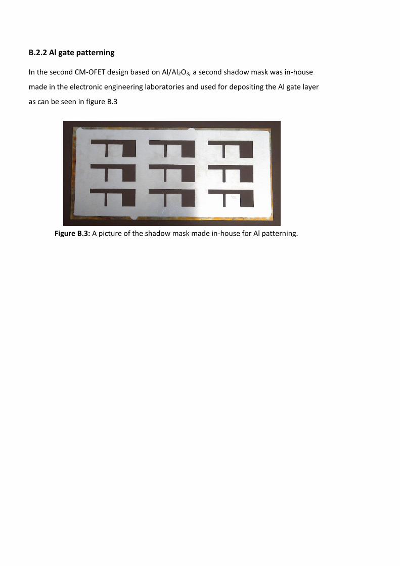
B.2.2 Al gate patterning
In the second CM-OFET design based on Al/Al2O3, a second shadow mask was in-house
made in the electronic engineering laboratories and used for depositing the Al gate layer
as can be seen in figure B.3
Figure B.3: A picture of the shadow mask made in-house for Al patterning.
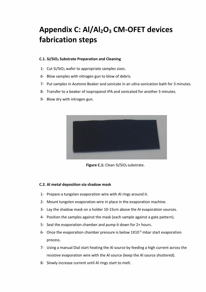
Appendix C: Al/Al2O3 CM-OFET devices fabrication steps
C.1. Si/SiO2 Substrate Preparation and Cleaning
1- Cut Si/SiO2 wafer to appropriate samples sizes.
6- Blow samples with nitrogen gun to blow of debris.
7- Put samples in Acetone Beaker and sonicate in an ultra-sonication bath for 3 minutes.
8- Transfer to a beaker of isopropanol IPA and sonicated for another 3 minutes.
9- Blow dry with nitrogen gun.
Figure C.1: Clean Si/SiO2 substrate.
C.2. Al metal deposition via shadow mask
1- Prepare a tungsten evaporation wire with Al rings around it.
2- Mount tungsten evaporation wire in place in the evaporation machine.
3- Lay the shadow mask on a holder 10-15cm above the Al evaporation sources.
4- Position the samples against the mask (each sample against a gate pattern).
5- Seal the evaporation chamber and pump it down for 2+ hours.
6- Once the evaporation chamber pressure is below 1X10⁻⁵ mbar start evaporation
process.
7- Using a manual Dial start heating the Al source by feeding a high current across the
resistive evaporation wire with the Al source (keep the Al source shuttered).
8- Slowly increase current until Al rings start to melt.
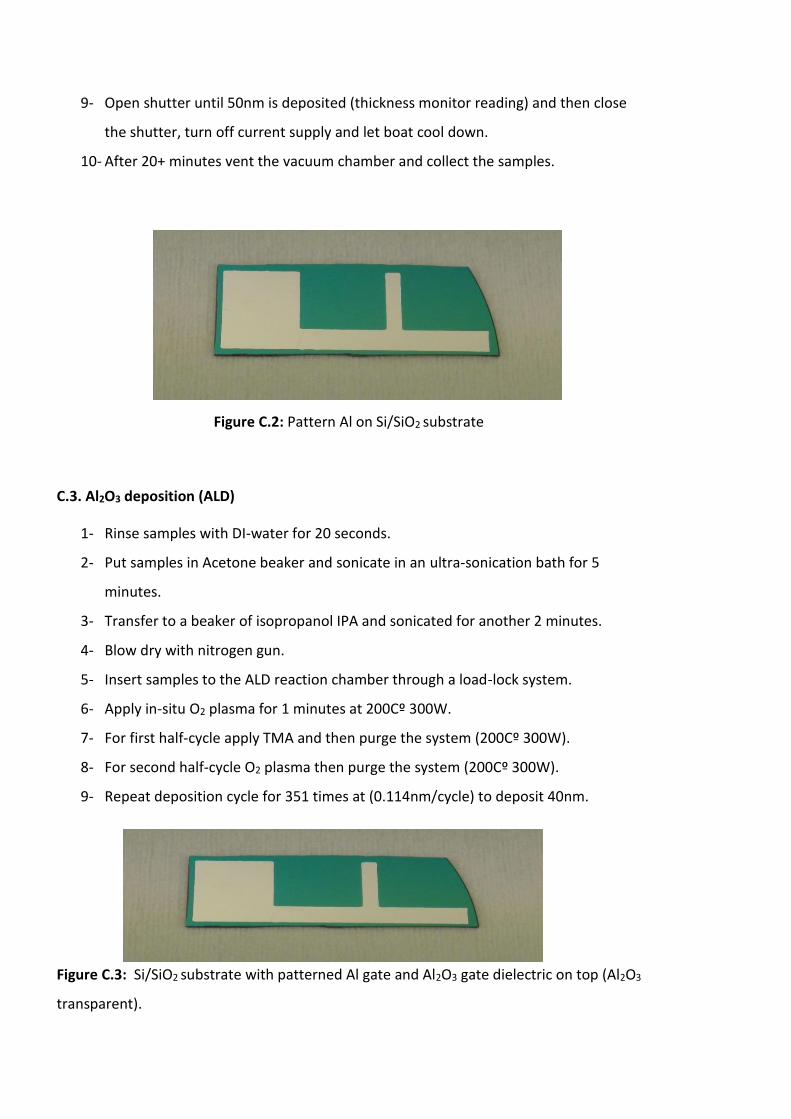
9- Open shutter until 50nm is deposited (thickness monitor reading) and then close
the shutter, turn off current supply and let boat cool down.
10- After 20+ minutes vent the vacuum chamber and collect the samples.
Figure C.2: Pattern Al on Si/SiO2 substrate
C.3. Al2O3 deposition (ALD)
1- Rinse samples with DI-water for 20 seconds.
2- Put samples in Acetone beaker and sonicate in an ultra-sonication bath for 5
minutes.
3- Transfer to a beaker of isopropanol IPA and sonicated for another 2 minutes.
4- Blow dry with nitrogen gun.
5- Insert samples to the ALD reaction chamber through a load-lock system.
6- Apply in-situ O2 plasma for 1 minutes at 200Cº 300W.
7- For first half-cycle apply TMA and then purge the system (200Cº 300W).
8- For second half-cycle O2 plasma then purge the system (200Cº 300W).
9- Repeat deposition cycle for 351 times at (0.114nm/cycle) to deposit 40nm.
Figure C.3: Si/SiO2 substrate with patterned Al gate and Al2O3 gate dielectric on top (Al2O3
transparent).
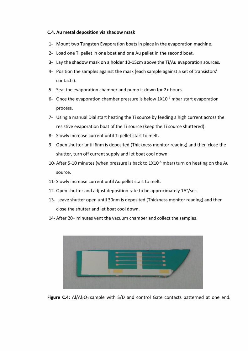
C.4. Au metal deposition via shadow mask
1- Mount two Tungsten Evaporation boats in place in the evaporation machine.
2- Load one Ti pellet in one boat and one Au pellet in the second boat.
3- Lay the shadow mask on a holder 10-15cm above the Ti/Au evaporation sources.
4- Position the samples against the mask (each sample against a set of transistors’
contacts).
5- Seal the evaporation chamber and pump it down for 2+ hours.
6- Once the evaporation chamber pressure is below 1X10⁻⁵ mbar start evaporation
process.
7- Using a manual Dial start heating the Ti source by feeding a high current across the
resistive evaporation boat of the Ti source (keep the Ti source shuttered).
8- Slowly increase current until Ti pellet start to melt.
9- Open shutter until 6nm is deposited (Thickness monitor reading) and then close the
shutter, turn off current supply and let boat cool down.
10- After 5-10 minutes (when pressure is back to 1X10⁻⁵ mbar) turn on heating on the Au
source.
11- Slowly increase current until Au pellet start to melt.
12- Open shutter and adjust deposition rate to be approximately 1A°/sec.
13- Leave shutter open until 30nm is deposited (Thickness monitor reading) and then
close the shutter and let boat cool down.
14- After 20+ minutes vent the vacuum chamber and collect the samples.
Figure C.4: Al/Al2O3 sample with S/D and control Gate contacts patterned at one end.
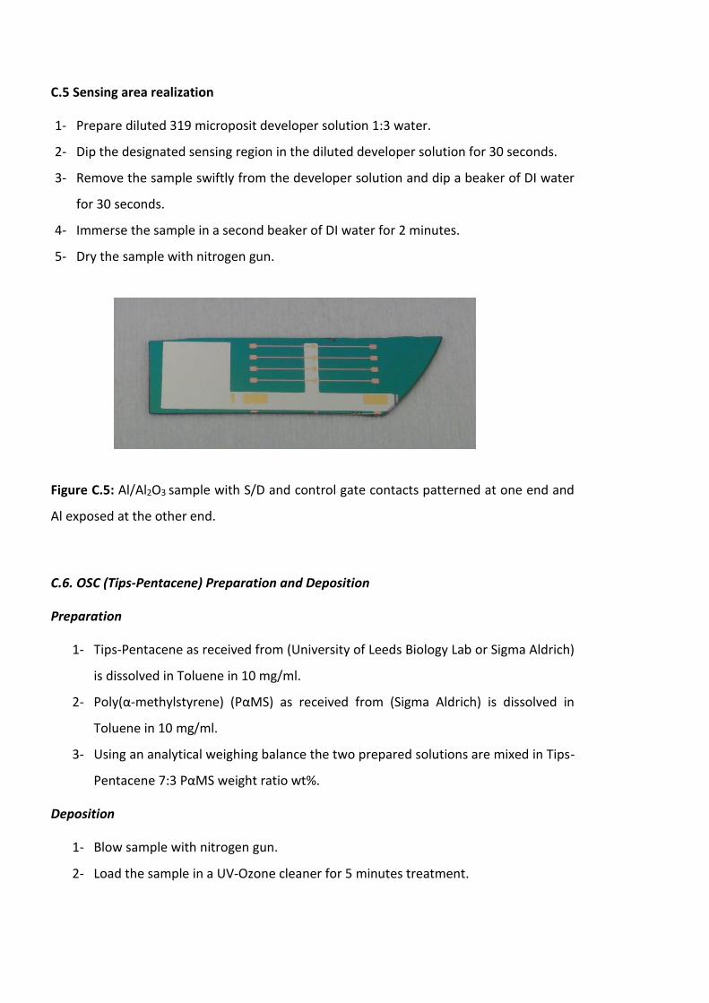
C.5 Sensing area realization
1- Prepare diluted 319 microposit developer solution 1:3 water.
2- Dip the designated sensing region in the diluted developer solution for 30 seconds.
3- Remove the sample swiftly from the developer solution and dip a beaker of DI water
for 30 seconds.
4- Immerse the sample in a second beaker of DI water for 2 minutes.
5- Dry the sample with nitrogen gun.
Figure C.5: Al/Al2O3 sample with S/D and control gate contacts patterned at one end and
Al exposed at the other end.
C.6. OSC (Tips-Pentacene) Preparation and Deposition
Preparation
1- Tips-Pentacene as received from (University of Leeds Biology Lab or Sigma Aldrich)
is dissolved in Toluene in 10 mg/ml.
2- Poly(α-methylstyrene) (PαMS) as received from (Sigma Aldrich) is dissolved in
Toluene in 10 mg/ml.
3- Using an analytical weighing balance the two prepared solutions are mixed in Tips-
Pentacene 7:3 PαMS weight ratio wt%.
Deposition
1- Blow sample with nitrogen gun.
2- Load the sample in a UV-Ozone cleaner for 5 minutes treatment.

3- Using a Micro-pipette apply a droplet of Tips-Pentacene/PαMS mixture onto the
S/D region of the fabricated sample.
4- Cover the sample and leave for slow solvent evaporation for 20-30 minutes.
5- Check under optical microscope for crystals formation.
6- If crystals have not satisfyingly formed a second droplet is applied.
7- Check again under optical microscope for crystals formation, if crystals still not
satisfyingly formed strip the layer by dissolving in Toluene and start the process
from step 1 again.
8- Anneal the sample on a hotplate at 80C° for 20 minutes in ambient condition.
Depositing the Tips-Pentacene on top of the patterned S and D completes the fabrication
of a bottom contact OFET.
C.7 Microfluidic chamber making
See A.5 (Appendix A)
C.8 Gate sensing region functionalization and fluidic chamber integration
If performed before OSC deposition
1- Place samples in Acetone Beaker and sonicate in an ultra-sonication bath for 1
minutes.
2- Transfer to a beaker of isopropanol IPA and sonicated for another 1 minutes.
3- Blow sample with nitrogen gun.
4- Load the sample in a UV-Ozone cleaner for 5 minutes treatment.
5- Prepare 5ml of 5% APTES solution in IPA by volume in a 50ml centrifuge tube.
6- Immerse the cleaned sample uprightly in the 5%APTES solution, covering only the
sensing region.
7- Leave the sample immersed in the functionalizing solution overnight
(approximately 18 hours).
8- Remove the sample from the functionalizing solution and immersed in a beaker of
IPA and shake for 1-2 minutes.
9- Remove the sample from the IPA beaker and give it a quick rinse with IPA.
10- Dry with nitrogen gun.
11- Put a pre-prepared PDMS chamber in an IPA beaker and sonicate for 3 minutes.

12- Remove PDMS chamber from IPA and dry with nitrogen gun.
13- Load the PDMS chamber to the UV-Ozone cleaner and turn on the UV light source
for 5 minutes to activate the silanol groups on the PDMS surface.
14- Mount the PDMS chamber to the sensing region of the sample.
15- Transfer the sample to a 90C° hotplate.
16- Pour liquid PDMS around the corner of the PDMS chamber.
17- Leave PDMS to cure for 20 minutes.
If performed after OSC deposition
1- Clean sensing region with DI water by dipping the sensing region only
2- Dry with nitrogen gun.
3- Put a pre-prepared PDMS chamber in an IPA beaker and sonicate for 3 minutes.
4- Remove PDMS chamber from IPA and dry with nitrogen gun.
5- Load the PDMS chamber to the UV-Ozone cleaner and turn on the UV light source
for 5 minutes to activate the silanol groups on the PDMS surface.
6- Mount the PDMS chamber to the sensing region of the sample.
7- Transfer the sample to a 90C° hotplate.
8- Pour liquid PDMS around the corner of the PDMS chamber.
9- Leave PDMS to cure for 20 minutes.
10- Prepare 1ml of 5% APTES solution in IPA by volume in a micro-centrifuge tube.
11- Connect tubing to the inlet and output of the PDMS chamber.
12- Using a micro-pump draw a 100-200µl of the functionalizing APTES solution to the
sensing region inside the PDMS chamber.
13- Leave the functionalizing APTES solution resting on the sensing region inside the
PDMS chamber overnight (approximately 18 hours).
14- Using the micro-pump flow IPA through the PDMS chamber for 5 minutes to wash
away the un-attached APTES molecules.
15- Disconnect Tubes and leave sample to dry before use.

Figure C.6: A complete Al/Al2O3 CM-OFET-sensor with functionalized sensing region and
integrated PDMS microfluidic chamber.
Appendix D: How to extract the figures of merits
Utilizing the transfer and output characteristics the following parameters which evaluate
the performance of the fabricated Si/SiO2 OFET devices can be extracted:
Mobility
µFET
ON/OFF ratio
ION/ IOFF
Onset
Voltage VSO
Threshold
Voltage VTH
Sub-threshold
Swing S
All the transfer characteristics measurements were collected at saturation. The mobility
and the threshold voltage VTH are extracted by exploiting equation (D.1). Plotting of the
square root of ISD against the gate voltage, the slope of the line = (WCiµ/2L)½ and from the
line equation y=a+bx at y = 0 i.e. ISD½ = 0, VTH = -a/b.
𝐼𝐷𝑆 = 𝑊𝜇𝐶𝑖
2𝐿 (𝑉𝐺 − 𝑉𝑇)
2 (D.1)
Ci is the capacitance per unit area of the gate insulator = εr ε0 /t
Where ε0 is the free space permittivity and εr is the relative permittivity of the silicon
dioxide (gate insulator) and t is the oxide thickness.
Ci = (3.9 X 8.854 X 10-14 F/cm) / (300X10-7 cm) = 11.51nF/cm2
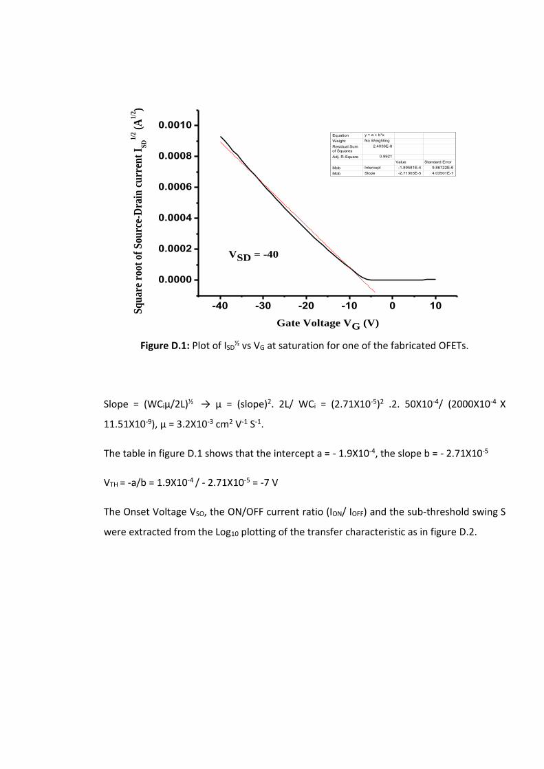
Figure D.1: Plot of ISD½ vs VG at saturation for one of the fabricated OFETs.
Slope = (WCiµ/2L)½ → µ = (slope)2. 2L/ WCi = (2.71X10⁻⁵)2 .2. 50X10-4/ (2000X10-4 X
11.51X10-9), µ = 3.2X10⁻³ cm2 V-1 S-1.
The table in figure D.1 shows that the intercept a = - 1.9X10⁻⁴, the slope b = - 2.71X10⁻⁵
VTH = -a/b = 1.9X10⁻⁴ / - 2.71X10-5 = -7 V
The Onset Voltage VSO, the ON/OFF current ratio (ION/ IOFF) and the sub-threshold swing S
were extracted from the Log10 plotting of the transfer characteristic as in figure D.2.
-40 -30 -20 -10 0 10
0.0000
0.0002
0.0004
0.0006
0.0008
0.0010
Sq
uar
e ro
ot o
f S
ourc
e-D
rain
cu
rren
t I S
D
1/2 (
A1/
2 )
Gate Voltage VG (V)
Equation y = a + b*x
Weight No Weighting
Residual Sum of Squares
2.4036E-8
Adj. R-Square 0.9921
Value Standard Error
Mob Intercept -1.89581E-4 9.86722E-6
Mob Slope -2.71303E-5 4.03501E-7
VSD = -40
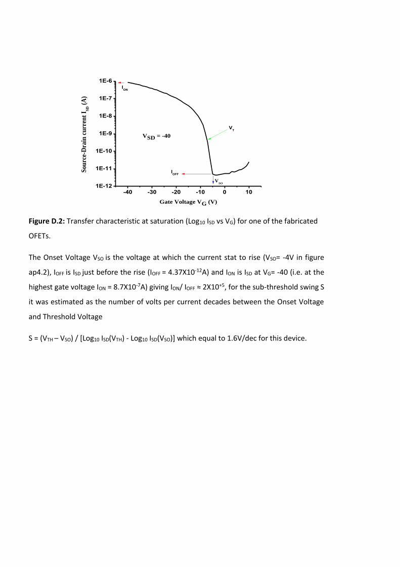
Figure D.2: Transfer characteristic at saturation (Log10 ISD vs VG) for one of the fabricated
OFETs.
The Onset Voltage VSO is the voltage at which the current stat to rise (VSO= -4V in figure
ap4.2), IOFF is ISD just before the rise (IOFF = 4.37X10⁻¹²A) and ION is ISD at VG= -40 (i.e. at the
highest gate voltage ION = 8.7X10⁻⁷A) giving ION/ IOFF ≈ 2X10+5, for the sub-threshold swing S
it was estimated as the number of volts per current decades between the Onset Voltage
and Threshold Voltage
S = (VTH – VSO) / [Log10 ISD(VTH) - Log10 ISD(VSO)] which equal to 1.6V/dec for this device.
-40 -30 -20 -10 0 101E-12
1E-11
1E-10
1E-9
1E-8
1E-7
1E-6
IOFF
VSD = -40
Sou
rce-
Dra
in c
urr
ent
I SD (
A)
Gate Voltage VG (V)
ION
VSO
VT
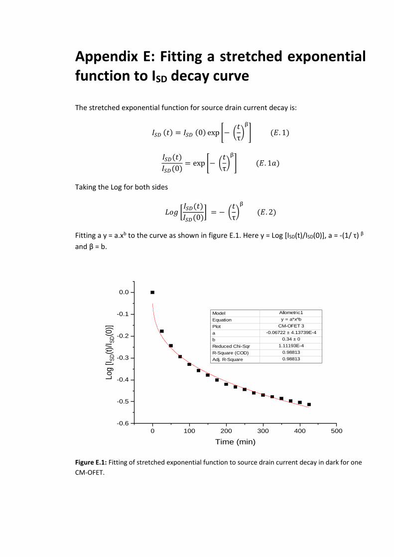
Appendix E: Fitting a stretched exponential function to ISD decay curve
The stretched exponential function for source drain current decay is:
𝐼𝑆𝐷 (𝑡) = 𝐼𝑆𝐷 (0) exp [− (𝑡
τ)β
] (𝐸. 1)
𝐼𝑆𝐷(𝑡)
𝐼𝑆𝐷(0)= exp [− (
𝑡
τ)β
] (𝐸. 1𝑎)
Taking the Log for both sides
𝐿𝑜𝑔 [𝐼𝑆𝐷(𝑡)
𝐼𝑆𝐷(0)] = − (
𝑡
τ)β
(𝐸. 2)
Fitting a y = a.xb to the curve as shown in figure E.1. Here y = Log [ISD(t)/ISD(0)], a = -(1/ τ) β
and β = b.
Figure E.1: Fitting of stretched exponential function to source drain current decay in dark for one
CM-OFET.
0 100 200 300 400 500
-0.6
-0.5
-0.4
-0.3
-0.2
-0.1
0.0
Log [I S
D(t
)/I S
D(0
)]
Time (min)
Model Allometric1
Equation y = a*x̂ b
Plot CM-OFET 3
a -0.06722 ± 4.13739E-4
b 0.34 ± 0
Reduced Chi-Sqr 1.11193E-4
R-Square (COD) 0.98813
Adj. R-Square 0.98813