CHAPTER 3 PROJECT METHODOLOGY
20
CHAPTER 3 PROJECT METHODOLOGY 3.1 Introduction This chapter will cover the details explanation of methodology that is being used to make this project complete and working well. Many methodology or findings from this field mainly generated into journal for others to take advantages and improve as upcoming studies. The method is use to achieve the objective of the project that will accomplish a perfect result. In order to evaluate this project, the methodology based on System Development Life Cycle (SDLC), generally three major step, which is planning, implementing and analysis. Planning Analysis Design Implementation Maintenance and support Figure 3.1: SLDC Phase 12
-
Upload
independent -
Category
Documents
-
view
2 -
download
0
Transcript of CHAPTER 3 PROJECT METHODOLOGY

CHAPTER 3
PROJECT METHODOLOGY
3.1 Introduction
This chapter will cover the details explanation of methodology that is being used to
make this project complete and working well. Many methodology or findings from this
field mainly generated into journal for others to take advantages and improve as upcoming
studies. The method is use to achieve the objective of the project that will accomplish a
perfect result. In order to evaluate this project, the methodology based on System
Development Life Cycle (SDLC), generally three major step, which is planning,
implementing and analysis.
Planning Analysis Design Implementation Maintenance and support
Figure 3.1: SLDC Phase
12
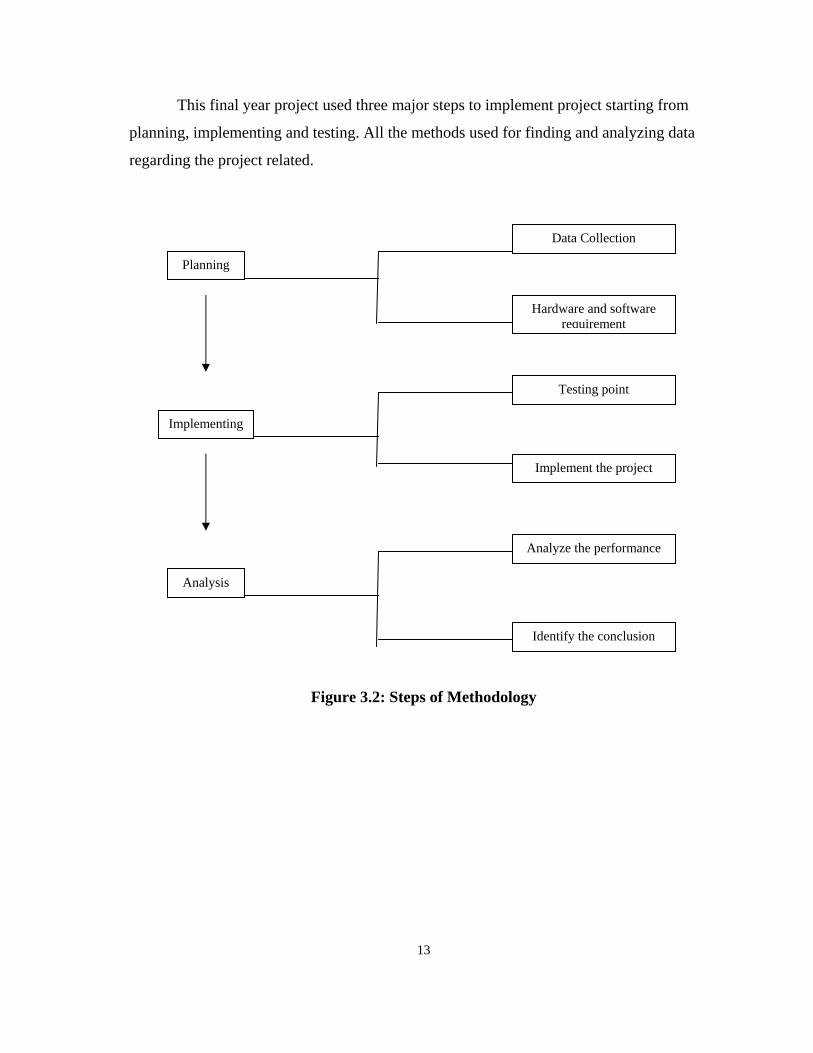
This final year project used three major steps to implement project starting from
planning, implementing and testing. All the methods used for finding and analyzing data
regarding the project related.
Planning
Implementing
Identify the conclusion
Analyze the performance
Implement the project
Testing point
Hardware and software requirement
Data Collection
Analysis
Figure 3.2: Steps of Methodology
13

14
3.2 Planning
To identify all the information and requirement such as hardware and software,
planning must be done in the proper manner. The planning phase have two main elements
namely data collection and the requirements of hardware and software
3.2.1 Data collection
Data collection is a stage in any area of study. At this stage I planned about the
projects resources and requirements, literature studies and schedule to get more information
in this study. All the materials are collected from journal, texts book and research papers
gathered from libraries and Internet.
Within the data collection period I have found the study about the FM Telephone
Transmitter in the Internet and do some research about the project related. Once I got the
project manual, I tried to find out the electronic component and other materials and some of
equipment to be used.
While planning, I have done the research about the project related, which including
with study about the electronic component such as capacitor, resistor, inductance, transistor
and diode. The study is not just for the function of the component but the types of small
circuit build by each component related.

Figure 3.3 below shows the schematic diagram for FM Telephone Transmitter project.
Figure 3.3: FM Telephone Transmitter Schematic Diagram
15

16
3.2.2 Hardware and Software Requirement
3.2.2.1 Hardware Requirement
Below is the list of the entire electronic components and the other material that will
support to complete this project.
• Semiconductors
i. Transistor (Q4) BC107
ii. Transistor (Q6) BF199
iii. Diode (D1-D4) 1N4148
• Resistors
i. R1 – 100 ohm
ii. R2 – 33K ohm
iii. R3 – 10K ohm
iv. R4 – 47K ohm
v. R5 – 390 ohm
• Capacitors
i. C1 – 27p Farad, Ceramic Disc
ii. C2 – 100n Farad, Ceramic Disc
iii. C3 – 22n Farad, Ceramic Disc
iv. C4 – 1n Farad, Ceramic Disc
v. C5 – 7p Farad, Ceramic Disc
vi. C6 – 47p Farad, Ceramnic Disc
vii. C7 – 47p Farad, Ceramnic Disc
viii.C8 – 0 – 25p Farad, Trimmer Cap (red cap)

17
• Additional Parts and Materials
i. Inductor, L1 – 15n Henry, 6 turns of copper wire
ii. Inductor, L2 – 30n Henry, 8 turns of copper wire
iii. Inductor, L3 – 8n Henry, 6 turns of tinned copper wire
iv. Copper wire for connection to phone line
• Telephone Set
• FM Radio
3.2.2.2 Software Requirement
For software requirement, I have choose Orcad Capture CIS Software. OrCAD is a
software tool suite used primarily for electronic design automation. The software is used
mainly to create electronic prints for manufacturing of printed circuit boards, by electronic
design engineers and electronic technicians to manufacture electronic schematics and
diagrams, and for their simulation.
The name OrCAD is a portmanteau, reflecting the software's origins : Oregon +
CAD, since this software can do the simulation of the schematic diagram, waveform for the
output and can perform the PCB layout for the further step of this project.
After the process of gathering all the related information about this final year
project, a step of designing the circuit consist of FM Telephone Transmitter was done.
Using the OrCAD Capture CIS software, where several basics process of designing the
circuit was done.
Transistor selection is the first and most important step in this electronic circuit
design. The transistor should exhibit high gain, low noise figure, and high performance at

D4
D1N4148
7.423V
R5
390
C4
1n
L3
8nH
816.2mV
R1
100
6.484V
6.484V
0V
V19Vdc
7.423V
-788.5mV
4.383V
C3
22n
3.661V
C80-25p
C7
47p
L1
15n
7.423V
VQ4
BC107A
Q6
BF240/PLP
L2
30nH
0
C6
47p
D2
D1N4148
6.484V
R4
47k
6.484V
R2
33k
C127p
R3
10k
8.212V
C5
5p
D1
D1N4148
D3
D1N4148
C2
100n
the lowest possible current consumption, while preserving relatively easy matching at
frequency of operation.
After the transistor had been selected the circuit were then designed. Figure 3.4
shows the actual design of FM Telephone Transmitter that had been done using OrCAD
Capture CIS. However for the value of resistor, capacitor and the inductor the process of
obtaining the desired value is done in manually where each of the component that consist in
the circuits shown below will be tuned until the desired waveform occurs.
Figure 3.4: Schematic Diagram designed by OrCAD
18

3.3 Simulation
After the OrCAD Capture System did the process of designing the circuit, the
simulation of the circuit process is followed. By using the same software, ORCAD Capture
CIS was performed the result of simulation. Several simulation characteristics that can be
observed by using this software are such as the output waveform and also the characteristics
of the project. Since this project using the DC Volt value for input power, so the simulation
result is performed straight-line form.
Figure 3.5: Simulation Result by OrCAD
3.4 Layout design
After all the process of designing the schematic circuits, then the designing process
of the layout was done where it requires several steps until the layout can be done properly.
The procedures of performing the layout design are stated as below:
• Annotate the circuit of FM Telephone Transmitter.
19

20
• Run the Design Rule Check (DRC).
- From this stage the circuit will check whether it is successfully done and
error will alert if anything was failed.
• Netlist process.
- The netlist process is done due to link the schematic circuits to the layout
footprint. In this part of process will creating a file of .mnl
• Creating the circuit layout process.
- In this process the circuit’s file of .mnl is needed to be import. Next, all the
footprint needs to be link to each of the component that is includes inside the
circuits.
• Rearrangement of the circuit.
- By doing this the size of the circuit can be minimized. While doing the
arrangement, the setting of the circuit also must be done where the size of
drilling, size of tracks, which layer is going to be used; as for this circuit
design the single layer will be used.
• After all the process had been done the circuit then will be route in automatically
and so on it then will be checked again using the design rule check.

The layout design for this project FM Telephone Transmitter is performed as shown
in figure 3.4 below.
21
Figure 3.6: Layout Design performed by OrCAD Capture CIS Software (backside)
Figure 3.7: Layout Design performed by OrCAD Capture Software (topside)

22
3.5 Implementing
3.5.1 Project Board Circuit (PCB)
When OrCAD Capture CIS Software did the process of designing the electronic
circuit diagram, the process of produce project board circuit (PCB) is followed. The layout
diagram circuit from OrCAD Capture CIS Software was sent to Engineering Centre
UniMAP (PCB Fabrication Lab) due to produced the project board circuit (PCB). The
procedure of the PCB process by Engineering Centre UniMAP has to attach with PCB
Fabrication Form that was issue by Engineering Centre UniMAP itselt. The form has to fill
up by the student and certified by project supervisor. See at Appendix
The Engineering Centre UniMAP takes a week to produce the printed PCB, which
complete with the mark of every components located and holes drilled for components
mounting.
3.5.2 Components
The components for this project are based on the circuit diagram where all the
components related have been ready at one of electronic component shop at Alor Setar. The
costing for the components as stated at the buying receipt and can see at Appendix.
3.5.3 Construction
i. When mounting components parts to the PCB, I used the parts-placement
diagram as a guide.
ii. Install the resistors and diodes; the board is so tight that those components
must be mounted vertically.

23
iii. The next step is to install the inductors. Coils L1 and L2 are six and eight
urns, respectively, of enameled copper wire. In this part of install I has done
my own inductor where I was wind my own coils, use approximately 22-
gauge wire and a 1/8-inch drill bit as your winding form. Any enamel on the
leads where the coils are to be soldered must be sanded, scraped, or burned
off with a soldering iron before solder will adhere to them properly.
iv. Coil L3 is six turns of tinned copper wire in which the coils must be spread
out with about 1 millimeter between each of turn; none of the turns should
be touching each other.
v. The following is step is installed the fixed capacitors and the trimmer
capacitor (C8) with one.
vi. The next step is mount the transistors, Q4 and Q6 and do solder the two
transistors to appropriate places.
vii. The final step is solder the two wires for connecting to phone line.
viii. Updates any components left and do mounting at PCB.
3.6 Checking
After the parts of mounting the components at PCB finished, I need to check the
continuity track of the circuit. This part of job is to ensure that the operation of this circuit
will run smoothly.
The tools related with the checking parts is multimeter and the continuity checking
involve with every circuit tracks and the point of soldering. By using the buzzer multimeter,
it’s will alert the failed continuity. The failed continuity will recover with the solder again
the lake of components related.

24
3.7 Testing and Tuning
The procedure of testing is beginning with do the connection the FM Telephone
Transmitter circuit to the phone line. Turn on a FM radio and tune to a quiet spot (no station
using that frequency) on the dial somewhere between 90 and 95 MHz. Pick up the phone;
we should hear the dial tone right away on the FM radio.
If that is not the case, we will adjust the trimmer capacitor, C8 until we do hear the
dial tone. First adjust trimmer capacitor, C8 for the best reception, and then fine-tune the
radio. The tuning parts must be done slowly since the matched frequency is hard to get.
3.8 Analysis
The analysis stage is the final stage in this methodology where the two points will
be done. The analysis is base on the performance of the circuit related where the output
must be performed well and successful and the second is identifying the conclusion.
3.8.1 Analyzed the circuit
The circuit of FM Telephone Transmitter is a combination of a small electronic
circuit, where in the working of small electronic circuit will perform the good result of
broadcasting on FM radio as a receiver. In this FM Telephone Transmitter, I have defined
that the small electronic circuits, which stated as below:

Rectifier Circuit
The Rectifier circuit is a combination of four diodes, D1 through D4 and located as
a bridge circuit. This circuit will rectified the full-wave circuit from the power source where
in Telekom Malaysia ™ battery power supplied to telephone line are different for every
conditions, there are:
• Normal power supply – 48 DC Volt
• Ringing power – 98 AC Volt
• On Hook power – 9 DC Volt
The meter reading of telephone line power supply that certified by the technician of
Telekom Malaysia ™ attached at Appendix.
In theory, the rectifier bridge circuit will perform the output of half cycle form. The
full-wave rectifier design exists, and it is built around a four-diode bridge configuration.
The diagram below shows the output of full-wave bridge circuit.
Figure 3.8: The Output of Full-wave rectifier circuit
25

Basic Operation
Current directions in the full-wave bridge rectifier circuit are as follows for each
half-cycle of the AC waveform:
First cycle (positive cycle)
Figure 3.9: The Output of half-cycle (positive) rectifier circuit
Second cycle (negative cycle)
Figure 3.10: The Output of half-cycle (negative) rectifier circuit
26

27
A Full bridge rectifier is an arrangement of four diodes connected in a bridge circuit
as shown above, that provides the same polarity of output voltage for any polarity of the
input voltage. When used in its most common application, for conversion of alternating
current (AC) input into direct current (DC) output, it is known as a bridge rectifier. The
bridge recitifier provides full wave rectification from a two wire AC input but has two
diode drops rather than one reducing efficiency over a center tap based design for the same
output voltage.
The essential feature of this arrangement is that for both polarities of the voltage at
the bridge input, the polarity of the output is constant. When the input connected at the left
corner of the diamond is positive with respect to the one connected at the right hand corner,
current flows to the right along the upper colored path to the output, and returns to the input
supply via the lower one.
When the right hand corner is positive relative to the left hand corner, current flows
along the upper colored path and returns to the supply via the lower colored path. In each
case, the upper right output remains positive with respect to the lower right one. Since this
is true whether the input is AC or DC, this circuit not only produces DC power when
supplied with AC power, it also can provide what is sometimes called reverse polarity
protection. It’s protects the circuitry it powers against damage that might occur without this
circuit in place.
FM Oscillator
The Oscillator is the single most important part of an FM telephone transmitter. The
term oscillator is the name given to an object that generates a frequency by repetition. In the
field of electronics, the oscillator generates an electronic signal with a voltage that varies
with respect to time (t). This voltage will vary from one value to another, and then back to
the initial value.
The concept of oscillation (voltage varying with respect to time) is shown in Figure
3.10. This is a "sinusoidal" waveform, which begins at point A, then increases voltage to
Vmax, returns the same voltage as it had at point A, then decreases voltage to Vmin before

finally returning to its initial voltage, the same voltage as at point A. This is a very simple
"single cycle sinusoidal waveform" and it is a typical sample of a waveform generated by
an FM oscillator. These oscillators have a set frequency, and their output frequency (known
as the center frequency) will be that frequency on which the transmitter will broadcast.
Figure 3.11: The concept of oscillation
The oscillator frequency will change slightly depending on the voltage of the audio
signal modulating it and the oscillator design. The minor change in this frequency is known
as "deviation", and the frequency of the oscillator should deviate equally both above and
below the center frequency of the oscillator. The oscillator generates the output frequency,
which determines where on the FM Band your transmission will be located. The output of
the oscillator contains all of the essentials for an FM broadcast. It is modulated by the audio
signal and transmitting on a user defined frequency. When tuned to with an FM radio as a
receiver voice will be heard.
Power Amplifier
The output power of an oscillator is usually very low, perhaps 50 mWatts
(milliWatts). This level of power would only be capable of transmission over a range of 100
- 300 meters depending on environmental conditions. Since the output from oscillator is
very low, so we have to increase the output power.
28

The RF Power Amplifier is the final part of an FM telephone transmitter. It will be
fed by the oscillator and will have the single property of increasing the power of the
oscillating signal generated by the oscillator.
Shown in Figure 3.11, is an RF amplifier module with a sinusoidal input signal with
value Vin. Without getting technical, this signal undergoes an amplification process, which
produces a signal at the output with a value of Vin multiplied by the gain factor. Normally
the letter “A” denotes the gain factor, and as shown below the gain (A) for this amplifier
has a value of 10. Therefore is we were to apply a signal of 1 Volt to the input of this
amplifier, then the output should be 1 X 10 = 10 Volts, if we applied 5 volts then Output =
5 X 10 = 50 Volts. The frequency of the output signal must be exactly the same as the
frequency of the input signal. Included in the amplifier is usually some form of a lowpass or
bandpass filter.
Figure 3.12: The RF amplifier module with a input and output form
The frequency of the output signal must be exactly the same as the frequency of the
input signal. Included in the amplifier is usually some form of a lowpass or bandpass filter.
29

30
3.8.2 Identify the conclusion
The final step is identifying the conclusion of the circuit operation.
Circuit Description
While the connection has been done at telephone line, the FM telephone transmitter
accepts the power of different conditions same as mentioned earlier. The power for the
circuit is fullwave bridge and have been rectified by rectifier bridge circuit where the
combination of four diodes D1 through D4.
Transistor Q4, capacitors C1 and C8, and inductor L3 form an FM oscillator. This is
the part of the transmitter that generates the frequency (f), hence the name frequency
generator of around 93 MHz. Variable-capacitor C8 allows the oscillator frequency to be
adjusted between 90 and 95 MHz. The output of frequency that generate by oscillator is
very low, therefore output have to increase the power. Audio from the phone line is coupled
through resistor R3 and capacitor C2 to the base of transistor Q4 where it frequency
modulates the oscillator.
The signal tapped off L3 in the oscillator circuit is fed to the base of transistor Q2
and the FM signal is transmitted from Q2's collector. Transistor Q6 inductor L1, and
capacitor C6 form a power amplifier circuit. This power amplifier is use to amplified the
output that generated by oscillator. The inductor L2 is a radio-frequency shunt that
decouples power and audio from the amplifier circuit.

31
3.8 Conclusion
As a conclusion, every project will have different methodologies that is being used
to make the project successful and working well. Generally, the methodologies are divided
into three parts, there are planning, implementing and analysis. In planning phase there are
including with reading activity and some job of requirements of hardware and software to
be used.
In reading activity I do research through several sources such as text books, journal,
paper references, the Internet and more sources due to get the information about the project
related. While in the requirements of hardware and software to be use I was study and find
out the functional and operational of the hardware and software related.
Next step is implementing phase where in this part I did the appointment with third
party due to produce the project circuit board. When the PCB was ready to mount the
electronic components, the process of construction circuit is followed. The process of
checking, testing and tuning are followed due to complete a part of implementing.
Finally, in analysis phase, the project was come out with the operations of FM
telephone transmitter circuit. It was looking at the combination of electronic circuits that are
rectifier, oscillator and power amplifier. The functions and the operations of the circuits
related are very important to be analyzed. With appropriate steps and methodology, any
process of completing the project can be managed wisely and will be make a good result.