Cadence AWR Design Magazine Volume 16.1
16
ni.com/awr Antenna Synthesis and Optimization Technology Design of Base Station Power Amplifiers From Load-Pull Measurements The Latest Design Software from NI Customer Successes MaXentric and Infineon AWR Design Magazine Vol.16.1
-
Upload
khangminh22 -
Category
Documents
-
view
0 -
download
0
Transcript of Cadence AWR Design Magazine Volume 16.1

ni.com/awr
Antenna Synthesis and Optimization Technology
Design of Base Station Power Amplifi ers From Load-Pull Measurements
The Latest Design Software from NI
Customer SuccessesMaXentric and Infi neon
AWR Design MagazineVol.16.1

Performance of high-frequency
electronics is continually advancing to
meet increasing global demands for
information. And while the cellphone has
been around for over 40 years and the
smartphone for over a decade, wireless
communication systems are still evolving.
As such, looking
beyond cellular has
become the central
theme of this year’s
IMS keynote talks:
■ Dr. Martin Cooper, father of the
cellphone, “Birth and Death of the Cell
Phone”■ Dr. James Truchard, NI president, CEO
and cofounder, “Software’s Role in
Next-Generation 5G RF and Microwave
Systems “■ Prof. Jan M. Rabaey, UC Berkeley, “The
Human Intranet - Where Swarms and
Humans Meet”
From the inner body to outer space,
how will the hardware that connects
more people and things to data continue
to advance? Through collaborative
innovation and continued advances in
engineering tools.
During IMS, more detail on the state
of smart RF/microwave design and test
solutions from NI will be presented in
MicroApp presentations and in-booth
product demonstrations. Read on to
learn more.
Designing Better PAs … BetterIf your focus is on designing RF power
amplifi ers with higher linearity and power
added effi ciency (PAE), the latest load-pull
capabilities in NI AWR Design Environment™
offer an unprecedented level of support
and data management. Today’s PAs must
achieve multiple performance metrics that
are diffi cult to achieve simultaneously. In
addition, higher PAE levels can often only
be achieved through harmonically tuned
devices that employ output waveform
shaping techniques. Combined, these
requirements force many designers not
using the NI AWR Design Environment to
iterate their optimization efforts between
different impedance matching scenarios
until a reasonable trade-off is achieved.
Optimum PA performance is extremely
diffi cult and time consuming with this
back-and-forth approach.
With the load-pull capabilities within
NI AWR Design Environment, engineers
can dynamically explore the impact of
fundamental and harmonic terminations
and directly observe the impact
(simultaneously) on any number of power
amplifi er (PA) responses, including gain
compression versus power, PAE, error
vector magnitude (EVM), adjacent channel
power ratio (ACPR), and more.
Integration Made Possible Through EM AnalysisMany of today’s PAs are integrated into
radio front-end modules that contain
the fi ltering and switching necessary for
multi-mode, multi-band mobile devices.
Such modules include high-density
components, embedded passives, and
complex interconnects that require planar
and/or 3D electromagnetic characterization.
The latest chip-package-board design and
validation solutions from NI are based on
the powerful integration of AXIEM (3D
planar) and Analyst™ (arbitrary 3D fi nite
element) electromagnetic (EM) solvers
within NI AWR Design Environment.
Complementing these EM modeling
tools, bi-directional interoperability has
been developed between Microwave
Offi ce circuit simulator and third-party
EM simulators such as ANSYS HFSS. This
integration supports unrestricted planar
structures, as well as commonly used 3D
circuit interconnect structures such as
wire bonds and ball-grid arrays. Structures
defi ned in NI AWR Design Environment defi ned in NI AWR Design Environment
are then automatically solved by HFSS
during the overall network analysis, with
the results embedded directly into the
circuit hierarchy without leaving the circuit
design environment or requiring manual
steps on the part of the designer.
A New Starting Point for Antenna DesignersEM simulation and EM optimization have
been the tools of choice for modern
antenna design, with designers modifying
the physical dimensions of antenna
structures they already know or can fi nd
in reference materials. While tweaking
physical dimensions will allow designers
to shift antenna behavior to operate in the
band of interest, there is no guarantee
that the optimum performance has been
achieved. To address the challenge of
fi nding the optimum antenna structure and
dimensions for a desired set of electrical
characteristics, AntSyn™ antenna synthesis
and optimization software was recently
added to the NI AWR software portfolio.
Based on evolutionary algorithms (EAs),
a programmatic method for exploring the
design space and automatically locat ing
novel antenna designs combined with
EM simulation, AntSyn is proving to be
more effective at generating antenna
structures with greater performance
than would otherwise be developed by
traditional methods.
To learn more about NI AWR software and
its fi t for your microwave/RF design needs,
visit Booth #1529 to speak with the NI AWR
software experts.
Best regards,
David Vye
Director of
Technical Marketing
AWR Group, NI
The Latest Design Software from NI

Hands-On Practical WorkshopFrom Bits to Waves: Building a Modern Digital Radio in One Day
Hosted by: NCSU Professor David Ricketts
Date: Wed, May 25
Time: 9 a.m. - 3 p.m.
Location: Exhibition Area
Fee: $100
In this fun and interactive workshop that features the use of NI AWR software, participants will learn the basic theory of modern digital radios,
as well as the RF circuits and systems used to build them.
■■ Participants need only a basic background in RF circuits, such as S-parameters and basic transmission line theory.■■ Example designs will be available to ensure that everyone, from the most advanced RF designer to the student, will
be successful. ■■ You only need to bring your laptop. All other materials and equipment (PC in a bag) will be provided.
To learn more, visit ims2016.org/technical-program/practical-workshop
AWR Design Forum 2016Celebrating its sixth year, the AWR Design Forum (ADF) is an
open forum that brings together NI AWR software customers,
partners, and microwave/RF engineering professionals to learn,
network, and collaborate on the design of today’s microwave
and RF circuits and systems.
This free-to-attend event travels the globe to bring NI AWR
software experts to demonstrate the latest design technologies
and encourage dialogue and the exchange of technical ideas
around the design challenges you face.
Highlights■■ Technical presentations featuring NI AWR Design Environment■■ Select customer and keynote presentations■■ Live demo exhibition area
LocationsAsia■■ Tokyo, Japan - July 8■■ Shanghai, China - August 16■■ Shenzhen, China - August 19■■ Taipei, Taiwan - August 22■■ Hsinchu, Taiwan - August 23■■ Seoul, Korea - September 6
North America■■ Boston, MA (EDICON) - September 20 - 22
Europe■■ London, UK (EuMW) - October 4
Visit awrcorp.com/adf for more information
©2016 National Instruments. All rights reserved. Analog Offi ce, AWR, AXIEM, LabVIEW, Microwave Offi ce, National Instruments, NI, and ni.com are trademarks of National Instruments. Other product and company names listed are trademarks or trade names of their respective companies.

The Design ChallengePAs are an integral part of all cellular phones, base stations, and radio systems and represent one of the most expensive component sub-
assemblies in modern wireless infrastructure equipment. Both performance and cost are important drivers in system design and effi ciency,
making physical size, linearity, and reliability among the principal challenges. As systems and their waveforms get more complicated, new and
innovative techniques and materials must be used to provide the required performance.
The increasing demand for higher data rates and larger signal bandwidth, while maintaining signal integrity, has led to the use of signals with
non-constant envelope and high peak-to-average power ratio (PAPR). In conventional fi xed-bias PAs, the maximum effi ciency occurs at saturation,
with a single-tone signal. As the PA operates at power levels away from saturation, the effi ciency degrades. This creates an issue in the presence
of high PAPR signals (such as orthogonal frequency-division multiplexing [OFDM]), where the average power is well below saturation.
“NI AWR Design Environment enhances the designer’s experience by signifi cantly reducing optimization time. In addition, in envelope tracking, the ability to simultaneously simulate one’s design at the chip, board, and system level has become paramount in enabling next generation wideband high effi ciency PA design.”
Johana Yan, Lead Engineer, MaXentric Technologies, LLC , maxentric.com
Various techniques have been explored to increase the effi ciency
of PAs for high PAPR signals. One area of research is the ET
technique. The drain voltage of the RFPA is varied dynamically
to track the envelope of the signal, providing the appropriate DC
supply signal and keeping the RF transistor operating continuously
in its saturation region. Since the DC supply power is changing with
the input envelope signal, the overall transmitter will not consume
excessive DC power in a low-output power region. This results in a
dramatic increase in PA effi ciency.
The platform development of the ETPA is very important because
the ETPA transmitter architecture is different from the conventional
transmitter. Figure 1 shows the MaXentric ETPA.
The bandwidth of the RF signal from the up-converter is the same
as that of the signal at the antenna. The bandwidths of both the
RF and envelope signals are fi ve times wider than that of the
conventional transmitter. Many of the available evaluation platform/
testbeds today are limited in bandwidth to ~200 MHz. This limits
the bandwidth of the supported signal to ~40 MHz. In addition,
the feedback path is needed for the digital pre-distortion (DPD)
linearization. The transmitter for the conventional PA is simple,
but the effi ciency of the PA is relatively low. On the other hand,
the effi ciency of the ETPA is quite high thanks to the dynamic
modulator design. To simplify ETPA development, it is important to
establish the ETPA design platform.
The challenge for the MaXentric design team was to develop
an ETPA using real-time effi ciency and linearity measurements
for optimizing ETPA design, with fl exibility to accommodate
different 5G signals. As talk of future 5G LTE systems calls for
signal bandwidths of greater than 100 MHz, the need for an
evaluation platform with 500 MHz was crucial.
Figure 1: MaXentric ETPA.
MaXentric Designs and Optimizes Envelope Tracking Power Amplifi ers for 5G LTE
The SolutionMaXentric designers chose NI AWR Design Environment, specifi cally Microwave Offi ce circuit design
software, to design and optimize their ETPA, as well as the NI vector signal transceiver (VST) for RF signal
generation and the NI arbitrary waveform generator (AWG) for envelope signal generation. On-board
tuning and fi nal optimization of the PA impedance matching network was performed with Microwave
Offi ce software, which provided nonlinear harmonic balance circuit simulation in conjunction with design
features such as load-pull analysis, transient analysis, circuit envelope, and verifi cation through circuit/
electromagnetic (EM) co-simulation via NI AWR Design Environment’s AXIEM 3D planar EM simulator.
Results of Envelope Tracking using PXI and VST
The VST and PXI were used to optimize the LTE Band 1 (2.14 GHz) access point (AP) using MaXentric’s
MaXEA 1.0 modulator. The MaXEA 1.0 is a 30 V integrated envelope modulator with greater than 70
percent modulator effi ciency, capable of outputting up to 7 W of average envelope power. It is designed
to support signals with high PAPRs, such as those used in 5G LTE. It is compatible with various
semiconductor technologies, such as laterally diffused metal oxide semiconductor (LDMOS), gallium
nitride (GaN), gallium arsenide (GaAs), and more. In this application, a GaN device was used for the PA
design. The PA was tuned and optimized for envelope tracking operation using the NI PXI system.
Initially, output and input external tuners were used to optimize the effi ciency, gain, and output power
of the ETPA. The desired input and output impedances were measured using a vector network analyzer
(VNA) and the impedance tuning measurements were de-embedded via simulations performed using
Microwave Offi ce software in order to derive the required matching structures at the input/output of the
power transistor. The retuned ETPA was then measured again using the PXI, VST, and LabVIEW ET setup
to confi rm its performance. Time alignment between the RF (VST) and the envelope (AWG) paths was
performed digitally in LabVIEW for best effi ciency and linearity.
The use of Microwave Offi ce software enabled the designers to signifi cantly reduce PA optimization
time without sacrifi cing measurement accuracy. The close correlation between simulation and
measurement enabled them to perform most of the optimizing in software before physically
implementing it on the board, thus reducing the number of iterations that had to be performed.
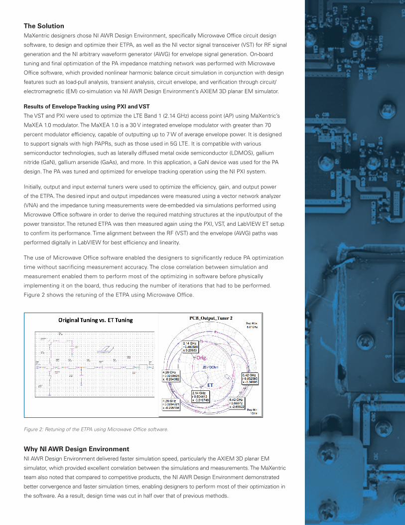
Figure 2 shows the retuning of the ETPA using Microwave Offi ce.
Why NI AWR Design EnvironmentNI AWR Design Environment delivered faster simulation speed, particularly the AXIEM 3D planar EM
simulator, which provided excellent correlation between the simulations and measurements. The MaXentric
team also noted that compared to competitive products, the NI AWR Design Environment demonstrated
better convergence and faster simulation times, enabling designers to perform most of their optimization in
the software. As a result, design time was cut in half over that of previous methods.
Figure 2: Retuning of the ETPA using Microwave Office software.

The Design ChallengeTo deliver best-in-class linearity and noise-fi gure performance,
Infi neon designers rely on the robust, accurate circuit simulation
and precise modeling of all the components used in their MMIC
and module designs, including printed-circuit board (PCB) test
boards. Precise linear models enable faster verifi cation of system-
level performance for the application circuits supporting different
bands of 4G LTE-A, currently numbering more than 44 LTE bands
worldwide. By using powerful scripting capabilities built into NI AWR
Design Environment, the time for designing and documenting new
application circuits has been reduced from days to hours.
The SolutionInfi neon chose NI AWR software for its exacting device modeling
needs . The LNA and LNA/multiplexer PCB test structure include
an RF input and output transmission line of predefi ned length and
width. S-parameter and noise fi gure measurements of any device at
the calibrated test equipment port will include this transmission line,
as well as the SMA connector launches on the test boards input/
output. The response of the test structure can be removed from the
measurement through de-embedding, resulting in a more accurate
measurement of the isolated device response. The test structure can
be characterized through a variety of measurement-based methods
or rigorous electromagnetic (EM) simulation. In this case, engineers
used the closed-form transmission line and SMA models in NI AWR
Design Environment, specifi cally Microwave Offi ce circuit design
software, to compare to three different calibration standards: namely
a short, open, and through transmission line, as shown in Figure 1.
Highly integrated and performance optimized32-bit microcontrollers for automotive and industrial applications
www.infineon.com/aurix
“Generating the application notes and technical reports for the hundreds of circuits we developed from our LNA model was very time consuming, however, we wrote a custom script for the application note generator add-on tool in Microwave Offi ce software that automated the whole operation, reducing the time and effort considerably.”
Moakhkhrul Islam, Technical Marketing and Application Engineering, RF and Sensors, Infineon Technologies AG, infineon.com
Figure 1: Actual layout of the PCB (left) and Microwave Office schematic diagram for PCB characterization (right).
Infi neon Supports LTE-A LNA Customers With Band-Specifi c Application Notes
Simulating the device, application circuit, and test fi xture together
enabled the engineers to make a direct comparison to the
application circuit’s measured results (in the test fi xture). If the
simulation and measurement results showed equivalent responses,
then the model was accepted.
As the simulation and measurement results of the application
boards demonstrated an acceptable level of agreement, the LNA
model was used in hundreds of simulation circuits for different
wireless applications, especially for different LTE bands. Generating
the documentation (datasheets and application notes) for the
hundreds of application circuits is very time consuming, however,
the Infi neon RF & Sensors Business Unit was able to develop
an application note generator add-on tool for Microwave Offi ce
software. Using this tool, the documentation for each application
circuit was completed in a few minutes.
The generator tool is based on a custom script fi le that automates
the entire operation, reducing the time and effort considerably.
By running the script fi le fi rst, all the necessary graphs were
generated with proper annotations, axis defi nition, title, and
markers. Then all the graphs were verifi ed by the applications
engineers. If the graphs were approved, the script was used
again and all the graphs were copied from Microwave Offi ce
software to the appointed document fi le. The script was also used
to complete the table in the document fi le by fi nding the proper
values from the generated graphs.

The Design ChallengeThe design challenge for Technion SAMPL Lab students was to build an effi cient, easy-to-use synthetic
aperture radar (SAR) simulator that connects to MATLAB for signal processing. SAR is a type of radar
used to create two and three dimensional representations of an object. SAR uses the motion of the
radar antenna over a targeted region to provide fi ner spatial resolution than is possible with conventional
beam-scanning radars. The SAMPL Lab design focuses on sub-Nyquist sampling of the received signal
and full reconstruction of the image.
The students, supervised by Kfi r Aberman and Prof. Yonina Eldar, wanted to create a SAR simulator that
could handle many targets on the surface and then use MATLAB to calculate the object shapes. The SAR
simulator had to perform as quickly as possible.
The SolutionThe SAMPL Lab students used NI AWR Design Environment, inclusive of Visual System Simulator™ (VSS)
system design software, for this SAR simulator research project because it provides an intuitive, accurate
and fl exible environment. The software gave the students a simple yet accurate look at the architecture
and design phases of the SAR simulator. They were able to examine many related examples that were
provided, which helped them in learning the software, its capabilities, and its usefulness for the SAR
simulator project.
“We found the e-learning tools and software documentation very helpful. The vast simulation options within NI AWR Design Environment makes radar design a very easy and straightforward process.”
Yoav Chachamovitz, Student SAMPL Lab Techniontechnion.ac.il
Technion Students Design Synthetic Aperture Radar (SAR) Simulator
The Design ChallengeSubstrate-to-substrate interconnection is important in order to achieve a higher isolation among the parts of
a transceiver. Each part must be designed on a separate circuit substrate to avoid signal leakage through the
shared substrate, especially the high-power LO leakage to other parts. Additionally, it is not possible in every
case to place all components on one circuit substrate so they must be placed on different substrates for a
complex circuit. To solve these challenges, engineers at Nanjing University of Posts and Telecommunications
wanted to design a novel broadband substrate-to-substrate interconnection structure.
The SolutionThe designers developed a broadband interconnection using double bond wires with square-shaped
defected ground structure (DGS) under open stubs. The square-shaped DGS etched under compensated
microstrip open stubs not only expanded its operating bandwidth, but also increased the characteristic
impedance of the microstrip line without narrowing its width, which overcame the PCB fabrication
limitation of narrow stubs.
The advantage of using this structure was that it enabled the designers to increase the characteristic
impedance of the microstrip line without narrowing its width. Electromagnetic simulation was
accomplished using NI AWR Design Environment, specifi cally Microwave Offi ce circuit design software
and AXIEM 3D planar EM simulator. The novel structure provides more than 1200 percent bandwidth
increment compared to a conventional structure.
“Using Microwave Offi ce and AXIEM to simulate and optimize this novel broadband interconnection structure gave us the insight we needed to overcome the challenges and develop a successful design.”
Dr. ZhouNanjing University of Posts and Telecommunicationsnjupt.edu.cn/en
NUPT Students Design Novel Broadband Substrate Interconnection Structure

OverviewThe wireless revolution that brought smart
phones and Wi-Fi enabled everything
to consumers is largely thanks to our
community of microwave/RF engineers,
as well as NI AWR software. NI AWR
Design Environment software – inclusive
of Microwave Offi ce, VSS, Analog Offi ce,
AXIEM, and Analyst, is what you—
microwave and RF engineers—use to
design wireless products that range from
base stations to smart phones to satellite
communications.
An Evolution in Antenna DesignGrowing demand for wireless connectivity
relies more and more on integrated
antenna solutions customized for
optimal system performance, cost, and
size. Achieving multiple performance
metrics such as impedance matching,
gain, radiation effi ciency, and operating
bandwidth is a time consuming process
involving numerous iterative simulations
and a signifi cant amount of design
knowledge. With the demand for design
experience greatly exceeding the
current supply of antenna engineers, an
alternative approach is needed.
AntSynAntenna Synthesis and Optimization Technology
Fortunately, research into the use of
the evolutionary algorithms (EAs), a
programmatic method to explore the
design space and automatically locate
superior antenna designs, offers a means
to accelerate the overall design process.
EA is proving to be highly effective at
generating antenna structures with greater
performance than would otherwise be
developed by traditional methods. AntSyn,
a combination of EA with RF/microwave
simulation, which has been successful in
the development of a variety of antenna
types for aerospace applications, is now
available as a commercial product from NI.
AntSyn is an automated antenna design,
synthesis, and optimization tool that
enables users to input antenna engineering
requirements and output antenna designs.
AntSyn was designed to be used by many
types of designers, from experts to those
who are relatively new to antenna design.
The Antenna Design BottleneckA properly designed antenna is typically
characterized by a number of critical
performance metrics driven by the target
application. Chief concerns relate to the
directional characteristics (as depicted in the
antenna’s radiation pattern) and the resulting
gain. As a result, the range of antenna
design types is extensive, with a very large
number of shapes, sizes, requirements,
and applications. Designing and optimizing
antennas by hand requires signifi cant
domain expertise. This process is both time
and labor intensive and is unlikely to reveal
new and/or improved antenna designs.
It is not uncommon for an experienced
engineer to consume several months
developing a new antenna design,
depending on the level of diffi culty as
defi ned by the antenna specifi cations.
The time and effort invested increases
signifi cantly when addressing factors such
as antenna interaction with the platform/
wireless device or co-site interference.
Design delays are compounded when
program requirements change, such as
in early stage development or in the case
where antenna integration requires in-situ
optimization. The ability to conduct rapid
antenna design and re-design is a growing
concern as the number of wireless
devices proliferate.

Figure 1. Complexity in antenna design illustrated in wide range of gain resulting from variations in dipole length and reflector separation of a simple antenna.
As an alternative or adjunct to designing by hand, researchers have been investigating methods based
on evolutionary antenna design and optimization since the early 1990s. One highly successful technique
from NI is based on EA. This technology has been developed into a complete antenna synthesis tool,
AntSyn, and has been used successfully by companies and government agencies operating in aerospace,
communications, and wireless electronics markets to design antennas operating at frequencies ranging
from below high frequency (2 MHz) to above Ka band (40 GHz). In contrast to the man-months of
engineering time typically required for a fi nal antenna design, AntSyn can generate a design in hours,
fi nding optimal tradeoffs between criteria and often producing counter-intuitive designs that outperform
traditional antennas.
Design by RequirementsAntSyn operates on a “what you want is what you get” principle, where the user inputs the antenna
requirements rather than a (parameterized) physical design. Antenna specifi cations such as frequency
band, target impedance match (return loss), gain pattern, and more, are put into the intuitive “spec
sheet” user interface, which is automatically organized into a project fi le, as shown in Figure 2 (left). By
running the spec sheet, AntSyn returns one or more optimized antenna designs, the results of which are
viewed using a customizable dashboard for rapid evaluation, as shown in Figure 2 (right).
Figure 2. The AntSyn user interface spec sheet (left image) defines antenna requirements and the AntSyn results dashboard (right image).
The user-specifi ed dashboard can be set to view the proposed 3D model, input impedance (match)
performance vs. frequency in several formats, max gain vs. frequency, radiation pattern cuts, and
qualitative star rating to help identify good performers quickly. AntSyn has been used to develop a wide
range of antenna types including single-band, dual-band, multiband, broadband and ultra-wideband
(UWB) (>100:1), high effi ciency, loaded, electrically small, phased array, wire, patch, conformal, handset,
multifunction and multiport, and more.
Learn more at: awrcorp.com/antsyn

Women in Microwaves – Diversity Gone GlobalDiversity Gone GlobalNearly a year ago now, the WIE (Women
in Engineering) Leadership Conference
was held in Silicon Valley. I have
commented prior about Intel CEO Brian
K. Krzanich’s keynote and reference to its
“Diversity Challenge.”
Little does Brian know, but his talk has
had far-reaching effects within our own
IMS MTT-S WIM organization. It has
inspired me to take the essence of this
challenge—that diversity brings different
viewpoints, skills, and knowledge to
the table, improving the workforce and
driving better business—and use it to
spearhead similar talks.
First up was IMS2015 and our WIM-
sponsored panel titled, “Diversity
in Microwaves: Let’s Talk About the
Demographics.” Moderated by Dr. Kate
Remley, National Institute of Standards
and Technology (NIST) Metrology for
Wireless Systems Project, it included
participants representing our global
community with the intent to share and
discuss issues that women and other
minorities face in their career paths
around the world. This full afternoon
session spotlighted a diverse group of
exceptional women and their involvement
and contribution to our microwave
engineering society.
Next stop on this world tour was
COMCAS 2015 in Tel Aviv, Israel. Here
I met Professor Orit Hazaan of the
Department of Education in Science and
Technology at Technion - Israel Institute of
Diversity Gone GlobalTechnology. Prof. Hazaan was the featured
speaker in our WIM-sponsored session,
“Diversity in High-Tech – What’s Working
and Why?”
In her speech, Prof. Hazaan asserted
that it is in the interest of the high-tech
world, rather than in the interest of
any specifi c underrepresented group in
the community, to enhance diversity in
general, and gender diversity in particular.
She illustrated how the creation of a
culture that enhances diversity benefi ts
the entire STEM community.
The follow-on discussion, which included
prominent women from Israel, the U.K.,
and the U.S., addressed the benefi ts a
diverse organization offers, as well as
where we are in achieving a diverse work
culture in North America and Europe.
Thereafter was APMC in China in early
December, where I met Professor
“Cherry” Wenquan Che of the Nanjing
University of Science and Technology
(NUST), who led a panel discussion, “The
Current Status of Women in Microwave
Engineering in Universities of China.”
This discussion looked at diversity in
engineering throughout the world and
especially in China, and focused on
diversity in Chinese universities. Online
surveys were shared that show the
outlook for engineering careers in China
is bright. Some key observations were
that female professors and students
are becoming a more important part of
the workforce, males and females have
different advantages and teamwork and
cooperation are the best way to achieve
the highest productivity, and for women
who desire to achieve balance between
career development and family, more
understanding and support are expected
from family, colleagues, society, and
government policy making.
Now coming full circle, we are back
to IMS again. This year the diversity
challenge has evolved to take on a new
angle, namely, “Leadership: How to
Inspire Change.” The panel will explore
and discuss ideas useful to all technical
professionals who are striving to grow
their leadership skills. Specifi c topics
explored include:
■ How diversity helps us avoid becoming
stagnant■ How to overcome career roadblocks■ The role that visibility plays in
successful leadership
WIM @ IMS2016Date: Tue, May 24
Time: 1:30 p.m. - 3:10 p.m.
Location: Moscone Convention Center
Best regards,
Sherry HessVP Marketing, AWR Group, NI
Prof. CheNUST
Join me on LinkedIn to share your ideas
for WIM: linkedin.com/groups/6955695

Foundry Partners
■■ ams■■ Cree Inc.■■ Global Communications Semiconductors■■ IHP Microelectronics■■ LFoundry■■ Northrop Grumman Space Technology■■ OMMIC
■■ Qorvo■■ Silanna■■ TSMC■■ TowerJazz■■ United Monolithic Semiconductors■■ WIN Semiconductors
The AWR Connected™ product family integrates NI AWR Design Environment with third-party software/hardware products to provide a breadth
and depth of solutions for the design of high-frequency products. AWR Connected offerings span application areas such as synthesis, PCB
layout, verification, and EM/thermal, as well as test and measurement.
AWR Connected Solutions
Alliance Partners
Consortiums
■■ Accellera■■ ESDA (formerly EDAC)■■ IPC-2581■■ Si2
NI AWR Software Alliance Partners span industry consortiums as well as leading GaAs/GaN and silicon foundries. All of these relationships
enable us to deliver a better user experience to you, our customer.
Synthesis■■ AMCAD■■ AMPSA■■ Nuhertz■■ Optenni Lab
PCB Layout/Verification■■ Cadence■■ DWT■■ Intercept■■ Mentor Graphics■■ Zuken
EM/Thermal■■ ANSYS■■ CapeSym■■ CST■■ Sonnet■■ WIPL–D
Test/Measurement■■ Anritsu■■ Focus■■ Maury Microwave■■ National Instruments■■ Rohde & Schwarz

New Technical ResourcesWhite Papers■■ Integrating EM Simulation Technologies Within an RFIC Design Flow■■ Design of Class F Power Amplifiers to Optimize Gain, Efficiency, and Stability
Application Notes■■ Using AntSyn to Design an Ultra-Wideband Antenna■■ Using Enhanced Load-Pull Measurements for the Design of Base Station PAs■■ A Simulation-Based Flow for Broadband GaN Power Amplifier Design■■ Design of a 10 GHz Low-Noise Amplifier for Amateur Radio Operation■■ Load-Pull Analysis Using NI AWR Software■■ Design, Optimization and Production of an Ultra-Wideband (UWB) Receiver
Visit awrcorp.com/solutions/technical-papers for the latest white papers,
application notes, and web events/archives.
E-Learning PortalThe NI AWR Design Environment E-Learning
Portal gives current customers of NI AWR
software the ability to learn more about
the powerful tools, technologies, and
applications of the software as their time and
interest allows. Recent additions include:
Analyst 3D FEM EM■■ Introduction to Analyst■■ 3D Cells■■ An Example - Coil■■ Setup Through Simulation
To learn more and get started visit:
awrcorp.com/e-learning
Academic ProgramsWorking with students and faculty members at universities worldwide, we’ve developed the following programs:
Send your students intothe world with a post graduate scholarship.
Free software.
Visit awrcorp.com/graduates to review qualification terms
■■ Software donations to qualified teaching programs■■ Student self-help license creation and software download■■ Graduate Gift Initiative
■■ Professors in Partnership■■ Student design competitions and sponsorships
Email or visit us online to discuss how we can be of assistance to you and your university.
Email: [email protected] | Web: awrcorp.com/university

S M A R T D E V I C E S R E Q U I R E
MICROWAVE DESIGN AND TEST
SMARTERDeveloping next-generation wireless devices
and 5G infrastructure is challenging the way
we engineer smaller, faster, and smarter
products, but you already knew that. Look at
your balance sheet. To design and test smart
devices, you need a smarter test system
built on NI PXI, LabVIEW, and NI AWR Design
Environment™. More than 35,000 companies
deploy NI technology to lower their cost of
design and test—what are you waiting for?
Stop by booth 1529 for a live demonstration.
©2016 National Instruments. All rights reserved. AWR LabVIEW, National Instruments, NI, and ni.com, are trademarks of National Instruments. Other product and company names listed are trademarks or trade names of their respective companies. 25454
NI PXI, LabVIEW, and NI AWR Design Environment
25454_AT_program ad.indd 1 3/25/16 3:46 PM

OverviewLoad-pull simulation is a very simple yet powerful concept in which
the load or source impedance presented to an active device is
swept and its performance is measured. Performance contours
are then plotted on a Smith chart, which shows the designer how
changing impedances impact the device’s performance (Figure 1).
Recent advances in data fi le formats by load-pull measurement
system vendors have signifi cantly expanded the usefulness of load-
pull characterization. These fi le formats now support input power, DC
bias, temperature, or tone spacing (in the case of two-tone load pull),
swept source, and/or load impedances, to name a few. The ability to
import and manipulate these load-pull data sets in NI AWR Design
Environment greatly simplifi es and speeds the design process, giving
designers a broader design space to explore.
Traditional Design FlowThe traditional circuit design fl ow often involves running a load-pull
simulation on a nonlinear model of the device in circuit design
software, but there are issues. The fi rst is overall accuracy of
nonlinear models across all operating conditions such as bias,
frequency, and power level. The second is the ready availability of
such models. Consequently, PA designers have begun to design
their matching networks and associated circuitry directly from
measured load-pull data.
The challenge for EDA companies, however, is to provide intuitive
methods for dealing with these new and expanded complex swept
load-pull data sets, which can include nested harmonic load pull,
nested load and source pull, and two-tone excitation, in which
intermodulation distortion levels can be analyzed as a function of
load impedance. The data can also include multiple fundamental
frequencies. As such, an entire array of possibilities exists for
manipulating the data, including plotting as a function of frequency,
power, bias, load, or source impedance at the fundamental
frequency, and load or source impedance at harmonic frequencies.
Above and beyond viewing and plotting swept load-pull data, the ability
to directly optimize matching networks is of paramount importance.
Design of Base Station Power Amplifi ers From Load-Pull Measurements
Matching networks that are designed from measured load-pull data
enable fast and accurate prototype builds, as the uncertainty of a
nonlinear model is removed and replaced with empirical, verifi able
data. In this case, the EDA software must establish a means of
interpolating device performance from load-pull data using the
impedances computed from an output matching network. In this way,
after the load-pull data has been imported into the circuit design tool,
the matching networks can be designed directly.
A fi nal consideration is the ability to produce equivalent data sets from
nonlinear models. That is, the circuit tool must be capable of producing
data that can be fi t to empirical data, in order to enable modeling
groups to produce accurate device models. In this way, the circuit
simulator can be used not only for data manipulation and circuit design,
but also for improving the accuracy of nonlinear device models.
Load-Pull Capabilities in NI AWR SoftwareThe new load-pull formats in NI AWR Design Environment, specifi cally
Microwave Offi ce software, give designers access to an extensive
array of data manipulation possibilities. Figure 2 shows a rectangular
graph (left) of the input power versus the index. There is a marker
Figure 1: The load-pull methodology in which the load (or source) impedance of a device is swept and measured, then performance contours are plotted on a Smith chart.
Figure 2: The rectangular graph on the left shows the input power vs. index. A marker points to a specific input power and plots the contours in the Smith chart. When the marker is moved, a new set of contours is plotted.

that points to a specifi c input power and the contours for that power
level are being plotted (right). If the marker is moved, another set of
contours is obtained corresponding to that power level. If the marker is
moved again, a third set of contours is obtained.
Instead of choosing an input power level and plotting contours,
users can choose a gamma point or impedance and plot swept
data. Figure 3 shows how the user chooses a gamma point from
the impedances that are in the data fi le and plots gain compression
curves. The grayed out curves are the gain compression curves for
all the gamma points in the fi le and the dark blue trace corresponds
to the gamma point that has been selected with the marker.
Similarly, if the marker is moved to another gamma point, the gain
compression curve changes to refl ect the performance at the new
impedance (Figure 4).
Another capability in NI AWR software enables something called
an “overlap contour.” Figure 5 shows general contours for output
power and power-added effi ciency (PAE), along with the overlap
contour for specifi c output power and PAE levels. 50 dBm power
capability and 70 percent PAE have been chosen, and the overlap
contour shows the tiny locus of impedances where both of these
design criteria are being met.
For base station designers, you are never designing for just one
target. When there are multiple performance criteria that must be
met simultaneously, this measurement helps to quickly convey
where both design criteria are achieved. It’s also important to note
that just because users are sweeping input power doesn’t mean
they are constrained to making all their measurements based on
input power. Designers who are interested in plotting contours or
designing in terms of output power or gain compression level, can
use the capability in NI AWR Design Environment to easily plot
output power-based or gain compression-based contours.
Additionally, matching networks can also be optimized directly from
load-pull data. In Figure 6, output power capability, gain, and PAE
have been plotted, this time as a function of frequency. The matching
networks can now be tuned or optimized based directly on these
performance criteria. The bars in the fi gure are the goals for the
optimizer. Once goals have been set, the optimization runs on the
matching network to meet the desired performance and the physical
parameters for the matching network are updated. Figure 7 shows
the result of the optimization and the updated matching network.
ConclusionLoad pull will continue to be an integral part of the design fl ow
for microwave and RF power devices for the foreseeable future.
The new swept format fi les combined with updated EDA vendor
capabilities has served to encourage the use of load pull. The
collection of a rich load-pull data set can shorten design cycles
and NI AWR Design Environment provides enough fl exibility in
interacting with load-pull data that users have the ability to choose
whatever is best for each design project at hand.
Figure 4: If the marker (left) is moved to another gamma point, the gain compression curve (right) changes to update that impedance.
Figure 3: The user chooses a gamma point (left) from the impedances in the local file and plots gain compression curves (right). The grayed out curves are gain compression curves for all gamma points and the dark blue trace corresponds to the gamma point that has been swept with the marker.
Figure 5: Overlap contour for design criteria of 50 dBm power and 70 percent PAE.
Figure 6: Several performance criteria have been plotted and matching networks can now be optimized based directly on those performance criteria.
Figure 7: Performing the optimization based on empirical load-pull data updates the matching network’s physical parameters.