C51 Microcontroller with USB and Smart Card Reader ...
208
Rev. 4202F–SCR–07/2008 1 Features • Clock Controller – 80C51 core with 6 clocks per instruction – 8 MHz On-Chip Oscillator – PLL for generating clock to supply CPU core, USB and Smart Card Interfaces – Programmable CPU clock from 500 KHz / X1 to 48 MHz / X1 • Reset Controller – Power On Reset (POR) feature avoiding an external reset capacitor – Power Fail Detector (PFD) – Watch-Dog Timer • Power Management – Two power saving modes : Idle and Power Down – Four Power Down Wake-up Sources : Smart Card Detection, Keyboard Interrupt, USB Resume, External Interrupt – Input Voltage Range : 3.0V - 5.5V – Core’s Power Consumption (Without Smart Card and USB) : •30 mA Maximum Operating Current @ 48 MHz / X1 •200 μA Maximum Power-down Current @ 5.5V • Interrupt Controller – up to 9 interrupt sources – up to 4 Level Priority • Memory Controller – Internal Program memory : •up to 32KB of Flash or CRAM or ROM for AT8xC5122 or ROM for AT83R5122 •up to 30KB of ROM for AT83C5123 – Internal Data Memory : 768 bytes including 256 bytes of data and 512 bytes of XRAM – Optional : internal data E2PROM 512 bytes • Two 16-bit Timer/Counters • USB 2.0 Full Speed Interface – 48 MHz DPLL – On-Chip 3.3V USB voltage regulator and transceivers – Software detach feature – 7 endpoints programmable with In or out directions and ISO, Bulk or Interrupt Transfers : •Endpoint 0: 32 Bytes Bidirectionnal FIFO for Control transfers •Endpoints 1,2,3: 8 bytes FIFO •Endpoints 4,5: 64 Bytes FIFO •Endpoint 6: 2*64 bytes FIFO with Pin-Pong feature • ISO 7816 UART Interface Fully Compliant with EMV, GIE-CB and WHQL Standards – Programmable ISO clock from 1 MHz to 4.8 MHz – Card insertion/removal detection with automatic deactivation sequence – Programmable Baud Rate Generator from 372 to 11.625 clock pulses – Synchronous/Asynchronous Protocols T=0 and T=1 with Direct or Inverse Convention – Automatic character repetition on parity errors – 32 Bit Waiting Time Counter – 16 Bit Guard Time Counter – Internal Step Up/Down Converter with Programmable Voltage Output: •VCC = 4.0V to 5.5V, 1.8V-30 mA, 3V-60 mA and 5V-60 mA •VCC = 3.0V, 1.8V-30 mA, 3V-30 mA and 5V-30 mA – Current overload protection – 6 kV ESD (MIL/STD 833 Class 3) protection on whole Smart Card Interface • Alternate Smart Card Interface with CLK, IO and RST • UART Interface with Integrated Baud Rate Generator (BRG) • Keyboard interface with up to 20x8 matrix management capability • Master/Slave SPI Interface • Four 8 bit Ports, one 6 bit port, one 3-bit port – Up to Seven LED outputs with 3 level programmable current source : 2, 4 and 10 mA – Two General Purpose I/O programmable as external interrupts – Up to 8 input lines programmable as interrupts – Up to 30 output lines C51 Microcontroller with USB and Smart Card Reader Interfaces AT83C5122 AT83R5122 AT85C5122 AT89C5122 AT89C5122DS AT83C5123
-
Upload
khangminh22 -
Category
Documents
-
view
3 -
download
0
Transcript of C51 Microcontroller with USB and Smart Card Reader ...

Rev. 4202F–SCR–07/2008
1
Features• Clock Controller
– 80C51 core with 6 clocks per instruction– 8 MHz On-Chip Oscillator– PLL for generating clock to supply CPU core, USB and Smart Card Interfaces– Programmable CPU clock from 500 KHz / X1 to 48 MHz / X1
• Reset Controller– Power On Reset (POR) feature avoiding an external reset capacitor– Power Fail Detector (PFD)– Watch-Dog Timer
• Power Management– Two power saving modes : Idle and Power Down– Four Power Down Wake-up Sources : Smart Card Detection, Keyboard Interrupt, USB
Resume, External Interrupt– Input Voltage Range : 3.0V - 5.5V– Core’s Power Consumption (Without Smart Card and USB) :
•30 mA Maximum Operating Current @ 48 MHz / X1•200 μA Maximum Power-down Current @ 5.5V
• Interrupt Controller– up to 9 interrupt sources– up to 4 Level Priority
• Memory Controller– Internal Program memory :
•up to 32KB of Flash or CRAM or ROM for AT8xC5122 or ROM for AT83R5122•up to 30KB of ROM for AT83C5123
– Internal Data Memory : 768 bytes including 256 bytes of data and 512 bytes of XRAM– Optional : internal data E2PROM 512 bytes
• Two 16-bit Timer/Counters• USB 2.0 Full Speed Interface
– 48 MHz DPLL– On-Chip 3.3V USB voltage regulator and transceivers– Software detach feature– 7 endpoints programmable with In or out directions and ISO, Bulk or Interrupt Transfers :
•Endpoint 0: 32 Bytes Bidirectionnal FIFO for Control transfers•Endpoints 1,2,3: 8 bytes FIFO•Endpoints 4,5: 64 Bytes FIFO•Endpoint 6: 2*64 bytes FIFO with Pin-Pong feature
• ISO 7816 UART Interface Fully Compliant with EMV, GIE-CB and WHQL Standards– Programmable ISO clock from 1 MHz to 4.8 MHz– Card insertion/removal detection with automatic deactivation sequence– Programmable Baud Rate Generator from 372 to 11.625 clock pulses– Synchronous/Asynchronous Protocols T=0 and T=1 with Direct or Inverse Convention– Automatic character repetition on parity errors– 32 Bit Waiting Time Counter– 16 Bit Guard Time Counter– Internal Step Up/Down Converter with Programmable Voltage Output:
•VCC = 4.0V to 5.5V, 1.8V-30 mA, 3V-60 mA and 5V-60 mA•VCC = 3.0V, 1.8V-30 mA, 3V-30 mA and 5V-30 mA
– Current overload protection– 6 kV ESD (MIL/STD 833 Class 3) protection on whole Smart Card Interface
• Alternate Smart Card Interface with CLK, IO and RST• UART Interface with Integrated Baud Rate Generator (BRG)• Keyboard interface with up to 20x8 matrix management capability• Master/Slave SPI Interface• Four 8 bit Ports, one 6 bit port, one 3-bit port
– Up to Seven LED outputs with 3 level programmable current source : 2, 4 and 10 mA– Two General Purpose I/O programmable as external interrupts– Up to 8 input lines programmable as interrupts– Up to 30 output lines
C51 Microcontroller with USB and Smart Card Reader Interfaces
AT83C5122 AT83R5122 AT85C5122AT89C5122AT89C5122DSAT83C5123

2
AT83R5122, AT8xC5122/234202F–SCR–07/2008
Reference Documents The user must get the following additionnal documents which are not included but whichcomplete this product datasheet• Product Errata Sheet• Bootloader Datasheet

3
AT83R5122, AT8xC5122/23
4202F–SCR–07/2008
Product Description AT8xC5122/23 products are high-performance CMOS derivatives of the 80C51 8-bitmicrocontrollers designed for USB smart card reader applications.
The AT8xC5122 is proposed in four versions :
- ROM version referenced AT83R5122 is only factory programmable.
- CRAM version without internal data E2PROM. The CRAM device implements a vola-tile program memory which is programmed by means of an embedded ROMedbootloader which transfers the code from a remote software programming tool calledFLIP through UART or USB interfaces.
- Flash version without internal data E2PROM. At power-up, the program located in theflash memory is transferred into the CRAM then executed.
The AT83C5123 is a low pin count of the AT8xC5122 and is proposed in ROM versionwith or without internal data E2PROM. The ROM device is only factory programmable.
The AT8xC5122DS is a secure version of the AT8xC5122 on which the external pro-gram memory access mode is disabled.
Table 1. Product versions
FeaturesAT83C5122AT83R5122 AT85C5122 AT89C5122 AT89C5122DS AT83C5123
PackagesVQFP64QFN64
Die Form
PLCC68VQFP64Die Form
VQFP64QFN64
VQFP64QFN64
VQFP32QFN32
Die Form
Program memory 32KB ROM 32KB CRAM 32KB E2PROM 32KB E2PROM 30KB ROM
Internal Data E2PROM No No No No No
Embedded bootloader No Yes Yes Yes No
Features
VQFP32,QFN32
packages
Features not available :
- Keyboard Interface- Master/Slave SPI
Interface- External Program
Memory Access Reduced features :- Only 12 I/O with up
to 4 LED Outputs with Programmable
Current
PLCC68,VQFP64,QFN64
packages
All features are available
All features are available
except External Program Memory
Access

4
AT83R5122, AT8xC5122/234202F–SCR–07/2008
AT8xC5122/AT83R5122 Block Diagram
AT83C5123 Block Diagram
DC/DCConv erter
LI CVC
C
CV
SS
UARTInterf ace
TxD
RxD
16-BITTIMERS
T[0
-1]
InterruptController
INT
[0-1
]
AlternateCard
CR
ST1
CC
LK1
CIO
13.3 VRegulator
VCC
VS
S
WATCH-DOGPORPFD
RESETRST
PLLPLLF
XTAL1XTAL2
8 MHzOscillator
256 x 8RAM
512 x 8XRAM
80C
51 8-
BIT
CO
RE
256 x 8RAM
INTERNAL ADDRESS AND DATA BUS
32K x 8ROM (1)
32K x 8E2PROM (1)
32K x 8CRAM (1)
External MemoryController
EA
PSEN ALE
A[8
-15]
AD[0
-7]
WRRD D+ D-
VREF
USBInterf ace
ISO
781
6In
terfa
ce
CCLK
CRST
CPRES
CC8
CC4
CIO
3.3VRegulator
AVS
S
AVC
C
DVC
C
Note 1 : the implementation of these f eatures depends on product v ersions
512 x 8E2PROM (1)
Parallel I/O Ports
P0[
0-7]
8-BITPORT
8-BITPORT
P2[
0-7]
8-BITPORT
P3[
0-7]
6-BITPORT
P4[
0-5]
8-BITPORT
P5[
0-7]
LED's
LED
[0-6
]
3-BITPORT
P1[
2,6-
7]
SPIInterf ace
MIS
OM
OSI
SCK SS
KBDInterf ace
KB
[0-7
]
DC/DCConv erter
LI CVCC
CV
SS
UARTInterf ace
TxD
RxD
16-BITTIMERS
T[0-
1]
InterruptController
INT[
0-1]
AlternateCard
CRST
1
CC
LK1
CIO13.3 V
Regulator
VCC
VSS
WATCH-DOGPORPFD
RESET
RST
PLLPLLF
XTAL1XTAL2
8 MHzOscillator
256 x 8RAM
512 x 8XRAM
80C
51 8-
BIT C
OR
E
256 x 8RAM
INTERNAL ADDRESS AND DATA BUS
30K x 8ROM
512 x 8E2PROM (1)
Parallel I/O Ports
8-BITPORT
P3[0
-7]
D+ D-
VREF
USBInterf ace
ISO
7816
Inte
rface
CCLK
CRST
CPRES
CC8
CC4
CIO
3.3VRegulator
AVSS
AVC
C
DVC
C
Note 1 : the implementation of these f eatures depends on product v ersions
1-BITPORT
P5.0
LED's
LED
[0-3
]
3-BITPORT
P1[2
,6-7
]

5
AT83R5122, AT8xC5122/23
4202F–SCR–07/2008
Pinout
High Pin Count Package Description
AT8xC5122/AT83R5122 version
Figure 1. VQFP64 Package Pinout
62 61 60 59 58 63 57 56 55 54 53
P0.
1/A
D1
P0.
3/A
D3
P0.
5/A
D5
P0.
7/A
D7
D+
P4.1/MOSI
P4.0/MISO
P4.2/SCK
P4.5/LED6
P3.1/TxD
P4.3/LED4
P4.4/LED5P3.6/WR/LED2
D-
XTA
L1X
TAL2
P2.
5/A
13P
2.4/
A12
P2.
2/A
10P
2.1/
A9
P2.
0/A
8
CRST
CCLK
LI
P2.
3/A
11
2
345
67891011
4847 4645
4443 42
41403938
VQFP64
64 52
1213 36
37
VCC
VSS
P5.0/KB0P3
.7/R
D/L
ED
3
51 50
AVSS
49
AVC
C
P3.3/INT1
35
33
34
P3.4/T0/LED1
P3.5/T1/CRST1C
VCC
14
1516
CV
SS
31 32 P
0.0/
AD
0
P1.2/CPRES
P0.
2/A
D2
P0.
4/A
D4
P0.
6/A
D6
P1.6/SSP2.7/A15
P2.
6/A
14
P1.
7/C
CLK
1
P5.1/KB1
P5.2/KB2P5.3/KB3
P5.4/KB4P5.5/KB5
P5.6/KB6P5.7/KB7
P3.2/INT0/LED0/CIO1
CC4
PLL
F
ALE
PSEN
DVCC
CC8
CIO
P3.0/RxD
1
30 29 28 27 26 25 24 23 22 21 20 19 18 17
VR
EF
EA
RST

6
AT83R5122, AT8xC5122/234202F–SCR–07/2008
Figure 2. PLCC68 Package Pinout (for engineering purpose only)
18171615
1413
11
P0.
1/A
D1
P0.
3/A
D3
P0.
5/A
D5
P0.
7/A
D7
D+
P4.1/MOSI
P4.0/MISO
P4.2/SCK
P4.5/LED6
CC8
P4.3/LED4
P4.4/LED5P3.6/WR/LED2
D-
XTA
L2X
TAT1
P2.
5/A
13P
2.4/
A12
P2.
2/A
10P
2.1/
A9
P2.
0/A
8
P3.1/TxD
CCLK
LI
P2.
3/A
11
PLCC68
VCC
VSS
P5.0/KB0
P3.7
/RD
/LE
D3
AVS
S
AVC
C
P3.3/INT1
P3.4/T0/LED1
P3.5/T1/CRST1
CVC
C
CV
SS
CIO
P0.
0/A
D0
P3.0/RxD
P0.
2/A
D2
P0.
4/A
D4
P0.
6/A
D6
P1.6/SSP2.7/A15
P2.
6/A
14
P1.
7/C
CLK
1P5.1/KB1
P5.3/KB3
P5.4/KB4P5.5/KB5
P5.6/KB6P5.7/KB7
P3.2/INT0/LED0/CIO1
VR
EF
CC4
PLL
F
ALE
PSEN
DVCCP1.2/CPRES
CRST
N/A
N/A
1 68 67 66 65 64 63 62 6123456789
605958575655545352515049
4847464544
10
12
19202122
242526
35 36 37 38 39 40 41 42 433433323130292827
23
NC
NC
EA
RST
P5.2/KB2
NC : not connectedN/A : not available

7
AT83R5122, AT8xC5122/23
4202F–SCR–07/2008
Figure 3. QFN64 Package Pinout
62 61 60 59 58 63 57 56 55 54 53
P0.
1/A
D1
P0.
3/A
D3
P0.
5/A
D5
P0.
7/A
D7
D+
P4.1/MOSI
P4.0/MISO
P4.2/SCK
P4.5/LED6
P3.1/TxD
P4.3/LED4
P4.4/LED5P3.6/WR/LED2
D-
XTA
L1XT
AL2
P2.
5/A
13P
2.4/
A12
P2.
2/A
10P
2.1/
A9
P2.
0/A
8
CRST
CCLKLI
P2.
3/A
11
2
345
67891011
4847 4645
4443 42
41403938
QFN64
64 52
1213 36
37
VC
C
VSS
P5.0/KB0
P3.
7/R
D/L
ED
3
51 50
AVS
S
49
AVC
C
P3.3/INT1
35
33
34
P3.4/T0/LED1
P3.5/T1/CRST1
CV
CC
14
1516
CV
SS
31 32
P0.
0/A
D0
P1.2/CPRES
P0.
2/A
D2
P0.
4/A
D4
P0.
6/A
D6
P1.6/SSP2.7/A15
P2.
6/A
14
P1.
7/C
CLK
1P5.1/KB1
P5.2/KB2P5.3/KB3
P5.4/KB4P5.5/KB5
P5.6/KB6P5.7/KB7
P3.2/INT0/LED0/CIO1
CC4
PLL
F
ALE
PSEN
DVCC
CC8
CIO
P3.0/RxD
1
30 29 28 27 26 25 24 23 22 21 20 19 18 17
VR
EF
EA
RST

8
AT83R5122, AT8xC5122/234202F–SCR–07/2008
AT89C5122DS version Figure 4. VQFP64 Package Pinout
62 61 60 59 58 63 57 56 55 54 53
P0.
1/A
D1
P0.
3/A
D3
P0.
5/A
D5
P0.
7/A
D7
D+
P4.1/MOSI
P4.0/MISO
P4.2/SCK
P4.5/LED6
P3.1/TxD
P4.3/LED4
P4.4/LED5P3.6/WR/LED2
D-
XTA
L1XT
AL2
P2.
5/A
13P
2.4/
A12
P2.
2/A
10P
2.1/
A9
P2.
0/A
8
CRST
CCLKLI
P2.
3/A
11
2
345
67891011
4847 4645
4443 42
41403938
VQFP64
64 52
1213 36
37
VC
C
VSS
P5.0/KB0
P3.
7/R
D/L
ED
3
51 50
AVS
S
49
AVC
C
P3.3/INT1
35
33
34
P3.4/T0/LED1
P3.5/T1/CRST1
CV
CC
14
1516
CV
SS
31 32
P0.
0/A
D0
P1.2/CPRES
P0.
2/A
D2
P0.
4/A
D4
P0.
6/A
D6
P1.6/SSP2.7/A15
P2.
6/A
14
P1.
7/C
CLK
1P5.1/KB1
P5.2/KB2P5.3/KB3
P5.4/KB4P5.5/KB5
P5.6/KB6P5.7/KB7
P3.2/INT0/LED0/CIO1
CC4
PLL
F
ALE
PSEN
DVCC
CC8
CIO
P3.0/RxD
1
30 29 28 27 26 25 24 23 22 21 20 19 18 17
VR
EF
VC
C
RST

9
AT83R5122, AT8xC5122/23
4202F–SCR–07/2008
Figure 5. QFN64 Package Pinout
62 61 60 59 58 63 57 56 55 54 53
P0.
1/A
D1
P0.
3/A
D3
P0.
5/A
D5
P0.
7/A
D7
D+
P4.1/MOSI
P4.0/MISO
P4.2/SCK
P4.5/LED6
P3.1/TxD
P4.3/LED4
P4.4/LED5P3.6/WR/LED2
D-
XTA
L1XT
AL2
P2.
5/A
13P
2.4/
A12
P2.
2/A
10P
2.1/
A9
P2.
0/A
8
CRST
CCLKLI
P2.
3/A
11
2
345
67891011
4847 4645
4443 42
41403938
QFN64
64 52
1213 36
37
VC
C
VSS
P5.0/KB0
P3.
7/R
D/L
ED
3
51 50
AVS
S
49
AVC
C
P3.3/INT1
35
33
34
P3.4/T0/LED1
P3.5/T1/CRST1
CV
CC
14
1516
CV
SS
31 32
P0.
0/A
D0
P1.2/CPRES
P0.
2/A
D2
P0.
4/A
D4
P0.
6/A
D6
P1.6/SSP2.7/A15
P2.
6/A
14
P1.
7/C
CLK
1P5.1/KB1
P5.2/KB2P5.3/KB3
P5.4/KB4P5.5/KB5
P5.6/KB6P5.7/KB7
P3.2/INT0/LED0/CIO1
CC4
PLL
F
ALE
PSEN
DVCC
CC8
CIO
P3.0/RxD
1
30 29 28 27 26 25 24 23 22 21 20 19 18 17
VR
EF
RST
VC
C

10
AT83R5122, AT8xC5122/234202F–SCR–07/2008
Low Pin Count Package Description
AT83C5123 version Figure 6. VQFP32 Package Pinout
Figure 7. QFN32 Package Pinout
CIO
VQFP32
P3.1/TxD
CCLKP5.0
CC4
DVCC
CC8
XTA
L1LI
VC
CP3
.7/L
ED
3
CV
CC
CVS
S
P3.6/LED2
CRST
P1.2/CPRES
D-
D+
AVC
C
AVS
SP
LLF
P3.4/T0/LED1
P3.0/RxD
28 27 261234567
24232221201918
1211109 13 14 15VSS 8
1617
P1.6
P3.5/T1/CRST1
P1.
7/C
CLK
1V
REF
2529303132
XTA
L2R
ST
P3.2/INT0/LED0/CIO1P3.3/INT1
CIO
QFN32
P3.1/TxD
CCLKP5.0
CC4
DVCC
CC8
XTA
L1LI
VC
CP
3.7/
LED
3
CV
CC
CV
SS
P3.6/LED2
CRST
P1.2/CPRES
D-
D+
AVC
C
AVS
SPL
LF
P3.4/T0/LED1
P3.0/RxD
28 27 261234567
24232221201918
1211109 13 14 15VSS 8
1617
P1.6
P3.5/T1/CRST1
P1.7
/CC
LK1
VRE
F
2529303132
XTA
L2R
ST
P3.2/INT0/LED0/CIO1P3.3/INT1

11
AT83R5122, AT8xC5122/23
4202F–SCR–07/2008
Pin DescriptionTable 2. Pin Description
Port VQFP
64
VQFP
32
PLC
C68
PLC
C28
QFN
64
QFN
32
InternalPowerSupply ESD I/O
Reset Level Alt
Reset Config Conf 1 Conf 2 Conf 3 Led
P0.0 30 - 41 - 30 - VCC 2KV I/O Float AD0 P0 KB_OUT Push-pull
P0.1 29 - 40 - 29 - VCC 2KV I/O Float AD1 P0 KB_OUT Push-pull
P0.2 28 - 39 - 28 - VCC 2KV I/O Float AD2 P0 KB_OUT Push-pull
P0.3 27 - 38 - 27 - VCC 2KV I/O Float AD3 P0 KB_OUT Push-pull
P0.4 25 - 36 - 25 - VCC 2KV I/O Float AD4 P0 KB_OUT Push-pull
P0.5 24 - 35 - 24 - VCC 2KV I/O Float AD5 P0 KB_OUT Push-pull
P0.6 23 - 34 - 23 - VCC 2KV I/O Float AD6 P0 KB_OUT Push-pull
P0.7 22 - 33 - 22 - VCC 2KV I/O Float AD7 P0 KB_OUT Push-pull
CIO 64 32 9 4 64 32 CVCC 6KV I/O 0 Port51
CVCC inactive at reset.ESD tested with a 10μF on CVCC
An external pull-up of 10K is recommended to support ICC’s with too weak internal pull-ups.
CC4 3 3 12 7 3 3 CVCC 6KV I/O 0 Port51CVCC inactive at reset
ESD tested with a 10μF on CVCC
P1.2 2 2 11 6 2 2 VCC 2KV I/O 1 CPRES Port51 Weak & medium pull-up can be disconnected
CC4 9 5 18 9 9 5 CVCC 6KV I/O 0 Port51CVCC inactive at reset
ESD tested with a 10μF on CVCC
CCLK 12 6 21 10 12 6 CVCC 6KV O 0 Push-pullCVCC inactive at reset
ESD tested with a 10μF on CVCC
CRST 6 4 15 8 6 4 CVCC 6KV O 0 Push-pullCVCC inactive at reset
ESD tested with a 10μF on CVCC
P1.6 47 23 58 - 47 23 VCC 2KV I/O 1 SS Port51
P1.7 62 31 7 - 62 31 VCC 2KV I/O 1 CCLK1 Port51
P2.0 58 - 3 - 58 - VCC 2KV I/O 1 A8 Port51 Push-pull KB_OUT Input WPU
P2.1 57 - 2 - 57 - VCC 2KV I/O 1 A9 Port51 Push-pull KB_OUT Input WPU
P2.2 56 - 1 - 56 - VCC 2KV I/O 1 A10 Port51 Push-pull KB_OUT Input WPU
P2.3 52 - 65 - 52 - VCC 2KV I/O 1 A11 Port51 Push-pull KB_OUT Input WPU
P2.4 51 - 64 - 51 - VCC 2KV I/O 1 A12 Port51 Push-pull KB_OUT Input WPU
P2.5 50 - 63 - 50 - VCC 2KV I/O 1 A13 Port51 Push-pull KB_OUT Input WPU

12
AT83R5122, AT8xC5122/234202F–SCR–07/2008
P2.6 49 - 62 - 49 - VCC 2KV I/O 1 A14 Port51 Push-pull KB_OUT Input WPU
P2.7 46 - 57 - 46 - VCC 2KV I/O 1 A15 Port51 Push-pull KB_OUT Input WPU
P3.0 45 22 56 24 45 22 VCC 2KV I/O 1 RxD Port51 Push-pull KB_OUT Input WPU
P3.1 48 24 59 25 48 24 VCC 2KV I/O 1 TxD Port51 Push-pull KB_OUT Input WPU
P3.2 43 20 54 23 43 20 VCC 2KV I/O 1 INT0 Port51 LED0
P3.3 41 19 52 22 41 19 VCC 2KV I/O 1 INT1 Port51 Push-pull KB_OUT Input WPU
P3.4 39 18 50 21 39 18 VCC 2KV I/O 1 T0 Port51 Push-pull KB_OUT Input WPU LED1
P3.5 44 21 55 - 44 21 VCC 2KV I/O 1 T1 Port51
P3.6 36 17 47 20 36 17 VCC 2KV I/O 1 WR Port51 LED2
P3.7 26 13 37 16 26 13 VCC 2KV I/O 1 RD Port51 LED3
P4.0 42 - 53 - 42 - VCC 2KV I/O 1 MISO Port51
P4.1 40 - 51 - 40 - VCC 2KV I/O 1 MOSI Port51
P4.2 38 - 49 - 38 - VCC 2KV I/O 1 SCK Port51
P4.3 37 - 48 - 37 - VCC 2KV I/O 1 Port51 Push-pull KB_OUT Input MPU LED4
P4.4 35 - 46 - 35 - VCC 2KV I/O 1 Port51 Push-pull KB_OUT Input MPU LED5
P4.5 33 - 44 - 33 - VCC 2KV I/O 1 Port51 Push-pull KB_OUT Input MPU LED6
P5.0 14 7 23 - 14 7 VCC 2KV I/O 1 KB0 Port51 Push-pull Input MPU
Input WPU
P5.1 13 - 22 - 13 - VCC 2KV I/O 1 KB1 Port51 Push-pull Input MPU
Input WPU
P5.2 11 - 20 - 11 - VCC 2KV I/O 1 KB2 Port51 Push-pull Input MPU
Input WPU
P5.3 10 - 19 - 10 - VCC 2KV I/O 1 KB3 Port51 Push-pull Input WPD
Input WPU
P5.4 8 - 17 - 8 - VCC 2KV I/O 1 KB4 Port51 Push-pull Input WPD
Input WPU
Table 2. Pin Description (Continued)
Port VQFP
64
VQFP
32
PLC
C68
PLC
C28
QFN
64
QFN
32
InternalPowerSupply ESD I/O
Reset Level Alt
Reset Config Conf 1 Conf 2 Conf 3 Led

13
AT83R5122, AT8xC5122/23
4202F–SCR–07/2008
P5.5 7 - 16 - 7 - VCC 2KV I/O 1 KB5 Port51 Push-pull Input WPD
Input WPU
P5.6 5 - 14 - 5 - VCC 2KV I/O 1 KB6 Port51 Push-pull Input WPD
Input WPU
P5.7 4 - 13 - 4 - VCC 2KV I/O 1 KB7 Port51 Push-pull Input WPD
Input WPU
RST 34 16 45 19 34 16 VCC I/0
Reset InputThe Port pins are driven to their reset conditions when a voltage lower than VIL is applied, whether or not the oscillator is running.This pin has an internal 10K pull-up resistor which allows the device to be reset by connecting a capacitor between this pin and VSS.Asserting RST when the chip is in Idle mode or Power-Down mode returns the chip to normal operation.The output is active for at least 12 oscillator periods when an internal reset occurs.
D+ 60 29 5 2 60 29 DVCC I/O
USB Positive Data Upstream Port This pin requires an external serial resistor of 27Ω (AT8xC122) or 33Ω (AT83C5123) and a 1.5 KΩ pull-up to VREF for full speed configuration.
D- 59 28 4 1 59 28 DVCC I/OUSB Negative Data Upstream Port This pin requires an external serial resistor of 27Ω (AT8xC122) or 33Ω (AT83C5123)
VREF 61 30 6 3 61 30 AVCC OUSB Voltage Reference: 3.0 < VREF < 3.6 VVREF can be connected to D+ through a 1.5 KΩ resistor. The VREF voltage is controlled by software.
XTAL1 31 14 42 17 31 14 VCC I
Input to the on-chip inverting oscillator amplifierTo use the internal oscillator, a crystal or an external oscillator must be connected to this pin.
XTAL2 32 15 43 18 32 15 VCC O
Output of the on-chip inverting oscillator amplifierTo use the internal oscillator, a crystal circuit must be connected to this pin. If an external oscillator is used, leave XTAL2 unconnected.
EA/VCC 63 - 8 - 63 - VCC I
External Access Enable (Only AT8xC5122)EA must be strapped to ground in order to enable the device to fetch code from external memory locations 0000h to FFFFh.If security level 1 is programmed, EA will be latched on reset.Warning : EA pin cannot be left floating. If the External Access Enable mode is not used, EA pin must be strapped to VCC. If this last condition is not met,the MCU may have an unpredictable behaviour.VCC (Only AT89C5122DS)
ALE 21 - 32 - 21 - VCC O
Address Latch Enable/Program Pulse: Output pulse for latching the low byte of the address during an access to external memory. In normal operation, ALE is emitted at a constant rate of 1/6 (1/3 in X2 mode) the oscillator frequency, and can be used for external timing or clocking. Note that one ALE pulse is skipped during each access to external data memory. ALE can be disabled by setting SFR’s AUXR.0 bit. With this bit set, ALE will be inactive during internal fetches
Table 2. Pin Description (Continued)
Port VQFP
64
VQFP
32
PLC
C68
PLC
C28
QFN
64
QFN
32
InternalPowerSupply ESD I/O
Reset Level Alt
Reset Config Conf 1 Conf 2 Conf 3 Led

14
AT83R5122, AT8xC5122/234202F–SCR–07/2008
PSEN 15 - 24 - 15 - VCC O
Program Strobe Enable: The read strobe to external program memory. When executing code from the external program memory, PSEN is activated twice each machine cycle, except that two PSEN activations are skipped during each access to external data memory. PSEN is not activated during fetches from internal program memory.
PLLF 54 26 67 27 54 26 AVCC O PLL Low Pass Filter inputReceives the RC network of the PLL low pass filter.
AVCC 55 27 68 28 55 27 PWRAnalog Supply VoltageAVCC is used to supply the internal 3.3V analog regulator which supplies the internal USB driver
VCC 20 12 31 15 20 12 PWRSupply VoltageVCC is used to supply the internal 3.3V digital regulator which supplies the PLL, CPU core and internal I/O’s
LI 18 10 29 13 18 10 PWR
DC/DC InputLI supplies the current for the charge pump of the DC/DC converter.- LI tied directly to VCC : the DC/DC converter must be configured in regulator mode.- LI tied to VCC through an external 10μH coil : the DC/DC converter can be configured either in regulator or in pump mode.
CVCC 17 9 28 12 17 9 PWR
Card Supply VoltageCVCC is the ouput of internal DC/DC converter which supplies the Smart Card Interface. It must be connected to an external decoupling capacitor of 10 μF with the lowest ESR as this parameter influences on the CVCC noise
DVCC 1 1 10 5 1 1 PWR
Digital Supply VoltageDVCC is the output of the internal analog 3.3V regulator which supplies the USB driver. This pin must be connected to an external 680nF decoupling capacitor if the USB interface is used.This output can be used by the application with a maximum of 10 mA.
CVSS 19 11 30 14 19 11 GNDDC/DC GroundCVSS is used to sink high shunt currents from the external coil
VSS 16 8 25 11 16 8 GND Digital GroundVSS is used to supply the PLL, buffer ring and the digital core
AVSS 53 25 66 26 53 25 GND Analog GroundAVSS is used to supply the USB driver.
Table 2. Pin Description (Continued)
Port VQFP
64
VQFP
32
PLC
C68
PLC
C28
QFN
64
QFN
32
InternalPowerSupply ESD I/O
Reset Level Alt
Reset Config Conf 1 Conf 2 Conf 3 Led

15
AT83R5122, AT8xC5122/23
4202F–SCR–07/2008
Typical Applications
Recommended External componentsAll the external components described in the figure and table below must be imple-mented as close as possible from the microcontroller package.
Table 3. External Components Bill Of MaterialsReference Description Value Comments
R1 USB Full Speed Pull-up 1.5 KΩ +/-10% All product versions
R2 USB pad serial resistor27 Ω +/-10% For AT8xC5122 versions
33 Ω +/-10% For AT83C5123 versions
R3 USB pad serial resistor27 Ω +/-10% For AT8xC5122 versions
33 Ω +/-10% For AT83C5123 versions
R4 PLL filter resistor 1.8 KΩ +/-10% All product versions
R5 CIO Pull-up resistor 10 KΩ +/10% All product versions
C1 Power Supply filter capacitor 100 nF +80/-20% All product versions
C2 PLL filter capacitor 33 pF +/-10% All product versions
C3 PLL filter capacitor 150 pF +/-10% All product versions
C4 USB pad decoupling capacitor 680 nF +/-30%All product versions.If USB interface is not used, this capacitor is optional
C5 Smart Card clock filter capacitor 27 pF +/-10% All product versions.
C6 DC/DC Converter decoupling capacitor10 μF +/-10%Low ESR
All product versions.This capacitor does not impact the USB Inrush Current
C7 DC/DC Converter filter capacitor 100 nF +80/-20% All product versions
C8 Power Supply decoupling capacitor 4.7 μF +/-10%All products versionsThis capacitor impacts the USB Inrush Current. Maximum application capacitance allowed by the USB standard is 10 μF.
C9 Power Supply filter capacitor 100 nF +80/-20C All product versions
C10 Reset capacitor 10 μF +/-10% Optional capacitor for all product versions
L1 DC/DC converter input inductance10 μH +/- 10%Min rated current : 200 mAMin rated freq. : 4 MHz
All product versions.Qualified component : Murata LQH32CN100K21LIf DC/DC converter is not used at 5V, this inductance is optional.
Q1 Crystal8.0000 Mhz +/- 2500 ppm onlyESR max : 100 Ω
All product versions

16
AT83R5122, AT8xC5122/234202F–SCR–07/2008
USB Keyboard with Smart Card Reader Using AT83R5122, AT8xC5122/AT89C5122DS
LEDx
VCC
KB1KB2KB3KB4KB5KB6KB7
R19
R18
R17
R16
R15
P3[0-1,3-4]P2[0-7]
R14
R13
R12
R11
R10
R09
R08
P0[0-7]
R07
R06
R05
R04
R03
R02
R01
R00
Keyboard Matrix
C1C2C3C4C5C6C7
KB0C0
GNDC1
EA/VCC (1)
GND GNDC8C9
VCC
VCCVCC AVCC
XTAL2XTAL1
Q1
VCC
R2
GND
D-
D+
VREF
D+
D-
VCC
VBUS
GND
USB
R3
R1
AVSS
GND
C2R4
C3
PLLF
VSS
GND
GND
C4DVCC
10mA Max
GND
CCLK1CRST1
CIO1
RSTCLKI/O
C2C3C7
VCCC1
GNDC5
Alternate CardVCC
GND
RSTOptional CapacitorC10
Notes :1 - Pin configuration depends on product versions
LIL1
Smart CardC1
C2
C3C4C7C8
C5
VCC
RST
CLKC4I/OC8
GND
S1CPRESS2
GND
GND
C6
S1
C7
CC8CIOCC4
CCLKCRST
CVSS
CVCC
VCC
R5
180Ohms
15pF

17
AT83R5122, AT8xC5122/23
4202F–SCR–07/2008
USB Smart Card Reader Using the AT83C5123 Version
LEDx
VCC
GND
RSTOptional
Capacitor
GND
GNDC1
GND GNDC8C9
VCC
VCC AVCC
XTAL2XTAL1
Q1
VCC
R2
GND
D-
D+
VREF
D+
D-
VCC
VBUS
GND
USB
R3
R1
C10
CCLK1CRST1
CIO1
RSTCLKI/O
C2C3C7
VCCC1
GNDC5
Alternate Card
AVSS
GND
C2R4
C3
PLLF
VSS
GND
GND
C4DVCC
10mA Max
VCC
LIL1
Smart CardC1
C2C3C4C7C8
C5
VCC
RSTCLKC4I/OC8
GND
S1CPRESS2
GND
GND
C6
S1
C7
CC8CIOCC4
CCLKCRST
CVSS
CVCC
VCC
R5

18
AT83R5122, AT8xC5122/234202F–SCR–07/2008
Memory Organization The AT83R5122, AT8xC5122/23 devices have separated address spaces for Programand Data Memory, as shown in Figure 12 on page 27, Figure 13 on page 29 and Figure14 on page 30. The logical separation of Program and Data memory allows the DataMemory to be accessed by 8-bit addresses, which can be more quickly stored andmanipulated by an-bit CPU. Nevertheless, 16-bit Data Memory addresses can also begenerated through the DPTR register.
Program Memory Managament
Depending on the state of EA pin, the MCU fetches the code from internal or externalprogram memory (ROMless mode)
Warning : the EA pin can not be left floating, otherwise MCU may have an unpredict-able behaviour.
If EA is strapped to VCC, the MCU fetches the code from the internal program memory.The way the MCU works in this mode depends on the device version. See next para-graphs for further details.
If the EA is strapped to GND, the MCU fetches the code from external program memory.This mode is common for all device versions wich supports it. After reset, the CPUbegins the execution from location 0000h. There can be up to 64 KBytes of programmemory. In this mode, the internal program memories are disabled.
The hardware configuration for external program execution is shown in Figure 8.
Figure 8. Executing from External Program Memory
Note that the 16 I/O lines (Ports 0 and 2) are dedicated to bus functions during externalProgram Memory fetches. Port 0 serves as a multiplexed address/dat bus. It emits thelow byte of the Program Counter (PCL) as an address, and then goes into a float stateawaiting the arrival of the code byte from the Program Memory. During the time that thelow byte of the Program Counter is valid on P0, the signal ALE (Address Latch Enable)clocks the byte into an address latch. Meanwhile, Port 2 emits the high byte of the Pro-gram Counter (PCH). Then PSEN strobes the External Program Memory and the codebyte is read into the MCU.
PSEN is not activated and Ports P0 and P2 are not affected during internal programfetches.
EXTERNAL PROGRAM MEMORYAT8xC5122
P2
P0AD7:0
A15:8
A7:0
A15:8
D7:0
A7:0
ALELatch
OEPSEN#

19
AT83R5122, AT8xC5122/23
4202F–SCR–07/2008
Data Memory Managament
All device versions implements :
- 256 Bytes of RAM to increase data parameter handling and high level language usage
- 512 bytes of XRAM (Extended RAM) to store program data.
RAM Achitecture The internal RAM is mapped into three separate segments :• The Lower 128 bytes (addresses 00h to 7Fh) are directly and indirectly
addressable. • The Upper 128 bytes (addresses 80h to FFh) are indirectly addressable only. • The Special Function Registers (SFRs) (addresses 80h to FFh) are directly
addressable only.
The Upper 128 bytes and SFR’s have the same address space but are physicallyseparated.
When an instruction accesses an internal location above address 7Fh, the CPU knowswhether the access is in the upper 128 bytes of data RAM or to SFR space by theaddressing mode used in the instruction.• Instructions that use direct addressing access SFR space. For example: MOV
0A0H, # data, accesses the SFR at location 0A0h (which is P2). • Instructions that use indirect addressing access the Upper 128 bytes of data RAM.
For example: MOV @R0, # data where R0 contains 0A0h, accesses the data byte at address 0A0h, rather than P2 (whose address is 0A0h).
The stack pointer (SP) may be located anywhere in the 256 bytes RAM (lower andupper RAM) internal data memory. The stack may not be located in the XRAM.
The M0 bit allows to stretch the XRAM timings. If M0 is set, the read and write pulsesare extended from 6 to 30 clock periods. This is useful to access external slowperipherals.
XRAM Achitecture Depending on the state of EXTRAM bit in AUXR register (See Table 5 on page 22), theMCU fetches data from internal or external XRAM.
If EXTRAM=0 (reset condition), the MCU fetches the data from internal XRAM. The sizeof internal XRAM is configured by the bit XRS0 in AUXR register (See Table 5 on page22).
The XRAM logically occupies the first bytes of external data memory. The bit XRS0 canbe used to hide a part of the available XRAM . This can be useful if external peripheralsare mapped at addresses already used by the internal XRAM.
The XRAM is indirectly addressed, using the MOVX instruction in combination with anyof the registers R0, R1 of the selected bank or DPTR.
For example, MOVX @R0, # data where R0 contains 0A0H, accesses the XRAM ataddress 0A0H rather than external memory.
Table 4. XRAM Size Configuration
XRS0 XRAM size
Address
Start End
0256 Bytes
(Reset condition)000h 0FFh
1 512 bytes 000h 1FFh

20
AT83R5122, AT8xC5122/234202F–SCR–07/2008
An access to external XRAM memory locations higher than the accessible size of thememory (roll-over feature) will be performed with the MOVX DPTR instructions, with P0and P2 as data/address busses, WR and RD as respectively write and read signals.Accesses above XRAM size can only be done by the use of DPTR.
If EXTRAM=1 the MCU fetches the data from external XRAM Memory. There can be upto 64 KBytes of external XRAM Memory.
The hardware configuration for external Data Memory Access is shown in Figure 9
Figure 9. Accessing to External XRAM Memory
MOVX @Ri and MOVX @DPTR will be similar to the standard 80C51. MOVX @ Ri willprovide an eight-bit address multiplexed with data on Port 0 and any output port pinscan be used to output higher order address bits. This is to provide the external pagingcapability. MOVX @DPTR will generate a sixteen-bit address. Port 2 outputs the high-order eight address bits (DPH) while Port0 multiplexes the low-order eight address bits(DPL) with data. MOVX @ Ri and MOVX @DPTR will generate either read or write sig-nals on WR and RD.
Ports P0, P2 are not affected and RD, WR signals are not activated during access tointernal XRAM.
Note that external XRAM Memory access is only available on High Pin Count Packages.
External Program Memory and external XRAM Memory may be combined if desired byapplying the RD and PSEN signals to the inputs of an AND gate and using the ouput ofthe gate as the read strobe to the external program/data memory.
Dual Data Pointer Register (DDPTR)
The additional data pointer can be used to speed up code execution and reduce codesize.
The dual DPTR structure is a way by which the chip will specify the address of an exter-nal data memory location. There are two 16-bit DPTR registers that address the externalmemory, and a single bit called DPS = AUXR1.0 (see Table 7) that allow the programcode to switch between them (Figure 10).
EXTERNAL XRAM MEMORYAT83R5122,
P2
P0AD7:0
A15:8
A7:0
A15:8
D7:0
A7:0
ALE
WROERD#
WR#
Latch
RD
PSEN
STROBE

21
AT83R5122, AT8xC5122/23
4202F–SCR–07/2008
Figure 10. Use of Dual Pointer
a. Bit 2 stuck at 0; this allows to use INC AUXR1 to toggle DPS without changing GF3.
Assembly Language ; Block move using dual data pointers ; Modifies DPTR0, DPTR1, A and PSW ; note: DPS exits opposite of entry state ; unless an extra INC AUXR1 is added ; 00A2 AUXR1 QU 0A2H ; 0000 909000MOV DPTR,#SOURCE ; address of SOURCE 0003 05A2 INC AUXR1 ; switch data pointers 0005 90A000 MOV DPTR,#DEST ; address of DEST 0008 LOOP: 0008 05A2 INC AUXR1 ; switch data pointers 000A E0 MOVX A,@DPTR ; get a byte from SOURCE 000B A3 INC DPTR ;increment SOURCE address 000C 05A2 INC AUXR1 ; switch data pointers 000E F0 MOVX @DPTR,A ; write the byte to DEST 000F A3 INC DPTR ; increment DEST address 0010 70F6JNZ LOOP ; check for 0 terminator 0012 05A2 INC AUXR1 ; (optional) restore DPS
INC is a short (2 bytes) and fast (12 clocks) way to manipulate the DPS bit in the AUXR1SFR. However, note that the INC instruction does not directly force the DPS bit to a par-ticular state, but simply toggles it. In simple routines, such as the block move example,only the fact that DPS is toggled in the proper sequence matters, not its actual value.For example, the block move routine works the same whether DPS is '0' or '1' on entry.Observe that without the last instruction (INC AUXR1), the routine will exit with DPS inthe opposite state.
External Data Memory
AUXR1(A2H)
DPS
DPH(83H) DPL(82H)
07
DPTR0DPTR1

22
AT83R5122, AT8xC5122/234202F–SCR–07/2008
Registers
Reset Value = 0XXX X000b
Table 5. Auxiliary Register - AUXR (8Eh)7 6 5 4 3 2 1 0
DPU - - - XRS0 EXTRAM AO
Bit Number
Bit Mnemonic Description
7 DPUDisable weak Pull-up
0 weak pull-up is enabled1 weak pull-up is disabled
6-3 - ReservedThe value read from this bit is indeterminate. Do not change these bits.
2 XRS0XRAM Size
0 256 bytes (default) 1 512 bytes
1 EXTRAM
EXTRAM bitCleared to access internal XRAM using MOVX @ Ri/ @ DPTR.Set to access external memory.Programmed by hardware after Power-up regarding Hardware Security Byte (HSB), default setting , XRAM selected.
0 AO
ALE Output bitCleared , ALE is emitted at a constant rate of 1/6 the oscillator frequency (or 1/3 if X2 mode is used)(default).Set , ALE is active only when a MOVX or MOVC instruction is used.

23
AT83R5122, AT8xC5122/23
4202F–SCR–07/2008
Table 6. Auxiliary Register 1 AUXR1- (0A2h) for AT8xC5122
Reset Value = XX1X XX0X0b (Not bit addressable)
Table 7. Auxiliary Register 1 AUXR1- (0A2h) for AT83C5123
Reset Value = XXXX XX0X0b (Not bit addressable)
7 6 5 4 3 2 1 0
- - ENBOOT - GF3 0 - DPS
Bit Number
Bit Mnemonic Description
7 - 6 - ReservedThe value read from this bit is indeterminate. Do not change these bits.
5 ENBOOT
Enable Boot ROM (CRAM / E2PROM version only)Set this bit to map the Boot ROM from 8000h to FFFFh. If the PC increments beyond 7FFFh address, the code is fetch from internal ROMClear this bit to disable Boot ROM. If the PC increments beyond 7FFFh address, the code is fetch from external code memory (C51 standard roll over function)This bit is forced to 1 at reset
4 - ReservedThe value read from this bit is indeterminate. Do not change this bit.
3 GF3 This bit is a general-purpose user flag.
2 0 Always cleared.
1 - ReservedThe value read from this bit is indeterminate. Do not change this bit.
0 DPS Data Pointer SelectionCleared to select DPTR0. Set to select DPTR1.
7 6 5 4 3 2 1 0
- - - - GF3 0 - DPS
Bit Number
Bit Mnemonic Description
7 - 6 - ReservedThe value read from this bit is indeterminate. Do not change these bits.
5 ReservedThe value read from this bit is indeterminate. Do not change these bits.
4 - ReservedThe value read from this bit is indeterminate. Do not change this bit.
3 GF3 This bit is a general-purpose user flag.
2 0 Always cleared.
1 - ReservedThe value read from this bit is indeterminate. Do not change this bit.
0 DPSData Pointer SelectionCleared to select DPTR0.Set to select DPTR1.

24
AT83R5122, AT8xC5122/234202F–SCR–07/2008
Reset Value = XXXX 0XXXb
AT8xC5122’s CRAM and E2PROM VersionsThe AT8xC5122’s CRAM and E2PROM versions implements :
- 32 KB of ROM mapped from 8000 to FFFF in which is embedded a bootloader for In-System Programming feature
- 32 KB of CRAM (Code RAM) , a volatile program memory mapped from 0000 to 7FFF
In CRAM versions only :
- 512 bytes of E2PROM can be optionally implemented to store permanent data
In E2PROM version :
- 32KB of E2PROM are implemented to store permanent code
Warnings :– some bytes of user program memory space are reserved for bootloader
configuration. Depending on the configuration, up to 256 bytes of code may be not available for the user code from 7F00h location. Refer to bootloader datasheet for further details.
– Port P3.7 may be used by the bootloader as a hardware condition at reset to select the In-System Programming mode. Once the bootloader has started, the P3.7 Port is no more used.
Table 8. CRAM Configuration Register - RCON (D1h)7 6 5 4 3 2 1 0
- - - - RPS - - -
Bit Number
Bit Mnemonic Description
7 - 4 - ReservedThe value read from this bit is indeterminate. Do not change these bits.
3 RPS
CRAM Memory Mapping BitSet to map the CRAM memory during MOVX instructionsClear to map the XRAM memory during MOVX. This bit has priority over the EXTRAM bit.
2-0 - ReservedThe value read from this bit is indeterminate. Do not change these bits.

25
AT83R5122, AT8xC5122/23
4202F–SCR–07/2008
When pin EA =1 and after the reset, the MCU begins the execution of the embeddedbootloader from location F800h of the ROM. The bootloader implements an In-SystemProgramming (ISP) mode which manages the transfer of the code in the volatile Pro-gram Memory (CRAM).
For CRAM version, the code is supplied by the ATMEL’s FLexible In-system Program-ming software (FLIP) through USB or UART interface
For E2PROM version, the code is supplied from the internal code E2PROM or by FLIP.The state of pin P3.7 at reset determines the code source. If P3.7=1 (reset condition)the source is the internal E2PROM and the transfer takes about 1.5 seconds. If P3.7=0the source is FLIP and the transfer time depends mainly on external conditions notrelated to bootloader.
Once the code is running in CRAM, the roll-over condition (code fetched beyondaddress 7FFFh) depends on the state of ENBOOT bit of AUXR1 register (Table 6 onpage 23).
If ENBOOT=1 (reset condition) the MCU fetches the code from bootloader ROM. IfENBOOT=0, the MCU fetches the code from the external Program Memory. In this lastcase, PSEN is activated and Ports P0 and P2 are used to emit data and addresssignals.
Warning : external Program Memory access is not allowed on Low Pin CountPackages.
7FFFh
0000h
7EFFh7F00h Reserved
User code
Bootloader
FFFFh
P3.7
AT8xC5122 Microcontroller

26
AT83R5122, AT8xC5122/234202F–SCR–07/2008
Using CRAM Memory The CRAM is a read / write volatile memory that is mapped in the program memoryspace. Then when the power is switched off the code is lost and needs to be reload ateach power up. In return, the CRAM enables a lot of flexibility in the code developmentas it can be programmed indefinitely. The user code running in the CRAM can performread operations in CRAM itself by means of MOVC instructions like any C51 microcon-troller does. Although the writing operations in CRAM are usually handled by thebootloader, it is possible for the user code to handle its own writing operations in CRAMas well. The user code must call API functions provided by the bootloader in the ROMmemory. Refer to bootloader datasheet for further details about the use of these APIfunctions. These API functions use a mechanism provided by the AT8xC5122 microcon-troller. When the bit RPS is set in RCON register (Table 8 on page 24), the MOVXintructions are configured to write in CRAM instead of XRAM memory. However, due toC51 architecture, it is not possible for the user code to write directly in CRAM when it isitself running in CRAM. This is why the API functions must be called in order to have thecode executing in ROM while the CRAM is written.
Figure 11. Read / Write Mechanisms in CRAM Memory
MOVX
API functions
RPS=1
Read operation
Writing operation
User code
CRAM
BOOTLOADER
API Call
MOVC

27
AT83R5122, AT8xC5122/23
4202F–SCR–07/2008
Figure 12. AT8xC5122’s CRAM and E2PROM Versions
Reset@<0000>
EA = 0
PROGRAM
EXTERNALPROGRAM
PSEN
Reset@
0000
7FFF
8000
FFFF
32K
ROM
32K
CRAM
<F800>
EA = 1
INTERNAL
INTERNAL
32K
PROGRAMEXTERNAL
ENBOOT=1 ENBOOT=0
8000
FFFF
MEMORY
On-chip512 bytes
XRAM0000
01FF
FFFF
RD WR
DATA MEMORY(Read / Write)
0000
EXTRAM=0 EXTRAM=1
EXTERNAL
EXTERNAL
XRAM
XRAM
01FF
0200
PSENRoll-Over
Roll-Over
MEMORY
MEMORY
32KINTERNALE2PROM
(Read/Write)
(Read Only)
(Read/Write)
SFRSpace
80
FF
00
7F
80
FF Upper128 Bytes
RAM
Lower128 Bytes
RAM
On-Chip 256 bytes RAM
Direct Addressing
Indirect Addressing
512 BytesINTERNALE2PROM
01FF
0000
Optional
FFFF
8000
(applicable only to CRAM version)
(E2PROM version)

28
AT83R5122, AT8xC5122/234202F–SCR–07/2008
AT83R5122, AT8xC5122’s ROM Version
The AT83R5122, AT8xC5122’s ROM version implements :
- 32 K of ROM mapped from 0000h to 7FFFh in which is embedded the user code. TheROM device is only factory programmable.
- 512 bytes of E2PROM can be optionally implemented to store permanent data. Withthis option, the size of ROM is reduced to 30K.
After the reset, the MCU begins the execution of the user code from location 0000h ofthe ROM.
Access to external Program Memory is not allowed.
Security Level There are two security levels (applicable to High Pin Count packages only) :
The security level 2 can be used to protect the user code from piracy. This option is con-figured at factory and must be requested by the customer at order time.
Table 9. Security Levels DescriptionSecurity Level Protection description
1 No protection lock enabled
2
MOVC instruction executed from external Program Memory is disabled when fetching code bytes from internal Program MemoryEA is sampled and latched on reset.External code execution is enabled.

29
AT83R5122, AT8xC5122/23
4202F–SCR–07/2008
Figure 13. AT83R5122, AT8xC5122’s ROM Version
PROGRAM MEMORY(Read only)
0000
7FFF
FFFF
EA=1
INTERNAL32K ROM
EA=0
EXTERNAL
EXTERNAL
RESET@<0000>
SFRSpace
80
FFOn-chip
512 bytesXRAM
0000
01FF
FFFF
RD WR00
7F
80
FF Upper128 Bytes
RAM
Lower128 Bytes
RAM
DATA MEMORY(Read / Write)
0000
EXTRAM=0 EXTRAM=1
EXTERNAL
EXTERNAL
XRAM
XRAM
01FF
0200
8000Roll-Over
PSEN
On-Chip 256 bytes RAM
Direct Addressing
Indirect Addressing
512 BytesINTERNALE2PROM
01FF
0000
Optional
Roll-Over

30
AT83R5122, AT8xC5122/234202F–SCR–07/2008
AT83C5123 Version The AT83C5123 device is a low pin count version of the AT8xC5122.
The ROM version implements :
- 30 KB of ROM mapped from 0000 to 77FF in which is embedded the user code. TheROM device is only factory programmable.
- 512 bytes of E2PROM can be optionally implemented to store permanent data
Figure 14. AT83C5123’s Device
PROGRAM MEMORY(Read only)
7FFF
INTERNAL30K ROM
RESET@<0000>
SFRSpace
80
FF
On-chip512 bytes
XRAM0000
01FF
00
7F
80
FF Upper128 Bytes
RAM
Lower128 Bytes
RAM
DATA MEMORY(Read / Write)
On-Chip 256 bytes RAM
Direct Addressing
Indirect Addressing512 Bytes
INTERNALE2PROM
01FF
0000
OPTIONAL

31
AT83R5122, AT8xC5122/23
4202F–SCR–07/2008
Special Function Registers (SFR’s)
Introduction The Special Function Registers (SFRs) of the AT8xC5122/23 can be ranked into the fol-lowing categories:• C51 Core Registers: ACC, B, DPH, DPL, PSW, SP• System Configuration Registers: PCON, CKRL, CKCON0, CKCON1, CKSEL,
PLLCON, PLLDIV, AUXR, AUXR1, RCON• I/O Port Registers: P0, P1, P2, P3, P4, P5, PMOD1, PMOD2• Timer Registers: TCON, TH0, TH1, TMOD, TL0, TL1• Watchdog (WD) Registers: WDTRST, WDTPRG• Serial I/O Port Registers: SADDR, SADEN, SBUF, SCON• Baud Rate Generator (BRG) Registers: BRL, BDRCON• System Interrupt Registers: IE0, IPL0, IPH0, IE1, IPL1, IPH1• Smart Card Interface (SCI) Registers: SCSR, SCCON/SCETU0, SCISR/SCETU1,
SCIER/SCIIR, SCIBUF, SCGT0/SCWT0, SCGT1/SCWT1, SCICR/SCWT2, SCICLK• DC/DC Converter Registers: DCCKPS• Keyboard Interface Registers: KBE, KBF, KBLS• Serial Port Interface (SPI) Registers: SPCON, SPSTA, SPDAT• Universal Serial Bus (USB) Registers:USBCON, USBADDR, USBINT, USBIEN,
UEPNUM, UEPCONX, UEPSTAX, UEPRST, UEPINT, UEPIEN, UEPDATX, UBYCTX, UFNUML, UFNUMH
• LED Controller Registers: LEDCON0, LEDCON1

32
AT83R5122, AT8xC5122/234202F–SCR–07/2008
AT8xC5122 Version
Notes: 1. Mapping is done using SCRS bit in SCSR register. 2. Grey areas : do not write in.
Bitaddressable Not bit addressable
0/8 1/9 2/A 3/B 4/C 5/D 6/E 7/F
F8h UEPINT0000 0000
F0h B0000 0000
LEDCON00000 0000
E8hP5
1111 1111
E0h ACC0000 0000
LEDCON1XX00 0000
UBYCTX0000 0000
D8h
D0h PSW0000 0000
RCONXXXX 0XXX
UEPCONX1000 0000
UEPRST0000 0000
C8h UEPSTAX0000 0000
UEPDATX0000 0000
SCRS
1
C0hP4
1111 1111
SCICLK (1)
0X10 1111 UEPIEN0000 0000
SPCON0001 0100
SPSTA0000 0000
SPDAT1111 1111
USBADDR1000 0000
UEPNUM0000 0000
0SCWT3 (1)
0000 0000
B8h IPL0
X000 000SADEN
0000 0000UFNUML
0000 0000UFNUMH0000 0000
USBCON0000 0000
USBINT0000 0000
USBIEN0000 0000
DCCKPS0000 0000
SCRS
1
B0hP3
1111 1111IEN1
XXXX X000IPL1
00XX 00X0IPH1
00XX 00X0
SCGT0 (1) 0000 1100
SCGT1(1) XXXX XXX0
SCICR (1)
0000 0000 IPH0X000 0000
0SCWT0(1)
1000 0000SCWT1 (1)
0010 0101SCWT2 (1)
0000 0000
SCRS
1
A8hIEN0
0000 0000SADDR
0000 0000SCIBUF
XXXX XXXXSCSR
X000 1000
SCETU0 (1)
0111 0100SCETU1 (1)
XXXX X001SCIER (1)
0X00 0000
0 SCCON (1) 0000 0000
SCISR (1)
10X0 0000SCIIR (1)
0X00 0000
A0hP2
1111 1111ISEL
0000 0100AUXR1
XX1X 0XX0PLLCON
XXXX X000PLLDIV
0000 0000WDTRST
XXXX XXXXWDTPRG
XXXX X000
98h SCON
0000 0000SBUF
XXXX XXXXBRL
0000 0000BDRCON
XXX0 0000KBLS
0000 0000KBE
0000 0000KBF
0000 0000
90hP1
1111 1111PMOD0(2)
0000 0000CKRL
XXXX 1111
88h TCON
0000 0000TMOD
0000 0000TL0
0000 0000TL1
0000 0000TH0
0000 0000TH1
0000 0000AUXR
0XXX X000CKCON0
X0X0 X000
80hP0
1111 1111SP
0000 0111DPL
0000 0000DPH
0000 0000PMOD1
0000 0000CKSEL
XXXX XXX0PCON
00X1 0000

33
AT83R5122, AT8xC5122/23
4202F–SCR–07/2008
AT83C5123 Version
Notes: 1. Mapping is done using SCRS bit in SCSR register. 2. Grey areas : do not write in.
Bitaddressable Not bit addressable
0/8 1/9 2/A 3/B 4/C 5/D 6/E 7/F
F8h UEPINT0000 0000
F0h B0000 0000
LEDCON00000 0000
E8hP5
XXXX XXX1
E0h ACC0000 0000
UBYCTX0000 0000
D8h
D0h PSW0000 0000
UEPCONX1000 0000
UEPRST0000 0000
C8h UEPSTAX0000 0000
UEPDATX0000 0000
SCRS
1
C0hP4
11XX XXXX
SCICLK (1)
0X10 1111 UEPIEN0000 0000
USBADDR1000 0000
UEPNUM0000 0000
0SCWT3 (1)
0000 0000
B8h IPL0
X000 000SADEN
0000 0000UFNUML
0000 0000UFNUMH0000 0000
USBCON0000 0000
USBINT0000 0000
USBIEN0000 0000
DCCKPS0000 0000
SCRS
1
B0hP3
1111 1111IEN1
X0XX 0XXXIPL1
X0XX 0XXXIPH1
X0XX 0XXX
SCGT0 (1) 0000 1100
SCGT1(1) XXXX XXX0
SCICR (1)
0000 0000 IPH0X000 0000
0SCWT0(1)
1000 0000SCWT1 (1)
0010 0101SCWT2 (1)
0000 0000
SCRS
1
A8hIEN0
0000 0000SADDR
0000 0000SCIBUF
XXXX XXXXSCSR
X000 1000
SCETU0 (1)
0111 0100SCETU1 (1)
XXXX X001SCIER (1)
0X00 0000 CKCON1XXXX XXX0
0 SCCON (1) 0000 0000
SCISR (1)
10X0 0000SCIIR (1)
0X00 0000
A0hISEL
0000 0100AUXR1
XXXX 0XX0PLLCON
XXXX X000PLLDIV
0000 0000WDTRST
XXXX XXXXWDTPRG
XXXX X000
98h SCON
0000 0000SBUF
XXXX XXXXBRL
0000 0000BDRCON
XXX0 0000
90hP1
1111 1111PMOD0
00XX 0XXXCKRL
XXXX 1111
88h TCON
0000 0000TMOD
0000 0000TL0
0000 0000TL1
0000 0000TH0
0000 0000TH1
0000 0000AUXR
0XXX X000CKCON0
X0X0 X000
80h SP0000 0111
DPL0000 0000
DPH0000 0000
PMOD1XXXX 00XX
CKSELXXXX XXX0
PCON00X1 0000

34
AT83R5122, AT8xC5122/234202F–SCR–07/2008
SFR’s Description
Note: 1. Only for AT8xC5122
Note: 1. Only for AT8xC5122
Table 10. C51 Core SFRs
Mnemonic Add Name 7 6 5 4 3 2 1 0
ACC E0h Accumulator ACC
B F0h B Register B
PSW D0h Program Status Word CY AC F0 RS1 RS0 OV F1 P
SP 81h Stack Pointer SP
DPL 82h Data Pointer Low byte (LSB of DPTR) DPL
DPH 83h Data Pointer High byte (MSB of DPTR) DPH
Table 11. Clock SFRs
Mnemonic Add Name 7 6 5 4 3 2 1 0
PCON 87h Power Controller SMOD1 SMOD0 POF GF1 GF0 PD IDL
CKCON0 8Fh Clock Controller 0 WDX2 SIX2 T1X2 T0X2 X2
CKCON1 AFh Clock Controller 1 SPIX2
CKSEL 85h Clock Selection CKS
CKRL 97h Clock Reload Register CKREL 3-0
PLLCON A3h PLL Controller Register EXT48 PLLEN PLOCK
PLLDIV A4h PLL Divider register R3-0 N3-0
AUXR 8Eh Auxiliary Register 0 DPU XRS0 EXTRAM A0
AUXR1 A2h Auxiliary Register 1 ENBOOT(1) GF3 DPS
RCON (1) D1h CRAM memory Configuration RPS
Table 12. I/O Port SFRs
Mnemonic Add Name 7 6 5 4 3 2 1 0
P0(1) 80h Port 0 P0
P1 90h Port 1 P1
P2(1) A0h Port 2 P2
P3 B0h Port 3 P3
P4(1) C0h Port 4 P4
P5 E8h Port 5 P5 (only P5.0 for AT8xC5122)
PMOD0 91h Port Mode Register 0 P3C1 P3C0 P2C1(1) P2C0(1) CPRESRES - P0C1(1) P0C0(1)
PMOD1 84h Port Mode Register 1 P5HC1(1) P5HC0(1) P5MC1(1) P5MC0(1) P5LC1 P5LC0 P4C1(1) P4C0(1)

35
AT83R5122, AT8xC5122/23
4202F–SCR–07/2008
Table 13. Timers SFRs
Mnemonic Add Name 7 6 5 4 3 2 1 0
TH0 8Ch Timer/Counter 0 High byte TH0
TL0 8Ah Timer/Counter 0 Low byte TL0
TH1 8Dh Timer/Counter 1 High byte TH1
TL1 8Bh Timer/Counter 1 Low byte TL1
TCON 88h Timer/Counter 0 and 1 control TF1 TR1 TF0 TR0 IE1 IT1 IE0 IT0
TMOD 89h Timer/Counter 0 and 1 Modes GATE1 C/T1# M11 M01 GATE0 C/T0# M10 M00
Table 14. Watchdog SFRs
Mnemonic Add Name 7 6 5 4 3 2 1 0
WDTRST A6h Watchdog Timer Reset WDTRST
WDTPRG A7h Watchdog Timer Program S2-0
Table 15. Serial I/O Ports SFRs
Mnemonic Add Name 7 6 5 4 3 2 1 0
SCON 98h Serial Control FE/SM0 SM1 SM2 REN TB8 RB8 TI RI
SBUF 99h Serial Data Buffer SBUF
SADEN B9h Slave Address Mask SADEN
SADDR A9h Slave Address SADDR
Table 16. Baud Rate Generator SFRs
Mnemonic Add Name 7 6 5 4 3 2 1 0
BRL 9Ah Baud Rate Reload BRL
BDRCON 9Bh Baud Rate Control BRR TBCK RBCK SPD M0SRC
Table 17. Interrupt SFRs
Mnemonic Add Name 7 6 5 4 3 2 1 0
IEN0 A8h Interrupt Enable Control 0 EA ES ET1 EX1 ET0 EX0
IEN1 B1h Interrupt Enable Control 1 EUSB ESCI ESPI(1) EKB(1)
IPL0 B8h Interrupt Priority Control Low 0 PSL PT1L PX1L PT0L PX0L

36
AT83R5122, AT8xC5122/234202F–SCR–07/2008
Note: 1. Only for AT8xC5122
IPH0 B7h Interrupt Priority Control High 0 PSH PT1H PX1H PT0H PX0H
IPL1 B2h Interrupt Priority Control Low 1 PUSBL PSCIL PSPIL(1) PKBL(1)
IPH1 B3h Interrupt Priority Control High 1 PUSBH PSCIH PSPIH(1) PKBH(1)
ISEL A1h Interrupt Enable Register CPLEV PRESIT RXIT OELEV OEEN PRESEN RXEN
Table 17. Interrupt SFRs
Mnemonic Add Name 7 6 5 4 3 2 1 0
Table 18. SCIB SFRs
Mnemonic Add Name 7 6 5 4 3 2 1 0
SCGT0 B4h Smart Card Transmit Guard Time Register 0 GT7 - 0
SCGT1 B5h Smart Card Transmit Guard Time Register 1 GT8
SCWT0 B4h Smart Card Character/ Block Waiting Time Register 0 WT7 - 0
SCWT1 B5h Smart Card Character/ Block Waiting Time Register 1 WT15-8
SCWT2 B6h Smart Card Character/ Block Waiting Time Register 2 WT23-16
SCWT3 C1h Smart Card Character/ Block Waiting Time Register 3 WT31-24
SCICR B6h Smart Card Interface Control Register RESET CARDDET VCARD1-0 UART WTEN CREP CONV
SCCON ACh Smart Card Interface Contacts Register CLK CARDC8 CARDC4 CARDIO CARDCLK CARDRST CARDVCC
SCETU0 ACh Smart Card ETU Register 0 ETU7 - 0
SCETU1 ADh Smart Card ETU Register 1 COMP ETU10-8
SCISR ADh Smart Card UART Interface Status Register (Read only) SCTBE CARDIN ICARDOVF VCARDOK SCWTO SCTC SCRC SCPE
SCIIR AEhSmart Card UART Interrupt Identification Register (Read only)
SCTBI ICARDERR VCARDERR SCWTI SCTI SCRI SCPI
SCIER AEh Smart Card UART Interrupt Enable Register ESCTBI ICARDER EVCARDER ESCWTI ESCTI ESCRI ESCPI
SCSR ABh Smart Card Selection Register BGTEN CREPSEL ALTKPS1-0 SCCLK1 SCRS
SCIBUF AAh Smart Card Buffer Register
Can store a new byte to be transmitted on the I/O pin when SCTBE is set. Bit ordering on the I/O pin depends on the conventionProvides the byte received from the I/O pin when SCRI is set. Bit ordering on the I/O pin depends on the convention.

37
AT83R5122, AT8xC5122/23
4202F–SCR–07/2008
Note: 1. Only for AT8xC5122
Note: 1. Only for AT8xC5122
Notes: 1. Only for AT8xC5122
SCICLK C1h Smart Card Frequency Prescaler Register XTSCS(1) SCICLK5-0
Table 18. SCIB SFRs
Mnemonic Add Name 7 6 5 4 3 2 1 0
Table 19. DC/DC SFRs
Mnemonic Add Name 7 6 5 4 3 2 1 0
DCCKPS BFh DC/DC Converter Reload Register MODE OVFADJ BOOST[1-0] DCCKPS3-0
Table 20. Keyboard SFRs
Mnemonic Add Name 7 6 5 4 3 2 1 0
KBF(1) 9Eh Keyboard Flag Register KBE7 - 0
KBE(1) 9Dh Keyboard Input Enable Register KBF7 - 0
KBLS(1) 9Ch Keyboard Level Selector Register KBLS7 - 0
Table 21. SPI SFRs
Mnemonic Add Name 7 6 5 4 3 2 1 0
SPCON(1) C3h Serial Peripheral Control SPR2 SPEN SSDIS MSTR CPOL CPHA SPR1 SPR0
SPSTA(1) C4h Serial Peripheral Status-Control SPIF WCOL MODF
SPDAT(1) C5h Serial Peripheral Data R7 - 0
Table 22. USB SFRs
Mnemonic Add Name 7 6 5 4 3 2 1 0
USBCON BCh USB Global Control USBE SUSPCLK SDRMWUP DETACH UPRSM RMWUPE CONFG FADDEN
USBADDR C6h USB Address FEN UADD6-0
USBINT BDh USB Global Interrupt WUPCPU EORINT SOFINT SPINT
USBIEN BEh USB Global Interrupt Enable EWUPCPU EEORINT ESOFINT ESPINT
UEPNUM C7h USB Endpoint Number EPNUM3-0
UEPCONX D4h USB Endpoint X Control EPEN NAKIEN NAKOUT NAKIN DTGL EPDIR EPTYPE1 EPTYPE0
UEPSTAX CEh USB Endpoint X Status DIR RXOUTB1 STALLRQ TXRDY STL/CRC RXSETUP RXOUTB0 TXCMP
UEPRST D5h USB Endpoint Reset EP6RST EP5RST EP4RST EP3RST EP2RST EP1RST EP0RST
UEPINT F8h USB Endpoint Interrupt EP6INT EP5INT EP4INT EP3INT EP2INT EP1INT EP0INT

38
AT83R5122, AT8xC5122/234202F–SCR–07/2008
Note: 1. Only for AT8xC5122
UEPIEN C2h USB Endpoint Interrupt Enable EP6INTE EP5INTE EP4INTE EP3INTE EP2INTE EP1INTE EP0INTE
UEPDATX CFh USB Endpoint X Fifo Data FDAT7 - 0
UBYCTX E2hUSB Byte Counter Low (EPX)
BYCT6-0
UFNUML BAh USB Frame Number Low FNUM7 - 0
UFNUMH BBh USB Frame Number High CRCOK CRCERR FNUM10-8
Table 22. USB SFRs
Mnemonic Add Name 7 6 5 4 3 2 1 0
Table 23. LED SFRs
Mnemonic Add Name 7 6 5 4 3 2 1 0
LEDCON0 F1h LED Control 0 LED3 LED2 LED1 LED0
LEDCON1(1) E1h LED Control 1 LED6 LED5 LED4

39
AT83R5122, AT8xC5122/23
4202F–SCR–07/2008
Clock Controller The clock controller is based on an on-chip oscillator feeding an on-chip Phase LockLoop (PLL). All the internal clocks to the CPU core and peripherals are generated by thiscontroller.
On-Chip Oscillator The on-chip oscillator is composed of a single-stage inverter and a parallel feedbackresistor. The XTAL1 and XTAL2 pins are respectively the input and the output of theinverter, which can be configured with off-chip components as a Pierce oscillator (seeFigure 15).
The on-chip oscillator has been designed and optimized to work with an external 8 MHzcrystal and very few load capacitance. Then external load capacitors are not neededgiven that :
– the internal capacitance of the microcontroller and the stray capacitance of circuit board are enough to ensure a stable oscillation
– a very high accuracy on the oscillation frequency is not needed
The circuit works on its fundamental frequency at 8 MHz.
Figure 15. Oscillator Schematic
C1 and C2 represents the internal capacitance of the microcontroller and the straycapacitance of the circuit board. It is recommended to implement the crystal as close aspossible from the microcontroller package.
Quartz Specification The equivalent circuit of a crystal is represented on the figure below :
The Equivalent Serial Resistance R1 must be lower than 100 Ohm with a tolerance of+/- 2500 ppm only.
FeedbackResistor
XTAL1 XTAL28 MHz
GND GND
Microcontroller
C1 C2
To internal clock circuitry
L1 C1 R1
C0

40
AT83R5122, AT8xC5122/234202F–SCR–07/2008
Phase Lock Loop (PLL)
PLL Description The AT83R5122, AT8xC5122/23’s PLL is used to generate internal high frequencyclock synchronized with an external low-frequency. Figure 16 shows the internal struc-ture of the PLL.
The PFLD block is the Phase Frequency Comparator and Lock Detector. This blockmakes the comparison between the reference clock coming from the N divider and thereverse clock coming from the R divider and generates some pulses on the Up or Downsignal depending on the edge position of the reverse clock. The PLLEN bit in PLLCONregister is used to enable the clock generation. When the PLL is locked, the bit PLOCKin PLLCON register is set.
The CHP block is the Charge Pump that generates the voltage reference for the VCO byinjecting or extracting charges from the external filter connected on PLLF pin (seeFigure 17). Value of the fi l ter components are detai led in the Section “DCCharacteristics”.
The VCO block is the Voltage Controlled Oscillator controlled by the voltage VREF pro-duced by the charge pump. It generates a square wave signal: the PLL clock. TheCK_PLL frequency is defined by the follwing formula:
FCK_PLL = FCK_XTAL1 * (R+1) / (N+1)
Figure 16. PLL Block Diagram and Symbol
Figure 17. PLL Filter Value
PLL Programming The PLL must be programmed to work at 96 MHz frequency by means of PLLCON andPLLDIV registers. As soon as the PLL is enabled, the firmware must wait for the lock bitstatus to ensure that the PLL is ready.
PLLENPLLCON.1
N3:0N Divider
R divider
VCO CK_PLLCK_XTAL1
PFLD
PLOCKPLLCON.0
PLLF
CHPVREF
Up
Down
R3:0
VSS
PLLF
VSS
1,8 KΩ
150 pF33 pF

41
AT83R5122, AT8xC5122/23
4202F–SCR–07/2008
Figure 18. PLL Programming Flow
Clock Tree Architecture The clock controller outputs several different clocks as shown in Figure 19:• a clock for the CPU core• a clock for the peripherals which is used to generate the timers, watchdog, SPI,
UART, and ports sampling clocks. This divided clock will be used to generate the alternate card clock.
• a clock for the USB • a clock for the SCIB controller• a clock for the DC/DC converter
These clocks are enabled or not depending on the power reduction mode as detailed inSection “Power Management”, page 178.
These clocks are generated using four presacalers defined in the table below:
PLLProgramming
Configure DividersN3:0= xxxxbR3:0= xxxxb
Enable PLLPLLEN= 1
PLL Locked?PLOCK= 1?
Prescaler Register Reload Factor Function
PR1 CKRL CKRL[0:3] CPU & Peripheral clocks
PR2 SCICLK SCICLK[0:5] Smart card
PR3 SCSR ALTKPS[0:1] Alternate card
PR4 DCCKPS DCCKPS[3:0] DC/DC

42
AT83R5122, AT8xC5122/234202F–SCR–07/2008
Figure 19. Clock Tree Diagram
CPU and Peripheral Clocks Two clocks sources are available for CPU and peripherals:– on-chip oscillator– a derivative of the PLL clock.
These clock sources are configured by the PR1 prescaler to generate the CPU coreCK_CPU and the peripheral clocks:
– CK_IDLE for alternate card and peripherals registers access– CK_T0 for Timer 0– CK_T1 for Timer 1– CK_SI for the UART– CK_WD for the Watchdog Timer– CK_SPI for SPI
AlternateCardXTAL1
XTAL2
PDPCON.1
96 MHz
EXT48PLLCON.2
0
1
0
1
CKSCKSEL.0
0
1
X2CKCON0.0
PR1CKRL[3:0]
IDLPCON.0
DC/DCPR4
PR2
CK_IDLE
PR3
Converter
1/2CK_USB0
1
CK_ISO
CK_CPU
CK_XTAL1
CK_PLL
DCCKPS[3:0]
SCICLK[5:0]
SCSR[3:2]
1
0
PeriphX2
CKCON0.X or
1
0
X2CKCON0.0
CK_T0
Peripherals
CK_T1CK_SICK_WDCK_SPI
CK_PERIPH
CK_IDLE
CK_IDLE
PLLENPLLCON.1
CK_XTAL1
CK_PLL
CK_PLL
CK_XTAL1
CK_XTAL1
PERIPH = T0, T1, SI, WD or SPI
CKCON1.0
XTSCSSCICLK.7
CPU
SCIB
USB
PLL
CK_DCDC
1/2
SCICLK[5:0]
=48
<48

43
AT83R5122, AT8xC5122/23
4202F–SCR–07/2008
The CPU and peripherals clocks frequencies are defined in the table below.
X1 and X2 Modes Use of on-chip oscillator
When the CPU and Peripherals clocks are fed by the on-chip oscillator, the CPU andPeripherals can be configured independently in X1 or X2 mode depending on the fre-quencies wanted by the user. There is however one exception : the periperals can beconfigured in X2 mode while the CPU remains in X1 mode. This exception is handled bythe hardware and the user does not need to take care of.
The X1 or X2 modes can be individually selected for the CPU and each peripheral bymeans of CKCON0 and CKCON1 registers. At reset, the CPU and Peripherals are setall by default to X1 mode. In this mode, changing any peripheral to X2 mode has noeffect. When X2 bit is set in CKCON0 register, CPU and All peripherals are automati-cally switched to X2 mode. It is then possible for the user to individually switch anyperipheral back to X1 mode.
In X1 mode (X2 bit cleared in CKCON0 regsiter), the PR1 prescaler is active while it isbypassed in X2 mode (X2 bit set in CKCON0 register).
The X1 mode is true only when the prescaler PR1 is set to 1/2 (default condition atreset).
CKS X2 FCK_IDLE
0 0 FCK_XTAL1/(2*(16-CKRL))
0 1 FCK_XTAL1
1 0 FCK_PLL/(2*(16-CKRL))
1 1 Not allowed
Table 1. X1 and X2 Mode SelectionCPU Peripherals Status Frequenci
X1 mode X1 modeAllowed
(default configuration at reset) FCK_IDLE = FCK_PERIPH
X1 mode X2 mode Not Allowed by the hardware
X2 mode X1 mode
AllowedOnce the CPU is switched to X2 mode, the user is free to switch
any of the peripherals to X1 mode
FCK_IDLE = 2*FCK_PERIPH
X2 mode X2 modeAllowed
Default configuration when CPU is switched to X2 mode
FCK_IDLE = FCK_PERIPH

44
AT83R5122, AT8xC5122/234202F–SCR–07/2008
Figure 20. X1 mode
When the X1 mode is selected, the CPU and Peripherals work at 8Mhz / X1
Figure 21. X2 mode
When the X2 mode is selected, the CPU works at 8 MHz / X2. The Peripherals can workat 8 MHz / X2 or 8 MHz / X1.
When the PR1 prescaler is different from 1/2, the usual X1 mode can not be defined. Inthis case, it is necessary to define a X1 or X2 equivalent mode from equivalent clockcircuits.
Example : PR1=1/8, X2=0.
In this configuration, the CPU works at 1 MHz. This frequency could also be obtained byan equivalent clock circuit where the on-chip oscillator would run at 2 MHz in X1 modeor at 1 MHz in X2 mode. So we can say that the CPU works at 2 MHz / X1 or 1MHz / X2.
As the X2 bit is cleared in CKCON0 register, we have FCK_IDLE = FCK_PERIPH.
8 MHz 1/2
PR1 prescaler CPU frequency4 MHz
4 MHz
Peripheral frequency
Crystal
8 MHz
CPU frequency (X2 Mode)
8 MHz
8 MHz
Peripheral frequency (X2 mode)
4 MHz1/2Peripheral frequency (X1 mode)Internal Prescaler
Crystal

45
AT83R5122, AT8xC5122/23
4202F–SCR–07/2008
Use of PLL Clock When the CPU clock is fed by the PLL, the X2 mode is forbidden. The bit X2 mustalways remain cleared in CKCON0 register. As the PR1 prescaler is always differentfrom 1/2, the usual X1 mode can not be defined. So it is necessary to define an equiva-lent X1 or X2 mode from equivalent clock circuits, as in previous section.
Example: PR1=1/4, PLL feeds the CPU. The CPU works in this case at 24 MHz. Thisfrequency could also be obtained by an equivalent clock circuit where the on-chip oscil-lator would run at 48 MHz in X1 mode or at 24 Mhz in X2 mode. So we can say that inthis configuration, the CPU works at 48 MHz / X1 or 24 MHz / X2 (See figures below).
As the X2 bit is cleared in CKCON0 register, we have always FCK_IDLE = FCK_PERIPH.
8 MHz
CPU frequency1 MHz1/8
PR1 Prescaler
(Equivalent to)
2 MHz 1/2
External Clock X1 mode selected
PERIPH frequency1 MHz
CPU frequency1 MHz
PERIPH frequency1 MHz
(Equivalent to)
1 MHzX2 mode selected
CPU frequency1 MHz
PERIPH frequency1 MHz
Crystal
External Clock

46
AT83R5122, AT8xC5122/234202F–SCR–07/2008
SCIB Clock The Smart Card Interface Block (SCIB) uses two clocks : – The first one, CK_IDLE, is the peripheral clock used for the interface with the
microcontroller.– The second one, CK_ISO, is independant from the CPU clock and is
generated from the PLL or XTAL1 output. PR2, a 6-bit prescaler, will be used to generate: 12/9.6/8/6.85/6/5.33/4.8/4.36/ ..../1MHz frequencies. SCIB clock frequency must be lower than CPU clock frequency.
During SCIB Reset, the CK_ISO input must be in the range 1 - 5 MHz according to ISO7816. The SCIB clocks frequency is defined in Figure 41 on page 72 and Table 42 onpage 72.
Two conditions must be met for a correct use of the SCIB:• CK_CPU > 4/3 * CK_ISO and• CK_CPU < 6 * CK_ISO.
96 MHz
CPU frequency
24 MHz
PLL
1/4
Prescaler
48 MHz 1/2
External Clock CPU frequency
24 MHz
(Equivalent to)
X1 mode selected
24 MHz
CPU frequency
24 MHz
(Equivalent to)
X2 mode selected
PERIPH frequency24 MHz
PERIPH frequency24 MHz
PERIPH frequency24 MHz
External Clock

47
AT83R5122, AT8xC5122/23
4202F–SCR–07/2008
If the CK_CPU <= 4/3 * CK_ISO, the SCIB doesn’t work.
If the CK_CPU >= 6* CK_ISO, the programmer must take care of three cases:• Read (or write) operation on a SCIB register followed immediatly with an other Read
(or write) operation on the same register.• Read (or write) operation on a SCIB register followed immediatly with an other Read
(or write) operation on a linked register. The list of linked registers is in the table below.
• Write operation on a register of the list below followed immediatly with a read operation on a SCIB register.
To avoid any trouble, a delay must be added between the two accesses on the SCIBregister. The SCIB must complete the first read (or write) operation before to receive thesecond. A solution is to add NOP (no operation) instructions. The number of NOP to adddepends of the rate between CK_CPU and CK_ISO (see table below).
Alternate Card Clock The alternate Card uses the peripheral clock divided by the PR3 prescaler. (1; 1/2; 1/4;1/8 division ratio). See Section "Alternate Card", page 76 for the definition of the alter-nate clock.
DC/DC Converter Clock The DC/DC block needs a clock with a 50% duty cycle. The frequency must also beincluded in the range 3.68 MHz and 6 MHz. The PR4 prescaler is used to configure theDC/DC frequency.
Linked registers
Write in SCICR and after read of SCETU0-1
Write in SCIBUF and after read of SCISR
Wait after Write operation on this registers
SCICR, SCIER, SCETU0-1,SCGT0-1,SCWT0-3,SCCON
Min CLK_CPU Max CLK_CPUNumber of CPU cycles to add
CLK_CPU >= 6 * CLK_ISO CLK_CPU <= 12 * CLK_ISO 6 ( example1 NOP)
CLK_CPU >= 12* CLK_ISO CLK_CPU <= 16 * CLK_ISO 12 ( example 2 NOP)
XTAL1 (MHz) DCCKPS3:0 value Prescaler Factor DC/DC converter CLK (MHz)
8 0 2 4

48
AT83R5122, AT8xC5122/234202F–SCR–07/2008
USB Interface Clock The USB Interface uses two clocks : – The first one is the CPU clock used for the interface with the microcontroller,
CK_IDLE.– The second one is the CK_USB supplied from the PLL through a divider by
2.
Registers
Reset Value = XXXX XXX0b
Reset Value = XXXX 1111b
Table 24. Clock Selection Register - CKSEL (S:85h)7 6 5 4 3 2 1 0
- - - - - - - CKS
Bit Number Bit Mnemonic Description
7:1 - ReservedThe value read from this bit is indeterminate. Do not set this bit.
0 CKSCPU Oscillator Select BitSet this bit to connect CPU and Peripherals to PLL output.Clear this to to connect CPU and Peripherals to XTAL1 clock input.
Table 25. Clock Reload Register - CKRL (S:97h)7 6 5 4 3 2 1 0
- - - - CKRL3 CKRL2 CKRL1 CKRL0
Bit Number Bit Mnemonic Description
7 - 4 - ReservedThe value read from this bit is indeterminate. Do not set this bit.
3:0 CKRL3:0Clock Reload registerPrescaler1 value Fck_cpu =[ 1 / 2*(16-CKRL)] * Fck_XTAL1

49
AT83R5122, AT8xC5122/23
4202F–SCR–07/2008
Reset Value = X0X0 X000b
Table 26. Clock Configuration Register 0 - CKCON0 (S:8Fh)7 6 5 4 3 2 1 0
- WDX2 - SIX2 - T1X2 T0X2 X2
Bit Number Bit Mnemonic Description
7 -ReservedThe value read from this bit is indeterminate. Do not set this bit.
6 WDX2
Watchdog clock This control bit is validated when the CPU clock X2 is set; when X2 is low, this bit has no effect.Cleared to bypass the 1/2 prescaler.Set to select the 1/2 output for this peripheral.
5 -ReservedThe value read from this bit is indeterminate. Do not set this bit.
4 SIX2
Enhanced UART clock (Mode 0 and 2) This control bit is validated when the CPU clock X2 is set; when X2 is low, this bit has no effect.Cleared to bypass the 1/2 prescaler.Set to select the 1/2 output for this peripheral.
3 -ReservedThe value read from this bit is indeterminate. Do not set this bit.
2 T1X2
Timer 1 clock This control bit is validated when the CPU clock X2 is set; when X2 is low, this bit has no effect.Cleared to bypass the 1/2 prescaler.Set to select the 1/2 output for this peripheral.
1 T0X2
Timer 0 clock This control bit is validated when the CPU clock X2 is set; when X2 is low, this bit has no effect.Cleared to bypass the 1/2 prescaler.Set to select the 1/2 output for this peripheral.
0 X2
System clock Control bitCleared to select the PRT output for CPU and all the peripherals .Set to bypass the PRT prescaler and to enable the individual peripherals ‘X2’ bits.

50
AT83R5122, AT8xC5122/234202F–SCR–07/2008
Reset Value = XXXX XXX0b
Reset Value = 0000 0000b
Reset Value = 0000 0000b
Table 27. Clock Configuration Register 1 - CKCON1 (S:AFh) only for AT8xC51227 6 5 4 3 2 1 0
- - - - - - - SPIX2
Bit Number Bit Mnemonic Description
7 - 4 - ReservedThe value read from this bit is indeterminate. Do not set this bit.
3 - ReservedThe value read from this bit is indeterminate. Do not set this bit.
0 SPIX2
SPI clockThis control bit is validated when the CPU clock X2 is set. When X2 is low, this bit has no effect.Cleared to bypass the 1/2 prescaler.Set to select the 1/2 output for this peripheral.
Table 28. PLL Control Register - PLLCON (S:A3h)7 6 5 4 3 2 1 0
- - - - - EXT48 PLLEN PLOCK
Bit Number Bit Mnemonic Description
7 - 3 -ReservedThe value read from these bits is always 0. Do not set this bits.
2 EXT48
External 48 MHz Enable BitSet this bit to select XTAL1 as USB clock.Clear this bit to select PLL as USB clock.SCIB clock is controlled by EXT48 bit and XTSCS bit.
1 PLLENPLL Enable bitSet to enable the PLL.Clear to disable the PLL.
0 PLOCKPLL Lock IndicatorSet by hardware when PLL is lockedClear by hardware when PLL is unlocked
Table 29. PLL Divider Register - PLLDIV (S:A4h)7 6 5 4 3 2 1 0
R3 R2 R1 R0 N3 N2 N1 N0
Bit Number Bit Mnemonic Description
7 - 4 R3:0 PLL R Divider Bits
3 - 0 N3:0 PLL N Divider Bits

51
AT83R5122, AT8xC5122/23
4202F–SCR–07/2008
I/O Port Definition
Ports vs Packages Table 30. I/O Number vs Packages
Port 0 Port 0 has the following functions: – Default function: Port 0 is an 8-bit I/O port.– Alternate function: Port 0 is also the multiplexed low-order address and data
bus during accesses to external Program and Data Memory. In this application, it uses strong internal pull-ups when emitting 1’s and it can drive CMOS inputs without external pull-ups.
Port 0 has the following configurations: – Default configuration: open drain bi-directional I/O port. Port 0 pins that have
1’s written to them float, and in this state they can be used as high-impedance inputs.
– Configuration 2: Low speed output, “KB_OUT”– Configuration 3: Push-pull output
P0 P1 P2 P3 P4 P5 Total
VQFP64QFN64 8 8 8 8 6 8 46
VQFP32QFN32 - 8 - 8 - 1 17
PLCC28 - 6 - 6 - 1 13

52
AT83R5122, AT8xC5122/234202F–SCR–07/2008
Port 1 Port 1 has the following functions: – Default function : Only Port 1.2, P1.6 and P1.7 are standard I/O’s; the other
ports can be activated only with the SCIB function.– Alternate function and configuration: see Table 31.
Table 31. Port 1 Description.
Port 2 Port 2 has the following functions: – Default function: Port 2 is an 8-bit I/O port. – Alternate function 1: Port 2 is also the multiplexed high-order address during
accesses to external Program and Data Memory. In this application, it uses strong internal pull-ups when emitting 1’s and it can drive CMOS inputs without external pull-ups.
Port 2 has the following configurations: – Default configuration: Pseudo bi-directional “Port51” digital input/output with
internal pull-ups.– Configuration 1: Push-pull output– Configuration 2: Low speed output, “KB_OUT– Configuration 3: Input with weak pull-up, “WPU input”
Port
Alternate Function Configuration
Signal Description Mode Comments
CIOSmart card interface functionCard I/O
Quasi-bidirectional port supplied by DC/DC converter
Low level at reset.Caution : if DPU bit is set in AUXR register, the weak-pull of the port is disabled
CC8Smart card interface functionCard contact 8
Quasi-bidirectional port supplied by DC/DC converter
Low level at resetCaution : if DPU bit is set in AUXR register, the weak-pull of the port is disabled
P1.2 CPRESSmart card interface functionCard presence
Quasi-bidirectional port supplied by VCCWeak & medium pull-up’s can be disconnected by CPRESRES bit in PMOD0 regsiterHigh Level at reset
CC4Smart card interface functionCard contact 4
Quasi-bidirectional port supplied by DC/DC converter
Low level at resetCaution : if DPU bit is set in AUXR register, the weak-pull of the port is disabled
CCLKSmart card interface functionCard clock
Push-Pull port supplied by DC/DC converter Low level at reset
CRSTSmart card interface functionCard reset
Push-Pull port supplied by DC/DC converter Low level at reset
P1.6 SS SS pin of the SPI function Quasi-bidirectional supplied by VCC
P1.7 CCLK1 Alternate Card Clock output
Quasi-bidirectional supplied by VCC Alternate Card Clock function disabled
Quasi-bidirectional supplied by VCCAlternate Smart Card Clock enabledSwitched automatically to Push-pull (see Table 47 on page 80 )

53
AT83R5122, AT8xC5122/23
4202F–SCR–07/2008
Port 3 Port 3 has the following functions: – Default function: Port 3 is an 8-bit I/O port. – Alternate functions: see table below
Port 3 has the following configurations: – Default configuration: Pseudo bi-directional “Port51” digital input/output with
internal pull-ups.– Alternate configurations: See Table 32.
Table 32. Port 3 Description
Port
Alternate Functions Configurations
Signal Description Mode 1 Mode 2 Mode 3 Mode 4
P3.0 RxD Receiver data input (asynchronous) or data input/output (synchronous) of the serial interface Push-pull KB_OUT Input WPU
P3.1 TxD Transmitter data output (asynchronous) or clock output (synchronous) of the serial interface Push-pull KB_OUT Input WPU
P3.2 INT0 External interrupt 0 input/timer 0 gate control input LED0
P3.3 INT1 External interrupt 1input/timer 1 gate control input Push-pull KB_OUT Input WPU
P3.4 T0 Timer 0 counter input Push-pull KB_OUT Input WPU LED1
P3.5 T1 Timer 1 counter input
P3.6 WR External Data Memory write strobe; latches the data byte from port 0 into the external data memory LED2
P3.7 RDExternal Data Memory read strobe; Enables the external data memory. Port 3 can drive CMOS inputs without external pull-ups
LED3

54
AT83R5122, AT8xC5122/234202F–SCR–07/2008
Port 4 Port 4 has the following functions: – Default function: Port 4 is an 6-bit I/O port. – Alternate functions: see table below
Port 4 has the following configurations: – Default configuration: Pseudo bi-directional “Port51” digital input/output with
internal pull-ups.– Alternate configurations: See Table 33.
Table 33. Port 4 Description
Port 5 Port 5 has the following functions: – Default function: Port 5 is an 8-bit I/O port. – Alternate function 1: Port 5 is an 8-bit keyboard port KB0 to KB7.
Port 5 has the following configurations: – Default configuration: Pseudo bi-directional “Port51” digital input/output with
internal pull-ups.– Alternate configuration: see Table 34.
Table 34. Port 5 Description
Port
Alternate Functions Configurations
Signal Description Mode 1 Mode 2 Mode 3
P4.0 MISO SPI Master In Slave Out I/O
P4.1 MOSI SPI Master Out Slave In I/O
P4.2 SCK SPI clock
P4.3 Push-pull KB_OUT Input MPU
P4.4 Push-pull KB_OUT Input MPU
P4.5 Push-pull KB_OUT Input MPU
Port
Configurations
Mode 1 Mode 2 Mode 3 Comments
P5.0 Push-pull Input MPU Input WPU
First clusterP5.1 Push-pull Input MPU Input WPU
P5.2 Push-pull Input MPU Input WPU
P5.3 Push-pull Input WPD Input WPUSecond cluster
P5.4 Push-pull Input WPD Input WPU
P5.5 Push-pull Input WPD Input WPU
P5.6 Push-pull Input WPD Input WPU Third cluster
P5.7 Push-pull Input WPD Input WPU
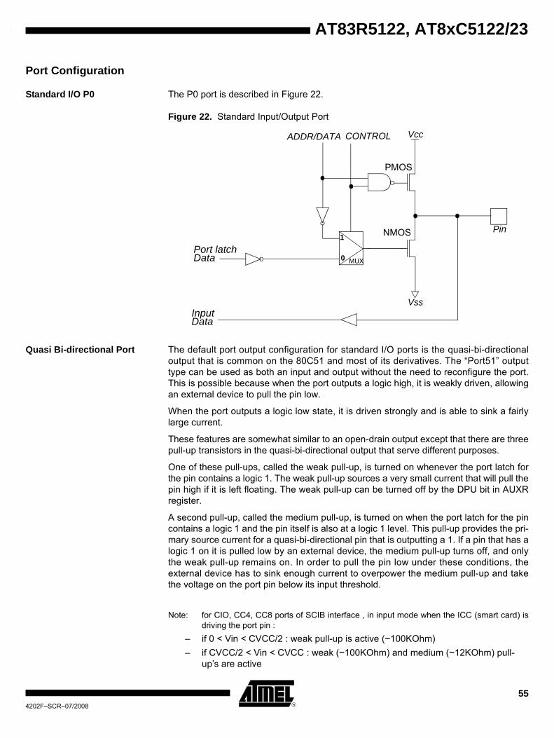
55
AT83R5122, AT8xC5122/23
4202F–SCR–07/2008
Port Configuration
Standard I/O P0 The P0 port is described in Figure 22.
Figure 22. Standard Input/Output Port
Quasi Bi-directional Port The default port output configuration for standard I/O ports is the quasi-bi-directionaloutput that is common on the 80C51 and most of its derivatives. The “Port51” outputtype can be used as both an input and output without the need to reconfigure the port.This is possible because when the port outputs a logic high, it is weakly driven, allowingan external device to pull the pin low.
When the port outputs a logic low state, it is driven strongly and is able to sink a fairlylarge current.
These features are somewhat similar to an open-drain output except that there are threepull-up transistors in the quasi-bi-directional output that serve different purposes.
One of these pull-ups, called the weak pull-up, is turned on whenever the port latch forthe pin contains a logic 1. The weak pull-up sources a very small current that will pull thepin high if it is left floating. The weak pull-up can be turned off by the DPU bit in AUXRregister.
A second pull-up, called the medium pull-up, is turned on when the port latch for the pincontains a logic 1 and the pin itself is also at a logic 1 level. This pull-up provides the pri-mary source current for a quasi-bi-directional pin that is outputting a 1. If a pin that has alogic 1 on it is pulled low by an external device, the medium pull-up turns off, and onlythe weak pull-up remains on. In order to pull the pin low under these conditions, theexternal device has to sink enough current to overpower the medium pull-up and takethe voltage on the port pin below its input threshold.
Note: for CIO, CC4, CC8 ports of SCIB interface , in input mode when the ICC (smart card) isdriving the port pin :
– if 0 < Vin < CVCC/2 : weak pull-up is active (~100KOhm) – if CVCC/2 < Vin < CVCC : weak (~100KOhm) and medium (~12KOhm) pull-
up’s are active
MUX
Pin
ADDR/DATA CONTROL Vcc
1
0
InputData
Port latchData
PMOS
NMOS
Vss

56
AT83R5122, AT8xC5122/234202F–SCR–07/2008
The “Port51” is described in Figure 23.
Figure 23. Quasi Bi-directional Port
Push-pull Output Configuration
The push-pull output configuration has the same pull-down structure as both the opendrain and the quasi-bi-directional output modes, but provides a continuous strong pull-up when the port latch contains a logic 1. The push-pull mode may be used when moresource current is needed from a port output.
The Push-pull port configuration is shown in Figure 24.
Figure 24. Push-pull Output
Input with Medium or Weak Pull-up Configuration
The input with pull-up (Input MPU and Input WPU) configuration is shown in Figure 25.
2 CPU
Input
Pin
Strong Weak Medium
N
P PPCLOCK DELAY
Port Latch
Data
Data
DPU (AUXR.7)
Vss
vcc vcc vcc
Pin
Strong
N
P
Port latchData
PMOS
NMOS

57
AT83R5122, AT8xC5122/23
4202F–SCR–07/2008
Figure 25. Input with Pull-up
Input with Weak Pull-down Configuration
The input with pull-down (input WPD) configuration is shown in Figure 26
Figure 26. Input with Pull-down
Low Speed Output Configuration
The low speed output with low speed tFALL and tRISE can drive keyboard.
The current limitation of the LED2CTRL block requires a polarisation current of about250 μA. This block is automatically disabled in power-down mode.
The low speed output configuration (KB_OUT) is shown in Figure 27.
Figure 27. Low-speed Output
LED Source Current The LED configuration is shown in Figure 28.
Input
PinData
WeakP Medium
PStuck to 0 if Medium
Stuck to 0 if Weak
Input
PinData
WeakN
1
Pin
PPWEAKCTRL
Port latchData
N
N
NMOS
PCON.1
Weak
LED2CTRL

58
AT83R5122, AT8xC5122/234202F–SCR–07/2008
Figure 28. LED Source Current
Notes: 1. When switching a low level, LEDCTRL device has a permanent current of about N mA/15 (N is 2, 4 or 8).
2. The port must be configured as standard C51 port by means of PMOD0 and PMOD1registers and the level of current must be programmed by means of LEDCON0 andLEDCON1 registers before switching the led on.
Table 35. LED Source CurrentLEDx.1 LEDx.0 Port Latch Data NMOS PIN Comments
0 0 0 1 0LED control disabled
0 0 1 0 1
0 1 0 0 0LED mode 2 mA
0 1 1 0 1
1 0 0 0 0LED mode 4 mA
1 0 1 0 1
1 1 0 0 0LED mode 10 mA
1 1 1 0 1
Pin
Port LatchData
LEDx.0
LEDx.1
NMOS N
NLEDCTRL

59
AT83R5122, AT8xC5122/23
4202F–SCR–07/2008
Registers
Reset Value = 0000 0x00b
Reset Value = 00xx 0xxxb
Table 36. Port Mode Register 0 - PMOD0 (91h) for AT8xC51227 6 5 4 3 2 1 0
P3C1 P3C0 P2C1 P2C0 CPRESRES - P0C1 P0C0
Bit Number Bit Mnemonic Description
7 - 6 P3C1-P3C0
Port 3 Configuration bits (Applicable to P3.0, P3.1, P3.3, P3.4 only)00 Quasi bi-directional01 Push-pull10 Output Low Speed11 Input with weak pull-up
5-4 P2C1-P2C0
Port 2 Configuration bits00 Quasi bi-directional01 Push-pull10 Output Low Speed11 Input with weak pull-down
3 CPRESRESCard Presence Pull-up resistorCleared to connect the internal 100K pull-upSet to disconnect the internal pull-up
2 - ReservedThe value read from this bit is indeterminate. Do not set this bit.
1-0 P0C1-P0C0
Port 0 Configuration bits 00 C51 Standard P001 Reserved10 Output Low Speed11 Push-pull
Table 37. Port Mode Register 0 - PMOD0 (91h) for AT83C51237 6 5 4 3 2 1 0
P3C1 P3C0 - - CPRESRES - - -
Bit Number Bit Mnemonic Description
7 - 6 P3C1-P3C0
Port 3 Configuration bits (Applicable to P3.0, P3.1, P3.3, P3.4 only)00 Quasi bi-directional01 Push-pull10 Output Low Speed11 Input with weak pull-up
5-4 ReservedThe value read from these bits are indeterminate. Do not set these bit.
3 CPRESRESCard Presence Pull-up resistorCleared to connect the internal 100K pull-upSet to disconnect the internal pull-up
2-0 - ReservedThe value read from these bits are indeterminate. Do not set these bit.

60
AT83R5122, AT8xC5122/234202F–SCR–07/2008
Reset Value = 0000 0000b
Reset Value = xxxx 00xxb
Table 38. Port Mode Register 1 - PMOD1 (84h) for AT8xC51227 6 5 4 3 2 1 0
P5HC1 P5HC0 P5MC1 P5MC0 P5LC1 P5LC0 P4C1 P4C0
Bit Number Bit Mnemonic Description
7 - 6 P5HC1-P5HC0
Port 5 High Configuration bits (Applicable from P5.6 to P5.7 only)00 Quasi bi-directional01 Push-pull10 Input with weak pull-down11 Input with weak pull-up
5 - 4 P5MC1-P5MC0
Port 5 Medium Configuration bits (Applicable from P5.3 to P5.5 only) 00 Quasi bi-directional01 Push-pull10 Input with weak pull-down11 Input with weak pull-up
3 - 2 P5LC1-P5LC0
Port 5 Low Configuration bits (Applicable from P5.0 to P5.2 only)00 Quasi bi-directional01 Push-pull10 Input with medium pull-up11 Input with weak pull-up
1 - 0 P4C1-P4C0
Port 4 Configuration bits (Applicable from P4.3 to P4.5 only)00 Quasi bi-directional01 Push-pull10 Output Low Speed11 Input with medium pull-up
Table 39. Port Mode Register 1 - PMOD1 (84h) for AT83C51237 6 5 4 3 2 1 0
- - - - P5LC1 P5LC0 - -
Bit Number Bit Mnemonic Description
7 - 4 ReservedThe value read from this bit is indeterminate. Do not set this bit.
3 - 2 P5LC1-P5LC0
Port 5 Low Configuration bits (Applicable from P5.0 to P5.2 only)00 Quasi bi-directional01 Push-pull10 Input with medium pull-up11 Input with weak pull-up
1 - 0 ReservedThe value read from this bit is indeterminate. Do not set this bit.

61
AT83R5122, AT8xC5122/23
4202F–SCR–07/2008
Reset Value = 0000 0000b
Reset Value = 0000 0000b
Table 40. LED Port Control Register 0 - LEDCON0 (F1h)7 6 5 4 3 2 1 0
LED3.1 LED3.0 LED2.1 LED2.0 LED1.1 LED1.0 LED0.1 LED0.0
Bit Number Bit Mnemonic Description
7 - 6 LED3
Port LED3 Configuration bits 00 LED control disabled01 2 mA current source when P3.7 is configured as Quasi-bi-directional mode10 4 mA current source when P3.7 is configured as Quasi-bi-directional mode11 10 mA current source when P3.7 is configured as Quasi-bidirect. mode
5 - 4 LED2
Port LED2 Configuration bits00 LED control disabled01 2 mA current source when P3.6 is configured as Quasi-bi-directional mode10 4 mA current source when P3.6 is configured as Quasi-bi-directional mode11 10 mA current source when P3.6 is configured as Quasi-bidirect. mode
3 - 2 LED1
Port LED1 Configuration bits 00 LED control disabled01 2 mA current source when P3.4 is configured as Quasi-bi-directional mode10 4 mA current source when P3.4 is configured as Quasi-bi-directional mode11 10 mA current source when P3.4 is configured as Quasi-bidirect. mode
1 - 0 LED0
Port LED0 Configuration bits 00 LED control disabled01 2 mA current source when P3.2 is configured as Quasi-bi-directional mode10 4 mA current source when P3.2 is configured as Quasi-bi-directional mode11 10 mA current source when P3.2 is configured as Quasi-bidirect. mode
Table 41. LED Port Control Register 1- LEDCON1 (F1h) only for AT8xC51227 6 5 4 3 2 1 0
- - LED6.1 LED6.0 LED5.1 LED5.0 LED4.1 LED4.0
Bit Number Bit Mnemonic Description
7 - 6 ReservedThe value read from this bit is indeterminate. Do not set this bit.
5 - 4 LED6
Port LED6 Configuration bits00 LED control disabled01 2 mA current source when P4.5 is configured as Quasi-bi-directional mode10 4 mA current source when P4.5 is configured as Quasi-bi-directional mode11 10 mA current source when P4.5 is configured as Quasi-bidirect. mode
3 - 2 LED5
Port LED5 Configuration bits 00 LED control disabled01 2 mA current source when P4.4 is configured as Quasi-bi-directional mode10 4 mA current source when P4.4 is configured as Quasi-bi-directional mode11 10 mA current source when P4.4 is configured as Quasi-bidirect. mode
1 - 0 LED4
Port LED0 Configuration bits 00 LED control disabled01 2 mA current source when P4.3 is configured as Quasi-bi-directional mode10 4 mA current source when P4.3 is configured as Quasi-bi-directional mode11 10 mA current source when P4.3 is configured as Quasi-bidirect. mode

62
AT83R5122, AT8xC5122/234202F–SCR–07/2008
Smart Card Interface Block (SCIB)
The SCIB provides all signals to interface directly with a smart card. The compliancewith the ISO7816, EMV’2000, GSM and WHQL standards has been certified.
Both synchronous (e.g. memory card) and asynchronous smart cards (e.g. micropro-cessor card) are supported. The component supplies the different voltages requested bythe smart card. The power off sequence is directly managed by the SCIB.
The card presence switch of the smart card connector is used to detect card insertion orcard removal. In case of card removal, the SCIB de-activates the smart card using thede-activation sequence. An interrupt can be generated when a card is inserted orremoved.
Any malfunction is reported to the microcontroller (interrupt + control register).
The different operating modes are configured by internal registers.• Support of ISO/IEC 7816• character mode• one transmit/receive buffer• 11 bits ETU counter• 9 bits guard time counter• 32 bits waiting time counter• Auto character repetition on error signal detection in transmit mode• Auto error signal generation on parity error detection in receive mode• Power on and power off sequence generation• Manual mode to drive directly the card I/O

63
AT83R5122, AT8xC5122/23
4202F–SCR–07/2008
Block DiagramThe Smart Card Interface Block diagram is shown Figure 29:
Figure 29. SCIB Block Diagram
Definitions This paragraph introduces some of the terms used in ISO 7816-3 and EMV recommen-dations. Please refer to the full recommendations for a complete list of terms.
Terminal and ICC Terminal is the reader, ICC is the Integrated Circuit Card
ETU Elementary Timing Unit (Bit time)
T=0 Character oriented half duplex protocol T=0
T=1 Block oriented half duplex protocol T=1
Activation: Cold Reset Reset initiated by the Terminal with Vcc power-up. The card will answer with ATR (seebelow)
Activation: Warm Reset Reset initiated by the Terminal with Vcc already powered-up, and after a prior ATR orWarm Reset
De-Activation Deactivation by the Terminal as a result of : unresponsive ICC, or ICC removal.
Barrel shifter
Scartfsm
Interrupt generatorPower on Power off
fsm
I/O mux
IO (in)
IO (out)
CLK
RST
C4 (out)
Clk_iso
C8 (out)
C4 (in)
C8 (in)
Waiting time counter
Guard time counter
VCARDINT
Clk_cpu Etu counter
SCI Registers

64
AT83R5122, AT8xC5122/234202F–SCR–07/2008
ATR Answer To Reset. Response from the ICC to a Reset initiated by the Terminal
F and D F = Clock Rate Conversion Factor, D = Bit rate adjustment factor. ETU is defined as :ETU = F/(D*f) with f = Card Clock frequency. If f is in Hertz, ETU is in second. F and Dare available in the ATR (byte TA1). The default values are F=372, D=1.
Guard Time The time between 2 leading edges of the start bit of 2 consecutive characters is com-prised of the character duration (10) plus the guard time. Be aware that the Guard Timecounter and the Guard Time registers in the AT8xC5122/23 consider the time between 2consecutive characters. So the equation is Guard Time Counter = Guard Time + 10. Inother words, the Guard Time is the number of Stop Bits between 2 characters sent inthe same direction.
Extra Guard Time ISO IEC 7816-3 and EMV introduce the Extra Guard time to be added to the minimumGuard Time. Extra Guard Time only apply to consecutive characters sent by the termi-nal to the ICC. The TC1 byte in the ATR define the number N. For N=0 the character tocharacter duration is 12 ETUs. For N=254 the character to character duration is 266. ForN=255 (special case) The minimum character to character duration is to be used : 12 forT=0 protocol and 11 for T=1 protocol.
Block Guard Time The time between the leading edges of 2 consecutive characters sent in opposit direc-tion. ISO IEC 7816-3 and EMV recommend a fixed Block Guard Time of 22 ETUs.
Work Waiting Time (WWT) In T=0 protocol WWT is the interval between the leading edge of any character sent bythe ICC, and the leading edge of the previous character sent either by the ICC or theTerminal. If no character is received by the terminal after WWTmax time, the Terminalinitiates a De-Activation Sequence.
Character Waiting Time (CWT) In T=1 protocol CWT is the interval between the leading edge of 2 consecutive charac-ters sent by the ICC. If the next character is not received by the Terminal after CWTmaxtime, the Terminal initiates a De-Activation Sequence.
Block Waiting Time (BWT) In T=1 protocol BWT is the interval between the leading edge of the start bit of the lastcharacter sent by the Terminal that gives the right to sent to the ICC, and the leadingedge of the start bit of the first character sent by the ICC. If the first character from theICC is not received by the Terminal after BWTmax time, the Terminal initiates a De-Acti-vation Sequence.
Waiting Time Extention (WTX) In T=1 protocol the ICC can request a Waiting Time Extension with a S(WTX request)request. The Terminal should acknowlege it. The Waiting time between the leadingedge of the start bit of the last character sent by the Terminal that gives the right to sentto the ICC, and the leading edge of the start bit of the first character sent by the ICC willbe BWT*WTX ETUs.
Parity error in T=0 protocol In T=0 protocol, a Terminal (respectively an ICC) detecting a parity error while receivinga character shall force the Card IO line at 0 starting at 10.5 ETUs, thus reducing the firstGuard bit by half the time. The Terminal (respectively an ICC) shall maintain a 0 for 1ETU min and 2 ETUs max (according to ISO IEC) or to 2 ETUs (according to EMV). TheICC (respectively a Terminal) shall monitor the Card IO to detect this error signal thenattempt to repeat the character. According to EMV, following a parity error the charactercan be repeated one time, if parity error is detected again this procedure can berepeated 3 more times. The same character can be transmitted 5 times in total. ISO

65
AT83R5122, AT8xC5122/23
4202F–SCR–07/2008
IEC7816-3 says this procedure is mandatory in ATR for card supporting T=0 while EMVsays this procedure is mandatory for T=0 but does not apply for ATR.
Functional Description The architecture of the Smart Card Interface Block can be detailed as follows:
Barrel Shifter The Barrel Shifter performs the translation between 1 bit serial data and 8 bits paralleldata
The barrel function is useful for character repetition since the character is still present inthe shifter at the end of the character transmission.
This shifter is able to shift the data in both directions and to invert the input or outputvalue in order to manage both direct and inverse ISO7816-3 convention.
Coupled with the barrel shifter is a parity checker and generator.
There are 2 registers connected to this barrel shifter, one for the transmission and onefor the reception. They act as buffers to relieve the CPU of timing constraints.
SCART FSM (Smart Card Asynchronous Receiver Transmitter Finite State Machine)
This is the core of the block. Its purpose is to control the barrel shifter. To sequence cor-rectly the barrel shifter for a reception or a transmission, it uses the signals issued by thedifferent counters. One of the most important counters is the guard time counter thatgives time slots corresponding to the character frame.
The SCART FSM is enabled only in UART mode.
The transition from the receipt mode to the transmit mode is done automatically. Priorityis given to the transmission. Transmission refers to Terminal transmission to the ICC.Reception refers to reception by the Terminal from the ICC.
ETU Counter The ETU (Elementary Timing Unit) counter controls the working frequency of the barrelshifter, in fact it generates the enable signal of the barrel shifter. It receives the CardClock, and generates the ETU clock. The Card Clock frequency is called “f” below. TheETU counter is 11 bit wide.
A special compensation mode can be activated. It accomodates situations where theETU is not an integer number of Card Clock (CK_ISO). The compensation mode is con-trolled by the COMP bit in SCETU1 register bit position 7. With COMP=1 the ETU ofevery character even bits is reduced by 1 Card Clock period. As a result, the averageETU is : ETU_average = (ETU - 0.5). One should bear in mind that the ETU countershould be programmed to deliver a faster ETU which will be reduced by the COMPmechanism, not the other way around. This allows to reach the required precision of thecharacter duration specified by the ISO7816-3 standard.
Example1 : F=372, D=32 => ETU= F/D = 11.625 clock cycles.
We select ETU[10-0] = 12 , COMP=1. ETUaverage= 12 - (0.5*COMP) = 11.5
The result will be a full character duration (10 bit) = (10 - 0.107)*ETU. The EMV specifi-cation is (10 +/- 0.2)*ETU
Guard Time Counter The minimum time between the leading edge of the start bit of 2 consecutive characterstransmitted by the Terminal is controlled by the Guard Time counter, as described inFigure 32.

66
AT83R5122, AT8xC5122/234202F–SCR–07/2008
The Guard Time counter is an 9 bit counter It is initialized at 001h at the start of a trans-mission by the Terminal. It then increments itself at each ETU until it reach the 9 bitvalue loaded into the SCGT1[0] concatenated with SCGT0[7:0]. At this time a new Ter-minal transmission is enabled and the Guard Time Counter stop incrementing. As soonas a new transmission start, the Guard Time Counter is re-initialized at 1 decimal value.
It should be noted that the value of the Guard Time Counter cannot be red. ReadingSCGT1,0 only gives the minimum time between 2 characters that the Guard TimeCounter will allow.
Care must be taken with the Guard Time Counter which counts the duration betweenthe leading edges of 2 consecutive characters. This correspond to the character dura-tion (10 ETU) plus the Guard Time as defined by the ISO and EMV recommendations.To program Guard Time = 2 : 2 stop bits between 2 characters which is equivalent to theminimum delay of 12 ETUs between the leading edges of 2 consecutive characters,SCGT1[0],SCGT0[7:0] should be loaded with the value 12 decimal. See Figure 30
Figure 30. Guard Time.
Block Guard Time Counter The Block Guard Time counter provides a way to program a minimum time between theleading edge of the start bit of a character received from the ICC and the leading edge ofthe start bit of a character sent by the terminal. ISO IEC 7816-3 and EMV recommend afixed Block Guard Time of 22 ETUs. The AT8xC5122/23 offer the possibility to extendthis delay up to 512 ETUs.
The Block Guard Time is a 9 bit counter. When the Block Guard Time mode is enabled(BGTEN=1 in SCSR register) The Block Guard Time counter is initialized at 000h at thestart of each character transmissions from the ICC. It then increments at each ETU untilit reach the 9 bit value loaded into shadow SCGT1,0 registers, or until it is re-initializedby the start of an new transmission from the ICC. If the Block Guard Time counterreaches the 9 bit value loaded into shadow SCGT1,0 registers, a transmission by theTERMINAL is enabled, and the Block Guard Time counter stop incrementing. The BlockGuard Time counter is re-initialized at the start of each TERMINAL transmission.
The SCGT1 SCGT0 shadow registers are loaded with the content of GT[8-0] containedin the registers SCGT1[0),SCGT0(7:0] with the rising edge of the bit BGTEN in theSCSR register. See Figure 32.
CHAR n+1 CHAR n+2 CHAR n+3
>= SCGT
TRANSMISSION to ICC

67
AT83R5122, AT8xC5122/23
4202F–SCR–07/2008
Figure 31. Block Guard Time.
Figure 32. Guard Time and Block Guard Time counters
To illustrate the use of Guard Time and Block Guard Time, let us consider theISO/IEC7816-3 recommendation : Guard Time = 2 (minimum delay between 2 consecu-tive characters sent by the Terminal = 12 ETUs), and Block Guard Time = 22 ETUs.
After A smart Card Reset– Write 00decimal in SCGT1, Write 21decimal in SCGT0– Set BGTEN in SCSR (BGTEN was 0 before as a result of the smart card
reset)– Write 12decimal in SCGT0
Now the Guard Time and Block Guard Time are properly initialized. The TERMINAL willinsure a minimun 12 ETUs between 2 leading edges of 2 consecutive characters trans-mitted. The TERMINAL will also insure a minimum of 22 ETUs between the leadingedge of a character sent by the ICC, and the leading edge of a character sent by theTERMINAL. There is no need to write SCGT1,0 again and again.
Waiting Time (WT) Counter The WT counter is a 32 bits down counter which can be loaded with the value containedin the SCWT3, SCWT2, SCWT1, SCWT0 registers. Its main purpose is timeout signalgeneration. It is 32 bits wide and is decremented at the ETU rate. see Figure 33.
CHAR 1 CHAR 2 CHAR n CHAR n+1 CHAR n+2 CHAR n+3
>= Block Guard Time>= SCGT
RECEPTION from ICC TRANSMISSION to ICC
Write “Block Guard Time” in SCGT1,0
Write SCGT1,0 with
and set BGTEN to transfer the value to theshadow SCGT1,0 registers
a value for Guard Time
ETU Counter
Block Guard Time Counter
Enable
SCGT1 SCGT0
9 bits
Guard Time Counter
GT[8:0]
Shadow SCGT1 ,Shadow SCGT0
9 bits
Comparator
transmit
Comparator9 bits
9 bits
Enabletransmit

68
AT83R5122, AT8xC5122/234202F–SCR–07/2008
When the WT counter times out, an interrupt is generated and the SCIB function islocked: reception and emission are disabled. It can be enabled by resetting the macro orreloading the counter.
The Waiting Time Counter can be used in T=0 protocol for the Work Waiting Time. It canbe used in T=1 protocol for the Character Waiting Time and for the Block Waiting Time.See the detailed explanation below.
Figure 33. Waiting Time Counter
In the so called manuel mode, the counter is loaded, if WTEN = 0, during the write ofSCWT2 register. The counter is loaded with a 32 bit word built with SCWT3 SCWT2SCWT1 SCWT0 registers (SCWT0 contain WT[7-0] byte. WTEN is located in theSCICR register.
When WTEN=1 and in UART mode, the counter is re-loaded at the occurence of a startbit. This mode will be detailed below in T=0 protocol and T=1 protocol.
In manual mode, the WTEN signal controls the start of the counter (rising edge) and thestop of the counter (falling edge). After a timeout of the counter, a falling edge onWTEN, a reload of SCWT2 and a rising edge of WTEN are necessary to start again thecounter and to release the SCIB macro. The reload of SCWT2 transfers all SCWT0,SCWT1, SCWT2 and SCWT3 registers to the WT counter.
In UART mode there is an automatic load on the start bit detection. This automatic loadis very useful for changing on-the-fly the timeout value since there is a register to holdthe load value. This is the case for T=1 protocol.
In T=0 protocol the maximun interval between the start leading edge of any charactersent by the ICC and the start of the previous character sent by either the ICC or the Ter-minal is the maximum Work Waiting Time. The Work Waiting Time shall not exceed960*D*WI ETUs with D and WI parameters are returned by the field TA1 and TC2respectively in the Answer To Reset (ATR). This is the value the user shall write in theSCWT0,1,2,3 register. This value will be reloaded in the Waiting Time counter everystart bit.
ETU Counter WT CounterTimeout
SCWT2 SCWT1 SCWT0
WT[31:0]
LoadWTEN
Start BitUART
Write_SCWT2
SCWT3

69
AT83R5122, AT8xC5122/23
4202F–SCR–07/2008
Figure 34. T=0 mode
In T=1 protocol : The maximum interval between the leading edge of the start bit of 2consecutive characters sent by the ICC is called maximum Character Waiting Time. TheCharacter Waiting Time shall not exceed (2**CWI + 11) ETUs with 0 =< BWI =< 5. Con-sequently 12 ETUs =< CWT =< 43 ETUs.
T=1 protocol also specify the maximum Block Waiting Time. This is the time betweenthe leading edge of the last character sent by the Terminal giving the right to send to theICC, and the leading edge of the start bit of the first character sent by the ICC. TheBlock Waiting Time shall not exceed (2**BWI*960 + 11) ETUs with 0 =< BWI =< 4. Con-sequently 971 ETUs =< BWT =< 15371 ETUs.
In T=1 protocol it is possible to extend the Block Waiting Time with the Waiting TimeExtension (WTX). When selected the waiting time becomes BWT*WTX ETUs. TheWaiting Time counter is 32 bit wide to accomodate this feature.
It is possible to take advantage of the automatic reload of the Waiting Time counter witha start bit in UART mode (T=1 protocol use UART mode) . If the Terminal sends a blockof N characters, and the ICC is supposed to respond immediately after, then the follow-ing sequence can be used.
While sending the (N-1)th character of the block, the Terminal can write theSCWT0,1,2,3 with BWImax.
At the start bit of the Nth character, the BWImax is loaded in the Waiting Time counter
During the transmission of the Nth character, the Terminal can write SCWT0,1,2,3 withthe CWImax.
At the start bit of the first character sent by the ICC, the CWImax will be loaded in theWaiting Time counter.
Figure 35. T=1 Mode
CHAR 1 CHAR 2
< WT
> GT
BLOC 1
CHAR 1 CHAR 2 CHAR n
BLOC 2
CHAR n+1 CHAR n+2 CHAR n+3
< BWT< CWT
TRANSMISSION RECEPTION

70
AT83R5122, AT8xC5122/234202F–SCR–07/2008
Power-on and Power-off FSM The Power-on Power-off Finite State Machine (FSM) applies the signals on the smartcard in accordance with ISO7816-3 standard. It conducts the Activation (Cold Reset andWarm Reset as well as De-Activation) it also manages the exception conditions such asovercurrent (see DC/DC Converter)
To be able to power on the SCIB, the card presence is mandatory. Upon detectection ofa card presence, the Terminal initiate a Cold Reset Activation.
The Cold Reset Activation Terminal procedure is as follow and the Figure 36. Timingindications are given according to ISO IEC 7816
– RESET= Low , I/O in the receive state– Power Vcc (see DC/DC Converter)– Once Vcc is established, apply Clock at time Ta– Maintain Reset Low until time Ta+tb (tb< 400 clocks)– Monitor The I/O line for the Answer To Reset (ATR) between 400 and 40000
clock cycles after Tb. ( 400 clocks < tc < 40000clocks)
Figure 36. SCIB Activation Cold Reset Sequence after a Card Insertion
The Warm Reset Activation Terminal procedure is as follow and the Figure 37– Vcc active, Reset = High, CLK active– Terminal drive Reset low at time T to initiate the warm Reset. Reset=0
maintained for at least 400 clocks until time Td = T+te (400 clocks < te)– Terminal keep the IO line in receive state– Terminal drive Reset high after at least 400 clocks at time Td– ICC shall respond with an ATR within 40000 clocks (tf<40000 clocks)
Figure 37. SCIB Activation Warm Reset Sequence
CVCC
CRST
CCLK
CIO DataUndefined
Ta Ta+tb Tb+tc
CVCC
CRST
CCLK
CIO Data
T Td=T + te Td + tf
Undefined

71
AT83R5122, AT8xC5122/23
4202F–SCR–07/2008
Removal of the smart card will automatically start the power off sequence as describedin Figure 38.
The SCIB deactivation sequence after a reset of the CPU or after a lost of power supplyis ISO7816-3 compliant. The switching order of the signals is the same as in Figure 38but the delay between signals is analog and not clock dependant.
Figure 38. SCIB Deactivation Sequence after a Card Extraction
Interrupt Generator There are several sources of interruption but the SCIB macro-cell issues only one inter-rupt signal: SCIBIT.
Figure 39. SCIB Interrupt Sources
This signal is high level active. Each of the sources is able to activate the SCIB interrup-tion which is cleared when the Smart Card Interrupt register is read by themicrocontroller.
If during the read of the Smart Card Interrupt register another interrupt occurs, the acti-vation of the corresponding bit in the Smart Card Interrupt register and the new SCIBinterruption is delayed until the interrupt register is read by the microcontroller.
Warning : Each bit of the SCIIR register is irrelevant while the corresponding interrup-tion is disabled in SCIER register. When the interruption mode is not used, the bits ofthe SCISR register must be used instead of the bits of the SCIIR register.
CVCC
CRST
CCLK
CIO
8 Clock Cycles
ESCTBI
ICARDER
ESCWTI
ESCRI
ESCPI
EVCARDER
Transmit buffercopied to shift register
Output currentout of range
Output voltageout of rangeTimeout on WT counter
CompletetransmissionComplete receptionParity errordetected
SCIB IT
ESCTI
SCTBI
ICARDERR
VCARDERR
SCWTI
SCTI
SCRI
SCPI

72
AT83R5122, AT8xC5122/234202F–SCR–07/2008
Additional Features
Clock The CK_ISO input must be in the range 1 - 5 MHz according to ISO 7816.
The CK_ISO can be programmed up to 12 MHz. In this case, the timing specification ofthe output buffer will not comply to ISO 7816.
Figure 40. Clock Diagram of the SCIB Block
Figure 41. Prescaler 2 Description
The division factor SCICLK must be smaller than 49. If it is greater or equal to 49, thePR2 prescaler is locked.
See Figure 17 clock tree diagram in the clock controller chapter.
Table 42. Examples of Clock settings
Card Presence Input The internal pull-up (weak pull-up) on Card Presence input can be disconnected in orderto reduce the consumption (CPRESRES, bit 3 in PMOD0).
In this case, an external resistor (typically 1 MΩ) must be externally tied to Vcc.
CPRES input can generate an interrupt (see Interrupt system section). The detection level can be selected.
PR2
Ck_cpu
Ck_ISO
SCIB
CK_PLL or
CK_IDLE
CK_XTAL1
PR2
1/(2*(48 - SCICLK[5-0])) CK_ISO
EXT48PLLCON.2
0
1
CK_PLL
CK_XTAL1
XTSCSSCICLK.7
SCICLK[5:0]
<48
=48
XTAL1 (MHz) EXT48 SCICLK CK_ ISO
8 0 36 4
8 0 44 12
8 0 42 8
8 0 40 6
8 0 24 2
8 0 0 1

73
AT83R5122, AT8xC5122/23
4202F–SCR–07/2008
Transmit / Receive Buffer The contents of the SCIBUF Transmit / Receive Buffer is transferred or received into /from the Shift Register. The Shift Register is not accessible by microcontroller. Its role isto prepare the byte to be copied on the I/O pin for a transmission or in the SCIBUFbuffer after a reception.
During a character transmission process, as soon as the contents of the SCIBUF bufferis transferred to the shift register, the SCTBE bit is set in SCISR register to indicate thatthe SCIBUF buffer is empty and ready to accept a new byte. This mechanism avoids towait for the complete transmission of the previous byte before writing a new byte in thebuffer and enables to speed up the transmission.
– If the Character repetition mode is not selected (bit CREP=0 in SCICR), as soon as the contents of the Shift Register is transferred to I/O pin, the SCTC bit is set in SCISR register to indicate that the byte has been transmitted.
– If the Character repetition mode is selected (bit CREP=1 in SCICR) The TERMINAL will be able to repeat characters as requested by the ICC (See the Parity Error in T=0 protocol description in the definition paragraph above). The SCTC bit in SCISR register will be set after a successful transmission (no retry or no further retry requested by the ICC). If the number of retries is exhausted (up to 4 retries depending on CREPSEL bit in SCSR) and the last retry is still unsuccessful, the SCTC bit in SCISR will not be set and the SCPE bit in SCISR register will be set instead.
During a character reception process, the contents of the Shift Register is transferred inthe SCIBUF buffer.
– If the Character repetition mode is not selected (bit CREP=0 in SCICR), as soon as the contents of the Shift Register is transferred to the SCIBUF the SCRC bit is set in SCISR register to indicate that the byte has been received, and the SCIBUF contains a valid character ready to be red by the microcontroller.
– If the Character repetition mode is selected (bit CREP=1 in SCICR) The TERMINAL will be able to request repetition if the received character exhibit a parity error. Up to 4 retries can be requested depending on CREPSEL bit in SCSR. The SCRC bit will be set in SCISR register after a successful reception, first reception or after retry(ies). If the number of retries is exhausted (up to 4 retries depending on CREPSEL bit in SCSR) and the last retry is still unsuccessful, the SCRC bit and the SCPE bit in SCISR register will be set. It will be possible to read the erroneous character.
Warning : the SCTBI, SCTI SCRI and SCPI bits have the same function as SCTBE,SCTC, SCRC and SCPE bits. The first ones are able to generate interruptions if theinterruptions are enabled in SCIER register while the second ones are only status bits tobe used in pulling mode. If the interruption mode is not used, the status bits must beused. The SCTBI, SCTI and SCRI bits do not contain valid information while theirrespective interrupt enable bits ESCTBI, EXCTI, ESCRI are cleared.

74
AT83R5122, AT8xC5122/234202F–SCR–07/2008
Figure 42. CharacterTransmission Diagram
SCIBUFTransmittedCharacter
Shift RegisterI/O pin
SCTBE SCTC
SCISR register
SCTBI SCTI
SCIIR register
ESCTBI
ESCTI
SC
IER
Reg
iste
r
Parity error
SCPE
SCPI
Parity error

75
AT83R5122, AT8xC5122/23
4202F–SCR–07/2008
Figure 43. Character Reception Diagram
SCIB Reset The SCICR register contains a reset bit. If set, this bit generates a reset of the SCIB andits registers. Table 43 defines the SCIB registers that are reset and their reset values.
Table 43. Reset Values for SCI Registers
SCIBUFReceivedCharacter
Shift RegisterI/O pin
SCTBE SCTC
SCISR registerSCRC
SCTBI SCTI
SCIIR registerSCRI
ESCTBI
ESCTI
SC
IER
Reg
iste
r
ESCRI
SCPE
Register Name SCIB Reset Value (Binary)
SCICR 0000 0000
SCCON 0X00 0000
SCISR 1000 0000
SCIIR 0X00 0000
SCIER 0X00 0000
SCSR X000 1000
SCIBUF 0000 0000
SCETU1, SCETU0 XXXX X001, 0111 0100 (372)
SCGT1, SCGT0 0000 0000, 0000 1100 (12)
SCWT3, SCWT2, SCWT1, SCWT0 0000 0000, 0000 0000, 0010 0101, 1000 0000 (9600)
SCICLK 0X10 1111
Parity error
SCPI
Parity error

76
AT83R5122, AT8xC5122/234202F–SCR–07/2008
Alternate Card A second card named ‘Alternate Card’ can be controlled.
The Clock signal CCLK1 can be adapted to the XTAL frequency. Thanks to the clockprescaler which can divide the frequency by 1, 2, 4 or 8. The bits ALTKPS0 andALTKPS1 in SCSR Register are used to set this factor.
Figure 44. Alternate Card
RegistersThere are fifteen registers to control the SCIB macro-cell. They are described fromTable 58 to Table 45.
Some of the register widths are greater than a byte. Despite the 8 bits access providedby the BIU, the address mapping of this kind of register respects the following rule :
The Low significant byte register is implemented at the higher address.
This implementation makes access to these registers easier when using high level pro-gramming languages (C,C++).
SIM, SAM
CARD
Alternatecard
CVCCCRSTCIOCCLK
CK_IDLE 10
CCLK1
SCSR Reg.
PR3
SCCLK1
1, 1/2, 1/4 or 1/8
P1.7
Maincard
CPRES
SMART
CARD
SCSR Reg.ALTKPS0,1

77
AT83R5122, AT8xC5122/23
4202F–SCR–07/2008
Reset Value = 0000 0000b
Table 44. Smart Card Interface Control Register - SCICR (S:B6h, SCRS = 1)7 6 5 4 3 2 1 0
RESET CARDDET VCARD1 VCARD0 UART WTEN CREP CONV
Bit Number Bit Mnemonic Description
7 RESET
ResetSet this bit to reset and deactivate the Smart Card Interface.Clear this bit to activate the Smart Card Interface.This bit acts as an active high software reset.
6 CARDDETCard Presence Detector SenseClear this bit to indicate the card presence detector is open when no card is inserted (CPRES is high).Set this bit to indicate the card presence detector is closed when no card is inserted (CPRES is low).
5-4 VCARD[1:0]
Card Voltage Selection:VCARD[1] VCARD[0] CVCC
0 0 0 V0 1 1.8 V1 0 3.0 V1 1 5.0 V
3 UART
Card UART SelectionClear this bit to use the CARDIO bit (P1.0) bit to drive the Card I/O (P1.0) pin. Set this bit to use the Smart Card UART to drive the Card I/O pin (P1.0 pin).Controls also the Waiting Time Counter as described in Section “Waiting Time (WT) Counter”, page 67
2 WTEN
Waiting Time Counter EnableClear this bit to stop the counter and enable the load of the Waiting Time counter hold registers. The hold registers are loaded with SCWT0, SCWT1, SCWT2 and SCWT3 values when SCWT2 is written.Set this bit to start the Waiting Time Counter. The counters stop when it reaches the timeout value.If the UART bit is set, the Waiting Time Counter automatically reloads with the hold registers whenever a start bit is sent or received.
1 CREP
Character RepetitionClear this bit to disable parity error detection and indication on the Card I/O pin in receive mode and to disable character repetition in transmit mode.Set this bit to enable parity error indication on the Card I/O pin in receive mode and to set automatic character repetition when a parity error is indicated in transmit mode. Depending upon CREPSET bit is SCSR register, the receiver can indicate parity error up to 4times (3 repetitions) or up to 5times (4 repetitions) after which it will raise the parity error bit SCPE bit in the SCISR register. If parity interrupt is enabled, the SCPI bit in SCIIR register will be set too.Alternately, the transmitter will detect ICC character repetition request. After 3 or 4 unsuccessful repetitions (depending on CREPSEL bit in SCSR register), the transmitter will raise the parity error bit SCPE bit in the SCISR register. If parity interrupt is enabled, the SCPI bit in SCIIR register will be set too.Note : Character repetition mode is specified for T=0 protocol only and should not be used in T=1 protocol (block oriented protocol)
0 CONV
ISO ConventionClear this bit to use the direct convention: b0 bit (LSB) is sent first, the parity bit is added after b7 bit and a low level on the Card I/O pin represents a’0’.Set this bit to use the inverse convention: b7 bit (LSB) is sent first, the parity bit is added after b0 bit and a low level on the Card I/O pin represents a’1’.

78
AT83R5122, AT8xC5122/234202F–SCR–07/2008
Reset Value = 0X00 0000b
Table 45. Smart Card Contacts Register - SCCON (S:ACh, SCRS=0)7 6 5 4 3 2 1 0
CLK - CARDC8 CARDC4 CARDIO CARDCLK CARDRST CARDVCC
Bit Number Bit Mnemonic Description
7 CLK
Card Clock SelectionClear this bit to use the Card CLK bit (CARDCLK bit below) to drive Card CLK (P1.4) pin.Set this bit to use CK_XTAL1 or CK_PLL signals for CK_ISO to drive the Card CLK pin (CCLK = P1.4 pin)Note: internal synchronization avoids glitches on the CLK pin when switching this bit.
6 - ReservedThis bit can be changed by software but the read value is indeterminate.
5 CARDC8
Card C8Clear this bit to drive a low level on the Card C8 pin (CC8 = P1.1 pin).Set this bit to set a high level on the Card C8 pin (CC8 = P1.1 pin).. The CC8 pin can be used as a pseudo bi-directional I/O when this bit is set.Warning : VCARDOK=1 (SCISR.4 bit) condition must be true to change the state of CC8 pin
4 CARDC4
Card C4Clear this bit to drive a low level on the Card C4 pin (CC4 = P1.3 pin).Set this bit to set a high level on the Card C4 pin (CC4 = P1.3 pin).The CC4 pin can be used as a pseudo bi-directional I/O when this bit is set.Warning : VCARDOK=1 (SCISR.4 bit) condition must be true to change the state of CC4 pin
3 CARDIO
Card I/OIf UART bit is cleared in SCICR register, this bit enables the use of the Card IO pin (CIO = P1.0) as a C51 pseudo bi-directional port :To read from CIO (P1.0) port pin : set CARDIO (P1.0) bit then read CARDIO (P1.0) bit to have the CIO port valueTo write in CIO (P1.0) port pin : set CARDIO (P1.0) bit to write a 1 in CIO (P1.0) port pin , clear CARDIO (P1.0) bit to write a 0 in CIO (P1.0) port pin.Warning : VCARDOK=1 (SCISR.4 bit) condition must be true to change the state of CIO pin
2 CARDCLKCard CLKWhen the CLK bit is cleared in SCCON Register, the value of this bit is driven to the Card CLK pin. Warning : VCARDOK=1 (SCISR.4 bit) condition must be true to change the state of Card CLK pin
1 CARDRST
Card RSTClear this bit to drive a low level on the Card RST pin.Set this bit to set a high level on the Card RST pin. Warning : VCARDOK=1 (SCISR.4 bit) condition must be true to change the state of Card RST pin
0 CARDVCC
Card VCC ControlClear this bit to desactivate the Card interface and set its power-off. The other bits of SCCON register have no effect while this bit is cleared.Set this bit to power-on the Card interface. The activation sequence should be handled by software.

79
AT83R5122, AT8xC5122/23
4202F–SCR–07/2008
Reset Value = 1000 0000b
Table 46. Smart Card UART Interface Status Register -SCISR (S:ADh, SCRS=0)
7 6 5 4 3 2 1 0
SCTBE CARDIN ICARDOVF VCARDOK SCWTO SCTC SCRC SCPE
Bit Number Bit Mnemonic Description
7 SCTBE
UART Transmit Buffer Empty StatusThis bit is set by hardware when the Transmit Buffer is copied to the transmit shift register of the Smart Card UART.It is cleared by hardware when SCIBUF register is written.
6 CARDINCard Presence StatusThis bit is set by hardware if there is a card presence (debouncing filter has to be done by software).This bit is cleared by hardware if there is no card presence.
5 ICARDOVF
Card Current Overflow StatusThis bit is set when the current on card is above the limit specified by bit OVFADJ in DCCKPS register (Table 61 on page 92)It is cleared by hardware.
4 VCARDOKCard Voltage Correct StatusThis bit is set when the output voltage is within the voltage range specified by VCARD[1:0] in SCICR register.It is cleared otherwise.
3 SCWTOWaiting Time Counter Timeout StatusThis bit is set by hardware when the Waiting Time Counter has expired.It is cleared by the reload of the counter or by the reset of the SCIB.
2 SCTC
UART Transmitted Character StatusThis bit is set by hardware when the Smart Card UART has transmitted a character. If character repetition mode is selected, this bit will be set only after a successful transmission. If the last allowed repetition in not successful, this bit will not be set.It is cleared by software when this register is read.
1 SCRC
UART Received Character StatusThis bit is set by hardware when the Smart Card UART has received a characterIt is cleared by hardware when SCIBUF register is read. If character repetition mode is selected, this bit will be set only after a successful reception. If the last allowed repetition is still unsuccessful, this bit will be set to let the user read the erroneous value if necessary.
0 SCPE
Character Reception Parity Error StatusThis bit is set when a parity error is detected on the received character.It is cleared by software when this register is read. If character repetition mode is selected, this bit will be set only if the ICC report an error on the last allowed repetition of a TERMINAL transmission, or if a reception parity error is found on the last allowed ICC character repetition.

80
AT83R5122, AT8xC5122/234202F–SCR–07/2008
Reset Value = 0X00 0000bNote: 1) In case of multiple interrupts occuring at the same time (sampled by the same edge of
the internal clock), the interrupts will be serviced in the following order from the highest tothe lowest priority :- UART Transmit Buffer Empty- Card Current Overflow - Card Voltage Error- Waiting Time Counter Timeout- UART Transmitted Character- UART Received Character- Character Reception Parity Error
2) It is recommended that the application saves the SCIIR register after reading it inorder to avoid the loss of pending interruptions as the SCIIR register is cleared when it isread by the MCU.
Table 47. Smart Card UART Interrupt Identification Register (Read Only)SCIIR (S:AEh, SCRS=0)
7 6 5 4 3 2 1 0
SCTBI - ICARDERR VCARDERR SCWTI SCTI SCRI SCPI
Bit Number Bit Mnemonic Description
7 SCTBI
UART Transmit Buffer Empty InterruptThis bit is set by hardware when the Transmit Buffer is copied into the transmit shift register of the Smart Card UART. It generates an interrupt if ESCTBI bit is set in SCIER register otherwise this bit is irrelevant.It is cleared by hardware when this register is read.
6 - ReservedThe value read from this bit is indeterminate. Do not change this bit.
5 ICARDERR
Card Current Overflow InterruptThis bit is set when the current on card is above the limit specified by bit OVFADJ in DCCKPS register (Table 61 on page 92). It generates an interrupt if ICARDER bit is set in SCIER register otherwise this bit is irrelevant.It is cleared by hardware when this register is read.
4 VCARDERR
Card Voltage Error InterruptThis bit is set when the output voltage goes out of the voltage range specified by VCARD field. It generates an interrupt if EVCARDER bit is set in SCIER register otherwise this bit is irrelevant.It is cleared by hardware when this register is read.
3 SCWTI
Waiting Time Counter Timeout InterruptThis bit is set by hardware when the Waiting Time Counter has expired. It generates an interrupt if ESCWTI bit is set in SCIER register otherwise this bit is irrelevant.It is cleared by hardware when this register is read.
2 SCTI
UART Transmitted Character InterruptThis bit is set by hardware when the Smart Card UART has completed the character transmission. It generates an interrupt if ESCTI bit is set in SCIER register otherwise this bit is irrelevant.It is cleared by hardware when this register is read.
1 SCRI
UART Received Character InterruptThis bit is set by hardware when the Smart Card UART has completed the character reception. It generates an interrupt if ESCRI bit is set in SCIER register otherwise this bit is irrelevant.It is cleared by hardware when this register is read.
0 SCPI
Character Reception Parity Error InterruptThis bit is set at the same time as SCTI or SCRI if a parity error is detected on the received character. It generates an interrupt if ESCPI bit is set in SCIER register otherwise this bit is irrelevant.It is cleared by hardware when this register is read.

81
AT83R5122, AT8xC5122/23
4202F–SCR–07/2008
Reset Value = 0X00 0000b
Table 48. Smart Card UART Interrupt Enabling Register - SCIER (S:AEh, SCRS=1)7 6 5 4 3 2 1 0
ESCTBI - ICARDER EVCARDER ESCWTI ESCTI ESCRI ESCPI
Bit Number Bit Mnemonic Description
7 ESCTBIUART Transmit Buffer Empty Interrupt EnabledClear this bit to disable the Smart Card UART Transmit Buffer Empty interrupt.Set this bit to enable the Smart Card UART Transmit Buffer Empty interrupt.
6 - ReservedThe value read from this bit is indeterminate. Do not change this bit.
5 ICARDERCard Current Overflow Interrupt EnabledClear this bit to disable the Card Current Overflow interrupt.Set this bit to enable the Card Current Overflow interrupt.
4 EVCARDERCard Voltage Error Interrupt EnabledClear this bit to disable the Card Voltage Error interrupt.Set this bit to enable the Card Voltage Error interrupt.
3 ESCWTIWaitingTime Counter Timeout Interrupt EnabledClear this bit to disable the Waiting Time Counter timeout interrupt.Set this bit to enable the Waiting Time Counter timeout interrupt.
2 ESCTIUART Transmitted Character Interrupt EnabledClear this bit to disable the Smart Card UART Transmitted Character interrupt.Set this bit to enable the Smart Card UART Transmitted Character interrupt.
1 ESCRIUART Received Character Interrupt EnabledClear this bit to disable the Smart Card UART Received Character interrupt.Set this bit to enable the Smart Card UART Received Character interrupt.
0 ESCPICharacter Reception Parity Error Interrupt EnabledClear this bit to disable the Smart Card Character Reception Parity Error interrupt.Set this bit to enable the Smart Card Character Reception Parity Error interrupt.

82
AT83R5122, AT8xC5122/234202F–SCR–07/2008
Reset Value = X000 1000b
Reset Value = 0000 0000b
Table 49. Smart Card Selection Register - SCSR (S:ABh)7 6 5 4 3 2 1 0
- BGTEN - CREPSEL ALTKPS1 ALTKPS0 SCCLK1 SCRS
Bit Number Bit Mnemonic Description
7 - ReservedThe value read from this bit is indeterminate. Do not change this bit.
6 BGTEN
Block Guard Time EnableSet this bit to select the minimum interval between the leading edge of the start bits of the last character received from the ICC and the first character sent by the Terminal. The transfer of GT[8-0] value to the BGT counter is done on the rising edge of the BGTEN.Clear this bit to suppress the minimum time between reception and transmission.
5 - ReservedThe value read from this bit is indeterminate. Do not change this bit.
4 CREPSEL
Character repetition selectionClear this bit to select 5 times transmission (1 original + 4 repetitions) before parity error indication (conform to EMV)Set this bit to select 4 times transmission (1 original + 3 repetitions) before parity error indication
3-2 ALTKPS1:0
Alternate Card Clock prescaler factor00 ALTKPS = 0: prescaler factor equals 101 ALTKPS = 1: prescaler factor equals 210 ALTKPS = 2: prescaler factor equals 4 (reset value)11 ALTKPS = 3: prescaler factor equals 8
1 SCCLK1Alternate card clock selectionSet to select the prescaled PR3 clock for CCLK1 (P1.7) pinClear to select P1.7 port bit
0 SCRS Smart Card Register SelectionThe SCRS bit selects which set of the SCIB registers is accessed.
Table 50. Smart Card Transmit / Receive Buffer - SCIBUF (S:AA)7 6 5 4 3 2 1 0
- - - - - - - -
Bit Number Bit Mnemonic Description
- -
Smart Card Transmit / Receive Buffer- A new byte can be written in the buffer to be transmitted on the I/O pin when SCTBE bit is set. The bits are sorted and copied on the I/O pin versus the active convention.- A new byte received from I/O pin is ready to be read when SCRI bit is set.The bits are sorted versus the active convention.
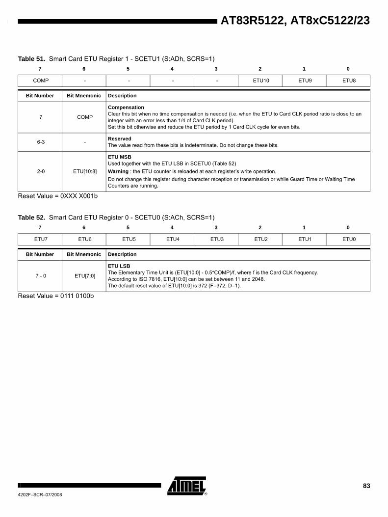
83
AT83R5122, AT8xC5122/23
4202F–SCR–07/2008
Reset Value = 0XXX X001b
Reset Value = 0111 0100b
Table 51. Smart Card ETU Register 1 - SCETU1 (S:ADh, SCRS=1)7 6 5 4 3 2 1 0
COMP - - - - ETU10 ETU9 ETU8
Bit Number Bit Mnemonic Description
7 COMP
CompensationClear this bit when no time compensation is needed (i.e. when the ETU to Card CLK period ratio is close to an integer with an error less than 1/4 of Card CLK period).Set this bit otherwise and reduce the ETU period by 1 Card CLK cycle for even bits.
6-3 - ReservedThe value read from these bits is indeterminate. Do not change these bits.
2-0 ETU[10:8]
ETU MSBUsed together with the ETU LSB in SCETU0 (Table 52)Warning : the ETU counter is reloaded at each register’s write operation. Do not change this register during character reception or transmission or while Guard Time or Waiting Time Counters are running.
Table 52. Smart Card ETU Register 0 - SCETU0 (S:ACh, SCRS=1) 7 6 5 4 3 2 1 0
ETU7 ETU6 ETU5 ETU4 ETU3 ETU2 ETU1 ETU0
Bit Number Bit Mnemonic Description
7 - 0 ETU[7:0]
ETU LSBThe Elementary Time Unit is (ETU[10:0] - 0.5*COMP)/f, where f is the Card CLK frequency.According to ISO 7816, ETU[10:0] can be set between 11 and 2048.The default reset value of ETU[10:0] is 372 (F=372, D=1).

84
AT83R5122, AT8xC5122/234202F–SCR–07/2008
Reset Value = 0000 1100b
Reset Value = XXXX XXX0b
Reset Value = 0000 0000b
Table 53. Smart Card Transmit Guard Time Register 0 - SCGT0 (S:B4h, SCRS=1)7 6 5 4 3 2 1 0
GT7 GT6 GT5 GT4 GT3 GT2 GT1 GT0
Bit Number Bit Mnemonic Description
7 - 0 GT[7:0]
Transmit Guard Time LSBThe minimum time between two consecutive start bits in transmit mode is GT[8:0] * ETU. This is equal to ISO IEC Guard Time +10 (see Guard Time Counter description.According to ISO IEC 7816,the time between 2 consecutive leading edge start bits can be set between 11 and 266 (11 to 254+12 ETUs).
Table 54. Smart Card Transmit Guard Time Register 1 - SCGT1 (S:B5h, SCRS=1)7 6 5 4 3 2 1 0
- - - - - - - GT8
Bit Number Bit Mnemonic Description
7 - 1 - ReservedThe value read from these bits is indeterminate. Do not change these bits.
0 GT8 Transmit Guard Time MSBUsed together with the Transmit Guard Time LSB in SCGT0 register (Table 53).
Table 55. Smart Card Character/Block Waiting Time Register 3 SCWT3 (S:C1h, SCRS=0)
7 6 5 4 3 2 1 0
WT31 WT30 WT29 WT28 WT27 WT26 WT25 WT24
Bit Number Bit Mnemonic Description
7 - 0 WT[31:24] Waiting Time Byte3Used together with WT[23:0] in registers SCWT2,SCWT1, SCWT0 (see Table 56).

85
AT83R5122, AT8xC5122/23
4202F–SCR–07/2008
Reset Value = 0000 0000b
Reset Value = 0010 0101b
Reset Value = 1000 0000b
Table 56. Smart Card Character/Block Waiting Time Register 2 SCWT2 (S:B6h, SCRS=0)
7 6 5 4 3 2 1 0
WT23 WT22 WT21 WT20 WT19 WT18 WT17 WT16
Bit Number Bit Mnemonic Description
7 - 0 WT[23:16] Waiting Time Byte2Used together with WT[31:24] and WT[15:0] in registers SCWT3,SCWT1, SCWT0 (see Table 58).
Table 57. Smart Card Character/Block Waiting Time Register 1 SCWT1 (S:B5h, SCRS=0)
7 6 5 4 3 2 1 0
WT15 WT14 WT13 WT12 WT11 WT10 WT9 WT8
Bit Number Bit Mnemonic Description
7 - 0 WT[15:8] Waiting Time Byte 1Used together with WT[31:16] and WT[7:0] in registers SCWT3,SCWT2, SCWT0 (see Table 55).
Table 58. Smart Card Character/Block Waiting Time Register 0 SCWT0 (S:B4h, SCRS=0)
7 6 5 4 3 2 1 0
WT7 WT6 WT5 WT4 WT3 WT2 WT1 WT0
Bit Number Bit Mnemonic Description
7 - 0 WT[7:0]
Waiting Time Byte 0WT[31:0] is the reload value of the Waiting Time Counter (WTC).The WTC is a general-purpose timer. It is using the ETU clock and is controlled by the WTEN bit (see Table 44 on page 77 and Section “Waiting Time (WT) Counter”, page 67).When UART bit of Registers is set, the WTC is automatically reloaded at each start bit of the UART. It is used to check the maximum time between to consecutive start bits.

86
AT83R5122, AT8xC5122/234202F–SCR–07/2008
Reset Value = 0X10 1111b (default value for a divider by two)
DC/DC Converter The Smart Card voltage (CVCC) is supplied by the integrated DC/DC converter which iscontrolled by several registers: • The SCICR register (Table 44 on page 77) controls the CVCC level by means of bits
VCARD[1:0].• The SCCON register (Table 45 on page 78) enables to switch the DC/DC converter
on or off by means of bit CARDVCC.• The DCCKPS register (Table 61 on page 92) controls the DC/DC clock and current.
The DC/DC converter cannot be switched on while the CPRES pin remains inactive. IfCPRES pin becomes inactive while the DC/DC converter is operating an automatic shutdown sequence of the DC/DC converter is initiated by the electronics.
It is mandatory to switch off the DC/DC Converter before entering in Power-down mode.
Configuration The DC/DC Converter can work in two different modes which are selected by bit MODEin DCCKPS register: • Pump Mode: an external inductance of 10 μH must be connected between pins LI
and VCC. VCC can be higher or lower than CVCC.• Regulator mode : no external inductance is required but VCC must be always higher
than CVCC+0.3V. The Regulation mode will work even if an external inductance of 10 μH is connected between pins LI and VCC
The DC/DC clock prescaler which is controlled by bits DCCKPS[3:0], in DCCKPS regis-ter must be configured to set the DC/DC clock to a working frequency of 4 MHz whichdepends upon the value of the crystal. There is no need to change the default configura-tion set by the reset sequence if an 8 MHz crystal is used by the application.
The DC/DC Converter implements a current overflow controller which avoids permanentdamage of the DC/DC converter in case of short circuit between CVCC and CVSS. Themaximum limit is around 100 mA. It is possible to increase this limit in normal operating
Table 59. Smart Card Clock Reload Register - SCICLK (S:C1h, SCRS=1)7 6 5 4 3 2 1 0
XTSCS - SCICLK5 SCICLK4 SCICLK3 SCICLK2 SCICLK1 SCICLK0
Bit Number Bit Mnemonic Description
7 XTSCS
Smart Card Clock Selection BitIf XTSCS bit is set OR EXT48 bit is set (in PLLCON register) , CK_PLL is used to generate CK_ISO. Otherwise, CK_XTAL1 is used to generate CK_ISO.See the Clock Tree diagram figure 17.
6 - ReservedThe value read from this bit is indeterminate. Do not change these bits.
5 - 0 SCICLK[5:0]
SCIB clock reload registerPrescaler 2 reload value is used to defines the card clock frequency.If SCICLK[5:0] is smaller than 48 :Fck_iso = Fck_pll or Fck_XTAL1/ (2 * (48 - SCICLK[5:0]))If SCICLK[5:0] is equal to 48 :Fck_iso = Fck_XTAL1SCICLK[5:0] must be smaller than 49.

87
AT83R5122, AT8xC5122/23
4202F–SCR–07/2008
mode by 20% by means of bit OVFADJ in DCCKPS register. When the current overflowcontroller is operating, the ICARDOVF is set by the hardware in SCISR register.
The current drawn from power supply by the DC/DC converter is controlled during thestartup phase in order to avoid high transient current mainly in Pump Mode which couldcause the power supply voltage to drop dramatically. This control is done by means ofbits BOOST[1:0], which increases progressively the startup current level.
Initialization Procedure The initialization procedure is different depending upon the required Card Vcc. One pro-cedure apply for Card Vcc =< 3 volts and one procedure for Card Vcc = 5 volts.
The initialization procedure involves :• Select the CVCC level by means of bits VCARD[1:0] in SCICR register,• Set bits BOOST[1:0] in DCCKPS register following the current level control wanted. • Switch the DC/DC on by means of bit CARDVCC in SCCON register,• Monitor bit VCARDOK in SCISR register in order to know when the DC/DC
Converter is ready (CVCC voltage has reached the expected level)
Procedure for CVcc =< 3 volts The DC/DC regulation mode must be selected for Card Vcc = 1.8 volts and Card Vcc =3 volts (MODE = 1 in DCCKPS register) The detailed procedures is described in flowchart of Figure 45. for Card Vcc = 1.8 volts and in the flow chart of Figure 46. for CardVcc = 3 volts

88
AT83R5122, AT8xC5122/234202F–SCR–07/2008
Figure 45. Card Vcc = 1.8V Initialization Procedure
Mode RegulationDCCKPS[7]=1
VCARDOK=1
Set Timeout to 3 ms
TimeoutExpired
DC/DC InitializationFailure
DC/DC Initialization successful
BOOST[1:0]=01
SCICR.7=Reset=0
SCICR.7=Reset=1
SCCON CardVcc=1
VCARD[1:0] = 01

89
AT83R5122, AT8xC5122/23
4202F–SCR–07/2008
Figure 46. Card Vcc = 3V Initialization Procedure
Mode RegulationDCCKPS[7]=1
VCARDOK=1
Set Timeout to 3 ms
TimeoutExpired
DC/DC InitializationFailure
DC/DC Initialization successful
BOOST[1:0]=01
SCICR.7=Reset=0
SCICR.7=Reset=1
SCCON CardVcc=1
VCARD[1:0] = 10

90
AT83R5122, AT8xC5122/234202F–SCR–07/2008
Procedure for CVcc = 5volts The DC/DC pump mode must be selected (MODE = 0 in DCCKPS register). Thedetailed procedure is described in flow chart of Figure 47.
Figure 47. Card Vcc = 5V Initialization Procedure
While VCC remains higher than 4.0V and startup current lower than 30 mA (dependingon the load type), the DC/DC converter should be ready without having to incrementBOOST[1:0] bits beyond [0:0] level. If VCC > 4.0V and startup current > 30 mA, it will benecessary to increment the BOOST[1:0] bits until the DC/DC converter is ready.
Incrementation of BOOST[1:0] bits increases at the same time the current overflow levelin the same proportion as the startup current. So once the DC/DC converter is ready it is
SCCON CardVcc=1
VCARDOK=1
Set Timeout to 3 ms
TimeoutExpired
Increment BOOST [1:0]
BOOST[1:0] = max = 3?
DC/DC InitializationFailure
DC/DC InitializationSuccessful
Decrement BOOST[1:0]to adjust the
current overflow
Mode PumpDCCKPS[7]=0
BOOST[1:0]=[0:0]
SCICR.7=Reset=0
SCICR.7=Reset=1
VCARD[1:0] = 11
BOOST[1:0] = [0:0]

91
AT83R5122, AT8xC5122/23
4202F–SCR–07/2008
advised to decrement the BOOST[1:0] bits to restore the overflow current to its normalor desired value.
Monitoring Procedure Once the DC/DC has been successfuly initialized, it is necessary to monitor the DC/DCconverter by means of bits VCARDOK and ICARDOVF in the SCISR register.
Table 60. DC/DC converter statusVCARDOK ICARDOVF DC/DC Status
0 0
- Not Started or switched off by application. The current overflow sensor is disabled during the DC/DC converter startup. Then if a current overflow condition is applied during the DC/DC converter startup, the DC/DC converter is unable to start and both bits VCARDOK and ICARDOVF remains at 0.
DC/DC converter correctly started then the output voltage is out of ISO/IEC 7816-3 specifications. In this case the firmware must take appropriate actions like deactivating the DC/DC converter in compliance with ISO/IEC 7816.
0 1 Started and automatically switched off by a current overflow condition
1 0 Operating properly according to ISO/IEC 7816-3 and EMV recommendations
1 1 Not applicable

92
AT83R5122, AT8xC5122/234202F–SCR–07/2008
DC/DC Converter register
Reset Value = 0000 0000b
Table 61. DC/DC Converter Control Register - DCCKPS (S:BFh)7 6 5 4 3 2 1 0
MODE OVFADJ BOOST1 BOOST0 DCCKPS3 DCCKPS2 DCCKPS1 DCCKPS0
Bit Number Bit Mnemonic Description
7 MODERegulation mode0 : Pump mode (External Inductance required)1 : Regulator mode (No External inductance required if VCC > CVCC+0.3V)
6 OVFADJCurrent Overflow Adjustment on Smart Card terminal0 : normal: 100 mA average1 : normal + 20%
5 - 4 BOOST[1:0]
VCARDOK=0 VCARDOK=1
Maximum Startup Current drawn from power supply00 : Normal: 30 mA average01 : Normal + 30%10 : Normal + 50%11 : Normal + 80%
Current Overflow Level on Smart Card terminal00 : Normal = OVFADJ01 : Normal + 30%10 : Normal + 50%11 : Normal + 80%
3 - 0 DCCKPS[3:0]
DC/DC Clock Prescaler Value0000 : Division factor: 2 (reset value)0001 : Division factor: 30010 : Division factor: 4 0011 : Division factor: 50100 : Division factor: 60101 : Division factor: 80110 : Division factor: 100111 : Division factor: 121000 : Division factor: 24 Other values are reserved

93
AT83R5122, AT8xC5122/23
4202F–SCR–07/2008
USB Controller The AT8xC5122D implements a USB device controller supporting Full Speed datatransfer. In addition to the default control endpoint 0, it provides 6 other endpoints, whichcan be configured in Control, Bulk, Interrupt or Isochronous modes:• Endpoint 0: 32-byte FIFO, default control endpoint• Endpoint 1,2,3: 8-byte FIFO• Endpoint 4,5: 64-byte FIFO• Endpoint 6: 2 x 64-byte Ping-pong FIFO
This allows the firmware to be developed conforming to most USB device classes, forexample:• USB Mass Storage Class Control/Bulk/Interrupt (CBI) Transport, Revision 1.0 -
December 14, 1998.• USB Mass Storage Class Bulk-Only Transport, Revision 1.0 - September 31, 1999.• USB Human Interface Device Class, Version 1.1 - April 7, 1999.• USB Device Firmware Upgrade Class, Revision 1.0 - May 13, 1999.
USB Mass Storage Classes
USB Mass Storage Class CBI Transport
Within the CBI framework, the Control endpoint is used to transport command blocks aswell as to transport standard USB requests. One Bulk-Out endpoint is used to transportdata from the host to the device. One Bulk-In endpoint is used to transport data from thedevice to the host. And one interrupt endpoint may also be used to signal commandcompletion (protocol 0); it is optional and may not be used (protocol 1).
The following configuration adheres to these requirements:• Endpoint 0: 8 bytes, Control In-Out• Endpoint 4: 64 bytes, Bulk-Out• Endpoint 5: 64 bytes, Bulk-In• Endpoint 1: 8 bytes, Interrupt In
USB Mass Storage Class Bulk-Only Transport
Within the Bulk-Only framework, the Control endpoint is only used to transport class-specific and standard USB requests for device set-up and configuration. One Bulk-Outendpoint is used to transport commands and data from the host to the device. One Bulk-In endpoint is used to transport status and data from the device to the host. No interruptendpoint is needed.
The following configuration adheres to these requirements:• Endpoint 0: 8 bytes, Control In-Out• Endpoint 4: 64 bytes, Bulk-Out• Endpoint 5: 64 bytes, Bulk-In
USB Device Firmware Upgrade (DFU)
The USB Device Firmware Update (DFU) protocol can be used to upgrade the on-chipprogram memory of the AT8xC5122D. This allows the implementation of productenhancements and patches to devices that are already in the field. Two different config-urations and description sets are used to support DFU functions. The Run-Timeconfiguration co-exists with the usual functions of the device, which may be USB MassStorage for the AT8xC5122D. It is used to initiate DFU from the normal operating mode.The DFU configuration is used to perform the firmware update after device re-configura-tion and USB reset. It excludes any other function. Only the default control pipe(endpoint 0) is used to support DFU services in both configurations.

94
AT83R5122, AT8xC5122/234202F–SCR–07/2008
The only possible value for the wMaxPacketSize in the DFU configuration is 32 bytes,which is the size of the FIFO implemented for endpoint 0.
Description The USB device controller provides the hardware that the AT8xC5122D and theAT83C5123 need to interface a USB link to a data flow stored in a double port memory(DPRAM).
The USB controller requires a 48 MHz reference clock, which is the output of theAT8xC5122D/23 PLL (see Section "Phase Lock Loop (PLL)", page 40) divided by aclock prescaler. This clock is used to generate a 12 MHz full speed bit clock from thereceived USB differential data and to transmit data according to full speed USB devicetolerance. Clock recovery is done by a Digital Phase Locked Loop (DPLL) block, whichis compliant with the jitter specification of the USB bus.
The Interface Engine (SIE) block performs NRZI encoding and decoding, bit stuffing,CRC generation and checking, and the serial-parallel data conversion. The UniversalFunction Interface (UFI) performs the interface between the data flow and the Dual PortRam
Figure 48. USB Device Controller Block Diagram
Serial Interface Engine (SIE) The SIE performs the following functions:• NRZI data encoding and decoding.• Bit stuffing and unstuffing.• CRC generation and checking.• Handshakes.• TOKEN type identifying.• Address checking.• Clock generation (via DPLL).
SIE
DPLL
USBD+/D-Buffer
UFI
12MHz
48 MHz +/- 0.25%
D+
Up to 48 MHzUC_SYSCLK
C51MicrocontrollerInterface
D-

95
AT83R5122, AT8xC5122/23
4202F–SCR–07/2008
Figure 49. SIE Block Diagram
Function Interface Unit (UFI) The Function Interface Unit provides the interface between the AT8xC5122D (orAT83C5123) and the SIE. It manages transactions at the packet level with minimal inter-vention from the device firmware, which reads and writes the endpoint FIFOs.
Figure 50. UFI Block Diagram
End of PacketDetection
Start of PacketDetection
D+
D-
ClockRecovery
SYNC detection
PID decoder
Address DecoderSerial to Paral lelConversion
CRC5 & CRC16Generation/Check
USB Pattern Generator
Parallel to Serial ConverterBit StuffingNRZI ConverterCRC16 Generator
NRZI ‘ NRZBit UnstuffingPacket bit counter
Clk48(48 MHz)
SysClk(12 MHz)
DataIn [7:0]
DataOut8
8
TransferControlFSM
DPR ControlUSB side
CSREG 0 to 7
RegistersBank
DPR ControlmP side
UFI
User DPRAM
Up to 48 MHzUC_SYSCLK
C51MicrocontrollerInterface
Asynchronous InformationTransfer
Endpoint 0
Endpoint 1
Endpoint 2
Endpoint 3
SIE
DPLL
Endpoint 4
Endpoint 5
Endpoint 6

96
AT83R5122, AT8xC5122/234202F–SCR–07/2008
Figure 51. Minimum Intervention from the USB Device Firmware
OUT Transactions:HOSTUFIC51
OUT DATA0 (n Bytes)
ACKEndpoint FIFO read (n bytes)
OUT DATA1
NACK
OUT DATA1
ACK
IN Transactions:HOSTUFIC51
IN ACK
Endpoint FIFO write
IN
DATA1NACK
interrupt C51
IN
DATA1 interrupt C51Endpoint FIFO write

97
AT83R5122, AT8xC5122/23
4202F–SCR–07/2008
Configuration
General Configuration • USB controller enable
Before any USB transaction, the 48 MHz required by the USB controller must be cor-rectly generated (Section "Clock Controller", page 39).
The USB controller should be then enabled by setting the USBE bit in the USBCONregister.• Set address
After a Reset or a USB reset, the software has to set the FEN (Function Enable) bit inthe USBADDR register. This action will allow the USB controller to answer to therequests sent at the address 0.
When a SET_ADDRESS request has been received, the USB controller must onlyanswer to the address defined by the request. The new address should be stored in theUSBADDR register. The FEN bit and the FADDEN bit in the USBCON register shouldbe set to allow the USB controller to answer only to requests sent at the new address.• Set configuration
The CONFG bit in the USBCON register should be set after a SET_CONFIGURATIONrequest with a non-zero value. Otherwise, this bit should be cleared.
Endpoint Configuration • Selection of an Endpoint
The endpoint register access is performed using the UEPNUM register. The followingregisters
correspond to the endpoint whose number is stored in the UEPNUM register. To selectan Endpoint, the firmware has to write the endpoint number in the UEPNUM register.
– UEPSTAX,– UEPCONX,– UEPDATX,– UBYCTX,
Figure 52. Endpoint Selection
UEPNUM
Endpoint 0
Endpoint 6
UEPSTA0 UEPCON0 UEPDAT0
UEPSTA6 UEPCON6 UEPDAT6
0
123456
SFR Registers
UEPSTAX UEPCONX UEPDATXX
UBYCT0
UBYCT6
UBYCTX

98
AT83R5122, AT8xC5122/234202F–SCR–07/2008
• Endpoint enable
Before using an endpoint, this one should be enabled by setting the EPEN bit in theUEPCONX register.
An endpoint which is not enabled won’t answer to any USB request. The Default ControlEndpoint (Endpoint 0) should always be enabled in order to answer to USB standardrequests.
• Endpoint type configuration
All Standard Endpoints can be configured in Control, Bulk, Interrupt or Isochronousmode. The Ping-pong Endpoints can be configured in Bulk, Interrupt or Isochronousmode. The configuration of an endpoint is performed by setting the field EPTYPE withthe following values:
– Control: EPTYPE = 00b– Isochronous: EPTYPE = 01b– Bulk: EPTYPE = 10b– Interrupt: EPTYPE = 11b
The Endpoint 0 is the Default Control Endpoint and should always be configured in Con-trol type.
• Endpoint direction configuration
For Bulk, Interrupt and Isochronous endpoints, the direction is defined with the EPDIRbit of the UEPCONX register with the following values:
– IN:EPDIR = 1b– OUT:EPDIR = 0b
For Control endpoints, the EPDIR bit has no effect.
• Summary of Endpoint Configuration:
Make sure to select the correct endpoint number in the UEPNUM register beforeaccessing to endpoint specific registers.
Table 62. Summary of Endpoint ConfigurationEndpoint configuration EPEN EPDIR EPTYPE UEPCONX
Disabled 0b Xb XXb 0XXX XXXb
Control 1b Xb 00b 80h
Bulk-In 1b 1b 10b 86h
Bulk-Out 1b 0b 10b 82h
Interrupt-In 1b 1b 11b 87h
Interrupt-Out 1b 0b 11b 83h
Isochronous-In 1b 1b 01b 85h
Isochronous-Out 1b 0b 01b 81h

99
AT83R5122, AT8xC5122/23
4202F–SCR–07/2008
• Endpoint FIFO reset
Before using an endpoint, its FIFO should be reset. This action resets the FIFO pointerto its original value, resets the byte counter of the endpoint (UBYCTX register), andresets the data toggle bit (DTGL bit in UEPCONX).
The reset of an endpoint FIFO is performed by setting to 1 and resetting to 0 the corre-sponding bit in the UEPRST register.
For example, in order to reset the Endpoint number 2 FIFO, write 0000 0100b then 00000000b in the UEPRST register.

100
AT83R5122, AT8xC5122/234202F–SCR–07/2008
Read/Write Data FIFO
Read Data FIFO The read access for each OUT endpoint is performed using the UEPDATX register.
After a new valid packet has been received on an Endpoint, the data are stored into theFIFO and the byte counter of the endpoint is updated (UBYCTX register). The firmwarehas to store the endpoint byte counter before any access to the endpoint FIFO. The bytecounter is not updated when reading the FIFO.
To read data from an endpoint, select the correct endpoint number in UEPNUM andread the UEPDATX register. This action automatically decreases the correspondingaddress vector, and the next data is then available in the UEPDATX register.
Write Data FIFO The write access for each IN endpoint is performed using the UEPDATX register.
To write a byte into an IN endpoint FIFO, select the correct endpoint number in UEP-NUM and write into the UEPDATX register. The corresponding address vector isautomatically increased, and another write can be carried out.
Warning 1: The byte counter is not updated.Warning 2: Do not write more bytes than supported by the corresponding endpoint.
Figure 53. Endpoint FIFO Configuration
Endpoint 0 - bank 0
Endpoint 1 - bank 0
Endpoint 2 - bank 0
Endpoint 3 - bank 0
Endpoint 4 - bank 0
Endpoint 5 - bank 0
Endpoint 6 - bank 0
Endpoint 6 - bank 1
8 Bytes
32 Bytes
8 Bytes
8 Bytes
64 Bytes
2 x 64 Bytes
Bas
e A
ddre
sses
00H
20H
28H
30H
38H
78H
B8H
F8H
138H
64 Bytes

101
AT83R5122, AT8xC5122/23
4202F–SCR–07/2008
Bulk / Interrupt Transactions
Bulk and Interrupt transactions are managed in the same way.
Bulk/Interrupt OUT Transactions in Standard Mode
Figure 54. Bulk/Interrupt OUT transactions in Standard Mode
An endpoint should be first enabled and configured before being able to receive Bulk orInterrupt packets.
When a valid OUT packet is received on an endpoint, the RXOUTB0 bit is set by theUSB controller. This triggers an interrupt if enabled. The firmware has to select the cor-responding endpoint, store the number of data bytes by reading the UBYCTX register. Ifthe received packet is a ZLP (Zero Length Packet), the UBYCTX register value is equalto 0 and no data has to be read.
When all the endpoint FIFO bytes have been read, the firmware should clear theRXOUTB0 bit to allow the USB controller to accept the next OUT packet on this end-point. Until the RXOUTB0 bit has been cleared by the firmware, the USB controller willanswer a NAK handshake for each OUT requests.
If the Host sends more bytes than supported by the endpoint FIFO, the overflow datawon’t be stored, but the USB controller will consider that the packet is valid if the CRC iscorrect and the endpoint byte counter contains the number of bytes sent by the Host.
OUT DATA0 (n bytes)
ACK
HOST UFI C51
Endpoint FIFO read byte 1OUT DATA1
NAK
RXOUTB0
Endpoint FIFO read byte 2
Endpoint FIFO read byte n
Clear RXOUTB0OUT DATA1
NAK
OUT DATA1
ACKRXOUTB0
Endpoint FIFO read byte 1

102
AT83R5122, AT8xC5122/234202F–SCR–07/2008
Bulk/Interrupt OUT Transactions in Ping-Pong Mode (Endpoints 6)
Figure 55. Bulk / Interrupt OUT Transactions in Ping-Pong Mode
An endpoint should be first enabled and configured before being able to receive Bulk orInterrupt packets.
When a valid OUT packet is received on the endpoint bank 0, the RXOUTB0 bit is set bythe USB controller. This triggers an interrupt if enabled. The firmware has to select thecorresponding endpoint, store the number of data bytes by reading the UBYCTX regis-ter. If the received packet is a ZLP (Zero Length Packet), the UBYCTX register value isequal to 0 and no data has to be read.
When all the endpoint FIFO bytes have been read, the firmware should clear theRXOUB0 bit to allow the USB controller to accept the next OUT packet on the endpointbank 0. This action switches the endpoint bank 0 and 1. Until the RXOUTB0 bit hasbeen cleared by the firmware, the USB controller will answer a NAK handshake for eachOUT requests on the bank 0 endpoint FIFO.
When a new valid OUT packet is received on the endpoint bank 1, the RXOUTB1 bit isset by the USB controller. This triggers an interrupt if enabled. The firmware empties thebank 1 endpoint FIFO before clearing the RXOUTB1 bit. Until the RXOUTB1 bit hasbeen cleared by the firmware, the USB controller will answer a NAK handshake for eachOUT requests on the bank 1 endpoint FIFO.
The RXOUTB0 and RXOUTB1 bits are alternatively set by the USB controller at eachnew valid packet receipt.
The firmware has to clear one of these two bits after having read all the data FIFO toallow a new valid packet to be stored in the corresponding bank.
A NAK handshake is sent by the USB controller only if the banks 0 and 1 has not beenreleased by the firmware.
OUT DATA0 (n bytes)
ACK
HOST UFI C51
Endpoint FIFO bank 0 - read byte 1RXOUTB0
Endpoint FIFO bank 0 - read byte 2
Endpoint FIFO bank 0 - read byte n
Clear RXOUTB0
OUT DATA1 (m bytes)
ACK
RXOUTB1Endpoint FIFO bank 1 - read byte 1
Endpoint FIFO bank 1 - read byte 2
Endpoint FIFO bank 1 - read byte m
Clear RXOUTB1
OUT DATA0 (p bytes)
ACK
RXOUTB0Endpoint FIFO bank 0 - read byte 1
Endpoint FIFO bank 0 - read byte 2
Endpoint FIFO bank 0 - read byte p
Clear RXOUTB0

103
AT83R5122, AT8xC5122/23
4202F–SCR–07/2008
If the Host sends more bytes than supported by the endpoint FIFO, the overflow datawon’t be stored, but the USB controller will consider that the packet is valid if the CRC iscorrect.
Bulk/Interrupt IN Transactions In Standard Mode
Figure 56. Bulk/Interrupt IN Transactions in Standard Mode
An endpoint should be first enabled and configured before being able to send Bulk orInterrupt packets.
The firmware should fill the FIFO with the data to be sent and set the TXRDY bit in theUEPSTAX register to allow the USB controller to send the data stored in FIFO at thenext IN request concerning this endpoint. To send a Zero Length Packet, the firmwareshould set the TXRDY bit without writing any data into the endpoint FIFO.
Until the TXRDY bit has been set by the firmware, the USB controller will answer a NAKhandshake for each IN requests.To cancel the sending of this packet, the firmware has to reset the TXRDY bit. Thepacket stored in the endpoint FIFO is then cleared and a new packet can be written andsent.
When the IN packet has been sent and acknowledged by the Host, the TXCMPL bit inthe UEPSTAX register is set by the USB controller. This triggers a USB interrupt ifenabled. The firmware should clear the TXCMPL bit before filling the endpoint FIFO withnew data.
The firmware should never write more bytes than supported by the endpoint FIFO.
All USB retry mechanisms are automatically managed by the USB controller.
INDATA0 (n bytes)
ACK
HOST UFI C51Endpoint FIFO write byte 1
IN
NAK
TXCMPL
Endpoint FIFO write byte 2
Endpoint FIFO write byte n
Set TXRDY
Clear TXCMPL
Endpoint FIFO write byte 1

104
AT83R5122, AT8xC5122/234202F–SCR–07/2008
Bulk/Interrupt IN Transactions in Ping-Pong Mode
Figure 57. Bulk / Interrupt IN transactions in Ping-Pong mode
An endpoint will be first enabled and configured before being able to send Bulk or Inter-rupt packets.
The firmware will fill the FIFO bank 0 with the data to be sent and set the TXRDY bit inthe UEPSTAX register to allow the USB controller to send the data stored in FIFO at thenext IN request concerning the endpoint. The FIFO banks are automatically switched,and the firmware can immediately write into the endpoint FIFO bank 1.
When the IN packet concerning the bank 0 has been sent and acknowledged by theHost, the TXCMPL bit is set by the USB controller. This triggers a USB interrupt ifenabled. The firmware will clear the TXCMPL bit before filling the endpoint FIFO bank 0with new data. The FIFO banks are then automatically switched.
When the IN packet concerning the bank 1 has been sent and acknowledged by theHost, the TXCMPL bit is set by the USB controller. This triggers a USB interrupt ifenabled. The firmware will clear the TXCMPL bit before filling the endpoint FIFO bank 1with new data.
The bank switch is performed by the USB controller each time the TXRDY bit is set bythe firmware. Until the TXRDY bit has been set by the firmware for an endpoint bank,the USB controller will answer a NAK handshake for each IN requests concerning thisbank.
Note that in the example above, the firmware clears the Transmit Complete bit (TXC-MPL) before setting the Transmit Ready bit (TXRDY). This is done in order to avoid thefirmware to clear at the same time the TXCMPL bit for bank 0 and the bank 1.
The firmware will never write more bytes than supported by the endpoint FIFO.
INDATA0 (n Bytes)
ACK
HOST UFI C51Endpoint FIFO Bank 0 - Write Byte 1
IN
NACK
TXCMPL
Endpoint FIFO Bank 0 - Write Byte 2
Endpoint FIFO Bank 0 - Write Byte n
Set TXRDY
Endpoint FIFO Bank 1 - Write Byte 1
Endpoint FIFO Bank 1 - Write Byte 2
Endpoint FIFO Bank 1 - Write Byte m
Set TXRDYIN
DATA1 (m Bytes)
ACK
Endpoint FIFO Bank 0 - Write Byte 1
Endpoint FIFO Bank 0 - Write Byte 2
Endpoint FIFO Bank 0 - Write Byte p
Set TXRDY
Clear TXCMPL
IN
DATA0 (p Bytes)
ACK
TXCMPLClear TXCMPL
Endpoint FIFO Bank 1 - Write Byte 1

105
AT83R5122, AT8xC5122/23
4202F–SCR–07/2008
Control Transactions
Setup Stage The DIR bit in the UEPSTAX register should be at 0.Receiving Setup packets is the same as receiving Bulk Out packets, except that theRxsetup bit in the UEPSTAX register is set by the USB controller instead of theRXOUTB0 bit to indicate that an Out packet with a Setup PID has been received on theControl endpoint. When the RXSETUP bit has been set, all the other bits of the UEP-STAX register are cleared and an interrupt is triggered if enabled.The firmware has to read the Setup request stored in the Control endpoint FIFO beforeclearing the RXSETUP bit to free the endpoint FIFO for the next transaction.
Data Stage: Control Endpoint Direction
The data stage management is similar to Bulk management.
A Control endpoint is managed by the USB controller as a full-duplex endpoint: IN andOUT. All other endpoint types are managed as half-duplex endpoint: IN or OUT. Thefirmware has to specify the control endpoint direction for the data stage using the DIR bitin the UEPSTAX register. • If the data stage consists of INs,
the firmware has to set the DIR bit in the UEPSTAX register before writing into the FIFO and sending the data by setting to 1 the TXRDY bit in the UEPSTAX register. The IN transaction is complete when the TXCMPL has been set by the hardware. The firmware should clear the TXCMPL bit before any other transaction.
• If the data stage consists of OUTs,the firmware has to leave the DIR bit at 0. The RXOUTB0 bit is set by hardware when a new valid packet has been received on the endpoint. The firmware must read the data stored into the FIFO and then clear the RXOUTB0 bit to reset the FIFO and to allow the next transaction.
The bit DIR is used to send the correct data toggle in the data stage.
To send a STALL handshake, see “STALL Handshake” on page 108.
Status Stage The DIR bit in the UEPSTAX register should be reset at 0 for IN and OUT status stage.
The status stage management is similar to Bulk management.• For a Control Write transaction or a No-Data Control transaction, the status stage
consists of a IN Zero Length Packet (see “Bulk/Interrupt IN Transactions In Standard Mode” on page 103). To send a STALL handshake, see “STALL Handshake” on page 108.
• For a Control Read transaction, the status stage consists of a OUT Zero Length Packet (see “Bulk/Interrupt OUT Transactions in Standard Mode” on page 101).

106
AT83R5122, AT8xC5122/234202F–SCR–07/2008
Isochronous Transactions
Isochronous OUT Transactions in Standard Mode
An endpoint should be first enabled and configured before being able to receive Isochro-nous packets.
When an OUT packet is received on an endpoint, the RXOUTB0 bit is set by the USBcontroller. This triggers an interrupt if enabled. The firmware has to select the corre-sponding endpoint, store the number of data bytes by reading the UBYCTX register. Ifthe received packet is a ZLP (Zero Length Packet), the UBYCTX register value is equalto 0 and no data has to be read.The STLCRC bit in the UEPSTAX register is set by the USB controller if the packetstored in FIFO has a corrupted CRC. This bit is updated after each new packet receipt.
When all the endpoint FIFO bytes have been read, the firmware should clear theRXOUTB0 bit to allow the USB controller to store the next OUT packet data into theendpoint FIFO. Until the RXOUTB0 bit has been cleared by the firmware, the data sentby the Host at each OUT transaction will be lost.If the RXOUTB0 bit is cleared while the Host is sending data, the USB controller willstore only the remaining bytes into the FIFO.
If the Host sends more bytes than supported by the endpoint FIFO, the overflow datawon’t be stored, but the USB controller will consider that the packet is valid if the CRC iscorrect.
Isochronous OUT Transactions in Ping-pong Mode
An endpoint should be first enabled and configured before being able to receive Isochro-nous packets.
When a OUT packet is received on the endpoint bank 0, the RXOUTB0 bit is set by theUSB controller. This triggers an interrupt if enabled. The firmware has to select the cor-responding endpoint, store the number of data bytes by reading the UBYCTX register. Ifthe received packet is a ZLP (Zero Length Packet), the UBYCTX register value is equalto 0 and no data has to be read.The STLCRC bit in the UEPSTAX register is set by the USB controller if the packetstored in FIFO has a corrupted CRC. This bit is updated after each new packet receipt.
When all the endpoint FIFO bytes have been read, the firmware should clear theRXOUB0 bit to allow the USB controller to store the next OUT packet data into the end-point FIFO bank 0. This action switches the endpoint bank 0 and 1. Until the RXOUTB0bit has been cleared by the firmware, the data sent by the Host on the bank 0 endpointFIFO will be lost.If the RXOUTB0 bit is cleared while the Host is sending data on the endpoint bank 0, theUSB controller will store only the remaining bytes into the FIFO.
When a new OUT packet is received on the endpoint bank 1, the RXOUTB1 bit is set bythe USB controller. This triggers an interrupt if enabled. The firmware empties the bank 1 endpoint FIFO before clearing the RXOUTB1 bit. Until the RXOUTB1 bit hasbeen cleared by the firmware, the data sent by the Host on the bank 1 endpoint FIFOwill be lost.
The RXOUTB0 and RXOUTB1 bits are alternatively set by the USB controller at eachnew packet receipt.The firmware has to clear one of these two bits after having read all the data FIFO toallow a new packet to be stored in the corresponding bank.

107
AT83R5122, AT8xC5122/23
4202F–SCR–07/2008
If the Host sends more bytes than supported by the endpoint FIFO, the overflow datawon’t be stored, but the USB controller will consider that the packet is valid if the CRC iscorrect.
Isochronous IN Transactions in Standard Mode
An endpoint should be first enabled and configured before being able to send Isochro-nous packets.
The firmware should fill the FIFO with the data to be sent and set the TXRDY bit in theUEPSTAX register to allow the USB controller to send the data stored in FIFO at thenext IN request concerning this endpoint.
If the TXRDY bit is not set when the IN request occurs, nothing will be sent by the USBcontroller.
When the IN packet has been sent, the TXCMPL bit in the UEPSTAX register is set bythe USB controller. This triggers a USB interrupt if enabled. The firmware should clearthe TXCMPL bit before filling the endpoint FIFO with new data. The firmware shouldnever write more bytes than supported by the endpoint FIFO.
Isochronous IN Transactions in Ping-Pong Mode
An endpoint should be first enabled and configured before being able to send Isochro-nous packets.
The firmware should fill the FIFO bank 0 with the data to be sent and set the TXRDY bitin the UEPSTAX register to allow the USB controller to send the data stored in FIFO atthe next IN request concerning the endpoint. The FIFO banks are automaticallyswitched, and the firmware can immediately write into the endpoint FIFO bank 1.If the TXRDY bit is not set when the IN request occurs, nothing will be sent by the USBcontroller.
When the IN packet concerning the bank 0 has been sent, the TXCMPL bit is set by theUSB controller. This triggers a USB interrupt if enabled. The firmware should clear theTXCMPL bit before filling the endpoint FIFO bank 0 with new data. The FIFO banks arethen automatically switched.
When the IN packet concerning the bank 1 has been sent, the TXCMPL bit is set by theUSB controller. This triggers a USB interrupt if enabled. The firmware should clear theTXCMPL bit before filling the endpoint FIFO bank 1 with new data.
The bank switch is performed by the USB controller each time the TXRDY bit is set bythe firmware. Until the TXRDY bit has been set by the firmware for an endpoint bank,the USB controller won’t send anything at each IN requests concerning this bank.
The firmware should never write more bytes than supported by the endpoint FIFO.

108
AT83R5122, AT8xC5122/234202F–SCR–07/2008
Miscellaneous
USB Reset The EORINT bit in the USBINT register is set by hardware when a End of Reset hasbeen detected on the USB bus. This triggers a USB interrupt if enabled. The USB con-troller is still enabled, but all the USB registers are reset by hardware. The firmwareshould clear the EORINT bit to allow the next USB reset detection.
STALL Handshake This function is only available for Control, Bulk, and Interrupt endpoints.
The firmware has to set the STALLRQ bit in the UEPSTAX register to send a STALLhandshake at the next request of the Host on the endpoint selected with the UEPNUMregister. The RXSETUP, TXRDY, TXCMPL, RXOUTB0 and RXOUTB1 bits must be firstreset to 0. The bit STLCRC is set at 1 by the USB controller when a STALL has beensent. This triggers an interrupt if enabled.
The firmware should clear the STALLRQ and STLCRC bits after each STALL sent.The STALLRQ bit is cleared automatically by hardware when a valid SETUP PID isreceived on a CONTROL type endpoint.
Start of Frame Detection The SOFINT bit in the USBINT register is set when the USB controller detects a Start OfFrame PID. This triggers an interrupt if enabled. The firmware should clear the SOFINTbit to allow the next Start of Frame detection.
Frame Number When receiving a Start of Frame, the frame number is automatically stored in theUFNUML and UFNUMH registers. The CRCOK and CRCERR bits indicate if the CRC ofthe last Start Of Frame is valid (CRCOK set at 1) or corrupt (CRCERR set at 1). TheUFNUML and UFNUMH registers are automatically updated when receiving a new Startof Frame.
Data Toggle Bit The Data Toggle bit is set by hardware when a DATA 0 packet is received and acceptedby the USB controller and cleared by hardware when a DATA 1 packet is received andaccepted by the USB controller. This bit is reset when the firmware resets the endpointFIFO using the UEPRST register.
For Control endpoints, each SETUP transaction starts with a DATA 0 and data togglingis then used as for Bulk endpoints until the end of the Data stage (for a control writetransfer). The Status stage completes the data transfer with a DATA 1 (for a control readtransfer).
For Isochronous endpoints, the device firmware should ignore the data-toggle.
NAK Handshakes When a NAK handshake is sent by the USB controller to a IN or OUT request from theHost, the NAKIN or NAKOUT bit is set by hardware. This information can be used todetermine the direction of the communication during a Control transfer.These bits are cleared by software.

109
AT83R5122, AT8xC5122/23
4202F–SCR–07/2008
Suspend/Resume Management
Suspend The Suspend state can be detected by the USB controller if all the clocks are enabledand if the USB controller is enabled. The bit SPINT is set by hardware when an idlestate is detected for more than 3 ms. This triggers a USB interrupt if enabled.
In order to reduce current consumption, the firmware can put the USB PAD in idle mode,stop the clocks and put the C51 in Idle or Power-down mode. The Resume detection isstill active.The USB PAD is put in idle mode when the firmware clear the SPINT bit. In order toavoid a new suspend detection 3ms later, the firmware has to disable the USB clockinput using the SUSPCLK bit in the USBCON Register. The USB PAD automaticallyexits of idle mode when a wake-up event is detected.
The stop of the 48 MHz clock from the PLL should be done in the following order:1. Disable of the 48 MHz clock input of the USB controller by setting to 1 the SUS-
PCLK bit in the USBCON register.2. Disable the PLL by clearing the PLLEN bit in the PLLCON register.
Resume When the USB controller is in Suspend state, the Resume detection is active even if allthe clocks are disabled and if the C51 is in Idle or Power-down mode. The WUPCPU bitis set by hardware when a non-idle state occurs on the USB bus. This triggers an inter-rupt if enabled. This interrupt wakes up the CPU from its Idle or Power-down state andthe interrupt function is then executed. The firmware will first enable the 48 MHz gener-ation and then reset to 0 the SUSPCLK bit in the USBCON register if needed.
The firmware has to clear the SPINT bit in the USBINT register before any other USBoperation in order to wake up the USB controller from its Suspend mode.
The USB controller is then re-activated.

110
AT83R5122, AT8xC5122/234202F–SCR–07/2008
Figure 58. Example of a Suspend/Resume Management
Warning: The core must be switched in external clock mode before disabling the PLL.
Upstream Resume A USB device can be allowed by the Host to send an upstream resume for RemoteWake-up purpose.
When the USB con t ro l le r rece ives the SET_FEATURE reques t :DEVICE_REMOTE_WAKEUP, the firmware should set to 1 the RMWUPE bit in theUSBCON register to enable this function. RMWUPE value should be 0 in the othercases.
If the device is in SUSPEND mode, the USB controller can send an upstream resume byclearing first the SPINT bit in the USBINT register and by setting then to 1 the SDRM-WUP bit in the USBCON register. The USB controller sets to 1 the UPRSM bit in theUSBCON register. All clocks must be enabled first. The Remote Wake is sent only if theUSB bus was in Suspend state for at least 5 ms. When the upstream resume is com-pleted, the UPRSM bit is reset to 0 by hardware. The firmware should then clear theSDRMWUP bit.
USB Controller Init
Detection of a SUSPEND StateSPINT
Set SUSPCLK
Disable PLL
microcontroller in power-down
Detection of a RESUME StateWUPCPU
Enable PLL
Clear SUSPCLK
Clear WUPCPU bit
Clear SPINT
Note :WUPCPU bit must beCleared before enablingthe PLL
Put the USB pads in power down mode

111
AT83R5122, AT8xC5122/23
4202F–SCR–07/2008
Figure 59. Example of REMOTE WAKEUP Management
USB Controller Init
Detection of a SUSPEND stateSPINT
Set RMWUPE
Suspend management
Enable Clocks
upstream RESUME sentUPRSM
Clear SPINT
Set SDMWUP
Clear SDRMWUP
SET_FEATURE: DEVICE_REMOTE_WAKEUP
Need USB Resume
UPRSM = 1

112
AT83R5122, AT8xC5122/234202F–SCR–07/2008
Detach Simulation In order to be re-enumerated by the Host, the AT83R5122, AT8xC5122/23 has the pos-sibility to simulate a DETACH-ATTACH of the USB bus.
The VREF output voltage is between 3.0V and 3.6V. This output can be connected to theD+ pull-up as shown in Figure 60. This output can be put in high-impedance when theDETACH bit is set to 1 in the USBCON register. Maintaining this output in high imped-ance for more than 3 μs will simulate the disconnection of the device. When resettingthe DETACH bit, an ATTACH is then simulated. The USB controller should be enabledto use this feature.
Figure 60. Example of VREF Connection
Figure 61. Disconnect Timing
D-D+
D-D+GND
VCC
VREF
R1
USB-B Connector
1234
R2
R3
D+
D-VSS
VIL
VIHZ(min)
DeviceDisconnected
DisconnectDetected
>= 2,5 μs

113
AT83R5122, AT8xC5122/23
4202F–SCR–07/2008
USB Interrupt System
Interrupt System Priorities
Figure 62. USB Interrupt Control System
Interrupt Control System As shown in Figure 63, many events can produce a USB interrupt:• TXCMPL: Transmitted In Data (Table 70 on page 119). This bit is set by hardware
when the Host accept a In packet.• RXOUTB0: Received Out Data Bank 0 (Table 70 on page 119). This bit is set by
hardware when an Out packet is accepted by the endpoint and stored in bank 0.• RXOUTB1: Received Out Data Bank 1 (only for Ping-Pong endpoints) (Table 70 on
page 119). This bit is set by hardware when an Out packet is accepted by the endpoint and stored in bank 1.
• RXSETUP: Received Setup (Table 70 on page 119). This bit is set by hardware when an SETUP packet is accepted by the endpoint.
• NAKIN and NAKOUT: These bits are set by hardware when a Nak Handshake has been received on the corresponding endpoint. These bits are cleared by software.
• STLCRC: STALLED (only for Control, Bulk and Interrupt endpoints) (Table on page 120). This bit is set by hardware when a STALL handshake has been sent as requested by STALLRQ, and is reset by hardware when a SETUP packet is received.
• SOFINT: Start Of Frame Interrupt (Table 65 on page 116). This bit is set by hardware when a USB start of frame packet has been received.
• WUPCPU: Wake-Up CPU Interrupt (Table 65 on page 116). This bit is set by hardware when a USB resume is detected on the USB bus, after a SUSPEND state.
• SPINT: Suspend Interrupt (Table 65 on page 116). This bit is set by hardware when a USB suspend is detected on the USB bus.
EUSBIEN1.6
EAIEN0.7
USBController
IPH/LInterrupt Enable Lowest Priority InterruptsPriority Enable
00011011
D+
D-
Table 63. Priority LevelsIPHUSB IPLUSB USB Priority Level
0 0 0 Lowest
0 1 1
1 0 2
1 1 3 Highest

114
AT83R5122, AT8xC5122/234202F–SCR–07/2008
Figure 63. USB Interrupt Control Block Diagram
TXCMPUEPSTAX.0
RXOUTB0UEPSTAX.1
RXSETUPUEPSTAX.2
STLCRCUEPSTAX.3
EPXIEUEPIEN.X
EPXINTUEPINT.X
SOFINTUSBINT.3
ESOFINTUSBIEN.3
SPINTUSBINT.0
ESPINTUSBIEN.0
EUSBIE1.6
Endpoint X (X = 0..6)
EORINTUSBINT.4
WUPCPUUSBINT.5
EWUPCPUUSBIEN.5
RXOUTB1UEPSTAX.6
EEORINTUSBIEN.4
NAKOUTUEPCONX.5
NAKINUEPCONX.4 NAKIEN
UEPCONX.6

115
AT83R5122, AT8xC5122/23
4202F–SCR–07/2008
Registers
Reset Value = 0000 0000b
Table 64. USB Global Control Register - USBCON (S:BCh)7 6 5 4 3 2 1 0
USBE SUSPCLK SDRMWUP DETACH UPRSM RMWUPE CONFG FADDEN
Bit Number
Bit Mnemonic Description
7 USBE
USB EnableSet this bit to enable the USB controller.Clear this bit to disable and reset the USB controller, to disable the USB transceiver and to disable the USB controller clock inputs.
6 SUSPCLKSuspend USB ClockSet this bit to disable the 48MHz clock input (Resume Detection is still active).Clear this bit to enable the 48MHz clock input.
5 SDRMWUP
Send Remote Wake-upSet this bit to force an external interrupt on the USB controller for Remote Wake UP purpose.An upstream resume is send only if the bit RMWUPE is set, all USB clocks are enabled AND the USB bus was in SUSPEND state for at least 5 ms. See UPRSM below. This bit is cleared by software.
4 DETACH
Detach CommandSet this bit to simulate a Detach on the USB line. The VREF pin is then in a floating state.Clear this bit to maintain VREF at 3.3V.
3 UPRSM
Upstream Resume (read only)This bit is set by hardware when SDRMWUP has been set and if RMWUPE is enabled.This bit is cleared by hardware after the upstream resume has been sent.
2 RMWUPE
Remote Wake-Up EnableSet this bit to enabled request an upstream resume signaling to the host.Clear this bit otherwise.Note: Do not set this bit if the host has not set the DEVICE_REMOTE_WAKEUP feature for the device.
1 CONFG
ConfiguredThis bit should be set by the device firmware after a SET_CONFIGURATION request with a non-zero value has been correctly processed.It should be cleared by the device firmware when a SET_CONFIGURATION request with a zero value is received. It is cleared by hardware on hardware reset or when an USB reset is detected on the bus (SE0 state for at least 32 Full Speed bit times: typically 2.7 μs).
0 FADDEN
Function Address EnableThis bit should be set by the device firmware after a successful status phase of a SET_ADDRESS transaction.It should not be cleared afterwards by the device firmware. It is cleared by hardware on hardware reset or when an USB reset is received (see above). When this bit is cleared, the default function address is used (0).

116
AT83R5122, AT8xC5122/234202F–SCR–07/2008
Reset Value = 0000 0000b
Table 65. USB Global Interrupt Register - USBINT (S:BDh)7 6 5 4 3 2 1 0
- - WUPCPU EORINT SOFINT - - SPINT
Bit NumberBit
Mnemonic Description
7 - 6 - ReservedThe value read from these bits is always 0. Do not change these bits.
5 WUPCPU
Wake-up CPU InterruptThis bit is set by hardware when the USB controller is in SUSPEND state and is re-activated by a non-idle signal FROM USB line (not by an upstream resume). This triggers a USB interrupt when EWUPCPU is set in the Table on page 117.When receiving this interrupt, user has to enable all USB clock inputs.This bit should be cleared by software (USB clocks must be enabled before).
4 EORINT
End of Reset InterruptThis bit is set by hardware when End of Reset has been detected by the USB controller. This triggers a USB interrupt when EEORINT is set in the Table on page 117.This bit should be cleared by software.
3 SOFINT
Start Of Frame InterruptThis bit is set by hardware when an USB Start Of Frame PID (SOF) has been detected. This triggers a USB interrupt when ESOFINT is set in the Table on page 117.This bit should be cleared by software.
2-1 - ReservedThe value read from these bits is always 0. Do not change these bits.
0 SPINT
Suspend InterruptThis bit is set by hardware when a USB Suspend (Idle bus for three frame periods: a J state for 3 ms) is detected. This triggers a USB interrupt when ESPINT is set in USBIEN register (Table 66 on page 117). This bit must be cleared by software before powering the microcontroller down as it disables the USB pads to reduce the power consumption.

117
AT83R5122, AT8xC5122/23
4202F–SCR–07/2008
Reset Value = 0001 0000b
Reset Value = 1000 0000b
Table 66. USB Global Interrupt Enable Register - USBIEN (S:BEh)7 6 5 4 3 2 1 0
- - EWUPCPU EEORINT ESOFINT - - ESPINT
Bit NumberBit
Mnemonic Description
7 - 6 - ReservedThe value read from these bits is always 0. Do not change these bits.
5 EWUPCPUEnable Wake-up CPU InterruptSet this bit to enable Wake-up CPU Interrupt. Clear this bit to disable Wake-up CPU Interrupt.
4 EEORINTEnable End of Reset InterruptSet this bit to enable End of Reset Interrupt. This bit is set after reset.Clear this bit to disable End of Reset Interrupt.
3 ESOFINTEnable SOF InterruptSet this bit to enable SOF Interrupt.Clear this bit to disable SOF Interrupt.
2-1 - ReservedThe value read from these bits is always 0. Do not change these bits.
0 ESPINTEnable Suspend InterruptSet this bit to enable Suspend Interrupts (See Table 65 on page 116).Clear this bit to disable Suspend Interrupts.
Table 67. USB Address Register - USBADDR (S:C6h)7 6 5 4 3 2 1 0
FEN UADD6 UADD5 UADD4 UADD3 UADD2 UADD1 UADD0
Bit Number
Bit Mnemonic Description
7 FENFunction EnableSet this bit to enable the function. FADD is reset to 1.Cleared this bit to disable the function.
6-0 UADD[6:0]
USB AddressThis field contains the default address (0) after power-up or USB bus reset.It should be written with the value set by a SET_ADDRESS request received by the device firmware.

118
AT83R5122, AT8xC5122/234202F–SCR–07/2008
Reset Value = 0000 0000b
Reset Value = 1000 0000b when UEPNUM = 0Reset Value = 0000 0000b otherwise
Table 68. USB Endpoint Number - UEPNUM (S:C7h)7 6 5 4 3 2 1 0
- - - - EPNUM3 EPNUM2 EPNUM1 EPNUM0
Bit Number Bit Mnemonic Description
7 - 4 - ReservedThe value read from these bits is always 0. Do not change these bits.
3 - 0 EPNUM[3:0]
Endpoint NumberSet this field with the number of the endpoint which should be accessed when reading or writing to, USB Byte Count Register X (X=EPNUM set in UEPNUM Register) - UBYCTX (S:E2h) or USB Endpoint X Control Register - UEPCONX (S:D4h). This value can be 0, 1, 2, 3, 4, 5 or 6.
Table 69. USB Endpoint X Control Register - UEPCONX (S:D4h)7 6 5 4 3 2 1 0
EPEN NAKIEN NAKOUT NAKIN DTGL EPDIR EPTYPE1 EPTYPE0
Bit Number Bit Mnemonic Description
7 EPEN
Endpoint EnableSet this bit to enable the endpoint according to the device configuration. Endpoint 0 will always be enabled after a hardware or USB bus reset and participate in the device configuration.Clear this bit to disable the endpoint according to the device configuration.
6 NAKIENNAK Interrupt EnableSet this bit to enable NAKIN and NAKOUT Interrupt. Clear this bit to disable NAKIN and NAKOUT Interrupt.
5 NAKOUT
NAK OUT SentThis bit is set by hardware when the a NAK handshake is sent by the USB controller to an OUT request from the Host. This generates an interrupt if the NAKIEN bit is set.This bit shall be cleared by software.
4 NAKIN
NAK IN SentThis bit is set by hardware when the a NAK handshake is sent by the USB controller to an IN request from the Host. This generates an interrupt if the NAKIEN bit is set.This bit shall be cleared by software.
3 DTGLData Toggle (Read-only)This bit is set by hardware when a valid DATA0 packet is received and accepted. This bit is cleared by hardware when a valid DATA1 packet is received and accepted.
2 EPDIR
Endpoint DirectionSet this bit to configure IN direction for Bulk, Interrupt and Isochronous endpoints.Clear this bit to configure OUT direction for Bulk, Interrupt and Isochronous endpoints.This bit has no effect for Control endpoints.
1-0 EPTYPE[1:0]
Endpoint TypeSet this field according to the endpoint configuration (Endpoint 0 will always be configured as control): 00Control endpoint01Isochronous endpoint10Bulk endpoint11Interrupt endpoint

119
AT83R5122, AT8xC5122/23
4202F–SCR–07/2008
Reset Value = 0000 0000b
Table 70. USB Endpoint Status and Control Register X - UEPSTAX (S:CEh) X=EPNUM set in UEPNUM Register)7 6 5 4 3 2 1 0
DIR RXOUTB1 STALLRQ TXRDY STL/CRC RXSETUP RXOUTB0 TXCMP
Bit Number
Bit Mnemonic Description
7 DIR
Control Endpoint DirectionThis bit is used only if the endpoint is configured in the control type (see“USB Endpoint X Control Register - UEPCONX (S:D4h)” on page 118).This bit determines the Control data and status direction.The device firmware should set this bit ONLY for the IN data stage, before any other USB operation. Otherwise, the device firmware should clear this bit.
6 RXOUTB1
Received OUT Data Bank 1 for Endpoint 6 (Ping-pong Mode)This bit is set by hardware after a new packet has been stored in the endpoint FIFO Data bank 1 (only in Ping-pong mode). Then, the endpoint interrupt is triggered if enabled (see “USB Global Interrupt Register - USBINT (S:BDh)” on page 116) and all the following OUT packets to the endpoint bank 1 are rejected (NAK’ed) until this bit has been cleared, excepted for Isochronous Endpoints. This bit should be cleared by the device firmware after reading the OUT data from the endpoint FIFO.
5 STALLRQ
Stall Handshake RequestSet this bit to request a STALL answer to the host for the next handshake.Clear this bit otherwise.For CONTROL endpoints: cleared by hardware when a valid SETUP PID is received.
4 TXRDY
TX Packet ReadySet this bit after a packet has been written into the endpoint FIFO for IN data transfers. Data should be written into the endpoint FIFO only after this bit has been cleared. Set this bit without writing data to the endpoint FIFO to send a Zero Length Packet.This bit is cleared by hardware, as soon as the packet has been sent for Isochronous endpoints, or after the host has acknowledged the packet for Control, Bulk and Interrupt endpoints. When this bit is cleared, the endpoint interrupt is triggered if enabled (see Table 65 on page 116).
3 STLCRC
Stall Sent / CRC error flag- For Control, Bulk and Interrupt Endpoints:This bit is set by hardware after a STALL handshake has been sent as requested by STALLRQ. Then, the endpoint interrupt is triggered if enabled (see“” on page 116)It should be cleared by the device firmware.- For Isochronous Endpoints (Read-Only):This bit is set by hardware if the last received data is corrupted (CRC error on data).This bit is updated by hardware when a new data is received.
2 RXSETUP
Received SETUPThis bit is set by hardware when a valid SETUP packet has been received from the host. Then, all the other bits of the register are cleared by hardware and the endpoint interrupt is triggered if enabled (see Table 65 on page 116). It should be cleared by the device firmware after reading the SETUP data from the endpoint FIFO.
1 RXOUTB0
Received OUT Data Bank 0 (see also RXOUTB1 bit for Ping-pong Endpoints)This bit is set by hardware after a new packet has been stored in the endpoint FIFO data bank 0. Then, the endpoint interrupt is triggered if enabled (see“” on page 116) and all the following OUT packets to the endpoint bank 0 are rejected (NAK’ed) until this bit has been cleared, excepted for Isochronous Endpoints. However, for control endpoints, an early SETUP transaction may overwrite the content of the endpoint FIFO, even if its Data packet is received while this bit is set. This bit should be cleared by the device firmware after reading the OUT data from the endpoint FIFO.
0 TXCMPL
Transmitted IN Data CompleteThis bit is set by hardware after an IN packet has been transmitted for Isochronous endpoints and after it has been accepted (ACK’ed) by the host for Control, Bulk and Interrupt endpoints. Then, the endpoint interrupt is triggered if enabled (see Table 65).This bit should be cleared by the device firmware before setting TXRDY.

120
AT83R5122, AT8xC5122/234202F–SCR–07/2008
Reset Value = XXXX XXXXb
Reset Value = 0000 0000b
Table 71. USB FIFO Data Endpoint X (X=EPNUM set in UEPNUM Register) -UEPDATX (S:CFh)
7 6 5 4 3 2 1 0
FDAT7 FDAT6 FDAT5 FDAT4 FDAT3 FDAT2 FDAT1 FDAT0
Bit Number
Bit Mnemonic Description
7 - 0 FDAT[7:0]Endpoint X FIFO dataData byte to be written to FIFO or data byte to be read from the FIFO, for the Endpoint X (see EPNUM).
Table 72. USB Byte Count Register X (X=EPNUM set in UEPNUM Register) - UBYCTX(S:E2h)
7 6 5 4 3 2 1 0
- BYCT6 BYCT5 BYCT4 BYCT3 BYCT2 BYCT1 BYCT0
Bit Number
Bit Mnemonic Description
7 - ReservedThe value read from these bits is always 0. Do not change this bit.
6 - 0 BYCT[6:0]Byte Count LSBLeast Significant Byte of the byte count of a received data packet. This byte count is equal to the number of data bytes received after the Data PID.

121
AT83R5122, AT8xC5122/23
4202F–SCR–07/2008
Reset Value = 0000 0000b
Table 73. USB Endpoint FIFO Reset Register - UEPRST (S:D5h)7 6 5 4 3 2 1 0
- EP6RST EP5RST EP4RST EP3RST EP2RST EP1RST EP0RST
Bit Number
Bit Mnemonic Description
7 - ReservedThe value read from these bits is always 0. Do not change this bit.
6 EP6RST
Endpoint 6 FIFO ResetSet this bit and reset the endpoint FIFO prior to any other operation, upon hardware reset or when an USB bus reset has been received.Then, clear this bit to complete the reset operation and start using the FIFO.
5 EP5RST
Endpoint 5 FIFO ResetSet this bit and reset the endpoint FIFO prior to any other operation, upon hardware reset or when an USB bus reset has been received.Then, clear this bit to complete the reset operation and start using the FIFO.
4 EP4RST
Endpoint 4 FIFO ResetSet this bit and reset the endpoint FIFO prior to any other operation, upon hardware reset or when an USB bus reset has been received.Then, clear this bit to complete the reset operation and start using the FIFO.
3 EP3RST
Endpoint 3 FIFO ResetSet this bit and reset the endpoint FIFO prior to any other operation, upon hardware reset or when an USB bus reset has been received.Then, clear this bit to complete the reset operation and start using the FIFO.
2 EP2RST
Endpoint 2 FIFO ResetSet this bit and reset the endpoint FIFO prior to any other operation, upon hardware reset or when an USB bus reset has been received.Then, clear this bit to complete the reset operation and start using the FIFO.
1 EP1RST
Endpoint 1 FIFO ResetSet this bit and reset the endpoint FIFO prior to any other operation, upon hardware reset or when an USB bus reset has been received.Then, clear this bit to complete the reset operation and start using the FIFO.
0 EP0RST
Endpoint 0 FIFO ResetSet this bit and reset the endpoint FIFO prior to any other operation, upon hardware reset or when an USB bus reset has been received.Then, clear this bit to complete the reset operation and start using the FIFO.

122
AT83R5122, AT8xC5122/234202F–SCR–07/2008
Reset Value = 0000 0000b
Table 74. USB Endpoint Interrupt Register - UEPINT (S:F8h read-only)7 6 5 4 3 2 1 0
- EP6INT EP5INT EP4INT EP3INT EP2INT EP1INT EP0INT
Bit Number
Bit Mnemonic Description
7 - ReservedThe value read from these bits is always 0. Do not change this bit.
6 EP6INT
Endpoint 6 InterruptThis bit is set by hardware when an interrupt has been detected on the endpoint 6. The interrupt sources are part of UEPSTAX register and can be : TXCMP, RXOUTB0, RXOUTB1, RXSETUP or STLCRC. A USB interrupt is triggered when the EP6INTE bit in the UEPIEN register is set.This bit is cleared by hardware when all the interrupt sources are cleared.
5 EP5INT
Endpoint 5 InterruptThis bit is set by hardware when an interrupt has been detected on the endpoint 5. The interrupt sources are part of UEPSTAX register and can be : TXCMP, RXOUTB0, RXOUTB1, RXSETUP or STLCRC. A USB interrupt is triggered when the EP5INTE bit in the UEPIEN register is set.This bit is cleared by hardware when all the interrupt sources are cleared.
4 EP4INT
Endpoint 4 InterruptThis bit is set by hardware when an interrupt has been detected on the endpoint 4. The interrupt sources are part of UEPSTAX register and can be : TXCMP, RXOUTB0, RXOUTB1, RXSETUP or STLCRC. A USB interrupt is triggered when the EP4INTE bit in the UEPIEN register is set.This bit is cleared by hardware when all the interrupt sources are cleared.
3 EP3INT
Endpoint 3 InterruptThis bit is set by hardware when an interrupt has been detected on the endpoint 3. The interrupt sources are part of UEPSTAX register and can be : TXCMP, RXOUTB0, RXOUTB1, RXSETUP or STLCRC. A USB interrupt is triggered when the EP3INTE bit in the UEPIEN register is set.This bit is cleared by hardware when all the interrupt sources are cleared.
2 EP2INT
Endpoint 2 InterruptThis bit is set by hardware when an interrupt has been detected on the endpoint 2. The interrupt sources are part of UEPSTAX register and can be : TXCMP, RXOUTB0, RXOUTB1, RXSETUP or STLCRC. A USB interrupt is triggered when the EP2INTE bit in the UEPIEN register is set.This bit is cleared by hardware when all the interrupt sources are cleared.
1 EP1INT
Endpoint 1 InterruptThis bit is set by hardware when an interrupt has been detected on the endpoint 1. The interrupt sources are part of UEPSTAX register and can be : TXCMP, RXOUTB0, RXOUTB1, RXSETUP or STLCRC. A USB interrupt is triggered when the EP1INTE bit in the UEPIEN register is set.This bit is cleared by hardware when all the interrupt sources are cleared.
0 EP0INT
Endpoint 0 InterruptThis bit is set by hardware when an interrupt has been detected on the endpoint 0. The interrupt sources are part of UEPSTAX register and can be : TXCMP, RXOUTB0, RXOUTB1, RXSETUP or STLCRC. A USB interrupt is triggered when the EP0INTE bit in the UEPIEN register is set.This bit is cleared by hardware when all the interrupt sources are cleared.

123
AT83R5122, AT8xC5122/23
4202F–SCR–07/2008
Reset Value = 0000 0000b
Table 75. USB Endpoint Interrupt Enable Register - UEPIEN (S:C2h)7 6 5 4 3 2 1 0
- EP6INTE EP5INTE EP4INTE EP3INTE EP2INTE EP1INTE EP0INTE
Bit Number Bit Mnemonic Description
7 - ReservedThe value read from these bits is always 0. Do not change this bit.
6 EP6INTEEndpoint 6 Interrupt EnableSet this bit to enable the interrupts for this endpoint.Clear this bit to disable the interrupts for this endpoint.
5 EP5INTEEndpoint 5 Interrupt EnableSet this bit to enable the interrupts for this endpoint.Clear this bit to disable the interrupts for this endpoint.
4 EP4INTEEndpoint 4 Interrupt EnableSet this bit to enable the interrupts for this endpoint.Clear this bit to disable the interrupts for this endpoint.
3 EP3INTEEndpoint 3 Interrupt EnableSet this bit to enable the interrupts for this endpoint.Clear this bit to disable the interrupts for this endpoint.
2 EP2INTEEndpoint 2 Interrupt EnableSet this bit to enable the interrupts for this endpoint.Clear this bit to disable the interrupts for this endpoint.
1 EP1INTEEndpoint 1 Interrupt EnableSet this bit to enable the interrupts for this endpoint.Clear this bit to disable the interrupts for this endpoint.
0 EP0INTEEndpoint 0 Interrupt EnableSet this bit to enable the interrupts for this endpoint.Clear this bit to disable the interrupts for this endpoint.

124
AT83R5122, AT8xC5122/234202F–SCR–07/2008
Serial I/O Port The serial I/O port in the AT83R5122, AT8xC5122/23 is compatible with the serial I/Oport in the 80C52.
The I/O port provides both synchronous and asynchronous communication modes. Itoperates as an Universal Asynchronous Receiver and Transmitter (UART) in three full-duplex modes (Modes 1, 2 and 3). Asynchronous transmission and reception can occursimultaneously and at different baud rates
Serial I/O port includes the following enhancements:• Framing error detection• Automatic address recognition
Framing Error Detection Framing bit error detection is provided for the three asynchronous modes (Modes 1, 2and 3). To enable the framing bit error detection feature, set SMOD0 bit in PCON regis-ter (See Figure 64).
Figure 64. Framing Error Block Diagram
When this feature is enabled, the receiver checks each incoming data frame for a validstop bit. An invalid stop bit may result from noise on the serial lines or from simultaneoustransmission by two CPUs. If a valid stop bit is not found, the Framing Error bit (FE) inSCON register (See Figure 69 on page 128) bit is set.
Software may examine FE bit after each reception to check for data errors. Once set,only software or a reset can clear FE bit. Subsequently received frames with valid stopbits cannot clear FE bit. When FE feature is enabled, RI rises on stop bit instead of thelast data bit (See Figure 65 and Figure 66).
Figure 65. UART Timings in Mode 1
RITIRB8TB8RENSM2SM1SM0/FE
IDLPDGF0GF1POF-SMOD0SMOD1
To UART Framing Error Control
SM0 to UART Mode Control (SMOD0 = 0)
Set FE Bit if Stop Bit is 0 (Framing Error) (SMOD0 = 1)
SCON (98h)
PCON (87h)
Data Byte
RISMOD0=X
StopBit
StartBit
RXD D7D6D5D4D3D2D1D0
FESMOD0=1

125
AT83R5122, AT8xC5122/23
4202F–SCR–07/2008
Figure 66. UART Timings in Modes 2 and 3
Automatic Address Recognition
The automatic address recognition feature is enabled when the multiprocessor commu-nication feature is enabled (SM2 bit in SCON register is set).
Implemented in hardware, automatic address recognition enhances the multiprocessorcommunication feature by allowing the serial port to examine the address of eachincoming command frame. Only when the serial port recognizes its own address, thereceiver sets RI bit in SCON register to generate an interrupt. This ensures that the CPUis not interrupted by command frames addressed to other devices.
If desired, you may enable the automatic address recognition feature in mode 1. In thisconfiguration, the stop bit takes the place of the ninth data bit. Bit RI is set only when thereceived command frame address matches the device’s address and is terminated by avalid stop bit.To support automatic address recognition, a device is identified by a given address anda broadcast address.Note: The multiprocessor communication and automatic address recognition features cannot
be enabled in mode 0 (i.e. setting SM2 bit in SCON register in mode 0 has no effect).
Given Address Each device has an individual address that is specified in SADDR register; the SADENregister is a mask byte that contains don’t care bits (defined by zeros) to form thedevice’s given address. The don’t care bits provide the flexibility to address one or moreslaves at a time. The following example illustrates how a given address is formed.
To address a device by its individual address, the SADEN mask byte must be 11111111b.
For example:SADDR0101 0110bSADEN1111 1100bGiven0101 01XXb
The following is an example of how to use given addresses to address different slaves:Slave A:SADDR1111 0001b
SADEN1111 1010bGiven1111 0X0Xb
Slave B:SADDR1111 0011bSADEN1111 1001bGiven1111 0XX1b
Slave C:SADDR1111 0011bSADEN1111 1101bGiven1111 00X1b
RISMOD0=0
Data byte Ninthbit
Stopbit
Startbit
RXD D8D7D6D5D4D3D2D1D0
RISMOD0=1
FESMOD0=1

126
AT83R5122, AT8xC5122/234202F–SCR–07/2008
The SADEN byte is selected so that each slave may be addressed separately.For slave A, bit 0 (the LSB) is a don’t care bit; for slaves B and C, bit 0 is a 1. To commu-nicate with slave A only, the master must send an address where bit 0 is clear (e.g.1111 0000b).For slave A, bit 1 is a 1; for slaves B and C, bit 1 is a don’t care bit. To communicate withslaves B and C, but not slave A, the master must send an address with bits 0 and 1 bothset (e.g. 1111 0011b).To communicate with slaves A, B and C, the master must send an address with bit 0 set,bit 1 clear, and bit 2 clear (e.g. 1111 0001b).
Broadcast Address A broadcast address is formed from the logical OR of the SADDR and SADEN registerswith zeros defined as don’t care bits, e.g.:
SADDR0101 0110bSADEN1111 1100b
Broadcast =SADDR OR SADEN1111 111Xb
The use of don’t care bits provides flexibility in defining the broadcast address, howeverin most applications, a broadcast address is FFh. The following is an example of usingbroadcast addresses:
Slave A:SADDR1111 0001bSADEN1111 1010bBroadcast1111 1X11b,
Slave B:SADDR1111 0011bSADEN1111 1001bBroadcast1111 1X11B,
Slave C:SADDR=1111 0010bSADEN1111 1101bBroadcast1111 1111b
For slaves A and B, bit 2 is a don’t care bit; for slave C, bit 2 is set. To communicate withall of the slaves, the master must send an address FFh. To communicate with slaves Aand B, but not slave C, the master can send and address FBh.
Reset Addresses On reset, the SADDR and SADEN registers are initialized to 00h, i.e. the given andbroadcast addresses are XXXX XXXXb (all don’t care bits). This ensures that the serialport will reply to any address, and so, that it is backwards compatible with the 80C51microcontrollers that does not support automatic address recognition.
Timer 1 When using the Timer 1, the Baud Rate is derived from the overflow of the timer. Asshown in Figure 67 the Timer 1 is used in its 8-bit auto-reload mode). SMOD1 bit inPCON register allows doubling of the generated baud rate.

127
AT83R5122, AT8xC5122/23
4202F–SCR–07/2008
Figure 67. Timer 1 Baud Rate Generator Block Diagram
Internal Baud Rate Generator When using the Internal Baud Rate Generator, the Baud Rate is derived from the over-flow of the timer. As shown in Figure 68 the Internal Baud Rate Generator is an 8-bitauto-reload timer feed by the peripheral clock or by the peripheral clock divided by 6depending on the SPD bit in BDRCON register (see Table 82 on page 134). The InternalBaud Rate Generator is enabled by setting BRR bit in BDRCON register. SMOD1 bit inPCON register allows doubling of the generated baud rate.
Figure 68. Internal Baud Rate Generator Block Diagram
Synchronous Mode (Mode 0) Mode 0 is a half-duplex, synchronous mode, which is commonly used to expand the I/0capabilities of a device with shift registers. The transmit data (TXD) pin outputs a set ofeight clock pulses while the receive data (RXD) pin transmits or receives a byte of data.The 8-bit data are transmitted and received least-significant bit (LSB) first. Shifts occurat a fixed Baud Rate (see Section “Baud Rate Selection (Mode 0)”). Figure 69 showsthe serial port block diagram in Mode 0.
TR1TCON.6
0
1
GATE1TMOD.7
Overflow
C/T1#TMOD.6
TL1(8 bits)
TH1(8 bits)
INT1#
T1
CK_T1 / 6
0
1
SMOD1PCON.7
/ 2
T1CLOCK
To serial Port
0
1
Overflow
SPDBDRCON.1
BRG(8 bits)
BRL(8 bits)
CK_SI / 6
IBRGCLOCK
BRRBDRCON.4
0
1
SMOD1PCON.7
/ 2To serial Port

128
AT83R5122, AT8xC5122/234202F–SCR–07/2008
Figure 69. Serial I/O Port Block Diagram (Mode 0)
Transmission (Mode 0) To start a transmission mode 0, write to SCON register clearing bits SM0, SM1.As shown in Figure 70, writing the byte to transmit to SBUF register starts the transmis-sion. Hardware shifts the LSB (D0) onto the RXD pin during the first clock cyclecomposed of a high level then low level signal on TXD. During the eighth clock cycle theMSB (D7) is on the RXD pin. Then, hardware drives the RXD pin high and asserts TI toindicate the end of the transmission.
Figure 70. Transmission Waveforms (Mode 0)
Reception (Mode 0) To start a reception in mode 0, write to SCON register clearing SM0, SM1 and RI bitsand setting the REN bit.
As shown in Figure 71, Clock is pulsed and the LSB (D0) is sampled on the RXD pin.The D0 bit is then shifted into the shift register. After eight sampling, the MSB (D7) isshifted into the shift register, and hardware asserts RI bit to indicate a completed recep-tion. Software can then read the received byte from SBUF register.
Figure 71. Reception Waveforms (Mode 0)
IBRGCLOCK
TXD
RXDSBUF Tx SR
SBUF Rx SR
SM1SCON.6
SM0SCON.7
Mode Decoder
M3 M2 M1 M0
ModeController
RISCON.0
TISCON.1
CK_T1
Baud RateController
Write to SBUF
TXD
RXD
TI
D0 D1 D2 D3 D4 D5 D6 D7
Write to SCON
TXD
RXD
RI
D0 D1 D2 D3 D4 D5 D6 D7
Set REN, Clear RI

129
AT83R5122, AT8xC5122/23
4202F–SCR–07/2008
Baud Rate Selection (Mode 0) In mode 0, baud rate can be either fixed or variable.
As shown in Figure 72, the selection is done using M0SRC bit in BDRCON register.
Figure 73 gives the baud rate calculation formulas for each baud rate source.
Figure 72. Baud Rate Source Selection (Mode 0)
Figure 73. Baud Rate Formulas (Mode 0)
Asynchronous Modes (Modes 1, 2 and 3)
The Serial Port has one 8-bit and two 9-bit asynchronous modes of operation. Figure 74shows the Serial Port block diagram in such asynchronous modes.
Figure 74. Serial I/O Port Block Diagram (Modes 1, 2 and 3)
Mode 1 Mode 1 is a full-duplex, asynchronous mode. The data frame (see Figure 75) consists of10 bits: one start, eight data bits and one stop bit. Serial data is transmitted on the TXDpin and received on the RXD pin. When a data is received, the stop bit is read in theRB8 bit in SCON register.
0
1
M0SRCBDRCON.0
CK_SI / 6
To Serial PortIBRG
CLOCK
Baud_Rate =6(1-SPD) ⋅ 32 ⋅ (256 -BRL)
2SMOD1 ⋅ FCK_SI
BRL = 256 -6(1-SPD) ⋅ 32 ⋅ Baud_Rate
2SMOD1 ⋅ FCK_SI
a. Fixed Formula b. Variable Formula
Baud_Rate = 6FCK_SI
TB8SCON.3
IBRGCLOCK
RXD
TXDSBUF Tx SR
Rx SR
SM1SCON.6
SM0SCON.7
Mode DecoderM3 M2 M1 M0
RISCON.0
TISCON.1
Mode & ClockController
SBUF Rx RB8SCON.2
SM2SCON.4
T1CLOCK
CK_SI

130
AT83R5122, AT8xC5122/234202F–SCR–07/2008
Figure 75. Data Frame Format (Mode 1)
Modes 2 and 3 Modes 2 and 3 are full-duplex, asynchronous modes. The data frame (see Figure 76)consists of 11 bits: one start bit, eight data bits (transmitted and received LSB first), oneprogrammable ninth data bit and one stop bit. Serial data is transmitted on the TXD pinand received on the RXD pin. On receive, the ninth bit is read from RB8 bit in SCONregister. On transmit, the ninth data bit is written to TB8 bit in SCON register. Alterna-tively, you can use the ninth bit as a command/data flag.
Figure 76. Data Frame Format (Modes 2 and 3)
Transmission (Modes 1, 2 and 3)
To initiate a transmission, write to SCON register, setting SM0 and SM1 bits accordingto Figure 69 on page 128, and setting the ninth bit by writing to TB8 bit. Then, writing thebyte to be transmitted to SBUF register starts the transmission.
Reception (Modes 1, 2 and 3)
To prepare for a reception, write to SCON register, setting SM0 and SM1 bits accordingto Figure 69 on page 128, and setting REN bit. The actual reception is then initiated by adetected high-to-low transition on the RXD pin.
Framing Error Detection (Modes 1, 2 and 3)
Framing error detection is provided for the three asynchronous modes. To enable theframing bit error detection feature, set SMOD0 bit in PCON register as shown inFigure 77.
When this feature is enabled, the receiver checks each incoming data frame for a validstop bit. An invalid stop bit may result from noise on the serial lines or from simultaneoustransmission by two devices. If a valid stop bit is not found, the software sets FE bit inSCON register.
Software may examine FE bit after each reception to check for data errors. Once set,only software or a chip reset clear FE bit. Subsequently received frames with valid stopbits cannot clear FE bit. When the framing error detection feature is enabled, RI rises onstop bit instead of the last data bit as detailed in Figure 75 and Figure 76.
Figure 77. Framing Error Block Diagram
Mode 1 D0 D1 D2 D3 D4 D5 D6 D7
Start bit 8-bit data Stop bit
Modes 2 and 3 D0 D1 D2 D3 D4 D5 D6 D8
Start bit 9-bit data Stop bit
D7
SM0
1
0
SMOD0PCON.6
SM0/FESCON.7
Framing ErrorController FE

131
AT83R5122, AT8xC5122/23
4202F–SCR–07/2008
Baud Rate Selection (Modes 1 and 3)
In modes 1 and 3, the Baud Rate is derived either from the Timer 1 or the Internal BaudRate Generator and allows different baud rate in reception and transmission.
As shown in Figure 78 the selection is done using RBCK and TBCK bits in BDRCONregister.
Figure 79 gives the baud rate calculation formulas for each baud rate source whileTable 76 details Internal Baud Rate Generator configuration for different peripheralclock frequencies and giving baud rates closer to the standard baud rates.
Figure 78. Baud Rate Source Selection (Modes 1 and 3)
Figure 79. Baud Rate Formulas (Modes 1 and 3)
0
1
RBCKBDRCON.2
T1CLOCK
To serialIBRG
CLOCK
reception Port0
1
TBCKBDRCON.3
T1CLOCK
To serialIBRG
CLOCK
transmission Port/ 16/ 16
Baud_Rate =6(1-SPD) ⋅ 32 ⋅ (256 -BRL)
2SMOD1 ⋅ FCK_SI
BRL = 256 -6(1-SPD) ⋅ 32 ⋅ Baud_Rate
2SMOD1 ⋅ FCK_SI
Baud_Rate =192 ⋅ (256 -TH1)2SMOD1 ⋅ FCK_T1
TH1 = 256 -192 ⋅ Baud_Rate
2SMOD1 ⋅ FCK_T1
a. IBRG Formula b. T1 Formula

132
AT83R5122, AT8xC5122/234202F–SCR–07/2008
Baud Rate Selection (Mode 2) In mode 2, the baud rate can only be programmed to two fixed values: 1/16 or 1/32 ofthe peripheral clock frequency.
As shown in Figure 80 the selection is done using SMOD1 bit in PCON register.
Figure 81 gives the baud rate calculation formula depending on the selection.
Figure 80. Baud Rate Generator Selection (Mode 2)
Figure 81. Baud Rate Formula (Mode 2)
For mode 0 for UART, thanks to the bit M0SRC located in BDRCON register (Table 82)
Table 76. Internal Baud Rate Generator Value
Baud Rate
FCK_IDLE= 4 MHz FCK_IDLE= 8 MHz FCK_IDLE= 9.6 MHz
SPD SMOD1 BRL Error% SPD SMOD1 BRL Error% SPD SMOD1 BRL Error%
115200 1 1 254 8.51 1 1 252 8.51 1 1 251 4.17
57600 1 1 252 8.51 1 1 247 3.55 1 1 246 4.17
38400 1 1 249 6.99 1 1 243 0.16 1 1 240 2.34
19200 1 1 243 0.16 1 1 230 0.16 1 1 225 0.81
9600 1 1 230 0.16 1 1 204 0.16 1 1 194 0.81
4800 1 1 204 0.16 1 1 152 0.16 1 1 131 0.00
Baud Rate
FCK_IDLE= 12 MHz FCK_IDLE= 16 MHz FCK_IDLE= 24 MHz
SPD SMOD1 BRL Error% SPD SMOD1 BRL Error% SPD SMOD1 BRL Error%
115200 1 1 249 6.99 1 1 247 3.55 1 1 243 0.16
57600 1 1 243 0.16 1 1 239 2.12 1 1 230 0.16
38400 1 1 236 2.34 1 1 230 0.16 1 1 217 0.16
19200 1 1 217 0.16 1 1 204 0.16 1 1 178 0.16
9600 1 1 178 0.16 1 1 152 0.16 1 1 100 0.16
4800 1 1 100 0.16 1 1 48 0.16 1 1 N/A N/A
1
0
SMOD1PCON.7
CK_SI x2
/32 To Serial Port
Baud_Rate = 322SMOD1 ⋅ FCK_SI

133
AT83R5122, AT8xC5122/23
4202F–SCR–07/2008
Registers
Reset Value = 0000 0000b (Bit addressable)
Table 77. Serial Control Register - SCON (98h)7 6 5 4 3 2 1 0
FE/SM0 SM1 SM2 REN TB8 RB8 TI RI
Bit Number
Bit Mnemonic Description
7
FE
Framing Error bit (SMOD0=1)Clear to reset the error state, not cleared by a valid stop bit.Set by hardware when an invalid stop bit is detected.SMOD0 in PCON register must be set to enable access to the FE bit
SM0Serial Port Mode bit 0 (SMOD0=0)Refer to SM1 for serial port mode selection.SMOD0 in PCON register must be cleared to enable access to the SM0 bit
6 SM1
Serial port Mode bit 1SM0 SM1 Mode DescriptionBaud Rate0 0 0 Shift Register FCk_IDLE/6 0 1 1 8-bit UARTVariable1 0 2 9-bit UARTFCK_IDLE /32 or /16 1 1 3 9-bit UARTVariable
5 SM2
Serial port Mode 2 bit/Multiprocessor Communication Enable bitClear to disable multiprocessor communication feature.Set to enable multiprocessor communication feature in mode 2 and 3, and eventually mode 1. This bit should be cleared in mode 0.
4 RENReception Enable bitClear to disable serial reception.Set to enable serial reception.
3 TB8Transmitter Bit 8/Ninth bit to transmit in modes 2 and 3Clear to transmit a logic 0 in the 9th bit.Set to transmit a logic 1 in the 9th bit.
2 RB8
Receiver Bit 8/Ninth bit received in modes 2 and 3Cleared by hardware if 9th bit received is a logic 0.Set by hardware if 9th bit received is a logic 1.In mode 1, if SM2 = 0, RB8 is the received stop bit. In mode 0 RB8 is not used.
1 TI
Transmit Interrupt flagClear to acknowledge interrupt.Set by hardware at the end of the 8th bit time in mode 0 or at the beginning of the stop bit in the other modes.This bit can aslo be set by software.
0 RI
Receive Interrupt flagClear to acknowledge interrupt.Set by hardware at the end of the 8th bit time in mode 0, see Figure 65 and Figure 66 in the other modes.This bit can aslo be set by software.

134
AT83R5122, AT8xC5122/234202F–SCR–07/2008
Reset Value = 0000 0000b
Reset Value = 0000 0000b
Reset Value = XXXX XXXXb
Reset Value = 0000 0000b
Table 82. Baud Rate Control Register - BDRCON - (9Bh)
Reset Value = XXX0 0000b (Not bit addressable)
Table 78. Slave Address Mask Register for UART - SADEN (B9h)7 6 5 4 3 2 1 0
Table 79. Slave Address Register for UART - SADDR (A9h)7 6 5 4 3 2 1 0
Table 80. Serial Buffer Register for UART - SBUF (99h)7 6 5 4 3 2 1 0
Table 81. Baud Rate Reload Register for the internal baud rate generator, UART - BRL (9Ah)
7 6 5 4 3 2 1 0
7 6 5 4 3 2 1 0
- - - BRR TBCK RBCK SPD M0SRC
Bit Number
BitMnemonic Description
7 - 5 - ReservedThe value read from this bit is indeterminate. Do not change these bits.
4 BRRBaud Rate Run Control bitCleared to stop the internal Baud Rate Generator.Set to start the internal Baud Rate Generator.
3 TBCKTransmission Baud rate Generator Selection bit for UARTCleared to select Timer 1 for the Baud Rate Generator.Set to select internal Baud Rate Generator.
2 RBCKReception Baud Rate Generator Selection bit for UARTCleared to select Timer 1 for the Baud Rate Generator.Set to select internal Baud Rate Generator.
1 SPDBaud Rate Speed Control bit for UARTCleared to select the SLOW Baud Rate Generator.Set to select the FAST Baud Rate Generator.
0 M0SRCBaud Rate Source select bit in Mode 0 for UART Cleared to select FCK_SI /6 as the Baud Rate Generator.Set to select the internal Baud Rate Generator for UART in mode 0.

135
AT83R5122, AT8xC5122/23
4202F–SCR–07/2008
Serial Port Interface (SPI)
Only for AT8xC5122.
The Serial Peripheral Interface module (SPI) which allows full-duplex, synchronous,serial communication between the MCU and peripheral devices, including other MCUs.
Features Features of the SPI module include the following:
• Full-duplex, three-wire synchronous transfers• Master or Slave operation• Eight programmable Master clock rates• Serial clock with programmable polarity and phase• Master Mode fault error flag with MCU interrupt capability• Write collision flag protection
Signal Description Figure 82 shows a typical SPI bus configuration using one Master controller and manySlave peripherals. The bus is made of three wires connecting all the devices:
Figure 82. Typical SPI Bus
The Master device selects the individual Slave devices by using four pins of a parallelport to control the four SS pins of the Slave devices.
Master Output Slave Input (MOSI)
This 1-bit signal is directly connected between the Master Device and a Slave Device.The MOSI line is used to transfer data in series from the Master to the Slave. Therefore,it is an output signal from the Master, and an input signal to a Slave. A byte (8-bit word)is transmitted most significant bit (MSB) first, least significant bit (LSB) last.
Master Input Slave Output (MISO)
This 1-bit signal is directly connected between the Slave Device and a Master Device.The MISO line is used to transfer data in series from the Slave to the Master. Therefore,it is an output signal from the Slave, and an input signal to the Master. A byte (8-bitword) is transmitted most significant bit (MSB) first, least significant bit (LSB) last.
SPI Serial Clock (SCK) This signal is used to synchronize the data movement both in and out the devicesthrough their MOSI and MISO lines. It is driven by the Master for eight clock cycleswhich allows to exchange one byte on the serial lines.
Slave 1
MIS
OM
OS
ISC
KSS
MISOMOSISCKSS
0123
Slave 3Slave 4
MIS
OM
OS
ISC
KSS
Slave 2
VDDMaster
PO
RT
MIS
OM
OS
ISC
KSSM
ISO
MO
SI
SCK
SS

136
AT83R5122, AT8xC5122/234202F–SCR–07/2008
Slave Select (SS) Each Slave peripheral is selected by one Slave Select pin (SS). This signal must staylow for any message for a Slave. Only one Master (SS high level) can drive the network.The Master may select each Slave device by software through port pins (Figure 82). Toprevent bus conflicts on the MISO line, only one slave should be selected at a time bythe Master for a transmission.
In a Master configuration, the SS line can be used in conjunction with the MODF flag inthe SPI Status register (SPSTA) to prevent multiple masters from driving MOSI andSCK (see Section “Error Conditions”, page 140).
A high level on the SS pin puts the MISO line of a Slave SPI in a high-impedance state.
The SS pin could be used as a general-purpose if the following conditions are met:• The device is configured as a Master and the SSDIS control bit in SPCON is set.
This kind of configuration can be found when only one Master is driving the network and there is no way that the SS pin will be pulled low. Therefore, the MODF flag in the SPSTA will never be set (1).
• The Device is configured as a Slave with CPHA and SSDIS control bits set (2). This kind of configuration can happen when the system comprises one Master and one Slave only. Therefore, the device should always be selected and there is no reason that the Master uses the SS pin to select the communicating Slave device.
Baud Rate In Master mode, the baud rate can be selected from a baud rate generator which is con-troled by three bits in the SPCON register: SPR2, SPR1 and SPR0. The Master clock ischosen from one of six clock rates resulting from the division of the internal clock by 4, 8,16, 32, 64 or 128.
Table 83 gives the different clock rates selected by SPR2:SPR1:SPR0
Table 83. SPI Master Baud Rate Selection
1. Clearing SSDIS control bit does not clear MODF.2. Special care should be taken not to set SSDIS control bit when CPHA = ’0’ because in
this mode, the SS is used to start the transmission.
SPR2:SPR1:SPR0 Clock Rate Baud Rate Divisor (BD)
000 Reserved N/A
001 FCK_SPI /4 4
010 FCK_SPI / 8 8
011 FCK_SPI /16 16
100 FCK_SPI /32 32
101 FCK_SPI /64 64
110 FCK_SPI /128 128
111 Reserved N/A

137
AT83R5122, AT8xC5122/23
4202F–SCR–07/2008
Functional Description Figure 83 shows a detailed structure of the SPI module.
Figure 83. SPI Module Block Diagram
Operating Modes The Serial Peripheral Interface can be configured as one of the two modes: Mastermode or Salve mode. The configuration and initialization of the SPI module is madethrough one register:• The Serial Peripheral Control register (SPCON)
Once the SPI is configured, the data exchange is made using:• SPCON• The Serial Peripheral Status register (SPSTA)• The Serial Peripheral Data register (SPDAT)
During an SPI transmission, data is simultaneously transmitted (shifted out serially) andreceived (shifted in serially). A serial clock line (SCK) synchronizes shifting and sam-pling on the two serial data lines (MOSI and MISO). A Slave Select line (SS) allowsindividual selection of a Slave SPI device; Slave devices that are not selected do notinterfere with SPI bus activities.
When the Master device transmits data to the Slave device via the MOSI line, the Slavedevice responds by sending data to the Master device via the MISO line. This impliesfull-duplex transmission with both data out and data in synchronized with the same clock(Figure 84).
Shift Register01234567
Internal Bus
PinControlLogic
MISOMOSI
SCKMS
ClockLogic
ClockDivider
ClockSelect
/4
/64/128
SPI Interrupt Request8-bit bus1-bit signal
SS
IntClk
/32
/8/16
Receive Data Register
SPDAT
SPIControl
SPSTA
CPHA SPR0SPR1CPOLMSTRSSDISSPENSPR2
SPCON
WCOL MODFSPIF - - - - -

138
AT83R5122, AT8xC5122/234202F–SCR–07/2008
Figure 84. Full-duplex Master-Slave Interconnection
Master Mode The SPI operates in Master mode when the Master bit, MSTR (3), in the SPCON registeris set. Only one Master SPI device can initiate transmissions. Software begins the trans-mission from a Master SPI module by writing to the Serial Peripheral Data Register(SPDAT). If the shift register is empty, the byte is immediately transferred to the shiftregister. The byte begins shifting out on MOSI pin under the control of the serial clock,SCK. Simultaneously, another byte shifts in from the Slave on the Master’s MISO pin.The transmission ends when the Serial Peripheral transfer data flag, SPIF, in SPSTAbecomes set. At the same time that SPIF becomes set, the received byte from the Slaveis transferred to the receive data register in SPDAT. Software clears SPIF by readingthe Serial Peripheral Status register (SPSTA) with the SPIF bit set, and then reading theSPDAT.
When the pin SS is pulled down during a transmission, the data is interrupted and whenthe transmission is established again, the data present in the SPDAT is resent.
Slave Mode The SPI operates in Slave mode when the Master bit, MSTR (4), in the SPCON register iscleared. Before a data transmission occurs, the Slave Select pin, SS, of the Slavedevice must be set to ’0’. SS must remain low until the transmission is complete.
In a Slave SPI module, data enters the shift register under the control of the SCK fromthe Master SPI module. After a byte enters the shift register, it is immediately transferredto the receive data register in SPDAT, and the SPIF bit is set. To prevent an overflowcondition, Slave software must then read the SPDAT before another byte enters theshift register (5). A Slave SPI must complete the write to the SPDAT (shift register) atleast one bus cycle before the Master SPI starts a transmission. If the write to the dataregister is late, the SPI transmits the data already in the shift register from the previoustransmission.
Transmission Formats Software can select any of four combinations of serial clock (SCK) phase and polarityusing two bits in the SPCON: the Clock Polarity (CPOL (6)) and the Clock Phase(CPHA(4)). CPOL defines the default SCK line level in idle state. It has no significanteffect on the transmission format. CPHA defines the edges on which the input data aresampled and the edges on which the output data are shifted (Figure 85 and Figure 86).The clock phase and polarity should be identical for the Master SPI device and the com-municating Slave device.
8-bit Shift Register
SPI Clock Generator
Master MCU
8-bit Shift RegisterMISOMISO
MOSI MOSI
SCK SCK
VSS
VDD SSSS
Slave MCU
3. The SPI module should be configured as a Master before it is enabled (SPEN set). Alsothe Master SPI should be configured before the Slave SPI.
4. The SPI module should be configured as a Slave before it is enabled (SPEN set).5. The maximum frequency of the SCK for an SPI configured as a Slave is the bus clock
speed.6. Before writing to the CPOL and CPHA bits, the SPI should be disabled (SPEN = ’0’).

139
AT83R5122, AT8xC5122/23
4202F–SCR–07/2008
Figure 85. Data Transmission Format (CPHA = 0)
Figure 86. Data Transmission Format (CPHA = 1)
As shown in Figure 85, the first SCK edge is the MSB capture strobe. Therefore theSlave must begin driving its data before the first SCK edge, and a falling edge on the SSpin is used to start the transmission. The SS pin must be toggled high and then lowbetween each byte transmitted (Figure 87).
Figure 87. CPHA/SS Timing
Figure 86 shows an SPI transmission in which CPHA is “1”. In this case, the Masterbegins driving its MOSI pin on the first SCK edge. Therefore, the Slave uses the firstSCK edge as a start transmission signal. The SS pin can remain low between transmis-
MSB bit6 bit5 bit4 bit3 bit2 bit1 LSB
bit6 bit5 bit4 bit3 bit2 bit1MSB LSB
1 32 4 5 6 7 8
Capture Point
SS (to Slave)
MISO (from Slave)
MOSI (from Master)
SCK (CPOL = 1)
SCK (CPOL = 0)
SPEN (internal)
SCK Cycle Number
MSB bit6 bit5 bit4 bit3 bit2 bit1 LSB
bit6 bit5 bit4 bit3 bit2 bit1MSB LSB
1 32 4 5 6 7 8
Capture point
SS (to Slave)
MISO (from Slave)
MOSI (from Master)
SCK (CPOL = 1)
SCK (CPOL = 0)
SPEN (internal)
SCK Cycle Number
Byte 1 Byte 2 Byte 3MISO/MOSI
Master SS
Slave SS(CPHA = 1)
Slave SS(CPHA = 0)

140
AT83R5122, AT8xC5122/234202F–SCR–07/2008
sions (Figure 87). This format may be preferable in systems having only one Master andonly one Slave driving the MISO data line.
Error Conditions The following flags in the SPSTA signal SPI error conditions.
Mode Fault (MODF) MODF error bit in Master mode SPI indicates that the level on the Slave Select (SS) pinis inconsistent with the actual mode of the device. MODF is set to warn that there mayhave a multi-master conflict for system control. In this case, the SPI system is affected inthe following ways: • An SPI receiver/error CPU interrupt request is generated.• The SPEN bit in SPCON is cleared. This disable the SPI. • The MSTR bit in SPCON is cleared.
When SS Disable (SSDIS) bit in the SPCON register is cleared, the MODF flag is setwhen the SS signal becomes ’0’.
However, as stated before, for a system with one Master, if the SS pin of the Masterdevice is pulled low, there is no way that another Master is attempting to drive the net-work. In this case, to prevent the MODF flag from being set, software can set the SSDISbit in the SPCON register and therefore making the SS pin as a general-purpose I/O pin.
Clearing the MODF bit is accomplished by a read of SPSTA register with MODF bit set,followed by a write to the SPCON register. SPEN Control bit may be restored to its orig-inal set state after the MODF bit has been cleared.
Write Collision (WCOL) A Write Collision (WCOL) flag in the SPSTA is set when a write to the SPDAT register isdone during a transmit sequence.
WCOL does not cause an interruption, and the transfer continues uninterrupted.
Clearing the WCOL bit is done through a software sequence of an access to SPSTAand an access to SPDAT.
Overrun Condition An overrun condition occurs when the Master device tries to send several data bytesand the Slave device has not cleared the SPIF bit issuing from the previous data bytetransmitted. In this case, the receiver buffer contains the byte sent after the SPIF bit waslast cleared. A read of the SPDAT returns this byte. All others bytes are lost.
This condition is not detected by the SPI peripheral.
SS Error Flag ( SSERR ) A Synchronous Serial Slave Error occurs when SS goes high before the end of areceived data in slave mode. SSERR does not cause in interruption, this bit is clearedby writing 0 to SPEN bit ( reset of the SPI state machine ).
Interrupts Two SPI status flags can generate a CPU interrupt requests:
Table 84. SPI Interrupts
Serial Peripheral data transfer flag, SPIF: This bit is set by hardware when a transferhas been completed. SPIF bit generates transmitter CPU interrupt requests.
Flag Request
SPIF (SP data transfer) SPI Transmitter Interrupt request
MODF (Mode Fault) SPI Receiver/Error Interrupt Request (if SSDIS = ’0’)

141
AT83R5122, AT8xC5122/23
4202F–SCR–07/2008
Mode Fault flag, MODF: This bit becomes set to indicate that the level on the SS isinconsistent with the mode of the SPI. MODF with SSDIS reset, generates receiver/errorCPU interrupt requests.
Figure 88 gives a logical view of the above statements.
Figure 88. SPI Interrupt Requests Generation
Registers There are three registers in the module that provide control, status and data storagefunctions. These registers are described in the following paragraphs.
Serial Peripheral Control Register (SPCON)
The Serial Peripheral Control Register does the following:• Selects one of the Master clock rates• Configures the SPI module as Master or Slave• Selects serial clock polarity and phase• Enables the SPI module• Frees the SS pin for a general-purpose
SSDIS
MODF
CPU Interrupt RequestSPI Receiver/error
CPU Interrupt RequestSPI Transmitter SPI
CPU Interrupt Request
SPIF

142
AT83R5122, AT8xC5122/234202F–SCR–07/2008
Reset Value = 00010100b
Table 85. Serial Peripheral Control Register - SPCON (C3h)7 6 5 4 3 2 1 0
SPR2 SPEN SSDIS MSTR CPOL CPHA SPR1 SPR0
Bit Number
Bit Mnemonic
R/W Mode Description
7 SPR2 RWSerial Peripheral Rate 2Bit with SPR1 and SPR0 define the clock rate
6 SPEN RWSerial Peripheral EnableClear to disable the SPI interface (internal reset of the SPI)Set to enable the SPI interface
5 SSDIS RW
SS DisableClear to enable SS in both Master and Slave modesSet to disable SS in both Master and Slave modes. In Slave mode, this bit has no effect if CPHA = ’0’
4 MSTR RWSerial Peripheral MasterClear to configure the SPI as a SlaveSet to configure the SPI as a Master
3 CPOL RWClock PolarityClear to have the SCK set to ’0’ in idle stateSet to have the SCK set to ’1’ in idle low
2 CPHA RW
Clock PhaseClear to have the data sampled when the SPSCK leaves the idle state (see CPOL)Set to have the data sampled when the SPSCK returns to idle state (see CPOL)
1 SPR1 RW
Serial Peripheral Rate (SPR2:SPR1:SPR0)000: Reserved001: FCK_SPI /4010: FCK_SPI/8011: FCK_SPI/16
0 SPR0 RW
100: FCK_SPI/32101: FCK_SPI/64110: FCK_SPI/128111: Reserved

143
AT83R5122, AT8xC5122/23
4202F–SCR–07/2008
Serial Peripheral Status Register (SPSTA)
The Serial Peripheral Status Register contains flags to signal the followingconditions:• Data transfer complete• Write collision• Inconsistent logic level on SS pin (mode fault error)
Reset Value = 00X0XXXXb
Table 86. Serial Peripheral Status and Control Register - SPSTA (C4h)7 6 5 4 3 2 1 0
SPIF WCOL SSERR MODF - - - -
Bit Number
Bit Mnemonic
R/W Mode Description
7 SPIF R
Serial Peripheral data transfer flagClear by hardware to indicate data transfer is in progress or has been approved by a clearing sequence.Set by hardware to indicate that the data transfer has been completed.
6 WCOL R
Write Collision flagCleared by hardware to indicate that no collision has occurred or has been approved by a clearing sequence.Set by hardware to indicate that a collision has been detected.
5 SSERR RSynchronous Serial Slave Error flagSet by hardware when SS is modified before the end of a received data.Cleared by disabling the SPI (clearing SPEN bit in SPCON).
4 MODF R
Mode FaultCleared by hardware to indicate that the SS pin is at appropriate logic level, or has been approved by a clearing sequence.Set by hardware to indicate that the SS pin is at inappropriate logic level
3 - 0 - RWReservedThe value read from this bit is indeterminate. Do not change these bits.

144
AT83R5122, AT8xC5122/234202F–SCR–07/2008
Serial Peripheral DATa Register (SPDAT)
The Serial Peripheral Data Register (Table 87) is a read/write buffer for the receive dataregister. A write to SPDAT places data directly into the shift register. No transmit bufferis available in this model.
A read of the SPDAT returns the value located in the receive buffer and not the contentof the shift register.
Reset Value = XXXX XXXXb
Table 87. Serial Peripheral Data Register - SPDAT (C5h)7 6 5 4 3 2 1 0
R7 R6 R5 R4 R3 R2 R1 R0
Bit NumberBit
Mnemonic Description
7-0 R7:0
Receive data bitsSPCON, SPSTA and SPDAT registers may be read and written at any time while there is no on-going exchange. However, special care should be taken when writing to them while a transmission is on-going:Do not change SPR2, SPR1 and SPR0Do not change CPHA and CPOLDo not change MSTRClearing SPEN would immediately disable the peripheralWriting to the SPDAT will cause an overflow

145
AT83R5122, AT8xC5122/23
4202F–SCR–07/2008
Timers/Counters The AT8xC5122D implements two general-purpose, 16-bit Timers/Counters. Althoughthey are identified as Timer 0, Timer 1, you can independently configure each to operatein a variety of modes as a Timer or as an event Counter. When operating as a Timer, aTimer/Counter runs for a programmed length of time, then issues an interrupt request.When operating as a Counter, a Timer/Counter counts negative transitions on an exter-nal pin. After a preset number of counts, the Counter issues an interrupt request.
The Timer registers and associated control registers are implemented as addressableSpecial Function Registers (SFRs). Two of the SFRs provide programmable control ofthe Timers as follows:• Timer/Counter mode control register (TMOD) and Timer/Counter control register
(TCON) control respectively Timer 0 and Timer 1.
The various operating modes of each Timer/Counter are described below.
Timer/Counter Operations
For example, a basic operation is Timer registers THx and TLx (x= 0, 1) connected incascade to form a 16-bit Timer. Setting the run control bit (TRx) in the TCON register(see Table 88 on page 150) turns the Timer on by allowing the selected input to incre-ment TLx. When TLx overflows, it increments THx and when THx overflows it sets theTimer overflow flag (TFx) in the TCON register. Setting the TRx does not clear the THxand TLx Timer registers. Timer registers can be accessed to obtain the current count orto enter preset values. They can be read at any time but the TRx bit must be cleared topreset their values, otherwise the behavior of the Timer/Counter is unpredictable.
The C/Tx# control bit selects Timer operation or Counter operation by selecting thedivided-down system clock or the external pin Tx as the source for the counted signal.The TRx bit must be cleared when changing the operating mode, otherwise the behaviorof the Timer/Counter is unpredictable.
For Timer operation (C/Tx#= 0), the Timer register counts the divided-down systemclock. The Timer register is incremented once every peripheral cycle.
Exceptions are the Timer 2 Baud Rate and Clock-Out modes in which the Timer registeris incremented by the system clock divided by two.
For Counter operation (C/Tx#= 1), the Timer register counts the negative transitions onthe Tx external input pin. The external input is sampled during every S5P2 state. TheProgrammer’s Guide describes the notation for the states in a peripheral cycle. Whenthe sample is high in one cycle and low in the next one, the Counter is incremented. Thenew count value appears in the register during the next S3P1 state after the transitionhas been detected. Since it takes 12 states (24 oscillator periods) to recognize a nega-tive transition, the maximum count rate is 1/24 of the oscillator frequency. There are norestrictions on the duty cycle of the external input signal, but to ensure that a given levelis sampled at least once before it changes, it should be held for at least one full periph-eral cycle.
Timer 0 Timer 0 functions as either a Timer or an event Counter in four operating modes.Figure 89 through Figure 95 show the logic configuration of each mode.
Timer 0 is controlled by the four lower bits of the TMOD register (see Table 89 on page151) and bits 0, 1, 4 and 5 of the TCON register (see Table 88 on page 150). The TMODregister selects the method of Timer gating (GATE0), Timer or Counter operation(T/C0#) and the operating mode (M10 and M00). The TCON register provides Timer 0control functions: overflow flag (TF0), run control bit (TR0), interrupt flag (IE0) and inter-rupt type control bit (IT0).

146
AT83R5122, AT8xC5122/234202F–SCR–07/2008
For normal Timer operation (GATE0= 0), setting TR0 allows TL0 to be incremented bythe selected input. Setting GATE0 and TR0 allows external pin INT0# to control Timeroperation.
Timer 0 overflow (count rolls over from all 1s to all 0s) sets the TF0 flag and generatesan interrupt request.
It is important to stop the Timer/Counter before changing modes.
Mode 0 (13-bit Timer) Mode 0 configures Timer 0 as a 13-bit Timer which is set up as an 8-bit Timer (TH0 reg-ister) with a modulo-32 prescaler implemented with the lower five bits of the TL0 register(see Figure 89). The upper three bits of the TL0 register are indeterminate and shouldbe ignored. Prescaler overflow increments the TH0 register.
Figure 90 gives the overflow period calculation formula.
Figure 89. Timer/Counter x (x= 0 or 1) in Mode 0
Figure 90. Mode 0 Overflow Period Formula
Mode 1 (16-bit Timer) Mode 1 configures Timer 0 as a 16-bit Timer with the TH0 and TL0 registers connectedin a cascade (see Figure 91). The selected input increments the TL0 register.
Figure 92 gives the overflow period calculation formula when in timer mode.
TRxTCON reg
TFxTCON reg
0
1
GATExTMOD reg
OverflowTimer xInterruptRequest
C/Tx#TMOD reg
TLx(5 bits)
THx(8 bits)
INTx#
Tx
CK_Tx/6
6 ⋅ (16384 – (THx, TLx))TFxPER = FCK_Tx

147
AT83R5122, AT8xC5122/23
4202F–SCR–07/2008
Figure 91. Timer/Counter x (x = 0 or 1) in Mode 1
Figure 92. Mode 1 Overflow Period Formula
Mode 2 (8-bit Timer with Auto-Reload)
Mode 2 configures Timer 0 as an 8-bit Timer (TL0 register) that automatically reloadsfrom the TH0 register (see Figure 93). TL0 overflow sets the TF0 flag in the TCON reg-ister and reloads TL0 with the contents of TH0, which is preset by the software. Whenthe interrupt request is serviced, the hardware clears TF0. The reload leaves TH0unchanged. The next reload value may be changed at any time by writing it to the TH0register.
Figure 94 gives the autoreload period calculation formula when in timer mode.
Figure 93. Timer/Counter x (x = 0 or 1) in Mode 2
Figure 94. Mode 2 Autoreload Period Formula
TRxTCON reg
TFxTCON reg
0
1
GATExTMOD reg
OverflowTimer xInterruptRequest
C/Tx#TMOD reg
TLx(8 bits)
THx(8 bits)
INTx#
Tx
CK_Tx/6
6 ⋅ (65536 – (THx, TLx))TFxPER = FCK_Tx
TRxTCON reg
TFxTCON reg
0
1
GATExTMOD reg
Overflow Timer xInterruptRequest
C/Tx#TMOD reg
TLx(8 bits)
THx(8 bits)
INTx#
Tx
CK_Tx/6
TFxPER=FCK_Tx
6 ⋅ (256 – THx)

148
AT83R5122, AT8xC5122/234202F–SCR–07/2008
Mode 3 (Two 8-bit Timers) Mode 3 configures Timer 0 so that registers TL0 and TH0 operate as 8-bit Timers (seeFigure 95). This mode is provided for applications requiring an additional 8-bit Timer orCounter. TL0 uses the Timer 0 control bits C/T0# and GATE0 in the TMOD register, andTR0 and TF0 in the TCON register in the normal manner. TH0 is locked into a Timerfunction (counting FUART) and takes over use of the Timer 1 interrupt (TF1) and run con-trol (TR1) bits. Thus, operation of Timer 1 is restricted when Timer 0 is in mode 3.
Figure 96 gives the autoreload period calculation formulas for both TF0 and TF1 flags.
Figure 95. Timer/Counter 0 in Mode 3: Two 8-bit Counters
Figure 96. Mode 3 Overflow Period Formula
Timer 1 Timer 1 is identical to Timer 0 except for Mode 3 which is a hold-count mode. The fol-lowing comments help to understand the differences:• Timer 1 functions as either a Timer or an event Counter in three operating modes.
Figure 89 through Figure 93 show the logical configuration for modes 0, 1, and 2. Mode 3 of Timer 1 is a hold-count mode.
• Timer 1 is controlled by the four high-order bits of the TMOD register (see Table 89 on page 151) and bits 2, 3, 6 and 7 of the TCON register (see Table 88 on page 150). The TMOD register selects the method of Timer gating (GATE1), Timer or Counter operation (C/T1#) and the operating mode (M11 and M01). The TCON register provides Timer 1 control functions: overflow flag (TF1), run control bit (TR1), interrupt flag (IE1) and the interrupt type control bit (IT1).
• Timer 1 can serve as the Baud Rate Generator for the Serial Port. Mode 2 is best suited for this purpose.
• For normal Timer operation (GATE1 = 0), setting TR1 allows TL1 to be incremented by the selected input. Setting GATE1 and TR1 allows external pin INT1# to control Timer operation.
• Timer 1 overflow (count rolls over from all 1s to all 0s) sets the TF1 flag and generates an interrupt request.
TR0TCON.4
TF0TCON.5
INT0#
0
1
GATE0TMOD.3
OverflowTimer 0InterruptRequest
C/T0#TMOD.2
TL0(8 bits)
TR1TCON.6
TH0(8 bits) TF1
TCON.7
Overflow Timer 1InterruptRequest
T0
CK_T0/6
CK_T0/6
TF0PER = FCK_T0
6 ⋅ (256 – TL0) TF1PER = FCK_T0
6 ⋅ (256 – TH0)

149
AT83R5122, AT8xC5122/23
4202F–SCR–07/2008
• When Timer 0 is in mode 3, it uses Timer 1’s overflow flag (TF1) and run control bit (TR1). For this situation, use Timer 1 only for applications that do not require an interrupt (such as a Baud Rate Generator for the Serial Port) and switch Timer 1 in and out of mode 3 to turn it off and on.
• It is important to stop the Timer/Counter before changing modes.
Mode 0 (13-bit Timer) Mode 0 configures Timer 1 as a 13-bit Timer, which is set up as an 8-bit Timer (TH1 reg-ister) with a modulo-32 prescaler implemented with the lower 5 bits of the TL1 register(see Figure 89). The upper 3 bits of TL1 register are ignored. Prescaler overflow incre-ments the TH1 register.
Mode 1 (16-bit Timer) Mode 1 configures Timer 1 as a 16-bit Timer with TH1 and TL1 registers connected incascade (see Figure 91). The selected input increments the TL1 register.
Mode 2 (8-bit Timer with Auto-Reload)
Mode 2 configures Timer 1 as an 8-bit Timer (TL1 register) with automatic reload fromthe TH1 register on overflow (see Figure 93). TL1 overflow sets the TF1 flag in theTCON register and reloads TL1 with the contents of TH1, which is preset by the soft-ware. The reload leaves TH1 unchanged.
Mode 3 (Halt) Placing Timer 1 in mode 3 causes it to halt and hold its count. This can be used to haltTimer 1 when the TR1 run control bit is not available i.e. when Timer 0 is in mode 3.

150
AT83R5122, AT8xC5122/234202F–SCR–07/2008
Registers Timer/Counter Control Register
Reset Value = 0000 0000b
Table 88. TCON (S:88h)7 6 5 4 3 2 1 0
TF1 TR1 TF0 TR0 IE1 IT1 IE0 IT0
Bit Number
Bit Mnemonic Description
7 TF1Timer 1 Overflow flagCleared by the hardware when processor vectors interrupt routine.Set by the hardware when Timer 1 register overflows.
6 TR1Timer 1 Run Control bitClear to turn off Timer/Counter 1.Set to turn on Timer/Counter 1.
5 TF0
Timer 0 Overflow flagCleared by the hardware when processor vectors interrupt routine or by software when the interrupt is disabledSet by the hardware when Timer 0 register overflows.
4 TR0Timer 0 Run Control bitClear to turn off Timer/Counter 0.Set to turn on Timer/Counter 0.
3 IE1Interrupt 1 Edge flagCleared by the hardware when interrupt is processed if edge-triggered (see IT1).Set by the hardware when external interrupt is detected on the INT1# pin.
2 IT1Interrupt 1 Type Control bitClear to select low level active (level triggered) for external interrupt 1 (INT1#).Set to select falling edge active (edge triggered) for external interrupt 1.
1 IE0Interrupt 0 Edge flagCleared by the hardware when interrupt is processed if edge-triggered (see IT0).Set by the hardware when external interrupt is detected on INT0# pin.
0 IT0Interrupt 0 Type Control bitClear to select low level active (level triggered) for external interrupt 0 (INT0#).Set to select falling edge active (edge triggered) for external interrupt 0.

151
AT83R5122, AT8xC5122/23
4202F–SCR–07/2008
Reset Value = 0000 0000b
Table 89. Timer/Counter Mode Control Register - TMOD (S:89h)7 6 5 4 3 2 1 0
GATE1 C/T1# M11 M01 GATE0 C/T0# M10 M00
Bit Number Bit Mnemonic Description
7 GATE1Timer 1 Gating Control bitClear to enable Timer 1 whenever TR1 bit is set.Set to enable Timer 1 only while INT1# pin is high and TR1 bit is set.
6 C/T1#Timer 1 Counter/Timer Select bitClear for Timer operation: Timer 1 counts the divided-down system clock.Set for Counter operation: Timer 1 counts negative transitions on external pin T1.
5 M11 Timer 1 Mode Select bitsM11 M01 Operating mode
0 0 Mode 0:8-bit Timer/Counter (TH1) with 5-bit prescaler (TL1). 0 1 Mode 1:16-bit Timer/Counter. 1 0 Mode 2:8-bit auto-reload Timer/Counter (TL1) reloaded from TH1 at overflow. 1 1 Mode 3:Timer 1 halted. Retains count.
4 M01
3 GATE0Timer 0 Gating Control bitClear to enable Timer 0 whenever TR0 bit is set.Set to enable Timer/Counter 0 only while INT0# pin is high and TR0 bit is set.
2 C/T0#Timer 0 Counter/Timer Select bitClear for Timer operation: Timer 0 counts the divided-down system clock.Set for Counter operation: Timer 0 counts negative transitions on external pin T0.
1 M10 Timer 0 Mode Select bitM10 M00 Operating mode 0 0 Mode 0:8-bit Timer/Counter (TH0) with 5-bit prescaler (TL0). 0 1 Mode 1:16-bit Timer/Counter. 1 0 Mode 2:8-bit auto-reload Timer/Counter (TL0). Reloaded from TH0 at overflow. 1 1 Mode 3:TL0 is an 8-bit Timer/Counter.TH0 is an 8-bit Timer using Timer 1’s TR0 and TF0 bits.
0 M00

152
AT83R5122, AT8xC5122/234202F–SCR–07/2008
Reset Value = 0000 0000b
Reset Value = 0000 0000b
Reset Value = 0000 0000b
Reset Value = 0000 0000b
Table 90. Timer 0 High Byte Register - TH0 (S:8Ch)7 6 5 4 3 2 1 0
Bit NumberBit
Mnemonic Description
7:0 High Byte of Timer 0
Table 91. Timer 0 Low Byte Register - TL0 (S:8Ah)7 6 5 4 3 2 1 0
Bit Number
Bit Mnemonic Description
7:0 Low Byte of Timer 0
Table 92. Timer 1 High Byte Register - TH1 (S:8Dh)7 6 5 4 3 2 1 0
Bit NumberBit
Mnemonic Description
7:0 High Byte of Timer 1
Table 93. Timer 1 Low Byte Register - TL1 (S:8Bh)7 6 5 4 3 2 1 0
Bit NumberBit
Mnemonic Description
7:0 Low Byte of Timer 1

153
AT83R5122, AT8xC5122/23
4202F–SCR–07/2008
Keyboard Interface Only for AT8xC5122.
Introduction The AT83R5122, AT8xC5122/23 implements a keyboard interface allowing the connec-tion of a 8 x n matrix keyboard. It is based on 8 inputs with programmable interruptcapability on both high or low level. These inputs are available as alternate function ofP5 and allow to exit from idle and power-down modes.
Description The keyboard interfaces with the C51 core through 3 special function registers: KBLS,the Keyboard Level Selection register (Table 96 on page 156), KBE, The Keyboardinterrupt Enable register (Table 95 on page 155), and KBF, the Keyboard Flag register(Table ).
Interrupt The keyboard inputs are considered as 8 independent interrupt sources sharing thesame interrupt vector. An interrupt enable bit ( KBD in IE1) allows global enable or dis-able of the keyboard interrupt (see Figure 97). As detailed in Figure 98 each keyboardinput has the capability to detect a programmable level according to KBLS.x bit value.Level detection is then reported in interrupt flags KBF.x that can be masked by softwareusing KBE.x bits.
This structure allows keyboard arrangement from 1 by n to 8 by n matrix and allowsusage of P5 inputs for other purpose.
The KBF.x flags are set by hardware when an active level is on input P5.x. They areautomatically reset after any read access on KBF. If the content of KBF must be ana-lyzed, the first read instruction must transfer KBF contend to another location. The KBFregister cannot be written by software.
Figure 97. Keyboard Interface Block Diagram
Figure 98. Keyboard Input Circuitry
P5.0
Keyboard InterfaceInterrupt Request
EKBIEN1.0
Input Circuitry
P5.1 Input Circuitry
P5.2 Input Circuitry
P5.3 Input Circuitry
P5.4 Input Circuitry
P5.5 Input Circuitry
P5.6 Input Circuitry
P5.7 Input Circuitry
KBDIT
P5.x
KBE.x
KBF.x
KBLS.x
0
1

154
AT83R5122, AT8xC5122/234202F–SCR–07/2008
Power Reduction Mode P5 inputs allow exit from idle and power-down modes as detailed in Section "Power-Down Mode".
Registers
Reset Value = 0000 0000b
Table 94. Keyboard Flag Register - KBF (9Eh)7 6 5 4 3 2 1 0
KBF7 KBF6 KBF5 KBF4 KBF3 KBF2 KBF1 KBF0
Bit Number
Bit Mnemonic Description
7 KBF7
Keyboard line 7 flagSet by hardware when the Port line 7 detects a programmed level. It generates a Keyboard interrupt request if the KBE.7 bit in KBE register is set.Cleared by hardware after the read of the KBF register.
6 KBF6
Keyboard line 6 flag Set by hardware when the Port line 6 detects a programmed level. It generates a Keyboard interrupt request if the KBE.6 bit in KBE register is set.Cleared by hardware after the read of the KBF register.
5 KBF5
Keyboard line 5 flag Set by hardware when the Port line 5 detects a programmed level. It generates a Keyboard interrupt request if the KBE.5 bit in KBE register is set.Cleared by hardware after the read of the KBF register.
4 KBF4
Keyboard line 4 flag Set by hardware when the Port line 4 detects a programmed level. It generates a Keyboard interrupt request if the KBE.4 bit in KBE register is set.Cleared by hardware after the read of the KBF register.
3 KBF3
Keyboard line 3 flagSet by hardware when the Port line 3 detects a programmed level. It generates a Keyboard interrupt request if the KBE.3 bit in KBE register is set.Cleared by hardware after the read of the KBF register.
2 KBF2
Keyboard line 2 flagSet by hardware when the Port line 2 detects a programmed level. It generates a Keyboard interrupt request if the KBE.2 bit in KBE register is set.Cleared by hardware after the read of the KBF register.
1 KBF1
Keyboard line 1 flag Set by hardware when the Port line 1 detects a programmed level. It generates a Keyboard interrupt request if the KBE.1 bit in KBE register is set.Cleared by hardware after the read of the KBF register.
0 KBF0
Keyboard line 0 flag Set by hardware when the Port line 0 detects a programmed level. It generates a Keyboard interrupt request if the KBE.0 bit in KBE register is set.Cleared by hardware after the read of the KBF register.

155
AT83R5122, AT8xC5122/23
4202F–SCR–07/2008
Reset Value = 0000 0000b
Table 95. Keyboard Input Enable Register - KBE (9Dh)7 6 5 4 3 2 1 0
KBE7 KBE6 KBE5 KBE4 KBE3 KBE2 KBE1 KBE0
BitNumber
BitMnemonic Description
7 KBE7Keyboard line 7 Enable bitCleared to enable standard I/O pin.Set to enable KBF.7 bit in KBF register to generate an interrupt request.
6 KBE6Keyboard line 6 Enable bitCleared to enable standard I/O pin.Set to enable KBF.6 bit in KBF register to generate an interrupt request.
5 KBE5Keyboard line 5 Enable bitCleared to enable standard I/O pin.Set to enable KBF.5 bit in KBF register to generate an interrupt request.
4 KBE4Keyboard line 4 Enable bitCleared to enable standard I/O pin.Set to enable KBF.4 bit in KBF register to generate an interrupt request.
3 KBE3Keyboard line 3 Enable bitCleared to enable standard I/O pin.Set to enable KBF.3 bit in KBF register to generate an interrupt request.
2 KBE2Keyboard line 2 Enable bitCleared to enable standard I/O pin.Set to enable KBF.2 bit in KBF register to generate an interrupt request.
1 KBE1Keyboard line 1 Enable bitCleared to enable standard I/O pin.Set to enable KBF.1 bit in KBF register to generate an interrupt request.
0 KBE0Keyboard line 0 Enable bitCleared to enable standard I/O pin.Set to enable KBF.0 bit in KBF register to generate an interrupt request.

156
AT83R5122, AT8xC5122/234202F–SCR–07/2008
Reset Value = 0000 0000b
Table 96. Keyboard Level Selector Register - KBLS (9Ch)7 6 5 4 3 2 1 0
KBLS7 KBLS6 KBLS5 KBLS4 KBLS3 KBLS2 KBLS1 KBLS0
Bit Number
Bit Mnemonic Description
7 KBLS7Keyboard line 7 Level Selection bitCleared to enable a low level detection on Port line 7.Set to enable a high level detection on Port line 7.
6 KBLS6Keyboard line 6 Level Selection bitCleared to enable a low level detection on Port line 6.Set to enable a high level detection on Port line 6.
5 KBLS5Keyboard line 5 Level Selection bitCleared to enable a low level detection on Port line 5.Set to enable a high level detection on Port line 5.
4 KBLS4Keyboard line 4 Level Selection bitCleared to enable a low level detection on Port line 4.Set to enable a high level detection on Port line 4.
3 KBLS3Keyboard line 3 Level Selection bitCleared to enable a low level detection on Port line 3.Set to enable a high level detection on Port line 3.
2 KBLS2Keyboard line 2 Level Selection bitCleared to enable a low level detection on Port line 2.Set to enable a high level detection on Port line 2.
1 KBLS1Keyboard line 1 Level Selection bitCleared to enable a low level detection on Port line 1.Set to enable a high level detection on Port line 1.
0 KBLS0Keyboard line 0 Level Selection bitCleared to enable a low level detection on Port line 0.Set to enable a high level detection on Port line 0.

157
AT83R5122, AT8xC5122/23
4202F–SCR–07/2008
Interrupt System
Introduction The AT83R5122, AT8xC5122/23 implements an interrupt controller with 15 inputs butonly 9 are used for :
– two external interrupts (INT0 and INT1)– two timer interrupts (timers 0, 1), – the UART interface– the SPI interface– the keyboard interface– the USB interface– the Smart Card Interface.
Interrupt System Description
Each of the interrupt sources can be individually enabled or disabled by setting or clear-ing a bit in the Interrupt Enable registers (Table 98 on page 160 and Table 99 on page161). These registers also contain a global disable bit, which must be cleared to disableall interrupts at once.
Each interrupt source can also be individually programmed to one out of four priority lev-els by setting or clearing a bit in the Interrupt Priority Low registers (Table 101 on page162 and Table 103 on page 164) and in the Interrupt Priority High register (Table 102 onpage 163 and Table 105 on page 166) shows the bit values and priority levels associ-ated with each combination.
A low-priority interrupt can be interrupted by a high priority interrupt, but not by anotherlow-priority interrupt. A high-priority interrupt can’t be interrupted by any other interruptsource.
If two interrupt requests of different priority levels are received simultaneously, therequest of higher priority level is serviced. If interrupt requests of the same priority levelare received simultaneously, an internal polling sequence determines which request isserviced first. Thus within each priority level there is a second priority structure deter-mined by the polling sequence.
Table 97. Priority Level Bit Values
IPH.x IPL.x Interrupt Level Priority
0 0 0 (Lowest)
0 1 1
1 0 2
1 1 3 (Highest)

158
AT83R5122, AT8xC5122/234202F–SCR–07/2008
Figure 99. Interrupt Control System
IE0
SPI
SMART CARD
INT1
CPRES
RXD
RXEN
0
1IE1
1
0
0
1PRESIT
ISEL.0
ISEL.4RXIT
OEENISEL.2
OELEVISEL.3
IT1TCON.2
TCON.3
PRESENISEL.1
CPLEVISEL.7
ISEL.5
0
1
IT0TCON.0
TF0
TF1
RI
TI
ET1IEN0.3
EUSBIEN1.6
ESIEN0.4
EX0IEN0.0
00011011
EAIEN0.7
ET0IEN0.1
EX1IEN0.2
EKB (1)
IEN1.0
ESPI (1)
IEN1.2
IPH/L
Interrupt Enable Lowest Priority Priority Enable
00011011
00011011
00011011
00011011
00011011
00011011
00011011
ESCIIEN1.3
00011011
Highest Priority Interrupts
Interrupts
TCON.1INT0#
RXD
TXD
D+
D-
CIO
CCLK
MOSI
SCK
MISO
TCON.5
TCON.7
SCON.0
SCON.1
P5.x01 KBFx
KBExKBLSx
SERIALINTERFACE
CONTROLLER
CONTROLLER
USBCONTROLLER
CONTROLLER
INTERFACE
note (1) : Not applicable to AT83C5123
(1)

159
AT83R5122, AT8xC5122/23
4202F–SCR–07/2008
INT1 Interrupt Vector The INT1 interrupt is multiplexed with the following three inputs: • INT1 : Standard 8051 interrupt input• RXD : Received data on UART• CPRES: Insertion or remove of the main card
The setting configurations for each input is detailed below.
INT1 Input This interrupt input is active under the following conditions : • It must be enabled by OEEN Bit (ISEL Register)• It can be active on a level or falling edge following IT1 Bit (TCON Register) status• If level triggering selection is set, the active level 0 or 1 can be selected with OELEV
Bit (ISEL Register)
The Bit IE1 (TCON Register) is set by hardware when external interrupt detected. It iscleared when interrupt is processed.
RXD Input A second vector interrupt input is the reception of a character. UART Rx input can gen-erate an interrupt if enabled with Bit RXEN (ISEL.0). The global enable bits EX1 and EAmust also be set.
Then, the Bit RXIT (ISEL Register) is set by hardware when a low level is detected onP3.0/RXD input.
CPRES Input The third input is the detection of a level change on CPRES input (P1.2). This input cangenerate an interrupt if enabled with PRESEN (ISEL.1) , EX1 (IE0.2) and EA (IE0.7)Bits.
This detection is done according to the level selected with Bit CPLEV (ISEL.7).
Then the Bit PRESIT (ISEL.5) is set by hardware when the triggering conditions aremet. This Bit must be cleared by software.

160
AT83R5122, AT8xC5122/234202F–SCR–07/2008
Registers
Reset Value = 0000 0000b (Bit addressable)
Table 98. Interrupt Enable Register 0 - IEN0 (A8h)7 6 5 4 3 2 1 0
EA - - ES ET1 EX1 ET0 EX0
Bit Number
Bit Mnemonic Description
7 EAEnable All interrupt bitCleared to disable all interrupts.Set to enable all interrupts.
6 - 5 - ReservedThe value read from this bit is indeterminate. Do not change these bits.
4 ESSerial port Enable bitCleared to disable serial port interrupt.Set to enable serial port interrupt.
3 ET1Timer 1 overflow interrupt Enable bitCleared to disable timer 1 overflow interrupt.Set to enable timer 1 overflow interrupt.
2 EX1External interrupt 1 Enable bitCleared to disable external interrupt 1.Set to enable external interrupt 1.
1 ET0Timer 0 overflow interrupt Enable bitCleared to disable timer 0 overflow interrupt.Set to enable timer 0 overflow interrupt.
0 EX0External interrupt 0 Enable bitCleared to disable external interrupt 0.Set to enable external interrupt 0.

161
AT83R5122, AT8xC5122/23
4202F–SCR–07/2008
Reset Value = X0XX 00X0b (Bit addressable)
Table 99. Interrupt Enable Register 1 - IEN1 (B1h) for AT8xC51227 6 5 4 3 2 1 0
- EUSB - - ESCI ESPI - EKB
Bit Number
Bit Mnemonic Description
7 - ReservedThe value read from this bit is indeterminate. Do not change this bit.
6 EUSBUSB Interrupt Enable bitCleared to disable USB interrupt .Set to enable USB interrupt.
5 - 4 - ReservedThe value read from this bit is indeterminate. Do not change these bits.
3 ESCISCI interrupt Enable bitCleared to disable SCIinterrupt .Set to enable SCI interrupt.
2 ESPISPI interrupt Enable bitCleared to disable SPI interrupt .Set to enable SPI interrupt.
1 - ReservedThe value read from this bit is indeterminate. Do not change this bit.
0 EKBKeyboard interrupt Enable bitCleared to disable keyboard interrupt .Set to enable keyboard interrupt.

162
AT83R5122, AT8xC5122/234202F–SCR–07/2008
Reset Value = X0XX 0XXXb (Bit addressable)
Reset Value = X000 0000b (Bit addressable)
Table 100. Interrupt Enable Register 1 - IEN1 (B1h) for AT83C51237 6 5 4 3 2 1 0
- EUSB - - ESCI -
Bit Number
Bit Mnemonic Description
7 - ReservedThe value read from this bit is indeterminate. Do not change this bit.
6 EUSBUSB Interrupt Enable bitCleared to disable USB interrupt .Set to enable USB interrupt.
5 - 4 - ReservedThe value read from this bit is indeterminate. Do not change these bits.
3 ESCISCI interrupt Enable bitCleared to disable SCIinterrupt .Set to enable SCI interrupt.
2 ReservedThe value read from this bit is indeterminate. Do not change this bit.
1 - ReservedThe value read from this bit is indeterminate. Do not change this bit.
0 ReservedThe value read from this bit is indeterminate. Do not change this bit.
Table 101. Interrupt Priority Low Register 0 - IPL0 (B8h)7 6 5 4 3 2 1 0
- - - PSL PT1L PX1L PT0L PX0L
Bit Number
Bit Mnemonic Description
7 - 5 - ReservedThe value read from this bit is indeterminate. Do not change these bits.
4 PSL Serial port Priority bitRefer to PSH for priority level.
3 PT1L Timer 1 overflow interrupt Priority bitRefer to PT1H for priority level.
2 PX1L External interrupt 1 Priority bitRefer to PX1H for priority level.
1 PT0L Timer 0 overflow interrupt Priority bitRefer to PT0H for priority level.
0 PX0L External interrupt 0 Priority bitRefer to PX0H for priority level.

163
AT83R5122, AT8xC5122/23
4202F–SCR–07/2008
Reset Value = X000 0000b (Not bit addressable)
Table 102. Interrupt Priority High Register 0 - IPH0 (B7h)7 6 5 4 3 2 1 0
- - - PSH PT1H PX1H PT0H PX0H
Bit Number
BitMnemonic Description
7 - 5 - ReservedThe value read from this bit is indeterminate. Do not change these bits.
4 PSH
Serial port Priority High bitPSH PSL Priority Level
0 0 Lowest0 11 01 1 Highest
3 PT1H
Timer 1 overflow interrupt Priority High bitPT1H PT1L Priority Level
0 0 Lowest0 11 01 1 Highest
2 PX1H
External interrupt 1 Priority High bitPX1H PX1L Priority Level
0 0 Lowest0 11 01 1 Highest
1 PT0H
Timer 0 overflow interrupt Priority High bitPT0H PT0L Priority Level
0 0 Lowest0 11 01 1 Highest
0 PX0H
External interrupt 0 Priority High bitPX0H PX0L Priority Level
0 0 Lowest0 11 01 1 Highest

164
AT83R5122, AT8xC5122/234202F–SCR–07/2008
Reset Value = X00X 00X0b (Bit addressable)
Table 103. Interrupt Priority Low Register 1 - IPL1 (B2h) for AT8xC51227 6 5 4 3 2 1 0
- PUSBL - - PSCIL PSPIL - PKBDL
Bit Number
Bit Mnemonic Description
7 -ReservedThe value read from this bit is indeterminate. Do not change this bit.
6 PUSBL USB Interrupt Priority bitRefer to PUSBH for priority level.
5 - 4 - ReservedThe value read from this bit is indeterminate. Do not change these bits.
3 PSCIL SCI Interrupt Priority bitRefer to PSPIH for priority level.
2 PSPIL SPI Interrupt Priority bitRefer to PSPIH for priority level.
1 - ReservedThe value read from this bit is indeterminate. Do not change this bit.
0 PKBL Keyboard Interrupt Priority bitRefer to PKBDH for priority level.

165
AT83R5122, AT8xC5122/23
4202F–SCR–07/2008
Reset Value = X0XX 0XXXb (Bit addressable)
Table 104. Interrupt Priority Low Register 1 - IPL1 (B2h) for AT83C51237 6 5 4 3 2 1 0
- PUSBL - - PSCIL
Bit Number
Bit Mnemonic Description
7 -ReservedThe value read from this bit is indeterminate. Do not change this bit.
6 PUSBL USB Interrupt Priority bitRefer to PUSBH for priority level.
5 - 4 - ReservedThe value read from this bit is indeterminate. Do not change these bits.
3 PSCIL SCI Interrupt Priority bitRefer to PSPIH for priority level.
2ReservedThe value read from this bit is indeterminate. Do not change this bit.
1 ReservedThe value read from this bit is indeterminate. Do not change this bit.
0ReservedThe value read from this bit is indeterminate. Do not change this bit.

166
AT83R5122, AT8xC5122/234202F–SCR–07/2008
Reset Value = XXXX X000b (Not bit addressable)
Table 105. Interrupt Priority High Register 1 - IPH1 (B3h) for AT8xC51227 6 5 4 3 2 1 0
- PUSBH - - PSCIH -
Bit Number
BitMnemonic Description
7 - ReservedThe value read from this bit is indeterminate. Do not change this bit.
6 PUSBH
USB Interrupt Priotity High bitPUSBH PUSBL Priority Level
0 0 Lowest0 11 01 1 Highest
5-4 - ReservedThe value read from this bit is indeterminate. Do not change these bits.
3 PSCIH
SCI Interrupt Priority High bitPSCIH PSCIL Priority Level
0 0 Lowest0 11 01 1 Highest
2 PSPIH
SPI Interrupt Priority High bitPSPIH PSPIL Priority Level
0 0 Lowest0 11 01 1 Highest
1 - ReservedThe value read from this bit is indeterminate. Do not change this bit.
0 PKBH
Keyboard Interrupt Priority High bitPKBDH PKBDL Priority Level
0 0 Lowest0 11 01 1 Highest

167
AT83R5122, AT8xC5122/23
4202F–SCR–07/2008
Reset Value = X0XX 0XXXb (Not bit addressable)
Table 106. Interrupt Priority High Register 1 - IPH1 (B3h) for AT83C51237 6 5 4 3 2 1 0
- PUSBH - - PSCIH - - -
Bit Number
BitMnemonic Description
7 - ReservedThe value read from this bit is indeterminate. Do not change this bit.
6 PUSBH
USB Interrupt Priotity High bitPUSBH PUSBL Priority Level
0 0 Lowest0 11 01 1 Highest
5-4 - ReservedThe value read from this bit is indeterminate. Do not change these bits.
3 PSCIH
SCI Interrupt Priority High bitPSCIH PSCIL Priority Level
0 0 Lowest0 11 01 1 Highest
2 ReservedThe value read from this bit is indeterminate. Do not change these bits.
1 - ReservedThe value read from this bit is indeterminate. Do not change this bit.
0 ReservedThe value read from this bit is indeterminate. Do not change these bits.

168
AT83R5122, AT8xC5122/234202F–SCR–07/2008
Reset Value = 0000 0000b
Table 107. Interrupt Enable Register - ISEL (S:A1h)7 6 5 4 3 2 1 0
CPLEV - PRESIT RXIT OELEV OEEN PRESEN RXEN
Bit Number
Bit Mnemonic Description
7 CPLEV
Card presence detection levelThis bit indicates which CPRES level will bring about an interruptSet this bit to indicate that Card Presence IT will appear if CPRES is at high level.Clear this bit to indicate that Card Presence IT will appear if CPRES is at low level.
6 - ReservedThe value read from this bit is indeterminate. Do not change this bit.
5 PRESITCard presence detection interrupt flagSet by hardware Must be cleared by software
4 RXITReceived data interrupt flagSet by hardware Must be cleared by software
3 OELEVINT1 signal active levelSet this bit to indicate that high level is active.Clear this bit to indicate that low level is active.
2 OEENINT1 Interrupt Disable bitClear to disable INT1 interruptSet to enable INT1 interrupt
1 PRESENCard presence detection Interrupt Enable bitClear to disable the card presence detection interrupt coming from SCIB.Set to enable the card presence detection interrupt coming from SCIB.
0 RXEN
Received data Interrupt Enable bitClear to disable the RxD interrupt.Set to enable the RxD interrupt (a minimal bit width of 100 μs is required to wake up from power-down) .

169
AT83R5122, AT8xC5122/23
4202F–SCR–07/2008
Interrupt Sources and Vectors
Note: 1. Only fot AT8xC5122
Table 108. Interrupt Vectors
Interrupt SourcePolling Priority at Same Level
Vector Address
Reset0
(Highest Priority)C:0000h
INT0 1 C:0003h
Timer 0 2 C:000Bh
INT1 3 C:0013h
Timer 1 4 C:001Bh
UART 6 C:0023h
Reserved 7 C:002Bh
Reserved 5 C:0033h
Keyboard Controller (1) 8 C:003Bh
Reserved 9 C:0043h
SPI Controller (1) 10 C:004Bh
Smart Card Controller 11 C:0053h
Reserved 12 C:005Bh
Reserved 13 C:0063h
USB Controller 14 C:006Bh
Reserved15
(Lowest Priority)C:0073h

170
AT83R5122, AT8xC5122/234202F–SCR–07/2008
Microcontroller Reset
Introduction The internal reset is used to start up (cold reset) or to re-start (warm reset) the micro-controller activity. When the reset is applied (active state), all internal registers areinitialized so that the microcontroller starts from a known and clean state for the programalways runs as expected.
The reset is released (inactive state) when the following conditions are internally met : – The power supply has reatched a minimum level which garantees that the
microcontroller works properly– The on-chip oscillator has reached a minimum oscillation level which
ensures a good noise to signal ratio and a correct internal duty cycle– the active state duration is at least two machine cycles.
If one of the above conditions is not met the microcontroller is not correctly reset andmight not work properly.
The internal reset comes from four different sources :– Reset pin– Power On Reset (POR)– Power Fail Detector (PFD)– Hardware Watch-Dog Timer (WDT)
Figure 100. Reset bock diagram
Watch Dog
RST
Internal Reset
Timer
Microcontroller
Vcc 3.3V InternalDigital Regulator
C51Core
VCore
POR PFD

171
AT83R5122, AT8xC5122/23
4202F–SCR–07/2008
Power On Reset (POR) The role of the POR is to monitor the power supply rise of the microcontroller core andrelease the internal reset only when the internal voltage exceeds the VPFDP thresholdfrom which the microcontroller core is stable (see Figure 101). This feature replaces theexternal reset function and therefore avoid the use of external components on the resetpin.
Power Fail Detector (PFD)
The role of the PFD is to monitor the power supply falls during a steady state conditionin order to suspend the microcontroller and peripherals activity as soon as the powersupply drops below the VPFDM threshold from which the microcontroller’s core mightbecome instable (see Figure 101). The PDF suspends the microcontroller’s activity byholding the microcontroller under a reset state to avoid an unpredictable behaviour.
A filter prevents the system from reseting when glitches lower than 50 ns duration arecarried on Vcore. See Figure 101 and Figure 102 on page 172.

172
AT83R5122, AT8xC5122/234202F–SCR–07/2008
Figure 101. Static behaviour of POR and PFD
Figure 102. Dynamic behaviour of POR and PFD
VCore
t
Internal
VPFDP
VPFDM
1
0
PO
R
PO
R
PFD
Reset
VCore
t
Internal
VPFDP
VPFDM
1
0
POR
POR
PFD
Reset
t<50ns t>50ns

173
AT83R5122, AT8xC5122/23
4202F–SCR–07/2008
Reset pin As explained in the POR section there is no need to use the reset pin as the internalreset function at power up is ensured by the POR. Anyway, if some applicationsrequires a long reset, a reset controlled by the user or a reset controlled by externalsuperviser device, the use of the reset pin is necessary.
Long Reset As the pad integrates an internal pull-up of 10K, only an external capacitor of at least 10μF is required to have an impact on the reset duration.
Figure 103. Long Reset
Reset Controlled by the User The external capacitor is not needed if no long reset is required.
Figure 104. Reset Controlled by the User
RST
Vcc
10 K
Internal Reset
Microcontrolleur10 μF
RST
Vcc
10 K
Internal Reset
Microcontrolleur

174
AT83R5122, AT8xC5122/234202F–SCR–07/2008
Reset Controlled by an External Superviser Device
As the reset pin can be forced in output by the Watch-Dog timer (WDT) or the POR/PFDfeatures, there can be a conflict between the external superviser device and the micro-controller’s reset pin when in one side the external superviser is pulling the reset pin toVCC and in another side the WDT or POR/PFD features tries to force the reset pin toground. Therefore, it recommended to insert a series resistor of 1.8K +/-10% or a diode(1N4148 for instance) between the external superviser device and the reset pin asdetailed in the following figures.
Figure 105. Use of an External Serial Resistor
Figure 106. Use of an External Diode
RST
Vcc
10 K
Microcontrolleur
1.8 KSuperviserdevice
To other on-boardcircuitry
Power FailDetector
WatchdogTimer
Power OnReset
RST
Vcc
10 K
Microcontrolleur
Superviserdevice
To other on-boardcircuitry
Power FailDetector
WatchdogTimer
Power OnReset
1N4148

175
AT83R5122, AT8xC5122/23
4202F–SCR–07/2008
Watchdog Timer The AT83R5122, AT8xC5122/23 microcontrollers contain a powerfull programmablehardware Watchdog Timer (WDT) that automatically resets the chip if its software failsto reset the WDT before the selected time interval has elapsed. It permits large timeoutranking from 4ms to 524ms @ FCK_WD = 24 MHz / X2
This WDT consist of a 14-bit counter plus a 7-bit programmable counter, a WatchdogTimer reset register (WDTRST) and a Watchdog Timer programmation (WDTPRG) reg-ister. When exiting the reset, the WDT is, by default, disabled. To activate the WDT, theuser has to write the sequence 1EH and E1H into WDRST register. When the WatchdogTimer is enabled, it will increment every machine cycle while the oscillator is runningand there is no way to disable the WDT except through reset (either hardware reset orWDT overflow reset). When WDT overflows, it will generate an output RESET pulse atthe RST pin. The RESET pulse duration is 96xTOSC, where TOSC=1/FOSC. To make thebest use of the WDT, it should be serviced in those sections of code that will periodicallybe executed within the time required to prevent a WDT reset.
The WDT is controlled by two registers (WDTRST and WDTPRG).
Figure 107. Watchdog Timer
RESET Decoder
Control
WDTRST
WR
Enable
14-bit COUNTER 7 - bit COUNTER
Outputs
FCK_WD
RESET
- - - - - 2 1 0
WDTPRG

176
AT83R5122, AT8xC5122/234202F–SCR–07/2008
Reset Value = XXXX X000b
The three lower bits (S0, S1, S2) located into WDTPRG register enables to program theWDT duration.
To compute WD Timeout, the following formula must be applied:
Time Out = 6 * (214 * 2 Svalue - 1 ) / FCK_WD
Note: Svalue represents the decimal value of (S2 S1 S0)
Table 109. Watchdog Timer Out Register - WDTPRG (0A7h)7 6 5 4 3 2 1 0
- - - - - S2 S1 S0
Bit Number
Bit Mnemonic Description
7 - 3 - ReservedThe value read from this bit is indeterminate. Do not change these bits.
2 S2 WDT Time-out select bit 2
1 S1 WDT Time-out select bit 1
0 S0 WDT Time-out select bit 0
Table 110. Machine Cycle Count S2 S1 S0 Machine Cycle Count
0 0 0 214 - 1
0 0 1 215 - 1
0 1 0 216 - 1
0 1 1 217 - 1
1 0 0 218 - 1
1 0 1 219 - 1
1 1 0 220 - 1
1 1 1 221 - 1

177
AT83R5122, AT8xC5122/23
4202F–SCR–07/2008
Table 111. Timeout value for FCK_WD = 24 MHz / X2
Reset Value = XXXX XXXXb
The WDTRST register is used to reset / enable the WDT by writing 1EH then E1H insequence.
S2 S1 S0 Timeout for FCK_WD= 24 MHz / X2
0 0 0 4.10 ms
0 0 1 8.19 ms
0 1 0 16.38 ms
0 1 1 32.77 ms
1 0 0 65.54 ms
1 0 1 131.07 ms
1 1 0 262.14 ms
1 1 1 524.29 ms
Table 112. Watchdog Timer Enable register (Write Only) - WDTRST (A6h)7 6 5 4 3 2 1 0
- - - - - - - -

178
AT83R5122, AT8xC5122/234202F–SCR–07/2008
Power ManagementBefore activating the Idle Mode or Power Down Mode, the CPU clock must be switchedto on-chip oscillator source if the PLL is used to fed the CPU clock.
Idle Mode An instruction that sets PCON.0 indicates that it is the last instruction to be executedbefore going into the Idle mode. In the Idle mode, the internal clock signal is gated off tothe CPU, but not to the interrupt, Timer, and Serial Port functions. The CPU status ispreserved in its entirety: the Stack Pointer, Program Counter, Program Status Word,Accumulator and all other registers maintain their data during Idle. The port pins holdthe logical states they had at the time Idle was activated. ALE and PSEN hold at logichigh level.
There are two ways to terminate the Idle mode. Activation of any enabled interrupt willcause PCON.0 to be cleared by hardware, terminating the Idle mode. The interrupt willbe serviced, and following RETI the next instruction to be executed will be the one fol-lowing the instruction that put the device into idle.
The flag bits GF0 and GF1 can be used to give an indication if an interrupt occured dur-ing normal operation or during an Idle. For example, an instruction that activates Idlecan also set one or both flag bits. When Idle is terminated by an interrupt, the interruptservice routine can examine the flag bits.
The other way of terminating the Idle mode is with a hardware reset. Since the clockoscillator is still running, the hardware reset needs to be held active for only twomachine cycles (24 oscillator periods) to complete the reset.
Power Down Mode To save maximum power, a power-down mode can be invoked by software (see Table13, PCON register).
WARNING: To minimize power consumption, all peripherals and I/Os with static currentconsumption must be set in the proper state. I/Os programmed with low speed outputconfiguration (KB_OUT) must be switch to push-pull or Standard C51 configurationbefore entering power-down. The CVCC generator must also be switch off.
In power-down mode, the oscillator is stopped and the instruction that invoked power-down mode is the last instruction executed. The internal RAM and SFRs retain theirvalue until the power-down mode is terminated. VCC can be lowered to save furtherpower. Either a hardware reset or an external interrupt can cause an exit from power-down. To properly terminate power-down, the reset or external interrupt should not beexecuted before VCC is restored to its normal operating level and must be held activelong enough for the oscillator to restart and stabilize.
Only external interrupts INT0 , INT1, Keyboard, Card insertion/removal and USB Inter-rupts are useful to exit from power-down. For that, interrupt must be enabled andconfigured as level or edge sensitive interrupt input. When Keyboard Interrupt occursafter a power-down mode, 1024 clocks are necessary to exit to power-down mode andenter in operating mode.
Holding the pin low restarts the oscillator but bringing the pin high completes the exit asdetailed in Figure 108. When both interrupts are enabled, the oscillator restarts as soonas one of the two inputs is held low and power-down exit will be completed when the firstinput is released. In this case, the higher priority interrupt service routine is executed.Once the interrupt is serviced, the next instruction to be executed after RETI will be theone following the instruction that put AT83R5122, AT8xC5122/23 into power-downmode.

179
AT83R5122, AT8xC5122/23
4202F–SCR–07/2008
Figure 108. Power-down Exit Waveform
Exit from power-down by reset redefines all the SFRs, exit from power-down by externalinterrupt does no affect the SFRs.
Exit from power-down by either reset or external interrupt does not affect the internalRAM content.Note: If idle mode is activated with power-down mode (IDL and PD bits set), the exit sequence
is unchanged, when execution is vectored to interrupt, PD and IDL bits are cleared andidle mode is not entered.
Table shows the state of ports during idle and power-down modes.
Note: 1. Port 0 can force a 0 level. A "one" will leave port floating.
Reduced EMI Mode The ALE signal is used to demultiplex address and data buses on port 0 when used withexternal program or data memory. Nevertheless, during internal code execution, ALEsignal is still generated. In order to reduce EMI, ALE signal can be disabled by settingAO bit.
The AO bit is located in AUXR register at bit location 0. As soon as AO is set, ALE is nolonger output but remains active during MOVX and MOVC instructions and externalfetches. During ALE disabling, ALE pin is weakly pulled high.
INT1
INT0
XTAL1
Power-down phase Oscillator restart phase Active phaseActive phase
Table State of PortsMode Program Memory ALE PSEN P0 P1 P2 P3 P4 P5
Idle Internal 1 1 Port Data(1) Port Data Port Data Port Data Port Data Port Data
Idle External 1 1 Floating Port Data Address Port Data Port Data Port Data
Power-down Internal 0 0 Port Dat* Port Data Port Data Port Data Port Data Port Data
Power-down External 0 0 Floating Port Data Port Data Port Data Port Data Port Data

180
AT83R5122, AT8xC5122/234202F–SCR–07/2008
USB Interface
Suspend The Suspend state can be detected by the USB controller if all the clocks are enabledand if the USB controller is enabled. The bit SPINT is set by hardware when an idlestate is detected for more than 3 ms. This triggers a USB interrupt if enabled.
In order to reduce current consumption, the firmware can put the USB PAD in idle mode,stop the clocks and put the C51 in Idle or Power-down mode. The Resume detection isstill active.The USB PAD is put in idle mode when the firmware clear the SPINT bit. In order toavoid a new suspend detection 3ms later, the firmware has to disable the USB clockinput using the SUSPCLK bit in the USBCON Register. The USB PAD automaticallyexits of idle mode when a wake-up event is detected.
The stop of the 48 MHz clock from the PLL should be done in the following order:1. Disable of the 48 MHz clock input of the USB controller by setting to 1 the SUS-
PCLK bit in the USBCON register.2. If CPU clock is fed from PLL, the on-chip oscillator must be selected to fed the
CPU clock.3. Disable the PLL by clearing the PLLEN bit in the PLLCON register.
Resume When the USB controller is in Suspend state, the Resume detection is active even if allthe clocks are disabled and if the C51 is in Idle or Power-down mode. The WUPCPU bitis set by hardware when a non-idle state occurs on the USB bus. This triggers an inter-rupt if enabled. This interrupt wakes up the CPU from its Idle or Power-down state andthe interrupt function is then executed. The firmware will first enable the 48 MHz gener-ation and then reset to 0 the SUSPCLK bit in the USBCON register if needed.
The firmware has to clear the SPINT bit in the USBINT register before any other USBoperation in order to wake up the USB controller from its Suspend mode.
The USB controller is then re-activated.

181
AT83R5122, AT8xC5122/23
4202F–SCR–07/2008
Figure 109. Example of a Suspend/Resume Management
Warning: The core must be switched in external clock mode before disabling the PLL.
Smart Card Interface
Entering in Power-down Mode In order to reduce the power consumption, a power-down or idle mode can be invokedby software (see Table 13, PCON register). Before activating these modes the applica-tion will need to:
Power-off the Smart Card Interface by applying the following sequence: • Set CRST pin at low level by clearing the bit CARDRST in SCCON register.• Set CCLK pin at low level by clearing the bit CLK then the CARDCLK in SCCON
register.• Set CIO pin at low level by clearing the bit UART in SCICR register then the bit
CARDIO in SCCON register.• Power the Smart Interface off by clearing the CARDVCC bit in SCCON register. This
instruction enables to switch DC/DC converter off.
CPRES input: • Set the bit PRSEN in ISEL register• Set the bit EX1 in IE0 register• Set the bit EA in the IE0 register • Invert the bit CPLEV in ISEL register (INT1 interrupt vector)• Clear the bit PRESIT in the ISEL register
USB Controller Init
Detection of a SUSPEND StateSPINT
Set SUSPCLK
Disable PLL
microcontroller in power-down
Detection of a RESUME StateWUPCPU
Enable PLL
Clear SUSPCLK
Clear WUPCPU bit
Clear SPINT
Note :WUPCPU bit must beCleared before enablingthe PLL
Put the USB pads in power down mode

182
AT83R5122, AT8xC5122/234202F–SCR–07/2008
Exiting from Power-down Mode
The microcontroller will exit from Power-down or Idle modes upon a reset or INT1 inter-rupt which is a multiplexing of the interruptions generated by the CPRES pin (Carddetection), RxD flag (UART reception) and INT1 pin.
Keyboard Interface The keyboard interface applies only to AT8xC5122 version.
Entering in Power-down Mode In order to reduce the power consumption, the microcontroller can be set in power-downor idle mode by software (see Table 13, PCON register). Before activating these modesthe application will need to configure the keyboard interface as follows: • Set all keyboard’s ouputs pins KB Rx at low level by writing a 0 on the ports. This
operation has a double effect: – any key that is pressed generates an interrupt capable of waking-up the
microcontroller,– Set all bits KBE.x in KBE registers to enable interrupts.
Exiting from Power-down Mode
The microcontroller will exit from Power-down Mode upon a reset or any interrupt gener-ated by a key press. Note that 1024 clocks are necessary to exit from power-down modewhen a keyboard interrupt occurs. This means that there will be a delay between thetime at which the key is pressed and the time at which the application is able to identifythe key.
Watchdog Timer during Power-down and Idle Mode
In Power-down mode the oscillator stops, which means the WDT also stops. While inPower-down mode the user does not need to service the WDT. There are 2 methods ofexiting Power-down mode : by a hardware reset or by a level activated external interruptwhich is enabled prior to entering power-down mode. When Power-down is exited withhardware reset, servicing the WDT should occur as it normally does wheneverAT8xC5122D is reset. Exiting Power-down with an interrupt is significantly different. Theinterrupt is held low long enough for the oscillator to stabilize. When the interrupt isbrought high, the interrupt is serviced. To prevent the WDT from resetting the devicewhile the interrupt pin is held low, the WDT is not started until the interrupt is pulled high.It is suggested that the WDT be reset during the interrupt service for the interrupt usedto exit Power-down. To ensure that the WDT does not overflow within a few states of exiting of powerdown, itis best to reset the WDT just before entering powerdown. In the Idle mode, the oscillator continues to run. To prevent the WDT from resettingwhile the microcontroller is in Idle mode, the user should always set up a timer that willperiodically exit Idle, service the WDT, and re-enter Idle mode.

183
AT83R5122, AT8xC5122/23
4202F–SCR–07/2008
Registers
Reset Value = 00X1 0000b
Power-off flag reset value will be 1 only after a power on (cold reset). A warm resetdoesn’t affect the value of this bit.
Table 113. Power Control Register - PCON (S:87h)7 6 5 4 3 2 1 0
SMOD1 SMOD0 - POF GF1 GF0 PD IDL
Bit Number
Bit Mnemonic Description
7 SMOD1Serial Port Mode bit 1 for UARTSet to select double baud rate in mode 1,2 or 3
6 SMOD0Serial Port Mode bit 0 for UARTCleared to select SM0 bit in SCON registerSet to select FE bit in SCON register
5 -ReservedThe value read from this bit is indeterminate. Do not change this bit.
4 POF
Power-Off Flag (Only for ROM version parts)Cleared to recognize next reset typeSet by hardware when VCC rises from 0 to its nominal voltage. Can also be set by softwareWarning : in CRAM and FLASH versions, this bit is reserved.
3 GF1General purpose FlagCleared by user for general-purpose usageSet by user for general-purpose usage
2 GF0General purpose FlagCleared by user for general-purpose usageSet by user for general-purpose usage
1 PDPower-Down mode bitCleared by hardware when reset occursSet to enter power-down mode
0 IDLIdle mode bitCleared by hardware when interrupt or reset occursSet to enter idle mode

184
AT83R5122, AT8xC5122/234202F–SCR–07/2008
Electrical Characteristics
Absolute Maximum Ratings
DC ParametersTA = -40 to +85°C; VSS = 0 V, FCK_CPU= 0 to 24 MHz , VCC = 3.0V to 5.5V
Ambiant Temperature Under Bias ......................-25°C to 85°C
Storage Temperature .................................... -65°C to + 150°C
Voltage on VCC to VSS ......................................-0.5 V to + 6.0V
Voltage on Any Pin to VSS........................-0.5 V to VCC + 0.5 V
Power Dissipation 1 W
Note: Stresses at or above those listed under “AbsoluteMaximum Ratings” may cause permanent damage tothe device. This is a stress rating only and functionaloperation of the device at these or any other condi-tions above those indicated in the operationalsections of this specification is not implied. Exposureto absolute maximum rating conditions may affectdevice reliability.Power Dissipation value is based on the maximumallowable die temperature and the thermal resistanceof the package.
Symbol Parameter Min Typ Max Unit Test Conditions
VIL Input Low Voltage -0.5 0.2 VCC - 0.1 V
VIH Input High Voltage except XTAL1, RST 0.2 VCC + 0.9 VCC + 0.5 V
VIH1 Input High Voltage, XTAL1, RST 0.7 VCC VCC + 0.5 V
VOL Output Low Voltage: P0, ALE, PSEN 0.45 V IOL = 1.6 mA
VOH Output High Voltage: P0, ALE, PSEN 0.9 VCC V IOH = 10 μA
VOL1Output Low Voltage: P2, P3, P4, P5, P1.2, P1.6, P1.7 0.45 V IOL = 0.8 mA
VOH1Output High Voltage: P2, P3, P4, P5, P1.2, P1.6, P1.7 0.9 VCC V IOH = -10 μA
IILLogical 0 Input Current ports 2 to 5 and P1.2, P1.6, P1.7, if Weak pull-up enabled -50 μA Vin = 0.45 V
ILI Input Leakage Current ±10 μA 0.45 V < VIN < VCC
ITLLogical 1 to O transistion Current, Port 51 configuration −650 μA VIN = 2 V
RMEDIUM Medium Pullup Resistor 10 kΩ
RWEAK Weak Pullup Resistor 100 kΩ
CIO Capacitance of I/O Buffer 10 pF Fc = 1MHzTA = 25°C
DVCC Digital Supply Voltage 3 3.4 3.6 V CL = 470 nF
DICC Digital Supply Output Current (DVcc pin) 10 mA CL = 100 nFFCK_CPU = 24 MHz
VPFDP Power Fail High Level Threshold 2.8 3 V
VPFDM Power Fail Low Level Threshold 2,5 2.6 V
trise, tfall VDD rise and fall time 1μs 600 second

185
AT83R5122, AT8xC5122/23
4202F–SCR–07/2008
RRST Internal reset pull-up resistor 5 10 30 kΩ
IPDPower down consumption
60μA40μA
200μA200μA
Vcc = 5.5VVcc = 3.6V
ICCIDLE Power Supply current in IDLE mode 0.4*F+2 mA Vcc = 5.5V (F in MHz)
ICCOP
Power Supply current in Active mode (AT89C5122) with DC/DC ON 1.6*F+3 mA Vcc = 5.5V (F in MHz)
ICCOP
Power Supply current in Active mode (AT85C5122) with DC/DC ON 1.6*F+3 mA Vcc = 5.5V (F in MHz)
ICCOP
Power Supply current in Active mode (AT83C5122) with DC/DC ON 1.6*F+2 mA Vcc = 5.5V (F in MHz)
ICCWRITE
Power Supply current in Active mode (AT89C5122) Flash or E2PROM write DC/DC ON 1.6*F+4 mA Vcc = 5.5V (F in MHz)
ICCOP
Power Supply current in Active mode (AT89C5122) with DC/DC OFF 0.8*F+3 mA Vcc = 5.5V (F in MHz)
ICCOP
Power Supply current in Active mode (AT85C5122) with DC/DC FF 0.8*F+3 mA Vcc = 5.5V (F in MHz)
ICCOP
Power Supply current in Active mode (AT83C5122) with DC/DC OFF 0.8*F+2 mA Vcc = 5.5V (F in MHz)
ICCWRITE
Power Supply current in Active mode (AT89C5122) Flash or E2PROM write DC/DC OFF 0.8*F+4 mA Vcc = 5.5V (F in MHz)
Symbol Parameter Min Typ Max Unit Test Conditions

186
AT83R5122, AT8xC5122/234202F–SCR–07/2008
ICC Current Test Conditions Figure 110. Power Down Mode
Figure 111. Active and Idle Mode
LED’s
Note: 1. (TA = -20°C to +50°C, VCC - VOL = 2 V )
All other pins are disconnected.
EA
Ipd
VCC VCC
(NC)
P0
XTAL2XTAL1
Vss
VCC
PLLF
GND GND
LIAVCC
GND
AVss
VCC
GND
All other pins are disconnected.
EA
VCCIcc
VCC VCC
(NC)
P0
XTAL2XTAL1
Vss
VCC
CLOCK SIGNAL PLLF
GND GND
LIAVCC
GND
AVss
Symbol Parameter Min Typ Max Unit Test Conditions
IOL Output Low Current, P3.0 and P3.7 LED modes125
3610
5820
mAmAmA
2 mA configuration4 mA configuration10 mA configuration

187
AT83R5122, AT8xC5122/23
4202F–SCR–07/2008
Smart Card InterfaceCard VCC 5V (for IEC7816-3 Class A cards)Symbol Parameter Min Typ Max Unit Test Conditions
Vcc Power Supply 3.0 5.5 V
CICC_ovf Card Supply Current overflow 100 mA
CVCC Card Supply Voltage 4.6 5.4 V VccMin = 4.0V, CICC = 60 mA VccMin = 3.0V, CICC = 30 mA
Ripple on Card Voltage 200 mV 0 < CIcc < 60 mA
CVCC Card Supply Voltage during spike on Icc 4.5 5.5Max. charge 20 nA.sMax. duration 400 nsMax. variation CICC 100 mA
TOFF CVcc to 0 750 μsCload=10μF, Lload=10μHVcard = CVcc to 0.4V
TON 0 to CVcc 750 μsCload=10μF, Lload=10μHVcard = 0V to CVccWith Boost at 60%
Card VCC 3V Power Supply (for IEC7816-3 Class B cards)Symbol Parameter Min Typ Max Unit Test Conditions
Vcc Power Supply 3.0 5.5 V
CICC_ovf Card Supply Current overflow 100 mA
CVCC Card Supply Voltage 2.76 3.24 V VccMin = 3.6V, CICC = 55mA VccMin = 3.0V, CICC = 30 mA
Ripple on Vcard 200 mV 0 < CICC < 55mA
CVCC Card Supply Voltage during spike on Icc 2.7 3.3 VMaxi. charge 10nA.sMax. duration 400 nsMax. variation CICC 50mA
TOFF CVcc to 0 750 μsCload=10μF, Lload=10μHVcard = CVcc to 0.4V
TON 0 to CVcc 750 μsCload=10μF, Lload=10μHVcard = 0V to CVccWith Boost at 60%

188
AT83R5122, AT8xC5122/234202F–SCR–07/2008
Notes: 1. Test conditions, Capacitor 10 μF, Inductance 10 μH.2. Ceramic X7R, SMD type capacitor with minimum ESR or 250 mΩ is mandatory
Notes: 1. The voltage on CLK should remain between -0.3V and VCC+0.3V during dynamic operation.
Card VCC 1.8V Power Supply (for IEC7816-3 Class C cards)Symbol Parameter Min Typ Max Unit Test Conditions
Vcc Power Supply 3.0 5.5 V
CICC_ovf Card Supply Current overflow 100 mA
CVCC Card Supply Voltage 1.68 1.92 V CICC = 35 mA
TOFF CVcc to 0 750 μsCload=10μF, Lload=10μHVcard = CVcc to 0.4V
TON 0 to CVcc 750 μsCload=10μF, Lload=10μHVcard = 0V to CVccWith Boost at 60%
Smart Card CCLK, DC parametersSymbol Parameter Min Typ Max Unit Test Conditions
VOL Output Low Voltage 0(1)0.4
0.15 CVCC
0.15 CVCC
VIOH = 50 μA (5V until 2009)IOH = 100 μA (5V from 2009)IOH = 100 μA (3V & 1.8V)
IOL Output Low Current 15 mA
VOH Output High VoltageCVCC-0,50.8 CVCC
0.8 CVCC
CVCC VIOH = 50μA (+5V until 2009)IOH = 100 μA (+5V from 2009)IOH = 100 μA (+3V & 1.8V)
IOH Output High Current 15 mA
tR tF Rise and Fall delays14.515.532
ns
CIN=30pF (5V)CIN=30pF (3V)CIN=30pF (1.8V)
Voltage Stability -0.25CVCC-0.5
0.4 CVCC
CVCC + 0.25V
Low level High level
Frequency variation (Jitter) 1%
Cycle ratio 45% 55%
Smart Card CIO, DC ParametersSymbol Parameter Min Typ Max Unit Test Conditions
VIL Input Low Voltage 0(1) 0.2 CVCC V
IIL Input Low Current 500 μA
VIH Input High Voltage 0.6 CVCC CVCC V
IIH Input High Current -20 / +20 μA
VOL Output Low Voltage 0(1) 0.15 CVCC V
IOL = 1mA (5V & 3V))IOL = 0.5 mA (1.8V)External 10K pull-up tied to CVCC

189
AT83R5122, AT8xC5122/23
4202F–SCR–07/2008
Note: 1. The voltage on RST should remain between -0.3V and VCC+0.3V during dynamic operation.
Note: 1. The voltage on RST should remain between -0.3V and VCC+0.3V during dynamic operation.
IOL Output Low Current 15 mA
VOH Output High Voltage 0.8 CVCC CVCC (1) VIOH = 20 μAExternal 10K pull-up resistor tied to CVCC
IOH Output High Current 15 mA
Voltage Stability-0.25
0.8 CVCC
0.4 CVCC + 0.25
V Low level High level
tR tF Rise and Fall delays 0.8 μs CIN=30pF.
Smart Card RST, I/O, DC ParametersSymbol Parameter Min Typ Max Unit Test Conditions
VOL Output Low Voltage 0(1)0.4
0.12 CVCC
0.12 CVCC
VIOL = 50 μΑ (5V until 2009)IOL = 200 μΑ (5V from 2009)IOL = 200 μΑ (3V & 1.8V)
IOL Output Low Current 15 mA
VOH Output High VoltageCVCC-050.8 CVCC
0.8 CVCC
CVCC (1) VIOH = 50 μΑ (+5V until 2009)IOH = 150 μΑ (+5V from 2009)IOH = 150 μΑ (+3V & 1.8V)
IOH Output High Current 15 mA
tR tF Rise and Fall delays 0.8 μs CIN=30 pF
Voltage Stability -0.25CVCC-0.5
0.4 CVCC
CVCC + 0.25Low level High level
Smart Card CIO, DC ParametersSymbol Parameter Min Typ Max Unit Test Conditions
Card Presence (P1.2) DC ParametersSymbol Parameter Min Typ Max Unit Test Conditions
IOL1 CPRES weak pull-up output current 3 10 25 μAP1.2=1, short to VSSPull-up enabled

190
AT83R5122, AT8xC5122/234202F–SCR–07/2008
USB Interface Figure 112. USB Interface
Symbol Parameter Min Typ(5) Max Unit
VREF USB Reference Voltage 3.0 3.6 V
VIH Input High Voltage for D+ and D- (driven) 2.0 4.0 V
VIHZ Input High Voltage for D+ and D- (floating) 2.7 3.6 V
VIL Input Low Voltage for D+ and D- 0.8 V
VOH Output High Voltage for D+ and D- 2.8 3.6 V
VOL Output Low Voltage for D+ and D- 0.0 0.3 V

191
AT83R5122, AT8xC5122/23
4202F–SCR–07/2008
AC Parameters
Explanation of the AC Symbols
Each timing symbol has 5 characters. The first character is always a “T” (stands fortime). The other characters, depending on their positions, stand for the name of a signalor the logical status of that signal. The following is a list of all the characters and whatthey stand for.
Example:TAVLL = Time for Address Valid to ALE Low.TLLPL = Time for ALE Low to PSEN Low.
TA = -40°C to +85°C; VSS = 0V; VCC = 3.0V to 5.5V ; FCK_CPU = 0 to 24 MHz.
(Load Capacitance for port 0, ALE and PSEN = 60 pF; Load Capacitance for all otheroutputs = 60 pF.)
Table and Table 118 give the description of each AC symbols.
Table 117 and Table 120 give for each range the AC parameter.
Table 115, Table 117 and Table 119 give the frequency derating formula of the ACparameter for each speed range description. To calculate each AC symbols. take the xvalue and use this value in the formula.
Example: TLLIV and 20 MHz, Standard clock.x = 30 nsT = 50 nsTCCIV = 4T - x = 170 ns
External Program Memory Characteristics Table 114. Symbol Description
Symbol Parameter
T CPU clock period (FCK_CPU)
TLHLL ALE pulse width
TAVLL Address Valid to ALE
TLLAX Address Hold After ALE
TLLIV ALE to Valid Instruction In
TLLPL ALE to PSEN
TPLPH PSEN Pulse Width
TPLIV PSEN to Valid Instruction In
TPXIX Input Instruction Hold After PSEN
TPXIZ Input Instruction Float After PSEN
TAVIV Address to Valid Instruction In
TPLAZ PSEN Low to Address Float

192
AT83R5122, AT8xC5122/234202F–SCR–07/2008
External Program Memory Read Cycle
Table 115. AC Parameters for a Variable Clock
Symbol TypeStandard
clock X2 Clock X parameter Units
TLHLL Min 2T - x T - x 15 ns
TAVLL Min T - x 0.5 T - x 20 ns
TLLAX Min T - x 0.5 T - x 20 ns
TLLIV Max 4T - x 2 T - x 35 ns
TLLPL Min T - x 0.5 T - x 15 ns
TPLPH Min 3T - x 1.5 T - x 25 ns
TPLIV Max 3T - x 1.5 T - x 45 ns
TPXIX Min x x 0 ns
TPXIZ Max T - x 0.5 T - x 15 ns
TAVIV Max 5T - x 2.5 T - x 45 ns
TPLAZ Max x x 10 ns
12 TCLCL
TLLIVTLHLL
TLLPLALE
TPLPH
PSEN
PORT 0 INSTR IN A0-A7 INSTR IN A0-A7 INSTR IN
TLLAX
TPLAZ
TPXAV
TAVLL TPXIXTPXIZTPLIV
TAVIV
PORT 2 ADDRESSOR SFR-P2 ADDRESS A8-A15 ADDRESS A8-A15

193
AT83R5122, AT8xC5122/23
4202F–SCR–07/2008
External Data Memory Characteristics Table 116. Symbol Description
Symbol Parameter
TRLRH RD Pulse Width
TWLWH WR Pulse Width
TRLDV RD to Valid Data In
TRHDX Data Hold After RD
TRHDZ Data Float After RD
TLLDV ALE to Valid Data In
TAVDV Address to Valid Data In
TLLWL ALE to WR or RD
TAVWL Address to WR or RD
TQVWX Data Valid to WR Transition
TQVWH Data set-up to WR High
TWHQX Data Hold After WR
TRLAZ RD Low to Address Float
TWHLH RD or WR High to ALE high

194
AT83R5122, AT8xC5122/234202F–SCR–07/2008
Table 117. AC Parameters for a Variable Clock
(warning x value differ from AT89C51RD2)
External Data Memory Write Cycle
Symbol TypeStandard
Clock X2 Clock X parameter Units
TRLRH Min 6T - x 3 T - x 20 ns
TWLWH Min 6T - x 3 T - x 20 ns
TRLDV Max 5T - x 2.5 T - x 25 ns
TRHDX Min x x 0 ns
TRHDZ Max 2T - x T - x 20 ns
TLLDV Max 8T - x 4T - x 40 ns
TAVDV Max 9T - x 4.5 T - x 60 ns
TLLWL Min 3T - x 1.5 T - x 25 ns
TLLWL Max 3T + x 1.5 T + x 25 ns
TAVWL Min 4T - x 2 T - x 25 ns
TQVWX Min T - x 0.5 T - x 15 ns
TQVWH Min 7 T - x 3.5 T - x 25 ns
TWHQX Min T - x 0.5 T - x 10 ns
TRLAZ Max x x 0 ns
TWHLH Min T - x 0.5 T - x 15 ns
TWHLH Max T - x 0.5 T + x 15 ns
TQVWHTLLAX
ALE
PSEN
WR
PORT 0
PORT 2
A0-A7 DATA OUT
ADDRESSOR SFR-P2
TAVWL
TLLWL
TQVWX
ADDRESS A8-A15 OR SFR P2
TWHQX
TWHLH
TWLWH

195
AT83R5122, AT8xC5122/23
4202F–SCR–07/2008
External Data Memory Read Cycle
Serial Port Timing - Shift Register Mode
Table 118. Symbol Description (F = 40 MHz)
Table 119. AC Parameters for a Variable Clock
ALE
PSEN
RD
PORT 0
PORT 2
A0-A7 DATA IN
ADDRESSOR SFR-P2
TAVWL
TLLWL
TRLAZ
ADDRESS A8-A15 OR SFR P2
TRHDZ
TWHLH
TRLRH
TLLDV
TRHDXTLLAX
TAVDV
Symbol Parameter
TXLXL Serial port clock cycle time
TQVHX Output data set-up to clock rising edge
TXHQX Output data hold after clock rising edge
TXHDX Input data hold after clock rising edge
TXHDV Clock rising edge to input data valid
Symbol TypeStandard
Clock X2 Clock X parameter Units
TXLXL Min 12T 6 T ns
TQVHX Min 10T - x 5 T - x 50 ns
TXHQX Min 2T - x T - x 20 ns
TXHDX Min x x 0 ns
TXHDV Max 10T - x 5 T- x 133 ns
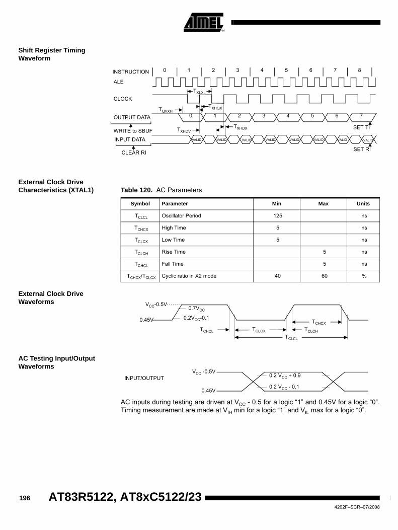
196
AT83R5122, AT8xC5122/234202F–SCR–07/2008
Shift Register Timing Waveform
External Clock Drive Characteristics (XTAL1) Table 120. AC Parameters
External Clock Drive Waveforms
AC Testing Input/Output Waveforms
AC inputs during testing are driven at VCC - 0.5 for a logic “1” and 0.45V for a logic “0”.Timing measurement are made at VIH min for a logic “1” and VIL max for a logic “0”.
VALID VALID VALID VALID VALIDVALIDINPUT DATA VALID
0 1 2 3 4 5 6 87
ALE
CLOCK
OUTPUT DATA
WRITE to SBUF
CLEAR RI
TXLXL
TQVXHTXHQX
TXHDVTXHDX SET TI
SET RI
INSTRUCTION
0 1 2 3 4 5 6 7
VALID
Symbol Parameter Min Max Units
TCLCL Oscillator Period 125 ns
TCHCX High Time 5 ns
TCLCX Low Time 5 ns
TCLCH Rise Time 5 ns
TCHCL Fall Time 5 ns
TCHCX/TCLCX Cyclic ratio in X2 mode 40 60 %
VCC-0.5V
0.45V
0.7VCC
0.2VCC-0.1
TCHCL TCLCX
TCLCL
TCLCH
TCHCX
INPUT/OUTPUT 0.2 VCC + 0.9
0.2 VCC - 0.1
VCC -0.5V
0.45V

197
AT83R5122, AT8xC5122/23
4202F–SCR–07/2008
Float Waveforms
For timing purposes as port pin is no longer floating when a 100 mV change from loadvoltage occurs and begins to float when a 100 mV change from the loaded VOH/VOL leveloccurs. IOL/IOH ≥ ± 20 mA.
Clock Waveforms Valid in normal clock mode. In X2 mode XTAL2 must be changed to XTAL2/2.
FLOAT
VOH - 0.1 V
VOL + 0.1 V
VLOADVLOAD + 0.1 V
VLOAD - 0.1 V
DATA PCL OUT DATA PCL OUT DATA PCL OUT SAMPLED SAMPLED SAMPLED
STATE4 STATE5 STATE6 STATE1 STATE2 STATE3 STATE4 STATE5
P1 P2 P1 P2 P1 P2 P1 P2 P1 P2 P1 P2 P1 P2 P1 P2
FLOAT FLOAT FLOAT
THESE SIGNALS ARE NOT ACTIVATED DURING THEEXECUTION OF A MOVX INSTRUCTION
INDICATES ADDRESS TRANSITIONS
EXTERNAL PROGRAM MEMORY FETCH
FLOAT
DATASAMPLED
DPL OR Rt OUT
INDICATES DPH OR P2 SFR TO PCH TRANSITION
PCL OUT (IF PROGRAMMEMORY IS EXTERNAL)
PCL OUT (EVEN IF PROGRAMMEMORY IS INTERNAL)
PCL OUT (IF PROGRAMMEMORY IS EXTERNAL
OLD DATA NEW DATAP0 PINS SAMPLED
P1, P2, P3 PINS SAMPLED P1, P2, P3 PINS SAMPLED
P0 PINS SAMPLED
RXD SAMPLED
INTERNALCLOCK
XTAL2
ALE
PSEN
P0
P2 (EXT)
READ CYCLE
WRITE CYCLE
RD
P0
P2
WR
PORT OPERATION
MOV PORT SRC
MOV DEST P0MOV DEST PORT (P1. P2. P3)(INCLUDES INTO. INT1. TO T1)
SERIAL PORT SHIFT CLOCK
TXD (MODE 0)
DATA OUT
DPL OR Rt OUT
INDICATES DPH OR P2 SFR TO PCH TRANSITION
P0
P2
RXD SAMPLED

198
AT83R5122, AT8xC5122/234202F–SCR–07/2008
This diagram indicates when signals are clocked internally. The time it takes the signalsto propagate to the pins, however, ranges from 25 to 125 ns. This propagation delay isdependent on variables such as temperature and pin loading. Propagation also variesfrom output to output and component. Typically though (TA=25°C fully loaded) RD andWR propagation delays are approximately 50 ns. The other signals are typically 85 ns.Propagation delays are incorporated in the AC specifications.
USB Interface
Rise Time Fall Time
VCRS
DifferentialData Lines
90%
10%
90%
10%
tR tF
VHmin
VLmax
Symbol Parameter Min Typ(5) Max Unit
tR Rise Time 4 20 ns
tF Fall Time 4 20 ns
tFDRATE Full-speed Data Rate 11.9700 12.0300 Mb/s
VCRS Crossover Voltage 1.3 2.0 V
tDJ1 Source Jitter Total to next transaction -3.5 3.5 ns
tDJ2Source Jitter Total for paired transactions -4 4 ns
tJR1 Receiver Jitter to next transaction -18.5 18.5 ns
tJR2 Receiver Jitter for paired transactions -9 9 ns

199
AT83R5122, AT8xC5122/23
4202F–SCR–07/2008
Packaging Information
Ordering Information
Note: 1. Check avaibility with sales office
Lead free/ RoHSPart Number
Lead free/ RoHSInternal Part Number
Memory Size (bytes)
Supply Voltage (V)
Temperature Range
Max Frequency(MHz) Package Packing
AT83R5122xxx-RDTUM AT83R5122xxx-ALTUM 32K ROM 3.0 - 5.5 Industrial 48 MHz / X1 VQFP64 Tray
AT83R5122xxx-RDRUM AT83R5122xxx-ALRUM 32K ROM 3.0 - 5.5 Industrial 48 MHz / X1 VQFP64 Tape & Reel
AT83R5122xxx-PSTUM AT83R5122xxxZ1TUM 32K ROM 3.0 - 5.5 Industrial 48 MHz / X1 QFN64 Tray & Dry Pack
AT83R5122xxx-PSRUM AT83R5122xxx-Z1RUM 32K ROM 3.0 - 5.5 Industrial 48 MHz / X1 QFN64 Tape & Reel & Dry Pack
AT85C5122D-RDTUM AT85C5122D-ALTUM 32K CRAM 3.0 - 5.5 Industrial 48 MHz / X1 VQFP64 Tray
AT85C5122D-RDRUM AT85C5122D-ALRUM 32K CRAM 3.0 - 5.5 Industrial 48 MHz / X1 VQFP64 Tape & Reel
AT89C5122D-RDTUM AT89C5122D-ALTUM 32K FLASH 3.0 - 5.5 Industrial 48 MHz / X1 VQFP64 Tray & Dry pack
AT89C5122D-RDRUM AT89C5122D-ALRUM 32K FLASH 3.0 - 5.5 Industrial 48 MHz / X1 VQFP64Tape & Reel& Dry pack
AT89C5122D-PSTUM AT89C5122D-Z1TUM 32K FLASH 3.0 - 5.5 Industrial 48 MHz / X1 QFN64 Tray & Dry Pack
AT89C5122D-PSRUM AT89C5122D-Z1RUM 32K FLASH 3.0 - 5.5 Industrial 48 MHz / X1 QFN64 Tape & Reel & Dry Pack
AT89C5122DS-RDTUM AT89C5122DS-ALTUM 32K FLASH 3.0 - 5.5 Industrial 48 MHz / X1 VQFP64 Tray & Dry Pack
AT89C5122DS-RDRUM AT89C5122DS-ALRUM 32K FLASH 3.0 - 5.5 Industrial 48 MHz / X1 VQFP64 Tape & Reel & Dry Pack
AT89C5122D-PSTUM AT89C5122D-Z1TUM 32K FLASH 3.0 - 5.5 Industrial 48 MHz / X1 QFN64 Tray & Dry Pack
AT89C5122D-PSRUM AT89C5122D-Z1RUM 32K FLASH 3.0 - 5.5 Industrial 48 MHz / X1 QFN64 Tape & Reel & Dry Pack
AT83C5123xxx-RATUM AT83C5123xxx-ALTUM 30K ROM 3.0 - 5.5 Industrial 48 MHz / X1 VQFP32 Tray
AT83C5123xxx-RARUM AT83C5123xxx-ALRUM 30K ROM 3.0 - 5.5 Industrial 48 MHz / X1 VQFP32 Tape & Reel
AT83C5123xxx-PUTUM AT83C5123xxx-Z1TUM 30K ROM 3.0 - 5.5 Industrial 48 MHz / X1 QFN32 Tray
AT83C5123xxx-PURUM AT83C5123xxx-Z1RUM 30K ROM 3.0 - 5.5 Industrial 48 MHz / X1 QFN32 Tape & Reel

200
AT83R5122, AT8xC5122/234202F–SCR–07/2008
Mechanical Dimensions
VQFP64 Package

201
AT83R5122, AT8xC5122/23
4202F–SCR–07/2008
PLCC68 Package

202
AT83R5122, AT8xC5122/234202F–SCR–07/2008
VQFP32 Package

203
AT83R5122, AT8xC5122/23
4202F–SCR–07/2008
QFN32 Package

204
AT83R5122, AT8xC5122/234202F–SCR–07/2008
Datasheet Revision History
Changes from 4202A to 4202B1. Product AT8xEC5122 added.2. Products AT83C5123 and AT83EC5123 added.
Changes from 4202B to 4202C1. All sections updated.2. QFN64 and QFN32 packages added.3. SCIB section : VCC must be higher than 4.0V when DC/DC is operated at 5V.
Changes from 4202C to 4202D1. Product AT89C5122DS added (EA pin changed to VCC)2. Typical applications section: external pull-up shown on CIO pin3. Ports section : Detailed explanations on CIO, CC4, CC8 quasi-bidirectional ports 4. Ordering information section: AT89C5122DS part-numbers added
Changes from 4202D to 4202E1. Changed input voltage frequency from 3.6V to 3.0V throughout the document.2. Update of DC parameters of smart card interface to be EMV 4.1 compliant.
Changes from 4202E to 4202F1. Product AT83EC5122 and AT83EC5123 removed.2. Product AT83R5122 added.3. Package PLCC28 not supported anymore.4. Global update.

2054202F–SCR–07/2008
AT83R5122, AT8xC5122/23
Table of Contents
Features ................................................................................................. 1Reference Documents .......................................................................................... 2Product Description .............................................................................................. 3AT8xC5122/AT83R5122 Block Diagram .............................................................. 4AT83C5123 Block Diagram ..................................................................................4
Pinout .................................................................................................... 5High Pin Count Package Description.................................................................... 5Low Pin Count Package Description .................................................................. 10Pin Description.................................................................................................... 11
Typical Applications ........................................................................... 15Recommended External components .................................................................15USB Keyboard with Smart Card Reader Using AT83R5122, AT8xC5122/AT89C5122DS
16USB Smart Card Reader Using the AT83C5123 Version................................... 17
Memory Organization ......................................................................... 18Program Memory Managament .......................................................................... 18Data Memory Managament ................................................................................ 19Dual Data Pointer Register (DDPTR) ................................................................. 20Registers............................................................................................................. 22AT8xC5122’s CRAM and E2PROM Versions ....................................................24AT83R5122, AT8xC5122’s ROM Version .......................................................... 28AT83C5123 Version ........................................................................................... 30
Special Function Registers (SFR’s) .................................................. 31Introduction ......................................................................................................... 31AT8xC5122 Version............................................................................................ 32AT83C5123 Version ........................................................................................... 33SFR’s Description ............................................................................................... 34
Clock Controller .................................................................................. 39On-Chip Oscillator .............................................................................................. 39Phase Lock Loop (PLL) ...................................................................................... 40Clock Tree Architecture ...................................................................................... 41Registers............................................................................................................. 48
I/O Port Definition ............................................................................... 51Port Configuration............................................................................................... 55Registers............................................................................................................. 59
Smart Card Interface Block (SCIB) ................................................... 62Block Diagram .................................................................................................... 63

2064202F–SCR–07/2008
AT83R5122, AT8xC5122/23
Definitions ........................................................................................................... 63Functional Description ........................................................................................ 65Additional Features............................................................................................. 72Alternate Card..................................................................................................... 76Registers .............................................................................................................76DC/DC Converter................................................................................................ 86
USB Controller .................................................................................... 93Description.......................................................................................................... 94Configuration ...................................................................................................... 97Read/Write Data FIFO...................................................................................... 100Bulk / Interrupt Transactions............................................................................. 101Control Transactions......................................................................................... 105Isochronous Transactions................................................................................. 106Miscellaneous ................................................................................................... 108Suspend/Resume Management .......................................................................109Detach Simulation............................................................................................. 112USB Interrupt System....................................................................................... 113Registers........................................................................................................... 115
Serial I/O Port .................................................................................... 124Framing Error Detection ................................................................................... 124Automatic Address Recognition........................................................................ 125Asynchronous Modes (Modes 1, 2 and 3) ........................................................ 129Modes 2 and 3 .................................................................................................. 130Registers........................................................................................................... 133
Serial Port Interface (SPI) ................................................................ 135Features............................................................................................................ 135Signal Description............................................................................................. 135Functional Description ...................................................................................... 137
Timers/Counters ............................................................................... 145Timer/Counter Operations ................................................................................ 145Timer 0.............................................................................................................. 145Timer 1.............................................................................................................. 148Registers........................................................................................................... 150
Keyboard Interface ........................................................................... 153Introduction ....................................................................................................... 153Description........................................................................................................ 153Registers........................................................................................................... 154
Interrupt System ............................................................................... 157Introduction ....................................................................................................... 157Interrupt System Description ............................................................................ 157

2074202F–SCR–07/2008
AT83R5122, AT8xC5122/23Registers........................................................................................................... 160Interrupt Sources and Vectors .......................................................................... 169
Microcontroller Reset ....................................................................... 170Introduction ....................................................................................................... 170Power On Reset (POR) .................................................................................... 171Power Fail Detector (PFD)................................................................................ 171Reset pin........................................................................................................... 173Watchdog Timer ............................................................................................... 175
Power Management .......................................................................... 178Idle Mode.......................................................................................................... 178Power Down Mode ........................................................................................... 178Reduced EMI Mode.......................................................................................... 179USB Interface ................................................................................................... 180Smart Card Interface ........................................................................................ 181Keyboard Interface ........................................................................................... 182Watchdog Timer during Power-down and Idle Mode........................................ 182Registers........................................................................................................... 183
Electrical Characteristics ................................................................. 184Absolute Maximum Ratings ..............................................................................184DC Parameters .................................................................................................184LED’s ................................................................................................................186Smart Card Interface ........................................................................................ 187USB Interface ................................................................................................... 190AC Parameters ................................................................................................. 191Float Waveforms............................................................................................... 197
Packaging Information ..................................................................... 199Ordering Information......................................................................................... 199
Datasheet Revision History ............................................................. 204Changes from 4202A to 4202B ........................................................................204Changes from 4202B to 4202C ........................................................................204Changes from 4202C to 4202D ........................................................................204Changes from 4202D to 4202E ........................................................................204Changes from 4202E to 4202F .........................................................................204
Table of Contents ............................................................................. 205

Printed on recycled paper.
4202F–SCR–07/2008
© Atmel Corporation 2006. All rights reserved. Atmel®, logo and combinations thereof, are registered trademarks, and Everywhere You Are®
are the trademarks of Atmel Corporation or its subsidiaries. Other terms and product names may be trademarks of others.
Disclaimer: The information in this document is provided in connection with Atmel products. No license, express or implied, by estoppel or otherwise, to anyintellectual property right is granted by this document or in connection with the sale of Atmel products. EXCEPT AS SET FORTH IN ATMEL’S TERMS AND CONDI-TIONS OF SALE LOCATED ON ATMEL’S WEB SITE, ATMEL ASSUMES NO LIABILITY WHATSOEVER AND DISCLAIMS ANY EXPRESS, IMPLIED OR STATUTORYWARRANTY RELATING TO ITS PRODUCTS INCLUDING, BUT NOT LIMITED TO, THE IMPLIED WARRANTY OF MERCHANTABILITY, FITNESS FOR A PARTICULARPURPOSE, OR NON-INFRINGEMENT. IN NO EVENT SHALL ATMEL BE LIABLE FOR ANY DIRECT, INDIRECT, CONSEQUENTIAL, PUNITIVE, SPECIAL OR INCIDEN-TAL DAMAGES (INCLUDING, WITHOUT LIMITATION, DAMAGES FOR LOSS OF PROFITS, BUSINESS INTERRUPTION, OR LOSS OF INFORMATION) ARISING OUTOF THE USE OR INABILITY TO USE THIS DOCUMENT, EVEN IF ATMEL HAS BEEN ADVISED OF THE POSSIBILITY OF SUCH DAMAGES. Atmel makes norepresentations or warranties with respect to the accuracy or completeness of the contents of this document and reserves the right to make changes to specificationsand product descriptions at any time without notice. Atmel does not make any commitment to update the information contained herein. Unless specifically providedotherwise, Atmel products are not suitable for, and shall not be used in, automotive applications. Atmel’s products are not intended, authorized, or warranted for use as compo-nents in applications intended to support or sustain life.
Atmel Corporation Atmel Operations2325 Orchard ParkwaySan Jose, CA 95131, USATel: 1(408) 441-0311Fax: 1(408) 487-2600
Regional HeadquartersEurope
Atmel SarlRoute des Arsenaux 41Case Postale 80CH-1705 FribourgSwitzerlandTel: (41) 26-426-5555Fax: (41) 26-426-5500
AsiaRoom 1219Chinachem Golden Plaza77 Mody Road TsimshatsuiEast KowloonHong KongTel: (852) 2721-9778Fax: (852) 2722-1369
Japan9F, Tonetsu Shinkawa Bldg.1-24-8 ShinkawaChuo-ku, Tokyo 104-0033JapanTel: (81) 3-3523-3551Fax: (81) 3-3523-7581
Memory2325 Orchard ParkwaySan Jose, CA 95131, USATel: 1(408) 441-0311Fax: 1(408) 436-4314
Microcontrollers2325 Orchard ParkwaySan Jose, CA 95131, USATel: 1(408) 441-0311Fax: 1(408) 436-4314
La ChantrerieBP 7060244306 Nantes Cedex 3, FranceTel: (33) 2-40-18-18-18Fax: (33) 2-40-18-19-60
ASIC/ASSP/Smart CardsZone Industrielle13106 Rousset Cedex, FranceTel: (33) 4-42-53-60-00Fax: (33) 4-42-53-60-01
1150 East Cheyenne Mtn. Blvd.Colorado Springs, CO 80906, USATel: 1(719) 576-3300Fax: 1(719) 540-1759
Scottish Enterprise Technology ParkMaxwell BuildingEast Kilbride G75 0QR, Scotland Tel: (44) 1355-803-000Fax: (44) 1355-242-743
RF/AutomotiveTheresienstrasse 2Postfach 353574025 Heilbronn, GermanyTel: (49) 71-31-67-0Fax: (49) 71-31-67-2340
1150 East Cheyenne Mtn. Blvd.Colorado Springs, CO 80906, USATel: 1(719) 576-3300Fax: 1(719) 540-1759
Biometrics/Imaging/Hi-Rel MPU/High Speed Converters/RF Datacom
Avenue de RochepleineBP 12338521 Saint-Egreve Cedex, FranceTel: (33) 4-76-58-30-00Fax: (33) 4-76-58-34-80
Literature Requestswww.atmel.com/literature