APJ ABDUL KALAM KERALA TECHNOLOGICAL UNIVERSITY
86
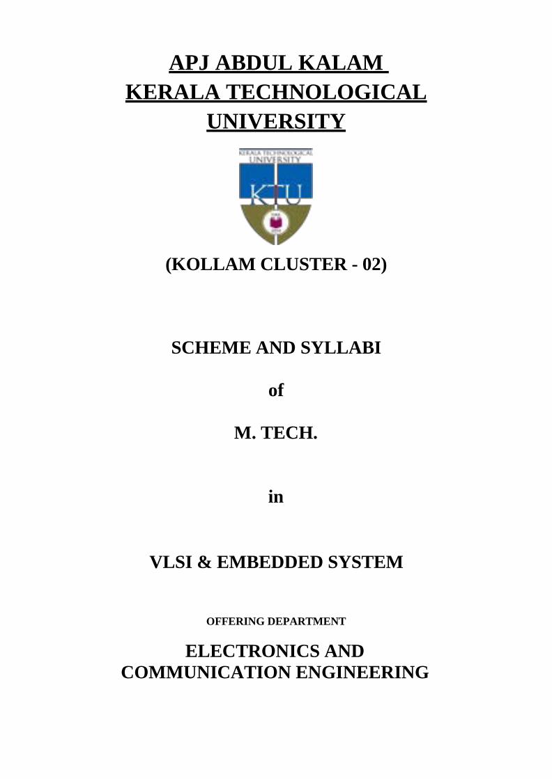
APJ ABDUL KALAM KERALA TECHNOLOGICAL UNIVERSITY (KOLLAM CLUSTER - 02) SCHEME AND SYLLABI of M. TECH. in VLSI & EMBEDDED SYSTEM OFFERING DEPARTMENT ELECTRONICS AND COMMUNICATION ENGINEERING
-
Upload
khangminh22 -
Category
Documents
-
view
1 -
download
0
Transcript of APJ ABDUL KALAM KERALA TECHNOLOGICAL UNIVERSITY
APJ ABDUL KALAM KERALA TECHNOLOGICAL
UNIVERSITY
(KOLLAM CLUSTER - 02)
SCHEME AND SYLLABI
of
M. TECH.
in
VLSI & EMBEDDED SYSTEM
OFFERING DEPARTMENT
ELECTRONICS AND COMMUNICATION ENGINEERING

Page 1
CLUSTER LEVEL GRADUATE PROGRAM COMMITTEE
NO MEMBER
1 Dr. S. Mohan, Professor, IIT Madras, Chennai
2 Principal, TKM College of Engineering, Kollam
3 Principal, Baselios Mathews II College of Engineering, Sasthamcotta, Kollam
4 Principal, College of Engineering, Karunagapally, Kollam
5 Principal, College of Engineering, Perumon, Kollam
6 Principal, Pinnacle School of Engineering and Technology, Anchal, Kollam
7 Principal, Shahul Hameed Memorial Engineering College, Kadakkal, Kollam
8 Principal, TKM Institute of Technology, Ezhukone, Kollam
9 Principal, Travancore Engineering College, Parippally, Kollam
10 Principal, Younus College of Engineering and Technology, Pallimukku, Kollam
Page 2
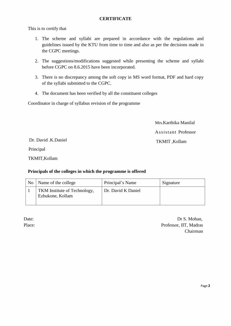
CERTIFICATE
This is to certify that
1. The scheme and syllabi are prepared in accordance with the regulations and guidelines issued by the KTU from time to time and also as per the decisions made in the CGPC meetings.
2. The suggestions/modifications suggested while presenting the scheme and syllabi before CGPC on 8.6.2015 have been incorporated.
3. There is no discrepancy among the soft copy in MS word format, PDF and hard copy of the syllabi submitted to the CGPC.
4. The document has been verified by all the constituent colleges
Coordinator in charge of syllabus revision of the programme
Dr. David .K.Daniel
Principal
Mrs.Karthika Manilal
Ass i s tan t Professor
TKMIT ,Kollam
TKMIT,Kollam
Principals of the colleges in which the programme is offered
No Name of the college Principal’s Name Signature
1 TKM Institute of Technology, Ezhukone, Kollam
Dr. David K Daniel
Date: Dr S. Mohan, Place: Professor, IIT, Madras
Chairman
Page 3
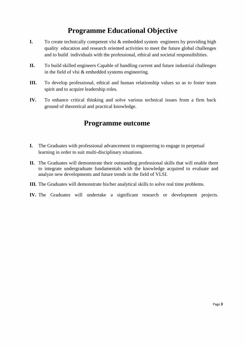
Programme Educational Objective
I. To create technically competent vlsi & embedded system engineers by providing high quality education and research oriented activities to meet the future global challenges and to build individuals with the professional, ethical and societal responsibilities.
II. To build skilled engineers Capable of handling current and future industrial challenges in the field of vlsi & embedded systems engineering.
III. To develop professional, ethical and human relationship values so as to foster team spirit and to acquire leadership roles.
IV. To enhance critical thinking and solve various technical issues from a firm back ground of theoretical and practical knowledge.
Programme outcome
I. The Graduates with professional advancement in engineering to engage in perpetual learning in order to suit multi-disciplinary situations.
II. The Graduates will demonstrate their outstanding professional skills that will enable them to integrate undergraduate fundamentals with the knowledge acquired to evaluate and analyze new developments and future trends in the field of VLSI.
III. The Graduates will demonstrate his/her analytical skills to solve real time problems. IV. The Graduates will undertake a significant research or development projects.
Page 4
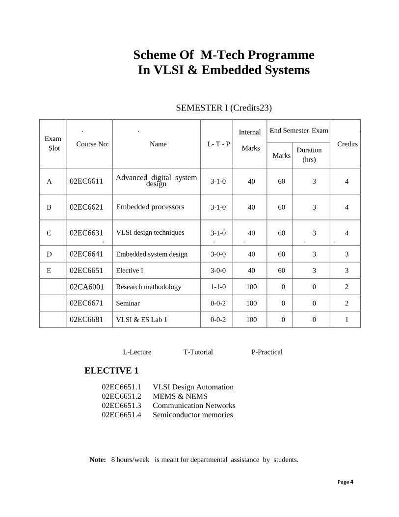
Scheme Of M-Tech Programme In VLSI & Embedded Systems
SEMESTER I (Credits23)
Exam Slot Course No: Name L- T - P
Internal
Marks
End Semester Exam
Credits Marks
Duration (hrs)
A 02EC6611 Advanced digital system design 3-1-0 40 60 3 4
B 02EC6621 Embedded processors 3-1-0 40 60 3 4
C 02EC6631 VLSI design techniques 3-1-0 40 60 3 4
D 02EC6641 Embedded system design 3-0-0 40 60 3 3
E 02EC6651 Elective I 3-0-0 40 60 3 3
02CA6001 Research methodology 1-1-0 100 0 0 2
02EC6671 Seminar 0-0-2 100 0 0 2
02EC6681 VLSI & ES Lab 1 0-0-2 100 0 0 1
L-Lecture T-Tutorial P-Practical ELECTIVE 1 02EC6651.1 VLSI Design Automation 02EC6651.2 MEMS & NEMS 02EC6651.3 Communication Networks 02EC6651.4 Semiconductor memories
Note: 8 hours/week is meant for departmental assistance by students.

SCHEME OF M-TECH PROGRAMME IN VLSI & EMBEDDED
SYSTEM
SEMESTER II (Credits19)
L-Lecture T-Tutorial P-Practical
ELECTIVES 02EC6642.1 Embedded System Programming 02EC6642.2 Digital System Synthesis and verification 02EC6642.3 Nano Scale Transistors 02EC6642.4 VLSI Fabrication Technology 02EC6652.1 Embedded Networking 02EC6652.2 Low Power VLSI Design 02EC6652.3 Cryptography and Network Security 02EC6652.4 RF CMOS Design Note: 8 hours/week is meant for departmental assistance by students
Exam
Slot Course No: Name L- T - P
Interna
l
Marks
End Semester Exam
Credits Marks
Duration (hrs)
A 02EC6612 Digital signal processing structures for VLSI 3-0-0 40 60 3 3
B 02EC6622 Embedded and real time operating systems
3-0-0 40 60 3 3
C 02EC6632 Analog integrated circuit design 3-1-0 40 60 3 4
D 02EC6642 Elective II 3-0-0 40 60 3 3
E 02EC6652 Elective III 3-0-0 40 60 3 3
02EC6662 Mini project 0-0-4 100 0 0 2
02EC6672 VLSI & ES Lab II 0-0-2 100 0 0 2
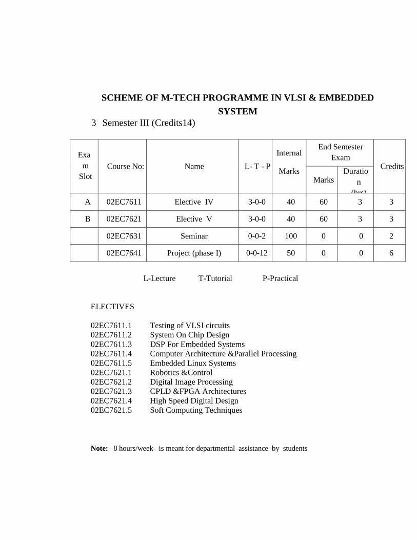
SCHEME OF M-TECH PROGRAMME IN VLSI & EMBEDDED SYSTEM
3 Semester III (Credits14)
Exam
Slot Course No: Name L- T - P
Internal
Marks
End Semester Exam
Credits
Marks Duratio
n (hrs)
A 02EC7611 Elective IV 3-0-0 40 60 3 3
B 02EC7621 Elective V 3-0-0 40 60 3 3
02EC7631 Seminar 0-0-2 100 0 0 2
02EC7641 Project (phase I) 0-0-12 50 0 0 6
L-Lecture T-Tutorial P-Practical
ELECTIVES 02EC7611.1 Testing of VLSI circuits 02EC7611.2 System On Chip Design 02EC7611.3 DSP For Embedded Systems 02EC7611.4 Computer Architecture &Parallel Processing 02EC7611.5 Embedded Linux Systems 02EC7621.1 Robotics &Control 02EC7621.2 Digital Image Processing 02EC7621.3 CPLD &FPGA Architectures 02EC7621.4 High Speed Digital Design 02EC7621.5 Soft Computing Techniques
Note: 8 hours/week is meant for departmental assistance by students
Page 7
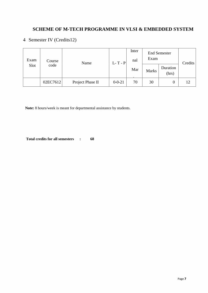
SCHEME OF M-TECH PROGRAMME IN VLSI & EMBEDDED SYSTEM 4 Semester IV (Credits12)
Exam Slot
Course code Name L- T - P
Inter
nal
Mar
k
End Semester Exam
Credits
Marks Duration
(hrs)
02EC7612 Project Phase II 0-0-21 70 30 0 12
Note: 8 hours/week is meant for departmental assistance by students. Total credits for all semesters : 68
Page 8
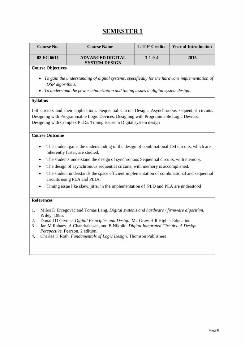
SEMESTER 1
Course No. Course Name L-T-P-Credits Year of Introduction
02 EC 6611 ADVANCED DIGITAL SYSTEM DESIGN
3-1-0-4 2015
Course Objectives
• To gain the understanding of digital systems, specifically for the hardware implementation of DSP algorithms.
• To understand the power minimization and timing issues in digital system design.
Syllabus LSI circuits and their applications. Sequential Circuit Design. Asynchronous sequential circuits. Designing with Programmable Logic Devices. Designing with Programmable Logic Devices. Designing with Complex PLDs. Timing issues in Digital system design
Course Outcome
• The student gains the understanding of the design of combinational LSI circuits, which are inherently faster, are studied.
• The students understand the design of synchronous Sequential circuits, with memory. • The design of asynchronous sequential circuits, with memory is accomplished. • The student understands the space efficient implementation of combinational and sequential
circuits using PLA and PLDs. • Timing issue like skew, jitter in the implementation of PLD and PLA are understood
References 1. Milos D Ercegovac and Tomas Lang, Digital systems and hardware / firmware algorithm.
Wiley, 1985. 2. Donald D Givone. Digital Principles and Design. Mc-Graw Hill Higher Education. 3. Jan M Rabaey, A Chandrakasan, and B Nikolic. Digital Integrated Circuits- A Design
Perspective. Pearson, 2 edition. 4. Charles H Roth. Fundamentals of Logic Design. Thomson Publishers
Page 9
COURSE PLAN
Module Contents Contact Hours
Sem.Exam Marks ;%
I
LSI circuits and their applications Arithmetic circuits, comparators, Multiplexers, Code Converters, XOR and AOI Gates, Wired Logic, Bus oriented structures, Tristate bus systems, Propagation Delay.
10
15
II
Sequential Circuit Design. Clocked Synchronous State Machine Analysis, Mealy and Moore machines, Finite State Machine design procedure derive state diagrams, obtain state tables, state reduction methods, state assignments, Incompletely specified state machine, Implementing the states of FSM
10
15
FIRST INTERNAL EXAM
III
Asynchronous sequential circuits Derivation of excitation table, Race conditions and cycles, Static and dynamic hazards, Methods for avoiding races and hazards, essential hazards, Designing with SM charts State machine charts, Derivation of SM charts, and Realization of SM charts.
10
15
IV
Designing with Programmable Logic Devices Read Only Memories, Programmable Array Logic PALs, Programmable Logic Arrays PLAs PLA minimization and PLA folding
8
15
SECOND INTERNAL EXAM
V
Designing with Complex PLDs Design of combinational and sequential circuits using PLDs. XILINX FPGAs Configurable Logic Block(CLB), Input/ Output Block (IOB),Programmable Interconnection Points(PIP),XILINX CPLDs
10
20
VI
Timing issues in Digital system design Timing classification – synchronous timing basics skew and jitter– latch based clocking- self timed circuit design - self timed logic, completion signal generation, self-timed signaling synchronizers and arbiters
8
20
END SEMESTER EXAM

Page 10
Course No. Course Name L-T-P-Credits Year of Introduction
02EC6621 Embedded Processors (L-T-P :3-1-0: 4) 2015
Course Objectives • Almost all embedded systems are designed with microcontrollers as an essential basic
part. • To expose the students to the fundamentals of microcontroller based system Design. • To learn the architecture, programming, interfacing of certain 8 bit and 32 bit
microcontroller. • To design and develop microcontroller based embedded systems.
Syllabus
Study of micro controller (MCS 51 family- 8051), Architecture and programming. PIC16F87X Microcontroller, Architecture, peripherals and programming. High Performance RISC Architecture- ARM, CORTEX M3 architecture, ARM programming. Microcontroller system development tools, typical application design using 8/16/32 microcontrollers design. Course Outcome
• Understand basic processor architecture and programming concepts. • To expose the students the system design processes using different processors.
References
1. Ayala Kenneth J, “8051 microcontroller: Architecture, Programming and Application”, 1st edition, West Publishing Company,1996.
2. John B Peatman, “Designing with Microcontrollers”, 1st edition, McGraw Hill International.
3. Muhammad Ali Mazidi,Janice G. Mazidi, R.D.McKinlay, “The 8051 Microcontroller and Embedded Systems using Assembly & C”, 2nd Edition, Pearson Education,2008.
COURSEPLAN
Module Contents Contact Hours
Sem. ExamMark
I
8-Bit Microcontrollers Study of micro controller (MCS 51 family- 8051) -Architecture: CPU Block diagram, Memory organization, Program memory, Data memory, Interrupts, Peripherals: Timers, Serial port, I/O Port Programming, Addressing Modes, Instruction Set, Programming.
9
15
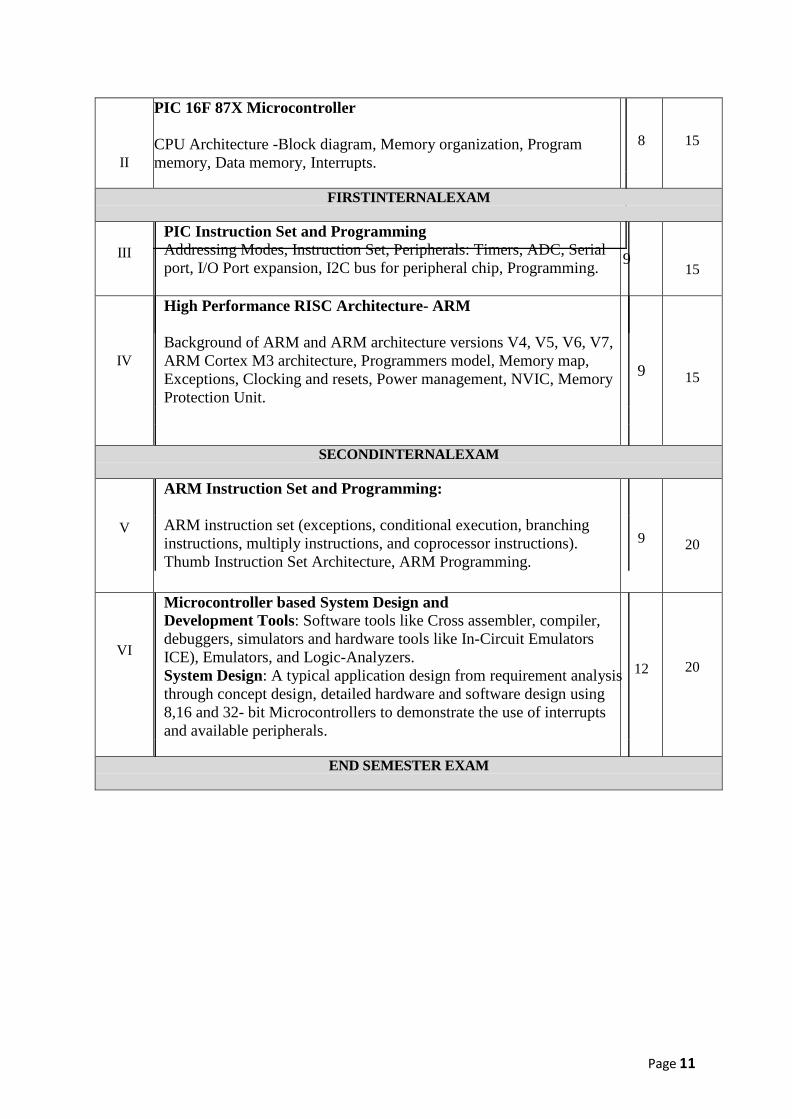
Page 11
II
PIC 16F 87X Microcontroller CPU Architecture -Block diagram, Memory organization, Program memory, Data memory, Interrupts.
8
15
FIRSTINTERNALEXAM
III
PIC Instruction Set and Programming Addressing Modes, Instruction Set, Peripherals: Timers, ADC, Serial port, I/O Port expansion, I2C bus for peripheral chip, Programming.
9
15
IV
High Performance RISC Architecture- ARM Background of ARM and ARM architecture versions V4, V5, V6, V7, ARM Cortex M3 architecture, Programmers model, Memory map, Exceptions, Clocking and resets, Power management, NVIC, Memory Protection Unit.
9
15
SECONDINTERNALEXAM 3
V
ARM Instruction Set and Programming: ARM instruction set (exceptions, conditional execution, branching instructions, multiply instructions, and coprocessor instructions). Thumb Instruction Set Architecture, ARM Programming.
9
20
VI
Microcontroller based System Design and Development Tools: Software tools like Cross assembler, compiler, debuggers, simulators and hardware tools like In-Circuit Emulators ICE), Emulators, and Logic-Analyzers. System Design: A typical application design from requirement analysis through concept design, detailed hardware and software design using 8,16 and 32- bit Microcontrollers to demonstrate the use of interrupts and available peripherals.
12
20
END SEMESTER EXAM

Page 12
Course No. Course Name L-T-P-Credits Year of Introduction
02EC6631 VLSI Design Techniques (L-T-P : 3-1-0: 4) 2015
Course Objectives • As many real life applications involve both analog and digital circuits, this course helps
to understand, design and analyze various analog and digital CMOS Circuits. • To explore various design strategies to be followed for designing VLSI circuits.
Syllabus
Introduction to MOS Technologies, MOS Transistor, The MOS Inverter ,Latch-up in CMOS circuits, Ratioed logic, Pass Transistor logic, Digital-to-analog converters (DAC) , Analog-to digital converters (ADC), Sequential MOS Logic Design, Designing arithmetic building blocks: Adders, Multiplier, Shifters, Circuit design Process.
Course Outcome
• Subject familiarizes the concepts of MOS transistors operations and their AC, DC characteristics.
• Will get an idea of static and switching characteristics of the CMOS Inverter, pass transistor logic and latch up in CMOS circuits.
References
1. Sung-Mo Kang & Yusuf Leblebici, “CMOS Digital Integrated Circuits - Analysis & Design”,Tata MGH, 3rd edition.2003.
2. Jan M Rabaey, “Digital Integrated Circuits - A Design Perspective”, Pearson Education, Second Edition, 2003.
3. Douglas A Pucknell & Kamran Eshragian, “Basic VLSI Design”, PHI, Third Edition. 2005.
COURSEPLAN
Module Contents Contact Hours
Sem. ExamMarks
I
Review of Microelectronics and Introduction to MOS Technologies: Technology trends, MOS Transistor, threshold voltage equation, body effect, MOS device design equation, sub threshold region, Channel length modulation. Mobility variation, tunneling, punch through, hot electron effect, SOI MOSFET, Fin FET(Structure only).
12
15
Page 13
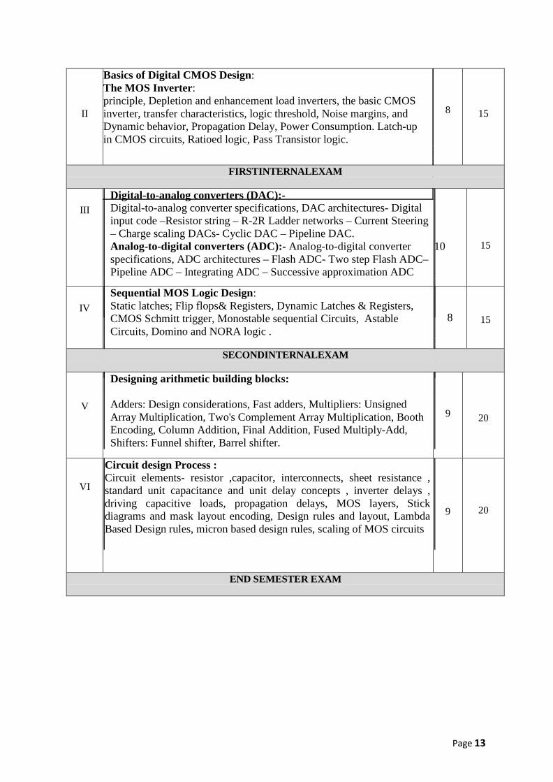
II
Basics of Digital CMOS Design: The MOS Inverter: principle, Depletion and enhancement load inverters, the basic CMOS inverter, transfer characteristics, logic threshold, Noise margins, and Dynamic behavior, Propagation Delay, Power Consumption. Latch-up in CMOS circuits, Ratioed logic, Pass Transistor logic.
8
15
FIRSTINTERNALEXAM
III
Digital-to-analog converters (DAC):- Digital-to-analog converter specifications, DAC architectures- Digital input code –Resistor string – R-2R Ladder networks – Current Steering – Charge scaling DACs- Cyclic DAC – Pipeline DAC. Analog-to-digital converters (ADC):- Analog-to-digital converter specifications, ADC architectures – Flash ADC- Two step Flash ADC– Pipeline ADC – Integrating ADC – Successive approximation ADC
10
15
IV
Sequential MOS Logic Design: Static latches; Flip flops& Registers, Dynamic Latches & Registers, CMOS Schmitt trigger, Monostable sequential Circuits, Astable Circuits, Domino and NORA logic .
8
15
SECONDINTERNALEXAM 3
V
Designing arithmetic building blocks: Adders: Design considerations, Fast adders, Multipliers: Unsigned Array Multiplication, Two's Complement Array Multiplication, Booth Encoding, Column Addition, Final Addition, Fused Multiply-Add, Shifters: Funnel shifter, Barrel shifter.
9
20
VI
Circuit design Process : Circuit elements- resistor ,capacitor, interconnects, sheet resistance , standard unit capacitance and unit delay concepts , inverter delays , driving capacitive loads, propagation delays, MOS layers, Stick diagrams and mask layout encoding, Design rules and layout, Lambda Based Design rules, micron based design rules, scaling of MOS circuits
9
20
END SEMESTER EXAM
Page 14
Course No.
Course Name
L-T-P-Credits
Year of Introduction
02EC6641 Embedded System Design
3-0-0:3
2015
Course Objectives
The subject gives an overview on an Embedded System and also helps the students to understand the details of embedded system development process.
Syllabus Embedded system overview, Processor Technology, Major application areas of embedded
systems, Embedded hardware, Processor Design, Embedded software and peripherals. Memory Concepts and testing, Hardware/Software co-design and process model, Embedded design and testing. Course Outcome
• The student will get an overview on the basic modules of an embedded system. • Students will be exposed to the Hardware/Software co-design and Embedded design
life cycle and testing.
References: 1. Shibu.K.V, “Introduction to embedded systems”, Tata McGraw Hill Education, 2009 2. James K. Peckol, “Embedded Systems A Contemporary Design Tool”, John Wiley and Sons,
Inc.1st edition, 2007. 3.Raj Kamal, “Introduction to Embedded Systems”, Tata McGraw Hill Publications, 2002. 4.Lyla B Das, “Embedded systems -An integrated approach”, Pearson education,2013. 5.Frank Vahid and Tony Givargis, “Embedded System Design-A Unified Hardware/Software
Introduction”, John Wiley & Sons,2002. 6. Arnold S Berger, “Embedded System Design”, CMP Books, USA 2002. 7.Steve Heath, “Embedded System Design”, Butterworth Heinemann.
COURSEPLAN
Module Contents Contact Hours
Sem.Exam Marks;%
I
Introduction to embedded system Embedded system overview, Classification of embedded systems, Purpose and characteristics of embedded systems, Quality attributes, Core of an embedded system. Processor Technology, General-purpose Processors embedded system. Single-purpose Processors and Application Specific Processors, Major application areas of embedded systems.
6
15
Page 15
II
Embedded hardware Custom Single purpose Processors: Hardware combination Processor Design- RT level Design, Optimizing Custom Single- purpose Processors, Optimizing the original program, Optimizing the FSMD, Optimizing the datapath, optimizing the FSM
7
15
FIRST INTERNAL EXAM
III
Embedded software and peripherals Software: Basic architecture-operation- Programmer’s view- Development environment. Peripherals: Timers, counters, watch dog timers- UART, LCD controller, Keypad controller, A/D converter, real time clock.
7
15
IV
Memories and memory subsystems Introduction, Overview of SRAM and DRAM, memory chip organization, Terminology, timing analysis, Memory sub-systems: concept of caching-designing a cache system-dynamic memory allocation-memory testing.
8
15
SECOND INTERNAL EXAM
V
Hardware/Software co-design and process model Fundamental issues in co-design, computational models in embedded design, concurrent process- communication among process, synchronization among process, design technology-hardware/software co-simulation.
synchronization among process, design technology -hardware/software co-simulation. co-simulation.
7
20
VI
Embedded design life cycle and testing Objective, need, different phases and modeling of EDLC, choice of target architecture for control dominated, data dominated systems. Performance-unit testing-regression testing- choosing test cases-functional tests-coverage tests- Testing embedded software-Performance testing.
7
20
END SEMESTER EXAM
Course No. Course Name L-T-P-Credits Year of Introduction
02EC6651.1 VLSI Design Automation
3-0-0: 3
2015
Course Objectives
• There is a great need for methods to automate VLSI design methods. This course introduces the various automation techniques.
• To familiarize the major routing techniques.
Syllabus Graph Algorithms, N-P complete Problem, Logic synthesis & verification, Compaction, VLSI automation Algorithms, Placement, floor planning & pin assignment, Global Routing, Detailed routing.
Course Outcome
• Familiarize on automation methods for VLSI physical design. • Will familiarize with the major routing techniques.
References: 1. Sabih H. Gerez, “Algorithms for VLSI Design Automation”, John Wiley & Sons, 1999 2.Naveed.A. Shervani, “Algorithms for VLSI physical design Automation”, Kluwer Academic Publisher, Second edition,1995. 3.Christophn Meinel & Thorsten Theobold, “Algorithm and Data Structures for VLSI Design”, KAP, 2002. 4.Rolf Drechsheler, “Evolutionary Algorithm for VLSI”, Second edition 5.Trimburger, “Introduction to CAD for VLSI”, Kluwer Academic publisher, 2002 6.T.H. Cormen, C. E. Leiserson, R. L. Rivest, “Introduction to Algorithms”, PHI. 3rd edition,2009.
COURSEPLAN
Module Contents ContactHours
Sem.Exam Marks;%
I
Graph Algorithms: Data structures for Representation of Graphs, Breadth First Search, Depth First Search, Topological Sort, Spanning Tree Algorithm - Kruskal’s and Prim’s, Shortest path Algorithm - Dijkstra’s and Bellman Fort Algorithm for single pair Shortest paths, Floyd-Warshall algorithm for All pair Shortest path, Matrix multiplication modeling of All pairs shortest path problem, Min cut and Max cut Algorithms.
12
15
II
N-P complete Problem: Polynomial time non-deterministic algorithm, N-P completeness and reducibility, Proof and problems. Logic synthesis & verification: Introduction to combinational logic synthesis, Binary Decision Diagram, Hardware models for High-level synthesis, allocation, assignment and scheduling
8
15
FIRST INTERNAL EXAM
III
Compaction: problem formulation, one-dimensional compaction, two dimension based compaction, hierarchical compaction. VLSI automation Algorithms: Partitioning: problem formulation, classification of partitioning algorithms, Group migration algorithms, simulated annealing & evolution, other partitioning algorithms.
5
5
15
IV
Placement, floor planning & pin assignment: problem Formulation, placement algorithms, floor planning concepts, constraint based floor planning, floor planning algorithms for mixed block & cell design. General & channel pin assignment.
8
15
SECOND INTERNAL EXAM
V
Global Routing: Problem formulation, classification of global routing algorithms, Maze routing algorithm, line probe algorithm, Steiner Tree based algorithms, ILP based approaches.
9
20
VI
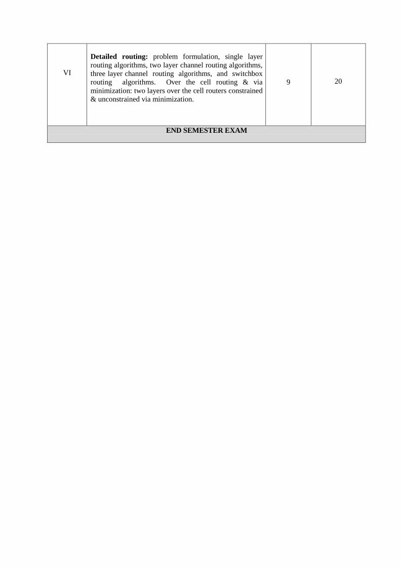
Detailed routing: problem formulation, single layer routing algorithms, two layer channel routing algorithms, three layer channel routing algorithms, and switchbox routing algorithms. Over the cell routing & via minimization: two layers over the cell routers constrained & unconstrained via minimization.
9
20
END SEMESTER EXAM
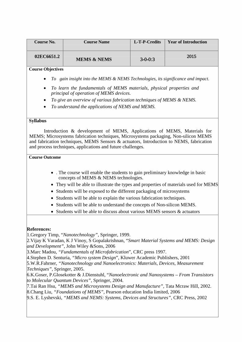
Course No. Course Name L-T-P-Credits Year of Introduction
02EC6651.2 MEMS & NEMS
3-0-0:3
2015
Course Objectives
• To gain insight into the MEMS & NEMS Technologies, its significance and impact.
• To learn the fundamentals of MEMS materials, physical properties and principal of operation of MEMS devices.
• To give an overview of various fabrication techniques of MEMS & NEMS. • To understand the applications of NEMS and MEMS.
Syllabus
Introduction & development of MEMS, Applications of MEMS, Materials for MEMS; Microsystems fabrication techniques, Microsystems packaging, Non-silicon MEMS and fabrication techniques, MEMS Sensors & actuators, Introduction to NEMS, fabrication and process techniques, applications and future challenges.
Course Outcome
• . The course will enable the students to gain preliminary knowledge in basic
concepts of MEMS & NEMS technologies. • They will be able to illustrate the types and properties of materials used for MEMS • Students will be exposed to the different packaging of microsystems • Students will be able to explain the various fabrication techniques. • Students will be able to understand the concepts of Non-silicon MEMS. • Students will be able to discuss about various MEMS sensors & actuators
References: 1.Gregory Timp, “Nanotechnology”, Springer, 1999. 2.Vijay K Varadan, K J Vinoy, S Gopalakrishnan, “Smart Material Systems and MEMS: Design and Development”, John Wiley &Sons, 2006 3.Marc Madou, “Fundamentals of Microfabrication”, CRC press 1997. 4.Stephen D. Senturia, “Micro system Design”, Kluwer Academic Publishers, 2001 5.W.R.Fahrner, “Nanotechnology and Nanoelectronics: Materials, Devices, Measurement Techniques”, Springer, 2005. 6.K.Goser, P.Glosekotter & J.Dienstuhl, “Nanoelectronic and Nanosystems – From Transistors to Molecular Quantum Devices”, Springer, 2004. 7.Tai Ran Hsu, “MEMS and Microsystems Design and Manufacture”, Tata Mcraw Hill, 2002. 8.Chang Liu, “Foundations of MEMS”, Pearson education India limited, 2006 9.S. E. Lyshevski, “MEMS and NEMS: Systems, Devices and Structures”, CRC Press, 2002

COURSEPLAN
Module Contents ContactHours
Sem.ExamMarks;%
I
New trends in Engineering and Science: Micro and Nano scale systems, Development of microelectronics - Region of Nanostructures - methods and limits on microminiaturization in semiconductors.
5
15
II
Introduction to Design of MEMS and NEMS: Applications of Micro and Nano electromechanical systems. MEMS devices and structures, Materials for MEMS: Silicon, silicon compounds, polymers, metals.
7
15
FIRST INTERNAL EXAM
III
Microsystems fabrication techniques: Photolithography, Ion Implantation, Diffusion, Oxidation. Thin film depositions: LPCVD, Sputtering, Evaporation, Electroplating; Etching techniques; Micromachining; High Aspect-Ratio (LIGA and LIGA-like) Technology. Packaging: Microsystems packaging, Essential packaging technologies, Selection of packaging materials, Packaging of MEMS devices by anodic/fusion bonding.
13
15
IV
Non-silicon MEMS and fabrication techniques: SiC MEMS- Biomedical-MEMS techniques- Integration of microsystems with electronics– RF MEMS– Applications. Polymers in Microsystems
4
15
SECOND INTERNAL EXAM
V
MEMS Sensors & Actuators: Design of Acoustic wave sensors, resonant sensor, Vibratory gyroscope, Capacitive and Piezo Resistive Pressure sensors. Micro Actuators: Design of Actuators: Actuation using thermal forces, Actuation using shape memory Alloys, Actuation using piezoelectric crystals, Actuation using Electrostatic forces (Parallel plate, Torsion bar, Comb drive actuators),
8
20
VI
Nano electro mechanical systems: Fabrication and Process techniques- Integration of Nano systems and devices-applications and future challenges.
5
20
END SEMESTER EXAM
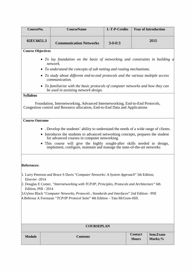
CourseNo. CourseName L-T-P-Credits Year of Introduction
02EC6651.3 Communication Networks
3-0-0:3
2015
Course Objectives
• To lay foundation on the basis of networking and constraints in building a network.
• To understand the concepts of sub netting and routing mechanisms. • To study about different end-to-end protocols and the various multiple access
communication. • To familiarize with the basic protocols of computer networks and how they can
be used in assisting network design.
Syllabus
Foundation, Internetworking, Advanced Internetworking, End-to-End Protocols, Congestion control and Resource allocation, End-to-End Data and Applications
Course Outcome
• . Develop the students’ ability to understand the needs of a wide range of clients. • Introduces the students to advanced networking concepts, prepares the student
for advanced courses in computer networking. • This course will give the highly sought-after skills needed to design,
implement, configure, maintain and manage the state-of-the-art networks
References: 1. Larry Peterson and Bruce S Davis “Computer Networks: A System Approach” 5th Edition, Elsevier -2014 2. Douglas E Comer, “Internetworking with TCP/IP, Principles, Protocols and Architecture” 6th Edition, PHI - 2014 3.Uyless Black “Computer Networks, Protocols , Standards and Interfaces” 2nd Edition - PHI 4.Behrouz A Forouzan “TCP/IP Protocol Suite” 4th Edition – Tata McGraw-Hill.
COURSEPLAN
Module Contents ContactHours
Sem.Exam Marks;%

I
Foundation: Building a Network, Requirements: Perspectives, Scalable Connectivity, Cost-Effective Resource sharing, Support for Common Services, Manageability, Protocol layering, Performance: Bandwidth and Latency, Delay X Bandwidth Product, Perspectives on Connecting: Classes of Links, Encoding, Reliable Transmission: Stop-and-Wait, Sliding Window, Concurrent Logical Channels.
7
15
II
Internetworking: Switching and Bridging: Datagram’s, Virtual Circuit Switching, Source Routing, Bridges and LAN Switches, Interface standards: RS 449 and X.21.Basic Internetworking: Service Model, Global Addresses, Datagram Forwarding in IP, sub-netting and classless addressing, Address Translation(ARP), Host Configuration (DHCP), Error Reporting (ICMP), Virtual Networks and Tunnels.
7
15
FIRST INTERNAL EXAM
III
Advanced Internetworking: Network as a Graph, Dynamic Routing Protocols: Distance Vector(RIP), Link State(OSPF),Hierarchical routing, Metrics, The Global Internet: Routing Areas, Routing among Autonomous systems(BGP), IP Version 6(IPv6), Mobility and Mobile IP, Network Address Translation(NAT).
8
15
IV
End-to-End Protocols: Simple Demultiplexer (UDP), Reliable Byte Stream(TCP): End-to-End Issues, Segment Format, Connecting Establishment and Termination, Sliding Window Revisited, Triggering Transmission, Adaptive Retransmission, Record Boundaries, TCP Extensions
7
15
SECOND INTERNAL EXAM
V
Congestion control and Resource allocation: Queuing Disciplines: FIFO, Fair Queuing, TCP Congestion Control: Additive Increase/ Multiplicative Decrease, Slow Start, Fast Retransmit and Fast Recovery, Congestion-Avoidance Mechanisms: DEC bit, Random Early Detection (RED), Source-Based Congestion Avoidance.
7
20
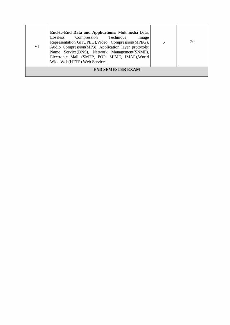
VI
End-to-End Data and Applications: Multimedia Data: Lossless Compression Technique, Image Representation(GIF,JPEG),Video Compression(MPEG), Audio Compression(MP3), Application layer protocols: Name Service(DNS), Network Management(SNMP), Electronic Mail (SMTP, POP, MIME, IMAP),World Wide Web(HTTP).Web Services.
6
20
END SEMESTER EXAM
Course No. Course Name L-T-P-Credits Year of Introduction
02EC6651.4 Semiconductor Memories
3-0-0:3
2015
Course Objectives
• Memory is an important part in many digital circuits and microcontrollers. This
course discusses implementation methods and problems in designing and making semiconductor memories.
• To gain knowledge on various testing methods of semiconductor memories.
Syllabus Static Random Access Memories (SRAMS), Dynamic Random Access Memories,
Nonvolatile Memories, Memory Fault Modeling and Testing, Semiconductor Memory Reliability, Semiconductor Memory Radiation Effects.
Course Outcome
• The student should get a thorough understanding of the various architectures for SRAM and DRAM.
• Will familiarize with the fault modeling and testing of memories for fault detection and the reliability issues of semiconductor memories.
References: 1. Ashok K. Sharma, “Semiconductor Memories: Technology, Testing, and Reliability”, Wiley-
IEEE Press, 2002. 2. Ashok K. Sharma, “Semiconductor Memories, Two-Volume Set”, Wiley-IEEE Press,2003. 3. Brent Keeth, R. Jacob Baker, “DRAM Circuit Design: A Tutorial”, Wiley-IEEE Press,2000. 4.Betty Prince, “High Performance Memories: New Architecture DRAMs and SRAMs -
Evolution & Function”,Wiley,1999.
COURSEPLAN
Module Contents ContactHours
Sem.ExamMarks;%
I
Static Random Access Memories (SRAMS): SRAM Cell Structures-MOS SRAM Architecture-MOS SRAM Cell and Peripheral Circuit Operation-Bipolar SRAM Technologies- Silicon On Insulator (SOI) Technology- Application Specific SRAMs.
8
15

II
Dynamic Random Access Memories: DRAM Technology Development-CMOS DRAMs- DRAMs Cell Theory and Advanced Cell Structures- BiCMOS DRAMs-Soft Error Failures in DRAMs- Application Specific DRAMs.
8
15
FIRST INTERNAL EXAM
III
Nonvolatile Memories: Masked Read-Only Memories (ROMs)-High Density ROMs-Programmable Read-Only Memories (PROMs) -Bipolar PROMs-CMOS PROMs-EPROMs –Floating -Gate EPROM Cell.
6
15
IV
Memory Fault Modeling And Testing: RAM Fault Modeling, Electrical Testing, Pseudo Random Testing, Megabit DRAM Testing- Nonvolatile Memory, Modeling and Testing, Application Specific Memory Testing.
7
15
SECOND INTERNAL EXAM
V Semiconductor Memory Reliability General Reliability Issues-RAM Failure Modes and Mechanism-Nonvolatile Memory Reliability -Reliability, Modeling and Failure Rate Prediction
7
20
VI
Semiconductor Memory Radiation Effects RAM Fault Modeling, Electrical Testing,
Pseudo-random Testing- Megabit DRAM Testing- Nonvolatile Memory Modeling and Testing -Application Specific Memory Testing.
6
20
END SEMESTER EXAM

Course No. Course Name L-T-P-Credits Year of Introduction
02 CA 6001 RESEARCH METHODOLOGY 1-1-0: 2 2015
Course Objectives
• Students should get the ability to identify problem related to research topic and to characterize the research problems.
• To developed physical insight about the research design and to develop a more reliable design.
• To study about the research by the methods of data analysis and to develop report and thesis according to the data.
Syllabus Introduction to research ;Research problems; Research design ; Data collection and analysis;Research Reporting; Research Application and Ethics
Course Outcome
• Students will develop an understanding of the potential benefits and technical challenges associated with conducting a research and the development of thesis and reports according to the research carried out.
References 1. Donald R. Cooper, Pamela s. Schindler, Business Research Methods, Tata McGraw-
Hill. 2. Stuart Melville and Wayne Goddard, Research Methodology: An Introduction for
Science and Engineering Students, Wiley 3. C. R. Kothari, Research Methodology Methods and Technique, Tata McGraw-Hill. 4. Leedy, P.D. and Ormirod, J.E., Practical Research : Planning and Design, Prentice Hall 5. Donald H. McBurney, Research Methods, Thomson Learning. 6. Turabian, K.L Revised by Grossman, J. and Bennert, A., A Manual for writers of term
papers, thesis and dissertation, University of Chicago press. 7. J. W James, Statistical Analysis for Engineers and Scientist, McGraw Hill. 8. Donald H. McBurney, Research Methods, Thomson Asia Pvt. Ltd. Singapo
COURSE PLAN
Module Contents Contact Hours
Sem.Exam Marks ;%
I
INTRODUCTION TO RESEARCH Meaning and definition of Research- Motivation and Objectives of research-Types of research- fundamental – applied descriptive-analytical– qualitative-quantitative-conceptual-empirical-research and scientific methods-research process-criteria for good research.
5
15
II
RESEARCH PROBLEMS Sources Of Research Problems-Characteristics Of A Research Problem- Problem Defining Techniques-Sources Of Literature-Review Of Literature-Issues And Gap Areas Identification-Purpose of study- exploratory and descriptive-qualities of good hypothesis-null and alternative hypothesis- importance of hypothesis testing.
4
15
FIRST INTERNAL EXAM
III
RESEARCH DESIGN Features of good design- different research designs – Laboratory and field experiments- measurement concepts- scales and levels- Measurement of variables- Factors affecting validation- Internal and external validation- Reliability- Stability methods- Development of experimental and sample designs.
5
15
IV
- DATA COLLECTION AND ANALYSIS Methods of data collection- Data sources – Surveys and questionnaires- Methods of data collection and their utility- Concepts of statistical population- Sampling techniques – Probabilistic and non-probabilistic samples- Sample size determination issues- Primary and secondary data analysis- Use of computers, internet and library- Data analysis with statistical packages- Preparation of data for analysis
4
15
SECOND INTERNAL EXAM
V
RESEARCH REPORTING Purpose of written reports- Concept of audience- Types of reports- Structure and components of reports- Technical report and thesis- Features of a good thesis- Layout and language of reports- Illustrations- Tables- Referencing- Footnotes- Intellectual contents of the thesis- Making oral presentations- Effective communications- Publishing research findings-Defending the thesis.
5
20
VI
RESEARCH APPLICATION AND ETHICS Application of results of research outcome- environmental impacts- Professional ethics- Ethical issues and committees- Copy right- Royalty- Intellectual property rights- Patent laws and patenting- Reproduction of published material- Plagiarism- Citation and acknowledgement- Reproducibility and accountability- Developing research proposals. .
5
20
END SEMESTER EXAM
Course No. Course Name L-T-P-Credits Year of Introduction
02 EC 6671 SEMINAR 0-0-2:2 2015
Course Objectives To train the student in
• data collection • the presentation and visualization of the collected data • making oral presentations with the help of presentation tools • making technical reports
.
Syllabus The topic of presentation can be any recent and notable research trend on the field of VLSI & EMBEDDED SYSTEMS and its applications.
Methodology
• The topic of seminar should be approved by the concerned staff in charge with regards to its relevance and impact.
• The content of the presentation should also be approved by the departmental committee of two faculty members headed by the head of the department.
• The seminar presentation should not exceed 30 minutes. • The student should submit a report not exceeding 25 pages. • The evaluation of the seminar and the report should be done by the departmental committee.
Course Outcomes • All students get familiarized with recent trends in signal processing • The data collection, visualization and presentation skills are enhanced.

Course No. Course Name L-T-P-Credits Year of Introduction
02 EC 6681 VLSI & ES LABORATORY I 0-0-2:1 2015
Course Objectives
• To verify the concepts, learned in the theory papers, with the help of simulations and or on real time systems.
• to gain the understanding of practical limitations when the theory is mapped onto real time systems.
List of Excercises/ Experiments
All the students are expected to do laboratory experiments based on a minimum three courses that they have undergone in that semester. The PG Course co-ordinator in consultation with the faculty who are offering the various subjects, and the faculty in charge of the PG Laboratory should frame syllabus with a minimum of eight experiments covering fundamental concepts, design and implementation of simple applications based on the theory papers the students have undergone during that semester. Experiments: Implementation of 8051 experiments 1. Programming timers & Counters 2. Programming Serial Port 3. Interrupt Programming in C 4. LCD and Sensor interfacing 5. Interfacing ADC, DAC, external Memory 6. Interfacing Seven Segment and Dip switch 7. Motor control: relay, PWM, DC and Stepper motors 8. I2C interface and software protocol. Implementation of ARM experiments 1. Communicate with PC via UART port. 2. I2C Implementation. 3. Interfacing Temperature sensor, Graphical LCD, TFT, and Character LCD. 4. Perform ADC operation and plot the values in Graphical LCD. 5. Interfacing 4X4 matrix keypad. 6. Configuring RTC. 8. Interfacing Seven Segment. VLSI design lab
Analog/Digital Based Experiments using appropriate Simulation Tool (sub micron technology), Schematic Design, Simulation and Characterization of the CMOS Logic Circuits. Digital Integrated Circuit Design: Behavioral Modeling, RTL design, Synthesis, Verification, Placement, Routing, Design Rules, Layout Design, Parasitic extraction. Analog Integrated Circuit Design: Device Models, Spice simulation, Custom Layout Design
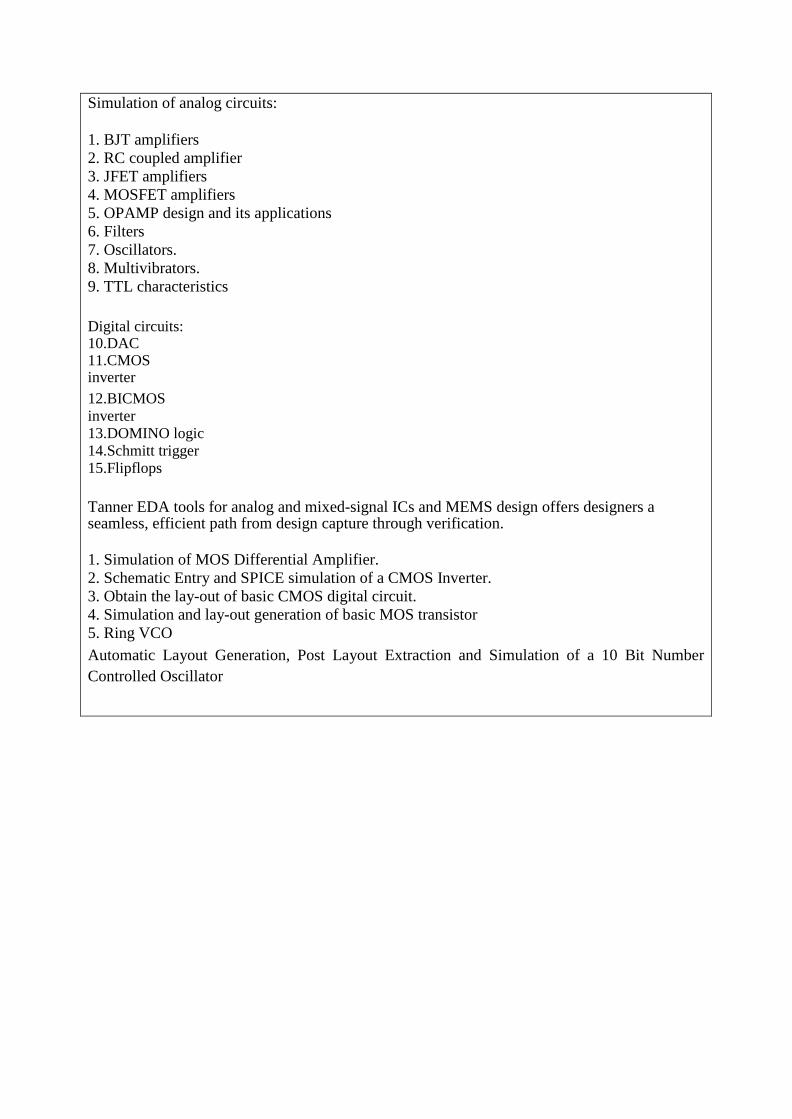
Simulation of analog circuits: 1. BJT amplifiers 2. RC coupled amplifier 3. JFET amplifiers 4. MOSFET amplifiers 5. OPAMP design and its applications 6. Filters 7. Oscillators. 8. Multivibrators. 9. TTL characteristics Digital circuits: 10.DAC 11.CMOS inverter 12.BICMOS inverter 13.DOMINO logic 14.Schmitt trigger 15.Flipflops Tanner EDA tools for analog and mixed-signal ICs and MEMS design offers designers a seamless, efficient path from design capture through verification. 1. Simulation of MOS Differential Amplifier. 2. Schematic Entry and SPICE simulation of a CMOS Inverter. 3. Obtain the lay-out of basic CMOS digital circuit. 4. Simulation and lay-out generation of basic MOS transistor 5. Ring VCO Automatic Layout Generation, Post Layout Extraction and Simulation of a 10 Bit Number Controlled Oscillator
Course No. Course Name L-T-P-Credits Year of Introduction
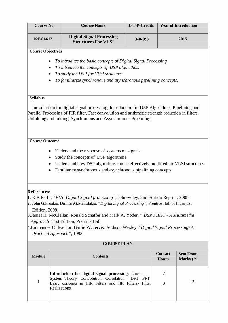
02EC6612 Digital Signal Processing Structures For VLSI 3-0-0:3 2015
Course Objectives
• To introduce the basic concepts of Digital Signal Processing • To introduce the concepts of DSP algorithms • To study the DSP for VLSI structures. • To familiarize synchronous and asynchronous pipelining concepts.
Syllabus Introduction for digital signal processing, Introduction for DSP Algorithms, Pipelining and Parallel Processing of FIR filter, Fast convolution and arithmetic strength reduction in filters, Unfolding and folding, Synchronous and Asynchronous Pipelining. Course Outcome
• Understand the response of systems on signals. • Study the concepts of DSP algorithms • Understand how DSP algorithms can be effectively modified for VLSI structures. • Familiarize synchronous and asynchronous pipelining concepts.
References: 1. K.K Parhi, “VLSI Digital Signal processing”, John-wiley, 2nd Edition Reprint, 2008. 2. John G.Proakis, DimitrisG.Manolakis, “Digital Signal Processing”, Prentice Hall of India, 1st
Edition, 2009. 3.James H. McClellan, Ronald Schaffer and Mark A. Yoder, “ DSP FIRST - A Multimedia
Approach”, 1st Edition; Prentice Hall 4.Emmanuel C Ifeachor, Barrie W. Jervis, Addison Wesley, “Digital Signal Processing- A
Practical Approach”, 1993.
COURSE PLAN
Module Contents Contact Hours
Sem.Exam Marks ;%
I
Introduction for digital signal processing: Linear System Theory- Convolution- Correlation - DFT- FFT- Basic concepts in FIR Filters and IIR Filters- Filter Realizations.
2
3
15
II
Introduction for DSP Algorithms: Representation of DSP Algorithms - Block diagram-SFG-DFG, Data-Flow Graph Representations - Loop Bound and Iteration Bound Algorithms for Computing Iteration Bound-LPM Algorithm.
4
15
FIRST INTERNAL EXAM
III
Pipelining and Parallel Processing of FIR filter: Pipelining and Parallel Processing: Pipelining of FIR Digital Filters-Parallel Processing Pipelining and Parallel Processing for Low Power. Retiming: Definitions Properties and problems- Solving Systems of Inequalities.
9
15
IV
Fast convolution and arithmetic strength reduction in Filters: Cook-Toom Algorithm- Modified Cook-Toom Algorithm. Design of Fast Convolution Algorithm by Inspection. Parallel FIR filters-Fast FIR algorithms-Two parallel and three parallel.
6
15
SECOND INTERNAL EXAM
V
Unfolding and folding: Algorithm for Unfolding-Properties of Unfolding- Critical Path- Unfolding and Retiming-Applications of Unfolding. Folding: Folding Transformation Register Minimization Techniques Lifetime analysis-Data Allocation using forward-Backward register Allocation- Register Minimization in Folded Architectures- Folding of Multirate Systems.
6
7
20
VI
Synchronous and Asynchronous Pipelining: Clocking Styles- Clock Skew and Clock Distribution in Bit-Level Pipelined VLSI Designs- Wave Pipelining Constraint Space Diagram and Degree of Wave Pipelining-Implementation of Wave-Pipelined Systems-Asynchronous Pipelining.
5
20
END SEMESTER EXAM
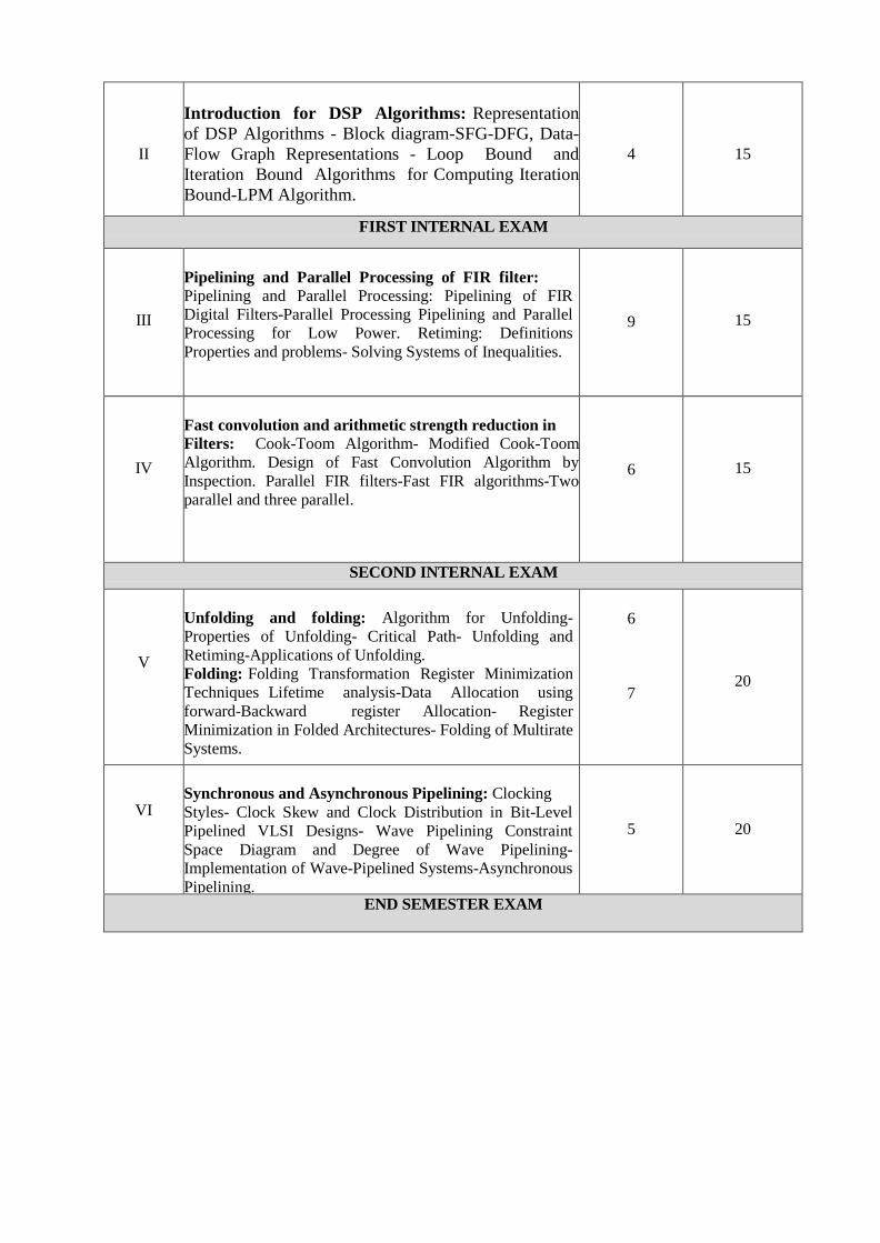
Course No. Course Name L-T-P-Credits Year of Introduction
02EC6622 Embedded and real time operating
systems
3-0-0:3
2015
Course Objectives
• To introduce the fundamentals of real time communication • Familiarize various Real time operating systems available and their use in
Syllabus
Introduction to embedded systems, Communication interfaces, software Architectures Design using RTOS, Saving memory and power, Embedded Software Development Tools , Writing Software for Embedded Systems , Data structure programming.
Course Outcome
• To expose the students to the basics of RTOS programming • Understand the basics of data structure.
References: 1. Dr. K V K K Prasad, “Embedded / Real time systems: Concepts, Design and Programming”,
Dream Tech press, New Delhi, 2003. 2. David Simon, “Embedded Software Primer”, Addison- Wesley, 1999. 3.Raj Kamal, “Introduction to Embedded Systems”, Tata McGraw Hill Publications, 2002. 4.Frank Vahid,Tony D. Givargis, “Embedded System Design- A Unified Hardware/ Software Introduction”, John Wiley and Sons, Inc 2002 5.Jonathan W. Valvano, “Embedded Microcomputer systems”, Brooks / Cole, Thompson Learning. 6.Arnold S Burger, “Embedded Systems Design - Introduction to Processes, Tools Techniques”,CMP books.
COURSEPLAN
Module Contents Contact Hours
Sem.Exam Marks;%
I
Introduction to embedded systems: Categories of embedded systems, overview of embedded system architecture; specialties of embedded systems recent trends in embedded systems, Communication interfaces: RS232/UART, USB, IEEE1394, Bluetooth, Zigbee, Wi-Fi, I2C, SPI, CAN.
6
15

Page 35
II
Survey of software Architectures: Round Robin, Round Robin with interrupts, Function Queue scheduling Architecture, RTOS Architecture, Architecture selection, Introduction to RTOS,- Task and task states, Task and data, Semaphore and Timer functions , events, Memory Management, Interrupt routine in an RTOS environment.
Optimizing Custom Single- purpose Processors, Optimizing the original program, Optimizing the FSMD, Optimizing the datapath, optimizing the FSM.
7
15
FIRST INTERNAL EXAM
III
Basic Design using RTOS: Principle, Encapsulating Semaphores and Queues, Hard
Real-Time scheduling considerations, saving memory saving memory space, saving power.
6
15
IV
Embedded Software Development Tools: Host and Target Machines, Linker/ Locator for embedded
Software, Getting Embedded Software into the target system, Debugging Techniques, Testing on your host machine, Instruction, Set Simulators, The Assert Macro, Using Laboratory tools.
8
15
SECONDINTERNALEXAM
V Writing Software for Embedded Systems:- The compilation process, Native versus cross compilers, Run time libraries, Writing a library, Using alternative libraries, Using a standard library, Porting Kernels,
C extensions for Embedded Systems, Downloading, Emulation and Debugging Techniques.
8
20
VI
Data structure programming : Buffering and other data structures, Linear buffer, Directional buffer, Double buffering, Buffer exchanging
Linked lists, FIFO, Circular buffers, Buffer under run and overrun, Allocating buffer memory, memory leakage, Memory and performance trade offs .
8
20
END SEMESTER EXAM
Page 36
Course No. Course Name L-T-P-Credits Year of Introduction
02EC6632 Analog Integrated Circuit Design 3-1-0- 4 2015
Course Objectives
• To discuss the single stage amplifier stages and its frequency response. • To study the cmos single stage and advanced Op amp circuits. • To introduce the basic analog design problems and the influence of noise. • To discuss the commonly used waveform generator circuits.
Syllabus
Analog CMOS Sub-circuits, CMOS Single stage Amplifiers, Frequency response,
Differential Amplifier & Operational Amplifiers, Oscillators, Noise Characteristics. Course Outcome
• Familiarize commonly used analog cmos circuits. • Compare the performance of different single stage amplifiers. • Extend the basic design concepts to advanced design methodologies. • Study the performance of each circuit. • Compare the circuit response in ideal and non ideal characteristics
References: 1. David. A. Johns and Ken Martin, “Analog Integrated Circuit Design”, John Wiley and Sons,2001 2. Behzad Razavi, “Design of Analog CMOS Integrated Circuit”, Tata McGraw HILL, 2002. 3.Philip Allen & Douglas Holberg,“CMOS Analog Circuit Design”, Oxford University Press, 2002 4.R Gregorian and G C Temes, “Analog MOS Integrated Circuits for Signal Processing”, John Wiley,1986. 5. R L Geiger, P E Allen and N R Strader, “VLSI Design Techniques for Analog & Digital Circuits”, McGraw Hill, 1990. 6. Gray, Wooley, Brodersen, “Analog MOS Integrated circuits”, IEEE press, 1989. 7. Kenneth R. Laker, Willy M.C. Sensen, “Design of Analog Integrated circuits and systems”, MGraw Hill, 1994 8. Mohammed Ismail &Feiz, “Analog VLSI – Signal Information and Processing”, John Wiley and Sons
COURSE PLAN
Module Contents Contact Hours
Sem.Exam Marks ;%

Page 37
I
Analog CMOS Sub-circuits: Introduction to analog design, Passive and active current mirrors, band-gap references,Switched capacitor circuits - basic principles.
10
15
II
CMOS Single stage Amplifiers: Common-Source stage (with resistive load, diode connected load, current source load, triode load, source degeneration), source follower, common-gate stage, cascode stage, folded cascode stage.
10
15
FIRST INTERNAL EXAM
III
Frequency response: Frequency responses of CS stage, CD stage, CG stage, cascode stage, simulation of CMOS amplifiers using SPICE.
8
15
IV
Differential Amplifier & Operational Amplifiers: Single-ended and differential operation, basic differential pair - qualitative and quantitative analyses, common-mode response, differential pair with MOS loads Performance parameters of op-amp, one stage op-amp, and two-stage.
10
15
SECOND INTERNAL EXAM
V
Oscillators: General considerations, Ring oscillators, LC oscillators – cross-coupled oscillators, Colpitts oscillator, One-port oscillator, and voltage controlled oscillators. Simulation of oscillators using SPICE.
9
20
VI
Noise Characteristics: Statistical characteristics of noise, Types of noise - thermal noise, flicker noise, Representation of noise in circuits, noise in single-stage amplifiers (CS, CD and CG stages), noise bandwidth.
9
20
END SEMESTER EXAM
Page 38
Course No. Course Name L-T-P-Credits Year of Introduction
02EC6642.1 Embedded System Programming 3-0-0-3 2015
Course Objectives
• Understand the embedded programming concepts • Familiarize with the use of C and Java for embedded system programming.
Syllabus
Embedded Programming overview, Embedded C Concepts, Embedded OS Creation,
Embedded C programming, Time driven multi-state architecture and Hardware, Embedded Java
Course Outcome
• Ability to program embedded systems using C and Java • RTOS Programming Concepts.
References 1. . Steve Oualline, “Practical C Programming 3rd Edition”, O’Reilly Media, Inc, 2006. 2. Stephen Kochan, “Programming in C”, 3rd Edition, Sams Publishing, 2009. 3. Michael J Pont, “Embedded C”, Pearson Education, 2007. 4. Zhiqun Chen, “Java Card Technology for Smart Cards: Architecture and
Programmer’s Guide”, Addison-Wesley Professional, 2000 5. Zurell, Kirk, “C Programming for Embedded systems”,CMP books, 2002 6. SamiranChattopadhyay, DebarataGhoshDastidar, MatanginiChattopadhyay, “Data structures
Through ‘C’ Language”, DOEACC Society 7. Herbert Schildt, “The Complete reference Java2”, 5thEdition, TMH 8. Rajkamal, “Microcontrollers: Architecture, programming, interfacing, and system design”,
2nd Edition, Pearson Education, 2012.
COURSE PLAN
Module Contents Contact Hours
Sem.Exam Marks ;%
I
Embedded Programming: C and Assembly - Programming Style - Declarations and Expressions - Arrays, Qualifiers and Reading Numbers - Decision and Control Statements - Programming Process- More Control Statements- Variable Scope and Functions- C Preprocessor - Advanced Types – Simple Pointers - Debugging and Optimization – In-line Assembly.
5
15

Page 39
II
Embedded C : Adding Structure to ‘C’ Code: Object oriented programming with C, Header files for Project and Port, Examples. Meeting Real-time constraints: Creating hardware delays -Need for time out mechanism - Creating loop timeouts - Creating hardware timeouts.
6
15
FIRST INTERNAL EXAM
III
Embedded OS: Creating embedded operating system: Basis of a simple embedded OS, Introduction to sEOS, Using Timer0 and Timer1, Portability issue, Alternative system architecture, and Important design considerations when using sEOS.
4
15
IV
Embedded C programming: Review of data types –scalar types-Primitive types-Enumerated types-Subranges, Structure types-character strings –arrays- Functions, Introduction to Embedded C- Introduction, Data types Bit manipulation, Interfacing C with Assembly. Embedded programming issues – Reentrance, Portability, Optimizing and testing embedded C programs.
11
15
SECOND INTERNAL EXAM
V
Time driven multi-state architecture and Hardware: Multi-State systems and function sequences: Implementing multi-state (Timed) system -Implementing a Multi-state (Input/Timed) system. Using the Serial Interface: RS232 - The BasicRS-232 Protocol Asynchronous data transmission and baud rates - Flow control –Software architecture - Using on-chip UART for RS-232 communication - Memory requirements
8
20
VI
Embedded Java: Introduction to Object Oriented Concepts: Core Java/Java Core- Java buzzwords, Overview of Java programming, Data types, variables and arrays, Operators, Control statements. Embedded Java – Understanding J2ME, Connected Device configuration, Connected Limited device configuration, Profiles, Anatomy of MIDP applications, Advantages of MIDP.
8
20
END SEMESTER EXAM
Page 40
Course No. Course Name L-T-P-Credits Year of Introduction
02EC6642.2 Digital System Synthesis & Verification 3-0-0- 3 2015
Course Objectives
• To introduce the ideas of Hardware modeling concepts. • To introduce the concepts of Hardware Description languages VHDL, Verilog and
SystemVerilog. Syllabus
VHDL, Advanced Features, Verilog, advanced Features, System Design Using Verilog HDL, System Verilog.
Course Outcome
• Understand the general Hardware Modeling Concepts • Study the VHDL and Verilog Language. • Model simple hardware units using VHDL and Verilog. • Study the basic concept of System Verilog.
References:
1. J.Bhasker, “VHDL Primer”,3rdEdition,Prentice Hall PTR ,1999. 2. Samir palnitkar, “Verilog HDL”, Pearson education, Second Edition,20O3. 3. J. Bhasker, “A Verilog HDL Primer”, Second Edition, Star Galaxy, 1999. 4. J. Bhasker, “A Verilog Synthesis: A Practical Primer”, Star Galaxy, 1998. 5. System Verilog 3.1a –Language Reference Manual (Accellera Extensions to Verilog
2001), 2004..
COURSE PLAN
Module Contents Contact Hours
Sem.ExamMarks ;%
I
VHDL: Operators, Basic concepts, Entity and Architecture design, System task and functions, Value set,
Data types, Operands, Operators, Entity and ports, Gate level Modeling, Dataflow Modeling, Behavioral Modeling, Test Bench
8
15
Page 41
II
VHDL-Advanced Features: Packages and Functions, Sub-Program,User Defined Attributes,Specifications and Configurations, Delay modeling- pin-to-pin delay & distributed Delay modeling- Timing delay analysis- FSM design and Synthesis
8
15
FIRST INTERNAL EXAM
III Verilog: Operators, Basic concepts, Identifiers, System
task and functions, Value set, Data types, Parameters , Operands, Operators, Modules and ports, Gate-level Modeling, Dataflow Modeling, Behavioral Modeling, Test bench.
7
15
IV Verilog-advanced Features: Tasks and Functions, Timing
and delays, Switch level modeling, Tri state gates, MOS Switches, Bidirectional switches, User defined primitives,
Combinational UDP, Sequential UDP, Verilog HDL synthesis - Synthesis Design flow.
10
15
SECOND INTERNAL EXAM
V
System Design Using Verilog HDL: Verilog Description of combinational Circuits,arrays, Verilog operaters, Compilation and simulation of Verilog codes, Modelling using Verilog, Flip Flops, registers, counters, sequential machine, combinational logic circuits, Verilog codes, serial adders.
7
6
20
VI
System Verilog: Introduction to System Verilog – Literal values-data Types, Arrays, Data Declarations-attributes-operators, expressions, procedural statements and control flow. Processes in System Verilog – Task and functions, Classes, Random Constraints, Random, Scheduling Semantics, Interfaces, Clocking Blocks
10
20
END SEMESTER EXAM

Page 42
Course No. Course Name L-T-P-Credits Year of Introduction
02EC6642.3 Nano Scale transistors 3-0-0, 3 2015
Course Objectives
• To investigate the impact of device scaling on MOS technology and short channel effects.
• To learn the fundamentals of multigate transistors • To enable the students to acquire knowledge about MOSFETS with 0D, 1D and 3D
channels. • To discuss the performance of MOSFET in presence of nuclear radiations. • To design various circuits using multigate transistors
.
Syllabus MOSFET scaling, short channel effects, SOI MOSFET, multigate transistors,1D & 2D
MOS Electrostatics, MOSFET Current-Voltage Characteristics, Nanowire FETS, Carbon nanotube FETs, MOSFETs with 0D, 1D, and 2D channels, Molecular transistors, Single electron transistors, Radiation effects in SOI MOSFETs, circuit design using multigate transistors. Course Outcome
• The course will enable the students to gain preliminary knowledge in basic
concepts of MOSFET scaling & short channel effect. • They will be able to illustrate various multigate transistors. • Students will be exposed to the different packaging of Microsystems • Students will be able to explain the MOSFETs with 0D, 1D, and 2D channels • Students will be able to understand the effects of nuclear radiation on MOSFETs • Students will be able to discuss about circuit design using multigate transistors References:
1. FINFETs and other multi-gate transistors- J P Colinge, (Springer – Series on integrated
circuits and systems, 2008). 2. Nanoscale Transistors: Device Physics, Modeling and Simulation- Mark Lundstrom Jing Guo,
(Springer, 2006). 3. Fundamentals of Carrier Transport- M S Lundstorm, (2nd Ed., Cambridge University Press,
Cambridge UK, 2000).
COURSE PLAN
Module Contents Contact Hours
Sem.Exam Mark
Page 43
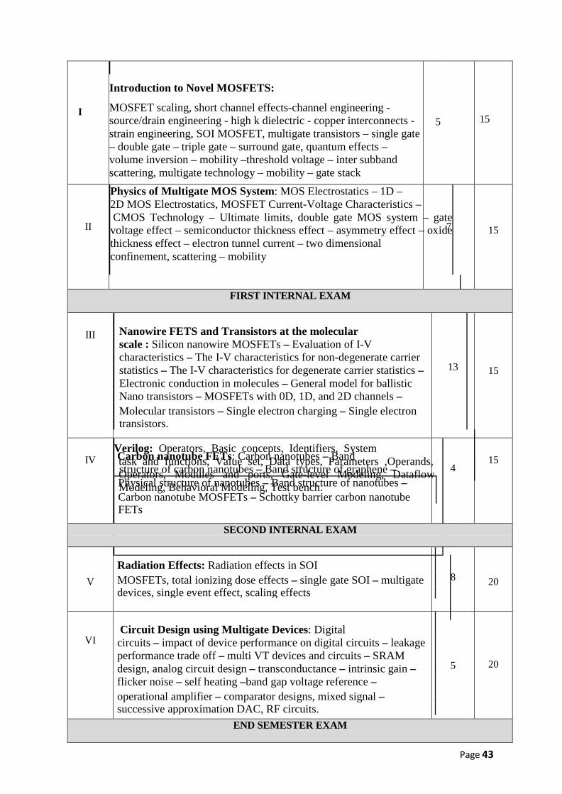
I
Introduction to Novel MOSFETS:
MOSFET scaling, short channel effects-channel engineering - source/drain engineering - high k dielectric - copper interconnects - strain engineering, SOI MOSFET, multigate transistors – single gate – double gate – triple gate – surround gate, quantum effects – volume inversion – mobility –threshold voltage – inter subband scattering, multigate technology – mobility – gate stack
5
15
II
Physics of Multigate MOS System: MOS Electrostatics – 1D – 2D MOS Electrostatics, MOSFET Current-Voltage Characteristics – CMOS Technology – Ultimate limits, double gate MOS system – gate voltage effect – semiconductor thickness effect – asymmetry effect – oxide thickness effect – electron tunnel current – two dimensional confinement, scattering – mobility
7
15
FIRST INTERNAL EXAM
III Nanowire FETS and Transistors at the molecular
scale : Silicon nanowire MOSFETs – Evaluation of I-V characteristics – The I-V characteristics for non-degenerate carrier statistics – The I-V characteristics for degenerate carrier statistics – Electronic conduction in molecules – General model for ballistic Nano transistors – MOSFETs with 0D, 1D, and 2D channels – Molecular transistors – Single electron charging – Single electron transistors.
Verilog: Operators, Basic concepts, Identifiers, System task and functions, Value set, Data types, Parameters ,Operands, Operators, Modules and ports, Gate-level Modeling, Dataflow Modeling, Behavioral Modeling, Test bench.
13
15
IV Carbon nanotube FETs: Carbon nanotubes – Band
structure of carbon nanotubes – Band structure of graphene – Physical structure of nanotubes – Band structure of nanotubes – Carbon nanotube MOSFETs – Schottky barrier carbon nanotube FETs
4
15
SECOND INTERNAL EXAM
V Radiation Effects: Radiation effects in SOI MOSFETs, total ionizing dose effects – single gate SOI – multigate devices, single event effect, scaling effects
8
20
VI Circuit Design using Multigate Devices: Digital circuits – impact of device performance on digital circuits – leakage performance trade off – multi VT devices and circuits – SRAM design, analog circuit design – transconductance – intrinsic gain – flicker noise – self heating –band gap voltage reference – operational amplifier – comparator designs, mixed signal – successive approximation DAC, RF circuits.
5
20
END SEMESTER EXAM

Page 44
Course No. Course Name L-T-P-Credits Year of Introduction
02EC6642.4 VLSI Fabrication Technology 3-0-0- 3 2015 Course Objectives
• To understand the impact of the physical and chemical processes of integrated circuit
fabrication technology on the design of integrated circuits. • To understand Concepts of thermal oxidation and Si/SiO2 interface. • To describe the various fabrication techniques.
Syllabus Crystal Growth, Wafer Preparation and Epitaxy, Oxidation, Lithography and Relative
Plasma Etching, Deposition, Diffusion, Ion Implantation and Metallization, Process Simulation and VLSI Process Integration, Analytical, Assembly Techniques and Packaging of VLSI Devices. Course Outcome
• The course will give the idea about the physics of crystal growth, wafer fabrication,
basic properties of silicon wafers and oxidation. • To learn concepts of dopant solid solubility, diffusion macroscopic point,
different solutions to diffusion equation.
• The student can get the concepts of ion implantation, role of the crystals structures, high-energy implants, ultralow energy implants and ion beam heating methods and concepts of dopant solid solubility, diffusion macroscopic point, different solutions to diffusion equation References:
1. Gary K. Yeap, “Practical Low Power Digital VLSI Design”, KAP, 2002.
2. Rabaey, Pedram, “Low power design methodologies”, Kluwer Academic, 1997.
3. Kaushik Roy, Sharat Prasad, “Low-Power CMOS VLSI Circuit Design”, Wiley, 2000.
COURSE PLAN
Module Contents Contact Hours
Sem.Exam Mark
I
Crystal Growth, Wafer Preparation and Epitaxy: Electronic Grade Silicon, Czochralski crystal growing, Silicon Shaping, processing consideration, Vapor Phase Epitaxy, Molecular Beam Epitaxy, Silicon on Insulators,
Epitaxial Evaluation
8
15
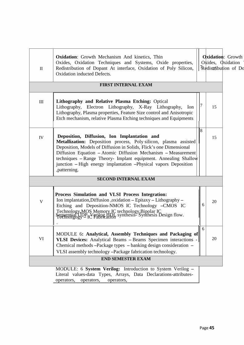
Page 45
II
Oxidation: Growth Mechanism And kinetics, Thin Oxidation: Growth Mechanism And kinetics, Thin Oxides, Oxidation Techniques and Systems, Oxide properties, Oxides, Oxidation Techniques and Systems, Oxide properties, Redistribution of Dopant At interface, Oxidation of Poly Silicon, Redistribution of Dopant At interface, Oxidation of Poly Silicon, Oxidation inducted Defects.
7
15
FIRST INTERNAL EXAM
III Lithography and Relative Plasma Etching: Optical
Lithography, Electron Lithography, X-Ray Lithography, Ion Lithography, Plasma properties, Feature Size control and Anisotropic Etch mechanism, relative Plasma Etching techniques and Equipments
7
15
IV Deposition, Diffusion, Ion Implantation and
Metallization: Deposition process, Poly silicon, plasma assisted Deposition, Models of Diffusion in Solids, Flick’s one Dimensional Diffusion Equation – Atomic Diffusion Mechanism – Measurement techniques – Range Theory- Implant equipment. Annealing Shallow junction – High energy implantation –Physical vapors Deposition ,patterning.
Sequential UDP, Verilog HDL synthesis- Synthesis Design flow.
8 15
SECOND INTERNAL EXAM
V Process Simulation and VLSI Process Integration: Ion implantation,Diffusion ,oxidation – Epitaxy – Lithography – Etching and Deposition-NMOS IC Technology –CMOS IC Technology,MOS Memory IC technology,Bipolar IC Technolgogy – IC Fabrication .
6
20
VI MODULE 6: Analytical, Assembly Techniques and Packaging of VLSI Devices: Analytical Beams – Beams Specimen interactions - Chemical methods –Package types – banking design consideration – VLSI assembly technology –Package fabrication technology.
MODULE: 6 System Verilog: Introduction to System Verilog – Literal values-data Types, Arrays, Data Declarations-attributes- operators, operators, operators,
6
20
END SEMESTER EXAM
Page 46
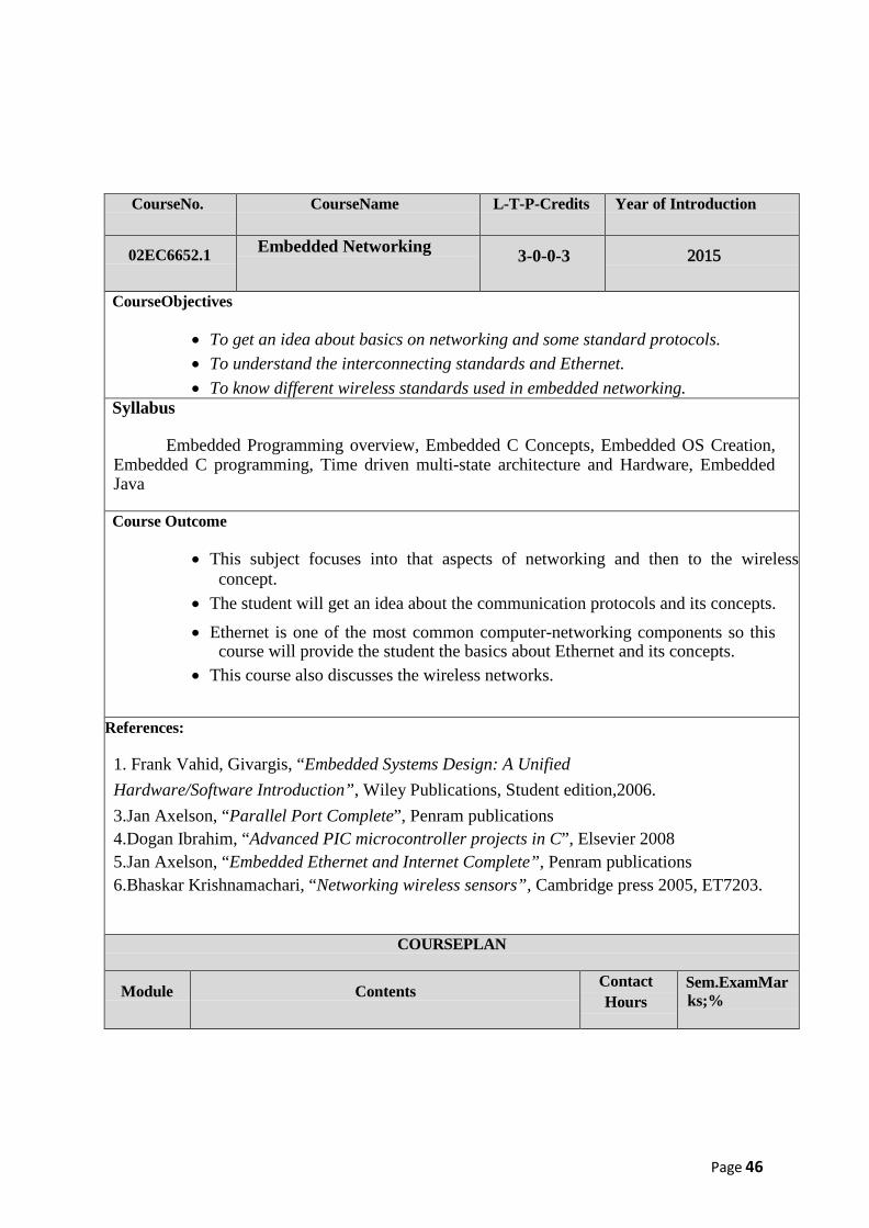
CourseNo. CourseName L-T-P-Credits Year of Introduction
02EC6652.1 Embedded Networking 3-0-0-3 2015
CourseObjectives
• To get an idea about basics on networking and some standard protocols. • To understand the interconnecting standards and Ethernet. • To know different wireless standards used in embedded networking.
Syllabus
Embedded Programming overview, Embedded C Concepts, Embedded OS Creation, Embedded C programming, Time driven multi-state architecture and Hardware, Embedded Java
Course Outcome
• This subject focuses into that aspects of networking and then to the wireless
concept. • The student will get an idea about the communication protocols and its concepts. • Ethernet is one of the most common computer-networking components so this
course will provide the student the basics about Ethernet and its concepts. • This course also discusses the wireless networks.
References: 1. Frank Vahid, Givargis, “Embedded Systems Design: A Unified Hardware/Software Introduction”, Wiley Publications, Student edition,2006.
3.Jan Axelson, “Parallel Port Complete”, Penram publications 4.Dogan Ibrahim, “Advanced PIC microcontroller projects in C”, Elsevier 2008 5.Jan Axelson, “Embedded Ethernet and Internet Complete”, Penram publications 6.Bhaskar Krishnamachari, “Networking wireless sensors”, Cambridge press 2005, ET7203.
COURSEPLAN
Module Contents ContactHours
Sem.ExamMarks;%
Page 47
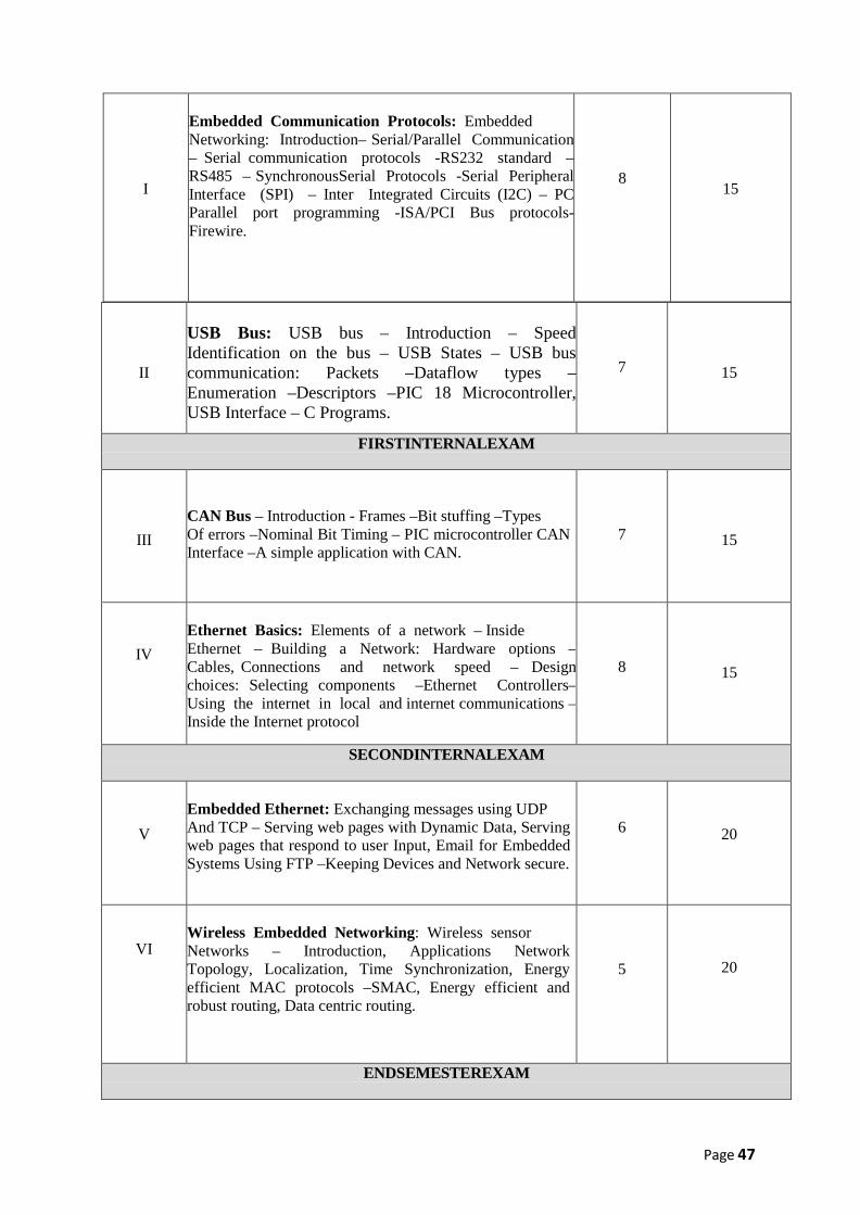
I
Embedded Communication Protocols: Embedded Networking: Introduction– Serial/Parallel Communication – Serial communication protocols -RS232 standard – RS485 – SynchronousSerial Protocols -Serial Peripheral Interface (SPI) – Inter Integrated Circuits (I2C) – PC Parallel port programming -ISA/PCI Bus protocols- Firewire.
8
15
II
USB Bus: USB bus – Introduction – Speed Identification on the bus – USB States – USB bus communication: Packets –Dataflow types –Enumeration –Descriptors –PIC 18 Microcontroller, USB Interface – C Programs.
7
15
FIRSTINTERNALEXAM
III
CAN Bus – Introduction - Frames –Bit stuffing –Types Of errors –Nominal Bit Timing – PIC microcontroller CAN Interface –A simple application with CAN.
7
15
IV
Ethernet Basics: Elements of a network – Inside Ethernet – Building a Network: Hardware options – Cables, Connections and network speed – Design choices: Selecting components –Ethernet Controllers– Using the internet in local and internet communications – Inside the Internet protocol
8
15
SECONDINTERNALEXAM
V
Embedded Ethernet: Exchanging messages using UDP And TCP – Serving web pages with Dynamic Data, Serving web pages that respond to user Input, Email for Embedded Systems Using FTP –Keeping Devices and Network secure.
6
20
VI
Wireless Embedded Networking: Wireless sensor Networks – Introduction, Applications Network Topology, Localization, Time Synchronization, Energy efficient MAC protocols –SMAC, Energy efficient and robust routing, Data centric routing.
5
20
ENDSEMESTEREXAM
Page 48
CourseNo. CourseName L-T-P-Credits Year of Introduction
02EC6652.2 Low Power VLSI Design 3-0-0:3
2015
CourseObjectives
• To know the sources of power consumption in cmos circuits • To study the concepts on different levels of power estimation and
optimization techniques. • To study the design concepts of low power circuits.
Syllabus Sources of power dissipation, Simulation Power analysis, Probabilistic power analysis,
Low Power Design, Low power Architecture & Systems, Low power Clock Distribution, Algorithm & architectural level methodologies. CourseOutcome
• To know the sources of power consumption in cmos circuits • To study the concepts on different levels of power estimation and optimization
techniques. • To study the design concepts of low power circuits.
References 1. . Gary K. Yeap, “Practical Low Power Digital VLSI Design”, KAP, 2002. 2. Rabaey, Pedram, “Low power design methodologies”, Kluwer Academic, 1997. 3.Kaushik Roy, Sharat Prasad, “Low-Power CMOS VLSI Circuit Design”, Wiley, 2000
COURSEPLAN
Module Contents ContactHours
Sem.ExamMarks;%
Page 49
I
Need for low power VLSI chips: Sources of power dissipation on Digital Integrated circuits. Emerging Low power approaches. Physics of power dissipation in CMOS devices. Device & Technology Impact on Low Power: Dynamic dissipation in CMOS, Transistor sizing & gate oxide thickness, Impact of technology Scaling, Technology & Device innovation, Hierarchy of limits of power.
8
15
II
Simulation Power analysis: SPICE circuit simulators, gate level logic simulation, capacitive power estimation, static state power, gate level capacitance estimation, architecture level analysis, data correlation analysis in DSP systems- Monte Carlo simulation
8
15
FIRST INTERNAL EXAM
III
Probabilistic power analysis- Random logic signals, probability & frequency, probabilistic power analysis techniques,signal entropy, Power estimation Techniques.
7
15
IV
Low Power Design: Circuit level- Power consumption in circuits, Flip Flops & Latches design, high capacitance nodes, low power digital cells library, Logic level- Gate reorganization, signal gating, logic encoding, state machine encoding, pre-computation logic
8
15
SECOND INTERNAL EXAM
V
Low power Architecture & Systems: Power & performance management, switching activity reduction, parallel architecture with voltage reduction, flow graph transformation, low power arithmetic components, low power memory design, CMOS floating node, low power bus.
6
20
VI
Low power Clock Distribution: Power dissipation in clock distribution, single driver Vs distributed buffers, Zero skew Vs tolerable skew, chip & package co design of clock Network. Algorithm & architectural level methodologies: Introduction, design flow, Algorithmic level analysis & optimization, Architectural level estimation & synthesis.
5
20
END SEMESTER EXAM
Page 50
CourseNo. CourseName L-T-P-Credits Year of Introduction
02EC6652.3 Cryptography and Network Security
3-0-0:3
2015
CourseObjectives
• Data security is an integral part of todays communication system where credibility and storage capacity bomes the biggest challenge in front of any system designer. Here the subject discusses some key issues in this area and conveys some basic algorithms on this
Syllabus Symmetric ciphers, Public-key encryption and Key management, Hash functions and Hash algorithms, Network security practice, System security, Wireless security
CourseOutcome
The course will enable the students to gain preliminary knowledge on various cryptographic standards.
.
References 1. Jan Axelson, “Parallel Port Complete”, Penram publications 2. Dogan Ibrahim, “Advanced PIC microcontroller projects in C”, Elsevier 2008 3. Jan Axelson, “Embedded Ethernet and Internet Complete”, Penram publications 4. Bhaskar Krishnamachari, “Networking wireless sensors”, Cambridge press 2005, ET7203
COURSEPLAN
Module Contents ContactHours
Sem.ExamMarks;%
I
Symmetric ciphers: Overview – Classical Encryption Techniques – Block Ciphers and the Data Encryption Standard –Introduction to Finite Fields – Advanced Encryption Standard.
8
15
II
Public-key encryption and Key management: Introduction to Number Theory – Public-Key Cryptography and RSA –Key Management –Diffie-Hellman Key Exchange – Elliptic Curve Cryptography
8
15
FIRSTINTERNALEXAM
Page 51
III
Hash functions and Hash algorithms: Message Authentication and Hash Functions – Hash Algorithms – DigitalSignatures and Authentication Protocols.
7
15
IV
Network security practice: Authentication Applications – Kerberos – X.509 Authentication Service – Electronic mail Security– Pretty Good Privacy – S/MIME – IP Security Architecture –Authentication Header – Encapsulating Security Payload – Key Management.
8
15
SECONDINTERNALEXAM
V
System security: Intruders – Intrusion Detection – Password Management – Malicious Software – Firewalls –Firewall Design Principles – Trusted Systems.
6
20
VI
Wireless security: Introduction to Wireless LAN Security Standards – Wireless LAN Security Factors and Issues.
5
20
ENDSEMESTEREXAM
Page 52
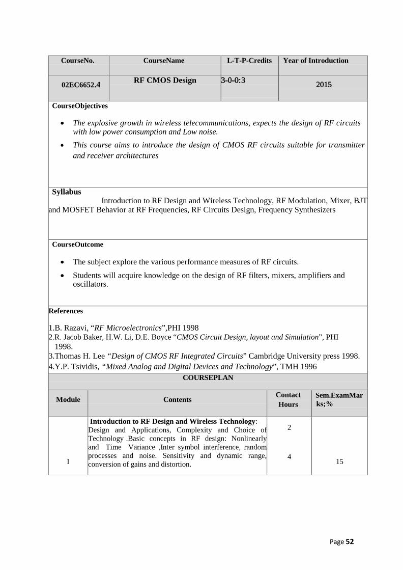
CourseNo. CourseName L-T-P-Credits Year of Introduction
02EC6652.4 RF CMOS Design 3-0-0:3
2015
CourseObjectives
• The explosive growth in wireless telecommunications, expects the design of RF circuits with low power consumption and Low noise.
• This course aims to introduce the design of CMOS RF circuits suitable for transmitter and receiver architectures
Syllabus Introduction to RF Design and Wireless Technology, RF Modulation, Mixer, BJT
and MOSFET Behavior at RF Frequencies, RF Circuits Design, Frequency Synthesizers
CourseOutcome
• The subject explore the various performance measures of RF circuits. • Students will acquire knowledge on the design of RF filters, mixers, amplifiers and
oscillators.
References 1.B. Razavi, “RF Microelectronics”,PHI 1998 2.R. Jacob Baker, H.W. Li, D.E. Boyce “CMOS Circuit Design, layout and Simulation”, PHI
1998. 3.Thomas H. Lee “Design of CMOS RF Integrated Circuits” Cambridge University press 1998. 4.Y.P. Tsividis, “Mixed Analog and Digital Devices and Technology”, TMH 1996
COURSEPLAN
Module Contents ContactHours
Sem.ExamMarks;%
I
Introduction to RF Design and Wireless Technology: Design and Applications, Complexity and Choice of Technology .Basic concepts in RF design: Nonlinearly and Time Variance ,Inter symbol interference, random processes and noise. Sensitivity and dynamic range, conversion of gains and distortion.
2
4
15
Page 53
II
RF Modulation: Analog and digital modulation of RF circuits, Comparison of various techniques for power efficiency ,Coherent and non-coherent detection. Mobile RF communication and basics of Multiple Access techniques .Receiver and Transmitter architectures, Direct conversion and two-step transmitters.
3
3
15
FIRST INTERNAL EXAM
III
Mixer: Balancing Mixer - Qualitative Description of the Gilbert Mixer - Conversion Gain – Distortion – Low Frequency Case: Analysis of Gilbert Mixer – Distortion - High-Frequency Case – Noise. Switching Mixer - Distortion in Unbalanced Switching Mixer –Conversion Gain in Unbalanced Switching Mixer - Noise in Unbalanced Switching Mixer
4
3
15
IV
BJT and MOSFET Behavior at RF Frequencies: BJT and MOSFET behavior at RF frequencies, Modeling of the transistors and SPICE model, Noise performance and limitations of devices, integrated parasitic elements at high frequenciesand their monolithic implementation.
2
5
15
SECOND INTERNAL EXAM
V
RF Circuits Design: Overview of RF Filter design, Active RF components & modeling, Matching and Biasing Networks.Basic blocks in RF systems and their VLSI implementationLow noise Amplifier design in various technologies, System levelverification, Block level verification, Hardware/software co-verification and Static net list verification.
4
4
20
VI
Frequency Synthesizers: Oscillators- Basic topologies VCO and definition of phase noise, Noise power and trade off.Resonator VCO designs, Quadrature and single sideband generators. Radio frequency Synthesizers- PLLS, Various RF synthesizer architectures and frequency dividers, Power Amplifier design, Liberalization techniques, Design issues in integrated RF filters.
5
3
20
END SEMESTER EXAM
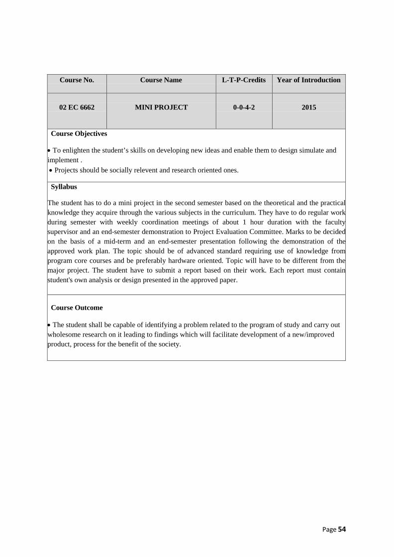
Page 54
Course No. Course Name L-T-P-Credits Year of Introduction
02 EC 6662
MINI PROJECT
0-0-4-2
2015
Course Objectives • To enlighten the student’s skills on developing new ideas and enable them to design simulate and implement . • Projects should be socially relevent and research oriented ones. Syllabus
The student has to do a mini project in the second semester based on the theoretical and the practical knowledge they acquire through the various subjects in the curriculum. They have to do regular work during semester with weekly coordination meetings of about 1 hour duration with the faculty supervisor and an end-semester demonstration to Project Evaluation Committee. Marks to be decided on the basis of a mid-term and an end-semester presentation following the demonstration of the approved work plan. The topic should be of advanced standard requiring use of knowledge from program core courses and be preferably hardware oriented. Topic will have to be different from the major project. The student have to submit a report based on their work. Each report must contain student's own analysis or design presented in the approved paper. Course Outcome • The student shall be capable of identifying a problem related to the program of study and carry out wholesome research on it leading to findings which will facilitate development of a new/improved product, process for the benefit of the society.
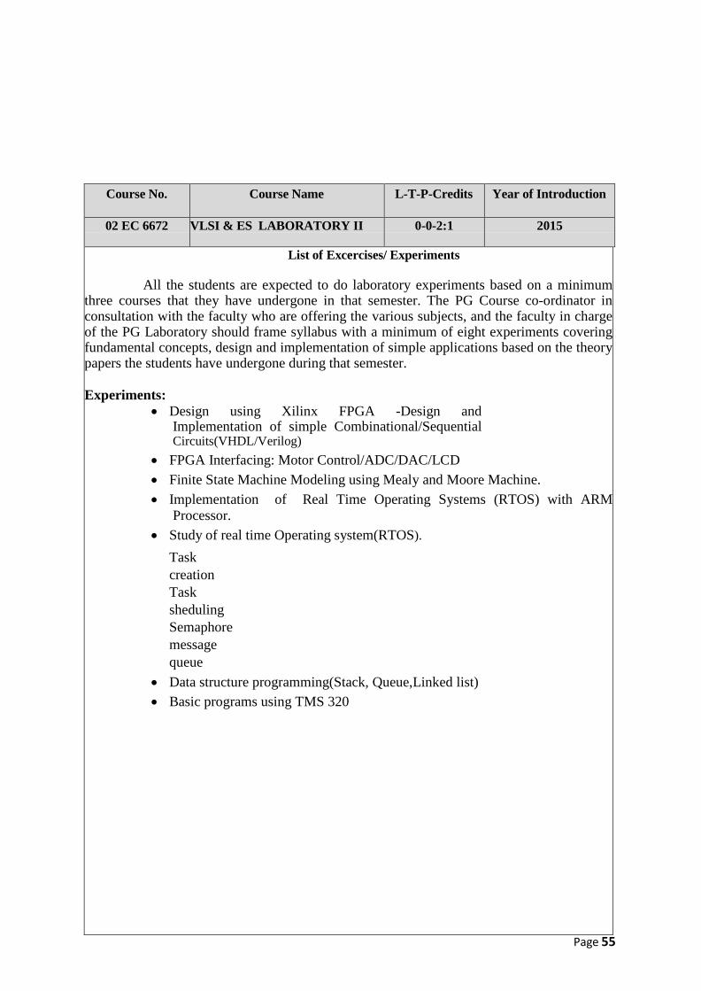
Page 55
Course No. Course Name L-T-P-Credits Year of Introduction
02 EC 6672 VLSI & ES LABORATORY II 0-0-2:1 2015
List of Excercises/ Experiments
All the students are expected to do laboratory experiments based on a minimum three courses that they have undergone in that semester. The PG Course co-ordinator in consultation with the faculty who are offering the various subjects, and the faculty in charge of the PG Laboratory should frame syllabus with a minimum of eight experiments covering fundamental concepts, design and implementation of simple applications based on the theory papers the students have undergone during that semester.
Experiments:
• Design using Xilinx FPGA -Design and Implementation of simple Combinational/Sequential Circuits(VHDL/Verilog)
• FPGA Interfacing: Motor Control/ADC/DAC/LCD • Finite State Machine Modeling using Mealy and Moore Machine. • Implementation of Real Time Operating Systems (RTOS) with ARM
Processor. • Study of real time Operating system(RTOS).
Task creation Task sheduling Semaphore message queue
• Data structure programming(Stack, Queue,Linked list) • Basic programs using TMS 320

Page 56
SEMESTER 2
CourseNo. CourseName L-T-P-Credits YearofIntroduction
02EC7611.1
Testing Of VLSI Circuits 3-0-0:3 2015
Course Objectives The purpose of testing a design is twofold:
• To ensure that, before fabrication, the circuit behavior satisfies the intent of the designer. • To detect faulty devices, after fabrication.
Syllabus
Logic Simulation, Testing for single stuck faults (SSF), Design for testability, Compression techniques, Built-in self-test (BIST), Memory BIST (MBIST). Course Outcome
• Students will acquire knowledge on digital testing as applied to VLSI design. • Students will learn various testing methods for digital circuits.
REFERENCES 1. “Digital Systems Testing and Testable Design”, Miron Abramovici, Melvin A. Breur, Arthur
D.Friedman, Jaico Publishing House, 2001.
2. “Introduction to VLSI Testing”, Englehood Cliffs, Robert J. Feugate, Jr., Steven M.Mentyn, Prentice Hall,1998.
3. “Design for Test for Digital ICs & Embedded Core Systems”, Alfred Crouch, Prentice Hall.
COURSEPLAN
Module Contents ContactHours
Sem.ExamMarks;%
I
Introduction to Test and Design for Testability Fundamentals: Modeling digital circuits at logic level, register level and structural models. Levels of modeling. Logic Simulation: Types of simulation, Delay models, Element evaluation, Hazard detection, Gate level event driven simulation. Logic fault models, Fault detection and Redundancy, Fault equivalence and fault location.
8
15
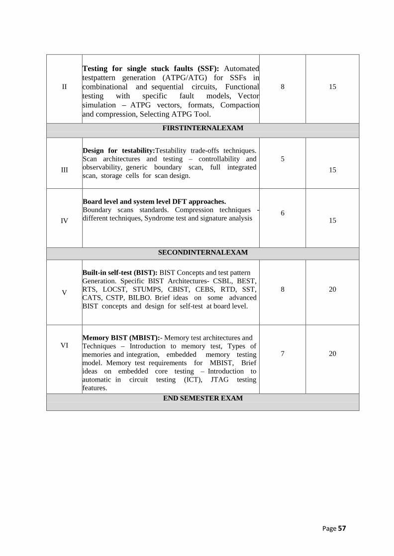
Page 57
II
Testing for single stuck faults (SSF): Automated testpattern generation (ATPG/ATG) for SSFs in combinational and sequential circuits, Functional testing with specific fault models, Vector simulation – ATPG vectors, formats, Compaction and compression, Selecting ATPG Tool.
8
15
FIRSTINTERNALEXAM
III
Design for testability:Testability trade-offs techniques. Scan architectures and testing – controllability and observability, generic boundary scan, full integrated scan, storage cells for scan design.
5
15
IV
Board level and system level DFT approaches. Boundary scans standards. Compression techniques - different techniques, Syndrome test and signature analysis
6
15
SECONDINTERNALEXAM
V
Built-in self-test (BIST): BIST Concepts and test pattern Generation. Specific BIST Architectures- CSBL, BEST, RTS, LOCST, STUMPS, CBIST, CEBS, RTD, SST, CATS, CSTP, BILBO. Brief ideas on some advanced BIST concepts and design for self-test at board level.
8
20
VI
Memory BIST (MBIST):- Memory test architectures and Techniques – Introduction to memory test, Types of memories and integration, embedded memory testing model. Memory test requirements for MBIST, Brief ideas on embedded core testing – Introduction to automatic in circuit testing (ICT), JTAG testing features.
7
20
END SEMESTER EXAM

Page 58
CourseNo. CourseName L-T-P-Credits Year of Introduction
02EC7611.2 System On Chip Design
3-0-0:3
2015
Course Objectives
• To introduce SoC design process. • To study the fundamentals of testing and verification methods. • To learn techniques for designing MPSoCs.
Syllabus
System On Chip Design Process, Macro Design Process, Design for Testability
Fundamentals, Fault, Fault analysis, Scan Architectures and testing, SoC Verification, Verification approaches MPSoCs, Techniques for SoC design, SIP design
CourseOutcome
• To expose the students the basic design processes included in SoC and macro design
process. • To know the different faults in digital circuits and testing and verification of SoC.
.
References: 1. Prakash Rashinkar, Peter Paterson and Leena Singh, “SoC Verification-Methodology and
Techniques”, Kluwer Academic Publishers, 2001. 2. Miron Abramovici, Melvin A. Breur, Arthur D. Friedman, “Digital systems
Testing and testable Design”, Jaico Publishing House, 2001. 3. Michael Keating, Pierre Bricaud, “Reuse Methodology manual for System-On-A-Chip
Designs”, Kluwer Academic Publishers, Second edition,2001. 4. William K.Lam, “Design Verification:Simulation and Formal Method based
Approaches”, Prentice Hall,first edition,2005. 5. Rochit Rajsuman, “System-on-a-Chip-Design and Test”, ISBN. 6. A.A.Jerraya, W.Wolf, “Multiprocessor Systems-on-chips”, M K Publishers,2005. 7. Dirk Jansen, “The EDA HandBook”, Kluwer Academic Publishers. 8. Alfred Crouch, “Design for test for digital IC & Embedded Core Systems”, Prentice hall.
9. Stanley L. Hurst, “VLSI Testing: digital and mixed analogue digital techniques”,Pub: Inspec / IEE, 1999
COURSEPLAN
Module
Contents ContactHours
Sem.ExamMarks;%
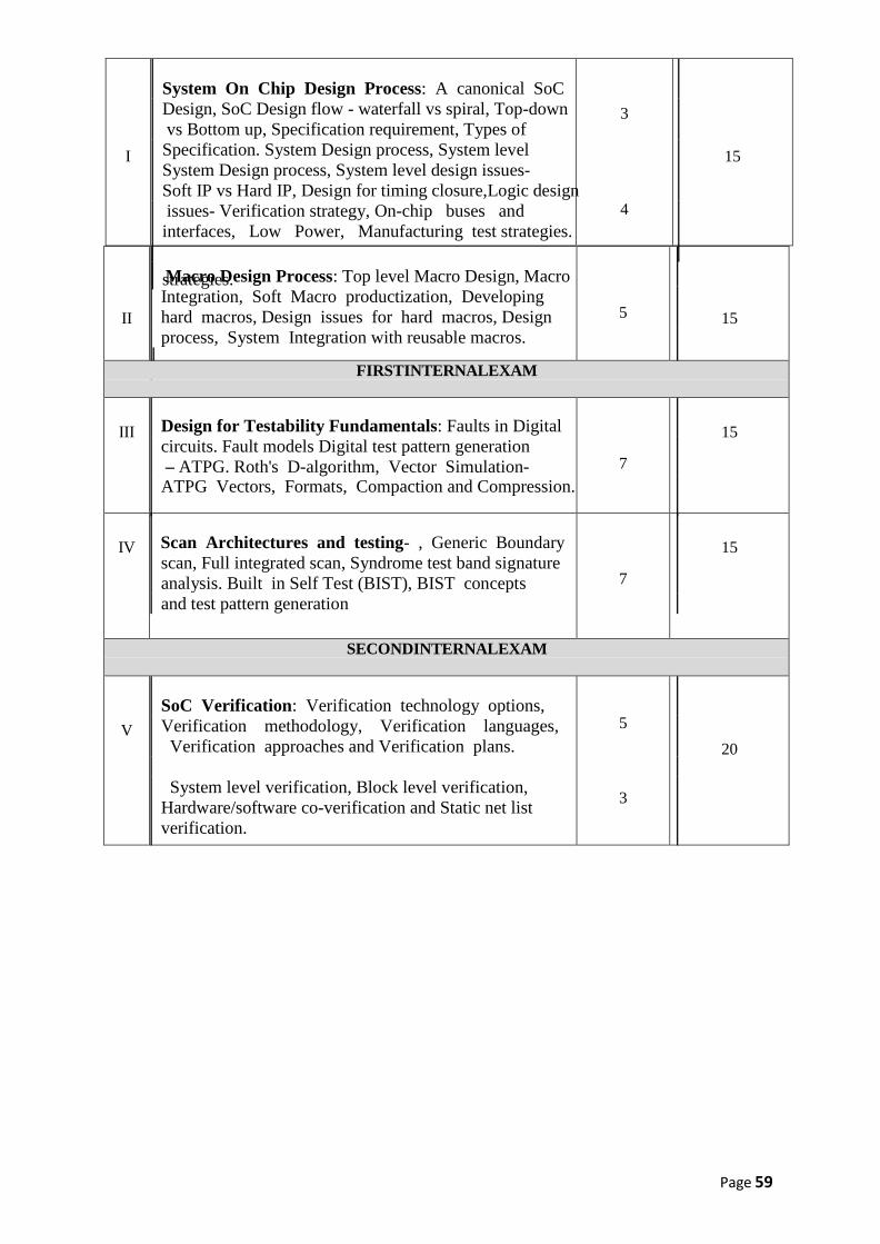
Page 59
I
System On Chip Design Process: A canonical SoC Design, SoC Design flow - waterfall vs spiral, Top-down vs Bottom up, Specification requirement, Types of Specification. System Design process, System level
System Design process, System level design issues- Soft IP vs Hard IP, Design for timing closure,Logic design issues- Verification strategy, On-chip buses and interfaces, Low Power, Manufacturing test strategies.
strategies.
3
4
15
II
Macro Design Process: Top level Macro Design, Macro Integration, Soft Macro productization, Developing hard macros, Design issues for hard macros, Design process, System Integration with reusable macros.
5
15
FIRSTINTERNALEXAM
III Design for Testability Fundamentals: Faults in Digital
circuits. Fault models Digital test pattern generation – ATPG. Roth's D-algorithm, Vector Simulation- ATPG Vectors, Formats, Compaction and Compression.
7
15
IV Scan Architectures and testing- , Generic Boundary
scan, Full integrated scan, Syndrome test band signature analysis. Built in Self Test (BIST), BIST concepts and test pattern generation
7
15
SECONDINTERNALEXAM
V SoC Verification: Verification technology options, Verification methodology, Verification languages, Verification approaches and Verification plans.
System level verification, Block level verification, Hardware/software co-verification and Static net list verification.
5
3
20

Page 60
VI MPSoCs: What, Why, How MPSoCs. Techniques for designing MPSoCs, Performance and flexibility for MPSoCs design, MPSoC performance modeling and
analysis, System-In-Package (SIP) design.
8
20
END SEMESTER EXAM
Page 61
Course No. Course Name L-T-P-Credits Year of Introduction
02EC7611.3 DSP For Embedded Systems 3-0-0-3 2015
Course Objectives
The objectives of this course are to:
• To familiarize with the architecture of the various digital signal processors. • To have an understanding of various processor structures and functional
units of different processors.
Syllabus DSP Introduction, Fixed point DSPs, TMS 320 C 55 x Digital Signal Processor, TMS 320 C 6x, SHARC Digital Signal Processor, Some Practical applications of Digital Signal Processors.
Course Outcome Students should be able to:
• The student will get exposed to the basic features of digital processors. • The student will get an idea about the software development tools used in the
digital processors and this course also discusses the implementation of different applications on digital processors.
References
1. Steven W Smith, “Digital Signal Processing: A Practical guide for Engineers and
scientists”, Newness(Elsevier), 2003 2. Rulf Chassaing, “Digital Signal Processing and applications with the C6713 and C6416
DSK”, Wiley- Interscience, 2005
3 . Sen M Kuo, Bob H Lee, “ Real time Digital Signal Processing”, John Wiley and Sons, 2001.
4.Naim Dahnoun, “Digital Signal Processing Implementation using the
TMS320C6000 DSP Platform”, 1st Edition; 2000.
5..David J Defatta J, Lucas Joseph G & Hodkiss William S, “Digital Signal Processing: A System Design Approach”, 1st Edition, John Wiley 6.E C Elfeachor and B W Jervis, “ Digital Signal Processing- A Practical approach”, Pearson, 2005.
7.James H. McClellan, Ronald Schaffer and Mark A Yoder, “DSP FIRST - A Multimedia Approach”, 1st Edition, Prentice Hall
8.B.Venkataramani and M Bhaskar, “Digital Signal Processors: Architecture, Programming and Applications”, Tata McGraw-Hill, New Delhi, 2011
9. “Wavelets and Subband Coding”, Martin Vetterli, Jelena Kovacevic, Prentice Hall Inc., 1995.

Page 30
COURSE PLAN
Module Contents Contact Hours
Sem.Exam Marks ;%
I
DSP Introduction to programmable DSPs: DSPs and Conventional Microprocessors, Bus architecture- Von Neumann, Harvard, Super Harvard architectures, Circular Buffering. Fixed vs. Floating point DSP processors, Programming in C vs Programming in assembly, speed benchmarks for DSPs, Multiprocessing for high speed DSP applications.
5
3
15
II
Fixed point DSPs Overview of TMS320C54xx-Architecture of C54xx, CPU, MAC unit, Special function units-Interrupts of C54x processor, Internal memory organization, On chip peripherals- Addressing modes and instruction set.
7
15
FIRST INTERNAL EXAM
III
TMS 320 C 55 x Digital Signal Processor: Architecture overview, Buses, memory maps, software development tools- C compiler, assembler, linker, Code Composer studio, Addressing modes and instruction set, pipelining and parallelism in TMS 320C 55X, Mixed C and Assembly programming.
6
15
IV
TMS 320 C 6x: Architecture, Functional Units, Fetch and Execute Packets, Pipelining, Registers, Linear and Circular Addressing Modes, TMS320C6x Instruction Set, Types of Instructions, Linear Assembly, Timers, Interrupts, Multichannel Buffered Serial Ports, Direct Memory Access, Memory Considerations
6
15
SECOND INTERNAL EXAM
V
SHARC Digital Signal Processor Architecture - IOP Registers - Peripherals - Synchronous Serial Port -Interrupts -Internal/External/Multiprocessor Memory Space - Multiprocessing - Host Interface - Link Ports.
9
20
VI
Some Practical applications of Digital Signal Processors: Sine wave generators, Noise generators, DTMF Tone detection, Adaptive echo cancellation, Acoustic echo cancellation, Speech enhancement.
6
20
END SEMESTER EXAM
Page 31
CourseNo. CourseName L-T-P-Credits YearofIntroduction
02EC7611.4 Computer Architecture and Parallel Processing
(L-T-P : 3-0-0)- 3
2015
CourseObjectives • To familiarize with fundamentals of computer design. • To learn parallel and pipeline architectures. • To understand the difference between the pipeline and parallel concepts. • To study the various memories and optimization of memory.
Syllabus
Computer design and Performance measures, Parallel processing, Pipelining and ILP, Memory hierarchy design, Multiprocessors , Multi-core architectures , Case studies
CourseOutcome
• The student can understand the fundamentals of computer design. Also give a brief
idea about single and multiple architectures and its performance measures used in computer design.
• Memory hierarchy gives different memory technologies and optimization of cache and its design, a brief about the multiprocessors, its performance issues, different multicore architectures.
References
4. Kai Hwang, "Advanced Computer Architecture", McGraw Hill International, 2001. 5. John P. Hayes, “Computer Architecture and Organization”, McGraw Hill 6. David E. Culler, Jaswinder Pal Singh, “Parallel Computing Architecture: A
hardware/ softwareapproach”, Morgan Kaufmann / Elsevier, 1997. 7. Dimitrios Soudris, Axel Jantsch, "Scalable Multi-core Architectures: Design
Methodologies andTools", Springer, 2012 8. John P. Shen, “Modern processor design. Fundamentals of super scalar processors”, Tata
McGraw Hill 2003
COURSEPLAN
Module Contents Contact hours
Sem. ExamMarks
I
Computer design and Performance measures: Fundamentals of Computer Design – Parallel and Scalable Architectures – Multiprocessors –Multivector and SIMD architectures – Multithreaded architectures – Data-flow architectures -Performance Measures
3
4
15

Page 32
II
Parallel processing, Pipelining and ILP: Instruction Level Parallelism and Its Exploitation - Concepts and Challenges - Overcoming Data Hazards with Dynamic Scheduling – Dynamic Branch Prediction - Speculation - Multiple Issue Processors -
Performance and Efficiency in Advanced Multiple Issue Processors
6
15
FIRSTINTERNALEXAM
III Memory hierarchy design: Memory Hierarchy - Memory
Technology and Optimizations – Cache memory – Optimizations of Cache Performance – Memory Protection and Virtual Memory - Design of Memory Hierarchies
7
15
IV Multiprocessors: Symmetric and distributed shared
memory architectures – Cache coherence issues – Performance Issues – Synchronization issues – Models of Memory Consistency - Interconnection networks –Buses, crossbar and multi-stage switches.
7
15
SECONDINTERNALEXAM 3
V Multi-core architectures: Software and hardware multithreading – SMT and CMP architectures – Design issues
7
20
VI Case studies– Intel Multi-core architecture – SUN CMP architecture – IBM cell architecture - hp architecture
8
20
END SEMESTER EXAM
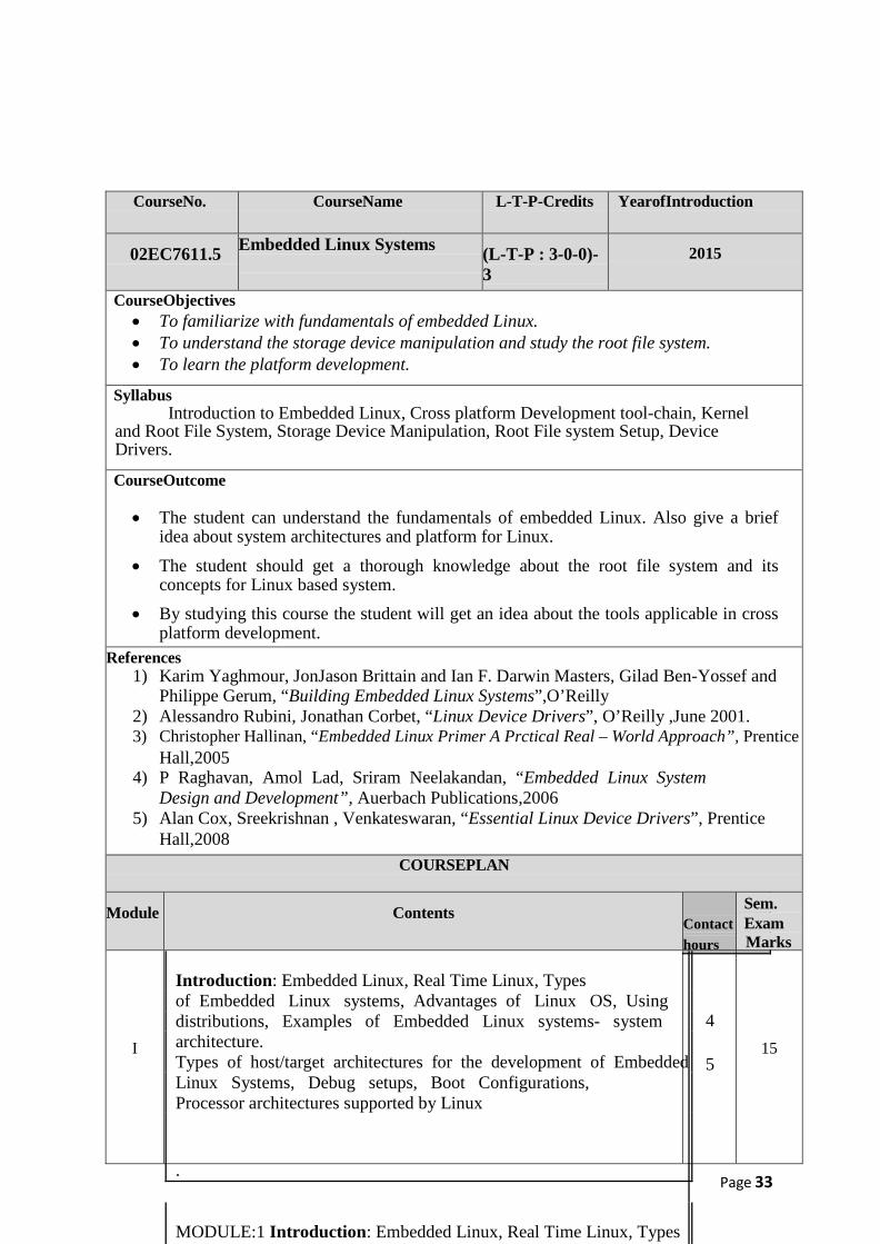
Page 33
CourseNo. CourseName L-T-P-Credits YearofIntroduction
02EC7611.5 Embedded Linux Systems (L-T-P : 3-0-0)-
3 2015
CourseObjectives • To familiarize with fundamentals of embedded Linux. • To understand the storage device manipulation and study the root file system. • To learn the platform development.
Syllabus Introduction to Embedded Linux, Cross platform Development tool-chain, Kernel
and Root File System, Storage Device Manipulation, Root File system Setup, Device Drivers.
CourseOutcome
• The student can understand the fundamentals of embedded Linux. Also give a brief
idea about system architectures and platform for Linux. • The student should get a thorough knowledge about the root file system and its
concepts for Linux based system. • By studying this course the student will get an idea about the tools applicable in cross
platform development.
References 1) Karim Yaghmour, JonJason Brittain and Ian F. Darwin Masters, Gilad Ben-Yossef and
Philippe Gerum, “Building Embedded Linux Systems”,O’Reilly 2) Alessandro Rubini, Jonathan Corbet, “Linux Device Drivers”, O’Reilly ,June 2001. 3) Christopher Hallinan, “Embedded Linux Primer A Prctical Real – World Approach”, Prentice
Hall,2005 4) P Raghavan, Amol Lad, Sriram Neelakandan, “Embedded Linux System
Design and Development”, Auerbach Publications,2006 5) Alan Cox, Sreekrishnan , Venkateswaran, “Essential Linux Device Drivers”, Prentice
Hall,2008
COURSEPLAN
Module Contents Contact hours
Sem. ExamMarks
I
Introduction: Embedded Linux, Real Time Linux, Types of Embedded Linux systems, Advantages of Linux OS, Using distributions, Examples of Embedded Linux systems- system architecture. Types of host/target architectures for the development of Embedded Linux Systems, Debug setups, Boot Configurations, Processor architectures supported by Linux
.
MODULE:1 Introduction: Embedded Linux, Real Time Linux, Types of Embedded Linux systems, Advantages of Linux OS, Using
4
5
15
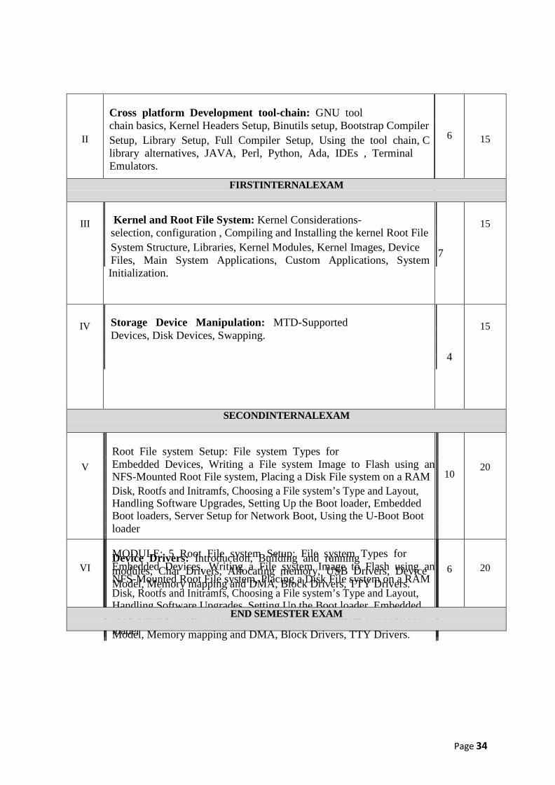
Page 34
II
Cross platform Development tool-chain: GNU tool chain basics, Kernel Headers Setup, Binutils setup, Bootstrap Compiler Setup, Library Setup, Full Compiler Setup, Using the tool chain, C library alternatives, JAVA, Perl, Python, Ada, IDEs , Terminal Emulators.
6
15
FIRSTINTERNALEXAM
III Kernel and Root File System: Kernel Considerations-
selection, configuration , Compiling and Installing the kernel Root File System Structure, Libraries, Kernel Modules, Kernel Images, Device Files, Main System Applications, Custom Applications, System Initialization.
7
15
IV Storage Device Manipulation: MTD-Supported
Devices, Disk Devices, Swapping.
4
15
SECONDINTERNALEXAM 3
V Root File system Setup: File system Types for Embedded Devices, Writing a File system Image to Flash using an NFS-Mounted Root File system, Placing a Disk File system on a RAM Disk, Rootfs and Initramfs, Choosing a File system’s Type and Layout, Handling Software Upgrades, Setting Up the Boot loader, Embedded Boot loaders, Server Setup for Network Boot, Using the U-Boot Boot loader
MODULE: 5 Root File system Setup: File system Types for Embedded Devices, Writing a File system Image to Flash using an NFS-Mounted Root File system, Placing a Disk File system on a RAM Disk, Rootfs and Initramfs, Choosing a File system’s Type and Layout, Handling Software Upgrades, Setting Up the Boot loader, Embedded Boot loaders, Server Setup for Network Boot, Using the U-Boot Boot loader
10
20
VI Device Drivers: Introduction, Building and running modules, Char Drivers, Allocating memory, USB Drivers, Device Model, Memory mapping and DMA, Block Drivers, TTY Drivers.
modules, Char Drivers, Allocating memory, USB Drivers, Device Model, Memory mapping and DMA, Block Drivers, TTY Drivers.
6
20
END SEMESTER EXAM
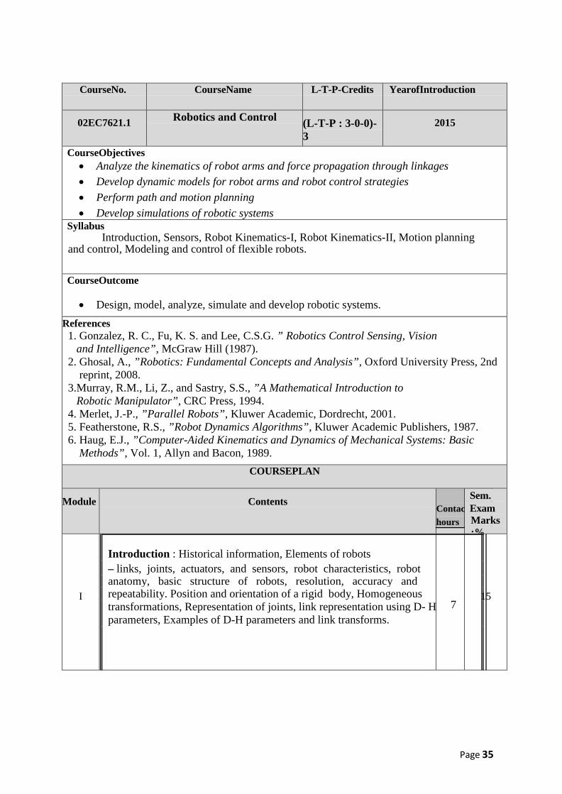
Page 35
CourseNo. CourseName L-T-P-Credits YearofIntroduction
02EC7621.1 Robotics and Control (L-T-P : 3-0-0)- 3
2015
CourseObjectives • Analyze the kinematics of robot arms and force propagation through linkages • Develop dynamic models for robot arms and robot control strategies • Perform path and motion planning • Develop simulations of robotic systems
Syllabus Introduction, Sensors, Robot Kinematics-I, Robot Kinematics-II, Motion planning
and control, Modeling and control of flexible robots. CourseOutcome • Design, model, analyze, simulate and develop robotic systems.
References 1. Gonzalez, R. C., Fu, K. S. and Lee, C.S.G. ” Robotics Control Sensing, Vision
and Intelligence”, McGraw Hill (1987). 2. Ghosal, A., ”Robotics: Fundamental Concepts and Analysis”, Oxford University Press, 2nd
reprint, 2008. 3.Murray, R.M., Li, Z., and Sastry, S.S., ”A Mathematical Introduction to
Robotic Manipulator”, CRC Press, 1994. 4. Merlet, J.-P., ”Parallel Robots”, Kluwer Academic, Dordrecht, 2001. 5. Featherstone, R.S., ”Robot Dynamics Algorithms”, Kluwer Academic Publishers, 1987. 6. Haug, E.J., ”Computer-Aided Kinematics and Dynamics of Mechanical Systems: Basic
Methods”, Vol. 1, Allyn and Bacon, 1989.
COURSEPLAN
Module Contents Contact hours
Sem. ExamMarks;%
I
Introduction : Historical information, Elements of robots – links, joints, actuators, and sensors, robot characteristics, robot anatomy, basic structure of robots, resolution, accuracy and repeatability. Position and orientation of a rigid body, Homogeneous transformations, Representation of joints, link representation using D- H parameters, Examples of D-H parameters and link transforms.
7
15
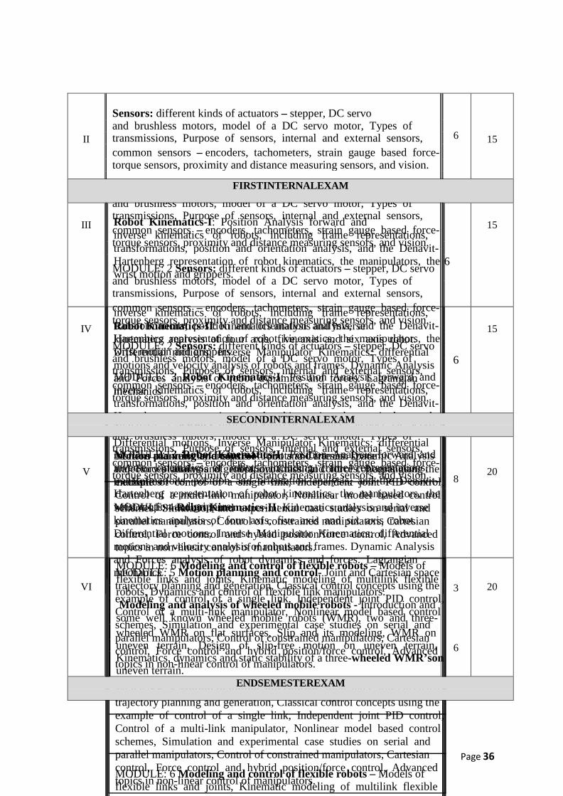
Page 36
II
Sensors: different kinds of actuators – stepper, DC servo and brushless motors, model of a DC servo motor, Types of transmissions, Purpose of sensors, internal and external sensors, common sensors – encoders, tachometers, strain gauge based force- torque sensors, proximity and distance measuring sensors, and vision.
MODULE: 2 Sensors: different kinds of actuators – stepper, DC servo and brushless motors, model of a DC servo motor, Types of transmissions, Purpose of sensors, internal and external sensors, common sensors – encoders, tachometers, strain gauge based force- torque sensors, proximity and distance measuring sensors, and vision.
MODULE: 2 Sensors: different kinds of actuators – stepper, DC servo and brushless motors, model of a DC servo motor, Types of transmissions, Purpose of sensors, internal and external sensors, common sensors – encoders, tachometers, strain gauge based force- torque sensors, proximity and distance measuring sensors, and vision.
MODULE: 2 Sensors: different kinds of actuators – stepper, DC servo and brushless motors, model of a DC servo motor, Types of transmissions, Purpose of sensors, internal and external sensors, common sensors – encoders, tachometers, strain gauge based force- torque sensors, proximity and distance measuring sensors, and vision.
MODULE: 2 Sensors: different kinds of actuators – stepper, DC servo and brushless motors, model of a DC servo motor, Types of transmissions, Purpose of sensors, internal and external sensors, common sensors – encoders, tachometers, strain gauge based force- torque sensors, proximity and distance measuring sensors, and vision.
6
15
FIRSTINTERNALEXAM
III Robot Kinematics-I: Position Analysis forward and
inverse kinematics of robots, including frame representations, transformations, position and orientation analysis, and the Denavit- Hartenberg representation of robot kinematics, the manipulators, the wrist motion and grippers.
inverse kinematics of robots, including frame representations, transformations, position and orientation analysis, and the Denavit- Hartenberg representation of robot kinematics, the manipulators, the wrist motion and grippers.
MODULE: 3 Robot Kinematics-I: Position Analysis forward and inverse kinematics of robots, including frame representations, transformations, position and orientation analysis, and the Denavit- Hartenberg representation of robot kinematics, the manipulators, the wrist motion and grippers.
MODULE: 3 Robot Kinematics-I: Position Analysis forward and inverse kinematics of robots, including frame representations, transformations, position and orientation analysis, and the Denavit- Hartenberg representation of robot kinematics, the manipulators, the wrist motion and grippers.
6
15
IV Robot Kinematics-II: Kinematics analysis and inverse
kinematics analysis of four axis, five axis and six axis robot. Differential motions, Inverse Manipulator Kinematics: differential motions and velocity analysis of robots and frames. Dynamic Analysis and Forces analysis of robot dynamics and forces. Lagrangian mechanics
kinematics analysis of four axis, five axis and six axis robot. Differential motions, Inverse Manipulator Kinematics: differential motions and velocity analysis of robots and frames. Dynamic Analysis and Forces analysis of robot dynamics and forces. Lagrangian mechanics
MODULE: 4 Robot Kinematics-II: Kinematics analysis and inverse kinematics analysis of four axis, five axis and six axis robot. Differential motions, Inverse Manipulator Kinematics: differential motions and velocity analysis of robots and frames. Dynamic Analysis and Forces analysis of robot dynamics and forces. Lagrangian mechanics
6
15
SECONDINTERNALEXAM 3
V Motion planning and control- Joint and Cartesian space trajectory planning and generation, Classical control concepts using the example of control of a single link, Independent joint PID control, Control of a multi-link manipulator, Nonlinear model based control schemes, Simulation and experimental case studies on serial and parallel manipulators, Control of constrained manipulators, Cartesian control, Force control and hybrid position/force control, Advanced topics in non-linear control of manipulators.
MODULE: 5 Motion planning and control- Joint and Cartesian space trajectory planning and generation, Classical control concepts using the example of control of a single link, Independent joint PID control, Control of a multi-link manipulator, Nonlinear model based control schemes, Simulation and experimental case studies on serial and parallel manipulators, Control of constrained manipulators, Cartesian control, Force control and hybrid position/force control, Advanced topics in non-linear control of manipulators.
MODULE: 5 Motion planning and control- Joint and Cartesian space trajectory planning and generation, Classical control concepts using the example of control of a single link, Independent joint PID control, Control of a multi-link manipulator, Nonlinear model based control schemes, Simulation and experimental case studies on serial and parallel manipulators, Control of constrained manipulators, Cartesian control, Force control and hybrid position/force control, Advanced topics in non-linear control of manipulators.
8
20
VI
Modeling and control of flexible robots – Models of
MODULE: 6 Modeling and control of flexible robots – Models of flexible links and joints, Kinematic modeling of multilink flexible robots, Dynamics and control of flexible link manipulators. Modeling and analysis of wheeled mobile robots - Introduction and some well known wheeled mobile robots (WMR), two and three- wheeled WMR on flat surfaces, Slip and its modeling, WMR on uneven terrain, Design of slip-free motion on uneven terrain, Kinematics, dynamics and static stability of a three-wheeled WMR’son uneven terrain.
flexible links and joints, Kinematic modeling of multilink flexible
MODULE: 6 Modeling and control of flexible robots – Models of flexible links and joints, Kinematic modeling of multilink flexible
3
6
20
ENDSEMESTEREXAM
Page 37
Course No. Course Name L-T-P-Credits Year of Introduction
02 EC 7621.2 DIGITAL IMAGE PROCESSING 3-0-0-3 2015
Course Objectives
The objectives of this course are to: • Impart knowledge on fundamental theory and some basic architectures of VLSI based
digital image processing • Learn the concepts of spatial filtering and basic enhancement techniques • Understand the basics of restoration methods and color image processing • Study the underlying mechanisms of image compression and image compression
standards
Syllabus Digital Image fundamentals; Image Enhancement; Image restoration; Image Segmentation; Image Compression; VLSI architectures for digital image processing
Course Outcome Students should be able to: • Understand ,analyze and develop new image processing problems and algorithms • Design the hardware architecture for image processing algorithms • Develop the skill to further explore the advanced topics of digital image processing
References
1..Gonzalez and Woods, “Digital Image Processing”, Pearson education, 2008. 2.Yung-scheng Chen, “ Image processing”,InTech ,2009 3.A K Jain, “Fundamentals of Digital Image Processing”, Pearson education, 2003. 4.W K Pratt, “Digital Image Processing”, John Wiley, 2004 5.Tamal Bose, “Digital Signal and Image Processing”, John Wiley publishers,1st edition,2003. 6. J S Lim, “Two dimensional signal and Image Processing”, Prentice Hall.1990
Page 38
COURSE PLAN
Module Contents Contact Hours
Sem.Exam Marks ;%
I
Digital Image fundamentals: Representation, simple image formation model, Image processing system on chip- on chip vision system PARIS architecture, vision system based on logarithmic CMOS sensor.
3
3
15
II
Image enhancement: Histogram processing, Image subtraction, Image averaging Mechanics of spatial filtering-correlation, convolution. Spatial smoothing, sharpening filters.
4
4
15
FIRST INTERNAL EXAM
III
Image segmentation: Thresholding, edge detection. Binary image processing: SIMD array for binary image processing- processing element, Binary edge detector, Hole filling, shortest path problem. Hough transform.
3
4
15
IV
Image Restoration: Degradation model, Algebraic approaches to restoration: inverse filtering, Blind restoration, wiener filtering, geometric transformation. Color Image Processing: color models, pseudo coloring, intensity slicing, gray level to color transformation
4 3
15
SECOND INTERNAL EXAM
V
Image compression fundamentals, redundancy in images. Lossless compression-variable length, bit plane coding, lossy compression-transform coding. Fundamentals of JPEG compression
3 5
20
VI
VLSI Architectures: ZNCC, Wavelet transform. Hardware architecture: spatial architecture, Spectral architecture. Reconfigurable architecture for image processing and computer vision-Hough transform.
3 3
20
END SEMESTER EXAM
Page 39
CourseNo. CourseName L-T-P-Credits YearofIntroduction
02EC7621.3 CPLD And FPGA Architectures
3-0-0:3
2015
Course Objectives
• To study various programmable logic devices and FPGAs. • The design and analysis methods of finite state machines. • To comparatively study the classification of commercial family of
Programmable gate arrays.
Syllabus Programmable logic devices, FPGAs, Finite State Machines(FSM), FSM Architectures, Systems Level Design, Implementing applications with FPGAs, CORDIC architectures for FPGA computing. Course Outcome
• The student will get an introduction about different programmable logic
devices, FPGAs and its architectures. • The FSM design gives an idea about top down design, realization and
synchronization of state machines. • To get an idea about different architectures used in FSM design and system
level design, implementation startegies, arithmetics and FPGA computing using cordic processors.
References: 1. John F.Wakerly, “Digital Design-Principles and Practices”, Fourth Edition, Prentice Hall. 2 .Charles.H.Roth,Jr, “Digital systems design using VHDL”,PWS Publishing Company. 3. Richard.F.Tinder, “Engineering digital design”, Second edition, Academic Press,2000. 4. Scott Hauck and Andre DeHon, “Reconfigurable Computing:The Theory and Practice of
FPGA based Computation”, Morgan Kaufmann Publishers. 5.S.Trimberger, Edr., “Field Programmable Gate Array Technology”, Kluwer Academic Publications,1994. 6.J. Old Field, R.Dorf, “Field Programmable Gate Arrays”, John Wiley & Sons, Newyork, 1995. 7.S.Brown , R.Francis, J.Rose, Z.Vransic, “Field Programmable Gate Array”, Kluwer Pubin, 1992. 8.P.K.Chan& S. Mourad, “Digital Design Using Field Programmable Gate Array”, Prentice Hall, 1994.
COURSEPLAN
Module Contents ContactHours
Sem.ExamMarks;%

Page 40
I
Programmable logic : ROM, PLA, PAL, PLD, PGA –Features, programming and applications Altera series – Max 7000 series and Altera FLEX logic – 10000 series CPLD, AMD’s – CPLD (Mach 1&2). Cypress FLASH 370 Device Technology, Lattice pLSI’s Architectures– 3000 Series – Speed Performance and in system programmability.
4
2
15
II
FPGAs: Field Programmable Gate Arrays – Logic blocks, routing architecture, Design flow, Technology Mapping for FPGAs, Case studies – Xilinx Spartan-3. Virtex-II, Virtex-4, Virtex-6, Spartan-6 FPGAs & Sub-families, ALTERA’s FLEX 10000 FPGAs, NIOS II Embedded Processor, AT &T – ORCA’s (Optimized Reconfigurable Cell Array), ACTEL’s IGLOO series, ProASIC3 series FPGAs.
3
5
15
FIRSTINTERNALEXAM
III
Finite State Machines (FSM): Top Down Design – State Transition Table, state assignments for FPGAs. Problem of initial state assignment for one hot encoding. Derivations of state machine charts, Alternative realization for state machine chart using microprogramming. Linked state machines. One – Hot state machine, Petrinets for state machines – basic concepts, properties. Extended petrinets for parallel controllers. Finite State Machine - Meta Stability, Synchronization.
4
3
15
IV
FSM Architectures and Systems Level Design: Architectures centered around non-registered PLDs. State machine designs centered around shift registers. One – Hot design method. Use of ASMs in One – Hot design. Application of One – Hot method. System level design – controller, data path and functional partition.
2
3
15
SECOND INTERNAL EXAM

Page 41
V
Implementing Applications with FPGAs: Strengths and Weaknesses of FPGAs, Application and computational characteristics and Performance .General Implementation Strategies for FPGA based Systems - Configure-once, Runtime Reconfiguration. Implementing Arithmetic inFPGAs-Fixed-pointnumber Representation and Arithmetic, Floating- point arithmetic, and Block Floating Point ,Constant Folding and Data-oriented Specialization.Instance-specific Design. System level verification, Block level verification, Hardware/software co-verification and Static net list verification.
4
6
20
VI
MODULE: 6 CORDIC Architectures for FPGA Computing- CORDIC Algorithm, Architectural Design, FPGA Implementation of CORDIC Processors.
6
20
ENDSEMESTEREXAM
Page 42
CourseNo. CourseName L-T-P-Credits YearofIntroduction
02EC7621.4 High Speed Digital Design 3-0-0:3
2015
Course Objectives
• To give a thorough introduction to the digital aspects of basic transmission line theory.
• To analyze the practical aspects of making measurements in high-speed digital systems.
• Methodologies for designing high-speed buses and handling the very large number of variables that affect interconnect performance.
Syllabus Introduction to High Speed Digital Design, Power Distribution and Noise , Signaling convention and Circuits , Timing Convention and synchronization
CourseOutcome
• Will get an idea about distribution of power ,supply noise ,cross talk and non-ideal transmission line effects on signal quality and timings.
• The impact of packages, vias, and connectors on signal integrity and explanations of how driving circuit characteristics affect the quality of the digital signal is analyzed.
• Digital timing analysis at the system level that incorporates high-speed signaling effects into timing budgets is discussed.
References: 1.Dally &Paulton, “Digital System Engineering”, Cambride University Press,1998
2.Johnson & Graham, “High Speed Digital Design: A Handbook of Black Magic”, PrenticeHall 1993 3.Masakazu Shoji, “High Speed Digital Circuits”, Addison Wesley, 1996 4.Jan M.Rabaey, AnanthaChandrakasan, BorivojeNikolic,“ Digital Integrated Circuits: Adesign Perspective”,Second edition, PHI Learning, 2003
5. Douglas.A.Pucknell, Kamran Eshraghian, “Basic VLSI Design”,Thirdedition,PHI Learning.
COURSEPLAN
Module Contents ContactHour
Sem.ExamMarks;%

Page 43
I
Introduction to High Speed Digital Design: Frequency, time and distance- Capacitance and Inductance Effects- High speed properties of logical gates- Speed and power- modeling of wires- Geometry and Electrical properties of wires- Electrical model of wires- transmission lines- lossless LC transmission lines- lossy RLC transmission lines – Special transmission lines..
4
4
15
II
Power Distribution and Noise: Power supply network- Local power regulation- IR drops- Area bonding- On chip bypass capacitors- Symbiotic bypass capacitors- Power supply isolation – Noise sources in digital system- Power supply Noise – Cross talk- Intersymbol interference.
7
15
FIRSTINTERNALEXAM
III
Signalling convention and Circuits: Signalling modes for transmission lines- Signalling over lumped transmission media-Signalling over RC interconnects- driving lossy LC lines- simultaneous bi-directional Signalling- terminators- transmitter and receiver circuits.
4
4
15
IV
Timing Convention and Synchronisation I:Timing fundamentals- Timing properties of clocked storage elements- signals and events- open loop Timing , level sensitive clocking- pipeline
7
15
SECONDINTERNALEXAM
V
Timing Convention and SynchronisationII Timingclosed loop Timing – clock Distribution- Synchronisation failure and metastability- PLL and DLL based lock aligners.
6
20
VI
Ultra-fast VLSI Circuits and Systems: GaAs crystal structure, Technology development, Device modeling and performance estimation, Thermal design, Electromagnetic compatibility
6
20
END SEMESTER EXAM
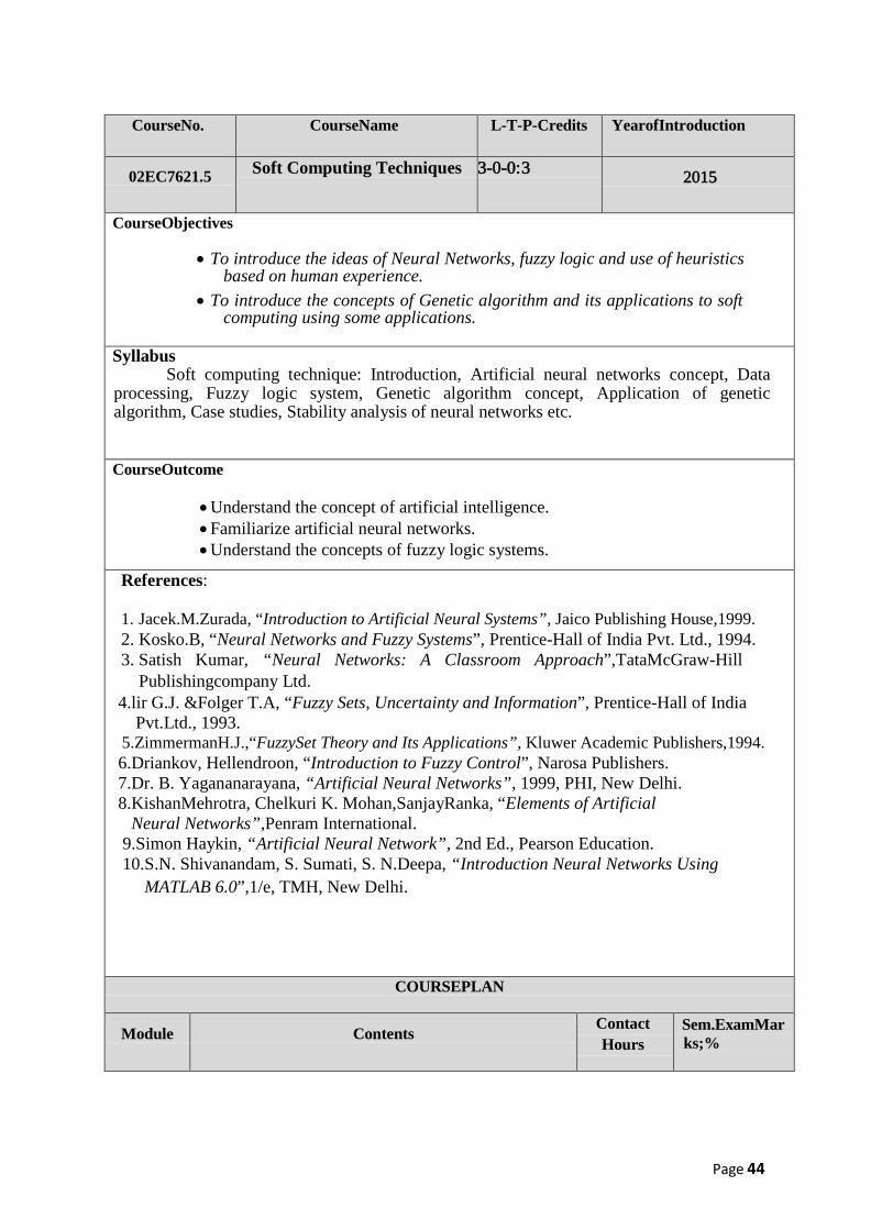
Page 44
CourseNo. CourseName L-T-P-Credits YearofIntroduction
02EC7621.5 Soft Computing Techniques 3-0-0:3
2015
CourseObjectives
• To introduce the ideas of Neural Networks, fuzzy logic and use of heuristics based on human experience.
• To introduce the concepts of Genetic algorithm and its applications to soft computing using some applications.
Syllabus
Soft computing technique: Introduction, Artificial neural networks concept, Data processing, Fuzzy logic system, Genetic algorithm concept, Application of genetic algorithm, Case studies, Stability analysis of neural networks etc.
CourseOutcome
• Understand the concept of artificial intelligence. • Familiarize artificial neural networks. • Understand the concepts of fuzzy logic systems.
References:
1. Jacek.M.Zurada, “Introduction to Artificial Neural Systems”, Jaico Publishing House,1999. 2. Kosko.B, “Neural Networks and Fuzzy Systems”, Prentice-Hall of India Pvt. Ltd., 1994. 3. Satish Kumar, “Neural Networks: A Classroom Approach”,TataMcGraw-Hill
Publishingcompany Ltd. 4.lir G.J. &Folger T.A, “Fuzzy Sets, Uncertainty and Information”, Prentice-Hall of India Pvt.Ltd., 1993. 5.ZimmermanH.J.,“FuzzySet Theory and Its Applications”, Kluwer Academic Publishers,1994. 6.Driankov, Hellendroon, “Introduction to Fuzzy Control”, Narosa Publishers. 7.Dr. B. Yagananarayana, “Artificial Neural Networks”, 1999, PHI, New Delhi. 8.KishanMehrotra, Chelkuri K. Mohan,SanjayRanka, “Elements of Artificial Neural Networks”,Penram International. 9.Simon Haykin, “Artificial Neural Network”, 2nd Ed., Pearson Education. 10.S.N. Shivanandam, S. Sumati, S. N.Deepa, “Introduction Neural Networks Using MATLAB 6.0”,1/e, TMH, New Delhi.
COURSEPLAN
Module Contents ContactHours
Sem.ExamMarks;%
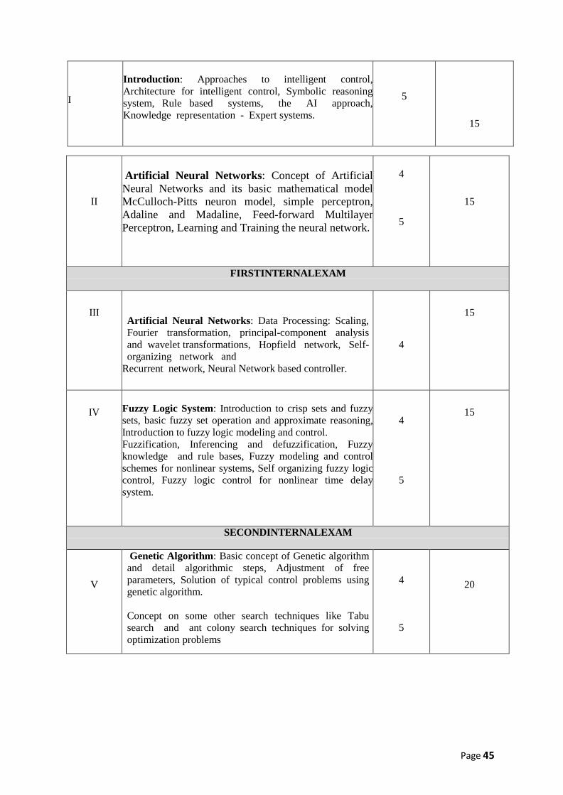
Page 45
I
Introduction: Approaches to intelligent control, Architecture for intelligent control, Symbolic reasoning system, Rule based systems, the AI approach, Knowledge representation - Expert systems.
5
15
II
Artificial Neural Networks: Concept of Artificial Neural Networks and its basic mathematical model McCulloch-Pitts neuron model, simple perceptron, Adaline and Madaline, Feed-forward Multilayer Perceptron, Learning and Training the neural network.
4
5
15
FIRSTINTERNALEXAM
III
Artificial Neural Networks: Data Processing: Scaling, Fourier transformation, principal-component analysis and wavelet transformations, Hopfield network, Self-organizing network and
Recurrent network, Neural Network based controller.
4
15
IV
Fuzzy Logic System: Introduction to crisp sets and fuzzy sets, basic fuzzy set operation and approximate reasoning, Introduction to fuzzy logic modeling and control. Fuzzification, Inferencing and defuzzification, Fuzzy knowledge and rule bases, Fuzzy modeling and control schemes for nonlinear systems, Self organizing fuzzy logic control, Fuzzy logic control for nonlinear time delay system.
4
5
15
SECONDINTERNALEXAM
V
Genetic Algorithm: Basic concept of Genetic algorithm and detail algorithmic steps, Adjustment of free parameters, Solution of typical control problems using genetic algorithm. Concept on some other search techniques like Tabu search and ant colony search techniques for solving optimization problems
4
5
20
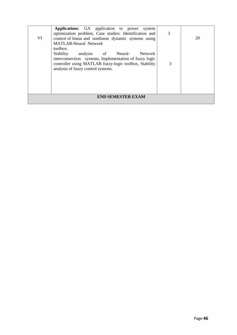
Page 46
VI
Applications: GA application to power system optimization problem, Case studies: Identification and control of linear and nonlinear dynamic systems using MATLAB-Neural Network toolbox. Stability analysis of Neural- Network interconnection systems, Implementation of fuzzy logic controller using MATLAB fuzzy-logic toolbox, Stability analysis of fuzzy control systems.
3
3
20
END SEMESTER EXAM
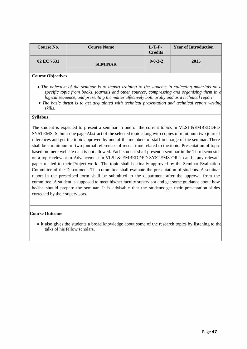
Page 47
Course No. Course Name L-T-P-Credits
Year of Introduction
02 EC 7631 SEMINAR
0-0-2-2 2015
Course Objectives
• The objective of the seminar is to impart training to the students in collecting materials on a specific topic from books, journals and other sources, compressing and organising them in a logical sequence, and presenting the matter effectively both orally and as a technical report.
• The basic thrust is to get acquainted with technical presentation and technical report writing skills.
Syllabus
The student is expected to present a seminar in one of the current topics in VLSI &EMBEDDED SYSTEMS. Submit one page Abstract of the selected topic along with copies of minimum two journal references and get the topic approved by one of the members of staff in charge of the seminar. There shall be a minimum of two journal references of recent time related to the topic. Presentation of topic based on mere website data is not allowed. Each student shall present a seminar in the Third semester on a topic relevant to Advancement in VLSI & EMBEDDED SYSTEMS OR it can be any relevant paper related to their Project work.. The topic shall be finally approved by the Seminar Evaluation Committee of the Department. The committee shall evaluate the presentation of students. A seminar report in the prescribed form shall be submitted to the department after the approval from the committee. A student is supposed to meet his/her faculty supervisor and get some guidance about how he/she should prepare the seminar. It is advisable that the students get their presentation slides corrected by their supervisors.
Course Outcome
• It also gives the students a broad knowledge about some of the research topics by listening to the talks of his fellow scholars.
Page 48
Course No. Course Name L-T-P-Credits
Year of Introduction
02 EC 7641 PROJECT DESIGN PHASE-I
0-0-12-6 2015
Course Objectives
• To develop the student’s skills and enable innovation in design, simulation, implementation and fabrication work from the theoretical and practical knowledge acquired from the previous semesters.
• To apply and enhance the knowledge acquired in the related field and to make the students come up with new ideas in their area of interest.
Syllabus
A project is a task that requires a lot of time and effort. During the Project phase I, the students should choose the area of interest for their project work and collect as many references or literatures as possible related to it and come up with a novel Idea/Problem .There should be a systematic identification and prioritization of problems and it should be addressed through the development of the project. Based on the literature survey, a system/method should be proposed by the student as a solution to the problem identified. One third of the design should be completed during the phase-I. Every project work will be guided by a faculty member of the institution. Eight hours per week will be allotted in the time table and this time should be utilized by the students to receive the directions from the guide, on library reading, laboratory work, computer analysis or field work as assigned by the guide and also to present in periodical reviews and reports on the progress made in the project. Each report must contain student's own analysis or design presented in the approved format. Sessional marks will include (a) Evaluation of the student's progress, (b) Degree of involvement and participation, (c) Merit of the project A student will have to defend his/her project design work and credit will be given on the merits of presentation and viva-voce examination.
Course Outcome
• Appreciate various aspects of the curriculum which support students in increasing their mastery. • Get an idea and develop confidence in designing, analyzing and executing the project.
Page 49
FOURTH SEMESTER
Course No. Course Name L-T-P-Credits
Year of Introduction
02 EC 7612 PROJECT PHASE II
0-0-21-12 2015
Course Objectives
• To develop the student’s skills and enable innovation in design ,Simulation, Implementation and fabrication work from the theoretical and practical knowledge acquired from the previous semesters
• Apply and enhance the knowledge acquired in the related field, Make the students come up with new ideas in their area of interest.
Syllabus
The student has to continue the project work done in third semester There would be qualifying exercises/Reviews for the students. At least one technical paper is to be prepared for possible publication in Journals/Conferences. Twenty one hours per week will be allotted in the time table and this time should be utilized by the students to receive the directions from the guide, on library reading, laboratory work, computer analysis or field work as assigned by the guide. At the end of project work, a project report must be submitted. Each report must contain student's own analysis and/or results presented in an approved format. Sessional marks will include (a) Evaluation of the student's progress, (b) Degree of involvement and participation, (c) Merit of the project A student will have to defend his/her project work and credit will be given on the merits of presentation and viva-voce examination.
Course Outcome
• Appreciate various aspects of the curriculum which support students in increasing their mastery, • Get an idea and develop confidence in designing, analyzing and executing the project • It helps the student to develop a skill of entrepreneurship

Page 50

Page 51

Page 30

Page 31