A comparative study of transport properties of monolayer graphene and AlGaN-GaN heterostructure
Volume II, Issue V, May 2015 IJRSI ISSN 2321 - 2705
www.rsisinternational.org/IJRSI.html Page 49
Abstract—A two dimensional analytical model based on solution
of 2-DEG charge expressions for potential and electric field
distribution in dual channel dual material gate AlGaN/GaN high
electron mobility transistor (DCDMG HEMT) is developed to
demonstrate unique features of this device structure in
suppressing short channel effects (SCEs), reduction in overall
drain current collapse with further improvement in device
current drive capability. The model accurately predicts the
channel potential and electric field distribution along the device
channels. It is observed that work function difference of dual
metal gate leads to a screening effect of the drain potential
variation by second metal gate portion near the drain resulting in
suppressed drain induced barrier lowering (DIBL) and hot
carrier effect. This further improves carrier transport efficiency
due to improved uniform distribution of electric field along both
the channels of device. Improvement in device current drive
capability is due to incorporation of lower channel in the device.
The resultant double channel dual material gate device get
improved transconductance that suppresses current collapse
that normally occurs in GaN based conventional HEMTs. Since
current collapse mainly occurs in upper channel closer to the
device surface while graded profile lower channel in the device is
at far distance resulting in minimal current collapse. The
proposed model also considers trap concentration, a responsible
factor, for current collapse for device analysis and
characterization. Finally theoretical prediction of our model
results compared with device simulation results and experimental
data. Results are found to be in close agreement giving validity to
our proposed model.
Keywords—2DEG-two dimensional electron gas, SCE- short
channel effect, DCDMG-Dual Channel Dual Material Gate,
HEMT-High Electron Mobility Transistor, AlGaN/GaN-Aluminum
Gallium Nitride/Gallium Nitride.
I. INTRODUCTION
eing an important device for high frequency, high power
application AlGaN/GaN hetrostructure based High
Electron Mobility Transistors attracting a lot of attention of
device scintists word wide. Better performance of
AlGaN/GaN hetrostructures relies on high saturation velocity,
thermal stability, high breakdown benefits of electric field and
development of polarization induced high sheet charge density
of 2DEG at hetrointerface [2]. This kind of hetrostructures can
provide much higher output power density compared with
conventional AlGaAs/GaAs-HEMT [3]-[6]. Long et al [6][7]
has fabricated and characterized AlGaAs/GaAs HFET
structure, named as dual material gate HFET, in which two
different metals of different workfunction were selected and
merged into a single gate by making them contact laterally.
The work function of metal region M1 was chosen to be
greater than that of metal region M2 leading to reduction in
SCEs and supressed DIBL. This structure got improvement in
the carrier transport efficiency due to step function in the
channel potential distribution.
In order to enhance the current drive capability of HEMTs,
efforts were made by scientists to construct AlGaN/GaN
double-channel HEMTs. However, due to the additional
AlGaN barrier between the two channels, accesses to the
lower carrier channel w e r e usually inefficient thus double-
channel behaviors was not pronounced [1]. Fabrication of
an AlGaN/GaN/AlGaN/GaN epilayer structure using a lower
AlGaN barrier layer with smaller layer thickness and low and
graded Al composition was proved to be an effective
approach to implement the double-channel HEMT with the
second channel of high electron density and acceptable access
resistance Roanming Chu et al [1]. The resultant AlGaN/GaN
double-channel HEMTs exhibit device performance better
than or comparable to baseline AlGaN/GaN HEMTs in all
aspects. However, so for no analytical model is developed to
incorporate the effect of double channel with dual material
gate using AlGaN/GaN hetero-interface. In our DCDMG
AlGaN/GaN HEMT model we considered multilayer device
structure which provide better device performance in
comparison to base line GaN HEMTs structures.
II. MODEL FORMULATION
2.1. 2-D Analytical model for Channel Potential Analysis:
Following Fig.1 shows schematic cross sectional view of
DCDMG AlmGa1.mN / GaN HEMT with Al mole fraction
Analytical Modeling of Potential and Electric
Field Distribution and Simulation of Large
Signal Parameters for Dual Channel Dual
Material Gate AlGaN/GaN High Electron
Mobility Transistor
Rahis Kumar Yadav1, Pankaj Pathak
2, R M Mehra
3
Department of Electronics and Communication Engineering, School of Engineering and Technology,
Sharda University, Gr. Noida, India
B
Volume II, Issue V, May 2015 IJRSI ISSN 2321 - 2705
www.rsisinternational.org/IJRSI.html Page 50
m=0.30, L1 and L2 are lengths of the laterally merged gate
metals M1 and M2 respectively having different workfunction
and forming single gate for the device. The source and drain
regions are uniformally doped at Nd+
=1026
m-3
. The work
function of metal gates M1 and M2 are фM1=5.3 V and
фM2=4.1V respectively.
In normally on device the Al0.3 Ga0.7 N barrier layer are fully
depleted under normal operating conditions and electons are
confined to the 2DEG in upper and lower GaN layers forming
hetrointerfaces for double channel effects.
In our analytical model the channel region it is devided into
two parts each under metal gate M1 and metal gate M2. The 2-
D potential distribution ф1(𝑥, 𝑦 and ф2 𝑥, 𝑦 in upper channel
can be obtained by solving the 2-D Poission,s equation as
𝑑2ф1(𝑥 ,𝑦)
𝑑𝑥2 +𝑑2ф1(𝑥 ,𝑦)
𝑑𝑦2 =−𝑞𝑁𝑑
𝜀(𝑚) 𝑓𝑜𝑟 0 ≤ 𝑥 ≤ 𝐿 (1)
where x and y denotes horizontal and vertical axis in the
device cross section respectively, Nd is doping density of the
Al0.3 Ga0.7 N layer, 𝜀(𝑚) is the dielectric constant, q is the
electronic charge of Al0.3 Ga0.7 N and L=L1+L2 is the effective
channel length. Potential profile ф1 𝑥, 𝑦 in vertical y
direction for upper channel can be approximated by following
parabolic function as
ф1 𝑥, 𝑦 = ф1𝐿 𝑥 + 𝐶11 𝑥 𝑦 − 𝑑1 + 𝐶12 𝑥 𝑦 − 𝑑1 2 (2)
Similarly, ф1𝐿 𝑥 is the upper channel potential, 𝑑1 = 𝑑𝑏1 +𝑑𝑠 + 𝑑𝑐 + 𝛥𝑑1 distance of upper channel from gate, 𝑑𝑏1 the
thickness of n-Al0.3 Ga0.7 N , 𝛥d1 depth of 2DEG in upper
GaN layer from its top edge.
Similarly, ф2 𝑥, 𝑦 in lower channel can be obtained as
𝑑2ф2(𝑥 ,𝑦)
𝑑𝑥2 +𝑑2ф2(𝑥 ,𝑦)
𝑑𝑦2 =−𝑞𝑁𝑑
𝜀𝑎 (𝑚 ) 𝑓𝑜𝑟 0 ≤ 𝑥 ≤ 𝐿 (3)
Where ф2(𝑥, 𝑦) is and lower channel potential, Similar to as
stated above the potential profile in vertical direction for lower
channel can be apprximated by following parabolic function
ф2 𝑥, 𝑦 = ф2𝐿 𝑥 + 𝐶21 𝑥 𝑦 − 𝑑2 + 𝐶22 𝑥 𝑦 − 2 (4)
ф2𝐿 𝑥 is the lower channel potential, 𝑑2 = 𝑑1 + 𝑑𝑐1 +𝑑𝑏2 + 𝛥𝑑2 is distance of lower channel from gate, 𝑑𝑐1 is
thickness of upper undoped-GaN layer , 𝑑𝑏2 the thickness of
lower n-AlmGa1-m N and 𝛥𝑑2 is depth of 2DEG in lower GaN
buffer layer.
In expressions (2) and (4), 𝐶11 𝑥 , 𝐶12 𝑥 , and 𝐶21 𝑥 , 𝐶22 𝑥
are arbitary coefficients.
Since in DCDMG Al0.3 Ga0.7 N /GaN HEMT gate is formed
by merging two different metal gates M1 and M2 of
workfunctions фM1 and фM2 respetively. Thus flatband
voltages 𝑉𝐹𝐵1 and 𝑉𝐹𝐵2 of gates are given by expressions
𝑉𝐹𝐵1 = ф𝑀𝑆1 = ф𝑀1 − ф𝑆 (5)
𝑉𝐹𝐵2 = ф𝑀𝑆2 = ф𝑀2 − ф𝑆 (6)
Where, ф𝑀𝑆1 and ф𝑀𝑆2 are metal to semiconductor work
functins for gate region M1 and gate regin M2 respectively.
Also,
ф𝑆 = 𝜒𝑎 (𝑚) +𝐸𝑔
2 − ф𝐹 (7)
𝑊𝑒𝑟𝑒, ф𝑆 is work function of n- Al0.3 Ga0.7 N, 𝜒𝑎 (𝑚) is
electron affinity , 𝐸𝑔 is band gap of n- Al0.3 Ga0.7 N at
T=300K and ф𝐹 is fermi potential given by expression
ф𝐹 =𝑘𝑇
𝑞 𝑙𝑛
𝑁𝑑
𝑛𝑖 (8)
where 𝑛𝑖 is intrinsic career concentration and 𝑁𝑑 is donar
concentration in the material.
In the DCDMG Al0.3 Ga0.7 N HEMT structure gate has been
partitioned in to two parts, hence potential under gate region
M1 and gate region M2 for upper channel will be given
separately as
ф11 𝑥, 𝑦 = ф1𝐿1(𝑥) + 𝐶111 𝑥 𝑦 − 𝑑1 + 𝐶112 𝑥 𝑦 − 𝑑1
2 0 ≤ 𝑥 ≤ 𝐿1 (9)
ф12 𝑥, 𝑦 = ф1𝐿2 𝑥 + 𝐶121 𝑥 (𝑦 − 𝑑1)+ 𝐶122 𝑥 𝑦 − 𝑑1
2 𝐿1 ≤ 𝑥 ≤ ( 𝐿1 + 𝐿2)
(10)
Similarily potential under gate regions M1 and M2 for lower
channel will be given separately as
SOURCE
L1 L2
Nd+
Nd+
dc = 3 nm (undoped Al0.3Ga0.7N)
db1 = 18 nm (Si-doped Al0.3Ga0.7N) Nd
ds = 3 nm (undoped Al0.3Ga0.7N)
dch1 = 14 nm (undoped GaN)
db2 = 21 nm AlmGa1-mN
(m graded from 3% to 6%)
-
dch2 = 2.5 µm (GaN)
SAPPHIRE
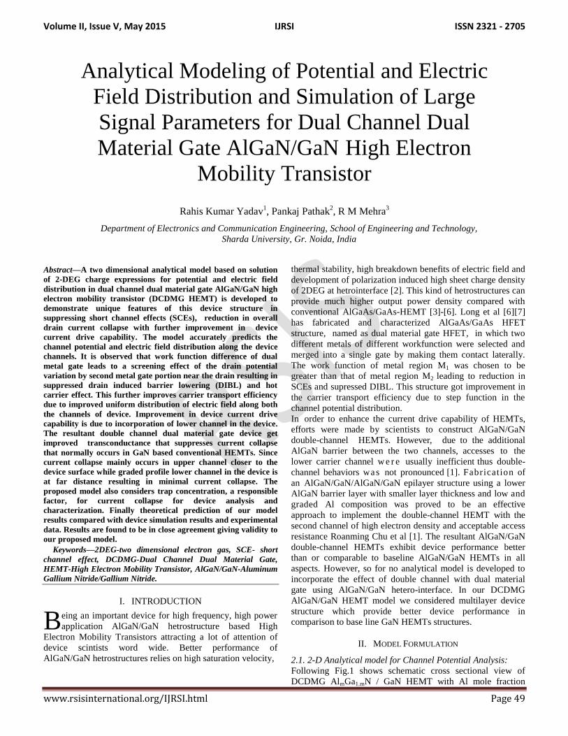
Fig.1. Cross sectional schematic of DCDMG AlGaN/GaN HEMT based on double channel AlGaN/GaN HEMT epilayer on sapphire
substrate [1], Total gate length (L)=L1+L2, L1=L2=0.5µm, work
function of gate region M1 (фM1) =5.3V, work function of gate
region M2 (фM2) =4.1V [6][7], Gate width (W) =100𝝻m,
Nd=2x1024m-3, d1=db1+ds+dc+𝛥d1 and d2=d1+dch1+db2+Δd2 are
distance of upper channel and lower channel from gate , 𝛥d1 and Δd2
denotes 2DEG effective depth in upper and lowere GaN layers
respectively.
DRAIN GATE
Upper 2-DEG
Lower 2-DEG
M2 M1
Volume II, Issue V, May 2015 IJRSI ISSN 2321 - 2705
www.rsisinternational.org/IJRSI.html Page 51
ф21 𝑥, 𝑦 = ф2𝐿1 𝑥 + 𝐶211 𝑥 𝑦 − 𝑑2 + 𝐶212 𝑥 𝑦 − 𝑑2
2 𝑓𝑜𝑟 0 ≤ 𝑥 ≤ 𝐿1
(11)
ф22 𝑥, 𝑦 = ф2𝐿2 𝑥 + 𝐶221 𝑥 𝑦 − 𝑑2 + 𝐶222 𝑥 𝑦 − 𝑑2
2 𝑓𝑜𝑟 𝐿1 ≤ 𝑥 ≤ ( 𝐿1 + 𝐿2)
(12)
The Poisson equations are solved separately for upper channel
and lower channel under each gate regions using the following
boundary conditions
1. Channel potential at the interface of two dissimilar metals is
continuous [9-11]
ф11 𝑥, 𝑑1 = ф12 𝑥, 𝑑1 𝑎𝑡 𝑥 = 𝐿1 (13)
ф21 𝑥, 𝑑2 = ф22 𝑥, 𝑑2 𝑎𝑡 𝑥 = 𝐿1 (14)
2. Similarily electric field at the interface of two dissimilar
metal is also continuous [9] , thus
ф11 𝑥 ,𝑦
𝑑𝑥=
ф12 𝑥 ,𝑦
𝑑𝑥 𝑎𝑡 𝑥 = 𝐿1 𝑓𝑜𝑟 𝑢𝑝𝑝𝑒𝑟 𝑐𝑎𝑛𝑛𝑒𝑙(15)
ф21 𝑥 ,𝑦
𝑑𝑥=
ф22 𝑥 ,𝑦
𝑑𝑥 𝑎𝑡 𝑥 = 𝐿1𝑓𝑜𝑟 𝑙𝑜𝑤𝑒𝑟 𝑐𝑎𝑛𝑛𝑒𝑙 (16)
3. Taking gate to source voltage in consideration, potential
ф11 𝑥, 0 = 𝑉𝑔1 (17)
ф12 𝑥, 0 = 𝑉𝑔2 (18)
ф21 𝑥, 0 = 𝑉𝑔1 (19)
ф22 𝑥, 0 = 𝑉𝑔2 (20)
where 𝑉𝑔1 = 𝑉𝑔𝑠 − 𝑉𝐹𝐵1, 𝑉𝑔2 = 𝑉𝑔𝑠 − 𝑉𝐹𝐵2 , and 𝑉𝑔𝑠 is
gate to source voltage.
4. 𝑑ф11 𝑥 ,𝑦
𝑑𝑦 𝑦=𝑑1
= −𝐸𝑖𝑛𝑡 11 (21)
𝑑ф12 𝑥 ,𝑦
𝑑𝑦 𝑦=𝑑1
= −𝐸𝑖𝑛𝑡 12 (22)
𝑑ф21 𝑥 ,𝑦
𝑑𝑦 𝑦=𝑑2
= −𝐸𝑖𝑛𝑡 21 (23)
𝑑ф22 𝑥 ,𝑦
𝑑𝑦 𝑦=𝑑2
= −𝐸𝑖𝑛𝑡 22 (24)
where 𝐸𝑖𝑛𝑡 11 𝑎𝑛𝑑 𝐸𝑖𝑛𝑡 12 are fields at hetrointerface of upper
channel under M1 and M2. Similarily 𝐸𝑖𝑛𝑡 21 and 𝐸𝑖𝑛𝑡 22 are
fields at hetrointerface of lower channel under M1 and M2 [9-
11]. Thus
𝐸𝑖𝑛𝑡 11 =𝑞𝑛𝑛𝑠 11
𝜀(𝑚 ) (25)
𝐸𝑖𝑛𝑡 12 =𝑞𝑛𝑛𝑠 12
𝜀(𝑚 ) (26)
𝐸𝑖𝑛𝑡 21 =𝑞𝑛𝑛𝑠 21
𝜀(𝑚 ) (27)
𝐸𝑖𝑛𝑡 22 =𝑞𝑛𝑛𝑠 22
𝜀(𝑚 ) (28)
here 𝑛𝑠11 and 𝑛𝑠12 are sheet career densities for upper
channel under M1 and M2 respectively, also 𝑛𝑠21 and 𝑛𝑠22are
sheet career densities for lower channel under M1 and M2
respectively [12]. These values can be obtained by [13] as
𝑛𝑠11 = 𝜀(𝑚 )
𝑞𝑑1 𝑉𝑔𝑠 − 𝑉𝑡1 − 𝑉𝑐1 𝑥 𝑓𝑜𝑟 0 ≤ 𝑥 ≤ 𝐿1 (29)
𝑛𝑠12 =𝜀(𝑚 )
𝑞𝑑1 𝑉𝑔𝑠 − 𝑉𝑡1 − 𝑉𝑐1 𝑥 𝑓𝑜𝑟 𝐿1 ≤ 𝑥 ≤ (𝐿1 + 𝐿2)
(30)
𝑛𝑠21 =𝜀(𝑚)
𝑞𝑑2 𝑉𝑔𝑠 − 𝑉𝑡2 − 𝑉𝑐2 𝑥 𝑓𝑜𝑟 0 ≤ 𝑥 ≤ 𝐿1
(31)
𝑛𝑠22 =𝜀(𝑚)
𝑞𝑑2 𝑉𝑔𝑠 − 𝑉𝑡2 − 𝑉𝑐2 𝑥 𝑓𝑜𝑟 𝐿1 ≤ 𝑥 ≤
( 𝐿1 + 𝐿2) (32)
Where, 𝑉𝑐1(𝑥) and 𝑉𝑐2 𝑥 are upper and lower channel
potentials at any point x along the channel due to 𝑉𝑑𝑠 as
applied drain to source voltage, 𝑉𝑔𝑠 is applied gate to source
voltage. The thresold voltages 𝑉𝑡1 of upper channel and 𝑉𝑡2
lower channels respectively are given as
𝑉𝑡1(𝑚) = 𝜒(𝑚) – 𝛥𝜑(𝑚) −𝑞(𝑁𝑑 −𝑁𝑡 ) 𝑑𝑏1
2
2 𝜀(𝑚 )−
𝜎𝑝𝑧 (𝑚 )𝑑1
𝜀(𝑚) (33)
𝑉𝑡2(𝑚) = 𝜒(𝑚) – 𝛥𝜑(𝑚) −𝑞(𝑁𝑑 −𝑁𝑡 ) 𝑑𝑏2
2
2 𝜀(𝑚 )−
𝜎𝑝𝑧 (𝑚)𝑑2
𝜀(𝑚) (34)
Where, 𝝌(m) as the Schottky barrier height, 𝛥𝜑(𝑚) as the
conduction band discontinuity at the Al0.3 Ga0.7 N /GaN
hetrointerface. 𝑁𝑑 is Si doping concentration of n-AlGaN
layer and 𝑁𝑡 is trap concentration [9], 𝜎𝑝𝑧 𝑚 net polarization
induced sheet carrier density at the hetrointerfaces and obtained as
𝜎𝑝𝑧 𝑚 = [ 𝑃𝑆𝑃 𝑚 − 𝑃𝑆𝑃 0 + 𝑃𝑝𝑧 ] (35)
Where PSP (m) and PSP(0) is spontaneous polarization of AlmGa1-mN
and GaN material system [13-15]. In our model piezoelectric polarization depends on the amount
of strain developed at hetrointerfaces in order to accommodate
the difference in lattice constants of GaN and AlGaN. For
fully satrained device piezoelectric polarization dependent
charge density is given as
𝑃𝑝𝑧 = 2 𝑎 0 −𝑎(𝑚
𝑎(𝑚 ) 𝑒31 𝑚 − 𝑒33 𝑚
𝐶13 (𝑚)
𝐶33 (𝑚) for 0≤m≤1
𝜎𝑝𝑧 𝑚 = 2 𝑎 0 − 𝑎(𝑚
𝑎(𝑚) 𝑒31 𝑚
− 𝑒33 𝑚 𝐶13(𝑚)
𝐶33(𝑚) + + 𝑃𝑆𝑃 𝑚 − 𝑃𝑆𝑃 0
for 0≤m≤1 36) Where a(m) is lattice constant e31(m) and e32(m) are piezoelecric constants and C13(m) and C33(m)are elastic constants[14-16]. Increasing Al mole fraction in barrier layer increases lattice mismatch that further results in stain relaxation. For partially relaxed device with AlmGa1-mN layer thickness
in the range of 18nm to 40 nm piezoelectric polarization
induced charge density depends on the Al mole fraction as
[16].
𝑃𝑃𝑧 =
2
𝑎 0 −𝑎(𝑚
𝑎 𝑚 𝑒31 𝑚 − 𝑒33 𝑚
𝐶13 𝑚
𝐶33 𝑚
𝑓𝑜𝑟 0 ≤ 𝑚 ≤ 0.38
2 2.33−3.5 𝑚
𝑎 0 −𝑎(𝑚
𝑎 𝑚
𝑒31 𝑚 − 𝑒33 𝑚 𝐶13 𝑚
𝐶33 𝑚
𝑓𝑜𝑟 0.38 ≤ 𝑚 ≤ 0.670 𝑓𝑜𝑟 0.67 ≤ 𝑚 ≤ 1
(37)

Volume II, Issue V, May 2015 IJRSI ISSN 2321 - 2705
www.rsisinternational.org/IJRSI.html Page 52
In above equation (37) device remains completely strained for
Al molefraction up to 38% and partially relaxed for m from
38% to 67%. Device is fully relaxed for m greater than 67%.
The potential at source end for each channel is
ф11 0, 𝑑1 = 𝑉𝑏𝑖1 = ф1𝐿1 0 (38)
ф21 0, 𝑑2 = 𝑉𝑏𝑖2 = ф2𝐿1 0 (39)
Where𝑉𝑏𝑖1and 𝑉𝑏𝑖2 is built in voltages.
5. 𝑇𝑒 𝑝𝑜𝑡𝑒𝑛𝑡𝑖𝑎𝑙 𝑎𝑡 𝑑𝑟𝑎𝑖𝑛 𝑒𝑛𝑑 𝑓𝑜𝑟 𝑒𝑎𝑐 𝑐𝑎𝑛𝑛𝑒𝑙 𝑖𝑠
Ф12 𝐿1 + 𝐿2, 𝑑2 = 𝑉𝑏𝑖1 + 𝑉𝑑𝑠 = Ф1𝐿2 𝐿1 + 𝐿2 (40)
Ф22 𝐿1 + 𝐿2 , 𝑑2 = 𝑉𝑏𝑖2 + 𝑉𝑑𝑠 = Ф2𝐿2 𝐿1 + 𝐿2 (41)
the constants in (9), (10), (11) and (12) can be found from
boundry conditions and on substituting their values in (9), (10),
(11) and (12), We get
ф11 𝑥, 𝑦 = ф1𝐿1 𝑥 − 𝐸𝑖𝑛𝑡 11 𝑥 − (𝑦 − 𝑑1)
+ 𝑉𝑔1 − ф1𝐿1 𝑥
𝑑12 −
𝐸𝑖𝑛𝑡 11
𝑑1
𝑦 − 𝑑1 2
(42)
ф12 𝑥, 𝑦 = ф1𝐿2 𝑥 − 𝐸𝑖𝑛𝑡 12 𝑥 − (𝑦 − 𝑑1) +
𝑉𝑔2−ф1𝐿2 𝑥
𝑑12 −
𝐸𝑖𝑛𝑡 12
𝑑1 𝑦 − 𝑑1 2 (43)
ф21 𝑥, 𝑦 = ф2𝐿1 𝑥 − 𝐸𝑖𝑛𝑡 21 𝑥 − (𝑦 − 𝑑2) +
𝑉𝑔1−ф2𝐿2 𝑥
𝑑22 −
𝐸𝑖𝑛𝑡 21
𝑑2 𝑦 − 𝑑2 2 (44)
ф22 𝑥, 𝑦 = ф2𝐿2 𝑥 − 𝐸𝑖𝑛𝑡 21 𝑥 − (𝑦 − 𝑑2)
+ 𝑉𝑔2 − ф2𝐿1 𝑥
𝑑22 −
𝐸𝑖𝑛𝑡 22
𝑑2 𝑦 − 𝑑2 2
(45)
Channels potentials ф1L1 (x) and ф2L2(x) are obtained by
substituting (42), (43) in (1) and (44), (45) in (2)..On
substitution we get
𝑑2ф1𝐿1
𝑑𝑥2 +𝑉𝑔1− ф1𝐿1(𝑥)
𝜆12 =
−𝑞𝑁𝑑
𝜀(𝑚 )+
2𝐸𝑖𝑛𝑡 11
𝑑1 (46)
𝑑2ф1𝐿2
𝑑𝑥2 +𝑉𝑔2− ф1𝐿2(𝑥)
𝜆12 =
−𝑞𝑁𝑑
𝜀(𝑚)+
2𝐸𝑖𝑛𝑡 12
𝑑1 (47)
𝑑2ф2𝐿1
𝑑𝑥2 +𝑉𝑔1− ф2𝐿1(𝑥)
𝜆22 =
−𝑞𝑁𝑑
𝜀(𝑚)+
2𝐸𝑖𝑛𝑡 21
𝑑2 (48)
𝑑2ф2𝐿2
𝑑𝑥2 +𝑉𝑔2− ф2𝐿2(𝑥)
𝜆22 =
−𝑞𝑁𝑑
𝜀(𝑚 )+
2𝐸𝑖𝑛𝑡 22
𝑑2 (49)
where 𝜆1 = 𝑑12
2
characteristic length of upper channel
and 𝜆2 = 𝑑22
2
characteristic length of lower channel
Introducing a new variable
𝜂11(𝑥) = ф1𝐿1 𝑥 − 𝑉𝑔1 − −𝑞𝑁𝑑
𝜀(𝑚 )+
2𝐸𝑖𝑛𝑡 11
𝑑1 𝜆1
2 (50)
𝜂12(𝑥) = ф1𝐿2 𝑥 − 𝑉𝑔2 − −𝑞𝑁𝑑
𝜀(𝑚 )+
2𝐸𝑖𝑛𝑡 11
𝑑1 𝜆1
2 (51)
𝜂21(𝑥) = ф2𝐿1 𝑥 − 𝑉𝑔1 − −𝑞𝑁𝑑
𝜀(𝑚)+
2𝐸𝑖𝑛𝑡 22
𝑑2 𝜆2
2 (52)
𝜂22(𝑥) = ф2𝐿2 𝑥 − 𝑉𝑔2 − −𝑞𝑁𝑑
𝜀(𝑚 )+
2𝐸𝑖𝑛𝑡 22
𝑑2 𝜆2
2 (53)
on substituting (50) in (46) , (51) in (47) , (52) in (48) and (53)
in (49), we get
𝑑2𝜂11 (𝑥)
𝑑𝑥2 −𝜂12 (𝑥)
𝜆12 = 0 (54)
𝑑2𝜂21 (𝑥)
𝑑𝑥2 −𝜂22 (𝑥)
𝜆22 = 0 (55)
using (50) and (51) , η11 (x=0) = η111, η12 (x=L1+L2) = η122 and
boundry conditions, similarly using (52) and (53) η21 (x=0) =
η211, η22 (x=L1+L2) = η222 and boundry conditions we get
𝜂111 = 𝑉𝑏𝑖 − 𝑉𝑔1 − 𝑞𝑁𝑑
𝜀(𝑚 )−
2𝐸𝑖𝑛𝑡 11
𝑑1 𝜆1
2 (56)
𝜂122 = 𝜂111 + 𝑉𝑑𝑠 – 𝑉𝐹𝐵1 – 𝑉𝐹𝐵2 − 𝑏12 − 𝑏11 𝜆12(57)
𝜂211 = 𝑉𝑏𝑖 − 𝑉𝑔1 − 𝑞𝑁𝑑
𝜀(𝑚 )−
2𝐸𝑖𝑛𝑡 21
𝑑2 𝜆2
2 (58)
𝜂222 = 𝜂211 + 𝑉𝑑𝑠 – 𝑉𝐹𝐵1– 𝑉𝐹𝐵2 − 𝑏22 − 𝑏21 𝜆22 (59)
where 𝑏11 =𝑞𝑁𝑑
𝜀(𝑚 )−
2𝐸𝑖𝑛𝑡 11
𝑑1 and 𝑏12 =
𝑞𝑁𝑑
𝜀(𝑚)−
2𝐸𝑖𝑛𝑡 12
𝑑1 for upper
channel and 𝑏21 =𝑞𝑁𝑑
𝜀(𝑚)−
2𝐸𝑖𝑛𝑡 21
𝑑2 and 𝑏22 =
𝑞𝑁𝑑
𝜀(𝑚 )−
2𝐸𝑖𝑛𝑡 22
𝑑2 for
lower channel respectively.
Solving (54) for 𝜂11(𝑥) and 𝜂12(𝑥) and substituting in (46)
and (47) we get channel potential for upper channel as:
------------------------------------------------------------------------------------------- ----------------------------------------------------------------
Ф1𝐿 1 𝑥 =𝜂111 𝑠𝑖𝑛
𝐿1−𝑥
𝜆1 +𝜂112 𝑠𝑖𝑛
𝑥
𝜆1
𝑠𝑖𝑛 𝐿1𝜆1
+𝑉𝑔1 +
𝑞𝑁𝑑
𝜀(𝑚)−
2𝐸𝑖𝑛𝑡 11
𝑑1 𝜆1
2 (60)
Ф1𝐿 2 𝑥 = 𝜂122 𝑠𝑖𝑛
𝑥−𝐿1𝜆1
+𝜂121 𝑠𝑖𝑛 𝐿1+𝐿2−𝑥
𝜆1
𝑠𝑖𝑛 𝐿2𝜆1
+𝑉𝑔2 +
𝑞𝑁𝑑
𝜀(𝑚)−
2𝐸𝑖𝑛𝑡 12
𝑑1 𝜆1
2 (61)
Similarily solving (55) for 𝜂21(𝑥) and 𝜂22(𝑥) and substituting in (49) and (50) we get potential for lower channel as:
Ф2𝐿1 𝑥 =𝜂211 𝑠𝑖𝑛
𝐿1−𝑥
𝜆2 +𝜂212 𝑠𝑖𝑛
𝑥
𝜆2
𝑠𝑖𝑛 𝐿1𝜆2
+𝑉𝑔1 +
𝑞𝑁𝑑
𝜀(𝑚 )−
2𝐸𝑖𝑛𝑡 21
𝑑2 𝜆2
2 (62)
Ф2𝐿 2 𝑥 = 𝜂222 𝑠𝑖𝑛
𝑥−𝐿1𝜆1
+𝜂221 𝑠𝑖𝑛 𝐿1+𝐿2−𝑥
𝜆2
𝑠𝑖𝑛 𝐿2𝜆2
+𝑉𝑔2 +
𝑞𝑁𝑑
𝜀(𝑚)−
2𝐸𝑖𝑛𝑡 22
𝑑2 𝜆2
2 (63)
Volume II, Issue V, May 2015 IJRSI ISSN 2321 - 2705
www.rsisinternational.org/IJRSI.html Page 53
Using boundry conditions (38), (40) and (56), (57) in (60) and (61) we get values of η112 and η121 as
𝜂112 =𝜂111 𝑠𝑖𝑛
𝐿2𝜆1
+𝜂122 𝑠𝑖𝑛 𝐿1𝜆1
+ 𝑉𝑔2−𝑉𝑔1 𝑠𝑖𝑛 𝐿1𝜆1
𝑐𝑜𝑠 𝐿2𝜆1
+(𝑏12−𝑏11 )𝜆12
𝑠𝑖𝑛 𝐿1𝜆1
𝑐𝑜𝑠 𝐿2𝜆1
𝑐𝑜𝑠 𝐿1𝜆1
𝑠𝑖𝑛 𝐿2𝜆1
+𝑐𝑜𝑠 𝐿2𝜆1
𝑠𝑖𝑛 𝐿1𝜆1
(64)
𝜂121 =𝜂122 𝑠𝑖𝑛
𝐿1𝜆1
+𝜂111 𝑠𝑖𝑛 𝐿2𝜆1
+ 𝑉𝑔1−𝑉𝑔2 𝑐𝑜𝑠 𝐿1𝜆1
𝑠𝑖𝑛 𝐿2𝜆1
+ 𝑏11−𝑏12 𝜆12 𝑠𝑖𝑛
𝐿2𝜆1
𝑐𝑜𝑠 𝐿1𝜆1
𝑐𝑜𝑠 𝐿1𝜆1
𝑠𝑖𝑛 𝐿2𝜆1
+𝑐𝑜𝑠 𝐿2𝜆1
𝑠𝑖𝑛 𝐿1𝜆1
(65)
Now using boundry conditions (39), (41) and (58), (59) in (62) and (63), we get values of η212 and η221 as
𝜂212 =𝜂211 𝑠𝑖𝑛
𝐿2𝜆2
+𝜂222 𝑠𝑖𝑛 𝐿1𝜆2
+ 𝑉𝑔2−𝑉𝑔1 𝑠𝑖𝑛 𝐿1𝜆2
𝑐𝑜𝑠 𝐿2𝜆2
+(𝑏22−𝑏21 )𝜆22 𝑠𝑖𝑛
𝐿1𝜆2
𝑐𝑜𝑠 𝐿2𝜆2
𝑐𝑜𝑠 𝐿1𝜆
𝑠𝑖𝑛 𝐿2𝜆2
+𝑐𝑜𝑠 𝐿2𝜆2
𝑠𝑖𝑛 𝐿1𝜆2
(66)
𝜂221 =𝜂222 𝑠𝑖𝑛
𝐿1𝜆2
+𝜂211 𝑠𝑖𝑛 𝐿2𝜆2
+ 𝑉𝑔1−𝑉𝑔2 𝑐𝑜𝑠 𝐿1𝜆2
𝑠𝑖𝑛 𝐿2𝜆2
+(𝑏21−𝑏22 )𝜆22 𝑠𝑖𝑛
𝐿2𝜆2
𝑐𝑜𝑠 𝐿1𝜆2
𝑐𝑜𝑠 𝐿1𝜆2
𝑠𝑖𝑛 𝐿2𝜆2
+𝑐𝑜𝑠 𝐿2𝜆2
𝑠𝑖𝑛 𝐿1𝜆2
(67)
----------------------------------------------------------------------------------------------------------------------------- ------------------------------
2.2 Electric Field Analysis:
The electron transport velocity through the channel is directly
related with the electric field along the channel. The surface
electric field component along the upper channel in x direction
under the Gate M1 is given as
𝐸11 𝑥 = 𝑑ф11 𝑥 ,𝑦
𝑑𝑥 𝑦=𝑑1
=𝑑ф1𝐿1(𝑥 ,𝑦)
𝑑𝑥 (68)
𝐸11 𝑥 = −1
𝜆1 𝜂111 𝑐𝑜𝑠
𝐿1−𝑥
𝜆1 +
1
𝜆1 𝜂112 𝑐𝑜𝑠
𝑥
𝜆1
𝑠𝑖𝑛 𝐿1𝜆1
(69)
and x component under M2 is
𝐸12 𝑥 = 𝑑ф12 𝑥 ,𝑦
𝑑𝑥 𝑦=𝑑1
=𝑑ф1𝐿2(𝑥 ,𝑦)
𝑑𝑥 (70)
𝐸12 𝑥 = −1
𝜆1 𝜂121 𝑐𝑜𝑠
𝐿1+𝐿2−𝑥
𝜆1 +
1
𝜆1 𝜂122 𝑐𝑜𝑠
𝑥−𝐿1𝜆1
𝑠𝑖𝑛 𝐿2𝜆1
(71)
The surface electric field component along the lower channel
in x direction under the Gate region M1 is given as
𝐸21 𝑥 = 𝑑ф21 𝑥 ,𝑦
𝑑𝑥 𝑦=𝑑2
=𝑑ф2𝐿1(𝑥 ,𝑦)
𝑑𝑥 (72)
𝐸21 𝑥 = −1
𝜆2 𝜂211 𝑐𝑜𝑠
𝐿1−𝑥
𝜆2 +
1
𝜆2 𝜂212 𝑐𝑜𝑠
𝑥
𝜆2
𝑠𝑖𝑛 𝐿1𝜆2
(73)
and x component under gate region M2 is given as
𝐸22 𝑥 = 𝑑ф22 𝑥 ,𝑦
𝑑𝑥 𝑦=𝑑2
=𝑑ф2𝐿2(𝑥 ,𝑦)
𝑑𝑥 (74)
𝐸22 𝑥 = −1
𝜆2 𝜂221 𝑐𝑜𝑠
𝐿1+𝐿2−𝑥
𝜆2 +
1
𝜆2 𝜂222 𝑐𝑜𝑠
𝑥−𝐿1𝜆2
𝑠𝑖𝑛 𝐿2𝜆2
(75)
III. RESULTS AND DISCUSSIONS
To verify the present DCDMG Al0.3 Ga0.7 N/GaN -HEMT
model, ATLAS TCAD [8] device simulator is used to analyse
channel electric field, potential distribution, current voltage
characteristics as well as transconductance of device. Also
model and simulation results are compared with experimental
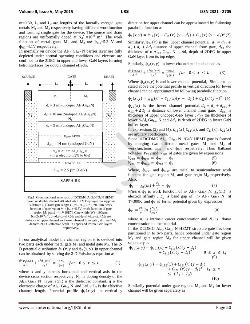
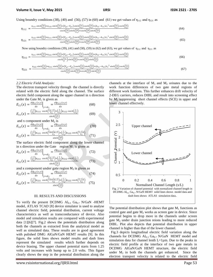
data [1][6][7]. Fig.2 shows the potentials distribution along
both the channels as extracted from the analytical model as
well as simulated data. These results are in good agreement
with pulished DMG AlGaN/GaN HEMT results [9]. In this
figure, the solid lines shows model results and dash lines
represent the simulated results which further depends on
device biasing. The upper channel potential starts from 1.25
volts and increases with hump up to 2.0 volts. This figure
clearly shows the step in the potential distribution along the
channels at the interface of M1 and M2 orinates due to the
work function differences of two gate metal regions of
different work funtions. This further enhances drift velocity of
2-DEG carriers, reduces DIBL and result into screening effect
by M2 suppressing short channel effects (SCE) in upper and
lower channel effectvely.
The potential distribution plot shows that gate M1 functions as
control gate and gate M2 works as screen gate in device. Since
potential begins to drop more in the channels under screen
gate M2 under drain junction reions leading to more reduced
DIBL. Plot also depicts that potential distribution in upper
channel is higher than that of the lower channel.
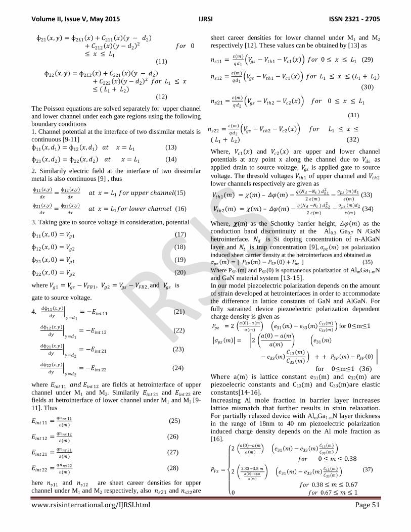
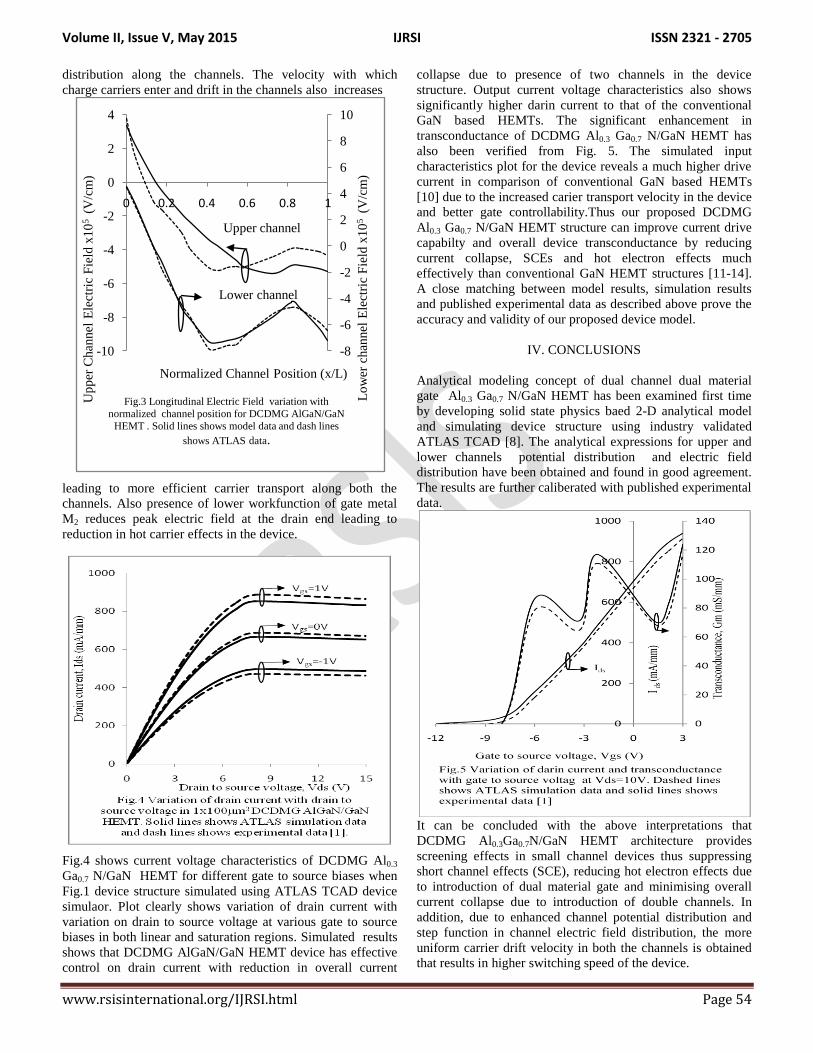
Fig.3 depicts longitudinal electric field variation along the
channels for DCDMG Al0.3 Ga0.7 N/GaN HEMT model and
simulation data for channel lenth L=1µm. Due to the peaks in
electric field profile at the interface of two gate metals in
DCDMG AlGaN/GaN HEMT structure, the electric field
under M2 in both the channels get enhanced. Since the
electron transport velocity is related to the electric field
0.5
1
1.5
2
2.5
3
0 0.2 0.4 0.6 0.8 1
Chan
nel
P
ote
nti
al
(V)
Normalised Channel Length (x/L)Fig. 2 Variation of channel potential with normalized channel length in
DCDMG Al0.3 Ga0.7 N/GaN HEMT solid lines shows model data and
dash lines shows ATLAS simulation data.
Upper channel
Lower channel
Volume II, Issue V, May 2015 IJRSI ISSN 2321 - 2705
www.rsisinternational.org/IJRSI.html Page 54
distribution along the channels. The velocity with which
charge carriers enter and drift in the channels also increases
leading to more efficient carrier transport along both the
channels. Also presence of lower workfunction of gate metal
M2 reduces peak electric field at the drain end leading to
reduction in hot carrier effects in the device.
Fig.4 shows current voltage characteristics of DCDMG Al0.3
Ga0.7 N/GaN HEMT for different gate to source biases when
Fig.1 device structure simulated using ATLAS TCAD device
simulaor. Plot clearly shows variation of drain current with
variation on drain to source voltage at various gate to source
biases in both linear and saturation regions. Simulated results
shows that DCDMG AlGaN/GaN HEMT device has effective
control on drain current with reduction in overall current
collapse due to presence of two channels in the device
structure. Output current voltage characteristics also shows
significantly higher darin current to that of the conventional
GaN based HEMTs. The significant enhancement in
transconductance of DCDMG Al0.3 Ga0.7 N/GaN HEMT has
also been verified from Fig. 5. The simulated input
characteristics plot for the device reveals a much higher drive
current in comparison of conventional GaN based HEMTs
[10] due to the increased carier transport velocity in the device
and better gate controllability.Thus our proposed DCDMG
Al0.3 Ga0.7 N/GaN HEMT structure can improve current drive
capabilty and overall device transconductance by reducing
current collapse, SCEs and hot electron effects much
effectively than conventional GaN HEMT structures [11-14].
A close matching between model results, simulation results
and published experimental data as described above prove the
accuracy and validity of our proposed device model.
IV. CONCLUSIONS
Analytical modeling concept of dual channel dual material
gate Al0.3 Ga0.7 N/GaN HEMT has been examined first time
by developing solid state physics baed 2-D analytical model
and simulating device structure using industry validated
ATLAS TCAD [8]. The analytical expressions for upper and
lower channels potential distribution and electric field
distribution have been obtained and found in good agreement.
The results are further caliberated with published experimental
data.
It can be concluded with the above interpretations that
DCDMG Al0.3Ga0.7N/GaN HEMT architecture provides
screening effects in small channel devices thus suppressing
short channel effects (SCE), reducing hot electron effects due
to introduction of dual material gate and minimising overall
current collapse due to introduction of double channels. In
addition, due to enhanced channel potential distribution and
step function in channel electric field distribution, the more
uniform carrier drift velocity in both the channels is obtained
that results in higher switching speed of the device.
-8
-6
-4
-2
0
2
4
6
8
10
-10
-8
-6
-4
-2
0
2
4
0 0.2 0.4 0.6 0.8 1
Lo
wer
chan
nel
Ele
ctri
c F
ield
x1
05 (V
/cm
)
Up
per
Chan
nel
Ele
ctri
c F
ield
x1
05 (V
/cm
)
Normalized Channel Position (x/L)
Fig.3 Longitudinal Electric Field variation with
normalized channel position for DCDMG AlGaN/GaN
HEMT . Solid lines shows model data and dash lines
shows ATLAS data.
Upper channel
Lower channel
Volume II, Issue V, May 2015 IJRSI ISSN 2321 - 2705
www.rsisinternational.org/IJRSI.html Page 55
REFERENCES
[1] Roanming Chu,Yugang Zhou, Zie Liu, Deliang
Wang, Kevin J. Chen, “AlGaN/GaN Double Channel
HEMT,” IEEE Transaction on Electron Devices,
vol.52, no.4, Apr. 2005.
[2] O. Ambacher, J. Smart, J. R. Shealy, N. G. Weimann, K. Chu,
M.Murphy, W. J. Schaff, L. F. Eastman, R. Dimitrov, L. Wittmer,
M. Stutzmann, W. Rieger, and J. Hilsenbeck, “Two-dimensional
electron gases induced by spontaneous and piezoelectric
polarization charges in N- and Ga-face AlGaN/GaN
heterostructures”, J. Appl. Phys, vol. 85, no. 6, pp. 3222–3233, Mar.
1999.
[3] Y. F. Wu, A. Saxler, M. Moore, R. P. Smith, S. Sheppard, P. M.Chavarkar, T. Wisleder, U. K. Mishra, and P. Parikh, “30-W/mm GaN HEMTs by field plate optimization”, IEEE Electron Device Lett., vol.25, no. 3, pp. 117–119, Mar. 2004.
[4] V. Tilak, B. Green, V. Kaper, H. Kim, T. Prunty, J. Smart, J. Shealy, and L. Eastman, “Influence of barrier thickness on the high power performance of AlGaN/GaN HEMTs”, IEEE Electron Device Lett., vol. 22, no. 11, pp. 504–506, Nov. 2001.
[5] K.Kasahara, N. Miyamoto, Y. Ando, Y. Okamoto, T. Nakayama, and M.Kuzuhara, “Ka-band 2.3 W power AlGaN/GaN hetrojunction FET,” in IEDM Tech. Dig., pp. 667–680, Dec. 2002.
[6] W. Long, H. Ou, J. M. Kuo and K.K Chin., "Dual-Material G a t e
(DMG) Field Effect Tr a n s i s t o r ” , IEEE Trans. Electron
Devices, vol. 46, pp. 865-70, May 1999.
[7] W. Long et.al. “Methods for fabricating a dual material gate of a
short channel field effect transistor”, US Patent, US006153534,
Nov 2000.
[8] Silvaco TCAD, ATLAS Device Simulator, www.silvaco.com.
[9] Sona P.Kumar et all, “Analytical modeling and simulation of
subthreshold behavior in nanoscale dual material gate AlGaN/GaN
HEMT” Elsevier, Superlattices and Microstructures, vol. 44, pp.
37-53, Mar. 2008.
[10] Jia-Chuhan Lin, Yu-Chieh Chen, Wei-Chih Tsai ,Po-Yu Yang
“Structure design criteria of dual channel high mobility electron
transistor”, Solid-State Electronics, vol.51, pp. 64-68, 2007.
[11] Sona P.Kumar, A. Agarwal, R Chaujar, S. Kabra , M. Gupta, R.S.
Gupta, “Threshold Voltage model for small geometry AlGaN/GaN
HEMT based on analytical solution of 3-D Poisson’s equations”
Microelectronics Journal, vol.38,pp. 1013-1020, Oct.2007.
[12] Sona P.Kumar, A. Agarwal, R Chaujar, M. Gupta, R.S. Gupta,
“Performance Assessment and sub-threshold analysis of gate
material engineered AlGaN/GaN HEMT for enhanced carrier
transport efficiency”, Microelectronics Journal, vol.39,pp.1416-
1424, Aug.2008.
[13] Rashmi “Modelin and characterization of spontaneous and
piezoelectric dependent lattice mismatched AlGaN/GaN HEMT
for microwave and millimeter wave applications” PhD Thesis,
UDSC, India, 2001.
[14] E.S. Hellman, “The polarity of GaN: A critical review”, MRS
Internet J. Nitride Semiconduct. Res. 3, vol. 11, pp. 1-11, 1998.
[15] Y.Zhang,I.P.Smorchkova, C.R.Elsass, S.Kellar, J.P.EIbbetson,
S.Denbaars, U.K.Mishra ans J.Singh “ Charge control and mobility
in AlGaN/ GaN Transistor:Experimental and theoretical studies”
J.Appl, vol.87, no11, pp.7981-7987, 2000.
[16] T.Li,R.P.Joshi and C.Fazi “Montecarlo evaluation of degeneracy
and interface roughness effects on electron transport in AlGaN/
GaN hetrostructures” J.Appl,Phys vol.88, no.2, pp.829-837,2000.
Copyright © 2022 FDOKUMEN