Analysis of the Power Balance in the Cells of a Multilevel Cascaded H-Bridge Converter
10
1 Analysis of the Power Balance In the Cells of a Multilevel Cascaded H-Bridge Converter S. Vazquez, Member, IEEE, J. I. Leon, Member, IEEE, J. M. Carrasco, Member, IEEE, L. G. Franquelo, Fellow, IEEE E. Galvan, Member, IEEE, M. Reyes, Member, IEEE, J.A. Sanchez and E. Dominguez, Member, IEEE Abstract—Multilevel cascaded H-Bridge converters (CHB) have been presented as a good solution for high power appli- cations. In this way, several control and modulation techniques have been proposed for this power converter topology. In this paper the steady state power balance in the cells of the single phase two cell CHB is studied. The capability to be supplied with active power from the grid or to deliver active power to the grid in each cell is analyzed according to the dc-link voltages and the desired ac output voltage value. Limits of the maximum and minimum input active power for stable operation of the CHB are addressed. Simulation results are shown to validate the presented analysis. I. I NTRODUCTION M ULTILEVEL converters have turned into a mature tech- nology that has increase its use in last years [1]-[3]. Among the multilevel converter topologies the cascaded H- bridge converters (CHB) were firstly presented in 1975, [4], [5]. Since then, the researches have paid attention in this topology because it presents several advantages compared with other multilevel converter topologies in terms of modularity, simplicity and number of levels with minimum number of power semiconductors [6]-[8]. The CHB has been used to develop different applications such as synchronous rectifiers, inverters, Statcoms, active filters, renewable energy integration systems, motor drives, etc [9]-[16]. Besides, specific control strategies and mod- ulation techniques, associated with those applications, have been designed for this converter topology [17]-[22]. As each dc-link is independent, when the CHB converter is used as a synchronous rectifier, it is possible to connect loads with several values to each dc-link. Besides, each dc-link can be controlled to a different dc voltage level providing a high degree of freedom. When two or more dc voltage values are needed, although it is possible to use independent two-level converters, the CHB converter provides some extra benefits. It has a lower input current harmonic content, thus a lower smoothing inductor value can be used. Besides, when inde- pendent two-level converters are used, it is necessary to put Manuscript received March 13, 2009. Accepted for publication September 26, 2009. This work was supported by the Spanish Science and Education Ministry under project TEC2007-61879. Copyright c 2009 IEEE. Personal use of this material is permitted. However, permission to use this material for any other purposes must be obtained from the IEEE by sending a request to [email protected]. S. Vazquez, J. I. Leon, J. M. Carrasco, L. G. Franquelo, E. Galvan, M. Reyes, J.A. Sanchez and E. Dominguez are with the Electronic Engineering Department, University of Seville (Spain), (e-mail: [email protected]). an smoothing inductor for each converter. Therefore the CHB provides reduction in overall volume, weight and economical cost. For these reasons, the CHB topology is very suitable when two or more dc voltage levels are needed. However, the converter operation has to be taken into account in the design process. Due to the fact that every cell share the same input ac current, the loading condition of each cell affects to the behavior of the overall system. In this paper the steady state power balance in the cells of a single-phase two-cell multilevel cascaded H-bridge power converter (2C-CHB) and the grid is analyzed. In section II a brief description of the 2C-CHB topology is presented. Then in section III the steady state power balance in the cells of the 2C-CHB is studied. The capability to be supplied with active power from the grid or to deliver active power to the grid in each cell is analyzed according to the dc-link voltages and the desired ac output voltage value, addressing the limits of the maximum and minimum loads for stable operation of the 2C- CHB. In section IV a brief description of the system controller is introduced. Finally in sections V and VI, simulation results validating the presented analysis and final conclusions are stated. II. SYSTEM DESCRIPTION A single-phase two-cell multilevel cascaded H-bridge power converter (2C-CHB) is depicted in Fig. 1. The system is connected to the grid through a smoothing inductor L. Load behavior is considered by using current sources i L1 and i L2 connected to each dc-link capacitor, C 1 and C 2 respectively. The system parameters and variables are described in Table I, where the continuous control signals δ 1 and δ 2 , represent the switching functions. The equations that describe the 2C-CHB behavior are well known and they have been reported previously [23]. v m1 = δ 1 v dc1 ; p 1 = v dc1 i L1 (1) v m2 = δ 2 v dc2 ; p 2 = v dc2 i L2 (2) p t = p 1 + p 2 (3) V s = L dI s dt + v m1 + v m2 (4) v m1 I s = C 1 d dt v 2 dc1 2 ¶ + p 1 (5) v m2 I s = C 2 d dt v 2 dc2 2 ¶ + p 2 (6)
Transcript of Analysis of the Power Balance in the Cells of a Multilevel Cascaded H-Bridge Converter

1
Analysis of the Power Balance In the Cells of aMultilevel Cascaded H-Bridge Converter
S. Vazquez, Member, IEEE, J. I. Leon, Member, IEEE, J. M. Carrasco, Member, IEEE, L. G. Franquelo, Fellow,IEEE E. Galvan, Member, IEEE, M. Reyes, Member, IEEE, J.A. Sanchez and E. Dominguez, Member, IEEE
Abstract—Multilevel cascaded H-Bridge converters (CHB)have been presented as a good solution for high power appli-cations. In this way, several control and modulation techniqueshave been proposed for this power converter topology. In thispaper the steady state power balance in the cells of the singlephase two cell CHB is studied. The capability to be supplied withactive power from the grid or to deliver active power to the gridin each cell is analyzed according to the dc-link voltages andthe desired ac output voltage value. Limits of the maximum andminimum input active power for stable operation of the CHB areaddressed. Simulation results are shown to validate the presentedanalysis.
I. INTRODUCTION
MULTILEVEL converters have turned into a mature tech-nology that has increase its use in last years [1]-[3].
Among the multilevel converter topologies the cascaded H-bridge converters (CHB) were firstly presented in 1975, [4],[5]. Since then, the researches have paid attention in thistopology because it presents several advantages compared withother multilevel converter topologies in terms of modularity,simplicity and number of levels with minimum number ofpower semiconductors [6]-[8].
The CHB has been used to develop different applicationssuch as synchronous rectifiers, inverters, Statcoms, activefilters, renewable energy integration systems, motor drives,etc [9]-[16]. Besides, specific control strategies and mod-ulation techniques, associated with those applications, havebeen designed for this converter topology [17]-[22]. As eachdc-link is independent, when the CHB converter is used asa synchronous rectifier, it is possible to connect loads withseveral values to each dc-link. Besides, each dc-link can becontrolled to a different dc voltage level providing a highdegree of freedom. When two or more dc voltage values areneeded, although it is possible to use independent two-levelconverters, the CHB converter provides some extra benefits.It has a lower input current harmonic content, thus a lowersmoothing inductor value can be used. Besides, when inde-pendent two-level converters are used, it is necessary to put
Manuscript received March 13, 2009. Accepted for publication September26, 2009. This work was supported by the Spanish Science and EducationMinistry under project TEC2007-61879. Copyright c© 2009 IEEE. Personaluse of this material is permitted. However, permission to use this materialfor any other purposes must be obtained from the IEEE by sending a requestto [email protected]. S. Vazquez, J. I. Leon, J. M. Carrasco, L. G.Franquelo, E. Galvan, M. Reyes, J.A. Sanchez and E. Dominguez are withthe Electronic Engineering Department, University of Seville (Spain), (e-mail:[email protected]).
an smoothing inductor for each converter. Therefore the CHBprovides reduction in overall volume, weight and economicalcost. For these reasons, the CHB topology is very suitablewhen two or more dc voltage levels are needed. However, theconverter operation has to be taken into account in the designprocess. Due to the fact that every cell share the same inputac current, the loading condition of each cell affects to thebehavior of the overall system.
In this paper the steady state power balance in the cells ofa single-phase two-cell multilevel cascaded H-bridge powerconverter (2C-CHB) and the grid is analyzed. In section II abrief description of the 2C-CHB topology is presented. Thenin section III the steady state power balance in the cells of the2C-CHB is studied. The capability to be supplied with activepower from the grid or to deliver active power to the grid ineach cell is analyzed according to the dc-link voltages and thedesired ac output voltage value, addressing the limits of themaximum and minimum loads for stable operation of the 2C-CHB. In section IV a brief description of the system controlleris introduced. Finally in sections V and VI, simulation resultsvalidating the presented analysis and final conclusions arestated.
II. SYSTEM DESCRIPTION
A single-phase two-cell multilevel cascaded H-bridge powerconverter (2C-CHB) is depicted in Fig. 1. The system isconnected to the grid through a smoothing inductor L. Loadbehavior is considered by using current sources iL1 and iL2
connected to each dc-link capacitor, C1 and C2 respectively.The system parameters and variables are described in Table I,where the continuous control signals δ1 and δ2, represent theswitching functions.
The equations that describe the 2C-CHB behavior are wellknown and they have been reported previously [23].
vm1 = δ1vdc1 ; p1 = vdc1iL1 (1)vm2 = δ2vdc2 ; p2 = vdc2iL2 (2)
pt = p1 + p2 (3)
Vs = LdIs
dt+ vm1 + vm2 (4)
vm1Is = C1d
dt
(v2
dc1
2
)+ p1 (5)
vm2Is = C2d
dt
(v2
dc2
2
)+ p2 (6)

2
TABLE ISYSTEM VARIABLES.
Parameter DescriptionL Smoothing inductor
C1, C2 Dc-link capacitorsiL1, iL2 Load currents
Is Grid currentVs Grid voltage
vdc1, vdc2 Dc-link voltagesVab Converter output voltage
vm1, vm2 Cell output voltagesδ1, δ2ε[−1, 1] Control signals
pt Converter input instantaneous power
b
avdc1
vdc2
C1
1S
1S
2S
2S
C2
4S
4S
3S
3S
vm1
vm2
+
iL1
iL2
L
Fig. 1. Two-cell single-phase CHB power converter.
+
+
+
Fig. 2. 2C-CHB equivalent circuit.
The behavior of the 2C-CHB is characterized by the induc-tor current dynamic (4) and dc-link capacitor voltage dynamicin each cell (5)-(6). In these equations, signals vm1 and vm2
represent the output voltage of each cell. These voltagesdepend on the dc-link voltage and the control signal valuesin each cell. Besides, signals p1 and p2 are the instantaneouspower demanded or delivered by the current sources connectedto each cell respectively.
To analyze the steady state power balance in the cells ofa cascade converter, the power converter equivalent circuitshown in Fig. 2 is used. In this representation, the cells havebeen replaced by voltage sources with values v1 and v2, equalto the RMS values of the fundamental harmonic of the voltagesmodulated by the cells, vm1,1 and vm2,1 respectively. Besides,the RMS values of the fundamental harmonic of the outputphase voltage (vab), grid voltage (vs) and grid current (is) areconsidered in the equivalent circuit.
Fig. 3. 2C-CHB phasorial diagram of voltages and current.
xy =
√1T
∫ T
0
X2y,1dt (7)
The RMS values can be calculated from the fundamentalharmonic value of each variable using (7), where xy representsthe RMS and Xy,1 represents the fundamental harmonic.
Py = vyiy cos θy (8)Qy = vyiy sin θy. (9)
The equivalent circuit is composed by sinusoidal voltagesources and passive components. As a consequence it ispossible to analyze it using conventional active and reactivepower definitions under sinusoidal conditions for single-phasesystems [24]- [25].
In equations (8) and (9) vy and iy are the RMS values of thevoltage and the current respectively and θy represents the shiftangle between them. Besides, Py is the active power whichis equal to the mean value of the instantaneous power py andQy is the reactive power.
III. POWER BALANCE ANALYSIS
The sign of the active power of each cell depends on theshift angle between the current is and the output voltage in thecell vi, i=1,2. This can be analyzed using the phasorial diagramof the 2C-CHB equivalent circuit represented in Fig. 3, wherethe RMS values of the converter main magnitudes are plotted.In the analysis it is assumed that, vab is calculated in sucha way that is is in phase with vs. Other solutions can beconsidered, however the same active power has to be suppliedby the grid to the cells or delivered from the cells to the grid.The only difference is the shift angle between the input currentand the grid voltage, leading to a reactive power exchangebetween the grid and the converter. Therefore the conclusionsfrom the presented analysis are still valid. In these phasorialdiagrams, it is important to show the maximum output voltagesin RMS of each H-bridge which can be calculated as
vc1 =4
π√
2vdc1 (10)
vc2 =4
π√
2vdc2. (11)
The capability to be supplied with active power from thegrid or to deliver active power to the grid in each cell dependson the value of the capacitor voltage in the cell, and the voltagethat should be modulated by the 2C-CHB. In what follows,the three possible cases are described and in all cases, it isassumed that vab can be modulated by the converter, i.e:
vc1 + vc2 ≥ vab. (12)

3
Fig. 4. Stable control area when vc1≤vab and vc2≤vab.
A. vc1≤vab and vc2≤vab
In this case it is necessary to use both cells to generatethe output voltage vab. Fig. 4 shows in a red marked areathe possible points to achieve the desired output voltage. Anypoint outside of this region make the system unstable becausethe output voltage can not be modulated with those values ofthe dc-link capacitor voltages. In addition, as it is shown inthe figure, the projection of v1 over is is always positive andthe same occurs for v2, as a consequence the active power inboth cells are positive values, meaning that the grid suppliesactive power to both cells simultaneously Moreover, it is notpossible to find a point where the grid supplies active powerto once cell and at the same time the other cell delivers activepower to the grid. In addition, this situation means that itis not possible to have the grid supplying active power onlyto one cell or to have only one cell delivering active powerto the grid On the other hand, it can be observed that thereactive power exchanged with the inductor is supplied bythe cells. There is no restriction to the reactive power signcontributed by each cell. This means that the reactive powerin each cell can be different, even in one cell the reactivepower can have capacitive nature meanwhile in the other ithas inductive nature.
In Fig. 5 it is shown that, for a given total amount of activepower supplied by the grid to the the converter, the powerdelivered to each cell has to be between a minimum and amaximum value to achieve a stable operation. Fig. 5a showsthe minimum active power that has to be supplied to cell 1.This value corresponds with the minimum reachable lengthof the projection of v1 over is, represented in the figure withvmin1p . As the total amount of active power is fixed, this value is
related with the maximum active power that can be deliveredto cell 2, shown in Fig. 5a as vmax
2p , which is the maximumreachable length of the projection of v2 over is. In the sameway, the values for the maximum active power that can besupplied in cell 1, vmax
1p , and the minimum active power thathas to be delivered to cell 2, vmin
2p , can be defined. Thesevalues are represented in Fig. 5b.
Fig. 5. Maximum and minimum active power limits when vc1≤ vab andvc2≤vab.
B. vc1 >vab and vc2≤vab
In this case the desired output voltage can be achievedusing both cells or just using the cell with the higher dcvoltage. This allows two possible power balance situations inthe cells. In Fig. 6 the marked red area represents the pointswhere both cells are supplied with active power from thegrid, while the marked green area shows the points wherethe first cell is supplied with active power from the gridmeanwhile the second cell delivers active power to the grid.As in section III-A, the reactive power is exchanged betweenthe inductor and the cells without restrictions in the reactivepower sign contributed by each one.
Fig. 6a shows a possible solution with both cells suppliedwith active power from the grid and Fig. 6b shows a possiblesolution when the first cell is supplied from the grid meanwhilethe second cell delivers active power to the grid. It is worthnoting that when vc1> vab and vc2≤ vab, if the total activepower supplied to the converter from the grid is positive thenonly the second cell active power can be negative meanwhilethe first cell active power is positive, and it is not possible tohave a negative active power in the first cell meanwhile thesecond cell has a positive active power value.
Fig. 7 shows the limits for the maximum and minimumactive power values allowed in the cells to achieve a stableoperation when the total amount of active power supplied fromthe grid to the converter is fixed. Two different power balancesituations can be clearly identified.
The first one can be considered as the conventional op-eration of the converter and it is shown in Fig. 7a. In thiscase both cells are supplied from the grid, as a consequencea minimum active power has to be supplied to cell 1 fromthe grid, this value corresponds with the minimum reachablelength of the projection of v1 over is, represented in the figurewith vmin
1p . Associated with this value is vmax2p , which is the
maximum reachable length of the projection of v2 over is andrepresents the maximum active power that can be supplied tocell 2.
The second power balance situation, represented in Fig. 7b,implies that the active power in each cell have different sign.Thus the cell with the higher dc voltage is supplied from thegrid meanwhile the other cell is delivering active power to

4
Fig. 6. Stable control area when vc1 > vab and vc2≤ vab. From top tobottom: Possible solution with: a) P1>0 and P2>0. b) P1>0 and P2<0.
the grid. Under this situation, the values for the maximumactive power that can be delivered to cell 1, vmax
1p , and theminimum active power that has to be supplied to cell 2, vmin
2p ,can be defined. In Fig. 7b it can be noticed that vmin
2p hasopposite direction than is, so the second cell is deliveringactive power. Besides, the maximum active power supplied tocell 1 is higher than the total amount of active power deliveredfrom the grid. This means that the active power delivered fromthe second cell is going into the first cell.
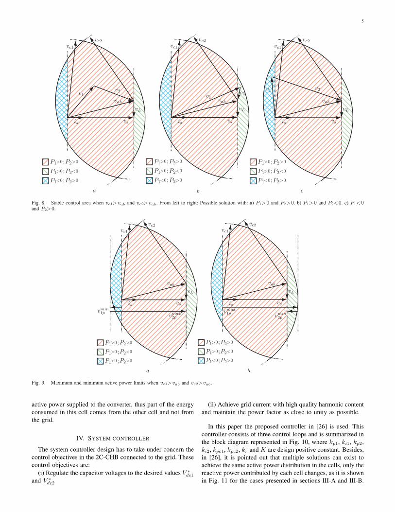
C. vc1 >vab and vc2 >vab
In this case the output voltage can be modulated usingboth cells or just using one of them. As a consequence threepossible power balance situations in the cells are under con-cern. In the marked red area of Fig. 8, both cells are suppliedsimultaneously with active power from the grid whereas themarked green area shows the set of points where the firstcell is supplied with active power from the grid meanwhilethe second cell delivers active power to the grid. In opposite,the marked light blue area represents the set of points wherethe first cell delivers active power to the grid meanwhilethe second cell is supplied with active power from the grid.Again, the reactive power is exchanged between the smoothinginductor and the cells without restrictions in the sign of thereactive power of each cell.
Fig. 7. Maximum and minimum active power limits when vc1> vab andvc2≤vab.
Fig. 8 shows three possible solutions, one for each powerbalance situation under concern. Fig. 8a shows the conven-tional operation, where both cells are supplied with activepower from the grid. Fig. 8b represents the converter operationwhen the first cell is supplied from the grid meanwhile thesecond cell delivers active power to the grid. Finally, Fig. 8cshows a solution with the first cell delivering active powerto the grid meanwhile the second cell is supplied with activepower from the grid. It can be noticed that when vc1>vab
and vc2>vab, although the total active power supplied to theconverter from the grid is positive it is possible that any onecell delivers active power to the grid meanwhile the other oneis supplied with active power from the grid.
When the maximum and minimum limits of the activepower consumed or injected by the loads connected to thecells are analyzed, similar conclusions to those presented insection III-B, when the power balance through each cell havedifferent sign, are found. In Fig. 9 are shown the maximumactive power that can be supplied and the minimum activepower values that have to be deliver to each cell to achievea stable operation, for a given total amount of active powerconsumed by the loads connected to the converter. Under thissituation, the minimum active power that has to be supplied ineach cell is negative, thus the cell is delivering active power.Meanwhile the maximum active power that can be consumedby the loads connected to the cell is higher than the total
5
Fig. 8. Stable control area when vc1>vab and vc2>vab. From left to right: Possible solution with: a) P1>0 and P2>0. b) P1>0 and P2<0. c) P1<0and P2>0.
Fig. 9. Maximum and minimum active power limits when vc1>vab and vc2>vab.
active power supplied to the converter, thus part of the energyconsumed in this cell comes from the other cell and not fromthe grid.
IV. SYSTEM CONTROLLER
The system controller design has to take under concern thecontrol objectives in the 2C-CHB connected to the grid. Thesecontrol objectives are:
(i) Regulate the capacitor voltages to the desired values V ∗dc1
and V ∗dc2
(ii) Achieve grid current with high quality harmonic contentand maintain the power factor as close to unity as possible.
In this paper the proposed controller in [26] is used. Thiscontroller consists of three control loops and is summarized inthe block diagram represented in Fig. 10, where kp1, ki1, kp2,ki2, kpc1, kpc2, kr and K are design positive constant. Besides,in [26], it is pointed out that multiple solutions can exist toachieve the same active power distribution in the cells, only thereactive power contributed by each cell changes, as it is shownin Fig. 11 for the cases presented in sections III-A and III-B.

6
Fig. 10. Block diagram of the system controller.
Fig. 11. Set of possible solutions for a particular active power distribution.From left to right: a) vc1≤vab and vc2≤vab. b) vc1>vab and vc2≤vab.
In Fig. 11a, all the points located in the segment betweenthe points MN lead to the same active power consumption ineach cell. Only the reactive power contribution changes. Sameconclusion can be reached for the points located in the segmentbetween the points OP of Fig. 11b. In the proposed controller,the reactive power contribution of each cell is defined by thevalues of the design constants k1 and k2, which must satisfy
k1 + k2 = 1. (13)
V. SIMULATION RESULTS
In this section, simulation results are shown to validate theanalysis presented in section III. For this purpose a single-phase two-cell multilevel cascaded H-bridge converter pro-totype has been used. The electric parameters of the proto-type are summarized in Table II. The proposed control of
TABLE IIELECTRIC PARAMETERS.
Parameter DescriptionRMS grid voltage (vs) 230 V
Grid frequency (f ) 50 HzSmoothing inductance (L) 3 mH
DC-Link capacitors (C1, C2) 2200 µFSwitching frequency (fsw) 10 kHzSampling frequency (fs) 10 kHz
TABLE IIICONTROL CONSTANTS.
Parameter Descriptionkp1, kp2 0.05ki1, ki2 0.5Tsw
kpc1, kpc2 6kr 1.8K 0.9
k1, k2 0.5
section IV has several design constants, which have beenadjusted experimentally to achieve a good behavior of theproposed controller. These constant values are summarizedin Table III. To assess the presented analysis, three differentexperiments are described. The first one shows the converteroperation in the stable region as described in subsection III-Awhile the second experiment shows the prototype behaviorwhen the loading condition leads outside this stable operationregion. Finally, an experiment showing the stable converteroperation with both cells having opposite power balance sign,as presented in subsection III-B, is analyzed.
A. Stable operation with vc1≤vab and vc2≤vab
In this case, both cells have to be supplied or to deliveractive power from the grid simultaneously. To illustrate this

7
0 0.5 1 1.5 2 2.5 3 3.50
50
100
150
200
250
300
350
Time (s)
V dc1,
V dc2 (V)
Vdc1Vdc2 Vdc1
Vdc2
Fig. 12. Evolution in time of dc voltages.
0 0.5 1 1.5 2 2.5 3 3.5-20
-15
-10
-5
0
5
10
15
20
Time (s)
I s(A)
Is
Fig. 13. Evolution in time of grid current.
operation a resistor of 60 Ω is connected to each dc-link as aload. Several dc voltage step references are applied to showthe behavior of the 2C-CHB. Initially the dc voltage com-mands are set to 200 V. When the actual dc voltages achievetheir references the loads are connected. Approximately twoseconds later the voltage command for the first cell is changedto 300 V and then, after one second, a new reference for thesecond cell of 100 V is established.
Fig. 12 shows the evolution in time of vdc1 and vdc2,and Fig. 13 the input current in the same period of time.It can be noticed that the dc output voltage references areachieved without difficulties. Besides Is grows or decreases inaccordance with the output load value variations. Additionally,the input current is almost in phase with the input voltage andpresents a low total harmonic distortion (THD), this can beobserved in Fig. 14 where a detail of Vs and Is is shown.This input current has a power factor (PF) of 0.99 and a THDof 2.5%. This THD value has been calculated up to the 50th
harmonic order.
B. Unstable operation with vc1≤vab and vc2≤vab
In this section it is shown the behavior of the 2C-CHBconverter when is operated in a point outside the stable region.As has been shown in section III-A, for a fixed total amountof active power exist a minimum active power values thathave to be consumed by the loads connected in each cell and
2.32 2.33 2.34 2.35 2.36 2.37-25
-20
-15
-10
-5
0
5
10
15
20
25
Time (s)
V s(V),
VsIs
I s(A
)
VsIs
Fig. 14. Detail of grid voltage and current.
2 3 4 5 6 7120
140
160
180
200
220
240
260
Time(s)
V dc1,V
dc2(V)
Vdc1Vdc2Vdc1
Vdc2
Fig. 15. Evolution in time of dc voltages.
a maximum active power values that can be supplied to thecells. In this experiment, the output dc voltage commands areestablished to 200 V and the total active power consumed bythe converter is set to 2 kW. The minimum and maximumactive power values under these working conditions can becalculated using equations (14) to (17) and are summarized inTable IV. Initially the converter is operated with a load locatedinside the stable region. For this purpose two resistors of 40 Ωare connected to the cells, consuming 1 kW in each cell. Thena load step is applied to the converter in such a way that theconverter goes to an unstable point. To achieve this condition,a resistor of 100 Ω is connected in the first cell and 25 Ω tothe second cell, drawing 1.6 kW and 0.4 kW respectively.
Pmax1 =
vmax1p
vsPt (14)
Pmin1 =
(vs − vmax2p )
vsPt (15)
Pmax2 =
vmax2p
vsPt (16)
Pmin2 =
(vs − vmax1p )
vsPt (17)
Fig. 15 shows the behavior of the dc voltages and Fig. 16the evolution of the input current. It can be noticed that forthe first load configuration the converter achieves a stable

8
2 3 4 5 6 7-15
-10
-5
0
5
10
15
Time(s)
I s(A
)
Is
Fig. 16. Evolution in time of grid current.
TABLE IVMAXIMUM AND MINIMUM ACTIVE POWER VALUES.
Parameter DescriptionP max
1 , P max2 1566 W
P min1 , P min
2 434 W
operation, the dc voltages are stable in the reference commandsand the input current is established in agreement with theoutput load. When the load step is applied, the converter triesto follow the references however, as it is working outside thestable region, it is not possible to achieve the commands andthe dc voltages change without control. Finally the converterhas to be stopped to avoid a malfunction caused by the inputcurrent or by a high output voltage value.
C. Stable operation with vc1 >vab and vc2≤vab
When vc1 >vab and vc2≤vab, the stable region can be splitin two areas depending on the cells power balance. In thisexperiment, the behavior of the 2C-CHB converter working inboth areas is explored. To develop the test, the following stepsare applied. In the beginning both cells are controlled to 200 Vand a resistor of 100 Ω is connected to each cell. When thesteady state is achieved, the first cell command is changed to400 V, thus the converter load is consuming 2 kW with bothcells supplied with active power from the grid. Then, afterone second, a current source is connected to the second cellto supply power from the cell to the grid. For this purpose,the source injects a current of 1.7 A so the final active powervalue supplied to the converter from the grid is 1.7 kW but thefirst cell is supplied from the grid meanwhile the second celldelivers active power to the grid. Fig. 17 shows the dc voltageschange along the time. It can be noticed that, when the currentsource is connected at 5.5 s, vc1 and vc2 values increase, dueto the active power delivered by the second cell. However thecontroller evacuates this power achieving the voltage referencecommands. When grid current is observed (Fig. 18), it canbe appreciated that current amplitude decreases when activepower is supplied from the second cell, so there is an energytransfer from the second cell to the first cell.
3 4 5 6 7 8150
200
250
300
350
400
450
Time(s)
V dc1,V
dc2
Vdc1Vdc2 Vdc1
Vdc2
Fig. 17. Evolution in time of dc voltages.
3 4 5 6 7 8-25
-20
-15
-10
-5
0
5
10
15
20
25
Time(s)
I s(A)
Is
Fig. 18. Evolution in time of grid current.
VI. CONCLUSIONS
The cascaded multilevel H-bridge power converter (CHB) isa suitable topology to be used when two or more independentdc voltage values are needed in a synchronous rectifier or back-to-back application. However some criteria have to be takeninto account to achieve a stable converter operation. In this pa-per, the power balance limits in the cells of a single-phase two-cell multilevel cascaded H-bridge power converter (2C-CHB)are addressed. These limits depend on the dc-link voltagevalues. It is shown that under certain conditions, it is possibleto have opposite sign active power values simultaneously inboth cells. Besides, to have a stable operation it is necessaryto ensure that, for a total amount of active power supplied tothe 2C-CHB, both cells loads are between the maximum andminimum allowed. Finally, simulation results are introducedvalidating that the presented analysis is an appropriate toolto establish the design criteria for the 2C-CHB synchronousrectifier or back-to-back application.
REFERENCES
[1] J. Rodriguez, S. Bernet, B. Wu, J. O. Pontt and S. Kouro, “MultilevelVoltage-Source-Converter Topologies for Industrial Medium-VoltageDrives,” IEEE Transactions on Industrial Electronics, vol. 54, no. 6,pp. 2930–2945, December 2007
[2] L. G. Franquelo, J. Rodriguez, J. I. Leon, S. Kouro, R. Portillo and M.M. Prats, “The age of multilevel converters arrives,” IEEE IndustrialElectronics Magazine, vol. 2, no. 2, pp. 28–39, June 2008.
9
[3] D. Krug, S. Bernet, S. S. Fazel, K. Jalili and M. Malinowski, “Com-parison of 2.3-kV Medium-Voltage Multilevel Converters for IndustrialMedium-Voltage Drives,” IEEE Transactions on Industrial Electronics,vol. 54, no. 6, pp. 2979–2992, Dec. 2007.
[4] R. H. Baker and L. H. Bannister, Electric power converter, U.S. Patent3 867 643, Feb. 18, 1975.
[5] M. Marchesoni, M. Mazzucchelli and S. Tenconi, “A non ConventionalPower Converter for Plasma Stabilization,” in Power Electronics Spe-cialist Conference 1988 (PESC’88), pp. 122–129, 11-14 April 1988.
[6] J. Rodriguez, Jih-Sheng Lai and Fang Zheng Peng, “Multilevel inverters:a survey of topologies, controls, and applications,” IEEE Transactions onIndustrial Electronics, Volume 49, Issue 4, pp. 724–738, August 2002.
[7] Y. Cheng, C. Qian, M.L. Crow, S. Pekarek and S. Atcitty, “A Comparisonof Diode-Clamped and Cascaded Multilevel Converters for a STATCOMWith Energy Storage,” IEEE Transactions on Industrial Electronics, vol.53, no. 5, pp. 1512–1521, October 2006.
[8] M.E. Ortuzar, R.E. Carmi, J.W. Dixon and L. Moran, “Voltage-sourceactive power filter based on multilevel converter and ultracapacitor DClink,” IEEE Transactions on Industrial Electronics, vol. 53, no. 2, pp.477–485, April 2006.
[9] H. Iman-Eini, J.L. Schanen, S. Farhangi, J. Roudet, “A Modular Strategyfor Control and Voltage Balancing of Cascaded H-Bridge Rectifiers,”IEEE Transactions on Power Electronics, vol. 23, no 5, pp. 2428–2442,September 2008.
[10] A.J. Watson, P.W. Wheeler, J.C. Clare, “A Complete Harmonic Elimina-tion Approach to DC Link Voltage Balancing for a Cascaded MultilevelRectifier,” IEEE Transactions on Industrial Electronics, vol 54, no 6,pp. 2946–2953, December. 2007.
[11] O. Alonso, P. Sanchis, E. Gubia, L. Marroyo, ”Cascaded H-bridgemultilevel converter for grid connected photovoltaic generators withindependent maximum power point tracking of each solar array,” inPower Electronics Specialist Conference 2003 (PESC’03), vol 2, pp731–735, 15-19 June 2003
[12] P. Lezana, J. Rodriguez, and D. A. Oyarzun, “Cascaded multilevelinverter with regeneration capability and reduced number of switches,”IEEE Transactions on Industrial Electronics, vol. 55, no. 3, pp. 1059–1066, March 2008.
[13] P. Lezana, C.A. Silva, J. Rodriguez, M.A. Perez, “Zero-Steady-State-Error Input-Current Controller for Regenerative Multilevel ConvertersBased on Single-Phase Cells,” IEEE Transactions on Industrial Elec-tronics, vol 54,no 2, pp. 733–740, April 2007.
[14] R. Teodorescu,F. Blaabjerg, J.K. Pedersen, E. Cengelci, P.N. Enjeti,“Multilevel inverter by cascading industrial VSI,” IEEE Transactionson Industrial Electronics, vol. 49, no 4, pp. 832–838, August 2002.
[15] J. A. Barrena, L. Marroyo, M.A.R. Vidal, J.R.T. Apraiz, ”Individual Volt-age Balancing Strategy for PWM Cascaded H-Bridge Converter-BasedSTATCOM Barrena,” IEEE Transactions on Industrial Electronics, vol.55, no 1, pp21–29, January 2008.
[16] A.M. Massoud, S.J. Finney, A.J. Cruden, B.W. William, “Three-Phase,Three-Wire, Five-Level Cascaded Shunt Active Filter for Power Con-ditioning, Using Two Different Space Vector Modulation Techniques,”IEEE Transactions on Power Delivery, vol. 22, no 4, pp. 2349–2361,October 2007.
[17] A. Dell’Aquila, M. Liserre, V.G. Monopoli and P. Rotondo, “Overviewof PI-Based Solutions for the Control of DC Buses of a Single-PhaseH-Bridge Multilevel Active Rectifier,” IEEE Transactions on IndustryApplications, vol 44, no. 3, pp. 857–866, May–June 2008.
[18] M.A. Perez, P. Cortes and J. Rodriguez, “Predictive Control AlgorithmTechnique for Multilevel Asymmetric Cascaded H-Bridge Inverters,”IEEE Transactions on Industrial Electronics vol. 55, no 12, pp. 4354–4361, December 2008.
[19] A. Dell’Aquila, M. Liserre, V.G. Monopoli, P. Rotondo, “Two passivity-based approaches to the control of the H-bridge-based multilevel recti-fier,”; in IEEE Industrial Electronics Conference 2003 (IECON03) vol.2, pp 1191–1196, 2–6 November 2003.
[20] D. Soto, R. Pena, “Nonlinear control strategies for cascaded multilevelSTATCOMs,” IEEE Transactions on Power Delivery, vol. 19, no 4, pp1919–1927, October 2004.
[21] J. I. Leon, S. Vazquez, A. J. Watson, P. W. Wheeler, L. G. Franqueloand J. M. Carrasco, “Feed-forward Space Vector Modulation for Single-Phase Multilevel Cascaded Converters With Any DC Voltage Ratio,”IEEE Transactions on Industrial Electronics, vol. 56, no. 2, pp. 315–325, February 2009.
[22] C. Cecati, A. Dell’Aquila, M. Liserre, V.G. Monopoli, “Design of H-bridge multilevel active rectifier for traction systems,” IEEE Transactionson Industry Applications, vol. 39, no 5, pp. 1541–1550, September–October 2003
[23] A. Dell’Aquila, M. Liserre, V.G. Monopoli and P. Rotondo, “An Energy-Based Control for an n-H-Bridges Multilevel Active Rectifier,” IEEETransactions on Industrial Electronics, vol. 52, no. 3, pp. 670–678, June2005.
[24] “IEEE Trial-Use Standard Definitions for the Measurement of ElectricPower Quantities Under Sinusoidal, Nonsinusoidal, Balanced, or Unbal-anced Conditions,” IEEE Standard 1459-2000, January 2000.
[25] H. Akagi, E.H. Watanabe and M. Aredes, “Instantaneous Power Theoryand Applications to Power Conditioning,” Wiley, 1st Ed., 2007.
[26] S. Vazquez, J. I. Leon, J. M. Carrasco, L. G. Franquelo, E. Galvan, J.A. Sanchez and E. Dominguez, “Controller Design for a Single-PhaseTwo-Cell Multilevel Cascade H-bridge Converter,” IEEE InternationalSymposium on Industrial Electronics, 2008 (ISIE 2008), pp. 1–6,Cambridge, UK, June 30–July 2 2008.
Sergio Vazquez (S’04, M’08) was born in Seville,Spain, in 1974. He received the B.S. and M.S.degrees in industrial engineering from the Universityof Seville (US) in 2003 and 2006, respectively. In2002, he was with the Power Electronics Group, US,working in R&D projects. He is currently an As-sistant Professor with the Department of ElectronicEngineering in the US. His research interests includeelectronic power systems, modeling, modulation andcontrol of power electronic converters and powerquality in renewable generation plants.
Jose I. Leon (S’04, M’07) was born in Cadiz,Spain, in 1976. He received the B.S. and M.S.and PhD degrees in telecommunications engineeringfrom the University of Seville (US), Spain, in 1999,2001 and 2006 respectively. In 2002, he joined thePower Electronics Group, US, working in R&Dprojects. Currently, he is an Associate Professor withthe Department of Electronic Engineering, US. Hisresearch interests include electronic power systems,modeling, modulation and control of power convert-ers and industrial drives.
Juan M. Carrasco (M’97) was born in San Roque,Spain. He received the M.Eng. and Dr.Eng. degreesin industrial engineering from the University ofSeville (US), Seville, Spain, in 1989 and 1992,respectively. From 1990 to 1995, he was an As-sistant Professor with the Department of ElectronicEngineering in the US where he is currently anAssociate Professor. He has been working for severalyears in the power electronic field where he wasinvolved in the industrial application of the designand development of power converters applied to
renewable energy technologies. His current research interests are in distributedpower generation and the integration of renewable energy sources.
L. G. Franquelo (M’84, SM’96, F’05) was bornin Malaga, Spain. He received the M.Sc. and Ph.D.degrees in electrical engineering from the Universityde Seville (US), Seville, Spain in 1977 and 1980respectively. His current research interest lies onmodulation techniques for multilevel inverters andits application to power electronic systems for re-newable energy systems. He was the Vice-Presidentof the Industrial Electronics Society (IES) SpanishChapter (2002 - 2003), member at Large of the IESAdCom (2002 - 2003). He was the Vice-President
for Conferences of the IES (2004 - 2007), in which he has also been aDistinguished Lecturer since 2006. He has been an Associated Editor forthe IEEE Transactions on Industrial Electronics since 2007. Since January2008 he is President Elect of IEEE Industrial Electronics Society.
E. Galvan (M’97) was born in Aracena (Huelva),Spain, in 1964. He received the M.Sc. degree inelectrical engineering and the Ph.D. degree in in-dustrial engineering from the University of Sevilla,Sevilla, Spain, in 1991 and 1994, respectively. He isan Associate Professor of electronic engineering atthe Escuela Superior de Ingenieros, Sevilla. He hasbeen working for several years in the power elec-tronic field where he was involved in the industrialapplication for the design and development of powerconverters applied to renewable energy technologies.
His research interests include control of power converters (wind turbineapplications, active filters, and electric machines).
10
M. Reyes (S’06, M’09) was born in Seville, inSpain, in 1981. He received the B.S. and M.S.degrees in telecommunications engineering from theUniversity of Seville (US), Spain, in 2005 and 2007respectively. In 2004, he joined the Power Elec-tronics Group, US, working in R&D projects. Cur-rently, he is a predoctoral researcher pursuiting hisPhD degree in electronic engineering. His researchinterests include electronic power systems; Flexi-ble AC Transmission Systems (FACTS); microgrids;distributed power generation and the integration of
renewable energy sources.
J.A. Sanchez was born in Moron, Spain, in 1974. Hereceived the B.S. and M.S. degrees in industrial engi-neering from the University of Seville (US), Seville,Spain, in 2001 and 2004 respectively He is currentlyan Assistant Professor with the University of Seville,where he is working on his doctoral thesis on gridpower quality. His research interests include poweractive filters, power control, and wind turbines. He iscurrently involved in related industrial projects, suchas power conditioners for fuel cells and photovoltaicplants.
E. Dominguez (S’04, M’07) was born in Madrid,Spain, in 1976. He courses studies of telecommu-nication engineering from the University of Seville(US), Spain. He joined the Power Electronics Groupin 1999, US, working in R&D projects. He was theResearch and Development Power Electronics Lab.Manager from 2005 to 2009 and currently he worksas director of several research projects in the PowerElectronics Group. His research interests includeelectronic power systems, hi performance hardwarecontrol systems and physical implementation of new
power electronic converters applied to renewable energies.