
AN486: High-Side Bootstrap Design Using ISODrivers in ...
12
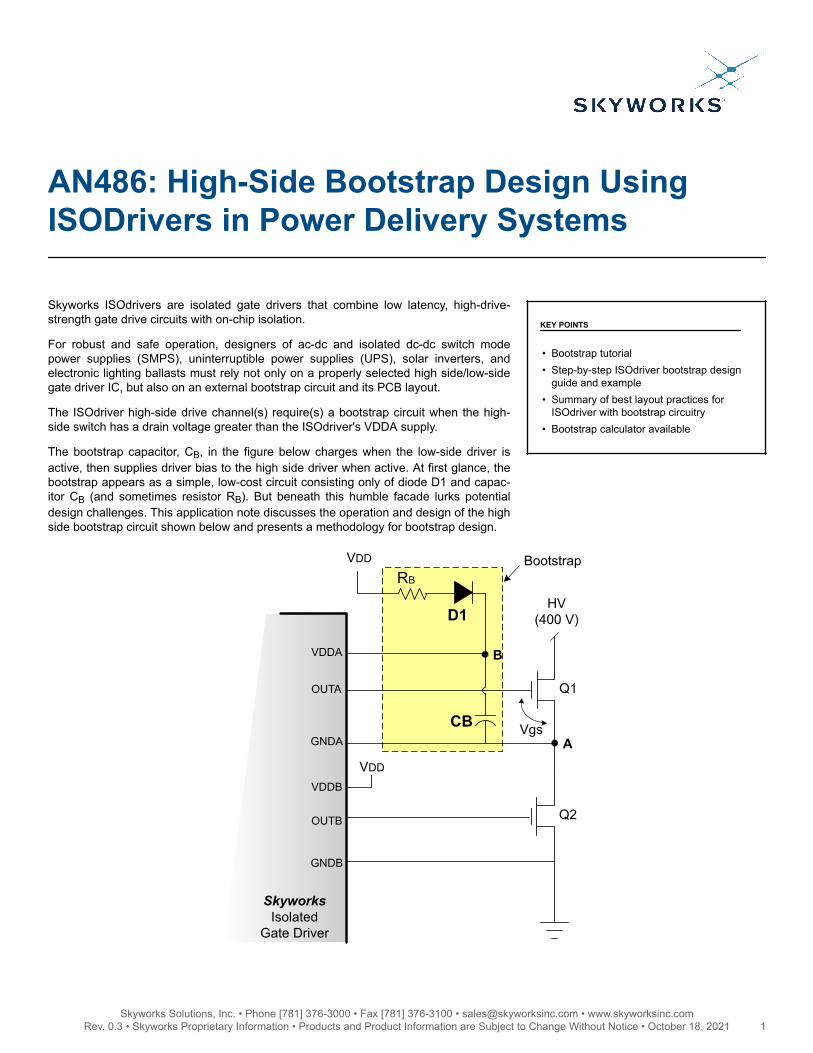
AN486: High-Side Bootstrap Design Using ISODrivers in Power Delivery Systems Skyworks ISOdrivers are isolated gate drivers that combine low latency, high-drive- strength gate drive circuits with on-chip isolation. For robust and safe operation, designers of ac-dc and isolated dc-dc switch mode power supplies (SMPS), uninterruptible power supplies (UPS), solar inverters, and electronic lighting ballasts must rely not only on a properly selected high side/low-side gate driver IC, but also on an external bootstrap circuit and its PCB layout. The ISOdriver high-side drive channel(s) require(s) a bootstrap circuit when the high- side switch has a drain voltage greater than the ISOdriver's VDDA supply. The bootstrap capacitor, C B , in the figure below charges when the low-side driver is active, then supplies driver bias to the high side driver when active. At first glance, the bootstrap appears as a simple, low-cost circuit consisting only of diode D1 and capac- itor C B (and sometimes resistor R B ). But beneath this humble facade lurks potential design challenges. This application note discusses the operation and design of the high side bootstrap circuit shown below and presents a methodology for bootstrap design. KEY POINTS • Bootstrap tutorial • Step-by-step ISOdriver bootstrap design guide and example • Summary of best layout practices for ISOdriver with bootstrap circuitry • Bootstrap calculator available HV (400 V) VDDA OUTA GNDA Skyworks Isolated Gate Driver VDD D1 CB Q1 A B Q2 OUTB GNDB VDDB VDD Vgs Bootstrap RB Skyworks Solutions, Inc. • Phone [781] 376-3000 • Fax [781] 376-3100 • [email protected] • www.skyworksinc.com 1 Rev. 0.3 • Skyworks Proprietary Information • Products and Product Information are Subject to Change Without Notice • October 18, 2021 1
-
Upload
khangminh22 -
Category
Documents
-
view
5 -
download
0
Transcript of AN486: High-Side Bootstrap Design Using ISODrivers in ...
AN486: High-Side Bootstrap Design UsingISODrivers in Power Delivery Systems
Skyworks ISOdrivers are isolated gate drivers that combine low latency, high-drive-strength gate drive circuits with on-chip isolation.
For robust and safe operation, designers of ac-dc and isolated dc-dc switch modepower supplies (SMPS), uninterruptible power supplies (UPS), solar inverters, andelectronic lighting ballasts must rely not only on a properly selected high side/low-sidegate driver IC, but also on an external bootstrap circuit and its PCB layout.
The ISOdriver high-side drive channel(s) require(s) a bootstrap circuit when the high-side switch has a drain voltage greater than the ISOdriver's VDDA supply.
The bootstrap capacitor, CB, in the figure below charges when the low-side driver isactive, then supplies driver bias to the high side driver when active. At first glance, thebootstrap appears as a simple, low-cost circuit consisting only of diode D1 and capac-itor CB (and sometimes resistor RB). But beneath this humble facade lurks potentialdesign challenges. This application note discusses the operation and design of the highside bootstrap circuit shown below and presents a methodology for bootstrap design.
KEY POINTS
• Bootstrap tutorial• Step-by-step ISOdriver bootstrap design
guide and example• Summary of best layout practices for
ISOdriver with bootstrap circuitry• Bootstrap calculator available
HV(400 V)
VDDA
OUTA
GNDA
SkyworksIsolated
Gate Driver
VDD
D1
CB
Q1
A
B
Q2OUTB
GNDB
VDDB
VDD
Vgs
BootstrapRB
Skyworks Solutions, Inc. • Phone [781] 376-3000 • Fax [781] 376-3100 • [email protected] • www.skyworksinc.com1 Rev. 0.3 • Skyworks Proprietary Information • Products and Product Information are Subject to Change Without Notice • October 18, 2021 1
1. Bootstrap Operation
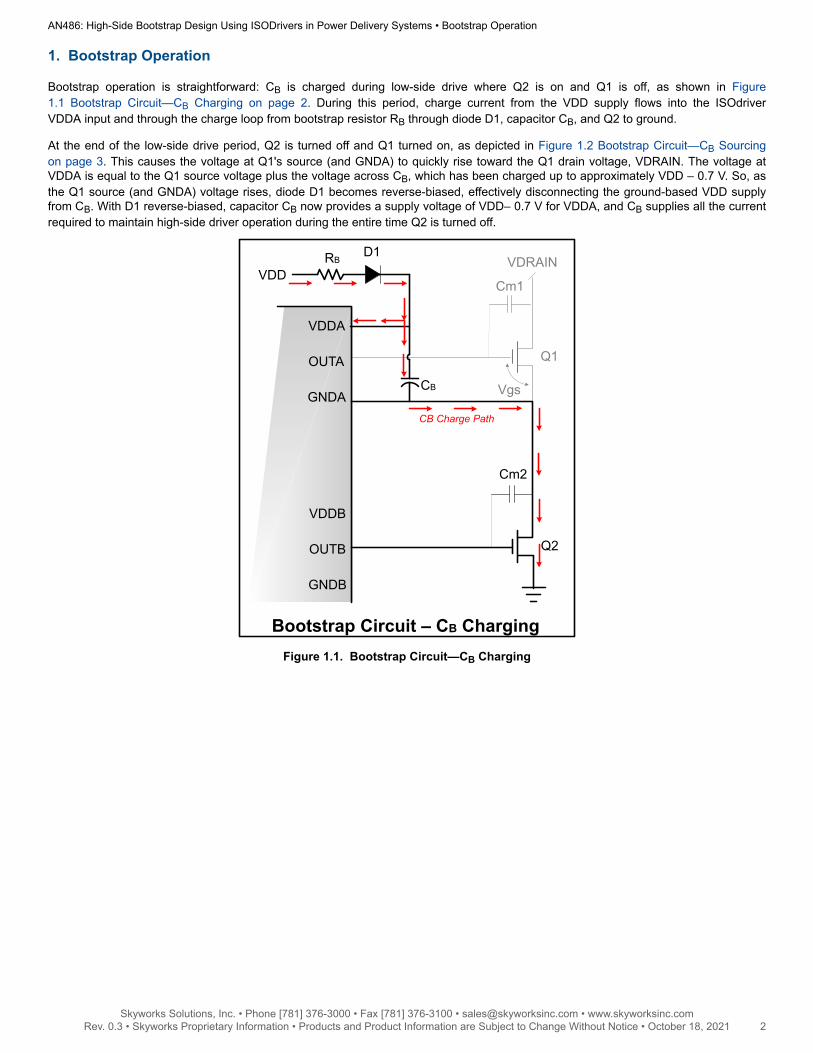
Bootstrap operation is straightforward: CB is charged during low-side drive where Q2 is on and Q1 is off, as shown in Figure1.1 Bootstrap Circuit—CB Charging on page 2. During this period, charge current from the VDD supply flows into the ISOdriverVDDA input and through the charge loop from bootstrap resistor RB through diode D1, capacitor CB, and Q2 to ground.
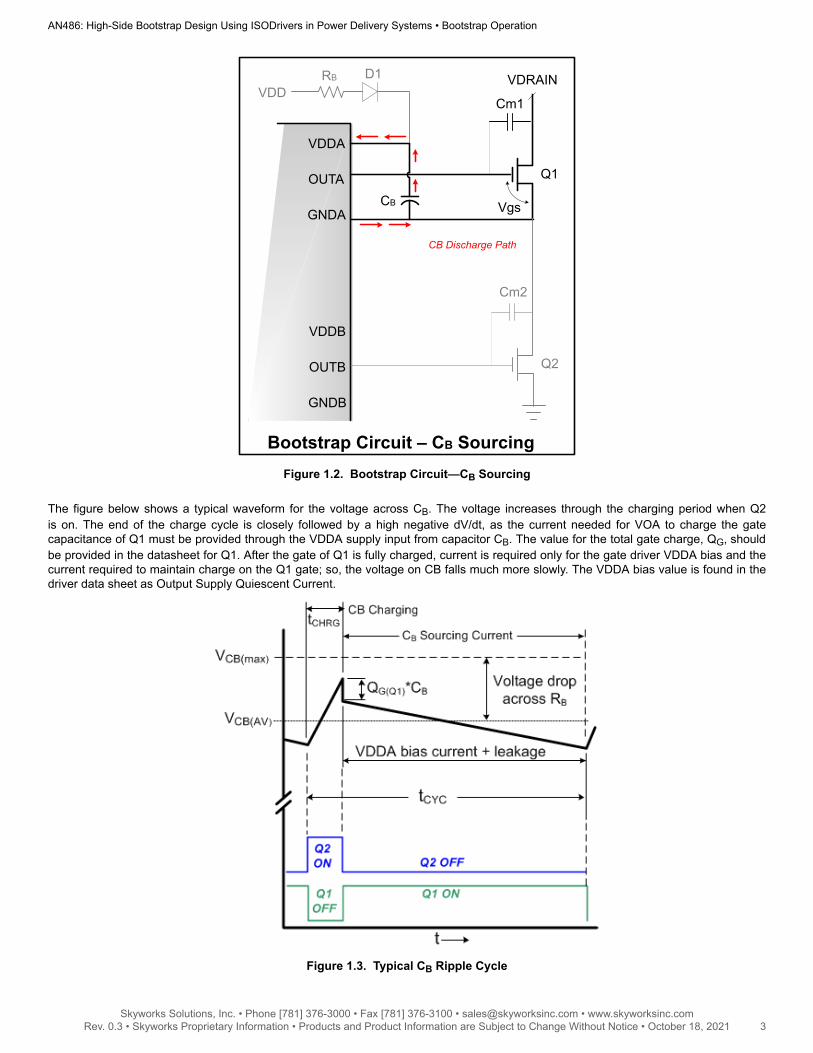
At the end of the low-side drive period, Q2 is turned off and Q1 turned on, as depicted in Figure 1.2 Bootstrap Circuit—CB Sourcingon page 3. This causes the voltage at Q1's source (and GNDA) to quickly rise toward the Q1 drain voltage, VDRAIN. The voltage atVDDA is equal to the Q1 source voltage plus the voltage across CB, which has been charged up to approximately VDD – 0.7 V. So, asthe Q1 source (and GNDA) voltage rises, diode D1 becomes reverse-biased, effectively disconnecting the ground-based VDD supplyfrom CB. With D1 reverse-biased, capacitor CB now provides a supply voltage of VDD– 0.7 V for VDDA, and CB supplies all the currentrequired to maintain high-side driver operation during the entire time Q2 is turned off.
VDRAIN
VDDA
OUTA
GNDA
VDD
D1
CB
Q1
Q2
Vgs
RB
VDDB
OUTB
GNDB
Cm1
Cm2
CB Charge Path
Bootstrap Circuit – CB ChargingFigure 1.1. Bootstrap Circuit—CB Charging
AN486: High-Side Bootstrap Design Using ISODrivers in Power Delivery Systems • Bootstrap Operation
Skyworks Solutions, Inc. • Phone [781] 376-3000 • Fax [781] 376-3100 • [email protected] • www.skyworksinc.com2 Rev. 0.3 • Skyworks Proprietary Information • Products and Product Information are Subject to Change Without Notice • October 18, 2021 2
VDRAIN
VDDA
OUTA
GNDA
VDDD1
CB
Q1
Q2
Vgs
RB
VDDB
OUTB
GNDB
Cm1
Cm2
CB Discharge Path
Bootstrap Circuit – CB SourcingFigure 1.2. Bootstrap Circuit—CB Sourcing
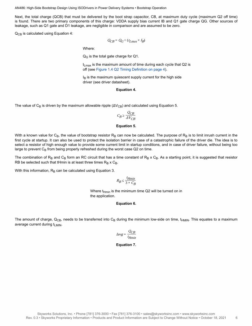
The figure below shows a typical waveform for the voltage across CB. The voltage increases through the charging period when Q2is on. The end of the charge cycle is closely followed by a high negative dV/dt, as the current needed for VOA to charge the gatecapacitance of Q1 must be provided through the VDDA supply input from capacitor CB. The value for the total gate charge, QG, shouldbe provided in the datasheet for Q1. After the gate of Q1 is fully charged, current is required only for the gate driver VDDA bias and thecurrent required to maintain charge on the Q1 gate; so, the voltage on CB falls much more slowly. The VDDA bias value is found in thedriver data sheet as Output Supply Quiescent Current.
Figure 1.3. Typical CB Ripple Cycle
AN486: High-Side Bootstrap Design Using ISODrivers in Power Delivery Systems • Bootstrap Operation
Skyworks Solutions, Inc. • Phone [781] 376-3000 • Fax [781] 376-3100 • [email protected] • www.skyworksinc.com3 Rev. 0.3 • Skyworks Proprietary Information • Products and Product Information are Subject to Change Without Notice • October 18, 2021 3

1.1 Bootstrap Design
While it is a simple circuit, the bootstrap can be problematic if not designed correctly. In particular, care must be taken to ensure low CBripple to avoid triggering the driver's undervoltage lockout, which can halt converter operation; additionally, the refresh period must besufficient to fully charge CB. The inherent limitation of the high-side bootstrap circuit is the time required to sufficiently refresh CB. Somepower topologies may have an excessively high duty cycle or frequency to support refresh, or they may have a high-side circuit thatcauses the load to be in series with the charge path. For those applications, a charge pump (instead of a high-side bootstrap) may berequired.
A typical bootstrap design flow first determines the total charge that CB must deliver during the high-side drive cycle (QCB). WithQCB known, the value of CB is calculated based on allowable ripple amplitude and verified adequate refresh under worst-case timingconditions. Note, in the figure below, that only the timing for the low-side switch, Q2, is used and not the high-side switch, Q1. This isdone because the time that Q2 is on represents the time provided to refresh CB, and the time that Q2 is off represents the amount oftime for which CB must provide charge to turn on Q1 as well as maintain the power supply for the high-side driver. By using this timing,we include any dead time used in the driver or built into the input signals.
PWMWaveform
Q2 ON(tH)
Q2 OFF(tL)
tCYC
Figure 1.4. Q2 Timing Definition
AN486: High-Side Bootstrap Design Using ISODrivers in Power Delivery Systems • Bootstrap Operation
Skyworks Solutions, Inc. • Phone [781] 376-3000 • Fax [781] 376-3100 • [email protected] • www.skyworksinc.com4 Rev. 0.3 • Skyworks Proprietary Information • Products and Product Information are Subject to Change Without Notice • October 18, 2021 4

1.2 Design Procedure
The design begins with the calculation of the minimum and maximum off time, and the minimum on time of the low-side MOSFET, Q2.This will allow the programmed dead time to be incorporated into the calculations as described in Figure 1.4 Q2 Timing Definition onpage 4.
Because the dead time is implemented in the driver as a delay between the falling edge of one channel and the rising edge of the otherchannel, the on time of Q2 can be derived as follows:
TH =(1 - D)FSW
- TDT
Where:
TH is the on time of Q2.
D is the duty cycle of the input signal.
FSW is the switching frequency.
TDT is the dead time.
The on time, tH, is minimized when the duty cycle, D, is at its maximum value:
THmin =(1 - Dmax)
Fsw- tDT
Where:
THmin is the minimum time Q2 is on.
Dmax is the maximum duty cycle in the application.
Equation 1.
Similarly, the off time, TL, is given by:
TL =D
Fsw+ tDT
For which the maximum and minimum are given by:
TLmax =D
Fsw+ tDT
Equation 2.
TLmin =DminFsw
+ tDT
Equation 3.
AN486: High-Side Bootstrap Design Using ISODrivers in Power Delivery Systems • Bootstrap Operation
Skyworks Solutions, Inc. • Phone [781] 376-3000 • Fax [781] 376-3100 • [email protected] • www.skyworksinc.com5 Rev. 0.3 • Skyworks Proprietary Information • Products and Product Information are Subject to Change Without Notice • October 18, 2021 5
Next, the total charge (QCB) that must be delivered by the boot strap capacitor, CB, at maximum duty cycle (maximum Q2 off time)is found. There are two primary components of this charge: VDDA supply bias current IB and Q1 gate charge QG. Other sources ofleakage, such as Q1 gate and D1 leakage, are negligible in comparison and are assumed to be zero.
QCB is calculated using Equation 4:
QCB = QG + (tLmax × IB)
Where:
QG is the total gate charge for Q1.
tLmax is the maximum amount of time during each cycle that Q2 isoff (see Figure 1.4 Q2 Timing Definition on page 4).
IB is the maximum quiescent supply current for the high sidedriver (see driver datasheet).
Equation 4.
The value of CB is driven by the maximum allowable ripple (ΔVCB) and calculated using Equation 5.
CB ≥QCB
ΔVCB
Equation 5.
With a known value for CB, the value of bootstrap resistor RB can now be calculated. The purpose of RB is to limit inrush current in thefirst cycle at startup. It can also be used to protect the isolation barrier in case of a catastrophic failure of the driver die. The idea is toselect a resistor of high enough value to provide some current limit in startup conditions, and in case of driver failure, without being toolarge to prevent CB from being properly refreshed during the worst case Q2 on time.
The combination of RB and CB form an RC circuit that has a time constant of RB x CB. As a starting point, it is suggested that resistorRB be selected such that tHmin is at least three times RB x CB.
With this information, RB can be calculated using Equation 3.
RB ≤tHmin3 × CB
Where tHmin is the minimum time Q2 will be turned on inthe application.
Equation 6.
The amount of charge, QCB, needs to be transferred into CB during the minimum low-side on time, tHMIN. This equates to a maximumaverage current during tLMIN.
Iavg =QCBtHmin
Equation 7.
AN486: High-Side Bootstrap Design Using ISODrivers in Power Delivery Systems • Bootstrap Operation
Skyworks Solutions, Inc. • Phone [781] 376-3000 • Fax [781] 376-3100 • [email protected] • www.skyworksinc.com6 Rev. 0.3 • Skyworks Proprietary Information • Products and Product Information are Subject to Change Without Notice • October 18, 2021 6

This current represents the current through the boot strap diode during each charging cycle in the steady state. However, the peakcurrent through the diode will happen during startup conditions when the capacitor CB is initially completely discharged. This is givenby:
Ipk =VDD - VD
RB
Where VD is the diode forward voltage drop.
Equation 8.
The diode chosen must be able to handle the maximum average current given by Equation 7 as well as the peak current from Equation8 for short periods of time during startup conditions.
In addition to the forward current ratings, the maximum repetitive reverse voltage specification of the boot strap diode must be at leastas high as the high-side MOSFET drain voltage minus the low-side MOSFET source voltage. Also, the diode must be able to switchfrom conducting forward current to blocking reverse current sufficiently fast to prevent excessive reverse current from flowing into thedriver power supply and causing damage. Furthermore, the diode reverse leakage current must be sufficiently low at all operatingtemperatures to prevent the same issue.
1.3 Design Example
For this example, we will use the following values as given for the application:• High-side MOSFET QG = 85 nC• Diode D1 VF = 0.7 V• VDDA input = 12 V• IB = 3 mA (Output supply quiescent current from datasheet)• FSW = 200 kHz, D = 10% to 90%• Programmed dead time, tDT = 100 nsec
The design begins with the calculation of the maximum and minimum off time, and the minimum on time of the low-side MOSFET, Q2.
Using Equations 1, 2 and 3, we get:
THmin =(1 - 0 . 9)200kHz - 100ns
THmin = 0 . 4μs
TLmax =0 . 9
200kHz + 100ns
TLmax = 4 . 6μs
TLmin =0 . 1
200kHz + 100ns
TLmin = 0 . 6μs
Next, calculate the total charge (QCB) that must be delivered by CB at maximum duty cycle. There are two primary components ofthis charge: VDDA supply bias current IB and Q1 gate charge QG. Other sources of leakage, such as Q1 gate and D1 leakage, arenegligible in comparison and are assumed to be zero.
From Equation 4, we get:
QCB = 85nC + (4 . 6μs × 3mA)
QCB = 98 . 8nC
AN486: High-Side Bootstrap Design Using ISODrivers in Power Delivery Systems • Bootstrap Operation
Skyworks Solutions, Inc. • Phone [781] 376-3000 • Fax [781] 376-3100 • [email protected] • www.skyworksinc.com7 Rev. 0.3 • Skyworks Proprietary Information • Products and Product Information are Subject to Change Without Notice • October 18, 2021 7
This means CB must supply a total of 98.8 nC of charge during the high-side drive cycle.
The value of CB is driven by the maximum allowable ripple (ΔVCB), and calculated using Equation 5. In this design, ΔVCB is chosen tobe 5% of VDD.
CB ≥98 . 8nC12 × . 05
CB ≥ 164 . 7nF
Use the closest standard value of 180 nF.
Now calculate the value of resistor RB using Equation 6.
RB ≤0 . 4μs
3 × 180nF
RB ≤ 0 . 74
Using 0.75 Ω will be sufficient.
In this design, 98.8 nC of charge must be transferred into CB within the minimum low-side on time tHMIN. Equation 7 calculates thecurrent required to meet this criterion:
Iavg =98 . 8nC0 . 4μs
Iavg = 247mA
From Equation 7, a maximum average current of 247 mA is required to fully refresh CB at maximum duty cycle time. However, the peakcurrent during startup conditions is given by Equation 8:
Ipk =12 - 0 . 7
0 . 75
Ipk = 15A
The diode chosen must be able to handle the maximum average current given by Equation 7 as well as the peak current from Equation8 for short periods of time during startup conditions.
In addition to the forward current ratings, the maximum repetitive reverse voltage specification of the boot strap diode must be at leastas high as the full high-side MOSFET drain voltage.
Also, the diode must be able to switch from conducting forward current to blocking reverse current sufficiently fast to prevent excessivereverse current from flowing into the driver power supply and causing damage. Many MOSFET specifications include information onhow fast the transistor’s drain-to-source voltage, VDS, will drop once the gate has been charged. In addition, there will be a turn ondelay time indicating how fast the VDS will start dropping once the gate-to-source voltage, VGS, begins rising. The sum of these twonumbers can be used to approximate when the ground reference of the high-side driver will reach the high-side drain voltage. Thereverse recovery time of the boot strap diode should be lower than this turn on time of the high-side MOSFET.
Furthermore, the diode reverse leakage current must be sufficiently low at all operating temperatures to prevent the same issue.
AN486: High-Side Bootstrap Design Using ISODrivers in Power Delivery Systems • Bootstrap Operation
Skyworks Solutions, Inc. • Phone [781] 376-3000 • Fax [781] 376-3100 • [email protected] • www.skyworksinc.com8 Rev. 0.3 • Skyworks Proprietary Information • Products and Product Information are Subject to Change Without Notice • October 18, 2021 8

2. Layout Considerations
Good layout is important in high-side bootstrap design. CB should be located as close to the driver IC pins as possible. A tantalumor ceramic capacitor (preferably ceramic) can be used for CB as they provide low leakage and low ESR. If an electrolytic capacitor isused for CB, it is recommended that a small, low-ESR decoupling capacitor be added in parallel with the electrolytic, as shown in thefollowing figure.
Figure 2.1. Bootstrap Layout Guidelines
AN486: High-Side Bootstrap Design Using ISODrivers in Power Delivery Systems • Layout Considerations
Skyworks Solutions, Inc. • Phone [781] 376-3000 • Fax [781] 376-3100 • [email protected] • www.skyworksinc.com9 Rev. 0.3 • Skyworks Proprietary Information • Products and Product Information are Subject to Change Without Notice • October 18, 2021 9

3. Conclusion
Proper attention to bootstrap component selection and PCB layout are critical to ensuring reliable, high-performance isolated gatedriver circuits.
To assist customers in performing some of these calculations, a boot strap calculation tool is available on the Skyworks website athttps://www.skyworksinc.com/tools/bootstrap-calculator.
AN486: High-Side Bootstrap Design Using ISODrivers in Power Delivery Systems • Conclusion
Skyworks Solutions, Inc. • Phone [781] 376-3000 • Fax [781] 376-3100 • [email protected] • www.skyworksinc.com10 Rev. 0.3 • Skyworks Proprietary Information • Products and Product Information are Subject to Change Without Notice • October 18, 2021 10
4. Revision History
Revision 0.3
January, 2020• Modified text and equations to be more descriptive and accurate.• Corrected minor errors in figures.• Added hyperlink to the online boot strap calculator.
Revision 0.2
September, 2015• Removed references to Si823x throughout.
Revision 0.1
March, 2010• Initial release.
AN486: High-Side Bootstrap Design Using ISODrivers in Power Delivery Systems • Revision History
Skyworks Solutions, Inc. • Phone [781] 376-3000 • Fax [781] 376-3100 • [email protected] • www.skyworksinc.com11 Rev. 0.3 • Skyworks Proprietary Information • Products and Product Information are Subject to Change Without Notice • October 18, 2021 11

Copyright © 2021 Skyworks Solutions, Inc. All Rights Reserved.Information in this document is provided in connection with Skyworks Solutions, Inc. (“Skyworks”) products or services. These materials, including the information contained herein, are provided by Skyworks as a service to its customers and may be used for informational purposes only by the customer. Skyworks assumes no responsibility for errors or omissions in these materials or the information contained herein. Skyworks may change its documentation, products, services, specifications or product descriptions at any time, without notice. Skyworks makes no commitment to update the materials or information and shall have no responsibility whatsoever for conflicts, incompatibilities, or other difficulties arising from any future changes.
No license, whether express, implied, by estoppel or otherwise, is granted to any intellectual property rights by this document. Skyworks assumes no liability for any materials, products or information provided hereunder, including the sale, distribution, reproduction or use of Skyworks products, information or materials, except as may be provided in Skyworks’ Terms and Conditions of Sale.
THE MATERIALS, PRODUCTS AND INFORMATION ARE PROVIDED “AS IS” WITHOUT WARRANTY OF ANY KIND, WHETHER EXPRESS, IMPLIED, STATUTORY, OR OTHERWISE, INCLUDING FITNESS FOR A PARTICULAR PURPOSE OR USE, MERCHANTABILITY, PERFORMANCE, QUALITY OR NON-INFRINGEMENT OF ANY INTELLECTUAL PROPERTY RIGHT; ALL SUCH WARRANTIES ARE HEREBY EXPRESSLY DISCLAIMED. SKYWORKS DOES NOT WARRANT THE ACCURACY OR COMPLETENESS OF THE INFORMATION, TEXT, GRAPHICS OR OTHER ITEMS CONTAINED WITHIN THESE MATERIALS. SKYWORKS SHALL NOT BE LIABLE FOR ANY DAMAGES, INCLUDING BUT NOT LIMITED TO ANY SPECIAL, INDIRECT, INCIDENTAL, STATUTORY, OR CONSEQUENTIAL DAMAGES, INCLUDING WITHOUT LIMITATION, LOST REVENUES OR LOST PROFITS THAT MAY RESULT FROM THE USE OF THE MATERIALS OR INFORMATION, WHETHER OR NOT THE RECIPIENT OF MATERIALS HAS BEEN ADVISED OF THE POSSIBILITY OF SUCH DAMAGE.
Skyworks products are not intended for use in medical, lifesaving or life-sustaining applications, or other equipment in which the failure of the Skyworks products could lead to personal injury, death, physical or environmental damage. Skyworks customers using or selling Skyworks products for use in such applications do so at their own risk and agree to fully indemnify Skyworks for any damages resulting from such improper use or sale.
Customers are responsible for their products and applications using Skyworks products, which may deviate from published specifications as a result of design defects, errors, or operation of products outside of published parameters or design specifications. Customers should include design and operating safeguards to minimize these and other risks. Skyworks assumes no liability for applications assistance, customer product design, or damage to any equipment resulting from the use of Skyworks products outside of Skyworks’ published specifications or parameters.
Skyworks, the Skyworks symbol, Sky5®, SkyOne®, SkyBlue™, Skyworks Green™, Clockbuilder®, DSPLL®, ISOmodem®, ProSLIC®, and SiPHY® are trademarks or registered trademarks of Skyworks Solutions, Inc. or its subsidiaries in the United States and other countries. Third-party brands and names are for identification purposes only and are the property of their respective owners. Additional information, including relevant terms and conditions, posted at www.skyworksinc.com, are incorporated by reference.
Portfoliowww.skyworksinc.com
Qualitywww.skyworksinc.com/quality
Support & Resourceswww.skyworksinc.com/support
Connecting Everyone
and Everything,
All the Time
Skyworks Solutions, Inc. | Nasdaq: SWKS | [email protected] | www.skyworksinc.comUSA: 781-376-3000 | Asia: 886-2-2735 0399 | Europe: 33 (0)1 43548540 |