An In-Depth Study of High Energy Oxygen Implantation into ...
216
Université de Montréal An In-Depth Study of High Energy Oxygen Implantation into Ion-Damaged Silicon Par Sandy Bultena Département de physique Faculté des arts et sciences Thèse présentée à la Faculté des études supérieures en vue de l'obtention du grade de P hilosphiæ Doctor (P h.D .) en Physique décembre, 1995 @ Sandy Bultena
-
Upload
khangminh22 -
Category
Documents
-
view
0 -
download
0
Transcript of An In-Depth Study of High Energy Oxygen Implantation into ...

Université de Montréal
An In-Depth Study of High Energy Oxygen Implantation into Ion-Damaged Silicon
Par
Sandy Bultena
Département de physique Faculté des arts et sciences
Thèse présentée à la Faculté des études supérieures en vue de l'obtention du grade de
P hilosphiæ Doctor (P h.D .) en Physique
décembre, 1995 @ Sandy Bultena

National Library 1*1 ofCanada Bibliortieque nationale du Canada
Acquisitions and Acquisitions et Bibliographie Services services bibliographiques
395 Wefllngton Street 395, nie Wellington OîîawaON K 1 A W OttawaON K 1 A W Canada Canada
The author has granted a non- exclusive licence allowing the National Library of Canada to reproduce, loan, distribute or sell copies of this thesis in microform, paper or electronic formats.
The author retains ownership of the copyright in this thesis. Neither the thesis nor substantial extracts fiom it may be printed or otherwise reproduced without the author's permission.
L'auteur a accordé une licence non exclusive permettant a la Bibliothèque nationale du Canada de reproduire, prêter, distriiuer ou vendre des copies de cette thèse sous la forme de microfiche/fih, de reproduction sur papier ou sur format électronique.
L'auteur conserve la propriété du droit d'auteur qui protège cette thèse. Ni la thèse ni des extraits substantiels de celle-ci ne doivent être imprimés ou autrement reproduits sans son autorisation.
Abstract
To produce high qudity SIMOX (separation by impiantation of oxygen) wafers, it is necessary
to reduce the damage that remairu in the silicon Mm after it has been anneaieci- The current method
of achieving this is to create BOX (buried oxide) wafers, which are essentially Iow-dose SMOX wafers.
To create BOX structures, it is necessary to undentand and manipulate the three precipitation
processes (homogenous (HO), heterogenous (E) and etherogeneous (ET) precipitation) that occur in
the silicon wafer during the implantation. The interaction between oxygen and pre-e.xisting damage
in a silicon wafer during the oxygen implantation and anneôling is studied in an effort to understand
how the presence, or absence, of damage changes the HE precipitation process.
Oxygen is implanteci into pre-damaged silicou, as well as undamaged silicon. The energy of
the oxygen implants is fixed at 2.50 MeV. The oxygen doses that are studied are o = 0.3 x 10".
1.0 x 10" and 3.0 x 10" 0/crn2. The implant temperature is 5i0°C.
Three different types of pre-damage are d. The k t two types are produced by a silicon
implant at room temperature, foiiowed by a 1 h, 900°C anneal. When d(Si) = 5 x 10" Si/cm2,
the resuiting pre-damage is cornposed aimost entirely of dislocation loops, and when &(Si) =
1 x 10L5 Si/cm2, it is cornposed almosr entirely of dislocation dipoles. The depth of the pre-damage
is varied by adjusting the implant energy. The sikon energies are E = 2.00,2.25,2.50 and 2.73 MeV.
The third type of pre-damage is created by a 2.5 MeV oxygen implant (2 x 10i5 0/cm3) around 300°C.
not followed by an anneal. This prdamage consists of s m d defect ciusters and rnicr-precipitates.
The distribution of oxygen as a function of depth was determineci by Elastic Recoil Detection
(ERD) and Semndary Ion Maos Spectrometry (SIMS). The damage profiles were characterized by Cross-
sectional Electron Microscopy (XTEM) and Ruthedord Badcscattering Spectrometry & Channeling
(RBS/C). The location and sizes of the oxide precipitates were characterized by XTEM-
First, the properties of oxygen implantation into un-damaged silicou are studied. The range
a d stragghg of the oxygen ions are determineci- The oxygen concentration profiles as a fuoction

of dose (asimplanteci and anneaieci), and the damage type and distribution as a functiot: of dose
(simplanted and annealed), are also studied.
An ernpirical mode1 is presented which describes the experimental results. It is demon-
strated that the minimum dose needed to form a BOX Iayer in an undamageci silicon wafer is
qi -1-2 x 10¹⁸ 0/cm2 when E = 2.5 MeV.
With the exception of the (O = 3.0 x 10" 0/cm2 sample, the silicon film is Gee of damage, up
to a depth of 2.33 Fm- In the ci = 3.0 x lol' 0/cm2 sample there is darnage located in a narrow
(0.4 pm) depth region around 1.2 Pm. After discussing the propenies of strain, and possible strain
relief mechanisms, it was concluded that the strain in the silicon film exceeded the elastic limit. which
resulted in the formation of s m d l dislocations and oxide precipitates.
Xext, the properties of oxygen implantation into pre-damaged siiicon are studied. The o q g e n
concentration profiles and the damage profiles, as a function of (1) oxygen dose, (2) pre-damage type
and (3) distance separating the pre-damage region from the oxygen implant, are studied.
The fotlowing results are presented. The remaining quantity of damage and precipitates at the
pre-damage depth ( d s i ) is an inverse function of the oxygen dose. When dsi is less than the depth of
- - the maximum darnage production (do), the concentration of oxygen at do is reduced in the annealed
sarnples. When dsi = do the concentration of oxvgen in this region is increased. The number of
threading dislocations between dsi and do is related to the stability of the pre-damage during the
oxygen impiantation. I t is sbown that the relevant properties of the pre-damage are (1) the rate
that interstitials can be absorbeci by the pre-damage, (2) the number of nucIeatioa sites for o d e
precipitation and (3) the relative stabiiity of the pre-damage d u ~ g the oxygen implantation.
Empirical models are developed which dis<suss the interactions between the pre-damage, silicon
interstitials and oxide precipitation. We demonstrate that the oxide precipitation at do, and the
subsequent oxygen concentration profile after annealing, is a rmult of oxygen and silicon interstitial
diffusion £rom do to dsi in the early stages of the implantation. We also demonstrate that the damage
in the silicon fiim is a r d t of excess silicon interstitiah, and can be reduced by providing a diffusion
barrier between the oxygen implant region and the silicon film.
(iii)
Résumé
Afin de produire des couches SMOX (Séparation par IMplantation d'oxygène) de bonne
quaiité, il est nécessaire de réduire le dommage résiduel dans la couche de silicium après l'avoir re-
cuite. Un échantillon s ~ o x est en fait une couche d'oxyde de 0,1-1 pm d'épaisseur enfouie sous une
épaisseur de 0,I à 5 p m de silicium crisfailin que l'on forme sur une pastille de silicium monocristaIlin.
L a performance de plusieurs dispositifs électroniques se trouve améliorée Iorçqu'ib sont frabriqués
sur des gaufres S ~ O X . On forme une couche SMOX en implantant une forte dose d'oxygène (4 >
1 - 2 x 10¹⁸ 0/cm2) à haute énergie (150 keV - 5 MeV) dans une gaufre de silicium suivi d'un recuit
haute température. On tente actuellement de produire des couches SIMOX en utilisant des doses
plus faibles d'oxygène (4 - 2 - 5 x 10li 0/cm2) dans le but de fonner des couches d'oxyde enfouies,
communément appelées BOX (Buried OXide). Les principaux avantages sont: (1) une réduction d u
dommage dans la couche de siIiciurn puisque l'on implante une dose plus faible d'oxygène et (2) une
production d'un plus grand nombre d'échantillons à un moindre coût.
Afin de créer des structures BOX, il est nécessaire de comprendre et de controler les trois pr*
cessus de nucléation qui se produisent dans la gaufre de silicium durant l'implantation. La nuciéation
hétérogène (HE) est le principal processus de nucléation qui se produit awc sites cristallins endommagés-
Ce processus survient principalement dans la région où se produit le maximum de dommage (do).
La nucléation homogène (HO) se produit à la profondeur du maximum de la concentration d'oxygène
(4) où cette concentration dépasse la b i t e de solubilité de l'oxygène dans le silicium. Le troisième
processus de nucléation (nucléation étherogène (ET)) résulte de l'interaction de l'oxygène avec la cas-
cade ionique dense et chaude et se produit à des profondeurs plus grandes que &. L a différence entre
les propriétés des nucléations HO, HE et ET constitue le processus fondamental régissant la formation
des couches d'oxyde enfouies BOX,
est important de bien c o m p r h e comment le processus de nucléation HE se produisant dans
le dk5.m durant i'implantion est iduencé par la présence ou I'absence de dommage et égalernuit
en quoi cela affecte I'échantiilon durant le recuit. Pour répondre à ces questions, nous avons décidé
d'étudier l'interaction entre l'oxygène et le dommage préexistant dans une gaufre de silicium durant
l'implantation e t durant le recuit.

On a déterminé la distribution d'oxygène en fonction de la profondeur par la méthode de
détection du recul elastique (ERD) et par spectrométrie de masse des ions secondaires (SIMS). Les
pro f i de dommage furent caractérisés par microscopie électronique à transmission (XTEM) et par
spectrométrie de rétrodiffusion Rutherford en mode canalisation (-s/c). La position et la taille des
précipités d'oxyde ont été déterminées par XTEM.
On a implanté l'oxygène dans des échantillons de silicium pré-endommagés et non endommagés.
L'énergie d'implantation des atomes d'oxygène était de 2,50 MeV. Ce choix de l'énergie d'implantation
se voulait un compromis entre une énergie élevée, où la séparation des ré@ons hétérogènes (2,3 pm)
et homogènes (2,55 pm) est bien définie, et une énergie faible, où les résultats pourraient ëtre plus
facilement reliés aux structures BOX. Les doses d'oxygène étudiées furent 4 = 0'3 x 101', L, O x 10''
et 3, O x 1017 0/cm2. La température de l'échantillon était maintenue à 570°C lors de l'implantation.
On a étudié les propriétés de l'implantation d'oxygène dans le silicium non endornagé en premier
lieu. L a couche de silicium demeure cristalline jusqu'à une profondeur de 2,33 pm, sauf pour la dose
4 = 3,O x 1017 0/cm2. cette dose, on retrouve une région étroite (0,4 prn) de dommage à la
profondeur de 1,2 pm. La formation des petites dislocations et des précipités d'oxyde résultent du
fait que la déformation du silicium excédait la limite élastique.
b
L a forme des profils de concentration d'oxygène dans les échantillons recuits dépend de la
dose d'oxygène. Cet effet est décrit à partir d'un modèle empirique. Ce modèle nécessite l'existence
d'au moins deux maxima locaux de la taille des precipités, situés respectivement à la profondeur du
maximum de dommage (précipités HE) et à la profondeur du maximum de concentration des ions
oxygène (précipités HO). Le nombre de précipités et leurs tailles augmentent avec la dose. .Aux doses
étudiées dans ces expériences, les précipités HO sont plus gros que les précipités m. L a nudéation
ET n'affecte pas la nucléation HE. Les précipités qui sont plus petits qu'une certaine taille critique
(-50 n m à la température du recuit) vont se dissoudre au tout début du recuit.
En utilisant le modèle empirique mentionné ci-haut, on peut expliquer les profils d'oxygène
après un recuit de 12 h comme étant dus au processus standard d'ostwald (Ostwdd ripening) appliqué
aux précipités résidu& de l'échantdlon. A la température de recuit utilisée, la majorité des précipités
d'un Cchaatiilon implanté à une dose de 3 x 10¹⁶ 0/cm2 sont plus petits que le rayon critique et, p x
conséquent, se dissolvent au de%ut du recuit. La distribution finale de l'oxygène a la forme d'une boîte-
Dans le cas d'échantillons implantés à une dose de 1 x 10'' 0/cm2. seuls l a précipités Ho sont plus
larges que le rayon critique. Finalement, dans un échantillon implanté à une dose de 3 x 10¹⁷ 0/cm2,
les précipités HE et HO sont tous plus larges que le rayon critique. Ces précipités croissent durant le
recuit et Ie profil final de la concentration d'oxygène est famé de deux pics distincts. Pour ce dernier
échantillon, il n'y a pas de diffusion d'oxygène entre les régions HO et HE durant le recuit. Pour cette
raison, toute couche d'oxyde fabriquée à des doses 6 = 3 x loL7 0/cm2 OU plus élevées doit ètre au
moins aussi épaisse que la distance qui sépare les régions de nucléations HE et HO. On en conclut que
la dose minimale pour former une couche d'oxyde est d'environ 1 - 2 x 10" 0/cm2.
Dans un deuxième temps, la compréhension de l'interaction entre la dommage et le comporte-
ment de l'oxygène dans le silicium s'est poursuivie par une étude de l'oxygène irnpianté dans des
échantillons de silicium pré-endommagés suivi d'une comparaison de ceux-ci avec les échantillons
préparés sur des substrats non endommagés. On a étudié trois types de pré-endommagement. Les
deux premiers types furent produits par l'implantation de silicium à la température de la pièce suivie
d'un recuit à 900°C pendant 1 h. Pour une dose 4(Si) = 5 x 10" Si/cmz. le prédommage se com-
pose presque entièrement de boucles de dislocations. Pour une dose &(Si) = 1 x 10¹⁵ Si/cm2. le
prédommage se compose presque exclusivement de dip6les de dislocations. La profondeur de création
de ce prédommage (dsi ) change avec l'énergie d'implantation du silicium. Les énergies chosies furent
' E = 2,00,2,25,2,50 et 2,75 MeV. Le troisième t-vpe de pré-endommagement fut créé par l'implantation
d'oxygène (2 x 10¹⁵ 0/cm2) d'une énergie de 2,s MeV à une température - 300°C; aucun recuit ne
fut fait dans ce cas. Le prédommage consiste en de petits amas de défauts et de micreprécipités.
Bien que la distribution des atomes d'oxygène dans les échantillons tels qu'implant& n'est
généralement pas affectée par les différences entre les processus de nuclëation HE, HO et ET, la dis-
tribution des précipités d'oxyde l'est. Cela résulte en une mosaïque de résultats pour les échantillons
recuits. Les profüs de concentration d'oxygéne et du dommage furent analysés en fonction (1) de la
dose d'oxygène, (2) de la distance de la région présadommagée de celle où l'oxygéne a été implanté
et (3) du type de prédommage. La distribution des précipités d'oxyde dans les échantiUons tels
qu'hplantéa est déduite de l'état des échantillons recuits.
La quantité de dommage et de précipitb qui restent à la profondeur dsi est inversement pr*
portionde à la dose d'oxygène, en accord avec l a résultats des pro& de concentration d'oxygéne.
En conséquence, la présence du prédommage dans les échantiIlons avant l'implantation est moins
apparente pour des doses plus élevées d'oxygène.
Si la profondeur du prédommage (dsi) est plus faible que la profondeur du maximum de p m
duction de dommage (do), la concentration d'oxygène à do est réduite dans les échantiilon recuits-
Quand dsi = do, la concentration d'oxygène dans cette région augmente-
Le profil final de la concentration d'oxygène dépend du type de prédommage. L e nombre de
dislocations entre dsi et do est relié à la stabilité du préàommage lors de l'implantation d'oxygène.
ce qui, par la suite, change la quantité de précipités dans la région entre do et dsi. Les propriétés
pertinentes du préciommage sont ( I) le taux d'absorption des interstitiels par le prédommage. (2) le
nombre de sites de nucléation pour la formation de précipités d'oxyde et (3) la stabilité relative du
prédommage lors de l'implantation d'oxygène.
Un modèle a égaiement été développé pour e-upliquer les différences entre les profils de con-
centration d'oxygène des échantillons recuits. Au début de l'implantation, il y a précipitation dans
trois régions distinctes: (1) dans la région du prédommage ( d s i ) , (2) dans la région du maximum de
dommage (do) et (3) dans la région du maximum de pénétration de l'oxygène dans le silicium (4)- Au tout début de l'impiantation, la majorité des sites de nucléation pour l'oxydation se situent à la
profondeur dsi. Les atomes d'oxygène et les silicium interstitiels diffusent vers dsi, ce qui réduit le
taux de croissance du dommage et des précipités d'oxyde à do. 11 y a cependant plus d'ions d'oxygène
déposés dans cette région par unité de temps qu'il y en a autour de dsi. En conséquence, les précipités
y croissent plus rapidement que dans la région dsi. Les interstitiels de silicium en excès qu'on retrouve
dans cette dernière région ne sont pas libres de migrer vers la surface. Ils interagissent plutôt avec
le prédommage ou avec le dommage causé par l'oxygène, résultant en la formation de dislocations
entre ces deux couches. Une nouveiie région d'oxydation préférentielle qui s'étale entre dsi et do est
formée. Après le recuit de l'échantillon, les régions qui contiennent de gros précipités forment des pics
de concentration d'oxygène,
En résumé, nous avons démontré que la précipitation d'oxyde à do peut ëtre contrôlée par un
endommagement préalable de la g a h e de silicium avant l'implantation. Si le prédommage se situe à
Q , la nudéation HE est augmentée. Dans l'avenir, il serait possible de créer des structurer Box à des
énergies élevées d'implantation d'oxygéne en contrôlant la nucléation Ho de la m ê m e fyon.

Table of Contents
........................................ ABSTRACT ... ........................................... i
TABLE OF CONTENTS ...................................... ................................ vii
LIST OF TABLES ............................................................................. xi
.. ............................................................................ LIST OF FIGURES .y11
..................................................................... 1 INTRODUCTION 1
............................................................... 2-1 CRYSTAL DEFECTS - 6
........................................................................ 2- 1- 1 Dislocations - 6
2-1-2 Point Defects and Intermediate Defect Clusters ..................................... - 9
............................................................. 2-2 ION IMPLANTATION 13
.................................................................... 2-2-1 Stopping Power 13 .......................................................... 2-2- 1- 1 NucIear S topping 13
........................................................ 2-2- 1-2 EIectronic Stopping 14
...................................................... 2-2-2 Range and Straggiing of Ions -15
.............................................................. 2-2-3 Implantation Darnage 17
............................. ..*.-.*.......... 2-2-4 High Energy Implantation Damage .. -20 ........................................... 2 - 2 4 1 Damage as a Function of Depth -22
.................................... 2 - 2 4 2 Damage as a Function of Temperature - 2 5 ............................................ 2 - 2 4 3 Damage as a Function of Dose - 2 6
........................................................ 2-2-4-4 Defect Engineering -27
............................................................ 24 OXYGEN IN SILICON -31
...................................................................... 2 4 1 Precipitation -31
.................................................................. 2 4 2 Ostwdd Ripening 34
............................................................. 2 4 3 A Mode1 of AMealiDg -35

TABLE OF CONTENTS (k)
......................... 4 EXPERIMENTAL RESULTS AND DISCUSSION 70
............................................... 4 1 EXPERIMENTAL PARAMETERS 70
............................................................................ 4-1-1 Oxygen 71
............................................................................. 4-1-2 Silicon 71
........................................................................... 4-1-3 Analysis 72
.............................................................. 4 2 SILICON IN SILICON 74
.............................................................................. 42- 1 Range 74 .. ............................................................................ 4-2-2 Damage la - - .............................................................. 4-2-2- 1 -4s-Implanted r a
.................................................................. 4-2-2-2 Annealed 78
............................................................. 4 3 OXYGEN IN SILICON 83
.............................................................. 4-51 Range and Straggling 83 ................................................................... 43-1-1 RBS/C - 8 4
....................................................................... 43- 1-2 ERD 86 ..................................................................... 4-3-1-3 SIMS -87
................................................................. 4 3 - 1 4 Discussion d f
........................................................................... 4-3-2 Damage -88 ............................................................. 4-3-2-1 AcImplanted - 8 9
................................................................. 43-2-2 Annealed - 9 5 ................................................................ 43-2-3 Discussion 102
.............................................................. 4-3-3 Oxygen Distribution 104 ............................................................ 4-3-81 .A s-lmplanted -104
................................................................. 4-3-3-2 .Annealed 108 ................................................................ 43-3-3 Discussion 114
....................................... 4-4 OXYGEN IN PREDAMAGED SILICON 120
........................................................................... 4-41 Damage 122 ............................................................. -1- 1 As-implanted 122
................................................................. 44-1-2 h e a l e d 132 ................................................................ 4-4- 1-3 Discussion 141
.............................................................. 4-4-2 Oxygen Distribution 147 ............................................................ 4 4 2 - 1 &Implanted -147
.......................................... 4-42-2 9 = 0.3 x 10" 0/cm2, healed 150
.......................................... W 2 - 3 q5 = 1.0 x loL7 O/an3, Annealed 151
.......................................... 4-4-2-4 9 = 3.0 x loL7 O/cma, Annealed 157
........................................................................ 4 4 3 Discussion 161 .................................................... 443-1 Effect of Oxygen Dose 164
........................................ 4-44-2 Effat of Silicon Prdamage Depth 166 ................................................ 4-4-3-3 Effift of Prcdamage Type 168

TABLE OF CONTENTS (x)
5-1 RANGE AND STRAGGLmG ................................................... -171
3-2 QUALITY OF THE SILICON FILM ............................................ -171
5-2-1 Function of Dose ................................................................. -171
5-2-2 Retease of Strain .................................................................. 172
5-3 OXIDE PRECIPITATION ........................................................ -173
5-3-1 Standard SarnpIe .................................................................. Li3
%3-2 Pre-damaged Szunple ............................................................. -174
5-4 SILICON SUBSTRATE ........................................................... .L15
.. 5-5 FURIïIHER WORK ................................................................. Li -3
6 CONCLUSION ....................................................................... 177
REFERENCES .......................................................................... 178
APPENDIX A -WTROGEN IN-DIFFUSION -LVD ACCUMULATION IX O-XYGEX-I-UfPLXYITD SILICON DURIi\lG THER\fAL .LhïYEXL I-jG . ~ - . - ~ ~ - - - - - ~ * ~ ~ - ~ - ~ ~ ~ ~ ~ . ~ - + ~ ~ ~ ~ ~ - - - - - - - . - . - - - - - 185
List of Tables
...................................................................................... Table 2-1 16 Experimental and theoretid range and straggling depths for oxygen into silicon-
Table2-II ..................................................................................... 43 The dose (&), energy, and implant temperature dependence on the formation of a dislocation network in the silicon overlayer.
Table 4-1 ...................................................................................... 70 Experimental Parameters.
Table411 ..................................................................................... 73 A summary of the implanted samples and the techniques used to analyse them.
Table 4-111 .................................................................................... 74 Location of damage peak in silicon damaged silicon.
.................................................................................... Table Q-ïV 88 X summary of the measured and estirnatecl projected range and straggling of 2.5 Mev O in silicou.
.................................................................................... Table4-V 121 X surnrnary of the experimentai parameters and resdts (a) The experimental results and interpretation of pre-damaged samples. (b) The experimental and interpretations of oxygen implanted into pre-damaged samples, as a funtion of pre-damage conditions . and oxygen dose.
.......................................................... ..................... Table 4-VI ,.. 142 Damage (as seen in xTEM photos) in as-implanteci samples as a function of depth and implant-conditions.
Table4-VI1 .................................................................................. 143 Damage (as seen in XTEM photos) in annealed samples as a function of depth and implant-conditions.

List of Figures
Figure 2-1 ............................~~~...........--.-------....--.-.-..-..-.......... 7 (a) A closed curve in a perfect crystal formed by the addition of Bravais lattice vectors (6 down, 8 right, 6 up, 8 left). (b) The same addition of Bravais lattice vectors as described in (a) (from 'B' to C') do not form a closed loop since there is a defect within. The Burgers vector is defined as the sum of these vectors. The dislocation that the second path surrounds is seen most readiIy by viewing the page at a very low angle.
Figure
Figure
Figure
Figure
Figure <
Figure
...................................................................................... 2-2 7 (a) Slip in a crystal via the motion of an edge dislocation. (b) Slip in a crystal via the motion of a screvl dislocation.
...................................................................................... 2-3 9 X schematic representation of (a) an e-utrinsic dislocation loop, (b) an intrinsic disloca- tion loop, and (c) a dislocation dipole.
............................................................ 2-4 .................. ..... LO X diagram of a perfect silicon crystal.
..................................................................................... 2-5 LO An illustration of (a) Td interstitial (6) split <110> interstitid, (c) Mcancy, (d) di- interstitial, and (e) di-vacancy, in the silicon crystal structure.
..................................................................................... 2-6 11 Row (a) interstitial and (b) vacancy defects elongated along the (110) chain.
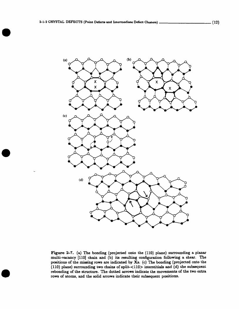
........................................................... .................. 2-7 ..... 12 (a) The bonding (projected onto the (110) plane) surrounding a planar multi-vacancy [110] chain and (b) its resulting configuration foliowing a shear. (c) The bonding (pro- jected onto the (1 10) plane) surrounding two chains of split-< l l0> interstitids and (d) the subsequent rebonding of the structure.
..................................................................................... Figure 2-8 21 (a) A plot of the Electronic and Nuclear Stopping powers for oxygen ions projected into a silicon target. (b) Nuclear and electronic energy losses as a function of depth for 2.5 MeV O+in silicon.
..................................................................................... Figure 2-9 24 TRIM calculation of ion distribution, Frenkei pair distribution (not to scale) and the excess interstitial distribution (not to scale).
.................................................................................... Figure 2-10 32 The formation of a doubly decorated oxygen/vacancy complex-
Figure 2-11 .................................................................................... 32 The formation of a coherent oxide precipitate on a <loo> split-interstitid by the inser- tion of 4 oxygen atoms (black circles), and the migration of the interstitial.
LIST OF FiGUWS (iii)
Figure2-12 .................................................................................... 38 A figure dernonstrating Heinïgs cornputer simulation of M d ripening. (a) Initiai conditions. (b)-(d) Subsequent steps in the evolution of the precipitates and oxygen solute concentrations.
Figure 3-1 ................................................................................. 54 An illustration of the method used to construct a conversion table relating the depth of the scattering centre to the measured energy of the recoiied or xattered ion.
Figure 3-2 ...-........-...............~~...--.....~........-...........~.~....~.-..-.........-. 56 (a) Theoretical total depth resolution for O recoils in Si for B = 30° and a = P = lao as a function of depth cornpareci with the experimental vaiues from several Si02 targets. (b) Calculatecl depth resolutions for different scattering grometries. (1 pg/cm2 % 43A for silicon)
Figure 3-3 ..................................................................................... 60 A mode1 of a silicon crystai aligned in a (a) randorn, (b) <100> and (c) <110> direction.
Figure 3-4 ..................................................................................... 66 A diagram illustrating the (a) BF imaging and (b) SAD made of the efectron microscope.
Figure 345 ..................................................................................... 68 An edge dislocation with a Burgers vector b (a) perpendicular to f and (b) pardel to
Y-
................................... ............................................. Figure 3-6 ,., 69 XTEM samp1e preparation: (a) gIueing, (b) slicing, thinning (not sbown), (c) dimpling, and (d) ion milling.
- Figure 4- 1 ..................................................................................... 72 TRIM predictions for the depth profile of recoiled atorns for 2.0-2.75 MeV Si and 2.5 MeV O implanted silicon, as well as the predicted oxygen distribution.
Figure 4 2 ..................................................................................... 7 6 RBS/C results of silicon implanted into siiicon at room temperature.
-- ..................................................................................... Figure 4 3 r i The norrndized aligneci yield (X) for (a) 5 x 10¹⁴ and (c) 1 x 1oL5 Si/cm2 as-implanteci saniples, for a vVgin sample ( X v ) , and for the cdculated randam fraction ( X R ) - The cdculated damage profiles (circles) for (b) 5 x 10" and (c) 1 x 10IS Si/cm2 samples, and the T m (not to scale) caldat ion of displacecl atoms (lines).
............................................... Figure 4-4 ................................... ... 19 (a) RBS/C <100> aligned backscattering yieids from Si implanted Silicon. (b) The praduct of the number of defects and the cross-section for dechanneiing as a function of depth for the annedeci silican sample.
..................................................................................... Figure 4-5 80 XTEM photos of samples implanteci witk q5 = 5 x 10¹⁴ Si/an2 and annealeci at 90O0C for 1 h. (a) f = < 11 1 >, M= l5,OOOx. The damage profile, as calculateci by TRIM, is shown on the photo. (b) 9 = <220>, M=38,000x.

Figure46 .........................~..~......-..........-..--.-..-..--..-...................... 82 XTEM photos of samples implanted with 4 = 1 x loi5 Si/cm2 and annealed at 900°C for 1 h. (a) g' = < I1 1>, M=15,000x. The damage profiIe, as calculated by TRIM, is also shown on the photo. (b) g'= < I l l > , M=15,000x.
Figure 4-7 ..................................................................................... 85 RBS spectra for o = 1 x 10¹⁷ 0/cm2 (a) asimplanted, (b) annealed, 4 = 3 x 10¹⁷ 0/cm2 (c) as-implanted, and (d) annealed samples. and the respective calculated oxygen con- centration.
Figure 4-8 .................................................................................. 86 The *implanted oxygen concentration profiles (atoms/ion/.&j for m = 0.3. 1.0 and 3.0 x 10¹⁷ 0/cm2 samples. The profiles were measured using ERD.
Figure 4-9 ..................................................................................... 90 NS/C spectra of a+implanted o = (a) 0.3, (b) 1.0 and (c) 3.0 x 10" 0/cm2 samples. (d) Damage profiles calculated, assuming that only point defects are present.
Figure 4-10 .................................................................................... 93 XTEM photos of asimplanted 0 = 0.3 x 10" 0/cm2 sample. (a) bf=l~,000x, d = < I l l > and (b) M=38,000x, f = < I l l > .
................................... .............*..-.............................. Figure 4-11 .. 95 XTEM photos of as-implanted i = 1.0 x 10" 0/cm2 sample. (a) M=15.000x, g' = < I l l > and (b) &I =38,OOOx, g' = < 11 1>. ( c ) Selected Area Diffraction Pattern (SADP) of darnaged region, L = 1.1 m.
.................................................................................... Figure 4-12 96 XTEM photos of 2s-implanted ib = 3.0 x 10" 0/cm2 sample. (a) M=l5.000x, g' = <I l l> . (b) Defects found at -1 pm. M=115,000x, g'= < I l l > .
Fi,.;ure 4-13 .................................................................................... 97 RBS/C spectra of annealed 4 = (a) 0.3, (b) 1.0 and fc) 3.0 x loi7 0/cm2 samples. (d) Aiigned backscattering yield of asimplanted and annealed sampies implanted with 1.0 x 10¹⁷ 0/cm2. X m w s indicate direct backscatter from oxygen atoms in the sample. Both samples have been etched in KOH prior to the analysis.
Figure 4-14 .................................................................................... 99 XTEM photos of annealed 9 = 0.3 x 10" 0/crn2 sample. (a) &I=l5,000x, f = < I l l > and (b) M=38,000x g' = < 11 I>-
................................................................................... Figure 4-15 100 (a) XTEM photo of annealed 4 = 3.0 x loi7 0/cm2 sample. M=66,000x, = multi- beam. (b) A micrdiflk~tion pattern, L = 1-00 rn, taken kom the oxide precipitate indicated by the arrow in (a).
................................................................................... Figure 4-16 101 XTEM photo of annealed q5 = 3.0 x 10¹⁷ 0/cm2 sample. M=15,000x, $= < I l l > -
................................................................................... Figure 4-17 105 Oxygen concentration pmfües (at/cm3) of asimplanteci 4 = (a) 0.3, (b) 1.0, and (c) 3.0 x 10" 0/cm2 samples. (d) Oxygen profiles of (a), (b), and (c) after converti ing to at/ion/A.
Figure 4-18 ................................................................................... 106 Oxygen concentration profile of asimplanteci 4 = 3.0 x 1oL7 0/m2 sample using SIMS analysis of '% and 62(SiOz) signal.
Figure419 ................................................................................... 107 A cornparison of the as-implanteci oxygen prome (ERD and S ~ S ) with the oxygen profile predicted by TR[M calculations, for = 3 x 10" O/cmZ.
Figure 4 2 0 ................................................................................... 109 XTEM photo of anneakd t$ = 3.0 x 10" O/cma sample. hf=200,000x, f = <111>.
Figure 4-2 1 ..................... ... ....................................................... 1 10 XTEM photos of anneded 4 = (a) 0.3. (b) 1.0 and (c) 3.0 x 10'' 0/cm2 sarnples. h k LS,OOOx, P = < 11 1 >,
................................................................................... Figure 4 2 2 11 1 Oxygen concentration profües of asimplanteci and annealed d = 0.3, 1.0 and 3.0 x l0l7 0/cm2 samples. The dots are the calculateci ERD data (a), and the wlid lines are the results after smoothing (b).
................................................................................... Figure 4-23 1 13 Oxygen concentration profile of anneaieci 6 = 3.0 x 10¹⁷ 0/cm2 sample using SiMs anal- ysis of 160 and 62(Si0Î).
................................................................................... . Figure 4-24 114 The annealed and as-implanted (a) 62(Si02) and (b) 160 oxygen concentration profiles for a 9 = 3.0 x 10" 0/cm2 sample.
................................................................................... Figure 4-25 117 A schematic diagrarn illustrating the relationship between precipitate sizes and the initiai stages of anneaikg. (a) A possible depth distribution of precipitate sizes asçuming a constant density of precipitates in ail regions except do. rc represents the critical radius at 1300°C. (b) The corresponding cross-sectionai distributions of precipitates. (c) The same distributions as shown in (b) , but with al1 the precipitates smaller t han r, dissolved.
................................................................................... Fi- 4 2 6 123 (a) The normalized digned yield (X) for as-implanteci 6 = 0.3 x 10¹⁷ 0/an2 (5 x 10¹⁴ Si/cm2 pre-damaged) samples. (b) The calculatecl damage pro& assuming ody point defects.
................................................................................... Figure 4-27 123 (a) The normalized aligned yield ( X ) for as-implartted ) = 3.0 x 10¹⁷ 0/cm2 (5 x 10¹⁴ Si/cxn2 prdamaged) samples. (b) The calnilateci damage profiles d g oniy point defects.

Figure 4 2 8 ................................................ 124 (a) The normaiized aligned yield (X) for *implanteci 4 = 1.0 x 10" O/cmZ ((a) 5 x 10¹⁴ Si/cm2 and (c) 1 x 10¹⁵ Si/cm2 pte-damaged) samples. The calculateci damage profiles ((b) 5 x 10¹⁴ Si/cm2 and (d) 1 x Si/cm2pre-damaged) srrsurning ody point defects.
Figure 4 2 9 ................................................................................... 126 XTEM photos of as-implanteci 4 = (a) 0.3, (b) 1.0 and (c) 3.0 x Ioi7 O/cmz (2.00 MeV, 5 x 10¹⁴ Si/cm2 pre-damaged) samples. M=15,000x, g= <I l l> .
Figure 4-30 ................................................................................... 128 XTEM photos of as-implanteci 4 = (a) 0.3. (b) 1.0 and (c ) 3.0 x 10'' 0/cm2 (2.00 MeV, 5 x LOI4 Si/cm2 predarnaged) samples. M=38,000x, 4 = < I l l > .
Figure 4 3 1 ................................................................................... 130 XTEM photos of as-implantecl d = 1.0 x 10'' O / m z (2.00 MeV, 1 x L015 Si/cm2 pre- damaged) sample. (a) M=15,000x, g = < I l l > . (b) M=38,000x, = < O 1 l>.
Figure 4 3 2 ................................................................................... 131 XTEM photo of as-irnplanted 4 = 3.0 x 10¹⁷ 0/cm2 (2.00 MeV, 5 x 10¹⁴ Si/cm2 pre- damageci) sample- M=66,000xl 9 = < 11 1 >.
Figure 4 3 3 ................................................................................... 131 XTEM photos of defects in the film of the C$ =3.0 x 10¹⁷ 0/cm2 (2.00 MeV. 5 x IOL4 Si/cm2 pre-damaged) sample. (a) 420 a m under-focused. (b) In focus. (c) 1.2 prn over-focuseci. M=200,000x, l? = [110], ij = multi-beam.
Figure 4-34 ................................................................................... 133 The normalized aiigned yield (X) for anneaieci , = 0.3 x 10'' 0/cm2 (5 x 10" Si/cm2 pre-damaged) samples.
Figure 4-35 ............................................~.~.-........~......................... 133 The normaIized digned yield ( X ) for annealecl <P = 3.0 x 10L7 0/cm2 (5 x 10¹⁴ Si/cm2 pre-damageci) samples. The arrow indicata direct backscatter from oxygen atoms in the sample-
..... Figure 4-36 ............................................................................ .. 134 The normalized aligneci yield (X) for annealed gi - - 1.0 x 10¹⁷ 0/cm2 ((a) 5 x l(IL4 Si/cmz, (b) 1 x 10¹⁵ Si/cm2 and (c ) 2 x lois O/cmZ, T=30O0Cl pre-darnaged) sarnples. The somple anaiyzed in (c) was etched 1.62 prn pnor to the analysis. The arrows indicate direct backscatter from oxygen atoms in the sarnple.
Figure 437 ................................................................................... 135 The calculateci damsge profiles aPsumiag only extendeci defects for 4 = 1.0 x 10L7 0/nn2 (2 x IOL5 0/cm2 prcdarnaged and standard) samples.
Figure 4-38 ................................................................................... 137 XTEM photos of anneded qi = 0.3 x 10L7 0/cm2 (2.00 MeV, 5 x 10" Si/=* pre- damaged) sample. (a) M=15,000x a d (b) M= ll5,OOOx. f = < 11 1>.
Figure 439 ......................~..................................-----.--.........---...... 138 XTEM photos of annedeci ) = 1.0 x 10" 0/cm2 (2.00 *V, 5 x 10¹⁴ Si/cmz pre- damaged) sample, (a) iM=15,000x, g' = <115> and (b) M=66,000x, g" = <400>. f = <111>.
Figure 4-40 ................................................................................... 139 XTEM photos of annealed q5 = 3.0 x 10¹⁷ O/cmZ (2.00 MeV, 5 x 101* Si/cm2 pre- damaged) sample. (a) M= l5,OOOx, and (b) -M=38.OOOx.
Figure 4-41 ................................................................................... 140 XTEM photo of anneded d = 1.0 x 10" 0/cm2 (2.00 MeV, I x 10'' Si/crn2 pre- damaged) sample. hl= 15,000~- g' = multi-beam.
Figure 4 4 2 ................................................................................... 144 Schematic of the interaction of silicon interstitials and vacancies in the early stages of oxygen implantation into (a) virgjn and (b) pre-damaged silicon sarnple.
Figure 4-43 ................................................................................... 148 Oxygen concentration profiles for as-implanted b = 3.0 x 10" O/cmZ ((a) 2.00 MeV and (b) 2.50 MeV, 5 x 10¹⁴ Si/crn2 pre-damaged) sarnples. The arrows indicate the depth of the silicon pre-damage.
Figure 4-44 ................................................................................... 149 Oxygen concentration profiles for asimplauted Q = 1.0 x 10'' 0/cm2 ((a) 2.00 MeV, (b) 2.00 MeV, (cl 2.25 MeV and (d) 2.50 MeV, 5 x 10¹⁴ Si/crn"re-darnaged) samples.
Figure 445 .................................... .... ........................................... 15 L (a ) Oxygen concentration profile of asimplanteci 4 = 3.0 x 10'' O/cmZ (2.00 MeV. 5 x 10¹⁴ Si/crn2 pre-damaged) sample using SIMS analysis of l60 and "2(SiOz) signal. (b) Same as (a), but expanded ta show the bump in the oxygen profile at a dept h of 2 Pm. The integral oxygen concentration under the bwnp, indicated by dashed lines, is 5 x I V 4 0/cm2.
Figure 4-46 .................................................................................. 152 XTEM photo of annealed @ = 0.3 x loi' 0/cm2 (2.00 MeV, 5 x 10¹⁴ si/cm2 pre- damaged) sample. M=38,000x, 9 = < 11 1>.
Figure 4-47 ................................................................................... 152 Oxygen concentration profile of annedeci ) = 0.3 x 10" 0/an2 (2.25 MeV. 5 x 10¹⁴ Si/cm2 pre-damaged) sample.
Figue 448 ......................................................................~~....---.--. 154 Oxygen concentration profdes of annealeci ) = 1.0 x 10" 0/cm2 ((a) 2.00, (b) 2.25, (c) 2.50 and (d) 2.75 MeV, 5 x 10¹⁴ Si/cxn2 prdamaged) samples.
Figure 4.49 ................................................................................... 155 Oxygen concentration at the oxygen-dama& depth do, and a t the maximum m g e of oxygen in Silicon, 4, as a function of the p rdamage depth.
Figure 450 ..................................... .,.. .......................................... 157 Oxygen concentration profiie of annealeci 4 = 1.0 x 10" 0/cm2 (2.00 MeV, 5 x 10i4 Si/cm2 p d a m a g e d ) sample using SIMS analysir of ''0.
LIST OF FIGURES (xvÜi)
................................................................................... Figure 4 5 1 L5C XTEM photo of annealed $ = 1.0 x 10" 0/cm2 (2.00 MeV, 3 x 10¹⁴ Si/cm2 pre- damageci) sample. M=38,000x, g = < I l l > .
........................................................... ..................... Figure 4-52 .. 158 Oxygen concentration profiles of annealeci d = 1.0 x 10¹⁷ 0/cm2 ((a) 2.00 MeV and (b) 2.25 MeV, 1 x 10¹⁵ si/cm2 pre-damagecl) samples.
................................................................................. Figure 4-53 XTEM photos of annealed & = 1.0 x 10'' 0/cm2 (2.00 MeV. 1 x 10¹⁵ si/cm2 pre- damageci) sarnples. M=38,000x, f = < 1 1 1>.
................................................................................. Figure 4-54 Oxygen concentration profile of annealed e = 1.0 x 10'' 0/cm2 (2.50 MeV, Z=300°C. 2 x LOL5 0 /cm2 pre-darnaged) sample.
................................................................................... Figure 455 160 Oxygen concentration profiles of annealed o = 3.0 x 1oL7 0/crn2 ((a) 2.00 SleV and (b) 2.50 MeV, 5 x 10¹⁴ Si/crn2 pre-damageci) sarnples.
................................................................................... Figure 4-56 160 XTEM photo of annealed o = 3.0 x ioL7 0/crn2 (2.00 MeV. 5 x 10¹⁴ Si/cm2 pre- darnaged) sample. (W=38,OOOx, 9 = < 1 L 1>.
................................................................................... Figure 4-57 163 .A schematic iilustration of the evolution of the damage and precipitates during an oxygen implantation into pre-darnaged siiicon.

Nomenclature
BF
BOX
BPM
Cz
daldS2
d q , / d Q
do
dsi
EOR
ratio of stopping power for aiigned and non-aligneci ions in a crystal
Bragg scattering angle
total dose (or fl uence) of the oxygen implanted into silicon
total dose (or ff uence) of the silicon implanted into silicon
the oxygen dose where the size of the precipitates at do are the same as the precipitates at dsi
integrated Rutherford scattering cross section
integrated scat tering cross section off of a crystal defect
critical angle for channeling
ratio of aligned yield ta random yield (RBS/C analysis)
random fraction of beam during RBS/C analysis
random fraction of bearn during =SIC analysis for a virgin sample
BurgerJs vector of a dislocation.
upward drawn incident bearn direction in an electron microscope. opposite to the direc- tion of the electron beam
brigbt field (electron microscope image)
buried oxide (typically refers to low dose SlMOX structures
bearn profiie monitor
Czochraiski (type of sdicon wafer)
differential Rutherford scattering cross section
dxerentiai scattering cross section off of a crystal defect
depth of the maximum damage production when oxygen is implanted into siiicon
depth of the maximum damage production when siiicon is implanted into silicon or depth of the prdamage
total stopping power of an ion in an amorphous target
dark field (electron microscope image)
probability that a channeied probing ion, p a s h g through a t h i d m e s dx, will scatter with an angle greater than ++
end of range (refen to a depth region in a sample beyond the range where the majority of the implanted ions corne to rest)

ERD elastic recoil detection
ET etherogeneous (refers to precipitation which occurs well past the EOR region)
fa (%ldQ) l (du/dQ)
FF'ï fast Fourier transform
FWHM full width a t half maximum
9 a vector normal to the reflecting plane (hkl), with magnitude l /dnkr, o r , the vector corresponding to the difiacting planes in an e k t r o n microscope D F or BF image
HE heterogeneous ( refen to precipitation which occurs on damage sites)
HF hydrofluoric acid
HWS high intensity negative ion source
HO homogeneous (refers to precipitation which occurs when there is a supersaturation of oxygen
D L Ion beam laboratory (at the Université de Montréal)
IDc intermediate defect cluster (for example: row vacancies)
KOH potassium hydroxide
LN tiquid nitrogen (temperature)
n atomic density (atoms/cm3)
n~ density of defects (atoms/cm3) - P ( ) probability that a chameled probing ion, passing through a thickness x, will scarter
with an angle greater than @ Ltt
pre-damage damage that is created before implanting oxygen into silicon
rc the critical radius of an oxide precipitate, defineci such that if r < rc the oxide precipitate will dissolve
4 the range, or depth, of the peak concentration of oxygen in siticon
A% the sigmoidd widt h (Gaussian) of the concentration profile
RIE reactive ion etch
RBS Rutherford backscattering spectrometry
Fü3s/C Rutherford backattering spectrometry with chaaaeling
S the deviation from the Bagg rdection position, defineci by If 1 = 9' where g' defines the exact Bragg condition. s'> O when 9 > Bg-
SAD selected ares cüfkaction
SBD surface barrie detector
SIMOX separa tion by implantation of oxygen
NOMENCLATURE
SOI
standard
TCE
TGM
TOF
secandary ion mass spectrometry
silicon on insulator
a sample that was not pre-damaged before impianting oxygen
implant temperature
t richloroet hylene
transmission elect ron microsco py
tirne-of-flight
transport of ions in rnatter (cornputer simulation)
crosssectionai transmission electron rnicroscopy
yield (refers to nurnber of detected recoiIs or scattered ions)

Acknowledgements
1 wouid like to gratefully acknowledge al1 the heip, guidance and patience thac I received fiom
my two c-directors, Drs. Arthur Yelon and John Brebner. in addition 1 would a h like to thank Dr.
Sjoerd Roorda for many interesthg discussions.
My work would not have been possibie without the help and guidance from Drs. Subhash
Gujcathi and Keaneth Oxorn. who not only tau& me everythiug there is to know about ERD. but
also spent many hours providing insights to science in general, and my work in particular.
In recognition of ail the nitty gritty little details about the Tandem accelerator and the
~ss/channeling chamber that were passed dong to me, 1 wouid like to thank Dr. Geoqe Kajrys
and his invaluable store of howledge. W-hen times were tough (often). and a reasonable interpreca-
tion of rny data seemingly impassible. my feiiow students and lunch-mates would d y around and.
through many brainstorming attempts, aid me in the overall undemanding of my data. Many th&
to Yves Trudeau, Gilles Gagnon and George Kajrys.
-. 1 wouid like CO extend rny t h a r h to Drs. J. Jackman and G. 4IcMahon from C-LXMET.
who provided me with the s n f ~ analysis presented in this thesis. 1 would also [ike to thank Dr. G.
Carpenter frorn CX.Xh1 E T who determineci that those funny spots in rny XTE&î samples were voids.
1 wodd very much Like to express my gratitude and appreciation to LIi&ael LeBlanc. who was
my dark room assistant. Many many hous were spent in the dark room, pmcesçing prints. The entire
proces pmceeded faster and with greater ease with his heip.
Xnd h d y 1 wodd like to thank my husband, Kennech Oxom, and my son, Michad LeBlanc,
for supporthg me throughout t& work. Their loving support and understanding has been invaluable.
The financial support of the Université de Montréai, Naturd Sciences and Engineering Fiesead
Courtcil of Canada and Fonds Q u è b i s pour la Formation des Chercheurs et l'Aide à la Recherche,
is gratefully acknowldged.

Chapter 1 Introduction
In recent years, the electronics industry has shown a resurgent interest in SOI technolagy [r-31.
SOI (Silicon on Insutator) structures coaçist of a silicon wafer with a thin fiIm of crystalline silicon
separateci from the bulk by a thin insulacor. The basic advantage of sor structures is that a dielectric
isolation under a mono-crystailine silicon layer can be used to irnprove the performance of many
electronic devices. These include I.UI-CMOS (ultra large scale integration - complementary metal
oxide semi-conductor) logîc, radiation hard RAM (random access memory) bipolar CMOs and wave
guides, to name just a few. The two main characteristics of the SOI device, silicon fürn thickness and
insulator thickness, can be adjusted to suit the needs of e d electronic application-
.As an added bonus to improved performances in many electrouic devices. it is also projected
that the cost of producing SOI devices wiil be les than that of producing their standard counter-
parts [il. This is becauçe the fabrication of an SOI device requires 20% fewer processing steps. whih
offjets the additional cost of an sor wafer.
The most promising technique for the production of SOI materiai is the formation of a buried
Sioz insulating layer in a single crystal by high-energy (150 keV - 5 MeV) oxygen implantation (4.51.
This is referred to as S ~ O X (Separation by IMplantation of Oxygen). The ided ÇMOX wafer has a
pure silicou crystal film with no oxygen, no dislocations, no defects and an a tomicdy sharp Si/SiOl
interface. The goal of s M O X fabrication is to create a wafer as close to the ideai as possible.
When SMOX was first being studied, the standard production technique [6] was to implant
silicon with low energy (keV), high m e n t oxygen beams with doses greater than 10" 0/cm2. The
high beam curent heats the tasget to a temperature in excess of 300°C. . a e r amealing for 2 to 6 h
at elevated temperatures (> 1 150°C) a continuous stoichiometric dicon-oxide layer is formed. When
a SIMûX samplé is aeated in this fashion, it typicaiiy hâs many dekts and excess oxide pt-ec@Wes
in the silicmn fiim. It is also cornman to have regions of crystaliine Silicon in the Si02 layer. These
degrade the quality of any electronic device built on this wafer.

Over the years, the procedures for rnaking SfMûX samples gradually changed. It was found
that the quality of the finai product improves as the annealing temperature inmeases- Annealhg
temperatures ao high as 1405OC (7% less than the melting point of siiicon) were studied [?,a]. The
duration of the annealing was increased in an effort to give more time for the oxygen to form a
continuous oxide layer (91. Tt was aiso found that the b a l form (after annd ing) of the SMOX layer
is very much a factor of the sample implant temperature, and so the sample is now heated externaliy.
There exlsts an ideal temperature (-600°C) at which the damage in the as-irnplanted and ameded
samples is at minimum (io,ir]. Xway from this ideal temperature, there are two processes which
compromise the quality of the final product. First, as the temperature of the wafer is reduced there
is an increase in the number of defects. These defects getter oxygen during the annealing process.
Second, if the implant temperature is increased, Iarger oxïde precipitates are fonned which do not
dissolve. These precipitates prevent dislocations from annealing.
It was also found that the ideal parmeters for making SmOX samples are different for high
energy (MeV) and low energy (keV) implantations, For MeV implants, iow implant temperatures,
which are not attainable with the high current low energy ion implanters. result in better .sMûx
samples (12-151. When the implant temperature is low, the oxide precipitates are very small, and they
- dissolve quite readily during the anneal- Therefore these precipitates do not pin dislocations, and thus
the annealing of the implantation induced damage is more effective.
The next major advance in SMOX production was the discovery that , at lower oxygen doses
(< 10L8 0/crn2), there is a range of oxygen doses that will result in a thin continuous Buried OXide
(BOX) layer after anneaiing at high temperatures [rôl. if the dose is too low, the oxygen forms a
network of oxide precipitates. If the dose ia too high, the oxide layer is broader, not necrrsaniy
continuous, the silicon/oxide layer is not smooth and there are silicon islands in the oxide layer. BOX
formation has two major advantages ove- S ~ O X : ( L ) lower oxygen doses means there is less damage
in the silicon tilm and (2) lower doses mean a higher throughput of samples and a reduced cost to the
manufacturer .
The range of doses that wili resuit in a BOX layu is a direct consequence of the distribution and
size of the oxide precipitates in the abimplanteci sample, as a function of dose. In the agimplanted
sample there is preferential precipitation (HE precipitation) at the peak concentration of damage ( Q ) . There is a h precipitation at the peak concentration of oxygen (4) which is the r d t of having a
supersaturateci solution of oxygen in silicon (HO precipitation). A third region of precipitation was
noted much deeper in the sample, and this precipitation process (ET precipitation) is thought to be a
result of the interaction of the oxygen 4 t h the dense hot ion cascades wbich occur at the EOR (end-
of-range) [it]. At lower oxygen doses and elevated implant temperatures, HE precipitation dominates
over HO precipitation. At higher oxygen dases, HO precipitation dominates. Thus Box layers are
formed by finding the delicate balance between having enough oxygen for a stoichiometric oxide Iayer
to form at do, and yet a Iow enough dose such that HE precipitation stili dominates. For a given
dose, the interplay between HO and HE precipitation is a function of the implant temperature, which
affects the implantation-induced defects, and the ion energy, which determines the distance separating
the region of maximum damage production and the region of maximum oxygen concentration. The
dxerence in the properties of HO, and ET precipitation is the fundamental process governing BOX
formation.
The latest efforts on BOX fabrication take advantage of the HE and ET preferential oxidation
sites to create regions of large precipitates that will be the focus of the precipitate growth when
the sample is annealed [la]. To use the HE precipitation effectiveiy a clear understanding is needed
of how the presence, or absence, of damage changes the oxidation in the silicon sample during the
implantation, and how this affects the sample during the anneal. .
The purpose of this thesis is to study the interaction of oxygen and crystalline damage within
a stlicon crystai so that the processes involved in making BOX devices can be better understood.
To study the interaction between damage and oxygen in silicon, damage is needed in the siLicon
crystal which is not a f ' i o n of oxygen dose. It is for this reason that we choose to damage the silicon
beJore implanthg the oxygen. Thus it is easier to separate out the effects of the oxygen implated
damage and the pre-elasting damage. The darnage, or pre-damage, has to be stable at the Mplant
temperature. The depth of the pre-damage must be adjustable, and it is preferable to have more than
one type of defect to study. Standard samples are also studied to provide a b a i s for cornparis4n- The
standard samples are made by implanting oxygen into un-dama&i dicon. With these conditions
met, we can snalyze and interpret the oxygen concentration profdes md the damage profles a
fundion of (1) oxygen dose, (2) pdamage type and (3) distance separating the pre-damage r&on
from the oxygen implant. The distribution of the oxide precipitates in the wimplanted samples are
inferreci from the status of the anneded samples.
INTRODUCTION (4)
In an effort to more redi ly observe the clifferences in HO, HE and ET precipitation, we choose
to implant oxygen at high energies (2.5 MeV). A t higher energies there is a Iarger separation between
the depth of the peak oxygen concentration and the depth of the peak oxygen damage concentration-
Oxygen doses are chosen between 0.3 x 10¹⁷ to 3.0 x 10" O/cma. This is lower than standard S M O ~ .
However, studying the samptes as a function of dose reveals how a sample evolves during larger dose
implants.
The pre-damage in the sample is created by implanting high energy ions- Silicon was chosen to
produce the damage so that there would be no additionai chernical interactions between the silicon,
damaging ion and the implanted oxygen. To ensure that the darnage is relativeiy stable during the
oxygen implants, which are carried out a t a sample temperature of 3iO0C, the defects in the implanteci
iilicon were first anneated at 900°C for 1 h. At this tirne the remaining damage is mastly extended
defects which are stable at temperatures Iess than 1000°C [19]. The depth of the pre-damage is chosen
to be shallower than the peak oxygen concentration and is varied (by adjusting the energy of the silicon
implant) between 0.84 to 0 . 9 5 4 . Two kinds of silicon pre-damage are used, which is achieved by
varying the silicon dose used to make the damage.
Cross-sectional Transmission Electron Microscopy (XTEM) and Rutherford Backscattering
Spectrometry with Channeling (RBS/C) are used to study the damage. XTEb1, Ruthedord B a c k a t -
tering Spectrometry ( R ~ s ) , Elastic Recoil Detection (ERD) and Secondary Ion Mass Spectrometry
(SfMs) are used to study the oxygen concentration profiles. The distribution of oxide precipitates and
their relative sizes is inferred from t h e results-
The organization of the thesis is presented as follows: Chapter 1 is this introduction- Chapter 2
gives a review of the physical phenornena and t h e o h which have been exploreci by others, but are
necessary for the reader to know in order t o follow the thesis herein. Chapter 3 gives a description of
the experimental apparatus and analysis techniques as t hey pertain to this t hesis, with the emphasis on
the reliability and accuracy of the me& quantities. Chapter 4 is divided into three sections to make
the understanding of the thesis casier. The first is a presentation of the experimental results and brief
discussion of the damage pmduced by silicon in silicon, the second is a presentation of the eqerimental
results aad detailed discussions of range, damage and ovgen profiles for oxygen implanted into silicon,
and the thitd is a presentation of the experimental results and detailed discussions of damage and
oxygen profiles for oxygen implanted into pre-damaged silicon, which are compared with results h m
INTRODUCTION (5)
section 2. Chapter 5 summarizes the models and conclusions, and dixussol passible directions for
furt her work. Chapter 6 presents the conclusions.
In t his thesis, we hope to demonstrate many things. W e wiH show that alt hou& the distribution
of oxygen in an as-implanteci sarnp1e is typicaiiy not affected by the differences in HE, HO and ET
precipitation, the distribution of the oxide precipitates is, and these ciifferences can result in a myriad
of dXerent results after the sarnples have been annealeci. We will demonstrate that the damage in
the silicon film is a result of excess sifcon interstitials, and can be reduced by providing a d i f i i o n
barrier between the oxygen implant region and the silicon film. W e will demonstrate that for BOX
formation to be effective, the size of the precipitates at do must be large enough so that they d l
not dissolve during the early stages of the anneaiing. Models to describe the interaction between the
oxygen, pre-damage and implantation induced damage will be presented. The proposed interaction of
interstitiais, mancies and oxygen in the silicon film [14,20] during high energy oxygen implantations
has been independently venfied by Our work.

Chapter 2 Review In this chapter we will review the basic principIes of crystal defects, ion implantation, ion imptantation
induced damage, annealing, oxygen in silicon, and finally the formation of SMoX (Separation by
IMplanted Oxygen) and BOX (Buried Oxide) structures, a s they pertain to the work presented in
this thesis. Iln most cases, only the general principles of each section wi l l be discussed, and if further
information is desired we refer the reader to the references quoted within the text or at the beginning
of each section.
2-1 CRYSTAL DEFECTS [2~,22]
Before we can describe the damage created by ion implantation, it is necessary to review some of the
basic types of defects found in silicon crystais, in the following sections, only a few of the many types
of crystal defects will be described.
2-2-1 Dislocations
The first group of defects to be d i s c d are dislocations. Dislocations are described as a region of
crystal where there is a row or plane of atoms that are displaced from their perfect crystal positions.
Outside of this region, the crystal is only negligibIy different from a perfect crystal lattice. X general
dislocation is described by a non-vanishing Burgers vector (g), which is defined as follows (see figure 2-
I). Consider a closed m e in a perfect crystal passing through a succession of lattice sites, defined by
the addition of a series of Bravais Iat tice vectors. If there is a dislocation in the area within this curve,
then the same addition of Bra- lattice vectors may not define a c l o d loop. The Burgers vector r is defined as the vector joining the starting and stopping position of the m e , and is independent of
the initial path chosen.
Figure 2-2a illustrates one of the two simplest kinds of dislocations, the edge dislocation. An
edge dislocation can be thought of as the termination Line of an extra vertical half-plane of atoms
crowded into the upper haif of the crystal (a shown in the figure). The simple edge dislocation

2-1-1 CRYSTAL DEFECTS (Dislocations) (7)
Figure 2-1. (a) A closed curve in a perfect crystd fonned by the acidition of Bravais lattice vectors (6 dom, 8 right, 6 up, 8 left). (b) The sarne addition of Bravais lattice vectors as described in (a) (frorn 'B' to 'C') do not form a closed Loop since there is a defect within. The Burgers vector is defined as the s u m of these vectors. The dislocation that the second path surrounds is seen most readily by viewing the page at a very low
-. angle.
Figure 2-2. (a) Slip in a crystal via the motion of an edge dislocation. (b) Slip in a crystd via the motion of a scma dislocation.
2-1-1 CRYSTAL DEFECTS (Distocatiom) (8)
extends indefinitely in the slip plane in a direction normal to the slip direction. The Burgers vector
for an edge dislocation is perpendicular to the dislocation h e .
Figure 2-2b illustrates the other one of the two simplest kinds of dislocations, the screw dislo-
cation. A screw dislocation can be thought of as a crystal which has been cut partway through, to
the dislocation line, where one haif of the crystal has been displaced exactly one atomic spacing with
respect to the other. A screw dislocation marks the boundary between stipped and unslipped parts of
the crystal. The boundary parallets the slip direction, instead of lying perpendicuiar to it as it is for
the edge dislocation. The Burgers vector for a screw dislocation is parallel to the dislocation line.
Another common dislocation in crystals is the stacking fault. .A stacking fault, by definition,
is a disorder in the stacking arrangement of the successive planes in a crystai. Consider the order in
which successive (1 11) planes in a face centered cubic (f cc) crystal are stacked and let each of the
three planes be uniquely defined by the letters a. b and c. The stacking order in a perfect fcc crystal,
along the < I l l > axis, is:
. . . . abcabcabc. . . .
One example of a stacking fault occurs when one plane (c) is missing, e-g.:
4
The Burgers vector for this dislocation is b = % < 11 1>. Another specific example of stacking faults,
referred to as twinning, occurs when one section of the crystal becomes the rnirror image of the other,
for exampie:
. . . . abcabcbacbabcabc . . . . .
Stadang fadts are mediateci by dislocations, in which the applied stress causes the coherent
format ion of dislocations in successive crystal planes. As each dislocation moves t hrough the cryst al,
it leaves în its wake a lattice plane displaced by a non-Bravais lattice vector. Becawe the Burgers
vector of a stadang fault is not an integer multiple of a Bravais lattice vector, stacking fauits are
sometimes referred to as partial dislocations.
S t sdring faults, edge dislocations, w e w dislocations, and ot h u dislocations can merge together
to form more complicateà structures with a large variety of types aod sizes. These defat structures
are ofken referred to as simply 'extendeci' defects. Two simple examples of these are the dislocation

2-1-1 CEZYSTAL DEFECTS (Dislocations) (9)
Ioop and the dislocation dipole, Uustrated in figure 2-3. An extrinsic dislocation Ioop consists of an
extra, bounded, plane of atoms in the crystal. The plane is typicdy describeci as being bounded by a
loop of edge dislocations. An intrinsic dislocation loop is dehed by the absence of a bounded section
of a crystd plane. A dislocation dipole consists of two parallei edge dislocations w hose Burgers vectors
are the same magnitude, but anti-pardel.
(a) extrinisic dislocation l o o ~ aige dis~axtionr
(b) intrinsic dislocation
(CI dislocation dipole slip planes
edge diSl0c;~aons
Figure 2-3. A schematic representation of (a) an extriosic dislocation loop, (b) an intrinsic dislocation loop, and (c) a dislocation dipole. The Burgers vector is represented by g. The vector along which the extra row of atoms terminates is indicated by Ü. L represents an extra row of atoms above the slip plane, and T represents an extra row of atoms below the slip plane.
2-1-2 Point Defects and Intermediate Defect Clust ers
in addition to dislocations or twists in the crystalline planes, defects can also be attributed CO individ-
ual atoms. A point defect occurs when one of the atoms in the crystal is midsing ( w m c y ) or when
there is an additional atom occupying a non-crystal position (interstitial). At room temperature,
there wili always e&t both types of defects within the crystal. The equilibrhm density of the defects
is found by minimizing the Gibbs fiee energy which gives the
2-1-2 CXYSCAL DEFECTS (Point Ddecta and Intermedi Defect Clusters) (10)
Figure 2-4. A diagram of a perfect silicon crystal.
where c j is the energy required to either remove an atorn from the crystal lattice or add an atom CO
the crysral lattice and j indicates the type of defect. t j is usudly of the order of several eV.
Some theoretical calculations predict that the most stable self-interstitial in silicon at room
temperature is a split <100> interstitial [SI, so called because the defet occurs in the < 100> direc-
tion. A mode1 of a perfect silicoa crystd is shown in figure 2-4. The most common point defects are
illustrateci in figure 2-5.
Figure 2-5. An Uustrationof (a) Td interstitiai (b) s p h <110> interstitiai, (c) vacancy, (d) di-interstitiai, and (e) di-vacancy, in the silicon crystaI structure. The opeil ciKies represent the exact crystsl psi tions of the displaceci or rnissing atoms.

2-1 -2 CRYSTAL DEFECCS (Point Defects and Xnteiated'ta~e Detcct Cluste-) W )
These simple defects are mobiIe, and d u ~ g implantation and high temperature annealing,
they aggregate to form more cornplex defeet structures. It has been thebrized that, if the dominant
foctor in the organization of point defects is the number of dangiing or stretched bonds per defect
absorbed, point defects will first condense into a row configuration elongated in <ZlO>, as shown
in figure 2-6 [24. Note that the vacancy row configuration has extended or stretched bonds and the
interstitial row configuration has dangIing bonds.
Figure 2-6. Row (a) interstitial and (b) vacancy defects elongated dong the (110) c h a h The open circles represent the positions of the missing atoms.
These row configurations are part of a class of defects called intermediate defect complexes
(IDCS), so called because they subsequently evolve into dislocation and extended defects. Row config-
urations evolve into < 100> elongated dislocation dipales. This evolution is driven by the realignment
of the atorns to d u c e the number of dangling and extended bonds. Figure 2-Ta iiiustrates the ar-
rangement of atoms in a row multi-vacancy (projected onto the (110) plane). The misshg rows are
shown in the figure as Xs. m e r a shear stress in the (KI ) plane in the <112> direction (figure 2-7b),
the resulting configuration has no dangling bonds. This could easily be the preursor to a dislocation
dipole- Figure 2-7c similarly illustrates two row split-interstitiah projected onto the (1 10) plane- mer
the a b rearrange themselves to d u c e the number of dangling bonds (figure 2-7d), the result is
also a p r e c w r ta a dislocation dipole.
Simple defects can a&o aggregate together to form other kinds of dislocations- For example
interstitiah can condense into a single plane between two atomic planes, thus forming an extrinsic
2-1-2 CRYSTAL DEFECTS (Poin~ Dd- and intermediate D d k t Clrutcrs) ( 12)
Figure 2-7. (a) The bonding (projected onto the (110) plane) surroundhg a planar multi-vacancy [LIO] chah and (b) its resulting configuration foilowing a shear. The positions of the misshg rows are indicated by Xs. (c) The bonding (projected onto the (1 10) plane) sumunding two chains of split-< llO> interstitiab and (d) the subsequent rebonding of the structure. The dotted m m indicate the movements of the two extra rows of atoms, and the soiid arrows indicote their subsequent positions.

dislocation loop. They can a h aid in the growth or shrinkage of a dislocation, such as edge disloca-
tions, which gmw or shrink as they absorb or emit point defects a t the point where the extra plane
ends, In most instances, these interactions between point defects and dislocations occur during heat
treatments-
2-2 ION IMPLANTATION
This section describes some of the basic properties of ion implantation, such as the t r a d e r of energy
from the ion tu the target, the range of the ion in the target, and damage in the target r d t i n g from
the ion implantation. There is also a section which describes the specific properties of hi& energy
(MeV) implantation, which can be sigdicantly difFerent than low energy implantation &eV).
22-1 Stopping Power [24]
As an energetic ion travels through a solid, as long as its energy is Iess than the nuclear coulomb
barrier, it wiil Iose energy by transferring some of its kinetic energy to the target nucleus via elastic
collisions and to the target electrons by inelastic collisions. This energy lass continues until such tirne
as the ion cornes to rest. The total cross-section for energy loss Ïs divided into two pans, nuclear and
- electronic stopping. This separation of the stopping methanisms ignores possible correlations between
the two proceses, which is considered negligible when averaged over many couisions.
2-2-1-1 Nuclear Stopping
TO study nuclear stopping (or nuclear energy loss), we assume that the target nucleus is not physically
bound to its lattice position during the padsage of the ion, and that the elastic recoil enegy transfemd
to it may be treated by analyzing the kinetic scattering between two electronieaiiy screened &arged
particles.
Given two point partides, with masses and charges (AU1, LU?) and (21, Zz), in an elzstic collision
(where kinetic energy and rnomentum are conserveci), the t d e r of mergy to the target nudeus can
be calculateci. It is
where Eo is the initial uiergy, and 8 is the scattering angle in the cuiterof-mas coordinates.

2-2-1 ION IMPLANTATION (Stopping Power) (14)
The nuclear stopping cross-section Sn (E) is defined as the energy transferred to the target ion,
Uitegrated over al1 possible impact parameters p.
where p,,, is the sum of the two atomic radii, beyond which the interatomic potential, V(r), and the
kinetic energy, T, are zero.
The energy lost via nuclear collisions by the ion per unit path length ( d E / d x ) is related to the
nuclear stoppuig cross-section Sn (E) by the relation
where LV is the atornic density of the target.
2-2-1-2 EIectronic S topping
The electronic cross-section is difficult to define in absolute terms since there are many possible ways
- that the ion can lose energy to the electrons, namely:
1) Direct kinetic energy transfers to target electroris, mainly due to electron-electmn collisions.
2) Excitation or ionization of target atorns-
3) Excitation of band- or conduction-electrons, i-e. weakly bound or oon-localized target electrons.
4) Excitation, ionization or electron-capture of the projectile itself.
For light ions the stopping power (or energy l a s ) is a function of the electron density p. of the
target. The stopping power is relatively constant when the projectile is rnuch f a t e r than the target
electrons. It then falls sharply when the ion velocity becornes equal to the Fermi velocity ( v F ) of a
free electron gos with density p,.
In the case of low-velocity heavy ions, the majority of the target electrons are travelling faster
than the projectile, and the collisions with the ion are mostly without direct energy loss to electron-
electron collisions. The energy lost by the projectile is c a d by the ionization of the target atom.
The stopping power for these ions is proportional to v in metals and uO-' in semiconductors. For high-
veloaty ions, the stopping power is calculatecl by d i n g the appropriate proton stopping powus.
2-% t ION IMPLANTATION (Stopping Power) (15)
The stopping powers (nucl- and electronic) used in this work are the theoreticd d u e s as
cdculated by Ziegler [w] and are considered to be accurate w i t b 10% of experimental values.
2-2-2 Range and Straggling of Ions
As an ion travels through a soiid, it loses momentum via the energy losses describeci above. However,
with each binary collision between the ion and the target nucleus, the direction of motion of the ion
is altered, and hence the final depth of the ion cannot be predetermined. The probability curve of
the ion stopping a t a given depth is usudly represented by a Gaussian curve, with the peak position
defining the range of the projectile (4). and sigma (c) defining the range straggie (A&).
Typically, the impianted profile is simulateci by T m (TRansport of Ions in .Matter), a Monte
Car10 program which follows the trajectory of each ion as it traverses through the target material.
The ion is assurned to change direction and lose energy in discrete amounts as a result of binary
nudear collisions, and to move in straight free ffigbt paths while Iosing eneray continuously From
ekctronic interactions between collisions. It is assumed that the target material is amorphous. T m 1
calculations do not inchde diffusion of the irnplanted ions within the target, changes in the d E / d z
due to the inclusion of the implanteci species, removal of the surface due to sputtered material, and
changes in the density due to phase changes, such as amorphization, during the implantation. In spite
of these inherent difllculties, TRM typicdly gives reasonable results for the range and straggling of
ions in soli&.
Many researchers have studied the range of oqgen in siiicon, as wetl as it's Iongitudinal and
lateral spread, and compared them to and other Monte Carlo simulations. At oxygen energies
of less than 2 MeV, the simulations agree fairly weil with the experimental results- However, at higher
energies, TRIM typicdy underestimates the range (see Table 2-1).
Kappert et ai. [27] investigated the range and damage ponl& for 2-20 MeV oxygen ions in a
silicon target, with duses up to 1018 0/cm2. The cornparison between the experimentaI resdts and
the computer caldations were consistent within experimental Li-& for the meôsutement of the range
and damage peaks. However, the experimental r d t s for the FWHM of the oxygea distribution are
systematically Iarger, up to 13% Iarger than the caldated values- Fahrner et al. [28] investigated
bomn and oxygen depth and damage ranges with implantation energies of 58 MeV and 65 MeV. They

2-2-2 ION M'PLANTATION (Range and Straggiing of Ions) ( 16)
TABLE 2-1
Experirnentai and theoretical range and straggling depths for oxygen into silicon. The depth of the peak concentration is denoted by %. A h is the sigmaof a Gaussian fit of the depth distribution. Because the concentrations are often skewed Gaussians, the results can be fitted to two Gaussians for each side of the peak, resulting in two a's, ARi and AR2. The FWHM is denoted by RI/*. ARI is the transverse straggling of the implanteci ions. The damage depth range do is also shown.
tGrob et a1.[25,26] 'Kappert et al. [27] 'Fahrner et al. [a] 'Touhcuche et al. kg]
exp - experimental results MC - Monte Car10 TR - TRIM * Buitena [this work]

2-2-2 ION IMPLANTATION (Range and Straggiing of Ions) (17)
found that the theoretical values for straggling of ion damage (A&) in the 100 MeV range is about
two thirds too small compared to the experimental value. Their results for oxygen implants are given
in Table 2-1.
Grob et al. [.rs] studied the lateral spread of oxygen ions imptanted in silicon with energies
ranging from 0.6 to 2.0 MeV. For each energy, two sarnples were implanteci, the first at normal
incidence (0 = 0) and the second a t an angie 8 = 60° relative to the surface normal. The first implant
gave the value of the mean projected range 4 and the longitudinal straggling A&. The second
implant at 60° is used to calculate the transverse straggling from the standard deviation (a2) of the
oxygen distribution using the iollowing formula,
The results are summarized in Table 2-1 The experirnentaily measured projected range (4) is slightiy
higher thau t hose calculated with TRM over the range of energies studied. The longitudinal straggling
results (A41 agrees well with TFUM and saturates at high energies. In a first approximation, the ratio
ARLIA$ is a constant (- 1.6) within the energy range studied, indicating a trend to saturation of
ion spread in both directions.
- 2-2-3 Implantat ion Damage [%,3i]
As the projectile ion slows down during implantation, the crystal atoms gain energy from the nuclear
collisions. If the energy transferred is greater than the displacement energy rd (15 eV for a silicon
target [32,33]) the target stom will be knocked out of the crystd p s i t b n creating a Frenkel pair
(interstitiai plus vacanccy). Each recoiled target atom will in tum act as a projectile, losing energy
via electronic and nuclear collisions, ausing even more atoms to be kaocked out of their crystai sites.
Each projectile can create many new "projectiles" via nuclear collisions. The growing aualanche of
dynamic recoils is known as a Linear cascade. A3 the recoils slow down, such that they can no longer
generate defect pairs, they behave similady to very low energy incident projectiles and dissipate their
residual energy to their neighbours via phonon excitation and lattice vibrations. This results in a
large thermal spike with a t h e scaie in the order of - 10-l3 S.

2-2-3 ION WLGNTATION (Implantation Damage) (l8)
In the Iinear cascade region, where collisions are spatially isolateci and of low density (with
respect to the atornic density), the total number of point defect pairs (Ni) generated by each p r e
jectile of energy Eo, averaged over many events, can by approximated by the modifiecl Kinchin Pease
where ~ ( E o )
displacement
is the fraction of the projectile energy dissipated in nuclear collisions, and cd is the
energy.
In the cascade volume. the incident ion and subsequent recoil atoms irnpart mornentum to the
scattered atoms, but not to the vacancies left behind. Hence the vacancies are concentratd neat the
centre of the cascade while the interstitials are conceatrated towards the periphery of the core in al1
tbree coordinates (2, y, =). Sputteting of the target material can be d-nbed as the backward tlux of
dynamic recoil interstitials.
If the nuclear energy losses of a heavy ion is greater than r d / d (d is the inter-atomic spacing),
then displacement events occur a t every inter-atomic spacing. This creates a dynarnic displacement
spike with a very rich vacancy core (depleted zone) surrounded by a thin mantle of interstitial rich
substrate, Le., a pressurized shell surrounding a cavity. Cascades which satisfy these conditions are
cailed displacement cascades. When silicon is implauted in silicon, displacement cascades occur only
when the ion eaergy - I keV.
Whatever the target material. each projectile creates a highly darnaged region, with vacancies
and interstitiais unevenly distributed, which is thennodynarnically hot due to the phonon and lattice
excitations, as describeci previously. The mobility of both defect species (vacancies and interstitials)
will be high while the cascade temperature is large. The darnage created in the crystal is determined
by the distribution of defect pairs, and their ability to move together to recombine.
The damage, dehed as the total number of point defect pairs, is typically interpreted in
terrns of the cascade damage density (FD) which is defineci as FD = O.%N,'/N,, where Ni is the total
number of generated defect pairs, and N,,/0.35 is the number of atoms in the carcade volume [a]. The
damage cascade volume is approximated as an ellipse of revolution having transverse and longitudinal
straggie (ARL, Al$) as the minor and major axa, respectively. The factor 0.35 is obtained since,
if a Gaussian distribution is ariumed, about 35% of the damage will be containeci in this e l l i p i d .
2-23 ION IMPiANTATION (Implantation Damage) (19)
For low temperature (50K) low dose (- 1013/cm2) implantations into siiicon. the damage density -1.6
shows a positive correlation with the deposited energy density, in the form of & a E [wj. At
room temperature there is more dynamic anneaiing (Frenkel pair recombination) due to the increase
in temperature. Consequentl y FD is dramaticaily reduced.
Irnmediately after the cascade has been created, the defects in the cascade begin to re-form
(quench) into either amorphous regions, defect stmctures, or even re-grown crystal structures. The
relaxation process is influenced by the substrate material (metal vs serni-conductor for example),
crystal structure, temperature of the implant, orientation of the crystal surface, the impurïty Ievels
(if any), and the energy of the incident ion.
During the quenching process, as described in a review article by Carter and Grant [ml, the
interstitial distribution will tend to drive interstitials both inwards atong the concentration gradient
to the vacancy rich core, and outwards into the surrounding crystal. They may then recombine with
vacancies, interact with dopants. or combine to form more stable complexes such as dislocation Ioops.
Even at low substrate ternperatures, interstitial mobiiity is generally high. The vacancy loss procm
rnay occur both by the recombination with free interstitials in the overall cascade volume or via
vacancy escape into the surrounding crystal. In siiicon, vacancies becorne mobile around 100K. and
can be trapped by oxygen impurities (A-centres), by dopant atoms (Ekentres), or combine to form
di-vacancies. These point defects then condense to form IDCs, which is the first step of arnorphization.
If vacancy l o s cannot occur, recrystailization cannot occur-
There are two models to describe the formation of amorphous regions. The k t is the heter*
geneous modei, which assumes that the arnorphous zone is generated directly by the incident ions. At
low ternperatures, each incident ion in dicon creates one amorphous zone. The difference in density
between the arnorphous zones and the surrounding crystal gives rise to a strain within the crystal that
is Iineariy dependent upon the total volume of arnorphous material. CeUini et al. (351 studied the rela-
tion between the strain and the total number of defects in silicon and found that the proportion&&
constant between the two was consistent with the heterogeneous model. As the number of amorphous
zones inuesses with increasing ion dose, these regions graduaIIy overlap until a completely amorphous
layer is formeci. If the temperature is too hi&, the amorphous zones are expected to SM, and may
ameal prior to the zone overiap if the flux is tao Iow. Amorphous zones in sGcon f o d by ion
implantation are unstable at room temperature, which suggests that theu formation is controUed by

2-2-3 ION IMPLANTATION (Implantation Damage) (20)
the existence of a temperature dependent criticai size, which has an equd opportunity of shrinking or
growing. Below this criticd size, the phase k unstable- However, if the radiation flux is high enough,
amorphous zones will merge and then grow.
In the homogenous model, i t is the change in the average defect density which increases, until
the damaged crystal becomes metastable. Since amorphous semiconductors are typically less dense
than their crystalhe counterparts, a large accumulation of vacancies, which changes the density,
will result in an amorphous phase. In silicon, the ratio of the amorphous to crystalline density is
0-983 [3s]. Once a critical vacancy density is accumulated Locally an amorphous phase forms, which
then grows at the expense of the crystailine phase. The free energy of the amorphous phase is
0.1 eV/atom higher than the crystalline phase. This suggests that a point defect concentration of 2%
is sufficient for arnorphization, if one assumes a defect energy formation of - 5 eV. In this rnodel,
the defect concentration during irradiation will also depend on a balance between defect creation and
annihilation rates. The increasing difficulty of amorphizing semiconductors tvith increasing ambient
ternperature can be understood because the vacancies flow out of the center of the cascade region
with greater ease as the substrate temperature increases. Thus, at higher implant temperatures, the
defett density is reduced and the interstitials and vacancies cluster to form extended defects.
In general, amorphization is expected to result from a combination of heterogeneous and h e
rnogeneous processes, with the dominant process depending on ion species and energy.
2-2-4 High Energy Implantation Damage
The damage profiies for hi& energy implantation are dXerent from the damage profiles for low energy
implantation, mostly due to the foct that MeV implanted ions Iose most of their kinetic energy via
electronic interactions wit hin the target . The electronic energy l o s does not necessariiy create damage.
However, it can affect the mobility of point defects as well as enhance the cross section for nuclear
collisions. Figure 2-8 shows the nudesr and electronic energy losses, as a function ofenergy and depth,
of oxygen ions through a siiicon target. As the ion slows down, the energy Ioas to the target electrons
diminishes, whiie the energy loss to the target nuclei increases, until a t very low energies, the energy
loss is dominated by nuclear interactions- It is primarily these nuclear interactions t hat cause crystai
damage, since m a t of the energy tranderred is to the target atoms rather than the electrons. The ion
implantation damage occun near the Final ra t ing place of the ion, and is generally referred to as the

2-24 ION IMPLANTATION (High En- Implantation Damage) (21)
peak domage. The damage that occvs past this point is called the end-of-range (EOR) damage. For
medium and heavy atomic mass projectiles (M > 20 amu), nuclear energy lass dominates for energies
in the range kom zero to tens or hundreds of keV, whilst for tighter ions, nuclear collisions dominates
only in the low keV regirne.
1 .a1
r I I I
200 400 600 000 1(
Energy (keV)
2.5 MeV O in Silicon
9
V1 ' - - 0 rl) vi 0.8- O J
w
!
\
Figure 28. (a) X plot of the Electronic and Nuctear Stopping powers for oxygen ions projected into a silicon target. (b) Xuclear and electronic energy losses as a function of depth for 2.5 MeV O+in silicon.
During high energy implantations, more energy is transferred to the knock-on atorns via nuciear
collisions than in keV implantation. These knock-on atoms can travet Iarge distances before they, too,
lose energy via nuclear collisions. Hence hi& energy cascades are expected to be strongly inhomoge-
neous since the y are cornposeci of spatidly separateci sub-cascacies. Consequentiy, the defect formation
wili be a heterogeneous process. This high transfer of eoergy to the km&-on collisions in a preferred
direction (the ion beam direction), creates a large separation of the vacancies and interstiti&. The
correlation between damage and excess defect production, which is defined as the diference between
interstitiah and vacazlcies as a function of dept h, strongiy supports the hypothesis that damage growth
and its rnorphology are to a large extent controUed by the mechanism of Renkel-pair separation [4- Vacancy-type defects are found a t depth just prior to the EOR, and interstitiabtype defects just after
the EOR.
2-24 ION IMPLANTATION (High Energy Implantation Demage) (22)
In addition to the above, the laterai and transverse straggle for MeV ions is much larger than
for keV ions, and hence the density of the total number ofdefects created pet unit dose is signikaritly
reduced. For example, although an increase in the ion energy h m 150 keV to 2 MeV oxygen involves
an increase in the energy Ev deposited in nuclear coIlisions by a factor of 1.9 [25] the average density
( E d ) of the energy deposited by a single projectile is considerably lower for 2 MeV implants. The
decrease in Ed (Eu / unit volume) is given by [26]
E d (2 MeV) = 0.18. E d (1%) keV)
At room temperature the recombination of Frenkel pairs and clustering rates of point defects depend
on the ion species useci, which suggests that the nucleation of stable defect clusters during high energy
implantation is related to the primary defect density Ed
AI1 these factors, (Iarpe electronic energy Losses, increased depth of maximum damage. large
spatiaI separation of su b-cascades, large separat ion of vacancies and intersti tials, and decreased densi ty
of Frenkel pairs created per unit volume per ion), contribute to the effective differences in the ion
induced damage rnorphotogy between MeV and keV imptantation.
-- 2-2-41 Damage as a Function of Depth
The damage density. as well as the def't types, of MeV ion-implanted silicon varies as a function of
depth, and is significantly different in character between the sub-surface and the EOR regron.
Traditionat iinear cascade theory predicts very Little damage to the crystal in the near surface
region for MeV implanteci silicon. This is not always consistent with experimental results. It has been
suggested that the defects formed in the subsurfkce region of the erystal are due to their radiation-
stimulateci migration fiom the bulk to the surface @]. It has also been postulated that in the
subsurface region, the relaxation of the electronic excitations of the silicon atoms located off lattice
sites (interstitiah, grain boundaries, etc) proceeds much more effkctively than on atoms occupying
regular positions. This leads to selective heating of the defects, giving them a greater mobility. Thus,
the greater the ion energy, the greater the mobility of defect forming atoms in the subsurface region,
and hence, the probability that defects recombine during the process of migration is increased. During
high energy implantation we observe two cornpethg processes, a) d e f a formation in the subsurface

2-24 ION IMPLANTATION (High Energy Implantation Damage) (23)
region due to the migration of defects fmm the bulk outwards and, b) effixtive annealing of defects
due to the increased mobility of d e k t forming atorns near the surface.
For a liquid nitrogen (LN) temperature implant of 1.25 MeV Si, discrete amorphous regions are
observed throughout the silicon matrix [40]. The density of these amorphous pockets increases with
increasing depth, although the average sizes are constant t hroughout the sample. This suggests t hat
the cluster size is determineci primady by the kinetics of cluster growth during the LN implantation.
These resuits are not entirely inconsistent with the linear cascade model- However, when high energy
ions are implanted into siiicon at room temperature, the damage near the surface region saturates,
with respect to the ion dose, at a relatively Iow Ievel [=39,ri,r2]. At this temperature, and in this
dept h region, the relaxation of the cascade volume is sufficiently rapid to allow out-diffusion of defects
from the cascade or sub-cascôde volume on a t k e scde similar to the quench rate. -4s a consequence,
knock-on cascades are ineffectual at roorn temperature in nucleating damage during t heir quench .
Extended defect nucleation and growth are suppressed and no amorphous clusters occur before the
EOR. The damage in the surface region anneals out at 200°C, which is the temperature where di-
vacancies become mobiIe. Therefore, it is believed that the defects that do exist in the surface region
consist of small isolated defect cornpiexes, such as di-vacancy and di-interstitial defects. Di-vacancies
are thought to be the predominate defect within the near surface region of 1.25 MeV Si implanted
samples [38]. Under near-coom temperature conditions, these defects have an extremely Long half-life
( 4 s) (44.
Holland et al. [37I p r o p d a homogenous damage growth model to explain the saturation
of damage in the near surface region, It assumes that the point defects created dong the tracks of
different ions are sufficiently long lived to become uaifirrnly distributecl wi thin the irradiated volume.
It aise assumes o d y small defect clusters fonn, as rnentioned above. Thus,

where G is the generation rate of the Frenkel pairs, ni, n, are the number of interstitials and vac=anQes
respectively, n6, na. are the number of di-interstitiafs and di-~acatlcies, and k is rhe recombination rate.
If one assumes a steady state (dnldf = O), then the defkct saturation Ievel would be a fuoction of
the generation rate (- fi). The experimentd results show a 1/3 power dependence on the dose rate
rather than the predicted 1/z power dependence. This model is rather simplistic in that there is no
depth dependence for the d e f a generation rate nor any beam heating effects due CO i n d beam
intensity. Therefore this level of agreement between the experiment and the model indicates the basic
validity of the theory behind the model.
2.5 MeV O in Silicon 1 1 I L Y !
1 . I I 1 , I I
Depth b m j
Figure 2-9. calculation of ion distribution, Frenkel pair distribution (not to d e ) and the excess interstitial distribution (not to scale) .
The damage at the EOR behaves dXerentfy fiom that created in the surface region because:
a) there is the addition of mass b m the implanteci ion itself, b) there is a much higher density of
defects created in this region, and c) there is a large separation between the interstitials and va~anciês.
Figure 2-9 is a graph of the ion distribution, the Renkel pair distribution, and the e x c s interçtitial
distribution, defineci as I ( r ) - V ( x ) where I ( t ) and V ( t ) are the interstitial and vacancy concentrations
at depth z, respectiveiy, for 2.5 MeV oxygen implanted aicon- As cca be seen h m this figum, the
interstiti& and vacanccies are weil separateci, with the exces interstitiais located a h r the EOR and
the wrcess vacanues immedïately before! the EOR The damage morphology in the EOR is beiieved to be
mntrolled by the cornpetition between the recornbination of Frenkel pairs, and the clustering of point
defects h m different d e s . A s the Cascades overlap, large d e f ' complexes form. with the ability
to remain stable, or to grow. during room temperature implantation f3sj. The excess interstitials form
extended defects, such as dislocation Ioops, which can be a biased sink for more inmit ia ls , leaving
an excess of vacancies- These vaamcies then cluster and eventuaüy form amorphous regions The
h d EOR structure of a room temperature implant is typified by an amorphous layer fouowed by a
region wit h a high density of extrkic dislocations.
2 4 - 4 2 Damage as a Function of Temperature
Since the temperature of the sample during implantation affects the diffusivity of ~ c a a c i e s and in-
terstitials, and the since the defect morphology is based upon the abiiity, or lack thereof. of Frenkel
pairs to recombine, it can be easily seen that the final defect structure is dependent upon the implant
temperature. For example. the fraction of primary defects that recombine during a 1 MeV oxygen
implantation into silima. at room temperature, is 98% when compareci to an quivalent implantation
at LN temperature [38,44].
When silicon is implanted at LX temperature, the damage nrunure for O and Si inmeases
- monotanicdly as a function of depth, until the maximum is r e d e d at the EOR. The darnage p r e
files are consistent with the linear cascade theory, where the darnage is produced solely by nuciear
collisions [a]. Similady, the EOR damage (s) m e a s d by optical reflectivity, for 2 MeV silicon into
-150°C silicou a t low dosg, is directly proportional to the total dose o [41], which again is as expected
from simple collision theory.
The derreasing ratio s/t$ with increasing target temperature Ti is caused by an enhaaced
recornbination of anci ci es and interstitials within eacb individual damage zone, due in part to a higber
defect mobility. The probability of the point defêcts forming stable clusters is expectd to decrease
progressively with inaeasing z. The decrease of damage &âency with increasing temperature, T,
can be describeci by [45]
where A and B are constants, E is the energy deposited into the d e , and k~ is the BoItamann
constant.
2-24 ION IMPLANTATION (High Eaergy Implantation Damage) (26)
Sch J t z [M] studied the effkct of temperature (LN to 12T'C) and dose rate (10d to 1pA) of
1 MeV implantation of siiicon into silicou, with a total dose of 1 x 10~~/crn'. .4s was expesteci, there
was a decrease in the amount of damage created as the implantation temperature was increased. BeIow
a certain implant temperature z, an amorphous layer is formed at the EOR. At temperatures above
z, the Ievel of damage at the EOR decreases as T increases until, a t a temperature Th, a minimum
damage level is attained. With the Iowest dose rate studied (10 &/an2) the critical temperature for
amorphization was 17'C and the critical temperature for the minimum damage production was 4i0C,
a temperature range of only 30°C. For different dose rates the results are similar, with the exception
that both Ti and Th are offset by a Kxed amount. The maximum change in damage as a function of
temperature occurs around room cemperature. From this. it was concluded that the temperature and
dose rate during the implantation are uefy important experimental parameters.
2-24-3 Damageas a Function of Dose
As one would expect. the final damage in the silicon crystal is dependent on the dose of the implanteci
ion. However, in spite of the fact that the total number of Frenkel pairs created is a iinear function
of dose, certainiy the final number of displaced ions is not. At very low doses (- 10L2/cm'), the
.- individual ion tracks are well separatecl, and the recornbination of Frenkel pairs is confined to each
individual cascade volume. At higher doses (- 1013 /cm2 for 2 MeV Si in silicon) the mean diçcance
between different ion tracks is less chan 2 nm. and thus the recornbination of point defects is more
efficient because defects recombine fiom different cascades.
.A drainatic illustration of this effect is the behaviour of 16 MeV nitmgen in silicon implanced
at room temperattue [39]. The damage increasa thmughout the depth (excluding the d a c e re-
@on which has no messurable damage) as the dose is increased from 5 x 10'~ to 5 x 10'~/cm', but
subsequenrly, at higher doses (up to 1 x 10¹⁶) the darnage decreases rapidly. in other words, large
irradiation doses result in annealing rather than d e f e production.
At low doses (3 - 8 x 10L4 cm2) of 1 MeV Silicon, the total damage inaeases sublinearly
with inaeashg dose, while at higher doses (0.8 - 2 x 10lS /cm2) the damage shows a linear relation
between the dose and damage M. The damage morphologies are dinerent in these two dose regimes-
Point de fs t s (primarily planar tetra-vamacies and Silicon di-interstitiais [+8l), are formed for the Iow
dose implants, while cornplex defects domiaate in the higher dose -es. Bdow the amorphization
level, the width of the heavily damaged region increases as the implant dose increasor, and both
s m d amorphous podrets as well as s m d ddect dusters are generated [44. The critical dose for
transition fiom crystalline to amorphous can be estimateci to be 2 x 10'~/crn' for 1 MeV silicon at
room temperature [dl].
2-2-44 Defect Engineering
Because the defect production is very much a function of the implant conditions (temperature, dose,
dose rate, etc.), it is sametimes possible to 'design' the b a l defea structure. In addition to controlling
the implant temperature and dose, it is also possible to anneal the damage within the sample by further
ion implantation. Battaglia et al. [49] calculateci the annealing properties of dopeà damaged silicon.
where the damage was created with 150 keV Au, and the anneahg was done with 600 keV Kr. With
an implantation temperature of 125'C, which is insuffiaent to provide thermal anneaikg, a total dose
of 3 x 10L5 k/crn2 was sufficient to completely remove dl the damage created by the A u implant in
the pdoped silicon. At lower temperatures, the darnage in the region of the Au implant inaeased
with incresing Kr dose. It was postulateci that the regrowth of the pre-existing damage is related to
the selective heating of the displaced atoms via the electronic energy losses from the K r atoms.
'- 2-3 ANNEALING
A crystai with dislocation loops. stacking fauits, or Frenkel pain is not an equiIibriurn structure
because the defects carry with them strain energy, core energy, and stackiïig fault energy. Thermal
annealhg speeds up the process of crystal repair to d u c e the totai energy. Dislocations move
with relative ease in a perfect crystai. However if they encounter intenritiak, impurities, or other
dislocations crossmg their paths, the work required to move them can increase considerably [sol. This
is referred ta as Lpinning" a dislocation. On the other hand, if the deréd and impurity density is low
then nearly all the vacancies formed during the implantation wiU recombine with a foreign or a s i l i ~ ~ n
interstitial during anneahg, if T > 800" [si].
Calcagno et uf. [52] studied damage rem0va.i in siiïam (implantecl with 4 x 10'' Ge/cm3 at
600 keV, room temperature) using rapid thermal aruiealing with various temperature and times. The
data indicate an exponentiai dependence of the damage removai on the annealing h e :
where r is the defect Metirne. A plot of the def& lifetime versus l / k ~ T (T = temperature of the
armeal) gives the activation energy of the defect removal as 4.3 I0.2 eV. The activation energy is near
the activation energy of seLf-diffusion. Thus the meal ing of extended defects suggests the formation
and migration of silicon self-interstitiais.
Thermal annealhg does not guarantee a perfect uystal because the possible aggregation of de-
fects may fonn some sort of extended defect. For example, the precipitation of Iattice vacancies into
penny-shaped vacancy plates may be foiiowed by colIapse of the plates and the formation of disloca-
tion rings that grow with further Mcancy precipitation. In therdly-recrystalrued, ion-implantation
induceci amorphous silicon, there exists a peculiar class of defects not found in metais: the so cailed
rod-like defects, which are possibly dislocations in the early nucleating stage or defefts wit h structures
ciosely associateci with the dislocation nucieation process @]. The type of secondary defects found
is also sensitive to the orientation of the implanted surface @il particularly if the ion dose and irn-
plantation temperature are such that an an amorphous layer is formed. For example, twinning occurs
during the regrowth of an amorphous layer in the { I I I ) direction (541.
During the initial stages of anneaiing, XTEM pictures often indicate the presence of small
defects which have the appearance of thin rods, as well as smali (1 13) stacking faults. These defects
rnay be either point defect rows and/or narrowly ipaced dislocation dipoles. Rod-like defects and
(113) stacking faults are metastable and typically transform into dislocations upon heat treatment.
The process of crystal regrowth thmugh thermal furnace anneaihg is a compiicated procedure
due to the interaction of various defects with dopants and with t hemselves. The final damage structure
can be dehed by 5 categories, as describeci by Jones e t al, [ss]. Category 1 defects are those that are
leR behind after annealing a &con s m p l e that has been damaged, but no t amorphized. Category II
is the EOR damage beyond the amorphous region created during implantation. Category III defects
resuit from the imperfect regrowth of an amorphous laye, category IV defects are the resuit of the
intersection of the regrowth of two amorphous zones, and h d y , category V defects are forrnd if the
solid solubility of the implanted species at the annealing temperature is exceeded.
if the sample is not amorphous (category 1) before anneftling, the damage typicaily consists
of extended dislocation loops and point deféct structurer. Anneahtg at T-600°C will recrystallize
amorphous zones but not defect clusters. Anneaihg at a higher temperature causes the d e k t clusters
to agglornerate and form extended defects that are of an interstitial nature. A ~ e d n g at temperatures
of 900°C or higher is necessary to elhinate secondary defects which form when the primary damage is
annealeci. Initiaily, the point defstp wili form IDCs ( rd-We defats, { 113) staeLing fauits .- 20A) in
order to rninimize the number of dangiing bonds. However rod-like defects are unstable above 700°C,
and consequently they will dissalve during the growth of the extended dislocations, which form on
the (111) habit planes, elongated in the (110) direction. The extrinsic dislocation lcmps are the m a t
energeticaiiy favourable way of accommodating the increase in lattice density, due to the increase in
mas from the implanted ions.
As was noted in the previous section, under m a t implantation conditions that result in an
amorphous iayer, there is a region beyond the amorphous zone which is saturated with interstitiais.
This region is where category II defects are formed. These defects are typicaily extrinsic dislocations
and stacking faults. If there is no amorphous layer, then these defects do not forxn here since the
category 1 defects act as sinks for the exces interstitiah. Due to the difference in the inherent density
of amorphous silicon and interstitiaily saturated silicon, the amorphous region is negatively strained
while the EOR regioo is positively strained. This enhances the formation of extrhsic dislocation loops
at the EOR. The EOR defects cao be rduced by using low temperature impiantations (77K) because
the amorphous zone will be wider, and consequently a b r b a larger proportion of the excess interstitial
region [ss,sï].
Category III defects are a result of imperfect regrowth of an amorphous layer and consist maidy
of segregat ion defects, micro- twins, and hairpin dislocations. .4morphous silicon recryst allizes during
thermal annealing when individual atoms attach themselves to the original crystal structure ac the
amorphous/crystalline interface. The measured interface velocity V is describeci by
where is dependent upoa the direction of gruwth and the type of doping. W w t h rates of
amorphous silicon are strongiy dependent on the type of dopants found in the amorphous [ayer-
Phosphorus, arsenic, and especiaiiy boron enhance the growth rate, while oxygen, carbon and the
noble gases retard it [SI.
The relative growth rate of amorphous silicon is aiso a functioa of the substatz orientation [d. In the <111>, <110>, and <IOO> directions, the relative p w t h rate ratio is 1:6.5:15 [SI]. This
ciifFerence in p w t h rates can be accounted for if one assumes that an atom is part of the crystai,
rather than the adjacent amorphous material, if it has fonned at least 2 reguiar bonds to the Iattice.
On the (100) interface, a single atom can be added to the face anywhere, whereas on the (110)
interface, two atoms must first nucleate a p w t h step by a t t d g to the crystal simultaneously,
and on the {lll) interface, three adjacent atoms must attach simultaneously, which can Iead to the
formation of rnicrotwins.
During the growth of the crystal. the implanted ion stays in the amorphous layer as long as
thermodynarnically possible. However if the solubility of the implanted species is low then at some
maximum concentration a precipitate forrns. The growing crystal must then grow around the opposite
sides of the precipitate island, inkibiting defect-free growth. The result is segregatioo t-vpe defects,
and an uneven distribution of the implanted ion.
Hairpin dislocations are created when the regrowing amorphous/crystalline (a/c) interface en-
counters srnall micro-crystalline regions that have become slightiy misorientateci with respect to the
bulk crystaliine material. .As the rnicrwxystaiiine pocket is incorporated into the single crystal bulk, a
hairpin dislocation is nucleated. This dislocation propagates with the advancing a/c interface, becom-
ing V' in shape, until it intersects with the surface. Hairpin disiocations can be avoided by keeping -.
the sample cool during implantation, which prevents the formation of rnicr~crystalline regions.
During hi&-energy imptantation it is typical to form two a/c interfaces (on either side of the
amorphous layer). Each a/c interface advances independently, and if there is a slight mismatch of the
surface cryst=rlline material with respect to the bulk silicon, defects, such as grain boundaries, will
form. These defects (category IV) will lie at the point where the two a /c interfaces meet. From thk,
the relative velocities of the two interfaces c m be measured.
FinaUy, category V defsts are the result of the implanteci species forming precipitates in the
sample during the anneal. The precipitation of oxygen in silicon is described in detail in the next
section.
2 4 OXYGEN iN SILICON (31)
2-4 OXYGEN IN SILICON
24-1 Precipitation
The solubility of oxygen in silicon at the melting point of silimn is - 3 x 10'~/cm', which is of the
sarne order of magnitude as the interstitial oxygen concentration normally fouad in a cornmercially
grown Czochralski (CZ) wafer (591. Consequently, CZ wafers contain a supersaturated concentration
of owgen, and upon annealing, the oxygen will interact with the dicon to form Si02 precipitateç.
The nucleation sites for precipitation are typically point defects or defect clusten [17,6(H3]- Oqgen
k trapped at silicon vacancies, which is guaranteed by the relief of the stress associated with the
undecorated vacancy, as illustrated in figure 2- 10. In a silicon vacancy, the atoms A,B ,C,D have been
pulled out of their exact cryst ai positions in an effort to reduce the length of their respective bonds
(see figure). The covalent bonding of oxygen with silicon relieves the stress of the stretched bonds
since the Si-O-Si length is 0.366 nm, vcry close to the Si-Si distance of 0.383 nm. The double decorated
oxygen/vacancy cornplex is the most stable [17]. As these oxygen decorated vacancies cluster, Sioz
precipitation occurs (64. .hother preferential site for oxygen precipitation [l:] is thought to be the
durnbbell interstitial (similar to a <100> spiit interstitial, but has a doubIe bond rather than a
dangiing bond), and is shown in figure 2- 11. There is an addition of four oxygen atoms and the
migration of the silicon interstitiai to one of its ne.- nearest neighbours which allows the proc- to
repeat itself. In the early stages, no net interstitials are created. However, once the associated stress
from the voiume increase is above the threshold for the formation of a silicon interstitial, interstitials
are created by the following mechanism,
where strain-free precipitation requires that the volume of SiOl is equd to the dispiaced Si atoms,
(ie. z/ y = 2.25).
This process of strain relief is inefficient at low temperatures (<700°C) and oxygen/vafancy
complexes [17] (200-400°C), thermd donors [iq (400-500°C), and n d e shaped pmipitates which
induce strains in the dicon matrix [srj (450-700°C) are formed. At intermediate t e m p e a t w s (650-
105O0C) platcWre precipitates form, induhg stress in the dicon as well as mating dislocation loops
h m the expellecl interstitiah. At higher temperatures (above 1050%) amorphous precipitatrr are
formed whose volume can be easily accommodated by the ejection of silicon interstitials. Hence the

2 4 1 OXYGEN IN SILICON (Precipitation) (32)
Figure 2-10. The formation of a doubiy decorated oxygen/vacancy cornplex. Oxygen atoms are represented by bIack circles. The open circles represent the exact crystal position of the displaced or rnissing atoms.
Figure 2-11. The formation of a coherent oxide precipitate on a < 100> spiit-interstitiai by the insertion of 4 oxygen atoms (black circles), and the migration of the interstitial. The open circles represent the exact crystd positions of the displaced or misimg atoms.
morphology and shape of the precipitates are no longer detennined by stresses. These precipitates
do not induce strain in the silicon matrix [40,a3,64]. Nudei of precipitates formeci on disiocations
are initially elongated dong the lines of the dislocation (211. Since the (111) silicon planes have the
highest oxidation rate [iz], larger precipitates are octahedrai in shape, exposing the most (111) planes-
TO reduce the curvature of the octahedron tips, which reduces the surface energ,, the tips are cut
24-1 OXYGEN IN SILICON (PreQpitation) (33)
off by the (100) planes. Substoichiometric o q g e n concentrations are thought to be SiO, (x < 2)
by Maeyama et ai. [6s], but Reeson et ai. [d suggest that SiO, is actudly Si02 interwoven with
crystailine silicon. The interstitials that are created in the above process migrate through the crystal
via diffusion coefficients that are dependant on tempeiature [a]. The surface acts as an i d n i t e sink
for these defects. Dislocations and IDCs are fomed in the near surface region as a result of this
migration [67].
lntrinsic oxygen alsa getters on extendeci defetts and defect clusters created during ion im-
plantation (6&63]. By using different ion species and doses, Tamura et d. [61] demonstrated that the
gettering efficiency of oxygen (anneded a t l000OC for L h) is not dependent on the type of defect
structure. However, given that oxygen is not gettered at the EOR damage by Si or Ge implants (thére
is virtually no mismatch stress for Si or Ge in silicon), Tamura alsa concluded that it is necessary
to have a strain fieid in order t o getter oxygen. There is also another region (at a depth of - 1/2
the distance from the surface to the EOR) in MeV implanted silicon which getters oxygen, which is
not so redily understood. XTEM and RBS/C analysis does not indicate any damage in this region.
The gettering of oxygen in this region does not occur for B or C implants. However. for even slightly
heavier elements (Fl, Si, P), the total gettered oxygen concentration is a function of the mass of
the implanted ion, saturating with As and Ge implantations. This phenomenon is attributed to a .--
vacancy-rich surface region (as derived by the hornogenous mode1 Erom Hoiiand et al. as described in
52-24). However, t his does not explain why the oxygen should getter preferentially at one particular
depth position, rather than the entire surface region. This phenomenon has a h been obsemed for
200 keV o.xygen implanted silicon annealed at l l5O0C for 2 hours [64, for 6 MeV oxygen as-implanted
samples [29], and 2.5 MeV oxygen as-implanted and annealed (12 h, 1300~C) samples, as seen in this
t hesis.
Once an oxide precipitate has formed, it retards the movement of silicon interstitiah, since the
diffusion of silicon in Si02 is very low (- 10-20 cm2/s at 600°C [a], as cornpared to oxygen in Sioz
(- IO-'' cm2/s a t 600°C [a]). Since extendeci defects grow and shrink by the absorption or expuision
of point defects. oxide precipitates efféctively pin the dislocation and prevent it h m annealing. For
example, in CZ d e r s (- 10"- 10L8 0/cm3) ion implanted damage ca~not be rernoved as e f f ' i v d y
by annealing as the same amount of damage in a float-zone (FZ) d e r (- 10'' 0/cm3) [@
2 4 2 OXYGEN IN SiLICON (Ostwaid Ripening) (34)
24-2 Ostwald Ripening
The Gibbs free energy of a system mmposed of a silicon matrix, an SiOz precipitate with radius r,
a concentration of oxygen Co and a corresponding concentration of interstitiah Ci, can be expresseci
by the foilowing [70]
where No and Ni are the number of oxygen atoms and self-interstitiais respectively, C,S(T) a d C:(T)
are the solubility Limits of the oxygen and silicon interstitials in the bulk silicon a t a temperature TI
47rr2u is the Si02 /Si surface tension contribution, and finally Gc is the strain energy, which is relieved
by the production of interstitials. When modelling the behaviour of the omde precipitate during a
high temperature anneai, the stress term G, con be negiected.
For a given temperature, there exists a critical radius, r,, such that the energy of the SiO2 /Si
surface tension balances the energy of the oxygen and interstitial supersaturations,
where f2 is the rnolecular volume of SiO2 . The critical radius is not only ternperature dependent. but +
is also dependent on the level of supersaturation (C,/C,S(T)) of oxygen in the silicon. if r < r,, ic is
energetically more favourable for the oxide precipitate to dissolve, reducing r and increasing Co, untd
an equilibrium is reached. Likewise, if r > r,, the precipitate will grow by absorbing oxygen £rom the
matrix, thus increasing r while decreasing Co. The equilibrium concentration of oxygen CE4(r) at the
surface of the precipitate of size r is given by
Note that more oxygen can remain in solution surrounding a precipitate if the interstitial concentration
is higher. The concentration of oxygen surrounding the precipitate only shows çpatiai variation dose
to the individual precipitates [TI].
If there are two precipitates of diflerent &es, each in equilibrium with the oxygen concentration
at the interface, close enough that thete &ts a gradient of o q g e n concentration separating the
two precipitates, a process cailed Ostwald npening will omir. The oxygen surmunding the smder
precipi tate will diffuse t o w d the larger precipitate, which har a lower equilibrium concentration-
24-2 OXYGEN IN SILICON (0-d Ripming) (35)
As the oxygen d i away h m the smaller precipitate, the criticid radius is increased, thus ma&-
ing the smaller precipitate unstable, which in turn causes the precipitate to start dissolving, again
increasing the concentration in the irnmediate area. If the oxygen can d i h away f-er than it
can be ce-absorbed by the precipitate, the precipitate continues to shrink. Sirnilady the oxygen that
has migrated ta the larger precipitate wiil be absorbed, and continue to be absorbed as long as the
concentration of oxygen is higher than C,'Q(r}. Over tirne, the smaIler precipitate will dissolve, and
the subsequently released oxygen will be absorbeci by the larger precipitate- This process is cailed
Ostwald ripening, and is, if one ignores the interstitial saturation and stress effects, a purely diffusion
limiteci process.
During annealing, the oqgen solubility concentration Cz (T) increases as the temperature in-
meases, effecting a subsequent increase in the critical radius. Precipitates with r < r, imrnediately
start to dissolve. This, coupled with a much higher diffusion rate of oxygen in silicon, greatly enhances
the Ostwald ripening process.
Up until this point we have effectively ignored the contribution of the silicon interstitial su-
persaturation. Because of the coupling between the oxygen diffusion flux arriving at the precipitate
and the diffusion flux of self-interstitiais leaving the precipitate, the precipitate growth is governed
-- by the slower one of these two proceses! which is the oxygen diffusion [72]. This is expressed by the
where Di and Do are the di'ion coefficients for silicon and oxygen interstitials, respenively. Taylor,
Tan and G k l e [ÏO] studied t h matbematically, and they C U U C ~ U ~ ~ ~ that the supersaturation of
interstitials is not as important as it initialiy appears, although the growth rate of the precipitates is
reduced in regions of hi& interstitiai supersaturation.
In larger systems, with many oxide precipitates, the results of Ostwald ripening are not always obvious-
Reiss k Heinig et ai. [[75,74] modeled the evolution of precipitates via the Ostwald proasr. The strain
asmciated with precipitation and the effect of defect production on the process was not included in
the model. The precipitates were assumed to be spherical, located a t points rk , with radii of Rk. The

2 - 4 3 OXYGEN IN SILICON (A Modd of Ameaiing) (36)
reaction rate Qk is proportional to the Merence between the concentration of the soiute around the
precipitate, and the equilibrium concentration as calculateci by equation 2- 15. Thus, the &ange in
the oxygen concentration (K) at F and time t is
These equations are solved numerically by assuming that the process is adiabatic (âC/& = O for
small time steps). From Qk , the radius of each precipitate k is adjusted accordingly. The system is
strongly nonlinear with respect to the tirne evolution of the radii of the precipitates. The evolution
of the system is strongly dependent on thz intial conditions. such as the spatial and size distribution
of precipitates at the beginning of the simulation.
In one simulation, the initiai distribution of precipitates was homogeneous, but randomiy dis
tributed throughout a sphere. Outside of this sphere, the concentration of the solute was kept at
the soiubility limit. Consequently, the precipitates at the outer regions dissotved while the inner pre-
cipitates grew, with a general trend of d u t e moving towards the centre of the sphere. in a sirnilar
simulation, where the volume density (v) of precipitates was increased by a factor of 125, the final
structure had three distinct bands of precipitates, separateci by a nearly constant distance A. with the
centre of the sphere denuded of precipitates. Further simulations showed that the number of bands
increased, while the distance between these bands decreased, a a linear function of the mean initial
distance between each precipitate (- 1/ m.
To explain the mechanism which results in the banding of the precipitates, as a function of
the precipitate density, consider the foiiowing argument. S tart with evenly sized precipitates homoge-
neously scattered throughout a sphere, where, outside the sphere, the buik material is an infinite sink
for diffusing solute. Initidy, the concentration of solute in the sphere is in equilibrium with respect
to the precipitates (figure 2-12a). NOW, at the edges of the sphere the solute wili diffuse out because
of the ciifference in concentrations, This increases the critical radii of the precipitates in this region,
and consequently they begin to dissolve (figure 2-12b). This of course increases the oxygen solute
concentration (figure 2-12~)- If the nesrest precipitate is close enough, the solute concentration will
increase sufficiently to cause this precipitate to grow, which will then subsequently reduce the sohte
concentration below the initial value (figure 2-12d). Again, the solute from iw nearest inner neigh-
boum will diffuse outward, increasing the size of the precipitates on either side of it. This proc- 4.i
24-3 OXYGEN IN SILICON (A Modd of A n a d r y ) (37)
continue on inward to the centre of the sphere. However, if the precipitates are spaced too far apart,
the salute will diffuse irito the matrix before increasing the concentration around the next nearest
precipitate, and it wiil then, too, start to dissolve.
h m these simulations, it can be readily seen that even a simple distribution of pdpitates
can lead to quite complicated structures upon anneaiing. The segregation of oxygen into distinct
bands ha9 b e n seen in high energy as-implanted samplrr [16] with high Ti. suggesting that Ostwdd
ripening occurs even during the oxygen implantation.

2-44 OXYGEN IN SZLICON (A Mode1 of Anntating) (38)
(a) ,- -- --- ----- - - -- i l /
(low deasity of precipiraies)
(high density of preci~itates)
Figure 2-12. A figure dernonstrating Heinig's amputer simulation of Ostwdd ripening. (a) Initiai conditions. (b)-(d) Subgequent step in the evolution of the precipitates and oxygen solute concentrations. The solid Line indiates the relative concentration of oxygen in solute only. The thick arrows indicate the di£Eusioa direction of the oxygen solute. The thin arrows surroundkg the precipitates (grey cirdes) indicate whether the precipitate are growing or shrinking.

2-5 FORMATION OF STMOX (39)
2-5 FORMATION OF SIMOX
The ideal SMOX (Separation by IMplantation of OXygen) d e r has the foUowing structure, 1) a
perfect silicon crystailïne film with no oxygen or oxide precipitates, 2) a 0at, staichiometric SiOl layer
with no silicon inclusions, and 3) a defect fiee silicon substrate. Unfortunately, commercid SMox has
not yet reached this goal. However, with continued experiments, and the knowledge gained therein,
success seerns likely. Bowever, ta achieve this, the interplay between the oxygen, oxide precipitation,
defects, and strain must be understood in order ta find the 'ideal' conditions for implantation and
annealing-
The silicon film is defined as the silicon which remains between the SiO? layer and the surface.
The substrate is detined as the siiicon which forms the bulk of the wafer, and is deeper than the Si02
layer .
25.1 As Implanted
Given the interplay between damage, strain, oxygen concentration and precipitates during the anned
procesr of oxygen implanteci silicon, it is generdy understood that the final product is very much
dependent upon the state of the asimplanteci sample. %
There are many interstitiais formed during the implantation of oxygen into silicon, some via nuclear
collisions, and others from the resdt of the oxygen precipitation. These interstitials then migrate
towards the surface. However, wherever there are SiOa precipitates, the interstitials wiU become
trapped, and extrinsic dislocation lwps and s t d g faults form. The typical defects in oxygen
implanteci silicon are {113) and {Ill} stacLing faults, pure edge dislocation loops, half loops, and
multiple fault defects. En the region of maximum damage production, do, al1 the dislocations are
pinned by SiOi precipitates [64. A t higher doses of oxygen, this region becornes amorphous.
In the siiiwn film, the damage arises fiom the exces interstitiah migrating to the surface. if the
flux is hi&, the resdting epitaxial gmwth on the surface carmot accomodate dl the interstitials. As a
resdt, extririsic dislocations and stackïng fauk t o m neat the surface, aided by the hi& concentration

2-5-1 FORMATION OF STMOX (k Implanteci) (40)
of oxygen. It is beiieved that it is this defect zone that is the source of the threading disIocations in
the annealeci S ~ O X samples [20,a].
2-5-1-2 Oxide Precipitation and Growth [.rli7,ss,66,8r-89]
There are three characteristic precipitation processes o h n g in the wafer during implantation, as
described by Cerobiini et uf. [ml, and each procois dominates over the others depending on the
implantation conditions. At high current densities (J) , hi& implantation temperature (Ti ) , and high
dose (Q), homogeneous (HO) precipitation dominates. HO precipitation occurs a& 4, the region of
maximum concentration of oxygen, and consequently the precipitates in this region continue ta grow
as more oxygen is impianted.
At low J, high and low Q. heterogeneous (HE) precipitation dominates. This precipitatioc
occurs at do, the region of maximum damage production. In this highly defective. oxygen-rich area,
the oicidation takes place preferentially along the defects. They then grow by the diffusion of oxygen
frorn the region of Rp. Bowever, if the flux J is too high, the HO precipitation will occur before there
is enough tirne for the oxygen to diffuse from 4 to &. Similady, at Low J, there is a criticai dose
above which the supersaturation of oxygen around i$, is sufficient for Ho precipitation CO occur. Once
this occurs, there will be a cornpetition between the HO and the HE processes.
Etherogeneous (ET) precipitation, described in d e t d in reference 1171, is the process which
results in the formation of Si02 precipitates past the region of maximum oxygen concentration.
In the final stages of certain cascades, there is a very hot region which effec~ively accornpkhes
three things; aii the exkting oxide precipitates in this region dissolve due to the high temperature,
the released oxygen atoms and the prewzxisting interstial oxygen form one large oxide precipitate, and
the rernaining silicon in the cascade volume recrystabes. And so at low q, when the oxygen and
interstitiai difhsivity is low, large precipitates WU preferentially form in these dense hot regions. In
this region, precipitates are typicdy Larger and Les dense than those formed by HO. These prefefentid
oxidation regions r d t in the multiple band structures typically obsenred in anneaieci samples.
In direct contraçt to the above rnodel, Reiss et ai- [74] claim that the multi-band structures
obsenred after a n n e h g resuit only h m the Ostwaid ripening process as described previously in
$243.
At doses lower than that required to form stoicbiometric Sioz, the oxygen profiles in the
eimplanted state are skewed GaussÏans with the sharper intedkce located at the lower (deeper)
SiOz/Si interface. As the oxygen concentration increases, the SiOl precipitates coalesce to form a
continuous buried layer. The dicon intentitials formeci during the oxidatioa process can no longer
reach the surface to annihilate, and hence the saturation of interstitials prevents hrther growth into the
substrate because there is no longer a mechanism for stress release [6,90]. Once the silicon interstitials
supersaturate, they cluster to form the additional atomic planes which comprise the stacking faults
and dislocation loops typically found in SIMOX structures, aided by the excess strain of the silicon
crystal [4,6?]. Once formed, the oxide Iayer then grows preferentially at the upper surface interface.
This process is enhanced by the following effects, oxygen has a reduced depth range once the oxide
Iayer is formed due to the ciifferences between the energy losses in siiicon and silicon dioxide, and 0 2
molecules diffise rapidly (the diffusion coefficient is - 8 x 10-16 cm2/s in Si02 at 850°C [84) with
extensive diffusion and atomic exdiange with the Si02 network [ s z , ~ ] . Therefore, once a layer has
been formed, continued oxygen implantation results in a rapid diffusion of the excess oxygen to the
upper SE02/Si interface.
2-5-1-3 Temperature of Implant [s, 10- is,is12s,66,85-87,gi-971
- One of the predorninant implant conditions which affects the pst-annealed wafer is the implanta-
tion temperature, 1;.. It is important to note that Ti controls precipitation both thermodynamicalIy,
through the over-saturation concentration Co (T) , and kinetically, because the concentration remain-
ing at depth R, results hom the total implant dose minus that which has diffwd out into the
beterogeneous or etherogeneous si tes.
At Iow Z (250-400°C), the diffusion of oxygen and interstitials is low, and the criticai radius
r, is small, and so oxide precipitation on defects WU be enhanced, thus inhibithg the already low
migration of the silicon interstitials. This resdts in a high density of defects within the silicon fih,
and at these temperatures, amorphous regions on either side of the SiOa Iayer are always present [ml.
At high Z (500-700°C), the point deféct ciustuing is retarded; however, the larger critical radius of
oxide precipitatcs and the higher dinusion rate of oxygen wiIl r d t in large Si02 precipitates being
fomed. If the final radius of an oxide precipitate is larger than rc at the anneal ternperatue, the
precipitate may not be diasolved during the anneal. When these precipitates are near the oxide layer,
the r d t is an Si02 layer with undulating interfaces. The higher temperatures r e d u a the defects

2-SI FORMATION OF SIMOX (AS hpianted) (42)
to such an extent that there are no amorphous silicon regions on either side of the oxide layer; these
regions are polycrystaiiine [86,87i.
For high dose S ~ O X (> 10~ /cm*) , there is an ideai temperature in which the number of
defects, ruid hence nucteation sites for precipitation, are reduced, and yet the sizes of the precipitates
are s m d enough that they can be dissolveci upon anneaiing. This critical temperature for low energy
(keV) SiMox production is -600°C. For MeV SmOX production, the 'ideal' temperature is not so
clear. In the as-implanteci state, the darnage a t the EOR goes down with increasing temperature,
but the damage at the surface increases [13,15]. At low .C;:, poIysi1icon or twinned regions resuit after
annealing, aibeit witb a good quaiity SiO2 Layer, and high T, results in 1- damage but larger oxygen
precipitates in the film. It should be noted that al1 MeV implants retain a crystdine surface region
even in the as-implanted state, which improves the chances for a better recovery after annealing.
2-5-1-4 S train [~4,20,34,80,9& LOO]
It has been s h o w that there are two distinct regions of strain in an oxygen implanted sample. These
strain regions are due an excess of mancies in the near surface region and the formation of Si02
precipitates a t the EOR. At very tow doses, as studied by Venables and Jones [20] (1 x 10'~/crn',
160 keV, Z=500°C, 10pA/cm2), there exists only a compressive strain in the region of the irnplanted
oxygen (4). At higher doses (1 x 10" and 3 x loL7) there are two distinct strained layen. with the
surface layer being under high tensile stress and the implant region still under compressive strain. .4s
the dose increases, the strain in the surface Iayer increases until there is an abrupt occurrence of a
tangied network of dislocations Iocated in the film, with a dek t -kee region on either side. .At the
same dose that t h defected band occurs, there is also a subsequent reduction in the tensile stress in
the surface film. The dose Q , ~ at which this network of dislocations form is a fuaction of energy as
well as the implant temperature, as can be seen fiom Table 2-11.
From the results from EIlingboe et al. [13] it appears that the location of the dislocations k
doser to the surface as the implant temperature inmases. Holland & Zhou et ai. [15,14] found that
at lower implant temperatures, it was the ai t ical dose that changed rather than the position of the
dislocation network. However, at high (650 and 800°C) and doses above )sr, the damage started
at the surface. At doses below ),t Harbeke et al. [ssj noted that the stress is reduced as Ti inneases-

2-61 FORMATION OF SIMOX (As hplanted) (43)
TABLE
The dosc (4st), enugy, and implant temperature dependence of the formation of a d i d o d o n network 18 in the dicon tifm. The dose bsr is in given in x 10 0/cm2, the location of the dislocation band
is given as an appdmate percentage of the implant depth 4, and finally, the lactice strain is in
1.0 MeV (a)
0.73 < dst < 1.45 r - O.If$,
0.73 < r$,t < 1.45 r - 0 . 8 5 4
0.73 < &s, < 1.45 r - surface
45&500 keV (b]
0.8 < bSt < 1.1 r - 1 / 3 4
strain = -0.32
2Ciû keV (c)
0.3 < dst < 0.6 f - surface
strain = -0.26
(a) Ellingboe et al. [13], (b) Holland k Zhou et a[- [14.151, ( c ) Venables and Jone [20]
There has also b e n some other unusaal resdts in oxygea implanteci silicon. .A network of
voids or O? gas filled bubbles [si,loi,los] in the as-implanted state, or a supedattice of oxygen pre-
cipitates [103,14, have been found under very stringeut implant conditions. In ail of these cases, the
researchers claim that the presence of these features significantty reduces the nurnber of defects and
strain within the silicon füm-
Through the years, it has b e n w d established that the higher the annealhg temperature, the bet-
ter the final results. Typically, the anneal temperature is above 1300°C, with the highest anneal
temperature 1405OC [ï] , P below the melting point of Silicon.
During annealing, if the sample is stiU under tensile stress, the stress is released by the formation
of voids at the boundary of the negatively straïned layer. The volume density of voids is proportional
to the stress released [ml. These voids are believed to bs filleci with O2 gas. In the samples that dready

2-5-2 FORMATION OF SIMOX (Annealed) (44)
have a dislocation network, annealing resdts in threading dislocations and oxygen precipitates in the
surface iayer, and very few, if any, voids or cavities. From these results, Venables and Jones [zo]
concludeci that in the low dose regime, the oxygen is bound in vacancy clusters (- IOAI, and hence
during the anneal, the clusters agglomerate to form the O:! filied voids. However, once the stress is
released by the formation of dislocations, the vacancy concentration goes d o m [14], thus releasing
the oxygen to form oxide precipitates. During the subsequent anneal, these precipitates retard the
mobiiities of the point defects, with the result being a higher density of threading dislocations.
During the annealing process, the oxïde precipitates that have a radius less than the criticai
radius (-3 nm at 1050°C and -50 nm @1300°C [iz]) dissolve. and the oxygen then migrates to the
most stable precipitate, or to the surface- This progressively decreases the oxide precipitate density
within the Si surface. The Larger precipitates becorne more rounded to minimize the interface free
energy and as they coalesce, they migrate towards the larger precipitates. In the upper oxide inter-
face, the precipitates meIt into the layer, making the interface sharper, which reduces the interfacial
energy. Initiaily, the top silicon layer is denuded of oxygen near the surface by the migration of the
o~cides. However, depending on the Iength of annealing, the o.xygen atoms released by the dissolution
of the oxide precipitates migrate towards the surface. In highly defective regions, the diffusion con-
_ stant decreases [87], hence oxygen rnay become trapped and form new olride precipitates, in addition
to the I-E preeipitates dready formed during the implantation. At low doses (- 10" /cm2), HE
precipitation prevails over HO and, in some instances, a single buried SiOa layer can be formed upon
annealing [ i s , ~ , i s ] . At higher doses, two regions of precipitates f o m upon annealing [16,4.8.82,106],
and finally, at very hi& doses, these two regions overlap.
As the oxides dissolve, migrate, and grow, the crystal defects &O change, The silicou Mm
recrystdizes fiom the reiatively undarnaged top surface layer towards the buried oxide layer by
solid phase epitaxiai growth and by homogeneous nucleation [107]. However, the presence of micr*
precipitates in low concentrations distnrbs the solid ph= epitaxial p w t h . The oxide precipitates
inhibit the migration of point defects, effeively pinning the dislocations. Microtmins are typical
defects formed during the epitaxial growth of amorphous sïiicon which has a high concentration of
oxygen [12]. As w e l , the oxygen pmipitates act as nudeation sites for polficon and can also inhibit
grain growth.

2 5 3 FORMATION OF SIMOX (Annedeci) (45)
The anneaied samples often contain a high density of threding dislocations. These threaduig
dislocations are made by ha-loops (partiai dislocation laops) extendhg progressiveiy deeper inta the
oxygendenuded silicon film, effe~fiveiy foilowing the migration of oxygen towards the buried layer.
Once these semi-loops reach the buned oxide layer, they are unable to extend any further and are
observed as thresding dislocations [ml. mer annealing the (113) defects h a v e generally evoived into
(11 1) and (100) stacking fautts and the dilocation b o p have grown, becorning pinned by the oxide
precipitates, which results in more threading dislocations. It is extremely rare to find dislocation loop
in SIMOX wafers after anneding (81j.
The overall effect of annealing is the sharpening of the SiO2 Iayer and the reduction of the
silicon defects formed during the implantation process. The density of dislocations in the silicon film
in commercially g~own S M o X is typicaily lo5 - UI7/crn2 [I;].
2-5-3 FinalProduct [64.68,23,86. lm. 1091
Aithough not al1 of these regions e-xist in every SMOX wafer, the Iayer structure of the annealeci
S ~ ~ M O X wafer can be describeci by the following:
In the top surface Iayer, the oxygen has either diffused out of the sample or has diffuseci
towards the SiO2 interface which results in an good quality oxygen-denuded dicon crystal.
This region has few defects, since the surface acts as a sink for point defects and since the
sample recrystallizes fiom the top downward .
Immediately below the surface region, the recrystailization of the silicon is affecteci by the
oxygen concentration , and t hus fa- a large density of oxygen rich dislocations. Zhou et d [t 41
attributed this to the release of stress.
Deeper in the sample, the oxygen ciifEuses into region 4, resdting in a an oxygen-free zone.
The interfaciai region, near the pcak of the radiation damage, is the location of heterogeneous
precipitation created during the implantation.
Because the regrowth of the silieon crystal is inhibited by region 4, the region between the het-
emgeneous precipitation and homogeneous precipitation regions fonns a p~lycrystalliae lattice
with a high concentration of oxygen.
This layer is amorphous Si02 which may have broadened during the anneal. Depending on the
implant conditions, c rys t abe silicon indusions with the same orientation as the subatrate [la
may be present near the upper and lower Si/Si02 interface. Cemfolini et a[- [d hypothbe
that these inclusions are a result of silicou becoming trapped during the merging of the HO and
HE precipitate zones, and the merging of the HO and ET precipitate zones, Since silicou hm a
low dih iv i ty in SiOz , (as describeci eariier) it is extremely difficult for these inclusions to be
annealed out [ssj.
(7) The large density of silicon interstitiah after the Si02/Si interface gives rise to a polysilicon
region and highly damaged zone.
Since low dose implantations have less darnage and smailer precipitates, one of the many
methods of improving the overd quality of the final product is to anneal the sample at various stages
during the implantation [14.20,613,95,99,1 1 ~ 1 1 2 1 . Another method under current study is the removal of
the residud defects by 'ion-beam-def't engineering', where the defects in the silicon film are reduced
via post-implantations of silicon [ n , ~ 131.
2-5-4 Low Dose SIMOX (BOX)
The advantages of using low doses to rnake s~MOX, or BOX (Buried OXide), sampïes are 1) lower cost
(les time neecied for the implantations) 2) l e s darnage in the silicon film (since the dose is Iower,
the subsequent darnage is also lower) and 3) a thin Si02 layer has a higher capacitance than an thick
SiOz layer, which therefore reduces the power consumption in the resulting electrouic devices [i 141.
One rnethod of BOX formation is to adjust the dose and implant temperature such that there
are enough HE oxide precipitates in the damaged zone to form a continuous layer upon anneal, but not
enough oxygen to grnerate HO precipitation [18,1s1ii5]. For example [76], at 90 keV, T, =680°C, a low
dose of 2.2 x 10¹⁷ O/cmZ is insufncient to produce a continuous oxîde layer, while 4 x 10¹⁷ /cm2 gives
an oxide Iayer with embedded silicon islands. These islands are probably the result of the HO and
HE precipitates merging during the aoneai. However, there is an ideal dose, 2.8 x 10¹⁷ /cm2, which
gives a thin, uniform SiOl layer, with very few defects in the silicon film (- 106 /cm2). Similady,
at 70 keV, the optimum dose is 5.2 x 10¹⁷ /cm2 (T+680°C) while 5.5 x 10¹⁷ /cm2 increases the
threading dislocation in the sikon fdm by a f'tor of at least two [its]. This method of creating
SMOX is ratricted to Iow energy oxygen in order to minimise the straggling effects, and hence the
depth of the finai oxide layer is restricted.

2-54 FORMATTON OF SIMOX (Low Dose SIMOX (BOX)) (47)
Another method of making low dose S ~ X [i8] is to take advantage of ET precipitation by
k t irnplanting at very low fluences and Ion temperatures (100 keV, 1 x 10" /cm2, 2 5 0 ~ ~ / c m ~ ,
no extemai heating), which creates a band of precipitates at a depth Rt (&r annealing) which
is beyond the maximum range of oxygen concentration Iip. The Ho precïpitation of a subsequent
implant (140 keV, 5 x 10" /cm2, 4 5 0 ~ ~ / c r n ~ , h(140 keV) = Rt (100 keV)) is aided by the initial
oxygen precipitates, and subsequently the straggiing effect of oxygen is reduced. Tbis experiment was
successfid in obtaining a continuous buried oxide with no sibcoo inclusions. The defect concentration
in the silicon film was not report&. One major advantage of this method over the previous one
describeci is that the dept h of the SiO2 Iayer is not as severeiy restricted, as long as 4 (E1) = Rt (E l ) .
It is Our goal, in this work, to expand the knowledge about the interactions between oxygen,
precipitates, and damage so that it might be possible ta create Box samples using high energy oxygen
implantation.
Chapter 3 Experiment al Techniques
3-1 IMPLANTATION SYSTEM
3-1-1 Accelerator
XI1 the high energy (MeV) silicon and oxygen impl ed samples used i n this study were prep
the Ion Beam Laboratory (BL) at the Université de Montréai. High-energy ion beams are gener&
using a High lntensity Xegative Ion Source (W), a 90 kV injection system, a 6 MV Van de G d
Tandem accelerator and a series of analyzing, steering and focussing magnets-
The ion source produces silicon ions from a powdered SiOz cathode and oxygen ions from a
powdered &O3 cathode. The ions are acceierated to 18 keV, after which a 90' andyzing rnagnet is
used to select the mass of the ion pre-acceilerated at 90 keV and injected into the Tandem accelerator.
M e r being acceierated by the Tandem, the now positiveiy charged ion beam passes through another
90' analyzing magnet. Only those ions with a given mass and charge stage pass through the analping
slits, resulting in a non-contaminated (only one ion species) ion beam.
.mer passing through the aoalyzing magnet the beam passes through a 3-witching magnet
(+60° to -30') which directs the beam to a specific experimental chamber, Because we have different
requirements for the silicon and oxygen implantations, we use two ciifferent implantation chambers.
3-1-2 Silicon Implantation Chamber
The silicon implantation chamber is compriseci of a set of standard vacuum pumps and gauges, a
remavable aperture (used to define the implant area) , a large movable copper target holder and a
Faraday cup located behind the target holder. The vacuum in the chamber during an implantation
is better than IO-' torr. The ion beam is swept over a tantdum aperture using electmstatic beam
sweepers. The position of the beam is determined by the cmrent on the aperture and the curent on
the sample holder .
31-2 IMPLANTATION SYSTEM (Silicon hpiantation Chamber) (49)
Many samples can be mounted simultaneously on the samptes holder, thus decreasing the
time n d e d to change targets. During the implantation, the sample holder is kept at a +200 V
potentid which prevents the escape of secondary electrons. Consequentiy the total charge deposited
on the sample (and hence the dose) can be measured with a standard current integrator. To prevent
accidental channeling of the ion beam, the target holder is rotated ï 0 from the beam axk, and the
sample is rotated - L O O about the nomal before mounting on the sarnple holder. The temperature of
the target hoider is not controlled during our implantations. Given the large mass of the sample holder,
low beam currents (200 nA) and short implantation t h e s (Iess than 15 min), the temperature of the
sample holder (measured by a K-type thermocoupie) never rises above the ambient room temperature
(typically 23OC). The silicon sarnples are clamped to the sample holder, but no effort is made CO ensure
a proper heat sink. Cansequently the actuai temperature of the silicon sample during the implantation
is unkown,
The oxygen implantation chamber is cornpriseci of a set of standard Mcum pumps and gauges, a
removable aperture (used to defme the implant area), a srnall temperature controlled (-150' to 600°C)
target holder mounted on a precision specimen transistor with 4-degrees of motion, t. y, : and 0, and
a Faraday cup located behind the target holder. The vacuum in the chamber during an imphtat ion
is better than 10-8 torr.
The ion beam is rastered using magnetic steering magnets coupled to a WAVETEK function
generator. The triangular waveforms used to power the magnets are set at frequencies of 15 Hz for
the x-direction and 1 Hz in the y-direction. The çteering magnets are 8 m h m the target, and since
the implantation size is never larger than 1 cm (z and y), the total angular displacement during
the sweeping is l e s than 0. 1°. The implant region is defîned by sweeping the beam over a 1 x 1 cm2
tantalum aperture, located 30 cm in front of the target holder. The position of the beam is determined
by the m e n t on the aperture.
The target holder is composed of a 90 W resistive tungsten heater, mmplete with a K-type
thermocouple used in the temperature control system, a thin, electrically içolated, molybdenum cover-
In the normal operating mode the target holder is also comected to a small reservoir (used for W
cooling) via a 6 cm copper braid. This braid is disconnecteci during our experiments. To prevent

3- 1-3 IMPLANTATION SYSTEM (Oxygen Implantation Chamber) ( 50)
accidental channeling of the ion beam, the target holder is rotated 7a h m the beam axis (using
the specMen translator), and the sample is rotated - 10' about the normal before mounting on the
sample holder. During long experiments (> 2 h) it is to move the target out of the beam
path so that the dose measurement system can be calibratecl with the Faraday cup, which is 1-
behind the sample holder. The accuracy of the specimen translator allows the placement of the target
into its previous position to within 0.05 cm.
3-1-3-1 Dose Measurement
It is not passible to rneasure the current, or the integrated dose, on the target holder if it îs aLo
used to heat the sample. Hot electrons coming fiom the heating systern neutralize the positive charge
from the incoming ions. Therefore a l e s direct approach to dose measurement is needed. Before the
steering magnets there is a rotating h g e r which passes tbrough the ion beam. The secondary electrons
resulting from collisions of the ion beam with the rotating finger are collected on an electrically isolateci
cytinder. The entire unit is a bearn profile rnonitor (BPM) without a current amplifier. The elenrons
generated by the BPM are collected and counted in a standard current integrator.
The current from the BPM is calibrated to the beam cunent, as measured by a Faraday cup
located just behind the regular position of the sample holder, before and afier each and every e--ri-
ment. It has been dete&ed that for any given experimentd set-up (km sweeping, beam focussing,
etc.) the BPM current is a linear h a i o n of the beam c u m n t o v u a range of 200 RA to 1.2 p-4. Since
the BPM is located before the tantalum aperture, the calibracion is dependent on the exact parameters
of the beam rastering system. Therefore the BPM must be calibrated for every experimenc. During
long implantations the BPM is cdibrated every 2 h o u s to ensure char there has been no excesive beam
drift. The calibration never varied more than 3% during a given implanration, arid in m m cases the
variation was l e s than 2%. The implant dose is calculateci using the average of the calibracions taken
immediately before and a h r each two h o u period. The atimated aaniacy of the d m meastuement
is 5 to 10%. which is consistent wïth the RBS and ERD andysis of the implanted samples.

To cornpensate for sample heating due to the ion bearu, the thermocouple used by the temperature
control unit is ciamped to the surface of the sample Cjust adjacent to the implant region) rather than
the sampIe hoider. The temperature is controUed by a variable current p w e r supply which is regulated
by the clifference between the pre-set temperature and the measured temperature. The current is
slowiy adjusteci untd the temperature difference is negiigible ( M o ) . Starting at room temperature,
an equilibrium temperature of 570 1°C is achieved after 20 min. The implantation begins only aher
the sample has reached the eqdibrium temperature. The additional - 2.5 W (2.5 MeV Oi. 1 FA)
of power h m the ion beam is compensateci for by a rduction in the heater current. Consequently
the temperature of the sarnple surface remains constant, independent of the beam current.
3-2 ANNEALING
To anneai the samples aher implantation, a Thermco Ranger 3000 conventional furnace is used. It
consists of resistive heaters wrapped around a Iong quartz tube. The theoretical temperature range is
400 to 1400 k 2S°C, but because the furnace is old it is recornmended thac the annealhg temperature
be Limiteci to 1300°C and under. The temperature is measured and controlled by themocouples.
- Xeutral gas is circulateci through the quartz tube during the entire anneating procedure.
The samples are placed in a quartz 'boat' and pushed slowly into the centre of the furnace.
To reduce the chance of thermal shodr this procedure is prolonged over 30 minutes when the anneal
temperature is 1300aC and 20 min when the anneal tempcrature is 900°C. The sample is removed
h m the furnace in the same fashion.
The anneaihg temperature for silicou irnplaateci samp1e.s is 900°C and the gas flow is NI. The
samples impiasted with oxygen are anneaieci at 130U°C. The gas fiow for some of the eariier samples
was Nz, but it was discovered that Nz diffuses into the samples during the a n n d (see Xppendix A).
Now, the oxygen implanteci samples are annealed with an lu (mixed with 5% Oz) gas. This resultç
in a 0.3 to 0.35 p m oxide layer forming on the surfax of the sample. It is removed, when nece~~afy,
by immersing the sample in an HF (hydrofluoric acid) solution.
3-3 ETCHING
One of the anaiyticd techniques (ERD) used to study the srunples is not capable of probing further
than 1 p m under the surface of the sample, Since the area of interest is more than 2 prn under the
surface, it is sometimes necessary tu etch samples. Before etching, the sampIe is thoroughly cleaned
fint with tetrachioraethaiene (TCE), then with acetone and finaily in propanol. .*y Si02 on the
surface of the sample is then removed in a 10% solution of HF. Two etching techniques were used.
3-3-1 Caustic Etch using KOH
The etch rate of silicon in a KOH solution is a function of the temperature of the solution, the
orientation of the crystal surface, the density of dopants and defects in the crystal and the ph level of
the solution. Different concentrations of KOH soiutions and different temperatures were investigated.
In order to prevent the deposition of silicon hydrides on the surface of the sample and reduce the etch
rate [116], propanol was added to the KOH solution. The final mixture was:
1 liter H 2 0 , 312 g KOH and 250 ml iso-propyl akohol.
The alcohol does not participate in the etching process.
- One end of the cIean sample is wrapped with teflon tape in an effort to prevent the etching
solution from attadang the material undemeath. The sample is then immersed in the 22OC etching
solution. Because the aIcoh01 does not mi,^ weil with the KOH solution, the entire mixture musc be
vigorously stirred during the etch. Unfortunately, the alcohol in the etching solution softens the teflon
tape, which sornetimes d o w s the solution to etch the supposed un-et&ed region. Consequently no
accurate measure of the etch codd be obtained. Many other rnethods for providing an un-etched
region on the sample were tried, but none proved to be reliable.
3-3-2 Reactive Ion Et ch
A more reüable etching rnethod is the Reactive Ion Etch (RIE). A 100 W rf plasma made from a
gas mixture of 95% CF4 and 5% Oa at 20 mT w i t h a flow rate of 8 smn gives an etch rate of
250 =t 50 A/rnin.
When using the technique, the non-et&ed regioas are obtained by covering a portion
of the sample with a srnall piece of siiicon. The amount of silicon etehed h m the sample was
3 4 2 ETCHING (Rcactive Ion Et&) (53)
measured using a profilorneter to determine the step height between the un-etched region and the
etched region. However, the measmement of the etch was dependent on where the step height was
measured, sometimes differing by as much as 0.2 pm. This is IikeIy due to an uneven etch rate near
the border between the un-etched and etched regions of the sample. The surface roughness of the
sampk in the centre of the etched regions was typicaiiy less than 100A.
The only analysîa perforrned on the etched samples was ERD. The measured depth resolution
is given in $3-4-2-3 and figure 3-2-
3-4 ANALYTICAL TECHNIQUES
3-41 Ion Beam Andysis
The three primary ion-beam analysis techniques used in this study are ERD (EIastic Recoii Detection),
RBS (Rutherford Backscattering Spectrometry ) and =S/C (Rutherford Backscat tering Spectrometry
with Chanrieling).
When high energy ions with energy Iess than the nuciear Coulomb barrier strike a target, the
nuclear collisions wil cause a large number of incident ions to backscatter out of the target (RBS),
- and in glancing angle target geometry some of the target atoms will also be recoiled out (m). The
energy of the backscattered and recoiled atoms depends on the energy-loss parameters, the scattering
angle, the masses of the projectile and target atoms, and the depth of the nuclear collision. The
resulting energy spectra of the recoiled and scattered a t o m can be used to determine the relative
abundance of atomic elements in the target. In the case of RBs/C analysis, the target is oriented such
that the ion beam direction is dong a major crystallographic a i s , This reduces the number of nuclear
collisions, and hence the number of scattered ions. The reduced number of scattered ions is a function
of the quaiity of the crystal, and thus the energy profile of the scattered ions can be used to obtain
information about the damage structure, as a function of depth.

3 4 1 ANALYTICAL TECHNIQUES (Ion Bcam Analysb) (54)
-1-1 Dep t h Measurement
To calculate the depth of the nuclear collision which corresponds to a given energy of a scattered or
recoiled atom, the following analytical procedure is used. The target is initiaily divided into s m d
sections of equal width (Az). The width is chosen (2 pg/crn2 for a 2-3 MeV 4He probing beam
(RBs/c) and 1 pg/cm' for a 30 MeV =Cl probing beam (ERD)) such that the energy lan, per unit
depth ( d E / d x ) is almost constant over the depth region x to x + Az. The change in energy as the
ion passes through the target is cdculated one section at a time until it reaches the depth n A x . The
energy los of the scattered ion or recoiled target atom is then calculated in the sarne manner. one
section at a time, as it passes through the target towards the detector. This is illustrateci in figure 3-1
where: E" is either (a) the detected energy of the projectile (mass ml) scattered h m a target atom
( m a s ml) at depth nAx or (b) the detected energy of the recoiied target atom; Eo is the initial e n e w
of the probing ion; d E / d z is the stopping power of an ion with energy E (Ziegier [MI); and k is the
kinematic factor. This is the technique we use to conçtruct a table relating the measured energy of
the atom to the the scattering depth.
Figure 3-1. An illustration of the method used to constntct a conversion table relating the depth of the scattering centre to the measured energy of the recoiled or scatteisd ion. ml is the mass of the projectile, m:! is the mass of the target atom.

34-2 ANALYTXCAL TECHNIQUES (Elastic h i 1 Detection) (55)
3-42 Elastic Ftecoil Detectioo
At IBL, ERD is typically done with a 30 MeV 35Cl probing beam, with an entrance angle a and exit
angle /3 of 15' with respect to the sample surface. A time-of-ffight (TOF) method is used to separate
the masses and the energies of the recoiled elements as weii as the Rutherford B&ttering incident
ions. The energy of the ions is measured with a standard Surface Barrier Detector (SBD). For a detailed
description of the experimentd hardware and andysis procedures at IBL, we refer the reder to the
folIowïng publications [II% iig]. It is worthwhile tu note that (1) any elements above the detection
Ievel are revealed during the m a s analysis and so no a prion knowledge of the sample's composition
is needed, and (2) the concentration profiles are detemined directly h m the energy spectra; they are
not a 'best-fit' simulation.
3-4-21 Mass Resolu t ion
The mass resotution is a function of the energy and time resolution. The time resolution is independant
of the m a s of the rneasured particle, however, the energy resolution is not. The energy resolution of
an sBD detector is approximated by 6E = A + BE* where A and B are mass related constants [i?~].
The energy resolution is degrded for heavier elernents, Consequently, the m a s redution is aho
- degradeci for heavier elements. .Lit BL, we have a m a s resolution better than 1 amu for light elements
(< 24 mu). Athough it wou1d be diflicuit ta separate them, we can dzerentiate between the isotopic
mas peaks of silicon recoils, but for more massive elements (> 40 amu) this is no longer possible.
3-4-2-2 Depth Resolution
Because the analysis is based upon a direct conversion h m energy to depth, it stands to reason
that the depth resolution is a function of the detected energy spread. The measured energ spread
is a function of (a) the detector resolution, (b) the probing beam spot size (the scattering angle is
no longer precise, and thus the caiculated path Length and bernatic factor is not correct), (c) the
detector size (solid angIe), which h g e s the angular acceptance of the recoiled atoms, (d) the energy
straggling within the target and (e) muitiple scattering within the target. The depth resolution
(based upon the theory expressed in referaces [121,122]) for oxygen in silicon (30 MeV CI probhg
beam) was calculateci for various geometric confxgurations, and the results are shown in figure 3-2b.
It can be seen that ot = p = lSO gives the best overail depth remlution t h u g h o u t the probing depth.
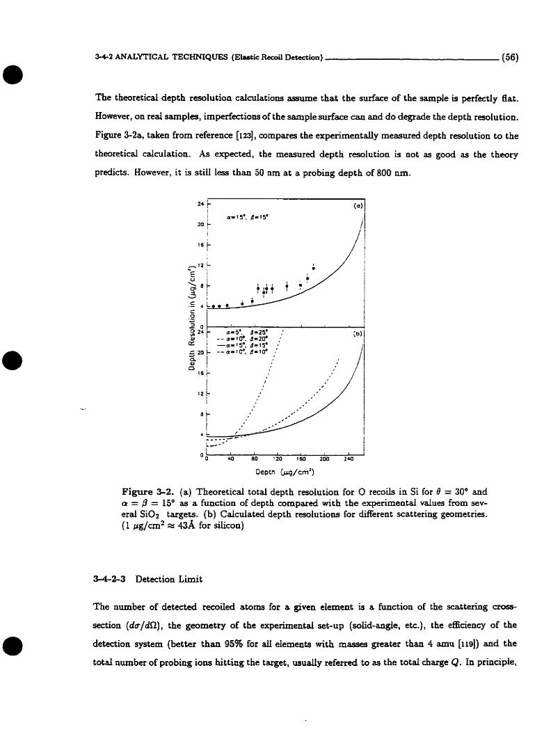
3-42 ANALYTICAL TECHMQüES (Elastic Recoil Detection) (56)
The t heoretical depth r a i u t i o n calcuiations assume that the surface of the sample is perfectly Eiat.
However, on real samples, imperfections of the sample surface can and do degrade the depth resolution.
Figure 3-2a, taken fiom reference [iq, compares the experirnentaiiy measured depth resolution t o the
theoretical calcutation. As expected, the measured depth resolution is not as good as the theory
predicts. However, it is still less than 50 nm at a probing depth of 800 m.
Figure 3-2. (a) Theoretical total depth resoiution for O recoils in Si for 8 = 30' and a = p = 15' as a function of depth compated with the experimentai values from sev- eral SiOl targets. (b) Calculateci dept h resolutions for different scat tering geometries. ( 1 pg/cm2 =43A for siiicon)
3-4-2.3 Detection Limit
The number of d e t b e d recoiled atorns for a given element is a function of the scattering cross-
section (da/dS2), the geometry of the experimentai set-up (solid-angle, etc.), the efnciency of the
detection system (better than 95% for aii elements with masses greater than 4 a m [ris]) and the
total number of probing ions hitting the target, usudy referred to as the total charge Q. In principle,

-2 ANALYTICAL TECHNIQUES (Elastic k i l Detection) (57)
using a reasonable beam current, any concentration of a doping element is detectable given a large
enough Q. However a semi-infinite dose of a high energy Cl probing beam is not practicai because
of (a) time limitations and (b) a possible akeration in the the target composition, as a Funetion of
depth, due to knock-on collisions. In practice, the linriting factor for detecting low concentrations of
a particular element is the background noise. If the production rate of the noise signais is higher than
the production rate of scattered recoih, it is Mpossible to detect this eiernent, irrespective of Q.
In our experiments the background noise is predominantly a result of 'tailing' in the energy
signal of other, more abundant, recoils or scattered ions. A low energy signal coupled with an accurate
TOF measurement results in an incorrect mass cdculation. Thus the detection tirnit is more a bnction
of the probing beam and the target composition than it is of the total depoçited charge Q. The majority
of the noise signai cornes from the scattered C1 ions, and although it is possible to reduce the noise
by using a 6 3 C ~ pmbing beam, which cannot kinematicdy scatter from silicon at a 30' angle, the
reduction in depth resolution due to an increase in multiple scattering precludes thk choice.
So for silicon targets, using a 1-2 nA 30 MeV Cl probing beam for approxlmately 2 h with
a 30' total scattering angle, the detection limit for elernents Iess than 24 amu is approxirnately
3 x 10¹⁴ at/cm2 over a probing depth of I Pm-
- 3-42-4 Concentration Accuracy
In the ERD anaiysis the depth scale and stopping powers (dE/dz) are in naturdized units. i-e. pg/cm2
and &4ev/(rng/cm2) respectively, which is independent of the density of the material being probed.
M'ter analysis, the concentration of the e1ement.s are either given relative to a pre-determined elernent
in a particular layer of the sample, or as a percentage in that par t idar depth region 62. If the
demity of the material is unknown, it is not possible to give an absolute concentration in atoms/cm3.
However, in the samples studied in this thesis, the density is known for the pure silicon regions
(5 x 10²' at/cm2), and it is assumed that the density does not change sigdicantly in the oxygen rich
region. This is not ELXI unreasonable approximation since the concentration of SiOl was never more
than 23% of the total volume at any given depth, and the clifference in density between Si and Si02
(2.2 vs 2.32 g/cm2) is smd. This gives Iess than a 1.5% error in the density approximation. When
the density of the material is knom and constant throughout the depth of the probing region, it is

a simple matter to convert the relative concentration profiles ta a b l u t e concentrations, and so for
simplicity's sake, the data was presented in t his form. * L ' . I
In the figures which show the calculated ERD results, there are error bars on each data point.
These error bars were calculated based solely on statistical analysis. For each depth channel there is
a fixed width (dx; = xi+l - x i ) and its associated concentration of oxygen Ci. The total number of
oxygen atoms detected (x) witbin the energy region E ( X ; + ~ ) - E ( z ~ ) is counted. The uncertainty in
the concentration is then given by
The curves representing
to the calculated data.
the ERD analysis were obtained by
(3-1)
using a Fast Fourier Transform (FFT) filter
3-43 Rutherford Backscattering Spectrometry
In Our RBS experiments, there are two SBD detectors at angles of 257.3O and 112.Ù0. Since it is
kinematicdly impossible for target atorns to recoil a t angles greater than 90°, only the scattered
probing ions will be detected, and thecefore no mass analysis is needed. The probing beam usecl for
these experiments was a 3 MeV 'He beam, which gives a probing depth in siiicon of approximately
3 Pm. It is not practical to increase the probing depth by increasing the He energy because, at higher
energies, there are resonance p e h for He scattered from oxygen. A complete description of the
principles of =S andysis can be found in reference [LZ~].
As mentioned previously, the energy cesolution is a function of (a) the detector rewlution, (b) the
probing beam spot s ix , (c) the detector size (solid angle), (d) the energy straggling and (e) multiple
scattering. The primary energy lads of a light ion is due to electron interactions rather than nuciear
scattering and consequently the multiple scattering term may be neglected. The energy spread ( 6 4 )
due to the geometric contribution [@) and (c)] has been calmlated for 3 MeV He in a silicon sample
(using the theories desaibed in [izz]) and is approximately 10 keV at the surface and 15 keV at a
depth of 3 Pm. If we use the Bohr approximation to the energy stragghg of He in siiicon [124],
the energy straggîe (JE.) is 35 keV at 3 Pm. Adding in the detector resolution (6Ed t y p i d y 15 to
20 keV) (1251, we have a t o t d energy rewlution of 22 keV a t the surface and 43 keV at 3pm. This

S4-3 ANALYTiCAL TECHNIQUES (Ruthuford Baducsttering Spcctmmetry) (59)
corresponds to a depth resolution 62 = 6 q ( a E d / a x ) of 0.04 pm at the surface and 0.07 p m at 3 Pm-
The experimental energy resolution is not available. However, it can be assumeci to be more than the
theoretical estirnates.
3-4-3-2 Detection Limit
The energy of the backattered ion is a function of the mass of the target eiement from which it
scattered, where heavier target atorns result in more energetically scattered He ions. Thus the signal
fiom an element whose m a s is larger than the bulk material is separate from the bulk signal (at least
in the near surface region). The detection limit for heavy impurities is approximated by fi241
.As an example, the detection limit for arsenic in silicon is -. 10" at/cm3.
The signai from an elernent whose m a s is lower than the bulk material is much more difncult
to detect, for two reasons. First, the signal from the low maçs element is added to the signal from
the bulk materiai, and wiIl be masked by the statistical fluctuations in the bulk signal. Second. the
signal for low mass elements is reduced because the scattering croessection du/dS2 is reduced (a Z2 ) .
.- An approximate detection limit was calculateci using only statistical considerations. If the number of
counts per energy channel (yield) of the b u k material is Y, the detection limit is
The yieid Y is of course a function of the total charge Q. For Y between 1,000 and 12,000 ccunts.
the detection limit of oxygen in siiicon is between 1.6 x 10" and 4.6 x 10²¹ at/cm3. However, if
the presence of Si02 is inferreci by the reduction in the silicon yield (1 silicon atom is displaced by
approximateiy 2 oxygen atoms) the ratio of the atomic numbers is not relevant, and the detection
b i t then cornes between 1 x 10²* and 3 x 10²' at/cm3.

Channehg of energetic ions occurs when the incident bearn is carefully aiigned with a symmetry
direction of a crystal. Looking at an aligned crystal (figure 3-3) it is essy to see that the majoriry of
ions t hat are not irnmediately scattered of€ the surface of the target wiII pass relatively unhindered
between the axial rows or planes of the crystal. This is referred to as channeling. Since well-channeled
particles do not get close enough to the atomic nuclei to undergo large angle Rutherford scattering, the
backscattering yield is reduced by a factor of - 3û-50 for most crystals. The resulting energy spectrurn
from the recoiled atoms can be used to determine the nature and depth of crystal imperfections as
well as the presence of impurity atoms. Many books [32,124,126] and papers [i2ï,izs] have been written
which describe channeling, its application to defect studies and eqerimental procedure, and should
be referred to for more information. OnIy a very brief review wiU be presented here.
Figure 3-3. X mode1 of a silicon crystai aligned in a (a) random. (b) < 100> and (c) < 110> direction.
3-4-4-1 Depth Resolution
For any channeling analysis, it is necessary to be able to relate a detected energy (Ed)i to a depth xi of
the scattering centre. The analyticai procedure is identicai to the one outlined in $341-1. However,
the standard Ziegler [24] energy loss parruneters (dE/dx) are no longer appropriate. The range of
channeled ions is much léuger than the range of non-channeleci ions. The ratio of the energy loss
between a channeled and a non-channeled He ion, y, is a non-linear fimction of energy (1291, and is
strongly dependent on the occutacy of the alignment where a 0.5" deviation h m the crystal axis can
change y from 0.5 to 1.0 [130], However, in spite of its inherent inaccuracies, the energy loss of the

channeled ion (AEi in figure 3-1) is ca lda ted by multiplying the standard Ziegler stopping powers
dE/dz by a constant (y - 0.5-0.6). If we use y = 0.5, the caiculated depth scale (and probing depth)
increases by app roha t e ly 25%. Because of the uncertainties in y, any depth scale caiculated from
channeled ions is always assumed to be a reasonable, but oot n e c d y accurate, approximation.
3-44-2 Defect ha lys i s
For an ion to be chameied in a crystalline target, the deviation from the crystalline axis direction
must be l e s than the d i c d angle r i > + , which is a function of the interatomic spacing, the energy of
the channeled ion, the atornic number of the ion and substrate atoms. For a <110> channeled 2 M e V
He ion in silicon, iIt - O . Z i O . if the direction of an ion deviata more than 6+ Gom the aligned
direction, it is said to be 'de-chaanekd'. The percentage of the ion beam that is not channeIed is
referred to as the random fraction, and is denoted by X R .
At a depth x, the random fraction in a crystd with defects is the random fraction that would
norrnally occur in a virgin crystal, Xv, plus the fraction of the remaining channelecl beam (1 - Xv ) that scatten, with angles greater than *+, off of n* x defects. Thus the random fraction is:
w here
P($ + , r ) : is the probability that an ion passing through the target of width x will be de-channeled,
dP(+ +, dx) : is the differentid probability over a distance dx, and
o~ : is the integrated scattering cross-section for scattering angles greater than ét.
The interaction between the random fraction of the beam and the target is the same as if
the target wem randornly oriented, and thus the yield from this part of the beam is XR times the
normal random yield. The remaining faction of the beam (1 - X R ) can scatter off of nD randomly
distributed defats. If the cross-section for scattering direaly off of the d e f e is doo/dR and the
standard Ruthedord scattering cross-section is dg/dQ, then the ratio ( X ) of the channeied yield to
the random yieid, at a given depth t, is:

3-44 ANALYTICAL TECHNIQUES (Channeiing) (62)
If the defects in the crystal are randomly distributeci point defects (neither spedically substi-
tutiond nor specificaily interstitial), srnall amorphous pockets, or even thin amorphous regions, t hen
the cross-section duD/df2 is the standard Rutherford cross-section (Le. fe = 1). In the aalysis used
in this thesis, we use an approximation for $+ from reference [32] to calculate u ~ .
w here
d : is the atomic spacing dong the axid direction in A, and
E : is the energy of the channeleci particle (MeV) just prior to scattering.
The number of defects is then calculateci iteratively by using the following equations.
w here
i : is the energy channel number,
x; : is the depth of the scattering centre corresponding to a m e a u r d energy Ei,
X(Ei) : iç the measured yield, expressed as a fraction of the random yield, at an energy E;
(depth t i ) ,
ZR(&) : is the random fraction of the beam at an energy Ei (depth x i ) ,
Xv (Ei ) : is the random fraction of the beam at an energy E; (depth x i ) in a virgin sarnple,
no(=,) : is the number of point defmts per cm3 at depth x i ,
n : is the atomic density of the probed materid.
For the specific case of extended defsts, dislocation loops, twins a d stadcing faults, the
Merential scattering cross section duD/dS2 for large scattering angles is negligible (Le. f, = O).
However, the integrated cross-section CD is not. Because the scattering-aoss section is a function
of the Burgers vector and the size of the d e f s t , it is difncult to quaatify without further analysis.
However it is known that the cross-section is not a strongly varying function of E and sol assuming
that the type of darnage in the sample does not vruy widdy with depth, a depth profle of the relative
damage in the sample can be obtained. Again, we use the iterative approach to solve for the differential
probability of dechanneling dP($+, dz):
w here
d P ( @ + , d ~ i ) : is the differential d d a n e l i n g probability over a depth xi- i to Zi ,
no ( x i } : is the nurnber of extended defects per cm2 at dept h xi, and
uo : is the integal cross-section (cm) for scattering with angles greater than iv+ off of ex-
tended defects.
The above analysis is based upon many assumptions and approximations, some of which are:
(1) the critical angle Jit is not a function of the q s t a i damage, (2) the flux of channeleci particles
is uniformly distributed throughout the channel, f 3) d d a o n e l e d particles are not scattered into
digneci directions, and (4) the defects are either al1 point defects or amorphous material, or al1
extended defects. Aithough there is no quantitative error anaiysis, it is generally accepted that the
overd distribution of the damage is representative of the 'red' damage distribution, and that the
number of defects, when compared from sample to sample, is reasonably accurate. s
The real difficulty in defect anaiysis arises from the differences in the stopping powers for
channeleci and non-chameled ions. It is assumeci that the conversion from an energy scale to a depth
seaie is the sarne for both the randorn spectrum and the aligned spectrum, but as was discussed in the
previous section, this k not the case. So in effect, X(Ei) is the ratio of aligned and random yields from
two different regions in the sampie- If the sample's composition is unifonn as a function of depth,
this does not affect the defect analysis. However if the sample is not uniforrn, X(Ei} is the ratio of
the yields between two dep th regions which could have cornpletel y different element al cornposi tions.
In this instance, the esladateci damage profile is distorted and must be interpreted accordingly.
3-45 Secandary Ion Mass S pectrometry
SiMs (Secondary Ion Mass Spectrometryj is used as a cornplementary technique to ERD for pro&g
the oxygen concentration in our samples. SIMÇ measures and counts the number of chargeci rscoil
ions from a target as it is being sputtereâ by: at least in out case, a Cs+ ion beam. During the SDfS
analysis, the beam is electronicaily scanneci over a 150 pm spot on the surface of the çample. but only
the sputtered atomç h m the center region of the xanned area (8 pm) are used in the anai-vsis. To
obtain a depth profile of s p d c elements in a targec. a e/m spectrorneter is used to isolate and count
a panicular chaged ion or molecule during a fixed time period. The spectmrneter is then adjusrd
for a new e/m ratio which corresponds to che next element being profil&. Ai1 the specified elements
are sampled, and the cycle then repeats itseif. The resuiting dara is the nurnber of counts of each
specific ion/moI~ule as a funnion of sputter tirne.
3-45-1 Depth
.-er measuring the depth of the sputtered Crater with a profilorneter. the depth d e is calculaced by
amiming that the sputter rate is comta t . The accuracy of this method is difEdt to quanti- since
ir îs dependent on the target and the experimental conditions. For our p a r t i d a r case. the caicuiated
sputter rates varied by more than 5% for difTerent experiments on the same sampie. Clearly the
sputter rate is not always constant. On one sample the calculated depth of the maximum oxygen
concentration (.- 2.4 pm) varied by more chan 0.17 p m between successive profiles. -4norher faaor
degrading the depth resolution is the facr that nuclear collisions berween the ion beam and the sample
can induce an intennixing of elemenrs between two regions T b ion mixing leads to ar: artficial
broadening of the concentration profiles.
345-2 Concentration kasurement
The sputtued material is emitted as individual aroms or as molecules in various neutrd and charged
states. The dat ive abundances of the various charge states are dependent upon the ion or molecular
species, and on the target composition. For example, in the ptcseflce of oxygen, the d a t i v e produdon
of both pcaitively and negativeiy charged ions for many elements is greatiy d a n a d [131]. Thus it is
di f i id t to obtain an accurate masure of the ratio of one dement to another without first dbrating
the system with a standard target which is as dose, chemidy spealang, as can be to the target

sample. Because the total concentration of oxygen was knom in our samples (eqnd to the implant
dose), it was simpler to normalize the sIMs d t s to the implant dose- In addition to errors in the
calculateci depths, it shouid be noted that differences in the spntter tate as a funaion of depth wiU
alter the apparent concentration profile.
The detection limit of oxygen in a c o n is of the order of 10'~ ar/cm3. w h c h is w ordes of
magnitude more sensitive than ERD. This sensitivity is limited by the naturd e r y berween silicon
and oxygen. The detection l i i t is impmved as the çputter rate increases since tbere is l e s time
for the oxygen within the system to react with the sihoon sample. However. this d e e s the depth
resoiu tion.
3-46 Transmission Electmn Micr~scopy
Transmission Electron Microscapy (TE!!) operates by passing a high-energy electron beam throu*
a very chin target and recording the image on a photographic plate. The electron beam k focussed
through a series of magnetic l e m . and either the diffraction pattern or the sarnple image k iormed
on the photographic plate. This is iilustrared çchematically in figure 3-4. Differenr target materials
have different electron absorbtion coefficients, and so by ming the image contrast it is possible to
differentiate between regions in the sampie that have different chernical cornpasrtions. In addition.
extendeci defens. twins. sacking faults and other d e f a also have their own charaineristic conrrast.
and so the types of d e f m . as weU as their qualitative distributio~. are vtsibie. For more deraileci
information about TE!^ how-to's and anaiysis procedutes tefer to the book by W g o n and
Glauert [1.?3j.
Before continuing funher, i t is n e c e s q to define cenain symbols and vectors used when
discussing TEM.
BF :
DF :
SAD :
OB :
3:
b :
Bright field (image).
Dark field (image).
Seiected Area Difhction.
Bragg scattering angle.
U p d drawn incident beam direction in the sp&imen that is opposite to the direction
of the electron beam.
The Burgers vector of a disiocation.
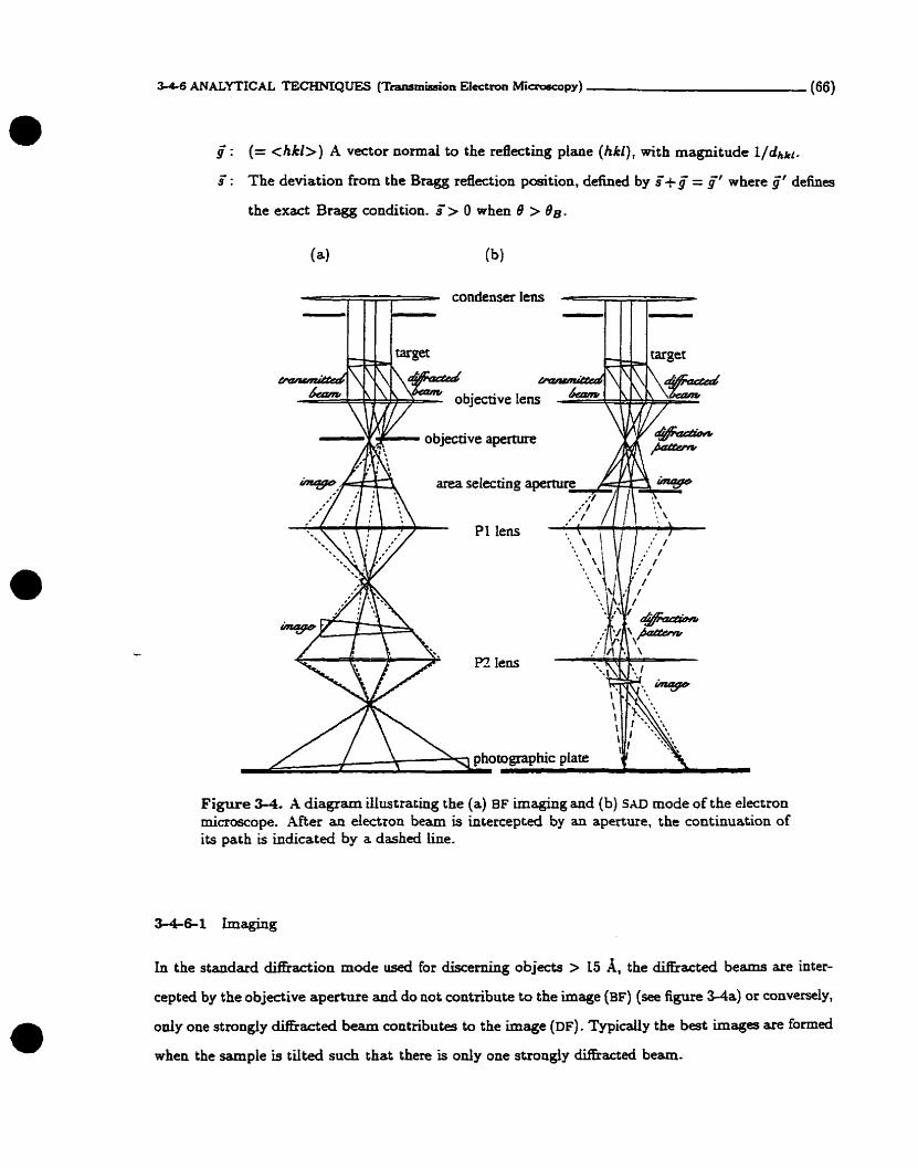
S4-6 ANALYTICAL TECHMQUES (Transmission Eiectron Microscopy) (66)
f : (= c h k l > ) A vector normal to the refiecting piane (hkl), with magnitude L/diikl.
s' : The deviation from the Bragg refIection position, defined by s'+y = 9' where ij' defines
the exact Bragg condition. 9 > O when 0 > OB.
condenser lens
Figure 3-4. X diagram austrating the (a) BF imaghg and (b) S A D mode of the electron microscope. After an electron beam is intercepted by an aperture, the continuation of its path is indicated by a dashed line.
In the standard clSiaction mode wed for cüscerning objects > 15 A, the dSiacted beams are inter-
cepted by the objective aperture and do not contribute to the image (BF) (see figure M a ) or conversely,
o d y one stmngly ciifliadeci beam contributes to the image (DF). Typicdly the b a t images are formeci
when the sample is t i l t 4 such that there is only one strongiy difbacted beam.
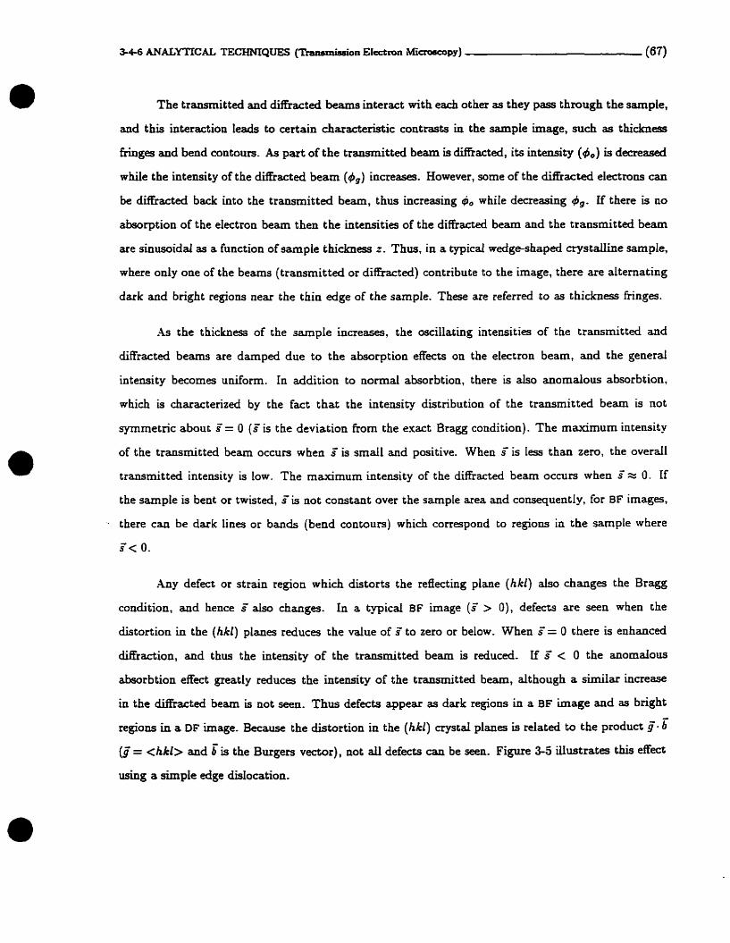
The transrnitted and diffracteci beams interact with each other as they pass thmugh the sample,
and this interaction leads to certain characteristic contrasts in the sample image, such as tàickness
fnnges and bend contours. As part of the transmitted beam is difiactecl, its intensity (4,) is decreased
whiIe the intensity of the diffracteci beam (4,) increases. However, some of the dXracted electrons can
be diffracteci back into the transmitted beam, thus increasing & while decreasing 4g. if there is no
absorption of the electron beam then the intensities of the diffracteci beam and the transmitted beam
are sinusoidal as a function of sample thickness z . Thus, in a typical wedge-shaped crystdine sampIe,
where only one of the beams (transmitted or diffractecl) contribute to the image, there are alternating
dark and bright regions near the thin edge of the sample. These are referred to as thickness kinges.
As the thickness of the sample increases, the osciilating intensities of the transrnitted and
diffracteci bearns are darnped due to the absorption effects on the electron beam, and the general
intensity becornes uniform. In addition to n o m d absorbtion, t here is also anornalous absorbtion,
which is characterized by the fact that the intensity distribution of the transrnitted beam is not
symmetric about s' = O (Z is the deviation from the exact Bragg condition). The maximum intensity
of the transmitted beam occurs when s' is srnall and positive. When s' is less than zero, the overdl
transmitted intensity is tow. The maximum intensity of the diffracted beam occurs when s'a O. If
the sarnple is bent or twisted, sis not constant over the sample area and consequently, for BF images,
- there can be dark lines or bands (bend contours) which correspond to regions in the sample where
S< o.
Any defect or strain region whidi distorts the reflecting plane (hkl) also changes the Bragg
condition, and hence S also changes. In a typical BF image (S > O), defects are seen when the
distortion in the (hkl) planes reduces the value of s' to zero or below. When S = O chere is enhanced
diffraction, and thus the intensity of the transmitted beam is reduced- If Z < O the anomalous
absorbtion effect greatly reduces the intensity of the transmitted beam, although a similar increase
in the diffracteci beam is not seen. Thus defects appear as dark regions in a BF image and as bright
regions in a DF image. Because the distortion in the (hkl) crystd planes is related to the product y- b
(g= < h k b and 1 is the Burgers vector), not aii defects can be seen. Figure 3-5 illustrates this effet
using a simple edge dislocation.
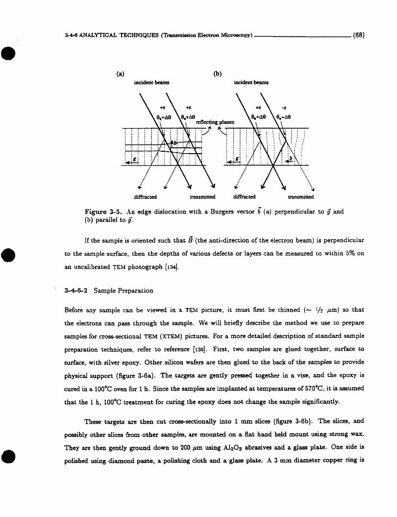
incident beams
Figure 3-5. An edge dislocation with a Burgers vector (a) perpendicular to g and (b) parallel to f'.
If the sample is orientecl such that (the anti-direction of the elecrron beam) is perpendicular
to the sample surface, then the depths of various defects or layers can be measured to within .5% on
an uncalibrated TESI photograph [134].
3-4-62 Sarnpie Preparation
Before any sample can be viewed in a TEM picture, it must first be thinned (- L/? p m ) so that
the electrons cari pass through the sample. We will briefly describe the method we use to prepare
samples for cross-sectional TE;M (XTEM) pictures- For a more detailed description of standard sample
preparation techniques, refer to reference (134. F k t , two samples are glued together, surface to
surface, with silver epoxy. Other silicou wafers are then glued to the back of the samples to provide
physical support (figure 3-6a). The targets are gentty pressed together in a vise, and the epoxy is
c d in a 100°C oven for 1 h. Since the samples are impianted at temperatures of 57D°C, it is apiumed
that the I h, LOOOC treatrnent for curing the epoxy does not change the sample significantly.
These targets are then cut c~w§ionally into 1 mm siices (figure 3-6b). The slices, and
possibly other sIices h m other samples, are mounted on a ffat hand heid mount using strong wax.
They are then gently ground d o m to 200 p m using &O3 abrasives and a glass plate. One side is
polished using diamond paste, a polishing cloth and a glass plate. A 3 mm diameter copper ring is
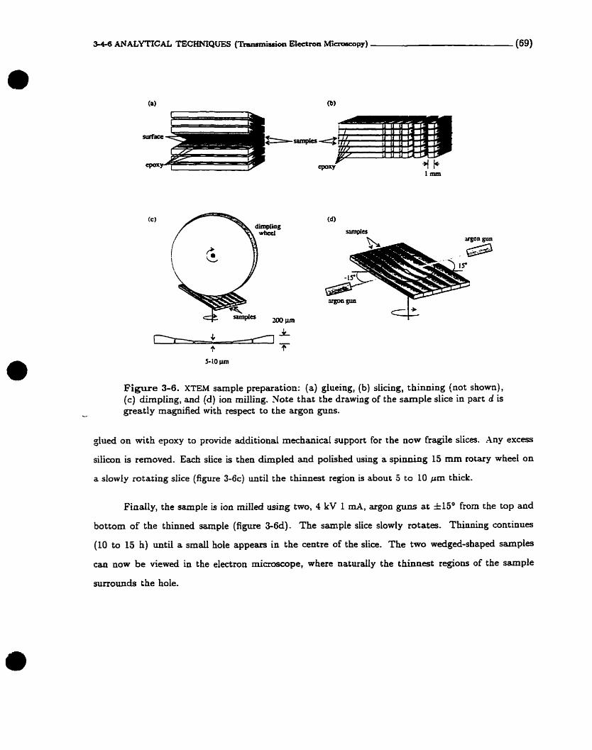
Figure 3-6. XTEM sample preparation: (a) glueing, (b) slicing, thinning (not shown), (c) dimpling, and (d) ion milling. Xote that the drawing of the sampie slice in part d is greatly magnified with respect to the argon guns.
giued on with epoxy to provide additional mechanical support for the now fragile slices. Xny excess
silicon is removed. Each slice is then diunpied and polished using a spinning 15 mm rotary wheei on
a slowly rotating slice (figure 3-6c) until the thinnest region is about 5 to 10 prn thick.
Finally, the sample is ion rnilled using two, 4 kV 1 r d , argon guns at *15' from the top and
bottom of the thinned sarnple (figure 3-6d). The sampte sfice slowly rotates. Thinning continues
(10 to 15 h) until a s m d hole appears in the centre of the slice. The two wedged-shaped sarnples
can now be viewed in the electron microscope, where naturdy the thinnest regions of the sample
surrounds the hole.

Chapter 4 Experiment al Results and Discussion
4 1 EXPERIMENTAL PARAMETERS
The purpose of this thesis is to study the interaction between oxygen and pre-existing damage in a
silicon wafer during oxygen implantation and annealkg. To create the damage, silicon wss implanted
with high energy Si ions, and then annealeci. This creates a band of dislocations that is stable at
the oxygen implantation temperature of 570°C. Oxygen was t heu implanted into t hese pre-damageci
samples, as welI as virgin silicon, and studied using the analytical techniques describecl in chapter 3-
The experimental parameters are listed table 4-1.
TABLE 4 1 Expcrimental Parameters
initial w a k c CZ n- type undoped [100] silicon
siticon implants:
energy: 2.00 -+ 2.75 ICICV
dose: 5 x loL3 _+ 1 x 10'' si/cm7 dose race: 150 -b 2Û0 CA/-' (siL+) implant temp: mom temperatun implant angle: 10 €mm beam, 10' tilt implant size: 1 cma anneal: htrnace, 900'~. 1 h in N:! Boa
camp up/doirrn: 45'~/min
oxygen implants:
encrgy: 2.50 MeV dose: 3 1oL6 + 3 x w7 o / - ~ dosc rate: OS + 1.0 p ~ / c m 2 (ol+) implant temp: 5 7 0 ~ ~ . ar rneaaud by a thermocoupIe
clamped to the s h e of the sample imphsnt size: 1 an2
implant angle: fO €rom beam, 10' tilt anneai: furnscc, 1 3 0 0 ~ ~ . 12 h in N2 or A 4 0 2 Bow
ramp up/down: ~ ~ ~ ~ / m i a
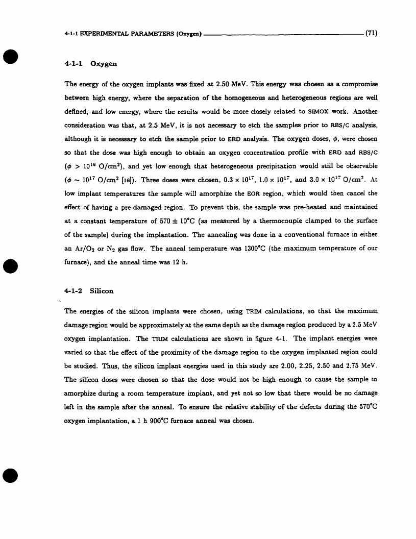
4-1-1 EXPERIMENTAL PARAMETERS fOxyg~1) (71)
The energy of the oxygen implants was fixed a t 2.50 MeV- This energy was chosen as a compromise
between high energy, where the separation of the homogeneous and heterogeneous regions are well
defined, and low energy, where the resuits would be more closely related to SmOX work, Another
consideration was that, at 2.5 MeV, i t is not necessary to etch the samples prior to RBS/C anaiysis,
aithough it is necessary to etch the sample prior to ERD analysis. The oxygen doses, 4, were chosen
so that the dose was high enough to obtain an oxygen concentration profile with ERD and Ms/c
(4 > 2016 0/cm2), and yet low enough that heterogeneous precipitation would still be observable
(4 - 1017 0/m2 fis]). Three doses a u e chosen, 0.3 x 10li, 1.0 x IO", aiid 3.0 x 10'' 0/cm2. At
low implant temperatures the sample wil1 omorphize the EOR region, which would then cancel the
effect of having a pre-damaged region. To prevent this, the sample was pre-heated and maintaineci
at a constant temperature of 570 * lO0C (as measured by a thermocoupIe clamped tu the surface
of the sarnple) during the implantation. The anneaiing was done in a conventional furnace in either
an Ar/Oa or N3 gas fiow. The anneal temperature was 1300°C (the maximum temperature of Our
furnace), and the anneal time was 12 h.
4-1-2 Silicon
The energies of the silicon imptants were chosen, using TRIM cdda t ions , so that the maximum
damage region would be approximately at the same depth as the damage region produced by a 2.5 MeV
oxygen implantation. The TW calculations are shown in figure 4-1. The implant energies were
varied sa that the effect of the prolami@ of the damage region to the oxygen implanteci region could
be studied. Thus, the silicon implant energies used in this study are 2-00, 2.25, 2.50 and 2-75 MeV.
The silicon doses were chosen sa that the dose would not be high enough to cause the sarnple to
amorphize during a room temperature implant, and yet not so low that there would be no damage
leR in the sarnple f i e r the anneal. To ensue the relative stability of the defects during the 570°C
oxygen implantation, a 1 h 900°C Eurnace anneid was chosen.
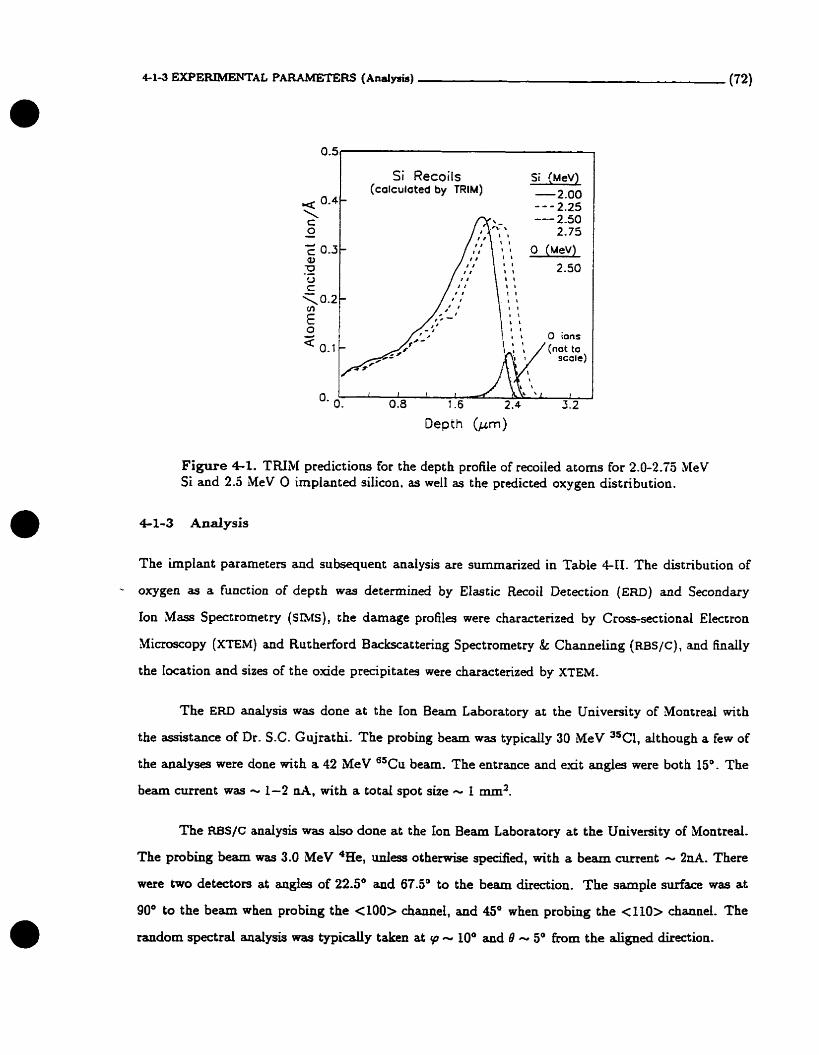
4-1-3 EXPERlMENTAt PARAMETERS ( h a l e ) (72)
Depth (pm)
0.4-
Figure 41. TRIM predictions for the depth profile of recoiled atoms for 2.0-2.75 MeV Si and 2.5 MeV O implanted silicon. as well as the predicted oxygen distribution.
Si Recoils Si { M ~ v ) (calculated by TRIM) -2.00
- - - 2-25
The implant parameters and subsequent analysis are surnmarized in Table 4-11. The distribution of
- oxygen as a function of depth was determineci by Elastic Recoil Detection (ERD) and Secondary
Ion Mass Spectrometry (SBCS), the damage profiles were characterized by Crosssectional Electron
Microscopy (XTEM) and Rutherford Backxattering Spectrometry 6c Channeling (RBS/C), and finaiiy
the Iocation and sizes of the oxide precipitates were characterized by XTEM.
d c 0.3- Q> '0 - - u
The ERD analysis was done a t the Ion Beam Laboratory at the University of Montreal with
the assistance of Dr. S.C. Gujrathi. The probing beam was typicaily 30 MeV 35C1, aithough a few of
the analyses were done with a 42 MeV "CU beam. The entrance and exit angles were botb 15'. The
beam curent was -. 1-2 ml, with a totai spot sue -. f mm2.
The -SIC anaiysis was also doae at the Ion Beam Laboratory at the University of Montreal-
The probing beam was 3.0 MeV *He, udess otherwise s p d e d , with a beam current - 2nA. There
were two detectors at angles of 22.5" and 67.5' to the beam direction. The sample surface was at
90' to the beam when probing the <100> Channel, and 45' when probing the <110> channel. The
random spectral analysis was typically taken at cp -. 10' and 0 -. S0 h m the aiigned direction.
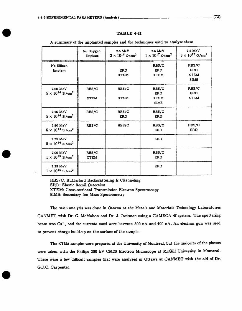
41-3 EXPERiMENTAL PARAMETERS (Andysis) (73)
TABLE 4-11
A sumrnary of the implanteci samples and the techniques used to analyse them.
No Silicon Implant
2.00 M e V 5 x 10f4 si/crn2
2.25 MeV
2.50 MeV 5 x 10i4 si/cm2
2.75 MeV O x 1oL4 si/crn2
2.00 MeV 1 x 10'' si/crn2
2.25 MeV I x 10" si/crn7
ERD XTEM
No Oxygen I 2.5 MeV Implant 3 1016 olcm2
RBS/C ERD XTEM
ms/c ERD
XTEM SIMS
2.5 &MeV 1 ioi7 olcrnZ
2.5 MeV 3 x loir o / -~
RBS/C
XTEM
=SIC: Rutherford Backscattering & Channeling ERD: Elastic Recoil Detection XTEM: Cross-sectional Transmission Electron Spectrascopy SIMS: Secondary Ion Mass Spectrometry
RBS/C
RBSIC
The SIMS analysis was done in Ottawa at the Metais and Materials Technology Laboratories
RBS/C
XTEM
CANMET with Dr. G. McMahon and Dr. J. Jackman using a CAMECA 4f system. The sputtering
beam was Cs+, and the currents used were between 300 nA and 400 d. An electron gun was used
to prevent charge build-up on the surface of the sample.
RBS/C ERD
RBS/C
The XTEM samples were prepared at the University of Montreai, but the majority of the photos
were taken with the Philips 200 kV CM20 Electron Microscope at McGiu University in M o n t d .
There were a few ditncuit samples that were andyzed in Ottawa at CANMET with the aid of Dr.
G.J.C. Carpenter.
m S / C ERD
XTEM SrMS
RBS/C ERD
XTEM
RBS/C EFLD
RBS/C ER5
RBS/C ERD

4 2 SILICON IN SILICON (74)
4 2 SILICON IN SILICON
in an effort to find the sets of experimental parameters t hat yield stable pre-damage in silicon, severai
samples were studied. These samples were implanteci with silicon at various doses ( 4 = 5 x 10¹³,
I x 1014, 5 x 10¹⁴, 1 x 10¹⁵ Si/cmz) and at various energies (E = 2.00, 2.25, 2.50, and 2.75 MeV).
The as-implanteci samples were andyzed by WS/C using a 3 MeV He bearn. After the samples were
annealed at 900°C for 1 h, they were again anaiyzed with RBS/C. The 2.00 MeV silicon implants (4 =
5 x 10¹⁴ and 1 x 10¹⁵ Si/crn2) were afsa anaiyzed with XmiM.
In this section we wiii present two sets of experimental parmeters that sat* the pre-damage
conditions. They are (1) 5 x 10¹⁴ Si/cm2, 2.00-2.73 MeV and (2) 1 x 10'' Si/cm2, 2.00-2.50 MeV,
followed by a 1 h, 900°C anneal. Wlen d(Si) = 5 x 10¹⁴ Si/an2, the resulting pre-damage is composed
almost entirely of dislocation loops, and when d(Si) = 1 x 1 0 ' ~ Si/cm2, ic is cornposed almost entirely
of dislocation dipales.
4-2-1 Range
To change the depth of the pre-damage, the energy of the silicon implant m u t be adjusted. The depth
- of the peak of the darnage profile was calculatecl from the ~ S / C spectra, using the method described
in 33-41. for 2.00, 2.25, and 2.50 MeV, a i = 5 x 10L4 Si/cm2. as-implanted samples and compared to
TRaf calculations and XTLV photographs. The resdts are tabulated In Table 4111.
TABLE em Location of damage peak in silicon damaged silicon.
r- 2.00 MeV 2.25 MeV 2.50 MeV 2.75 MeV
t ~ h e depth was caiculaeed zssuming thst the stopping power in an aligneci d i e i o n waa 0.5
c h a t of a randorn direction.

42-1 SILICON IN SILICON (~aoge) f 75)
To caldate the depth scale from RBS/C, it was necessary to approximate the He stopping
power in the aligned direction. The stopping power in a chamel is very sensitive to experimental
conditions, such as the beam energy and the beam phase space, and the damage within the sample.
Consequently, the depth scale in the ahgned direction cannot be accurately deterrnined. However,
if we approximate the stopping power for a channeleci particle to be a factor of 2 smaller than the
stopping power in an amorphous sample (se 53-44}, then the catcutated depth of the damage peak
gives a value reasonably close to that given by T M (Table 4-III), and rtTE&f rneasurements.
The damage profile as a function of dose was measured using ws/c andysis. Figure 4-2 shows
the RBS/C results for 2.0 MeV silicon-implanteci silicon (4 = 5 x NI3, 1 x 10L4. 3 x 1oL4. and
1 x 10¹⁵ Si/crn2) in the asimplanteci date. The RBS/C spectra from a v i r e sample in the aligned
direction and in a random direction are s h o m by solid lines. Even at the lowest dose, there is dam-
age near the surface of the sample. At the highest dose, the sampte is not amorphous at the EOR.
The general shapes of the -S/C spectra for the samples with 5 x 10¹³ 5 e 5 5 x 10¹⁴ Si/cm2 are
. al1 similar. The dechanneling inmeases graduaily from the surface to the EOR (-2 pm), indicating
a steady rise in the number of defects hom the surface to the EOR. At a dose of 1 x 10¹⁵ Si/crn2
however, the shape of the spectrum is quite different. The majority of the dechannehg occm at the
EOR region. The dechanneling in the near-surface region is not significantly more tban that in the
6 = 5 x 10'' Si/crnz sample, indicating a saturation of defets in this region. At the EOR the darnage
rises sharply, indicating that the damage production in chis region h a - not saturated as a hnction of
dose. This large increase in the dehanneling a t the EOR is most likely due to the creation of stable
point defect complexes, or s m d amorphous zones, or both.
The two samples chosen for further study are the the 4 = 5 x 10" and 1 x 1OLS Si/cm2 Sam-
ples. Since the sàape of their RBS/C spectra are not similar, it is quite probable that their deféct
characteristics are also dissimilar. To gain a better understanding of the damage within the sam-
ple, the profile of defects as a function of depth was dculated k g the theory described in 53-44,
with the assumption that dl the defects in the asimplanteci samples are point ddkcts or amorphous
clusters. The results of these caldations are shown in figure 4-3a and figure 43c. The shaded area

42-2 SILICON N SILICON (Damage) (76)
2.0 MeV Si as implan ted
1 O i.10"
Figure 4-2. RBS/C results of silicon implanted into silicon at room temperature. The aligneci spectra were taken in the <100> cbannel. The virgin and random spectra are given as solid lines. The depth =ale was calculateci assuming that the stopping in the channeleci direction is 1 / ~ of the stopping in a random direction. (3 MeV He. 6 = 22.5'. <100>)
between .Y and ,YR is proportional to the number of point defects in the sample. The number of point - defects. as a function of depth, is shown in figure 4 3 b and figure 4-36. The damage prose calculateci
by ?'RM is also shown.
The T m calculation for the number of point defects is based solely on the linear cascade
model, with no recombination between mancies and interstitiais, and with eoch point defect immobiie.
When the implant dose is low, the recombination of interstitials and vacancies occurs primarily within
individual ion cascades, and consequently the shape of the damage profile is simiiar to the damage
proiües calcuiated by m. For the 5 x 10¹⁴ Si/cm2 sample, it can be seen that the darnage profile
is similar in shape to the TW profile. However, the -1 results had to be reduced to fit the
experimental r d t s . Rom the &g factor needed to adjust the TRTM profile to fit the experimend
data, we caldateci that - 65% of the Frenkel pairs recombineci during the implantation.
AS the dose incfea~e~, the d e k t density increases and vaca~lcy/interstitial pairs h m different
ion cascades begin to interact. At this stage, the TRIM prdctions can no longer be applied, as for the
4 = 1 x 10'' Si/crn2 simple (figure 4-3d). According to the t heory of homogeneous damage production

42-2 SILICON IN SILiCON (Damage) (77)
2.0 MeV Si 5 x 1 O"/cmf as implanted
Energy ( M ~ v )
Oepth ( w d 3.0 2.5 2.0 1.5 1.0 0.5 0.0
I ' l r ' l " " l " " f ' r r l l ' r l ' I 1 " ' l
2.0 MeV Si 1 x 1 0 "/cm2
os irnplanted
Energy ( M ~ v )
2.0 MeV Si in Silicon 5 x I O'a/cmf os implonted O ExP - TRlM
0.81 2.0 MeV Si in Silicon
Figure 4-3. The nomaiized aligneci yield ( X ) for (a) 5 x 10¹⁴ and (c) 1 x 10L5 Si/cm2 as-implanteci sampies, for a virgin sample ( X v ) , and for the calculateci random fraction (XR). The caldated damage profiles (cirdes) for (b) 5 x 10¹⁴ and (c) 1 x 10¹⁵ Si/cmz samples, and the T m (not to scale) caldation of displaceci atoms (Iines). The depth scaie was calculateci assuming that the stopping in the chaunelecl direction is 112 of the stopping in a random direction. (3 MeV He, 8 = 2 2 . 5 O , <100>)
(described in detail in 52-24), the defects in the Silicon füm are Limiteci to vacancies, interstitials, di-
vacancies and di-interstitiais and they are uniforrrtiy distributeci throughout this region. AS a result,
the defects fiorn different ion cascades can recombine. The recombination rate of the point defects
in the surface region increases as the density of darnage increases, and hence the number of defects
in this region is not a Linear function of the dose. At scme criticai dose, & - 1015 Si/cm2 [mi, the
production rate of point defects is q u a i to the recombination rate. Consequently, at doses higher
than d,, the damage concentration saturates. This explains why the concentration of darnage for the
b = 1 x 10¹⁵ Si/cm2 saxnple in the surface regian is significantly lower than whac iç predicted by the
linear cascade model.
Io the EOR region the production rate of Frenkel pairs is much higher than in the near surface
region. The density of d e f m at any given time is also much higher. Consequently there is a higher
probability that defects in this region WU agglomerate into defects more compte^ than the di-vacanües
and di-interstitiais that are produceci in the dicon film. h the EOR region. vacancies will ~ ~ l o r n e r a t e
to f o m stable defect complexes, or small regions of amorphous material. and the interstitiais wil1 form
smaii defm complexes, or. if the density is high. they may fom intermdate defm configurations
(IDCs) such as row defects. or even elutfinsic disiocations. Hence the damage in c h i s region does not
saturate with the implant dose.
-%£ter the silicon samples were implanteci. they were annealeci at 900°C in a furnace with a Y2 gag
Bow. Figure 4-4 shows the annealed and as-implanced back-scs~tering yieids h m the 5 x Si/an2
sample- The dechannehg h m the annealeci sample is the same as the yield h m the virgin sample
in the d a c e region. and this indicates that this region is now relatively defect-free.
To obtain a depth profde of the damage for the anneaied sample we assumed thac the de-
channehg was only a result of lattice distortions due to extendeci def' (see Because
the scattering -section, CD, is iinknown (it is a functioa of the çize and Burgers vector of the
dislocation loop), only the probability of dedmmding for the 5 x 10¹⁴ Si/cm2 sample is shown Ï n
figure 4-4b- However, in this energy range of He, the cms+section u~ is o d y weakly d e p d e n t on
the He energy. Therefore dP/& can be considered to be pmportionai to the niimber of defgts. The
FWHM (full-width at half r n ~ ~ ) of the damage peak is 0.25 pm.
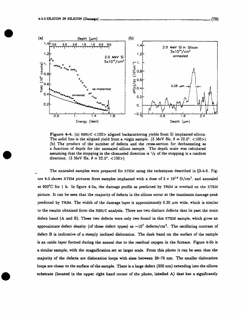
2.0 MeV 5 x t Om/c
1 1 I 1 1 1 1 1 1
0.6 1. 1.4 1.8
Energy ( M ~ v )
1 -41 2.0 MeV Si in Silicon 5 x 1 O"/cm2
onnealed
Figure 4-4. (a) RBS/C <100> aiigned backscattering yields fiom Si implanted silicon. The solid line is the aligneci yield from a virgin sample. (3 MeV He, 8 = 22.5'. c LOO>) (b) The product of the nurnber of defects and the cross-section for decfianneling as a function of depth for the aaaealed silicon sample. The depth scale was calculated assuming that the stopping in the channelecl direction is 1/2 of the stopping in a randorn direction. (3 MeV He. B = 22.5O, < 100>)
- The annealeci samples were prepared for XEM using the techniques describeci in 53-46. Fig-
ure 4-5 shows XTEM pictures frorn sampks implanted with a dose of 5 x 10¹⁴ Si/cm2, and annealed
at 900°C for I h. In figure 4-sa, the damage profile as predicted by TRM is overlaid on the XTEM
picture. It can be seen that the rnajority of defects in the siiicon occur at the maximum damage peak
predicted by T m . The width of the darnage layer is approximately 0.30 Pm wide, which is s d a r
to the results obtained fiom the FBS/C analysis- There are two distinct defects that lie past the main
defect band (A and B). These two defects were only two found in this XTEM sample, which gives an
approximate defect density (of these ddect types) as - lo7 defects/cm2. The oscillating contrast of
defect B is indicative of a steeply inclined dislocation- The dark band on the surface of the sample
is an oxide Iayer fonned during the anneal due to the residual oxygen in the furnace. Figure &Sb is
a similar sample, with the mognification set at larger d e . h m this photo it can be seen that the
rnajority of the defects are dislocation loops with sbes between 30-75 nm. The smailer dislocation
loops are closer to the sucface of the sample. There is a large d e f ' (300 nm) extenàing into the &con
substrate (Iocated in the upper right band corner of the photo, l a M d A) that bas a significantly
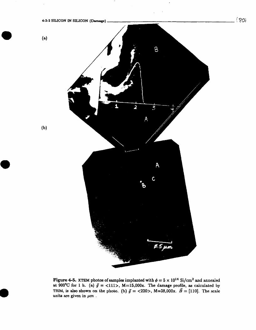
42-2 SILICON iN SLLICON (Damage) ( PO;
Figura 45. XTEM photos of samples implanteci with 4 = 5 x IOl4 Si/crn2 and anneded at 900~C for 1 h. (a) g = < I l l > , M=15,000x. The damage profile, as calculateci by
TRIMI is also shown on the photo. (b) 8 = <220>, M=38,000x. = [110]. The scale units are given in pm .
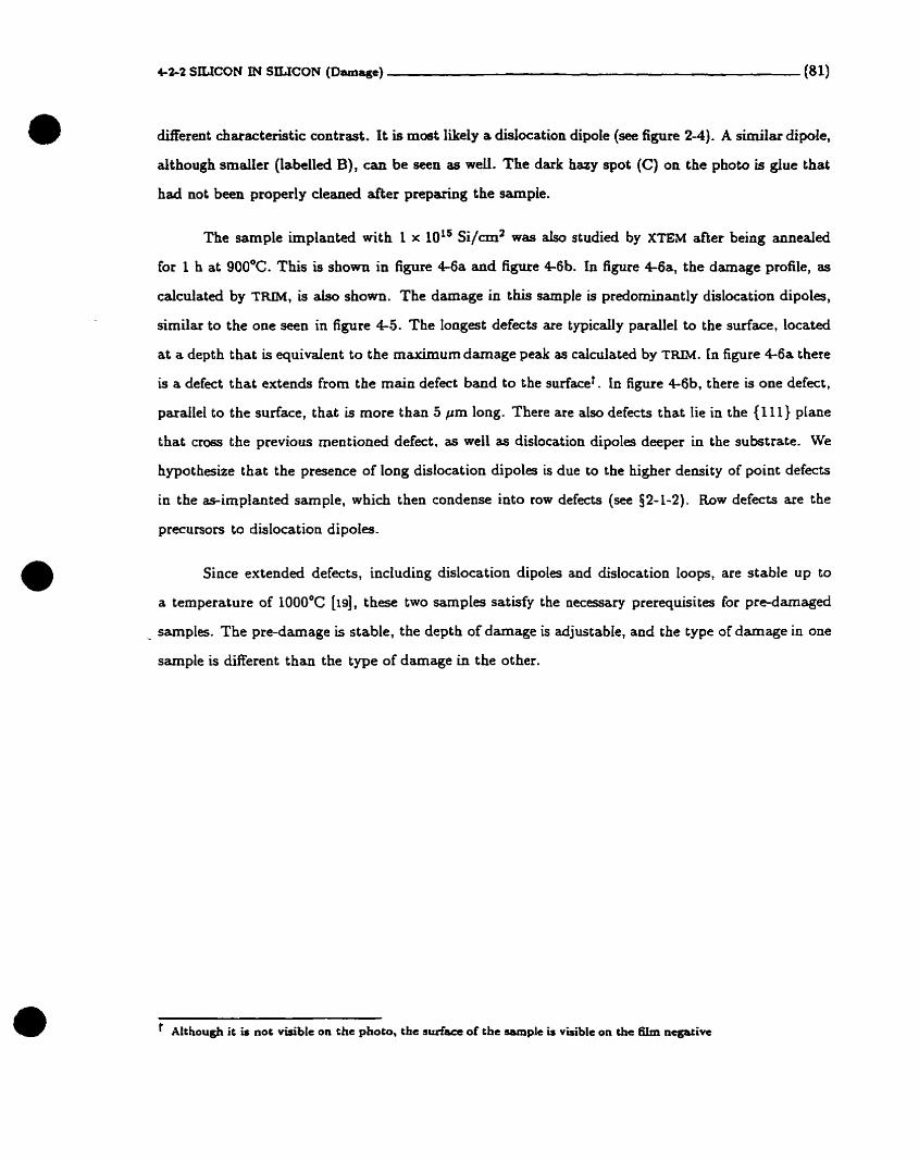
4-22 SILiCON Di SILICON (Damage) (81)
different characteristic contrast . It is magt likely a dislocation dipole (see figure 2-4)- A s imi la di pole,
although srnaller (labelled B), can be seen as weii. The dark hazy spot (C) on the photo is glue that
had not been properly cleaned after preparing the sample.
The sample implanteci with 1 x 10'' Si/cm2 was also studied by XTEM after being annealeci
for 1 h at 900°C. This is shown in figure 46a and figure 46b. In figure 4-6a, the darnage profile, as
calculatecl by T m , is aiso shown. The damage in this sarnple îs predominantly dislocation dipoles,
sirnilar to the one seen in figure 4 5 . The longest defects are typically parallel ta the surface, located
a t a depth that is equivaient to the maximum darnage peak as calcrrlated by T-. In figure 4-6a there
îs a defect that extends from the main defect band to the surfacet. In figure +6b, there is one defect,
parailel to the surface, that is more than 5 pm long. There are also defects that lie in the (1 11) plane
that cross the previous mentioned defect, as well as dislocation dipoles deeper in the substrate. We
hypothesize that the presence of long dislocation dipoles is due to the higher density of point defects
in the as-implanted sarnple, which then condense into row defects (w 52-1-2). Row defects are the
precursors to dislocation dipoles.
Since extended defects, inciuding dislocation dipoles and dislocation Ioops, are stable u p to
a temperature of 1000°C [is], these two samples satisfy the necessary prerequisites for pre-damaged
. samples. The pre-damage is stable, the depth of damage is adjustable, and the type of darnage in one
sample is different than the type of damage in the other.
Although it is not visible on the photo, the surf- of the -pie Ù visible on the 6im ncgative
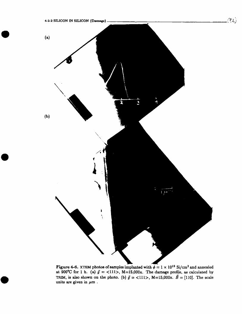
Figure 4-6. XTEM photos oofsarnples impianted with 4 = 1 x 10iS Si/cm2 and annealed at 900°C for 1 h. (a) g' = <Ill>, M=15,000x. The darnage profile, as calnilated by TRIM, is a h shown on the photo. (b) g = <Ili>, M=15,000x. 8 = [110]. The s d e units are given in prn .

4-3 OXYGEN IN SILICON
To understand the effects of oxygen implantation inta pre-damaged silicon, the properties of high
temperature (570°C) oxygen implantation into undamageci silicon must k t be studied.
The three dosa used in this study are 4 = 0.3 x 10¹⁷, 1.0 x 10" and 3.0 x loL7 0/cm2. Each
sample was cut into two pieces and then analyzed separately. Typically, one half of the sample was
annealed while the other hdf was ieft in the as-implanteci state. These sarnples provide the standards
with which to compare the results from the pre-damaged samples.
The range and straggling of the oxygen ions are determined.
The oxygen concentration profiles as a function of dose (as-implanteci and annealed) are studied.
X mode1 is presented which describes the experimental results in terms of HO and HE preciptation. It
is demonstrateci that if the precipitates at do do not anneai in the eariy stages of the anneai, they act
as an oxygen diffusion barrier. This Limits the minimum dose that can be used to fabricate a S N O X
or BOX sample-
The darnage type and distribution as a function of dose (as-implantecl and annealed) are dso
studied- At the EOR, the darnage is similar for al1 three samples. There is a thin layer of srnail
defect clustersi in the silicon film of the 3 x 10¹⁷ 0/cm2 sample. These defects are attributed to the
relaxation of the strain, caused by excess vacancies, in the silicon film. This relaxation releases the
oxygen atoms which were bound to the vacancies, and allows them to form precipitates. .Mer the
sample is annealed, there are t hee oxygen concentration peaks in the silicon film of this sample.
43-1 Range and Straggling
The measurement of the depth profles of oxygen Mplanted silicon was obtained by RBS, ERD. and
SMS. Although the oxygen concentration profile cannot be obtained by X ~ E M , the depth range, rather
than the depth of the mxümumoxygen concentration, of the oxide precipitates in the annealed sampla
can be detePIIÙI1ed.

4-SL OXYGEN IN SILICON (Range aod Straggling) (84)
The oxygen profile cannot be determined dkectly from the He energy spectrum because a helium
ion that has scattered off an oxygen atom at a depth of 2.5 Pm has an energy which is too Iow to
be detected in our experiment. However, the density of silicon in Si02 is less than it is in silicon
(2.2 x 10²*/cm3 in Sioz and 5.0 x in Si) and thus a dip in the RBS spectrum indicates the
presence of Sioz. The oxygen concentration and profle can be cdculated directly from the difference
in counts from a pure silicon sample and an oxygen implanteci sample, where a 56% reduction in the
backscattered yield would indicate a region of pure SiO?. Figure 4 7 shows the R ~ s spectra for two
samples () = 3.0 x 1OLT and 1.0 x 10" 0/cm2) and the calculated oxygen concentration profles as a
h c t i o n of He energy. The oxygen profile, as a functioa of energy, is converteci to a profile of oxygen
concentration versus depth by using the Ziegler stopping powers of He in silicon [MI. The depth s a l e
is calculated without adjusting the stopping powers for the presence of Si01 in the sample. For the
oxygen doses used in this study, the above approximation introduces, in the region of maximumoxygen
concentration, l e s than a 2% error in the stopping ponrers. The width of the surface oxides formed
during the anneal were measured with RBS and ERD for each set of samples. The samples were then
etched in HF (hydrofluoric acid) to remove the surface oxide. The depth scdes shown in figure 47,
and in crll subsequent figures, have been adjusteci to compensate for the volume of Si removed during - the H F etch.
The depth resolution of a 3 MeV He scattered off the surface of a silicon sample was measured,
and is 0.04 Pm, which is consistent with the theoretical depth resolution estimated in 53-43. Sim-
ilariy, the theoretical depth resolution at the oxygen peak is estimated to be 0.07 pm, However, it
is known that the theory undesestimates the observeci resolution [ 1 4 , and so to err on the çide of
caution, we quote a depth resolution of 0.1 Pm. It is difficult to measure the oxygen profles with
4 = 1.0 x 10" 0/cm2 because the dip in the RSS spectrum is not much Iarger than the statistical
fluctuations (se figure 47). With a dose of 3.0 x 10" O/cmZ. the dip e'cceeds the statistical Buc-
tuations. Using the same logic, one can see that the oxygen profiles for the annealeci sarnples have
a better statktid significance thon the as-implanted samples because the oxygen dip narrows and
deepens upon annealing. In spite of the estimated depth resolution of RBS at 2.5 p m being -0.1 Pm,
the statisticai variance of the r n d peaks was less than 0.06 pm for the as-implanted samples

4-3-1 OXYGEN IN SILICON ( M g e and Straggling) (85)
- i1-51 >- oxyqen
1.
Enerqy (MeV)
3.0~10" 0/cm2 s- 5 as implanted
Energy (MeV)
Enerqy (MeV)
Energy ( M ~ v )
Figure 47. RBs spectra for 4 = I x 10" 0/an2 (a) asimplanted, (b) annealed. q5 = 3 x 10¹⁷ 0/cm2 (c) asimplanteci, and (d) anneaied sarnples, and the respective calculateci oxygui concentration. The ~ra ight lines approximate the random spectrs for non-implanteci silicon. (3 MeV Ee, 6 = 67.5", <110>)
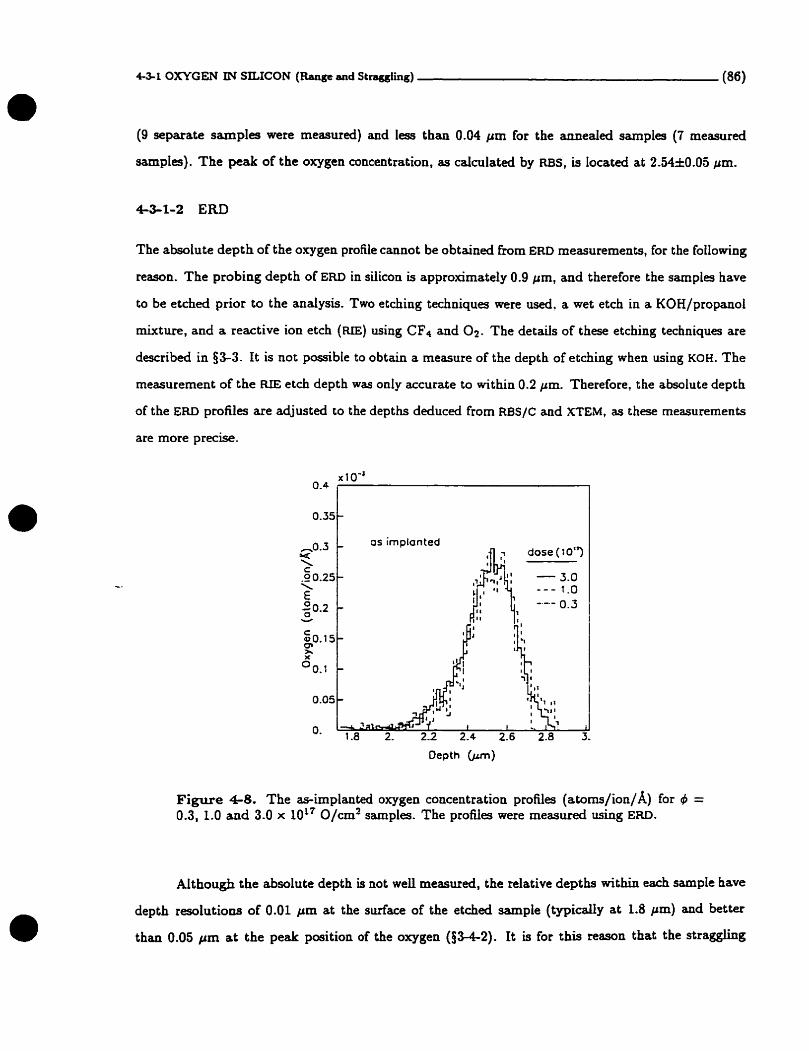
4-3-1 OXYGEN IN SILiCON (Range and Sttaggfing) (86)
(9 separate samples were measured) and less than 0.04 p m for the anneaieci sarnples (7 measured
samples). The peak of the oxygen concentration, as calculateci by RBS, is located at 2-54I0.05 Pm.
The a b d u t e depth of the oxygen profile cannot be obtained from ERD rneaçurements, for the following
reason. The probing depth of E- in silicou is approximately 0.9 Pm, and therefore the samples have
to be etched prior to the anaiysis. Two etching techniques were useci? a wet etch in o KOH/propanol
mixture, and a reactive ion etch (RIE) using CF4 and O*. The details of these etching techniques are
d ~ n b e d in 93-3. It is not p&bIe to obtain a measure of the depth of etching when using KOH. The
measurement of the RIE etch depth was only accurate to within 0.2 Pm. Therefore, the absolute depth
of the ERD profdes are adjusted CO the depths deduced from N S / C and XTEM, as these measurements
are more precise.
Figure 4-8. The as-irnplanted oxygen concentration profiles (atoms/ion/A) for 4 = 0.3, 1 .O and 3.0 x 10'' 0/cm2 samples. The profiles were measured using ERD.
Aithough the absolute depth is not well measured, the relative depths within each sample have
depth resolutions of 0.01 prn at the surface of the etched sample (typicdly at 1.8 pm) and better
than 0.05 pm at the peak position of the oxygen (83-4-2). It is for thïs r e w n that the straggling

calcdations were done with the ERD measurements rather than the RBS measurernents. The data for
seven samples were fitted to a Gaussian profile, and the straggiing was defined as a. In ait cases, the
shape of the as-implanteci oxygen profles were the same, independent of dose, within the limita of
statistical error (see figure 4-8). The straggiing of 2.5 MeV oxygen in silicon was measured by ERD ta
be 0-13 IO.01 Pm-
4-3-1-3 SIMS
To convert SEMS data into a depth profile, the sputter rate of the target must be caiculated. If
one assumes that the sputter rate is constant throughout the e-xperiment, then the sputter rate is
calculated by dividing the depth of the sputtered crater by the total sputter tirne. The depth of
the crater is rneasured with a profilorneter. Using this tedinique, the depth of the oxygea peak for
3.0 x 10'' O/& was measured, and the results were 2.45, 2.41, and 2.43 pm (one sample, multiple
measurements). For the sample with a dose of 1.0 x 10'' 0/cm2, the oxygen peak was rneasured at
2.7 Pm. T h s e results are within 6% of the positions of the oxygen peaks as rneasured b_v RsS, and
heace are considered reasonable. The straggling measured by SMS is 0.16 Pm, and is larger thao chat
rneasued by ERD.
-4-3-1-4 Discussion
The depth of the oxygen peak for as-implanteci sarnples is summarized in Table +IV. As can be seen
from the data, the oxygen peak, as rneasured by R ~ S and SMS is approxirnately 6% deeper th=
what is predicted by WI. This is not remarkable in and of itself, since others have also reported a
discrepancy between T m and experiment al resuits, w here TRIM typicdy underestimates the range
of oxygen in silicou for MeV implantations [25,26,24. The volume increase of the sample due to
the implantation and formation of SiOt (9 = 3-0 x 10" 0/crn2) is l e s than 70 =-cm2. and is not
sufEcient to exphin the disnepancy between T m and the experimental results.
The straggling, as calculateci from ~m and S I M ~ measurements is aIso larger than that pre-
dl& by TRIM. The samples studied in this thesis were all implanted at hi& temperatures and bw
current densities, and wnçequently the oxygen can migrate over large d i i c e s during the implanta-
tion since the düfusion rate is high and the implant tirnes are long (24 h for t$ = 3.0 x 10¹⁷ O/cmz).
We a h know that oxygen can accumulate preferentidy on damage sites (HE precipitation), at the
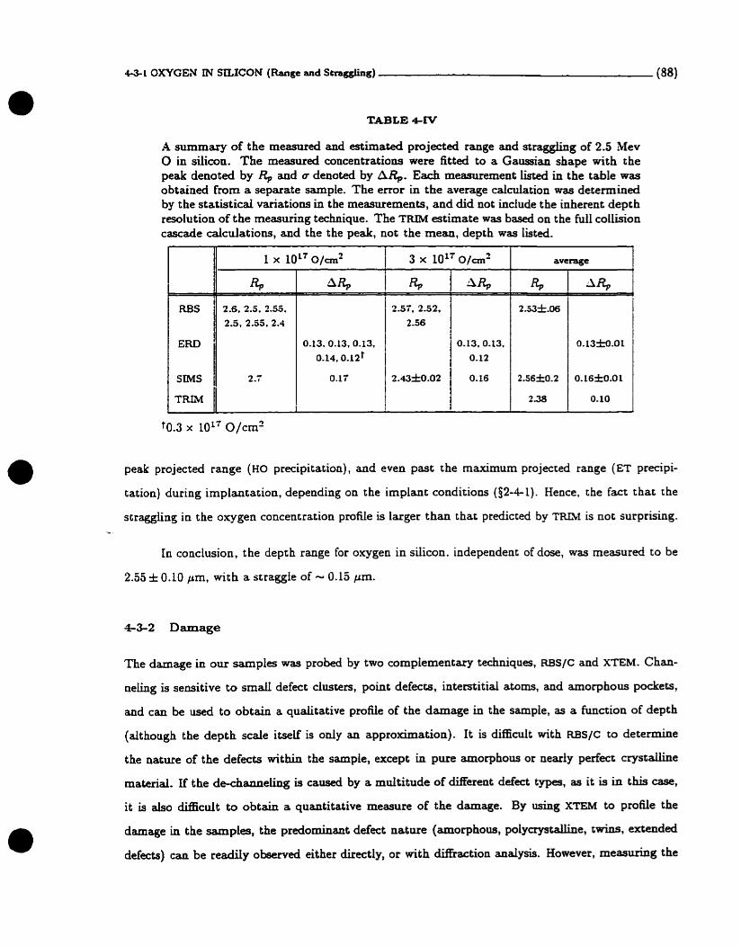
4-3-1 OXYGEN IN SILICON (Range and Stragding) (88)
TABLE 4-N
A summary of the measured and estimated projected range aad straggiing of 2.5 Mev O in dicon. The measured concentrations were fitted to a Gaussian shape with the peak denoted by R,, and o denoted by A& Each rneasurement listed in the table was obtained from a separate sample. The error in the average caldation was determineci by the statistical variations in the rneasurements, and did not inciude the inherent dept h resolution of the measuring technique. The T m estimate was b d on the full collision cascade caiculations, and the the peak, not the mean, depth was listed.
RBS
ERD
SIMS
T m
average
peak projected range (HO precipitatioa), and even past the maximum projected range (ET preapr-
tation) during implantation, depending on the implant conditions (52-4- 1). Hence, the fact t hat the
straggling in the oxygen concentration profile is Iarger than that predicted by T m 1 is not surprising. .-.
In conclusion, the depth range for oxygen in siiicon. independent of dose, was measured to be
2.55 f 0.10 Fm, with a straggfe of - 0.15 Fm.
The damage in our samplcs was probed by two complementary techniques, RBS/C and xTEM. Chan-
neling is sensitive to small defect clusters, point defects, interstitial atoms, and amorphous podrets,
and can be used ta obtain a qualitative profite of the damage in the sample, as a function of depth
(although the depth scale itself is ody an approximation). It is ciifficuit with RBS/C to determine
the nature of the defects within the sample, except in pure amorphous or neariy perfect crystaiiine
material. If the de-channeLing is caused by a muititude of different defect types, as it is in this case,
it is &O difEcult to obtain a quantitative measure of the damage. By using XTEM to profile the
damage in the samples, the predominaut defect nature (amorphous, polycrystalline, twins, extendeci
defects) caii be readily observed either dimtly, or with difnaction andysis. However, measuring the
4-3-2 OXYGEN IN SILICON (Dsmage) (89)
relative amounts of damage can be diBcult and tirne consuming, and we did not do this in our study.
Udike RBS/C, point defects are virtually invisible when imaging samples *th XTEM, unless very high
magnifications are used, It is possible with XTEM to obtain a reasonably accnrate masure of the
depth scale.
Figure 4-9 shows the aligned <110> and non-aligneci energy spectra for backscattered He ions from
as-implanteci sarnples implanteà with 4 = 0.3 x IO", 1.0 x 10'' and 3.0 x 10" 0/cm2. It should be
immediateiy pointed out that the sample implanted with Q, = 0.3 x 10¹⁷ 0/crn2 was initiaily implanteci
with 2 MeV silicon and then annealeci for 1 h at 900°C. This does not appear to affect the Ws/C
spectrum (as will be discussed in §4-4-1) and is thus used to illustrate the differences in the damage
Ieveis at difTerent oxygen doses- The depth scaies sbown in the figure are caiculated using the stopping
powers for amorphous targets, and consequently are not valid for the aligned spectra.
The most immediate and obvious characteristic of al1 the aligned spectra is that the yield in
the near surface region of the sarnples is the same as the yield in a virgin sample, indicating that the
sample has very few defects in the crystalline film. The second rnost obvious feature is that noue of
the sampfes show any indication of an amorphous region, even at the EOR- The aiigned badrscattered - yields of these samples al1 have a similar shape, mit h the lowest yield from the lowest dose sample.
Contrary to intuition, the highest dose sample ( 4 43.0 x 10¹⁷ 0/cm2) does not have the highest
backscattered yield. The change from undamaged crystal to the region of maximum damage occurs
over a depth range -0.3 Pm.
I t is much more difficult to interpret the channehg results from these samples than it was for
the silicon in silicon samples because the ddannel ing cornes fiorn more than one source, namely,
amorphous Si02, interstitial oxygen, interstitial silicon, and various types of dislocations. If the He
ion is scattered off of an interstitial oxygen, it will not have the same energy as He scattered from
a silicon interstitial, and consequently them wi l l not be direct backscatter from oxygen interstitiais
o b e d in this data (the energy would be too low to be detected at the depths at which the oxygen is
located). Multiple scattering wiil occur (He scatters fiom an oxygen ion, so it is no longer cha~neled,
and then backscatters h m a dicon atom). However, this is diflicult to analyze andytically when the
target contains an uneven distribution of scattering centers (oxides in this case). In addition, when
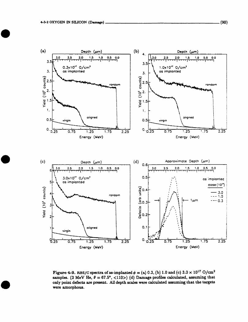
0.3~ 1 0" O/cmz 3. as implanted
Energy ( M ~ v )
Energy ( M ~ v )
(b) Depth Orm)
3.5 i .Ox T O" ~ / c m '
3 - os implanted
Energy (MeV)
id) Approximate Depth (pm)
. " l 1 . os implanted
dose ( 10'3
Energy ( M ~ v )
Figure 4-9. =/C spectra of zsimplanted q5 = (a) 0.3. (b) 1.0 and (c) 3.0 x 10" 0/cm2 sampies. (3 MeV He, 8 = 67 Sol <11O>) (d) Damage profiles caidated, d g that only point defects are present. AU depth d e s were caicuiated assuming that the targets were amorphous.

-2 OXYGEN IN SILICON (Damage) (91)
there is more oxygen in the sampte, there are more dechannehg centers present, which increôses
the backscatter yield, but there is less siticon per cm3, which decreases the backscatter yield. Each
de-channeling center has a different probability of scattering the He ion, and unless the exact ratios of
the respective de-channeling effects are known, the results of the damage caldations should not be
considered absolute. However, we do know that there is a larger cross-section for de-channeling £iom
point defetts and interstitials than there is for dislocations [124], and therefore, if the predorninant
defects are interstitials, then the defect analysis will give a reasonable approximation of the damage
distribution.
Bearing the above in rnind, if we assume that the predorninant cause of de-channeling in the
samples is not point defects but small amorphous pockets of SiOa or Si, which may be treated like
clusters of point defects, then the damage profiles of the samples are represented by the curves shown
in figure 4-9d. The data was analyzed assuming that the average scattering cross-section for the
defects is equivalent to the Ruthedord cross section ( i - e . f, = 1, eq'n 3-5). The assumption that
the predominant defects are point defects is not unreasonable, for the following reason. Firstly, the
majority of the Frenkel pairs are created in the EOR region (> LOO0 Frenkei pairs per oxygen ion).
The concentration of oxygen in the EOR region E -- 1oZ1 0/cm3 for the lowest dose (0.3 x 10~')
sample, which is more than a factor of 3 Iarger than the solubility lunit oloxygen in silicon at 140O0c
(- 10'' at/cm3). Therefore the oxygen has most probably formed oxide precipitates which prevent
the silicon interstitials from migrating out of this region (the diffusion of Si in Si02 is 10-20 m 2 / s at
600°C). Consequently one would e-xpect a large fraction of the de-channeling to be a result of direct
scattering off silicon interstitials or from the silicon in the SiOl pockets.
The shape of the darnage distribution is a skewed Gauçsian, with the interface between the
siiicon film and the EOR sharper than the interface between the EOR and the substrate. Although the
depth of the damage cano t be calculated accurately fiom R~S/C, the relative width of the damage
can be rneasured. This is because the He ions lose energy in this damaged region at the same rate as
if it were an amorphous sample. The width of the darnage region is approximately I Fm-
The damage profile for the high dose sample ($ = 3.0 x 10" 0/an2) is lower than the medium
dose sample (4 = 1.0 x 10" 0/cm2). However, the damage profile was ca ida ted assuming that only
point defects or s m d amorphous pockets were present. The lower damage profile for the high dose

4-3-2 OXYGEN IN SILICON (Damage) (92)
sarnple indicates that the defects have aglomerated together to form intermediate defect clusters or
extended defects.
Figure 4-10 shows the XTEM photos of the 6 =0.3 x 10'' 0/cm2 as-implantecl sarnple at L5k
and 38k magnification. There are no observable defects in the silicon film (the region between the
surface of the sample and the highly defected oxygen-rich region. See figure 4- IOa. The damage starts
abruptly a t 2-3 Pm. The dark bands crassing the picture are contour lines and are related only to
the fact that the silicon sample is slightly bent within the microscope. There are also no observable
defetts in the siiicon substrate. Figure 410b shows an expanded view of the defect layer. There
appear to be two distinct regions of damage. The main band of damage is approxirnately 0.5 prn
wide, Iocated at a depth of 2.3 prn to 2.8 Pm. In this region, one can see small straight biack lines
intermixed in the damage region, indicating the presence of extended defects or DCs. The other region
of damage extends much deeper into the substrate, with some damage apparent even at a depth of
3.3 pm (indicated by 'A' in figure 410b). This damage region does not exhibit the same characteristic
contrast as the previously mentioned region, but instead appean as small points of contrast, which
could be srnall arnorphous pockets, point defect; clusters, or even strained Si02 precipitates. .l further
increase in magnification did not clanfy the nature of these spots. The maximumoxygen concentration
(using the estimate of 2.05 prn as determineci in the previous section) Mls in the rniddle of the dark
defect band, and is indicated by an arrow. The sarnple is not amorphous in this region. There is not
a great deal of observable stress, typically indicated by a light band on either side of the defect region-
For the medium dose sampie, 9 = 1.0 x 10" 0/cm2, there are aiso no detectable defects in the
silicon film (figure 4l la) . Figure 4-llb is the same sample, with the magdcat ion increased, giving
a better picture of the damaged region. The transition frorn the ctystalline film to the damage region
is abmpt, and starts at 2.3 Pm, but the interface between the damage layer and the substrate is not
abrupt at ail, rather the quantity of damage slowiy decreases as it extends into the substrate, as was
the case with the Iow dose sample. The range of damage in the sample is, if one inchdes d visible
evidence of damage, 2.3 prn to 3.2 Pm. A Selected Axea Diffiraction (SW) pattern was taken of the
damaged region, and is shown in figure! 4-1 lc. There U no evidence of amorphous material, twins, or
polycrystxlline a c o n in this region.
Fi- 412 shows the XTGM photos for the hi& dose sample (4 = 3.0 x 10¹⁷). Although the
damage region appears to be amorphou (figure 412a), this is only an illusion due to the fact that the

-,
4-3-2 OXYGEN IN SILICON (Damage) 8 3 j
Figure 410. XTEM photos of as-implanteci t$ = 0.3 x loL7 0/cm2 sarnple. (a) M=15,000x, y = < I l l > and (b) M=38,000x, g = < I l l > . = [110]. The scale units are given in pm .
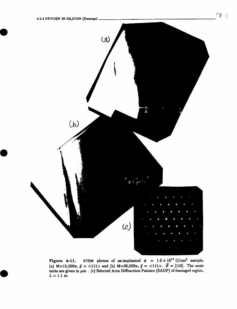
'7 -. ) 4-3-2 OXYGEN IN SILICON (Darnage)
Figure 4-11. XTEM photos of as-implanted 4 = 1.0 x 10" 0/cm2 sample. (a) M=15,000x, $ = <Ill> and (b) M=38,000x, g = <Ill>. l? = [110]. The scale units are given in pm . (c) Selected Area Diffraction Pattern (SADP) of darnaged region, L = 1.1 m.

4-3-2 OXYGEN IN SILICON (Damage) (95)
sampie has not been weIl thinnecl. When inspecting the sample at the edges of the thinned regions,
it was observed to be similar to the damage in the low dose sample. SAD patterns were alsa taken,
and confirmeci that this region is not amorphous. What is noticeable about this sample though, is
that the silicon film is no longer defect free- There appears to be a band of small defects located at
-1 Pm. The silicon on either side of this band remains defect fiee. Figure 4-12b is an expanded view
of these defects. The def- in the center of figure 412b (A) has a large strain field surrounding it,
indicated by a dark region slowly fading to the background contrast. It could be an oxide precipitate
with an w c i a t e d strain field, although this hypothesis bas not been experimentaily confinneci. One
of the smaller defects (8) is characterized by a straight dark Iine, surrounded by a strain field, possibIy
indicating a dislocation. High resolution XTEiM would be needed to confirm this.
+3-2-2 Annealed
After the samples were annealeci at 1300°C for 12 h, they were again analyzed with RBS/C. The results
are shown in figure 413a-c. In ail cases the dechanneleci yield is reduced. Figure 4 136 shows the
RBS/C spectra of the 4 = 1.0 x 1oA7 0/crn2 sample, before and afier annealing, d te r the sample was
etched approximateIy I pm in KOH. As can be seen from the figures, not oniy is the channeling yieki
reduced, but the shape of the spectrurn has also changed. The peak damage region (indicated by a
- dashed Line in figure 4-13d) is not as pronounceci, and there is no subsequent decrease in the yield
irnrnediately after this region. It can alsa be seen from figure 4-236 that there is a slight increase in
the depth of the crystalline film. The slight rise in the spectra in figure 4-13d (indicated by arrows)
is due to the He ion scattered off the oxygen in the sample.
XTEM analysis indicates that mast of the damage in the sampies bas changed into extended
d e k t s which are pinneci by the oxide precipitates. This formation and growth of the oxide pre-
cipitates, and the change in the damage type, is illustrateci very d'tively with the low dose,
4 = 0.3 x 10'' 0/cm2, sample, as shown in figure 414a and figure P14b. The silicon film is still
effectively defect free. The surface of the ssmple has s thick SiO2 layer (3000 A) that grew during
the anneai in an Ar/02 atmosphme. Even at the low magnificcation, the oxide precipitates in the
EOR are visible (small dark polygons) . At the higher magnification it can be seen that the remaining
defects are predominantly dislocations (straight dark lines) extendhg between the oxide precipitates.
In addition to the dislocations, the photo also shows signs of strain surromding the dislocations and
some of the oxide precipitates. These photos were taken under hi& contrast conditions (dynamical),
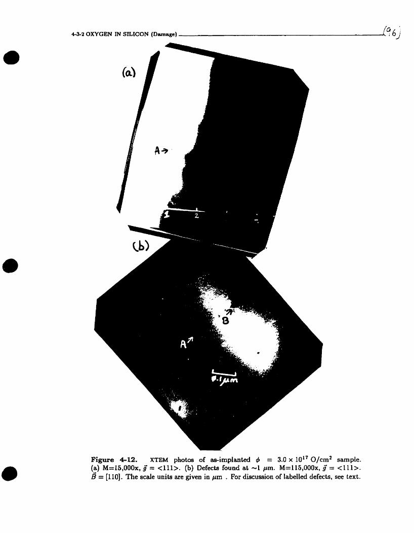
G 4-53 OXYGEN M STLICON (Damage) [A)
Figure 4-12. XTEM photos of as-implanted ) = 3.0 x laL7 0/cm2 sample. (a) M=15,000x, f = < I l l > . (b) Defects found at -1 prn. M=115,000x, g' = < 11 l>.
= [110]. The scale units are given in prn . For discussion of labelled defects, see text.

-2 OXYGEN IN SILICON (Damage) (97)
t .Cx 1 O" O/cmZ anneoled
3. "h
Energy ( M ~ v ) Energy ( M ~ v )
as imolanted
Energy (MN) Energy ( M ~ v )
Figure 4-13. RBS/C spectra of anaealed 4 = (a) 0.3, (b) 1.0 and (c) 3.0 x 10¹⁷ 0/cm2 samples. The depth d e was caiculated assuming that the target was morphous. (3 MeV He, 8 = 67.S0, <110>) (d) Aiigned backscattering yieid of as-implantecl and anneaieci samples implanted with 1 .O x 1017 O / d . Arrows indicate direct badLscatter fiom oxygen atoms in the sample. Both samples have been etched in KOH prior CO the anaiysis.
with the diffraction beam B = <111>. In a low contra&, multi-beam condition, a photo of a high
dose, qi = 3.0 x 10¹⁷ 0/an2 sample also shows the stresseci silicon between the oxides (figure 4-ISa).
This is seen most dramaticaiiy in the upper Ieft corner of the photo. No strain is observed in the
oxide precipitates t hemselves. A rnicm-diffraction pattern was obtainedt fiom the oxide precipitate
indicated by the arrow, and is shown in figure 4- Eb. This pattern is indicative of amorphous material.
The diffraction spots corne h m the silicon that lies either above or below the oxide precipitate.
In al1 three samples, the damage a t the EOR was composed of dislocations extending between
oxide precipitates. There is strain around the precipitates and dislocations, although the precipitates
themselves show no sign of intemal strain. The only significant difference between the EOR regions as
a function of dose was the size and number of oxides, and the total number of dislocations connecting
them. However, there is a very big difference in the quality of the silicon film in the high dose
( 4 = 3.0 x 10L7 0/cm2) sarnple. Whereas the lower dose sampla have no visible signs of defects
or oxide precipitates in the silicon film, this sarnpte has many defects in che silicon film, shown in
figure 416. At about a depth of L Pm, there is a large rectangular dark region on the photo. Upon
further rnagnification, the nature of this defect, or precipitate, did not become any more apparent. It
was the only defect of this kind that was observed. There are other srnall defects that can ais0 be
discerneci, if one Iooks closely at the photo, but beware of tiny white spots - they are most probably - just dust specs on the negative. The defects can be seen as very small black dots scattered throughout
the silicon film. These small defect clusters were oniy noticed after the photo had been developed-
The nature of these defects are unknown. They do not form a distinct layer or baud, nor can t hey be
describeci as following the sarne pattern as the defmts noticed in the as-implanted silimn film of the
same dose.

4 4 2 OXYGEN IN SILICON (Damage) 0 y)
Figure 4-14. XTEM photos of anneaieci t$ = 0.3 x 10¹⁷ 0/cm2 sample. (a) M=15,000x, f = <Ill> and (b) M=38,000x g = <Ill>. = [110]. The scale units are given in prn .-

4-52 OXYGEN IN SKICON (Damage) ! ! 00)
Figure 4-15. (a) XTEM photo of anneaied # = 3.0 x 10" 0/cm2 sample. M=66,000x. g = mu1ti-beam. (b) A micro-difiaction pattern, L = 1.00 rn, taken from the oxide precipitste indicated by the arrow in (a). 3 = [110]. The scale units are given in prn .
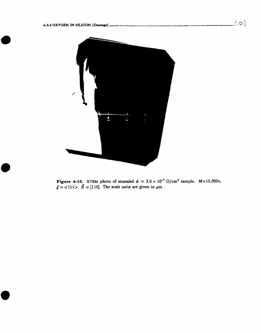
4-52 OXYGEN IN SILICON (Damage) ( i r ~ i )
Figure 4-16. XTEM photo of annealed 4 = 3.0 x 10" O/crnZ sample. M= lf i ,000~, ij = < 11 1>. = [110]. The scale units are given in jirn .

4 5 2 OXYGEN IN SILICON (Damage) (102)
43-23 Discussion
One would expect, a t the high implant temperatures used in these experiments (Ti = 570°C), that
most of the Frenkel pairs would recombine during the implantation, thus presenring the crystaiiine
nature of the target. For the most part, this expectation has been borne out by Our RBS/C and XTEM
studies. Even in the as-implaated state, the Ms/c analysis indicates that there is little or no damage
in the silicon film. Similarly, the damage in the EOR was not sufficient to produce an amorphous
layer, even at the highat dose of 3.0 x loi' O/cmZ. In contrast, Touhouche et al. [iM found that the
damage at the EOR was sufficient to produce an amorphous layer when d = 0.3 x 10¹⁷ O/cm%nd
Ti < ~00°C.
The generd shape of the damage distribution is the same for al1 the oxygen doses studied.
There is Little or no damage in the silicon Mm. At approximateIy 2.3 Pm, the damage concentration
changes irom a nearly perfect crystai to a highly damaged crystal over a depth region of 0.3 Fm. The
damage in the region 2.3-2.6 prn is predorninantly stacking faults and small dislocations. M e r 2.6 p m
the defect structure changes into what appears ta be smdl amorphous pockets, oxide precipitates or
point defect complexes. This damage extends into the subtrate to depths of 3.2 Fm. Each of these
dep t h regions will be discussed separatel y.
The XTEM results indicate that there is some damage in the silicon film of the b, =
3.0 x loL7 0/cm2 sample. This damage is located in a narrow (0.4 pm) depth region around 1.2 Fm.
Other researchers [la-rs] studying MeV oxygen implantation into silicon have found that at higher
oxygen doses (4 > 1.0 x 10¹⁸ 0/crn2) and high implant temperatures, a dense band of tangled dis-
locations wiii form in the silicon film, somewhere between the surface and Rp- Different tesearchers
have found this dislocation band at different locations within the silicon f h (see Table 2-11}. The
dislocation network (which only appears when Ti > 400°C) occurs a t a depth where the strain is
balanceci between the negative strain a t the surface (excess vacanàes) and the positive strain a t Rp
(excess interstitials and Si02). The formation of the dislocations is the method by which the excess
strain in the sample is releasedt [14,20,34,80,9810~1]. The silicon on either side of this band is typically
defect f ie . Cornparing o w results to the ones describeci above, we conclude that the thin band of
small (-20 nm) and thinly disperd defect dusters in the 4 = 3.0 x 10" 0/cm2 sampk is the initial
defects which are formed in an effort to ceduce strain in the silicon film.
For a more dctailed d y s i s of strain nduction ttvough the pnxas of defcct formation, s e $2-514

4-3-2 OXYGEN IN SILICON (Damage) (103)
Our anaiysis has shown that the depth (do) up to whiCh the silicon film retains a high crystailïme
quality is not a function of oxygen dose- For any one sample there is only a slight gradient in the
oxygen and oxide concentration profiles in the depth region surrounding do (to be dernonstrateci in 54-
3-4). Thus the sudden onset of damage at 2.33 pin is not related to a critical concentration of oxygen
or oxide precipitates. According to the standard defect production modeis [37], the high crystalline
qudity of the silicon füm is a result of a rapid recombination of defects in the dicon fiim. However,
at the EOR the defects cannot recombine fast enough ond thus cornplex defects form a t depths greater
than . Thus we conclude that the depth do is a function of the generation rate of defets (wtiich
is proportional to the ion flux) and the recornbination rate of these same defects (which is dependent
upon .I;:).
The maximum scattering yields in the RBS/C spectra occur at approximately 0.3 pm after the
onset of damage. Since it is known h m the XTEM photos that the damage starts at 2.3 Fm, and since
ic is &O known fiom RBS studies that the depth of the peak oxygen concentration, 4, is 2-55 Pm, it
is concludeci that the rnaximumyieId in the aligneci -S/C spectra is a tesuit of direct scattering from
silicon, or from the silicon in the oxide precipitates, in the region of maximum oxygen concentration.
The maximum range of the damage (3.2 pm) extends weil beyond the peak range of the oxygen
ions (2.55 pm). There are a few possible explanations for this. The first is that the excess silicon
interstitiah created by oxïde precipitation diffuse outwards, away from 4, and then cluster to form
s m d defett centers. This diffusion can be enhancd by the strain gradient produceci by the formation
of oxide precipitates. It is ais0 possible that the oxygen ions had been ueiatentionally channeleci dunng
the implantation. However, al1 seven samples analyzed by xTEM show the same defect structure, and
it is d i k e l y that oxygen was accidently channeleci seven times in a row-
There is yet a third possible explanation for the extended range of damage seen in the XTEM
results. There codd be a few, but nonetheless Large, oxide precipitates in this region. Cerofolini
et al. [17] have hypothesized (see $ 2 4 1) a region beyond the ion range where hot colliçional cascades
cause the oxygen ions, wit hin the volume of the cascade, to coalesce into a single oxide precipitate (ET
precipitatioa). The depth a t which the largest oxides are present changes with the dose, i n c r e ~ g
âs the dose increases. Their studies were done with 100 keV oxygen ions, and thus it was dScul t
to visudy separate the different regions within the as-implanted samples. At 2.5 M e V it is possible
that, because the phys id separation of EOR damage and the ET precipitation region is Iarger, it is

easier to visibly Merentiate these two regioos. The ET precipitation hypothesis is consistent with
the difference in appearance of the two defect regions visible in the XmM photographs (figure 4- lob).
If this hypothesis is valid, then one would a h expect that a 6 MeV oxygen implantation wodd
show an extended darnaged region. In the work of Touhouche et al. [LS], silicon was implanted with
3.0 x 10¹⁷ 0/crn2 a t 6 MeV. The implant was doue with a sample temperature of less than lOO0C
and consequently the EOR was amorphous, with a large strained layer beyond the amorphous layer.
The width of the amorphous region is x 0-5 Fm, and the strained region beyond the amorphous band
goes 0.4 pm deeper into the substrate. Whether this is, or is not, indicative of ET precipitation is not
clear.
After the sarnples are anneded, there is a coarsening of the oxïde precipitates, which is expected.
The damage in the EOR is now predominantly dislocations, extending fiom one precipitate to another.
In addition to the dislocations, the regions between the precipitates are strained. The location and
size of the oxide precipitates after anneaihg will be discussed in detail in the next section. There
continues to be small defect clusters present in the silicon nIm of the 4 = 3.0 x 10'' 0/crn2 sample.
However they no longer appear to be confineci to a fixed dept h region.
-. 4-34 Oxygen Distribution
The distribution of oxygen ions and oxide precipitatea were characterized by ERD, SMS and XTEM,
before and &ter annealing. The anneaihg was doue in a conventional furnace for 12 h a t L30O0C. 210
distinction is made here between samples that have been annealed in an Xr/02 fiow or N2 flow as the
oxygen profiles remain the same. This is discussed in Appendix A. The reader is reminded that the
ERD spectra have b e n shifted so that the depth is consistent with the RBS/C results, as describecl in
54-3- 1.
Figure 4-17 shows the results of the ERD analysis of t k e e samples Mplanted with doses of
4 = 0.3 x 10¹⁷, 1.0 x 10" and 3.0 x 10¹⁷ 0/cm2. The dots are the original data points and the
error bars indicate the statistical uncertainty. The solid tine is the same data after being smoothed
using a Fart Fourier Transformation (FFP) algorithm. Uniike the higher dose sample (figure 4-17~)

4-34 OXYGEN IN SILICON (Oxygen Distniution) ( los)
(a) xtof f 0.12F. .-
(b) ~ I O *
0.32 - f t
Figure 4-17. Oxygen concentration profiles (at/cm3) of wimplanted 4 = (a) 0.3, (b) 1.0, and (c) 3.0 x 10" 0/cm2 ssmpies. The dots are calculateci h m ERD data, and the solid lines are the results after smoothing. (d) Oxygen profles of (a), (b), and (c) d e r converting to at/ion/A.

43-3 OXYGEN IN SILICON (Oxygen Distribution) (W
the two Iower dose samples (figure 4-17a and 4-b) had not been etched d c i e n t l y to obtain a pro-
file which extends past the last remnants of oxygea. The respective pesk oxygen concentrations for
these three samples are 0.8 x 10~ ' . 2.5 x 10²' and 8.0 x 10²' 0/cm3. The concentration of oxygen in
amorphous SiO? is 4.4 x 1 0 ~ ~ 0/cm3, which means that, if al1 the oxygen is in an oxide phase, the
Si02 to Si ratio varies between 2 and 20%. Wit hin the limits of statistical uncertainty, the normalized
(at/ioo/A) oxygen profiles are equivaient for al1 three doses, as shown in figure 4-lid. This result
is not surprising since, at these doses, the phase change due to the oxygen implantation (formation
of Si&) is limited to srnall Si02 precipitates, and does not create stoichiornetrîc oxide Layers. The
oxygen profiles are neady gaussian. The standard deviation.0, of the fitted gaussian distribution is
0.13 Fm.
Figure 418. Oxygen concentration profile of as-implanteci 6 = 3.0 x 10¹⁷ 0/cm2 sample using SIMS analysis of "O and 62(Si02) signal. The 160 spectnim has been normaiized to the total dose. The ordinate axis represeats the oxygen concentration per cm3. The 62(Si02) spectrum has been scaled w that the peak concentration matches the "O peak concentration.
Another high dose sample (3.0 x 10" 0/cm2) was studied by S m and the results are shown
in figure 418. The oxygen content wss profiled by using the 1 6 0 , «(SiO) and b2(Si02) signal. The
160 s p e c t m has been normalized to the implanteci dose. The 62(SiOÎ) h a . oot been normdized.
aithough the scale was chosen so that the peak concentration of the 6a(Si02) signal would be the

4 8 3 OXYGEN IN SILICON (Oxygm Distribution) w7)
same as the peak concentration of the signal. The profile of the "(SiO) molecule is not shown
because it is virtuaily indistinguishable fiom the l'O profile. The ''(Sioz) profile however, shows a
marked ciifference fmm the "0 profile, and is thought to be an indicator of the oxide phase within
the silicon. The rise in S i 0 2 moleales occurs &ter the oxygcn concentration exceeds 3 x 10'' O / c d ,
which indicates t hat the surface region, at Ieast , is supersaturateci wi t h non-precipitated oxygen.
The oxygen concentration in the sikon film rises smoothly, starting Crom l e s than
5 x 10'' 0/cm3 at the surface, to a peak concentration of 0.8 x 10²' 0/cm3. There is no indic*
tion that excess oxygen has clustered at 1.1 prn, the depth of the anomalous defect band found in
this sample. Similady, there is no indication that the oxygen concentration is affectecl by the onset
of the highly defected region (roughly 2.3 pm to 2.8 pm) at the EOR. The decrease in the oxygen
concentration from 4 into the substrate is not smooth. There is a kink in both spectra ('=O and
62(Si02)) at approxirnately 3 prn deep, after which the concentration of oxygen dropa rapidly to, or
below, the detection limit of the apparatus.
Figure 4-19. A cornparison of the as-implanted oxygen profile (ERD and S ~ S ) with the owgen profile predicted by TRIM dculations, for q5 = 3 x 10¹⁷ 0/cm2. The TRIM and S ~ S data have been shifted dong the depth scaie such that the peak concentrations are at 2.55 Pm-

4-34 OXYGEN IN SILICON (Oxygen Distribution) (l08)
In figure 4-19, the ERD, TFt.Ihf and SMS oxygen profiles for 4 = 3.0 x 10" 0/cm2 are shown.
The TRIM profile was shifted by 0.2 pm and the SiMs by 0.08 p m so that the shapes of the profiles
could be cornpared more easily. The leading edge of the oxygen profile, from both the ERï) and
SiMS analysis, is consistent with the TW calculations, but the trading edge is not. It appears tbat
oxygen fiom the EOR diffused into the substrate during the implantation. This tailing of the oxygen
concentration is more pronounced in the sample analyzed by S M S than in the sample analyzed by
ERD. This difference will be discussed in $4-3-3-3.
,411 in all, it is not unreasonable to conclude that the as-implanted oxygen profile is independent
of the doses used in this experiment, and that the damaged silicon film in the 3.0 x 10" 0/cm2 sample
does not affect the oxygen distribution. It is also reasonable to conclude that not al1 of the implanted
oxygen has precipitated, but is bound in oxygen/vacancy complexes instead.
During aanealing, the oxide precipitates that have a radius Iess than the critical radius r, will dissolve.
The subsequently released oxygen solute will then diffuse to the larger, and more stable, oxide precip
itates. These precipitates will continue to grow via the Ostwald proces, and should two precipitates
- corne in contact with each other, they will merge in order to reduce the Si/Si02 surface tension. I t
has ben well established that the hotter and longer the anneal temperature and times, the better the
quality of the S M O X structure. For the Iow doses used here, there is not enough oxygen to form a
complete Si02 layer. However. even with a 12 h anneal time (1300°C), oxides have not yet finished CCP
alescing. This is drarnatically iilustrated in figure 4-20, an XTEM photo of a 3.0 x loL' 0/crn2 sample.
The large precipitate in the center of the photo has a diameter of approiamately 125 nm. A smaller
precipitate can be seen to be mcrging with this larger one (upper left), and given a longer anneal
time, they would have melded together to form one, even larger, precipitate. Because of the crys-
t u e nature of the target the precipitates are not spherical ( m i n i m u m s d ~ e area), but rather they
are facetted, with the edges lying dong the {100}, {110) and {111) planes. The srnallest precipitate
seen in this photo is -30 nm. Dislocations which extend between precipitates are also visible.
The X T m resdts for the anneded samples are shown in figure 4-21. The sizes of the pre-
cipitates in the low dose sample (d = 0.3 x 10¹⁶ 0/an2) are rather uniform. relatively speakuig,
with a diameter of approximately 50 nm. The largest precipitate seen (not shown) for this dose had
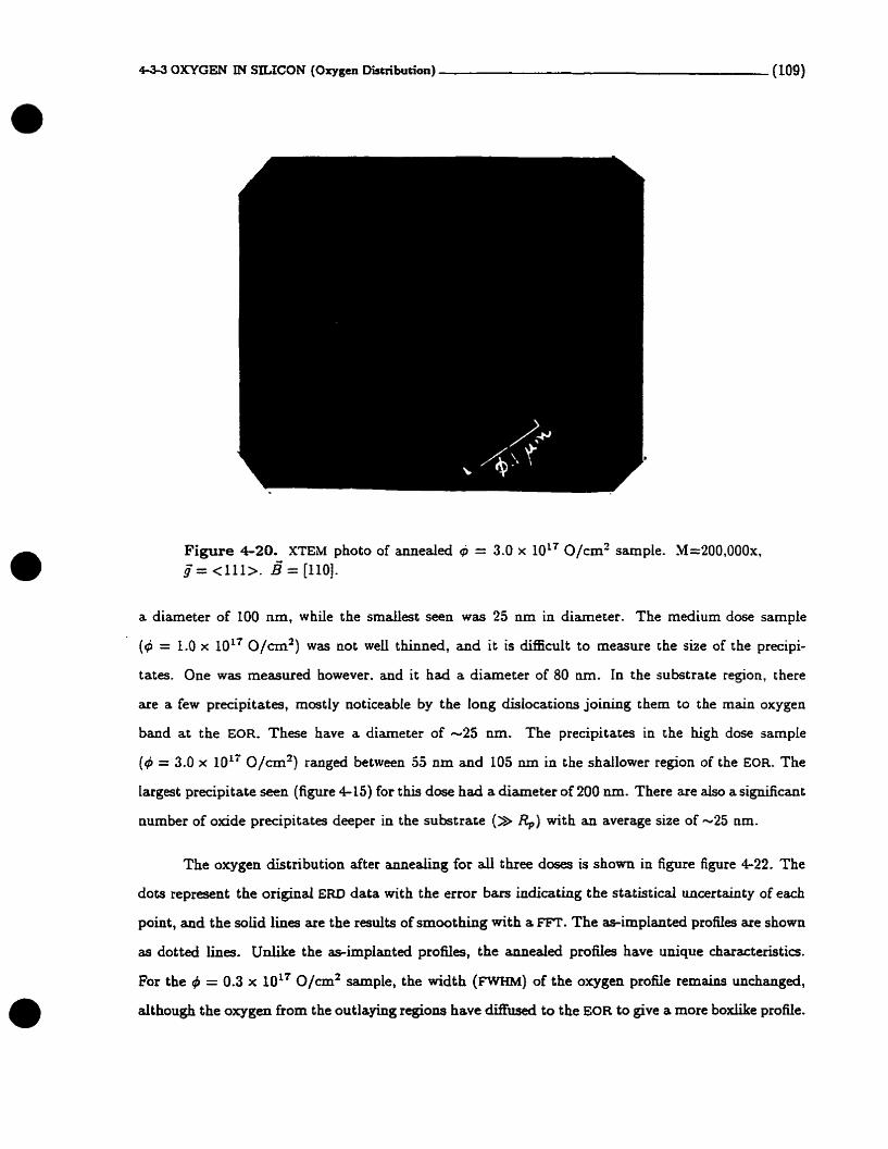
Figure 420. XTEM photo of annealeci 4 = 3.0 x 10¹⁷ O/crn2 sample. ~=200,00Ox, y= <lll>. B = [110].
a diameter of 100 nm, whiie the smdest seen was 25 nrn in diameter. The medium dose sample
( 4 = 1.0 x loL7 0/crn2) was not weil thinneci, and it is diffcult to measure the size of the precipi-
tates. One was measured however. and it had a diameter of 80 nrn. In the substrate region, there
are a few precipitates, rnostly noticeable by the long dislocations joining them to the main oxygen
band at the EOR, These have a diameter of -25 nm. The precipitates in the high dose sample
(4 = 3.0 x 10'' 0/cm2) rangeci between 55 nrn and 105 nm in the shallower region of the EOR. The
Iargest precipitate seen (figure 4- 15) for t his dose had a diameter of 200 nm. There are also a significant
number of oxide precipitates deeper in the substrate (> 4) with an average size of -25 nm.
The oxygen distribution after annealing for all three doses is shown in figure figure 4-22. The
dots represent the original ERD data with the error bars indicating the stotisticd uncertainty of each
point, and the solid lines are the resdts of smoothing with a m. The as-implanted profdes are shown
as dotted lines. Unlike the as-implanted profiles, the anneaied profiies have unique characteristics
For the 4 = 0.3 x 10¹⁷ 0/cm2 sample, the widt h (FWHhî) of the oxygen profüe remains unchangeci,
dthough the oxygen ftom the outlaying regions have diffused to the EOR to give a more boxiike profile.

4 4 3 OXYGEN IN SILICON (Oxygcn Distribution) ( L !O)
Figure 4-21. XTEM photos of annealed 4 = (a) 0.3, (b) 1.0 and (c) 3.0 x 10" 0/cm2 sarnples. M=15,000x, B = <111>, 8 = [110]. The scde units are given in pms.

44-3 OXYGEN IN SILICON (Oxygen Distribution) (111)
- 3 x 1 0 " 0/cm2 . annealed
onnealed
Figure 4-22. Oxygen concentration profiles of =implanteci and anneaied 4 = 0.3, 1.0 and 3.0 x 10L7 0/cm2 samples. The dots are calculated fiom ERD data, and the solid and dashed lines are the ERD reaults after smoothing.

4-34 OX'YGEN Dl SILICON (Oxygcn Distribution) ( 1 12)
The oxygen is located in a weU defineci depth range of 2.4 to 2.75 Fm. The peak concentration of
oxygen has increased h m 0.8 to 1 x 10" 0/cm3 during the anneal. There is a mdl, but noticeable,
kink in the profile between the EOR and the substrate located a t 2.65 Pm, with an oxygen concentration
of - O.? x 10" 0/crn3.
The a5 = 1.0 x 10¹⁷ 0/cm2 sample aiso has a broad region of maximum oxygen concentra-
tion (3.0 x 10²' 0 / m 3 ) in the same depth region as the low dose sample, as well as a kink in the
deeper interface, only now this hink is at a depth of 2.75 Pm, again with an oxygen concentration of
0.7 x 10" 0/cm3. In addition to t h , there is another region, appmximately 0.1 p m wide. with an
oxygen concentration of 2.0 x 10" 0/cm3, extending into the silicon film. Again. the oxygen that
was in the silicon film before annealing is no longer there, having diffused to the EOR region.
The = 3.0 x 10¹⁷ 0/cm2 sampie has a completely different oxygen profile than the other
two sarnples. There is no longer a broad region of evedy distributed oxygen. Instead. there are two
very sharp and distinct peaks, separated by 0.2 Fm- The first peak is at do (the depth in the as-
implanteci samples where there is a sudden increase in the damage concentration) and has a maximum
oxygen concentration of 4 x 10" 0/crn3. The second peak, centered at 2.55 p m ( Rp j , has a maximum
concentration of 15 x 1 0 ~ ' 0/crn3, an increase of 90% from the peak as-implanted concentration.
In addition to the ERD analysis, the oxygen concentration of the 3.0 x 10" 0 /cm2 sample was
analyzed with SMS, again using the "O signal and the 62(Si02) signal. The resuits are shown in
figure 4-23. The 160 profile was normalized t o the total dose and the '*(Sioz) profile was d e d so
that the peak concentration was the sarne as the 160 peak concentration. Although the noise signal
for the "O ion is significantly larger than the noise signal for the 6 2 ( ~ i 0 ? ) molecule, two of the three
62 (Sio?) pe& in the silicon film can stiU be seen, to a 1-r degree, in the 160 profile. Wiihin this
limitation, the 62 (Si02) profile has the same shape as the "0 profile indicacing that aii the oxygen
in the sample is now in the form of Si02 precipitates.
In the silieon film, the oxygen concentration is not evedy distributed. There are three distinct
bumps Iocated at depths of 0.55, 1.4 and 1.85 pm. The first two are bmad (-0.4 pm wide) while the
third oxygen bump is a very narrow peak approximately 0.1 pm wide. To insure t hat t hese bump
were not just a local phenornenon, the sample was probed six times and identical r d & were obtained.
These bumps have concentrations less than l0lg 0/cm3, the o r d m of magnitude lower than the peak
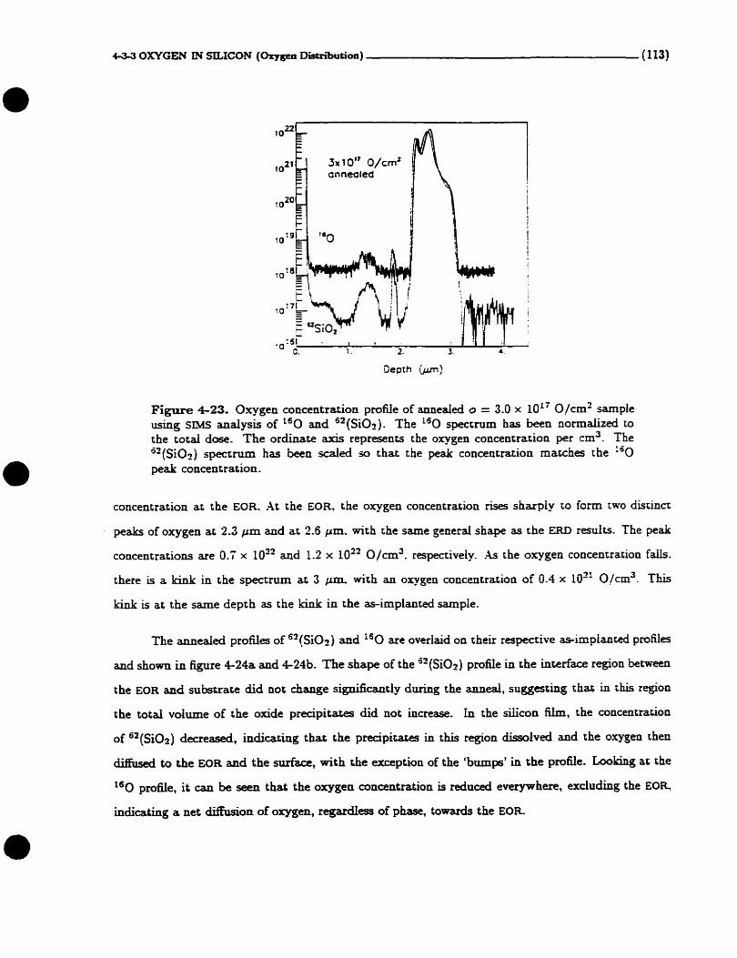
Figure 423. Oqgen concentration profle of anneaieci o = 3.0 x 10'' 0/crn2 sample using SM anaiysis of I6O and 62(Si02). The 160 specrrum has been normalized to the total dose. The ordinate axis represents the oxygen concentration per cm3. The "(Si02) specrnun has been d e d so that the peak concentration matches the 160 peak concentration.
concentration at the EOR. At the EOR, the oxygen concentration rises sharply to form two discina
- peaks of oxygen ac 2.3 pm and at 2.6 pm. with rhe same general shape as the €RD results. The peak
concentrations are 0.7 x 10'~ and 1.2 x 10'~ 0/cm3. respecrively. -4s the oxygen concentration falls.
chere is a kink in the spectrum ac 3 with an oxygen concentration of 0.4 x 10" 0/cm3. This
kink is at the same dept h as the kink in the as-irnplanted sample.
The annealeci profiles of " (Sioz) and are overiaid on their respective asimplanteci profiles
and shown in figure 4-248 and 4-24b. The shape of the "(Sioz) profiIe in the interface region between
the EOR and substrate did not change significantiy during the anneal, suggesting thas in t his region
the total voiume of the oxide precipitates did not increase. In the siiicon h, the concentration
of ''(si02) d e c r d , indicoting that the p d p i t a t e s in this region dissolveci and the oxygen then
difFused to the EOR and the surface, with the exception of the 'bumpb' in the profile. Loo- at the
160 prome, it can be seen that the oxygen concentration is reduced everywhere, exduding the EOR
indicating a net diffusion of oxygep, regardess of phase, towards the EOR

4-34 OXYGEN IN SILICON (Oxygcn Distribution) f 114)
5x1 O" O/cmZ
=Si& profile
3% IO" O/cmz
"3 profile
Figure 424. The annealeci and as-implanteci (a) "(Si02) and (b) 160 oxypn concen- tration profiles for a d = 3.0 x 10'' 0/cm2 sample.
4 3 - 3 4 Discussion
For oxygen implantation with doses between 3 x 10L%d 3 x IO": 0/cm2. the as-implanteci oxygen -
concentration profiles are similar in shape, in spite of the fact that the oxygen doses vary by a fanor
of ten. In contras, the oxvgen concentration profiles of the annealeci sarnples are remarkabiy different
(see figure 4-22). The oxygen profile of the 3 x 10¹⁶ 0/cm2 sample is boxlike in shape. the profile for
the 1 x 10'' 0/cm2 sample is broader with a distinctive %tep' in the concentration. And findy, the
profîle for the 3 x 101' 0/cm2 sample, aithough extending over a bmader region, has separateci inca
two very distinct sharp peaks at depths R, and do, which are the depths of the peak as-implanced
oxygen concentration and peak damage region respectively.
Thete are two possible explanations for the ciifferences in the annealeci oxygen concentration
profiles. The fk t is that the profiles of the oxygen concentration is just a direct manifestation of the
OstwaIcl ripening proces. Even in the simplet of systems, the redistribution of oxygen during the
anneal can result in very cornpl= concentration profles. For example, a homogeneaus distribution
of oxîdes of equd size can d t in a muiti-band oxygen distribution sRu annealing [=,74]. The
number of bands is a function of the original density of precipitates w h an increase in the density
of precipitates increases the number of bands (52-5-3). Since the higherdose sample has a la-

4-3-3 OXYGEN IN SKLICON (Oxygen Distribution) (115)
concentration ofoxygen, it is not hard to imagine that the initial density of precipitates is aiso larger,
and thus the final oxygen distribution is c o m p d of two bands. The lower-dose sample has a Iower
density of precipitates and thw does not fonn a multi-band structure. The concentration profile of
the intermediate-dose sample could be a transition from the lowerdcse to the higher-dose profiles.
Although Ostwald ripening alone could account for the oxygen distributions, there are reasons
to believe that this is not so. The first reason is the fact that the smaller of the two oxygen peaks
shown in figure 4-22 is at the sarne depth as the onset of damage in the asimplantecl sample. It has
been well established that oxygen will getter on crystalline damage sites fsi], and this effect should
not be ignored. The diffusion and annihilation of the silicon interstitiais also plays a significant role
in the final structure of the annealeci sample since the silicon interstitials that are released into the
matrix during the growth of oxides precipitates inhibit the growth rate of those same precipitates
[;O]. The distribution of silicon interstitials is &O mediated by the original distribution of damage.
Consequently, any explanation describing the reasons br the shapes of the oxygen profiles should
include HE precipitation, which is the preferential precipitation of oxygen on damage sites resulting
in larger, but fewer, precipitates.
It has been hypothesized [w] t hat if the oxygen current density during the implant is low , and if
the temperature of the sample is bigh, then precipitation, occurring at do, p r e d s over HO precipi-
tation, occurring a t %, at low oxygen doses, and that at very low doses, HO precipitation is impossible
(92-5-1). Given our experimental conditions of Ti=570°C, J * 1 pA/cm2, and 4 < 3.0 x 10'' 0/cm2
we would expect that this effect would be observable in at least çome of our results. However, carelul
analysis of the depths of oxide precipitation after annealing clearly indicates that HE precipitation is
not the predominate factor, even at the lowest dose of 3 x 10'' 0/cm2-
Taking this into account, the differences in the oxygen profües of the annealeci samples can be
explained if we rnake the foilowing assertions; (1) HO precipitation does occur, (2) HE precipitation
also occurs, and is a function of the quantity of the radiation induced damage, (3) although ET
precipitation may or rnay not occur, it does not affect the oxygen profües in the neighbourhood of Q,
(4) there are a t least two local maximaof precipitate sues, located at Q and Rp and (5) the number
and size of the precipi tates increases with increasing dose,

43-3 OXYGEN IN SILICON (Oxygen Distribution) (116)
Figure 4-25 is a schematic of the general distribution of the precipitates in the samples, assuming
that the size of the precipitates are proportional to vm, except in the region of damage, and C(x) is
the concentration of oxygen at depth x. The preferential precipitation a t 6 produces larger and more
stable precipitates, and has b e n accounted for by artificially increasing the radius of the precipitates,
and subsequently decreasing their density. This figure is only used to illustrate the problem, and
the reader shodd take note that the size of the precipitates shown in the figure is not indicative of
the actud size. In this simple representation, it is assumed that the rarnpup tirne of the anneal is
sufficiently fast so that very little dynamic annealing occurs before the sample reaches the maximum
temperature of 1300°C. Thus al1 the precipitates with a radius less than the critical radius at 1300°C
(- 50 nm [12]) will dissolve, leaving a distribution of precipitates similar to tvhat is shown in figure 4-
25c. It is then thas distribution of precipitates that affects the Ostwdd ripening process, rather than
the as-implanted distribution (figure 425b).
For the 3 x 10L6 0/cm2 sample, the majority of the precipitates are below the critical radius,
inctuding the precipitates at do, and consequently t hey dissolve during the initial stages of annealing.
During this time the residual radiation damage is also annealed and hence the preferential oxidation
sites are removed. New precipitates will form, d l eIse being equal, in the region of highest oxygen
concentration. These new precipitates will now act as gettering centers for the rernainingsolute oxygen
which &&ses inwards from the 'wings' of the original oxygen distribution. This is readily observed
by comparing the annealed and as-implanted profiles for this dose (figure 4-22). Some structure
is observed in the region of maximum oxygen concentration, and could be related to the natural
segregation of oxides into separate bands via the Ostwaid process.
For the 1 x 10" 0/cm2 sample, the precipitates at do dissolve, but unlike the lower dose, there
is a broad region centered around Rp with stable precipitates (figure 4-25). The solute oxygen which
migrates inward from the silicon film not only encounters stable precipitates, but a h the damage that
is trapped between these precipitates. This region now getters the oxygen before it can finish diffusing
towards do. Hence the 'step' in the concentration profile, and the reduced gettering efficiency at Rp
(figure 422).
For the highest dose sample (3 x 10¹⁷ 0/cm2), the stable precipitates t o m two bands centered
at R,, and do (figure 425c). These precipitates gmw by the normal Ostwald process. It is interesthg
to note that there is no net diffusion of oxygen during the anneai between the Ho and iIE regions
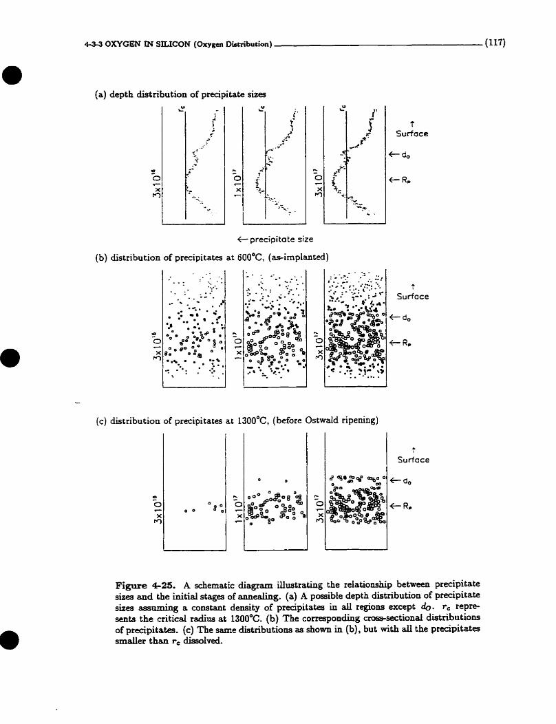
4-3-3 OXYGEN IN SILICON (Oxygen Distribution) (117)
(a) depth distribution of precipitate sizes
f- precipitate size
at 60Q°C, (as-implanted)
(c) distribution of precipitates at 1300~C, (before Ostwald ripeoing)
t Surface
+ do
f- R,
t Surface
f- do
f- R e
? Surface
Figure 4-25. A schematic diagram Uustrating the relationship between precipitate sizes and the initial stages of anneding. (a) A possible depth distribution of precipitate sizes ass;uming a constant density of precipitates in d regions except Q. r, repre sents the critical radius at 1300%. (b) The corresponding nogpsectional distributions of precipitates. (c) The same distributions as shown in (b), but with all the precipitates smder thon r, dissolved.

-3 OXYGEN IN SILICON (Oxygen Ditribution) ( 118)
(figure 4-22). Thus the first peak, located a t 2.3 Fm, is formed predominantly by the diffusion of
oxygen fiorn the d icon film and can be considerd to be independent of the growth of the peak at
4-
Thus the gross features of the oxygen profiles, before and after annealing, can be explained if
the foilowing two points are assumecl. First, there is preferentiai oxidation in regions of high crys ta lhe
damage, and secondly, that a significant portion of the precipitates dissolve (at least at the doses used
in this experirnent) in the very early stages of annealing. Once these initial conditions are satisfied, the
o.xygen profiles after annealing for 12 h can be explained by the standard Ostwaid ripening process.
Because the precipitates a t dg act as a diffusion barrier between the silicon film and the EOR,
any oxide layer made with doses of 4 = 3.0 x 10¹⁷ 0/cm2 or bigher must be at least as thick as the
distance separating and 4. If the density of the silicon dioxide is 2.32 g/cm2 and the minimum
width of the layer is between 0.2 and 0.4 Pm, the minimum dose needed to form an oxide layer woutd
be 4 -1-2 x 10¹⁸ 0/cm2.
The Iower oxygen concentrations in the film and substrate of the samples could not be pro bed
by ERD, but some information is available from the XTEM analysis of the samptes, and the S M S
analysis of the 3 x 10" 0/cm2 sample. Let us first discuçs the oxygen concentration which extends - beyond Rp. The XTEM photos of the asimplantecl samples (figures 4-10, to 4-12) cleariy show that
there is some damage and/or oxides weU past the peak concentration depth, extending as far as 3 Pm
into the sample. Comparing the XTEM photo and the SriMs andysis (figure 4-24) for the highest dose
sampte, we see that the 'spots' in the photo corresponds to the presence of oxygen in t hat dept h region.
After anneahg it can be seen t hat (figure 4 2 1) t here is no visible damage or precipitates in the lowest
dose sample between 2.7-3.0 Pm. In the intermediate dose sample there are a few precipitates in this
region, and in the highest dose sample there is a large number of s m d precipitates. The results of
the XTEM photos would suggest that the oxide precipitation in the deeper regions of the substrate is
a function of dose. But this, as will be shown in later sections, is not always reproducible.
Jh addition to the non-reproducibiiity, another factor should a b be discussed. The sriMs data
was obtained fkom the same target as the one used for the XTEM photos, but the ERD data was
obtained fkom a diffkrent target, dthough the history of the targets were nornindy the same. The
SIMS results show a larger concentration of oxygen in the substrate, M o r e and after anneaiing, than
4-34 OXYGEN IN SILICON (Oxygen Distribution) (119)
the ERD results. Two possible explmations for this could be: (1) there was unintentional channeling
in the target analyzed by SïMS or, (2) the Cs+ ions used to sputter the target for the SfMS anrslysis
knocked the oxygen atoms further into the target during the sputtering process, causing the oxygen
profde, as obtained by sIMS, to be incorrect.
Finally, the three peaks of oxygen concentration in the silicon film of the 3 x 10¹⁷ 0/cm2
sarnple (figure 4-24) wïll be d i s d . As the reader will recall, there is evidence of darnage and/or
oxide precipitates in the silicon film before annealing (figure 4-12), dthough there are no peaks in the
as-implanted profiles. In spite of the fact that the damage distribution could not be ascertaineci to
any great amiracyt, i t is presumed that the oxygen profile in the annealed sample is a result of the
oxygen interacting with the damage that was already present in the as-implanted sample. Tamura
et al. [6l] have dso noted oxygen concentration peaks in the film of ion-implanted silicon (- % 4) after annealing, even when the implanteci ion was not oxygen. They attribute this to vacancy rkh
regions within the silicon film acting as gettering centers for oxygen. Since the defects seen in the
as-implanted sample is a result of strain release via the condensation of vacancies, the oxygen is no
longer bound to the vacancies. The oxygen is now free to form oxïde precipitates [20].
To recap the results and conclusions of this section, we have: (1) HO and HE precipitation
- occurs in the as-irnplanted samples, (2) the final oxygen concentration profile is dependent on the
distribution of oxide precipitates that remain ufter the h a c e temperature has reached its maximum,
(3) ET pmipitation (precipitation that ocnirs well past 4) can neither be confinned nor denied since
there is a question of reproducibility and passible Midental channeling in the 3 x 1oL7 0/cm2 sample,
(4) the three oxygen peaks in the silicon füm of the 3 x 101' 0/crn2 sample can be attnbuted to the
as-implanted damage profile, but the reason for the shape of the peaks, their location, and even their
number, is not clear and (5) it is not possible to form a SiOl layer using only a mono-energetic oxygen
beam with doses l e s than 9 = I x 1018 0/cm2.
- -
The distribution of damage in thir sample can oniy be hypoçbcsizcd rince the XTEM photos WC= not sufiicient to
give a profiIe of the damage, and the RBS/C spectrurn was not sensitive enough to probe the damage in thii region.
4-34 OXYGEN IN SILfCON (Oxygen Distribution) ( l20)
4 4 OXYGEN IN PRE-DAMAGED SILICON
The next step in understanding the interaction between damage and the behaviour of oxygen in silicon
is to study oxygen implanted into pre-damaged smples. By prdamaged sampies we refer to silicon
that has b e n implanted with nlicon, a t the çpecified energy and dose, and subsquently anaeaied
for 1 h a t 900°C. The silicon doses useci were Q = 5 x LOI4 and 1 x 10~"i/crn'. The energy of the
silicon implants ranged between 2.00 and 2.75 MeV. The energy of the oqgen implants were fixed at
2.5 MeV, and the doses ranged between t$ = 0.3 x 10" and 3.0 x 10li 0/cm2. The oxygen implants
were camed out with a sample ternperature of 370°C. The specific experîmental conditions (dose rate,
temperature of implant, etc.) of the silicon and oxygen implants are @en in $4-1-
There is one exception to the above description of pre-damaged samples. in one instance,
while implanting oxygen into a virgin silicon sample, the heater for the sample holder malfunc-
tioned and stopped heating right at the start of the implantation procedure. However, the mal-
function was not noted until approximately 10 minutes later. At this time the total implanted dose
was -2 x 10" 0/cm2. The temperature at the start of the implant was 570°C, and based on ear-
lier tests on the heating system itself, 1 estimate that the final ternperature, after 10 minutes, w a ~
less than 200'C. The sample was leh within the implantation chamber for more than 2 days while
- the heater was being repaired. .ifter this, oxygen was again implanted at 5ïO°C to give a final
dose of 1.0 x 10¹⁷ 0/cm2. Fiereafter, this particdar sample is described as having a pre-damage of
2 x 10" 0/cm2, with Z=30O0C. This is the only sample that was not annealed before the final oxygen
implantation. It should also be noted that the temperature, of this particdar pre-damaged implant,
is o d y an approximation.
In all cases, the prdamaged depth of the silicon implant, dsi, is l e s than the range, Rp, of
oxygen in siiicon.
The oxygen concentration profiles and the damage profiles are studied as a function of (1) oxy-
gen dose, (2) distance xparating the prpdamage region h m the oxygen implant and (3) prcdarnage
type. A summary of the these rdationships is shown in Table PV. The distribution of the oxide
precipitates in the asimplanteci samples an inferred h m the status of the annealed sampla.

44-1 OXYGEN IN PREDAMAGED SILICON (Damage) (121)
TABLE 4-V
A summary of the experimental parameters and results. (a) The experimentaj results and interpretation of prdamaged sarnples. (b) The experimental results and interpretations of oxygen implanted into pre-damaged samples, as a function of pre-damage conditions and oxygen dose. Double arrows indicate trends, The silicon pre-damage depth is denoted by d,. The depth of the maximum damage production during the oxygen implant is defined as do.
ta) predamaqe: -----
h r m e n concemraOon beween d,, and ci, (after annealingl

The damage in the samples was analyzed using RBS/C with a 3 MeV He probing beam, and a tuta1
detector a g i e of 67.5*, unies otherwise stated. The aligned direction was < 1 IO>. Besides RBS/C,
XTEM was also used to characterize the damage- However, given the Iarge investment in time necessaq
to prepare XTEM sampIes, only samples pre-damaged with 2.00 MeV Si were anrrlyzed with this
technique.
The as-implanteci damage profiIes as a function of oxygen dose, as well as a function of the pre-
damage conditions, was measured using Ms/c analysis and the results are shown in figures 4-26 to
4-28. On the Ieft side of the figures, the aligned yield (X), normaiized to the random yield, is shown
in each individual graph for samples with equivalent oxygen doses, but with diRerent pre-darnage
conditions. The pre-damaged conditions are listed on the figure itself, and the individuai spectra
have been vertically offset in order to rnake the comparison between spectra easier. For the sake of
comparison, the RBS/C spectra and the damage profiles for the standard (no pre-damage) samples are
a h shown.
The damage profiles, s h o w adjacent to the X curves, were calculated based on the following
assumptions: 1) the energy l o s of He in the aligned direction is 60% of the energy Los in a random
direction, and 2) the predominant cause of de-channeling in the samples is due to point-like d e k t s .
Ushg the same arguments as discussed in $4-3-2-1, we wmise that the resulting damage profües give
a reasonable approximation of the damage distribution within the sample, although the depth scale
is only an approximation.
When comparing the pre-damaged samples to the standard samples, i t is immediately obvious
rhat the general distribution and concentration of the large damage peak a t -2.5 Fm is not affecteci
by the presence of the pre-àamage. Sinee the p rdamage depth dsi is leos than the range of the
implanted oxygen, 4, one wodd expect that any ciifferences in the damage profiles wodd occur at a
depth shdower than 4. Ln ail cases where the p r d a m a g e was 5 x loi* Si/cm2 at 2.00 MeV there
is a very maü, but noticeable, region of damage in the vicinity of 2 pm (indicated by armwg in
the figures), which is the deptb of the predamage for this Si implant energy. At higher Si implant

4-41 OXYGEN N PREDAMAGED SILICON (Damage) (123)
( 4 Approximate Oepth w) 35 3-0 25 20 1.5 1.0 0 5 0.0
1. "" l "'~l'"'1"''I''..TT'F'ITT'7
2-5 MeV
0.3~ 10" O/cml asimplanted
.- 5 x 1 O" Si/cml
ü 2.50 MeV
'O
I 2.5 MeV
0.3~ 10" O/cmS
O- o. 1 I f
0.8 1.0 2-4 3.2
Approxirnate Depth (pm)
Figure 4-26. (a) The nomalized aligned yield (Xf for aç-implanteci ai = 0.3 x 10¹⁷ 0/cm2 (5 x 10L4 Si/cm2 pre-darnaged) samples. (b) The calculated dam- age profiles assuming only point defects. The depth scaies were calculated assuming that the stopping power in the alignecl direction was 0.6 chat of a random direction.
1 .z Approximare Depth (pm)
3.5 3.0 2.5 2.0 1.5 1.0 0.5 0.0 1 " " ' r f " r l ~ L E * ' ~ x ' ~ l ~ " a l i ~ l l l
2.5 MeV
3.0~ r O" O/cma
1) asimplanted
2-50 MeV
2-00 MeV
t
Energy ( M ~ V )
2.5 MeV
3.0~ 10" O/cml
standard I I
0.8 1.6 2.4 3.2
Approximate Oepth (pm)
Figure 4-27. (a) The normaliaed aligneci yield (X) for asimpiantd 4 = 3.0 x 10" 0/cm2 (5 x 10L4 Si/cm2 prcdamaged) samples. (b) The caiculated dam- age profiles assuming only point defécts. The depth scales were calculateci d g thab the stopping power in the aligneci direction was 0.6 that of a randorn direction. (standard refers to no pdamage)

44-1 OXYGEN IN PRE-DAMAGED SILICON (Damage) (124)
(4 . Approximate Oepth (pm)
, .4 3 5 3.0 2.5 2 0 1 5 1.0 0.5 0.0
2.5 MeV
1 . 0 ~ 1 O" a/crnZ as-irnpfanted
standard
O.' 015 1 i 1 1
1. i .5 2.
Enerqy ( M ~ v )
Approximate Depth (gm)
3.5 3.0 2.5 2.0 1.5 1.0 0.5 0.0
2.5 MeV
1 .Ox 1 O" O/cmx aslmptonted
-0 k P) c -? 0.6 z
pre-darnage u Q)
.N - 0.4 1 x 1 O" ~ i / c d
z L 2-00 MeV
g 0.2 standard
I I 1 1 91 1
1. 1.5 2.
Enerqy ( M ~ v )
2.5 MeV
as-implantcd
standard f 1 11
2.4 3.2
Approximate Deoth (pm)
0.t -
1 I
2.4 3.2
Approxirnate Depth (pn)
Figure 4-28. (a) The normalized digneci yield (X) for apimplanted 4 = 1.0 x 10¹⁷ 0/cm2 ((a) 5 x lOl4 Si/cm2 and (c) L x 10'' S i / c m 2 pre-damaged) Sam- ples. The caldateci damage profiles ((b) 5 x 10¹⁴ Si/cm2 and (d) 1 x 10¹⁵ Si/cm$re- damageci) assuming only point defits. The depth d e s were caldated assumiog that the stopping power in the aügned direction was 0.6 that of a random direction. (standard ref- to no pre-damage)

4-4-1 OXYGEN IN PEIIGDAMACED SILICON (Da-) (125)
energies, the pre-clamaged region is deeper, and hence doser to the damage caused by the oxygen
implant, and thus it is not possible to separate these two damage regions.
To better understand the nature of the defectç in our sampies, the samples pdamaged with
2.00 MeV &con were analyzed via XTEM. To illustrate the similarïties and Merences between sarnples
with dXerent oqgen d m . XTEM photus of pre-damaged samples implsnted with o = 0.3 x 10".
1.0 x 10" and 3.0 x 10" 0/cm2 are shown in figure 429 . The pdamage was O = 5 x 10¹⁴ Si/an'.
In these sarnples there are. at minimum, two very distinct defwt regious. as was noted in the channeling
spectra, One of these defect regions is locatd at the same depth (-2 pm) as the original pre-darnqe-
The defect characteristics in this region are different for each oxygen dose. The other major de fw
region, in the depth range of 2.5 Pm, has the same characteristics and depth as in the standard
samples, and thus we conclude th& it is a result of the o q g e n inzpiantation icseff. For the higbest
d o e sample, o = 3.0 x 10" 0/cm2. (figure 4-29c) there is a third defect region -0.5 p m wide l o c d
around 1.3 pm, and is characterized by small black spots. This is not seen in the Iower dose sarnples.
even at higher rnagnificationç. The siiïcon substrate is not completely defect-free. as can be seen by the
1 p m dislocation extending into the substrate dong the < 11 1> dirwtion (labefled 'A' in figure 4 . 2 9 ~ ) .
This bas b e n seen before in other sampies. In the foilowing paragraphs. each defect region e l 1 be
presented separately.
The defect characteristics of the defect band at the EOR are similar to the standard samples
(se figures 4 1 0 to 4-12) insofar as (a) the damage starts abruptly at 2.3 Pm. (b) the interface between
the damage Iayer and the substrate is oot sharp. h t e a d , the quantity of damage siowly decreaçes
as it extends into the substrate to a maximum depth of 3 p m and hally ( c ) the defects cioser to
the surface are characterized by slnall dark bes (dislocations or stackng fadts) , and the defects
deeper in the sample are characterized by s m d dark spots (olàde precipitates or smail morphous
pockets). The highest dose sample (4 = 3.0 x 10" 0/cm2) has the largest visible strain, which is to
be expected. Since th& damage region has been thoroughly discussêd in $4-3-2 we will aot go into
it in any further detail. For simplicity's sake, thiç d e k t region wïll henceforth be r e f e n d to as the
'main defkct band'.
Next, let us consider the defect region centered around 2 pm. This is the depth at which
the original prdamage was located (dsi). The damage in this region for samples pre-damaged with
5 x 10" Si/anz is signincantly difterent thau the originai damage structure (cf. figure 4-3) as the

4 4 1 OXYGEN IN PRE-DAMACED SILICON (Damage) i \ 2 6 )
Figure 429. XTEM photo. of as-implanted 4 = (a) 0.3, (b) 1.0 and (c) 3.0 x 10" 0/crn2 (2.00 MeV, 5 x 10¹⁴ Si/cm2 pre-damaged) samples. M=15,000x, = [110], $= < I l l > . The scale units are given in pm .

dislocation loops are n o longer present, as can be seen in figure 4-29. Because the amount of damage
in this region decreases with increasing oxygen dose, we condude that the original pre-damage is being
annealeci during the implantation. For the lowest oxygen dose, 6 = 0.3 x 10¹⁷ 0/cm2 (figure 429a),
the def' fonn a continuous network of disIocations parallel ta the surface, with an occasional defect
which extends from the pre-darnaged region to the main defect band dong the <I l l> direction. At
a dose of 1.0 x 10¹⁷ 0/cm2 (figure 4-29b) the d e f e range is now broader, but the defgts no ionger
fonn a continuous network. Again, there are defects that extend between the two darnaged regions.
At the highest oxygen dose, d = 3.0 x 10¹⁷ 0/m2 (figure 4-29c), this defect region consïsrs only of
isolateci pockets of damage, surrounded by strain fields.
In an effort to further characterize this defect region, higher rnagnification XTEM photos were
t&en of the same sampies described above and are shown in figure 4-30. In the Iowest dose sample
(figure 4-30a) there is evidence of dislacations (straight Lines), predominantly dong the <LOO> and
<113> directions, as well as oxide precipitates (small dark polygons). In the medium dose sample
(figure 4-30b) there is no longer any evidence of simpie dklocations, although the oxide precipitates
are still evident. The darker undulaking lines in the photo are a result of an irnperfect thinning of
the sample rather than defect contrast. For the highest dose sample (figure M O c ) , it is difficult to
determine anything about the remaiaing d e f ~ t s , except that there is a Iarge strain field surrounding
the individual defect ciusters.
As was seen in figures 4-5 and 4-6. the original pre-damage is sigaificantly different when
the silicon dose is increased from 3.0 x 10¹⁴ to 1.0 x 10¹⁵ Si/cm2. One wodd then also q e c t that
the sample will be different after implanting it with oxygen. Figure 4-32 shows Xmf photos of
just such a sample? with an oxygen dose of $ = 1.0 x 10'' 0/crn2 and s prdamage of 2.00 MeV.
4 = 1.0 x 10¹⁵ Si/cm2. Ln the asimplantecl sarnple, the damage c a n o t be described as having two
distinct bands. Unlike the damage profiles with equivalent oxygen doses (figures 4-1 1 and 4-29), the
transition between the silicon fùm and the main damage region (at 2.3 prm) is not abrupt. [nnead,
at 2 Fm there are a few s m d dark spots (which could be oxide precipitates, point-defect dusters,
or s m d amorphous pockets) whose density rapidly in- so one goes deeper into the sample. At
2.3 Pm, the defect coatast hm grsdudy changed b m sxnd dark spots to a mixture of spots and
thin dark lines. At this depth, the defect contrat is s i d a r to the previously studied samples- As was
aiso seen in the other samples of equivalent oxygen dose, the defect contrast in the deeper layers of

44-1 OXYGEN IN PREDAMAGED SILICON (Damage) :i 2)
Figure 430. XTEM photos of as-implanted 4 = (a) 0.3, (b) 1.0 and (c) 3.0 x 10¹⁷ 0/cm2 (2.00 MeV, 5 x 10¹⁴ Si/cm2 pre-darnaged) samples. M=38,000x, a = [110], 9 = <111>.
4-4-1 OXYGEPJ IN PREDAMAGED SILICON (Damage) (129)
the sample are again characterized by s m d dark spots. hcluding al1 the visible signs of darnage, the
defect region extends from 2.0 to 3.2 pm. What is not evident is any distinct Iayer of damage which
corresponds to the original pre-damage depth-
The last defect region to be presented is the one located around 1.3 Pm, which is oniy visible in
the high dose (4 = 3-0 x 10'' 0/cm2) sample (figure 4-30c). Figure 4-32 is a magnifieci view of these
defects, giving a clearer picture of their size and spatial distribution. Their size varies about a mean
of -20 nm and the width of the defect band is -0.5 Pm. Without knowing the exact t hickness of the
sample foi1 it is impossible to calculate the density of these defects. However, if we assume a t hickness
of 100 A, the density is - 1016 /cm3. The defeccs were analyzed again at a higher magnifkacion, and
the results are shown in figure 4-33. These photos were taken with no strongly diffracted beam. The
microscope was adjusted so that the photo in figure 4-33a was 420 nrn under-focuseci, the photo in
figure 4-33b was in focus, and the photo in figure 4-332 was 1.2 p m over-focused. The relative intensity
of the defects compareci to the background changes as one goes from under-focuseci to over-focused,
where the defects in the under-focused photo are lighter than the background, and have dark rims,
and the defects in the over-focused photo are darker than the background with hght rims. These
image contrasts, as a function of the focus, are considered to be characteristic of cavities [r32], and
hence we conclude that these defects are indeed cavities. This is not unusuai since other researchen -
have observeci cavities in keV oxygen [is,zo,si,ror,ioz] and in keV nitrogen [KK] implanted samples.
The walls of the cavities are predominantly bounded by the (11 1) planes, with a small rounding of
the t i p dong the (100) and (110) planes, in a manner similar to the oxide precipitates.

4-4- 1 OXYGEN iN PRE-DAMAGED SiLICON (Damage) ((30)
Figure 431. XTEM photos of as-implanted 4 = 1.0 x 10¹⁷ 0/cm2 (2.00 MeV, 1 x 10¹⁵ Si/cm2 pre-damaged) sarnple. (a) M=15,000x, f = < 11 1>. (b) M=38,000x. f = <Oll>. l? = [110]. The scale unifs are given in prn .

4-4-1 OXYGEN IN PREDAMAGED SILICON (Damage) ( i 3 d
Figure 4-32. XTEM photo of as-implanteci # = 3.0 x 10¹⁷ 0/cm2 (2.00 MeV, 5 x 10i4 Si/cm2 pre-damaged) sample. M=66,000x, 8 = (1 101, g = < 11 1 >.
Figure 433. XTEM photos of defects in the film of the 4 =3.0 x 10¹⁷ 0/cm2 (2.00 MeV, 5 x l0l4 Si/cm2 pre-damaged) sample. (a) 420 nm under-focused. (b) In focus. (c ) 1.2 p m over-focuseci. M=200,000x, fi = (1101, g= rnulti-beam.

4 4 1 OXYGEN IN P S D A M A G E D SUCON (Damage) (132)
After the samples were annealed for 12 h at 1300°C, they were analyzed by RBS/C and XTEM. The
anaiyzing conditions for RBS/C, regarding the anatyzing beam and detector angles etc., are the same
as the previous section, unless otherwise stated.
The annealed ~ S / C profiles as a function of oxygen dose as weii as a function of the pre-
damage conditions are shown in figures 4-34 to 4-36. It should be noted that prior to the ~ s / C
analysis, each sample was dipped in HF to remove the surface oxide which grew on the samples during
the anneal. Soxne samples had more oxide than others depending on whether N3 or Ar/Ol was used
as the ambient gas during the anneal. Consequently, the relative depth scdes between spectra may be
off by as much as 0.15 Pm. The aligned yield (X), nonnalized to the random yield, is shown in each
individual graph for samples with equivalent oxygen doses, but with different pre-damage conditions.
For the sake of cornparison, RBS/C spectra from standard samples are also shown. As can be seen in
these figures, the amount of de-channeling is reduced considerably after the anneal, which indicates
the reduction of the number of point defects within the sample.
When comparing the m S / C results of the annealed samptes as a function of the pre-darnage
condition, there is little dXerence between spectra which have equivalent oxygen doses, with the
exception of the sample pre-damaged with oxygen (figure 4-36c). For this sarnple, there are two
distinct slopes in .Y as one goes from the non-damaged region to the darnaged region. Extendeci
defects are typically related to the derivative of the aligned yield, and hence these two changes in slope
are indicative of two damage regious. Figure 4-37 shows the damage profiles, which were calcuiated
assuming only the presence of extendeci defects, for this sample as well as the standard sarnplet. The
two peaks in the sample pre-damaged with oxygen are well separated (0.22 prn) and very distinct.
This is not the case for the standard sample, which has a 'step' in the damage profile approximately
0.15 pm nom the main damage peak. These damage profles are similar in shape to theu respective
oxygen concentration profiles, although the relative heights of the peaks for sample pre-damaged with
oxygen are reversed. This means that, although the maximum deshanneling occurs in the same
regions as the maximum oxygen concentration, it is not a direct one-to-one correlation. Since the
Because of the better depth -lution, the damage profile of the standard sampte was calculaced using the FLBS/C spectrum taken after the sarnple had b e e ~ etched (figure 4-134.
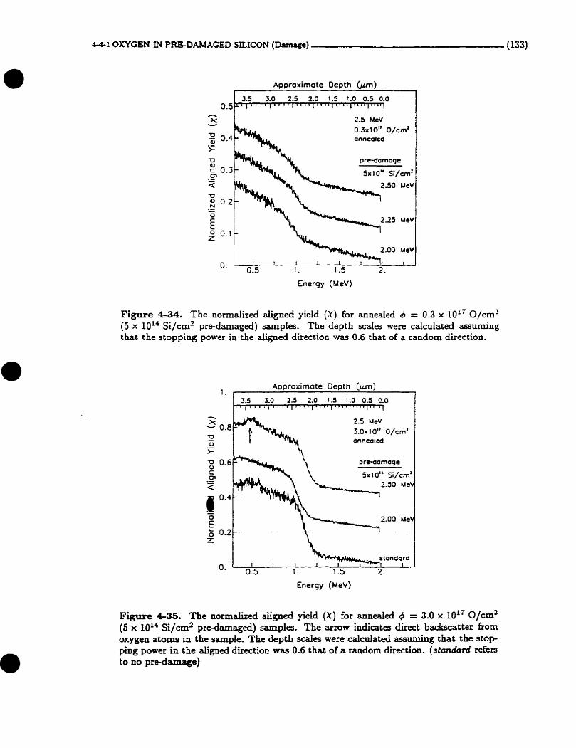
4-4-1 OXYGEN TN PREDAMACED SILICON (Damage) (133)
Aooroximate Deoth (un)
I I I 1 I l 1i I
0.5 1. 1.5 2.
Energy (MeV)
Figure 4-34. The oormalized aligned yield (X) for anneaied 9 = 0.3 x 10" 0/cm2 (5 x 10¹⁴ Si/cm2 pre-darnaged) sanipies. The depth scales were calculated assurning that the stopping power in the aligned direction was 0.6 that of a randorn direction.
Appraximate Depth (pm) 1.
3.5 3.0 2.5 2.0 1.5 1.0 0.5 @.O I + 1 I X I ~ ~ I I I S I I I I I
2.5 MeV
3.0% 10" O/cmz anneaied
N -
\z-sO Me'
E - . l.17c 2.00 Me'
; 0.2 -
Energy (MeV)
Figure 435. The normaiized aiigned yield ( X ) for annealed 4 = 3.0 x 10" 0/cm2 (5 x 10" Si/cm2 predamaged) samples. The arrow indicates direct badrxatter from oxygen atorns in the sample. The depth d e s were calculated assiiming that the s t o p ping power in the aligneci direction was 0.6 that of a random direction. (standard refers to no pre-damage)

4-41 OXYGEN LN PREDAlMAGED SILICON (Dam*) (134)
Approximate Depth (pm)
3.5 3.0 2.5 2 0 1.5 1.0 025 0.0
2.5 MeV 1 .Or 1 0" 0/cm2 annealcd
pre-damaqe
5 x 10" Si/cm2
N
standard O. 1 I l I 1 i I 1
0 -5 1 . 1.5 2.
Energy ( M ~ v )
(4 Approximate Depth (pm)
0.9 r
2 (2-5 M e V He pmbinq bea-1 2.5 MeV
- 0.7 1.0~ IO" O/cml
pre-damaqe
2x 10" O/cmz 2.5 MeV 7; = 300°C
O 1 O. 1 0.4 0.8 1.2 1.6 2. 2.4
Energy (MeV)
Approximate Oepth (pm)
3.5 3.0 2.5 2.0 1.5 1.0 0.5 0.0 1 1 l 1 ~ 1 1 1 , ~ 1 1 0 1 ~ 1 1 1 l ~ 1 1 1 1
. . 2.5 MeV
Energy (MeV)
Figure 436. The normalized aligneci yield (X) for annealeci ) = 1.0 x 10" 0/an2 ((a) 5 x 10¹⁴ Si/cm2, (b) 1 x lOlS Si/cm2 and (c) 2 x 10LS 0/cm2, Z=30O0C, pre- damaged) samples. The sample anaiyzed in (c) was etchd 1.62 pm prior to the analysis. The arrows indicate direct backscatter h m oxygen atoms in the sampie, The depth d e s were calculateci assuming that the stopping power in the aligned direction was 0.6 that of a random direction. (standard refers to no pre-damage)
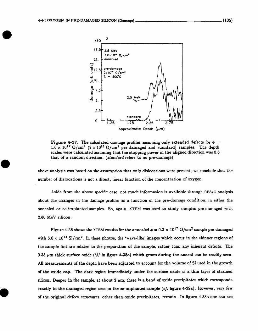
44-1 OXYCEN iN PRGDAMAGED SILICON (Damage) (135)
7-5 2-5 MeV t 1.0~ 10" O/cm1 15. anncaled
Approximate Depth (pn)
Figure 437. The calcuiated damage profiles assurning only extended defects for 4 = 1.0 x 10" 0/cm2 (2 x 1oL5 0/cm2 pre-damaged and standard) samples- The depth scales were calculateci assurning that the stopping power in the aligned direction was 0.6 that of a random directim. (stondad reiers to no pre-damage)
above analysis was based on the assumption that only dislocations were present, we conclude that the
nurnber of dislocations is not a direct, linear function of the concentration of oxygen.
h i d e frorn the above specific case, not much information is availabte through RBS/C analysis
about the changes in the damage profiles as a function of the pre-damage condition, in either the
annealecl or as-implanteci samples. So, again, XTEM was used to study samples pre-damaged with
2.00 MeV siiicon.
Figure 4-38 shows the XTEM resdts for the annealeci 4 = 0.3 x 10'' 0/cm2 sample pre-damaged
with 5.0 x 10¹⁴ Si/cm2. In these photos, the 'wave-like' images which occur in the thinner regions of
the sample foi1 are related to the preparation of the sample, rather than any inherent defects. The
0.33 p m thick surface oxide ('A' in figure 438a) which grows during the anneal can be readily seen.
AU rneasurements of the depth have been adjusteci to account for the volume of Si used in the growth
of the oxide cap. The dark region immediately under the surface oxide is a thin layer of strained
silicon. Deeper in the sample, at about 2 Pm, there is a band of oxide precipitates which corresponds
exactly to the damaged region seen in the as-impl sated sample (cfi figure 4-29a). However, very few
of the original defect structures, other than oxide precipitates, remain. In figure 4-38a one can see

4-41 OXYGEN IN PREDAMAGED SILICON (Damage) ( 136)
three dislocations extending between this initially damaged region and the main defect band, An
expandeci view of one of these defects is shown in figure 438b. In this photo it can be cfearly seen
that the dislocations are pinned by the oxide precipitah. The slightly darker contrast surrounding
the dislocations are caused by residuai stress in the siliçon. The majority of the defects in the main
band are located in the region 2-3 - 2.7 Pm. There is at Ieast one defect ('B' in figure 4-38a) which
extends 3 pm into the substrate.
XTEM photos of the anneaied c = 1 .O x 10" 0/cm2 sample, pre-damaged with 3 .O x 10" Si/crn2.
are shown in figure 4-39. At dsi (2 pm) a band of oxide precipitates remains. C'nlike the Iowerdose
sample, these photos do not show any dislocations stretching from the main band ail the way to the
pre-damaged region, nor are there any dislocations within the pre-damage region itself. There are no
visible signs of stress in this region (see figure 439b) either. However. there are dislocations which
span the region from the main band to precipitates located at -2.2 Pm, halfway to dsi. The main
defect band, which extends from 2.4 - 3.0 prn (figure 4-39a), is composed mostly of dislocations, each
being pinned at both ends by oxide precipitates. In figure 4-39b. the main in the main defect band
is evident, to such an extent that it is difficult to see the individual oxide precipitates-
Finally, in figure 4-40, XTEif photos of the anneaied O = 3.0 x loL' 0/crn2 sarnple. pre-
darnaged with 5.0 x 10L4 Si/cm" a.re shown. In both photos, the siiicon film has two distinct concrasts,
the shallower region being lighter. This is due ta the relative thickness of the sample foil. Looking at
the region around 1.3 Pm, it can be seen that the voids that were in the asimplanteci sample have
decreased in density, but have increased in size (cf. figure 4-30). They are now -50 nm. as compared
to 20 nm before the anneal. At a depth of 2 pm there are a few rernaining oxide precipitates. How-
ever, there are no visible dislocations extending between this region and the main defect band. .As
was the case for the 1.0 x 10¹⁷ 0/cm2 sample, there are precipitates located ac a depth ody slightly
more shdow than the main band, and they are connected via dislocations. .In expandeci view of one
of these defects (located at the bottom of the photo in figure 4-40a) is shown in fi y r e &Ob. The
&con substrate is not defect f ie , which can be seen by the two long dislocations, labelled 'A' and 'B'
(figure 4-40a), which extend to depths >4 pm. The dternating contrast of defect 'A' is an indication
that the defect is steeply inclined to the beam direction of [110]. Although it is not abeolutdy certsin,
it appears that defect 'B' starts at the site of an oxide precipitate which is located at a depth of 3 Pm.

' ,37.? 44-1 OXYGEN IN PRGDAMAGED SILICON (Damage)
Figure 438. XTEM photos of annealeci 4 = 0.3 x 10¹⁷ 0/cm2 (2.00 MeV. 5 x 10¹⁴ si/cm2 prdamaged) sample. (a) M=15,000x and (b) M=115,000x. = [110], f = < I l l > .

,:i 9) 4-4-1 OXYGEN fN PRE-DAMAGED SILICON ((Damage)
Figure 439. XTEM photos of annealeci 4 = 1.0 x 1oL7 0/cm2 (2.00 hlev. 5 x 10¹⁴ Si/cm2 pre-damaged) sample. (a) M=151000x1 g = <1 l5> and (b) M=66,000x. O = <400>. = [110]. f = < I l l > . Thescale unitg aregiveo in prn .

4-4- 1 OXYGEN m PREDAMAGED SILICON (~amage) C 1 3 )
Figure 4-40. XTEM photos of anneded # = 3.0~10'~0/crn~ (2.00 MeV, 5 x 10¹⁴ Si/crn2 pre-damageci) sarnple. (a) M=15,000x. and (b) M=38,000x. = [L lO], f = < I l l > . The scale units are given in pm .
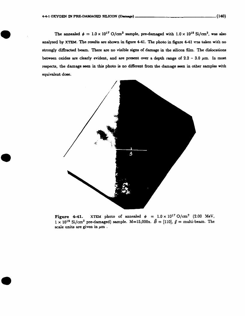
The a ~ e a i e d 4 = 1.0 x 10" 0/cm2 sample, pdamaged with 1.0 x 10¹⁵ Si/em2, was dso
analyzed by XTEM. The results are shown in figure 4-41- Tbe photo in figure 4-41 m s taken with no
strongly difhcted beam. There are no visible si- of damage in the silicon film. The distocations
between oxides are cleady evident, and are preseat over a depth range of 2.2 - 3-0 Pm. In most
respects, the damage seen in this photo is no different h m the damage seen in other samples with
equivalent dose.
Figure 4-41. X E M photo of annealeci q5 = 1.0 x 10¹⁷ 0/cm2 (2.00 MeV, 1 x 10" Si/an2 prcdamaged) sample. M=15,000x. 8 = [110], g' = rndti-bearn. The scale units are given in pm .
4-41 OXYGEN PREDAMACED SILICON (Damage) (141)
To help clarify the nature of the defects found in the pre-damaged sarnples implanteci with oxygen, the
defect contrast fkom all the XTEM photos have been summarized for the as-implanteci samples (Table
4VI) and the annealeci sarnples (Table 4VI1). Each depth region in the sample will be discussed
separately, starting with the silicon film.
It was only in the samples implanted with Q = 3.0 x 10¹⁷ 0/cm2 that there was any observable
damage in the silicon film. However, the nature of the damage depends on whether or not the sarnpIe
was damaged with silicon prior to the o.xygen implant. In the as-impianted samples, the damage in the
standard sampie appeared to be a mixture of oxide precipitates and very small(<IO nm) dislocations
(figure 4-12b). In the pre-damaged sample the defects were voids, with diameters in the range of
20 nm.
To explain this difference, we must first refer to the work done by Venabies and Zhou regarding
the interaction of oxygen, vacancies and strain, in o.xygen implanted silicon [ I~JO] . It was shown that
in low dose (5 10~') as-implanted sarnples, the silicon is positively strained in the region of peak
damage (& ), and negatively strained in the surface region. The negative strain, whose magnitude is
dependent on the oxygen dose, is directly related to an exces of vacancies in the silicon film. The -
oxygen in this region is bound in vacancy complexes and c a n o t forrn precipitates. If the strain exceeds
the elastic limit of silicon (0.33 - 0.65% [15]) dislocations fotm at the boundary between the negatively
and positively strained silicont with a subsequent reduction in the strain and number of vacancies.
The released oxygen is now able to f o m precipitates. Looking at the damage in the surface film in
the standard, 4 = 3.0 x 1oL7 0/cm2, as-implanteci sample, it is evident that the strain in the silicon
fîIm exceeded the elastic limit, resdting in the formation of srnaii dislocations ('B' in figure 4-12b)
and oxide precipitates ('A' in figure 4-12bf.
Another observeci mechanism for the releaae of strain in the the silicon film is the formation
of O2 gas fillecf cavities [za]. As the vacancies agglomerate to fomi voids, the oxygen atoms that
are bound to the vacancies form gaseous oxygen which then fills the void, keeping it stable. Hence
the oxygen is not fiee to form precipitates. This mechankm of s t a in relief is consistent with the
For keV Mplauts. tbi. oc- neu the surface. For MeV implants , h l dcpth is - 1/2 4.

4-4-1 OXYGEN IN PREDAMAGED SILICON (Damage) ( 142)
TABLE &VI
Damage (as seen in XTEiM photos) in asimplantcd samples as a function of dcpth and implantconditions. The pre-damage w a ~ 2.00 MeV siticon implant follo~ed by a 1 b, 900'~. anneai. The oxygen was irnpianted with an energy
of 2.5 MeV. - - - - - - - - - -
Silicon Film Prc- Damage Region Peak Damage Region Substrace
Predominantly d i s Small dark spots are locations- Damage seen..- starts zu -23 Fm.
No visible damage. 'lo visible damage. Film/damage interface - 1 0 ~ / a n ~ , III,-
Ü relatively sharp. mum depch 3.0 Pm- attends CO 2.7 Pm,
No visible damage No visible damage. Film/damage interface > 10~~/crn ' , maxi- is sharp, extends CO mum depch 3.4 Fm. 3.0 Pm.
Very srnall bladr No visible damage. FiIm/damage interface > 1OL0/cms. maxi- spots plus a few l q e r is sharp. extends CO mum depch 3.4 pm. spots vvith strain arc 3.2 p n .
No visible damage. Continuous necwork of di+ locations, 0.2 pm wide, in- cempersed nith oxide prc- cipitaces, Dislocations ex- tend h m this region to next damage region.
'io visible damage. Dislocations and highly sttained ngions. Width of Iaycr -03 pua- Dislo- cations extcnd €rom rhis region dong < 1 11 > d i m - tion to next damage region.
Mauy voids (-20 nm) Isolateci regions of d o (- 10~/can?) centenxi fe by Eghly -und 1.3 Fm- No sc"ned silicon. Dklocâ- sign of stress. tioas uttending berwetn
this region and the mut are not seen-
Pdorninancly dis- Smail dark spou are locations. Damage sen... s t a r t s at -23 Pm,
Un-damaged/damagcd - l O g / m Z . maxi- interface is noc sharp, mum depch 3 3 pm- extends to 2.7 Pm-
Un-damaged/d-qed > 1OLo/ctn2. muü- interfxt is not sharp, rnum depch 3.4 Pm. extends to 3.2 Pm-
Un-damaged/d-ed > 10'*/cm2, maxi- interface is not sharp, mum depth 3.4 Fm- utends to 3-2 prn- One long dislocation
dong < 1 > di,-- tion (- 1O7/cm-) ex- tends EO a find depth of 4 Pm.
No visible damage. No dislocations, but many No clcar dehastion S a d dark O& an s d biacù spou, p r o w t y betwua prcvious 'g Ken, - 1O1 /cmZ, up oxide pnxipitata. Deruity damage region and to a depch of 3.4 Pm. incttases with depth, UQ- this one- Damage is One long di~ocacion tü t ~ i -0. m- into peciominautiy dt (- 1o7/an-) dong a m , l d o l u , extends to < f 11 > direction ur-
3.2 pm. tends to a final dep& of 3.8 Pm.

44-1 OXYGEN IN PREDAMAGED SILICON (Damage) (143)
TABLE eVII
Damage (as m n in XTEM photos) in anaedtd sampfcs as a function of depth and implant-conditions- The prc-damage was 2.00 MeV silicon implant folloned by a 1 h. 90O0c, anneal. The oxygen was implantcd with an energy
of 2.5 MeV, and subsequently annealeci for 12 h at 1300'~.
Silicon Film Pre-Damage Region Peak Damage Region Substrate
No visible damage- No visible damage.
No visible damage. No visible damage.
Very small black spots No visible damage. art seen a t depths p a t e r thsa 1 Pm. One large ( l/2 prn long) unknown deiect a t 1 3 Fm.
Predominantiy ox- SmdI precipitates arc ides and dislocations. seen... Damage s t a r t s a t -2.3 Pm.
Film/damage intedace - 1O8/cm2 bctween is relatively sharp, 2.5 - 2.7 p. extends t o 2.7 Fm-
Film/damageiaterface - 10~ /cm~, maxi- U sharp, extends t o mum depth 3.2 pm. 2.7 Fm.
Film/damage interface 1010/cxn3 (2.7-3.2pm) is teiativeiy sharp, spots with disIo- extends t o 3.0 Pm. tions. maximum depth
3.2 Fm.
No visible damage. ~Many &des and a few dis- locations. Dislocations ex- tend h m this region to next damage region.
No visible damage. Lots of pncipitatcs, larger prccipitates haifway b o tween t h region and nem. Dislocations utend from oxidu in middie region to n u t damage region.
Voib (-50 nm) (- Isolatcd rcgiorw of p k p i - 109/&) ~ ~ C C S . Didocations -tend-
1.3 N~ ing betwten this region and sign of strc9, the next are not seen.
Pnxiorninantly ox- ides and dllocations. Damage starts at - 2 3 Pm.
Un-damaged/damagd interface is shacp, ex- tends to 2-7 Pm.
Un-damaged/damagcd interface is rtlatively sharp, extends t o 3.0 Pm.
Small precipitatu are seen-..
l O 7 / m 2 , with dis- location, a t 3.2 prn. Otherwisc no prccipi- t a t u past 2.8 pm.
~ o ' ~ / c m ' (2.7-3.2prn) spow with &il- tions, maximum depch 3.2 Pm.
Un-damaged/damaged - 1o8/cm2 deepcr interface is reIative1y than 2.8 Pm. Long sharp, utends t o dWlocations very deep 2.7 pm. in substrate.
No visible dam- No dislocations, or pmipi- Density of pcecipitatcs 1 0 ~ / c m ~ pcccipilates, tates. and dislocattioirs in- and dislocations, are
cnasesslowlywith s eenup toadep tho f depth, starting at 3.1 pm. 2.2 pm,

4-4-1 OXYGEN IN PRE-DAMAGED SILXCON (Damage) (144)
sz&ls
+ EOR
Figure 4-42. Schematic of the interaction of silicon interstitials and vacancies in the early stages of oxygen implantation into (a) virgin and (b) pre-damaged silicon sample-
- observeci results of the pre-damaged 3.0 x 10'' 0/cm2 sample, which had voids and no observable
oxide precipitates in the silicon film.
The question now becomes. why, in the pre-damaged sample, was the main released by the
formation of voids, rather than dislocations and precipitates? The first and foremost effect of the
pre-damage is its ability to act as a sink for excess interstitials geneated near the EOR (211. Thus, it
is an effective barrier preventing the silicon interstitiah from the EOR migrating to the near-surface
region. This ability to act as a sink for the interstitials is not constant with tirne, since the damage
at dsi changes as a hinction of dose. Kowever, up to a dose of 1.0 x 10¹⁷ 0/cm2 there is an almost
continuaus layer of damage, So, at least in the early stages of the implantation, the siiicon f i is
more vacancy-rich than its standard counterpart. With a larger density of anci ci es, the probability
is higher that the vacancies wiii interact to form larger and more stable vacancy complexes, or void-
like defects, A schematic Uustrating this process is shown in figure 4-42. As the dose incresses,
4-4-1 OXYGEN IN PREDAMAGED SILICON (Damage) (145)
the damage at dsi no longer forms a complete barrier to the silicon interstitials. However, once the
micr*voids have formed, they continue to grow.
The damage in the silicon film in these samples (4 = 3.0 x 10" 0/cm2) behaved in p d c t a b l e
ways during the anneal. In the annealeci, standard sample, the damage in the film was difficult to
anslyze. However, it appears that the tiny dislocations have annealed, whereas the oxïde precipitates
remain. In the pre-damaged sample, the siae of the voids grew larger, with a subsequent decrease
in density. It is clearly the as-implant4 damage characteristics which determines the nature of the
post-anneai damage in this region.
The next region to be d i s c d is the pre-damage region, located at a depth dsi. AS was
mentioued earlier, the pre-damage acts as a sink for the silicon interstitiah which are generated during
the oxygen implantation and precipitation. Essentially, the silicon interstitial atom binds to the edge
of the dislocation, becoming part of the extra atomic plane which comprises extrinsic dislocations.
This causes the dislocations to grow. The implanteci oxygen a b interacts with the pre-damage,
where the edge of the dislocation is an attractive site for the nucleation of onde precipitates. These
precipitates then impede the absorption of the silicon interstitiah onto the existing dislocation. It is by
t his mechanism t hat they prevent the dislocations from growing, effective1 y ' pinning' the dislocation.
In addition to these processes, there is dynamic annealing of the pre-damage which aIso occurs during
the implantation, The oxygen ion loses energy via elastic collisions (binary collisioos, formation of
phonons, etc.) which heats the sample localiy. Coupled with the fact that the sample is kept at a
global temperature of 570°C, the local temperature is sufficient to cause some of the existing damage
to anneal during the implantation-
Thus, we can now explain the defect characteristics of the prdamaged samples (2.00 MeV,
5.0 x 10L4 Si/cm2) as a hinctioo of oxygen dose. At the lowest oxygen dose (4 =0.3 x 10¹⁷ 0/cm2),
the defect structure has changed from the original extrinsic dislocation loops to a continuous network
of s m d dislocations, wit h evidence t hat there are oxïde precipitates decorating t hese dislocations.
Simiiarly, other dislocations originating from the pedr of the oxygen damaged region (Q ) have b e n
p h e d by the pdamage layer. As the dcse inmeases to q5 = 1.0 x 10L7 0/cm2 the dynamic a ~ & g
effect becornes noticeable, insofar as the dislocation network in the pre-darnage layer is no longer
continuous. The defect structure has continueci ta evolve, due to the interaction of the oxygen and
silicon interstitiais, where there appear to be fewer dislocations and more oxide precipitates. And
4-4-1 O W E N IN PRE-DAMAGED SILICON (Damage) (146)
finaiiy at the highest dose of 4 = 3.0 x 10¹⁷ 0/cm2, there are only isolateci pockets of damaged
regions lefi, which a h appear to be oxide precipitates surrounded by highly strained crystalline
silicon. At this stage, no dislocations spanning the region between do and dsi are seen in the XTEM
photos. Upon annealing, for d l the samples, the majority of the dislocations disappear, with only
oxide precipitates to mark the original location of the pre-damage. The few remaining dislocations
extend between the oxides.
For the sample pre-damaged with 2.00 MeV. 1.0 x 10¹⁵ Si/crn2, the processes involved are the
sarne, but the results are remarkably different. In this case, the original pre-damage did not consist
of a band of dislocation loops, but rather long dislocation dipoles dong the (001) and { I l l ) planes
(figure 46). There were also regions near dsi where there were no visible dislocations. With an oxygen
dose of only 1.0 x 10'' 0/cm2, al1 of the dislocation dipoies have annealed and there was no evidence
of any ot her dislocations.
The differences between this sample and the standard sample can lead one to hypothesize
about the evolution of the damage in the sample, as a function of oxygen dose. Unlike the standard
case, the damage in the as-implantecl sarnple does not start abruptly a t 2.3 Fm. instead there is a
gradua1 increase of srnall defect clusters starting at 2.0 Pm, which eventually merge with the main
- defect band. It appears as if the damage between 2.0 pn and 2.3 Fm could not be effectively annealed
during the implant. I t is hypothesized that in the earlier stages of the implant, before the predamage
was annealed, there were dislocations extending between the two darnage regions. These provided
the nucleation sites for oxide precipitation. As the oxygen dose increased, the dislocations were
aaneded and the olcide precipitates, or oxygen/point defecc clusten, remained. With very few, if
any, dislocations remaining a t dsi, there are no preferentiai nucleation sites for oxide formation a t
this depth. When the sample is annealed, the oxygen migrates towards the main oxide band via the
Ostwald ripening process. As a result, the silicon film has no observable defects up to a depth of
2.2 Pm.
The main defect region (2.3 - 3.2 ym) appears to be unaffecteci by the presence of pre-damage.
in dl the ss-implanted samples, the damage appeam to be comprised rnostly of dislocations in the
shailower region of the main defect band, and s m d defect clusters and/or precipitates in the deeper
regions. Again, in ail the samples, the darnage extends into the substrate to depths greater than 3 Fm.
However, after the samples are anneaied the quantity of damage past Rp is different for each sample
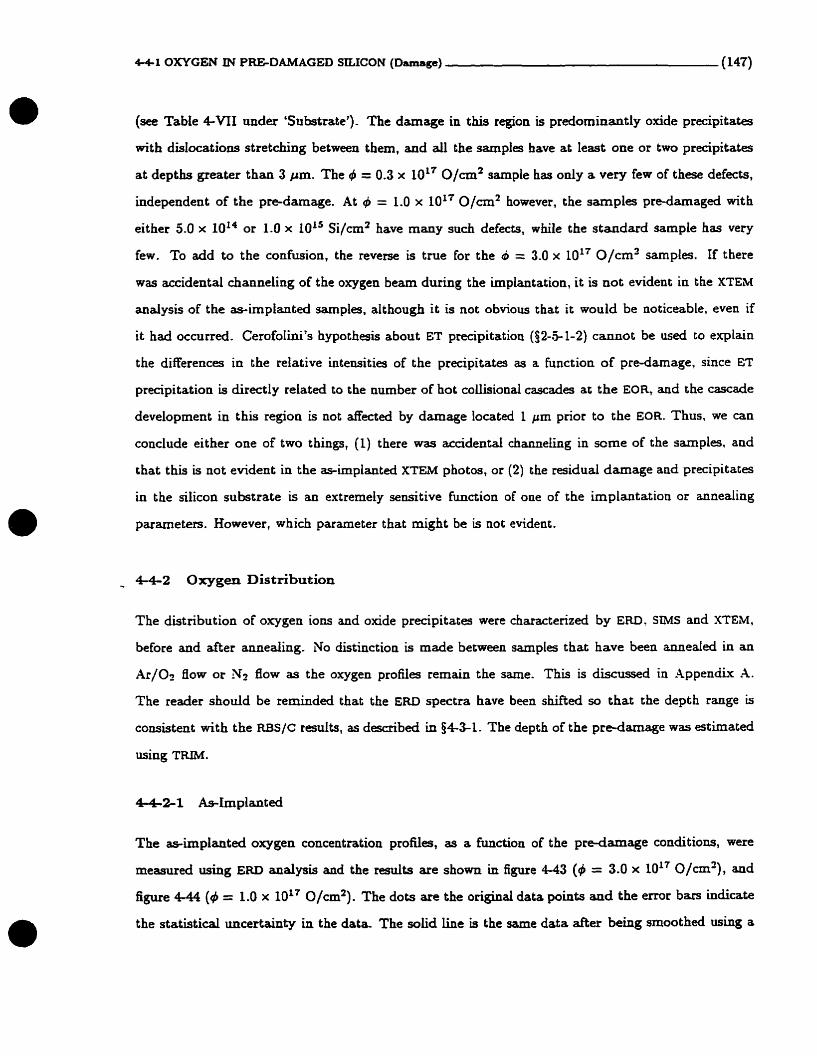
4-4-1 OXYGEN IN PREDAMAGED SILICON (Damage) ( 147)
(see Table 4-VI1 under 'Substrate')- The darnage in this region is predomuiantly oxide precipitates
with digIocatiolls stretching between them, and ail the samples have at least one or two precipitates
at depths greater than 3 pm. The q5 = 0.3 x loL7 0/cm2 sample has o d y a very few of these defects,
independent of the pre-damage. At 4 = 1.0 x 10" 0/cm2 however, the samples pre-damaged with
either 5.0 x l O I 4 or 1.0 x 10" Si/cm2 have many such defects, while the standard sample has very
few. To add to the confusion, the reverse is true for the 6 = 3.0 x 10¹⁷ 0/cm2 samples. If there
was accidental channehg of the oxygen beam during the implantation, it is not evident in the XTEht
anaiysis of the as-implantecl samples, although it is not obvious that it would be noticeable, even if
it had occurred. CerofoIini's hypothesis about ET precipitation (52-5-1-2) cannot be used to explain
the ciifferences in the relative intensities of the precipitates as a function of pre-damage, since ET
precipitation is directly related to the number of hot coilisional cascades at the EOR, and the cascade
development in this region is not af'fected by damage iocated I p m prior to the EOR. Thus, we can
conclude either one of two things, (1) there was accidental diannehg in some of the samples, and
chat this is not evident in the as-irnplanted XTEM photos, or (2) the residual damage and precipitates
in the dicon substrate is an extremely sensitive function of one of the implantation or annealing
parameters. However, which parameter that might be is not evident.
-. 44-2 Oxygen Distribution
The distribution of oxygen ions and oxide precipitates were chmterized by ERD, SMS and XTEM,
before and after annealing. No distinction is made between sarnples that have b e n annedeci in an
Ar/02 flow or N1 flow as the oxygen profiles remain the same. This is diçcussed in Appendk A.
The reader sbould be reminded that the ERD spectra have been shifted so that the depth range is
consistent with the RBS/C results, as describeci in $43-1. The depth of the pre-damage was estimateci
using TFüM.
The as-implanteci oxygen concentration profiles, as a function of the prdamage conditions, were
measured using ERD andysis and the r d t s are shown in figure 4-43 (4 = 3.0 x 10¹⁷ 0/cm2), and
figure 4-44 (4 = 1.0 x 10" 0/cm2). The dots are the original data points and the error bas indicate
the statistical uncertainty in the data The solid line is the same data after behg smoothd using a
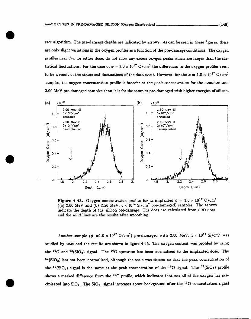
4-42 OXYGEN IN PRE.DAMAGED SILICON (Oxygen Distribution) (148)
FFT algorithm. The pre-damage depths are indicated by arrows. As can be seen in these figures, there
are only siight variations in the oxygen profiles as a function of the pre-damage conditions. The oxygen
profiles near dsi, for either dose, do not show any excess oxygen peaks which are larger than the sta-
tisticai Buctuatious. For the case of t$ = 3.0 x HlL7 0/cm2 the differences in the oxygen profiles seem
to be a result of the çtatistical fluctuations of the data itself. However, for the 4 = 1.0 x 10" 0/cm2
sarnples, the oxygen concentration profile is broder at the peak concentration for the standard and
2.00 MeV pre-damaged samples than it is for the samples pre-damaged with higher energies of silicon.
2.00 MeV Si
O. 1.8 2. 2.2 2.4 2.0 2.8 3.
Figure 4-43. Oxygen concentration profiles for as-implanted d = 3.0 x 10¹⁷ 0/crn2 ((a) 2.00 MeV and (b) 2.50 MeV, 5 x 10¹⁴ Si/cm2 pre-damaged) samples. The arrows indicate the depth of the silicon pre-damage. The dots are calculated from ERD data, and the solid lines are the results after srnoothing.
Another sample () =1.0 x 10¹⁷ 0/cm2) prcdamaged with 2.00 MeV, 5 x 10¹⁴ Si/cm3 was
studied by SIMS and the results are shown in figure 4-45. The oxygen content was profilecl by using
the L60 and 62(Si02) signai. The 160 spectnim has been normalized to the implant& dose. The
62(Si02) h a not ben normalized, although the scale was chosen so that the peak concentration of
the "(SiO?) signal is the same as the peak concentration of the 160 signal. The 62(SiOz) profle
shows a rnarked difference from the 160 profile, which indicates that not al1 of the oxygen has pre-
cipitated into Si02. The SiOÎ signal increasr, above background d e r the 160 concentration signal
4-42 OXYGEN iN PREDAMAGED SILICON (Oxygen Distribution) (149)
2.00 MeV Si . 5 x t ou/em1
onnealed
2.50 MeV O 1 x 1 O1'/cm'
O -0.2
2.25 MeV Si 5 x 1 O"/cml onnealed
2.00 MeV Si .
1 x 1 oU/crna onneoled 11
as-implantecl d i 2.50 MeV O
1.8 2- 2.2 2.4 2.6 2.8
2.50 MeV Si 5~1O'~/cm' . - t onnealed
2.50 MeV O 1 x 1 O"/cml as-implanted
1.8 2. 2 1 2-4 2 6 2.8
Oepth (Irm)
Figure 444. Oxygen concentration profiles for as-implanted g5 = 1.0 x 10" 0/cm2 ((a) 2.00 MeV, (b) 2.00 MeV, (c) 2.25 MeV and (d) 2.50 MeV, 5 x 10'' Si/cm2 pre- damageci) samples. The armws indicate the depth of the silicon pre-damage. The dots are cdculated fK>m ERD data, and the solid hes are the results after smoothing.

4-42 OXYGEN IN PRE-DAMAGED SILICON (Oxygui Ditribution) (150)
exceeds 5 x 10¹⁹ 0/cm3, which indicates that the surface region, at teast, is supersaturateci with
non-precipitatcd oxygent .
The total oxygen concentration rises smmthly, starting tiom 3 x 10" 0/cm3 at the surface,
and gradually increasing in concentration until it reaches 1.95 Fm. Xt this depth, indicated by the
arrow, there is a stight bump in the oxygen concentration, starting a t 1.8 p m and ending at 2.1 pm-
This is consistent with the XTEM photos shown in $44-1-2 which indicate the presence of precipitates
a t this depth. The integral concentration of excess oxygen in this peak, shown in greater detait in
figure U 5 b , is -5 x 10¹⁴ 0/cm2. This excess concentration clearly indicates that the pre-darnage
site preferentialiy attracts oxygen. Xfter the bump, the concentration of oxygen continues to increase
smoothiy to a peak concentration of 2.4 x 10~' 0/cm3. a t R, = 2.55 pm. Past this point. the
concentration of oxygen falls smoothly as one goes deeper into the substrate. The SiO2 concentration
faiis below the detection limit of the apparatus after 3 prn, and again, a t this point che total oxygen
concentration is - 5 x 10" 0/cm3. After 3.5 Fm, there is no detectable evidence of oxygen.
When the samples are annealed, the predominant factors in the final concentration profile are (a) the
- total oxygen concentration profile, (b) the initial distribution and sizes of the oxide precipitates. and
( c ) the location of the darnage sites which act as preferential oxidation centers. Frorn the previous
sections it is known that the remÂining pre-damage is a function of the oxygen dose, and consequently
the effects of the pre-damage on the oxygen concentration profiles are diiTerent for each dose. The
results wi11 be presented accordingly.
Figure 4-46 is an XTEM photo of an anneded 4 = 0.3 x 10L7 0/cm2 sample pre-damaged with
2.00 MeV 5 x 10¹⁴ si/cm2. Aithough an ERD spectrum is not available for this target, it is possible to
obtain a general idea of the oxygen concentration profile from the photo. .buming that the majority
of the O-xygen is in the form of precipitates, there is an oxygen concentration peak at 2 pm, which
is comprised of s m d (40 nm) precipitates. There is dso anothu peak at 2.2-2.3 prn coosisting of
the larger (100 nm) precipitates (only one precipitate is seen in this photo) locateci between dsi and
the main oxygen band. And h d y , the bulk of the oxygen is located around 2.55 pm. These t h r e
oxygen pe&s are also seen in the sample pre-damaged with 2.25 MeV silieon-
Thid nmb also the case for the standard +3.0 x 10L7 O/-' rramplc (set fi- 418)-
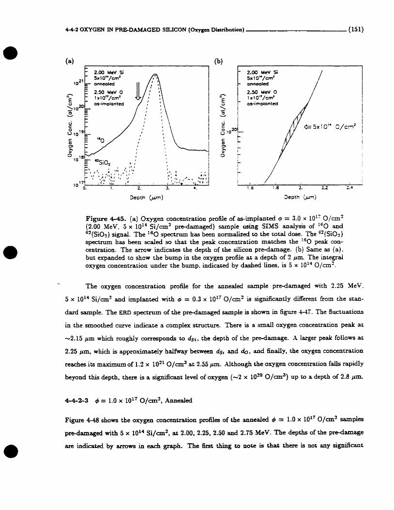
4 4 2 OXYGEN IN PREDAMAGEO SILICON (Orygai Dibut ion) (15 1)
Figure 4-45. (a) Oxygen concentration pronle of asimplanteci o = 3.0 x 10'' 0/cm2 (2.00 MeV, 5 x l0l4 si/cm2 pdamaged) sample using S M S andysis of ''0 and "(Sie?) signal. The 160 spectrum has been normalized to the total dose. The 62(Si02) spenrum has k e n scaied so that the peak concentration matches the "O peak coo- centration- The arrow indicates the depth of the dicon pre-damage. (b) Same as (a). but expandecl CO show the bump in the oxygen profle at a depth of 2 Pm- The inregrd oxygen concentracion under the bump. indicated by dashed lines, is 5 x IO'* 0/cm2.
The oxygen concentration profile for the anneaied sampIe predamaged with 2.25 MeV.
5 x 10¹⁴ Si/cm2 and implanteci with O = 0.3 x 10" O/-' is significantly different h m the sran-
dard sample. The ERD spectrum of the pre-damaged sample is shown in figure U T . The fluczuacions
in the smaathed cunre indicace a cornplex structure. There is a smd oxygen concmtration peak at
-2.15 p m which roughly corresponds to dsi, che depth of the pdamage. .. larger peak foUows at
2.25 pm, which is approximately halfway between dsi and 6, and fin&, the oxygen concentration
reaches its maximum of 1.2 x IO'= 0/cm3 at 2.55 Pm. Although the oxygen concentration falls rapidly
beyond this depth, there is a significaut level of oxygen (-2 x 10" O/-=) up to a depth of 2.8 PIIL
Figure 4-48 shows the oxygen concentration profiles of the anneded 4 = 1.0 x 10¹⁷ 0/cm2 samples
predamaged with 5 x 10¹⁴ Si/cm2, at 2.00, 2-25. 2.50 and 2.75 MeV. The depths of the prcdamage
are indicated by arrows in each graph. The b t thing to no& W that t h m is not any signingnt

4-4-2 OXYGEN IN PREDAMAGED SILICON (Oxygen Distribution) (152)
Figure 4-46. XTEM photo of anneaied 4 = 0.3 x 10" 0/cm2 (2.00 MeV. 5 x 10L4 Si/crn2 pre-damageci) sample. M=38,00ûx, fi = (1 10],9 = < 11 1 >.
Figure 4-47. Oxygen concentration profile of anneaieci 4 = 0.3 x 10¹⁷ O/cmZ (2.25 MeV, 5 x 10¹⁴ Si/cm2 prcdamaged) sample. The arrow indicates the depth of the silicon predamage. The dots are calculateci h m E E ~ D data, and the solid lines are the results d e r smoothing,
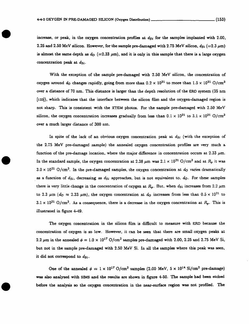
4-43 OXYGEN IN PREDAMAGED SILICON (Oxygen Distribution) (153)
inmase, or peak, in the oxygen concentration profiles at dsi for the samples impianted with 2.00,
2.25 and 2.50 MeV sifcon. However, for the sample prdamaged with 2.75 MeV silicon, ds; (=2.3 pm)
is almost the same depth as do (=2.33 pm) , and it is only in t bis sample that t here is a large oxygen
concentration peak at dsi.
With the exception of the sample pre-damaged with 2.50 MeV silicoa, the concentration of
oxygen around do changes rapidly, going h m more than 0.2 x 10²' to more than 1.5 x 10" 0/cm3
over a distance of 70 nm, This distance is Iarger than the depth resolution of the ERD system (35 nrn
[123l), which indicates that the interface between the dicon film and the oxygen-damaged region is
not sharp. This is consistent with the XTEM photos. For the sampie pre-darnaged with 2.50 MeV
silicon, the oxygen concentration increases gradually from Ieçs than 0.1 x 10" to 3.1 x 10" 0/cm3
over a much Iarger distance of 300 nm.
in spite of the lack of an obvious oxygen concentration pedc at dsi (with the exception of
the 2.75 MeV pre-darnaged sarnple) the annealed oxygen concentration profiies are very much a
function of the pre-damage location, where the major clifference in concentration occurs at 2.33 Pm-
In the standard sarnple, the oxygen concentration at 2.38 pm was 2.1 x 10²' 0/crn3 and at R, i t was
3.0 x IO*' 0/cm3. In the pre-damaged samples, the oxygen concentration at Q varies dramaticaily
as a fiinction of dsi, decreasing as dsi approaches, but is not quivalent to, do. For thse samples
there is very little change in the concentration of oxygen at 4. But, when dsi increases from 2.2 Fm
to 2.3 prn (do = 2.33 pm), the oxygen concentration at do increases from l e s than 0.5 x 10²' to
3.1 x loZ1 0/cm3. As a consequence, there is a decrease in the oxygen concentration at 4. This is ilhstrated in figure 449.
The oxygen concentration in the silicon film is difficdt to measure with ERD because the
concentration of oxygen is so low. However, it can be seen that there are small O-uygen peaks at
2.2 pin in the annealeci 4 = 1.0 x 10¹⁷ 0/cm2 samples pre-ciamaged with 2.00,2.25 and 2.75 MeV Si,
but not in the sample pre-damaged with 2.50 MeV Si, In all the sarnples where this peak was seen,
it did not correspond to dsi .
One of the anneded t$ = 1 x 10" 0/cm2 samples (2.00 MeV, 5 x 10L4 Si/an2 pre-damage)
~ 8 8 a h andyzed with SmS and the results are shown in figure 4-50. The sample had been etched
before the anaiysis so the oxygen concentration in the near-suface region was not profileci. The

4-4-2 OXYGEN ïN PFtE-DAMAGED SILICON (Oxygui Distribution) (154)
2.00 MeV Si 5x 1 0'*/cm' annealed
2-50 MeV O 1 1 O " / C ~ ' annealed
Oepth (pm)
(4 x r o n
2.75 MeV Si
O- 1.8 2. 2.2 2.4 2.9 2.8 2
Figure 4-48. Oxygen concentration profiles of annealeci ) = 1.0 x 10" O / d ((a) 2.00, (b) 2.25, (c) 2.50 and (d) 2.75 MeV, 5 x 10¹⁴ ~ i / c d pre-damaged) sam- ples. The anows indicate the depth of the silicon p d a m a g e . The dots are dcuiated h m ERD data, and the solid lines are the results alter smoothing.
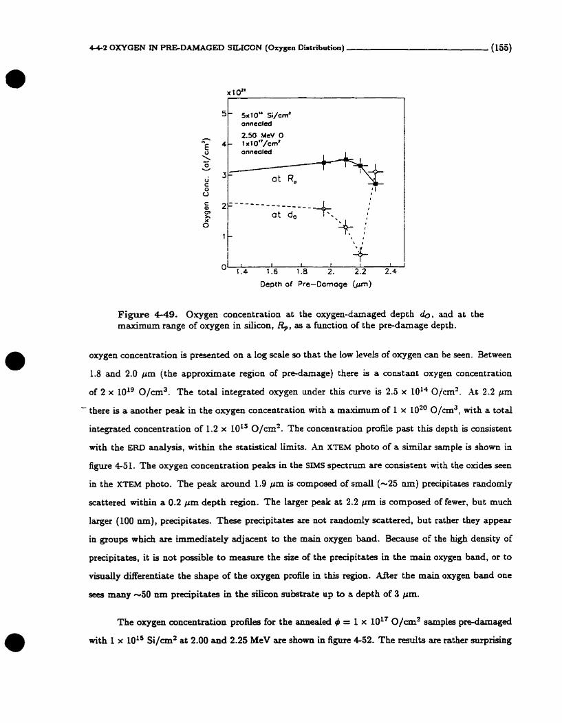
4 4 2 OXYGEN IN PFLEDAMAGED SILICON (Oxygen Distribution) (155)
t 5x t OY Si/cml annealed
Figure 4-49. Oxygen concentration a t the oxygen-damaged depth &, and at the maximum range of oxygen in silicon, Rp , as a function of the pre-damage depth.
oxygen concentration is presented on a log s a l e so that the low levels of oxygen can be seen. Between
1.8 and 2.0 p m (the approrcimate region of pre-damage) there is a constant oxygen concentration
of 2 x 10¹⁹ 0/cm3. The total integated oxygen under this curve is 2.5 x 10i4 0/cm2. At 2.2 pm
- there is a another peak in the oxygen concentration with a maximum of 1 x loZO 0/cm3, with a total
integrated concentration of 1.2 x 10" O/cmZ. The concentration profile past this depth is consistent
with the ERD andysis, within the statisticd iimits. An XTEM photo of a s d a r sample is shown in
figure 4-5 2 . The oxygen concentration peaks in the S M s spectrum are consistent with the oxides seen
in the XTEM photo. The peak around 1.9 prn is c o r n p d of small (-25 LUI) precipitates randomly
scattered within a 0.2 pm depth region- The Iarger peak at 2.2 p m is composed of fewer, but much
larger (100 am), precipitates. These ptecipitates are not randomly scattered, but rather they appear
in goups which are immediately adjacent to the main oxygen band. Because of the high density of
precipitates, it is not possible to measure the size of the precipitates in the main oxygen band, or to
visudiy diffkrentiate the shape of the oxygen profile in this region. Mer the main oxygen band one
sees many -50 nm precipitates in the silicon substrate up to a depth of 3 Pm.
The oxygen concentration profles for the annealed 4 = 1 x 10¹⁷ 0/cm2 samples p d m a g e d
with 1 x 10¹⁵ Si/crn2 at 2.00 and 2.25 MeV are showri in figure 4-52. The results are rather surprishg

4-4-2 OXYGEN IN PRGDAMAGED SILICON (Oxygen Distribution) (156 i
2.50 MeV O
annealed
Figure 450. Oxygen concentration profile of annealed ) = 1.0 x 10'' 0/cm2 (2.00 MeV, 5 x loL4 Si/cm2 pre-damaged ) sample using SIMS analysis of 160. The spectrum has been normalized to the total dose. The arrow indicates the depth of the si1 icon pre-damage.
Figure 4-51. XTEM photo of annealeci 9 = 1.0 x 10¹⁷ 0/cm2 (2.00 MeV, 5 x 10¹⁴ Si/cm2 prdarnaged) sample. M=38,000x, 3 = [LlO], f = < 11 1>.
44-2 OXYGEN IN PREDAMAGED SILICON (Oxygen Distributioa) (157)
for the sarnple pre-damaged at 1.95 prn (2.00 MeV Si). There is a significant oxygen concentration
peak at 2.2 pm, with a concentration of0.7 x 10" 0/cm3. This peak is not a t the same depth as dsi-
In the XTEM photo of this sample (figure 4-53) there is also no evidence of any oxide precipitates a t
dsi. The two oxygen concentration peaks cannot be individually distinguished in the XTEM photo.
The oxygen concentration at Rp is 3.3 x 0/cm3, which is the same as the previously discussed
samples. The sample pre-darnaged at 2.1 prn (2.25 MeV Si) has a similar structure to the sarnple
pre-damaged with 5 x 10¹⁴ Si/cm2 (shown in figure 441b), except for two things; (I) there is no
evidence of an oxygen coocentration peak at 2.2 pm and (2) there is a higher oxygen concentration
Finally, figure 4-54 shows the oxygen concentration profile for an annealed d = 1.0 x 10" 0/crn2
sample pre-damaged with 2.5 MeV, 2 x 10¹⁵ 0/cm2 with a substrate temperature of 300°C. In this
sampie there is an extremely sharp peak centered at 2.33 Pm, with a maximum concentration of
3.7 x 10'' 0/cm3. This is the highest concentration of oxygen seen in any of the m = 1.0 x 10¹⁷ 0/cm2
samples studied in this thesis, The FWHM of this peak is 70 nm, which is oniy slightly larger than the
depth resolution of the ERD systern at this depth (35 nm). The second peak, at Rp (2.55 pm), has a
m&um concentration of 3.0 x 10²' 0/cm3. Although it is not a distinct peak, there is a low level
of oxygen at 2-2 Fm. -
44-24 4 = 3.0 x 10¹⁷ 0/cm2, Anneaied
The E N oxygen concentration profiles for annealed 4 = 3.0 x 10" 0/cm2 samples, pre-damaged with
5 x 10¹⁴ Si/cm2, at 2.00 and 2.50 MeV are shown in figure 4-55. The depths of the pre-damage are
indicated by arrows in each graph. The characteristics of these profiles are defineci by two separate
regions of oxygen, the first being a t do (2.33 p m ) , and the second at R,, (2.55 pm). These profiles
have the same general shape as the oxygen concentration profle of the standard sample with the same
oxygen dose. The o>rygen concentration peaks in the sample pre-damaged with 2.00 MeV silicon are
bmader than the other samples. However, this couid be a result of the sample preparation prior to
the ERD andysis. This particular sample was etched many times in KOH, and as a resdt, the surface
of the sample was no longer smooth. Any irregularities in the sample surface decrease the ERD depth
resolution, so the bmadening of the peak at 2.33 pm may be an artifact of the analysis rather than
a physical reality. However, this would not affect the detection of a low level of oxygen a t 2.2 Pm,

4 4 2 OXYGEN IN f RErDAMAGED SiLlCON (Oxygen Distribution) ; ! ~ $ 9
Oepth (pm)
Figura 4-52. Oxygen concentration profiles of annealed 4 = 1.0 x 10¹⁷ 0/cm2 ((a) 2.00 MeV and (b) 2.25 MeV, 1 x 10¹⁵ Si/cm2 pre-damaged) samples. The armws indicate the depth of the silicon pre-damage. The dots are the calculated ERD data, and the solid lines are the results after smoothing.
Figure 4 5 3 . XTEM photo- of anneded t$ = 1.0 x 10¹⁷ 0/cm2 (2.00 MeV, 1 x IOL5 Si/cm2 pre-damaged) m p l e s . M=38,000x, 8 = (1 101,; = < 1 11 >.
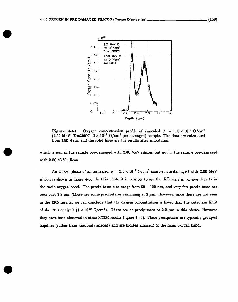
4-42 OXYGEN IN PREDAMAGED SILICON (Orygen Distribution) (159)
0.4 1 2.5 MeV O 2x 10"/cm' T, = 300%
t. 1
2.50 MeV O 1 x 1 ~"/cm' annealed
Figure 4-54. Oxygen concentration profile of annealed 4 = 1.0 x 10'' 0/cm2 (2.50 MeV, %=300~C, 2 x 10" 0/cm2 pre-damageci) sarnple. The dots are calculateci from ERD data, and the solid lines are the results after smoothing.
which is seen in the sample pre-damaged with 2.00 MeV silicon, but not in the sample pre-damaged
with 2.50 MeV silicon.
An XTEM photo of an anneaied # = 3.0 x 10¹⁷ 0/cm2 sample, pre-damaged with 2.00 MeV
silicon is shown in figure 4-06. In this photo it is possible to see the difference in oxygen density in
the main oxygen band. The precipitates size range fiom 50 - 100 nm, and very few precipitates are
seen past 2.8 Fm. There are some precipitates remaining at 2 Fm. However, since these are noc seen
in the ERD resdts, we can conclude that the oxygen concentration is lower than the detection limit
of the ERD analysis (1 x 10'' 0/cm3). There are no precïpitates at 2.2 Fm in t h photo. However
they have been observeci in other XTEM resuits (figure 4-40). These precipitates are typicauy grouped
together (rather than randody spaced) and are located adjacent to the main oxygen band.

4-62 OXYCEN M PRGDAMAGED SILICON (Oxygen Distribution) (1 60)
1.6- 2.00 MeV Si Sr 1 0'*/cmZ
Figure 455. Oxygen concentration profiles of annealed ) = 3.0 x 10" 0/cm2 ((a) 2.00 MeV and (b) 2.50 MeV, 5 x 10L4 si/cm2 pre-darnaged) samples. The arrows indicate the depth of the silicon pre-damage. The dots are the calculated ERD data, and the solid lines are the rmiilts after smoothing.
Figure 456. XTEM photo of annedecl q5 = 3.0 x 10¹⁷ 0/cm2 (2.00 MeV. 5 x 10'' Si/cm2 pre-damaged) sarnple. M=38,000x, L? = [1 IO], g = < 11 1>.

4-44 OXYGEN IN PREDAMAGED SILICON (Discussion) ( 161)
44-3 Discussion
It has been well established elsewhere (52-5 and 54-3-31 that the oxygen profiles after anneaiing are very
much a function of the conditions of the sample in the -implanted state, with regards tu the damage
profile and the distribution and size of the oxide precipitates. First, to facilitate the understanding of
the experimental results, a list containing the relevant information about the as-implanteci samples,
or the oxygen-in-silicon properties in general, is given below:
(1) If the sample temperature is high (> 400°C) and the current densi~y is Iow , then, during the
early stages of oxygen implantation, (heterogeneous) precipitationt dominates. The oxygen
ions then diffuse from R, to the domageci regions. As the dose increases the supersaturation
of oxygen at Rp is sunicient for HO (homogeneous) precipitation to occur. Thereafter there is
a competition between these two precipitation processes (52-5-1-2).
(2) Ostwaid ripening occun even during the implant. Ostwdd ripening is a very complex process,
which sometimes results in multi-peak oxygen concentration profiles, even in the simpiest of
systerns ($24). However, in rnost cases larger precipitates will grow at the expense of srnailer
precipitates.
b
(3) Aside from the pre-damage region dsi, there are two very distinct regions of dynamic annealing
within the sample. in the shailower region (less than 2.3 pm) the majority of the damage
produced during the oxygen implant is able to recover, in situ, whereas in the deeper region
(greater than 2.3 pm) the damage produced is not able to recover efficiently, with the result
that a dense network of small dislocations rernains (543-2 and $4-4- 1).
(4) For aU the samples studied by RBS/C, the r d t s do not show any significant ciifferences in the
damage profiles at depths greater than 2.3 pm (figures 4 2 6 to 4-28).
(5) The pre-damage consists prirnarily of (a) dislocation loops or (b) dislocation dipoles (figures 4-
5 and 46) . Since &islocations and extendeci defects are good sinks for interstitiah [zi], the
pre-damage region acts as a cUEkioa b&er and as a sink for the exces interstitiais (54-4-1-3).
pcefutntid pnxipitatioa on damage sites
4-4-3 OXYGEN IN PREDAMAGED SILICON ( D i o n ) (l62)
(6) Because the diffusion rate, in silicon, of silicon interstitials is higher than the diffusion rate of
oxygen, it is typically the oxygen diffusion which limits the growth rate of the precipitate, not
the silicon interstitial diffusion [n].
(7) There is an excess of oxygen (greater than background) at dsi (figure 4-45) and it has precipi-
tated (figure 4-30).
(8) There are threading dislocations spanning the region between cisi and 6, XTEM photos suggest
that there is preferential precipitation dong these defects (figure 4-30). The RBS/C anaiysis
confirms that there is more damage in this region than in the standard samples (figures 4-26
to 428).
(9) The presence of extended defects slows down the dissolution of precipitates during high tern-
perature annealing [?s].
Using the above information, the following desctiptirin is surmiseci (and illustraced in figure 4-
57): In the early stages of implantation, there are three depth regions in which there is precipitation.
These three regions are (1) the pre-damageci region dsi, (2) the oxygen-darnaged region do and (3) the
depth range of oxygen in silicon R,,- in the vERY early stages of the implant, the majority of the
- nucleation sites for oxïdation are a t dsi . Hence, this is the first region where olades form. AC this stage
the quantity of point defects a t dg, genetated by the incoming oxygen ions, is low enough that the
defects self-anneal rather thôn form stable defect complexes. However, as the O-xygen dose i n c r e w ,
the densi ty of defects increases to a point where self-anneaiing is no longer complete, and stable d e f ~ t
complexes form. These, in turn, provide nucleation sites foc oxide precipitation in the vicinity of do.
In this region there are more oxygen ions deposited per unit tirne than there are around d5i, and
consequently the precipitates here grow faster than their counterparts a t dsi. .As the precipitates
grow at do, they absorb the oxygen ions that otherwise might have d i to dsi, which means that
the rate of growth of precipitates at dsi is reduced. We d e h e a criticai dose 4 ~ s such that, when
4 = the average size of the precipitates at ki is the same as the average size of the precipitates
at do. It is important to note that das is dependent upon the number of stable damage sites at
do - Damage fiom the incoming oxygen ions continues to be aeated during the entire implantation
procecime, and so there will aiways be new nudeation sites for precipitation at &. The excess silicon
interstitials w i t h h this region are not fiee to migrate to the surface, but htead they interact with the

-vuy d y stage of implantation -oxide precipitacion pnmarily at 4 -oxygcn d i h m R, to 4
- gmwth of existing oxides at 4 - stil1 fonning new precipitarts at d, - level of damage at d, is decreasing - damage kgins to accumulate at do - heterogenaus prccipitation at do
- growth of thrcading dislocations
- no new p w t h of oxides ar d, - level of darnage at d, is decrcasing - C O ~ M U ~ I ~ ~ HE prccipitation at do - continucd p w t h of thieading disbcauons - HO precipiration a. R,
4 > Q nE
- oxidcs at 4 are dissolving - level of damage at d, is decrcasing - pmcipitates at do continue CO grow
- thrcading dislocations are anndng - precipiraccs at R, continue to grow
- oxides at d, arc almost completeiy dissulved - damage at 4 airnost cornpIetely dissotved - prccipitarcs at do continue to grow
- thrtading d i s l d o n s arc anneaihg - prccipitaies at R, conànue to grow
Figure 457. A schematic illustration of the evolution of the damage and precipitah during an oxygen implantation into prdamaged Silicon. 4 ~ s is defïned ar the oxygen dose (4) when the average size of the precïpitaks at Q is the same as the average size of the precipitates at dsi.

44-3 OXYGEN DI PREDAMAGED SUCON (Discussion) (la)
pre-damage or with the oxygendamage, causing the growth of threading dislocations between these
two layers. Thus a new region of preferentiai oxidation is formed, which vans the region between dsi
and &.
Homogeneous precipitation occurs at E$, when the concentration of oxygen exceeds the solu-
bility Limit (- 1018 0/cm3). Once the precipitates have formed a t 4, they grow faster than the
precipitates a t do because there is more oxygen deposited in this region, per unit time, than there
is at do. We define another critical dase d a o such that, when d = OH*, the average size of the
precipitates a t do is the same as the average size of the precipitates at Rp.
During the course of the implantation, the growth and dissolution of the precipitates is a func-
tion of not oniy the sizes of the oxide precipitates, but also of the local opgen solute concentrations.
the diffusion coefficients and the production of new nucieation sites for precipitation.
4-4-3-1 Effst of Oxygen Dose
Continuhg with the above description, consider what happens as the oxygen dose increases £rom
4 = 0.3 to 3.0 x 10¹⁷ 0/cm2. In the specific case of 5 x 10¹⁴ Si/cm2 pre-damage at 2.00 MeV. we
have observeci that as the oxygen dose increases. there is a decreaçe of damage a t dsi (figure 4-29), .
as weil as a reduction in the numbet of ozcide precipitates and threading dislocations. This suggests
that, a t these doses, precipitats ac and R, are growing a t the expense of the precipitat- at dsi
and hence 4 > HE and q > #HO.
Given that the remaining quantity of damage and precipitates at dsi is an inverse function
of the oxygen dose, one would expect that the pre-damage effects would, after annealing, be less
noticeable for the higherdose sarnples. This is consistent with our resuits. The generd effxts of
the pre-damage on the ha1 annded oxygen distribution, for the specific case of 5 x 10¹⁴ Si/cm2
pre-damage a t 2.00 MeV, can now be expiaineci as foUows-
0 = 0.3 x 10" 0/cm2
The ciifference between the 4 = 0.3 x 10¹⁷ 0/cm2 standard sampie and the sample pdamaged
with 2.25 MeVt, 5 x 10L4 Si/crn2 is strikingiy apparent, &dy at depths l e s than 2.3 pm, as
compared to the samples implanted at higher oxygen dases. The most obvious ciifference is the
An oxygur concentration prome of a -pie pre-damagecl with 2.00 MeV Si was not available-
4 ~ 3 OXYGEN IN PREDAMAGED SILICON (Discussion) (165)
presence of an oxygen peak at 2.25 pm. This peak is located h a i b y between dsi (2.1 pn) and
do (2-35 ~m). It is associateci with the precipitates that decorated the threading dislocations
between dsi and do in the as-implanteci sample. The smaü oxygen peak at 2.15 pm is a resuit
of the stable oxide precipitates which origindly formeci on the p d a m a g e , which implies that
Q, - 4=,g. The precipitates at do were not d c i e n t l y large compareci to the precipitates at
4 (4 > or to the precipitates decorating the threading dislocations- Consequently they
dissolved and the oxygen was absorbed into the precipitates either at 2.15 pm or at Rp. The
final result is an oxygen concentration profile with three distinct peaks at dsi, 112 (dsi + d o )
and Rp.
d = 1.0 x 10" 0/cm2
.4s the oxygen dose increases from 0.3 to 1.0 x 10¹⁷ 0/cm2, the precipitates at Q and at Rp
continue to grow, while the number and the size of the precipitates at dsi diminishes. There
is aiso a decrease in the number of threading disiocations between these two regions (figure 4-
29). -4s a result, the difference in the annealed oxygen profiles between the pre-damaged and
standami samples is les noticeable at this dose. The differences are a slight broadening of the
oxygen concentration distribution, a lowering of the oxygen concentration in tbis region, and
the presence of very small oxygen peaks at 1.9 and 2.1 prn (figure 4450). The first oxygen peak
at 1.9 prn is at the same depth as dsi- The precipitates are, on the average, smaller than the
precipitates at do (4 > + H ~ ) , and so only a small fraction (10%) of the oxygen rernains in
this region after anneaiing. The oxygen peak at 2.1 Pm, which is a tittle more than halfway
between the dsi (1.95 pm) and do (2.35 pm), is a result of the precipitates which decorated the
threading dislocations that c o ~ e c t e d the damage at dsi and do. The rnost obvious change in
the anneaieci oxygen profile, campareci to the standard, is the broadening of the oxygen peak-
This can be attributed to the presence of the threading dislocations previously rnentioned-
These dislocations retard the dissolution rate of the oxides that are located at the border
of the ' h d y damaged'/'highly damaged' regÏons. This reduction in the rate of disalution
is d c i e n t to stabiIize some of the precipitates long enough so that they WU grow during
the anned, rather than dissolving. The Iower oxygea concentration at &, compared to the
standard sample, d be discussed in the next section.
4-4-3 OXYGEN IN PREDAMAGED SILICON (Discussion) (166)
# = 3.0 x 10" O/cmZ
The ciifference in the oxygen profiles between the t$ = 3.0 x IO" O/-* pre-damaged and the
standard samples is aimost not detectable via ERD andYskg, which implies that 4 >> #HE-
However, a very low oxygen concentration just in fiont of do is seen in the pre-damageci sample.
Using the results of the XTEM anaiysis, it is concludeci that this residual oxygen concentration
is yet again a remnant of precipitates decorating the threading dislocations in the as-irnplanted
s a m ple-
These results indicate that the precipitates on the threading dislocations appear not to dissolve com-
pletely, even with doses much higher than &HE -
44-3-2 Effect of Silicon Pre-damage Depth
It is safe to assume that the rate of stable damage production at 6 (-2.3 pm) in the pre-damaged
silicon is less than that in the standard samples, as many of the interstitials generated in this region
migrate to, and are trapped or annihdated by, the pre-damage. Because this process is limited by
the diffusion of the silicon interstitials, it is a h safe to assume that the rate af absorption of the
interstitials is a function of the distance between the two regions (do - dsi). Thus the growth rate of
stable damage at do is a decreasing function of dsi, and it then CoUows that the critical dose C HE is
an increasing func t ion of dsi .
Since the precipitates a t dsi grow relatively unhindered while q5 < 4 a ~ , and since the growth
rate of these precipitates is a functioa of the quantity of oxygen depodired near dtii (which is slso
a positive function of dsi), it is clear that the size of the precipitates a t dsi, when O = O H E , is a
positive Function of dsi ih a consequence, the size of the precipitates remabhg at dsi , at the end
of the implantation is a h a posiuve Function of dsi. It is also hypothesized, although not verifid
with XTEM, that as the precipitates a t dsi grow larger, the precipitates more effectively impede the
migration of the interstitials, which in runi creates more threading dislocations between dsi and Q.
Thus, the final state of the as-implantai sample, as a h c t i o n of dsi (& # f ) is that, as dsi
increases (1) the size of the precipitates at dsi inaease, (2) the sbe of the precipitates at Q decrease,
Note that the surtace of the 3 -0 X 10" O/-' p r d a m a g d -pl= after etching wam not smooch, and hencc the depth cesolution of the ERD d y s i s , for this sample ody, ïs p e a l y deteriorated
4-43 OXYGEN IN PREDAMAGED SILICON (Discussion) (1671
(3) the quantity of damage at & decreases, (4) there are more threading dislocations between dsi
and Q and (5) the precipitates at R, are not significantly affected.
Ln the oxygen concentration profiles for the as-implanteci Q = 1.0 x 10¹⁷ O/cmZ samples (shom
in figure 4-44), there is a s m d (possibly insignificant) dXerence in the profiles, as a function of ds;.
In the samples pre-damaged with 2.00 MeV silicon (dsi = 1.95 pm), the oxygen profiles are broad,
and could be composed of two peaks, one at 2-55 Fm, and the other at 2.4 Fm- The oxygen profiles
of samples pre-damaged with silicon energies higher than 2.00 MeV (dsi = 2.1 and 2.2 pm) do not
have any indication of a secondary peak at 2.4 Pm, possibly indicating that some of the oxygen from
do has difiused towards dsi or 4. Unfortunately, the statistical fluctuations within the data itself
prevents a definitive interpretation of the data.
Fortunately, the oxygen concentration profiles for annealecl 4 = 1.0 x 10¹⁷ 0/crn2 samples,
pre-damaged with 5 x IOl4 Si/cm2 (figures 4-48 and 4-49), can be understood guite simpiy within the
framework of the mode1 described above. The difference in the oxygen concentration a t do between
the standard sarnple and the sarnple pre-damaged with 2.00 MeV silicon can be attributed to a slower
growth in size and nurnber of precipitates at do, due to the annihilation of the excess interstitiah by
the pre-damage. Sidar ly , as dsi approaches do, the size of the precipitates at do are even further
reduced in number and size, and consequently, during the anneal, the Ostwald ripening process favours - the Iarger precipitates in the region, until, as in the 2.50 MeV pre-darnaged sample (dsi = 2.2 pm),
there is no longer any oxygen concentration peak at dg at dl! However, this region is not completely
devoid of oxygen, the reason being that the defects at do retard the dissolution of oxides, and so,
although the oxides did not grow, they took too long to dissolve. The precipitates at dsi, in the
as-implanteci samples, are never sufEciently large to be able to grow during the anneal. However, they
are large enough not to be completely dissolved during the anneai, as one can see in the XTEM photos
and S~MS analysis, if not in the EEiD analysis.
For the specific case of 2.75 MeV dicon pre-darnage (dsi zü do), the growth of the oxide
precipitates during the implantation is different than previously described, in this case, the preferential
precipitation a t the prdamaged and oxygen-darnaged regions are in the same place, and consequently
the growth rate of the precipitates are enhan&, This results in larger precipitates whose radii are
Iarger than the criticai radius at the anneal temperature. The result, after anneaiing, is two distinct
and well separateci bands of oxygen precipitates.

4-4-3 OXYGEN IN PRE-DAMAGED SLLICON (Discussion) ( 168)
443-3 Effect of Pre-damage Type
The experiments discussed and included in this thesis include three different types of pre-damage. The
fint two types are produced by a silicon implant at room temperature, followed by a 1 h, 900°C anneal.
When #(Si) = 5 x 10¹⁴ Si /m2, the resulting prdamage is composeci a h o s t entireiy of dislocation
loopa (figure 4-5). and when d(Si) = 1 x 10'' Si /m2, it is c o r n p d almost entirely of dislocation
dipoles (figure 46) . The third defect type is created by a 2.5 MeV oxygen implant (2 x 10'' 0/cm2) at
=u 300°C, not followed by an anneal. The defects comprising this pre-damage have not been analyzed.
However, their nature can be reasonably postulatecf uçing the known properties of the behaviour of
oxygen in silicon and the darnage produced by ion beam implantations.
Let us first discuss the differences between the a5 = 1.0 x 10'' 0/cm2 samples pre-damaged
with 5 x 10¹⁴ Si/cm2 and I x 1015 Si/cm2. The pre-damage is different for the two samples, so the
initial conditions are aot the same. One of the biggest differences between these sampIes is that the
total length of dislocation Iine available as a sink for silicon interstitials is much smalIer for the sample
with dislocation dipoles than it is for the samples with numerous small dislocation loops. This reduces
the rate at which silicon interstitials can be absorbed into the pre-damage for the 1 x 10¹⁵ Si/cm2
samples, and it also reduces the number of nucleation sites for oxide precipitacion- In simplistic terms,
' if alI the parameters of the sampie (oxygen dose, pre-damage depth, etc.) are quivalent, except for
the silicon pre-damage dose, then @ H E ( l x 1015 Si/cm2) < 4 ~ ~ ( 5 x 10¹⁴ Si/cm2).
The darnage profile, as seen in the XTEM photo (figure 4-31), for the as-implanteci m =
1 x 10" 0/cm2 sample, pre-damaged with 1 x 10" Si/cm2, is significantly difFerent from that of
an quivalent sample with 5 x 10¹⁴ Si/an2 pre-damage (figure 4-30}. For the 5 x 10¹⁴ Si/cm2 pre-
damaged sample, there are defects and oxide precipitates at dsi, as weil as the remains of threading
dislocations located at depths just shailower than do. Other than the threading dislocations, the
visible damage st do st- abruptly. For the 1 x 10" Si/cm2 prdamaged sample, there is no dam-
age at dsi, and although there are no signs of threading dislocations, there are many oxygenldefen
complexes in the region joiuing Q and dsi There is no sharp delineation of the onset at damage at
do, instead it is a gradua1 increase of damage as one goes from dsi to do-
To explsin these differences, we hypothaiae the following xenatio for the 1 x 10'~ Si/an2 pre-
damaged sample: During the early stages of the implantation, t h e is a rapid growth of threading

44-3 OXYGEN IN PRSDAMAGED SILICON (Discussion) (169)
dislocations between dsi and Q, fapter than in the 5 x 10¹⁴ Si/cm2 pre-damaged sample, and conse-
quently there is a much broder regiou of nucleation sites for oxide precipitation. Thus the damage
at dsi is not the only immediate source of oxide growth, and so, instead of a few large precipitates
at dsi, there are oxide precipitates located throughout the region from dsi to do - These precipitates
grow rapiay during the eariy stages of the implantation. The point defects which are continuousiy
produced during the implantation are blocked by the oxide precipitates, and consequently they aggre-
gate to fonn even more defects in this region, which results in the damage profile seen in the XTEW
photos. In this sample, it is the damage that forms between the pre-damage and the oxygen-damage
depths that is more pronounceci t han the damage at dsi .
And so, after annealing, there is a diRerence in the oxygen concentration profiles for the two
4 = 1.0 x 10" 0/cm2, 2.00 MeV sificon (dsi=1.95 pm) predamaged sarnples. The oxygen concen-
tration profile of the 5 x 10¹⁴ Si/cm2 pr4amaged sampie has two large oxygen concentration peaks.
2 x 10" 0/cm3 at Q (2.33 pm) and 3.5 x 10" 0/cm3 at 4 (2.55 pm). In addition, there are two
very small oxygen concentration peaks, 2 x 10¹⁹ 0/cm3 s t dsi (1.95 pm) and 1 x lo2" 0/cm3 at
1/2 (dsi + do) (2-2 pm), (figures 4-48 and 4-5 1). h the 1 x iol' Si/cm2 pre-damaged sampte the peak
at 2.2 Pm is aimost a factor of ten larger than in the previously describeci sarnple, and there is no
oxygen concentration peak at do. W e hypothesize that the oxygen concentration peak at 2.2 p m is
-net a result of larger precipitates existing a t this depth in the as-implanteci sample, but that it is a
result of the Ostwaid ripening of a uniform distribution of oxides, of qua1 size, throughout the region
spanning dsi and do. If the density of precipitates is low, only one oxygen concentration peak wiii
form ($243). There is no oxygen concentration peak at do because the oxygen in this region diffused
either to R, or to the growing precipitates a t 2.2 pm.
For the sample pre-darnaged with 2.25 MeV, 1 x 10L5 Si/cma, (dsi=2.1 pm), dsi is closer to do
and thus the dynamic anneaihg during the implantation is more effective t han for the above described
sample. By the time the implant4 oxygen has reacbed the fuiai dose of t$ = 1.0 x 10" 0/cm2, the
pre-damage has been completely anneaieci. Thus the dislocations between do and dsi also have time
to anneal, releasing the oxygen to diffase towards R, and do. After the sample is annealeci, the shape
is similar to the standard sampie, with o d y a slight reduction in the oxygen concentration at do.
Next let us discusp the dinkrences betweea sarnples pre-damaged Mth 5 x 10L4 si/crn2
(T+room temperature, annealeci) and samples predamaged with 2 x 10¹⁵ 0/cm2 (2.5 MeV,

44-3 OXYGEN IN PRE-DAMAGED SILICON fDucudsion) (170)
Z=300°C, no anneal). There was no analysis of the oxygen pre-damage. However, according to
the theories presented by Cerofolini et ai- [d, at this low dose, low flux, and elevated temperature,
the majority of the implant4 oxygen form precipitates a t do (see 52-5-l), where the oxygen irom
Rp diffuses to do. The sample was not annealeci, and so we expect that the damage in this region
consists of small defect clusters. Since the depth of the pre-damage in an oxygen pre-damageci sample
is, by definition, equivaient to do, we will compare the 4 = I x IO'? 0/cm2 sample, pre-damaged
with oxygen (figure 4-54), with an equivalent sample, pre-damageci with 2.75 MeV 5 x 10¹⁴ Si/cm2.
such that dsi z (figure 4-43). In both of these samples, there is a higher concentration of oxygen,
after anneding, at do than there is at Rp. In the sarnple pre-damaged with silicon, this affect was
attributed to a preferential growth of precipitates at dsi in the VERY early stages of the implantation.
In the oxygen pre-damaged sample the oxide precipitates a t 6 already e.last. Thus both sarnples have
an enhanced growth of precipitates at d o , which results in sirnilar profiles after ameding. The oxygen
concentration peak at do is sharper for the oxygen pre-darnaged sampte, and this couid indicate maay
things, (a) the oxygen pre-damage was more effective at gettering oxygen into a smaUer depth region
during the implantation than the silicon pre-damage, (b) the precipitates at do were slightly Iarger
a t the end of the implantation or (c) there were fewer dislocations between do and Rp and thus the
precipitates in this region dissolveci quicker and more effectively during the anneal. Both samples
have a small oxygen concentration peak a t 2.2 Fm. The exact mechanism which is responsible for this
peak is not known, but because it is present in both samples a t the same location. it does not appear
to be related to the type of pre-damage.
It has been cleariy deruonstrated that the final oxygen concentration profile is dependenc on
the type of pre-damage. The number of threading dislocations between dsi and do is related to the
stability of the pre-damage during the oxygen implantation itself, which in tum changes the quantity
of precipitates in the region l/? (Q + dsi). Thus the relevant properties of the pre-damage are (1) the
rate that interstitials can be absorbed by the pre-damage, (2) the number of nucleation sites for oxide
prexipitation and (3) the relative stability of the predamage d w g the oxygen implantation.

Chapter 5 summary
In this work we studied si5con samples that were implanted w i t h high energy oxygen and
silicon ions. The purpose was to determine the interactions between oxygen ions, oxide precipitates,
silicon self-interstitials, vacancies and extended defects. Using the results of the analysis (chapter 4 ) ,
we have formulated simple models which describe the behaviour of the oxygen and the defects in the
sampl~ during the implantation. These models can then predict the subsequent oxygen profiIe after
the sample has been anneded at a high temperature. X relationship has been found between the
quality of the silicon film and the number of self-interstitids diffusing from the end-of-range to the
sample surface. We have not, however, been successful in modelling the behaviour of the precipitation
of oxygen in the silicon substrate.
5-1 RANGE AND STRAGGLING
The most probable projected range, GI of 2.5 MeV oxygen in silicon was found to be 2.55 k0.10 pm,
- with a straggle of -0.15 pm. The range is a little larger than the value predicted by m f (2.38 pm) ,
however this discrepancy is not unusual for high energy oxygen implantations, since no diffusion or
crystalline effects are considered in the TRIM calculations.
5-2 QUALITY OF THE SILICON FILM
5-21 Function of Dose
We have seen that the depth do, up to which the silicon film retains a high crystalline quality, is
not a function of oxygen dose when the doses are in the range 0.3 x loL7 t o 3.0 x loL7 0/crn2. We
have concluded that the depth do is a function of the rate of recombination of defetts in the film,
independent of the oxygen concentration. With an implant temperature of 570°C, and a dose rate
of t$/s < 6 x 10¹² 0/cm2-s, the silicon film maintains a high level of crystallinity up to a depth of
2.33 pm.
5-2-2 QUALITY OF THE SILICON F ~ L M ( ~ c ~ e a s c of Strain) (172)
3-22 Release of Strain
The Iow levei of crys tdine damage in the silicon f i does not preclude the presence of strain resdting
h m an uneven distribution of vacancies and intentitials. It has been hypothesized by Hoiiand [rsl
and Zhou [14j that when the strain in the siiicon film exceeds a critical value, it is released by the
formation of extended defects and oxide precipitates. This bypothesis has been partidly verifid by
our work insofar as we have found small defect clusters a t a depch of 1-1.3 pm (- L/z Rp) in samples
irnplanted with an oxygen dose of 3 x 10" 0/cm2. The presence of oxide precipitates at chis depth
has been inferreci from the resuhing oxygen concentration peak after a high temperature anneal.
Extendeci defects, seen in similar work by Rolland [is], Zhou [rs] and Ellingboe 1131, are found when
the oxygen dose is slightly bigher (4 > 7 x 10" 0/crn2). It is therefore concluded that the defect
clusters and precipitates seen in Our sampies are the precursors to the extended defects mentioned
above.
In this work we have also shown that the defect clusters in the silicon film in the as-implanted
and anneaieci sampies can be modifieci by the presence of a band of extended defects (pre-damage)
located at dsi > 0.9%. fnstead of s m d defect clusters and precipitates at 1.3 Pm, there are voids
füled with gaseous oxygen. This phenornenon is explaineci by the theoria proposed by Venables [20]
regarding vacancies, oxygen and strain relief, in silicon. There are excess vacancies in the film which
are decorated with oxygen. We have concluded that since the interstitiais produced by the oxidation
of the silicon at R,, are prevented by the pre-damage layer from diffusing to the silicon film, there is a
reduction of interstitial/vacancy pair recombination, As the vacancies agglomerate to form voids, the
oxygen atoms that are bound to the vacancies form gaseous oxygen which then fills the void, keeping
it stable.
With regards to the defects in the siiicon film there are many unaaswered questions. Since no
strain measurements were taken, i t is not possible to ver@ the relationçhip between strain release
and the formation of defect clusters o r voids in the silicon fiim. Nor is it understood why the defect
clusters and the vacancies form in a weil defined depth region around 1.3 Pm. By studying strain,
wing the XRD technique, as a function of oxygen dose in standard and prcdamaged samples, Mme
of these questions could be answered.
5-3 OXIDE PRECIPITATION
5-3-1 Standard Sample
For the standard (not pre-damaged) samples we have developed a realistic model, baseci on our exper-
imental results, to describe the interplay between the homogeneous and heterogeneous precipitation.
In Our mode1 there is no net diffusion of oxygen to the highly damaged areas in the samples. The
model is simpiistic and assumes that everywhere, except in the region near do, the mean size of the
precipitates is proportional to the cubed root of the concentration, where a is the constant of prc+
portionality. The preferential oxidation a t do is represented by a Gaussian distribution of Iarger, but
fewer, precipitates. Xny precipitate smaller than r,(T) at the anneal temperature (7') is diçsalved in
the very early stages of the anneal. Only the precipitates that remain contribute to the normal Ost-
wdd ripening process. It is not necessary to know the absolute d u e of r, and cr because their reiative
size, with respect to each other, has b e n estimated from Our experimental results (see figure 4-50).
The only significant unknown parameter in this model is the relative increase in size of the precipi-
tates in the do region. When this increase îs 30%, the mode1 can be used quite effectively to describe
the pst-anneal oxygcn concentration for the samples. impl&ted wich doses between 0.3 x 10'' and
3.0 x 10¹⁷ 0/cm2, studied in this work.
Based on this model. we conclude that at hiqh implant energies ( 2 5 MeV) it is aot possible to
form BOX (buried oxide) structures with low oxygen doses (< 10'~ 0/crn2). At Iow oxygen doses the
precipitates a t do and Rp dissolve and thus, the annealing process does not favour one precipitation
region over another. Xt intermediate doses there are a few precipitates at R, that survive the initial
stages of annealing. However there is stiii sufIicient damage a t do ta retard the diffusion of oxygen
from the silicon tüm to l+, . At higher doses the precipitates a& do remain as do the precipitaces at 4- The precipitates at do act as a diffusion barrier for the oxygen from the silicon film. Consequentiy,
any stoichiometric oxide layer must be at least as thick as the distance separating do and 4. Thus
the minimum d e for S ~ M O X production is 4 -1-2 x 10¹⁸ 0/cm2.
5 5 2 OXIDE PRECIPITATION (Pdamaged Sample) (174)
5-3-2 Pre-damaged Sample
We have also developed a mode1 to explain the interplay we have observed between different damage
regions and oxide precipitation. The concentration and size of olùde precipitates a t Rp is not grossly
affecteci by the presence of pre-damage when the pre-damage depth is Iess than do. The majority
of the differences occur in the depth region encompassing the oxygen-induced damage region at &
and the pre-darnage region dsi. It was shown that, during the early stages of the implanting, oxide
precipitates preferentiaily form at dsi. These precipitates getter oxygen more efficiently than the
smailer precipitates a t do, which results in an initial rapid growth of the precipitates ac dsi. The
stability of the damage and/or oxides a t 6 is reduced, and the result is that the precipitates in this
region are srnaller than in the equivdent standard samples. However, the precipitates at do still grow
faster than the precipitates a t dsi, due rnostly to the Larger concentration of oxygen being depasited
per unit time a t do. We have defined a dose OHE to be the dose at which the precipitates at do are the
same size as those at dsi. The dose HE increases as the distance between do and dsi decreases. For
- dsi = 0.40 Pm, Q~~ 0.3 x 10" 0/cm2. We have also seen chat the concentration of oxygen
at do, in the annealeci samples, is reduced as dsi approaches do. When dsi and 6 are iufficientty
close (0.1 p m ) the pre-darnage region getters oxygen and interstitiais so effectively that the oxygen
concentration at do in the ameaied sample is 75% lower than that in an quivalent standard sample. \-
In addition to providing a sink for oxygen and silicon incerstitials, the pre-damage also z t s as a
diffusion barrier between the end-of-range and the silicon film. Thus many interstitiah are trapped on
the 4 side of the predamage, and so they either aid in the growth and annihilation of the pre-damage
or they combine to form threading dislocations between the two damage regions. T h e disIocations
then getter oxygen, which can lead to the additionai oxygen peaks observed in some of our annealed
samples.
Due to the dynamic anneaiingof the pre-damage and the precipitates a t dsi, the above describeci
effects are more pronouncd at lower oxygen doses, (< daE). We predict t hat at higher doses of oxygen
(> 3.0 x 10¹⁷ 0/cm2), m a t of the effects of the presence of pre-damage at ds;, when dsi < Q, wiil
diminish. What will rernain is a srnail number of stable precipitates at dsi in addition to an oxygen
concentration profile that is similar to the oxygen concentration profde of an quivaluit standard
sample. Unfortunately this leads us to the o u t condusion that it is stiu not possible to form a

BOX structure by hi& temperature oxygen implantation into pre-darnaged Silicon samples when the
pr4amage depth is less than do.
Our results have shown t hat for samples pre-damaged at depths equivalent to do, the final oxy-
gen concentration after annealing is subetantially different than the concentration profiles previously
discussed- The preferential precipitation and p w t h of oxides on the pre-damage at dsi daes not com-
pete with the precipitation and gxowth of oxides at do. Since both processes occur at the same depth,
oxide precipitation is enhanceci in this region. For samples implanted with b = 1.0 x 10" 0/cm2 and
then annealed. there is a iarge (3.5 x 10~' at/cm3) narrow (70 nm) oxygen concentration peak at Q.
This peak contains about 40% of the total oxygen. as compared to the 25% in the standard sample.
The concentration of oxygeo is 75% higher than the normal concentration at this depth, and siightly
higher than its typical peak concentration. The analysis indicates that there may be a residual
concentration of oxygen just shailower than 6. However these samples have not been anaiyzed by
either S M S or XTEM, which would yield a better analysis.
5-4 SILICON SUBSTRATE
At this stage, we do not have an explanation as to why oxide precipitates remain in the silicon
- substrate in some annealed samples and not others. There does not appear to be a pattern regarding
t hese precipitates, and so it is necessary to determine a causal relationship between the parameters
used in making the samples and the precipitates in the substrate. The k t step in such an investigation
is to determine the reproducibility of the results. and in doing so, narrow down the m a t probable
cause. Aithough it has not been venfied, we believe that there is planar channehg which occurs
during the implantation, which in turn changes the oxygen distribution within the sample, especidy
at depths greater than Rp.
Although we have not succeeded in forming a BOX structure at high implant energies, we believe
that enough lmowledge has been gained regarding the dects of prcdamage in the silicon sample to
show that further research is warranteci. The next logicai step in this series of investigations wouid
be to iacrease the depth of the p d a m a g e so that it is deeper tban do, but less than 4. The pre-
damage should be made with a iow cemperatute oxygen implantation. The advantages of using oxygen
5-5 FUKIMER WORK (176)
pre-damage are two-fold- Firstly, the gettering efficiency of the oxygen pre-damage is siightly more
effective than silicon prdamage, and secondly, the sample neeâ not be removed from the implantacion
chamber between the pre-damage implan~ion and the regnlar implantation- hother variaion of the
experiments could include a shiR in oxygen energy at some point during the reguiar implantation so
that the precipitates at the pre-damage depth continue to grow faster than the p r e c i p i w at either
& or 4. ERD could be used as an rnethd of rejecting sets of parameters that don's work. fn the more
prornising samples, low levels of oxygen in the siliçon film and substrate would be investigated wïth
analysis techniques that are more sensitive than €RD. such as S B f i and -Y=?. If it were possible to
adjust the pre-damage and implant energy paramewrs mch th= ai1 the oxygen would be c o a c e n t d
at Q withio a 0.1 prn layer. the minimum oxygen dose woold be ody 4.5 x 10" O /cm2! .Ls this muid
dlow one to produce an oxide iayer in less time and with l e s damage in the siiicon film. the results
of such further investigation would defhireiy be mrthwhile.
Chapter 6 Conclusion
in this thesis we have studied the oxidation process of oxygen implanteci into pre-damaged
dicon as a function of the type of pre-damage, the depth of pre-damage and the oxygen dose. The
conclusions are based on the observations of damage, oxide precipation and the oxygen concentration
profiles of the post-anneal samples.
Two types of pre-damage were studied, and it was concluded that the reievant properties of
the predamage are: the rate that interstitiais can be absorbeci by the pre-damage, the nurnber of
nucleation sites for oxide precipitation and the relative stability of the pre-damage during the oxygen
implantation.
The relationship between the oxide precipitation process during the oxygen implantation and
the pre-damage is described by the failowing. The pre-damage region does not adverseiy change the
nature of the oxidation process at the depth of maximum owgen concentration. During the eady
stages of implantation there is preferential oxidation and more efficient gettering of oxygen in the
--pre-damage region (dsi ) than in the implantation induced damage region (&). This has the effett
of reducing the oxygen concentration at do in the anneaieci sarnples. The affect of the pre-damage
in the sample is more pronounceci as the distance between dsi and do is decreased. As the oxygen
dose increases, the pre-damage begins to anneal which reduceç the oxidation and gettering efficiency
at dsi. This in turn reduces the effects of pre-damaging the sample, especially in the region of &.
Unfortunately this leads us to the conclusion that it is not possible to form a BOX structure by
high temperature, high energy oxygen implantation into predamaged silicon samples when the pre-
damage dept h is Iess t han Q . For samples pre-damaged at depths equivalent to & , the prefcrential
precipitation and growth of oxides on the pre-damage at dEi does not compete with the precipitation
and growth of oxides in the region of & . The r d t , &er annealkg, is a hi& narrow pesk in the
oxygen concentration in the region of &.
Aithough we have not succeeded in forming a BOX structure at high impla~t energies, we believe
that it may be possible if the energy of the oxygen is modifiexi during the implantation i M - k t her
work is requùed to investigate this possibity.
References
A. Auberton-Herve, A. Wittkower, B. Aspar, Nucl- Insfr. lKeth., B96 (1995) 42b424.
A. Ionescu and Cristoloveanu, Nucl. Instr. Meth., B84 (1994) 265.
W. Ensinger, Nucl. lnstr. Meth-, B84 (1994) 181.
C.J. Griffin, J.A. Kilner, R.J. Chater, .A. Staton-Bevan, K.J. R-n, P.L.F. Remment, and
J.R. Davis, Nucl. Instr. Meth., B39 (1989) 215-219.
T.P. Sjoreen, O.W. Holland, D. Fathy, K. More, and R.F. Davis, Nucl. Instr. Meth.. B10/11
(1985) 564579.
AH. van Ommen, Nucl- Instr. Meth., B39 (1989) 194-202.
G.K. Celler, P.L.F. Hemment, K.W. West, and J.M. Gibson, ..lppf. Phys. Lett., 48 (1936) 532.
K.J. Reeson, vuc cl- Instr. Meth,, B19/20 ( 1987) 269-278.
A. Yoshino, K. Kasama, and M. Sakamoto, Nucl. Instr. Meth.. B39 (1989) 203-206.
A. Golanski, A. Perio, J.J- Grob, R- Stuck, S. SIaiIlet, and E. Claveiier, Appl. Phys. Lett., 49
(1986) 1423.
S. Maillet, R- Stuck, J.J. Grob, A. Golanski, R- Pantel, and A. Perio, LVucl. Instr. Meth.,
B19/20 (1987) 294298-
C.W. Nieh, F. Xiong, C.C. .Um, 2. Zhou, D.N. Jarnieson, T. Vreeland Jr., B. Fultz, and T A
Tombrello, in: Silicon-On-lnsulator and Buned Metah rn Semzconductors, eds. J-C. Sturm,
C.K. Chen, L. Pfeiffer, and P.L.F. Hemment , ~kfat. Res. Soc. Symp. Pm., vol 107 ( 1988) 73.
S. Ellingboe, M.C. Ridgway, and P.J. Schdtz, J. Appl . Phys., 73 (1993) 1133.
D.S. Zhou, O.W. HoIland, and J.D. Budai, Appl. Phys. Lett., 63 (1993) 3580.
O.W. HoIIand, D.S. Zhou, and D.K. Thomas, AppL Phys. Lett., 63 (1993) 896.
S. Nakashima and K. Izumi, J. Mater, Res., Vol 8 (1993) 523-534-
G.F. Cerofolini, S. Bertoni, P. Fumagalli, L. Meda, and C. Spaggiari, Phys. Reu. B, 47 (16)
(1993) 10174.
LI Meda., S. Bertoni, G.F. Cerofolini and C. Spaggiari, Nucl. Instr. Meth., B80/81 (1993)
813-827.
K.S. Jones, H.G. Robinson, J. Listebarer, J. Chen, J. Liu, B. Herner, H- Park, M.E. Law, D-
Sieloff, J.A. Slinkman, Nucl, Instr. Meth-, B96 (1995) 196-203.
D. Venables and K.S- Jones, Nucl. Instr. Meth., B74 (1993) 65-69.
F -R-ii. Nabarro, Theow of Çnrstai Dislocations, Oxford University Press (1967)
M. Lannoo and J. Bourgoin, Point Defects in Semicondudors I and II, Springer-Verlag, Hei-
delberg (1981)
J.W. Corbett, JP. Karins, T.Y. San, Nuci. Instr. Meth., 182/183 (1981) 457-476.
J.F. Ziegler, J.P. Biersack, U. Littmark, Pergamon P m s , New York, Vol 1 (1985) ed. J.F.
Ziegler.
J.J. Grob, A. Grob, P. Thevenin, P. Siffert, C. DPAnterroches and A. Golanski, J. .Mcrter. Res.,
4 (1989) 1227.
J.J.. Grob, A. Grob, P. Thevenin, and P. Siffert, Nucl. Instr. Meth., B30 (1988) 3437.
H.F. Kappert, K.F. Heidemann, D. Eichholz, E. te K a t , and W. Rothenrnund, Appl . Phys.,
21 (1980) 151-158.
W.R. Fahmer, K. Heidemann, and P. SchottIe, Phys. Stat. Sol., 70 (1982) 463.
K. Touhouche, J- Jackman and A. YeIon, Nucl- Instr. Meth., B80/81 (1993) 857.
G. Carter and W.A. Grant, Nucl. Instr. Meth,, 199 (1982) 17-35.
J.W. Williams, Rep- P q - Phys., 49 (1986) 491-587.
L.C. Feldrnan, J.W. Mayer, S-T. Picraux, Materiais AnaIvsis bv ion Channelinn, Submicron
Crvstallojzra~hv, Academic Press, New York, (1982)
S. Mader, Ion Implantation Damage in Silicon, Ion Imdantation. Science & Technologv, Aca-
demic Press, Orlando (1984), ed. J.F. Ziegler, pg 109
D.A. Thompson and R.W. Walker, Nucl. lnstr, Meth-, 132 (1976) 281-284,
C. Ceiiini, A. Carnera, M. Berti, A. Casparotto, D. Steer, M. Servidori, S. Milita, :Vucl. ïnstr.
Meth,, B96 (1995) 227-23 1.
K. Laaziri, S. b o r d a , L. CLiche, Nucl. Instr. Meth-, B90 (1994) 438-441-
O.W. Houand and C.W. White, Nucl. Instr. Meth., B59/60 (1991) 353-363.
A. Golanski, 4. Grob, J.J. Grob, O.W. Hoiiand, S-J. Pennycook, and C.W. White, Nucl. ïnstr.
Meth., B62 (1992) 365-371.
T. A. Belykh, A. L. Gorodishchensky, L.A. Kazak, V.E. Semyannikov, and AR. Urmanov, Nucl.
Instr. Meth., B51 (1990) 242-246.
S.M. Hu, Appl. Phys. Lett., 48 (1986) 115.
Qing-tai Zhao, Zhong-lie Wang, Tian-bing Xu, Pei-ran Zhu, Jun-si Zhou, Xiang-dong Liu,
Ji-tian Liu and Ke-miag Wang, Nucl. Instr. Meth., B82 (1993) 575.
R.G. Elliman, J.S. Wiliiams, S.T. Johnson and A.P. Pogany, Nucl. Instr, Meth., BI5 (1986)
439.
N. Hecking, K.F. Heidemann and E. Te Kaat, ficl. Instr. Meth., B15 (1986) 760.
J.F. Ziegler, Nucl- Instr. Mefh., B6 (1985) 270-282.
J.K.N. Lindner. R Domres, and E.H. Te K a t , Nucl. Imtr- Meth., B39 (1989) 306310.
P.J. Schultz, C. Jagadish. M.C. Ridgway, R.G. ELliman and J.S. Williams, Phys. Reo. B., 44
(1992) 9118.
A.E. Michel, NUCL h t t . Meth., B37/38 (1989) 379-383.
L. Sedy, R.C. Barklie, K.J. Reeson, W.L. Brown and D.C. Jacobsen, Nucl h t r - Meth., B62
(1992) 384387.
A- Battaglia, F. Prïolo, and E. Rimini, Nucl. Instr. Meth., B59/60 (1991) 382-385.
N.W. AshcroR. N.D. Mermin. Solid State Phvsics, Saunders Coliege: Holt, Rinehait and Win-
ston, Philadelphia (1976)
J. Washbum, Defects in Semiconductors, eds. J. Xarayan and T.Y. Tan, :\fat. Res. Sa:.
Symp. Pm., vol 2 (1980) . L. Calcagno, S. Coffa, C. Spinella and E. Rimini, Xucl. Instr. Meth.. B45 (1990) 442.
T.Y. Tan, Defccts in Semiconductors, eds. J. Narayan and T.Y. Tan, Mat. Res. Soc. S p p .
Pm., vol 2 (1980) .
U. Gosele, W. Frank, Defects in Semiconductors, eds. J. Xatayan and T.Y. Tan, Mat. Res.
Sm. S p p . Pm., vol 2 (1980) .
K.S. Jones, S. Prussin, and E.R. Weber, Appl. Phgs. A, 45 (1988) 1.
I.F. Bubb, D.J. Chivers, J.R. Liu, X.P. Pogany, KT. Short, H.K. Wagenfeid, and J.S. Williams,
Nucl. Instr. Meth., B2 (1984) 761.
A. Claverie, L. Laanab, C. Bergaud, A. Martinex, and D. Mathiot, vuc cl. Instr. Meth., B96
(1995) 202-209.
J. Gyulai, Damage Annedinq in Silicon and Electrical Activtty, Ion Im~lantation. Science 9t
Technolom, Xcademic Press, Orlando (1984), ed. J.F. Ziegier, pg 139
Y. Yatsurugi: N. Akiyarna, Y. Endo, a n d T. Nazaki, J. Electmchem- Soc., 120 (1973) 975.
D.K. Sadana, Pi-R- W u , J. Washburn, M. Curent, A. Morgan, D. M, and M. Maenpaa,
Nucl- Instr. Meth., 209/210 (1983) 743-730-
M. Tamura, T. Ando, and K. Ohyu, ~Vucf- htr. Meth., B59/60 (1991) 572-583.
M. Tamura, and T- Suzuki, Nucl. Instr. Meth., B39 (1989) 318-329.
J. Stoemenos, K.J. Reeson, A.K. Robinson, and P.L.F. Hemment, J. Appl. Phys, 69 (1991)
793.
C. Jaussaud, J. Margail, J. Stoemenos, a n d M. Bruel, in: Siliwn-On-Insulutor and Bun'ed
Metais in Semiconductors, eds. J-C. Sturm, C.K. Chen, L. PfeifEkr, and P.L.P. Hemment, Mat.
Res- Soc. Symp. Pm., vol 107 (1988) 17.
S. Maeyama, and K . Kajiyama, Jap. J. Appl. Phys., 21 (1982) 774-751.

K.J. Reewn, K.G. Stephens, and P.L.F. Hemment, Nucl. Imtr. Meth., B39 (1989) 29b295.
J. Margail, J. Stoemenos, C. Jaussaud, and M. Bruei, Appl. Phys. Lett., 54 (1989) 526.
KG. Stephens, K.J. R.eeson, B.J. Seaiy, R.M Gwilliam and P.L.F. Hemment, Nucl. Imtr.
Meth., B50 (1990) 368-378.
J.C. MikkeIsen Jr., in Ozygen, Carbon, Hydrogen and Nitmgen in Crystalline Silicon, eds. J.C.
Mikkelsen Jr. et al., Mat- Res. Soc. Symp. Pm. 59 (1986) 369.
W.J. Taylor, T.Y. Tan, and U.M. Gosele, Appl. Phys- Lett., 59 (1991) 2007.
M.J. Binns, W.P. Brown, J.G. Wilkes, R.C. Newman, F.M. Livingston, S. &lessoloras, and R.J.
Stewart, Appl. Phys. Lett., 42 (1983) 525.
U. GSele, T.Y. Tan, Appl. Phys., A28 (1982) 79-92.
S. Reiss and K.H. Heinig, Nucl. Instr. Meth., B84 (1994) 229.
S. Reiss, R. Weber, K--H Heinig, W. Skorupa, Nucl- Instr. Meth-. B89 (1994) 337-341.
F. Shimura, Appl. Phys. Lett., 39 (1981) 987.
A. Nejim, Y. Li, C.D. Marsh, P.L.F. Hemment, R.J. Chater, J A . Kilner, L.F. GiIes, 1Vucl.
Instr. ~Ueth., B74 (1993) 170-174.
L.F. Giles, F. Cristiano, A. Nejim, G. Curello, and P.L.F. Hemment, Ion Implantation Tech-
nology - 94, eds. S. Coffa, G. Ferla, F-Priolo, E. Rimini, (1995) 771.
S.J. Krause, C.W. Jung, T.S- Ravi, S.R. Wilson and D.E. Burke, in: Silicon-On-Insulator
and Buried Metals in Semiconductors, eds. J-C. Sturm, C.K. Chen, L. Pfeiffer, and P.L.F.
Hemment, Mat. Res. Sac. Symp. Pm., vol 107 (1988) 93.
D.M. Maher, A. Staudinger, and J.R. Patel, J. Appl. Phys., 47 (1976) 3813.
A. Nejim,C.D. Marsh, L.F. Giles, P.L.F. Hemment, Y. Li, R.J. Chater, J.A- Kilner, aad G.R.
Booker, Nucl. Instr. Meth., B84 (1994) 248.
M.K. El-Ghor, S.J. Pennycook, T-P. Sjoreen, C.W. White, and J. 'larayan, in: Silicon-On-
Insulator and B u r d Metab in Semiconductors, eds- J.C. Sturm, C.K. Chen, L. PfeiRer, and
P.L.F. Hemment, Mat. Res- Soc. Stpp. Pm., vol 107 (1988) 79.
J.A. Kilner, R.J. Chater, P-L-F. Hemment, R.F. Peart, E.A. MaydelI-Ondrusz, K R - Taylor,
and R.P. Arrowsmith, Nucl- Instr- Meth., B7/8 (1985) 293-298.
P.L.F. Hemment, K.J. &eson, A.K. Robinson, J. Stoemenos, J.A. Kilner, R.J. Chater, GX.
CeïIer and J.R. Davis, Nucl, Instr. MeM., B39 (1989) 220-214.
R.J. Chater, J.A. Kiher, P-L-F. Kemmenf, K.J. Fkeson, aod J.R. Davis, Nucl. Instr. Meth-,
B19/20 (1987) 29û-293.
J. Narayan, S.Y. Kim, K-Vedam, R. Manukonda, Appl Phys. Lett., 51 (1987) 343.
C-G- nippent M-R- Taylor, P-L.F. Hemment, and R.P. Anowsmith, &pl. P h y s Lett., 45
(1984) 57.
I.H. Wilson, Nucl. Instr. Meth., BI (1984) 331-343.
G.F. Cerofolini, S. Bertoni, L. Meda and C. Spaggiari, Nucl. Instr. Meth-, B84 (1994) 234.
R- Weber, R. MÛler and W. Skorupa, Yucl. Instr. Meth., B84 (1994) 286.
S.M. Hu, Appl- Phys. Le&, 36 (1980) 1.
J.A. Kilner, S.D. Littlewood, P.L.F. Hemment, E. Maydel-Ondnisz, and K.G. Stephens, iVucl.
Instr. Meth., 318 (1983) 573-578.
J.D. Larsan, Nucl. [nstr. Meth., 189 (1981) 71-91.
O.W. Holland, T.P. Sjoreen, D. Fathy, J. Narayan, -4ppl. Phys. Lett-, 45 (1984) 108 1.
J.R. Davis, M-R. Taylor, G.D.T. Spilier, P.J. Skevington, and P.L.F. Hemment, A p p l . Phys.
Lett., 48 (1986) 1279.
A.E. White, K.T. Short, J.L. Batstone, D.C. Jacobsen, J.M. Poate, and K.W. FVest, .4ppl.
Phys. Lett., 50 (198'7) 19.
K. Touhouche, Y. Tao, -4. Yelon, G. Kajrys, Y. Trudeau, K. Oxorn, S. Bultena, and G. Gagnon,
Nucl. Instr- Meth., B59/60 (1991) 676-679.
K. Touhouche, Y. Tao, and A. Yeion, Can. J. Phys., 69 (1991) 307.
G. Harbeke, E.F. Steigmeier, P.L.F. Hemrnent, K.J. Reeson, and L. Jastnebski, in: Silicon-
On-tnsulator and Bueed Metals in Semiconductors, eds. J-C. Sturm, C.K. Chen, L. Pfeiffer,
and P.L.F. Hemment, Mat. Res. Soc. Symp. Pm., vol 107 (1988) 133.
A. ~érez-R.od&uez, .A. ornan nu-~odr~guex, J. ~ a c b and J.R. Morante, E. Martin and J.
Jiménez, Nucl. Instr. Meth., B84 (1994) 275.
E.F. Steigmeier, G. Harbeke, K.J. Reeson, P.L.F. Heniment, and A.K. Robinson, iV~c l . Instr.
Meth., B37/38 (1989) 304-307.
S. Visitserngtrakd, B.F. Cordts, and S. Krause, Mat. Res. Soc- Symp. P m . , vol 157 (1990)
161.
Bent Nielsen, KG. Lynn, and T.C. Leung, B.F. Cordts, S. Seraphin, Phys. Rev. B, vol 44
No. 4 (1991) 1812.
A.H. van Omnten, B .B. Koek, and M.P.A. Viegers, Appl. Phys. Lett-, 49 (1986) 1062.
A.H. Van Ommen, in: Silicon- On-Insulator and Buried Metals in Semiconductors, eds. J-C.
Sturm, C.K. Chen, L. Pfeiffer, and P.L.F. Hemment, Mat, Res. Soc. Symp. Pm., vol 107
(1988) 43.
C. Jaussaud, J- Stoemeaos, J. Margail, M. Dupuy, B. Blanchard, aad M. Bruel, Appl- Phys.
Lett., 46 (1985) 1064.

H. Koyama and T. Kashiwaki, Appl. Phys. Lett., 38 (1981) 791.
A-H. Hamdi, F.D. McDaniel, R.F. Pinizzotto, M.S. Matteson, H.W. Lam, and S-D-S. Malhi,
&pl. Phys- Leff., 41 (1982) 1143.
A. Stolmeijer, lEEE Tmns. Elec. Deu., ED-33 (1986) 450.
B.Y. Mao, P.H. Chang, H.W. Lam, B. W. Shen, and J.A. Keenan. Appï. Phys. tett., 48 (1986)
794.
T.F. Cheek Jr. and Daniel Chen, in: Silicon-On-insulotor and Bun'ed Metais in Semiconduc-
tors, eds- J-C. Stunn, C.K. Chen, L. Pfeiffer, and P-L-F. Hemment, Mat. Res- Soc. Symp.
P m . , vol 107 (1988) 53.
J-Blake, J.C. Geipey, D.M. Lee, L. Rowland, and G.X. Rozgonyi, in: Silicon-On-lnsulator
and Buried ~Metals in Semiconductors, eds- J-C. Sturm, C.K. Chen, L. Pfeiffer, and P.L.F.
Hemment, Mat. Res. Soc. Symp. Pm. , vol 107 (1988) 61.
P. Sioshansi and F. Namayar, in: Silicon-On-lnsulator and Butied Metals in Semiconductors,
eds. J-C. Sturm, C.K. Chen, L. Pieiffer, and P.L.F. Hemment, Mat. Res- Soc. S p p . P m - ,
vol 107 (1988) 67.
S.L. Elhngboe and M.C. Ridgway, in Beam Soïid Intemctions: Fundamentals and Applications
Symposium, eds. Nastasi, M., H e d t , L-R-, Herbots, 3. Averback, R-SI, Mat. Res- Soc. Symp-
Pm., (1995) 147.
X.E. White, K.T. Short, R.C. Dynes, J.M Gibson. and R. Hull, in: Silicon-On-Insufator and
Buned ~Metals in Semiconductors, eds. J-C. Sturm, C.K. Chen, L. Pieiffer, and P.L.F. Hem-
ment, mat. Res- Soc. Symp. Pm., vol 107 (1988) 3.
A- Nejim, Y. Li, C.D. Marsh, P.L.F. Hemment, R.J. Chater, J.X. Kiher and G.R. Booker,
Nucl. Instr. Meth., B80/81 (1993) 822-826.
L.D. Dyer, G.J. Grant, C.M. Tipton, and A.E. Stephens, J. Electrochem. Soc., 136/10 (1989)
30 16.
S.C. Gujrathi, P. Xubry, L. Lemay, and J.-P. Martin, Can. J. Phys., 65 (1987) 950-955.
K. Oxorn, S.C. Gujrathi, S. Buitena, L. Cliche, and J. Miskin, ~Vud. Instr- iveth., 845 (1990)
166-170.
S.C. Gujrathi and S. Buitena, Nud. Instr. Meth., B64 (1992) 78S795.
D. Hinrichsen, D. Hetherington, S.C. Gujrathi, and L. Cliche, Nucl. Instr. Meth., B45 (1990)
275-280.
F- P b t i , E. SzilSgyi and E. Kotai, Nucl. Instr. Meth., B54 (1991) 507-512.
E. SdSgyi, F. Phati, G. A m d l NUCL Instr. Meth., BlOO (1995) 103421.
S.C. Gujrathi, D. Poitras, J.E. Klemberg-Sapicha and L. Martinu, 12th Int. Conf. on Ion
Beam Anaiysis, (1995) accepteci for publication.
Wei-Kan Chu, James W. Mayer, Marc-X Nicolet BacIcscatterinn Smxtrometrv Academic Press,
Orlando, (1978)
L-C. Feldman, J.W. Mayer. Fwidarnentals of Surface and Thin FiIm ,halvsis Xonh Hoiland,
New York, (1986)
D.V. Morgan (ed.), Channelina - Theorv. Observation and Xlipiications, J o h Wdey 96 Sons.
London, ( 1973)
K-J Gossrnann and L.C. Feldman, Bulletin, Angust/Sept (198'7) 30.
R. Simonton and 0. Kamenitsa, Nucl. Instr. Meth., B37/38 (1989) 344-347.
F.H. Eisen, G.J. Clark, J. Bottiger and J.M Poate, Radiat. Eff., 13 (1972) 93.
D.W. Hetherington, :Vucl. Instr. Meth., B90 (1994) 84-87.
2. Sroubek, Nucl. Instr. Meth., 194 (1982) 533.
Edington. J. W ., Practical Electron & ~ ~ c ~ O S C O D V in Materials Science, Van Xostrand Reinhold
Co, New York (1976)
Glauert, Audrey M. (ed.), PracticaI Methods in Electron Microsco~v, Xorth HoUaad Publish-
ing Co., London (1972)
CM20 Electron Miaosco~e User's Manual, Philips Export B.V., Eindhoven, The Yetheriands
(1989)
J-C. Bravman and R. Sinclair, J. Elec. ,r/licroswpy Tech., 1 (1984) .53-61.
K. Touhouche, Implantation ionique d'ozygéne à haute éneqne dans le dicium. PIiD Thesis,
École Polytechnique (Montreal) 1992.
RI Schork and H. Ryssel, Ion Implantation Technoiogy - 94, eds- S. Coffa, G. Ferla, F.Prioio,
E. Rimini, (1995) 885.
Appendix A
Nitrogen in-diffusion and accumulation in oxvgen-imdanted dicon
J u
during t hermAal annealing
Reprinted f Iom ION IMPLANTATION TECnNOLOGY-94
North Halland Publishing (1995) 791-796

[ON IMPLANTATION TECHNOLOGY - 95 S. Coffa. G. Feria, E Pnolo, E. Rimini (eds.) O 1995 Elsevier Science B.V. AI1 nghts reserved.
Niuogen in-diffusion and accumulation in oxygen-implanted silicon during thexmal mneding
S. BULTENA'. SC. GUJRATKI~. S.L. BREE~NER~, A. YELONL, S . ROORDA' Groupe de recherche en physique et technologie des Couches Minces.
' ~ e ~ a n e m e n r de Physique. Universite de Monuéai. C.P. 6128. Succ. Centre-Ville. c montré ai. Québec. H3C 317 CANADA
'~epanement de Genie Physique. École de Polytechnique. C.P. 6079. Succ. Centre-Viile. Montréal. Quebec. H3C 3A7 CANADA
Silicon wafers impianted with 2.5 MeV OC have becn studied by the Elastic Recoil Detection ! Tie-of-mght tERDnOF) technique to determine the depth protilt of light elernent impurirics beforc and aitcr a 12 h. 1300°C hmace m n d . The oxygen doses were no< suificient to produce a continous buricd SiO: Iayer. Significmt levels of nitrosen i - 10" - IO= d c m 3 ) wcrs found in d l n v n p b chat had been meaicd in a N2 aunosphere. including a ramplc char had a 1000 .A oxide cap dtposited berore the anncal. .As-iplanted samples. as wcl1 as chose annealed in an M O ? amosphere. have ni- cogen concentrations lower than our detcction limit of t ~ ' ~ a t / c m ' . The nitrogen c o n c e n a n o n was found to be consktentiy -6% of the oxygen concentration. cven though the oxygen doses varicd by 2 ractor of IO. The depth profiles of the nimgen wcrc simiIar to the depth pmtilcs of the oxygen. From this we surmise that. the nitrogen is prerérrntially ciccumularm~ In the region of the oxide precipira~s.
1. INTRODUCTION
- For the fabrication of SIMOX (Separation by Mplanted OXygen), silicon 1s implanted with oxy- gen and then annealed at high temperatures (1200" - 1425°C) for long periods of tirne ( -624 h). The quality of the final oxlde iayer and the siricon overlayer improves with longer mneaiing limes. and with higher anneaiing temperatures [ l .2 .3 .4 1. The anneal is typically pertormed in either an Ar (with -1% Oz) amosphere. or in a % aunosphere on samples previously covered with an oxide cap. However, it should be noted that the gas ambien t used during anneaihg can significan tly affect the formation of oxide precipitates in sili- con [5 1.
It is known [6 ] tbat impianted niuogen xcumuisrec both at the interface of surface oxide and bulk siücon, and at m g e d regions withia the sample. The fuial concentrauon of nimgen in the SiOl/Si interface region was shown to be independ- eut of the implanted dose, but longer anneal cimes resulted in larger concentrations of nitrogen in thïs region. The behaviour of implanted oxygen and implanted nitrogen in silicon has been studied by Bonin et al. [7 1 who found that Sioz precipitates act as gettering sites for nimgen, which chen fonn
stable SixOyNz phases upon annealing. There is a non-linear niuogen dose dependence on &e fornation of the SixOyNz phase due ro the precipita- tion of an Si3& phase outside of the oxide gercering centers. These SirJ& precipitates can then act as jettering centers for the free oxyjen atoms.
Hamdi and .McDaniel[8 1 reported bat anneal- ing in a N= ambient rather thm in an Ar ambient resuited in a decrease of the surface crystallinity of SIMOX sampies. Nejim er al. [9 ] did not tTnd evi- dence thac the amosphere during the annealing had any effect on the dislocation density in the anoeaied suucture. However. they found that the burieci oxide iayer. in samples anneaied in an &/O2 amiosphere. always had a planar top, wbereas this was noc al-
? amos- ways die case for samples annealed in a N- pbere.
The SIMS (Seconriiuy ion Mass Specmmeny) data of Davis er al. [IO 1 showed a significûnt amount of nimgen. -5~10' at/cm3. in their low eoergy. high dose (-10" at/cm2) SIMOX samples. Tbey amibuted this to the un-intentional implanta- tion of nitrogen hydride during the oxygen implan- tafion itseif. aithough they also noted an increase in the total nitmgen concentration if the samples were anneded in Nt racher than an Ar/02 aanosphere. Kilner es al. [ I l j also analyzed low eaergy, high
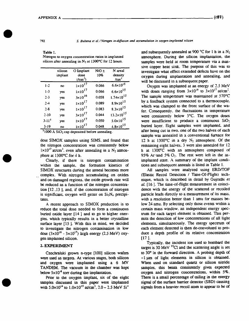
792 S. Birltena rr al. /Ximgen indiffùsion and accumularion in qgen-implanred silicon
Table 1. Nitmgen co oxygen concentration ntios in implanted siiicon aftcr mnealing in N2 rit L300°C for 12 bours.
implant dose 10% dcnsity
1-3 yes 1x10~' 0.066 6 . 6 ~ 1 0 ' ~
2 4 ycs 1x10~' 0.089 !3 .h< l0~~
7-8 yes tx10L7 0.083 8 . 3 ~ 1 0 ' ~
3-11' yes iX10" 0.050 5 . b loL5
3-19 no 1x10" 0.û48 - 1 . 8 ~ 1 0 ' ~ ' 1000 A SiO? cap dcpositcd bcforc mnealing.
dose SIMOX samples using SIMS, and found chat the nitrogen concenuation was consistendy below
7 amios- 1x10~' at/cm3. even a k r anneaiing in a N- phere at 1 300°C for 4 h.
Clearly, if there is niuogen contamination within the sample, the formation kinetics of SMOX structures during the anneal becomes more
- - cornplex. With niuogen accumulating on oxides and on damaged regions, the oxide growth rate wiIi be reduced as a function of the niuogen concentra- tion [12 -13 ), and, if the concentration of nitrogen is significant, oxygen will setter on Si3NI precipi- tates.
A recent approach to S N O X production is to reduce the total dose needed to form a contînuous buried oxide layer [ 14 j and to go to higher eaer- gies. which t y p i d y results in a better crystailine surface iayer 115 1. With this in min& we decided to investigate the nitrogen contamination in low dose (3x10'~ - 3x10") high energy (2.5 MeV) oxy- gen implanted siiicon.
Czochralski gfown n-type [100] silicon wafers were us& as targets. At various stages, both siiicon and oxygen were implankd using a 6 MV TANDEM, The vacuum in the chamber was kept below 5x10~ torr during tbe implantation.
Rior to the oxygen implant, six of the eight samples discussed in this paper were implanted with S.OX~O'' to 1 .OXIO'~ ac/cm2. 2.0 - 2.5 MeV Si'
and subsequendy annealed at 900 "C for 1 h in a Nz atmosphere. During the silicon implantauon, the samples were held at room temperature via a rnas- sive copper heat sink. Tbe purpose of his was to investigate what effect extended defects have on the oxygen during implantation and annealing, and wiU be discussed in a subsequent paper.
Oxygen was impianted at an energy of 2.5 MeV wich doses ranging from 3x10'~ to 3x10'~ arfcm'. Tbe sample temperature was rnaïntained at S70°C by a feedback system connectai to a tbermocoupls. which was clamped to the front surface of the wa- fer. Consequently. the fluctua.ions in temperature were consistentiy beiow 3OC. The oxygen doses were insufficient to produce a conunuous SiO2 buried layer. Eight samples were irnplanted and after king cut in two. one of the two balves of eacb sarnple was anneaied in a conventional fumace for 12 h at 1300°C in a d q & atmosphere. 0 1 the remaining eigbt haives. 3 were also annealed for 12 h at 1300°C witfi an amiosphere composed of 95% Ar -and 5% O,. The rest were left in the as- implanted state. X surnmary of the implant condi- tions and subsequen t anneals is Listed in Table 1.
Ai1 samples were analyzed using ERDrrOF (EIastic Recoii Decection / TÏe-Of-Flight) tech- nique, which is describeci in detail by Gujrarbi es al. [16 1. The Ume-of-flight measurement in coinci- dence with the energy of the scactered or recoiled particle leads direcdy to a measurement of i ts mas. wirh a resolu tion better than 1 m u for masses be- Iow 24 amu. By selecting only those events within a certain mass window. an independent energy spec- m m for each target element is obcained. This per- m i t ~ rhe detection of low concenmtions of ail Iight eiements. simllltaneously. ïhe energy specrnrm of each elernent detected is then de-convoluted io pro- duce a depth proNe of its relative concenuauon t17 1-
TypicaiIy, che incident ion used to bombard the target is 30 MeV 35Cl and the m e M g angle is sec to 30° in the forward direction. A probing depth of -1 pm of light elernencs in silicon is obtained- When used on standard quartz or silicon nimde samples, this beam coasistentiy giva expected oxygen and nitmgen concaitrations, within 5%. There is a small perceotage of t a i h g in the energy signal of the surface barrier detector (SBD) causing signais h m a heavier recoil atom to appear to be of
S. Bultena es ai. ,'Nimgen lndgutron and accumuIalion ur o-gen-impianled srlicon
a lower mass. which subsequently affects the deret- tion limit, To d u c e this noise from the probing bearn we used a JO MeV 6 3 ~ ~ beam. which kine- maticaily cannot recoil from silicon a t a 30' angle. to anaiyze samples 1-2 and 1-3. However. this ap- proach reduced the probing depth to 0.8 p, and also demeased the depth resolution significandy in the region of interest due CO multiple scattering within the target. Consequently. al1 other samples were analyzed with the Cl bearn.
The detection limits of ERDlTOF also depend upon the beam current and irradiation t h e . In the present experiment the beam currenc was typically 5 nA and the irradiation tune was -2 h. With 11 counts in the integrated peak giving a statistical uncertainty of 30%. we calculate the detection limit of niuogen to be -3x10L' ar/cm2 (- 10" ar/cm3 peak concentration). The depth resolution of oxygen and niuogen in silicon at the surface is 90 and better than 150 À at a depth of 0.5 p.m.
Because ERDfïOF bas a probing depth of -1 p. whicb is l e s than the range of 2.5 MeV O' (3.5 p). it was necessary to remove the surface iay er bstween su bsequen t ERD anal y ses. This was done either with a reactive ion etch 0 or with a wet chernical etch of KOH (where the etch rates - - were known [18 1). The etch depth was measured with a profdometer. and the ERD depth s d e was caiculated using standard dE/dx measurements assumiog a silicon density of 2.32 g/cm3. To avoid any possible influence of the pnor Cu or Cl beam. each ERD analysis was done on a different spot on rbe wafer.
Fig. 1 shows the number of de- events ver- sus the caiculated m a s . in the mass range of 10- 18 arnu, fiom sample 1-2 (2.5 MeV, :xlol' 0+/cm2) before and d e r annealing in a N: atmosphere. Each spectnun corresponds to a dier- ent depth region of che sample. obtained by etching the sample in KOH between measurements, Each peak corresponds rr, a specific element (carbon C, oxygen 0. and nitrogen N) where the area under the peak is a function of the relative concen~ons of the elements with respect to the silicon peak (not shown and nonnalized to 1). No nimgen was de- t e a d in the as-implanced sample (nor was ir detected in a virgin sample). However, it can be
Mass (cmu)
Figure 1. ERDITOF m a s spccm samptt 1-2. ta) =-un- planced md (b) mntalcd. &ch individuai specuum cor- responds to a differcnt region oi depth in the sunpies. (1 )
0.9-1.8 pm. (ii) 1-3-22 m. (iii) 13-2.5 pm. ( i v ) 1-3- 2.7 m. ï h c ordinate scde rcprcscnts the souots. normal- ized to the rotal number of integrated counrs tn rhe d i - son m a s p d (noc shown~.
clearly seen that nitrogen is detected in the an- nealed haif of the sample. and only in bat depcb region of the samplz that has a significant oxygen concentration. Note that the apparent increase in the carbon concenuauon is due to carbon unpurities within the target chamber itself. which are depos- ited on the sample during rhe ERD analysis.
The absolute concentration of niuogen a n b- approximated by using the following squarion [19 ] and the concentration of oxygen. which is known to within 5%.
A C o* T J w LE." F a - - - - (1) (5C0 QO qo AE* Fw
where AC = the number of integrated counts in the mass peak. o = Rutherford cross section. q = abso- lute concentrations (adan'). AJ5 = energy window corresponding to the mas peak. F = depth factor (relative stopping power). and the subscripts N and O refer to nitrogen and oxygen respectively.
The results of this dcuiation are hted in Table 1. It should be noted that ail the as-implanted samples. as well as those samples thac had been an- nealed in Ar with 5% O= aunosphere. containecl less than our detectable limit of nitmgen. However, ail oxygen implanted samples that bad been annealed in a & amosphere, including a sampte

annealed in N, 6
2- - Oxygen 3 -
Figure 2. Opgen and nitrogen depth protilzs in the sur- iacc region annealing far 1300°C for 11 h in (a) Nz md (b) 95% .Ar and 5% 0 2 atmosphere. The nimgcn coaaanatron bas been increased by a factor of 5. for east oi viewing.
n d e d in an .WO2 mix (2b). The sample annealed in Nz has a chin (70 nm) surface oxide layer which is most likely due ro the residual oxygen present in the h e c e during the anneal. The interface be- ween the oxide and the substrafe is nor sharp, and there is a signifcant amount of oxygen extending into the substrate. The peak nimgen concentfation is sibmed in the interface bemeen the bulk SiO? and the bulk silicon. The cud concentdon of ni- trogen was 12x10'~ atlcm'. Our resuits i n i d i m a broad region (60 nm) of n i m p n contaminauon. However. if the Si02/Si inoerface is not smooth, our results are not inconsistent with having a thin layer
rbat bad a 1000 Si02 u p depobited by P E W (Plasma Enhanced Chemical Vapour Deposition) before annealing, had integrated nitrogen doses between 1.7~10'~ to 1 .3xloL6 adcm2. Although rhe concentration of implanted oxygen varied by a factor of 10 (3x10'~ to 3x10" at/cm'). the relative concentration of nitrogen m oxygen was con- sistently found to be between 5 and 9%.
Fig. 2 shows the oxygen and nitrogen depth profiIes for the surface region of an un-implanted sample. subjected to che same processing steps as all the ocher samples. annealed in N= (2a) and an-
S. Bultena et aL I ' N i ~ ~ l e n i n d ~ f l i w n cmd accwnuiation in oxygen-tmplanteti silicon -95
of Si3Na f m e d a t the interface. similar to the re- suits reported by Josquin and Tamminga [6]. The sample annealed in .4r/0?. shown in figure 3b, has an oxide layer -300 nm thick. and the interface be- tween the oxide and the bulk silicon is considerably sharper. There were no detectable traces of nitrogen in this sample.
Fig. 3 shows a part of the oxygen and niuogen concentration profiles of samples 3-1 1 and 2-10 (oxygen doses of lr 10'' and 3x10'~ ar/cm2. respec- tively). Botb oxygen protiles consist of two peaks. the first corresponding to b e end-of-range EOR) damage caused by the oxygen implant itself. md the second corresponding to the maximum range of the oxygen ions. It can be seen that. within the h- its of statisticaI error. the depth profiles of the ni- uogen have the same shape as the oxygen profiles. where the nitrogen to oxygen rario remains f'uced at approximately 5%. Cross-sectional Transmission Elecmn microscopy (XTEM) picnrres r not shown). with equivalent doses of oxygen. clearly indicate that the oxide is in the form of hexagonal and spherical precipitates. with radii of -20-50 nm. The region of maximum oxygen concentration is corn- posed of many small oxide precipitates racher than a continuous buried layer.
_-The oxygen concentrarion profiles did not ap pear to be affected by the inclusion of nitrogen in the sample. as shown in Fig. 4. One half of sample 2-8 was annealed in Ado2 and tbe other half was annealed in IV,. These samples were etched inde- pendently and subsequently profiled with ERD. The depth scale was corrected for the respective removal of the surface layer. and as a result, the probing limit is slightly smaller for the sample annealed in the &/OZ amosphere. Within the limits of resolution, the prot'iles are indistinguishable.
4- DISCUSSION
We found more than 10" at/cm3 of nitrogen in the area of the oxygen implant, in all the samptes that had been annealed in a Nz amosphere (12 h at 1300°0, and found no nitrogen in any of the other samples. The intrinsic nitrogen impurity in com- mercially p w n silicon is less than 10" ~ l c m ~ [20 1, therefore the total integrated nitrogen concen- tration (in a 0.3mm sample) is less than 3x10'~ ~/cin', a factor of almost 500 times less than the measured nitrogen in sample 3-10. Therefore, it is
: 3 . 5 F 1 MeV - annealed ?i N, n 0 1 x I 0"/cm2 - - - annealed in A r - 0 , - I X 3- r w
Figure 4. Oxygen smcentration profiles ot sample 2-8. with one half of the carset annealed in N1 (sotid lint) ma the other half m e d e d in .WO: (dashed lint) . JC 13W°C for 12 h-
not Likely that this is the source of our niuogen contamination. We use =i TANDEM accelerator for our oxygen implantations. and hence xctdently implanting nitrogen in the form of nimgen hp- dride, as might have been the case in Davis er ai. [lo), is not possible. The only process that is different between those samples that have detect- able amounts of niuogen versus hose that do not, is the anneal in a N2 amosphere. This leads us to the conciusion that it is this N? amosphere which is the source of the nitrogen contamination within our sampies.
Nitrogen was also found in a sample that had a 1000 A oxide cap deposited prior to annealing in a N2 amosphere. This is not supnsing, since ic has been demonstrated that SiO? is not a barrier to ni- mgen diffusion [6,10].
The two suiking features of the niuogen prot7les are that (1) the final nitrogen concentration is a function of the oxygen concentration within tbe sample, and (2) the nitrogen depth profile has the same shape as the oxygen profile- If the nimgen is forming Si3Na at the Si/SiOt, boundaries, where the thiciaress is dependent only on the anneal tempera- ture and time 161, then one would expect that b e nitrogen concentration would be a function of che surface area of the oxide precipitates. Assuming
796 X Bultenu et al., .Vitmgen in-difluion and accumuIa~ion in opgen-implanred silicon
that the nurnber of precipitates is constant, the ni- uogen concenuauon would go as (dose)'". How- sver. as the dose increases, not only does the size of the precipitates i n m e . but they merge together to form sven larger precipimtes. thus further deçreas- ing the surfixe area of tbe SUS i02 interface. In this case the exponent in the nitrogen concentration dose dependency would be less than 2/3, which is considerably l e s than the one experimentally ob- served. A hizher oxygen dose increases the CNS- taliine darnage in the silicon. which provides addi- tionai gettering cenues for the nitrogen. and it is aIso likely that the damage wiii affect the diflùsivity of nimgen in silicon. In-diffusion seen in our studies may be due to niuogen k i n g gettered by clamage regions and oxygen precipitates.
The above discussion assumes that the oxide precipitates are stable. However in the as-irnplanted samples. the implanted region is highly damaged wich small oxide precipitates, and tbe larger pre- apimtes only tom during the anneal. Friwche and Rothmund detennined chat the growing oxide t-Xm on a Nt_ irnphnted siiicon sample is actudly an oxynitride polymer (21 1. Simiiarly Bomn er al. [7] found that impianted nitrogen and oxygen form rt
SiTOyNz dielectric phase during the anneal. It is - h o w n that SizNIO, SiO-, and Si3N, are al1 stable
in contact wich siiicon at temperatures between 700- 1000°C 122 1. From the Gibb's free energy 1221, SiOS is the most favoured compound to be hrmed. From this. and from our experimental re- su1 ts show ïng chat the ni trogen to oxygen ratio was constant thmughout the depth, independent of the damage prot"ile. ive hypothesize that the niuogen in our samples is reacting with the oxygen and silicon to t o m an oxyniuide phase. in addition CO the SiOl phase. during the anneal. However. further research is required to determine the exact chernical nature of the respective elements in Ihe sample.
5. CONCLUSION
We have found that niuogen difhses into oxy- gen implanted silicon samples during a high tem- p e r a w anneal (1300°C for 12 h) in N2 aünosphere and preferenuaiiy accumulates in the region of the oride precipitates, keeping the ni trogen- to-oxygen
1 . A. Yoshino. K. Kasama and ,M. Sakamoto. Nuct Insu. .&th.. 839 ( 1989) 703.
2 . KG. Sccphens. KJ. Reeson. B.J. Sedy. R.M. Gwiham and P.L.F. Hemment. Nucl. insa. Meth.. B50 (19901 365.
3 . W. Retson. Nucl, hstr. Mech.. B19E0 ( 1987 269. 4 . C.K.CeUer. P.L.F.Hemment. K W . Wesrmd J . M .
Gibson. .Appl. Phys. k t . 48 ( 1986) 532. 5 . SM. Hu. .J\ppl. Phys. Lctt. 36 c 1980) 56L. 6 . W.J.M. Josqum and Y. Tatnminoa I. Electrochcm.
Soc.. vol 129. No. il ( 1982) 1503. 7 . X.F. Borun. -4.8. Danilin. V . 3 . ,Mordkovich md
E.,M. Ternper. Rd. ER.. 107 i 1988) Y. Y . AH. Hacndi and F.D. McDaniel. .-\ppl. Phys. kct
41 i 1952'1 1113. 9 . A. Nejirn. Y . Li. C.D. .Marsh. P.LF. Hemmenc. R.J.
Chater. J.X. Kilner. L.F. Gilcs. and G.R. Booket. Nucl. Insn. Merh.. 874 ( 19931 170.
10 . G.E Davis. K S . Jones. S. Prussin. Mater. Rçs. Soc. vol 107 ( 1958) 1 1 1.
1 1 . J.X. Kiincr. R.J. Chater. S. Biswas. P.L.F. Hemment. and K J . Reeson. Mater. Res. Soc vol 107 1 195s) 15 1.
12. J. Wada md .M. Ashikawa. J . Xppl. Phys.. 15 \ 19781 389.
13 . .M. Ramin. H. Ryssei. and H. Kranz. Xppl. P.S.. 22 ( 1980) 393.
13. G.F. Ccrofoh. S. Bettoni. L. .Meda and C. Spaggiari. Nucl. [nsn. .Meth. B8-4 ( 19941 233.
15. X.E. White. KT. Short. J.L. Batsront. D.C. Jacobsen, J..M. Poate. md K.W. Wcsc. Xppi. Phys. Lctt.. 50 i 1987) 19.
16. S.C. Gujnthi. P. Xubry. L. Lcmay. and J.-P. Marnn. Cm. J. Phys.. Vol 65 i 19871 950.
17. K. Oxom. S.C. Gujrahi. S. Bultena. L. CIiche and J. ,Misk,tn. Nucl. Instr. m me th.. B45 ( 1990) 166.
18. H. Scidei, L. Csepresi. A. Heuberger. H. Baumgartel. J. EIecmhem. Soc., 137 ( 1990) 36 12.
19. S.C. Gujrathi. ASC Symp.. Stries no. M. iMetallizanoo in Polvmtrs, rds. E. Sacher. I. h u x and S.T. Kowalnyk (1990) chap. 6. p 88.
20 . Y. Yatsunigi. N. Akiyama Y. Endo. and T. Nozaiu J. Elecuochcm. Soc.. 120 (1973) 975.
11 . C.R. Fiiasche and W. Rothmund, J . Ekcmhem. Soc.. 120 (1973) 1603.
t2 . AS. Bhansali. R. Sincfair and X.E. Morgan, J. Appl. Phys.. 68 (1 990) 1043.
d o -6%. This in-diffusion is not impeded by the presence of a SiO2 surface iayer.
IMAGE EVALUATION TEST TARGET (QA-3)
APPLIEO IMAGE. lnc 1653 East Main Street - -- - - Rochester. NY 1- USA -- --= Phone: 71 61482-0300 -- -- - - Fax: i l WZô8-5989
O '993. r\gplied Image. lm. An Rlghg -