An efficient and low-cost TiO 2 compact layer for performance improvement of dye-sensitized solar...
27
1 An efficient and low-cost TiO 2 compact layer for performance improvement of dye-sensitized solar cells Hua Yu a , Shanqing Zhang a , * , Huijun Zhao a , * , Geoffrey Will b and Porun Liu a a Griffith School of Environment, Gold Coast Campus, Griffith University, QLD 4222, Australia Tel: 61-7-5552 8155; Fax: 61-7-5552 8067; Email: [email protected] (Dr. S. Zhang); [email protected] (Prof. H. Zhao) b Inorganic Materials Research Program, Queensland University of Technology, GPO Box 2434, Brisbane, QLD 4001, Australia Abstract A TiO 2 organic sol was synthesised for the preparation of a compact TiO 2 layer on fluorine-doped tin oxide (FTO) glass by a dip-coating technique. The resultant thin film was used for the fabrication of dye-sensitized solar cells (DSSCs). The compact layer typically has a thickness of ca. 110nm as indicated by its SEM, and consists of anatase as confirmed by the XRD pattern. Compared with the traditional DSSCs without this compact layer, the solar energy-to-electricity conversion efficiency, short circuit current and open circuit potential of the DSSCs with the compact layer were improved by 33.3%, 20.3%, and 10.2%, respectively. This can be attributed to the merits brought by the compact layer. It can effectively improve adherence of TiO 2 to FTO surface, provide a larger TiO 2 /FTO contact area, and reduce the electron recombination by blocking the direct contact between the redox electrolyte and the conductive FTO surface. Key words: TiO 2 organic sol, compact film, blocking layer, DSSCs
Transcript of An efficient and low-cost TiO 2 compact layer for performance improvement of dye-sensitized solar...

1
An efficient and low-cost TiO2 compact layer for performance improvement of dye-sensitized solar cells
Hua Yua, Shanqing Zhanga,* , Huijun Zhaoa,* , Geoffrey Willb and Porun Liua
aGriffith School of Environment, Gold Coast Campus, Griffith University, QLD 4222,
Australia Tel: 61-7-5552 8155; Fax: 61-7-5552 8067;
Email: [email protected] (Dr. S. Zhang); [email protected] (Prof. H. Zhao)
bInorganic Materials Research Program, Queensland University of Technology, GPO Box 2434, Brisbane, QLD 4001, Australia
Abstract A TiO2 organic sol was synthesised for the preparation of a compact TiO2 layer on
fluorine-doped tin oxide (FTO) glass by a dip-coating technique. The resultant thin
film was used for the fabrication of dye-sensitized solar cells (DSSCs). The compact
layer typically has a thickness of ca. 110nm as indicated by its SEM, and consists of
anatase as confirmed by the XRD pattern. Compared with the traditional DSSCs
without this compact layer, the solar energy-to-electricity conversion efficiency, short
circuit current and open circuit potential of the DSSCs with the compact layer were
improved by 33.3%, 20.3%, and 10.2%, respectively. This can be attributed to the
merits brought by the compact layer. It can effectively improve adherence of TiO2 to
FTO surface, provide a larger TiO2/FTO contact area, and reduce the electron
recombination by blocking the direct contact between the redox electrolyte and the
conductive FTO surface.
Key words: TiO2 organic sol, compact film, blocking layer, DSSCs

2
1 Introduction
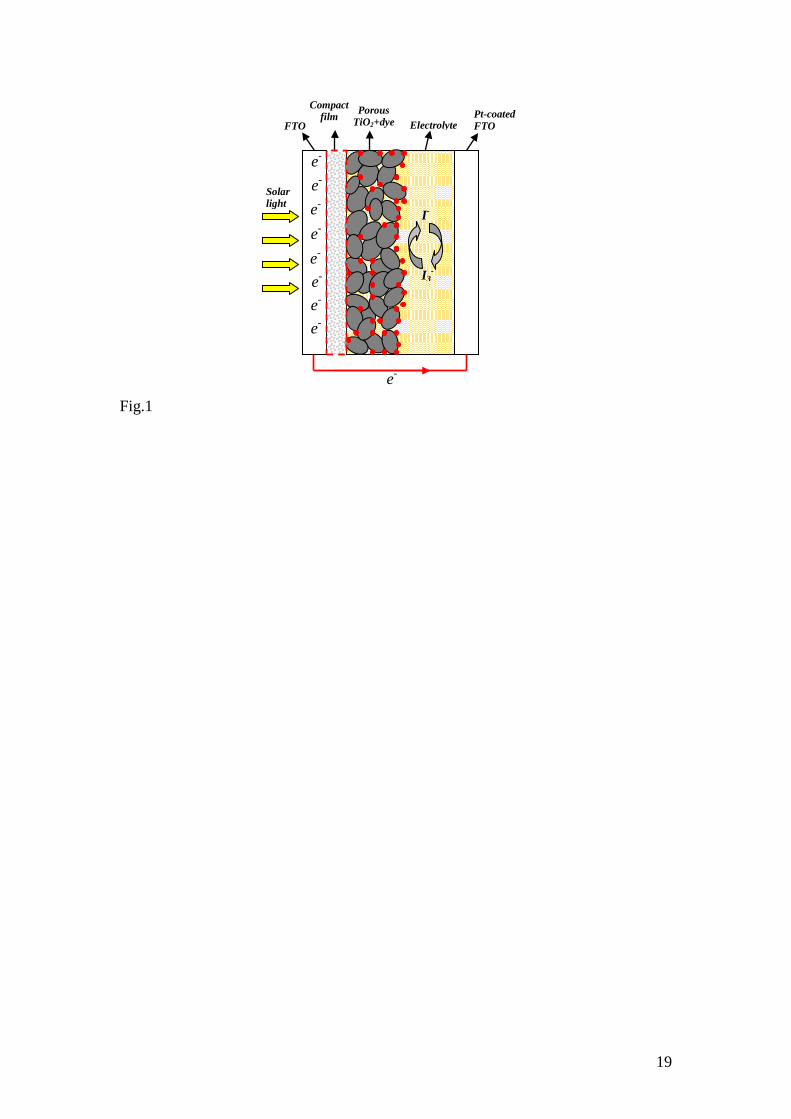
Dye-sensitized solar cell (DSSC) consists of a dye-adsorbed porous TiO2 layer on
fluorine-doped tin oxide (FTO) glass as a working electrode, a Pt thin film counter
electrode and an electrolyte normally containing I-/I3- redox couple [1-4]. Under the
illumination of solar light, dye molecules are excited and electrons are produced. To
generate meaningful electrical power from DSSC, the electrons need to pass 4
important interfaces of DSSC: dye/TiO2, TiO2/FTO, electrolyte/counter electrode, and
dye/electrolyte. The nanoporous nature of the TiO2 layer provides high surface area
that is of great importance to the efficient photon-to-electricity conversion because it
enhances dye loading and solar light absorption [5]. However, it also provides
abundant TiO2 surface sites (direct route) and bare FTO conducting sites (indirect
route), where the photo-injected electrons may recombine with I3- species in the redox
electrolyte (2e- + I3- → 3I-) [6-8]. The recombination will cause the loss of the
photocurrent. So the photovoltaic performance of DSSC is seriously decreased [9].
The introduction of a compact layer between the interface of the FTO/porous TiO2
(see Figure 1) has been proven theoretically and practically effective to block the
electron recombination via the indirect route [10-14]. This compact layer is much
denser than the TiO2 layer; therefore, it can reduce the contact surface area for bare
FTO sites and the redox electrolyte (so called blocking effect). Semiconductors, such
as TiO2 [15-17], Nb2O5 [18], ZnO [19] and some insulating materials, such as CaCO3
[20] and BaCO3 [21], have been used as a blocking layer for the fabrication of DSSCs.
Among them, the compact TiO2 layer is the most suitable candidate as the blocking
layer and has been investigated most frequently. Besides the blocking effect, higher
density of the compact layer, together with larger contact area and improved
adherence between the TiO2 layer and FTO surface provides more electron pathways

3
from TiO2 to FTO for photo-generated electrons, which facilitates electron transfer
and subsequently improves the electron transfer efficiency.
The modification layer can be coated directly on the conductive substrate by dip-
coating [22], spray pyrolysis method [23], chemical vapour deposition [24] and
sputtering methods [9, 25]. However, the overall cost for the resulting DSSCs can be
dramatically augmented if the coating process involves complicated fabrication
procedures or equipment.
In this work, a TiO2 organic sol is synthesized under very mild reaction conditions.
TiO2 compact layer was introduced from the TiO2 organic sol with a dip-coating
method, which is simple and low cost. Compared with the porous structure derived
from a commercially available TiO2 paste, the resulting TiO2 compact layer possesses
a dense structure that was found to be beneficial to the performance improvement of
the DSSCs. It is to note that, to our knowledge, this is the first time for such a TiO2
organic sol to be used for the modification of the DSSC photoanode. The organic sol
synthesis and coating processes do not require high temperature and high pressure
reaction environment (i.e., hydrothermal reaction [26]), or sophisticated and costly
equipment (such as spray pyrolysis method [23], chemical vapour deposition [24] and
sputtering methods [9, 25]); therefore, this preparation method for the compact TiO2
film is a low cost process.
The improvement of the DSSC performance, in terms of open circuit voltage (Voc),
short-circuit current density (Jsc) and solar energy-to-electricity conversion efficiency
(η), was observed. The mechanism for the increased efficiency of the DSSCs is
proposed based on the physiochemical characteristics of the compact films. The
photovoltaic investigations of the DSSCs also include dark-current measurement,

4
IPCE, open-circuit voltage decay (OCVD) and the dependence of Jsc on incident
irradiation power (Pin).
2 Experimental
2.1 Materials
Titanium butoxide (97%), diethanolmine (99%), anhydrous acetonitrile (99.8%), 1-
butanol (99.9%) and chloroplatinic acid hexahydrate (H2PtCl6·6H2O, ≥ 37.5% as Pt)
were purchased from Sigma-Aldrich. Ethanol (99.5%) and isopropanol (99.7%) were
supplied by Ajax Finechem and Merck respectively. Milli-Q water was used for the
sol preparation. TiO2 paste (DSL 18NR-T), dye (B2) and liquid electrolyte (EL141)
containing Li/LiI redox couple were from Dyesol Co. The dye was N-179 dye
(RuL2(NCS)2(TBA)2·(H2O)4, L=2,2'-bipyridyl-4,4'-dicarboxylic acid, TBA =
tetrabutylammonium). Fluorine-doped tin oxide (FTO) glass (≤14 Ω/square) was from
Pilkington.
2.2 TiO2 organic sol preparation and compact TiO2 film formation
A TiO2 organic sol for TiO2 compact layer was prepared at room temperature by a
method illustrated in our previous work [27]. Briefly, 68 mL of Tetrabutyl titanate
and 16.5 mL of diethanolamine were dissolved in 210 mL absolute ethanol, and then
the mixture was stirred vigorously for 1 hour at room temperature (Solution A). A
mixture of 3.6 mL H2O and 100 mL ethanol (Solution B) was added dropwise into the
Solution A under stirring. The resulting solution was aged for 24 hours at room
temperature resulting in the TiO2 organic sol. The resultant sol was then used for the
coating of a compact TiO2 film (namely, C film) on the FTO surface by dip-coating
with a withdrawing speed of 2 mm/s followed by a sintering process in a furnace at
450 for 2 h.
5
Both the FTO substrates with and without the C film were subject to the coating of a
porous film by a screen-printing technique with a commercial TiO2 paste [28]. The
resultant films were dried in an oven at 85 for 10 min and the coating process was
repeated until a thickness of 12-15 μm was obtained. Subsequently the films were
sintered in a furnace at 450 for 30 min. The resultant porous TiO2 films with and
without the C film were designated as compact-porous film (namely, CP film) and
porous film (namely, P film), and the corresponding electrodes were CP and P
electrode, respectively.
2.3 Characterization of TiO2 films
The surface morphologies of the C, P and CP films were characterized by scanning
electron microscopy (SEM, JSM 890). The crystalline phase of the TiO2 thin films
were determined by XRD (X-ray diffraction) using a diffractometer (Philips PW3020)
with Cu Kα radiation.
2.4 Counter electrode preparation, dye adsorption and dye loading measurement
Counter electrodes were fabricated by depositing a transparent platinum thin film on
FTO substrate from H2PtCl6 isopropanol solution with a spin-coating and pyrolyzing
method [29].
The P and CP films were immersed into a dye solution (3×10⁻⁴ M in butanol and
acetonitrile, 1:1, v/v) for 24 h. The dye-anchored films were washed with anhydrous
acetonitrile after the dye adsorption process, and then dried in N2 flow before
measurements. In order to analyse the dye loading, dye was desorbed completely from
the dye-adsorbed films into NaOH ethanolic solution (10-4 M) [30]. A
spectrophotometer (Varian, Cary 4500) was used to measure the desorbed dye
concentration in this solution.
6
2.5 Cells assembly and characterizations
The electrolyte solution was applied onto the dye-anchored TiO2 films using a
micropipet. Then the electrolyte/dye/TiO2 glass plates were fixed together with the
counter-electrode. A mask with a window area of 0.15 cm2 was used to define the
active illumination area of the DSSCs.
The photocurrent-photovoltage curves (J-V curves), dark current and OCVD of solar
cells were recorded by a Princeton Applied Research (PAR) Scanning Potentiostat
(Model 362) using a 500W Xe lamp (Changtuo, Beijing) coupled with an AM 1.5G
filter (Sciencetech, Canada). The incident light intensity was measured by a
broadband probe (Newport, 70268) and a radiant power meter (Newport, 70260).
The IPCE as a function of wavelength was measured with a Newport 66902 150 Watt
Xe-lamp in combination with an Oriel Cornerstone 130 monochromator and a
Keithley 236 source measure unit controlled by LabVIEW software. The number of
incident photons on the device was calculated for each wavelength by using a
calibrated Si-diode as a reference. The reported data were the average values of four.
The solar energy-to-electricity conversion efficiency (η) of DSSC was calculated by
equation (1):
%100×=in
ocsc
PFFVJη (1)
where Jsc is the short-circuit photocurrent density, Voc is the open-circuit voltage, Pin
is the light power per unit area and FF is the fill factor which is calculated by
equation (2):
maxmaxmax
ocscocsc VJVI
VJPFF == (2)
7
Where Imax and Vmax are the current and potential at the maximum power point
respectively in J-V curves of the solar cells. The J-V characterization was conducted
under Pin of 85mW·cm-2 for the η calculation.
The dependence of Pin on the Jsc and Voc was also investigated. The incident photon-
to-current conversion efficiency (IPCE) of DSSC, a measure of the external quantum
efficiency, is defined as:
in
sc
PehcJ
photonsincidentofnumberelectronscollectedofnumberIPCE
λ== (3)
Where λ, e, h and c are the incident wavelength, elementary charge, Planck constant
and speed of light, respectively.
OCVD experiment is conducted by monitoring the subsequent decay of Voc after stopping
the illumination on DSSC under open-circuit conditions [31].
From the OCVD experiment, the electron lifetime ( nτ ) is determined by the reciprocal of
the derivative of the decay curves normalized by the thermal voltage, using Equation 4
[31]:
(4) 1-
−=
dtdV
eTk ocB
nτ
where kB is Boltzmann constant, T is absolute temperature, e is the positive elementary
charge, and dVoc/dt is the derivative of the transient open-circuit voltage.
3 Results and discussions
3.1 Characterization of the TiO2 films
SEM analysis showed both P and C films have a crack-free and uniform structure. P
film has a typical porous structure with an average particle size of 30-50 nm. In a
sharp contrast with the P film, the C film has a dense and flat surface, as well as a

8
compact internal structure with an average particle size of 10-20 nm. Figure 2 shows
the SEM cross-section image of a CP film, where the layered structure of the CP film
is clearly indicated. The thickness of the C film is normally ca. 110 nm. The TiO2 film
from the organic sol dip-coating process (i.e., C film) is much more compact than that
from aqueous TiO2 sol-gel dip-coating method [15]. The C film has a very similar
compact structure to that from the conventional spraying pyrolysis deposition (SPD)
method [23], which may be due to the fact that both methods used organic precursor
rather than aqueous TiO2 colloid. Comparing with the SPD compact film, the C film
has a more uniform and flat surface (with no lumps that are caused by the aggregation
of mist from the spraying). The porous structure of the P film enlarges the surface
area greatly, up to a factor of 1000 as compared to a flat surface, which facilitates the
dye adsorption loading and also enables light harvesting due to its reflective nature
[23].
The X-ray diffraction patterns of the C film, P film and CP film are shown in Figure
3. Anatase and rutile phase peaks were marked as “A” and “R”, respectively. The C
film consists of pure anatase phase TiO2, showing only diffraction peaks
corresponding to the anatase phase. In contrast, P film and CP film have both anatase
and rutile phases. The XRD patterns and relative intensity of the P film and CP film
were almost identical. In fact, the content of anatase phase of TiO2 for the P film and
CP film are 92.3% and 92.5%, respectively. This implies that, compared with the P
film, the compact layer of the CP film will have little influence on the surface
behaviour, such as dye adsorption and mass transport of I-/I3- between the porous TiO2
layer and the counter electrode.
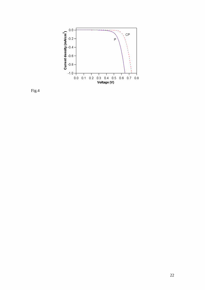
3.2 Dark current measurement
9
Controlling the back electron transfer in DSSC is vital to enhance the solar energy-to
electricity conversion efficiency. Dark current measurement in DSSC cannot be
related directly to the back electron transfer process, since the electrolyte
concentration in the films and the potential distribution across the nanoporous
electrode in dark are different than those under illumination [32]. However a
comparison of dark current between the investigated cells can provide useful
information regarding the back electron transfer process. So dark current
measurement of DSSC has been considered as a qualitative technique to describe the
extent of the back electron transfer [25]. The origination of the dark current stems
from the existence of naked FTO sites due to the porous nature of the TiO2 structure.
The porous structure provides pathways for the commonly used liquid redox
electrolyte (e.g., I3- species) to penetrate through the P film and contact the bare
conductive FTO surface. At these bare sites, the potential is thermodynamically
favourable for the reduction of the oxidative species, mainly I3-. This causes electron
recombination and results in the loss of photocurrent. A comparison between the dark
currents obtained from DSSCs with and without the compact layer can provide a
qualitative measure for the current leakage due to the back electron transfer [15, 25,
33]. Preventing the recapture of injected electrons by I3- at the photoanode is critical
to reduce the current leakage in DSSC.
Figure 4 shows the dark current-voltage characteristics of the DSSCs of the P film and
CP film with the applied bias from 0 to +0.75 V. The onset of the dark current for the
P film occurs at a bias about +0.40 V, with a subsequent dramatic increase of dark
current with the increase of potential. In contrast, for the DSSC with the CP film, the
onset potential shifted to +0.60V; furthermore, the dark current of the CP film
increased much slower than that of P film when potential was greater than +0.60V. In
10
other words, under the same potential bias, when the potential was >+0.4V, the dark
current for the CP film was noticeably smaller than that for the P film. The increase of
the onset potential and the reduction of the dark current demonstrated that the CP
successfully reduced the reaction sites for the reduction of I3-, i.e., the leakage of
electrons from the bare FTO was blocked by the compact layer.
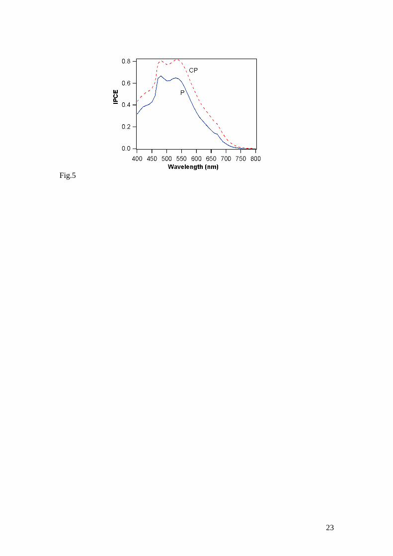
3.3 Incident photon-to-current conversion efficiency (IPCE)
The IPCE is defined as the ratio of the number of electrons in the external circuit
produced by an incident photon at a given wavelength. Using equation (2), the IPCE
values of the DSSCs with the P and CP electrode as a function of the illumination
wavelength are shown in Figure 5. As expected, the DSSC with the CP film showed
higher conversion efficiency in the wavelength range of 400~700 nm than that with P
electrode. For example, the porous TiO2 film shows a maximum IPCE of 64% at a
wavelength of 540 nm, while the compact CP film illustrates an IPCE of 82%. The
IPCE can be rationalized using the following equation [34]:
where A is the absorptivity referring to the fraction of the incident light absorbed by
the dye molecules. φinj is the injection efficiency, that is, the probability that the
excitation of an adsorbed dye molecule leads to electron injection into the TiO2
conduction band, and ηcoll is the collection efficiency.
The parameters A and φinj, are directly related to the dye loading on the TiO2 surface
of the CP and P film sample. In order to identify the mechanism of the IPCE
enhancement using the compact layer, the dye loadings on the TiO2 surface of the
both electrodes were investigated. The adsorbed dye on TiO2 surface in both samples
was firstly eluted completely in the NaOH ethanolic solution, and then subject to the
quantitative analysis using a UV-vis spectroscopy. Using an absorptivity of
(5) )( collinjAIPCE ηϕλ =

11
ε=13900M-1·cm-1 at 540nm, the number of dye molecules absorbed on the surface of
the P and the CP films were 1.005×10¹⁷ and 1.006×10¹⁷ respectively. The dye loading
of the both samples were similar; therefore, parameters A and φin, of both samples can
be considered the same. It could be assumed that the parameters A and φinj played a
minor role on the IPCE and dominating factor for the IPCE enhancement logically
should be the increased electron collection efficiency ηcoll consistent with literature
[35]. The increased ηcoll is due to the use of the compact layer with the mechanism
behind this potentially due to the increased number of electron pathways of the
compact layer and the blocking effect for the back electron transfer to the electrolyte.
The former originates directly from the dense structure of the compact layer as
demonstrated in SEM images in Figure 2. Under a given solar light intensity and for a
given amount of dye photo reaction sites, the number of photo-generated electrons is
constant. The electron collection efficiency and the electron recombination ratio will
determine the IPCE. An increased contact area of compact TiO2 with the FTO surface
is obviously in favour of the decrease of the electron transfer resistance and the
increase of the electron collection efficiency. At the same time, the compact layer also
significantly reduced the naked FTO reaction sites, where the back electron transfer
reaction was dramatically suppressed. These two factors worked synergistically
together and lead to the increase of the ηcoll, and ultimately, enhancement of IPCE.
3.4 Photocurrent density-photovoltage (J-V) curves
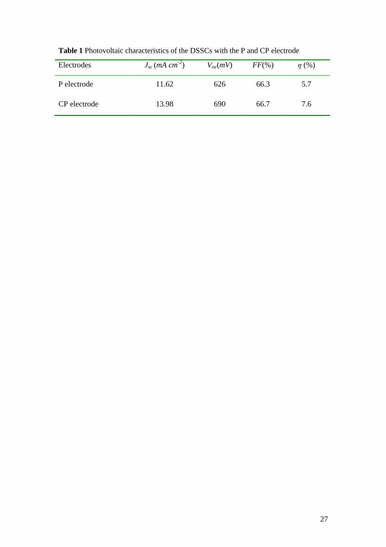
J-V curves of the DSSCs with and without the blocking layer are shown in Figure 6
and the photovoltaic characteristics of these DSSCs were summarised in Table 1.
Compared with the traditional DSSC without the compact layer, the performance of
the DSSC with the compact layer, in terms of solar energy-to-electricity conversion
efficiency, short circuit current density and open circuit potential, was significantly

12
improved by 33.3%, 20.3%, and 10.2%, respectively. The dye adsorption and light
scattering properties of the CP film showed negligible difference to the P film.
Therefore, the improvement of the overall performance of the solar cell was logically
due to the introduction of the C film.
The short-circuit current of DSSC is mainly influenced by two factors: dye loading
and the charge recombination at photoanode [36-38]. In our experiment, the
calculated dye loading amounts for the P and CP films were found to be 1.98×10⁻⁴
g/cm2 and 1.99×10⁻⁴ g/cm2 respectively, suggesting that the dye loading amount has
little influence on the Jsc. Hence, the main factor influencing the Jsc of the DSSC’s
studied should be the charge recombination at FTO/electrolyte interfaces. With the
application of the compact film, the recombination sites (bare FTO sites) are reduced
and the charge recombination in the DSSC is effectively suppressed as demonstrated
in the dark current measurement in Figure 4. At the same time, comparing with the
porous structure of the P film, the TiO2/FTO contact area was increased also due to
the introduction of the C film (see SEM image in Figure 2). Furthermore, the density
of the C layer is higher than that of the porous structure of the P film. As a result,
more effective electron pathways are generated via this compact layer to facilitate
electron transfer. Consequently, more electrons can be collected at the conduction
band of the photoanodes and transferred to external circuit, resulting in the
improvement in Jsc of the DSSC.
At a given sun illumination, the flux of injected electrons should be the same for the
DSSCs with the P film and CP film. The improvement of Voc may be explained due to
the improved adherence and the increased number of electron pathways and therefore
less resistance to electron transfer to the FTO interface. The compact layer also
13
favours the accumulation of electrons at the interface of FTO resulting in a more
negative Fermi level and thus a larger Voc [39].
It is interesting to note that the IPCE of the DSSC cell with the compact layer had
only a small improvement, (i.e., range from 0% to 8% depending on the wavelength
of the incident light), comparing with the DSSC without the compact layer (see Figure
5). In contrast, the photocurrent of the DSSC cell dramatically increased (ca. 20%)
when the blocking layer was applied between the FTO and porous layer (see Figure
6). This non-consistency was attributed to the different experimental conditions (i.e.,
different light intensity) used in these two measurement. The light intensities
(<0.108mW/cm2) of the monochromatic light applied in the IPCE measurement were
much lower than the light intensity (85mW/cm2) used in photocurrent measurement.
It was suggested that the spectral measurement of the IPCE of DSSC can not be used
to predict the IPCE under white light, solar light or even very high intensities of
monochromatic light [35]. In other words, IPCE is also light intensity dependent.
Therefore, the spectral measurements of the IPCE should be compared under the same
light intensity to provide quantitative information of the blocking effect of the
compact layer.
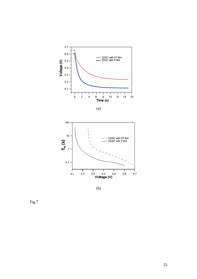
3.5 Open-circuit voltage decay (OCVD) measurement
OCVD technique has been employed as a powerful tool to study the electron lifetime
in DSSC and can provide some quantitative information on the electron
recombination velocity in DSSC [40, 41]. In order to conduct the OCVD
measurement, the simulated solar light is illuminated at DSSC and a steady-state
voltage was obtained. This indicated that equilibrium between electron injection and
electron recombination is attained at the FTO surface. A potentiostat then monitors
the decay of photovoltage, (Voc), after interrupting the illumination. The decay of the

14
photovoltage reflects the decrease of the electron concentration at the FTO surface,
which is mainly caused by the charge recombination. In other words, the
recombination velocity of photoelectron is proportional to the response of the OCVD.
Figure 7a shows the OCVD decay curves of the DSSCs with and without the blocking
layer, i.e., the CP film and P film. It was observed that the OCVD response of the
DSSC with the blocking layer (CP film sample) was much slower than that without
the blocking layer (i.e., P film sample), especially in the shorter time domain (within
15 seconds).
Electron lifetime ( nτ ) was proposed to quantify the extent of electron recombination
with the redox electrolyte and has been proven effective . nτ was calculated with the
OCVD results in Figure 7a according to Equation 4. Figure 7b compares the results of
the dependence of τn on the open circuit voltage for DSSC with and without the
compact layer. It clearly demonstrates that, at any given open-circuit potential, the
electron lifetime of the CP film cell was longer than that of the P film. Because the
dye adsorption and light scattering due to the introduction of the C film are negligible
as illustrated in previous sections, the difference in OCVDs was mainly due to the
blocking effect of the compact layer. This suggests that the electrons injected from
excited dye can survive longer and hence can facilitate electron transport without
undergoing losses at the bare FTO surface. In conclusion, the OCVD measurements in
Figure 7 demonstrated that the compact layer was able to reduce the photoelectron
recombination speed effectively and prolong the lifetime of the photoelectrons.
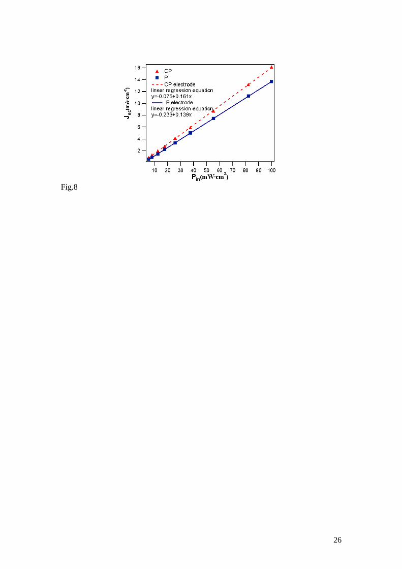
3.6 Variation of Jsc with Pin
Because the amount of the photo-generated electrons is directly proportional to the Pin,
the variation of Pin can be used to adjust the amount of photo-generated electrons in
the study of the electron transfer process. The investigation of the dependence of Jsc
15
on Pin may provide useful information on the electron transfer kinetics due to the
introduction of the compact layer. Figure 8 shows that Jsc of the DSSCs with the P
and CP electrodes were in direct proportion with Pin within the maximum illumination
level studied (100 mW/cm2). This indicates that the current density for both P and CP
solar cells were limited by the Pin, rather than other electron transfer processes, such
as mass transport of I3- or electron transfer at the counter electrode under the
investigated power range [42]. More importantly, the slope for the CP electrode (i.e.,
0.161), was 15.8% higher than that for the P electrode (i.e., 0.139), which indicates
that 15.8% more electrons were collected from the same amount of photo-generated
electrons (under the same Pin) at the FTO surface. This again confirms that the use of
the compact layer facilitates the electron transfer at the porous TiO2/ FTO interface as
explained in the previous sections.
4 Conclusions
The effect of the compact layer on the performance of the DSSCs was investigated.
The compact TiO2 film can not only improve adherence of TiO2 to FTO and provide a
larger TiO2/FTO contact area, but also effectively reduce the electron recombination
by minimising the direct contact between the redox electrolyte and the conductive
FTO surface. Compared with the traditional DSSCs without the compact layer, the
solar energy-to-electricity conversion efficiency, short circuit current and open circuit
potential of the DSSCs with the compact layer were improved by 33.3%, 20.3%, and
10.2%, respectively.

16
References
1. M. Gratzel, Nature 414 (2001) 338. 2. H. Pettersson, T. Gruszecki, R. Bernhard, L. Haeggman, M. Gorlov, G.
Boschloo, T. Edvinsson, L. Kloo, and A. Hagfeldt, Prog. Photovoltaics 15 (2007) 113.
3. E. Palomares, J.N. Clifford, S.A. Haque, T. Lutz, and J.R. Durrant, Chem. Commun. (2002) 1464.
4. E. Palomares, J.N. Clifford, S.A. Haque, T. Lutz, and J.R. Durrant, J. Am. Chem. Soc. 125 (2003) 475.
5. I. Kartini, D. Menzies, D. Blake, J.C.D. da Costa, P. Meredith, J.D. Riches, and G.Q. Lu, J. Mater. Chem. 14 (2004) 2917.
6. J.R. Durrant, S.A. Haque, and E. Palomares, Coord. Chem. Rev. 248 (2004) 1247.
7. P.J. Cameron and L.M. Peter, J. Phys. Chem. B 107 (2003) 14394. 8. K. Kalyanasundaram and M. Gratzel, Coord. Chem. Rev. 177 (1998) 347. 9. P.J. Cameron and L.M. Peter, J. Phys. Chem. B 109 (2005) 7392. 10. K. Zhu, N. Kopidakis, N.R. Neale, J. van de Lagemaat, and A.J. Frank, J. Phys.
Chem. B 110 (2006) 25174. 11. T. Hoshikawa, T. Ikebe, R. Kikuchi, and K. Eguchi, Electrochim. Acta 51
(2006) 5286. 12. S.A. Haque, E. Palomares, B.M. Cho, A.N.M. Green, N. Hirata, D.R. Klug,
and J.R. Durrant, J. Am. Chem. Soc. 127 (2005) 3456. 13. S. Nakade, T. Kanzaki, W. Kubo, T. Kitamura, Y. Wada, and S. Yanagida, J.
Phys. Chem. B 109 (2005) 3480. 14. N. Kopidakis, K.D. Benkstein, J. Van de Lagemaat, and A.J. Frank, J. Phys.
Chem. B 107 (2003) 11307. 15. J.N. Hart, D. Menzies, Y.-B. Cheng, G.P. Simon, and L. Spiccia, C. R. Chim.
9 (2006) 622. 16. R. Hattori and H. Goto, Thin Solid Films 515 (2007) 8045. 17. K.-S. Ahn, M.-S. Kang, J.-W. Lee, and Y.S. Kang, J. Appl. Phys. 101 (2007)
084312/1. 18. J. Xia, N. Masaki, K. Jiang, and S. Yanagida, J. Phys. Chem. C 111 (2007)
8092. 19. S.-J. Roh, R.S. Mane, S.-K. Min, W.-J. Lee, C.D. Lokhande, and S.-H. Han,
Appl. Phys. Lett. 89 (2006) 253512/1. 20. Z.-S. Wang, M. Yanagida, K. Sayama, and H. Sugihara, Chem. Mater. 18
(2006) 2912. 21. X. Wu, L. Wang, F. Luo, B. Ma, C. Zhan, and Y. Qiu, J. Phys. Chem. C 111
(2007) 8075. 22. W.Y. Gan, S.W. Lam, K. Chiang, R. Amal, H. Zhao, and M.P. Brungs, J.
Mater. Chem. 17 (2007) 952. 23. B. Peng, G. Jungmann, C. Jager, D. Haarer, H.-W. Schmidt, and M. Thelakkat,
Coord. Chem. Rev. 248 (2004) 1479. 24. M. Thelakkat, C. Schmitz, and H.-W. Schmidt, Adv. Mater. 14 (2002) 577. 25. S. Ito, P. Liska, P. Comte, R. Charvet, P. Pechy, U. Bach, L. Schmidt-Mende,
S.M. Zakeeruddin, A. Kay, M.K. Nazeeruddin, and M. Graetzel, Chem. Commun. (2005) 4351.
26. S. Zhang, D. Jiang, and H. Zhao, Environ. Sci. Technol. 40 (2006) 2363.
17
27. H. Yu, X.-J. Li, S.-J. Zheng, and W. Xu, Mater. Chem. Phys. 97 (2006) 59. 28. T. Tesfamichael, G. Will, J. Bell, K. Prince, and N. Dytlewski, Sol. Energy
Mater. Sol. Cells 76 (2003) 25. 29. N. Papageorgiou, W.F. Maier, and M. Gratzel, J. Electrochem. Soc. 144 (1997)
876. 30. X. Liu, Y. Luo, H. Li, Y. Fan, Z. Yu, Y. Lin, L. Chen, and Q. Meng, Chem.
Commun. (2007) 2847. 31. A. Zaban, M. Greenshtein, and J. Bisquert, ChemPhysChem 4 (2003) 859. 32. A. Zaban, A. Meier, and B.A. Gregg, J. Phys. Chem. B 101 (1997) 7985. 33. Y. Diamant, S.G. Chen, O. Melamed, and A. Zaban, J. Phys. Chem. B 107
(2003) 1977. 34. I. Bedja, P.V. Kamat, A.G. Lapin, and S. Hotchandani, Langmuir 13 (1997)
2398. 35. T. Trupke, P. Wuerfel, and I. Uhlendorf, J. Phys. Chem. B 104 (2000) 11484. 36. B.C. O'Regan, J.R. Durrant, P.M. Sommeling, and N.J. Bakker, J. Phys. Chem.
C 111 (2007) 14001. 37. M. Berginc, U. Opara Krasovec, M. Jankovec, and M. Topic, Sol. Energy
Mater. Sol. Cells 91 (2007) 821. 38. A.N.M. Green, E. Palomares, S.A. Haque, J.M. Kroon, and J.R. Durrant, J.
Phys. Chem. B 109 (2005) 12525. 39. B.C. O'Regan, S. Scully, A.C. Mayer, E. Palomares, and J. Durrant, J. Phys.
Chem. B 109 (2005) 4616. 40. F. Fabregat-Santiago, J. Garcia-Canadas, E. Palomares, J.N. Clifford, S.A.
Haque, J.R. Durrant, G. Garcia-Belmonte, and J. Bisquert, J. Appl. Phys. 96 (2004) 6903.
41. J. Bisquert, A. Zaban, M. Greenshtein, and I. Mora-Sero, J. Am. Chem. Soc. 126 (2004) 13550.
42. C. Zafer, C. Karapire, N. Serdar Sariciftci, and S. Icli, Sol. Energy Mater. Sol. Cells 88 (2005) 11.

18
Figure captions: Fig.1 Schematic diagram of the DSSC with a compact TiO2 layer.
Fig.2 SEM cross-section image of the CP film.
Fig.3 XRD spectra of the C, P, CP films.
Fig.4 Dark current of the DSSCs with the P and CP electrodes
Fig.5 Photocurrent action spectra of the DSSCs with the P and CP electrodes
Fig.6 J-V curves of the DSSCs with the P and CP electrodes
Fig.7 (a) Open-circuit voltage decay curves of the DSSCs with the P and CP films ;
(b) Comparison of electron lifetime as a function of open-circuit voltage of
DSSCs with the P and CP films.
Fig.8 The variation of Jsc with Pin for the DSSCs with the P and CP electrodes.
19
Fig.1
e-
Porous TiO2+dye Electrolyte
Pt-coated FTO
Compact film
FTO
Solar light
I3-
I-
e-
e-
e-
e-
e-
e-
e-
e-

20
Fig.2

21
Fig.3
22
Fig.4
23
Fig.5
24
Fig.6
25
(a)
(b)
Fig.7
26
Fig.8
27
Table 1 Photovoltaic characteristics of the DSSCs with the P and CP electrode
Electrodes Jsc (mA cm-2) Voc(mV) FF(%) η (%)
P electrode 11.62 626 66.3 5.7
CP electrode 13.98 690 66.7 7.6