An analytical model for turn-on characteristics of short channel polycrystalline-silicon thin-film...
13
Microelectronic Engineering 54 (2000) 263–275 www.elsevier.nl / locate / mee An analytical model for turn-on characteristics of short channel polycrystalline-silicon thin-film transistor for circuit simulation * Sonia Chopra, R.S. Gupta University of Delhi South Campus, Semiconductor Devices Research Laboratory, Department of Electronic Science, Benito Juarez Road, New Delhi-110021, India Received 27 September 1999; accepted 17 May 2000 Abstract Short channel effects are incorporated to investigate the impact of the channel length on the turn-on characteristics of a polycrystalline silicon thin-film transistor (poly-Si TFT). The developed threshold voltage and field effect mobility are the key parameters in analysing the above-threshold characteristics. The expressions for the device transconductance and drain conductance are then developed, from which the channel resistance has also been extracted. The expressions so developed are simple and can be extensively used in modeling the short channel TFT. The predicted results are compared with available experimental data, and excellent matching confirms the validity of the model. 2000 Elsevier Science B.V. All rights reserved. Keywords: Thin-film transistor; Poly-Si; Short channel effects 1. Introduction Poly-silicon thin film transistor (TFT) technology has received a great deal of attention because of its potential in becoming a viable technology for large-area integrated circuits. Such circuits have found wide applications in active-matrix liquid crystal displays [1] and for load device in static random access memories (SRAMs) [2]. While there are similarities between poly-Si TFTs and their crystalline silicon (c-Si) counterparts, the poly-Si grain boundary traps and intra-grain defects introduce many significant differences, like different mobility dependence on gate bias. Poly-Si TFTs also exhibit a high threshold voltage and low carrier mobility as compared to single crystal MOSFETs. Several models for long channel poly-Si TFTs have been proposed [3–5] giving the quantitative understanding of its characteristics. Several secondary and parasitic effects are introduced when we go *Corresponding author. Tel.: 191-11-688-6606; fax: 191-11-688-6606 / 6427. E-mail address: [email protected] (R.S. Gupta). 0167-9317 / 00 / $ – see front matter 2000 Elsevier Science B.V. All rights reserved. PII: S0167-9317(00)00412-3
-
Upload
independent -
Category
Documents
-
view
4 -
download
0
Transcript of An analytical model for turn-on characteristics of short channel polycrystalline-silicon thin-film...
Microelectronic Engineering 54 (2000) 263–275www.elsevier.nl / locate /mee
An analytical model for turn-on characteristics of short channelpolycrystalline-silicon thin-film transistor for circuit simulation
*Sonia Chopra, R.S. GuptaUniversity of Delhi South Campus, Semiconductor Devices Research Laboratory, Department of Electronic Science,
Benito Juarez Road, New Delhi-110021, India
Received 27 September 1999; accepted 17 May 2000
Abstract
Short channel effects are incorporated to investigate the impact of the channel length on the turn-on characteristics of apolycrystalline silicon thin-film transistor (poly-Si TFT). The developed threshold voltage and field effect mobility are thekey parameters in analysing the above-threshold characteristics. The expressions for the device transconductance and drainconductance are then developed, from which the channel resistance has also been extracted. The expressions so developedare simple and can be extensively used in modeling the short channel TFT. The predicted results are compared with availableexperimental data, and excellent matching confirms the validity of the model. 2000 Elsevier Science B.V. All rightsreserved.
Keywords: Thin-film transistor; Poly-Si; Short channel effects
1. Introduction
Poly-silicon thin film transistor (TFT) technology has received a great deal of attention because ofits potential in becoming a viable technology for large-area integrated circuits. Such circuits havefound wide applications in active-matrix liquid crystal displays [1] and for load device in staticrandom access memories (SRAMs) [2]. While there are similarities between poly-Si TFTs and theircrystalline silicon (c-Si) counterparts, the poly-Si grain boundary traps and intra-grain defectsintroduce many significant differences, like different mobility dependence on gate bias. Poly-Si TFTsalso exhibit a high threshold voltage and low carrier mobility as compared to single crystalMOSFETs.
Several models for long channel poly-Si TFTs have been proposed [3–5] giving the quantitativeunderstanding of its characteristics. Several secondary and parasitic effects are introduced when we go
*Corresponding author. Tel.: 191-11-688-6606; fax: 191-11-688-6606/6427.E-mail address: [email protected] (R.S. Gupta).
0167-9317/00/$ – see front matter 2000 Elsevier Science B.V. All rights reserved.PI I : S0167-9317( 00 )00412-3
264 S. Chopra, R.S. Gupta / Microelectronic Engineering 54 (2000) 263 –275
to submicrometer dimensions making the analysis more complicated. A recent study of submicrometerpoly-Si TFTs [6] shows a decrease in the number of grain boundaries leading to many favourablecharacteristics when the device dimensions approach submicrometer or deep submicrometer level.Steeper sub-threshold slope, lower threshold voltage and lower leakage current are obtained, and ahigher mobility and abrupt switching were also observed. As a consequence the characterisation andmodeling of these devices plays an essential role and our objective is to develop an analytical modelfor the short channel poly-Si TFT. Among the main parameters which characterise the deviceperformance are the drain-voltage characteristics and the transconductance.
In this paper a theoretical analysis of short channel poly-Si TFTs and an analytical expression forthe threshold voltage is presented. Based on the developed threshold voltage and field effect mobility,the I–V characteristics of poly-Si TFTs biased at the turn-on region are found. The theoreticalpredictions are compared with experimental data and a good match is found. The transconductance is,then, determined and its dependence on channel length and gate voltage is seen. Finally the drainconductance and channel resistance are extracted and their variation with gate and drain voltage isshown. In the present communication an attempt has been made to develop a model for I –Vd d
characteristics and small signal analysis for short channel poly-Si TFT.
2. Model analysis
2.1. Drain-voltage characteristics
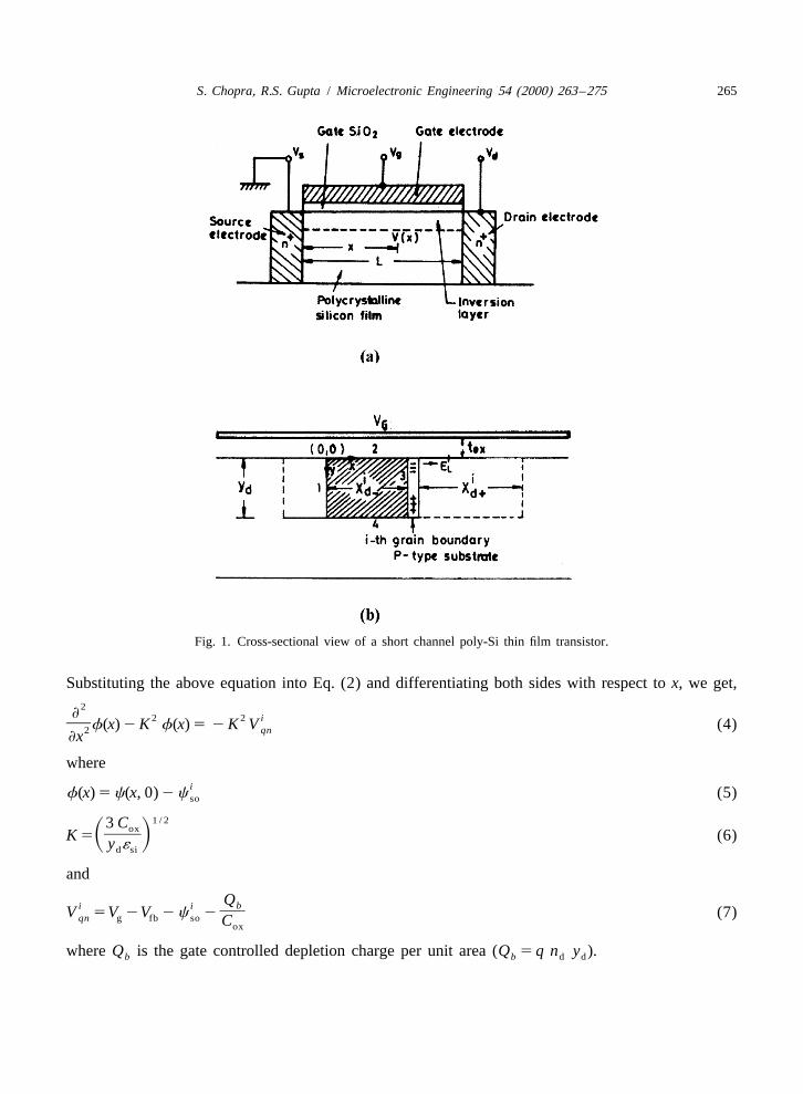
Fig. 1(a) shows the physical model of short channel poly-Si TFTs along with symbols used in theanalysis. A cross-sectional view of a poly-Si TFT with uniform grain doping is shown in Fig. 1(b). Inthe shaded region, free carriers are depleted by the trapped charges in the grain boundaries and thetwo-dimensional Poissons equation can be written as,
2 2 qn≠ c ≠ c d]] ]] ]]1 5 (1)2 2 ´≠x ≠y si
where q is the electronic charge, n is the doping density, ´ is the dielectric permittivity of Si. Sinced si
the electric field direction is almost lateral at the depletion edge y , it is reasonable to assume thed
normal electric field at y 5 y is zero. For simplicity it is assumed that y is independent of x.d d
Applying Gauss theorem to a volume enclosed by the planes located at these boundaries [7], weget,
yx d
2 C 2 q n y x≠c(x, y9)ox d d]] ]]] ]]]]E(V 2V 2 c(x9, 0)) dx9 2E dy9 5 (2)g fb´ ≠x ´si si
0 0
where V is the flat band voltage, y is the depletion depth, and C is the gate oxide capacitance.fb d ox
The variation of y with respect to x is not significant within a single grain and the resulting errord
for the grain barrier in the surface layer can be smeared out due to the integration process in Eq. (2).Under the same assumptions, the potential function can be expressed as,
2c(x, y)(c(O, y) 1 f(x) (1 2 ( y /y )) (3)d
S. Chopra, R.S. Gupta / Microelectronic Engineering 54 (2000) 263 –275 265
Fig. 1. Cross-sectional view of a short channel poly-Si thin film transistor.
Substituting the above equation into Eq. (2) and differentiating both sides with respect to x, we get,2
≠ 2 2 i]f(x) 2 K f(x) 5 2 K V (4)2 qn≠x
wherei
f(x) 5 c(x, 0) 2 c (5)so
1 / 23 Cox]]K 5 (6)S Dy ´d si
and
Qbi i]]V 5V 2V 2 c 2 (7)qn g fb so Cox
where Q is the gate controlled depletion charge per unit area (Q 5 q n y ).b b d d

266 S. Chopra, R.S. Gupta / Microelectronic Engineering 54 (2000) 263 –275
Solving Eq. (4) and applying the following boundary conditions,
w(0) 5 0 (8a)
and
≠w]5 0 (8b)≠x
The solution is obtained as,i i
w(x) 5V 2V cosh (Kx) (9)qn qn
Similarly, the potential distribution in the right side of the ith grain boundary can be easilycalculated. The electric field along the channel at the grain boundary is then given by,
iQgb6i i i]]K V sinh(K x ) 5 6E (10)qn d6 l2´si
where the symbol (6) means that the discussed region is in the right / left side of the ith grainboundary.
The trapped charge density, Q , in the grain boundary depends on the distribution of the localizedgb
trap states in the energy gap. Based on Seto’s model [8], the trap distribution can be wellapproximated by an effective trap state E and the trapped charge density can be written as,t
qnst]]]]]]]Q 5 (11)gb E 2 E1 t f
] ]]]1 1 expS D2 k tb
where n is the trap state density, k is Boltzmann constant, and (E 2E ) defines the position of thest b t f
fermi level relative to the trap level at the grain boundary.As the band bending is toward the Si–SiO interface, some induced carriers are captured by the2
traps in the grain boundaries. An additional gate voltage above the threshold voltage of a conventionalMOSFET is required to support these extra charges in the traps. In this case, the surface band bendingis determined not only by the gate bias and the ionized charges in the bulk but also by the chargestates of the traps at the grain boundaries. Taking the ith grain to be completely depleted (i.e.x 5 L /2), its value is detemined by,d g
iQgb6i i]]KV sinh(K L /2) 5 6E (12)qn g l2´si
As the channel becomes shorter, a large fraction of the field lines from the bulk charge under the gateare terminated on the source and drain islands. In Eq. (7) we implicitly assumed that the depletionregion due to the gate field is rectangular in shape and Q 5 q n y . This approximation neglects theb d d
charges near the source and drain ends that terminate the built-in field from the source and the drainjunctions. In fact the depletion regions in the channel due to the gate overlap with that due to the
9source /drain junctions. Due to overlapping of the fields, the effective gate controlled charge Q b
becomes smaller than Q . Yau et al. [9] proposed a simple model which uses a geometricalb
approximation in conjunction with charge conservation analysis to account for the decrease in the gate
S. Chopra, R.S. Gupta / Microelectronic Engineering 54 (2000) 263 –275 267
controlled charge in terms of a charge sharing factor. The charge sharing factor, f , describes thel
fraction of the total depletion charge in the channel terminated on the gate and is defined as]]]y 2yj d
] ]f 5 1 2 1 1 2 1 (13)S Dl L yjœwhere y is the junction depth and L is the channel length.j
Therefore, the depletion charge in terms of the charge sharing factor can be written as,
9Q 5 f q n y (14)b l d d
Using Eq. (14) in Eq. (7), we get,
9Q bi]]V 5V 2V 2 c 2 (15)qn g fb so Cox
Now, the threshold voltage is defined as the gate voltage at which minimum surface potential is at theonset of strong inversion. Replacing the surface potential in Eq. (15) by w and the gate voltage by thes
threshold voltage the equation is modified as,
9Q bi i]]V 5V 2V 2 f 2 (16)qn t fb s Cox
Substituting Eq. (16) in Eq. (12), we obtain the threshold voltage of a short channel poly-Si TFT atlow drain voltages as,
Qf qn y gbuf sl d d]]] ]]]]]]V 5V 1 f 1 1 (17)t fb s C 2´ K sinh(KL /2)ox si g
When the drain voltage is increased, the drain depletion region moves closer to the source depletionregion. This results in a significant field penetration from drain to the source and the potential barrierat the source is lowered, resulting in an increased injection of electrons over the reduced channelbarrier, giving rise to more drain current (DIBL). This penetration of the junction electric fields intothe channel region causes barrier lowering which in turn leads to reduction in the threshold voltage[10], given by,
s ´ ´o o si]]]V 5V 2 V (18)mth t dpC Lox
where s and m are technology dependent fitting parameters used to better fit the model for geometryo
dependent DIBL effect for a given range of impurity concentration and junction depth, ´ is theo
permittivity of free space. Hence, the threshold voltage developed for a short channel poly-Si TFT is,
Qf qn y s ´ ´gbuf sl d d o o si]]] ]]]]]] ]]]V 5V 1 f 1 1 2 V (19)mth fb s dC 2´ K sinh(KL /2) pC Lox si g ox
The presence of grain boundaries has a profound effect on the performance of poly-Si TFTs. Thepotential barriers associated with charged grain boundaries impede carrier transport in the channel andthe mobility is lower than that in bulk silicon. Jacunski et al. [11] have described the field effect
268 S. Chopra, R.S. Gupta / Microelectronic Engineering 54 (2000) 263 –275
mobility to be a power law for low gate voltages which asymptotically approaches a constant value athigher gate voltages and is given by,
1 1 1]] ]]]] ]5 1 (20)pm mk (V 2V )eff om g th
2 21 21where m , the band mobility is taken as 100 cm V s . k , the low field mobility constant has theo m2 23.7 21value 3.4 cm V s and the power law exponent ( p) is 2.7.
2.1.1. Linear regionUsing the gradual channel approximation the current–voltage characteristics can be obtained from
[12],Vd
I 5 WE[Q (x)v] dV(v) (21)d i
O
where Q (x), the inversion charge in the channel, is given as,i
Q (x) 5 C (V 2V 2V(x))i ox g th
On integrating Eq. (21) we get,
]]] 2f 2q´ n VW 1 si d d]]]]] ]] ]]] ]I 5 C m (V 2V )V 2 1 1 (22)H JF Gd ox eff g th dV 2C f 2œd ox s
]L 1 mS Deff vsat
where W is the channel width, V is the drain voltage and v is the saturated carrier velocity.d sat
3. Saturation region
At pinch-off point the drain current and drain voltage are designated as I and V , respectively.dsat dsat
In a short channel device the carriers reach velocity saturation even before pinch-off begins. So tocalculate V , we define I to be the current when the carriers at the drain end are velocitydsat dsat
saturated, i.e.,]]]
f 2q´ n1 si d]] ]]]I 5 Wv C (V 2V ) 1 1 V (23)F S D Gdsat sat ox g th dsat2C fœox s
If we replace V by V , I is also given by Eq. (22). Equating Eq. (22) and (23), the expression ford dsat dsat
V is obtained.dsat
For drain voltages larger than saturation voltage, the channel pinch-off point shifts towards thesource. This movement is referred to as channel length modulation. and the device under thiscondition behaves as if the channel length L was shortened by L . The drain current becomes largerd
than its value at the onset of saturation when L is zero. The drain current in the saturation region isd
calculated by replacing the normal channel length L by the reduced channel length (L 2 L ) and Vd d
S. Chopra, R.S. Gupta / Microelectronic Engineering 54 (2000) 263 –275 269
with V in the linear region current equation. The drain current expression developed in thedsat
saturation region is given as,
]]] 2f 2q´ n VW 1 si d dsat]]]]]]] ]] ]]] ]]I 5 C m (V 2V )V 2 1 1 (24)F GS Ddsat ox eff g th dsatV 2C f 2œdsat ox s5 ]] 6(L 2 L ) 1 mS Dd eff vsat
where L is determined as proposed by Frohman-Bentchkowsky and Grove [13], i.e.d
V 2Vd dsat]]]L 5 (25)d Et
where E is the average transverse electric field near the drain depletion region at the channel gatet
interface and is given by,
]]]]] 9 9V 2V V 2Vqn ´ ´d g g dsatd ox ox]] ]]]] ]]]]E 5 (V 2V ) 1 A 1 A (26)t d dsat 1 22´ ´ t ´ tœ si si ox si ox
where V 9 5V 2V and A and A are the fringing field factors. Typical values of A and A are 0.2g g fb 1 2 1 2
and 0.6 respectively. ´ is the dielectric permittivity of the gate oxide and t is the gate oxideox ox
thickness.
3.1. Transconductance
The transconductance, an important device parameter, is a measure of device gain and is directlyrelated to the circuit speed and is defined as,
≠Id]g 5 V 5 constt.um d≠Vg
Using Eq. (22) we get,
W]]]]]g 5 C m Vm ox eff dVd5 ]L 1 mS Deff vsat
WC V1ox d]]]]] 9 ]]]]] ] 91 m 2 m m (V 2V )V 2 1S Feff eff eff g th dV V vd d sat
] ]L 1 m 1 L 1 m 2S D S Deff effv vsat sat
]]] 2f 2q´ n V1 si d d]] ]]] ]1 (27)DG2C f 2œox s 6
9where m is the derivative of field effect mobility with respect to gate voltage.eff
Clearly the transconductance consists of two components.
270 S. Chopra, R.S. Gupta / Microelectronic Engineering 54 (2000) 263 –275
1]]]]]g 5 C m Vm1 ox eff dVd
]L 1 mS Deff vsat
and
WC V1ox d]]]]] 9 ]]]]] ] 9g 5 m 2 m m (V 2V )VSm2 eff eff eff g th dV V vd d sat5 ] ]L 1 m 1 L 1 m 2S D S Deff effv vsat sat
]]] 2f 2q´ n V1 si d d]] ]]] ]1 1 1 DF G2C f 2œox s 6
It is noted that a part of the transconductance g is not observed in single crystal Si MOSFET and ism2
related to the change in mobility with V .g
3.2. Drain conductance
The drain conductance or the channel conductance is another important parameter and can bewritten as,
≠Id]g 5 V 5 constt.uds g≠Vd
or
]]]f 2q´ nW 1 si d
]]]]] ]] ]]]g 5 C m V 2V 2 1 1 VS F G Dds ox eff g th dV 2C fœd ox s5 ]L 1 mS Deff vsat
m m VW eff eff d]]]]] 99 ]]]]] ]] ] 991 C m 2 m (V 2V )VSS Dox eff eff g th dV V v vd d sat sat
] ]L 1 m 3 L 1 m 4S D S Deff effv vsat sat
]]] 2f 2q´ n V1 si d d]] ]]] ]2 1 1 (28)DF G2C f 2œox s 6
99where m is the derivative of field effective mobility with respect to drain voltage.eff
The channel resistance is directly calculated from the channel conductance as,
1]R 5 (29)ch gds
S. Chopra, R.S. Gupta / Microelectronic Engineering 54 (2000) 263 –275 271
4. Results and discussion
A simple I 2V model has been developed for a short channel poly-Si TFT whose validity hasd d
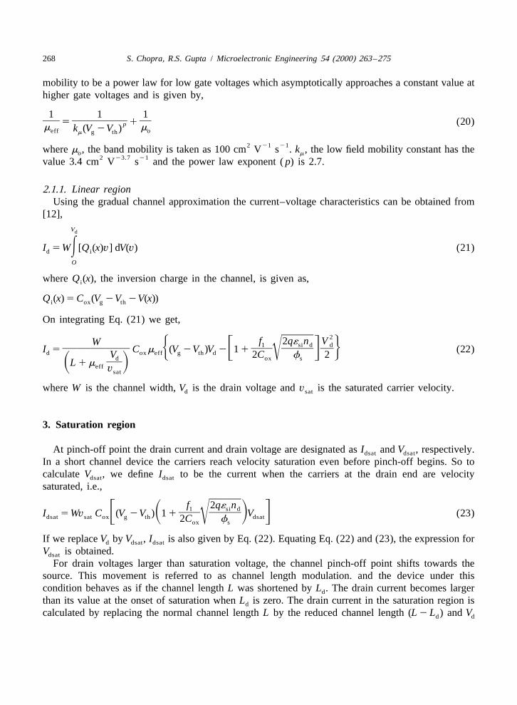
been demonstrated by comparing the predicted results with available experimental data [14].Fig. 2 shows the variation of the experimental and calculated threshold voltage with channel length.
The trap state density, n , is taken to be variable as shown in the figure. A good fit of the data to thest
experimentally measured results is observed. A drastic decrease in the threshold voltage is seen as weapproach short channel lengths due to the sharing of the channel depletion region charge between thegate and the source–drain junctions.
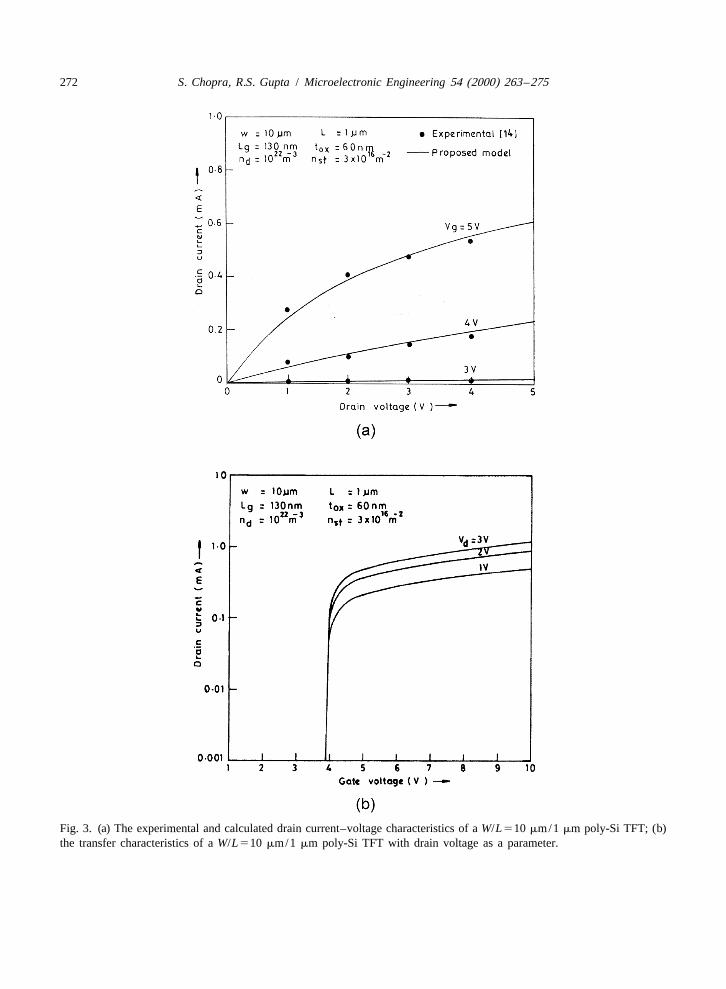
The variation of the drain current with drain–source voltage is shown in Fig. 3(a) with gate voltage16 22as a parameter and the trap state density taken as 3?10 m . The predicted results show an excellent
match with the experimental results in the linear and saturation region. The drain current of a shortchannel TFT is greater than that of a long channel TFT. This is because in short channel devices thesource and drain are so close to all points in the channel that they can affect the channel through theirproximity just as the gate does. This causes a deeper depletion region and hence a larger surfacepotential which makes the channel more attractive for electrons, and the device can conduct morecurrent than would be predicted from the long channel theory. Fig. 3(b) shows the transfercharacteristics of the device at various drain voltages.
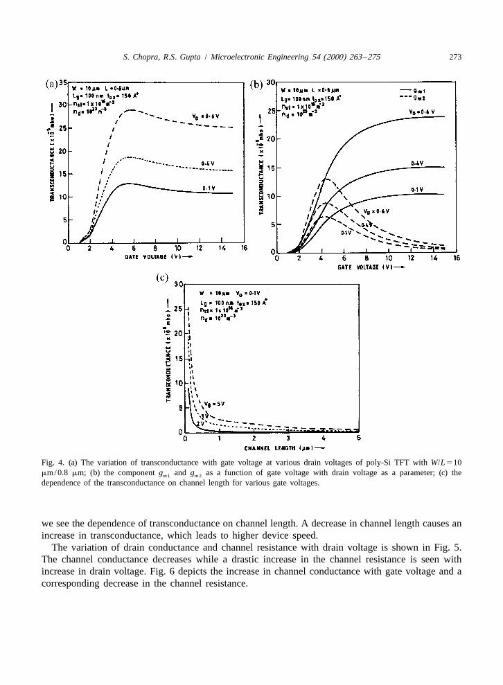
Fig. 4(a) depicts the variation of the transconductance of the short channel poly-Si TFT withdifferent gate voltages. Fig. 4(b) shows the variation of the two components, g and g , with gatem1 m2
voltage. In Fig. 4(a) we see that initially the transconductance increases and then decreases. Thisunique behaviour arises due to g . The component g is due to the effect of grain boundary barrierm2 m2
potential lowering with gate voltage. When the gate voltage reaches a value such that the fermi levelat the grain boundary is above the trap level, the decrease of the grain boundary barrier potential willbecome increasingly small. In this region the transconductance becomes nearly constant. In Fig. 4(c)
Fig. 2. The variation of the experimental and proposed threshold voltage and trap state density with channel length.
272 S. Chopra, R.S. Gupta / Microelectronic Engineering 54 (2000) 263 –275
Fig. 3. (a) The experimental and calculated drain current–voltage characteristics of a W/L510 mm/1 mm poly-Si TFT; (b)the transfer characteristics of a W/L510 mm/1 mm poly-Si TFT with drain voltage as a parameter.
S. Chopra, R.S. Gupta / Microelectronic Engineering 54 (2000) 263 –275 273
Fig. 4. (a) The variation of transconductance with gate voltage at various drain voltages of poly-Si TFT with W/L510mm/0.8 mm; (b) the component g and g as a function of gate voltage with drain voltage as a parameter; (c) them1 m2
dependence of the transconductance on channel length for various gate voltages.
we see the dependence of transconductance on channel length. A decrease in channel length causes anincrease in transconductance, which leads to higher device speed.
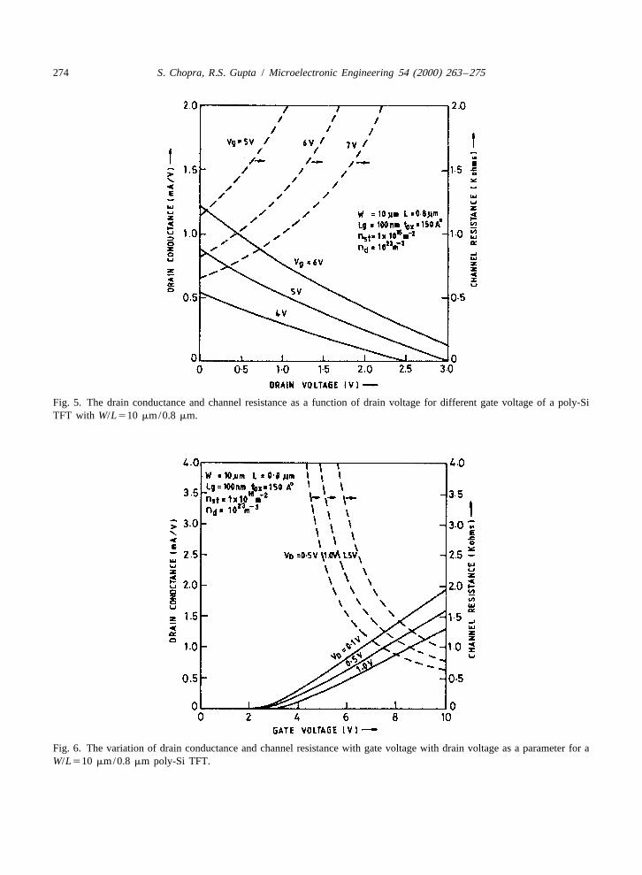
The variation of drain conductance and channel resistance with drain voltage is shown in Fig. 5.The channel conductance decreases while a drastic increase in the channel resistance is seen withincrease in drain voltage. Fig. 6 depicts the increase in channel conductance with gate voltage and acorresponding decrease in the channel resistance.
274 S. Chopra, R.S. Gupta / Microelectronic Engineering 54 (2000) 263 –275
Fig. 5. The drain conductance and channel resistance as a function of drain voltage for different gate voltage of a poly-SiTFT with W/L510 mm/0.8 mm.
Fig. 6. The variation of drain conductance and channel resistance with gate voltage with drain voltage as a parameter for aW/L510 mm/0.8 mm poly-Si TFT.
S. Chopra, R.S. Gupta / Microelectronic Engineering 54 (2000) 263 –275 275
5. Conclusion
A physical based analytical turn-on current and conductance model for short channel poly-Si TFTsis developed. The model has some important features. The relationships between the modelparameters and the device parameters are simple. The model has an analytical form, which enableseasy implementation in circuit simulators. Another attractive feature is the exponential grain sizedependence of the threshold voltage, which has not been incorporated in any previous models. Themodel can also explain the behaviour of the transconductance of the device. The charge sharingconcept, which is used to include the short channel effects in the model, is the most widely used incircuit simulators. The analysis predicts that decreasing device dimensions show improved charac-teristics. From comparisons with experimental and calculated results, the developed model is quitesuccessful in explaining the experimental observations.
Acknowledgements
The authors gratefully acknowledge the help extended by University Grants Commission,Government of India.
References
[1] S.D. Brotherton, Polycrystalline silicon thin film transistors, Semicond. Sci. Tech. 10 (1995) 721–728.[2] S. Ikeda, S. Hashiba, I. Kuramoto, H. Katoh, S. Ariga, T. Yamanaka, N. Hashimoto, S. Meguro, A polysilicon transistor
technology for large capacity SRAMs, in: IEDM Technical Digest, 1990, pp. 469–472.[3] T. Serikawa, S. Shirai, A. Okamoto, S. Suyama, A model of current–voltage characteristics in polycrystalline silicon
thin-film transistors, IEEE Trans. Electron Devices 34 (1987) 321–324.[4] H.N. Chern, C.L. Lee, T.F. Lei, An analytical model for the above-threshold characteristics of polysilicon thin-film
transistors, IEEE Trans. Electron Devices 42 (1995) 1240–1246.[5] K. Ono, T. Aoyama, N. Konishi, K. Miyata, Analysis of current–voltage characteristics of low-temperature-processed
polysilicon thin-film transistors, IEEE Trans. Electron Devices 39 (1992) 792–801.[6] N. Yamauchi, J.J. Hajjar, R. Raif, Polysilicon thin-film transistors with channel length and width comparable to or
smaller than the grain size of the thin film, IEEE Trans. Electron Devices 38 (1991) 55–59.[7] Y.A. El-Mansy, A.R. Boothroyd, A simple two-dimensional model for IGFET operation in the saturation region, IEEE
Trans. Electron Devices 24 (1977) 254–262.[8] J.Y.W. Seto, The electrical properties of polycrystalline silicon films, J. Appl. Phys. 46 (1975) 5247–5254.[9] L.D. Yau, A simple theory to predict the threshold voltage of short-channel IGFETs, Solid-State Electron. 17 (1974)
1059–1063.[10] N.D. Arora, MOSFET Models for VLSI Circuit Simulation, Springer Verlag, Wein, New York, 1993.[11] M.D. Jacunski, M.S. Shur, M. Hack, Threshold voltage, field effect mobility, and gate-to-channel capacitance in
polysilicon TFTs, IEEE Trans. Electron Devices 43 (1996) 1433–1439.[12] S.M. Sze, Physics of Semiconductor Devices, 2nd Edition, Wiley Eastern Ltd, 1983.[13] D. Frohman-Bentchkowsky, A.S. Grove, Conductance of MOS transistors in saturation, IEEE Trans. Electron Devices
16 (1969) 108–113.[14] S.S. Chung, D.C. Chen, C.T. Cheng, C.F. Yeh, A physically-based built-in Spice poly-Si TFT model for circuit
simulation and reliability evaluation, in: Proc. of IEDM, 1996, pp. 139–142.