An analogue computer - World Radio History
368
2 PHILIPS TECHNICAL REVIEW VOLUME 31 An analogue computer for simulating One-diMenSional aerial arrays A. Meijer In various .fields of transmitting and receiving technology such as radar, radio astronomy, telemetry, and space flight, aerial arrays are used rather than single aerials. The mathe- matical treatment of such systems is rather complex, even when the treatment is confined to linear systems and the interaction between the elements is neglected. The article presents two methods by which the array factors of symmetrical, unequally spaced linear aerial arrays can be simulated and displayed electronically, thus providing a rapid understanding of the radiation behaviour of the system. Introduction Interest in aerials has increased considefably in the last ten or twenty years. The aerial is always a vital part of the system: a radar is made or marred by the quality of its aerials, without good aerials space flight would not have reached its present state of development, and radio astronomy would have made little progress with- out the aerial syitems specially developed for it. For many applications an aerial is desired that trans- mits in just one direction or receives from just one direction - an ideal that can be achieved only imper- fectly. It has been found that the application of the well known interference principle familiar from optics can give a solution with some attractive aspects, par- ticularly for radar. For example, the direction of radia- tion of the aerial can be varied electronically - and hence rapidly - without the inertia of mechanically rotating aerials. Another possibility is rapid adaptation of the radiation characteristics to the often variable environment in which the radar targets are situated. By using the interference principle more versatile radar ,aerials can be designed. Since an aerial whose operation is based on the inter- ference Principle consists of more than oneelenient, we shall' lienceforth speak of an aerial array. Exact calculation of the radiation characteristics of an aerial 'array is extremely difficult, because'the radia- tion characteristics of' a single aerial in free: space is different from that of the same aerial when it is part of .an array. Here the various eleMents affect one anOther's performan0 in a very complicated way, depending on the type oraerial and on the geometry of the system. The problem is Made very much simpler if ,this interaction is neglected. The *errors introduced by neglecting the Jr. A. Meijer is with Philips Research Laboratories,, Eindhoven: interaction become far less significant the farther apart the elements are located. Although there is usually a difference between the calculated radiation character- istics and the mea§ided ones - even with widely spaced elements - the information obtained can be of value in designing an aerial array. When the interaction between the elements is neg- lected, we may considei the aerial array as a group of elements each of which has a completely defined radia- tion pattern. This radiation pattern, which is never omnidirectional, is known as the element factor. If all the elements have the same element factor, we can find the radiation pattern of an aerial array by starting from a hypothetical array consisting of omnidirectional elements. This will be explained later. The radiation pattern of such a system is called the array factor. This array factor depends only on the feed to the individual elements and on the geometry of the array. The radia- tion pattern of the aerial array is then given by the product of the array factor and the element factor. In this article we shall only deal with arrays whose elements are located on a straight line. They do not however all have to be at the same spacing. Unequally spaced linear aerial arrays of this type have become increasingly important in recent years. They were first used in radio astronomy, to obtain the same radiation pattern from' a smaller number of aerials than are needed when the spacing between the elements is equal DJ. Unequally spaced aerial arrays also have features of interest for radar systems. Some practical linear arrays can be seen in figs. la and lb. Even with the limitation to linear arrays and with the interaction between the elements neglected, the theor- ['] G. W. Swenson Jr. and Y. T. Lo, IRE Trans. AP -9, 9, 1961.
-
Upload
khangminh22 -
Category
Documents
-
view
0 -
download
0
Transcript of An analogue computer - World Radio History

2 PHILIPS TECHNICAL REVIEW VOLUME 31
An analogue computerfor simulating One-diMenSional aerial arrays
A. Meijer
In various .fields of transmitting and receiving technology such as radar, radio astronomy,telemetry, and space flight, aerial arrays are used rather than single aerials. The mathe-matical treatment of such systems is rather complex, even when the treatment is confinedto linear systems and the interaction between the elements is neglected. The article presentstwo methods by which the array factors of symmetrical, unequally spaced linear aerialarrays can be simulated and displayed electronically, thus providing a rapid understandingof the radiation behaviour of the system.
Introduction
Interest in aerials has increased considefably in thelast ten or twenty years. The aerial is always a vital partof the system: a radar is made or marred by the qualityof its aerials, without good aerials space flight wouldnot have reached its present state of development, andradio astronomy would have made little progress with-out the aerial syitems specially developed for it.
For many applications an aerial is desired that trans-mits in just one direction or receives from just onedirection - an ideal that can be achieved only imper-fectly. It has been found that the application of thewell known interference principle familiar from opticscan give a solution with some attractive aspects, par-ticularly for radar. For example, the direction of radia-tion of the aerial can be varied electronically - andhence rapidly - without the inertia of mechanicallyrotating aerials. Another possibility is rapid adaptationof the radiation characteristics to the often variableenvironment in which the radar targets are situated. Byusing the interference principle more versatile radar
,aerials can be designed.Since an aerial whose operation is based on the inter-
ference Principle consists of more than oneelenient, weshall' lienceforth speak of an aerial array.
Exact calculation of the radiation characteristics ofan aerial 'array is extremely difficult, because'the radia-tion characteristics of' a single aerial in free: space isdifferent from that of the same aerial when it is part of
.an array. Here the various eleMents affect one anOther'sperforman0 in a very complicated way, depending onthe type oraerial and on the geometry of the system. Theproblem is Made very much simpler if ,this interactionis neglected. The *errors introduced by neglecting the
Jr. A. Meijer is with Philips Research Laboratories,, Eindhoven:
interaction become far less significant the farther apartthe elements are located. Although there is usually adifference between the calculated radiation character-istics and the mea§ided ones - even with widely spacedelements - the information obtained can be of valuein designing an aerial array.
When the interaction between the elements is neg-lected, we may considei the aerial array as a group ofelements each of which has a completely defined radia-tion pattern. This radiation pattern, which is neveromnidirectional, is known as the element factor. If allthe elements have the same element factor, we can findthe radiation pattern of an aerial array by starting froma hypothetical array consisting of omnidirectionalelements. This will be explained later. The radiationpattern of such a system is called the array factor. Thisarray factor depends only on the feed to the individualelements and on the geometry of the array. The radia-tion pattern of the aerial array is then given by theproduct of the array factor and the element factor.
In this article we shall only deal with arrays whoseelements are located on a straight line. They do nothowever all have to be at the same spacing. Unequallyspaced linear aerial arrays of this type have becomeincreasingly important in recent years. They were firstused in radio astronomy, to obtain the same radiationpattern from' a smaller number of aerials than areneeded when the spacing between the elements isequal DJ. Unequally spaced aerial arrays also havefeatures of interest for radar systems. Some practicallinear arrays can be seen in figs. la and lb.
Even with the limitation to linear arrays and with theinteraction between the elements neglected, the theor-
['] G. W. Swenson Jr. and Y. T. Lo, IRE Trans. AP -9, 9, 1961.

1970, No. 1 ANALOGUE SIMULATION -OF AERIAL ARRAYS 3
I
Photo: N.V. Hollandse Signaalapparaten, Hengelo (0). The Netherlands
Fig. la. A linear equally spaced aerial array for radar.
etical treatment of unequally spaced arrays is verydifficult and as yet no satisfactory solution has beenfound. Any other method that can provide informationabout the relationship between the parameters describ-ing such an array and its radiation pattern is thereforevery welcome.
In the following it will be shown that the array factorof an unequally spaced linear array can be simulatedelectronically in two ways, making use of differentanalogies: the space-time analogy, which displays thearray factor as a time phenomenon, and the space -frequency analogy, which displays the array factor asa frequency spectrum.
The space-time analogy has been found particularlyuseful for studying aerial systems whose direction ofradiation can be varied electronically. This is not veryeasy with the space -frequency analogy. This analogydoes however have the advantage that certain elementfactors can also be simulated.
Fig. lb. The radio telescope atWesterbork (The Netherlands),which was brought into use in1969. To give a better view of theconstruction, the first element ofthe aerial has been turned outof position.
Of the two simulation methods the one based on thespace -frequency analogy can more easily be made towork with existing equipment. The space-time analogy,however, requires an analogue computer specially de-signed for this purpose. Since there is considerableinterest in electronically steerable aerial systems, wehave built such a computer.
In both methods the effect on the array factor of achange in the feed or in the arrangement of the aerialelements can be directly displayed on the screen ofa cathode-ray tube.
In the following we shall deal first with the principlesof simulation. A description of the electronic circuitsof the analogue computer for the space-time simulationis then given. Finally, to illustrate the principle, somearray factors obtained with the aid of the computer arepresented. To complete the picture, a few results ob-tained by space -frequency simulation are included forcomparison.

4 PHILIPS TECHNICAL REVIEW VOLUME 31
Theoretical principles of simulation
The array factor
Let us consider a linear array whose aerials are allfed from a single source by means of power dividers.Each aerial feed line is assumed to include an attenua-tor and a phase shifter, so that the feed to each aerialcan easily be controlled in both amplitude and phase(fig. 2).
We shall now consider the far field of such a system,that is to say we consider a point far enough away fromthe aerial array that the array can be treated as a pointsource. This implies that the relative differences in pathlength from our point to the aerial elements no longerhave any effect on the relative differences in the fieldstrength of the individual waves reaching the point.The differences in path length do however affect thephase differences between the individual waves. Theimprovement in radiation behaviour that can be ob-tained with respect to that of a single -element aerial isdue to these path -related phase differences.
It follows from what we have said that the far fieldof an aerial element may be regarded as a scalar quan-tity and that the total far field is found from a summa-tion of the fields of the individual aerial elements,taking account of both amplitude and phase. The totalfar field of a system consisting of N aerial elements isthus given by the expression:
Ftot(0,99) =
N
1=1
Fi(0,99), . . . (1)
where Fi(0,q9) is the far field of the i-th element; theangular coordinates 0 and q' determine the directionof view (see fig. 3). The field Fi(0,99) is determined bythe strength at and the phase /pi of the signal suppliedto the i-th element, by the element factor ei(0,99) ofthe i-th element and by the path -related phase differencewith respect to a reference source. Assuming that thereference source is located at the point s = 0,. asin fig. 3, and the i-th element at the point s = si,then this path -related phase difference is equal tokst sin 0 rad, where k is the wave number (k = 270).The far field of the i-th element is thus given by:
Fi(0,q2) = at exp (jvi) ei(0,q9) exp (jksi sin 0), (2)
so that the total far field is :
Ftot(0,(p) =1=1
at exp (jlp) et(00p) exp (jksi sin e).
(3)
If all the elements have the same element factor, wecan put this in front of the summation sign and writeequation (3) as follows :
Fig. 2.located
Diagram of a linear aerial system. The elements areon a straight line (coordinate of position s) and are fed
via a power divider D from a common source S. Incorporatedin each feed line is a phase shifter Pi and an attenuator As.
where
F tot(0 ,(p) = e (0,0 . E(sin 0), . . . . (4)
E(sin 0) = at exp j(ksi sin 0 + ?pi). (5)
i=1
This function is the array factor.It can be seen that the array factor may be regarded
as the far field of a row of omnidirectional aerials;consequently it does not depend on the nature of theelements.
The aerial designer now has to find a set of ampli-tudes at, phases /pi and locations si that will give an"acceptable" array factor. Owing to the great numberof variables it is by no means certain whether an arrayfactor arrived at more or less fortuitously that has"good" characteristics will also be the best one. Whatwe mean by "acceptable" or "good" will be seen laterfrom the discussion of the results obtained.
Fig. 3. The path -related phase difference, expressed in radians,of the signal of an element at Q at the position s = si and areference source at the origin, is 2n times the number of wave-lengths contained in the projection OP of the distance OQ inthe viewing direction (angular coordinates 0 and 0.

1970, No. 1 ANALOGUE SIMULATION OF AERIAL ARRAYS 5
The space-time analogy
Fig. 4 illustrates schematically the method of simu-lation based on the space-time analogy. The generators
(i = 1, 2, . . . , N) give voltages that vary with timeas a cosine function and have the frequencies fi. Theinitial phases vi of these signals are set by means ofphase -shifting networks. The amplitudes ai of the
Fig. 4. Illustrating the simulation of array factors in the space-time analogy. GL cosine voltage generators. Pi phase -shiftingnetworks. Ai attenuators. summation network.
signals can also be freely chosen. The i-th signal thushas the form:
V1(t) = ai cos (27rfit pi). . . . (6)
All the N signals of this nature are fed to a summa-tion network E. The output signal VR(t) of this net-work is thus given by:
VR(t)
= 1
Substituting
and
V1(t) =1 = 1
ai cos (2nfit v/). . (7)
t T sin 0 (8a)
fi = AT, (8b)
we obtain for (7) the expression:
VR(T sin 0) == 1
aj cos (ksi sin 0 + vi), (9a)
which is identical with the real part of (5). If sinusoidalvoltages are generated by the sources G1, we then obtainthe imaginary part of equation (5):
Vr(T sin 0) =1 = 1
at sin (ksi sin 0 + yi). (9b)
By adding the squares of VR and VI we obtain the
square of the array factor, represented as a functionof time. It appears from the substitutions (eq. 8) thatthe time has been made equivalent to the space variablesin 0. This is why we refer to this principle as thespace-time analogy.
The constant T, which may at first sight seem to havebeen introduced simply to preserve the correct dimen-sions, also has a physical significance: the functionsVR(t) and V1(t) only have physical significance in thet -interval [-T, T], since a t -value outside this intervalsymbolizes a value of sin 0 greater than 1, i.e. animaginary angle. For this reason the interval [-T, T]is also referred to as the "visible" region of t.
In the manner just described any array factor can besimulated with the aid of two sets of function genera-tors. In nearly all aerial systems, however, the elementsare arranged symmetrically about the centre of thesystem, and it is therefore sufficient to use only one setof generators. Mathematically this symmetry may bedescribed by the condition:
S -5 N -+
This also establishes that the origin s = 0 of the s -coordinate coincides with the centre of the aerialsystem. The system then consists of M pairs of elementssymmetrically arranged about the centre, possibly withan extra element at the centre (this will be the case ifN is odd, that is to say if N = 2M + 1). If also eachpair of elements is supplied with a signal of the sameamplitude (at = aN-r+1) but in opposite phase(yi = --visr_r+1), then equation (5) shows that eachsuch element pair contributes to the function E(sin 0)a real amount 2aj cos (ksj sin 0 + yi), where i = 1,2, . . . , M. The array factor then becomes:
E(sin 0) = ao + 21 = 1
aj cos (ks/ sin 0 + . (10)
Here ao is the amplitude of the signal fed to the centralelement.
If we compare (10) with (9a) we see that the circuitshown in fig. 4 is sufficient for generating a functionof time that is an adequate simulation of the arrayfactor of an aerial system that is unequally spaced butsymmetrically arranged about the centre, with equalamplitudes and opposite phases for each pair of ele-ments. The term ao in equation (10) can easily besupplied by adding a d.c. source of the appropriatevoltage.
A diagram explaining the simulation principle isshown in fig. 5 for the case where ?pi = 0. In fig. 5athe amplitudes and positions of the elements are pre-sented schematically. The array factor as a functionof sin 0 then has a form like that shown in fig. 5b.

6 PHILIPS TECHNICAL REVIEW VOLUME 31
Fig. 5. The space-time analogy.a) The right-hand part of a sym-metrical, unequally spaced linearaerial array represented schema-tically. The signal amplitude at isplotted vertically, the distance sifrom the aerial elements to thecentre is plotted horizontally.b) The array factor E(sin 0) for`the aerial array in (a). The func-tion is symmetrical with respectto sin 0 = 0. c) Amplitudes asand frequencies fi of a set ofcosine generators with which theaerial array is simulated. d) Thetime function V(t) of which (c)is the frequency spectrum. Thegenerated function only has aphysical significance (0 real)for t < T.
The space-time analogy con-sists in the correspondence of(b) and (d) to each other when(a) and (c) correspond.
53
a
0 fl f f3
Since the system is symmetrical, this far field will alsobe symmetrical with respect to sin 0 = 0; it is there-fore sufficient to draw this field for values of sin 0between 0 and 1.
Fig. 5c gives the amplitude and the frequency ofeach cosine generator. The time function is shown infig. 5d. The space-time analogy is found in the fact thatfigs. 5a and b are equivalent to figs. 5c and d. If wechange the frequency of the second cosine generator,for example, then the effect of this on the time functionin fig. 5d is the effect which a corresponding displace-ment of the second pair of elements would have on thefar field in fig. 5b.
Fig. 6. The space -frequency anal-ogy. a) An unequally spacedlinear aerial array, representedschematically. The elements areline sources of length 2LI. Thesignal amplitude at is plottedvertically, the distance si of theelement from the origin, whichis taken to be at the lefthandend of the array is plotted hori-zontally. b) The array factor ofthe aerial system as a functionof sin 0. This diagram is theFourier transform of the functionshown in (a). c)A series of pulsesof width 2r, with which the aerialarray is simulated. The pulseamplitudes are plotted vertically,the times at which the pulsesoccur are plotted horizontally.d) Frequency spectrum of thetime function of (c). The spec-trum has physical significance(0 real) only when f < B. If (a)and (c) correspond, so do (b)and (d).
a
S2
2d
I53 ;a
2r
11
6 th
C
b
d
The space -frequency analogy
The conclusion to be drawn from fig. 5 is that theconfiguration of the aerial array (fig. 5a) can be re-garded as the spectrum of the far field (fig. 5b), sincefig. 5c is of course the spectrum of the time functionof fig. 5d (see also equation 7). Now a time functionand its spectrum are Fourier transforms of one an-other. This means that the far field of an aerial arraycan be described as the Fourier transform of the con-figuration of the array. This conclusion is the basis forthe space -frequency analogy, whose principle is illus-trated in fig. 6.
In fig. 6c a time function is shown that consists of
SN-10-

1970, No. 1 ANALOGUE SIMULATION OF AERIAL ARRAYS 7
a series of pulses of peak amplitudes aj, which occurat the times ti. The width 2r of the pulses is smallcompared with the distance between them. .The fre-quency spectrum F(co) (fig. 6d) is the Fourier trans-form of this time function. Fig. 6a is an accurate re-production of fig. 6c and represents our aerial system,in which signals of amplitude aj are fed to elements offinite length 24 located at the points sj; in other wordsthe elements must now be treated as line sources insteadof omnidirectional point sources. Since the far field ofthis system as a function of sin 0 (fig. 6b) is the Fouriertransform of this configuration, this far field must haveexactly the same curve as the frequency spectrum infig. 6d.
The space -frequency analogy thus amounts to thegeneration of a signal whose variation with time is afaithful representation of the configuration of the arrayto be studied. In this case the array need not be sym-metrical. The frequency spectrum of this signal is thenthe representation of the far field of the aerial array.
PG
PSI
TP
A A A/
PSZ
n nFiDt
TP
1 1
11 11 11
PsN
fi t2
consisting of a series of pulses with the form of a half -cosine function (fig. 7).
Fig. 8 shows a diagram illustrating the simulationmethod just described. Each time the pulse generatorPG delivers a pulse, the pulse shapers PSj generate apulse of a particular shape. This pulse is delayed ti
Hrix-11- -I 1- -I1
S
Fig. 7. Example of the way in which the element factor can betaken into account in the far field by giving the pulse signals aparticular shape. Above: Aerial system consisting of four +Adipoles. Below: Series of pulses representing the current distri-bution in the elements and simulating this aerial array via thespace -frequency analogy.
A A A
n n n
At
tN
Tp
A
11 11 11
AN 1
t
Fig. 8. Diagram of arrangement for simulating an array factor on the space -frequencyanalogy principle. Every Tp seconds a pulse generator PG delivers a clock pulse that causesthe pulse shapers PSi to deliver a pulse of a particular shape. This pulse is delayed by thecircuit Di (ti seconds) and if necessary attenuated to the amplitude at by As. The signals arethen added in a summation network E and the sum signal goes to a spectrum analyser (notshown). An example of a sum signal is shown under the diagram.
In certain cases the space -frequency analogy allowsthe element factor to be taken directly into account bygiving the pulses a suitable shape. For example, the farfield of a group of half -wavelength dipoles can berepresented by the frequency spectrum of a pulse train
seconds in a delay network Di and is then attenuatedto the required amount by an attenuator Ai. All thepulses are then fed to a summation network E, andthe resulting signal goes to a spectrum analyser.
Since the spectrum analyser must be supplied with

8 PHILIPS TECHNICAL REVIEW VOLUME 31
a periodic signal, the pulse train representing the aerialsystem must be periodically repeated. The repetitionfrequency is 2n/Tp, where Tp is the period of the pulsetrain. This mean's that the screen of the spectrum ana-lyser shows a line spectrum with lines at the frequenciesthat are the harmonics of this repetition frequency. Theenvelope of this line spectrum then represents the arrayfactor.
From the mathematical treatment of this simulationprinciple (see the small print below) it appears that thespace -frequency analogy is only suitable for simulatingthe far field of an aerial system all of whose elementsare fed in phase. However, the equipment can be modi-fied in such a way that the simulation method can alsobe applied for an array whose elements are fed in dif-ferent phases, but we shall not go any further into thishere.
The calculation also shows that it is not necessary todisplay the whole frequency spectrum. Only frequen-cies between particular values -B and +B (see fig. 6)represent real 0 -values. The frequency interval [-B, B]is thus the visible region of the frequency spectrum,just as in the space-time analogy a time interval [-T, T]represented the visible region.
The space -frequency analogy can be verified mathematicallyas follows. Since the signal is periodic with a period Tp (seefig. 8), it can be expressed in a Fourier series:
+co 2ntitf(t) = E F8 exp (-jTp- . . . . (11)
-co
The Fourier coefficients F,, are found by using the expression:Tp
Fn =Tp
f(t) exp dt. . . . (12)n
Tpt
In view of the shape of the signal, this integral can be writtenas the 'sum of N integrals:
N ti1F8 = f ft(t) exp
. brat dt =1=1
where
at etTp
1=1
2.7rn, exp
27rnti),(13)
Tp Tp
+7.
et2ouz
T- T) = f ft(t) exp -27rtzt) dtTp
-"V
represents the element factor of the i-th element.Now the frequency spectrum of the aperiodic signal is propor-
tional toN
F(w) at et(co,rt) exp acoti), . . . . (14)
so that the Fourier coefficient Fn has been shown to be no morethan the sampling of the frequency spectrum at the frequency2.7ttt/Tp.
To establish the analogy of equation (14) with the expressionfor the array factor (equation 5) we assume that all the pulsesare equal. In this case et(co,tt) is identical for each pulse, and thisfactor can be put in front of the summation sign. We then obtain:
F(w) = e(co,T) . E(co),
whereE(w) = at exp (Jcoti). (15)
1=1
Substitutinga) = 27E13 sin 0 (16a)
tt = stIAB (16b)
in this expression, then for the case ?pi = 0 - i.e. where theelements are fed with signals of the same phase - equation (5)is identical with equation (14).
and
The analogue computer based on the space-time analogy
We shall now look a little more closely at the elec-tronic circuits of.the analogue computer for the space-time analogy [2]. The basic circuit diagram of thisequipment has already been shown in fig. 4; a photo-graph of the equipment can be seen in fig. 9.
We saw earlier that the function generators Gi infig. 4 have to be cosine generators of variable frequen-cy. If we want lo simulate unequally spaced aerialarrays, the frequencies of these generators must riot beharmonics of one another, which means that thegenerated time function is not periodic. In order never-theless to obtain a stationary picture on an oscilloscope,the part of the function in which we are interested isperiodically repeated. This is done by making all thegenerators run for T seconds only, starting them againafter T dT, stopping them again after 2T + dT,and so on. The time T is chosen such that only theright-hand half of the visible region is described (be-tween sin 0 = 0 and sin 0 = 1, see fig. 5). The startand stop signals are derived from the sawtooth genera-tor of the oscilloscope, as shown in fig. 10. The timeAT is made equal to the flyback time of the oscilloscopetrace.
At the moment the start pulse appears, all the genera-tors must immediately start generating a cosine func-tion of the right phase, frequency and amplitude. Theremust be no switching transients; the generated functionmust be undistorted during the period T, and it mustalso be accurately reproducible during a very largenumber of sawtooth periods. In addition it must bepossible to modify the function in a fast and reliableway.
This is done by deriving all the frequencies of thecosine functions from the same train of high -frequencypulses, which .come from a central pulse generator,called the master clock. New series of pulses of lowerfrequencies are derived from this pulse train by meansof frequency dividers. These pulse trains, whose fre-quencies correspond to the positions of the elements

1970, No. I ANALOGUE SIMULATION OF AERIAL ARRAYS 9
._ ,
_.;"
.00 do 41 !.
mi* 4b. -00111400
ma.
of the aerial array being studied, are fed to functiongenerators. As we shall see later, each pulse that arrivesat the input of a function generator initiates a step inthe output voltage, the successive steps being of thecorrect heights for the waveform to approximate to acosine function. It is clear that the frequency of thegenerated function will be lower than that of the pulsetrain at the input, and as many times lower as thenumber of steps in which the function is approximated.We have taken this number of steps as 24, which givesa favourable compromise between the time needed forgenerating a complete cosine function and the accuracyof the approximation. The function obtained in this waycan be started and stopped at any time without givingrise to switching transients, and since all the generatorsare driven by a common pulse generator there is nofrequency drift between the signals.
The initial phases of the cosine functions generatedare adjusted in the following way. We arrange that thefirst m pulses go straight to the cosine generator, to befollowed by the pulses from the frequency divider offrequencyfi'. The cosine generator then starts with thevalue cos 27cmlp (p being the number of steps in whichthe cosine function is approximated), so that a cosine
Fig. 9. The analogue computer for the simulation of array fac-tors by the space-time analogy (right). The system is capable ofsimulating aerial arrays with up to 13 elements. The array factorcan be displayed on the oscillosope screen (left) and also on theupper panel of the computer. The master clock is a separate unitat the top. Under the display panel can be seen, from top tobottom, the modulus shaper, the amplitude controllers, twopanels with phase -selector switches and, on the second panel up,six frequency -selector switches.
T AT
startfl 11
stop start flstop start
,,
Fig. 10. The signals from the cosine generators are made periodicby applying start and stop signals derived from the sawtoothvoltage of the oscilloscope. a) Sawtooth voltage. T is the sweeptime of the oscilloscope, AT the flyback time. b) Start and stoppulses derived from the sawtooth voltage. c) and d) Examplesof the cosine functions of different frequencies generated in theperiod 0-T.
[2] An important contribution to the construction of the ana-logue computer was made by J. Hopstaken, formerly withthis laboratory.

10 PHILIPS TECHNICAL REVIEW VOLUME 31
signal is generated of frequency fi'lp and initial phase2amlp rad. There are other well known analogue -com-puter techniques for generating cosine functions, butfor various reasons they were not so suitable for ourpurpose.
A more detailed circuit diagram of the analoguecomputer is given in fig. H. The unit M (on the left)is the master clock, whose output signal (frequencyabout 100 kHz) goes to the control units CDi. Thesecontrol units supply the cosine generators CGj at the
stop start stop
that may be necessary, the signals are summed in thesummation network L' and supplied to the oscilloscope0. Since often only the moduli of the array factor arerequired, the signals are passed through a modulusshaper MS. This is a rectifying circuit which reversesthe polarity of all voltages below a certain level (i.e.reverses them with respect to that level), so that theoutput signal is the modulus of the sum of the inputsignals (see equation 5), plus a constant amount whichrepresents the signal amplitude of the central element
CDI
CD,
CG
CDM
CG
CGM
Fig. 11. Basic diagram of the analogue computer for simulating array factors by the space-time analogy, with schematic indication of the various signals. M master clock. CA controlunits. CGt cosine generators. St circuit supplying the start and stop signals for the frequencydividers and the cosine generators. I summation network, in which the incoming signals areattenuated if necessary. MS modulus shaper. 0 oscilloscope.
appropriate instants with the required pulse trains, asdescribed above. First they supply a pulse train forsetting the initial phases of the cosine generators, andthen pulse trains of lower frequencies corresponding tothe positions of the symmetrically arranged pairs ofelements. The cosine generators CGi transform thepulse trains from the frequency dividers into step -approximated cosine functions. After any attenuation
St
MS
of the aerial system. The unit St is a circuit that derivesthe start and stop pulses for the control circuits fromthe sawtooth voltage of the oscilloscope.
The circuit arrangement of the control units is shownin fig. 12. The vital unit is the decimal counter C, whichconsists of a number of decade counters of the ringtype [31. The counter C has two functions in the controlunit; it acts as a frequency divider and it counts the

1970, No. I ANALOGUE SIMULATION OF AERIAL ARRAYS 11
Qt 21112
t.
SI
Res0
02 Mt
D StO
Fig. 12. Control unit for the cosine generator. The situation beforethe appearance of a stop pulse is as follows. The Q2 terminal [4]of the bistable circuit M2 is low, so that the AND gate G2 isclosed. The Q1 terminal of the bistable circuit MI is high, andtherefore the AND gate GI is open. The stop pulse now appearsat St. This causes MI to change its state: Qi becomes low andCi closes. At the same time Q2 of M2 goes high, so that G2 opens.The result is that the master -clock pulses entering at I, which arecounted by the digital counter C, are now transferred straight tothe output terminal 0 by means of the OR gate Go. After theselector switch Si has counted nt clock pulses, M2 changes state,causing G2 to close and thus preventing the clock pulses fromreaching 0. This state continues until. the start pulse arrives at St.This causes Mi to change state and GI then opens. (G2 remainsclosed because M2 does not respond to a trailing edge.) At thesame time the counter C is reset to zero, as the starting pulse alsoappears at the reset terminal Res of the counter via the diode D.After the transfer of each predetermined number of pulses,counted off by the selector switch S2, the -digital counter is reset.(The diode D prevents this reset pulse from making Mi changestate.) In this way a series of pulses of the required frequencyis obtained at the output terminal 0. After the next stop pulsehas appeared at St, the cycle starts again.
T0
Rt
transferred from the one bistable circuit to the next oneon the arrival of a trigger pulse at the trigger gate T.The output voltage from each bistable circuit is fedthrough a diode to the resistance network. The VoltageVo appearing at the generator output in any situationis equal to the fraction of this voltage that is determinedby Ri and Ro. The values of the resistors Ri are chosento make the output voltage give a stepped approxima-tion of a cosine function.
The actual circuit is somewhat more complicatedthan the one shown in fig. 13. It contains only seven bi-stable circuits but is nevertheless able to approximatethe cosine function in 24 steps. This is done by meansof a two-way shift register and by using the Q2 termi-nals of the bistable circuits. We shall not go into thedetails here.
Some radiation patterns obtained with the two methodsof simulation
We shall now give as an example some radiation pat-terns obtained with the analogue computer describedabove, and in comparison some patterns obtained withan arrangement based on the space -frequency analogy.These were not simulations of the radiation pattern ofaerial arrays designed for any particular applications,but simulations of arrays that were chosen because theygive a good illustration of the method.
Fig. 14 shows the computer -simulated radiation pat -
01Gt
--c74Ot
02
GtQ1
02
Fig. 13. Simplified circuit diagram of the cosine generator. All bistable circuits except one,e.g. the i-th, are at a low level (Qi terminal at 0 volts). The Qi terminal of the i-th bistablecircuit is at a high (negative) level (-6 volts), so that only the voltage divider consisting ofRt and Ro is operative. NO is thus equal at this moment to -6R0/(Ro Ri) volts.
number of clock pulses m corresponding to the requiredinitial phase of the cosine function.
The cosine generator is a combination of a shiftregister [3] and a resistance network. The principle isillustrated in fig. 13. The shift register is composed ofbistable circuits (flip-flops), arranged in such a waythat only the Q1 terminal of one bistable circuit is atthe high voltage at any given moment. This state is
tern of three aerial arrays, of two, four and six elements;and fed with signals of equal amplitude and phase. Allthe elements were spaced at N.
Fig. 14a gives the output signal of the summation
[3]
[9]
C. Slofstra, The use of digital circuit blocks in industrialequipment, Philips tech. Rev. 29, 19-33, 1968.We use the standardized letter code for the various terminals;see for example the article by Slofstra' [3] and our fig. 13.

12 PHILIPS TECHNICAL REVIEW VOLUME 31
Fig. 14. Radiation patterns (space-time analogy) of three aerialarrays whose elements are identical and have a spacing of 22.a) Diagram for a two -element system. b) Diagram for a four -element system. c) Diagram for a six -element system. d) The samesystem as in (c) but now showing the modulus of the signal.
circuit as a function of sin (9 for an array of two ele-ments. This signal is produced by a cosine generator offrequency A. As the spacing between the elements is22, a whole period of the cosine function is generated(see eq. 8b). It can clearly be seen that the cosine func-tion is approximated in 24 steps per period. Fig. 14bshows how the radiation pattern changes when we gofrom two to four elements. This change makes it neces-sary to include in the computer a second cosine genera-tor, which supplies a signal of frequency 3fo to thesummation network. Fig. 14c gives the correspondingdiagram of the aerial array with six elements. In fig. 14dthe more usual presentation for the aerial array offig. 14c can be seen: the output signal of the modulusshaper plotted as a function of sin 0.
A similar radiation pattern is presented in fig. 15a,but here for a system with 13 symmetrically arrangedelements at a spacing of one wavelength. Fig. 15b showsthat it is possible to make the level of the side lobesvery low for this kind of system. This diagram was ob-tained by feeding the elements with signals of differentamplitude.
The signal amplitudes at for the elements were chosen on thebasis of a solution given by T. T. Taylor [5] for a line source.
[5] T. T. Taylor, IRE Trans. AP -3, 16, 1955.
0 -s/ne
a

1970, No. I ANALOGUE SIMULATION OF AERIAL ARRAYS 13
(/
:; - .
A
.
. ..,:.
. ; '.. i i. ... .."...4..- , .---- -:.$. ;' .. ,..Pve: ',A:: "L.' V .; : :- ...i- f. ...S.%
:.?' ' .,:n:,,.....
Fig. 15. Radiation pattern (space-time analogy) of an equallyspaced linear aerial array with 13 elements at a spacing of onewavelength. a) All elements are fed in phase with signals of thesame amplitude. b) The elements are fed with signals of differentamplitude; the side lobes are now lower. c) The signals fed to theelements are of the same strength but the phase for each elementis displaced by 27° with respect to that of the previous one.d) The phase of each element is displaced by 162° with respectto the previous one.
For a side -lobe level of -35 dB he gives the curve shown infig. 16, representing the relative signal amplitude f(s) as a func-tion of position. The values a,: that we have chosen are propor-tional to the ordinate values of f(s) at the locations s = nd(n = 0-6), for the right-hand aerial elements.
f(s)1.0
0.8
0.6
0.4
0.2
02X 3X L.A 5X 6X
S
Fig. 16. Curve showing how the signal amplitude f(s) of a linesource should vary with position to give a side -lobe level of-35 dB.
The patterns shown in figs. 15c and 15d show howthe direction of radiation of an aerial array can bevaried by means of the phases of the signals fed to theelements. Fig. 15c relates to a 13 -element aerial systemfor which the feed for each element was 27° different inphase from the preceding one over the whole length.In fig. 15d this relative phase difference is 162°. We seethat the whole pattern remains intact, only the mainbeam being displaced. This means in fact that the whole

14 PHILIPS TECHNICAL REVIEW VOLUME 31
aerial pattern has been rotated with respect to the aerialarray. As we noted in the introduction, this can be avery attractive feature for radar systems.
Figs. 17 and 18 demonstrate what can be achieved
Finally, we shall present some patterns obtained bymeans of the method of simulation based on the space -frequency analogy.
Fig. 19a shows the radiation pattern of an equally
1110 1 2 3X
'
5'
III IIII0 1 2 3A
k
I
Fig. 17. Reduction of the side -lobe level by making the spacing of the elements unequal. The elementsare fed with signals of the same amplitude and in phase. a) Radiation pattern of an aerial array IN ith13 elements, all spaced at -IA. b) The same system after changing the spacing between the elements(see the position diagram).
by varying the positions of aerial elements radiatingwith equal amplitude and phase. If the elements arespaced at 4-2, which is often the case in equally spacedaerial arrays, then the higher -order maxima fall outsidethe visible region, and the side -lobe level decreases withincreasing O. Fig. 17a shows a radiation pattern forsuch an aerial array with 13 elements. By spacing theelements unequally the side -lobe level can be reducedfrom -13 dB to -20 dB (see fig. 17b).
Fig. 18 illustrates how maxima of higher order canbe suppressed by suitably arranging the elements of anaerial array; this is important when one very narrowmain beam is required without the side -lobe levelhaving to be very low.
spaced aerial array consisting of seven line -source ele-ments 0.12 long and at a spacing of 22. They are fedin equal amplitude and in phase. With the bandwidthof the spectrum analyser set to 100 kHz the system isrepresented - as eq. 16b will show - by a series ofseven pulses of width 1µs and 20 [Ls apart. The oscillo-gram of fig. 19a was obtained by repeating these pulsesat a repetition frequency of 3.5 ms, so that the pictureconsists of 350 lines.
The elements in the array of fig. 19 are so short thatthe element factor has no effect. If they are made 10times longer - corresponding to a pulse width of10 ./.s - then the element factor does have an effect.It can be calculated that the first zero of the element

1970, No. 1 ANALOGUE SIMULATION OF AERIAL ARRAYS 15
factor e(w,T) =-- (T/Tp) (sin co)/(or then coincides exact-ly with the third main lobe of the array factor, so thatthis lobe is not to be found in the radiation pattern(fig. 19b).
a
As can be seen from the earlier figures, the radiationpatterns obtained by using the space-time analogy havethe disadvantage that the picture looks as if it has noisesuperimposed on it. This "noise" appears because the
14 .1
i*1 1' 1
I.... :,, " ;;;;1.:44;, " '144 .'44:47,,tik'
1*..; . .;,
.
:; ,; *"?.: 4
: ;
4.
Il I I
8 75 24X
a
11 11110 8 16 24X
Fig. 18. Suppression of higher -order maxima by changing the spacing of the elements. a) Radiationpattern of an aerial array with 13 equally spaced elements (spacing 4A). b) As a result of changing thespacing the three higher -order maxima have been suppressed, though at the expense of a higher side -lobe level.
Fig. 19. a) Radiation pattern (space -frequency analogy) of an equally spaced aerial systemwith seven elements. b) The same aerial array, but now the element factor is included inthe simulation.

16 PHILIPS TECHNICAL REVIEW VOLUME 31
cosine functions are generated in a stepped pattern. Aparticular example is to be seen in fig. 20a. A com-parable pattern obtained by making use of the space -frequency analogy is much clearer (fig. 20b).
This disadvantage of the analogue computer can beremoved by not approximating each cosine function tobe generated in an equal number of steps per period,but by generating the values of these functions sampled
1 .1
w 4
. .% p :'4.
at the same times. This requires a much more elaboratecircuit, which we shall not describe here. It is worthnoting, incidently, the good agreement between thepatterns in fig. 20a and b.
Although the analogue computer described in thisarticle should not be considered any more than a proto-type, still capable of several improvements, it has al-ready been found a useful aid in designing aerial arrays.
Fig. 20. Comparison between the space-time analogy (a) and the space -frequency analogy(b) for an unequally spaced system with seven elements. Features that are not very clear in(a), e.g. the broad side -lobe, are seen more clearly in (b).
Summary. If it is assumed that there is no interaction betweenthe elements of an aerial, the array factors of symmetrical, un-equally spaced linear aerial arrays can be found in two ways bymeans of an electronic analogue system:1) by using a space-time analogy, in which the array is repre-sented by a frequency spectrum such that the related time functionis analogous to the array factor (i.e. a space function). An ana-logue computer has been made for this simulation;2) by using a space -frequency analogy. Here the aerial elementsare represented by pulse -shaped signals that are generated at timessuch that the frequency spectrum of this time function is analo-gous to the array factor.
A description is given of the electronic circuits of the computerbased on the space-time analogy, with particular attention to theway in which the cosine functions are generated. The cosinecurves are approximated in steps by means of pulse trains.Examples of radiation patterns obtained with this analogue com-puter are shown, together with some patterns obtained by meansof the space -frequency analogy. The two methods each have theirown advantages and limitations, and are capable of further ex-tension and improvement. An advantage of the space-time ana-logy is that this principle can be used to simulate systems in whichthe direction of radiation is varied by varying the phases of thesignals fed to the elements.

1970, No. 1 17
Traffic -flow analysis by radar
K. L. Fuller and A. J. Lambell
Since motorway construction isvery expensive,' and in many countries there is little spacefor new roads in or round the towns, it is essential that the existing roads should be usedin the most efficient way. Now that inexpensive solid-state microwave devices are available,the closed-circuit television equipment at present in lise as an aid to traffic.' controrcan'be supplemented by Doppler radar, which has several advantages. The work desciibidin the article below suggests that the Doppler radar alone may give adequate informationabout traffic flow.
In 1967 there were over 14 million motor vehicleslicensed in the United Kingdom, which represents onevehicle for every 25 metres of public road. The increasein traffic since 1945 is illustrated in fig. 1, which showsthe number of licensed vehicles in the United Kingdomfor the period 1912-1967. The number of vehicles onthe roads is doubling every ten years. An officialestimate of the number of licensed vehicles in 2010 is40 million, though this would appear to be a conserva-tive figure. The road building programme is scarcelykeeping pace with this increase and motorways arebeing built that are congested as soon as they areopened. Similar conditions prevail in many countries.Clearly it is essential on economic and social groundsthat the existing roads should be used as efficiently aspossible. Methods of increasing the traffic flow insituations where further road building is not possibleare being used. For example in the West London trafficcontrol scheme 70 sets of traffic lights in an area of17 km2 are controlled by computer to give a minimumtotal journey time [1]. The cost of the equipment forachieving such an increase in the traffic flow can beoffset against the cost of the extra road that would benecessary to achieve the same result. As motorwayscost £ 600 000 per km or more, it can be seen that ascheme which produces only a small increase in trafficflow may well be economically justifiable.
In order to achieve a better use of the available roadsmotorists will have to accept more external control overtheir actions. For example it is quite reasonable toimpose speed restrictions on motorways in foggyweather. However, if drivers know that these restric-tions are sometimes applied unnecessarily there is a
K. L. Fuller, B.Sc. (Eng.) and A. J. Lambell, M.A., are withMullard Research Laboratories, Redhill, Surrey, England.
15x106
10
5
01912 17 22 27 32 37 42 47 52 57 62 67
Fig. 1. Number of licensed motor vehicles in the United King-dom: 1912-1967. This curve indicates the rapid and continuingincrease in traffic in the last 20 years.
danger that the restrictions will be ignored. It is there-fore essential for the police to have adequate informa-tion on traffic conditions and weather, and the con-version of this information into directions to themotorist must be arranged to achieve maximum effi-ciency of traffic flow and maximum safety, while notgiving unnecessary warnings and diversions.
Radar as compared with closed-circuit television
One method of checking on traffic conditions whichis in current use is to survey heavily used sections ofmotorway with closed-circuit television. The monitor
[1] B. M. Cobbe, Traffic control for West London, Electronicsand Power 13, 118-121, 1967.

18 PHILIPS TECHNICAL REVIEW VOLUME 31
screens are at a control centre, with the controllerwatching for accidents or delays, and taking appro-priate action. With a long section of motorway theproblem arises that with so many screens to watch thecontroller may not notice an incident quickly enough.There is therefore a need for some device to direct thecontroller's attention to the appropriate screen or toallow the use of a single switched display. A suggestedsolution is that each television camera should have asso-ciated with it a Doppler radar (similar in principleto the police speed -measuring radar). This radar wouldproduce a signal indicating whether or not there was
surveillance system an experimental radar with displayequipment was built and trials were carried out onvarious sites (bridges, tunnels, etc.) and particularly onthe overhead section of the M4 motorway, whichruns westwards from, the outskirts of London towardsLondon Airport.
Experimental equipment
A block diagram of the system is shown in fig. 2.The solid-state source S generates a 10 GHz micro-wave signal which is formed into a beam by the aerialAe to illuminate the required section of road. It is
Fig. 2. Simplified block diagram of the Doppler radar for traffic -flow analysis. S solid-statemicrowave source (10 GHz). C circulator. Ae aerial. D detector. Amp head amplifier. T tele-phone line. F one of four filters. The output of each filter is amplified and displayed by alamp L and a meter M; it can also be heard on, a loudspeaker Sp.
slow -moving traffic in the section of road under sur-veillance. This would trigger a device (e.g. a lamp) inthe control room to draw the controller's attention tothe display.
Consideration of this proposal suggests that it wouldbe possible to dispense with the closed-circuit televisionand retain.theradar. The radar has the advantage thatit works in darkiiess.; fog and rain, whereas under theseconditions television no longer gives a clear indicationof traffic flow. It is at such times, of course, that acci-dents are most ,likely to occur and a speedy responseis necessary. Moreover 'the radar measures the impor-tant paraineter; speed, directly. The proposal to useradar has become realistic because of the availabilityof low-pol-ker solid-state microwave sources and micro-wave stripline componehts. A system based on klystrohoscillators, with high' voltage supplies and limited life,together4ith 'relatively expensive or bulky co -axial orwaveguide circuits, and requiring many equipments ina single stretch of Motorway would 'not be economic.As only low poweV is required for the motorway siirLveillance application, the new devices are ideal for sucha system.
To assess the feasibility of the proposed motorway
mounted at a suitable height above the motorway (say2-7 m) and the beam directed at a point 400 m distant.Because the beam makes a small angle with the road,almost the whole of the carriageway up to 400 m is"illuminated". The signals reflected by objects in thebeam are received by the same aerial. The circulator Cseparates the transmitted and received signals. Thefrequency of the signal reflected by stationary objectsis the same as the transmitted frequency, but, owing tothe Doppler effect, signals from moving objects areshifted up in frequency if motion is towards the aerial,and down if motion is away. The shift in frequency tlfis related to the transmitted frequencyfo by the relationLlf = 2vfo/c, where v is the velocity of the target(taken as -positive for motion towards the aerial, andnegative for motion away), and c is the velocity oflight. For a vehicle travelling at 60 km/h the Dopplershift is 1100 Hz if fo = 10 GHz, i.e. an audio fre-quency.
With a perfect circulator the transmitted signalwould all appear at port 1, and none at port 2, but inpractice a small amount of signal does leak through.This provides a reference frequency to which the fre-quency of the received signal is compared. The trans-

1970, No. 1 TRAFFIC RADAR 19
mitted and received signals are mixed by the diode D,which gives an output signal of frequency equal to zlf.The information about the direction of motion is lostwith this method of detection.
The signals from the detector are amplified andtransmitted by telephone line to the control station.The frequencies are filtered into four speed ranges:5-20 km/h, 20-40 km/h, 40-60 km/h, and over 60 km/h.After further amplification the output from each filteris fed to a loudspeaker Sp, a meter M and a lamp L.
The radar head that we used initially is shown infig. 3. The aerial was a paraboloid reflector of 0.7 m
Fig. 3. Radar head comprising solid state source S, circulator C,detector D and an aerial (diameter 70 cm). This is mountedabove the road so as to illuminate about 400 metres of carriage-way.
diameter with a front feed, which had a beamwidth ofabout 4°. The solid-state source was a varactor multi-plier chain which produced 15 mW of microwave powerat a frequency of 10 GHz. At the low frequencies cor-responding to slow -moving vehicles conventionalpoint -contact diodes give poor sensitivity as the flickernoise is high. In this equipment a backward diode wasused which gives lower flicker noise and a consequent10 dB increase in sensitivity compared to the conven-tional diode.
[2] The circuits in the display were constructed by C. D. McEwenand J. F. Oakley of Mullard Research Laboratories.
5cm
Fig. 4. Miniature radar equipment consisting of a Gunn oscilla-tor, stripline coupler and detector.
A more recently developed head is shown in fig. 4,which illustrates the rapid advances that have beenmade in miniaturizing microwave components. Thesolid-state source is a Gunn oscillator, which gives al-most the same output as the varactor multiplier chainbut is much smaller and cheaper. The circulator anddetector of fig. 3 have been replaced by a componentwhich combines a 3 dB stripline coupler and detectorin one unit.
The display unit [2] is shown in fig. 5. Because inthis experimental equipment the signals are fed to aloudspeaker, to meters, and to lamps these threemethods of presentation could be compared. On trials,
Fig. 5. The display unit, which is placed in the control centre,showing the loudspeaker (above left), meters (on the right) andlamps (lower left) which indicate the traffic speeds.

20 PHILIPS TECHNICAL REVIEW VOLUME 31
the loudspeaker is very useful for checking that theequipment is operating correctly, as the ear is a sensi-tive discriminator of frequency. The lamps are themost useful indication of the presence and speed oftraffic. The two lamps representing the upper speedranges / and 2 show green, while the lower speed ranges3 and 4 show red. The radar cannot detect stationaryvehicles, as there is no special feature of the signalreflected from them that distinguishes them from
these conditions the ultimate Doppler shift may have awide range of values which depends on the relativespeed of the vehicles and the angle of the surfaces fromwhich reflection has occurred. As any particular con-figuration of surfaces does not last for long the as-sociated spurious signals are also short-lived. To eli-minate these signals the circuits associated with the redlamps were modified so that the lamp only lights whenthe signal is present for two seconds. This time was
Fig. 6. The radar surveys the three left-hand lanes from the gantry to the slip -road (lowerleft). The positions of the radar and the television camera are marked Ae and TV.
reflections from the road. A vehicle that slows downand stops will show up as lamps 3 and 4 light briefly,but when it is stationary there is no further indication.The controller may not see that lamps 3 and 4 havelit, so it was arranged that these lamps should remainon until reset by the operator.
Preliminary trials showed that occasionally the redlamps lit when only fast-moving traffic was present.This occurred when a line of closely spaced vehiclesmoving with similar speeds was in the beam. The radarsignal may then be reflected from one car to anotherbefore being finally reflected back to the aerial. Under
chos.,ii to be long enough to eliminate the "falsealarms" but not so long that a slowing vehicle mightbe undetected.
Trials
The radar was installed on the overhead section ofthe M4 motorway to check its effectiveness in indica-ting traffic -flow conditions. The radar was mounted onan existing gantry about 5 metres above the carriageway.The aerial was positioned so that the beam coveredthe left-hand three lanes shown in fig. 6. The radarcould detect vehicles as far as the slip -road which can

1970, No. 1 TRAFFIC RADAR 21
be seen on the left-hand side of the photograph. Thissection of the motorway is surveyed by a televisioncamera mounted on the roof of a tall building by theside of the motorway. The display unit was installed atthe motorway control room close to the televisionmonitor screen. The traffic conditions indicated by theradar were compared with the conditions shown onthe monitor.
Vehicles slowing down and stopping on the sectionof motorway surveyed showed up immediately. More-over, stationary vehicles could also be detected indi-rectly since they slowed the traffic, causing the lamprepresenting band 3 to light up. This effect was so strikingthat the reset facility for the "slow" bands was not
Mod
A suggested installation
In the experimental system no attempt was made todistinguish the direction of traffic flow. One method ofdoing this is to use a narrow -beam aerial positioned soas to view one carriageway only. It is probable that thismethod would not give perfect isolation between car-riageways, and slow vehicles in one carriageway mightoccasionally trigger the warning lamps correspondingto the adjacent carriage way. A better method. is tomodify the radar head as shown in fig. 7. A fractionof the transmitted power is fed to a rotating -fieldmicrowave single-sideband modulator. This is a devicewhich changes the frequency of the microwave signalby an amount corresponding to the frequency of an
ti 5kHz
F Amp
Fig. 7. Block diagram of a Doppler radar which measures speed and direction. Apart fromthe components shown in the arrangement of fig. 2, the system also includes a single-sidebandmodulator Mod, a balanced mixer M, and a filter F that rejects 5 kHz signals. Thespodulatorshifts the direct signal to the detector downwards by 5 kHz, i.e. an amount greateOran thehighest expected Doppler shift. Consequently objects moving towards the radar head ,givesignals above 5 kHz and those moving away give signals below 5 kHz.
necessary. If the controller failed to notice the signalgiven by a vehicle slowing down and stopping, the pres-ence of the vehicle was still revealed by the changedpattern of traffic flow.
The trial was not complete in the sense that themotorway controller only compared the existing closed-circuit television method with the Doppler radar overa short length of motorway. Ideally more equipmentswould be used with the controller relying on these alonefor information. Nevertheless the limited trials carriedout revealed that the equipment was potentially veryuseful, and achieved the expected results.
When the system was first installed the red lamp correspondingto the slowest speed band was lit almost continuously. This wascaused by vibration of the gantry on which the radar wasmounted, which produced a low -frequency noise output from theradar head. This spurious signal was eliminated by adding a high-pass filter to the system, which effectively removed any frequencycorresponding to 5 km/h or lower. Once this modification hadbeen made, no further "false alarms" were observed during theperiod of the trial.
r
applied electrical signal. For example the frequency ofthe transmitted signal could be shifted down in fre-quency by 5 kHz. This signal is now mixed with thereflected signal received by' the aerial. -Signals fromstationary targets give rise to a detected output fre-quency of 5 kHz. Objects moving towards the radargive signals above 5 kHz, and those moving away givesignals below 5 kHz. A filter rejects the signals at 5 kHz,and further filters analyse the other signals into fre-,quency bands of particular speed and direction. Anadded advantage of.this system is that a single broad -beam aerial can be used to cover all carriagewaysrather than having separate aerials for each. Slightlyhigher microwave power may then be necessary, butthis is a feasible proposition and the.cost is more thanoffset by the decrease in aerial costs.
Experience with the existing equipment shows thatonly three speed ranges are necessary. Very little trafficon motorways travels at less than 60 km/h. Traffic inthe range 30-60 km/h represents either. heavily -laden

22 PHILIPS TECHNICAL REVIEW VOLUME 31
vehicles, or cars travelling at reduced speed because ofsome minor obstruction. Anything travelling at lessthan 30 km/h almost always indicates a major obstruc-tion. These speed ranges would be indicated by green,yellow and red lights respectively. The lights would bepositioned on a mimic diagram of the road with twosets of three lights corresponding to each radar installa-tion (one set for each direction). Fig. 8 shows how sucha mimic diagram appears in different traffic -flow con-ditions. Fig. 8a shows the normal traffic flow with all
e e eO O oO O o
1 2 3 4
e e e eO O 0 ED
o o o 02 3 4
ea0
36 The basic Doppler -radar head shown in fig. 4 can be
used in many ways. For example, used with a suitableflush -mounted aerial it could be buried in the road togive a point measurement of traffic speed. It can alsobe used as a very sensitive burglar alarm, and the useof a similar device for the speed control of an automatic -
b ally driven tractor has been reported. The traffic -con-trol aid described above is just one example of the
6 possible applications of low -power, low-cost radar5 systems.
5
e e o 0O + ED ED
O o o1 4
52 3
6
eOO
e007
e green light on ( > 60 km/h)
E13, yellow light on (60-30 km/h)
red light on ( <30 km/h)
O unlitFig. 8. A mimic diagram of one carriageway with lights to repre-sent the speed of the traffic. This illustrates a possible method ofdisplaying the information. a) Normal flow: all traffic movingat more than 60 km/h. b) Minor obstruction at 4; indicated byyellow light. c) Major obstruction between 4 and S; red andyellow lights indicate a major change in traffic flow, all the lightsat 5 are unlit.
traffic travelling at more than 60 km/h. In fig. 86 thereis either a slow -moving vehicle or a minor obstructionat point 4. The obstruction might be a vehicle pulled inat one side of the road and blocking one lane. The natureof the situation will be clarified in a short time for,if the lamp represents a slow vehicle, the yellow lampswill light up in sequence as it moves along the road.In fig. 8c the pattern of lights indicates a major blockageat point 4. The road is completely obstructed as notraffic appears at point 5. Traffic is effectively stationaryat point 4, and traffic at 2 and 3 is slowing. Withexperience a controller should be able to decide quitequickly the nature of any delays and take appropriateaction to investigate further and divert traffic wherenecessary.
The experimental equipment was built under con-tract to the United Kingdom Ministry of Transportand their permission to publish this article is acknow-ledged.
Summary. The introduction of solid-state microwave sources andstripline microwave components has made low -power radarsystems economic for civilian applications. An experimentalsolid-state Doppler radar system has been used to investigate thepossibilities of using radar to measure traffic speed as an aid totraffic control. A 15 mW solid-state 10 GHz source feeds a 0.7metre diameter paraboloidal reflector which beams the signal soas to illuminate a 400 metre length of carriageway. The signalsreflected from moving vehicles are shifted in frequency by anamount which is proportional to the velocity. These signals aremixed with the transmitted signal and give signals that areseparated into frequency bands corresponding to four speedranges. The signals in the four bands are displayed with the aidof lamps and meters and can also be heard on loudspeakers.The radar has been used on the overhead section of the M4motorway in West London. Comparison of the speed indicationsof the radar with the television coverage of the same stretch ofmotorway shows that the radar gives a reliable indication of ob-structions and delays with a negligible number of "false alarms".

1970, No. I
"Gems" of lithium niobate
1111
111 0Lithium niobate (LiNb03) has for some years at-tracted much attention because of its remarkableferroelectric and optical properties. It has a highrefractive index (no = 2.30 and ne = 2.21 for sodiumlight) and a high dispersive power (0.13 for the visibleregion of the spectrum). With properties such asthese, lithium niobate would appear to be of interestas a gem material. Its hardness, however, (Mohs 5)leaves something to be desired. Lithium niobate canbe given a variety of colours by adding oxides of thetransition metals, in particular Cr203 (green), Fe203(red) and Co203 (blue), in concentrations of about0.1 wt. %. In the Philips laboratories at Aachen manysingle crystals have been made by the Czochralski
method, with and without doping [1]. The crystalswere pulled from an inductively heated platinumcrucible, which had a cross-section of 40 mm and aheight of 45 mm. The pulling rate was between 10 and20 mm/h, and the rate of rotation about 30 rev/min.The crystals obtained in this way were of good qualitywith diameters up to 25 mm and lengths up to 80 mm(mass up to 120 g). The photograph shows an uncutsingle crystal of LiNb03 doped with Fe203, and anumber of gems cut by the firm Gebr. Bank of Idar-Oberstein from variously doped crystals.
[1] See also J. Liebertz, Z. Dtsch. Gemmolog. Ges. 64, 15-16, 1968.

24 PHILIPS TECHNICAL REVIEW VOLUME 31
Thermogravimetric analysis applied to ferritesP. J. L. Reijnen
Thermogravimetric analysis is a relatively simple but highly effective method of studyingchemical reactions in which both solids and gases are involved at the same time. Theaccuracy of the method is high, and in the analysis described in this article as an exampleit was even possible to obtain information about the defect structure. This information isof great use in the control of sintering processes.
A solid in equilibrium with an ambient gas will takeup or give off gas upon a change in the temperature orgas pressure, and its mass therefore changes until a newstate of equilibrium is reached. The determination ofthese changes in mass as a function of the temperatureand partial pressure of the gas with which the solidreacts therefore yields information on the solid -gasequilibrium and on the reaction producing that equi-librium. This is the principle of thermogravimetricanalysis W.
We have used this method to investigate ferrites inthe temperature range from 1000-1400 °C, with suchaccuracy that it was even possible to obtain informa-tion about the defect structure which the material ex-hibits in this temperature range.
One indication will be sufficient to make it clear whythis information is important. In the last few years greatadvances have been made in the control of sinteringprocesses. Sintering reactions take place at high tem-peratures, often higher than 1000 °C. In the materialtransport that occurs at these temperatures, latticedefects play an important part, particularly vacancies.The proper control of sintering behaviour thereforerequires knowledge of the defect structure of thematerial at the temperatures at which the sinteringprocesses take place.
As an example of how ferrites, and other solids, canbe investigated with the aid of a thermobalance, we shalldescribe in this article a thermogravimetric investiga-tion of the.ternary system MgO-FeO-Fe203 [2].
The thermobalance
In its simplest form a thermobalance consists of abalance and an open furnace of cylindrical shape, asillustrated schematically in fig. 1. The sample holderis attached by a refractory wire to one end of a balance
Dr. P. J. L. Reijnen, formerly with Philips Research Laboratories,Eindhoven,. is now with La Radio technique Compelec, Evrettx,France.
F
Th
BC
FC
dg
Rec
Fig. I. Diagram of a thermobalance arrangement. B balance.C sample holder. F furnace. Th thermocouple. BC circuit thatkeeps the balance automatically in equilibrium. FC furnace -tem-perature stabilizer. The temperature T and the change in masstIg are both registered by the recorder Rec.
arm, and is suspended in the middle of the furnace.The temperature of the furnace is measured and con-trolled by means of a thermocouple and a coiled heat-ing element. As the interior of the furnace is in freecommunication with the outside air, the pressure isconstant.
In investigating equilibria, the temperature shouldbe raised in steps and kept constant for a time aftereach step. In our investigation we raised the temper-ature in steps of 20 °C and kept it constant for20 minutes between steps.
During the analysis apparent changes in mass alsooccur as a result of changes in the density of the air inthe furnace and of air currents in the furnace. Althoughthese apparent changes in mass are not large, it is oftennecessary to make a correction for them. The amountof the .correction can for example be determined byapplying the same thermogravimetric analysis to a"baked -out" sample of A1203, which should theor-etically remain constant in mass.
The accuracy of the thermobalance which we usedwas 0.1 mg. The samples had a mass of about 5 g.

1970, No. 1 THERMOGRAVIMETRIC ANALYSIS FOR FERRITES 25
3
'6g x103
1 2
1
0
x=0.683
600 800 1000 1200 1400 1600°C
Fig. 2. Example of a thermogram for the system MgO-FeO-Fe203with composition x = 0.683. The release of oxygen starts atabout 550 °C. As the temperature rises, oxygen is initially givenoff in accordance with the reaction 3 Fe203 '1; 2 Fe304 + 4- 02(see also fig. 4). The horizontal part of the curve correspondsto the composition of stoichiometric spinet. With a furtherincrease of temperature the curve rises much more steeply. Theoxygen is then given off in accordance with the reaction:Fe304',.- 3 FeO + 02, during which the wilstite phase is formed.
Mg0
1Fe304
Fe0
Mg0
-MgFe2q
FeA
zFe203Fig. 3. The result of a thermogravimetric analysis carried out inatmospheric air on MgO-Fe0-Fe203 for different values of thecomposition parameter x, presented in the form of isotherms ina phase diagram.
F, or further analysis a more advanced type of thermo-balance has been developed, whose accuracy is about10 times greater. It is also possible to vary the gaspressure in this more accurate instrument.
Determination of the phase diagram
To determine the phase diagram 13] of the systemMgO-FeO-Fe203, samples consisting of MgO andFe203 are prepared, each in a different mass ratio.The compounds MgO and Fe203 do not react witheach other at low temperatures, so that their state ofequilibrium as required for determining phase diagramsis not reached. For this reason the samples have to besubjected to a pretreatment, which mainly consists ingrinding the starting material to a very fine powder andkeeping it for some time at about 1000 °C. This treat-ment also ensures that the starting material is com-pletely oxidized. The samples thus treated are subjectedto a stepped increase in temperature in the thermo-balance and the resultant decrease in mass is measured.These decreases in mass indicate the amount of oxygenwhich is released as a result of the reduction of tri-valent to divalent iron:
21
Fe3+ 02- Fe2+ + 02. . . (1)
From the measured decrease in mass we can cal-culate the proportionate amounts of divalent and tri-valent iron in the sample. It is usual to express thisproportionality in the ratio of the quantity of Fe2+ tothe total quantity of iron '(Fe2+ Fe3+). We call thiscomposition variable s; it can assume all values be-tween 0 and 1. Correspondingly, x indicates theratio of the quantity of iron to the quantity of magne-sium and iron together, also expressed in gramme-
equivalents. The value of x can be calculated fromthe weighed quantities of MgO and Fe203, but sincewe must make allowance for the fact that the startingmaterials may have been contaminated with iron duringthe grinding, x must again be accurately determined bychemical analysis. Fig. 2 shows an example of a ther-mogram, obtained from a material with the composi-tion x = 0.683.
The information given by the thermogravimetricanalysis is collected in a diagram as shown in fig. 3.The composition variables x and s are plotted alongtwo sides of an equilateral triangle, as is usual for
[1] A detailed treatment is given in: P. D. Garn, Thermoanalytic-al methods of investigation, Academic Press, New York 1965,chapters IX and X, and C. Duval, Inorganic thermogravimetricanalysis, 2nd edn., Elsevier, Amsterdam 1963, chapters 1, 2and 3.
[2] See also P. J. L. Reijnen, Philips Res. Repts. 23, 151, 1968.[31 The phase diagram of ternary systems is treated by J. L.
Meijering in: Phase theory, III. Ternary systems, Philips tech.Rev. 27, 213-227, 1966.

26 PHILIPS TECHNICAL REVIEW VOLUME 31
ternary phase diagrams. The curves in the diagram areisotherms. The diagram applies for a partial oxygenpressure of air of 1 atmosphere.
The shape of the isotherms in the diagram providesvaluable indications. It can be seen that the isothermsconsist partly of linear sections. From the phase ruleit can be shown that in the regions of composition wherethe isotherms are straight lines there are two solid phasesin equilibrium with each other.
The phase rule gives the relation between the number ofphases P, the number of components C and the number ofindependent variables F of a system in thermodynamic equi-librium: F = C -P + 2. The number of components of thesystem we are considering is three. If in addition to the gas phasethere is only one solid phase in the system, then the number ofindependent variables is three, if there are two solid phases thenthere are two independent variables, and so on. When the partialoxygen pressure is kept constant, there is only one independentvariable if two solid phases are present. This means that at a giventemperature the composition of each of the two phases is fixed.These constant compositions are indicated by the points mark-ing the transition between the straight parts of the isotherms andthe curved parts. The straight parts of the isotherms indicate theamounts in which the two phases with their constant compositionoccur. In other words, they correspond to the connodes of two-phase regions. The composition regions in which the curvedparts of the isotherms occur are regions with only one solidphase.
By connecting up the points at which the straightparts and the curved parts of the isotherms join we canmark out the boundaries of the regions with a singlesolid phase (fig. 4). We find that there are two com-position regions in which two solid phases are in equi-librium with one another, and three composition re-gions in which a single solid phase occurs. The threeseparate solid phases are: 1) the wiistite phase WO,which is a solid solution of MgO, FeO and Fe203,2) the spinel phase Sp, which is a solid solution ofMgFe2m04, FenFe21I04 and Fe203, and 3) thehaematite phase He, which consists mainly of Fe203.
One or two other points should be noted in con-nection with our interest in the defect structure of thesystem under investigation. We call the compositionson the line PQ, which consist exclusively of mixedcrystals of MgO and FeO, stoichiometric wiistite. Inthis stoichiometric composition the ratio of cations toanions is exactly 1. In the composition region outsidethe line PQ we find that Fe203 is also dissolved in thewiistite phase. This gives rise to cation vacancies, forreasons which will be explained later.
The compositions on the line RS, which consist ofpure mixed crystals of MgFe2m04 and FenFe2m04,are called stoichiometric spinel. The ratio of the numberof cations to the number of anions here is 3:4. Inthis case also there is a composition region where
Fe203 occurs in solution in the spine] phase, and hereagain we may assume that this phase is characterizedby the presence of cation vacancies. We shall see below,incidentally, that FeO and MgO also dissolve in thespinel phase, though to a much smaller extent, so thatthe left-hand boundary of the spinel region does notexactly coincide with the line RS. In that region anionvacancies will occur.
The defect structure of the spinel phase
We have assumed above that in thermogravimetricanalysis oxygen is released or taken up in accordancewith the reaction:
Fe+ + 02- f- Fe2+ 02. . . (1)
Whether or not this assumption is correct may bechecked as follows. An equilibrium constant K alwayshas the form A exp (-AGIRT), where AG is theGibbs free energy of the equilibrium reaction, A aproportionality constant, R the gas constant and T theabsolute temperature. This means that the logarithmof K must depend linearly on 1/T. In the following weshall be concerned most particularly with the spinelphase.
Putting the concentration of the oxygen ions equalto 1, we can write for the equilibrium constant:
[Fe21 p(02)i s
[Fel [0211 P(02)1. . . (2)K=
Fig. 4. From the shape of the isotherms in fig. 3 the phase bound-aries can be constructed. The straight parts of the isotherms liein regions with two solid phases, the curved parts in single solid -phase regions. One of these, the haematite phase He, is situatedat the right-hand corner and has no significant extent. The shadedtriangle Sp is the composition region of the spinel phase. Theline RS indicates the compositions of stoichiometric spinel: mixedcrystals of FenFe2m04 and MgFe2m04. The other part of thetriangle corresponds to the spinel phase in which Fe203 alsooccurs in solution. The region Wu at the top of the diagram isthe wiistite phase (only partially indicated), where the line PQcorresponds to the stoichiometric compositions.

1970, No. 1 THERMOGRAVIMETRIC ANALYSIS FOR FERRITES 27
In the analysis that we performed the partial oxygenpressure was constant. In fig. 5 logio K, calculatedfrom equation (2) with data obtained from a samplewith the composition parameter x = 0.702, is plottedagainst 1/T. As can be seen, the curve is not straight.This indicates that the above equilibrium (1) does notproperly describe the reaction.
K=xA-p(02114
9 8i/T -0-
x=0.702
7L10"
Fig. 5. Logarithm of the equilibrium constant K, calculated fromequation (2), plotted as a function of the reciprocal of the abso-lute temperature T. The relation is not linear, indicating that thereaction equation (1), from which equation (2) was derived, can-not be correct. (In this and some later figures "log" indicateslogarithm to the base 10.)
The main reason for this is that point defects, suchas vacancies and interstitial ions, are concerned in theequilibrium. Vacancies can occur in various ways, forexample as a result of the diffusion inwards of a vacantlattice site at the surface (Schottky disorder), or owingto the formation of interstitial ions (Frenkel disorder).In addition we must take account of the fact that thespinel phase contains two sub -lattices for the cations:the A sub -lattice, in which the cations are surroundedby four oxygen ions (tetrahedral sites), and the B sub-
lattice, in which the cations are surrounded by eightoxygen ions (octahedral sites). A third of the cationsare located on A sites and two-thirds on B sites. Thedistribution of the various types of cations over theavailable A and B sites depends on the temperature,and has a contribUtory effect on the equilibrium be-tween solid and oxygen.
We shall now give some examples of the symbolsused for the point defects; complex defects, formed by
association of point defects and ions, will be discussedlater.
MgA2+ = Mg2+ ion on A site,MgB2+ = Mg2+ ion on B site,mgi2+ = Mg2+ ion on interstitial site,VA = empty A site (vacancy),VA+ = empty A site which has lost an electron,Vo = oxygen vacancy,Vo- = oxygen vacancy which has gained an
electron [4].Thus, the formation of Schottky vacancies is describedby:
vacuum VA + 2 VB ± 4 Vo.
The formation of interstitial cations proceeds in accord-ance with the Frenkel equilibria:
MgA2+ Mgi2+ + VAand
FeB3+ t Fei3+ + VB.
The distribution of a type of ion over A and B sitesis represented by reaction equations such as:
MgA2+ Fes3÷ FeA3+ MgB2+, etc.
All these and the following reaction equations satisfythe following conditions:a) The electrical charge is preserved.b) The ratio of the number of cation sites to the num-
ber of anion sites remains equal to 3 : 4 (this ap-plies particularly to the spinel phase) and the ratioof the number of A sites to B sites remains equalto 1 : 2.
c) The number of atoms and ions of a particular ele-ment remains unchanged.
In an ionic lattice, point defects also occur if an ioniccompound dissolves with a different cation -anion ratio.For example, if A1203 is dissolved in MgA1204, thenfor every twelve 02- ions only eight A134- ions are addedto the spinel lattice. However, for every twelve oxygensites in the spinel lattice there are nine cation sitesavailable. If we assume that the oxygen is not inter-stitially dissolved, an assumption which is justified onenergy grounds, then for every four A1203 moleculesin the spinel lattice, one cation site will remain vacant.The solution of A1203 in MgA1204 thus gives rise tocation vacancies. This also affects the concentrations
[4] In semiconductor theory it is usual to call an atomic vacancyan uncharged vacancy and an ionic vacancy a charged vacancy.A notation is therefore used in which, for example, the symbolfor a cation located at its normal lattice site gives no indica-tion of charge. This semiconductor notation is not so suitablefor chemical reactions, since it'is not compatible with thenotation for ionic reactions in aqueous solutions. The nota-tion used in the text is similar to the ionic notation used byKroger and Vink; see F. A. Kroger, F. H. Stieltjes and H. J.Vink, Philips Res. Repts: 14, 557, 1959.

28 - PHILIPS TECHNICAL REVIEW VOLUME 31
of other point defects, since the equilibria between pointdefects and ions given earlier remain valid.
The number of defects is also affected by oxidationand reduction processes. Thus, the reduction of ferricions leads in the first place to the formation of oxygenvacancies:
FeB3+ 02- -<7 Fen2+ 02 + Vo (3)
Since we know that Fe203 is dissolved in the spinelphase, we must therefore also take into account thepresence of cation vacancies, on the same groundsas with A1203. The cation vacancies participate in theSchottky equilibrium:
vacuum <- VA + 2 VB + 4 Vo,
with the equilibrium constant Ks = [VA] [VB]2 [Val.From this it may be shown that even where the
amount of dissolved Fe203 is low the number of anionvacancies is very small. Moreover, since we know thatcation vacancies are mainly found in the B sub -lattice,our obvious course is to combine the above reaction (3)with the following equilibria:
VB + *VA + i Vo n. vacuum . . (4)
andVB 7; FeA3+ t>. -4- FeB3+ VA. (5)
The result is then:
FeA3+ FeB3+ VB 4 02- Fen2+ 02.
. . . (6)
The ions and defects taking part in this equilibrium alloccur in appreciable amounts in the spinel consideredhere. The reaction equation (6) is more suitable for de-scribing the equilibrium between solid and oxygen thanreaction equation (1): it describes the take-up or releaseof oxygen, taking into account the defect structure ofthe solid.
To calculate the equilibrium constant K for thisequation from the observed losses in mass we must alsoknow the equilibrium constants of the distribution equi-libria:
and
K1
FeA3+ MgB2+ FeB3+ MgA2+,
K2FeB3+ FeA2+,
K3
FeB3+ + VA.
FeA3+ FeB2+
FeA3+ VB
The equilibrium is also affected by any complex defectsand charged vacancies and ions that may be present.A quantitative calculation of the equilibrium constantfrom the experimental data is therefore only possible ifwe make additional assumptions regarding the other
equilibria, that is if we idealize the system.The special case where the ions, and vacancies have
no preference for either A or B sites (K1 = K2 = K3= 1), so that in fact the distinction between an A andB sub -lattice ceases to exist, will now be worked out inmore detail. The redox equilibrium can be simplifiedto:
Fe3+ 1 Vk 02- _7>. Fe2+ 02, . . (7)
where Vk is a vacant cation site.To calculate the concentrations of the ions taking
part in the reaction we take as a starting point a spinelphase with the composition
(1 - x)Mg0 (x -s)Fe01.5 +s FeO.
We assume that only two types of point defects arepresent, i.e. cation vacancies Vk and oxygen vacanciesVo, in other words we assume that the concentrationsof interstitial cations, charged defects and complex 'defects are negligibly small. The number of ions of eachtype per mole amounts to:
n(Mg2+) = (1 - x)N,
n(Fe3+) = (x - s)N,
n(Fe2+) = sN,
n(02-) = (1 + x -i s)N,where N is Avogadro's number. Let the number ofvacant oxygen sites be Mr. The total number of cationsites is of the number of anion sites, and is thus*(1 x -4 s)N 16N. For the number of vacantcation sites we thus find: x - is -1)N +
We have already noted that when a small quantityof Fe203 is dissolved in the spinel phase the number ofcation vacancies is much greater than the number ofanion vacancies. In the cation -deficient region we maytherefore write (a x is -1)N for the number ofcation vacancies. The concentrations of the cationsare now expressed as follows:
number of ions M[NI] -
total number of cations
The concentration of the oxygen ions is set equal to 1because nearly all the oxygen sites are occupied. Wethen obtain:
[Fe2+] p(02)+K=[Fe3+] [Vk] [02-]1-
x s)11.X p(02)i
(x - s) (4- x - s -1)11-
s(6 ± 3x - 3s)i(x - s) (3x -3s -
x p(02)+. . . . (8)
If we now plot logio K against 1/T for the composi-
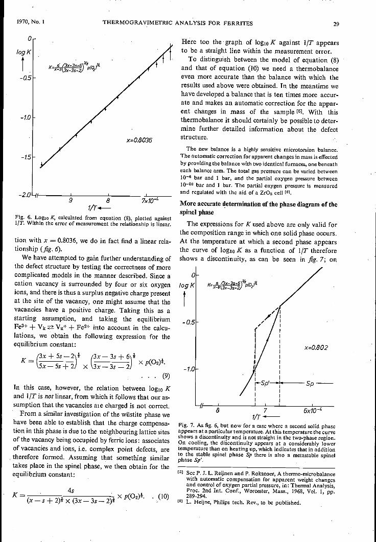
1970, No. 1 THERMOGRAVIMETRIC ANALYSIS FOR FERRITES 29
0
log K
- 0.5
-1.0
-1.5
-2.0-i9 8 7x10"
Fig. 6. Logio K, calculated from equation (8), plotted against1/T. Within the error of measurement the relationship is linear.
tion with x = 0.8036, we do in fact find a linear rela-tionship (fig. 6).
We have attempted to gain further understanding ofthe defect structure by testing the correctness of morecomplicated models in the manner described. Since acation vacancy is surrounded by four or six oxygenions, and there is thus a surplus negative charge presentat the site of the vacancy, one might assume that thevacancies have a positive charge. Taking this as astarting assumption, and taking the equilibriumFe3+ Vk ± Vk+ Fe2+ into account in the calcu-lations, we obtain the following expression for theequilibrium constant:
(3x + 5s -2\i(3x - 3s +K -5x - 5s + 2) x 3x - 3s -- 2 x p(02)+.
(9)
In this case, however, the relation between logio Kand 1/T is not linear, from which it follows that our as-sumption that the vacancies ate charged is not correct.
From a similar investigation of the wilstite phase wehave been able to establish that the charge compensa-tion in this phase is due to the neighbouring lattice sitesof the vacancy being occupied by ferric ions: associatesof vacancies and ions, i.e. complex point defects, aretherefore formed. Assuming that something similartakes place in the spinel phase, we then obtain for theequilibrium constant:
4sK - x p(02)+. . (10)(x -s x (3x - 3s - 2)i
Here too the -graph of logio K against 1/T appearsto be a straight line within the measurement error.
To distinguish between the model of equation (8)and that of equation (10) we need a thermobalanceeven more accurate than the balance with which theresults used above were obtained. In the meantime wehave developed a balance that is ten times more accur-ate and makes an automatic correction for the appar-ent changes in mass of the sample [5]. With thisthermobalance it should certainly be possible to deter-mine further detailed information about the defectstructure.
The new balance is a highly sensitive microtorsion balance.The automatic correction for apparent changes in mass is effectedby providing the balance with two identical furnaces, one beneatheach balance arm. The total gas pressure can be varied between10-6 bar and 1 bar, and the partial oxygen pressure between10-20 bar and 1 bar. The partial oxygen pressure is measuredand regulated with the aid of a ZrO2 cell 161.
More accurate determination of the phase diagram of thespinel phase
The expressions for K used above are only valid forthe composition range in which one solid phase occurs.At the temperature at which a second phase appearsthe curve of logio K as a function of 1/T thereforeshows a discontinuity, as can be seen in fig. 7; on
0
log K
-a5
-1.0
K- s ex -3.5'2678 4/1/4K -s 3x -3s- P -
8
x.0.802
r -Sp' Sp
I
7 6x;0"1/T
Fig. 7. As fig. 6, but now for a case where a second solid phaseappears at a particular temperature. At this temperature the curveshows a discontinuity and is not straight in the two-phase region.On cooling, the discontinuity appears at a considerably lowertemperature than on heating up, which indicates that in additionto the stable spinel phase Sp there is also a metastable spine!phase Sp'.
15) See P. J. L. Reijnen and P. Roksnoer, A thermo-microbalancewith automatic compensation for apparent weight changesand control of oxygen partial pressure, in: Thermal Analysis,Proc. 2nd Int. Conf., Worcester, Mass., 1968, Vol. 1, pp.289-294.
[8] L. Heijne, Philips tech. Rev., to be published.

30 PHILIPS TECHNICAL REVIEW VOLUME 31
cooling this discontinuity is obtained at a lower tem-perature indicating that there is a metastable spinelregion. If we determine a series of curves for variousvalues of x, we can then establish the boundaries of thetwo-phase region with great accuracy from the locationof these discontinuities (fig.8). The boundary of the spinelregion on the anion -deficient side cannot be determinedwith sufficient precision, but it appears from the curva-ture of the isotherms that FeO and MgO also dissolve.in the spinel phase, though only to a limited extent.In the related composition range anion vacancies willoccur.
As we noted in the introduction, knowledge of thedefect structure of the material is of great importance
Fig. 8. Detail of the phase dia-gram of the system MgO-FeO-Fe2O3 in the spinel region. Theisotherms have been derivedfrom thermograms like those offig. 2. The boundaries of thestable and metastable spinelphase (regions Sp and Sp') havebeen derived from the discon-tinuities in curves of the typeshown in fig. 7. yFe3u4
in the control of sintering processes. In these processes, where mass transport takes place by diffusion, theremust be a movement of both cations and anions. Therate of reaction is determined by the rate of diffusionof the slowest ion, which is the oxygen ion in the systemdiscussed above. In the presence of anion vacanciesoxygen ions can move much faster and therefore thematerial transport during sintering takes place morequickly. The prediction that this will result in a lessporous sintered product has been largely confirmed by
experiment [7].
03 P. J. L. Reijnen, Science of Ceramics 4, 169, 1968, and Reac-tivity of Solids, Proc. 6th Int. Symp., Schenectady 1968,p. 99.
Summary. Reactions and equilibria between solids and gases canbe investigated with a thermobalance, which is used to determinethe release or take-up of the gas as a function of temperature(and pressure). Great accuracy can be achieved with a thermo-balance even at high temperature. As an example a thermogravi-metric investigation of the system MgO-FeO-Fe2O3 is described,carried out between 1000 and 1400 °C at atmospheric pressureon samples of mass about 5 g; the change in mass could bedetermined with an accuracy of 0.1 mg. After a discussion of thedetermination of the phase diagram, it is explained how a know -
Mg Fe204
1000°C
1100
1150
1200
1250
Fe203
ledge of the defect structure of the spinel phase can be obtainedby testing models of the equilibrium between the spinel phaseand oxygen against experiment. It is shown that the equi-librium equation should, include cation vacancies, which are notcharged. It is likely that neighbouring ferric ions compensatethe negative charge of the oxygen ions surrounding the cationvacancies. In addition a small composition region containinganion vacancies has been brought to light. An improved micro -torsion balance has been developed, whose accuracy is ten timesbetter.

1970, No. 1 31
Recent scientific publicationsThese publications are contributed by staff of laboratories and plants which form partof or co-operate with enterprises of the Philips group of companies, particularly by staffof the following research laboratories:
Philips Research Laboratories, Eindhoven, NetherlandsMullard Research Laboratories, Redhill (Surrey), EnglandLaboratoires d'Electronique et de Physique Appliquee, Limeil-Brevannes (Val-
de -Marne), FrancePhilips Forschungslaboratorium Aachen GmbH, WeiBhausstraBe, 51 Aachen,
Germany APhilips Forschungslaboratorium Hamburg GmbH, Vogt-K4511n-StraBe 30,
2000 Hamburg 54, GermanyMBLE Laboratoire de Recherches, 2 avenue Van Becelaere, 1170 Brussels
(Boitsfort), Belgium.
Reprints of most of these publications will be available in the near future. Requests forreprints should be addressed to the respective laboratories (see the code letter) or to PhilipsResearch Laboratories, Eindhoven, Netherlands.
D. Andrew: The role of energetic neutrals in a magne-tron sputter ion pump.Brit. J. appl. Phys. (J. Physics D), ser. 2, 2, 1609-1615,1969 (No. 11).
P. M. van den Avoort: Traitement des signaux dansle tube index.Onde electr. 48, 921-924, 1968 (No. 499).
R. Bleekrode & J. W. van der Laarse: Optical deter-mination of Cs ground -state depletion in Cs-Ar low-pressure discharges, II. Radial and axial Cs -atomdistributions.J. appl. Phys. 40, 2401-2403, 1969 (No. 6).
P. J. C. Bogers & A. J. G. Op het Veld: A procedurefor making electric contact with embedded very thinwires or other very small specimens for electrolyticpolishing or etching.Pract. Metallogr. 6, 503-504, 1969 (No. 8).
B. Boittiaux, E. Constant, B. Kramer, M. Lefebvre, G.Vaesken (all with Faculte des Sciences de Lille) & A.Semichon: Proprietes generales des diodes semi-conductrices en regime d'avalanche.Acta electronica 12, 157-200, 1969 (No. 2).
P. B. Braun, J. Hornstra & J. I. Leenhouts: The crys-tal -structure determination of seven 9/3,10a -steroids.Philips Res. Repts. 24, 427-474, 1969 (No. 5).
J. C. Brice: The effect of kinetics on the stability ofcrystal interfaces during growth.J. Crystal Growth 6, 9-12, 1969 (No. 1).
K. H. J. Buschow & A. S. van der Goot: Phase re-lations, crystal structures, and magnetic propertiesof erbium -iron compounds.Phys. Stat. sol. 35, 515-522, 1969 (No. 1).
F. J. du Chatenier & J. van den Broek: Electricalproperties of vapour -deposited layers of red leadmonoxide.Philips Res. Repts. 24, 392-406, 1969 (No. 5).
T. Chisholm: Some comments on the paper "Anopto-electronic cold cathode for cathode-ray tubes".Solid -State Electronics 12, 925-926, 1969 (No. 11). M
H. Dammann: Computer generated quaternary phase-only holograms.Physics Letters 29A, 301-302, 1969 (No. 6).
M. Davio & J. P. Deschamps: Classes of solutions ofBoolean equations.Philips Res. Repts. 24, 373-378, 1969 (No. 5).
S. Garbe: Factors affecting the photoemission fromcaesium oxide covered GaAs.Solid -State Electronics 12, 893-901, 1969 (No. 11). A
Y. Genin & A. Thayse: Analysis of satellite -orbitperturbations due to forces deriving from a potential.Philips Res. Repts. 24, 477-558, 1969 (No. 6).
E. E. Havinga, J. H. N. van Vucht & K. H. J. Buschow:Relative stability of various stacking orders in close -packed metal structures.Philips Res. Repts. 24, 407-426, 1969 (No. 5).
K. R. Hofmann: Some aspects of Gunn oscillationsin thin dielectric -loaded samples.Electronics Letters 5, 227-228, 1969 (No. 11). E
K. R. Hofmann: Gunn oscillations in thin sampleswith capacitive surface loading.Electronics Letters 5, 289-290, 1969 (No. 13).
M. G. Hulyer: Still picture television.Roy. Telev. Soc. J. 12, 170-174, 1969 (No. 8).

32 PHILIPS TECHNICAL REVIEW VOLUME 31
Y. Kamp & J. Neirynck: Image parameter theory fornoncommensurate transmission lines.Archiv elektr. Ubertr. 23, 129-136, 1969 (No. 3). B
F. M. Klaassen: A computation of the high -frequencynoise quantities of a MOS-FET.Philips Res. Repts. 24, 559-571, 1969 (No. 6).
J. E. Knowles: A sensitive apparatus for the measure-ment of induced magneto -crystalline anisotropy.J. sci. Instr. (J. Physics E), ser. 2, 2, 917-920, 1969(No. 11).
W. G. Koster & J. B. Peacock (Institute for PerceptionResearch, Eindhoven): The influence of intensity ofvisual stimuli on the psychological refractory phase.Acta psychol. 30, 232-253, 1969.
J. Liebertz & P. Quadflieg: Einkristallziichtung andeinige physikalische Eigenschaften von. Langbeinit(K2Mg2(SO4)3).J. Crystal Growth 6, 109-110, 1969 (No. 1). A
J. Liebertz & G. Rosenstein: Untersuchungen imSystem LiNbO3-MgTiO3.Ber. Dtsch. Keram. Ges. 46, 548-550, 1969 (No. 10). A
G. J. Lubben: Le tube index.Onde electr. 48, 918-920, 1968 (No. 499).
R. J. Meijer: The Philips Stirling engine.Ingenieur 81, W 69-79, W 81-93, 1969 (Nos. 18, 19). E
C. van Opdorp & J. Vrakking: Avalanche breakdownin epitaxial SiC p -n junctions.J. appl. Phys. 40, 2320-2322, 1969 (No. 5).
J. Robillard: Application de la physique de l'etatsolide aux systemes d'affichage d'information.Rev. fr. Inform. Recherche open 2, No. 15, 53-84,1968.
P. J. Rommers & J. Visser: Spectrophotometricdetermination of micro amounts of nitrogen as indo-phenol.Analyst 94, 653-658, 1969 (No. 1121).
W. Schilz: Helicon wave propagation in a two -component solid state plasma.Phys. Stat. sol. 34, 213-220, 1969 (No. 1).
M. Valton: Mecanismes physiques de l'avalanchedans les semiconducteurs.Acta electronica 12, 131-155, 1969 (No. 2).
M. T. Vlaardingerbroek, P. M. Boers & G. A. Acket:High -frequency conductivity and energy relaxation ofhot electrons in GaAs.Philips Res. Repts. 24, 379-391, 1969 (No. 5).
J. H. Waszink & J. Polman: Cesium depletion in thepositive column of Cs-Ar discharges.J. appl. Phys. 40, 2403-2408, 1969 (No. 6).
Contents of Philips Telecommunication Review 28, No. 4, 1969:
C. J. Krayenbrink: AIRLORD Mk2, pre -departure handling system for airports (pp. 161-173).H. J. Spoon: The telegraph input-output multiplexer for the DS 714 message switching system (pp. 175-183).
E. A. Limberopoulos: Two new message switching centres for the SITA network (pp. 184-187).
Contents of Mullard Technical Communications 11, No. 103, 1970:
A. Lindell: "Electronic parts of assessed quality": an outline of the BS9000 scheme (pp. 50-57).
M. C. Gander: Integrated video pre -amplifier, sync, a.g.c. and noise protection system for monochrome re-
ceivers (pp. 58-65).D. J. Beakhust: Decoding circuits with colour -difference output (pp. 66-73).
J. Merrett: Dynamic stability of thyristor single-phase motor speed -control systems for d.c. shunt machines
(pp. 75-80).
Contents of Valvo Berichte 15, No. 3, 1969:
P. G. J. Barten: Theorie des Moire bei Schattenmasken-Farbbildriihren (pp. 79-92).
C. J. Boers: Hochspannungserzeugung aus dem Zeilenriicklauf-Impuls (pp. 93-108).
Volume 31, 1970, No. 1 pages 1-32 Published 19th Aug. 1970

PHILIPS TECHNICAL REVIEWVOLUME 31, 1970, No. 2
Photomagnetic effectsU. Enz and R. W. Teale
In recent years some interesting effects have been found, in a number of magnetic substances,that can be considered as a counterpart to the magneto -optical phenomena discovered byFaraday in the 19th century. Until recently research on these photomagnetic effects hasbeen mainly concerned with their basic physics. The article below gives a survey of thiswork. The applications envisaged for photomagnetics are mainly in the field of informationstorage.
For some years substances have been known whosemagnetic properties can be influenced by infra -red orvisible light irradiation. These photomagnetic effects,in which photons bring about changes in the magneticproperties of the material, must be distinguished frommagneto -optical effects (such as Faraday rotation),where the material's optical properties depend on itsstate of magnetization. In the cases investigated so far,the photomagnetic effects have only been found attemperature below ambient. At a sufficiently lowtemperature the change is permanent but at somewhathigher temperatures the initial state returns after theirradation has stopped.
The first observation of a photomagnetic effect wasthe discovery that the extra magnetic anisotropy ofsilicon -doped yttrium iron garnet, caused by coolingin a magnetic field, could be changed by illuminationwith an incandescent lamp [1] ("photomagneticanneal"). Soon afterwards we observed associatedeffects, such as changes of initial permeability andcoercive force induced by illumination, in experimentsboth on yttrium iron garnet [2] [4] and on gallium -doped CdCr2Se4 [3] [4].
All these phenomena may be explained in terms ofan internal photoeffect; an electron bound to aparticular lattice site at low temperature is able tomove under illumination. This electron movement isequivalent to the displacement of a polyvalent ion.If the structure of the lattice is such that ions of a
Dr. U, Enz is with Philips Research Laboratories, Eindhoven.Dr. R. W. Teale is a Senior Lecturer in Physics at the Univer-sity of Sheffield.
particular valency influence the magnetic propertiesof the substance differently depending on their sitein the lattice, then the direct consequence of theapparent displacement of the ions as a result ofillumination is a change in the value of the magneticquantities.
We shall first give some observations of the photo -
magnetic anneal in yttrium iron garnet, and thendescribe measurements of the effect of illumination onthe initial permeability and coercive force, both foryttrium iron garnet and CdCr2Se4. In both cases theobservations will be followed by an explanation givenin terms of a model. A comparison of these two modelsgives an understanding of the conditions under whichthe effects occur.
In conclusion some possible applications of thephotomagnetic effects are mentioned.
Photomagnetic anneal
Yttrium iron garnet (usually abbreviated to YIG), thefirst substance whose magnetic anisotropy was found tobe modified by light [1], owes its name to the correspon-dence in structure with the semi-precious stone garnet.The pure substance has the formula Y3Fe5O12 and isknown only in synthetic form. The silicon -dopedmaterial used for our experiments had the nominalchemical composition Y3Fer2x (Fe24-Si4+)z012 where
[1] R. W. Teale and D. W. Temple, Phys. Rev. Letters 19,904, 1967.
[2] U. Enz and H. van der Heide, Solid State Comm. 6, 347, 1968.13) W. Lems, P. J. Rijnierse, P. F. Bongers and U. Enz, Phys.
Rev. Letters 21, 1643, 1968.[43 U. Enz, W. Lems, R. Metselaar, P. J. Rijnierse and R. W.
Teale, IEEE Trans. MAG-5, 467, 1969 (No. 3).

34 PHILIPS TECHNICAL REVIEW VOLUME 31
0.1 < x < 0.3 at synthesis. Subsequent analysis of thematerial yielded lower values. So tetravalent silicon hasbeen substituted for part of the trivalent iron. Tocompensate the resultant surplus charge an equalnumber of ferric ions has been reduced to ferrous ions.
The photomagnetic-anneal effect has been observedin single -crystal samples, of the given composition,by magnetic resonance experiments. In a single crystalof magnetic material, the magnetization shows apreference for one or more directions in the crystalstructure, and the magnitude of this preference can beexpressed in terms of an anisotropy field. In YIG, thepreferred directions are the body diagonals of the cubicunit cell, the crystallographic <111> directions. Ourexperiments were magnetic resonance experiments,but we shall not describe them in detail here. In theexperiments the sum of the applied external field and theanisotropy field in the same direction is kept constant,at a known value. Hence the anisotropy field may bederived by measuring the required value of the appliedfield strength.
A single -crystal sphere of this material with a dia-meter of 0.4 mm is cooled to 20 °K in a strongmagnetic field in the dark. The magnetic field is
applied parallel to one of the body diagonals of thecubic unit cell of the substance (the crystallographic[111 ] direction). If we keep the sample in the darkbut now re -apply the external field in the direction ofone of the other body diagonals of the unit cell (inthis case the [1 11] direction), we find that a strongermagnetic field is now needed to produce resonance.This means that the anisotropy field, which assists theapplied field, is weaker in the [111 ] than in the [111 ]direction. This implies that there is now a frozen -inpreference for magnetization in the [111] direction,the original direction of the applied field.
In contrast to other materials which can be observedto have a frozen -in state of magnetization, the direc-tion of the frozen -in anisotropy of silicon -doped YIGcan be changed by illuminating the sample with anincandescent lamp (fig. 1). This is the effect we havecalled the photomagnetic anneal. As can be seenin the figure, some relaxation of the frozen -in anis-otropy occurs in the dark as well. The change in theanisotropy which is caused by the illumination dependson the temperature to which the sample has beencooled. Thus, in fig. 1 the difference z1H between thefinal levels of the curves a and b is 140 Oe for a sampletemperature of 20 °K. The same sample gives ZIH -=200 Oe at 4.2 °K; z1H only reaches 21 Oe at 66 °K.
The structure of yttrium iron garnet
Before outlining the model used to explain theobserved effects, we shall describe the structure of
YIG. The undoped material has a cubic structure inwhich all Fe ions are trivalent. These ions, however,occupy two different types of sites in the lattice:.sites surrounded tetrahedrally and sites surroundedoctahedrally by oxygen ions. The octahedrally sur-rounded Fes+ ions form a body -centred cubic struc-ture. A three-dimensional representation of the struc-ture is shown in fig. 2.
In the immediate environment of an octahedral Fe3+ion the Y3+ ions, which can be distinguished in twogroups of three, define a local threefold axis. Thislocal threefold axis coincides with one of the bodydiagonals of the cubes of the body -centred lattice,the crystallographic (111> directions. NeighbouringFes+ ions in octahedral coordination always have adifferent one of the four possible <111> directionsas local threefold axis.
If part of the Fes+ in Y3Fe501.2 is replaced by Si4+,these silicon ions will always occupy sites tetrahedrallysurrounded by oxygen.
Explanation of the observations
The observations may be explained as follows.There are four possible types of sites for the Fe2+ ionneeded for charge compensation, that is to say there
27kOe
H2
26
H1
I250to 50 t 100 min
Fig. 1. Photomagnetic anneal of single crystal Y3Fe4.oSio.1012.The strength H2 of the external field needed to keep the ferro-magnetic resonance frequency constant with magnetization inthe [11I] difection gives a measure of the anisotropy. Thematerial is cooled in the dark to 20 °K in an external field in the[111] direction. The magnetic anisotropy then correspondsto the level of applied field indicated as Hi. At the time t = 0the field is rotated to the [1 1 I] direction.
Curve a relates to a sample that was not illuminated; somerelaxation of the anisotropy is observed. Curve b relates to asample that was illuminated with an incandescent lamp fromthe time t = to. In this case there is complete relaxation of theanisotropy, i.e. after exposure to light there is an anisotropyfield in the [111 ] direction of approximately the same magnitudeas the original anisotropy field in the [1 1 1 ] direction.

PHOTOMAGNETIC EFFECTS
0: Fe3+ y.3. 0: 02'
/1
--.--
1 \/ \
Fig. 2. Crystal structure of Y3Fes012 5] (yttrium iron garnet or YIG). The right-hand picturegives the complete unit cell; the left-hand picture shows the details of one octant of this cell.The positions of the ions in the complete cell are obtained when the octant given is broughtinto line with the octants of the complete cell in such a way that the diagonals indicated in redcoincide.
The Fe3+ ions shown as full dots are surrounded octahedrally by six oxygen ions on octa-hedral sites and form a body -centred cubic lattice. The Fe3+ ions shown as black rings aresurrounded by four oxygen ions on tetrahedral sites. Two Fe3+ ions, (A and B in the diagram)are shown surrounded by six and four oxygen ions respectively as full blue dots. The otheroxygen ions are indicated by blue rings. The two groups of three Y3+ ions that define a localthreefold axis at the site of the Fe3+ ion A are connected by red triangles. The local three-fold axis coincides with the diagonal given in red.
are four types of sites where the extra electron sup-plied by SO+ can be localized. These are the octa-hedral sites, with the four different directions for thelocal threefold axis. When an external field is applied,that position whose local threefold axis makes thesmallest angle with the direction of the field is energet-ically somewhat more favourable than the siteswith the axis along the other three <111> directions.The energy difference is small compared with thermalenergy at room temperature. However, at 20 °K it issufficient to cause an observable over -occupation ofthe energetically more favourable positions, and thusmake the anisotropy field stronger in the directionof this particular threefold axis.
At 20 °K the electrons are not sufficiently mobile toallow the occupation of the available sites to adjustspontaneously to the change in the potential -welltopography caused by a change in direction of the mag-netic field. It is only when energy is supplied by thephotons injected upon illumination that the electronsare able to move, as a result of which the electrondistribution, and hence the magnetic anisotropy, canadjust to the new direction of magnetization.
The changes are certainly not due to the heating ofthe crystal by the light source; in our experiments thepower radiated into the crystal was too low to cause
any appreciable rise in the temperature of the sample.What we have said above implies that the light is
unpolarized. In experiments [61 in which the samplewas illuminated with polarized light, it was foundthat the final state reached did show a small variation,which was dependent on the position of the plane ofpolarization relative to the crystal axes.
The effect of illumination on initial permeability andcoercive force
At much smaller silicon concentrations than thosefor which the photomagnetic anneal is observable,the illumination can affect the initial permeabilityand the coercive force of yttrium iron garnet. Weobserved this effect for garnets having the compositionY3Fes_xSix012, with x < 0.05 [21[41 at synthesis; atthis composition the photomagnetic-anneal effect isvery weak.
For the measurement of permeability and coerciveforce, we used small frames cut from single crystals andrings of polycrystalline material made from pressedand sintered powder (fig. 3).
[5] Adapted from P. P. Ewald and C. Hermann, Strukturbericht1913-1926, page 364.
[6] R. W. Teale, D. W. Temple, U. Enz and R. F. Pearson,J. appl. Phys. 40, 1435, 1969 (No. 3).

36 PHILIPS TECHNICAL REVIEW VOLUME 31
(tie) yr90°
Fig. 3. Measurement of initial permeability and coercive force(schematic). The primary winding carries a sinusoidal currentof 10 KHz frequency. The relation between B and H, the hystere-sis loop (except for a phase shift equal to the relation betweenVsec and iprlm) is displayed on a cathode-ray oscilloscope. Whenthe magnitude of iprim is small the B -H curve is a line whoseslope is equal to the initial permeability; when the amplitudeof iprim is sufficiently large, an open hysteresis loop is displayed.
In measurements on single -crystal material diamond -shapedframes are used whose sides coincide with the (11I) directionsof the crystal; for polycrystalline material small rings are used.
The sample is cooled in the dark to 77 °K and de-magnetized by means of a monotonically decreasingalternating magnetic field. When the sample is illumin-ated with light from an incandescent lamp, the initialpermeability decreases. This decrease is larger, andoccurs in a much shorter time, in the polycrystal-line rings than in the single -crystal frames (fig. 4).
By using intermittent light we found that the changein the initial permeability depends on the quantity ofabsorbed radiation. When the same average power as
120
100Fir
--,, 0
b0r 6
5Pr
4 1
3
2
1
1 10 ibo sbos°
Fig. 4. Variation of initial permeability it, of yttrium iron garnetas a function of the time t elapsed since the beginning of theillumination of the sample, at a temperature of 77 °K. Curve arelates to polycrystalline material of composition Y3Fe3-2Six012with x = 0.006, curve b to single -crystal material of compositionY3Fe5_xSi.01.2 with x = 0.05.
In order to present the widely different behaviour of bothsamples in one figure, a logarithmic time scale is used. Thepermeability values at the moment t = 0 are indicated for bothsamples with horizontal arrows, denoted ao and bo.
180 -
60
40 -
20
0 '
0.1
in the continuous illumination experiments is suppliedin a rapid succession of flashes, the decrease ofpermeability follows exactly the same course as undercontinuous irradiation. When a sample is illuminatedwith flashes at such a slow rate that the effect of eachindividual flash can be seen, a stepwise decrease ofpermeability is observed (fig. 5).
The maximum permeability change Apr that can bebrought about by illumination depends on the tem-perature to which the material has been cooled. Atabout 120 °K the value of ZI,ur decreases sharply asthe temperature increases, and above 200 °K theeffect has entirely disappeared.
40
Pr
20
10t, rI
VO 1 2 3 4min.
Fig. 5. Decrease of the initial permeability itr of single -crystalyttrium iron garnet of composition Y3Fe3,Six012 (x = 0.025)as a result of illumination at 77 °K. The dashed curve relates tocontinuous irradiation with an intensity of 10-2 W/cm2, thefull curve to illumination in flashes (with the same average inten-sity) at the times ti, t2, t3 and t4. In the latter case the decreasealways takes place within 10-2 seconds; the subsequent slightincrease following each decrease of the permeability is presum-ably due to temperature effects. The integrating character of theeffect can clearly be seen here.
As long as the temperature of the illuminated sampleis kept below 150 °K, the permeability remains low.After the illumination is removed the permeabilityonly returns to its original value when the temperaturehas risen to a value at which the electrons have becomesufficiently mobile. This change in the initial permea-bility of yttrium iron garnet is only caused by radia-tion with a wavelength less than 1.3 rim.
The coercive force of yttrium iron garnet is alsoaffected by electromagnetic radiation at low temper-ature. Fig. 6 shows there is a marked change in the formof the hysteresis loop when the sample is illuminated.Again, this effect is much stronger in polycrystallinethan in single -crystal samples (Table I). An interesting

1970, No. 2 PHOTOMAGNETIC EFFECTS ' 37
Table I. Coercive force of yttrium iron, garnet of the compositionY3Fes-zSi.01.2 at 77 °K.
x unilluminated illuminated
Single crystal 0.025 0.5 Oe 0.8 OePolycrystalline
material 0.006 0.6 Oe 2.0 Oe
demonstration can be given with the set-up shownin fig. 3. The amplitude of the primary alternatingcurrent is set at a value such that the maximum pri-mary field strength is only just higher than the coerciveforce of the unilluminated material. The hysteresis loopof the material is then described once in each currentcycle. When the ring is illuminated, the coercive forceof the material increases and the primary field cannotreverse the direction of magnetization. The hysteresisloop is then no longer described. Only when the ampli-tude of the primary alternating field is increased doesthe hysteresis loop reappear, but in a considerablydifferent shape.
Explanation of the observed effects
Previously in our explanation of the photomagneticanneal effect, we characterized the octahedral sites inthe YIG lattice by the different orientations of thelocal threefold axes. We now need to make a seconddistinction: between sites in the immediate environ-ment of an Si4+ ion and sites at a greater distancefrom it. The octahedral sites near an Si4+ ion arereferred to as type I sites, those at a greater distanceare called type H sites. Owing to Coulomb forces be-tween Si4+ and Fe2+ ions, the Fe2+ ions at type I siteshave a smaller potential energy than those at the typeII sites.
When the material has been cooled, the Fe2+ ionswill be localized at type I sites. Upon irradiation, elec-
Fig. 6. The hysteresis loop of po ycrystalline yttrium iron garnet,of composition Y3Fes,Si.012, with x = 0.006, measured at77 °K. Loop a was measured on unilluminated material, loop bon illuminated material. The irregularities in curve a are dueto the Barkhausen effect, i.e. the discontinuous displacement ofdomain walls in a continuously changing external field.
trons, and therefore effective Fe2+ ions, can move totype II sites (dissociation of the Si4+-Fe2+ pair).Now if the temperature is low enough, the electronswill be relatively immobile and will remain localizedat the type II sites. At a somewhat higher temperaturea spontaneous return to type I sites will occur. Wemust now assume that a magnetic domain wall ismore strongly bound to Fe2+ ions which occupytype II sites than to those in type I sites. This strongerbinding results in a greater resistance of the materialto changes in magnetization [7], which is reflected in alower initial permeability and a higher coercive force.
Observations on CdCr2Se4
As well as the photomagnetic changes in silicon-
doped YIG, we also found that illumination affectsthe initial permeability of CdCr2Se4 in which trivalentgallium is substituted for part of the divalent cad-mium [3]. At temperatures below 130 °K this material isferromagnetic. The samples investigated had thecomposition Cdi_yGayCr2Se4 with y = 0.015.
At 4.2 °K, illumination causes a virtually permanentchange in the initial permeability, whereas at 77 °Kthe original state returns when the illumination isremoved (fig. 7). As in the case of YIG, the effectcan be explained by assuming two types of site.
50 100 s
Fig. 7. Change of initial permeability upon the illumination ofCdi-yGavCr2Sed, with y = 0.015, as a function of time, at twotemperatures. The permeability values in the unilluminatedstate (ltd) and the saturation value of the permeability duringillumination (us) are indicated. Three stages are clearly distin-guishable: I, the permeability decreases at the beginning ofillumination; II, the permeability reaches a stable final value (us)whose level is determined by the illumination intensity; III,the permeability recovers after the illumination has stopped(virtually no recovery at 4.2 °K owing to the very low mobilityof the electrons at that temperature).
171 With this type of material the permeability is mainly gov=erned by the motion of domain walls, which separate homoge-neously magnetized domains with different directions ofmagnetization.

38 PHILIPS TECHNICAL REVIEW VOLUME 31
Again illumination converts a type I site into a type IIsite and hence the domain walls are more stronglybound to their instantaneous position in the crystallattice.
For a particular. material, at a fixed temperature,the value ,us, to which the initial permeability decreasesupon illumination, is solely a function of the intensityof illumination. From the experimentally determinedshape of this function and the measured behaviourof ,ur during the recovery following the illumination(phase /// in fig. 7) we can calculate the time dependenceof the permeability at the beginning of the illumination(phase I). Good agreement is found between thecalculated curve for the change in the magnetic stiffness14ur and the experimental data (fig. 8).
The assumptions underlying the calculation are the following.1) The change in the magnetic stiffness (the reciprocal of thepermeability) as a consequence of the occupation of type II sitescaused by illumination is at every instant proportional to thenumber of occupied type II sites a [81:
LI /1-1 = C/I (1)
where a is a function of the time t and intensity I of the illumin-ation. (kt is written without subscript in the text below.)2) Both during and after illumination, recombination of theCr2÷-Ga3+ pairs occurs at a rate which is proportional bothto the number of occupied type II sites and to the number ofvacant type I sites. The number of vacant type I sites is alsoequal to a, and so the rate of recombination is proportional to n2.3) The dissociation rate of the Cr2+-Ga3+ pairs (occupation rateof type II sites) is proportional to the illumination intensity Iand to the number of type I sites occupied at any given instant.This number amounts to no-a, where no is the number of Ga3+ions and hence also the maximum available number of type I sites.
The net rate of occupation of the type II sites, that is, thedifference between the dissociation rate and the recombinationrate of Cr2+-Ga3+ pairs, may be obtained from the results ofassumptions 2) and 3). Thus,
= 13I(ao-a)-ant , (2)
where a and fl are proportionality constants.With the boundary condition n = 0 for t = 0, i.e. all type II
sites are vacant before the beginning of illumination, the solutionof the differential equation (2) is:
2non(t) -
1 z coth (4-13Izt)'
where z2 = 1 + 4amolf3I. After a sufficient time of illumination,n reaches the stationary value as:
ns = 2a01(1 z) (4)
and consequently the change in the magnetic stiffness reaches astationary value which is a function of the illumination intensity:
/2-1)s = Gas .
(3)
(5)
Equation (4) and (5) give a relation between the saturationvalue of the change of stiffness (z1 ic-1)s and the illuminationintensity. By fitting this curve to the experimentally determinedcurves we can obtain numerical values for a1/3 and C.
The recovery of the magnetic stiffness after the illumination
has been switched off at the moment t = 0 is found from thedifferential equation (2) with I = 0 and taking as the boundarycondition a = as for t = 0. The solution in this case is:
1 1
n(t) ns + atwhich, after being divided by C, becomes
(6)
1 1 aCas C
t.
The experiments have confirmed that the reciprocal of thechange in magnetic stiffness after illumination has ended isindeed a linear function of time. The slope of the straight linefound by experiment yields a/C and hence a, so that all para-meters are now established and the time dependence of themagnetic stiffness after switching on the illumination can becalculated.
1.5x10³
z
11.0
a5
0 .5 10 15 , 20s
Fig. 8. Change of magnetic stiffness .4 ic-1 (the change of thereciprocal of permeability) of Ccli_vGavCr2Se4 (y = 0.015), as afunction of the time after the beginning of illumination withan incandescent lamp (illumination intensity 9 x 10-$ W/cm2,temperature of sample 77 'K). The points give the experimentalresults. The solid line indicates the expected behaviour ascalculated from relation (3).
Compatibility of the two models
We have described two photomagnetic effects andexplained them in terms of two different models. Thequestion is, do these two models give rise to contra-dictions? We can get some insight into this by count-ing the number of sites available for the ferrous ionsin both cases. Such a count also indicates the limitsof the dope concentration regions in which the twoeffects occur.
The formula for yttrium iron garnet can be writtenas Y3Q2R3012, where Q are the metal ions that aresurrounded octahedrally by oxygen and R metalions surrounded tetrahedrally. For material dopedwith x atoms of silicon per molecule this results inY3(Fe2-Fx Fer) (Ferx six4+)012. We see that a fractionx/3 of the tetrahedral sites is occupied by silicon,and further that there are 2/3 octahedral sites per

1970, No. 2 PHOTOMAGNETIC EFFECTS 39
tetrahedral site. The number of octahedral sites 1
available per Si ion for the associated Fe2+ ion is 1 =(2/3) (3/x) = 2/x. The photomagnetic anneal has beenobserved for 0.1 < x < 0.3, in which case 6.6 < / < 20.For an Si ion the number of nearest -neighbour sitessurrounded octahedrally is four and the number ofnext -nearest -neighbour octahedral sites is eight.With a maximum of twenty available sites for anFe2+ ion there can therefore be no question of theexistence of type II sites at a considerable distancefrom an Si ion, which we used to explain the permea-bility effect. It is also plausible that for x > 0.3 thephotomagnetic anneal will get smaller because inthis case many Si ions will have less than four sitesavailable for the Fe2+ ion.
For x <0.05-the condition for the occurence of thepermeability effect-we have 1> 40, so that the type IIsites necessary for this effect will be numerous. Theconcentration of Si ions, and hence of Fe2+ ions,has now become so small however, that the photo-
magnetic anneal is no longer observable. Thus it isapparent that the two models do not exclude oneanother but they are, in fact, complementary.
Unfortunately, there are not sufficient experimentaldata available to allow us to construct a single modelwhich explains all the observed effects.
At present no practical applications of the photo-
magnetic effects are known to exist. One difficulty isthat the effects have, so far, only been found at verylow temperatures. The search for applications can beusefully complemented by a search for materialsthat show these effects at higher temperatures [91.
Conceivable applications are photomagnetic radia-tion detectors, whether or not of the integrating type,
and optically controlled inductors. Other possibilitiesare magnetic xerography and the photomagneticstorage of information. For this application a slice ofgarnet is uniformly magnetized and then made magnet-ically hard at appropriate places by illumination. Anexternal field is now applied of such orientation andmagnitude as to reverse the direction of magnetizationof the unexposed parts but not that of the exposedparts, so that the light pattern projected on to the sliceis converted into a pattern of different directions ofmagnetization. In a ferrite -core memory certaincores could be illuminated in order to prevent reversalof their magnetization upon the arrival of the nextcontrol pulse.
18] The basic physics of this relationship has been discussed byW. Lems, R. Metselaar, P. J. Rijnierse and U. Enz in Z.angew. Phys. 29, 87, 1970 (No. 1) and in J. appl. Phys. 41,1248, 1970 (No. 3).
[9] Recently materials have been found that show the phenom-ena reported here up to temperatures of 200 °K: Th. Holtwijk,W. Lems, A. G. H. Verhulst and U. Enz, IEEE Trans. onMagnetics (to be published).
Summary. The direct influence of electromagnetic radiation onmagnetic properties has been detected at low temperatures(T < 150 °K) in Si -doped YIG (Y3Fes-xSix012) and in Ga-dopedCdCr2Se4 (Cd1-yGayCr2Se4). Its manifestations are 1) a changein magnetocrystalline anisotropy observed in ferromagneticresonance experiments at high doping levels (0.1 <x<0.3) and2) a reduction in initial permeability and an increase in coerciveforce occurring for low doping levels (x < 0.05, y = 0.015).These changes are produced by irradiation with light of wave-length < 1.3 1./.m and are attributed to light -induced electrontransfer resulting in a redistribution of Fe2+ (or Cr2+) ions.At low temperature the redistribution and its manifestations arepermanent; at higher temperature there is a relaxation due tothermal electron motion. The magnitude of the effects dependsupon the product of light intensity and irradiation time. Quanti-tative results of a simple two -centre model are shown to agree wellwith experiment. Potential applications are in the field of infor-mation storage and processing.

40 PHILIPS TECHNICAL REVIEW VOLUME 31
A vibrating -reed magnetometer for microscopic particlesH. Zijlstra
The search for still better materials for permanent magnets has long been hampered by asuccession of problems. A new and highly sensitive magnetometer has now been developedthat eases many of the difficulties and opens the way to many new studies. The high sen-sitivity, achieved by ingenious use of a mechanical resonance, is sufficient to enable thehysteresis loops of individual microscopic particles to be determined with ease. Changes inmagnetic moment of less than 5 x 10-18 Wb m have been measured. The results achievedwith these new measurements have already had a considerable impact on the theoreticalapproach to magnetic processes involving only a few domains.
Investigation of microscopic particles
To improve powder materials for permanent mag-nets it is necessary to determine the hysteresis loops ofparticles whose dimensions lie between 0.1 and 5µm.This is the size of the crystallites in the familiar ferrox-dure material and in the new magnetic material SmCo5,an intermetallic compound of samarium and cobalt [1].The magnetic moments [2] of such microscopic par-ticles are about 10-16 Wb m. The magnetic processesin particles of this size extend over only a few domains.The main object of the research into these materialsis to establish the influence of the crystal structure -with any defects - and of the impurities on the coer-civity. The new magnetometer [3] that we shall de-scribe here plays a useful part in this research. Measure-ments with this instrument have already confirmedthat the present idea behind the choice of grain sizein magnetic powders - that there is a critical size -isnot very relevant and should make way for the idea ofcritical fields [4]. The results prove, moreover, thattheoretical considerations limited to only one domainhave little practical significance. We shall return to thecritical fields in the last section of this article, in which wediscuss a measurement made with the new instrument.
Most magnetometers are inadequate for suchinvestigations. Even for magnetic moments of about10-15 Wb m - which could be typical for particles100 p.m across - the output signal is too small to beusable. The new instrument meets all the requirementsimposed by the investigation of magnetic powders.It is about a hundred times more sensitive than othermagnetometers, yet is no more susceptible to inter-fering signals.
Dr. Ir. H. Zijlstra is with Philips Research Laboratories, Eind-hoven.
The new magnetometer
The new magnetometer is a simple instrument whichis easy to use and works by the method due to Curie(and Faraday). This method is based on the forceexperienced by a sample particle in a non -uniformmagnetic field. This force is equal to m dH/dz, theproduct of the magnetic moment m to be determinedand the known gradient of the magnetic field strengthH. The instrument measures the effect of the force,the displacement of the particle in the z -direction.
We have achieved the high sensitivity by using aperiodic displacing force whose frequency is equal tothe mechanical resonance frequency of a short wirewhich carries the sample particle at one end [6].
Instead of a single very small deflection (the static case)there is a periodic deflection which is about a hundredtimes larger because of the resonance and thereforereadily observable. The arrangement is shown infig. I. The test particle is attached by adhesive [6] tothe free end of a thin gold wire (the "reed"), which ishorizontal when not in vibration. The other end ofthe wire is clamped in a supporting block. The wire ismade short enough for the resonant frequency to be
K. H. J. Buschow, W. Luiten, P. A. Naastepad and F. F.Westendorp, Philips tech. Rev. 29, 336, 1968.The SI unit of magnetic moment is the weber m; the electro-magnetic unit of magnetic moment (the erg/oersted), whichcorresponds to 47C X 10-10 weber m, is still frequently en-countered.See also H. Zijlstra, A vibrating -reed magnetometer formicroscopic particles, Rev. sci. Instr. 41, 1241-1243, 1970(No. 8).H. Zijlstra, Coercivity and wall motion, paper presented atSecond European Conference on Hard Magnetic Materials,Milan, September 1969, in IEEE Trans. MAG-6, 179-181,1970 (No. 2).The method of measuring magnetic susceptibility proposedby Y. L. Yousef, H. Mikhail and R. K. Girgis, Rev. sci.Instr. 22, 342, 1951, is also based on resonance enhancement.Details of the use of adhesive are given in [3].

1970, No. 2 VIBRATING -REED MAGNETOMETER 41
above the frequency of interfering mechanical vi-bration from the surroundings. The position of thewire can be adjusted with a micrometer screw. Bend-ing of the wire under its own weight can be neglected.Gold is a suitable material for the wire: it can easilybe drawn thin and since it is only weakly diamagnetic,it is not subject to magnetic interference. The gradientcoils Cl and C2 - shown in the figure - each have350 turns, with an outside diameter of 6 mm and an
ti35Hz
G
which the amplitude of the vibration of the gold wiredepends on the field strength. The vibrating wire isilluminated stroboscopically by flashes that aresynchronized with the oscillator and can be observedfrom the side through a microscope. The phase isadjusted so that the lamp flashes each time the wirereaches the maximum deflection on one side. The cali-brated eyepiece of the microscope then gives a station-ary and sharp picture of the free end of the wire,
Fig. 1. A magnetometer based on the Curie (or Faraday) method, with improved sensitivity. Thesample particle S is fixed to the free end of the gold wire W (length 20 mm, diameter 38 lim),which vibrates in the vertical direction (the z-axis). The amplitude of the vibration is deter-mined with a calibrated microscope (not shown). C1, C2 gradient coils. K poles of variableelectromagnet. L stroboscope. P phase -shifter. G oscillator, tuned to the resonant frequencyof W.
inside diameter of 3 mm. These coils are connected inseries opposition. The magnetic field of these coils istherefore zero at the centre of the 2 mm air gap,where the sample is located, and at this point thevertical field gradient dH/dz has a finite magnitude.The coils are fed by an oscillator, tuned to the mecha-nical resonance frequency of the gold wire (about35 Hz). The wire and the gradient coils are mountedbetween the poles of an electromagnet K. This gives auniform vertical magnetic field, which can be varied tochange the magnetic moment of the sample.
The magnetic hysteresis effects to be investigatedare produced by varying the field strength of K cycli-cally. A measurement is then made of the way in
whose deflection from its stationary position is theamplitude to be measured (fig. 2). The stroboscopicillumination also shows whether the magnetic momentbeing measured is directed upwards or downwards.In the first case for example* the wire could appear .
above the stationary position and would therefore bebelow it in the second case.
In practice it is preferable to observe the microscopeimage via a television camera rather than by eye. Thewire then appears magnified about 1000 x on themonitor screen. Amplitudes of a few can bemeasured in this way.
We shall now add a few comments about finding thebest values for the quantities that determine the vi-

4 PHILIPS TECHNICAL REVIEW VOLUME 31
100 -Pm
0- l\_
Fig. 2. Displacement of the vibrating wire due to a magneticmoment of about 10-16 Wbm, arising from a particle of SmCosof mass about 10-6 gramme; a stroboscopic image was observedvia a calibrated microscope. The sharp projection at the end ofthe wire is the drop of adhesive containing the test particle, whichis itself invisible. The dashed line indicates the equilibrium posi-tion. The scale markings in the figure correspond to those ofthe calibrated eyepiece, which was removed before making thephotograph.
bration of the wire. This will also give some idea of thetheoretical sensitivity.
The wire is made to vibrate (see fig. 3) by the period-ic vertical force F sin 27Efit, where F is the peak valueof the force and fr the frequency. The deflection of thewire, i.e. the amplitude a to be measured, is given by:
a = as2nElEi.
Fig. 3. The vibrating wire clamped at one end. The magneticsample S at the free end is subjected to a periodic force, of am-plitude F, in the z -direction. The amplitude a of the periodicdeflection is greatest when the frequency of the force is equalto the mechanical resonance frequency of the vibrating wire.
In this expression as represents the static deflectionthat would be obtained if the force were constant andequal to F; E is the total vibrational energy (kineticpotential energy of the vibrating system) and E1 theenergy loss due to damping in one period. The im-provement a/as in the sensitivity is equal to 2irE/Ei,the Q (or quality) factor. Thus, when Et decreases,the sensitivity increases. If the practical difficultiescould be overcome, it would be preferable to mountthe system in a vacuum to minimize air damping.Further study [3] of the Q factor leads to the approxi-mate equation:
d ( y (dH\ -1-=a / e ) dz )
The left-hand side is the ratio of the unknownmagnetic moment m of the sample and the amplitude abeing measured. The constant C on the right-handside is approximately equal to 1/2. It can be seen howthe viscosity n of the ambient gas affects the ratio mla:n should be as small as possible. Small values shouldalso be chosen for the ratio of diameter d and length 1of the wire and for its modulus of elasticity y; thedensity e of the material, however, and the fieldgradient dH/dz should have high values. Insertion ofthe selected values in the equation [3] shows that anamplitude of 1 p.m indicates a magnetic moment ofabout 10-17 Wbm. It should be appreciated thatthis result is no more than an approximation. Amore accurate prediction of the behaviour of thevibrating wire can only be obtained from the com-plete solution of the appropriate non-linear differen-tial equation.
Measurements for an SmCo5 particle (10' gramme)
An example of the magnetic behaviour of an individ-ual SmCo5 particle measuring about 5 µm andweighing about 10-9 gramme is given in fig. 4. Thesaturation value of the magnetic moment of thisparticle is about 10-16 Wb m. The magnetic fieldstrength produced at the location of the particle bythe electromagnet K (see fig. 1) is plotted horizontally;this field strength determines the measured magneticmoment. The arrows indicate the sequence of changesin the principal field.
To clarify the physical background to the resultsof these measurements it will be useful to explain theidea of critical fields [4], which we referred to at thebeginning of this article. In this concept, the coercivityof a particle is closely related to three forces derivingfrom its structure, and not to its physical dimensions.The three forces are a nucleation field for creating adomain wall, a field derived from a pinning potential,which pins the wall at certain positions, and a

1970, No. 2 VIBRATING -REED MAGNETOMETER 43
-4
Fig. 4. Example of the magnetic behaviour of an SmCo5 particle, about 5µm across and witha mass of about 10-9 gramme. The measured magnetic moment in is plotted vertically,' and themagnetic field strength Mc produced at the location of the particle by the electromagnet(Kin fig. 1) is plotted horizontally; this field is varied in the direction indicated by the arrows.The lower limit of the detectable change in magnetic moment is about 4 x 10-18 Wb m. Thepoints A, B, C and the line U are explained in the text.
propagation field that causes a domain wall to move.A high coercivity is made possible by either a strongnucleation field or a strong pinning potential. Which ofthese two predominates in a particular case can befound from measurements on individual particles.
In the example given in fig. 4 A indicates the creation
of a domain wall, whichat first remains pinned. AtB the wall breaks away anddrifts to the other side ofthe particle. At C the wallbecomes pinned again. Thedisplacement from B toC evidently takes placewithout much difficulty:the change required in thefield produced by the mag-net K is small. The propa-gation field is thereforepractically zero. We con-clude from these resultsthat the coercivity of thisparticle is mainly deter-mined by the strong pin-ning potential that occursnear the surface.
Inside the particle a do-main wall can move fairlyeasily. The line U in fig. 4,Which represents the beha-7Viour of ferromagneticsphere with freely movablewalls, provides evidence ofthis, since the slope of theline agrees fairly well .withthe slope of the minorhysteresis loop shown forthe particle.
The small vertical"jumps" on the minor loopare due to the Barkhauseneffect, in which the wall
starts to move and then almost immediately stops again.These small changes of magnetic moment, a fewtimes 10-18 Wb m, can be reproducibly demonstratedwith the new magnetometer. In practice the sensitivityof the instrument therefore exceeds the value derivedfrom the approximate equation.
Summary. A description is given of the construction, optimi-zation and performance of a vibrating -reed magnetometer basedon the Curie (or Faraday) method, but using a periodic displace-ment force. A sample particle, fastened by adhesive to the freeend of a gold wire (length 20 mm, diameter 38 i.cm), is locatedbetween two gradient coils in series opposition. The frequencyof the field gradient is equal to the resonant frequency of thevibrating wire. The amplitude of the deflection of the wire is
measured with a calibrated microscope; a stationary image isobtained by stroboscopic illumination. The magnitude anddirection of the magnetic moment are found from the measure-ment. There is no perceptible interfering vibration from thesurroundings. The smallest measured change of magneticmoment, for a hysteresis loop of an SmCo5 particle (mass about10-9 gramme), is of the order of 10-18 Wbm. The measurementsindicate which of the critical fields determine the coercivity.

44 PHILIPS TECHNICAL REVIEW VOLUME 31
Renaissance in ceramic technology
A. L. Stuijts
The article below is almost identical with the text of the address given by Prof. StuUtsupon his inauguration as Visiting Professor at the Technical University of Eindhoven.Since about 1950 many new methods have been employed in ceramic technology withconsiderable success, and these have led to better control of the microstructure of ceramicmaterials. NoWadays it is no longer so necessary as it once was to adapt practical appli-cations to available materials: the material can now be "tailored" to suit the application.The notable features of the new methods include special additives, the use of very
fine powders with high sintering reactivity, materials with a slight deviation from thestoichiometric composition to allow the introduction of certain desired lattice vacancies,and the simultaneous application of high pressure and high temperature. These new devel-opments in ceramic tdchriology are of such significance that we are planning to followProf Stuijts's introduction to the subject with a second article in the near future.
Ceramic technology, past and present -
Solids have played such an important part in theevolution of man that whole ages of man's historyhave been named after them: the Stone Age, theBronze Age and the Iron Age. One might wonderwhat material our present age will be named after.Some have suggested that we might well be on thethreshold of the Glass Age.
The availability of materials has in many casesdetermined the outward forms of a civilization. Thisapplies equally to the important technical advancesof the last century. The growth of the railways and thelater motor traffic depended to a very great extent onthe pioduction of iron; this is clearly reflected in theFrench and German words for railways, "cheminsde fer" and "Eisenbahnen". The development of theaircraft industry only really got into its stride whenaluminium alloys became available. It was not untilthe advent of the tungsten filament that the incandes-cent lamp really came into general use as a light source.
The examples mentioned make it clear that metals"have had a dOminant influence on the major technicaldevelopments. In about 1950 a new age in the scienceof materials was born, in which many new materialswere developed by applying scientific principles.Until about 1950 alloys with special properties, suchas soft and hard magnetic alloys, refractory and hard-wearing materials, were almost solely the result ofempirical research. The manufacturer of tungsten fila-
Prof. Jr. A. L. Swills is with Philips Research Laboratories,Eindhoven, and is also Visiting Professor in Technology ofInorganic Materials at the Technical University of Eindhoven.
ments for incandescent lamps in about 1950 did ofcourse possess a high degree of craftsmanship, but forthat matter the bell -founder in ancient China was alsoa reasonably good craftsman. Generalizing, I thinkI may say that scientifically there is not so very muchdifference. You can see this, for example, from thedoping of the tungsten for the purpose of preventingwire fracture due to sagging or shearing of the crystals.This was discovered entirely by chance [1], and wirefracture is controlled in almost as mystic a way as thebeautiful tone of the bell produced by the Chinesebell -founder: in the poem which apparently served as amanufacturing recipe in old China, the sweet tones ofthe bell were called forth by the tragic sacrifice of thebell -founder's beautiful daughter.
Nevertheless, in the period before 1950 there was agreat deal of scientific work in metallurgy which hasprovided the basis for important recent developmentsof materials. It might perhaps be said that practicalmetallurgy had reached too advanced a stage of techni-cal development for it to be successfully explored byfundamental physical research. It was only a few yearsago, for instance, that it became possible to under-stand the magnetic structure of a complex alloy like"Ticonal" (fig. 1).
In the development of modern materials an essen-tial part has also been played by solid-state physics.The major advances here were made after the SecondWorld War, and they have led to developments thatinclude nuclear fuels, materials with special ferro-magnetic and ferroelectric properties, and important

1970, No. 2 CERAMIC TECHNOLOGY 45
semiconducting materials [2]. The most widely knownamongst these is the application of the semiconductingmaterials in the manufacture of transistors. The devel-opment of solid-state physics has come about throughclose cooperation between physicists and chemists,who, with a better picture of the atom, were then ableto understand many of the intrinsic properties of solids.
a
requirements of the application, provided that twoconditions are satisfied. First of all, it is necessary to beable to formulate quantitatively the relationshipbetween the desired properties and the microstructurerequired to achieve them. Secondly, the desired struc-ture must in fact be reproducible and economicallyobtainable.
Fig. I. The submicroscopic structure of a material can have a great influence on its physicalproperties. The above photographs show the orientation of the crystallites of which thealloy "Ticonal" consists. During their precipitation the small needles were oriented in amagnetic field. Their beautifully regular arrangement gives a high value of (BH)max(II x106 gauss oersted). a) The material as seen in the longitudinal direction of the needles;b) in a plane parallel to the needles.
The potential properties of a material are deter-mined by the chemical composition and crystalstructure of the material. In other words, whether amaterial is semiconducting, magnetic, stable at hightemperatures or transparent, depends in the firstplace on the chemical composition and crystal struc-ture of the metal, alloy or compound.
Even in the early twenties it had become clear tometallurgists that the really important technicalproperties of a material depend on the state of aggre-gation and the distribution of the phases from whichthe material is built up. Microstructure is the term of-ten used for this. The study of the microstructure ofmetals and alloys, and of its relation to their compo-sition and their physical and mechanical propertiesis called metallography.
This conception that the important technical pro-perties of materials depend to a very great extent onthe microstructure is of general validity for modernmaterials. In the case of composites it seems almost atautology.
"Tailoring" materials to meet practical requirements
Starting from this idea it becomes possible in prin-ciple to synthesize materials that meet the precise
Solid-state physics, which studies the relationshipbetween microstructure and material properties, andphysical metallurgy, which is concerned with theorigin of microstructures, have together laid thebasis for the advances that have been made in themodern technology of materials. The most surprisingaspect of this has been that research in these fieldshas in many cases shown sufficient basic knowledgeto be available to allow certain specific requirementsto be met. The ability to supply materials "made tomeasure" obviously represents an important stepforward. For the user, the electronic engineer, themechanical engineer, the aircraft designer, the nuclearphysicist, it is an ideal situation, for it is no longernecessary for the designer to match his approach tothe available materials. On the contrary, it is nowbecoming increasingly possible to obtain "custom-tailored" materials, which meet the specific require-ments of the technical problem.
This development has of course far-reachingpractical consequences. Industries that had the fore-sight to recognize the essential role of scientific
[I] See for example J. L. Meijering and G. D. Rieck, Philips tech.Rev. 19, 109, 1957/58.
[2] See Scientific American 217, No. 3, Sept. 1967.

46 PHILIPS TECHNICAL REVIEW VOLUME 31
research on materials have as a result gained a valuablelead. In aerospace techniques it has become commonpractice to treat materials research and materialsdevelopment as an essential part of any new project.The same view is reflected in the structure of the nu -
New ceramic materials
In the renaissance of materials to which I have re-ferred, ceramics play an essential part. Most peoplethink of ceramics as synonymous with earthenware orporcelain, products with a very ancient history.
Fig. 2. Some modern ceramic products. A memory matrix with ferrite cores can be seen in thebackground. The white blocks on the right are made from fine -crystalline, densely sinteredA1203; the material is so strong, resistant to wear and hard that the blocks can be used ascutting tools .The small black cylinders consist of uranium dioxide, fuel for nuclear reactors.The piece of tubing is made of coarse -crystalline non -porous A1203; it is resistant to hightemperatures, to chemical attack at such temperatures, and is also (owing to the smallquantity of pores translucent to visible light. The tubing is used as the envelope for high-pressure sodium lamps. The dish on the right and the large porous cube on the left are madeof glass ceramic; their coefficient of expansion is extremely small and this makes the materialresistant to temperatures up to about 700 °C; the porous material can be used, for example,for heat exchangers. Finally, in the foreground a soldering iron (laboratory model) can beseen in which the heating element consists of ceramic lanthanum -doped barium lead tita-nate [3].
clear -energy establishments. In many countries, how-ever, so much manpower has been poured into theseestablishments that there is now surplus researchcapacity. Attempts are now being made to apply theknowledge that has been obtained about the controlof material properties more widely in national indus-try, outside the specific domain of nuclear energy.
In this traditional sense, ceramics are still the productof an important branch of industry.
Today, however, the term ceramics embraces morethan the traditional ceramic materials, which allcontain clay as a basic substance. Modern ceramicmaterials comprise a very wide range of inorganiccompounds in which the oxides are predominant.

1970, No. 2 CERAMIC TECHNOLOGY 47
Graphite is also counted as a ceramic, and so are anumber of carbides, nitrides, borides, silicides andother compounds. More and more use is being madeof their unique properties. They are very hard, arehighly resistant to wear or erosion, possess greatstrength at high temperatures, are chemically inert andmany of them have remarkable electrical and magne-tic properties. It is a very heterogeneous group ofmaterials, with a very wide and varied range of appli-cations (fig. 2). The American Ceramic Society did itsutmost to find another name for ceramics. The best itcould find was "inorganic, nonmetallic materials";but the presence of two negatives in one designationdid not seem too desirable. And so we refer merely tothem as "ceramic" materials that have many features incommon with traditional ceramics.
(fig. 3). During the forming process it is necessaryto take the shrinkage that occurs during firing intoaccount.
A characteristic difference between the modern andthe traditional ceramics is perhaps the substitution ofthe concept tolerance for the old aesthetic criteria inthe setting of standards.
In traditional ceramic products the formation of aliquid phase is almost invariably, essential to allowthe sintering process from the high melting primaryphase to take place at reasonably low temperatures.In the new ceramic products (which may in fact beregarded as a class of materials and not so much as theproducts of a special branch of industry) liquid phasesare not usually considered to favour the ready controlof physical properties.
Fig. 3. An illustration of the shrinkage due to sintering. The photograph shows two ferriterings for particle accelerators: the lower ring has been compacted but has not been sinteredwhile the upper ring, which originally had the same diameter, has been sintered. The diameterof the lower ring is 55 cm, the diameter of the upper ring is 44 cm.
Most ceramic products are made from powders,and powder technology has always been the workingterrain of the ceramist. Because of the brittleness ofceramic materials, grinding is the only way in whichthe fired products can be machined, and this is anexpensive operation. A great advantage of the ceramicprocess, however, is that the products can be formedduring manufacture. Starting from powdered rawmaterials, a product is formed that has a porosity ofabout 50 % and is as yet not particularly strong.After the product has been heated for a time at hightemperature the volume of pores decreases to lessthan 10 % and the product is very much stronger
The first group of modern ceramic materials are theferrites, materials derived from the mineral magnetite.The combination of useful magnetic and electricalproperties makes these ferrites suitable for use at highfrequencies, where problems arise with metallic mag-netic materials. Many scientists at Philips ResearchLaboratories have had a considerable share in thedevelopment of these materials 14]. The development
[3] See for example E. Andrich, Philips tech. Rev. 30, 170, 1969(No. 6/7).
[4] See J. Smit and H. P. J. Wijn, Ferrites, Philips TechnicalLibrary, Eindhoven 1959.

48 PHILIPS TECHNICAL REVIEW VOLUME 31
of ferrites has been an excellent example of team workbetween solid-state physicists and chemists.
The second group are materials with a high dielec-tric constant, a typical example of which is bariumtitanate.
A third group are the nuclear ceramics, i.e. materi-als used as reactor fuels. The development of nuclearenergy imposes specific requirements on the accuratecontrol of the properties and composition of materials,such as high -melting uranium compounds, berylliumoxide, and also graphite. Uranium dioxide is withoutquestion the reactor fuel of today and for the nearfuture.
For the electronics industry, particularly for thedevelopment of computers, for aerospace techniques,for the optical industry, and also for more everydayapplications, as in the service -goods industry, therehas grown up in the last ten years a vast need forknowledge of the behaviour and the manufacturingprocess of a large number of inorganic non-metallicmaterials. Prominent among these are the pure oxidesand a number of special glasses [5].
Microstructure
It is still common practice to use polycrystallinematerials, produced by a ceramic process, even thoughthe synthesis of single crystals is also a practicalproposition. For industrial purposes, however, thesynthesis of single crystals has its attractions in only afew cases. The chemical compositions needed toobtain the exact properties required are often highlycomplicated. In this case a ceramic process is muchsimpler in principle and is also more economical forproducing sufficiently homogeneous products on alarge scale.
In many cases it is also necessary to use a ceramictechnique because problems connected with disso-ciation reactions can arise in a melting processowing to the high melting point of the compounds.
The choice of a ceramic process implies the intro-duction of a number of microstructure parameters.The principal elements of the microstructure are: thesize of the constituent crystallites, their size distri-bution, the presence of grain boundaries betweenthe crystallites, the possible presence of crystallo-graphic preferred orientations of the crystals, as
found in the permanently magnetic barium hexa-ferrite BaFe12019 (fig. 4), and the presence of a certainresidual porosity.
The nature of the porosity may vary considerably.The pores may be very small in relation to the crys-tallites, but also relatively large. The pores may onlybe present at grain boundaries, or they may be entirelyinside the crystallites (fig. 5).
One of the simplest examples of the way in which aphysical property can be influenced through themicrostructure is the scattering of light rays by pores.In aluminium oxide, which has a relatively high re-fractive index, the light transmission decreases to0.01 % at a residual porosity of 3 %. Even when theporosity is 0.3 % the material transmits only 10% ofthe light transmitted by a completely solid material.
The extent to which the various elements of the mi-crostructure of a ceramic material influence the physi-cal and mechanical properties is the subject of re-search in the material sciences [61. Sometimes the re-lationship is extremely complex or not readily ac-cessible to experiment. Of particular interest are themodern ceramic materials where the choice of mi-crostructure is essential to the achievement of adesired physical property. It may be necessary, forexample, to have a large number of grain boundaries,or a particular texture of crystal orientations.
Control of the microstructure
I shall now consider some basic aspects of the sin-tering process that determine the microstructure ofceramic materials. The microstructure is brought
Fig. 4. Crystallites of barium hexaferrite oriented along thec -axis. The orientation is brought about by introducing a suspen-sion of finely ground powder particles into a magnetic field,filtering them and then compacting them. The (BH)maz achievedis more than 4 x 10⁶ gauss oersted.

1970, No. 2 CERAMIC TECHNOLOGY 49
Fig.
a
." it 4 Ir>0 4
a INitt4 lir ow 4VI 14
41. k "
,nt w 00 IP ..-
. I a,-4: :?
fist IF ea. !rbird _r N..) 46
s . 0157 ift 4 /".b
b
5. a) Pores in crystallites in Ni-Zn ferrite. b) Pores at the crystallite boundaries in Mn-Zn ferrite.
about during the sintering of an aggregate of smallpowder particles, which may or may not be compactedto a particular shape. The free surface of a substancerepresents an extra amount of energy, called surfaceenergy. The difference in surface energy between apowder and a single crystal supplies the driving forcefor a number of thermally activated processes, prin-cipal among which are sintering and grain growth.
In the sintering process the powder particles in acompacted product are able to grow together and theopen spaces, the pores, are filled up with material.Because of this the product exhibits macroscopicshrinkage. The amount of energy available for thesintering process depends mainly on the surface ofthe powder. Since this surface energy is very small,no more than about 1 calorie per gramme atom,a sufficiently high sinter reactivity can only be achievedwith sufficiently small particles. Generally speaking,the particle size required is less than I micron.
This initial condition sets some difficult require-ments on the actual fabrication process from the verystart, because the handling of such fine powderspresents considerable technical difficulties. In thesintering process the voids between the powder par-ticles, the pores, must be filled with material in orderto obtain a strong and solid product. Effective sinter-ing thus means that the packing of the particles bycompaction in the forming process must be such that aproduct is obtained in which the small pores are distri-buted as homogeneously as possible. The poor flowproperties of fine powders complicate the formingprocess to a considerable extent.
In order to close up the pores a material -transportmechanism is necessary. In its simplest form, sinter-ing can be compared with the flowing together of
drops of liquid when brought into contact with eachother. For drops of liquid this process is easy tounderstand, since the liquid flow is brought about bythe effect of surface tension. The only resistance tothis material transport is the viscosity of the liquid.But how does this work out in the case of an aggregateof powder particles?
In its original significance the phenomenon ofsintering has always been discussed in connectionwith the occurrence of liquid phases upon heating,which causes a strengthening of the powder aggregate.The name sintering is derived from this process. Ithas been found, however, that although liquid phasesdo occur, the densification is not caused by macro-scopic liquid flows. The process appears to have more todo with the solution of the solid phase in the liquidphase, followed by precipitation. An importantproblem then remaining is to establish how the ma-terial transport takes place in the systems where noliquid phases are formed, in particular in the systemswhich are characteristic of modern ceramic products.
After many years of phenomenological studies theRussian researcher J. Frenkel laid the basis for ascientific approach to the sintering of solids in 1945 [71.He presented a theory for the formation and growth
[5] See G. Bayer, Oxyde als Werkstoffe der modernen Technik,Neue ZUrcher Zeitung 27 Jan. 1970, Fernausgabe No. 26,pp. 17-20 and 25.
[6] This subject is discussed in detail in an article by G. H.Jonker and A. L. Stuijts, shortly to appear in this journal.
[7] For the work of J. Frenkel and the other investigatorsmentioned here, see the following review articles:H. Fischmeister and E. Exner, Theorien des Sinterns,Metall 18, 932-940, 1964 and 19, 113-119 and 941-946, 1965;R. L. Coble and J. E. Burke, Sintering in ceramics, Progressin Ceramic Science 3, 197-251, 1963;F. Thtimmler and W. Thomma, The sintering process,Metallurg. Revs. 12, 69-108, 1967.

50 PHILIPS TECHNICAL REVIEW VOLUME 31
of the contact surface between two spherical particles,under the influence of the surface tension, by means of amechanism of viscous flow. A year later B. Ya. Pinesextended this theory with an analysis of the concentra-tions of point defects in solids with variously curvedsurfaces. In the subsequent years much fruitful theore-tical and experimental work was done on the mech-anisms underlying material transport in sintering. Thiswork,- started by a- G. -Kuczynski with metal powdersand followed by many elegant investigations under-taken by other American researchers, for exampleW. D. Kingery and his associates, was based on modelexperiments performed on different groups of materi-als: metals, oxides, glass, and ionic compounds suchas sodium chloride. As a result of this work the basicmechanisms of material transport have become wellknown.
It also emerged from these experiments that theprincipal mechanism that can explain the shrinkageof crystalline materials during sintering is basedon diffusion of the components of the compoundthrough the bulk of the material. The possibility thatsintering is determined by bulk diffusion, and thusthat point defects in the lattice play an importantpart, had already been recognized, but it took a rela-tively long time before it could be properly interpreted.Although it was clear where the flow of materialwas going to, it was not clear where it came from.The assumption that the material was transportedfrom the outside surface of the object into the bulkproved to be untenable. In that case the sintering pro-cess would be slower than was actually observed,and moreover no dependence was found between thesintering rate and the size of the object.
It was in the same period that the Nabarro-Herringtheory became known. This theory gives an explana-tion of the deformation of a polycrystalline metalunder an external pressure at high temperature.This microcreep, as it is called, gives rise to diffusionflows in the crystals, in which the material is transport-ed from grain boundaries that are under pressure toothers that are under a tensile stress (fig. 6). Thesegrain boundaries, being the interfaces between neigh-bouring crystallites, play an essential role in the courseof the process. A small grain size is very importantto this mechanism.
With this theory, the shrinkage during the sinter-ing of crystalline materials could be explained. It fellto J. E: Burke to establish a clear relationship betweenthe behaviour of the grain boundaries during thesintering process and the results of the process. It isknown that there can be grain grOwth at the temper-atures at which sintering is carried out, the drivingforce behind this grain growth being the interfacial
energy between neighbouring crystallites. Because ofthe grain growth the diffusion has to extend overgreater distances.
Although normal growth processes, includinggrain coarsening always follow a course in which thelarge grains grow at the expense of the small ones,the processes take place in a controlled manner aslong as all the crystallites have about the same chance
- of growing.From microscopic observations Burke concluded
that a certain form of grain growth that is fatal to thefurther densification of the material can occur duringsintering. It appears that some crystals, for reasonsthat are not yet entirely clear, may grow fairly sud-denly to relatively large dimensions. By enclosingthe pores in the crystal during their rapid growth,they render the important Nabarro-Herring mecha-nism inoperative.
The effect described here, in which a few crystalsgrow to dimensions much greater than those of thecrystals in the matrix, occurs very frequently incrystalline materials and has been given various
Fig. 6. The diffusion flow in a polycrystalline material: thereis transport from grain boundaries that are under pressure tograin boundaries that are under a tensile stress. (Made avail-able by C. Herring, J. appl. Phys. 21, 437, 1950.)
names in the literature. One of the most characteristicnames, which reflects the uncontrolled nature of theprocess, is cannibal grain growth (fig. 7).
There are some exceptional cases where this formof grain growth is desired. In general, however,Burke's studies of these processes have shown thatcontrol of grain growth is essential to effective sinter-ing. On the basis of the knowledge thus gained R. L.Coble managed to sinter aluminium oxide completelysolid by doping it with magnesium oxide. This was areal breakthrough in sintering practice.

1970, No. 2 CERAMIC TECHNOLOGY 51
,P**110
`.-"V
-Ur.4r
'50itmt
.
Fig. 7. An example of -cannibal" grain growth, in Ni-Zn ferrite.
The important technical result of Coble's work wasthat it now became possible to use aluminium oxide,long known for its useful properties, for the envelopesof high-pressure sodium lamps. In this applicationfull advantage can be taken of the high melting pointof the material, its great resistance to chemical attack,and its reasonably high strength at high temperatures.When the material is sintered completely free frompores, it can be made translucent to visible light.Lamps that used such a translucent aluminiumoxide give a beautiful white light and a high lumi-nous efficiency. It is typical of the further devel-opment in the sintering of many kinds of ceramicproducts that the transparency of the product hascome to be used as a measure of the control of theprocess. In more senses than one, scientific researchhas made the subject clear!
After this, of course, it became all the rage forceramists to study the effect of doping on sinteringand grain -growth behaviour. In most cases the resultswere negative, in others they were not applicableowing to the introduction of the second phase. Butour own results with the sintering of magneticspinels had already shown that there were otherpossible ways of achieving control of sintering pro-cesses [8]. Since these materials are opaque, atleast to light in the visible part of the spectrum, thisresult could not be represented in terms of transpar-ency, which had become the standard in sinteringpractice. In addition to this instance, many other
examples have meanwhile become known wheredensification sintering to a completely solid productis possible without the need for doping.
These results are probably to be interpreted in thefollowing way. Sintering and grain growth are twoprocesses that occur simultaneously, and densifi-cation can be hindered by the grain growth. To obtaina good result the conditions must therefore be chosenin such a way that the sintering process can take placerapidly. In the first place, very fine powders of highsinter reactivity should be used. Secondly, the compact-ed product must be as homogeneous as possible inorder to rule out problems from local variations insintering rate. Finally, as the sintering of crystallinesubstances is a diffusion process, there must also beempty lattice sites, or vacancies, present.
In the last few years it has become clear that in thislast respect ionic compounds differ characteristicallyfrom metals. In metals the concentration of vacanciesis usually dependent on the temperature alone, and istherefore difficult to control independently. In ioniccrystals, on the other hand, there may often be markeddeviations from the stoichiometric composition.This means that the concentrations of lattice defects inthe crystal are not only determined by the temperaturebut also depend on the chosen chemical composition.Recent investigations by P. Reijnen have shown thatsince optimum sintering behaviour depends on thetransport of both cations and anions, the choice of thelattice vacancies and their concentration is of the ut-most importance [9]. It is for example rather remark-able that adding magnesium oxide to aluminium oxidegives the appropriate lattice vacancies for good sinter -ability.
The great value of the knowledge outlined above isthat straightforward practical rules can be laid downwhich should ensure good sintering. On the otherhand it cannot yet be clearly established whether aneffect of grain -growth inhibition, by means of anappropriate doping agent, is in itself sufficient to givegood sintering. In contrast to the control of thechemical composition, it is not possible to use theavailable knowledge of grain -growth effects to indi-cate practical rules for improved sintering.
In what 1 have said so far I have given a broadpicture of some basic aspects of the sintering processthat determine the ultimate microstructure. Owingto the wide variety of materials and applications Ihave necessarily had to leave out a large number ofsintering phenomena, some of them highly complex.
[8]
[9]A. L. Stuijts, Proc. Brit. Ceramic Soc. 2, 73, 1964.P. J. L. Reijnen in: Reactivity of solids, Proc. 6th Int.Symp., Schenectady 1968, p. 99, and also Philips tech. Rev.31, 24, 1970 (No. 1).

52 PHILIPS TECHNICAL REVIEW VOLUME 31
They form a fascinating study for the scientific workerwho wishes to understand the microstructures ofmaterials from the processes taking place in them. Ishall now mention a few points which are typical ofthe technology of modern ceramic materials, payingspecial attention to the synthesis of materials with"tailored" properties.
In the first place the knowledge gained from re-search has led to a lively interest in the development ofnew processes for the synthesis of raw materials andcompounds. The preparation of sinterable powders
With all these processes powders of high purity andhigh sinter reactivity can be produced.
The powders obtained by these processes do not alllend themselves to the application of a normal form-ing method. Often it is not possible to compact themto the desired high density. The sol-gel process canproduce beautifully rounded pellets with dimensionsranging from a few microns to a few millimetres(fig. 8). It has not yet been found possible, however,to retain the intrinsic advantages of this process formaking objects of other shapes. A study of the forming
Fig. 8. Small spheres of A1203 obtained by sintering a highly homogeneously distributedfine powder made by the sol-gel process [10]. (By courtesy of the Atomic Energy ResearchEstablishment, Harwell.)
by the conventional processes of mixing, calcinationand grinding, is of limited scope. Moreover, theunderstanding of the role of vacancies can only beapplied if the chosen chemical composition does infact determine their nature and concentration. Im-purities can then have a marked disturbing effect,and "p.p.m." has now become a common term in thisfield too. The development of processes for the pre-paration of raw materials whose purity is maintained,or where purification takes place during the process,and in which the chemical composition can be wellcontrolled and adjusted, is now in full progress. Inthe field of electronic materials there is considerableinterest in the preparation of compounds by the spray -drying or freeze-drying of mixed salts. For nuclear -energy applications the development of the sol-gelprocess has opened up unique possibilities ROI,
process is therefore needed, with special reference tothe way in which the densification is influenced bycharacteristic features of the powders used.
Finally, the development of processes for formingmicrostructures that are difficult or impossible toobtain by the normal process is very important.I have in mind materials in which the constituentcrystallites have a crystallographic texture, as requiredfor optimum properties in hexagonal permanent -magnetic ferrites. Other examples are compoundswith volatile components, or compounds in which thechemical composition cannot be freely chosen toobtain good sinterability. Materials are also oftenneeded which have a low pore volume yet at the sametime very small crystallites. In many of these casesthe processes used combine high temperature withhigh pressure mi. The external pressure applied

1970, No. 2 CERAMIC TECHNOLOGY 53
allows the sintering temperature to be substantiallyreduced, thus strongly suppressing the grain growth.Many materials with interesting properties have beenobtained by such methods. They include microwaveferrites for use at high microwave power, magnesiumoxide of very high mechanical strength, fine -crystal-line aluminium oxide, and the piezoelectric materialpotassium sodium niobate, which cannot be sinteredby the normal method.
The renaissance in ceramic technology which I havedescribed is a typical example of the way in whichmany new materials are being created and used inmodern engineering. A characteristic of the variousmaterial technologies is the control of physical andmechanical properties through the control of micro -
[10] A review article by A. L. Stuijts has been published inScience of Ceramics 5, 335, 1970.
[ii] See for example G. J. Oudemans, Philips tech. Rev. 29,45, 1968.
structures. To be able to synthesize materials it isessential to control the processes that determine theformation of these structures. This is at once productengineering and process engineering, and it is themain function of the technologist here to ensure that heknows the industrially most suitable process for givinga material the desired microstructure.
Summary. The article is almost identical with the text of theaddress delivered by the author on his inauguration as VisitingProfessor at the Technical University of Eindhoven. In about1950 a breakthrough occurred in ceramic technology. Newunderstanding enabled the microstructure to be controlled withsuch accuracy that the materials could be "tailored" to therequirements of practical applications. The author discusses theuse of special doping agents, the application of very fine andhighly pure powders possessing high sintering reactivity, madefor example by spray -drying or freeze-drying or by the sol-gelprocess, the use of materials which have a slight deviation fromthe stoichiometric composition, the simultaneous applicationof high pressure and high temperature, and other related subjects.

54 PHILIPS TECHNICAL REVIEW VOLUME 31
An electronic starter for long fluorescent lamps
J. C. Moerkens
The semiconductor techniques of today offer many new possibilities to designers of controlgear for fluorescent lamps. Circuits that were once too unreliable, expensive or inefficient,
or reduced the life of the control gear can now be employed with success.
Large areas can be lit more attractively by usinglong fluorescent lamps rather than short ones. Thelonger lamps also have the advantage that they aremore efficient. The light loss that occurs at the elec-trodes because the cathode fall of a gas discharge isdark is independent of the length of the lamp, andis therefore less significant for longer lamps. Themounting and maintenance costs per unit length arealso lower for longer lamps. For all these reasonsfluorescent lamps about 2.5 metres long, popularlyknown as 8 ft lamps, have been developed along withthe conventional types of 1 to 1.5 m length - the4 ft and 5 ft lamps.
Because of their greater length these 8 ft lamps needa higher ignition voltage and a higher maintainingvoltage than the types now in common use. The con-ventional glow starters (fig. la) cannot therefore beused for the 8 ft lamps. These starters were originallydeveloped for igniting lamps with a maintaining volt-age of 100 V at a supply voltage of 220 V; the main-taining voltage of the long lamps is about 180 V andis too close to the supply voltage for glow starters tooperate reliably. Alternative solutions, such as starter -less circuits or ignition by means of an auxiliary circuit,also have their drawbacks. For 8 ft lamps the starterlesscircuit (fig. lb) requires a transformer with an open -circuit voltage of at least 350 V. A transformer of thistype with the built-in leakage reactance for stabilizingthe lamp would be expensive and the electrical losseswould be high. Moreover, this kind of circuitusually requires special lamps -fitted with a metallizedignition strip - or an earthed metal fitting. The otheralternative, starting the lamp with an auxiliary circuit(generally a resonant circuit), has the disadvantagethat this circuit continues to take current after thelamp has lit. Although this loss can be avoided byswitching off the auxiliary circuit after starting,
J. C. Moerkens is with the Philips Lighting Division, Eindhoven.
extra switches or relays are required, making theinstallation more expensive to buy and to maintain.
Now that inexpensive and reliable semiconductordevices are readily available a lamp can be ignited byan auxiliary circuit that can be switched off withoutusing switching contacts after the lamp has lit. Thedisadvantages of ignition by an auxiliary circuit areeliminated in this way.
A starter circuit will now be described that has beendeveloped for 8 ft fluorescent lamps, with switchingby semiconductor devices. The circuit is designed tooperate from the regular supply mains (e.g. 220 V,50 Hz, single phase).
a
Fig. 1. a) Circuit for a fluorescent lamp with glow starter. Ffluorescent lamp. L choke, whose impedance stabilizes the dis-charge. S bimetal glow switch in a small neon -filled bulb.Before the mains supply voltage is switched on S is open. Whenthe mains voltage is switched on there is a gas discharge in theneon -filled bulb; this discharge heats the bimetal element andthe switch closes. Current now flows, heating the electrodes.The neon discharge is short-circuited by the closed contacts and istherefore extinguished. Without the heat from the discharge thebimetal element cools down and the switch opens again. Theresultant voltage surge caused by the inductance L ignites thelamp. The glow starter is designed so that the neon discharge isignited at the lowest value of the mains voltage, but not by themaintaining voltage of the lamp.b) Starterless circuit. Before the lamp has ignited the transformersupplies the voltage for heating the electrodes as well as theignition voltage across the lamp. After ignition the voltageacross, the lamp falls because of the phase shift in the voltageacross the upper windings of the transformer, which act as theballast impedance. During operation the full filament voltage isapplied to the filaments of the lamp. The lower windings of thetransformer form an undesirable load on the mains while thelamp is operating.

1970, No. 2 ELECTRONIC STARTER FOR FLUORESCENT LAMPS 55
Principle of the starter circuit
The function of the starter and ballast circuits of afluorescent lamp is to ignite the lamp and keep itoperating stably. For ignition it is necessary first of allto heat the electrodes, then to apply a voltage surgethat is large enough to initiate the discharge in thelamp.
Our circuit (fig. 2) consists basically of two chokes,Li and L2, a capacitor C, and a switch S. Togetherwith the capacitor the chokes form two resonant cir-cuits L1C and L2C, which can be excited in turn by
Fig. 2. Basic diagram of the starter for long fluorescent lamps.The capacitor C draws energy from the mains. When switch Scloses, this energy is partly dissipated by the resonant circuit L2Cin the electrodes of the lamp. When S opens again at the instantthat C is charged up, the voltage surge produced by the reso-nance of the circuitLiC is sufficient to ignite the discharge acrossthe lamp F. While the lamp is alight the choke L1 keeps thedischarge stable.
opening and closing the switch. Choke Li also stabi-lizes the lamp current while the lamp is running (i.e. itis the ballast).
In describing the operation of the starter it is con-venient to assume that the circuit is connected to thesupply voltage at the instant at which this voltagepasses through zero (t = to, see fig. 3). The switch Sis then open. The values of Li and C are chosen sothat the resonant frequency of LiC is well above themains frequency and the impedance of C is muchgreater than the impedance of Li: the voltage across Ctherefore follows the mains voltage fairly closely inboth phase and amplitude. If we now connect theswitch S at the time ti, the circuit L2C is completed.When the switch is closed, a charge has built up on thecapacitor, and consequently this circuit is now setinto oscillation. The inductance of L2 is made muchsmaller than that of Li, so that the resonant frequencyof L2C is much higher than that of LiC. The impedanceof Li to these oscillations is sufficiently high topi:event the low impedance of the mains from dampingthe circuit L2C. The electrodes of the lamp, which
are in the form of filaments, give the only damping inthe circuit. The current in the circuit heats the fila-ments, thus causing the ignition voltage of the lamp tofall. We now open the switch S again at the instant atwhich the current in the circuit L2C has returned tozero. The circuit L2C is then broken and circuit L1Cis triggered into oscillation by the opening of the switch.As a result the voltage across the capacitor increasesto an amplitude of more than twice the instantaneousvalue of the mains voltage. If the electrodes have beenpre -heated sufficiently, the lamp will ignite; if not,the whole cycle must be repeated until the lamp doesignite.
Practical model; characteristics
In the actual device (fig. 4) the function of the switchS is performed by a thyristor circuit. The switch closesat the instant that one of the two thyristors Ti,2 con-nected in parallel opposition starts to conduct. Theinstant at which a thyristor starts to conduct is deter-mined by the R -C time constant of the network con-sisting of the resistors R1, R2 and R3 and the capacitorsC1 and C2. The capacitors are charged by the supplyvoltage via the resistance network. When the voltageacross the capacitors exceeds a given value, one of thetwo diode pairs connected in parallel opposition,D1,2, called "diacs" (fig. 5) switches on and part of thecharge flows to the control electrode of the associatedthyristor, which then starts to conduct; the switch is
rt
Fig. 3. a) Voltage vc across the capacitor C in fig. 2 as a functionof time t after switching on the supply voltage at time to. At tlthe switch S closes and the circuit L2C is set into oscillation.At to the switch opens again and the circuit LIG' goes into os-cillation. At to the switch again closes, and the whole cyclebegins again from t = ti.b) The current io in the circuit L2C as a function of time.

56 PHILIPS TECHNICAL REVIEW VOLUME 31
then closed. When the current through the conductingthyristor becomes zero - which happens after half aperiod of the oscillation in the circuit L2C - the con-duction ceases: the switch is then open again. Thevoltage across capacitor C is then increased in ampli-tude by the oscillation in the circuit L1C. After abouthalf a period of this oscillation, C1 and C2 are againcharged up to the breakdown voltage of the diacs,the thyristor can start to conduct again and the wholecycle is repeated. The breakdown voltage of the diacsis reached more quickly the second time than the first:the capacitors only need to be charged from the time
open and the oscillation of the circuit L1C dies away.Usually the lamp will not yet have ignited, and thewhole process repeats itself during the next halfperiod of the mains voltage, the other thyristor nowperiodically opening and closing the switch. Thewaveform of the voltage across the lamp during ig-nition is shown in fig. 6.
The ignited lamp
Once the lamp has ignited, the voltage across it willbe very nearly a square wave (fig. 7). The amplitudeof this square -wave voltage is equal to the maintaining
7; 7\
TFig. 4. Complete circuit diagram of the starter. Li, L2 and C as in fig. 2. The thyristors Ti and T2form a switch; Ti conducts during the negative half -cycle of the supply voltage, T2 duringthe positive half -cycle. The time at which the switch closes is determined by the R -C networkR1R2R3C1C2. When the voltage across Ci and C2 exceeds the breakdown voltage of thediacs Di and D2, one of the two delivers a voltage surge to the control electrode of the corre-sponding thyristor, causing it to conduct. The thyristor stops conducting (the switch opens)when the current flowing through it falls to zero. During the next half -cycle of the mainsvoltage the switching function is taken over by the other thyristor.
at which the forward voltage of the diacs is reached.During the first half period of the mains voltage
the whole cycle is repeated a number of times. Oncethe supply voltage has dropped to a value at which it isno longer high enough to charge up CI and C2 to thebreakdown voltage of the diacs, the switch remains
Fig. 5. Current -voltage characteristic of a "diac". A diac con-sists of two P -N -P -N diodes connected in parallel opposition.This combination gives a current -voltage characteristic ratherlike that of a gas discharge. A certain voltage has to be reachedbefore the diac starts to conduct, but after this the voltage canfall quite a long way before the current cuts off.
Fig. 6. Oscillogram of the voltage across the lamp during theignition process. The groups of peaks following quickly uponone another which repeat themselves every half cycle are theexcitation effects arising in the circuits LiC and L2C (see fig. 3).

ELECTRONIC STARTER FOR FLUORESCENT LAMPS 57
Fig. 7. Oscillogram of the voltage across the lamp while it isalight (curve with high amplitude) and of the voltage across thecapacitors C1 and C2 in fig. 4 (low -amplitude curve). Thereignition peaks with the oscillations that follow them canclearly be seen in the voltage across the lamp. These peaks donot appear in the voltage across Cl and C2, because of phaseshift and smoothing.
voltage of the lamp, and is thus lower than that of thesupply voltage. The voltage divider R1R2R3 is designedso that the capacitors Cl and C2 can no longer becharged up by this square -wave voltage to the break-down voltage of the diacs; the thyristors then receiveno further triggering pulses and the switch now staysopen the whole time. The starter circuit is then outof action.
While the lamp is operating the discharge is ex-tinguished after every half -period of the supply volt-age and then has to be reignited. In a short lamp,where maintaining voltage is about half the mainsvoltage, this presents no difficulties. After the dischargeis extinguished the voltage across the ballast chokefalls rapidly and the full instantaneous value of themains voltage then appears across the lamp (fig. 8a).
a b
Fig. 8. a) Vector diagram for a fluorescent lamp whose operat-ing voltage VF is much smaller than the mains voltage Vm.b) The same but with VF only slightly lower than the mains volt-age. In this case the voltage vm,t, which has to reignite the lamp,is too small. VI, is the voltage across the ballast.
This voltage is sufficient to reignite the discharge thathas just been extinguished.
For a long lamp, where the maintaining voltage isonly slightly lower than the mains voltage, the chokeused for stabilizing the discharge has a much lowerinductance. The voltage across the lamp after extinc-tion of the discharge is therefore too low to permitreignition (fig. 8b). If we now connect a capacitor inseries with the lamp, as well as the choke, we get thesituation illustrated in fig. 9. The voltages across capa-citor and choke differ in phase by 180°, and we cannow make the inductance and the capacitance solarge that the voltage that appears across the lampafter the discharge has been extinguished is highenough to reignite the discharge.
While the lamp remains alight the voltage acrossthe auxiliary capacitors Ci and C2 continues to followthe voltage across the lamp. However, as fig. 7 shows,there is a slight delay. This means that when the lampignites again there will be a negative voltage on thecontrol electrodes of the thyristors, so that they willbe better able to stand the voltage surges that appearacross them during reignition.
The negative voltage across the capacitors also
yr?,Vc.
Fig. 9. Vector diagram for a lamp with a maintaining voltageof 180 V connected in series with a choke and a capacitor to asupply voltage of 220 V. With this arrangement the voltage vtthat appears across the lamp when it has extinguished and thevoltage across the choke is zero is sufficient to reignite the lamp.Vc is the voltage across the capacitor C' (fig. 4), the other magni-tudes are as in fig. 8.
prevents them from being charged up by the reignitionpeak to a value higher than the ignition voltage of thediacs, which would have the effect of bringing thestarter circuit back into operation again.
Phase shift and mains voltage distortion
Since the maintaining voltage of an 8 ft lamp is closeto the mains voltage, the phase difference between themains voltage and the current through the lamp issmall (fig. 9). Long lamps do not therefore need any

58 PHILIPS TECHNICAL REVIEW VOLUME 31
special measures for phase correction, such as thoserequired for 4 ft and 5 ft types.
We have already seen that the voltage waveformacross the terminals of the operating lamp is approxi-mately a square wave. Fourier analysis of such awaveform shows that it has strong odd harmonics.These harmonics of the supply frequency must not ofcourse enter the mains, nor should the high -frequencycomponents due to the ignition surge, or they wouldcause interference elsewhere. In our circuit the capaci-tor C and the choke Li not only fulfil their normalstarter and ballast functions, they also form a highly
effective filter (see fig. 4), which stops the third, fifthand higher harmonics. Additional measures to suppressmains interference caused by the lamp are thereforesuperfluous.
Finally, a few practical details of our circuit shouldbe given. The total electrical losses in an electronicstarter and ballas designed for an 85 W lamp are only12 W while the lamp is alight (including the lossesat the lamp electrodes). The power factor (cos go) is 0.8(capacitive). The use of this circuit does away withthe need for an earthed metal fitting or for speciallamps fitted with an ignition strip.
Summary. To ignite fluorescent lamps about 2.5 metres long,which are very effective for lighting large areas, normal glowstarters cannot be used. This is because the maintaining voltageof such long lamps is so close to the mains voltage that glowstarters would not operate reliably. With the electronic starterdescribed in this article the lamp is ignited by means of a reson-
ant circuit, which is switched off while the lamp is alight toavoid needless power consumption. Two thyristors connectedin parallel opposition act as an inexpensive and reliable switchfor this purpose. The switch is controlled via "diacs" byan R -C network connected across the lamp electrodes. Noearthed metal fittings or ignition strip are required.

1970, No. 2 59
Recent scientific publicationsThese publications are contributed by staff of laboratories and plants which form partof or co-operate with enterprises of the Philips group of companies, particularly by staffof the following research laboratories:
Philips Research Laboratories, Eindhoven, NetherlandsMullard Research Laboratories, Redhill (Surrey), EnglandLaboratoires d'Electronique et de Physique Appliquee, Limeil-Brevannes (Val-
de -Marne), FrancePhilips Forschungslaboratorium Aachen GmbH, Weil3hausstralle, 51 Aachen,
Germany APhilips Forschungslaboratorium Hamburg GmbH, Vogt-Kolln-Stral3e 30,
2000 Hamburg 54, GermanyMBLE Laboratoire de Recherches, 2 avenue Van Becelaere, 1170 Brussels
(Boitsfort), Belgium.
Reprints of most of these publications will be available in the near future. Requests forreprints should be addressed to the respective laboratories (see the code letter) or to PhilipsResearch Laboratories, Eindhoven, Netherlands.
G. A. Acket, H. 't Lam & W. Heinle (Forschungs-institut AEG-Telefunken, Ulm/Donau): The low-temperature velocity -field characteristic of n -typegallium arsenide.Physics Letters 29A, 596-597, 1969 (No. 10).
H. J. Akkerman (Instituut voor Kernphysisch Onder-zoek, Amsterdam): Precisiedraaibank met hydrody-namische hoofdaslagering.Mikroniek 9, 248-251, 1969 (No. 11).
H. J. Akkerman (Instituut voor Kernphysisch Onder-zoek, Amsterdam): Een draaibank met numeriekebeitelpositie-aflezing.Mikroniek 9, 258, 1969 (No. 11).
W. Albers & J. Verberkt: Isothermal substitutionalgrowth of single crystals.Philips Res. Repts. 25, 17-20, 1970 (No. 1).
E. Allamando, E. Constant, G. Salmer (all withFaculte des Sciences de Lille) &A. Semichon : Proprieteshyperfrequences des diodes a avalanche. Modesd'oscillation.Acta electronica 12, 211-253, 1969 (No. 3).
J. A. Appels, E. Kooi, M. M. Paffen, J. J. H. Scha-torje & W. H. C. G. Verkuylen: Local oxidation ofsilicon and its application in semiconductor -devicetechnology.Philips Res. Repts. 25, 118-132, 1970 (No. 2).
A. J. F. de Beer & G. Diemer: Geintegreerde schake-lingen, 2. Opbouw en toepassingen.Natuur en Techniek 37, 318-327, 1969 (No. 9). EK. Bethe: -Ober das Mikrowellenverhalten nicht-linearer Dielektrika.Thesis, Aachen 1969.
J. H. Bijleveld (Instituut voor Kernphysisch Onder-zoek, Amsterdam): Het argonarc-lassen van alu-minium.Mikroniek 9, 254-257, 1969 (No. 11).
G. Blasse: Lanthanide tellurates Ln6Te012.J. inorg. nucl. Chem. 31, 3335-3336, 1969 (No. 10). E
G. Blasse: Thermal quenching of characteristicfluorescence.J. chem. Phys. 51, 3529-3530, 1969 (No. 8).
G. Blasse & A. Bril: Energy transfer in Tb3±-acti-vated cerium(III) compounds.J.' chem. Phys. 51, 3252-3254, 1969 (No. 8).
R. Bleekrode & W. van Benthem: Resonance fluores-cence of Cu atoms in the gas phase.J. chem. Phys. 51, 2757-2758, 1969 (No. 6).
J. B. de Boer & D. A. Schreuder (Philips LightingDivision, Eindhoven): Betrachtungen fiber die An-wendung von Halogenlampen fiir die Kraftfahrzeug-beleuchtu n g.Lichttechnik 21, 88A -92A, 1969 (No. 8).
G. A. Bootsma & F. Meyer: Measurement of adsorp-tion on semiconductors by ellipsometry and othermethods.Surface Sci. 18, 123-129, 1969 (No. 1).
C. J. Bouwkamp: Packing a rectangular box with thetwelve solid pentominoes.J. combin. Theory 7, 278-280, 1969 (No. 3).
C. J. Bouwkamp & N. G. de Bruijn (Technical Uni-versity of Eindhoven): On some formal power seriesexpansions.Proc. Kon. Ned. Akad. Wetensch. A72, 301-308,1969 (No. 4).
J. C. Brice: Facet formation during crystal pulling.J. Crystal Growth 6, 205-206, 1970 (No. 2).
J. C. Brice, G. W. Lelievre & P. A. C. Whiffin: Hy-dropneumatic apparatus for the Czochralski growthof crystals.J. sci. Instr. (J. Physics E), ser. 2, 2, 1063-1065, 1969(No. 12).

60 PHILIPS TECHNICAL REVIEW VOLUME 31
K. H. J. Buschow & H. J. van Daal: Evidence for thepresence of the Kondo effect in the compoUnd CeAl2.Phys. Rev. Letters 23, 408-409, 1969 (No. 8).
K. H. J. Buschow & A. S. van der Goot: The holmium -cobalt system.J. less -common Met. 19, 153-158, 1969 (No. 3). E
K. H. J. Buschow, A. S. van der Goot & J. Birkhan:Rare-earth copper compounds with AuBe5 structure.J. less -common Met. 19, 433-436, 1969 (No. 4). E
K. H. J. Buschow, P. A. Naastepad (Philips Philiteand Metalware Manufacturing Division, Eindhoven)& F. F. Westendorp: Preparation of SmCo5 perma-nent magnets.J. appl. Phys. 40, 4029-4032, 1969 (No. 10).
P. J. Buysman & G. A. L. Peersman: Stability ofceilings in a fluidized bed.Proc. Int. Symp. on Fluidization, 1967, pp. 38-52. E
R. J. Carbone & W. J. Witteman: Vibrational energytransfer in CO2 under laser conditions with and with-out water vapor.IEEE J. Quantum Electronics QE -5, 442-447, 1969(No. 9).
H. B. G. Casimir: G. Hoist: profile of a researchdirector.Science Journal 5A, No. 1, 80-84, 1969.
T. D. Clark & D. R. Tilley (Physics Dept., Universityof Essex, Colchester): Bulk mean field fluctuationsin resistance of arrays of superconducting pointcontacts above Tc.Physics Letters 29A, 514-515, 1969 (No. 9).
M. Davio & P. Piret: Les derivees booleennes et leurapplication au diagnostic.Rev. MBLE 12, 63-76, 1969 (No. 3).
Ph. Delsarte: A geometric approach to a class ofcyclic codes.J. combin. Theory 6, 340-358, 1969 (No. 4).
Ph. Delsarte & J. M. Goethals: Tri-weight codes andgeneralized Hadamard matrices.Information and Control 15, 196-206, 1969 (No. 2). B
R. Dessert: Applications aux hyperfrequences desdiodes semiconductrices en regime d'avalanche.Acta electronica 12, 275-284, 1969 (No. 3). ' L
J. C. Diets & H. M. G. J. Trum: Gain measurementsat 10.6 i. in pulse -generated CO2 plasmas at highpressures.Physics Letters 29A, 697-698, 1969 (No. 11). E
W..F. Druyvesteyn & A. J. Smets: A technique forstudying the anomalous penetration in the radiofrequency size effect.Physics Letters 30A, 415-416, 1969 (No. 7).
G. Engelsma: The influence of light of different spec-tral regions on the synthesis of phenolic compoundsin gherkin seedlings, in relation to photomorphogen-esis, VI. Phenol synthesis and photoperiodism.Acta bot. neerl. 18, 347-352, 1969 (No. 2). . E
G. Engelsma: Low -temperature dependent develop-ment of phenylalanine ammonia-lyase in gherkinhypocotyls.Naturwiss. 56, 563, 1969 (No. 11).
J. -F. Etaix: Etude du rayonnement lumineux emisTors d'une striction azimutale dans l'argon.C. R. Acad. Sci. Paris 268B, 230-233, 1969 (No. 3). L
R. Evrard & G. -A. Boutry (Conservatoire Nationaldes Arts et Métiers, Paris): An absolute micromano-meter using diamagnetic levitation.J. Vacuum Sci. Technol. 6, 279-288, 1969 (No. 2). L
I. Flinn & P. J. Hulyer: Testing piezoelectric ceramicsfor power transducer applications.Ultrasonics for Industry 1969 Conf. Papers, pp. 47-50.
M
L. F. Gee, D. W. Parker & P. Swift: A M.O.S.T.store.Information Processing 68, Proc. IFIP Congress,Edinburgh 1968, Vol. 2, pp. 778-782.
R. J. Gelsing & K. van Steensel: A multilayer inter -connexion system with gold beam leads.Microelectronics and Reliability 8, 325-329, 1969(No. 4). E
Y. Genin: Theorie du controle optimal et calcul desvariations.Rev. MBLE 12, 29-42, 1969 (No. 2).
Y. Genin: Polynomial approximations in pertur-bational navigation and guidance schemes.Advanced Problems of Mechanics for Space FlightOptimization, ed. B. Fraeys de Veubeke, Pergamon,Oxford 1969, pp. 13-24.
A. H. Gomes de Mesquita & A. Bril: Preparationand cathodoluminescence of Ce3+-activated yttriumsilicates and some isostructural compounds.Mat. Res. Bull. 4, 643-650, 1969 (No. 9).
H. C. de Graaff: Gate -controlled surface breakdownin silicon p -n junctions.Philips Res. Repts. 25, 21-32, 1970 (No. 1).
C. A. A. J. Greebe & K. A. Ingebrigtsen (NorwegianInstitute of Technology, Trondheim): On the electriccoupling between mechanically transverse electro-acoustic surface waves and an adjoining medium.Physics Letters 30A, 364-365, 1969 (No. 6). E
G. Groh & C. H. F. Velzel: Fehlerquellen bei derholographischen Bildvervielfachung.Optik 30, 257-272, 1969 (No. 3). E, H
W. van Haeringen & H. -G. Junginger: Empiricalpseudopotential approach to the band structures ofdiamond and silicon carbide.Solid State Comm. 7, 1135-1137, 1969 (No. 16). E, A
W. van Haeringen & H. -G. Junginger: Pseudopoten-tial approach to the energy band structure of gra-phite.Solid State Comm. 7, 1723-1725, 1969 (No. 23). E, A
S. H. Hagen & C. J. Kapteyns: The ionization energyof nitrogen donors in 6H and 15R SiC.Philips Res. Repts. 25, 1-7, 1970 (No. 1).

1970, No. 2 RECENT SCIENTIFIC PUBLICATIONS 61
C. M. Hargreaves: Anomalous radiative transferbetween closely -spaced bodies.Physics Letters 30A, 491-492, 1969 (No. 9).
J. C. M. Henning: Het meten van exchange met behulpvan elektronenspin-resonantie.Ned. T. Natuurk. 35, 317-333, 1969 (No. 11). E
J. C. M. Henning, P. F. Bongers, H. van den Boom &A. B. Voermans: E.S.R. investigations on chromiumdoped CdIn2S4.Physics Letters 30A, 307-308, 1969 (No. 5).
K. R. Hofmann: Stability criterion for Gunn oscil-lators with heavy surface loading.Electronics Letters 5, 469-470, 1969 (No. 20). E
F. N. Hooge, H. J. A. van Dijk & A. M. H. Hoppen-brouwers: 1/f noise in epitaxial silicon.Philips Res. Repts. 25, 81-86, 1970 (No. 2).
F. N. Hooge & A. M. H. Hoppenbrouwers: Contactnoise.Physics Letters 29A, 642-643, 1969 (No. 11).
F. N. Hooge & A. M. H. Hoppenbrouwers: 1/f noisein continuous thin gold films.Physica 45, 386-392, 1969 (No. 3).
A. M. H. Hoppenbrouwers & F. N. Hooge: 1/f noiseof spreading resistances.Philips Res. Repts. 25, 69-80, 1970 (No. 2).
K. Hoselitz & R. D. Nolan (University of Surrey,Guildford): Anisotropy -field distributions in bariumferrite micropowders.Brit. J. appl. Phys. (J. Physics D), ser. 2, 2, 1625-1633,1969 (No. 12).
B. B. van Iperen, H. Tjassens & J. J. Goedbloed: Onthe relation between microwave series resistance,capacitance, and output power of IMPATT diodes.Proc. IEEE 57, 1341-1342, 1969 (No. 7).
A. Klopfer: Sauerstoffdesorption von Wolfram durchElektronenstoB.Vakuum-Technik 19, 1-8, 1970 (No. 1/2). A
L. A. Ch. Koerts (Instituut voor Kernphysisch On-derzoek, Amsterdam): 20 jaar cyclotron.Mikroniek 9, 238-239, 1969 (No. 11).
W. G. Koster (Institute for Perception Research,Eindhoven): Translations of four articles by F. C.Donders (1818-1889) (preceded by a reprint of SirWilliam Bowman's "In Memoriam F. C. Donders"):1) Official report of the ordinary meeting of theRoyal Academy of Sciences, Department of NaturalSciences, on Saturday, 24 June, 1865;2) On the speed of mental processes;3) Two instruments for determining the time requiredfor mental processes;4) A short description of some instruments and appa-ratus belonging to the collection of the PhysiologicalLaboratory and the Dutch Ophthalmic Hospital.Acta psychol. 30, 389-438, 1969.
E. Kratzig, K. Walther & W. Schilz: Investigation ofsuperconducting phase transistions in Pb-films withacoustic surface waves.Physics Letters 30A, 411-412, 1969 (No. 7).
W. Kwestroo, A. Huizing & J. de Jonge: The prepa-ration of pure cadmium telluride and gallium phos-phide using a generally applicable procedure.Mat. Res. Bull. 4, 817-824, 1969 (No. 11). E
J. Liebertz: Einkristallziichtung von Paratellurit(Te02).Kristall and Technik 4, 221-225, 1969 (No. 2). A
J. Liebertz: Dimorphie von Lithiumjodat-(LiJ03).Z. phys. Chemie Neue Folge 67, 94-97, 1969 (No. 1-3).
A
J. Liebertz: P,T,f-Werte von 4 n K2CO3-, Na2CO3-und NaOH-Losungen unter hydrothermalen Be-dingungen.Chemie-Ing.-Technik 41, 1231-1232, 1969 (No. 22).
A
F. K. Lotgering: On the double -exchange interactionsin Lai-xBazMn03.Philips Res. Repts. 25, 8-16, 1970 (No. 1).
F. K. Lotgering & G. H. A. M. van der Steen: Metal -deficient sulphospinels.Solid State Comm. 7, 1827-1829, 1969 (No. 24). E
M. H. van Maaren & H. B. Harland: An energy bandmodel of Nb- and Ta-dichalcogenide superconduc-tors.Physics Letters 29A, 571-573, 1969 (No. 9).
M. H. van Maaren & H. B. Harland: Critical carrierconcentration for superconductivity in a CuRh2Se4-based system.Physics Letters 30A, 204-205, 1969 (No. 3).
F. A. M. M. van Meel, A. C. van Maaren & G. J.van Weezel (Philips Lighting Division, Eindhoven):The influence of annealing on the recrystallizationbehaviour and the mechanical properties of dopedand undoped molybdenum wire.High Temperature Materials, 6th Plansee Seminar,Reutte/Tyrol 1968, pp. 172-181.
R. J. Meijer: Rebirth of the Stirling engine.Science Journal 5A, No. 2, 31-37, 1969.
F. Meyer: Plane specificity in the reaction of methanoland ethanol vapor with clean germanium.J. phys. Chem. 73, 3844-3848, 1969 (No. 11).
F. Meyer & G. A. Bootsma: Ellipsometric investi-gation of chemisorption on clean silicon (111) and (100)surfaces.Surface Sci. 16, 221-233, 1969.
F. Meyer & G. A. Bootsma: Ellipsometrie.Ned. T. Natuurk. 35, 154-160, 1969 (No. 5/6).
J. Michel, R. Petit & A. Semichon: Elaboration desdiodes a avalanche.-Acta electronica 12, 255-273, 1969 (No. 3). L

62 PHILIPS TECHNICAL REVIEW VOLUME 31
R. F. Mitchell, W. Willis & -M. Redwood (QueenMary College, London): Electrode interactions inacoustic surface -wave transducers.Electronics Letters 5, 456-457, 1969 (No. 19). M
K. Mouthaan: Nonlinear characteristics and two -frequency operation of the avalanche transit -timeoscillator.Philips Res. Repts. 25, 33-67, 1970 (No. 1).
K. Mouthaan & H. P: M. Rupert: Second -harmonictuning of the avalanche transit -time oscillator.Proc. IEEE 57, 1449-1450, 1969 (No. 8).
K. Mulder, R. van Dantzig, J. E. J. Oberski & L. A.Ch. Koerts (Instituut voor Kernphysisch Onderzoek,Amsterdam): Constructie van de BOL strooiings-kamer.Mikroniek 9, 240-245, 1969 (No. 11).
P. H. Muller & P. Knoop: L'analyse de verres parspectrometrie d'absorption atomique.Silicates industr. 34, 325-330, 1969 (No. 12).
J. A. van Nielen: A simple and accurate approximationto the high -frequency characteristics of insulated -gate field-effect transistors.Solid -State Electronics 12, 826-829, 1969 (No. 10). E
W. C. Nieuwpoort & R. Bleekrode: On intensity alter-ations in C2 "Swan" emission spectra.J. chem. Phys. 51, 2051-2055, 1969 (No. 5).
S. G. Nooteboom (Institute for Perception Research,Eindhoven): The tongue slips into patterns.Nomen, Leyden studies in linguistics and phonetics,1969, pp. 114-132.
J. M. Noothoven van Goor: Impurity scattering inpure bismuth.Physics Letters 29A, 685-686, 1969 (No. 11).
D. P. Oosthoek (Instituut voor Kernphysisch Onder-zoek, Amsterdam): Precisie-opdamp-draadmasker.Mikroniek 9, 246-247, 1969 (No. 11).
A. van Oostrom: Application of a channel plate infield -ion microscopy.Philips Res. Repts. 25, 87-94, 1970 (No. 2).
L. J. van der Pauw: Influence of diffraction on thefour -pole impedance of electroacoustic delay lineswith circular or rectangular plane -parallel transducers.J. Acoust. Soc. Amer. 46, 497-507, 1969 (No. 3,Part 1). E
L. J. van der Pauw: Four -pole properties of an elec-troadoustic delay line with plane -concave transducers.J. Acoust. Soc. Amer. 46, 508-516, 1969 (No. 3,Part 1).
L. J. van de Polder: Beam -discharge lag in a tele-vision pick-up tube.Adv. in Electronics and Electron Phys. 28A, 237-245,1969.
R. G. Pratt & T. C. Lim (Imperial College of Scienceand Technology, London): Acoustic surface waveson silicon.Appl. Phys. Letters 15, 403-405, 1969 (No. 12). M
Eleanor D. Pyrah (Associated Semiconductor Manu-facturers Ltd., Wembley, England): Negative resist-ance and the development of the Gunn effect os-cillator.Physics Education 4, 333-341, 1969 (No. 6).
A. Rabenau & H. Rau: tiber Sulfidhalogenide desBleis and das Pb4SeBrs.Z. anorg. allgem. Chemie 369, 295-305, 1969 (No. 3-6).
A
J. E. Ralph & M. G. Townsend (Electricity CouncilResearch Centre, Capenhurst, Chester, Cheshire):Fluorescence and absorption spectra of Ni2+ in MgO.J. Physics C 3, 8-18, 1970 (No. 1).
P. Reijnen: Non-stoichiometry and sintering of ionicsolids.Reactivity of Solids, Proc. 6th Int. Symp., Schenec-tady 1968, pp. 99-114.
J. G. Rensen & J. S. van Wieringen: AnisotropicMossbauer fraction and crystal structure of BaFei2019.Solid State Comm. 7, 1139-1141, 1969 (No. 16). E
J. Roos: Electrets, semipermanently charged capaci-tors.J. appl. Phys. 40, 3135-3139, 1969 (No. 8).
J. H. T. van Roosmalen: Adjustable saturation in apick-up tube with linear light transfer characteristic.Adv. in Electronics and Electron Phys. 28A, 281-288,1969.
C. J. M. Rooymans: Chemical processes in high-pressure systems.Reactivity of Solids, Proc. 6th Int. Symp., Schenec-tady 1968, pp. 743-761.
F. L. J. Sangster & K. Teer : Bucket -brigade electronics- new possibilities for delay, time -axis conversion,and scanning.IEEE J. Solid -State Circuits SC -4, 131-136, 1969(No. 3).
P. Schagen & A. A. Turnbull: New approaches tophotoemission at long wavelengths.Adv. in Electronics and Electron Phys. 28A, 393-398,1969.
J. J. Scheer & J. van Laar: The influence of cesiumadsorption on surface Fermi level position in galliumarsenide.Surface Sci. 18, 130-139, 1969 (No. 1).
J. C. Schepers: De glasexpositie op de GlastechnischeDag 1969 te Petten, verzorgd door de GlastechnischeAfdeling van het Philips Natuurkundig Laboratoriumte Waalre.Glastechn. Meded. 7, 147-159, 1969 (No. 4). ' E

1970, No. 2 RECENT SCIENTIFIC PUBLICATIONS 63
H. J. Schmitt & M.elemente in StreifenleitInt. elektron. Rdsch.(Nos. 9, 10).
Lemke: Miniaturisierte Bau-ertechnik.
23, 225-229, 270-272, 1969H
J. F. Schouten (Institute for Perception Research,Eindhoven): Perils of perception in radiant radiology.12th Int. Congress of Radiology, Tokyo 1969; TokyoMonitor 1969, p. 42.
J. Schrader & F. J. Sieben: Bildungsenthalpie vonWolframhexafluorid and Wolframpentafluorid.Chem. Berichte 103, 76-81, 1970 (No. 1). A
H. Schweppe: Electromechanical properties of bis-muth germanate Bi4(Ge04)3.IEEE Trans. SU-16, 219, 1969 (No. 4). A
P. J. Severin: Superphase velocity effects caused by asingle electron in a ferrite.Physica 45, 253-256, 1969 (No. 2).
J. M. Shannon, J. Stephen (U.K. Atomic EnergyAuthority, Harwell, England) & J. H. Freeman(U.K. At. En. Auth., Harwell): MOS frequency soarswith ion -implanted layers.Electronics 42, No. 3, 96, 98-100, 1969.
J. G. Siekman: Nieuwe ontwikkelingen in de micro-bewerking, I. Microbewerkingen met gefocusseerdedeeltjesbundels.Ingenieur 81, 0 105-112, 1969 (No. 39).
I. H. Slis & A. Cohen (Institute for Perception Re-search, Eindhoven): On the complex regulating thevoiced -voiceless distinction, I, II.Language and Speech 12, 80-102, 137-155, 1969(Nos. 2, 3).
F. A. Staas & A. P. Severijns: Vorticity in He II andits application in a cooling device.Cryogenics 9, 422-426, 1969 (No. 6).
A. L. N. Stevels: Phase transitions in nickel and copperselenides and tellurides.Thesis, Groningen 1969.
T. G. W. Stijntjes, J. Klerk (both with Philips Elec-tronic Components and Materials Division, Eind-hoven) & A. Broese van Groenou: Permeability andconductivity of Ti -substituted MnZn ferrites.Philips Res. Repts. 25, 95-107, 1970 (No. 2).
T. L. Tansley: Opto-electronic properties of hetero-junctions -a review.Opto-electronics 1, 143-150, 1969 (No. 3).
T. L. Tansley & J. E. Ralph: Analogue conductivityswitch.Electronics Letters 5, 671, 1969 (No. 26).
D. G. Taylor, C. H. Petley & K. G. Freeman: Tele-vision at low light -levels by coupling an image intensi-fier to a "Plumbicon".Adv. in Electronics and Electron Phys. 28B, 837-849,1969.
H. Tazieff & M. Jatteau: Mesure dans l'infrarougedes parametres physiques des gaz eruptifs.C. R. Acad. Sci. Paris 268D, 767-770, 1969 (No.. 5). L
F. D. Tisi: Schnelle Datentibertragung in Kanalenmit grosser Frequenzverwerfung.Thesis, Zurich 1969.
P. J. Turner, P. Cartwright, M. J. Southon (all withDepartment of Metallurgy, University of Cambridge),A. van Oostrom & B. W. Manley: Use of a channelledimage intensifier in the field -ion microscope.J. sci. Instr. (J. Physics E), ser. 2, 2, 731-733, 1969(No. 8). E, M
J. G. Verhagen & A. Liefkens: Gasbescherming bijhet gasbooglassen.Lastechniek 35, 241-247, 1969 (No. 12).
L. Verhoeven: Demodulation of PAL signals withtwo uncritical delay lines.Electronics Letters 5, 344-345, 1969 (No. 15).
A. G. van Vijfeijken, A. Wairaven & F. A. Staas:Energy and stability of vortex rings in liquid helium II;critical velocities.Physica 44, 415-436, 1969 (No. 3).
A. T. Vink, A. J. Bosman, J. A. W. van der Does deBye & R. C. Peters: Low temperature luminescencein GaP at very low excitation densities.Solid State Comm. 7, 1475-1481, 1969 (No. 20). E
M. T. Vlaardingerbroek: Output spectrum of IMPATT-diode oscillators.Electronics Letters 5, 521-522, 1969 (No. 21).
A. G. C. Vogel (Instituut voor Kernphysisch Onder-zoek, Amsterdam): Aandrijving voor de energie-selectiespleet.Mikroniek 9, 252-253, 1969 (No. 11).
J. H. N. van Vucht, F. A. Kuijpers & H. C. A. M.Bruning: Reversible room -temperature absorptionof large quantities of hydrogen by intermetalliccompounds.Philips Res. Repts. 25, 133-140, 1970 (No. 2).
W. L. Wanmaker, J. W. ter Vrugt & J. G. Verlijsdonk(Philips Lighting Division, Eindhoven): Lumines-cence of Mn2+-activated spinels in the MgO-Li20-ZnO-Ga203-A1203 system.Philips Res. Repts. 25, 108-117, 1970 (No. 2).
C. H. Weijsenfeld: Empirical formula for the measuredHall angles of dirty type II superconductors.Physica 45, 241-252, 1969 (No. 2).
K. Weiss: Die Loslichkeit von Silber in Silberbromid.Z. phys. Chemie Neue Folge 67, 86-93, 1969 (No. 1-3).
E
K. Weiss: Die Uberfiihrungswarme der Kationen incc-Ag2S.Berichte Bunsenges. phys. Chemie 73, 683-690, 1969(No. 7).

64 PHILIPS TECHNICAL REVIEW VOLUME 31
K. Weiss: Die Oberfiihrungswarme von Frenkel-Defekten in AgBr.Berichte Bunsenges. phys. Chemie 73, 690-696, 1969(No. 7).
H. W. Werner: Investigation of solids by means of anion -bombardment mass spectrometer.Developm. appl. Spectroscopy 7A, 239-266, 1969. E
J. S. C. Wessels: Isolation and properties of twodigitonin-soluble pigment -protein complexes fromspinach.Progress in Photosynthesis Research, Vol. I, pp. 128-136, 1969.
G. Winkler & P. Hansen: Calcium -vanadium -indiumsubstituted yttrium -iron -garnets with very low line -widths of ferrimagnetic resonance.Mat. Res. Bull. 4, 825-837, 1969 (No. 11).
S. Wittekoek & P. F. Bongers: Observation of Cr3+absorption bands in CdIn2S4 (Cr) and the conse-quences for the interpretation of the absorption edgeof CdCr2S4.Solid State Comm. 7, 1719-1722, 1969 (No. 23). E
J. P. Woerdman & B. Bolger: Diffraction of light bya laser induced grating in Si.Physics Letters 30A, 164-165, 1969 (No. 3).
Contents of Philips Telecommunication Review 29, No. 1, 1970:
C. M. de Zeeuw: HF communication systems (pp. 1-10).E. Timmermans: New mechanical design for telephone transmission equipment (pp. 11-22).C. Ziekman: The 8TR 601 pulse code modulation system (pp. 23-31).G. Lind: Measurement of sea clutter correlation with frequency agility and fixed frequency radar (pp. 32-38).
Contents of Electronic Applications 29, No. 2, 1969:
G. van Dijk & G. Wolf: Recent developments in circuits and transistors for television receivers: X. A mixertransistor for v.h.f., XI. Coupling a v.h.f. mixer transistor to a double -tuned band-pass filter (pp. 39-46, 47-55).The 7A65X: a shadow -mask picture tube with 110° deflection (pp. 56-57).F. T. Backers: An ultrasonic delay line for chrominance signal correction (pp. 59-70).A counter tube for radiation dosimetry (p. 71).
Contents of Mullard Technical Communications 11, No. 104, 1970:
J. Merrett: Practical transient suppression circuits for thyristor power -control systems (pp. 82-88).P. Bissmire: Simple a.f.c. system for 625 -line tv receivers (pp. 89-93).K. W. Stanley: Reliability and stability of metal film resistors (pp. 94-100).
Contents of Mullard Technical Communications 11, No. 105, 1970:
B. E. Attwood & B. J. Simpson: Transformerless field timebase for 90° 625 -line colour (pp. 102-109).Ratings of Mullard carbon film resistors (pp. 110-112).J. M. Lavallee & J. Merrett: The basis of a design for a reversible drive with regenerative braking (pp. 113-120).
Contents of Valvo Berichte 15, No. 4, 1969:
E. Pech: Ein integrierter Synchrondemodulator fiir Farbfernseh-Empfanger (pp. 109-121).H. H. Feindt: Die Entwicklung eines integrierten RGB-Verstarkers fiir Farbfernseh-Empfanger (pp. 122-138).
Contents of Valvo Berichte 15, No. 5, 1969:
J. Koch: Berechnung eines mit Ticonal 750 aufgebauten Lautsprecher-Kernmagnetsystems (pp. 139-155).J. Brambring: Elektronenoptische Untersuchungen an Elektronenkanonen von Fernsehbildrohren (pp. 156-167).
Volume 31, 1970, No. 2 pages 33-64 Published 6th November 1970

PHILIPS TECHNICAL REVIEWVOLUME 31, 1970, No. 3
In Methoriam Ir. S. Gradstein
On 21st September 1970, barely six months after his retirementas Editor -in -chief of our journal, Ir. Stephan Gradstein died,after a short illness, in Eindhoven.
With the death of Stephan Gradstein we lose the last man to beclosely associated with the Review right from the start andthrough the whole 34 years of its existence. In the period ofalmost twenty years during which he was Editor -in -chief it washis achievement, building on the foundations laid by Holst andOosterhuis, to develop the Review into what it had become uponhis retirement.
The success that he achieved in this was due to his very specialcombination of talents and qualities of character. He had anexceptional feeling for language and was able to indicate the bestmethod of treating even the most unyielding matter, but he alsohad pictorial ability of a high order and he set himself andothers high standards.
We, who worked with him and learned so much from him, losein Stephan an example difficult to match and above all a goodfriend.
J. W. Miltenburg

66 PHILIPS TECHNICAL REVIEW VOLUME 31
Ferrite -cored kicker magnets
H. O'Hanlon
In the CERN Proton Synchrotron twenty bunches of protons, after being accelerated,circulate with the speed of light. The development of kicker magnets has made it possibleto select one or more of the bunches, and kick it out of the ring while leaving the otherbunches unperturbed. This article on the subject, kindly written for us by Mr. H. O'Hanlon of CERN, seemed apt since it is an interesting example of the application of ferrites inproton synchrotrons, and is quite different from another application recently treated in ourReview. When a material is used in a new way some previously unexceptional feature maytake on a special importance. In the present case it turns out that ferrite is a clean materialthat is compatible with ultra -high -vacuum practice.
In high-energy particle accelerator techniques theinjection of the particles into the accelerator beforeacceleration and the ejection from it after accelerationhave always presented a delicate problem. Todaykicker magnets are so widely used for these purposesthat they can be considered as vital for the progress ofhigh-energy nuclear physics. Ideally the kicker magnetprovides a rectangular pulse of magnetic flux, de-flecting the particle beam in an accurately definedway during a well defined short period of time.
H. O'Hanlon, M. Sc. is with the Intersecting Storage RingsDivision, CERN, Geneva.
Fig. 1. The accelerator complex at CERN, now nearing comple-tion. Protons, preaccelerated in the proton synchrotron boosterPSB, will be accelerated to 28 GeV in the CERN proton synchro-tron CPS. Protons from many synchrotron cycles will be stackedin the two intersecting storage rings ISR; at the intersections ofthe storage rings beam -collision experiments will be performed.E experimental hall. The diameter of the CPS ring is 200 m, thediameter of the ISR is 300 m. Fast kicker magnets are or will
The wide use of kicker magnets - now and in thenear future - is illustrated in fig. 1, which shows theaccelerator complex at CERN. This complex consistsof the proton synchrotron CPS, in which protons canbe accelerated to nearly 30 GeV, and the intersectingstorage rings ISR, in which protons circulating inopposite directions will be stored. (The purpose is tocause head-on collisions between protons at the inter-sections of the two rings.) The proton synchrotronhas been in use for high-energy experiments since1959 [11. In the near future protons will be injected intoit from a 800 MeV booster synchrotron (PSB in fig. 1),which is expected to come into operation in 1972.
be used in this complex for (a) ejection from the booster, (b)injection into and (c) ejection from the main synchrotron, and(d, e) injection into and (f) ejection from the intersecting storagerings. The proton synchrotron CPS has been in use since 1959;the first circulation of a beam in the storage rings is expected atthe beginning of 1971t*]; the 800 MeV booster is expected tocome into operation in 1972. At present injection into the mainsynchrotron is direct from a 50 MeV linear accelerator [1].

1970, No. 3 FERRITE -CORED KICKER MAGNETS 67
The storage rings are nearing completion; the first in-jection of a beam is expected to take place at the be-ginning of 1971[41. In fig. 1 a-findicate the zones wherekicker magnets are, or will be, used for switching theprotons from one orbit into another.
Fig. 2 shows the way in which kicker magnets areemployed in a synchrotron, where the particles inthe beam are bunched. This bunching is a resultof the acceleration by r.f. electric fields. In fig. 2 it is
b2
b3 Al
Fig. 2. The use of a fast kicker (K) for ejection from a synchro-tron. 14 proton equilibrium orbit in the synchrotron. K isenergized during the passage of one bunch of protons p, whichis deflected by a small angle a into the orbit b2 oscillating aboutb1. A d.c. bending magnet M deflects it further away from thesynchrotron guide fields. b3 ejected beam.
assumed that one bunch has to be ejected. During thepassage of this bunch the kicker magnet K is excited,giving a constant field that deflects the bunch fromthe equilibrium orbit; before and after the passagethe field is zero. The deflection, though small, is suf-ficient to cause the bunch to enter the aperture of astrong d.c. bending magnet M that deflects the bunchfurther away from the synchrotron guide fields.More bunches can be deflected by applying a longerpulse to the kicker magnet. For the injection of abunched beam into an accelerator or storage ringthe reverse order is followed.
The required rise and decay time of the magneticfield pulse depend upon the function of the kickermagnet. Ejection from a synchrotron, for instance,requires a discrete number of complete bunches to bedeflected, and rise and decay time must be shorterthan the separating period between consecutivebunches, which is typically 50-200 ns. In the case of ahomogeneous (non -bunched) beam (for example,a beam stacked in a storage ring) rise and decay timedetermine the efficiency of the ejection. Particles
[*] Tests have now been run successfully in which beams havecirculated in both storage rings; the magnets of figs. 8-11 haveperformed according to their design specifications. (Ed.)
Ei] For more information about the CERN proton synchrotron(and four other proton synchrotrons), see R. Gouiran, Fivemajor proton synchrotrons, Philips tech. Rev. 30, 330-365,1969 (No. 11/12).
[2] Another application of ferrites in synchrotrons has recentlybeen described in this Review by F. G. Brockman, H. vander Heide and M. W. Louwerse, Ferroxcube for protonsynchrotrons, Philips tech. Rev. 30, 312-329, 1969 (No. 11/12).
[2] G. K. O'Neill, Proc. Int. Conf. on High -Energy Acceleratorsand Instrumentation, CERN 1959, p. 125.
passing the magnet during the rise or decay of the pulseare partially 'deflected; they neither remain in theequilibrium orbit nor enter the bending magnet aper-ture and are lost.
Kicker magnets in existing proton synchrotronsusually have a low repetition rate: one pulse everyone to three seconds is typical. In electron synchro-trons they operate much faster, for instance at 60pulses per second.
A rise time of about 100 ns implies frequency com-ponents of about 10 MHz in the magnetic -field pulse.The magnet, and in particular the magnet core, mustfunction properly at these frequencies. Ferrites, wellknown as magnetic materials for other high -frequencyapplications [2], have also been found to be suitableas core material for kicker magnets, as we shallexplain below.
Generation of a rectangular magnetic field pulse
The ideal way to create a rectangular pulse of mag-netic field was first indicated by G. K. O'Neill [3].The magnet is built in the form of a delay line ortransmission line by connecting suitable capacitorsacross its single magnetizing winding which consistsof a central conductor and a return lead (fig. 3).
Such a delay line acts as a low-pass filter for electricalsignals. Ideally it has a flat response for frequencieswell below a certain cut-off frequency. If the cut-off
a
CT T Tc
Fig. 3. a) Delay -line kicker magnet, schematic. F ferrite core.G gap. The core is magnetized by the current I in a centralconductor A and a return lead B. The delay -line characteristicsare adapted to the requirements by the capacitors C between cen-tral and return conductor. b) Equivalent circuit of the delay line.

68 PHILIPS TECHNICAL REVIEW VOLUME 31
frequency is sufficiently high it can propagate elec-trical signals with no measurable distortion. For suchdistortionless propagation to take place in practice,input and output must be matched to the character-istic impedance of the delay line.
If a rectangular electrical pulse is propagatedthrough the delay -line magnet, a constant magneticfield is present throughout the magnet gap during thetime that the pulse completely fills the delay line(fig. 4). During the passage of the leading edge of theelectrical pulse the flux is building up, and it is removedwhen the trailing edge passes. It follows that a sub-stantially rectangular magnetic -flux pulse is createdif the velocity of propagation of the electrical pulseis high.
a
A
tt
t2
r t3
t4
4 t2 t3 is t
ts
C S K
T1
Fig. 5. Circuit for generating a magnetic flux pulse. K delay -line magnet. .D coaxial delay line. Rt terminating resistor.D and Rt are matched to K. While the switch S is open, D ischarged through a high resistance R. by the source G. Onclosing S, D discharges through K, giving the required pulse.
coaxial cable. While the switch S is open, it is chargedto a voltage Vo by a high -voltage source G through ahigh resistance Re. The output of K is connected toa terminating load Rt. D and Rt are matched to thecharacteristic impedance Z of K.
When the switch S is closed D and K together forma transmission line that is effectively open -circuitedat one end (because Re >> Z), and matched at theother (because Rt = Z). The fundamental solutionsfor a transmission line show that waves propagateforwards or backwards with a propagation constantcharacteristic of the line. Consequently when S isclosed the stationary rectangular voltage on D willseparate into two rectangular components of halfthe amplitude, one travelling forwards and the otherbackwards. This backward component is then re-flected at the open -circuited end and travels forward,following the first component. The process is sketchedin fig. 6. It follows that the electrical pulse propagatingthrough K is of voltage V = 1-V0, and its electricallength is twice the electrical length of D.
The length of the flat top of the magnetic fluxpulse can be made variable, if so desired, by intro -
a
Fig. 4. a) A rectangular electrical pulse propagating in a longtransmission line, part of which consists of the delay -line magnet(hatched). At each position along the gap the magnetic fieldis proportional to the current I. b) Total flux 0 in the magnet as ba function of time. ti, t2, ... times corresponding to (a). Theflux pulse is substantially rectangular if the propagation timeof electrical signals through the magnet (t3-t2 and t5-t4) is small.
The complete circuit used to create the magneticflux pulse is shown schematically in fig. 5. The inputof the delay -line magnet K is connected to a networkthat forms the rectangular electrical pulse. This net-work includes a delay line D which is usually a
Vo
V.iVo
D SFig. 6. Discharge of a coaxial cable (D in fig. 5). When the switch(S in fig. 5) is closed, the rectangular voltage on D (a) separatesinto two rectangular pulses of half the original amplitude, onetravelling forwards, the other backwards. The backward -tra-velling pulse is reflected at the open -circuited end and links, upwith the forward -travelling pulse (b). In (c) the trailing edge ofthe backward -travelling pulse has just been reflected.

1970, No. 3 FERRITE -CORED KICKER MAGNETS 69
ducing switches to direct part of the electrical pulseinto another matched load. This can be used to varythe number of proton bunches that are deflected.
Design of a kicker magnet
We shall outline some quantitative considerationsthat enter into the design of a kicker magnet of thetype shown in fig. 3. First we estimate the voltagesand currents that are required to build up a given"kick strength" (a concept defined below) in a magnetof given dimensions within a given time.
Let the length of the magnet gap be 1, the width wand the height h. The core represents a magneticshort-circuit if its permeability is sufficiently high,and all of the field induced by the current appearsacross the gap. Thus, if there is a single winding only,as in fig. 3:
I = hH (1)
The field H is required to deflect particles of charge eand momentum p over a certain angle a. If e is theradius of curvature of the particle orbit in the magnet,we have a = Ile. Combining this with the relation [4]p = eeB, where B is the flux density (B = yoH), wefind that the product BI must have the value:
BI = otple (2)
BI is by definition the "kick strength" of the mag-net [5].
The dimensions w and h are determined by thecross-section of the beam if the magnet is containedwithin the vacuum chamber or by the cross-sectionof the vacuum chamber if the magnet is external.This is discussed later. For a given kick strength BI,the length 1 of the magnet can in principle be tradedfor magnetic flux density B. Usually 1 is made aslarge as the available space permits in order to reducethe current required (see eq. 1), which in practiceturns out to be high. Consider a simple but not un-realistic example. A 30 GeV beam is to be deflectedover 2 mrad in a gap of dimensions 1 =1 m, h = 2 cm,w = 4 cm. We then have pc .c-2, 30 GeV (wherec = 3 x 10⁸ ms -1 is the velocity of electromagneticradiation), p/e = 30 GV/3 x108 ms -1 = 100 Vs/m.a = 2 x 10⁻³, so that Bl = 0.2 Vs/m and B = 0.2 Vs/m2.Hence H = Blito = 16 x104 A/m. The required cur-rent in this case is I = hH = 3200 A.
In this simplified treatment the total inductance Lsof the magnet is determined solely by the dimensionsof the gap, since Ls = 0/I, where P, the total fluxin the gap, is equal to lwB. Using eq. (1) we obtain:
Ls = izolw1h
The required voltage is directly related to the re-
quired rate of rise of the field, as can be seen by con-sidering the delay -line characteristics of the magnet.A magnet like the one of fig. 3 is closely relatedto a coaxial delay line. If the extra capacitors wereomitted and the outer conductor distributed over thecircumference it would be very similar to a coaxialline. The extra capacitors needed to optimize thedesign result in a network that is more suitably ap-proximated by a "lumped" delay line, with n lumpedinductances L (Ls = nL), each connected to earthby a lumped capacitor C. Such a line is characterizedby a cut-off frequency fc = 1IngLZ, and, for electro-magnetic waves with Fourier components of frequencywell below fe, by a time of propagation ta = nVLC,and a characteristic impedance Z = ITL7'. Multiplyingta and Z we obtain Zta = nL = Ls. The voltage Vis therefore V = ZI = LsIlta, or:
V = 0/ta (3)
The required voltage on the line is therefore pro-portional to the required flux and to the requiredrate of rise of the flux. In the example given above wehave = IwB = 8 x10⁻³ Vs. If this flux is to be builtup within 100 ns, the required voltage is 80 kV. Theimpedance of the line would be Z = VII = 25 a
The total capacitance Cs = nC that must be con-nected to the magnet is found by dividing ta by Z:
Cs = talZ = ta2lLs.
It has been assumed above that a perfectly rec-tangular pulse propagates through the delay lineundistorted (see fig. 4). If this were true the rise anddecay time of the magnetic flux would be equal to thetime of propagation ta, of the leading and trailingedge of the electrical pulse through the magnet.In fact the rise and decay time of the flux are longerbecause in the first place the input pulse itself has anon -zero rise (and decay) time tb, and secondly theleading and trailing edge of. the electrical pulse aredistorted while passing the delay -line magnet. Thelatter effect is characterized by a "pulse degenerationtime" tc. These spreading effects add a term j/tb2 tc2
to the flux rise time, giving an approximate total risetime of:
= ta Vtb2 ta2. . . . (4)
The rise time tb of the electrical pulse is in practicedetermined by the switch S in fig. 5; we shall return
[4]
[5]
A derivation of this well-known relation can be found inreference [1], fig. 8 (p. 336).More precisely, the kick strength is defined as the integralof the flux density B of the magnet along the path of theparticles, fBd1. This js equal to the product B1 if B is homo-geneous along the length of the magnet gap and if fringefields are zero.

70 PHILIPS TECHNICAL REVIEW VOLUME 31
to this later. It can easily become comparable to ta.The pulse degeneration time to has been shown
emprically [6] to be
to ,,-.,, (1.1/n)2/3 ta
In practice to is of little significance for the flux risetime if the number of sections n is greater than 10. Inthe ideal case of a continuous lossless line (n -,- cc, Land C ---, 0 such that Z and ta remain constant) therewould be no distortion of a pulse passing the delayline (f, -+ oo, to -0- 0).
Fig. 7. Cut -away perspective view of the CERN proton syn-chrotron ejection magnet. The magnet, being of the small -aper-ture type, operates completely in vacuum and is mechanicallyshifted into and out of its working position each cycle. Thevacuum chamber is locally enlarged to a tank (1 bottom ofthe tank). The magnet rests on a carriage on rails 2, and isconnected by a shaft 3 to a hydraulic activator outside thetank.The magnet consists of two symmetrical parts I and II. Eachof these consists of a central conductor A with large thin capa-citor plates Ai connected to it, and a set of eleven return leadsB with small thick capacitor plates Bi. The core of the magnetis made of ferrite rings F carried by the central conductor A;they are separated by the capacitor plates A1 and aligned atthe gap by the shims 4. The central conductor and the returnlead, each with the capacitor plates connected to it, form twointerlaced but mechanically independent and electrically isolat-ed structures; they are both supported only from the centralplate 5. This plate, made of epoxy resin reinforced with glass
Kicker -magnet types; two examples
The useful lifetime of a beam of charged particlesis limited by the vacuum pressure in the vacuumchamber. In proton synchrotrons the lifetime must beof the order of seconds, and the vacuum is in the rangel0-5 to 10-7 torr. In the storage rings the beam canhave a lifetime as long as a day and the vacuum mustbe in the range 10-9 to 10-19 torr. When designing akicker magnet consistent with these vacuum require-ments one is faced with the choice of building themagnet either in or around the vacuum chamber.
fibre, is mounted to the shaft 3. A steel ring A2 is cast into theplate 5, and the central conductor A is mounted to it by a flangeAs and studs A4. Another steel ring B2 in the central platecarries the return lead structure B. The capacitor plates andthe ferrite rings form a stack held together by the flange A5bolted to the central conductor A. The capacitor plates are ofpolished aluminium.
Entry and exit of the delay -line system A -B is by the coaxialtraversals P and Q in the bottom of the vacuum tank. A cur-rent pulse entering at P successively traverses the flexible par-allel strip conductors As and Bs, the endplates A7 and B7 sup-porting the strips, the actual delay -line system A -B, the platesAs and Bs and the strips A9 and Bs; the pulse leaves the sys-tem at Q. At any position along the delay line a current in sys-tem A is accompanied by a countercurrent in system B. P andQ are connected to the pulse generator and to the terminatingload. By a "field converter" these connections can be inter-changed, leading to pulse propagation in the opposite directionand to field inversion.

1970, No. 3 FERRITE -CORED KICKER MAGNETS 71
Also of importance in the design is the considerablereduction in cross-section of the beam during acceler-ation. It is estimated [7] that in the CERN protonsynchrotron the width and height of the beam shrinkby a factor of 10.
Consequently there are two types of kicker magnets.Large- or full -aperture kickers enclose the wide un-accelerated beam, and possibly the vacuum chamberas well. Small -aperture kickers only enclose theshrunken accelerated beam, and these are alwaysinside the vacuum chamber.
the beam has shrunk sufficiently. In practice displace-ments of 5-10 cm must be performed with actuationtimes of the order of 0.1 s.
An example of a kicker magnet that is in currentuse in the CERN proton synchrotron is shown infig. 7. It is a small -aperture, displaceable magnetused for ejection (area. c in fig. 1). Details of its con-struction and operation are given in the caption offig. 7 and in Table I. Its aperture is 20 x22 mm andthis may be contrasted with the 50 x100 mm dimen-sions of a typical full -aperture kicker, that of the
Table I. Data for .the CERN synchrotron ejection magnet (fig. 7) and the inflection magnetsfor the storage rings (fig. 8-11). The ejection magnet consists of two units (I and II in fig. 7);the data in this table apply to a single unit. Similarly, two magnets will be used in eachstorage -ring inflection area; again the data apply to a single magnet.
Synchrotronejectionmagnet(per unit)
Inflection magnetsfor storage
rings(per magnet)
Maximum flux density BEffective magnetic length /Maximum kick strength B!Maximum deflection angle a
(for 28 GeV protons)
Flux pulse durationFlux pulse rise time r
Useful aperture: height /1width it)
Inductance LsCapacitance CsCharacteristic impedance Z
Maximum voltage on magnet VMaximum current through magnet I
Moving mass
Stroke of movementMinimum actuation time
0.186 T0.40 m0.075 Tm0.80 mrad
0.1-2.1 vs85 ns
22. mm20 mm
0.97.710.8
353.5
200
nF
kVkA
kg
250 mm0.1 s
0.085 T1.37 m0.117 Tm1.25 mrad
2.40.31 1./.5
19.2 mm44.5 mm4.3 1AI22.0 nF14 f2
19.3 kV1.37 kA
400 kg (magn.) +2100 kg (tank)-60 to +60 mm
ca. 30 s
If a kicker is to be used for injection into a syn-chrotron it must be of the full -aperture type. Thevacuum chamber, if embraced by the magnet, mustbe made of ceramic or epoxy resin in the magnet gap,since pulsed magnetic fields cannot penetrate con-ducting surfaces.
When kickers are used outside the vacuum chamberspecial care must be paid to the insulation betweehthe capacitor elements; for example they may beimmersed in oil. For kickers used inside the chamberthe vacuum provides an ideal insulating medium.
Small -aperture kickers have the advantage that for agiven kick strength, length and rise time the requiredcurrents and voltages are relatively small (see eqs. (1)and (3)). If they are to be used for ejection from asynchrotron there is a complication however. Theymust not be in the way of the beam at injection andmust be mechanically shifted into position only after
Alternating Gradient Synchrotron in Brookhaven [8].Fig. 8 and 9 show one of the kicker magnets that
will be used for inflection in the intersecting storagerings at CERN (areas d and e in fig. 1). A cross-section is shown in fig. 10 and numerical details aregiven in Table I. At each inflection area two of thesemagnets will be used, giving a total maximum de-flection of 2.5 mrad to 28 GeV protons. The magnetsto be used inside the vacuum chamber can have asmall aperture (20 x44.5 mm) because it is the thinaccelerated beam that is to be deflected. These mag-nets will be displaceable; they are to be removedafter completion of the stacking process during whichthe protons of many synchrotron cycles are. stacked
[6] See for example J. Millman and H. Taub, Pulse and digitalcircuits, McGraw-Hill, New York 1956, pp. 293-294.
[7] See reference [1], p. 364.[8] E. B. Forsyth and C. Lasky, IEEE Trans. NS -12, No. 3, 882,
1965.

72 PHILIPS TECHNICAL REVIEW VOLUME 31
into a single beam. This is necessary as the stackedbeam must be relocated in the horizontal plane foroptimum use of the vacuum chamber since the beam"blows up" during its stored lifetime due to scatteringby residual gas. Magnet and vacuum tank form onedisplaceable unit; the tank will be flexibly connectedto the main vacuum chamber structure.
Fig. 8. A kicker magnet forinflection into the storage rings.Two such magnets will be usedin each of the areas d and eof fig. 1, giving a total deflec-tion of 2.5 mrad to 28 GeVprotons. Further details are giv-en in Table I.
Photo CERN
The decay time of the flux pulse (equal to the risetime, see Table I) does not need to be extremely shortby synchrotron standards, as the beam of one syn-chrotron cycle is only occupying two-thirds of a stor-age ring, so that the magnets can be switched off inone-third of the proton orbital period in the storagerings. The greatest problem with these magnets is to
Fig. 9. View from top into the inflection magnet of fig. 8, showing the ca-pacitor plates. Between the plates the top of the ferrite blocks can be seen.
Photo CERN

1970, No. 3 FERRITE -CORED KICKER MAGNETS 73
keep the mismatch reflec-tions which occur in the firstmicrosecond after the endof the pulse to less than 1 %,since the beam on theinjection orbit continues tocirculate through the kicker -magnet aperture until it isstacked.
These magnets are to beused in ultra -high vacuum(below l0-9 torr) and willbe baked in their tankup to 300 °C, for completeoutgassing. The capacitorplates are made of titanium,a material known to havegood outgassing properties.The outgassing propertiesof the ferrite core (to whichwe shall return below) arealso satisfactory. Becauseof the ultra -high vacuumand the high -voltage re-quirements, an elaboratecleaning and polishing pro-cedure is demanded duringthe construction of such amagnet. In a test assemblythis magnet has operatedwith pulsed voltages up to25 kV, and a vacuumwith a residual pressure of2 x 10-10 torr has beenachieved. A magnet of thistype mounted in its vacuumtank is shown in fig. 11.
Fig. 11. A storage -ring inflectionmagnet (see fig. 8), mounted inits ultra -high vacuum tank. Ascanning machine for measure-ments of the magnetic field (seefig. 12) is temporarily mount-ed on the magnet. The systemof horizontal and vertical barsguides the scanning loop. Themovable screen on the right isfor screening the stacked beamsin the storage rings from themagnet. Magnet and tank to-gether will be mounted in thestorage rings; they may be dis-placed through + 6 cm (12 cmtotal) as a single unit.
aFig. 10. a) Part of longitudinal section of the inflection magnet of fig. 8. b) Cross-section.A central conductor. B return conductor. Al capacitor plates connected to A. Bi capacitorplates connected to B. F ferrite blocks. P. is connected to the inner conductor and Pb tothe outer conductor of the coaxial input to the system. The coaxial output is at the otherend of the magnet. The magnet consists of four sections (each containing 10 ferrite blocks);the first section and part of the second are shown in (a).

74 PHILIPS TECHNICAL REVIEW VOLUME 31
Core material for kicker magnets
As noted before, ferrites are the obvious magneticmaterials for high -frequency applications at thepresent time. This is because they are effectively in-sulators and their high resistivity precludes eddycurrent losses, which are the main limitation with thetraditional magnetic materials at high frequencies.For eddy -current losses to be negligible, the skin -depth must be large compared to the size of the mat-erial. At 1 MHz, the skin depth for iron turns out to bein the micron range, and laminating the material -the traditional remedy - is no longer feasible. Inferrites the skin depth lies in the centimetre to metrerange at 1 MHz. This advantage of ferrites completelyoffsets the apparent disadvantages of a typical per-meability of 100-1000 which is smaller than the valueof 3000 for iron, and a smaller saturation polarizationup to 0.4 tesla, compared with up to 2 teslas for iron.In practice the saturation polarization is not often alimiting factor, as the required flux density is reducedas much as possible by making the magnet as long asspace permits (see eq. 2) so as to reduce the currentrequirements.
In this particular application which involves highvoltages, the high resistivity of the ferrite has the ad-ditional advantage that high -voltage components canbe inserted in the core without further insulation.
The two most commonly used ferrite varieties areferroxcube 3 (manganese -zinc ferrites) and ferroxcube4 (nickel -zinc ferrites). The latter is to be preferred,since again the advantage of a higher resistivity (104 Omin ferroxcube 4 compared to 1 Chin in ferroxcube 3)offsets the disadvantage of a smaller permeability andsaturation polarization. The losses in ferroxcube 4(including those not caused by eddy currents) remainreasonably low, and the permeability reasonably high,over the full frequency range required for the mag-netic -field pulse, that is, up to 20 MHz [9].
For the storage -ring inflector magnets at CERN(figs. 8-11), the sub -variety 4A of the ferroxcube 4series has been chosen, because it has the lowestcoercivity (see Table III of reference [2]). This is ofimportance for the suppression of any remanent fluxthat would perturb the beam before and after the mag-net is excited.
A final point to note is that ferrite, despite its poro-sity, is a clean material that can be employed in ultra-high vacuum provided care is exercised during ma-chining and subsequent cleaning of the material.During its manufacture it is sintered at temperaturesabove 1000 °C, and is devoid of organic contaminants.Preliminary comparative measurements on ferriteand stainless steel under the same conditions [101 haveshown that, after careful cleaning, the outgassing rate
of ferrite is only about 20 times as great as that ofstainless steel (which is around 10-12 torr 1/s cm2).This is sufficiently low to permit its use in ultra -highvacuum.
The pulse -forming network
There are some practical problems in making thepulse -forming network described above. In the firstplace, attenuation due to losses in the delay line (Din fig. 5) will cause the flat top of the electrical pulseto droop, since the trailing end of the pulse travels alonger distance along the line than the leading end.Such a droop gives a decrease in the kick strengthduring the magnetic pulse (see fig. 12), and this must berestricted to within the tolerances set for the kickstrength, which is + 1 % for the storage ring inflector.
Photo CERN
Fig. 12. Magnetic -flux pulse, as measured with the scanningapparatus shown in fig. 11. The result is obtained with a single -turn loop 3.7 mm wide and 1.6 m long. The flux ao is obtainedfrom the induced voltage &Dick by means of an integrator withRC = 500 t.Ls at the input to the oscilloscope. The horizontal timescale is 0.5 11s/division. About 0.5 % of the 1.5 % droop of theflat top is due to the finite RC time of the integrator, and thereforethe remaining I % is due to the attenuation in the delay line ofthe pulse -forming network.
Losses, which are more significant in low -impedancecable, may indeed form a problem for a delay lineto be matched to a low -impedance magnet. A solutionto this problem is to use several cables of higher impe-dance in parallel, but there is an economic and practi-cal limit to this technique. In the network used toenergize the storage -ring inflection magnet, the delayline D consists of two parallel 28 SI coaxial cableswith polyethylene insulation, to match the 14 SI
magnet.Secondly, the switch in the pulse -forming network
(S in fig. 5) is a critical element. It determines therise time tb of the electrical pulse, and, if not suf-ficiently fast, may limit the rate of rise of the magneticflux pulse (see eq. 4). Moreover, it must be able toconduct the very high currents (thousands of amperes)

1970, No. 3 FERRITE -CORED KICKER MAGNETS 75
common in this work. Deuterium tetrode thyratropshave been successfully employed in cases where risetimes of 30-50 ns were sufficiently short. The maximumrate of rise of current that these switches can handle isabout 100 kA/1].s. A faster switch is the spark gap;this can have a rise time as short as 5-20 ns. It shouldbe noted that the effective value of x may be increasedby jitter or other disturbing effects.
To maintain the rectangular pulse form as closelyas possible, all connections between the storage delayline, the switch, the magnet and the terminating resis-tor must be coaxial and matched. Finally, it should benoted that the peak power in the high -frequency com-ponents of the pulse is often many megawatts (greaterthan 30 MW in the storage ring inflection -magnetcircuits); therefore, all components must be ade-quately screened to prevent interference with controland measuring equipment.
As noted in the introduction, the kicker magnet israpidly becoming an essential piece of apparatus inhigh-energy nuclear physics. Particle beams can veryefficiently be injected or extracted with kicker magnets;beam extraction has been performed with an ef-ficiency greater than 90 % [11]. Extraction is not only
For a more extensive discussion of the relevant propertiesof ferroxcube, see reference [2].J. Sherwood, CERN Report No. AR-SG/64-13. IndustrialReport 1964.R. Bertolotto et al., Proc. 1963 Dubna Int. AcceleratorConf., p. 669; B. Kuiper and G. Plass, Proc. 1965 FrascatiInt. Accelerator Conf., p. 579.See for example K. H. Reich, Beam extraction techniquesfor synchrotrons, Progress in nuclear techniques and in-.strumentation 2, 161-215, 1967.
of importance for the transfer of beams from onering to the next (fig. 1), but for any experiment to beperformed with the accelerated beam [12]. The alter-native method of setting up an experiment, that ofinserting internal targets, is less flexible and gives riseto more induced radioactivity.
The author is indebted to Dr. B. de Raad and Dr.W. C. Middelkoop of the Beam Transfer Group,Intersecting Storage Rings Division, CERN for theirhelpful assistance in the preparation of this article,and to Dr. B. Kuiper of the Proton SynchrotronMachine Division, CERN for permission to publishdetails of the synchrotron ejection magnet.
Summary. Kicker magnets are designed to provide short.rec-tangular pulses of magnetic flux. They are used for deflectingelectrons or protons into and out of synchrotrons and storagerings. The CERN accelerator complex, comprising the main syn-chrotron (operating since 1959), an injector synchrotron (underconstruction) and the intersecting storage rings (nearing com-pletion), contains six deflection areas where kicker magnetsare or will be used.
Electrically the kicker magnet is equivalent to a delay line.A charged coaxial cable is discharged through the magnet toexcite it. Currents in the kiloamp range and voltages in the kilo-volt range are required in order to build up a useful kick strengthwithin tenths of a microsecond in a, gap of practical size.
Since a particle beam in a synchrUtron is wide at injection butthin after acceleration, there are two types of kicker magnets:"full -aperture" kickers for injection, and "small -aperture"kickers for other applications. A small -aperture kicker operatesin vacuum and must usually be rapidly displaceable.
As examples short descriptions are given of an ejection kickerin current use in the CERN proton synchrotron and of an in-flection magnet for the storage rings which is still under con-struction.
Because the pulse rise time must be short, the core has to bemade of ferrite. Measurements on outgassing rates have shownthe ferrite to be compatible with ultra -high -vacuum practice.

76 PHILIPS TECHNICAL REVIEW VOLUME 31
This machine records the programmes of music on the tapes forPhilips musicassettes. Four tapes are prerecorded simultaneously,each with four sound tracks; this is done at a speed which is 32 timesthe nominal tape speed. Cassettes and cassette players are the sub-ject of the article on the adjoining page.

1970, No. 3 77
Audio tape cassettes
P. van der Lely and G. Missriegler
"Speech (or singing) recorded on the cylinder can be reproduced as often as desired, withno weakening of the 'recording, and the timbre of the voice comes out well . . . The repro-duced speech is of great purity and clarity, without annoying background noise. The laterinstruments reproduce with extraordinary fidelity not only what is spoken and sung, butalso what is whispered into the microphone; even the faint sound of breathing can be repro-duced."Since V. Poulsen described his recording of sound on steel wire in these enthusiastic termsin the Annalen der Physik for 1900 ( the "cylinder" served for winding on the wire), a greatdeal has changed in the technique of magnetic recording. In the thirties steel tape was stillbeing used as the recording medium: this had to be played at a speed of two metres persecond. However, the development of iron -oxide coated tape and high frequency biasingled to a rapid increase in the use of magnetic sound recording after the Second World War,and to its wider popularity among the general public. Growing requirements for convenientoperation and for effective protection of ever -thinner tapes yesulted in the introduction oftape cartridges and cassettes. Among these the Compact Cassette developed by Philips,
.:.4and now internationally standardized, is outstanding for its convenient shap'e and smalldimensions, and has won a considerable and steadily growing popularity.
Why cassettes ?
In the last ten years the use of tape recorders hasincreased to an extent that at one time would haveseemed almost impossible. The popularity of the do-it-yourself sound recording is perhaps only to be com-pared with the popularity achieved through the yearsby home movies with 8 mm film.
The technical improvements that have accompaniedthis development, and are reflected in the products,have taken various directions. They have led not onlyto a higher quality of reproduction but also, and noless significantly, to simpler operation of the recordersand to a reduction of their volume and weight. Thisdevelopment has also brought the tape recorder into aspecial field, that of the dictation machine.
Like loading a camera with 8 mm cine film, threadingthe tape into a tape recorder or dictating machine is arelatively awkward operation for the inexperienceduser. And now, that recording equipment is so muchmore portable, tape often has to be loaded in difficultconditions, e.g. in a moving vehicle. The cartridge or
cassette provides the answer to this problem. It relievesthe user of the need to manipulate the tape himself andit offers effective protection.
The protection of the tape is the second importantfunction of the cassette. With the development ofthinner tapes, and with the lower tape speeds and nar-rower sound tracks made possible by improvement ofthe magnetic properties, it has become imperative toprotect the tape from dust and fingerprints. In fact, theuse of a cassette is almost essential if the full potential-ities of present-day tapes are to be realized [1].
What type of cassette?
In recent years many and various types of audio tapecassettes (often referred to as "cartridges") have ap-peared on the market. They may be divided into twogroups: one -reel and two -reel cassettes.
The one -reel cassette is shown in fig. la; at the endof the tape there is a catch -piece which is fed into asecond, empty cassette after the cassette has been
P. van der Lely is with the Hasselt (Belgium) branch of the Philips al In view of the two advantages noted here it is not surprisingRadio, Television and Record -playing Equipment Division; Dipl.-Ing. - that tape cassettes are also being used for video recording. AG. Missriegler is with Oesterreichische ?Philips Industrie, Werk video cassette and associated colour video recorder for use inWirag GmbH, Vienna. the home are at present under development.

78 PHILIPS TECHNICAL REVIEW VOLUME 31
a
C-120
d
Fig. 1. Various types of audio tape cassette. a) One -reel cassette.b) Reel-to-reel cassette. c) Compact Cassette. d) Cassette for thePocket Memo dictating machine.
loaded in the machine: the empty reel engages withthe catch -piece and begins to wind on the tape. Theone -reel cassettes are used in dictating machines. Inanother form of one -reel cassette the tape has an endlessloop; since the fast forward winding and rewindingneeded for finding a record-ing quickly is not possiblewith this kind of cassette,it is only suitable for someapplications (announce-ments, back -ground music).
Unlike the one -reel cas-settes the two -reel cassettescontain both a supply reeland a take-up reel. In theiroriginal form they were nomore than an encapsulationof the two reels of a taperecorder together with thelength of tape between them.At first, therefore, they
were rather bulky (fig. lb).The trend of development,however, was towards smal-ler dimensions. At Philips
this development led to the Compact Cassette (fig. 1c),which is now very widely used not only for makingrecordings but also as the "musicassette" with pre-recorded tape [2]. The compactness of the Philips cas-sette is partly due to the use of flangeless reels with tapewhich is narrower than usual - 3.81 mm (0.15 inch)instead of 6.25 mm (0.25 inch). But an even moreimportant factor is that the quality of the magnetictapes has advanced to such a stage that the design ofthe cassette could be based on a tape speed of only4.76 cm/s (li inch/s). For general use the CompactCassette seems to have won the day from the one -reelcassettes, not just because it is compact but also be-cause it can simply be taken from the machine withoutfirst having to wind it back, and because the equipmentthat the cassette fits into does not have to be as com-plicated.
Even more advanced miniaturization than with theCompact Cassette was possible in the design of a cas-sette for a pocket dictation machine (fig. 1d). Here,since the quality did not have to be so high, there wasno need to ensure a constant tape speed by using a drivecapstan and pressure roller: the tape is transporteddirectly by the take-up reel, and runs faster as the dia-meter of the winding on the reel increases. The resultwas not only a very small cassette but also an extremelycompact transport mechanism.
This machine - the Philips Pocket Memo - isshown in fig. 2 beside the smallest of the Philips rangeof cassette players. Later on we shall look more closelyat some of the special features of both these machines,but first we shall look more generally at the magneticrecording process and the relationship between tapespeed and quality of reproduction.
V
ida
aFig. 3. a) The record/playback head has a soft -iron core or yoke with a very short air gapThe tape is in contact with the head at the location of the gap. The magnetization of thetape sends its lines of force partly through the soft -iron core of the head and thus through thewinding round the head.b) Scale drawing, magnified about 1300 times, of a tape 18 tam thick moving at a speed vpast the gap, 2µm long, of the record/playback head. The tape consists of a plastic basecoated with a magnetic layer. d thickness of the magnetic layer. a average distance betweentape and head. 1 length of the gap. The dimensions correspond to those in actual cassetteplayers.

1970, No. 3 AUDIO TAPE CASSETTES 7,1
Fig. 2. Left: Pocket Memo dictating machine; right: cassette player with microphone.
Recording and playback at low tape speed
The design of the Compact Cassette is based on atape speed of 4.76 cm/s. This is low compared with thetape speeds of 9.53 cm/s and 19.05 cm/s commonlyused for sound recording, and this means that when ahigher frequency f is being recorded the wavelengthof the periodic magnetization on the tape is small, sinceA = v/f, where v is the tape speed. The recording andreproduction of such small wavelengths sets certainrequirements on the recording and playback process.The success achieved in meeting these requirements hasbeen such that in normal use frequencies up to 10 kHzcan readily be recorded and reproduced at a tape speedof 4.76 cm/s ; a performance that ensures satisfactoryreproduction of music.
Within the limited scope of this article the treatmentof the recording and playback process which now fol-lows is necessarily highly simplified. There are someavantages in describing the playback process first.
Playback
The requirements to be met by the playback processrelate mainly to the geometry of tape and head. Fig. 3aillustrates the way in which a tape moves past a record-
ing or playback head whose soft -iron core has a gapat the location where the tape is in contact with it.Fig. 3b shows a scale drawing, at about 1300 times fullsize, of a head with a gap length of 2 p.m [3] and a tape18 pm thick, "triple -play" tape. These dimensionsapply to the cassette player.
Let us assume that the magnetic layer in fig. 3b issinusoidally magnetized. The magnetization in andaround the gap sends its lines of force partly throughthe soft -iron core of the head, and hence through thewinding around it. The movement of the tape causesthe magnetic flux cP enclosed by the coil to vary, thus
[2]
[3]
The Compact Cassette has been internationally standardized:IEC Publication 94, Addition 1. In addition to its use forsound recording, the Compact Cassette is also beginning tobe used for recording digital signals; for program input insmaller computers and for use in cash registers it can be animprovement on the punched tape. These applications requirea somewhat modified construction, and sometimes cassettesare used that have been comprehensively inspected for "drop-outs" (momentary interruptions of the signal), which causemore of a nuisance in digital recording than in sound record-ing. Preparations for the standardization of digital cassetteshave reached an advanced stage.It is customary to call the dimension of the gap in the directionof tape travel the "length", although it is much smaller thanthe dimension perpendicular to the plane of the drawing infig. 3, which is called the "width".

80 PHILIPS TECHNICAL REVIEW VOLUME 31
inducing in the coil a voltage E which is equal to-NdOldt (N being the number of turns). If we repre-sent the flux 0, which varies sinusoidally with time t,by 0 = 00 Oa", where w = 2nf, then we may write
(10E = -N -= -N jag.dt
(1)
We see that the amplitude of E increases linearly withthe frequency f. Thus, each time the frequency doublesthe level of E increases by 6 dB. This 6 dB increase peroctave is represented by the straight line A in fig. 4.
OdB
-10 -.
-20-
-30-
-40-
-50-
- 60
-7010-3 2
'
is illustrated by curve B of fig. 4. If the wavelength oran integral multiple of it is approximately equal to thegap length, then there is no transfer at all. In practicethe minimum wavelength is taken to be 2/, at which thegap loss is 5 dB. In the cassette player of today the gaplength is 2 The limiting wavelength is thus 4µm,which corresponds to an upper cut-off frequency of12 kHz.
In addition to the gap losses, attenuation occurs atshort wavelengths because the tape is not in completecontact with the head but is displaced from it by an
10-25
10-1 2I; 5
102 103 104 f 105HzFig. 4. The frequency characteristic of the playback process is determined by a number ofeffects. With a constant magnetic flux through the playback head the induced voltage at theterminals of the head increases linearly with the frequency f (curve A). The flux through theplayback head drops to zero, however, when the frequency is so high that the wavelength Aof the magnetization on the tape or an integral multiple of it is approximately equal to thegap length 1 (curve B). Furthermore, with rising frequency the loss increases, partly becausethere is a certain spacing a between head and tape (curve C) and partly because at higherfrequencies a decreasing part of the thickness d of the magnetic layer contributes to the out-put (curve D). The addition of all these losses results in the frequency characteristic E. Withcertain simplifying assumptions the curves were calculated for a tape speed of 4.76 cm/s,/ = 2µm, a = 0.2 Rin, and d = 6µm, i.e. values that are normally encountered with cassetterecorders.
We shall use this straight line as the basis for calcula-ting the frequency characteristic of the playback pro-cess. In practice it is only at low frequencies that anyapproximation to this characteristic is found [4]: athigh frequencies there are losses because of certaingeometrical factors.
To begin with, there are the gap losses. Clearly, thedetailed pattern of the tape magnetization between thebeginning and end of the gap cannot be observed bythe playback head. The wavelength of the magnetiza-tion on the tape must therefore be large compared withthe gap length I. The nearer the wavelength approachesto the gap length the smaller the recorded signal; this
average .distance a. To calculate this attenuation westart with the flux which is induced in the head by athin layer of the tape of thickness dy and located at adistance y from the head; this flux is proportional toe-2 "IA [5]. If the whole magnetic layer of the tape isuniformly magnetized - this is not in fact true but weshall permit ourselves the assumption to make thingseasier - then the total flux 0 through the head is pro-portional to the average value of this function over thethickness d of the tape, i.e. proportional to
d -l -a
_1 e-2ny/A dy _A e-2Trap. (1 e-2rzdp.). (2)27cd
a

1970, No. 3 AUDIO TAPE CASSETTES 81
The factor e-2"/2 represents the attenuation due to thedistance a; this attenuation is 54.5 dB per wavelengthdistance between tape and head. In practice the distanceis 0.1 1.2.m to 0.3 p.m, which, at a wavelength of 4µm,corresponds to an attenuation of 1.4 dB to 4.1 dB. This"spacing loss", calculated for a spacing a of 0.2 [km, isgiven by curve C of fig. 4.
The factor (A/2ird)(1 - e--'") indicates that as thewavelength becomes shorter the contribution to theoutput signal comes more and more from the magneti-zation close to the tape surface. There is a "thicknessloss", and its magnitude appears in fig. 4 from curve Dfor the tape -head configuration of fig. 3b, i.e. for a layerthickness of 6µm.
If at each frequency we add up the three differentsorts of losses mentioned above and then subtract thesum from the theoretical 6 dB/octave characteristic A,we obtain the curve E of fig. 4. This curve gives thefrequency response of the playback process, and is validfor the assumption of homogeneous magnetizationover the whole thickness of the tape. It is evident thatthe cut-off frequency is determined primarily by thegap losses (curve B). One of the related problems witha mass-produced product like the cassette player is that'of making the very narrow gaps in the heads accuratelyto size and with properly finished edges; an increase of1 micron in the effective gap length could bring thetheoretical cut-off frequency mentioned above from12 kHz to 8 kHz.
There is another possible cause of losses at high fre-quencies, and this is also significant because the cassetterecorder is a mass-produced product. We have tacitlyassumed in our analysis that the tape is magnetized bya recording head in which the width of the gap, likethat of the playback head, is perpendicular to thedirection of travel of the tape, i.e. perpendicular to theplane of fig. 3. The correct setting is made as accuratelyas possible by individual adjustment of what is usuallycalled the "azimuth" of the head. A difference inangle a between the recording and reproducing gapsgives an effective lengthening of the gap and additionallosses at short wavelengths. These losses, again ex-pressed in dB, are given by
sin(rrw tan a/ A)20 logio dB, (3)nw tan a/A
where w is the width of the sound track. A plot of (3)as a function of frequency gives a curve similar tocurve B of fig. 4. In monaural recording on a cassettetape the track width is 1.5 mm; a 3 dB attenuation ofthe cut-off wavelength of 4µm occurs here at an azi-muth error a of only 4'. Regular adjustment of theazimuth of the head is obviously not possible in cassettemachines, and therefore azimuth errors may cause sig-
nificant deterioration of the frequency characteristic.They are mainly significant when a tape is played backon a different machine from the one on which therecording was made.
Recording
To obtain a linear relationship between magnetiza-tion and signal current during the recording process,a high -frequency a.c. current is passed through therecording head together with the signal current 161. Theamplitude of this bias current is so high as to cause themagnetic field at the gap to periodically exceed thecoercivity of the magnetic material in the tape; its fre-quency is several times higher than the audio frequenciesto be recorded. The tape acquires its remanent magne-tization when the tape has passed the gap and traversesa zone in which the peak value of the magnetic fieldhas decreased to a value exactly equal to the coercivity(fig. 5). This recording zone has a certain extent, partlybecause all the magnetic particles in the tape do nothave exactly the same coercivity. It is desirable that theinstantaneous value of the signal should not changemuch during the time that a point of the tape passesthrough the recording zone, in other words that the
Fig. 5. The magnetization of the tape takes place in a zone Z, inwhich the magnetic field strength has decreased to the coercivityof the tape. The path through this zone is longer at a high biascurrent (left) than at a small bias current (right).
extent of the recording zone should be small withrespect to the wavelength to be recorded. The width ofthe recording zone increases with the magnitude of thebias current (fig. 5). For short wavelengths it is there-fore best to use a smaller bias current. The recordingzone then contracts around the gap and no longercovers the full thickness of the magnetic layer. This isno disadvantage, however, since as we saw above atshort wavelengths the contribution to the output signal
[4] Unless the wavelength on the tape is much larger than thelength of tape in contact with the head; this is not the case forthe cassette player, where the wavelength at 50 Hz is onlyabout 1 mm.
[53 R. L. Wallace, Jr., The reproduction of magnetically recordedsignals, Bell Syst. tech. J. 30, 1145-1173, 1951.
[01 The idea of the high -frequency bias current seems to have hadthree different originators; see W. K. Westmijze, Studies onmagnetic recording, Thesis, Leyden 1953. Its linearizing actionis dealt with by the same 'author in: The principle of themagnetic recording and reproduction of sound, Philips tech.Rev. 15, 84-96, 1953/54.

82 PHILIPS TECHNICAL REVIEW ' VOLUME 31
4
3
2
/ / / / J // / -- / //
0//7 //7 / //7
-8 -7 -3 -4 -3 3 4
M.
lambda (cm) 4.0
b (Rai) 7.5
1. (fl.r) 1.06
gap (cal 1.95
distance (cm) .16
s
3
2
DI
m,
a
..e .e.
.., - ..,... ....
-- -e
..-
../
--..
...
.., ...,
...e
..,Ae / e
..,
,..,
....0
b../ ./ ../' -- - / ./". .- / .." e / ../ ..- r / --
- i / / - I / / - I / / .- I / / - / / / - i
I / / / / / - / 1 / / / / / 1 / /- / / t - / / ) - / / t - / / t - / / t /
-8 -7 -6 -5 -3 -2 -I 3 4
lambda (cm) 4.0
16 lflad 15.0
1. (F1,1 3.00
goo (cm) 1.95
distance torn) .16
5
4
3
2... -
-- .I, - I ... .... ....... .. ...... .... .-.-- ._-..- ..-.- ..- .... ..... - .---
..--'. .--.--. --- -.- ....- - .--'' .... ..----. ._._...-...
.", ----- ..------ ;-: .------ ...--- ......-- , . / --' ----- -----/
re"' .../..... "...-"' ..---- -- ..--. ., ee- ../'' ...../.. .-...---" .--..'.../ ../ ..../' .. ...- -.- ..... . \ ) / / 7 /".'.
-6 -7 -5 -4 -3 -2
lambda (cm) 16.0
lb (Rail 7.5
1. '94.,T) 1.06
gap (cm) 1.95
distance (cm) .16
4
3
2
3 4
0
-8
lambda lam) 16.0
lb (Rai) 15.0
I. )Al, 3.00
sap (cml 1.95
distance (am) .16
- .- 91,
\- \I /I //
-6 -4 -2 3 4
C
d
Fig. 6. The magnetization inside amagnetic tape, measured on a 5000 : 1
scale model. The magnitude of themagnetization is expressed by the lengthof the arrows; for comparison theremanence Mr of the magnetic materialis also given. The gap in the head isshown beneath the longitudinal sectionof the magnetic layer in the positionwhich it took up at one of the instantswhen the signal current passed throughzero. a) Short wavelength and low biascurrent /b. b) Short wavelength andhigh bias current; although the signalcurrent 16 is three times greater than in(a), the remanent magnetization is lower.c) Long wavelength and low bias cur-rent; only part of the layer thickness ismagnetized. d) Long wavelength andhigh bias current; almost the entirelayer is magnetized.

1970, No. 3 AUDIO TAPE CASSETTES 83
comes only from the surface of the magnetic layer. Onthe other hand at low frequencies, i.e. at long wave-lengths it is useful to magnetize the layer over its wholethickness, and for this purpose a higher bias current isdesirable.
The effect of the bias current on the recorded rema-nent magnetization at long and short wavelengths isillustrated in fig. 6, obtained from measurements on ascale model of the magnetic recording process magni-fied 5000 times [7]. For a short wavelength a compari-son of fig. 6b and fig. 6a shows that doubling the biascurrent Ib gives a smaller remanent magnetization eventhough the signal current Is is made three times aslarge. In this case the magnitude of the magnetizationfinally impressed on the tape is determined not only bythe signal current but also by the bias current. At longwavelengths the situation is different; in fig. 6c,d it canbe seen that when the wavelength is increased by afactor of four the remanent magnetism is the same bothfor high and low bias current, though with the highbias current a greater depth of the layer is magnetized.At this wavelength the result is an increased outputvoltage on playback.
The relative levels at which high and low frequenciesare recorded on the tape therefore depend partly on themagnitude of the bias current. This has to be takeninto account when devising the Corrections to the fre-quency response that will give the correct relative levelson playback; more will be said about this when wedescribe the cassette player on page 88. In any casethe choice of the bias current has in practice to be acompromise between what is desirable for high fre-quencies and what is desirable for low frequencies [8].The compromise adopted for the cassette player ratherfavours the high frequencies; the bias current is lowerthan in normal sound recording.
When the magnetic coating of the tape is saturated,the maximum output level of the tape has been reached.Exceeding this level will cause non-linear distortion.When making a recording the aim is to magnetize thetape to a level at which the loudest passages do notquite reach the maximum output level; this is oftendefined as the signal amplitude at which the third har-monic caused by non-linear distortion of the fundamen-tal reaches 5 % of the amplitude of the fundamental.This definition applies for low frequencies. At high fre-quencies it is not usually possible to drive the tape intosaturation. This is because an increase of the signal cur-rent, like an increase of the bias current, makes therecording zone broader, so that the recorded signalsare smaller for the short wavelengths, which are of thesame order of magnitude as the width of the recordingzone or less. At short wavelengths, therefore, the im-pressed magnetization does not increase linearly with
the signal current but reaches a maximum. This devia-tion from linearity at high frequencies is the cause ofnon-linear distortion. At high frequencies, also, thepermissible distortion determines the maximum signallevel that can be recorded on the tape, but 'in this caseit is not connected with magnetic saturation. At a higherbias current the deviation from linearity will start atlower signal currents, which means that the maximumundistorted output level of the tape is lower.
The tape
Audio tapes are made by coating a plastic base witha thin layer consisting of a suspension of magneticmaterial in a volatile solvent, mixed with an organicbinder. After drying, the magnetic material - particlesof iron oxide or nowadays chromium dioxide - remainon the base embedded in the binder. The following fourfactors have contributed significantly to the improve-ment in tape quality.1. Improvement in the shape of the particles, giving the
material better magnetic properties;2. A more uniform distribution of the particles in the
binder;3. The use of binders with better resistance to wear;4. Finishing treatment of the surface to make it
smoother.Originally cubic iron -oxide particles were used (fig.
7a). An advance came with the use of smaller, needle -shaped particles, about 1 p.m long and 0.2 [km thick(fig. 7b). Smaller particles are important because theaverage size of a particle should preferably be less thanhalf the shortest wavelength to be recorded. The shapeanisotropy of the needles gives a greater coercivity ;moreover, needle -shaped particles can be orientedparallel to the direction of travel of the tape while thecoating is still wet. This treatment increases the rema-nent magnetization of the tape and thus gives a higheroutput voltage on playback.
Since the particles are magnetic, they tend to clustertogether in the binder while it is still wet. This effect("clumping") makes it difficult to obtain a homoge-neous distribution. During the preparation, which takesplace at high temperature (about 350 °C), the iron -oxide particles are sometimes found to be sinteredtogether. This leads to a high noise level and a roughsurface, which increases the average spacing betweentape and head and consequently increases the spacing
[7] D. L. A. Tjaden and I. Leyten, A 5000: 1 scale model of themagnetic recording process, Philips tech. Rev. 25, 319-329,1963/64.
E81 There is no need to be content with a compromise if low andhigh frequencies are recorded one after the other, each underits own optimum conditions, on the same sound track: E. deNiet, K. Teer and D. L. A. Tjaden, Magnetic recording ofaudio signals at low tape speeds, 4th Int. Congress on Acous-tics, Copenhagen 1962, paper No. N 11.

84 PHILIPS TECHNICAL REVIEW VOLUME 31
a
loss. Clumping can be countered by adding dispersionstabilizers to the suspension. These are organic sub-stances which adhere to the iron -oxide particles. Nowa-days more effective dispersion stabilizers are available,and in addition there are other effective methods ofdispersion. Modern tapes are therefore more homo-geneous and have a smoother surface.
A smoother surface gives a lower spacing loss. An-other improvement in this respect comes from the useof binders which have better resistance to wear, so thatthere is less contamination of the head from abrasionof the magnetic layer. Moreover most tapes are nowgiven a finishing treatment to make the surfacesmoother. This is a calendering process, in which thetape is passed between heated rollers under pressure.
Tapes with chromium dioxide have particularly goodproperties. This is mainly because the chromium -dioxide needles are more uniform in size than the iron -oxide needles and also because they do not sintertogether during preparation (fig. 7c). There is no sin-tering since, unlike the iron oxide, the chromium -dioxide particles are prepared in a wet chemical pro-cess at ordinary temperatures. As they do not formclusters to the same extent, the chromium -dioxideneedles can also be better oriented, giving a higherremanence.
Apart from the improvements in the magnetic coat -
b
ing, there have also been important improvements inthe base. The oldest tapes, intended for a tape speedof 76.2 cm/s, were subjected to considerable mechanicalstress and the paper base had therefore to be verythick; the thickness of these "standard" tapes was54 ti.m. The availability of stronger base materials (inthe order of their appearance: cellulose acetate, poly-vinyl chloride and polyester) and the reduction of tapespeeds made it possible to introduce thinner tapes (seeTable I). Tapes with thicknesses of 12.5 [iln and 9µm,which are the latest development in this field, are ex-clusively for use in cassettes; since the bias current incassette recorders is lower, the magnetic coating of thesetapes is thinner. The greater flexibility of thin tapesgives better contact between tape and head.
An important aspect of the improvement in tapes is
Table I. Stages in the deve opment of thinner audio tapes.
Totalthickness
(-4m)
Thickness ofmagnetic layer
(i-n)Name
Type designationof cassette
54 15 standard tape -35 10-11 longplay tape25 10-11 double -play tape -18 6 triple -play tape C 6012.5 3-4 C 909 3-4 - C 120

1970, No. 3 AUDIO TAPE CASSETTES 85
C
that it has led to an increase in the density of the infor-mation that can be recorded on magnetic tape. Con-tributory factors here have been the introduction ofthinner tapes, improved characteristics at short wave-lengths, higher remanence and improved noise charac-teristics ; the last two factors have made narrower soundtracks possible. A reel with a diameter of 18 cm, forexample, can hold 360 metres of standard tape. Inthe old days, recording over the full width of the tapeand using a tape speed of 38.1 cm/s, which was thennecessary for high quality, the playing time was 15 min-utes. The same sound quality can now be obtainedwith a four -track recording and a tape speed of 9.5 cm/s.The same 18 cm reel can now take 1080 metres oftriple -play tape and thus at this speed gives a playingtime of 4 x 180 minutes. This means a 48 -fold increaseof the information per unit volume.
With such a long playing time on one reel of tape itbecomes difficult to find a particular passage or pro-gramme; the reel with four -track tape has become arelatively inaccessible carrier of information. Hereagain the cassette provides a welcome solution, sinceit can be taken out of the machine without first havingto wind the tape back, thus offering increased informa-tion density in a smaller package.
Fig. 7. Electron photomicrographs of the magnetic layer of a) atape with cubic iron -oxide particles, in common use about 20 yearsago; b) a tape with needle -shaped iron -oxide particles as com-monly used today, and c) a recently marketed tape with chro-mium -dioxide particles. The magnification of all three photo-micrographs is 14 500 x . Those in (b) and (c) were made by thereplica technique; in (c) the white bars are chromium -dioxideneedles that have stuck to the replica, while other chromium -dioxide needles have only left impressions in the replica.
The Compact Cassette
We shall now deal in somewhat more detail with thedesign of the Compact Cassette [9]. We have alreadymentioned that it was designed for a tape width of3.81 mm and for a tape speed of 4.76 cm/s. Two soundtracks are recorded on the tape, one in the forwarddirection and one in the reverse direction. Dependingon the thickness of the tape used, the cassette gives aplaying time of 2 x 30 minutes, 2 x 45 minutes or 2 x 60minutes; the three types are designated by the num-bers C 60, C 90 or C 120 (see Table I). In stereophonicequipment the 1.5 mm wide sound tracks are each sub-divided into two tracks of 0.6 mm, with a separation of0.3 mm, for the left-hand and right-hand channels (fig.8). This division of the tracks makes monaural andstereo recordings fully compatible. Crosstalk from onechannel to the other is minimal; the channel separation
1..51
1.51
3.8
0.6!
06!
R -L
MONO STEREO
[9] L. F. Ottens, The Compact Cassette for audio tape recorders, Fig. 8. Arrangement of the sound tracks on a cassette tape.J. Audio Engng. Soc. 15, 26-28, 1967. L left-hand channel, R right-hand channel.

PHILIPS TECHNICAL REVIEW VOLUME 31
-10dB
-20
- 30
-40
-5025 100 2 5 1000 2 5 10000Hz
Fig. 9. Separation between the two channels for playback of astereophonic programme on a Compact Cassette.
wound on to hubs / and fastened to them with aclamping -piece 2, shaped in such a way as to preserveas far as possible the circular shape of the hub. Alining 3 inside the cassette holds the tape in place atboth sides. To keep the power required for fast windingas low as possible, the tape is not threaded over fixedguide spindles but over rollers 4. When the cassette isloaded into the device and tape transport is switchedon, the erase head 5 and the record/playback head 6are brought into contact with the tape through openingsin the cassette; at the same time the pressure roller 7 ispressed against the driving spindle or capstan 8. Eachcassette contains high -permeability screening 9, which
Fig. 10. View inside a cassette in a cassette player. / hubs. 2 clamping piece. 3 lining. 4 rollers.5 erase head. 6 record/playback head. 7 pressure roller. 8 capstan. 9 high -permeabilityscreening. 10 felt pressure pad. 11 reference holes and pins. 12 recording lock. 13 supportpoints for tape transport. 14 tape guides. 15 tape guides. 16 screw for adjusting azimuth.
is presented in fig. 9 as a function of frequency. Thechannel separation is more than sufficient to give anunimpaired stereo effect and is in fact greater than theseparation on stereo gramophone records.
Fig. 10 shows the interior of a cassette. The tape is
connects up with the screening in the cassette player toprotect the head against stray fields, and a felt pressurepad 10, which presses the tape against the head with aforce of 0.1 N to 0.2 N. Two reference holes 11 corre-spond to the two locating pins in the cassette player; a

1970, No. 3 AUDIO TAPE CASSETTES 87
spring pushes the cassette towards the heads. A record-ing can be protected against accidental erasure bybreaking the lip of the recording lock 12; there is onelock for each track. A pawl in the cassette equipmentthen falls into the hole vacated by the lip and preventsrecording. At both ends of the tape there is usually athicker polyterephthalate strip which takes the strainwhen the tape suddenly stops at the end of fast forwardwinding or rewinding.
A few support points 13 help to guide the tape in thecassette. To give more accurate guidance of the tapepast the head, the capstan draws the tape between twoaccurately aligned guides 14 fitted to the housing of therecord/playback head. There are two similar guides 15on the erase head. We have already mentioned theimportance of accurate guidance of the tape in avoidingazimuth errors. The azimuth of the record/playbackhead is individually adjusted in every cassette player bymeans of an adjusting screw 16.
Philips cassette equipment
Transport mechanism
The transport mechanism of a cassette recorder orplayer has to feed the tape over the record/playback headat an accurately constant speed. Fluctuations in thisspeed, due for example to non -circularity of rotatingparts, result in fluctuations of pitch in the reproducedmusic, which can be very annoying and are referred toas "wow" or "flutter". Apart from feeding the tape ata constant speed, the transport mechanism for batteryequipment also has to take very little current. In addi-tion the mechanism must be accommodated in a smallvolume of prescribed shape.
The tape is transported by the capstan, with a rubberroller pressing the tape against the capstan. For uniformtape feed it is of prime importance that the motordriving the capstan should run at a constant speed,which does not decrease when the battery voltage dropsor when the mechanical load increases. During play-back the load does increase since the radius of the rollof tape becomes smaller as it unwinds while the brakingtorque acting on it remains constant; this causes anincrease in the tension on the tape. To keep the motorspeed constant, Philips cassette machines contain anelectronic control circuit (fig. 11). This circuit keepsthe tape speed constant to within 0.5 % during varyingload, and continues to operate as long as the batteryvoltage, which is 7.5 V nominal, has not dropped below5 V.
In the control circuit the motor M forms one of the branches
of a bridge circuit whose out -of -balance voltage is applied acrossthe emitter -base junction of a transistor Tr 1. This transistor drives
a second one, Tr 2, which determines the current through the
whole bridge. If the motor speed changes, the opposing voltageinduced in the motor coil changes in proportion to the speed, andthis change reacts on the balance of the bridge in such a way asto oppose the speed variation. This is accompanied by a changein the current through the motor and hence by a change in thevoltage drop across the ohmic resistance in the motor. The resis-tor & is given a value such that the voltage drop across it balancesthe drop across the ohmic resistance of the motor. The copper -wound resistor Rct, has the correct temperature dependence tocompensate various temperature effects in the motor and semi-conductors.
Fig. 11. Electronic control circuit which keeps the speed ofmotor M constant with decreasing battery voltage and varyingload. A decrease in motor speed causes a decrease in the inducedvoltage generated in the motor; this puts the bridge circuit out ofbalance, causing transistor Tr 1 to drive transistor Tr 2 in adirection such that the current through the bridge circuit in-creases, and with it the motor speed. The temperature dependenceof the copper -wound resistor Rcu compensates the sum of anumber of temperature effects in the motor and semiconductors.
A motor speed control system prevents slow varia-tions in tape speed, but not the fister variations thatcause wow and flutter.
To suppress these faster variations a flywheel is fittedto the capstan of a tape device. Because of the limitedspace available in the cassette transport mechanism,the flywheel can only be fairly small in diameter (see
fig. 12), but this is compensated by using a thin, fast -
running capstan. This has the disadvantages that the
capstan has to be machined even more accurately and

PHILIPS TECHNICAL REVIEW VOLUME 31
Fig. 12. View of the cassette transport mechanism from below.
that it may bend under the lateral force exerted by thepressure roller. Misalignment of the capstan affects thetape feed, causing effects such as azimuth error. InPhilips cassette equipment the compromise taken is tomake the capstan diameter 2 mm and the speed about7.5 revolutions per second.
The capstan with flywheel is driven by a rubber beltand pulley system. This gives better damping of any fastripple in the speed of the motor than a system of inter-mediate pulley wheels. Ripple of this kind can occurbecause the rotating rotor tends to "cling" at certainangular positions. Another advantage of such a drivesystem is that it gives greater freedom in the layout ofa tape -transport mechanism. For these advantages weare prepared to accept the disadvantages of possibleflutter due to variations of belt thickness or slipping ofa stretched belt. Precision -ground belts are used thathave thickness variations of less than 2 %. The samebelt drives both the flywheel and the take-up reel, butthe take-up reel is driven via a slipping clutch which isneeded because the speed of revolution of the take-upreel decreases as it fills up with tape.
To measure the magnitude of the flutter, which con-sists of frequency modulation of the tones recorded onthe tape, these tones are demodulated. The modulatingsignal can then be analysed into its constituent frequen-cies. A frequency analysis carried out in this way for theflutter of a cassette player is shown in fig. 13. The fourprincipal frequency components are seen to lie at therotational frequency of the belt (about 3 Hz), the slip-
dTr 7i00Hz I
inwathirnaV cm.. n:nAtiecno
Fig. 13. Frequency analysis of the flutter in a cassette player. Theamplitude is marked on the scale from top to bottom. Four fre-quency components may be observed, originating from the rubberbelt (a), the slipping clutch (b), the capstan (c) and the motor( d).
ping clutch (4.6 Hz), the capstan (7.5 Hz) and themotor (32 Hz).
The magnitude of the flutter is expressed as the per-centage frequency variation of a tone. The annoyancecaused by flutter depends on the rapidity of the varia-tions; the most annoying are variations with a frequen-cy in the region of 4 Hz. All frequency components inthe flutter are thus not equally troublesome. It is custom-ary to "weight" them against a certain specification,such as the widely used weighting curve (fig. 14) laiddown in the German standard DIN 45507. For thesimple Philips cassette players the flutter, when weight-ed from this curve, must be no more than 0.4 %; moreexpensive equipment has to meet a stiffer specification.
rap
20
z s 100HzFig. 14. Weighting curve after DIN 45507; which shows the weight-ing that the various frequency components of the flutter in a soundrecording have to be given in order to express the flutter in a singlenumerical value corresponding to the degree of annoyance ex-perienced.
Current consumption of the transport mechanism
The tape -transport mechanism in the Philips cassetteplayer takes a current of 75 mA. When the batteryvoltage has dropped to 5 V, the electrical power sup-plied to the player is distributed among the componentsof the mechanism as shown in fig. 15. The batteryvoltage is usually higher than 5 V; the speed controlthen has an appreciably larger share, because it dissi-pates the surplus power. The friction in the bearings of

1970, No. 3 AUDIO TAPE CASSETTES 89
**13
j' transverseb force ono pressure roller
Motor
Fig. 15. Distribution of electrical power among the components ofthe transport mechanism when a tape cassette is played on aPhilips cassette player. The fractions of the bearing friction dueto the lateral forces originating from the rubber belt and pressureroller are presented separately. The distribution shown here relatesto the situation when the battery voltage has decreased to 5 V.At a higher battery voltage the share of the control system is muchlarger.
0
motor and flywheel is considerably increased by thelateral forces exerted by the drive belt and the pressureroller; the flywheel bearing friction is in fact almostentirely due to these lateral forces.
Electroacoustic characteristics
The electroacoustic characteristics of a tape player,such as frequency response and signal-to-noise ratio,are determined not only by the characteristics of thetape and the tape geometry (see fig. 4) but also by theprocessing which the signals presented for recordingand reproduction receive in the electronic circuits of thedevice. The frequency characteristic resulting from therecording and playback process is not usable until ithas been corrected (or "equalized") in these circuits.The purpose of the equalization may be given a some-what wider formulation: to obtain the best signal-to-noise ratio, maximum use must be made at all frequen-cies of the dynamic range of the tape, and the replayoutput characteristic must be flat within the widestpossible range of frequencies.
The dynamic range of the tape is not identical for alltapes and at higher frequencies it also varies with thebias current (see page 83). To avoid a situation inwhich every manufacturer introduced his own correc-tions, and tapes would not necessarily be interchange-able, an international standard has been laid down for
Dm TEC Publication 94.
the variation of the magnetization on' the tape withfrequency, for a constant signal at the input of therecording amplifier RP]. The magnetization is definedin this standard as the magnitude of the "surface induc-tion", which is the flux density at right angles to thesurface of the tape when the tape is moved along againstan ideal reproducing head. Different surface -inductionfrequency curves have been laid down for the variousstandard tape speeds, and curve M in fig. 16 is anexample for the tape speed of 4.76 cm/s. In practicethe playback amplifier is equalized with the aid of areference tape, taken to be magnetized in accordancewith this standard; the amplifier is given a frequency characteristic such that when the reference tape isplayed, a virtually frequency -independent signal ampli-tude appears at the output. The replay characteristic ofthe Philips cassette players is given by curve P of fig. 16.
When the surface induction is the same at different frequencies,then - neglecting for a moment the losses indicated in fig. 4 -the induced voltage at the terminals of the playback head is alsothe same at these different frequencies. This explains why theplayback characteristic Pin fig. 16 is very like the mirror image ofthe magnetization curveM. The standard curve M thus determinesto a large extent the playback characteristic of a cassette player;at high frequencies, however, P rises steeply to offset the gaplosses occurring on playback (fig. 4, curve B), and this high -frequency equalization may differ from one type of cassette playerto another.
What frequency characteristic should we now give tothe recording amplifier to ensure that the overall fre-quency characteristic is flat when a tape is played backthrough the playback amplifier corrected in the mannerdescribed ? The answer to this question depends on howlarge we decide to make the bias current. We have ex-plained on page 83 that the relative levels at which lowand high frequencies are recorded depend on the magni-tude of the bias current, and that the maximum outputlevel of the tape at high frequencies also depends on thebias current. With a higher bias current the high fre-
10dB1
M
P /Th
' 2 5 100 2 5 1000 2 5 10000 Hz
Fig. 16. M internationally standardized curve (101 showing thevariation of tape magnetization with frequency for constantvoltage at the input of the recording amplifier; the curve relatesto a tape speed of 4.76 cm/s. P frequency characteristic of theplayback amplifier in the Philips cassette player.

90 PHILIPS TECHNICAL REVIEW VOLUME 31
quencies give a smaller recorded signal, and at the sametime the maximum undistorted output level of the tapedecreases at high frequencies. On the other hand, wealso saw that good recording of the low frequenciesrequires a relatively high bias current. If we are to meetthis requirement as well we shall have to compensatethe attenuation of the high frequencies by an appro-priate high -frequency "lift" upon recording. This canin fact be done without exceeding the maximum outputlevel of the tape, since the energy content of the higherfrequencies (higher than 2 kHz) in an average musicsignal is smaller than the energy content of the lowerfrequencies. The aim, however, is not only to obtainan optimum frequency response but also to achieve anoptimum distortion -free modulation of the tape. Wetry to achieve this by setting the bias current to a valueat which the low -frequency and high -frequency signalsin an average music signal both approach the limit fordistortion -free modulation on the tape to about thesame extent after the high -frequency compensation inthe recording amplifier. If a signal exceeds the per-missible amplitude, then there will be simultaneous dis-tortion of both low and high frequencies. If the biascurrent is higher than this optimum value, more high -frequency compensation will be needed; this conflicts,however, with the reduced modulation limit of the tapeand the high frequencies are the first to show distor-tion. At too low a bias current the low frequenciesbecome distorted first.
The term "average music signal" used here suggeststhat practical experience must also have a say in thechoice of bias current and high -frequency compensa-tion. In the Philips cassette player the recording ampli-fier has been given the frequency characteristic shownby curve R of fig. 17. This lifts not only the high fre-quencies but also the frequencies below 200 Hz. Thiscorresponds with the shape of curve M in this region,and the object is to improve the ratio of the signal to
10dB1
T
R
2 5 100 2 5 1000 2 5 10000 Hz
Fig. 17. R frequency characteristic of the recording amplifier inthe Philips cassette player. T overall frequency characteristic,measured via recording and playback (not including microphoneand loudspeaker).
any hum in equipment supplied from the mains. Thefrequency characteristic resulting from all the correc-tions applied in recording and playback is representedby curve T of fig. 17. The corresponding signal-to-noiseratio for present-day players and tapes is about 45 dB:
"Musicassettes"
All musicassettes are prerecorded with stereo pro-grammes. To speed up production the music pro-grammes on the master tape are not transferred to thecassette tapes at the nominal tape speed but at a con-siderably higher speed, 32 times higher in the latestproduction machines. This means that the master tape,which is modulated at a speed of 19.05 cm/s, is playedat the rather astonishing speed of slightly more than6 metres per second. The cassette tapes, four of whichare modulated simultaneously with the signal from themaster tape, are run at a speed of more than 1.5 m/s.All four tracks are prerecorded simultaneously, onepair from back to front.
During the copying process all frequencies are multi-plied by a factor of 32; the amplifiers cover a frequencyrange of 200 Hz to 500 kHz and the playback andrecording characteristics are correspondingly trans-formed. The high -frequency bias current has a fre-quency of 2.4 MHz. Ferrite heads are used to avoideddy current losses and rapid wear; the gap length ofthe recording heads is 4 p.m.
Large numbers of programmes are successivelyplayed on to a single cassette tape 1500 metres long,the programmes being punctuated by signal toneswhich act as "cues" in the semi -automated assemblyprocess for the cassettes. It would exceed the scope ofthis article to go into the details of this process [11].During recording great care is taken to minimize flutter,which is less than 0.06 % when properly weighted bythe curve of fig. 14. The perpendicular alignment of therecording gap is also carried out very accurately, theangular errors being less than 2'. This is very impor-tant, because azimuth errors in playback equipment canseriously impair the quality of reproduction when musi-cassettes are played; everything possible is done toensure that the recording process contributes as littleas possible to azimuth errors that may ultimately exist.
Pocket Memo
The development of the Philips Pocket Memo (fig. 2)was prompted by the desire to market an extremely smalldictation machine that could be carried in the pocketand used for making quick verbal notes. Small size wasthe principal requirement which the design had to meet;a playing time of 2 x 10 minutes (or 2 x 15 minutes with
Un For further information see J. L. Ooms, Multiple speed tapeduplicating, J. Audio Engng. Soc. 14, 343-355, 1966.

1970, No 3. AUDIO TAPE CASSETTES 91
Fig. 18. Transport mechanism of Pocket Memo. 1 motor, 1n, bpinions on motor shaft. 2 turntable of take-uii reel. 3 driving wheelfor supply reel with 4 pulley wheel. 5 rubber belt. 6 turntable ofsupply reel.
9 p.m tape) was desired, and also a rewind facility. Acassette was here the obvious means of making theaudio tape manageable. We have already mentionedabove that the Pocket Memo does not use a capstanfor tape transport but uses instead the mechanicallymuch simpler system of transporting the tape directlyby means of the take-up reel. Apart from saving spaceand simplifying the transport mechanism, this has theadvantage that less current is required. This is becausethere is no need of the slipping clutch used in capstandrive of the take-up reel, and this slipping clutch usuallytakes a fairly large amount of power (see fig. 15 whichshows the distribution of the power taken by the trans-port mechanism of the cassette).
Transport mechanism
The simplicity of the transport mechanism in thePocket Memo can clearly be seen in fig. 18. Attachedto the shaft of the motor 1 is a double pinion la, b.In the "record/playback" position the motor shaftis tilted upwards and presses pinion la, which has adiameter of 1 mm, against a rubber rim on the turn-table 2 of the take-up reel. In the "rewind" positionthe motor shaft is tilted downwards, and pinion lbruns on the rubber rim of wheel 3. Mounted on thesame spindle as wheel 3 is a pulley wheel 4 which drivesthe supply reel via belt 5 in the direction to wind thetape back on to the reel.
The rotating parts are given rotational frequencies that are asfar removed as possible from the value of 4 rev/s (fig. 19), sincethe human ear is most sensitive to flutter at a frequency of 4 Hz(page 88). A frequency analysis of the flutter is shown in fig. 20,in which the motor frequency fm and some of its harmonics canbe seen.
The Pocket Memo is provided with the same electronic motorspeed control as the cassette player. The circuit is shown in fig. 11.In the Pocket Memo a signal is derived from the control circuitto give an indication of the battery voltage. Superimposed on thecollector d.c. voltage of Tr 2 is an a.c. voltage due to the com-mutation of the d.c. motor. By means of 'a battery -check switchthis voltage can be applied to the playback amplifier. If the batteryvoltage falls too low, there is no longer any voltage across Tr 2,which then becomes effectively a short-circuit to earth, and con-sequently the a.c. voltage will no longer give an audible signal.
Od
-2
-4
L
B3x 6x
0
n
Fig. 19. The motor / and the take-up reel 2 (see fig. 18) are givenrotational frequencies which are as far removed as possible fromthe frequency 4 Hz, which is the most annoying flutter frequency.An indication is given of where they lie in relation to the weightingcurve of fig. 14. Unbalance of the rotor windings, magnetic "cling"at certain angular positions and commutator effects can lead tofluctuations with frequencies of 3 and 6 times the motor speed.
Tape modulation, frequency characteristic
The Pocket Memo incorporates a moving -coil micro-phone, which also acts as loudspeaker when the record-ing is played back. To ensure a good signal-to-noiseratio it is desirable that the tape should be modulatedto a reasonable output level, irrespective of the distancefrom which the microphone is spoken into. In most taperecorders, and in the cassette players as well, the record-ing level is adjusted by hand; in the Pocket Memo,however, this would make it unacceptably complicatedto use. The Pocket Memo is therefore given a fixedrecording level, which is set fairly high; signal limita-tion is provided by the natural saturation of the tape.Steps have been taken to ensure that the recording am-plifier remains well within the limits of its range oflinear operation even when the tape is modulated intosaturation, so that the tape is in fact the only limitingelement. The manner in which the tape limits the signalgives less annoying non-linear distortion than over-driving an amplifier, and the intelligibility of speech isnot so greatly affected.

92 PHILIPS TECHNICAL REVIEW VOLUME 31
3 5 10 20 30 50 100 200 300HzFig. 20. Frequency analysis of the flutter in the transport mechanism of a Pocket Memo.In the frequency band from 2.5 Hz to 300 Hz shown here the flutter originates entirely fromthe motor. This turns at a speed of fm revolutions per second; the component at the fre-quency 3 fm is due to magnetic unbalance of the rotor windings, the 6 fm frequency com-ponent is due to magnetic "cling" and commutator effects, and the 12 fm component is dueto the commutator alone.
Intelligibility of speech is again the significant factorthat should be borne in mind when examining fig. 21,which shows the frequency characteristic of the PocketMemo, measured at the output terminals with an
0dB
-10
-20100 2 5 1000 2 5 10000Hz
Fig. 21. Frequency characteristic of the Pocket Memo for record-ing and playback, excluding the frequency response of the micro-phone/loudspeaker. The characteristic favours the frequenciesimportant for intelligibility of speech.
ohmic load. The frequency characteristic does nottherefore comprise the microphone/loudspeaker; it canbe seen that it favours the frequencies which are ofmain importance for the intelligibility of speech.
Summary. Because they are easy to manipulate and provide effec-tive protection of the tape, audio tape cassettes are coming intoever-increasing use. Largely because of the continued improve-ment of tapes, it is now possible to use simple mass-producedcassette equipment to record frequencies up to 10 kHz at a tapespeed of 4.76 cm/s, and to obtain a signal-to-noise ratio of 45 dBon a track width of 1.5 mm. This has led to the development ofthe Philips Compact Cassette with aplaying time of 2 x 60 minutes(on a tape 9 p.m thick); it is also marketed with a stereophonicallyprerecorded tape (Musicassette, maximum playing time 1 X 45min). Cassette recorders and players are mostly portable and canwork from batteries; an electronic control circuit keeps the motorspeed constant as the battery voltage decreases.
The Philips miniature dictating machine, the Pocket Memo, isequipped with an even smaller cassette, specially developed forthis machine, which gives a maximum playing time of 2 x 15 min.The tape is transported directly by the take-up reel; with thissystem the cassette and machine can be kept small and simple,and the current required is small.

1970, No. 3 93
A non-destructive measurementof pressures in incandescent lamps
In the development of incandescent lamps with aninternal frosting layer of "Aerosil" powder [1] an initialdifficulty was the short life of the experimental lamps.It was soon suspected that the difficulty was due towater vapour being released from the free surface ofthe frosting layer (amounting to about 20 m2 in eachlamp). It is known that tungsten filaments react withwater vapour. A small amount of water vapour issufficient to transport a considerable amount of tung-sten to the bulb wall (in the "water cycle"). The releaseof an excessive amount of gas in an incandescent lampcan also lead to electrical breakdown.
Tests confirmed this suspicion: at the usual bulb -wall temperature of 150 °C it was found that the pres-sure in the frosted experimental lamps was 10 to 12times higher than in the lamps without frosted bulb.Measurements of this type, using the method describedbelow, also made it possible to establish which pumpingprocess is needed to produce lamps that do have a suf-ficiently long life.
In performing the measurements we were in thealmost ideal situation of being able to use the lampfilaments as a Pirani pressure gauge [2]. We were thusable to measure pressures of about 0.1 to 10 pascals[3]in the experimental lamps without having to interferewith them structurally in any way. Fig. 1 shows thetest circuit; the filament forms one arm of the bridge.The resistance of the filament is measured by balancingthe bridge, with an electronic voltmeter as the nullindicator. The pressure can be found from this resist-ance by using a calibration chart. The calibrationcurve depends on the temperature of the bulb wall.
The calibration charts were derived from measure-ments with a calibrated pressure gauge in lamps thathad been opened and filled with an adjustable quantityof air. To obtain useful calibration charts the filamenthad to be 100 to 200 °C hotter than the bulb wall.
Everything depended, of course, on the assumptionthat a calibration chart established for one particularlamp would also be valid for the other lamps. In prac-tice this assumption was sufficiently accurate, providedthat the filaments of the lamps were coiled from the
[1]
[2]
"Aerosil" (Si02) is a Registered Trade Mark of Degussa ofFrankfurt -am -Main. The specific surface of "Aerosil" powderis about 200 m2 per gramme.See for example M. Pirani and J. Yarwood, Principles ofvacuum engineering, Chapman and Hall, London 1961.
A recent article on the operation of a Pirani gauge is theone by L. Heijne and A. T. Vink: A Pirani gauge for pres-sures up to 1000 torr and higher, Philips tech. Rev. 30, 166-169, 1969 (No. 6/7).
[3] The SI unit of pressure, 1 N/m2, is the pascal (Pa); 1 torr =1/760 atm = 133.322 pascals.
Fig. 1. Non-destructive pressure measurement in an incandescentlamp, using the filament as a Pirani gauge. The bridge circuit isused for measuring the resistance of the filament of the lamp L.This resistance is a measure of the gas pressure in the bulb, sincethe gas pressure affects the temperature of the filament and henceits resistance. M electronic voltmeter, acting as null indicator forthe bridge. R balancing resistor.
10 p 20 pascal
Fig. 2. The result of calibration measurements on seven test lampswhose filaments were wound in the same way from the same wire.The horizontal axis shows the selected pressure p, and the ver-tical axis the decrease z1R in the balancing resistance (in arbitraryunits). The scatter in the measured points, indicated by verticaldashes, is extremely slight.
same wire on the same mandrel, and on the samemachine (fig. 2). Measurements and calibration wereof course carried out at the same bulb temperature.
The method of measurement described has also beenused for monitoring in a lamp -production unit. Duringa period of a year we made a routine measurement ofthe pressure in the lamps immediately after evacuation.This check provided valuable information about thereliability of the pumping process.
H. J. H. BeuvensJ. H. Dettingmeyer
H. J. H. Beuvens and J. H. Dettingmeyer are with the PhilipsLighting Division, Eindhoven.

94 PHILIPS TECHNICAL REVIEW VOLUME 31
Recent scientific publicationsThese publications are contributed by staff of laboratories and plants which form partof or co-operate with enterprises of the Philips group of companies, particularly by staffof the following research laboratories:
Philips Research Laboratories, Eindhoven, NetherlandsMullard Research Laboratories, Redhill (Surrey), EnglandLaboratoires d'Electronique et de Physique Appliquee, Limeil-Brevannes (Val -
de -Marne), FrancePhilips Forschungslaboratorium Aachen GmbH, WeiBhausstral3e, 51 Aachen,
Germany APhilips Forschungslaboratorium Hamburg GmbH, Vogt-Kolln-StraBe 30,
2000 Hamburg 54, GermanyMBLE Laboratoire de Recherches, 2 avenue Van Becelaere, 1170 Brussels
(Boitsfort), Belgium
Reprints of most of these publications will be available in the near future. Requests forreprints should be addressed to the respective laboratories (see the code letter) or to PhilipsResearch Laboratories, Eindhoven, Netherlands.
H. J. Akkerman (Philips Research Laboratories Am-sterdam): Draaibank met numerieke maatindicatievoor enkelfabricage in de fijnmechanische techniek.Metaalbewerking 35, 299-305, 1969 (No. 13).
V. Belevitch: Minimum -gyrator cascade synthesis oflossless n -ports.Philips Res. Repts. 25, 189-197, 1970 (No. 3).
K. Bethe & J. Verweel: On dielectric losses at micro-waves: sensitive measurements and results.IEEE Trans. MAG-5, 474-477, 1969 (No. 3).
R. Bleekrode & W. van Benthem: Spectroscopic investi-gations of high -current hollow -cathode discharges inflowing nitrogen at low pressures.J. appl. Phys. 40, 5274-5280, 1969 (No. 13).
P. F. Bongers: Faraday rotation of infrared and visiblelight by magnetic materials.IEEE Trans. MAG-5, 472, 1969 (No. 3).
J. Bootsma: The effect of viscosity variations with tem-perature on the performance of spiral groove bearings.ASLE Trans. 12, 287-296, 1969 (No. 4).
J. C. Brice, 0. F. Hifi & P. A. C. Whiffin: A modifica-tion to the Czochralski method of crystal pulling.J. Crystal Growth 6, 297-298, 1970 (No. 3).
J. -J. Brissot: Des cristaux pour les lasers.Atomes 265, 303-306, 1969.
J. van den Broek & A. Netten: Photoconductivity inlead -tin monoxide.Philips Res. Repts. 25, 145-154, 1970 (No. 3). .E
H. B. G. Casimir: Remarks on the formulation ofmagnetic theory.IEEE Trans. MAG-5, 159-161, 1969 (No. 3).
J. A. Clarke: Light -gathering properties of curved fibreoptic faceplates.Optica Acta 17, 123-130, 1970 (No. 2).
W. F. Druyvesteyn & A. J. Smets: Experimental dem-onstration that the electron velocity is normal to theFermi surface.Physics Letters 31A, 1-2, 1970 (No. 1).
G. Engelsma: Photoinduction of phenylalanine deami-nase in gherkin seedlings, IV. The role of the tempera-ture.Planta 90, 133-141, 1970 (No. 2).
U. Enz, W. Lems, R. Metselaar, P. J. Rijnierse & R. W.Teale (University of Sheffield, England) : Photomagneticeffects.IEEE Trans. MAG-5, 467-472, 1969 (No. 3).
L. Fraiture & J. Neirynck: Theory of unit -elementsfilters.Rev. HF 7, 325-340, 1969 (No. 12).
J. G. C. de Gast: Dynamic behavior of double filmhydrostatic bearing with variable flow restrictor.ASME Winter Annual Meeting, Nov. 1969, LosAngeles, paper 69-WA/Lub-12; 12 pp.
A. A. van der Giessen & C. J. Klomp: The preparationof iron powders consisting of submicroscopic elongatedparticles by pseudomorphic reduction of iron oxides.IEEE Trans. MAG-5, 317-320, 1969 (No. 3).
A. van de Grijp, T. Holtwijk & R. M. G. Wijnhoven:SATAN: a versatile memory array tester.IEEE Trans. MAG-5, 656-661, 1969 (No. 3). E
G. Groh & M. Kock: 3-D display of X-ray images bymeans of holography.Appl. Optics 9, 775-777, 1970 (No. 3).

1970, No. 3 RECENT SCIENTIFIC PUBLICATIONS 95
H. J. M. de Haan: THEMIS, three -hole elementmemory with integrated selection.IEEE Trans. MAG-5, 403-407, 1969 (No. 3).
N. Hazewindus: Calculation of particle trajectories in acyclotron axial injection system with an electrostaticdeflector.Nucl. Instr. Meth. 76, 273-277, 1969 (No. 2).
J. C. M. Henning & H. van den Boom: An orthorhombicFe2+ centre in Cs3ZnC15.Philips Res. Repts. 25, 155-170, 1970 (No. 3).
P. Hoist & M. Lemke: Ferrite substrates for microwaveintegrated systems.IEEE Trans. MAG-5, 478-480, 1969 (No. 3).
E. P. Honig & J. H. Th. Hengst: The point of zerocharge and solid-state properties of silver bromide.J. Colloid Interface Sci. 31, 545-556, 1969 (No. 4). E
H. -G. Junginger & W. van Haeringen: Energy bandstructures of four polytypes of silicon carbide calculatedwith the empirical pseudopotential method.Phys. Stat. sol. 37, 709-719, 1970 (No. 2). A, E
E. M. H. Kamerbeek: On the theoretical and experi-mental determination of the electromagnetic torque inelectrical machines.Thesis, Eindhoven 1970.
F. M. Klaassen: On the geometrical dependence of 1/fnoise in MOS transistors.Philips Res. Repts. 25, 171-174, 1970 (No. 3).
F. M. Klaassen & J. Prins: Noise of field-effect tran-sistors at very high frequencies.IEEE Trans. ED -16, 952-957, 1969 (No. 11).
A. Klopfer: Desorption durch Elektronenbeschul3 vonWolfram mit adsorbiertem Wasser.Vakuum-Technik 19, 37-42, 1970 (No. 3). A
A. Klopfer: Desorption durch Elektronenbeschul3 vonMolybdan mit absorbierten Gasen: H2, 02, H2O.Surface Sci. 20, 129-142, 1970 (No. 1). A
J. A. Kok: The corona ignition voltage of an electricaldischarge in a gas.Appl. sci. Res. 21, 303-305, 1969 (No. 3/4).
P. van der Laan (Philips Information Systems andAutomation Division, Eindhoven): Simple distribu-tion -free confidence intervals for a difference in loca-tion.Thesis, Eindhoven 1970.
J. Loeckx: Analyse syntaxique et transducteurs a pile.Math. Comm. Twente Univ. 5, 1-20, 1969 (No. 1). B
J. Loeckx: Grammaires formelles et automates.Bull. Soc. Math. Belg. 21, 145-165, 1969 (No. 2). B
F. A. Lootsma: Boundary properties of penalty func-tions for constrained minimization.Thesis, Eindhoven 1970.
J. -M. Martinache (Faculte des Sciences de Lille), A.Semichon, E. Constant (Fac. Sci. Lille) & A. Vanover-schelde (Fac. Sci. Lille): Sur le bruit de fond d'unediode a avalanche a barriere metal - semi-conducteur.C.R. Acad. Sci. Paris 269B, 644-647, 1969 (No. 14). L
A. 1VBjnheer: Compact counterflow heat exchanger hashigh thermal efficiency.Process Engng. June 1969, 85-88.
J. Monin (Conservatoire National des Arts et Métiers,Paris), J. Houdard & G. -A. Boutry (Cons. Nat. A. etM.): Nouvelle methode pour la determination desparametres definissant une vibration elliptique.C.R. Acad. Sci. Paris 270B, 200-203, 1970 (No. 3). L
K. Mouthaan: Nonlinear analysis of the avalanchetransit -time oscillator.IEEE Trans. ED -16, 935-945, 1969 (No. 11).
D. de Nobel & H. G. Kock: A silicon Schottky barrieravalanche transit time diode.Proc. IEEE 57, 2088-2089, 1969 (No. 11).
L. G. Pittaway: Computer aided design of a new massspectrometer ion source.Proc. Int. Conf. on Ion Sources, Saclay 1969, pp.449-458.
J. E. Ralph: Cathodoluminescence of Er3+ in YGaGand YAG.J. Phys. Chem. Solids 31, 507-516, 1970 (No. 3). M
G. W. Rathenau: Reflections on the INTERMAG con-ferences.IEEE Trans. MAG-5, 154-156, 1969 (No. 3).
A. G. Roederer (SODERN, Paris): Calculation of theelectromagnetic field radiated by a log -periodic dipoleantenna.Philips Res. Repts. 25, 175-188, 1970 (No. 3).
H. Schweppe: Elastic and piezoelectric properties ofparatellurite (Te02).Ultrasonics 8, 84-87, 1970 (No. 2).
J. W. Slotboom: Iterative scheme for 1- and 2 -dimen-sional d.c.-transistor simulation.Electronics Letters 5, 677-678, 1969 (No. 26).
M. J. Sparnaay: Analogies between semiconductorsand electrolyte solutions (in particular of surface effectsdue to space charges and Gouy layers).J. Chimie phys., No. special 19e Reunion, 87-99, 1969.
E
J. Verweel: On the HF permeability of dense ferritesin polarizing fields.IEEE Trans. MAG-5, 622-625, 1969 (No. 3). . H
J. F. Verwey: The introduction of charge in SiO2 andthe increase of interface states during breakdown ofemitter -base junction of gated transistors.Appl. Phys. Letters 15, 270-272, 1969 (No. 8).

96 PHILIPS TECHNICAL REVIEW VOLUME 31
Q. H. F. Vrehen, H. G. Beljers & J. G. M. de Lau:Microwave properties of fine-grain Ni and Mg ferrites.IEEE Trans. MAG-5, 617-621, 1969 (No. 3).
M. V. Whelan: Leakage currents of n+p silicon diodeswith different amounts of dislocations.Solid -State Electronics 12, 963-968, 1969 (No. 12). E
R. M. G. Wijnhoven: Magnetoelectronic mass stores.IEEE Trans. MAG-5, 640-641, 1969 (No. 3).
E. E. Windsor: A sensitive high vacuum gauge usingan electron multiplier.Vacuum 20, 7-9, 1970 (No. 1).
P. L. Wodon: Data structure and storage allocation.BIT 9, 270-282, 1969 (No. 3).
P. Wurtz: Thermographe medical.Acta electronica 12, 339-351, 1969 (No. 4).
Contents of Philips Telecommunication Review 29, No. 2, 1970:
P. W. L. van Iterson: Automatically tuned HF transmitter systems for 10 and 30 kW (pp. 41-54).H. P. J. Grubben & P. Veldkamp: The small EBX 15 private branch telephone exchange using mini -reed con-tacts (pp. 55-63).W. Beijnink: The 8TR 352 channel and group modulation equipment for carrier telephone systems (pp. 64-76).T. Poulsen, H. L. Bakker & W. van Vlijmen: 12 MHz line equipment for coaxial cables type 8TR 317 in opera-tion on the Copenhagen -Aarhus route (pp. 77-83).H. Bouwman: Modems for data transmission over the public telephone network (pp. 84-86).
Contents of Electronic Applications 29, No. 3, 1969:
The D13-500, a high -frequency instrument cathode-ray tube (pp. 73-76).M. J. Koppen: Vertical deflection amplifier for 300 MHz oscilloscope (pp. 77-91).Semiconductor dE/dx detector (pp. 92-93).,J. Nicot, M. Basque, J. C. Lavenir & A. Rousset: 500 nanosecond 3D memory (pp. 94-102).Reliability of the ZM1200 indicator tube (pp. 103-106).W. M. C. Swanenburg: A graphical method for finding transistor parameters (pp. 107-110).
. Improved delay line for colour television receivers (pp. 115-116).
Contents of Electronic Applications 29, No. 4, 1969:
D. J. G. Janssen: Inexpensive digital voltmeter (pp. 117-124).F. May: Wide -range multivibrator using integrated circuits (pp. 125-128).J. M. Rosa Bunge & B. W. Banega: Instrument for measuring incremental inductance (pp. 129-133).Magnetic catches and seals (pp. 134-137).
Contents of Mullard Technical Communications 11, No. 106, 1970:
D. Mason: High-grade long -life electrolytic capacitors: the 106/107 series in power supply design (pp. 122-129).D. R. Armstrong: TTL interfacing with GRL111 and GRL101 (pp. 130-138).
Contents of Mullard Technical Communications 11, No. 107, 1970:
C. V. Newcomb: A new adjustor for Mullard ferrite inductor cores (pp. 142-146).J. Thorig & W. A. M. Peters: High -quality audio amplifiers (pp. 147-152).J. Thorig: High -quality pre -amplifier (pp. 153-155).A. Ciuciura: A simple stabilised power supply for transistorised monochrome receivers (pp. 156-167).
Volume 31, 1970, No. 3 pages 65-96 Published 26th March 1971

PHILIPS TECHNICAL REVIEWVOLUME 31, 1970, No.4
The "bucket -brigade delay line",a shift register for analogue signals
F. L. J. Sangster
Information theory states that a signal of bandwidth B is completely characterized by 2Bsamples per second. If these values are stored in the stages of a kind of shift register (forexample in the form of charges on capacitors) the attractive features of the shift register- especially as a delay line - can also be used for analogue -signal handling. The transferof analogue information in a shift register has for years been a great problem, to whichthe author has now found a simple and elegant solution. By analogy with the old fire-fighting method, in which buckets of water are passed along the line, circuits of this typeare called "bucket -brigade delay lines".
In the processing of analogue signals, such as audioor video signals, there have always been problems inachieving a time delay, since hitherto there has been nouniversal electronic method that could be used for thispurpose. For operations such as amplification, modu-lation, detection and filtering, simple devices or circuitsexist, but for delaying the signals it is generally neces-sary to resort to non -electronic systems. It is true thata signal can be delayed by passing it through an elec-trical transmission line, e.g. a coaxial cable or an LCnetwork, where the distributed inductance and capaci-tance of a cable are lumped in a number of coils andcapacitors. Such transmission lines, however, can onlybe used for delays of a few microseconds at the mostfor video signals and a few milliseconds for audiosignals. As a rule the requirements are much higher forboth delay and bandwidth. For some colour -televisionsystems, for instance, a delay of 64 microseconds isrequired at a bandwidth of 1 MHz; for this applicationdelay lines have been made that use the propagation ofultrasonic waves in glass DJ. In audio applications,delays of a few tens of milliseconds are sometimesrequired to simulate reverberation : the effect is achieved
F. L. J. Sangster is with Philips Research Laboratories, Eindhoven.
either by using a magnetic recording disc, which israther bulky, or an arrangement in which mechanicalvibrations propagate in a metal strip, spring or plate [2].
The idea of making a shift register for analoguesignals and using it as a delay line dates back to thebeginning of the fifties [3]. The principle of such aregister is quite simple. Sampled values of the analoguesignal are stored in the form of charges on a series ofcapacitors. Between each of these storage capacitors isa type of "switch" that transfers the charges from onecapacitor to the next on a command from a clock pulse.Since each storage capacitor cannot take up its newcharge until it has passed on the old one, only half thecapacitors carry information and the ones in betweenare empty. A "bucket -brigade delay line" of this kind
(11 See C. F. Brockelsby and J. S. Palfreeman, Ultrasonic delaylines and their applications to television, Philips tech. Rev.25, 234-252, 1963/64, and F. Th. Backers, A delay line forPAL colour television receivers, Philips tech. Rev. 29, 243-251,1968.
(21 See R. Vermeulen, Stereo reverberation, Philips tech. Rev. 17,258-266, 1955/56.
(3) J. M. L. Janssen, Discontinuous low -frequency delay line withcontinuously variable delay, Nature 169, 148-149, 1952.G. A. Philbrick, Bucket -brigade time delay -a palimpsest onthe electronic analog art, Philbrick Researches, Boston, 1955.

98 PHILIPS TECHNICAL REVIEW VOLUME 31
is illustrated schematically in fig. I ; in (a) the even -numbered capacitors carry information and the onesin between are empty, and in (b) the information hasbeen passed on via switches S2 and S4 to the odd -numbered capacitors, while a new sample has beensupplied to C1, and a sample has been delivered to theoutput. In the next step the information is passed onto the even -numbered capacitors. The switches are thusdriven at the sampling frequency, but the even and odd
C6
Q
k
Fig. 1. The operation of an analogue shift register (bucket -brigadecircuit). Samples of the signal are stored in the form of charges oncapacitors, and are shifted by "switches" S from left to right. Atany given time only half of the storage capacitors contain a signalsample, e.g. only those of even number (a), and the capacitorsin between are discharged. While the information from the even -numbered capacitors is passed on by switches S2 and S4 to theodd -numbered capacitors, a new signal sample arrives at theinput and a sample is delivered at the output (b). Switches Si,S2 and S5 then pass on the information to the even -numberedcapacitors, and so on.
switches are driven with a relative phase difference ofhalf a period. The shifting and sampling are in practiceeffected by the same clock pulse.
The delay r obtainable with such a shift register de-pends on the bandwidth B of the signal, for we knowfrom the sampling theorem that, to characterize ananalogue signal completely, at least 2B samples persecond are needed [4]. To give a delay of ro the registermust therefore be capable of storing 2Bro samples- in the case illustrated in fig. 1 this calls for 4Brocapacitors - and the frequency of the clock pulsesthat effect the sampling and signal -shift must be 2B.For a greater r a longer register is necessary, but'with-out changing the length of the register a smaller delaycan be obtained by increasing the clock frequency. Thedelay can thus be continuously adjusted by varying theclock frequency, but this must not of course be lowerthan 2B.
These delay lines have not however come into generaluse, because of the inevitable complexity and bulk ofthe "switches" S, which have to ensure a correct andcomplete transfer of the signal sample to the nextcapacitor, without losses and without being affectedby non -uniformity of the different capacitors. Even withintegrated -circuit techniques it is not possible to designthese switching devices in a compact and economicform.
It will be shown in this article that we can get out ofthis impasse by transferring the signal in quite a dif-ferent way, in which the charge is not shifted in thedirection of signal travel but in the opposite direction.We start again from the situation in fig. la in whichthe even -numbered capacitors carry a sample (we shallconfine ourselves here to positive values). The odd -numbered capacitors, which carry no signal, are nowhowever no longer "empty", but are "full", that is tosay they are charged up to a particular reference volt-age, which is higher than the signal voltages. The trans-fer of information now takes place by transferring thecharge from these "full" capacitors to the left, until theeven capacitors in their turn are "full". It is clear thatthe charges that remain in the odd capacitors after thisare equal to the charges that were originally stored inthe preceding even capacitors, so that the signal hasshifted to the right over a distance of one capacitor.
If we design a bucket -brigade delay line on this newprinciple, then all we need for the "switches" is onetransistor per stage [5]. The whole circuit is now verysuitable for integration; for example, a complete shiftregister of say 72 stages can be produced in the form ofa monolithic circuit. Such a device can be used as aninexpensive and compact delay line for analoguesignals, with the advantages of low distortion, avariable time delay and a high Br product. This bucket -brigade circuit provides a considerable simplificationnot only as a delay line but also for various other formsof analogue signal processing.
Circuit of the bucket -brigade shift register
The operation of this new type of bucket -brigadeshift register will first be discussed with reference to thebasic diagram of fig. 2. It can be seen there that eachstage of the register consists Qf an NPN transistor anda capacitor. These storage capacitors are numbered C1,C2 etc.; C1 is the input capacitor. All the capacitors areequal and have the value C. The incoming signalsamples, which appear successively in the form ofvoltages across Ci, are designated Uk (k = 1, 2, . . .).
By adding a predetermined d.c. voltage to the a.c.signal to be delayed, it is ensured that all voltages Ukcan be made positive but lower than a fixed referencevoltage designated + U.

1970, No. 4 BUCKET -BRIGADE DELAY LINE 99
We start from the situation in fig. 2a, where Ci con-tains a signal sample, Uk, while the voltage + U appearsacross C1 an C2. Since the bases of Tri and Tr2 aregrounded, these transistors do not conduct and thevoltages on the capacitors remain stationary. To trans-fer the information from Ci to C1 the base potential ofTr' is now raised to ± U, while the base of Tr2 remainsgrounded (fig. 2b). Tri now starts to conduct, since itsbase -emitter voltage has become positive because
Tr Tr
1 -LITU -Ci CI u -7,2=u, C U
'T"=- 0
+U
a
b
Uk4 c2Tiu"+U
Fig. 2. The bucket -brigade shift register based on the new prin-ciple. Each stage or "bucket" consists of an NPN transistor anda capacitor. If a stage contains no signal sample, there is a voltageU across the storage capacitor. The signal samples, the voltagesUk, (k = 1, 2, ... ), are applied to the input capacitor Ct. (a).To shift a sample to the next stage, the base of Tri is broughtto the potential +U. Tri. then passes current until a quantityof charge (AO has flowed from Ci. to Ci sufficient to bring thepotential of Ci to + U (b). If all the capacitances have the samevalue, the voltage on C1 has thus dropped to U zlegC = Uk.In the same way U1 is shifted to C2 by bringing the base of Tr2to the potential + U (c). At the same time the next signal sampleLi1-F1 is fed to Ci, thus completing one period of the shift process.
U > Uk. From C1, whose upper terminal is now atthe voltage 2U, a positive charge can now flow to Ciuntil the voltage across Ci becomes equal to U (lessa small residual voltage across the base -emitter junc-tion of the transistor, which we shall neglect here). Thebase of Tr1 is then returned to ground potential. LetLig be the quantity of displaced charge, then: do-=C(U- Uk); the voltage now remaining across C1 isU- zlq/C, which is equal to the signal sample Uk.(The effect of the base current, which is neglected here,will be dealt with later.)
In the second step the base of Tr2 is brought to thepotential U (fig. 2c), Tr2 then starts to conduct and the
charge Lig that had flowed away from C1 is replacedfrom C2. The capacitor C1 is now at the potential U,while the voltage Uk appears across C2. This completesone period of the shift process. Simultaneously with thesecond step another sample is taken, so that the nextsignal sample Uk+1 appears across Ci.
When a storage capacitor is charged up, the voltage does notin practice quite reach the value + U. This is because there isalways a transistor in series with the capacitor, and the non-linearresistance of the base -emitter junction of this transistor deter-mines the charging process. As long as the voltage Vc on thecapacitor is low, with the base -emitter voltage Vbe = U Vc
therefore high, the resistance of this junction is very low, so thatthe charging process begins with a short RC time constant.However, as Vc rises and Vbe falls, the resistance now rapidlyincreases as a result of the exponential le- Vbe characteristic.When Vbe approaches the knee voltage that can be seen on thelinear -scale characteristic (the threshold voltage of the transistor),the resistance becomes so high that there is effectively rio furtherincrease in Vc. If we now interrupt the charging process byreturning the base of the transistor to ground potential, then thevoltage on the capacitor is equal to U - Vj, in which the residualvoltage Vj across the junction is somewhat higher than the thresh-old voltage. This means that when the next sample is taken over
the reference voltage on the capacitor is not U, but U- Vj.Although the charging current at the end of the charging pro-
cess is small (1 IJA to 1 nA) it is not quite equal to zero, andtherefore the exact value of Vj (400 to 600 mV) depends on thetime delay and hence on the shift frequency of the bucket -brigadecircuit. Moreover, at high shift frequencies Vj is to some extentdependent on the voltage that appeared across the capacitor be-fore charging up, and hence of the transferred sample. Because ofthis effect, a certain residual fraction of this sample remainsbehind to contribute to the reference level, giving an interferingeffect between successive signal values which leads to attenuationat high frequencies. A similar effect arises because of the Early -effect interaction between the collector and emitter voltage in thetransistor. We shall not discuss these effects further in this article.
In what follows we shall continue to assume, forsimplicity, that all the storage capacitors have the samecapacitance value, although this is not usually neces-sary in practice. For many applications, in fact, it isonly the voltage on the last capacitor that is important,and not the intermediate values. Since the quantity ofcharge transferred is determined by the value of theinput capacitance, and is independent of the capac-itance values of the others, it is usually sufficient if justthe output capacitor is equal to the input capacitorr.
In the simplest version of the bucket -brigade shiftregister the transistor base voltages are supplied in the
NI See C. E. Shannon, A mathematical theory of communication,Bell Syst. tech. J. 27, 379-423 and 623-656, 1948, and W. G.Tuller, Proc. I.R.E. 37, 468, 1949.
(5) F. L. J. Sangster and K. Teer, Bucket -brigade electronics- new possibilities for delay, time -axis conversion, andscanning, IEEE J. Solid -State Circuits SC -4, 131-136, 1969(No. 3).F. L. J. Sangster, Integrated MOS and bipolar analog delaylines using bucket -brigade capacitor storage, 1970 IEEE Int.Solid -State Circuits Conf., pp. 74, 75, 185.

100 PHILIPS TECHNICAL REVIEW VOLUME 31
form of two pulsed shift signals. Fig. 3a shows threestages of this circuit; fig. 3b gives the shift signalsformed by the two complementary square -wave volt-ages 01 and 02. Also shown in this figure are the wave-forms of the potentials Vi, V2 and V3 at the collectorsof the transistors, in other words the voltages on thestorage capacitors with respect to ground potential. Inthese graphs it can be seen that at the instant when 02goes positive the potential V2 first rises rapidly to thevalue +2U, and then drops because of the flow ofcharge from C2 to CI.. The final value of V2 is thenU ± Uk, where Uk is the signal sample taken overfrom Cl. When 02 goes to zero again, V2 drops to Uk,but at the same time 01 goes positive so that C3 nowtransfers charge to C2, causing V2 to rise to the poten-tial U again and V3 in its turn to drop to the valueU Uk. Simultaneously Ci takes over the next sampleUk+1 from the stage preceding it, so that when 01 goesto zero the sample Uk has been transferred from Ci toC3, and there is again a new value Uk+1 present in C1.
Compared with the circuits that have hitherto beenavailable for analogue shift registers the circuit in fig. 3is extremely simple. It is also easy to produce as anintegrated circuit, and in fact when made as an inte-grated circuit such a shift register requires only onetransistor per stage, since the capacitor can be obtainedsimply by giving the transistor a higher collector -basecapacitance. As will be shown later, it is also easy tomake the circuit with MOS transistors, and this hascertain advantages over the bipolar -transistor version.In recent years several related circuits have been de-scribed [6], but these give more distortion than the cir-cuit discussed here and are not so easy to integrate.
The sampling and output circuits are also driven bythe shift signals 01 and 02. These circuits will be dis-cussed later, but first we shall consider the signal distor-tion caused by the base current in the transistors.
Effect of the base current
When the base of Tri in fig. 2 is.given the potential U,the charge that flows to capacitor Ci is not derivedfrom C1 alone. Owing ;to the flow of base current inthe transistor a small quantity of charge also flows fromthe base to Ci. Less charge is thus taken from C1 thanis supplied to Ci; because of this, dg is attenuatedslightly in each stage during the transfer of charge. Thismeans that the signal sample Uk = U - tlqIC ap-proaches asymptotically to the value of U as it is trans-ferred through the shift register. The a.c. componentof Uk, which is of course the signal that is being delayed,becomes at the same time steadily smaller. We see thisillustrated in fig. 4, which shows a signal before andafter transfer through a number of stages. Eventuallythe signal can even disappear completely, if U- Uk
sb,
C52
+U -
o
11)2 *tio ---
42U- 4..
+U -U+U--k0
.2U -
V2 4U
0
.2U
V3 +U -
0
It/ ./k
r
1U.
-
t
a
Fig. 3. a) Three stages of the simplest bucket -brigade circuit,using two shift signals. b) The shift signals 01 and 02, consistingof two complementary square -wave voltages, and the voltages V1,V2 and 1/3 on the storage capacitors during the transfer of a signalsample (h. When the base of a transistor goes to the voltage + U,the transistor starts to conduct and current flows from the as-sociated capacitor to the preceding stage until this reaches thevoltage +U. The potential on the stage itself rises momentarilyto 2U and then drops, because of the loss of charge, to the valuewhich the preceding stage had (U+ Uk), so that the informationcontained in this stage has now been transferred.
becomes smaller than the threshold voltage of thetransistors; the transistors are then no longer broughtinto conduction and the voltage on the successivestages remains equal to U.
To give some idea of the magnitude of the signalattenuation we can express the attenuation of Zia perstage in terms of the current gain /3 of the transistors;the attenuation is then ie/ic = 1 ± 1/fl. After 16 stagesthis factor is (1 + 1//3)P; this number of /3 stages hasbeen chosen because (1 + W)a for 13 co has aknown limit, which is e. Since in practice /3 will be atleast 100, this limit is reasonably approximated here,and we can say that after /3 transfers zlq is attenuatedby a factor e (approximately 9 dB).
In bucket -brigade shift registers with 10 to 20 stagesit will not generally be necessary to compensate for thisattenuation, but compensation is certainly necessary ifthere are large numbers of stages with the attendantrisk of the signal eventually being lost. The compensa-tion can be provided in a simple form by inserting at

1970, No. 4 BUCKET -BRIGADE DELAY LINE 101
0 tFig. 4. Illustrating the effect of the base current in the transistors.The signal sample Uk fed to the bucket -brigade circuit consists ofa d.c. voltage with the a.c. signal to be delayed superimposed onit. After passing through a large number of stages the signal hasacquired the form Ua', since the quantity of charge transferredhas become smaller because of the base current, giving a decreaseof U- Ua. This causes an attenuation of the a.c. signal.
`P2
Fig. 5. Amplifier stage inserted at regular intervals in the line tocompensate for the charge -transfer loss caused by the base cur-rent in the bucket stages. If 01 is positive and the sample Ukappears in stage in, a quantity of charge C(U- Uk) is trans-ferred to stage (in - 1). Since Tr. is connected as an emitterfollower with (I as supply voltage, C. receives the same voltageas C,,,. If (P2 now goes positive, both Cm and C. are charged viathe two emitters of Trm+i with charge from Cm+i, resulting ina charge transfer of (C C.)(U- Uk). The displaced chargeis thus multiplied by the factor (C C.)/C.
C(U-Ukl (0+0,,)0-4,)
M.1
regular intervals an amplifier stage to restore the quan-tity of transferred charge to the correct value. Fig. 5shows a circuit of this type, inserted between the stagesin and in + 1. When 01 in this circuit goes positive,a signal sample of say Uk is applied to Cm. The voltageacross Cm then drops from U to Uk, causing a chargeC(U- Uk) to flow from Cm to the preceding stage(in - 1). The voltage across Cm is applied to the baseof a PNP transistor Tra, which is connected as anemitter follower with 01 as supply voltage. Conse-quently the same voltage Uk appears across capacitorCa as across Cm (we again neglect the residual voltageacross the base -emitter junction). Capacitor Cads alsoconnected 70 a second emitter of the transistor of stage(in ± 1). If now 01 goes to zero and 02 goes positive,this transistor starts to conduct and Cm+1 discharges totake over the value Uk. Charge then flows, however,not only to Cm but also to Ca, and continues until thesetwo capacitors are again at the voltage U M. As aresult Cm+iloses a quantity of charge (C+ Ca)(U- Uk),
so that Lig is multiplied by a factor (C Ca)/C. If theamplifier stage is inserted after /3 stages, then (C+ Ca)/Cmust be equal to e, and therefore Ca must be equal, to(e - 1)C.
The sampling circuit
The signal samples have to be supplied to the firststage of the bucket -brigade shift register. This is doneby the circuit shown in fig. 6a. The signal is fed in atthe left of the circuit and added to a positive bias voltagewhose value is such that the voltage at point P is alwaysbetween 0 and U volts. This voltage will from now onbe taken as the signal. The combined action of thediodes Di and D2 in conjunction with a kind of "bufferstage", consisting of the transistor Trb, the capacitor Cband the diode Db, puts samples Uk of this signal on tocapacitor C1, where they arrive at the instant when thefirst stage of the register can take them over in thenormal way, i.e. at the instant when 01 goes positive.Fig. 6b shows the shift signals 01 and 02, and thesquare -wave voltage 02' used for driving the bufferstage; this voltage is obtained by subtracting the d.c.voltage U from 02. The figure also shows the wave-forms of the input voltage I/1 on the capacitor Ci andthe voltage Vi on the first stage.
The sampling circuit works as follows. In the firsthalf period 01 is positive, 02 is at zero level and 02'is negative. Capacitor Ci is charged by transfer from Clto the voltage + U. The base of Trb is negative, so thatthis transistor does not conduct; diodes D1 and Di nowprevent current from flowing between Ci and the signalsource, so that Vi remains constant. Since 02' is nega-tive, the buffer capacitor Cb discharges via Db to thevoltage -U. In the second half of the period, 02' is atzero level. As the negative charge on Cb cannot leakaway, the base -emitter voltage of Trb is now positive,so that Trb can conduct. Current now flows via Di, D2and Trb until the voltage across Cb has again risen tonear the zero level; there is then a small residual voltageacross the base -emitter junction of Trb and the currenthas dropped to a negligible value.
The charging current for the buffer capacitor is de-rived in the first instance from C1, since the voltage Uacross this capacitor is higher than the signal voltage.
[61 G. Krause, Analog-Speicherkette: eine neuartige Schaltungzum Speichern and Verzogern von Signalen, ElectronicsLetters 3, 544-546, 1967.R. A. Mao, K. R. Keller and R. W. Ahrons, Integrated MOSanalog delay line, 1969 IEEE Int. Solid -State Circuits Conf.,pp. 164-165.W. S. Boyle and G. E. Smith, Charge coupled semiconductordevices, Bell Syst. tech. J. 49, 587-593, 1970 (No. 4).
[7] The same result could be obtained by connecting C. via a. diode to the emitter output of Trm+i. In an integrated circuit
it is easier, however, to make a second emitter contact in atransistor than to make a separate diode. Such "multi -emittertransistors'! are therefore widely used in integrated circuits.

102 PHILIPS TECHNICAL REVIEW VOLUME 31
952 0
As a result of this loss of charge, Vi quickly drops tothe value of the signal voltage at that moment, andfurther charging current is supplied by the signalsource. Vi can now drop no further, since Ci is con-nected via the now conducting diodes to point P, andthus remains at the same potential. When Cb is chargedup, so that the current no longer flows C1 is again separ-ated from the signal source by D1 and D2, and Vitherefore remains identical with the sampled signalvoltage. We have denoted this value by Uk (k = 1, 2,3, ).
Because there are no resistors in the circuit, thesampling takes place so rapidly (in a few nanoseconds)that it virtually coincides with the voltage jump of 02'.This means that the circuit can be used up to very highshift -signal frequencies (e.g. 30 MHz). In fig. 6b it canbe seen that the signal sample Uk is available at theright moment on Ci; if 01 again goes positive at thebeginning of the next period, the first stage takes overthe value by charging CI to the voltage + U.
1 0
0
2 _u
f
1 0 lj
.0
0
k1
a
b
Fig. 6. a) Circuit which samples the signal and feeds the sampledvalues to the bucket -brigade circuit. b) The square -wave shiftsignals 01, 02 and 02' which drive circuit (a), together with thewaveform of the voltage Vi on capacitor Ci and the voltage Vion the first bucket stage. Whenever the signal 02' goes fromnegative to zero level the transistor Trb conducts momentarily,so that VI becomes equal to the value that the signal voltage Vphas at that moment. This value Uk remains stored in CJ until (1)lgoes positive and the first bucket stage takes over the value.
The proper operation of the circuit depends on Cbbeing large enough to take up the maximum quantityof charge, not only from Ci but also from the straycapacitance Cpar (see fig. 6a), which is present when theshift register is in the form of an integrated circuit. Themaximum displaced charge U(Ci Cpar) occurs whenthe signal voltage is zero; Cb can then be charged from-U to zero, so that Cb must be greater than Ci Cpar.
The circuit of fig. 6a is in fact half of the four -diode bridgecircuit generally used for sampling. The resistor or pulse trans-former in series with the source of the sampling pulses is replacedhere by the buffer stage. This solution was chosen because thereis then no need for the high -voltage pulses which are necessaryfor the bridge circuit.
The output circuit
If the voltage of the last stage of the bucket -brigadeshift register is to be a useful output signal, the circuitmust be capable of delivering a certain amount ofpower at the output. The storage capacitors are very
Fig. 7. Output circuit in which an emitter follower Tre is in serieswith the last stage. The output voltage V. of this circuit is equalto the voltage V,1 of the last stage (less a residual voltage Vj of400 to 600 mV across the base -emitter junction). The emitterfollower gives only a very small load on C,,, and a much highercurrent can be taken at the output. However, since the parasiticcapacitance Cpar, because of the decrease in V0, has to dischargethrough R, this circuit can only be used in a limited frequencyrange. At high frequencies R must be small, otherwise Cpar can-not discharge quickly enough, whereas at low frequencies R mustbe large to prevent C,, from discharging through R.
small, however - no more than a few pF in an inte-grated version - and current cannot therefore bedrawn directly from the last capacitor. The amount ofcurrent that can be delivered can of course be increasedby connecting an emitter follower in series with the laststage, as shown in fig. 7. Provided the resistor R ismade sufficiently high, the output voltage Ito is equalto the voltage Tin of the last stage (less, of course, theresidual voltage Vi across the junction). Owing to thehigh input impedance of the emitter follower, the loadon C. is minimal, while a much higher power can bedelivered at the output of the emitter follower. (Thetransistor Trn+i is needed for repeatedly recharging Cnto the voltage U.)
Owing to the presence of a parasitic capacitance Cpar

1970, No. 4 BUCKET -BRIGADE DELAY LINE 103
the circuit in fig. '7 cannot be used over the whole fre-quency range of interest for the bucket -brigade shiftregister. This is because the parasitic capacitance hasto discharge via R when Vo drops, and the RC constantof this discharge may be so great that Vo cannot followthe voltage VII, causing distortion. To avoid this effectat high shift frequencies, R must be given a low value.At low frequencies, on the other hand, R must have ahigh value, otherwise distortion results from too muchcurrent being drawn from C.
A circuit that can be used over a wide frequencyrange can be obtained by replacing the resistor of theemitter follower by two buffer stages of the type usedin the sampling circuit. Fig. 8a shows the output cir-cuit obtained in this way, which is used in the bucket -brigade shift register; fig. 8b gives the required voltageswith the waveforms of I/. and Vo. We have alreadydescribed the operation of the buffer stages in con-nection with the sampling circuit; the transistor of sucha stage starts to conduct when the driving voltage (here01' and 02') goes from negative to zero level, and itstops conducting (or the current becomes negligiblysmall) when the buffer capacitor is charged up. In thecircuit of fig. 8a this means that at the beginning ofeach half -period of the shift voltages, i.e. at the momentwhen V. changes value, one of the transistors Trbl andTrb2 starts to conduct. This enables Cpar to discharge,and consequently Tre starts to conduct and thus actsas an emitter follower, so that the output voltage Vofollows the voltage Vn. The values of the buffer capaci-tors are so chosen that the time required to chargethem up is at least as great as the time required tocharge the storage capacitor C., so that the currentthrough Tre is not interrupted until V., and hence Vo,reach the new value. This output voltage is maintaineduntil the end of this half -period, during which time nofurther current is drawn from C. The length of theperiod is of no importance here; this circuit will there-fore also deliver the required output voltage at low shiftfrequencies without too heavy a load on C. The dis-charge of Cpar and the re-establishment of Vo at a newvalue take place so quickly that the maximum shiftfrequency of the bucket -brigade shift register is not inpractice determined by this output circuit. As a rulethe upper limit of the frequency range is determined bythe maximum frequency of the shift pulse source (e.g.30 MHz).
We thus have a circuit in which the effect of Cpar isneutralized over a wide frequency range without tooheavy a load on C. Owing to the presence of bufferstages, however, the output impedance is still fairlyhigh, and to reduce this to the required low value anordinary emitter follower is connected in series with thecircuit given in fig. 8a.
+U -c51 0
0 ,
2 0
0
a
b
+2U-
+U-
v0=1/n-1
Fig. 8. a) Output circuit suitable for a wide range of frequencies.b) The driving voltages for (a) and the waveform of the outputvoltage Vo. In this circuit the resistor R of the emitter followerin fig. 7 is replaced by two buffer stages of the type used in fig. 6a.These are driven by the signals 01' and 02'. At the beginning ofeach half -period of the shift signals, at the moment whenacquires a new value, the transistor of these buffer stages startsto conduct. This enables Cpar to discharge rapidly, while at thesame time Tre starts to conduct; since this transistor acts as anemitter follower, the output voltage V. follows the voltage V.(where we again have V. = V,, - Vj, of course). If the buffercapacitors are given appropriate values, the current is interruptedwhen V. and V. have reached the new constant value. Duringthe first half -period no further current is drawn from C.; thismeans that the requirement of a minimum load on C. is alsosatisfied at low frequencies. The discharge of Cpar and there-establishment of a new value of V. take place so quickly thatthe circuit can also be used for very high frequencies.
The information packing density
In the simplest form of bucket -brigade shift register,the type with two shift voltages as illustrated in fig. 3a,only half of the storage capacitors contain a signalsample at any given moment. The "packing density"is therefore no greater than 4-. A greater packing densitycan be achieved by modifying the circuit slightly andusing a more complex pattern of shift pulses. Fig. 9ashows part of a bucket -brigade shift register that usesthree shift signals, 01, 02 and 02 (fig. 9b). This circuitoperates in the same way as that in fig. 3, except thatnow three "shift pulses" are applied in each samplingcycle to groups of three stages. The voltages Vi, V2and V3 on the stages are thus somewhat different inwaveform from the corresponding voltages in fig. 3b,

104 PHILIPS TECHNICAL REVIEW VOLUME 31
gi) o
TrV V V V V1Tr2Tr 3_-zTr4hTr55
TC1 TC2 TC3 TC5
q52°9530
o
I-
3 o
.2U
V
- - I-
0U.Uk 1Yk
1 LAstik./ t uk.7
.2U
2 0.
.2U
.0
V3 0
U.Uk t- -
Fig. 9. a) Circuit of a bucket -brigade shift register with higherinformation packing density. b) The shift signals 01, 02 and 03,and the voltages VI, V2 and V3 of the first three stages. Thecurves show that in this circuit two out of every three stagescontain a signal sample. The packing density is thus comparedwith 4 for the circuit in fig. 3.
When 01 becomes positive, the first stage acquires thesignal sample, so that V1 becomes equal to U +When 01 returns to zero, Ci is not immediately re-charged to the voltage U, as in fig. 3, but Vi goes firstto the value Uk, and rises to the value U only when P2becomes positive and the second stage takes over thesample. The first stage thus contains a sample duringtwo-thirds of the shift -pulse period. If we consider thethree stages together, then at any given time two of thethree always contain a sample, so that the packingdensity is I.
On this principle it is also possible to work with morethan three shift voltages. With p voltages the informa-tion packing density is then (p - 1)/p. We have alreadyseen that to give a signal of bandwidth B a delay ofTO it is necessary to store 2ffro values. If the packingdensity of the register is (p - 1)/p, this means that2BTO . p/(p - 1) stages are needed. In the circuit givenin fig. 3, where p = 2, the number of stages needed isthus 4B -co; circuits with greater values of p requirefewer stages.
There are also certain disadvantages in the use of alarge number of shift signals. Since the time betweentwo sampling operations remains the same (it is equalto 1/2B), and since p shift pulses must appear duringthis time, a larger value of p implies shorter pulses andalso proportionately less time for charge transfer be-tween the capacitors, which must of course be com-pleted within the period of one pulse. If the bandwidthof the signal is large, this may set a limit top. Anotherdisadvantage is that an additional shift register with pparallel outputs is required for producing the shiftsignals, whereas all that was needed for this in the basiccircuit was a simple bistable circuit. Thirdly, the circuitrequires more crossovers (see fig. 9a), which involvestechnological difficulties if a monolithic circuit is
required. The choice of p will therefore depend on thenature of the application and on the technological pos-sibilities.
The first disadvantage of a large value of p, that the timeavailable for charge transfer is short, can be overcome by arrangingthe stages in p parallel rows instead of in one long row. The inputstages are then all connected to the sampling circuit and the shiftpulses are fed to the rows of stages in such a way that the succes-sive samples are distributed among the parallel rows. Each rowneed therefore store only one of p samples; this means that theshift pulses can be p times longer, so that the time available forcharge transfer is p times greater. An added advantage is thateach sample need only pass lip times the original number ofstages, giving a considerable reduction of distortion. Set againstthis is the disadvantage that any dissimilarity between the differ-ent rows will appear after combination of the samples in theform of a spurious signal.
The bucket -brigade shift register as an integrated circuit
The various types of bucket -brigade shift registersdescribed in this article lend themselves very well tofabrication by integration techniques. We have alreadyseen that only one transistor is needed for each stageof a bucket -brigade circuit; fig. 10a shows a cross-section of such a transistor [8]. The storage capacitor,located between base and collector, is formed by thecapacitance of the junction between the P -type baseand the enlarged N+ collector contact layer, togetherwith the "Miller capacitance" Ceb between collectorand base. The total value of the capacitance is approxi-mately 2.5 pF. Fig. 106 shows a plan view. The enlargedN+ layer of the collector is clearly visible; it extends overa much wider area than can be seen in fig. 10a. Fig. 11shows a photograph of the first experimental circuit,where 16 of these stages are laid out on a silicon chipin an array of four rows of four stages (i.e. for opera-tion with four shift signals).
Of the other parasitic capacitances the collector -
[8] The design for the integrated circuit was made in cooperationwith Ir. C. Mulder of this laboratory.

1970, No. 4 BUCKET -BRIGADE DELAY LINE 105
E B C
' WirA7A011,7"
CcE, B
Fig. 10. Cross-section (a) and plan view (b) of a stage in a mono-lithic bucket -brigade shift register. In a P -type silicon substratean island of epitaxial N -type silicon is formed by P+ diffusions.In this N -type region an NPN transistor is formed, the N÷ dif-fusion of the collector contact being made great enough to covera large part of the base diffusion. The junction between thesediffused areas forms, together with the parasitic capacitancebetween collector and base, the storage capacitor of the stage.The aluminium connectors of base, emitter and collector are shownblack in the figures, and the oxide white. The extra region of P -type material under the emitter connection serves to minimizethe parasitic capacitance Cce
Fig. 11. First experimental version of an integrated bucket -brigadearray with 16 stages, arranged in four rows of four stages. Thechip size is 1.25 x 1.25 mm. The configuration of fig. 10b canclearly be recognized in this photograph. Successive transistorsare directly interconnected by the aluminium strips of the col-lector and emitter (the aluminium looks white on the photo-graph). The base connections follow a particular pattern for thesupply of the four shift signals.
substrate capacitance and the emitter -base capacitanceact as voltage dividers for the shift signal and as extraparts of the storage capacitors, so that these capaci-tances present no difficulties at all. This is not the casefor the collector -emitter capacitance Cce; this bypassesthe transistor and thus forms a direct coupling betweensuccessive signal samples, resulting in distortion of thesignal steps. The collector -emitter capacitance arisesbecause the aluminium strip which connects two tran-sistors, and is connected with the emitter of one of thesetransistors, crosses the N -type collector area of thistransistor (see Cce in fig. 10). By making the alu-minium connection and the underlying strip of N -typematerial as narrow as possible, and by constrictingthe N -type material at this point with an extra zone ofP -type material, the area of the cross -over can be limitedto 2.5 x 5µm, giving a capacitance of less than 0.001 pF.The distortion caused by this capacitance then onlybecomes noticeable after a few hundred stages.
For the practical application of the bucket -brigadeshift register it is of course desirable to accommodatea large number of stages together with all their ancillarycircuits on a single chip. Fig. 12 shows an integratedcircuit of this type, consisting of 72 bucket stages(coupled in the manner illustrated in fig. 3), an amplifierstage, a sampling circuit and an output circuit. Theseintegrated circuits can be connected in series to forman even longer delay line. A delay line has been builtwith four of these integrated circuits giving a total of288 bucket stages. Such a delay line can give a signal ofbandwidth B a delay To for which Bro = 72. Themaximum delay time follows from the maximum shiftfrequency, which is about 30 MHz. The maximumsampling frequency is therefore 30 MHz as well, whichcorresponds to a maximum bandwidth of 15 MHz. Theshortest delay is thus approximately 5µs. The max-imum delay time is determined by the leakage currentsin the transistors, and this means that the shift frequen-cy may not in general go below a few tens of kHz. Theminimum bandwidth is in the region of 15 kHz and themaximum delay is 5 ms. Between 5µs and 5 ms thedelay can be continuously varied by varying the shiftfrequency.
To illustrate the low distortion of this delay line,fig. 13 shows a television picture, the left-hand stripshowing the original picture, and the following stripsthe picture after the passage of the signal through anincreasing number of delay -line stages. In the secondstrip the signal has passed through a delay line withfour integrated circuits (where rFk% 14 ps and B5 MHz), and in the third and fourth it has passedthrough eight and twelve circuits of 72 stages each.It can be seen that the picture has lost hardly anyof its sharpness even after hundreds of stages.

106 PHILIPS TECHNICAL REVIEW VOLUME 31
The bucket -brigade shift register with MOS transistors
The first experiments with the bucket -brigade shiftregister were carried out using bipolar transistors. Insome respects, however, the MOS transistor [9] seemsto be better suited for this circuit than the bipolartransistor. Owing to the absence of d.c. gate currentsin MOS transistors there is no loss during charge trans-fer, and therefore no amplifiers are necessary. In MOSbucket -brigade configurations the input and outputcircuits are also much simpler.
circuit a source follower (the equivalent of the emitterfollower) is sufficient; here again, the absence of a gatecurrent means that no current is drawn from Cn. Theresistor R need not therefore be high, so that no troubleis experienced from any parasitic capacitance that maybe present.
In integrated form the MOS bucket -brigade circuitcan be a very simple configuration, since a source con-nection is only required at the input of a row of stagesand a drain connection at the output, while only the
Fig. 12. Integrated bucket -brigade delay line with 72 stages, including sampling, amplifyingand output stages. Chip size 2 x 2 mm.
Fig. 14 shows a diagram of a complete MOS bucket -brigade shift register. It is built up with P -channel MOStransistors, which means that the shift signals 01 and12 must be negative. The transfer of information be-tween the stages takes place in the same way as in thebipolar circuit. Sampling, however, takes place at adifferent point in time. In this case, when 02 becomesnegative, Tri starts to conduct, so that the voltageacross Ci becomes equal to the signal and remainsequal to it until 02 has again gone to zero. The signalsample from that last instant thus remains stored in Ci,whereas in the bipolar case the sampling takes place atthe instant when 02 becomes positive. In the output
gates of the intermediate stages have to be accessible.Fig. 15 gives a cross-section of a circuit of this type [101.
In an N -type substrate P -type regions are diffused eachof which acts as the drain of one MOS transistor andas the source of the next one. The storage capacitorsare formed by situating the aluminium gate connec-tions asymmetrically with respect to these P -regions,so that there is always a capacitance present between
L9] H. C. de GraafT and H. Koelmans, The thin-film transistor,Philips tech. Rev. 27, 200-206, 1966. A forthcoming specialissue of this journal will be entirely devoted to the MOStransistor.
110] The design for the integrated circuit was made in cooperationwith Ir. H. Heyns of this laboratory.

1970, No. 4 BUCKET -BRIGADE DELAY LINE 107
Fig. 13. Photograph of television picture illustrating the lowdistortion caused by the passage of the same signal through abucket -brigade delay line. The original picture appears on theleft; in the second strip it has been delayed by four integratedcircuits of the type shown in fig. 12 (a total of 288 stages). Inthe third strip the signal has passed through eight of these cir-cuits, and in the fourth strip twelve. It can be seen that there isvery little degradation of the picture.
Tr
gate and drain. The part between the two dashed linesin fig. 15 thus comprises one bucket stage, with theMOST on the left and the capacitor on the right.
Fig. 16 is a photograph of a chip containing twointegrated MOS bucket -brigade shift registers. Theinput and output circuits are not integrated here; eachrow contains 36 stages. Each row has contact points Sand D for the input and output signals and points 01and 02 where the shift signals are applied. The capaci-tance per stage is 8 pF in this version.
Compared with the bipolar bucket -brigade circuitthe MOS version is much simpler and more elegant.MOS transistors do not switch as fast as bipolar tran-sistors, however, and the maximum shift frequency ofthe MOS circuit is about 10 times lower; the frequencyrange of the circuit given in fig. 16 is between 100 Hzand 3 MHz. Moreover the MOS circuits need highershift voltages, because an MOS transistor only starts toconduct when the gate voltage is higher than a thresh-old voltage of say 3 volts. Because of these highervoltages the dissipation of the MOS circuit is 10 to
t
0.2
Fig. 14. Bucket -brigade circuit using P -channel MOS transistors. The absence of gate currentin MOS transistors permits a much simpler input and output configuration than in circuitswith bipolar transistors.
MOST C
N
Fig. 15. Cross-section of an integrated bucket -brigade circuitusing P -channel MOS transistors. The P -type regions diffused inan N -type substrate act at the same time as the drain of one tran-sistor and the source of the next. The dashed lines comprise onebucket stage; the MOS transistor with source S, drain D andgate G is shown on the left; the capacitor C between the alumi-nium layer of the gate and the P+ region of the drain is shownon the right.
20 times higher than that of the bipolar one. An ad-vantage, on the other hand, is that higher signal voltagescan be handled. Generally speaking, the MOS circuitis well suited to audio applications and the bipolar onemore to video applications.
Some applications of the bucket -brigade shift register
The need for simple electronic delay lines to handleanalogue signals in the audio and video frequency rangeshas already been discussed in the introduction. We haveexplained there how the bucket -brigade shift registercan meet this need over a very wide frequency range.In what follows we shall give some special examples of

108 PHILIPS TECHNICAL REVIEW VOLUME 31
electronic signal processing where the use of the bucket -brigade shift register results in particularly elegantmethods and circuits.
The great virtue of the bucket -brigade circuit as adelay line is undoubtedly the facility of being able tocontinuously vary the delay time within a wide rangeby varying the shift frequency. This makes the bucket -brigade circuit particularly useful in systems wheretiming correction is required. A special case in point isthe reproduction of audio and video signals recordedon magnetic tape, where timing errors are caused by
of 3; this factor can be varied by means of the read-outfrequency.
A practical application of this principle is to be foundin telephony, where it is often desirable to transmit anumber of narrow -band signals over one broad -bandchannel. For this purpose each signal can be fed intoa separate bucket -brigade delay line at the low fre-quencies corresponding to their small bandwidth. Thedifferent signals are then collected by reading out thebucket -brigade delay lines in a fixed sequence at thehigh frequency corresponding to the bandwidth of the
Fig. 16. MOS integrated bucket -brigade circuit with two rows of 36 stages. (The input andoutput circuits are not integrated.) Chip size 1.5 x 2.4 mm. The metallized (aluminium) areason the photograph are light in colour, the regions where the oxide is visible are dark. Inthe lower row the connections are indicated for the source S of the first stage, the drain Dof the last stage and the points where the shift signals 01 and 02 are applied.
tape stretch and by fluctuations in the tape speed [11].These time errors can be corrected by passing the signalthrough a bucket -brigade delay line, using the errors tocontrol the shift frequency. The time errors must thenbe measured in relation to a reference signal on the tape(for example a clock signal or a line synchronizationsignal).
Variation of the shift frequency can also be used fordeliberately distorting the time axis of the signal, e.g.for expanding or contracting it. The television pictureinfig. 17 illustrates this facility. The left-hand part of thephotograph shows the original picture. The signal foreach line of this picture was fed into a bucket -brigadedelay line at a shift frequency of 9 MHz. Immediatelyafterwards the signals were read out at the lower fre-quency of 3 MHz and fed back to the monitor, givingthe picture displayed on the right of the photograph.The time axis has thus been expanded here by a factor
Fig. 17. Television picture illustrating time -axis conversion. Theoriginal picture on the left was written line by line into a bucket -brigade shift register and read out at a lower frequency, givingthe picture on the right.

1970, No. 4 BUCKET -BRIGADE DELAY LINE 109
channel. This results in a signal with the desired band-width, in which compressed portions of the signals fol-low each other at fixed intervals. At the receiving endthe signals are separated again by repeating the processin the reverse order. This is known as a time -compres-sion multiplex system.
The bucket -brigade circuit can also be used with ad-vantage for making transversal filters [12]. The signalhere is passed through a number of delay elements;after a delay r it is multiplied by a certain weightingfactor, and the products are summed to form the output
The weighting factors are now introduced by dividingone of every two storage capacitors into two parts. Oneof these sub -capacitors is connected to the shift -signalsource in the normal way; the other, which determinesthe weighting factor, is connected to the output of thefilter. A photograph of such a filter can be seen infig. 18.
An example of an application in which the bucket -brigade shift register is not used as a delay line is thescanning of an array of image -sensing devices. Thiscan be done by using an integrated bucket -brigade cir-
Fig. 18. Transversal low-pass filter consisting of an MOS bucket -brigade circuit with 52 stagesand 23 taps. The MOS transistors can be seen in a horizontal row in the middle of the picture.Above and below are the even and odd storage capacitors; these are divided by oxide strips(dark grey) into two parts, the outside parts being connected to the output. Chip size1.2 x 1.8 mm.
signal. The filter can be given any desired frequencyand phase characteristic by choosing appropriatevalues for r and the weighting factors. As the signal in abucket -brigade delay line is available after every stage,the circuit can very usefully serve as a basis for a filterof this type. The signal must of course pass through theline of delay elements unattenuated, and therefore onlythe MOS circuit enters into consideration for this pur-pose.
The weighting factors can be introduced into thebucket -brigade delay line in a very simple manner,since a measure of the signal sample transferred fromone capacitor to the next is readily available. This is thequantity of charge that flows from the energized shift -signal source via the two capacitors and the MOS tran-sistor to the other shift -signal source. The total currentdrawn from the shift -signal source during the transportis thus a measure of the sum of the displaced samples.
cuit in which the charge pattern is applied not by elec-trical means but by illuminating photo -sensitive partsof the bucket stages [131. In an MOS bucket -brigade cir-cuit these are the parts of the P-Njunctions not coveredby aluminium, between the source and substrate. Anarray of n x n light-sensitive elements can then be madeby forming an MOS bucket -brigade circuit on a siliconchip, with the buckets arranged in n rows of n buckets.Proceeding from an initial state in which all the capaci-tors are at a potential + U, illumination of the arraycauses a "charge pattern" to be formed as a result of
tilt W. J. Hannan, J. F. Schanne and D. J. Woywood, Automaticcorrection of timing errors in magnetic tape recorders, IEEETrans. MIL -9, 246-254, 1965.
[12] H. E. Kallmann, Transversal filters, Proc. I.R.E. 28, 302-310,1940; see also p. 74 etc. in P. J. van Gerwen, The use ofdigital circuits in data transmission, Philips tech. Rev. 30,71-81, 1969 (No. 3).
[13] This application was proposed by Dr. Ir. K. Teer of thislaboratory.

110 PHILIPS TECHNICAL REVIEW VOLUME 31
the varying extents to which the capacitors dischargeduring illumination. The information can be read outby rapid sequential scanning with shift pulses; the sig-nal then obtained is rather like the signal obtainedfrom the electron -beam scan in a television cameratube. Since no signal loss can be permitted in this appli-cation, even with correcting amplification at certainstages, only the MOS circuit is suitable here.
For the time being the number of image cells islimited. The minimum size of an image cell obtainablewith present MOS technologies is about 45 x 60 gym; amatrix with the same resolution as a television cameratube, i.e. with 625 x 625 image cells, would occupy anarea of 30 x 40 mm, which is not feasible at the presenttime. It is possible, however, to produce arrays of50 x 50 image cells, which can be used for applicationssuch as automatic character -recognition systems.
Although the bucket -brigade shift register was de-signed for analogue signals, this does not of course meanthat it cannot be used to process digital signals. Thebucket -brigade circuit can be used to good advantagein 'all cases where a binary shift register is employed.Since the bistable circuits used for making a binaryshift register are fairly complex, the use of the bucket-brigade circuit with digital signals may well give a higherinformation packing density.
Summary. Since an analogue signal with a bandwidth B iscompletely determined by 2B samples per second, it can be storedin a shift register in which each cell or stage can contain ananalogue signal sample. The bucket -brigade circuit is a registerof this type; the stages consist of a storage capacitor whosevoltage represents the signal sample, and a transistor which effectsthe transfer of the information. This is done by transferring thecharge of the capacitors not in the direction of signal travel butin the opposite direction, the charge on the next capacitor in theline being transferred to the one preceding it until the voltage onthat capacitor has reached a fixed reference level. The sampledsignal value is then shifted to the next stage. In the simplest circuittwo shift signals are needed, and every other stage contains asignal sample. The circuit may be used as a delay line, in whichcase, to give a signal of bandwidth B a delay oft seconds, thenumber of stages required is 4Br. An important advantage ofthe bucket -brigade delay line is that the same circuit can be usedfor large B and small t (e.g. in the video band), and for small Band large t (in the audio band). The time delay can also be con-tinuously varied by varying the shift frequency. The informationpacking density of the circuit can be increased by using more shiftsignals. The circuit lends itself particularly well to integration. Inintegrated form it requires transistors only; the capacitance be-tween the base and a specially enlarged collector contact layerserves as the storage capacitor. A large number of stages can beaccommodated on one chip; the article describes an experimentalmonolithic circuit containing 72 bucket stages, an amplifier stage(needed for compensating losses due to the base current of thetransistors), a sampling circuit and an output circuit. The shiftregister can be used at bandwidths ranging from about 10 kHzto 15 MHz. The bucket -brigade shift register can also be madewith MOS transistors. Since MOS transistors have no d.c. gatecurrent, the individual circuits are simpler than with bipolartransistors, but the maximum frequency is lower and the dissi-pation higher. The article mentions a number of applications:the delay of audio and video signals, the correction of timingerrors in magnetic -tape playback, the use of bucket -brigade cir-cuits for making transversal filters, and the scanning of arraysof image -sensing devices.

1970, No. 4 111
Measurement of wire -diameter variations
When small -diameter coils or filaments are wound invarious forms on a winding machine, certain data isneeded for designing, programming or setting up themachine for the winding process. The mechanical stressin the wire (e.g. copper wire with a thickness from tento a few hundred microns) is an important factor andmay vary considerably when winding coils of com-plicated shape. If this stress becomes too high, un-acceptable variations occur in the diameter of the wire.These diameter variations can be continuously and very
of the oscillator is set to a point on the rising slope of theresonance curve of the oscillatory circuit. In this way,a slight change in tuning of the oscillatory circuit causesa relatively marked change in the amplitude of thevoltage across the circuit.
The highest sensitivity is available when the coilaround the quartz tube is dimensioned to resonate atabout 300 MHz. A variation of % in the thickness ofcopper wire is easily detected when the applied r.f.voltage is about 2 V rms.
The measuring head. The upper part contains a coil which is wound around a smallquartz tube through which the wire to be measured is drawn. The lower part contains therectifying and detection circuit. The front wall of the box, which is fitted with a glass windowfor observing the wire and coil, has been removed. The oscillator section of the measuringsystem is not shown.
sensitively detected by passing the wire through a coilwhich, with stray capacitances present, forms a high -frequency oscillatory circuit. Variations in the diameterof the wire cause variations in the resonant frequencyand damping of the oscillatory circuit.
The photographs show the measuring head, whichcontains a thin -walled quartz tube with an inside diam-eter of 1 to 3 mm - depending on the thickness of thewire to be measured. Around the tube a few turns ofthin copper wire are wound. The measuring head alsocontains a circuit for rectifying and detecting the volt-age across the oscillatory circuit, and the amplitude ofthis voltage varies as a function of the wire thickness.
The oscillatory circuit is fed by an oscillator which isconnected to the head by a coaxial cable. The frequency
The d.c. voltage signal which has been detected fromthe oscillator section is amplified and fed to a meas-uring or recording instrument. The signal can then beused for various purposes such as stopping the machineor regulating the winding stress during the coilingprocess.
P. G. Havas
P. G. Havas is with Philips Lighting Division, Eindhoven.

112 PHILIPS TECHNICAL REVIEW VOLUME 31
An instrument for monitoring low oxygen pressures
N. M. Beekmans and L. Heyne
The use of stabilized zirconia as solid electrolyte in instruments for measuring lowoxygen partial pressures has been common practice for some time. By increasing thenumber of contacts and improving their characteristics as reversible electrodes, the authorshave developed an instrument which not only covers a very wide pressure range - approxi-mately 10-30 to 1 bar - but which can also be used to control simultaneously the oxygenpressure in a gas system. The lower limit of the measuring range is so small that theinstrument can also be used for measuring the partial pressure of gas -mixture componentsthat react with oxygen.
In some solid oxides the oxygen ions become mo-bile at high 'temperatures, so that the material actsas a solid electrolyte. If gases of different oxygen par-tial pressure exist at opposite sides of a wall made ofsuch' an oxide, the diffusion of the negatively chargedoxygen ions creates a potential difference just as ingalvanic cells with liquid electrolytes. Fuel cells usingthis effect were proposed a long time ago [1], and theprinciple has also been applied for measuring oxygenpartial pressures [2], using "stabilized zirconia" forexample as electrolyte. At Philips Research Laborato-ries, Eindhoven, we have developed an instrumentof this type that not only measures oxygen partialpressures down to very low values (about 10-30 barat a working temperature of about 600 °C) but whichalso, during measurement, controls the concentrationof oxygen in a gas or vacuum system by means ofan extra electrode. The lower limit of its measuringrange is so small that the instrument is also suitablefor determining the partial pressure of those compo-nents in a gas mixture that can react with oxygen.
The construction of our instrument differs in quitea few respects from related instruments describedelsewhere [3]. It consists of a stabilized-zirconiatube fitted with three cylindrical electrodes of porousplatinum, two on the outside and one opposite them,on the inside; see fig. la and fig. 2. One of the outerelectrodes (M) is used for measurement, and the other(D) is the dosing electrode. As the platinum is porous,the oxygen is able to pass through the electrodes.Moreover platinum acts as a catalyst in the dissocia-
N. M. Beekmans and Dr. L. Heyne are with Philips ResearchLaboratories, Eindhoven.
a
b
A 0
Fig. 1. a) Diagram of the instrument for moni oring the partialpressure of oxygen in a gas mixture. P tube of stabilized zirconia.C inner electrode, M measuring electrode, D dosing electrode,all made of porous platinum. F furnace. G, G' electrodes fortemperature control. pi, po oxygen partial pressures inside andoutside the tube. The auxiliary equipment for various applicationsof the instrument is connected to terminals 1-4: b) for measure-ment, c) for dosage, d) for automatically controlling the oxygenpartial pressure. V voltmeter. Q current source. I ammeter.A amplifier. U adjustable auxiliary voltage.

1970, No. 4 MONITORING LOW OXYGEN PRESSURES 113
M D G
C
WID G
Fig. 2. The tube with electrodes. Below: a specimen where part of the wall has beenremoved to show the inner electrode. The letters have the same meaning as in fig. la.
tion and ionization of the oxygen and in the reverseprocesses, which is essential for the dosage control.(The function of electrodes G, G' will be discussedin a moment.)
The part of this measuring cell where the electrodesare situated is kept at a constant temperature by meansof a furnace. If the oxygen partial pressures inside andoutside the tube are pi and Po and the absolute temper-ature is T, there will be a potential difference E betweenthe inner and outer electrodes (fig. lb) that can be cal-culated with Nernst's relation for an electrochemicalconcentration cell. In our case this relation is:
kT piE
2zeIn
Po(1)
Here k is Boltzmann's constant, z the valence of themobile ions (in our case 2) and e the elementary charge;the highest potential appears at the side of the highestpartial pressure. The voltage E is thus a measure of theoxygen pressure pi inside the measuring cell for agiven po - in general the oxygen partial pressureof the atmosphere.
The voltage E, at a constant ratio of pi and po, isproportional to the absolute temperature, and thetemperature of the tube must therefore be very stable.Suitable temperature stabilization can be achieved in astraightforward way by making use of the high (nega-tive) temperature coefficient of the electrical resistanceof the zirconia. This is done by using the tubewall between two additional, narrow electrodes G, G'(see fig. la and fig. 2) as a sensing resistance in acircuit which controls the power supply to the furnace.In this configuration, the effects of the varying cooling
rates, encountered when working with a variable gas -flow rate, are effectively compensated.
In practice the conduction of current in stabilizedzirconia is not exclusively by mobile oxygen ions assuggested previously but also by electron flow. Al-though this contribution is often small under practicalconditions, it may become important at low oxygenpartial pressures and high temperatures when it tendsto short-circuit the cell internally and therefore setsa low pressure limit to the measuring range belowwhich equation (1) is no longer valid [4].
In less extreme conditions, where equation (1) stillholds quite accurately, a second effect of the electronflow may become noticeable because it forms a loadfor the electrochemical cell. The resultant current flowcauses the cell to behave as if oxygen is leaking throughit. Although this leakage effect is usually small, it maybecome noticeable at low oxygen concentrations. Theoxygen partial pressure at which the effect becomessignificant depends on the system in which the cell isused and on the accuracy required. In vacuum systemswhere the pumping speeds are high a perceptible errorwill not appear above oxygen pressures of 10-10 to10-14 bar, whereas in gas systems with low gas veloci-ties the error may become apparent at 10-8 to 10 -10bar.
The electronic conduction can be decreased, and
iii W. Schottky, Wiss. Veroff. Siemens-Werken 14, No. 2, 1,1935.
[2] J. Weissbart and R. Ruka, Rev. sci. Instr. 32, 593, 1961.13] See, for example, H. S. Spacil, Metal Progress 96, No. 5, 106,
Nov. 1969, and R. G. H. Record, Instr. Practice 24, 161, 1970(No. 3).
[4] L. Heyne and N. M. Beekmans, to be published in Proc. Brit.Ceramic Soc., No. 19.

114 PHILIPS TECHNICAL REVIEW VOLUME 31
thus the leakage effect reduced, by working at a lowertemperature. This entails a lower ionic conductionhowever, and also imposes stricter demands on thecatalytic action of the electrodes, so that a com-promise is necessary. Owing to the good catalyticproperties and porosity of the platinum electrodesused, the operating temperature of the instrumentcould be chosen at about 600 °C. This is lower thanusual for such instruments - typical figures quoted intechnical literature are 850 °C and higher. It is evenpossible to use our instrument at a temperature appre-ciably lower than 600 °C but the response time, whichis less than 1 second at the chosen temperature, willthen increase somewhat.
Due to the suppression of electronic conduction themeasuring range of our instrument is very wide -from approximately 10-30 bar to more than 1 bar, andthis is several decades greater than that of many othersystems used for determining oxygen partial pressures.But in many cases, other advantages are of more impor-tance for the user, such as the ease with which the in-strument can be handled, the absence of liquids andvulnerable parts, the excellent stability and simple cali-bration (see below), and also the fact that the oxygencontent is not perceptibly affected by the instrumentitself during the measurement. The logarithmic rela-tionship makes it possible to cover the whole measur-ing range on one scale of the voltmeter, if required.This scale can then be calibrated either in pressure or inoxygen content, and the relative accuracy will be con-stant over the whole range. Fig. 3 shows the instrumentbeing used for measurement.
To provide dosage of oxygen in a gas system, acurrent source Q is connected between the inner elec-trode C and the dosing electrode D (fig. lc). The currentflowing in the electrolyte wall will be carried byoxygen ions, which are discharged at the positive elec-trode resulting in the formation of very pure, dry oxy-gen gas. If required, a voltmeter can be connected asbefore between C and the measuring electrode M todetermine the effect of the dosing current. Dependingon the direction of the current, oxygen is fed into orextracted from the system, and the current intensityis directly proportional to the quantity of oxygen:1 mA for 1 minute corresponds to 3.5 mm3 of oxygenat standard temperature and pressure. Since the quan-tity of oxygen thus supplied or extracted per unittime can be accurately determined by measuring thecurrent, a gas flow can be provided with an exactlyknown oxygen content. This is the principle used forcalibrating the instrument.
Since equation (1) is obeyed very accurately, all instruments canbe calibrated to one and the same calibration curve by choosingthe value for T. This is done by simply adjusting the temperature -
control circuit for each instrument such that one decade changein pi (equation 1) corresponds to the same difference in E, e.g.the convenient value of 45 mV (corresponding to T ss 900 °K).To realize this pressure change, a second identical instrument isconnected for dosing and positioned upstream in the gas -flowsystem.
The calibration is now carried out as follows. The temperatureof the measuring cell is generally such that the measuring errorin the ppm range does not exceed a factor of 2. Helium is passedthrough the two series -connected instruments, and the pi of theoxygen already present in the helium without dosing is measuredwith the non -calibrated instrument. This will give a reading whichcould be 2 ppm for example. The current source of the dosinginstrument is now switched on (3 mA) and thus an exactly knownquantity of oxygen is introduced into the helium flow. For examplethis could correspond to 100 ppm exactly. The total oxygenconcentration is then approximately 102 ppm which, accordingto equation (1), should correspond to 148.8 mV at the chosen po-tential difference of 45 mV per decade of oxygen pressure. Thetemperature -control circuit is now adjusted to give this reading of148.8 mV on the voltmeter. If the current source is now switchedoff, the instrument measures the "basic" calibration gas again.Being better calibrated however, the instrument now indicates amore accurate value for pi of say 2.4 ppm. When the currentsource is switched on again the new reading must be 102.4 ppm ofoxygen, corresponding to 148.7 mV. It only remains to make avery slight correction for the temperature. This procedure is re-peated until all combinations of concentration and potentialdifference are consistent. In practice the required accuracy(0.1 mV at 100 ppm) is usually reached after one attempt.
In the above procedure the value of pi is dependent on thegas flow, and the latter is therefore measured accurately by meansof a soap -film gas -flow meter. Corrections are also made forvariations in atmospheric pressure and room temperature.
The current source Q can also be controlled by thevoltage E across the measuring electrodes C and Mvia an amplifier A (fig. 1d): this results in automaticcontrol of the oxygen partial pressure, which can beset to a given value by applying the difference betweenthe voltage E and an adjustable voltage U to the ampli-fier input.
A few examples of the many applications of the in-strument will be given below. Some of these might notoccur immediately, for example measuring partialpressures of known components of a gas mixture thatreact with oxygen (such as Hz, CO, CH4), and use asa detector in gas chromatography.
The instrument does not have to be modified in anyway to measure partial pressures of gases reacting withoxygen, provided that certain other gases are eitherabsent or known in quantity. As an example we willdescribe the important case of measuring the CO con-tent in flue gases after incomplete combustion of fueloil [5].
The main constituents of flue gases after incompletecombustion of fuel oil in air are water vapour, carbondioxide, carbon monoxide and nitrogen. To determinethe CO content a small fraction of the flue gas is passedthrough the instrument. In the state of thermal equi-

1970, No. 4 MONITORING LOW OXYGEN PRESSURES 115
Fig. 3. Arrangement for recording the oxygen concentration in nitrogen during conductionmeasurements on oxides. The measuring cell, surrounded by the furnace, is in the upperpart of the cabinet shown in the foreground; the lower part houses the furnace control system.
librium the oxygen partial pressure in this gas mixtureis determined by the chemical equilibrium between COand CO2:
p(02) =p(CO2)2
. Kp. . . (2)p(CO)2
This equilibrium is established rapidly inside the meas-uring tube owing to the catalytic action of the porousplatinum of the electrodes. The value of the equilibriumconstant Kp is known, and using equations (1) and (2)we now find the carbon -monoxide partial pressurep(CO) from:
kT [ p(CO)21n
poE = - - -
4eIn
Kp. . . (3)-
p(CO2)
For small CO contents, e.g. 10-4 to 10% by volume,the carbon -dioxide partial pressure p(CO2) can beassumed to be constant. The value of p(CO2) may thenbe taken as that which follows from the reaction equa-tion for the complete combustion of the fuel oil. Fromequation (3) we see that for small CO contents, a log-arithmic CO scale corresponds to the linear scale ofthe voltmeter. The leakage effect, mentioned previous-ly as the factor that limits the measuring range, hasscarcely any influence on measurements of this type inspite of the very low value of p(02). This is because the
leakage effect can only give rise to an extremely smallrelative change in the carbon -monoxide and carbon -dioxide partial pressures, and it is these pressureswhich determine the oxygen partial pressure as shownin equation (2).
This application demonstrates clearly the excep-tionally wide measuring range of the instrument. Forinstance, a content of 1 % by volume of carbon mon-oxide in the flue gases corresponds to an oxygen partialpressure in the measuring cell of approximately 10-20bar, and this means that a transition from full com-bustion with 1 % excess oxygen to incomplete com-bustion with 1 % carbon monoxide causes a change of18 decades in the oxygen content. This method ofmeasurement is therefore particularly useful for op-timizing combustion processes, e.g. for adjusting cen-tral -heating installations or for the monitoring of fluegases in boiler houses.
In contrast with this application using the verysmall lower limit of the measuring range, we willnow give an example of the use of the instrument forkeeping a check on an oxygen content which is of theorder of 1 %. In certain types of ferroxcube, the ratioFe2+/Fe3+ is an important parameter for certain phys-ical properties. This ratio must be controlled during
[5] See also the article by Record [31.

116 PHILIPS TECHNICAL REVIEW VOLUME 31
manufacture by carrying out the sintering process in aprotective gas containing oxygen. However, the re-quired oxygen content is a function of temperature andthe sintering furnaces, which are about 20 metres long,contain compartments at different temperatures. Theseare now separated by gas -tight partitions, and theoxygen concentrations in the three most critical com-partments are controlled by means of the oxygenmeter described here.
An application where oxygen content has to be meas-ured between the values of the previous examples, isfound in the manufacture of high -voltage transistors.A small amount of oxygen inside the metal encapsu-lation of these transistors can be detrimental to thebreakdown voltage. The encapsulation must thereforebe sealed in a nitrogen atmosphere containing no morethan a few parts per million of oxygen. This operationtakes place in a "glove box", where the oxygen con-tent of the shielding gas is determined with our zir-conia oxygen meter.
In the field of medicine the instrument can be usefulfor respiration studies [6]. The very fast response of themeter makes it possible to record the variation of theoxygen concentration in air exhaled during the normalbreathing process.
There are many applications where the instrumentcan be used for monitoring a dose of oxygen. One exam-ple concerns the quantitative analysis of gas mixturesbased on the automatic control of the oxygen partialpressure (see page 114). For example, to determinethe unknown content of a reducing gas in an inertgas, the instrument can be set for a low oxygen pressurein the measuring cell, e.g. 10-10 bar. The amplifier en-sures that this pressure remains constant and thatduring the passage of the gas mixture, the amount ofoxygen introduced into the gas flow is exactly theamount needed for complete combustion of the re-ducing gas. The combustion equation gives the relationbetween the measured dosing current and the quantityof reducing gas introduced per unit time into the cell.For example the arrangement can be used for detectingthe combustible components emerging from a gas-chromatograph column [7]. The sensitivity of thissystem compares well with that of the conventionalsystem of flame -ionization detection, but the ioniza-tion yield is 100 %, which is 105 times greater than thatof the flame -ionization detector so that a sensitivecurrent.amplifier is not required [8]. Furthermore, thepeaks in the gas chromatogram can be evaluated interms of component mass without the need of calibra-tion.
Although the applications discussed so far relate togas systems, the instrument can equally well be used invacuum systems. One example is the dosage of oxygenduring reactive sputtering of silicon dioxide in a glowdischarge, where the oxygen pressure of the sputteringgas influences the speed of deposition of the cathodematerial. Another is in the vacuum evaporation ofnickel -chrome alloys such as those used in the manu-facture of resistors. During this process a very lowoxygen pressure is needed to obtain the appropriateresistivity and temperature coefficient. The use of anautomatic control system for stabilizing the oxygenpressure in the low-pressure system of a thermobalancehas previously been mentioned in this journal [9].
The use of the solid electrolyte has evident advan-tages over the use of a liquid electrolyte: in the firstplace only oxygen is transported and nothing else -not even water vapour; further, the tube acts as apartition between the gas system and the atmosphere,and finally it is only with this type of electrolyte thatthe oxygen can be supplied to a system as well asextracted from it without intermediate steps.
[6] I. E. Sodal, R. R. Bowman and G. F. Filley, J. appl. Physiol.25, 181, 1968.
[7] This application is at present being developed by Ir. B. Jansenof these Laboratories.
(8] For the definitions of the terms used here, see: J. Krugers,Ionization detectors in gas chromatography (Thesis, Eindho-ven 1964), Philips Res. Repts. Suppl. 1965, No. 1, p. 50.
[0] P. J. L. Reijnen, Philips tech. Rev. 31, 24, 1970 (No. 1).
Summary. In some solid oxides, e.g. stabilized zirconia, theoxygen ions become mobile at high temperature, so that sucha material acts as a solid electrolyte. If gases of different oxygenpartial pressure exist at opposite sides of a wall consisting of suchan oxide, a potential difference is created by the diffusion ofoxygen ions. This effect has been utilized in a simple, robust in-strument which not only measures oxygen partial pressures -over 30 decades - but can also simultaneously be used for dosingoxygen in the gas or vacuum system by the passage of an electriccurrent. The electrodes are made of platinum, whose good cata-lytic and porosity characteristics make possible an operatingtemperature of about 600 °C. As a result, the electronic con-duction remains so small compared with ionic conduction thatthe lower end of the measuring range for oxygen partial pressuresis extremely low (about 10-30 bar). The instrument can also beused to measure partial pressures of components in a gas mixturethat react with oxygen. The oxygen pressure can be controlledautomatically by using the resultant potential difference to con-trol the oxygen dosage by means of a current. Some of the numer-ous applications of the instrument are described briefly or in-dicated. One of these is the measurement of the CO content influe gases, where the highest sensitivity of the instrument occursin the transition region from weak 02 content to weak CO con-tent. Another is the control of the 02 content in the shielding gasduring the manufacture of ferroxcube components and in the N2atmosphere used during the encapsulation of high -voltage tran-sistors. Other applications are in respiratory examinations, thequantitative determination of reducing gas in gas chromato-graphy, and the dosage of oxygen in low-pressure systems.

1970, No. 4 117
A method of determining noise in X-ray films
C. Albrecht and J. Proper
In photography, as in electronics, the signal-to-noise ratio is an important quantity; togetherwith the contrast and sharpness of the image, it determines the perceptibility of details.The noise in radiographs is attributable both to the graininess of the film and to statisticalfluctuations in the intensity of the X-ray beam. A method for measuring the transmissionnoise of X-ray films has been developed in which the film sample is scanned by a beam oflight that is made narrow because of the relatively great thickness of these films. Withthis method several film samples can be rapidly investigated one after the other.
Introduction
To make a correct diagnosis a radiologist sometimeshas to be able to observe details in a radiograph whichare as fine as about 40 microns in diameter. Detail per-ceptibility may be limited not only by lack of contrastor by blurring but also by noise, caused on one hand
S CI 01 Ot H 02
been used for studying fine details in photographs madeby visible light or infra -red. The noise is measured byscanning a film specimen with a beam of light and de-tecting the fluctuations in the quantity of transmittedlight by means of a photomultiplier tube or photo -
02. C2
Fig. 1. Schematic arrangement of a conventional microdensitometer. S lamp. Ci condenser.Di diaphragm which collimates the light beam to minimize scatter. 01 and 02 microscopeobjectives. F film. H eccentrically rotating film holder. D2 measuring diaphragm. C2 con-denser. PM photomultiplier tube. Mi linear instrument for measuring the average transmis-sion T. M2 square -law instrument for measuring the rms value of the fluctuations in thetransmission (noise). The objective 01 forms an image of D1 on the film. An image of theresultant light spot is formed on D2 by objective 02. The transmitted light is directed by thecondenser C2 on to the photomultiplier tube, whose output signal is measured with Miand M2.
by the grainy structure of the film emulsion (film noise)and on the other by the statistical fluctuations in theintensity of the X-ray beam used in making the radio-graph (shot noise from the stream of X-ray quanta,briefly referred to as quantum noise).
Instruments known as microdensitometers have long
PM
electric cell [1]. The operation of such an instrument isillustrated in fig. I. An image of the diaphragm Diilluminated by the lamp S and the condenser lens C1is formed on the film F by the objective 01, and theobjective 02 forms an image of the illuminated patchof film on the measuring diaphragm D2, whose aper-
Dr. C. Albrecht is with Philips Research Laboratories, Eindhoven; [1] See for example G. C. Higgins and L. A. Jones, Photogr.J. Proper is with Philips Medical Systems Division, Eindhoven. Engng. 6, 20, 1955.

118 PHILIPS TECHNICAL REVIEW VOLUME 31
ture can be changed by changing the diaphragm. Toavoid scattered light, Di is always made greater thanD2. The light transmitted by D2 is focused on to thecathode of the photomultiplier tube PM by the con-denser lens C2.
If the film holder H is now made to rotate eccentric-ally with respect to the optical axis, the light spot willdescribe a circular path on the film and the photomulti-plier tube will give an output signal which is propor-tional at every instant to the local transmission T of thefilm, averaged over the area of the light spot. The trans-mission, averaged over time, through the area of the
S
dimensions it is therefore still possible to use a scanningbeam whose cross-section at the film is only a fewmicrons. This can be a great advantage in measuringfilms of very fine structure, e.g. films for cartographyand microphotography.
In radiography maximum absorption of X-ray quan-ta is required, and for this purpose the film base iscoated on both sides with a layer of emulsion, givingsuch a film a total thickness of 200 to 300 Thescanning beam used here therefore has to have a muchsmaller angular aperture. The fact that this entails lessreduction is not a disadvantage, since the smallest de -
L H C2
Fig. 2. New arrangement for measuring noise in X-ray films. S mercury -vapour lamp witha light -emitting area of only 300 µm cross-section (Philips type CS, 100 W). C1 condenser.D diaphragm. Pi adjustable prism which causes the axis of the parallel light beam to coincidewith the optical axis of L and C2. P2 and Pa prisms, mounted in the sleeve K fixed to therotating shaft of M, the motor. L objective lens ("Xenotar" f 1 2.8; 150 mm). F film. H sta-tionary, adjustable film holder. B image of the diaphragm D. The image B can be varied indiameter steps by changing D, the minimum diameter is 40 12m, the maximum diameter1 mm. C2 condenser. G opal -glass disc, cemented to a rod of transparent plastic coated withA1203. PM photomultiplier tube. M1 linear -law meter, and M2 root -mean -square meter. Somedimensional data: 50 mm. 350 mm. Optical path D -L 800 mm. L -F about 150 mm.
film scanned by the light spot is measured with a linearinstrument Ml, and the effective value of the transmis-sion fluctuations is measured with an instrument M2which has a square -law characteristic. This effectivevalue is equal to the standard deviation a(T) of thetransmission T (2) and is a measure of the noise inten-sity. The ratio Tla(T) then gives the signal-to-noiseratio of the transmission and can be used; at a givencontrast, as the starting point for determining detailperceptibility.
As the layer of emulsion on ordinary photographicfilms has a thickness of the order of 10 p.m, the lightbeam used for scanning such films can have a largeangular aperture. In this way greatly reduced imagescan be obtained (a reduction factor of 200 is no excep-tion). With a measuring diaphragm of reasonable
G
O
P PM
tails of interest in an X-ray film are generally largerthan in the other photographic films mentioned.
Another difference between the method of measure-ment we have developed and the conventional micro-densitometer is that the light beam rotates and the filmholder is kept stationary. This facilitates quick changingof the film specimens and also makes it possible toinvestigate different zones on one specimen in rapidsuccession.
The measuring arrangement for X-ray films
The arrangement we have designed is shown sche-matically in fig. 2. The light source S is a Philips typeCS 100 W mercury -vapour lamp. This lamp was spe-cially designed for measurement and projection pur-poses, and has a light -emitting area with a diameter of

1970, No. 4 NOISE IN X-RAY FILMS 119
only 0.3 mm. The condenser C1 forms the light fromthe mercury lamp into a practically parallel beam,which is directed on to the interchangeable round dia-phragm D. The aperture of this diaphragm can bevaried in steps from 0.2 mm to 6 mm. The transmittedlight beam is reflected by the adjustable prism P1 insuch a way that the beam axis coincides with the opticalaxis of the lens system L -C2. From the prisms P2 andP3 the beam then goes to a lens L, an f/2.8 "Xenotar"objective with a focal length of 150 mm, which pro-duces a 6 times reduced image of the diaphragm on thefilm F. The prisms P2 and P3 are mounted in a sleeve Kconnected to the shaft of the motor M. When the shaftrotates, the light spot describes a circular path on thefilm F. The light beam rotates at a speed of 25 revolu-tions per second, the diameter of the circular path is35 mm. By changing D the diameter of the light spoton the film can be varied from 40 t_Lm to 1 mm. Thespecimens of the film under investigation can simplybe inserted in the stationary film holder H, without themotor having to be stopped, which is necessary in themicrodensitometer in fig. 1. Moreover the film holdercan be adjusted in three directions, lengthwise for goodfocusing, and horizontally or vertically for examiningdifferent parts of the film.
The light passing through the film is directed by thecondenser lens C2 on to an opal glass disc. This isconnected to the window of the photomultiplier tubePM by a plastic rod coated with A1203, so that thelight is diffusely distributed over the photocathode ofthe photomultiplier tube. This ensures that changes inthe diameter and point of incidence of the beam haveno effect on the output signal, which would otherwisebe affected by local differences in the sensitivity of thephotocathode. As in the microdensitometer of fig. 1,
T and a(T) are measured by means of meters Mi. andM2. It has been found that an axial displacement of thefilm holder by 1 mm in either direction has hardly anyeffect on the results, indicating that the depth of focusis sufficient to measure relatively thick X-ray filmsaccurately.'
Comparison of the measured transmission noise with thequantum noise
The noise measured by the method described is acombination of film noise and quantum noise. ,Theshare of the quantum noise can be determined separ-ately in the following way. A measurement is made ofthe exposure [3] needed to produce a piedeterminedblackening of the film. This exposure and the quan-tum energy give the number of quanta incident on unitarea of the film; this number is called the fluence,The fluence and the absorption coefficient of the film, cc,which is determined from the mass -absorption coef-
ficient of the silver bromide in the film emulsion andthe mass of AgBr per m2, give the number of quantaabsorbed per unit area, a0. Since the quantum noisefollows a Poisson distribution, the standard deviationor noise related to a surface area of diameter d is:
6(a0) oirc3r0, . . . (1)
and the signal-to-noise ratio is:
*grd2c10 = . . (2)ViT7r3;
Both quantities are in this case equal.In order to compare the measured signal-to-noise
ratio of the transmission with that which .is caused bythe quantum noise, it is desirable to express the trans-mission fluctuations in terms of equivalent fluence fluc-tuations.
To do this we must take the roundabout route ofusing the characteristic curve of the film. This gives therelationship between the density D, i.e. the blackeningof the film, and the logarithm of the fluence c (seefig. 3). The density is defined as the negative logarithmof the transmission T:
D = -logio T. (3)
Fig. 3. Typical characteristic curve of an X-ray film, showing thedensity D plotted against the logarithm of the fluence O. Thegradation y of the film is the tangent of the slope of the curve 13.Unlike the characteristic curve obtained on irradiation withvisible light, the curve shown in this figure has no linear region.The gradation increases with increasing density.
[2] For continuously varying transmission the standard devia-2nr
tion a(T) is equal to { f (T - T)2 dx/27tr}112, where 2r is
the diameter of the scanning track. This expression is equi-valent to the rms value of T, measured over the circular path.
[33 This quantity used to be called the exposure dose; see, forexample, J. Hesselink and K. Reinsma, Philips tech. Rev. 23,56, 1961/62.

120 PHILIPS TECHNICAL REVIEW VOLUME 31
The gradation of the film, i.e. the steepness of itscharacteristic curve, is given by dD/d log io0 = tan 16and is denoted 'by the symbol y [4]. From (3) it canbe shown that
dD d T 0y= d logio . d 0 T . . (4)
In all parts of the film, therefore, a relative increaseZ1T/T of the transmission is associated with a relativedecrease 0/ -0 in the fluence, which is given by:
1 ZIT
y(5)
Here T and 0 represent the average values of the trans-mission and fluence that relate to the background. Wemay therefore write:
Cfeci (T)\ 1 ( a(T)\
id y
where the subscript d indicates that the measurementswere made for surface area of diameter d. The quantitycreq(0) is the "equivalent" standard deviation of thefluence that the measured standard deviation of thetransmission would cause if all the noise were due tothe X-ray beam. We can now compare quantum noiseand film noise in quantitative terms.
If a particular detail with the relative contrast ['TITis to be perceptible against a background of transmis-sion T, then ATIT must be at least three times the valueof aT/T [5]. Together with equation (6) this gives:
{ 0/6eq(0)}d > 3 yTIL1T. . . . (7)
We have thus found an expression for the minimumvalue of the equivalent signal-to-noise ratio of thefluence at which a detail with a particular transmissioncontrast is -still perceptible.
In order to be able to calculate the signal-to-noiseratio with the aid of (7) we still have to determine thevalue of y at the given density. To measure tan /3from the density increment accompanying a slightincrease in logio 0 would not be accurate enough.For this reason, and also to avoid errors due to theCallier effect, we have devised a method of measure-ment in which the noise meter itself is used for deter-mining y. An ;underlying principle of this method isthat the accuracy of a measurement is increased byfrequent repetition of the observation.
. . (6)
For the determination of y we start by making a test pattern.A lead wheel with about thirty spokes and an inside diameter alittle greater than the diameter of the track scanned by the noisemeter is placed on a strip of film. After the piece of film has beenexposed to X-rays and developed, a high -contrast image of the
spoked wheel is obtained. When the strip is scanned with thenoise meter the light spot illuminates in turn the exposed partsof the film and the unexposed parts where the spokes were, givinga measurement of the root -mean -square (rms) variation of thetransmission. A static measurement at and between the "spokes"gives the peak -to -peak value. From this the calibration constantof the noise meter is found, and with this constant we can thustranslate a root -mean -square value into a contrast.
To measure the noise and determine the y of a film the spokedwheel is now placed on a test strip of the film and a short expo-sure is made. The wheel is then removed and the test strip isexposed again until the parts of the film outside the spokes ofthe wheel reach the required density on developing. The initialexposure time is chosen so as to give a relatively small contrastbetween the spokes and the rest of the film (5 to 10 % differencein transmission). When the image of the wheel is scanned withthe noise meter in the way described above, the rms value of thetransmission variations and the knowledge of the calibrationconstant give an accurate indication of the difference in contrastcaused by a known small change in exposure. From this thevalue of y can be calculated. The noise measurement is madeon another part of the test strip.
Some results obtained with the new method
Fig. 4 shows the results of measurements on twotypes of X-ray film, one for industrial use (Gevaerttype D4) and one for medical use (Gevaert type D10).The equivalent signal-to-noise ratio of the fluence{0/creq(0)}d is plotted as a function of the diameterof the scanning spot, both on a logarithmic scale fora density D = 1.75 (solid curves). The measurementswere done with X-rays with rms quantum energies of32 keV and 105 keV. The radiation was so closelyfiltered that for our purposes it may be regarded asmonochromatic. The dashed curves give the value ofthe signal-to-noise ratio expressed as the number ofabsorbed X-ray quanta, calculated from (2). This quan-tity is equal to the value of {Cticreq(0)}d that wouldbe found if the transmission fluctuations were causedsolely by the spatial statistical fluctuations in the dis-tribution of the incident radiation and by the absorp-tion processes in the film.
As can be seen in fig. 4, the equivalent signal-to-noiseratio of the transmission is virtually equal to that ofthe quantum noise for both films. Moreover the differ-ence lies within the margin of error in the calculationof the quantum noise. One may therefore conclude thatthe limiting factor for both films is the quantum noise,since no higher value of the signal-to-noise ratio canbe measured on the film than that determined by thequantum noise. From what we have said it follows thatthe resolution of our noise meter is more than sufficientto determine the noise in the very fine-grained D4 film.The instrument is therefore certainly suitable for meas-uring the usually rather faster and coarser films formedical applications.

1970, No. 4 NOISE IN X-RAY FILMS 121
Fig. 4. Signal-to-noise ratio as afunction of the diameter d of thescanning spot for Gevaert films D4and D10 at two quantum -energyvalues. The film density D was inall cases 1.75. Solid lines: signal-to-noise ratio {Pio-eq(0)}d of the fluenceobtained from transmission meas-urements. Dashed curves: signal-to-noise ratio calculated from d, thefluence 0 and the absorption coef-ficient a. Apart from slight differen-ces probably due to inaccuracy in.the data used for calculating thequantum noise, the measured signal-to-noise ratio is identical with thecalculated values in all cases. Thisimplies that in this case the resolu-tion is determined by the quantumnoise.
The horizontal chain -dotted linesgive the value of the signal-to-noiseratio required for details with arelative transmission contrast of 2and 10 % to be perceived. For ex-ample, the circle indicates that fora D4 film with X-radiation of 32keV and a contrast of 2%, detailswith a diameter of 250 1.tm are stillperceptible.
1000
5
creq(011
1 2
100
5
2
10
1////
keV ,32// // /
// /
- / /AT - -.--- / / -- =002 ---T
/7
/ ///// 105keV
- // / / // // /// /
/ / /// / / / - - AT =0.10
T04 // / /
/ // D=1.75/
_ / //D10//
i
10 2
It might appear that, as long as the film noise is lower than thequantum noise, the film could be made coarser to increase itsspeed. In this case, however, the number of quanta required fora particular density will be less, so that the signal-to-noise ratiowill be lower. This can be seen clearly for the Gevaert D10 film,which is 30 times faster than the D4 film and has emulsion layerstwice as thick, thus requiring 15 times as many quanta to producethe same density. The signal-to-noise ratio would thus have tobe a factor of 1/15 smaller, and this is confirmed by the measure-ments.
Another thing shown by fig. 4 is that the signal -to -Poise ratio is proportional to the diameter of the scan-ning spot: this also follows from equation (2).
For radiation with a quantum energy of 105 keV thesignal-to-noise ratio is smaller than for radiation of32 keV, because fewer quanta of 105 keV are neededto produce a given density.
One further and final conclusion can be drawn fromfig. 4. The smallest transmission contrast zITIT that isstill perceptible to the eye is about 2 %. It follows thenfrom (7) that for y = 2.5, the value of {/creci(0)}dmust be at least 375 if details with a diameter of about
[4]
[5]
For a more detailed treatment of the properties of X-rayfilms, see D. H. 0. John, Radiographic processing in medi-cine and industry, The Focal Press, London 1967.T. Tol, W. J. Oosterkamp and J. Proper, Limits of detailperceptibility in radiology particularly when using the imageintensifier, Philips Res. Repts. 10, 141-157, 1955.C. Albrecht and J. Proper, Medicamundi 11, 44, 1965, par-ticularly fig. 1.
5 100 2
d5 1000 pm
250 p.m on the D4 film and about 800 µm on the D10film are to be perceived at an energy of 32 keV. For acontrast of 10 % the D4 film gives a minimum detailsize of about 50 tim and the D10 film one of about150 [Lin at this quantum energy (lower horizontalchain -dotted line).
This method of measurement has also been used forX-ray films that are used with a fluorescent layer pressedagainst each side during the exposure, a technique usedto increase the sensitivity of the emulsion layers [6]and reduce the X-ray dose. Our method can also beused for determining noise in radiographs obtained withthe aid of an X-ray image intensifier.
Summary. The noise in a radiograph is due not only to the quan-tum noise of the X-ray beam but also to the grainy structure ofthe film emulsion. This film noise can be a limit to the qualityof the radiograph and thus reduce its usefulness for diagnosis.A simple method has been developed for measuring the signal-to-noise ratio of X-ray films. It uses a rotating beam of lightof small angular aperture which scans a stationary film specimenalong a circular path. The small angular aperture gives a sufficientdepth of focus for the measurement of relatively thick X-ray films(thickness about 0.3 mm). The use of a stationary film holdermakes it possible to change film specimens quickly and to measuredifferent parts of films in rapid succession. One interesting resultof measurements by this method is that the signal-to-noise ratioof type D4 and DIO Gevaert films has been found to be limitedby quantum noise. The method can also be used for measuringthe noise characteristic of radiographs taken with the aid of anX-ray image intensifier.

122 PHILIPS TECHNICAL REVIEW VOLUME 31
Recent scientific publicationsThese publications are contributed by staff of laboratories and plants which form partof or co-operate with enterprises of the Philips group of companies, particularly by staffof the following research laboratories:
Philips Research Laboratories, Eindhoven, NetherlandsMullard Research Laboratories, Redhill (Surrey), EnglandLaboratoires d'Electronique et de Physique Appliquee, Limeil-Brevannes (Val -
de -Marne), FrancePhilips Forschungslaboratorium Aachen GmbH, WeiBhausstral3e, 51 Aachen,
Germany APhilips Forschungslaboratorium Hamburg GmbH, Vogt-Kolln-StraBe 30,
2000 Hamburg 54, GermanyMBLE Laboratoire de Recherches, 2 avenue Van Becelaere, 1170 Brussels
(Boitsfort), Belgium.
L
B
Reprints of most of these publications will be available in the near future. Requests forreprints should be addressed to the respective laboratories (see the code letter) or to PhilipsResearch Laboratories, Eindhoven, Netherlands.
W. Albers & J. Verberkt: The SnSe-SnSe2 eutectic; aP -N multilayer structure.J. Mat. Sci. 5, 24-28, 1970 (No. 1).
D. Andrew, J. P. Gowers, J. A. Henderson, M. J. Plum-mer, B. J. Stocker & A. A. Turnbull: A GaAs -Cs -0transmission photocathode.J. Physics D 3, 320-326, 1970 (No. 3).
F. G. M. Bax: Analysis of the FM receiver with fre-quency feedback.Thesis, Nijmegen 1970. .
V. Belevitch:.Interpolation matrices.Philips Res. Repts. 25, 337-369, 1970 (No. 5). B
F. Berz: Theory of low frequency noise in Si MOST's.,Solid -State Electronics 13, 631-647, 1970 (No. 5). M
G. Blasse: Structure and luminescence of MgGaBO4.J. inorg. nucl. Chem. 32, 700, 1970 (No. 2).
G. Blasse: -Luminescence of the tungstate group inscheelite and fergusonite.Philips Res. Repts. 25, 231-236, 1970 (No. 4).
G. Blasse & A. Bril: Some observations on the lumines-cence of fl-Ga203.J. Phys. Chem. Solids 31, 707-711, 1970 (No. 4). E
M. T. Borchert & J. S. C. Wessels: Combined prepara-tion of ferredoxin, ferredoxin-NADP reductase andplastocyanin from spinach leaves.Biochim. biophys. Acta 197, 78-83, 1970 (No. 1). E
C. J. Bouwkamp: Determination of the characteristicof a non-linear resistor by harmonic excitation.Ingenieur 82, ET 1-2, 1970 (No. 5).
C. J. Bouwkamp & D. A. Klarner (Technical'Universityof Eindhoven): Packing a box with Y-pentacubes.J. recreat. Math.' 3; 10-26, 1970 ,(No. 1).
K. H. J. Buschow: The erbium -copper system.Philips Res. Repts. 25, 227-230, 1970 (No. 4).
K. H. J. Buschow & H. J. van Daal: Investigations onthe resistivity of the compound CeAl3.Solid State Comm. 8, 363-365, 1970 (No. 5).
K. H. J. Buschow & A. S. van der Goot: The crystalstructure of some copper compounds of the type RCu6.J. less -common Met. 20, 309-313, 1970 (No. 4). E
H. B. G. Casimir: On supergain antennae.Philips Res. Repts. 25, 237-243, 1970 (No. 4).
M. C. Collet: Recombination -generation centers causedby 60° -dislocations in silicon.J. Electrochem. Soc. 117, 259-261, 1970 (No. 2). E
C. Crevecoeur & H. J. de Wit: Electrical conductivityof Li doped MnO.J. Phys. Chem. Solids 31, 783-791, 1970 (No. 4). E
H. J. van Daal & K. H. J. Buschow: Anomalous beha-viour of the electrical resistivity in the compoundCe3A111.Physics Letters 31A, 103-104, 1970 (No. 3).
H. Dammam: Blazed synthetic phase -only holograms.Optik 31, 95-104, 1970 (No. 1).
R. Dandliker & K. Weiss: Reconstruction of the three-dimensional refractive index from scattered waves.Optics Comm. 1, 323-328, 1970 (No. 7).
M. Davio: Extremal solutions of unate Boolean equa-tions.Philips Res. Repts. 25, 201-206, 1970 (No. 4).
M. Davio & G. Bioul: Representation of lattice func-tions. .
Philips Res. Repts. 25, 370-388, 1970 (No. 5).

1970, No. 4 RECENT SCIENTIFIC PUBLICATIONS 123
P. Delsarte: Automorphisms of abelian codes.Philips Res. Repts. 25, 389-403, 1970 (No. 5).
J. C. Diels: Light pulse propagation in homogeneouslybroadened amplifiers.Physics Letters 31A, 26-27, 1970 (No. 1).
J. C. Diels: Self induced transparency in near resonantmedia.Physics Letters 31A, 111-112, 1970 (No. 3).
A. M. van Diepen (Natuurkundig Laboratorium derUniversiteit van Amsterdam), K. H. J. Buschow &H. W. de Wijn (Natuurk. Lab. Univ. Amst.): Nuclearmagnetic resonance and magnetic susceptibility of
Nd3A111, and EuA14.J. chem. Phys. 51, 5259-5263, 1969 (No. 12).
P. Dolizy & R. Legoux: A new technology for trans-ferring photocathodes.Adv. in Electronics and Electron Phys. 28A, 367-373,1969.
H. C. Donkersloot & J. H. N. van Vucht: Martensitictransformations in gold -titanium, palladium -titaniumand platinum -titanium alloys near the equiatomic com-position.J. less -common Met. 20, 83-91, 1970 (No. 2).
G. Eschard & J. Graf : Quelques problemes concer-nant. les multiplicateurs canalises pour intensificateurd'image.Adv. in Electronics and Electron Phys. 28A, 499-506,1969.
G. Eschard & R. Polaert: Tubes obturateurs pour pho-tographie ultra-rapide au temps de pose d'une nano-seconde.Adv. in Electronics and Electron Phys. 28B, 989-998,1969.
K. G. Freeman, R. N. Jackson, P. L. Mothersole(Mullard Central Appl. Lab., Mitcham, England) &S. J. Robinson: Some aspects of direct television recep-tion from satellites.Proc. IEE 117, 515-520, 1970 (No. 3).
A. A. van der Giessen: De hydrothermale bereiding vankeramische poeders.Klei en Keramiek 20,. 30-38, 1970 (No. 2).
W. J. A. Goossens & D. Polder: Size effects in theresonances of nonlocal helicon waves.Phys. Rev. 187, 943-950, 1969 (No. 3). E
A. D. C. Grassie (School of Math. and Phys. Sci.,Univ. of Sussex, Brighton, UK) & D. B. Green: Tran-sition anomalies of disordered aluminium films.Physics Letters 31A, 135-136, 1970 (No. 3).
C. A. A. J. Greebe: Enhancement of the interactionbetween an acoustic surface wave in a piezoelectric anda drifted electron gas by means of a magnetic field.Physics Letters 31A, 16-17, 1970 (No. 1).
G. Groh & G. W. Stroke (State University of NewYork, Stony Brook, N.Y.): Information retrieval fromcoded images formed by generalized imaging systems.Optics Comm. 1, 339-340, 1970 (No. 7).
E. E. Havinga & M. H. van Maaren: Superconductivityand band structure.Physics Letters 31A, 167-168, 1970 (No. 4).
E. E. Havinga, J. H. N. van Vucht & K. H. J. Buschow:Reply to the comments of K. A. Gschneidner (pp.255-256, on the paper "Relative stability of variousstacking orders in close packed metal structures").Philips Res. Repts. 25, 257-258, 1970 (No. 4).
H. F. van Heek: Emission profile of the Mg resonanceline by Zeeman scanning.Spectrochim. Acta 25B, 107-109, 1970 (No. 2).
B. J. Hoetink (Philips Glass Division, Eindhoven):Process dynamics of a glass furnace following a stepchange of one of the batch components.Glass Technol. 10, 84-89, 1969 (No. 3).
E. P. Honig & J. H. Th. Hengst: Current/voltage curvesof BaSO4 membranes.Electrochim. Acta 15, 491-499, 1970 (No. 3).
J. T. Klomp & Th. P. J. Botden: Sealing pure aluminaceramics to metals.Amer. Ceramic Soc. Bull. 49, 204-211, 1970 (No. 2). E
H. Levine (Dept. of Mathematics, Stanford Univ.,Cal.): Some problems in potential theory. "
Philips Res. Repts. 25, 207-222, 1970 (No. 4).
F. A. Lootsma & J. D. Pearson (Philips InformationSystems and Automation Division, Eindhoven): Anindefinite -quadratic -programming model for a con-tinuous -production problem.Philips Res. Repts. 25, 244-254, 1970 (No. 4). E
J. Monin (Conservatoire National des Arts et Métiers,Paris), J. Houdard & G. -A. Boutry (Cons. Nat. A. etM.): Determination des constantes optiques du cesiumdans le visible et dans le proche ultraviolet.C.R. Acad. Sci. Paris 270B, 279-282, 1970 (No. 4). L
K. Mouthaan: Niet-lineariteit van de lawine-looptijd-oscillator.Ingenieur 82, ET 4-7, 1970 (No. 5).
M. Noe: Problemes d'interconnexion optimale (2epartie). '
Rev. MBLE 12, 117-132, 1969 (No. 4).
B. Paternostre & P. Wodon: Description et applica-tions d'un generateur de macros.Rev. MBLE 12, 133-151, 1969 (No. 4). '
R. Plumier (Centre d'Etudes Nucleaires de Saclay,France) & F. K. Lotgering: Antiferromagnetic inter-actions between Fe3+ ions at a large distance inFel/2Cul/2Rh2S4Solid State Comm. 8, 477-480, 1970 (No. 6).

124 PHILIPS TECHNICAL REVIEW VOLUME 31
A. Rabenau, H. Rau & G. Rosenstein: Ober Chalko-genidhalogenide des Kupfers.Z. anorg. allgem. Chemie 374, 43-53, 1970 (No. 1). A
J. E. Ralph: Optical transitions in Tm3+ dopedY3Ga5012 near 2.0 11.Solid State Comm. 7, 1065-1067, 1969 (No. 15). M
J. E. Ralph & T. L. Tansley: Photoelectric effects incadmium sulphide MIS devices.J. Physics D 3, 620-623, 1970 (No. 4).
H. D. Riipke: Magnetodynamic modes in ferrite spheresfor microwave filter application.IEEE Trans. MAG-6, 80-84, 1970 (No. 1).
U. J. Schmidt & W., Thust: Temperature stabilisationof the deflection pattern of a digital light deflector con-taining single prisms.Opto-electronics 2, 29-35, 1970 (No. 1).
J. Schroder & F. J. Grewe: Darstellung and Eigen-schaften von Wolframpentafluorid.Chem. Berichte 103, 1536-1546, 1970 (No. 5). A
E. Schwartz: Die Bandbreite von Anpassungsvierpolenmit zwei Reaktanzen.Archiv elektr. Ubertr. 24, 179-186, 1970 (No. 4). A
H. Schweppe: Excitation of two adjacent resonanceswith a chosen frequency separation in a ceramic piezo-electric resonator.IEEE Trans. SU-17, 12-17, 1970 (No. 1). A
J. M. Shannon, R. Tree & G. A. Gard (Atomic EnergyResearch Establishment, Harwell, England): Electricalcharacteristics of ion implanted boron layers in silicon.Can. J. Phys. 48, 229-235, 1970 (No. 2).
L. A. R. Sluyterman & M. J. M. de Graaf : Thefluorescence of papain.Biochim. biophys. Acta 200, 595-597, 1970 (No. 3). E
L. A. E. Sluyterman & J. Wijdenes: An agarose mer-curial column for the separation of mercaptopapainand nonmercaptopapain.Biochim. biophys. Acta 200, 593-595, 1970 (No. 3). E
T. L. Tansley & J. E. Ralph: Photoeffects in metal -insulator -gallium arsenide diodes.J. Physics D 3, 807-811, 1970 (No. 5).
A. Thayse: Transient analysis of logical networks ap-plied to hazard detection.Philips Res. Repts. 25, 261-336, 1970 (No. 5).
K. Timling: Scaled -particle theory of two-dimensionalanisotropic fluids.Philips Res. Repts. 25, 223-226, 1970 (No. 4).
H. J. L. Trap: Les effets de quelques traitements con-ventionnels sur la conductibilite superficielle du verre.Verres et Refr. 23, 28-37, 1969 (No. 1).
T. S. to Velde: Mono -grain layer solar cells.Performance forecast of selected static energy conver-sion devices, 29th Meeting of AGARD Propulsion andEnergetics Panel, Liege 1967, pp. 927-941.
F. F. Westendorp: On the coercivity of SmCo5.Solid State Comm. 8, 139-141, 1970 (No. 3).
M. V. Whelan: Electrical behaviour of defects at athermally oxidized silicon surface.Thesis, Eindhoven 1970.
Contents of Mullard Technical Communications 11, No. 108, 1970:
A. J. Guest: Channel multiplier plates for image intensification (pp. 170-176).J. Wickens: 15 W class A audio amplifier (pp. 177-178).R. F. Mitchell, R. G. Pratt, J. S. Singleton & W. Willis: Surface wave filters (pp. 179-181).M. H. Jervis & F. D. Morten: Mercury cadmium telluride infrared detectors, at 5 p.m and normal ambienttemperature (pp. 182-184).
Contents of Valvo Berichte 16, No. 1, 1970:
F. Weitzsch; Farbabweichungen als Folge von Exemplarstreuungen im Farbart-Teil von Farbfernseh-Empfan-gern (pp. 1-12).B. J. M. Overgoor: Ein Operationsverstarker mit Feldeffekt-Transistoren in der Eingangsstufe (pp. 13-33).Schliffbild eines Sperrschicht-Feldeffekt-Transistors (pp. 34-35).
Volume 31, 1970, No. 4 pages 97-124 Published 4th May 1971

PHILIPS TECHNICAL REVIEWVOLUME 31, 1970, No. 5/6
One of our most loyal readers has recently celebrated the 40thanniversary of his joining Philips on 1st December 1930. Anni-versaries do not usually receive any attention in our pages, but wefeel that this one is rather special, since the reader we have in mind,one of the founders of our Review, is the President of the groupof companies that bears his name. The photograph above showsour President (on the left) and Dr. Rinia, the former director ofPhilips Research Laboratories, looking at an experimental Stirlingmotor for heavy traction work. We join the authors in presentingto Ir. F. J. Philips this issue, whose articles are all on subjectsthat have attracted his special interest.

PHILIPS TECHNICAL REVIEW VOLUME .0
Hydraulically driven precision lathe with hydrostatic bearings for themain spindle and for -the carriages, designed in the Philips Research La-boratories. The two numeric displays above the lathe show the coordinatesof the cutting tool in ten -thousandths of a millimetre. Machine tools arethe subject of the article on the adjoining page.

1970, No. 5/6 127
Forty years of workshop technologyB. L. ten Horn
Introduction
In many kinds of industry workshop technology is avital and basic activity. Yet it is not so easy to defineexactly what "workshop technology" implies, for thereare so many kinds of workshop using such a widevariety of techniques.
In the Netherlands, long a sea -faring nation, engi-neering works and boiler -makers' shops first grew uparound the shipyards, and they probably represent theoldest form of workshop technology in this country.It was a natural step for these shops and works, whichoriginated around the ship's engine and its boiler, tohelp to provide for the needs of the power and chemicalindustries.
Construction yards for building cranes, bridges,roofing structures, etc., form another and entirely dif-ferent category of workshops. In the mass productionof consumer goods workshop technology plays an im-portant part in the manufacture of production tools,such as special machine tools, punches and dies. Work-shop techniques are also indispensable to research.
Scientific and medical equipment, telecommunica-tion systems and equipment used for national defenceand transport, are all examples of products that oftenrequire the highest possible degree of mechanical refine-ment. It is no exaggeration to say that many of the newfields opened up to science, such as nuclear technology,space travel and advanced medical methods, are acces-sible to science only provided workshop technology isable to supply the necessary equipment.
The vital importance of workshop technology to verymany industries stems from its role in the production ofthe capital goods that are essential for the running ofthose industries.
A new viewpoint
In the last two decades numerical control has led toa new, refreshing approach to workshop technology,which has also shed light on problems outside the directfield of application of this new method of processing.In the jargon of cybernetics, which includes numericalcontrol as one. of its specializations, there is much tosay that is highly relevant to workshop technology.
Prof. Ir. B. L. ten Horn is a Scientific Adviser with the PhilipsMachine Workshops Division and is a Professor Extraordinary ofDelft Technical University. He is also a member of the Board ofManagement of the Philips Centre for Manufacturing Techniques,with special responsibility for Mechanical Process Operations.
Every form of mechanical production involves alarge quantity of mainly geometrical information. Thisinformation originates in the conception and develop-ment of a product. In the specification and detailingof a design in the drawing office an enormous amountof information is added, which is set down, in all itsmultitudinous ramifications, in engineering drawings [1].Behind the indications on the parts lists of these draw-ings there is a wealth of information packed in stan-dards sheets.
The "workshop" in its various forms mentionedabove always contains the interface between the worldof the designer, dealing in abstract ideas, and the worldof the actual manufacture of the product by productionmachinery.
The skilled workshop technician is perhaps bestcharacterized as the -man who can read a drawing andwho, with his machines and tools, can make whateveris described in the drawing. We invariably find him atthe interface between design and production, usuallyoperating a machine -tool or lathe, or perhaps in theassembly shop, using the drawings to assemble theparts that make a product.
The processing of the flow of information referred toabove is time-consuming and is moreover a potentialsource of human error. The double delay involved inthinking out the right way of setting the machine byreference to the drawing, and then checking and oftenrechecking the setting decided upon - for which theAmericans have coined the apt term "ear -scratchingtime" - makes productivity at the interface of designand production unavoidably low.
In the one-off manufacture of capital goods, little canbe done about this state of affairs. As soon as the manu-facture becomes repetitive, however, it becomes pos-sible to make the effort required for the informationprocessing just once'for the manufacture of a wholebatch of products. The information must then be pro-grammed into the setting of the machine, into the jigsand fixtures and other "hardware" in such a way thatthe product can be made with no need for a drawingto be consulted. How far one can go in this directiondepends on the size of the production run. In massproduction it always pays to record the entire design
PA H. Huizing, Numerieke besturing: integratie van construerenen produceren?, Ingenieur 80, W 197-203, 1968.

128 PHILIPS TECHNICAL REVIEW VOLUME 31
information in punches, dies, special machines, test andinspection devices, etc., so that the reading of drawingsis no longer necessary in the actual production and therate of production can be stepped up.
The design/production interface has now been shiftedto the toolmaking shop and the specialized machineshop, where we again find the skilled operator with hisdrawings, his universal tools and his flexible methodsof working.
The position of workshop technology between designand production was undoubtedly recognized before theadvent of, numerical control. Numerical control, andparticularly the integration of design and productionwith the aid of modern information technology - com-puter -aided design (CAD) and computer -aided manu-facture (CAM) have forced engineers into more ad-vanced thinking in this field and have provided us withthe terminology to define our ideas on this subject [2],
The characteristic trends of the forty years reviewedin this article are rationalization and increase of scale,Which have frequently turned one-off production into batch, production and batch prOduction into mass pro-duction. Here the skilled operator has. moved more andmore towards the preparation for production.
In the last fifteen years we have seen the emergenceof an entirely new development. The higher degree ofautomation brought about by numerical control is nolonger directed towards 'a shift in the labour-intensivelink in the production process from production itselfto the manufacture of the means of production, buttowards' automation of the information processing onthe spot, in order to rationalize this difficult productionphase as well.
Some important techniques
Metal -Cutting or machining is still one of the princi-pal subjects of workshop,technology. The combinationof skilled operator and a universal metal -cuttingmachine remains the best means of making componentsof mechanisms direct from the information in the draw-ing. The interplay of rotary and linear movements isapplied in, such a way as to generate the shapes requiredfor the components of mechanisms that ,move in arelated way. There are very few other shaping techni-ques that give sufficient accuracy for making properlymating machine parts.
Mechanical metrology, including the theory of fitsand tolerances, is rightly regarded as belonging toworkshop technology. Its connection with the manu-facture of components and with assembly is obvious.
In sheet -metal work the distinction between partsmanufacture and assembly is often of little significance.The product is made by joining together relativelysimple parts and jointing techniques such as resistance
and fusion welding, brazing, bonding, etc., are of vitalimportance.
In small -batch production by sheet -metal fabricationit is usually preferable to make parts by bending flatpieces of sheet, since special tools are required to formcompound -curved surfaces. In the aircraft industry it isabsolutely essential to be able to make surfaces withcompound curvature. This industry has given us anumber of workshop methods that can be used to pro-duce small batches of products with compound -curvedsurfaces from sheet metal.
Toolmaking has always been a skill on its own. Tool-makers have learnt to think in shapes "the other wayround" : a plastic product, for example, is for them acavity in a mould. In machining operations this reversalof the shape of a product often creates intractableproblems of accessibility. To solve these problems tool-makers have developed a number of reversal techniquessuch as hobbing, electroforming and spark machining.
Finally, the whole of the data-processing activity inplanning, tooling up, work study, etc. also constitutesan essential part of workshop technology. However, inthis historical survey we shall limit ourselves to thepurely engineering aspects of data-processing seen innumerical control.
Forty years of machining technology
The thirties were important years for machining.High-speed steel was well established as a cuttingmaterial. The cumbersome overhead drive systems(fig. 1) had disappeared or were disappearing frommost workshops. This led not only to better siting ofthe machines but also made it possible to supply asmuch power to the machine as was considered neces-sary.
In 1927 the firm of Krupp demonstrated for the firsttime the new "Widia" cutting material at the LeipzigFair [31. This was what we now know as cemented carbideor "hard metal". This event proved to be just as signi-ficant as the demonstration by F. W. Taylor andM. White of high-speed steel at the Paris World Ex-hibition in 1900. The new material once again meantan increase in cutting speed by a factor, of about five.Nevertheless, for reasons which we shall explain lateron, the new cutting material made disappointing pro-gress in the thirties.
Meanwhile . the development of the older cuttingmaterial, high-speed steel, received fresh incentive be-cause of the competition of hard metal. The originalinvention by Taylor and White related rather to a newheat treatment for the already familiar tungsten -alloyed"Mushet steel" than to a new type of steel, even thoughhigh-speed steel proper originated in its turn from theadaptation of tungsten steel to the new heat treatment.

1970, No. 5/6 WORKSHOP TECHNOLOGY 129
The further developments in the consolidation ofhigh-speed steel in the thirties were therefore mainlydirected more towards perfecting the heat treatmentthan the alloy itself. These activities were made possibleby improvements in temperature control and the intro-duction of salt -bath hardening. The results of the heattreatment were verified by life tests, which could nowbe speeded up through the knowledge of the Taylor
machining steel. This kind of wear was not found inthe machining of non-ferrous metals and cast iron.
An even more troublesome property of the newcutting material was its brittleness. The pressure of thechip causes tensile stresses in the tool material imme-diately behind the cutting edge. With a cutting materialas brittle as hard metal these stresses can lead to chip-ping or complete breakage of the tool. To keep these
Fig. 1. The Philips Engineering Workshop in 1917. Groups of machinetools were driven with the aid of belts by overhead driving shafts.
relation between cutting speed and tool life. W. F.Brandsma's disc test, developed at Philips ResearchLaboratories, is a good example of this approach [C.
The new hard metal, which was originally developedto make dies for drawing tungsten wire, was a sinteredproduct consisting of tungsten carbide and cobalt. Nowat the temperature of more than 1000 °C which isreached on the rake face of the tool at the cutting speedsused in carbide turning, tungsten carbide possesses asolubility in iron which is by no means always negli-gible DI. Because of this solubility the earliest carbidecutting tools gave rapid crater wear at the rake surface,which meant that hard metal was not very suitable for
stresses low the wedge angle (see fig. 2) must be in-creased at the expense of the rake angle. This was notserious, however, since at the high cutting speeds per-missible with hard metal there is good chip flow evenwhen the rake angle is small.
The practical experience gained with high-speed steel
[21 J. L. Remmerswaal, De machinefabriek van morgen, Inge-nieur 82, A 626-631, 1970 (No. 33).
[31 (Anonymous) Widia, Metaalbewerking 1, 20-21, 1934/35.141 See: A speed -increment test as a short -time testing method
for estimating the machinability of steels, Philips tech. Rev.1, 183-187 and 200-204, 1936 (compiled by P. Clausing).
15] E. M. Trent, Some factors affecting the wear of cementedcarbide tools, Machinery (Eng.) 79, 823-828 and 865-869,1951.

130 PHILIPS TECHNICAL REVIEW VOLUME 31
had indicated that rake angles should be between 20°and 30° and the machine operator found it difficult toaccept the new rake angles of 0° to 6°, which were theoptimum values for carbide. Moreover, tungsten car-bide could only be ground with diamond. Since thediamond grinding wheels were expensive and easilydamaged, the operator was not usually allowed toresharpen the tools himself. The trouble and loss oftime which this involved did not endear the new cuttingmaterial to the operator, who of course could do thejob himself when high-speed steel was used. What ismore, the machine tools were often not powerfulenough to achieve the proper cutting speeds for hardmetal. They were not sufficiently stable, and unwantedvibrations led to early failure of the cutting edge of thetool.
a
was when it was found possible to sinter alumina withsuch purity and freedom from internal stresses anddefects that it could suitably be used for machiningmost metals. The experience meanwhile gained with car-bide paved the way for the successful application ofthis even more brittle cutting material. Aluminiumoxide could not, however, be joined to the metal shankby the usual method of brazing and it now becameabsolutely essential to clamp the tool tips in the sameway as had already been used here and there forcemented carbides. To avoid tensile stresses near thecutting edge of the ceramic tool, a wedge angle of 90°was used and in addition the cutting edge was cham-fered (fig. 2).
All the measures necessary for making successful useof the ceramic cutting materials were also found to be
0
b
Fig. 2. The rake angle and the wedge angle of lathe tools made from high-speed steel (a)cemented carbide (hard metal) (b) and ceramic (c). The rake angles are 25°, 6° and -6°respectively, the wedge angles 57°, 80° and 90°. The cutting edge of the ceramic tool isbevelled to reduce the tensile stresses that occur during machining.
All these reasons taken together meant that it wasnot really until after the Second World War, when massdestruction followed by Marshall Aid led to a large-scale renewal of the stock of plant and machinery, thata real breakthrough came in the application of hardmetal.
Even in the early years, experiments were being carriedout in the United States of America (Fansteel "Ramet"1930) and elsewhere with sintered products of the car-bides of titanium and tantalum. Krupp had greatsuccess with mixed carbides of tungsten and titaniumcontaining about 10 % of TiC [6] (Widia X, 1931). Thelower solubility of titanium carbide in the material ofthe hot chip gave much less crater wear than with thetungsten -carbide hard metal. The mixed carbide oftitanium and tungsten was much easier to sinter to anon -brittle product than the pure titanium carbide.Moreover, with the titanium carbides it was very dif-ficult to braze the tool tip to the shank unless the tita-nium -carbide content was kept below a critical value.
The story of titanium -carbide hard metal was to havea remarkable sequel, closely bound up with the develop-ment of ceramic cutting materials in the late fifties. This
the very measures to get the best out of the titaniumcarbides that had been prematurely born in the thirties.The titanium -carbide hard metal, with nickel used as abinder and molybdenum carbide as an additive, andbearing a close resemblance to the material of thethirties, was successfully used by the Ford MotorCompany in 1959 [7] [8].
The use of titanium -carbide hard metal offered manyof the advantages of the ceramic cutting material.Since it was less brittle, however, it was much easier toput to practical use. Ford's example found so manyfollowers that it definitely slowed down the advanceof the ceramic cutting materials in the sixties.
At the present time it looks as if this phase has runits course. Ceramic cutting materials are coming intowider use again, largely because of the pioneering workwith titanium carbide, which is rather more brittle thanthe older hard metal but not so brittle as ceramic.Titanium carbide has recently gained yet another fieldof application as a wear -resistant coating on ordinarycemented carbide [9].
The clamp holder (fig. 3) did more than solve theproblem of brazing the ceramic material and the tita-

1970, No. 5/6 WORKSHOP TECHNOLOGY 131
nium carbide. Even with the older hard metal, whichcould be easily soldered, the absence of brazing stressesimproved the durability of the hard -metal tip. Whatis even more important, however, is that with the latestclamping devices the operator has a number of sharpcutting edges at his disposal. Freeing the carbide tip (orinsert), indexing and reclamping it to bring a new cut-ting edge into play are jobs that require some care butwhich can quite safely be left to the skilled operator.When the new cutting edge is turned into position thesetting of the tool remains unchanged, which is not thecase when a tool has to be completely replaced. Onceagain, the skilled operator can do the job himself, justas when a high-speed steel cutting tool was used.
The use of hard -metal inserts, also known as "throw-away" tool tips, has not been confined to lathe tools.Mechanically clamped inserts are also being used withsuccess in hard -metal milling cutters.
Machine tools
Machine tools are machines which shape a workpieceby the kinematic generation obtained through theinterplay of rotary and linear movements. The veryhigh accuracy that can be achieved is the most charac-teristic feature of this method of shaping.
In 1927 G. Schlesinger published his "Priifbuch fluWerkzeugmaschinen", which described test methodsand standards for determining the accuracy of machine -
tool movements. This book ushered in a new era. Be-fore that time evaluation of a machine was usually leftto the experience of the skilled operator. Now a founda-tion had been laid for an objective evaluation based onscientific measurement.
A shortcoming of Schlesinger's test methods andstandards, important though they were, was that theyhad to be applied to idle machines. They did not takeinto account the stringent requirement for the move-ment of the machine to be accurate in spite of appre-ciable dynamic stress that appears when metal is beingcut. In fact from 1930 to 1950 these problems becameeven more important, because the power applied tomachines was increased while machining with the newhigh-grade but brittle cutting materials required stableand vibration -free operation. These matters howeverfall outside the scope of Schlesinger's "Priifbuch".
The movements of a machine tool can be divided
[6]
[7]
[8]
[91
E. Ammann and J. Hinnither, Die Entwicklung der Hart-metallegierungen in Deutschland, Stahl and Eisen 71,1081-1090, 1951.New titanium carbide tools outlast ceramics, Amer. Machinist103, No. 6, 125-126, 1959.B. L. ten Horn and R. A. Schlirmann, Beproeving van titaan-carbide hardmetaal, Metaalbewerking 26, 1-3, 1960/61.P. Groen and C. A. van Luttervelt, Hardmetalen wisselplatenmet titaancarbidelaag, Metaalbewerking 35, 495-500, 1969/70(No. 20).
Fig. 3. Cutting tools with interchangeable tip ("throw -away" tip)that has more than one cutting edge. As soon as a cutting edgebecomes blunt the next one is brought into use. The cuttersshowed here are clamped to the shank in three different ways.

132 PHILIPS TECHNICAL REVIEW VOLUME 31
into the cutting movement, the feed movement, andpositioning. These movements together encompass aconsiderable speed range, which increased with theintroduction of high-speed steel, and yet again with theintroduction of carbide.
Up to the thirties most main spindle bearings ofcentre -lathes and milling machines were plain bearings.With the higher spindle speeds needed for machiningwith hard -metal cutters there was a marked increase in
by the AI -DR I instrument lathe (fig. 4). In this lathe,designed in 1940 and the first machine tool to be madein any quantity in the Netherlands, the headstockspindle was mounted on ball bearings.
After the war the use of pre -stressed ball and rollerbearings made good headway. The Monarch lathe,supplied to Europe in large numbers under MarshallAid, and also the highly successful Cazeneuve latheboth had roller bearings in the main spindle.
Fig. 4. The Dutch Al -DR 1 instrument lathe, designed in 1940.
the top limit of the speed range that the machine hadto cover. A speed range of 1 : 40 to I : 60 was fairlynormal for a lathe. It is very difficult, however, to de-sign a plain main bearing that gives adequate hydro-dynamic stiffness at the lowest speeds in such a rangeand does not get too hot at the highest speeds.
Towards the end of the thirties roller and ball bear-ings began to come into use for the main bearing oflathes and milling machines, particularly in the UnitedStates. The fact that good results could be achieved withthese much less speed -sensitive bearings, provided theyare of high quality and correctly mounted, was proved
The recirculating -ball leadscrew and nut can be madeto give virtually absolute accuracy in location; this isvital in numerical control. The use of balls and rollersin the elements responsible for the linear movement ofmachine tools came about twenty-five years later, how-ever, than their use in the main spindles of lathes,milling machines and grinding machines.
The bearings based on rolling friction have certaindisadvantages which are not unimportant. One of themis the virtual absence of damping in both journal andguide bearings. Moreover, a roller or ball bearing is nomore accurate than the elements it is made from. Any

1970, No. 5/6 WORKSHOP TECHNOLOGY 133
slight defect in the rollers, balls or races causes a dis-turbance in the movement controlled by the bearing.The oil film of a plain bearing, on the other hand, isable to smooth out small, unsystematic defects of thistype, so that the accuracy of the movement obtainedis better than that of the components of the bearing.For the very highest accuracy of rotation, therefore, theplain bearing comes back into consideration. A note-worthy bearing of this type is the plain bearing that wasdeveloped in Philips Research Laboratories in connec-tion with the manufacture of the Schmidt optical correc-tion plates for television projectors. This bearing wasmounted in the headstock of a lathe that was used, withspecially ground diamond tools, to turn methacrylatematerial to a mirror finish UM.
The hydrostatic bearing, which came into wide usein the sixties, combines to a certain extent the advan-tages of plain and ball bearings. Since the lubricatingfilm is maintained by an external pump, and is thereforeindependent of the sliding -speed, this bearing is ideallysuited for very slow movements such as those occurringin positioning the critical moment of stopping at theright position. For this reason hydrostatic bearings arevery suitable for use in the guideways of high -precisionmachines for performing measurements and specialmachining operations. Good examples of these are thestep -and -repeat cameras used for the reproduction ofthe photomasks used in microelectronics. Anotherapplication can be seen in the title photograph [11).
The hydrostatic bearing also has important advan-tages at the high end of the speed range. The high stiff-ness required at low speed does not have to be achievedby choosing a bearing clearance which is too small atthe highest speed. Much of the bearing surface consistsof recesses which are very deep compared with thenormal clearance, thus considerably reducing the vis-cous friction. Furthermore the heat generated in -thebearing is removed by the oil flow that circulates in thebearing and can be cooled externally.
A hydrostatic bearing has a very high stiffness, whichcan be raised to any required value by means of a con-trol system incorporated in the oil circuit. With themembrane restrictors developed at Philips ResearchLaboratories the stiffness can be made infinite.
The advent in the thirties of hard metal necessitatedthe design of more stable machines and tools. Strangelyenough, new cutting materials like hard metal andceramics caused a decrease rather than an increase inthe forces that arise during machining. There was adramatic increase, however, in the power entering themachine via the drive motor, to be dissipated entirelyin and around the machine. "Scholls Fiihrer desMaschinisten", which was widely used on the Conti-nent in the latter half of the 19th century, quotes the
maximum powers that were needed for the heaviestmachining in those days: "a heavy-duty lathe, whichcuts large chips, uses up to 22 hp", and "it is reckonedthat 2 to 3 hp is used in boring out cylinders for steamtools, blowers, etc.". Modern lathes comparable withthe first machine would probably take some 30 or 40 hp.
Many of the problems which faced the designer ofmachine tools after the introduction of carbide toolsrelate to the control of the greatly increased flow ofpower through the machine. Part of this power mayin certain circumstances be tapped off from the mainflow and give rise to vibrations in the machine, tool orworkpiece. These self -exited vibrations, known as "toolchatter", must of course be avoided. The limited successachieved in the early applications of hard metal and thepoor results later obtained with the even more brittlecutting materials were largely due to vibrations of thiskind.
Tool chatter had not been unknown with high-speedsteel, and the experienced operator was usually able,after a certain amount of trial and error, to find theconditions for stable machining. Owing to the greaterpower available and the brittleness of the cuttingmaterial, the consequences of tool chatter when hardmetal was used were almost invariably fatal to the toolbefore anything could be done.
In the early days the designer set about designingmachines of higher rigidity in .a rather intuitive fashion,by increasing the stiffness of all the vital parts of themachine. This usually increased the mass of these partswhich meant that the effect of such measures on thedynamic stability of the machine was rather uncertain.
In the last decade the dynamic behaviour of machinetools has been the subject of intensive study (fig. 5).The vibrational behaviour of the machine in its manydegrees of freedom has been calculated and measured,and the mechanism underlying the transfer of powerfrom the machining process to the vibrating system hasalso been carefully investigated [12]. The knowledgethus acquired is difficult to apply in practice because theworkpieces and tools form an integral part of thevibrating system yet are frequently changed for differ-ent ones. The problem is an urgent one, however, asthe unpredictability of machining vibrations has provedto be one of the greatest problems inAhe introductionof numerical control.
Apart from tool chatter, forced vibrations or shocks
10] L. M. Leblans, A high -precision lathe headstock, Philipstech. Rev. 19, 68-69, 1957/58.
111) H. J. J. Kraakman and J. G. C. de Gast, A precision lathewith hydrostatid bearings and drive, Philips tech. Rev.- 30,117-133, 1969 (No: 5).
(12] J. Peters and P. Vanherck, Ein Kriterium fur die dynarn'zcheStabilitilt von Werkzeugmaschinen, Industrie-Anzeiger 65,168-174 and 342-346, 1963.

134 PHILIPS TECHNICAL REVIEW VOLUME 31
can also upset the process of metal removal. The shocksarising from the gear teeth in the transmission as theyengage may completely ruin a precision -turned surfaceif they penetrate to the jaws of a chuck. For this reasonthe designer of a precision lathe will attempt to inter-pose a transmission element of low stiffness between
Cazeneuve lathe mentioned earlier (fig. 7), datingfrom the fifties and sixties, used V belts, with the samebasic system as the Karger lathe, for transmitting thepower from the gearbox to the main spindle.
All the power supplied to the machine by the motoris ultimately converted into heat. Because of the friction
Fig. 5. Investigation of vibration on a surface grinder in the Philips Centre for Manu-facturing Techniques. The machine is made to vibrate by electrodynamic transducers.
the gearbox and the main spindle. In the renownedUrger lathe (fig. 6), built in the thirties, this was doneby connecting an endless flat belt between the gearboxand the spindle, so that the gearwheels and workpiecewere entirely isolated from each other, at least at thespindle speeds used for finish -turning. The machinehad such a good reputation as a precision lathe that itsdisappearance as a result of the poet -war situation inGermany was widely regretted.
The low torque that can be transmitted by a flat beltunder acceptable tension makes it less suitable forincorporation in the transmission behind the gearbox.Later successful lathes like the AI -DR 1 and the
losses in belts, bearings and gearwheels sufficient heatis developed to bring these parts some tens of degreesCelsius above the ambient temperature. The powerused up in the actual machining is also converted intoheat, and is distributed among the workpieces, the tooland the chip. A substantial part of this heat is trans-ferred to the machine by conduction. The quite ap-preciable thermal deformations of the machine whichthis can give rise to received surprisingly little attentionfor many years. This was because the operator was wellcapable of making the necessary corrections to themachine setting by regularly measuring his workpieces.In numerically controlled machine tools workpiece

1970, No. 5/6 WORKSHOP TECHNOLOGY 135
Fig. 6. Karger DL 1 lathe. This lathe had a very good reputa-tion before the Second World War as a high -precision machine.
dimensions are checked by sensors mounted on themachine slideways. In this case thermal deformationof the machine affects the resulting workpiece dimen-sions and presents an undesirable factor in machiningaccuracy. Towards the end of the sixties there wastherefore a considerable growth of interest in thermaldeformation in machine tools.
The magnitude of the power flow that appears as heatin and around the machine makes it seem unlikely thattroublesome heat sources will ever be completelyavoided. A more likely solution is an adaptive -controlmethod in which temperatures are measured and suit-able corrections are derived from these measurements.
Forty years of shop metrology
The manufacture of interchangeable components,whose origin is to be found at the very beginning of thenineteenth century in Eli Whitney's arms factory inMassachusetts, U.S.A., was crowned in the thirties ofthe twentieth century by the work of ISA (InternationalStandards Association, later ISO, International Stan-dardization Organization) recommending a system offits for international use.
The interchangeability of components is an absolutenecessity in mass production, and it was therefore theautomobile industry that gave the great impetus for itspenetration into ordinary non-military production. The

136 PHILIPS TECHNICAL REVIEW VOLUME 31
year 1908 was a great year for two reasons. This wasthe year in which Henry Ford introduced his Model T,of which 15 million were to be manufactured; and itwas also the year in which Henry M. Leland had threeCadillacs completely dismantled at the Brooklands cir-cuit of the British Royal Automobile Club, and theircomponents shuffled like a pack of cards. After 89 ofthese parts had been replaced by randomly chosen
machine continued to rely on all the old skills and tricksdeveloped in the shop for producing the required fit formating parts. By mating all the holes of a batch withone and the same plug gauge and all the shafts with aring gauge a reasonably good interchangeability wasensured. Since, however, the gap gauge did not in factprovide the operator with much more information thanwhether the machining operation was a success or a
Fig. 7. Cazeneme lathes in Philips Engineering Workshops (Lira ing by H. Eusermanh
spares, the three Cadillacs were put together again, andthen proceeded to complete a faultless trial run of500 miles.
In spite of all this, manufacture still remained strong-ly dependent on components "made to measure". Inthe typical workshop in the thirties the only instrumentavailable for checking dimensional accuracy was thegap gauge.
Gauges are excellent aids in inspection work, and theterm "Go and Not Go" gives a good indication of whatthey were useful for; they cannot, however, be calledproper measuring instruments. The operator at his
failure, many a high -precision piece of work had to bemade a number of times before it could be "passed" bythe gap gauge. This situation obviously imposed acautious and scarcely productive style of working onthe operator when he was producing workpiecesrequiring high dimensional accuracy. Not until thefifties did instruments of a truly scientific type begin tofind their way into the workshop. Only instrumentsgiving an output signal are capable of providing thequantitative dimensional information that can be fedback to control the operation.
There were, of course, good reasons for this state of

1970, No. 5/6 WORKSHOP TECHNOLOGY 137
affairs. For reliable measurements the accuracy of themeasuring instruments should be an order of magnitudebetter than the dimensional accuracy required of theworkpieces. However, instruments as accurate as thisare all too easily damaged or put out of adjustment. Ifinstruments in a workshop give incorrect readings, theresults can be disastrous.
A cylindrical shaft or hole can be out of shape inmany ways ("errors of form"). It is difficult to interpreta measurement made on such a workpiece. Moreover,the relation between the dimensioning of mating partsand the functional quality of their fit is not so straight-forward as might be suggested by a system of fits andlimits. The combination of materials, the geometricalconfiguration of the mating surfaces and the characterof errors of form that may be present all have theireffect on the quality of the fit. Plug and ring gaugesused for inspection simulate the constructive functionof a fit, and, provided "Taylor's principle" is observed,proper allowance is automatically made for errors ofshape.
In the fifties Solex, the carburettor and moped manu-facturers, used air for measuring the apertures of car-burettor jets. By passing the air through two constric-tions connected in series, one of which is known andthe other unknown, the size of the unknown constric-tion can be determined with great accuracy. In pneu-matic gauging the unknown constriction consists of anaperture that approaches the surface of a workpiecemore or less closely. The measuring method combinesvery high sensitivity with low vulnerability. In additionto air gauging, many other mechanical and electronicmeasuring devices were brought out in the fifties andsixties, all of which have contributed to the develop-ment of workshop metrology.
At least as important as the measuring devices, how-ever, is the knowledge needed to use them. This know-ledge applies not only to the handling of expensive andsensitive instruments, but above all to the choice of theright instrument and of the right method for the meas-urement to be performed (fig. 8). A good solution tothis problem is to have a measurement specialist in theworkshop, who is responsible for issuing the instru-ments and at the same time for giving the instructionsfor setting up an appropriate measuring arrangement.
Metrology and quality control are always closelyinterrelated in mechanical engineering. In the develop-ment outlined here, in which measuring techniqueshave progressed from inspection to an aid in the con-trol of manufacturing processes, it is appropriate tohave a method of ensuring quality which is directedmore towards control than to inspection.
In shops employing skilled labour it has always beengood practice to make the operator responsible for the
Meetinstrumentenkiezer
MATEN
NOMINALE MAAT(van 1 tot 180 mm)
MICROMETER
nwetbermi 0 - 150 mm
uttaalvetdelmt6 10 um
15 14 h6 n7 09 h 11 00 0.0 AO ,0
PASSAMETER
ineettletrok. 0 -150 mmschaaTordel,ng: 2 ,um
MARAMETER met MIIIIMESSmeetbeteiL. 0 -200 motiduaIrertitling. Tom
1'
45 h4 h6 hi h9 hll 00 ,00* .00 0
MIWMESS dginiMIERCKATOR
schaalbereik, ± 100peuheeleedeliq; lAue
4 n6 h9 00 00 00 0
MILLIMESS 1 pn jawMICROCATOR
schmalbereik ± 50 mm
sthsalverdelmq I mm
k5 15 h4 h6 h7 h9 hil ,00
MICROCATOR m slatml
uhsalberel4 ± 10 401
schaalrenlelmq 0.2 um
15 h4 h6 h/ h9 hll 00 00 00 0
2
Fig. 8. Measuring -instrument selector in the form a of slide. Thewindows are located above the horizontal white strips.
quality of the work he produces. In this connection thequality -control department must take responsibility forthe means, methods and organizational proceduresneeded for effective inspection, leaving the actual in-spection of parts to the shop personnel.
The information which still has to be obtained bythe quality inspectors from the traditional final inspec-tions is used for supervising and controlling the inspec-tion procedures of the production departments. Theinformation gathered should be used for tracking down

138 PHILIPS TECHNICAL REVIEW VOLUME 31
critical points in manufacture to determine whether theworking methods and measuring instruments used atthose critical points are capable of guaranteeing therequired quality.
The most outstanding and fundamental developmentin linear measuring techniques in the last forty yearswas the advent of interferometric methods of measure-ment. The platinum metre of the International Bureau
in metrology. Numerical control of machine tools andthe related development of measuring instruments withdigital read-out have created a need for displacement -measuring devices that often have to satisfy very dif-ficult requirements for accuracy of the absolute valueat total displacements that may be quite large. Most ofthese devices are based on a linear scale provided witha grating whose displacement can be read off optically
Fig. 9. Arrangement for measuring displacements by means of the interference of laser lightin a modified Michelson interferometer [13]. On the left: a stabilized helium -neon laser. Threeof the four interferometer mirrors are mounted on the carriage in the centre, the fourth onthe workpiece on the right. The counter counts the number of quarter wavelengths overwhich the workpiece is displaced.
of Weights and Measures was replaced as a standardof length by the wavelength of a particular line in thespectrum of crypton 86.
The potential of interferometry was enormouslywidened by the invention of the laser. The extremelyintense monochromatic and strictly coherent lightemitted by the laser made interferometric measure-ments possible over distances with light -path differencesof tens of metres (fig. 9). In such measurementsenormous numbers of interference fringes have to becounted, and it is only through the speed and reliabilityof electronics that this is practical at all.
The laser interferometer of fig. 9 also gives a goodillustration of another important recent development
or by an electronic system. From its very nature such ameasuring system cannot be more accurate than thegrating it is based on, and the making of accurategratings is becoming an important exercise in metrol-ogy. The laser interferometer is a particularly usefuldevice in this activity of making accurate gratings.
At Philips Research Laboratories and in the In-dustrial Applications Division ("PIT") measuringsystems based on optical gratings have been developed.The PIT system has an accuracy that is suited to themore usual machine tools, and is particularly insensi-tive to contamination. The system developed at theResearch Laboratories, based on a grating [14], is ex-tremely accurate and is therefore suitable for applica-

1970, No. 5/6 WORKSHOP TECHNOLOGY 139
tions in instruments and in machine tools of excep-tionally high accuracy. The digital unit is 0.5 p.m; bymeans of analogous interpolation and with the help ofan analogue -digital converter one can easily have anaccuracy which is ten times better. The super -precisionlathe in the title photograph makes use of displacement -measuring devices of this type.
The laser beam has also enabled the shape of aworkpiece to be recorded in a hologram. Since thefamiliar interference patterns can be made by puttingtogether a series of holograms, it is possible to makeextremely accurate comparisons of workpieces beforeand after small changes of shape.
Laser interferometry is so young that its range ofapplications has probably not yet been fully discoveredand applied.
Forty years of production with sheet metal
In sheet -metal work there is no clear-cut distinctionbetween parts manufacture and assembly. Indeed, inproduction methods based on sheet metal the actualjoining together of the different parts is usually themost important operation. This is why jointing tech-niques such as riveting, welding and, in special cases,bonding, have been so much in the forefront of devel-opments in the past forty years. In heavier construc-tions hot -riveting has been almost totally supersededby electric -arc welding.
In fine sheet -metal work resistance welding has beenextensively developed and in aircraft engineering, wherethe special properties of duraluminium sheet coveredwith a layer of pure aluminium rules out the use ofthermal jointing methods, metal bonding is becomingsteadily more important.
In the thirties electric -arc welding was regarded as ajointing method that could not be used where strengthand reliability were of prime importance. Boilers andships, for example, still had to be riveted for the sakeof safety, and the construction of a welded bridge hadalready proved a failure in at least one case.
The coating of welding electrodes in the thirties pro-tected the transferred metal droplets by a slag formedfrom the coating and also by means of gas that con-tained a great deal of hydrogen because of the reactionbetween the iron and the water vapour. In certain casesthis gave rise to serious porosity in the weld, and wherethis was not the case the hydrogen dissolved in themetal often gave rise to microcracks under the bead ofthe weld or next to it. This occurred particularly incarbon steel, which can acquire a martensite lype-ofstructure at these locations [15].z Virtually the only protection provided for the meltingmetal by the coating of the electrode, which had madewelding with an electric arc possible, was against the
nitrogen in the air. Efforts to reduce the effect of oxygenby the addition of reducing agents to the coating ledto a problem with hydrogen as long as the gas from thecoating still contained a great deal of water vapour [16].Only by welding under a powder shield, where the slagprotected the welding metal from contact with gases,was it possible to produce welds that did not havedangerous weaknesses due to the presence of hydrogenin the arc plasma.
It was not until the fifties that an electrode coatingwas brought out that produced a gas shield free fromwater vapour and could give completely reliable electricwelds.
Another important development, which did notemerge until after the Second World War, is the use ofinert protective gases such as helium and argon. Argon -
arc (TIG) welding yielded excellent results in the weld-ing of thin aluminium sheet and stainless steel. Un-fortunately the method was not suitable for the mostimportant of all structural materials, ordinary mildsteel.
The "low -hydrogen" electrode, whose gas shield con-sisted of a mixture of CO and CO2 after eliminationof all components containing hydrogen, prompted theuse of a corresponding gas mixture for welding with agas shield. Obviously, there could be no question ofusing large quantities of poisonous CO gas in the work-shop, and welds were therefore made in pure CO2 gas(fig. 10). The non -melting tungsten electrode could notbe used with this protective gas. The electrode had tobe a consumable wire, which also contains the - de-oxidizing agents needed to compensate for the oxidizingaction of the CO2. With the CO2 process it was readilypossible to weld mild steel [17].
The ideal protection for a weld is obtained by com-pletely eliminating the gas atmosphere around the jointto be welded. Modern reactive metals like titanium andzirconium can only be welded in an extremely pureinert gas or in a vacuum. A vacuum represents theeasiest way of limiting the concentration of unwantedgases to an extremely low value. The plasma arc cannotserve as a heating source in vacuo and the heating has
1131 H. de Lang and G. Bouwhuis, Accurate digital measurementof displacements by optical means, II. Displacement meas-urement with a laser interferometer, Philips tech. Rev. 30,160-165, 1969 (No. 6/7).
0.41 H. de Lang, E. T. Ferguson and O. C. M. Schoenaker,Accurate digital measurement of displacements by- opticalmeans, I. Displacement measurement with a reflection phasegrating, Philips tech. Rev. 30, 149-160, 1969 (No. 6/7).
1131 -.1-.D. Fast, Causes of porosity in welds, Philips tech. Rev.11, 101-110, 1949/50.
(16) P. C. van der Willigen, Booglasmethodes voor staal en derol die de waterstof daarbij speelt, Chem. Weekblad 57,170-176, 1961.
Ern P. C. van der Willigen, Some modern methods of arc -weldingsteel, Philips tech. Rev. 24, 14-26, 1962/63.

I40 PHILIPS TECHNICAL REVIEW VOLUME 31
Fig. 10. Philips CO2 welding unit.
to be done by the beam of fast electrons. The electronbeam also has certain other very attractive features forwelding.
If we consider the development of fusion welding it isnoticeable that there has been a continuous increase inone particular quantity, which is the power suppliedper unit area, referred to below as the power density.The oxy-acetylene flame is the only open flame hotenough to melt low -carbon iron, but it has little heatin reserve and the power density of the heat flow to thesteel heated to the melting point is not very high. Theplasma of the electric arc has much more to offer, andin the development of electric -arc welding we see thatthe power density is gradually increasing. The weldingmethods using a shielding gas permit a more intensiveheat flow than those using coated electrodes, and thefurther development of argon -arc welding is in thedirection of "constricted -arc" or plasma welding.Various means are used to concentrate the arc plasmamore intensely on the part to be heated in order toincrease still further the power density of the heatsource. In this respect the beam of fast electrons is a
virtually ideal heat source. The power density is ex-tremely high and the beam can be readily focused andcontrolled by electronic means. Only the laser exceedsit in power density.
In welding metalwork together, heat is a necessaryevil. When a desired shape is obtained by assemblingvarious separate parts together, the relative location ofthe parts must be very accurately held. Distortion of theassembly due to heat from the weld must as far as pos-sible be avoided. The method that gives the absoluteminimum of such "thermal contamination", coupledwith the absolute minimum of chemical contamination,is electron -beam welding.
Another welding method that is noted for givinglittle warping due to heating is resistance welding. Hereagain, the good performance is achieved because of thevery high power density of the energy supplied. Anadded advantage of resistance or spot welding is thatthe spot-welding electrodes also act as a clamp whichkeeps the parts to be joined in the correct relative loca-tions during welding. The welding rate, compared withthe fusion method, is extremely high, so that thismethod of welding is economically very attractive.
Against all this is the virtual impossibility of inspect-ing the joint, hidden between the plates, other than bydestroying it. Because of this spot welding was regardedin the thirties as a cheap and not very reliable jointingmethod, which could in any case only be used on theeasily welded mild steel.
Spot welding, more especially since the war, hasdeveloped in the direction of greater reproducibility ofthe process to produce a more reliable weld. This canlargely be attributed to the use of electronic devices,which control the primary current in the welding trans-former by means of thyratrons and ignitrons. The: sameequipment controlled the electrode pressure synchron-ously with the power supply, where necessary inaccordance with a complex pressure -time programme.Accurate switching of the applied power in synchron-ism with the mains enabled the welding time to bemarkedly reduced, with a corresponding inversely pro-portional increase in the power. The resultant steepincrease in power density meant that metals like alumi-nium and aluminium alloys, which are difficult to weldowing to their high thermal and electrical conductivi-ties, could now be joined by spot welding.
The control of the spot-welding process has de-veloped into what is called "predictive control". Theprocess parameters are controlled with such high preci-sion that the result can be reliably predicted from ex-perience with welds previously produced in an identicalway. In spot welding, again because of the inaccessibil-ity of the welded joint, no generally applicable methodof "adaptive control" has yet been found.

1970, No. 5/6 WORKSHOP, TECHNOLOGY 141
Integral construction with sheet metal
Although the basic idea of integral construction withsheet metal is not new, this method of constructiongained rapid ground in the thirties. The majority oflarge objects made from sheet metal have two func-tions: to "carry" their contents and to "enclose" them.In older methods of construction the carrying functionwas fulfilled by a chassis or framework of ribs andtrusses, etc., covered with some material for the en-closing function. The two functions can be integratedif the shell is designed in such a way that it carries theload.
Notable examples of integral construction in thethirties were the Douglas DC 2 built in 1934 and thebodywork of the Citroen car built in 1937. Each in itsown way ushered in a new era in aircraft engineeringand in automobile manufacture.
Integral construction also made headway in lessspectacular fields of sheet -metal applications, such asthe building of cabinets, panels and control desks forelectronic and engineering products and medical equip-ment. The availability of wide strip, which was superiorin surface quality to the separately rolled sheets usedin the past for covering purposes, and which moreovercould be bent easily, gave a considerable boost to theuse of integral construction, in which the steel frame-work is eliminated.
There are undoubted advantages in building up inte-gral -construction sheet -metal designs from sheet -metalparts that owe their inherent stiffness to compoundcurvature. Such parts can only be manufactured bydeep -drawing methods that require special tools andexpensive presses. This is no problem in the automobileindustry, with the enormous quantity it produces, butin the aircraft industry it does present difficulties. Sincesheet -metal parts with compound curvature are indis-pensable in aerodynamic design, this branch of industrystruck out along other lines.
The methods in which only the most easily manu-factured press tool is made, the male part, and in whichthe female die is replaced by a liquid or by rubber, weredeveloped by the aircraft industry but have also found
'important applications outside it [18] [19), With thesemethods, sometimes known as "hydroforming","rubber -die pressing" etc., a single draw can produceshapes that would require several draws with the tra-ditional steel dies.
A drawback of the hydroforming method is that itrequires a large and costly press. Explosive formingmakes such a press completely superfluous; all that isneeded here is half a tool,, but here it is the female part.The role of the punch is taken over by a shock wavegenerated by means of a chemical explosion or electricaldischarge in water, imparting high velocity to the blank.
The shaping of the metal is effected by the kinetic energytransferred to the sheet metal by the shock wave.
Both methods have so far been used only on a limitedscale and usually confined to specialized applications.In the sixties the fashion in design moved towardsaustere shapes with sharp edges, which could readily bemade by bending operations. The danger and the noiseinvolved by the use of explosives - or of their equallydangerous and noisy electrical , counterpart - havetended to discourage the wider application of explosiveforming.
Though less spectacular, the development of the tra-ditional methods of cutting and shaping sheet metal- shearing, punching and bending - has been no lesssignificant. A substantial improvement in accuracy andalso in mechanization and rationalization, coupled withthe improvements mentioned earlier in basic materialsand jointing techniques, have raised sheet -metal workto a higher standard and in many cases made it aninteresting alternative to other, more traditionalmethods of construction. Punching, for long a partic-:ularly efficient operation in mass production, alsocame into its own in batch production with the application of jig punching machines with facilities for therapid exchange of tools, in some cases effected by a toolturret [28].
The transformation of industry by electrical andelectronic methods has of course given great impetus tothe development of the small -batch production *of thesheet -metal cabinets that are used to support and en-close electrical or electronic equipment.
Toolmaking
In the years between the First World War and 1930the growth of the radio industry caused the demand forpunches and dies to increase by leaps and bounds. Inthe Netherlands, German toolmakers had to be broughtin to help meet this demand. The German master tool-makers were very skilled in their craft, which consistedin a number of difficult manual operations demandinga high degree of mechanical knowledge, but which inparticular called for a great deal of patience and devo-tion to their work. The productivity of these methods ofworking was low, but as toolmaking represents nomore than a few per cent of the cost price of the endproduct, this was not so important. Since it determinedthe quality of the product, the quality of the tool almostcompletely overruled considerations of cost:[18] H. Hermans and F. R. H. F. Vermeulen, Metaalverv'orming
met behulp van rubber, I, II, III, IV, Metaalbewerking 25,299-303, 320-324, 335-338, 361-366, 1959/60.
(10) W. van der Meulen, De technische mogelijkheden van hydro:form, I, IT, Metaalbewerking 29, 232-235, 239, 253-258,1963/64.
[20] J. W. Stemerdink, Toepassingen van revolverkopieerpersen,Metaalbewerking 31, 21-28, 1965/66.

142 PHILIPS TECHNICAL REVIEW VOLUME 31
In the Netherlands the greatly increased demand fortools to make thermionic valves and radios was origin-ally met by employing German toolmakers, and soonafterwards by training carefully selected young appren-tices in the difficult skill of toolmaking. At the sametime, however, a new trend towards mechanizationbegan, and in the last forty years the most difficultmanual operations of the old toolmakers' craft havesteadily been superseded by faster and more foolproofoperations based on the use of machine tools [21].
Making holes at accurately defined positions in thevarious plates that make up a press -tool punch and dieset was one of the principal operations in which themaster toolmaker excelled. For this purpose he not onlyhad a set of slip gauges - in those days they would behis own property - but also jigs and fixtures and work-ing methods which he often regarded as his "tradesecret".
The jig borer, which waspioneered by Moore in theUnited States and by the So-ciete Genevoise des Instru-ments de Physique (SIP) inEurope, began in the thirtiesto take the place of tradition-al manual methods for thepositioning of holes (fig.11). The young electronicsindustry, with its great de-mand for tools, was in theforefront of this ,develop-ment.
The surface grinder wasthe second machine thatvery gradually supersededa manual operation. Themagnetic chuck, with its ref-erence planes finish -groundextremely accurately on themachine itself, was ideallysuited to manufacturingprofile punches with thesame accuracy as thosemade by hand or even great-er. Numerous aids were de-veloped for the surfacegrinder such as"sine" tables,radius -dressing and panto-graphic equipment, whichgreatly extended the capa-bilities of this machine(fig. 12).
If the same form -grindingmethod is to be used for
making apertures in the die plate, the parts of the dieplate must be split up into sections to allow the grindingwheel access to the internal surfaces of the apertures tobe ground. The fifties in particular saw a marked de-velopment of this method for the manufacture of hard -metal punch and die sets. These tools are very costly,but they can make tens or even hundreds of millions ofproducts before the tool finally has to be discarded.
For steel die sets the meticulous craftsmanship of theold-style toolmaker has long remained the most efficientmethod of making shaped holes in the various platesof a punch and die set. As a result of rising wages andthe growing scarcity of highly skilled toolmakers, itlooks as if these old craft methods are also goingto be superseded by a mechanical technique, sparkmachining.
Apart from the manufacture of punches for metal
Fig. 11. Jig borer made by Societe Genevoise des Instruments de Physique (SIP).

1970, No. 5/6 WORKSHOP TECHNOLOGY 4
Fig. 12. Jung surface grinder with Diaform profiling system. The grinding disc is groundto shape with a diamond, whose movement is controlled by a jig via a pantograph.
parts, the radio industry also played a major part inpromoting the use of plastic products manufactured inmoulds. In the thirties the thermosetting plastic Bake-lite, invented by L. H. Baekeland in 1909, and variousassociated condensation polymers were the syntheticmaterials most widely used. In the years after the warthere was a gradual increase in the use of thermoplasticmaterials, and many new types were introduced. Thetraditional methods of compression moulding, likethose used with plastics between the two World Wars,were largely superseded by the injection moulding ofthermoplastics, but the thermosetting materials them-selves still had much to offer. New thermosettingplastics with interesting properties such as polyesters
and epoxy resins were developed, but a more importantdevelopment was the adaptation of the properties ofthermosetting plastics to the injection -moulding tech-nique. The transfer mould was also further developed,so that there was no reason for the forming of thermo-setting materials to lag behind that of the thermo-plastics.
Injection moulding itself made considerable advancesin the years after the war. Improvements in the injec-tion -moulding machine, such as the introduction ofscrew plasticizing, programmed control, etc., made the
[21] S. Wiegersma, De ontwikkelingsgang van de vervaardigings-methoden van snij-, buig- en trekgereedschappen, 1. 11, 111,Metaalbewerking 22, 276-281, 295-300, 319-321, 1956/57.

144 PHILIPS TECHNICAL REVIEW VOLUME 31
greatest contributions, but advances were also made inthe design of the mould. The introduction of "auto-matic" three- and two-pot moulds which eject productsand waste separately, and of "hot -runner" mouldswhich produce no wastage at all, are the most importantrecent developments.
The making of a mould cavity by a machining opera-tion almost invariably involves difficult problems ofaccess. The main difficulties do not arise in the metal -cutting process itself, but in the subsequent polishingrequired to remove the tool marks left after the previousoperation. Visually, an object looks "right" with itsprojecting parts better finished than less accessible andconsequently less visible parts. But since the toolmakerhas, to finish the product "in the negative", he naturallyachieves the reverse; the protruding parts of the productare of course the ones that lie deep in the die or mouldand are therefore difficult or impossible to finish com-pletely. For the manufacture of dies and moulds anumber of interesting "reversal methods" have there-fore been developed, which can be used to form theappropriate cavity from a positive model of the pro-duct. -
Casting, the most obvious reversal method, is usedsurprisingly little in the toolmaking shop. Unless thewhole -casting process can take place at room tempera-ture, it is simply not accurate enough for the purposesof toolmaking. Moreover, cast metals are as a rule tooApure and too inhomogeneous to be used as materialsfor making dies or moulds. Press moulds for glass arean exception to this, but even in this case a specialcasting technique is used to ensure that the layer ofmetal at the wall of the cavity is of high purity. Castingwith the aid of non -shrinking materials on a ceramicor plastic base is a familiar method of making copyingmodels.- However, since these materials are not suitablefor making the die itself, they do not solve the centralproblem of.finishing a shape "in the negative".
Hobbing is a reversal technique which is particularlysuitable for making multiple cavities in pressing andinjection m-oulds.:In the thirties this technique couldonly be carried out with pure iron. With the means thenavailable this ductil9 and not particularly strong mater-ial was" the only' one in which a hardened steel punchcould be sunk cold to the required depth. A drawbackwith this method was that the resultant cavity had tobe hardened in, water aftei carbonizing.
After the war news cam- e 'from America about the'development of a new type -of steel that could behobbed and subseqUehtlY hardened in air." SystenCatic-investigations'into the influence of alloying elemenfs onthe strength and "hardenability" (critical -cooling speed)of this', new material. had shown .the strongly ferrite- -stabilizing `elements chromium and 'molybdenum to be
the best alloying elements and made it clear that theaustenite-stabilizing elements, such as carbon, nitrogenand manganese, had to be kept as low as possible.
Meanwhile in Germany -new, highly stable hobbingpresses had been brought out that permitted the use ofharder hobs. Towards the end of the fifties this hobbingtechnique had reached its peak. In the sixties a newdevelopment in the technology of spark -machining wasto supersede hobbing to a great extent.
A very interesting reversal technique dating frombefore the war is electroforming. By the electrical de-position of a thick non -adhering layer of metal, usuallyhard nickel, on a positive metal mould, a shell -shapednegative is made that can be built into a die as amoulding cavity. The use of electroforming for themanufacture of gramophone -record moulds and sur-face -roughness samples indicates the great value of thismethod, in which the extremely pure and homogeneouselectrolytic metal deposit enables the finest details ofthe model to be faithfully reproduced (fig. 13). Al-though in recent years spark -machining or erosion hasseemed to be in the process of superseding all otherreversal techniques in mould and die manufacture, itwill never be able to take the place of electroforming inreproducing fine detail.
Spark machining is the most significant developmentin toolmaking since the war. The various methods ofspark machining are well suited to reversal methods fortoolmaking.
The first reversal method for which spark machiningwas used as an alternative was the finishing of profiledholes. In this operation alone the severe electrode wear- which was originally unavoidable - was overcomeby the fact that the outer surface of the electrode couldbe made many times longer than the thickness of thedie in which the hole had to be cut. Even the extremelyunfavourable ratio between the eroded volumes ofworkpiece and electrode, as in the spark erosion ofcemented carbide, could be overcome by using a suf-ficiently long electrode. Spark erosion was applied ata very early stage for making hard -metal die sets, andhas contributed considerably to the wider use of thesetools.
In the early days of spark machining - the earlyfifties - spark machining of blind holes was only accur-ate enough for making the shallow holes for forgingdies, which did not require high accuracy or muchdetail.
In the middle of the sixties the picture was completelychanged through the solution of the problem of elec-trode wear, which was reduced to about 0.1 % of theeroded volume of the workpiece. The method at oncebecame a possibility for making deep, accurate cavitieslike the ones required in moulds for plastics. The range

1970, No. 5/6 WORKSHOP TECHNOLOGY 14.`
Fig. 13. Jig (above) with a metal shell deposited on it by electro-forming (top picture) and die (right) in which the shell acts asmould cavity.

146 PHILIPS TECHNICAL REVIEW VOLUME 31
of applications of spark machining doubled in a fewyears as the older reversal techniques such as hobbingwere superseded.
The revolutionary change in the technology of sparkmachining was attributable to a new spark generatorequipped with power transistors. The old generator
that is inversely proportional to the power. The latesttype of spark has made it possible to erode dissimilarmaterials selectively, and with the correct choice ofmaterials the erosion of the workpiece material can bea thousand times higher than that of the electrode(fig. 14).
Fig. 14. Spark -erosion machine made by Charmilles Eleroda with Isopulse generator, in useat the Philips Centre for Manufacturing Techniques.
produced the necessary separate spark discharges bythe discharge of a battery of capacitors, whereas thenew generator simply opens and closes the connectionto a d.c. source. The capacitor -discharge generator pro-duces sparks of very high power and very short dura-tion, whereas the sparks from a modern generator givethe same energy for a much lower power and a duration
Although the reversal of a positive shape, enablingit to be transferred directly into the hard material, is byfar the most widespread application of spark machiningthere are some other applications that are worth dis-cussing.
In one form of spark machining the electrode consistsof a taut wire which cuts contours out by erosion, in

1970, No. 5/6 WORKSHOP TECHNOLOGY 147
much the same way as a fret -saw. Owing to the absenceof machining forces the wire is not deflected and theaccuracy can be high. The tensioned wire runs overrollers, so that the part of it subject to erosion is con-tinuously renewed. This contour cutting can effectivelybe controlled by means of a numerical -control system.
specialized machine and generator neeued for it weredeveloped at Philips Research Laboratories [22].
With this high -precision spark -machining techniquecontour cutting of the same type as wire cutting can becarried out, but now using a finite wire electrode. Inconjunction with an appropriate control system, this
Fig. 15. A demonstration of the exceptional capabilities of precision spark machining. Thismap of the centre of Eindhoven was cut by spark machining in a metal film evaporated onto a glass plate, and its true size is only 2 x mm. A very special method was used to controlthe size of the spark gap and a photoelectric line -detection system vas -used to transfer thelines of the original drawing, much reduced, to the workpiece [22].
Spark machining can be adapted for drilling verysmall holes (up to a diameter of 5µm). Conventionaldrilling is ruled out for holes of this size, since the hair -fine drills it would require would completely lack stiff-ness. The absence of machining forces also makes sparkmachining very suitable for this application. Themethod of carrying out the operation and the highly
technique makes it possible to cut very accurate con-tours of complicated shape, as in the masks used inintegrated -circuit work. Fig. 15 gives an impression ofwhat can be achieved with this technique.
(22] C. van Osenbruggen, High -precision spark machining,Philips tech. Rev. 30, 195-208, 1969 (No. 6/7).

148 PHILIPS TECHNICAL REVIEW VOLUME 31
Numerical control
The advent of the digital computer led many peopleto predict a new "industrial revolution". Similar pre-dictions were made about a revolution in the workshopwhen numerical control was introduced. In the firstindustrial revolution the steam power that drove themachines forced engineers to find new cutting materialsthat would enable this power to be used to the full. Itwas obviously to be expected that external changes, inthis case development of data -handling techniques,would have far-reaching consequences for the work-shop. We have already mentioned the information -intensive nature of the work at the interface of designand production.
The development of -numerical control started inabout 1950 in the United States of America. Thepioneering work done at the Massachusetts Instituteof Technology, with the financial support of the U.S.Government, related right from the outset to the mostcomplex form of numerical control, contour milling.The motivation for the governmental support of thisproject was the recognition that the making of thenumerous jigs and fixtures needed in the manufactureof intricate aircraft was an exceptionally lengthy pro-cess and thus affected the tooling -up time for war pro-duction of aircraft. The first development project aimedright away at the technically most significant applica-tion of numerical control, relating as it did to theprimary manufacture of complex workpieces straightfrom design information. Moreover, these workpieces,since they *contained contours not accessible to simplekinematic generation, required a great deal of informa-tion to make them.
A kind of workpiece that is simpler, but neverthelesscontains a great deal of information, is the cam. In 1955a cam -milling machine [23] of high accuracy for thattime was built at Philips Research Laboratories, and alater version of this machine was taken into use in thePhilips Engineering Works as early as 1961.
Strangely enough, the approach of the Americanmachine -tool industry - and even.more so that of theEuropean industry - in the period that followed wasalmost diametrically opposed to this first large projectin the field of numerical control. Two -axis positioningtables with a very simple positioning system sprang upeverywhere. These simple jig tables had the advantageof being within the financial' means of the ordinaryfirms, but in most cases they did not offer very mucheconomic advantage. As fig. 16 shows, numerical con-trol becomes more - attractive as. the amount ofgeometrical information in the design increases: thisinformation can be measured by the number of di-mensions on the drawing that have to be achieved bymetal -cutting operations on a machine tool [24].
An important step forward, in about 1956, was theidea of the "machining centre". One of the earliest andmost successful versions of this idea was the Kearneyand Trecker "MilwaukeeMatic". The machining centreutilizes the potentialities of numerical control by per-forming a large number of operations in one or moresettings on a single machine. This machine is usually ahorizontal -boring machine that can perform milling,drilling, boring, tapping and facing operations; it is themost versatile machine in the workshop, and performsall these operations on the frequently intricate types ofworkpiece that serve as machine frames or housings.Because of the large amount of information involvedin their manufacture, these workpieces were made inthe past by dividing the production process into a largenumber of simple sub -operations, and these compo-nents therefore determined the delivery time of the pro-duct in which they were used. Fig. 17 shows a Schar-mann machining centre with Philips S -NOR numericalcontrol.
With the development of the equipment the problemof generating the information was recognized, as earlyas 1952, at M.I.T. This resulted in a programminglanguage, known as APT, which is now used inter-nationally for contour and positioning problems [25].
At first sight it would not appear particularly attrac-tive to apply numerical control to lathe work. Thedrawings for lathe work contain on an average far fewerdimensions than those for frames and housings madeon "machining centres". In many cases, however, theworkpieces have to be turned in a large number of cuts.This amounts to producing a large number of work -pieces each of which is made from the preceding one.
size ofbatch
traditional automaticsjigscams
hand -operatedmachines
numericalcontrol
degree of complication of the workpiece(number of dimensions x accuracy)
Fig.. 16. The,choice of the type of machine depends on the sizeof the batch to be manufactured and on the complexity of theworkpiece. For very complicated workpieces numerical controlis a paying proposition even for relatively small production -runs.

1970, No. 5/6 WORKSHOP TECHNOLOGY 149
A drawing of the complete series of workpieces wouldin fact contain a very great deal of information.
Only the dimensions of the last workpiece are func-tional and therefore established by the designer. Alldimensions of "intermediate workpieces" are chosento suit the machining operations. These dimensionsought therefore to be established during tooling up, inthe optimization of the working method. Numerically
cate ones were screw threads and involute gearwheels.Copy -milling is only apparently an exception to thisrule, since this operation requires an existing model.Making this master model is the crucial problem, notmaking the copies of it.
The amount of information needed for exactly de-fining a given contour is in theory infinitely large. Inpractice, of course, the quantity of information is not
Fig. 17. Scharmann machining centre, equipped with Philips S -NOR numerical -control system. (Drawing by H. Euverman.)
controlled turning will only give its maximum benefitwhen optimization of the working method by means ofa computer program provides direct information suit-able for controlling the machine. The "Miturn" pro-gram developed by the Metalworking Centre of theNetherlands Organization for Applied Scientific Re-search (TNO) is an important contribution in thisrespect.
Numerical control can most properly be referred toas a "breakthrough" where it concerns true contouringcontrol. All the earlier existing machine tools couldonly generate simple kinematic shapes. The most usualshapes were cylinders and prisms, and the most intri-
infinite, though it is always very large, and the moreaccurately the contour has to be defined the more infor-mation must be provided. The problems involved inproducing such a contour are twofold: firstly a largeamount of data relating to the shape must be generatedin the design drawing office, and secondly this informa-
[23] J. A. Haringx, R. C. van Ommering, G. C. M. Schoenakerand T. J. Viersma, A numerically controlled contour millingmachine, Philips tech. Rev. 24, 299-331, 1962/63.
[241 H. Huizing, Over de toepassing van numerieke besturing,Metaalbewerking 31, 97-102, 1965/66.
[251 J. Vlietstra, The APT programming language for thenumerical control of machine tools, Philips tech. Rev. 28,329-335, 1967.

150 PHILIPS TECHNICAL REVIEW VOLUME 31
tion must be processed while the machine is in use- and in such a way as to fit in with the timing ofoperations of, say, a milling machine.
Modern electronic equipment for digital data pro-cessing provides the answer for both sides of theproblem: the computer can generate in an acceptabletime enough information to define the shape with greataccuracy, and the numerically controlled machine tool,controlled with this information, can make the requiredworkpiece at a hitherto unprecedented rate. The transferof the information generated is a problem here; it be-comes more and more necessary to integrate the genera-tion and the processing of the material.
An integration of this kind has been achieved atPhilips Research Laboratories, for the manufacture ofcams. With a cam we are concerned with two dimen-
The amount of design information produced in thisway can be made as large as is needed for the mostaccurate definition of the shape. This information ismoreover available in numerical form, and is thus anideal input for the numerical -control unit of a machine.
Integrated systems for computer -aided design, fol-lowed by the production of designs using numericallycontrolled milling machines, are now employed on avery wide scale for die manufacture in the automobileindustry. The exact definition of shape and the exactobservance of specific boundary conditions are partic-ularly important in mass production. Parts of thebodywork of any desired shape can now be manufac-tured so as to be fully interchangeable and to fit eachother just as reliably as pistons and cylinder blocks inthe days of Henry Ford's "Model T".
Fig. IS. Cam -milling machine, directly controlled by a Philips P 9201 computer. The con-trol system and the software were designed by Philips Research Laboratories and the machinewas designed by the Philips Engineering Workshops.
sions whose kinematic relationship is dependent on theapplication of the cam and also on the kind of cam -follower mechanism. The equations in which this rela-tionship is expressed are very suitable for generatingthe shape information from simple design data. Thedesired contour is produced quickly and accurately ona milling machine of special construction. The machineis controlled by the same minicomputer that has justpreviously calculated the control information (fig. 18).
Shapes that are designed from aesthetic considera-tions and are not susceptible to mathematical definitionderived from their function can be produced in a "con-versation" between a "mathematically" programmedcomputer and an "aesthetically" -:evaluating designer.The computer can ensure that the boundary conditionsincorporated in the program are continuously fulfilledduring the process.
The numerically controlled three-, four- or five -axismilling machine is becoming a worthy and even moresuccessful successor of the copying lathe in the tool-making shop and in the aircraft industry (fig. 19). Thecopying lathe, useful though it was, contributed nothingto the making of the master model, let alone to thegeneration of the enormous amount of design informa-tion needed to define a master model of arbitrary shapein three dimensions.
In contour milling the computer and the numerical -control system undertake work which in the past wasperformed by human hand and brain only when therewas no other way. The aircraft and marine designengineer filled pages with calculated coordinate tables,and the man on the shop floor had an equally difficultjob in interpreting this information to set up jigs, markout plates or centre them, or drill and file templates.

1970, No. 5/6 WORKSHOP TECHNOLOGY 151
Fig. 19. Five -axis numerically controlled milling machine (Kearney and Trecker, Milwaukee-Matic model III, 5 -axis). This machine will be set up in 1971 in the new workshop at thePhilips Engineering Workshops to manufacture pressed -glass moulds for television tubes.
The less advanced forms of numerical control takeover the more ordinary tasks of the craftsman. Thegreat question is whether numerical control is going toturn the skilled craftsman into a machine -minder, ashappened to the unskilled worker before him as a resultof the earlier mechanization.
Like the skilled work of the craftsman, numericalcontrol lies at the interface between design and pro-duction and is potentially capable of taking over here
much of the work of the skilled craftsman. No onecan predict at the present time, however, how farthe evolution will go or how fast it will proceed.Complex machines and ingenious techniques havenever yet made human work redundant, and, howevermuch may change in the workshop, this is just asunlikely to be the case as it was when the manualskills of the old-style toolmaker were taken over bymachines.

I 5 2 PHILIPS TECHNICAL REVIEW VOLUME 31
611111ruirarl''''',N.:11r14irirwrillrall."4irtf riT '.1
rir
r
I i I II
imrstrir
- ir ---it i I
t ,4411-
I
This "universal" laboratory building (WY) on the Waalre complex ofPhilips Research Laboratories has been in use since 1968. On its roof,on the right-hand side, there is an aerial for the experimental colour -television station. The following article gives an account of the buildingsand also of the planning and development of the laboratory complex.

1970, No. 5/6 153
The Waalre complex of Philips Research Laboratories
L. A. de Haas and S. S. Wadman
When the Waalre complex of buildings for PhilipsResearch Laboratories was officially inaugurated in1963 it consisted principally of the low building WAand the multi-storey block WB with associated work-shops [n. Since then various new buildings have beenbuilt and put into use, including the multi-storey labor-atory block WY.
Scientific research in industrial laboratories nowa-days calls fol. great flexibility, not only in the overalllayout of a complex of this type, but also in the indi-vidual buildings and the technical facilities. The basicplan devised at the outset for the Waalre laboratorycomplex has been found more than sufficiently adapt-able to allow the continuously changing requirementsto be met.
The emphasis has, of course, shifted here and there.For example, the idea of dividing the complex intoseparate sectors has rather tended to recede into thebackground. Personal contact between staff engaged indifferent branches of research has proved in practice tobe even more important than was originally assumed,and the sector idea has obviously not been adhered tofor very costly and specialized technical equipment andfacilities that could not have been made economic inin a single sector. Nevertheless, the idea that a sectorshould consist of a universal laboratory, a number ofspecialized laboratories and a workshop has proved tobe right, and it remains - albeit in a modified form -a guiding principle for the further extension of the com-plex. It is true to say, however, that the need for spe-cialized laboratory space has grown much more inrecent years than that for universal laboratory space;because of this there has also been an increase in thefloor area needed per member of staff.
Another essential requirement of the basic plan wasthat the laboratories should be subject to the minimumof disturbance from outside. A separate area was there-fore reserved in the basic plan to accommodate smallbuildings for research work in which there might berisk of fire or explosion, and also buildings such as the
Ir. L. A. de Haas is a Senior Architect with the Architectural andCivil -Engineering Department of the Philips Plant -EngineeringDivision; Ir. S. S. Wadman is in charge of the General TechnicalServices of Philips Research. Laboratories.
boiler house, stores for acids and containers, the tele-phone exchange, the water supply and drainage facili-ties and the maintenance workshop. This area was tobe separated from the laboratory area by parking sites.In the expansion of the complex there has been nodeparture whatever from this idea, and indeed it willreceive even more attention in future planning.
The consistent adherence to the third guiding prin-ciple of the basic plan - perhaps the most importantone for many people inside and outside the labora-tory - which was that the laboratory complex shouldhave an open character and detract as little as possiblefrom the natural landscape between Eindhoven andWaalre, appears from the photographs in this articleand on the facing page. The original plans for land-scape design [2] have been modified where necessary,but on the whole remained unchanged. It cannot bestressed enough that the harmonious blending ofgreenery and buildings in a complex of this size isessential to the creation of a good working andliving environment.
Before taking a closer look at the buildings at presentin use or under construction, we ought to mention animportant part of the basic plan that still remains onpaper. This is the administration building. In view ofthe more urgent need for laboratory space, this buildingwill not be started until later. The plans have also beenslightly modified so that the administration buildingwill not be the only centrally situated building on thecomplex. The Patents Department has also been ingreat need of extra space, and because this Departmentplays such an important part in the day-to-day workof the laboratories a joint decision was taken to rehousethe Patents Department at Waalre, where it will con-tinue its activities as an independent unit. The newaccommodation for the Patents Department is alreadyunder construction and will be linked with the ad-ministration building of the laboratories.
['J See M. J. Jansen Gration, The planning of the new complexof buildings for Philips Research Laboratories in the Nether-lands, Philips tech. Rev. 24, 385-395, 1962/63. An explanationof the letter coding of the buildings will be found in the photo-graph of the model shown on page 155.
[21 Designed by Ir. J. Vallen, landscape architect, Roermond,the Netherlands.

IPHILIPS TECHNICAL REVIEW VOLUME 31
The necessary contacts between the main office blockand the buildings in the individual sectors made theirsiting a problem that called for very careful study. Theadvantages of the layout envisaged in the basic plan willnot be fully appreciated until the whole complex ofbuildings at Waalre has been completed.
The first laboratory building to be erected on theWaalre site - building WA built in 1958 - was de-signed for technological research and may be regardedas a specialized laboratory. Because of the particularrequirements they have to meet, the rooms in thisbuilding differ to some extent from the pattern of auniversal laboratory. The building was also a pilotproject to provide experience of equipment, ventila-tion and the supply system for water, gases etc. Thesetting of this first building, with its carefully plantedgarden courtyards and the surrounding ornamentalgardens, bears witness to the not inconsiderable impor-tance that we attach to the guiding principle relating tothe landscaping of the laboratory site.
Above: an aerial photo of the Waalre complex taken in mid1968. Upper right: a photograph of the model illustrating cur-rent plans; the model in the lower photograph shows the plansas they stood in 1958. The northern boundary to the site is formedby the river Dommel (on the right in the photograph). In themodel in the upper photograph the most important buildingsnow in use or being built are marked by their code letters. Thebuildings on the nearer side of the lake are: I the administrationbuilding, 2 the large lecture theatre and 3 the Patents building.

1970, No. 5/6 WAALRE LABORATORY COMPLEX 155

156 PHILIPS TECHNICAL REVIEW VOLUME 31

1970, No. 5/6 WAALRE LABORATORY COMPLEX 157
__nnninm
Building WA. Above: a planof the ground floor; the threegarden courtyards and theservice roads to the base-ment are shown shaded.Right: the west front of thebuilding, with the cafetariaprojecting over the main en-trance. The photographs op-posite show the hall and oneof the garden courtyards.
IL 1
1,--1 1L-

JOVI.--

1970, No. 5/6 WAALRE LABORATORY COMPLEX 159
I
11-11 11 -TIHall
U--1 11--1:1 11--17
rr-u rr-ri rr-n
WB
Plan of WB (above) and WY (right). Part of building WB (cafe-taria, lecture theatre) is not shown. The main corridor in WBis not located centrally.
The first universal laboratory, the multi-storey blockWB, has on the whole proved to be satisfactory. In thetypical floor plan of this building the laboratoryrooms and the offices for the laboratory staff are locatedon opposite sides of the corridor. In this building allthe electric cables and supply pipes for water and gasesreach the rooms via vertical service shafts, which alsocontain the exhaust ducts for the fume cupboards.Since the exact number of offices that would be requiredcould not be foreseen at the time, shafts are providedon both sides of the corridor, so that the offices can ifnecessary be converted into laboratory rooms. This hasin fact happened on a fairly large scale.
The plan of the second universal laboratory, themulti-storey block WY, is not identical with that ofblock WB. The design of block WY benefited from thefew years of experience gdined with block WB. Toachieve a more favourable ratio between net and grossfloor areas, the laboratory rooms in blobk WY are cod- .centrated in the middle of the building on both sidesof the corridor, and the offices are located in the twoend sections of the building. One advantage of thisarrangement is that fewer shafts are required, giving aconsiderable saving in building costs.

160 PHILIPS TECHNICAL REVIEW VOLUME 31
Above: one of the chemical laboratories in WB. Left: a serviceshaft in WB; doors on every floor give access to the service shafts.Upper right: on the roof of WY. The tops of the shaftscan be seen; each shaft can carry up to eight ventilator outlets.Lower right: the "input" end of a service shaft in the basementof WY.
The vertical electrical distribution system used inblock WB was changed to a horizontal system, givinga better distribution of the load. The ventilation systemused in WB [1] was also changed in a number of re-spects, making more room available in the service shaftsfor supply lines and for special exhaust ducts.
To help to achieve the best possible control of tem-perature and humidity in the rooms, the WY block,with its long sides facing East and West, has a morestrongly profiled façade and smaller areas of glassthan block WB.
In block WY the sound -proofing is applied direct tothe underside of the floors, a measure that allowed areduction in the height between storeys. As a result,although the building has roughly the same volume asblock WB - which is fitted with lowered acousticceilings - it was possible to give it an extra storey.

1970, No. 5/6 WAALRE LABORATORY COMPLEX 161

PHILIPS TECHNICAL REVIEW VOLUME 31
The lounge near the entrance to the lecture theatre, located in the annexe of building WB.The metal sculpture, by Toon Kelder (The Hague) was presented to the Laboratoriesin September 1969 by Prof. H. B. G. Casimir on the occasion of his 60th birthday.

1970, No. 5/6 WAALRE LABORATORY COMPLEX 163
A view of building WB from the cafetaria of WY. The covered bridge linking the two buildings can be seen at the upper left

PHILIPS TECHNICAL REVIEW VOLUME 31
There is also a distinct difference in the design of theworkshops associated with the two universal labora-tories. Workshop WD, belonging to the laboratoryblock WB, was designed as a simple workshop for glassand metal, with a basement to accommodate the supplylines and for storing materials. Workshop WZ, be-longing to the laboratory block WY, has only an out-ward resemblance to building WD. Rapid advances inspecialized workshop techniques made it necessary todesign a workshop that would be capable of meetingspecific requirements now and in the future, concernedparticularly with temperature and humidity control andfreedom from vibrations. The basement of this buildingis not exclusively intended for stores and pipelines, anda large part of it is laid out to accommodate specialtechnical departments.
In its present phase of construction the Waalre com-plex contains, in addition to the pilot building WA, fiveother specialized laboratories, two of which are alreadyin use and two under construction. In the first sectorthere is a building (WP) which houses a cryogenic
Above: the new Patents building in construction, seen from WB;part of the lake can be seen on the right of the photograph.Right: WAG in construction, seen from the building WZunder construction (see the picture of the model, p. 155); in thebackground the building WY can be seen.

1970, No. 5/6 WAALRE LABORATORY COMPLEX 165
laboratory, and a second building (WO) which accom-modates a television and sound studio with associatedlaboratory rooms. The two buildings are connectedwith each other and with block WB by a covered pas-sageway. The specialized laboratory WAA, in thesecond sector, is equipped as a scientific computingcentre. Work has started on the erection of a laboratoryfor radiochemistry and a laboratory for special dust -free techniques, as required for the fabrication of cer-tain semiconductor devices and integrated circuits.
Since the start of the Waalre laboratory complex in1958, which marked the beginning of a period in whichthe staff of the Research Laboratories increased from1400 to 2300, the net area of the laboratories and work-shops has grown to about 50 000 m2. About 8000 m2of research accommodation will be added to this in themiddle of 1971.
For the more distant future plans are being made tobuild a third universal laboratory and a specializedlaboratory for nuclear -physics techniques.

166 PHILIPS TECHNICAL REVIEW VOLUME 31
-. -
X X
X
II IN X
. MN
14
:1111
i:::: 13111111:11111
X
R
I
It
I
N
I
I
II
It
N
X X 111
X X
X
X
111X a
.................:..:......:.............:::
X
II
. Iir
.110 1
limominiiwn
ii:1111:1111Iit ill....
lu
IN t t v. T, el a . a YR t Ill
Plan of WAG. The interiorcourtyard (shaded) is surround-ed on three sides by officesand laboratories. On the fourthside (the upper one in the photo-graph) there are two dust -freerooms. The ventilation systemfor these rooms is located on aspecial floor, one storey above.The equipment for temperatureand humidity control is locatedin ...the "superstructure" abovethe .main roof; see the photo-graph on the right.
Another day's research comes to an end ....

1970, No. 5/6 167WAALRE LABORATORY COMPLEX
Nil I1011114104
1111$1110e4 I rim .11.14101PPM01 NIN m":
11,4 mom:Sill Mag. 11 lit 1¢.11.11
1010011111.
.61 r -
1111011111114111111111 411 111111
ati 4111141111/114114111 M1111
1111011111140 /II /11/ 111 411 III III
po II ill HI
illarathitt 111 111 11 1111 III 111
...1ItI ill 01111 111111 111111
41.11.4111/.1,1111,
/1/W 11114001111/11111111
111114111111 1111111U1 11110101141114111
441101111411111411111111 41111011111141411
111111111111111141 Ul III 111111111111101011
4111111 /11111111111 10101111 111141
111141111411411 el1, MI /11 111/111111111111

I 68 PHILIPS TECHNICAL REVIEW VOLUME 31
A small generator -set with a Stirling engine driven by the heat from abrazier. The Stirling engine is connected to the heat source by a heatpipe. This method of heat transmission is of considerable interest forvehicle engines.

1970, No. 5/6 169
7 Prospects of the Stirling engine for vehicular propulsionR. J. Meijer
Introduction
In our changing society increasing attention is beingpaid to the general climate of life on Earth. Indeed, itis becoming an ever greater problem to maintain thehabitability of the Earth and to safeguard it for thefuture. Posterity may justly accuse us of squanderingthe common wealth of raw materials, which we con-sume on a vast scale by combustion or by dissipationas rubbish over the Earth.
One of the many facets of this problem is the sheervolume of the rubbish and pollution which we producein our modern society. The volume of this rubbislrisgrowing virtually exponentially, partly because of thegrowth of population and partly because consumptionis the basis of our twentieth-century prosperity. At thesame time the biosphere - the thin shell on the Earthin which we live - grows no larger and natural bio-logical regeneration is in fact deteriorating [1].
The terms "rubbish" and "pollution" should beinterpreted in a sense wider than the purely material:they may be held to refer to any worsening of our en-vironment. Apart from air pollution and water pollu-tion, our environment is also threatened by excessivenoise, vibration and the dissipation of heat. In theliterature the terms noise pollution and thermal pollu-tion have been introduced as counterparts to air pollu-tion and water pollution.
In discussing such matters we should try to avoid atoo emotional approach; we should rely instead on theevidence of sober figures. Unfortunately there is far toolittle factual material to permit of making absolutestatements, but present indications are disquietingenough. On the basis of available knowledge, extra-polation of our present rate of pollution of the bio-sphere implies that sooner or later an end must cometo the society of men on Earth. Clearly it is our res-ponsibility to consider what action should be taken toprevent such an eventuality. If nothing is done, the endmay be sooner rather than later.
To obtain some idea of how far things have gone letus take for our example the expectation of the world'sfuture consumption of energy. It is common knowledgethat the generation or, rather, conversion, of energy isalmost invariably accompanied by some pollution orother. Thus an atomic -energy power station, even if noaccidents occur, still gives' rise to thermal pollution, a
Dr. Ir. R. J. Meijer is a Scientific Adviser with Philips ResearchLaboratories.
coal-fired power station leads to thermal and air pollu-tion, a petrol or diesel engine produces thermal and airpollution and noise. The total consumption of energyin the world depends on the world population and onthe amount of energy consumed on average per person.Fig. 1 shows the growth of the world's population andthe reduction in available living space per person as afunction of time, up to the year 2000. Fig. 2 indicatesthe expected annual consumption of energy in theworld.
Thus we see that if no special measures -are-taken inthe coming decades there will be an enormous increasein the consumption of energy. One of the great usersof energy, and therefore one of the agents giving riseto pollution of the environment, is the motor -car, whichin the United States, for example, accounts for 20
101
Pop
7 210m
. i
1
f
' --I.
. -
' -;
/
- .i.
I
'11,1,1 7nnn n 7111
A
109 06
2
108
2
10'
Os
00
A.D.
Fig. I. The world's population (Pop) and the area (A) availableon Earth per person, plotted against time 12]. If the presentpopulation explosion continues, the Earth will be inhabited byabout 7 thousand million people in the year 2000, and the spaceavailable per person will have fallen to about 1 hectare (21 acres).
[1]
[2]
See, for example, G. E. Hutchinson, The biosphere, Sci.Amer. 223, No. 3,.44-53, Sept. 1970 (issue on the grand -scalecyclic mechanisms of life on the Earth), and Committee onResources and Man, Resources and man, Freeman, SanFrancisco 1969.Taken from P. S. Myers, Automobile emissions -a studyin environmental benefits versus technological costs, paper700182 of Society of Automotive Engineers, Inc.

170 PHILIPS TECHNICAL REVIEW VOLUME 31.010.
30x10
2
10
01
I
- (
I I
I -I
--
- ,
_
1
1
1800 2000
A.D.
4
xiogWh/a
Fig. 2. The annual consumption of energy, plotted againsttime (3]. If the present increase continues, the consumption inthe year 2000 will be about 9 x 10²⁰ joule or 2.5 x 10¹⁴ kWh.
of the overall consumption of energy and for as muchas 60 % of the total air pollution produced there.
The air pollution caused by motor -cars poses a verycomplex problem. The main constituents of the exhaustgases considered to be noxious are: carbon monoxide(CO), oxides of nitrogen (NO and NO2, generallyindicated by NOz), unburned hydrocarbons (CzHy),sulphur dioxide (SO2), and in a certain sense also car-bon dioxide (CO2); also tiny solid constituents such assoot, and compounds of lead.
The abatement of air pollution caused by the enginesof cars is being taken in hand by governments by theissuing of statutory regulations which lay down maxi-mum amounts of the harmful substances that may beproduced by a vehicle.
Though there is but little scientific knowledge aboutair pollution as such and about its consequences, itseems that care must be taken in the laying down of themaximum amounts, quite apart from economic rea-sons, because different pollutants can interact with eachother. Thus the notorious smog is the result of a chemicalreaction in which unburned hydrocarbons (CzHy),oxides ofnitrogen (N0z) and sunlight play an importantrole. Here circumstances can arise in which a reductionin the amount of NOz causes the amount of smog toincrease. This means that the specification of maximumpermissible amounts is a matter of considerablesubtlety.
Another example of a topic still somewhat contro-versial in scientific circles is the effect of carbondioxide and of solid particles floating in the atmosphereon the average temperature of the Earth. The increaseof CO2, inherent in the combustion of fossil fuels, muston account of the "hot -house effect" cause the meantemperature of the Earth to rise. Yet this temperaturehas been falling during the last few decades; this fall isattributed to the greatly increased amount of dust in
the atmosphere, which intercepts the solar radiationwhich would otherwise reach the Earth's surface andthis effect prevails over the hot -house effect of CO2.
It is against the background of the above problemsand the statutory regulations that have been or will betaken that the properties of the Stirling engine will bedescribed. As a prime mover for vehicles, the Stirlingengine can make a contribution to the abatement of airpollution and noise; furthermore the Stirling enginecan run on sources of heat other than those utilizingfossil fuels.
In the United States of America the first statutorymeasures were taken in the state of California, andthese were later taken over by the federal government.For the 1970s a programme of specifications of gradu-ally rising severity has been drawn up with which carengines must comply. A trend is furthermore discerniblein 'the legislature to have these statutory requirementsintroduced at a faster pace. Though in Europe, too,some measures have already been taken, let us forgreater clarity restrict ourselves to those of the UnitedStates.
In the drawing -up of statutory measures the problemwas to lay down certain requirements quite unambigu-ously. For this purpose test procedures (cycles) repre-sentative of city traffic have now been established.Fig. 3 represents the test prescribed by the U.S. Depart-ment of Health, Education, and Welfare (HEW) whichhas been taken over practically unchanged from theCalifornia test and which is applicable to the end of1971. It is for the present restricted to unburned hydro-carbons (CzHy) and carbon monoxide (CO); in thefuture, oxides of nitrogen (N0z) and solid particleswill follow. The mean specific amounts produced bythe car engine in the California test cycle - four timeswith a cold start and three times with warm starting -are expressed in grammes per mile.
In Table I we see in the first column the mean emis-
100km1h
80
V
I 60
40
20
0030 60 90 120
60mph
50
40
0
20
10
0150s
Fig. 3. In tests for the amounts of CzHy and CO in the exhaustgases of cars in accordance with the specifications now imposedby the U.S. Department of Health, Education, and Welfare(HEW) the velocity v of the car must be varied as a functionof time in the manner here shown.
*ow,'

1970, No. 5/6 STIRLING ENGINE FOR VEHICLES 171
Table I. Exhaust gases of cars with petrol engines and a maximum weight of 2700 kg. The first column shows the situation in theUnited States of America in 1963. The other columns represent the specifications given in the years indicated, namely those of theFederal Government and those of the State of California [4]. The specifications of the Federal Government refer, in the years 1966-1971,to the test cycle of fig. 3, and those from 1972 onwards to the cycle of fig. 4. The California requirements all refer to the former cycle.
1963 1966 1968 1969 1970 1971 1972 1973 1974 1975 1980 1980
hydrocarbonsCzHv (g/mi) 5 7.
Fed.Calif.
- 3.3 3.3 2.2 2.23.4 3.4 2.2 2.2 2.2
2.9+ 2.9 2.9 0.5 0.25*1.5 1.5 1.5 0.5
0.14**
carbon monoxideCO (g/mi) .87 2 Fed.
Calif.- 34.0 34.0 23.0 23.0
34.0 34.0 23.0 23.0 23.037.0+ 37.0 37.0 11.0 4.7*23.0 23.0 23.0 12.0
6.2**
oxides of nitrogenNOz (g/mi) 5 8.
Fed.Calif.
- - - - -- - 4.0- 3.0* 3.0* 0.9* 0.4*3.0 3.0 1.3 1.0*
0.4**
particles (includinglead) (g/mi)
Fed.Calif.
- - - - -- - - - - - 0.1* 0.03*- - 0.03**
Fed.Calif.
cycle in accordance with fig. 3cycle in accordance with fig. 3
cycle in accordance with fig. 4cycle in accordance with fig. 3
Proposed.Research goals of National Air Pollution Control Administration (NAPCA) of U.S. Dept. of Health, Education, and Welfare.According to the Federal Register of 10 Nov. 1970 these values have recently been slightly increased (2.9 3.4; 37.0 39.0).
100km/h
80
t 60
I 40
20
00
80
60
40
20
ibo 200
700 800 900
300 400
1000 1100
500 600
1200
60 mph
50
40
30
20
10
706's °
1400s
Fig. 4. As fig. 3, in accordance with the specifications imposed with effect from thebeginning of 1972 by the U.S. Dept. of Health, Education, and Welfare (HEW). Later theamounts of NOz and solid particles will also be measured.
sion prior to any measures against air pollution. In thecolumn for 1973 we see for the first time a Tiro -bledspecification for NOz. In 1972 a new Federal test willapply to the whole of the United States, with muchaccelerating, braking, and idling over a total distanceof 7.5 miles [Q. The entire test, including the cold start,lasts for 1370. seconds (fig. 4).
The reduction of the NOz content to the values indi-cated in the proposal for 1980 will be the biggestobstacle for internal-combustion engines, and even forengines with external combustion it is not free from
50
40
30
20
10
problems. In the case of the petrol engine the specific-ations of 1970 and 1971, in the matter of CxHy and CO,have been met mainly by tuning the engine to acceptless rich mixtures; the temperature during combustionthen becomes higher, so that less CzEly and CO, butmore NOz are formed.
[3] Taken from R. P. Hammond, Low cost energy: a new dimen-sion, Science Journal 5, No. 1, 34-42, 44, Jan. 1969.
[4) Control of air pollution from new motor vehicles and newmotor vehicle engines, U.S. Dept. of Health, Education, andWelfare (HEW), Washington D.C., Federal Register 35,11334-11359, 1970 (No. 136, part II).

172 PHILIPS TECHNICAL REVIEW VOLUME 31
Exhaust outlet
Annular duct
Expansion space
Burner -air inlet
Displacer
Cylinder
Compression spaceDisplacer rod
Piston
Piston rod
Piston yoke
Piston connecting rod
Displacer connecting rod -
Displacer yoke
Fig. 5. Cross-section of a Philips Stirling engine. In the centre are the cylinder, piston anddisplacer. Below is the crankcase with the rhombic drive which governs the movement ofthe piston and displacer with respect to each other. The part above the cylinder is the heater.The air required by the burner enters at the place marked by the arrow and passes through achannel heated by the exhaust gases before reaching the flame. The exhaust gases escape atthe top. It is equally possible to perform the heating by other methods.
The development of potentially cleaner engines forvehicles is being greatly stimulated by the U.S. Depart-ment of Health, Education, and Welfare. Thus a pro-gramme has been drawn up in which the motor industryis being activated to develop engines capable of com-plying with the severest emission tests, and in whichattention is being paid also to mass production, price,safety, reliability, and fuel consumption [5]. By 1975it is hoped to have made the selection from thealternatives so that industry can proceed with devel-opment, with or without government backing.
Atomizer
Burner
Preheater
Heater tubes
Fins
Regenerator
Cooler tubes
- Buffer space
Counter weight
Timing gear
Crank
The exhaust gases of the Stirling engine
With the Stirling engine (fig. 5) the exhaust gasesare relatively very clean even if fossil fuels are used isa normal - that is to say adiabatic - burner. Becauseof the continuous combustion of the fuel in a spacesurrounded by hot walls, the latitude in the choice ofthe air -to -fuel ratio and the considerable freedom in thedesign of the burner, the amount of unburned hydro-carbons becomes virtually negligible and the amountof carbon monoxide is very low. Strong preheating ofthe combustion air does, it is true, lead to a high flame

1970, No. 5/6 STIRLING ENGINE FOR VEHICLES 173
temperature, which promotes the formation of oxidesof nitrogen. However, the combination of relativelybrief residence time, lower peak temperatures thanin internal-combustion engines, and the continuouscombustion does lead to quite a small value for NOW.Nevertheless this would in the long run still be ahandicap if nothing further were done. On account ofthe external heating of the Stirling engine it is possibleto incorporate modifications of the heater system with-out affecting the Stirling system, i.e. without diminish-ing the efficiency and specific power. The present-dayefficiency of the engine is obtained at a temperature ofthe heater wall of only about 700 °C, so that the highadiabatic flame temperatures of more than 2000 °Care not essential (in contrast to engines with internalcombustion, in which the highest temperature attainedin the cylinder is decisive for the efficiency and power).
It is rather difficult to measure directly the effect ofthe flame temperature on the amount of NOW formed,but it can be done quite well indirectly. For this pur-pose an electrically operated preheater was constructedfor a 90 hp single -cylinder engine equipped with anormal adiabatic burner [6]. The production of nitro-gen oxides was measured as a function of the tempera-ture of the combustion air. The curve of fig. 6 showsthat the nitrogen -oxide content drops considerably asthe air temperature is decreased. Work is going on atpresent with burners having a lower flame temperaturethan adiabatic burners, the so-called suppressed -flame -temperature burners, which function in combinationwith heat pipes (see below) to make the amount ofNO:, negligibly small. Another method readily appli-cable to the Stirling engine for reducing the nitrogenoxide content is to recirculate a fraction of the fluegases to the fresh combustion air (fig. 7). With goodmixing this does not lead to an appreciable changein the amounts of CO and CxHy.
Table II shows the test results obtained with theabove 90 hp Stirling engine. Tests recently performedwith a 10 hp engine gave corresponding results. Inaddition, published values for motor -car gas turbines(which also give clean exhaust gases) are included inthis table. Because of the much greater excess of airand the poorer efficiency of the gas turbine in com-parison with the Stirling engine the amount of exhaustgas per hp of the gas turbine is about eight times thatof the Stirling engine. Hence a better comparison isobtained by calculating how many milligrammes of a
150ppmN0
1100
50
00100 200 500 600 °C
Fig. 6. The concentration of NOz in the exhaust gases of a Stirlingengine as a function of the temperature Ti of the combustion air.
125ppm
NOx
I 75
ix
50
300 400
25
00 25 -Fret 50%
Fig. 7. The effect of recirculation on the amount of NOz in theexhaust gases of a Stirling engine. The abscissa represents thefraction Free of the exhaust gases flowing back to the inlet. IfFree is made 25% or more, the content of NOz becomes threetimes smaller than that without recirculation.
Table H. The contents of CzHy, CO and NOz in the exhaust gasesof a Stirling engine. Excess air 40%. In one of the tests, 25% ofthe exhaust gases have been passed back and mixed with thefresh combustion air (recirculation; cf. fig. 6). By way of com-parison, the values found in the case of a gas turbine for privatecars [7] are also given.
Stirling engine(ppm)
Gas turbine(ppm)
CztlyCONOz (adiabatic burner)
(with recirculation)
1-2
70-300100-200
about 40
1.5
200-50090-250
Table ILL As Table II, but now calculated per horsepower andexpressed in mg/s.
(5] Federal Clean Car Incentive Program, Report HEW NationalAir Pollution Control Administration (NAPCA), Oct. 1970,
Stirling engine Gas turbine
Attachment D. CxHy 3-6 x 10⁻³ 36 x 10-3[6] R. J. Meijer, The Philips Stirling engine, Ingenieur 81,
W 69-79, W 81-93, 1969 (Nos. 18, 19).[7] Taken from Study of unconventional thermal, mechanical,
and nuclear low -pollution -potential power sources for urban
CONOz (adiabatic)
(25 recirc.)
0.1-0.30.1-0.2
0.04
2.0-3.60.7-2.0
vehicles, HEW/NAPCA, Raleigh N.C., Oct. 1969.

174 PHILIPS TECHNICAL REVIEW VOLUME 31
certain compound are emitted per second per hp. this test, the following results are obtained:Table III shows the values found at full load, for which
Czfly 0.02 g/milepurpose the oxides of nitrogen and the unburnedhydrocarbons are assumed to be respectively NO and
CO 1.00 g/mile
C61-11.4.
It is not possible directly from these tests to expressNO 25% recirculated 0.16 g/mile
the emission of the Stirling engine in grammes per mile, The new HEW test programme (fig. 4) applicableas prescribed by the HEW test (which will apply up to from the beginning of 1972 is very complicated. Tothe end of 1971). In the Federal test to come into force obtain an idea of what the emission of the Stirlingthereafter the emission must also be expressed in engine would be if it were built into a car of 1800 kggrammes per mile. For this purpose the engine must be and subjected exactly to this new test, calculations wereinstalled in a vehicle or, if measurements are made with made of the engine power required to overcome frictionthe engine in the test bed, actual conditions must be in the transmission, air and rolling resistance, and forsimulated as closely as possible. accelerating and decelerating, allowance being made
However, certain estimates can be given: the first for the effect of power variations on the fuel con -calculation, applicable to the present-day HEW test sumption. Fig. 8 shows the requisite crankshaft power(fig. 3), can be performed because of the indication that generated in such a test, assuming a loss of 20 % in thethe Cztly content, expressed in terms of C61-44, cor- transmission. For calculating the emission per mile,responds in the case of a large American car to the following further assumptions have been made:180 ppm [8]. Assuming that the excess air of a Stirling average excess air 60 %; efficiency of Stirling engineengine is 40 % larger than in the petrol engine and that (average over the entire test) 30 %; Czfly 2 ppm;the efficiency is 1.4 times that of the petrol engine in CO 300 ppm; NOad 200 ppm; NO/ 40 ppm.
50pk
40
30
20
10
0
-10
-20
-30
-40
NOadiabatic 0.8 g/mile
40
30
20
10 I0700
-10
-20
-30
-40
-50
100 00 300
000
400 500
1200v
600
1300
700s
1400s
Fig. 8. Calculated varia-tion, as a function oftime, of the engine power(in hp) of a car weighing1800 kg undergoing thetest of fig. 4. The efficien-cy of the transmission istaken as 80 %.

1970, No. 5/6 STIRLING ENGINE FOR VEHICLES 175
The results are shown in Table IV, which also givesthe proposed Federal requirements for 1980 as wellas the NAPCA research goals for 1980 (cf. Table I).A remarkable fact is that these two entirely differentcalculations, applied to entirely different tests, lead topractically the same results.
The numerical values in respect of the Stirling enginedo not include cold starts. Measurements have shownthat these would slightly increase the values of CA-lyand CO but that the value for NO would undergopractically no change. The latter is not surprising, since,during warming up, the mean flame temperature islower than when the air has been fully preheated (cf.fig. 6).
We have seen that with regard to its emission of ex-haust gases the Stirling engine is very attractive. Thequestion now arises as to how far the engine is suitablefor vehicle propulsion in other respects.
The Stirling engine as a vehicle engine
Specific weight
One of the most important characteristics of a vehicleengine is the specific weight, i.e. the weight per kW orhorsepower. In fig. 9 the specific weight of Americandiesel and petrol engines is plotted against the shafthorsepower of the engine [91. This figure shows alsolines representing the Stirling engine. The upper line,A, represents the mean values of present-day laboratorymodels. The drives of these engines have been designedfor twice as high a pressure and thus for twice as higha value of the shaft horsepower as that indicated. Theheater material, however, does not yet have an ade-quate creep strength at such high pressures. Whenthis material has been replaced by one of greater creepstrength it will be possible to achieve this higher pres-sure in the engine for longer running periods. We then
obtain line B for the Stirling engine. A reduction of20 % is expected if the engines are designed specificallyfor motor vehicles, so that provisionally the meanspecific weight of the Stirling engine in a few years'time can be represented to a good degree of approxi-mation by line C. (We shall see below that there arepossibilities of reducing the specific weight even furtherwithout effect on the efficiency.)
Efficiency and other properties
The efficiency of the engine depends on a number offactors, such as specific weight, heater temperature,cooling -water temperature, and configuration. Line Cof fig. 9 applies to engines with an efficiency of about35 % at a heater temperature of 750 °C and a tempera-ture of the cooling water of 55 °C. This line will bedisplaced upward or downward, depending on whether
Table IV. Exhaust gases, in grammes per mile, of a Stirling engineused for traction in a car of 1800 kg subjected to the test applicablein the United States of America at the present time and to thetest that will apply from the beginning of 1972 (cf. fig. 3, fig. 4,and Table I). The third and fourth columns show respectivelythe requirements for 1980 and the NAPCA research goals.
Stirling engine 1980require-ments
NAPCAresearch
goals 1980HEW 1970 HEW 1973
CzHy 0.02 0.03 0.25 0.14
CO 1.00 1.4 4.7 6.2
NOz (adiab.) 0.8 1.0 0.4 0.4(recirc.) 0.16 0.20
20kgIkW
10
5
2
110 20 50 100 kW
Fig. 9. The specific weight of the Stirling engine as a functionof the shaft horsepower. A mean values of present-day labora-tory models, with helium as working gas. B, as A, but withheaters permitting twice the working pressure. C, as B, if thedesign is based on the specific requirements of motor -cars. D,as C, but for an engine with hydrogen as the working gas. Thecurves have been calculated for a heater temperature of 750 °Cand a cooling -water temperature of 55 °C. For petrol enginesthe corresponding curves lie in the lower grey band, for dieselengines they lie in the upper grey band.
high specific power or high efficiency is the primary aim.Quite briefly, the following properties of the Stirling
engine are also attractive in its application as a vehicleengine:I. High efficiency at partial load.2. Low noise production and low vibration (20 to
40 dB lower than with corresponding diesel engines).3. Engine braking is possible (negative torque up to
about 80 % of full -load torque).4. Wide speed range and very favourable torque char-
acteristic and tangential -effort diagram.5. No oil consumption and very infrequent oil changes.6. Reliable starting, long service life.7. Rapid power variation.8. Very insusceptible to dust from the environment.9. External heating (heating possible by means other
than hydrocarbons).
[81
[9]
R. R. Allen and C. G. Gerhold, Catalytic converters for newand current (used) vehicles, paper read to the Fifth TechnicalMeeting, West Coast Section of the NAPCA, Oct. 1970.J. H. B. George, L. J. Stratton and R. G. Acton (Arthur D.Little, Inc., Cambridge, Mass.), Prospects for electric vehicles,paper prepared for HEW/NAPCA, May 1968.

176 PHILIPS TECHNICAL REVIEW VOLUME 31
In all these respects the Stirling engine is a very at-tractive proposition as a vehicle engine. It has only one,though surmountable, objection: the cooling water hasto dissipate a rather large amount of heat at the lowestpossible temperature. Optimization calculations of theentire system, i.e. engine with all auxiliaries and radia-tor, have shown that, in the case of an ambient tem-perature of 20 °C, the radiator must have a thermaldissipation power about 21 times greater than that ofa diesel engine. This is admittedly awkward, but not aninsurmountable engineering problem.
Further research and development
In the enumeration of the properties of the Stirlingengine nothing has been said about the price of theengine. The Stirling engine is certainly dearer than thepetrol engine, but here it should be noted that the priceis not the only factor determining the suitability of anengine; the diesel engine, too, is more expensive than'the petrol engine. If it is furthermore remembered that'in the United States the contribution of road vehiclesto air pollution is about 60 %, of which about 85 % isattributable to the petrol engines of private cars, it isobvious that the Stirling engine in spite of its some-what higher price can satisfy a demand as far as pas-senger vehicles are concerned.
What means are available in principle to make theengine cheaper? In the above considerations we have,of course, assumed that in developing our researchmodels for large series or mass production the enginehas been made cheaper: by using materials of highcreep strength and other expensive materials onlywhere strictly necessary, by shrewd design and fabrica-tion methods. Essentially a lowering of the price, withretention of the favourable properties, including thehigh efficiency, implies in mass production a reductionof the specific weight or, which amounts to the samething, an increase in the specific power.
In the first few years after the invention of therhoMbic drive all endeavours were directed to obtain-ing a reliable, robust engine of high efficiency. Theapplication then primarily envisaged was the pro-pulsion of boats, and the specific weight of about6.8 kg/kW (5 kg/hp) achieved corresponded well tothat of conventional boat engines. When in the sixtiesit became ever clearer that two features of the engine,namely clean exhaust gases and low noise, were be-coming more important on account of increasing con-cern for our environment, more attention was given tothe feasibility of the Stirling engine as a vehicle engine.Consequently our attention has become more and moredirected to raising the specific power.
Quite generally there are three possibilities of raisingthe specific power: increasing the pressure of the engine,
increasing the speed of the engine, and modifying theconfiguration.7 The first point has already been discussed in the con-
siderations concerning the specific power. The twoother points will now be treated in more detail.
Towards higher speeds; the heat pipe
If a Stirling engine of a certain configuration is opti-mized for a relatively high speed, the efficiency will beless than if the engine is optimized for a lower speed.In fig. 10 we see how the maximum attainable efficiencyof a single -cylinder rhombic -drive engine with a nominaloutput of 225 hp depends on the specific power andthe working medium. The manner in which the curveschange shows that with the same working medium arise in the specific power is accompanied by an increasein the speed (rpm) but also by a fallin the efficiency.
60%
50
ritot
40
3
2
1
=1. 50-...25
125500
50
750100o
250
Or400 rpm
1000
He
1250.
1500
H2
225 hp/cylinder
heater: 700°C
cooling water: 25°C
gas pressure: 110kgYan21
0 20 40 60 NO
VUILIIIIC) III we .ase 01 1.111M UllICICIIL WOI King gases. lA nigherspecific power requires a higher speed and leads to a fall in n.
The use of hydrogen instead of helium results in anappreciable increase in the specific power at the sameefficiency. The snag is, however, that hydrogen slowlydiffuses out through the hot parts of the heater,which means that in this respect the engine has a slowleak. There are applications where this is a seriousobjection, but in the case of vehicle engines this slightloss of hydrogen appears to be of little importance, sothat, for traction purposes, hydrogen can certainly beused as the working medium. This will lead to a further30 % fall in the specific weight (fig. 9, line D).
If we now look at the Stirling system more closelywe find that the limitation of the speed is due mainlyto the form of the heater assembly. In spite of the largedifference in temperature between the flame gases and

1970, No. 5/6 STIRLING ENGINE FOR VEHICLES 177
Fig. 11. Design of the heater of a Stirling engine heated by flamegases. The regenerator is distributed over the cylindrical canistersaround the lower end. Three tubes leave each section and extendupwards to form the vertical tubes of the heater. Alternatingwith them are the down -going tubes coming from the annularduct at the top and discharging into the expansion space of theengine. At the lower end of the tubular wall thus formed finsare brazed to improve the heat transfer between the combustiongases and the tubes.
.1'40!. ,!..!451'rally rjr
tV
the heater tubes the heat transfer from the flame gasesto the tube wall is relatively poor, so that a rather largetube surface is required. Large tubes (large surfacearea) giving optimum heat transfer on the outside donot, however, give an optimum heat transfer on theinside. The heater assembly is therefore a compromise,see fig. 11. In order to improve the heat transfer of theflame gases the heater is made in the form of a cage oftubes, to which fins are brazed at the lower ends. Themore the specific power is raised, the worse the com-promise becomes. It would be much better if the Stirlingsystem could be optimized without any need to takethe transfer of heat on the outside into account. Thisbecomes possible if we make use of indirect heating.A very suitable system to realize this is the so-calledheat pipe, by which large amounts of heat can be trans-ferred from a large surface to a small surface with avery small difference in temperature.
In principle a heat pipe consists of a hermeticallysealed chamber, the inside walls of which are providedwith a lining of porous material in which a liquid isabsorbed by means of capillary forces. The simplestform is a sealed pipe (fig. 12). For the temperaturesof interest for the Stirling engine (700 to 800 °C) so-dium is a suitable transport medium. On local heating
evaporates, absorbingheat. On account of the difference in pressure the va-pour flows to the colder area and condenses on theunheated surfaces, giving off the amount of heat pre-viously absorbed. The liquid thus formed flows backagain, under the influence of capillary forces, to thearea of evaporation. Thus a cycle is set up in whichsodium goes successively through the vapour and theliquid phase and in which large amounts of heat can betransferred with very slight differences in temperature.In comparison with the thermal conduction of a copperrod of the same dimensions the flow of heat through a
heat pipe can, with thesame difference in temper-ature, be several thousandtimes greater. The heat -pipesystem can in principle beregarded as a transformerof the heat -flux density.For example, a large areacan be heated with a lowheat -flux density, and theamount of heat taken upcan then be released at ahigh heat -flux density, dur-ing condensation, to a smallsurface. This property isprecisely what we need inthe heating of the Stirling
Fig. 12. Schematic cross-section of a heat pipe. The inner wall 's lined with porous material.If one of the ends (here on the left) is heated, then the heat transfer medium (here sodium)melts and evaporates. The vapour (Na yap) flows to the cool end (right) and condenses there,during which process heat is given up. The condensed sodium (Na liq) flows back under theaction of capillary forces in the porous lining to the warm end. Between the places wherethe pipe takes up and gives up the heat it is surrounded by a layer of insulating material Is.

178 PHILIPS TECHNICAL REVIEW VOLUME 31
engine, whether the heating is by flame gases or byother heat sources (see title photograph, p. 168). Weshall return to this point later. Using such a heatpipe the heat source and the Stirling system can beseparated, and four important advantages accrue:1. Since the heat transfer by means of the condensationof sodium can be considered infinitely great in compari-son with heat conduction through the wall of the tubes
NN
77/7/T+7777/77//
Fig. 13. Cross-section through a Stirling engine with a systemof indirect heating by flame gases via a heat pipe (above). Thebroken line, drawn just inside the wall, represents the porouslining. The wall is heated by flame gases flowing through theshaded spaces. The sodium vapour condenses on the pipes H,which connect the expansion space Ve of the engine with theregenerator R. Below the regenerator is the cooler C, which isconnected to the compression space Ve. P is the piston. D isthe displacer. Below, the crankcase and the rhombic drive.
and the transfer of heat from the walls to the gas inside,the Stirling system can be optimized for a constanttemperature of the outside wall of the heater tubes.2. Since the heat pipe can act as a transformer of theheat -flux density we can make the heat -transfer surfacesubject to the flame gases large, so that a high burnerefficiency can be obtained.3. Since the heat -pipe system functions practically iso-
vcr11
2
r- H- R-C
Fig. 14. Schematic representation of a double-acting four -cylinderStirling engine. The symbols have the same meaning as in fig. 13.The open end, on the right below C, must be thought of as con-nected to the opening on the left of the left-hand cylinder. Herethere are no separate pistons and displacers; the expansion spaceof one cylinder is connected via H, R and C to the compressionspace of the next one.
Fig. 15. A second -generation Stirling engine. Double-acting four -cylinder engine with direct heating; the burner cage is on theright.
thermally (absence of hot -spots) the average tempera-ture of the pipe can be 50 to 75 °C higher for the samelife; accordingly the power and the efficiency can againbe considerably raised.4. Because the heat -transfer surface at the flame -gasend can be made arbitrarily large it is possible to workwith a smaller temperature difference between flamegases and wall while yet retaining a high burner effi-ciency; hence it is possible in principle to work with alower flame temperature than in the "adiabatic" case- the so-called "suppressed-flame temperature" -allowing of drastic reduction of the NOx content.
Fig. 13 shows a schematic diagram of a system ofindirect heating by means of flame gases.

1970, No. 5/6 STIRLING ENGINE FOR VEHICLES 179
Other engine configurations
After 1945 intensive work was done on the double-acting hot-air engine. In principle this engine is verysimple, because various functions of the Stirling systemcan be combined (fig. 14). One of the main advantagesat that time was that the crankcase did not have to beunder pressure, so that this cleared the way to biggerengines. Owing to enormous difficulties, then quiteinsurmountable, this promising hot-air engine couldnot at the time be realized. When the rhombic drivewas invented in 1953 it was possible to go back oncemore to the displacer principle, in which the functions
ILA
It
F:\
1
Fig. 16. Engine of the type of fig. 15, but now equipped with asystem for indirect heating (cf. fig. 13). Two of the four cylindersare shown in cross-section, and in the centre the third cylindercan be seen. The cylindrical enclosures behind the first two cylin-ders contain the regenerators. In these engines the movement ofthe pistons is transmitted to the main shaft by a swash-plate Sw.
250hp
200
150
100
50
0
tli {
112
T
He
fi - DIRECT- INDIRECT
HEATINGHEATING
1
1
2000 4 000 6000 8000 rpmn
50%
40
30
0
10
0
Fig. 17. The indicated power Pi and the indicated efficiencyof the engine of fig. 15 as a function of the speed (rpm) n fortwo different working gases. The black lines refer to direct heatingof the engine, the red lines to indirect heating (fig. 16). Indirectheating is much more advantageous because it permits of higherengine speeds.
are separated, while retaining such advantages as apressureless crankcase and complete balancing, but atthe cost of the compactness of the double-acting engine.But if we now strike a balance of the problems whichat that time were insoluble we find that many of theseproblems have in fact been solved during the develop-ment of the engine with rhombic drive. This, in viewof the desire to achieve a higher specific power, justifieda cautious resumption of research into the double-acting Stirling engine. We call this type a "second -generation" Stirling engine (fig. 15). Research is inprogress and initial successes are in sight.
In order to run this four -cylinder engine on oneburner, heated directly by flame gases, the four heatersare combined into a single heater cage, but the systemsare still completely separate (though this cannot be seenfrom the outside). It is interesting, on the basis of ourcalculations of this engine, which was designed speciallyfor a high specific power, to demonstrate the effect ofindirect heating (fig. 16). From fig. 17, in which thecalculated indicated efficiency and indicated power areplotted, the difference can be seen between helium andhydrogen as the working medium of the engine and the

180 PHILIPS TECHNICAL REVIEW VOLUME 31
difference between direct and indirect heating. Indirectheating shifts the maximum power towards higherengine speeds and raises the power enormously. Itshould be noted that the volume of the engine, apartfrom the preheater, is the same for all the calculatedcurves. On the basis of tests and calculations it is tobe expected that with this type of engine for this powerrange, a specific weight (including auxiliaries) of lessthan 1.5 kg/kW or 1.1 kg/hp will be attainable.
From the foregoing we may conclude that the Stirlingengine is a technically very interesting engine for trac-
engine is that the type of heat source is irrelevant aslong as the heat is supplied at a sufficiently high tem-perature. And with the intervention of the heat pipe,the applicability of the Stirling engine has become stillmore general.
Below we shall discuss two methods of heating whichmay become interesting in the future in view of airpollution or a possible scarcity of fossil fuels: heatingby means of a "heat accumulator" [10], and heatingby the combustion of hydrogen, stored in a hydrogenaccumulator.
Fig. 18. Laboratory model for demonstrating that a Stirling engine will run on the heat ob-tained from all.manner of fuels, here ten different liquids.
tion purposes and that it is potentially possible to lowerthe cost price by increasing the specific power. Yet it iseasy to imagine that a company considering venturinginto the field of the Stirling engine will want to know,before making large investments, what possibilities theStirling engine has to offer if, for whatever reason, fossilfuels are no longer availab!e.
In summarizing the various properties of the engine,mention was made of the feature of external heating,which makes various heating systems possible. We aretherefore not restricted to the combustion of varioustypes of liquid and gaseous hydrocarbons, as our de-monstration model (fig. 18) may perhaps wrongly sug-gest: quite generally, the salient feature of the Stirling
New sources of heat
The heat accumulator
Essentially a heat accumulator consists of a containerwhich is filled with a material capable of absorbing andreleasing large amounts of heat. This heat can be givenup to the heater of the engine, for example via a systemof heat pipes. We have done most of our experimentswith lithium fluoride as the heat -accumulation materialand what follows will be restricted to that material.
1101 See also R. J. Meijer, Mit Elektro-Warmespeicher and Stir-lingmotor - eine mechanische Antriebsalternative, Denk-schrift 11/1969 Deutsche Forschungsgemeinschaft: Elektro-speicherfahrzeuge, pp. 143-164.

STIRLING ENGINE FOR VEHICLES 181
Lithium fluoride is a chemically very stable salt witha melting point of 848 °C, a heat of solidification of250 kcal/kg, a mean specific heat of 0.56 kcal/kg°Cbetween 550 °C and 848 °C, a density at 870 °C (liquid)of 1.79 g/cm3, and a density at 700 °C (solid) of2.64 g/cm3. If the heat of solidification and the sensibleheat obtained on cooling to 550 'C are passed to theengine, account being taken of the efficiencies corre-sponding to these temperatures, we find a specificmechanical energy of about 200 Wh per kilogramme oflithium fluoride (fig. 19). During the last ten yearssuperinsulation materials for these temperatures havebeen developed in the United States to enable radioisotopes to be used in space, and these are just thething for our purposes.
In order to transport the heat from the accumulatorto the engine we make use, as already mentioned, of asystem of heat pipes, and their property of also beinga transformer for the heat -flux density is here veryuseful. The thermal conduction of solidified LiF is notvery high, so that a relatively large wall surface with asmall heat -flux density is necessary in order to avoidan excessive temperature gradient in the solidified salt.
Fig. 20 shows schematically an experimental set-upof heat accumulator, heat -pipe system, and Stirlingengine. The heat accumulator actually consists of anenclosure containing small thin -walled sealed elementsfilled with lithium fluoride. In the liquid state the saltoccupies practically the whole volume, a small volumeabove the molten salt being occupied by argon at apressure such that, when the salt solidifies, there isalways a slight overpressure inside the element to pre-vent it from collapsing. The broken lines in fig. 20indicate the porous lining through which the sodium,the heat -transfer medium, flows back as liquid to thesite of evaporation. The operation of the system is asfollows: let there be a kind of valve at A which sealsoff the connection between the accumulator and theengine. If the bottom of the large container is electric -
Is
500Whlkg
0
400
300
200
100
472 Whlkg50 %
Pic
40
30
200Whlkg
100
500 600 700 800 900 1000 °GT
Fig. 19. The energy content Q per kilogramme of lithium fluorideas a function of the temperature T. At 848 °C the salt melts,and the (large) heat of fusion is taken up (vertical part of thecurve). When all the lithium fluoride has melted, Q amounts to472 Wh/kg. W is the mechanical energy obtainable from Q,is the conversion efficiency.
ally heated, sodium evaporates and condenses on theelements, where the heat of condensation is given up.The liquid sodium is led back to the bottom by theporous lining. This process can go on until all the saltin the elements has been melted, which is indicated byan increase in the rate at which the temperature rises.The heat accumulator is now "charged" and the supplyof electrical energy can be shut off. If we wish to startthe engine, we open the "valve" at A, so that the sodium
1'
Fig. 20. Schematic representation of aStirling engine (right) connected via aheat pipe to a heat accumulator (left).I closed cells (elements) filled with LiF.2 porous lining. 3 electric heater. Is in-sulation. A isolating valve in heat pipe.During charging, heat is supplied untilall the LiF has melted. The walls ofthe elements then act as the cold endof a heat pipe and the electric heateras the hot end. When A is open, theelements form the warm end of theheat pipe which connects the accumula-tor to the engine (arrows).

182 PHILIPS TECHNICAL REVIEW VOLUME 31
vapour condenses on the heater tubes and the liquidflows back again to the outer surface of the elements,which now constitute the evaporating part of this heat -pipe system. Fig. 21 is a radiograph of a test elementsurrounded by a system of heat pipes. The salt is herein the solidified state. Fig. 22 shows a test set-up of theentire system in accordance with fig. 20.
It is an interesting exercise, with our present data,to work out the size and weight of a motor vehicleequipped with the above system if it is specified thatthe accumulator is charged only once every twenty-fourhours and that the car's radius of action is the sameas that of a petrol-engined car.
For this calculation we use the data of Table V, takenfrom the previously -mentioned study by Arthur D.Little, Inc. for the U.S. Department of Health, Educa-tion, and Welfare in respect of six types of cars. Thisstudy includes, in addition to present-day vehicles, alsoso-called lightweight cars which, it is assumed, it willbe possible to design in the future.
The principal assumptions which we have made forthese calculations are: the specific power lies in theregion between lines C and D of fig. 9; the loss of heatin twenty-four hours is 12 % of the maximum amountof stored heat (half of this is conducted away by theinsulation, and the remainder is lost via supportingand connecting pieces); the insulation thickness of thesuperinsulation material of medium quality is calculatedfor a hot -face temperature of 850 °C and an ambienttemperature of 20 °C as being
1= 1.4 x 10⁻⁵W cm/cm2 °C;
finally the shape of the heat accumulator is cylin-drical, its length equal to the diameter. The results areshown in Table VI. We see that the propulsion systemwith heat accumulator, for example for a large Amer-ican passenger car, will become 275 kg oo heavy ifits range has to be 322 km. In the case of a light-weight car the difference is only 45 kg. For practi-cally all other cars the specifications can be met withease. Thus a commuter car, if it satisfies the prescribedweight, has almost twice the specified radius of action.
It is clear that, if we wish to continue in this direction,a great deal more development work will have to bedone, though even in its present form the system showsgreat promise.
Besides the large radius of action and the completeabsence of exhaust gases, the heat accumulator offersstill more advantages. "Charging" can be relatively fastand can conveniently be done at night, taking advantageof cheaper tariffs for electric power at off-peak period;and evening out the load on the electricity grid. Further-more, full engine power is available at all times, even ifthe heat accumulator is almost exhausted, because then
Fig. 21. A radiograph of one ele-ment of a heat accumulator, sur-rounded by a heat pipe. The salt(light region) is here in the solidstate.
the temperature of the heater head drops, so that theengine may be charged with a higher gas pressure. Lastbut not least the interior of the car can be warmed byheat taken either from the cooling water or from theheat accumulator. In the case of cars with electric pro-pulsion this has always been a particularly difficultproblem.
Fig. 22. Test set-up in accordance with fig. 20. On the left, withcover removed, the heat accumulator. The upper ends of theelements are just visible.
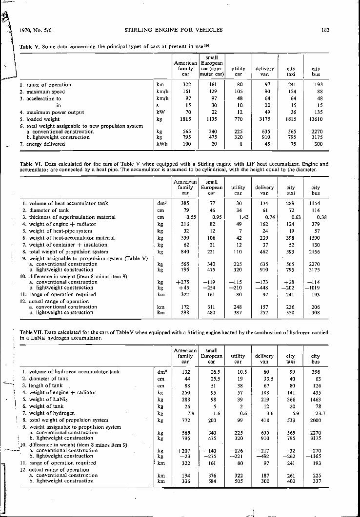
1970, No. 5/6 STIRLING ENGINE FOR VEHICLES
Table V. Some data concerning the principal types of cars at present in use [9].
183
Americanfamily
car
smallEuropeancar (com-muter car)
utilitycar
deliveryvan
citytaxi
citybus
1. range of operation km 322 161 80 97 241 193
2. maximum speed km/h 161 129 105 90 124 88
3. acceleration to km/h 97 97 48 64 64 48in s 15 30 10 20 15 15
4. maximum power output kW 70 22 12 49 36 135
5. loaded weight kg 1815 1135 770 3175 1815 136106. total weight assignable to new propulsion system
a. conventional construction kg 565 340 225 635 565 2270b. lightweight construction kg 795 475 320 910 795 3175
7. energy delivered kWh 100 20 8 45 75 300
Table VI. Data calculated for the cars of Table V when equipped with a Stirling engine with LiF heat accumulator. Engine andaccumulator are connected by a heat pipe. The accumulator is assumed to be cylindrica , with the height equal to the diameter.
Americanfamily
car
smallEuropean
carutility
cardelivery
vancitytaxi
citybus
1. volume of heat accumulator tank dm3 385 77 30 174 289 11542. diameter of tank cm 79 46 34 61 72 1143. thickness of superinsulation material cm 0.55 0.95 1.43 0.74 0.63 0.384. weight of engine + radiator kg 216 82 49 162 124 3795. weight of heat -pipe system kg 32 12 7 24 19 57
6. weight of heat -accumulator material kg 530 106 42 239 398 15907. weight of container + insulation kg 62 21 12 37 52 130
8. total weight of propulsion system kg 840 221 110 462 593 21569. weight assignable to propulsion system (Table V)
a. conventional construction kg 565 340 225 635 565 2270b. lightweight construction kg 795 475 320 910 795 3175
10. difference in weight (item 8 minus item 9)a. conventional construction kg +275 -119 -115 -173 +28 -114b. lightweight construction kg +45 -254 -210 -448 -202 -1019
11. range of operation required km 322 161 80 97 241 193
12. actual range of operationa. conventional construction km 172 311 248 157 226 206b. lightweight construction km 298 480 387 252 350 308
Table VII. Data calculated for the cars of Table V when equipped with a Stirling engine heated by the combustion of hydrogen carriedin a LaNi5 hydrogen accumulator.
Americanfamily
car
smallEuropean
carutility
cardelivery
vancitytaxi
citybus
1. volume of hydrogen accumulator tank dm3 132 26.5 10.5 60 99 3962. diameter of tank cm 44 25.5 19 33.5 40 63
3. length of tank cm 88 51 38 67 80 1264. weight of engine + radiator kg 250 95 57 183 141 4355. weight of LaNi5 kg 288 98 39 219 366 14636. weight of tank kg 26 5 2 12 20 787. weight of hydrogen ' kg 7.9 1.6 0.6 3.6 5.9 23.78. total weight of propulsion system kg 772 200 99 418 533 20009. weight assignable to propulsion system
a. conventional construction kg 565 340 225 635 565 2270b. lightweight construction kg 795 475 320 910 795 3175
10. difference in weight (item 8 minus item 9)a. conventional construction kg +207 -140 -126 -217 -32 -270b. lightweight construction kg -23 -275 -221 -492 -262 -1165
11. range of operation required km 322 161 80 97 241 19312. actual range of operation
a. conventional construction km 194 376 322 187 261 225b. lightweight construction km 336 584 505 300 402 337
+lb

184 PHILIPS TECHNICAL REVIEW VOLUME 31
Hydrogen as fuel; the hydrogen accumulator
Though at first sight it seems strange to use hydrogenas a fuel for an engine, it is clear that at a given momentwe may have to give thought to a synthetic fuel which,in production and use, does the least possible damageto the natural cycle on Earth [11] Apart from thermalpollution, which is inherent in all thermal engines,hydrogen is a very "clean" fuel. On combustion thereare no problems with carbon dioxide, carbon monoxide,and unburned hydrocarbons, and if the reaction ofcombustion is allowed to take place at not too high atemperature, the final product is just water. The use ofhydrogen as a fuel holds no problems for the Stirlingengine.
The applicability of hydrogen as a fuel dependsmainly on the solution of two problems. In the firstplace a method must be found to produce hydrogeneconomically from water, and here the oxygen pro-duced must be allowed to "escape" into the atmosphereso that subsequent combustion of the hydrogen restoresthe status quo. Naturally this is necessary only if hydro-gen is used on a large scale as a fuel. Recently a veryinteresting chemical cycle has been described in whichwater is split into hydrogen and oxygen with a theor-etical efficiency of 75 %; the process requires the
supply of heat at a temperature of at most 750 °C [12].Once such a cycle is mastered, the heat liberated innuclear reactions could be used directly to producehydrogen on a mass scale. Still higher operating tem-peratures of nuclear reactors would, with suitablechemical cycles for those temperatures, yield still higherconversion efficiencies, and produce hydrogen stillmore economically.
The second problem that has to be solved is to findan easy way of storing large amounts of hydrogen, sothat sufficient fuel can be carried in the vehicle. A recentdiscovery in our laboratory [13) may be a significantstep in this direction. It has been found that somehexagonal intermetallic compounds of compositionAB5, in which A is a rare-earth metal and B is nickelor cobalt, readily absorb and desorb large amounts ofhydrogen at a pressure of a few atmospheres. At2.5 atm and room temperature the density of hydrogenin LaNi5, for example, is almost twice as great as thatof liquid hydrogen.
As in the case of the heat accumulator we have cal-culated for all six types of cars mentioned in Table Vthe dimensions of a tank filled with LaNi5 capable ofstoring an amount of hydrogen at 20 °C sufficient forthe previously mentioned specifications to be met. Thecalculation is based on the following data: 1) theamount of hydrogen that can be absorbed and desorbedis 180 cm3(NTP)/g LaNi5; 2) the plateau pressure isabout 2.5 atm.; 3) the density of LaNi5 is 8.5; 4) the
Fig. 23. Schematic representation of a Stirling engine (centre)with LaNis hydrogen accumulator (left). Because heat is liberatedduring the charging of the accumulator and heat must be sup-plied during discharge, the accumulator is incorporated in thecooling -water system of the engine. The water is forced by a rpump (bottom right) through the accumulator, the engine, andthe radiator (top right).
heat of reaction is 0.059 kcal/g LaNi5; 5) the netcalorific value of hydrogen is 2570 kcal/m3 (at NTP).
When the tank is filled with hydrogen a great dealof heat is liberated (about 13 % of the calorific value).We have assumed that the tank is built into the cooling -water system, as shown in fig. 23. When the engine isrunning, hydrogen is continuously withdrawn from thetank, which will thereby tend to cool. This heat is madegood by the cooling water of the engine after it haspassed through the radiator. This causes the coolingwater to cool down further (about 10 % of the amountof heat which has to be withdrawn from the coolingsystem of the engine can be used to prevent coolingof the LaNi5). For the calculation of the LaNi5 tankwe have assumed furthermore that the volume of thetank is 2.3 times greater than the volume of the LaNi5because a) the LaNi5 is present in powder form, b) theLaNi5 powder expands during the uptake of hydrogen,and c) about 15 % of the volume is required for theheat exchanger in contact with the cooling water.We have also assumed the tank to have a cylin-drical shape with a length of twice the diameter. Theefficiency of the Stirling engine is taken as 38 %. Withthese data and assumptions the values shown in TableVII have been obtained.
We see from this table that the propulsion systemwith hydrogen accumulator, just like that with the heatlaccumulator, is too heavy for the large American;motor -car by 207 kg if a radius of action of 322 km is,specified. But it can easily satisfy the requirements ofa lightweight car (-23 kg). For all other motor vehiclesthe specifications can be met with an ample margin.Thus a small European car with an all -up weight of1135 kg (Table VII) has a range of 376 km, while thespecifications call for a range of 161 km.
Although the above considerations on the applica-tion of heat accumulators and hydrogen accumulatorsin various types of motor -cars are purely theoretical,they do indicate the wide applicability of the Stirlingengine.

1970, No. 5/6 STIRLING ENGINE FOR VEHICLES 185
Conclusions
There are signs which indicate that the biosphere isundergoing changes in the negative sense because of theactivities of man. The interference with nature on thepart of man in the course of his struggle for survival andthe pursuit of pleasure has vast consequences both forhimself and for other life on Earth. Above all the ex-ponential increase in the consumption of raw materialsand in the production of rubbish - which pollutes theEarth - gives rise to great concern. At present it isair and water pollution that give cause for particularanxiety. The air is being polluted not only by industrybut also by the exhaust gases of motor -car engines.In the United States the contribution of vehicle enginesto air pollution is more than half of the total, butlocally it is much greater because of the heavy con-centration of cars in and around cities (about 80for Los Angeles). In addition the diesel engine inbuses and lorries contributes to other sources ofannoyance: noise, smell and soot.
It is against the background of these facts that a de-scription has been given of the Stirling engine, which,from the technical point of view, could well replaceconventional vehicle engines. With its many specialfeatures, the Stirling engine could make a great contri-bution to environmental hygiene, not just today andtomorrow, while fossil fuels are still in use, but also theday after tomorrow, when these are no longer available.
However, it must be admitted that the really large-scale introduction of the Stirling engine for vehicularpropulsion will be extremely difficult for economicreasons. To a question put to me a few years ago inthe United States after a lecture on the Stirling engine,namely "What is wrong with the engine?", the answerhad to be "The existence of other engines". Indeed itis difficult to compete against engines whose price islittle more than that of so many pounds of steel, castiron, or aluminium. That is why, up to a few years ago,only those applications were envisaged in which, purelyon economic grounds, the introduction of the Stirlingengine would have a fair chance of success. These arethe areas where the conventional internal-combustionengine cannot be used or where the abatement of thenuisance caused by these engines is expensive.
We may fairly ask whether the changed conditionsregarding pollution will give the Stirling engine, orsome other alternative to the petrol engine, a place inthe near future as a prime mover for vehicles. Muchwill depend on regulations and othercircumstances. Letus consider once more the United States, because thatis where plans and regulations are furthest developed.
The first question is whether the legislator will main-tain the strict specifications of the emission of exhaustgases proposed for the year 1980.
The second question is whether the present-daypetrol engine can be improved so far as to meet allspecifications (including NOW) without giving rise tobig price increases. Here of course it is not just aquestion of the purchase price but also the more ex-pensive maintenance, stricter government surveillance,greater fuel consumption - particularly if lower com-pression ratios have to be used - and the higher priceof petrols with a high octane value obtained by meansother than lead dopes.
In the third place the new regulation which specifiesthe maximum amount of exhaust gases, irrespective ofthe size of the car; will certainly lead to the introductionof smaller, lighter cars of lower engine power. Thequestion is how far one must and can go in this respect.
The fourth question is how far the real cost price ofthe Stirling engine can be lowered by the measuresmentioned in this article, so that this engine can, withinthe framework of the regulations concerning exhaust -gas emission, compete on level terms with all the otheralternative methods of propulsion.
The final question is what further measures thegovernments will take to combat environmental pollu-tion: the introduction of a new type of engine - eventhe engine with the best qualifications - is in factfeasible only on the basis of general governmentpolicy [14].
Irrespective of whether an improved petrol engineor a new prime mover is going to propel the privatevehicle of the future, it is obvious that limitation ofnoxious substances in exhaust gases is going to cost agreat deal of money. In this connection there is agrowing opinion in America that continual and fre-quent government supervision of cars with "cleaned -up" internal-combustion engines will turn out to beimpracticable [15]. That is why thoughts are steadilyturning to power sources which are "clean" by nature:prevention is better than cure.
En] L. Green, Jr., Energy needs versus environmental pollution:a reconciliation ?, Science 156, 1448-1450, 1967.J. McHale, World energy resources in the future, Futures 1,4-13, 1968.P. E. Glaser, Solar energy - an alternative source for powergeneration, Futures 1, 304-313, 1969.
[12] G. de Beni and C. Marchetti, Hydrogen, key to the energymarket, Euro-Spectra 9, 46-50, 1970 (No. 2).
(13] J. H. N. van Vucht, F. A. Kuijpers and H. C. A. M. Bruning,Reversible room -temperature absorption of large quantitiesof hydrogen by intermetallic compounds, Philips Res. Repts.25, 133-140, 1970 (No. 2).
OM D. D. Kummerfeld and G. Wilcox, Federal policy on autoair pollution control, research report of Center for PoliticalResearch, Washington D.C., April 1970.
[15] In the United States attempts are being made to encouragethe design of clean engines: in order to bring mass produc-tion into the realm of practical politics, the "winner" of theFederal Clean Car Incentive Program [5] can, according .toa certain time -table, replace all government vehicles (severalhundred thousand) at a reasonable return (at most, twicethe normal price) by cars equipped with the new power unit.

186 PHILIPS TECHNICAL REVIEW VOLUME 31
The construction of a very unusual building seen through the eyes of anartist. The following pages give an account of the birth of the ideabehind it and of the equally unusual exhibition it houses.

'970, No. 5/6 187
The EVOLUONA permanent Philips exhibition
J. F. Schouten
In 1961 Ir. F. J. Philips, thinking ahead to the forth-coming 75th anniversary of Philips in 1966, put thefollowing question:"Is there any sense in continuing to take part in worldexhibitions, as we did in Brussels and as we might do,for example, in New York and Montreal? We do thisbecause other firms do it. The costs, however, are veryhigh and the effects, though spectacular, are shortlived.Suppose that we stopped taking part, saved up themillions that we would have spent on these exhibitions,and then used that money, perhaps with a supplementaryinvestment, to set up a permanent exhibition about ourown company?"
Not all of Ir. Philips's colleagues on the Board ofManagement were as enthusiastic about this idea as hewas. The investments required would have to be madeat the expense of industrial projects, and it was difficultto assess the indirect profit from such an undertaking.
Despite this the plan was finally accepted. Ir. L. C.Kalif, former arts director of Philips, was commissionedto design the building in collaboration with De Bever,a firm of architects. The services of Mr. James GardnerRDI were obtained for the design of the exhibition, andMr. Jacobus Kleiboer was appointed adviser.
The search for a "distinctive form for a distinguishedcontent" led to the concept of an enclosed shallow bowl(like a "flying saucer"), supported by twelve V-shapedpillars to give an illusion of weightlessness. Within thedome thus formed there were to be three galleries, thediameter increasing towards the top. Two platformsprojected inwards from the third and uppermost gal-lery. Galleries 3 and 2 each comprised about a thirdof the total available floor area for the exhibition,gallery 1 a sixth, and the two platforms the remainingsixth.
We shall not deal here with the particularly interest-ing way of building the dome with prefabricated con-crete elements - 288 flat sheets form the lower partand 822 hexagonal prisms the upper part. The buildingwas started in September 1964.
Prof. Dr. J. F. Schouten is a Scientific Adviser with Philips ResearchLaboratories and a Professor Extraordinary at the TechnicalUniversity of Eindhoven. Prof Schouten is also Director of theInstitute for Perception Research ( 'PO), Eindhoven, a memberof the Advisory Council of the Evoluon and a member of the Boardof Consultants of the Netherlands Young Scientists Association.
The birth of the central theme
From 1961 onwards all kinds of ideas were put for-ward about what Philips should exhibit in this buildingand about the way in which the exhibits should belinked together in a framework of topics and themes.
Photo Lucien Herne, Paris
Bronze by Ossip Zadkine "Eclatement de l'atome", which waspresented to Ir. L. G. Kalif, the former arts director of Philips,by the society "Recherches et formes de demain", as a prizefor the whole of his completed work, and is now on displayat the Evoluon. Various other works of art inspired by naturalevents are also to be found in the building.

188 PHILIPS TECHNICAL REVIEW VOLUME 31
Z11.78 '-`44.4.-4.4444, !II 4::
44 al tit %...4 1
-,, iiv la ii, 0- lk., e : :: st mik ap-i ,.A 4'
I. am
, -IMAM e F :.-1 1 eat 1°)., ') 1. r
14(j.
f.. halac e
4 44 - "
One of the impressions drawn by Charles Eyck of Maastricht during the building of the Evoluon; there is another on p. 186.

1970, No. 5/6 EVOLUON 189
Above: the first sketch of the design by Ir. Kalif. On the fol-lowing pages there are some photographs of the construction ofthe building.
tt
As early as 1961 Mr. J. Kleiboer came up with thename EVOLUON or EVOLEION. It was a name, hesaid, that symbolized growth in time and growth incomplexity, and would characterize an enterprise likePhilips very well. Moreover, speaking from his ex-perience as an exhibition designer, he thought it wouldbe an enormous advantage to have a new name insteadof one of the hackneyed variants on "expo" and"rama". At the time his proposal was not taken upbecause a term borrowed from biology did not appealparticularly to those who had a technological exhibitionin mind. By the beginning of 1965 it was clear that thisname would in fact be a particularly appropriate onefor an exhibition whose dominant theme was to beindustrial evolution.
This concept of industrial evolution was developedin a memorandum, published as a booklet in July 1965.The booklet served as a working document to indicatethe general lines on which the exhibition was to be de-signed, and a translation of the key section of thebooklet is given below.

190 PHILIPS TECHNICAL REVIEW VOLUME 31
WHAT THE EXHIBITION IS NOT TO BE
Not a showroom for the products of the Philips Product Divisions.This would attract only transient interest. Moreover, many ProductDivisions already have better showrooms than they could hope toget from their share of the total floor area of about 5000 m2.
Not a kind of Science Museum. Here again, the interest would betoo limited. Moreover, it would not give a truly representative pictureof the industrial group that is presenting the exhibition.
No surfeit of technology, or of mechanization and automation.This could make the visitor feel humbled and insignificant when heleft the exhibition. It would quicken his fear of losing his job to arobot, the more so in a period of economic recession. Moreover, weconsider that such an overemphasis would give an untrue and un-balanced picture of the essential significance of technology to man.
Finally, the thinking of the exhibition must be based not on our-selves - Philips - but on the visitor. Obviously, the exhibits relateto Philips, but the visitor's attention can only be caught and held byappealing to his interest and natural curiosity.
THE EVOLUTION IDEA
Man has always striven to acquire mastery over matter and to formstable societies with his fellows.
By the end of the 19th century, in a society already unmistakablyindustrial, many people had to work as producers in conditions thatwe should consider appalling. The hours were long, the work hard,and the conditions unhealthy. But their share as consumers (of foodand clothing, housing, medical care, schooling, leisure, etc.) seemspitiably small to us today.
The key to the enormous improvement that has taken place inWestern society during this century, both in working conditions andthe goods available to the average consumer, is to be found in theenormous progress made in the industrial process. More rationalproduction' methods brought about by mechanization and automationhave vastly increased output per worker, while at the same timemaking it economically possible to bring about the much desiredhumanization 'of working conditions (shorter working hours, betterworking'conditions, social facilities, etc.). As for the consumer, whatused to be the luxury for the few has become the everyday fare forthe entire population.
Mechaniiation is sometimes referred to as the first industrialrevolution, and automation as the second. However, these twotrends, plus the humanization of working conditions - all developingin equilibrium - ought really to be regarded as an industrial evolu-tion.
If we define industrial evolution in this way we are not indulging inan easy optimism, for too hasty an introduction of mechanizationand automation by the employers, or too eager demands from theemployees for better conditions, could upset the balance and bringabout a degeneration from evolution to revolution.
We might also speak of the evolution of man through technologyevolved in a controlled way by man himself.

1970, No. 5/6 EVOLUON
INDUSTRIAL EVOLUTION
GCHANIZATI021) CUTOMATI?1)
1st Industrial Revolution 2nd Industrial Revolution
. .
.10 Up IIa on air not aeliaiiiivatOir ;WM SAP 74414414'`'411110111WIP,111.111.-111ru .1."4151'11,iatto-' , .
4,1 I Imo'
r
la44401

192 PHILIPS TECHNICAL REVIEW VOLUME 31
THE EVOLUON
In this evolutionary industrial development Philips clearly play anextremely important and fascinating role. It is the role of a growingenterprise which has made available to the whole world a vast arrayof important products and systems that contribute to the consumerneeds of man and society; which is organizationally and financiallysounder and more forward -looking than many state systems; whichis a welcome partner, supplier and customer of other business enter-prises; and which offers employment and the opportunity for per-sonal development to some two hundred and fifty thousand peopleall over the world.
This is essentially a dynamic role. All that we have to offer istoday's solution of yesterday's problem, and we have the keen deter-mination and unbounded confidence that we shall solve today'sproblems by tomorrow.
This leads us to see the exhibition not as a technological exhibitionbut as an industrial one. This in its turn means that we should showthat all that has been done in the last 75 years in organization,methods, products and the distribution of those products has beenachieved by a community of people, who have time and again beenfaced with almost insoluble problems, who have struggled to over-come those problems and who have achieved no small success.
It should moreover be made clear that an industrial firm is a com-munity which makes its products to sell them, and which must seeevery guilder it spends come back to the till.
An exhibition is of course a display of material objects, adornedwith texts and art work. Everything turns, however, on the ideaswhich are communicated to the visitor through this display.
The main idea is this: that technology should be the servant ofman. In view of his needs as a consumer, man cannot do withouttechnology. He must therefore organize technology so effectivelythat he is able to meet his consumer needs in the fullest possibleway by matching human labour to man's capacity and potential.

1970, No. 5 6 EVOLUON 193
This exhibition will be opened on the occasion of a 75th anni-versary, and is therefore bound to call up a perspective of those75 years. This perspective, this dynamism, this continuous struggleand process of creation in the midst of a struggling society whichis itself still in the making, should form, quite apart from the anni-versary, the main and permanent idea behind the EVOLUON.
We shall then be presenting not a static display of what now exists,as in a zoo, but the evolutionary dynamism of the creative processand of mankind's struggle to overcome its problems.
Most industrial exhibitions lack this evolutionary theme. It willtherefore give our exhibition a style and distinction of its own.
Another tremendous advantage of placing our activities in thecontext of an evolving society is that it will enable people to "under-stand" Philips. Every visitor, whether employee, housewife, child,scholar, layman, industrialist or statesman, will recognize some partof the display that bears on the life he or she knows.
This recognition should leave a more lasting impression, with theresult that the visitors will continue to think about and discuss theproblems (television, education, upbringing, recreation, industry,society, evolution, revolution, etc.), even after they have left theexhibition.
The EVOLUON, then, whose name embodies its theme of evolu-tion, is a human story. A story of people banding together to createtechnology and distribute its benefits to those who have need ofthem.

194 PHILIPS TECHNICAL REVIEW VOLUME 31
The choice of the main and subsidiary themes
After these rather general digressions, the questionwas now to arrive at significant main themes on thebasis of the principles outlined. The presentation ofthese themes would have to be adapted to the spaceavailable for them, and it would also be necessary to takeinto account the visitor's progress through the building.The idea was that he would first go by lift to the largeplatform, and then descend via galleries 3, 2 and 1to the ground floor. Our original choice was the fol-lowing:
On gallery 3: the impact of technology on society.On the large platform: research in the naturalsciences.On the small platform: research in the life sciences.On gallery 2: technology.On gallery 1 : Philips as an industrial enterprise.
If the social significance of technology is to be dis-played, this main theme should be divided into subsid-iary themes relating to social aspects. These were:
1. Life and health2. Comfort in the home3. Recreation4. Education5. Communication
firms.
In broad lines this scheme was adhered to in therealization of the exhibition, but in one point of detaila change was made at once. Mr. Gardner wanted thevisitor, as soon as he left the lift at the large platform,to be confronted with a spectacular representation ofthe origin of the Earth and of life on Earth. This meantthat research in the natural sciences could not take upthe whole of the platform, and it was decided to splitthis subject up, situating some of the display on theright side of the platform and the rest on the adjoiningarea of gallery 3 linking up with it.
The line of thought behind the scheme outlinedabove was the following. On gallery 3 the visitor willbe able to find an answer to the question, "What useis technology to me?" and thereupon start taking acloser interest in technology itself. This he will find ongallery 2, divided into six subsidiary themes:
1. Sound2. Light3. Matter, the key to all production4. The disciplined electron5. Equipment and systems6. Manufacture and production control.After completing gallery 2 the visitor has covered
five -sixths of the exhibition but has as yet scarcely en-countered the name Philips. This confrontation takesplace on gallery 1, which is devoted entirely to Philips.Here the visitor sees the history of the company, the
story of people at Philips, the organization of Philipsas a multinational Group and a representative displayof the products made by the fourteen Product Divi-sions.
ENTRANCE
-r3C
ti
tENTRANCE
-
3F
One of the pages from the "work book", with the planned divi-sion of space; the present division differs somewhat from this.

1970, No. 5/6 EVOLUON
Photo Jan Envank, EindhovenThe interior, seen from gallery 3. The three galleries can clearly be distinguished. One of thefeatures on the upper gallery is a 1/4 scale model of the ELDO telemetric aerial for trackingsatellites. The molecular model hanging from the ceiling is a representation of polypropylene.The photograph was taken while a light -diffusion grid was being hoisted into place.

tuimppols usNyeisA Jeuuri9 oloya
A.Nip;Av- 4/0 40., ?:1$,%, 1;T:LII
ii,*,---A......:-,w.--- 41"P /rv% PrYirgifyi w f
\\,0-71- ,''4 1---y-/ ter % Peiii.,
.,:._.4:.,,i4-
-1- - --4 -tfitOi Y 74 P74 At A 1 N'Av"-4< vr}:404P-/4P-40
r4 I 1 At /4; t #1,040-40/4P-44
4040140 -
**440 --4"\- rfLOr
1£ 31/11110A M3IA311 1VDINIFID3.l SdflIHd 961

1970, No. 5/6 EVOLUON 197
Realization
To carry out the ideas outlined above eighteen work-ing groups were formed - one for each of the eighteensubsidiary themes - with a total of about 120 members.These working groups were to take as their startingpoint the premise that the value of an exhibition to thepublic need not depend solely on the intrinsic techno-logical or scientific contents. It was necessary to thinkup a "story" which the industrial designer could getacross to the public. Moreover it was impressed uponthem that a rigid sequence of ideas or rigorous consis-tency soon becomes boring. We called this requirementthe "alternation of aspects". The visitor was to bealternately confronted with logic and surprise, matterand man, seriousness and humour, "don't touch !" and
necessary human aspect, but it would bring home tothe visitor what science, technology and society owesto the past, and remind him that we stand on theshoulders of our forebears. Moreover it would be afitting tribute to those pioneers.
The composition of the working groups was inter-esting, because there was hardly any subsidiary themeto which widely different departments of the Philipsorganization were not able to make some contribution.A number of working groups had already been activefor some time, but it was not until the official inaugura-tion of the working groups in June 1965 that all theeighteen were complete and a full start could be made.It was a gigantic enterprise to bring into being, withinfifteen months from the first confused discussions, a
Sketch by James Gardner for one of the exhibits.
do-it-yourself, the topical and the historical, today andthe future, and so on. It was expressly stipulated thatcompleteness in the treatment of a theme was never adesirable aim.
By far the most difficult task was to give expressionto the human aspect in what was obviously a materialexhibition. To this end eighty "pioneers" in the fieldsof the subsidiary themes were depicted. This was toserve several purposes. Not only would it bring out the
-4- The interior seen from gallery 3, in the opposite directionfrom that in the previous photograph. On gallery 1: the exhibit"People at Philips".
.7" f 4 r
reasonably consolidated exhibition ready for openingon 24th September 1966.
Meanwhile all kinds of subsidiary projects tookshape. Mr. Kleiboer, for example, kept insisting on thesignificance of the Evoluon for youth. This led to theinstallation of the "Prelude to Technology" display inthe basement of the annexe building, originally intendedfor service use. The basement also provided accom-modation for the small auditorium. The original plansfor a large auditorium, to be built as a separatebuilding beside the Evoluon, could not be carried outbecause of lack of time and money.

198 PHILIPS TECHNICAL REVIEW VOLUME 31
H.R.H. Prince Bernhard andMr. Philips looking at an exhibitafter the opening of the Evoluonon 24th September 1966.
"Prelude to Technology"
Photo Jan Bijvank, Eindhoven

1970, No. 5/6 EVOLUON
The inauguration and the experience of the first years
The Evoluon was officially opened on Saturday24th September 1966 by His Royal Highness PrinceBernhard. At that time 85 % of the planned exhibitionhad been completed. It must be admitted that on theeve of its opening the Evoluon was decidedly unpopularwith many people in Philips, except among the fewhundred people who had contributed and who hadtheir imaginations stirred by this adventure. This nega-tive attitude changed abruptly during the openingweekend, when the visitors had the surprising exper-ience of not finding themselves in the super Philipsshowroom they had expected. It was of course ourintention that the Evoluon should contribute to theprestige of Philips. Our belief that this prestige wouldbest be achieved by an indirect approach was confirmedbeyond all expectations.
This welcome success had two main origins. First,the Philips staff engaged in this project possessed solittle exhibition experience that they were able to givefull rein to their imagination. Secondly, and perhapsmore important, Mr. Gardner and Mr. Kleiboer andthe other expert advisers were only too ready to applytheir enthusiasm to these unconventional ideas.
Although the number of visitors is not a direct meas-
Photo Jan Bijvank. Eindhoven
ure of success, it was nevertheless extremely gratifyingthat the most optimistic estimate - 300 000 visitorsa year - was well surpassed. The annual number ofvisitors steadily rose from about 440 000 to nearlyhalf a million, and not long ago the two -millionth visitorwas welcomed.
Something that far exceeded our wildest dream wasthe way in which the Evoluon has been found toappeal to the young. That well-known phrase "youngpeople from 8 to 80" often came up in our discussions.Indeed, it must conceal a deeper truth : something witha direct appeal to the young may also appeal to theirelders through its rejuvenating qualities.
Greatly aided through the personality of Ir. G.Ahsmann 1*1, the Evoluon's appeal to the young alsomade it into a natural springboard for a wide varietyof new youth activities, such as study weekends forsecondary -school children, for the Young ScientistsAssociation (both nationally and internationally [**1)and a young people's laboratory.
[*] Ir. G. Ahsmann was the chief associate of Prof. Schoutenin 1965 and 1966 and is now head of the scientific depart-ment of the Evoluon (Ed.).
[**1 The International Coordinating Committee for the Presen-tation of Science and Development of Out -of -school Activ-ities (ICC), Place St. Lazare 2, 10130, Brussels.

Top: Faraday in his laboratory.Left: Model of the atom. The nucleus and theelectron orbits for the first eleven elements ofthe periodic system can be made visible in thedark interior of the sphere.
Upper right: One of the exhibits on gallery 1:The organization of Philips.Lower right: The colours, characterized by thethree-dimensional colour space. The rectangu-lar coordinates are chosen in accordance withHering's complementary colours.Far right: The exhibits differ not only in subjectbut also in the way they are presented. Fromtop to bottom:The living cell
Perception, inside and outside the exhibit
Sound spectroscope
Interrupted gearwheels
Working model of a steam-engine, made in1864 by E. H. Stuyver, an Amsterdam copper-smith
Business organization

1970, No. 5/6 EVOLUON 201

PHILIPS TECHNICAL REVIEW VOLUME 31
The future
Now that we are at some distance from our work,we can see clearly the task emerging for us in the future.Gallery 3 was only partly successful in its concept. Weought to say here that Mr. Gardner originally took avery sceptical attitude to the depicting of such anabstract theme as "The significance of technology forsociety". Within this main theme the least successfulwas the subsidiary theme "Recreation", the very fieldin which Philips has the highest turnover. Manyinteresting ideas were proposed, but for one reason oranother we failed to present this theme in a reallysatisfactory way.
Our current view is that although the six subsidiarythemes should be represented on gallery 3, it is artificialto do so in separate sections. Where indeed can the linebe drawn between recreation and education, and wherein turn between these fields and communication?
This line of thought has led to an entirely new con-ception of gallery 3, in which the previous subsidiarythemes repeatedly return in different forms. A start hasalready been made on carrying this new concept intoeffect, with a new and more flexible form of presenta-tion.
Photo KLM Aerocarto N.V
Up to now we have referred solely to the planning,the construction and the success of the exhibition. Wemust also remember that such an exhibition cannotfunction without permanent care. This applies in par-ticular to working exhibits and to those which thepublic can operate themselves. There must be an un-tiring team of guides and continuous renovation ofexhibits. Every year at least 10 % of the exhibits areimproved or replaced. The Evoluon, in order to go onliving, must itself evolve.
Finally, a word or two about the appeal of theEvoluon to young people. We believe that the educa-tional value of an exhibition like that in the Evoluonlies in the fact that everyone is at liberty to skip some-thing that at school they would be compelled to grap-ple with. Unfortunately things cannot be done in thisway at school, but in the Evoluon everyone has thedelightful freedom to concern himself with just whathappens to take his interest at that moment. A lot canbe learnt in this way. What appeals to youth, we trust,will also appeal to the youthful element in every visitor.And what constantly renews itself will never cease tofascinate.

1970, No. 5/6 EVOLUON 203
Photo Bart Hofmcester, Rotterdam

204 PHILIPS TECHNICAL REVIEW VOLUME 31
Volume 31, 1970, No. 5/6 pages 125-204 Published 27th May 1971

PHILIPS TECHNICAL REVIEWVOLUME 31, 1970, No. 7/8/9
Until quite recently, anyone speaking of a "transistor" would have beenreferring to the junction transistor, which has replaced the thermionicvalve in so many fields in the last fifteen years. For individual circuitelements this would in the main still be quite correct. For integrated cir-cuits, however, there is now another important contender in the field: thisis the MOS transistor, which is a particular type offield-effect transistor.
Philips have been working intensively on these MOS transistors forseveral years, both in the laboratory and in production plants, in theNetherlands and in other countries. This issue of Philips Technical Reviewis completely given over to these activitiesThe first five articles are aboutthe characteristics and technology of the MOS transistor; the next -to -last article is concerned with a medium-sized integrated circuit, and thelast one with a large-scale integrated circuit. The other seven articles discusssmall integrated circuits as well as particular transistors that have beenmade as part of the research programme to enable various special aspectssuch as high paver or high cut-off frequency to be investigated.
Although many facets of the MOS transistors and the related Philipswork are discussed, the contents of this issue by no means cover the wholefield. There are for example no general considerations of MOS transistorcircuits nor is there anything about complementary MOS transistors. Ofcourse, not all of the contributions to a combined issue like this can beequally topical: fairly recent developments such as the LOCOS techniqueare accompanied by other topics that are not so new, but not necessarilytherefore of lesser interest.

206 PHILIPS TECHNICAL REVIEW VOLUME 31
MOS transistors
L. J. Tummers
With the advances in semiconductor technology ofa few years ago it became possible to produce a newsolid-state amplifier, the MOS transistor (MOS formetal/oxide/semiconductor). When the term transistoris used, what is generally meant is the junction tran-sistor. And in fact the junction transistor remains theonly type to be widely used as a discrete element. Atransistor of this type has three layers (NPN or PNP)and charge -carriers of both polarities play an importantpart in its operation; because of this they are sometimescalled "bipolar transistors". In this type of transistor,and particularly in the middle layer (the base), thebehaviour of the minority charge carriers is of greatimportance; in a P -type layer the minority carriers arethe electrons, and in an N -type layer they are the holes.
Unipolar transistors depend for their operation oncharge -carriers of only one polarity. This class includesfield-effect transistors (sometimes called FETs). Herethe current -flow in a strip of semiconducting materialis modulated by applying a voltage to a control elec-trode, called the gate, which is insulated from the strip.
The idea underlying the operation of the field-effecttransistor goes back to 1925 [1], but it was not untilabout 1950 that devices could be made that workedsuccessfully [23. In the first field-effect transistors to beproduced the gate was not insulated from the semicon-ductor by a dielectric; it was itself a semiconductinglayer, but of the opposite conduction type, and biasedin the reverse direction with respect to the other material(this was the junction FET). This approach avoideddifficulties arising from surface effects at the interfacebetween the semiconductor and the insulating layer.which had prevented other types from workingproperly.
In about 1960 a new situation was created by theadvent of the planar technique for making bipolarsilicon transistors [3] In doping of the silicon by diffu-sion this technique makes use of the masking propertiesof a layer of Si02 applied to the silicon. It was foundthat this Si02 layer could also act as an insulator be-tween the semiconductor and the gate electrode of afield-effect transistor, and in this way the MOStransistor was born [5]. These devices were also not
Prof Ir. L. J. Tutnniers is a Deputy Director of Philips ResearchLaboratories, Eindhoven, and Professor Extraordinary in Traii-sistor Technology at Eindhoven Technical University.
entirely free from difficulties due to surface effects, butwith time they have increasingly been overcome [6]. Infact, the metal/oxide/semiconductor configuration hasshown itself to be a wonderfully sensitive measuringinstrument for investigating silicon surfaces.
From its very nature the MOS configuration permitsa wide variation in device geometry. For example,MOS transistors with a very short channel have beenmade, which is an advantage for high -frequency opera-tion, and others have been made with a very widechannel, which is necessary if the device is required togive a high output power. Examples of such deviceswill be found in other articles in this issue.
It is of course important to consider the practicaladvantages and disadvantages of the MOS transistorcompared with the bipolar transistor. A striking dif-
Schematic cross-section of a MOS transistor on a substrateof P -type silicon. S source. D drain. S and D are regions ofstrongly doped N -type silicon. G metal gate, insulated fromthe substrate by the Si02 layer ay. The voltage between D andS is the drain voltage Vth that between G and S is the gatevoltage V5. The electrons flow through the substrate from S toD in an extremely thin layer called the channel, situated underthe oxide. Owing to the presence of the negative charge inducedby V5, the channel is in fact a layer of N -type silicon 14].
ference is the very high input impedance of the MOStransistor, due to the presence of the oxide layer. Thismeans that in applications where a very high inputimpedance is required the MOS transistor is clearlyprefefable. But there are other features that may favourthe choice of a MOS transistor. Its characteristics aremore linear than those of bipolar transistors and there-fore introduce less distortion; less feedback can beused; simpler circuits can sometimes be used, and thedevice has good thermal stability. Another point in itsfavour is that the MOS transistor is a little easier tomanufacture than a bipolar transistor.
Set against these good features there are others which

1970, No. 7/8/9 MOS TRANSISTORS 207
Example of includes very recent developmentsin both geometry and materials [8]. The circuit is a 16 -bit store in which each bit is a MOStransistor with an adjustable threshold voltage. This voltage represents the information storedin the bit. The MOS transistors in this circuit differ from the conventional ones in that theinsulation between the substrate and the gate is a sandwich formed by an SiO2 and an Si3N4layer. The circuit was made with the aid of the LOCOS technique.
make the MOS transistor less suitable for certain typesof application. They explain why the MOS transistorhas until now only been used on a very limited scaleas a discrete circuit element. For operation at very highfrequencies the bipolar transistor is superior because ofits higher transconductance. While MOS transistorscan be made with a high transconductance, the gatethen has to be large, giving a high capacitance. Theratio gm/C of the transconductance and the capaci-tance, which is in many cases a figure of merit for high -frequency behaviour, is therefore usually smaller forthe MOS transistor than for the bipolar transistor.However, it is not completely impossible to make aMOS transistor with a high gm/C ratio, but to achievethis the current I through the transistor has to be maderather large. This reduces the ratio gm/I, which is ameasure of the voltage gain, so that in effect we haveonly exchanged one disadvantage for another. Gener-ally speaking, a MOS transistor at a given currentsetting requires a much higher load resistance to givea particular voltage gain than a bipolar transistor [7].
The high input impedance of the MOS transistor,
which is a very attractive feature for certain applica-tions, also gives rise to a difficulty. Electrostatic chargebuild-up may easily increase the voltage on the gateto a value high enough to cause breakdown in theoxide layer, destroying the device. It is often necessaryto protect the gate with a diode or resistor.
Another disadvantage of the MOS transistor - al-though one that is diminishing with the advance oftechnology - is that its characteristics tend to be moresusceptible to variations in the production process thanthose of the bipolar transistor. This applies particularly
See for example H. C. de Graaff and H. Koelmans, Thethin-film transistor, Philips tech. Rev. 27, 200-206, 1966.W. Shockley, A unipolar "field-effect" transistor, Proc. I.R.E.40, 1365-1376, 1952.See A. Schmitz, Philips tech. Rev. 27, 192, 1966.A more detailed treatment will be found in the article byJ. A. van Nielen in this issue, page 209.D. Kahng and M. M. Atalla, Silicon-silicondioxide field -induced surface devices, IRE Solid -State Device ResearchConference, Pittsburgh 1960.See the article by J. A. Appels, H. Kalter and E. Kooi inthis issue, page 225.See, for example, the article by J. A. van Nielen [4].This circuit was made by Ir. R. H. W. Salters of PhilipsLaboratories, Eindhoven.

208 PHILIPS TECHNICAL REVIEW VOLUME 31
to the threshold voltage, i.e. the gate voltage at whichthe transistor just starts to conduct.
Although at present there may be little likelihood ofthe large-scale use of MOS transistors as individualcircuit elements, the situation is entirely different fortheir use in integrated circuits. In integrated circuitsusing bipolar transistors the individual circuit elementscomprised in a single silicon chip have to be isolatedfrom one another, which involves a number of separatesteps in the production process. No such isolation isrequired in MOS circuits, and this not only makes thefabrication process simpler but also saves space on thesilicon chip. A further saving of space is achieved byusing the MOS transistor as a load resistor. In this waycomplex integrated circuits can be made that consistentirely of MOS transistors.
With their high impedance levels, integrated MOScircuits are not particularly fast, but for very largeintegrated arrays where speed requirements are notcritical the MOS transistor has a slight advantage.Research is still going on in both fields, however, andit is therefore difficult to make any forecast.
The most advanced investigations now in progress orrecently completed relate to refinements in device geo-metry and materials. The hope is that these refinementswill allow MOS transistors to be made that can beused up to higher frequencies, that have a very low oradjustable treshold, voltage, etc. In the refinements ofthe geometry one of the aims is the more accurateregistration of the gate with the source and drainregions, and experiments are being carried out bothwith variants of the classical methods and with entirelynew methods, such as doping the material by bombard-ment with fast ions (ion implantation). In the ion-
implantation technique, and in other techniques as well,
the gate electrode itself is used as a mask, thus ,simpli-.fying registration.
.
In the study of the materials, efforts, are being madeto find insulators that can be used instead of Si02, or incombination with it, and also other materials for thegate. Here the search is not only for metals suitableto replace the aluminium used at present - the natureof the metal partly determines the threshold voltage'-but devices are also being made with non-metals, suchas polycrystalline silicon.
In the development of the integrated bipolar or MOScircuits there has been a fair amount of cross-fertiliza-tion. Not only have the potentialities of the MOS cir-cuits stimulated the search for new ideas in the fieldof bipolar circuits, but progress in the one field has alsofrequently proved of value to the other: For example.the research on silicon surfaces that made the MOSstructure possible has also given valuable help in thedevelopment of the bipolar transistor.
There is every indication of this pattern of cross-fertilization between the two fields continuing in thenear future.
Summary. The MOS transistor (MOS = metal/oxide/semicon-ductor) originated in about 1960. It is a field-effect transistorwhose metal gate electrode is isolated from the silicon substrateby an oxide layer. Previous efforts to make field-effect transistorswith an isolated gate failed because of undesirable effects at thesemiconductor/insulator interface. Advantages of the MOST com-pared with the bipolar transistor are its very high input impe-dance, better linear characteristics and lower feedback. It hashigh thermal stability and is a little easier to make than thebipolar, but the latter is better at high frequencies. MOST researchis now directed towards refining the geometry and improving thematerials. In integrated circuits using MOST devices the elementsdo not have to be isolated. For large integrated circuits that donot have to be particularly fast there is some advantage to begained by using the MOST.

1970, No. 7 8 9 209
Operation and d.c. behaviour of MOS transistors
J. A. van Nielen
The MOS transistor (MOS = metal/oxide/semicon-ductor) is a type of field-effect transistor. It may beregarded as a resistor of semiconducting material whoseconductivity is determined by the potential of a controlelectrode (the gate) situated outside the current path.The gate of a field-effect transistor is isolated from thecurrent path either by an insulating layer or by a reversebiased P -N junction. In the MOS transistor there is aninsulating layer.
MOS transistors are made on a relatively thick sub-strate of monocrystalline, lightly doped silicon by meansof the planar technique: a schematic cross-section canbe seen in the previous article (page 206). The in-sulator between semiconductor and gate is a layer ofSi02, obtained by oxidation of the silicon. The sourceand drain electrodes are heavily doped zones of theopposite conduction type from that of the substrate.They are produced by with the aidof a bombardment by fast ions (ion implantation).
There are two types of MOS transistor: those on anN -type substrate and those on a P -type substrate. Inthe first type current conduction takes place by the flowof holes from the source to the drain, and the device iscalled a P -channel MOS transistor (fig. la). The othertype, in which the conduction is due to electrons, iscalled an N -channel MOS transistor (fig. lb). We shallreturn to the current conduction in an MOS transistorin more detail later.
The relation, at constant gate voltage Vg, betweenthe current Id flowing through a MOS transistor andthe potential Vd of the drain we assume the poten-tial of the source to be zero - much resembles theIa-Va characteristic of a pentode valve. Characteristicsof an N -channel MOS transistor are shown in fig. 2a.The Id- Vg characteristic takes the form of a quadraticfunction (fig. 2b); in a MOS transistor Id is zero whenVg is less than a certain voltage Vtli, called the thresholdvoltage. The transconductance of MOS transistors isusually between 1 and 10 mA/V. A special feature ofthe device is its exceptionally high input resistance, ofthe order of 1014 ohms.
In this article we shall first deal at somewhat greaterlength with the operation of a MOS transistor andconsider the factors that determine the threshold volt-
Ir. J. A. van Nielen is with Philips Research Laboratories, Eind-hoven.
GcAEDS 0___011GED
a
Fig. I. Schematic representation of the MOS transistor, a) withP -channel, b) with N -channel. S source. G gate. D drain. Thediagram shows that the substrate is connected to the source;this connection is not always present.
10 m A
Id
5
0
Id sat
0
00 Vh
10V
V
Fig. 2. a) Some /d- Vd characteristics of a MOS transistor. Eachcharacteristic relates to a particular value of Vg and consists ofa curved region and an almost horizontal region (saturationregion).b) An /d -Vg characteristic relating to a value of Vd in the satura-tion region. The variation of the saturation value Id sat of thecurrent with Vg is a quadratic function and Id is zero when Vgis lower than the threshold voltage Vta.

210 PHILIPS TECHNICAL REVIEW VOLUME 31
age Vth. We shall then derive some approximate equa-tions for the d.c. voltage characteristics, and finallybriefly discuss the way in which the behaviour of aMOS transistor depends on the doping and potentialof the substrate.
Operation of an MOS transistor
Let us consider the case of a MOS transistoron a P -type substrate as illustrated in the previousarticle (page 206). The source S and the substrate forma diode and similarly the drain D and the substrateform a diode. When a voltage is applied between S andD, at Vg = 0, then one of these two diodes is biasedin the reverse direction and only an extremely weakcurrent flows through the transistor.
We shall now see what happens when Vg is graduallyincreased from zero, and we start with the simple casewhere no voltage has been applied between S and D(Vd = 0). The system constituted by gate, oxide layerand silicon can be regarded as a capacitor whose lowerplate is not a metal, but a P -type semiconductor. Aslong as Vg = 0 the charge on both plates of the capac-itor is zero and the semiconductor is everywhereelectrically neutral. When Vg > 0, a positive chargeappears on G and a negative charge of equal magnitudeappears on the semiconductor in a layer next to theoxide. At first this charge is carried solely by the (im-mobile) acceptor ions. Since their density is determinedby doping of the substrate, and is thus fixed, this layeris thicker the higher the positive charge, i.e. the greaterthe magnitude of Vg. Since the positive, mobile chargecarriers are driven out of this layer, it is referred to asa depletion layer.
When Vg is further increased, the negative charge inthe semiconductor is then no longer carried by theacceptor ions alone, but also by electrons which nowappear in a very thin layer of the depletion region nextto the oxide. This layer, which may for example be10-2 pin thick, forms a conducting connection betweenthe source and drain and is therefore referred to as thechannel.
In fig. 3 this picture is presented in the form of anenergy -band diagram. The bands are of course curvedin the depletion region. The curve for the Fermi energyEF, however, will, be a horizontal straight line, as thesemiconductor is everywhere in thermodynamic equi-librium. When Vg is sufficiently high, EF at the inter-face of the silicon and silicon dioxide may thereforecome to lie above Ei, the centre of the forbidden zone.This means that the silicon at that position has changedto the other conduction type. This change, which hasnothing to do with a change in doping, but is onlypresent when Vg is high enough, is called inversion.The inverted layer is the channel. Since Vg determines
the electron concentration in the channel, it also de-termines the conductivity of the channel and hence thecurrent flowing through the transistor when Vd 0 0.The minimum gate voltage needed at Vd = 0 to bringabout inversion is the threshold voltage Vth mentionedabove.
When a gate voltage sufficient to give inversion isapplied the electron concentration in the channel veryquickly adjusts itself to the value appropriate to thenew situation, since most of the electrons required aresupplied from S and D, where there are large numbersof electrons available. The new equilibrium thus comesabout much more quickly than if the electrons were tocome into the conduction band as a result of thermalexcitation alone.
We now consider the situation that actually appliesin an operating MOS transistor: here Vd 0 0. Thepotential V(x) in the channel is then a function of thecoordinate x along the channel, and gradually increasesgoing from S to D. The extent of the inversion, or theconductivity of the channel, therefore gradually de-creases from S to D. The thickness of the depletionlayer, on the other hand, gradually increases, because
M 0 S
M
eVg
EF
E,
P
P
a
Fig. 3. a) Energy -band diagram of the metal/oxide/silicon system(M, 0 and S) when the silicon is P -type and there is no naturalband curvature near the interface of the semiconductor and theoxide. The Fermi energy EF in the silicon is lower than themiddle Ei of the forbidden zone (Ey is the upper edge of thevalence band, Ec the lower edge of the conduction band). Sincemetal and silicon are at the same potential, EF has the samevalue in both.b) When the metal (the gate electrode) is raised to a potential Vg,the holes in the silicon are driven from the zone at the interface,giving rise there to a negative space charge, carried by ionizedacceptor ions. The corresponding band curvature may be so greatthat Ei at the interface comes below EF, so that an N -type layeris formed there (an inversion), the "channel".

1970, No. 7/8/9 OPERATION OF MOS TRANSISTORS 211
the voltage across the N -P junction formed by thechannel and the rest of the substrate rises from S to D(fig. 4a).
If we now gradually raise the potential of D, at fixedVg, then the current Id also rises, but owing to thedecrease in the conductivity of the channel the increaseof Id gradually becomes less steep as Vd becomeshigher. At a particular value of Vd the effective gatevoltage Vg- Vd at the end of the channel, whereV(x) = Vd, has decreased to Vth. At that position thecondition for inversion is no longer fulfilled; thechannel is said to be "pinched off" (fig. 4b). Thisvalue of Vd, which is equal to Vg- Vth and is de-noted by Vd sat, is called the "pinch -off voltage". IfVd is increased further the point in the channel whereV(x) = Vd sat, the pinch -off point, is shifted in thedirection of S. In the region of Vd values at which thechannel is pinched off, the current id varies much lessstrongly with Vd (saturation region; see fig. 2a).
Later in this article, when we present an approximatetheory of the d.c. current behaviour of the MOS tran-sistor, we shall return to the current -saturation effect.First, however, we shall take a closer look at the thres-hold voltage Vth
The threshold voltage Vth; four types of characteristic
In the simple case outlined above, where the energybands at the boundary surface were not curved in thesemiconductor at Vg = 0 and Vd = 0, the gate volt-age Vth required to produce inversion could only bepositive. In practice the situation is usually not assimple as that, because the structure of the MOS tran-sistor may already contain built-in charges. In MOStransistors on a P -type substrate Vth may be negative.Such transistors conduct even at Vg = 0. For MOStransistors on an N -type substrate it is also possible inprinciple for Vol to be either positive or negative. Fourtypes of characteristic may therefore be encountered( fig. 5). The MOS transistors that conduct at Vg = 0- i.e. those in which a channel is naturally present -are called depletion -type MOS transistors, and theothers are said to be of the enhancement type. Thesenames come from the use of the MOS transistor asswitching devices in digital circuits. Devices of thedepletion type are normally open and require to beclosed by a gate voltage, which depletes the conductingchannel; those of the enhancement type are normallyclosed and require to be opened by a gate voltage.
Apart from the relative positions of Ei and EF, i.e.
the doping of the substrate, there are three other factorsthat determine the value of Vth found in a MOS tran-sistor. The first is that, during the oxidation of thesilicon, a quantity of positive charge qox enters theoxide, which has the effect of shifting Vth in the nega-
x=0
a
b
Fig. 4. a) Schematic picture of the situation in a non -saturatedMOS transistor on a P -type substrate. Situated immediatelyunder the oxide is an extremely thin, inverted layer of the sub-strate, through which the current flows and whose conductivitygradually decreases from S to D. The latter is schematicallyrepresented by diminishing thickness. Under the channel, andalso under the drain, is a layer in which there are no mobilecarriers, the depletion layer (white); its thickness increases goingfrom S (x = 0) to D (x = 1).b) The same for the case of current saturation. In the last partof the channel V(x) Vg -
Fig. 5. In MOS transistors on either a P -type or an N -type sub-strate the threshold voltage Vth may in principle be either posi-tive or negative, so that there are four types of fa -Vg characteristic.MOS transistors which conduct when Vg = 0 are "depletion -type" devices (Dept) and the others "enhancement -type" de-vices (Enh).
tive direction. Because of this effect P -channel tran-sistors usually belong to the enhancement type andN -channel transistors to the depletion type.
In the second place Vth depends to some extent onthe metal from which the gate electrode is made. Thedifference between the work function of this metal andthat of the substrate, the contact potential Oms, actsas a built-in contribution to the gate voltage (fig. 6a, b).Finally there may be effects from surface states whoseenergy levels lie in the forbidden band. These surface

212 PHILIPS TECHNICAL REVIEW VOLUME 31
states may trap free charge carriers, which can thenmake no contribution to the conduction. The largerthe number of surfaces states, the higher the gate voltageneeded to produce a particular concentration of freecharge carriers, in other words the threshold poten-tial I Vth I is higher. Advances in recent years in thetechnology of manufacturing MOS transistors havemade it possible to keep the concentration of surfacestates so low that they no longer have any significanteffect [1].
If we include all these charges then the charge on thetwo plates of the capacitor formed by the MOS tran-sistor is:
qg qox = - (giov qss qdepi), . . . (I)
where qg is the charge per unit area on the gate, qinv
M
F
Vac
a
S
Approximate theory of the d.c. current behaviour
Let us again consider the case of an MOS transistoron a substrate of P -type silicon, i.e. with a channel inwhich the conduction is by electrons. To calculate thecharacteristics we introduce two simplifications. In thefirst place we assume that everywhere in the layer of thesubstrate adjacent to the oxide - the lower face of thecapacitor - the charge per unit area'q(x) is determinedby the difference between Vg and the potential V(x)at the position x in the channel, the relationship being:
q(x) = -Cox{Vg- V(x)}. . (3)
(Expressed in the symbols used in equation (I),q(x) = qinv (mow qss.) Let // be the thickness ofthe oxide layer and gox its relative dielectric constant,then Cox = Eggox/h. The minus sign in (3) indicates that
b
eVG
M
Fig. 6. a) Energy -band diagram of a metal M and a semiconductor S which are not in con-tact with each other and have a different work function (i.e. the work that must be performedin order to remove an electron with an energy Er from the metal or the semiconductor intoa vacuum). The difference in work function is &Piss; Osis is the contact potential.b) If the metal and semiconductor in (a) are joined by an oxide layer to form an MOS struc-ture, then EF has the same value everywhere and the original difference e0,,, brings intoexistence a voltage across the oxide and a band curvature eV, in the semiconductor;Vo. + Vs Oms Because of the band curvature, Vu, has here a value different from thatin the case illustrated in fig. 3.c) As (b), but for the case where a gate voltage Vg is applied such that Ei - EF at the sur-face is exactly equal to -e0 F.
the charge in the channel, qss that in the surface statesand qdepl that in the depletion layer. If we take theusual definition of the threshold voltage Vfil as thevalue of Vg at which the energy difference Ei - EF atthe interface between the silicon and the Si02 is equalto that in the bulk of the substrate but of oppositesign (fig. 6c), then:
Vth = cm + 2 OF - ((pm, qss qox qaeoi)/Cox. . . (2)
Here Cox is the capacitance per unit area of the capac-itor. The term 2 OF is in this case the band curvaturecaused by Vg. The charge q/ov is usually so much smal-ler than the other charges that it may be neglected inestablishing a value for the threshold potential.
the charge q(x) is negative if Vg- V(x) is positive.Equation (3) would apply exactly if the lines of force
in the dielectric were perpendicular to the surface. Thissituation is approximated when V(x) in the channeldoes not vary too greatly with x, that is to say whend V(x)/dx and d2V(x)/dx2 are small (this is Shockley'sgradual approximation [9; in practice this is the casein the greater part of the channel.
The second assumption is that the density qinv(x) ofthe negative charge carried by mobile electrons in thechannel is given by:
qi ov(x) = - Cox { Vg' - V(x)}, . . (4)
where Vg = Vg- Vth.If this equation can also be used, the current, which
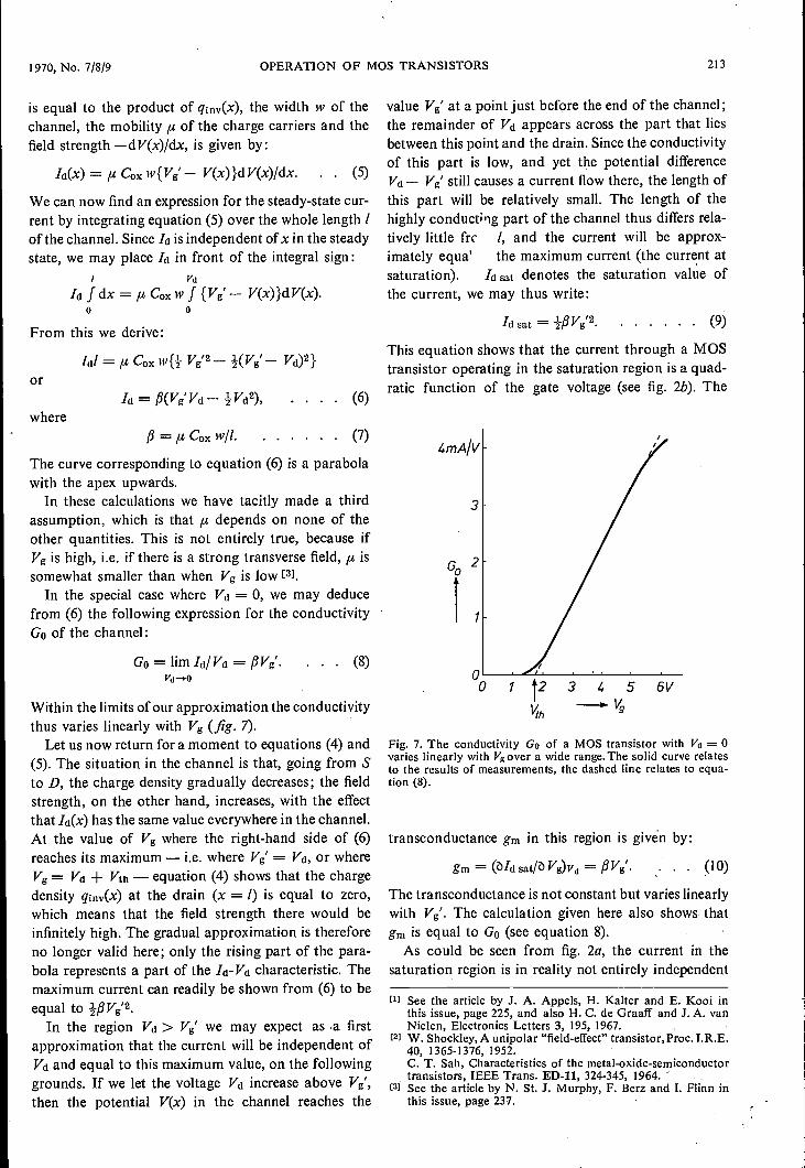
1970, No. 7/8/9 OPERATION OF MOS TRANSISTORS 213
is equal to the product of qinv(x), the width w of thechannel, the mobility ,u of the charge carriers and thefield strength -d V(x)/dx, is given by:
/o(x) ju Cox w {Vg' - V(x)}d V(x)Iclx. (5)
We can now find an expression for the steady-state cur-rent by integrating equation (5) over the whole length /of the channel. Since Id is independent of x in the steadystate, we may place Id in front of the integral sign :
Vd
Id f dx = ,u Cox w f {Vg - V(x)}dV(x).0 0
From this we derive:
idi = Cox w{2 Vg'2 - -12(Vg - Vd)2}or
/d = Vg' Vd Vd2),
where. . (6)
= Cox wit. (7)
The curve corresponding to equation (6) is a parabolawith the apex upwards.
In these calculations we have tacitly made a thirdassumption, which is that ,u depends on none of theother quantities. This is not entirely true, because ifVg is high, i.e. if there is a strong transverse field, It issomewhat smaller than when Vg is low [3]
In the special case where Vd = 0, we may deducefrom (6) the following expression for the conductivityG0 of the channel:
G0 = lira /a/ Vd = j Vg. . . (8)vd,co
Within the limits of our approximation the conductivitythus varies linearly with Vg (fig. 7).
Let us now return for a moment to equations (4) and(5). The situation in the channel is that, going from Sto D, the charge density gradually decreases; the fieldstrength, on the other hand, increases, with the effectthat /o(x) has the same value everywhere in the channel.At the value of Vg where the right-hand side of (6)reaches its maximum - i.e. where Vg' = Vd, or whereVg = Vd Vth - equation (4) shows that the chargedensity ginv(x) at the drain (x = 1) is equal to zero,which means that the field strength there would beinfinitely high. The gradual approximation is thereforeno longer valid here; only the rising part of the para-bola represents a part of the Id-Vd characteristic. Themaximum current can readily be shown from (6) to beequal to 2/3Vg'2.
In the region Vd > Vg' we may expect as =a firstapproximation that the current will be independent ofVd and equal to this maximum value, on the followinggrounds. If we let the voltage Vd increase above Vg',then the potential V(x) in the channel reaches the
value Vg at a point just before the end of the channel;the remainder of Vd appears across the part that liesbetween this point and the drain. Since the conductivityof this part is low, and yet the potential differenceVd -Vg still causes a current flow there, the length ofthis part will be relatively small. The length of thehighly conducting part of the channel thus differs rela-tively little frc 1, and the current will be approx-imately equal the maximum current (the current atsaturation). Id sat denotes the saturation value ofthe current, we may thus write:
Id sat = 1,6 Vg '2 (9)
This equation shows that the current through a MOStransistor operating in the saturation region is a quad-ratic function of the gate voltage (see fig. 2b). The
00 1 t2 3 4 5 6V
VIII*--P. V
Fig. 7. The conductivity Go of a MOS transistor with Vd = 0varies linearly with V5 over a wide range. The solid curve relatesto the results of measurements, the dashed line relates to equa-tion (8).
transconductance gm in this region is given by:
gm = (old sat/6 Vg)vd = f3Vg. . . (10)
The transconductance is not constant but varies linearlywith Vg. The calculation given here also shows thatgm is equal to G0 (see equation 8).
As could be seen from fig. 2a, the current in thesaturation region is in reality not entirely independent
[I] See the article by J. A. Appels, H. Kalter and E. Kooi inthis issue, page 225, and also H. C. de Graaff and J. A. vanNielen, Electronics Letters 3, 195, 1967.
[2] W. Shockley, A unipolar "field-effect" transistor, Proc. I.R.E.40, 1365-1376, 1952.C. T. Sah, Characteristics of the metal -oxide -semiconductortransistors, IEEE Trans. ED -11, 324-345, 1964.
13] See the article by N. St. J. Murphy, F. Berz and I. Flinn inthis issue, page 237.

214 PHILIPS TECHNICAL REVIEW VOLUME 31
of Vd. One of the reasons for this is that near the drainthe lines of force from the gate are no longer perpen-dicular to the interface between oxide and channel,which is the assumption made in the gradual approxi-mation. On increasing Vd the distribution of the linesof force in insulator and substrate around the pinch -offpoint of the channel varies in such a way that the pinch -off shifts slightly towards the source, making thechannel shorter. This increases the transconductanceof the device (see equations 10 and 7) and also, sincethere is no change in the gate voltage, it increases the
' current as well.
Transconductance and gain
The characteristics and relations arrived at in ourtheoretical treatment are of significance in the practicalapplication of the MOS transistor. Very often a maxi-mum voltage gain is required from the MOS transistor.The voltage gain ILI Vd/Z1Vgi in the amplifier circuit offig. 8 is approximately equal to the product of the trans -conductance gm and the load resistance RI. Now gm inthe MOS transistor increases with the d.c. current Id;equations (9) and (10) show that the relation is:
gm = (2P' d)1 (11)
This means that to obtain a high voltage gain the userwill be inclined to bias the transistor to a high current.At a given supply voltage Vdd a limit is set to this,however, by the maximum permissible voltage dropacross RI, i.e. /d/21. Therefore not gm, but the quan-tity gm/Id is a measure of the available voltagegain in ,any given circuit [4]. As a rule the transcon-ductarice of MOS transistors is smaller than that ofbipolar transistors, and a higher load resistance is
therefore needed to obtain an equally high voltagegain.
The purely second -order characteristic of the MOStransistor (see equation 9) is an advantage for applica-tions in receiver input stages. If the valve or transistorin this stage has a non-linear characteristic, strongsignals outside the passband of the receiver can intro-duce spurious signals (intermodulation products) byinteraction with the desired signal. With a selectivereceiver, most of these intermodulation products donot appear within the passband of the following stagesand introduce no interference. If however the expres-sion for the characteristic of the valve or transistorcontains higher terms in odd powers of the inputvoltage, the intermodulation products will include asignal at the carrier frequency of the desired station,but with its amplitude determined by the modulationof the interfering station. The programme from theinterfering station appears to be modulating the carrierfrom the desired station: this effect is called "cross -
modulation". A MOS transistor, whose characteristicdoes not contain such higher odd terms, does not intro-duce cross -modulation 151.
The substrate
To conclude this article we shall examine how thebehaviour of a MOS transistor is affected by thedoping of the substrate and by a substrate potential Vbdiffering from zero [6]. We again consider a transistoron a P -type substrate and again start with the casewhere Vd = 0 and a gate voltage Vg is applied to pro-duce an inversion layer. We have already seen that thislayer is extremely thin, and that the depletion layer isrelatively thick (e.g. I 1.1.m) because the charge densityin it cannot be greater than the density N of the accep-tor ions present in the silicon. The charge density in thedepletion layer is therefore constant over a large part
IVd
Fig. 8. Circuit for voltage amplification with a MOS transistor.R1 load resistance. Vdd supply voltage.
of the thickness, and there is a fairly sharp boundarybetween this layer and the rest of the substrate.
To calculate the space charge in the depletion layerwe may regard the channel and depletion layer togetheras an abrupt Nt-P junction and apply the appropriateequations. If a particular Vg produces a voltage Vsacross the Nt-P junction - the band curvature is then-eVs (fig. 6b) - then the thickness d of the depletionlayer is:
d = (2 edeV5leN)1 , . . . (12)
and the depletion charge per unit area qdepi is:
qaent = -(2 edeeN)1 Vs+ = aVst . (13)
In the approximate theory leading to equations (4) and(6), gdepi is taken to be zero or regarded as constant,i.e. independent of Vg and x. In calculating the effectof Vg on qdepi this is a very good approximation, be-cause provided the inversion is not unduly small - i.e.provided the charge density in the channel is greaterthan that in the depletion layer - a variation of Vginfluences the electron concentration in the channelvery much more than the depletion charge 171: thefirst varies exponentially with Vs, whereas qdepi only

1970, No. 7/8/9 OPERATION OF MOS TRANSISTORS 215
varies with Vs}, as we have seen. This means that whenthe gate voltage Vg is made high enough, the depletioncharge remains practically constant, whereas the mobilecharge increases linearly with Vg.
When Vd 0, the potential V(x) in the channel goesfrom 0 to Vd, and similarly the reverse voltage acrossthe induced N -F -P junction also goes from 0 to Va.This reverse voltage can be further increased by givingthe substrate an additional reverse bias Vb with respectto the source. The total depletion charge per unit areais then a{Vs V(x) Vb}} and is thus dependenton x. The increase in the depletion charge due to thecontributions from V(x) and Vb takes place at theexpense of the mobile charge qinv(x), since the totalcharge is still that given by equation (3). The directconsequence of this is that the current reaches satura-tion at a drain voltage lower than Vg- Vth and thesaturation value Id sat is also smaller than that givenby equation (9). The transconductance is now alsolower and no longer equal to Go.
The effect of applying Vb is thus to change theamount of mobile charge, and with it the current. Thesubstrate contact may therefore be regarded as a secondgate electrode. If the doping N of the substrate is1016 per cm3 the transconductance can in fact be justas high when the device is driven via the substrate aswhen it is driven via the insulated gate electrode G.We should also note that when Vb 0 the value ofthe threshold potential is of course different:
Vtb( Vb) = V1n(0) ± {( Vb 200+ - (2 OF)+}a/Cos.
As can be seen from (13) is proportional to N+.
G. Klein and H. Koelmans, Active thin film devices, Fest-korperprobleme 7, 183-199, 1967.R. J. Nienhuis, A MOS tetrode for the UHF band with achannel 1.5 1.i.m long; this issue, page 259.J. A. van Nielen and 0. W. Memelink, The influence of thesubstrate upon the DC characteristics of silicon MOS tran-sistors, Philips Res. Repts. 22, 55-71, 1967.A. S. Grove, B. E. Deal, E. H. Snow and C. T. Sah, Solid -State Electronics 8, 145, 1965, and T. I. Kamins and R. S.Muller, Solid -State Electronics 10, 423, 1967.See the article by R. D. Josephy in this issue, page 251.
Equations (6), (9) and (10) for Id, Id sat and the trans -conductance gm, respectively, will thus become moreaccurate as N decreases, i.e. as the doping is reduced;the deviation is already very small for N = 1014/cm3.
In spite of the deviations from these equations whenthe substrate is more strongly doped, it is still fairlyaccurate to take the variation in transconductance withVg as linear and the variation of the saturation cur-rent ht sat with Vg as a quadratic function.
Punch -through
We should note here an unwanted effect that mayoccur in the substrate when the drain voltage is toohigh, particularly when the substrate is weakly doped.The higher the voltage of the drain with respect to thesubstrate, the wider becomes the depletion zone aroundthe drain. In MOS transistors with a short channel thiszone may become so wide that it touches the source.The electric field in the depletion region then actsdirectly on the charge carriers in the source diffusion,causing the carriers to move outside the channel to thedrain. This effect is known as punch -through. It sets alimit to the improvement in the high -frequency char-acteristics of a MOS transistor that can be achievedby making it with a shorter channel; it also limits themaximum drain voltage in high -frequency power tran-sistors [83.
Summary. A MOS transistor is a field-effect transistor in whichthe gate is insulated from the semiconductor (silicon) by a layerof SiOs. If the semiconductor is P -type the source and drain arestrongly doped zones of N -type silicon. The current flows througha thin layer at the surface of the oxide, called the channel, inwhich the silicon is changed by the field of the gate from P -typeto N -type. The input resistance is very high (about 1014 SI). Thecurrent -voltage characteristic (when the gate voltage is constant)shows saturation, just as in the case of a pentode valve. Thetransconductance varies linearly with the gate voltage and is ofabout the same magnitude as in thermionic valves. If the gatevoltage has a magnitude lower than a certain threshold voltage,no current flows. This threshold voltage in both an N -type andP -type transistor may be either positive or negative. The dopingof the silicon substrate makes the behaviour of the MOS tran-sistor deviate from the theoretical description given in the article;with a doping level of N = 101.41cm3 or less, however, the devia-tions are small and can be neglected.

216 ,PHILIPS TECHNICAL REVIEW VOLUME 31
The MOS transistor as a small -signal amplifier
P. A. H. Hart and F. M. Klaassen
Introduction
Under the usual conditions of operation the MOStransistor operates in saturation and is a square -lawdevice: the characteristic curve of the drain current asa function of the gate voltage is parabolic in shape (seethe preceding article [1], fig. 2b). However, if the MOStransistor is biased to bring the operating point on tothe slope of the parabola, then the amplification willbe practically linear for small signals, since a smallportion of the slope of the parabola near the operatingpoint approximates to a straight line.
The very high input impedance of the MOS transistormakes it an attractive device for use in amplifier circuits,especially in the input stages. It has applications bothin the audio frequency range [23 and at high frequen-cies [3J.
For these applications it is necessary to know whatgain the MOS transistor will give at these frequencies,and also its noise characteristics. This information canbe obtained from a model of the MOS transistor in theform of a network of electrical elements (fig. 1). Fora fairly wide range of frequencies the network can begreatly simplified to give a useful equivalent circuit.This can be used as the basis for designing the circuitin which the MOS transistor is to be included. For moregeneral calculations of the maximum available gain ofthe MOS transistor, this equivalent circuit can bereduced to a representation of the MOS transistor as alinear four -terminal network (or two -port), character-ized by four complex quantities. The general theory oflinear four -terminal networks can then be applied.
The noise generated in as MOS transistor is mainlythermal noise, originating in the conducting channel.The magnitude of this noise can readily be derived fromthe elements of the equivalent circuit or from the equi-valent four -terminal network. This is not the case forflicker noise, which is predominant at low frequenciesand appears to be connected with the behaviour of thecharge carriers at the interface between the silicon andthe oxide surface layer. The level of the flicker noise isinversely proportional to the frequency, and it is there-fore known as 1/f noise. We shall give an approximateexpression for the magnitude of this 1/f noise, which
Dr. Ir. P. A. H. Hart and Dr. F. M. Klaassen are with PhilipsResearch Laboratories, Eindhoven.
a
MIMS MIMSb
Fig. 1. a) An N -channel MOS transistor in cross-section. P isa P -type silicon substrate, S a N+ -type source. G gate. D drain.Ox oxide layer. Ch channel. PO pinch -off point. DL depletionlayer.b) Electrical model of a MOS transistor. The channel has adistributed capacitance to the gate G. This capacitance and theresistance of the channel belong fundamentally to the mechanismof the MOS transistor and are therefore drawn in heavy lines.The distributed capacitance of source, drain and channel to thesemiconducting substrate is a stray element, like the capacitancesbetween the source and drain and the gate G. The arrow -idindicates the direction in which the electrons move.
has been derived by applying a generally acceptedtheory of its origins.
First of all we shall take a closer look at the magni-tude and frequency -dependence of the linear amplifica-tion of the MOS transistor. Here we shall make use ofthe equivalent circuit and the equivalent linear four -terminal network. The noise will be dealt with in thelast part of this article, beginning on page 222.
Linear amplification, equivalent circuit
The description of the characteristics of the MOStransistor as a linear amplifier is subdivided into twoparts: the development and description of the equi-valent circuit, and a discussion of the gain and stabilityin terms of the general theory of linear four -terminalnetworks. The construction of the MOS transistor is

1970, No. 7/8/9 MOST AS SMALL -SIGNAL AMPLIFIER 217
illustrated schematically in fig. la. We assume that theMOS transistor is made of P -type silicon, so thatelectrons are responsible for the charge transport in theconducting channel produced by inversion at the sur-face. (In what follows, however, it makes no essentialdifference whether we start from P -type or N -typematerial; all that need be done is to substitute N for P,and to read "hole" for "electron".) In fig. la, Ch standsfor the channel that extends from the source S to thepinch -off point PO. (If the MOS transistor is not biasedfor operation in saturation, the channel extends to thedrain D.) Fig. lb shows an electrical network which isdirectly derived from the structure of the MOS tran-sistor. Here the channel is represented by a resistancebetween S and PO, which is coupled to the gate by adistributed capacitance, thus forming an RC laddernetwork. The arrow marked -/d indicates the directionof the electrons coming from the channel and movingthrough the pinched -off part of the channel under theinfluence of the electrical field between the drain D andthe point PO. The whole system of source, channel anddrain is surrounded by a depletion layer (DL in fig. la)and is therefore isolated from the substrate, apart froma small leakage current. It is however capacitivelycoupled to the substrate. In fig. lb this capacitive coup-ling is represented by a distributed capacitance betweenthe system and a resistance network (shown by thinlines) which represents the substrate. Finally, sincethere is overlapping of the electrodes, there will be afringing capacitance between source and gate, andalso between gate and drain. The capacitance be-tween source and gate is often negligible compared withthat between channel and gate; the capacitance Cfbbetween drain and gate is of considerable importance,since it gives signal feedback from drain to gate.
It has been found that for a fairly wide frequencyrange the network with distributed elements in fig. lbcan be simplified to a network with lumped elements,as shown in fig. 2. The resistance R1 and the capaci-tance Cl represent the impedance between the gate Gand the source S. The current source i - by definitiona current source supplies a current whose magnitudeis independent of the load - represents the a.c. com-ponent of /d. The sign of i is such that the transcon-ductance gm is positive in the expression i = gmvgs,which gives the relation to the a.c. voltage vgs on thegate. The capacitance Cfb represents the feedbackcapacitance referred to above. To describe the feed-back from the drain via the substrate to the channel afurther impedance should really be shown in parallelwith Cfb, consisting in its simplest form of a resistanceand capacitance in series. This has not been done be-cause the effect of Cfb is usually predominant. Theresistance R2 and the capacitance C2 represent the
Fig. 2. Equivalent circuit of the MOS transistor. As in fig. lb,the principal elements of the MOS transistor are shown in heavylines. The network of distributed capacitances and resistancesthat indicate the gate and channel in fig. lb has been simplifiedhere to a series arrangement of CI and RI, and the stray effectof the substrate is represented by C2 and Rz.
substrate impedance between source and drain. Finally,fig. 2 includes the resistance R; this bears no directrelation to fig. la and b, but indicates that the satura-tion of the MOS transistor is not complete. In thesaturated state Id still increases slightly with the drainvoltage Vd. This can be seen in fig. 2a of the precedingarticle tn. It is also explained there (page 214) thatwhen Vd is increased the channel becomes shorter sincethe distribution of the lines of force changes, and thiscauses the current to increase because the transcon-ductance is inversely proportional to the length of thechannel. At low frequencies the effect of R is greaterthan that of R2 and C2, and at high frequencies it isusually the other way about.
When the MOS transistor is not operated in saturation, Vdhas a much greater effect on /d. This means that we must substi-tute a much smaller resistance for R in the equivalent circuit. Nowthe amplification factor of the MOS transistor, like that of thethermionic triode, is equal to the product of the internal resist-ance R and the transconductance gm. Because of its lower internalresistance the unsaturated MOS transistor has a lower amplifica-tion factor, which explains why it is usual to operate a MOStransistor in saturation if it is to be used as an amplifier. Thedifference between an unsaturated MOS transistor and a saturatedone is rather like that between a triode anda pentode in valvecircuits; the pentode gives a higher voltage amplification.
Now that we have established the form of the equi-valent circuit, we shall discuss the various elements inquantitative terms. The elements Ci, R1 and i are essen-tial to the operation of the MOS transistor and areshown in heavy lines in fig. lb and fig. 2. All the otherelements are strays, and are found to be very dependenton the method of manufacture. Since C1 and RI in factrepresent an RC ladder network, their value is no
[1] J. A. van Nielen, Operation and d.c. behaviour of MOStransistors; this issue, page 209.
PI R. J. Nienhuis, Integrated audio amplifiers with high inputimpedance and low noise; this issue, page 245.
[3] R. J. Nienhuis, A MOS tetrode for the UHF band with achannel 1.5 i.tm long; this issue, page 259. See alsoT. Okumura, The MOS tetrode, Philips tech. Rev. 30,134-141, 1969 (No. 5).

218 PHILIPS TECHNICAL REVIEW VOLUME 31
longer constant at frequencies that are so high that thedistributed nature of the channel, which is only a fewmicrons long, starts to become significant. The sameapplies to the transconductance gin. Although the pres-ence of stray capacitance usually makes it impossibleto use the MOS transistor at such high frequencies, itwill nevertheless be useful to look a little more closelyat this frequency limitation which is inherent in themechanism of the MOS transistor.
The essential elements
Solutions to the differential equations that describethe operation of the MOS transistor when the strayscan be neglected have been obtained at Philips ResearchLaboratories and the numerical results have beenpublished [41. It would take us too far to discuss thesesolutions in detail here, and we shall therefore simplypresent the results.
To express the frequency -dependence of the trans -conductance gm, we must express gm in the followingform (see equations (7) and (10) in the precedingarticle [11):
p, Coxwgm - Vsa t.1 -1(a)) = gmoH(w) , . ( I )
where it is the mobility of the charge carriers (assumedto be constant), 1 is the length and w the width of thechannel, Cox is the capacitance of unit area of the gateto the channel, and Vsat is the voltage between thepoint PO of the channel and the source S; H(w) is acomplex function of the frequency that approachesunity at low frequencies. If there is no charge in theoxide, if the oxide layer is relatively thin (say 0.1 lr.m)and if the impurity concentration in the substrateis sufficiently low (say < 1014/cm3), then VsatVgs - Vth = Vgs' ( Vth is a threshold voltage); in
other cases Vsat is less than Vgs' and should be cal-culated taking these effects into account [5]. Thenumerical approximations given here for H, C1 andRI as a function of frequency are derived for the casewhere Vsat = Vgs. Computer calculations show, how-ever, that even when Vsat < Vgs', the approximationsare still reasonably good.
The frequency -dependent function H(w) is shown infig. 3 with cur as variable; .r is given by = C/gmo,where C is the total capacitance of the gate to thechannel. The quantity r can be taken as the relaxationtime of the RC ladder network in fig. I b, since the totalresistance of the channel is equal to 1/gmo, as explainedin the preceding article [1] on page 213. We canapproximate H(co) by an analytical form:
.104 jun.1
H(co) . . (2)1 ± 0.164 jarr 1 ± 0.267 jcor
-0.2 00
Im
10 -0.4
9\87
-0.86
--- Re Meal0.2 0.4 0;6 0..8 160
5
1tl
Fig. 3. The complex function H(w) describing the frequencydependence of the transconductance of the MOS transistor. r isthe relaxation time of the RC ladder network formed by gateand channel.
the first approximation applies for cur < 10, thesecond is adequate if cur < 1.
Not only the transconductance but also R1 and C1are dependent on frequency. The approximations [4]derived for air < 10 are:
/21 = 0.2 --1 - (I - 10-3 co2r2),gmo
(3)
Ci = 0.67 C(1 - 5.8 x 10⁻³ arc - 1.62 x 10⁻³ co2r2). (4)
We see that R1 and C1 are virtually constant at fre-quencies below about an = 4, and gradually decreaseat higher frequencies. The reason for this is that R1and Ci are lumped elements that represent the impe-dance of a ladder network (fig. lb). If the frequencyrises, the impedance of each partial capacitance de-creases, while the channel resistance remains un-changed. The a.c. current flowing via the gate to thesource electrode will thus take a shorter and shorterpath. Since it thus "sees" a shorter and shorter portionof the RC ladder network, the values of CI andwill have to decrease.
The behaviour of H(w) can also be explained in asimilar manner. The a.c. current i in the channel under-goes an increasing phase shift with increasing frequen-cy, and the effect of this is enhanced because, as thefrequency rises, the current in the channel becomesincreasingly modulated in the neighbourhood of thesource and decreasingly modulated in the neighbour-hood of the pinch -off.
It has already been pointed out that this distributednature of the channel only becomes apparent at veryhigh frequencies (in an existing MOS transistor, whichwill later be taken as an example, arc = 4 correspondsto about 4 GHz). For practical purposes R1 and C1,and often gm as well, may be treated as independent offrequency.

1970, No. 7/8/9 MOST AS SMALL -SIGNAL AMPLIFIER 219
Stray elementsThe magnitude of the stray elements, which depends
to a great extent on the structure of the MOS transistorand on the method of manufacture, is often impossibleto calculate with sufficient accuracy and usually has tobe determined experimentally. For example, to cal-culate Cfb the formula for the parallel -plate capacitorcan be applied to the overlapping parts of the gate anddrain, with the oxide layer as the dielectric. If there is arelatively large overlap, this gives the correct expressionfor Cfb; if the overlap is small, however, as it is fortransistors made by ion implantation [6], then thisexpression is incorrect since Cfb is then determinedentirely by fringing effects. In high -frequency MOStransistors the value of Cfb is between 0.01 and 1 pF.
Actual values found for R2 and C2 are 50-10 000 ,C/and 0.1-1 pF. Very high values of R2 and low valuesfor C2 can be obtained in MOS transistors madein a thin silicon layer on an insulating substrate [7];the substrate is then largely eliminated. The sameapplies to MOS transistors made by ion implantationin a weakly doped substrate; a large depletion zoneforms in the weakly doped silicon around the drain, sothat the influence of the substrate is very small [6].
The value of the internal resistance R cannot be cal-culated exactly from the transistor configuration either.
14] J. A. Geurst, Calculation of high -frequency characteristicsof thin-film transistors, Solid -State Electronics 8, 88-90, 1965.J. A. Geurst and H. J. C. A. Nunnink, Numerical data on thehigh -frequency characteristics of thin-film transistors, Solid -State Electronics 8, 769-771, 1965. The equations for theMOS transistor and for the thin-film transistor are identicalprovided the effect of the substrate can be neglected. A moreeasily handled approximate solution in the form of a seriesexpansion has been given by D. H. Treleaven and F. N.Trofimenkoff, MOS FET equivalent circuit at pinch -off,Proc. IEEE 54, 1223-1224, 1966. A more accurate approxi-mation has recently been derived at Philips Research Labo-ratories by J. A. van Nielen, A simple and accurate approxi-mation to the high -frequency characteristics of insulated -gatefield-effect transistors, Solid -State Electronics 12, 826-829,1969 (No. 10).J. A. van Nielen and 0. W. Memelink, The influence of thesubstrate upon the DC characteristics of silicon MOS tran-sistors, Philips Res. Repts. 22, 55-71, 1967.J. M. Shannon, Ion -implanted high -frequency MOS tran-sistors; this issue, page 267.J. A. van Nielen, M. J. J. Theunissen and J. A. Appels,MOS transistors in thin monocrystalline silicon layers; thisissue, page 271.J. A. Geurst, Theory of insulated -gate field-effect transistorsnear and beyond pinch -off, Solid -State Electronics 9, 129-142,1966.V. G. K. Reddi and C. T. Sah, Source to drain resistancebeyond pinch -off in metal -oxide -semiconductor transistors(MOST), IEEE Trans. ED -12, 139-141, 1965. A multi-dimensional analysis was recently published by D. Frohman-Bentchkowsky and A. S. Grove, Conductance of MOS tran-sistors in saturation, IEEE Trans. ED -16, 108-113, 1969(No. I). A numerical calculation has been given by H. W.Loeb, R. Andrew and W. Love in Electronics Letters 4, 352,1968 and by J. E. Schroeder and R. S. Muller, IG FET analysisthrough numerical solution of Poisson's equation, IEEETrans. ED -15, 954-961, 1968.
[10] S. R. Holstein and F. P. Heiman, The silicon insulated -gatefield-effect transistor, Proc. IEEE 51, 1190-1202, 1963.
15]
[0]
[7]
[8]
[0]
As we saw above R is related to the displacement ofthe pinch -off point that occurs when the drain voltageVd is changed, and this displacement is due to arearrangement of the electric lines of force in the oxidelayer, channel and substrate in the region of the drain.The calculation of this field variation is a two-dimen-sional potential problem, for which no analytical solu-tion can be given [8] [8]. The values of R found inpractice lie between 1 IS2 and 100 ki2, depending on theconfiguration and on the conductivity of the substrate.
There are a number of approximate relations for R that expressthe relationship to the characteristics of the MOS transistor andthe operating conditions. If the substrate is heavily doped, thebehaviour of the pinched -off part of the channel can be approxi-mated to that of a one-dimensional P -N junction with a reversebias Vds Vsat across it 19/. If, in addition, the pinched -off partof the channel is short compared with the total channel length 1,then it can be shown that:
Rti 21 II2eN(Vds- Vsat)gmoVsat Y Co.
Here e is the elementary charge, N the number of donors oracceptors per unit volume of the substrate, and Ed, the dielectricconstant of the oxide.
On lightly doped substrates the depletion zone around the drainis much more extensive. In this case, provided the channel length 1is not too large compared with the thicknes of the depletion layer,the following approximation gives a better fit [1°]:
1 / Cox VsatRgmo h esi Vgs'
In this expression 11 is the thickness of the oxide layer and esiis the dielectric constant of the silicon. The influence of thegeometrical ratio h/I can be seen here; high -frequency transistorswith a short channel have a low internal resistance R.
The Y -parameters
The behaviour of a MOS transistor can be moregenerally described by treating the device as a linearactive four -terminal network (or two -port; see fig. 4).A MOS transistor has only three terminals, but maynevertheless be treated as a four -terminal network byassuming that input and output have one terminal incommon. We adopt the four -terminal network systemof notation in which the currents Ii and /2 at the inputand output are expressed in the voltages V]. and V2across input and output. The parameters that charac-terize the four -terminal network then have the dimen-sions of admittance and are described, applying the
Fig. 4. An electrical four -terminal network (two -port) is com-pletely described by four Y -parameters.

220 PHILIPS TECHNICAL REVIEW VOLUME 31
conventional symbol, as Y -parameters. These Y -para-meters have the following physical significance: Yurepresents the input admittance when the output ofthe four -terminal network is short-circuited, whereasY22 is the output admittance when the input is short-circuited; Y21 is called the transfer admittance, and Y12the feedback admittance. Table I gives the Y -parameterscalculated from the equivalent circuit for the threepossible configurations: grounded -source, grounded -gate or grounded -drain. (These might be comparedwith the familiar grounded -cathode, grounded -grid andgrounded -anode or cathode -follower configurations invalve circuits.)
The gain
Active four -terminal networks can be divided intotwo classes of different gain characteristics: stable net-works and potentially unstable networks. In the firstcase the gain of the four -terminal network is finite forevery value of the admittances of signal source andload. In the second case this is not so, and the gain willbe infinitely high for certain combinations of source andload admittance. In the latter case, therefore, spontane-ous oscillation is possible. (The real part of both thesource and the load admittance is always assumed to beeither positive or zero.)
The highest gain that can be obtained with stablefour -terminal networks with appropriately matchedsource and load admittance is called the maximumavailable power gain Gm. The source and load admit-tances are then exactly equal to the conjugate complexvalue of the input and output admittances of the four -terminal network.
J. M. Rollett [ill has given the following convenientexpression for Gm:
where
13'211 ,/k2Gm= (k- - 1) , .
1Y121(5)
2 Re Y11 Re Y22- Re (Y.1.2Y2].)k=11'10'211
Rollett has shown that k indicates whether the four -terminal network is potentially unstable or not: ifk z I then the network is stable; if k < 1, the net-work is potentially unstable and equation (5) becomesmeaningless.
To avoid misunderstanding we should emphasizethat a potentially unstable four -terminal network is farfrom useless; however, a careful choice of source andload admittances must then be made to ensure stabil-ity [12]. A two -port of this type can always be madestable by introducing damping resistances at the inputor output, preferably in such a way that the k of the"new" two -port is then. exactly equal to unity. Asequation (5) shows, Gm then has a maximum valueequal to
1 Y211
Gms = (6)
The quantity Gms is called the unconditionally stableavailable gain. (It is also possible to obtain an uncon-ditionally stable gain Gms from stable two -ports withk > 1 by adding negative resistances, such as tunneldiodes.)
Another way of achieving stabilization is the methodknown as "neutrodyning". In this method feedback isintroduced at such a level that the "new" two -port thusformed has a feedback admittance of zero. Expressedin the Y -parameters of the original two -port, the maxi-mum available gain in this case is:
1 Y21 Y/212Ginn = . . . (7)4 Ke (r Y12) Ke(r 22 Y12)
Neutrodyning usually requires one of the elementsin the newly introduced feedback path to be adjustable(a special "neutralizing capacitance" is often used).Since this is not a practical proposition in mass-pro-duced circuits, especially with integrated circuits,neutrodyning is not widely employed. Nevertheless,Gmn is frequently quoted in the literature as a kind offigure of merit for a semiconductor device, indicating
Table I. Y -parameters of a MOS transistor Cr1 = R1C1, T2 = R2C2).
grounded source . grounded gate grounded drain
Y11. itt)CijtoCrbJwCi jaiC2 1 jwCi+ 1 + jwri gm + + +
1 -1- jurri 1 -I- jaYr2 RiC0Cfb -I-
1 + josri.
Y22
Y12
jWC2jCOCI
1 jcoC2+ jcoCeb -I-
jcoCi. jcoC2 1-1 + 1) +R 1 + jeuT2 R 1 + jan-2
1 jcoC2
-1- -1-1 + jar r i 1 + jcor2 R
jCOC1
Y21
HCOCfbR 1 -1- jcor2
1 jcoC2
1 + jcoTi
j(DC1gm .--..k0CfbR 1 -1- jart2 1 -1- join.

1970, No. 7/8/9 MOST AS SMALL -SIGNAL AMPLIFIER 221
1000
5
2
100Gm(s)
5
2
10
5
2
1
5
2
0.1
.
.\ \\-4-'0.50
x
\0-
.0.'..\\25
,'-- ,- \
\\
\\\\ .-\ %\--.
\ \ 1
Cfb=0.75pF \\i
`i
I
10 2 5 102 2 5 103 2 5 104MHZf
Fig. 5. Calculation of the power gain of an actual high -frequencyMOS transistor. Below about 1000 MHz the transistor is poten-tially unstable (k < 1) and a plot is given of the uncondition-ally stable available gain Gins; above about 1000 MHz themaximum available power gain Gm is given. The characteristicsand operating conditions of the transistor are: / = 6 p.m,w = 740 1.1.M, the thickness of the oxide layer h = 0.11 p.m,
= 3 mA, gmo = 5.8 mA/V, C2 = 0.55 pF, RI = 140 II,R =--- 6.6 kn. The feedback capacitance Cr b is 0.75 pF. Toillustrate the effect of Cr b, calculations have also been made forthe theoretical values 0.5 pF, 0.25 pF and 0 pF.
the gain that can theoretically be attained with thedevice.
In the MOS tetrode [3], and in the MOS transistormade by ion implantation 161, Cm is extremely small,and consequently so is Y19. If we neglect Y12, the ex-pression for Gm becomes very simple and equal tothat for Gm:
I Y2112Ginn -..4 Gm
4 Re Yll Re Y22(8)
To illustrate this, fig. 5 gives calculated values of Gm
for an actual MOS transistor 1131, designed for high -frequency operation in a grounded -source configura-tion. To demonstrate the effect of Cm, the calculationswere carried out for four values of Cm: the actual value0.75 pF and the purely theoretical values 0.5 pF,0.25 pF and 0 pF. In the region where k < 1 it is
assumed that stabilization is achieved by means ofdamping resistances, so that Gm = Gms. The transitionfrom the region where k < 1 (low frequencies) to theregion where k > 1 (high frequencies) can be seen asa bend in the curves. Gms is inversely proportional tothe frequency (see (6) and Table I); this explains theslope of the three curves for Cm 0 on the left ofthe bend in fig. 5. If Cfb is zero, Gm is given by equa-
1000
5
2
100
Gm(s) 5
I 2
10
2
k1
52
0.1
G
Se
..._ ..
-
G,.............../
/ /5//i , , !
2 5 102 210 5 103 2 5 104MHZf
Fig. 6. The power gain (solid curves) and k (dashed curves),calculated for the same MOS transistor to which fig. 5 relates,but now with Cr), = 0.75 pF and for two configurations: withgrounded source (S) and with grounded gate (G). Where k < 1,the circuit has to be stabilized, and here the unconditionallystable available gain Gms is plotted; for other cases the maximumavailable gain GIII applies.
tion (8) and the parameter k is meaningless. Thereshould therefore be no bend in the curve for this value.For low frequencies, the expression (8) is cc ar-2, forhigh frequencies it is cc co -4. For the transistor inquestion the transition is about 300 MHz, and thepart of the curve shown in the figure for Cfb = 0 istherefore shown slightly bent.
The magnitude of k as a function of frequency isgiven in fig. 6 for Cfb = 0.75 pF, and for two con-figurations, one with grounded source (S) and the otherwith grounded gate (G). It can be seen that k deviatesless from unity for the grounded -gate case, and that atlower frequencies the gain is lower than for a grounded -source configuration. At higher frequencies howeverthe gain is higher than with the grounded -source con-figuration.
A circuit of particular interest can be obtained bycombining the two configurations and connecting agrounded -source MOS transistor in cascade with agrounded -gate MOS transistor. This combination isknown as a cascade circuit or, in integrated form, asa MOS tetrode [31.
till J. M. Rollett, Stability and power -gain invariants of lineartwoports, IRE Trans. CT -9, 29-32, 1962.
[121 H. W. Bode, Network analysis and feedback amplifier de-sign, 13th printing, Van Nostrand, Princeton, N.J., 1959.
[131 This transistor was designed by J. A..van Nielen, whoprovided us with the data.

222 PHILIPS TECHNICAL REVIEW VOLUME 31
Noise in MOS transistors
To describe the noise in a MOS transistor it is helpfulto distinguish between the frequency range where thenoise is mainly of thermal origin and the region where1/f noise dominates. This happens at the lowest fre-quencies; above a certain frequency limit only thethermal noise is significant. This limit depends on avariety of factors, such as the operating point and con-figuration of the MOS transistor, and also the fabrica-tion process.
Thermal noise
The thermal noise mainly originates from thechannel, i.e. from the distributed resistance shown inheavy lines in fig. lb. Since this resistance does not havea constant value - it depends on the applied voltages -and since moreover it is capacitively coupled with thegate and the substrate, the Nyquist noise theorem can-not be applied directly to the thermal noise in the chan-nel as a whole. To calculate the noise we divided up thechannel resistance into a large number of short seg-ments and applied Nyquist's theorem to each segmentseparately. We then found the sum of the noise contri-butions, using the equations for the MOS transistor.This is a complicated calculation, but the result isrelatively simple and easy to represent in the equivalentcircuit. This is done by connecting a noise -currentsource in parallel with the current source i in the equi-valent circuit (fig. 2); the mean square value of thenoise current is then given by [14]:
where
<in2> = 4 kT a gm Elf, . . . (9)
a = Vgs'/ Vsat
In this expression k is Boltzmann's constant, T theabsolute temperature in the channel, a a factor definingthe effect of the substrate (without this effect, =Vsat and a = -; as a rule 1 < a < 3) and Zif is thefrequency interval within which the noise is to be cal-culated.
In addition to the current source in it is also neces-sary to include a voltage source eni in the equivalentcircuit, in series with the resistance Ri, because the gate"sees" the channel via a capacitive coupling. Themagnitude of the noise voltage enl is given by [151:
<eni2> = 4 kT R1 Llf.
Since in and eni have the same physical origins, theywill be correlated. As we shall see later, this correlationhas very little effect.
Another source of noise in the MOS transistor is thethermal noise in the substrate. This can be taken intoaccount by introducing a voltage source en2 in series
with R2 in the equivalent circuit:
<en22> = 4 kT R2 /If.
In practice, however, it is found that en2 plays nosignificant part, except at very high frequencies, wherethe gain is in any case low.
It appears at first sight that shot noise could arise in the trans-port of the charge carriers through the pinched -off part of thechannel. Experiments have shown, however, that the noise hasthe magnitude that would be expected if it were thermal noisein the channel. If noise did arise in the transport of charge carriersthrough the pinched -off portion, the measured noise would be anorder of magnitude greater. Moreover, shot noise is unlikely tooccur, since in this part of the channel, just as at the base -col-lector junction in a transistor, the charge carriers have no poten-tial barrier to overcome.
The leakage currents to the gate and the substrate are ex-tremely low (.< 10-1`1 A), and their contribution to the noiseis negligible.
Equivalent noise resistance and noise factor
In theory the noise sources in, eni and en2 give acomplete description of the thermal noise of the MOStransistor. To make the description more general, andto permit easier comparison with other amplifyingelements, the MOS transistor is represented as a linearnoise -free active four -terminal network, as in the Y -parameter representation, and the noise generated inthe MOS transistor is accounted for by introducingequivalent external noise sources. It can be shown thatit is in general necessary and sufficient to introduce two
sources [16], for example a voltage source E in serieswith the input and a current source J in parallel withit. Other configurations are possible, e.g. a currentsource shunted across the input with a current sourceshunted across the output. These sources will usuallybe correlated with each other.
Neglecting the noise source en2, we can write for Eand J:
and
in
gm
inJ = Yll(enigm
(10)
If,the impedance of the signal source is much smallerthan the input impedance 1/Y11 of the MOS transistor,then J plays no significant role as in P -N junction field-effect transistors and valves and the signal-to-noiseratio is determined entirely by E. This is the case atlow frequencies - certainly in the audio region andoften above it; if Cl is say 1.5 pF, then the inputimpedance of a MOS transistor at 1 MHz still has anabsolute value of about 105 Q. It is therefore commonpractice to represent the noise voltage E as originating

1970, No. 7/8/9 MOST AS SMALL -SIGNAL AMPLIFIER 223
from an imaginary resistance at the input of the MOStransistor, called the equivalent noise resistance Rn,defined by
<E2> = 4 kToRnlif, (12)
where To = 290 °K. It is necessary here to fix a valueTo for the temperature of the MOS transistor and theresistance, because the thermal noise of the MOS tran-sistor varies with temperature in an entirely differentway from that of a resistor. From equations (9), (10)and (12) it follows that
Rn = algm.
The noise resistance of the MOS transistor is thusinversely proportional to the transconductance, sincefor any given MOS transistor a is of course a constant.This implies that the noise resistance is related to theoperating current, because the transconductance gmincreases as the current increases (see equation (1),which shows that the transconductance is proportionalto the gate voltage). The connection with the operatingcurrent setting is shown in fig. 7, which gives the resultsof measurements on a low -frequency MOS transistor:at f > 30 kHz, Rn decreases with increasing Id. Thefrequency range below f = 30 kHz is the range inwhich flicker noise predominates; we shall return tothis presently. The measurements show that a = 1.1in this transistor.
When the noise source J also becomes significant,the noise can no longer be represented by a singlenoise resistance. This is the case at high frequencies,and here it is preferable to use the concept of noisefigure. The noise figure F of a four -terminal networkis defined by the expression :
Pn0 PnlF -Pno
Here Pno Pra is the total noise power at the outputin a narrow frequency band df. Pilo is the contributionfrom the thermal noise of the impedance Z, of thesignal source connected between the input terminals,assuming that the temperature of Zi is 290 °K. Prl istherefore the part of the output noise added by thefour -terminal network [17]. The noise figure is a func-
(14] F. M. Klaassen and J. Prins, Thermal noise of MOS tran-sistors, Philips Res. Repts. 22, 505-514, 1967.
(15] F. M. Klaassen and J. Prins, Noise of field-effect transistorsat very high frequencies, IEEE Trans. ED -16, 952-957, 1969(No. II).
(16] A. G. Th. Becking, H. Groendijk and K. S. Knol, The noisefactor of four -terminal networks, Philips Res. Repts. 10,349-357, 1955.
1171 P. A. H. Hart, Standard noise sources, Philips tech. Rev.23, 293-309, 1961/62.
118] A numerical calculation has been given by F. M. Klaassen,A computation of the high -frequency noise quantities of aMOS-FET, Philips Res. Repts. 24, 559-571, 1969 (No. 6).
10S2
104
10
NXN....._,:,°.-,...°-...2-...)------./d=2511,4
.N....:
100pAx-x x-i--s4.oz--.-..-.-0.5mA -a-
30mA0 c ,'*-...,0 0 c,-Q-o
,
2 5 10 2 5 102 2 5 103 2 5 10 kHz-fFig. 7. The equivalent noise resistance Rn of a low -frequencyMOS transistor as a function of frequency f. Below 30 kHz,1/f noise dominates. The noise resistance Rn decreases on in-creasing Id, i.e. with increasing transconductance of the MOStransistor.
tion of the signal -source impedance and has a minimumFmin for a particular value of this impedance. For aMOS transistor at a temperature of 290 °K the followingexpression has been found to be a very good approxi-mation [15]:
where
CO CO2
Fmin = 1 ± 2132- ± 2/3 (-) ,wo wo
/3 = Ri/Rn and wo = (RnCi.)-1.
For co < coo the variation of Fmin with co is substan-tially linear, but it becomes effectively square -law forCV > COO [18].
Measurements of the minimum noise figure Fmin atvarious frequencies are presented in fig. 8. Thesemeasurements were made with a MOS transistor verysimilar to the one assumed for the calculated curves offig. 5; the figure shows that the gain of the transistorat about 1 GHz has dropped to unity. The useful fre-quency range of the device therefore lies below this fre-
100
5
Fmin-1
10
5
2
1
5
2
al10 5 103 2 5
fFig. 8. Measurements and calculated frequency behaviour of thenoise figure Fmin at optimum signal -source admittance for theMOS transistor in figs. 5 and 6. The calculation is based on thedata given in fig. 5 and the values Cl = 1.5 pF, 13 = Ri/Rn = 0.2.
2 5 102 2 104MHz

224 PHILIPS TECHNICAL REVIEW VOLUME 31
quency, and fig. 8 shows the noise figures that will beencountered. Calculating Finin fo.r this transistor usingthe above equation we obtain the solid curve shown infig. 8, which fits the measured points very well.
Noise at low frequencies
No definitive and detailed theory has yet been givenfor the 1/f noise that predominates at low frequencies.It is assumed that this noise originates as a result ofcharge carriers from the channel entering the oxidelayer through a tunnelling process and becoming tem-porarily trapped there [19]. The fluctuation in thenumber of free charge carriers in the channel appearsas a fluctuation in current. Assuming that the noisedoes originate in the way we have just described, it canbe shown that the current fluctuation L1/4 is given by:
y(Ns)ett df(L1/(12> = /d Vd . . (13)
/2
Here y is an empirical factor that varies with thenumber of traps Ns, and e is the elementary charge.To some extent, y depends on the fabrication processused for the MOS transistor. It has been confirmedexperimentally that <4/d2> is proportional to the pro-duct hi Vd [20].
From equation (13) an equivalent noise resistancecan be defined, as was done for thermal noise. In thiscase the equivalent noise resistance is a function offrequency, and will be designated Rm. Confining our-selves to the practical case of a MOS transistor opera-ting in saturation, then
h Vsat. 1
Rnr cn (14)wl fwhere h is the thickness of the oxide layer and
ey(Ns)cn -8 kToeox
(sox is the dielectric contant of the oxide). For different
[10] A. L. McWhorter, 1/f noise and germanium surface proper-ties, in: Semiconductor surface physics, editor R. H.Kingston, University of Pennsylvania Press 1957, pp. 207-228.N. St. J. Murphy, F. Berz and I. Flinn, Carrier mobility inMOS transistors; this issue, page 237.
[20] I. Flinn, G. Bew and F. Berz, Low frequency noise in MOSfield effect transistors, Solid -State Electronics 10, 833-845,1967.
[21] For an experimental confirmation, see F. M. Klaassen, Onthe geometrical dependence of 1/f noise in MOS transistors,Philips Res. Repts. 25, 171-174, 1970 (No. 3).
[221 G. Abowitz, E. Arnold and E. A. Leventhal, Surface statesand 1/f noise in MOS transistors, IEEE Trans. ED -14,775-777, 1967.
MOS transistors made by the same process, cn has thesame value, so that Rn is then only proportional to thegeometrical factor h/w/ [211. (A condition is that themeasurements should always be made at the samevalue of Vsat, not only because Vsat occurs in thenumerator of equation (14), but also because y(Ns)varies with Vsat.) It has been found experimentally thatas a first approximation cn is proportional to Ns [22].
Values of cn between 108 mA-1s-1 and 5 x 10⁸ mA-1s-1,depending on the fabrication process, have been foundfor N -channel transistors with fewer than 1010 trapsper cm2.
It can be seen from equation (14) that the shortchannel required for high -frequency transistors givesconsiderable flicker noise, so that MOS transistors ofthis kind will give a relatively large amount of flickernoise.
To indicate the limit of the low -frequency region in whichflicker noise is significant, we define a transition frequency fo,at which the flicker noise is equal to the thermal noise. There isno correlation between these two, so that the total noise may berepresented as originating from a total noise resistance Rm. =R. + Rnr. At fo the values of Rn and Ra are identical, andtherefore:
R01 = (I j.4)
It can be shown that the transition frequency is given by therelation:
cn pe,,,,V, t2fo .=aa --72-
This shows that the transition frequency depends on the squareof the channel length. With the values cn = 108 mA-Is-1,
= 6x 10⁻² m2V-Is-1, eo, = 3.6eo, Vsat = 1.5 V, and= 1.1, the transition frequency is calculated to be 3 MHz for
1 = 12 p.m, and 30 kHz for I = 120 p.m. The latter case cor-responds to the low -frequency transistor of fig. 7 (in particularthe curve for in = 3 mA).
Summary. When the MOS transistor is operated on the slopeof its parabolic characteristic, it can be used as a linear amplifierfor small signals. A lumped -element equivalent circuit can bederived from the structure of the MOS transistor. Since thechannel is in reality a distributed circuit the values of the inputelements and of the transconductance change at high frequen-cies; numerical expressions are given which show the values asa function of frequency. Up to the frequencies at which straycapacitances limit the use of the MOS transistor, this frequencydependence is often of no practical significance. A general four -terminal -network representation of the MOS transistor is given,from which the maximum available gain and a stability criterionare calculated. Above a transition frequency fi) the noise of theMOS transistor is mainly thermal noise, whose magnitude isexpressed by an equivalent noise resistance or, at high frequen-cies, by a noise figure. Below this transition frequency, 1/f noisepredominates; this can also be represented by an equivalentnoise resistance. Expressions for the two noise resistances, thenoise figure, and fo show the relationship between the geometryof the MOS transistor and its characteristics.

1970, No. 7/8/9 225
Some problems of MOS technology
J. A. Appels, H. Kalter and E. Kooi
Introduction
Scientists and engineers working in MOS transistortechnology are charged with the production of MOStransistors and integrated circuits that possess certainspecified characteristics, are stable in behaviour, andgive high production yields. The specified requirementsdetermine the various steps in the production process:from the design geometry to the choice and techniquesof oxidation, etching, diffusion and other processes inthe manufacture of a MOS transistor tn. Some ofthe problems which this involves are described in thisarticle; the structure and operation of the MOS tran-sistor, which are dealt with elsewhere in this issue 121,are assumed to be generally familiar to the reader.
A typical example of a quantity that is determinedby design geometry and technological processes is thetransconductance of the MOS transistor. In the articlejust noted [2] it is shown that the transconductance- and hence the current that the transistor can carryat the maximum permissible gate voltage - is propor-tional to
= (I)
Here /2 is the mobility of the charge carriers in thechannel, Co. the capacitance of the gate per unit area,w is the width and I the length of the channel (fig. I).
The mobility II depends on the semiconductormaterial of which the MOS transistor is made. Forpractical reasons this is almost invariably silicon. Oneof these reasons is that it is relatively simple to applyeffective isolating layers to silicon by oxidation. Al-though impurity centres or defects may be present atthe Si/Si02 interface, the nature and concentrations ofthese impurities can now be controlled, and they canin fact be used to alter the behaviour of a MOS tran-sistor in a desired direction. Much of this article willbe concerned with the Si/Sisa, interface.
In the bulk of the silicon the mobility /2 may beregarded as a constant of the material. At the surfacethe mobility is usually appreciably lower than in thebulk. Not only may it be affected here by the impuritiesor defects, but it is also found that it decreases withincreasing gate voltage, and therefore depends on the
J. A. Appels, Drs. H. Kalter and Dr. E. Kooi are with PhilipsResearch Laboratories, Eindhoven.
magnitude of the charge induced in the channel. Atheoretical analysis based on detailed physical consid-erations has shown that this is to be expected 131.
It has also been found that the surface mobility isdependent on the crystal orientation at the surface. Forelectrons the mobility is greatest for the (100) plane ofsilicon; the surface mobility in this plane can even ap-proach the value of it in the bulk. For the holes the
Fig. 1. Schematic diagram of a MOS transistor, made on aP -type silicon substrate. Two diffused zones of N+ silicon con-stitute the source S and the drain D. Between them, isolated byan oxide layer Ox, is a metal control electrode, the gate G. IfG is sufficiently positive, a concentration of free electrons occursunder the gate, forming an N -type conducting channel betweensource and drain. The length / and width w of the channel, andthe thickness h of the oxide are the chief factors that determinethe characteristics of the MOS transistor.
mobility is greatest for the (1 1 1) orientation, but holemobility is substantially less than electron mobility.To achieve the maximum carrier mobility, and hencethe maximum transconductance, the best choice is anN -channel transistor on a silicon chip whose surface isoriented in the (100) plane.
If a high value of /3 is desired it is also necessary tohave a high Co. (see equation 1), and for this purposethe oxide layer under the gate is made as thin as pos-sible. The minimum thickness is mainly determined by
ul A description of the photo -etching and diffusion processes isgiven in: A. Schmitz, Solid circuits, Philips tech. Rev. 27,192-199, 1966.
[2] J. A. van Nielen, Operation and d.c. behaviour of MOS tran-sistors; this issue, page 209.
[3] N. St. J. Murphy, F. Berz and 1. Flinn, Carrier mobility inMOS transistors; this issue, page 237.

226 PHILIPS TECHNICAL REVIEW VOLUME 31
the breakdown field -strength (about 103 V/p.m); prac-tical values frequently lie between 0.05 and 0.25 1.1.m.
The dimensions of the silicon chips set an upper limitto the width w of the channel, and of course the chanceof a defect increases with increasing w. A width of afew millimetres is fairly easy to achieve, and specialtechniques can be applied to give a channel with awidth of a few centimetres [4].
The length I of the channel cannot be made verysmall without running the risk of "punch -through", i.e.a flow of current between source and drain outside thechannel. The length I is usually a few microns, butspecial methods can be used to bring it down to about1 micron. A very short channel is particularly impor-tant in MOS transistors for the UHF band [5].
In addition to the transconductance /3, the parasiticcapacitances play an important part in fast transistors.The most detrimental one is usually the feedback capac-itance between drain and gate [6]. This capacitancedepends on the amount of overlap between drain andgate: it can be reduced by bringing the gate into accur-ate register with the channel region. Various usefulmethods that we have developed for this will bediscussed in this article.
The speed of integrated circuits made with MOS tran-sistors is mainly limited by the parasitic capacitancebetween wiring and substrate. MOS transistors aretherefore made with thick oxide layers under the wiringbut with thin oxide layers at the active regions. Thisapproach also tends to prevent the formation of para-sitic MOS transistors; these can be formed when avoltage applied to a conductor induces a conductingchannel in the substrate underneath the conductor. Inthe transition from the thick oxide to the thin oxidethere has to be a step in the metallization; this hasoften proved to be a weak spot. We have thereforedeveloped a process in which the thicker oxide isembedded deeper in the silicon substrate, so that anysteps above the surface are smaller. This is known asthe LOCOS process (local oxidation of silicon), andwill also be described in this article.
First of all we shall take a closer look at the sili-con/silicon-dioxide interface. The surface defects pres-ent there and the contact potential of the gate metaland the substrate doping all have an important effecton the threshold voltage, i.e. the minimum gate voltageneeded to form a channel [2]. In fact these defects canhave a much greater influence than the contactpotential and substrate doping. They can change thethreshold voltage by tens of volts, whereas the changesdue to differences in contact potential between dissim-ilar metals and the variation of substrate doping thatoccurs in practice amount to only a few volts. Thepresence of mobile ions can result in a slow change
in the threshold voltage. Control of the thresholdvoltage and making sure that it is stable are the mainfactors that decide which technology should be followed.
The silicon/silicon-dioxide interface
The theoretical treatment given here of the sili-con/silicon-dioxide interface makes no pretence atbeing complete, but is a simple model that is neverthe-less capable of explaining many experimental results,and one that has also been found useful for qualita-tively predicting the behaviour of the Si/Si02 systemfrom the processing conditions that were used when itwas made. In this model we distinguish between defectsof two kinds:a) Surface states - states that can exchange charge
with the silicon, and which can be described inphysical terms as quantum states with an energylevel between the valence and conduction band;
b) Oxide charge - fixed positive charges (ionizeddonors) near the interface and presumably in theoxide.
We shall now consider both types of defect in turn.
: Si : Si : Sia
: Si : Si : Si :
Si 0 Si :
0 0
Si Si Si Si 0
Fig. 2. a) Crystal lattice of silicon. At the surface of the crystal(top of the figure) each atom has an unpaired electron. b) Wherethe surface of the silicon crystal is covered with silicon dioxide,the lattices of the two substances do not exactly match. As aresult silicon bonds remain unsaturated in places.

1970, No. 7/8/9 MOS TECHNOLOGY 227
Surface states
If the crystal lattice terminates abruptly at the sur-face of a silicon chip, then a large number of unsaturat-ed silicon bonds are to be expected, i.e. each atom inthe outside layer of silicon atoms should have an un-paired electron (fig. 2a). Since there are about 1015 Siatoms per cm2 at the surface, one would expect aboutthe same number of unsaturated bonds on a "clean"surface. If the silicon is oxidized, as it is in the caseunder consideration, then the number of unsaturatedbonds is of course lower, but it is not equal to zerobecause there will probably not be an exact fit betweenthe Si and Si02 networks (fig. 2b). We shall now con-sider what electrical effects can result from the un-saturated silicon bonds.
It is very probable that it will take less energy to raisean unpaired electron into the conduction band than toraise a paired valence electron; in other words, the un-
XNXNNNNNNNMNN******PW;00:10ONVANNVANNVANNON440
bonds may act not only as electron donors or traps forholes, but also as traps for electrons, since trapping anelectron changes a silicon atom with an unpaired elec-tron into an atom with eight electrons in its outer shell.This is the inert -gas configuration:
: Si: + e- :Si: (4)'
The effect may also be seen as the giving -up of a hole:
-: Si: :-± : Si: + e+,
and we may then conclude that the relevant energylevel must lie in the forbidden band.
From a wide variety of measurements [7] it has beenfound that energy levels do in fact occur in the for-bidden band, and that broadly two groups may bedistinguished: a group near the conduction band
yvyWKWORORMMOWyvvvy.....;;;;
Fig. 3. The unpaired electron of a silicon atom with an unsaturated bond has an energy Esswhich lies in the forbidden band between valence band (energy Es.) and conduction band(energy Ec). The atom may occur as a donor; by giving up an electron (on the left) or takingup a hole (on the right) it then acquires a positive charge. If there is a high electron con-centration the atom may also occur as an acceptor and acquire a negative charge.
paired electron possesses an energy level that lies in theforbidden band. A silicon atom to which such an elec-tron is bound may give up this electron or take up ahole, but in both cases the atom itself becomes posi-tively charged (fig. 3):
:Si: : Si : e-, . . (2)
e+ 1 :Si: :Si: (3) If we are dealing, for example, with P -type silicon,
then there are many holes and the equilibria (2) and (3)shift to the right. If moreover the energy gap Ess- Evis small, a number of holes from the silicon may betrapped, and therefore the hole conduction near thesurface of the crystal is not so good as in the bulk ofthe material.
It is also conceivable that the unsaturated silicon
- these are probably acceptor levels - and a groupnear the valence band - probably donor levels. De-pending on the voltages applied in the measurements,there is a tendency for electrons or holes to concentrateat the Si/Si02 interface; if there is a high electron con-centration the defects act mainly as acceptor levels, butat a high hole concentration mainly as donor levels.On the same sample the number of acceptor levelsfound in one measurement is invariably almost equal
[4]
[5]
[6]
[7]
R. D. Josephy, MOS transistors for power amplification inthe HF band; this issue, page 251.R. J. Nienhuis, A MOS tetrode for the UHF band with achannel 1.5 la.m long; this issue, page 259.P. A. H. Hart and F. M. Klaassen, The MOS transistor asa small -signal amplifier; this issue, page 216.E. Kooi, The surface properties of oxidized silicon, Thesis,Eindhoven 1967.M. V. Whelan, Influence of charge interactions on capaci-tance versus voltage curves in MOS structures, Philips Res.Repts. 20, 562-577, 1965; Electrical behaviour of defects at athermally oxidized silicon surface, Thesis, .Eindhoven 1970.

228 PHILIPS TECHNICAL REVIEW VOLUME 31
to the number of donor levels found in another meas-urement; this lends plausibility to our assumptionthat the same trapping centres are involved in bothcases.
The assumption that the centres are related to un-saturated silicon bonds explains why the number ofsurface states depends on the crystal orientation of thesilicon surface. If this is a (111) plane, then there areusually 3 to 5 'times as many surface states as on a(100) plane. This suggests that the oxide network fitsbetter on a (100) crystal plane than on a (1 1 1) plane.Other crystal orientations give various numbers of sur-face states that lie between those of the (100) and (111)planes. -
The way in which the surface states can affect thecharacteristics of a MOS transistor will be demon-strated by means of a number of experimental transis-tors on a P -type silicon substrate, i.e. with an N -typechannel. This channel would have to be induced byapplying a positive voltage to the gate. Since the effectof this is a decrease in the concentration of holes nearthe silicon surface and an increase in the electron con-centration, the equilibria (2) and (3) shift to the leftand the equilibria (4) and (5) to the right. This meansthat the donor states tend to become neutral (if theywere not neutral already) and the acceptor states nega-tive. The build-up of negative charge in the surfacestates means that the mobile charge entering the bulkof the silicon is less than the total induced charge. Con-sequently the threshold voltage, required for inversion,is higher than expected, and on increasing the gatevoltage the subsequent increase in the inversion charge(and hence in the current through the transistor) islower, and the transconductance is therefore affected.
The effect of the surface states is illustrated in fig. 4,which shows the Id- Vgs curves for the experimentalMOS transistors that all have the same dimensions butwere annealed in different gas atmospheres afterforming the gate oxide in an extremely dry atmosphereat about 1100 °C. During the anneal, the temperaturewas kept low (450 °C) compared with the normalgrowth temperature of Si02 on Si (1000 °C orhigher), so that the processing steps could cause nodifference in oxide thickness. They did, however, giverise to differences in the numbers of surface states,as may be shown from the threshold voltages andtransconductances. In fact a hydrogen atmosphereand water vapour in an atmosphere of wet nitrogeneven lead to negative threshold voltages and thus ap-pear to remove the surface states for the most part.Water vapour in an oxygen atmosphere has consider-ably less effect. This suggests that a reduction of waterto hydrogen plays an important part in the process.This hypothesis seems to be confirmed by the experience
that the treatment in wet nitrogen is most effectivewhen the chip is heated to a high temperature in aninert gas immediately after the silicon is oxidized. Thistreatment reduces the oxygen content of the Si02through the influence of the silicon beneath it.
The simplest explanation for the disappearance of thesurface states is a chemical reaction of hydrogen withthe centres involved, i.e. the formation of SiH groupsin our model. This explanation has been confirmed byinfra -red absorption measurements (8] With the aid ofa sensitive method of measurement it has been shownthat the SiO2 almost invariably contains a certainnumber of SiH groups, whose concentration is par-ticularly high when the oxidized surface is subjected tooperations which reduce the number of surface states.
Often very little water vapour is sufficient to reducethe number of surface states; a heat treatment in aninert gas (e.g. nitrogen or helium) which is not extreme,ly dry (containing a few ppm of water) may be effec-tive. It is also found that treatment in a fairly dry en-vironment may also be highly effective if there is a base -
metal electrode (e.g. of aluminium) on the silicon sur-face. Here again the surface states under the electrodedisappear upon heating. It is assumed that in this casea reaction of the metal with traces of water producessufficient hydrogen.
-0-Vgs
Fig. 4. The /d-Vgs characteristics of a number of geometricallyidentical MOS transistors which have been processed in differentgas atmospheres after the chips had been oxidized.

1970, No. 7/8/9 MOS TECHNOLOGY 229
We may therefore conclude that the structure of theinterface is generally very dependent on the crystalorientation of the silicon, on the method of growingthe oxide and on the subsequent treatments. Manyexperiments can be explained on the assumption thatthe silicon bonds are or are not saturated with hydro-gen. We can be certain, however, that this does not givea complete description of the interface. A more exacttheory would have to take into account, for example.the occurrence of SiOH groups and particularly theinfluence of other impurities (whether deliberatelyintroduced or not) on the interface structure. We shallreturn to this in the next section.
Positive charge at the oxide/silicon interface
Anyone assuming that all the difficulties are resolvedby a suitable after -treatment that reduces the numberof surface states to a negligible value will be surprisedby the result that, although the /d-l/gs curve has ap-proximately the theoretically expected shape after sucha treatment, the threshold voltage often has a value lesspositive (or more negative) than was expected.
Indeed, the N -channel MOS transistors of fig. 4 havea negative threshold voltage after treatment in hydro-gen or wet nitrogen; in other words, they already havean inversion channel when the gate voltage is zero.This effect cannot be explained in terms of the surfacestates, since they have the very effect of opposing theinversion.
We must therefore assume that there are other cen-tres present in addition to the ones we have mentioned.It is usually supposed that the effect is caused by thepresence of positively charged centres in the oxideimmediately adjacent to the silicon surface, althoughthese are difficult to distinguish experimentally fromionized donor centres in the silicon near the surface.The amount of oxide charge, like the number of surfacestates described above, is connected with the interfacestructure. Again, with identical processing, the oxidized(100) plane is found to give the lowest oxide charge, andthe (1 11) plane the highest. Impurities have an impor-tant effect, particularly sodium. It has been clearlydemonstrated [71 that the presence of sodium duringoxidation can have a marked effect on the amount ofcharge, although the crystal orientation still remainsimportant. It has been shown by neutron -activationanalysis that the sodium has a distribution in the oxidelike that illustrated in fig. 5. Most of the sodium can beseen to lie in the top layer of the oxide, but there is alsoan accumulation at the interface with the silicon. Theposition of sodium in the oxide structure may perhapsbest be represented as in fig. 6a. This structure maybe regarded as a somewhat reduced oxide structure,which is also to be expected on the silicon side of
Tg/
the oxide layer. The sodium atom breaks the bondbetween an oxygen and a silicon atom, and itself formsa bond with the oxygen atom. As a result, one of thevalence electrons of the silicon loses its bond, and asthis electron is easily released, a positively chargedcentre is formed.
The sodium at the interface may conceivably bereplaced by other alkali metals and even by hydrogen.This may perhaps explain why, even under fairly cleanconditions, oxidation in steam gives rise to more oxidecharge than oxidation in dry oxygen. On the otherhand, it has also been observed that heating in hydro-
rem-
Na
I 1018
o'
1160 0 0.2 0.4 0.6 .0.8pm
/
Fig. 5. Distribution of the concentration of Na atoms in theoxide as a function of the distance x from the silicon; the hatchedarea indicates the scatter of the measuring results.
a 0 : S 0 : NaeSi :0
12
/ 0 -
0 0 0 S. 0 Na Si
Hs. 0 0
Fig. 6. a) The location of a sodium atom in SiO2. The sodiumatom breaks the bond between a silicon and an oxygen atom,and as a result one of the valence electrons of the silicon losesits bond; this electron is easily released and leaves behind apositive charge. b) A hydrogen atom can introduce an SiH groupin SiO2. In this group the hydrogen atom forms a homopolarbond with the silicon and there is no longer an unpaired electron.
18] These measurements were carried out by Dr. K. H. Beckmannand T. Tempelmann of the Philips Hamburg laboratories:see K. H. Beckmann and N. J. Harrick, J. Electrochem.Soc. 118, 614-619, 1971 (No. 4).

230 PHILIPS TECHNICAL REVIEW VOLUME 31
gen or in water vapour - particularly at less elevatedtemperature (600 °C) - may cause the charge to de-crease. Here again, the formation of SiH may be ex-pected, resulting for example in the structure illustratedin fig. 6b. The hydrogen atom now forms a homopolarbond with the silicon atom, and this no longer has anunpaired electron.
Fixed negative charge has sometimes been found. Itcan be caused by at least one impurity - gold, which isoften present in small quantities. Gold is also readilymade radioactive by neutron activation and its presencedemonstrated in this way.
The presence of sodium and of other impurities mayhave a variety of causes. The impurities may come fromthe chemicals used or from the quartz glass tubes inwhich the oxidations are carried out. Another impor-tant source may be dust; if this settles on hot quartztubes, sodium ions may easily enter the tube by diffu-sion and thus mix with the oxidizing gas. To achievegood process control it is therefore important to usepure chemicals and to protect the quartz tube fromdust. Where extremely clean oxides are required, water-cooled quartz tubes may be used, and the silicon chipmay then be heated by induction heating.
For the control of the oxide charge, cleanliness is not the onlyimportant consideration, and indeed it may not always be neces-sary; what is particularly important, as in the case of the surfacestates, is the gas atmosphere. An oxidizing atmosphere increasesthe oxide charge, especially when the temperature is relativelylow (the effect is shown for example in fig. 4, where heating at450 °C in oxygen does not in fact give a transistor of the de-pletion type- because there are so many surface states opposinginversion - but it does clearly alter the threshold voltage in thenegative direction, by 15 volts). This effect of oxygen is not yetsufficiently understood. It is undoubtedly related to the oxidationmechanism: perhaps the, oxygen at the upper surface attractselectrons which are then generated by structural change of theoxide/silicon interface. It is also conceivable that traces of im-purities again play an important part: the transport of hydrogenfrom the interface towards the supplied oxygen is a likely possi-bility, which could cause the structure in fig. 6b to change forexample to that in fig. 6a. In any case the significance for thetechnologist is that to obtain a low oxide charge he will have toend the oxidation in one way or another by tempering in a non -oxidizing gas.
Depending on the process used, the oxide charge isfound to have a value ranging from less than 1010 tomore than 1013 unit charges per cm2. At an oxidethickness of say 0.2 p.m, this means a change in thethreshold voltage with respect to the theoretical valueranging from less than 0.1 V to more than 100 V.Process control has now advanced to a stage wherevariation of the oxide charge with a tolerance of 1010charges per cm2 is quite feasible. One of the results ofthe presence of the positive oxide charge was that it was
originally very difficult to make N -channel MOS tran-sitors that did not already have an inversion channel atzero gate voltage in the abence of surface states. Thisis the main reason why most MOS circuits have been(and still are) made with transistors of the P -channeltype: here of course the presence of oxide charge onlymeans that the threshold voltage is rather more nega-tive, since P -channel transitors are always of the en-hancement type.
Determination of oxide charge and surface states by meas-
urement of the MOS capacitance
Information about the nature.and number of the surface statescan be obtained by a.c. circuit measurements that determine howthe effective capacitance of the capacitor formed by gate, oxidelayer and substrate depends on the applied d.c. voltage. A numberof measurements have been made on MOS configurations spe-cially designed for the purpose, with the metal contact on theoxide much greater than the gate of a transistor but small withrespect to the dimensions of the silicon wafer, which was entirelycovered on the other side by a metal substrate contact. These con-figurations might be referred to as MOS capacitors ( fig. 7). The
I Si02 Si02
Si
Fig. 7. MOS capacitor. The capacitance measured at the ter-minals is that of the series arrangement of Csio2 and Csi. Themagnitude of Csi depends on the applied d.c. voltage.
Fig. 8. Variation of the capacitance C of a MOS capacitor (onP -type silicon) with the applied d.c. voltage Vp in the theoreticalcase where there are no surface states and no oxide charge. Inthis case the energy bands at V5 = 0 are not bent and the capac-itance measured is the flat -band capacitance Cr. The MOS capac-itor has a capacitance equal to Csto, when the silicon directlybeneath the oxide is a good conductor. This can be demonstratedquite clearly with low -frequency a.c. voltages (curve LF), but athigher frequencies the agreement is not so good (H F).

1970, No. 7/8/9 MOS TECHNOLOGY 231
capacitance C measured at a particular frequency may be regarded
as the resultant of the series configuration of a capacitance Csio2
across the oxide layer and a capacitance Csi, which is related tothe fact that the charge on the lower "plate" of the capacitor hasthe form of a space -charge cloud in the silicon. We may write:
1 I
Z" = Csio2 Csi
If Csio2 CSI, then C ti Csi; if Csi >> Csio2, then C Csio2.
In these equations Csio2 is a constant, but Csi depends on thethickness of the depletion layer, that is to say on the appliedvoltage and on the doping concentration of the silicon.
If there is no oxide charge and there are no surface states, wemay expect the relation between C and Vgs in a MOS configura-tion on a P -type substrate to be represented by curves like thosein Jig. 8. This figure also applies to N -type material, providedthe positive and negative Vgs scales are interchanged.
28pF
26-C
I
24-
C
Vf
22-30 -20 -10
th
d sat
1.5mA
1.0
Id sat
I
as
0 10 200V
Vgs
.2
to about Csto,, but at higher frequencies C remains small. This
is because the supply and removal of charge carriers in the invertedlayer of an MOS capacitor cannot take place fast enough at suchhigh frequencies. In MOS transistors this effect is not so pro-nounced, the inverted layer here being connected with sourceand drain diffusion.
Two typical examples of the results of capacitance measure-ments can be seen in fig. 9a and b. These measurements were notmade on MOS capacitors but on MOS transistors specially madefor the purpose, since it was also required to measure the draincurrent Id. This is also included in the figures. The transistorson which the measurements represented in fig. 9a and fig. 96 werecarried out had the same shape and dimensions and were madeon P -type substrates having the same conductivity (50 Slcm).There was only a slight difference in the production process: afteroxidation (16 hours at 1200 °C in oxygen) and a phosphorusdiffusion (4 hours at 1150 °C in dry nitrogen) the transistor of
28pF
26
C
24
22 ' 4
-80 -40
d sat
1.5mA
10
Id sat
05
114?
40 80 120 160VVgs
k
Fig. 9. Variation of the gate capacitance C with the d.c. voltage Vgs in an N -channel MOStransistor. a) After oxidation, the transistor was processed in wet nitrogen. From the cal-culated flat -band capacitance Cr it follows that the flat -band voltage Vr is -12 V. The thresh-old voltage Vth of this transistor is -6 V, as appears from the Id sat-Vgs characteristic.b) Here the transistor has not undergone treatment in wet nitrogen, and consequently sur-face states are present at the SiO2/Si interface. The flat -band voltage Vr is -30 V, the thresh-old voltage Vu, is +80 V.
The nature of the curves may be explained in qualitative termsas follows. In the case of a P -type substrate a negative chargeon the measuring electrode of the MOS capacitor would increasethe hole concentration at the surface. Charge variations causedby the a.c. Signal used for measurement then occur so close tothe interface that Csi is relatively large and C is approximatelyequal to Csio2. If the negative voltage on the electrode is allowedto approach zero, then these charge variations gradually occurless close to the interface and Cst becomes smaller. As a resultthe measured capacitance is also lower. If Vgs is raised to positivevalues, this process continues until the threshold voltage is reachedand inversion takes place at the surface.
The values of C found when Vgs is raised still further dependon the frequency at which the measurement is made. At lowfrequencies (below about 100 Hz). C increases with rising Vgs up
fig. 9a was subjected to heat treatment at 450 °C for a further30 minutes in wet nitrogen before the electrode metal was de-posited.
The oxide layer was 1.2 um thick in both transistors, and forthe substrate conductivity of 50 Ocm the threshold voltage Vutshould be +6 V when all other effects are neglected. As can beseen in fig. 9a, the threshold voltage is -6 V, i.e. 12 V lower.If the sum of the oxide charge and the charge present in the sur-face states at the threshold voltage is put at Nt, elementary chargese per cm2, we can calculate Nt from the expression:
Nte = -CoxAVutt
where.zl Vu, is the change in Vu, caused by the positive charge,i.e. -12 V in the present case. We then arrive at Nt, = 2 x 10¹¹positive charges per cm2.

232 PHILIPS TECHNICAL REVIEW VOLUME 31
From the shape of the curves of fig. 9a it can be shown thatthe positive charge in this transistor must be situated almostentirely in the oxide, and that the charge in the surface states isnegligible in this case. Now let us return for a moment to fig. 8.This shows the variation of C with Vgs for the theoretical casein which there are no surface states and no oxide charges. In thiscase, for a gate voltage of Vgs = 0 the energy bands in the energy -band diagram of the MOS transistor are not curved 12], and Chas a value Cr that can be calculated from the oxide thicknessand the substrate doping. If oxide charges do exist, they causeband curvature at zero gate voltage, and a negative gate voltageVT is then required to remove the band curvature and obtain theflat -band capacitance Cr. If we calculate this for a given transistorwe can use the measured C- Vgs curve to find the magnitude ofVf for that transistor. The voltage Vf is a measure of the oxidecharge without the charge in the surface states, because it is
measured when there is as yet no question of inversion and theassociated electron trapping. In fig. 9a, VT = -12 V, which istherefore the same as A Vth. It is apparent, that A Ifth is thenentirely due to the oxide charge, and the surface states are negli-gible. The calculated number Nt. = 2 x 10u/cm2 therefore con-sists entirely of oxide charge.
In fig. 9b we have a different case. Here the value of Vf isabout -30 V, and we see from the curve for Id that V11, is about480 V. If we compare the measured C- Vgs curve with the theor-etical curve of fig. 8, we find that the fairly sharp minimum therehas now become a broad region: the left-hand part of the curvehas been displaced to the left (by 30 V) and the right-hand partto the right. The displacement to the left corresponds to VT andis attributable to positive charge in the oxide, the displacementto the right must be due to the trapping of charge carriers, forthe Vgs value at which C begins to increase coincides exactlywith the value of the threshold voltage, as can be seen from thehi curve.
Stability of the threshold voltage
It is found in practice that the threshold voltage of aMOS transistor may drift in use. This instability of thethreshold voltage may be the result not only of a changein the number of surface states but also of a change inthe oxide charge; in practice the change in the oxidecharge is usually the cause 191.
A change can occur in the oxide layer through chargetransport becoming possible in one way or another inthe MOS system. There may for example be a transportof holes or electrons from the silicon to the oxide, wherethe carriers become trapped in defect centres. Thiseffect is particularly noticeable at elevated temperatures(200 °C to 300 CC); it can be reduced to negligible pro-portions provided every effort is made to make a per-fect interface structure (a (100) plane with a clean oxideand appropriate heat treatments).
A more serious effect is the transport of ions to theoxide. This occurs when the gate is positive with respectto the silicon. If no precautions are taken, this effectmay be particularly marked at elevated temperature(e.g. 100 'C-300 °C). The threshold voltage may changeby many volts, and always in the negative direction.This points to the build-up of a positive oxide charge
near the interface. It is known that electric conductionin vitreous materials, such as Si02, is often due toalkali ions. Turning again to fig. 5, we see that there isa relatively large amount of sodium present in the ox-ide, particularly in the top layer. If all this sodium wereto be driven towards the oxide/silicon interface whena positive voltage was applied, this would give rise toa concentration of about 1013 positive elementarycharges per cm'- (at an oxide thickness of 0.2 p.m thiswould mean a change of 100 V in the threshold voltage).Such large changes are not generally found, however,and also the absence of any significant instability whenthe gate voltage is negative indicates that most of thesodium ions present in the oxide do not take part inthe conduction. It is probable that reaction betweenthe metal electrode and the oxide causes the release ofions at the oxide surface (not necessarily sodium ionsalone), which then easily migrate through the oxideunder the influence of the electric field.
This again demonstrates the need for clean conditionsduring oxide growth, but this alone is not sufficient.In the photo -etching techniques used after oxidationthe oxide surface can again easily become contaminat-ed, and contamination can also occur in the metalliza-tion stage. If all these operations are carried out withscrupulous care, MOS transistors can be made whosethreshold voltage drifts by no more than a fraction ofa volt when a field of 100 Winn is applied, even at atemperature of 300 C. The chance of something goingwrong is however so great that another solution is
usually adopted, which is to cover the SiO, layer withanother dielectric that is far more difficult for the ionsto penetrate.
Other dielectrics
The main purpose of covering oxidized silicon witha second isolating layer is to prevent the migration ofions from the metal electrode into the oxide. A widelyused procedure is to heat the oxidized silicon chip in avapour of P905. This reacts with the Si09, whose toplayer is converted into a vitreous mixed oxide (usualcomposition Si02 : P205 10 : 1). This phosphateglass prevents the migration of sodium ions very effec-tively, so that up to about 200 °C the instabilities canbe kept to a fraction of a volt. On the other hand, itmay itself introduce a slight instability, due to theoccurrence of a polarization effect, which may causesome instability even at room temperature 111)1. Themagnitude of the effect depends on the compositionand thickness of the phosphate glass in relation to thesilicon dioxide beneath it. Given favourable ratios, theeffect of the polarization can be restricted to a thresholdvoltage change of less than 0.1 V. It becomes moredifficult when the oxide layers are very thin, because if

1970, No. 7/8/9 MOS TECHNOLOGY 233
the phosphate glass is too thin (less than about 20 nm)there is a danger that the metal will react through thelayer in places.
An interesting side effect of the application of phos-phate glass is that at high temperature it absorbs im-purities, such as sodium, from the Si02, which can bean advantage. A disadvantage of phosphate glass forthin layers is that the oxide charge is found to be a littlehigher after application of the layer, this resembles theeffect found after heating in oxygen.
The best isolating layer known so far for blocking ionconduction is probably silicon nitride. This can beapplied to the Si02 layer by reacting silane or siliconchloride with ammonia at a temperature of 800 to1000 °C:
3 SiH4 4- 4 NH3 --a Si3N4 + 12 H2.
If the reaction is made to take place in a hydrogenatmosphere, the immediate result is a radical reductionof surface states on the silicon. Traces of impurities arevery important in this process also and cleanliness inprocessing is therefore necessary to keep the oxidecharge low.
Since silicon nitride gives such effective masking, athin layer is sufficient (10 nm to 20 nm). A disadvantageof silicon nitride is that there can be a small amount ofelectron conduction in it, which can give rise to slowinstability effects (drift due to charge build-up at thenitride/oxide interface). The effect is more pronouncedat high field strengths. To minimize the effect it is
necessary to make the nitride much thinner than theoxide underneath it.
The effect can also be utilized to bring about a change in thethreshold voltage: it then constitutes a storage effect 1-11), whichcan be made to last for days or weeks. The nitride should thenbe thick compared with the oxide. When the oxide is very thin(a few nanometres) charge can also be transferred from thesilicon to the centres at the nitride/oxide interface by the tunnel-ling of carriers. This is also most effective at high field strengths;the momentary application of a high gate voltage (e.g. about103 Wpm for 1 vs) causes a change in the threshold voltage thatis maintained for a long time.
Aluminium oxide (A1203) is another good insulatorwhich effectively blocks alkali ions. It is made at about900 °C from AlC13 and CO2 in a hydrogen atmosphereby the reaction:
CO2 + H2 H2O -I- CO (the "water -gas reaction"),
3 H20 + 2 AlC13 A1203 4- 6 HC1.
Since the atmosphere is again hydrogen, the result isan Si02 interface with very few surface states. It hasbeen reported that the application of the A1203 layercauses a change of about 1.5 volts in the positive direc-tion in the threshold voltage [121. This is an interesting
effect because it can be used in certain cases to counter-act the unwanted effect of positive oxide charge.
To learn more about this effect we measured the flat -bandvoltage Vr in a MOS capacitor, by the method described onpage 232. The insulation of the measuring electrode consistedof a coating of A1203 on a layer of Si02. The measuring electrodeitself was a globule of mercury. After every measurement a thinlayer of the insulating double layer was etched away and themeasurement repeated. In this way we hoped to establish the dis-tribution of the oxide charges over the thickness of the oxide.The results of the measurements are shown in fig. 10, in whichthe measured flat -band voltage Vr is plotted as a function of theoxide thickness h.. The flat sections of the curve indicate thatthere is no oxide charge present there (or at least less than 1010charges per cm2). The potential jump in the transition region fromA1203 to Si02 might be explained by assuming the presence ofan electric double layer of positive charges in the A1203 and
3V
12
oo
Si02 A1203 .
al 0.2pmhox
Fig. 10. The flat -band voltage Vr, measured for a MOS capac-itor whose dielectric consisted of a layer of A1203 on a layerof SiO2. During the experiment thin layers of the dielectric wereetched away; after each etching operation renewed contact wasmade with a mercury globule and the magnitude of Tie wasmeasured. The potential jump may be due to an electric double -layer in the junction between A1203 and SiO2.
negative charges in the Si02. From measurements with othercontact metals than mercury we found that the magnitude of thepotential jump in fig. 10 depends on the metal used. To give acomplete description of the metal/A1203/Si02/Si system we musttherefore take into account not only the charge at the junctionbetween the A1203 and the Si02 but also an exchange of chargebetween the metal and the isolating layer. This exchange causesa change in the effective contact potential of the metal.
Besides those in the A1203/Si02 system, potential jumps werealso found at the interfaces of various other combinations ofSi02, Si3N4, phosphate glass and A1203. The potential jump atthe A1203/Si02 interface was found to be the best for obtainingthe highest positive value of Vr.
19] The sensitivity of the MOS transistor to ionizing radiation,which generates free electrons and holes in the oxide, is notdealt with here; see chapters 5 and 6 of the thesis by E.Kooi t7t.
11"1 E. H. Snow and B. E. Deal, Polarization phenomena andother properties of phosphosilicate glass films on silicon,J. Electrochem., Soc. 113, 263-269, 1966.
1113 J. T. Wallmark and J. H. Scott, Switching and storage char-acteristics of MIS memory transistors, RCA Rev. 30,335-365, 1969 (No. 2).
[12] H. E. Nigh, Some properties of vapour deposited aluminiumoxide, Proc. Int. Conf. on the properties and use of M.I.S.structures, Grenoble 1969, pp. 77-87.

234 PHILIPS TECHNICAL REVIEW VOLUME 31
The use of Si3N4 or A1203 offers the additional ad-vantage of a higher dielectric constant than that ofSi02 (Esi3N4 = 6.5; EAI203 = 9.5; Esio2 = 3.8). Onecan profit from this, for example, by making the isola-ting layer somewhat thicker for the same value ofcapacitance, which increases the breakdown voltage.In practice, however, the SiO2 layer beneath the Si3N4or A1203 is made relatively thick, in order to avoid thestorage effects we mentioned earlier. The advantage ofthe dielectric constant is then minimal.
Silicon nitride and aluminium oxide are both difficultto etch with hydrofluoric acid, the etchant generallyused in photo -etching techniques for Si02 layers, andhave to be etched with hot phosphoric acid. However,this attacks most photo -lacquers. To overcome thedifficulty, a layer of SiO2 is grown (e.g. from S&L,C09 and H2) on the S13N4 or AI203, and a pattern isetched in this SiO2 by the usual etching techniques. Thepattern serves as a mask during the etching of the Si3N4or A1203 layer by hot phosphoric acid.
Parasitic inversion channels; the LOCOS technique
Even when all charge transport through the isolatinglayer is avoided, MOS transistors can still give verytroublesome instability effects. This is the case whencharge is able to leak from the gate across the insulatorsurface. The surrounding area then acquires the samepotential as the gate, and an inversion channel mayalso appear beside the gate. The result is that the draincurrent I gradually increases. When the current in theMOS transistor is switched off by a change in the gatevoltage, the parasitic channel remains for some timeand therefore I does not immediately go to zero.
In discrete devices this unwanted effect can easily beavoided by making the transistors in such a way thatthe drain region is entirely surrounded by the sourceregion and the channel region is entirely covered by thegate. In integrated circuits, however, this is an unde-sirable arrangement, because the various electrodeshave to be interconnected to other elements across theisolating layer. Another consequence of this may bethe occurrence of inversion channels under the wiring.The way in which such parasitic transistors may occuris illustrated in fig. //a.
The remedy is to ensure that at those places whereparasitic channels are likely to occur the thresholdvoltage is higher than the potential that can appearacross the oxide. It may be sufficient for this purposeto apply a thick isolating layer in the region concerned.This has the additional advantage of keeping down thecapacitance of the wiring to the silicon. An unduly thicklayer, however, also has serious disadvantages. Shallowwindows have to be etched in the thick layer, and at theedge of these the metallization must make a fairly large
step (fig. 11b). This has been found to be a weak spotin the metallization, which is detrimental to the yieldand reliability.
We have developed a method which almost entirelyovercomes this difficulty. The method is based on thelocal oxidation of a silicon surface masked with a layerof silicon nitride [13]. With this method, which we havecalled the LOCOS technique (local oxidation of sili-con), structures can be made in the way shown infig. I 1. It also offers advantages for other MOS circuits.
The way in which the sunken layer of oxide is pro-duced is shown in fig. 12. A silicon -nitride mask of theappropriate pattern is applied to the silicon (fig. 12a,
b, c). Silicon is etched away from the parts not coveredto a depth of about I tim (fig. 12d). Oxidation is now
7 iim
/// /;Fig. I I. a) In an integrated circuit with MOS transistors a para-sitic inversion channel may form under the wiring (see arrows).13) To prevent this, the oxide beneath the wiring is generally madethick. The step which the metallization then has to make to thesilicon surface forms a weak spot. e) By using the LOCOS tech-nique with local oxidation the thick oxide (e.g. 2 p.m) can bepartly buried in the silicon, thus eliminating the large step inthe metallization.
carried out until the recesses are completely filled withSi02. The oxide growth takes place at the expense ofthe silicon beneath it and the oxide layer formed isalmost 2µm thick (fig. I 2e). Oxidation of the siliconnitride during this process is very slight, and the siliconnitride can be removed by etching in hot phosphoricacid (fig. 121). The MOS transistors can now be madein the silicon islands formed on the surface.

1970, No. 7/8/9 MOS TECHNOLOGY 235
Another method of avoiding parasitic inversionchannels, or of at least splitting them up, is to increasethe N -type or P -type doping of the substrate in thevulnerable zones. This has the effect of locally increasingthe threshold voltage [2] [14]. The method is also usedin combination with thick oxide in cases where thelatter still offers insufficient protection.
We have already seen that the presence of surface states tendsto prevent inversion (page 228). The parasitic channels mighttherefore also be avoided by incorporating a sufficient number ofsurface states at these places. This must be done locally, however,otherwise they would cause trouble in the MOS transistors. Wehave devised a simple method of doing this. Here again, use ismade of the effective masking action of silicon nitride, althoughin a quite different way. The oxide is then covered with the nitrideat the places where there is a risk of parasitic channels forming.A high -temperature heat treatment follows, which causes a largenumber of surface states to be formed because of the out -diffusionof hydrogen. In a second stage the surface states under the oxidecan be removed by means of a treatment with water vapour,while those under the nitride/oxide system are maintained.
Parasitic capacitances
We have already mentioned the parasitic capac-itances due to the wiring. The LOCOS technique pro-vides a very effective means of reducing these.
In the MOS transistor a parasitic capacitance is oftenformed by the overlap of the gate metal across the drainregion, setting a limit to the speed of the transistor.Fig. /3 shows a number of methods that can be usedfor minimizing this capacitance.
For comparison, fig. 13a illustrates a conventionalmethod for making an N -channel MOS transistor.After the N diffusions the gate isolation is applied, andthe metallization is then brought into register by meansof photoetching techniques. An overlap of a fewmicrons is difficult to avoid.
In fig. 13b the metal electrode is applied before theN+ regions are made. These can be made either bydiffusion or by ion implantation [15], using the maskingeffect of the metal (polycrystalline silicon can also beused in this case).
Often a thick oxide layer is used to reduce parasiticcapacitances. The structure shown in fig. I 3c was ob-tained by covering the whole surface with a thick layerof oxide after the N+ diffusion. The thick oxide wasthen removed from the channel region and the thingate isolation deposited in its place. The gate metalnow lies partly on thick oxide, and the contributionof this part to the parasitic capacitance is thereforeslight.
In fig. 13d the source and drain regions are diffusedfrom a phosphorus -doped layer of silicon dioxide.During the diffusion a thin oxide film forms on thechannel region [51. Compared with fig. I 3c, this has the
100 nm Si02150 nm si3N4
a Si
/ZZc
V..2.11.1..1.SSVO
e
f
Fig. 12. The LOCOS technique.a) A layer of silicon nitride and a layer of silicon dioxide aresuccessively formed on the silicon.b) A pattern of holes is etched in the SiO2 using the conventionalphoto -etching technique.c) The pattern is etched into the Si3N4 with hot phosphoric acid,the Si02 serving as a mask. Si02 masking is required becausethe photo -lacquers normally used for masking are attacked byhot phosphoric acid.d) The silicon is etched away at the holes in the pattern to adepth of about 1e) The silicon in the I p.m deep holes is oxidized to a depth ofabout 2µm. The holes are completely filled with the SiO2 thusformed. The Si3N4 is only superficially oxidized.f) All Si3N4 is etched away with hot phosphoric acid.
1131 J. A. Appels, E. Kooi, M. M. Paffen, J. J. H. Schatorjeand W. H. C. G. Verkuylen, Local oxidation of siliconand its application in semiconductor -device technology,Philips Res. Repts. 25, 118-132, 1970 (No. 2).J. A. Appels and M. M. Paffen, Local oxidation of silicon;new technological aspects, ibid., in press.E. Kooi et al., LOCOS devices, ibid., in press.
[14] L. M. van der Steen, Digital integrated circuits with MOStransistors; this issue, page 277.
1151 J. M. Shannon, Ion -implanted high -frequency MOS tran-sistors; this issue, page 267.

216 PHILIPS TECHNICAL REVIEW VOLUME 31
1 1 1 1 1 1 1 1
P -Si SiO2
N# -Si Si02#P
Al
Fig. 13. a) Conventional MOS structure, in which the overlap-ping of the gate G causes fairly large parasitic capacitances tosource S and drain D. b) to e) MOS structures with low parasiticcapacitances. b) The overlap is small because the gate serves asa mask in the formation of the source and drain regions, formedby diffusion or ion implantation. c) Outside the channel regionthe gate lies on thick oxide. d) As c), but here the source and drainregions have been produced by diffusion from a doped oxide,so that their position in relation to the gate is more accuratelydetermined. e) The thick oxide has been half buried in the siliconby the LOCOS technique. Exact control of the diffusion andoxidation processes gives diffusion regions that are only a frac-tion of a micron deep, thus minimizing the capacitance of theraised edges to the gate.
great advantage that it is not necessary to etch a holeat exactly the right place in thick oxide. The over-lapping part of the metal electrode now lies almostentirely on thick oxide, and therefore makes very littlecontribution to the parasitic capacitance.
Fig. 13e illustrates how the LOCOS technique can beused with advantage here. After etching the channel -region pattern in the nitride layer, the diffusion of thesource and drain regions is carried out, combined withoxidation, by briefly exposing the silicon chip to anatmosphere that contains the N -type dopant (arsenicor antimony) and then exposing it to an oxidizingatmosphere. During the oxidation process the N -typedopant diffuses further into the silicon. In the sourceand drain regions this results in a half -buried layer ofoxide with a shallow N diffused zone under it. Finallythe nitride on the channel region is replaced by anotherinsulator. Here again the overlapping part of the gatelies mainly on thick oxide, so that the parasitic capaci-tance to the drain remains small. The technique ofdiffusion and oxidation that we have described alsohelps to keep this capacitance small by limiting thediffusion depth to a fraction of a micron, which keepsthe raised edges of the N- regions opposite the gatevery narrow.
Summary. The threshold voltage of a MOS transistor dependscritically on the surface states (silicon atoms with unsaturatedbonds) at the Si/SiOs interface, and on positive charges in theSiOs. The number of surface states is reduced by treatment in agas atmosphere that promotes the formation of Si H groups. Thepositive oxide charge is mainly connected with the presence ofN ions in the oxide. The oxide charge can also be reduced bythe same treatment. Sodium ions in the oxide can cause positiveoxide charge.
Migration of alkali ions through the oxide can cause slow driftof the threshold voltage. To avoid this, a layer of phosphor -silicate glass, silicon nitride or aluminium oxide is applied to thesilicon dioxide. The electric charge at the interface, particularlythat of A1202 and SiO2, is sometimes utilized for controlling thethreshold voltage.
Thick oxide is used for keeping down parasitic capacitancesand for preventing the formation of parasitic channels under thewiring of integrated MOS circuits. The LOCOS technique de-veloped by the authors makes it possible to embed the thickeroxide in the silicon, thus avoiding the steps or ridges in themetallization, which have been found to be weak spots.

1970, No. 7/8/9 237
Carrier mobility in MOS transistors
N. St. J. Murphy, F. Berz and 1. Flinn
Introduction
The conductivity of a MOST channel is determinedby the number of charge carriers in the channel andtheir mobility.
The channel is confined to a very thin layer (of theorder of I to 10 nm), and the number of carriers inthe channel is conveniently expressed by the surfacedensity 11 (number of carriers per cm' of the layer).This quantity varies linearly with the gate voltage inthe absence of trapping.
It is generally recognized that in the channel thecarriers will undergo an extra scattering at the surface,so that they are characterized by a surface mobility ,uthat is smaller than the mobility as measured in thebulk. This surface mobility is usually treated as a quan-tity that is independent of the gate voltage Vgs, andalso as a constant along the channel between sourceand drain. These assumptions are often not justified.The influence of the surface upon the mobility willdepend upon Vgs, amongst other things, since it is
affected by the channel thickness, and possibly alsoby the surface density of the carriers. Similarly, it willdepend upon the potential difference between channeland substrate. This will vary along the channel, be-cause of the potential variation along the channelbetween source and drain. It therefore seemed worth-while to measure the carrier mobility as a function ofvarious parameters, in particular of the gate voltageand of the bias between channel and substrate. Thesemeasurements are described in this article.
The surface mobility and the surface density areobtained by combining conductivity and Hall measure-ments I11 on a uniform channel, i.e. a channel in whichvariations of mobility and density along the channelcan be neglected. This is ensured by keeping the drainvoltage V18 small compared to Vgs. A reverse bias Vi,,may also be applied between channel and substrate.In the measurements Vgs and Vbs are the main para-meters that have been varied. Other parameters are thetemperature and the orientation of the crystal axes withrespect to the surface.
Our most important result is the finding that thesurface mobility It varies strongly with the gate voltage
N. Si. J. Murphy, M.A., was formerly with Mallard ResearchLaboratories and is now with the Department of ElectronicEngineering at Liverpool University; F. Berz, Ph.D., and I. Flinn,B.Sc., are with Mallard Research Laboratories, Redbill, Surrey,England.
Vgs. Generally it increases steeply from a very smallvalue at threshold to a maximum at gate voltages of theorder of a few volts above threshold, decreasing slowlybeyond this maximum. We are also led to the conclu-sion that trapping of carriers at the surface is insigni-ficant at gate voltages greater than a few volts abovethreshold.
The results cannot be explained in terms of a simplekind of surface scattering, and they present a chal-lenging problem for the theoretical physicist. Practic-ally, the mobility variations have an appreciable effecton the characteristics of a MOST, and should be takeninto account when for instance relating the perform-ance of a MOST to the quality of preparation of thesurface and the oxide layer. Finally it may be men-tioned that data on surface mobility and trapping areimportant for the analysis of output noise in
MOSTs 121.
Samples; method of measurement
The conductance of the channel is easily aerivedfrom the relation between drain current and drainvoltage well below saturation. Hall -voltage measure-ments however need special specimens carrying Hallprobes. Fig. I shows an example of the Si devices thatwere especially prepared to our design. There are fourMOSTs on each sample defined by the source anddrain contacts A -F, A -B and B -(H H'). Only thelarge square MOST A -B (250 p.m x 250 1..tm) has beenused for the measurements described here. This largeMOST has diffused Hall contacts D and E. G is thegate contact and C is the contact to the substrate. (TheMOST A -F, of dimensions typical for a commercialMOST, was used for measurements on noise [23; theMOST B -(H H') was designed for a different typeof Hall measurement.)
III J. N. Zemel and R. L. Petritz, Phys. Rev. 110, 1263, 1958;N. St. J. Murphy, Surface Sci. 2, 86, 1964; A. B. Fowler,F. Fang and F. Hochberg, IBM J. Res. Devel. 8, 427, 1964;D. Colman, R. T. Bate and J. P. Mize, J. appl. Phys. 39,1923, 1968; H. F. van Heek, Solid -State Electronics 11,459, 1968; F. F. Fang and A. B. Fowler, Phys. Rev. 169,619, 1968.
12) 1. Flinn, G. Bew and F. Berz, Solid -State Electronics 10, 833,1967; F. Berz and I. Flinn, Proc. Conf. on physical aspectsof noise in electronic devices, Nottingham 1968, p. 135;F. Berz, Solid -State Electronics 13, 631, 1970 (No. 5);C. T. Sah and F. H. Hielscher, Phys. Rev. Letters 17,956, 1966; G. Abowitz, E. Arnold and E. A. Leventhal,IEEE Trans. ED -14, 775, 1967.

238 PHILIPS TECHNICAL REVIEW VOLUME 31
Some of the samples were prepared at Mullard Re-search Laboratories, Salfords, Redhill, others were madeat Hirst Research Centre, Wembley, and again othersat Philips Research Laboratories, Eindhoven. They wereall oxidized at 1200 °C. This was followed by a sta-bilizing phosphorus glass treatment and the depositionof an evaporated aluminium gate. The thickness of theoxides varied between 0.2 and 0.3 gym. The resistivityof the substrate was in the range of 5 to 20 Clem.
Vgs
Vds1
V
b
250µm
-
250µm
b -b
F
Fig. I. MOST used for the measurements. In the cross -sectionsthe substrate is hatched with a broad spacing, diffused contactsare shaded or closely hatched, the oxide layer is white andthe metal layer is black. Only the large square MOST A -B wasused for the present measurements. (A -F has been used fornoise measurements and B -(H + H') was designed for a dif-ferent type of Hall measurement.) Connections for the drainvoltage Vds, the gate voltage Vgs, the Hall voltage Vx and thebias voltage between channel and substrate Vbs are indicatedschematically. The conductance is measured between the con-tacts A and B, the Hall voltage between the contacts D and E.In (c) the overlap of the contacts D and E with the gate exten-sions at D and E is indicated.
The following measurements were made simultane-ously as a function of Vgs.
1) The source -to -drain current Id,channel conductance gs:
gs = la/Vds. (1)
2) The Hall voltage VH between the Hall probes Dand E, when a magnetic field creating a flux density Bof about 13 kG was applied along the normal to thechannel.
Since the channel is square, the channel conductance(in A/V) is equal to the surface conductivity and istherefore given in terms of the mobility pc (in cm2/Vs)and the surface carrier density n (in cm -2) by:
gs = nepe, (2)
where e is the electronic charge in coulombs.The Hall voltage VH is proportional to Vds and B,
and the proportionality factor is determined by the"Hall mobility" pH:
VH = 10-8 apH
which gives the
(3)
where a is a (dimensionless) geometric factor depend-ing on the aspect ratio of the channel (in our case ofa square channel, a 0.68): 0H is in cm2/Vs and Bin gauss. The Hall mobility pH may differ by a factorbetween 1 and 2 from the "conduction mobility" ,ateas introduced in (2).
In what follows we shall take pc = pH when de-termining n. In terms of the measured quantities VHand gs we then have:
pH108 VH
aB Vds'
gsn -ep H
(4)
(5)
Theoretically pH = rile, where r is a statistical constant de-termined by the dependence of the average collision time of thecarriers upon their energy 131. In the bulk, r = 1.18 for scat-tering by thermal lattice vibrations (phonon scattering), andr = 1.93 for scattering by ionized impurities. As we shall seebelow (p. 241) we have found evidence that, for each of oursamples, jiii/pe is substantially independent of Vw.. Its value wasfound to be between 1.15 and 1.85, and varies from sample tosample. Therefore, taking ire = //x, our results for n will becorrect for each sample within a constant factor between I and 2.
Measurements were carried out on some ten samples,both with N and P type Si channels, and with surfacesoriented in the {1 1 1 and {100} planes, at room tem-perature and at lower temperatures down to 150 °K.The source -to -drain voltage Vds was kept small (0.2 V)with respect to Vgs, to ensure uniformity of the channel.In some measurements a reverse bias Vbs was applied

1970, No. 7/8/9 CARRIER MOBILITY IN MOSTS 239
between channel and substrate. All samples showedsimilar qualitative characteristics, and only represen-tative examples are quoted below.
Results
The direct results of our measurements were recordertraces of VH and gs versus Vgs, as shown in figs. 2aand b. The presence of hysteresis can be seen in thesegraphs. (In this example it is larger than in most cases.)Equation (3) shows that the hysteresis in VH is dueto a hysteresis in ttii. It has been checked that in fig. 2b,for (Vgsj > 10 V, the hysteresis of gs is mainly due toa hysteresis in ,a, and not, as is often assumed, to ahysteresis in n alone. These hysteresis effects are ofgreat interest. They are probably linked with trappingat gate voltages close to threshold, or with ion mobilityin the oxide. We have not however made any systematicstudy of them, and in what follows we shall only referto curves taken for ascending values of 1Vgsl.
From the direct results like those of fig. 2, the Hall
4mV
3-
0-100
95
-60 -40 -20Vgs
-40Vgs
0V
-20 0 V
800cm2/Vs
6001-41
1400
200
800cm2/Vs
600
NH
1400
200
0-100
20 40 60 80Vgs
8x1012cm2
6
4
a2
0100 V
8x1912cm
-80 -60 -40 -20 OV
Vgs
i)rb
a Fig. 3. Variation of Hall mobility pH and carrier density 11 withgate voltage Vgs, a) for an N -type channel, b) for a P -type channel,both oriented in a {1 1 1 } plane and at 285 °K.
b
mobility fLH and the surface carrier density n werederived, using eqs. (4) and (5). Typical results are shownin figs. 3a and b.
Variation of the Hall mobility with Vgs at room temper-ature
Most striking in our results is the strong variationof itH with Vgs. In all cases /LH increases steeply withVgsl near threshold. It reaches a maximum value ,u,Hn,
for a value Vgm of Vgs of between 4 and 10 V abovethreshold according to sample. For I Vgsl > I Vgml,
itx decreases slowly with increasing values of iVgsl.The value of pH. is of the order of 4 to i of the bulkmobility. The value of n which corresponds to Vgm hasbeen found to be below 1012 per cm2 for all samples.
Values of ftHm for various crystal orientations aregiven in Table I. There is a large variation in the experi-mental values Of gllm, and the effect of crystal orienta-tion is not clear. It has been found by other workers [4]
[3] See for example R. A. Smith, Semiconductors, CambridgeFig. 2. a) Variation of the Hall voltage VII and b) variation of University Press 1961, pp. 117-123.the channel conductance gs with gate voltage Vgs, for a P -type [41 E. Arnold and G. Abowitz, Appl. Phys. Letters 9, 344, 1966;channel parallel to a {111} plane, at 285 °K. see also the article by Colman et al. under 11/.

240 PHILIPS TECHNICAL REVIEW VOLUME 31
Table I. The effect of crystal orientation on the maximum mobil-ity pH., at T = 300 °K. Each value shown is representative fora group of samples from the same silicon slice.
Channel type
Surldce orientation {l11} I {100} {11 1 } {100}
pmg in cm2/Vs 610 740 180 166870 224
that for N -type channels pHm{111} < pHm{100},whereas for P -type channels p,Hm{111} > pHm{100},and our data tend to confirm these findings. -
The mechanism of the variation of pH with Vgs isnot understood. It has often been assumed, followinga much simplified mathematical model used by J. R.Schrieffer [5], that the scattering of carriers at the sur-face is diffuse [6]. This, however, does not agree withour observations. As I Vgsl increases, the 'carriers aredrawn.. closer to the surface; therefore diffuse surfacescattering would imply a continuous decrease of pHwith increasing I Vgsl, in disagreement with the ob-served initial rise of H.
It may be that in the region of I Vgs! < j Vgml scat-tering by ionized impurities plays a significant part.For increasing j Vgsj the free -carrier density in thechannel increases [7], resulting in a more effectivescreening of the charged impurities, which for impurityscattering would correspond to an increase in NH. Inthe region where I Vgsl > I Vgml the decrease of mobil-ity with increasing I Vgsl indicates some diffuse scat-tering at the surface. However, this decrease is muchslower than predicted by Schrieffer [81 (see fig. 4). Thescattering may be due to surface phonons associatedwith "Rayleigh surface waves" [9]. The scattering ofcarriers and their mobility in the channel must alsobe affected by the fact that for large values of I Vgsj
the carrier motion perpendicular to the surface will be
Fig. 4. The mobility as a function of Vgs. Curve / experimental.Curve 2 based on the Schrieffer theory of diffuse surface scat-tering (schematically).
hindered by quantization effects. At large gate voltagesthe carriers will constitute a two-dimensional gas in aplane parallel to the surface [101.
This quantization effect may be understood by considering thesimple case of a particle of mass in in a one-dimensional squarepotential -energy well of width a. In such a well the magnitudeof the wave vector k of the particle wave function is restrictedby boundary conditions to the values 7rnla (n = I, 2, ...), cor-responding to the energy values En 112k212/n = (11212m)(7nla)'2.The difference between successive energy levels increases whena is decreased.
In a MOST channel the carriers are attracted to the surfaceby the electric field produced by the gate voltage Vgs. This meansthat in the direction (z) normal to the surface they are containedwithin a potential well (though not a square one) which decreasesin width when Vgs increases. As above, this leads to quantizationeffects in the z -direction )in. More precisely, the carrier energytakes the form E = Ezn ± -Ins*(vr2 vy2), where in* is theeffective mass, v.r and v11 are the velocity components in thedirections parallel to the surface, and Ezn is quantized (it =I, 2, ...) (see fig. 5). Each value of n defines a two-dimensionalsub -band, in which the energy minimum is E. The differenceEzn -Ea)-i) increases with increasing I Vol. For large valuesof i Vgs:, Ez2 - Ez, will be larger than kT. At 285 -K this occursfor carrier densities of the order of 3 to 5 x 10¹¹ per cm2 whenthe carrier effective mass is half of the electron free mass. Atthese densities the carrier gas is non -degenerate; the majority ofparticles will occupy the lowest sub -band Ezt and remain mostlyin this sub -band as the energy exchange during scattering byimpurities or lattice vibrations is of the order of kT and thusnot sufficient to reach Ez2. This implies that the velocity canonly be altered by scattering in directions parallel to the surface.This restriction must have a strong influence on the mobility ofcarriers. Furthermore the effective mass in* in the plane parallelto the surface is dependent upon surface orientation. This shouldalso have an influence on the mobility values (p = ethyl*, wherez is an average of the time between collisions). This effect hasbeen tentatively mentioned 112] as a possible cause of the de-pendence of pH upon surface orientation (Table I).
Variation of free carrier density With Vg, at room tem-perature
In contrast to the behaviour of H. the behaviourof n is very regular (see fig. 3). Although n is derivedfrom IH (and gs, see eq. 5) it varies linearly with Vgswell into the region where pH varies strongly. In fact,n varies linearly with Vgs within 1 or 2% from largevalues of I Vgsi down to 2 to 4 V below I Vgml, corre-sponding in some cases to a value of pH that is belowpHm by as much as 20%. For still lower values of I Vgsldeviations from linearity seem to occur, but the resultsare inaccurate in this region.
A linear behaviour is expected in the absence oftrapping. In this case the charge of the free carriers percm2, ne, must be equal to the product of the capacitanceper cm2 C and the voltage Vgs plus a constant:
ne = CVgs 4- constant. . . . (8)

1970, No. 7/8/9 CARRIER MOBILITY IN MOSTS 241
meV
d10 15 20nm
Fig. 5. Quantization of the energy of holes in a narrow P -typechannel. The carrier effective mass is taken to be half of theelectron free mass. The hole energy Ez is plotted downwardssince electron energy is conventionally taken to increase upwards.d is the distance from the oxide -semiconductor interface. 0 oxide,S semiconductor. A potential -energy well for the holes (indicatedby heavy lines) is created by the surface potential barrier (verticalline at d = 0) and by a field of 105 V/cm, assumed to be constantin the channel. The energy Ez of the holes corresponding tomotion perpendicular to the channel is quantized, and the firstsix levels are indicated (thin lines). 'F,2 is plotted (dashed curves)over each of the first four levels. IP is the normalized wave func-tion corresponding to the level.
300cm2/1/.5
200
1 100
PFE
c
0-100 -80 -60 -40 -20 OV
V95
Fig. 6. Variation of pc and /IFE with gate voltage Vgs, for a P -type channel oriented in a {111} plane at 285 °K.
Is] J. R. Schrieffer, Phys. Rev. 97, 641, 1955.[61 R. F. Pierret and C. T. Sah, Solid -State Electronics 11, 279,
1968; F. Fang and S. Triebwasser, IBM J. Res. Devel. 8,410, 1964.E. Arnold and G. Abowitz, Appl. Phys. Letters 9, 344, 1966;R. F. Greene and R. W. O'Donnell, Phys. Rev. 147, 599,1966; F. Stern and W. E. Howard, Phys. Rev. 163, 816, 1967;see also the article by Murphy under (11.
[8] See the article by Pierret and Sah under [s).[91 R. F. Wallis, Surface Sci. 2, 146, 1964.1101 See the articles by Murphy and by Colman et al. under [I],
and by Stern and Howard under 171.[111 See the articles by Murphy and by Colman et a/. under 111.[121 See the article by Colman et al. under In.
[7]
Our analysis was in fact somewhat more detailed. Let us setaside for a moment our identification of pc with pH, anddistinguish between the measured quantity nil = gslefiu, andthe surface -carrier density proper ire = gslefre. Then the observedlinear variation of nit with Vg for all samples, combined with thefact that, in the absence of trapping, ne is expected to vary linearlywith Vgs, can be considered as evidence that pchux is substantiallyindependent of Vgs. This is the evidence that we mentionedbefore. Assuming this to be so, we have:
dire fru diztt,
d Vgs pc d Vgs(9)
dire/d Vgs is given by the channel -gate capacitance C (which canbe determined independently) so that pn/pc can be calculatedfrom the observed variation of ow with Vgs. In this way, asquoted earlier, values between 1.15 and 1.85 were obtained forp
The field-effect mobility //FE
When discussing the performance of a MOST, themobility is often defined as
I dgsit FE -
C d Vgs,
which for the present we shall call the 'tfield-effectmobility". C is the gate capacitance per cm2. fiFFand pc would be equal if u were independent of Vgs,
that is of n, and the incremental charge Cd Vgs inthe channel induced by d Vgs were equal to the incre-mental free -carrier charge edn. However, if pc varies'with ir we obtain from (6) and (2):
it FE +dpc] di/
d Vg,
(6)
= (I -Y)[lic (7)do
where y = (Cd Vgs - edn)/Cd Vgs is the fraction ofthe induced charge that is trapped in surface states. Itcan be seen from equation (7) that when tic varies withn, it is not correct to assume, as is often done, that,UFE = (1 - Atic
Fig. 6 shows an example of the variation of ,tic (takenequal to pH) and of the field-effect mobility itFE. Itcan be seen that, except near the maximum of pc,//FE is different from tic although there is no appreci-able trapping over most of the range. The values differbecause the mobility depends on Vgs, and thereforeon n (eq. 7).
Effect of reverse bias between channel and substrate
The measurements described above were repeatedwith various values of reverse bias Vbs between channeland substrate (see fig. I), for {l I I } and {I00} channels.(Vbs is applied between source and substrate; Vgs is
still measured between source and gate.) Figs. 7 and 8

242
200crn21Vs
160
.120
80
0-100 -80 -60 -40 -20
Vgs
PHILIPS TECHNICAL REVIEW VOLUME 31
Fig. 7. Effect of a reverse bias Vbs on the Hall mobility as a func-tion of Vgs, for a P -type channel in a {111} plane at 285 °K.
Fig. 8. Effect of a reverse bias Vbs on the carrier density II as afunction of Vgs for the same channel as in fig. 7.
show an example of the results. It is always found thatthe mobility ftH decreases with increasing Vbs for anygiven values of Vgs or n, at least in the range between 500
threshold and Vgm. This may be due to scattering bycharges in the depletion layer. Another possible factoris that the average field normal to the channel increaseswith Vbs. For IVgsi» IVgml the mobility, in somecases, does not appear to be affected by Vbs. 150
The slope of n versus Vgs remains constant and inde- 1.1,41V
pendent of Vbs, confirming again the absence of trap-ping (fig. 8). The difference between the values of n 100
for Vbs.= 0 and Vbs 0 0, at given Vgs, is mainly due g5
to charges in the depletion layer, and can be used toestimate the doping in the substrate near the surface. 50
thermal lattide vibrations (phonon scattering). Themaximum mobility /trim varies with temperature T asT-a, where a is about 1.5 [13]. The slope of the nversus Vgs curve (not shown here) does not vary signif-icantly with temperature, but the curve is slightly dis-placed, implying a variation of the threshold voltagewith temperature.
For the N -type {100} channels of fig. 9 and only forthose, dgs/d Vgs becomes negative at large values ofVgs for T < 200 °K. This is because ,ux decreasesfaster than 1/n. Such a decrease has been ascribed toquantization, which introduces changes in the averageeffective mass in {100} channels (141. However morerecent observations of a negative dgs/d Vgs for otherOrientations and for P -type channels render this ex-planation doubtful [13].
Effect of the mobility variation on the characteristics ofa MOS transistor
J. A. van Nielen and 0. W. Memelink [16] havederived a theoretical relation between the drain cur-rent /a and the drain and gate voltages Vds and Vgs,taking into account the charges held by donors oracceptors in the depletion layer between the channeland the substrate. Trapping is assumed to be negligible.
2000cm2/Vs
1500
PH
Effect of temperature
Examples of variation of mobility and channel con-ductance with temperature between 156 °K and 285 °Kare shown in fig. 9. It can be seen that for I Vgsl > I Vgmlthe mobility tends to increase when the temperature isdecreased, as would be the case for scattering by
11000
156°K
200°K
285°K
0020 40 60 80 100 120V
Vgs
20 40 60 80 100 120VVgs
a
b
Fig. 9. Effect of temperature on a) carrier mobility µH and b)channel conductance gs, both as a function of Vgs, for an N -type channel in a {100} plane. Vbs = 0.

1970, No. 7/8/9 CARRIER MOBILITY IN MOSTS 243
The electric field in the oxide and in the depletion layeris taken normal to the surface (the "gradual -channelapproximation"). This approximation is justified when,as in our case, the source -drain separation is muchlarger than the thickness of the depletion layer near thedrain. More questionable assumptions used by theseauthors concern the mobility pe which is taken to beconstant along the channel, and also independent ofVgs. This is not justified, since, as has been shown here,ict, varies with Vgs (see also [17]) and with reverse biasVbs. At any point of the channel at a potential V(x)with respect to the source, the mobility is equal to themobility of a uniform channel, with a potentialVgs - V(x) between gate and channel, and a reversebias V(x) between channel and substrate (it is assumedthat hot -electron effects can be neglected).
Fig. 10 shows the effect of the mobility variation onthe Id-Vds characteristics. The solid curves repre-sent experimental data for the large experimentalMOST (AB in fig. 1) with a P{111} channel. Thedashed curves correspond to Van Nielen and Meme-link's relation, with the mobility it, assumed constantalong the channel and adjusted to fit the experimentalcurves at low values of Vds. For Vgs = -8.5 V the dis-crepancy between the calculated and the measuredcurrent is as large as 40 %. It can be seen that theresults are qualitatively consistent with our previousobservations:1) For small values of Vds the mobility pc varies with
Vgs in the way shown by the typical curve forVbs = 0.5 V of fig. 7 (note the maximum of Ice atVgs -8.5 V).
2) For higher values of Vds the drain current Id fallsbelow the theoretical curve; this corresponds to adecrease in the average value of ft, over the channel,due to the reverse bias created at each point of thechannel by the potential drop between source anddrain. For very large values of Vds, where Id isclose to saturation, the discrepancies between thetheoretical and the experimental curves may in partbe due to inaccuracies in the estimated values of thethreshold voltage and the bulk doping.
3) The misfit of Id is largest at I Vgsl-values close toand below the mobility maximum, in accordancewith fig. 7.
[13] J. Grosvalet, C. Jund, C. Motsch and R. Poirier, SurfaceSci. 5, 49, 1966; see also the articles by Fang et al.under u] and under [61.
[14] F. F. Fang and W. E. Howard, Phys. Rev. Letters 16, 797,1966.
[15] See the article by Fang and Fowler under [I].(163 J. A. van Nielen and 0. W. Memelink, Philips Res. Repts.
22, 55, 1967.[17] D. Frohman-Bentchkowsky, Proc. IEEE 56, 217, 1968.[18] N. St. J. Murphy, F..Berz and I. Flinn, Solid -State Elec-
tronics 12, 775, 1969 (No. 10).
103
102
Id
101
0951
10° ' '
0 -1 -2
: -65V
-4 -5Vds
Fig. 10. Comparison of the experimental Id- Vds character-istics (solid curves) of a P -type {111} channel, at 285 °K, withthe theoretical characteristics (dashed curves) derived under theassumption that the mobility is constant along the channel. Themobilities indicated are obtained by a best fit at small valuesof Vds. Threshold voltage Vth = -4.45 V. Bulk doping ND =3.3 x l014 cm -3.
-8V
Quantitatively, the variation of pc and of the poten-tial V(x) along the channel can be derived from theexperimental Id -Vas characteristics. The method isgiven in reference [18] . The results for Vds = -8 V,Vg, = -15 V, for the same sample, are shown in
fig. 11.
-8V
-6
-2
0.2 0.4 as 08
10
0.4
0.2
01.0
Fig. 11. The variation of the voltage V(x) and the mobility pax)along the channel, as derived from the experimental /d: Vdscharacteristics of fig. 10. The voltage V(x) and the normalizedmobility tie(x)/p.,(0) are Plotted as functions of the normalizeddistance x/1 from the source (1 is the source -to -drain distance),for the sample of fig. 10. Vds = -8 V, Vgs = -15 V.

244 PHILIPS TECHNICAL REVIEW VOLUME 31
Conclusions
Summarizing our main results, we note first that thehysteresis observed in a MOST conductance as afunction of gate voltage is often largely due to hysteresisin the mobility and not just to hysteresis in the carrierdensity. Secondly, our results for surface density offree carriers lead to the conclusion that there is nosignificant trapping in the region where the channel iswell developed.
Our most significant observation, however, is thestrong variation of surface mobility with gate voltage.The variation is of practical importance as it occursmainly at gate voltages between threshold and some10 V above (for oxide thickness of 0.2 to 0.3 u.m), arange in which practical MOSTs- often operate. Themobility is also affected by a bias between channel andsubstrate. The.variation of the mobility should be taken
into account when calculating the characteristics of aMOST. The origin of the surface scattering producingthe observed variation is not well understood, andpresents a challenging problem to the physicist.
Summary. The free -carrier surface density and surface mobilityin large experimental MOSTs are obtained from conductivityand Hall measurements. Results are given for uniform N- andP -type channels, with various crystallographic orientations, andover a range of temperatures and reverse biases between channeland substrate. It is found that trapping of free carriers does notexceed a few per cent when the gate voltage is more than a fewvolts above threshold. The mobility of free carriers is very smallat threshold. It increases rapidly with gate voltage and rises toa maximum of about or 4 of its bulk value at gate voltagescorresponding to free -carrier surface densities below 1012 car-riers/cm2. At larger gate voltages there is a slow decrease in themobility. The mobility is also affected by a reverse bias betweenchannel and substrate. It is shown that these mobility variationshave an appreciable influence on the drain characteristics ofM OSTs.

1970, No. 7/8/9 245
Integrated audio amplifierswith high input impedance and low noise
R. J. Nienhuis
The MOS transistor as an audio amplifier
An amplifier to be used with a voltage source of veryhigh internal impedance like a crystal pick-up shouldhave a high input impedance (1 MS2 or more) and intro-duce a minimum of noise when connected to such avoltage source. With bipolar transistors it is difficult tomeet these requirements: the source impedance atwhich the noise factor is a minimum is no more thana few kit. However, the MOS transistor seems morepromising in this respect. It has a very high input im-pedance and gives a minimum noise figure at a highinternal impedance of the signal source. A drawback,however, is its low transconductance. An amplifier thatcan amplify the signal from a crystal pick-up sufficientlyto enable it to drive a conventional output transistordirectly should have a transconductance of about50 mA/V, and a MOS transistor only has a transcon-ductance of about 3 mA/V.
In this article we shall describe how simple integratedcircuits consisting of a combination of a MOS tran-sistor and one or two bipolar transistors can be used togive the required transconductance while preserving thedesirable features of the single MOS transistor. In con-clusion we shall give a brief description of a completerecord-player amplifier in which an integrated circuitof this type is incorporated as a preamplifier.
Amplifier circuits with MOS transistors and bipolartransistors
A much higher transconductance than that of a singleMOS transistor can be obtained by putting a MOStransistor in cascade with a bipolar transistor. Thedrain current of the MOS transistor then forms thebase current of the bipolar transistor (fig. 1). This cur-rent is thus amplified in the bipolar transistor, by thecurrent amplification factor a' 1t1. However, this doesnot necessarily mean that the transconductance of thecircuit of fig. I is a factor of a' greater than that of asingle MOS transistor. lf, for instance, we do not wantthe addition of the bipolar transistor to make the totalcurrent consumption larger, we must make the currentin the MOS transistor a' times smaller. Now the trans -conductance of a MOS transistor is proportional tothe square root of the current (21, so the addition of thebipolar transistor only makes the total transconduct-
Ir. R. J. Nienhuis is with the Philips Electronic Components andMaterials Division (Elcoma), Eindhoven.
ance increase by a factor of 1;'a'. Thus, if a' is 100, onecan only gain a factor of 10 in this way.
A further increase in transconductance can be ob-tained by adding a second bipolar transistor to 'thecircuit (fig. 2). This Means, of course, that for a giventotal current consumption the current in the MOStransistor is now even smaller. It can drop to such alow value (a few microamperes) that the' mobility. ofthe charge carriers decreases 131, and the transconduct-ance becomes even smallei than would' be expectedfrom the square -root relation with the current. Theimprovement in transconductance by a factor of
that might at first sight be expected cannottherefore be obtained in this way. With this circuitwe were able to obtain a transconductance of 40 mA/Vat a current consumption of 10 mA.
Fig. 1. Cascade circuit of a MOS transistor M and a bipolartransistor T. This circuit has a higher transconductance than asingle MOS transistor.
Fig. 2. An even higher transconductance can be obtained with acascade arrangement of a MOS transistor M and two bipolartransistors, T1 and T2.
[I]
[2]
In the fourpole-network theory of the transistor this factoris also denoted by heE or h12.See equation (11) in the article by J. A. van Nielen in thisissue, page 209.
t3] See the article by N. St. J. Murphy, F. Berz and I. Flinn inthis issue, page 237.

246 PHILIPS TECHNICAL REVIEW VOLUME 31
Besides the addition of a second bipolar transistor,there is another way of making the transconductancelarger, and this is by increasing the current in the MOStransistor. This can be done by putting a resistor be-tween the base and emitter of the bipolar transistor(fig. 3). Owing to the increased current the transcon-ductance of the MOS transistor is now greater, to suchan extent that the transconductance of the circuit alsoincreases even though a part of the current flowsthrough the resistance and is thus lost to the bipolartransistor. Of course, the resistance chosen should notbe too small. The optimum value was found to be about800 i2, at which, for a current consumption of 10 mA,a transconductance of 40 to 80 mA/V was reached.
Integrated versions were made of the amplifiers infig. 2 and fig. 3. Fig. 4 is an enlarged photograph of themonolithic circuit corresponding to the diagram offig. 3. The crystal chip measures 0.5 x 0.5 mm. Thelocation of the transistors, which enclose one an-other in the plane of the crystal, is indicated by thelines linked to the diagram.
A brief description will now be given of some of thecharacteristics of the amplifiers shown in figs. 2 and 3.
Distortion
Apart from its greater transconductance the circuitof fig. 3 has the further advantage over the circuit offig. 2 that it distorts the signal less. In the circuit withtwo bipolar transistors the current in the MOS tran-sistor is very small, as we noted earlier, and this tran-sistor therefore introduces fairly considerable distor-tion. The circuit of fig. 3 is better in this respect; thedistortion is smaller because of the higher bias currentin the MOS transistor. With decreasing R, however, thedistortion in the bipolar transistor increases. (To obtainlow distortion a transistor of this type should be driven
Fig. 3. Putting the resistanceR into a circuit like that offig. I increases the currentin the MOS transistor andhence its transconductance.Provided R is not too low,the transconductance of thewhole circuit is also increased.
by a signal source with a high internal impedance.)There should therefore be some value of R for whichthe distortion is at a minimum. This is in fact the caseas can be seen from fig. 5, which shows the relativeamplitude of the second harmonic as a function of R,with the peak value of the fundamental as a parameter.Here again the d.c. current flowing in the circuit was10 mA. It can be seen that the distortion is least whenR is about 3 W.. Fig. 5 also shows the transconductanceof the circuit; this has a maximum at R = 800 S2 aswe saw earlier. To obtain both high transconductanceand low distortion at the same time some kind of com-promise has to be made. A value of 1.2 ki2 for R givesthe best results.
Input and output impedance
The input impedance of the circuits of fig. 2 and fig. 3is equal to that of the MOS transistor, i.e. to that of aparallel arrangement of a capacitor of about 10 pF anda resistor of 1012 Q. This impedance is so high as tobe of no practical significance at audio frequencies.
The output impedance is virtually a pure resistancewhich depends on the operating current of the ampli-fier. With the circuit that has two bipolar transistors(fig. 2) this is simply the internal impedance of the
Fig. 4. Enlarged photograph ofa monolithic circuit made to thecircuit of fig. 3. The crystal is0.5 x 0.5 mm. The location ofthe transistors and the resistoris indicated by the lines linkedto the diagram.

1970, No. 7/8/9 INTEGRATED AUDIO AMPLIFIERS 247
15%
12d2
T8
4
/ % mis= 8mA
//.
\\
.......y.,..--.----2
50gm
60mi1/1/ MOS transistor (at a very low current) divided by theproduct of the current amplification factors of thebipolar transistors. At a current of 10 mA the outputresistance is about 5 ka In the circuit shown in fig. 3the output resistance is partly determined by the resist -
40 ance R. The output resistance is therefore smaller; it
is about 2.5 ki2 at a current of 10 mA. These values
30 are high enough for each of these circuits to be able todrive an output stage at an acceptable distortion level.
0.1 10 100k5220
I
R
Fig. 5. The distortion in the circuit of fig. 3, with an operatingpoint such that the d.c. current taken is 10 mA. The relativemagnitude d2 of the second harmonic appearing in the outputsignal for a sinusoidal input signal is shown as a function of R.The parameter i is the peak value of the alternating output cur-rent. A curve of the transconductance g,,, is also shown.
10(N
Un
In
10-6
In
io-7 I
102 103 104 f 105Hz
Fig. 6. Equivalent noise voltage /in and equivalent noise current/,, (both in a frequency band of 1 Hz) as a function of frequency ffor an arbitrary MOS transistor.
Fig. 7. Circuit of a record-player amplifier consisting of an inte-grated preamplifier and an output stage. The part inside thedashed line is an integrated monolithic circuit like that of fig. 4.The output power is 2 W, the distortion 4.5 %. The distortion canbe reduced to 3 % by using negative feedback (dotted lines).
Noise
In the two circuits discussed here the noise is entirelydetermined by the MOS transistor, so that in this re-spect the two circuits are equivalent. Fig. 6 gives anexample of the noise level of a MOS transistor, showingthe equivalent noise input voltage and input currentper unit bandwidth in Hz. The noise current is foundto be so small that it plays no part even when the signalsource has an internal resistance as high as that of mostcrystal pick-ups. To determine the total noise we needtherefore only take into account the noise voltage.
Turning to the audio frequency band (15 Hz -15 kHz),we find an r.m.s. value of 7.5 1..tV for the noise voltage.If the voltage output from the pick-up is 100 mV, thenthe signal-to-noise ratio of the MOS transistor in fig. 6is 13 300 or 82 dB.,
A record-player amplifier with integrated preamplifier
With a preamplifier that can drive an output stagedirectly, like the ones discussed above, a completerecord-player amplifier becomes very simple. Fig. 7
shows the circuit of an amplifier that can deliver anoutput of 2 W and has an integrated preamplifier ofthe type shown in fig. 4. With an input signal of100 mV the measured signal-to-noise ratio for thisamplifier was 73 dB. At the same output the relativemagnitude of the second harmonic is 4.5 %, which isacceptable for non-professional equipment. If neces-sary the distortion can be reduced to 3 % by intro-ducing negative feedback, as indicated in the diagramby the dashed lines.
Summary. Because of its high input impedance a MOS transistormakes a very useful preamplifier for the signal voltage from acrystal pick-up. The transconductance of a MOS transistor istoo low, however, for driving an output stage directly. The trans -conductance can be increased by connecting a MOS transistorin cascade with one or two bipolar transistors. Two circuits arediscussed, both of which have been produced in the laboratoryin integrated form. Since it is desirable to set the operating pointfor the MOS transistor at not too low a current, the current inone of the amplifiers was increased by putting a resistor betweenbase and emitter of the bipolar transistor. A transconductancebetween 40 and 80 mA/V could be obtained in this way. Finallya circuit diagram is given for a complete record-player amplifierconsisting of an integrated preamplifier and an output stage. Theoutput power is 2 W with a distortion of 4.5 % and a signal-to-noise ratio of 73 dB. The distortion can be reduced to 3% byusing negative feedback.

248 PHILIPS TECHNICAL REVIEW. VOLUME 31
An integrated chopper circuit with MOS transistors
B. J. M. Overgoor
When direct -coupled amplifiers are used to amplifysmall d.c. voltages, it is usually found that there is anoutput signal present even when there is no signal atthe input. The output signal can then be made zero byapplying to the input a particular signal referred to asthe offset voltage. As a rule this signal is not constant,because the characteristics of transistors vary with tem-perature. For measuring instruments this is undesirableThe output signal here should be zero when there is nosignal at the input; in other words, the offset voltagemust be zero, or at least very small.. The disadvantage of an offset voltage does not
occur in an a.c. amplifier with capacitive input andoutput coupling; an amplifier of this type gives no out-put signal, apart from noise, when there is no inputsignal. This useful feature can be turned to advantagefor amplifying d.c. signals if they are first "chopped"to form a.c. signals. When the a.c. voltage obtained inthis way is amplified and then detected, the chopper -
amplifier -detector system then acts as a d.c. amplifier.For chopping and detection identical or nearly identi-cal switches are generally used, and these are drivenby,the same voltage.
The output signal of a direct -coupled d.c. amplifiercontains information not only about the magnitude ofthe input signal but also about its polarity. Because ofthis information such an amplifier is suitable for use ina feedback circuit. A system consisting of a chopper.an amplifier and a detector can also be applied in thisway by, making use of the fact that the phase of theamplifier output signal is equal (or opposite) to thephase of the input signal. The chopper must then deliveran a.c. voltage whose phase is determined by the po-larity.of the input signal, and the detector must pro-duce a, d.c. voltage whose polarity depends on thephase of its input signal. This is referred to a synchro-nous or phase -sensitive detection; the phase of theconverter control signal is The reference phase.
Of course, full benefit can only be derived from theindicated advantages of the chopper -amplifier -detectorsystem if the,d.c. voltage can be converted into an a.c.one in a simple way. The chopping process was atfirst effected by electromechanical switches whichperiodically broke the connection between the signalsource and the amplifier. Later, these were superseded
Ir. B. J. M. Overgoor is with the Philips' Electronic Componentsand. Materials Division (Elcoma), Nijmegen.
by electronic circuits based on devices such as photo -resistors and bipolar transistors.
An objection to the use of a bipolar transistor as aswitch is that it gives an offset voltage of between afew tenths of a millivolt and several millivolts. Thisoffset voltage is difficult to compensate since it variesappreciably with temperature. When a photoresistoris used the offset voltage is much smaller, but thenother difficulties are encountered: the switching fre-quency is limited to about 100 Hz, and chopping witha light source makes the equipment rather complicated.
In this article we describe choppers based on MOStransistors. An advantage of this type of transistor isthat there is no offset voltage between source anddrain. However, there are stray capacitances, althoughnot to the same extent as in bipolar transistors, partic-ularly between the gate and the source and drain.When a square -wave voltage is applied to the gate toswitch periodically between the conducting and non-conducting state, these capacitances induce periodicvoltage peaks (spikes) at both source and drain (fig. I);these may even be high enough to overload the ampli-fier. As a result of these switching peaks a d.c. voltageappears at the output of the detector; in other words,there is again an offset voltage. This voltage is pro-portional to the frequency of the square -wave voltageat the gate, and also depends on the impedance of thesignal source and on temperature.
A considerable improvement in this respect is ob-tained by using two MOS transistors instead of one,and even better results are obtained with four MOStransistors in a balanced circuit. In this article we shalldescribe two chopper circuits, one with two MOStransistors and one with four. The performance of thechopper with four MOS transistors has been considera-bly improved by making it as an integrated circuit.
The series -shunt chopper
In the chopper with two MOS transistors, one isconnected in series with the input of the amplifier andthe other in parallel with it (fig. 2). These transistors arethen driven in opposite phase. The voltage peaks nowappearing on the interconnected drain electrodes Diand D2 occur simultaneously and are in oppositephase. They do not, however, cancel each other com-pletely, since one transistor goes from the conductingto the non -conducting state while the other transistor

1970, No. 7/8/9 INTEGRATED MOST ,CHOPPER 249
Fig. I. A MOS transistor as a switch or "chopper" that periodic-ally breaks the connection between the voltage source U to bemeasured and the amplifier A. G gate. S source. D drain. Rs in-ternal impedance of the voltage source U. The resistance RD andthe internal impedance RA of the amplifier together form theload. When the chopper switches, voltage peaks due to the capa-citances Cs. and Cgd appear at S and D. The waveform of thevoltages at G, S and D is shown in the figure.
Rs M1
S1 D1 1
P.1 I2 M2
RA
Fig. 2. Circuit of a series -shunt chopper with two MOS transis-tors M1 and M2 driven in opposite phase. The switching peaksnow occurring are much smaller than in the circuit of fig. 1 andare also of the same sign.
Fig. 3. Diagram of a chopper with four MOS transistors in abalanced circuit. The voltage to be measured is applied betweenpoints a and b. The a.c. voltage to be amplified, which appearsbetween points e and f, is fed to the differential amplifier Ad.Mt and Ma are driven in the opposite phase to M2 and M4. Thepart of the circuit inside the dashed line is made as an integratedcircuit.
does just the opposite; the symmetry is not thereforecompletely perfect. If the two MOS transistors haveexactly the same characteristics, and the impedancesin the leads to the source electrodes are identical, theresultant voltage peaks will be equal in magnitude andphase. There is then no offset voltage on synchronousdetection. However, the transistors and impedancesare not usually identical, and therefore two successivepeaks do not have the same magnitude and phase, andan offset voltage is detected. Moreover, the peaks canstill overload the amplifier.
Chopper with four MOS transistors
The disadvantages connected with the occurrenceof switching peaks can be largely avoided by using acircuit consisting of two series -shunt choppers oper-ated in opposite phase (fig. 3). The d.c. voltage to bemeasured is applied between points a and b. The a.c:voltage to be amplified, which appears between pointse and f, is fed via coupling capacitors to a differentialamplifier which has a high rejection factor for common -mode signals. In the same way as with the series -shuntconverter discussed above, voltage peaks now appearat the two resistors RL. If the transistors are 'identical,these peaks are of equal magnitude and sign and there-fore are not amplified, or only very slightly: in thedifferential amplifier. The a.c. voltage signal is ampli,fied, however; this has a peak -to -peak value twice ashigh as the d.c. voltage to be measured,' and appears infull as a differential or series -mode signal at the inputof the amplifier. Since the amplifier is not now diivenby the switching peaks, it can be given a much greateramplification than when a single series -shunt circuitis used.
A balanced chopper like that of fig. 3 has been pro-duced in our laboratory in the form of an integratedcircuit with four MOS transistors of the P -channelenhancement type. This automatically giVes four vie-tually identical devices. Moreover, in an integratedcircuit there are no temperature differences between thbtransistors, which could cause undesirable thermo-electric effects that would contribute to the' offsetvoltage.
The magnitude of the switching peaks depends ofcourse on the amplitude of the square-viave Voltageat the gates. This voltage should therefore be no higherthan is necessary to switch the MOS transistors. Togive a general 'rule, the bias and the amplitude 'of thesquare -wave voltage at the gate 'should have valuesthat allow the instantaneous value of the voltage at thegate to go no.further than 0.5 to 1 volt into the regionof the non -conducting state, even when the spread inthe threshold voltages is taken. into account.
Finally, one or two other advantages of the balanced

250 PHILIPS TECHNICAL REVIEW VOLUME 31
circuit over the series -shunt chopper should be men-tioned. First of all, the voltage peaks occurring at theinput terminals are much smaller in the balancedcircuit. This is because the peaks simultaneouslyinduced at point a are of opposite sign, since transis-tors M1 and M4 are driven in opposite phase. Thesame applies to M2 and M3 with respect to point b.
During the switching of the MOS transistors it mayhappen that all four are in the conducting state for ashort time, so that the source of the input signal ismomentarily short-circuited. This can also happenwith the series -shunt chopper. To avoid this periodicshort-circuiting the transistors are driven with asquare -wave voltage whose rise time is different fromthe fall time. However, this degrades the, symmetry andthe successive switching peaks are unequal. In theseries -shunt chopper this gives an increase in theoffset voltage, but the effect is much less troublesomein the balanced chopper, because the simultaneouslyoccurring switching peaks are applied to the differenceamplifier as common -mode signals.
An incidental advantage of the balanced chopper isthat the signal source works into a constant load, andnot a periodically varying one as with the series -shuntchopper. The input impedance of a balanced chopperwith amplifier is therefore equal to that of the amplifier.
-The small offset voltage that remains in the inte-grated choppers described here depends on the resid-ual inequality of the four MOSTs and the internalimpedance of the voltage source to be measured. Thesame applies to the temperature coefficient of thisoffset voltage, which amounts to about 1 % per °C forthis signal. Furthermore, both quantities increasewith the switching frequency. An idea of the magnitudeof the offset voltage can be obtained from fig. 4,where it is shown as a function of the switching fre-quency fs for various values of the signal source im-pedance. It can be seen that the offset voltage is pro-portional to IS". The increase with .14 is greater thanlinear because the effect of a voltage peak has notyet disappeared when the next peak arrives; the contri-bution which this makes to the offset voltage increaseswith the rate of arrival of the peaks.
It should be noted, finally, that the measurements
1O3µ V
5
2
102
Ur5
2
10'
5
2
1001022 5 103 2 5 103HZ
f5
Fig. 4. The offset voltage U, due to the switching peaks, whichoccurs when a chopper like the one of fig. 3 is symmetricallyconnected to the voltage source, shown as a function of the switch-ing frequency fs. The four curves relate to different values of theinternal impedance Rs of the voltage source. Thermoelectriceffects are not taken into account. The threshold voltage of thefour MOS transistors was between -3.0 and -3.5 V, and theupper and lower levels of the square -wave driving signal were-2.5 and -8.5 V.
whose results are shown in fig. 4 were carried outusing a signal source with a symmetrical arrangementof the resistance R,. An asymmetric configuration(see fig. 3) gives a larger offset voltage.
Summary. A d.c./a.c. converter in the form of an integratedcircuit comprising four MOS transistors has been developed forthe amplification of weak d.c. signals by means of an a.c. ampli-fier. It has a very small residual signal, due entirely to smalldifferences between the voltage peaks that arise through theswitching of the transistors.

1970, No. 7/8/9 251
MOS transistors for power amplification in the HF band.
R. D. Josephy
Introduction
The MOS transistor has several attractive featuresas a high -frequency power amplifier. One feature is thatit can be used with a high supply voltage; another is itssquare -law characteristic. The absence of odd -orderterms from this characteristic means that two frequencycomponents lying within the passband of the high -frequency amplifier will not give rise to intermodula-tion products - i.e. sum or difference frequencies -falling within this passband. All of the sum and differ-ence frequencies created by the square -law charac-teristic lie far outside this band and are rejected by theband-pass filters of the amplifier. In this way the MOStransistor can provide linear operation as a high -frequency amplifier.
Furthermore, in contrast to the bipolar transistor,the MOS transistor has a negative temperature coef-ficient of current at high current levels, and thereforea MOS transistor tends to be thermally stable evenwhen its area is large. This leads to uniform tempera-ture distribution over the transistor, and to freedomfrom thermal runaway and second breakdown, whichcan be serious problems in the design of bipolar powertransistors.
The MOS transistor is therefore a potentially usefuldevice for high -frequency power amplification. This iswhy a MOS power transistor is being developed toreplace the valve in the output stages of a single -side -band transmitter operating in the 3 to 30 MHz fre-quency range. In this application the power at the maxi-mum value of the envelope of the amplitude -modulatedcarrier - the peak envelope power - amounts to100 W and the intermodulation-product level shouldbe better than -30 dB. This article describes the firststages of the development, which have resulted in
MOS transistors delivering an output power of 30 Wwith an intermodulation level below the specified value.The article starts with a discussion of design considera-tions connected with voltage and current limitation andthe effects of frequency on performance. Experimentalresults are given next, and the article closes with anindication of probable directions of future advances inMOS power transistor design.
R. D. Josephy, B.A., who was with Associated SemiconductorManufacturers Ltd. at Wembley, England, while this work was inprogress, is now with The General Electric Company Ltd.
Design considerations
Power outputThe output power Po available from any transistor
is proportional to the product of the maximum peakvoltage swing which can be maintained across it andthe peak current /max which it can safely pass. For aMOS transistor the maximum voltage swing which thedevice can withstand is the difference between thedrain -source breakdown voltage, Vds br, and the drainsaturation voltage at the maximum current, Vds sat.Hence:
Po CC /max( Vds br Vds sat) (I)
The saturation voltage of a MOS transistor made onhigh -resistivity material is approximately equal to the"effective gate voltage" Vg', i.e. the gate voltagemeasured from the threshold point Ill. As is apparentfrom fig. I, this leads to saturation voltages at highcurrents which are an appreciable fraction of thesupply voltage. It is desirable therefore to make thesupply voltage as large as possible and to design aMOS power transistor with a large drain -source break-down voltage.
Fig. 1. Example of the Id-Vds characteristics of a MOS powertransistor. The knee voltage Vds sat increases with current.
III See M. B. Das, Solid -State Electronics 11, 305-322, 1968.The fundamentals and d.c. performance of MOS transistorsare discussed in the article by J. A. van Nielen in this issue,page 209.

252 PHILIPS TECHNICAL REVIEW VOLUME 31
Voltage limitations on the MOS transistor
There are three types of voltage limitation for theMOS transistor: destructive breakdown of the gateoxide, avalanche breakdown of the drain junction, andpunch -through between source and drain.
The first of these, destructive breakdown of the gateoxide, occurs at a field of approximately 107 V/cm.However, for large -area devices, a considerable marginof safety must be allowed since weak points will existin the oxide under the gate and breakdown may takeplace at a lower value than expected. For a P -channelMOS transistor in class B operation the maximum
-10A -13V
Vds
-05
-50 -100V
c=r2)
region is made narrower at the surface by the gate fieldand so the field in the depletion region reaches itsbreakdown value at a lower drain voltage. This effectis most unfavourable when the device is used asa class B amplifier. In this mode of operation, duringthe cut-off half -period the drain voltage and the gatevoltage swing simultaneously to their maximum values,which are of opposite sign (this is illustrated in fig. 2hfor a P -channel MOS transistor). A thicker oxide maynot be used to decrease the gate field because a givenpeak current must be reached during the other half -period and this requires a gate field of a given strength.
-70A
Id
4
-13V
gs
-50 -100V'Vds
#13
Fig. 2. Class A operation (on the left) and class B operation (on the right) of a P -channelMOS power transistor. In either case the drain voltage swing is limited by the drain -sourcebreakdown voltage on one side and the saturation voltage on the other side. A large volt-age difference between drain and gate occurs in class B operation at maximum drainvoltage VI,.
voltage appears across the oxide at the drain when thegate voltage is at the peak of its positive swing and thedrain voltage at its most negative (fig. 2b). Voltagesof the order of 100-120 V can occur under these con-ditions and an oxide thickness of at least 0.2 p.m istherefore required.
The avalanche breakdown voltage of the drain junc-tion depends on the impurity -doping level on the sub-strate side of the junction: it is inversely proportionalto the square root of the donor (or acceptor) atom con-centration in the substrate. This breakdown voltage isalso influenced by the radii of curvature of the junc-tion [21, and by the vertical field between gate andsubstrate close to the drain [31. These two factors com-bine to determine the field distribution in the draindepletion region and hence the junction breakdownvoltage. For radii of curvature less than about 4 p.mthe breakdown voltage falls quite rapidly with decreas-ing radius, and so a junction depth of this value orhigher should be used for the MOS power transistor.The dependence of drain -junction breakdown on gatevoltage is shown in fig. 3, from which it can be seenthat the breakdown voltage is lowest when the gatevoltage is such as to turn the transistor off. This occursbecause under these conditions the drain depletion
With class A operation the situation is less critical.since the effective gate voltage is zero at maximumdrain voltage (fig. 2a).
Punch -through breakdown takes place when thesubstrate resistivity is so high and the channel so shortthat the drain depletion region can extend to the sourcebefore avalanche breakdown occurs 141. When the deviceis cut off by the gate, punch -through breakdown issimilar in appearance to avalanche breakdown exceptthat it is "softer-, and its variation with gate field isin the opposite direction. When the device is conducting,
Id
0
=MINPARINI
imaliminaimmaimaim innuausamiammau0 -100 -200 V
Vds
Fig. 3. Measured /a -Vas characteristics of a P -channel MOSpower transistor showing breakdown. The breakdown voltagebecomes lower when the effective gate voltage V'gs turns thetransistor off.

1970, No. 7/8/9 MOS TRANSISTORS AS HF POWER AMPLIFIERS 253
the effect of the extension of the drain depletion regionto the source is to cause the drain current to departfrom saturation and to vary approximately as thesquare of the drain voltage as it becomes space -chargelimited 151. This is shown for an N -channel MOS tran-sistor in fig. 4a. The departure from saturation leadsto a departure from the square -law hi- Vgs character-istic, which causes intermodulation distortion in linearamplifiers.
Figures 3 and 4a relate to two MOS transistors of thesame geometry and substrate doping level, but one witha P channel (fig. 3) and one with an N channel (fig. 4a).
200mA
Id
100
00 50
a
100 V
Vds
be used in designing a MOS transistor with a highvoltage rating. For a P -channel MOS transistor thedevice whose characteristics are shown in fig. 3 hasbeen found to be approximately optimum for drain -voltage rating. This device is made on 10 S2cm N -typesilicon, has a channel length of 9 (..un and an oxidethickness of 0.2 p.m, and is limited by avalanche break-down. For an N -channel device of similar structure thevoltage limitation would be much lower, as shown infig. 4a.
Another type of drain -source breakdown, encoun-tered in N -channel MOS transistors with large source
200mA
Id
100
025 50 V
Vds
Fig. 4. Measured J,1-V2s characteristics of an N -channel MOS power transistor of the samegeometry and bulk -doping level as the P -channel MOS transistor of fig. 3. a) Low -concen-tration source and drain diffusions: breakdown occurs by punch -through. b) High -concen-tration source and drain diffusions; another type of breakdown occurs introducing negativeresistance into the characteristics. As soon as the drain voltage V,k has reached about 43 voltsthe curve jumps back and starts again at a lower voltage and a somewhat higher current.
The drain -voltage limitation results from drain -junc-tion breakdown in the P -channel device and frompunch -through in the N -channel device. This differenceis believed to be caused. at least partly, by impurityredistribution during thermal oxidation which, in anN -channel MOS transistor gives a very low impurityconcentration close to the silicon surface. Hence thedrain depletion region spreads considerably furthertowards the source than in a P -channel MOS transistorwhere the effect of redistribution is the opposite, pro-ducing an enhanced impurity concentration near thesurface.
To predict accurately the conditions under whichavalanche and punch -through breakdown occur in aMOS transistor, a two-dimensional analysis of the fieldin the drain depletion region is required, which musttake account of variation of substrate doping level withdistance from the surface. A satisfactory analysis ofthis kind has not yet been carried out (61, and so ex-perimental results and approximate calculations must
and drain surface concentrations, is shown in fig. 4bThis breakdown introduces a negative resistance intothe characteristic when this has reached a given drainvoltage; at this point the curve suddenly jumps backto a lower drain voltage value and restarts there at asomewhat higher current. The phenomenon is poten-tially catastrophic; it has been shown to occur locallyby light emissions and by measurements of the surface
121 S. M. Sze and G. Gibbons, Solid -State Electronics 9, 831-845,1966.
131 A. S. Grove, 0. Leistiko, Jr., and W. W. Hooper, IEEE Trans.ED -14, 157-162, 1967.
141 See the article by J. A. van Nielen in this issue, page 209.151 G. F. Neumark and E. S. Rittner, Transition from pentode -
to triode -like characteristics in field-effect transistors, Solid -State Electronics 10, 299-304, 1967. The effect has been turnedto practical use by P. Richman, Modulation of space -charge -limited current flow in insulated -gate field-effect tetrodes,IEEE Trans. ED -16, 759-766, 1969 (No. 9).
161 Two-dimensional analyses for uniform doping level have beencarried out by J. E. Schroeder and R. S. Muller, IGFETanalysis through numerical solution of Poisson's equation,IEEE Trans. ED -15, 954-961, 1968, and by H. C. de Graaff,Gate -controlled surface breakdown in silicon p -n junctions,Philips Res. Repts. 25, 21-32, 1970 (No. 1).

254 PHILIPS TECHNICAL REVIEW VOLUME 31
temperature of the chip using an infra -red microscope.On account of these various effects P -channel MOS
transistors are to be preferred for power devices, inspite of their lower channel mobility, until the voltagecharacteristics of N -channel MOS transistors can beimproved.
Current and gain factor
In the saturated region of operation the drain currentof a MOS transistor is given by:
Id = 113 vgs'2, (2)
where the current gain factor 13 is given by:
16 = fiCo.w11. (3)
Here tt is the surface mobility for holes or electronsin P- and N -channel MOS transistors respectively;Cox is the gate capacitance per unit area, w is thechannel width, and 1 is the channel length.
There are thus three variables, Cox, w and 1, in thedevice geometry which can be adjusted to obtain alarge value of j3, and hence give a high current.The minimum oxide thickness which can be used islimited by dielectric breakdown considerations to0.2 t.t.m when voltages of up to 120 V may appearacross it. This leaves the channel dimensions, w and 1,to determine 13. To obtain the best results at the higherfrequencies it is better to reduce / rather than increasew, as the time constant r [71 of the ideal device, con-sidered apart from its stray elements, is then decreased.Unfortunately / cannot be reduced to the technologicallimit in a power device because punch -through break-down would then limit the drain -voltage rating to alow value. Given a channel length of 10 [J.m, whichhas been found to be a reasonable compromise, thefollowing calculation yields the order of magnitude ofw which will be required for a peak current of 1 A ata gate voltage of 10 V. The mobility it is 150 cm2/Vs,and Cox for a 0.2 p.m thick oxide is 1.8 x 10⁻⁸ F/cm2.From equations (2) and (3) it then follows that
w = 2 Id . . . . (4)
hence w ti 7.4 cm. Thus a very large channel width isrequired for large peak currents, and an interdigitatedgeometry is the best means of achieving this. Fig. 5shows an interdigitated power MOS transistor with achannel width of 4.2 cm and a chip size of 2.8 x 2.1 mm.
Because of their square -law 1d- Vgs characteristic andthermal stability it might be thought that MOS powertransistors could be driven to extremely high currents.Unfortunately, however, the square -law behaviour doesnot persist at very high currents. When the field in thechannel exceeds about 1.5 V/p.m, the carrier mobilityfalls with increasing field and the carriers are said to
Fig. 5. MOS power transistor with interdigitated electrode struc-ture; channel width 4.2 cm. S source. G gate. D drain. Fromthe metallized source and drain areas finger -like diffusions pro-trude into the loops of the gate electrode. The source fingersbetween the gate loops are metallized with 5 u.m wide aluminiumstrips to reduce series resistance; the drain fingers are not metal-lized. The gate loops are strapped together to reduce series resist-ance. Magnification about 30 x .
be velocity limited. This causes a serious departurefrom the square -law characteristic. In a linear amplifiercircuit this cannot be tolerated, and velocity limitingsets an upper limit to the current.
So far the characteristics of the ideal deviceconsidered. In a real device there are stray elementswhich reduce the output power. The most importantof these are the source and drain series resistances, Rsand Rd. These resistances arise from a combination ofthe resistance of the diffused source and drain fingers,the resistance of the aluminium strips on the fingers ifthese are used, and the aluminium -to -silicon contactresistance. Both Rs and Rd reduce the voltage appearingacross the ideal device, and give a useless dissipationof power, but the source resistance also acts as anegative -feedback element, in a common -source cir-cuit, and reduces the mutual conductance gm. Inpractice Rd should be significantly less than the mini-mum "ON resistance" of the ideal device, which maybe as low as 10 f2. The voltage dropped across Rsshould be much less than the applied gate -sourcevoltage at the maximum current:
Rsh max << Vgs'max (5)
Consequently Rs should be kept small compared withthe ratio Vgs'maxiid max This ratio may typically be5 a Hence Rd should be preferably less than 1 Q andRs less than 0.5 SI.
In an interdigitated structure there are two ways ofreducing R8 and Rd. One is to provide aluminium stripsalong the diffused fingers of either the source or thedrain or both. The structure shown in fig. 5 usesmetallized source fingers and unmetallized drain fingers.

1970, No. 7/8/9 MOS TRANSISTORS AS HF POWER AMPLIFIERS 255
This is a compromise arrangement giving an acceptablysmall drain series resistance yet not too large an areafor the device. The other approach is not to metallizeeither the source or the drain fingers but to make themshort enough to have sufficiently low resistance. Anexample is shown in fig. 6. Such a geometry has theadvantage of a higher yield of working devices becausethe likelihood of gate -to -source short-circuits is greatlyreduced.
It is interesting to note that, in general, higher seriesresistances can be tolerated in MOS transistors than inbipolar transistors because of the higher impedancelevels involved.
Variation in performance with frequency
For the ideal MOS transistor the time constant as-sociated with gate capacitance and channel resistanceis equal to /2/,u Vga' Pl. For a P -channel MOS transis-tor with a 10 p.m channel, operated at an effective gatevoltage of 10 V, this time constant is about 0.67 ns,which leads to a decrease in performance above a fre-quency of about 250 MHz. The stray elements maygive rise to a larger time constant than this. Forexample the series resistances of the source and thegate form a stray time constant with the gate capaci-tance. It can be seen in figs. 5 and 6 that the loops ofthe gate are strapped together at the source and acrossthe base of each finger. If this were not done the verylarge gate width necessary in a MOS power transistorcould give an effective resistance of about 10 SI inseries with the gate. This, with a gate capacitance of130 pF would give a time constant of about 1.3 ns,and the cut-off frequency would be 120 MHz.
In practice the operating frequency of a MOS powertransistor may be limited by its input impedance. Theequivalent circuit for the input of a MOS transistor isshown in fig. 7. Here 1/5gm represents the distributedchannel resistance, C1 the distributed gate capacitances,and Rs and Rg are the source and gate series resistances.The overlap capacitance is neglected for simplicity.This circuit may be readily transformed into the equi-valent parallel RC circuit, where:
I + (Rs Rg I /5gm)20)2C12Rpar =- . . (6)
(Rs Rg 115gm)co2C12
Thus Rpar varies as gm changes over the gate -voltagecycle. By differentiating Rpar with respect to gm,it can be shown that Rpar has a minimum value whenR8 Rg 1/5gm = 1 NCI and that this minimumvalue is 2/a)Ci.
For the MOS power transistor shown in fig. 6,
= 130 pF. This means that, at a frequency of30 MHz, the parallel input resistance Rpar will passthrough a minimum value of 81 S2 whenever gm,
.411111110111111111111111111 1111111111111111111
rhommommil minmillimmomm II I Itt.
II II I I I I 111111 I
Fig. 6. MOS power transistor consisting of three identical unitsto be wired in parallel. S source. G gate. D drain. The totalchannel width is 12.2 cm. Both source and drain fingers are un-metallized (magnification about 30 x ).
S
Fig. 7. Equivalent circuit for the input of a MOS transistor.Rs and Rg represent the internal source and gate resistancesrespectively, I/5gm the distributed channel resistance - gm isthe transconductance - and C1 the distributed gate capacity.
which oscillates between zero and 150 mA/V, passesthrough the value of 5 mA/V. This occurs twice inevery period. This example shows that large MOS-transistor structures can have quite small effectiveinput resistances at high frequencies, and the resultinglow gain may be the most important limitation.
In a linear amplifier, the fact that the input resistance
[73 More about the time constant r can be found in the articlesby P. A. H. Hart and F. M. Klaassen and by R. J. Nienhuisin this issue, pages 216 and 259.

256 PHILIPS TECHNICAL REVIEW VOLUME 31
changes during the input voltage swing results in dis-tortion of the input signal, particularly if the gate capa-citance and frequency are large, so that 2/wCi repre-sents a very small value.-
: -
Thermal behaviour
The effect of temperature on the drain current of aMOS transistor is determined by two factors: a drift inthreshold voltage and a mobility fall with increasingtemperature [81. These changes are usually in ,oppositedirections and so a biasing point of zero temperaturecoefficient exists. However, at high currents the fallingmobility predominates, and an increase in temperaturetends to produce a fall in current. Experimental resultsconfirming this are presented in the next section.
This behaviour has extremely important consequencesfor practical devices. A large MOS transistor is ther-mally stable for fluctuations of current either over thesurface of the device or with time. The stability overthe surface ensures that the distribution of current overa device will be good without the introduction ofstabilizing resistances, which is often necessary in
bipolar power transistors. The stability of a MOStransistorf6r time changes of current means that ther-mal runaway does not occur. Consequently, a MOStransistor is potentially a rugged device. The phenom-enon of second breakdown [9] would for the samereason not be expected in the MOS power transistorand indeed it has not been observed except for thespecial case considered in the section on voltage limi-tations [101.
Experimental results
MOS power transistors have been fabricated usingthe geometry of fig. 5. As this was designed before theinformation about differences in voltage behaviourbetween N- and P -channel MOS transistors was avail-able, it was intended for use as an N -channel MOStransistor and had a channel length of 16 (J.M. TheN -channel devices made with this geometry did notproduce the expected poiver because of their lowvoltage limitation. Because of this, P -channel deviceswere made. The availability of the photomasks led tothe decision to maintain the same geometry althoughthe optimum channel length in this case would be
10 p.m.
The power output to be expected from this devicein a linear amplifier can be simply calculated and com-pared with experiment. For linear -circuit operation, thedevice must be operating substantially within thesquare -law part of its 1u- Kgs characteristic, and so theload line must not cross the saturation "knee" of theId-Vds characteristic (see fig. 2 on p. 252). For a singledevice, operating in class B, the peak envelope power
Ppe which can be transferred to the load is given by:
Ppe = Rid max/P)(Vd max/P, (7)
where Vd max is the maximum peak voltage to whichthe drain swings about the supply voltage. With thehelp of eqs. (1), (2) and (3) this can be reduced to:
Ppe = ittCoxIV Vgs'2( Vds br Vds sat)/16 /. . (8)
For the power transistor under considerationIts 150 cm2/Vs, Cox = 1.8 x 10⁻⁸ F/cm2, w = 4.2 cmand I = 161i.m. The minimum value of the drain break-'down voltage Vds br was 90 V but the device wasonly driven to 85 V in this experiment. The maximumgate voltage was 14 V, and Vds sat was 15 V. Hencethe peak envelope power to be expected is 6.1 W.
Pairs of these devices were mounted on the sameheader and wired in parallel, and assessed in the fre-quency range 3 to 30 MHz [11]. A two-tone test signalwas used to measure the level of intermodulation prod-ucts, a test of the circuit linearity. A peak envelopepower of 11.5 W was obtained with an intermodulation-product level of -30 dB. Hence each chip was giving5.75 W, or 95 % of the expected power.
The yields of working devices obtained from thisdesign indicated that a future device with a consider-ably wider channel could still maintain a practicableyield. In addition the experiments on breakdownvoltage referred to above suggested that the highestpower output would be achieved from a P -channelMOS transistor with a channel length of about 10 p. m .
The structure of fig. 6 was therefore fabricated, with achannel length of 9µm and width of 12.2 cm, andassessed under similar conditions to those describedabove. Insertion of the values into equation (8) yieldsan expected output power of 31.5 W. The measuredpeak envelope output power from these devices was infact 30 W.
One drawback of these devices was that in order toavoid the difficulties of neutralization, which would beneeded because_of their rather large feedback capaci-tances, it was found necessary to use an untuned inputcircuit. In addition, to avoid distortion of the inputsignal, the gate had to be damped with a 50 Q resistor,which resulted in a reduced gain for the amplifier.
Measurements of the variation of drain current withtemperature of a device of the type shown in fig. 5 havebeen made and are shown -in fig. 8. The temperatureof the transistor was controlled by an oil bath, andthe appropriate gate voltage was applied in the formof pulses with a repetition frequency such that thecurrent through the transistor did not appreciably alterits surface temperature. These curves show quite clearlythat the drain current falls with increasing temperatureat high currents.

1970, No. 7/8/9 MOS TRANSISTORS AS HF POWER AMPLIFIERS 257
WA
0.8
Id
06
0.4
0.2
XX,.....
x X
*----x-Vgs=14V
,- 10
x- 7
0 20 40 60 80 100 120 140 160 180 200°C
Fig. 8. The drain current hi for the MOS power transistor offig. 5, plotted against the temperature T of the transistor. Thecurves show a negative temperature coefficient.
The distribution of temperature over the surface ofan interdigitated MOS power transistor has beenmeasured using an infra -red microscope. Typicalresults, in the form of isotherms, are shown in fig. 9.
Methods of improving MOS power transistor perfor-mance
It has already been stated that the feedback capaci-tance of a MOS power transistor may be relativelylarge, and that the drain breakdown voltage dependson the gate voltage. Both these difficulties can be over-come by using an offset -gate structure, in which thegate does not overlap the drain but stops a few microns
100 110 115 107 100
Fig. 9. The temperature distribution across the surface of a MOSpower transistor is nearly uniform. S source. D drain.
short of it (fig. 10). Devices of this kind have beenmade and the drain breakdown voltage (on 8 Ocmmaterial) was increased from 90 V to 125 V, and wasindependent of gate voltage, while the feedback capac-itance was 3.5 pF, compared to 50 pF for the full -gatedevice. In general, however, such a device will sufferfrom having a higher saturation voltage than a full -gate type, because of the series resistance introducedinto the channel. To avoid this effect, the device mustbe a depletion type and must have a threshold voltage
Y
Fig. 10. Schematic cross-section of a MOS transistor providedwith an offset gate for reducing the feedback capacity. S sourceG gate. D drain.
such that the conductivity of the uncontrolled part ofthe channel is greater than that of the controlled partat all times. In practice this means a threshold voltageof around 15 V on the depletion side. It is very difficultto achieve a stable threshold voltage of this value withconventional MOS technology.
For producing such a "heavy depletion" device twolines of attack are available. One is to use a dielectricwhich gives a stable turn -on voltage of the requiredvalue. This has been done successfully with N -channelMOS transistors using a double layer of silicon dioxideand silicon nitride, but these devices suffer from thelow breakdown voltage discussed in the section onvoltage limitations, and for P -channel transistors wherea large positive threshold voltage is required theproblem is much more difficult. The other approachis to produce a permanent built-in channel, so that thedevice no longer relies on inversion of the surface layer,but simply depletes or enhances a thin skin of siliconof opposite type from the bulk. Such a layer can be
H. C. de Graaff and J. A. van Nielen, Electronics Letters 3,195-196, 1967.Second breakdown is a particular difficulty with bipolarpower transistors. It is found if the collector current vs.voltage characteristic is continued beyond the point of firstor Zener breakdown and shows up as a sudden jump of thecurve to a lower voltage value - not unlike the breakdownphenomena shown by fig. 4b. Some authors believe thatit is associated with local thermal instability. See H. A.Schafft, Second breakdown -a comprehensive review, Proc.IEEE 55, 1272-1288, 1967.
[101 It has also been reported by T. Asakawa and N. Tsubouchi,Second breakdown in MOS transistors, IEEE Trans. ED -13,811-812, 1966.
[111 The high -frequency measurements were carried out byJ. Ling of the Mullard Central Application Laboratories.
HI

258 PHILIPS TECHNICAL REVIEW VOLUME 31
produced by epitaxy, diffusion, or ion implantation.The device characteristics are critically dependent onthe resistivity and thickness of the layer [12].
It is also possible to overcome the feedback andvoltage problems by using a tetrode structure with twoindependent gates. This would also remove the diffi-culty of providing a "heavy depletion" device. MOStetrodes have been made successfully for small -signaloperation [13], but for a power device, simplicity of
[121 An example of such a device is discussed in the article byJ. A. van Nielen, M. J. J. Theunissen and J. A. Appels inthis issue, page 271.
[13] T. Okumura, The MOS tetrode, Philips tech. Rev. 30,134-I41, 1969 (No. 5).R. J. Nienhuis; A MOS tetrode for the UHF band witha channel 1.5 p.m long; this issue, page 259.
geometry and economy of area are so important thatthe offset -gate structure seems to be more promisingat the present time.
Summary. The MOS transistor has several attractive features asa high -frequency power amplifier. An important one is its nega-tive temperature coefficient, which gives a nearly uniform tem-perature distribution and freedom from thermal runaway andsecond breakdown. A high output power requires a high current -carrying capacity and a high drain -junction breakdown voltage.P -channel MOS transistors have a higher breakdown voltagethan N -channel MOS transistors; a detailed theory is not avail-able. A high current requires a thin oxide layer and a short, widechannel; high -frequency performance requires a short channel.Oxide thickness and channel length are limited by breakdown to0.2 utm and 10 1./.M. respectively. Experimental MOS power tran-sistors with a channel width of 4.2 cm and 12.2 cm have beenmade by giving drain and source an interdigitated structure. Inthe HF band (3-30 MHz) the measured peak envelope powerwas 5.75 W with the 4.2 cm channel width and 30 W at 12.2 cm,i.e. nearly equal to the calculated value. Where a small feedbackcapacitance is required the offset -gate approach is the mostpromising one for MOS power transistors.

1970, No. 7/8/9 259
A MOS tetrode for the UHF bandwith a channel 1.5 pin long
R. J. Nienhuis
In the MOS transistor the gate metallization partlyoverlaps the diffused region of the drain, owing tounavoidable variations of dimension. This gives rise toa capacitance between gate and drain which is generallyof the order of 1 pF. Because of this capacitance thereis negative feedback from the drain to the gate, whichincreases with the frequency of the signal. This limitsthe application of MOS transistors to frequenciesbelow about 100 MHz.
In the MOS tetrode [1] the feedback capacitance ismuch smaller. This device, which consists of a seriesconfiguration of two MOS transistors, can thereforebe used for higher frequencies. What will the upperlimit of frequency be for an optimal design? An ana-lysis of the characteristics of the MOS tetrode indicatesthat for good high -frequency performance the channelfor the first transistor should be as short as possible,but this introduces manufacturing problems. However,by using a special process we have succeeded in makingwell defined channels with a length of no more than1.5 microns, and the result is a MOS tetrode which canstill give a gain of about 5 dB at 1000 MHz. This showsthat the MOS tetrode could be used in the UHFband [2], for example in the tuner of a television set.In this application, as will be shown later, the MOStetrode also provides an attractive means of gain con-trol.
Some characteristics of the MOS tetrode
The MOS tetrode is a cascode arrangement of twoMOS transistors (also called MOS triodes). In thisarrangement the two triodes are connected in series,the first with its source earthed and the second withits gate earthed for a.c. voltages (see fig. la, whichgives a diagram of a MOS tetrode with an N -typechannel). The cascode circuit is made as a single unit,one diffused region serving at the same time as thedrain for the first triode and as the source for thesecond. The diffused region is called the "island" andhas no contacts. The signal voltage Vie! for the islandis approximately equal to the output voltage vd at thedrain of the tetrode divided by the voltage amplifica-tion factor /22 of the second triode. This means thatthe feedback through the feedback capacitance Cfbl to
fr. R. J. Nienhuis is with the Philips Electronic Components andMaterials Division (Elcoma), Eindhoven.
the first gate is a factor of ,u2 smaller than in a singletransistor. The effective feedback capacitance of thecomplete tetrode is therefore ,u2 times smaller than fora single transistor. In a simplified equivalent circuit forthe MOS tetrode (fig. lb) it is therefore usually per-missible to leave it out altogether. These features areillustrated in fig. 2a, in which the measured values ofCfb for a type BFS 28 MOS tetrode are shown as afunction of the d.c. voltage Vds at the drain. At a drainvoltage lids of less than about 5 V the second triode ofthe tetrode is not saturated and operates as a simpleseries resistance. The Cfb at the drain of the first triode
G20
637
Gi
vgis
11 Rt
a
b
S
gm2v2
R
0S
Fig. 1. a) Schematic diagram of a MOS tetrode. S source. Gi gateof the first triode. G2 gate of second triode; this is earthed toa.c. voltages. D drain. Cf in. feedback capacitance of first triode.b) Simplified equivalent circuit of the MOS tetrode. Cp strayinput capacitance. CI capacitance between first gate and thechannel. RI part of the channel resistance of the first triode.gml, gm2 transconductances of the first and second triodes. C2capacitance between the second gate and the channel. R2 partof the channel resistance of the second triode. R output resist-ance of the tetrode.
I'] T. Okumura, The MOS tetrode, Philips tech. Rev. 30,134-141, 1969 (No. 5).
I21 In accordance with international usage we take the VHF (veryhigh frequency) band to include the frequencies from 30 to300 MHz, and the UHF (ultra high frequency) band toinclude the frequencies from 300 to 3000 MHz.

260 PHILIPS TECHNICAL REVIEW VOLUME 31
can be measured through this series resistance, and itis found to be about 0.8 pF. If the drain voltage Vdsis far enough above 5 V, then the second triode issaturated, and has the voltage amplification factor ,u2.The tetrode is now in its characteristic mode of opera-tion and the value of Cfb measured at the drain is,u2 times smaller, in this case 40 times smaller, i.e..0.02 pF.
The capacitance between the drain of the tetrode andthe second gate does not contribute to the feedback asthe second gate is earthed to a.c. voltages.
The output resistance R of a MOS tetrode is about1/12 times greater than that of the single MOS transistor.The drain voltage Vds in the MOS transistor has someeffect on the saturation current /a sat because the
a
b
1pF
Cfb 5
0.1
0.0112
10652
12
105
104
10
5 10
Vg2s--4V
f =1MHz
id=10mA1mA
100y-' Vds
10 2 5 100VVds
Fig. 2. a) Feedback capacitance Cfb and b) output resistance Rof the MOS tetrode BFS 28 as a function of drain voltage Vds.When Vds goes higher than about 5 V the second triode issaturated. The tetrode then enters its characteristic mode ofoperation and the feedback capacitance Cr b measured at thedrain becomes a factor of 40 smaller and the output resist-ance R a factor of 40 higher.
drain voltage affects the length of the conductingchannel and hence the transconductance [3]. This alsoapplies to the first triode of the MOS tetrode. Since,however, the voltage variations on the island are only1/,a2 of those at the drain, the effect referred to is alsoreduced by a factor of 1/,u2.. As a result the outputresistance becomes u2 times higher, as can be seenfrom the measured values given in fig. 2b. This showsthe output resistance R as a function of the drainvoltage Vds of the tetrode. As soon as this voltage ishigh enough to give the tetrode action, the outputresistance increases by a factor of about 40.
An additional advantage of the MOS tetrode, besidesits small feedback capacitance and high internal impe-dance, is that the gain can be controlled by means ofthe voltages Vg2s at the second gate, since Vg2s can beused to bias the first triode to the saturation limit. Thislimit is reached when the potential of the island Visi s
is equal to Vgis- Vth. If both triodes of the tetrodehave the same characteristics, then Vg2s - Visi s Vth
= Vgis - Vth, or Vint s = VOS Vgls [11, and there-fore the saturation limit is reached when Vg2s =2 Vgis - Vth. If the first triode is saturated but closeto this limit, then Vg2s already has an appreciableeffect on the current through this triode and henceon its transconductance. The transconductance of thetetrode as a whole is equal to that of the first triode (4]and is therefore affected by Vas in the same way. Thisis illustrated by fig. 3, which shows that the slope ofthe /d-Vgis curves becomes less steep as Vg2s decreases.This facility for gain control is used in radio andtelevision receivers for the automatic gain control,which matches the receiver sensitivity to the strengthof the incoming signal. If a decoupled resistor R, isincorporated in the supply lead of the MOS tetrode, asshown in the inset of fig. 3, the d.c. operating point ofthe MOS tetrode is automatically shifted when a strongsignal is received so that not only does the gain decreasebut the maximum input voltage that can be amplifiedwithout noticeable distortion is increased. This helpsto improve the linearity of the MOS tetrode. Becauseof this, and the absence of odd terms in the square -lawcharacteristic of the MOS transistor and tetrode, thereis less cross -modulation than with a bipolar transistoror thermionic valve (fig. 4).
Short channel required for high frequencies
When we seek to make the most of the good high -frequency characteristics of the MOS tetrode by meansof an optimum design, we find that the design of thefirst transistor of the tetrode is of particular importance,since this determines the input characteristics and trans -conductance of the tetrode. The high -frequency beha-viour is strongly affected by stray capacitances and

1970, No. 7/8/9 MOS TETRODE WITH 1.5 1.t.m CHANNEL 261
inductances. These cannot be accurately calculated,and all that one can do is to try and keep the strayelements small by keeping the dimensions small. Thesituation is different for the actual amplification mech-anism of the MOS transistor; in this case the relationbetween characteristics and channel dimensions can be
Id
1-20mA
i2s=10V 4
10
0
ss5-so,o.12
-1
-15 -2
1 2 3 4V-10Vgis
Fig. 3. The Id- Vos characteristics of a MOS tetrode with Vg2sas parameter. When Vg2s decreases the slope of the curve de-creases and hence also the amplification of the tetrode. This effectis used for automatic gain control. If a decoupled resistor Rs(see inset) is included in the supply lead, the d.c. voltage Vgisbetween GI and S becomes dependent on the current operatingpoint. When a large input signal is received, Vg2s becomes lower;the current Id then decreases and consequently the voltage dropacross Rs also decreases. As a result the bias Vgis increases; theoperating point /d, Vgis shifts along the sloping dashed line tothe right and the maximum signal excursion (i.e. that can beapplied without completely cutting off the MOS transistor)increases. This enables the larger input signal for which the gainwas reduced to be handled without excessive distortion.
1000m
Vi
100
30
..-' ,"
,--'"-T3FS:..
.. --4::
2F-'-.......... BF 200--
.....
.... PC 900."*".- .
i
:
.\
-10 -20 -30 -40dG
-50dB
Fig. 4. The magnitude VI which an unwanted signal at the inputof a receiver may reach before the cross -modulation reaches Idepends on the operating point of the amplifying device (MOStetrode, transistor or thermionic valve) in the input circuit of thereceiver. This operating point is determined by the automaticgain control, which gives a greater reduction in the gain G thestronger the desired input signal. The results of measurementson the BFS 28 MOS tetrode are better than those obtained withthe BF 200 bipolar transistor or the PC 900 triode valve, whichare widely used in input stages. The measurements on thePC 900 were made at a supply voltage of 280 V.
calculated. Let us look at fig. lb, in which most of thestray elements have been omitted. The first transistoris represented by a current source which delivers acurrent of magnitude gmi times the input voltage vox.To find some indication of the usefulness of the MOStransistor at high frequencies we'consider the frequencyat which the input current it of the first transistor(neglecting the stray capacitance Cp) is equal to itsoutput current gm]. vets. Since at this frequency thereactance of Ci is still a few times greater' thanwe may write as an apprOximation coCi = gnu orcoCi/gmi = 1.
We have already encountered the time constant= Ci/gmi in a previous article in this issue [5]. The
smaller the value of sr, the better the high -frequencycharacteristics of the MOS transistor. In order to lookinto the relation of r to the channel dimensions, wewrite:
C1 Cox 14 /CoxW/3/ (1)
gml 1/2/tCox/dIV// 2ith
Here Cox is the capacitance per unit area between thegate and the channel, and / and w are the length andwidth of the channel. The expression for gm]. has beengiven in a previous article in this issue [p]; it followsfrom equations (7) and (I I) in that article. We see thatfor a given value of the drain current /d the timeconstant z of the first transistor is proportiofial to /3/2.For a small value of z the first transistor must there-fore have a short channel.
Another factor of importance besides z is the maxi-mum available power gain Gm, i.e. the power gain avail-able with ideal matching. This is a theoretical quantitythat describes the performance of an active linear four -terminal network (or two -port) as an amplifier. It isused in practice to give an indication of the quality ofan amplifying device, represented as a two -port [51. Inthe case where the feedback capacitance Crb can beneglected, the maximum available power gain is givenby the simple expression:
13'2112Gm -4 Re Y11 Re Y22
Here Y21 is the transfer admittance of the two -port, i.e.the output current divided by the input voltage, andYn and Y22 are the input and output admittance,respectively. In designing the tetrode the denominatorof (2) should be kept as small as possible. There is muchto be gained from this, particularly by paying attentionto Re
13) See the article by J. A. van Nielen in this issue, page 209.141 See equation (7) of [1I. t.
t51 P. A. H. Hart and F. M. Klaassen, The MOS transistor as asmall -signal amplifier; this issue, page 216.

262 PHILIPS TECHNICAL REVIEW VOLUME 31
From the equivalent circuit of fig. lb it can be shownthat:
(02C12RI jwCiY11 = jcoCp 1 + (02c12R12
At the frequencies at which the MOS tetrode is used,the impedance 1/coCi is still several times greater thanR1, so that the denominator of the fractional term doesnot differ much from unity; we may therefore simplifyto:
)711 '2,`!, w2C12R1 j0)(C1 + Cr). . . (3)
For these frequencies R1 can be approximated byRl = 0.2/gmi. This gives Re Y11 = 0.2w2C12/gmi.Inserting the expressions given in (1) for Cl and grinwe come to the conclusion that:
Re Yll oc w3/2 15/2 (4)
This again demonstrates how important it is to havethe shortest possible channel in the first transistor.
Process for making short channels
The length of the channel of a MOS transistor isequal to the distance between source and drain diffusedareas. When a MOS transistor is made by diffusing intothe silicon substrate through a hole etched in the oxidelayer, the diffusion also spreads out laterally to a dis-tance approximately equal to the diffusion depth. Thishas the result that the distance between the diffusionsis a little smaller than the distance between the etchedholes. Also, any variation in the spacing of the twoetched holes is matched by a corresponding variationin the spacing of the two diffusions. Such variationsalways arise, owing to inaccuracies in the etching pro-cess, but if a very short channel is to be produced be-tween the diffusions the effect of these variations be-comes disproportionately large. We therefore favour aprocess in which the channel length is not determinedby a distance between two contact diffusions, but by thedimensions of a single etched hole. A special process ofthis kind has been developed, which also has the ad-vantage that the oxide layer formed is thin directlyabove the channel but thick elsewhere, so that the over-lap of the gate electrodes does not give excessive straycapacitances to the source, island and drain. The suc-cessive stages in the process are illustrated in fig. 5 forthe case of a MOS tetrode with an N -type channel [61.The special feature of this process is that in step 4 aphosphorus -doped oxide layer is applied from whichN -type diffusions grow in step 6 with a thickness ofonly a few tenths of a micron and with accuratelydefined boundaries. The two boundaries are sufficientlyaccurately defined to enable a very short channel to beleft between them.
P -SiN+ -Si
N -SiI I
Si02
Si02#13
Al
0
0
Fig. 5. Stages in the production of a MOS tetrode with a veryshort channel.I) Oxidation of the P -type silicon substrate.2) Holes are etched in the oxide layer for source and drain.3) Source and drain are produced by A 1 + diffusions to a depth
of about 2.5 1J.M.4) All oxide is removed and another oxide layer, doped with
phosphorus is applied. Phosphorus is a donor and producesN -type silicon when it diffuses into the silicon substrate.
5) Holes are etched in the new oxide layer for source and draincontacts and for the two gates.
6) An N -type diffusion only a few tenths of a micron deep ismade from the oxide. A thin oxide layer forms in the holes.
7) Aluminium contacts are deposited.
We were able in this way to make channels with alength of no more than 1.5 11,M. This would seem to bethe lower limit, because at smaller distances the dangerof punch -through [31 between island and source wouldbe too great with the maximum drain voltage of 20 Vwhich MOS tetrodes must be able to handle. This iswhy the channel of the second transistor of the tetrode,whose length has less effect on the high -frequencycharacteristics, is always made longer; the tetrode canthen take a higher drain voltage. Putting the gate elec-trodes on thick oxide away from the channel area,which is done to avoid excessive stray capacitances, has

1970, No. 7/8/9 MOS TETRODE WITH 1.5 tim CHANNEL 263
27pm
6
1.5 m 3 m14pm
the incidental advantage that the location of themetallization is not too critical.
Two types of MOS tetrode have been made by theprocess described, one with a channel of 3µm andintended for the VHF band, and the other with a1.5 1.1.m channel, for the UHF band. The first type isnow in production under the type designation BFS 28.Fig. 6 shows cross -sections of both types drawn toscale, except for the thickness of the substrate. Fig. 7shows photomicrographs of both tetrodes produced ona surface 0.5 x 0.5 mm. The configuration is such thata maximum channel width w is obtained on the areanot affected by the four contact areas at the corners.The photographs show clearly the difference in channellength between the first and second transistors of thetetrode and the overlap of the gate metallization [7].
Comparison of the characteristics of the two types
The dimensions of the channel in the first triode ofboth types are:
BFS 28: 1 = 3µm, w = 2.4 mm,UHF tetrode: 1 = 1.5 w = 3.7 mm.
If we use these dimensions to calculate the ratio of thetime constants t of the two tetrodes, assuming the sameoperating point and otherwise identical parameters, wefind from equation (1) that t for the BFS 28 is 2.16times greater than for the UHF type. This result is noteasily verified by measurements, because of the markedand sometimes dominant influence of all kinds of strayeffects. At the high frequencies we are concerned withthere are also stray effects in the metal encapsulation
161 Another process is ion implantation, in which the shallowdoped regions are produced by bombarding the substratewith fast donor or acceptor ions. The already applied gatemetal acts as a mask in this process and ensures sharp defi-nition of the boundary of the channel. See the article byJ. M. Shannon in this issue, page 267.
17] The photomasks for the UHF tetrode could only be made bypushing the step -and -repeat processing camera to the limitsof its performance. See F. T. Klostermann, Philips tech. Rev.30, 57, 1969 (No. 3), where a detail of the UHF tetrode isshown on page 69.
Fig. 6. Cross-section of two MOStetrodes, drawn to scale, made bythe process illustrated in fig. 5. (Thethickness of the substrate is not toscale.) Type BFS 28 (a) is for the VHFband, the other type (b), with a chan-nel only 1.5 p.m long, is for the UHFband.
Fig. 7. Above: The VHF tetrode type BFS 28 (channel length= 3µm, channel width w = 2.4 mm). Below: The UHF tetrode
(1 = 1.5 w = 3.7 mm). The light surfaces are the aluminiumtracks and terminal areas; the corresponding electrodes areindicated on the terminal areas. Both MOS tetrodes are pro-duced on a surface 0.5 x 0.5 mm. The indentations that can beseen in the terminal areas of the BFS 28 were made by testprobes during checking procedures.

264 PHILIPS TECHNICAL REVIEW VOLUME 31
(TO -72). This is illustrated in fig. 8, where the complextransfer admittance Y21 measured for both types isplotted with the frequency as parameter. The remark-able increase in 1Y211 with frequency is probably dueto stray effects in the encapsulation, which make itdifficult to measure the characteristics of the deviceitself; The UHF tetrode gives less phase shift than theBFS 28; this indicates that it does have better high -frequency characteristics.
In equation (1) we see that for the same drain cur-rent Id the ratio of the transconductances of two MOStransistorsis equal to the ratio of the values of w1/21-112.Calculating this ratio for the two types, we find that thetransconductance of the UHF tetrode should be 1.75times greater than that of the BFS 28. To a first ap-proximation the quantity Y21 is equal to the transcon-ductance gm]. of the first transistor of the tetrode, butits value is also affected by stray effects in the MOStetrode. Nevertheless, we find that fig. 8 shows a ratioof about 1.75.
The ratio of the values of Re Yu. can also be cal-culated from the dimensions (see equation 4). We findthat Re Y11 for the BFS 28 should be 2.94 times thevalue for the UHF tetrode. Measurements of this quan-tity as a function of frequency are given in fig. 9, anddo in fact show approximately this ratio, particularlyat lower frequencies. The effect of stray elements ismore easily seen here; the chief stray element is thecapacitance Cp between gate and source (see fig. lb)and this does not contribute to Re Y1i. In this case,therefore, calculations and measurements seem toagree. The curve of Re Yu. as a function of frequencycorresponds approximately to equation (3).
Fig. 9 also shows the results of measurements of theoutput conductance Re Y22. The variation of thisquantity with frequency differs from one tetrode toanother. There is as yet no generally accepted theorythat can explain these differences.
Part of the total output admittance Y22 is given bythe series arrangement of the depletion -layer capaci-tance Ca around the drain and the substrate resistanceRb. If we call this contribution Y22', we may write:
co2cd2Rb ja,cdY22 = (5)
1 -1- (wCdRb)2
At those frequencies where (wCd./2b)2 is very much lessthan I, Re Y22' is proportional to w2. Experimentally,the frequency dependence found for Re Y22 invariablycorresponds to an exponent of less than 2, which indi-cates that other mechanisms come into play. Forexample, the voltage across Rb, which is due to theoutput signal at the drain, also modulates the channeland hence the output signal.
If, finally, we want to calculate the maximum avail -
00
5
-10400300
.500
700800 . Id=10mA
-20mS
--0-Re 2110 15 20 25mS
100MHz100MHz 1200
BFS28/200 300
i0400
IUHF7500
0600
700
Fig. 8. The transfer admittance 1'21 of the MOS tetrodes is acomplex quantity with a phase angle that increases with fre-quency. The increase in 1Y211 at high frequencies is probablydue to'stray elements that arise when the standard metal encap-sulation of the MOS tetrodes is used. The unit S (siemens) isequivalent to A/V.
able gain G. of the two tetrodes from the measuredvalues of 1Y211, Re V11 and Re Y22, using equation(2), we encounter the difficulty that the measurementsof Y21 are no more than provisional, as appears fromthe anomalous form of the curves in fig. 8. Assumingthat 1 Y211 is constant, at 13 mA/V for the BFS 28 and20 mA/V for the UHF tetrode, the calculations givethe gain values shown in fig. 10 for three different fre-
10mS
0.110 100
r
///-1-UHF epit./ /BFS28 epit./
e 22
1000MHz
Fig. 9. Re Yu. of both MOS tetrodes increases approximatelyas the square of the frequency; the value of Re Y11 for theUHF tetrode is two to three times lower than for the BFS 28.The variation of Re Y22 with frequency is approximately linearfor both types. A better approximation to a square law is ob-tained with epitaxial versions of both types on a low -resistancesubstrate; in these versions, moreover, Re Y22 is smaller (dashedlines).

1970, No. 7/8/9 MOS TETRODE WITH 1.5 1.trn CHANNEL 265
2 5f
1000MHz
Fig. 10. The maximum available power gain Gm of the MOStetrodes calculated for three frequencies, assuming Y21 to havea constant value of 13 mA/V for the BFS 28 and 20 mA/V forthe UHF tetrode. These approximate to the values from fig. 8.Direct measurements of the gain of the UHF tetrode (crosses),also adjusted to 10 mA, show good agreement with the calcula-tions. The dashed line gives the calculated gain for the epitaxialtype of UHF tetrode on a low -resistance substrate.
quencies. The values calculated for the UHF type areabout 6 dB higher than those for the BFS 28. Measure-ments made for a UHF tetrode incorporated in a UHFtuner are indicated by crosses in fig. 10; it can be seenthat the calculation gives a fairly good description ofthe characteristics of the tetrode in spite of the reser-vation noted earlier, and that this type can be used asan amplifying device up to frequencies in the region of1 GHz.
We have referred above to the effect of the substrate resis-tance Rb on Re Y22. It is desirable to keep Rb as small as pos-sible, both in order to minimize Re Y22 (see equation 5) and tominimize feedback to the channel via the substrate. In order toobtain a lower value of Ru, experimental versions of both tetrodeswere made in a shallow P -type layer grown epitaxially on aheavily doped P+ substrate. These epitaxial types are found tohave a lower output conductance Re Y22 (fig. 9), whose fre-quency variation moreover approximates more closely to anu)2 curve. The input conductance Re Yu in the epitaxial typesis about 20% higher than in those on homogeneous material,and the transconductance has approximately the same value. Acalculation of the power gain Gm of the epitaxial-type UHFtetrode is also given in fig. 10. This shows that even higher gainsare obtainable in this way.
Summary. A MOS tetrode is a cascode circuit of two MOStransistors. It has a smaller feedback capacitance than a singleMOS transistor and can therefore be used as an amplifier up to fre-quencies in the UHF band (above 300 MHz). Calculations showthat the length of the channel in the first transistor of the tetrodemust be made as small as possible to achieve maximum gain athigh frequencies. Short channels of well-defined length are ob-
tained by producing shallow diffused regions with limited side-ways spread in the silicon substrate from a doped oxide layer.Two tetrodes have been made by this process, one with a channellength of 3 pm (type BFS 28) and the other with a channellength of 1.5 p.m. The latter type, available only in a laboratoryversion, has about 6 dB more gain than the BFS 28, and stillgives about 5 dB of gain at 1 GHz.

266 PHILIPS TECHNICAL REVIEW VOLUME 31
Integrated bucket -brigade delay line using MOS tetrodes
An advantage of the bucket -brigade delay line [11using MOS transistors, as compared with the bipo-lar version, is that there is no attenuation of the signalon account of gate currents in the transistors. The MOSversion can therefore have a large number of stages incascade without having to put amplifying stages be-tween them. With such large numbers, however, an-other source of distortion becomes significant. Thisis a small feedback of the drain voltage to the source inthe individual MOS transistors that form the stagesof a MOS bucket -brigade delay line; this feedback in-creases as the internal resistance of the MOS transistordiminishes. As a result the transferred signal sampleaffects the residual voltageof the source, and hencethe reference voltage forthe next signal sample. Theeffect is that a residue ofthe signal sample is addedto the next one, causingattenuation at high signalfrequencies. The residueper stage in a MOS delayline is about 1/1000 of thesignal sample, which limitsthe number of stages to be-tween 100 and 200. Formany applications this is
not sufficient; a delay of100 ms at a bandwidth of5 kHz, as used for artificialreverberation, requires no fewer than 2000 stages.
The feedback can be reduced by adding to eachstage a second MOS transistor biased so that it al-ways operates in saturation (Trn' and Trn-1-1' in fig. a;all the transistors are of the P -channel type). Theseextra transistors together with the original ones formtetrodes; since the internal resistance of such a tetrodeis much greater than that of a single transistor [2],smaller residual values may now be expected. However,there is a limitation to this improvement because of thepresence of a parasitic capacitance Cpar, which retainsa part of the charge when a signal is transferred. Never-theless, if this capacitance is kept low, the residue canbe reduced by a factor of between 10 and 20 compared
C-a- par-T-r Tri; Tr
00,_,LILJULJU0
-U
b
e40 Pl.19Zs mos int 11! d
-sr Alr-
[11 F. L. J. Sangster, The "bucket -brigade delay line", a shiftregister for analogue signals, Philips tech. Rev. 31, 97-110,1970 (No. 4).
[2] See the article by R. J. Nienhuis in this issue, page 259.[31 This drawing follows the same conventions as fig. 9b on page
283 of this issue.
with the residue in the original circuit, making it pos-sible to connect several thousand stages in cascade.
The photograph shows a bucket -brigade delay lineof this type, with 32 stages and a chip size of 0.95 x1.65 mm (maximum shift frequency 100 kHz). Adetailed sketch of two successive stages (fig. b) showsthe storage capacitors and the channels of the differenttransistors [3]. The aluminium strips that form thestorage capacitors and the gates of the extra transistorscan be seen in the photograph as horizontal whitetracks; the boundaries of the various regions in thesetracks show up as thin dark lines (because of thedifferences in oxide thickness). The chip also contains afew transistors for use as input and output circuits.
F. L. J. Sangster
F. L. J. Sangster is with Philips Research Laboratories, Eindhoven.

1970, No. 7/8/9 267
Ion -implanted high -frequency MOS transistors
J. M. Shannon
The conventional method of doping a semiconduc-tor is to diffuse the dopant into the semiconductorlattice at high temperature. In recent years, however,considerable interest has arisen in a new doping meth-od which uses energetic ions of the dopant. The re-quired dopant ions are accelerated in an electric fieldbefore impinging on the semiconductor target. Thision -implantation method is attractive because the con-centration of dopant atoms in an implanted layer canbe controlled accurately down to the lowest dopinglevels and doping can be carried out at low temper-atures with device metallization already in place. Thesetwo features of ion implantation enable MOS tran-sistors to be made with a better high -frequency per-formance than those manufactured by conventionaldiffusion methods.
For high -frequency performance, a MOS transis-tor must have a narrow source -drain separation to give
a high cut-off frequency, and the parasitic capacitancebetween the drain and the substrate, which shunts theoutput terminals, must be small to minimize loss ofpower gain. Furthermore, if the full gain of the deviceis to be used without a neutralizing stage, the devicemust have a small feedback capacitance Cfb. The drain
capacitance of a MOS transistor depends upon itsarea and the width of the drain -to -substrate depletionlayer, while the feedback capacitance is determined bythe gate -drain overlap. Gates on MOS transistors madeconventionally by diffusion have to be defined photo -lithographically over the gap between the source anddrain diffusions and an overlap of typically 2-3 pmoccurs owing to the tolerances in the photolitho-graphic process.
A cross-section through a P -channel MOS transistorhaving a low feedback capacitance is shown in fig. I.The transistor is made by defining a metal gate be-tween two widely spaced P+ diffused contact regions
in silicon and then bombarding the device with accep-tor ions having sufficient energy to penetrate the gateoxide and implant P+ regions below the oxide. Theions do not however have enough energy to penetratethe metal gate and consequently the P+ contact regionsare extended up to a position directly below the gate.
In this way the gate is automatically registeredover the source -drain gap. A microsection through
J. M. Shannon, B.Sc., is with Mullard Research Laboratories,Redhill, Surrey, England.
N Imp!.
Fig. 1. Schematic cross-section of an autoregistered MOS tran-sistor on an N -type silicon substrate. The hatched contact regionsof the source and drain are produced by diffusion, and the cross-hatched parts by implantation. Ox is the oxide layer, and S, D,G are the metallic contacts to source, drain and gate.
3
2
fpm
150
Fig. 2. A 15° microsection through an "autoregistration" MOStransistor (see schematic cross-section at the left) made by im-planting 6 x 10¹⁵ boron ions/cm2 at 60 keV through an 0.12 IAITIoxide. The implanted P+ regions (white arrows) extend thediffused contact regions and automatically register the gate overthe source -drain gap. In the cross-section 1 is silicon, 2 aluminiumand 3 a protective top -layer.
a P -channel MOS transistor made using this "auto -registration" procedure is shown in fig. 2. Followingimplantation the device has to be annealed to removeradiation damage and to encourage implanted atomsinto substitutional lattice sites where they are electric-ally active.
P -channel and N -channel devices have been madeusing boron and phosphorus ions respectively [1].
[1] The boron and phosphorus implants were done by the UnitedKingdom Atomic Energy Authority, Harwell, England, underthe supervision of J. H. Freeman and J. Stephen.

268 PHILIPS TECHNICAL REVIEW VOLUME 31
With the exception of nitrogen these are the lightestacceptor and donor impurities in silicon and thus re-quire the smallest energies to penetrate the gate oxideand give a reasonable junction depth. The distributionof atoms implanted into a substrate is approximatelygaussian. The mean range of boron ions lies just belowthe silicon/silicon-dioxide interface when implantingat 35 keV through a 0.12 p.m oxide, while phosphorus,being about three times as heavy as boron, requires anenergy of 100 keV to give a similar profile.
The sheet resistance of implanted layers decreaseswith increasing annealing temperature as damageanneals out and more of the implanted atoms becomeactive. When aluminium is used as the gate metal,500 °C is the highest annealing temperature which canbe used before diffusion of aluminium into the gateoxide becomes significant. The sheet resistances oflayers implanted at room temperature through oxideused for "autoregistration" purposes are typically2 la2/C1 and 0.6 kil/D for boron and phosphoruslayers respectively after annealing at 500 °C. Thejunctions are formed approximately 0.3 p.m below thesilicon -dioxide interface. The implanted regions addresistance in series with the channel of the device, butthe implanted regions only need be a few microns wideand consequently the additional resistance has a neg-ligible effect on the mutual conductance of the device.
There is no evidence that implantation through theoxide surrounding the gate during the autoregistrationstage increases the number of gate shorts, and stabilitytests at high temperatures on MOS transistors stabil-ized with phosphorus glass indicate that the stabilityof the gate oxide of autoregistered transistors is notsignificantly different from the stability of oxides onconventionally made devices.
The low feedback capacitance of autoregistereddevices (gate -drain overlaps are typically 0.25 p.m)enables them to be used at high frequencies withoutneutralization. For example N -channel autoregisteredMOS transistors on 1.5 11cm material with 3 p.mchannel lengths have been made [2] with a calculatedmaximum stable power gain Gms of 8 dB at 1 GHz. Asthe maximum frequency of oscillation fmax of thesedevices was 800 MHz, all the available power gain couldbe used without a neutralizing stage 13).
One way to increase the frequency capability evenfurther is to reduce the capacitance of the drain deple-tion layer, which shunts the output of the transistorwhen it is operated in the common source -substratemode.
An N -channel MOS transistor structure designed toreduce the parasitic drain capacitance while maintain-ing a low output conductance is shown in fig. 3. Thebulk of the drain junction area lies in a high -resistivity
epitaxial layer while the channel is located within amore highly doped implanted layer. The drain depletionlayer will be wide in the high -resistivity epitaxial layerand thus the drain capacitance will be small. As well asextending down into the substrate, the drain deple-tion layer also extends sideways towards the source, andif the drain voltage is large enough the depletion layerwill extend the whole way across and the current be-tween source and drain will cease to be controlled bythe gate voltage 141. This punch -through condition willoccur at low drain voltages when using narrow source -
drain separations and high -resistivity substrates. Whenlocating the channel in an implanted layer which isdeeper than the junction formed by the autoregistra-tion stage, the width of the depletion region in thechannel region will be much narrower and the punch -
through voltage is increased to a value determined bythe separation of the diffused contact regions.
The device is made on an epitaxial layer so that thedrain -capacitance charging current finds a low -resist-ance path through the substrate to the source connec-tion, thereby minimizing losses 151.
One of the terms that contribute to the output con-ductance Re Y92 of the device is related to the incre-mental change in channel length with drain voltage[4] With an implanted layer width,and hence the pinched -off channel length, will varyslowly with drain voltage and the device will have alow output conductance as well as a low drain capaci-tance.
RN P-
P
N
111.1 Impl.
Fig. 3. An autoregistered MOS transistor with an implantedP layer. The channel is situated in the implanted layer while themajor part of the drain depletion region is in high -resistivity P --material epitaxially grown on a TH- substrate giving a low draincapacitance.

1970, No. 7/8/9 ION -IMPLANTED MOS TRANSISTORS 269
101.1S
Ret2Y2
1
0.1109
//
i/
//
/
/
-4.a
109Hz
24dB
20Gmt 16
12
8
4
0108
Gm
Vg,
1Y2112
4Rel;i ReY22
- V,,, =6.0V%
1
' \N,
fb
109Hz
Fig. 4. a) The output conductance Re Y22 (expressed in siemens;I S = I A/V) and b) the maximum available power gain G,,, ofa MOS transistor with an implanted layer (fig. 3) plotted as afunction of frequency': The layer was made by bombarding thesubstrate with 7.5 x 10'2 boron ions/cm2 at 100 keV. For com-parison curves have been drawn (dashed lines) for a similartransistor made without an implanted layer, on a 2 Dcm ( I II)substrate. Both transistors have 3µm channel lengths.
The output conductance of an autoregistered N -
channel device incorporating a layer made by implant-ing 7.5 x 10¹² boron ions/cm2 at 100 keV into a 15 S2cmepitaxial P -layer before growing the gate oxide is com-pared with that of a simple autoregistered structure infig. 4a. The latter structure was made in 2 ncm ma-terial. The lower output conductance at low frequen-cies of the former structure is due to a higher dopinglevel in the channel. At high frequencies the outputconductance increases due to the shunting effect of thedrain capacitance across the output terminals. Thiseffect has been considerably reduced with the implantedlayer structure.
The maximum available power gain Gm of a deviceat a given frequency depends on the biasing conditions.In fig. 4b the power gains of the two devices are plottedfor the same gate voltages above threshold ; the for-mula shown in the figure refers to MOS transistors inwhich the feedback capacitance Cfh is so small as tobe negligible. Although the mutual conductance Y21 ofthe implanted -layer structure is low (see below) due tothe highly doped channel region [5] [6], the low -frequencygain is higher than that of the simple autoregisteredstructure owing to a much smaller output conductanceRe Y22. At high frequencies the low parasitic draincapacitance of the implanted -layer structure delaysthe 12 dB/octave fall -off and gives fmax at 1.4 GHz.
Ion implantation introduces a high density of de-fects, hence additional scattering occurs in the channelof MOS transistors made on these layers. The effectivechannel mobility of a MOS transistor can be estimatedfrom the combined substrate- and gate -controlled mu-tual conductance, which is equal to ii'Vgs and indepen-
dent of substrate doping [7]. The quantity /3 is propor-tional to the channel mobility and contains the dimen-sions of the MOS transistor [4]. The mobility can beobtained from it if the dimensions are substituted. Thegate -controlled and gate -plus -substrate -controlled mu-tual conductance are plotted as a function of theeffective gate voltage Vgs - Vth in fig. 5 for devicesmade on the same slice, one with an ion -implantedlayer. In the measurements the effective length of thechannel was kept constant by adjusting the value ofVd so that Vgs- Vd was a constant. The slopes of thesecurves at low effective gate voltages give effectivechannel mobilities of 340 cm2/Vs for the non -implantedand 275 cm2/Vs for the implanted device. The differ-ence between these values is close to that expectedfrom additional impurity scattering' in the more highlydoped implanted layer and suggests that any radiationdamage in the layer remaining after growth of thegate oxide does not have a major effect on carriermobility.
As fig. 5 indicates the mutual conductance of thesedevices does not increase linearly with Vgs- Vth aspredicted by simple theory, but tends to saturate: Thiseffect is particularly noticeable with the more lightly
6 8VVgs-Vth
Fig. 5. The gate -controlled (curves G) and gate -plus -substrate -controlled (curves G B) mutual conductance gm of MOS tran-sistors with 3µm channel lengths plotted against the effectivegate voltage V5 - Vo. The solid curves refer to a device made onan implanted layer in a 10 f/cm substrate (Vu, = + 0.7 V), thedashed curves refer to a device made without an implantedlayer on the same substrate (Vu, == -3.9 V).
[2] J. M. Shannon, J. Stephen and J. H. Freeman, Electronics42, No. 3, 96, 3 Feb. 1969.
131 A discussion of a c. behaviour of MOS transistors, includingneutralizing and the definition of the different types ofpower gain, can be found in the article by P. A. H. Hart andF. M. Klaassen in this issue, page 216.
14] See the article by J. A. van Nielen in this issue, page 209.t5] See J. M. Shannon, Electronics Letters, 5, 181, 1969 (No. 9),
and the article by R. J. Nienhuis in this issue, page 259.[61 J. A. van Nielen and 0. W. Memelink, Philips Res. Repts. 22,
55, 1967.[71 M. B. Das, Solid -State Electronics 11, 305, 1968.

270 PHILIPS TECHNICAL REVIEW VOLUME 31
doped substrate. The pinch -off potential of the devicemade on the lightly doped substrate is approximatelythree times that of the device on the more highly dopedimplanted layer and there are much higher fields par-allel to the channel. It seems probable that the carriervelocity in these short -channel devices where such highfields are present tends to saturate in a manner similarto that observed in bulk material under high fields; the
carrier velocity ceases to increase linearly with electricfield but tends to a limit. This means that for the de-vice without an implanted layer the power gain underbiasing conditions shown in fig. 4b is close to the maxi-mum obtainable.
This work is published by permission of the UnitedKingdom Ministry of Defence (Navy Department).
,Summary. MOS transistors have been made with a low feedbackcapacitance using ion implantation to implant the source anddrain regions with the metal gate in position acting as a mask.All the available power gain from these autoregistered P -channeland N -channel devices made using boron and phosphorus ionsrespectively could be used without needing neutralization. The
high -frequency performance of a MOS transistor has been im-proved further by making the drain junction area in high -resistiv-ity material thus reducing the parasitic drain capacitance. Thechannel region of the device is located in an implanted layer. De-vices with implanted layers have been made with a maximum fre-quency of oscillation of 1.4 G Hz.

1970, No. 7/8/9271
MOS transistors in thin monocrystalline silicon layers
J. A. van Nielen, M. J. J. Theunissen and J. A. Appels
MOS transistors and MOST circuits are usuallymade by the planar technique [1], starting from wafersof monocrystalline silicon with a thickness of at least100 microns. For some time now, interesting resultshave been obtained with silicon "wafers" which aremuch thinner, e.g. 1 to 2 microns. To make themeasier to handle these layers are usually mounted on aninsulating substrate.
What are the advantages of such a thin siliconlayer, and what can it be used for? First of all, inmaking diffusion zones it is possible to ensure thatthey extend through the whole thickness of the layer.Since the P -N junctions are now only perpendicularto the thin layer, the capacitance of the diffusion zonesis considerably reduced. Secondly, it is not difficult toetch away the whole thickness of parts of the silicon
layer. For example, the various circuit elements can he
isolated from one another in separate islands. Sincethe interconnections (the "wiring") between theislands are then no longer carried by the silicon, thisalso results in a reduction in the wiring capacitance.Thirdly, by using thin silicon layers it becomes pos-sible to make a type of MOS transistor that has noP -N junction at all. We shall discuss this type oftransistor in more detail later.
One of the methods that has been used for sometime for making MOS transistors and MOST de-
vices in a thin silicon layer is based on the combinationof silicon and sapphire 121; good results have also been
obtained with silicon and certain spinels I31. Sapphire,
i.e. crystalline aluminium oxide, is an excellent in-sulator, and in a certain orientation the arrangementof the atoms in the surface resembles that of silicon so
closely that. it is possible to grow monocrystallinesilicon epitaxially on this surface from a gaseous at-mosphere (heteroepitaxy). In this way a layer of silicon
a few microns thick can be obtained which is firmlyjoined to a layer of sapphire perhaps 200 microns thick.
The product is easy to handle and is reasonably
resistant to the high temperatures that have to be used
for diffusing the required dopants (about 1150 °C).
This method is not however ideal in all respects:
the silicon grown on sapphire and on the other mat-erials mentioned does not entirely meet the qualityrequirements usually demanded of the silicon used as
Ir. J. A. van Nielen, Ir. M. J. J. Theunissen and J. A. Appelsare with Philips Research Laboratories, Eindhoven.
starting material in the planar technique. It containsmore crystal defects, and therefore the mobility ofthe charge carriers and in particular the life time ofthe minority carriers are less than they are "normally".There are more crystal defects mainly because thesapphire or spinel lattice does not completely matchthe silicon lattice.
At Philips Research Laboratories in Eindhoven amethod has been developed by means of which thinsilicon films of high quality can be made by firstgrowing an epitaxial layer a few microns thick on asilicon substrate and afterwards removing the sub-strate. This is done by means of an exceptionallyneat electrochemical etching process, developed byH. J. A. van Dijk [41, which makes it possible to re-move the silicon selectively, depending on the degree ofdoping. As expected the crystal quality of the epitaxiallayer is in no way affected by the etching.
What we have said above has been confined toMOS transistors and MOST devices, but it will beevident that the possibility of improving the insulationbetween the components of a circuit and of reducingthe wiring capacitance is of considerable significancefor solid-state circuits.
The etching process and further operations
If we put a silicon anode in a dilute solution of HF,the silicon will be selectively etched away dependingon a number of factors: the most important ones arethe conduction type of the silicon, the concentrationof the dopant and the magnitude of the applied volt-age. This selective etching action can be used forremoving epitaxial layers from the substrate on whichthey were grown. This is possible if the substrate ismore strongly doped than the epitaxially grown silicon.Under appropriate conditions the etching processthen stops "automatically" at the boundary of theepitaxially grown part. The best results up to nowhave been obtained with the combinations N+ -N andN+ -P. The combinations P -1--N and P÷ -P have also
See A. Schmitz, Philips tech. Rev. 27, 192, 1966.[2] See J. D. Filby and S. Nielsen, Single -crystal films of silicon
on insulators, Brit. J. appl. Phys. 18, 1357-1382, 1967.13] See G. W. Cullen, G. E. Gottlieb, C. C. Wang and K. H.
Zaininger, J. Electrochem. Soc. 116, 1444, 1969 (No. 10).See H. J. A. van Dijk and J. de Jonge, J. Electrochem. Soc.117, 553, 1970 (No. 4), and M. J. J. Theunissen, J. A. Appelsand W. H. C. G. Verkuylen, J. Electrochem. Soc. 117,959, 1970 (No. 7).

272 PHILIPS TECHNICAL REVIEW VOLUME 31
been investigated, but have proved to be less suitablebecause the resultant surface is somewhat uneven.
The electrochemical etching is followed by ordinarychemical etching. This is necessary because in thenarrow boundary region between the substrate and theepitaxial region the doping concentration makes adiffuse transition instead of forming a sharp junction.Owing to the effect of the doping concentration on theelectrochemical etching process it is not possible topreserve a homogeneous silicon layer by using thismethod alone.
Thus, with the combination N' -P a layer of N -typesilicon (which is extremely thin) is left behind on thesurface of the P -type region; this layer is removed inthe chemical etching stage. Chemical etching also has
2 b
is evaporated on to the oxide film. This substrate istough enough to stand up to the various operationsthat still have to be carried out, in particular the elec-trochemical etching and the diffusion at high temper-ature.
A second method is illustrated in fig. 2. Here theapplication of the insulating substrate is the laststep. First the normal processing is carried out tomake the transistor or circuit diffusion zones in theepitaxial layer. The surface is then temporarily pro-tected by a coating of wax and a glass plate. Theelectrochemical and chemical etching processes comenext. The wax is then dissolved away and the very thinsubstrate is attached to an insulating substrate, suchas a ceramic plate. by means of a suitable polymer.
Fig. I. One cf the methods of making MOS transistors in thin silicon layers. Instead of N4and P -type silicon IV' and N -type silicon can also be used.a) A thin P -type silicon layer is grown epitaxially on a single -crystal wafer of N+ silicon,
200 I J. Ill thick.b) The epitaxial layer is oxidized and polycrystalline silicon is evaporated on to it. The oxide
film and the polycrystalline silicon (cross -hatching) together form the insulating substrate.c) The N+ layer is etched away electrochemically. This is done selectively: the etching stops
at the boundary of the epitaxial region. Chemical etching completes the operation. (Notethat the wafer is upside down.)
d) MOS transistors are produced in the silicon layer by the usual masking and diffusiontechniques.
to be used if it is necessary to etch down to a zone inwhich strongly doped diffusion zones are located(fig. 2).
The silicon layers can be etched to a thickness of0.5 u.m. It should be noted in this connection that theminimum layer thickness is not determined by theetching process but primarily by irregularities in thethickness and doping of the epitaxial layer.
There are various ways in which an insulating sub-strate can be applied. Fig. I shows the method inwhich the insulating layer is applied before etching.An oxide film of about I p.m is grown on the epitaxiallayer, and a 200 p.m thick film of polycrystalline silicon
d
Examples of application
To illustrate the potential of the new method, weshall first consider the reduction in drain capacitancethat can be obtained, and then discuss a MOS transis-tor without P -N junctions that has very good high-frequency performance.
Reduction of the drain capacitance
By making a MOS transistor in a thin layer it canbe made in such a way that there is no P -N junctionbelow the drain (fig. Id). Only the side walls of thedrain then contribute to the P -N junction capacitance.Fig. 3 gives a comparison of the drain capacitance of a

1970, No. 7/8/9 MOSTS IN MONOCRYSTALLINE Si LAYERS 273
P -channel transistor before and after etching. Thefigure shows that the capacitance is reduced by afactor of 30, corresponding to the reduction in junc-tion area that is obtained after making the slicethinner (by the second method).
The drain capacitance of a conventional MOStransistor is proportional to the area of the drainregion, and the transconductance is proportional to thecircumference of the drain. For this reason such tran-sistors are usually made in the form of a ribbon,which is "folded" to save space. The drain capacitanceof the thin -layer MOS transistor described above isnot proportional to the area but to the circumference.This means that the transistor can be given any shape,for example circular. An advantage of such a simpleshape is that it simplifies the alignment of the masksused in the fabrication of the transistor. Moreoverthe series resistance of the drain is negligibly small.
An important point is that the various useful
features are not obtained at the expense of others [61.For example, measurements before and after etchinghave shown that the etching causes no noticeablechange in the mobility of the charge carriers in theinversion channel or in the drain leakage current.
A MOS transistor for the UHF band
Our second example is a MOS transistor with noP -N junction which has both a low drain capacitanceand a low feedback capacitance, and can be used inthe UHF band.
If source and drain diffusion of the same conductiontype are produced in a substrate of normal thickness,giving for example an N' -N -N' combination,an applied voltage between source and drain sets upa high current which cannot be controlled by the
gate electrode. The situation is different if the thicknessof the substrate is reduced to 2 microns or so. Thedepletion zone caused by a negative gate voltage canthen cover a considerable part of the N layer. As longas no inversion channel appears at the surface, the
depletion layer can be made to expand by increasingthe gate voltage, and thus the current can be controlled.In this way a depletion -type MOS transistor with noP -N junction has been obtained. Given appropriatedoping and an N layer of appropriate thickness, thedepletion zone can be made to cover the whole thick-ness of the layer before an inversion channel appears.
As soon as the depletion zone reaches the undersideof the N layer (fig. 4), the current is "pinched off" and
to] See L. Heijne, Philips tech. Rev. 25, 120, 1963/64, in particu-lar page 131.
t6] We also found that this was so when bipolar transistors weremade: there was no difference before and after etching apartfrom a higher collector series resistance.
/4 /// ////4 4Y /4 /4
4,//// /// ,7/ ///
Fig. 2. An alternative to the method illustrated in fig. 1.
a) After the epitaxial growth of N -type silicon on N+ siliconthe operative parts of the transistor are made. The examplegiven here relates to a MOS transistor without a P -N junction(an N+ -N -N+ transistor, see text).
b) The operative part of the transistor is temporarily protectedwith wax (shaded region) and a glass plate.
c) The substrate (N+) is etched away electrochemically. Siliconis etched away chemically down to the dotted line at (b).Earlier etching (during stage a) permits the separation in thisstage of the individual transistors.
d) Glass and wax are removed.e) The transistor is fixed to a ceramic plate (cross -hatching)
by means of a polymer (darkly shaded region).2
10 p
5
2
101
5
.- ...
%... %
....J...,
% ....
.1°..
10°
2
5100 2
5101 V
2
Fig. 3. Drain capacitance Cd of a 3 p.m thick !V' -P-N+ MOStransistor as a function of the reverse bias Vrev plus a constantdiffusion voltage 1/(1 a of 0.6 V M. The drain is circular with adiameter of 360 1J.M. For comparison the drain capacitancebefore etching is shown (dashed line).
10-

274 PHILIPS TECHNICAL REVIEW VOLUME 31
S G D pattern of the photomask can be seen through thetransistor. The transistor can be seen again in fig. 6,this time on a standard mount.
At a drain current of 10 mA and a drain voltage of10 V the transconductance of the transistor is 6 mA/V.The feedback capacitance is no more than 0.15 pF,and the capacitance between source and drain is
about 0.5 pF. The cut-off frequency at which theavailable gain is I is 1400 MHz (fig. 7).
Fig. 4. Schematic cross-section of the MOS transistor with no The high cut-off frequency is due both to the lowP -N junction (N+ -N -N-) and with offset gate. S source. G gate. drain and feedback capacitances and to the highD drain. The dashed line indicates the depletion zone.
,,n
:4!5--to in
7- 9-
e+44.0***
current saturation occurs, just as in a conventionalMOS transistor. Since the potential between gate andchannel is greatest at the drain, the pinch -off pointlies on the drain side. An important difference fromthe conventional MOS transistor is that the currentconduction does not take place solely in a thin (inver-sion) layer at the surface, but over the whole layer(less the depletion zone, of course). Consequently themobility of the charge carriers is greater than in theconventional MOS transistor. It will also be evidentthat the type of transistor described here has a lowdrain capacitance.
In the case of a P+ -P -P` transistor the doping and the thicknessof the P layer can be chosen in such a way that all free holesbetween source and drain are driven out by the positive chargepresent in the oxide layer 171 At zero gate voltage there is thenno current conduction; no current can flow until a negative gatevoltage is applied. In this k ay an enhancement type MOStransistor with no P -N junction has been produced. In combina-tion with conventional N -channel MOS transistors of the en-hancement type, these transistors can be used for making com-plementary MOST circuits.
Fig. 4 shows a schematic cross-section of ourtransistor. The drain is a disc with a diameter of600 p.m. The gate and source are arranged round it inthe form of rings. The distance between source anddrain is about 8 um. To achieve a low feedbackcapacitance this transistor has what is termed anoffset gate, that is to say the gate metal does notextend up to the drain, leaving uncovered about 2.5µmof N -type silicon channel adjoining the N' drainregion. The resistance of this N region is so low thatthe high -frequency characteristics of this transistor arenot adversely affected. The region may be regardedmore or less as an extension of the drain. Nevertheless,the feedback between drain and gate is small becausethe depletion layer (dashed line) extends a little wayinto this N region at saturation.
Fig. 5 is a photograph of the transistor, which isabout 2µm thick, lying on a photomask. The photo-graph shows that the silicon layer is so thin that the
Fig. 5. Photograph of the transistor in fig. 4 withotit substrate,lying on a photomask. The silicon liker is so thin that the patternof the photomask can he seen through the transistor (the crossis part of the pattern). The silicon chip is I mm square.
Fig. 6. The transistor in fig. 5 on a standard TO 18 mount.

1970, No. 7/8/9 MOSTS IN MONOCRYSTALLINE Si LAYERS 275
Fig. 7., Maximum available gain Gm (circles) of the MOS transis-tor described in the text, with no P -N junction, and with offsetgate. The transistor is fixed to a standard mount TO 18. Thecut-off frequency at which the maximum available gain isequal to I is obtained by extrapolation of the values measuredbetween 400 and 900 MHz. Measurement of the Y -parameters,at frequencies up to 600 MHz, shows that the transistor isunstable as an amplifier at frequencies below 400 MHz, whichimplies that the gain Gm is not defined below 400 MHz. Themaximum stable gain Gms, calculated from the Y -parameters, istherefore given for this frequency range. The values found(black dots) lie above chain -dotted line of slope -1 since nocorrection was made in this calculation for the apparent in-crease of Y21, due to the inductance of the contact wires andthe pins of the mount.
mobility of the charge carriers. For comparison aconventional MOS transistor of the depletion type wasmade with the same masks. From measurements ofthe Y -parameters of both types of MOS transistor itcan be shown that a conventional MOS transistorwith identical transconductance, feedback and inputimpedance, would have a cut-off frequency of only500 MHz, because of its higher output capacitance.
As discussed in other articles in this issue, a cut-offfrequency of 1400 MHz can also be obtained by meansof ion implantation [8] or by using a tetrode structurewith short channels [91. The cut-off frequency of the
17] See the articles by J. A. Appels, H. Kalter and E. Kooi andby J. A. van Nielen in this issue, pages 225 and 209.
[81 See the article by J. M. Shannon in this issue, page 267.LW See the article by R. J. Nienhuis in this issue, page 259.
10
5
2
101
5
2
100102
\ G. MS
.
\\
\0,
a
\0 \Gm
\
\
.
\2 5
f io3mHz2
transistor discussed here can be further increased bymaking the channel shorter and reducing the thicknessof the oxide film, which in the present case was 0.2A thickness of 0.1 lirn is quite common nowadays, andit should be possible to halve the length of the channel.
Summary. Thin silicon layers of high quality can be made byfirst growing an epitaxial layer of silicon a few microns thick ona silicon substrate, and then removing the substrate by selectiveelectrochemical etching. Two of the various possible applicationsof the method are discussed: a MOS transistor 3 microns thickwhich has a drain capacitance about 30 times lower than thatof a conventional MOS transistor, and a MOS transistor 2microns thick which has no P -N junction and has an offset gate(channel about 8µm long, of which about 2.5 p.m is not coveredby the gate metal; feedback capacitance 0.15 pF, cut-off fre-quency 1400 MHz).

276 PHILIPS TECHNICAL REVIEW VOLUME 31
LOCOS technology
One of the articles in this issue [11 gives a description of a method for makingintegrated circuits, developed at Philips Research Laboratories, in which thickoxide layers are sunk into the silicon chip to avoid the necessity for large stepsin the metallization. This is the LOCOS technique. It is of importance notonly for MOS transistors, but also for integrated circuits with bipolar tran-sistors [21. Comparison of the two drawings, showing the cross-section of anN-PN transistor in an integrated circuit made by the conventional procedureand one by the LOCOS technique, indicates that with the LOCOS techniquethe P diffusion isolating the transistor from its neighbours has been replacedby a thick strip of oxide. Unlike the P diffusion, this oxide strip borders directly
base emitter
tiZZALZ)collectorAimirmimst
V/A
z//21//i/-
/ ////%%// / !LOCOS
P -Si 4 Pt -Si l 1 N -Si I 1 N* -Si Al l 1 Si02
on the P layer of the transistor; this arrangement saves a good deal of spaceon the chip. Another important advantage is the reduction of the parasiticcapacities which is obtained with the LOCOS technique. In the example shownhere the connection between the collector and the appropriate contact zone ismade by a buried layer that passes underneath the thick oxide strip. Thisenables the base zone and the collector contact zone to be defined by a singlephotomask and - because they are flanked by oxide - the zones arrive auto-matically at the right place (autoregistration), which is an important advantageas well. The colour photograph shows a view from above of a part of an ex-perimental integrated circuit, made with the LOCOS technique. Each of thegreen squares is a bipolar transistor. The metal connections (yellow -white) andthe bonding pads are all situated on thick oxide (grey -brown).
Hi J. A. Appels, H. Kalter andE. Kooi, Some problems ofMOS technology; this issue,page 225.
t21 J. A. Appels, E. Kooi, M. M.Paffen, J. J. H. Schatorje andW. H. C. G. Verkuylen, Localoxidation of silicon and its ap-plication in semiconductor -de-vice technology, Philips Res.Repts. 25, 118-132, 1970 (No. 2).J. A. Appels and M. M. Paffen,Local oxidation of silicon; newtechnological aspects, ibid., 26,157-165, 1971 (No. 3).E. Kooi et al., LOCOS devices,ibid., 26, 166-180, 1971 (No. 3).
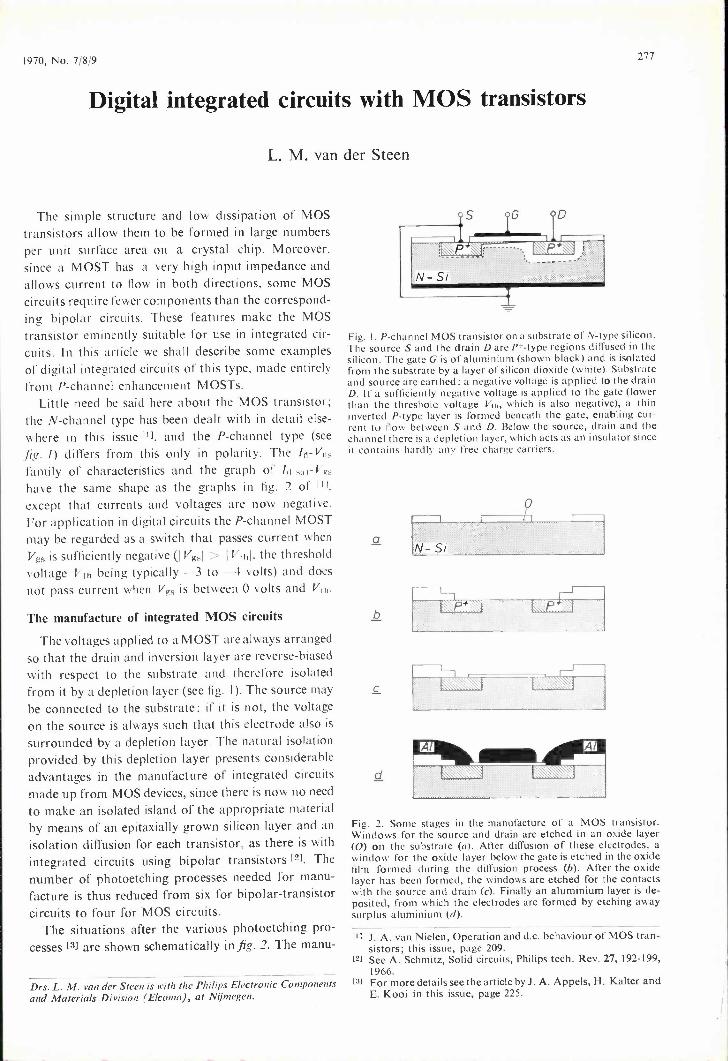
1970, No. 7'8,9 277
Digital integrated circuits with MOS transistors
L. M. van der Steen
The simple structure and low dissipation of MOStransistors allow them to be formed in large numbersper unit surface area on a crystal chip. Moreover,since a MOST has a very high input impedance andallows current to flow in both directions, some MOScircuits require fewer components than the correspond-ing bipolar circuits. These features make the MOStransistor eminently suitable for use in integrated cir-cuits. In this article we shall describe some examplesof digital integrated circuits of this type, made entirelyfrom P -channel enhancement MOSTs.
Little need be said here about the MOS transistor;the N -channel type has been dealt with in detail else-where in this issue II, and the P -channel type (seefig. 1) differs from this only in polarity. The ht -Vii,family of characteristics and the graph of ht sat- Vgshave the same shape as the graphs in fig. 2 of In.except that currents and voltages are now negative.For application in digital circuits the P -channel MOSTmay be regarded as a switch that passes current when
Vg, is sufficiently negative (I VgsI > I Vthl. the thresholdvoltage Vti, being typically -3 to -4 volts) and doesnot pass current when lig, is between 0 volts and Vo.
The manufacture of integrated MOS circuits
The voltages applied to a MOST are always arrangedso that the drain and inversion layer are reverse-biased
with respect to the substrate and therefore isolatedfrom it by a depletion layer (see fig. 1). The source maybe connected to the substrate; if it is not, the voltageon the source is always such that this electrode also issurrounded by a depletion layer. The natural isolationprovided by this depletion layer presents considerableadvantages in the manufacture of integrated circuitsmade up from MOS devices, since there is now no needto make an isolated island of the appropriate material
by means of an epitaxially grown silicon layer and anisolation diffusion for each transistor, as there is withintegrated circuits using bipolar transistors [21. Thenumber of photoetching processes needed for manu-facture is thus reduced from six for bipolar -transistorcircuits to four for MOS circuits.
The situations after the various photoetching pro-cesses [3] are shown schematically in fig. 2. The manu-
Drs. L. M. van der Steen is with the Philips Electronic Componentsand Materials Division (Elcoma), at Nijmegen.
Fig. I. P -channel MOS transistor on a substrate of N -type silicon.The source S and the drain D are P+ -type regions diffused in thesilicon. The gate G is of aluminium (shown black) and is isolatedfrom the substrate by a layer of silicon dioxide (white). Substrateand source are earthed: a negative voltage is applied to the drainD. If a sufficiently negative voltage is applied to the gate (lowerthan the threshold voltage Vih, which is also negative), a thininverted P -type layer is formed beneath the gate, enabling cur-rent to flow between S and D. Below the source, drain and thechannel there is a depletion layer, which acts as an insulator sinceit contains hardly any free charge carriers.
a
b
C
N- Si
FP+
ii
Fig. 2. Some stages in the manufacture of a MOS transistor.Windows for the source and drain are etched in an oxide layer(0) on the substrate (a). After diffusion of these electrodes, awindow for the oxide layer below the gate is etched in the oxidefilm formed during the diffusion process (b). After the oxidelayer has been formed, the windows are etched for the contactswith the source and drain (c). Finally an aluminium layer is de-posited, front which the electrodes are formed by etching awaysurplus aluminium (d).
[1] J. A. van Nielen, Operation and d.c. behaviour of MOS tran-sistors; this issue, page 209.
121 See A. Schmitz, Solid circuits, Philips tech. Rev. 27, 192-199,1966.
31 For more details see the article by J. A. Appels, H. Kalter andE. Kooi in this issue, page 225.

278 PHILIPS TECHNICAL REVIEW VOLUME 31
facture of a P -channel MOS circuit starts with a single -crystal wafer of homogeneously doped N -type silicon(of diameter say 50 m. rri and thickness 250 1../.m), onwhich a silicon -dioxide film is formed in a hot oxygen -rich atmosphere. A photoetching process is used tomake windows in this oxide film at the places wherethe source and drain are to be located (fig. 2a). Thewafer is then heated in a boron -containing atmosphere,so that the boron diffuses through the windows intothe N -type silicon and causes regions of P -type siliconto form. During the diffusion process a new layer ofsilicon dioxide forms on the wafer, and windows aremade in this layer in a second etching process (fig. 2b).By heating in an oxygen -rich atmosphere a thin layerof silicon dioxide (0.1 1..trn) is then formed in thesewindows to give isolation between the substrate and thegate electrodes. In a third etching process windows aremade in this oxide layer above the source and drain(fig. 2c). A layer of aluminium is then deposited, fromwhich the various electrodes and connections betweenthe components of the circuit are formed by removingthe surplus aluminium in a fourth and last etchingprocess.
Since in this technology there is no isolation diffu-sion, which takes up a good deal of space, a very largenumber of components can be formed on a siliconchip. And since the dissipation of MOS transistors isvery low, such a high packing density is a practicalproposition for many circuits. In a dynamic shiftregister, for example, which is discussed later on in thisarticle, the local packing densities are as high as 6 x 10⁴components per cm2, and the average packing densityfor the complete monolithic circuit is 2 x104 cm -2. Amonocrystalline silicon chip measuring a few mm2can now accommodate complete MOS circuits of 300to 1500 component; in the near future monolithiccircuits with several thouspnd components will be
possible. At the present, the average packing densitythat can be achieved in integrated circuit made withbipolar transistors is generally much smaller: about afew thousand per cm2.
MOS logic circuits
Simple logic circuits such as NOR gates or NANDgates are generally used as the "building blocks" fordigital circuits, since all digital circuits, from simplebistable circuits to storage elements, shift registers, etc.,can be made up from such basic. elqpients [4]. A gatecircuit is very easily made with MOS transistors ;fig. 3ashows such a circuit, which has four MOS transistorsTr' to Tr4. Briefly, the circuit operates as follows. Thedrain and gate of Tr4 are both connected to the negativesupply voltage, so that Tr4 always operates in the satu-ration region. However, current can only flow through
a
A B C0 0 0 1
0 0 1 00 1 0 00 1 1 01 0 0 01 0 1 01 1 0 01 1 I l 0
b
Fig. 3. a) The NOR gate, made as an integrated MOS circuit.The supply voltage Vad is negative. The voltages at the inputs A,B and C can be either zero or negative. The voltage at the out-put Q is at the zero level when one or more of the inputs arenegative, since there is then current in the circuit. When negativelogic is used (the negative voltage is then related to the state I
and the zero level to state 0), the relation between the output leveland the input levels is given by Q = A + B C, which is aNOR function. b) The truth table of the circuit with negativelogic.
Tr4 provided one or more of the transistors Tri to TOare passing current, i.e. provided the voltage at one ormore of the inputs A, B and C is sufficiently negative.The circuit is designed in such a way that in this situa-tion the voltage at the output Q is at the "zero level".i.e. between 0 volts and Vii,. If the voltage at each ofthe three inputs is at the zero level, no current flows andthe output voltage is negative. The transistors Tr', Tr.,and Ti3 in this circuit thus behave as switches, and soare called switching transistors: whereas Tr4 acts as aresistor and is therefore called a load transistor.
The voltage levels can be related in two ways to thestates 0 and I used in the mathematical treatment oflogical operations by Boolean. algebra. In positive logicstate I denotes the high level and state 0 the low, andvice versa in negative logic. It is the practice to usenegative logic for logic circuits built up from P -channelMOS transistors: A = I here therefore means thatthe voltage at point A is negative. and A = 0 meansthat this voltage is at the zero level. In the circuit givenin fig. 3a we then have: Q = I if A = 0, B = 0 andC = Q = 0 if one or more of the inputs A, B andC are I. Thus. Q is not I if A or B or C is I; thisNOT -OR relation is represented by the NOR functionQ=-AH-B+C, so that the circuit of fig. 3a, usingnegative logic, is a NOR gate. Fig. 3b gives the truthtable for this case. In the transition from negative topositive logic AND and OR gates change their name,a NOR gate then becoming a NAND gate. This canbe seen from the table in fig. 3b by interchanging onesand zeros; Q is ,then zero (i.e. not I) only if A and B
141 See for example page 48 in: E. J. van Barneveld, Digital cir-cuit blocks, Philips tech. Rev. 28, 44-56, 1967, and page 20in: C. Slofstra, The use of digital circuit blocks in industrialequipment, Philips tech. Rev. 29, 19-33, 1968.

1970, No. 7/8/9 DIGITAL INTEGRATED'CIRCUITS WITH MOSTS 279
and C are 1, so that Q is then indeed equal to A.B.C.The switching transistors, which are in parallel in
fig. 3a, can also be arranged in series; the result is thena gate circuit which, with negative logic, acts as aNAND gate. If the output voltage in a current -con-ducting circuit is to remain within the zero level, thetotal resistance of the switching transistors must notexceed a particular value. This requirement presents nodifficulties if the switching transistors are in parallel;if they are in series, however, an increasing number ofinputs requires the use of larger and larger switchingtransistors, and the circuit then takes up a lot of spaceon the crystal chip. The circuit with parallel transistorsis therefore preferred.
Inverter circuit
To describe the behaviour of the gate circuit duringthe transition between the levels, we can take thesimplest situation, for which B = 0 and C = 0. A canbe 0 or 1, and Q is then I or 0 as the case may be;Tri and Tra then constitute an inverter circuit. We shallnow analyse this circuit, referring to fig. 4, and fromthis analysis we shall derive the requirements that haveto be met in the design of the transistors.
Provided that there is no saturation the current in aMOS transistor is related to the applied voltage Vasand the gate voltage Vgs by:
/a = /3( Vgs - Vt h - Vas) Vas. . . (1)
Here the threshold voltage Vth is the voltage betweengate and source at which inversion starts, i.e. at whichcurrent begins to flow. If I Vas' > I Vgs- Vt1,l, satura-tion occurs and the current is given by:
/a sat - -1/3(Vgs - 1/n02. . (2)
In these equations /3 = u Cos it.//, where ft is themobility of the holes in the channel, Cox the oxidecapacitance per unit surface area (i.e. of the capacitorformed by gate, oxide and substrate), w is the widthand / the length of the channel. (See equations (6) and(9) of the article mentioned in [1].)
For transistor Tr' in fig. 4 we have Vgs = V; andVas = Vo, so that:
Fig. 4. MOS inverter circuit de-rived from the NOR gate offig. 3a with B = C = O. V1 andV. are the input and outputvoltages. When Vi is at the nega-tive level (V1 = 1), V. is at thezero level (V0 = 0), and viceversa.
411 = /91( VI - Vthl- Vo) Vo
if I Vi - Vaal > I Vol (no saturation), and
'dl sat = -1131(Vi - Vthl)2
if I Vi - Vtb 1 I < I Vol (saturation).
Since the gate of Tr4 is connected to the drain, sothat I Vasl > I Vgs Vth4I at all times, this transistorwill always operate in the saturation region. In factTra acts here only as a resistor; a transistor is used atthis position because a diffused resistor of high enough'value would take up too much space on the crystalwafer. For Tr4 we have Vgs = Vas = Vad - Vo (seefig. 4), so that:
/d4 sat = 04( Vdd - Vo - Vth4)2. . . (5)
Fig. 5 shows the /d-Vo characteristics of Th; thesehave V; as parameter and at V1 - Vthl = Vo they allmeet the horizontal part of the curve where the currentis saturated. The figure also shows the curved loadline which is obtained because Tr4 is used as a loadresistance and is derived from equation (5). Since atall times
hl 1 = /(14,
(3)
(6)
the points where the load line intersects the /a-Vocharacteristics of Tri are the operating points of the
11-v/h/ =v.
-(Vdd-111)4) -Vdd
Vo
Fig. 5. Id- Vo characteristics of the transistor Tri from the invertercircuit of fig. 4, showing the curved load line which results whenTr) is used as a load resistor. In the characteristics of Tri theparameter is Vi: when Vi is more negative the current is higher.The dashed line Vi - Vot = V. connects the points where thecurrent through Tri goes into saturation.
circuit at different values of VI; these operating pointsset out in a Vo-V1 diagram form the Vo-V; characteris-tic of the inverter circuit (fig. 6).
In the characteristic given in fig. 6 three regionscan be distinguished. In region 1, Vi is at the zerolevel, i.e. 0 < I Vil < I Vila'. Tri is now not conduct-ing, so that /di = 1/14 = 0, and from equation (5) it
follows that Vo = Vdd - Vth4. This is therefore the"1 level" of the output voltage. In fig. 6 this situation

280 PHILIPS TECHNICAL REVIEW VOLUME 3l
corresponds to the horizontal part of the characteristic;in fig. 5 the operating point lies on the Vo-axis.
In region II V1 falls below the threshold voltage, sothat Tr]. starts to conduct. At the same time, however,
- Ythil < I Vol, and therefore in fig. 5 the opera-ting point lies to the right of the line 1/1- Vita =. Vo,so that Tr i operates in saturation. In fig. 6 a lineartransition now arises between the two voltage levels;the region is bounded here by the lines V1 = Vtiaand Vi - V1111 =
In region III V1 is even more negative, and hereI Tit - Vthil > I Vol. The current through the circuithas further increased, and Tri is now no longer insaturation. In this situation V1 = 1 and hence V, = 0.To ensure that this is so, the voltage divider formed byTr]. and Tr4 must be so arranged that Vo is between 0and Vthl when the circuit is passing current (as a ruleVo is put at approximately 0.1 Vdd). Region I11 liesto the'right of the line .1/0 = Vi - Vuli in fig. 6 andto the left of it in fig. 5.
We shall now take a closer look at the situation inthe transition region I I. in which both transistors oper-ate in saturation. From equations (4). (5) and (6) it
then follows that:
01( Vi - Vth )2 = 04( Vdd - Vo - V1114)2 (7)
and this gives:
Vo = -044)1/2 ( Vi - Vt hi) ( Vdd VIIi4 ) (8)
In this region the V0-1/1 characteristic is therefore astraight line with a slope of a = -(13034)112. Fig. 7shows a set of these characteristics for various valuesof a and for the same values of Vdd. Volt and V1114.In designing a circuit the choice of a is partly deter-mined by the requirement noted above that in region I l
the output voltage should be at the zero level. Thismeans that the slope must exceed a particular limitingvalue; in practice it is usual to take 1111114 z 20.
Since the transistors are parts of a monolithic circuit.and are thus formed during the same operation. theyhave the same thickness of oxide layer below the gatesand the same mobility for the holes in the channels. In/31 and P4 the factors ft and Cox are therefore identical,so that
i9 willt=P4 W4/14
The ratio /-311/34 is therefore determined entirely by thew// aspect ratios of the transistors. lf, for example, theswitching transistor` has the dimensions iv =--
p.m (so that wilii. = 1), and if fl11/34 should have avalue of 20 to give the right slope, then 11)4/14 for theload transistor should have a value of 1/20. Thus wecould have w = 10 t./..m arid / = 200 p.m.
11=Vtni
,/ti-v/h1=vo
Fig. 6. Vo- V1 characteristic of the inverter circuit in fig. 4, derivedfrom fig. 5 by plotting the points where the load line intersectsthe hi- V. characteristics of Tri. In region I, Vi = 0 and Vo = 1;in region III, Vi = 1 and Vo = 0. Region 11 is the transitionbetween these situations. The curves Vi = 1/11,1 and Vi - Vult
Vo form the boundaries between the regions. In I and It thecurve is virtually a straight line.
Fig. 7. Some V0-1,1 characteristics for different values of flillit.In the transition region II the slope of the curves is proportionalto (/31/134)1/"2. The output voltage in region III is within the zerolevel only for the two steepest curves in this region.
The characteristics of figs. 6 and 7 hold for the NORcircuit of fig. 3a when only one switching transistor isconducting. If several switching transistors are acti-vated simultaneously, Vo adjusts itself to a still lowervalue; the NOR circuit will operate correctly in anysituation if each of the switching transistors has thecorrect value of /1 to suit the load transistor.
If the load transistor were to be replaced by a diffused resistor,a widely used integrated -circuit element, the surface area of thisresistor would be much larger than that of the load transistor.The resistance between source and drain of a MOS switchingtransistor of minimum dimensions (w = 1= 10 1.1,m) is severaltens of Ica This means that a load resistance of several hundred

1970, No. 7/8/9 DIGITAL INTEGRATED CIRCUITS WITH MOSTS 281
k11 should be used to give the correct voltage division. A diffusedresistor of this value would be about 10 mm long and 10 1.un wide,whereas the corresponding load transistor with the same widthis only 0.2 mm long. Although the load transistor has the ad-vantage of being small it has the disadvantage that the full supplyvoltage can never be obtained at the output of the circuit, sincethe threshold voltage of the load transistor is always lost. An-other disadvantage is that the response of the circuit with theload transistor is slower than when a diffused resistor is used.However, the most important feature is the extra space gainedon the chip.
The /WA-hint/71 switching frequency
The maximum permissible switching frequency of aNOR circuit is determined by the speed at which theoutput voltage switches over, and hence by the rate atwhich the capacitor connected to this output is chargedup. Of course, we must consider the worst case here,i.e. the transition from 0 to I, at which the switchingtransistors stop conducting and the output capacitor istherefore only charged up by the load transistor.
In a logic circuit the load on the output of a NORwill usually be several inputs of other NOR circuits.Here we shall take the simplest case where the only loadon the NOR is a single input of another NOR (e.g.input A in fig. 3a), so that the load is determined mainlyby the capacitance Cl of this input. Then the chargingcurrent /d4 sat is equal to -1/34(Voci - Vo - Vth4)2,and is therefore also equal to Cid Voldt. Fromthe differential equation obtained by equating thesetwo expressions it can be shown that the .RC timeconstant is proportional to COL, and hence to
Since the value of oc is already fixed, we must make/1 small to be able to reach a high switching frequency.The channels in the switching transistors must there-fore be as short as possible and it must be as large aspossible.
A much more unfavourable situation is found whenthe output of a NOR gate is not connected to anotherNOR circuit but to a point outside the integrated cir-cuit. The load capacitance is then usually determinedby the printed wiring of the board on which the inte-grated circuit is mounted. This wiring capacitance mayeasily be 1000 times larger than the input capacitanceof a NOR (a few tens of pF against a few tens of fF;1 fF = 10-15 F), and consequently the switching fre-quency for the logic circuit as a whole would be 1000times lower. Measures therefore have to be taken tokeep the RC product as small as possible. This is doneby using larger load transistors for the final NOR cir-cuit connected to this high capacitance, which make thecurrent 100 times greater than in the earlier circuits.The resistance of the load transistor in this circuit isthen only 1/100 of the original value, so that the RCproduct at the output is now not 1000 times larger but
only 10 times. The switching transistors in the laststage must of course be made larger in the same way,and this in turn gives a 100 times greater capacitiveload for the penultimate stage. To maintain a reason-able RC time constant the current through this stagemust therefore be increased as well, say by a factor of10, so that larger transistors are also necessary here.The output stages of a circuit thus take up a relativelylarge amount of space on the chip; in fact it may hap-pen that no transistors at all of minimum dimensionscan be used in a small circuit.
MOS shift registers
It can be seen from the above that MOS transistorsare most suitable for use in integrated circuits with asmall number of outputs. This is the case, for example,in stores with a fixed information content (read-onlystores), in "scratch -pad" stores and in shift registers.A shift register consists of a sequence of bistable cir-cuits, or cells whose information content, i.e.. the stateof the individual cells, moves up one place when a shiftpulse or a combination of pulses is applied. Thus,information supplied to the input of the first cell ap-pears, after a number of shift pulses, at the output ofthe last cell of the register. Shift registers are widelyused as storage elements in the arithmetic unit of acomputer.
A distinction is made between static and dynamic
shift registers. In static shift registers the informationcontent of the register is stored for an unlimited timeafter a shift pulse. In dynamic shift registers the infor-mation content is soon lost and therefore has to berepeatedly replenished. The shift pulses must con-sequently be repeated at a particular minimum fre-,quency, and this means that the information in adynamic shift register can never be kept in the sameplace. Another disadvantage of dynamic shift registersis that they require a more complex combination ofshift pulses than a static type: On the other hand, adynamic shift register is a great deal faster than a staticone, and its dissipation is also much lower. Moreover,in integrated -circuit form a dynamic shift register canhave a greater. packing density than a static shiftregister.
The static shift register
Fig. 8a gives the diagram of a static shift -register cellbuilt with MOS transistors.. The cell consists of abistable circuit (or flip-flop) formed by two invertersTr1-Tr2 and Tr3-Tr4 coupled to form a loop by meansof Tr6 and Tr7. The capacitors C1 and C2, which playan essential part in the operation of the cell, are formedby the capacitances between the gates of Tri and Tr3
and the substrate, and by some stray capacitances. The

282 PHILIPS TECHNICAL REVIEW VOLUME 31
output voltage V0 represents the information contentof the cell. States 0 and 1 correspond, as in the invertercircuit, to the zero level (Vo between 0 volts and Vol) and the negative level (Vo = Vdd Vth4). The infor-mation in the preceding cell of the register is presentedas a voltage V1 at the input of the cell. The gate signals01, 02 and 03, consisting of shift -pulse trains (fig. 8b)are also fed to the circuit; the pulses 02 and 03 differonly in the steepness of their leading edges. Whenever'a combination of shift pulses arrives, the informationcontent of the previous cell is taken over; in otherwords, the voltage Vo assumes the level of
a
b
Tr2 pi Li
Tr;
C-1=
Trh
Vdd
C2
Tr
T
41 1 U0
t-2 1
03 LI
Fig. 8. a) Diagram of a cell of a static shift register. Tri-Tr2 andTrn-Trn form two inverter circuits, which are coupled to form aclosed loop by means of Trn and Tr,. The level of Vo (zero ornegative) is regarded as the "state" of the cell; V1 indicates thestate of the preceding cell. b) The control (gate) signals 01, 02and Os form a train of shift pulses. The information at the inputis transferred to the output by each group of three pulses.
Fig. 9a gives a photograph of a 64 -bit static shiftregister built up from cells of the type shown in fig. 8a.An idea of the way in 'which the various componentsare joined together to form a circuit can be obtainedfrom fig. 9b, which illustrates a single cell from theregister; this is the cell that can be seen at the upperleft of the photograph.
The cell works as follows. In the situation where 01is at zero level (see fig. 8a) and 02 and 03 are negative,Tr5 passes no current while Tr6 and Tr7 are both con-ducting. Assuming that the output voltage Vo is at thezero level, then the gate of Tr1, through Tr6, is also at
this zero voltage (i.e. Cl is not charged). Tn then passesno current, so that point A is negative, and this nega-tive voltage appears via Tr7 at the gate of Tn3 (i.e. C.is negatively charged); TO passes current, so that Vois held at the zero level. The two inverters are thuscross -coupled via Tr6 and Tr7, so that the outputvoltage remains unaltered.
At the instant when the shift pulse 01 arrives thesequence of events is as follows. b2 and 03 go to thezero level, so that Tr6 and Tr7 no longer conduct andthe cross -coupling is broken. The output voltage, how-ever, is maintained because the capacitor C. is nega-tively charged and Tn3 therefore continues to pass cur-rent. Since 01 has become negative, Tr5 starts to con-duct. Assuming that the content of the preceding cellis I, then CI will become negatively charged via Tr5,so that Tri also starts to conduct. If 01 returns to thezero level, Tr6 becomes non-conductive again, butthe negative voltage on CI remains and Tr' continuesto conduct. At the same time P2 and 03 go negativeagain, so that Tr6 and Tr; agairi start to conduct. Sincethe leading edges of these pulses are not equally steep,Tr7 starts to conduct somewhat earlier, so that C2discharges first through this transistor and Tr' ; as aresult, Tr3 stops conducting and V. becomes negative.Meanwhile Tr6 also starts to conduct and the cross -
coupling is restored, but now with a negative outputvoltage, with C1 negatively charged and C. discharged.The information can now be stored again for an un-limited time.
The principle of this cell is thus fairly simple. Duringthe shifting process the cross -coupling is broken; theold information is held at the output by the capacitorC2, which keeps the inverter Tr3-Tr.1 in its former state.The new information is meanwhile applied to CI,causing Tri-Tr2 to assume the new state. Next, CO israised to the new voltage (via Tr7), so that Tr3-Tr4 alsoassume the new state, and the cross -coupling is thenrestored through Tr6.
During the transfer of information a capacitivestorage is used twice. The capacitor Cl need only retainthe charge during the leading edge of 03, that is to sayuntil the cross -coupling is restored, while C2 must holdthe charge during the time that 02 and 03 are at thezero level. Both capacitors can only discharge throughthe leakage current of the P -N junctions of Tr6 and Tr7.At room temperature the time constant of this dis-charge can have a value of a few tens of milliseconds;if we compare this with the conventional pulse dura-tion of 1 to 20 .is, we see that the storage action of thecapacitors is amply sufficient.
The maximum permissible frequency of the shiftpulses depends on the speed at which the circuitchanges state. This speed is determined by the time

1970, No. 7/8/9 DIGITAL INTEGRATED CIRCUITS WITH MOSTS 283
- ITITITITITITITITITITITITITITITITITITITIT
vm....... "
....***.......1,wI
2
Vdd
Vdd
2Oim
Fig. 9. a) A static shift register (64 bits) using the cell shown in fig. 80. The circuitcontains 458 components and measures 1.15 by 2.3 mm. The blue -grey strips are thescribed lines along which the crystal wafer can be broken to separate the circuits fromeach other. In the blue regions the upper layer consists of oxide, in the white regionsit consists of aluminium.h) Sketch of a single cell from the shift register. The areas covered with oxide areshaded; the shading is light where there is only substrate material under the oxide,and dark where there is a diffused region below the oxide. The areas where aluminiumhas been deposited by evaporation are left white, whatever is beneath them. The solidlines in the aluminium indicate boundaries between diffused regions and substratematerial; the dashed lines indicate regions with a thin oxide film (these are mostlythe isolation layers under the gate electrodes). These boundaries can also be seen onthe photograph, since there is a difference in height here. The contact windows areshown cross -hatched; these are the locations where the aluminium layer makes contactwith an underlying diffused region of source or drain. The various transistors inthe diagram are indicated by their number, placed in the channel.
A number of these cells are placed side by side, and the various signals are appliedto the strips of aluminium, which are clearly visible in the photograph. The sources ofTr]. and Tr:3 are earthed by connecting the central diffused layer with the earthedsubstrate at a point which lies outside this diagram.
needed to charge CI or C2. In the transition from state I to state 0,described above, CI must be charged via transistor Tr4 of the previouscircuit. During the transition from I to 0, C2 must be charged via Tr2and Tr7. Since Tr2 and Tr4 are load transistors, they have a fairly highresistance; however, when they are combined with switching transistorsof minimal dimensions (Ci and C2 are then about 50 fF), the RC timeconstant for charging the capacitors can still be as small as 50 ns. Inthe situation illustrated, i.e. the transfer of information between twosuccessive cells in the shift register, this gives a maximum shift -pulserepetition frequency of I MHz. The speed of the register as a wholeis of course adversely affected by the output stage in the same way asdescribed for the NOR gate; in practice the maximum frequency wouldbe about 250 kHz.

284 PHILIPS TECHNICAL REVIEW VOLUME 31
The dynamic shift register
Fig. 10a shows the diagram of a dynamic shiftregister cell built with MOS transistors. The level ofthe output voltage Vo again indicates the state of thecell, and Vi the state of the preceding cell. C1 and C2are the capacitances of the gates of Tn. and Tr4, is
the capacitance C1 of the next cell. There are four shiftsignals 01, 02, 03 and 04 (fig. 10b), consisting of nega-tive pulse trains; after each group of four shift pulsesthe input voltage is taken over by the output. In fig. 10ait can be seen that both 01 and 03 are fed to two pointsof the circuit. Fig. 11a gives a photograph of a part of adynamic shift register in which this cell is used; fig. 1lbagain shows a diagram of one of the cells from thisregister.
To explain the operation of the cell we start from thesituation where Vi is negative; Tr1 is then conducting.At the moment when the first shift pulses arrive. 01and 02 go negative, so that Tr2 and Tr3 also start toconduct. From the source supplying the voltage 01the capacitor C2 will now be charged to a negativevoltage via Tr3 and the series arrangement of Tr1 andTr2. The voltage 01 then returns to zero, but 09 re-mains negative. As a result, Tr3 stops conducting butTri and Tr2 continue to pass current, and since the gateof Tn is now at the zero level, C2 discharges throughthese transistors. When 09 also returns to zero, C., isthus nearly discharged. Now when the shift pulses of03 and 04 arrive, Trs and Tr6 start to conduct but Tr4remains non -conducting because C2 is discharged.C3 is now charged (through Tn6 only). but when 03returns to zero it can no longer discharge. Thus, when04 also goes back to zero, a negative voltage remainsat the output.
If the input voltage is at the zero level, Co cannotdischarge because Tn. does not go into conduction.Consequently C2 remains negative, which then enablesC3 to discharge, and the output voltage goes to zero.We see that in both cases the voltage that was at theinput is transferred toward the output after four shiftpulses. Since four phases can be distinguished in thisprocess, a circuit of this type is known as a four -phaseshift register.
The dynamic shift register of fig. 10a is based on thestorage action of the capacitors Cl and C2. Thesecapacitors, however, discharge as a result of the leakagecurrents in the P -N junctions of the correspondingtransistors, and since the dynamic circuit has no cross -coupling as in the static type, the information would begradually losi. To prevent this, the loss of charge isregularly compensated by the signals 01 and 03, andthis means that the whole shift -pulse pattern must berepeated at a particular minimum frequency. The re-gister therefore continues to transfer the information.
b
oLI U
02 1 11 1_1o
°3 1 U U0
C4 11_1 L_I
Fig. 10. a) Diagram of a cell from a dynamic four -phase shiftregister. The output voltage V0 indicates the state of the cell,and the state of the preceding cell. b) The gate signals Oh02, 03 and 'P4 consist of negative pulse trains: the informationat the input is transferred to the output by each group of fourof these shift pulses.
The minimum frequency at which the shift pulses haveto be supplied depends on the magnitude of the capaci-tances and leakage currents. Since leakage currents ofP -N junctions are involved the repetition frequency istemperature dependent; at room temperature a fre-quency of 40 or 50 Hz may be high enough, but forevery 10 degrees increase in temperature the minimumfrequency required increases by a factor of 2.
For the static shift registers MOS transistors of dif-ferent dimensions are needed (switching and load tran-sistors) in order to obtain the desired voltage divisionin the inverter circuits. This is not necessary for thedynamic registers, and switching transistors of mini-mum dimensions can therefore be used. The capaci-tances C1 and C2 in fig. 10a have about the samevalue as those in the static shift register in fig. 8a, butduring the transfer process they are charged up throughtransistors whose resistance is a tenth of that of theload transistors in the static register. Because of thisthe maximum permissible shift frequency for thedynamic shift register is an order of magnitude higherthan for the static type; it is about 10 MHz. Anotherconsequence of only using switching transistors is thatthe component density on the chip is higher in dynamicregisters.

1970, No. 7/8/9 DIGITAL INTEGRATED CIRCUITS WITH MOSTS 285
sailiammildike =As oralie NBA maw warm Am iiissamjiLdfio111110 01110 IMO WOO WOO MC MK) IMO WOO WIC IMO
katribRatglinaltklatalantitgiAXPIMPYVVVIR.:41411114X.
kettosettanallsenagionerittrindOink apt Gilt MOP 011111 OM Cali Oils 011111: D h 010111 all14
rIrei.161.76.6.1q1186.;146.11786.7571STEITrEppalur
*140 11410 440 440 440 MC 440 It40 440 1100 440
imillawfinfinstalandatilsamobst000 440 *140
6rimwtaliffirin"14161"rtrill 1111
riklitaskithirkiniihrkv!iretivliValatikstembsalsriartatiumo#11,X414414,11,#44:41.4ff.
a
(153
r'
VoO
lOpm
Fig. I I. a) Part of a dynamic shift register built up with cells of the type shown in fig. 10a.
h) Sketch of one cell of the shift register. The various areas are indicated in the same wayas in fig. 9b.
The cells are located in a row on the crystal wafer and the various voltages are appliedto the aluminium strips. The photograph shows four such rows of cells one above the other,the strips for the voltages 01 and 03 being connected to adjacent rows; the transistor Tn;in the sketch therefore belongs to a cell in a following row.
The dynamic register also dissipates less heat. In thestatic shift register there is always current flowingthrough one of the two inverter circuits, and the dissi-pation per cell is 2 mW. In the dynamic shift register nocurrent can flow direct to earth; energy is only dissi-pated when the capacitors are charged. The dissipationis therefore substantially lower than in the static case,and moreover it is proportional to the frequency of theshift pulses. The dissipation per cell is 50 µW/MHz;even at a pulse frequency of 5 MHz the dissipation
per cell is therefore no more than 250 [LW, which is agreat deal better than the 2 mW per cell of the staticregister.
As we noted earlier, there is a penalty to be paid forthese advantages: the information cannot be kept inthe same place and a more complex combination ofshift pulses is required.
Summary. The source and drain in MOS transistors are isolatedby a depletion layer from the substrate, so that no isolation dif-fusions are required. MOS transistors can therefore be packedvery densely on a crystal wafer. Since MOSTs also dissipate littleheat, they are very suitable for use in integrated circuits. After abrief description of the technology, some examples of such cir-cuits are given. The first is a logic circuit: the NOR gate, in whichthe MOS transistors are used as switches and also as resistors:the MOST is smaller than a diffused resistor of the same resis-tance. The other examples, a static and a dynamic shift register,make use of the specific advantages of the MOST: its very highinput impedance and the fact that the current through a MOSTcan flow in both directions. A cell cf the static shift register con-sists of a bistable circuit; the cell of the dynamic shift register isbased on the storage action of a capacitor. In the dynamic shiftregister there is no cross -coupling to prevent the informationfrom being lost, and the voltage on the capacitor therefore hasto be continuously replenished by the shift pulses (4 pulses percycle). This means that the information in the dynamic registermust be kept moving through at a specific minimum frequency.Compared with the static type the dynamic register has the twoadvantages of a maximum pulse frequency that is 10 times higher(10 MHz against I MHz), which is possible because only MOSTsof minimum dimensions are used, and a lower dissipation(50 1.1.W/MHz per cell as against 2 mW per cell).

286 PHILIPS TECHNICAL REVIEW VOLUME 31
A MOS transistor store with discretionary wiring
A. F. Beer
Introduction
There has been in the past few years an increasinginterest in the possibility of using integrated circuitsfor computer storage. This interest has arisen for anumber of reasons. Since integrated circuits are usedfor the logic operations in data-processing machines,the introduction of I.C.s into storage would reduce thepresent problems associated with driving ferrite -corestores from the relatively low signal levels availablefrom I.C.s. Furthermore, integrated circuits offer po-tential advantages in speed, size and also cost. How-ever, although integrated circuits can be very cheap,the costs associated with their assembly into largesystems is high so that in order to make an economicsemiconductor storage system it is necessary to in-corporate as many storage elements (bits) as possibleinto one package. Such an approach is generallytermed large-scale integration.
Mullard Research Laboratories have chosen aparticular technique to solve some of the problems oflarge-scale integration in the development of a fullyintegrated 32 -word, 32 -bit -per -word store, which in-cludes independent read and write selection matricesand has a worst -case read-write cycle of about 450 ns.The design and technology for making this store isdescribed in this article.
The MOS transistor was chosen as the active devicein the bit circuits since its simple processing shouldlead to high yield and high packing density. However,even with MOS transistors it is unlikely that the yieldwill be high enough to make a 1024 -bit static store onone silicon chip without some faults M. Therefore it wasdecided to incorporate on one silicon chip more bit cir-cuits than are finally required, test them and devise aninterconnection pattern which joins good circuits onthe chip and by-passes faulty ones. This technique isknown as discretionary wiring. For the store describedin this article an initial array of 40 x 40 bits is provided.The interconnection pattern joins 1024 of these appro-priately to form the 32 -word, 32 -bit store.
When the first draft for this article was written,several small storage units had been completed andhad worked successfully, but on each of the 1024 -bitchips some bits failed to work. Investigation of these
A. F. Beer, B.A.Sc., is with Mallard Research Laboratories, Red -hill, Surrey, England.
units showed that the failures were due to faulty con-tacts between the interconnection lines and the appro-
.,priate bits. The difficulty has since then been over-come.
In the next section the possible approaches to large-scale integration are briefly discussed. The subsequentsections deal with design, fabrication and testing of thecircuits and the details of interconnection strategy andmask manufacture. The article is concluded with adiscussion of the -results so far 'achieved =as well assome considerations concerning the expected cost ofdiscretionary wiring compared to other large-scaleintegration techniques as applied to storage systems.
Approaches to large-scale integration
In the field of semiconductor storage, present-daytechnology enables one to make at reasonable yield astatic store of about 256 bits. As techniques improve thisfigure will increase but the rate of increase is unlikelyto be high. On the other hand, the main use for semi-conductor stores will be in computers where even asmall machine might require as much as 250 000 bitsof storage (i.e. two thousand I28 -bit units). As men-tioned in the introduction the packaging of each smallunit and the assembly of many packages into a largesystem is expensive. Therefore some new techniquesare required for integration.
Two main approaches have been put forward forlarge-scale integration. In one, the multi -chip system,small storage units are fabricated by conventionaltechnology, but instead of mounting each one in apackage a number of units are mounted on one appro-priate substrate, using some special technique such as"beam leads" or "flip chips". An interconnectionpattern is provided on this substrate so that the small'units are correctly joined together to form a largerstore. These substrates can then be built up to formlarge stores using techniques similar to those involvedin the assembly of printed -circuit boards. The numberof bits in each unit and the number of units on a sub-strate are determined by the yields and costs of theprocesses involved. At present, substrates containingone or two thousand bits are feasible.
The second approach, namely discretionary wiring,is designed to increase the size of the store that can be

1970, No. 7/8/9 MOST STORE WITH DISCRETIONARY WIRING 287
made on one silicon chip. This is done by Providing,on the silicon chip, more circuits than are actuallyused, probe testing each one and then devising andapplying an interconnection pattern to join the goodcircuits while by-passing faulty ones. In this way alarge store (equivalent to the completed substrate inthe multi -chip system) can be made in one package, andthe amount of assembly necessary for the main com-puter store is minimized.
The size of each circuit (i.e. the number of bits ineach circuit) and the size of the final store are deter-mined as in the multi -chip system, by the yields andcosts of the processes. For our MOST store it wasdecided that the final size should be 1024 bits, andthat each circuit should consist of one bit only. Thenumber of excess bits required is a function of bityield and the interconnection scheme available. Inour case, an initial array of 40 x 40 bit circuits wasfound to be satisfactory.
A great deal of discussion has been recorded in theliterature on the relative merits of the multi -chip,discretionary -wired and fixed -wired systems [1). Thispaper will not add to that material beyond pointingout that because of the simple repetitive nature of thestore, the computation and generation of an inter-connection pattern for discretionary wiring is herequite straightforward. As a result the costs of the pro-cesses are expected to be fairly low and a fully compet-itive product appears to be possible.
The circuits
The bit circuits
Although the use of discretionary wiring leads toless stringent requirements on yield, a relatively highbit -circuit yield is still needed as will be seen in thesection on the interconnection algorithm. Further-more, because of the excess circuits provided on thechip, discretionary wiring requires more silicon areathan other systems. Therefore, it is desirable to employprocesses leading to both high yield and high packingdensity. This leads directly to the choice of a singletype of MOS transistor as the active device since ithas much simpler processing and higher packing den-sity than either bipolar transistors or complementaryMOS transistors (i.e. combinations of N- and P -channel MOSTs in one circuit). Because the P -channelMOS transistor is normally of the required enhance-ment type it was chosen in spite of its lower gain com-pared to N -channel MOSTs.
The circuit chosen for the storage cells is shown infig. 1. It is made up of two cross -coupled invertersconsisting of two active transistors (Ti and T4) andtwo load transistors (T2 and T3). An extra transistor
3 4 5Fig. 1. The storage -cell circuit ("bit circuit"). It consists of, twocross -coupled inverters (MOS transistors TI -T4), a MOS tran-sistor for writing into the cell (Ts) and two MOS transistors forreading (To and T7). 1 word -read line, 2 word -write line. 3 senseline. 4 digit line. 5 supply -voltage line.
T5 is provided for writing into the cell, and two furthertransistors, T6 and T7, are used for reading -out.
The gains of the active and load transistors have to be propor-tioned to give the appropriate logic levels, dissipation and speed.If node a is set to the "one" state, its voltage is -V - Vth, where-V is the supply voltage and Vu, is the transistor threshold volt-age with substrate bias. This must be sufficient to make transis-tor Ti conduct hard enough for the voltage at node b to be morepositive than -Vu,, i.e. T4 is off. A ratio of about 10 : 1 in thegains of the active transistors (Ti., T4) to the gains of the loadtransistors (T2, T3) is adequate for this. Having fixed the gainratios of the transistors the absolute values of the gains are thenadjusted to give acceptable speed and dissipation.
Setting of the bit is achieved by applying a negativepulse to the gate of T5 (word -write line) and therebyforcing node a up to zero ("0" state) or down to-V - Vth ("1" state) by the appropriate voltage onthe drain of T5 (digit line). The time required to setthe cell is determined by the rate at which the capaci-tance attached to node b can be charged to -V-Vththrough the load MOS transistor (T2) or discharged tozero through the active MOS transistor (Ti). Since T2has substantially lower gain than T1, the negative -going transition of node b will be the slower - i.e.setting the cell in the "0" state. The capacitance atnode b is made up of the gate capacitance of T4, thedrain capacitance of T1 (or source of T2), some por-tion of the channel capacitance of T2 and some straycapacitance due to aluminium connections.
The dissipation of the circuit is determined by the"on" resistance of the load transistors. When this re-sistance is increased, the node b capacitance (exclud-
I*[ This article is concerned only with static storage. Usingdynamic -circuit techniques, 1024 -bit units are available, butthese techniques are not considered here. (Cf. the previousarticle in this issue.)
I1I See for example: R. L. Petritz, Current status of large scaleintegration technology, IEEE J. Solid -State Circuits SC -2,130-147, 1967, and D. A. Hodges, Large -capacity semicon-ductor memory, Proc. IEEE 56, 1148-1162, 1968.

288 PHILIPS TECHNICAL REVIEW VOLUME 31
ing strays) is decreased if the gain ratio is maintainedby reducing the length of .the devices rather than in-creasing source -drain separation. Hence the speed ofthe circuit remains constant as dissipation is varieduntil the transistors' become so small that the straycapacitances start to dominate. The time constant ofnode b starts to increase at about 3 mW dissipationand by 1 mW is increasing extremely rapidly. The bithas been designed to operate at 2 mW where the risetime has increased only a small amount. Node b thenrequires about 150 ns for a negative -going transition,while the opposite transition takes place in about 50 ns.
The slow transition could be improved by incorporating afurther transistor in the circuit similar to T5 but connected tonode b and with its gate coupled to that of T5. Then both nodescould be forced up or down through these low -impedance tran-sistors and only 50 ns would be required for either transition.However, such a circuit would require an additional digit lineleading to increased complexity in interconnections.
Reading of the cell is accomplished by current -sensing off -chip. The current derives from the bufferamplifier To and the gating transistor T7. This mini-mizes direct loading of the bistable and offers a reason-ably fast non-destructive read-out. Since it is desirableto use bi-polar transistors for sensing this current, theyhave to' be supplied off -chip and may serve for otherstore planes as well in a main store of many planes.
The circuit has been simulated on an Elliot 503computer [2]. This has shown that with the circuitchosen, wide tolerances of transistor parameters arepermissible. The circuit will operate reliably if thefactor 13 [3] is in the range 0.34 ± 0.07 A/V2m and ifthe threshold voltage Vth is in the range -3.5 ± 1.5 V,provided the supply voltage is at least a factor of threegreater than Vth.
The selection matrices
If the chip containing the 1024 bits is mounted in apackage as a simple 32 -word 32 -bit store, a total of130 leads, must be provided between the chip and thepackage: 32 each of read, write, sense and digit plusearth and supply. This is clearly unsatisfactory butcan be improved while still retaining the word organi-zation of the store if selection matrices are providedon the chip to reduce the number of word -read andword -write connections. However,it is then necessaryfor the processing of the selection matrices to be com-patible with that of the MOS transistors, and thesimplest means to achieve .this is to use MOS tran-sistors as the active devices in the matrices as well,even though this is likely to lead to slower speeds thanbipolar devices.
A number of matrices have been studied. The com-plete binary selection system shown in fig. 2 reduces
32 word -write or word -read lines to one input and tengate leads, but because there are five MOS transistorsin series it is very slow. This matrix can be improvedby increasing the branching at two of the levels to foureach, so that there are only three branching levels(2 x 4 x 4) and hence only three transistors in series.This gives a delay time of about 450 ns which is stillrather long.
The matrix finally chosen is shown in fig. 3. It re-quires one more lead (twelve in total) than the completebinary system and is an incomplete matrix in thatsome additional selection off -chip is needed to separ-ate the eight input leads. However, in a large systemrequiring several store planes this can be coupledwith the selection required between store planes.
The complete store has independent read and writematrices. A complete read-write cycle occupies about450 ns. Reading alone, including selection, requiresabout 150 ns.
Silicon processing
The basic processing is largely conventional. Thesilicon is 3 C2cm N on N+ epitaxial material orientedin the <100> direction. The N layer is 10 (../.m thick andthe N+ substrate is 150 p.m thick. The epitaxy is
required to ensure a low resistance through thematerial as the earth line is the common substrate.
A thick (800 nm) steam -grown oxide is provided tomask off the diffusions. The source and drain regionsare boron -diffused from oxidized slices of boron ni-tride. After reoxidizing the boron -diffused windowsand opening new ones, a phosphorus diffusion is pro-vided to ensure good ohmic contact to substrate ofthose regions which are earthed. At the same time thephosphorus diffusion provides channel stoppers inthose regions where parasitic MOS transistors mightotherwise occur.
After the boron and phosphorus diffusions, the gateregions and source and drain contact areas are strippedof the thick oxide, and a new oxide layer is grown at1200 °C in a double -walled tube in very dry oxygen.Immediately following the oxidation (1 hour giving200 nm oxide), the gas is changed to dry nitrogen for afive-minute anneal at the same temperature. Aftercooling a phosphorus deposition drive-in is carried outfor stabilization. The resulting phosphorus glass is
about 15 nm thick.Contact windows are opened in the thin oxide using
double photoresist methods, and aluminium is evap-orated using an electron -bombarded source. Follow-ing definition of the aluminium, the slice is annealedat 450 °C in wet nitrogen in order to remove excesssurface states.
A second dielectric layer is then deposited on top of

1970, No. 7/8/9 MOST STORE WITH DISCRETIONARY WIRING 289
B C
11-7 . ABC
'ABCT.177" ABC
AgeT1
Thr-o ABC
T.
ABC
TABC
Fig. 2. Three of the five stages of a complete binary se ection cir-cuit for the reduction of 32 word -write or (word -read) lines toone input. There are ten gate leads (A, A etc.) in the completematrix. A system like this is very slow.
8
Fig. 3. The selection circuit applied in the MOST store consistsof eight equal groups of four MOS transistors each. Two ofthese groups are shown. The total number of input leads is 12,i.e. one more than in the complete binary circuit shown in fig. 2.
the slice. At present, the preferred dielectric is Si02,deposited from the reaction of SiH4 and 02, but r.f.sputtered Si02 has also been used.
Holes are etched in the top oxide to the aluminiumunderneath, after which a second layer of aluminiumis evaporated and probe pads defined. Fig. 4 shows apart of a slice processed to this stage and a cross-section through one bit circuit. Each bit circuit occu-pies about 270 x 220 1./.m and is repeated at 300 ti.msteps in both directions. It can be seen that probe padsare applied to the word -write, word -read, digit, senseand supply -voltage lines, the earth line being completedthrough the substrate. The digit, sense and supply -voltage lines are each provided with two contacts tothe top region. Only one is used for probing but bothare needed for interconnections subsequently.
When the good circuits have been determined andthe interconnection mask made, aluminium is re -eva-porated and the interconnection pattern defined. Thisis an extremely critical operation since any faultoccurring after testing usually means the rejection ofthe entire chip.
A number of techniques are being examined in orderto improve the interconnection yield - that is, theyield of chips free from interconnection defects.Present results suggest that it will not be impossibleto use aluminium alone but a higher success rate maybe achieved by the use of two metals, such as molyb-denum and gold, evaporated one on the top of theother, and defined in different etches. This will 'tendto reduce the incidence of short circuits between ad-jacent lines without increasing the incidence of opencircuits in any one line.
Testing
In a production system it would be sufficient to carryout a series of go/no go tests on each element of thestore and to use the results as the basis for the inter-connection pattern. Such a procedure could be veryfast. For example, by having two probe machines al-ternately driven by one tester, and having the probesconnected simultaneously to four bit circuits at eachmeasuring position, two complete 40 x 40 arrays couldbe measured in about two minutes. At the presentstage of development however it is necessary to notethe results of each measurement and analyse eachfault in order to adjust the processing of the slices togive the best result.
The system used at present consists of a high-speedprobe -test machine' coupled to a data logger. Each
[2] L. F. Gee, D. W. Parker and P. Swift, An M.O.S.T. store,Information Processing 68, Proc. IFIP Congress, Edinburgh1968, Vol. 2, pp. 778-782.
[31 The significance of the factor j9 and the voltage Yen is discussedin the article by J. A. van Nielen in this issue, page 209.

290 PHILIPS TECHNICAL REVIEW VOLUME 31
I 4g. 4a
Fig. 4. a) Photomicrograph of apart of a silicon slice ready forprobing the bit circuits. Nineof these circuits are entirely orpartly visible. Each of the fiveconnections of every circuit isprovided with a probe pad.Magnification 130 .
b) A part of (a) extending overone bit circuit. S, G and D arethe source, gate and drain ofthe different transistors; thesubscripts and the numbers onthe probe pads correspond withthose in fig. I.c) Cross-section through one bitcircuit (not to scale) along theline a -a drawn in (b).
01,02 and °t are the differentoxide layers, Pb is a protectingphosphate -glass layer and St achannel stopper.

1970, No. 7/8/9 MOST STORE WITH DISCRETIONARY WIRING 291
Fig. 4c
07-
5
Si02
device is tested and the results recorded on punchedtape by the logger. The completed data tape is thenanalysed by computer. Mean values and deviations arecalculated for each measurement. These are then re-corded on the print-out along with a slice map. On theslice map the result of the measurements on each de-vice is recorded in a spatial position corresponding tothe position of the devices on the silicon slice.
The measurements made on the bit circuits are basic-ally functional. The digit voltages required to set thebit in the "I" and "0" states are measured along withthe bit current and sense output current in each state.The leakage currents to the substrate of the sense, digit,word -write, word -read and supply lines are also meas-ured. The measurements are checked against a speci-fication. and the slice map and the interconnectionpattern produced from the result.
Although these measurements are satisfactory fortesting bit circuits, it is not always possible to determinethe cause of failure from them. For this reason, it isconvenient to fabricate discrete transistors using thesame processes as for the bits. From the measurementon these transistors one can deduce the values of thetransistor parameters in the circuits. In the early stagesof development large numbers of arrays of such dis-crete transistors were processed on separate slices,and then measured and analysed in order to find theoptimum processing conditions. Latterly the transistorsprovided for the selection matrices have been usedsatisfactorily for this purpose.
The interconnection algorithm
The results of the tests are used to derive an inter-connection pattern which will join good bits but by-pass bad ones. The basis of the algorithm 141 whichdetermines this pattern is described briefly in thissection.
As mentioned already the storage module is arrangedas a word -organized unit of 32 words each of 32 bits.Hence the word -write and word -read lines have to beconnected to all 32 bits in one word, while the senseand digit lines are connected to the corresponding bitsin each word. The supply -voltage line is common to
NtSi N -Si [ Pt -Si =AI
all bits. For convenience the word -write and word -read lines are considered to run horizontally and thesense and digit lines vertically (i.e. from the top to thebottom of the page).
The first step in the algorithm is to reject any columnof bits in which there are more than eight faults andthen to put in the vertical lines in the remaining col-umns. These lines by-pass faulty bits but do not de-flect from one column to the other. Then, starting at thetop left-hand corner, the horizontal lines are put inone word at a time. As the lines move across fromcolumn to column, they are allowed to deflect up ordown so that each non -rejected column contributesone bit to each word. The deflections are limited inthat for each move from one column to the next, thelines may move up or down by one step only. The pro-gram is arranged so that a deflection upwards is triedfirst and downwards tried last.
As the lines move across they may reach a pointwhere a single deflection is insufficient to get around afaulty bit. In that case one or more previous movesare erased, and deflection put in where allowed in or-der that the faulty area can be by-passed. This ap-proach means that it will often be necessary to by-passgood bits in order to avoid some faulty ones.
One result of this is that the last good bit in a col-umn may be used for a word other than the last (i.e.32nd) word. There is not then a usable bit available inthat column for the next word. The computer programis arranged to wipe out the entire pattern and then re-ject that column. Vertical connections are again putin and the horizontal ones started. This procedurecontinues until 32 horizontal lines can be made ormore than eight columns are rejected in which casethat array is rejected. The entire procedure requiresbetween 30 and 45 seconds of computing time on anElliot 503 computer.
The usefulness of the algorithm has been checkedby simulating random faults in arrays of various sizes
141 This algorithm was designed by D. W. Parker of MullardResearch Laboratories. For a more extensive descriptionsee: D. W. Parker, Discretionary wiring of a MOST storagesystem, IEE Conf. Publ. No. 30, Integrated Circuits, pp.192-208, 1967.

292 PHILIPS TECHNICAL REVIEW VOLUME 31
by computer, and then calculating the interconnectionpattern for each array. Fig. 5 shows the yield of com-pleted 32 x 32 arrays as a function of initial array sizewith element fault rate as a parameter. It can be seenthat over 99% of initial 40 x 40 arrays can be inter-connected to form 32 x 32 stores when the bit -faultrate is 10 %. Thus, although 540 extra bits are provided,on average only 160 can be faulty if a high yield ofcompleted stores is to be obtained.
A variant of this algorithm has been tried in whichthe horizontal lines may deflect up or down by two orone steps. As expected, this gives a less stringent re-quirement on fault rate but in general requires slightlymore silicon area between bits. At present this is thepreferred version. The results of this algorithm areshown by the dashed lines on fig. 5.
The program is arranged in such a way that it willtry to find an interconnection pattern for any size ofarray up to 40 x 40. This enables one to get a smallerarray pattern successfully when the fault distributionis such that a full 32 x 32 is unsuccessful.
In practice, when a complete 32 x 32 store with se-lection is required, the discrete transistors which willform the selection matrices are considered in the sameway as the bits. One column of 40 transistors is pro-vided for the word -write matrix on one side of the bitarray and a second, identical, column for the word -read matrix on the other side. The program then pro-duces a 34 x 32 interconnection pattern with the con-straint that the two outermost columns must be used.
Interconnection -mask generation
The interconnection pattern, designed by the methoddescribed in the preceding section, has now to bemade into a mask suitable for defining aluminium on
a
b
/ I
t=1
Fig. 5. The yield of completed 32 x 32 arrays as a function of theinitial array size with the element fault -rate as a parameter. Thesolid lines apply for an interconnection algorithm in which theword -write (word -read) lines may deflect up or down by one steponly. The dashed lines refer to an algorithm in which these linesmay deflect by one or two steps.
the silicon slice. Since each slice will in general requirea different mask, its generation must be fast and inex-pensive. An opto-mechanical line -writing machine I51has been developed and appears to meet these re-quirements.
The basic principle of this machine is illustrated infig. 6a. A slit in an aperture plate is imaged by a seriesof light pulses on to a photographic plate mounted ona moving table. The light pulses are synchronized tothe moving table in such a way that an overlap of theimage occurs on the photographic plate. As a result acontinuous line can be drawn in the direction of tablemovement.
Horizontal lines (that is, normal to the direction oftable movement) can be built up by a series of slits, eachwith a shutter as shown in fig. 6b. As the table moves
111
i
Fig. 6. Schematic representationof the generation of the "verti-cal" (a) and "horizontal" (b)lines of a mask suitable fordefining of the interconnectionpattern. A reduced image of aslit in an aperture plate A illu-minated by a pulsed light source(a) or by opening a shutter (b) isformed on a photographic plateP mounted on a moving table.

.1970, No. 7/8/9 MOST STORE WITH DISCRETIONARY WIRING 293
11
3
Isalt!-Ilall,-1. 6-1.0-1 . !1-1.tT-11.iH .1311-1.11,1.11!-1.14,-1,111-1.1 T-1 t! -I L. -I 6-1t,"1t!-AT-171 L! -It! -10-1t,-1 U-1.
11 ( 11: 111 in I, 11
:11 I:1 r
I.
n ii,, n., ii, .n, rn, 1 1::i rii Ell Ell ll k I 1 1
En in n I, 11 .n .33 31 11 3LI1 I 11 I . 11. f: En 1:13 cot.)E1::: :3:- t 11' I II' I 11' I. .. '
1 E I. IllI 73 I11- iirrirrti_prif.:: : iv E 11' 1.11111: 1,
1 [J. li 11 I 11 1 :: : : 11 1.11 I: 11 I 11.
1 1 1 I 11, Ell, E 11, IL11 1
::: :11 111 1.11 1111,1
: : 11 1:11 Ell IL I
11 1.11 1,11'1.11'11
1 :11 r.111 11 11 1 1 11
11 Ilrl 11rIII'ElfElla I' 17' 1:11' I'll 111rif.,T7',II,LI11
I: 13'
H11 11 I :I ' - 11 ' . 11' 1:11. mi. tn fir 111 11:: ..n. Ell' 1111, II lf
.. Ir..,1 el : :I; 11 Ilr 117' 111' lir III' 3 1 E 1 1 '
..... .1:
..r1.1h. 111 ' ' ' 11 I ' Ill' I 11: Ell; I: 11; Ill: 3
1-1
[1
II 1. ,..,_,..H. 7fti-111., I , rill' 111' I 11' I. 11' 1.37' IV: 11 ( 11. 1 11..11.
:Uri11 I, i,_si.r!iliff . 11: 1 iri (.rir.: r ir,11 LiT.;,Iiii. ( ii 111k
IIii 0 :iii 11, (11 in [ n, [n. coln, L.,. n lliiii 1 , I ,
H-rt.11 ... . a A A" /I 7. .1 I: ii [, .1 111 w 011)11. /1 11 1.11, 1 11. ri 1 -1 11 1 11
,.1-'1,1 1 11. 1 .
a 11 1 Ina 1 01, 1 11,k 01 1 11,1i ::: : 11
,1-'
11411 1 1 11. 11_,..1113 ( I . 13. " 11 1
131 13 I 11 1
11
11 ( ' 1111 111:
1.. 11
33 11
.7;1,11 , 11, 1 11' I 1,)_:: 1+,.,,11. ,.11117 1 1 1 1 I '1 ' Ell' E 11' Ili .11 1 I
.1
-Filtlf.,1,2I11.1.1Hi'l( 11 " 11 11' (4gq_1,1. . 11 1 11
r--, ,
111 1 '_,, ,.,11I NT Ell' Elf 11 Elr
11 1 I , . '[1717r.j/1" ' ' I 11' . DX : 11 1 7 ,
It ( . 111 PIi111:EnQ rn,
1 113 1.l]1 1 II 1 I 11
11 . 11 11" 11' I ; I ; Ill. 11. : : :111 I "; 1' (121111.q.,111 1-1-1-111 ,j 11
ri..
- fl I
101:.11 .
.. .11.
II
if 11" 11 i 'la 1111 '01 1013 1. 3 1 ,111 11111" 1113 1 11 /1- ,, 1 r. if 1 ' 1 ' [1:1111. - 1 e n' ['Lir : 1111 I ' 77 I
11 1rr---,n-, '-''-i ,-/11. 1 , Li'L, ,L-ri 11 1 "-,11 1 7-'1-1 ,1-i'-,1 1 ri. 11'11. 11 L -J, n 11. An 1.01 in :... ! n in o Ill n NI n t .1, 1 ro RI 1T111 El ' IV(' : 1
I -I'-'---N ,-7-1-11-I I'TI'il . . 11. .....
.-fil 11 1 1 H7 ' 11 ; 13. k Tr: EThikn'1=11 -1 -K11.1, -,?-/11 (J" 1'
----'1-. ,-,--,r111. 11
11 113 111 I , 1,. 33. 1 111 1 11 1,1 I , 1 ... .i 3- 3
... . v.,. ,, 11 r ),31 [,..0 . in Or ; : 11: CO
II .---, 11 II V.-"71,---,'''-1 ,-,-17'11 H ,a 1 11' 031 11. (r),";.:,,;..,.;11. __Jiin ill(
11 Lib .
...1:L. J.L.L1,.), 114:1.,..8 , /1, V, . 11, 1 1 II' 11/3, 11/1, '1 ' E .'( 11" t1i.., ,Ill_}27,111,1.7nri:Thlprnaili. ' 31 k -riri
[4 -,-,-,-,r1;=',-1, 11 L1}11111 1ti ," 11, [H11 111111,1F ? 1 ; . 11 1 E 13' 11 1 17. 11 " 11 11, I. ' VII 1 // I 31. : : II I : : 1. (11- 111" 1 Ir.:
.1.... , ,ii II ,. .. 111 .n r!±;.rsqiji . ,, 11 111 1 n772.3,111Z,117.111 ril II, I 1 :r., 1 I 11' I 11 f7T7711411 1 13, ILOil 1--e,--- 1.'11-3-p.''-,,11 : 11,. 11 1k1.1,41.4),.1 , , 111, IC .7111. . 1 313 t121,1 E 11, I '1,i , 1:177yi E ; I, 1 I 11' 1 11' I "" 11 I 11 I 11" 1 .1' 1
--1 '-,-,7-1, 11 .--/,-,r11.1 3. .11. r71 , , ,1 , , Litt .,--/11.11;TIT-1, 11. NI 11 ' 1, 31. 11. 11, 11,1 31, 111_1i , 11, I 11, , , . 1, 11. 01. 1 li ( 11 11 I 11 1 I 1. 1
11 -1 ' LI -'1-11-11;. Li .-.4311 FT --Lt , , /Il ,1-' '-''-111
II: , 11: : II, 1111, 11, Ill 101 1 11, /1, II' 11, 11 : 11 111, . 1/, . 11, . , I 1 , 133 , I 11 I 11 1: 11' li 11'I 1 11 4. 1 /1.1. 1^ L, 17.-,1-C7 ,?,--/11 11 , , n' , , ,", , , ,'-i
11; : 1r-ILI II,. 11, 1,11. ( 11 , I1. 11, ,11;:1 11, I 11, , 11, ,11, : 11, . ,l, I , . I , I II 4 1 .1' 1'1'11 1 11'.,1 II, I 11 11 I: 3:1" .1. '1 11 :::. . 1
1A:111.1Lt, 11 ( 111[5,-r_FI-/, : : ',,Lr--' , ' , ,tiV , ' 21fifI h--11 rl'i ' 11" ' 111 ' 11' ' 11' I ll'[1-1-11 1 ' 11' 1 ' 1 '1111 1 11, E 17:r : 11' I ::: '3.EiLtrlfiTTI2lj 1, '
111111 : , ,11, 11, .41 101 f 11 : /1, 11,,iI 11 111 '. 11 ;11!11 ,1 . , ( 1 , 1 1 /111 IFiTLI.1.77;7:711-blat,111LrIN 1. ( :1. li I: : : : 11
II ' lli--' Llil : ]1:VI ti 1 7_'.77 j if :1 NI t I lt: . 11. 1 [1' ' lij 1 li II
3 1 ill
r12,P111LIr.... TIT7pihk: I 11 1 17
11 7
lii7771iiI 11 I 7
11 113 111' 1 /I' 11 1'
1 11. C1r6311,
1 E 11 :11:
i-N-n,f----Laii:1(,14--,,-/ii114(e L,--t--i,,il,! !! ,,1,(111R-Nii
,--,, res,-,,--)____,±;,-;_,11,1_2,,,LH,11,-,,,,, ii ii,_,,,,-ir.h,iftk; , 11, I 11, I 11, 1111 1, 11 1 11, w 11 1 Nil i±rrli ,iiii u, . -,-) , ,iev , ,ii In Ill 1 1,1,111 1 11, 101 1 101 11 1 011J1 11 0 , Ill 101
' 1 -, r -f -,HL --71 '111 ,-,!--JJr,J,-.---, ,Illlyi , 11 I,/ 111 11 : , 111 I 11 I,11 1,11 /1 1121.1.,, 11 11 111 1 111 17
1 11:11 rLI-L"'L r-ljr-r--y17,ffr'l I 17117--1:14-.1.1 -rrirp---j11II ki HN" 1!,.,L1,11,' ro II 11 II II 214-iTy-:'2,,lh II 11 1 11
11 II
a [a a on . .. .. .. .. 11 a on . . .. .. ..ri_e'111111 11 II II II 11 111 II 11 I 11 11 11
III 11 11 II " 111 11 1111 1 11 11 11 11 II 11111111 .11 11 1 11 11 ill
11--.11 11111111 11111111111111
1 1 in
Fig. 7. Mask based on a single -deflection algorithm for defining the inter-connections of a 32 X 32 store, including selection matrices and bonding pads.
down an image is formed by one slit at a time. At theend of travel of the table, it indexes along and movesback in the opposite direction (up in the diagram). Theslits are again imaged one at a time so that horizontallines are built up.
The shutters are operated by means of piezo-electricbilaminar flexure elements ("Bimorphs") which de-flect on application of voltage. The bimorphs and thetable movement are driven by a punched tape pro-duced by the interconnection program.
By suitable positioning of horizontal and verticalslits, combinations of lines are built up as the tablemoves up and down and indexes along. For the store,two horizontal lines (word -write and word -read) arerequired. These must be capable of deflecting vertically
1.11 1:
: 11 1:, y 11 1:
in order to avoid faulty areas. The store also requiresthree vertical lines - sense, digit, and supply voltage -which either make contact to good bits or go over badones by-passing the contact areas. The supply lines,which are organized vertically, are finally joined to-gether to one bonding pad. The sense and digit linesall go to separate pads while the word -write and word -read lines are taken through the selection matrices tobonding pads. All the pads are made by the machineas well.
A complete 32 x 32 interconnection mask based onthe algorithm described in the previous section isshown in fig. 7. This mask includes selection matrices
[5] This machine was designed by I. H. Lewin of Mullard Re-search Laboratories.

294 PHILIPS TECHNICAL REVIEW VOLUME 31
Fig. 8. Photomicrograph of a part of a slice on which the interconnections have been defined. Magnification 130X.
and all necessary bonding pads. The regular array ofeight dots to be seen on the figure are the points wherecontact is made on the second oxide to the metalliza-tion underneath.
Once the mask has been generated, it is used in thenormal way to define the interconnections on the topoxide. It then only remains to mount and bond theslice to an appropriate header before final testing.Fig. 8 shows detail of the interconnections defined onthe slice.
Results
All the arrays of discrete MOS transistors, made forcontrol purposes, have been tested and the resultsanalysed. The MOST arrays are normally 32 x 32 withtwo transistors in each position so that 2048 devicesare measured on each slice. A good array typically hasa yield of over 90% of working devices, and about85-90 % yield of devices within specification. By exam-ination of the slice map for each array, it has been
found that in general catastrophic faults are randomlydistributed even amongst closely grouped devices. Itshould, however, be noted that the extreme edges of theslices are not used. Working devices out of specifica-tion are somewhat more likely to occur in groups.Some of these can be accounted for by variations inoxide thickness and oxide charge, but the majority andvirtually all the catastrophic faults arise from photo-lithographic errors.
Substantial numbers of arrays of bit circuits havealso been made. Neglecting those slices where grossdefects are apparent, the remainder have typical bityields of between 60 and 85%, with about 20 % of theslices in the range 70 to 85%. Extensive analysis ofthese arrays has shown that the majority of faults aredue to incorrect photolithographic processing andfaulty areas on the masks themselves.
In the introduction it was mentioned that in theearly 32 x 32 stores some of the bits were inoperativebecause they did not make contact with the intercon-

1970, No. 7/8/9 MOST STORE WITH DISCRETIONARY WIRING 295
nection lines. However, the interconnection lines werefound to be free of faults, and they can be aligned to theslice with an error of less than 3µm at any point. De-tailed examination has shown that the interconnectionlines on the top oxide can become open -circuited dueto the sharp steps in the oxide. The difficulty has beenovercome by careful attention to the evaporation ofthe aluminium and to the routing of the lines so thatthe worst areas are avoided.
The electrical behaviou'r of the working portions ofthese stores have been investigated and the measure-ments largely confirm the results predicted by the com-puter simulation. The main difference is that the slowtransition (from "1" to "0") is some 50 ns faster thanpredicted.
As the bit yield is now sufficiently high to give somefull 1024 stores, the main technological problem thatremains is concerned with the deposition and definitionof the interconnection pattern, since any fault intro-duced at this stage will result in the rejection of theentire chip.
In order to obtain the highest possible yield of inter-connections, the processing is arranged so that the min-imum possible disturbance is caused to the bits afterprobe testing. Nevertheless, some faults will continueto arise.
It is as yet too early to predict the interconnectionyield with any certainty, but the experiments so farcarried out suggest that the definition of interconnec-tions is comparable in difficulty to any one of tendiscrete steps in producing a circuit. This leads directlyto the result that the interconnection yield is given byyo.in, where Y is the yield of individual storage -cellcircuits and n is the number of cells to be connected.
On the basis of the results obtained so far on bityields, the known costs of silicon processing and theinterconnection -mask generation and with the help ofthe expression for the interconnection yield just men-tioned, extensive cost analyses have been carried out tofind an answer to the crucial question of whether dis-cretionary wiring does offer a cost advantage overother approaches.
The cost study predicts that for any given yield of in-dividual bits there is a specific size of encapsulated finalarray that gives a minimum cost per bit. As one mightexpect, both the minimum cost and the array sizecorresponding to that cost are a function of the wiringstrategy used. The discretionary -wiring approach leadsto a lower cost per bit and a larger array at that costthan a fixed -wiring approach as long as the bit yield isless than about 99.5%.
These cost indications are based on the system de-scribed in this article. However, once the bit yield isreasonably high a modified discretionary -wiring strat-
egy gives a further reduction in cost. At high bit yieldsthe testing and subsequent interconnection of bits oneat a time is wasteful. It then becomes practicable to testa unit which is larger than one bit and accept or rejectthis whole unit. The testing, pattern generation andpattern definition all become simpler and some siliconarea is saved as well since the bits can be packed moretightly when they do not need to be separately tested.On the other hand, some loss of yield Will result sinceone faulty bit in a unit causes the rejection of that en-tire unit. Nevertheless, our cost studies suggest that a16 -bit unit discretionary system leads to a more econom-ical product than the single -bit system once the bityield is about 95% and it is cheaper than the fixed -wired system until this yield exceeds about 99.9 %.This latter figure is likely to be beyond our capabilitiesfor some years.
As mentioned in the beginning of this article, thereexists an alternative method of making large arrays byusing a multi -chip approach in which smaller fixed -wired arrays are mounted on to an insulating substrateon which a fixed interconnection pattern has been pro-vided. The costs in this.system depend on the testing,mounting and bonding of the chips onto the substrate.There is not yet sufficient information available on thetechniques involved to be able to predict the costs_pfthe multi -chip system relative to discretionary wiring.
There seems, however, little doubt that the discretion-,ary-wiring approach based on techniques describedin this paper offer a simple and economical deans ofachieving large arrays of interconnected elements suchas bits in a computer memory.
The author wishes to thank the United KingdomMinistry of Technology for permission to publish thispaper, which results from work supported by a normalcost -sharing contract under the Ministry's AdvancedComputer Technique Project.
Summary. The ever increasing scale on which integrated circuitsare being used for the logic functions in computers makes itdesirable that integrated circuits suitable for stores should alsobe available. These circuits are inexpensive but combining themto form larger units is not. It is important therefore that thecircuits should be made as large as permissible. An MOS storenow in the process of development has a capacity of 32 words,each of 32 bits, with independent selection circuits for readingand writing and with a maximum read-write cycle of 450 ns. It ismade by forming a matrix 40 x 40 storage elements each consistingof seven MOS transistors, on a silicon chip, testing these elementsone at a time and then connecting them in a pattern that leavesout the faulty elements (discretionary wiring). The yield ofoperating elements on any one chip is now between 60 and 85(between 70 and 85 % for 20 % of the chips), which is sufficientlyhigh to enable a 32 x 32 -bit store to be made up from a number ofthem. Making the connections is no more difficult than any of theten steps needed to make the circuits. Once the yield of goodelements per chip exceeds 95 % ,it will be unnecessary to check theelements individually. As long as this proportion is under 99.9 %,stores with discretionary wiring will probably be cheaper toproduce, than those with fixed wiring.

296 PHILIPS TECHNICAL REVIEW VOLUME 31
Volume 31, 1970, No. 7/8/9 pages 205-296 Published 1st July 1971

PHILIPS TECHNICAL REVIEWVOLUME 31, 1970, No. 10
Characteristic luminescence
During the past five years many new phosphors have been discovered that have found
immediate application in the fields of lighting and television. A common property of these
phosphors is that the luminescent centre is an ion of one of the rare-earth metals. A consider-
able number of the new phosphors were discovered at Philips Research Laboratories.The discovery of new phosphors has greatly stimulated fundaniental research into the
numerous puzzling aspects of phosphors, concerningfor example the colour and efficiency of
the emission. Up to a few years ago, for instance, there was no explanation for the fact thatthe colour of the emission from Eu3+ phosphors is orange or red, depending on the host
lattice. At first sight this is baffling, because the emission is caused by electron transitionsbetween deep -lying atomic orbits upon which the host lattice has little or no influence. Since
compounds containing Eu3+ ions are used as red phosphors in colons television screens, it is
of great practical importance to understand this phenomenon.As regards the efficiency of phosphors, a distinction must be made between the lumines-
cence where the absorption and emission both take place in the same ion or group of ions,and the luminescence where the emitting centre is other than that at which the energy is
absorbed. In the first case it is possible to identify the ions or groups of ions that will inprinciple give emission and the host lattices in which they will give the highest efficiency.This identification is still based on empirical rules, but they can be shown to be theoretically
reasonable with a surprisingly simple model. The theory underlying the transfer of energy inthe second case is well established, and this understanding can be successfully used to predict
the efficiency of phosphors.The present article, consisting of three parts, presents much new insight and data gathered
mainly in the last five years. Contrary to our practice in the past, these parts are notpublished
in separate numbers of our Review but form the complete contents of the number before
you. The editors wish to emphasize in this way the educational aspect of ,articles summa-
rizing recent advances in science and technology.

304 PHILIPS TECHNICAL REVIEW VOLUME 31
Characteristic luminescenceG. Blasse and A. Bril
I. The absorption and emission spectra of some important activators
Introduction
Phosphors are materials capable of emitting radia-tion when subjected to ultraviolet radiation, X-rays,electron bombardment, friction or some other form ofexcitation. This emission is known as luminescence Pl.In a tubular fluorescent lamp, for example, the energyof the mercury line at 253.7 nm is converted into radia-tion covering the whole visible region. In a televisiontube the energy of fast electrons is converted intovisible radiation.
In the course of the years a great deal of research hasbeen devoted to the colour and the quantum efficiencyof the luminescence of phosphors, two factors whichobviously dictate to an important extent the usefulnessof a given phosphor. In recent years great strides havebeen made in this field. The present article gives abroad review of the fundamental research done onphosphors that show characteristic emission. In suchphosphors the emission comes from luminescent cen-tres as a result of an electron transition that, in prin-ciple, would also be possible if the centre were situatedin free space instead of in a crystal lattice. Nevertheless,as will be seen, the crystal lattice does play an impor-tant part.
The physical processes involved in the phenomenonof characteristic luminescence are presented schemat-ically in fig. /..The figure shows part of a crystal M inwhich two kinds of foreign ions or ionic groups (cen-tres) are incorporated. One centre of each type isshown, marked A and S. We assume that the hostlattice, that is a crystal without these centres but other-wise of the same composition, absorbs no radiation.The centre in the right half is raised to an excited stateas a result of radiation absorbed by that centre. Thecentre returns to the ground state by giving up theexcitation energy as radiation or as heat. The formercase is referred to as luminescence, and the centreinvolved is called an activator.
Dr. G. Blasse, formerly with Philips Research Laboratories,Eindhoven, is now Professor of Solid State Chemistry .at the Uni-versity of Utrecht. Dr. A. Bril is with Philips Research Labor-atories, Eindhoven. On 26th August 1970 Professor Blasse wasawarded the Gold Medal for Research of the Royal NetherlandsChemical Society for his work on ferrites and on luminescence.
It is also possible to excite the activator A by indirectmeans. If, for example, we want to excite a phosphorwith the 253.7 nm radiation from a mercury lamp, andif A does not absorb this radiation, the excitation cannevertheless take place via the centre S which doesabsorb this radiation. In some cases the host latticeitself plays the part of S. The excited centre S canreturn to the ground state in three ways: by radiation,by the dissipation of the excitation energy in the formof heat, and by transfer of the excitation energy to A.In the latter case the excitation energy absorbed by S,or part of it, is emitted by A. S is then often referred toas a sensitizer of the luminescence from A, although itmay itself also act as activator.
In the first part of this article we shall examine thepossible excitation and emission transitions and theinfluence which the crystal lattice can exert on thesetransitions. In the second part we shall deal with thequantum efficiency of the activator for direct excitation
Fig. 1. Diagrammatic representation of luminescence. Incorpora-ted in a host lattice Mare an activator A and a sensitizer S. The hostlattice does not absorb incident radiation. The activator A canabsorb radiation (e,scA). This excitation is followed by emission(emA) and/or by the dissipation of heat. The activator can also beexcited via the sensitizer S. In that case S absorbs the radiation(excs) and then transfers excitation energy to A. Emission and/orheat dissipation from S are also possible.
III The terms fluorescence and phosphorescence have been muchlonger in use than luminescence, although with differentmeanings in different branches of science. We have thereforeavoided their use here. Particulars of the terminology usedin this field will be found in G. F. J. Garlick, Handbuch derPhysik, ed. S. Fliigge, Vol. XXVI, Springer, Berlin 1958, p. 1.

1970, No. 10 CHARACTERISTIC LUMINESCENCE, 1 305
of the activator. In the third part we shall take a lookat cases of luminescence where the excitation energy isnot absorbed by the activator itself.
In what follows, the role of activator is often playedby one of the ions of the rare-earth metals (R.E. ions)or of the closely related elements yttrium (Y) andscandium (Sc).
Research on these phosphors in particular hasconsiderably advanced the understanding of charac-teristic luminescence, since the properties of these phos-phors can be studied on simple model compounds. Thisis possible because of the close similarity between thechemical properties of these ions. The host lattice maybe, for instance, a compound of the ions La3+, Y3+ orLu3+. The latter ions do not absorb ultraviolet radia-tion. Rare-earth ions, for example Eu3+ or Tb3+, arenow substituted for a small proportion of the host -lattice ions. These R.E. ions occupy in the host latticethe crystallographic sites of La3+, Y3+ or Lu3+ in avirtually random distribution. This too is attributableto the similarity between their chemical properties. Itis possible in this way to make phosphors whosechemical constitution is well defined. As will be seenin the following sections, this has important advan-tages.
The energy -level diagram of the ions of the rare-earthmetals
The characteristic properties of the R.E. ions areattributable to the presence in the ion of a deep -lying4f shell (see Appendix I, page 313) which is not entirelyfilled. The electrons of this shell are screened by theouter electron shells, and as a result they give rise to anumber of discrete energy levels. Since the presence ofthe crystal lattice scarcely affects the positions of theselevels, there is a close resemblance between the energy -level diagram of the free ion and that of the incorpora-ted ion.
The 4f shell may contain 14 electrons. Table I showsthe most common valencies of the R.E. ions and thenumber of 4f electrons in the ground state of therelevant ions. The energy -level diagrams for Ce3+,Eu2+, Eu3+, Gd3+ and Tb3+ are given in fig. 2. Theseenergy -level diagrams have been chosen here as exam-ples because they are the simplest ones and are at thesame time representative of all the types encountered. Inmost R.E. ions the number of levels is fairly large, exceptin Ce3+ and Eu2+ (and Yb3+). The Ce3+ ion has onlyone 4f electron, and this gives rise to two energy levels :in the one state the orbital and spin moments of theelectron are parallel (2F712), and in the other state anti -parallel (2F512). As the number of electrons increases,there is in general a rapid increase in the number ofpossible states.
Fig. 2 shows that in addition to the discrete 4f levelsthere are other levels,present. These are representedschematically as broad, hatched bands. The energylevels of these bands depend to a great extent on thelattice.
The bands referred to fall into two groups. In thefirst group one of the 4f electrons is raised to the higher5d level : 4fn->- 4fn-15d. This 5d orbit lies at the surfaceof the ion, and can therefore be strongly influenced bythe lattice. In the Eu2+ ion, the 4f65d level lies so lowthat the 4f7 levels present (except for the ground level)are completely overlapped (fig. 2). In the second groupone of the electrons of the.surrounding anions of thelattice has jumped across to the 4f orbit of the centralR.E. ion. Since this is a transfer of charge, the state isreferred to as a charge -transfer state. Obviously theposition of this energy band depends on the nature ofthe surrounding ions.
What is it that determines whether the energeticallylowest band corresponds to a 4fn-15d state or to acharge transfer state? The answer to this question isbound up with the fact that a state with a completely orhalf-filled electron shell is very stable. If we compare,for example, the trivalent ions with one another, weget the following picture. The excited states of Gd3+
Table!. The ions of the rare-earth metalsand the number of 4f electrons in their res-pective ground states.
ion number of4f electrons
La3+ 0Ce3+
Ce4+Pr3+ 2Nd3+ 3
Pm3+ 4Sm2+ 6
Sm3+ 5Eu2+ 7
Eu3+ 6Gd3+ 7Tb3+ 8
` Tb4+ 7Dy3+ 9Ho3+ 10Er3+ 11
Tm3+ 12Yb2+ 14
Yb3+ - 13Lu3+ 14
(4f7, hence half-filled) lie at a high energy level (fig. 2).In the case of Tb3+ (4f8, half-filled plus one) the 4f shellreadily releases an electron, and the transition4f8 4175d takes place at relatively low energy, whilein the case of Eu3+ (4f6, half-filled less one) the 4f shellreadily accepts an electron and thus the charge -transferstate has a low energy.
Having seen which states play a part in the R.E. ions

306 PHILIPS TECHNICAL REVIEW VOLUME 31
4 0403cm-/
35
30
25
20
15
10
5
0
5d
2 2F,72
4 f 6 5d
esw
72
4f 72p-/
6
P2
5
5D2
5Dtm5D
7Fo
7,
5
3
21
0 6
F-6
4f75d
55L10
D3
50h
8.312
7Fo
1
23
4
5
Ce3"
4f1
Eu2.
4f7
Eu3+
f6
Gd3'
f7
Tb3*
4f
and considered the basic structure of the energy -leveldiagrams of these ions, we shall deal in the followingsections with the optical transitions between the levelspresent in the energy -level diagram of R.E. ions.
Situations will be encountered where the electric -dipole transition between two levels is allowed, andothers where such a transition is forbidden. It will beseen that in the latter case, apart from magnetic -dipole
Fig. 2. Energy -level diagram of some ions of rare-earth metals inoxide host lattices (the energy is plotted vertically in cm -1).Horizontal lines indicate the narrow 4f levels. Where the levelsare not well known they are shown as dashed lines. The hatchedbroad bands correspond to charge -transfer states (Eu3+) or 4fn-15dstates (Ce3+, Eu2+, Tb3+). For Gds+ these states have such a highenergy that they cannot be shown in the figure. Levels labelledwith black half -circles are levels from which luminescence is ob-served.

1970, No. 10 CHARACTERISTIC LUMINESCENCE, I 307
radiation, electric -dipole radiation is nevertheless fre-quently observed, albeit very much weaker. We shalllook at the conditions in which a forbidden transitionpartly ceases to be forbidden. We shall devote consid-erable attention to the red emission of the Eu3+ ion,not only because it concerns a very simple and instruc-tive case, but also because of the great practical import-ance of Eu3+ phosphors in their application as the redphosphor on colour television screens {2].
Optical transitions involving a 5d level or a charge -transfer state
Let us look first at 4f -5d transitions. These transitionsare allowed for the emission and absorption of electric -dipole radiation (see Appendix II, page 313) and there-fore correspond to an intense optical absorption. It maybe derived from fig. 2 that this absorption lies in theultraviolet part of the spectrum for the ions mentionedin the figure (Ce3+, Eu2+, Tb3+). Figs. 3 and 4 give re-flection and excitation spectra for the garnets Y3A13012,(Y,Ce)3A13012, (Y,Tb)3A13012 and (Y,Tb)3Gas012being respectively the host lattice without activator andthe host lattice with Ce3+ and with Tb3+ as activator).Both the reflection spectra and the excitation spectra givea picture of the absorption, and we see that in the acti-vated crystals there is indeed strong absorption in theUV. It is noticeable here, particularly in the excitationspectra, that this absorption takes place in a number ofdiscrete bands. This may be explained as follows. Theexcited 5d state is strongly influenced by the electricfield of the surrounding ions, that is to say, the crystalfield [3]. This crystal field has the effect of splitting the5d level into a number of levels which are roughly15 000 to 20 000 cm -1 apart. The number of theselevels is determined by the crystallographic symmetryat the position of the rare-earth ion.
Since the crystal -field splitting varies considerablyfrom one lattice to another, so too does the spectralposition of the absorption bands appertaining to aparticular 4f -5d transition ( fig. 4). In Table II this isillustrated for the Ce3+ ion.
Now let us see what happens when an activator inwhich 4f -5d transitions take place is excited in thecorresponding absorption bands in the UV.
In the case of Tb3+, excitation in the 4f -5d absorptionbands is followed by green emission. As a result ofabsorbing UV radiation, the ion is raised to a 4f75d
Table II. Position of some absorption and excitation bands ofCe3+ in various host lattices (in 103 cm -1).
(Y,Ce)BOa 27.4 29 40.8 . 43.5(La,Ce)B03 30.8 36.9 41.5(Y,Ce)PO4 32.8 34.2 39.6(Y,Ce)3A15012 22.0 29.4 37 44(Y,Ce)OCI 31.6 35.8
Fig. 3. The chain -dotted line gives the reflection spectrum (thereflectance R in % as a function of wavelength 2) of the host latticeY3A15012. Spectral regions of low reflection correspond to regionsof high absorption. As can be seen, the host lattice shows practiclalyno absorption in the spectral region considered. The dashed lineIndicates the reflection spectrum of the Ce3+-activated phosphorY2.9Ceo.1A1501.2, which has two absorption bands. The solid linegives the excitation spectrum of the Ce51- luminescence ofY2.oCeo.1A15012: the relative quantum yield qr of the lumines-cence is plotted as a function of the wavelength of the excitingradiation. (qr is the ratio of the number of emitted quanta to thenumber of incident excitation quanta, multiplied by a factor suchthat the maximum becomes unity.) Each excitation band corre-sponds to an absorption band. The excitation spectrum gives aclearer picture of the absorption bands than the reflection spec-trum. The Ce3÷ absorption bands correspond to the various 4f -5dtransitions. The distance between them in the spectrum is equal tothe crystal -field splitting of the 5d level [3].
1.0
0.5-
0200 250
ilY,Tbl3A15012
2.(Y,Tb)3Ga5012
350nm
Fig. 4. Excitation spectrum of the Tb3+ emission of the compoundsY2.9Tbo.1A15012 and Y2.9Tbo.iGa501.2. The excitation bandscorrespond to absorption resulting from a 4f -5d transition. It canbe seen that the substitution of G a for Al causes a marked dif-ference in crystal -field splitting.
state; it then decays stepwise from this state to the 5D3or the 5D4 state, or both (see fig. 2), thereby giving upto the lattice small quanta of energy, or phonons. Be-cause of the large distance between these states and the7F levels, the process stops here and the ion then re-turns to the ground state by emitting radiation (lumi-nescence). Although the position of the 4f -5d absorp-tion and excitation bands depends to a very great extenton the nature of the lattice, the (green) emission doesnot. 'This, of course, is because the emission is theconsequence of a transition between 4f levels (in prin:
[21 See for example A. Bril and W. L. Wanmaker, Philips tech.Rev. 27, 22, 1966.
[3] For a treatment of the crystal field and its influence on the. ,- energy levels, see P. F. Bongers, Philips tech. Rev. 28, 13, 1967.

308 PHILIPS TECHNICAL REVIEW VOLUME 31
ciple a strictly forbidddn transition for electric -dipoleradiation, but this will be discussed presently).
The situation as far as the Ce3+ ion is concerned isentirely different. Excitation in the 4f -5d absorptionbands is followed by emission from the 5d' statesthemselves. Contrary to the case of Tb3+, the emissionhere depends strongly on the lattice. Fig. 5 shows var-ious emission spectra of Ce3+ phosphors. Emission ofa very short wavelength is found with (Y,Ce)PO4,whereas the emission of (Y,Ce)3A15012 is of very longwavelength. The latter phosphor exhibits emission notonly from the lowest 5d state but also from the stateimmediately above it. It is also noticeable that theemission bands are split to some extent. This splitting-is a consequence of the fact that the emissive transitiontakes place both to the 2F712 level and to the 2F512 level.
1.0
0.5-
300 400
unusual for characteristic luminescence, in which phos-phors can be made with the same anions and the sameactivator in different host lattices so as to producedifferent emissions covering almost the entire visiblespectrum. This is due in the first place to the differencein crystal -field splitting of the 5d level.
We shall now consider the optical absorption causedby a transition to a charge -transfer state. The Eu3+ ionshows absorption of this type. Some examples ofreflection spectra are presented in fig. 7. These transi-tions, too, correspond to allowed optical transitions.Unlike the 4f -5d transitions, however, there is no dis-tinct splitting in the absorption spectra (cf. figs. 3 and4). The relation between the energy level of the charge-
transfer absorption band and the nature of the hostlattice can be explained here in the following way. In
500 6b0 nm
t (Y,COPO4
2. (Y,Ce)A13B4012
3. (Ca,Ce)2Al2S707
4. (Y,Ce)3A15012
Fig. 5. Emission spectrum of some Ce3+ phosphors for excitation with 254 nm radiation. Thequantity OA is the relative spectral radiance. The maxima are put equal to 1. Note that in(Ca,Ce)2Al2SiO7, trivalent Ce3+ ions are situated at the sites of divalent Ca2+ ions.
The average lifetime of the excited 5d state of theCe3+ ion is very short, being between 10-7 and 10-8s.After the excitation (UV radiation or fast electrons),the Ce3+ ion returns very rapidly to the ground state;the intensity of the emission therefore decreases rapidlywhen the excitation stops. This property makes the Ce3+phosphors very suitable for application in tubes forflying -spot scanners and in index picture tubes forcolour television [4]. .
In the case of the Eu2+ ion, the excited 4f -5d bandoverlaps nearly all 4f7 levels, and in this respect itstrongly resembles the Ce3+ ion. There are some con-spicuous differences, however. Firstly, the emission bandis not split (see fig. 6). This is due to the fact that thereis only one 4f level below the 4f65d band (8S712). Sec-ondly the 4f65d state has a lower energy than the 5dstate of the Ce3+ ion. Consequently the emission bandsof the Eu2+ ion in various host lattices lie closer to thevisible part of the spectrum. We then have the situation,
the crystal lattice the Eu3+ ion will be surrounded bynegative anions, for example 02- ions. A free 02- ionis unstable and breaks up into an 0 -ion and an elec-tron, giving up energy in the process; in a crystal lat-tice, however, an 02- ion is stabilized by the surround-ing positive ions. The smaller the radius and the higherthe charge of these ions, the larger this stabilization willbe and the more energy it will cost to remove an elec-tron from the 02- ion. We may therefore expect thecharge -transfer absorption band of an Eu3+ ion sur-rounded by anions to lie at shorter wavelength (i.e.higher energy) if the cations of the lattice are smallerand carry a higher charge. The first case is illustrated inTable III. In the emission process of the Eu3+ ion thecharge -transfer level plays no part, since the ion decaysfrom the charge -transfer level via a number of 4f levelsto the 5D levels, from which the ground state is reachedby the emission of radiation (fig. 2). More will be saidabout this under the next heading.

1970, No. 10 CHARACTERISTIC LUMINESCENCE, I 309
1.0
95x
0.5
0 400
2 3 4 5
500 A
1. (5r,Eu)ltigP207
2. (9a,Eu) A112019
3. (SnEu)3Mg Si208
4. (Ba,Eu)2Mg57207
5. (Ba,Eu),412q
6. (.5r,E4si0600 nm
Optical transitions between 4f levels
Electric -dipole transitions between 4f levels of rare-earth ions are in principle strictly forbidden. This isbecause the parity of the wave function of the electronsdoes not change (Laporte's selection rule, see Appen-dix II).
We shall now consider in particular the transitionsbetween the 5D and 7F levels of the Eu3+ ion. Theelectric -dipole transition between these levels is forbid-den not only because of the above -mentioned Laporte'sselection rule, but also because the spin quantum num-ber S of the total angular momentum changes (from 2to 3). As a result of this the transition is forbidden bothfor electric- and for magnetic -dipole radiation.
250 300 350
R
Fig. 7. a) Reflection spectrum of the host lattice LaA103 (chain -dotted line) and of (La,Eu)A103 (dashed). The solid line is theexcitation spectrum of the Eu3+ luminescence of (La,Eu)A103. Theabsorption and excitation bands at about 310 nm correspondto the charge -transfer absorption. R is the reflectance, qr the re-lative quantum yield. b) As a, but now for Li(Y,Eu)02. The charge -transfer absorption now lies at much higher energy (shorterwavelength).
Fig. 6. Emission spectrum of some Eu2+ phos-phors for excitation with 254 nm radiation.
Table III. Position of the charge -transfer level of Eu3+ and itsdependence on the nature of the host lattice, particularly on thesize of the cations. The phosphors are divided into two groups,each with their own crystal structure.
phosphor charge transferlevel (103 cm -1)
ionic radii (A)
(La,Eu)OBr 30.7 Br- 1.95; La3+ 1.14(La,Eu)OCI 33.3 Cl- 1.81; La3+ 1.14(Gd,Eu)OCI 35.0 Gd3+ 0.97(Y,Eu)OC1 35.4 Y3+ 0.92
Na(La,Eu)Os 36.0 Na+ 0.94; La3+ 1.14Na(Gd,Eu)02 41.1 Na+ 0.94; Gd3+ 0.97Li(Y,Eu)02 42.0 Li+ 0.68; Y3+ 0.92Li(Lu,Eu)02 43.0 Li+ 0.68; Lu3+ 0.85
How, then, can the relevant transitions neverthelessbe observed? No more than a very brief summary of theunderlying theory [5] can be given here.
The spin prohibition is not strict because the de-scription of the 7F levels as states with six parallel spinsis not entirely correct. Because of spin -orbit coupling itis necessary to consider what we call 7F states as beingcomposed of a pure 7F state with a slight "admixture"of the pure 5D state. Consequently this spin prohibitionno longer applies so strictly. The same applies to thefree ion.
The parity prohibition can be lifted only by theinfluence of the crystal lattice. Just as the spin prohibi-tion was cancelled by the slight mixing of the 7F statewith the 5D state as a result of spin -orbit coupling, sotoo can the parity prohibition be cancelled by mixingthe 4f6 configuration with a state possessing a differentparity. The interaction responsible for this is formed bythe odd crystal -field terms [5], that is to say those termsthat change sign on inversion with respect to the R.E.ion. If the R.E. ion is located at a site that is a centre ofsymmetry in the relevant crystal lattice, then the oddcrystal field terms are absent and the parity prohibitioncannot be lifted.
In that case only magnetic -dipole transitions arepossible. The selection rule here is: ZIT = 0, + 1
[4] Shortly to appear in this journal.t51 See for example B. G. Wybourne, Spectroscopic properties
of rare earths, Interscience, New York 1965.

310 PHILIPS TECHNICAL REVIEW VOLUME 31
(except that J = 0 ->- J = 0 is forbidden). J is the totalorbital angular momentum and appears in the notationas a subscript, e.g. 7FJ (here J can have values rangingfrom 0 to 6). If, then, the Eu3+ ion is situated at a centreof symmetry and is brought into the 5Do state (fig. 2),the only possible transition accompanied by the emis-sion of radiation is 5D0 7F, (magnetic -dipole emis-
580
a
7
Ba2(Gd,Eu)Nb06
5 -F7D
600 620nm;
the crystal field. A field possessing cubic symmetrypermits triple degeneration (equivalent x-, y- and z-axes) and does not cause splitting. Tetragonal andtrigonal fields cause splitting into two levels; fields withlower symmetry cause splitting into three levels.
In Ba2GdNbO6 the Eu3+ ion occupies the position ofGd3+. This is a crystallographic site with cubic sym-
Na(Lu,Eu)02
580 600 620nm
(GclEul2Ti207
D0 -F
580 600 620nmx
Fig. 8. Emission spectrum (linear scale) of the Eu3+ ion when it occupies a site with a centre ofsymmetry. Excitation with 254 nm radiation, a) in Ba2GdNbO5, b) in NaLuO2, c) in Gd2Ti207.The colour of the emission is orange.
sion; initial level J = 0, final level J = 1, LIJ = 1) Fig. 8 shows the emission spectrum of an Eu3+ ionsituated at a centre of symmetry. As expected, thisspectrum consists of emission lines that correspond tothe 5D0 -7F1 transition. The colour of this emission isorange. Since the 4f levels are discrete, we must expectdiscrete emission lines, and these are in fact observed.The figure also shows that in the case of Eu3+ inBa2GdNbO6 only one 51D0 -7F1 line is found. For Eu3+in NaLuO2. and Gd2Ti2O7 several 5130-7F1 emissionlines are found. What is the reason for this disparity?
We have already mentioned above that ionic energylevels can be split by the field of -the surrounding ions(crystal -field splitting). For the 5d level the splitting isconsiderable (this orbit is at the surface of the ion).Crystal -field splitting is also found for 4f levels but,since the 4f electrons are well screened from the en-vironment, the splitting is much smaller. For d elec-trons the splitting may amount to a few 10 000 cm -1,but for the 4f electrons it may be no more than a few100 cm -1. Now a level with J = 0 is a single, non -degenerate state and cannot therefore be split. A levelwith J = 1 is triply degenerate and can be split.The manner of splitting depends on the symmetry of
OD0 Ba Nb
Gd,Eu
Ba2(Gd Eu)Nb 06
Fig. 9. Crystal structure of Ba2GdNbOG.

1970, No. 10 CHARACTERISTIC LUMINESCENCE, I 311
metry (see fig. 9). The 7F1 level is therefore not split.The 5D0 level (J = 0) can never be split. The emissiontransition 5D0 -7F1 therefore consists of one line. InNaLuO2 (fig. 10) and Gd2Ti2O7 the symmetry at thelocation of the Eu3+ ion is trigonal. The 7F1 level issplit into two sublevels, and the emission transition5D0 -7F1 therefore consists of two lines.
Lu,Eu
0 Na
O°
No(Lu,Eu102
(fig. 8b) and in NaGdO2 (fig. 11a). Both host latticescrystallize in the rock -salt structure (fig. 10; standardexamples NaC1, MgO). All cations here are located atthe centre of an octahedron with six 02- ions at thecorners (i.e. at a centre of symmetry). In NaLuO2(NaGdO2) the Mg2+ ions in MgO are replaced by Na+and Lu3+ (Gd3+) ions. The monovalent and trivalent
Gd,Eu
0 Na
O°
No(Gd,Eu102
Fig. 10. Crystal structure of NaLuO2 and NaGdOs (schematic). To make the relation betweenthe two structures clear, the unit cube of the rock -salt structure is drawn rather than the unitcells. Deformations of the ideal structure are not represented.
Let us now consider the situation where the Eu3+ ionoccupies a crystallographic site that does not coincidewith a centre of symmetry. In this case not only mag-netic -dipole transitions are possible but also electric -dipole transitions. The latter are known as forcedelectric -dipole transitions (the parity prohibition hav-ing had to be forced). The forced electric -dipole transi-tions are similarly subject to selection rules, viz.
J s 6. If, however, J = 0 for the initial or final level,then z1 J = 2, 4 or 6.
In the example we have chosen (emission startingfrom the 5D0 level of the Eu3+ ion) we have J = 0 forthe initial level. We may therefore expect the followingelectric -dipole transitions: 5D0 -7F2, 7F4, 7F6 with, inaddition, 5D0 -7F1 (magnetic -dipole transition). Thetransitions 5Do-7Fo, 7F3, 7F5 will necessarily be of lowintensity, and this is in fact observed [6].
Fig. 11 gives some examples of emission spectra ofthe Eu3+ ion in host lattices where it occupies a sitewhich is not a centre of symmetry. The colour of theemission from these phosphors is red. It is interestingto compare the emission spectra of Eu3+ in NaLuO2
ions, howeyer, are ordered over the cation sites (super-structure). This differs for the combinations Na+Lu3+ and Na+ Gd3+ (see fig. 9). Owing to the dif-ference in superstructure, Eu3+ occupies a centre ofsymmetry in NaLuO2 but not in NaGdO2. This seem-ingly minor difference in structure has a considerableinfluence on the relative intensities of the Eu3+ emissionlines. In NaGdO2 the electric -dipole lines predominateand the colour of emission is red; in NaLuO2 they areabsent and the colour of emission is orange.
A comparison of the emission spectra also shows thatthe Eu3+ ion in NaLuO2 does show some emission atthe position of the 5D0 -7F2 lines. This emission consistsof weak, fairly broad lines. The relevant transitionsoccur because the ions of the host lattice are not sta-tionary, as hitherto assumed, but in fact vibrate. Thesevibrations can cause a deviation from pure inversionsymmetry, which means that the electric -dipole transi-tions are no longer forbidden.
In YA13B4012 the Eu3+ ion occupies the centre of a
[61 G: Blasse, A. Bril and W. C. Nieuwpoort, J. Phys. Chem.Solids 27, 1587, 1966.

312 PHILIPS. TECHNICAL REVIEW VOLUME 31
Na(Gd,Eu)02
_7
5D0-7F
5D(3 -7F3
();Eumt3eho12
5 7Do 4
-F
5n -7
(Gd,Eu)2Ga5b07
5Do -
580 600 620nm 580 600 620 640 660 680 700nm 560 580 600 620 640nm
b "
Fig. 11. Emission spectrum (linear scale) of the Eu3+ ion when not located at a centre ofsymmetry. Excitation with 254 nm radiation, a) in NaGdOs (cf. fig. 8b), b) in YA13B4012 (asomewhat larger spectral region is drawn here) and c) in Gd2GaSb07 (cf. fig. 8c). The colourof the emission is red.
trigonal prism. With such an environment there cannotof course be any centre of symmetry. Nevertheless theemission spectrum of Eu3+ in YA13B4012 (fig. 10b)differs only slightly from that of Eu3+ in NaGdO2 (fig.10c), which still shows, to a rough approximation, acentre of symmetry. This indicates that even slight de-viations from inversion symmetry have a marked in-fluence on the intensity of the electric -dipole transitionsof R.E. ions.
The same appears from the emission spectrum ofEu3+ in Gd2GaSb07 (fig. 10c). This host lattice can bethought of as being derived from Gd2Ti207 by sub-stituting for two Ti4+ ions a Ga3+ and an Sbs+ ion. TheEu3+ ion in Gd2Ti207 shows orange emission, but inGd2GaSb07, where the next -nearest neighbours of theEu3+ ion are different, the emission is red.
It is worth noting that the lifetime of the luminescent5D0 level is about 10-3 s. This is approximately 105times longer than the lifetime of a level that luminescesvia an allowed electric -dipole transition, and roughlyequal to the value expected for a magnetic -dipoletransition..This illustrates just how strictly forbiddenthe 4f -4f transitions are.
Up to now we have not considered which state hasto be mixed in the 4f6 configuration in order to breakthrough the parity prohibition. The most likelyassumption is that this is the 5d state. As far as the Eu3+ion is concerned we have a different opinion 17]. In thecase of Eu3+ the 5d state lies at high energy. The mixingof states is the more important the smaller the energydifference between the mixed states. It therefore seemsobvious in the case of the Eu3+ ion to assume that thecharge transfer state is the one that is mixed in the 4f
states. The effect will be greater (more electric -dipoleradiation) the lower the energy of the charge -transferstate. This is in fact the case (see Table IV).
Considerable support for our view comes from thefact that the emission of the Eu3+ ion in fluoride hostlattices always consists to a large extent of magnetic-
dipole radiation, even if the Eu3+ ion is located at aposition without inversion symmetry (see Table IV).Below energies of 50 000 cm -1, the Eu3+-(F-)n complexdoes not show broad absorption bands. The charge-
transfer band is shifted with respect to that in oxidestowards a much higher energy. This is attributable tothe fact that the F- ion is very much more electronega-tive than the 02- ion. It will thus cost more energy toremove an electron from the F- ion than from an 02 -ion. Admixture with a state possessing the oppositeparity will not therefore occur to any great extent, andthe emission will contain a great deal of magnetic -dipoleradiation.
Let us now return to the oxides. It also appears to bepossible to introduce into the lattice the charge -transfer
Table IV. Ratio of the intensity of the magnetic -dipole emission(5130-7F1) to that of the total electric -dipole emission for Eu3+ invarious host lattices, and its dependence on the position of thelowest -lying, strong absorption bands. In the last column thenature of the group showing this absorption is indicated betweenbrackets.
host lattice ratio position of lowest -lying strongabsorption band (103 cm -1)
YF3 0.85 ca. 50 (Eu3+-F-)ScPO4 0.62 ca. 48 (Eu3+-02-.)YPO4 0.43 ca. 45 (Eu3+-02-n)YV04 0.15 31.2 (VO4)ScVO4 0.12 29.8 (VO4)

1970, No. 10 CHARACTERISTIC LUMINESCENCE, I 313
state of other groups that are neighbours of the Eu3+ion.An example is the charge -transfer state of the vanadategroup in the familiar phosphor (Y,Eu)VO4 (see TableIV). This phosphor gives red emission. On the otherhand the phosphor (Y,Eu)PO4, which has the samecrystal structure, gives orange emission. In the vana-date phosphor the low-lying (33 000 cm -1) charge -transfer state of the vanadate group is introduced. Thephosphate phosphor contains no such low-lying charge -transfer state. The lowest -lying state that can then beconsidered is the charge -transfer state of the Eu3+ ionitself (45 000 cm -1). Owing to its much higher energy,however, this state is much less effective in breakingdown the parity prohibition.
We see then that, if we choose the host lattice ap-propriately, we can control the colour of emission fromEu3+ phosphors. Orange emission (5D0 -7F1) is onlypossible if the Eu3+ ion in the lattice occupies a sitewith a centre of symmetry. Red emission (5D0 -7F2) isonly possible provided the Eu3+ ion does not occupy asite that is a centre of symnietry in the crystal structureand also provided that a state exists with allowed op-tical transitions that is not too high above the groundstate.
Some surprises are found, however, one example being thephosphor with the composition Srs-szNaxEuxTiOn. In SrsTiOnpart of the strontium is replaced by Na+ and Eu3+. This phosphorhas an orange emission 18]. The emission spectrum (fig. 12)shows that this is not the result of 6D0 -7F1 emission but of strong6130-7F0 emission, which, together with the 6130-2F2 emission,causes the orange colour. This transition (J = 0 J = 0) is amost strictly forbidden one. To explain the observed intensity onemust assume a linear crystal -field term. In this article we shall notgo any further into this phenomenon.
500F 5,00-7Fo
(ScEu3+12Tiq
560 580 . 600 620 640 660nm
Fig. 12. Emission spectrum (linear scale) of the Eu3+ ion inSr2TiO4. Excitation with 365 nm radiation. The colour of emis-sion is orange. Note the very intense 61D0 -2F0 transition.
The case we have discussed in the foregoing(5D0-7FJ emission of Eu3+) is a fairly simple one, be-cause the 5D0 state is not split by the crystal field andbecause a simple selection rule applies to the electricdipole transitions. More complex cases, such as forexample the emission of Tb3+, will not be considered inthis article. In any case', the structure -dependence insuch cases is by no means so striking.
In this first part of our article we have looked at theenergy diagram and associated optical transitions of anumber of rare-earth ions. These diagrams and transi-tions are nowadays reasonably well known. The in-fluence of the crystal lattice on the situation and in-tensity of absorption and emission bands or lines canalso be well understood in qualitative terms. In thenext part we consider the efficiency of the luminescence.
Appendix I. The notation of the quantum states
We give here a short description of the notation of the quantumstates, both for the individual electrons in their different orbits andfor the electron cloud as a whole. In describing the quantumstates of electrons we use the principal quantum number a andthe azimuthal quantum number 1, which characterizes the orbitalangular momentum. The principal quantum number is expressedin figures, the azimuthal quantdm number in lower -Case letters(s, p, d, f, etc. for / = 0, 1, 2, 3, etc.). We speak, for example, of 4felectrons or 4f orbitals. Exponents are used to indicate the num-ber of electrons of each type of which the electron cloud is com-posed, for example (1s)2 (2s)2 (2p)63s or simply 1s22s22p03s.
In describing quantum states of the whole cloud we use inaddition to the azimuthal quantum number L of the total orbitalangular momentum, the quantum number S of tile total spinangular momentum and the quantum number J of the totalangular momentum. These quantum states are described with thesymbol 2s+ILJ. The quantity 2S + 1 indicates the number ofvalues which J can assume (IL - SJ, IL -S . . . L S),referred to as its multiplet character. The value of L is againexpressed in letters, but now in the upper case (S, P, D, F etc. forL = 0, 1, 2, 3, etc.). Thus, when S L = 3 and J = 7/2, wespeak of the 2F712 level.
Appendix II. Transition probability, selection rules
The radiation emitted during the transition of an electron fromone quantum state to another is an oscillation of the electromag-netic field in the space around the atom. The frequency v of thisoscillation is given by Bohr's equation: by = Es; here lt isPlanck's constant, and Ei and .E2 are the energies of the initial andfinal states, respectively. The nature of this radiation can furtherbe characterized by treating the oscillating field as composed ofcontributions from an oscillating electric or magnetic dipole,quadrupole, octupole, etc. If the probability of the transitionbetween two quantum states is large, we speak of an "allowed"
[7] G. Blasse and A. Bril, J. chem. Phys. 50, 2974, 1969.[8] W. C. Nieuwpoort and G. Blasse, Solid State Comm. 4, 227,
1966.
R

314 PHILIPS TECHNICAL REVIEW VOLUME 31
transition, which may be accompanied by intense radiation. If theprobability of the transition is very small or zero, the transition isdescribed as "forbidden". If the transition takes place throughthe emission of radiation, its probability per unit time is equal tothe reciprocal of the lifetime of the initial quantum state.
Whether or not a transition is allowed depends on whether thechanges of the various quantum numbers corresponding to thetransition obey certain selection rules. It makes a difference herewhat kind of radiation is absorbed or emitted, whether for ex-ample it is electric -dipole radiation, magnetic -dipole radiation,electric -quadrupole radiation, etc. Thus it is possible for a partic-ular transition to be -forbidden for electric -dipole radiation butallowed for magnetic- or for electric -quadrupole radiation. This isalso bound up with the symmetry properties of the wave functionsthat describe the initial and final states (see below). The maximumvalue of the transition probability for electric- and for magnetic -dipole radiation is approximately 108 and 103 per second, respec-tively. The magnetic -dipole radiation is much less intense thanthe electric, and is observable only when the electric -dipole radia-tion is strictly forbidden. The intensity of quadrupole and highermultipole radiation is so much less that it can in general bedisregarded.
ParityThe symmetry properties referred to above are known as the
parity of the functions. A wave function f(x, y, z) is said to haveeven parity (or parity 1) when
f(-x, -y, -z) = f(x, y, z)
and odd parity (or parity -1) when
f(-x, -y, -z) = - f(x, y, z).
In the latter case the integral of the function over the whole coor-dinate space is always 0, since the contributions of points such as(x, y, z) are exactly compensated by those from (-x, -y, -z).
In wave mechanics the probability of a transition between aninitial state with wave function and a final state with wavefunction y2 can be described by equations of the form
Ppi(r) g(r) v2*(r)dr.
Here g(r) is a function characterizing the type of radiation whoseprobability of emission is to be calculated. Thus g(r) for electric -dipole radiation is a first -degree function of r, for electric -quad-rupole radiation a second-degree function of r and for magnetic -dipole radiation a function of rdr/dt. Since the integral can differfrom 0 only if the function ip5g(r)v2* is even, electric -dipoleradiation - g(r) odd - can only be emitted during transitionsbetween states for which viy2* is also odd, that is to say when /piand v2 differ in parity (Laporte's selection rule). It is also imme-diately clear from this why electric -dipole transitions between twoterms with the same electron configuration are forbidden, andwhy for the same transition electric-multipole radiation canhave a markedly different transition probability from magnetic-multipole radiation of the same order.
Summary I. The article begins with a survey of the physical pro-cesses that can take place in a phosphor showing characteristicemission. A discussion then follows of the absorption and emis-sion spectra of a number of ions of the rare-earth metals. Theenergy -level diagrams of these ions consist partly of discrete levels(4fn states) and partly of broad bands (4fn-15d and/or charge -trans-fer states). Transitions between the ground state and the latterstates in the broad bands are permitted. For Ce3+ and Eu2+these transitions are also observed in emission. Electric -dipoletransitions between the 4f levels are strictly forbidden. Never-theless their occurrence in both absorption and emission is ob-served. The selection rules involved and the breaking of these rulesare illustrated in the context of the Eu3+ ion. This ion shows a redor an orange emission, depending on the nature of the host lattice:This phenomenon is explained in terms of well -established theor-ies on transitions between 4f levels.
II. The efficiency of phosphors excited in the activator
As explained in part I of this article, phosphors canbe excited in two fundamentally different ways. In theone case the excitation energy is absorbed by theactivator itself; in the other case the excitation energyis absorbed elsewhere, after which it must be trans-ferred to the activator. In this second article we shallbe concerned exclusively with the first case.
The conversion efficiency of a phosphor can benumerically expressed in various ways. We shall referonly to the quantum efficiency, that is to say the ratioof the number of quanta emitted by the phosphor tothe number of quanta it absorbs. Phosphors of techni-cal interest have quantum efficiencies of 70 to 90 %.
The problems we shall touch on in this part of thearticle are among the most difficult and least wellunderstood problems of luminescence. We shall deal
first with the question of why certain ions (or groups ofions) luminesce and others do not. We shall then go onto show that the chemical composition of the environ-ment of a luminescent centre can strongly influence theefficiency. Finally, relations will be sought between theefficiency and the other physical properties of thecentre.
The configurational -coordinate model for characteristicluminescence
Since the end of the thirties, various models havebeen proposed to explain the presence or absence ofcharacteristic luminescence. These models are basedon what is termed the configurational -coordinationdiagram of the luminescent centre. We shall start byconsidering this type of diagram.

1970, No. 10 CHARACTERISTIC LUMINESCENCE, II 315
Various configurational -coordination diagrams areshown in figs. 13, 14 and 15. The potential energy of theluminescent centre in the crystal lattice is plotted as afunction of the configurational coordinate r. To seewhat r represents, we take a metal ion Mn+ surroundedby four 02- ions at the corners of a tetrahedron. Theseions will vibrate, that is to say oscillate in relation toone another while the centre of mass of the systemremains in its place. An example of such a vibration iswhat is termed the symmetric valence vibration. Herethe Mn+ ion remains stationary while the 02- ionsvibrate in phase along the M -O bonding axis. Whendrawing the configurational -coordinate diagram it is
assumed (on not unreasonable grounds) that we needonly take this symmetric valence vibration into account.The quantity r then represents the distance M-0.
dE
1
1 -terdrri-41ro re
Fig. 13. Configurational -coordinate diagram of a luminescentcentre. The potential energy E of the centre in the lattice is plot-ted as a function of the configurational coordinate r for theground state and the first excited state. In practice r is identifiedwith the distance between the central cation and the surroundinganions. Vibrational states are represented schematically by hori-zontal lines in the parabolae. The excitation and emission transi-tions correspond to vertical transitions between the two curves.Since zIr 0 0, the emission shows a Stokes shift (wavelength ofthe emission is longer than that of the excitation). Since the centrecan be in various vibrational states both at the ground level andat the excited level, and since dr 0 0, the transitions occur in a.broad band of energies (schematically indicated by vertical dashedlines). Non -radiative return from the excited state to the groundstate is possible via the point of intersection S of the two curves.This requires an activation energy zlE, which can be supplied athigher temperatures (thermal quenching of the emission). In theregion where the two parabolae intersect, the curve is marked bydashes since the situation is actually more complicated than isindicated here. This is due to interaction between the ground andthe excited state at the situation of the intersection point. Ourtreatment is not invalidated by this:
At a temperature of absolute zero the luminescentcentre will occupy the lowest vibrational level of theground state. The ions surrounding the central ionvibrate about their equilibrium positions situated at a
dr r
Fig. 14. The Seitz model for explaining the absence of lumines-cence; see fig. 13. The minimum of the curve for the excited statelies outside the curve for the ground state; luminescence is thennot possible.
dr pir
Fig. 15. The Dexter-Klick-Russell model for explaining a lowluminescence efficiency or the absence of luminescence. Theintersection point S of the two curves lies below the vibrationallevel reached after excitation. The non -radiative return to theground state now requires no activation energy (as it did in fig. 13).

316 PHILIPS TECHNICAL REVIEW VOLUME 31
distance ro from the central ion. At higher temperature,higher vibrational levels may be occupied. In fig. 13 thehorizontal lines represent vibrational states. Due to theabsorption of radiation of the appropriate wavelength(in our case very often UV radiation) the centre is raisedto an excited state. Since the equilibrium distance re ofthe excited state will not in general be equal to that ofthe ground state, and since the centre may be at dif-ferent vibrational levels, this transition will correspondto a fairly broad absorption band. The fact that theoptical absorption corresponds to a vertical transition infig. 13 is attributable to the rapid nature of electronictransitions as compared to vibrational movements,which involve the (heavier) nuclei.
10
10.5
0200 400
nescence of some phosphors depends on temperature. Itcan be seen that the luminescence decreases with risingtemperature.
With the aid of the simple model in fig. 13 (the Mott -Seitz model) we can therefore explaina) the broad -band character of the emission and ab-
sorption of many centres;b) the Stokes shift of the emission;c) the temperature dependence of the emission.
If now the equilibrium configuration of the excitedstate lies outside the curve of the ground state (fig. 14),then after excitation the intersection point of bothcurves is reached before the above -mentioned equi-librium configuration, and the system relaxes non -
600 800
SrW04(W04-em.)
2.CaW04(W04-em.)
3.(Ba,Eu)BP05
4. YP09516.0504(VO4ern.)
5.(Gcl,Eu)2031000K
Fig. 16. Thermal quenching of the luminescence. The relative intensity of the luminescencefrom a number of phosphors, obtained by excitation with 254 nm radiation, plotted as a func-tion of absolute temperature. The relative intensity is the ratio of the intensity I to the value/0 approached asymptotically as T approaches the absolute zero point.
Once in an excited state, the system will relax towardsthe equilibrium state (of the excited level) by dissipat-ing heat. From this state or nearby levels the systemreturns to the ground state, thereby emitting radiation.The emission too, therefore, consists of a broad band.Line emission is found only in the exceptional casewhere the configurational -coordinate curves are iden-tical in shape and have the same equilibrium distance,as for example in the case of the rare-earth ions.Because of the above -mentioned heat dissipation, theemission always lies at a lower energy than the ab-sorption. This displacement of emission with respectto absorption is known as the Stokes shift.
From the configurational -coordinate diagram infig. 13 we can now understand also why the emissionwill be quenched at higher temperature. If the lumines-cent centre is in the equilibrium configuration of theexcited state, it may also, as a result of thermal activa-tion, occupy a vibrational level situated at the point ofintersection S of the curves representing the excited andground states (activation energy AE). Having arrivedhere, the centre will return non-radiatively to the equilib-rium configuration of the ground state, dissipating heatin the process. Fig. 16 shows the way in which the lumi-
radiatively to the ground state. No emission is thenpossible. The radiationless return to the ground state istemperature -independent. This is the model which Seitzproposed to explain the absence of luminescence incertain cases [9]. In other words, the condition for theabsence of luminescence is a large difference betweenthe equilibrium distance of the excited state and thatof the ground state.
D. L. Dexter, C. C. Klick and G. A. Russell laterproposed a different model [10]. This shows that evenunder less rigorous circumstances than in fig. 14 non -radiative transitions to the ground state may occur (fig.15). The characteristic feature of the situation in fig.15 is that the intersection point S of the two curves islower than the level reached after excitation. When,after excitation, the system now relaxes, while vibrating,to the equilibrium position of the excited state, theintersection point of the two curves is passed. Here too,a temperature -independent, radiationless return to theground state can take place.
We learn from these models that the difference Zlrbetween the equilibrium configuration of the excitedstate and that of the ground state must be small ifluminescence is to occur.

1970, No. 10 CHARACTERISTIC LUMINESCENCE, II 317
Which ions exhibit characteristic luminescence?
Taking as our starting assumption that the value ofJr is the principal criterion for the presence or absenceof luTinescence, we looked for a method of learningsomething about dr. The equilibrium distance of theexcited state is known in only a few cases. It provedpossible to make an estimate of Jr with the aid of theradii of electron orbits as calculated by J. T. Waberand D. T. Cromer [11], and in this way we were able topropose a criterion for the occurrence or non-occurrenceof luminescence [12]. Only the absolute value of zlr is im-portant in this respect : in other words, we are only inter-ested in the shift of the curve of the ground state relativeto that of the excited state. A few cases will serve toillustrate our method.
We consider first of all the Sb3+ ion, a well-knownluminescent centre. The ground state of the electrons inthe outer shell is 5s. Upon excitation one of the 5s elec-trons is raised to .5p; the emission corresponds to thereverse transition. For all elements Waber and Cromerhave calculated radii that correspond to the maximumin the charge density of an electron orbit. For the 5sorbit of Sb the radius is 0.97 A, for the 5p orbit 1.16 A.We made the assumption that the difference betweenthe electron orbit radii, 0.19 A, is equal to the differenceJr between the equilibrium distances of the luminescentcentre.
Let us now look at the Sbs+ ion. Characteristic lumi-nescence has never been observed from this ion. Theground state is 4d10. Excitation consists in raising oneof the d electrons to the 5s or 5p orbit. For the 4d orbitWaber and Cromer gave 0.44 A, for 5s 0.97 A and for5p 1.16 A. The minimum value of zlr that follows fromthis is 0.53 A. This is a much greater value than wefound for Sb3+ (0.19 A). According to the models infigs. 13, 14 and 15, this difference in Jr might explainwhy Sb3+ luminesces and Sba+ does not.
We applied calculations of this type to all ions orgroups of ions where the electron transitions involvedin the absorption and emission are known. Some exam-ples are presented in Table V. It was found that a neces-
Table V. Excitation transitions of some luminescent centres andthe electron -orbit radii used for calculating Jr.
. centre
excita-tion
electron -orbit radius (A) .
zlrtransi- ground state excited stateLion'
Nb5+(02-)n. 2p -4d 4p(Nb) 0.59 4d(Nb) 0.75 0.16W64(02-). 2p -5d 5p(W) 0.58 5d(W) 0.75 0.17Sb3+ 5s -5p 5s(Sb) 0.97 5p(Sb) 1.16 0.19Sb5+ 4d -5s 4d(Sb) 0.44 5s(Sb) 0.97 0.53Ce3+ 4f -5d 5p(Ce) 0.82 5d(Ce) 1.07 0.25Eu2+ 4f -5d 5p(Eu) 0.74 5d(Eu) 0.98 0.24Eu3+(02-)n 2p -4f 5p(Eu) 0.74 5p(Eu) 0.74 0Mn2+, Mn4+(02-). 2p -3d 3d(Mn) 3d(Mn) 0
sary but not sufficient condition for the occurrence ofluminescence is that the calculated absolute value of A rmust be smaller than 0.3 A. This condition is not suf-ficient because the calculation of Jr applies to the freeactivator ion or ionic group, neglecting the influence ofthe surrounding lattice, which can be very- great (seebelow). We shall now comment on the other examplesin Table V.
The Ce3+ ion. As explained in part I, the excitationis a 4f -5d transition and the emission a 5d -4f transition.Since the 4f shell lies inside the ion, we take the radiusfor the ground state to be that of the outer orbit of theion in the ground state. This is the 5p orbit withr = 0.82 A. For the 5d orbit r = 1.07 A, so thatdr = 0.25 A. And, indeed, the Ce3+ ion shows lumi-nescence in many lattices. Similar reasoning appliesto the Eu2+ ion.
The W042- group. In the ground state the outer filledorbit of the tungsten ion is 5p (r = 0.58 A). Theexcitation (absorption) band is the consequence of acharge -transfer process: one of the 2p electrons of theoxygen ions goes to the empty 5d orbit of the W6+ ion.This orbit has a radius of 0.75 A, so that .4r = 0.17 A.The tungstate group indeed shows luminescence. Theniobate group behaves analogously (charge transferfrom the 2p orbits of the oxygen ions to the empty outer4d orbit of the Nb6+ ion).
The Eu3+ ion. This ion too can be excited in a charge -transfer state. Since the charge transfer now takes placefrom the 2p orbits of the oxygen ions to the 4f shellsituated inside the Eu3+ ion, Jr according to ourmethod of calculation is zero. The result Jr = 0 mustobviously be interpreted to mean that Jr is very small.Very high quenching temperatures are in fact found forthe luminescence of Eu3+. The same applies to thewell-known activators Mn2+ and Mn4+, where thecharge is transferred from the anions to the alreadypartly filled 3d shell of the manganese ion.
It is really rather surprising that such a rough methodworks so well. For we are now in a position, with thecriterion that Jr must be smaller than 0.3 A, to selectthose groups of ions that are capable in principle ofexhibiting luminescence. The absence of characteristicluminescence in other cases can thus be attributed to atoo high value of Jr.
As stated, the occurrence of luminescence depends toa very great extent on the nature of the host lattice.Thus, the WO4 group in CaWO4 luminesces veryefficiently, both at low temperature (77 K) and at rela-
[91 F. Seitz, Trans. Faraday Soc. 35, 74, 1939.Rol D. L. Dexter, C. C. Klick and G. A. Russell, Phys. Rev. 100,
603, 1955.[1.11 J. T. Waber and D. T. Cromer, J. chem. Phys. 42, 4116, 1965.[121 G. Blasse, J. chem. Phys. 48, 3108, 1968.

318 PHILIPS TECHNICAL REVIEW VOLUME 31
tively high temperature (300 K).- In the isomorphousBaWO4, however, this group shows a weak lumines-cence only at temperatures of 77 K and lower. The Eu3+ion too is an efficient luminescent centre in Y3A15012,whereas in LaAIO3 the efficiency is very much lower.We shall now take a closer look at this effect of the hostlattice.
Dependence of the efficiency of luminescence on the hostlattice
In the 'present state of knowledge it is not possible tostate in quantitatiye terms how the efficiency of theluminescence depends on the host lattice. Proceedingfrom the idea developed above that it is the magnitudeof Jr that determines the quenching temperature of theluminescence, and hence also the efficiency at roomtemperature, we were able to indicate a rough relation--ship between the quenching temperature of -the lumi-nescence and the radius and charge of the cations ofthe host lattice [13]. Unlike the previous theoreticaltreatment, where only the absolute value of Jr wasimportant, in this treatment the sign of Jr plays asignificant part.
In fig. 13 it is assumed that Jr is positive, in otherwords that the luminescent centre expands after exci-tation. However, Jr may be negative as well as posi-tive. This was shown long ago by F. E.Williams OM in hispioneering work on (K,TOCI. The TI+ ion situated ata -potassium site in the host -lattice KCl is the lumines-cent centre. In the ground state the T1+ ion has two 6selectrons in its outer shell; in the state from whichemission occurs the ion has one electron in the 6s orbitand one electron in the 6p orbit. The emission andexcitation thus correspond here to a transition in whichthere is no transfer of electrons to another ion (unlike acharge -transfer transition, where an electron transfersfrom a neighbouring anion to the cation).
Upon 'excitation of the T1+ ion the electron -chargedistribution of the ion moves somewhat farther awayfrom the nucleus (due to the transition of one of theelectrons from -6s 6p). The negative charge cloudbecomes more diffuse and as a result the cation effec-tively assumes a greater positive charge. It thereforeattracts the negative ions more strongly, so that theequilibrium distance of the luminescent centre in theexcited state is smaller than that of the ground state.Williams's calculations showed that in the case of Tl+inKCI, Jr has a negative value and is 0.2 A. The reason-ing adopted applies to all cases where the luminescentcation itself is excited. These include, for example, the4f -5d transitions of the ions of the rare-earth metals.
A positive value of Jr is to be expected when theanion is excited. The electron cloud becomes morediffuse and the anion thus effectively assumes a greater
positive charge (that is to say becomes less negative) andtherefore attracts the cations less strongly, so that theequilibrium distance becomes greater. The only case ofexcitation of anion electrons of interest to us is that ofthe charge -transfer transitions already dealt with.
In the considerations that follow, we shall divide theluminescent centres into two groups, those with Jr > 0(excitation of anion electrons) and those with Jr < 0(excitation of cation electrons). We shall now see howJr depends on the size of the host lattice ion for whichthe activator ion has been substituted and on the mag-nitude of the charge and size of the host -lattice ions sur-rounding the activator.
If the activator ion is larger than the host -lattice ionwhich it replaces, e.g. Eu3+ (ionic radius 0.98 A) orCe3+ (1.07 A) in an Lu3+ host lattice (0.85 A), the envi-ronment of the activator will be compelled to expand inorder to make room for the activator. If the activatoris raised to the excited state, and if this is accompaniedby an increase of the equilibrium distance (anionexcitation, Jr > 0), then the environment of the acti-vator will have to expand yet further. Since this expan-sion costs energy, the lattice will tend to oppose theexpansion of the luminescent centre, in other wordsJr will be relatively small.
The opposite is the case if the activator is located at asite which is occupied in the host lattice by a larger ion,for example Eu3+ (0.98 A) in an La3+ compound(1.14 A). Upon excitation in the charge -transfer absorp-tion band of the Eu3+ ion (Jr > 0) we shall then findJr to be relatively large.
If the excitation of the activator ion occurs by anelectronic transition at the ion itself (Jr < 0), thesituation is reversed as compared with that involvingan activator with [Jr > 0 (charge transfer). If, forexample, the site in the lattice occupied by an activatorwith Jr < 0 is too small, then the environmental ex-pansion that occurs for the activator in the groundstate is partly reversed by excitation. In that case Jr isnot constrained to remain small.
The second of the factorsjust mentioned that deter-mine Jr, the influence of the cations surrounding theluminescent centre, may be sketched as follows. Small,highly charged cations will give the host lattice greatbonding strength. In such a rigid lattice it is evidentthat Jr will be relatively small (irrespective of whetherJr is positive or negative). If the lattice contains largecations of low charge, the bonding in the lattice will beweak. Such a lattice can thus comply with the tendencyof the. activator to expand or shrink.upon excitation.The absolute value of Jr in this case will therefore berelatively large.
Table VI summarizes these conclusions. We shallnow take a number of examples to show that the

1970, No. 10 CHARACTERISTIC LUMINESCENCE, II 319
Table VI. The relation between the quenching temperature Tq ofthe emission and the radius and charge of the host lattice cations,in accordance with the thermal -quenching model proposed inthis article.
radius and chargeof cations
ilr < 0(e.g.TI+, Eu2+, Ce3+)
ilr > 0(e.g.Eu3+, W04)
activator ion largerthan host -lattice ion Tq low Tq high
activator ion smallerthan host -lattice ion Tq high Tq low
host lattice with small,highly charged cations Ta high Tq high
host lattice with largecations of low charge Tq low Tq low
Table VII. Relation between the quenching temperature of theemission of the W04 group and the radius of the other ions of thelattice.
compound quenching temperature(K)
ionic radius(A)
CaW04SrW04BaW04
Li2W04Na2W04
410280100
300100
Ca2+Sr2+Ba2+
Li+Na+
0.991.121.34
0.680.94
Table VIII. Some properties of the isomorphous phosphorsR.E.1.9EuodS0q. The radius of the Eu3+ ion 's 0.98 A.
rare earth Lu
radius R.E.3+ ion (A)
position of charge -transfer 270absorption band (nm)
quantum efficiency q (%) 60for excitation with thisWavelength
quenching temperature (K) 750
0.85
Y Gd
0.92 0.97
270
55
750
275
50
700
La
1.14
290
35
600
experimental results are in good agreement with thepredictions in Table VI. The experimental quantity isin all cases the quenching temperature of the lumines-cence; the prediction relates to Lir. We have alreadyshown that a small value of zlr corresponds to a highquenching temperature and a large value of Jr to a lowquenching temperature. To limit the number of var-iables we shall as far as possible compare host latticespossessing the same crystal structure.
Highly charged ions with inert -gas structure
In oxides the groups consisting of highly chargedcations with an inert -gas structure and surroundingoxygen ions, such as the vanadate group V5+04 and thetungstate groups W6+04 and W6+06, are known lumi-nescent centres. The absorption band in which thesecentres can be excited corresponds to the transition of
an electron from the surrounding 02- anions to thecentral ion (charge transfer by means of anion excita-tion, hence Lir > 0). We have found [153 that thequenching temperature of the emission from centres ofthis type depends to a great extent on the other cationsin the lattice, in the manner predicted in Table VI.Some examples are listed in Table VII. These illustratein particular the influence of the surroundings of theactivator.
For Ti4+ especially, a great deal of information isavailable concerning the influence which the size of thespace occupied by the activator ion Ti4+ in the hostlattice exerts on the quenching temperature. These data are due to F.A.Kroger [163. He found the highest quench-ing temperatures for Ti4+ (r = 0.68 A) at Si4+ sites(r = 0.42 A) in silicates. In germanates at Ge4+ sites(r = 0.53 A) and in stannates at Sn4+ sites (r = 0.71 A)the quenching temperature of the emission from theTi4+ ions is appreciably lower.
We see then that for this group of activators ourmodel provides a good explanation for the relationbetween the experimentally determined quenching tem-perature and the ionic radius of the cations in the hostlattice. We shall now turn to some rather more com-plicated cases.
Trivalent europium (Eu3+)
Like the above -mentioned group of activators,. theEu3+ ion can be excited in a charge -transfer absorptionband (but also in discrete 4f levels). The difference com-pared with the foregoing group is that the emissivetransition is not the reversed -excitation transition [17](see I, fig. 2, p. 306). If the excitation takes place in thesharp 4f levels, then Ar is zero, because in this case theconfigurational -coordinate curves have the same shapeand the same equilibrium distance. Thermal de -excita-tion is thus practically impossible. If, on the oth,er hand,the excitation takes place in the charge -transfer state(see fig. 19), dr has a positive value. The activationenergy for non -radiative de -excitation is thus lowerthan in the case of excitation in the 4f levels, and there-fore the quenching temperature is lower.
It is a known fact that the quenching.temperature ofthe Eu3+ emission for excitation in the charge -transferabsorption band decreases upon an increase in theradius of the cation for which Eu3+ has been substitut-ed in the host lattice (see Table VIII). One would alsoexpect this from Table VI, since Zlr is positive. Non -
[13] G. Blasse, J. chem. Phys. 51, 3529, 1969.OA] F. E. Williams, J. chem. Phys. 19, 457, 1951.['51 G. Blasse and A. Bril, Z. phys. Chemie Neue Folge 57, 187,
1968.[16) F. A. Kriiger, Some aspects of the luminescence of solids,
Elsevier, Amsterdam 1948.V71 G. Blasse and A. Bril, Philips Res. Repts. 23, 461, 1968.

320 PHILIPS TECHNICAL REVIEW VOLUME 31
radiative losseS in the Eu3+ centre are attributed in thismodel to a direct,- non -radiative transition from thecharge -transfer state to the ground state.
This explains why the quenching temperature of theemission of the well-known phosphor (Y,Eu)203(about 800 K) is much lower upon excitation in thecharge -transfer absorption band than upon excitationin the discrete 4f levels. -In the latter case non -radiativede -excitation is virtually impossible [18].
In accordance with Table VI, the Eu3+ emission isfound to have a high quenching temperature in the caseof small highly -charged cations in the host lattice. Thisis found, for example, in the Eu3+ phosphors where thehost lattice is a borate or a silicate.
We see, then, that the prediction given in Table VI isalso borne out for the Eu3+ ion. We shall now considerthe case where zli is negative after excitation, taking theEu2+ ion as an example.
Divalent europium (Eu2+)
The excitation band of the Eu2+ ion corresponds to a4f -5d transition. This is thus a case of cation excitation,so that we have Ar < 0. All efficient Eu2+ phosphorscontain small highly -charged cations. Examples are(Sr,Eu)2P207, (Sr,Eu)A1204, (Ba,Eu)A112019 and(Ba,Eu)BPO3 [19]. The quenching temperature of thesephosphors is relatively high, as one would expect.
What now will be the effect of the size of the ionwhich has been replaced by Eu2+ (r = 1.13 A)? Inpractice these will be the ions Ca2+ (0.99 A), Sr2+(1.12 A) and Ba2+ (1.34 A). From Table VI we wouldexpect Lir to decrease in the case of the Eu2+ ion, goingfrom Ca2+ to Ba2+. However, a complication arises. Ifwe put an Eu2+ ion at one of the Ba2+ sites of a Ba2+host lattice, the site will be too large for the Eu2+ ion,and therefore Lir will be relatively small (since Zli. < 0).But in the neighbourhood of the Eu2+ ion there areother Ba2+ ions. These are very large, so that in theenvironment of an activator with zlr < 0 the influenceof the size of the surrounding ions and the influence ofthe size of the substituted ion will oppose one another.
This is reflected in the experimental results (Table IX).In host lattices where the concentration of the alkaline-
earth 'metal ions is relatively low (e.g. BaA112019,BaPB05, (Sr,Ba)2MgSi207), the quenching tempera-ture of the Eu2+ emission increases, going from Ca toBa. The influence of the alkaline -earth metal ions asneighbours of the Eu2+ centre is evidently of littlesignificance here. If the concentration of alkaline -earthions increases, the quenching temperature going fromCa to Ba (Ba3MgSi205) shows a smaller increase.Scarcely any difference is found in the quenching tem-perature of the Eu2+ emission in Ba2SiO4, Sr2SiO4 andCa2SiO4.
Table IX. Quenching temperature of theEu2+ emission in various groups of isomor-phous host lattices [19].
host lattice quenchingtemperature (K)
CaA112019 420SrA112019 460BaAb.20to 670
CaBPOs 325SrBPOs 550BaBPOs 670
Ca2MgSi207 275Sr2MgSi207 305Sre.sBat.sMgSi207 350
CaaMgSisOs 505SoMg5i208 520Ba3MgSi208 545
Ca2SiO4 390Sr2SiO4 410Ba25iO4 420
Here too, it can be said that the experimental resultsare in good agreement with Table VI. It is difficult,however, to make any prediction concerning thequenching temperature, since two mutually opposingeffects are involved. This is particularly the case withthe Ce3+ and the Tb3+ ions [13].
Cerium (Ce3+) and terbium (Tb3+)
Like the Eu2+ ion, the Ce3+ ion and the Tb3+ ion canbe excited in a 4f -5d transition, so that hl r < 0. Where-as in the case of Eu3+, where Lir > 0, there is a clearrelationship between the quenching temperature andthe size of the ion for which Eu3+ has been substituted(La3+, Gd3+,y3+, Lu3+, see Table VIII), we have neverbeen able to find any such relation for Ce3+ and Tb3+substituted for the same ions. This result is, however,in agreement with our model. It should also be men-tioned that Ce3+ and Tb3+ are examples of activatorswhose emission shows a high quenching temperature insilicates, borates, phosphates etc. Here too, the smallhighly -charged ions clearly exert a marked effect.
Summarizing it can be said that we have a relationthat gives us some idea of the connection between thequenching temperature of the emission of an activatoron the one hand and of the size and charge of the host -lattice cations on the other.
For activators that can be excited by charge transferfrom anion to cation, we have found another relationwhich also provides information on the quenching tem-perature of the emission. This will now be discussed.
us] See e.g. M. J. Weber, Phys. Rev. 171, 283, 1968.[19) G. Blasse, W. L. Wanmaker and J. W. ter Vrugt, J. Elec-
trochem. Soc. 115, 673, 1968.G. Blasse and A. Bril, Philips Res. Repts. 23, 201, 1968.G. Blasse, A. Bril and J. de Vries, J. inorg. nucl. Chem. 31,568, 1969.

1970, No. 10 CHARACTERISTIC LUMINESCENCE, II 321
Influence of the energy level of the charge -transfer stateon the quenching temperature
Luminescent centres that can be excited by chargetransfer from the anions to the central cation show as arule a higher emission quenching temperature theshorter the wavelength of the charge transfer absorp-tion band. We are concerned here with chemicallydiverse activators such as Eu3+, NbOc, W06 anduranyl (U022+). Some examples are given in TableVIII and fig. 17.
600K
500
Tq
1400
300
200
100
034
10
12X /xx 0i110 2
15 X
o 3
x x x16 14 13
007 6
- 0 X
8 17
36 38 40v
1. Li3(Sb,Nb)04
2 Ca(Sb,Nb)206
3. Li(Sb,Nb)03
4. Sr(5b,Nb)206
5. Ba(5b,Nb1206
6. Mg(Sb,Nb)206
z Mg4(Sb,Nb)209
8. AI(Sb,Nb)04
9. Li Nb03 4
10. Mg4 Nb209
11. AINb04
12 Ca Nb206
13. MgA/b206
14. Li Z nNbq
15. CdNb206
16. ZnNb206
17 LiNb03
42 x103crfil
Fig. 17. Quenching temperature Tq of the niobate emission in var-ious host lattices as a function of the wave number v of themaximum of the charge -transfer absorption band. In the region42 000-37 000 cm -1 a linear relation exists. The crosses are meas-ured points for niobates, the circles for antimonates activatedwith Nb.
In fig. 17 the quenching temperature of the emissionof the niobate group is plotted as a function of theposition of the charge -transfer absorption band. Overa wide region the relation found is in fact a linear one.This relates to host lattices with completely differentcrystal structures. We observed further that the quan-tum efficiency of the phosphors that lie on the straightline is in any case high at 100 K, whereas that of thephosphors well below the straight line is low even at100 K. If the absorption band of the niobate group liesbelow 34 000 cm -1, no luminescence is observed atall [12]. Similar effects were observed with the tungstategroup and the Eu3+ ion.
Using the simple configurational -coordinate diagramin figs. 13 and 15 it is possible to get some idea of whatis happening. Fig. 18 shows another configurational -coordinate diagram. Various possibilities are shown
for the excited state. The shape of the curves is the sameand the value of Lir is constant. The curves MS corre-spond to the Mott -Seitz model, which predicts a highluminescence efficiency for 0 K. The curve D corre-sponds to the Dexter-Klick-Russell model, which allowslow efficiencies for 0 K.
We assume that the Mott -Seitz model is valid for thephosphors that lie on the straight line in fig. 17. Theirabsorption band lies at 37 000 cm -1 or higher. Theirefficiency at low temperature is high. The curve Dent in
dr r
Fig. 18. If the minimum of the curve for the excited state lieswithin the curve of the ground state, there are two situations pos-sible for the relative positions of the intersections of the first curvewith the ordinate axis and with the other curve. In the case ofcurves MS the point of intersection with the ordinate axis is lowerthan the other intersection point (Mott -Seitz model), in the caseof curve D it is higher (Dexter-Klick-Russell model). The curveDern represents the borderline case. The relation between figures17 and 18 is discussed in the text.
fig. 18 corresponds roughly to the niobate group,which has the absorption band at 37 000 cm -1. If thisband lies at lower energy, then the Dexter-Klick-Russell model is apparently applicable. It is even pos-sible to work out this picture quantitatively [12].
It cannot be said, however, that the relation between

322 PHILIPS TECHNICAL REVIEW VOLUME 31
quenching temperature and position of the absorptionband is explained. We have rather an illustration hereof a transition from the Mott -Seitz model to the Dexter-Klick-Russell model under the influence of the hostlattice. It should also be noted that the relation is validonly for octrahedrally surrounded, highly -charged ionswith an inert -gas structure (Nb06 and WO6 groups)and not for the tetrahedrally surrounded ions (VO4 andWO4 groups), which are frequently encountered. Thevariation of LI r for the smaller tetrahedral site probablyplays a much more important part than for the octahed-ral site, which is in fact somewhat too large. What isessential in the model presented in fig. 18, is that tlrremains constant.
The work described in the foregoing led us to predicta number of possible ways in which non -radiativelosses might take place in the Eu3+ centre of Eu3+phosphors. These will now be discussed.
Non -radiative losses in the Eu3+ centre
Fig. 19 gives a schematic (and incomplete) configura-tional -coordinate diagram for the Eu3+ ion in oxides.In drawing the diagram we started from the assumption
Fig. 19. Schematic configur'ational-coordinate diagram for theEu3+ ion (in LaA103, for example). The curves for the 4f levels(solid line) have the same shape. For clarity only a few 4f levelsare shown. The dashed line refers to the charge -transfer state.As explained in the text, non -radiative de -excitation is possibleby way of D E (followed by a luminescent transition E -4 A),D C A, and at higher temperature also E -+ D C A.
that the curves relating to the 4f levels all have the sameequilibrium distance. This is a very reasonable assump-tion, because differences only occur deep in the rare-earth ion, and these do not influence the chemical bond.The curve relating to the charge -transfer state, how- ever, is considerably shifted with respect to that forthe 4f states (dr > 0). We have shown that in this casethere are three possible ways in which non -radiative los-ses may occur [20]. These may be understood as follows.
Upon excitation the system is raised to the charge -transfer state (AB in fig. 19). Giving up vibrationalenergy to the lattice the system relaxes to point D, theequilibrium state of the charge -transfer state. In thisprocess point C is passed, the point where the curve ofthe ground state intersects the curve of the excitedstate. This is the first possible way in which non -radia-tive losses may take place. Such losses are temperature -independent. This process is identical with what takesplace in the Dexter-Klick-Russell model (fig. 15). If theprocess does not take place and the system arrives at D,then the following may happen.
At low temperature the only possible means of fur-ther relaxation is a transition from the charge -transferstate to the 4f levels 5D0, 5D1, 5D2 etc., so that thesystem arrives at E(Iuminescence from point D has neveryet been observed). Luminescence then takes placefrom the 5D0 level (E).
At higher temperature the system may choose an-other route. It may reach C thermally via D and thenreturn to A non-radiatively (Mott -Seitz model). This isthe second possible form for a radiationless process.At a sufficiently high temperature this process(D > C -->- A) will become more probable than theprocess that gives rise to luminescence (D ->- E A).
This is in fact observed (///0 in fig. 20). Upon excitationin the charge -transfer absorption band, the Eu3+ emis-sion is quenched at a particular temperature.
Again at higher temperature (though lower than thequenching temperature) there will always be a smallfraction of the excited centres that choose the routethat leads to E. The decay time of the luminescencefrom this level has been measured as a function oftemperature (-c/To in fig. 20). It is equal to the averagetime which the ion remains at the luminescent level.As soon as non -radiative processes become operative,the lifetime of the level and hence the decay time of theluminescence will become shorter. This only occurs atmuch higher temperatures than that of the quenching ofthe luminescence (fig. 20), indicating that relaxationcan also take place along the path E ->- D ->- C ->- A(fig. 19). This process is the third possible mode for non -
[20] G. Blasse, A. Bril and J. A. de Poorter, J. chem. Phys. 53,4450, 1970 (No. 12).

1970, No. 10 CHARACTERISTIC LUMINESCENCE, II 323
radiative losses. It calls for an activation energy equal tothe difference between the levels E and D, i.e. theenergy needed for a return to the charge -transfer state.
Which of the three types of non -radiative lossesoccur depends both on the temperature and on theenergy level of the charge -transfer state. The occurrenceof the two temperature -dependent losses can be pre-vented by a sufficiently low temperature (fig. 20). If theefficiency of the luminescence is still found to be lower
1.0
0.5
(La,Eu)A103
00 200 400 600 800K
--a- TFig. 20. Relative decay time tiro and relative intensity ///0 of theemission of the Eu3+ ion in LaAIO3 as a function of temperature.The excitation takes place in the charge -transfer level. The quan-tities to and /0 represent the values oft and I respectively, extra-polated to T= 0 K. The temperature quenching shown by theNo curve corresponds to the process D C -0- A in fig. 19; thedrop shown by the tiro curve is due to the processE-) -D-) -C-) -Ain fig. 19. This drop therefore occurs at highertemperature than that of /M.
than 100 % in spite of a very low temperature, we mustattribute this to the temperature -independent losses(Dexter-Klick-Russell model). The condition then isthat the energy level of the charge -transfer state mustbe so low that C lies below B (as drawn in fig. 19).Such a low energy for the charge -transfer state is onlyrarely encountered. Examples are Eu3+ in LaA1O3 andthe niobate phosphors, where the charge -transfer ab-sorption band is lower than 37 000 cm -1 (fig. 17).
In most cases, however, the charge -transfer state liesat a higher energy, for example at about 40 000 cm -1,and then C in fig. 19 will not be below B but above it,as indicated schematically in fig. 18. The temperature -independent losses are then impossible.
If the charge -transfer state has a higher energy therecan be a second consequence. It should be rememberedthat if the curve BDC (fig. 19) shifts upwards, the curvethrough E remains in its place. For by manipulating thehost lattice we can influence the situation of the charge -transfer level but not that of the 4f levels. This impliesthat if the charge -transfer state is sufficiently high, non -
radiative losses from E are impossible at the tempera-ture commonly used for the measurements (T about -1000 K). This is because the energy difference E -D hasbecome too great to be overcome thermally, so that theroute E D C-- A is blocked. We are thus leftwith only one non -radiative process, the one involvingthermal excitation from D -e- C (Mott -Seitz model).This distance, too, will become greater as the energylevel of the charge -transfer state is higher, so that thequenching temperature of the emission increases whenthe charge -transfer state shifts towards higher energies.This has been observed in the case of Eu3+ (see TableVIII) and also for the octahedral niobate group(fig. 17).
Summarizing it can therefore be said that there is noessential difference between the processes associatedwith the Eu3+ and the niobate centres. The situationwith the Eu3+ ion is only somewhat more complicatedowing to the occurrence of the process D -+ E, whereaswith the niobate group the luminescence occurs directlyfrom D.
In this part of the article we have dealt with the leastunderstood aspects of the luminescence process. Itneed hardly be said that our considerations do not havethe character of a theory. They may rather be describedas a set of empirical rules that throw light on thequestion of which ions or ionic groups will in principlegive emission and which host lattices can be used withmost chance of success.
It is in a sense surprising that such a simple qualita-tive model as described here (figs. 13, 14 and 15) iscapable of showing what may probably be the physicalbackground of our empirical relations.
Summary II. This article considers the quantum efficiency ofphosphors showing characteristic luminescence, for the casewhere the excitation energy is absorbed directly by the lumines-cent centre. The starting point of these considerations is the con-figurational -coordinate diagram (Mott -Seitz model, extended bythe Dexter-Klick-Russell model). An empirical method is de-scribed by means of which the change of distance dr between thecentral cation and the neighbouring anions, brought about byexcitation of the centre, can be estimated from calculated valuesof electron -orbit radii. It is shown that for the occurrence ofluminescence the absolute value of dr calculated in this way mustbe smaller than 0.3 A. The effect of the host lattice is estimatedfrom the radius and charge of the cations of the host lattice. Thetreatment makes it possible to obtain some idea of the efficiencyof the luminescence, and how it is influenced by the chemicalcomposition of the luminescent centre and by the host lattice.Finally a relation is dealt with between the quantum efficiencyand the situation of the charge -transfer state of a number of centres(e.g. Eu3+, Nb06). This relation can also be explained with the aidof the configurational -coordinate model.
. .

324 . PHILIPS .TECHNICAL REVIEW VOLUME 31
III. Energy transfer and efficiency
Introduction
The radiation emitted by a phosphor originates froma centre (activator) which is incorporated in some wayin a crystal lattice (host lattice). In the preceding partsof this article we have looked at the electron transitionsinside such a centre and at the quantum efficiency whenthe activator is excited directly, that is to say where theactivator itself absorbs the excitation energy. In thispart we shall discuss the case where the excitationenergy is not absorbed in the activator itself but in an-other centre, which then transfers the energy to theactivator.
An extensively studied example of such energy trans-fer is the phosphor (Ca,Sb3+,Mn2-95(PO4)3(F,C1),familiar for its use in tubular fluorescent lamps. Whenthe phosphor is excited by radiation with a wavelengthof 254 nm from the mercury -discharge spectrum, thisradiation is absorbed by the Sb3+ ion, and not by thehost lattice or by the Mn2+ ion. However, the lumines-cence consists of emission both from Sb3+ (blue) andfrom Mn2+ (yellow). This is due to the fact that theSb3+ ions transfer part of the absorbed energy to theMn2+ ions. If the relative concentrations of the twotypes of ions are suitably chosen, it is even possibleto effect a complete energy transfer.
As already mentioned in part I, the centre (ion orgroup of ions) which absorbs the radiation is called thesensitizer, and the centre to which the energy is trans-ferred is the activator. We also pointed out that thereis in fact no fundamental difference between these twokinds of centre. This is evident for example, from theability of the Sb3+ ion to emit radiation itself.
Fig. 21 gives a schematic picture of a crystal latticecontaining sensitizer ions S and activator ions A. Weshall use this figure to illustrate the processes that cantake place in such a crystal.
If a centre S has absorbed a quantum of the excitingradiation, four things can happen:1) S luminesces itself (thus acting as an activator). Theprobability of this process will be called Psr.2) S returns non-radiatively to the ground state, whiledissipating heat to the lattice. The probability of thisprocess will be called Psnr. Unless otherwise stated, weshall disregard this process.3) S transfers its excitation energy to A. The probabili-ty of this energy transfer will be called PsA. This pro-cess can be followed by emission from A, but also pos-sibly by the radiationless return to the ground state.4) S transfers its energy to another centre S. The prob-ability of this process will be called Pss
emA
Fig. 21. Host lattice M with activator A and sensitizers S. Theexciting radiation excs is absorbed by one of the centres S. Thisprocess is followed by one or more of the following processes:emission from S (ems, probability Psr), non -radiative loss fromS by heat dissipation (probability P5nr), transfer of energy toanother centre of the type S (Pss) and finally transfer of energyto a centre of the type A (PsA). In the latter case A can emitradiation (einn).
There are various methods that can be used to dem-onstrate the occurrence of energy transfer. One can,for example, measure the excitation spectrum of theemission from A. This is done by measuring the quan-tum yield of the emission from A (identified by itswavelength region) as a function of the wavelength ofthe incident radiation. A band in the excitation spec-trum corresponds, of course, to an absorption band.If the excitation spectrum of the A emission shows theexcitation bands of S in addition to those of A, thisindicates energy transfer from S to A, since the exci-tation energy is absorbed by S and emitted by A. Thisis illustrated in fig. 22 for energy transfer by the Ce3+ion in (Y,Ce,Tb)Al3B4O12 The excitation spectrumof the Tb3+ emission contains not only a band corre-sponding to excitation of the Tb3+ ion itself but alsobands that correspond to excitation of the Ce3+ ion.
Another method of demonstrating energy transfer isto measure the decay time of the luminescence from Sas a function of the concentration of A. If S is situatedin the host lattice in an isolated position, the averagelifetime Ts of the excited state of S (i.e. the decay timeof the luminescence) is equal to the reciprocal of Psr.If we now add A ions we make an extra processpossible in which S can lose its excitation energy. As aresult Ts will become shorter and so too will the decaytime of the luminescence from S. By measuring Ts asa function of the concentration of A we can thus obtaininformation about PSA.

1970, No. 10 CHARACTERISTIC LUMINESCENCE, III 325
The quantum efficiency q of the emission from A isdefined in the case of excitation in S as the ratio of thenumber of quanta emitted by A to the number ab-sorbed by S. If we want a high q we must ensure thatPSA >> PSr. Now of course PsA is a function of thedistance rsA between S and A. At low A concentrations,that is to say large rsA, it is often difficult to make PSAsufficiently large. As will later be shown, it is essentialin many cases to keep the A concentration low. Onecan then still cause the energy of S ions to be trans-ferred to A ions by increasing the S concentration. Theenergy then goes through the lattice from one S ionto the other (at least where Pss >> PO until an A ionis reached.
g250
Fig. 22. a) Excitation spectrum of the CO+ emission of(Y,Ce)A13B4012. The relative quantum yield qr(Ce)of the CO+emission is plotted as a function of the wavelength R of the incf-dent radiation. The excitation bands correspgnd to CO+ absorp-tion bands. b) Excitation spectrum of the Tb3+ emission of(Y,Ce,Tb)AlaB4012. The relative quantum yield qr(Tb) of theTb3+ emission is plotted. This spectrum shows the same bandsas the excitation spectrum of the CO+ emission, with in additiona band which is characteristic Of Tb3+ itself (at about 225 nm).The latter corresponds to direct excitation of the Tb3+ centre;the bands first mentioned correspond to excitation of the CO+centre followed by energy transfer from CO+ to Tb3+.
Up to now it has been assumed that the symbols Sand A represent ions or ionic groups incorporated in anon -absorbing host lattice. In many cases, however,S is an ion or ion group of the host lattice itself. In(Y,Eu)VO4, for example, radiation with a wavelengthof 254 nm is absorbed by the vanadate group. Theemission, however, takes place in the Eu3+ ion, and atransfer of energy takes place from the vanadate groupto the Eu3+ ion. In Eu3+(A1,Cr)3B4012, the Eu3+ ionabsorbs 254 nm radiation. Emission takes place in the
Cr3+ ion. The latter two phosphors illustrate the factthat one and the same ion - here the Eu3+ ion -can play the role of either S or A, depending on thenature of the host lattice.
Concentration quenching
In order to obtain a high emission efficiency it wouldseem obvious to make the activator concentration ashigh as possible. In many cases, however, it is foundthat the emission efficiency decreases if the activatorconcentration exceeds a specific value known as thecritical concentration. An example is to be seen infig.23. This effect, called concentration quenching, maybe explained in a number of cases as follows. If theconcentration of the activator becomes so high that theprobability of energy transfer exceeds that for emission,the excitation energy repeatedly goes from the oneadtivator ion to the other. Now the <host lattice is notperfect: it contains all kinds of sites where the excita-tion energy may, in some obscure way, be lost, such asat the surface, at dislocations, impurities, etc. In tra-versing the lattice the excitation energy will sooner orlater encounter such a site where, dissipated as heat, itmakes no contribution to the luminescence. The 'effi-ciency then decreases, in spite of the increase of theactivator concentration.
In a similar way, concentration quenching for Scentres can also take place. The value of the criticalconcentration of S centres provides information aboutPss: if the critical concentration is high, then Pss islow and vice versa.
In the following section we -shall take a closer lookat the theory of the energy -transfer effect, and we shallconclude this article with the application of this theoryto a variety of examples.
Fig. 23. Concentration quenching of the Eu2+ emission ofBal,Eu.BP0s. For Eu2+ concentrations x which are greaterthan the critical concentration xeris the absolute quantum effi-ciency q decreases with increasing x. (q is the ratio of the numberof emitted quanta to the number of absorbed excitation quanta.)

. 326 PHILIPS TECHNICAL REVIEW VOLUME 3t
Theory of the energy transfer
We shall consider here only those forms of energytransfer that involve no displacement of electric -chargecarriers. We shall also disregard energy transfer byradiation (S radiates its energy and this is then ab-sorbed by A). This case is seldom of importance in thephosphors of interest to us. The process most frequent-ly observed is the non -radiative transfer, of energy. TheUnderlying theory was given by Th. Forster [21] andlater worked out in more detail by D. L. Dexter [22].
In fig. 24 we show schematically an energy -level dia-gram for an S and an A centre. We raise S from theground state 1 to the excited state 2, and we want theenergy to be transferred from S (state 2) to A. In otherwords, we want S to return from state 2 to state 1,while A at the same time moves from state rto a higherenergy level. The theory shows that this is only possibleif one of the levels of A lies at the same height as level 2of S (resonance). In the theory mentioned,,such a trans-fer can take place in two essentially different ways.
In the first place the transfer can be brought aboutby the Coulomb interaction between all charged par-ticles of S and A. If S and A are so far apart that theircharge clouds do not overlap, this form of energy trans-fer is the only one possible.
If the charge clouds of S and A do overlap, however,another transfer process is possible by exchange inter-action between the electrons of S and A. The essentialdifference between the previous process and this oneis that here electrons are exchanged between S and A,whereas in the Coulomb interaction process the elec-trons remain with their respective ions or ionic groups.
A mathematical treatment of these mechanisms isoutside the scope of this article [21] [22]. We will, how-ever, discuss the result, because it gives some idea ofwhat takes place in the process of energy transfer. Webegin with energy transfer by Coulomb interaction, andconsider the case where the dipole -dipole interaction ismuch stronger than that of multipoles of higher order, sothat we can disregard the contributions of the latter.In that case the probability PsA(dd) of energy transferfrom S to A is given by the expression:
PsA(dd) =3h4c4 QA
fsfAdE. (1)
47cK2 rSrSA6 ,
In this expression:h = 1112n, where h is Planck's constant,c is the velocity of light,K the dielectric constant of the host lattice,rs the decay time of the emission from S in the ab-sence of A (this quantity is equal to the reciprocal ofFar).
The integral represents the overlapping of the nor-malized emission band fs(E) of S and the normalized
1
A
exc
nnn,-
em
S A
5
4
2
Fig. 24. Energy transfer from a sensitizer to an activator centre(S and A respectively). Due to the excitation (--)- exc), S israised from the ground state 1 to the excited state 2. On transferof the excitation energy to A, S returns to I and A goes to theenergy level 4. In the case illustrated, the return to the groundstate takes place via two non -radiative transitions (4 -. 3 and3 2) followed by a transition 2 -.1 where radiation is emit-ted. If A has no energy level very close to the level 2 of S, noenergy transfer is possible.
absorption band fA(E) of A, both given as functions ofphoton energy E. QA is the integrated absorption of A.
It is possible to determine experimentally whetherthe levels involved are in resonance with one anotherby comparing the frequency of the emission band of S(transition 2 -- 1 in S) with that of the relevant ab-sorption band of A (1 4 in A). The more thesebands overlap, the better the resonance condition isfulfilled. Greater overlapping corresponds to a greatervalue of the integral in expression (1) and hence impliesa higher energy -transfer probability. If the bands donot overlap, energy transfer is not possible.
Fig. 25 shows the overlapping of emission and ab-sorption spectra. In fig. 24, the relevant levels areshown for simplicity as discrete lines; in practice,however, the spectra consist of bands possessing a cer-tain width.
a.
a b
x
Fig. 25. The probability of energy transfer depends on the spec-tral overlapping of the emission band ems of S and the absorp-tion band absA of A. a) Considerable overlapping, b) moderateoverlapping, c) no overlapping; in this case the transfer of energyfrom S to A is impossible.

1970, No. 10 CHARACTERISTIC LUMINESCENCE, III 327
Let us now return to equation (1) in order to examinemore closely the part QA/rsrsA6. We see that the trans-fer probability for electric dipole -dipole interaction de-pends on the absorption area of the relevant transitionin A. The transfer probability is therefore greatest if therelevant transition is an allowed electric -dipole transi-tion in A. The transfer probability also depends to agreat extent on the distance between S and A.
If QA = 0 (forbidden electric -dipole transition inA) there can still be a certain transfer probability byinteraction due to terms of higher order. The mathe-matical expressions for these are not fundamentallydifferent from equation (1). For electric -dipole -quadru-pole interaction the distance term now appears as theeighth power and QA represents the absorption arearesulting from a quadrupole transition, etc. The resul-tant transfer probabilities are in some cases, surprising-ly, scarcely less than those for electric dipole -dipoleinteraction [22].
We now want to know over what distances energycan be transferred by Coulomb interaction. For thispurpose we fill in the constants in equation (1), takingfor QA the value for an allowed electric -dipole transi-tion and for the overlapping integral a value whichcorresponds to a fairly high overlap. We then find:
PsA(dd) = (27/rsA)°rs-1.. . . . . (2)
In this equation the distance rsA must be expressed inAngstrom units. We must realize that Ts -1 (where Tsis the decay time of S in the absence of A) is equal toPsr, the probability of a radiative transition in S. WhenA centres also are present the probability of emissionfrom S and the probability of transfer from S to A aretherefore equal to one another if rsA = 27 A, anappreciable distance. This distance, called the criticaldistance for energy transfer, is denoted by the symbolrsA°. For rsA > rsA° the emission is almost exclusi-vely in S. For rsA < rsA0 energy transfer dominates,and is more important the smaller the value of rsA.
We shall now discuss the equation for the probabilityof transfer by exchange interaction:
2nPsA(ex) = -h Z2 1 fs fAd E. . . (3)
This equation, of course, again contains the overlapintegral. The quantity Z cannot be obtained directlyfrom optical experiments; it is proportional to theexchange integral
f IpAefrovso(r2) r e2 ,1 VA°(r2)1pse(r1) dridr2.- r2)
. . (4)
and r2 of the two electrons, and also the quantum -mechanical wave functions y of the two centres.
The product between the first set of curly bracketsgives the final state: S is then in the ground state (ipso),A in the excited state (+pAe). The product between thesecond pair of curly brackets gives the initial state:S is in the excited state (yse), A in the ground state(VA. The complex character of the exchange integral isa consequence of the fact that electron I is in the initialstate at S but in the final state at A. The converseapplies to electron 2 (exchange). If the charge cloudsof S and A do not overlap, Z is zero and. so too isPsA(ex). If there is some overlapping, however, thenelectrons I and 2 repel each other in.the region of over-lap between S and A. Because of this, exchange cantake place. Since the density of charge clouds decreasesexponentially with the distance of the electron to thenucleus; the dependence of Z upon distance will alsobe exponential and so too will that ofPsA(ex). Significantoverlapping of the charge clouds of two cations in acrystal lattice is found only between cations that arenearest neighbours (separation 3 to 4 A). Exchangeinteraction is therefore limited to neighbouring cationsin the lattice. The critical distance for this transfer willnever be much greater than 4 A.
We note that equation (3) does not comprise the op-tical properties of S and A (apart from the overlapintegral). Exchange transfer, then, unlike transfer byCoulomb interaction, is not dependent on the oscillatorstrength or transition probability of the relevant transi-tions, and may even take place to a level from which areturn to the ground state is strictly forbidden.
The equations for the probability of two modes ofenergy transfer may be summarized as follows. Fortransfer by Coulomb interaction we write:
PSA = gSAESA,
and for transfer by exchange interaction:
PSA = fSAESA.
(5)
(9In these two analogous equations, EsA represents theoverlap integral of the emission band of S and the ab-sorption band of A. The quantity gsA comprises theoptical strengths of the relevant transitions and a dis-tance -dependence of the type of rsA-?L. The quantityfsA is proportional to the overlapping of the chargeclouds of S and A and therefore comprises an expo-nential distance -dependence.
We shall now apply this theory to a number of specif-ic cases and show how strongly the luminescence prop-erties may vary as a result of differences in the transferprobabilities.
[21] Th. Forster, Ann. Physik (6) 2, 55, 1948.This expression contains the position coordinates ri [22] D., L. Dexter, J. chem. Phys. 21, 836, 1953.

328 PHILIPS TECHNICAL REVIEW VOLUME 31.
Specific examples
In Table X we have listed a number of phosphors andsubdivided them as follows. The transfer from a centreS to a centre A takes place either over distances greaterthan the distance between the nearest cation neigh-bours (SA+), or over distances equal to or smallerthan the distance between nearest neighbours (SA-).We make the same division for the transfer from oneS centre to another. The phosphors then fall into fourgroups (SS+ and SA+, SS+ and SA-, SS- andSA+, and SS- and SA-). The probability of a highemission yield is of course greatest with a transfer ofthe type SA+ or of the type SS+, and certainly ifboth of them are possible at the same time.
Phosphors with SS+ and SA+
An example of a phosphor with SS+ and SA+ is(Y,Bi)VO4. The vanadate group acts here as S, andthe Bi3+ ion as A. Excitation of the VO4 group by254 nm radiation results in a yellow -green emission inthe Bi3+ centre. We now look first at the luminescenceproperties of the VO4 group. We find that YVO4 itselfshows no or scarcely any luminescence at room tem-perature. The explanation must be sought, as we havebeen able to demonstrate, in concentration quen-ching [23].
This may be deduced from the surprising fact thatthe VO4 group at 20 °C - and even at much highertemperatures - does show emission if the concentra-tion of the VO4 groups is sufficiently reduced. This canbe ascertained owing to the fact that YPO4 is iso-morphous with YVO4 and readily forms mixed crystalswith it. The phosphate group does not absorb the254 nm radiation. It is found that in the mixed crystalseries YPi_xVx04 for 0 < x < 0.2 the efficiency ofthe blue vanadate luminescence under excitation with254 nm radiation is high and constant. For x > 0.2,however, it decreases. The concentration of vanadategroups then increases such that the excitation energytravels throUgh the lattice from one VO4 group to an-other. In this way, with increasing vanadium content xan ever larger part of the excitation energy is trapped inlattice imperfections and so lost for the emission.
From our experiments we have derived a value forthe critical distance rss° in the case of the transferVO4 VO4; it amounts to about 8 A [24]. Fig. 26shows the emission and excitation (absorption) spectraof the vanadate group. It can be seen that both bandshave, in fact, some overlap. The absorption spectrumof the Bi3+ centre in YVO4 is also shown; it overlapseven more markedly the VO4 emission. We may there-fore assume that PsA will certainly be just as great andprobably even greater than Pss. This now explains thehigh efficiency of the Bi3+ emission from the phosphor
Table X, Some phosphors classified according to the nature ofthe atoms between which energy is transferred (S and A or Sand S, denoted respectively by SA and SS) and also by the dis-tance over which the energy transfer takes place. A plus sign fol-lowing the symbols SS and SA means that the transfer takesplace over distances larger than the distance between nearest -cation neighbours in the lattice; a minus sign means that thetransfer takes place over distances equal to or less than the dis-tance between nearest -cation neighbours.
SA+ SA-
SS+
(Y,Bi,Eu)A13134012
S =:Bi3+; A =Eu3+
(Y,Bi)VO4
S =VO4; A =Bi34-
(Y ,Eu)V 0 4
S =VO4; A =- Eu3+
(Ce,Tb)BO3
S = Ce34; A = Tb3-1-
SS-
(Y,Tb)Ta04
S = Taal; A = Tbs+(Y,Eu)Nb04
S = Nb04; A = Eu3 ±
Eu(A1,Cr)3134012
S = Eu3+; A = Cr3+(Ce,Tb)F3
S = Ce3+; A =Tb3+
(Y,Bi)VO4 when excited in the VO4 group, even whenthe Bi3+ concentration is low. As already remarked,in cases where SS+ and SA+ can occur together theefficiency of the A emission upon excitation in S willalways be high, unless the S and A concentrations areboth very low. For in that case not all excitation energywill be transferred from S to A, and in addition toemission in A we also observe emission in S. The com-position Yo.o9Bio.c1Po.o9V0.0104 upon excitation inthe vanadate group does in fact show both the bluevanadate emission and the yellow -green of the Bi3+centre.
qr
1.0
0.5
1.0
0),
0.51
0 0300 400 500 600nm
Fig. 26. Overlapping of emission spectra (spectral radiant powerOA ,plotted as a function of the emitted wavelength A andabsorption spectra. Curve 3: emission spectrum of the VO4emission from YVO4. Curve 1: excitation spectrum (qr vs. A;cf. fig. 22) of the same phosphor. We take this spectrum as arepresentation of the absorption spectrum; it may be concludedthat there is some overlapping with curve 3. Curve 2: excitationspectrum of the Bi3+ ions of (Y,Bi)VO4. This curve overlapscurve 3 even more.

1970, No. 10 CHARACTERISTIC LUMINESCENCE, III 329
An even more extreme example in this class of phos-phors is (Y,Bi,Eu)A13B4042. The Bi3+ ion here playsthe role of S and the Eu3+ ion the role of A. Owingto the high value of the overlap integral (fig. 27) theBi3+-)-Bi3+ transfer can take place over a very consid-erable distance. In phosphors with the compositionY1-xBixAl3B4042 concentration quenching of the Bi3+emission already takes place when x is about 0.005.The critical distance for the Bi3+ Bi3+ transfer isno less than about 35 A in this case [24]. The Bi3+emission band not only substantially overlaps theBi3+ absorption band but also the charge -transfer ab-sorption band of the Eu3+ ion. The transition fromthe ground state to the charge -transfer state, an allowedtransition, also has high absorptivity. For theBi3+ Eu3+ transition as well, the critical distance istherefore very considerable. In phosphors consisting ofYA13B4012 with low Bi3+ and Eu3+ concentration, theEu3+ emission therefore shows a high efficiency on ex-citation in the Bi3+ ion.
To obtain phosphors with a high emission efficiencyin A it is not necessary for both the SS and SA transfersto take place over a great distance. It is sufficient if oneof them does this, as will appear from the following.
Phosphors with SS+ and SA-
A familiar phosphor from this class is (Y,Eu)VO4.Here the VO4 group is S and has already been discussedabove. The role of A is played by the Eu3+ ion. As wehave seen above, SS+ applies in this case. We now lookat the energy transfer VO4 -* Eu3+. The vanadateemission lies in the blue part of the spectrum. Asargued in part I of this series, the Eu3+ ion in this spec-tral region has no allowed absorption transitions. In theabsorption spectrum of Eu3+ in this region we do find,however, a number of very weak, sharp absorptionpeaks, which correspond to the strictly forbidden 4f -4ftransitions within this ion. This implies that both QAand the overlap integral in equation (1) have low values,so that the probability of transfer from VO4 to Eu3+ byCoulomb interaction will be small. This transfer, then,can only take place over a short distance, in other wordswe have here a case of SA-. An estimate of rsA0 givesroughly 4 A [24]. For this distance PsA is roughly104 s -1.
The probability of energy transfer from VO4 to Eu3+by exchange interaction is much greater. An estimategives a value of about 107 s-1. The fact that the transferfrom groups such as vanadate, niobate and tungstateto rare-earth ions takes place by exchange interactionis evident from the angular dependence of the transfer.We have investigated this in a large number of cases,and we shall illustrate it here for the phosphors(Y,Eu)2W06 and (Gd,Eu)2WO6 [25]. Upon excitation
1.0
qr
0.5
0200 250 300
Fig. 27. The spectral overlap of the emission and excitationspectra of (Y,Bi)A13134012 (curves 3 and 2) and of the emissionspectrum of (Y,Bi)A13B4012, and the excitation spectrum of(Y,Eu)A13B4012 (curves 3 and /).
1.0
05
0350nm
in the tungstate group the quantum efficiency of theEu3+ emission shows a high value for (Y,Eu)2W06 anda low value for (Gd,Eu)2W06 This difference in effi-ciency proves to be attributable to the difference in theprobability of energy transfer from the tungstate groupto the Eu3+ ion in both lattices. The difference betweenthe tungstate-Eu3+ configuration in Y2W06 andGd2WO6 is that the angle W-0-Eu3+ in Y2W06 isabout 180° and in Gd2WO6 about 90°. Angular de-pendence of the transfer probability does not followfrom the theory for transfer by Coulomb interaction,but it does from the theory for transfer by exchangeinteraction. In the latter, as described, the overlappingof the charge clouds of the W6+ ion and of the Eu3+ ionplays an important part. It is known that this over-lapping is much greater for the linear than for therectangular configuration. This explains the higherprobability of transfer from the tungstate group of theEu3+ ion in (Y,Eu)2W06. A transfer process of thistype is of course limited to short distances.
Thus (Y,Eu)VO4 is an example of a phosphor withSS+ and SA-. The quantum efficiency of the Eu3+emission for excitation in the vanadate group is high.As in the case of the phosphor (Y,Bi)VO4, we canreduce Pss by lowering the vanadate concentration.We find that in the system (Y,Eu)Vi-xPx04 the effi-ciency of the Eu3+ emission upon excitation of thevanadate group decreases if x becomes greater than 0.8.In that case Pss has become so low that it is no longerpossible for all excitation quanta to reach the Eu3+ ion.We therefore find in fact that for x > 0.8 the bluevanadate emission occurs in addition to the red Eu3+emission.
Another example of a phosphor with SS+ and SA-
[231 G. Blasse, Philips Res. Repts. 23, 344, 1968.[24] G. Blasse, Philips Res. Repts. 24, 131, 1969.[221 G. Blasse and A. Bril, J. chem. Phys. 45, 2350, 1966.

330 PHILIPS TECHNICAL REVIEW VOLUME 31
is (Ce,Tb)B03. The quantum efficiency of the Tb3+ em-ission for excitation in the Ce3+ ion is high. Physicallythis example is completely analogous to (Y,Eu)VO4,even though the chemical differences are considerable.
The host lattice CeB03 shows rather a low efficiency.This too is caused by concentration quenching of theCe3+ emission. If the Ce3+ concentration is loweredby replacing the Ce3+ ion in CeBO3 by the La3+ ion,which does not absorb UV radiation, then efficientCe3+ luminescence (maximum at 390 nm) occurswhen the Ce3+ concentration is sufficiently low. Thissituation is therefore entirely comparable with that inthe case of Y(P,V)04. In CeBO3 the excitation energymoves readily through the lattice. If no activator ispresent, the excitation energy is finally lost at an im-perfect ion in the lattice. If Tb3+ is added, however,the energy is transferred to the Tb3+ ion [26]. This iongives a green luminescence. For the same reasons asmentioned above in connection with the transferVO4 Eu3+, the transfer Ce3+ Tb3+ takes placeby exchange interaction.
The third manner of obtaining efficient emissionfrom A by excitation in S is to make a phosphor withSS- and SA+. This is discussed below.
Phosphors with SS- and SA+
A good example of such a phosphor is (Y,Tb)Ta04.The tantalate group here plays the role of S. From thefact that the tantalate emission of YTa04 has a veryhigh efficiency [27], and thus shows no concentrationquenching, it follows that the critical distance for theSS transfer is small (SS-).
Fig. 28 shows the relevant emission and excitationspectra. The TaO4 emission lies far in the UV regionand can only be excited with radiation whose wave-length is shorter than 225 nm. The figure also indicatesthe main reason for the low probability of the transferTa04 TaO4: the overlap of the emission and exci-
1.0 7 0
Fig. 28. Spectral overlap of the emission band of YTa04 and theexcitation band of (Y,Tb)Ta04 (3 and 2). 1 is the excitationband of YTa04. The spectral overlap of the emission and exci-tation bands of YTa04 is very slight.
tation (or absorption) bands is very slight, implying asmall spectral -overlap integral.
In order to make efficient phosphors on the basis ofthis lattice we must try to create a case of SA+, thatis to say we must ensure that the SA transfer takes placeby Coulomb interaction. We are helped in this by thefact that the emission of YTaO4 is of very short wave-length. There are many activators that show no oronly forbidden absorption in the visible region but haveallowed absorption bands in the UV region. An exampleis Tb3+. In the visible part of the spectrum this ionshows only the very weak 4f -4f absorptions, but in theUV region we find the allowed 4f -5d absorption(see I). Transfer to the 4f levels over a large distanceis impossible; it is, however, possible to the 5d level.Fig. 28 shows that the emission band of YTaO4 does. infact overlap slightly the broad absorption and excita-tion bands of the Tb3+ ion in YTaO4. Transfer byCoulomb interaction is therefore possible; the criticaldistance for this transfer is approximately 10 A [27].
A similar situation is found for Eu3+ and Bi3+ inYTa04.
Another example of a phosphor with SS- and SA+is Eu(ALCr)3B4012 [28]. The Eu3+ ion this time playsthe role of S and the Cr3+ ion that of A. The EuAl3B4012lattice shows efficient Eu3+ emission. The emissionspectrum is given in fig. 29. Here the transfer from Eu3+to Eu3+ ion is virtually impossible. The spectral over-lapping of Eu3+ emission and absorption is very slight;moreover the distance between the Eu3+ ions is fairlylarge (about 6 A). The substitution of Cr3+ for asmall percentage of the Al3+ ions of EuAI3B4O12 (e.g.1 %) results in the almost complete disappearance of theEu3+ emission, while now an efficient Cr3+ emissionoccurs. This lies in the red and the near infra -red partof the spectrum (fig. 29); both discrete lines and abroad band are found. We shall not here go any furtherinto this remarkable emission spectrum. Fig. 29 alsoshows the absorption bands of the Cr3+ ion. The emis-sion lines of the Eu3+ ion at about 600 nm are wellcovered by a Cr3+ absorption band. The critical dis-tance for the transfer Eu3+ Cr3+ is roughly 15 A.The fact that this is not even higher, in spite of thegood spectral overlapping, must be attributed to therelatively low absorption area of the Cr3+ absorptionband (QA in equation 1). The energy transferEu3+ ->- Cr3+ also takes place by Coulomb interaction.
Phosphors with SS- and SA-
Finally we consider phosphors with SS- and SAThis means that the quantum efficiency of the A emis-sion for excitation of S will invariably be low, unlessthe A concentration can be raised to a very high valuewithout the occurrence of concentration quenching of

1970, No. 10 CHARACTERISTIC LUMINESCENCE, III 331
100%
R
75
50
EuA1297Crao3B4012
500
_Cr3.
Eu''
I
600
Eu3+
10
0700 nm
Fig. 29. Emission of EuAl2.97Cro.o3B4012 (solid curve) for exci-tation in the Eu3+ ions. The emission consists of a broad bandwith a maximum at about 700 nm (Cr3+ emission) with, super-imposed on it, the Cr3" emission lines around 690 nm and theEu3+ emission lines (around 600 and 700 nm). With this Cr3-concentration the transfer Eu3, -0- Cr;' is not complete. TheCr3+ absorption band in the visible part of the spectrum appearsas a valley in the reflectance spectrum (dashed curve). The Eu3'emission around 600 nm is well overlapped by this Cr3+ absorp-tion band.
the A emission, a condition which is difficult to fulfil.Our first example in this section is (Y,Eu)Nb04. The
Eu3+ ion is A here, the niobate group is S. The emis-sion and excitation spectra concerned are given infig. 30. The compound YNbO4 itself shows efficientluminescence, which is an indication that the SS (nio-bate-niobate) transfer does not take place over a largedistance. The critical distance for this transfer is 4 A,roughly equal to the shortest Nb-Nb distance in the
5 5 5 5D35D2G L../2
III I
300 400X
10
05
0500nm
Fig. 30. Excitation (left) and emission band (right) of the nio-bate emission from YNb04. The spectral overlap is very slight.Above the figure the position of some absorption lines of theEu3+ ion is shown. These correspond to transitions between theground state and the indicated higher states. It can be seen thatthe absorption lines of the Eu3+ ion are well overlapped by theniobate emission.
crystal lattice [24]. This means, then, that the probabil-ity Ps" of emission of an excited Nb04 group is equalto that of the transfer Pss. Fig. 30 shows the cause ofthe low probability of transfer, which is that the spec-tral overlapping of the niobate emission and absorp-tion bands is very small. As regards the transferNb04 -- Eu3+ the same applies as stated above forthe transfer VO4 -> Eu3+. This too takes place overa relatively short distance. In fact a phosphor with thecomposition Yo.97Eu0.03Nb04 shows both red Eu3+emission and blue Nb04 emission if the excitation takesplace in the niobate group.
The efficiency of the Eu3+ emission of (Y,Eu)Nb04can be raised by increasing the Eu3+ concentration. Ifthis concentration is higher than 10%, then the effi-ciency is fairly high, in spite of the occurrence of someconcentration quenching. The reason for this is thatenergy transfer over a large distance is not necessarywith such an Eu concentration: nearly every excitedNb04 group has an Eu3+ ion as a neighbour. Energy isreadily transferred between these neighbours owing tothe fact that the angle Nb-O-Eu3+ is roughly 135°.
Another example of a phosphor with SS- and SA-is (Ce,Tb)F3. Unlike CeBO3, the Ce3+ emission of CeF3exhibits no concentration quenching. On the contrary,CeF3 shows UV emission with a high efficiency. Theprobability of SS transfer (Ce3+ Ce3+) is thereforesmall. We have already seen above that the energytransfer Ce3+ -- Tb3+ is also limited to a short dis-tance. The low efficiency of the Tb3+ emission in(Ce,Tb)F3 for excitation in the Ce3+ ions must there-fore be attributed to the fact that both SS- and SA-are applicable. If the Tb3+ concentration is increasedto 20 %, an efficient phosphor is obtained even underthese conditions.
Other cases
In the foregoing we have consistently assumed that,with only S present, the probability of emission fromS far exceeds the probability of a non -radiative transi-tion in S p( sr >> p snr) With A also present, the largerPer, the smaller will be the probability of energytransfer. The probability of energy transfer must begreater than the probabilities of emission and of non -radiative loss together (PsA > Par + Psnr) for signif-icant energy transfer.
We have used this argument in order to explain, forexample, the low efficiency of the Eu3+ emission in(Sc,Eu)Nb04 for excitation in the niobate group. Thefactors that determine the transfer probabilities areidentical with those in (Y,Eu)Nb04. Nevertheless the
[261 G. Blasse and A. Bril, J. chem. Phys. 51, 3252, 1969[27] G. Blasse and A. Bril, J. Luminescence 3, 109, 1970.[28] G. Blasse and A. Bril, Phys. Stat. sol. 20, 551, 1967.

332 PHILIPS TECHNICAL REVIEW VOLUME 31
efficiency of the Eu3+ emission is low compared withthat in (Y,Eu)Nb04. The reason for this is that quitesubstantial non -radiative losses occur in the niobategroup in ScNbO4. This appears from the fact that theefficiency of the luminescence of this compound is low(about 20 %). A considerable part of the excitationenergy is therefore immediately dissipated as heat afterexcitation.
Finally we should point out that not all cases ofconcentration quenching can be explained with thetheory described above. The explanation of some casesof concentration quenching calls for an entirely differ-ent mechanism, based not on energy transfer but onanother interaction between the centres [29).
Broadly speaking, our discussion in this third part ofthe article amounts to the following.
Energy transfer in phosphors with characteristicemission, and a large number of cases of concentrationquenching of characteristic emission, can readily beexplained with the Forster and Dexter theory. If weconsider a phosphor where the excitation energy is ab-sorbed by a centre S and emitted by a centre A, thenthe efficiency of the A emission can be understood andindeed often predicted by using the theory to estimatethe probability of both the SS- and the SA- energytransfer. Efficient luminescence from A is only possibleas a rule if at least one of the two transfer processescan take place over a distance which is large comparedwith the shortest distance between the relevant centresfound in the lattice.
[29] For a short summary of the theories on concentrationquenching of characteristic luminescence, see G. Blasse,J. Luminescence 1/2, 766, 1970.
Résumé
If, to conclude this article, we review the presentstate of our knowledge about phosphors, we may dis-tinguish three main themes.1) The situation of the energy levels of ions in crystalsis for the most part well known, and the influence ofthe host lattice on this situation can be explained inqualitative terms.2) The energy transfer between two centres showingcharacteristic emission takes place as predicted by thetheory, and this insight can successfully be used forexplaining or predicting the efficiency of phosphors.3) The non -radiative processes that may take place ina luminescent centre, and especially the influence of thehost lattice on these processes, are not well known andconstitute the major gap in our knowledge of phos-phors showing characteristic emission. Nevertheless,even here it is possible to advance explanatory hypo-theses and to make predictions on the grounds ofempirical rules.
Summary III. This part of the article deals with the efficiency ofthe luminescence from phosphors showing characteristic emis-sion, where the excitation energy is not absorbed by the emittingcentre itself (the activator A) but by another centre (the sensi-tizer S). The efficiency is determined to a great extent by theprobability of energy transfer from S to A. First the Forster andDexter theories on energy transfer are discussed. The theoriesare then applied to a number of cases. Apart from transfer fromS to A, it is found that transfer from S to S also plays a part.Phosphors in which energy transfer takes place can accordinglybe subdivided into four groups, indicated by the combinationsSS+ and SA+, SS+ and SA-, SS- and SA+ and SS- andSA- (the symbol + refers to energy transfer over a distancelarger than one atomic spacing, and the symbol - refers totransfer over one atomic spacing or less). Phosphors with SS+and/or SA+ will have a high efficiency for A emission, even witha low A content.

1970, No. 10 333
Recent scientific publicationsThese publications are contributed by staff of laboratories and plants which form partof or co-operate with enterprises of the Philips group of companies, particularly by staffof the following research laboratories:
Philips Research Laboratories, Eindhoven, NetherlandsMullard Research Laboratories, Redhill (Surrey), EnglandLaboratoires d'Electronique et de Physique Appliquee, Limeil-Brevannes (Val -
de -Marne), FrancePhilips Forschungslaboratorium Aachen GmbH, WeiBhausstraf3e, 51 Aachen,
Germany APhilips Forschungslaboratorium Hamburg GmbH, Vogt-Kolln-StraBe 30,
2000 Hamburg 54, GermanyMBLE Laboratoire de Recherches, 2 avenue Van Becelaere, 1170 Brussels
(Boitsfort), Belgium
Reprints of most of these publications will be available in the near future. Requests forreprints should be addressed to the respective laboratories (see the code letter) or to PhilipsResearch Laboratories, Eindhoven, Netherlands.
D. Blom & J. 0. Voorman: Noise and dissipation ofelectronic gyrators.Philips Res. Repts. 26, 103-113, 1971 (No. 2).
P. Branquart & J. Lewi: On the implementation ofcoercions in ALGOL 68.Proc. Int. Computing Symp., Bonn 1970, Vol. II, pp.322-345.
J. C. Brice: An analysis of factors affecting dislocationdensities in pulled crystals of gallium arsenide.J. Crystal Growth 7, 9-12, 1970 (No. 1).
K. Carl & K. H. Hardt': Strukturelle and elektrome-chanische Eigenschaften La-dotierter Pb(Tii_zZrz)03-Kerami ken.Ber. Dtsch. Keram. Ges. 47, 687-691, 1970 (No. 10). A
P. J. Courtois & J. Georges: An evaluation of thestationary behavior of computatiOns in multiprogram-ming computer systems.Proc. Int. Computing Symp., Bonn 1970, Vol. I, pp.98-115.
P. Delsarte: Weights of p-ary Abelian codes.Philips Res. Repts. 26, 145-153, 1971 (No. 2).
F. Desvignes: Pourquoi l'arseniure d'indium?Acta Electronica 13, 9-12, 1970 (No. 1).
F. C. Eversteijn: Gas -phase decomposition of silane ina horizontal epitaxial reactor.Philips Res. Repts. 26, 134-144, 1971 (No. 2).
R. C. French: Electronic arts of non -communication.New Scientist 46, 470-471, 1970 (4 June).
A. Gowthorpe: Economical dual -polarity regulatedpower supplies.Electronic Engng. 42, No. 505, 33-35, March 1970. M
G. Groh: Holographie.Rontgeristrahlen 22, 23-27, 1970.
F. N. Hooge & J. L. M. Gaal: Fluctuations with a 1/fspectrum in the conductance of ionic solutions and inthe voltage of concentration cells.Philips Res. Repts. 26, 77-90, 1971 (No. 2).
J. Hornstra: A program which, using a.known part ofthe molecule, produces the parameters ,of all atoms.Crystallographic Computing, Proc. 1969 SummerSchool, pp. 103-109; 1970.
J. G. M. de Lau: Preparation of ceramic powders fromsulfate solutions by spray drying and roasting.Amer. Ceramic Soc. Bull. 49, 572-574, 1970 (No. 6). E
J. Lewi & P. Branquart: Implementation of local namein ALGOL 68.Proc. Int. Computing Symp., Bonn 1970, Vol. II, pp.474-490.
S. R. Longley: Multioctave tunable 3 -port circulatorusing a y.i.g. sphere.Electronics Letters 6, 406-408, 1970 (No. 13).
J. Michel & F. Desvignes: Simulateurs de rayonnementsolaire destines a la mesure du rendement des photo -piles au silicium.Techniques Philips 1970, No. 3, 15-37.
J. A. Pals: On the noise of a transistor with d.c. currentcrowding.Philips Res. Repts. 26, 91-102, 1971 (No. 2).
P. J. L. Reijnen: Nonstoichiometry and sintering inionic solids.Problems of Nonstoichiometry, editor A. Rabenau,North -Holland Publ. Co., Amsterdam 1970, pp. 219-238.
G. Rinzema: A simple wavelength -independent mod-ulator for linearly polarized light.Appl. Optics 9, 1934, 1970 (No. 8).

334 PHILIPS TECHNICAL REVIEW VOLUME 31
T. E. Rozzi: Modal analysis for nonlinear processes inoptical and quasi -optical waveguides.IEEE J. Quantum Electronics QE -6, 539-546, 1970(No. 9).
E. Schwartz: -Ober eine scharfere Ungleichung alsdX/doa > 0 bei Reaktanzzweipolen.Archiv elektr. Ubertr. 24, 491-495, 1970 (No. 11). A
J. M. Shannon, R. A. Ford & G. A. Gard (A. E. R. E.,Harwell, England): Annealing characteristics of highlydoped ion implanted phosphorus layers in silicon.Radiation Effects 6, 217-221, 1970 (No. 3/4).
J. M. Shannon, J. Stephen (A. E. R. E., Harwell, Eng-land) & J. H. Freeman (A. E. R. E., Harwell): Iondoping of M.O.S. structures.Proc. Int. Conf. on properties and use of MIS struc-tures, Grenoble 1969, pp. 593-604.
A. M. Stark: Computer methods for electrostatic fielddetermination and ray tracing in image intensifiers.Computer Aided Design 1, No. 3, 3-10, 1969.
,W. Tolksdorf & P. Hoist: Gemeinsames Sintern vonFerriten mit unterschiedlicher Sattigungsmagnetisie-rung and Curie-Temperatur fiir integrierte Mikrowel-lensysteme.Ber. Dtsch. Keram. Ges. 47, 670-673, 1970 (No. 10). H
J. -C. Tranchart: Preparation de monocristaux d'ar-seniure d'indium.Acta Electronica 13, 13-21, 1970 (No. 1).
J. F. Verwey: On the mechanism of hFE degradation byemitter -base reverse current stress.Microelectronics and Reliability 9, 425-432, 1970(No. 5).
J. 0. Voorman & D. Blom: Noise in gyrator -capacitorfilters.Philips Res. Repts. 26, 114-133, 1971 (No. 2).
H. P. J. Wijn: Werkstoffe der Elektrotechnik.Vortrage Rhein.-Westfal. Akad. Wissensch. N 204,pp. 37-62, 1970.
R. -E. Zeida: Realisation et etude des proprietes electri-ques et photoelectriques des jonctions p -n en arseniured'indium.Acta Electronica 13, 23-101, 1970 (No. 1).
H. Zijlstra: Coercivity and wall motion.IEEE Trans. MAG-6, 179-181, 1970 (No. 2).
H. Zijistra: A vibrating reed magnetometer for micro-scopic particles.Rev. sci. Instr. 41, 1241-1243, 1970 (No. 8).
Contents of Philips Telecommunication Review 29, No. 4, 1971:
H. L. Bakker: Long-term stability of 12 MHz coaxial line equipment 8TR 317 (pp. 145-148).H. L. Bakker & L. F. Dert: Modulation system, type 8TR 331, for the transmission of television signals over12 MHz line equipment for coaxial cables (pp. 150-159).H. L. Bakker & L. F. Dert: Measuring results of simultaneous television and telephony transmission over 12 MHzcoaxial cable (pp. 160-164).S. H. Liem, J. P. de Raaff & R. T. van der Schaaf: Type UV telephone system for automatic trunk and inter-national calls (pp. 165-186).B. J. Beukelman: The undetected -error probability of codes using two -coordinate parity check and of cyclicalcodes (pp. 188-204).
Contents of Electronic Applications 30, No. 2, 1970:
B. J. Leenhouts: Graphical analysis of reflections on long lines (pp. 45-52).J. M. Siemensma: Simulation of a READ -only memory with the MOS READ-WRITE memory FDQ106(pp. 53-63).A. H. Hilbers: High -frequency wideband power transformers (pp. 64-73).D. J. G. Janssen: Dynamic drive circuits for multiple -decade indicator tubes (pp. 74-86).
Contents of Mullard Technical Communications 12, No. 111, 1971:
E. C. Snelling: Design of power transformers having ferrite cores (pp. 2-26).M. Keohane: Pulse -modulator thyristor BTW35 as a radar magnetron driver (pp. 27-29).B. Goudswaard: Solid aluminium electrolytic capacitors, 121 -series (pp. 30-36).
Volume 31, 1970, No. 10 pages 303-334 Published 8th October 1971

PHILIPS TECHNICAL REVIEWVOLUME 31, 1970, No. 11/12
Code modulation with digitally controlled compan dingfor speech transmission
J. A. Greefkes and K. Riemens
In telephone communication the aim is always to transmit the speech signals with acceptablequality using the smallest possible bandwidth. If code modulation is employed this meansthat the frequency of the pulses in which the transmitted signal is coded must be kept aslow as practicable. In some cases, especially in mobile communications, efforts in thisdirection go so far that speech signals that are only just intelligible at the receiver areconsidered acceptable. In this article a code -modulated transmission system is describedthat largely eliminates the adverse effect that variations of level have on the intelligibilityof a speech signal. This is done by "companding" the variations in level of the signals, i.e.subjecting them to compression followed by expansion. In conventional analogue-trans-missiOn systems with companding there has always been the difficulty that compandingcould only be applied to the signals to a limited extent. This difficulty does not apply to thedigital system described here. With this system, an intelligible speech signal can be trans-mitted at a low bit rate even when the interference level in the transmission path is nearlyas high as the signal level.
Introduction
For the transmission of speech, music and other"information" ever-increasing use is being made ofdigital systems, where the signal is quantized in ampli-tude and in time. Quantization in time means that theinstantaneous value of the analogue signal to be trans-mitted is not sent out continuously but only at certaininstants in time, when the signal is "sampled". Quanti-zation in amplitude means thai the continuous scale ofinstantaneous values is replaced by a finite number ofdiscrete values. Every time a sample is taken, one ofthese discrete values is transmitted. This can be doneby supplying the sampled and quantized signal to ananalogue -digital converter (the coder) which forms adigital signal consisting of pulses representing "1" of"0" (bits) that contain coded information about theinstantaneous value of the analogue signal. (Samplingand coding can also take place simultaneously in thesame part of the circuit.) At the receiver the bits are
J. A. Greefkes and K. Rienzens are with Philips Research Labor-atories, Eindhoven.
fed to a digital -analogue converter (decoder), whichreconstitutes the analogue signal.
Because of the quantization the decoded signal differsfrom the original signal. This effect is known as quan-tization distortion. The difference between the twosignals covers a wide spectral region, and includesnoise referred to as quantization noise. In this articlewe are only interested in the part of this noise that fallsin the frequency band of the transmitted audio signal.The term quantization noise as used here will thereforerefer to that part alone.
Compared with systems for the direct transmissionof analogue signals, digital systems have various ad-vantages. The digital pulse pattern can be regeneratedboth at repeater stations and at the terminal station, andif the spacing between stations is small enough for thepattern to be regenerated before the signal has becomeso far attenuated that interference such as noise distortsit beyond recognition, the original bit pattern is trans-mitted free from distortion. Noise in the transmission

336 PHILIPS TECHNICAL REVIEW VOLUME 31
- tYtil III III Will I II II I
15
10
5
0
t8
IN1 3 4 5 6 7 8 9- t
I-
t2 t3 t4 t5 t6 7
path does introduce a certain probability of error, butthis is small. (For example, with a signal-to-noise ratioof 20 : 1 (13 dB) in the transmission path the pro-bability of an error in the reception of a pulse is lessthan 10-5.) Consequently, provided the signal level issufficiently high, the bits are transmitted with a negli-gible number of errors. The length of the transmissionpath and the number of repeater stations have verylittle effect on this. The only noise then noticeable isthe quantization noise. The fidelity of transmission ofthe analogue signals, after coding and decoding, istherefore virtually unaffected by the transmission path.
Another advantage of digital signal processing, whichwill probably become important in the future, is thatit allows the time -division multiplex principle to beapplied in a very simple and economic way to tele-phone -transmission links and switching devices forlarge numbers of telephone channels. The number ofswitching devices then needed is very much smallerthan in conventional switching systems for analoguesignals. The bit streams can be switched by means ofcoincidence circuits (AND gates) and, digital memorydevices can be used for temporary storage of the bitsfor the different channels. The bits can then be trans -
t8 t9
-mot
Fig. I. Principle of pulse -code mod-ulation (PCM) with code groupsof 4 bits. The upper graph shows thesignal for transmission x as a func-tion of time t. The 16 discrete signalvalues (0 to 15) that can be codedwith 4 bits are shown on the verticalaxis. At the sampling instants (h....t9, etc.) xis sampled and quantizedat the values indicated by smallcircles. The bit pattern, y, in whichthe signal is coded is plotted alongthe second time scale (code groupsWi... Wo, etc.). Each code group isdecoded at the receiver. The signallevel remains constant until the nextgroup is decoded (see lower graph). Astepped waveform k is thus received,from which xo, a good approxim-ation to x, is obtained by meansof a low-pass filter. Since the decod-ing cannot begin until a completecode group has been received, thereis a time lag in the signal received.The difference between x and xoincludes the quantization noise.
mitted in any desired sequence and direction. Anotherimportant aspect of digital circuits is that integrationtechniques can readily be employed, giving very com-pact equipment.
The principal systems using quantized signals arepulse -code modulation and delta modulation. Pulse -code modulation is widely used for transmitting tele-phone signals. An article on these coding methods ap-peared in this journal as long ago as 1951 [1]. In thepresent article we shall discuss a number of new devel-opments in speech transmission using digital signals.In particular we shall examine a number of methodsdesigned to reduce the undesirable effect that variationsof level in speech signals have on transmission quality.It will be shown that the use of a compander circuitwhich we have. developed makes the application ofdelta modulation a particularly attractive proposition.First, however, we shall briefly recapitulate the prin-ciples of pulse -code modulation and delta modulation.
Ii) J. F. Schouten, F. de Jager and J. A. Greefkes, Delta modu-lation, a new modulation system for telecommunication,Philips tech. Rev. 13, 237-245, 1951/52. See also J. F. Schou-ten, F. de Jager and J. A. Greefkes, Dutch patent No. 96166(System for delta modulation, with associated transmitters andreceivers), application made 22nd May 1948.

1970, No. 11/12 DIGITALLY CONTROLLED COMPANDING 337
Code -modulation methods
Pulse -code modulation
In pulse -code modulation, PCM, the amplitudequantization takes place in such a way that the instan-taneous value of the analogue signal is rounded off atevery sampling instant to the nearest of the quantizinglevels used. This value is then expressed as a numberin the binary system. The number, referred to here asa code group, consists of a group of bits each of whichmay have the value 1 or 0. If, for example, code groupsof four bits are used, 24 = 16 different discrete valuescan be transmitted in this way. The method is illustrat-ed in fig. I. With code groups of five bits 32 discretevalues can be coded and with seven bits 128. At every
xWM
Since the signal to be transmitted is approximated bya number of discrete values it follows that its amplitudeis limited in two ways. If the highest discrete value isexceeded, exact coding is obviously not possible, andthe same applies if the signal is smaller than the quan-tizing unit. These limits are of course independent ofthe frequency of the signal to be transmitted.
For each signal sample a certain number of quan-tizing units is used. The ratio of this number to themaximum number is called the modulation index. Thisis reflected in the bit pattern of each code group. If,for example, the most significant bit in a code group(the bit corresponding to the highest value in the binarynumber) is 1, the modulation index is greater than 4.
The principle of a coder for PCM is illustrated in
AND1 111 1111111
f
11111111111 e,
BC
Fig. 2. Principle of a coder for pulse -code modulation. The signal to be coded x is sampledin the sampling circuit S and then fed to the pulse -width modulator WM. This delivers width -modulated pulses d to the AND gate, together with pulses e from the pulse generator PG. Theoutput signal f from the AND gate goes to the binary counter BC, which delivers the PCMsignal y.
sampling instant the quantized signal thus goes up ordown by as many quantizing intervals as are needed:toapproximate as closely as possible to the instantaneousvalue of the analogue signal. The interval between thequantization levels is referred to as the quantizing unit.
To transmit the complete information contained inthe original analogue signal, the sampling rate mustbe at least twice the highest frequency in the signalspectrum. In the case of a speech signal, whose spectrumfor telephony is usually limited to the frequency bandbetween 200 and 3600 Hz, the sampling rate is therefore8000 per second. The number of bits transmitted persecond, the "bit rate", is equal to the product of thesampling rate and the number of bits in the code group.If there are seven bits in the code group, this gives abit rate of 56 kilobits/second for telephony.
This only applies when the sampled series of bits follow eachother continuously, as illustrated in fig. 1. As a rule, however,additional bits are needed for synchronizing the code groups,and this makes the bit rate somewhat higher. Moreover, in PCMa number of signals may often be transmitted simultaneously bytime -division multiplex. The code groups transmitted in a samp-ling period then relate to different signals in turn, so that the bitrate increases in proportion to the number of signals to betransmitted.
fig. 2. The signal x to be coded is sampled and thenconverted into a signal d which consists of rectangularpulses with a constant height and a duration propor-tional to the instantaneous value of the signal at theinstants of sampling (pulse -width modulation). Thesepulses are fed to an AND gate together with the con-tinuous pulse trains e from a pulse generator. Thenumber of the pulses let through from the train e isalways proportional to the duration of the pulses dand thus proportional to the quantized signal. Thepulse trains f thus obtained are fed to a binary counter(code converter), which reads out at the sampling rateto deliver the required PCM signal y.
A signal like that of fig. 1 is unipolar: the discretevalues used in the quantizing process all have the samepolarity. Usually, however, the signal will be an a.c.voltage. Positive and negative discrete values can thenbe used. It is also possible to make the signal unipolarby adding to it a d.c. voltage having such a value thatthe total signal always has the same polarity. Anotherway to make the signal unipolar is to pass it througha full -wave rectifier. In this case the polarity also hasto be indicated; this is usually given by the first bit ofeach code group.

338 PHILIPS TECHNICAL REVIEW VOLUME 31
Differential pulse -code modulation
In another form of digital signal transmission, insteadof quantizing the instantaneous value of the signal at thesampling instants, as in PCM, it is the difference be-tween the instantaneous value and the quantized valuefor the previous sampling instant that is quantized. Themagnitude and sign of this quantized difference areagain converted into a code group of a number ofbits 2]. This method is known as differential pulse -codemodulation (DiffPCM). In fact what is now transmittedis not the signal itself but its Itime derivative. ADiffPCM system is therefore fully modulated (modula-tion index = 1) when the derivative of the signal hasa certain maximum value. Consequently the maximumpermissible amplitude of a sinusoidal signal to be codedis inversely proportional to the frequency. The sig-nificance of this for the transmission of speech will bedealt with presently.
I I I I I 1 I I I i
by one unit. How this takes place is illustrated infig. 3.Since no more than one pulse is sent out in every samp-ling interval, the term "code group" is not appropriatein DM; the bit rate here is equal to the samplingrate [3].
The principle of a circuit for generating DM signalsis shown infig. 4. A description of its operation is givenin the caption. A coder of this type is essentially anegative -feedback circuit in which the feedback signalis quantized in both amplitude and time and is alsointegrated.
The integrator mnt1 consists in its simplest form of aresistor and a capacitor. (In this case an approximatingsignal like the one indicated by k in fig. 3 is produced.)A better approximation to the original signal can beobtained, however, by using an integrating circuit thatgives double integration above a particular frequency.Because of the storage effect introduced by the double
I I I
Fig. 3. Principle of delta modulation. The time scales, the bit rate and the discrete signallevels are the same as those of the PCM system in fig. 1. x is again the signal to be coded.k is the approximating signal, which goes up or down by one quantizing unit at each sample,depending on whether k is smaller or greater than x. The transmitted bit pattern y is plottedalong the lower time scale.
Delta modulation
In delta modulation (DM) it is again the differencebetween the instantaneous value of the signal and thequantized value at the previous sampling instant thatis quantized. Now, however, it is not the magnitude ofthis difference that is coded, as it is in DiffPCM, butonly the sign. If the difference is positive a pulse istransmitted, causing the quantized value of the signalto, rise by one quantizing unit in the receiver. If thedifference is negative no pulse is sent out; the receiverreacts to this by making the quantized signal decrease
integration the input -signal value at more than onesampling plays a part in the approximation, and thisreduces the quantization noise. In the transmission ofspeech an optimum signal -to -quantization -noise ratiocan be achieved by designing the circuit Mt). in such away as to make the overload probability equal for allcomponents of the average speech spectrum. The fre-quency above which double integration takes place isthen about 2 kHz. A circuit of this type is shown withits attenuation characteristic in fig. 5.
In delta modulation the magnitude of the transmitted

1970, No. 11/12 DIGITALLY CONTROLLED COMPANDING 339
1111111111 ey
Fig. 4. Principle of a coder for delta modulation (DM). Thedifferential amplifier DAi compares the instantaneous value ofthe signal x for transmission and the stepped approximatingsignal k. The sign of the output signal e depends on the sign ofthe difference x- k. Depending on this sign the decision circuitDC passes the pulses e from the pulse generator PG as a pulse yor 53 on one of the outputs. The differential amplifier DA2 nowdelivers a positive or a negative pulse (g) depending on whethera pulse y or r, appears. Integration of these pulses in the inte-grator //ti results in the approximating signal k. One of thepulse trains y or y (here y) is sent out.
signal is limited in two ways. Since the quantized valuealways rises or falls one unit at each sampling, there isan upper limit for the time derivative just as there is inDiffPCM. With a sinusoidal signal the maximum per-missible amplitude is again inversely proportional tothe frequency of this signal. As with PCM, no codingis possible with DM for signals that are smaller thanthe quantizing unit.
In connection with this upper limit to the time deriv-ative for proper coding of the DM signal, the modula-tion index is defined here as the ratio of the derivativeof the signal to the maximum permissible value of thisderivative. This ratio is again reflected in the bit pat-tern. If the pattern consists for example of a successionof three bits of value 1 followed by one bit of value 0(or vice versa) then the modulation index is 4-. (Since
80d
V6A
Vo
142
/
iii Ili0-CH-1=---=-0
i
1/vi
/
o
/
yr../....T____"(:
10 2 5 102 2 5 103 2 5 104 2 5 105Hz
Fig. 5. Attenuation characteristic (attenuation A as a functionof frequency f) of a network that can be used for speech trans-mission, at the position indicated in fig. 4 by hal.
three steps up and one down means two steps up infour samples.)
In DM all bits of value 1 have the same significance:they indicate an increase in the height of the signalcurve. Synchronization, which is necessary in PCM be-cause the bits have differing significance, is thereforeunnecessary in DM. (It does become necessary howeverif a number of signals have to be transmitted with DMin time -division multiplex.)
If the bit rate is already fixed (e.g. by the character-istics of the transmission path), then the sampling ratewith DM is much higher than with PCM. This offersvarious advantages. In the first place it means that at agiven signal-to-noise ratio a signal with a broader fre-quency band can be transmitted (for telephony, e.g.0.2-5 kHz). With DM, furthermore, the requirementsimposed on certain filters are not so severe. This appliesin particular to the filter that is used in the transmitterto suppress components in the input signal with fre-quencies higher than half the sampling rate. The de-coded signal at the receiver is also accompanied byunwanted components, whose frequencies increase withthe sampling rate. The filter used for suppressing thesecomponents can also be simpler at a high sampling rate.
Other advantages of DM compared with PCM arethe simplicity of the equipment and the fact that it doesnot have to meet such tight specifications as the equip-ment used for PCM. For example, the differential am-plifiers in fig. 4 do not have to be linear, since it is onlythe sign and not the magnitude of the difference betweeninstantaneous value and quantized value that is impor-tant. With PCM, on the other hand, linearity is impor-tant in certain parts of the circuit, in particular thesampling circuit S and the pulse -width modulator WM(see fig. 2).
The spectrum of the transmitted digital signal forDM differs considerably from that of a PCM signal.In the transmission of speech by DM the average num-ber of pulses per second is constant (it is equal to halfthe bit rate), and therefore a DM signal contains aconstant d.c. component. Furthermore, the spectrumcontains no a.c. components at frequencies lower thanthose in the speech signal to be transmitted. This makesit possible to use capacitive coupling elements in am-plifiers for DM signals. With PCM, on the other hand,there is no linear relationship between the instantaneous
[2]
[3]
H. van de Weg, Quantizing noise of a single integration deltamodulation system with an n -digit code, Philips Res. Repts. 8,367-385, 1953. See also: R. W. Donaldson and R. J. Douville,Analysis, subjective evaluation, optimization, and compari-son of the performance capabilities of PCM, DPCM, AM,AM, and PM voice communication systems, IEEE Trans.COM-17, 421-431, 1969.The system discussed here is sometimes referred to as "one -bit delta modulation". The term "multi -bit delta modulation"then refers to the differential pulse -code modulation discussed"earlier.'

340 PHILIPS TECHNICAL REVIEW VOLUME 31
value of the speech signal and the number of bits in thecode groups. Because of this a PCM signal containscomponents at very low frequencies, which complicatesamplifier design.
Quantization noise
The quantized signal is approximated by a steppedcurve. In addition to other components, the differencebetween this curve and the original signal contains thequantization noise mentioned earlier. For PCM theratio of the coded signal to this noise has been cal-culated by W. R. Bennett [a]: In the case of a sinusoidalsignal whose magnitude is such that all the quantizinglevels are utilized (maximum modulation) and usingcode groups of n bits, he found the following expressionfor the ratio of signal to quantization noise:
(S/N)max = 6n + 3 (dB) (1)
A speech signal, however, is not sinusoidal. A morepractical equation, therefore, is one that relates to asignal of less regular waveform. For this we take asignal of 800 Hz, frequency -modulated by noise andlimited in bandwidth (e.g. 750-850 kHz). Taking asampling rate of 8 kHz, the signal -to -quantization -noise ratio at a bit rate fp (expressed in kilobits/second)is then given by:
(S/N)max = ifp + 2 (dB). . . . (2)
The noise in this case has a flat spectrum. In fig. 6 thepoints on curve a give the relation indicated by (2)between (S/N)max and fp. (For n bits per code group,fp = 8n. Of course, only the points relating to integralvalues of n are significant.)
For differential pulse -code modulation the signal-to-noise ratio has been calculated by H. van de Weg [2],E. N. Protonotarios [5], and others. Under the sameconditions as quoted above for PCM, this ratio is:
(S/N)max + 6.5 (dB). . . . (3)
In fig. 6 the points on curve b give the values of(S/N)max corresponding to this equation.
Quantization noise for delta modulation was firstcalculated by F. de Jager [6]. Using a double -integra-ting circuit and with the coder fully modulated by asinusoidal signal, he gives the signal -to -quantization -noise ratio as:
(S/N)max = 10 x lo o f2ffP:2 fo) 32 (dB). . (4)
Here fp is again the bit rate, f is the signal frequency,fm the frequency above which double integration takesplace in the feedback loop, and fo is the upper cut-offfrequency of the low-pass filter at the output of thedecoder.
Equation (4) holds under the limiting condition thatthe bit rate fp is high compared with the cut-off fre-quency fo (e.g. fp = 10 fo). For lower values of fp theapproximate equation:
(S/N)max = 43 x logio fp- 28 (dB) . . (5)
has been experimentally established (see line c in fig. 6).In these experiments a double -integrating circuit withfm = 1.8 kHz was used in the feedback loop, and thelow-pass filter had a cut-off frequency fo of 3.4 kHz.
Equations (1) to (5) and fig. 6 are only valid formaximum modulation of the coder. Since the quantiza-tion noise is virtually independent of the signal level,the signal-to-noise ratio is nearly proportional to thislevel and therefore decreases as the signal level decreases.This is demonstrated for delta modulation on the gram-ophone record accompanying this article, and further
70 dB
60(SIN)max
1 50
40
30
20
10
0511.1 2
t t t t t ttt3 C 5 6 7 8910
10 20 50fp
100kb/s
Fig. 6. Signal-to-noise ratio (S/N)inaa when the coder is fullymodulated with a signal consisting of an a.c. voltage of 800 Hz,frequency -modulated by noise. The points on curve a relate topulse -code modulation and those on curve b to differential pulse -code modulation (both at 8000 samples per second). Here 7i isthe number of bits per code group. The line c relates to deltamodulation, with a double integrating circuit as shown in fig. 5in the feedback loop.
particulars are given in the Appendix (demonstrationsla and lb). A demonstration on the same track illu-strates the improvement in signal-to-noise ratio ob-tained with DM when a double -integrating circuit isused (demonstration lc).
Fig. 6 enables us to make some comparisons betweenPCM and DM. For good speech transmission thesignal-to-noise ratio must be at least 40 dB. From fig. 6we see that for PCM the code groups must then consist

1970, No. 11/12 DIGITALLY CONTROLLED COMPANDING 341
of 7 bits; for DiffPCM 6 bits are sufficient. At asampling rate of 8 kHz this implies a bit rate of 56 kb/sin the one case and 48 kb/s in the other. As can be seenfrom curve c, a signal-to-noise ratio of 40 dB is reachedat a bit rate of only 40 kHz for DM. This means that asmaller bandwidth is needed for the transmission pathwith DM. This advantage is even greater for communi-cation where the transmitted speech does not have tobe of very high quality, which is often the case withmobile links. If a signal-to-noise ratio of 20 dB isacceptable, fig. 6 shows that code groups of 3 bits arethen required for PCM and DiffPCM, i.e. a bit rateof 24 kb/s. With DM, however, a bit .rate of 16 kb/s issufficient.
However, there is another important point that has abearing on these figures. Since the signal-to-noise ratiodecreases when the signal level decreases, a very low
xDiff Cod L
the signal to be coded is also important. If the spectrumis flat, i.e. if all components have the same averagelevel [2], then the spectrum is matched to an overloadlimit which is independent of frequency, as is the casewith PCM. In most cases, however, this is not so, andspectral matching is therefore necessary. In telephonyspeech signals have to be transmitted in the frequencyband from 200 to 3600 Hz, and the average spectrumhere has a maximum at about 500 Hz. As the frequencyincreases the components decrease in amplitude (by 8to 10 dB per octave). In this case the full potential ofPCM is more readily realized when the spectrum isequalized. The signal is then fed to the transmitterthrough a differentiating circuit that attenuates thecomponents at higher frequencies less than those atlower frequencies (pre -emphasis). At the receiver anintegrating circuit is used (de -emphasis, see fig. 7). The
Decod Int xo
Fig. 7. PCM with equalization. By means of a differentiating circuit Diff at the input ofthe coder Cod (pre -emphasis) and an integrating circuit Int at the output of the decoderDecod (de -emphasis) the signal-to-noise ratio can be improved for the transmission of aspeech signal. x is the speech signal to be coded, xo the decoded output signal, L the trans-mission path.
level of the input signal (or no input) is associated witha relatively high noise level, called "idle" noise. Ifnothing is done about this a speech -transmission systemthat meets the requirements given above would not beusable. In the following we shall consider measures thatcan be taken to reduce the noise with weak signals,using compression and expansion.
Matching of the coding system to the signal spectrum
In most signal -transmission systems it is usual tokeep the signal-to-noise ratio as high as possible andthe bandwidth as small as possible. For digital -trans-mission systems a low bandwidth implies a low bit rate.To arrive at the optimum situation the systems underconsideration should be studied in conjunction with thecharacteristics of the signal and the perceptional char-acteristics of the ear. This involves paying particularattention to the spectrum of the signal and to itsdynamic range.
With regard to the spectrum, the bandwidth of thecoding system must of course be sufficiently large topass all the important components of the signal. Wehave already said that the sampling rate should be atleast twice the highest frequency to be transmitted. Weshould also mention here that the bandwidth of thetransmission channel ought to be equal to at least halfthe bit rate [7].
Apart from the width the shape of the spectrum of
total transmission characteristic is then flat again. Withsuitably designed equalization networks the character-istics of this system correspond to those of differentialpulse -code modulation. Therefore PCM with equaliza-tion can be considered as a form of DiffPCM.
The use of pre -emphasis and de -emphasis improvesthe signal-to-noise ratio, since both noise and signalpass through the de -emphasis network in the receiver,so that the higher -frequency components in the noiseare also suppressed. Calculations have shown that withthe system fully modulated the same equation appliesas for DiffPCM (equation 3 and curve b in fig. 6).
In passing we should note that with PCM pre -emphasis can also be obtained using a circuit with afeedback loop containing a decoder and an integratingcircuit (fig. 8). The signal-to-noise ratio here is about1.5 dB greater than that given by equation (3) [2].
The situation is entirely different with DM where, as
W. R. Bennett, Spectra of quantized signals, Bell Syst. tech.J. 27, 446-472, 1948; B. Smith, Instantaneous companding ofquantized signals, Bell Syst. tech. J. 36, 653-709, 1957.E. N. Protonotarios, Slope overload noise in differential pulsecode modulation systems, Bell Syst. tech. J. 46, 2119-2161,1967.F. de Jager, Delta modulation, a method of PCM transmis-sion using the 1 -unit code, Philips Res. Repts. 7, 442-466,1952.See for example E. Holzler and H. Holzwarth, Theorie andTechnik der Pulsmodulation, Springer, Berlin 1957, p. 114et seq.This is the case with some types of electronic.music.

342 PHILIPS TECHNICAL REVIEW VOLUME 31
Cod
Int Decod
Fig. 8. In code modulation pre -emphasis can also be obtainedby using a feedback loop incorporating a decoder Decod and anintegrating circuit hit.
we have seen, the overload characteristic is not flat; atlow frequencies a greater amplitude is permissible thanat high frequencies. Because of this, DM is more orless naturally matched to the shape of the averagespeech spectrum. However, if signals are to be trans-mitted by DM in which all components of the spectrumare of the same average level, the coding system can bematched to these signals, i.e. the overload characteristiccan be flattened, by inserting an integrating circuit infront of the coder. This means of course that a differ -
xInt Cod L
output of the receiver to restore these variations totheir original values. This combination of compressingand expanding is referred to as companding.
The same principle can be applied to digital signaltransmission, since a compressor can be connected tothe input of the coder and an expander to the outputof the decoder. In this case there is however anotherway of bringing about the compression and expansion.Up till now it has been tacitly assumed that the inter-vals between the quantizing levels are the same (uniformquantizing, UQ, also known as uniform coding), but thisis in fact not necessary; levels of unequal intervals canbe used instead (wn-uniform quantizing, NUQ). Theseintervals then become greater when the instantaneousvalue of the modulation index increases, i.e. when theinstantaneous value of the signal increases for PCM,and when the time derivative of the signal increases forDM.
There is another system that does use uniform quan-tizing, but with a variable quantizing unit. This unitdepends on the mean value of the modulation indexover a given time. In the system that we have developedthe magnitude of the quantizing unit is controlled by
Decod Diffxo
Fig. 9. With an integrating circuit Int at the input of the coder Cod and a differentiatingcircuit Duff at the output of the decoder Decod a delta -modulation transmission system can bematched to signals in which all components in the spectrum may be of equal amplitude (sigma -delta modulation).
entiating circuit has to be used in the receiver (fig. 9).This is known as a sigma -delta modulation system(EDM). Since the noise also passes through the differ-entiating circuit in the receiver, its higher -frequencycomponents are emphasized, which causes a decreaseof the signal-to-noise ratio. Psophometric measure-ments [9] have shown that the decrease is 7 dB. EDMis not therefore a very good system for the transmissionof speech.
Companding
Since the signal-to-noise ratio is proportional to thesignal level, intelligibility can be very adversely affectedby the kind of marked fluctuations in level of the trans-mitted signal that always occur in telephone communi-cation. One of the devices used in analogue -signaltransmission to minimize variations of level is thecompander, a device that has formed the subject of anearlier article in this journal DM. A compressor is con-nected to the input of the transmitter to reduce varia-tions in level, and an expander is connected to the
the bit pattern of the coded signal. It is thereforereferred to as digitally controlled companding. Weshall show that this form of companding offers consid-erable advantage compared with NUQ, particularyfor DM.
Pulse -code modulation with non -uniform quantizing
As we noted above, the spacing of the quantizinglevels in PCM with NUQ depends on the instantaneousvalue of the signal to be coded. This system of corn-panding is therefore known as instantaneous compand-ing. If the signal is weak, the interval between thequantizing levels is small, if the signal values are highthe levels are farther apart. In coder and decoder theintervals must obviously correspond exactly.
[91 i.e. measurements with a filter whose attenuation charac-teristic corresponds to the standard aural response charac-teristic.
OM J. A. Greefkes, P. J. van Gerwen and F. de Jager, Corn -panders with a high degree of compression of speech levelvariations, Philips tech. Rev. 26, 215-225, 1965.

1970, No. 11/12 DIGITALLY CONTROLLED COMPANDING 343
' -.11111111
Fig. 10. Instantaneous companding in analogue -signal transmis-sion can be achieved by passing the signal at the transmitterthrough a circuit with a characteristic like the one of (a). Viinput signal, V0 output signal. A circuit with the complementarycharacteristic (b) must then be used in the receiver. A drawbackof this system is that it requires a larger bandwidth than is neededfor transmitting the uncompanded signal.
Fig. 11. Compression characteristic in a simple case of piecewiselinear coding with code groups of 4 bits. The 16 discrete levelsat which the signal is quantized are shown horizontally on anarbitrary scale. They are divided into four groups, I ... IV, of4 levels each. The intervals between these levels are equal to 1,1, 2 and 4 quantizing units respectively. The code groups, num-bered 0... 15, in which the quantizing levels are coded, areshown vertically, on a linear scale.
'15
14
13
12
11
10
9,8
11T5'
0
It would also be possible to use instantaneous compandingin analogue -signal transmission, by feeding the signal to thetransmitter through an element with a characteristic curve likethe one shown in fig. 10a (a compression characteristic). Thiswould mean using a complementary characteristic (an expansioncharacteristic) in the receiver (fig. 10b). In practice, however,there are objections to this, because higher harmonics of thesignal are formed in the transmitter. Although these arecompensated in the receiver, they have to be transmitted faith-fully, and this requires a larger bandwidth. This is not an ob-jection when compression and expansion are employed withPCM and DM, since the sampling rate does not have to beincreased. (The use of such a companding syitem does howeverdecrease the accuracy with which the signals are transmitted.)
The intervals between the quantizing levels can bechosen in various ways. A frequently used system isillustrated in fig. //. This simplified example relates toa unipolar signal transmitted with code groups of fourbits each. There are thus 24 = 16 discrete signal levels.These are divided into four groups, I to IV, each ofwhich has four levels. In the first two groups there isno compression and the intervals between the levelsare identical; we shall now call this interval the quan-tizing unit. In the third group the intervals are equalto two units and in the last group to four units.
Since the intervals in each of the four groups areconstant, the compression characteristic (fig. 11) is
composed of linear segments, and the system is referredto as piecewise linear coding. In each code group thefirst two bits now indicate in which of the four linearsegments the related quantized voltage sample lies; thelast two bits are a more exact indication of the positionin each of the segments. Fig. I2 shows an example ofa signal quantized and coded in this manner.
In piecewise linear coding the smallest steps are
yt1
t5 110 t1 1 1 1 1 1 _ 1 _ 1 1 I I I I _Ill I I I I I I I I I I I I I I I I I I I _
t
Fig. 12. Quantizing and coding ofa signal for PCM with code groupsof 4 bits, using piecewise linear cod-ing with a compression characteris-tic as shown in fig. 11. The quan-tizing levels 0 ... 15 are given on thevertical axis, the sampling instantstl etc. on the horizontal axis. Smallcircles agin indicate the discreteinstantaneous values of the signalat every sampling. At low signallevels greater accuracy and a bettersignal-to-noise ratio are -now ob-tained than with uniform quantizing.At high signal levels, however, uni-form quantizing is better. The bitpattern is shown along the lowertime scale. The code groups areindicated by the brackets.

344 PHILIPS TECHNICAL REVIEW VOLUME 31
smaller than those which would ,be used if the samesignal were to .be uniformly quantized with the samenumber of discrete signal levels. Small signals are there-fore more accurately reproduced than with UQ. Tomanage with the same number of levels, however,greater intervals must be used in piecewise linear codingfor high instantaneous values of the signal than in UQ.The accuracy is then less than with UQ.
Since the intervals change with the instantaneousvalue of the signal, the quantization noise also varieswith the signal. This is referred to as modulation noise.Also, because of the smaller steps with small signals thequantization noise with NUQ is less than with UQ. If,in the simple example given above, using code groupsof 4 bits, the signals are so small that only the smalleststeps are used, then the gain in signal-to-noise ratiois a factor of 4 (6 dB). Against this, however, there is aloss of about the same magnitude in signal-to-noiseratio when the coder is fully modulated.
Since when NUQ is used a low signal level is accom-panied by greater accuracy and lower noise, there isan improvement in the intelligibility of the transmittedspeech signals. This gain is greater than calculatedabove if the number of discrete signal levels is greaterthan 16 (i.e. if the code groups consist of more than4 bits). Let us consider as an example the systemrecommended by the CCITT (Comite ConsultatifInternational de Telegraphie et Telephonie). In thissystem an a.c. voltage is transmitted with code groupsof 8 bits, of which 1 bit is used for indicating thepolarity and 7 bits for quantizing the magnitude of thesignal.
There are then 27 = 128 levels available (and thus127 intervals between the levels). The levels are nowdivided into 8 linear ranges each of them comprising16 levels. In the first two ranges the.intervals are againidentical (one quantizing unit) and in the followingranges they are each increased by a factor of 2. Thelongest intervals are thus equal to 64 units.
It can easily be seen that in this case three bits ofeach code group indicate the linear range of the com-pression characteristic and four bits form a furthersubdivision of each range. The signal value at maxi-mum modulation is then 31 x 1 + 16 x 2 + 16 x 4 -I-. . . + 16 x 64 = 2047 times the quantizing unit. Thisunit is therefore 127/2047 or about 16 times smallerthan would be used with uniform quantizing in the samenumber of levels. With signals so small that only thesmallest steps are used, the signal-to-noise ratio thusachieved is 162 times (24 dB) better than with UQ.When this coder is fully modulated the largest steps areUsed for. a great deal of the time (for as long as theinstantaneous value of the input signal is greater thanhalf the maximum value). There is then a loss in signal-
to-noise ratio compared with uniform quantizing. Itcan be shown that this loss is 10 dB in the transmissionof an irregular signal (for which we can again take asignal frequency -modulated with noise in a narrowfrequency band). In fig. 13 curve a gives the signal-to-
xlx,,-80dB -60 -40 -20 0
i/ C /
//
/////
.
/..,
S/N
(SIN)max
-204
-40
60dB
F'g. 13. Signal-to-noise ratio S/N as a function of the strength ofa signal x (800 Hz, frequency -modulated by noise), both on arelative scale. The starting point (0 dB) is taken to be the signal-to-noise ratio (S/N)max when a signal xm fully modulates a coderfor uniform quantizing. Curve a: non -uniform quantizing (instan-taneous companding); the ratio of the maximum to the minimumquantizing unit is 64. Curve b; digitally controlled companding;the ratio of the maximum to the minimum quantizing unit is100. Curve c: uniform quantizing: there is a linear relationshipbetween signal strength and signal-to-noise ratio.
noise ratio as a function of signal strength, both on arelative scale, for this form of piecewise linear coding.Curve c, which relates to uniform quantizing, is inclu-ded for comparison. The starting point (0 dB) is thesignal-to-noise ratio (S/N)max given in fig. 6, as foundfor UQ with maximum modulation of the coder (atsignal strength xin). The improvement in signal-to-noiseratio that can be obtained with non -uniform quantizingin PCM at lower signal levels can be heard by com-paring the demonstrations a and b of track 2 on thegramophone record.
Delta modulation with non -uniform quantizing
Instantaneous companding (NUQ) can also be usedwith delta modulation. Since the modulation level isdetermined here not by the magnitude of the signal butits time derivative, it is normal practice to use largesteps if this derivative is large and small steps if itsvalue is small. One companding system of this form has,been proposed by M. R. Winkler [12]. In this systemsuccessive steps in the same direction always double inheight, except that two steps in the same directionthat follow a change in direction always have the samemagnitude. If the steps alternate in direction, each stepis half the previous one (fig. 14). Here again there is

1970, No. 11/12 DIGITALLY CONTROLLED COMPANDING 345
yt 1111 11_11
Fig. 14. Example of delta modulation with non -uniform quan-tizing, after M. R. Winkler [12]. Each successive step in the samedirection is increased by a factor of 2. (Except for two steps inthe same direction following a change in direction. These havethe same magnitude.) If the steps alternate in direction, eachstep is half the previous one. The vertical axis gives the equi-distant quantizing levels. x is the signal for transmission, k theapproximating signal, both as a function of the time t ; ti etc.sampling instants. The transmitted bit pattern is again shownalong the lower time scale.
of course an upper and a lower limit to the magnitudeof the steps. Clearly the large steps are used when thetime derivative of the signal during a more or less"long" time is not very different from its maximumvalue; for a sinusoidal signal this means that the prod-uct of amplitude and frequency is large.
As in PCM with non -uniform quantizing, the smalleststeps are smaller and the largest steps greater than inuniform quantizing. This again means a gain in signal-to-noise ratio at a low signal level, and a loss at a highsignal level. If the ratio of the largest to the smalleststeps is taken to be the same for both PCM and DM,the curves that give the signal-to-noise ratio as a func-tion of signal strength on relative scales for PCM andDM are very nearly coincident.
[11] Document WP 33/XV, No. 20 E of the CCITT report ofthe meeting of study group XV, Geneva, Feb. 7-11, 1966.
[la] M. R. Winkler, High information delta modulation, IEEEInt. Cony. Rec. 11, No. 8, 260-265, 1963.
113] J. A. Greefkes and F. de Jager, Continuous delta modulation,Philips Res. Repts. 23, 233-246, 1968.
[1A] J. A. Greefkes and K. Riemens, Dutch patent No. 6616294(System for signal transmission by pulse delta modulation,with associated transmitters and receivers), application made22nd November 1966.
Controlled companding
In the transmission of analogue signals it is commonpractice to use a companding system in which the de-gree of compression and expansion is controlled with areaction time of about 30 milliseconds. This systemcannot then follow the dynamic variations within asingle syllable, and is therefore described as "syllabiccompanding". If the same principle is applied to digitalsignals, the compression and expansion can be obtainedby varying the magnitude of the quantizing unit.
To restore the transmitted signal completely to itsoriginal form, it is necessary to control the quantizingunit simultaneously and in exactly the same way in thecoder and de'coder. -This can be achieved by means ofan auxiliary signal, as used for companders with ahigh degree of compression [10]. Examples of suchsystems combined with delta modulation are -continu-ous delta modulation [13] and two -channel delta mod-ulation OA]. The auxiliary signal must be transmittedfrom the transmitter to the receiver very faithfully,which in practice is a difficult operation. In the systemwe have developed, which we shall call digitally con-trolled companding, an auxiliary signal is not needed.In this system the magnitude of the quantizing unit isderived from the bit pattern in such a way that it de-pends upon the mean value of the modulation indexduring a certain time. We have chosen this time as5 milliseconds, as it has been found by experiment thatthe quality of the transmitted speech signals is then bet-ter than with the 30 milliseconds mentioned above [13].Since the bit pattern is exactly the same in transmitterand receiver, the variations in magnitude of the quan-tizing unit in transmitter and receiver can be made tofollow each other accurately.
Digitally controlled companding
The basic diagram of a digitally controlled compand-ing system (often called "digitally controlled codemodulation") is shown in fig. 15. The diagram applies
UC
MLA
xoUD
MLA
Fig. 15. Basic diagram of a transmitter and receiver for codemodulation (PCM or DM) with digitally controlled companding.UC uniform coder, UD uniform decoder. MLA modulation -levelanalysers which determine the relationship between the digitalsignal y and the magnitude 9 of the quantizing unit of UC andof UD. L transmission path. x signal for transmission. xo receivedand decoded signal.

346 PHILIPS TECHNICAL REVIEW VOLUME 31
both to PCM and DM. A uniform coder UC is used atthe transmitter and a uniform decoder UD at the recei-ver. The quantizing unit q is varied by the outputvoltages from the modulation -level analysers MLA,which are controlled by the digital signal y. (The circuitwill be dealt with in more detail presently.) The mag-nitude of q is now a function of y, and hence of theinput signal x. If q were proportional to x, then y andhence the modulation index would be independent ofx. This ideal state is not feasible in practice, but oursystem approximates to it.
If the two analysers MLA are identical, the magni-tude of q is identical in coder and decoder, and theoutput signal xo is then equal to the input signal x.
The modulation index, which is a measure of the degree ofcompression, can be measured by feeding the digital signal to adecoder operating with a constant quantizing unit. One way ofdoing this would be to make the quantizing unit of the decoderUD always equal to qm, the maximum value of q. In this case xois a measure of the modulation index.
Modulation -level analyser
The relation between the quantizing unit and thedigital signal can be chosen in many ways. Varioustypes of modulation -level analyser can therefore beused. We shall discuss here a circuit that has givensatisfactory results in our experiments. The principleis shown in fig. 16. It amounts to determining from thebit pattern how many times in a particular time inter-val the modulation index exceeds a particular value,which we have taken as half of the maximum value.The digital signal y (see fig. 15) is fed to the thresholdcircuit Th, which delivers a voltage signal V to theintegrating circuit Int, whose time constant is 5 ms. Aslong as the modulation index a is greater thanhas the value 'Vo. If a becomes smaller than i, then Vgoes to zero. The integrating circuit hit provides acontrol voltage Vc, which varies with the mean valueof a between zero and a set maximum value, Km. Thevoltage. Vo controls the amplitude modulator AM,which sets the quantizing unit q between zero and themaximum value qm. If the input signal is very small,the value of a does not reach at any sampling, andtherefore q would be zero. To prevent this, a smallconstant voltage Worn (6 ti 0.01) is added to the con-trol voltage V. This added voltage thus determines theminimum value of q.
Just as in NUQ, the quantization noise varies withsignal strength and therefore has the characteristics ofmodulation noise. There is an important advantage,however, in the use of controlled companding. In in-stantaneous companding, as we have seen, the gain insignal-to-noise ratio obtained with small signals isoffset by a loss at high input levels, because the use of
smaller quantizing intervals at small instantaneoussignal values makes it necessary to use larger intervalsat high instantaneous values. The higher quantizationnoise which this entails limits the choice of the ratiobetween maximum and minimum quantizing intervals.
In controlled companding, on the other hand, it ispossible to use the same quantizing unit at maximummodulation of the coder (a = 1) as for uniform coding.There is therefore no loss in signal-to-noise ratio athigh signal levels. A drop in signal level results in asmaller quantizing unit, and the system can be designedin such a way that this causes only a slight decrease insignal-to-noise ratio. Consequently, the signal-to-noiseratio is greater at all signal levels than with uniformquantizing. To illustrate this in quantitative terms, let
Th
F0 1/2err
IntVt
AM
Fig. 16. Basic diagram of a modulation -level analyser. Th thres-hold circuit; the output voltage V is equal to a fixed value Vo aslong as the modulation index a is greater than +. If a is smallerthan f, then V is zero. Int integrating circuit that delivers acontrol voltage Ve varying between 0 and Item. This controlvoltage is fed together with a constant voltage S Vem to theamplitude modulator AM, which varies the magnitude q of thequantizing unit. go, maximum value of this unit.
us consider a sinusoidal signal, a = A sin wt, whosefrequency is so low that the number of samples perperiod is fairly high. If this signal has the maximumpermissible value, (x/xm = 1, i.e. 0 dB), then a isgreater than i A during two-thirds of each period,which means that cc > for PCM. During the samefraction of the period Ida/dti is also greater than Acv,which means that a > for DM. The system is nowarranged so that the quantizing unit has the magnitudeit would have had for uniform quantizing. The signal-to-noise ratio SIN is then equal to (S/N)max, the valuethat would be found with a fully modulated uniformcoder.
If the signal level decreases, the number of samplesfor which a > 4 decreases. After a time of at least afew times 5 ms a new equilibrium sets in, with smallervalues of q. Although the number of samples for whichcc is greater than z has now increased again, the numberis nevertheless smaller than in the previous equilibriumstate. The decrease in the magnitude of the quantizingsteps is therefore only slightly less than proportionalto the signal level, so that there is not much decrease

1970, No. 11/12 DIGITALLY CONTROLLED COMPANDING 347
in the signal-to-noise ratio. In fig. 13 curve b showsthe signal-to-noise ratio for controlled companding inour system, where the minimum value of the quantizingunit is one hundredth of its maximum value. The mini-mum value is used when the signal level has droppedto a threshold below which samples with a > 4- nolonger occur. If the magnitude of the quantizing unitq were constant, a would always remain smaller than4- if the amplitude of a sinusoidal signal were half thatfor maximum modulation. However, because of thereduction of q this situation does not arise until thesignal has become a hundred times smaller, that is tosay 200 times smaller than with maximum modulation.The signal level is then -46 dB, and the signal-to-noiseratio compared with that for maximum modulation has
Cl 0
yo
controlled pulse -code modulation). As we saw earlier,the modulation index here exceeds the value 4- if theinput signal level is greater than half that at which thecoder is fully modulated. This is reflected in the codegroup by the presence of the most significant bit. Inthis case the binary counter BC in fig. 2 could be usedas the detector. Whenever this has received a completecode group, the most significant bit is contained in afixed element. The state of the appropriate bistable cir-cuit (flip-flop) can then be used for controlling a circuitwhich switches the voltage V on or off.
When digitally controlled companding is applied indelta modulation, the instantaneous value of the modu-lation level depends on the time derivative of the signal,and the threshold circuit has to detect whether this
AND
FF FF FF
sRi
8
AND
OR1
DR2
Vol SR2
Fig. 17. Block diagram of a modulation -level analyser for delta modulation. SR]. and SR2shift registers. FF stages of the shift registers; AND and OR gates are indicated in the figure.y digital input signal. Cl clock signal. The output voltage V2 of OR2 has the value "I" fortimes that are equal to the length of pulse trains of more than three identical bits in y, unlikethe output signal V1 of OR', in which each series of identical bits is followed by a deadtime of 3 bits (see also fig. 18).
decreased by a factor of 4 (6 dB). This theoretical situa-tion is indicated in fig. 13 by the point P.
If the signal decreases still further, q remains con-stant; the signal-to-noise ratio then remains larger bya factor of 1002 (40 dB) than with uniform quantizing(see the left-hand part of curve b). The improvementin transmission quality that can be achieved with NUQand with controlled companding can clearly be heardin tracks 2 and 3 on the gramophone record.
Operation of the threshold circuit
In the treatment of controlled companding we madeno distinction between PCM and DM. In fact the prin-ciple described can be applied in both cases, usinglargely identical circuits. The only difference betweenPCM and DM is in the design of the threshold circuit(Th in fig. 16), which is required to determine from thedigital pulse pattern at each sample whether or not theinstantaneous value of the modulation index exceedshalf the maximum value.
A PCM system using digitally controlled compand-ing is often referred to as a DCPCM system (digitally
2
derivative is greater than half the maximum value thatcan be transmitted. This is also reflected in the pulsepattern, since the modulation index exceeds the value-1 when more than three successive bits have the same2
value. The detector here can be a shift register con-sistingof four bistable circuits (flip-flops), as indicated bySR]. in fig. 17. The outputs of the stages are connectedto an AND gate, and the inverted outputs are connectedto another AND gate. The two AND gates are con-nected to an OR gate, OR'. When the digital signal yis applied to the input of SRI, one of the AND gates,and hence also the OR gate, delivers a "1" voltagewhen all four bistable circuits are in the state "1" or"0". As soon as a bit of opposite sign enters the register,one of the AND gates changes state and OR]. alsochanges state. The circuit therefore detects both posi-tive and °negative derivatives.
The shift register SRI causes a certain time lag in theresponse of the thresholdcircuit, because the equalityof four or more successive bits is not indicated by thebistable circuits until the fourth has appeared at theinput. The end of such a series of bits is observed, how-

348 'PHILIPS TECHNICAL REVIEW VOLUME 31
ever, as soon as a series of identical bits is interruptedby an opposite bit (in which case the shift register SRI.no longer contains four identical bits). The time duringwhich ORi indicates that the modulation index has atleast one half of its maximum value will therefore in-variably be 3 bit periods shorter than the correspondingseries of identical bits. Each such series is consequentlyfollowed by a dead time of 3 bit periods. Thus, threebits are lost every time the derivative of the signalchanges sign, which means that at high signal frequen-
companding (referred to in previous publications asdigitally controlled delta modulation, DCDM). As acomparison with fig. 4 shows, in addition to the feed-back loop used in uniform quantizing, the circuit nowcontains a second feedback loop formed by the modu-lation -level analyser (Th, In'2 and AM; see fig. 16).
In DM with uniform quantizing (fig. 4) the feedbackloop has a stabilizing effect on the circuit. Any asym-metry in the differential amplifier DA1 gives rise to adifference between the average number of positive and
...... 1..1.1111111.11.1.._1 _1.11.1111111.
11_111111.11.1 I 1 111.111111.1..1 ...... .1
Fig. 18. Illustrating (for single integration) the operation of a modulation -level analyser fordelta modulation corresponding to the block diagram of fig. 17. x signal for transmission.k stepped approximating signal, y bit pattern in which k is coded. y inverted bit pattern. Vioutput signal of the OR' gate. V2 output signal of the OR2 gate. This signal is a measure ofthe duration of pulse trains of more than three identical bits.
cies it would not be possible to determine the modula-tion index. To get around this difficulty the shiftregister SR2 has been added 1151. The outputs of thebistable circuits of the shift register and also the out-put of OR1 are connected to a second OR gate, OR2.As can easily be seen the output voltage V2 of OR2is equal to the output voltage V1 of OR1. The onlydifference being that V2 takes over the change of statefrom "1" to "0" three bit periods later. The lattervoltage V2 is thus "1" for times that are equal inlength to the incoming pulse trains of more than threeidentical bits. This is illustrated in fig. 18, which showsa signal to be coded x, the quantized signal k, the bitpattern y, and the inverted bit pattern 3./. The outputvoltages Vi and V2 of the OR gates OR1 and OR2are also shown.
Fig. 19a shows the block diagram of a coder whichwe have developed for DM with digitally controlled
f
negative pulses arriving at the input of the integratingcircuit Int'. The output from this circuit is then a d.c.voltage which restores the symmetry in the differentialamplifier. If controlled companding with a high degreeof compression and expansion is used, this stabilizingeffect is almost non-existent for weak signals, since thepulses fed to Intl are then very small. In view of thisthe circuit was given a third feedback loop, which alsoconsists of a differential amplifier and an integratingcircuit (DA3 and Int3). Since the pulses received byDA3 come direct from the decision circuit DC, theirmagnitude does not decrease when the signal level islow. The stabilizing effect has thus been restored.
Since the output voltage from Int3 is fed to the dif-ferential amplifier DA1 together with the signal fortransmission, there is a danger that the signal will beaffected by the third feedback loop. To avoid this,Into should have a fairly large time constant. The atten-

1970, No. 11/12 DIGITALLY. CONTROLLED CO MPANDING 349
uation characteristics of the circuits //al, Litt and Int3are given in fig. 20 (the characteristic for Intl was alsogiven earlier in fig. 5).
Fig. 19b shows the block diagram of a decoder forDM signals with controlled companding. The basiccircuits are the same as those of the coder. Because ofthis the transmitter and receiver can be built up in asimple way with integrated circuits, only two types ofchip being needed, one for the analogue part of thecircuit and one for the digital part. The only circuits
80dB
60A
I 40
20
09 2 5 10 2 5 102 2 5 903 2 5 104 2 5 105HZfFig. 20. Attenuation characteristics of the circuits Lill, MN and111(3, as used in a coder and a decoder for DCDM correspondingto the block diagrams in fig. 19.
b
not included on the chips are the integrating circuitsIntl and Int3. Fig. 21 shows a coder and a de-
coder built up in this way. In each of these there isone chip of each type.
Comparison of the different companding systems
To get some idea of the improvement in signal-to-noise ratio that can be achieved with digital compand-ing, both with PCM and with DM, we must comparethe signal-to-noise ratios of the various systems in
Fig. 19. a) Block diagram of a coder for delta modulation with digitally controlled compan-ding (DCDM). The modulation -level analyser, formed by the threshold circuit Th, the inte-grating circuit Inca and the amplitude modulators AM, now constitute a second feedbackloop, in addition to the one formed by DA3 and Intl (see also fig. 4). A third loop, formed bythe differential amplifier DA3 and the integrating circuit Intl, stabilizes any asymmetry in thedifferential amplifier DAi. F low-pass filter. b) Block diagram of a decoder. This is built upfrom the same basic circuits as the coder.
Int3 Intl Intl
terms of their absolute value. The necessary data canbe derived from figs. 6 and 13. Some results of sucha comparison are presented in figs. 22, 23 and 24. Infig. 22 the signal-to-noise ratio is plotted as a functionof signal level at a bit rate of 56 kb/s. Curve a relatesto PCM with non -uniform quantizing (PCM-NUQ)and curve b to PCM with digitally controlled compand-
[15] J. W. Glasbergen, J. A. Greefkes, A. W. M. van den Endenand F. de Jager, Dutch patent No. 6803992 (System forspeech transmission with pulse delta modulation, with as-sociated transmitters and receivers), application made 21stMarch 1968.

350 PHILIPS TECHNICAL REVIEW VOLUME 31
ing (DCPCM). These curves in fact correspond tocurves a and b in fig. 13 (where, however, a relativevertical scale was used). As we saw earlier from fig. 13,digitally controlled companding gives a better signal-to-noise ratio than NUQ. A further improvement of4.5 dB is obtained with digitally controlled differentialpulse -code modulation (DiffPCM, curve c). Thissystem gives a slight improvement compared with deltamodulation using digitally controlled companding(DCDM, curve d).
The results at an even lower bit rate, 16 kb/s, arepresented in fig. 24, which gives the curves for the twobest systems, Diff PCM and DCDM. It can be seenthat none of these systems now meet the specificationfor satisfactory telephone communication. In practice,however, it has been found that with DCDM speechcan be transmitted intelligibly at such a low bit rate.
The calculated curves in figs. 22, 23 and 24 agree verywell with the measured results. As an illustration,fig. 25 gives some theoretical curves for DCDM corn -
Fig. 21. Practical circuit of a coder (left) and a decoder unit (right) for DCDM correspondingto the block diagrams in fig. 19. Except for the integrating circuits and one or two discretecomponents the units are made in integrated -circuit form; only two different types of chip arerequired.
Curve e in fig. 22 gives the CCITT specification forthe signal-to-noise ratio required for good voice trans-mission by telephone. It can be seen that all the systemsamply meet this specification at this high bit -rate. Thisis not always the case at lower bit rates, as can be seenfrom fig. 23, which relates to a bit rate of 32 kb/s.Curves a to d in this figure refer to the same systemsas the corresponding curves in fig. 22. It can be seenthat only DCDM now meets the CCITT specification.
pared with the results of measurements. Curves a, band c relate to bit rates of 40, 24 and 16 kb/s. Themain discrepancies between theory and measurementare to be found at high signal levels. These discrepan-cies are not due to quantization noise but to signal dis-tortion. In this connection it is important to note thatsignal distortion is much less troublesome than noisein telephone communications; distortion of a few percent in a speech signal is of little significance.

1970, No. 11/12 DIGITALLY CONTROLLED COMPANDING 351
d- OCOM
DCPCM
PCM-NUQ
CCITT
fp=56 kbls
50 dB
40
S/N
30 1
20
10
-60 dB -50 -40 -30 -20 -10 00xlxn,
Fig. 22. Signal-to-noise ratio S/N at the output of the decoderas a function of the signal level x/xm, at a bit rate of 56 kb/s.The curves relate to the following systems. Curve a: PCM withpiecewise linear coding. Curve b: PCM with controlled compan-ding. Curve c: differential PCM with controlled companding.Curve d: delta modulation with digitally controlled companding(DCDM). Curve e gives the CCITT specification for a goodtelephone link. At this high bit rate all the systems amply meetthis specification.
Fig. 23. Signal-to-noise ratio S/N as a function of the signal levelx/xm at a bit rate of 32 kb/s. Curves a . . . d relate to the samesystems as the corresponding. curves in fig. 22; a is again theCCITT specification. It can be seen that only DCDM now meetsthis specification.
///DCDM
Diff PCM
fp =16 k bls
30 dB
S/N
204
10
-60 dB -50 -40 -30 -20 -10 00xlxn,
Fig. 24. Signal-to-noise ratio S/N as a function of the signal levelx/xm at a bit rate of 16 kb/s. Curve c: differential PCM with con-trolled companding. Curve d: DCDM. The line a is again theCCITT specification for a good telephone link, which none ofthe systems now satisfy. With' DM, however, intelligible com-munication is still possible.
-6 dB -50 -40 -30 -20 -10xlx,
Fig. 25. Measured signal-to-noise ratio S/N as a function of thesignal level x/xm for DCDM at three different bit rates (solidcurves: a bit rate 40 kb/s, b bit rate 24 kb/s, c bit rate 16 kb/s.The dashed lines give the calculated values. The discrepancy be-tween the theoretical and practical results at high signal levels(on the right) is attributable to distortion of the signal.
The effect of interfering signals in the transmission path
As we said earlier, in digital signal transmission thedistortion of the received signal and the noise it con-tains are practically independent of the length of thetransmission path and of interfering signals introducedin the transmission path. This does not of course applyif the pulses received are so weak that interference inthe transmission path causes errors in the regenerationof the pulses at repeater stations and terminal station.Radio links in particular can present such difficulties,caused for example by fading [16].
If a certain percentage of the bits received containserrors, a PCM signal is found to be more mutilatedthan a DM signal under otherwise identical conditions.If for example in PCM a significant bit in a code groupcorresponding to a, small instantaneous value of thetransmitted signal has the incorrect value I, the decodedsignal will show a large and undesirable voltage peak(a "spike"). An error of the same magnitude occurswhen a significant bit wrongly has the value 0 in a codegroup corresponding to a high instantaneous value ofthe transmitted signal. (Errors of this type are not soconspicuous, however, at high signal levels.)
With DM, on the other hand, digital errors in thepulse pattern have much less effect on the decodedsignal, for in this case the reception of an incorrect bitonly causes the signal to make one step in the wrongdirection.
A second reason why DM is less disturbed by a cer-tain percentage of digital errors than PCM is that at a
wn Particulars on the relation between the signal-to-noise ratioand the error probability in pulse reception will be foundin: W. R. Bennett and J. 'R. Davey, Data transmission,McGraw-Hill, New York 1965.

352 PHILIPS TECHNICAL REVIEW VOLUME 31
particular bit rate a PCM signal has a much lowersampling rate then a DM signal. If for example we havecode groups of 7 bits with an error percentage of 10 %,then with PCM an average of 52 % of the samplesreceived will contain errors. With DM, where each bitis also a sample, errors are then found in only 10 % ofthe samples, which is of course much less troublesome.
The use of non -uniform quantization gives an in-crease in the sensitivity to interference, both with PCMand with DM. In both cases interference may affectbits that correspond to greater steps in the signal thanwould have been the case with uniform coding.
Controlled companding is much better in this respect.This is because the mean value of the modulation indexis little affected by the occurrence of a number of digitalerrors, particularly since the probability of receiving anerroneous bit is usually just as great as the probabilityof erroneously not receiving one. Where the errors arerandomly distributed in time, as is the case with noise,there will therefore be little change in the control volt-age and consequently the intervals between the quan-tizing levels will not be additionally increased by thepresence of noise. Here again we find that DM has con-siderable advantages over PCM. With DM a samplewith a modulation index greater than z is not detecteduntil at least four identical bits have been received. Inperiods when no such series of bits are received (quietpassages and intervals in the signal) any digital errorsreceived have no effect on the control voltage, nor there-fore on the magnitude of the quantizing steps. In suchperiods any interference is therefore practically in-audible. With PCM, on the other hand, every bit thatwrongly causes the modulation index to exceed thevalue i does affect the control voltage. Because of this.the sensitivity to interference during intervals in thesignal is much less with DM than with PCM.
Because of the lower sensitivity to interference aDM system with controlled companding for speechtransmission still gives good intelligibility with digitalerror probabilities that are so high that intelligible trans-mission would be impossible with other systems. Someresults of experiments that have demonstrated this arepresented in fig. 26. These experiments were carriedout with logatoms (special meaningless monosyllabicwords). For DCDM transmission the percentage oflogatoms understood is plotted as a function of thesignal level. Curve a relates to a noise level in thetransmission path that is low enough for all bits to bereceived without errors. Curves b, c and d were ob-tained at noise levels that were so high in relation tothe level of the pulses that the average percentage ofdigital errors received was 1 %, 5 % and 10 % re-spectively. Curve e, given for comparison, relates touniform quantizing at a noise level low enough to per -
100%
90
80
70
60
a"---b-
zec d/0% 1% 5% 10%
Pi
/
/1
1
-60 -50 -40 -30 -20 -10 0xixa,
+10 dB
Fig. 26. Intelligibility of speech transmitted with DCDM at dif-ferent interference levels and at a bit rate of 20 kb/s. The curvesrelate to experiments with logatoms (meaningless monosyllabicwords). The graph shows the percentage of logatoms understood,i, as a function of the relative signal level x/x.. Curve a relatesto an interference level in the transmission path low enough forall bits to be received without errors. Curves b, c and d relate tohigher interference levels. The interference is such that 1 %, 5%and 10% of the bits are reception errors. Curve a relates to asystem with uniform quantizing and pulse transmission withouterrors.
mit good reception of all bits. We see that with DCDMeven in the presence of 10 % digital errors, the intelli-gibility is much better than with uniform quantizing.
Even when the level of interference in the transmis-sion path is so high that communication cannot bemaintained with other systems DCDM can be used togive intelligible reception. This is demonstrated intrack 4 on the gramophone record. DCDM is com-pared here with the code -modulation system nowadaysmost frequently used, PCM with piecewise linear co-ding.
important contributions to the development of thetransmission systems described in this article were madeby J. W. Glasbergen of Philips TelecommunicationIndustries in Hilversum, and by Ir. F. de Jager,A. W. M. van den Enden and H. P. J. Boudewijns ofPhilips Research Laboratories, Eindhoven.
Gramophone record
The gramophone record [173 obtainable with this article presentsa number of demonstrations that permit a comparison of thequality of the received and decoded signals transmitted by someof the systems discussed. The demonstrations all relate to thetransmission of speech for telephony; the frequency band is there-fore limited to between 200 and 3600 Hz.
The demonstrations, which are divided into four groups, arepreceded by a code signal of dots and dashes.

1970, No. 11/12 DIGITALLY CONTROLLED COMPANDING 353
Track I. Demonstration of quantization noise at different signallevels with delta modulation and of the improvement obtained byusing a double -integrating circuit.
Bit rate: 40 kb/s.
a
b
C
Delta modulation with a single -integrating cir-cuit. Signal level 0 dB [18].
The signal level has been reduced to -20 dB.(The gain following the decoder has been in-creased by the same factor.) Note the dis-appearance of the weakest passages (the thresh-old effect).
The input level is again -20 dB. Now, how-ever, the feedback loop of the coder incorpor-ates a double -integrating circuit (see fig. 5). Notethe improvement in quiet passages.
Track 2. The effect of companding with PCM with dodewords of5 bits.
Bit rate: again 40 kb/s.
a -- PCM with uniform quantizing. Signal level-20 dB.
b PCM at the same signal level, now with non-uniform quantizing. The ratio of the maximumto the minimum intervals between the quan-tizing levels is 20.
c Again at a signal level of -20 dB, now withdigitally controlled companding. The ratio ofthe maximum to the minimum quantizing unitis 60.
Track 3. The effect on transmission quality of digitally controlledcompanding with DM.
Bit rate: 40 kb/s.
a ---
b
C
d
DM with double integration; signal level-20 dB. This demonstration corresponds to lc,and makes it easier to assess the next twodemonstrations.
Digitally controlled companding at the samesignal level (DCDM). The quantizing unit qvaries in magnitude by a factor of 50.With the same variation of q the signal levelcan be reduced to -30 dB.For comparison: the same system with thecoder fully modulated (0 dB).
[17] The record can be obtained by returning the form attachedto the summary sheet.
[18] The 0 dB level is the one at which the coder is fully modu-lated; for speech and other signals of irregular waveform,a system is said to be fully modulated when this 0 dB levelis exceeded 3 times in every 10 seconds.
Track 4. Comparison of PCM-NUQ with DCDM, relating tosensitivity to interfering signals in the transmission path.
To give a clearer demonstration of the effect of digital errors,particularly when they are few in number, the relatively high bitrate of 56 kb/s is now used for both systems. The signal level is0 dB (coder fully modulated).
a PCM with piecewise linear coding for a signal -to -transmission -path -noise ratio of 10 dB. Thisfigure implies that an average of 0.1 % of thebits received are errors (bit -error rate 1 %).
b DCDM under the same conditions.
c PCM with piecewise linear coding, at a signal -to -transmission -path -noise ratio of 7.5 dB. (Bit -error rate 1 %.)
d DCDM under the same conditions.
Summary. A review is first given of the principal code -modula-tion systems, pulse -code modulation (PCM) and delta modula-tion (DM). For speech transmission DM has certain advantagesover PCM. The overload characteristic with DM correspondsvery closely with the average speech spectrum, so that no equali-zation is required. With DM no code -group synchronization isnecessary, and the equipment does not have to meet such dif-ficult requirements as for PCM. Another advantage with DM isthat simpler filters can be used in transmitter and receiver thanwith PCM. Quantization noise is given particular attention. Thesame signal-to-noise ratio can be achieved with DM for a lowerbit rate than with PCM. In telephony the quality of the trans-mitted signals is adversely affected by the variations in level(dynamic range). A considerable improvement in this respect isobtained by compressing and subsequently expanding the signal(a process known as "companding"). With quantized signals thecompanding can be effected by non -uniform quantizing (NUQ),where the intervals between the discrete quantizing levels of thesignal are not made equal. A system widely used at present isPCM with NUQ in which the compression characteristic con-sists of linear ranges (piecewise linear coding). Another methoduses linear quantizing, but the quantizing unit varies with themean value of the modulation index over a particular time inter-val. The authors have applied this principle to delta modulation,deriving the control voltages for varying the quantizing unitfrom the bit pattern (digitally controlled delta modulation,DCDM). With this system a much better signal-to-noise ratio canbe obtained than with PCM using piecewise linear coding. ADCDM system is also much less sensitive to interfering signals inthe transmission path. Even when the noise in the transmission pathis so high that other systems are unusable, DCDM will maintainintelligible speech communication. Identical basic circuits areused in the transmitter and receiver for DCDM. The integratedcircuits developed for this system require only two types of chip.

354 PHILIPS TECHNICAL REVIEW VOLUME 31
Digital tone generation for a transposing keyboard instrument ,
N.V. Franssen and C. J. van der Peet
On the 18th of November 1626 the Liege engineer Jean Galle and the organ builder AndreSeverin appeared before a notary in Liege to draw up a contract, in which Jean Geepromised to teach. Severhz
"la facon de faire orgues positives, regales espinettes et clavis, lesquelles par son inven-tion se pourront haulser et abaisser s'accordantes a touts tons avec une harmoniemeilleure qu'a pouvant commencer UT par tout !'octave, . . . " *
The requirement for a transposing keyboard instrument - one whose pitch can be varied-is thus quite long established. As to the precise details of Galles invention, we are nowalmost completely in the dark. The authors of the article below however have succeededin using electronics to create a transposing keyboard instrument. The digital circuitsemployed in the instrunent also make it possible to change the tuning of the instrumentin a relatively simple way, so that the various systems of tuning that came into fashionin the course of history can be heard in rapid succession. This will certainly be of interestto institutions for musical education. These and other possibilities of the instrumentbuilt by the authors are demonstrated on a gramophone record which can be obtained withthis article.
Introduction
In the traditional keyboard instruments - organ,harpsichord and piano - each key operates one ormore pipes or strings, which have to be tuned to thecorrect pitch. Once the whole instrument has beentuned, two things have been established: the pitch ofthe instrument, and the system it is tuned in. Neithercan easily be altered; the pitch cannot be adjusted tosuit other instruments, and the system of tuning- nowadays always the scale of equal temperament -cannot be adjusted to the tuning practice of a formerera for playing old music.
We have developed a digital process for generatingaudio frequencies that does offer these two facilitieswhen it is applied in an electronic keyboard instrument.In this process all the audio frequencies are derivedfrom a single oscillator, and when the frequency of thisoscillator is altered the pitch of the whole instrumentis changed. The oscillator frequency can be altered byjust a small amount to tune up with another instrument,or by one or more semitones, so that the performer canplay a piece of music in a different key from the one
Dr. Ir. N.V. Franssen is with Philips Research Laboratories, Eind-hoven. C. J. van der Peet was with Philips Research Laboratoriesuntil his death in January 1970.
it is written in, without having to transpose on sight- something that few performers are really accustomedto. Moreover, the connections to the adding circuit, inwhich the audio frequencies arise through the summa-tion of a number of pulse trains of different repetitionrates, can easily be switched in and out. This allows aninstrument to be made that can be switched betweenvarious systems of tuning. Such a facility is of interestbecause various systems of tuning came into fashionin the history of music, and these all had their effect onmusical composition. Before going on to deal with thecircuit for generating the audio frequencies, we shallnow look a little more closely at the history of themusical scale.
Problems in tuning a keyboard instrument
The impression that two musical notes make on uswhen they are played together can either be one ofconsonance or of dissonance. The two notes form a
"the manner of making organs, positive organs, regals, spinetsand harpsichords, which through his invention should permitof being transposed higher and lower and thus possess a bettertuning than is usual, so that one may begin anywhere in theoctave with DOH, . . . "

1970, No. 11/12 TRANSPOSING KEYBOARD INSTRUMENT 355
consonance if the ratio of their frequencies is the ratioof two small integers. The most perfect consonance isthat between two notes of the same frequency: to theear the two notes blend completely into one another.Again, when one of the notes has twice the frequencyof the other, the two blend so well together that theyare given the same letter as a musical name. The twonotes can be thought of as being separated by a distance,which can be graphically represented by the spacingbetween the corresponding keys of the keyboard(fig. 1); in musical theory this is called an interval.The interval between two notes whose frequency ratiois 1 : 2 is called an octave. The octave on the key-board (e.g. c to c1 in fig. 1) is divided into twelve stepsin a readily recognized pattern that is the result ofhistorical development. This pattern repeats itself afterevery octave. The frequencies of the notes inside theoctave are dependent on the system in which the instru-ment is tuned.
The Pythagorean scale
According to the classical writers it was the philos-opher Pythagoras (6th century B.C.) who discoveredthat the unstopped lengths of a string vibrating atconsonant intervals were related in simple ratios. Hisname has been given to a musical scale based upon thefifth. The fifth is the interval between two notes whosefrequencies are in the ratio of 2 : 3, and is also a con-sonant interval. The fifth of the note F is C, the fifthof C is G, and so on; if we start at F and go up sixfifths (see fig. 2) then all seven notes corresponding tothe white keys of the keyboard will have been played.The notes fall in various octaves, but this does notmatter; since we can assume that transpositions of oneor more octaves are applied to bring them back to thesame octave. If the series of fifths is then extendedfurther upwards and downwards, then we obtain thesharps and flats (the black keys). Finally, whether goingup or down, we arrive at the same black key, A flat/Gsharp in fig. 2. It is found however that the G sharpin fig. 2 is slightly higher than the A flat. This can beshown directly from a calculation: the twelve fifthsabove the A flat represent a frequency ratio of(D12 R- 129.74, which is slightly larger than the fre-quency ratio 27 = 128 of seven complete octaves. Theratio 129.74 : 128 is called the comma of Pythagoras.
Clearly, there is a difficulty here: a keyboard instru-ment cannot be tuned in such a way that all the fifthshave the limper simple ratio of frequencies - so thatthey are true perfect fifths, as the musician would say.One of the fifths -C sharp to A flat in fig. 2 - willhave to be flattened to produce a closed system. Thisfifthls traditionally known as the "wolf fifth", sincethe dissonance of this interval put the hearer in mind
F G A Bc
F# G. A# cit f# g# a#
Gb Ab Bb db eb gb ab bb
ef g a bd
major
0 hird fit th-Oo octave
d'b e'b1 di
"middle c "
O
Fig. 1. Part of the piano keyboard with the names of the notes.The intervals of major third, fifth and octave from the C belowmiddle C are indicated.
of the howling of a wolf. Music in which these two notesare frequently sounded together sounds unacceptablewhen played on an instrument tuned in the Pythagoreanscale.
The frequency ratios of the notes of the Pythagoreanscale with respect to C are given in Table I, part 1. Thisand the following parts of the table also show thebinary values of the ratios, which will be of interestin the discussion of the digital circuits later in thearticle.
The scale of just intonation
The most important consonant interval after theoctave and the fifth is the major third with the frequencyratio 4 : 5. Major thirds are represented by the inter-vals such as F -A, C -E and G -B. In the Pythagoreansystem these intervals are built up from four intervalsof a fifth (fig. 2), which means that on transposing backto the original octave they have the frequency ratio(1)4 : 22 N 1.2656 instead of the consonant ratio
= 1.25. The Pythagorean thirds consequently seemrather dissonant and "hard" in character, and the erroris referred to as the comma of Didymus.
If it is desired to have a system in which there aretrue thirds, as well as true octaves and fifths, then anumber of the intervals of a third that frequently occurin music can be made true. The scale that can be builtup in this way is known as the scale of just intonation,the natural scale, or the true scale. Its thirds could for
AbEbBb FCGD AEBF#C#G#
Fig. 2.. All the notes of the keyboard appear in a series of twelvenotes with an interval of a fifth between successive notes. W whitekeys.

356 PHILIPS TECHNICAL REVIEW VOLUME 31
example be the intervals noted above with the thirdD -F sharp. This is shown schematically in fig. 3 bywriting A, E, B and F sharp above F, C, G and D.The three notes in each L-shaped "box" of fig. 3, e.g.F -A -C give the "major common chord"; the notes ofthe chord are, true and have the frequency ratios4 : 5 : 6. The true major common chord is a perfectconsonance; however, only a limited number of triadscan be made true. Thus, although the common chordson F, C and G in fig. 3 can be made true, the oneD -F sharp -A on D cannot. This is because the A isalready determined as the major third of F and thefifth D -A* is therefore a comma of Didymus smallerthan the perfect fifth.
rA
FL
L rC 1 LG D j
_r -
Fig. 3. When the intervals F -C, C -G and G -D are all made truefifths and the intervals F -A, C -E and G -B are all made truemajor thirds, then true common chords F -A -C, C -E -G and G -B -Dare obtained. These are grouped in thA L-shaped "boxes" ofthe figure.
In fig. 3 eight of the twelve notes have been estab-lished. The remaining four, all corresponding to blackkeys, can now be tuned as major thirds of notes alreadyestablished. There are various possible ways of doingthis; the G sharp could be located a major third abovethe E for example or it could be made a major thirdbelow the C (and then called A flat). The frequenciesin the two cases are different and are in the ratio1.5625 : 1.6000. Fig. 4 shows one of the possible waysof completing the scale of just intonation; the five truemajor common chords are grouped in "boxes" as be-fore. Part 2 of Table I shows the related frequencyratios. The seven imperfect major common chords areoften very dissonant; in fact an instrument tuned injust intonation can only be played in one key. A specialfeature of the system of just intonation shown in fig. 4is that the four intervals F -D sharp, C -A sharp,D flat -B and A flat -F sharp all approximate very close-ly to the frequency ratio 4 : 7 (the ratio is 4 : 7.03).This means that they produce an almost perfect 7thharmonic- (which the musician knows as the truediminished seventh).
Mean -tone scale
Although the scale of just intonation does offer theadvantage of a number of completely true intervals, the
complete impossibility of a modulation in key limits its.application considerably. The Pythagorean scale doesallow key modulation to a limited extent by startingfrom as many true fifths as possible and making thebest of the dissonant thirds. However, one can alsostart from true thirds and make the best of the imper-fect fifths that then arise. The Pythagorean third is toolarge by a comma of Didymus. If this comma is dividedover the four intervals of a fifth that togetherform a major third, then each fifth is only too small bya quarter of this comma. A system of tuning with asmany true thirds as possible came into use in the 16thcentury; this was the system based on the mean -tonescale. In this scale the fifths were tuned slightly flat, toan extent such that the notes of the upper row in fig. 5formed a true third with the notes below. Neither wasthis system a closed one: the frequencies of the notesA flat -C -E -G sharp are in the ratios 3.2 : 4 : 5 : 6.25,
so that the G sharp is clearly not the octave of theA flat. The G sharp was usually taken as the true third,above the E. Arnold Schlick (about 1500), one of thepioneers of mean -tone tuning, however recommendedputting this note halfway between the G sharp and theA flat. With this scheme the consonance in thirds withthe C, which could frequently occur in polyphonicmusic, is acceptable. On the other hand, the consonantthird E -G sharp, which occurs in the closing cadenceof a piece in the key of A, is not true. However, Schlickbelieved that a wrong third would be more acceptablehere than anywhere else, and that a good organistshould be able to add ornamentations and grace notesin such a way that the "harsh" G sharp is only heardin passing (fig. 6).
The relative frequencies for the mean -tone scale areshown in the 3rd part of Table I. The A flat is here
rt-F
L
E
Db AbL
ri
B1
G
1
D
Fig. 4. One of the possible "true" systems of keyboard tuning.The interval between the notes in the horizontal rows is a truefifth, and the interval between the notes in vertical columns is atrue major third. The five true common chords are grouped inthe same way as in fig. 3.

1970, No. 11/12 ' TRANSPOSING KEYBOARD INSTRUMENT 357
made a true third below the C. The interval C sharp -A flat is much too large (frequency ratio 1.5312) andis also known as a "wolf fifth". The four intervalsE -A flat, B -E flat, F sharp - B flat and C sharp - Fare also all too large, with the frequency ratio 1 : 1.28.
Werckmeister's system of tuning
The flattened fifths are a disadvantage of the mean--tone scale; but its most important disadvantage is thathere again the dissonant intervals make it impossibleto play in certain keys. As the development of musicfor the organ and harpsichord progressed the needincreased for a system of tuning in which music of anykey could be played. There were many attempts to pro-
CGDAEBF#C4(G#)AbaBbFCGDAE
Fig. 5. In the mean -tone scale the notes in the upper row are atrue major third above the notes in the lower row. To make thispossible the fifths (horizontal in the figure) are flattened slightly.
duce such a system; two of the pioneers in this fieldwere Andreas Werckmeister (1645-1706) and JohannPhilipp Kirnberger (1721-1783). Both tried to keep thethirds in some of the frequently used common chordsas near true as possible. By way of example we shalllook at one of Werckmeister's systems of tuning.
We saw that in the Pythagorean scale eleven truefifths are used, with the resulting error - the Pytha-gorean comma - located in a single fifth. In the mean -tone scale eleven flattened fifths were used and againthe remaining error was located in a single fifth: InWerckmeister's system eight fifths are kept in perfecttune and the error is divided over the four remainingfifths. These fifths are then found to be about the sameas the mean -tone fifths and are therefore acceptable.These flattened fifths are C -G, G -D, D -A and B -Fsharp. The character of the tuning now changes withthe key; in C major the tuning is almost mean -tonetuning, in F sharp major it is nearly Pythagorean.Consequently all keys are usable, but they have a dif-ferent character. The relative frequencies are shown inpart 4 of Table I.
The scale of equal temperament
The last step in the direction of a complete equi-valence for all keys, that is to say a system of tuningin which the comma of Pythagoras is divided equallyover all twelve fifths, had in theory a very early be-ginning. When Simon Stevin calculated this systemvery accurately in the early years of the 17th centuryand proposed its introduction he was by no means the
42'
0)00it.
07.
E0
.-]
c0
0a)
uCf)
Co
CD -. ,-. CD CD CD CD r, CD CD --, --. CDCD CD CD ,-, -. ... 0 ... .. ... 0 0 0CD - 0 0 0 --. CD .--. CD CD .--. -. 0
,-.
-..>,
C7 CD CD ,-, -.. CD CD CD ,-. .-. 0CD CD ,-. CD CD CD
.0 CD CD CD CD .. --, CD 7.7, CD .-. -. CD CD.... 0 -. 0 .-. C7 --, ,-. CD C7 .--. CD CD 01) 0 -. ,-. CD CD0000D--
CRD-CCRC0..
g 00. 00 co Tr en rq oo as r.1 41 01 CD
-c, r- -, -- r- co Tr Tr CA 0, CA CA CDCD 00 co 00 00 CN ri un ()
c.) 0 00 r- VD on .q. .cr rn cA ,-. --. CD 0
1:1 C`i
O. C. 0, C. C.._, 1-, L.
a al 0..0 ..0 .0 ..0 .0w co , ,n v,
0 cel Q d(.70u.u,walAUL)
0
C.)V)
.ci.).E)
U.14
L.,0
4
' CD CD CD -. CD ., CD --, -.00..0CD CD CD ,-, ,--, -. ,-. CD ,-, ,--. CD -. CD
,-. CD C) ,--, .-..., CD .--, CD .-- CD
. CD C) ,-. C) -. -. ...-, ...... O.-, .-. ,-, CD0g 0° 8 ° 0= ° 8 8. 8 8 8:.,, (Z) .1 1^1 0 0 .... ,1 I 1, 0000o- .. .." ^. 0 CD CD 0 CD CD CD CD
. . . . . . . . . . . .
-.
00 ..4.g ON cA rn cn r- m co cl Tr vl c)E C) CN r- 0 CD ..cr .:1'M NCI r, en CD7; CD r- V- 1-- oo 01 CD on vn 00 -. vn CDir cp. ot e-. ::. wl ,:t. .4.. ee! cl el el 0 CD
'"0 es1
0, cn. 0. 0.,. ,- ...fD
L.
a a a a a..0 ..0 .0.0 .0u) u) a u) u)
OgqQ-ttc7(.7[1.11.41C000
-0-alu.C)CO--Ca
CD CD CD CD CD -- -. CD CD --, --, CD CD
D CD 0 ..
D..-.
DD 7p . D
CD -. --. CD CD .. CD ,-. CD .-. r, ,.. C),-, C7 -. CD --, CD -. -. .. CD CD .. CD CDat 700000'.-=74-
0- 0 C
D 7- C 00C-..0.0000- .-1 -- .--: C7 CD O O 0 CR CD C7
<5-'cl o cA CN CN CD <1. VD 41 0 en -. O0E CD CN c0 -. CD v11- r- c) v) co CO 0,..-; 010 co r- CD 0, CN on 41 0, ,-. ..d. CD
cD 00 1...... VD V1 NI. en on CI ,--, ,-. CD CD
''G CV
2'2'L.
0 C -4., acl ,0C = 73 c= u)
(..) Pa pa -tC ¢ (.7 u. u, 44 p4 A c.) c..)
C
=0a..,a'-,,tc,
Ou
uun
csi
CD CD CD -, CD 0 0 ,.., CD CD CD C7 CD
CDDD 00 CDC D700 00oDCD0CC.a C D D D
C D D C- C D D D D
DCD -.C-0C DDC0D00-0 000-.7-- C-C-.CC-.CC-.--D000 .-.0 0 0 0 0 0 000d.,"
7z.,. CD CD 00 r- CD C) on on 00, CD r-0a CD Co r- '0 CD CD VD vl o -. un VD 0.- CD r- 41 VD CD CD CD on 1,1 r- r4 vD CD- CD 00 r- VD VD vn ,r m r4 - - o o
-c; el
12' 12,a,..
a .. 0 a ,..,
.0 c/ .0 ..0 dN = v, u) I=
(.) gq Q -,t 0 44 4, 41 AAA°
w,a
CO0
aepk>,
4.-,
04';u00-
CD CD CD CD .-. CD CD -. CD .-. CD CD c>
'D..--0-.00- DDC.00 DCDDC-.C 7000000
0 0 D D-.
CDD
CCDD
0 C D C. -.D C D-D D C r. Cc o..CD--CD".-DC
4
O1
7,0 CD cr 00 un cA CD co on VD cA CD CA C)c 0 co r- r. 0 CD cn on Cr) un 41 r- CD- CD CN r- oo oo CD N on 0 00 cl VD 08 CD cC' r: \c! 4? 4? '4: "? cl '1 -00.ID c4
El, ei..., - . - aa a ,, a ,.,W rig . cg a
o pa faa -. ..rc o pr, wwwno (.)

358 PHILIPS TECHNICAL REVIEW VOLUME 31
first to do so; but it was not until the middle of the18th century that it began to come into use [IL Nowa-days this scale of equal temperament is in general use.
of beats per second is proportional to the frequency ofthe notes that comprise the fifth. In the octave of theequally tempered scale all the twelve semitones are
epiaseeta Otgelautcga IA itttiffett deal ett Rae/fo OsireetMitiota nutdR eaffm nta314.burceten 4: aimprat 'on ranftradk trevita atm* _till atsifcgatcengattilli 4=114 vaf4r.vti ,o$ 2kaitu aikr1 a mateitatfoam Mglicija 6frey6lig 1,10 auff evidit viiattfeangri.
Fig. 6. Title page of the book "Spiegel der Orgelmacher and Organisten" by Arnold Schlick,organist to the Counts Palatinate, published at Speyer in 1511. Schlick advocated a mean -tone system in which the G sharp was not perfectly tuned with respect to E, but was tunedsufficiently sharp to give an acceptable consonance with the C. While the third E -G sharpdoes occur in a closing cadence on A - with the G sharp usually in the upper part -Schlick believed that a wrong third was more acceptable here than elsewhere. In his own words:
"It is however more to be tolerated at this place than at any other since it is a close andit is not needful that the G sharp of the descant should be held for as long as the othervoices: instead in such a close the descant may be disguised or hidden with a little pauseat its start or a sequence of short notes, a grace, run, shake or ornament - name it as thouwilt - so that the harshness of the close shall not be noticed, in such manner as a skilledorganist knows."(The title page is reproduced from the facsimile edition prepared by P. Smets, with the
kind permission of the publishers, Rheingold Verlag, Mainz 1959.)
The system has been called the "system of proportionalbeats" (by A. D. Fokker) because all the intervals of afifth have the same relative deviation in frequency,audible as slow beats in the consonance: the number
equal, each therefore corresponding to the frequencyratio 21/12.
In the scale of equal temperament the only intervalthat is true is the octave; every other interval is imper-

1970, No. 11/12 TRANSPOSING KEYBOARD INSTRUMENT 359
fect in some way. The major third is fairly poor andlies halfway between the perfect major third and thePythagorean third; this is really the main reason whythe equally tempered scale did not gain earlier accept-ance. The fifths do not differ greatly from the true fifth;the error is no more than a twelfth of the Pythagoreancomma. Tuning an instrument to the system of equaltemperament requires considerable training, for all thefifths have to be flattened by exactly the same ,smallamount. The relative frequencies for the scale of equaltemperament are shown in part 5 of Table I.
Tone generation by digital methods .
The tone generation in electronic keyboard instru-ments usually takes place in a system of. twelve oscilla-tors, which generate the twelve tones for the notes ofthe highest octave. The tones for the lower octaves arederived from these tones by frequency dividers. Thetwelve master oscillators can be tuned independentlyof one another.
In such instruments there are no more than twelveoscillators that need tuning. The octave ratios are fixedonce and for all time in the electronic circuits..
With digital circuits, the ratios between the frequen-cies of the twelve notes of the octave can also be fixedby the design of the circuit. A difficulty, however, isthat the ratios corresponding to the equal -temperedscale are irrational ones. This means that they cannotbe made exact, but can only be approximated.' The ap-proximation has to be extremely close to obtain a resultacceptable to the ear; in our opinion' it should be nomore than 0.05 % of the true frequency.
The reason for this is that the interval of the fifth in the equal -tempered scale is only 0.1 % smaller than the true fifth (the ratiois 1.4983 instead of 1.5000). With a frequency error greater than0.05 %, two notes forming a fifth can both be wrong by 0.05in different directions in such a way that the interval becomesequal to a true fifth or larger. Then not all of the fifths are smallerthan the true fifth, and this degrades the character of the tuning.
To achieve such an accurate approximation a gooddeal of digital equipment is required and until recentlythe cost and size have been prohibitive. This situationis now changing, however, with the increasing varietyof digital circuits now available.
A number of proposals for digital tone generationhave consequently been put forward. Most designersapproximate the twelve tone frequencies by dividing asingle high master frequency by twelve carefully chosenlarge integers (between about 200 and 300) [2] [3]. Inthis way a train of pulses is obtained with a numberof pulses per second that approximates to the requiredfrequency. Our approach, however, has been rather dif-ferent. Encouraged by related researches performedelsewhere [4], we took the apparently drastic step of
10
1
0.1
0.01
0.001
0.0001
0.0000/
0.00000/
1.101011
111111111111111111111111111111111111111111111111111111111111111111I
1 1 1111 1 1 1 1 1 1 1 11111 111111111111 1 1 I 1
I 1 I I I I 1 I
1
1 1
I
III 111 II II 1111111 111 11111 II III 1111 1111
Fig. 7. The trains of pulses used for generating the tone frequen-cies, with pulses that do not coincide. The repetition rates aregiven in the binary system, with the frequency of the masteroscillator set at 10 (2 in decimal notation). An example of theaddition of a number of pulse trains can be seen at the bottom;the number of pulses per second is shown next to it in binarynotation.
dropping the requirement for the absolute periodicityof the pulses: Provided that the timing error for theseparate pulses does not exceed a few per cent of theiraverage spacing, trains of pulses that are not absolutelyperiodic are heard as a single tone. The pitch corre-sponds to the average repetition rate and the aperiodic-ity can only be'sensed through the presence of a smallnoise -like signal -that gives a certain husky quality tothe note. If the aperiodicity is limited to a few tenthsof one per cent this huskiness is barely perceptible.
This tolerance of the human eat allows us to assemblethe required number of pulses per second by addingtrains of pulses at differing' repetition rates. The pulsetrains are derived from a master oscillator by a progres-sive frequency division in which each train of pulseshas half the repetition rate of the one that preceded it(fig. 7). For simplicity we shall now express all fre-quencies in the binary system, normalizing half themaster frequency to 1. The master frequency, which isits octave, then has the frequency 10 in binary notationand all twelve notes inside the octave are now givenby a binary number between 1 and 10 (see Table I).
The view that J. S. Bach published his "WohltemperirtesClavier", with its 48 preludes and fugues in all keys, to pro-mote the use of the equal -tempered scale is now questionedby some authorities...In their view, Bach was attempting togain support for a system proposed by Werckmeister. Thequestion is discussed in: A. D. Fokker, De muzikale ontwik-keling op een tweesprong, Ned. Akoest. Genootschap Publ.No. 7, 3-7, 1965.D. Gossel, Generation of musical intervals by a digitalmethod, Philips tech. Rev. 26, 170-176, 1965.F. B. Maynard, Sr., Designing a digital organ tone generator,Motorola Application Note AN -424.The investigation we are referring to was carried out at theInstitute for Perception Research, Eindhoven, and has beendescribed in the article by B. Lopes Cardozo and R. 3. Ritsma,On the perception of imperfect periodicity, IEEE Trans.AU -16, 159-164, 1968. See also I. Pollack, Discrimination ofmean temporal interval within jittered auditory pulse trains,J. Acoust. Soc. Amer. 43, 1107-1112, 1968.

360 PHILIPS TECHNICAL REVIEW VOLUME 3I
The pulse trains obtained by further halving corre-spond successively with the binary numbers 0.1, 0.01,0.001, etc. and provide the material for making up thebinary numbers between 1 and 10 to the desired accur-acy. If the frequency 1 is made to correspond to thenote C, then the A, for example, of the equal -temperedscale is given by 1.1010111010 (see Table I, part 5),and is formed by adding the following pulse trains (seefig. 7):.
0.1
0.001 .
0.000010.0000010.00000010.000000001
1.10161 1101
The other notes are formed in a similar way.The number of binary digits required is determined
by the degree of accuracy to which the frequencies pro-duced by this binary synthesis have to match the fre-quencies required by the system of tuning. Our require-ment that no deviation should be greater than 0.05 % =1/2000 indicates an accuracy of 1/211 = 1/2048 for thebinary frequencies and hence eleven -digit binary num-bers. This means that eleven frequency dividers areneeded for the synthesis of the tone frequencies.
The aperiodicity of the pulse trains obtained is fartoo large to allow them to be used directly as tones forthe notes of the instrument. We mentioned earlier apermissible aperiodicity of a few tenths of one per cent;the timing error At in the summation pulse trains(fig. 8) can however be nearly equal to one averageperiod. If the summation pulse train of fig. 7 is halved,the pulses are used alternately; the situation is thenimproved by a factor of two, for the timing errorremains the same while the average period becomestwice as long. This procedure is used to reduce theaperiodicity - the whole summation process is carried
11111111111At
I 1 111111 1
dt
Fig. 8. For a situation in which the ideal regular pulse train hasnine pulses in a time T (below), one of the pulses will have atiming error zit nearly equal to the mean period when the ninepulses are produced by the binary synthesis 8 + 1 (above). Thenumber 9 is just an example: this holds generally for all numbers2n + 1 and the effect becomes worse as n increases.
out at high frequencies and the sum frequencies ob-tained are divided by a large number (in the version tobe described later, with a master frequency of 2 MHz,this large number is 29 = 512) to obtain the pulsetrain for the highest octave of the instrument. Thelower octaves are then obtained by further halving;the pulse trains give the raw tone, which is then madeacceptable to the ear by means of tone -colour filtersand other processing circuits. The pulse trains shownin fig. 7 have the special feature that the pulses indifferent rows never occur at the same time. This is anessential feature for the operation of our system, andcannot be obtained by using divide -by -two circuitsalone. We have made use of logic circuits for this partof the process.
Circuits for deriving the pulse trains
In discussing a circuit that derives trains of non -co-incident pulses from the master frequency we shallmake use of fig. 9. In this figure Fo is the symmetricalsquare -wave signal generated by the master oscillator.This signal is successively divided by two, using standardcircuits, to give the symmetrical signals F1, F2, ..., Fn.Besides these signals the inverted signals Fo, F1, F2, ...,Fn are also required. If, by using a NOR gate with twoinputs, we now form the signal /). = Fo i.e. asignal that corresponds to a logical "0" when at leastone of the input signals Fo or F1 is "1", then thissignal has the pulse width of Fo but the repetition rateof F1. For the signal /2, whose repetition rate shouldbe half that of Ii, F2 is necessary to determine theperiodicity and F1 is required to prevent the pulsesfrom coinciding with those of /1; 1.2 is produced bymeans of a NOR gate with three inputs: I2 =Fo + Fi + F2. The process is continued in this wayto the last division; the last NOR gate (with 12 inputs)gives the pulse train In = Fo Fi + F2 + . ++ FE) + F11. In fig. 9 Il, /2 and h are shown asexamples, and so is the sum /1 +12 + /3, also ob-tained with a NOR gate, which corresponds to thebinary addition 1 + 0.1 + 0.01 = 1.11 (1 + 0.5 ++ 0.25 = 1.75 in decimal notation).
The required number of pulses per second can be ob-tained not only by adding trains of pulses but also bysuppressing a number of the pulses from the masteroscillator, i.e. by subtraction instead of addition. Withthis method the wiring can be rather simpler, and wehave therefore chosen it for our experimental versionof a digital tone -generation system. Pulse trains thatare non -coincident are again required with this ap-proach, now for the synthesis of the binary number thathas to be subtracted from the binary 10 of the primaryfrequency to obtain the desired tone frequency. Thefrequency of the note A for example, is shown by part 5 of

1970, No. 11/12 TRANSPOSING KEYBOARD INSTRUMENT 361
Table I to be equal to 1.1010111010 =10- 0.0101000110.The pulses in the train can now have double width;some of these pulse trains, /2' and /3' are shown infig. 9; these are also formed by using a NOR gate.The signal Fo /3' is shown as an example; this takesthe same form as /1 + /2 + 13 but is produced hereby subtraction. The binary subtraction is 10 - 0.01 == 1.11 (2 - 0.25 = 1.75 in decimal notation). Thesignal Fo /3' is obtained with the aid of an OR gate.The output of an OR gate is "1" when at least one ofthe inputs is "1".
Adisadvantage of the addition or subtraction methoddescribed here is that it requires NOR circuits with upto twelve inputs for making the /pulse trains. This canbe countered by generating a subsignal that effectivelycontains all the information from the preceding signalsat various points on the divider chain. These subsignalsthen serve as a starting point for the following stages.Here, however the unavoidable delays introduced by
Fig. 9. The various signals fordigital tone generation.
Fo symmetrical square -wavemaster oscillator.
F2, ... output signals ofsuccessive divider stages.Po, inverted signals.Ii, 12, . . trains of non -coin-
cident pulses, which are addedtogether to obtain pulse trainswith the required number ofpulses per second.
/2', ... trains of non -coin-cident pulses for generating therequired number of pulses persecond by suppressing the pulsesfrom the master oscillator, i.e. bysubtraction. The pulse trains Fform windows w through whichthe pulse trains I can now andagain see a half -period of Fo,or the pulse trains I' can now andagain see a half -period of
The signal Ii + /2 + to is anexample of an addition, and thesignal Fo 13' is an example ofa subtraction; both give the sameresult. The repetition rates of thesignals are shown at the right inbinary notation, with the fre-quency Fl made equal to 1.
Fl
Fj
F2
F2
dividers and other logic circuits are something of anuisance. The last of the sections into which thedivider chain is now split is dependent for its timereference on a signal that has acquired a certain delayin its passage through the previous sections. It can beshown from fig. 9 that this delay should be kept smallenough to prevent the pulses of the partial pulse trains/3.1 or In' from being delayed by more than half aperiod of the master signal Fo, which in our case meansthat it should not be delayed by more than 250 ns withrespect to Fo. The advantage of NOR gates with fewerinputs therefore has to be weighed against the disad-vantage that the circuits must be very fast -acting.
In the simple addition or subtraction method described in theprevious paragraphs the delays do not play any part, since eachsignal I or I' is derived directly from the pulses of Fo; the signalsFi, F2, . . merely create the windows a' (fig. 9) through whichthe correct pulses of Fo appear, and these windows have suffi-cient "play" to cover any delays in the F pulse trains.
w
F3 --Iii
I
5 -1
Fo+F-1 =I1
Fo F 4- -F2 =12
10
1
0.1
Fo-Fif-F2-1-F-3./3 n n OD?
1'7 +12+13
F1 +F2 =I2
Fj +F2+F3 =t3,
1+ 0.1+ 0.01= 1.11
I I
I I
I
0.1I I
I I
I I
0.01
10- ao1=1.11

'7
362 PHILIPS TECHNICAL REVIEW VOLUME 31
C
1
0-
0
0-e-
1
1
0-
0
0 Ql.a+b+c
0-o Q3= a+c-+FI
In the development of the integrated circuits for thedigital tone generators it was found that the advantageof fewer inputs to the NOR gates was an importantone, and the required speed of action of the circuits wasachieved.
Integrated circuits
We have succeeded in making the complete circuitfor generating the tones, apart from the master oscilla-tor, from only two types of integrated circuit, which wedeveloped specially for the purpose. Both types aremade up entirely from NOR -gate circuits, some ofwhich have only one input and serve as polarity inver-ters. One of the two types of circuit, which we shall call.circuit A, is shown schematically in fig. 10. Five cir-cuit A modules are required for producing the asym-
1
O --
0--
o Q2= a+b+E+d
Fig. 10. Schematic diagram ofthe logic of circuit A, one of thetwo integrated circuits speciallydeveloped for the instrument.The truth table is shown on theright.
metrical signals I from the symmetrical signals F ob-tained by halving the master signal. A subsignal is usedhere to reduce the number of inputs for I signals ofhigher order.
The other integrated circuit, circuit B, is used in twoversions, which differ only in the external connections.Circuit B contains an OR gate with eight inputs and achain of eight divide -by -two circuits; the OR gate andthe first divider are shown schematically in fig. 11. Cir-cuit B is used both for the divide -by -two circuits for thesignals F and for the connecting chain of divide -by -twocircuits that give the tone frequencies, giving a total of24 units in the complete instrument. Fig. 12 shows ablock diagram of the complete system built up fromintegrated circuits A and B; as noted above the opera-tion depends on subtraction of pulses. The system can
1
3.-
1
Fig. 11. Schematic diagram ofthe logic of circuit B. This con-tains an OR circuit for eight in-puts (left) and a chain of eightdivide -by -two circuits, of whichonly the first one is shown (right).There are two versions, whichdiffer only in the final assembly;in version B1 there are externalconnections to all eight inputsof the OR circuit but not to allof the divider outputs, in versionB2 there are external connectionsto only two of the OR -circuitinputs but to all of the divideroutputs.

1970, No. 11/12 TRANSPOSING KEYBOARD INSTRUMENT 363
be produced on a single printed -wiring board (fig. 13).Both integrated circuits operate with bipolar transis-
tors. The logic circuits combine short switching timesand low energy consumption. The delay times are 20
Fo
=}-I1 1
}-H1+2
+2
B21f--r +2
+2
+2
f
f+2I
+2 I
, f
82<
+2
+2
+2
1+2
5
C4
2
1111111
I I
a4
+2
+2
master oscillator, and that this permitted the pitch tobe altered to tune up with other instruments of anensemble or to give an easy way of transposing musicto a different key from the one it is written in. Glissandi
llUVVHUUVUUUVVUUUllllllllllllllllll1111111111UDU 10
nnnnnnnnrol
o.00t
rL aoom
0.0000001
0.000000001
+21
0.0000000001
1.101011101
Fig. 12. Block diagram of digital tone generation with integrated circuits A and B. Thecircuit operates by pulse subtraction. The production of the note A is shown by way ofexample; the subtraction takes place in a Bi circuit and the pulse train obtained is dividedby 28. Further division -by -two in a B2 circuit gives the As for the various octaves of theinstrument. Every note is produced in this way with the aid of two B circuits, with the ex-ception of the various Cs, which are produced by direct division -by -two from the masteroscillator.
to 30 ns per logic function or divide -by -two circuit; thedissipated power is 14 mW for circuit A and 55 mWfor circuit B; the voltage swing between logic levels"0" and "1" is about 200 mV [5].
Further possibilities.
In the introduction it was pointed out that the com-plete instrument could be detuned by detuning the
can also be produced, like those encountered in the"Hawaiian" style of light music.
If an extra divide -by -two circuit is periodicallyswitched in and out after the master oscillator, at sayseveral times a second, the pitch of the instrumentjumps an octave several times a second. We call this
[51 A. Slob, Fast logic circuits with low energy consumption,Philips tech. Rev. 29, 363-367, 1968.

364 PHILIPS TECHNICAL REVIEW VOLUME 31
effect the "octave tremolo"; it sounds rather like thetremolo of a street organ and is also of interest for lightmusic. It can therefore be seen that digital methods oftone generation offer various facilities that conventionalinstruments do not have and which arise quite naturallyfrom the use of electronics.
tions per second by international agreement since 1939,it was 870 between 1885 and 1939, and there werevarious fluctuations in concert pitch in the precedingcenturies. It is therefore desirable that a device that canbe used for tuning to a historical system should also betunable to the appropriate standard pitch.
Fig. 13. The complete circuit for generating the tone frequencies on a single panel withprinted wiring on both sides. The field of lines that carry the master signal and the partialpulse trains appears centrally (see the block diagram in fig. 12; there are twelve lines here,since two are provided for the master signal). Above and below this field can be seen the elevenBi circuits in which the pulse trains for the notes C sharp to B are synthesized from the mastersignal and the partial pulse trains.
Finally, we should like to point out that the elec-tronic tone generator is not only of use for instrumentsbut can also be used for an electronic device for tuningmusical instruments. In this device the partial pulsetrains I are connected via switches to the inputs of agate circuit. A table indicates which switches should beclosed for a particular note and in this way any notein the octave can be produced for whatever kind ofmusical scale is desired. These notes can be comparedby ear or electronically [21 with the instrument to betuned. For this application the master oscillator shouldhave a fixed frequency or, preferably, it should be pos-sible to switch it between several standards of concertpitch. Although a2 has been standardized at 880 vibra-
Gramophone record
A gramophone record tel is available to give a better illus-tration of various points that have been discussed here in con-nection with historical systems of tuning and with the particularcapabilities of this system of digital tone generation. Eachexample is preceded by a code signal of dots and dashes.
Track I. Consonances in different kinds of scaleThe true fifth C sharp - G sharp alternatingwith the imperfect "wolf" fifth C sharp - Aflat in the Pythagorean scale. The differencein pitch between the G sharp and the A flatis the Pythagorean comma.
The Pythagorean third C -E, followed by thetrue third C -E. The Pythagorean third is largerthan the true third by the "comma of Didy-mus".
16] A request coupon is attached to the summary sheet.

1970, No. 11/12 TRANSPOSING KEYBOARD INSTRUMENT 365
The common chord C -E -G in just intonation.The tetrad C -E -G -A sharp in just intonation,followed by the same chord in the modern equal -tempered scale. In the true tuning used here theA sharp is almost equaLto the true diminishedseventh of the C, and therefore the tetrad inthis system is an almost perfect consonance(frequency ratio 4 : 5 : 6 : 7).
The common chord C -E -G in just intonation,followed by the same chord in the mean -tonescale. In this.scale the third C -E is true, butthe fifth C -G is too small.Closing cadence on A in the mean -tone scale,first in its basic form, and next played with anornamented upper part to hide the dissonantthird E -G sharp (fig. 14).
Track 2. A musical exampleThe first line of the chorale "Herzlich tut mich verlangen" in
a setting by Johann Pachelbel (1653-1706).
With the keynote C, successively in the scaleof just intonation, the mean -tone scale, ,Werck-rneister's system as described in the article, andthe scale of equal temperament.
With the keynote C sharp, successively in thesame four kinds of scale. The appearance of anumber of. very impure concords in the just -intonation and mean -tone scales shows thatmusic of all keys cannot be played in thesesystems.
Track 3. Technical capabilitiesContinuous detuning of the pitch.Glissando in a piece of "Hawaiian" music.
Octave tremolo.
aCl
0Cl
J J,
0
Fig. 14. The closing cadence in A in mean -tone tuning as on thegramophone.record. The basic version is shown on the left; in theversion shown on the right the upper part is ornamented in sucha way that the dissonant third E -G sharp is only heard in passing.
Summary. The twelve tone frequencies in an electronic keyboardinstrument are generated from a set of eleven pulse trains inwhich each pulse train has half the repetition rate of the previousone. Pulse trains are chosen and added together to give the de-sired number of pulses per second. The frequencies are then accur-ate to 1 part in 211 ti 0.05 %. The pulse trains are derived froma master oscillator at a frequency of about 2 MHz by logic cir-cuits; pulses from different trains never coincide. It is also pos-sible to suppress a number of pulses from the master oscillatorin such a way that the correct number of pulses per second re-main. The resulting pulse trains contain the desired numbers ofpulses but not in strict periodicity; dividing by 29 reduces theaperiodicity to below the level of perception and provides thepulse frequencies for the highest octave of the instrument. Whenthe master oscillator is detuned the pitch of the whole instrumentis altered: this can be employed to give glissandi and electronickey transposition. The instrument can be tuned to differentkinds of scale by switching between different summations ofpulse trains.

366 PHILIPS TECHNICAL REVIEW VOLUME 31
Integrated circuit with Hall device for brushless d.c. motors
Magnetic field strengths are often measured withHall devices made from the semiconducting materialsindium arsenide or indium antimonide. We have nowmade Hall devices from silicon, using the usual technol-ogy for producing integrated circuits with bipolartransistors in [21. Although a silicon Hall device has alower sensitivity than devices made with the materialsmentioned above, it offers the great advantage that itcan be manufactured by an existing method of quantityproduction. In any case the loss of sensitivity can beamply compensated by incorporating the Hall devicein an integrated circuit which amplifies the Hall volt-age. A further advantage of using silicon technologyis that extremely small devices can be made (with asensitive area down to 10 x 10 gm).
We have developed Hall devices with amplifier foruse as magnetic sensors in a brushless d.c. motor. Insmall d.c. motors of the conventional type the statoris generally a permanent magnet which provides therequired magnetic flux, and the rotor is fitted with coilsto which the current is supplied through the brushesand the rotating commutator. The disadvantages ofthis type of motor are commutator wear, undesirablenoise (particularly undesirable in sound recording andreproduction equipment) and high -frequency inter -
r
r
S1; L, H2
L2
S2\
L3 S3
Fig. 1. Controlling a brushless d.c. motor by means of Halldevices. When the north pole of the permanent magnetic rotor Ris close to the Hall device H1, one of the electrodes of the Halldevice supplies a positive voltage which keeps the switch Siclosed (in the actual circuit, switches Si to S4 are transistors).The stator coil Li is then energized. A quarter of a revolutionlater, coil Lry is energized by Hall device Hz, and a further quarterof a revolution later coil L3 is energized by Hall device Hi, whichis now close to the south pole of the rotor.

1970, No. 11/12 HALL DEVICE FOR BRUSHLESS D.C. MOTORS 367
ference. These disadvantages can be avoided by usinga permanent magnet for the rotor, which is diametric-ally magnetized, and by incorporating the coils in thestator. They can then be supplied with current at theright moments by means of an electronic switchingsystem. A device is then needed, however, for sensingthe position of the rotor. Hall devices are particularlysuitable for this purpose, and have already been usedfor this application [3]. A possible basic circuit is showninfig. 1.
Usually the Hall devices are mounted in recesses cutinto the stator. We have avoided the necessity for suchrecesses by mounting the devices at the head of therotor.
Fig. 2. Diagram of the Hall circuit, drawn to correspond withthe pattern of the integrated circuit. The value of the resistors isgiven in ohms.
Fig. 3. The integrated Hall circuit in a plastic encapsulation. Tapered recesses at both endscontain pole pieces for increasing the magnetic flux density in the device. In the motor thatwe have developed this is about 0.6 T ( I T = 104 gauss). The devices are made in strip formand later punched out.
The Hall device which we have developed for thisapplication is shown in the title photograph; thedimensions are about 1.5 x 1 mm. There are six NPNtransistors and seven resistors in the circuit. The actualHall device in the middle is surrounded by a clearlyvisible 13+ isolation diffusion. Two of these chips switchfour discrete transistors which energize the stator coilsof the motor. The diagram of the Hall circuit is givenin fig. 2.
The integrated Hall devices are used in d.c. motorsintended for semi-professional tape recorders. Thedevices are contained in a plastic standard encapsula-tion which in this case, however, has tapered recesseson both sides into which pole pieces are fitted toincrease the flux density (fig. 3). A cut -away photo-graph of the motor is shown in fig. 4; the two Halldevices (see the arrows) are mounted on a printedwiring board together with their output leads.
Another possible application of a Hall device withintegrated amplifier is a clip -on probe; other applica-tions might be found in cases where a mechanicaldisplacement has to be converted into an electricalsignal, such as the keyboard of an electric typewriter [4],or a tachometer.
In addition to the Hall circuit shown in the titlephotograph, a small Hall probe made from silicon hasbeen developed (fig. 5) for magnetic -field measure-ments at locations where access is difficult. This Hall
[1]
[2]
[3]
[4]
G. Bosch, A Hall device in an integrated circuit, Solid -StateElectronics 11, 712-714, 1968.A. Schmitz, Solid circuits, Philips tech. Rev. 27, 192-199,1966.W. Dittrich and E. Rainer, Siemens -Z. 40, 690, 1966.Another method of position sensing, using ferrite cores, wasdescribed by W. Radziwill in Philips tech. Rev. 30, 7, 1969.R. H. Cushman (Ed.), Hall effect put in IC, Electronic DesignNews, 11 Nov. 1968, p. 87.

,r,s PHILIPS TECHNICAL REVIEW VOLUME 31
Fig. 4. Cut -away view of our"Hall motor". The Hall devices(white arrows) are mounted on aprinted wiring board, to whichthe lead -out pins are also at-tached. The motor takes about7 watts at a speed of 2000 rev/min. Speed control is effected bya transistor outside the drivingcircuit.
Fig. 5. Hall probe. The rectan-gular Hall device (1.5 x 1 mm)can be seen at the end of thesilicon chip.
probe is not combined with an amplifier. Apart from circuit. The contacts, like the collector contacts in anthe advantages of silicon Hall devices mentioned earlier, integrated circuit, are N+. The sensitivity at a supplysuch as small dimensions, this probe has the additional voltage of 10 V is about 0.75 V/T (IT (tesla) = 104advantage that for the small thickness required in this gauss).case (0.1 mm) a silicon single crystal is not so fragile asthe insulating substrate (e.g. of aluminium oxide) which G. Boscha Hall device of indium antimonide requires. Moreover J. H. H. Janssenthe silicon device is linear up to higher field strengths.
The dimensions of the silicon chip are 12x 1.5x0.1 mm; the actual Hall device on the chip (dimensions1.5 x 1 mm) is surrounded by a P± isolation diffusion Ir. G. Bosch and Ir. J. H.f H. Janssen are with the Philips Radio,in the same way as the "islands" in an integrated Television and Record -playing Equipment Division, Eindhoven.

1970, No. 11/12 369
Objects of glassy carbon
A new solid modification of carbon that is very differ-ent in some ways from diamond and graphite, theknown modifications, has been prepared by means ofa synthetic method [11. This "glassy" carbon is obtainedby decomposition (pyrolysis) of appropriate polymers,such as phenol -formaldehyde resins. In its physicalproperties glassy carbon is completely isotropic. Thenew material combines the useful features of graphite(high thermal and electrical conductivities and abilityto withstand high temperatures and temperature fluc-tuations) with very high strength. Its hardness (Mohs6-7) is much greater than that of graphite, and eventhough its density is low (1.4-1.5 g/cm3) it is imper-meable to gases. The material is exceptionally resistantto corrosion, and many experiments have demonstrat-ed that glassy carbon is a very suitable material forcrucibles for chemical and metallurgical work. Thephotograph shows a number of crucibles, bowls anddiscs of different shapes and sizes made in the PhilipsAachen laboratories.
The piece at the lower right consists of carbon foamstrengthened with glassy carbon. This material differsfrom the commercially available carbon foam in itsvery much greater strength and greater resistance tooxidation (it will not burn in air below 600 °C). Thisstrengthened carbon foam is obtained by carboniza-tion of a suitably impregnated plastic polymer foam,like the phenol -formaldehyde resins mentioned above.The density can be varied from 0.1 g/cm3 to say 1.0g/cm3; the corresponding bulk modulus varying from10 to 25 000 N/cm2 but the thermal conductivity onlyfrom 8 x 10⁻⁴ to 14 x 10-4 J/°C s cm. This is a mostadvantageous feature for heat insulation, which is oneof the principal applications of this material. Strength-ened carbon foam can also be used as a structuralmaterial. It can be machined either before or after car-bonization, although a diamond tool has to be usedwith the carbonized material.
[1] B. Lersmacher, H. Lydtin and W. F. Knippenberg, Glasar-tiger Kohlenstoff, Chemie-Ing.-Technik 42, 659-669, 1970.

370 PHILIPS TECHNICAL REVIEW VOLUME 31
Recent scientific publicationsThese publications are contributed by staff of laboratories and plants which form partof or co-operate with enterprises of the Philips group of companies, particularly by staffof the following research laboratories:
Philips Research Laboratories, Eindhoven, NetherlandsMullard Research Laboratories, Redhill (Surrey), EnglandLaboratoires d'Electronique et de Physique Appliquee, Limeil-Brevannes (Val -
de -Marne), FrancePhilips Forschungslaboratorium Aachen GmbH, Weil3hausstraBe, 51 Aachen,
Germany A
Philips Forschungslaboratorium Hamburg GmbH, Vogt-Kolln-StraBe 30,2000 Hamburg 54, Germany
MBLE Laboratoire de Recherches, 2 avenue Van Becelaere, 1170 Brussels(Boitsfort), Belgium.
Reprints of most of these publications will be available in the near future. Requests forreprints should be addressed to the respective laboratories (see the code letter) or to PhilipsResearch Laboratories, Eindhoven, Netherlands.
R. P. Adriaanse & P. van der Laan (Philips InformationSystems and Automation Division, Eindhoven): Someremarks on a general class of Markov processes withdiscrete time parameter and dependent increments.Technometrics 12, 851-866, 1970 (No. 4).
C. S. Aitchison & R. Davies: Large -signal varactormeasurements.Electronics Letters 6, 780-781, 1970 (No. 24).
C. S. Aitchison & B. H. Newton: Varactor-tuned Xband Gunn oscillator using lumped thin-film circuits.Electronics Letters 7, 93-94, 1971 (No. 4).
G. A. Allen: The performance of negative electron af-finity photocathodes.J. Physics D 4, 308-317, 1971 (No. 2).
J. A. Appels & M. M. Paffen: Local oxidation of sili-con; new technological aspects.Philips Res. Repts. 26, 157-165, 1971 (No. 3).
G. Arlt, W. Puschert & P. Quadflieg: Dielectric beha-viour of lithium iodate.Phys. Stat. sol. (a) 3, K 243-246, 1970 (No. 4). A
V. Belevitch: Relationships between design parametersof very selective filters.Electronics Letters 6, 585, 1970 (No. 18).
F. Berz & C. G. Prior: Test of McWhorter's model oflow -frequency noise in Si m.o.s.t.s.Electronics Letters 6, 595-597, 1970 (No. 19).
F. Berz & E. Pyrah: Numerical -integration proceduresin transistor -analysis computer programs.Electronics Letters 7, 94-97, 1971 (No. 4).
G. Blasse, A. Bril & J. A. de Poorter: Radiationlesstransitions in the Eu3+ center in LaA103.J. chem. Phys. 53, 4450-4453, 1970 (No. 12).
G. Blasse & A. D. M. de Pauw: Crystal structure ofsome LiMeS+MeG+Oo compounds.J. inorg. nucl. Chem. 32, 3960-3961, 1970 (No. 12). E
J. Bloem (Philips Semiconductor Development Labor-atory, Nijmegen): Silicon epitaxy from mixtures ofSiH4 and HCI.J. Electrochem. Soc. 117, 1397-1401, 1970 (No. 11).
P. A. Boter, M. D. Wijnen & H. L. C. Nuyens (PhilipsElectroplating Laboratories, Eindhoven): Some newrefill cell systems.Power Sources 1968, editor D. H. Collins, PergamonPress, Oxford 1970, pp. 359-371.
A. Boucher & L. Hollan: Thermodynamic and experi-mental aspects of gallium arsenide vapor growth.J. Electrochem. Soc. 117, 932-936, 1970 (No. 7). L
J. Bouma, A. J. J. Franken & J. D. B. Veldkamp: Atensile testing machine for thin filaments of highstrength and stiffness.J. Physics E 3, 1006-1008, 1970 (No. 12).
J. -P. Boutot & G. Pietri: Ultrahigh -speed microchannelphotomultiplier.IEEE Trans. ED -17, 493-495, 1970 (No. 7).
M. J. G. Braken: Het lassen van dunne materialen.Lastechniek 36, 243-247, 1970 (No. 11).
P. C. Brandon: Thiocyanato-indoles as energy -transferinhibitors in photophosphorylation.Arch. Biochem. Biophys. 138, 566-573, 1970 (No. 2). E
P. Branquart & J. Lewi: Structure d'un compilateurALGOL 68.Congres AFCET, Paris 1970, pp. 5.4.138-152.
P. B. Braun, J. Hornstra & J. I. Leenhouts: The crystalstructure of tricyclo[4,3,1,13,8]undecane-4,5-dione.Acta cryst. B 26, 1802-1806, 1970 (No. 11).

1970, No. 11/12 RECENT SCIENTIFIC PUBLICATIONS 371
C. H. J. van den Brekel: Easy controllable injection ofvapours in carrier gases.J. Physics E 3, 878-880, 1970 (No. 11).
J. C. Brice: Pulling crystals for optical devices.Opt. Laser Technol. 2, 206-208, 1970 (No. 4).
E. Bruninx: The measurement of fast neutron flux den-sities above 0.5 MeV by a simple moderation method.Int. J. appl. Rad. Isot. 21, 657-666, 1970 (No. 11). E
K. H. J. Buschow: Rare-earth ,cobalt intermetallic com-pounds.Les elements des terres rares, Coll. Int. C.N.R.S. No.180, Paris -Grenoble 1969, tome I, pp. 101-112; 1970. E
K. H. J. Buschow: The crystal structure of Th2Co?.Acta cryst. B 26, 1389-1392, 1970 (No. 10).
K. H. J. Buschow, A. M. van Diepen (NatuurkundigLaboratorium der Universiteit van Amsterdam) &H. W. de Wijn (Natuurk. Lab. Univ. Amst.): Magneticproperties and nuclear magnetic resonance of cubicRCu5 intermetallic compounds.J. appl. Phys. 41, 4609-4612, 1970 (No. 11).
K. H. J. Buschow & A. S. van der Goot: The crystalstructure of rare-earth nickel compounds of the typeR2Ni7.J. less -common Met. 22, 419,428, 1970 (No. 4). E
K. H. J. Buschow & R. P. van Stapele: Magnetic prop-erties of some cubic rare -earth -iron compounds of thetype RFe2 and RzYi-zFe2.J. appl. Phys. 41, 4066-4069, 1970 (No. 10).
K. H. J. Buschow & J. S. van Wieringen: Crystal struc-ture and magnetic properties of cerium -iron com-pounds.Phys. Stat. sol. 42, 231-239, 1970 (No. 1).
H. B. G. Casimir: Microwave and optical generationand amplification.Proc. MOGA Conf., Amsterdam 1970, pp. 0.1-0.6. E
Ph. Chevalier, J. -P. Boutot & G. Pietri: A PM of newdesign for high speed physics.IEEE Trans. NS -17, No. 3, 75-78, June 1970.
T. Chisholm & A. M. Stark: A technique for the computation of charged -particle trajectories in radio -fre-quency quadrupole devices.J. Physics D 3, 1717-1726, 1970 (No. 11).
R. W. Cooper: Optical communication.Rev. HF 8, 67-72, 1970 (No. 3).
C. D. Corbey & R. Davies: Amplitude stabilisation ofa varactor frequency multiplier using self -bias resistancecompensation.Electronics Letters 7, 151-152, 1971 (No. 7).
R. Cosier, A. Wise, A. Tressaud (Faculte des Sciences deBordeaux), J. Grannec (Fac. Sci. Bordeaux), R. Olaz-cuaga (Fac. Sci. Bordeaux) & J. Portier (Fac. Sci.Bordeaux): Sur de nouveaux composes fluores ferri-magnetiques a structure weberite.C.R. Acad. Sci. Paris 271C, 142-145, 1970 (No. 2). M
J. B. Coughlin & R. W. Lindop: Subnanosecond delaysin circuit complexes measured by slice probing.Solid State Technol. 14, No. 3, pp. 12 & 70, March1971.
H. J. van Daal & K. H. J. Buschow: Kondo effect insome intermetallic compounds of Ce.Phys. Stat. sol. (a) 3, 853-871, 1970 (No. 4).
P. A. van Dalen & C. A. A. J. Greebe: Generation ofBleustein-Gulyaev waves in piezoelectric plates.Physics Letters 33A, 93-94, 1970 (No. 2).
P. Delsarte: BCH bounds for a class of cyclic codes.SIAM J. appl. Malh. 19, 420-429, 1970 (No. 2). B
P. Delsarte, J. M. Goethals & F. J. MacWilliams (BellTelephone Laboratories, Murray Hill, N.J.): Ongeneralized Reed -Muller codes and their relatives.Information and Contro116, 403-442, 1970 (No. 5). B
F. Desvignes, V. Duchenois & R. Polaert: EqUipementpour la mesure continue du diametre de fibres.Techniques Philips 1970, No. 5, 2-10.
F. Dintelmann (II. Physikalisches Institut der Techni-schen Hochschule Darmstadt), E. Dormann (II. Phys.Inst. T.H. Darmstadt) & K. H. J. Buschow: NMR-investigation on ferromagnetic, yttrium -diluted GdAl2.Solid State Comm. 8, 1911-1913, 1970 (No. 22). E
J. A. W. van der Does de Bye, A. T. Vink, A. J. Bosman& R. C. Peters: Kinetics of green and red -orange pairluminescence in GaP.J. Luminescence 3, 185-197, 1970 (No. 3).
F. Doittau, H. Bourcier, G. Verschoore, M. Hebert (allwith SODERN, Paris) & J. C. Pauwels: Camerasultra-rapides. Problemes relatifs au dispositif d'ouver-ture du tube obturateur (generateur d'impulsions titshaute tension).Techniques Philips 1970, No. 5, 11-22.
H. Duifhuis (Institute for Perception Research, Eind-hoven): Audibility of high harmonics in a periodicpulse.J. Acoust. Soc. Amer. 48, 888-893, 1970 (No. 4, Part 2).
A. J. Fox & P. W. Whipps: Longitudinal quadraticelectro-optical effect in KTN.Electronics Letters 7, 139-140, 1971 (No. 5/6).
K. G. Freeman: The physics of colour television.Physics Education 5, 326-331, 1970 (No. 6).
K. G. Freeman & R. E. Ford (University of Surrey,Guildford): Variable gamma corrector improves tele-vision video signals.Electronic Engng. 42, No. 511, 90-93, Sept. 1970. M
K. L. Fuller: AVOID - short-range high -definitionra6r.Wireless World 77, 110-113, 1971 (No. 1425).
S. Garbe & G. Frank: Photo -emission from silicon -doped p -type gallium arsenide.Gallium Arsenide, Proc. 3rd Symp., 1970, pp. 208-211;1971. . A

372 PHILIPS TECHNICAL REVIEW VOLUME 31
R. Geneve: Some complementary observations as con-clusion (to the series of papers on medical thermographyin Acta Electronica).Acta Electronica 13, 179-183 (in French), 185-189 (inEnglish), 1970 (No. 2).
T. G. Gijsbers & W. J. Hoogenboezem (Philips Mechan-ical Engineering Works, Eindhoven).: Een numeriekbestuurde coordinatograaf biedt vele mogelijkheden.Metaalbewerking 36, 347-352, 1970 (No. 13).
J. J. Goedbloed : On the up -converted noise of IMPATTdiode oscillators.Proc. MOGA Conf., Amsterdam 1970, pp. 12.36-12.40.
E
J. M. Goethals & J. J. Seidel (Technical University ofEindhoven): Strongly regular graphs derived fromcombinatorial designs.Canad. J. Math. 22, 597-614, 1970 (No. 3).
H. C. de Graaff: A modified charge -control theory forsaturated transistors.Philips Res. Repts. 26, 191-215, 1971 (No. 3).
G. Groh: Holographische Methoden in der IC-Techno-logie.Mikroelektronik 4 (Vortr. KongreB INEA, Munchen1970), 162-179, 1971.
J. de Groot & M. T. Vlaardingerbroek: Some numericalresults on modes of oscillation in a transferred -electrondevice.Proc. MOGA Conf., Amsterdam 1970, pp. 20.34-20.39.
E
S. H. Hagen: Leitungsmechanismus in spannungsab-hangigen SiC-Widerstanden.Ber. Dtsch. Keram. Ges. 47, 630-634, 1970 (No. 10). E
P. Hansen: Contribution of some 4d and 5d transition -metal ions on octahedral sites to the anisotropy offerrites and garnets.Phys. Rev. B 3, 862-870, 1971 (No. 3).
P. A. H. Hart, J. A. Pals, J. Prins & C. A. G. Stricker:Noise -measuring set-up for devices under. low -gainconditions.Philips .Res. Repts. 26, 216-228, 1971 (No. 3).
H. Haug & K. Weiss: A new derivation of the equa-tions of motion for the complex order parameter ofhelium II.Physics Letters 33A, 263-264, 1970 (No. 4).
E. E. Havinga, H. Damsma & M. H. van Maaren:Oscillatory dependence of superconductive criticaltemperature on number of valency electrons in Cu3Au-type alloys.J. Phys. Chem. Solids 31, 2653-2662, 1970 (No. 12). E
D. Hennings & K. H. Hardtl: The distribution of vacan-cies in lanthana-doped lead titanate.Phys. Stat. sol. (a) 3, 465-474, 1970 (No. 2). A
B. Hill: Spatial noise in optical data -storage systemsusing amplitude Fourier -transform holograms.J. Opt. Soc. Amer. 61, 386-398, 1971 (No. 3).
F. N. Hooge: noise in the conductance of ions inaqueous solutions.Physics Letters 33A, 169-170, 1970 (No. 3).
B. B. van Iperen & H. Tjassens: Measurement of large -signal impedance, optimum ac voltage and efficiencyof Si pnn+, Ge npp+ and GaAs Schottky -barrier ava-lanche transit time diodes.Proc. MOGA Conf., Amsterdam 1970, pp. 7.27-7.32. E
R. E. Jesse & H. F. J. I. Giller: Cellular growth: therelation between growth velocity and cell size of somealloys of cadmium and zinc.J. Crystal Growth 7, 348-352, 1970 (No. 3).
H. Kalter, J. J. H. Schatorje & E. Kooi: Electric doublelayers in MIS structures with multilayered dielectrics.Philips Res. Repts. 26, 181-190, 1971 (No. 3).
M. A. Karsmakers: Het verbinden van glas aan metaal.Glastechn. Meded. 8, 116-125, 1970 (No. 4).
D. Kasperkovitz & J. G. van Santen: Integration den-sity and power dissipation of MOS and bipolar shiftregisters -A comparison.Microelectronics and Reliability 9, 497-501, 1970(No. 6).
J. T. Klomp: Festkorperbindung zwischen Metall undKeramik.Ber. Dtsch. Keram. Ges. 47, 627-629, 1970 (No. 10). E
A. Klopfer: Wasserstoffdesorption von Wolfram durchElektronenstoB.Vakuum-Technik 19, 167-170, 1970 (No. 7). A
J. E. Knowles & P. Rankin: Disaccommodation of per-meability in manganese -zinc -titanium ferrites.J. Physique 32, C1/845-846, 1971 (Colloque No. 1,Vol. II).
H. G. Kock & D. de Nobel: Technology of siliconSchottky barrier IMPATT diodes.Proc. MOGA Conf., Amsterdam 1970, pp. 7.1-7.3. E
H. Koeman (Philips Research Labs. Amsterdam): Acontrolled analogue pulse height store.Nucl. Instr. Meth. 86, 301-309, 1970 (No. 2).
E. Kooi, J. G. van Lierop, W. H. C. G. Verkuijlen &R. de Werdt: LOCOS devices.Philips Res. Repts. 26, 166-180, 1971 (No. 3). E
L. J. Koppens: Beziehung zwischen magnetischenEigenschaften und Mikrostruktur von Speicherkernen,die mit einer neuen Technik hergestellt wurden.Ber. Dtsch. Keram. Ges. 47, 654-657, 1970 (No. 10). E
E. Kraetzig: Investigation of superconducting proxim-ity effects with acoustic surface waves.Physics Letters 33A, 343-344, 1970 (No. 6).
D. E. Lacklison, J. Chadwick & J. L. Page: Photo -magnetic effect in ferric borate.J. appl. Phys. 42, 1445-1446, 1971 (No. 4).

1970, No. 11/12 RECENT SCIENTIFIC PUBLICATIONS 373
P. R. Locher & R. P. van Stapele: Supertransferredhyperfine fields on tetrahedral sites in some chromiumsulpho- and selenospinels.J. Phys. Chem. Solids 31, 2643-2652, 1970 (No. 12). E
J. Loeckx: The parsing for general phrase-structuregrammars.Information and Control 16, 443-464, 1970 (No. 5). B
M. H. van Maaren, H. B. Harland & E. E. Havinga:Critical carrier concentration for superconductivity inmixed metal -semiconductor systems.Solid State Comm. 8, 1933-1935, 1970 (No. 22). E
F. E. Maranzana: Kondo sidebands.Phys. Rev. Letters 25, 239-242, 1970 (No. 4).
R. J. Meijer: De Philips stirlingmotor (edited by H. vanGinkel).Chem. Weekblad 66, No. 44, 58-62, 30 okt. 1970. E
R. Memming & H. Tributsch (Physikalisch ChemischesInstitut, Technische Hochschule, Munich): Electro-chemical investigations on the spectral sensitization ofgallium phosphide electrodes.J. phys. Chem. 75, 562-570, 1971 (No. 4).
R. Metselaar: Een nieuwe wisselwerking: het foto-magnetisch effect.Chem. Weekblad 66, No. 41, 31-34, 9 okt. 1970. E
R. Metselaar, P. J. Rijnierse & U. Enz: LichtinduzierteAnderungen der magnetischen Eigenschaften von poly-kristallinem Yttrium-Eisen-Granat.Ber. Dtsch. Keram. Ges. 47, 663-665, 1970 (No. 10). E
D. Meyer-Ebrecht: Entwurfsprinzipien fiir Prazisions-Relaxationsoszillatoren.Mikroelektronik 4 (Vortr. Kongref3 INEA, Miinchen1970), 391-403, 1971.
M. Monneraye: Le scellement metal ceramique. Unrenouveau du scellement non metallique.Techniques Philips 1970, No. 5, 23-35.
B. J. Mulder: Preparation of BaTiO3 and other ceramicpowders by coprecipitation of citrates in an alcohol.Amer. Ceramic Soc. Bull:49, 990-993, 1970 (No. 11). E
G. T. M. Neelen: Vacuum brazing of complex heat ex-changers for the Stirling engine.Welding J. 49, 381-386, 1970 (No. 5).
D. de Nobel & R. P. Tijburg: Improved method for thefabrication of GaAs microwave devices.Proc. MOGA Conf., Amsterdam 1970, pp. 9.1-9.3. E
R. C. Oldfield: Stratification in evaporated nickel -ironfilms.J. Physics D 3, 1495-1496, 1970 (No. 10).
W. J. Oosterkamp: Die Entwicklung der Rontgenrohre.Rontgenpraxis 23, 252-260, 1970 (No. 11).
Ph. Piret: Les codes de convolution utilises pour lacorrection d'erreurs en paquets.Rev. HF 8, 49-59, 1970 (No. 2).
R. J. van de Plassche: A new high speed operationalamplifier.Mikroelektronik 4 (Vortr. KongreB INEA, Miinchen1970), 336-350, 1971.
E. Roeder: Extrusion of glass.J. non-cryst. Solids 5, 377-388, 1971 (No. 5). A
F. L. J. Sangster: Integrated MOS and bipolar analogdelay lines using bucket -brigade capacitor storage.1970 IEEE Int. Solid -State Circuits Conf. Digest tech.Papers, pp. 74-75 & 185.
P. Schagen: Electronic aids to night vision.Phil. Trans. Roy. Soc. London A 269, 233-263, 1971(No. 1196).
C. Schiller: Interface analysis by X-ray diffraction topo-graphy.Solid -State Electronics 13, 1163-1166, 1970 (No. 8).
U. J. Schmidt & W. Thust: Korrektur der Ablenkfehlerdoppelbrechender Prismen in digitalen Laserstrahl-ablenkern and Bildvervielfachern.Optik 32, 570-584, 1971 (No. 6).
J. F. Schouten (Institute for Perception Research,Eindhoven): Technologische en maatschappelijke evo-lutie.Natuurk. Voordr. Diligentia Nieuwe Reeks No. 48,51-60, 1970.
J. F. Schouten (Institute for Perception Research,Eindhoven): Tijd voor toonhoogte.Versl. gew. Verg. Afd. Natuurk. Kon. Ned. Akad.Wetensch. 79, 150-153, 1970 (No. 9).
E. Schwartz: Obere Grenzen fijr die Empfindlichkeitder Resonanzfrequenzen von Reaktanzzweipolen.Nachrichtentechn. Z. 23, 553-558, 1970 (No. 11). A
P. J. Severin: On the infrared thickness measurementof epitaxially grown silicon layers.Appl. Optics 9, 2381-2387, 1970 (No. 10).
A. M. Stark & B. Singer (Philips Laboratories Briar-cliff Manor, N.Y., U.S.A.): Beam discharge lag, in thesilicon diode array camera tube.1971 IEEE Int. Solid -State Circuits Conf. Digest tech.Papers, pp. 136-137.
A. Thayse: Boolean differential calculus.Philips Res. Repts. 26, 229-246, 1971 (No. 3). B
J. P. Thiran, Ph. van Bastelaer & C. Wellekens: Des-cription of a filter synthesis and analysis program witha special study of the numerical accuracy.Rev. MBLE 13, 39-58, 1970 (No. 2).
D. R. Tilley: Superradiance in arrays of superconduct-ing weak links.Physics Letters 33A, 205-206, 1970 (No. 4).

374 PHILIPS TECHNICAL REVIEW VOLUME 31
R. J: Tree, M. J. Josh & C. T. Foxon: On a failuremechanism in indium phosphide microwave oscilla-tors.Solid -State Electronics 14, 519-520, 1971 (No. 6). M
J. Ubbink: Optimization of the rotor surface resistanceof the asynchronous electrostatic motor.Appl. sci. Res. 22, 442-448, 1970 (No. 6).
'J. Ungelenk: Herstellung dinner epitaktischer Gal-liumarsenidschichten durch Ionenzerstaubung.Vakuum-Technik 19, 231-234, 1970 (No. 9). A
J. G. Veihagen, G. den Ouden, A. Liefkens & G. W.Tichelaar: Nitrogen absorption by ferritic weld metalduring arc welding.Metal Constr. Brit. Welding J. 2, 135-143, 1970 (No. 4).
E
A. G. van Vijfeijken: Technological forecasting: eenbruikbaar instrument voor wetenschapsbeleid?Ned. T. Natuurk. 37, 5-11, 1971 (No. 1).
A. T. Vink & R. C. Peters: Absorption and lumines-cence due to excitons bound to neutral, acceptors inGaP.J. Luminescence 3, 209-229, 1970 (No. 3).
J. Vlietstra: FOURBAR, een interactief systeem voorhet samenstellen van vierstangenmechanismes.Informatie 12, 508-516, 1970 (No. 12).
K. Weiss: Untersuchungen an kubischem Kupfer(I)sul-fid (Digenit), III. Zum elastischen Entmischungseffektin Digenit.Berichte Bunsen-Ges. phys.- Chemie 74, 1257-1261, .
1970 (No. 12).
F. F. Westendorp & A. G. Rijnbeek: A transducer to it
measure forces under high pressure.Rev. sci. Instr. 41, 1881-1882, 1970 (No. 12).
H. J. de Wit & C. Crevecoeur: Deviation from Ohm'slaw in As2Se3 glass.Physics Letters 33A, 25-26, 1970 (No. 1).
J. P. Woerdman: Formation of a transient free carrierhologram in Si.Optics Comm. 2, 212-214, 1970 (No. 5).
H. Zijlstra: Domain -wall processes ip SmCo5 powders.J. appl. Phys. 41, 4881-4885, 1970 (No. 12).
Contents of Electronic Applications 30, No. 3, 1970:
Channel electron multipliers: single channels and channel plates (pp. 89-97).M. J. Kiippen: P -I -N diode aerial switches for the 160 MHz communication band (pp. 98-103).H. W. Evers & J. Peerlings: Rules for the design of short series -heater chains in hybrid television receivers(pp. 104-108).B. A. Bland: High -voltage silicon rectifier stacks (pp. 109-116).J. G. Versteeg: Line oscillator using a silicon controlled switch (pp. 117-119).J. M. Rosa Bunge: Addendum to the article "Instrument for measuring incremental inductance" in Vol: 29,No. 4 (p. 120).
Contents of Valvo Berichte 16, No. 4, 1971:
V. Dubravec: Permanentmagnetische Wechselfeldfokussierung bei Klystrons (pp. 95-126).
ti
Volume 31, 1970, No. 11/12 pages 335-374 Published 27th October 1971