
The multikernel: a new OS architecture for scalable multicore systems
Upload
khangminh22Category
view
3download
0

Editorial Jane C. Blake, Editor Helen L. Patterson, Associate Editor Kathleen M. Stetson, Associate Editor
Cover Design The DECchip 21064, the fzrst implementation of Digitalk Alpha AXP computer architecture, is the world's fastest single-chip micropocessolr Represented on our couer by the RrlP logo, the DECchip takes its phce among sywzbols of other dewices from computing history, including the vacuum tube, apuncb card, sketches of Bubbagek Analytical Engine, a wheel from the ~aciculke, and an abacus.
The cover was aksi~ned by Deborah Fulck oJ Digital's Corporate Human Factors Group ,with the help of Knzn Design.
Circulat ion Catherine M. Phillips, Administrator Sherry L. Gonzalez
Product ion Terri Autieri, Production Editor Anne S. Katzeff, Typographer Peter R. Woodbury, Illustrator
Advisory Board Samuel H. Fuller, Chairman Richard W Beane Donald 2. Harbert Richard J. Hollingsworth Alan G. Nemeth Jeffrey H. Rudy Stan Smits Michael C. Thurk Gayn B. Winters
The Digital TecbnicalJoutnnl is published quarterly by Digital Equipment Corporation, 146 Main Street ML01-3/B68, Maynard, Massachusetts 01754-2571. Subscriptions to the
Journal are $40.00 for four issues and must be prepaid in U.S. funds. University and col- lege professors and Ph.D. students in the electrical engineering and computer science fields receive complimentary subscriptions upon request. Orders, inquiries, and address changes should be sent to the Digital Technical./ournal at the published-by address. lnquirks can also be sent electro~ically to D T J ~ C R L . D E C . C O M . S ~ ~ ~ I ~ copies and back issues are available for $16.00 each from Digital Press of Digital Equipment Corporation, 1 Burlington Woods Drive. Burlington, ,MA 01830-4597
Digital employeesmay send subscription orders on the ENET to RDVAX:,JOURNAL or by interoffice mall to mallstop ML01-3/B68. Orders should include badge number, site location code, and address. All employees must adv~se of changes of address.
Comments on the content of any paper are welcomed and may be sent to the editor at the published-by or network address.
Copyright O 1993 Digital Equipment Corporation. Copying without fee is permitted provided that such copies are made for use in educational institutions by faculty members and are not distributed for commercial advantage. Abstracting with credit of Digital Equipment Corporation's authorship is permitted. All rights reserved.
The information in the Journal is subject to change without notice and should not be construed as a commitment by Digital Equipment Corporation. Digital Equipment Corporation assumes no responsibility for any errors that may appear in the Jortrnnl.
Documentation Number EY-J886E-DP
The following are trademarks of Digital Equipment Corporation: ACMS, ALL-IN-1, Alpha AXE the AXP logo, AXT: DEC, DEC 3000 AXE DEC 4000 AXI: DEC 6000 AXI: DEC 7000 AXp DEC 10000 AXl? DEC DBMS for OpenVMS, DEC Fortran, DEC OSWl AXE DEC Pascal, DEC RAL1.Y- DEC Rdb for OpenVMS, DECchip 21064, DECnet, DECnet for OpenVMS &XI: DECnet for OpenVMSVAX, DECnet/OSI, DECnet-VAX, DECstation, DECstation 5000, DECwindows, DECWORLD, Digital, the Digital logo, DNA, OpenVMS. OpenVMS AXI: OpenVMS RMS OpenVMS VAX, PDP-11, Q-bus, Thinwire, TURBOchannel, IJLTRM, VAX, VAX-11/780, VAX 4000, VAX 6000, VAX 7000, VW 8700, VrLv 8800, VAX 10000, VAX Fortran, VAX Pascal, VMS, and VMScluster.
CMY-I is a registered trademark of Cray Research, Inc
HP is a registered trademark of Hewlett-Packard Company.
IBM is a registered trademark of International Business Machines, Inc.
LSI Logic is a trademark of LSI Logic Corporation
Macintosh is a registered trademark of Apple Computer, Inc.
MIPS is a trademark of MIPS Computer Systems, Inc.
Motorola is a registered trademark of Motorola, Inc.
OSWl is a registered trademark of Open Software Foundation, Inc.
PAL is a registered trademark of Advanced Micro Devices, Inc.
SPEC, SPECfp, SPECint, and SPECmark are registered trademarks of the Standard Performance Evaluation Cooperative.
SPICE is a trademark of the University of California at Berkeley
UNIX is a registered trademark of UNM System Laboratories, Inc.
Windows and Windows NT are trademarks of Microsoft Corporation.
Book production was done by Quantic Communications, Inc

Contents 17 Forauord
Robert M. Supnik
Alpha AXP Architecture and Systems
19 Alpha AXP Architecture Richartl L. Sites
35 A 200-MHz 64-bit Dual-issue CMOS Microprocessor Daniel W Dobberpuhl. Richard T. Witek. Randy Allrnon. Robert Anglin, Davitl Bertilcci. Sharon Britton, Lintla Chao, liobert A. Conrad, Daniel E. [)ever, Bruce Gieaeke, Soha M.N. H;lssoun, Gregory W. Hoeppnel; KathrynKuchler, Maureen Ladtl, Burton M. Lear): Liam Madden, EtlwardJ. McLellan, Derrick R. Meyer, James Montanaro, Donald A. Priore, Vidya Rajagop:~l;~n, Sridhar Sarnucl~~l;~, and Sribal:~n S;lnrIianam
51 The Alpha Demonstration Unit: A High-performance Multiprocessor for Sopware and Chip Development Charles I? Thacker, David G. Conro!: ;lnd Lawrence C. Stewart
66 The Design of the DEC3000 AXP Systems, Two High-performance Workstations Todd A. I)i~tton, Daniel Eiref, Nlrgh R . K~rrth,JnmesJ. Reisert, ant1 Robin I,. Ste~vart
82 Design and Performance of lhe DEC 4000 AXP Departmental Server Computing Systems Barry A. M;~skas, Stephen E Shirron, and Nicholas A Wlrcliol
100 Technical Description of the DEC 7000 and DEC 10000 AXP Family Brian R. Allison and Catharine van Ingen
1 11 Porting OpenVMS from VAX to Alpha AXP Nancy P Kronenbrg, Thomas R. Benson, Wayne M. (hrtloza, Ravindran J;~jian~~atlian, ant1 BenjaminJ. Thomas I l l
12 1 The GEM Optimizing Compiler System Davitl S. Hlickstein, Peter W Craig, <:aroJine S. Davidson, R. Neil Riman,Jc, Kent D. <;lossop, Richartl H. Grove, Steven 0. I-lobbs, and William H. Noyce
137 Binary Translation Richard L. Sites, Anton Chernoff. Mattliew B. Kirk, M;~urice P Marks, and Scott (;. Robinson
153 Porting Digital's Database Management Prodzrcts to the Alpha AXP Platforrn Jeffrey A. Coffler. Zia Mohatnecl, and I'eter M. Spiro
165 DECnet for OpercVMS AXP: A Case History James V. (:olombo, Pamela). Rickard, ant1 Paul Benoit
181 Using Simzrlation to Develop and Port SoJfu)are George A. 1):lrcy 111, llonaltl F, Rrcntlel; SrcphenJ. Morris, ;~ntl ~Michacl V. IIcs
AIpha AXP Program Management
193 Enrollment Management, Managing the Alpha AXP Program Peter E Conklin

I Editor's Introduction
Jane C. Blake Editor
'T'his special issue of tlie Digit~ll Teclnrlical Jourf1crl presents the computer architecture that Digital believes will become the universal platform for computing over the next 25 years. A signific;uit ~liilestone in the comp;cny's history the i\lplia A S P
architecture arises out of Digital's extensive etigi- neering experience antl puts into place a cohesive, .I'lexible framework for high-perform:~nce 64-bit IlISC computing. This issue contains papers repre- sentative of the scope of tlie program across Digital's Engineering organization, including hartl- \\?;Ire systems, a n operating system, compilers, binary tr;~nslators, network ant1 database software, and simulators.
The results of the engineering efforts cliscusscd in these papers reflect three primary goals fix tlie Alpha AXI' architecture: high performance, longevit!; and e;~sy migration from tlie 32-bit VAX
VMS computer line. Dick Sites, one of the chief Alpha AXl' architects, 1i;rs written a definitive p;cper th;lt explains how key architectural decisions were made relative to the gonls. He reviews the similari- ties and differences between the U P ;rrcIiitecti~re and other RIS<: ;crchitectures, ant1 then presents details of-' the design, including data and instruction formats. In his conclusion, he projects evolutionary c1i:lnges in the ;~rchitect~lre antl the resultilig per- formance increases of a thous;~~idfold over tlie next 25 years.
'The first implementation of the Alpha t1XP arclii- tecture i.4 tlie I>EC:chip 21064 microprocessor, which can execute up to 400 million operations per secontl. I)an L)obberpuIil ancl members of the Alpha chip team offer an overview of the CMOS pro- cess tech~~olog)! the chip micro;~rchitect~~re, ant1 the external interface. They tlieti detail the circuit implementation ancl explain the design choices directed toward meeting architectural performance
req~~irements :~nd to allow :~pplication flexibility The result of their design efforts is a microproces- sor that operates at speeds up to 200 MHz-the fastest commercially available chip in the industry
Early implementations of this chip became part of a prototype system, the Alpha Demonstration Unit. As Chuck Thacker, Dave Conro): and Larry Stewart explain in their paper, the prototype servecl the overaII Alpha ,tYl' program by giving software devel- opers early access (ten months) to AXP-compliant hardware. Because of tlie architectural emphasis on multiple processors, prototype designers focused on delivering a robust multiprocessing system. The ;iuthors tliscuss the significance of tlie choice of a backplane interconnect for a multiprocessor, corn- pare different ;ipproaches to cache coherence, ancl describe the system modules and packaging.
With constraints different from those of the pro- totype, the li;~rdware procloct projects are repre- sentetl here b), three different implementations: desktop, departmental, and data center systems. In the desktop area, the I>EC 3000 U P family of work- stations are balanced u~iiprocessor syste~ns. Totlcl Dutton, Dan Eiref, Hugh Kurth. Jim Reisert, and Iiobin Stewart review tlie rlecision to replace the traditional common system bus with a crossbar system intercontiect constructetl of ASI(:S. This new interconnect allorved the designers to meet the goals of Low memory latency, high memory band- width, ;~nd ~>i i~ i i~nal (:I'll-I/O memory contention in a cost-competitive manner.
The I>EC 4000 AXI' system is a tlepartmental server that iniplements the IEEE Futurebus+ stan- tlard. Barry Maskas, Stephen Shirron, and Nick Wrcliol present tlie reasoning behind the system architecture antl technology decisions that resulted in the ;~chievement of optimized uniprocessor per- form;ince, tlu;rl-l>rocessor symmetric multiprocess- ing, and baJ;uiced 1/0 tlirouglipi~t. lletnils of the subsystems that make up this expanditble modular system are also provitled.
'The I)EC 7000 ant1 I>E<: 10000 systems are po\ver- fill niitl-rangc and ~ii;~inframe platforms intended for large commercial applications ancl clesigned to utilize multiple hiti~re generations of the DECchip. Described by Brian Allison ancl (:;~tl~arinc van Ingen. tlie heart of these systems is a high-perfor- mancc interconnect that allows communic;~tions between multiple processors, memory arrays, and I/O subsystems. The ;~uthors revie131 e;ich of the modules and the I/() subsystem design, which includes interfaces for SMI and Futurebus. Notably, ;I 32-bit \'AX <:I '~I ~iiodule has been designetl to tlie

reqi~irements of the higli-performance system interconnect. Users who wish to migrate from the VAX system to Alpha U P neetl only swap module boards.
Migration to Alpha tU(P from other architectures, in particular from VAX VMS, is one of the major goals set by the Alpha architects. Existing software- operating systems, languages, programs-must be adapted to run effectively on 64-bit RISC systems. A paper by Nancy Kronenberg, Tom Benson, Wavne Cardoza, Ravintlran Jagannatlian, ant1 Ben Thomas addresses the ch;~llenges of porting the OpenVMS operating system-originally eleveloped specifi- cally for 32-bit VAX systems-to Alpha A X P systems. To deal with the huge amount of code, the project team developecl a compiler that treats VrLY ,assembly langiiage (VLY MA<:RO-32) as a source language to be compiled. The authors also cliscuss the major arclii- tectural differences in the kernel, performance, and some future directions for tlie system.
The GEM compiler system is the technology Iligjtal is using to build state-of-the-art compiler products. <;E>I is describetl here by David Blickstein, Peter Craig, Caroline Davidson, Neil Faiman, Kent <;lossop, Rich Grove, Steve Hobbs, and Bill Noyce. A significant achievement in the clevelopment of this compiler i s that a single opti- mizer is used for all languages and platforms. Developers of compilers will find in-tlepth informa- tion i n the ;~i~tIiors' disc~~ssions of optin~izatio~i techniques, code generation, compiler engineer- ing, and future enhancements.
Binary translation is another rne;ins of moving cornplex software applications from one architec- ture and operating system to another architecture and operating system. Two binary translators are the subject of a paper by Dick Sites, Anton Chernoff, M;~ttliew Kirk, Maurice Marks, ~111cl Scott I<oobinson. The authors discuss the alternatives to translators, performance issi~es, and tlie development of the tr:unslators, VEST nntl mx, antl the complementary run-time environments. VEST tr;inslates OpenVMS \'hY images to OpenVMS images. and mx trans- lates ULTRIX/MII'S images to DEC OSWI AXP images.
An easy migration path to Alpha A.XP for two database rnali;lgement systems usecl in large com- mercial applications is the subject of a paper by Jeff Coffler, Zia Moh;~mecl, and Peter Spiro. Tlie authors define the issues involved in por~ing tlie complex W DBMS and Rdb/VivlS proclucts to the tutP plat- form. Adding to the challenge but balanced by its advantages was the decision to have a common source, or single code, base. The authors review
this design approach and provicle tletails of tlie individi~al porting efforts.
The process of porting l)C<:nct-VKX to the OpenV1\1S operating system is described by Jim Colombo, Pam Rickard, and Paul Benoit. They dis- cuss the DECnet features supported in the operat- ing system, tlie softm~are techniqi~es used, and the importance of the clecisio~i to build common code for the VAX and Alpha IU;P sjSsterns. The autliors share details of the port ancl lessons learned that can be applied to tiiture porting efforts.
Complementary to the previously mentionecl prototype hartlware system are h)ur software simu- lators that enabled engineers to tlevelop softw;ire for Alpha U P concurrently with harclware develop- ment. Described by George Darcy Ron Brendel; Steve Morris, and Mike Iles, the M;ln~iequin si~nu- lator was i~setl by the OpenvivlS group to boot the entire operating system and clebug utilities; the ISP simulator was used by the l)EC oSF/ l group with similar success. A major section of the paper focuses on the Alpha User-niotle Debugging Envi- ronment in which user-mode code being devel- oped for Alpha . U P platforms c;un be compiled and executed as N11h;l ILYP code.
Tlie closing paper is an uni~si~al one for tlie Jo~lrnnl because it addresses engineering manage- ment, not strictly technical issues. Peter Conklin offers insights into the reasons for the success of one of the largest engineering programs untler- taken in the intlustry. He defines tlie enrollment management rnoclel used for tlie Alpha U P pro- gram and explains key concepts, i~icluding the program office ;~n(l project "cusps."
The editors are very gratefill for the help of Hob Supnik, Vice I'resident and (:o~-porate Consultant. in planning this special issue ;inti for writing its Foreword.
We are also pleased to note that four papers in this issue ;ire being copulAislied with tlie Co1?~1?z~117ications of the ACII, including those o n the Alpha ASP architecture, the Alpha Demon- stration Unit, OpenvhrS~XP, ant1 binary translation. Barbara Watterson from Digital's semiconductor organization; I>i;rne Crawford, Executive Eclitor of the CACM; the I>TJ editors; anel the ;ii~tIiors cooper- ated so that these inforni;~tive papers coultl be niacle available to ;I broad technical audience.

Biographies
Brian R. Allison Hrian Allison is a senior consultant engineer for Digital's mid-range VAX/Alpha AXP systems groi~p ant1 is the stem architect responsible for the coordination of the VAX a~lcl DE<: 7000 ant1 10000 system definition and design. Prior to this work, he served as system architect for the Vr\X 6000 product. Brian holcls a B.S.E.E. and a B.S.C.S. from Worcester Polj~echnic Institute (1977).
Randy Allmon After receiving a B.S. tlegrce in electrical engineering from the University of Cincinnati, Randy Allmon joined Digital in 1981. As a circuit designer in the Semiconductor Engineering Group, he has contribt~ted to the development of numerous high-performance <:Mas processors. Currently, Randy is responsible for the technical tlesign and manilgernent of :I next-genera- tion processor based on the Alpha AXP architecture. He is the coauthor of four high-performance processor papers given at ISSC<: and has one patent pentling.
Robert Anglin Robert Anglin received S.B. and S.M. degrees in electrical engi- neering in 1989 from the M;lssachusetts Institute of Technology. In the same year, he joined Digital's Semiconductor Engineering Group. where he has worked on the design of high-perform:~nce microprocessors. Robert is a niem- ber of Signla Xi. He is currently pursuing an M.B.A. degree at Harvard University.
Paul Benoit Paul Senoit is a ]?rincipnl software engineer in the Networks and Communications Group. He is the project/technical leader for tlie DECnet for OpenVMS AXP project; the team receivecl an Alpha Achievenient Award for early completion of project commitments. Previous to this, Paul led the DECnet-VAX Phase 1V effort. He holds an M.S.S.E. (1991) from Boston University and a H.S.C.S. (1986) from the llniversity of Lowell. Paul is a member of ACM anti IEEE
Computer Society.
Thomas R. Benson A consulting engineer in the OpenVMS AXI' Group, ?i)m Benson was the project leader ;lnd princip;~l designer of tlie V4X ;Llr\CRO-32 com- piler. Prior to his Alpha AXP contributions, he led the VhlS UECwindows Fileview and Session Manager projects and b ro~~gh t the Xlib graphics library to the V,MS
operating system. E;trljel; lie supported ;in optimizing compiler shell used by several V!\X compilers. Torn joined Digi1;il's VhX U;~sic project in 1979, after receiving 13,s. ant1 ,M.S. degrees in computer science from Syracuse li~liversit)~, He has applied for four patents rel;ited to his Alpha AXP work.

David Bertucci David Bertircci received ;I B.S.E.E. degree in 1982 from Wayne State University ant1 an M.S.E.E. degree in 1988 from Michigan State University. He joined Digital's Semiconductor Engineering Group in 1989 and worlzed o n advanced (:MOS microprocessor design. Currently, he is employed at Sun Microsystems, Inc.
David S. Blickstein Principal software engineer David Blicksteill has worked on optimizations for the GEM compiler system since the project began in 1985. During that time, he designed various optimization techniques, including induc- tion variables, loop unrolling, code motions, common subexpressions, base binding, and binary shadowing. Prior to this, David worked o n Digital's PDP-11 and VAX API. implement:~tions and led the VAX-11 PL/I project. He received a B.A.
(1980) in mathematics from Rutgers College, Rutgers University, and holds one patent on side effects analysis and anotller on incluction v~riable analysis.
Ronald F. Brender Ron Brender is a senior consultant software engineer, contribilting to the GEM compiler back-end project in the Software Development Technologies Group. He has worked on con1,pilers and program- ming langui~ge definition for Alpha U P , VAX, PDP-11, and PIIP-10 systems, inclutl- ing Acl;~, FOII'TIWN and HI.ISS. A member of various standards committees since the mid-1970s, Ron is now responsible for Vi\X and Alpha A X P calling standards. He joined Digital in 1970, after receiving a P1i.D. in computer and communica- tion sciences at the University of Michigan.
Sharon Britton Sharon Britton received a B.S.E.E. degree from Boston Ilniversity in 1983 and an M S.E E degree from the Massachusetts Institute o f Technology in 1990. She joined Digital in 1983 to work on tlie design and clevel- opment of 80186-based controllers for read-only and write-once optical disk drives. Sharon's graduate research involved tlie development o f an integrated content adtlressable memory system with error detection c;~pability Currently a member of the Semicontluctor Engineering Group, she is involvetl in the design ant1 implementation of high-performance CMOS microprocessors.
Wayne M. Cardoza Wayne Cardoza is a senior consultant engineer in the OpenVMS AXP Group. Sincc joining Digital in 1979, he has worlied in various areas o f the OpenVMs kernel. \Vdyne was also one of tlie architects of PRISM, an earlier Digital RJSC architecture; lie holcls several patents for this work. More recently, Wlyne participated in the design of the Alpha AXP architecture and was a member of the initial design team for the OpenVMS port. Before coming to Digital, WAyne was employetl by Bell Laboratories. Wayne received a B.S.E.E. from Southeastern Massachusetts University ancl an M.S.E.E. from MIT.

Linda Chao Lintl;~ Chao received ;I 1% S E E degree from the i\il;tssacht~setts Institute of Technology in 1987. Since joining Digital in the Semiconductor Engineering Group/Atlvancecl llevelopment in 1987, Linda has been engaged in the design of microprocessors basetl on the Vi\X and Alpha AX1' architecti~res. She is currently pursuing master's degrees in electrical engineering and nianage- nient through the MIT Leaclers for illanufirct~~ring 1'rogr;rm.
Anton Chernoff A~iton Chernof'f is ;I member of tlie technic:rl st;rffat Digital E q u i ~ m e n t Corporation. working in the Alpha t\XP Migration Tools Group. He joinecl Iligital in 1991, but also worked at 1)igital between 1973 ant1 1981 as proj- ect le;~der ;rnd developer of the In'-11 ant1 IISTS/E oper;rting systems. Anton spent 1982 through 1991 ;rt L.iant Soft\v;lre Corporation as a senior consulting engineer in compiler ant1 d e b ~ ~ g g e r tlevelolxnent.
Jeffrey A. Coffler A prjncipal software engineer in tlie 1)at;lbase Syst-enis Engineering Gro~lp . Jeff Cofl'ler led the effort to port I>IIMS to the Alpha AX1' plat- form. Prior to this, Jeff worked 011 the DBVS and Rdb b;~ckup/restore facility ancl on new DBMS fe;itures and ni;rintenance. He is currently working on the project to port Rclb for OpenVMS to operating systems such as Winclo\vs N'f ant1 OSB1. He has ;~ l so contributed to the RSTS/E operating system, WPS-I'LIJS porting, ;rntl workflow nianagernent projects. Jeff joined Digital in 1984 ancl holds a R S<: S
(1981) I'roni Californi;~ State Ijniversity ; ~ t Northridge.
James V. Colombo Project/technical leatler James Colonibo is currently responsil,le for tlie next rele:rse o f DE(:net/OSI for OpenVMS for the Vr\X :~nd Alpha A X P computing environments. Prior to this, he lecl the port of DECnet-VAS Phase Iv to the OpenV,\lS AXI' oper;~ting system; the team received an Alpha Achievement Aw;~rtl for earl! completion of the project. Jim also let1 the DE<:net for OS/2 V I .O and v;rrious PIITH\VORKS procluct efforts. Before conling to Digital in 1983, Jirn worked at Prinle <;ornputer, Inc. and Computer Devices, Inc. He holtls ;I 1% SC S fro111 Host011 I!niversity ant1 is ;I rnember of lEEE.
Peter F. Conklin Peter Conklin is tlirector of Alpha t\XP Systems Develop- ment. Since joining Digital in 1969, lie h;ls held engineering nian;rgement posi- tions in large ant1 small systems and terminals groups, direct hardware :rntl softw:rre engineering, product management, base product m;~rl<eting, quality man;~gaiient , ant1 ;rclvancetl development. Peter was the first softw;rre engineer on the v,\lIS project in 1975, r;rn the \ihS architectirre team, and was instrument;~l in cleveloping the key architectures ancl protlucts for the ViiX V>lS layerecl prod- uct set . Peter received an A\.[\. in n1athem;rtics from Marvard University in 1963.

Robert A. Conrad Robert Conrad receivecl a H.S. degree in electrical ant1 com- puter engineering from tlie 111iiversity of Cincinnati in 1984 ancl n n M.S. degree in electrical and computer engineering from tlie University of ~ M i i ~ ~ a c h u ~ e t t ~ in 1992. In 1981 he joined Digital's Semicontluctor Engineering Groilp, where he worked ;IS a co-op student in the Architectilrally Focused Logic Group. Since 1984 Rob has been engaged in the research and tlevelop~lient of VLSl micro- processors, including thc MicroVAX CPU, a 50-MHz RISC CPU, ;lncl most recently the DECchip 21064 microprocessor.
David G. Conroy Dave Conroy receivetl a 13.A.Sc. degree in electrical engi- neering from the University of Waterloo, Canada, in 1977 After working briefly in industrial automation, Dave movetl to tlie United States in 1980. He cofoundecl the mark Williams Company and built a successh~l copy of the Iliul>; operating systerr~. In 1983 he joined Digital to work on the DECtalk speech synthesis system and related products. In 1987 he became a member of Digital's Semiconductor Engineering Group, where and has been involved with system- level aspects of RISC microprocessors.
Peter W. Craig Peter Craig is a principal software engineer in tlie Software Development Technologies Group. He is currently responsible for the design ant1 implementation of a tlependence analyzer for use in future compiler procl- ucts. Peter was a project leader for the VAX Code Generator used in the VrLY C and VAX PIJI compilers, and prior to this. he cleveloped CPlr perform;~nce simulatioli
I software in the VAX Architecture Group. He received a R . S . E . E . (magna cum I;lucle, 1982) from the University of Con~~ect ic i~ t ;~nd joined Digital in 1983.
George A. Darcy I11 As a senior software engineer in the Alpha Migration Tools Group, George Darcy has worked on the Mannequin Alph:~ )\XI' sin~ulator, the VEST' binary translator, and the Translateel 11nage Environment ('l'lE) run-time library. 111 his ten years at Digital, he has also developed a virtual disk driver for the OpenVMS V5.0 SMP operating system, soltware behavioral models of a high- end VAX processor, and various simulatio~i and <:AD software tools. George receivetl a R.S.C.E. (cum laude, 1984) from Boston Universit): where he was an Engineering Merit Scholar ancl a member of Tau Beta Pi.
Caroline S . Davidson Since joining Digital in 1981, Caroline I);~vidson has contributed to several software projects, primarily relatetl to code generation. Currently a principal software engineer, she is working on the (;EM compiler generator project and is responsible for tlie areas of lifetimes, storage ;II location, and entry-exit calls. Caroline is also a project leatler for the Intel cocle generation effort. ller prior miork involved the VAX FOIITRAN for IJL'I'KIX, VAX Code Generator, ancl FORTRAN 1V software products. Caroline has a H.S.<:.S. from the State University of New York at Stony Brook.

Daniel E. Dever 1);ln Dever receiveti a I3 S E.E. degree in 1988 from the University of Cincinn:iti. He joined Digit;il's Semiconductor Engineering Group in 1988, where he worked on the tlesign ant1 logic verific;~tion of CMOS V!\X
tnicroprocessors. Since 1990 he has been involved in the design of R1S<; arcliitec- ture microprocessors, including the floating-point unit of the DECchip 21064 ~ ~ i i c r o p r o c e o r Ihln is currently involvetl in the design of integer arithmetic logic for the next-generation processor b:lsetl 011 the Alpli;~ t\Xll architecture.
Daniel W. DobberpuN Dan Dobberpulil received a I3.S.E.E. degree from tlie [Jniversity of Illinois in 1067 Subsequent to positions with the Department of Defense and Ge11er;tl Electric Company, he joined Digital's Sernicontluctor Engineering Group in 1976. Since that time, he has been active in the design o f four generations of microprocessors, including the first single-chip PDP-11 and the first single-chip VAX. Most recently, 1)an was the project leader for the first \rl.SI implementation of IXgital's new 64-bit Alpha tD(P computing architecture. He is co;~u t hor of the text, The Desi'yz arld ArznI)!sis of VLSJ Cir-ctlits.
Todd A. Dutton A priticipal hartlw;ire engineer, Totld Dutton was responsible for the overall design integration and timing verification of the DEC 3000 AXl'
Motlel 500. Prior to this, he led a team in developing vector processor hardware in the Advanced VAS Development Group. Todd joinetl Digital in 1987 Pre- viously, he was employed at Xumerix Corporation and at Signal Processing Systems. Inc. Totltl 1i;ls a 1%.S. degree in computer science from the ~Massachusetts Institute of Technology and was electetl to Tau Beta Pi. He lioltls a patent on vec- tor processor technology and has published two papers on vector processors.
Daniel Eiref Dan Eiref joined Digital in 1987 after receiving B.S. and M S . degrees in electric;il engineering from <:olumbia University. At Columbia he was electetl to Tau Ret;~ Pi ant1 WAS awartled tlie Steven Abbey O~~tstanding Student- r~thlete i4m~artl. He is currently attentling Harvard Business School. A principal hardware engineer, Dan was responsil>le for the design of tlie memory and clock systems of the l>E(: 3000 AXP Model 500. He also designetl the workstation's SI.I<:E and rU)l)K ASI<:s. Prior to this project, he worketl as an ECL hardware tlesigner in the Advancerl VAX Development Group.
R. Neil Faiman, Jr. Neil Fai~n;ln is ;I consultant softw:ire engineer in the Software Development Technologies <;roi~p. He was tlie primary architect of the (;EM intermediate I;lnguage and a project leader for the <;EM compiler optimizer. Prior to this work. he led the BLISS conipilrr project. Neil c;lme to Digital in 1983 from MDSI (now SchIu~~~berger/Applicon). He has B.S. (1974) and k1.S. (1975) tlegrees in computer science, both from ~Micl~igan State Ilniversity Neil is a mem- ber of Tau Beta I'i and A<:M, and ;In affiliate member of the IEEE Computer Society.

Bruce Gieseke Bruce Gieseke received a B.S. degree in electrical engineering from the University of Cincinnati in 1984. and an M.S. degree in electrical e~lgi- neering from North Carolina State IJniversity in 1985. In 1986 he joined Digital's Sen~iconcluctor Engineering Group, where he has been e~lgagetl in the imple- mentation and circuit clesign of RIS<: microprocessors.
Kent D. Glossop Kent Glossop is ;I princip;il engineer in the Softw;ue Development ?'ethnologies G ~ O L I P . Since 1987 he h ; ~ s worked on the GEM com- piler sys te~n, focusing o n code gencr;ition and instruction-level tr;insformations. Prior to this, Kent was the project leader for a release of the VAX PWI. compiler and contributed to version 1 of the VAX Performance and Coverage Arxalyzer. Kent joinecl Digital in 1983 after receiving a B.S. in conipilter science from the University of Michigan. He is a meniber of IEEE.
R i c h a r d B. Grove Senior consultant software engineer Rich Grove joined Digital in 1971 ant1 is currently in the Software Develol>ment Technologies Group. He has led the GEM compiler project since the effort bcg;~n in 1985, con- tributing to the code generation phases. Prior to this work, Rich was the project leader for the PDP-11 ancl \(AX F O R T R l N compilers, \worked o n VAX Ada V l , and was a member of the ANSI X3.13 FOK'I'RAN Committee. He is presently a member of the clesign team for Alpha AXI' c;illing standarcls and architecture. Rich has H.S.
ancl M.S. degrees in mathematics from C~rnegie-Mellon University.
S o h a M.N. H a s s o u n Soha Hassoun received a H.S.E.E. degree from South Dakota State University in 1986, ancl all S.M.E.E. degree from the Massachusetts Institute of Technology in 1988. From August 1988 t o August 1991 she was employecl at Digital as a custom tlesign engineer in the Semiconductor Engineering Group. She contributetl to the design of tlie flo;tting-point unit of the I)E<:chip 21064 processor. Soha was the recipient of a Digital Minorit)r ;in(I Women's Scholarship in I991 and is pursuing a 1'h.l). degree ; ~ t the IJniversity of \Vashington, Seattle, (:oniputer Systems Engineering Uepartme~?t.
Steven 0. H o b b s A ~ n e m b e r of the Software Development Technoltigies Group, Stcven Hobbs is working on tlie GEM compiler project. In prior contribu- tions at Digital, h e was the project leader for \'AX Pascal. the lead designer for the global optinlizer in VAX FORTIWN, ant1 a member of the Alpha AXP architecture design team. Steve received his A.R. (1069) in mathematics at Dartmouth College and while there, helped develop the original BASIC: time-sharing system. He has an M.A. (1972) in m;ithcmatics from the Univel-sit). of Michigan and has done additional graduate work in compiiter science at Carnegie-~Mellon University.

Gregory W. Hoeppner Gregory Hoeppner graduatetl with tlistinction from I'urtlue IJniversity in 1979. His research topic was ion-implanted optical wave- guicles. In 1980 he worked at C;ener;~l Telephone ant1 Electronics Researc1.r L;~bor;itor!: \vilere he performecl basic properties rese;lrch on (;ails for fabrica- tion of submicrometer FETs. From 1981 to 1992 he helcl ;I number of positions at Digitill Eqi~ipment Corporation's Nuclson, iLL\ site, including co-implementation 1e;lcler of 1)igit;il's DECchip 21061. He is currentl). emplo!recl ;is a senior engineel- at III.LI, Adv;~nced Workstation Division.
Michael V. Iles Michael Iles is a senior technology consultant at (he UK Alpha MI' Migration Centre. Since joining Digital in 1975, Mike has worketl in various fieltl positions, in Advanced \'AX development :IS iI microcotler, and for VMS engi- neering as a software engineer. He worked on the migration of OpenVMS VAX to the Alpha AXl) platform. designing and implemcntillg a user-mode simulation environment that became AuD. Mike has a B . s ~ . in electrical engineering (hon- ors. 1973) from City University. Lontlon. and holds a patent for tligital speech synthesis techniques. Hc has several patents pentling for AriI).
Ravindran Jaga~athan Ravintlran Jaga~inathan is :I principal software engi- neer in the OpenVMS l'erformance Group currently investig;~ting OpcnVMS ASI '
~nultiprocessing performance. Since 1986, he has worked on perforrn;~nce anal- ysis ; I I I ~ ch;~r;lcteri~;~tio~i, ;~nd ;~lgoritlim design jn the ;ire;is of OpenVMS ser- vices, S>IP, \ihXcluster sjwems, ;tncl host-b;~setl volume sh;itlowing. Ravindrian receivecl a H.E. (honors, 1983) from the University of M;ltlras, Incli;~, and M.S.
degrees (1986) in oper;~tions rese:~rch and st;~tislics ant1 in computer ;rncl sys- tems engineering from Rcnsselaer Polytechnic Institute.
Matthew B. Kirk Matthew Kirk is ;I senior software engineer in the SE(;/I\I> kYI) ,Migration Tools Group, where he works o n binary tl.;inslator de\~elopnirnr. testing, ant1 support. He joined Digital in 1986 ;lnd has also tlqsignccl ;ind clevel- oped automated architectural test software for pipelined VAX harclw:ire and the ( 3 computer interconnect. Matthew holds it 13,s. in computer scicnce (1986) from the University of Massacl~usetts.
Nancy P. Kronenberg Nancy Kro~ienberg joined Digital in 1978 and has cleveloped VMS support for several vrV( systems. She designetl and wrote the VklS
CI port clriver ;111d part o f the VkIscluster System Communications Services. In 1988, Nancy joined the team th;~t investigated ;~lternatives to the VAX ;irchitec- ture ant1 drafted the propos;il for the Alpha /\XI1 ;irchitecture and for porting the (.)pcn\/.LlS operating sjrstem to it. N;lncy is a senior consulting software engineer ;inti technic;~l clirector for the OpenVhIS t\Xl1 <;SOLID. She holcls ;11i !\.1$, degree in physics froni <':orncll University

I Kathryn Kuchler Kathryn Kuchler received a R.S. degree in electrical engi- neering from Cornell University in 1990. Upon graduation, she joined Digital's Semiconductor Engineering Group, where she worked on tlie first implementa- tion of a RISC microprocessor basecl on the Alpha AXP architecture.
Hugh R. Kur th Hugh Kurth joined Digital in 1986 after receiving a R.S. degree in electrical engineering, computer engineering, and mathematics from Carnegie-Mellon University. At Carnegie-Mellon, he was elected to Eta Kappa Nu and was awarded the David Tuma Undergraduate Laboratory Project Award. A senior hardware engineer, Hugh designed the TCDS ASIC and SCSl subsystem for the DEC 5000 AXP Model 500. Prior to this work, lie designed floating-point hardware for two projects in the Advanced VAX Development Group.
Maureen Ladd Maureen Ladd received a B.S degree in computer engineering frorn tlie University of Illinois in 1986. She then joinecl tlie Semiconcliictor Engineering Group within Digital and worked on a 32-bit RISC microprocessor. Maureen received an M.S.E. degree in electrical engineering from the University of Michigan in 1990 through Digital's Graduate Engineering Education Program. Upon her return to Digital, she worked on the implementation of the first micro- processor based on tlie Alpha AXP architecture.
Burton M. Leary Mike Leary is currently a consulting engineer in the Semiconductor Engineering Group/Advanced Developn~ent Memory Groi~p. He designed the instruction and data caches for the DECchip 21064 CPlJ and is cur- rently working on the design of advanced memory products. Milze joined Digital in 1980 after receiving a B.S.E.E. degree from the University of Massachusetts.
C Liam Madden Liam Nladden joinecl Digital in 1984 and has since designed both ClSC and RISC microprocessors and contributed in the area of CMOS process development. He is currently a consultant engineer in Digital's CPU Advancecl Development Group and his interests include circuit design and CMOS tech- nology development. Prior to joining Digital, Liam designed industrial micro- controllers for ~Mahon and McPhillips, Ireland, and worked for Harris Semicontluctor. He received a B.S, clegree from University College Dublin in 1979 and an M.E. degree from Cornell University in 1990.

Maurice P. Marks Maurice Marks is a senior engineering manager in the Semiconcluctor Engineering Advanced Development Group. He currently man- ages the AXP Migration Tools Group and contributed to the design and imple- mentation of the translators. In Maurice's twenty years with Digital, he has led compiler, operating system, hardware and software tools, CAD, system, and chip projects. He holds B.Sc. and B.E. degrees from the University of New South Wales ant1 l~as publishecl papcrs on transaction processing, software portabilic): and CAD technology. Maurice is a member of the Australian Computer Society.
Barry A. Maskas Barry Maskas is the project leader responsible for architec- ture, semiconcluctor technology, and development of the t>EC 4000 AXP system buses, processors, and memories. He is a consulting engineer with the Entry Systems Busi~~ess C;roup. In previous work, he was responsible for the architec- ture and development of custom vLS1 peripheral chips for VAX 4000 and MicroVAX systems. Prior to that work, be was a codesigner of the MicroVAX 11 CPU and mem- ory modules. He joined Iligital in 1979, after receiving a R.S.E.E. from Pennsylvania State University. He holds three patents and has eleven patent applications.
Edward J. McLellan Etl McLellan is a principal engjneer in the Semi- contluctor Engineering Group. He has co~ltributed to the design of several pro- cessor chips. Ed joined Digital in 1980 after receiving a B.S. degree in computer and systems engineering from Rensselaer Polytechnic Institute, where he was elected to Eta Kappa Nu. He holds three patents in computer design and l~as one application pentling.
Derrick R. Meyer Dirk Meyer joined Digital's Senliconductor Engineering Group in 1986. He was initially involvetl in the design of the cache and memory systems for a chilled CMOS VAX processor. He 11% since been involved in the development of n~icroprocessors based on the Alpha AXP architecture. Prior to joining Digital, he was employed at Intel Corporation, where he was involved in the design of various CMOS microcontrollers, inclucling the 80C51 and 80~196. Dirk received a R.S. degree in compilter engineering from the University of Illinois in 1983.
Zia Mohamed Zia Mohamed has been a member of the Database Systems Group since joining Digital in 1989. He works in the area of query optimization for the DEC Rdb for OpenVMs products; his contributions involve cost-based optimization of database queries and algorithms for execution of optimized cluery plans He has tleveloped clynamic O I ~ optimization techniques, refine~netlt of cost-model, ant1 algorithms for better access plans for views. Zia holds a B.S. tlegree in electrical engineering from Bangalore Universit): India, and an M.S
degree in cornpiitcl- science from Texas Tech Universit)!

James Montanaro James Montanaro received B.S.E.E. and M.S.E.E. degrees from the Massachusetts Institute of Technology in 1980. He joined Digital Equipment Corporation in 1982. He was a circuit designer on the floating-point chip for the LSI 11/74 and a MicroVAX peripheral chip. He led the physical imple- mentation of the uPRrSM CI'IJ, a 70-MHz prototype RlSC CPU completed in 1988. James also led the pllysical implementation of the first CPU chip based on the Alpha AXP architecture and then contributed as a circuit designer for the DECchip 21064 CPU. He is currently with Apple Computer, Inc.
Stephen J. Morris Stephen Morris is a consultant software engineer in the Semiconductor Engineering Advanced Development Group. In addition to writ- ing the Alpha ISP simulator, he wrote the OpenVMS antl OSF PALcode for the Alpha AXP program. In previous work, Stephen designed the control sections of the instruction prefetch and translation look-aside buffer for an experimental Digital MS<: chip. He also worked on the MicroVAX chip team, doing console ant1 debug work, and in the RSTS/E operating system group. Stephen joined Digital after receiving a U i\ in biology from the University of Rochester in 1977.
William B. Noyce Senior consultant software engineer William Noyce is a member of the Software Development Technologies Group. He has developetl several GEM comp~ler optimizations, inch~ding those that eliminate branches. In prior positions at Digital, Bill implementetl support for new disks and proces- sors on the RSl'S/E project, led the development of VAX DBMS V1 and VAX
RdbNMS V1, and designed and implemented automatic parallel processing for VAX FORTIIAN/HPO. Bill received a B.A (1976) in mathematics from Dartmouth College, where he implemented enhancements to the time-sharing system.
Donald A. Priore After receiving an S.M. degree in electrical engineering and computer science from the Massacli~lsetts Institute of Technology, Donald Priore joined Digital in 1984. Initially, he worked on device characterization, yield enhancement, and yield modeling of NMOS and CMOS processes in manu- facturing. Subsequently, he joined a CMOS design group, working first with low-temperature CMOS technology and later with conventional CMOS in high- performance microprocessor design. His interests include signal, clock, and
- power integrity in the on-chip environment.
Vidya Rajagopalan Vidya Rajagopalan received a B.E degree in electronics engineering from Visvesvaraya Regional College of Engineering, Nagpur, India, in 1986, and an M.S. degree in electrical engineering from the University of Maryland in 1989. She was with Norsk Data India Ltd, from 1986 to 1987 as a systems design engineer. In 1989 she joined Digital's Semiconductor Engineer- ing Group and was a member of the design team of the DECchip 21064 RISc
microprocessor. Vidya i s currently involvecl in the design of high-performance microprocessors.

James J. Reisert A senior hardware engineer.Jim Reisert designecl the TC ASIC
for tlie DE(: 3000 AX[' Moclel 500. I'rior to this project work, he designed instruc- tion parsers/decotlers for two \RX imp1ement:itions. Jim holtls a patent for his tlesign of a method for replaying instructjons after a microtrap. Before joining I>igital in 1986. he received an S.B. in electrical engineering from tlie Massa- cliusetts institute of Technolog)! He is currently in charge of timing verific;ition h)r another AXP workstation.
Pamela J. Rickard Principal software engineer Pan1 Rickard is a member of the team porting DECnet/OSI for OpenVMS to tlie Alpha AS1' pl;rtform. As the ini- tial member of the DECnet for OpenVMS AXP porting team, Pam took responsi- bility for creating an effective team, ported NETDRIVER ant1 other MACRO-32 cocle, atitl debugged major portions of the portecl product. Si~lce joining Digital in 1978, she has contributed to I.'hTHWORKS for OS/2 ant1 led the console, microcode, and system test activities of the VAX-11/785 project. Pam receivecl a H.S. (1970) in mathematics and computer science from the IJniversity o f 1)enver.
Scott G. Robinson Scott Robinson is a software engineering mirnager in the AXP Migration Tools Group. He contributed to the design ant1 implementation of the binary translators, particularly the \'AX tratislatecl iniagc environment. Scott has also developed iniplementations of DE<:net ilntl CAI)/<:ANl systems to design \%X processors. Prior to joining Digital in 1978, Scott worketl on ;I vi4riety of Digital hardware ant1 software implementations. He holds a B.S. in electrical engi- neering from the University of Arizona anel is a member of IEEE.
Sridhar Samudrala Sridliar Sa~~iutlrala is ;I consulting li;rrtl.iv;~re engineer in the Semicontlirctor Engineering Group, where lie is currently working on a new (:I'[I chip. He joined Digital in 1977. Since t1i:rt time, lie h;rs \vorketl o n tlie design and verification of PDPil1/23 chips, VAX 8200 micrococle tlevelopnient, ancl on the ;rrchitecture ;~ntl design of floating-point chips. He holtls t\vo p:ttcnts :rnd has three patent app1ic;rtions pending, all on floating-point design. Sritlhar received ;III M.Sc. ('Tech) tlegree from Antlhra Universit); India, and ;III M.S E.E. tlegree fron'l the llniversity of Wisconsin.
Sribalan Santhanam Sri Santhanam receivccl a n .E . degree in e1ectric;il cngi- neering from Anna University, Maclr;~s, India, in 1987, anel an M.s.E. dcgrcc in co~il- lxtter xiecne crntl engineering from the University of Michigan in 1089. I Jpon gratluation, he joined Digital as a design engineer h)r the Semicontluctor Engineering Group, responsible for tlie full-custo11-1 tlesign rind clevelopnient of high-perform;~nce CMOS VLSI processors. Sri worked on the design of the flo;ct- ing-point unit of the UECchip 21064 CPU. He is currently involveel in the tlesig~l of another high-performance microprocessor.

Stephen F. Shirron Stephen Shirron is a consulting software engineer in the Entry Systems Business Group and is responsible for Open\/MS support of new systems. He contributed to man)' ;lre;is of the I>EC 4000, including PALcode, con- sole, and OpenVMs support. Stephen joined Digital in 1981 after completing B.S.
ant1 MS. degrees (summa cum lautle) at <>~tholic University In previous work, he tleveloped an interpreter for VAX/Smalltalk-80 and wrote the firmware for the ItQDX3 disk controller. Stephen has two patent applications and has written a chapter in Smc~lltalk-80: Hits of lfistor:~~, Words oJAdi)ice.
Richard L. Sites Dick Sites is a senior consultant engineer in the Semicon- tluctor Engineering Group. where he is working on binary translators ;~ntl tlie Npha AXP architecture. He joined Digital in 1980 and I~as contributecl to v;lrious VAX implementations. Previously, he was employetl by IBhl, Hewlett-Packard, and Burroughs, and taught at the I.iniversit)' of C;~lifornia. Dick received a 13,s. in mathematics from MIT and a Ph.1). in computer science from Stanford University He also studied computer architecture at tlie Ilniversity of North Carolina. He Iiolds a number of patents on computer hnrclware and software.
Peter M. Spiro Peter Spiro. ;I consulting software engineer, is presently the technical director for the Rdl:, ant1 IIt3;MS software proclucts. Peter's current focus is database performance for Alpha AXl' systems and very large database issues. Peter joined Digital in 1985, after receiving 1M.s. degrees in forest science ant1 computer science from the Ilniversity o f Wisconsin-Madison. He has f o u r patents related to database journaling and recover): and he has authoretl two papers for earlier issues of the L)i<yilzil Techi~icalJour~znL,
Lawrence C. Stewart Larry Stewart received an S.U. in electrical engineering from M1'1 in 1976, followed by M.S. (1977) and P1i.D. (1981) degrees from Stanfortl IJniversity, both in electrical engineering. His PI1.D. thesis work was on data com- pression of speech waveforms using trellis cotling. Upon graduation, he joinetl the Computer Science Lab : ~ t the Scrox Palo Alto Resr:~rch Center. I n 1984 he joined Digital's Systems Research Center to work on the Firefly multiprocessor workstation. In 1985) he moved to Digitnl's Gunibridge Research Lab, where he is currently involved with projects relating to multimetlia ant1 A X P products.
Robin L. Stewart Robin Stewart joined I)igit;~l in 1986 after receiving a 1l.s. in electrical engineering from tlie University of \/ermont. She is in the process of obtaining an M.B.A. degree from Boston College. A senior technology (liartlware) engineer, Robin had responsibility for the integrated circuit teclinolog)~ in the I>EC 3000 a P Moclel 500 workst:ttion. Prior to this project work, she was a com- l~onent engineer in Digital's Semiconductor Hi~siness Organization.

Charles P. Thacker Chuck Thacker h;~s been with 1)igital.s Systems Research Center since 1983. Ikfore joiiiing Digitill, he was a senior rese;trch fellow at the Xerox I'alo Alto Rcsearch Center. His research interests inclutle computer archi- tecture, comprlter networking, ;inti computer-;~ided clesign. He holds several patents in the ;ires of computer organization :u~tl is coinventor of the Ethernet local network. [ t i 1984. Chuck was the recipient (with B. Lampson and R. T;~ylor) o f the i\(:kl Software System Award. He received :In A.H. degree in physics from the ljniversity of California in 1967. He is a member ofACM and IEEE.
Benjamin J. Thomas 111 Benjamin Thom;~s joined the OpenVMS AXIJ project in 1989 ;IS project leader for I/O subsystem design ;mcl porting. In this role, he has also contributetl to the I/O architecture of current ancl future AXP sgtenls. Ben joined Digital in 1982 ant1 has worked in the VklS g r o i ~ ~ since 1984. In prior work, he WAS the director of software engineel-ing ;it ;I microcomputer firm. Ben is ;I consulting engineer and has a H.S. (197%) in physics from tlie University o f New Hampshire :ulid an M.S.C.S. (1990) from Worcester Polytechnic Institute.
Catharine van Ingen A consulting softw;lre engineer, <:atliarine van Ingcn was co-system ;~rchitect for the \'A)(. and [>I':(: 7000 proclucts. is cur- rentl!, o n Ie;~ve from Digital and is n7orking 011 engineering document manage- ment in large heterogeneous systems. Hefore joining Digital in 1987. she worked on d;lta ncquisition systems for two I;irge physics tlctectot.~ :it tlie Ferrni N;ltio~l;iI Acceler;~tor 1.abor;ttory and Stanfortl Linc;ir Acceler;~tor Center. She holcls serf- era1 clegrees in civil engineeri~ig, inclutling a 13 s. ;untl ;In k1.S. from the University of <hlifortlia :uncl a 1'h.D. from the California Institute of Technology.
Nicholas A. Warchol Nick Warchol, a consulting engineer in the Entry Systems Ii~isiness <;soup, is the project le;itler responsible for I/O architecture and I / ( ) rnoclule tlevelopment for the DE(: 4000 AXI' systems. In previous work, he contributeti to he development of VAX 4000 s)rstelils. He was also a tlesigner of the MicroV,\\S 3300 and 3400 processor moclules and the RQDXJ disk con- troller. Nick joined 1)igitnl in 1977 ;lfter receiving a I3.S.E.E. (cum 1;rude) from the New Jersey Institute of Technology. In 1984 he received an k1.S.E.E. from Worcester Polylechnic Institute. He h;~s hmr patent :ipplications.
Richard T. Witek Rich Witek joined l>igit;~l in 1977 to work on DE(:net network nrchitecture during Phase 11. In 1982 lhe joined lligital's Semiconductor Engineering < ; S O L I ~ ~ where he worked o n <:,\I> rlevclopment, MicroVAX VLSr
chil>s, ant1 ;I variety of internal MS<: projects. Rich \v;~s ;I coclesigner of the ALpha 1 'w!. 1 -
.\XI' ;uchitectilre :rntl the principal micso;~rchitect of the DECchip 21064 CP11 chip. He recei\rctl a 13.,1. degree in computer sciencc from 11uror;a College. Rich is currently employed by Apple Computer. Inc.

I Foreword
Robert M. Supnik Corporate Consultant, Vice Preside~zt Tkch~icnl Llirectol; Engineering
I t all started with eight people in a conference room.':'
The time was the summer of 1988. Digital Equipment Corporation had just closed the best fiscal year in its history, with record revenues ancl profits. Digital's vA>; systems were the most widely i~secl timesharing systems in the intlustry and were the "blue-ribbon standard" for mid-range comput- ing. Digital was tlie second-largest workstation ven- dor. The company hat1 just introducetl the VA>( 6000 system, its first exlxmdable multiprocessor, was deveJ.oping a true VAX mainframe, ancl had decided on a rapid thrust into lilSC workstations to capital- ize on that growing market. What could possibly go wrong?
Nonetheless, senior managers and engineers saw trouble ahead. Workstations hat1 displaced VAX W S
from its original technical market. Networks of per- sonal computers were replacing timesharing. Application investment was moving to standarcl, high-volume computers. Microprocessors had sur- passed the performance of traditional mid-range computers ant1 were closing in on mainframes. And aclvances in RISC technology threatened to aggra- vate all of these trends. Accordingl): the Executive Committee asketl Engineering to develop ;I long- term strategy for keeping Digital's systems cornpet- itive. Engineering convened a task force to study the problem.
l'he task force looked at a wide range ofpotential solutions, from the application of atlvancetl pipe- lining techniques in Vtm systems to the tleployment of a new architecture. A basic constraint was that
the proposed solution l~acl to provide strong conl- patibility with current products. After several months of study, tlie team concluded that only a new RISC architecture could meet the stated objec- tive of long-term competitiveness, and that only the existing VMS and UNlX environments coulcl meet the stated constraint of strong compatibility. Thus, the challenge posed by the task force was to design the most competitive MS<; systems that would run the current software environments.
Key groups in Engineering responded to this challenge. A cross-functional team from hardware and software defined the basic architecture. Advanced development teams began work on the knotty eiigineering problems: it1 the serniconduc- tor group, the specification ant1 design of a fast microprocessor, and the automatic translation of executable binary images; in the operating systems groups, on the porting of ULTRlX and of VMS (which was not portable!); and in the compiler group, on superscalar code generation. In the fall of 1989, Alpha became an officially sanctioned advanced development p r ~ g r a m . ~ In the summer o f 1990, it transitioned to product development.
From the original core in semiconductors, oper- ating systems, and compilers, work expantlecl throughout Engineering. The server and work- station hardware groups specified and started designing a family of systems, from desktop to clata center. The networks group began porting DE<:net, TCP/IP, X.25, LAT, ant1 the many other network- ing products. 'l'he layeretl software group inve~l- toried the existing portfolio of products and prioritized the ortier and i~nportance of clelivei-J: The research group pitched in by designing an experimental multiprocessor as a software devel- opment testbed.
In parallel with the engineering work, market- ing, sales, and service teams worked closely with business partners and customers to shape tlie tleliv- erables and messages to meet external require- ments. These teams briefed key customers ancl partners early in the development process ant1
The Corona Borealis conferencr room in the LTNI f:~ciljry in Littletoi~. Mass. !,I4N1 was clloscn bec:~ilsc ~t nins thc geogr;~phic epicenter of the arc o f Digital engineering k~cilities on ,\lassa- chusetts Koc~te 495, the Corona Borealis bec:~use it was the only conference room mith ~.c'iotlo.ivs.
+ M e r going through Illore than one nanlc change. Thc original study team was c;~lletl the 'RIS(:y \'AX Tksk Forcc:"The ;~tlvanced tlcvclopment nlorli W;IS labeled "EVhX:' W l ~ e ~ i rhc program w;kh al,provetl, the Executive Committee den~;~ntletl ;I
n r ~ ~ t r a l code tl;lrne, hence "Alph;~."

incorporated their aclvice into the develol~ment prog~-:lm. Ongoing partner ant1 customer aclvisory bo;~rtls provitlecl 1-egr1l;ir !kc.tlb;~ck on all aspects of the 1xogr;Im ;uicl helped shape two critic;il extensions of the original concept: the open licens- ing of Alpha technology. and the porting of Wi ndo\vs N1'.
Taken together. the scope of the Engineering effort, the ~ieetl for il1:lrketing. Field, and Service involvement, ant1 the liigli degree of customer antl bilsiness partner p;~rticipation, posed irniclue man- agement challenges. Rather than organize a large- scale hierarchical project, the company chose to manage Alpha as a clistributed program. A small progr;lni te;m irsed enrollment m;~nagernent prac- tices ancl strict operation;~l discipline to coortlillate and inspect activities ;Icross the cornp;lny. This net- worked appro;~ch to n1;ln;lgernent g;ivc the program both flexibility ant1 resiliency in the face of rapitlly changing business and organizational conditions.
The work of Engineering, M;~n~~hcturing. M;II-- keting, Sales, and Service c;rme together in Noveni- ber 1992 with the annoilncement of the Alpli;~ &XI' systems family: seven s),stenls, three operating sys- tems, six languages, multiple networks, migration tools, open licensing of technology, hartlwilre ancl software partnersl>ips, and more than 2000 com- mitted applic;~tions. Totl;~; A l p h : ~ ASI' e~iibodies 21
fi~ndamental repositioning of 1)igit:il Equipment Corporation to be the technology alitl solutions leader in twentjyfirst centrlry conipi~ting: ;I com- pan). dedicated to meeting customers' neetls n~ith the best computing, business, ancl service technol- ogy available. The tlelivery o f Alpl~a AXI' recluired the largest engineering progr;lm in 1)igit;il's histor): spanning lllore tli;tn twenly Engineering groups worldwide. This issue o f tlie lli~qit~il Exlnt?icnl Jozrrr?al documents just ;I few of tlie lli~ntlreds of projects involved in bringing Alph:c to fruition; filture issues will continue the story.

Richard L. Sites I
Alpha AXP Architecture
The Alpha A X P 64-bit conzptiter. arcl~itect~ire is designed for. high pefonizance G I H ~
l o r~~ev i t l ! Bewi~ise oftlnefoc~is or1 i ~ ~ ~ ~ l t i p l ~ i l i s t r ~ ~ d i o r ~ iss~/e, the ar-chitectui~ does not contain jhcilities s~ich cis brc~~zch ~ l e l c ~ ~ slots, lyte zur3ites, arzclprecise arithnzetic e,vceptions. Brccluse of the focus 012 multiple processors, the architecture does con- tail? a careful shared-memory rrzodel, atomic-tipdate pri~nitire i~zstluctio~zs, atzd r.elcixed read/ii~rite orcleri~zg. T l ~ e first itrzplenzentation ofthe Alpha A X P arclgitec- ture is the zi~orld'sfastest sirzgle-chill ~~zicr~oprocessor The DECtbip 21064 r.utzs 11zulti- ple operwti~~g sjsterns and r ~ i ~ z s nati~le-conzpiled progra~rzs that were tra~ulated fro111 the 1!4X arzd 11.flPS architect~ires.
Thus in all these cases the Romans did what all wise princes ought to [lo; namely, not only to look to all present troilbles. I,ut ;~lso to those in tlie fut~lre, ;lgailist which they provided with the Lltniost prudence.
-Niccolo Machial-i-lli. The Y~Yrrce
Historical Context The Alpha I U P architecture grew out of a srn;~ll task force chartered in 1988 to explore ways to preserve the VAX VMS custon~er base through the 1990s. This group eventually came to the conclusion that ;I new retlucecl instruction set computer (RISC) architec- ture would be neecled before the turn of the cen- tury, primarily because 32-bit architectures will run out of address bits. Once we 11i;ltle the decision to pursue a new architecture, we shaped it to do much more than just preserve the VL I 15 .' customer base.
This paper cliscusses the architecture from a number of points of view. It begins by making the distinction between ;lrcIiitecture and implementa- tion. The paper then states the overriding arclii- tectural goals and cliscusses a number of key arcli i tect~~ral decisions that were derived directly from these goals. The key clecisions distinguish the Alpha A X P architecture from other architectures. The remaining sections of the paper discuss the ;irchitecture in more (letail, From data and instruc- tion formats through the detailed instruction set. The paper conclirtles with a discussion o f the designed-in fu t i~ re growth of the architecture. An Appenclis explains some o f the key technical terms l~secl in this paper. These terms are highlightecl with ;In asterisk in tlie text.
Architecture Distinct from Implementations From tlie beginning of the Alpha AX[' design, w e distinguished the architecture from tlie implemen- tations, following the distinction made by the IL\M System/360 architects:
Computer ;~rcliitecture is tlefinetl as cl~c ;~tt[.ibutes ant1 behaviol. o f ;I computer as seen by :I mz~chine- language I,rogr:unmer. This definition includes the instruction set, instruction formats. oper:~tion codes, addressing motles, and all registers ;~ntl memory loc:rtions th;~t may be tlirec[ly m;~nipu- laced by a machine-1:lnguage progr;lninier. 1mplement:itioll is tlefinccl as the actu:~l h;trdw;~re structure, logic design. and data-path org;~nization of a particular embotliment oF the architecture.'
Thus, the architecture is a d o c ~ ~ m e n t that describes the behavior of all possible irnplementa- tions; an implementation is typically a single com- puter c h i p 2 The architecture and software written to the architecture are intended to last several decades, while indivitlual implementations will have much shorter lifetimes. The architecture must therefore carefi~lly describe the behnvior that a machine-langu:lgr programmer sees, but must not describe tlie nie;lns by which a p;lrticul;~r imple- mentation achieves that behavior.
A similar appro;~ch has been used with much success in specifying the PDP-11 ant! VtlX klmilies of computers. An alternate approach is to design and build a fast RISC chip, then wait to sce if it is suc- cessful in the marketplace. If so, successive imple- mentations are often forced to reproduce accidents of the initial design, or to introduce slight software incompatibilities. This approach works, but with varying success.

Alpha A X P Architecture and Systems
Architectural Goals When we st;irted the tletailetl clesign of the Alpha AXP architecture, we had ;I short list of goals:
1 . High perfi)rrnance
3. Capability to run both Vh1S ;lnd IJNIX oper;iting s!stems
4 Easy migr;ition from Vr\X ancl MIPS architectures
Tliese goals directly influencecl our key decisions in clesigning tlie architecture.
In consiclering performance atlcl longevity, we set a 15- to 25-year design horizon and tried to avoitl any clesign elements that we thought could hrco~iie limitations during this ti~iie. In current arcliitec- tures, ;I primary limitation is the 32-bit memory address. Thus we adopted a fill1 64-bit architecture, with :I mjnimal number of 52-bit operations for backw:irtl compatibility.
W'e also cotlsidered how implenietitation perfor- mance shoi~ld scale over 25 years. During the p;ist 25 ye:irs, computers have become about 1,000 times faster. Therefore we focusetl our design deci- sions on :~llowing Alpli;~ ASP system imple~nentn- tions to become 1,000 times kister over tlie coming 25 years. 111 011s projections of future perforni;ince, we re;lsoned that raw clock rates woulcl improve by a factor of 10 over that time, ant1 that other tlesign dimensions would have to provide two niore kic- tors of 10.
If the clock cannot be made fastel; then more work milst be done per clock tick. We therefore designed the Alpha AXP architectirre to encourage ~nultiple instruction issue" implementations that will eventi~;illy sust:iin ;~l)oi~t ten new instructions starting every clock cycle. This aggressive tech- nique of starting multiple instructions distin- guishes tlie Alpha AXI' architecture froni many other I<ls(: ;irchitectirres.
The remaining factor of 10 will come from m~ilti- ple processors. A single s).stem will cont;~in per- 11;ips tell processors ant1 s1i;ire memory. We therefore designed a niultiprocessor memory model :incl matching instructions from the begin- ning. 'This early accommotl;ition for multiple pro- cessors also distingi~ishes the Alpha AXI'
architecture from many other RlSC architect~rres, which try to atltl the proper primitives later.
To run the OpenVMS AM-' and the DE<: OSF/l AXP-;inel now the Microsoft Wjntlows N'Y-operat- ing systcms, we adopted ;111 itlea from :I previous
Digital RIS(: clesign cnlletl I ' R I S M . ~ We p1:icetl the underpinnings for interrupt tlelivery ;uid ret i~m, exceptions. context switchitig, memory manage- ment, ant1 error hantlling in a set of privileged sol'twarc subroutines c:~lled I'r\Lcotle. These sub- routines have control let1 entry points, run with interrupts ti~rned off, ;~nd 11;lve access to real hard- ware (implementation) registers. By inclueling tlif- ferent sets of PA1.code h)r different operating systems, neither the harclware nor the operating system is burclened wit11 ;I b;itl interface m;~tch, anti the arcl~itecture itself is not bi:isetl tow;ircl a partic- ular compi~ting style.
To r u ~ i existing V A ~ and MIPS binary images, we atloptetl the idea of bin;rry tr;msl~~tion,':' as tlescribed in n cornpanion paper.^.^.'^ The co~iil,in:ttion of Pr\I.cocle anel binary transl;ition gave us tlie luxury of designing ;I new architecture. Other tli;ln the h ~ n - clamental integer and floating-point tlata types. there ;Ire no specific VAX or M ~ P S features carried directly into tlie Alpha i\>;ll instruction-set architec- tilre for compatibility re;isons.
Key Design Decisions This section presents the design tlecisions that clis- tinguisli the Alp1-1;~ AXI' arcl~itccture from others.
Tlie Alpha AXP architecture is ;I tradition;il HIS<:
loacl/store ;irchitecture, All ti;it;i is J I I ~ V ~ ~ between registers ;inti Iiletnory without cornpiitalion, ;lnd ;il l
'ISteI-S. computation is done bctwcen values it1 re&' Little-entlian byte adtlressing ;lnd both VAX and IEEE floating-point operations':' arc carried over from the \biS ;ind %]IPS ;~rchitecturcs.- We assumed th;it most irnpleoicntations woultl pipeline instrilctions, i . ~ . ,
they woulcl start execution o f a second, thircl, etc. instruction before the execution of ;I first instruc- tion con~pletes. We ;~ssunirtl that the implementa- tjon Iiitency of ni;lny oper;itions would be import;int. L;itency is the number of cycles ;I pro- gr:111i I ~ ? L I S ~ wait to i~ sc tlie result of a preceding instruction. We assumetl that the vast majority of memory operands woultl be aligned. An ;iligned operand of size 2**N bytes" has an adclress with N low-orcler zeros. Other memory oj>erantls ;ire tenlied u11:iligned.
Fz~ll64-bit Design Tlie Alphii hXl' architecture uses a linear::' &-bit vir- tual ;~ddress space. Registers, acldresses, integers, f1o:iting-[?oilit numbers, :inti character strings are

;ill operated on ;IS full &-bit qi~antities. There ;Ire no segmented atldresses."
Register File In choosing the register file design, we consideretl both a single combined I-egister file ant1 split integer and floating-point register files. We chose a split register file to support aggressive multiple issue. A combined file is somewhat more flexible, espe- cially for programs that are heavily skewed toward integer-only or floating-point-only computation. A combined file also makes it easier to pass a misture of integer and floating-point subroutine parameters in registers. However, split files ;illow graceh~l two- chip implementations ant1 smaller integer-only implementations. They also need fewer read/write ports per file to sustain a given amount of mi~ltiple instruction issue.
We ;ilso considered whether e;icli file s h o ~ ~ l d con- t;iin 32 or 64 registers. We chose 32, largely hecause
1. Thirty-two registers in each file are enough to support at least eight-way multiple issue.
2. Two valuable instruction bits are better i~sed to make a 16-bit tlisp1:icenient fjelcl in memory- h)rmat instructions.
More registers might seem better, but excess reg- isters consume chip area and access time, save/restore speetl across subroutines and context switches, and instruction bits that might be put to better use. Compilers can deliver substantial per- h)rm;~nce gains when given 32 registers instead of 16, but there is no clear evidence of similar gains with 64 registers. Deniantl for registers is likely to increase slowly in the future, but a number of implementatio~l techniques, such as short latency pipelines ant1 register renxrning, shoultl satisfy this demand.
Mtiltiple I~zsl'ructio~z Issue Our design sought to eliminate any mechanism that would hinder aggressive multiple instruction issue implementations. Therefore we tried to ;ivoitl ;II . I special or Iiidclen processor r e sou rces .~hus , the Alpha AXP ;lrchitecture 1i;is no condition codes, no glolx~l exception enables. no multiplier-quotient or string registers, no bsanch delay slots, no sup- pressed instructions or skips, no precise arithmetic exceptions, and no single-byte writes to memory. All of these features, found in some 1US(: :~rchitec- tures, have the effect of hintlering multiple instruc- tion issue, or hinclering pipelining of multiple
instances of the same instruction. For example, a dedicated string wgister makes it hard to 11;lve three unrelated string operations in the pipeline at once.
To illustrate the performance loss associated witli special or liitltlen processor resources, con- sider a dual-issuc implementation witli ;I four-cycle- deep pipeline. At the beginning of each cycle. up to six prior instructions are partially executed and two more are about to be issuetl. Six prior instruc- tions can have six pending writes to result regis- ters, plus six sets of side effects on special or hidclen processor resources. The next two instruc- tions can specify ;I total of four operand registers, two more result registers, ant1 two more sets o f sitle effects on special or hidtlen resources. The decision to issue 0, 1, or 2 of the next instructions involves 36 simple comparisons of pairs of register numbers and 12 complex coniparisons of sets ofsitle effects. The number of sucll comparisons incre;ises as a function of the issue width, the pipeline tlepth, and the number of special or hicltlen processor
' I lsons resources. The complexity of these comp-I -' can limit the clock rate. The register-number con]- pr isons are unavoicl;tble, therefore we triecl to lj~nit special or Ilidtlen processor resources.
Bmrzcb Delay Slots The Alpha AX]' ;irchitecture has no brancl-1 delay slots. The branch tlelay slots found in some KISC architectures require exactly one following instruction to be executetl after a conditional br;incIi. In 1988 this was, perIi;ips, a goocl itlea for overlapping branch Intenclr jn a sin- gle-issue chip with a one-cycle instruction cache. In 1995, however, it will not scale well to a h)ur-w~y issue chip with a two-cycle instruction cache. Illstead of one instruction, up to eight instructions would be needed in tlie delay slot. Br;uncli del;~y slots also introtluce ;I restart problem jf the instruc- tion in the tlela)~ slot fiiults: one restart pr.ogr;rm counter is needed for the delay slot and ;inother one for the actual br;inch target.
Slippressed Iizstructioizs The Alpha A X P archi tec- ture has no suppressecl instructions, wllerehy tlie execution of one instruction conclition;llly sup- presses a 1-01 Lowing one. Suppressetl (or skipped) instructions are fountl in other RISC architectures. The suppression bit(s) represent nonreplicated hidden state, so multiple instruction issue is diffi- cult for more than one potential suppressor. If an interrupt is taken between a suppressor ;uncl sup- pressee, or i f the silppressee takes a rest;~rtable exception (e.g., page fault), tlie correct version of
Digital lkcbnical Journal Vo1.4 llkr 4 Special Issue 1392 2 1
Alpha AXP Architecture and Systems
tlie suppression state 111irst be swed ant1 restored. There are ;~lso clefinitiotlal problems with this ;ipproach: Are exceptions ever reported for sup- pressed instructions? What happens if the sup- pressed instruction suppresses a third instruction?
Byte Loud or Store Iristt-uctions The Alpha AXl'
architectlrre has no byte load or store instructions anel no iniplicit irnalignetl accesses. There also are no partial-register writes. The byte load/store instructiolis and unaligned accesses found in some RIS<: architectures can be a perforniance bottle- neck. They require an extra byte sl~ifter in tlie speetl-critical loatl and store paths, ant1 they force a hard choice in fast cache tlesign. The partial-regis- ter writes found in other RlSC architectures can also be a performance bottleneck because they require masking ancl shifting in the filndamental operation of accessing a register.
On a previous project involving a MII'S implen~en- t;~tion, we found the shifter for the loatl-left/lo;rd- right instri~ctions to he a direct cycle-time bottleneck. Also, the VAX 8700 i~~iplementation~tio~~ (circa 1986) removed the byte shifter in the lo;~cl/store hardware in favor of a faster microcycle, with 2 cycles for ;I byte 1o;rcl and 6 c!.cles for :III ~ln;rlignetl 32-bit access. This decision irchieved ;I
net performance gain. Our experience encour;~getl 11s to avoid byte load/store.
A n addition;il problem with byte stores is that an iliiple~ilenter niay easily choose only two of the three design features: fast write-back cache, single- bit error correction code (E<:<:), or byte stores.
Byte stores are straightforward in simple byte- parity write-through cache implementations. Except for tlie expensive design of four or five E<:<: bits for every eight bits of clata, a byte store to ;I fast E<:<; write-back cache ilivolves
1. Reading a11 entire caclic word::'
2. Checking tlie ECC bits and correcting any single- bit error
3. Moclifiing the byte
4. Calculating the new E<:<: bits
5. Writing the entire cachc word
This reatl-rnotlifi-write sequence requires l~iclclen seqire~icer li;~rtlware and hidden state to hold the c:rche word temporarily. The secluelicer tencls to slow clown ortlinary full-cirche-wortl stores. The neetl for byte stores tends to ripple tl~roughout the memory subsystem tlesign, m;rking each piece
;I little more complicatetl anel a little slower. With nonreplicated hitlden state, it is difficult t o issue another byte store until the first one finishes. Fin;~lly, the existence of a byte store instruction has led to programs and library routines for other NSC
implementations with single-byte move ancl com- pare loops. String manipillatioa on Alpha AXP implementations is up to eight times faster by pro- cessing eight bytes ;it a time."
Insteacl of inclueling byte loacl/store, we followed tlie RISC philosophy of exposing hidden computa- tion as a sequence of many simple, fast instructions. In the Alpha U P architecture, a byte load is clone as an explicit load/shift sequence; a byte store as an explicit load/modify/store sequence. We tuned the instruction set to keep these sequences short. The instructions in tliese sequences can be intermixed, scheduled, and issued as multiples with other com- putation, as can tlie rest of the instructions jn the architecture. Table I gives :I sunlmary of the Alpha f i t ' instruction set.
A~'il%?/rietic E.vceplio7l.s The Alpha IU(P architec- ture has no precise arithmetic exceptions. Reporting an arithmetic exception (e.g,, overflow, unclerflow) precisely means that instri~ctions subsecluent to tlie one c;rusing the exception must not be executetl. This is straightforwarcl in 21 slow implementation that runs a single instruc- tion to completion before starting the next one, but becomes substantially more difficult to do qi~ickly in a pipelined four-way issue implemen- tation. There are standard techniques available for clelivering precise exceptions while run- ning quickly (checking exponents, supl~ressing register writes, exception silos and backout), but thesc techniqiles consume substantial design time and can cost some performance. They appear not to scale well with wider multiple issue or faster clocks.
Exceptional cases are just that-exceptional, or mre, events. Based p;~rtly on customer requests, we cleciclecl to eliipliasize the performance of normal operations at the expense of exceptional cases. Rather than an implicit exception ortlering between every pair of instructions, we atlopted the Cr;iy-1 model of :~rithmetic exceptions-in which exceptions are reported eventirally-plus an explicit trap barrier (T1WR) instruction that c;111 be used to make exception reporting as precise as desired.lo We also tlocumented ;I code-generation clesign that needs one trap b;rrrier per branch (at most) to give precise reporting. Using TRAPB

Alpha AXP At.c./7itectrrt.e
Table 1 Alpha AXP Architecture Instruction Set Summary I
Load/Store, Byte Manipulation
LDA LDAH LDL LDQ LDQ-U LDL-L
LDQ-L STL-C STQ-C STL STQ STQ-U EXTBL EXTWL EXTLL EXTQL EXTWH EXTLH EXTQH INSBL INSWL INSLL INSQL INSWH INSLH INSQH MSKBL MSKWL MSKLL MSKQL MSKWH MSKLH MSKQH
Load address Load address high Load sign-extended longword Load quadword Load unaligned quadword Load sign-extended
longword, locked Load quadword locked Store longword, conditional Store quadword, conditional Store longword Store quadword Store unaligned quadword Extract byte low Extract word low Extract longword low Extract quadword low Extract word high Extract longword high Extract quadword high lnsert byte low lnsert word low lnsert longword low lnsert quadword low lnsert word high lnsert longword high lnsert quadword high Mask byte low Mask word low Mask longword low Mask quadword low Mask word high Mask longword high Mask quadword high
Floating Point Load/Store
LDF LDG LDS LDT STF STG STS STT
Load F format (VAX single) Load G format (VAX double) Load S format (IEEE single) Load T format (IEEE double) Store F format (VAX single) Store G format (VAX double) Store S format (IEEE single) Store T format (IEEE double)
CMPLT CMPLE CMPULT CMPULE MULL MULQ UMULH SUBL S4SUBL S8SUBL SUBQ S4SUBQ S8SUBQ AND BIS XOR BIC ORNOT EQV SLL SRL SRA CMOVEQ CMOVNE CMOVLT CMOVLE CMOVGT CMOVGE CMOVLBC
CMOVLBS
CMPBGE ZAP ZAPNOT
lnteger Branch
BEQ BNE BLT BLE BGT BGE BLBC BLBS BR
Compare signed quadword < Compare signed quadword 5 Compare unsigned quadword < Compare unsigned quadword 5 Multiply longword Multiply quadword Multiply quadword high, unsigned Subtract longword Subtract longword, scale by 4 Subtract longword, scale by 8 Subtract quadword Subtract quadword, scale by 4 Subtract quadword, scale by 8 AND logical OR logical XOR logical AND-NOT logical OR-NOT logical XOR-NOT logical Shift left, logical Shift right, logical Shift right, arithmetic Conditional move if reg = 0 Conditional move if reg # 0 Conditional move if reg < 0 Conditional move if reg 5 0 Conditional move if reg > 0 Conditional move if reg 2 0 Conditional move if reg low
bit clear Conditional move if reg low
bit set Compare bytes, unsigned Clear selected bytes Clear unselected bytes
AddressIConstant
Branch if reg = 0 Branch if reg # 0 Branch if reg < 0 Branch if reg I 0 Branch if reg > 0 Branch if reg t 0 Branch if low bit clear Branch if low bit set Branch
BSR JMP
Branch to subroutine J U ~ D
S4ADDL Add longword, scale by 4 SBADDL Add longword, scale by 8 ADDQ Add quadword S4ADDQ Add quadword, scale by 4 S8ADDQ Add quadword, scale by 8 CMPEQ Compare signed quadword =
LDA Load address LDAH Load address high - lnteger Computation and Conditional Move
ADDL Add longword FBEQ FP branch if = 0 FBNE FP branch if # 0 FBLT FP branch if < 0 FBLE FP branch if I 0 FBGT FP branch if > 0 FBGE FP branch if 2 0
JSR ~ u m p to subroutine R ET Return from subroutine JSR-COROUTINE Jump to subroutine, return
Floating Point Branch
I I I
conrinucd on n c x ~ page

Alpha AXP Architecture and Systems
Table 1 Alpha AXP Architecture Instruction Set Summary (continued)
instructions in the first Alpli;~ AXP imp1emenl';ttion lowers ~,erformance 3 percent to 25 percent in real floating-point progralms ;~iir l less than 1 percent ill integer progr;irns, but improves cycle time :lpprosi- mately 10 percent.
I n co11tr;tst to a r i t l l ~ l~e t i c exceptions, nlemor). nlanagenicnt exceptions, such :IS page faults. ;Ire reportetl precisel!: This is not ;IS much o f ;I I,urtlen on implemcnters as precise arithtnetic mceprions a ~ o ~ ~ l t l be. ;tntl I;lck of precise nlenior!r manapmcl1t faults would be a severe burden on softw:tre writers.
Floating Point Computation and Conditional Move
CPYS Copy sign CPYSN Copy sign, negate CPYSE Copy sign and exponent CVTQL Convert quadword to longword CVTLQ Convert longword to quadword FCMOVEQ FP conditional move if reg = 0 FCMOVNE FP conditional move if reg ;t 0 FCMOVLT FP conditional move if reg < 0 FCMOVLE FP conditional move if reg 5 0 FCMOVGT FP conditional move if reg > 0 FCMOVGE FP conditional move if reg 2 0 MF-FPCR Move from FP control register MT-FPCR Move to FP control register ADDF Add F format (VAX single) ADDG Add G format (VAX double) ADDS Add S format (IEEE single) ADDT Add T format (IEEE double) CMPGEQ Compare G format =
(VAX double) CMPGLT Compare G format <
(VAX double) CMPGLE Compare G format 5
(VAX double) Compare T format = CMPTEQ
(IEEE double) CMPTLT Compare T format <
(IEEE double) CMPTLE Compare T format I
(IEEE double) CMPTUN Compare T format
unordered (IEEE double) CVTGQ Convert G format to quadword
(VAX double) CVTQF Convert quadword to F format
(VAX single) CVTQG Convert quadword to G format
(VAX double) CVTDG Convert D to G format
(VAX double/double) CVTGD Convert G to D format
(VAX double/double)
The Alpha ASP architecturc's sl~arecl-nlcmory ~ ~ l u l t i p l - o c ~ ~ s i ~ ~ g modcl is ;In integral p;irr of the clesign. I t is 1101 the ;~tlt l-on founcl i n other RlSc:
CVTGF Convert G to F format (VAX double/single)
C W Q Convert T format to quadword (IEEE double)
CVTQS Convert quadword to S format (IEEE single)
CWQT Convert quadword to T format (IEEE double)
C ~ S Convert T to S format (IEEE doublelsingle)
CVTST Convert S to T format (IEEE singleldouble)
Dlw Divide F format (VAX single) DNG Divide G format (VAX double) D~VS D~vide S format (IEEE single) DlVT Divide T format (IEEE double) MULF Multiply F format (VAX single) MULG Multiply G format WAX double) MULS Multiply S format (IEEE single) MULT Multiply T format (IEEE double) SUBF Subtract F format (VAX single) SUBG Subtract G format (VAX double) SUBS Subtract S format (IEEE single) SUBT Subtract T format (IEEE double)
Srstem CALCPAL Call privileged architecture
library TRAP8 Trap barrier (precise exception) FETCH Prefetch (cache) date hint FFICH-M Prefetch (cache) data,
modify hint ME Memory barrier (serialize) WMB Memory barrier (serialize) write RPCC Read process cycle counter RC Read and clear RS Read and set PALRESO PALcode reserved opcode 0 PALRES1 PALcode reserved opcode 1 PALRES2 PALcode reserved opcode 2 PALRES3 PALcode reserved opcode 3 PALRESQ PALcode reserved opcode 4
arcl~itcctures. 'I'hc untlerl!ing pr i~ i i i t ivc for safe updating o f
a mi~ltilxocesor-s11:trctl memory location is a sequcncc o f RI:.r' instructions: loacl-locked. in-regis- ter modify, store-conditional. test. I f this seqilence completes w i th no i t~terrupts, no exceptions, ;~ i i t l no interfering write from anothc-r processor, then the store-conditional stores the motlified result.

Al)lna A X P A ~.clnitecl.~~i 1.c~
ant1 the test indic;~tes success: an atomic update was in fact performed.
If anything goes wrong, the store-conditional does not store a result, and the test i~iclicates fail- ure. The program must then retry the sequence until it succeetls. We chose this primitive sequence (quite similar t o tlie MIPS R4000 chip designs) because it can be implemented in a way that scales up with processor performance. 111 the xbsence of an interfering write, the entire secluence can be tlone in an on-chip write-back cache, ant1 hi~ndreds of chips can tlo noninterfering sequences simulta- neously. The sequence can also be ilsetl to achieve byte granularity" of writes in sharecl memory.('
Tlie Alpha AX[' arcliitecture has no strict multi- processor reatl/write ordering, whereby the sequence of re;icls ant1 writes issuetl 1,y one proces- sor in a mi~ltiprocessor configuration is tlelivered to :ill other processors in exactly tlie order issued. Strict order is simple, but has a problem similar to that of byte stores. An implenienter may easily choose only two of the three tlesign llentures: pipelined writes. bus retry, or strict reacl/write ordering.
If one processor starts ;i write to location A and a write to location 13, then tliscovers t l i ;~ t the write to i\ 11;ls hiled (bus parity error. etc.) :11itl retries it suc- cessfully, then a second processor will observe the writes out of order: H, then A.
Before Alpha AXI' implementations, many VAX implementations ;ivoicletl pipelinetl wrilcs to main memory, multibank c;~ches, write-buffer bypassing, routing networks, crossbar memory interconnect, etc.. to preserve strict reatl/write ordering. Tlie Alpha AXl' architecture's shared-n~emory 111otlel instead specifies 110 implicit orclering between tlie reads and writes issuecl on one processor, ;IS viewed by a different processor. This programming model is an enabling technology for a wide variety of high- perfor~iiance i~iil)lement;~tion techniq~~es. Strict orclering can be hpecificd when neecletl by insertion of explicit memory barrier (Me) instructions, quite similar to the lB*l System/370 serinlizatio~i tlesign.11
Data Representation and Processor St-ate This section tlescribes the fundamental Alpha AXP tlata types ant1 their representation in memory and I-egisters. It also tlescribes the con~plete Il;~rdware register state for e;ich processor ant1 outlitles the adtlitio~ial state maintained by operating- system-specific 1'AI.cotle routines. The Alpha AXP
arcliitecture differs from other Rlsc architectures by careli~lly specifying a canonical form for 32-bit tlat;~ in 64-bit registers. A c;inonical form is ;I stan- cl;lrclizetl choice of clata representation for retlun- d;~ntly encoded values. Since 32-bit operations assume canonical operands and give canonical results, very few explicit conversions between 32- ;incl64-bit representations are needed.
The fi~ndamental unit of data in the Al~lpli;~ AXl'
architecture is a 64-bit quadword." As shown in Figure I, quadwortls may reside in memory or regis- ters. For backwartls compatibility, 32-bit long- wortls:' may also be stored in memory.
There are three fi~ntlamental clata types: integer, IEEE floating point, and VAX floating point; each is available in 32-bit and 64-bit f o r m ~ . ~ - I ~ VAX floating- point values in memory have 16-bit words swapped, for compatibility with VAS (and PDP-11) formats. The VAX floating-point load and store instructions tlo word swapping" to give a common register order. The 9-b i t loat1 instructions expand vali~es to 64-hit canonical form, anti tlie 32-bit store instruc- tions contract 64-bit values back to 32."AII register to-register operations are thus done on fill 1 64-bit values in a common integer or floating-point for- 111at. N o partial-register I.~:ICIS or writes ;ire tlone.
The cano~lical form of ;I 32-bit value in ;I 64-bit integer register has the most significant 33 bits all equal to bit<31>. In essence, bit<31> is kept ;IS ;I
"fat bit." This allows signet1 integer values to be used directly in 64-bit ;~ritIimetic and branches. This canonical for111 is maintained as ;I closed system (even for 32-bit data considered to be "i~nsigned") by using a combination of 64-bit oper- ates, 32-bit add/subtract/rnulti~>ly, and two-instruc- tion sequences for shifts.
'T'he canonical form of a 32-bit value in a 64-bit floating-point register has the %bit exponent field expanded to 11 bits ant1 the 23-bit mantissa field expanded to 52 bits. Except for IEEE tlenor- mals.':' this allows single-precision floating-point values to be used directly in double-precision arith- metic and branches. This canonical form is main- tained as a closecl slatem by using single-precision instructions.
Bytes nntl words (16-bit quantities) are not fund;^-
mental data types. Tl~e!. may be transferred between memory ant1 registers with short sequences of jnstructioiis ;~ncl manipulatetl jn regis- ters using normal arithmetic ;incl the byte-m;inipil- lation instructions described in the Operate Instructions section.
DigiLnl TecbaiUrtJoumd Vd. 4 hb, 4 Specic~l /.s.srrc 1992 2 5

Alpha AXP Architecture and Systems
QUAbH6RD lNfffiER (MEMORY) QUADWORD INTEGER (REGISTER)
f iR TEE€ T#.mlWG POINT (MEMORY) IEEE T-FLOATING POlNT (REGISTER)
VAX G-FLOATING POlNT (MEMORY) ,-. mn VAX G-FLOATING POINT (REGISTER) -
LONGWORD INTEGER (MEMORY) LONGWORD INTEGER (REGISTER) 0
- . SSSSSSSsssSsSSSSsSs ... S - - RX
1 3 1 32 1 31
U OJ L
Im war. r '.=. ' . . . . I .. W 1 M2 EXP M I M2 ~3
I I I M4 FX
16 16 16 1 11 4 52
IEEE S-FLOATING POlNT (MEMORY) 31
IEEE S-FLOATING POlNT (REGISTER) 0 63 0
'rlie liartlware processor state, shown in Fig~rre 2, includes 9 integer registers RO..K?I of 64 bits each; R31 is alw;~!ls zero. There are ;ilso 32 floating-point registers FO..P31 of 64 bits cacli; FS1 is alw:ys zero. Writes to R31 ;rnd F31 ;Ire ignorecl.
A 64-bit program counter (IIC) contains a long- word-aligned virtual byte atldress (i.e., tlie low 2 bits of the I>(: ;Ire ;~lways zero). The VAX arcliitectr~rr keeps tlie I><: in general I-egister 15, wlicre it is directly used for PC-rel;~ti\:e memory ;iddressing. In the Pclgh;~ AX]' architecti~rc, lio\vever, code ;rntl tl:~t;~ pages are usirally separated by 64 kilobytes (K11) or more to allow separate memory protection, but tlie 16-bit displ;lcement in lo;~d/store instructions c:ln- not span more than 64~11.
The hardware processor state includcs ;I lock flag ant1 ;I locked physic;il atltlress for the lo:rtl- locketl/storc-condiriornrl sccjirence. It also h;ts ;I
floating-point control register containing the IEEE dynamic rountling motle."'
VAX F-FLOATING POlNT (MEMORY) 31
VAX F-FLOATING POlNT (REGISTER) 0 63 0
Hardware implementations may optionally inclutle ;I pair of state registers for menlory prefetching (FETCN/FFI'(:I-I-hl instructions), ;inti an optional interrupt flag for use only by tr;rnslatetl VAX OlxnVMS ASP progr;lms th;rt reprotluce com- plex instruction set computer (C1SC8) instruction atomicity using a sequence of RISC instructions.(>
In acltli tion to the above hartlw;rre state, the privi- legctl :ircIiitecture library routines for the \;;irio~rs operatitlg systems implement ;itltlitional st;rte. This state m;iy be m:~intained by h;rrtlware or (I'AI.code) softw;ire, ;it the option of the implementer, and it
varies from one operating system to anotlier.
EXP
Typical I'i.\l.cotle state includes a processor st:ltrrs (13s) worcl, kernel and user stack pointers, ;l process control block base for context switching, a process- unique v;tlire for thre;ids. ;rntl ;I processor number for mi11 tipl-ocessor disp;itchil~g. Atldition;il I'til.code state may include a floating-point enable bit, inter- rupt jxiority level, ant1 translation loolc-aside
1 8 23 1' 11 ' 52
MANTISSA
M2
FX SXX
16 1 8 7 1' 11 ' 52
FX S SXX
EXP
EXP
MANTISSA
WI EXP
00000000000000000 ... 0
M1 M2 00000000000000000 ... 0

Alphci AXP Architecture
HARDWARE STATE
I LOCKED PHYSICAL ADDRESS I
a IEEE FLOATING-POINT DYNAMIC ROUNDING MODE
/ / 4 d
0 LOCK-FLAG
R30 (STACK POINTER) R31 (ALWAYS ZERO)
F30 F31 (ALWAYS ZERO)
TYPICAL PALCODE STATE
OPTIONAL HARDWARE STATE
I PS I I KERNEL STACK POINTER I
I PREFETCH STATE A I
I PROCESS CONTROL BLOCK BASE I
PREFETCH STATE B I
I WHO AM I (PROCESSOR NUMBER) I
0 INTR-FLAG
I] FLOATING-POINT ENABLE (FEN)
1 INTERRUPT PRIORITY LEVEL
-
I-STREAM TRANSLATION BUFFER 1
USER STACK POINTER
PROCESS-UNIQUE VALUE
1 D-STREAM TRANSLATION BUFFER T
buffers for mapping instruction-stream nnd clata- stream virtual adclresses. All of this state is soft in the sense t1i:lt it is defined only in relationship to the I'ALcotle routines for a specific operating systeni. In ;I tni~ltiprocessor implementation, all of the above state is replicated for each processor.
Mernory Access Alpha AX11 memory is byte atltlressetl, using the low- est-numbered byte of a datum. Only aligned long- wortls or clu:cclwords may be accessetl: an :~ligned longworcl is a fonr-byte clati~m whose atltlress is a niultiple of four; an aligned quadwortl is an eight- byte datum m~liose address is ;I multij,le of eight. Normal loatl or store instructions that specify an unaligned :~cltlress take a precise data alignment trap to I?4Lcocle (which may clo the access irsing
two aligned accesses or report a fat;~l error, depentl- ing on the operating system design).
illpha I\XP implementations allow clata to be accessed using either a little-e11di:tn"' view (byte 0 is tlie low byte of an integer), or ;I big-entlian'. view (byte 0 is the high byte o f an integer). As tlescribetl in the Load/Store Instructions section, there is a one-instruction bhs in tlie secluenceb for little- ant1 big-endian byte manipi~lation.
Virtual addresses are a full 64 bits; implenienta- tions may restrict ;~tlclresses to have some number of identical high-ostler bits, but must always distin- guish at Least 43 bits. Virtual ;~ddresses ;Ire nx~pped in an operating-specific way to plij~sical ;~dtlresses, using fixed-size pages. Memory protection is clone on a per-page basis. Atldrcss mapping errors (e.g.. protection, page faults) take precise traps to
Digilnl Tecbnicnl Jortrnnl Vo1. 4 !\'a 4 Speci~~l Issue 1392 27

Alpl~a AXP Architecture and Systems
I'i\l.code. Each page ma!. :~lso be m;irkccl to provicle a fault 011 each read, write, or instruction-fetch.
Virt11;il ;~ddresses may be further qu;~lifietl bj- atltlress space numbers (ASAS). to allo\v multiple disjoint addresses spaces. l 'hc choice ofclisjoint or common mapping across all processes is clone on a per-page basis.
'The virtual- to physical-atltlrt.ss mapping is tlonc 011 :I per-page basis. Each i~iiplc~~ient;irio~i m;iy 1i;ive ;I p;tge size of 8m, I ~ K H , -32Kll. or 64Kl1. ?'he 0 i h ; ~ up1?er bound allows a linker to ;~lloc;ite blocks of memory with cliffering protection o r , \ h \ proper- ties htr enough apart to work on all implementa- tions. The virtual- to p.hysic;~l-;ttltlrcsh mapping can be m;in) to one, i.e.. sgnon!.ms :~rc ;~llo\i~ecl. In ;I
multiprocessor implement;ition, sIi;~recl main rnern- ory 1oc;ltions haw tlie same pl1ysic;ll ;~tltlrc.ss on all processors. Per-processor i~~i.sI~:irccl 1oc;ttions ;ire also ;~llowetl.
Memory has longworcl gl-;~ni~l:irity: two proces- sors III;IJ' si1ni1Itaneo~is1y ~CCC.SS ;tclj:tccnL longwortls without rnut~~al interScrcnce. T1ie loatl-locketl/ store-co~~tlitiollal sequence d isc i~sx~l ~>re\,io~~sl!. c;in be i~sed to achieve rnultiproccs~or bj,te granul;lrit!:
Inpi~t /oi~tpi~t is memory m:~ppeti: some phys- ical memory adclresses may refer to I / ( ) device registers whose access trigpcrs sirlc cl'l'ccts (such as tlie transfer of d;~t;l). Sicle effects on re;~cls are cliscour;tgecl.
Irtstraiction F o r m a t s Four funclamental instruction format>-operate, menlor!;, branch, and <:h1.IL124L-are shown in Figi~re 3. All instructions :Ire 32 bits witlc ant1 reside ill memory at aligned longwortl ;icltlresses. E;tch i~~struction contains :1 &bit opcocle fieltl :mtl zero to three ?-bit register-number t'ieltls. Kh, Rl ) . ;tntl RC:.
The rem;~ining bits cont;~i~i filtlction (opcode extension). literal, or dispI;~cetnent fields. To mini- mize register file ports in fast implementations, R13 is never written, ;~ncl R(: is never rcatl.
All the operate instructions are three-operand register-to-register, c:llcul;rting RC = RA oper~lte RR.
In integer operzttes, tlic opcode and a 7-bit firnction field specify tlic exact operation. Integer operates may Iinve ;In 8-bit zero-extentlecl literal instead of RH. In floating-point operates, the opcode and ;in 11-bit function fieltl specify the exact operation. Tliere :ire n o flo;iting-point literals.
Memory format instructions are used for lo;tds. stores, ;und a few miscellaneous operations. Loads ant1 stores ;ire two-opcrancl instructions, specifying a register KA ;uid a base-disp1;lcernent virtual byte adtlress. l'hc effective atltlress calculation sign extertcls the 16-bit clispl;~cement to 64 bits ancl :iclcls the 64-bit RI$ b;ac rcgister (ignoring overflow). The resulting virtu:~l byte ntldress is mappecl to a pliysi- cal adclrrss. The ~nisceIl;~aeous instructions makc other uses of the 11A, RH. ;ulcl displacement fields.
Branch h)rm;lt instructions spec@ a single regis- ter It1 ant1 ;I signet1 PC:-relative lotigword displ:ice- rnent, The br;uicIi target c;tlculation shifts tlie 21-bit tlisplacemcnt left b)~ 2 bits to make it a longwortl (not byte) tlisplacemetit. then sign extc~lds it anel atltls it to tlie uptlatecl I>(:. Conditional br;inch instructions test register hi, ;ind unconclitional branches write tlie uptl;~ted PC to FU for subroutine linkage. The 1:lrge longwortl displacement allows a range of+4Rill3, subst;~ntially reducing the need h)r branches arountl or to other branches.
The (:~r.I.-l%l. instruction has only a 6-bit opcotle ;ind :I 26-bit function fielcl. The hnction fieltl is ;I
small integer specifying one of a few dozen privi- Iegecl ;ircl-litecture Iil)r;~rj~s~~broutines.
OPERATE FORMAT 31
LITERAL 1 FUNC. INTEGER. LITERAL
INTEGER. REGISTER
RB FUNC. FLOATING POINT
6 5 5 11 5
BRANCH FORMAT
MEMORY FORMAT 31 26 21 16 0
OP
CALL-PAL FORMAT 31 26 0 I I 1
31 26 21 0
1 Op 1 FUNCTION I
OP
6 5 5 16
RA
28 I hl. .# .Vo. - I .T/~c,c,ir/l /s.s/tc~ 1992 Digitnl Tec/~niral Jour~rnl
6 5 21
RA
RB
DISPLACEMENT
DISPLACEMENT

Alpha AXP Arclnitect~lr.c
OJemte Instructions 'I'here arc five g r o ~ ~ p s of register-to-register operate instructions: integer arithmetic, logical, byte- manipulation, floating-point, and misce l l ;~neo~~s . All instructions operate on 64-bit qu;~dworcls unless otherwise specified.
Integer Arithinetic I~~structiorzs The integer arith- metic instructions are add, subtract, multiply, and compare. Acld. subtract, and multiply have variants t11;lt enable ;~rithmetic overflou~ tr ;~ps. ?'liejr ; ~ l s o 11;lve longword variants that check h)r 32-bit over- flow (instc:id of 64) ancl force the high 33 bits of the result to all equal bit<31>. Add ancl subtract also Ihave sc;~lecl v;lri;rnts that shift the first operanel left by 2 o r 3 bits (with no overflow cl~ecl~ing) t o speed 1113 simple subscripted address arithmetic. The IIMII1.H instruction (from I'RISM) gives the higll 64 bits of an unsigned 128-bit product and may be used for dividing by a constant. rl'lie~.e is n o integer clividc instruction; a software subroutine is usecl to tlivicle by a nonconstant. The compare instructions are signed o r i~nsigned ancl write a Hoole;~n result (0 or I ) to the target register.
Logiccrl Itistr~lctiorls The logical instructions :Ire AND, OR, and XOR, with the secontl opcs;lnd optionally complemented (ANDNOT, O R N O T ,
SOIINOT). The sliifts are shift left logic;il, shift right logical, ;lncl shift right arithmetic. The (,-bit shift count is given by RB o r a literal. The conclition;~l move instructions test RA (same tests as the branch- ing instructions) and conditionally move RIi to It(:. These can be llsetl t o eliminate branches in short sequences such as &llN(a,b).
Bj)te-~i~unip~~btioncton It~structiorts The byte-manip- i11;ition instructions are usetl with the lo;~tl :~ncl store i~naligned instructions to manip11l;lte short un;~ligned strings of bytes. Long strings shoultl be manipulated in groups of eight (aligned quad- worcls) whe~iever possible. The b\~e-m;u~iipi~l:ltion instructions :Ire fi~nclamentally maskecl shifts. They differ born normal shifts by h;~ving a byte count (0..7) instead o f ;i bit count (0..63), ;lncl by zcroing some bytes of the result, based on tlic cl ;~t;~ size given in the function field.
The extract (ESTxx) instructions extract part of a I - , 2-, 4-, or 8-byte field from ;I qu;iclworcl anel place the resulting bytes in a fielcl of zeros. A single ES'l'xL instruction can perform b!.te or worrl loads, p ~ ~ l l i n g the datum out of a qi~aclwortl ;11ic1
placing it in the low end of a register with h i g h order zeros. A pair ol E>(Txl./EXt'xFI instructions can perform unalignecl loacls, pulling the two parts of an unalignecl cl:~tum out of two qlladwords anel placing the parts in result registers. A s i~nple O R
operation can then co~nb ine the two parts into the full tlatum.
The insert (INSxx) ;ind mask (MSKxx) instruc- tions position new t1:1r;1 :incl zero o ~ ~ t oIt1 data in reg- isters for storing bytes. words, and i~naligtled data. I f the Alpha AXI1 ;ircliitecture were a four-operantl one, inserting and masking coulcl have been com- bined into ;I single instruction.
The compare-byte instruction ;~llows character- string search and conipnre to be done eight bytes at a time. The ZAP instructions ;~ l low zeroing of arbi- trary patterns of bytes in a register. These instruc- tions allow very fast iml>leme~lt;~tions of the C language string routines, among other uses.
Floatingpoilzt AritI~~~zeIic Ii~struc'tior?~ Tlie float- ing-point arithmetic instructions :ire aclcl, subtract, multiply, clivide. conipare, ;inti convert. The first four have v;iriants for IEEE ; ~ n d \b\X floating-point, a ~ i d single- and double-precisio~i clat;~ t!.pes. ?'hey ~ l s o have variants that en;ible combin;ttions of arith- metic t ra l~sancl t1i;lt spcc ih the roi~ncling mode. Tlie single-precision instructions write canonical 64-bit results, but clo exponent checking and rouncling to single-precision ranges. The compare instructions write ;I Boolean result (0 or nonzero) to the target register. Tlie convert instr11ctio1.1~ transfer between single nncl clouble, floating-point and integer, ancl two forms of Vt\X double (D-float ;Inel G - b a t ) . A conlbination o f liarelware and soft- ware provides full IEi(li ;~ri thmetic. Operations on \%S reserved operancls;' clirty zeros,'.' IEEE denor- mals, infinities, and not-;1-1ii1rnht.rs are done in softnlare.
There are also :I fc\v f1o:lting-point i n s t r ~ ~ c t i o ~ i s tlxit move tlata wi thoi~t ;~pl,lying any interpretation to it. These include a complete set of conditional move instructions similar to the integer conditional moves.
h4iscellar~eon.s I~zslruclio~zs The miscellaneous instructions i n c l ~ ~ d e : Inernory prefetching instruc- tions to help decre:~se memory latency a re:ld cycle counter instruction for perh)rrn;111ce measurement, ;I trap barrier instruction for forcing precise arith- metic traps, ancl nlernor!. barrier instructions for forcing multiprocessor rc:lcl/write ordering.
Dig ~ I ~ I I T ~ C I J ~ I ~ C L ~ I JOU ~ I L L C I 14~1. 4 !YO. 4 .S/)L,CIO/ /.C.SIIO 1092 29

Alpha AXP Architecture a ~ l d Systems
The load ant1 store instructions only move data. They never apply an interpretation to tlie data and therefore never take any data-tlepentlent traps. This design allows moving completely z~rbitrary bit pat- tcl-ns in and out of registers ant1 ;illows con~pletely tr;insl'arent saving/restoring of registers.
'l'lie integer load and store quadword unaligned (I.l)Q-lJ, STQ-U) instructions ignore the Ion7 three bits of the byte address antl ;~lw:lys transfer an ;~ligned quadword. These instructions are ~isetl with the in-register byte manipiilation instructions to operate on byte, word. and itn;tiigned tlat;~ by short sequences of RISC ilistructions.
Ex;unple 1 in Figure 4 shows :I two-instruction seclilence for loacli~ig ;I byte into the low entl of a register. using little-entlian byte numbering. Example 2 shows a similar secluence for loatling a byte into the high end of ;I register, using big-entlian byte nunlbering. Example 3 shows a sequence for storing ;I byte (the first two and last two instruc- tions might issue sin~ultiineously o n the first Alpha AXP implementation). Example 4 shows a sequence for ;In explicit unalig~ietl Ioatl quatlwortl (no data ;il ignment trap).
'l'lie integer load-lockecl ;lnd store-conditional (1,I)Q-I., LDL-L, ST(>-C, STL-<:) instri~ctions are inclutled in the architecture to facilitate atomic i11~tl;ites of multiprocessor-sh;~red t i As tlescribed above, they can be i~sed in short sequences of RISC instructions to do atomic read- modify-writes, Example 5 shows ;I sequence for doing a multiprocessor test-;inti-set. Note that ch;lnging the r.DQ-~J/Sl'Q-tl in Exr~niple 5 to ANI)/~.I>Q-L/ST(~-C/BEQ gives a byte-store sequence chat is s;ll'c to use with n~~~Itiproccssor-~l~:~recl data.
There :ire two related loxl :~dtlrcss instructions. 1 . 1 ) ~ calculates the effective atltlress and writes it into R(;. LDAH first shifts the tlisp1;lcernent left 16 bits, then calculates the effective aclclress ;inti writes i t into RC. LDAM is inclilcletl to give a sirn- pie way of creating most $2-bit constants jn a pair of instructions. (Because I.I>A sign-extends the tlisplacement, some v;ilucs in the range 0 0 0 0 0 0 0 0 7 F F F 8 0 0 O .. 0 0 0 0 0 0 0 0 7 F F F F I : F F require three instructions.) Constants o f 64 [?its :ire loadetl with I,DQ instructions.
Blwrzclning Instructions 'The br;incli instructions include conditional branches, unco~ld i t io~l ;~~ br;lnches, and c;llculated jumps. In ;~cltlition to the previously described
conditional moves, the ;irchitecture contains hints to improve branching performance.
The integer contlitional branches test register RA for an opcotle-specified condition (>O >=O =O !=O <=O <O even odd) and either branch to the target adclress or fall through to the updated PC adtlress. The floating-point contlitio~~al branches are the same, except they d o not include even/odtl tests. Arbitrary testing (and faulting on VAX or IEEE nonfi- liite values) can be done by sequences of con1p;u.e instructions and branch instructions. Logical or arithmetic instructions can combine compare results without using br;~nches.
LJnconditional b ~ m c h e s write tlie updatetl PC to Rt\ for subroutine linkage ant1 branch to the target atlclress. R i i = R31 may be i~secl if no linkage is needed.
Calcu1:ltetl jumps write the updatccl PC: to hi ;lnd jump to the target ;~tltlress in M. Calculated junlps are used for suk>routine call, return, CASE (or SWIT(:H) statements, and coroutine linkage.
The architecture specifies three kinds of brancli- ing hints in instructions. The hints need not be correct, but to tlie extent that they are, implementa- tions may perform bster.
The first for111 of llint is an architectetl static branch precliction rule: forward conditional branches :ire predicted not-taken, and backw;~rcl ones taken. To the extent that compilers and hard- ware implenlenters follow this rule, programs c ;~n run more quicldy with little hardware cost. This hint does not eliminate the use of dynamic br:unch prediction in ;in implementation, but it may recluce tlie need to use it.
The secontl for111 describes co~npi~ted jump tar- gets. Unusetl instruction hits are defined to give the low bits of the most likely target, using the same tar- get calcul;~tion as unco~iditional branches. Tlie 14 bits providetl are enough to specifi the instruction offset within ;I page, which is often enough to start a fastest-level instruction-cache read many cycles before the :~ctual target value is known.
Tlie third for111 tlescrjbes sr~broutine ;lot1 corou- tine returns. By marking each branch and jump as c:ill, return, or neither, the architecture provides enough information to maintain a small stack o f likely subroutine retilrn atldresses within an iniple- mentation. This implement;~tion stack can be usecl to prefetch subroi~tine returns quickly.
The conditional move instructions (discussed previously in the L.ogic:~l Instructions section and the Floating-point Arithmetic Instructions section)

Alpha AXP Architecture
EXAMPLE 1: LOAD BYTE (UNSIGNED. LITTLE-ENDIAN)
7 6 0 4 3 2 1 0 LDQ-U R2,O(R1) 1 ( BYTE 1 R2
7 6 5 4 3 2 1 0
EXTBL R2,Rl ,R2 r 0 IBYTE R2
EXAMPLE 2: LOAD BYTE (SIGNED. BIG-ENDIAN)
0 1 0 3 4 5 6 7 LDQ-U R2,O(R1) I ( BYTE ( R2
SUBQ R31 ,R1 ,R3 I -2 R3
EXAMPLE 3: STORE BYTE (LITTLE-ENDIAN)
0 1 2 3 4 5 6 7
7 6 0 4 3 2 1 0 LDQ-U R2,O(Rl) I I OLD I R2
EXTQH R2,R3,R2 BYTE 1 R2
OR R2,R3,R2 I ( NEW ( R2
7 6 5 4 3 2 1 0
7 6 5 4 3 2 1 0 STQ-U R2,O(R1) I NEW I ( o ( ~ 1 )
INSBL RO,Rl,R3
EXAMPLE 4: EXPLICIT LOAD QUADWORD (UNALIGNED, LITTLE-ENDIAN)
7 6 0 4 3 2 1 0 LDQ-U R2,O(RI) LOW PART I R2
1 NEW 1 R3
15 14 13 @ 11 10 9 8
EXAMPLE 5: MULTIPROCESSOR TEST-AND-SET
LDQ-U R3,7(R1)
7 6 5 4 3 2 1 0
HIGH PART R3
EXTQL R2,Rl ,R2
BNE R2,FLAG-SET FLAG R2
I LOW PART R2
LDQ-L R2,O(R1) I FLAG
BEQ R2,CONTENTION I STORED? I R2
Figure 4 Load/Store Instrzlctio17s
R2
Digital Tech~cical Jo~i~-lrnl Vol 4 iVo 4 J / I ~ L L C I / I.FSLIL' 1992 3 1
7 6 5 4 3 2 1 0 EXTQH R3,Rl ,R3 I HIGH PART R3
7 6 5 4 3 2 1 0
OR R2,R3.R2 I HIGH PART ( LOW PART R2

Alpha AXP Architecture and Systems
anrl the bratiching hints eliniinate some branches ant1 speetl 1111 tlie remaining ones without conipro- mising multiple instruction issue.
Supmu ision The ;ictions unclerpinni~ig an operating system are perforrnetl in [?.\J.cotle subroutines ant1 are a flexi- ble 1x11-t of the architecture. All ;isyncI~rotioiis events, such as intet-rupts, exceptions, and m;~chine errors, are rnediatecl by l%I,code routines. I'i\Lcotlc establishes the initial state of the machine before execution of the first software instruction. l'A1~c0tle routines 11iecli;ite all Accesses to physical liartlw:~rc resources, includitig physical main memory anel memory-rn;i1>1>etl I/() device registers.
This design allows irnple~iienters to craft ;i set o f l't\Lcotle routines tliat closely match an oper;tting s),stem tlesign, not onljr for trnclitioniil oper:iting s),stems, but also for specialized environ~iients such ;is rc;il-time or bigblj. secure cotiiputing. As new co~~ ip i~ t ing p:ir;~dignisare atlopred ;lntl new opcr;it- ing systems ;ire created, the Alpha r\XP architecture may we1 l prove flexible enougli to accommotl;~le then1 cfficie~~tly.
Future Changes The Alpli;~ AXP ;~rchitecture will surely ch:ulge during its lifetime. In addition to the I'~iI.cocle flexibility discussed above, explicit performance flexihilit)~ and instruction-set flexibility exist in the arcliitcct~~re.
Architectural fields that are too sm;11l can limit perfo-ni;ince. The Alpha h X P architect~~re there- fore h;~s many fields tleliberatel!. sized for 1;iter exp;insion.
i\lthougli initial implernentations ~1s t onl!, 43 bits of virtual ;~cldress. they check the reriiaining 21 bits, so tli;~t software can run ~inrnoclifictl 011
1;lter implementations that use (up to) :ill 0 4 bits. Furthermore, ;~ltl~ough initi;il implementations use only 34 bits of pliysical atldress, the nrchilcctetl I>;lge t;tble entry (PTE) formats ancl p:~ge-size choices allow growth to 48 bits. By exp;lncling into a 16-bit I'?'E fieltl tli;lt is not currently used by m;~p- ping Ii;irtlw;~re, another 16 bits of physical adtlress grcnvth can be acl~ieved, if ever neetletl.
Initial implementations also use only SKI3 p;lges, but tIie clesign accommodates I i ~ i i i t ~ t l growth to 6,iKIi pages. Beyontl that, page t;tljle gr:in~~l:lrit)~ liin~s :illow groups of 8, 64. or 513 p;iges to be rrc;ttc.cl ;is ;I single large page, th~is eSf'ectivcljr cstcncling tlic. p:~gc-sjze range b). :I ktctor o f ovc,r
1,000. liacli ;irchitected IYl'P; form:it also hi~s onc bit reservetl for h tu re expansion.
Sevcr:il other soft 1)ALcocle registers, such ;IS tlic 1'5 or ,iSN. that need only a few bits toclay ;Ire allo- cated ;I fi111 64 bits for future exp:insion.
Exception processing can limit perforrn;~ncr. I'Al.code routines tleliver exceptions to an oper;lt- ing s).stcln, so the dcsign can be gr;iclt~;~lly im]>rovecl. In hct . I?,\Lcotle routines for t1-1~. clat;~ ;~lignment Ixtve bcen iniprovetl in the Open\ ITIS A X P ;untl Ill:(: OSWI t\XP operating systcnis. Some cur- rently specified softwarc exceptions (such ;is Ilrlil; clenornl;il ;irithmetic) could be mo\~etl into 1'/2l,coclc or hartl~v:ire.
?'here ;)I-e ;I llumber of areas of instl-i~ction-set flesibilit!. designetl into the architecture. tour of the (,-bit opcodes are no~iiinally reser\.ecl for ;itlcling intcgcr and floating-point alignctl oct:~- \s;ort14 (128-bit) load/store instructions I ' Nine more 0-bit ol~codes remain for other cxpiinsion. Witliin e;icli opcocle, the function firltl contains room for fi~~-tIicr esp;tnsio~l. For csample. tlie sc;ilcd ;icltl/sirl~- tract f~rnctions were atldcd between l~rototypc chip iind protluct chip. The fnct th;it tlie function fielcls ;ire not f~11Iy policecl is a mistitke.
Within the I iXE floating-point f~tnction ficltl, coclc points are nomin~lly reserveel for clo~~blc- estenclrtl" precision (128-bit) aritlimetic. Within {:lie memory b:trricr instruction gr0~113, t b r e ~ COCIC' poi~its were reserved for subset bal-ricrs. One of these h;is alre;idy been redcfi~inetl as ;I write-write b;trricl:
Not all changes involve growth. l'herc ;*re subsct- ting rulcs clcfined for removing either one or both (1I;I;l; ;uicl U S ) floating-point clat:i types. I f both ;Ire removecl, the floating-point registers c:ln ;~lso I>e rerno\,etl. Tlie h.\ l(>Yss P~\Lcocle roiltinc> :~ntl 1<5/11(;
instructions are defined as option:il ;~ntl c;in be tleletecl n k n the trailsirion o f tl-;insl;itcrl \ii\S coclc is cornplcted. Other unneecled l)r\l.cocle rolltines c:m ;~lso be removed e\;enti~;ill\:
S Z ~ V I ~ ? ~ ~ ~ ? ~ ~ FShc goals rii;lt shaped tlie Alpha AXl' ;~rchitecture clesigli have largely been realized. For high perfor- mance, the first irnp1ement;ttion (the I)lcc:cliil~ 21004 11iicroprocessor) is listcd in the October 1992 (,'r~irilicss :soot2 of Recor.ds ;IS tlie world's cistest sill- glc-chip microprocessor. It is too early to mc;isure longe\..ity but tlie fact that \\.c had clesigncd-in flcsi- bility in pl:~cea tl1;it cliangecl tlurir~g clc\.clopment is ;it 1c;ist encour:iging. OpenVYlS ,\XI', [>kc: OSI/l ,\XI'.

and Windows NT operating systems a11 run on Alpha AXI-' implementations today. Programs from the VAX ant1 ,\LIPS architectures transport easily to Alpha AXIJ implenientatiolls ant1 run quickly Many of the ideas in the Alpha AX11 design are now being adopted by other architectures in the industry.
Appendix Biiznry traizsl~~tioiz-A software technique to change an executable program written for one architecture/operating-s~rstem pair into an equiva- lent program for a different architecture/ol>erating- system pair.
Rig-endiaiz nleinory addressing-A view of niem- ory jn which byte 0 of an operancl contains the most significant (sign) bit of an integer. Compare lit- tle-endian memory addressing.
Byte-An 8-bit datum
Byte granularity-The appearance that two pro- cessors can update adjacent bytes in memory with- out interfering with each other.
CLSC-Complex instruction set computer, charac- terized by variable-length instructions, a wide vari- ety of memory aclclressing motles, and instructions that combine one or more memory accesses with arithmetic. <:Is(: designs express computation as a few complex steps.
IEEE clei~ormalizecl nunzber (denorma1)-A float- ing-point number with magnitude between zero and the smallest represelltable normalized number. Numbers in this range are typically not repre- sentable in other floating-point arithmetic systems; such systems lnight s~gnal an untlerflow exception or force a result to zero instead.
IEEE clouble-extended fornzat-A loosely specifed floating-point format with at least 64 significant bits of precision and at least 15 bits of exponent witlth; typically implemented using a total of 80 or 128 bits.
IEEE clynntnic rounding mode-One of four differ- ent rounding rules.
IL5k f%o~!tiizgll,oi~zt-A form of computer arith- metic specified by lEEE standartl 754.l' IEEE arith- metic inclr~des rules for tlenormalized numbers, infinities, and not-a-numbers. It also specifies four different modes for rounding results.
IEEE i~zfinitjl-An operand with an arbitrarily large magnitude.
Digital Technical Journal %)I. 4 IVO. 4 Special Issue 1992
IEEE not-a-~zuinber (NLLAV-A symbolic entity encoded in a floating-point format. The lEEE stan- dard specifies some exceptional results (e.g., 0/0) to be NaNs.
Linear crddressilzg-A memory addressing tech- nique in which all addresses form a single range, from 0 to the largest possible address. Subscript cal- culations can create any address in the entire range.
Little-endian rnenzory addressirzg-A view of memory i n which byte 0 of an operand contains the least significant bit of an integer. The terms little- endian and big-endian are borrowed from Gulliver's Tr~iz~els in which religious wars were waged over which end of an egg to break.
Longz~~ord-A 32-bit datum.
Mz~ltiple instr~iction issz~e-A highperformance computer implementation technique of starting more than one instruction at once. An implements tion that starts (up to) two instructions at once is called dual-issue; four instructions, quad-issue or four-way issue; etc.
Quadu~orcl-A 64-bit datum.
RISC-Reduced instruction set computer, charac- terized by fixed-length instructions, simple Inem- ory acltlressing modes, and a strict decoupling of load/store memory access instructions from regis- ter-to-register arithmetic instructions. NSC designs express computation as many simple steps.
Segmented addressi~zg-A memory addressing technique in which acltlresses are broken into two or more parts (segments). Subscript calc~~lations can only be done within a single segment, and elab- orate software techniques are needed to extend addressing beyond a single segment
VAX dirty zero-A zero value represented with a non-zero faction; must be converted to a true zero result.
VAX flroating-point-A form of computer arith- metic specified by the VAX architecture manual.4 VAX arithmetic includes rules for reserved operands and dirty zeros.
VAX reserved operand-A non-number that signals an exception when used as an operand in VAX float- ing-point arithmetic.
VAX ulord su~apping-The rearrangement needed for the 16-bit pieces of a vi\X floating-point number

Alpha AXP Architecture and Systems
to put the fields in a more ilsr~al order; this is an arti- krct of the l'l>IJ-l L 16-bit ;~rchitecture.
W ~ I * L / - ) ~ 16-bit tI:~ti~ni,
Acknowledgments Hirntlretls o f people have worked on the Alpha AX[' ;~rcli i tectt~re, h;irdware, ancl software. M;my Alpli;~ AXI' arcllitectural icleas came from the PRISM design, most notably the PALcode i d e a . The archi- tecture work was clone in the rich envirolirnent of dozens ;inti later Iiundrecls of bright, thoi~gli tf i~l , and outspoken professional peers. Ellen bat bout;^. Dileep 13handarkar, Richard Brunnel; Wayne <:;irdoz;~. Dave Cutler, Daniel Dobberpuhl, Robert (iiggi. Henry Grieb, Richard Grove, Robert M:~lste;~d. Jr.. MicIi;~el Harvey, Nancy Kronenberg, R~ymoncl Lanza. Stepheti Morris. Willialn Noyce, Charles Nylanclec Ilave Orbits, Mary Payne. Audrey Reith, Robert Supnik. Benjamin Thomas, Catharine van Ingen, ant1 Rich Witek all contributed directl!, to the written specification. Rich Witek is co-;rrclii- tect ; ~ n d is the other half of the term "we" usetl in this paper.
References and Notes
1. C;. Amdahl, G. Blaauw, and E Brooks, Jr., "Architecture of the IBM System/S60," Ih'M
Jou1.7~rrl oJKesearcl7 arzd Derlelopment, vol . 8, no. 2 (April 1967): 87-101.
2. R. Sites, ed., Alkbn Architectur-e Refererlce l L I r ~ r z ~ ~ ~ l (Burlington? h a : Digital Press, 1992).
3. 11. Conr;ltl et al., "A 50 MIPS (Peak) 32/(i4b Nlicrolxocessor," ISSCC Digest cg ~ ~ ' c % ? I ~ ~ L . c I / Pz~I~ers (February 1989): 76-77
4. It. Brunner, etl., I2.X Arclnitectnre Kt?jbr.er?cc. ,Wcln~~oI Second Etlition (Bedhrtl, MA: 1Iigit;ll Press, 1991).
5. <;. Kane and J. Heinrich, ,llIP,F R1.K Ar'cbitec- ture (Englewoocl Cliffs, NJ: Prentice-Hall, 1992).
6. R. Sites, A. Chernoff, M. Kirk, M. Marks, atid S. Robinson, "Binary Translation," L)igitz~I Tcclnnic-a/ Jourrznl, vol. 4. no. 4 (1992, this issue): 137-152.
7 The little-endian bias is very slight; both big- and little-entli;~n Alpha AXP systems and soft- wxre are in fact being built.
8. There are two special-resource ;inornalies in the architecture that w e were unable to avoid: the tleclicated state for the load-locked instruction and the dynamic rountling-mode register required for f11ll IEEE conh)rm:~nce.
9. This is borne out in a large customer's recent C string manipillation benchmark result, run- ning 3 to 6 t i~iies faster than the custoniet-~s expectation (wl~icli was basecl solely on clock rate ratios).
10 C ~ - L I J ~ - ~ Colrzputer Systenz KeJerence ~ V l ~ ~ ~ z u o l , For111 2240004 (Minneapolis Crny Rese:ircli, Inc., 1977).
I I . IB,l-1 Systenz/.?70 Prilzciples of 0~)erwtion. Form C~22-7000-4 (Armonk. M': Ilih4 Corpo- ration. 1974): 28.
12. Institute of Electrical and Electronics Engi- neers. "Binary Floating-point Arithlnetic for ,Microprocessor Systems,'' Standard Number 11313-754 (New York, 1985).
3. The ca reh~ l reader will notice that A l p l ~ ; ~ ,\XI)
implementations require a longword shifter in the loacl/store patli for 32-bit operands. Although w e briefly considered ;I design with no 32-bit operands, we decided to Iccep 52-bit load/store support for good business reasons. Similarly, iUpha AXP implementatiolls require ;I worcl swapper in the load/store patli for VAX
flo;~ting-point operands. We clecidetl t o keep VAX floating-point support for good I)i~siness reasons. Depending o n market needs, \'AX floating-point support can be removetl in the h ~ t u r e .
14. Many commercially successful arcliitcc- tilres have grown to double-witlt11 memory implementations in mid-life: the lohl 709 series from 36 to 72 bits; the II%M Systeni/3GO series from 32 to 64 bits: the Digital I'1)1'-11 series from 16 t o 32 bits; ;rnd the 1)igit;ll VAX series from 32 to 64 bits. This trentl is likely to continue.

Daniel W Dobberpuhl Richard 1: Witek
Randy Allmon Robert Anglin
David Bertucci Sharon Britton
Linda Chao
Robert A. Conrad Daniel E. Deuer Bruce Gieseke
Soha M.N Hassoun Gregory W Hoeppner
Kathryn Kuchler Maureen Ladd
Burton M. Leary
Liam Madden EdwardJ McLellun
Derrick R. Meyer James Montanaro Donald A. Priore
Vidya Rajagopalan Sridhar Samudralu
Sribalan Santhanam
A 200-MHz 64- bit Dual-issue CMOS Microprocessor
A 400-1n~s/200-1~1FLOPS (peak) custom 64-bit VLSICPU chip is described. The chip is fabricated in a 0.75-pm CMOS technology utilizing three levels of metnlizntio~z and optimized for 3.3-Voperation. The die size is 168 mm X 13.9 mm and contains 1.68 lnilliolz transistors. The chi) includes sepamte 8KB instrtiction and dcit~r cacl?es and a fully pipelined floating-point unit tlgat can handle both IEEE and VRY standard floating-point data types. It is designed to execute two instructionsper cycle among scorebonrded integer; floating-point, address, and branch execution units. Pozoer dissipation is 30 W at 200-MHz operation.
A reduced instruction set computer (NSC)-style microprocessor has been designed and tested that operates up to 200 megahertz (MHz). The chip implements a new 64-bit architecture, designed to provide a huge linear address space and to be devoid of bottlenecks that would impede highly concur- rent implementations. Fully pipelined and capable of issuing two instructions per clock cycle, this implementation can execute up to 400 million oper- ations per second. The chip includes an 8-kilobyte (JSB) I-cache, 8KB D-cache and two associated trans lation buffers, a four-entry, 32-byte-per-entry write buffer, a pipelined 64-bit integer execution unit with a 32-entry register file, and a pipelined floating- point unit (FPU) with an additional 32 registers. The pin interface includes integral support for an exter- nal secondary cache. The package is a 431-pin pin grid array (PGA) with 140 pins dedicated to V,,/y, (power supply voltage/grouncl). The chip is fabri- cated in a 0.75-micrometer (pm) n-well comple- mentary metal-oxide semiconductor (CMOS) process with three layers of metalization. The die measures 16.8 millimeters (mm) x 13.9 mm and con- tains 1.68 million transistors. Power dissipation is 30 watts (W) from a 3.3-volt (V) supply at 200 MHZ.
0 IEEE. Reprinted, with permiasion, from thc /EEEJortr.i?al of SolidStute Circuils, volumc 27, number 11, pages 1555 to 1567, November 1992.
CMOS Process Technology The chip is fabricated in a 0.75-pm, 3.3-V, n-well CMOS process optimized for high-performance microprocessor design. Process characteristics are shown in Table 1. The thin gate oxide and short transistor lengths result in the fast transistors required to operate at 200 MHz. There are no explicit bipolar devices in the process as the incre- mental process complexity and cost were deemed
Table 1 Process Description
Feature size
Channel length Gate oxide
Ynl 4, Power supply Substrate Salicide
Buried contact
Metal 1
Metal 2
Metal 3
- -
0.75 Krn 0.5 pm 10.5 nm 0.5 Vl-0.5 V 3.3 v P-epitaxial with n-well Cobalt-disilicide in diffusions and gates Titanium nitride
0.75-pm AICu, 2.25-pm pitch (contacted)
0.75-~m AICu, 2.625-~m pitch (contacted)
2.0-pm AICu, 7.5-pm pitch (contacted)
Digital Tecbnicnl Jourrrnl Vol. 4 No. 4 Sl,ecinl lssi~e 1992 3 5

Alpha AXP Architecture and Systems
too large in comparison to the benefits provided- principally more area-efficient large drivers such as clock and I/O.
The metal structure is designed to support the high operating frequency of the chip. Metal 3 is very thick ancl has a relatively large pitch. I t is important at these speeds to have a low-resis- tance metal layer available for power ant1 clock distribution. It is also used for a small set of special signal wires such as the clata buses to the pins and the control wires for the two shifters. Metal 1 ancl metal 2 are maintained at close to their maxi- mum thickness by planarization and by filling metal 1 and metal 2 contacts with tungsten plugs. This removes a potential weak spot in the electromi- gration characteristics of the process and allows more freedom in the design without compromising reliability.
Alpha AXP Architecture The computer architecture implemented is a 64-bit load/store RISC architecture with 168 instructions, a11 32 bits wick.' Supportecl data types include 8-, 16-, 32-, and 64-bit integers ancl both Digital and IEEE 32- and 64-bit floating-point formats. Each of the two register files, integer and floating point, contains 32 entries of (54 bits with one entry in each being a hardwired zero. The program counter and virtual address are 64 bits. Implementations can subset the virtual atltlress size, but are required to check the fi1I1 64-bit adclress for sign extension. This ensures that when later implementations choose to support a larger virtual address, pro- grams will still run and not find addresses that have dirty bits in the previously "unused" bits.
The architecture is designed to support high- speed multi-issue implementations. ?b this end the architecture does not include condition codes, instructions with fixed source or destination regis- ters, or byte writes of any kincl (byte operations are supported by extract ant1 merge instructions within the CPU itself). Also there are no first-gener- ation artifacts that are optimized around tod;iy's technology, which would represent a long-term lia- bility to the architecture.
Chip Microarchitecture The block diagram (Figure 1) shows the major func- tional blocks and their interconnecting buses, most of which are 64 bits wicle. The chip iniplements four functional units: the integer unit (IRF plus
Figt~~-c? I CPU Cbip Block. Dingizlm
BIU
E-box), the floating-point unit (FRF plus F-box), the loacl/store unit (A-box), and the branch unit (dis- tributecl). T'he bus interface unit (UIU), described in the next section, handles all communication between the chip and external components. The microphotograph (Figure 2) shows the boundaries of the major functional units. The dual-issue rules are a direct consequence of the register file ports, t l ~ e functional units, ancl the I-cache interface. The integer register file (IM) has two read ports and one write port dedicated to the integer unit, and two read anrl one write port shared between the branch unit and the load/store unit. The floating-point reg- ister file (FRF) has two read ports and one write port dedicated to the floating unit, and one read and one write port sharecl between the branch unit and the load/store unit. This leads to dual-issue rules that are quite general:
Any loacl/store in parallel with any operate
I-CACHE -F
An integer operate in parallel with a floating operate
E-BOX
A floating operate and a floating branch
An integer operate and an integer branch
-
except that integer store and floating operate and floating store and integer operate are disallowecl as pairs.
-
36 W)1. 4 No. 4 S~ecidlssue 1992 Digilal Tecbrrical Jozrrrzal
-
- FRF
t A
7 7
A- A-BOX
t t l F-BOX
I-BOX t t l ~

A 200-MHz 64-bit Dual-issue CMOS iMicro~~rocessor
CLOCK
Figure 2 ~klicrophotogrl,h of Chip
As shown in Figure 3a, the integer pipeline is 7 stages deep, where each stage is a 5-nanosecond (ns) clock cycle. The first four stages are associated with instruction fetching, dccotling, and score- board checking of operands. Pipeline stages 0 through 3 can be stalled. Beyond 3, however, all pipeline stages advance every cycle. Most arith- metic and logic unit (ALU) operations complete in cycle 4, allowing single-cycle latency, with the shifter being the exception. Primary cache accesses complete in cycle 6, so cache 1;ltency is three cycles. The chip will do hits under misses to the primary D-cache.
The I-stream is based on autonomous prefetch- ing in cycles 0 and 1 with the final resolution of I-cache hit not occurring until cycle 5. The prefetcher includes a branch history table and a
subroutine return stack. The architecture provides a convention for compilers to predict branch deci- sions ancl destination adtlresses, inclutling those for register indirect jumps. The penalty for branch mis- predict is four cj~cles.
The floating-point unit is a fi~lly pipelined 64-bit floating-point processor that supports both vioc standard and IEEE stantlarcl data types and rouncling modes. It can generate a 64-bit result every cycle for all operations except divide. As shown in Figi~re 3b, the floating-point pipeline is identical and mostly shared with the integer pipeline in stages 0 through 3; however, the execution phase is three cycles longer. All operations, 32- and 64-bit (except divide) have the same timing. Divide is handled by a nonpipelined, single bit per cycle, dedicated divide unit.
Digital Techtrical Jourt~al W1. 4 /\lo. 4 .S/)eciul lssue 1992 37

Alpha AXPArchitecture and Systems
0 IF
CACHE ACCESS
SWAP PREDICT
2 10
DECODE
ISSUE RF READ
(0) Integer Unit Pipeline Tirning
4 A1
ALUl 4 4 4
PCGEN
VAGEN
KEY:
5 A2
ALU2
ITB
DTB
0 IF
CACHE ACCESS
PC GEN GENERATE NEW PROGRAM COUNTER VALUE VA GEN GENERATE NEW VIRTUAL ADDRESS ITB INSTRUCTION TRANSLATION BUFFER DTB DATA TRANSLATION BUFFER
6 W R
WRITE
I-CACHE HITIMISS
D-CACHE HITIMISS
Figure 3 Pipeline Tinzi~zg
1 SW
SWAP PREDICT
In cycle 4, the register file data is formatted to fraction, exponent, antl sign. In the first-stage :rclder; exponent difference is calculated and ;I 3 x ~n~lltiplicand is generated for multiplies. In aclcli- tion, a predictive leading 1 or 0 detector using the input operands is initiated for use in resillt nor- malization. In cycles 5 and 6, for add/subtract, alignlnent or normalization shift and sticky-bit cal- cul:ition are perfornietl. For both single- ant1 tlou- ble-precision mi~ltiplication, the multiply is done in ;I radix-8 pipelined array multiplier. In cycles 7 and 8, the final acldition and rounding are performed in parallel and the final result is selected and driven back to the register file in cycle 9. With an ;tllowed byp;~ss o f the register write data, floating-point latency is six cycles.
'The <:I'IJ cont;rins all the hardware necessary to support a tlemand paged virtual memory system. It inclutles two translation buffers to cache virtu;il-to- physic;~l address translation. The instruction trans- lation buffer contains 12 entries, 8 that map 8KR
pages and 4 that map 4-megabyte (MB) pages. l'he data tr;~nslation buffer contains 32 entries that can map SKU, 6 4 ~ ~ , 512KB, or ~ M B pages.
T11e CPLI supports performance measurement with two counters that accumulate system events on the chip such as dual-issue cycles and cache misses or external events through two dedicatetl pins that are s;lmpled at the selected system clock speetl.
2 10
DECODE
External Interface The external interface (Figure 4) i s designed to directly support an off-chip backup cache that can range in size from 128KB to 8h4B and can be constructed from ordinary SRAMs. For most opera- tions, the CPU chip accesses the cache directly in ;I combinatorial loop by presenting an address antl waiting N CPlJ cycles for control, tag, ant1 tlat:~ to appear, where N is a mode-programmablt:nibl num- ber between 3 and 16 set at power-up time. For writes, both the total number of cycles and the
9 I1
4 F1
'4
ISSUE RF READ
5 F2
ADD L I D SHIFT ADDIRND FRF WRITE
3X MULl MUL2 ADDJRND FRF WRITE
7 F4
6 F3
I
8 F5
9 FWR
I BY PASS

osc<2> (400 MHz)
CPU CHIP
I I
I RAM
adr-h<33:5> 4
Fi'q~1r.e 4 CPU Exterrzal I~zter;firce
RAM-cll
MEMORY SYSTEM INTERFACE
sys-RAM-ctl
t1ur;ltion and position of the write signal are progranimable in units of CIJU cycles. This allows the module designer to select the size and access time of the SkL\ls to match the tlesirecl price/ performance point.
The interface is designed to allow all cache pol- icy clecisions to be controllecl by logic external to the c:l'ri chip. There are tliree control bits associ- i~tecl with e;~ch backup cache (B-c;~che) line: valid, shared, and dirty. The chip completes a B-cache re;ld ;IS long as valid is true. A write is processetl by the <:l'lJ only if valid is true and sliarecl is false. When ;I write is performed, the dirty bit is set to true. In ;ill other cases, the chip defers to an exter- nal state machine to complete the transaction. This stare m;~chine operates synchronously with the S\'s_(;l.l< output of the chip, which is a motle-con- trolled submultiple of tlie cPrJ clock rate ranging from divitle by 2 to divitle by 8. It is also possible to operate without a backup cache.
Ah shown in the diagram, the extern;il c:iche is connected between the ClTJ chip ancl the sys- tem memory interface. The cornbin;~torial cache access begins with the desired address cleliveretl o n the adr-12 lines and results in ctl, tag, data, and checlc bits appearing at the chip receivers within the prescribed access time. In 128-bit mode. R-cache accesses require two external data cyclcs to transfer the 32-byte cache line across
-1 -; -1-I I I I SYSTEM DEPENDENT LOGIC 1 .
the 16-byte pin bus. In &-bit mode, it is four cycles. This yields a maxiniuni backup cache read bantl- width of 1.2 gigabytes per second ((;B/s) antl a write bandwidth of 711MH/s. Internal cache lines can be invalidated at the rate of one line per cycle using tlie dedicated invalidate address pins, iAdr-11<12:5>.
In the event extern;~l intervention is requirecl, a request code is presented by the CDU chip to the external state machine in the time domain of the SYS-CLK as describecl pre\~iousl)! Figure 5 shows the read miss timing where each cycle is a SYS-CLK cycle. The external transaction starts with the address, the quadword within block and instruc- tion/data indication si~pplied on the cW>Iask-11 pins, ant1 REAII-I3I.OCK function supplied on the cReq-11 pins. The external logic returns the first 16 bytes of dat;~ 011 the data-h and error correct- ing cocle (ECC) or parity on the check-h pitis. The CPU latches the data based o n receiving acknowl- edgment o n rclAclc-H. The tliagratn shows a stall cycle (cycle 4 ) between tlie request ant1 the return data; this depencls on the external logic and coiilcl range from zero to many cycles. The second 16 bytes o f data are returnetl in the same way with rdAck-h signaling the return of the data antl cAck-11 signaling the completion of the transaction. cRecl-h returns to idle and ;I new transaction can start ;it this time.
Digital Tecbricnl Jottrnnl Vof. 4 No. 4 Spccial fswr 1992 39

Alpha , U P Architecture and Systems
sysCLKOut-h
adr-h
cWivlask-h X VALID X cReq-h
data h /
1 ecc VALID VALID check-h
rdAck h - cAck-h
Tlie chip itllplements a novel set of fe;~tures sup- porting chip ant1 motlule test. When the chip is reset, the first action is to reael from ;I seriiil re;td- only memory (SKOM) into the I-cache via a private three-wire port. The <;Ptl is then enabled ancl the program counter (PC) is forced to 0. 1'11~1s with only three fi~nctional components (<:I'll chip, SlWkI, and clock input), a system is able to begin executing instructions. This initial set of instructions is r~secl to write tlie bus control registers inside the <:I'U
chip to set the cache timing and to test the chip and nlotlule from the CPI out. After the SKoiLI loads tlie I-c;tchc, the pins used for the sl<o.~l interktce arc enableel ;IS serial in and out ports. These ports can be used to load more clata or to return status of test- ing ;~ntl setup.
Circuit Implementation Many novel circuit structures ;~ntl clet;~ilecl analysis techniclues were develolxcl to support the clock rate in conjunction with tlie complexity clemanded by the concurrence ant1 wide data paths. Tlie clock- ing methotl is single wire level sensitive, The bus interk~ce unit operates from a bufferecl version of the main clock. Signals that cross tliis interface are tleskewed to eliminate races. This clocking method elirnin:~tcs cle;ttl time between ph:lses ;~ncl requires onl!. a single clock signal to be routccl t l~ ro~~g l lo i~ t the chip.
One d ifIiculty inherent in this clocking methoel is the substant~i;tl lo;~tl o n the clock node. 3.25 nanofaratl (nl;) in our design. This load anel the requirement for a fast clock eclge led us to take par- ticular care with clock routing and to do extensive analysis o n the resulting grid. Figure 6 shows thc distribution of clock 1o:cel among the major func- tional units. The clock drives into a grid of vertical metal 3 ;tnd horizont;tl metal 2. Most of the loading occurs in tllc integer ;lnd floating-point ini its that are fed from the more robust metal 3 lines. To ensure the integrity of the clock grid across tlie chip, the grid MGLS ex~r;~ctccI From the layout ancl thc resulting network. which contained 630.000 R<; ele- ments, w:ts simulateel using a circuit simulation program b;lsct! o n the AWEsinl sin1u~aror from Carnegie-Nlellon Ilniversit): Figure 7 shows :I three- clirnensiotial representation of the output of this simulation ;inel shows the clock delay from the clriver to e:icli o f the 65,000 transistor gates con- nected to the clock grid.
The 200-MHz clock signal is fed to the clriver through :I bin;~r-y fanning tree with five levels of buffering. There is ;I 1iorizont;tl shorting bar at the input to the clock driver to hell-, slnooth out possi- ble asymmetry i t1 the incoming wave front. The driver itself consists of 145 sepzirate elements, each of which contitins h)ur levels of prescaling into a final output stagc that drivcs the clock grid.

A 200-MHz 64-bit Dual-iss~~e CMOS Mic~.oprocessol-
INT UNIT WRITE 1129 pF BUFFER
I-CACHE 373 pF
TOTAL CLOCK LOAD = 3.2 nF D-CACHE 208 pF
803 pF
TOTAL BYPASS CAPACITANCE = 128 nF
Note: Total effective switching capacitance = 12.5 nF
Figure 6 Qock Load Distrib~ltiorz
Figure 7 CPU Clock Skew
The clock driver ;~nd predriver represent about on-chip. This consists o f thin oxide c;tpacit;~nce 40 percent o f the total effective switching c;~paci- that is clistributed ;irountl the chip, primarily ulider tance cletermined by power mc:lsurement to be the data buses. In addition, there are horizont;tl 12.5 nF (wrorst case inclucling output pins). To metal 2 power and clock sliortj~ig straps adjacent manage the problem of di/dt on the chip power to the clock generator, and the thin oxide decoup- pins, explicit decoupling c;~pacit;tnce is provided ling cap under these lines supplies cb;~rge to

Alpha AXP Architecture and Systems
the clock driver. di/dt for the driver alone is about 2 X 101' amperes per second. The total decoupling capacitance as extracted from the layout measures 128 nE Thus the ratio of decoupling capacitance to switching cap is about 10: 1. With this capacitance ratio, tlie decoupling cap could supply all the charge associated with a complete CI'U cycle with only a 10 percent reduction in the on-chip supply voltage.
Latches As previously described, the chip employs a single- phase approach, with nearly all latches in the core of the chip receiving the clock node, CLK, directly. A representative example is illustrated in Figure 8. Notice that L1 and L2 are transparent latches separated by random logic and are not simultane- ously active; 1.1 is active when CLK is high and L2 is active when CLK is low. The minimum number of delays between latches is zero and the maximum number of delays is constrainecl only by the cycle time and the details of any relevant critical patlis. The bus interface unit, many tlatepath structures, and some critical paths deviate from this approach and use buffered versions and/or conditionally buf-
CLK
LOGIC
LOGIC c (h) Latching Scl?ema
L1 OPAQUE L2 OPAQUE L2 TRANSPARENT L1 TRANSPARENT
(6) Latch Timing
fered versions of CLK. The resulting clock skew is managed or eliminated with special latch structures.
The latches used in the chip can be classifietl into two categories: custom ant1 standard. The custom latches were used to meet the unique needs of tlata- path structures ant1 the special constraints of criti- cal paths. The standarcl latches miere used in the design of noncritical control and in some data-path applications. These latches were designed prior to the start of implementation ant1 were includetl in the library of usable elements for logic synthesis. NI synthesized logic used only this set of latches.
The standard latches are extensions of previously publisked work, and examples are shown in Fig- ures 9 to 11.' To understand the operation of these latches, refer to Figure 9a. When CLK is high, P l , N l , and N3 function as an inverter cornplemcnt- ing IN 1 to produce X. P2, N2, and N4 filnction as a second inverter and complement X to produce OUT. Therefore, the structure passes IN1 to OUT. W%en C1.K is low, N 3 and lV4 are cut off. If I N l , X, and OU'T are initially high, low, and high respcc- tively, a transition of IN1 falling pi~lls X high through P1 causing P2 to cut off, which tristates OUT high. If IN1, X, and OUT are initially Low, high, and low respectively a transition of ln l l rYsing causes P1 to cut off, which tristates X high leaving out tristatetl low. In both cases, additional transi- tions of IN1 leave X tristated or driven high with OUT tristated to its initial value. Therefore, the structure implements a latch that is transparent when CLK is high and opaque when CLK is low. Figure 9c sliows the dual circuit of tlie latch just dis- cussed; this structure implements a latch that is transparent when CLK is low and opaque when CLK is high. Figures 9b and 9d depict latches with a n output buffer used to protect the sonietiines dynamic node OUT and to drive large loatis.
The design of the standard latches stressed three primary goals: flexibility, immunity to noise, and immunity to race-through. To achieve the desired flexibility, ;i variety of latches like those in Figures 9 to 11 it1 a variety of sizes were characterized for the implementors. Thus the designer could select a latch with an optional output buffer and an embecl- decl logic function that was sized appropriately to drive various loatls. Furthermore, it was clecided to allow zero delay between latches, complctely free- ing the designer from race-through considerations when designing static logic with these latches.
In the circuit methodology adopted for the imple- mentation, only one node, X (Figure 9a), poses
42 W)/. 4 No. 4 . Y ~ L ' c ~ c I / ISSLLL' 1992 Digitnl Technical Jour'rtrtl

CLK
IN1 OUT
CLK
CLK
(c) Noni~zverting Actiz~e-loz~~ Latcln
OUT
CLK
CLK
IN, -+ 6G
(d) Inzm-ting Actiue-lo LLI Latch
Figzcre 9 Basic Latches
inordinate noise margin risk. As noted above, X may be tristated high with OUT tristated low when the latch is opaque. This maps into a dynamic node driving into a dynamic gate that is very sensitive to noise that recluces the voltage o n X , causing leakage through P2, thereby destroying OtlT. This problem was addressecl by the addition of PS. This weak feedback device is sized to source enough current to counter reasonable noise and hold P2 in cutoff. N5 plays an analogous role in Figure 9c.
Race-through was the major f ~ ~ n c t i o n a l concern with the latch design. It is aggravatecl by clock skew,
the variety of available latches, and the zero clelay goal between latches. The clock skew concern was actually the easiest to atlclress. If data propa- gates in a direction that opposes the propagation of the clock wave front, clock skew is functionally harmless ancl tends only to reduce the effective cycle time locally. minimizing this effect is of con- cern when designing the clock generator. If data propagates in a direction similar to the propagation of the clock wave front, clock skew is a functional concern. This was acltlressed by radially distrib- uting the clock from the center of the chip. Since
Digital Technical Jotrrnal Vol. 4 iVo. 4 .S/>ecirrl l s s ~ ~ e 1992 4 3

Alpha &W Architecture and Systems
CLK CLK
IN1 & IN2 OUT
,-ql xp5kq OUT
IN1 -1 X ,I -
, N3 , N4 CLK I I
N1 N2
CLn CLK
;;; -+ OUT
IN1 -1
P4 CLK T
IN1
CLK - OUT - OUT
the clock wave front moves out radially from the clock driver toward the periphery of the die, it is not possil~le for tlie data to overtake tlie clock i f tlie clock network is properly designed.
li) verify the remaining race-through concerns, ;I mix-ancl-m;~tch approach was taken. All reasonable combin;~tions of I:~tclies were cascatletl together and sirn~~latetl. The simulations were stressetl by eliminating all interconnect ant1 difilsion cap;~ci- tancc ;inti by pushing each device into ;I comcr o f the process that emphasizetl race-through.
'l'hen m;iny simulations mrith varying CLK rise and fall times, temperatures, and power supply volt- ages were performed. The results sbowetl n o ;~ppreciable evidence of race-through for C1.K rise and fall times at or below 0.8 ns. With 1.0-ns rise ~und hll times, tlie latches showed signs of ti~ilure. To gi~;t~-;lntee fi~nctionality, CLK was specifiecl and tlt-signed to have an edge rate of less than 0.5 ns. This was not a serious constraint since other circilits in the chip required similar edge rates of the clock.
44 Vol. 4 A'o. 4 Sper'iot Issue 1992 Digilnl Tecl~~ricnl Jorrrrrttl

I N2
IN1 -b X -- , N3
CLK
N2
OUT
-
CLK
;;; OUT
IN1
CLK
OUT
(i.) Tzilo-ii.zp~~.t OR Actiue-LOZLJ Latch
CLK
( 6 ) T ~ i ~ o - i i ~ p ~ ~ t ArOK Aclir~e-high Lntch
CLK
- OUT -
(d) T~t~o-i lzp~i t NOR A c t i ~ ~ e - ~ O L U LCI~CIJ
A litst design issue worth noting is the feedback tlevices, PI5 and P5, in Figures 10c, 10d, 112, ancl Ilb. Notice thar these devices l ~ v e their gates tied to C1.K instead of OrJT like the other latches. This difference is required to account for an effect not present in the other latches. In these latches, a stack o f tlevices is connected to node X, without passing through the clocked transistors P.3 or N3. Referring to Figitre Ila, assume CLK is low, X is higli, and OllT is low. If multiple rarldoni transitions are allowed by IN1 with IN2 high, then coupling
t l ~ r o ~ ~ g l l PI can drive X down by more th;m ;I
threshold even with weak feedback, thereby destroying olrl'. To counter this phenomenon, P5 c:lnnot be :I weak feedback device arid thcreforc cannot he tietl to OUT if the latch is to h~nction properly when <:LK is high. Note that taller stacks ;iggr;tvate this problem because the devices become larger and there are Inore tlevices to partic- ipi~te in coupling. For this reason, st;~cl<s in these latches were limited to three high. Also. note that clocking P5 introcluces another race-through j ~ a ~ l i
Digirtrl Tecbrrictrl Jorrrirnl WlI. ,-I ,Vo. 4 Special lssrre 1992 4 5

Alpha AXP Architecture and Systems
since X will uncontlitionally go high with C1.K falling, iuntl OIIT must be able to retain a stored ONE.
S o there is :I two-sidetl constraint: P5 must be large enough to counter coupling and small enough not to c;~use race-tlirougli. These trade-offs were ana- lyzed by simulation in a manner similar to the one oi~tlined ;ibove.
64-bit Ad~Zer A tlifficult circuit problem mras the 64-bit adtler por- tion o f the integer and floating-point ALUs. Unlike a previous Iiigh-speed design, we set a goal to ;~cliieve single-cycle latency in this unit.3 Figure 12 h:is ;In organiz;~tional diagram of its structure. Every p:~th t h ro~~gh the adder includes two latclies, allow- ing fully pipelined operation. The result latches are shown explicitly in the diawani; honlevec the input latches ;ire somewhat implicit, taking advantage of the predischarge characteristics of tlie carry chains. 'flit. con~l>lete adder is a combination of three meth- ods for proclucing a binary adcl: a byte long carry ch:iin, 21 longwortl (32-bit) carry select, ant1 local logal-ithmic carry select.' The carry select is built as :I set of n-channel metal-oxide sernicontluctor (NMOS) switches that direct the data from byte c:irry chains. The 32-bit lo~igwortl lool<ahead is implementecl as ;I tlistributecl tlifferential circuit controlling the final stage of the upper longword switches. The carry chains are organizecl in groups of eight bits.
(:;lrry c11;lin witlth was chosen to implement a byte compare fi~nctio~i specifiecl by the architec- ture. The citrry chain implemented with NMOS tran- sistors is shown in Figiire 13a. Operation begins with the c1i;iin pretlischarged to I&, with tlie con- trolling signill an OR of CLK and the kill function. E\~;llu:ition begins along the chain length without the del:~y :~ssoci;itetl with the ys- thres1lold foii~ld in ;I cli;~in precliargetl to V,,. An alternative to a pre- tlischarged state was to precl~arge to l/o,- C;. but the resulting low noise margins were deemed unac- ceptable. From the least significatlt bit to the most significsnt bit, the witlth of the NMOS gates for each carry chain stage is tapered down, reducing t l ~ e loading presentetl by the remainder of the chain. The local carry nodes are received by ratioed invert- ers. Each set of propagate, kill, and generate signals colitrols two carry chains, one that assumes a carry in :incl one tIi;lt assumes no carry in. The results feetl the bit-wise tlata switches as well as the carry selects.
The longword carry select is built as a distributed cascode structure used to conibine tlie byte gen- erate, k i l l , and propagate signals across the lower 52-bit longworcl. It controls tlie final data selection into the upper longworcl output latch ant1 is out of tlie critical path.
The NMOS byte carry select switches are con- trolletl by a cascade of closest neighbor byte c;~rr)l o ~ ~ t s . Data in the most significant byte of the upper longworcl is switchecl first by the carry-out dat;~ of the next lower byte, byte 6, then by byte 5, ancl finally byte 4. The switches direct the sum dxta from either the carry-in channel or the no-carry channel (Figure 13b). Sign extension is accom- plished by clisabling the upper longwor-tl switcli controls on longword operations and forcing the sign of tlie result into both data channels.
To provide maximum flexibility in applic;itions, the external interface allows for several different modes of operation all using common on-chip cir- cuitry. This includes choice of logic fri~nily (CMOS/
transistor-transistor logic [TTL] or emitter-couplet1 logic [B<:L]) as well as bus width (64/128 bits), exter- nal cache size and access time, and BIl i clock rate. These parameters are set into mode registers dur- ing chip power-up. The logic family choice pro- vided an interesting circuit challenge. The input receivers are differential an~plifiers that t~tilize an external reference level which is set to the switcli- ing midpoint of the external logic family. To rnain- t;rin signal integrity of this reference voltage, it is resistively isolated and KC-filtered at each receivec
The output driver presented a more difficult problem clue to tlie 3.3-V V,, chip power suppl3-. To provicle a good interface to ECL, it is important that the outpi~t tlriver pull to the V,, rail (for ECL. operil- tion I(,,, = O V, V,, = -3.3 V). This precludes iisitig NhWS pi11 I-ups. P-channel metal-oxide semicon- ductor (l1&lOs) pull-ups have the problem of well- junction forwarcl bias and l%lOS turn-on when biclirectional outputs are connected to 5-V logic in (:ivlOS/T'rL mode. The solution, as sliom/n in Fig- ure 14, is a u~iique floating-well driver circuit that i~voicls the cost of series PMOS pul I-ups in the final stage, \vliile providing clirect interhce to 5-V <;MOS/Tl'l. ;Is we1 1 as ECL.i
Tr;~~isistors Q1, Q2, and Q6 are the actual output devices. 91 and Q2 are NMOS devices arr;ingecJ in cascocle fasl~ion to limit tlie volt;~ges itcross a single
4 0 W1. -i ,\i~, f .S/)ot irtl 1ss11c. 1992 Digital ~~chrricrrlJorrrnnI

A 200-MHz 64-bit Duc~l-isstie CMOS Microp~ocessor
Digilal Techriicnl Jozrriinl k1. 4 No. 4 Specic11 ISSLI~ 1992 47

Alpha AXP Architecture and Systems
GENERATE DEVICE
VDD VDD VDD VDD VDD VDD VDD
-I
PREDISCHARGE -' PROPAGATE AND KILL DEVICE DEVICE
(a) Adder Carrj~ Chain
SUM-OUT-ASSUMING-CARRY
I u1 CO GETS CO
SUM-IN-ASSUMING-NO-CARRY
(6) Adder Cufry-select Suu'tcl7e.s
Figure I.? Adclel- C ~ I . [ ) I
Figure 14 Floating-zuell Driver
TO PAD
transistor to no more than 4 V: QG is a Ph4OS pull-up device that shares a common n-well with Q7 through Q10, which have responsibility for supply- ing the well with a positive bias voltage of either C;,, or the I/O pin potential, whichever is higher. Q3 through Q5 control the source of voltage for the gate of Q6-either the output of the inverter or the I/O pad if it moves above y),,. K 1 and R2 provide 50-ohm series termination in either operating mode.
C L Z C ~ ~ S 'I'he two internal caches are almost identical in con- struction. Each stores up to 8KB of data (D-cache) or instri~ction (I-cache) with a cache block size of 32 bjTes. T'lie caches are direct mapped to realize a sjngle cycle access, ancl can be accessed using
48 kt)/. 4 /Vo. 4 Sfircictl I.c.sus 1392 Digitnl Tecbiricnl Jorrrrzal

A 200-MHz 64-bit Dual-issue CMOS Microprocessor
untranslated bits of the virtual address since the page size is also 8KB. For a read, the address stored in the tag and a 64-bit quadword of data are accessed from the caches and sent to either the memory management unit for the D-cache or the instruction unit for the I-cache. A write-through protocol is used for the D-cache.
The D-cache incorporates a pending fill latch that accumulates fill clata for a cache block while the D-cache services other load/store requests. Once the pending fi l l latch is full, a11 entire cache block can be written into the cache on the next available cycle. The I-cache has a similar facility called the stream buffer. On an [-cache miss, the I-box fetches the required cache block from mern- ory and loads it into the I-cache. In addition, the I-box will prefetch the next cache block and place it in the stream buffer. The data is held in the stream buffer ancl is written into the I-cache only if the data is requested by the I-box.
Each cache is organized into four banks to reduce power consumption and current transients during precharge. Each array is approximately 1,024 cells wide by 66 cells tall with the top two rows used as redundant elements. A six-transistor, 98-pm* static RAM cell is used. The cell utilizes a local inter- connect layer that connects between polysilicon and active area, resulting in a 20-percent reduction in cell area comparetl to a conventional six-transis-
tor cell. A segmented word line is used to accom- modate the banked design, with a global word line implemented in third-level metal and a local word line implemented in first-metal layer. The global word line feeds into local decoders that decode the lower two bits of the address to generate the local word lines. As shown in Figure 15, the word lines are enabled while the clock is high, and the sense amplifiers are fired on the falling edge of the clock.
Summary A single chip microprocessor that implements a new 64-bit high-performance architecture has been described. By using a highly optimized design style in conjunction with a high-performance 0.75-pm technology, operating speeds up to 200 MHz have been achieved
The chip is superscalar degree 2 and has 7- and 10-stage pipelines for integer and floating-point instructions. The chip includes primary instruction and data caches, each 8KR in size. In each 5-ns cycle, the chip can issue two instructions to two of four units, yielding a peak execution rate of 400 mips and 200 MFLOPS.
The chip is designed with a flexible external interface providing integral support for a sec- ondary cache constructed of ordinary SRAMs. The interface is fi~lly compatible with virtually any multiprocessor write cache coherence scheme,
PIPELINE STAGE
1 3 1 4 1 5 1 6 1 7 1 8 1
CLK
DISPLACEMENT ADD
CACHE WORD-LINE
SENSE AMP ENABLE
CACHE DATA1 TAGS OUT
REGISTER FILE WRITE PORT
ALU BYPASS IN
Figure 15 D-cache Timing Diagram
Digital Techrrical Journal Yr)f. 4 No. 4 Spedallssrre 1992 49

Alpha AXP Architecture and Systems
and can accommodate a wide range of timing parameters. It can interface directly to standard l'TL and CMOS as well as lOOK ECL technology.
References
1. Alpha Architecture Handbook (Maynard: Digital Equipment Corporation, Order No. EC-~1689-10, 1992).
2. J. Yuan and C. Svensson, "High-Speed CMOS Circuit Techniques," IEEEJotrrnal of Solid-State Circuits, vol. 24, no. 1 (February 1989).
3. R. Conrad e t al., "A 50 MIPS (peak) 32/64b Microprocessor," ISSCC Digest of Technical Papers (February 1989): 76-77
4. J. Sklansk, "Conditional-Sum Addition Logic," IRE Transactions on Electronic Computing, vol. EC-9 (1960): 226-231.
5. H. Lee et al. , "AII Experimental IMb ChlOS SRAW
with Configurable Organization and Operation," ISSCC Digest of Technical Papers (February 1988): 180-181.
50 Vol. 4 No 4 S/~acicr l fss~~e 1992 Digital Tecbrricu~Jor~rira~

Charles I? Thacker David G. Conroy
Lawrence C. Stewart
The Alpha Demonstration Unit: A High-pmformance Multiprocessor for Software and Chip Development
Digital's firs1 RISC systenz built usir?g tlge 64-bit Alpha iVTP architecture is the prototype knoz~ln as the A@ha dernorzstlwtion unit or ADU It consists of n Dackplalze corztairzi~zg 14 slots, each of z~lhich con hold a CPU modctle, a 641118 storqe nzod~rle, or a ?nodz~le containirzg lziu 501MB/s I/O cbcrr~~zels. A new cache cobererzce protocol prouides eachp~.ocessor and I/O chatltzel with a consistent uieui of shared merlzorj! T/gir&y-five ADU systenzs ulere built zvitbin Digital to nccelerwte softtonre develop- 11zent and early chi11 Iesti~zg.
There is nothing more dif'ficiilt to tnkc in hantl, more perilous to contluct, or more uncertain in its success, than to take the lead in the introtluction OF :I new order of things.
-Niccolo ~Machiavelli, Ibe Prirrce
Introducing a new, 64-bit computer architecture posed ;I number of challenges for Digital. In addition to developing the architecture and the first integratetl implementations, an enormous amo~lnt of software had to be moved fronl the VAX and MIPS (MIt'S Computer Systems, Inc.) architec- tures to the Alpha AXP architecture. Some software was originally written in higher-level languages and coultl be recompiled with a few changes. Some could be converted using binary translation too1s.l A.11 software, however, was subject to testing and debugging.
It became clear jn the early stages of the program that builtling an Alpha demonstration unit ( ~ [ ) l i ) would be of great benefit to software developers. Having a functioning hardware system would moti- vate software developers and reduce the overall time to market considerably. Software clevelop- ment, even in the most disciplined organizations, proceetls much more rapidly when real 11artlw;lre is available for programmers. In addition, hardware engineers could exercise early implementations of the processor on the ADU, since a part as complex as the DE(:cliip 21064 CPU is difficult to test i~sing conventional integrated circuit testers.
For these reasons, a project was started in early 1989 to build a number of prototype systems as
rapidly as possible. These systems dicl not require the high levels of reliability and availability typical of Digital products, nor did they need to have low cost, since only a few w o ~ ~ l t l be built. They clicl need to be ready at the same time as the first chips, and they had to be sufficiently robust that their pres- ence would accelerate the over;lll program.
Digital's Systems Research Center (SRC) in Palo Alto, CA had had experience in builtling similar pro- totype systems. SRC: had designed nntl built much of its computing e~ lu ipment .~ Being located in Silicon Valley, SRC coultl employ the services of a number of local medium-volume fabrication ant1 assembly companies without impetling the mainstream Digital engineering and manufacturing groups, which were develoj>ing AXI' protluct systems.
The project team was cleliber;~tely kept small. Two designers were locatetl at SRC. one was with the Semiconductor Engineering Group's Aclvancetl Development Crroul> in Hudson, a\, and one was a member of Digital's Cambridge Research Laboratory in Cambridge, M.A. Although the project team was scparatecl both geographically ant1 organ- zat ional l~ communication flowetl smoothly because the individu;ils had collaborated on similar projects it1 the past. The team used a commonset of design tools, and Digital's global network made it possible to exchange design information between sites easily. As the project moved from the design phase to production of the systems, the group gren7, but at no point did the entire team exceed ten people.
Digital Technical J o u r d Vo1. 4 /\lo. 4 .Sl,ecu~l ISS I I~ 1992 51

Alpha A;r(p Architecture and Systems
Since multiprocessing capability is central to the Alpha AXP architecture, we decided that the ADU had to be a multiprocessor. We chose to implement a bus-based memory coherence protocol. A high- speed bus connects three types of modules: The CPU module contains one rnicroprocessor chip, its external cache, ancl an interface to the bus. A stor- age module contains two 32-megabyte (Me) inter- leaved banks of dynamic random-access memory (DRAM). The I/O module contains two 5 0 M B per second (MB/s) 1/0 channels that are connected to one or two DECstation 5000 workstations, which provide disk and network I/O as well as a high- performance debugging environment. Most of the logic, with the exception of the CPU chip, is emit- ter-coupled logic (ECL), which we selected for its high speed and preclictable electrical characteris- tics. Modules plug into a 14-slot card cage. The card cage ancl power supplies are housed in a 0.5-meter (m) by 1.1-m cabinet. A fully loaded cabinet tlissi- pates approximately 4,000 watts and is cooled by forced air. Figures 1 and 2 are photographs of the system and the modules.
In the remaining sections of this paper, we dis- cuss the backplane interconnect and cache coher- ence protocol used in the m u . We then describe the system modules and discuss the design choices. We also present some of the uses we have found for the ADU in addition to its original purpose as a soft- ware development vehicle We conclude with an assessment of the project and its impact on the overall Alpha LKP program.
Figure I The A//~ha Dernonstrzttio~z Unit
c (a) CPUrModtlle
r -. ; ,T ' .L~ - a-..O. ,: - , - t - \ r : r - ,, - , - L I . - I L . - ;-*mm: : =:=?=,=!= $ ,;- -!..;a1* - .
-_ - , .S : )B I.. . . . .,-- .: .- . .. . , - i @ .: - -I-- : * -.-.--.d=~ ,;,t,: ,,c. -0001 - -=,b--2-*E; :b:h*h,- ,
- -* . -# -,-{- - : -:-:-.-: .ao.o: ; =::!=:=!=
Storage lModule
52 W>l. 4 No. 4 Specicll lssrce 1,992 Digital Techriictrl Journal
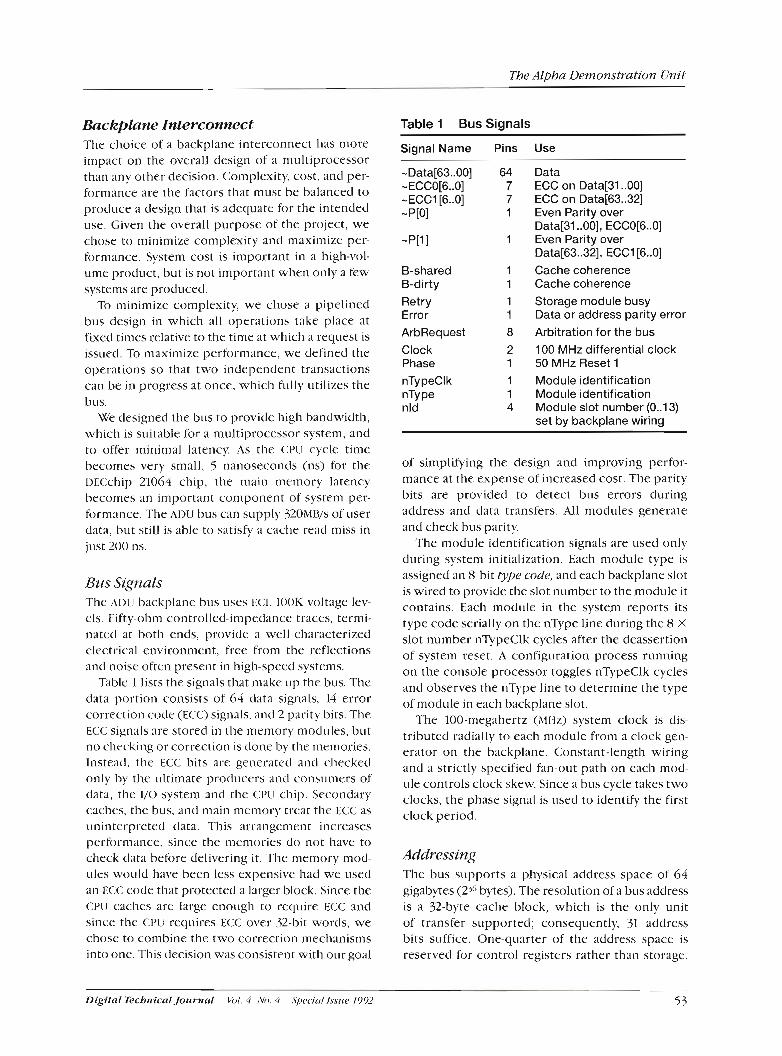
The Alpha De~nonstration Unit
Backplane Interconnect The choice of a backplane interconnect has more impact on the overall design of a multiprocessor than any other decision. Complexit): cost, and per- formance are the factors that must be balanced to procluce a design that is adequate for the intended use. Given the overall pilrpose of the project, we chose to minimize complexity and maximize per- formance. System cost is important in a high-vol- ume product, but is not important when only a few systems are produced.
To minimize complexity, we chose a pipelined bus design in which all operations take place at fiietl times relative to the time at which a request is issued. To maximize performance, we defined the operations so that two independent transactions can be in progress at once, which h~lly utilizes the bus.
We designed the bus to provide high banclwidth, which is suitable for a multiprocessor system, and to offer minimal latency. As the CPU cycle time becomes very small, 5 nanoseco~ltls (ns) for the I)E<:chip 21064 chip, the main memory latency becomes an important component of system per- formance. The ADU bus can supply 320N113/s of user data, but still is able to satisfy a cache read miss in just 200 ns.
Bus Signals The i\l)lJ backplane bus uses E(:L 100K voltage lev- els. Fifty-ohm controlled-impetlance traces, termi- nated at both ends, provide a well-characterized electrical environment, free from the reflections and noise often present in high-speed systems.
Table 1 lists the signals that make LIP the bus. The data portion consists of 64 data signals, 14 error correction cotle (KC) signals, ant1 2 parity bits. The ECC signals are stored in the memory modules, but no checking or correction is clone by the memories. Instead. the ECC bits are generated and checked only by the ultimate producers ant1 consumers of data, the I/O system and the CPU chip. Secondary caches, the bus, and main memory treat the ECC as uninterpreted data. This arrangement increases performance, since the memories do not have to check data before delivering it. The memory mod- ules would have been less expensive had we used an ECC code that protected a larger block. Since the crrr caches are large enough to require ECC and since the CPLI requires ECC over 32-bit words, we chose to combine the two correction mechanisms into one. This decision was consistent with our goal
Digilal Tecbnical Jottrnal k1. 4 /Vo. 4 .S/)rri~~l lsscie 1992
Table 1 Bus Signals
Signal Name Pins Use
-Data[63..00] 64 Data -ECCO[6..O] 7 ECC on Data131 ..00] -ECCl[G..O] 7 ECC on Data163.-321 -pi01 1 Even Parity over
Data[31..00], ECCO[G..O] -PI11 1 EvenParityover
Data[63..32], ECC1[6..0] B-shared Cache coherence B-dirty Cache coherence Retry 1 Storage module busy Error 1 Data or address parity error ArbRequest 8 Arbitration for the bus Clock 2 100 MHz differential clock Phase 1 50 MHz Reset 1 nTy peCl k 1 Module identification ~ T Y pe 1 Module identification nld 4 Module slot number (0..13)
set by backplane wiring
of simplifying the design and improving perfor- mance at the expense of increased cost. The parity bits are provided to detect bus errors during address and data transfers. All modules generate and check bus parity.
The module identification signals are used only during system initialization. Each module type is assigned an 8-bit type code, and each backplane slot is wired to provide the slot number to the module it contains. Each module in the system reports its type code serially on the nType line during the 8 X
slot number nl)lpeClk cycles after the deassertion of system reset. A configuration process running on the console processor toggles nTypeClk cycles and observes the nType line to determine the type of module in each backplane slot.
The 100-megahertz (MHz) system clock is dis- tributed radially to each module from a clock gen- erator on the backplane. Constant-length wiring and a strictly specified fan-out path on each mod- ule controls clock skew. Since a bus cycle takes two clocks, the phase signal is used to identify the first clock period.
Addressing The bus supports a physical address space of 64 gigabytes ( 2 3 % ~ ~ ) . The resolution of a bus address is a 32-byte cache block, which is the only unit of transfer supported; consequently, 31 address bits suffice. One-quarter of the address space is reservetl for control registers rather than storage.

Alpha AXP Architecture and Systems
Accesses to this region are treatetl specially: (;l'us clo not store data from this region in their caches, ant1 the target need not supply correct E<:<: bits.
'I"11e methocl used to select the target ~notlule of ;I bus operatjon is geographic. The initi;itor sencls the target module's slot number with the :iddress tluring a request cycle. In addition to the 4-bit slot number. the initiator supplies a 3-bit subizo~le idem tiJier with the address. Subnodes are the itnit of memory interleaving. The 6 4 ~ ~ storage moclule, for ex:~rnple, contains two intlepentlent 32MB sub- nodes that can operate concurrently
'The geographic selectio~i of the target means that a particular subnode only needs to compare the requested slot and subnode bits with its own slot and subnode numbers to decicle whether it is tlie tiirget. This reduces the time reqiliretl li)r the deci- sion compared to a scheme in which the target inspects the atldress fielcl, but it means that e;lch ini- tiator rnilst niaintain a mapping between physical addresses and slot and subnotle numbers. This map- ping is performed by a Iw;M in each initiator. For CPII modules, tlie RAM lookup tloes not reduce per- formance, since the access is clone in parallel with the access of the module's secontlary cache. The slot-mapping W\ls in each initiator are lontled at
system initialization time by the configuration pro- cess described previously.
Bus Operation The timing of adtlresses and data is shown in Figure 3. All dat:~ transfers take place at fixetl times relative to the start o f a n operation. Eight of tlie backplane slots can contain modules capable of initiating requests. These slots are numbered from 0 to 7, but are located at the center of the backplane to retluce tlie transit time between initiators and targets.
A bus cycle starts when one of the initiators arbi- trates lor the bus. The arbitration metliotl gu;iran- tces t11;lt no initiator can be st;~rvetl. Each initiator
monitors all bus operations and must request only those cycles that it knows the target can accept. Initiators are ;~llowetl to arbitrate for a particular target nine or more cycles after that target has started a read, or ten or more cycles after the target has started a write. To arbitrate, an initiator asserts the ArbReqilest line correspontling to its current priority. Priorities range from 0 (lowest) to 7 (high- est). If a module is the highest priority requester (i.e.. no higher priority ArbRequest line than its own is asserted). that motlule wins the arbitration, and i t transmits an ;iclclress ant1 a comma~lcl i n the next cycle. The winning module sets its priority to zero, ant1 all initiators with priority less than the ini- tial priority of the winner increment their priority regclrdless of u~hetl~er thcy made a request dztrirzg the ctr6itrclTion cycle. Initially, each initiator's prior- ity is set to its slot number. Priorities are thus distinct initially 21ncl remain so over time. This algo- rithm favors initiators that have not macle a recent request, since the priority of such an initiator increases even if it tloes not make requests. If all ini- tiators make continuous requests, the algorithm provides rountl-robin servicing, but the implemen- tation is simpler than round robin.
An arbitr;~tion cycle is followeel by a request cycle. The initiator pl;ices ;in address, node and subllode numbers, ;ind a command on the bus. There are only three commands. A read command requests a 32-byte cache block from memory. The target memory or a cache that contains a more recent copy supl'ljes the clata after a five-cycle delay A write comnialld transmits a 32-byte block to memory, using the same cycles for the clata trans- fer as the read cornm;it~d. Other caches may also take the block ant1 itpdate their contents. A victim writc is issued by a <;IYJ module when a block is evicted from the seconclary cache. When such an eviction occurs, nny other c:lches that contain the block are guaranteed to cont;~in the same value, so
This figure shows the contenls of the bus during four read cycles. I f requests are made at full rate, the bus is fully occupied wilh addresses and data. Bshared and 0-dirty are sen1 in Ihe fifth cycle after the arbilration request. I f any module detects a parily error during an address cycle, it asserls error two cycles later.
CYCLE 0 1 2 3 4 5 6 7 8 9 10 11 12 13 14 15 16 17 18 19 20 21 22 23 24 25
5 4 Vol 4 No. 1 S/)et iitl I s s r ~ c , 19%' Digilnl Techrricrtl JortrwrrI
ARB REQUEST DATA B-SHARED, B-DIRTY ERROR
R1
E l
A1 S2 S4
E3

The AlJ!bcr Delnonstration Unit
they need not participate in the transfer at all. The block is stored in memory, as in a nor~iial write.
Cache Coherence In ;I multiprocessor system with caches, it is essen- tial that writes clone by one processor be made available to tlie other processors in the system in ;I timely fashion. A number of approaches to the cache coherence problem have appeared in the Jit- erature. These approaches fall into two categories, depending on the way in which they liancl Ie proces- sor writes. Azt~nlidntiorz or oti!lzership protocols require th:lt ;I processor's cache must acquire an exclusive copy of the block before the write can be clone.? If another cache contains a copy of the block, that copy is invalidated. On the other hand, ~rpd~zte protocols maintain coherence by perform- ing write-through operations to other caches that sh;~re the block.2 Each caclie maintains enough state to determine whether any other cache shares the block. If the data is not present in another cache, then write through is unnecessary and is not done.
The two protocols have quite clifferent perfor- mances, depending on system activity. An update pl-orocol performs better than an invaliclation pro- tocol in an application in which data is sharetl (and written) by multiple processors (e.g., a parallel algorithm executing on several processors). In an inv;~lid;~tion protocol, each time a processor writes a location, the block is inrralidateci in all other caches that share it. All caches require an expensive miss to retrieve the bloclc when it is next refel= enccd. On the other hand, an update protocol per- forms lx)orly in a system in which processes can migrate between processors. With migration, data iippears in both caches, and each time a processor writes a location, a write-through operation uptlates the other cache, even though its CI'U is no longer interested in the block. Larger c;~ches with long block lifetimes exacerbate this problem.
Coherence Protocol The coherence protocol usetl in the ADIJ is :I hybrid of an update ancl an invalidation protocol, ant1 like many hybritls, it combines the good features of both parents. The protocol depends on the fact that the CPrJ chips contain an on-chip cache backed by a much larger secondary caclie that monitors all bus operations. Initially, the seco~iclary caches use ;in update protocol. Caches that contain shared d;rt;~ perform a write-through operation to upclate
the blocks in other caches whenever the associated CPU performs a write. If no other cache shares a block, this write through is unnecessary ant1 is not done. Wlien a secontlary caclie receives an update (i.e., it observes a write on the bus directed to a block it contains), it has two options. It can invalidate tlie block and report to the writer that it has done so. If it is the only cache sharing the block, subsequent write-through operations will not occur. Alternatively, it cat1 accept the uptlate and report that it did so, in which case the cache that performed the write-through operation con- tinues to send upclates whenever its CPU writes the block.
The actions taken by a cache that receives an update are determined by whether the block is in the CPU's on-chip cache. The seco~idary cache con- tains a table that allows it to determine this without interfering with the CI'IJ. If tlie block is in the on- chip caclie, tlie secondary c;~che accepts the update and invalidates the block in the on-chip cache. If the block is not in the on-chip caclie, tlie secondary cache block is invalidated. If tlie block is being actively shared, it will be reloaclecl by the CPIJ before the next upd;~te arrives, and the block will continue to be sharetl. If not, the block will be inval- idated when the second update arrives.
Implementation of the P~otocol The implementation of the coherence protocol is not complex. The five possible states of a secondary cache block are shown in Figure 4. Initially, all blocks in the cache are marked invalid. Misses in the CPU's on-chip cache cause a bus read to be issued if the block is not in the secondary cache. If the cache block is assigned to another memory loca- tion and is dirty (i.e., has been written since it was read from memory), a victim write is issued to evict the block, then a read is issuetl. Other caches moni- tor operations on tlie bus and assert the block- shared (B-shared) signal if they contain the block. If a cache contains a dirty block ancl it observes a bus reacl, it asserts B-shared and B-dirty, and supplies the data. B-dirty inhibits the memory's delive~y of data.
The CPu's on-chip caclie uses a write-through strategy. A CPU write to a shared block in the sec- ondary caclie initiates a bus write to update the contents of other caches that share tlie block. Memory is written, so the block beconies clean. If another cache takes the uptlate, i t asserts B-shared, and tlie initiator's state beconles Shared not (-)
Digital Ticbrrical Jorrrnnl Vol. -I No. 4 .S/)ec'irrl Issue 1992 5 5

Alpha AXP Architecture and Systems
C-READ C-READ C-WRITE
C-WRITE -SHARED
C-WRITE (-6-SHARED) * -SHARED
-DIRTY 4 DIRTY
C-WRITE (-6-SHARED) B-WRITE, INC; 6-READ
6-READ INVALID
SHARED + -DIRTY
C-WRITE (6-SHARED) C-READ C-READ 6-READ B-WRITE, INC B-READ
Transitions occur as a result of CPU reads and writes (C-read. C-write) and bus operations initiated by other caches or I10 controllers (6-read, 6-write). A C-read or C-write to an invalid block causes a 6-read; a C-write to a shared block causes a 6-write. The 6-shared response ind~cates that some other cache contains the block. INC indicates that the block is in the CPU's on-chip cache.
Figrrre 4 Secondary Cache Line States
Dirty. If no other cache takes the update, either because it does not contain the block or because it decicles to invalidate it, then the B-shared signal is not asserted, and the initiator's state becomes -Shared -Dirty. The B-shared and B-dirty signals may be asserted by several moclules during cycle five of bus operations. The responses are ORed by the open-emitter ECL backplane drivers. More than one cache can contain a block with Shared = true, but only one cache at a time can contain a block wit11 Dirty = true.
Designing the bus interconnect and coherence protocol was an experiment in specification. The informal description required approximately 15 pages of prose to describe the bus. The real specifi- cation was a multithreaded program that repre- sented the various interfaces at a level of detail sufficient to describe every signal, but, when exe- cuted, simulatecl the components at a Iiigher level.
By running this program with sequences of sitnu- lated memory requests, we were able to refine the design rapidly and nleasure the performance of the system before clesigning any logic. Most design errors were discovered at this time, and prototype system debugging took much less time than usual.
System Modules In this section, we describe the system modules ant1 the packaging of the ADU. We discuss the design choices made to produce the c:IjU module, storage modules, and I/O niodule on scheclule. We also cliscuss applications of the ADU beyond its intended use as ;I vehicle for software development.
CPU Module The ADU CPU module collsists of a single CPU chip, a 256-kilobyte (KR) secondary cache, and an inter- face to the system bus. All CPU modules in the
56 Vol. 4 ,\'o. 4 .S/):[,ci'iol ISSILP 1992 D i g i l ~ l Tecbrricnl Jorrrnnl

The Alphrr De~norzstmtiorr Unit
system are identical. The CPll motlules are not self- sufficient; they must be initialized by the console workstation before the Cl'u can he enabled.
The CPti module contains exterisive test access logic that allows other bus agents to read and write most of the module's internal state. We irnple- rnented this logic because we knew these motlules would be used to debug <:Pll chips. Test access logic would help us determine the cause of a CPU chip malfunction and would make it possible for us to introduce errors into tlie secondary cache to test the error detection and correction capabilities of the C;I'LJ chip. This logic was used to perform almost all initi;~lization of the Cl'u nioclule ;~nd W;IS also ilsed to troubleshoot CI'U modules ;ifter they were htbricatetl.
Tlie central featlire of the (:rri motlule (shown in Figi~re 5 ) is the secondary c;~che; built using 16K by 4 BiCMOS static lL\Ms. Each of the 16K half- blocks in the data store is IS6 bits wide (4 long- words of data, each protectecl by 7 ECC bits). Each of the 8 K entries in the tag store is an 18-bit address (protected by parity) ancl ;I +bit control fieltl (valid/sliared/dirty, also protected by parity). In addition, it secondary cache cluplicate tag store, consisting of an 18-bit ;idtlress ancl a valid bit (protected by parity), is used as a hint to speecl pro- cessing of reads and writes encountered on tlie system bus. Finally, a CPIl chip data cache duplicate tag store (protected hy parity) filnctions as an
BYPASS
invalidation filter and selects between update and invalidation strategies.
Tlie system bus interface w;~tclies for reads and writes on the bus, and looks up e;icli ;idtlress in the secontlary cache. On read hits, it ;isserts B-shared on the bus, ;ltid, if the block is dirty in the sec- ond;u-y c;iche, it asserts B-dirty ;und supplies read data to the bus. On write hits, it selects between the invalidate and update strategies, modifies the con- trol fieltl in the secondary cache tag store appropri- ately, and, if tlie update strategy is selected, it ;iccepts tlata from the system bus.
Unlike most bus devices, the <;Plr module's system bus interface must accept a new ;td<lress every five cycles. To do this, it is iniplementecl as two intlependcnt finite state rr~;icIiines connected together in a pipelined fashion.
Tlie t ~ g state machine, which operates during bus cycles 1 through 5. watches for addresses, per- forms all tag store reads (in bus cycle 4. just in time to assert B-shared ant1 U-di1.t). in bus cycle j), ancl performs any needed tag store writes (in bus cycle 5 ) . If the tag state machine tletermines that bus data must bc suppliecl or accepted, it enables the data state ms~chine, and, at tlie same tinic, begins pro- cessing the next bus request.
The clata state machine, which operates during bus cycles 6 through 10. moves data to ancl from the bus and handles the reatling and writing of the seconclary cache data store. 'l'he liiglily pipelinetl
DATA STORE REGISTERS
BUS DATA
WRITE CPU DATA LATCH
- BUS DATA , BUSTAG ADDRESS ADDRESS
- I
SYSTEM BUS
Digital Technical Journrrrl Vd. 4 No. 4 Spec-id Lss~fe 199.2 57

Alpha AXP Architecture and Systems
fi;~tllt-e of the sjatern bus liiakes reading and writing the data store somewhat trichy. Figure 61 shows ;I write hit that has selected the update strategy immedi;~tely followed by a read hit that must supply d ~ t a to the bus. High performance mandates the use of clocked transceivers, which means the second;~rj~ cache data store must reacl one cycle ahcad of the bus ancl must write one cycle behind thc bus, resulting in a conflict in bus cycle 11. However, the bus transfers data in a fixed order, so thc reat1 will always access quadword 0 of the block, ant1 the write will always :~ccess quacl- word 3 of the block. By implementing the data store ;IS two 64-bit-wide banks, it is possible to lian- tlle these back-to-back transactions without creat- ing :uliy special cases, as shown in Figilre 6b. This example is typical of the style of design used in the t\1)11, wliich eliminates extra mechanisms wherever possible.
?'hc <:1'lJ interface handles the arbitration for the seconclary cache and generates the necessary reads ant1 writes on the system bus when the CPI' sec- ontl:~ry ciiche misses.
Thc (:PIJ chip is supplied with a clock that is not rel;~tetl to the system clock in frecl~lency or phase. This factor made it easier to use both the 100-MHz frequency of the DC227 prototype chip ant1 tlie 200-MHz frequency of tlie DECcliip 21064 CPIJ. It ;~lso ;~llowed us to vary the operating freqilency tluring (:PU chip debugging. However, the clata lxlses connecting the CPIJ chip to the rest of the (:I'IJ motlule must cross a clock-domain boundary. Perhaps more significant, the secondary cache tag and data stores have two asynchronous sources of control, since the <:PU chip contains an integrated secoticlary cache controllel:
CYCLE
The bidirectional tlata b ~ ~ s of the CPU chip is con- verted into tlie unidirectional data buses used b). the rest of the <:I'I! module by transparent cutoff latches. 'These latches, wliich are located in a ring surrounding the <:Pli, also convert the quasi-ECL lell- els generated by the Cl'U chip into true E<:L levels for the rest of the <:P'IJ module. These latches are norn~ally Iield open, so tlie CI3[! chip is, in effect, connected directly to the secondary cache tag and data RAMS. Control signals from the CPU cl~ip's inte- grated seconcl;rry c;lche controller are simply OKed into the appropri;~te secontlary cache f t ~ \ , 1 drivers.
These latches are ;tlso ~lsecl to pass data across the two-clock-clom:~i~i bounclary Normally all latches are open. On reatls, logic in tlie CPU chip clock clomain closes all the latches and sends a read reqi~est into the bus clock domain. Logic in the bus clock domain obtains the cli~ta, writes both the sec- ontlary c;lcIie and the reacl latches, and sends an acknowledgment back into the CPlJ chip clock domain. Logic in the CPtJ chip clock tlotnain accepts the first half-block of the data, opens the first read I;ltch, accepts the second half-line of the data, ancl opens all remaining latches. Writes are similar: Logic in the <:l'Ll chip clock dolnaiti writes the first half-line into the write latch, makes the second half-line valid (behintl the latch), and sentls a write request into the bus clock tlomain. Logic in the bus clock clomain accepts the first half-line of data, opens tlie write I;~tcli, accepts the secontl 1i;rlf- block of clata, and scncls an acknowledgment back into the <:Hi chip clock tlo~iiain.
Logic in tlie <:IW chip clock tlomain controls all latches. Only two signals pass through synchroniz- ers: a single request signiil passes from the CPU chip clock domain to the bus clock clom;iin, ant1 a single
CYCLE
- ~
toihe secondary cache RAMS Caused
WRITE CYCLE READ CYCLE CACHE EVEN CACHE ODD
Figzlr-r 6 CPU Timing
f cycle R7.
R8 R9
WRITECYCLE READ CYCLE CACHE
W8 R3 W7
14 15 Figure 6b shows how this conflict can be resolved by treating the cache as
R9
R10
by back-to-back cycles. In the marked cycle, thecache writes the bus data thal arrived in cycle W10. but it also needs to read data lo supply it during
W9 R4 W8
R9 R10
WO R1O
W3
R10
W10 R5 W9
W1
two independent banks (even and odd)
W4 W2 R6
{$O
R7 R8
W7 R2
W5 RO
W6 R1

acknowledge signal passes from the bus clock domain to the CPU cliip clocl< domain.
'I'lie secondary cache arbitration scheme is i~nconventional because the system bus has no stall mechanism. If a reatl or a write appears on the system bus, the bus interface tnust have uncondi- tional access to the secondary cache; it cannot wait for the CPU to finish its current cycle. In fact, the bus interf~ce cannot detect if a cycle is in progress in tlie CPU chip's integrated cache controller.
Nevertheless, all events in the system bus inter- face occur at fixed times with respect to bus arbi- tration cycles. As a result, the system bus interface can supply a busy signal to the CPU interface, which allows it to preclict the bus interface's use of the secondary cache in the immediate future. The Cl'U
interface, therefore, waits until the secontlary cache can be accessetl without conflict and then performs its cycle without additional checking. .This waiting is performetl by the cpU chip's inte- grated secondary cache controller for some cycles, and by logic in the CPIJ interface running in tlie bus clock domain for other cycles. To reduce latency the CPU reatls the seco~ltlary cache while waiting. and ignores tlie data if it is not yet valitl.
All operations use ownership of the system bus ;IS an interlock. For example, if the CPU writes to a location in the secondary cache that is marked as shared, the CPIJ interfrrce accluires the system bus, ancl then updates the secondary cache at the same time as it broadcasts the write. This does not elimi- nate all race conditions; in particular, it allows a dirty secondary cache block to be invalidated by ;I system bus write while the CPU interface is wait- ing to acquire the bus to write the block to memory. l'liis is easily handled, however, by having the Cpll
interface generate a signal (always-update) that insists that the systeni hus interface select the update strategy.
The combination of arbitration by predicting fiiture events and the use of the system bus as an interlock makes tlie (:I'IJ rnotlule's control logic extremely simple. The bus interface and the (:pu interface have no knowledge of one another beyond the busy ant1 alw;~ys-update signals. Since no complicatecl interactions between the (:l'lJ and tlie bus exist, no time-consuming simulations of the interactions needed to be performed, and we had none of the clifficult-to-track-down bugs that are usually associated with multiprocessor systems.
The CPU module contains a number of control registers. TIie bus c)lcles that reatl and write these
registers are processetl by the system bus inter- face as ortlinar): hut somewliat degenerirtc, cases. The local CPlJ accesses its local registers over tlie system bus, using ordinary system bus rc;itls ant1 writes, so no special logic is neetlecl to resolve r:~ce conclitions.
To keep pace with our schedule. we ;~rr;~ngetl for niost of the system to be debugged before the (:I'Ij cliip arrived. By 11si11g ;I suitably wired intcgr;~tetl circuit test clip, we could place cornnlantls o~ i to the CPU chip's comm;~~ltl bus and verify tlie contl-ol signals with an oscilloscope. The results 01.' these tests left us fairly confident that the system worked before the first chip arrived.
We resumetl testing the CPIJ rnotlulc :it'tcr tlic CPU chip was installed. We placetl short (three to five instructions) programs into milin rnenior); enabled the c:PrJ chip for a short rime, then inspected the secondary cache (using tlic (:I'll mod- ule's test access logic) to examine tlie results.
Eventually we connected an external pulse gen- erator to the (:t'[J chip's clock ancl ;in external power supply to the chip. These moclific;~tions permitted us to vary both the operating frequency and tlie operating voltage of the c:t'rr cliil,. R!, using a pulse generator and a power supply that coultl be remotely controlled by another computer, we were able to write siniple programs that coi~lcl 1.~111 (:1'11
cliip diagnostics, without manual intervention, over a wide range of operating conditions. l'his greatly simplificcl the task of collecting the r;~\\; cl;ir:~
needed by the cliip designers to verie the critical paths in the chip.
Storage Modules The ADU's storage modules must provitlc high bandwidth, both to service cache nlisses ;111t1 t o
support dernantling I/O tlevices. More iniport:~nt, they must provicle Low latenc): since in the c;lse of a cache miss, the processor is stalled until tlie miss is satisfied. It is also important to pro\7itle ;I motlest amount of memory interleaving. Altliough tlie bus protocol allows only two memory subnotlcs to be active at once, higher interleave increases the prob- ability that ;I moclule will be free when a memory request is issued.
Each storage module is organizecl as two independent bus subnodes, so that even i n ;I sys- tem with one module, menlory is two-way inter- leaved. Each of the subnodes consists of four banks, each of whicli stores two longwortls of t l ;~t ;~ and their associatecl error correction bits. With
Digilrrl Techrricnl Jorrrirrrl WJI 4 i\b. 4 Specinl lssr!c. I 992 59

Alpha AXP Architecture and Systems
1-megabit (Mb) I&\,i chips, the capacity of each niotlule is 6 4 M B . Figure 7 sllows the organization of the storage modille. The module consists of two independent subnodes, each with four banks o f storage. Control signals are pipelinetl through the banks so that the module can deliver or accept a 64-bit data word (plus EC:<:) every 20 ns. With the exception of the DIb\IM interface sign~ls, all signals are ECL levels. The GO14 gallium arse- nitle (<;aAs) driver chip improves performance by allowing parallel termination of the DRAM adclress lines.
A memory cycle consists of a five-bus-cycle access period followed by four bus cycles of data transfer. Each data transfer cycle moves two 39-bit longwords between the module and the backplane bus, for a total of 32 data bytes per memory cycle. This is the size of a CPU module cache block. A read operation takes 10 bus cycles to complete, but a write requires 11 cycles.
Since a data rate of 1 word every 20 ns is beyond the capabilities of even the fastest nibble-mode RAMS, we needed an approach that did not require each to provide more than 1 bit per access.
. . . . . . . . . . . . . . . . . . . . . . . . . BANK 3 1
1 M BY 39-BIT 1 M BY 39-BIT I I , n STORAGECARD STORAGECARD n
+--------t--t--j-------- BANK 2
A I -. .. . - I
1 M BY 39-BIT 1 M BY 39-BIT STORAGE CARD
1 M BY 39-BIT STORAGE CARD
t STORAGE CARD
A
1 M BY 39-BIT STORAGE CARD
I M BY 39-BIT STORAGE CARD
STORAGE CARD
- - - - - - - - - - - - - - - - - - - - - - J t ADDRESS
I BANK ENABLES I
Figure 7 ADU Stor~~~qe Modtlle
4 SUBNODE 1 SUBNODE 2
60 I'ol. 4 ,Vo. 4 Specir~l lss~re I992 Digital TecbnicnlJorrrnnl
4
TRANSCEIVER
BACKPLANE
CONTROL CONTROL
DATA + ECC (39)
CONTROL DATA + ECC, ADDRESS (39)

The Alpha Demonstration Unit
We chose to pipeline the four banks of each sub- node. Each of the four banks contributes only one 78-bit word to the block. The banks are started sequentially, with a one-cycle delay between each bank.
The high performance of the storage module is achieved by maintaining ECL levels and using ECL lOOK components wherever possible. The W\1 1/0 pin levels are converted to ECL levels by latching transceivers associated with each bank. Fortunately, the timing of accesses to the two sub- nodes of a module makes it possible to share these transceivers between the same banks of the mod- ule's two subnodes.
The DRhM chips are packaged on small daughter cards that plug into connectors on both sides of the main array module. There are 2 daughter cards for each bank within a subnode, for a total of 16 daugh- ter cards per module. The DRAM address and con- trol lines are carried on controlled impedance traces. Since each of the 39 DUMs on an address line represents a capacitive load of approximately 8 picofarads, the loaded impedance of the line is about 30 ohms.
The usual approach to driving the address ancl control lines of a RAM array uses series termination, as shown in Figure 8a. This arrangement has the advantage that the driver current is reduced, since the load impedance seen by the driver (R, + Z, is twice that of the loaded transmission line (Zo). Unfortunately, thc RpuM access time is increased, because the signal from the driver (5,) must propa- gate to the far end of the line, be reflected, and return to the driver before the first rwlM on the line sees a full-amplitude signal. Since the capacitive loading added by the RAM pins lowers the signal propagation velocity in addition to reducing the impedance, the added delay can be a significant fraction of the overall cycle time.
Since low latency was a primary design goal, we chose parallel termination of the 1ziiiM address ant1 control lines, as shown in Figure 8b. Each address line is terminated to +3 volts with a series resistor (R,) of 33 ohms, slightly higher than the line impedance. In this configuration, each line's driver must sink a current of almost 0.1 ampere. Since no commercial chip could meet this requirement at the needed speed, we com~ilissioned a semicustom GaAs chip.'
As shown in Figure 9, each CaAs chip contains a register for eight address bits, row/column address nlultiplexing ant1 high current drivers for the U M
VC: v h ~ - - 0
DRAM
Series term~nat~on results In a half-amplilude signal at the first RAM on the line until the signal reflects from point C
DRAM -.. DRAM
( a ) Series Terrninal.io7z
B Zo C
DRIVER
A
VA: " h ~ p 0
Parallel termination saves one line lranslt time, but increases driver current.
( 6 ) Parallel Terniiuafioiz
F ~ ~ L L I - e 8 Aclclress Line Ter.r?zinntion
address lines, and a clriver for one o f the three I b i M
control signals ( U S , CAS, Write). To reduce the cur- rent switched by each chip, each address bit tlrives two output pins. One pin carries true data, ant1 the other is complemented. The total cunent is there- fore constant. Each pin drives one of the two I w M modules of a bank. A total of three GaAs chips is required per bank. In the present module, with 1M- by 1-bit U M chips, only 10 of the 12 address drivers are usrcl, so the system can be easily expanded to make use of 16M RhiMs.
The storage module contains only a small amount of control logic. This logic generates the control signals for the IWiLls and the various transceivers that route data from the backplane to each bank. This logic also generates the signals
Digital Tecbnicnl Jozrrnnl Vol. 4 1X;o. .I Specin1 lssiie 1992 6 1

Alpha &XP Architecture and Systems
I I SELlN , I D O 1 SELOUT
I+TCy~lr.e 9 Add~.c.ss and Control Driver
to exercise new CPIJ chips and untested software. With this in mind, we org~nized the I/O system round a DECstation 5000 workstation as a front- end ant1 console processor. This reduced our work consitlerably, as all I/<) is clone by the workstation. A 'I'IlRt3Ochannel module connects the DECstation 5000 over a SOMB/s cable to the I/O module in the A1)Ii. We selectetl SOMU/s in orcler to support the simultaneous, peak-bandwitlth operation of two SCSI disk strings, an Ethernet, and a fiber dis- tributed data interface (FI)Ol) network adapter. The I / ( ) module contains two of these channels, which ;tllows two DECstation 5000 worl<stations to be attachecl.
At tlie hardware level, the I / ( ) system supports block transfers of data from the main memory of tlie workstation to and from t\I)lJ memory In addi- tion. the I/O module includes command and door- be1 1 registers, which are used by AI)t! processors to attract the attention of the l/O bysteln.
In software, 1/0 requests are placed by ADU pro- cessors into command rings in t\ l>U niemory, The memory address of a comm;lnd ring is placed into an I/() control register, ;mcl the associated doorbell is rung. The doorbell causes a hardware interrupt on the front-end DECstxtion 5000, which alerts the I/<) server process that action is needed. The I/o server reads the command ring from ADU memory and performs the requested I/(). 1/0 completion sta- tus is stored into ADU memot-); and an interrupt is sent to the requesting t\DI1 processor.
In addition to its role as an I/O front-end proces- sor, the DECstation 5000 workstation acts as a cliag- nostic and console processor. When an ADU is powerecl on, diagnostic software is run from the
ncccled to refresh the I<t\l\r,s xncl to assert the retry workstation. First, the correct functioning of the
signal if another nocle attempts to access the mod- I/() module is tested. Then tlie AD17 module identifi-
ule \vliile it is refreshing itself. ciition process determines tlie types and locations
I/O iWodule The I/O module for the A[>U contains two 50Mn/s I/o channels ant1 ;I loc;~l (:I'll subsystem. The I/O ch;innels connect to one or two DECstation 5000 workstations, which act as I/() front-end proces- sors ;ud also provide console and tliagtlostic fi~nc- tions. The local CPlJ subsystem is used to provitle interval timer and time-of-day clock services to ADll
processors. 'l'he original specification for the ADIJ I/O system
required support only for serial line, small com- puter s)-stems interface (S(:Sr) disk, and Ethernet I/o clevices. We knew that the ADU would be used
o f all CPU ant1 storage modules in the system. 1)i;ignostics are then run for e;lcli module.
Once diagnostic software has run, the console soft~vi~re is given control. This software is responsi- ble for loading privileged architecture library (PAL) ;~nd operating system software. Once the operating system is running, the workst;ition becomes an 1/0 server.
The presence of the I>E<:statjon 5000 gave the chip team and operating system developers a stable place to stand while cliecking o u t their own com- ponents. In addition, the complete diagnostic capa- bility ;lnd error checking coverage of the ADCJ hardware helped to isolate faults.
62 W1. 4 ,Ira. 4 SpecJnl lssrre 1392 Digilnl Tecbnicnl Jorrrnal

The Alpha Den?orzsrrzrtion Unit
The central features of the I/o moclule, shown in Figul-e 10, are two 1K- by 80-bit register files built from 5-1-1s ECL WMs. These memories are cycled every 10 ns to simulate dual-portecl memories at the 20-11s bus cycle rate. One memory is used as a stag- ing RAM for block transfers from the I/O processors 1.0 ADlJ memory. The other memory is shared between use as commancl register space for the I/O system and a staging W M for transfers from AI)II memory to the 110 system.
On the bus side, the register files are connected directly to the backpl;~ne bus transceivers. On the I/O side, the register files are connected to a shareel 40-11s bus that connects to the two I/O channels.
The buses are time-slotted to eliminate the need for arbitration logic. As a consequence, the 1 / 0 module control logic is contained in a small number of programmable array logic chips that implement the 1 /0 channel controllers ant1 a
block-transfer st;ite machine that 11;lncl les bus transfers.
Each I/O ch;~nnel carries 32 bits of t l ; ~ t ~ plus 7 bits of ECC in parallel on a SO-pair cable. Each dat:~ word also carries a 3-bit tag that specifies the destin;~tion of the data. The cable is half-duplex. wr i t11 the tlirec- tion of data flow uncler the control of softw;lre on the DECstation. Data arriving from the I)ECst;~tion is buffered in 1K E'[FOs. These FIFOs c;irry data across the clock-domain boundary between the I/O system and the AULI nncl permit both 1 / 0 cIi;~nnels to run at h ~ l l speed simultaneously.
Each I/O channel interface also has a11 ;~ddress counter and a slot-mapping IWM, which are loadecl from the workstation. The slot-mapping function sets the correspondence between t\l)ll bus addresses and the geographically addressed storage and CPU moclules. The address ant1 slot m;~p for each cllannel are connected to a common adclress
TO DECSTATION
TO DECSTATION
- INTERFACE
SYSTEM BUS
(61) ADU I/O Module
OUTBOUND FlFO
n
INBOUND FlFO
TURBO- 4-1 4yB-k ( I ? ) TURBOchan~zel I/O M o d ~ i l e
CHANNEL INTERFACE
Digital Technical Jotrrrrrrl 161 4 No. 4 Spec i~~l Issue 1992 63
INTERFACE

Alpha AXP Architecture and Systems
bus. This bus bypasses the register files ancl directly clrives the backplane transceivers during bus address cycles.
The far end of tlie I / ( ) cable connecls to a single- width TI'RBOchannel niotliile in the 1)EC:station 5000. This nodule cont;~ins EC<: gener:ltion and checking logic, and FIFO clueues for buffering data between the citblc antl tlie 1~ClRBOch;uinel. The FIFO
queues also carry tlatn across the clock-domain boundary between the I/O channel ;rml the nJRBOchannel motlules.
The I/<> module has a local <:PU subsystem con- taining a 12-MHz Motorola 68302 processot; 128KH of erasable programmable read-only memory (EI'KOM). anel 128KI3 of R A V . The CPll subs!.stem also includes an Ethernet interface, two serial ports, an SCSl interface, an Integrated Services Digital Network (ISDN) interfidce. and auclio input ant1 output ports. When in use, the loc;tl <;l'r r sub- system uses one of the 1/0 channels otherwise i~vail- able for the connection of a DE(;st;~tiotl 5000. Although the local <:I't! on the I/O module is capltble of rilnning the ~ L I I [ Al>rl 1 / 0 system, in pr;ictice \ve ~1st. it for supplying interval timer and real-time clock service for the Al>lJ.
The VO morlule was somewhat overdesignetl h)r its original purpose o f supplying disk, networl<, :tntl console I/O service for A D l J processors. This capa- bil ity was piit to use in mid-1991 when the tle~nand for ADUs became so intense that we considered building adtlitional systems. Instead. by using the excess 1/0 resources, the slot-mapping featilres of the hardware, nncl the capabilities of PAI.code, we were able to use ;I three-processor A l ) u ;IS three independent virtual computers. Inclependet~t copies of the console program shared the I/() h;ircl- ware through software locking and were allocateel one CP'LJ ant1 one storxge motlule e;lch. lMultiprocessor xl>[ls now routinely run both OpenVi\fJS AXl' ;incl l>T:(: OSW1 AXP oper:iting sys- tems :it the same time.
Packaging Simplicity was the primary goal in tlie tlesign of the Al)U package. Our short schedule dem;~ncletl that we avoicl innovation and use standard p;irts wher- ever possible.
The WU's modules ant1 card cage are st;ind;ircl 9U (280 millimeter by 367 tnillimeter) Euroc;~rtl com- ponents, which ;Ire avail;tble from a nurnbcr o f ven- dors. The cabinet is ;I st;tndard Digital unit. ~~su; i l l '~ '
usecl to hold disks. Power supplies are off-the-shelf units. Three supplies are requiretl to provide the 4,000 watts consumed by a system containing a full complement of 111otluIes. A stantl;lrd power condi- tioner provides line filtering and distributes pri- mary ti(; to the power supplies. This unit ;tllows the system to operate on 110-volt tic in the United States, or 220-\wit A C in Europe.
Coolitig was the most difficult part of the packag- ing effort. The use of ECL throughout the system meant that we had to provide an airflow of at least 2.5 m/s over the modules. After st~ldying several alternatives. we selected a reverse impeller blower usecl on Digital3 VAX 6000 series m;~cliines. Two of these blowers provide the requireel airflow, while generating much less acoustic noise than conven- tional fans.
Since blower tiiilure woulcl result in a catas- trophic meltclown, airflow and temperature sen- sors are provided. A small module containing a rnicrocontrolle~- monitors these parameters as well as all power supply voltages. In the event of failure, the ;iutonoruorls controller can shut down the power supplies. This module also generates the system clock.
Conclusions Sometimes it is better to have twenty million instruct~onb by Fritlay than twenty million instruc- tions per seconcl. -Wesley Cl;~rk
One liuntlred <:I'lJ antl storage modules and 35 I/O modules haw been built. packaged as 35 ADU sys- tems, :untl dcliverecl to software development groups throughout Digital. Not just laboratory curiosities, these systems have become part of the mainstream AXP clevelopment environment. They are in regul:~r usc by compiler development groups, operating system developers, and :~pplications groups.
The AJ)II also provided a full-speed, ill-system exerciser h)r the chips. By using the ti1)U. the chip tlevelopers were ;~ble to detect several subtle prob- lems in carly chip implementations.
The /\I>[] project was quite successful. AIIU sys- tems were in the hands of tlevelopers ;ipproximately ten months before the first product prototypes. The systems esceedcd our initial expectations for reliability. ;rntl provided a rugged, stable platform for software clevelopment ant1 chip test. The proj- ect demonstratetl that a small team, with focused objectives. can protluce systems of substatltial com- plexity in a short time.
64 V d . 4 No. 4 SpccZL(tlsuue 1992 Digital Technical Journal

The AlJlna Denzo~zstratio?~ Unit
Acknowledgments John Dillon designed the power control subsystem and the package. Steve Morris wrote the ADU con- sole software. Andrew Paync contributed to ADU
tliagnostics. Tom Levergood assisted with the physi- cal design of the VO modules. Herb Year): Scott Kreider, and Steve 1,loytl tlitl module debugging and testing at Huclson ant1 at SIK:. Ted Equi handled proj- ect logistics at Hutlson, ant1 Dick Parle was respon- sible for material accluibition and supervision of outsicle venclors at SRC.
References
1. R. Sites, A. Chernoff, M . Kirk, M. Marks, and S. Robinson, "Binary Translation," Digital Rclnlzical Jo~lrnal, vol. 4 , no. 4 (1992, this issue): 137- 152.
2. C. Thacker, L. Stewart, and E. Satterthwaite, Jr., "Firefly: A Multiprocessor Workstation:' IEEE Transactions on Conzputers, vol. 37, no. 8 (August 1988): 909-920.
3. R. Katz, S. Eggers, D. Wood, C. Perkins, and R. Sheldon, "Implementing a Cache Consistency Protocol," in Proceeclirigs of the 12th Interna- tional S~~nzpositlm on Co~lzputer Architecture ( I E E E , 1985).
4. J. Archibald and L. Baer, "Cache Coherence Pro- tocols: Evaluation Using a Multiprocessor Simu- lation Model," ACM Transactions on Computer Systems, vol. 4 (November 1986): 273-298.
5. 1991 GaAs IC Data Book and Desigizer's Guide (GigaBit Logic, Newbury Park, CA, 1991): 2-39.
Digital Tecbnkal Journal Vol. 4 No. 4 Speciallssue 1992 65

ToddR Dtitton Daniel EireJ
Hugh R. Kurth JamesJ RReisert Robin L. Stewart
The Design of the DEC3000 AXP Systems, Two High-performance Workstations
A fanzily of bigh-perJ-bnnance 64-bit RISC zuorkst~~tions alzd serzlers based 012 the izeuJ Digital Alpha AXP ar~chitecture is described. The bar-du~are implementatiot? uses the pozue~zzll new DECcl?$21064 CPU and ernploys a sophisticated neLc sj~stenz interconnect structzrre to achieve the necessary high Da~tdwidth and lmu-latency cache, memory, and t/O 6tues. The melnory subsjlstem of the high-end DEC 3000 AXP Model 500prouides a 512KB secondary cache and up to I GB of tnemory The I/O subsyst@?z of the Model 500 has integral two-dime1.2sionalgrqbics, SC.51, ISDIV, and six TURBOchannel expansion slots.
The DEC 3000 AXP system family consists of both workstations and servers that are basecl on Digital's Alpha I U P architecture.' The family includes the desktop (DEC 3000 A?(P Model 400) ancl desk-side and rack-mounted (DEC 3000 AXP lMoclel 500) sjls- terns. The available operating systems are the DEC OSF/1 AXP and the OperlViMS AX-' systems. All sys- tems use the DECchip 21064 microprocessoc2
Table 1 gives the specifications for the three DEC 3000 AXP systems.
The IIEC 3000 iucP systems are designed to be sig- nificantly faster than all previous Digital work- stations and to offer performance competitive with that of other reduced instruction set computer (RISC) workstations currently available. In general, NSC systems have larger code sizes ancl conse- quently require more instruction-stream bantl- width than complex instruction set computer (CISC) systems. Further, 64-bit machines recluire more data-stream bandwidth than 32-bit machines. To complement the power of the DECchip 21064 microprocessor, the systems need a balanced system architecture, including a high-bandwidth, low-latency memory system and an efficient, high- performance 1/0 subsystem.
Traditional workstation designs that use a com- mon system bus exhibit increased memory latency and reduced memory bandwidth due to system bus contention. This is a special concern for clesigiis
using a large number of high-performance I/O devices. Increased latency can also result from the additional levels of buffering ancl system bus loaci- ing common to traditional architectures. Many system Isi~ses also exhibit multiplexing between address and data, leading to further performance degradation.
To meet the goals of low memory latency, high memory bandwidth, ancl minimal CPU-1/0 mcrnory contention in a cost-competitive manner, the designers implemented the DEC 3000 AXP system architecture in an unusual way. They chose to build the system interconnect from inexpensive applicit- tion-specific integrated circuits (ASICs), as shown in Figure 1. Tlie ASICs act as a crossbar between the CPU, memory, and VO buses. Addresses and data are switched independently by the crossbar.
The system block diagram in Figure 2 shows the system architectl~re of the DEC 3000 U P systcrns. The system crossbar in the center of the diagram is composed of six ASlCs, consisting of the N ) D R ASIC, the TURBOchannel (TC) ASIC, and four SLICE ASICs. The ADDR ASIC switches addresses between the CPU, the memory, and the TC ASIC. The four SLICE AS~CS switch data between the CPU, the mem- ory, and the TC ASIC. The TC ASIC switches I/O acldresses and clat;~ between the ADDK ant1 SLlCL
ASKS ancl the TClRUOchannel bus. Connected to the TURBOchannel bus are the various 1/0 controllers,
66 1f01. 4 1%. 4 spec.int / .YSI I~ 1992 Digital Tecbrzical Juurtrnl

The Design oftbe DEC 3000 AXP Systems, Two High-performance Workstations
Table 1 DEC 3000 AXP Family Specifications
Desk-side Rack-mount Desktop Specifications Model 500 Model 500 Model 400
Height, inches 24.7 15.75 5
Width, inches 12.75 17.5 20
Depth, inches 29.7 27 16.75
Maximum DC power 480 480 295 output, watts
Memory Standard, MB Maximum, MB
Internal hard disk Standard, MB Maximum, MB
Serial ports ISDN port SCSl ports* Ethernet portst TURBOchannel slots Removable media* Integral graphics accelerator Audio
Notes: ' One internal and one external. 1 AUI (th~ck wire) and 10Base-T (twisted pair).
5.25-inch half-height slots.
1050 4200
2
1
2
2
6 2
Yes Yes
1050 4200
2
1 2
2 6 2
Yes Yes
426 21 00
2
1
2 2
3 1
No Yes
F i e I Simple Crossbar
CPU
including the dual small computer systems inter- face (SCSI) controller ASIC, the general t/O con- troller ASIC, and the two-dimensional graphics accelerator ASIC (not present in DEC 3000 AXP Model 400 systems). In addition, six TURBOchannel option slots are available for expansion (three slots in DEC 3000 AXP Model 400 systems).
MEMORY
CPU Module The DEC 3000 AXP systems are composed of two primary modules, the CPU module and the l/O mod- ule. The CI'U module contains the processor,
secondary cache, control logic, TURBOchannel interface and, in the Model 500, the two-dimen- sional graphics subsystem. It has connectors for the I/O module, four memory mother boards, a lights and switches module (LSM), three TURBOchannel options, and the power supply. Figure 3 shows the layout of the module. CACHE
CPU The DECchip 21064 microprocessor is the CPU of the DEC 3000 AXP systems. On the Model 500. the CPU runs at 150 megahertz (MHz), and on the Model 400, it runs at 133 MHz. The processor is a super- scalar, fully pipelined implementation of the Alpha AXP a r c h i t e c t ~ r e . ~ It contains two on-chip %kilo- byte (KB) direct-mapped caches, one for use as an instruction cache, the other as a data cache. Both the integer and floating-point units are contained on-chip.
B-cache Szlbsystem The system employs a second-level cache (B-cache) to help minimize the performance penalty of misses and write throughs in the two relatively
SYSTEM CROSSBAR
Digflal Technical Journal 1/01, 4 No. 4 Special Issue 1992 67
- I10

I FOUR MEMORY MOTHER BOARDS
.L ----....---- 0 8 8 _C - - - - - _ _ _ _ _ . . I I I I
I d -C ------..---- # # # I # n n , , , 4 0 0 0 8 8 8 - CPU ADDRESS, TAG, AND I 1: 4 : TC I I I I I, 0 0 I I,
CACHE PROBE BUSES CPU. 110, DMA I10 ADDRESS BUS I P j OPTIONS j::' 1 - - - - - - - - _ - . . - ,
BUFFERING
I DECCHIP I ADDRASIC I I J L
21064 CACHE I v -
CPU I CPU I
/ BUFFERING I ,/ ONE LONGWORD
LONGWORDS 1 - I
FOUR SLICE ASlCS - -
I SYSTEM CROSSBAR L - - - - - - - - - - - - - - - - - - - - - - - - - - - - - J
1 - - - -
ISDN AND AUDIO
ADDRESS ::OR. Fw EIGHT LONGWORDS
- - - - - - - - - - - - - - - - - - - - - -
Figure 2 System Block Diagram

The D e s i ~ n o f the DEC 3000 AXP Systems, Tzvo HighQerformnfzce Workstutiofzs
MEMORY CONNECTORS
I
I I DECCHIP 21 064 CPL
SECONDARY CACHE I
MEMORY CLOCK TC CONNECTORS SUBSYSTEM CONNECTOR 0
I INTEGRAL GRAPHICS
1 TURBOCHANNEL n A T A - D A T U I W-IP
, " C SU"", ,,...,. LL I CONTROL LOGIC
SYSTEM RESET LOGIC I
110 MODULE TC ' TC ' CONNECTOR CONNECTOR 1 CONNECTOR 2
Fgure 3 CPU Module
small 8KB primary caches of the DECchip 21064 processor. The B-cache is a 512KB, direct-mapped, write-back cache. A direct-mapped cache elimi- nates the logic needed to choose among the multi- ple sets of a set-associative cache, resulting in a faster cache cycle time. A write-back protocol was selected because it reduces the amount of write traffic from the B-cache to main memory, leaving more main memory bandwidth available for other memory transactions.
The block size of the B-cache is 32 bytes, match- ing the block size of the primary caches. The cache block allocation policy used is to allocate on both read miss and write miss. Hardware keeps the cache coherent on direct memory access ( D M ) trans- actions; DMA reads probe the cache and DMA writes update the B-cache (and invalidate the primary data cache).
The DEC 3000 AXP systems are designed to be uniprocessor systems, which simplifies the cache
Digital Technical Journal Vo1. 4 No. 4 Special Issue 1992 69

Alpha AXP Architecture and Systems
controller design in a number of ways. For example, since no other CPU's cache can contain a copy of a cache block, there is no need to implement cache coherency constructs such ;IS a shared bit. Further, by loading the B-cache during the power-up sequence and keeping it coherent during D I M by using an always-update protocol, cache blocks in the B-cache are always guaranteed to be valitl. This method eliminates stale data problems without needing to use a valid bit.
In addition to the cache memor): the subsystem consists of the cache controller, the main memory controller, and the protocol control logic for mem- ory access arbitration. A block diagram of the CPU and B-cache subsystem is shown in Figure 4.
The B-cache is alternately controlled by the CPU and the external cache controller. When controlled by the CPU, the cache may be read by the CPIJ in five CPU cycles. The cache data bus width is 16 bytes; therefore two reads are necessary to f i l l a cache
block. The Model 500 has a maximum cache read bandwidth of 480 megabytes per second (MB/s). The cache may be written by the CPU with an initial tag probe latency of five CPU cycles followed by up to two write cycles of five CPU cycles each. The Model 500 has a cache write bandwidth of 320 MB/s.
When a CPU probe misses in the B-cache, or when the CPli accesses the external lock register, control of the cache is turned over to the external cache controller This logic controls filling the cache with the required data from main memory, handing the data to the CPlJ during reads, merging CPU write data into the cache on writes, and main- taining the contents of the external cache tag ancl tag control store. In addition, this logic maintains the architecturally defined lock flag and locked physical address register, which can be used to implement software semaphores and other con- structs normally requiring atomic read-mod@- write memory transactions.
Figure 4 CPCJ and R-cache Block D i a p m
kl. 4 No. 4 Special Issue I992 Digigllal Tecbrrical Jouriral
SYSTEM CROSSBAR
DECCHIP 21064 MICROPROCESSOR
SIGNALS
110 CONTROLLER CONTROL
MAIN SEQUENCER SIGNALS *
CPU ADDRESS BUS > DMA CACHE INDEX
2:1 MUX
CACHE DATAIECC STORE
512KB 16K X 32-BYTE BLOCKS
CACHE TAGIPARITY STORE
16K x 1 1 -BIT TAGS
CACHE TAG CONTROU PARITY STORE
16K x 2-BIT CONTROL TAGS
CPUDATABUS
CPU TAG BUS
CPU TAG CONTROL BUS
> > >
MEMORY CONTROL SIGNALS *
CROSSBAR STATUS SIGNALS
CROSSBAR CONTROL SIGNALS
CPU STATUS SIGNALS
CPU CONTROL SIGNALS
I10 CONTROLLER STATUS
CPUICACHE CONTROL LOGIC AND SEQUENCERS *a-
CYCLE DECODER

The Design of the DEC3000 AXP Systems, Two High-perfo~nnance Workstations
The control logic for the B-cache consists of two interlocking state machines. These state machines control arbitration and decoding of processor and 110 subsystem requests. They also generate the con- trol signals needed to execute these requests to the CPII. B-cache, and main memory.
The state machines prioritize and arbitrate requests from various sources, including the CI-'U, the 1 / 0 subsystem, and the memory refresh logic. Arbitration is done according to a fixed priority First priority goes to DMA requests from the I/O sub- system. Second priority goes to memory refresh requests. Lowest in priority are requests made by the CPU. The one exception to this scheme occurs at the conclusion of a D m transaction. In this case, the first arbitration cycle following the DMA changes the priority to memory refresh first, CPU request second, and DLMA last. This guarantees that requests for CPll and memory refreshes are granted during heavy DiMA traffic.
The larger state machine, o r main sequencer, examines the commancl generated by the smaller state machine, or cycle decoder, and initiates the control flow necessary to perform that command. Fifteen unique flows are implemented by the main sequencer. They are
Read cache;rblc memory with/without victim block
Write cacheable memory with/without victim block
Write noncacheable memory (diagnostic use only)
Full block write cacheable memory with/with- out victim block
Tag space write (cliagnostic use only)
Programmed I/O read/write
Load lockliit
Store conclitional hit
Memory refresh
When a cache miss occurs and the new cache block replaces a cache block that has been modi- fiecl, as intlicatetl by the "dirty" status bit, the dis- placed data is referred to as a "victim block" o r "victim data."
The many variants of cacheable reads and writes provide optimized flows that maximize the paral- lelism of cache accesses and memory accesses. For
example, during the "read cacheable memory with victim block" flow, the n ~ a i n sequencer reads the victim block from the B-cache and stores it in the SLICE ASKS in parallel with reading the new block from main memor)l. The same flow without a vic- tim block makes use of the main memory access time to update the tag store. The control flows for writes to cacheable memory also take advantage of this parallelism. A hlrther write optimization is used when the cycle decoder determines that the entire cache block will be written; in this case the data from memory is completely overwritten, and therefore it is never fetched from memory.
D m flows are entered upon request of the D M controller in the I/O control section. DIM control flows start by asserting a "hold request" to the CPU, causing the CPu to cease B-cache operations within a specified time, after which it asserts a "hold acknowledge" signal. It shoulcl be noted that the CPU will continue to execute instructions inter- nally until such time as it experiences a miss in one of its internal caches, or it requires some other external cycle.
Each DM.% write to memory results in a probe of the B-cache for the D M target block, with a hit resulting in the B-cache block being updated in par- allel with main memory and the corresponding pri- mary data cache block being invalidated. D M reads cause main memory to be read in parallel with probes and reads of the R-cache. If a cache probe hits, the B-cache data is used to fill the D m read buffer in the SLICE ASICs; otherwise the main mem- ory data is used. In this manner, cache coherence is maintained.
Memory System and System Crossbar The DEC 3000 ltYP Model 400 and Motlel 500 archi- tecture supplants the traditional system bus with a system crossbar constructetl from ASICs. Tightly coupled to the crossbar is the system memot-).. Three types of ASICs-SLICE, ADDR, and TC-form the crossbar. SLICE and t D D R are cliscussetl next and TC is discussed in the I/O Subsystem Interface section.
SWCE ASICs The four SLICE ASICs are used strictly for data path; together they form a 32-byte bus to main memory, a 16-byte bus to the CPU and cache, and a 4-byte bus to the TC ASIC. It is helpful to think of the SLICE ASICs as a train station for data with the data buses as train tracks. Data can come and go on any track, different tracks have different speeds and widths,
D i g i l ~ l Tech~ricnl Jorrrrrcrl Vol. 4 IVO. 4 Special lsstre 1992 7 1

Alpha AXP Architecture and Systems
and data can find temporary storage in the ASKS.
The SLICE ASlCs provide the systems with a location to buffer D m , I/O read, I/O write, ant1 victim data while the data waits to trwel the next leg of its jour- ney The use of the SLICE ASICs also eliminates one to two levels of buffering between the dynamic ran- dom-access memories (DMMs) and the <:PLl, thus decreasing latency and improving bandwidth.
A key design decision was determining the width of tlie memory data bus. A conventional design would have matched the width of the memory bus to the width of the cache bus (16 bytes). However, to reduce the memory latency of the second half of the cache block (cache line size is 32 bytes), the system reads the entire cache block from memory at once using a 32-byte memory bils. Tliis technique eliniinates the additional latency from ;I seconcl page-mode read.
Tlie DEC 3000 AXP Model 500 returns the entire block to tlie cache ant1 CPlJ with an average latency of only 180 nanoseconds (ns) from the <;PU memory request. In contrast, a less aggressive prelimin;~ry design using a system bus ant1 16-byte-wide mem- ory bus yielded an average memory latency of 320 ns. The 32-byte n1emoi-y bus costs little more tli;ln a 16-byte bus-two low-cost ASlC:s, resistor p;~cks, and some address fan-out parts.
ADDR ASIC The ADDR ASIC is a crossbar for addresses. AJ)I)R
sends addresses from the CPU to memory (CI'II reads ant1 writes), from the c~rl to I/O (I/<) reacls and writes), ant1 from the I/O to CPri and meniory ( D I M reads and writes). ADDR selects between <:1-'1J
read, victim write, ant1 DivU atltlresses to send to memory. A counter that increments DLMA addresses on long TIRROchannel DMAs :llso resides in AIIDR.
AI)I>R provides a home to the memory configura- tion registers. At power-on time, the boot firmware writes ant1 reacls memory space, determines tlie memory configuration, ant1 writes the configura- tion registers. At run time, each memory address maps into a i~nique bank, regardless of the type and order of the single in-line memory modules (SIMMs) installed.
AI)I>R also provides a home for niiscellaneous functions such as tag parity checking, refresh counter. ;~ncl the lockecl physical address register. It generates the c;lche probe intles to check the cache tags for ;I hit or a miss on .DMA probes.
Memory Mother Board and S1MlV.s ?'he memory system is composetl of memory mother bo;lrcls (MMRs) th:~t rise from the system card. and SIMMS. This arrangement is a good solu- tion to the problem of limited space on the system motlule. I t ;~llows for a wide dicta bus and for good sign:~l integrity for short propagation times on the memory data bus.
As shown in Figure 5, an MMB module supports up to eight SlMMs at a time (four SIMMs in Motlel400 systems). A minimum of two SIMMs is required for each boarcl. A system always contains four MMUs. Tlie MMHs act as a carrier for the SIlLlMs ant1 also con- tain tlrive~-s for adclress and control signals.
A total ofX, 16, 24, or 32 SlMPls (m;~xim~~rn of I6 in Morlel400 systems) can be pluggcd into tlie system. Slhh~ls m;ly be single- or double-sitled with LO DRhikIs
1 TO 8 DRAMS INSTALLED
I I I I I I I I I
MEMORY MOTHER BOARD
I CACHE RAM I CACHE DATA BUS
MEMORY DATA BUS
I I 1 SLICE ASIC 1 I CPU I
72 l id 4 ,\'(A 4 S/)ecirrl I.v.vrfr. 1332 Digital Tecb~icnl Jorrrrtal

The Design of the DEC 3000 AXP Systems, Two High-pwfo fonnnnce Workstations
per side. Each side of a SIMM constitutes one-eighth of a bank. Eight SlMMs must be plugged in to com- plete a bank; hence the 320-bit-wide data bus (4 bits per D W M by 10 DRAivls per SIMM by 8 SIMMs). One megabit (Mb), 4Mb, and 1 6 ~ b DRATMs are sup- ported, and users are allowed to populate banks in any order. In this way, the DEC 3000 AXP Model 500 can support from 8MB to 1 gigabyte (GB) of mem- ory, and the DEC 3000 AXP Model 400 can support 8MB to 512MB of memory.
Main memory is protected by a single-bit-correct, tlouble-bit-detect error-correcting code ( E X ) . In addition, the arrangement of data bits allows the detection of any number of errors restricted to a single DWM chip. ECC corrections for CPU trans- actions are performed by the CPU, and corrections for I/O transactions are done in the TC ASIC.
Memory Transactions When data is stored in the B-cache by the CPU, it is not immediately sent to memory. Data is written to main memory only when a dirty block in the cache is replaced. Data tlestined for the cache is read from main memory only on cache misses Reads to main memory, whether from the CPU or from D I M , always return 32 bytes. On CPU reads of main memory, data is returned to the cache and CPU in two halves by the SLICE ASICs. Likewise when the B-cache control writes victim data to main mem- ory, two reads are made of the cache, but only one write is made to main memory.
On D h c ~ writes, 4 bytes of clata arrive from the TURBOchannel interface ASIC each cycle and are storetl in the SLICE ASICs. The SLICE ASICs can buffer up to 128 bytes of data prior to writing the data to main memory using page-mode writes, 32 bytes at a time. To maintain cache/memory coherence, data is also provided to the cache RAMS so that it may be written in the case of a cache hit. On DlMA reads, up to 128 bytes of data are read page mode out of main memory and buffered in the SLICE ASICs. Data flows out to the TC ASIC and the TURBOchannel bus at the rate of 4 bytes per cycle (100MB/s). In the event of a cache hit, data is taken preferentially from the cache.
The crossbar employs a techniclue that permits simultaneous transactions from C1'U to main menl- ory and DMA. The TURBOchannel bus supports D m transactions of up to 512 bytes in length. Once the D I M starts, the system must be able to provide or receive data without any gaps. However, while the D m buffer in the SLICE ASICs is sufficiently fill1 (for
DMA reads) or empty (for DMA writes), the CPU is allowed to use memory. When the I/O controller detects that the buffer is too full or too empty, it requests memory time to service the DMA buffer. At this time, further CPU requests are temporarily ignored. This technique prevents the CPU from being locked out of main memory, even cluri~~g long DMA transactions ant1 even though D M has priority over CPU transactions.
The crossbar also permits sirnultaneous write transactions from the CPU to main memory and from the CPU to an I/O device. SLICE and ADDR ASICs can buffer one I/O write transaction of up to 32 bytes in size. Once the ASICs have accepted the data and address, the cache and crossbar are free to pro- cess other CPU transactions, which can include cache and main memory reads and writes. If the CPU issues an I/O write while a previous write is still pending in the ASIcs, the cache controller simply stalls.
I.0 Subsystem Interface/ TURBOchannel ASIC The I/O system is based on the TURBOchannel, a 32- bit high-performance, bidirectional, multiplexed address and data bus developed by Digital for work- stations."he DEC 3000 AXP supports up to six plug-in options, as well as the integral smart frame buffer (SFB) graphics ASIC, the I/O controller (IOCTL) ASIC, and the TURBOchannel dual SCSI (TCDS) ASIC. The TURBOchannel bus is synchronous and requires only five control signals in each direc- tion between the system and the option cards.
The system interfaces to the TURsOchannel bus by a data-path Tc ASIC ancl control logic contained in a number of progra~nmable array logic devices (PALS). The TC ASIC: completes the system crossbar by passing addresses between the TURBOchannel bus and the address ASIC, and passing data between the TURROchannel bus and the SLICE ASICs. Furthermore, the TC ASIC checks and generates par- ity on the TURBOchannel, and checks, corrects, and generates ECC on the data bus to the SLICE ASICs. Parity checking of TURBOchannel data is optional and is enabled on a per-option basis through a con- figuration register in the TC ASIC. Finally, the TC ASIC contains a number of counters for tracking Divh progress, as well as configuration and error registers. All control logic was implemented in PALS to minimize the impact to the project schedule of any design changes. The TURBOchannel interface block diagram in shown in Figure 6.
Digital Technical Jouml 1/01. 4 r\b. 4 Speciullssue 1992 73

Alpha AXP Architecture and Systems
TURBOCHANNEL
SLICE ASlCS
DMA REQUEST . CONTROL
STATE MACHINES AND DECODE LOGIC TC - OPTIONS
.
Figure 6- TURBOcbaiznel Interface Block Diagram
There are two types of TURI30channel opera- tions: the system initiates I/O reads and writes, and the options initiate D h f i reads and writes. On an I /O operation, the system sends the I/o address from the ADDR ASIC to the TC ASIC, ant1 from there to the TURBOchannel. For I/O reads, the option returns data on the TLJRBOchannel. This data passes through the "I'C ASIC ancl over the bus to the SLICE
ASlCs. The system inclucles some special hardware for byte rnasking of [/O read data. This hardware is used to provide support for VIMEbus adapters.
For 1/0 writes, the system sends data from the SLICE ASlCs across the data bus to the TC ASIC. The TC ASIC: then sends i t to the option over the TIIRROchannel. The DEC 3000 AX-' workstation supports a block write extension to the original TURBOchannel protocol. In this mode, the system supplies a single address followed by multiple consecutive data transfers for improved I/O write performance. This extension is also config~~rable on a per-option basis through the TC configuration register.
The TURBOchannel protocol specifies that before any option can use the bus for D&U, it must issue a
recpest to the system. The DEC 3000 AXP architec- ture employs an arbitration scheme using rotating priority that prevents any option from being locked out. After being granted the bus, the option sup- plies a D M address on the TURBOchannel bus. This address routes through the TC ASIC and onto the address ASIC. In the case of a DLMA write, data imme- diately follows the address on the r u ~ o c h a n n e l . This data passes through the T<: ASIC and onto the clata bus to the SLICE buffers.
DMA reads are more complicated than writes because the TURROchannel bus does not transmit ahead of time the number of bytes of data to be read from memory. Instead, it continues to assert its read request signal for as long as it is requesting data. The SLICE buffers begin to fill up with D,W data, and only when they can guarantee that there will be no gaps in the DlMA will the data transfer start. The TC ASIC receives the read data from the SLICE ASlCs and sends it onto the TURBOchannel to the requesting option.
Virtual D M allows the system to map non- contiguous regions of physical address space into contiguous regions of virtual address space. This
74 Vol. 4 No. 4 S'pecicrl Jssue 1992 Digital Tecbtricnl Jozrrtinl

The Design of the DEC 3000 AXP Systems, Two Highperformance Workstations
method allows TURBOchannel options to transfer large blocks of DMA data without knowledge of how that data is mapped in the physical address space in main memory Virtual DIMA enhances operating system performance because the memory mapping is performed before the transfer of DMA data.
The DEC 3000 AXP workstation supports virtual DMA through the use of a scatter/gather (SG) map, which acts as a translation buffer. SG mapping is enabled on a per-option basis through the configura- tion register in the TC ASIC. The SG map is organized as 32K 24-bit entries. Each entry contains a 17-bit physical page number (PPN), parity, and valid bit. Software sets up the map through 1/0 space reads and writes. DMA byte address bits [27:13] index the SG map, which produces a 17-bit PPN (bits [29:13]) to append to the virtual DMA byte address bits [12:0]. The resulting 30-bit physical DMA byte address can then address all IGB of the possible system address space. An SG map is shown in Figure 7
I/O Subsystem Most of the I/O subsystem is implemented on its own module. This I/O module, shown in Figure 8, contains the connectors for attachment unit
interface (AUI) Ethernet, 10Base-T Ethernet, Integrated Services Digital Network (ISDN), alter- nate console/serial printer, mouse/keyboard, com- munications, internal and external SCSI, three TURBOchannel options, and audio module port. The various I/O controllers interface to the TURBOchannel through one of three ASICs. These ASICs are the smart frame buffer (SFB) on the CPU module and the TURBOchannel dual SCSl (TCDS) ASIC and the I/O controller (IOCTL) ASIC on the I/o module.
VIRTUAL DMA BYTE ADDRESS FROM TURBOCHANNEL
SG MAP
33 28 27 1312 0
UNUSED
Figure 7 Scattec/Gather Mafifiing
29 + 13 12 + 0
Mousv TPlC \ EXTERNAL SCSl COMMUNICATIONS KEYBOARD ISDM AUI CONNECTOR
VIRTUAL PAGE
PPN
I \ INTERNAL SCSl TC
I CPU MODULE TC
\ \ I REAL-TIME FLASH TC
\ AUDIO
CONNECTOR 5 CONNECTOR CONNECTOR 4 CLOCK MEMORY CONNECTOR 3
BYTE
BYTE
Figure 8 V O Module
PHYSICAL DMA BYTE ADDRESS TO MEMORY SYSTEM
Digital Technical Journal Vo1. 4 No. 4 Speciallss~te 1992 75

Alpha AXP Architecture and Systems
I/O Module-IOCTL ASIC A key I/O subsystem design tlecision was to reduce time-to-market by elinii~iating unnecessary new harclware and software development. I'o support most of the I/<) functionalit): the designers chose the lOCTL ASIC developed for the I>E<:st;~tion 5000 Motlel 240.
Tlie lO<:TL ASIC provides ; i n interface to a 16-bit, general-purpose I/O bus, which supports the fol- lowing devices: two Zilog Z85C30 serial communi- cations controllers (S<;Cs), an &\.I[) 7990 Loc;~l ;tre;i netnlork controller for Ethernet (ILANCE), a I);~ll:is semicontluctor DS1287 real-time clock. an ~ , \ l l >
79C30A ISDN data controller (IIIC), a S<:SI coo- troller. and an AVlD 27C020 2 5 6 ~ ~ er;ls:ible pro- grarnrn;ible re;~d-only memory (El)l<~)x~).
The SCCs implement the keyboard, mouse, alter- nate console/printe~-. and cornmunic;itions ports. The mouse and keyboanl tlo not use I>Yl~lr\. The alter- nate console/printer and the communic;itions port do use Dkw.
The 1.ANCE implements the Ethernet interface, wliich connects to the loc;il area network (LAN) tliroiigh either the Arrl (thickwire) or lOH;~se-~l (twisted-pair interconnect [I'I'IC]) connectors. Soft- ware controls which one of these interfaces is enabled.
'The real-ti~iie clock provitles time-of-year (TOY')
reference ant1 50 IsjTes o f nonvol;~tile Iwhl. A lithium battery supplies power in the event of system power-off or failure.
The IDC implelilents both an ISDN interk~ce ant1 telepl~one-quality autlio. The autlio connects to the autlio interface module (AIM), which provides the audio I/O in the Model 500. Audio I/<> in the Model 400 is on its f/O motlule.
Tlie i \ lV on the iModel 500 supports ;~uclio input through either a X-inch minijack for microphone input, a 4-pin modular jack (8lJ) connector for use of a telephone handset, or ;In RCA-style phonogr;lph jack used as a line-in i n p ~ ~ t Output is provitletl by the i~lJ connector ;IS well as by a %inch stereo- pl~onic jack. The stereophonic jack accepts only a stereophonic plug. If monophonic headphones are usctl, ;I mono-to-stereopl~onic atl;ipter is requiretl. On the Nlotlel400, audio input ;lnd o i ~ t p l ~ t is imple- mented using a 4-pin 8 1 ~ connector.
Analysis of the complete audio system in a Motlel 500 shows a frequency response of '145 I-Jz to 3,500 Hz, with typical distortion in the 0.8 percent to 1.9 percent range for the microphone ;ind 0.4 percent to 1.5 percent for the telephone handset. 'Che
signal-to-noise ratio ranged from 24 decibels with a minim;~l signal input to 58 decibels with a high- level sign;ll inpiit.
I/O Module-TCDS ASIC Although the IO<:TL ASIC contains an interface t o a SC:SI controller, the DE<: 3000 A X P s)Istems implement their SCSI interface using the TCDS ASIC:. This design has several advantages. First, the l'<:I>S ASIC: supports two SCSI ports rather than the one supportetl by the IOCTI.. ASIC, permitting separate internal and external SCSI chains. Second, this design eliminates contention between the Ethernet controller ant1 the SCSI controller for the 10(:'1'1.. 1x1s. 'T'hird, tlie T<:l>S t\SIC supports much longer 'I'1JReoch;lnnel I>,W\ bursts (64-byte bursts rather than 16-byte bursts). Finally, tlie resulting ASIC: design is i~sed to implement a dual SCSl
-l'lJi~l$OclianneI option module. The 'I3c:1)S i\Slc: inlplenients two separate SCSl
ports using two NCK 5SC94 advanced SCSI con- trollers (A~<:S). The TcDs allows both controllers to h;lve I>lLli\ transfers in progress s i ~ ~ ~ i ~ l t a ~ ~ e o ~ ~ s l j ~ .
'L'CIIS TIJRHOchan~iel DIMA transactions are aligned 64-byte blocks. Starting Dim addresses that :Ire not aligned to these bounclaries begin with a sm;rller IIMA tr;ins;rction. This technique aligns tlie atlclress so that succeeding transactions are aligned 64-byte blocks. Large, alig~letl transactions increase both ~ l ~ ~ ~ o c h a n n e l and memory access efficiency.
The TCns ASIC: and the AS(;s provicle odd parity protection on major data paths. This protection inclutles 8-bit parity on the 16-bit bus between the TCOS and the AS<:s, 32-bit parity on TCDS DIMA buffer entries, and 32-bit parity on TIJRROchannel trans- :ictions, both I/O ;ind IIILIA.
Grap bics The gr;rphics subsystem on the Model 500 sys- tem c:irtl provides integral 8-plane graphics with hardware enhancements for improved frame buf- fer performance. These enklncements increase the performance of stipple, line drawing, ant1 copy operations. The grapl~ics system consists of an SFB
ASIC:, 2MH video l U M , ant1 the Brooktree Bt459 IL4MI)A<: chip for sourcing the 8-plane RGB data. The user can select either a 66-Hz or a 72-Hz moni- tor refresh rate through a switch on the back of the workstation. The graphics subsystem can draw 6I5K two-dimensional vectors per second and can perform copy operations at 31.8MH/s.
76 I b l . .-I 1Vo. .Fpcc.ic~l LSSII~ 1992 Digital Techtrical Joun~al

The Design of the DEC 3000 A X P Sj/sle?ns, Tzijo High-perfimance Workstations
The graphics subsystem is available separately as the T ~ ~ s o c h a n n e l HX graphics option card. In acldi- tion, high-performance two-dimensional and three- dimensional graphics accelerators are available through the TURBOchannel bus for all systems.
Clock System The input clock circuitry to the DECchip 21064 CPU contains a differential 300-MHz oscillator (266 MHz for the Model 400), which drives an alternating cur- rent (AC) decoupling circuit and the CPU chip. The CPU chip divides down the input clock frequency by a factor of two ancl operates internally at 150 MHz. The DEC 3000 AXP Model 500 is capable of sup- porting a 200-MHz CPU with a ~ ~ O - M H Z oscillator.
The entire system, with the exception of some I/O devices, runs synchronously. The master system clock is generated by the <:PU chip at a frequency of 25 MHz (22 MHz for the Model 400), resillting in system clock cycles of 40-ns duration. This master system clock is duplicated and distributed with differential pseudo-emitter coupled logic (PECI.) to maintain minimum skew and to improve noise
3.3-v rFd-T 25 MHz F G E L , DELAY
SYSCLK
300 MHZ
margin. The PECL clocks are converted to transistor- transistor logic (nL) in the last stage of the clock fan-out tree.
Two stages of system clock fan-out are used as shown in Figure 9. Two MClOOEll l ECL clock buffer chips (PECL input and output) provide 18 lorn.- skew differential copies of the clock. Seventeen @1~100~641 ECL-to-TTL converters (PECL input, T T L output) are distributed throughoi~t the system and I/O boards to provide more than 100 clock lines. All clock lines are length matched to reduce skew, and PECL wires are separated from TTL. Worst-case SPICE simulation indicates a skew between typical components such as PALS to be 1.5 11s. Actual skews measisurecl in the lab are approximately 0.5 ns.
To give designers maximum flexibility, four phases of the system clock are generated, one every 10 ns. Delay lines are used to generate an offset of 10 ns. By swapping the 11igI1 and low differential inputs to selected ~ ~ 1 0 0 ~ 6 4 1 com7erters, the 20- and 30- ns delayed clocks are generated. The master system clock is delayed using delay lines so that the even- tual system clock is synchronous with the (:PrJ chip.
TTL
I ib Figure 9 Clock Distribution
LEVELS
Digital Tecbnical Journal Vo1. 4 No. 4 Special Issue 1992 77
PECL LEVELS
C
- 0 1 2
ECL-TO-TTL 4 CONVERTER 5
1
ECL
0-
13
LEVELS BUFFER 5 2 CMOS-TO- CHIP ECL-TO-TTL - - PECL CONVERTER - CONVERSION -
I CLK
3 - - -
6- 7- 8-
PECL
0
BUFFER 1
CHIP 10-NS ECL-TO-TTL - DELAY CONVERTER
LINES
> PAL
> GA
> FLOP
0- -
- 2 - - DELAYED
CLK
2 - > PAL
6-

Alpha AXP Architecture and Systems
The goal in choosing semiconductor devices was to select mature silicon technologies and then push those technologies to the limit. Module- and chip- level signal integrity was verified by correlating silicon bench characterization data to device simu- lation modules. CAD tools were used to perform worst-case module timing and signal integrity sim- ulation. This methodology minimized device costs, reduced risks, and shortened time-to-market.
The nine ASICs in a DEC 3000 AXP workstation use six unique 1.0-micrometer complementary metal-oxide semiconductor (CMOS) designs. (See Table 2.) Plastic quad flat packs (PQFP) are used as the packaging technology to limit device cost. Because the ASICs are 1/0 limited and the PQFPs do not have ground planes, the effects of simultaneous switching outputs (SSOs) were a concern. The potential effects of ssos in CMOS output buffers include corrupted data and undesirable oscil- lations. Simulation and bench characterization were used to quant@ the SSO effects, and in some cases SSOs were reduced by staggering output driver timing.
Although ASICS were chosen for the data path, PALS were used for control logic due to their greater flexibility and faster turnaround time. A total of 63 20XX (5 ns) and 22V10 (10 ns) PALS with 57 different codes was used. Exhaustive system-level simula- tion and bench characterizations were performed to understand device behavior in the man)? differ- ent loading scenarios.
The CPU board technology proved moderately difficult for system-level assembly due to the large distance between the fine-pitch (25 mil) compo- nents. There are 19 fine-pitch components on the 14- by 16-inch CPU board, with a maxinlunl distance of 14 inches between any two devices. With this large distance, an aggressive, true positional diam- eter (TPD) tolerance requirement of 6 mils was
implemented. TPD is defined as the total diameter of permissible movement from a theoretical exact location around the true position of the pads. This TPD requirement ensures proper positional accu- racy between the solder paste stencil apertures and the surface-mount features. In addition, solder mask between pads on the fine-pitch components is used to reduce manufacturing defects.
To reduce power and cost, the slower DEC 3000 AXP Model 400 design substitutes CMOS technology for the BiCMOS cache SRAMs and for many of the bipolar P U .
Pawer and Packaging The following fixed disk drive options are currently available.
RZ25 3.5-inch half-height 4 2 6 1 ~ ~ disk drive
~ ~ 2 6 3.5-inch half-height 1050MB disk drive
The following removable media options are also available.
R R D ~ ~ 5.25-inch half-height 6 0 0 ~ ~ CD-ROM drive
~ X 2 6 3.5-inch half-height 2.8MB floppy disk drive
TZKlO 5.25-inch half-height 525MB QIC tape drive
T L Z O ~ 5.25-inch half-height 4 0 0 0 ~ 0 DAT drive
The Model 500 has a 480-watt output, off-line, switching regulated power supply, which includes a capacitor-input, automatic voltage-selecting cir- cuit to permit worldwide operation without a volt- age-select jumper for 120 or 240 volt (V) input. The power supply provides five outputs to the load: +3.3 V, +5.1 V-CPU, +5.1 V-turbo, +12.1 V, and - 12.1 't:
The power supply also provides power for three external fans. Temperature-sensing fan speed con- trol is provided to reduce system noise. The power
Table 2 ASlCs Used on the DEC 3000 AXP Workstations
Total Number Number of Number of Used Available Chip of Pins Pins Used Signal Pins Gates Gates
SFB 184 184 150 21.6K 54 K
TC 1 84 182 144 12.1K 44K
SLICE 184 184 153 11.2K 44 K
ADDR 1 84 183 148 5.7K 44K
TCDS 120 120 94 26.5K 68K
IOCTL 160 160 126 11.2K 44K
78 Vol. 4 Ale 4 Special Issue 1992 Digital Techtricnl Journal
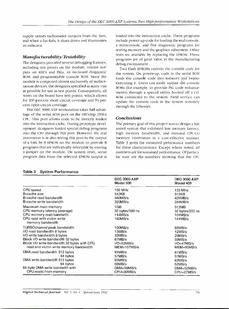
The Design of the DEC 3000 AXP Systems, Two High~erforrnnnce Workstc~tiorzs
supply senses tachometer outputs from the fans, and when a fan fails, it shuts down and illuminates an indicator.
The designers provided several debugging features, including test points on the module, tristate out- puts on ASICS and PALS, an on-board diagnostic ROM, and programmable console ROkI. Since the module is composed almost exclusively of surface- mount devices, the designers specified as many vias as possible for use as test points. Consequently, all wires on the board have test points, which allows for 100 percent short-circuit coverage and 94 per- cent open-circuit coverage.
The DEC 3000 AXP workstation takes full advan- tage of the serial ROM port on the DECchip 21064 CPU. This port allows code to be directly loaded into the instruction cache. During prototype devel- opment, designers loaded special debug programs into the C:PU through this port. However, the real innovation is in also wiring this port to the output of a 64K by 8 EPROM on the module to provide 8 programs that are individually selectable by moving a jumper on the module. On system reset, serial program data from the selected EPROM output is
Table 3 System Performance
loaded into the instruction cache. 'These programs include power-up code for loading the real console, a miniconsole, and five tliagnostic programs for testing memory and the graphics subsystem. Other tests are available by replacing the EPROM. These programs are of great value in the manufacturing debug environment.
Two flash EPROMs contain the console code for the system. On power-up, code in the serial ROM loads the console code into memory and begins executing it. Users can easily update the console ROMs (for example, to provide PAL code enhatice- ments) through a special utility booted off a CD- RO&i connected to the system. Field service can update the console code in the system remotely through the Ethernet.
Conclusions The primary goal of this project was to design a bal- anced system that exhibited low memory latencj: high memory bandwidth, and mini~nal <;pU-I/O memory contention in a cost-effective manner. Table 3 gives the measured peformancc numbers for these characteristics. Except where noted, all numbers are for sustained performance. Of particu- lar note are the numbers showing that the CPU
DEC 3000 AXP Model 500
-
DEC 3000 AXP Model 400
CPU speed B-cache size B-cache read bandwidth B-cache write bandwidth Maximum main memory CPU memory latency (average) CPU memory read bandwith CPU read with victim write
memory bandwidth TURBOchannel peak bandwidth I10 read bandwidth 8 bytes I10 write bandwidth 8 bytes Block I/O write bandwidth 32 bytes Block I/O write bandwidth 32 bytes with CPU
read and victim write memory bandwidth DMA read bandwidth 51 2 bytes
64 bytes DMA write bandwidth 512 bytes
64 bytes 64-byte DMA write bandwith with
CPU reads from memory
150 MHz 51 2KB 480MB/s 320MB/s
1 GB 32 bytes11 80 ns 1 14MBIs 16OMB/s
133 MHz 51 2KB 426MBls 284MB/s
51 2MB 32 bytes1203 ns 101 MBIs 141 MBls
89MBIs 12MBIs 29MB/s 59MB/s I/O=47MB/s MEM=95MB/s
81 MBIs 51 M B/s 82MB/s 52MBIs DMA=52MB/s CPU=27MB/s
Digital Technical Journal V'l 4 No. 4 . 5 p e c r ~ 1 l l s s ~ ~ e 1992 79

Alpha AXP Architecture and Systems
receives significant memory bandwidth even in the presence of heavy block VO and DIMA traffic.
Another goal of the project was to offer per- formance that is cotnpetitive with RISC worksta- tions available from other vendors. The benchmark performance of any system derives from the inter- dependent performance of the hardware, the oper- ating system, and the compilers that generate the application code. The benchmark perforn~ance should improve as each element matures. Table 4 shows the performance of the DEC 3000 AXP sys- tems on a selected set of benchmarks as of the announcement dates of these products. Table 5 compares the performance of the DEC 3000 AXP Model 500 to the published performance of several currently available competitive systems.-'
Acknowledgments The DEC 3000 AXP Model 500 design was a team effort-more people were involved than can be acknowledged in this space. Recognition is due to
Table 4 Benchmark Performance
those mrho contributed to the design of original hardware: Dave Archer, Mark Baxter, John DeRosa, Chris Gianos, Leon Hesch, Dave Laurello, Bob McNarnara, Dick Miller, Rick Ruclman, Dave Senerchia, Petr Spacek, Bob Stewart, Ned Utzig. Debbie Vogt, and John Zurawski. The tight schedule could not have been met without the special efforts of the Power and Packaging, Console, Qualifi- cation, Proto Management, and Technology and Operating Systems Groups. The design team for the DEC 3000 AXP Model 400 project is also recognized: John Da): Jamie Pierce, Dennis Rainville, and Ken Warcl. The thorough device evaluations by Rob Zahora contributed significantly to the success of the projects. We would also like to acknowleclge the contributions by FXO personnel. The Electronic Storage Development Group was responsible for the design of the nEC 3000 AXP Model 500 memory module. Significant efforts by the Maynard TIME, Albuquerque, and Ayr Manufacturing Plants should be recognized for delivering quality hardware
DEC 3000 AXP Model 400
DEC 3000 AXP Model 500
Clock (MHz) SPECmark89 Dhrystones V1.l (Dhrystones per second) V2.1 (Dhrystones per second) LINPACK 64-bit double precision 100 x 100 (MFLOPS)* 1000 x 1000 (MFLOPS) Xl 1 PERF
Two-dimensional vectors per second Two-dimensional pixels per second
Note: *Million floating-point operations per second
Table 5 Com~etitive Com~arison
DEC 3000 IBM RS6000 HP9000 Model 500 Model 580 Model 750
SPECmark89 121.5 126.2 86.6 Dhrystones V1.l (Dhrystones per second) 257.7K nla 133.7K V2.1 (Dhrystones per second) 281.2K nla 122.3K LINPACK 64-bit double precision 100 x 100 (MFLOPS) 26.4 38.1 23.7 1000 x 1000 (MFLOPS) 79.9 84.0 nla
80 Vol. 4 No. 4 Special Issue 1 9 2 Digital Technical Journal

Tbe Design of the DEC -3000 A X P S]lster?zs, TLPO High performance Workstations
during the development ancl production phases; a special thanks to Jirn Ersfelcl for his significant efforts in this regard.
References
1. R. Sites, etl., Alpha Architecture Reference Manual (Burlington, MA: Digital Press, Order No. EY-L520E-DP, 1992).
2. D. Dobberpuhl CL al., "A 200-MHz 64-bit Dual- issue CMOS Microprocessor," 1EEE Jout,lza/ oJ Solid-Stc~te Circuits, vol. 27, no. 11 (November
1992) 1555-1567 and Digital TecI7~zical J o ~ i ~ ~ n a l , vol 4, no 4 (1992, this issue) 35-50
3. TI:RROchannel Specifications, Version 2C (Palo Mto, CA: Digital Equipment Corporation, TRI/ADD Program, Order NO. EK-TCDEV-DK-004, September 1991).
4. Alpha AXP Workstation Family Performance Brief-Openv>lS, Secontl Edition (Maynard: Digital Ecluipment Corporation, Order No. EB-N0102-51, November 20, 1992).
Digilul Techrrical Journal Vo1. 4 IVO. 4 Spccirtl Issue 1992 8 1

Barry A. Maskas Stephen F. Shindon
Nicholas A. Warclgol
Design and Performance of the DEC 4000 AXP Departmental Server Computing Systems
DEC 4000 AXP systems demonstrate the highest performance and fu~zctionality for Digital's 4000 series of departmental server systems. DEC 4000 AXP sjatems are based on Digital's Alpha AXP architecttire and the IEEE's Futurebust profile B stczndard. They provide sy~nnzetric multiprocessing perforwza~zce for Open EVJSRYP
and DEC OSF/I AXP operating systems in an office enz~ironment. The DEC 4000 AXP systems were designed to optimize the cost-perforinance ratio and to irzclticle zqgmdability and expa~zdability. The systems combine the DECchip 21064 nzicro- processol; submicron CIMU sea-of-gates techrzolog7~ ClVIOS memory and I/Oper.~ph- erals technolog3,, a high-performance multiprocessing backplane interconnect, and modular system design to supply the most advanced functionality forperformance- driven applications.
The goal of the departmental server project was to establish Digital's 4000 family as the inclustry's most cost-effective and highest-performance depart- mental server computing systems. To achieve this goal, two clesign objectives were proposed for the DEC 4000 AXP server. First, migration was necessary from the VAX architecture, which is based on a com- plex instruction set computer (CISC), to the Alpha AXP architecture, which is basecl on a reduced instruction set computer (RIsc). Second, for expan- sion I/o in an upgradable office environment enclo- sure, migration was necessary from the Q-bus to the Futurebus+ I/O bus.' In addition, the new system had to provide balance between processor performance and I/O performance. maintaining customer investments in VAX and MIPS app1ic;ltions through support of OpenvMS AXP and DEC OSF/1 AXP operating systems was implicit in the archi- tecture migration objective. Migration, porting, and upgrade paths of various applications were defined.
This paper focuses on the design of the DEC 4000 AXP hardware and firmware. It begins with a discus- sion of the system architecture and the selection of the system technology. The paper then details the CPU, 1/0, memory and power subsystems. It con- cludes with a performance summary.
System Overview The DEC 4000 AXP system provides supercomputer class performance at office system cost.? This com- bination was achieved through architecture and technology selections that provide optimized tuniprocessor performance, low additional cost symmetric multiprocessing (SMP), and balanced I/O throughput. High I/O throughput was accom- plished through a combination of integrated con- trollers and a bridge to Futurebus+ expansion I/().
The system uses a modular, expandable, and portable enclosure, as shown in Figure 1. With current technologies, the system supports up to 2 gigabytes (GB) of dynamic random-access nlem- ory (DRAM), 24GB of fixed mass storage, and 1 6 ~ ~ of removable mass storage. The DEC 4000 AXP
system is partitioned into the following modular subsysten~s:
Enclosure ( ~ ~ 6 4 0 box)
CPU module (DECchip 21064 processor)
110 module
Memory modules
Mass storage compartments and storage device assembly (brick)
82 Vi l . 4 IVO. 4 Special Issue 1992 Digital Techrrical JoztrtraI

Design and Perfor~nance of tbe DEC 4000 AXP Depclrtmeiztul Seri~cr Conzputirzg Sjntenzs
increased processing power provided by the DECchip 21064 CI'11. Although processing power was taking a revolutionary jump in performance with no cost increase, disk and main memory tech-
Figure I DEC 4000 AXP S~a tem Enclos~tre
Futurebus+ Expansion I/O, Futurebus+ con- troller module (FBE)
Power supply modules - universal line front-encl unit (FEU)
- Power system controller (PSC) - DC-DC converter unit 5.0 volt (V) (DC5)
- DC-DC converter unit 2.1 V, 3.3 V, 12.0 V (DC3)
Cooling subsystem
Centerplane module
Operator control panel (OCP)
Digital storage systems interface (DSSl) and small computer systems interface (SCSI) termination voltage converter (VTERM)
Figure 2 shows these subsystems in a functional diagram. The subsystems are interconnected by a serial control bus, which is based on Signetic's 12C bus.+
System Architecture From the beginning of the project, it was apparent that the I/O subsystem had to be equal to the
nology were still o n an evolutionary cost ancl per- formance curve. 'l'he nietrics that had been used for V A ~ systems were difficult, if not impossible, to meet through lineill- scaling within a fixed cost bracket. These metrics were based on VAX-11/780 units of performance (VtlPs); they give main mem- ory capacity in megabytes (MR)/VLIP, clisk-queuecl I/O (($0) completions in QlOIs/\~lTP, and disk data rate in MB/s/VUP. As an example, Table 1 gives the metrics for ;I VAX 4000 ivlodel 300 scaled lin- early to 125 wl's i~nd then nonlinearly scaled for the DEC 4000 system implementation. Performance rnoc.leling of the DECchip 21064 <:PlJ suggested that 125 VllI's was a reasonable goal for the DEC 4000 AXP.
Without an Alph;~ AXP architecture custo~ner base, we did not know if these metrics woulcl scale linearly with the processor performance. The DECchip 21064 processor technology has the poten- tial for attracting new classes of compute-intensive applications that may make these metrics obsolete. We therefore chose a nonlinear extrapolation of the metrics for our initial implementation. By trading off disk and memory capacity for I/O throughput performance, we kept within established cost ant1 performance goals. The implementation metrics were not limited by the architecture; further scal- ing up of metrics was planned. Of the four metrics, the disk capacity metric has the most growth potential.
To ensure conipliance with both the Alpha &?<I' architecture and the Futurebus+ specifications, the system was partitioned as shown in Figure 2. The bridge between tlie <:l'lJ subsystem ant1 the Futurebus+ subsystem afforcletl maximum design flexibility to accomrnotlate specification changes, modularit): ant1 i~pgr;~dability The I/O module was organized to balance the requirements between CPU performance and I/O throughput rates. The DEC 4000 AXP system implementation is based o n open standards, with a six-slot Futurebus+ serving as tlie expansion 1 / 0 bus ancl the system bus serving to interconnect memory (:PUS, ant1 the I/o module. The modularity of the system enables module swap upgrades and configurability of the I/O subsystem such that performance and f~unctionality may be tailored to user recluirements. The modularity aspects ofthe system design extend into the storage
Digital Technical Joumnl Vo1. 4 iVo. 4 Sprcirrl Issrbe 1992 83

Alpha AXP Architecture and Systems
CONNECTION MODULE
CONTROL PANEL
- - - - - - - - - - - - - I CPU SUBSYSTEM
I I I I I I I I
ASYNCHRONOUS SERIAL LlNE (AUXILIARY WITH MODEM CONTROL)
I ASYNCHRONOUS SERIAL LINE - I I
- -
(CONSOLE LINE)
I
FUTUREBUS+ 1 I10 EXPANSION 1 1 ;==========2 1 I MASS STORAGE COMPARTMENT I I I
I 1 I DSSIISCSI 0 FIXED I
161 MEDIA DEVICE
110 I I DSSIISCSI 1 FIXED
) MEDIA DEVICE I i c DSSllSCSl2 4 0 b; > DEVICE
I I n h, DSSIISCSI 3
1 . 8
I I .
DEVICE U ' I '
DSSIISCS14 REMOVABLE > MEDIA > DE\JICE
I I I
1 / 1 q ~EE::~A~A~~~F-+ DEVICE
ETHERNET PORT 1
ETHERNET PORT 0 TOETHERNET
r - - - - - - - I r - - - - - - - i I POWERSUBSYSTEM I COOLING SUBSYSTEM I
I I
AC POWER CABLE 1 - - - - - - - A
KEY:
fl EXTERNAL PORT CONNECTION
Figure 2 DEC 4000 AXP S'lstem F~~~zctioural Partitiotr
TO STORAGE EXPANSION DEVICES
84 Vol 4 ,Vo. 4 Specin1 Issue 1992 Digital Technical Journal

Design and Pevorrnance of the DEC 4000 AXP Departmental Server Comnpziting Systems
Table 1 Extrapolated VAX Metrics
VAX 4000 Scaled Scaled Model 300 Linearly Nonlinearly Metrics to 125 VUPs for DEC 4000 AXP
Memory capacity 60 MBIVUP 7.5 GB 2 GB
Disk capacity 1.65 GBIVUP 206 GB 100 GB
Disk QIO rate 49 QlO/s/VUP 6,125 QlOIs >4,000 QlOls
I10 data transfer rate 1.4 MBIslVUP 175 MBIs 210 MBIs
compartment where each brick has a dedicated controller and power converter. Support for DSSI, SCSI, and high-speed 10MB/s SCSI provides maxi- mum flexibility in the storage compartment. The modular mass storage compartments enable user optimization for bulk storage, fast access, or both.
The cost of SIMP was a key issue initially, since Digital's SMP systems were considerecl high-end sys- tems. Pulling high-end functionality into lower- cost systems through architecture and technology selection was managed by evaluation of perfor- mance and cost through trial designs and software breadboarding. Several tlesigns of a CPU module were proposed, including various organizations of one or two DECchip 21064 CPUs per module inter- faced to I/O and memory subsystems. Optimization of complexity, parts cost, performance, and power density resulted in a CPU module with one proces- sor that could operate in either of two CPU slots on the centerplane. Consequently, a system bus had to be developed that coulcl be interfaced by proces- sors, memory, ant1 I/O subsystems in support of the shared-memory architecture.
As development of the DECchip 21064 processor progressed, hardware engineers and chip designers established a prioritized list of design goals for the system bus as follows:
1. Provide ;I low-latency response to the CPLl's secontl-level cache-miss transactions and I/O moclule read transactions without pending transactions.
2. Provide a low-cost shared-memory bus, based on the cache coherence protocol, that woulcl facilitate upgrades to faster CPU modules. This provision implied a simple protocol, synchro- nous timing, and the use of transistor-transistor logic OTL) levels rather than special electrical interfaces.
3. Provide I/O bandwidth enabling local VO to operate at 25 megabytes per second (MB/s) and the Futurebus+ to operate at 100MB/s.
4. Provide scalable memory banclwidth, based on protocol timing of 25 nanoseconds (ns) per cycle, which scales with improvements in DRAM and static memory ( S W ~ ) access times.
5. Use module and connector technology consis- tent with Futurebus+ specifications.
The cache coherence protocol of the system bus is designed to support the Alpha t\XP architecture and provide each CPU and the I/O bus with a consis- tent view of shared memory. To satisfy the band- width and latency requirements of the processor's instruction issue rate, the processor's second-level cache size, 128-bit access width, and 32-byte block size were optimized to avoid bandwidth limits to performance. The block size and access width were made consistent with the system bus, which satis- fied the VO throughpilt metrics. Consitleration was given to support of a 64-byte block on the 128-bit- wide bus. Such support would have resulted in a 17 percent larger miss penalty ant1 higher average memory access time for the CPU and I/(), more stor- age and control complexity, and hence higher cost.
Simplicity of the bus protocol was achieved by limiting the number and variations of transactions to four types-read, write, exchange, and null. The exchange transaction enables the second-level cache of the CPU to exchange data, that is, to per- form a victim write to memory at the same time as the replacement read transaction. This avoided the coherence complexity associated with a lingering victim block after the replacement read transaction completed.
To address the issue of bandwidth requirements o17er time as faster processors become available, an estimate of 40 percent bus utilization for each pro- cessor with a l M B second-level cache was obtained from trace-based performance models. The utiliza- tion was shown to be reduced by using a 4MB sec- ond-level cache or by using larger caches on the DECchip 21064 chip. This approach was reserved as a means to support future CPU upgrades.
Digital Technical Journal Vol 4 iVo 4 S j ~ e c r ~ ~ l Issue 1992

Alpha AXP Architecture and Systems
Figure 3 is a block diagram of the length-limited seven-slot synchronous system bus. To achieve tight motlule-to-modulc clock skew control for this single-phase clock scheme, clocks are radially dis- tributed from the CPU 1 module to the seven slots. This avoided the added cost of a separate module dedicated for radial clock clistribution, and enabled the bus arbitration circuitry to be integrated onto the CPlJ 1 module.
Arbitration of the two CPU modules ancl the I/O module for the system bus is centralized on the (;ptJ 1 motlule. To satisfy the I/O motlule's latency requirements, the arbitration priority allows the I/O nloclule to interleave with each CPU module. In the absence of other requests, a module may utilize the system bus continnously. Shared-memory state evaluations from the bus adclresses during continu- ous bus utilization causes CPU "starvation" from the seconcl-level cache. To avoid CPU starvation from the second-level cache, the arbitration con- troller creates one free cycle after three consecu- tive bus transactions.
Technology Selection The primary force behind technology selection was to realize the f ~ ~ l l performance potential of the DECchip 21064 microprocessor with a balanced I / O subsystem, weighted by cost minimization, sched- ule goals, and operation in an office environment. SPICE analysis was used to evaluate various module and semiconductor technologies. A technology tlemonstration module was designed ancl fabri- catecl to correlate the SPICE models and to validate possible technology. Basetl on clemonstrations, the project proceeded with analytical data supported by empirical data.
The 25-watt DECchip 21064 c:PU was designed in a 3.3-V, 0.75-micrometer compleincntary metal- oxide semiconductor (CMOS) technology and was packaged in a 43-pin pin grid array (PGA). The CPU was the only given technology in the system. The power supply, air cooling, and logical and electrical CPU chip interfacing aspects of the CPU module and system bus designs evolved from the DECchip 21064 specifications. System design attention focused on powering ancl cooling the Cr-'rJ chip. Compliance with power and cooling specifications was deter- mined to be achievable through conventional volt- age regulation and decoupling teclino1og)r and conventional fan technology.
To adtlress system integrity and reliability requirements, all data transfer interconnects and
storage devices had to be protected. Tlie DECchip 21064 CPU's data bus and secontl-level cache are lo~lgword error detection and correction (EDC) pro- tected. The system bus is longword parity pro- tected. The memory subsystem has 280-bit-wide EDC-protected memory arrays. The Futurebus+ is longword parity protected.
System Bus Clocking To establish the 25-11s bus cycle time, analog models of the interconnect were developed and analyzed for 5 0-V CMOS transceivers. Assuming an edge-to- edge data transfer scheme, the modelers evaluated the timing from a driver transition to its settled sig- nal, including clock input to driver delay, receiver setup time, and module-to-module clock skew. The cycle time and the data transfer width were com- bined to determine compliance with low latency and bandwidth. Further analysis revealed that the second-level cache access timing was critical for performing shared-memory state look~rps from the bus. One solution to this problem was to store duplicate tag values of the second-level cache. This was evaluated and found to be too expensive to implement. However, the stucly did show that a duplicate tag store of the CPU's primary data cache had a performance advantage and was affordable if implemented in the CPU module's bus interface unit (BIu) chips.
To evaluate second-level cache access timing, a survey of SRAM access times, density, availabil- ity, and cost was taken. Results showed that a IMB cache using 12-11s access time S W s was optimal. With a 12-11s access time SRAM, the critical timing could be managed through the design of the BlU chips. The SRAM survey also showed that a ~ M B second-level cache could be planned as a follow-on boost to performance, as SRAII,~ prices declined. Trace-based performance simulations proved that these cache sizes satisfied performance goals of 125 WPs. This clock rate required a bus stall mecha- nism to accommodate current DRAII access times in the memory subsystem, which will enable future enhancements as access times are reduced.
The system bus clocks are distributed as positive emitter-coupled level (PECL) differential signals; four single-phase clocks are available to each slot. Each module receives, terminates, and capacitively couples the clock signals into noninverting and inverting PECL-to-CMOS level converters to provide four edges per 25-ns clock cycle. System bus hand- shake and data transfers occur from clock edge to
Vol. 4 No. 4 Special Issue 1992 Digital Technical Journrrl

Fi'qure 3 DEC 4000 AXP Sj~stenz Bus

Alpha AXP Architecture and Systems
clock edge ancl utilize one of two system bus clocks. A custom clock chip was implemented to provide process, voltage, temperature, and load (PVTL) reg~llation to the pair of application-specific integrated circuit (ASIC) chips that compose each BKl. The clock chip achieves module-to-module skews of less than 1 ns.
Our search for a clock repeater chip that coulcl minimize module-to-module skew and chip-to- chip skew on a module, and yet directly drive high fan-out ASIC chips with CMOS-level clocks, led us to Digital's Semiconcluctor Operations Group. Such a chip was in design; however, it was tailored for use at the DEC 6000 system bus frequency. The Semiconductor Operations Group agreed to change the chip to accommoclate the DE(: 4000 MI' system bus frequency.
I /O Bus Technology Because of technology obsolescelice, 1 / 0 buses have a 21-year life cycle divideel into 3 phases. During the first 7 years of acceptance, peripherals and applications are developed anel supportecl. Sustained acceptance takes holcl in the next 7 years as peripherals and applications are enhanced. In the last 7 years, a phase out or rnigmtion of periph- erals ant1 applications occurs. For the DEC 4000 AXP systems, our first priority was selection of an open expansion I/O bus in the first third of its life cycle. In addition, we wanted to select an open IEEE stan- dard bus that woulcl attract third-party developers to provide I/<) solutions to customers. The follow- ing prioritized criteria were established for the selection of a new 1/0 bus:
1. Open bus that is an accepted industry standard in the beginning third of its life cycle
2. Compatibility with Alpha hXP architecture
3. Minimum data rate of 100MB/s
4. Scalable features that are perfor~nance-exten- bible through architecture (e.g., bus width), and/or t h r o ~ ~ g h technology improvements (e.g., semiconductor device performance and integration)
5. Nlinimum 64-bit data path
6. Support of bridges to other I/O buses
7. Minim;~l interoperability problenls between devices from different venclors
After examination of several I/O buses that satis- fied these criteria, the Futi~rebus+ was selected. At the time of our investigation, however, the Futurebus+ specification was in development by the IEEE and a wide range of interest was evident throughout Lhe industry By providing the right sup- port to the Futurebus+ committee, Digital was in a position to help stabilize and bring the specifica- tion to con-2lctjon.
A DigiLal team represented the project's interests on the IEEE P896.2 Spccification Committee and proposecl standards as the DEC 4000 AXP system design evolvecl. This team achiewd its goal by help- ing the IEEE Committee define a profile that enabled the Futurebus+ to operate as a high-perfor- mance I/O expansion bus. To mitigate schedule impact due to instability of the Futurebus+ specifi- cations, the I/O module's Futurebus+ interface was architected to accommodate changes through a more discrete, rather than a highly integrated implementation Compliance with thr I;uturebus+ specifications influenced most mechanical aspects of the module compartment design, as is eviclent from the centerplane, card cage, rnodu le construc- tion and size, and power supply voltage specifica- tions and implementations.
Module Technology 1Module technology was selected to maximize sig- lyal density w-ithin the fewest layers with minimal crosstalk and to provide a uniform signal distribu- tion impedance for any module layer. Physical-to- electrical modcling tools were used to create SPICE models of connectors, chip packages, power planes, signal lincs of various lengths and impedances (based 011 the nlodule construction technology), ant1 multiplc signal lines. Uecause the placement of components affects signal perfor- mance anel quality and system performance (e.g., in the sccond-lev(:' processor cache), moclule floor plans and trial layouts wcrr. cornpletecl. A moclule layout tool was used to ensure procli~cibility com- pliance wit11 manufacn~ring standarcls as well as sig- nal routing constraints. The moclule layout process was iterative. As sections of the module routing were completed. SPICE moctels of the etch were extracteel. These ext~-actecl moclcls were connectecl to S P I G models of chip elrivers and run. Analysis was completed and reqi~irecl changes were imple- mented and a~lalyzed again. The process continuecl until the optimal specification conformance was achieved for all signals.
88 Vnt. 4 >Vo. 4 Spect'ul Issue I992 Dtgital Techrrical Journal

Desiqlz and Perfor~nnnce of the DEC 4000 A X P Deprrt~nental Seri~er Co~nput ing Sjntenzs
Motlule size was estimated basecl on system h~nc - tionnlity requirements and a stutly of tlie size and power recli~irements of that fi~nctionality. To simpli- fy the enclos~~re design, module size specifications are consistent with the Futurebus+ motlule specifi- cations. To achieve lower system costs, the proces- sor, memory, and I/o modules arc basecl on the same ten-layer controlled impedance construction.
Chip engineers avoitled the specification of fine- pitch surface-mount chips when possible. Compo- nent choices and module layouts were completed with ;I view toward ma~iufactur;tbility. Cost 2111alysis showetl th:~t mixetl, tlouble-sitletl surface-mount components and through-hole components had insignificant aclded cost when fusecl tin-lead mod- ule technology ancl wet-film solder-mask technol- ogy were i~setl. The required layer constri~ction and impetlances of 45, 70, and 100 ohms coulcl easily be achieved within cost goals through this technology. Solder-mask over bare copper technology was also ev;~lu;~tetl to determine if fine-pitch surfi~ce-mount components achieved higher yield througli the sol- der reflow process. This evaluation showed fused tin-le;~tl technology was better suited, based on defect densities, for the manufacturing process. Consequently, all DEC 4000 U P modules are imple- mented with fused tin-lead module technology ;~nd wet-film solder-mask technology
Semiconductor Technology As ;I result of a performance, cost, power, ancl mod- ule real est;ite study, CMOS technology was used extensively. The custo~ii-tlesignecl I'VTI. clock chips were developed in 1.0-micrometer (:MOS technol- ogy to supply CMOS-level signals for driving directly into the HllJ chips. Each module's RIlJ used the same 0.8-micrometer ASIC technology ant1 die size to closely manage clock skews. Each system bus mod- ~ ~ l e ' s 1%11l is implemented by two iclentical chips operatetl in an even ant1 an odd slice rnotle. Chip clesignrrs invented a rnetliotl for accepting 5.0-V sign;ils to be driven into their 3.3-V biased IIECchip 21064 (:1'IJ. Consequently, the selection ;~nd irnple- ment;~tion of 5.0-V ASIC: technology were easier. ASI(: vendor selection was based on (1) perfor- mance of trial tlesigns and timing analysis of parity and El)<: trees, (2) SPICE analysis of 1/0 drivers with direct-drive input clock cells, and (3) a layout abil- ity to si~pport wide clock trunks ant1 distributed clock buffering to effect low skews.
All memory chips on the CPr! moclule, memory module, and I/() module were implemented in
submicron CMOS or Hi(:i\.IOS technolog)! All the I/O and power subsystem controller chips such as the SCSI ancl DSSl controllers, Ethernet controllers, serial line interfaces, and analog-to-digital convert- ers were implemented in CMOS technology.
Speed or high drive is critical in radial clock dis- tribution, Futurebus+ interfacing, or memory mod- ule address and control signal fan-out. In these special cases, lOOK ECL operated in positive motle (PECL) or BII'OLAR technology was ernployeel.
S y s t ~ n . Bus Protocol and Technology The cache coherence protocol for the shared-mem- ory system bus is based on a scheme in which each cache that has a copy of the data from memory also has a copy of the information about it. All cache controllers monitor or snoop on the bus to deter- mine whether or not they have a copy of tlie shared block. Hence tlie system bus protocol is referred to as a snooping protocol, and the system bus is referred to as a snooping bus:'
The 128-bit-wide synchronous system bus pro- vides a write update 5-state snooping protocol for write-back cache-coherent 32-byte block read and write transactions to system memory address space. Each module uses a 192-pin signal connector-the same connector used by Futurebus+ modules. Each module interfaces between the system bus and its back port with two 299-pin PGA packages contain- ing CpIOS ASIC chips, which implement the bus pro- tocol. A total of 157 signals ant1 35 reference connections implement the system bus in the 192- pin connector (6 interrupt and error, 8 clock and initialization, 128 command and address or data, 4 parity, 11 protocol). All control/status registers (CSRs) are visible from the bus to simplify the data paths as well as to support SNIP.
To sinipldy the snooping protocol, only full block transactions are supported; masking or sub- block transactions occur in each module's BIU. Transactions are described from the perspectives of a commandel; a responder, and a bystander. The address space is partitioned into CSR space that can- not be cached, memory space that can be cached, and secondary VO space for the Futurebus+ and I/O module devices. Seconclary 1/0 space is accessible through an 1/0 module mailbox transaction, which pends or retries the system bus when access to very slow I/O controller registers conflicts with direct memory access (Div1.A) traffic. 'This software- assistecl procedure also provides masked byte read and write access to VO devices as well as a standard
Uigitrrl 7tcbnicnl Jorrrnal ).%I. 4 IVO. 4 .Speciul Isare 1992 89

Alpha kW Architecture and Systems
software interface. The use of 32-bit peripheral I > I & ~ devices :~voiclecl tlie need to imple~nent harcl- ware acltlress tr;insl;itors. Tlie software drivers pro- vide physical addresses; hence mapping registers are not necess:lr):
The I/O mod~lle drives two device-related inter- rupt signals that are received by both CPI. modules clue to SMI' requirements. One interrupt is associ- ;ited with tlie Fut~~rebus+, ;lnd the other is associated wit11 :ill tlie device control.lers local to the I/O mocl- ule. Tlie 1/0 niodule 1,rovicles a silo register of Futurebus+ interrupt pointers and a device request register of local clevice interrupt requests. CPU 1 or CPU 2 is the clesignated interrupt dispatcher mod- ule. I'rivileged architecture library software sub- routines, Icnown ;IS I'Al.cocle, run 01-1 the prin1a1-y CPIJ module ancl re;id tlie device interrupt register or Futurebus+ interrupt register to cletermine which local devices or which Futurebus+ device handlers are to be dispatched.
The enclosure, power, and cooling subsystems ;Ire capable of interrupting both processors when immecliate attention js required. A CP1J can obtain information fro111 s~~bsystenis sliow~i in Figure 2 through tlie serial control bus. The serial control bus enables highly reli;~ble conirnunications between field replaceable subsystems. [luring power-up, it is used to obtain configuration infor- mation. It is also used as an errol--logging channel and as a me;lns to communicate between the CPlJ
subsystem, power subsystem, and the OCP. Tlie nonvolatile RAhl (NVKAM) chip iniplementecl 011
each module :lllovled the firni\vare to use software switches to configure the system. Tlie software switches avoidecl the need for hardware switches and jumpers, fielcl replaceable unit identification tags. and handwritten error logs. As ;i result, the h;irtlware system is fully configured tllrough firmw;lre, ;i t i t l fault information travels with tlie fielcl repl:ice;lble unit.
The five-state c;~clic coherence protocol assumes that tlie processor's primary write-through cache is maintained as ;I subset of the seconcl-levcl write- back cache. The slr: on the CPrI module enforces this subset policy to simplify the simulation verifi- cation process. Wjtl-~out it, tlie number of verifica- tion cases woulcl h;ivc been escessive, difficult to exlxess, :~ntl clifficult to simi~l:~te anel check for correctness. Tlie l/O module implements an invali- date-on-write policy, such that a block it has read from memory will be invalicl;lted and then re-read if a <:PI1 writes to the block. The I/O module parti-
cipates in the coherency policy by signs~ling slis~red status to a CPU reacl of :I block it lias bufksecl. The five states of the cache coherence protocol ;ire given in Table 2.
The cache coherence protocol etisures that only one CPU rnoclule can return a dirty response. The dirty response obligates the responding <:I'li mod- ule to supply the read clata to the bus, since the memory copy is stale and the memory controller aborts the return of tlie re:icl data 1311s writes ;ilw;lys clear the dirty bit of the seferencecl c:~clie block in both the comrnantler niodule ;~ncl tlie module that takes the update.
A CPlJ hiu two options when a bus transaction is a write and the block is found to be valid in its cache. A CPLJ either invalitlates tlie block or accepts the blocl< and upd:ites its copy, keeping tlie block valicl. This decision is basecl on the state o f tlie pri- mary cache's duplicate tag slore iuid tlie state of the second-level cache tag store. Acceptance o C the transactiol~ into the second-level cache on a tag
Table 2 Five States of the Cache Coherence Protocol
State
1 NOT VALlD 2 VALlD
NOT SHARED NOT DIRTY
3 VALlD NOT SHARED DIRTY
4 VALlD SHARED NOT DIRTY
5 VALlD SHARED Dl RTY
Remarks - - -
Block is invalid. Valid for read or write, this cached block contains the only copy of the block; the copy is identical to the memory copy. Valid for read or write, this cached block contains the only cached copy of the block. Thecachedcopyhasbeen modified more recently than the memory copy. Block is valid for read or write, but a write must broadcast to the bus. This block may be in another cache, but the memory copy is identical. Block is valid for read or write, but a write must broadcast to the bus. This block may be in another cache, but the contents have been modified more recently than the memory copy. This is a transitional state that occurs when arbitrating for the bus to broadcast a write or when an unshared dirty block is returned to a bus read transaction.

Design and Perfirrnai?ce of the DEC
m;ltcli is c;tlled conditional update. When the com- mander is the I/O module, the write is accepted by a CPtr only if the block is valid. Depending on the state of the primary data cache tluplicate tag store, two types of hit responses can be sent to an 1/0
commander-I/O update always ancl VO conditional update. In the case of either I/O or CPU commander writes, if the valid block is in the primary data c:tclie, the block is invalidated. The two acceptance modes of I/() writes by a CPIi are programmable because ilccepting writes uses approximately 50 percent more second-level cache bandwidth than invalidating writes.
To implement the cache coherence protocol, the <:l'tJ motlulc's second-level cache stores informa- tion as shown in Figure 4 for each 32-byte cache block.
Figure 5 shows the cycle timing and transaction sequences of the system bus. Write transactions occur in six clock cycles. Read, null, ant1 exch;u~ige transactions occur in seven clock cycles. A null tr;tnsaction enables a commander to nullify the active transaction request or to acquire the bus and avoid resource contention, without motltying memory. The arbitration controller monitors the bits transaction type and follows the transactions, cycle by cycle, to know when to rearbitr~te and sig- nal a new atltlress and command cycle. Atlditional cycles can be added by stalling in cycle 2 or cycle 4. Transactions begin when the arbitration controller grants the use of the CPrJ motlule's second-level
4000 AXP Depnrt7neiztal Seriier Corlz,!!t~ting Systenzs
caches to a commander module. The controller then signals the start of the adclress and commantl cycle 0 (CA). The commander drives a valid address, command, and parity (CAI)) in cycle I . A comman- der may stall in cycle 2 before supplying write data (W) in cycles 2 and 3.
Read data (RD) is received in cycles 5 and 6. The addressed responder confirms the clata cycles by asserting the acknowledge signal two cycles later. The commancler checks for the acknowledgment and, regardless of the presence or absence, com- pletes the number of cycles specified for the trans- action. Snooping protocol results are made available half way through cycle 3. As shown in Figure 5, the protocol timing from valid address to response of two cyclcs is critical. A responder or bystander may stall any transaction in cycle 4 by asserting a stall signal in cycle 3. The bus stalls ;IS
long as the stall signal is assertecl. Arbitration is overlappecl with the last cycle of a transaction, such that tristate conflict is avoiclcd.
A 29-bit lock address register provides a lock mechanism per cache block to assist with software synchronization operations. The lock address regis- ter is managetl by each CP1J as it executes load from memory to register locket1 longword or quadwortl (LDx-L) and store register to memory conditional longword or quadwortl (STx-C) instruction^.^ The lock adtlress register holds an address and a valid bit, which are compared with all bus transaction addresses. The valid bit is cleared by bus writes to a
TAG conslsts of 9 physical address blts with a 4MB second-level cache, or 11 physical address blts with a 1 MB second-level cache.
TAG PARITY (TP) bit indicates even parity
TAG
VALID (V) b ~ t lndlcates whether or not th~s block can be considered for a response lo the snoop transaction
V Tp
SHARED (S) b11 indicales whether or not this block may also be resident in another module's cache.
DIRTY (D) bit indicates whether or not this block has been modified by thls processor
S LW4
CONTROL PARITY (CP) bit indicates even parity.
CK5
DATA (LW) b~ts organized as two 128-b~t-wide half blocks; each 128-bit block is composed of tour longwords.
CK4
Digital Tecbnicnl Jotrnrc11 W)l. 4 ~VO. 4 S/)c.cial lss~lr 19%
D LW5 LW6
CHECK (CKO through CK7) bits detect errors for each longword.
Cp
Figur'e 4 Second-level Cache Structure
LWO CK6
CK1 CKO LW7
LWI LW2 CK7
CK2 LW3 CK3

Alpha AXP Architecture and Systems
WRITE CYCLE
ARBITRATE COMMAND ADDRESS ACKNOWLEDGE SHARED DATA
READ, NULL, EXCHANGE CYCLE
ARBITRATE COMMAND ADDRESS ACKNOWLEDGE SHAREDJDIRTY DATA
KEY:
6
GRANT
CA COMMAND CAD ADDRESS WD WRITE DATA
0
C A CAD
1
CAD
5
GRANT
RD READ DATA
Figure 5 System Bus Tlwizs~ictio~z Sequetzces
2
WDI
0
C A CAD
2
WDl
~llatcbing address or by CI-'lJ execution of STx-C instructions. The register is loaded and validated by a CPll's LDx-L instruction. This hardware and soft- ware construct, as ;i means of memory synchroniza- tion, statistically avoids the known problellls with exclusionary locking schemes. Exclusionar~7 lock- ing schemes create resource deatllocks, transaction ordering issues, and performance degraclation ;is side effects of the exclusion. This construct allows a processor to continue program execution while harclware provitles the branch conditions. The lock f;tils only when it loses the race on a write collision t o the locked block.
A bus transaction address that hits on a valid lock address register must return a snooping protocol shared response, even if the block is not valid in the primary anti seconcl-level caches. The shared response forces writes to the block to be broadc:tst, and STx-C instructions to function correctly. The NULL transaction is issued when a STx-C write is abortetl clue to the failure of the Jock to avoici system memory modification.
1
CAD
3
CA CAD WD2
4
WD1
CPU Module Sz~bsystems Each <:PU modiile consists of a number of subsys- telns as shown in Figure 3. The CPU module's sub- systems are
3
CA CAD WD2
1. DE<:chip 21064 processor
2. l M B or 4bIB physically addressed write-back secontl-level cache
4
WDI
0
C A
5
WD2
RDI
3. BIlJ chips containing write merge buffers, a duplicate tag store of the processor's 8-kilobyte (KR) data cache for invalidate filtering and write update policy decisions, an arbitration con- troller, a system bus interface, an address lock register, and CsRs
6
GRANT
RD2
4. System bus and processor clock genera- tors, clock and voltage detectors, and clock tlistributors
5
GRANT
WD2
5. System bus reset control
6 . 8 K R serial KOkI for power-up software loading of the processor
0
C A
7 Microcontroller (MC) with serial system bus interface allcl serial line unit for communication with the processor's serial line interface
I
8. i\WhM. chip on the serial control bus
Sincc a (:PU nlodule bas to operate in either CPU 1 or CPlJ 2 rnocle, the CPU 2 connector was designed to provide an identification code that enables or dis- ables the clock drivers and configures the CSRs'
Vo1. 4 iVo. 4 .Specic~l Iss~te /992 Digitul Technical Jounzul
Design and Perfir.r?~unce (J lhe 111:
atldress space and CPU identification code. As a result, arbitration and other slot-depentlent func- tions are enabled or disabled when power is applied.
A re1i;ibility sti~dy of a parity-protected second- lcvel cache showed that the SWMs contributed 44.7 percent of tlie failure rate. By implementing El)(: on the data S~W&I portion of the secontl-le\iel cache, a tenfold improvement in per processor me;ln time to failure was achieved. Consequently, six Slli\M chips per processor were implemented to ensure high reliabilit)!
The niultiplcxecl interface to tlie second-level cache of the CPU module allows tlie processor chip ant1 tlie system bus equal ant1 sh;~retl access to the second-level cache. To achieve low-latency memory access, both the microprocessor and the system bus operate the second-level caclie ;is fast ;is pos- sible based on their clocks. Hence the seconcl- level cache is multiplexed, and ownership deh~ults to the microprocessor. When the system bus requires access, ownership is transferred cluickly with tlat;i Slii\l\l parallelism while the t;ig SlbiMs are monitored.
Many of the CPLJ module subsyste~ns are found in the interkice gate array called tlie < ; A chip. Two of these chips working in tandem implement the and tlie secontl-level caclie controller. Write merge buffers combine masked write data from the micro- processor with the cache block as p;irt of :11i allo- cate-on-write policy. Since the microprocessor has write buffers that perform packing, fill1 block write arouncl the second-level cache w;rs implementetl ;is an exception to the allocate-on-nrrite policy. To meet schedule atid cost goals with few personnel, one complex gate array was designecl r;ither t11;ln sever;~l lower-complexity gate arrays. Hence the data path and the control functions were parti- tioned such that the microprocessor could operate as an even or odtl member of ;I pair on the <:IJ[I 1 o r the <:lJU 2 niodule.
Tlie system bus clock design is somewhat intle- pentlent of the processor clock, but the r;ilige is restricted clue to the implementation of the snoop- ing protocol timing, the multiplexed us;Ige o f tlie secontl-level caclie, ant1 the CPrJ interk~ce Ii;~ntl- shake and data timing. Therefore, the system bus cycle time is optimized to provide the rn;~xin~um performance regardless of the processor speed. Likewise, tlie processor's cycle time is optimized to provide maximum performance reg;~rdless of the bus speed. Considerable eff'ort resultetl in a second- level caclic ;~cccss time that enablecl tlie (:IJ~I's reat1
or write accesses to complete in four internal clock cycles, calletl the four-tick loop timing of the sec- ond-level cache. To realize hoth optimizations, tlie CPlJ's synchronous interface is supportecl by an asynchronous interkrce in tlie DllJ. \fiarious timing relationships between tlie processor and the system bus are control lecl by programmable timing controls in the IlllJ chips.
To achieve the tight, four-tick timing of the sec- ond-level cache, clouble-sided surface-nlount tech- nologjrm7as used to place the SIL4M chips physically close together. This minimized address wire length and the number of tiiodule vias; hence tlie driver was loaded effectively This c;~reful placement was combined with the tlesign of a custom CMOS address fan-out buffer ;Inel ~iii~ltiplexer chip (<;I\H) to achieve hst propagation delays. The CAB chip was implementeel in the same <:MOS process ;IS tlie DECchip 21064 (:I)[! to obt;lin the desired through- put clelay. Combiliecl with 12-11s S W M chips, tlie <:At%
chip enabled optimiz;~tion ol'the (;rrl's second-level caclie timing 21s well as the system bus snooping protocol response timing.
I/O Module, Mass Storage, and Expansion I/O Subsystems The I/O moclule co~isists of a local I/O subsystem that interfaces to the common I/() core ancl a bridge to the Futi~rebus+ for I / ( ) options. By incorporating modularity into the tlesign, a bro;itl range of appli- cations could be supported. To satisfy the tlisk per- formance and bulk storage ~iietrics given in Table 1, mass storage was configured based on applications requirements. Elst access times of 3.5-inch tlisks and multiple spindles were selectetl for applica- tions with results in QlO/s. Tlie density of 5.25-inch disks was selected for ;~pplications requiring more storage space. As intlic;~tetl in T~ble 1. the metrics of greater than 4,000 QlO/s tletermined the perfor- malice requirrrnents of tlie storage colilpartrnent. Each of the four disk storage com],artn~ents in the system enclosi~re can holcl a till I-size 5.25-inch tlisk i f cost-effective bulk storage is needed. If the neetl is for the mnximuni numI>er of I/Os per secontl, each compartment can holtl 1113 to four 3.5-inch tlisks in a mini array.
Co~ifigurations of 5.5-inch disks in a brick enable optimization of throughput tlirough parallelism techniques such ;IS stripe sets and redundant arr;q7 of inexpensive tlisks (1b111)) sets. Tlie brick con- figuration also enables hult tolerance, at the expense of tIiroi~glil>i~t, 13)' 11si11g sliatlow sets. With
Digital Technical Jorirtral Vol. 4 iVo. 4 Specicrl l s s~ lc I991 9.5

Npha AXP Architecture and Systems
this technique, each storage compartment is inter- faced to the system through a separate built-in con- troller. The controller is capable of running in either DSSI mode for high availability storage in cluster connections with other OpenVMS U P or VMS systems, or in SCSI mode for local disk storage available from many different vendors. For applica- tions in which a disk volume is striped across multi- ple drives that are in different storage cavities, the benefit from the parallel seek operations of the drives combines with the parallel data transfers provided by the multiple bus interfaces. The main memory capacity of the system allows for disk caching or RAM disks to be created, and the process- ing power of the system can be applied to managing the multiple disk drives as a RAID array. With cur- rent technology, maximum fixed storage is 8GB with 5.25-inch disks ancl 2 4 G ~ with 3.5-inch disks. If the built-in storage system is inadequate, connec- tion to an external solution can occur through the Futurebus+.
Tlie BlU is implemented by two 299-pin ASIC chips. The bridge to the Futurebus+ and the inter- face to the IocaJ I/O devices are provided with sepa- rate interfaces to the system bus. Each interface contains two buffers that can each contain a hex- word of data. This allows for double buffering of I/O writes to memory for both interfaces and for the prefetching of read data by which the bridge improves throughput. These buffers also serve to merge byte and longword write transaction data into a fill1 block for transfer over the system bus. In this case, the write to main memory is preceded by a read operation to merge modified and unmodi- fied bytes within the block.
The Ethernet controllers and SCSI and DSSI controllers can handle block transfers for most operations, thus avoiding unnecessary merge trans- actions. As shown in Figure 3, the I/O module inte- grates the following:
1. Four storage controllers that support SCSI, high-speecl SCSI, or DSSI for fivecl disk drives and one SCSI controller for removable media elrives
2. 128K.B of SRAM for disk-controller-loadable microcode scripts
3. Two Ethernet controllers and their station address ROMs, with switch-selectable ThinWire or thick-wire interfaces
4. 512KB flash erase programmable ROM (FEPROM) for console firmwdre
5. Console serial line unit (SLIJ) interface
6. Auxiliary SLU interface with modem control supp01-t
7 Time-of-year (TOY) clock, with battery backup
8. 8KB of electrically erasable memory (EEKOM) for console firmware support
9. Serial control bus controller and 2 kilobits of m 1 1
10. 64-bit-wide Futurebus+ bridge
11. BIU, containing four hexwords of cache block buffering, two mailbox registers, and the system bus interface
The instability of the Futurebus+ specifications and the use of new, poorly specified controller chips presented a high design risk for a highly inte- grated implementation. Therefore the Futurebus+ bridge and local VO control logic were imple- mented in programn~able logic to isolate the high risk design areas from the ASIC development process.
Memory Subsystem As shown in Figure 3, up to four menlory modules can reside on the system bus. This modularity of the memory subsystem enabled maximum configu- ration flexibility. Based on tlle metrics listed in Table 1, 2GB of memory were expected to satisfy most applications requirements. Given this 2GB design goal, the available DRAM technology, and the module size, the total memory size was configured for various applications.
The memory connectors provide a unique slot identification code to each BIU, which is used to configure the CSRs' address space based on the slot position. Memory modules are synchronous to the system bus and provide high-bantlwidth, low- latency dynamic storage. Each memory module uses 4-bit-wide, 1- and 4-megabit-deep DRAW tech- nology in various configurations to provide 6 4 ~ ~ , 128MB, 2 5 6 ~ 8 , or 512MB of storage on each module.
To satisfy memory performance goals, each memory module is capable of operating alone or in one of numerous cache block interleaving configu- rations with other memory modules with a reacl- stream capability. A performance study of stream buffers revealed an increase in performance from memory-resident read-stream buffers. The strean1 buffers allow each memory module to reduce the
94 Vo1. 4 No. 4 Special Issue I992 Digital Technical Journal
IlesiLyn arzd PerorA~?zance of the DEC 4000 U P Del,artw?e?ltul Server. C o ~ ~ z p ~ l t i ~ z g .Sj(j_~'sterns
average read latency of ;I <:I)( or I / O module. 'Thus more banclwidth is us;lble on a congested bus because the anticipated read data in a detected access sequence is prefetched. The stream buffer orefetch activity is st;rtistically determined by bus ;~ctivity.
Overall memory bandwidth is also improveel through exchange trvis;lctions, which use victim writes with repl;~cernent reacl parallelism. Intel- ligent memory refresh is scheduled based o n bus iictivity and anticipatecl opportunities. Write trans- actions are buffered from the bus before being writ- ten into the DbWs to ;~voicl stalling the bus.
Data integrity, memory reliability, and system ;~vailability are enh;lnced by the EDC circuitry Each memory niotlule consists of 2 or 4 banks with 70 I)RrW chips each. This enables 256 data bits ant1 24 El><: hits to be accessetl at once to provide low latency for the system bus. A cost-benefit ;inalysis sl?owetl a savings of IIRAM chips when ED<: is in~ple- nientcd on each memory module. The processor's 32-bit EDC requires 7 check bits as opposed to the 128-bit ED<:, which reqilires 12 check bits zinc1 uses ['ewer chips per bank. 'T'lie selected EDC code also provides better error detection capabilit-y of 4-bit- wide chips than the processor's 32-bit EDC.
To improve performance, separate EDC logic is implemented on tlie write path and read path of each memory nlodule's RIU. The EDC logic performs detection anel correction of all single- bit errors and most 2-bit, .)-bit, and 4-bit errors in tlie D&\1 array Tlie El>(:'s generate function can detect certain types of addressing failures associ- ated with the DRAM row and column address bits, along with the bank's select address bits. Failures associated with these ;~dtlressing fields can be detected, thus improving data integrity. Software errors can be scrubbed from liiemory by the <:PU
when requested through use of PALcode subrou- tines, which use tlie LUX-L and STx-C synchroniza- tion construct without having to suspend system operations.
Enclosure and Paver Subsystems The DEC 4000 AXP enclosure seen in Figure 1 is c;~lled the ~ ~ 6 4 0 box and is 88.0 centimeters (cm) high, 50.6 cm wide, and 76.2 cm deep. It weighs 118 to 125 kilograms hl ly configured. The enclosure is designed to operate in an ol'fice environment from 10 to 35 degrees Celsius. The power cord can con- nect to a conventional will1 outlet which supplies up to 20 amperes at either 120 V AC or 240 V AC.
Tlie DE(: 4000 AXP system is a portable unit that provides rear access and simplified install;~tion and maintenance. Tlie systelii is mounted o n casters and fits easily into an open office environnient. Modular design allowed con~pliance with stan- dards, ease of manufacturing, and easy fielcl servic- ing. Constructed of molded plastics, the chi~ssis is sectioned into a card cage, :I storage compart- ment, a base containing four 6-inch variable-speed D c fans and casters, an air plenum ;uicl baffle assem- bly, front ant1 rear doors, ancl side panels. The mass storage compartment supports 111, to I6 fixed-storage clevices and 4 removable storage devices. Expansion to storage enclosures is sup- ported for applications that recjuire speci;~lizecl storage subsystems.
Feedback from fielcl service engineers proriiptecl 11s to omit uselcss light-emitting devices (LEIIS) in each subsystem, since access to most electronics is from the rear. As a result, the OCP was m;~de coni- n~oli to all sul>systems through the serial control bus and made visible inside the front door of the enclosure. It provides DC on/off, hz~lt. ;lncl restart switches, and eight LEDs, which inclic:~te faults of CPU, I/O, memory, and Futurebus+ nlodules. The fault lights are controlled either by a microcon- troller on either <:I'(J module or by ;In interhce on the 1/0 module.
Futurebus+ slot spacing was provided by the lEEE specification. The system bus slot spacing for each module was cleterniined by h~nctional require- ments. For example, the CPU moclule requires 300 linear feet of air flow across the DE<:chip 21064 microprocessor's 3-inch square heat sink, as seen in Figure 1, to ensure the 25-watt chip could be cooletl reliably. Since 4000 systems provide this same air flow across modules, cooling was not a major design obst;~cle. The rnotlule compartment's Futurebus+, systerri bus, and power subsystems can be seen in the enclosure back view of Figure 6.
All electronics in the enclosure, as shown in Figure 7, are air cooled by four 6-inch fans in the base. Air is drawn into the enclosure grill at the top front, guided along a pleni~m ancl baffle ;lssernbly and down through the module compartment and power supply comp;lrtrnent to the base. Air is also drawn tlirougli front door louvers and across the storage compartments and down to tlie base. Electro~iics connected to the power subsystem monitor ambient and nodule compartment exhaust teniperatures. Thus the fan speed c;ln be regulated based on temperatllre measurements,
Digilal Technical Joun1~11 1/01. 4 rVo. 4 Special 1.ssr1.e 1992 95

Alpha AXP Architecture and Systems
SYSTEM BUS are for fixecl storage bricks. A storage brick consists
I of a base plate and mounting hardware, disk drives, local disk converter (LDC). front bezel assembly, anel wiring harnesses. The LDC converts ;I tlis- tributed 48.0 V to 12.0-V and 5.0-V supplies :lnd a 5.0-V termination reference for the brick to ensure compliance with voltage regulation specific;~tlons
POWER
Figure 6 DEC 4000 AXP Enclosure Rear View
reducing acou5tic noise in an air-conditioned office environment.
The centerplane assembly consists of a storage backplane, a module backplane, and an electroniag- netic shielcl. This implementation avoids depen- clence on cable assemblies, which are unre1i;tble and d~fficult to install and repair. Defined connec- tors and module sizes allowed the enclosure devel- opment to proceecl unencumbered by moclule specification changes. The shielded module com- partment provides effective attenuation of signals UP to 5 gigahertz. There are six Futurebus+ slots, four memory slots, two CPU slots, one 1/0 slot, and four central power module slots, which include the FEU, PSC, DC5, and DC3 units
The storage compartment contains six cavities, as seen in the enclosure front vlew of F~gure 8 Two cavities are for removable media, and four
and termir~ation voltage levels of current ;ul~cl fi~tilre disks.
The 20-ampere power subsysteni can cleliver 1,400 watts of DC power divided across 2.1 V, 3.3 V, 5.0 V, 12.0 V, ant1 48.0 V. The enclosure can cool 1,500 watts of power and can be configured as a master or a slave of AC power application. IJse of ;I
universal FEU eliminates the neecl for selecting operating voltages of 120 V or 240 V A<;. The F H r converts the input AC into 385 V DC, which is clis- tributed to provide 48 V DC to two step-down I)(:- to-I)C converters. which work in parallel to share the lo;~d current. The combined 48 V I)(: outpi~t from these converters is deliverecl to the rest of the system.
Control of tlistributed power electronics is diffi- cult anel expensive with dedicated electronics. A cost-effective alternative was use ol a one-chip <:l\lOS microcontroller, surrounded with a n array of sensor inputs through CMOS analog-to-digital con- verters, to provide PSC intelligence. I>ecisiori-mak- ing ;ubility in the power subs!~stern enabled compliance witli voltage-sequencing specific;~tions anel fail-safe operation of the system. l'he micro- controller can control each LDC and communicate witli the C:Pl.I and OCP over the serial control bus. I t monitors over and under voltage, temperature, and energy storage conditions in tlie n~oditle and stor- age compartments. It also reports status ancl failure information either to the CPU or to a elisplay o n the PS(: rnocl~~le, whicli is visible insicle the enclosure back door.
Firmware The prim;lry goal of the console interface is to bootstrap the operating system tliro~lgh a process c;ulled boot-block booting. The console inter- face runs a nlinimal I/O device h;lncller routine (boot primitive) to read a boot block fro111 a device that has descriptors. The descriptors point to the logical block numbers where the prinlar); boot- strap program can be found, and the console interface loads it into system memory To accom- plish this task, t11e firmware must configure at~cl
96 Vo1. 4 i\b. 4 Special Issue 1992 Digital Technical Jouniol

Design and Performance of the DEC 4000AXP Departmental Server Computing Systems
OCP STORAGE BRICK CENTERPLANE STORAGE BRICK FBE
, r q 9 :;;$qm!p'.:- 0% '4~ . 4 .. ' y,t; .uT
, - ,,!, 7 , -*-a ..*>.- -..- fit,?
.<?##,:$;t 1 : r . p 2 k - ?
VTERM PSC MEMORY CPU
Figure 7 DEC 4000 AXP Modular Electronics
test the whole system to ensure the boot process can complcte without failures. To minimize the bootstrap time, a fast menlory test executes in the time necessary to test the largest memory module, regardless of the number of memory modules. If fa~lures are detected after configuration is com- pleted, the firmware must provide a means for diag- nosis, error isolation, and error logging to facilitate the repair process. The DEC 4000 AXP system pro- vides a new console command interface as well as integrated diagnostic exercisers in the loadable firmware.
The firmware resides on two separate entities, a block of serial ROM on the CPU moclule and a block of FEPROM o n the I/O module. The serial ROM con- tains software that is automatically loaded into the processor on power-up or reset. This software is responsible for initial configuration of the CpU module, testing minimal module h~nctionality, mi- tializing enough memory for the console, copying the contents of the FEPROM into this initialized
console memory, and then transferring control to the console code.
The FEPIiOM firmware consists of halt dispatch, entry/exit, diagnostics, system restart, system boot- strap, and console services functional blocks.
PALcode subroutines prov~de a layer of software with common interfaces to upper levels of sofware. PALcode serves as a bridge between the hardware behavior and service requirements and the require- ments of the operating system. The system takes advantage of I'ALcode for hardware-level interrupt handling and return, security, implementation of special operating system kernel procedures such as queue management, dispatching to the operating system's special calls, exception handling, DECchip 21064 virtual instruction cache management, virtual memory management, and secondary I/o operations. Through a combination of hardware- and software-dependent I'ALcode subroutines, OpenVMS AXP, DEC OSF/l AXP, and future operating systems can execute on this hardware arcliitecture
Digital Tecbnical Journal Vo1. 4 No. 4 Special Issue 1992 97

Alpha AXP Architecture and Systems
Ackmnuledgments Development of a new system requires contribu- tions from individuals throughout the corporation. The authors wish to acknowledge those who con- tributed to the key aspects of the DEC 4000 AXP system. Centerplanes: Henry Entnan, Jim Padgett; CPU: Nitin Godiwala, George Harris, Jeff Metzger, Eugene Smith, Kurt Thaller; Firmware: Dave Baird, Harold Buckingham, Marco Ciaffi, John DeNisco. Charlie Devane, Paul LaRochelle, Keven Peterson; Futurebus Exerciser: Philippe Klein, Kevin Ludlam, Dave Maruska; Futurebus+: Barbara Archinger, Ernie Crocker, Jim Duval, Sam Duncan, Bill Samaras; 110: Randy Hinrichs, Tom Hunt, Sub Pal, Prasad Paranjape, Chet Pawlowski, Paul Rotker, Russ Weaver; Management: Jesse Lipcon, Gary I? Lidington; Manufacturing: Mary Doddj: Al Lewis, Allan LyaII, Cher Nicholas; Marketing: Kami Ajgaonkar, Charks Monk, Pam Reid; Mechanical: Jeff Lewis, Dave Moore, Bryan Porter, Dave Simms; Memory: Paul Goodwin, Don Smelser, Dave Tatosian; Operations: Jeff Kerrigan; Operating Systems: AJ Beaverson, Peter Smith; Power: John Ardunio, Robert White; Simulation: Paul Kinzelman; Systems: Vince Asbridge, Mike Collins, Dave Conro): A1 Deluca, Roger Gagne, Tom Orr; Eric Piip; Thermal: Steve Cieluch, Sharad Shah.
Figure 8 DEC 4000 AXP System Enclosure Front Vieru
Refmence and Note
Performance Summary The DEC 4000 AXP Model 610 system's performance numbers as of November 10, 1992 are given in Table 3. Its performance will continue to improve.
Summary r)EC 4000 IU(P systems demonstrate the highest performance and functionality for Digital's 4000 series of departmental server systems. Based on Digital's Alpha i\xP architecture and the IEEE's Futurebus+ profile B standard, the systems provide symmetric multiprocessing performance for OpenVMS AXP and DEC OSF/l AXP operating systems in an office environment. The L)EC 4000 AXP systems were designed to optimize the cost-performance ratio ant1 t o include upgradability and expanclabil- ity. The systems combine Digital's CMOS technol- ogy, I/O peripherals teclmology, ahigh-performance multiprocessing backplane interconnect, ant1 mod- ular system design to supply the most advanced filnctionality for performance-driven applications.
1. IEEE Standard for FzttztreDus+-Physical Layer and Profile Spec~iccltion lEEE Standard P896.2- 1991 (New York: The Institute of Electrical and Electronics Engineers, April 24, 1992).
2. Supercomputer performance as defined by the composite theoretical performance (CTP) rating of 397, with the or:<:cliip 21064 operated at 6.25 ns, as established by the U.S. export regulations.
3 Inter-l7ztegr~1lc.d Circuit Ser3ial Bus Specvi- catior~ (ILC Bus Specification). (Sunnjwale, CA: Signetics Company, 1988).
4. J. Hennessy and D. I'atterson, compute^^ Architecture: A Quantitative Approach (San iMateo, ct\: Morgan Kailfm;inn Publishers, Inc., 1990): 467-474.
5. R. Sites, ed. , Alpha AX'P Sjjstenz Reference Manual, Version 5.0 (Maynard: Digital Equipment Corporation, 1992).
98 Vol d iVo 4 Ypccmllsc~~c~ I992 Digital Technical Jorrrrral

Table 3 CPU Performance Summary for the DEC 4000 AXP System
Futurebus+ Performance Latency Bandwidth
Peak 16 bytes/l 00 ns 16OMBls Read 16 bytedl 82 ns 88M B/s Write 16 bytes11 33 ns 1 20MB/s
Local Bus Performance
Peak Read Write
Latency 4 bytes180 ns 4 bytes11 60 ns 4 bytedl 60 ns
Bandwidth
50MBIs 25MBIs 25MB/s
System Bus Performance Latency
Peak 16 bytes125 ns Read 32 bytes/l 75 ns Write 32 bytedl 50 ns Exchange 64 bytedl 75 ns
Internal Cache Miss, Second-level Cache Hit (Four-tick) Performance
Latency Read 16 bytes/25 ns Write 16 bytes125 ns
Bandwidth
640MB/s 182MB/s 21 3MB/s 365MBIs
Bandwidth
640MB/s 640MBIs
CPU Second-level Cache Miss Performance
Read Write Exchange
Latency 32 bytes/275 ns 32 bytes1200 ns 64 bytes/275 ns
Bandwidth
1 1 6MB/s 16OMBIs 232MB/s
- - -
DEC 4000 Model 610 SPECmark89 and SPECthruput89* Estimated CPU Performance Summary
Integer (INT) Benchmarks Ratio GCC 61.58 ESPRESSO 82.91 LI 93.05 EQNTOTT 103.46
Floating-point (FP) Benchmarks SPICE2G6 72.58 DODUC 11 3.81 NASA7 229.27 MATRIX300 101 9.1 7 FPPPP 180.32 TOMCATV 128.70
SPECmark > 136.23 SPECint > 83.73 SPECfp > 188.45
Ratio
1 @ 54.80 I@ 81.76 I@ 92.19 1 @ 100.76
I@ 68.19 1 @ 11 3.53 1 @ 221.56 1 @ 963.81 1 @ 177.89 1 @ 123.25
SPECthruput > I@ 131.18 SPECintthruput > I@ 80.32 SPECfpthruput > I@ 181.92
Ratio
2@ 50.78 2 8 78.33 2@ 92.18 2@ 97.94
LINPACK - double precision 100 X 100 36.8 MFLOPS LINPACK - double precision 1000 X 1000 78.4 MFLOPS Dhrystone 165.0 MIPS
Note: 'Version 1.0 OpenVMS AXP operating system, 160-MHz clocked DECchip 21064 microprocessor, 1 ME3 second-level cache. Notice the 1.9 scaling of the second CPU.
Digital Techrricwl Journal &)I. 4 :Yo. 4 SpeciolIssrrr 1 9 2 99

Brian R Allison Catharine van Ingen
Technical Description of the DEC 7000 and DEC 10000 AXP Fame@
The DEC 7000 ar7d DEC 100OOprod~rcts ~11.0 rizicl-lwrlye nlzd nzairIfrnlrze Alphcr A X P
sjb-tei~z ($fk/'illgs ~ ; ' O I ? I Digitcll E y ~ ~ i l ~ i l i e i ~ t Corpoiriti011. These r?zucbir7es ~1le1.e designed to lneet the rieeds of large colnnzerrial al7d scientific c,yl,licutiolzs arzd ther.@re ore /?igl?$erfon.nc~i?ce, expattcl~rble sj~sterns that can be e~rs ib~ ~ ~ p g ~ w d e d . The DEC' 7000 ~17d 10000 ~j~ster'lzs zltilize t/7e IlI:Cc/?if) 21064 17zicroprocessoi operat- illg a t speeds LIP to -300 MHz. The high-speed chips, large c~~cbes , ~~lultip~~oce.ssor sj~ste~iz ai.c/~itc~ctui.e, hiyl~$eifornza17c D L I C ~ ~ ~ L I I ~ C ir?te~.cot~~~ect, a~?d IGII;~C I I I P I I I O I : ~ ~
cclprpacit~l colnbiile to create ~ ~ z n h ~ i z ~ ~ ~ ~ e - L k I s s p e r ~ f i , ~ ~ ~ i ~ a ~ ~ c e zllith a cost ri17d sizej)i.e- zliousl)~ att~.iDuted to ~/zid-ralzge sjlsten~s.
The tlesign of the DE<: 7000 and 10000 systems pro- vides a high-end pl ;~thrm nntl system environment for rn~~l.tiple generations of iilpha A X P chips. This platform, combined with a multiprocessor archi- tecture, yields a multidimensional upgrade capabil- ity that will allow the s)rstem to meet users' needs Cor several years. System i~pgratle can take place by ;ttlding processors, replacing existing processors with next-generation processors, or both. 'l'his upgrade capability ensures stability to the system in terms of the physical and fiscal ;tspects of the entl user's computing erivironment.
The DEC 7000 and LIE<: 10000 systems are the logical follow-on products of the highly suc- cessf~~l VAX 6000 himily 'The new systems are capa- ble of supporting either VAX processors or Alpli;~ A S P processors. The c;tpabilit)- to upgrade from ;I VAX processor to ;rn Alpha AXI' processor with- out ch;inges to the system is essential for niini- rnal disruption of large commercial applications. Most fe;~tures of the V A S 6000 systems have been carried forward to the 1)E(: 7000 and DE(:
10000 proclucts, ant1 any tleficiencies have been corrected.
The DEC 7000 :1nc1 I)E(: I0000 products :KC
derived from the same system tlesign. The DE<: 10000 is a more Si111y configured system and inclutles ;ln 1z+1 ~~~iinterruptible power system. atlditional 1 / 0 subsystems. ;mcl 1 / 0 expansion cabi- nets. 'l'he DEC 7000 uses n 182-megahertz (MHz)
I)E<:chip 21064 whereas the I)E<: 10000 uses a 200- MHz I)E<:chip 21064.
A \/er!, important goal h)r the project that encom- passed the clevclopment of the I>E<: 7000 and 10000 systems was to provitle a si~llil:ir pair of systems b;isecl o n a VAX microproccssoc A Vi\X niicroproces- sor, called hWAS+, W;IS designed to be pin com- patible with the DECchip 21064 (the Alpha AXP microprocess~r).~ + The S!~S~CIII '~V;IS designed to be somewhat microprocesso~- independent, and both VAX and Alpha AXP versions of the systems were i~iiplernentetl. The VAX prodr~cts (VAX 7000 ancl VAS 10000) were introduced in July 1992 and can be upgraded to DEC 7000 ;uld I)E(: 10000 systems by a simple swap of C P r r modules.
System Architecture The 1>E<: 7000 system consists of <:PIl(s), memory an I/() port controller, ancl I/() ;td;~pters, as shown in 1:igure 1. The system is configurecl in a variety of w:~ys, depending on the size and f~~nc t ion of the system. A system backplane consists of nine slots and houses CPlJs, memory, and an I/(> port con- troller. The I/O port controller resides in a fixed slot, ;ind CPlrs and memories occupy the remaining eight slots. The initial system offerings allow up to 6 (:r'rts. (Architecturally, the s!.steni may support i ~ p to 16 CPUs.) Up to I4 gig:tbytes ((;I3) of memory can bc supported if onlj. 1 ( ; I > [ : niodule is present and ;ill remaining slots contain memory.
100 Vi1. 4 No. 4 Speciallssue 1992 Digital Technical Journal

TecLw~icu[ Description of the DEC 7000 and DEC IOOOOAXP Fcrmi l ]~
ALPHA AXP OR VAX PROCESSOR(S) 64,128,256,512MB
+ f SYSTEM BUS 640MBlS
4
I 110 PORT CONTROLLER I
XMl ADAPTER I10 ADAPTER I10 ADAPTER US+ k 'V '77 XMI FUTUREBUS+
Note: All four I10 ports are ~dentical. Any combination of XMI, Futurebust, or "custom" inlerfaces may be configured.
Figure 1 DEC 7000 nncl LIE(: 10000 System Architecture
The 1 /0 subsystem consists of ;In I/O port con- troller and four I/() ports which have been ;~d;~pted to the X1\41 or the Futurebus+. Tlie I/O ports are generic ;~ntl may be adapted to other forms of inter- connect in the fiuture. The system b;~ckplane. power system, and up to two 1/0 backplanes are housed in the system cabinet. Adtlitional 1/0 bi~ck- planes (up to ;I system total of h)ur) may be config- i~red in expansion cabinets.
Technology The I)E<: 7000 system is built prim;lrily of C:MOS
(coniple~nentary metal-oxide semiconductor) coni- ponents. The IIECchip 21064 microprocessor is built using Digital's 0.75-micrometer <:MOS-~ pro- cess. AJI modules utilize LSI I.ogic l.<:r\lOOK series gate arrays for tlie system bus interface and for on-bo;~rcl logic fi~nctions. Tlie LSl Logic LCA100K features up to 235K two-input NAN> gates. MI motlules use the same custom r / o tlriver circuit within their respective gate ;Irr:.tys to drive ant1 receive the system bus. A custo~ii 419-pin pin gritl array (P<;A) package was tleveloped to house all bus interface gAte arrays. Unlike the VAX 6000 series, a common bus driver part is not used in ortler to min- imize tlie nunlber of levels of buffering in the system.
Moclule technology is standard 10-I,], ' ver construc- tion with 4 signal layers, 4 power I;lyers, and top ;rncl I,ottom cap layers. Double-side, surfi~ce-mount construction is used extensively throughout the
systeni. Etch width is 5 mils with 7.5-mil minimum spacing. Via sizes down to 15 mils are used. A t i i i s -
ture of physical coniponent technologies is used with all large vl.sI (very large-scale integration) parts in 100-~iiil I'<;A packages. Most standard logic utilizes 50-mil surface-mount technology Moclule interconnect to the backplane is made through a 340/420-connection, four- row, 100-mil-spaced pin and socket type connector. Forty-eight-volt power is distributed throughout the system; local regula- tion is provided on tlie niodule for specific voltages required.
System Interconnect The heart of tlie I>E<: 7000 systeni is a high-perfor- mance system interconnect, called the LSR, which allows communications between multiple proces- sors, memory arrays, ant1 I/O subsystems. I t pro- vides a low-latency, high-l~~ndwitlth data path among all components. A common shared view of menlory is maintained by means of the systeni intcr- connect and cache logic on processor modules.
Three types of niodules ;Ire defined for the LSD.
Processor modules, which contain the CPli chip, cache subsystem, ;~nd console functions. The ini- tial DEC 7000 design has the capacity for a maxi- mum of six processor modules.
Memory moclules, wllicb contain dynamic raii- dorn-access memory (I)Ib\ii\iLI) chips and a mem- ory controller. A system can contain up to seven memory niotlules, e;~cli with a capacity of 64 megabytes (MIj) to 2(;13.
I/O interface motll~les, which provide access to I/O buses and I/O adapters. Only a single I/O port controller niotlule may reside in the system. Tlie 1/0 port controller niotlule can arbitrate at a higher priorit! than <:l-'tJ nocles to improve I/O
direct memory ;lccess (IIMA) latency and provide atomic DMA writes of tl;lt;~ less than ;I c;~che block in size.
Tlie LSB is a liniitecl-length, non-pended, pipe- lined, synchrotious, 128-bit-wide bus with clistrib- i~ted arbitration. All transactions occur in ;I set of fixed cycles rel;~tive to ;in ;isbitration cycle. Up to three transactions can be in the pipeline at a given time. enabling the fill1 capability of the bus to be realized. Arbitration occurs on a dedicated set of control signals :~ntl may he overl:~pped with tlata transfer. Data ;inti :~tldress are n~ultiplexed on tlie same set of signals. 'The bus protocol supports

Alpha AXP Architecture and Systems
write-back caches, ancl all memory transfers are 64 I~j~tes in length. The cycle time of the bus is 20 nanoseconcls (ns), providing an overall clnta rate of 8001MB per second ancl a utilized system bandwitlth of 6 4 0 ~ 1 ~ per second.
The T.SR transmits 40-bit physical addresses, pro- viding a physical address space of 1 terabyte. Given the current rate of DRAM technology evolution, the LSIj will have a usef~il life of 8 to 10 years before physical atldress space is exhausted. A 40-bit physi- cal address was chosen to minimize the data path width in the processor bus control gate array
A non-pencled pipelined bus was chosen instead of :I tr;iditional pended bus to allow for si~nple node interface clesigns. Transactions start ;cncl finish at precisely defined times. A "stall" function may be used if a given transaction cannot be completed within the system timing constraints. The "stall" function freezes the bus pipeline, maintaining the order of all transactions. Consequently, nodes can be clesignetl with no queuing between tlie bus interface and local storage ( D ~ i l s for main mem- ory or static RANIS [SFGuVs] for cache memory). The maintenance of strict bus transaction ortlering also allevi;ites many potential lockout conclitions expe- rienced on petided buses.
Digital's previous mainframe systems have usetl a switch-based system interconnect instead of a bus. This interconnect was typic;~lly requiretl because these systems were based on emitter coupled logic (E<:L) with only a small, single-level cache suh- system; therefore, high bandwitltli was required between main memory and the processor. The <;MOS clesign of the DEC 7000 allows a large (4MR) seconcl-level cache to complement the 16-kilobyte (KB) on-chip cache. Tlie large amount of c;iche minimizes the need for memory bandwidth. A bus-based design was chosen over a switch-based design to minimize memory latency minimize clesign complexit): and reduce system cost.
All I 5 R transactiotis consist of a single commantl cycle ant1 four dnt;~ cycles. These five cycles appear in fixed cycles relative to the arbitration c)lcles. Up to three transactions may be pipelined, as shown in Figure 2.
The LSR uses a distributed arbitration scheme. Ten request wires are driven by the cpus or the I/o module that wishes to use the bus. Eight request lines are ;~lloc;itetl to tlie eight potential CPU ~iiocl- ules. The remaining two request lilies arc i~setl by the I/O controller moclule. All modules indepen- dently monitor the request wires to determine whether a transaction has been requested, and if so. which module wins tlie right to sentl a cornm;lncl cycle to start the transaction.
The arbitration scheme employs a least-recently- used rotating priority algorithm for CplJ modules ancl a fixed high/low scheme for the I/O port con- troller. The I/() port controller arbitrates using the highest ant1 lowest priority levels, arbitrating high six times then low two times. This arrangement ensures that the 1/0 port controller can i~tilize greater than 50 percent of tlie available system bus bandwidth while still ensuring the CPUs some access to the system bus. The I/() port controller also uses its uniqi~e ;~rbitration scheme to ensure atomic reatl/modify/write sequences on the bus necessary for performing writes of less than a full naturally aligned 64-byte quantity. Tlie I/O port controller does the rend at its next scheduled prior- ity ant1 then imrnet1i:itely follows up with the write at highest priorit)! This scheme ensures that 110
other node can access the data between tlie read and the write.
A1 comm;incl/acldress anel control/status register (CSR) cycles are protected with parity Data cycles to and from niemory are protected with error cor- rection code (E(;(:). Transmit check is used by all modules to verifj that what a given module is asserting on the bus is ;~ctually being seen on the
41 I+ BUS CYCLE TlME = 20 NS
ARBITRATE COMMAND CONFIRMATION SHARElDlRTY DATA
I+ BUS ACCESS TlME = 340 NS +I Bus Data Rate = 16 bytes per 20 ns = 800MBls Utilized Bus Bandwidth = 16 bytes per 20 ns x 4 data cycles per 5 bus cycles = 640MBIs
lo:! 161. 4 ,Vo. 4 .Sprci~~lI .ss~~c 19'11 Digital Techtrical Jozrrnnl

Teclmical Description of the DEC 7000 and DEC 20000 AXP Family
bus. Transmit check allows the detection of bus col- lisiolis and faulty bus drivers or receivers.
The system interconnect is physically imple- mented as a centerplane which is 350 millimeters (rnrn) wick ancl 500 mm high. There are four mod- ule connections on one sicle, ancl five on the other. The centerplane-moclule connection is imple- mented using a four-row pin and socket connector with connections on a 100-mil grid. Modules are 410 mm high and 340 mrn deep. This module size was chosen to allow the maximum module size within the constraints of an 865-mm-deep cabinet and of the centerplane technology. Moclules are spaced 011 65-mm centers ant1 are contained within a box that provides customized air flow for each dif- ferent module design.
The DEC 7000 was tlcsigned with a centerplane interconnect to solve the problem of bus length and to meet the need for wide moclule spacing that allows for the anticipated heat-dissipation requirements of future processor chips. With a centerplane, the number of module slots available for a given length of bus increases by (72.2)-1 where n is the number of slots available in a con- ventional backplane. t\ centerplane configuration leaves little space on the backplane for termination
networks. Designers solvecl this problem by adopt- ing a distributed termination scheme with bus ter- minator networks present on all modules in the backplane.
Processor Module The primary purpose of the processor module is to provide a large second-level cache to the processor chip and to act as an interface to the system bus and memory for missed cache references. The proces- sor module in the DEC 7000 system was designed to use either VAX or Alpha AXP chips. As noted above, a common design is used in the implementation of the VAX ant1 DEC 7000 and 10000 systems, with the only significant clifferences being the processor chip and the console/diagnostic cocle. Figure 3 is a block diagram of the processor module.
The processor module provides ;I 4MB external cache, which is shared by the processor chip and the bus interface chips. The cache is organized as a single set (direct mapped), with a block ancl f i l l size of 64 bytes. The external cache conforms to a write- back, conditional update, cache coherency proto- col. The processor on-chip clata cache is a proper subset of the external cache and uses a write- through protocol.*4
BACKMAP D-CACHE
- DECCHIP CONTROL + * BUS INTERFACE 21 064 GATE ARRAYS
PROCESSOR ADDRESS * LSB ADDRESS *-
D-CACHE
B-CACHE 0-CACHE TAG, VALID
DATA TAG AND STATUS
I-CACHE DATA, ECC BUFFER
F646 DATA. ECC
W-BUFFER
TAG, VALID, SHARED, DIRTY VICTIM
ROM
ROM I WATCH rttH UART
I I I A SYSTEM
BUS
Figz~re 3 Block Dicigram of the DEC 7000 Processor Module
Digital Technical Joz~mnl ti,/. 4 .Vo. 4 Sl~ecictl Issue 192 103

Alpha AXP Architecture and Systems
The structure of the cache is shown in Figure 4. Each cache line consists of 512 bits of data (with 112 bits of ECC), 12 bits of tag (with 1 parity bit), and 3 status bits (with 1 parity bit). The 12 bits of tag data applied to a ~ M B cache size sets a processor pliysi- cal address capability of 1 6 ~ ; ~ . (This is a processor limitation, ant1 fi~ture processors will address larger memory sizes.) The control bits contain informa- tion that allows the c;~che and mernory systems to maintain coherency The control bits are tlefinetl :IS
follows:
A valitl bit, indicating whether or not this line contains valid data
A shared bit, indicating whether or not this line niny also be resident in another procesbor's cache in the system
A clirty bit, indicating whether or not this line has been written to by this processor
Upon detection of a cache read miss in the pro- cessor on-chip cache, the processor accesses the extern;~l cache tag to see if the given block is resi- dent. The processor chip contains the tag compari- tor ancl status logic to cletcrrnitie ;I "hit." If the block is resident in the external cache, the processor then cycles the external cache d;tt;i store twice, each time reading in 128 bits of data and 28 bits of ECC for a total of 32 bytes (internal processor cache block size is 32 bytes). The external cache cycles at a rate five tjnles the processor chip clock period (and at two times the period for the VAX variant). Upon the detection of a "miss," the processor chip informs the bus interface chips by means of hanc1sh;lke sig- nals and waits until the miss is serviced on the I S H .
IJpon a data write by the processor, the clata is written through to the external cache. If the data is already resident in the cache. it is updated and conditionally bro;tdcast onto the system bus if marked as sh;lred. If the selectecl cache line cont21ins a different valid tag, the current (old) cache line is written to memory and replaced by the new tag ancl data. To improve performance during this opera-
tion, the current cache line is stored in a local victim buffer while the new data is read. After the new data has been placed in the cache, the oltl clata is written back to memory :IS ;I background operation.
A cluplicate set of cache tags (backniaps) are kept by the bus interface logic for both the external cache and the internal processor chip Ikache . These backmaps are accessed by the bus interface logic 011 all bus references to determine the action necessary to maintain cache/memory coherency
On bus read requests, the processor bus inter- face references its external cache backnlap and sup- plies data from the on-board cache if a "dirt)"' copy of the d;lt;l is present. On bus writes, a check is per- for~netl to see if the data is present in the processor on-chip D-c;tche. If the data line is present, the i~pdated data is ;~ccepted. If the data line is not pre- sent but is instead in the external cache, the line is inv;llitlated. This cache update policy is an attempt to minimize false sharing of tlata by only updating on references to a cache line in the processor on- chip cache, which is small 2nd should contain only freshly referenced data.
False sharing of data is a problem common to multiprocessor systems running fully symmetric operating systems. When a process is migrated fi-on1 one processor to nothe her, dirty data often remains in the cache of the previoi~s processor. When the new processor requests that data, it becomes "shared," resulting in the need to update all copies by means o f bus transactions on all subse- quent modifications of the tl:it;~. Since the process has migrated, there is no need to maintain the state of the clat;~ it1 the cache of the previous processor; tloing so slows down execution of the process due to the bus tr;~ns;~ctions recluired to update. The write-upd;tte policy described in the previous para- graph provides a means to estimate if "sl~ared" data is still in use by the previous processor and pro- vides ;I means to flush it from the previous cache if it has not been recently referenced.
The external cache is 128 bits wide with long- word E<:<: protection. The E<:<: scheme i~sed to
X 64K CACHE ENTRIES
104 14)l. 4 I\?). 4 , S / ) C L . ~ C I / I S S ~ I ~ 199.2 Digital Technical Joui-nnl
ECC ECC ECC ECC
PARITY
P I V IS I D 112-BIT TAG I P
L DIRTY SHARED VALID
LONGWORD 2 LONGWORD 6 LONGWORD 10 LONGWORD 14
LONGWORD 3 LONGWORD 7
LONGWORD 11 LONGWORD 15
ECC ECC ECC ECC
ECC ECC ECC ECC
LONGWORD 1 LONGWORD 5
LONGWORD 9 LONGWORD 13
ECC ECC ECC ECC
LONGWORD 0 LONGWORD 4 LONGWORD 8 LONGWORD 12

Technical Description of the LlEC 7000 and DEC 10000 A X P Fanzilj)
protect the external cache is identical to that used on the LSB, which allows flow-through ECC. The processor chip checks and corrects data for all pro- cessor refills. The bus interface chips perform lookaside ECC checking for fault isolation purposes but do not perform ECC correction.
The processor module also provides system con- sole functions. The moclule includes universal asynchronous receiver/transrnitters (IJARTs) for communication with the console terminal and power subsystems, a time-of-year clock, and 8 9 6 ~ ~ of flash read-only memories (]<OMS) for console and diagnostic code. Each processor contains a com- plete console subsystem, but only one motlule uses this function in a multiprocessor system. This approach allows static reconfiguration of the system in the event of a module failure.
A 4Mu module-level cache was chosen because it was the largest natural implementation using 256K X 4 S U M S drivel1 by the 128-bit-wide cache data path defined by the DECchip 21064 micropro- cessor. Denser S W i s were not available at the nec- essary speetl (10 to 12 ns), ant1 a multiway cache architecture is not easily implemented with the DECchip 21064. The fill size of 64 bytes was selected to efficiently use the 16-byte-wide system bus and provide 80 percent bus data efficiency.
Figure 5 shows a photograph of side 1 of a pro- cessor module. Atltlitional cache m i s and drivers reside on side 2.
Memory Module The memory subsystem of the DEC 7000 cornpr~ses one to seven memory array modules with a single moclule capacity of 64 to 2 0 4 8 ~ ~ . The primary functions of the memory array modules are to respond to bus read/write functions, refresh the memory &is, and maintain ECC data for the mem- ory. The design supports either ~ M R or 1 6 ~ 1 ~ DRkMs, on-board interleaving on modules with greater than 6 4 ~ ~ , and niultimodule interleav~ng under many cond~tions.
The DEC 7000 memory modules run synchro- nous with the LSB Memory transactions occur in fixed cycles relative to the system bus. All memory space transfers consist of 64-byte blocks that are transferred 16 bytes at a time over four contiguous data cycles. Read and write data wrapping is done on 32-byte naturally aligned boundaries. The DRkMs are 4-bit-wide parts, and an entire 64-byte block is read or written in parallel and buffered for bus transmission.
Data wrapping is a method used to provide a lower latency return of the data required by a read commantl. The bus contains an extra address bit that indicates in which half of a 64-byte block the requested data lies. The memory colitroller returns the half block containing the target clata first, allow- ing Faster resumption of processing. Data wrapping has no benefit on write transactions but is clone to sirnplrfy the design of the system.
DEC 7000 memory modules are protected with a quadword ECC algorithm. The chosen ECC: imple- mentation allows detection and correction of sin- gle-bit failures, detection of all 2-bit failures, and detection and correction of any error wholly con- tained within a 4-bit-wide D M l . Memory motlules convert LSB longword (32-bit) ECC into quadword (64-bit) E<:C; that is stored with LSB data on writes. During LSB reads, quadword ECC is converted to longword ECC. Quadword ECC allows for higlier packing densities on the memory module with fewer DRAM components. Longwortl ECC is used on the system bus because the DECchip 21064 micro- processor dictates the use of longworcl ECC in its external caches, and the timing of the external cache will not allow a conversion to a different ECC
for bus transactions. The memory module contains a hardware-based
self test that checks each bit on the module to be sure it can be set to either a 0 or a 1 state and initial- izes the memory to a known good E(:C state. All memory moclules execute self-test in parallel upon system initialization at a rate of approximately 35MB per secontl. This approach results in substan- tial savings in boot time as compared to a system that tests memory with initialization code executed by the processor. Moreover, the self-test provides excellent error isolation in the event of a failure.
DEC 7000 memory is designed in A ~ M B , 128MB, 2 5 6 ~ ~ , 512MB, and 2GB modules. The 6 4 ~ ~ , 128MR, and 256&1\1~ modules use ~ M R DW~fls, double-side surface mounted. The 512MB modules use ~ M R DRAMS mounted on soldered-in single in-line mem- ory modules (SIMMs). (PC-style socketed SIMMs proved unreliable for large configurations.) The 2GB modules use 1 6 ~ ~ DRAMS mounted on sol- dered-in SIMMs.
I/O Subsystem The DEC 7000 1/0 subsystem consists of an l/O port controller and four high-speed parallel ports. The I/O controller provides an interface between the system bus and the parallel ports. Atlclitional
Digital Tecb~ricalJonrnal Vol. 4 iVo. 4 Special I.ss~lc, 1992 105

Alpha AXP Architecture and Systems
182 TO 200 MHZ ALPHA AXP CPU CHIP 4MB CACHE
m - r
-& yg Y...
POWER SUPPLY SYSTEM BUS INTERFACE
Figure -5 Processor Moduk Major CornJ~onents HigIdighted
modules provide the interface between the high- speed parallel ports and specific standard 1/0 buses. To date, interfaces have been designed for the XMI, which is used as the I/O bus on the VAX 6000 and VAX 9000 systems, ancl for the Futurebus+, which is an IEEE standard high-performance bus definition.
The I/O port controller and specific bus adapter architecture was adopted to allow a flexible bus strategy that can evolve over time, as well as to accommodate the pl~ysical separation of processor and I/o subsystems necessary in an expandable system with multiple I/O channels The 1/0 port
controller cable(s) will function to a maximum cable length of 3 meters. T h ~ s length allows 110 expansion cabinets to be placed o n e ~ t h e r side of the main system cabinet.
The aggregate bandwidth of the I/O port con- troller is 2 5 6 ~ ~ per second. Each parallel port 1s capable of operating at a maximum of 135MB per second for data flowing from the I/O subsystem to memory and at 8 8 M B per second for data flowing from memoly to the 1/O subsystem.
The I/O port controller module with its four parallel ports is a st;~ndard part of all DEC, 7000
106 Vol. 4 No. 4 .Ypecial lssrte 1992 Digital Technical Journnl

systems and resides in a tletlicated system back- plane slot. Various systeni configurations are avail- able that contain between one ancl flour S M I I/() buses. 'The Futurebus+ subsystems will be available when Futurebus+ components become :~v;tilable in the computer industry.
The I/O port controller provides :I "mailbox'. interface between the processor ancl I/O tlevices. A processor instruction cannot tlirectly access a regis- ter in ;In I/(> tlevice, as was possible on previous Vt\X
in~plementations. To use the "nlailbox" interface, a processor creates a work descriptor packet in meni- ory and then issues a conimantl to tlie I/() port con- troller to execute the cotiimancl. Comniand completion is asynchronous and the processor may choose to tlo otlier work while the conimancl is exe- cuted. The "mailbox" interface between proces- sors and I/() devices was createtl to allow relatively slow I/O devices to interface to ;I high-speed, non- pended systeni bus. I f a processor were allowetl to access the I/() device tlirectly, the system bus u~oi~ld be stalletl for I;irge portions of time.
Clearly the mailbox communic:~tions methotl is more con1plic;rted than traditiolyal direct access. Fortunately the mailbox is usetl only when a pro- cessor neecls to directly access an I/O device. The I/O device can clirectly access main memory (or possibly a Ct'U cache) with all necessary buffering done by tlie I/() port controller. Most modern higli- performance 1/0 adapters use high-level, packet- based protocols, which require very little direct access of the r/o adapter by the processor.
A typical <:P1J-initiated I/<) trans;iction to an intel- ligent tlisk controller on an XNII bus to re;~tl from the disk would have the following steps.
The CPU jAaces ;I disk controller conim;~nd packet requesting ;I disk read into system nlenior)r.
The CHI sets up an I/(> mailbox structure with a conimantl to inform the disk controller that there is a command packet in memory, writes a register in the I/O port controller to inform it that there is a mailbox transaction to complete, and then spins on ;I clone bit in tlie mailbox structure.
The I/O port controller fetches the mailbox strLlctilre from memory gener:!tes ;in S M I write cornrn;~ncl to the disk controller, and sets the done bit in the mailbox structure. The CI'U sees the assertion of tlie done bit and goes on to other work,
Tlie disk controller receives the m;iilbox data ant1 then generiites ;In request to reatl its command packet from niemor)I.
'The r/o port controller re:~tls the specified corn- nivitl packet from Inenlory 64 bytes at a time and sends it back to the disk controller 32 bytes ;it a time.
Tlie disk controller decodes the command packet, reads the requested data from tlisk, and starts writing to system memory in 32-byte segments.
The I/<) port controller buffers tlie 32-byte writes from tlie disk controller into 64-byte seg- ments ;rntl writes the data to system memory.
'The tlisk controller sig11:ils a n interrupt o ~ l tlie >(IL~[ to indic;~te that tlie requested operation is complete, wliicli is received 1))' the 1 /0 port coli- troller. The I/() port controller signals an inter- rupt to the <:PII.
Console and Diagnostics Like m:lny previous VtiS systems, the DEC 7000 systeni employs ;in enibedtletl console. The console function is performed by code run on the proces- sors within the system r:ither tli;~n bjr a dedicatecl, detached front-end processor.
Unlike the strategy for previous VA); systems, a unifietl console and tliagnostic strategy w;is adopted for the DE(: 7000 and 10000, VAX 7000 ant1 10000, ;mtl IIEC 4000 systems. A single code base not only provides tlie basic console functions but also extends diagnostic support for manufacturing and fieltl firmware upgrade support. This i~nifietl strategy has reduced the total development effort and promoted :I common "look and feel" across the different systems.
The console development also differed from that of previous Vt\x systems. The priniary implemen- tation 1;lnguage was (1, \vith only various architec- ture-specific code in Alpha AXP (or VAX) assembly I:~nguage. Tlie console :~ntl processor cliagnostic code was simulated prior to the arrival of hardware. This simulation greatly simplifietl early hardware tlel~i~g; the console h;ld basic functio~lality after a single debi~g session.
At power-up, each processor ~ c t s independently to execute processor-specific diagnostics ;uitl con- sole initializ~tion. The processors then select a con- sole primary, which then proceetls to test and configure the memory atid I/O subsystems. Tlie console primary also retains control of tlie console terminal line; console second;lries communicate
Digital Techrricnl Jorrrrral k l . .4 No. 4 .S/)eciol lssrlc I992 107

Alpha AXP Architecture and Systems
with the primary through memory-resident mes- sages. After initialization, diagnostic or other con- sole tasks can be assigned to any processor in the configuration. One benefit of this arrangement is that system tliagnostics and exercisers can be run in parallel.
Like previous DECsystem consoles (that is, sys- tems based on MIPS Co. chips). the DEC 7000 con- sole provides a set of services, or callbacks, to the operating system. These services can be used to control automatic bootstrapping across operating system crashes as well as primitive l/O servicvs used by the operating system during bootstrap ancl system crash. The latter simplifies the operating system device support by providing simple read/write functions common to all clevices.
A feature of the power of the console is the field firmware update utility. Field upgrade of all system firmware (console and I/O adapters) is accorn- plished by the DEC 7000 firmware update i~tility (LVU). LFll is really a dedicated console image which is tlistributecl on CDROM. The system console is used to boot LFU, which is then usetl to update all system firnlware.
System Packaging The DEC 7000 system cabinet is 1700 mm high by 800 mm wide by 865 nim deep. The cabinet houses the system backplane, up to two T/O subsys- tems, and disk arrays or batteries for the system bat- tery-bacicup function. Expansion is possible by using one or t w I/<) expander cabinets, each of
which houses up to two additional 1 /0 subsystems and additional disk arrdys. Further mass storage expansion is possible with Digital's standard line of mass storage cabinets connected by CI, DSSI, or S1
iilterconnects. The DEC 7000 cabinetry has been designed for
easy system upgrade and servicing. The system backplane assenlbly, power system, and 1/0 subsys- tems are modular and easily replaced by field per- sonnel. The process of future upgrades can be accomplished more quickly and reliably through the use of modular subassemblies.
As shown in Figure 6, the DEC 7000 main system cabinet contains a central air mover with logic assemblies above and below it. The air mover is a single motor with a large molded vane assembly and can pull air througl~ both the upper and the lower logic assemblies. An air flow of approxi- mately 900 cubic feet per minute with velocities up to 1800 linear feet per minute is maintained through the upper logic assembly, which contains the processor ant1 memory subsystems. Although not necessary for the DECchip 21064, this large volume of air movement was designed into the machine to allow upgrades through several genera- tions of processor chips. Hy using standard air-cool- ing techniques and customized module "boxes" that optimize local air flow, it is possible to cool processor chips of up to 70 watts in the DEC 7000 system cabinet.
Above the air mover are the system backplane and the modular power subsystenl. Below the air
REMOVABLE MEDIA
CPU OR MEMORY MODULES
N + 1 POWER SYSTEM
110 PORT CONTROLLER MODULE
COOLING SYSTEM
110 SUBSYSTEM (XMI)
MASS STORAGE
Figure 6 DEC 7000 1Wui11 System Cuhitzet, hv~zl (Left) and Rear (Right) Vieztls
108 161. 4 No. 4 Specirrl Issue 19.92 Digital Technical Joul-nu1

./'tion of the DEC 7000 ctnd DEC 10000 AXP Fninily
mover are four modular spaces for I/O bus back- planes, disk drives, or batteries.
I/O, disk, ant1 battery subsystems occupy varying amounts of the four modular spaces. The XMI sub- system occupies two spaces and is oriented front to back because of its rear-exit cabling scheme. The Futurebus+ subsystem occupies a single rear space. Disk subsystems consisting of up to six 5.25-inch (DSSI or SCSl [small computer system interface]) or fourteen 3.5-inch (3.31 only) drives may occupy any of the modular spaces. Batteries for the uninter- ruptible power system occupy two modular spaces, which may be oriented either front to back (for SI\/lI-based systems) or side to side (for Futurebus+ systems).
The expander cabinet is identical to the main system cabinet, with two exceptions: disks may be packaged in the area occupietl by the system back- plane, and there is no control panel. Up to two XMn or Futurebus+ subsystems may be placed in an expander cabinet.
Power Subsystem The power subsystem of the DEC 7000 family has a highly modular, hierarchical design. The basic power system provides 48-volt direct current (VDC) to all subassemblies which in turn further regulate to necessary voltages. Each module in the system backplane contains on-board regu1;ltion. This fea- ture will allow the system to easily evolve wit11 changing voltage requirements as <;MOS technology moves to lower voltages to reduce power consump- tion. Voltage toler;~nces can be tightly controllecl since transmission clrops are negated; a precise voltage level can be set at the time of module manu- facture. The voltage and tolerance to a high-per- formance CMOS processor must be very tightly controllecl in order to extract maximu~n perfor- mance. %MI, Puturebiis+, ant1 disk subsystems all regulate the 48 VDC to lower voltages at a subsys- tem-wide level, not at the module level.
The 48-lTDC modular power system consists of one to three pasallel regulators, each of which pro- duces 2400 watts of power. A maximally config used cabinet needs 110 more than two power regulators. An additional regulator can be config- ured into the system to provide an ? z + l capability for higher availabilitj~.
The power system also includes a battery standby function that provides 48 VDC throughout the system in the event of an AC power failure. Unlike earlier VAX systems in which power was
niaintainetl o d y to systeln memory, the DEC 7000 keeps the entire system powered, including in-cabi- net mass storage. Depending on the system config- uration, power is maintained for a minimum of 20 minutes in an n+l power configuration. N+l power with fill1 battery backup is standard on all DEC 10000 systems.
The DEC 7000 system employs a highly intelligent power subsystem with microprocessors in all 48- volt regulators, which report status to processor modules by means of a serial interconnect. System software can therefore monitor a wide range of power system operating parameters, including voltage output, AC inpi~t, efficient): and battery charge state. In a large configuration with optional expander cabinets, the expander cabinet power sys- tems also communicate with the systenl processors to provide system-wide power status.
The UEC: 7000 and DEC 10000 systems are the fastest uniprocessor and multiprocessor, microprocessor- based computer systems in the worlcl as of their introduction date (10 November 1992) and as definecl by SPEC89 and SPEC92 benchmark data. For compute-intensive benchmarks, the I>EC 10000 is approximately 10 percent faster than the DEC 7000, basetl entirely on the difference in processor clock speed.
The base performance of the DEC: 7000 ant1 DEC 10000 systems is determined by the speed of the processor chip and is heavily influencetl by cache, memory, and 1/0 subsystems. The design goal for the DEC 7000 and DEC 10000 systems was to extract the maximum possible performance from the DECchip 21064 by providing an electrical and physi- cal environment capable of supporting 200-MHz processor operation as well as large c;tclies, a large and fast memory s~tbsystem, and m~~lt iyle t/O
subsystems. While h111 system-level performance data is still
being collected, the very high speecl processor per- formance measurecl on the SPEC benchmarlcs com- bined with the very high performance cache, memory, and I/O subsystems of the DEC 7000 ant1 DEC 10000 systems s h o ~ ~ l d yield very im],ressive overall systenl performance. See Table 1.
Design Process The DEC 7000 system was specified, designecl, ant1 tested by a group of approximately 200 people in Boxboro, Massachusetts. The system design teani
Digital Technical Journal 1/01. 4 No. 4 SpectalIss~te 19% 109

Alpha AXP Architecture and Systems
Table 1 DEC 7000 and DEC 10000 System (primarily multiprocessor VAX 6000 Model 500 sys- Performance Measurements tems) and used over 325,000 hours of CPtJ time
DEC 7000 DEC ,0000 for simulations. - - - --
SPECmark89 167.4 184.1 SPECint89 95.1 104.5 SPECfp89 244.2 268.6 SPECint92 96.9 106.5 SPECfp92 182.1 200.4 SPECthroughput89
(4 CPUs) 604.4 654.6
LINPACK double-precision 100x1 00 (MFLOPS) 38.6 42.5 1000x1 000 (MFLOPS) 102.1 111.6
was responsible for all aspects of the design except the DECchip 21064 microprocessor.
Conceptual work on a system to follow the Vi\x 6000 family was started in early 1989, although at that time design work was focused on iniplernenta- tions using VAX and MIPS R4000 processors. I11 the latter part of 1989, the tlecision was made to pursue the Alpha AXP strategy, and earlier concepts were reworked to incorporate much higher levels of per- formance to accommodate the proposed Alpha AXP chip.
In October-December 1989, a core team of approximately 10 engineers was assembled to firmly define system architecture and to produce specifications for all subassemblies. By July 1990 all specifications were complete, and implementatjon was started. The first processor module was pow- ered up in June 1991, followed by a full system power-up in September 1991. The VMS operating system was booted on a DEC 7000 system on September 9, 1991, ancl OSF was booted in November 1991.
A minimal DEC 7000 system includes 430,000 gates of logic contained in gate arrays, whereas a minimal VAX 6000 Motlel200 includes 94,000 gates. Despite more than four times the gate count, the clesign portion of the DEC 7000 program was completed in approximately 9 months as com- pared to 12 months for the VAX 6000 program. This reduction in design time was achievable in part because of the maturing of the engineering pop- ulation (many of the DEC 7000 engineers had worked on various VAX 6000 implementations), as well as advances in design tool technology alld the availability of significantly more powerh~l computers for design simulation. At its peak, the DEC 7000 program was consuming 1500 VAX units of performance, or WPs, of compute power
Conclusion Tlle DEC 7000 and DEC 10000 systems are the sec- oncl generation of highly configurable and expand- able systems produced by Digital Equipment Corporation. These are the first systems expressly designed to accommodate multiple-processor archi- tecture types. As computer technology moves for- ward at an ever-increasing pace, this type of clesign will be cletnandetl by computer users and will be necessary to manage engineering costs.
The DEC 7000 and DEC 10000 system platform will accommodate new VAX and Alpha AXP proces- sors for several years. Over that time, this platform will span a performance range of greater than 50:l. It will provide computer users with a stable system environment tl~at should help minimize the changes caused by the continued development of new pro- cessor chil?s. While this level of flexibility incurs additional initial engineering ant1 product costs, it does provide a very cost-effective way to cleal with the inexorable forward march of technology
Ackninuledgments The following engineers formed the system archi- tecture team of the project that protluced the DEC 7000 and DEC 10000 and VAX 7000 and VAX 10000 products: Frank Romba, Reinhard Schumann, Mike Callander, Steve Polzin, Kathy Harrington, Dave Mayo, Catharine van Ingen, Vicky Triolo, Bob Dickson, Dave O'Keefe, Jim Leahy, Hansel Collins, Jim Stegeman, Darrel Donaldson, Dave I-Iartwell, Charlie Barker, Mark Stefanski. Brian Allison. Various parts of this text originated within engi- neering specifications written by this team.
References
1. Digital Technical./o~trnal, vol. 2, no 2, featuring papers on the VA;\; 6000 Model 400 (Spring 1990).
2. G. lJNer et a]., "The ~VAX and NVAX+ High-perfor- mance VAX Microprocessors," Digital Teclwzical Journal, vol. 4, no. 3 (Summer 1992): 11 -23.
3. D. Dobberpuhl et al., "A 200-MHz 64-bit Dual- issue CMOS Microprocessor," Digital Technical Jounzal, vol. 4, no. 4 (1992, this issue): 35-50.
4. A.J. Smith, "Cache Memories," Coflzpc~ting S~rrvq1s, vol. 14, no. 3 (September 1982).
110 W1. 4 A1o. 4 .Fpecial lsslre 1991 Digital Technical Journal

Nancy l? Kronenberg Thomms R. Benson Wayne M. Cardora
Ravindran Jagannuthan BenjaminJ Thomas 111
Porting OpenVMS from VAX to Alpha AXP
The Open ViVlS operating system, developed by Digital for the VAX famnilj~ of comnput- ers, zuas recently moved from the VAX to the Alpha AXP architecture. The Alpha AXP architect~lre is n new RISC architect~~re introduced In/ Digital in 1992. This paper describes solutions to severalproblerns in porting the operating systeml in addition to perjonnance benefits nzeaszlred on one of the systems that implements this new architecture.
The VAX architecture is an example of complex instruction set coniputing (CISC), whereas the Alpha AXP architecture is basecl on reduced instruc- tion set conlputing (RISC). The two architectures are very different.' ClSC architectures have perfor- mance disadvantages as compared to RISC architec- t u r e ~ . ~ Digital ported the OpenVblS system to the Alpha architecture mainly to deliver tlie perfor- mance advantages of RISC to OpenVMS appli- cations. This paper focuses on how Digital's Open\lMS AXP operating system group dealt with the large volume of VAX assembly language and with system kernel modifications that had VAX architecture dependencies.
The OpenVMS AXP group had two impor- tant requirements in addition to tlie primary goal of increasing performance: first, to make it easy to move existing users and applications from OpellVMs VAX to OpenVlMS U P systems; second, to deliver a high-quality first version of the product as early as possible. These requirements led us to adopt a fairly straightforward porting strategy with minimal redesigns or rewrites. We view the first version of the OpenVMS i\XP product as a begin- ning, with other evolutiona1-y steps to follow.
The Alpha ASP architecture was designed for high performance but also with software migration from the \AX to the Alpha t\Xp architecture in mind. Included in the Alpha AXP architecture are some \'/I>; features that ease the migration without com- promising hardware performance. VAX features in the Alpha IU(P architecture that are important to OpenVMS system software are: four protec- tion mocles, per-page protection, and 32 interrupt
priority levels. The Alpha AXP architecture also defines a privileged architecture library (PAL) envi- ronment, which runs with interrupts disabled and in the most privileged of the four modes (kernel). PALcode is a set of Alpha ASP instructions that exe- cutes in the PAL environment, implementing such basic system software functions as translation buffer (TB) miss service. On OpenVMS AXP systems, PALcode also implements some OpenVMs VAX fea- tures such as software interrupts and asynchronous traps (ASTs). The combination of hardware archi- tecture assists and OpenVMS AXP PALcode made it easier to port the operating system to the Alpha AXP architecture.
The VAX architectrlre is 32-bit; it has 32 bits of virtual address space, 16 32-bit registers, and a comprehensive set of byte, word (16-bit), and long- word (32-bit) instructions. The Alpha ASP archi- tecture is 64-bit, with 64 bits of virtual address space, 64-bit registers (32 integer and 32 floating- point), and instructions that load, store, and oper- ate on 64-bit quantities. There are also longword load, store, and operate instructions, and a canoni- cal sign-extended form for a longword in a 64-bit register.
The OpenVMS AXP system has anticipated evolu- tion from 32-bit address space size to 64-bit address space by changing to a page table format that sup- ports large address space. However, the OpellVMS software assumes that an address is the same size as a longword integer. The same assumption can exist in applications. Therefore, the first version of the OpenVMS iUCP system supports %-bit address space only.
Digital Techrtical Journal Vo/ 4 N o 4 .T /~e~ la l lssne 1992 111

Alpha AXP Architecture and Systems
Most of the OpenV,\j1s kernel is in Vt\X assembly language (VAX MA<:It0-32). Instead of rewriting the VAX h,h\CR(>-32 code in nothe her language, we devel- opecl a compiler. In adtlition, we requiretl inspec- tion and ~nanual ~nodification of the Vt\S MA(:KO-32 code to deal with certain VAX' architecttlr;il tlepen- dencies. Parts of the ker~lel that dependetl heavily on the VAX ;~rcliitccture were rewritten, but this was a small percentage of the total volume of \lilX MACRO-32 source cocle.
Compiling VAX MACRO-32 Code for the Alpha AXP Architecture Simply statetl, tlie VAX >IACI<O-32 compiler treilts VAX >lA<:llO-32 as a source language to be conlpiled ;ant1 creates native OpenVMS AXP object files just ;is ;I FORTRAN compiler might. This task is f;lr more cornplex than a simple ins t ruct ion-by- ins t r~~ct io~~ translation because of fi~ndamental differences in the architectures, :~ncl because source cocle fre- cluently contains assuml,tions about the \/AX archi- tecture ancl the OpenV>lS Calling Stantlartl o n VAX
systen1s.5.~ The compiler must either transp;u-ently convert these Vr\X depcntlencies to rlieir OpenVMS AXP counterpans or inform the user that the source cvtle has to be cli;~~igetl.
Source Code Annotation We extentled the Vt\X MACRO-32 source I;~ngu;ige to inclucle entr!.-point tleclarations and other tlirec- rives for the compiler's use, which provjcle more information about the intentled behavior of the pro- gram. Entry-point decl;~rations were introtlucecl to allow declaration o f : (1) tlie register semantics for ;I routine when the tlel;~ults are not approlxi;~te ;lnd (2) the speci;~lized semantics of frameless subrou- tines and exception routines to be dec1;irecl.
The differing register size between the VAX and the Alpha ,\XP arcliitect~~res influencetl tlie clesign of tlie compiler. On tlie VAX, BWCRO-32 operates on 32-bit registers, :mtl in general, the compiletl code ~iiaintains 32-bit sign-estendetl values in Alpha AXP
64-bit registers. However, this code is now part of a system th;~t uses true 64-bit values. As a result, we designed the compiler to generate 64-bit regis- ter saves of ;illy registers modified in a routine, :IS part of the "routine prologue cotle." Autoni;~tic register preservation 11;s proven to be the safest default but must be overriclden for routines that return valires in registel-s, using appropri;~te entry- point dec1ar:itions.
Other directives allow the user to provide addi- tional information about register state and code flow to improve generated code. Another class of directives instructs the compiler to preserve the VAX behavior with respect to gran11l;lrity of mem- ory writes or atomicity of memory updates. The Alpha t \XP architecture makes atomic updates and gu;~ranteed write granularity sufficie~ltly costly to performance that they shou Id be enabled only when required. These concepts are discusset1 in the section Major Architecti~r:il Differences in the OpenV31S Kernel.
As mentioned earlier, the compiler must either transparently support VAX architecture-tlepe~itlent constructs or infor111 the user that ;I source change is necess;rrv. A good example of the latter case is reliance on VAS )SH/RS13 (jump to subroutine and return) instruction return atltlress semantics. On VAX systems, :I JSB instruction leaves the return acldress on top o f the stack, which is used by the HS13 instruction to r e t u r ~ i . ~ System subroutines often take ;~tlvant;~ge of this semantic in order to change the rettrrn adtlress. This level of stack con- trol is not ;~v;rilable in a compiletl language. In porting the OpenVMS system to the Alpha L Y P architecture, we developed altern;~tive cotling prac- tices for this and many other notltr;rnsportal~le itlioms.
The co~npiler must also account for the dif- ferences in tlie Openvh4S Calling St:~ndartl on the VAS and Alpha AX]' architectures. Although trans- parent to high-level language progr;lniniers, these differences are very significant in assembly lan- guage p rog ra~ i~n~ ing .~ To operate correctly in a mixed language environment, the code generated by the \(AX hlA<:RO-32 co~iipiler must conform to the <)penVMS (blling Standard on the Alpha LYP architecture.
On WX systems, a routine refers to its argurnents by means of a11 argument pointer (AP) register, which points to an argument list that was built in nien1or)l by tlie soutitie's caller. 011 Alpha AXP sys- tems, up to six routine arguments are passed to the c;~lletl routine in registers: any ;~dtlitional argii- ments ;ire p;~ssetl in stack locatiorls. Normally, the VAS Mt\(;RO-32 co~iipiler transparentl). converts M-basecl references to their correct Alph:~ AXP loca- tions ant1 converts the cotle that builtis the list to
112 Vol. 4 hb. 4 Speclnl Issne 1 9 2 Digital Technical Jotrmnl

Porting OpenVMS from VXX to Alpha AXP
initialize the arguments correctly. In some cases, the compiler cannot convert all references to their new locations, so an emulated VAX argument list must be constructed from the arguments received in the registers. This so-calletl "homing" of the argu- ment list is required if the routine contains indexed references into the argument list or stores or p?. , sses . the address of an argument list element to another routine.
The compiler identifies these coding practices during its process of flow analysis, wliich is similar to the analysis done by a standard high-level lan- guage optimizing compiler. The compiler builds a flow graph for each routine and tracks stack depth, register use, condition code use, and loop depth through all paths in the routine flow. This same information is requiretl for generating correct and efficient code.
Access to Alpha AXP Instructions and Registers In addition to providing migration of existing VA>;
cocle. the VAX ,MACRO-32 compiler includes support for a subset of Alpha AXP instructions and PALcotle calls and access to the 16 integer registers beyond those that map to the VAX register set. The instruc- tions supported either have no direct counterpart in the VAX architecture or are required for efficient operation on a full 64-bit register value. These "built-ins" were required because the OpenviMs AXP system uses full 64-bit values for some opera- tions, such as manipul;~tion of 64-bit page table entries (PTEs).
Optimization The compiler includes certain optimizations that are particularly important for the Alpha AXP archi- tecture. For example, on a VAX system, a reference to an external symbol would not be considered expensive. On an Npha AX'P system, however, such a reference requlres a load from the linkage section to obtain the address of the symbol prior to loading the symbol's value (The linkage section is a data region used for resolving external references ') Multiple loads of this address from the linkage section may be reduced to a single load, or the load may be moved out of a loop to reduce memory references.
Other optimizations include the elimination of memory reads on multiple safe references, regis- ter state tracking for optimal register-based mem- ory references, redun~lant register save/restore
removal, and many local code generation optimiza- tions for particular operand types. Peephole opti- mization of local code sequences and low-level instruction scheduling are performed by the back end of the compiler.
In some instances, the programmer has knowl- edge of register state or other code behavior that cannot be inferred from the source code alone. Compiler directives are provided for specifying reg- ister alignment state, structure base address align- ment, and likely flow paths at branch points.
Certain types of optimization typically per- formed by a high-level language compiler cannot be performed by the VAX W R O - 3 2 compiler, because assumptions made by the MACRO-32 programmer cannot be broken. For example, the order of mem- ory reads may not be changed.
Major Architectural DtHerences in the OpenVMS Kernel This section concentrates on architectural changes that affect synchronization, memory management, and I/O. These are not the only architectural differ- ences that cause significant changes in the kernel. However, they are the major differences and are representative of the effort involved in porting the OpenVMS system to the Alpha AXP architecture.
For the most part, it was possible to isolate archi- tecture-dependent changes to a few major sub- systems. However, differences in the memory reference architecture had a pervasive impact on users of shared data and many common synchro- nization techniques. Other differences such as those related to memory management, context switching, or access to I/O devices were confined mostly to the relevant subsystems.
Effects of Architectural Dzffeel-ences in Memory Subsystems The following differences between the VAX ancl Alpha AXP memory reference architectures affected synchronization:',3
Load/store architecture rather than atomic mod- Ify instructions
Longword and quadword writes with no byte write instructions
Read/write ordering not guaranteed
Load/store memory reference instructions are characteristic of most RlSC designs. However, the other differences are less typical. The reasons for all
Digital Technical Jorrrnnl Vvl. 4 No. 4 Special Issue 1992 113

Alpha AXP Architecture and Systems
three rlifferences were hiirdware simplification and opportilnities for increased hardware perfor- mance.' These differences result in significant changes in system software ant1 in many opportitni- ties for subtle errors, which can be detected only under heavy loacl. Adapting to these architecti~ral changes without greatly inilxrcting performance was one of the major c11;tllenges that faced the group in porting the OpenVMS system to the Alpha AXP architecture.
A load/store architecture s i~ch as Alpha I-IS~' can- not provide the atomic read-motlify-write instruc- tions present in the vt\X architecture. Tllus, instruction sequences are necessary for many oper- ations performed by a single, atomic VAX instruc- tion, such as incrementing a memory location. The consequence is 21 need for increased awareness of synchronization. Insteatl of depending on hartl- ware to prevent interference between multiple threads of execution on a single processor, explicit softw;u-e synchronization may be reqi~iretl. Without this synchronization, the interleaving of indepentlent load-modify-store sequences to a sin- gle tnemory location may result in overwritten stores and other incorrect results.
The lack of byte writes i~iiposes addition;ll syn- chronization burdens on software. Unlike VAX and most lus(: systems, an Alph;~ t\Sp syster-il has instruc- tions to write only longwords and 64-bit quad- words, not bytes or words. 'l'hus to write bytes, the software must include a sequence of instructions that reads the encompassing longword, merges in the byte, and writes the longword to memory. As a conseqitence, software must be concernetl not only with shared access to the same memory cell by multiple threads, but also with access to indepen- dent but adjacent variables. Synchronization aware- ness is now extencled from sharetl data to tlata items that are merely near each other.
The OpenVMS tV(P operating system group avoided the above-mentionetl problems introduced by the ;~rchitectural changes in one of three ways:
Explicit software synchronization was added between threads.
Data items were relocated to aligned Longwords or quadw~ortls.
= Alph;~ ,\XP load locked and store conditional instructions were used.
The obvious solution ofatlding explicit synchro- nization in the form of a software lock is not always
appropriate for several reasons. First, the problem may be independent data items that happen to share a longword. Synchronizing this sort of access in unrelated code paths is prone to error. Explicit syncl1roniz;ition ma)! also have an unaccept;~ble performance impact. Finally, deadlocks are a possi- bility if one thread interri~pts nothe her.
Ensuring that data items are in aligned long\vords or qu;itlwords both improves performance ant1 eliminates interactions between unrelated data. This technique is used wherever possible but can- not be used in two major cases. One case occurs when the replication fictor is too l;irge. Exp;incling an array of thousantls of bytes to longwortls may simply not be acceptable. The other major problem case is data structures that cannot be changed because of external constr;lints. For example, tliita may represent a protocol message or a structure primarily resitlent on disk. Separate internnl and extem;il fonlis of such data strilctilres could exist, but the performance cost of continuous conver- sions may not be acceptable.
Often the easiest and highest-performance WAY to solve synchronization problems is to use sequences of load locked and store conditional instructions. 'The load locl<ed instruction loads ;in aligned longword or quaclwortl while setting a hart1w;tre flag that indicates the physical atltlress that was loadecl. The h;~rtlware flag is cleared if any other tlire:id, processor, or I/() device writes t o the locked memory location. The store conditional instruction stores an aligner1 longworcl or cluacl- word if and only if the hardware lock flag is still set. Otherwise, the store returns ;in error i~ldic;itiot~ without modifying the storage location. These instructions ;~llow the construction of atomic rcad- modify-write sequences to update any datum th;rt is contained within a single aligned quadword. Thcse sequences of instructions are significantly slower than normal loads and stores due to the necessity o f waiting for the write to reach a point in the meni- ory hierarchy where consistency can be girar;tn- teed. In atltlition, their use i?lay inhibit 111any compiler optimizations because of restrictions on the instructions between the load and store. Although faster than most other synchronization methods, this mechanism shoi~ld be used sparingly
The lack of guaranteed read/write ordering between multiple processors is another complic;i- tion for the programmer trying to achieve proper s)~nchronization. Although not visible 011 a single processor, this lack of ordering means that one
114 Vol. 4 ,Ib, 4 .Spc.cinl [safe 1992 Digilnl Tecb~ricnl Jourrrnl

Porting 0penVMS f r o m VAX to Alpha AXP
processor will not necessarily observe memory operations in the ordcr in which they were issuecl by another processor. Thus, many obvious synchro- nization protocols will not work when writes to the synchronization variable and to the data being protected are observed to occur out of order. A memory barrier instruction is provided in the architecture to ensure ordering. However, the nega- tive impact of this instruction on system perfor- mance requires that it be used only when necessary.
As described in the previous section, we used various mechanisms to solve the synchronization problems. Having multiple solutions allowecl us to choose the one with the least performance impact for each case. In some cases, explicit synchroniza- tion was already in place due to multiprocessor syn- chronization requirements. In other cases, we expancled dat;~ structures at a cost of modest amounts of memory to avoid expensive synchro- nization when referencing clata.
Privileged Arcbitectzlre Changes Unlike tlie pervasive architectural changes describecl in the previous section, the privileged architecture clifferences had a more limited impact. 'The primary remaining areas of change are the new page table formats and the details of process contest switching. This section describes mem- ory managenlent as a representative example. However, many limited changes still amount to modifying virtually every source niodule in the OpenVMs kernel, even if only to add compiler directives.
Melnory Management Not surprisingly the mem- ory man;igement subsystem required the most change when moving from tlie VAX to the Alpha A S P architecture. Aside from the obvious 64-bit addressing capability, two significant differences exist between the page table structures on the VAX
and the Alpha AXP architectures. First, Alpha A S P does not have an architectural division between shared ancl process private address space. Seconcl, the Alpha AXP three-level page table structure shown in Figure 1 allows the sharing of arbitrary subtrees of the page table structure and the effi- cient creation of large, sparse address spaces. In ziddition, future Alpha AXP processors may have larger page sizes.
To meet our schedule goals, we decided initially to emulate the VAX architecture's 32-bit address
space as closely ;IS possible. This decision recjuirecl creating a 2-gigtbyte (GU) process private address region (i.e., VAX PO and PI) ant1 a 2(;B shared acldress region (i.e., VAX SO and S 1 ) for each pro- cess. This is easily accomplished by giving each process a private level 1 page table (Ll m) that con- tains two entries for level 2 page tables (L2t'Ts). One of these L2Ws is shared and implements tlie sharecl system region, whereas the other is private and implements tlie process private address regions. Although the smallest allowed page size of 8 kilobytes (KB) results in an 8GR region for each level 2 page table, we use only 2GB of each region to keep within our ~ G B 32-bit limit. As shown in Figure 1, the L2PTs are chosen to place the base address of the shared system region at F F F F F F F F 8 0 0 0 0 0 0 0 (hexadecimal), the same as the sign-extencled address of the top half of the \'AS arcliitecture's 32-bit address space.
Although changes were extensive in the memory management subsystem, many were not conceptii- ally difficult. Once we dealt with tlie new page table structure, most changes were merely for alter- native page sizes, new page table entry formats, and changes to associated data structures. We tlitl
clecide to keep the OpenVMS VAX concept of map- ping process page tables as a single array in shared system space for our initial implementation. Although not viable in the long term due to the potentially huge size of sparse process page tables, this decision minimized changes to code that refer- ences process page tables. Having process page tables visible in shared system space turned out to be a significant complication in paging and in address space creation, but the schedule benefits derived from avoiding changes to other subs)~stcms were considered worthwhile. We expect to ch~nge to :I more general mechanism of self-mapping pro- cess page tables in process space for a subsequent OpenVMS AXP release.
Retaining the VAX appearance of process page tables allowed us to meet our goals of minimum change outside of tlie memory management subs)ls- tenl. Unprivileged code is unaffected by the niem- ory management changes unless it is sensitive to the new page size. Even privileged code is generally unaffected unless it has knowledge of the length or format of PTEs.
Opl.i?r?ixcd T~*acllzslatio~z Buffer Use Thus fiir, we may have given the impression that architectural changes always create problems for software. This was not universally true; some changes offered us
Digital Tcchrrical Jo~rrrrnl Vol 4 /\To. 4 Jpecrrrl lssrre 199.2 115

Alpha AXP Architecture and Systems
PAGE TABLE BASE REGISTER
m LEVEL 1 I PAGETABLE (L l PT)
LEVEL 3 PAGE TABLES
CODE OR DATA PAGES
PO SPACE
LEVEL2 flyn +VIRTUAL ADDRESS 0 PAGE TABLES
PROCESS- I PRIVATE
UNUSED
P I SPACE
+SOME P1 SPACE VIRTUAL ADDRESS
LlPTE
+SOME SYSTEM SPACE VIRTUAL ADDRESS
SYSTEM SPACE L3PT -
SYSTEM SPACE L3PT
Figure I OpenVMS AXP Page Table Structure
L3PTE
opportunities for significant gains. One such change was an Alpha AXP translation buffer feature called granularity hints. TBs are key to performance on any virtual memory system. Without them, it would be necessary to reference main memory page tables to translate every virtual address to a physical address. However, there never seems to be enough TB entries. The Alpha AXP architecture allows a single TB entry to optionally map a virtu- ally and physically contiguous block of properly aligned pages, all with identical protection attributes. These pages are marked for the hard- ware by a flag in the PTE.
Given granularity hints, near-zero TB miss rates for the kernel became attainable. To this end, we e~~hanced the kernel loading mechanisms to create and use granularity hint regions.
The OpenVMS AXP kernel is made up of many separate images, each of which contains several regions of memory with varying protections. For
--n example, there is read-only code, read-only data, and read-write data. Normally, a kernel image is loaded virtually contiguously and relocated so that it can execute at any address. To take advantage of granularity hints, kernel code and data are loaded in pieces and relocated to execute from discontigu- ous regions of memory. Only a very few TB entries are actually used to map the entire nonpaged ker- nel, and the goal of near-zero TB misses was reached.
The benefits of granularity hints became immedi- ately obvious, and the mechanism has since been expanded. Now, the OpenVMS AXP system also uses the code region for user images and libraries. This feature extends the benefits not only to images sup- plied by the OpenVMs system, but to customer applications and layered products as well. Of course, usage of this feature is only reasonable for images and libraries used so frequently that the permanent allocation of physical memory is
'0 +VIRTUAL ADDRESS
L3PTE FFFFFFFF80000000 SHARED L2PT
116 Vol. 4 No. 4 Specinllssue 1992 Digital Technical Journal
4 UNUSED
L2PTE -

Porting OpenVMS from VXX to Alpha AXP
warranted. However, most applications are likely to have such images, and the performance advantage can be impressive.
I/O Unlike the architectural changes, the new I/O archi- tecture structures an area that previously was rather uncontrolled. The project goal was to allow more flexibility in defining hardware 1/0 systems while presenting software with a consistent inter- face. These seem like contradictory aims, but both must be met to build a range of competitive, high- performance hardware that can be supported with a reasonable software effort.
The Alpha AXP architecture presents a number of differences and challenges that impacted the OpenVMS AXP I/O system. These changes spanned areas from longword granularity to device control and status register (CSR) access to how adapters may be built.
CSR Access A fundamental element of I/O is the access of CSRs. On VAX systems, CSR access is accomplished as simply another memory reference that is subject to a few restrictions. Alpha AXP sys- tems present a variety of CSR access models.
Early in the project, the concept of I/O mailboxes was developed as an alternative CSR access model. The I/O mailbox is basically an aligned piece of memory that describes the intended CSR access. Instead of referencing CSRs by means of instruc- tions, an I/O mailbox is constructed and used as a command packet to an 1/0 processor. The mail- box solves three problems: the mailbox allows access to an I/O address space larger than the address space of the system; byte and word refer- ences may be specified; and the system bus is sirn- plified by not having to accommodate CSR references that may stall the bus. As systems get faster, these bus stal Is are increasingly larger imped- iments to performance.
Mailboxes are the I/O access mechanism on some, but not all, systems. To preserve investment in driver software, the OpenVMS U P operating system implemented a number of routines that allow all drivers to be coded as if CsRs were accessed by a mailbox. Systems that do not support mailbox I/O have routines that emulate the access. These routines provide insulation from hardware implementation details at the cost of a slight perfor- mance impact. Drivers may be written once and used on a number of differing systems.
Red/Write Ordering An I/O device is simply another processor, and the sharing of data is a multiprocessing issue. Since the Alpha AXP archi- tecture does not provide strict read/write ordering, a number of rules must be followed to prevent incorrect behavior. One of the easiest changes is to use the memory barrier instructions to force order- ing. Driver code was modified to insert memory barriers where appropriate.
The devices and adapters must also follow these rules and enforce proper ordering in their interac- tions with the host. An example is the requirement that an interrupt also act like a memory barrier in providing ordering. In addition, the device must ensure proper ordering for access to shared data and direct memory access.
Kernel Processes Another important way in which the Alpha AXP architecture differs from the VAX architecture is the lack of an interrupt stack. On VAX systems, the interrupt stack is a separate stack for system context. With the new Alpha AXP design, any system code must use the kernel stack of the current process. Therefore, a process kernel stack must be large enough for the process and for any nested system activity. This burden is unreason- able. A second problem is that the VAX V 0 sub- system depends on absolute stack control to implement threads. As a result, most of the I/O code is in MACRO-32, which is a compiled language on the OpenvMS AXP system that does not provide abso- lute stack control.
These facts resulted in the creation of a kernel threading package for system code at elevated inter- rupt priority levels. This package, called kernel pro- cesses, provides a set of routines that support a private stack for any given thread of execution. The routines include support for starting, terminating, suspending, and resuming a thread of execution.
The private stack is managed and preserved across the suspension with no special measures on the part of the execution thread. Removing require- ments for absolute stack control will facilitate the introduction of high-level languages into the I/O system.
Performance As stated earlier, the main purpose of the project was to deliver the performance advantages of RISC to OpenVMS applications. We adopted several methods, including simulation, trace analysis, and a variety of measurements, to track and improve
Digital Technical Jorrrrrnl Vol. 4 No. 4 Special ISSLL~ 1992 117

Alpha AXP Architecture and Systems
operating system and application performance. 35
This section presents data on the performance of OpenVMS services and on the SPEC Release 1 bench- 30
mark suite.5 Note that all Alpha LYP results are preliminar)! m25 +
(I)
Performance of OpenVMS Services 20 0
To evaluate the performance of the OpenvlLls l 5 system, we used a set of tests that measure the CPU 5 processing time of a range of OpenVMS services. 10
These tests are neither exhaustive nor representa- tive of any particular workload. We w e relative CPU 5
speed ( i t . , VAX CPU time divided by Alpha U P CPU
time) as a metric to truly conlpare CPU perfor- ~ ~p -
O 0.7 0.8 0.9 1.0 1.1 1.2 1.3 1.4 1.5 1.6 1.7 1.8 1.9 2.0>2.0 mance. For I/O-related services, a RAM disk was RELATIVE CPU SPEED
used to eliminate I/O latencies. Notes:
The tests were run on a Vi\X system and an Alpha LYP system that are the same except for the CPrJ Table 1 shows the configuration details of the two systems. Figure 2 shows the distribution of the rela- tive CPU speed for the OpenVMS services measured. Most tests ran between 0.9 and 1.7 times faster on the Alpha AXP system than on the VAX system. Table 2 contains the results for a representative subset of the measured OpenvlLls services.
Application Performance Applications vary in their use of operating system services. Most applications spend the ~najority of
1. The relative CPU speed equals the CPU time on a VAX system divided by the CPU time on an Alpha AXP system.
2. A relative CPU speed greater than 1.0 implies that the Alpha AXP system is faster.
3. The total number of tests is 198.
Figure 2 Distribution of Relative CPUSpeed for OpenVMS Services
their time performing application-specific work and a small fraction of their time using operating system services. For these applications, perfor- mance tlepends mainly on the performance of hardware, compilers, and run-time libraries. We
Table 1 Configuration Details for OpenVMS Services Test Environment
VAX System Alpha AXP System
Model number
Clock rate
VAX 7000 Model 61 0
91 MHz
DEC 7000 Model 61 0 182 MHz
Memory size On-chip cache size
Backup cache size Translation buffer
Page size
Number of registers
OpenVMS version
1 KB virtual I-cache 8KB physical I- and D-caches 4MB I- and D-caches 96 entries
51 2 bytes 16 32-bit GPRs
8KB physical I-cache 8KB physical D-cache
4MB I- and D-caches 12 ITB entries 32 DTB entries
32 64-bit integer 32 64-bit floating-point
Key: I Instruction D Data ITB Instruction translation buffer DTB Data translation buffer GPR General-purpose register
118 Vol. 4 No. 4 Special Iss~ce 1992 Digital Tecb$rical Jourrral

Pol-ting OpenVMSfro~n VAX to Alphcr AXP
Table 2 Relative CPU Speed for a Subse t of OpenVMS System Services and Primitives
OpenVMS System Service Relative or Primitive CPU Speed
Memory Management Services Create virtual address space Delete virtual address space Expand address region Page fault without I10
(soft page fault) Logical Name Services
Translate a logical name Event Flag Services
Set an event flag Clear an event flag
Process Control Services Create a process and
activate an image File System Services (File on a RAM Disk)
File open File close File create File delete
Record Management System (RMS) Services (File on a RAM Disk)
Get record from a sequential file Put record into a sequential file
Note that the relative CPU speed equals the CPU time on a VAX system divided by the CPU time on an Alpha AXP system. A relative CPU speed greater than 1.0 implies that the Alpha AXP system is faster.
used the SI'E(: Release 1 benchm;~rks as representa- tive of such applications. Table 3 shows the details of the VAX ;llid Alpha A S P systems on which the SPEC Release I suite was run, ;inti Table 4 contains the results. "l'he Sl-'E(:rnark89 comparison shows that the OpenV1US AXI' system outperforms the OpenViLIs M\X system by ;I blctor of 3.59.
The perform;~nce of OpenVNlS services and the SPECmark results ;Ire consistent with other stiidies of how operating system primitives and SPECmark results scale between ClSC and RISC6 Overall, the results are very encour;~ging for a first-version product in which redesigns were purposely limited to meet an aggressive sclietli~le.
Conclusions Some OpenVMS VtlX features such as symmetric multiprocessing and VMScluster support were
deferred from the first version of the OpenVMS AX]' system. Beyond this, we anticipate taking signifi- cant steps to better exploit the hardware architec- ture, including evolving to a true 64-bit operating system in a staged fashion. Also, detailed ;~n;~lysis of performance results shows the ~ieecl to alter inter- nal designs to better match KISC architecture. Finally, a graclual replacement of Vr\S NLlCRO-32 source with a high-level 1;ingu;lge is essential to sup- port a 64-bit virtual address space and is an impor- tant element for increasing performance.
The OpenVMS AXP system clearly tlemonstrates the viability of making dramatic changes in tlic fundamental assumptions of a m;lture opernt- ing system while preserving the investment in software Iayeretl on the system. Thc future challenge is to continue operating system evolu- tion in order to provide more capabilities to appli- cations while maintaining that essential level of compatibility.
Acknowledgments The work described in this paper was done by members of the Open\JMS A X P operating system group. This work would have been impossible witli- out the help of many software and hardware engi- neering groups at Digital. Thanks to Bradley Waters, who measured OpenVMS performance, ant1 to John Shakshober ancl Sandeep Dcshmukh, who obtained the SPEC Release 1 benchmark results. We also thank Barbara A. Heath and Kathleen D. Morse for their comments, which lielpetl in preparing this paper.
References
1. R. Sites, "Alpha ASP Architecture," I)i~itrrl Tech- nicfll Jotirncll, vol. 4, 1 1 ~ ) . 4 (1992, this issue): 19-34.
2. D. Bhandarkar and D. Clark, "Performance from Architecture: Comparing a NS<; ancl a CISC with Similar Hardware Organization," Proceedings the Fourth International Corzferelzce o r z Arcbi- tectzlre Support Jor Propmmitzg Larz~rtrct~,es and Operating Systems (ASI-?(,OS-IV) (New York, NY: The Association for Computing Machinery, 1991): 310-319.
3. T. Leonard, ed., VAX Architecture ReJerence Manual (Bedfortl. ,MA: Digital Press, 1987).

Alpha AXP Architecture and Systems
Table 3 Configuration Details for the SPEC Release 1 Benchmark Test Environment
VAX System Alpha AXP System
Hardware Model number
Clock rate Backup cache size
Memory size
Software
Operating system and version
Compilers and version
Other software
VAX 7000 Model 61 0 91 MHz
4MB I- and D-caches 128MB
OpenVMS V5.5-2 Field Test VAX C V3.2 VAX FORTRAN V5.7 with HPO V1.3 (high-performance option) KAP V1.O for VAX C and FORTRAN
DEC 7000 Model 61 0 182 MHz 4MB I- and D-caches
256MB
OpenVMS V1.O
Pre-release C compiler Pre-release FORTRAN compiler
KAPFIKAPC V1.49 native KAP for Alpha AXP systems
Key: I Instruction D Data
Note that DECram, a memory-resident disk device, was used to create and manage memory-resident disks
Table 4 SPEC Release 1 Benchmark Results
SPEC Benchmark Name and Number
VAX 7000 Model 610 SPECratio
DEC 7000 Model 61 0 SPECratio
Relative Performance
Note that relative performance represents the ratio of DEC 7000 Model 610 performance to VAX 7000 Model 610 performance.
4. 0penKtfS Calling Standard (Maynard, MA: Digital Equipment Corporation, October 1992).
5. SpecNewslettel; vol. 4, no. 1 (March 1992).
6. T. Anderson, H. Levy, B. Bershad, and E. Lazowska, "The Interaction of Architecture and Operating System Design," Proceedings of the Fourth International Conference on Architec- ture Strpport for Programming Langtlages an61 Operating Systems (ASPLOS-IV) (New York, NY: The Association for Computing Machinery, 1991): 108-120.
General References
R. Goldenberg ancl S. Saravanan, VlW forAlyhu Plnt- forms Internals ancl Data Strzrctures, Preliminary edition of vols. 1 ancl 2 (Maynard, {MA: Digital Press, 1993, forthcoming).
J. Hennessy ant1 D. Patterson, Computer Architec- tzrre, A Quantitative Approach (San Mateo, CA:
Morgan Kaufmann Publishers, Inc., 1990).
R. Sites, ed., Alpha Architecture Refi?rerzce Mnr?unl (Burlington, MA: Digital Press, 1992).
120 Vo1. 4 I\'(). 4 Specinllssue 1992 Digilnl Technicul Jouri~c~l

David S. Blickstein Peter W Craig
Caroline S. Dauidson R. Neil Faiman, Jr.
Kent D. Glossop Richard B. Grove
Steven 0. Hobbs William B. Noyce
The GEM Optimizing Compiler System
The GEIVI colnpiler systenz is the technology Digital is using to bziild state-of-the-art conzpiler prod~lcts for a uc11~iet31 of langz~clges and ha?.d~~~are/softzilare platforms. Portc~ble, modt~lar soJltuare colnponemzts with carefttllly specifiecl intevaces simplify the engineering of diverse compilers. A single optimizer; independent of the kcin- gtiage and the targetplntfonn, transjomns the intermediate lnmzgzlage gene~uted @ J
the front end into a semantic all]^ equiu~rlent fornz that execzltes faster on the target machine. The GLibl system supports a range of languages and has been s~lccessfL11ly retargeted and rehosted for the Alpba AXP G I I Z ~ ,VlIPS architectures and for several operating environl?zents.
I11 the past, Digital has made major investments in optimizing compilers that were specifically directed at one hartlware platform, namely \',AX
computers. When Digital began broadening its hardware offerings to include reduced instruction set computer (MSC) architectures, it became clear that new optimization technology was needed, as well as a new strategy for leveraging investments in compiler techno log)^ across an increasing rllrmber of I~ardware platforms.
This paper presents a technical description of the GEM compiler technology that Digital uses to generate compiler products for a wide range of hartlware and software combinations. We begin with an explanation of the GEM strategy of leverag- ing investmellts by using portable, modular soft- ware components to build compiler products. The bulk of the paper describes the GEM optimizer and cotle generator technologies, with a focus on how they adclress challenges posed by the Alplla AXP architect~1re.l W then move to a discussion of com- piler engineering and conclutle with an overview of some planned enhancements to the software.
GEM Compiler Architecture Because of the many hardware platforms available, often with multiple operating systems and a v;~riety of languages offered on those platforms, builtling a compiler from scratch for each combination is no longer feasible. To simplify the engineering of
diverse compilers, GEM compiler products share a basic architecture. The compiler is divided into sev- eral major components, in effect, the fi~ntlamental building blocks from which a compiler is con- structed. The interfaces among these components are carefully specified. The major components of a GEM compiler are the front end, the optimizer, the code generator, and the compiler shell. The logical clivision of GEM colltponents and the range of GEM support is shown in Figure I. Note that the host is the computer on which the conlpiler runs, and the target is the computer on which the generated object runs.
The front end performs lexical analysis anel pars- ing of the source program. The primary outputs are interme~liate bng~ iage (IL) graphs and symbol tables, which are both standardized. In an IL graph, each node, referred to as a tctple, represents a n operation. Front ends for a11 source languages translate to the single standard IL. All Ianguage-spe- cific code is encapsulated in the front end. All knowledge of the source language is cornmuni- cated in the IL or through callbacks to the front end. Knowledge of the target liarclware is represented in tables and in a minimal amount of conditional cocle.
The optimizer transforms the IL generateel by the front end into a semantically equivalent form that will execute faster on the target machine. A signifi- cant technical achievement is that a single opti- mizer is used for all languages and target platforms.
Digilrrl Technical Jorrrtirrl Vol. 4 IVO. 4 Spccirrl I s s l~e 1992 121

Alpha AXP Architecture and Systems
FRONT END SHELL CODE GENERATOR
LANGUAGES OPERATING SYSTEM HOST CPU OPERATING SYSTEM TARGET CPU
Alpha AXP OpenVMS BLISS
ULTRIX ULTRIX Olhers Windows NT Windows NT
COBOL Fortran Pascal OPTIMIZER
Opal
Figzlre I GEIM Corlzponents and Supported CPUs, Operatiizg Syste~ns, cind Lcrngz~~zglges
The codegc.rzerc~r"or translates the 11. into ;I list ot code cells, each of which represents one machine instruction for the target hardware. Virtually all the target machine instruction-specific code is encap- sulated in the cotle generator.
The shell is a collection of common compiler functions such as listing generators, object file emitters, and command line processors. Basically, the shell is a portable interface to the external envi- ronnient in which the compiler is used. 7'liis inter- face allows the other components to remain independent of the operating system.
There are numerous benefits to this modu1;ir approacli:
Adding a new feature to a common component enhances many products.
Source language compatibility is ensr~red ;itnong all cornl~ilers that use the same front entl.
Standardizetl interfaces enable us to plug in ;I
new front end to build a conlpiler for a new [;in- guage, or a new shell to allow the compiler to run on a new host.
Wlien ;I new language is added, it can be offered quickly on rnany platforms.
When a new target Cpu or operating system is supported, many 1;lnguages are i~nmediately ;ivailable to that target.
Order of Processing When compiling a program, the overall order of pro- cessing must be carefully arranged so that each com- ponent of the compiler can see a large portion of the program at one time. When processing one portion
of ;I program, certain information about other rele- vant piu-ts of the source program can be useful.
Figure 2 illustrates the overall process of compil- ing a program. Since <;EM compilers include inter- procedural optimizations, as much of the program as possible shoultl be presentetl to the optimizer at the same time. For this reason. <;EM co~i~pilers allow the user to process multiple source files in a single compil;~tion. The front end parses these source files ;ind constructs the symbol t;ible ant1 a compact form of 1L in memory before invoking tlie <;EM back end. The portion of tlie user's program thus compiletl is called a con~pil;~tion unit.
The GEM back-end interprocedural optimization phase is the first to operate on tlie program. This phase analy~cs the routines within a compilation unit to tlevelop a call graph that shows which routines might call which other routines. Interpsocedural optimizations :ire applietl to the routines ;a ;I group.
Next, the global optimizer and the cotle genera- tor process each routine in a bottom-up order, resulting in :I tr;inslation of the program to cotle cells th;~t represent oper;~tions at niacliine level. This bottom-up order is convenient li)r certain opti- mizations, as discussed in the Optimization section. The first action of the global optimizer is to trans- late the roiltine's IT. from the compact form pro- videcl by tlie front entl to ;in exp;intlecl form i~secl by the optimizer and the cotle generator. Since only one routine at ;I time is storetl in expanded form, a much 1;lrger tlat:~ structilre c;111 be used to store the results o f the optimizer ;~nalysis. The expansion from comp;1ct form illso expands certain shorthand forms, which are convenient for a front end, into explicit oper;itions in the expanded 11.. much like a ni;lcro expansion facility in a source language.
122 H>1. 4 No. 4 Special Issue 1992 Digilnl Tecbnicrrl Jorrrtrrrl
D.7e GEM Optimizing Compiler System
SOURCE PROGRAM
1 FRONT END
SCANNER PARSER SEMANTIC PROCESSING
SYMBOL TABLE COMPACT INTERMEDIATE LANGUAGE
INTERPROCEDURAL INLINING OPTIMIZATION
COMPILATION ORDERING
I I
SYMBOL TABLE COMPACT INTERMEDIATE LANGUAGE
GLOBAL OPTIMIZATION INTERMEDIATE LANGUAGE EXPANSION
FLOW GRAPH REDUCTION LOOP UNROLLING COMMON SUBEXPRESSION CODE MOTION VALUE AND CONSTANT PROPAGATION STRENGTH REDUCTION TEST REPLACEMENT SPLIT LIFETIME ANALYSIS
1 SYMBOL TABLE EXPANDED INTERMEDIATE LANGUAGE
CODE GENERATION CODE SELECTION
INTERMEDIATE LANGUAGE SCHEDULING REGISTER HISTORY REGISTER ALLOCATION CODE EMISSION STORAGE ALLOCATION
I SYMBOL TABLE CODE CELLS
INSTRUCTION PROCESSING PEEPHOLING
CODE SCHEDULING I BRANCHIJUMP RESOLUTION
COMPILER SHELL AND UTILITIES
FILE 110 SUPPORT MESSAGING COMPILER DEBUGGING TOOLS LOCATOR PACKAGE COMMAND PROCESSING LISTING GENERATION MEMORY MANAGEMENT
I SYMBOL TABLE CODE CELLS
OBJECT MODULE CONSTRUCTION
0 OBJECT MODULE
Figure 2 GEM Compiler Order of Processing
Once all the routines have been processed by mizations and instruction scheduling, are per- the global optimizer and the code generator, a formed on this program description. Finally, the complete description of the program is available at optimized machine instructions are converted to the machine instruction level. Certain machine- the appropriate object language for the target oper- specific optimizations, such as peephole opti- atingsystem.
Digital Techrrical Joccrrrnl Vol. 4 No. 4 Sf)eciol Iss t~e 1992 123

Alpha AXP Architecture and Systems
Optimization The GEM compiler system's optimizer is state-of- the-art ant1 independent of the language ancl the tar- get platform. The input to the optimizer is the 1L and symbol table for multiple routines; the output is the semantically eq~~ivalent IL and symbol table, both modified to run faster on the target platform.
GEM optimizations include interprocedural opti- mizations, modern optimizations for superscalar IUSC architectures such as the Alpha U P archi- tecture, plus a robust implementation of the classi- cal global optimizations. In addition, (;EM'S code generator includes a number of optimization fea- tures that help it produce extremely high Local code quality.
Design Principles Certain general design approaches or principles were applied throughout the optimizer. For instance, choices had to be made in the design of the IL; the front end could either provide a higher- level description of program features or rely on the back end to derive the higher-level description frorn an analysis of a lower-level description. In cases where accurate, well-defined algorithms for deriving those higher-level features exist, GEM
chooses to derive the descriptions. Describing source code loops is a key example of
the implementation of this design principle. Most source languages have explicit syntax for writing loops, and the front end could translate these lan- guages into a higher-level I L that designates those loops. Instead, GEM uses a lower-level I L with primi- tives such as conditional branch and label opera- tors. The advantage of this approach is that GEM recognizes all loops, even those constructetl with GOT0 statements.
A general design approach that emerged from experience gained during the GEM project is the use of cnahling or expanding transformations to support fundamental optimizations. Often, repre- senting operations in the IL in a way that hides cer- tain implicit operations is a compact ancl efficient approach. However at times, making these implicit operations explicit allows a particular optimization routine to operate on them. Agood solution to this problem is to initially represent the operations in the 1L in the compact form. Then, before applying optimizations that could benefit from seeing the ituplicit operations, apply expanding transforma- tions to convert the IL into a longer form in which all operations are explicit.
Out of concern for the time required to compile large programs, GEM also established the design principle that the order of complexity as a function of the number of IL operations should be as close to linear as possible.
Data Access Model and Side Effects Interface Since GEM compilers translate all source languages to a common IL and symbol table format, the semantics of these languages must be specified precisely. Many optimizations require an exact understanding of which symbols are being written or read by operations in the IL, and which opera- tions might affect the results computed by other operations.
The GEM team developed a detailed specification known as the data access model, which defines those operations that can write to memory and those that can read from memoq7. Each of these memory-accessing operations can explicitly desig- nate the syn~bol being accessed when it is known. The model also requires the front end to speclfy when symbols may be aliased with parameters and when they may be pointer aliased A pointer- aliased symbol may be accessed through pointers or other operations that do not spec@ the symbol that they access.
The model can indicate that the pointer-aliased property is derivable, i.e., a symbol is pointer aliasecl only if an operation that stores its address is present in the IL. A special IL operator marks such operations. When the derivation of this property is deferred, the optimizer can avoid marking symbols pointer aliased.
The data access model provides a standard way for a front encl to indicate how IL operations affect or depend upon synlbols. However, some front ends can provide additional language-specific dis- crimination of operations that cannot be allowed to interfere with one another. For example, a strongly typed language like Pascal may stipulate that an assignment to a floating-point target must refer to different storage than an integer read, even when the assignment target is accessed indirectly through a pointer.
To represent language-specific rules while adher- ing to the philosophy that the back end should have no knowledge of the source language, GEM compil- ers employ a unique interface with the front end, calletl the side effects interface. The front end pro- vides a set of procedures that GEM can call during
124 1/01. 4 No. 4 Special Isstre 1992 Digital Tecbnicul Journal

The GEM Opti~nizing Co~npiler System
optimization to ask which IL operations have side effects and which IL operations depend upon those side effects.
Interprocedural Optimization GEM's interprocedural optimization phase starts by walking over the 1L for all routines to build the call graph. The call graph is a directed multi- graph in which the nodes are routines, and the edges are calls from one routine to another. The graph is not a tree because recursion is allowed. A special virtual routine node represents all unknown routines that might call or be called by a routine in this compilation.
GEM walks the graph to determine which local symbols that are potential targets of up-level access are actually referenced in a called routine. When up-level references do occur, GEM can also deter- mine the most efficient way to pass that context from the routine that declares the variable to the routine that references it.
On the same walk, GEM analyzes the use of sym- bols whose pointer-aliased property is derivable. If operations that store the address of such a symbol are present, then the symbol is marked as pointer aliased. The front end's indication is also retained so that this analysis can be repeated after address storing operations are eliminated.
The most significant interprocedural optimiza- tion that GEM performs is procedure inlining. Inlining is a well-known method for reducing procedure call overhead and for increasing the effectiveness of global optimizations by enlarging the scope of the operations seen at one time. Inlining has additional benefits on superscalar FUSC architectures, like the Alpha AXP system, because the optimization allows the compiler to schedule the instructions of the two routines together.
GEM's inliner reviews all calls in the call graph and uses heuristic algorithms to determine which calls should be inlined for maximum speed without unreasonable increases in code size or compilation time. The heuristics consider the number and kind of IL operations, the number of symbols referenced, and the kinds of optimization that would likely be enabled or disabled by inlining.
When callers pass constants as actual parame- ters, better optimization is likely to result from inlining because the corresponding formal parame- ter will have a known constant value. On the other hand, when two sections of the same array are
passed as arguments, and the corresponding for- mals are described as not aliased with one another, eliminating the formal parameters through inlining discards valuable alias information."5
Also, the order in which inlining clecisions are made can be important. In a chain of calls in w.hich A calls B and B calls C, the call from A to B might be the most desirable inlining candidate. However, if the call from B to C is inlined first, the size of B may increase, making it a less attractive candidate for inlining into A. Consequently, GEM uses its heuris- tics to preevaluate all calls and then orders the calls by desirability. GEM inlines the most desirable can- didate first, and then reevaluates the caller's prop- erties, possibly acijusting its position in the ordered list.
In many C programs, the acldress of a variable (especially a struct) is passecl to a called routine that refers to the variable through a pointer for- mal parameter. After inlining, a symbol's address is stored in a pointer and indirect references are made through the pointer. Later, while optimizing the routine, GEM's value propagation often elimi- nates the pointer variable. Finally, whet1 one or more pointer-storing operations have been elimi- nated, GEM reevaluates the pointer-aliased prop- erty of derivable local symbols, ant1 the variable that was once passed by address is no longer pointer aliased.
After interprocedural analysis, the routines of the user's program pass through the optimizer and code generator one at a time. GEM'S interprocedural phase chooses a bottom-up routine order in the call graph. Except for recursive cycles, this order causes GEM to generate the code for a called routine before generating the caller's code. GEM takes advantage of this property by recording the scratch registers that were actually used in a called routine ant1 adjusting register usage at its call sites.' GEM also determines whether or not the called routine requires an argu- ment count.
Intermediate Lnlzguage Peepholes GEM uses a peephole optinlizer to improve the 1L. In addition to performing the many obvious simplifi- cations such as n~ultiplying by one or adding zero, the optimizer performs other transformations. Integer division by a constant is expanded into a multiply by a reciprocal operation, which can be efficiently inlplemented with a UMULH instruction. String operations on short fixed-length strings are converted into integer operations, to benefit from
Digital Technical Joumnl Vo1. 4 No. 4 Special Issue 1992

Alpha AXP Architecture and Systems
various optimizations performed only on scalars. Also, integer multiply operations by a constant are converted into an equivalent set of shift and add or subtract operations.
IL peepholes sometimes expose new optimiza- tion opportunities by expanding complex opera- tions into more explicit components. Also, other optimizations such as value propagation may create new opportunities to apply peepholes. To take advantage of these opportunities, GEM compilers apply these IL peepholes n~ultiple times during the optimization of a routine.
Data-flow Analysis In previous Digital compilers, the use of data-flow analysis was limited largely to the elimination of common subexpressions (CSEs), value propaga- tions, and code motions. We generalized the data- flow analysis technique to perform a wider variety of optimizations including field merging, induction variable detection, dead store elimination, base binding, and strength recluction.
The process of detecting <:SEs is divided into the tasks of
Knowing when two expressions would com- pute the same results given identical inputs. Within GEM compilers, such expressions are said to be fomnlly eqttirmlent.
Verifying that the inputs to formally equivalent subexpressions are always identical. Such expressions are said to be value eyuiunlent. This verification is accomplishetl by using the side effects mechanism.
Determining when an expression dominates a value eqi~ivalent expression.5 This information guarantees that GEM will have computed the dominating expression whenever the dorniilated expression is needed.
Code motions introduce the additional task of finding those places in the flow graph to which an expression could be legally moved such that
The moved expression would be value equiva- lent to the original expression, ant1
The moved expression would execute less often than the original expression.
The following sections describe how GEM detects base-binding and strength-reduction candi- dates by substituting slightly different equivalence functions.
Base Binding On RISC machines, a variable in memory is refer- enced by loading the address into a base register and then using indirect addressing through the base reg- ister. To reduce the number of address loads, sets of variables that are closely allocated share base regis- ters. GEM considers two address expressio~ls for- mally ecli1i\7alent ifthey differ by an amount less than the range of the hardware instruction offset field. The CSE detection algorithm determines which adtlress expressions are formally ecluivalent and thus can share a base register, and the code motion algorithm moves the base register loads out of loops.
Induction Variables Some of GEM'S most valuable optimizations require the identification of inductive expressions and induction variables, which is done during data-flow analysis. An expression in a loop is inductive if its value on a particular iteration is a linear function of the trip count. The simplest forms of inductive expressions are the control variables of counted loops. Expressions that are linear functions of induction variables are also inductive.
GEM'S implementation of data-flow analysis uses a technique for determining what variables are modified between basic blocks in the flow graph.6' The variables modified between a basic block ant1 its dominator are represented as a set called the IDEF set. The mapping from variables to set ele- ments is clone using the side effects interface.
The algorithm for detecting induction variables starts by presuming that all variables modified in the loop are induction variable candidates. It then tlisqualifies variables not redefined as a linear func- tion of themselves with a coefficient equal to one. The loops that GEM chooses to analyze have a loop top that dominates all nodes within the loop. The IDEF set for a loop top is exactly those variables that are modified within the loop and thus serves as the starting value for the induction variable candidate set, again using the side effects mapping of vari- ables to set elements. During the walk of the loop, whenever a disqualifying store is encountered, the contents of the candidate set are updated. Thus, at the end of the walk, the remaining variables it1 the set are known to be true induction variables.
Strength Reduction of Induction Variables Strength reductiol~ is the process of replacing an expensive operation with a less expensive opera- tion. The most basic example of strength reduction on induction is as follows:
126 Vol. 4 No. 4 Special Issue 1992 Digital Techtrical Journal
The GEM Optimizing Compiler Sjntem
If the original source prowam was
D O 20 I = 1,10 2 0 P R I N T 1*4
strength reduction would reduce the multiply to an acld as follows:
I ' = 4 D O 20 I = 1,10 P R I N T I' 20 I' = I ' + 4
Note that the most common array references are of the forin A(I), which implies a multiplication of I by the stride of the array. Thus, strength reduction yields a significant performance improvement in array-intensive conlputations.
To detect strength-reduction candidates, we redefine formal and value equivalence as follows:
Two inductive expressions are formally equiva- lent if, given identical inputs, they differ only by a constant.
Two formally equivalent inductive expressions are value equivalent if their inpiits are value equivalent or are direct references to induction variables.
Thus, strength-reduction candidates appear loop invariant, and two expressions that are value equivalent can share a single strength reduction. Code motion yields the initial value of the strength reduction.
Split Lijetime Analysis The GEM optimizer analyzes the usage of certain variables to determine if the stores and fetches of a variable can be partitioned, i.e., split, into disjoint variables or lifelinzes.
For example, consider the following program segment.
The references to V can be divided into two dis- joint lifetimes V' and V" without changing the semantics of the program as in:
V' and V" can be treated as two completely independent variables. This has several useful applications.
V' and V" can be assigned to different registers, each with shorter lifetimes than the original vari- able V 'The allocator can thus pack registers and memory more tightly.
V' and V" can be scheduled indepentlently. For example, the computation of Z in line 2 could be scheduled after the redefinition of V in line 3.
A lifetime that begins with a fetch is an uninitial- ized variable. GEM issues a diagnostic in such cases.
Any lifetime with only stores is effectively "dead," and thus, the stores can be eliminated.
When a lifetime of an incluction variable con- tains an equal number of stores and fetches, the variable is used only to compute itself. Thus, the whole lifetime can be eliminated. This is called induction variable elimination.
GEM uses split lifetime information to optimize the flushing and reloading of register variables around routine calls.
GEM uses split lifetime information to determine what variables are potentially refcrenced by exception handlers.
Lifetimes often need to be extended around loop tops and loop bottoms. Split lifetime analysis has fill1 information in many cases in which the code generator's lifetime computation must make pessimistic assumptions. Thus, analyzed vari- ables are allocated more efficiently inside loops.
The technique GEM uses for split lifetime analysis is based on the VAX Fortran SPLIT phase.# The tech- nique includes several extensioils in the areas of induction variables, unselected variables (the origi- nal algorithm analyzed only a fixed number of vari- ables), and exception handling.
Code Generation The GEM code generator matches code templates to sections of IL trees.9 The code generator has a set of approximately 600 code patterns and uses dynamic programming to guide the selection of a least-cost covering for each statement tree in the IL graph pro- duced by the global optimizer.
Each code pattern specifies a set of interpretive code-generation actions to be applied if the tem- plate is selected. The code-generation actions cre- ate temporaries, determine their lifetimes, allocate registers and stack locations, and actually emit sequences of instructions. These actions are applied during the following four separate code- generation passes over the IL graph for a procedure:
Digital Techtrical Jourital '01. 4 No. 4 Special lsszie 1992 127

Alpha AXP Architecture and Systems
Context. During the context pass, the code gen- erator crcates tlat;~ structures t11;lt describe eiich temporary variable. The information computerl includes the lifetime, usage counts, and ;I \wiglit scaled by loop depth.
Register history. 1)liring the register history p;iss, the code generator eloes a rlominator-order walk of the flow graph to identify pote11ti;il redundant loads of values t1i:lt could be ;ivail;tble in registers.
Temp name. During the temp name pass. the code generator performs register allocation using the lifetime ;inel weigllt inform;ition coni- piited tluring the context pass. The code genera- tor also ilses register I i i~tor)~ to ;llloc:ite temporaries that holtl the same vi~lue in the same register. I f successfi11, this ;lction eliminates lo:~tl ancl move instr~ctions.
<:otle. I>uring tlie cotle pass, the code generiitor emits instructions ;~ncl cotle labels. 'The resulting code cells are an internal representation : ~ t the assembly code level. Each cotlc cell conL;~ins ;I
single target mirchine instruction. The cotle cells have specific registers ;rncl boiincl offsets from base registers. References to Iiibels in the cotle stream are in a symbolic form, pentling further optilnization and final offset ;lssignmcnt after instruction peephole optimiz;ition and instruc- tion schecluling.
Code tenlpli~te enumeration and selection occurs during tlie context pass. The enumeration pllase scans IL notles in execution ortler (11otto111-tip) ;ind labels each node with alterni~tive patterns ant1 costs. When ;I root notle such ;IS n store or br;inch ti~ple is reached, the lowest-cost ternpl;~te h)r that node is selectetl. l'he selection process is then applietl recursively to the leavcs for the entire tree. l o
The IL tree pattern oPa cocle-generi~tion tenipl;~te consists of four pieces of inform;rtion:
A pattern tree that clescribes thc rirr;1ngemcnt of 11. nodes that can be cotled by this template. The interior nodes of the pattern tree are I f . operit- tors; the It.dves are either result rnocle sets or 11,
operxtors with no operantls.
A predicate on the tree notles of the pattern. The pretlic:ite milst be true in orcler for the piittern to be i~pplicable.
A result mode that encodes the representation of;^ value computed by the template's generated code.
An intcger that represents the cost of the code generated by this template.
The result modes :ire an enurner;ttion of the tlif- ferent ways the compiler can represent a value in the m ; ~ c h i n e . ~ ~ <;EM conipjlers llse the following result modes:
Sc;iL;ir, for ii value, negated value. and comple- mented value
Hoolean, for low-bit, high-bit, and nonzero values
Flow, for ;I Boole;ln represented ;IS control flow
Result motles for different sizes of integer literals
Result nodes for clelayetl generation of adclress- ing calculations
Result modes indicating that only a part of a v;ilue has been materialized, i.e., the low byte, or that the n1ateri;ilizecl \;;ilue has usetl :i lower-cost solution
As templates are m;~tchetl to portions of the 1L
tree, c:ich node is 1;tbeled with ii vector of possible solutionb. The vector is inclexed by result mode, ancl the lowest-cost solution for each result mode is recortletl on the forw;lrd bottom-up walk. When a root nocle is encountered, the lowest-cost template in its vector of solutjons is chosen. 'This choice then tietcrmines the required result mode and solution for e;1c11 leaf of the pattern, recursivel!~.
GEM Code Generator Action Language Tllc (;I;&] cocle generittor uses and extends methods clcvelopccl in the 131,lsS compilers, the Ci~megie- Mellon llniversity 1)rocliiction-Quality Compiler- Compiler Project, ancl Digital's VAX Pascal cornpiler.1i.13 One key <;EM innovation is the use of :I formalizctl action Language to give a ~~nif ied description of all actions performecl in the four cotle-generation passes. The same formal action descriptions ;ire interpretetl by four different inter- preters. For example, the Allocate-TN action is ilscd to iilloc;~te long-lived temporaries that may be in a register or in memory. This action creates a data structiire describing tlie temporary in the context pass, ailocates a register tluring the temp name pass, and provides the actual temporary location h)r code emission.
I*/. 4 IUo. 4 Specir11 lssrre I992 Digital TechrticulJourtial

The GEM Optimizing Compiler System
Tree-matching code generators were originally developed for complex instruction set computer (CISC) machines, like the PDP-11 and VAX comput- ers. The technique is also an effective way to build a retargetable compiler system for current NSC architectures. The overall code-generation struc- ture and many of the actions are target indepen- dent. Some IL trees use simple, general code patterns, whereas special cases use more elaborate patterns and result modes.
Register Allocation GEM compilers use a simple linear model to charac- terize register lifetimes. The context, temp name, and code passes process the basic blocks and the IL nodes of each block in execution order. Each code pattern has a certain number of lifetime ticks to represent points at which a temporary value is cre- ated or used. The lifetime of a temporary is then the interval defined by its starting lifetime tick and end- ing lifetime tick.
Simple expression temporaries have a linear life- time contained within a basic block. User variables and CSEs may require that lifetimes be extended to cover loop tops and loop bottoms. The optimizer inserts special begin and end markers to delimit the precise lifetimes of variables created by the split lifetime phase.
The code generator uses a number of heuristics to allocate registers to avoid copying. If a new lifetime begins at exactly the same tick as another lifetime ends, this may indicate that they should share a register. Otherwise, the allocator uses a round-robin allocation to avoid packing registers too tightly, which would inhibit scheduling. The Move-Value action is used to copy one register to another and provides a hint that the source and des- tination should be allocated to the same register.
Actual allocation of registers and stack tempo- raries occurs in the temp name pass. The allocator uses a bin-packing technique to allocate each com- piler and user variable to a register or to memory.'* The allocator first attempts to assign variables to registers; lifetimes that conflict cannot be assigned to the same register. The allocator uses a density fi~nction to control the process. A new candidate can displace a previous variable that has a conflict- ing lifetime if this action increases the density mea- sure. After the allocation of temporaries to registers is completed, any unallocated or spilled tempo- raries are allocated to stack locations.
Scheduling To take advantage of high instruction-issue rates in Alpha AXP systems, compilers must carefully sched- ule the object code, interleaving instructions from several parts of the program being compiled. Performing instruction scheduling only once after registers have been allocated places artificial con- straints on the ordering, as illustrated in the follow- ing code example:
rO, a ( s p ) ; Copy a t o b rO, b ( s p ) rO, c ( s p ) ; Copy c t o d rO, d ( s p )
If the load of c and store of d were to use some other register, the code could be rescheduled to save three cycles on the DECchip 21064 processor, as shown in the following code:
rO, a ( s p ) ; Copy a t o b r l , c ( s p ) ; Copy c t o d rO, b ( s p ) r l , d ( s p )
On the other hand, scheduling only before regis- ter allocation does not incorporate decisions made by the code generator. Therefore, instruction scheduling in GEM compilers occurs twice, before and after registers are allocated. This practice is fairly common in contemporary RISC compiler sys- tems. In most other systems, scheduling is per- formed only on machine code. GEM has two different schedulers-one that schedules machine code and one that schedules IL.
Intermediate Language Scbedziling IL scheduling is performed one basic block at a time. First, a forward pass over the block gathers information needed to control the scheduling, and then a backward pass builds the new ordered list of tuples. During the forward pass, the con~piler builds dependence edges to represent the neces- sary ordering relationships between pairs of tuples. Tuples that would require an excessive number of edges, such as CALL tuples, are considered markers. No tuples can be reordered across a marker.
The compiler uses the data access model to determine whether two memory-access tuples con- flict. Also, if two tuples have address operands with the same value (using data-flow information) but different offset attributes, the tuples must access different memory. Thus, no dependence edge is needed, and more rescheduling is possible.
Dfgftal Technical Journal Vol. 4 No. 4 Special Issue 1992 129

Alpha AXP Architecture and Systems
The general code for an expression tuple places the result into a compiler-generated temporar): and the general code for a store into a register vari- able moves the value from a temporary into the variable. Many GEM code patterns for expression tuples allow targeting, where the expression is computed directly into the variable instead of into a temporary. These cocle patterns are valid only if there are no fetches of the variable between the expression tuple and the store operation. Similarly, a fetch tuple need not generate any code (called virtual), if no stores exist between the fetch and its consumer. For example,
T = A - I ; A = B+1; C = T;
might generate the GEM IL
In this example, SUB operates directly on the reg- ister allocated for A, and ADD targets its result to the register allocated for A. The obvious dependence edge is from FETCH(A) to STORE(A,. . .). However, I L scheduling must be careful not to invalidate the code patterns, which would happen if it moved FETCH(A) between ADD and STORE(A) or STORE(A) between FETCH(A) and SUB. To ensure valid code patterns, the first pass moves the head of clepen- dence edges backward from targeted stores to the expression tuple that does the targeting Sinlilarly, the first pass moves the tail of dependence edges forward from virtual fetches to their consumers. In this example, the edge runs from 2$ to 4$ and pre- vents either of the illegal reorderings.
In addition to building dependelice edges, the first pass computes heuristics for each tuple, to be used by the second, i.e., scheduling, pass. One heuristic, the anticipated execution time (AET), estimates the earliest time at which the tuple could execute. The AET for tuple T is either the maximum AET of any tuple that must precede T, or the maximum AET plus the latency of T's operands. If some of the tuples that must precede T require the same hardware resources, the AET may be opti- mistic Nevertheless, the AET is a usefill guide to the scheduling pass.
The first pass also computes the minimum number of registers (separately for integer and floating-point registers) needed to evaluate the subexpression rooted at a particular tuple. The
value of this heuristic is the Sethi-Ullman number, i.e., the number of registers needed to evaluate the subexpressions in tlie optimal order, keeping their intermediate values, plus the additional registers to evaluate the tuple itself.Ii If the second pass sched- ules tuples with a lower count later in the program, the register usage will be kept low. Without such a mechanism, scheduling before register allocation tends to cause excessive register pressure.
CSEs can be treated similarly to subexpressions in this computation, but with two complications. The first pass cannot predict the last use of the CSE and therefore treats each use as the last one. The sched- uler ignores any register usage associated with CSEs that are not both created and used within the block being scheduled. This action allows the register allocator to place the CSEs in memory, if the sched- uled code has better uses for registers.
The second pass of the IL scheduler works back- ward over the basic block. The scheduler removes all tlie tuples up to the last marker and makes avail- able those that have no clependence edges to tuples that must follow. The scheduler then selects an available tuple and places it in the scheduled out- put, updates the state of each modeled f~~nctional unit, and makes available new tuples whose depen- dences are now satisfied. When the marker is scheduled, the scheduler continues to remove the preceding group of tuples from the block until the entire block has been scheduled.
The scheduler keeps track of the number of scheduled cycles and the estimated number of live registers. When choosing among tuples, the schetl- uler prefers one whose subtree can be evaluatetl within the available registers, or, failing that, one whose subtree can be evaluated with the fewest registers. When several tuples qualify, the sched- uler chooses the one with the greatest AET.
Limiting register pressure, while not important for all programs, is important in blocks with a lot of available parallelism. With this feature, IL schedul- ing is a significant contributor to the high perfor- mance of GEM-compiled programs.
Instruction Peepholing After cocle has been generated or code cells have been created directl-): the instruction processing phases are run as a group. Instruction peepholing performs a variety of localized transformations, typ- ically by matching patterns of adjacent instructions and replacing them with better patterns. From the perspective of instruction scheduling, the most
130 \lo/. 4 No. 4 SDeci~~l Issue 1392 Digital Technical Journal

The GEM Optimizing Compiler System
interesting function of the instruction peepholer is to perform a set of branch reductions. The peep- holer also replicates short sequences of code to facilitate instruction scheduling and to eliminate the instruction pipeline effects of branches.
A control flow processing phase follows the instruction peepholing phase. Currently, this phase determines labels that are backward branch targets for alignment purposes. This action occurs before instruction scheduling, because instruction align- ment is important for the DECchip 21064 Alpha AXP processor, in which instructions must be aligned on qiiadword boundaries to exploit dual instruc- tion issue. In the near future, the control flow pro- cessing phase will collect register information for each basic block to allow additional scheduling transformations.
Instruction Scheduling The instruction scheduler is the next phase. At this point, all register binding ancl code modifications other than branch/jump resolution have occurred. The scheduler docs a forward walk over the basic blocks in each code section to determine the align- ment of the first instruction in each block.
For each basic block, the instruction scheduler does two passes that are effectively the inverse of the passes that the IL scheduler performs, namely a backward walk to determine instruction-ortlering requirements and path length to the entl of the block, and a forward pass that actually schedules the cotle.
The backward ordering pass uses an AET compu- tation similar to the one usecl by the 1L scheduler. The instruction scheduler knows the actual instruc- tions to be scheduled and has a more detailed machine model. For the DECchip 21064 processor, for example, the instruction scheduler has tletailed asymmetric bypassing information ant1 information about multiple issue. For architectures that have branch delay slots, the AET computation is biasetl so that instructions Likely to be able to fill branch delay slots will occur immediately before branch operations.
The forwarcl scheduling pass does a cycle-by- cycle model of the machine, inclutling modeling multiple issue. The reasons for choosing this approach rather than an approach that just selects an ordering of the instructions are ;IS follows:
For machines with significant issue limitations, e.g., nonpipelined functional units or multiple issue pairing rules, packing the limiting resource
well is often preferable to obtaining a good sched- ule. A cycle model allows other instructions to "float" into the no-issue slots, while allowing the critical resource to be scheduled well.
~Mocleling the machine allows easy determination of where stalls are occurring, which in turn allows instructions from the current block or from suc- cessor blocks to be moved into no-issue slots.
Modeling the machine in a forward direction captures the fact that processors are typically "greedy" and issue all the instructions that they can issue at a given time.
The cycle model allows a variety of dumps, which can be useful both to users of the com- piler system and to developers who are trying to improve the performance of generated code.
The forward pass does a topological sort of the instructions. The scheduler moves instructions that have either a direct dependence or an antidepen- dence (e.g., register reuse) to a data structure called the issuing ring for fiiture issue.
The scheduler represents the instructions avail- able for issuing ;IS ;I list of data structures known as heaps, which are priority clueues. Each heap on the list contains instructions with a similar "signature." For example, a heap might contain all store instruc- tions. When looking for the next instruction to issue, the scheduler examines the top instruction in each heap. Within each heap, instructions are typi- cally ordered by their AET values, with occasional small biases for different instruction properties, such as loads that may have a variable execution time longer than the projected time.
The heaps are, in turn, orcleretl in the list accord- ing to how desirable it is that a particular heap's top instruction be issued. All nonpipelined instruction heaps are first on the list, followed by all semi- pipelineil heaps and, last, all fully pipelinecl ones. A semipipelined resource may prevent particular instructions from issuing in certain fiiture cycles but can issue every cycle. For example, stores on somc machines interact with later loads.
Instructions that use multiple resources are rep- resented in the heap ordering. For example, float- ing-point multiplies on the MIPS R3000 machine use both the multiplier ancl some of the same resources as additions. As a result, the heap that holcls multiplies is always kept ahead of the heap that holds adds. This ordering scheme works well for both machines with a significant number of nonpipelined units, such as the MIPS processors,
Digital Technical Journal 1/01. 4 rVo. 4 Speciul lssrre 1992 131

Alpha AXP Architecture and Systems
and machines that have largely pipelined fi~nctional units with only particular combinations of multiple issue allowed, like the DECchip 21064 processors.
Note that, other than the architecture-specific computation for AET and per-processor imple- mentation data tables, the scheduler is completely target independent. For example, currently, proces- sor implementation tables exist for the MIPS R3000 and R4000 processors, the DECchip 21064 pro- cessor, and Alpha AXP processors that are under development.
Field Merging Example Generating efficient code for the extraction and insertion of fields within records is particularly challenging on RlSC architectures, like Alpha AXP, that provide only 32-bit (longword) or 64-bit (quad- word) memory operations.
Often, a program will fetch or store several fields that are contained in the same longword. Without optimization, each fetch would load the longnlord from memory, and each store would both load and store the longword. However, it is possible to per- form a collection of field fetches and stores with a single load ant1 store to memory. As another exam- ple, two bit tests within the same longword could be done in parallel as a mask operation.
In the IL generated by the front end, each field operation is generated as a separate IL operation. Thus, the real task of optimizing field accesses is to identify IL operations that can be combined.
In the initial IL, a field fetch or store is repre- sented as an IL operator. The underlying problem is that the redundant loads and stores are not visible in this representation. The first part of the solution involves expanding the field fetch or store into
lower-level operators. The I L generated by the front end for two field extractions as shown in (a) of Figure 3 is expanded into the IL shown in (b) of Figure 3. With the loads exposed as fetches, data- flow analysis is now capable of finding the common subexpressions of 1 $ and 3$.
Similarly, each field store expands into a fetch of the background longword, an insertion of the new data into the proper position, and a store back. Given two field stores, value propagation can elimi- nate the second fetch, and then dead-store elimina- tion can eliminate the first store.
In some cases, a program operates on the field and thus eliminates the extract and insert opera- tions. For example, the following example gener- ates the machine code shown in Figure 4.
t y p e d e f s t r u c t n o d e C c h a r n - k i n d ; c h a r n-f L a g s ; s t r u c t n o d e * x l - c a r ; s t r u c t n o d e * x l - c d r ;
1 NODE;
# d e f i n e MARK 1 # d e f i n e L E F T 2
v o i d d e m o ( p t r 1 NODE * p t r ;
w h i l e ( p t r ) C i f ( p t r - > n - k i n d == 0 ) C
p t r - > n - f l a g s I = MARK; p t r - > n - f l a g s & = - L E F T ;
1 p t r = p t r - > x l - c d r ;
1
The unoptimized code would contain a load and an extract for each reference to n-kind or n-flags, plus an insert and a store for the latter two references. The optimizer has eliminated two of the
I $ : FETCHX(RECORD, C O I , [ I ] ) ; F e t c h t h e #I ( l o w - o r d e r ) b i t ; f r o m m e m o r y
2s: FETCHX(RECORD, C I I , [ I ] ) ; F e t c h t h e # 2 b i t f r o m m e m o r y
(a) Pre-field merging 1L
1 $ : F E T C H ( R E C 0 R D ) 2 s : E X T V ( l $ , LO], C I I ) ;
3s: FETCH(RECORD1 4 s : E X T V ( I $ , [I], [ I ] );
(b) Post-field merging I L
; F e t c h t h e l o n g w o r d ; E x t r a c t t h e # I f r o m t h e l o n g w o r d
; F e t c h t h e l o n g w o r d ; E x t r a c t t h e # 2 f r o m t h e L o n g w o r d
Figure 3 Field Merging Example
132 Vo1. 4 No. 4 Speciallssue I992 Digital Technical Journal

The GEM Optimizing Compiler System
d e m o : : BEQ NOP
L S 7 : L D L AND BNE MOV B I S M 0 V AND S T L
L S 9 : LDL BNE
L S 5 : RE T
p t r , L S 5
RO, ( R 1 6 ) ; L o a d n - k i n d a n d n - f l a g s RO, 2 5 5 , R1 ; E x t r a c t n - k i n d R1, L S 9 2 5 6 , R 1 7 RO, R 1 7 , R 1 7 ; S e t MARK ( i n p l a c e ) - 5 1 3 , R1 R 1 7 , R1, R 1 7 ; C l e a r L E F T ( i n p l a c e ) R 1 7 , ( R 1 6 ) ; S t o r e b a c k
p t r , 8 ( R 1 6 ) p t r , L $ 7
Figure 4 Machine Code w i t h Field Merging
three loads, two of the three extracts, both inserts, and one of the two stores.
Brancb Optimization Examples Branch instructions can hurt the performance of high-performance systems in several ways. In addition to consuming space and causing time to be expended while issuing the instruction, branches can disrupt the hardware pipeline. Also, branches can inhibit optimizations such as code scheduling. Therefore, the GEM compiler system uses several strategies to avoid branches in the I L and generated code or to eliminate some bad effects of branch instructions.
Some branches appear as part of a we1 I-defined pattern that need not inhibit optimizations. GEM
uses special operators for these cases. A simple example is the MAX function. For Alpha AXP sys- tems, IMAX can be implemented using the CMOVxx instructions, avoiding branch instructions entirely. For other architectures, the main benefit is that the branch does not appear in the IL. A more compli- cated example involves the so-called "flow- Boolean" operators. Consider the C code example,
which generates the following GEM JL:
The ANDSKlP and WNDC tuples implement the conditional-AND operator. If tuple 2$ is false, tuples 4$ and 5$ are skipped, and the result of the LANDC
is false. Otherwise, the LANDC uses the result of tuple 5$.
Similarly, the SELTHEN, SELELSE, and SELC tuples implement the select operator. If tuple 6$ is true, then tuples 8$ and 9$ compute the result, and tuples 11$ and 12$ are skipped. If tuple 6$ is false, then tuples 8$ and 9$ are skipped, and tuples 11$ and 12$ compute the result.
These operators allow programs to represent branching code within the standard basic-block framework but require branches in the generated code, to avoid undesired side effects of the skipped tuples. In some cases, though, GEM can determine that the skipped tuples have no side effects and then converts the operators to an unconditional form, allowing the generated code to be free of branches.
GEM ~e r fo rms other transformations on the IL to eliminate branches and thus enable further opti- mizations. For example, GEM transforms
i f ( e x p r ) v a r = 1 ; e l s e v a r = 0;
into
v a r = ( ( e x p r ) ! = 0 )
Alpha AXP implementations typically include a branch prediction mechanism. Correctly predicted
Digital Technical Journal Vol. 4 No. 4 Speciullssssrre 1992 133

Alpha AXP Architecture and Systems
branches take several cycles less time than mispre- dictecl branches. The fastest conditional branch is one that is correctly predicted not to be taken. GEM uses several strategies to arrange branches for best performance.
GEM selects an order for the basic blocks of a pro- gram that may differ from the order in the source program. For each basic block that ends with an unconditional branch, GEM places the target block next, unless that block has already been placed. Similarly, ifa basic block within a loop ends with an ilnconditional branch, a target block within that loop is placed next, if possible. For example,
w h i l e (--i > 0 ) C i f ( a C i 1 ! = b C i 1 ) r e t u r n a C i 1 - b C i 3 ; a C i 1 = 0;
1
To eliminate the unco~~ditional branch when the loop iterates, GEM transforms the pretested loop into a posttested loop. Since the return statement is outsidc the loop, the generated code looks like
i f (--i > 0 ) d o (
i f ( a C i l ! = b C i l ) g o t o L a b e l ; a C i 1 = 0;
) w h i l e (--i > 0 ) ; . . .
l a b e l : r e t u r n a C i l - b C i l ;
(;Eht can also ilnroll loops and thus reduce the number of times the branch back must be exe- cutecl. more important. GEM often allows opera- tions from different iterations to be scheduled together. Unrolling by four transforms the above loop into a cleanup loop and the main loop into code that resembles
d o c i f ( a C i 1 ! = b C i 1 ) g o t o L a b e l ; a C i 1 = 0; i f ( a C i - 1 1 ! = b C i - 1 1 ) g o t o L a b e l ; a C i - 1 1 = 0; i f ( a C i - 2 1 ! = b C i - 2 1 ) g o t o L a b e l ; a C i - 2 1 = 0; i f ( a C i - 3 1 ! = b C i - 3 1 ) g o t o l a b e l ; a C i - 3 1 = 0;
1 w h i l e (i -= 4 ) ;
This code executes four fall-through branches and one taken branch, whereas the original code executed four fall-through branches and four taken branches.
Certain code patterns generate code that is likely not to be executed. For example, when the com- piler believes th;it ;I 16-bit value in memory is apt to be naturally aligned, but may be unaligned, it gen- erates the instructions shown jn Figure 5 to load the value, given the address in 10. The code runs quickly for the aligned case, bec;~use the branch is correctly predictetl to fall through, but gets the cor- rect value for unalignetl data, as well. A similar code pattern hantlles stores.
Compiler Engineering Engineering compilers for a large combination of languages and platforms required a considerable number of innovations in the area of project engi- neering. In this section we describe some of the project methods and tools GEM uses.
Opal Intermediate Language Compiler The task of a <;EM compiler is to translate a pro- gram presented by the front end in the form of an IL graph and symbol table into machine code. In the early stages of GEM tlevelopment. no front
: 3 - i n s t r u c t i o n i n l i n e s e q u e n c e i f a l i g n e d
Ldq-u r l , (1-0) e x t w l r l , r0 , r l b l b s r O , 1 0 8
2 0 8 :
; o u t - o f - l i n e s e q u e n c e t o L o a d a n d m e r g e ,
1 0 s : Ldq-u r 2 8 , l ( r 0 ) e x t w h r 2 8 , r O , r 2 8 o r r l , r 2 8 , r l b r r 3 1 , 2 0 8

ends existetl to generate I L graphs ant1 symbol tables. To f i l l this recluirement, a synt;~ctic speci- fication of the 1L and symbol table was designed and an 1L assembler called Opal was built to com- pile this syntax. Opal uses GEM components such as tlie slicll and thus supports a robust set of fea- tures including listing generation, object files, inclutle files, clebug support, and language editor diagnostics.
Even with the availability of front ends, Opal rem;iins a vital project tool: it allows GEM develop- el-s to exercise new features before front-entl sup- port is available; front-end developers use Opal to experiment wit11 different 1L alternatives; ant1 the Opal syntax serves as the output form;~t of the J L
d ~ ~ ~ i p e r .
Attrib.~lte and Operator Signature Tables <;EM tables give a complete description of all <;EM data structures, including IL operators and symbol t;tble nodes. The operator sign;tture table contains the operator type, result type, ntlmber of operantls, and leg;~l operand types for I L operators. The ;~ttribute t;tbles describe each component in a notle including loci~tion, abstract GEM data type, legal val- ues, node type for pointers, and special print for- mats. 1Vhen a new attribute is added to the <;EM
specification, the attribute is described once in the tables and automatically the Opal compiler 11ndel.- stands the syntax and semantics, the <;EM dump utility is able to clump the attribute, and tlie <;EM integrity checker is able to verify tlie structure.
Automatic KFOLD Builder The <;EM compiler needs to evaluate constant expressions at compile tinie, which is referred to as constant folding. GEM'S intermediate language has many IL operators ant1 data types. A constant folder is ~ I I L I S ;I complic;ited routine with many cases, and the compile-time and run-time results must be itlentical.
After writing our first, incomplete, hantlcraftecl const;lnt folder, we searched for a methocl to ;~uto- marc the process. No source language supported all the operators and data types of the GEM IL. The key insight was that there is one language in which IL
progr;lrns can be written precisely ;~nd tersely: the G E M JJ.. itself. Since GEM already embodies knowl- edge of the code sequences to evaluate every IL operator, no other encoding is needed.
The automatic KFOLD builder is a speci;llized (;EM compiler that uses the standard (;EM b ~ c k end
but has a front entl that compiles only one program. The KFOLD builder scans the G E M operator signa- ture table ant1 constructs a procedure that contains a many-way conditional branch to select a case based on the I[* operator specified in the argument list. Each case fetches operand values from the argument list, applies the oper;itor, and returns the result. Since most GEM 11. tuples operate on several data types, additional subcases rnay be based on tlie operator type or result type. We have already recov- ered the investment in developing the automatic KFOLD builder, and it significantly eases the task of retargeting GEM.
Conclusion This paper describes the current GEM compiler system. However, a portable, optimizing compiler provides many opportunities that we have not yet exploited. Some enhancements planned for future versions are:
Additional 1L operators ant1 data types, to sup- port more langliages
Support for xtltlitional architect~lre and operat- ing system combinations
Dependence analysis, to enable some of the following enhancements
Loop transformations, to improve the use of the memory hierarchy
Software pipelining, to increase parallelism in vectorizable loops
Better reordering of memory references during instruction scheduling
The schecluling of instructions into different basic blocks
The relaxing of tlie linear restriction on the lifetime model, i.c., ;~llomling holes in register lifetimes
The GEM compiler system has met demanding technical and time-to-niarl<et goals. The system has been successfi~lly retargeted and rehosted for tlie Alpha AXP and MIPS ;ircliitectures and several oper- ating en\~ironnients. G E M supports a wide range of la~igi~ages and provides high levels of optimization for each. The current version of GEM generates effi- cient code for Alpha A X P systems, and the imple- mentation is robust and flexible enough to support filture iniprovernents.

Alpha AXP Architecture and Systems
Acknozuledgments The authors wish to acknowletlge the contribu- tions of the following indivicluals to the design and implementation of the GEM con~pilers: Ron Brender, Patsy Griffin, Lucy Hamnett, Brian Koblenz, Dennis Murphy, Bob Peterson, Paul Winalski, Stan Whitlock (Fortran), Bevin Brett (Ada), and Farokh Morshed (C).
References
1. R Sites, ed. , Alpha Architeclure Reference k h n z ~ a l (Burlington, bLA: Digital Press, 1992).
2. K. Cooper, M. Hall, and L. Torczon, "The Per- ils of Interprocedural Knowledge," Rice COkIP
Th'90-132 (1990).
3. K. Cooper, M. Hall, and L. Torczon, "Unes- pected Side Effects o f Inlilie Substitution: t\ Case Study," TOPLAS (March 1992): 22-32.
4. E Chow, "Minimizing Register Usage Penalty at Procedure Calls," SI(;PD~IV '88 Conference on Program~ning Lcrnguage Design and Implementation (June 1988): 85-94.
5. T. Lengauer ancl R. Tarjan, "A Fast Algorithm for Finding Dominators in a Flowgraph," TOPLAS, vol. 1, no. 1 (July 1979): 121-141.
6. J. Reif, "Symbolic Interpretation in Almost Lin- ear Time," CotzJivwux Records of the Fzyth ACtW Symposi~lrn on Principles of Program ming Languages (1978): 76-83.
7. J. Reif and R. Tarjan, "Symbolic Program Anal- ysis in Almost-Linear Time," SIAtW Journal of Computing, vol. 11, no. 1 (February 1981): 81-93.
8. K Harris and S. Hobbs, "VAX Fortran," Optimization in Co~npilers, ed. , F. Allen, B. Rosen, and E Zndek (New York, NY: ACM
Press, forthcoming).
9. R. Cattell, "Form;~liz;~tion and Automatic Derivation of Code Generators," P1i.D. thesis, CMU-CS-78-115, Carnegie-Mellon Universit): April 1978.
10. A. Aho and S. Johnson, "Optimal Code Gener- ation for Expression Trees," J o ~ ~ r n a l of the AChI: vol. 23, no. 3 (July 1976): 488-501.
11. B. Leverett, "Register Allocation in Optimiz- ing Compilers," Ph.D. thesis, CMU-CS-81-103, Carnegie-Mellon University, February 1981.
13. W Wulf et al., The Design of a n Opti7nizi7zg Compiler (New York, h?': American Elsevier Publishing Co., 1975).
13. B. Leverett et al., "An Overview of the Pro- duction-Quality Compiler-Compiler Project," Conzpz~ter; vol. 13, no. 8 (iiugust 1980): 38-49.
14. R Johnsson, "An Approach to Global Register Allocation." P1i.D thesis, Carnegie-Mellon University December 1975.
15. R. Sethi and J. Ullni;ln, "The Generation of Optimal Code for Arithmetic Expressions," J o ~ ~ r n a l of the ACM, vol. 17, no. 4 (October, 1970): 715-728.
General Reference
I? Puiklam e t al., Engineering a Co~~.piler (Bedford, ILL\: Digital Press, 1982).
136 It11 4 1\10 4 S p e c t n l l \ \ ~ ~ e 1'1% Digitul Technical Jourrral

Richard L. Sites Anton Chernofl
Matthew K Kirk Maurice I? Marks Scott G. Robinson
Binary Translation
Binary translatio~z is a technique used to change an exect~table progmnz for one computer architect~ire and operating system into an e x e c ~ ~ t a b l e p ~ ~ o g m ~ ~ o r a d q &rent comnptiter architecture and opemtirzg system. Two binmy tra~zslators are 6imong the nzigmtion tools available for Alpha AXP computers: E S T translates Open VIMS VAX binary images to Open KVIS AXP images; ~ n x translates ULTRIX I\IIP~P images to DEC OSF/I AXP images. In both cases, translated code zisually runs 011
Alpha AXP computers as fast or faster than the original code runs oiz the origilzal ?. nrchitectz~re. In contrast to other migration eflorts in the industry, the VAX transla- tor reprod~ices subtle CISC behauior on a RISC machine, and both open-ended trans- lators provide good performance on ~Lynai~zically modified programs. Alpha A X P Di~zary translators are importalzt migration tools-hundreds of translated Open VbfS MX and ULTRIXIIIIPS images currently run on Alpha AXP systems.
When Digital started to design the Alpha A?(P archi- tecture in the fall of 1988, the Alpha jLYP team was concerned about how to run existing VAX code and soon-to-exist MIPS code on the new Alpha N(P coni- puters.l.2 To take fill1 advantage of the performance capability of a new compilter architecture, an appli- cation must be ported by rebuilding, using native compilers. For a single program written in a stan- dard programming language, this is a matter of recompile and run. A complex softmiare application, however, can be built from hundreds of source pieces using dozens of tools. A native port of such an application is possible only when all parts of the build path are running on the new architecture.
Therefore, devising a way to run an existing (old architecture) binary version of a complex applica- tion on a new architecture is an important interim measure. Such a technique allows a user to get applications up and running immediately, with minimal porting effort. Once a user's everyclay envi- ronment is established, applications can be rebuilt over time, using handwritten native code or par- tially native and partially old code.
Background Several techniques are used in the industry to run the binary code of an old architecture on a new architecture. Figure 1 shows four conimon tech- niques, from slowest to fastest:
Software interpreter (e.g., Insignla Soluttons' SoftPC)
Microcodeti emulator (e.g., PD1'-11 compatibility mode in early VAX computers)
Binary translator (e.g., Hunter System's XDOS)
Native compiler
A software interpreter is a program that reads instructions of the old architecture one at a time, performing each operation in turn on a soft- ware-maintained version of the olcl architecture's state. Interpreters are not very fast, but they run on a wide variety of machines and can faithfully
FASTER
TRANSLATOR
SOFTWARE INTERPRETER
Figcli"e1 Co1n1nonTecl~1ziyuesforRu1zni1zg01d Code on Nezu Conz)ctter.s
Digital Techtrical Joc~rrral Vol. 4 iVo. 4 Sl~ecinl issue I992 137

Alpha AXP Architecture and Systems
reproduce the behavior of self-modifying pro- grams, programs that branch to clata, programs that branch to a checksum of themselves, etc. Caching interpreters gain speed by retaining pretlecocled forms of previously interpreted instructions.
A microcociecl emulator operates similarly to a software interpreter but usually with some key hardware assists to decode the old instructions quickly and to hold hardware state information in registers of the micromachine. An emulator is typi- cally faster than an interpreter but can run only on a specific microcoded new macl~jne. This technique cannot be used to run existing code on a recluced instruction set computer (RISC) machine, since RlSC
:trchitectures do not have a microcoded hardware layer unclerlyjng the visible machine architecture.
A translated binary program is a sequence of new-architecture instructions that reproduce the behavior of an old-architecture program. Typically, much of the state information of the old machine is kept in registers in the new machine. Translated cocle hithfillly reproduces the calling stantlard, implicit state, instruction side effects, branching flow, and other artifacts of the old machine. Translated programs can be much faster than interpreters or emulators, but slower than native- compiled programs.
'Translators can be classified as either (1) bounded translation systems, in which all the instructions of the old program must exist at trans- late time ant1 must be found and translated to new instru~tions,3-~.~ or (2) open-ended translation sys- tems, in which code may also be discovered, cre- ated, or moclifiecl at execution time. Bounded s)rstems usually require manual intervention to find 100 percent of the code; open-ended systems can be fi~lly automatic.
To run existing VAX and MIPS programs, an open- ended system is absolutely necessary. For example, some customer programs write license-check code (VAX instructions) to memory, ant1 branch to that code. A bounclecl system fails on such programs.
A native-compiled program is a sequence of new- architecture instructions produced by recompiling the program. Native-compiled programs usually use newer, faster calling co~lventions than old pro- grams. With a well-tuned optimizing compiler, native-compiled programs can be substantially faster than any of the other choices.
Most large programs are not self-contained; they call library routines, winclowing services, data- bases, and toolkits, for example. These programs
also directly or indirectly invoke operating system services. In simple environments with a single dom- inant library, it can be sufficient to rewrite that library in native code and to interpret user pro- grams, particularly user programs that actually spend no st of their time in the librar),. This strategy is conllnonly used to run Witldows and Macintosh programs ilncler the UNIX operating system.
In more robust environments, it is not practical to rewrite all the sharecl libraries by hand; collec- tions of dozens or even hundreds of images (such as typical VAX ALL-IN-I systems) must be run in the old environment, with an occasional excursion into the native operating system. Over time, it is desirable to rebuilt1 some images using a native compiler while retaining other images as translatecl code, and to achieve interoperability between these old and new images. The interface between an old environ- ment and a new one typically consists of "jacket" routines that receive a call using old conventions and data structures, reformat the parameters, per- form a native call using new conventions anel data structures, reformat the result, and return.
The Alpha ILYP Migration Tools team considerecl runnjng olcl VAX binary programs on Alpha AXP compilters using a simple software interpreter, but rejected this method because the performance would be too slow to be useful. We also rejected the idea of using some form of microcoded emula- tor. This technique would compromise the perfor- Jnance of a native Alpha AXP implementation, and VA)r' compatibility woultl be nearly impossible to achieve without microcode, which is inconsistent with a high-speecl NS(: design.
We therefore tilriied to open-ended binary trans lation. We were aware of the earlier Hewlett- Packartl binary translator, but its single-image HP 3000 input code looked much simpler to translate than large collections of hancl-coded VAX assembly language programs.' One member of the team (R. Sites) wrote a V~x-to-vAX binary translator in October 1988 as proof-of-concept. The concept looked feasible, so we set the following ambitious protluct goals:
1. Ope1-1-ended (completely automatic) translation of almost all user-mode applications from the OpenVMS VkY system to the OpenVMS AXP system
2. Open-ended translation of almost all user-mode applications from the 'lJT.TRIX system to the DEC O S W ~ system
138 Wl. 4 No. 4 .$peci~~l Isstre 19.92 Digital Tec/~tricalJournal

3. Run-time performance of translated code on Alpha .UP computers that meets or exceeds the performance of tlie original code on the original architecture
4. Optional reproduction of subtle old-architecture details, at the cost of run-time performance, e.g., complex instruction set computer (CISC) instruction atomicity for multithreaded applica- tions and exact arithmetic traps for sophisti- cated error handlers
To achieve these goals, the Alpha AXP Migration Tools team created two binary translators: VEST, which translates OpenViMS VN( binary images to OpenVMS t\)(P images, and mx, which translates ULTRlX MlPS images to DEC OSWl AXP images. However, binary translation is only half the migra- tion process. As shown it1 Figure 2, the other half is to build a run-time environment in which to exe- cute the translated code. This second half of tlie process must bridge any differences between old and new operating systems, calling standards, exception handling, etc. For open-ended transla-
5. If translation is not possible, generation of tion, this part of the process must also include a
explicit messages that give reasons and speclCy way to run old code that was not discovered (or did
what source changes are necessary not exist) at translate time. The translated image
While we were creating the VLY translator, we discovered that the process of building flow graphs of the cocle and tracking data clepenclencies yielded information about source code bugs, performance bottlenecks, and dependencies on features not avail- able in all Alpha AXP operating systems. This analy- sis information could be valuable to a source code maintainer. Thus, we aclded one more product goal:
6. Optional source analysis information
environment (TIE) and mxr run-time environment support the VEST and mx translators, respectively, by reproducing the old operating environments. Each environment supports open-encled transla- tion by including a fallback interpreter of old code, and extensive run-time feedback to avoid using the interpreter except for dyt~atnically created code. Our design philosophy is to do everything feasible to stay out of the interpreter, rather than to increase the speed of the interpreter. This approach gives
OLD BINARY
TRANSLATOR (VESTIMX)
I ::? IMAGE I I I I OPTIONAL I I ZFi'AL I OLD CODE AND ERROR NEW CODE MESSAGES GRAPHS
RUN-TIME OTHER OTHER SUPPORT TRANSLATED NATIVE (TIEJMX) IMAGES IMAGES
Figure 2 Binary Translation and Execution Process
Digital Tech~iicnl Journal Vol. 4 No. 4 Special Issue 1992 139

Alpha AXP Architecture and Systems
better performance over :I wicler range of progranis than using pure interpreters o r bounded transla- tion systems.
The remainder of this paper tliscusses the two binary translator/run-time environment pairs ;~v;iil- able for Alph;~ icvP computers: VEST/'T'IE and mx/mxr. ?b establish a basis for the discussion, the reader must ilnderstarid the following terms: datum, alignment, instruction atomicity granular- ity interlocked uptlate, :ind word tearing. Definitions of these terms appear in the References and Note section.-
VEST: Translating a VAX Image Translating a V.kX image involves two main steps: analyzing VkY cock and generating Alpha AXP code. The translated images produced are OpenVMS i\XP images and may he run just like native i~i iages .~ Translateel images run with the ;issistance of the translated image environment, wliich is discussed later in this paper. The VEST binary translator is written in C++ and runs on V f i , MIPS, ancl Alpha MI' machines. The TIE is written in the Open\lbls system programming langu;lges, BLISS ;Inti A.lpha assembler.
To locate VAX code, \ fESI ' starts disassembling code at known entry points ant1 recursively traces the progr:~m's flow of control. Entry points come from main and global routines, debug symbol table entries, and optional information files (including run-time feedback from the TIE).
As VEST traces the program, i t builcls ;I flow graph that consists of basic blocks ( i t . , htr;iight-line code sequenccs) annotateel with information clerivetl from parsing instructions. VEST then performs sev- eral ;in;ilyses on the flow graph to propagate con- text information to each basic block and eliminate unnecessary operations. Context information includes contlition code us;ige, register contents, stack depth, ancl ;I variety of other information that allows VEST to generate optimized code.
Analysis is important for achieving good perfor- mance. For exanlple, no condition codes exist in the Alpha LYP architecti~re. Without analysis it woultl be necessary to conlpute condition codes for each VAX instruction even if the codes were not used. Furthermore, several forms of ;lnalysis were invented to ;~llow correct tr;~nslation. For example, VEST automatically determines if a subroutine does a normal return.
Cotle analysis can detect many problems, includ- ing some that indicate latent bugs in the source image. VEST can detect, for example, uninitialized variables, improperly formed VAX CASE instruc- tions, stack depth mismatches along two different paths to tlie s;lme code (the program expects data to be at a certain stack depth), improperly formed returns from subroutines, and modifications to a VAX call frame. A latent bug in the source image should be fixed, since the translated image may demonstrate incorrect behavior due to that bug.
Aniilysis also detects the use of unsupported OlxnVMS features inclutling unsupported system services. The source image must be modified to eliminate the use of these features.
Some problems reported by VEST result from code that is hackish in nature. For example, we foi~nd code that expects a call mask at an entry point to be executed as a no-op instruction so that the code preceding the subroutine can simply exe- cute the call mask, rather than go through the over- head of a \%X jump (JMP) instruction. VEST reproduces the behavior of the VAX program, even if this beh:~vior is a result of luck.
A VEST-generated flow graph is displayed in Figure 3. Dashed lines represent code paths fol- lowed if a conditional branch is taken. Solid lines indicate fall-through paths. A problem is high- lighted by a wide, dashed pointer whose bottom entl inclicates tlie basic block in which the problem was uncovered. Full blocks show the path that reveals the error; empty blocks show basic blocks that are not in the error path. In Figure 3, a path exists by which register 3 (R3) may be used without being set if the VtLK BNEQ (branch if tlie register tloes not equal zero) instruction in the second basic block is true the first time through the code sequence.
Code Generation The VEST tr;inslator generates code by converting each VA>< instruction into zero o r more Alpha .GYP instructions. The ;irchitecture mapping is straight- forward because there are more Alpha AXP registers than VAx registers. The VAX architecture has only 15 registers, which ;ire used for both floating-point and integer operations. The Alpha AXP architecture h;~s separate integer and floating-point registers. VAX RO through R14 are mapped to Alpha AXP RO through R14 for all operations except floating point. R12, RJ3, and R14 retain their V . desig- nations ;is argument pointer, frame pointer, and
140 Vo1. 4 No. 4 Specictl lssrre 1992 Digital Tecbnicul Journal

Binar), Translation
DHRY'srMC\Prcc2\504 ICI R3 used t V E S - I - W 5 T K A L l , U , P I C W : Nen-standard call uses A j .
Figure .? VESTgenemted Flow Graph Sboioing Uninitialized Variable
stack pointer, and R15 is used to resolve PC-relative references. Floating-point operations are mappecl to FO through F14.
The VAX architecture has condition codes that may be referenced explicitly. In translated images, condition codes are mapped into R22 and R23. Similar to the HP 3000 translator, R23 is used as a fast condition code register for positive/negative/ zero results." R22 contains all four condition code bits and is calculated only when necessary. All
remaining Alpha AXP registers are used as scratch registers or for OpenvMS MI' standard calls.
VEST connects simple branches directly to their translated targets. VEST performs backward sym- bolic execution of VAX instructions to resolve as many computed branch targets as feasible. If more than one possible computed target exists, a run- time lookup is done on the V k d target adclress. If the lookup fails to find a translated target, a fallback V M interpreter is used, as described in the TIE sec- tion Failure to Find All Code during Translation. Unlike boundetl translation systenls, which must achieve 100 percent resolution of computed tar- gets, the VEST and mx binary translators require no manual intervention.
Translated Images A translated image has the same format ;IS an OpenVMS AXP image and contains the original OpenVMS VAX image as well as the Alpha AXP instructions that were generated for the VAX coclc. The run-time VAX interpreter TIE needs the original
instructions as a fallback. (Also, some error handlers look u p the call stack for pointers to spe- cific V M instructions.) The addresses of statically allocated data in the translated image are identical to their V.&X addresses. The image contains a VM-to- Alpha AXP address m:~pping table for use during lookups and may contain an instruction atomicity table, described in the VAX Instruction Guarantees section.
Translated images use the OpenVMS VAX calling standard. Native images use different conventions, but translated images interoperate with native o r translated shareable images. Automatic jacketing services are providetl in the TIE to convert calls using one set of conventions into the other. In many cases, jacketing services permit substitution of a native shareable image for a translated share- able image without modification. However, a jacket routine is sometimes required. For example, o n OpenVhlS U P systems, the translated FORTRAN run-time library, FORRTL-TV, invokes the native Alpha IU(P library DEC$FORRTL for I/O-related sub- routine calls. DEC$FORRTL has a different interface than FORRTL has on an OpenVMS VAX system. For these calls, FORRTL-TV contains handwritten jacket routines.
Files Used Translating an image requires only one file-a VAX executable image. Several optional files make t rans lation more effective.
Digital Tecbnical Journal Vol. 4 No. 4 Special Issue 13-2

Alpha AXP Architecture and Systems
1 . 1ni;lge information Files (IIFs). VEST automati- c:llly creates IIFs to provide information ;ibout shareable image interfaces. The inform:ition inclucles the adtlresses o f e n t ~ ~ ~ points, n;lnies of routines, and resource utilization.
2. Symbol information files (SIN). VEST automati- cally generates sIFs to control the global syrubol table in a translated shared library, facilitating interoperation between translated ant1 n;~tive image>.
3. Hand-edited information files (HIFs). The TIE a~~tomatically generates I-IIFs, which m;ly be hand-edited to supply information that VEST can- not cleduce. HIFs cont:~in directives to tell VEST about i~ndetected entry points, to force it to ch;lnge specific assumptions ;ibout an image tliir- ing translation, ant1 to provide known interpice properties to be prop;~g;~ted into an [IF.
VEST Per$ormance Considerations I n evr~lu;~ting translated cotle performance, we rec- ognized that there was a significant trade-off between performance ant1 the accuracy of emulat- ing the VAX architecture. VEST perlnits i~sers to select several architectural assumptions and opti- miz;ltions, including:
D-float precision. The Alpha U P architecti~re jxovitles hardware support for D-float with only 53-bit mantissas, whereas the vhx architecture provitles 56-bit mantissiis. Tile user may select translation with either 53-bit hardware support (f~ster) or 56-bit software support (slower).
Alignment. Alpha AXP instructions slipport Only nati~rally aligned longword (32-hit) ant1 quatl- wortl (Whit) memos). operations. LJnalignetl memory operations cause alignment fi~ults, wliicli :Ire handled tr:unsp;rrently by softw;~re at signitlcant run-time expense. The user may direct VEST to assume th;it data references are ~~n:~lignetl whenever ;rlignment information is ~~n;~v;iil:~ble,
Instruction aton1icit)l. Multitasking and multi- processing programs may depend on jnstri~ction atomicity and memory operation cllaracteristics simil;~r- to those of the VAS architecture. VEST uses special code sequences to produce exact \/AX memory characteristics. VEST and the TIE cooperate to ensure VAX instruction atomicity wlien instructed to d o so. This mecliaoisni is
describcd in detail in the section Special Considerations for Instruction Atomicity.
Untranslatable Images Some characteristics make OpenVMS VAX images untranslatable, including:
Exception handler issues. Images that tlepend on ex;~mini~ig the V s processor status longword (~'sL) (luring exception Iianclling must be niodi- fiecl, because the VAX PSL is not available within exception handlers.
Direct reference to undoci~nlented system ser- vices. Some software contains references to unsuj>l'orted and undocumented system ser- vices, such as an intern2il-to-\/MS service, which parses image symbol tables. VEST highlights these references.
Exact VAX memory management requirements. Images that tlepend on exact VtU( memory man- agement behavior clo not function properly and must be modified. These images inclucle those that tlepentl on VN( page size or that cxpect certain objects to be m;ippetl to particular addresses.
1m;ige format. Programs that use images as data are not able to read Open\OtS S P images with- out modifications, because the image formats are different.
TIE Design Overuiew The run-time translatetl image environment TIE assists 111 executing translated OpenVMS VrU( images under the OpenmSA)(P operating sptem. Figure 4 and Table 1 show the contents of the TIC
Problems Solved at Run Time Complici~tions may occur when translated OpenVMS \ I U images arc run under the OpenVMS AXP operating system. This section tliscusses the following related topics: the failure to find a11 code during translation, \'AX instruction guarantees, instruction atomicity, memory update, and preserv- ing VtLY exceptions.
Failure to Find All Code dt~ring TI-c~nslation When the \/EST binary translator encounters ;i
brancli or subroutine c;ill to an unknown destina- tion, VEST generates code to call one of the TIE lookup ro~~tines. The lookup soutilies niap a V a
142 kl. 4 Vo. 4 Specic~l r.sslrr I992 Digital 7ecbrriccrl Jour~inl

instruction address to a translated Alpha tLYP code If the target of the flo-w change is translated cotle, address. If an address mapping exists, then a trans- the interpreter exits to this code. Otherwise, the fer to the translatetl code is performed. Otherwise, interpreter continues to interpret the target. the VAX interpreter executes the destination code. Lookup operations that transfer control to the When the VAX interpreter encounters a flow of con- interpreter also record the starting V k u code trol change, it checks for returns to translated code, address in an HIF file. The ViU( image can then be
retranslatecl with the HIF information, resulting in an image that runs faster.
Lookup routines are also usecl to call native Alpha AXP (nontranslated) routines. The TIE sup- plies the required special autojacketing processing that allows interoperation between translated and native routines with no manual intervention. At load time, each translated image identifies itself to the TIE anti supplies a mapping table ilsetl by the lookup routines. The TIE maintains a cache of trans- lations to speed LIP the actual lookup processing.
Every translated image contains both the original VAX code and the corresponding Alpha U P code. When a translated image identifies itself, tlie TIE marks its original VtU( addresses with the page pro- tection called fault on execute (FOE). An Alpha AXP processor that attempts to execute an instruction on one of these pages generates an access violation fault. This fault is processed by a TIE condition Iian- dler to convert the FOE page protection into an appropriate destination address lookup operation. For example, the FOE might occur when a trans- lated routine returns to its caller. If the caller was interpreted, then its return address is a Vtm code address insteatl of a translated VAx (Alpha Axp
Figztrc? 4 VEST Run-time Eizzlirontnent code) address. The Alpha AXP processor attempts
MAIN AND SHAREABLE IMAGES
Table 1 TIE Contents
NATIVE IMAGES
VAX-to-Alpha AXP Address Mapping (VAX State Manager)
OPENVMS AXP
CALLBACKS
4 4 4
MANAGER
INTERPRETER
VAX Instruction Atomicity Controller (VAX State Manager)
VAX Instruction Interpreter VAX Complex Instructions
OpenVMS VAX Exception Processing
Routines for Differences between OpenVMS VAX and OpenVMS AXP System Services
Used to find computed destinations and other cases where VEST did not find the original VAX code. Each translated image has a mapping table included. Achieves VAX instruction atomicity for asynchronous events. This allows data sharing between the single asynchronous execution context (AST) provided by OpenVMS and non-AST level routines. Executes VAX instructions not found by VEST. Some VAX instructions do not have code generated in-line by VEST. Those instructions are processed in the TIE. Examples are MOVC3 and MOVC5 that move byte strings. Certain aspects of OpenVMS AXP exception processing are necessarily different from OpenVMS VAX. For example, the VAX computers have two scratch registers, but Alpha AXP computers have 15. Translated condition handlers are passed the VAX equivalents. Some operating system interfaces were rearchitected. The TIE intervenes to make the differences transwarent.
Digital Technical Jourt~al 1'01. 4 1Vo.4 SpeciuI Issue 1992 143

Alpha AXP Architecture and Systems
to exccute the VXZ code ant1 generates a FOE condi- tion. The T I E condition h;~ndler converts this into a ,1J41' lookt~p operation.
VAX I~zstt~zrctio~z Gunr~rritees Instruction guaran- tees :ire characteristics of a computer architecture th:~t are inhercnt to instructions executecl on that architecl~rre. For example, o n ;I VLG computer, if instruction 1 writes data to memory ancl then instruction 2 writes data to memory, a second pro- cessor must not see the write from jnstruction 2 before thc write from instruction I.. This property i s called strict read-write ordering.
The VES'IYTIE pair can provide the illusion that a single (:IS<: instruction is executed in its entirety, even thougli the underlying translation is :I series of RlX: instructions. VEST/?'IE can also provide the illusion o f two processors updating adjacent mem- ory l3yte.s without interference, even thoirgh the
unclerlying IUSC instructions manipulate four o r eight bytes at a time. Finally, VEST/TIE can provide exact memory read-write ordering and arithmetic exceptions, e . g . , overflom~. All these provisjons are option;~l and require extra execution time.
Tables 2 and 3 show the visibility differences between various guarantees on VAX and Alpha AXP
systems as well as for translated VhX programs.
Special Considerations for- Instrzrction Atoi?licity The VAX' ;lrchitecture requires that interrupted instructions complete o r appear never to have started. Since translation is ;I process of converting one VAX instruction to potentially many Alpha AXP instructions. run-time processing must achieve this gu;lr;lntee of instruction atomicity Hence, a \'AX instruction atomicity controller (MC) was created to manipulate Alpha AXP state to an equivalent VAX state. When a translated asynchronous event
Table 2 Single P r o c e s s o r G u a r a n t e e s
Single Processor Guarantees Characterized by What an Observer Sees on t h e Same Processor That Executes t h e Data Change
Topic VAX Translated VAX Native Alpha AXP
Instruction An entire An entire translated A single Alpha AXP Atomicity VAX instruction VAX instruction with instruction
/PRESERVE=INSTRUCTION -ATOMICITY and TIE'S instruction atomicity controller, else a single Alpha AXP instruction
Table 3 M u l t i ~ l e P r o c e s s o r G u a r a n t e e s
Multiple Processor Guarantees Characterized by What a n Observer on a Different Processor S e e s versus the One Executing the Data Change
Topic VAX Translated VAX Native Alpha AXP
Byte Granularity Yes, hardware ensures this
Interlocked Update
Word Tearing
Yes, for aligned datum using interlock instructions Aligned longword writes change all bytes at once
Other writes are allowed to change one byte a t a time
Yes, with /PRESERVE=MEMORY - ATOMICITY Yes, for aligned datum using VAX interlock instructions Aligned longword or quadword writes change all bytes at once
Yes, via LDx-L, merge, STx-C sequence Yes, via LDx-L, modify, STx-C sequence Aligned longword or quadword writes change all bytes at once
144 Vo1. 4 iVo. 4 Speciallssue I992 Digital Technical Journal

Binary Translation
processing routine is called, the L4C is invoked. The LAC examines the Alpha ASP instruction stream and either backs up the interrupted program counter to restart at the equivalent v a instruction boundary or executes the remaining instructions to the next boundary. Many V ! programs do not require this guarantee to operate correctly, so VEST emits code that is VAX instruction atomic only if the qualifier /PRESERVE=INSTRUCTION-ATOMICITY is specified when translating an image.
VEST-generated code consists of four sections that are detected by the L4C. These sections have the following functions:
Get operands to temporary registers
Operate on these temporary registers
Atomically update VAX results that could gener- ate side effects (i.e., an exception or interlocked access)
Perform any updates that cannot generate side effects (e.g., register updates)
The \TAX interpreter achieves VAX instruction atomicity by using the atomic move, register to memory (AMOVRM) instruction. The AIIOVRM instruction is implemented in privileged archi- tecture library (PAL) subroutines and updates a contiguous region of memory containing \TAX
state without being interrupted. At the begin- ning of each interpreted vAx instruction, a read and set flag (RS) instruction sets a flag that is cleared when an interrupt occurs on the processor. AMOVRM tests the flag, and if set, performs the update ant1 returns a success indication. If the flag is clear, the h10VRhl instruction indicates failure, and the interpreter reprocesses the interrupted instruction.
Isszles with Changing Memory VAX instruction atomicity ensures that an arithmetic instruction does not have any partially updated memory loca- tions, as viewed from the processor on which that instruction is executed. In a multiprocessing envi- ronment, inspection from another processor could result in a perception of partial results.
Since an Alpha M P processor accesses mem- ory only in aligned longwords or quadwords, it is therefore not byte granular. To achieve byte granularity, VEST generates a load-locked/store- conditional code sequence, which ensures that a memory location is updated as if it were byte granu- lar. This sequence is also used to ensure interlocked
Digital Technical Journal Vo1. 4 No. 4 Special Issue 2992
access to shared memory. Longword-size updates to aligned locations are performed using nor- mal load/store instructions to ensure longword granularity.
Many multiprocessing vAX programs depend on byte granularity for memory update. VEST generates byte-granular code if the condition /PRESEU\~E=MEMOU\'-ATOMICln is specified when translating an image. In addition, VEST generates strict read-write ordering code if the qualifier /PRESERVE=RUD-WRITE-ORDERING is specified when translating an image.
Preserving VAX Exceptions Alpha AXP instruc- tions do not have the same exception characteris- tics as VA); instructions. For instance, an arithmetic fault is imprecise, i.e., not synchronous with the instruction that caused it. The Alpha kXP hardware generates an arithmetic fault that gets mapped into an OpenvMS AXP high-performance arith metic (HPARITH) exception. To retain compati- bility with VkY condition handlers, the TIE maps HPrUiITH into a corresponding VA?< exception when calling a translated condition handler. Most VAX languages do not require precise exceptions. For those that do, like BASIC, VEST generates the necessary trap barrier (TRAPB) instructions if /PRESERVE=FLOATING-LYCEPTIONS is specified when translating an image.
OpenVMS AXP and OpenVfWS VAX DzIfferences Functional Differences Most OpenVMS AXP system services are identical to their OpenVMS VAx counterparts. Services that depend on a \TAX-spe- cific mechanism are changed for the Alpha AXP architecture. The TIE intervenes in such system ser- vices to ensure the translated code sees the old interface.
For example, the declare change mode handler ($DCLCMH) system service establishes a handler for VAX change mode to user (CHMU) instructions. The handler is invoked as if it were an interrupt service routine required to use the V . return from inter- rupt or exception (REI) instruction to return to the invoker's context. On OpenVMS AXP systems, the handler is called as a normal procedure. To ensure compatibility, the TIE inserts its own handler when calling OpenVMS iiXP $DCLCMH. When a CHMU is invoked on Alpha t U P computers, the TIE handler calls the handler of the translated image, using the same VAX-specific mechanisms that the handler expects.

Alpha AXP Architecture and Systems
Exceptio?z Handlirg OpenVMS AXP exception processing is alrnost identical to that performed in the OpenVMS VAX system. The niiijor tlitference is that the VA)C. mechanism array neetls to hold the value of only two temporary registers, RO and R1, whereas the Alpli~ LYP mechanism array neetls to holcl the value of 15 temporary registers, RO, R1, ant1 R16 through R28.
Co~nl~ lex Instrz~ctions Translating some VAS
instri~ctions woulcl require many Alpha AXI-' instructions. Instead, VEST generates code that calls a TIE subroutine. Subroutines are implemcntetl in two ways: (1) handwritten native enlulation rou- tines, e.g., MOVC5, ancl (2) VEST-translatecl VAX emu- lation routines, e.g., POLYH.
Together, VEST ant1 TIE can translate ant1 run most existing user-mode VAX bin;irlr inxlges. As shown in Table 4, performance of translated VAX programs slightly exceeds the original goal. Performance depends heavily on tlie frequency of use of VAX fea- tures that are not present in Alpli;l AM-' machines.
ULTRYX MIPS Translation mx is the translator that converts IJ1:SRIX >lIl'S pro- grams to DEC OSF/l AXP programs. The rnx project
started after VEST was filnctional, and we took advantage of the VEST common code base for much of tlie analysis nnd Alpha AXP code assembly phases of the translator. In hc t , about h;ilf of the cotle in mx is compilecl from the same source files as those usetl for VEST, with some architectural specifics suppljecl by differing inclutle files. The cocle-shar- ing aspects of C++ have proven quite valuable in this regard.
mxr is the run-time support system for translated programs. It provicles services simil;~r to TIE, emu- lating the ULTRIX MIPS environment on a DE<: OSUl AXP system. mxr is written in C++, C , and Alpha ;~ssenibler.
Challenges Creating a translator for the MIPS R2000/R3000 architecture presented us with a Iiost of new oppor tunities, along with some significant challenges. The basic structure of the mx triinslator is much simpler than that of VEST. Both the source and the target architectures are IIISC: niachines; there- fore, the two instruction sets have a consideriible similaritj~. Many instructions translate one for one. The MIPS architecture has very few instruction sick effects or subtle architect~~ral ciet;lils, although
Table 4 Translated VAX Performance, Normalized to Native-compiled OpenVMS AXP Code
VEST VAX Time Translated Time Native Time on VAX 6610 on DEC 7000 AXP on DEC 7000 AXP
Program (83.3 MHz) (167 MHz)* (1 67 MHz)
gee express0 spice2g6 doduc nasa7 l i eqntott matrix300 ~PPPP tomcatv
Geometric Mean (without gcc)
Notes: The larger the number, the slower the performance. These performance numbers were measured on derated field test hardware and software at various times during 1992; production results will vary somewhat. The SPEC benchmarks are written in FORTRAN and C; no conclusions should be drawn about other classes of programs wr~tten in other languages.
'The DEC 7000 system was running at a derated speed compared to product~on DEC 7000 systems.
t~ iming information for this run is not available.

those that are present are particularly tricky. Furthermore, the format of an executable program i~ncler the IJLTRIX system collects all code in a single contiguous segment and makes it easy for rnx to reliably find close to 100 percent of the code in the MIPS application. The system interfaces to the rJLTRIX and DEC OSF/1 systems are similar enough that most ULTRlX system calls have functionally identical counterparts under the DEC OSF/l system.
The challenges in mx stem from the fact that the source architecture is a RlSC machine. For example, DEC OSF/l L K P is a 64-bit computing environment, i.e., all pointers used to communicate with the operating system are 64 bits witle. This environ- ment does not present a problem when the pointer is passed in a register. However, when a pointer (or a long data item, such as a file size) is passed in memory, it must be converted between the 32-bit representation, used by the LILTRIX system, and the 64-bit mP representation, even when the seman- tics of the operating system call are the same on both systems.
A significant challenge is the fact that our users' expectations for performance of translated pro- grams are much higher than for VEST. Reasoning that the source and target machines are similar, users also expect mx to achieve a translated pro- gram perfornlance better than that of the source program, since Alpha U P processors are faster. Thus, as our performance goal, we set out to pro- duce a translated program that runs at about the same speed as the original program would run on a MIPS R4000 machine with a 100-megahertz (MHz) internal clock rate.
Mapping the Architectures At first glance, it appears that we could simply assign each MITJS register to a corresponding Alpha iu;P register, because each machine has 32 general- purpose registers. The translated code would then have two scratch registers, since the MIPS architec- ture does not allow user-level programs to use reg- isters KO and K1, which are reserved for the operating system kernel.
Unfortunately, translation requires more than two scratch registers The Alpha I\XP arch~tecture does not have byte or halfword (16-bit) loads or stores, and the code sequences for perform- lng these operations require four or five scratch registers. Furthermore, rnx reclulres a base register to locate mxr without having to load a 64-bit address constant at each call. Finally, the ivlIPs
architecture has more than 32 registers, including the HI and LO registers used by the multiply and divide instructions, and a floating-point condition register, whose layout and contents do not corre- spond to the Alpha &YP floating-point condition register.
In mx, we assign registers using standard conl- piler techniques. To assign registers to 33 MII-'S resources (the 32 general registers plus one 64-bit register to Iiold both HI and LO), certain registers are permanently mapped, and other M[PS registers are kept in either AXP registers or memory. The MIPS argument-passing registers A0 through A3 are permanently assigned to Alpha AXP registers R16 through R19, mihicll are the argument registers in the DEC OSF/l AXP calling standard. This correspon- dence simplifies the work needed when mxr must take arguments for an UUrlUX system call and pass them to a DEC OSF/1 system call. Similarly, the argu- ment return registers VO and V1 are mapped to the Alpha &XI3 argument return registers RO and R1. The return address registers and stack pointer registers of the two machines are also mapped. MIPS RO is mapped to Alpha AXP R31, where both registers contain the same hard-wired zero value. We reserve Alpha AXP registers R22 through R24 as scratch reg- isters and also use them when interfacing to mxr. We reserve Alpha L K P R14 as a pointer to an mxr communication area. Finally, we reserve three more registers as scratch registers for use by the code generator.
The remaining 16 Alpha AXP registers are avail- able to be assigned to the remaining 23 MIPS resources. After the code is analyzed and we have register usage information, the 16 most freqi~ently used MIPS registers get mapped to the remaining 16 Alpha AXP registers, and the remaining registers are assigned to memory slots in the mur cornmunica- tion area. When a MIPS basic block uses one of the slotted registers, rnx assigns it to one of the scratch registers. If the first reference reads the old con- tents of the register, mx generates a load instruc- tion from the communications area. If the value of the MIPS resource changes in the basic block, the scratch register is stored in the communication area before the end of the block. As in most compil- ers, if we run out of registers, a spill algorithm chooses a value to save in the communication area and frees up a register.
Alpha AYI-' integer registers are 64 bits witle, whereas MlPS registers are only 32 bits wide. We chose to keep all 32-bit values in Alpha U P integer
Digital Trchtrical Jourtcal Val. 4 No. 4 Special Issue 1992 147

Alpha AXP Architecture and Systems
registers as sign-extended values, with the high 32 bits equal to bit 31. This approach occasionally requires mx to generate additional code to create canonical 32-bit integer results, but the &-bit com- pare operations do not need to change the values that they are comparing.
The floating-point architecture is more complex. Each of the 32 MIPS floating-point registers is 32 bits wide. Only the even registers are used for single precision, and a double-precision number is kept in an even-odd register pair. We map each pair of MIPS floating-point registers onto a single 64-bit Alpha AXP floating-point register. Also, one Alpha AXP floating-point register represents the condition code bit of the MIPS floating-point control register. Thus, the mx code generator can use 14 scratch registers. nLu goes to considerable effort to find paired loads and stores in the MIPS code stream, and to merge them into one Alpha AXP floating-point operation.
MII'S single-precision operations cause problems with floating-point corresponclence. Since on MIPS machines, the single-precision number is kept in only the even register of the register pair, the even and odd registers in a pair are independent when single-precision (or integer) operations are done in the floating-point unit. On Alpha AXP machines, computation must be done on a value extended to double format in the whole 64-bit register. We defined two forms for values in Alpha AXP floating- point registers: computational form, in which com- putation is done, and canonical form, which mimics the MIPS even and odd registers. If a MlPS program loads an even register and uses this regis- ter as a single-precision value, mx loads the value from memory to be used computationally. Lf a MlPS program loads only an even register but does not use this register in the basic block, mx puts the 32- bit value into half of the Alpha AXP floating-point register. This permits correct behavior in the patho- logical case where half of a floating-point number is lo:~ded in one place, and the other half is loaded in some other basic block. If a register is used as a sin- gle-precision number in a basic block without first being loaded, the code generator inserts code to convert it from canonical to computational float- ing-point form. If a single-precision value has been computed in a block and is live at the end of the block, it is converted to canonical form.
mx inserts a register mapping table into the translated program that indicates which MIPS resources are statically mapped to which Alpha
AXP registers, ancl which MIPS resources are nor- mally kept in memory. This table allows mxr to find the MIPS resources at run time.
Finding Code As with the VEST translator, mx finds code by starting at entry points and recursively tracing down the flow of control. mx finds entry points using the executable file header, the symbol table (if present), and feedback from mxr (if present). Finally, mx performs a linear scan of the entire text section for unexaminetl words. mx analyzes any data that looks like plausible code but does not connect this data into the main flow graph. Plausible code consists of a series of valid MIPS instructions terminated by an unconditional trans- fer of control.
While finding code and connecting the basic blocks into a flow graph, mx looks for the code sequence that indicates ;I switch statement, i.e., a multi-way branch, usually through an element of a table. mx finds the branch table and connects each of the possible targets as successors of the branch.
Code Analysis Our static analysis of hundreds of NlIPS programs indicates that only 10 instructions account for about 85 percent of all code. These instructions are LW, ADDIU, SW, NOP, ADDIJ, BEQ, JAL, BNE, Lt J I , and SLL. The corresponding sequences of Alpha AXP code range from zero operation codes, or opcodes, (for NOP, since the Alpha AXP architecture does not require NOPs anywhere in the code stream) to two opcodes (for SLL).
Code analysis for source programs is much more important in mx than in VEST, because the coding idioms for many common operations dlffer between the Alpha AXP and MlPS processors. The simple technique of mapping each MIPS instruction to a sequence of one or more Alpha AXP instruc- tions loses much of the context information in the original program.
For example, the idiom used to load a 32-bit constant into a register on M[PS machines is to gen- erate a load upper immediate (LUI) opcode, placing a 16-bit constant in the high-order 16 bits of a register. This operation is followecl by an OR imme- diate (OM) opcode, logically ORing a 16-bit zero-extended value into the register. The LUI corresponds exactly to the Alpha i \xP load address high (LDAH) opcode. However, the Alpha AXP
148 1/01. 4 No. 4 Special Issue 1992 Digital Technical Jourtral
Binary Translation
architecture has no way of directly ORing a 16-bit value into a register and cannot even load a zero- extended 16-bit constant into a register. When the high-order bit of the 16-bit constant is 1, the short- est translation for the ORI is three instructions. The mx translator scans the code looking for such idioms, and generates the optimal two-instruction sequence of Alpha AXP code that performs the 32- bit load. No opcode exists that corresponds to the ON, but the results in the registers are correct.
When we started writing the mx translator, we listed a number of code possibilities that we thought we would never see. In retrospect, this was a misguided assumption. For example, we have seen programs that branch into the delay slot of other instructions, requiring us to indicate that the delay slot instruction is a member of two different basic blocks-the block it ends, and the one it starts. We have observed programs that put soft- ware breakpoint (BREAK) instructions in the branch delay slot, and thus BREAK ends a basic block with- out being the last instruction. Some compilers schedule code so that half of a floating-point regis- ter is stored and then reused before the other half is stored. The general principle that we intuit from these observations is "if a code sequence is not expressly prohibited by the architecture, some pro- gram somewhere will use it."
Code Generation After the program is parsed and analyzed and the flow graph is built, the code generator is called. It builds the register mapping table and then, in turn, processes each basic block, generating Alpha AXP code that performs the same functions as the MIPS code.
At each subroutine entry, mx scans the code stream with a pattern-matching algorithm to see if the code corresponds to any of a number of stan- dard MlPS library routines, such as strcpy. (Note that the ULTRlX operating system has no shared libraries, so library routines are bound into each binary image.) If a correspondence exists, the entire subroutine is recursively deleted from the flow graph and replaced with a canned routine to perform the subroutine's work on Alpha AXP pro- cessors. This technique contributes significantly to the performance of translated programs.
For each remaining basic block, the instructions are converted to a linked list of intermediate opcodes. At first, each opcode corresponds exactly to a MIPS opcode. Tlie list is then scanned by an
optimization phase, which looks for MlPS coding idioms and replaces them with abstract machine instructions that better reflect the idiom. For exam- ple, mx changes loads of immediate values to a non- MlPS hardware load immediate (LI) instruction; shift and add sequences to abstract operations that reflect the Alpha AXP scaled add and subtract sequences; and sequences that change the floating- point rounding mode (used to truncate a floating- point number to an integer) to a single opcode that represents the Alpha &V convert operation with the chopped mode ( /C) modifier.
MlPS code contains a number of common code sequences that cross basic block boundaries, but which can be compressed into a single basic block in Alpha AXP code. Examples of these are the min and max functions, which map neatly onto a single conditional move (CMOVxx) instruc- tion in Alpha AXP code. The code generator looks for these sequences, merges the basic blocks, and creates an extended basic block, which includes pseudo-opcodes that indicate the MIPS code idiom.
After the optimizer completes the list of instruc- tions, it translates each abstract opcode to zero or more Alpha AXP opcodes, again building a linked list of instructions. This process may permit further improvements, so the optimizer makes a second pass over the Alpha AXP code.
When processing a basic block, the code genera- tor assumes that it has an unlimited number of tem- porary resources. Since this is not actually true, the code generator then calls a register assigner to allo- cate the real Alpha AXP temporary resources to the intermediate temporary registers. Tlie register assigner will load and spill MIPS resources and gen- erated temporary registers as needed.
Finally, the list of Alpha AXP instructions is assem- bled into a binary stream, and the instruction scheduler rearranges them to remove resource latencies and use the chip's multiple issue capability.
Image Formats The file format for input is the standard ULTRIX extended common object file format (COFF). In most ULTRIX MlPS programs, the text section starts at 00400000 (hexadecimal) and the data at 10000000 (hexadecimal). In virtually all programs, a large gap exists between the virtual address for the end of text and the start of the data section. When mx creates the output image, it places the generated Alpha AXP code after the MIPS code and
Digital Technical Joztrnal Vol. 4 No. 4 Speciallssue 1992

Alpha AXP Architecture and Systems
before the MIPS data. This allows the program to have one large text section. The Alpha AXP code begins at an Alpha AYP page boundary, so that we can set the memory protection on the IMII'S code separately from the Alpha t\XP code.
The translatecl image is not in LIE<: OSF/l tU1' exe- cutable format. Instead, i t looks like a Mil's (:OFF file, but with tlie first few bytes changetl to the string "*!/usr/bin/mxr".
Execw ting n Translated Program When a translated image is run on I)E(: OSWl x x ~ . its ~i~otlifiecl header invokes mxr first. mxr uses tlie nienior!r map (mrnap) system call to loacl the trans- lated program at the same virtual atltlress th;lt it
would have liad under tlie LlL'I"I1LX operating system. rnxr resets the protection of the MIi-'S code to read/no-write/no-execute, the Alpha ASP code to read/no-write/esecute, and the c1;1t;1 to read/ write/no-execute.
mxr allocates a communication area ancl ini- tializes Alpha &YP R14 to point to this are;). The colnmi~nication area contains save areas for >,IIPS resources, iliitialized pointers to nlxr ser- vice routines, ancl other scr:~tcli space. mxr then constructs new conimantl argument (nrgv) and environment vectors as 32-bit wicle pointers (as the MII-'S program expects). arranges to intercept cer- tain signals from the I>EC OSF/l U P system. and transfers control. to the translated start acldress of the program.
When a system signal is tleliveretl to the program, control goes to the signal intercept code in mxr. This cocle transforms the signal context structure from the DEC OSF/l ILYP system and constructs a n LIL'TRIX PIIPS style context, which it tllen passes to the translated signal h:lncller.
Certain signals are processed specially. For instance, a program that attempts to transfer con- trol to a location containing MIPS code rather than translated code gets a segmentation violation, since the MIPS code is not executable. This situation can occur if a routine modifies its return adclress to be a MIPS address constant, mxr will examine the target address antl, if it correspontls to the start of ;I pretranslated MIPS basic block, divert the flow of control to the translatetl cocle for that block. If not, mxr enters the MII-'S interpreter. The interpreter proceeds to emulate the MIPS code until a translated point is reached. mxr then resynchronizes its machine state and reenters the translated code.
Translation Goals and Classes of Programs Not Supported 011s goill was to translate most user-mode MIPS pro- grams compiled for a MIPS R2000 or R3000 machine running III*TRIX Release 4.0 (or later) to run iclenti- cally on the I>EC OSF/l AYP system with acceptable 1xrh)rrn;lnce. As shown in Table 5, performance of translatetl MIPS programs meets or exceeds the origin;~l goal.
Table 5 Translated MlPS Relative Performance
MlPS Time on Translated Time DECstation on DEC 3000 5000 Model 240 AXP Model 500
Program (40 MHz) (1 50 MHz)
SPECint92 espresso 2.4 1.1 (1 .O)* l i 1.6 1.2 (1 .O) eqntott 1.6 2.1 (1 .O) compress 2.7 1.0 (1.0) SC -t - gee 2.1 1.2 (1 .O)
Geometric Mean 2.0 1.3 (1.0) (without sc)
SPECfp92 spice2g6 - doduc 1.7 mdljdp2 2.7 wave5 1.1 tomcatv 3.0 o ra 1.5 alvinn 1.6 ear 1.7 mdljsp2 1.4 swm256 2.3 su2cor 2.7 hydro2d 2.9 nasa7 2.6
~ P P P P 2.2 Geometric Mean 2.0 (without spice2g6)
Notes: The larger the number, the slower the performance. These performance numbers were measured on derated field test hardware and software at various times during 1992; production results will vary somewhat. The SPEC benchmarks are written in FORTRAN and C; no conclus~ons should be drawn about other classes of programs wr~tten In other languages.
'The values in parentheses are from running once, then retranslating with the run-time feedback from the f~rst run; this gave a significant performance difference only for the programs shown.
t ~ i m i n a information for this run is not available.
I50 It)/. 4 i\'o. I .S/)c,cir/l I.<S/IC 1992 Digilnl Technical Jorrnral

Due to extreme technical obstacles, some classes of programs will never be supported by mx. U'c decidecl not to translate programs that use privi- leged opcodes or system calls o r that neetl to run with superuser privileges. In cases where the file system hierarchy differs between the LJLTRIX and I>E<: SF/^ at' systems, programs that expect files to be in particular places o r in a particular format m;ry fail. Similarly, programs that read /dev/kmem and expect to see an LJLTRIX MIPS memory layout f ~ i l .
Certain other classes of programs are not cur- rently supported, but are technically feasible. These include big entlian MIPS programs from non- L)igit;~l >Ill'!, environments, programs that use 1c4000 or 116000 instructions that are not present 011 tlie R3000 motlel, programs that need to be ~nu l t i~ rocesso r safe, and programs that require cer- tain categories of precise exception heh;~vior.
Szcmmary Builtling successful turnkey binary translators reqi~ires hartl work but not magic. We built two dif ferent translators; VEST and mx. In both c;rses, the oltl and new environments are, by design, quite similar in fundamental data types, memory atltlress ing, register ;rnd stack usage, and operating system services. Translators between dissiniil;~r ;rrchitec- tures or operating systems are :I different matter. Translating tlie code might be a reason;lbly straight- h~rward task. However, emulating a run-time envi- ronment in which to execute the code might ,?resent insurmountable technical ;rntl business 01~st:icles. Without capturing the environment, an instruction translator would be of no use.
The ide;~ of binary translation is becoming more common in the conlputer industry, as v;~rious other co11ip;lnies start on their transitions to 64-bit ;~rchitectures.
Acknowledgments Steve Hobbs originally suggestetl the binziry transla- tion p:rth in the arcliitect~lre task force tliscirssions. N:~ncy Kronenberg ancl Bob Supnik ;~clded critical e:rrly support and later coordination. Jucl 1.eonard set the engineering direction of cloing careful static translation once, instead of on-the-fly dynamic tr21nslation ;it each execution. Butler Lampson boostetl morale at a critical time. Jim Gettys has also been an important and vocal supporter.
The success of the translators would not have been possil~le without the enthusiastic support of the OpenVklS tCYP and DEC OSWl iUCP operating
system groups, and tlie rcspcctivc run-time library groups, especially Matt I..aPine, 1.arry Woodman, Hai Huang, Dan Murphy Nitin Karkhanis, Ray Lanza, Anton Verh~~l s t , :rntI Terry Grieb.
Tlie Porting ant1 Performance Engineering Group did extensive porting and testing of cus- tomer applications. Tlie group members, especially Shamin Bhindarwala and Robi d-Jaar, were sources of extremely valuable customer feedback. The Engineering System Group under Mike Greenfielcl also made extensive early ilse of tlie translators and provided valuable feedback.
The Alpha iLYP Migration Tools team is relatively small for tlie subst;lnti;rl ;rmoutit of work acconi- plished in the past two and one-half years. Every person has made several key contributions. In atltli- tion to the authors of this paper, the team members are: Kate Burleson, Peigi Cleniinshaw, George Darc): Catherine Frean, Bruce Gordon, Rick Gorton, Kevin Koch, Mark Herdeg, Giovanni Della Libera, Nikki Mirghafori, Srinivasan Murari, J i m Paradis, and Ashutosh Roy.
References and Note
1. R. Sites, ecl., Alpha Ar.cbitect~rr-e ReJerellce rllanunl (Burlington. MA: Digital Press, 1992).
2. R. Sites, "Alph;~ tLYt' Architecture," Digital Tech~zical./ounza~,L, vol. 4, no. 4 (1992, this issue): 19-34.
3. C. Hunter ant1 J. Banning, "DOS at RISC," Byte ~Mngnzine (Novern her 1989): 361- 368.
4. Echo Logic, News Release (May 4, 1992).
5. L. Wirbel, "1)OS-to-lJNlX Compiler," Electronic Eizgineel.i~lg Tilnes (,M;lrch 14, 1988): 83.
6. A. Bergh, K. Keilman, D Magcnheime~ ancl J. Miller, "HP 3000 Emulation on HP Precision Architecture Coniputcrs," He~ulett-Packor-clJour.- 1zc11 (December 1987).
7 Datum is the term ilsetl to refer to a piece of information that has ;in adtlress ancl a size.
Alignment is the property of a datum of size 2" bytes. This clati~m is aligned if its byte atldress has n low-order zeros. A size o r address not meeting this constr;~int implies that the datum is irnaligned.
Instruction atomicity is the property of instruc- tion execution on single processor systems such that an interrupted instruction has been
Digital Tecbrricnl J o ~ ~ r n n l %I. 4 ,Vo 4 Specitrl 1ss11e 1992 151

Alpha AXP Architecture and Systems
completed or has never started, i.e., partial exe- cution of an instruction is never observetl.
Granularity is tlie property of memory n~rites on niultiprocessor systems such that independent writes to adjacent alignetl tlata produce consis- tent results. The terms byte, word, longword, quadwortl, and octaword granularity refer to writing I-, 2-, 4- , 8-, and 16-byte size adjacent data.
Interlocked update is the property of memory updates (read-modify-write sequences) on niulti- processor systems such that simultaneous
intlepenclent uptlates to the saine alignetl datum will be consistent. This property causes serial- ization of the independent re;id-niodify-write sequences ant1 is not guaranteed for an unalignetl datum.
Word tearing is tlie property of alignetl memory writes on multiprocessor systems such tli;it a reader inclepenclent of the writer c;in see partial results of the write.
8. N. Kronenberg et al., "Porting OpenVMS from VAX to Alpha AX[-'," Digitul Tech~zical J o ~ ~ r r z d , vol. 4, 110. 4 (1992, this issue): 11 1-120.
152 Vol. 4 ATo 4 Speciol Isslie 1 9 2 Digital Techrrical JorrrrrnI

Jeflrey A. Co fJler Zia Mohamed Peter M. Spiro
Porting Digital's Database Management Products to the Alpha AXP Platform
The cornerstowe softulare conzpolzent of higb-end production sjatevns is a database rnancrgenzent y~stetn Digital has successfklly ported the DEC Rd6 for Open Kt/.$ rela- tiolzal dc~t~~buse ~narzage1tze1zt s.yste~?z and the DEC DB,IlS for OpenKrrs nettilor15 d~lt~dxrse nzanagen~erzt systelrz to the Alpha AXPplatforln Rd6 nrzd Dfi1ll5 z1ler.e per- haps the most co~~zplex h~)e~eclproducts to be ported The tzght couplii~g o j these two products to the Open KVS VAX system made theport a challetzgi~zg tcuk. To avoid the fz~tz~re problem of integrati~zg tu~o source code bases, the porting teailz decrded to cise a common code base and to overlap current VAX development with the Alpha AXP port. The goal ZLIC~S to l~ronide cln easy ~nigmtion pclth for softzvnre products to the Alpha AXPplc~~orm
Digital is one of a small number of ventlors conipet- ing in the high-end, complex production systems market. Applications for this market support i n t l ~ ~ s - tries such as banking, stock exchanges, telecomrnu- nications, ant1 information services. The Alpha AXI'
platform is ideally suited to meet the response time, throughput, and availability requirements of these applic;ttions, since it offers increasetl perfor- mance while maintaining the superb :~vailability characteristics of VMScluster systems.
Although high-end production systems involve a collection of software packages, the cornerstone software component is a database management system. Digital offers two database management systems for high-end commercial systems: I)E<: ILIb for OpenVMs, a relational database n1;lnagement system, ;lnd DEC DBMS for OpenVMS, a network (<:OI)ASYL) database management system. Digital had to port the DEC Rdb for OpenVMS VAX and DE<: DHMS for OpenVMS VAX database systems to the Alph;~ i \XI j pl;~tforni as early as possible to continue to compete in this commercial arena. The resulting products are the DEC Rdb for OpellViMS A X P and DE<: DBMS for OpenVivIS AXP systems. (Since these two products for tlie Alpha AXP system are the same as those for the VAX system, hereafter, w e will refer to the protlucts as Rclb and III3MS.) Atldition;illy, both software protlucts clrive many sales of Digital's OpenVMS operating system ant1
transaction processing and information manage- ment products such as <:I)I>. A<;MS, and DEC RALLY, which integsatc with the Rclb and DBMS systems.
Database management systems are anlong the most conlplex of all software protlucts. Applica- tions expect these systems to have 7 by 24 availabil- ity, sophisticated concurrency capabilities, fast data access, high-speecl backup and restore mecha- nisms, and largc buffer pools. 17) provide such hlnc- tionality, the Rtlb and 1>13>IS products make extensive w e of the OpenV~\4S \!AX system, the VAX
run-time libraries, and the HLISS and VAX MACRO-32 programming languages. The current release of the product set uses more than 100 system services o r run-time library c;~lls. The two protlucts utilize almost every RI.lSS D1IILTIN function, i t . , a machine- specific function c:ill tli;it generates in-line code. Combined, Rtlb and 1)HMS comprise more than 30 different images. The products run in elevated pro- cessing modes, both executive and kernel, and inclucle user-written system services.
Further compounding tlie coniplexit)~ of porting tlie Rclb ant1 DBMS software to tlie Alpha AXI' plat- form is the fact that they are niatilre products; DHMS was released in 1981, ltclb in 1984. Because varioi~s system capabilities did not exist in the early 1980s, the two database n1an:igement systems include code that is no longer required. For example, both prorlucts have code to move bytes from one data
Digilal Technical Jozrrnnl Vol. 4 IVo. 4 .S/~rcictl lsst~e 1992 153

Alpha AXE' Architecture and Systems
type to another. Also, during image runclown, the products rely on undocumented, operating system behavioral patterns such as the ;~synclironous system trap (AST) delivery protocols. In ;tddition, the lidb software contains a niotlifiecl version of the Ope11\~1\4s SORT routine.
Rdb and DBMS were initially clesignetl to run only on the OpenVMS VAX operating system. Consequently, both products heavily utilize VAX-
specific features for performance gains.' For exam- ple, Rdb generates VAX machine code routines as part of query execution plans; the machine cocle is carefully generateel for maximum execution effi- ciency. This tight coupling of Rdb ancl DBMS to the OpenvMs vAX system made the port a challenging task.
Since the OpenVNJS ant1 BLISS groups were busy with their own porting projects, m e in the Database Systems Group had to ;iccomplish our port with lit- tle outside help. The task was noteworthy because, by necessity, the team had to port its procluct set to the Alpha AXP platform earlier than most of the other porting groups. At the same time, Rdb and I>IlkfS were perhaps the most complex layered proclucts that \voulcl be ported. Our goal was to port these two proclucts in a timely fiisliion, so that lligital woulcl truly succeetl in providing an easy migration path for software products to the Alpha AXP platform.
In this paper, we first present a brief description of the architecti~re of the two database manage- ment system products. We nest clescribe tlie guitl- ing policies we formulatecl to allow the port to proceed as efficiently as possible. Then, we docu- ment porting issues that we resolved for the two products. Finally, we summarize our experiences related to this effort.
The DBMS procluct also provides language pre- processors, an interactive query front encl. ;uncl other software necessary to define, create, ancl manage data in simple or complex databases. In contrast to Rtlb, I>IlMS provides a CODASYL inter- face to the d;it;ib;~se.
Fjgure 1 shows tlie relationship of the Rtlb anti L)BMS software products to the KODA d;~tab:ise kernel.
Porting Policies Initially, we cle\~elopecl policies to guide our port to the Alpha ,\S1' platform. These policies, which applied to the KOl>r\, Rtlb, anel I>RklS teams. mere clesigned to simplify the port ;ind to ease long-term maintenance requirements.
Common Source Code Base Our most important clecisiorl was to have a com- mon source code base. 'That is, mie wantetl to 1i;ive one set of source code that could be compiletl a~?d run on either a VAX or an Alpha AXP system. At the time we began our port, the OpenVMS group was the only other software group that had started their port, anel they had chosen to have two distinct cock bases. (The OpenVMS AXP porting schedule dic- tated the choice.) S o with respect to code base, the path we chose was untested. \Ve also decidecl to maintain common command procedures to con1- pile, builcl, and link, and common regression tests between the VAX and Alpha IGYP systems.
A primary season for our code base decision w;ls that we did n o t 11;ive the resources to manage two different code b:ises. Also, :~lthougli two divergent code sources woulcl have ;illowetl for a stable cocle
Product Architecture lligital is unique in tlie tlatahase industry in that we provitle two different types of clatahise manage- ment systems that layer on top of the same database kernel, which is called KOIIA. The KOIIA kernel provicles journaling and recovery, locking, access nietliods (e.g., B-tree, hashing), recorcl ancl page nianagenient, and buffer pool m:in:igement.
The Rtlb software provides 1:ingu;ige preproces- sors, an interactive query front end, a ca1l;tble inter- face, catalogue management, query optimization, and relational operations such as join, select, ancl project. Rtlb supplies a relational interface to tlie cl;it;ibase.
RDB DBMS
KODA DATABASE KERNEI
OPENVMS OPERATING SYSTEM
Figure I Rel~~tionship of Rdb n77d DB1Lf.S to the KODA Dat~d>nse Ker~~el
154 Vat. 4 No. 4 Sjx~Jn l Isstti? 1992 Dk i tn l T ~ L . ~ / J I Z ~ C O / J O I ~ / " I I ~ /

Porting Digitc~I'J' Database Mcirt~ige~rterzt Products to the Alpha AXP PlcrfJi,r~n
base witli wliicll to begin the Alpha AXP port, the group strongly wantetl to avoid having to merge the two code bases at a future date. Consequentl}: since our prelirnin;lry investigation indicated that a single code base was feasible and that we could hick most of the platform dependencies through the superb macro capability of the BLISS language, we proceecletl with tlie common source cotle implementation. The single code base allowed us to built1 and release Alpha A X P ant1 VAX versions of our products at the same time.
Concurrent Releases Our release scheclule complicated the process of adhering to the single code base policy. To meet the schedule, we hat1 to overlap some of the Alpha A X P port with our current VAX releases. That is, the sce- nario we followed was Nm': work on a VAX release; complete all necessary code changes; stabilize the release; ant1 then create ;I newer set of sources for the Alpha )jXI-' port. Rather, for the beginning por- tion of the Alpha AXP port, we also had to change source code destinetl for a \'AX release. Tlius, if a module had to be changed for the earlier VAX release and the same module bacl already been ported h)r tlie Alph;~ AXP release, the engineer had to propagate the code change to the Alpha AXP source cotle.
To minimize the effect of double cocle changes, we first worked on those modules for the Alpha A X P release that were reasonably stable in the cur- rent VAX code stream. For example, the BLISS
REQUIRE files that we use for data definitions were reasonably stable for the VAX release by the time the Alpli;~ AXI-' port began. The modules that did not change for the vt\X release were also good cancli- dates for helping us to avoid making double code changes. When we finally began to port the bulk of the motlules, they were mostly stable and, as a result, only bug fixes for the VAX release required that we manually modiQ the same module for the Alpha AXl' release.
F~rrtherrnore, once we began work on the Alplia AXI' release, we neetled the capability of being able to compile, link, ;mtl test on both the Alpha AXP ant1 VAX platforms. So m7e had to modify our devel- opment environment to allow us to identify the code change session as either an Alpha ,UP or a VAX session.
Ab New Functionality The Alpha AXI' release of the database management system PI-oduct set contains no new fi~nctionality.
On the first pass, we decidecl to port the \'AX cocle wjthout designing any new algorithms. We tlitl clean up some code for style, conventioti, and per- formance, but basically, the Alpha ,+XI-' relei~se remains functionally equivalent to the latest \'AX release.
Correct and Fast Code Execution We clitl not prioritize our effort to first, be correct, anti second, be kist. We clecided that we must be correct a~zd fast on certain key issues. For ex;rmplc, 011 VAX systems, our argument-passing mechanism i~tilizetl the argumetit pointer (AP). To minimize code chatlges, we could have used the AR<;I'?'II con- struct it1 the BLISS cross compiler. However, ARGITR
is inefficient aml, therefore, not appropriate for our needs. Consequently! we ensured that our new argument-passing design was efficient, even thougli cloi~ig so was time-consuming.
Minimizing Platform -specific Modz~les Cotle contlitionalizatio11, i.e., producing sep;lr;lte code for tlie VAX and the Alpha AXP platforms, requires various levels of code duplication. For example, the process may require the duplication of an entire module, routines within a tnodule, or certain lines of code within a routine. To rnini~iiize the amount of cotle duplicatecl, we condition;~lizetl on the srnallest code segment possible, using a sen- sible approach. For example, when forced into using conditional code, we avoidetl duplicating motlules by choosing to keep within a single mod- ule. Ideally, we conditionalized just a few lines. Wherever possible. BLISS macros were motlifiecl to hide tlie code conditionalization.
Rd6 Is Rdb \Ve wanted our database management protlucts to "look and feel" the same on an Alplia I\XP system as they did on a VAX system. So, to paraphrase from the OlxnVMS operating system maxim, we wantetl Rdb to be Rdb! That is, the ported Rdb should have tlie same utilities, the same data structures, tlie s l m e data tlefinitjon c;~pabilities, tlie same tlata manipu- lation constructs, etc., as the DEC Rdb for 0penV~MS Vhx' j>rotluct. Incorporated in this tlesire h)r s;lme- ness was the fi~ndamental point t l~at we were not going to change the on-disk structures. IIRMS was ported witli the same goal in mind.
No Changes to On-disk St?~zrctures The KODA kernel stores recortls on database pages Unfortunatelj: the database page is not nat11r;llly

Mpha A;YP Architecture and Systems
aligned; page heatler fields and fields within the reconls are not aligned. Although aligni~ig these fields \vo~ilcl boost performance, to realign all the structures 011 the d;ltabase page woulti r eq~~ i r e tlie tlat:ib;we to be unloatled and then reloaded. Current customers c:innot afford the downtime needecl to perh)rm the conversion, so we decided to maint;~in the sztrne p;tge/recortl structure. Furthermore, by m;~int;iining the same on-disk structure for the VAX
zinc1 Alpha .\>(I' tlatabases, we tlo not preclude f~t i tse concurrent access to the database in a mixed-architecture \'MScluster. Thus, our present clesign tloes not require an unload/reloatl opera- tion, since performing that action woultl be too 1i1~1cli o l an impeclime~lt to migrating to the Alplia AXI' p1;ttforrn. However, we do plan to investig;~te the potential performance boost from aligned p;tges/reco~-cls ;inti, if the gain is substantial, to offer some alignment solution. Note that tliis section refers only to data structures tied to on-disk struc- tures. We did align all in-memory structures. ant1 we cl;~bos;itc on this topic in the next section.
Porting Details In this section we describe a general set of issues ;1nd solutions that ;~pplietl to all the groups involved in porting the tlat;tb;tse management system soft- ware to the Alpha AXP platform. We then explain sorlie of the more interesting issues and solutions pcrt;iining to each group.
(;i)??znzoiz Issues t\ collection ot'genes:~l posting issues applietl to tlie Rtlb. I)lnls, :lncl KOIIA groups. For ex;trnple, all groups needed the cap;tbility to contlitionalize code jn ;I motlule. so that the compiler on an Alplia /\XI' s!.atc.~n \vould procluce one set of object cocle. ;~nd the compiler on a \%X sj~stern woultl produce ;tnothcr set. <:on~rnon issues were:
Varianted code
Data alignment and field resizing
Argument- as sing mechanism
BUILTIN functions
VAX testing
The CALI.('; mechanism and AP references
VAX MACRO-32 modules
Message file support
Vurbnted Code To simplify conditional code, we added a set of literals, for example KOD$K-VAX or KOI)$K-ALPHA, that can be usetl in all our BLISS modules. We could then use these literals to concli- tionalize code. The code example shown in Figure 2 illustrates the conditionalizing of the PROBE instr~~ction. The I'liOBE instruction checks the re;~d/write access of a memory location. On Alpha ASP systems, the instruction is quite different from the corresponding instruction on VAX systems. However, BLISS easily handles tliis difference in :I
macro, which allows us to change the name and the order of the arguments, pass arguments by value instead of reference, and use an offset instead of a length. By developing such a macro, the actual source code tlitl not have to change.
Ll~itct Aligtztnent and Field Resizing On the first pass, we it~imecliately modified all in-memory data strilctilres so that they were naturally aligned. 'This step avoided incurring a significant performance penalty on the Alpha AXP platform. In atldition, since no single Alpha AXP instructions exist that could be i~setl to easily manipulate bytc5 or wortls, 111:11iy o f our in-memory byte (8-bit) and word (16-bit) fieltls were changed to longwords (32 bits) to reduce the object code size and i~nprove performance.
$ P R O B E R ( B A S E , L E N = 4, MODE = 0) = % I F KOD$K-ALPHA % T H E N ( B U I L T I N PAL-PROBER;
PAL-PROBER ( B A S E , L E N - 1, M A X (MODE, $ P R E V - M O D E ) ) ) % E L S E ( B U I L T I N PROBER;
PROBER ( % R E F ( M O D E ) , % R E F ( L E N ) , B A S E ) ) % F I %, I
Figzire 2 Conditiorzalized PROBE Itzsh'uction
156 \+,I. 4 :Vo. 4 Speiinl Issue 1992 Digital Techtzicrrl Jourtrnl

Porting Digilnlj: Dat~~lbase
Once w e aligned tlie in-memory data strilctilres, two groups of data structures remained unaligned: those tied to the database root file, which records database parameters such as associated files and database settings, and the database pages that actu- ally contain the data records. Since the database root file is relatively small (i.e., less than 100 blocks in size), it was aligned also. Thus, the root file is automatically re-created in a conversion that occurs when upgracling a database product to sup- port both the t\lplia AXP and VAX architectures. Since this conversion invariably takes place when converting to a newer version of either the Rdb o r the DBMS product, the additional realignment of the root is a minor additional expense.
Thus far, w e have not pursued any potential mod- ifications of the page data structures, s~icli as align- ing them once they are fetched into memory. Note that these structures d o not generate un:~lignetl faults. Insteacl, they force the compiler to generate a few aclditional instructions to hanclle the odd alignment.
Argurne~zt-J~clssing Mechanism The VAX ;Inel Alpha AXP argument-passing mechanisms are entirely different. Rather than using the st;lntlarcl BLISS mechanism, the existing code clepended strongly on the VAX argument-passing mech;~nisms by using BLISS macros to reference arguments from the AP. This approach was not possible on Alplia A X P systems due to the lack of an A P register. (You coulcl force the AP to be generated, but that process would be slow and would waste memory.) Therefore, w e changed our procedure headings to declare a generic formal parameter list (e.g., 1'1 through PN) for both the Alpha tLYP and the VAX systems and then developed another set of BLISS macros that allowed us to bind to the arguments based on the generated formal parameter list. Since this process involved changing every routine decla- ration, we developed a text-processing tool tIi;lt would autoniatically change the routine headings and thereby avoid the expensive ant1 error-prone taslz of nianually changing each routine.
BlJILTIN Fzinctions Together, the KODA, Rdb, ;u~itl DBMS code uses most of the BLISS BlJlLTlN hlnc- tions. This fact presented a problem for the team porting the software to tlie Alpha AXP platform. Some VAX BUlLTlNs were not supported, some behaved differently, and some were eliminated as BUILTIN5 but emulated by Starlet, an OpenVMS
support library. Again, w e used BLISS macros to solve the problem. Essentially. ou r macros catego- rized the RLJlLTINs ant1 then performed the appro- priate expansion, basecl o n the category. For example, the PROHE IlIllLTlN differed markedly between the \AX ant1 Alpha A S P implementatioiis, as indicated by Figure 2.
VXX Testing Another general problem that we had to guard against was the possibility that tlie Alpha &\'IJ cocle changes wo~tlcl introduce bugs into the VAX versions of the products. Consequently, w e adopted a policy whereby all Alplia AXP changes had to be testeel o n :I VAX system. Tliis policy ensured that w e maintained a stcady pattern of cor- rect VAX behavior. Also, since tlie VAX environment was more stable than tlie i\lp11;1 )\XI' environment, testing on a \%X system helped tremendously in identtfying and fixing bugs rel:~tecl to the port.
The CALLG ~ l f c c h a r ~ i s ~ ~ i a~zd AP Refcreizces The Alpha iD(P platform does not tlirectly support CALLG, a VAX procedure calling mechanism, and references to the AP. The <:.-\l.I.<; ~ilechanisni ancl A P
references are slow since they :Ire sin1ul:ited iintl automatically allocate st;lck space to accommotlate the largest possible argument list (i.e., 255). In sitil- ations where perforin;~nce was not critical, for example, in an error hancl Ier, w e replaced CALLG by a standard routine call o n both the VAX ant1 the Alpha software versions. When performance was an issue, w e usetl conclition;~l code to retain the CALLG mechanism for the VAX code and to use ;I
standard routine call in the Alpha AXP code. 111 instances where the (:t\LL<; mechanism is used to pass the argument list to the next routine, we con- structed an arguiuent vector ;~ntl replaced CALLG by a special call linkage. The new mechanism passed the pointer to the argument vector b!, means of a single parameter o r a global register. This solution guaranteed good performxnce o n both VAX :lntl Alpha A X P systems yet avoided any conclitionalizing of the code.
VAXMACRO--32 Mo~lzilcs For ;I variety of reasons, we used VAX LMACRO-s2 to code some rot~tines in the Rdb, DBMS, and KOl>A softw;~re. For example, basic operations such ;IS record compression, record expansion, ant1 buffer initii~lization are performed through calls to VAX MA<:RO-32 routines that are heavily optirnizetl for efficient operation. Some routilies are cocted in \ii\X MACRO-32 for ease
Digital Techirical J O U ~ H U ~ 1/01, 4 IVO 4 4pe~icrl Issue 1992 157

Alpha AXP Architecture and Systems
of character manipulation. Also. we used u\X ,\.W<:RO-32 to code machine instructions that were not avai1;tble tl~rough a Ul.1Ss BIJIL1'IN function.
We adopted various solutions for these VAS MA<:110-32 routines. For those routines where per- formance was not an issue and BLISS generated acceptable code, we converted to t3I.ISS cotle. For routines where performance wns absolutely criti- cal, we rewrote the routine in Alpha AXP m c : ~ O - 6 4 to utilize the additional registers. Fin;illy, in some c;lses where we could not rewrite the routine in 13LJSS code and did not have tlie resources to con- vert t o X I A < : I < O - ~ ~ code, we employetl the Alpha MA<:RO cross compiler.
il.lc.ssc~gc File 5~1'por.l Due to the structure of the clatabasc products, as shown in Figure 1, each com- ponent has separate message files. Both Rtlb and 1)1%&tS have a message file that is separate From the KODA message file. Furthermore, the Rdb and DBMS software share the KODA message file.
The message files are merged during the build cycle, so that customers are not required to be ;iw;lre of the modular layout of the cotle. As a result, KODA messages, when appentletl to Rclb's message file, print as Rdb messages (e.g., Rl),VIS-F-msgcode, message text). However, the Rdb source code still references the KODA message codes with the liOl)$- message prefix.
Prior to the introduction of the Alpha ASP archi- tecture, the KODA messages were defined with .I.ITERAL declarations in the message files. Since we occasionally link images with multiple message files, we wrote a program that woiild read an .Ow
file and write a new .OBJ file without writing the KOl>i\ literal declarations. This process woultl no longer work since Alpha AXP object files have a clif- ferent format than \IAX object files. As a result, we
changed the mechanism to define the KOD$- sym- bolic values to be compatible with both the VAx and Alpha t1)cl' architectures.
First, we removed all .LITERAL declarations from the KODA message file. As a result, all KODA mes- sages were defined strictly as RDMS or DBMS messages. Then, after passing the message source file tlirough the 111ess;lge c o ~ i ~ ~ i l e r to get tlie mes- sage object file, we invoked tlie ANALYZWORJECT facility to get 3 listing of the message symbol codes ant1 values for each message. Finally, we wrote a small utility to reatl the ANALYZWOBJECT output ant1 generate a I3I..ISS .B32 file, which is shown in Figure 3.
This BLISS program, when compiled and included in an execut;rble image, defines the appropriate KODS- message cocles ant1 their associated values. This proceclure is used on both the OpenVMS V I G and the OpenVMS ASP operating systems to gener- ate the message files. Furthermore, since this group no longer writes programs that read object code, the resulting methotl is easier to maintain.
l'he following three sections discuss some proh- lems encounteretl by each of the porting teams.
Porting the KODA Database Kernel Among the issues that the KODA group dealt with were those related to calling mechanisms, kernel- motle rundown I~andlers, ant1 a bugcheck dump mechanism.
Stc~ck-su~itchirzg/.Stall rl.lecl~a~zism The KODA data- base kernel performs its own multithreacling activi- ties. A single process can be actively attached to multiple databases in the context of a single install- tiation of the software. For example, in the D B M S
interactive query (DHQ) facility, the user can per- form the following operzition:
M O D U L E D B M K O D M S G = B E G I N
G L O B A L L I T E R A L K O D $ - A B O R T - W A I T G L O B A L L I T E R A L K O D $ - A C C V I O G L O B A L L I T E R A L K O D $ - A I J A C T I V E G L O B A L L I T E R A L K O D $ - A I J A L L D O N E . . .
E N D E L U D O M
Figure .3 BLISS Cocle to Gerzelz~te KOD ~%Iessage Dclfinitiorzs
158 VoI. 4 So. 4 .S/)c2ciol lssrrc 1992 Digital Techrricnl Jorrrtral

iWol?nge~?zrnt Prod~~cls to the Alpha AXP l'/[email protected]
d b q > ! A t t a c h t o f i r s t d a t a b a s e a s u s e r l . d b q > B I N D D B I O N S T R E A M 1 d b q > d b q > ! A t t a c h t o s e c o n d d a t a b a s e a s u s e r 2 . d b q > B I N D D B 2 O N S T R E A M 2 d b q > d b q > ! E s t a b l i s h u s e r l c o n t e x t . d b q > S E T S T R E A M 1
This example has tlie user ;~ttachecl to two differ- enr databases, DH1 ancl 1>132. To issue queries against either elatabase, the user enters the SET STRM,tl command. 111 response, KOIIA establishes the cor- rect data structures :~nd stream context for this database session. This process involves switching dxta structures and stack context. Consequentlj: KOIIA manages its own stack for its executive rnode code ant1 data structures. This stack-switching mechanism is con~plex, and this code is intin1:ltely tied to tlie VAX procetlure calling mechanism. For cxa~iiple, whenever a (1ilel-y must stall (e.g., while waiting for a lock request), KOIIA saves the current executive mode context and then switches back throi~gh the stream cocle o i ~ t to user mode. This iiction allows the process to receive user-mode ASTs. This mech:anism essentially saves a call fsame so that after the user-niocle stall has con~pletetl, KOIIA can set up the appropri;~te stack and return to the calling routine by me;ins of the saved call frame.
The calling/retum mechanism is entirely differ- ent for tlie VAX anel Alpha AXP architectures. On Alpha AXI-' systems, for each routine, the compiler generates prologi~e code and epilogue code to man- age the routine calling nlechanism. Accortlingly, the KODA stack mech:inism had to rely on this new mechanism. In adclition, for this level of support, tlie routine that was coclcd in BLISS for the \iAX plat- form had to be cotled in N M < : R O - ~ ~ on the Alpha AX1' platform.
Kc.1.r7e/-1node R L I I Z L / O ~ . ~ J I Z fI~1nd1ers Another esanl- ple of KODA's close tie to OpenVMS behavior involved the use of KOfIt\'s kernel-mode rundown hancllec On \RX systems, in the event of an abnor- m;ll failure, we must cle;ln up certain data struc- tures and release resources such as locks or ch;~nnels. Furthermore, elatabase recovery must start before the image sunclown is completed, so that surviving processes cannot acquire locks on resources before the databases are recoverecl.
We accomplish tliis image cleanup through the use of a user-definecl system service (i.e., a system service not defined by the OpenViLlS system), which acts as a kernel-mocle rundown handler. 111 atldition to releasing tlatabase resources, the
handler also cleaned up OpenVMS clata structilres such as the pending AST queue. These OpenVMS data structures changed significantly for the Alpha AXP architecture. For example, an Alpli;~ AXI-' system has five pending AST queues instead of one. In addition, this Iiancller routine would acquire the OpenVMS scheduler spinlock and perform ,'poor man's locktlown," wliicli effectively pages the entire routine into memory (since the code cannot incur a page fault at elevated interrupt priority level, IPL). For Alpha AXP, code and data cannot be 1oc;lted in the same PSECT, so this trick was not possible. Instead, we used the $LK\vsET macro to lock pages in memory and then to clean up the Opcn\'h,lS data structures.
After we completetl and tested the code, the database and OpenVMS engineering teams clecidecl that such intricacy was needlessly con~plex, and that the OpenVMS AXl' software could clean up the data structures based on its image control block and related structures. This example shows how the OpenVMS AXP system offers clifferent func- tionality than the OpenvMS M X system, i.e., the port offered the opportunit)r to clean up existing mechanisms.
Bc~gcheck Drr~~z/) Mechanism Complex, sophisti- cated software products are by nature clifficult to tlebug, Most of these products utilize ;I data struc- ture dumping mechanism whenever an internal software or hardware error is encountered. KODA
has a mechanism called a bugcheck (lump that per- forms tliis service. Wlien an unexpected exception is generated, the bugcheck dump code prints all rel- evant data structures into a file. In addition, the dump includes a stack dump. On VAX systems, the bugcheck clump traces back clown the st;lck using the saved call frames and prints out all the fielcis in each call frame, the routine name, and tlie argu- ments passecl.
In particular, the method for printing the syni- bolic name of the routines is especially clever. After linking an image, we utilize a program that scans the symbol table (.STR file) produceel by the linker. Then the program creates its own object file, which inclucles a relative offset of all the routines ancl their symbolic names. Finally, the image is relinkecl, and this new object file is included into tlie image in a particular PSE<:I'. When tracing back clown the call frames, the bugcheck tlump also checks the special PSECT to locate ;~ntl print the correct routine name. This dump is an invaluable tool in determining tlie causes of unexpected errors. Figi~re 4 includes two

Alpha AXP Architecture and Systems
S a v e d PC = 0 0 0 4 0 8 A F : DIOSFETCH-DBKEY + 0 0 0 0 0 0 4 F ARG# A r g u m e n t [ d a t a . . . ] .....................................................
1 0 0 2 0 6 4 8 4 : OOOIFCFC 0 0 2 0 6 4 F 4 0 0 2 0 6 5 0 C 207COOOO 0 0 0 2 7 7 C 7 0 0 0 1 0 0 0 0 0 0 0 2 0 0 0 1 2 0 0 0 0 0 0 0 1
H a n d l e r = 0 0 0 0 0 0 0 0 , PSW = 0000, CALLS = 1, STACKOFFS = 0 S a v e d AP = 0020644C, S a v e d FP = 0 0 2 0 6 4 3 0 , PC O p c o d e = EO
SR2 = 002646DO: 0 0 0 0 0 0 0 0 0 0 0 0 0 0 0 0 0 0 0 0 6 9 1 8 FFDAA3E8 F F F 6 3 7 7 0 0 0 0 0 0 0 0 0 0 0 0 0 0 0 0 0 SR3 = 0 0 0 0 B C 4 1 : 0 1 3 A 2 0 4 8 CZFFFFFF FFFFF85E EOO09507 D512A4EO 4 0 0 0 0 0 0 0 1 8 C 0 0 0 4 0 SR4 = 0 0 2 6 4 6 0 0 : 0 0 0 0 0 0 0 8 0 0 2 0 6 4 5 C 002646AO 0 0 0 0 0 0 0 0 0 0 0 0 0 0 0 0 0 0 0 0 0 0 0 0 0 0 0 0 0 0 0 0
2 0 b y t e s o f s t a c k d a t a f r o m 0 0 2 0 6 4 1 C t o 0 0 2 0 6 4 3 0 : 0 0 2 6 4 6 B 0 0 0 0 0 0 0 0 1 0 0 2 0 6 4 B 4 0 0 0 0 0 0 0 2 0 0 0 0 ' . . . . 4 d . . . . . O F & . '
0 0 1 C7D08 0 0 1 0 ' . I . . '
S a v e d PC = 0 0 0 5 5 2 4 1 : PSI$MODIFY-STITM + 0 0 0 0 0 0 3 3 ARG# A r g u m e n t [ d a t a . . . ] .....................................................
I 0 0 2 0 6 4 B 4 : OOOIFCFC 0 0 2 0 6 4 F 4 0 0 2 0 6 5 0 C 2 0 7 C 0 0 0 0 0 0 0 2 7 7 C 7 0 0 0 1 0 0 0 0 0 0 0 2 0 0 0 1 2 0 0 0 0 0 0 9 6 3 002646DO: 0 0 0 0 0 0 0 0 O O O O O O O O 0 0 0 0 6 9 1 8 FFDAA3E8 F F F 6 3 7 7 0 0 0 0 0 0 0 0 0 OOOOOOOO
H a n d l e r = 0 0 0 0 0 0 0 0 , PSW = 0000 , CALLS = 1, STACKOFFS = 0 S a v e d AP = 0 0 2 0 6 4 9 0 , S a v e d FP = 0 0 2 0 6 4 6 4 , PC O p c o d e = D D
SR2 = 0 0 2 5 6 0 4 2 : 0 0 0 2 0 0 9 6 0 0 0 0 0 0 5 F 0 0 0 0 0 0 5 7 0 0 0 0 0 0 0 0 0 0 0 0 0 0 0 2 OOOIOOOO 0 0 2 E 2 A 1 3 SR3 = 0 0 2 6 4 6 8 0 : 0 0 0 0 0 0 0 0 0 0 0 0 0 0 0 1 0 0 0 0 0 0 0 8 0 0 2 6 4 6 A 0 0 0 2 6 4 6 7 0 0 0 0 0 0 0 0 0 0 0 0 0 0 0 0 0
2 4 b y t e s o f s t a c k d a t a f r o m 0 0 2 0 6 4 4 C t o 0 0 2 0 6 4 6 4 : 0 0 2 6 4 6 D 0 0 0 0 0 0 0 9 6 0 0 2 0 6 4 0 4 0 0 0 0 0 0 0 3 0 0 0 0 ' . . . . 4 d . . . . . P F & . '
OOlC7CF8002646CO 0 0 1 0 ' @ F & . x ( . . '
Figure 4 R~~gcbeck D I I I I Z ~ )
routine calls from a stack trace, intlicatetl by the lines of code thi~t begin with "S;~vecl PC."
Alpha ASI' systems have tio equi\alent to the \:iX c ~ l l frames, so it is impossible to use the call frii~iie mechanism to trace down through the stack. As meiitionetl previously, Alph;~ AXP routines i~tilize prologue ant1 epilogue code for returning from rou- tine calls. I-'rocetlure clescriptors contain informa- tion such as entry address :mcl register s;nre inforn1;ition.
On Alpha AXP systems, another Digital group supplietl ;I set of routines that allows tracing tlie call sequence. This set provitled the basic calxibil- ity to print the routine calling sequence tIi;it lecl to an ;tbnormal exception. In ;iclclition. the Alpha AXI' linker ~)rocluced a symbol t:tble file. However, we decided to simplify our bugcheck mecIi;~nism. Although we still search thc symbol table file for all routine addresses, rather t l i ; ~ ~ create an Alpha AXI' object file, we create a W\X JLIACRO-.~~ file th;lt inclutles the routine name and address/offset. Then, \vr simply use the Alpli:~ hlt\(:RO cross co~ii- piler to generate the Alph;~ AXI' object, which gets linked into the image on the second p;lss. In fact, we changed our VAX bugclieck routine to produce a >WCR0-.52 file with routine n;ime and offsets. ?'his
process is simpler than directly creating an object file, as we tlicl previously.
E\len though tlie routines provitled this call trace- back capabilit~ we were missing the arguments passed to the routines, perhaps the most important part of the s t ~ k trace. The VtlX mechanism cap- tured this tlata, because very often a bugcheck results fro111 one ro~itine passing an improper ; I ~ ~ L I -
tnent to another routine. The Alpha A X P system does not provicle a way to capture this information, because the routine calling sequence reuses regis- ters R16 through R21 for passing arguments.
Porting Rdb Some issues handled by the Rrlb porting group were :~ssoci:~ted with the clisp;rtch code, Alpha I\XP code generation, Rdb precompilers, and Rdb system relations.
Disl~crtch Code The tlispatcli cocle is the topmost layer of the Rdb software ant1 is called tlirectly by the user ;ipplication by means of relational call interface ( K I ) calls.? The main h~nction of dispatch cotle is to direct the user request to tlie correct tar- get Rdb executive (local o r remote) for processing. On VAX systems, tlie dispatch code passes the user
160 Ibl. 4 No. 4 Special Issue 1992 Digital Technical Journnl

Por-tirig Iligitlilk Dritribase 11.Iuiz~igenzelzt Pr-odircts Lo the Alpha AXP PlntJbrnz
arguments to the Rdb software using the <:hl.LC;
linkage.', On Alpha AX'P systems, <:AI.I.<; linki~ge is very inefficient. Therefore, the dispatch code was ch;lngetl to build a user argument vector in the same style ;IS the VAX argument list, :rnd the pointer to the argument vector was passed as a single par;inieter. The cocle in Rdb was cli;~ngetl to bintl to tlie user arguments using the offset fro111 the pointer to the argument vector.
Using two clifferent calling niecli;~nisrns in the tlispatch to pass user arguments WAS a c;~reful design. On VAX systems, the existing <:AI.I.<; mecha- nism was ret;~inetl to ensure backward compatibil- ity between different versions of the Rclb clispatch, Rdb layered protlucts, ant1 gateways. A new calling mechanism was used on Alpha ASl ' sysl.enis t o ensure gootl performance, since every user request to tlie Rdb executive goes through the tlispatch.
Cock lcCelz~.mto~* Rrlb uses compilecl BLISS cocle ant1 generated machine code to execute user recluests. I l ~ ~ r i n g request compilation, Rclb gener- ates highly efficient routines using the target m;tchine instructions. These routines perform basic data operations inclucling d ; ~ t ; ~ con\iersion, data movement between buffers, aggregirtion. ;rncl expression evaluation.
'The design of the Rdb code generator to protluce Alpha ASP machine code was i~ncloubtedly the most complex porting task. Iisc of a niechnnism other than code generation woulcl h;~ve retli~cecl the porting effort. However, at the time we beg;~n porting Rdb, it was not clear if an alternate mecIi;~- nism woulcl gu;~rantee an accept;lble level of perfor- mance. Good performance was consitleretl critical to tlie success of Iitlb on Alpliil ?\XIJ systems. TI~ereh)re, we decided to add f~rnction;llity to the Rclb code generator to produce Alpli;~ A S P cocle. To generate efficient Alpha AXI-' cotle sequences, we obsrrvetl specific gi1ide1ines.l
On Alpha ASP systems, cocle that references data itenis with incre;rsing memory atltlresses executes more efficiently. Therefore, the ;ilgorithrn was changed to first order tlie data items by increasing memory ;rtldresses and then generate code to pro- cess tlie dnt:~.
In Rdb, e;~ch data item has ;I null bit that indicates whether or not the value of the dat;~ item is known. As shown in Figure 5, to conserve space, the nirll bits of clifferent data items arc stored together like 21 bit vector within a record. Loading/storing ;I
null bit is ;In expensive operation 011 Alph;~ ASP
DATA ITEM^ I DATA ITEMZ I . . . NULL BIT VECTOR
systems.? Therefore, the algorithm was motlifiecl to fetch a batcli of null bits into a register. \When all null bits in the register are processed, the batcli is written and the next l>atcli of null bits is fetched. This approach reducetl the number of load and store instructions and niacle the code sequence nli~ch more efficient.
On A p h : ~ A S P systems. the machine code rou- tines generatetl by Rtlb use four different aclclress- ing modes to access clata items: absolute atldress, base register pills offset, integer register content, and floating-point register content. Each of the Alpha ASt' registers 1112 through R15 is used as a base register. Thus, any data stored within 256K (4 X 6 4 K ) of memory space can be accessed effi- ciently. To maximize tlata access efficiency and caching, changes were rnacle in the code generator to allocate data densely. To improve performance hlrtlier, data items were allocatecl at quatlword or longwortl aligned addresses.
An Alpha A S P code sequence executes more efficiently when instructions cxn be multi-issuetl and executed in p;~rallel. 'This can be achieved by reordering the sequence of instructions while maintaining any chronological depenclency between instructions. 1-0 take advantage of this Alpha AXP feature, I%I..ISS n1;rcros were developetl to reorder and interleave tlie instrirctio~is in a gen- erated cocle sequence.
On Alpha i\SP systems, backward branches in tlie code slow clown the exec~~tion because of instruc- tion stream invali~lation.~ Changes were made in the Rdb code generator to minimize bachw;rrtl branches. This cli;~nge at times increased the size of the generatecl code but improvetl the code execu- tion efficiency Further, Boolean code generation algorithnis were modified to incorporate branch prediction logic; code sequences with a smaller probability of execution were branched out of tlie main cotle stream. 'T'his technique maximized tlie effect of instruction stream caching.
KLID P~~ecoi~zl,ilc.r=s An Rclb precompiler prepro- cesses a user app1ic;rtion program that includes Rdb statements ant1 repl:lces these statements by standard R<:I c;rlls to rlie Rdb software.' The Rtlb
Digital Technical Jourtral Vol. 4 r\To. 4 .SI~ec.inl I.SSLI~ 1992 161

Alpha AXP Architecture and Systems
statements ernbedcled in the applications can be one of three types: structured query 1;lnguage (SQL), Rdb preprocessors language (Kdbl'KE). or re1ation;ll data manipulation language (f<I)ML). There are three different Kdb precompilers to sup- port these languages.
The SQL precompiler, an industry-stanclard lan- guage interface to Rdb, is a strategic Rdb compo- nent. A long-term goal of this precompiler is flexibility in fi~ture developments and ease of main- tenance. To meet this goal, the SQLprecompiler was reclesignetl to use tlie GEM compiler on Alpha AXI-' systems to preprocess SQL application programs and produce Alph;~ t\SP object code.
The RclbPRE precon~piler is a proprietary lan- guage interfice to Rclb. The long-term goal is no new functionality and minimal maintenance. So the main objective was to recluce the effort required to port this compiler. This was achieved by retaining the existing tlesign and using the Alpha MACRO cross compiler to produce Alpha AXP
objects froni VAX NlA<:R0-:$2 files. The RD>IL precompiler is also a proprietilry Ian-
gilage interface to Rclb. I;nlike the Rclbr~1: precom- piler, this compiler does not produce MX AWCRO-52 files. So porting it was an e~ts )~ ancl straightforw;~rd task.
Rd6 Sj~sten? Relutions Rdb uses system relations to record infornlation bout the user relations and the database. Tlie system relations are storetl on disk and loadetl into memory on deni;~nd. Since they are frequently referenced during user request processing, efficient access to data in system rela- tions is critical for performance. On Alpha A X P systems, accessing data froni memory is efficient if it is located on either a longword or a quadword address boundary Therefore, changes were niatle to the in-memory system data structures to align each dat;~ fielcl to at least ;I longword address bound- ary. Further, data fields that were a byte or ;I word were espancled to ;I longwortl.
The data in system relations was accessed by using RdbPRE st;iternents embedded in Rdb source modules. Porting such Rdb modules posed a dilemma. To compile these mocli~les, first the RtlbPRE compiler had to be ported to the Alpha t\XP platform. Vice versa, to port and test the Rdbl'RE precompiler, Rtlb hatl to be portetl ant1 running on the Alpha AX[' platform. Moreover, Rdbl'RE was no longer a strategic language interface. Therefore, new BLISS macros were clesigned that replacecl the embeddecl RdbPRE st:ltements.
Porting DBMS This section tliscusses some experiences of the DBMS porting group, namely those related to the Database Control System (I)I3CS) interfiice, tlie H-FLOAT data type support, ancl the use of the Alpha IJser-niotle Debugging Environment (t\llD).
DBiLI$.32. the Pril?mt-JJ 1nte1$1ce to the 1lHrlllS The DBCS for the OHMS software uses a single subrou- tine (DBMS32) ;IS its primary entry point. This entr-y point is used by the DBMS precompilers (FDML, for Fortran, ;lntl DML, for other I;ingu;~ges except COBOL), as well as other layeretl proclucts, such as COBOL and I>tvI;i71'RIEVE.
After receiving control, DBMS32 performs some processing and then, using the <:~1.1.(; mechanism, passes the entire argument list to lower-level rou- tines for furtl~er processing. These lower-level rou- tines, in turn, often pass on the argument list, sometimes :IS tleep as five or six levels.
Because we founcl CALLG to be inefficient, we tlecidccl to ch:~nge the primary entry point into the DBCS. Rather than passing up to 26 separate argu- ments, DDMS creates a vector of longwords; each longword contains an argument that would have been passed using a p;lrametel: Once this vector is created (often during the compilation phase for the precompilers), l>UM$J2-\IEC (the \fE<:'I30II version of D B M $ ~ ~ ) is called with a single parameter: the atlclress of the argument list. An ex;tniple is show1i in Figure 6.
Layereel products using DBMS were ;idvised of the new interface and were requested to use it as soon as possible. I-Iowever, since the cli;~nged interface was incomjx~tible with some existing proclucts, the old interface was retained. DB~$32-\/1l<: uses the new interface, ;~nd D B M $ ~ ~ homes the ;Irgument list (thus creating the above vector) ;md then passes that, by reference, to DBM$~Z-VE<:.
Sllyyorl o$ H-FLOAT Data o p e s Tlie H-FLOAT data type is fully supportecl on tlie vi\X processor, but the Alpha AXl' processor has no high-precision floating-point formats. Although Eicilities esist on Alpha A X P processors to read an H-ITLOAT data type, no such Pdcility exists to write :in H-FLOAT data type.
As a result, I)HMS customers arc atlvised to elimi- nate any H-FI.OAT data in tlatabases beh)re moving them to an Alpha AXP system. Tlie 1)1%,\4S Ilatabase Restructure IJtility (DR'II) can be llsetl to change all H-FLOAT data to ;unother common floating-point form:~t.

Po~-tit~'y Di~,ilal'.s JlatuDase Manag,oone?zt PI-ocllrcts to the Alpha AXP Platforr~
DBM$32 INTERFACE
ARGl = FIRST PARAMETER ARGP = SECOND PARAMETER
ARGN = NTH PARAMETER
DBM$32_VEC INTERFACE
ARGl -t
FIRST PARAMETER
NTH PARAMETER H Figure 6 DBCS Routine-calli~zg Interface
In preparation for mixed VAX and Alpl~a A X P
VMScluster systems, DBMS was modified such that tlatabases with H-FLOAT data can still be accessed. However, a rim-time co~iversion error occurs if H-FLOA'I' data is accessed from an Alpha AXP system.
Use of AfJl) The Alpha User-mode Ilebugging Environment is a set of facilities that aids testing atit1 tlebugging of native Alpha AXI' code on any OpenVMS Vt\X system. AUD allowetl as much Alpha AXP user-niode code as possible to be ported imme- diately to the Alpha AXP system and to be substan- tially debugged before Alpha A X P hardware was avail;tble. Early in the DBMS porting effort, we used A[~I> t o verify our por t and to ensure that our code was working correctly.
However, several issues hampered the success of using AlJl) in porting the DBMS software:
I . I)RMS makes frequent use of signaled excep- tions. AlJl) hat1 difficulty in handling exceptions that cross the boundary between the Alpha AX]) and VAX systems.
2 1113MS uses special stack m;~nipulation code (stream code) to perform n~ultithreading h ~ n c - tions. MID woultl become confusetl if the stack were to change unexpectedly
3. At the time w e were using AUD, the l>BCS hat1 been ported, but KODA (i.e., the low-level ser- vices used by the DRCS) had not. As 21 result, many variables needed to be defined as crossing the boundary between the Alpha AXP and VAX systems. The setup time to define this informa- tion was significant.
4. Since the code was still running on a VAX proces- sor, many VAX dependencies were not c;~ught by
In p;~rticulal; system services that ch;inged in subtle ways would work as before because the operating system was still the OpenVMs system.
5 . Most of the changes that we made in DRMS were not conditional, that is. tlie changes would affect both VAX and Alpha AX]' systems. As a result, we were able to test our code on vh\; aystems with a fairly I ~ i g l ~ degree of cert i~inty that our code was correct, barring any operating system o r com- piler bugs.
We did eventually get an AIID version of DBMS working. However, since w e spent a considerable amount of time ;~ccomplishing this, and w e did not actually find any bugs in our code by using AlJD, w e decided not to use MJI) in further areas of DBMS.
Shortly after using AUI>, w e received our Alpha Demonstration Unit (t\1)11) and coultl test our cock on actual Alpha AXP hardware. The only problems w e found, which were missed tluring our initial port, were VtlX-style argument list assumptions. Some of our code assunietl that routine arguments were contiguo~is in virtual memory; on Alpha AXP systems, this is not the case.
Conclusion To conclude tlie paper, w e discuss our plans for per- formance testing ant1 our reflectiolis on the porting process.
Performance We have only begun our performance tests. Cur- rently, w e are running the 'TPC-B performance benchmark. We also plan to test against all TPC
benchmarks (A, B, and C) and other benchmarks such as the Wisconsin benchmark. We are trying to minimize the amount o f time spent in PALcotle, decreasing the code path length, reducing the cycles pe r instruction, and optimizing internal algorithms.
Planned testing will also evaluate the effect of additional data alignment. As mentioned earlier, the ease-of-migration issue is par;lmount for our current customers. Consequently, w e have not realigned the database pages because that action would
Digital Technical Journal Vol. 4 1Vo. 4 Sl~eciril Issire 1992 163

Alpha AXP Architecture and Systems
require too much clowntime. Nevertheless, we do not want to preclude new customers, or current customers who need the performance boost, from utilizing a properly aligned database page. To test the potential performance improvement, we plat1 to create ;I test database that is completely aligned, in memory 21nd on disk, and compare tlie 'TPC per- formance against the standard database.
Reflections A t the beginning of the paper, we stated that oilr goi11 Mias for Digital to provide an easy migration path to tlie Alpha AXIJ platform for software prod- ucts. Although we encountered some difficulties, we believe our Rtlb and DBMS porting efforts attest to Iligital's success in this endeavor.
As one example of how the experience influ- enced our ;~ppro:~ch to porting, we had to 1e;lt-n new methodologies, practices, and system behavior on the Alpha A S P machines. For instance, when stepping through a particular code sequence n~itli the debugger, we would entl up in an infinite loop; if we just rrrn the cotle, the sequence would work. Althoi~gh this behavior was documented, we encountered the problem several times before we fully untlerstood the ramifications ant1 appropri- ately changed our development methods.
Overall, the porting effort had the following pos- itive results:
The port allowed us to clean up our cocle. even though we tried to avoid algorithm changes. Ijcc;iuse we had to port ancl review ever). line of cotle. we managed to moire the code to ;I more consistent cotling convention.
The port :~cteri as a learning experience for nlost of the engineers. Most niature products contain home code that has not been modified in years. The port forced us to review ancl understand such code becluences As a result, we ended up with more knowletlgeable engineers.
Thc port allowetl us to transform the code into a more portable state. As we moved away from tight ties to \/AX behavior, we simplified future tasks such ;IS moving to the OSF/l alitl Wi~itlows NT oper:lting systems.
Although overlapping current VAX development with the Alpha A X P port slowecl dow~l tlie port- ing process, the tlecisiorl to use a common code base elimin;~ted the future need to integrate two divergent source codes.
Surprisingly the code dicl not grow appreciably in size or complexity. One strength of the Kdb and IlUMS softnrare has been the ability to easily modify the code and to add new functionality Even after the port, m7e fincl that the products ;ire as malleable ant1 as easy to modify as before.
We h,und i~nreported bugs in our \ h X products.
Virtually all the groups involved did a masterfill job. 'The program team and various Alpha )\XI' com- mittees anticipated potential issues and ensured thi~t the program proceeded smoothly and pre- clict:ibly. The cross compilers from the language groups worked superblj~. The OpenVMS AX[' and hardware groups delivered their products on time, ;~ncl when a user logs in to an Alpha to(P system, the OpenVA4S AXP system is not only familiar but faster.
Acknowledgments The successf~il port of the Rdb and IIHMS software to the OpenViMS AXP operating system was a result of the contributions made by many of the engineers in the Database Syste111s G ~ o L I ~ . The autliors sin- cerely acknowledge the effort of each engineer in achieving tlie project goal, that is, to be able to quickly offer correct versions of Rdb ant1 DBMS on the Alpha AXP platform. Finally, an unsung hero in the company-wide effort was Digital's VAX Notes coninlunications facility. VAX Notes h~nctionetl as ;in excellent medium for identifying and sIi;lring problems ant1 solutions.
References
1. T. Leonartl, VA X Architectzir-e Refesence iMa17ual (Betlford. MA: Digital Press, Order No. EY-3459E- Ill', 1987),
2. /lMI Hnizc[Dook (Maynard, hw: Digital Equipment Corporation, Order No. AA-GV71 A-TE, 1986).
3. O/~erzKb%\' Cnllilzg Stnndald (Maynard, M/\: Digital Equipment Corporation, Order No. AA- 1'QY2A-TK, 1992).
4. R. Sites, ed., Alpha Architect~ire Rcfere~zcc Mar?ual (BurJington, M A : Digital Press, Order NO. EY-IJ52OE-DP, 1992).

James K Colombo PamelnJ Rickard
Paul Benoit
DECnet for OpenVMS AXP: A Case History
The DECnet for OpenVlMS AXP networking software facilitates the itztegration of Open R?fS AXP systems into existing DECnet computing environments. This new soft- ware product supports application migration by prouidiizg the follozui~zg net- working capabilities: support of compatible libraries, consistent application programming intetfaces, and the assurance of a common semantic operation with the OpenE\fS VAX system. The tecim implemented a phasedporti~zg process and e e - cuted the project coopemtiue& The eflort resulted in a solid knowledge Ocise with ~uhich to approach filtureporting u~zdertakings Using comnzon code wwherepossi- 61e and avoiding architectz~re-specific code were lessons learned during the project.
The DECnet for OpenVMS IU(P networking software product plays an important role in the integration of OpenVMS AXP systems into existing DECnet com- puting environments. The availability of DECnet software on the Alpha A?(P hardware platform facil- itates application migration. The networking capa- bilities needed to support this migration activity include support of compatible libraries, consistent application programming interfaces (APIs), ant1 the assurance of a common semantic operation with the OpenViMS VAX system. The network features such as network file transfer, remote file access, remote login, downline load, and local and remote network management allow the OpenVMS M P system to participate fully in a DECnet network.
The purpose of this paper is to describe the pro- cess of porting the DECnet-\AX product to the OpenVMS AXP operating system. The DECnet-VAX product consists of networking software written in the MACRO-32 and BLISS-32 programming languages. The software contains privileged system code, device drivers, and user-mode utilities.
This paper is divided into two major sections. The first section presents an overview of the proj- ect, including discussions about the DECnet fea- tures supported in the OpenVMS AXP operating system, the project schedule, and the major DECnet for OpenvMS AXP components. The second major section details the process of porting DECnet-VAX software to the OpenvMS AXP operating system, including testing and clebugging. This section pro- vides information on nonportable coding practices
and identifies specific problem areas. It concludes with a summary of the lessons learned during the course of the project.
Project Overview In addition to presenting the DECnet for OpenvMs AXP features, this section details how we derived a project schedule and gives an overview of the soft- ware components.
Software Code Base Prior to the formation of a team to port a DECnet product from VAX: to the Alpha AXP architecture, the DECnet-VAX development group completed a feasibility study of porting DECnet-VAX Phase IV
to the Alpha AXP architecture. This effort was nec- essary because the DECnet-VAX software was not designed with porting in mind. The study con- clutled that it woultl take four engineers twelve months (i.e., 48 person-months) to port DE<:net- VAX to the OpenVMS AXP operating system. After examining the proposal and investigating the alter- natives, we decided that the best approach would be to start by porting DECnet-VAX V5-4.3, a Digital Network Architecture (DNA) Phase IV implementa- tion.' One of the n~os t important factors in making this decision was that this software version was in external field test and was nearly ready for shipment to customers. Another consideration was that some very important fixes had been made in that release, and we wanted to offer our customers
Digital Technical Journal &)I. 4 r\'o. 4 Special lssr.te l992 165

Alpha AXP Architecture and Systems
the highest quality possible in the first version of DECnet for OpenVMS AXIJ software. Since that time, we have continued to improve our DECnet software for the OpenWS AXP operating system ancl have recently incorporated some fixes from DECnet for OpenVMS VAX V5.5-2.
DECnet for OpenVMSAXP Features The first release of the DECnet for OpenVNIS ASP
networking product is packaged with the OpenVMs ASP operating system. The initial offering includes the support of DECnet Phase IV protocols running over Ethernet or fiber clistributecl data interface (FDDI) local area networks. This release supports distributed task-to-task communications using the same set of documentecl programming interfaces supported in the DECnet-VAX environment. At this time, DECnet for OpenVMS AXP software does not support wide area communications devices and host-based routing. Future releases of DECnet for OpenVMS AXP may include symmetric multi- processor (SMP) and cluster alias support.
Project Schedule The DECnet for Open\lMS iD(P project scheclule was primarily driven by the overall OpenVMS i \ x l l oper- ating system product schedule, with the DECnet com- ponent scheduled for clelivery in November 1991. The DECnet-\RX porting project officially began in early January 1991, after the code base was selected.
Porting Estimates After analyzing the work required to achieve the port, we developed general porting guidelines and estimates based on a num- ber of factors, including the language the software was written in, the amount of software to port, and the number of software component modules. We then combined these estimates to determine an overall project schedule. Table 1 presents the guidelines we used for the porting estimates.
We used two methods to estimate the amount of work required to complete the port. The Module Size i~lethod taltes into account the number of lines
Table 1 Guidelines for Porting Estimates
Lines of Code Module Count Language (Per week) (Per week)
BLISS 10,000 10 MACRO 3,000 5
of code per software module. The Motlule Count Method uses the number of moclules per software component to determine the workload. Both meth- ods talze into consideration the programming lan- guage used in each module. Table 2 presents details of the component module count and sizes. Me fur- ther categorized the software being ported into three groups: privileged code, device driver, and user-mode utility The software type was used to estimate tlie amount of time needed for linking. In general, we allocated more time for privileged code ant1 device drivers.
The estimates were used to derive a first-pass scliedule ancl to determine resource allocation. A number of other factors affected the final schedule. A major factor that we could not quickly estimate was the portability of the software. The software techniques encountered and described in this paper such a s coroutines, up-level stack references, and condition code usage had a direct impact on the schedule. Also, during tlie first three months of the project, significant time was spent learning how to port code. During this learning period, we developed the skills, knowledge, and techniclues used throughout the remainder of our porting work.
Once we established the estimation metrics, the data was compiled ancl time estimates calculated for each component. Tables 3 and 4 show the aver- age amount of time required to port each DECnet for OpenVMS AXP component.
Based on these calculations, we estimated that it would take 13 person-months just to port the net-VAX software. We then used project man- agement software to plan the scheclule. The schecl- ule shown it1 Table 5 indicated that it would take 48 person-months to meet the OpenVkiS AXP sched- uled completion date of November 22, 1991. We made our first network connection on July 25, 1991, 20 person-months into the project. Although much work remained, we were well ahead of the November target date.
Since we were ahead of schedule, we assisted in the porting of other components, including RTPrU), CTDRIVER, RTTDRNER, ancl REMACP, all cliscussed later in the paper. In addition, we were able to add support for FDDI.
Milestones The OpenVMS AXP project schedule consisted of a series of functional internal base levels numbered one to five. In terms of the whole OpenVMS AXP project scliedule, DECnet for
Val. 4 No. 4 Special Issue 19.92 Digitul Technical Jozir~tal

Table 2 Component Module Count and Sizes
Average Software Module Number Number
Component TY pe Language Count of Lines of Lines
DTRIDTS User EVL Privileged HLD Privileged MIRROR Privileged
MOM Privileged
Subtotal
NCP
Subtotal
NETACP NETDRIVER* NlCONFlG
NMLt
Subtotal
NETSERVER
User
Privileged Driver User
Privileged
Privileged
Notes: * Includes estimates for NDDRIVER
Includes estlmates for NMLSHR
MACRO BLlSS MACRO MACRO
BLlSS MACRO
BLlSS MACRO
MACRO MACRO BLISS
BLlSS MACRO
BLlSS
Table 3 Module Size Method
Component
DTRIDTS EVL HLD MIRROR MOM NCP N ETAC P NETDRIVER* NlCONFlG NMLt NETSERVER
TOTAL Weeks Months Years
BLlSS MACRO Link Total Time per Component
Notes: ' Includes estlmates for NDDRIVER
Includes estlmates for NMLSHR
Note that the data presented IS in weeks, unless otherw~se specified. A week equals five working days, a month equals 4.33 weeks, and a year equals 12 months or 52 weeks.
Digilnl Techrr ical Jorrr~rd %I. 4 l\'o. $ .c;l,ecirrl /ssl(e 1992 167

Alpha AXP Architecture and Syste~ns
Table 4 Modu le Count M e t h o d
Total Time Component BLISS MACRO Link per Component
DT WDTS 0.00 2.80 2.00 4.80 EVL 1 .OO 0.00 2.00 3.00 HLD 0.00 1.80 2.00 3.80 MIRROR 0.00 0.20 2.00 2.20 MOM 1.50 1.40 4.00 6.90 NCP 3.50 0.40 4.00 7.90 NETACP 0.00 4.80 6.00 10.80 NETDRIVER* 0.00 0.80 6.00 6.80 NlCONFlG 0.70 0.00 2.00 2.70 NMLt 3.1 0 1.40 4.00 8.50 NETSERVER 0.30 0.00 2.00 2.30 TOTALS Weeks 10.1 0 13.60 36.00 59.70 Months 2.33 3.1 4 8.31 13.78 Years 0.1 9 0.26 0.69 1.15
Notes: * lncludes estimates for NDDRIVER
lncludes estimates for NMLSHR
Note that the data presented is in weeks, unless otherwise specified. A week equals five working days, a month equals 4.33 weeks, and a year equals 1 2 months or 52 weeks.
Table 5 Planned Pro ject Schedule
Code Total Time Component Port Debug Review Test per Component
DTWDTS EVL HLD MIRROR MOM NCP NETACP NETDRIVER" NlCONFlG NMLt NETSERVER TOTALS Weeks Months Years
Notes: * lncludes estimates for NDDRIVER
Includes estimates for NMLSHR
Note that the data presented is in weeks, unless otherwise specified. A week equals five working days, a month equals 4.33 weeks, and a vear eauals 12 months or 52 weeks.

DECnet for OpenVMS AXP: A Case History
OpenVMS AXP was targeted for base level five. However, it was highly desirable to provide file transfer and remote login capability over DECnet as early as possible. The project team worked closely with the OpenVMs AXP group to deliver this sup- port prior to b;~se level four.
Common Code One of the most important decisions that helped us deliver our software ahead of schedt~le was build- ing common code for the VAX and Alpha AXP systems. During the course of porting code, we dis- covered two advantages to building common code. The first was having the ability to generate Vi\X and Alpha AXI' images from a single set of source code. The second was being able to debug our ported changes in a stable OpenV&fS VAX environment. We accomplished this by rewriting code that required change so that it worked on both platforms. We
made arcl~itecture-specific code conditional on the platform on which it would execute. Our long-term goal is to incorporate common code into future DECnet for OpenVMS products.
DECnet for OpenWS AXP Components This section describes the major DECnet for OpenVMS AXP components and lists the porting issues relevant to each.* Figure 1 shows the inter- connection of the various components of the DECnet for OpenVMS LYP software. Detailed infor- mation for each porting issue is fi~rther discussed in this paper under the Porting Issues heading.
IVETDRWER NETDRIVER is a pseudo device driver, i.e., a device driver that does not directly control any hardware devices. It implements the routing, end communication, and session control layers of the Phase rV version of DNA.'
APPLICATION 7'7 I NICE MESSAGES I
LOCAL 1 1 REMOTE
I DATA LINK DRIVER I
$QIO
Figure I DECnet for OpenVMS AXP Components
NETSERVER
$QIO -
Digital Tech~zicnl Jourtrtrl Ih1. 4 A1o. 4 Specin1 /ssrre 1992 169
NETDRIVER
SESSION -
END COMMUNICATION
ROUTING
$010
MOM
$QIO
NDDRIVER
I
- NETACP
DATABASE
DATABASE

Alpha AXP Architecture and Systems
'I'lle queue 1/0 request ( $ ~ l 0 ) s)lstenl service is the interface into the session control layer. The NETL)IWER routing layer communicates with other device drivers that implement the clata link layer of DNA. NETDRlVER communicates with NETACP (another component discussetl later in this section) to perform network management functions, to report state and network topology changes, and to perform operations that require process context.
NETDRIVER is written in NMCItO-32 code and pre- sented us with many porting issues, includ- ing device driver changes, coroutines, memory management changes, page size clependencies, atomicity ancl granularity problems, OpenVMS ASP
operating system data structure changes, unaligned references, and up-level stack references.
IMO~W The mainte~~ance operations module ( M O M ) image processes service operations defined by the maintenance operation protocol (MOP). One such service operation is downline loading remote systems. MOM uses NDDRWER (described in the next subsection) to communicate with the remote system over a DECnet circuit. MOM comnlunicates with NETACP to gather information about nodes req~~esting to be downline loadetl. NETACP creates a process running the MOM image when a request for a service operation is receivecl on a circuit enabled to perform service operations.
MOM is written pri~narily in BLISS-32 code. Porting issues inclucled removing dependencies on the for- mat of a VAX argument list, condition handling changes, and Alpha tLYP image Ileacler changes.
NlmR/VER The pseudo clevice driver NDDNVER implements an interface that allows MOM to use a DECnet circuit to perform service operations using DNA MOP. The &IOM image uses the $QIO system service interface to send MOP messages to and receive klOP messages from NDL)KNER, which then communicates with the data link device clrivers to transmit and receive these messages. NDDNVER communicates with NETACP to perform tasks that require process context and to receive notifica- tion of state changes to circuits enabled for service operations.
NDDlUVER is written in MACRO32 code. Porting issues includecl changes to device clrivers, memory management, and OpenViMS U P operating system data structures, as well as page size dependencies.
CmRfVER, RTTDRIVER, anlzd REMACP CTDWER
is a pseudo device driver for remote terminals using
the DNA command terminal (CTEIbVl) protocol. CTDRIVER and RTTDIUVEII perform similar func- tions with the exception t l~at RIIDRIVER is used for interoperability with older implementations of remote terminal support. REMACP is an ancillary control process (AW) that receives incoming requests for remote terminal support. After REMACP establishes ;I connection with the remote nocle, either CTDRIVER or RTTDRIVER communicates directly with NETDRIVER to send and receive remote terminal protocol messages.
CTDRIVEI1, KTTDRNER, and RE;LWCP are written in MACRO-32 code and presented the following port- jng issues: device clriver changes, unaligned refer- ences, OpenVMS AXP operating system data structure changes, and for KEMI\CP, changes in the interface with CTDRIVER.
NETACP NETACP runs as an ACP that assists NE'['[)RTVER in performing network operations that require process context. Examples include creating processes for incoming logical links and assigning channels to data link clevices. NEI'DRNER ancl NE'TACP also work together to maintain information about the state of the network. Another major firnc- tion performed by NETKP is the management of the network configuration parameters residing in virti~al memory.
NETACP is written in MACRO-32 code. Porting issues included coroutines, usage of processor status longword (PSL) condition cocles, memory management changes, page size dependencies, atomicity and granularity problems, O p e n m s AXP operating system data structure changes, and unaligned references. It1 addition, tlie use of "poor programmer's lockdown," a method of locking pages into a working set, required moclification.
NETSERVER The NETSERVER image is run by server processes created to handle incoming logi- cal link requests. NBTSERVER invokes the image or command procetlure associated with the network object specified by the incoming logical link. To avoid the overhead of process creation, a server process can be reused after the logical link it was servicing is terminated. Iclle server processes regis- ter the~nselves wit11 NETACP so that they map be reused for another logical link.
NETSERVER is written in RLISS-32 code. The only porting change necessary was the addition of the BLISS VOLATILE attribute to several clata declarations.
170 Vol 4 No. 4 .Specral/s.c~~c 1992 Digital Techrricnl Jorrrtrnl

DECnet for ODenVM.7 A XP: A C~rsc. Histor))
NCP The network control program (NCP) is tlie user interface for network m;in;Igement. NCP com- municates with other network management com- ponents using the network information and control exchange (NICE) protocol. NCP can be usetl to manage thc 1oc;ll node ;15 well as I-emote nodes. When managing the local node, NCP exchanges NICE protocol messages with the NMLSHR shareable image. For remote management, NCI' creates a logi- cal link to the network rnzlnagement listener (NMI.) object o n the remote node ancl exchanges NICE pro- tocol messages over this logical link.
N<:l' consists primarily of HI..ISS-32 moclules. The major porting issue ;~ssociatecl with NCP was chang- ing the code to use I,IB$TAHI.E-PARSE rather than LIB$TPARSE.
1VMLSHK NMLSHR is ;z shareable image that pro- cesses NICE protocol nctwork management mes- sages on an Open\/MS system. NMLSHR decodes NICE messages received as input alld performs the requested n1an;lgernent operation. NMLSHR builcls NICE protocol messages as a response to requests asking for network n1an:lgement information to be returned. NCP and NML both link with tlie NMISHR image to call the routines th ;~t process tlie NICE pro- tocol messages.
NiMLSHR is written in BLISS-32 and MACRO-32. Porting issues inclutletl dependencies on the for- mat of a VAX ;Irgument list and ch;inges required to link shareable images.
IV,~!IL The network rn;~nagement listener (NML) image is run when a remote node requests a con- nection to the NML object to perform remote network management operations. NML sentls NICE
protocol messages to and receives them from the remote node. NML passes NICE protocol messages receivetl from the remote 11otle to NMLSHR for tlecoding and receives messages from NMISHR to send to the remote notle.
N M L is written in I3LISS-32 code. The only porting change made to N M L code was to atlcl the BLlSS VOLATILE attribute to one data declaration.
EVL 'I'he event logger (EVL) receives event mes- sages from the various DNA layers. EVL can also act as an event sink for messages generated at a remote node. EVL is started by NETACI1 ant1 declares itself *as a network object s o that remote nodes can con- nect to the EVL object ant1 send event messages. EVL
can log events to a file in binary form or format the
messages into something readable by a network manager.
EVL is written in BLISS-32 code. Porting ibsues included adding the BLISS VOLriTILE attribute to some data structure definitions and aligning data structure fields on natural bountlaries.
DT5 and DTR The DECnet test sender (DTS) and the DECnet test receiver (DTR) are cooperating pro- grams that can be used to test the network connec- tion between two nodes. DTS runs o n the local node and commuiiicates with DTR o n the remote nocle. DTS and DTR can be used to test the througliput and reliability of a line over which IIECnet is running.
DTS and DTR are writ ten primarily in MACRO-32 cocle. The two major porting issues associated with DTS and DTR were changing the code to use LIB$TABLE-PARSE rather than LIR$TI'ARSE ; ~ n d add- ing some BLISS-32 code to support flo;~ting-point operations.
RTPAD RTPAD provides the connection between a local terminal and the remote terminal services of a remote node. RTPAD is invoked as the result of executing the SET HOST cornm;lntl of the Digit;~l Command Language (DCL). RT13b\l) comniunic;~tes with REXIACP and CTDRIVEK o r Rl-TI>RIVER on the remote system to provide remote terminal support. RTPm accepts input from the local terminal (whicli could be another remote terminal) and sentls this data over the network to the remote node. Output from the remote nocle is receivetl by R'r'r'iil) ;incl tlis- played on the local terminal.
RTPm is written in MACRO-32 code. Porting issues inclucled unaligned references ;~ntl ;~ligning data structure fields on natural boiind;~ries.
NICONFIG NICONFIG is tlie Ethernet configurator that listens to the M<)P system itlentification mes- sages broadcast on Ethernet circuits and maintains a database of configi~ration information for all sys- tems heard. NCP is used to manage ;inel tlispl;~y the information maintained by NICONFIG. NI(:ONFI<; runs as a process created by NMLSHR and comniuni- cates with NMLSHR over a I>ECnet logical link using the NICE protocol.
NICONFIG is written in BLISS-32 code. The only porting change was to remove the module switch LANGUAGE.
HLD The host loader (HLD) communicates with the DECnet-RSX satellite loader to tlownline loacl

Alpha Architecture and Systems
tasks to ;In RSX-11s node. H1.D is wri t~en in ~i\(:tiO- 32 code. The only porting change was to upd;ite the structure definition language used to create one cI;tt;l s t ruct~~re.
MfRROR The loopback mirror p;u-ticipates ill networlc services protocol and routing 1;lyer loop- back testing. MIRROR is written in MM;l<O-32 cocle. N o porti~ig changes were recluiretl though changes were made to the link procetli~re.
DECnet-VAXPort to the OpenVMS AXP Operating System This section discusses the development environ- ment, process, ancl issues related to portlng the I>E<:net-VAX product to the OpenVlLlS operating system.
DECnet jor OpenWS M Y Dezielopment Environ~nent I>E(:net for OpenVMS AXP is built with ant1 inte- grated into the Openv~Ms AXl) operating system. Many cl1;inges were being ni;~cle to system d;tta structures that directly affected the I>EC:net soft- nr;tre. These changes required the l>EC~iet for OpenVMS AXP software to be built with ;~ntl tested 011 mnny interim operating system base levels Ixfore the combinetl OpenV&!s ,\XI-' oper:~ting system and OECnet for OpenVlLlS AX1' kit was shipped for layered product development.
Bec;~use the development tools ch;ingetl t I i ro~~g[~- out the project, we used the same tools to port the I)l:(;net-\3X software as were usecl to develop the opcr;tting system base levels. When we copied pol-- tions of an OpenvMS ASP base level, we also copied the tool directories associated with the system build. We used cross compilers for hlA(:RO-32 ;tncl I%l.ISS-.32. which allowed us to tlevelop Alpha A S P software on an Open\ra,Is \RS s!,stem.5 In ;tclrlition, we i~setl the OpenVMS AX]-' linker, 1ibr;trian. ;lncl system dump ;unalyzer (SDA) cross tools on the VAS
system. \Ye also used the Open\l,\IS r\Xl' debug- ging tools Delta and XDelta o n the Alpha .\XI' proto- type l~ardware.~
1niti;ll J)E(:net for Open\/i\lS AX1) testing was accomplished on a VAX system. Such testing was j7ossible because we designed ;i m:~jority of the I>L<;nct for OpenVMS AXP cock to run o n bofh VblS
:111d Alpha AXP hardware plath)rms. The Alph;~ I.W' prototype system i~secl for testing
utilizecl a sharetl disk that cont:iinetl the OpenVMS ,4XP operating system images. The imitges nnd test
procetlures were copied onto the disk from a U P
system. Each time new DECnet for OpenVMS AXP
images or test procedures hat1 to be adtletl to the sharetl disk during a test or debug session, the Alpha A)(P test system hat1 to be stopped, the disk mounted on the VAX system, images copied, the disk tlismounted, ancl the Alpha AXP system rebooted. Providing file transfer support by means of the DECnet for OpenVMS AXP software early in the tllplia A S P project provicled increased prodi~ctivity for anyone testing on Alpha U P prototype systems.
The process of- porting tlie DECliet software from the Vt\S 11rirtlw;tre platform to the Alpha A X P platforni consisted o f the following steps: code preparation, compilation, linking, code review, debug, and testing. We tlid not start the task of port- ing DECnet-VAX with a completely clear vision of the tot:~l process. As we progressed and learned more about tlie tools ant1 porting process, we improvecl our porting techniques and, as a result, our protlucti\lit):
Our stratcg) was to begill by porting the drivers and pri\rileged code. These components were the most complex: thejr were written completely in MACRO-32 cotle ;i~itl Iiad the greatest potential for change. \Ve started with NETDRTVEK and NETACI', assigning one engineer to work on each compo- nent. As our porting group grew in numbel; we began to port, in parallel, the BLISS modules that comprise NU', NMI., NILII.SI-IR, EVL, ant1 i\lOkl.
The following is an overview of the process we used to port the I>E<:net-VAX software to the Alphi1 A S P pl:~tform. L:~ter sections contain tletails of cotl- ing practices that had to change.
Code PI .C/ )NIYI~~OI I Our first task was to create procedures that we coulcl use early in the porting process to compile single ~ l l o d u l e ~ of a DECnet for OpenV,\IS A>\']' component. We also ported the com- ponent's bi~ild procedure to use the new Alpha AXP
cross tools. Nest, we began to prepare the code for initial
cornpilntion. &1.\(:1{(>-.32 code must have each entry point itlentit'iecl prior to the initial compile. Entry points itre identified by a compiler directive such as .ISB-ENI'RY iind .(:ALI.-ENTIIY. Each directive accepts optional p;cl.;tmeters that identify register usage. Howc\,er, this information is not required at this point in the porting process. The Alpha AXP ,\IA<:ItO-32 compiler will provide register
161. 4 No. 4 S/~cicrl Issue 1992 Digital Tecb~~icnl Jorrmnl
DECnet for OpenVMS AXP: A Case History
usage hints during the compilation, if so directed. As the team became familiar with tlie porting process, we were able to combine these steps ancl include the register usage information when declaring entry points. Also, as our experience increased, we were able to make changes to non- portable coding practices prior to the initial com- pile of a module.
Our experience proved, as we expected, that BLISS code is far easier to port than MACRO-32 code. For the DBCnet-VAX components containing BLlSS modules, we began the port by running the compo- nent's build procedure. BLISS routines do not require that entry points be identified. The com- piler can process each module, identtfy errors, and provide warning and informational messages.
Conzpile Process After we completed the initial code preparation ant1 created c~~stomized build procedures, the real iterative process of porting began. At this point we compiled one or more moclules, made additional modifications based on the compilation results, and recompiled until we were reasonably satisfied that all the errors were fiiecl.
The Alpha AXI' cross compilers, the I\WCKO-32 compiler in particular, have the capability of pro- viding a vast array of inforniational and warning messages. When compiling a module, we always requested all informational messages. The infor- mation assisted us in identifying the input and out- put registers as well as the registers that the compiler automatically preserved. Using this infor- mation, we verified tlie register usage in each rou- tine and added the information to the entry-point directives. Other informatiotsal and warning mes- sages directed us to cotling techniques that required change. By working wit11 one module at a time, we avoidecl making repetitive porting errors in multiple modules prior to our complete under- standing of bow to soLve the more complex porting problems.
Some informational messages caution that cer- tain coding techniques such as data alignment should be moclified. We observed that attempting to make changes to align all data structure ele- ments prior to completing preliminary debug and testing caused many debug problems. Therefore, we decicled to establish a porting policy to change only as much code ,as was absolutely necessary prior to the initial debug ant1 test of a DECnet for OpenVMS AXP software component. Adhering to this policy required careful consideration, since
some atomicity and granularity problems that are not resolved/atldressed might cause code failures during debug.'
NETLIIWER ancl NETACP cotitained architecture- specific code, including memory management, driver tables, and structure definitions, which had to be made conditional for the OpenVMS AXP and OpenVMS \'AX systems A prefix file was added to each hUCKO-32 module during the Alpha AXP com- pilation step. This file containetl an Alpha AXP dec- laration that allowed us to include the directives required for conditional compilation. To comp~le the portecl code on a VAX system, it was necessary to provide a VAX declaration and macros for the various entry-point directives that when espanded contained no instructions. These were placed in a common library file ant1 conditionally compiled. The library file is inclutled in each module. Figure 2 is an exanlple of a library file that contains a VAX
declaration and macros. BLISS architecture-specific code was made
conditional using the %if %bliss(bliss32v) or %if %bliss(bliss32e) constructs for OpeaVklS VAX and OpenVMS AXP, respectively.
After porting a11 the ~ i i o d ~ ~ l e s within a compo- nent, the component's build procedure was run to ensure that each module hat1 been ported without error. This was typically the first attempt to link the component. We also ran the Openv&b v!X proce- dure to ensure that the code would continue to compile ancl link on tlie OpenVMS VAX operating system.
Linking The process of linking was difficult at times. The DECnet for OpenVMS AXP software con- tains drivers, system images, and shareable images. Each component required changes to the link pro- cedures. We made these proced~~res conditional for both the OpenVklS VAX and the OpenVMS AXP oper- ating systems.
The process of linking the portecl modules brought to light many unresolved references. In general, these references were to external routines that had changed for the OpenVMS AXP operating system. One of the most difficult aspects of the porting project was determining which changes to the OpenVMS operating system had an impact on our project. Determining these changes was difficult because DECnet for OpenVMS AXP is tightly integrated into the OpenVMS AXP operating system. The process of pprting applications to the OpenVMs ASP environment should not be as difficult.
Digital Technical Jour~ral VoL. 4 ~\b. 4 Special Issue I992 173

Alpha AXP Architecture and Systems
. S U B T I T L E SDECNETDEF
D e f i n e a l l t h o s e s y m b o l s t h a t s h o u l d p r e c e d e a l l D E C n e t I m a c r o m o d u l e s .
.MACRO SDECNETDEF . I F NOT-DEFINED A l p h a - A X P
T h e s e make A l p h a A X P c o d e c o m p i l e o n VAX b u i l d s b y d o i n g I n o t h i n g w h e n e n c o u n t e r e d
V A X = l ; .JSB-ENTRY
. m a c r o . j s b - e n t r y , i n p u t , o u t p u t , s c r a t c h , p r e s e r v e
. endm .JSB32_ENTRY
. m a c r o . j s b 3 2 _ e n t r y , s c r a t c h , p r e s e r v e
. endm ; . CALL-ENTRY
. m a c r o . c a l l - e n t r y , p r e s e r v e , max-args=O,- h o m e - a r g s = f a L s e , i n p u t , o u t p u t , s c r a t c h
. endm . ENDC . ENDM /
Cor4e l<el~icul When ; \ I 1 tlie known porting prob- lems fount1 during tlie compile ant1 link phases had been corrected, we began our code review process. The original Vi\X cotle, the ported code, ;~ntl a dif- ference listing were avai1:tble to the porting team. One or more members of tlie team reviewed the ch:~nges matle ant1 pointecl o i ~ t ;In!' problems tliat were identified to the person responsible for tlie module being reviewetl. We ;ill had previously ;!greed that the reviews would be friendly ancl that egos wo~lld be left out oftlie process. We found that our successfill code reviews were well worth the effort.
Initial reviews turnetl 1113 differing pliilos- ophies I-egarding the porting process. We discussed these difl'c.1.encc.s and rr;iched a consensus. The reviews uncovered errors in the porting process, ant1 correcting these problems r ed~~ced the amount of delx~gging req~~ired. The review process also ;rllowed us to agree on and maintain coding stall- dartls.
U r b ~ ~ g g i i z ~ 0i1r ; ~ p y ~ ) ; ~ c h to tlehiigging the DEClieC h r OpenV>IS AXl' softw;~re \vas to build the common portetl cocle for a \hX system and to replitce tlie OpenVMS \)AX images with our portetl version on one of oilr wol-kst;~tions. We began by
loading the portetl NETI>RIVER ancl NEl'I\(:I' conipo- nents. Since many of the required chilnges were common to both OpenVhlS A X P ;~tld OprnVICIS VAX
systems, we were able to debug much of this code before we had access to Alpha IIXP liartlware. We foillid and fixed a number of problems using this technique.
W/lien we were re;ison;lbly confitlent t l i ; ~ t the ported code was working on the Open\l$ls \%X
operating system, we began testing on Alpha A S P
prototype hardrn;lre, which fort~~nately ti:icl just become available. We completecl the driver 1o:id and K P initialization testing. The initial test uncov- ered some problems tliat required special workarountls to allow debug to continue. Fl'liese problems were corrected in 1;lter versions o f tlie tools. Since the user interk~ce hacl not yet been ported, test code was written to start 1)EC:net for OpenViMS AXP and begin debugging the $QIO inter- face to tlie tlriver.
Eventually NCP, NMl,. ;lntl NMI.StIII were ported, and more comprehensive clebugging begctn. We used the OpenVMS AXl' XDelta ;~nd Delta tools to debug the .DECnet for OpenVMS AX]' cotle on our Alpha AXI' prototype h;~rdw;~re. System failures were tlebi~ggecl using the sDii cross tool on a Vt\X
system. We learned how to trace c;ill chiiins b),

studying the OpenVMs calling stantl:-~rtl.- 1 ide erst an cling the format of linliage pairs, proce- dure descriptors, ;~nd register save areas m;~tle tlebugging niuch easier prior to the avail;lbility of these features in SDA. 1)ebugging on ;in Alpha A S P
system is more tliffici~lt than on a VAS system since most VAX instructions generate multiple Alpha ASr'
instructions whose positions ;Ire optirilized by the conipiler to take ;idvantage of Alpha A X P architec- t~lre fe;~tures. "T'lil~s, it is not ;~l\vays easy to follow tlie AIphhiiXI' cock line by line bec;iuse the gener- ated Alpha AXP code from one language statement is interspersecl with Alpha AXl' code generatetl from aoother language statement.
Testiug M'ter solving the ol?\/io~~s problems clur- ing the tlebi~g process, we began to test the DE(:net for OpenVk1S ASP code. Elrly versions of the Openvprs ~ixl-' file system, record nianagement ser- vices (RILIS), ;inti the file access listener (FA13 were made av;rilable to us. We in turn provided tlie 1)EC:net for OpenVMS A S P cock to the group porting Open\'&lS R>lS ;tnd FAL for their use in debugging. We were then ;tble to run test scripts that used ;I
variety of I)(:[ . con~m:inds to perform loops of remote copies, differences, and clirectosy listings of I-emote files. I>E(:net networl< n1;In;igement scripts tested the network n1;lnagement interface. DTS ant1 I)TR were i~sed to perform tl:~t:~ transfer testing. Since the I)E(:net for OpenV,LlS t\XI1 softmiare was ;~vailable early, i t w:is used by other Alpha IU(P port- ing groups on Alpha AXP prototype llardware in various 1oc;ltions. As the code stabilized, a timeslur- ing system was set LIP, which provitlecl the opportu- nity for more testing.
Portitzg Issues When we beg;~n porting the I)E(:net-VAX softw;ire to the Alph;~ )\XI-' 11ardw:lre platf-i)rm, we fount1 many coding conventions coultl not be used. most of these coding p~lctices are called out by the cross compilers, which signific;~ntly helped the porting effort.3
The following is a discussion o f some problems we enco~~nteretl while porting ;~nd how we solvetl them.
Eiityy Poilils Approximately four months into the project, the porting team cletermined that usi~ig the .,\SI3_ENl'llY clirective in NE'T'1)RIVER was going to make porting clilficult. The tlifficulty was clue to the complexity of the code ancl the fact that some code paths contained more than ;I clozen layers of
subroutine c;ills. We conclutletl tlir~t tlie code, which had existed for a long time, :ilreatly savetl ;~nd restored the correct registers. We decided tli;~t tr!.- ing to con~mi~nic;~te the correct list of input, out- put, pass-through, and preserve registers to the compiler could be an impossible task, esl>eci;illy given our scl~etlule. We investig;~tetl the possibility of using the .JSH32_ENTRY directive. This directive allows the specification of registers that must be preserved but tloes not take any input, output, or scratcl? parameters. The OpenVMS hXP ~lh<;UO-32 cross compiler will not automatic;~lly preserve ;in!. registers when this directive is usecl. A great cle;ll o f care must be taken when L I S ~ I I ~ this entry-point tlirective.
Our tlecision to use . JSB32-EN'I'RY to declare entr!- points lecl to an interesting proble~n wit11 :IS!'II-
chronously executing code t l i ;~ t could jnterri~pt other threads o f execution. The 1)E(:net-\'AX code that we ported i~sed I'IJSHR anel IIOI'R instructions to save and restore registers th;it were ~nodificcl by DECbet-\'AX cock jnterrupting another thread of execution. When adding the . J S I ~ ~ ) ~ _ I N T R Y direc- tives, we specified a register preserve par:lrneLer only on external entry points, assuming that the remailider o f the original UE(:net-ViIX code was s ~ v - ing the proper registers. The preserve parameter ensures that all 64 bits of the registers specified ;Ire saved at routine entry ant1 restoretl at routine exit. The PUSl3R and L'OL'R instructions preserve only tlie low-ortler 32 bits of the specified registers. However, if I)G<;net-VAX code in ;I routine wi t l~oi~t the .JSB32_ENTRY preserve p;~rameter interrupts another threacl of execution th;~t makes use of tlie ul>per 32 bits of a register, these upper 32 bits would not be properly restorecl when contl-ol returned to the interruptecl thresd. The solutjon was to specify the register preserve parameter o n the .JSB32_ENTR\i directives used to declare the entry points o f routines in I>E(:Jiet I'or OpenVhdS ASP that are c;ipable of inte~-r~~l>tjng other thre:itls of execution.
Whenever we changed tlie i n p ~ ~ t or outl?t~t p;lrameters to ;In internal subroutine, we ;llso changed tlie name of that subroutine. This effoi-1 11elped identify all the internal calls lllade t o sub- routines whose interface had c11;inged.
C O ~ O L L ~ ~ ~ L ' S A feature of the Vt \ s ;rrchitectt~re usccl throughout the NETACP and NFI'I>RniER con>- ponents is called a coroutine. Coroutines usetl in >h\CRO-D a1 low a subroutine t o call cotle friig- ments in other subroutines. This technique uses the

Alpha AXP Architecture and Systems
jump-to-subroutine construct JSB @(SP)+ to jump between coroutines. The code example shown in Figure 3 denlonstrates the use of the JSB construct.
The general flow of the example is for ~ ~ A I N to call (:OKOUTINE with RO equal to 0 and R1 equal to 1. Usually, COROUTINE changes the value of R1 to 2 and calls back i W N at address SAVE. If COROUTINE is entered with R1 not eclu:~l to 1, then RO is set to 1 and the coroutine dialogue terminates. MAIN at address SAVE then tests R O and exits. Under normal circumstances, MAIN a t atlclress St\VE continues, storing the returned value of R1 in DATA and calling back the coroutine at adtlress FINAL. COROIJTINE at adilress FINAL then changes the value of R1 to 3, sets the return status in RO to 1, ant1 returns to 1ktA1N at address TERMINATE. TEliMlNATE then exits MAIN via the RSB instruction.
All entry points in MACRO-32 code on an OperlvMs AXP operating system must have an entry directive. Thus, i t is not possible to use tlie]SB con- struct to jump to any random line of code, as the previous example clenionstrates. To tlo so, the code shown in Figure 3 would have to be split into sub- routines, each with a .JSH-ENTRY or .jSB32_ENTRY entry directive. Also, we hail to change the irnple- mentation of coroutines. Rather than use the stack to pass return addresses, we passed each return address in a register.
Since some coroutines ported were more com- plex than the example shown in Figure 3, we clevel- oped a technique to port VAX coroutines to the
Alpha AXP architecture. When a coroutine is split into multiple routines, some cocle, such as that test- ing returned values. 11i;~y change relative loc;~tion. In our example, the error processing at SAYE is no longer necessary Insteatl. <:OIK>C)In'INE returns to MMN if it detects an error, and ,WN siti~l>ly returns to its caller with the status in RO. The V A ~ code exaniple in Figure 3 was converted to Alpli;~ AXI' code using our technique. The resulting code is shown jn Figure 4.
The use of coroutines o n Alpha ,\XI' s),stenis should be discouragetl because of the o\,erl~ead associated with storing the return adtlress in regis- ters and the ailditional consumption of stack space. Rather than a simple return ;iddress on the st;tck, there will be ;I register save arc.;( o n the stack for each subro~rtine that makes up the corol~tinc. Recursive coroutines can consume large qilantities of stack space. We have since converted coroutines usetl in main code paths to straight in-line s u b r o ~ ~ - tine calls.
S t ~ ~ c k . Uscf,~e MA(:IIO-32 coclc ilseb :I number o f common coding techniques t1i;it reqiiire knowl- edge of the state of the stack ; ~ n d th;~t must be changed for the OpenV,\IS ,.\XI' operating system. One such technique, referred to as ;in up-level st;ick reference, occurs nrhenever ;I subroutine ;Ittempts to access information (;lddrc.ss or rl;~ta) stored on the stack by its caller. Parameter passing sonietimes uses this technique. If :I routine pushes ;Irjiurnents
MAIN:
SAVE:
MOVL #O, R O MOVL # I , R1 JSB COROUTINE
; Assume f a i l u r e ; S e t i n i t i a l v a l u e ; Open a c o r o u t i n e d i a l o g u e
BLBS RO, TERMINATE ; No c h a n g e i n v a l u e MOVL R1, DATA ; Save t h e c h a n g e d v a l u e JSB @ ( S P ) + ; C o n t i n u e c o r o u t i n e d i a l o g u e
TERMINATE: RSB
COROUTINE: CMPL R 1 , # I BNEQ E X I T MOVL #2, R1 JSB @ ( S P ) +
F INAL: MOVL #3, R1
; E x i t w i t h s t a t u s i n R O
; S h o u l d we c h a n g e t h e v a l u e ' ! ; I f n o t , e x i t r o u t i n e ; Change t h e v a l u e ; C a l l b a c k t o c o r o u t i n ~
; F i n a l v a l u e
E X I T : MOVL # I , R O ; S i g n a l s u c c e s s R S B ; R e t u r n
Figure 3 VAX Code Example Shoulitzg the Use of the Construct JSB @ (SPj+ h. / l f rrll., Oetlireer~ Chr'olr tirzcs
176 Vol. 4 !\b. 4 Special Issue 1992 Digital Ticl~nicrtlJour?~a~

DECnet for 0penVlW.S AXP: A Case History
M A I N : .JSB-ENTRY OUTPUT=<RO,Rl>,- SCRATCH=<RZ>
MOVL #O, R O ; Assume f a i l u r e MOVL # I , R1 ; S e t i n i t i a l v a l u e NOVAB S A V E , R Z ; N e x t c o r o u t i n e a d d r e s s BSBW COROUTINE ; Open a c o r o u t i n e d i a l o g u e R S B ; R e t u r n t o c a l l e r
COROUTINE: .JSB-ENTRY INPUT=<Rl,RZ>,- OUTPUT=<RO,Rl,RZ>
C M P L R1, # I ; S h o u l d we c h a n g e t h e v a l u e ? BNEQ E X I T ; I f n o t , e x i t r o u t i n e PUSHL R2 ; Save n e x t c o r o u t i n e a d d r e s s MOVL #2, R1 ; Change t h e v a l u e MOVAB FINAL,RZ ; C o r o u t i n e a d d r e s s f o r SAVE t o u s e J SB @ ( S P ) + ; C o n t i n u e a t SAVE
E X I T : MOVL # I , R O ; S e t s t a t u s RSB ; R e t u r n t o MAIN
S A V E : .JSB-ENTRY INPUT=<RI,R2>,- OUTPUT=<RO, R1>
PUSHL R2 ; S a v e n e x t c o r o u t i n e a d d r e s s - F INAL MOVL R1, DATA ; S a v e t h e c h a n g e d v a l u e J SB @ ( S P ) + ; C o n t i n u e c o r o u t i n e d i a l o g u e a t F INAL RSB ; To COROUTINE
F INAL: .JSB-ENTRY OUTPUT=<RO,RI> MOVL #3, R1 ; F i n a l v a l u e R S B ; To SAVE
F ~ L L I - e 4 Alpha AXP Code Exu~)zple Sl~oiuirzg the Use of the Constr~tct JSB Q(SP)+ to J~tnzp Deliueen Coro~~trnes
onto the stack prior to jumping to a subroutine, the called subroutine does up-level stack references to retrieve the arguments. Other techniques include using the stack as ;I common data are;) or attempt- ing to manipulate the caller's return address in order to alter the progr;im flow.
MI these techniques require re-cotling. When we encountered code that passed parameters on the stack, we rnoclifiecl the code to pass parameters in registers. If a structure was being passed, separate memory was allocated and the adclress of the struc- ture p;lssetl in ;I register. In one case, NETACP used coroutines to perform specific functions to update a common data area allocated on the stack. This cotle w;is redesigned to eliminate the coroutines and LIP-level stack references. Another alternative woultl have been to pass the arldress of the data area on the sc;~ck to the c;~lled routine.
Altering the program flow when error condi- tions were encountered was also a common tech- nique i~sed in the Dl:<:net-VAX 1blCIK)-32 code.
Subroutilles removecl the return address from the stack and returned to the caller's caller. We modi- fied the cotle to remove the up-level stack refer- ence (the caller's return address) ant1 return a flag in a register to signal the caller that a change in the program flow was desirecl.
Condition Codes The Alpha A?<P ;~rcliitecture does not support global condition codes in the pro- cessor status word. Some routines set condition codes and reti~rned to the caller, which proceeded to perform a conditional br;lnch on the results of the called routine. All occurrences o f this tech- nique were changed; routines now p;~ss the result of any conditional test to the caller in a register.
G m n ~ / l ~ l I - i t j ~ arzcl Ator?ticil IssuesX The NLTACP and NETDRIVER components access shared data structures. Since NETDIUVER can interrupt NETtKP, the DECnet-VAX code relies on the atomicity of VAX


DLC'rict f?)r OperzV1l4S A X ? A Case N l s t o ~ ' ) ~
Conclusion This porting effort not only provitled a solid base of k~iowledge with which to begin the port of the DECnet/OSI for OpenVMS VAS softwilre anc1 the ;lssociated protlucts, but also gave us an apprecia- tion of common code and the avoitlnnce of archi- tecture-specific code.
More and more software is being ported to new hardware pl;~th)rms. The porting process is often carried out by individu;ils who did not develop the original software and who may not even be familiar with it. Our experience porting the I)ECnet-VtlX cotle leads us to believe that new soft- ware development should take into account the possibility that the code will be ported to new hardware platforms at some filrilre date. As we con- tinue to port the I)ECnet/OSI for OpenVMS VAX soft- ware, it is becoming increasingly obvious that certain coding practices are difficult to port. As a general suggestion, if the code has knowletlge of the architecture but can be written using system routines, system ser\lices, or run-time library func- tions, write the code in that manner. These system routines will be ported with the operating system, and in a majority of the cases, the application code will not require modification.
Also, if architecture-specific functions are req~liretl, provide only a minimunl amount of cocle to perform these required functions and segregate the code. Document how the code works, why it had to be clone that way, what the alternatives were, ;inti why they were not taken. 111 ;~ddition to helping maintain the cocle, this information may provide valuable assistance to a person porting tlie code in the future.
If a routine is written in assembly language for the sole purpose of performance improvement. consider rewriting i t in a high-lr\fel language. I t is possible that tlie assembly language coding conven- tions that may 1i;lve been optimal for one harclware platform will be slower on ;I clifferent 1iartlw;ire platform. Ilsing high-level langu:~ge compilers. which generate optimizeel hardware-specific code, will eliniinnte additional porting effort and m;~y very likely I)e the best performance solution.
As we tliscoverecl tluring the process of porting the DECnet-VAX software, iLLZ<:R<)-32 code is signifi- cantly more clifficlllt to port than code written in Iiiglier-level languages. However, certain ;~rchitec- ture-specific functions may have to be written in assembly 1;lnguage. Wk recommend that these func- tions be isol;~ted. In addition, we recommend that
any other code written in &bi(\<:l<o-32 be rewritten, over time, in :I higher-level language.
\Ve determined that the fastest approach to port- ing was to make the minimum number of changes required to get the DECnet for OpellVMS p u t ' soft- ware running. The porting process was accom- plished in phases. The first phase inclucled the initial port :untl addressed any errors that occurrccl until we successft~lly completecl linking the image. This phase also included the initiiil clebug, which was first performed on VAX systems because of o l ~ r common code approach and, subsequently, clone on Alpha 11x1' prototype liartlm~are. Wl?en the procl- uct was st;~ble, we proceedecl to tlie secontl plinse in which we began to methodically align data struc- tures and fix gr:~ni~larity and ;rtoniicity problenls. Small changcs coulcl then be ni;~cle and tested, ant1 any new p r o b l e ~ ~ ~ s were generall~. easy to idenritj!
Our team approach to the project worketl extremely well. Each team member was initially responsible for porting specific portions of tlie code. As the project progresseel, intli\iiduals workeel on any part of the product that needed attention. This flexibilit)l was also used when we began to clebug the portetl code and again when we began to respond to lx-oblem reports. Priorities were ilsetl to assign resources in orcler to solve problems ;IS
quickly as possible. Throughout the project, team members worketl together to share knowledge ancl to solve problems efficiently. This effective teani- work allowecl us to deliver the L)E<;net for OpenVLIS &KP product ahead of schedule.
Acknowledgments The authors would like to thank tlie other members of the software clevelopment team, Ken Roberts, Cathy Wright, our manager John Heron, and the group engineering manager ~Morea Martocchio, whose hard work made this project a success. In addition, we woulcl like to thank ;ill the itidividrr;lls of the Alpha A S P project who heljxd us along the way In particular, we woulcl like to recognize cer- tain individuals for their important contributions to tlie success of this project: Paul \Veiss, our porting consultant; Lenny Scubowitz. I>;~vicl Gagne, ;inti
Ben Thomas of the I/O team; Karen Noel ancl Mike Harvey of the executive group; and Steve Dipirro of the XDelta te;lm.
The DECnet for OpenVMS AX1' project was only part of the Alpha ASP teani effort. We feel fortun;ite to have experienced the synergy that this team created.
Digital Techr~icrrl Journal Vol. d ~Vfr,. 4 Special lsslre 199.2 170

Alpha AXP Architecture and Systems
References 7 OpenViVLS Calling Stnnclclrd (Maynard: Digital
1. A. Lauck, D. Oran, ant1 11. Perlman, "Digital Equipment Corporation, Order No. AA-PQY2A-
Network Architecture Overview," Digitul TK, 1992). Tecbrzicnl Jo~1t.nnl vol. 1, no. 3 (September 1986): 10-24. 8. N. Kronenberg et a l . , "Porting OpenVMS from
VAX to Alpha AXP," Digit611 Z~cbniccrl Jourrzcrl, 2. l? Beck and J. Krycka, "The DECnet-VAX Prod- vol. 4, no. 4 (1992, this issue): 111 -120.
uct-An Integrated Approach to Networking," Digit~rll TecI3nicnl Jounlcrl, vol. 1 , no. 3 (Septem- ber 1986): 88-99. General References
DECnet/or Open Vll-IS Nel~llork iVl~rnngetnet?l 1Jllli- 3 ~Migi-uti~zg to an Open L1f.S Alpha Systenl: Port-
ties mayna nard: Digital Equipment Corporation, i~zg K4X ilIACRO Code (Maynard Digital Equip-
Order No AA-PQYAA-TK, 1992). ment <:orporation, Ortler No AA-PQYEA-'TE, 1992). DECrzet Ji>r OpenKMS G~ride lo ~Vetrcorking (May-
4. Openr',lfS' Linker rLlununl (Maynartl: Digital nard: Digital Equipmcnt Corporation, Orcler No. Equipment Corporation, Order No. At\-P()?CA- AA-I'QY8A-TK. 1992). TK, 1992).
DECizet for Open vil4.Y Nel lvolflkiizg 1Wnn LICIL ( M ;I)'- 5. Open KV1.S Alpha Sj'stem Dump Analyzer IJtility
narcl: Digital Equipment Corporation, Order No. ~Mclnr~~rl (Majlnard. Digi t ;~ l Ecluipmen t Corpora-
A A-PQ'I'YA-TK, 1992). tion, Order No. AA-PQYCA-TE, 1992)
6. O11eiz ViMS Deltu/XDeltu Cltility i l l~zrz~~nl (May- iVligrating to arz O11en V;WS All,hcr Sjlstellz: Pl~r 1 2 rz irzg nard: Digital Equipment Corporation, Order No. forilligrution (Majlnard: Digita1 Equipment Corpo- A A-PQY PA-TK, 1992). ration, Order No. AA-PQY7AYTE, 1992).
180 Vol. 4 ~\b. 4 S[~ecin/ Issrre 1992 Digilul Technical Jourrrul

George A. Dccrcy III Ronald R Brender StephenJ Morn's
Michael K Iles
Using Simulation to Develop and Port Software
Anio~zg the tools deueloped to silpport Digitc~l's Alpha AXPprogrnl?~ zilere jolir soft- zuare sirnulc~tors. The iMa~inequi~z and I.SP instruction set si~)zulators were used to port the Open VIN and OSF/l operating systems to the AQha AXP platform. The Alpha User-nzode Debugging Eizt~ironment (AUD) allozi~ed Alpha A X P user-/node code to be debugged iilzth s~q~port fi'o~rz the Ope~zviVS VAX rz~rz-tune enz)iron~~ient on VAX hc~rclwc~re. AUD 1 1 ~ s b ~ i l t from a conzbinatzo~z of new and existing Digital softlvare conzponents. The Alpha User-mode Debugging Enz~ironnzent for Translated I~nages (AUDI) allouted translated images to be debugged 012 a sinzulator rz~rzizi~zg on a K4X conzputer With these clebz~gginzg enuiro~z~nents, user-mode cQplications G L I Z ~ code comn1)oizents coz~ld be tested before Alpha AXP hardware crnd operating systnn softzuare were availc~ble.
Digital developed several software simulators to support its Alpha AXP program.' These tools enabled engineers to develop rind port software for the 64-bit RISC Alpha AXP ;irchitecture concur- rently with harclware development. The simulators were used for a variety of purposes inclutling port- ing, testing, verification, ancl performance analysis. This paper discusses four Alplia iu rP software simu- lators: Nlannecluin, ISP, AUD, and AUDI.
The Mannequin a n d ISP Simulators Two tUpha iD(P instruction set simulators, Mannequin and ISP, were used to port operating systems to the Alpha AXP platform. Tlie OpenVMS group used the Mannequin si~nulator to port the Openv>ls v,\X system to the AJplia ASP platform. Likewise, the OSF/l group used the ISP simulator in their port of tlie ULTRlX ant1 OSF/l operating sys- tems to the Alpha AXP platform. Both sinlulators were also usetl for architectural and design verifica- tion, and for performance modeling.
l'he Nlannequin simulator grew out of a simula- tor developed for ;111 earlier RlSC project at Digital. The IsP simulator was written anew by engineers closely associated with the Alpha tLYP architecture.
The two tleveloprnent g r o ~ ~ p s were recluested to boot their respective operating systems on the sim- ul:itors before attempting to boot on the Alpha Demonstration Unit (ADIJ), the Alpha ASP proto- type hardware.' The simulators were so successfi~l
in tracking the Alpha I\XP architecture and in root- ing out software bugs that the OSF/1 group was able to boot the ULTRlX operating system on the hard- ware on the first attempt. The OpenvMS group hat1 similar success and booted the OpenVMS AXP oper- ating system in a few hours.
Note that the Alpha Demonstration Unit (ADU) is an Alpha AXP prototype hardware system and should not be confused with the Alpha User-mode Debugging Environment (AUD) or the Alpha User- mode Debugging Environment for Tr;inslated Images (AULII), two software simulator facilities dis- cussed later in the paper.
OpenVMS AXP Porting The OpenvMS group usetl NIannequin as their Alpha AXP instruction simulator in porting the OpenVMS VAX operating system to the Alpha AXP hardw;~re. Never before had an OpenVMS porting effort been able to debug as much operating system code in advance of hartlware. Prior porting efforts debuggetl only up to VMB, a priniary boot stage in the OpenVMS operating system. IJsing Mannequin, operating system developers were able to boot the entire operating system on tlie simulator ant1 actu- ally log in and debug utilities.
Some developers used Mannequin's own win- dows interface and debugging facilities to debug their code. Others ran the XDelta utility on top of mannequin? XDelta is a low-level system debugger
Digilrrl Tecbnicril Journal 1/01. 4 Are. 4 Speci~tl Issi~e 1992 18 1

Alpha AXP Architecture and Systems
used to debug the OpenvYlS ViX kernel :~nd tlrivers. However, the Ma~inequin interface was useful in ini- tially clebugging XlleJta, since the Alpha AXP con- sole allows neither breakpoints nor single stepping.
To debug their code before the fill1 OpenVMS A S P operating system was avail;lble, other clevelopers used Mannequin in conjunction with tlie Npha prim;~rjr boot (A13R) cotle and a test h:~rness. Wlannequin was especially usef~il in finding align- mcnt hults in the boot sequence. since the align- nielit tools are not operational until the OpenVMS AXP system is completely booted. Alignment faults occur when :in ;lttenlpt is rn;icle to access ;I unit of dat ;~ locatetl ;it ;in atldress that is not a multil>le of the size of the data.
Microcode L'@eedzip One mail1 reason the OpenVMS team was :ible to debug 21 large part of the operating system in real time was tlie use of specially written microcode to speetl LIP the siniul;ltor. Mannecluin is c;ip:~ble of running with speci;il user-written microcotle on thc VAX 8800 fi~mily of machines. This microcode is :ln addition to the normal VAX micrococle for [lie 8800 machines; the VAX microcotle remains unchangecl. With micrococle support, a large subset of Alpha A S P instructions is executed in microcode ;ind attains performance comparable to native VAX
instructions. The Mannequin microcode occupies 9:) percent of tlie total 1,024 worcls of thc user- writ:ible control store.
Using microcotle assistance greatly speetls up M;~n~ieql~in execution, yielding from 350 thousand Alpli;~ AXP instructions per ClYJ secontf (KII'S) to a peak perforniance of 1 million Alpha AXI' instruc- tions per CPli secontl (IMII'S) on ;I VAX 8800. lVitliout microcode assistance. iVIannequin perfor- mance is on the order of 1 0 KII'S. (For conlparison, the ISP siniul:~tor operates at approxim;~tely 30 KIl'S.) Code streams that execute completely in Mannequin microcode show much better perfor- mance than those that switch back ;inti forth between micrococle ancl the software simulator. With microcotlc ;tssistance on an unloadetl V I ~ X
8800, it takes from 20 to 30 minutes to boot the OpenVMS ASI' system and reach the Digital Command Language (DCL) prompt ;iftcr login. Becai~se of this microcode speedup, softwzire engi- ncers were able to simulate and debug a much larger part of the operating system and utilities than ever before.
OSF/l AXP Porting The OSF/l operi~ting system group usetl the ISP sim- ul;~tor as an Alpha AX'P instruction compute engine. The strategy was to connect the ISP simulator to dhx, a st:~ntl;ird UNIX source-level debugger, via cll?x's remote interface. hi interface \v;ls added to tlie ISP to support the following low-level debugger commands:
Instruction stream exiirnine and deposit . Data stream examine ant1 deposit
Register exmnine ant1 deposit . Single step
'She dbx tlebugger was motlified to work with the 64-bit Alpha architecture. 'That is, atltlresses in the debugger were extentlecl to 64 bits, and an Alpha ,%XIJ clisassembler was providetl. The ISp
simulator ant1 tlbx debugger operated as separate processes communicating on the same ni;~cliine by means of a socket. A socket is a protocol- independent connection point for interprocess communic;~tions.
Hjstoric;rll): the OSF/l group used the ISP-dl~ combination to port the I.I:rlu>; oper:iting system to the Alpha AXP platform as ;In advanced develop- ment effort. When the group began to port the OsW1 system, Alpha AM' prototype hardware (141)Us) and fieltl-test coml,ilers were av;~ilable. Thus, the OSI:/l group iisetl tlie ISP in its hl)Ii niocle. where the ISP simulator operated as a console to the ADU hardw;tre system. Tlie ADU consists of an All~ha AXI' 1)ECchip 21064 processor, memory, disks, Ethernet, ant1 a I>E<:station 5000 wwrksti~tion, which acted ;a the console interface. Instrilctions that norm;~lly execute on the simulator were trans- ferrccl to the A O U for execution. However, the entire symbolic debugging environment remained iinchanged.
Si~nulntor Specifics Tlie ISP simul;~tor was written entirely in portable <;. The Manneqi~in simulator was a hybrid of the <:++ ant1 C languages IsI' consisted of approxi- m;~tely 27,000 lines of code, Mannequin 31,800 lines. The two simulators shared common cotle: the ISP simulator provided Mannequin with float- ing-point routines ant1 a comprehensive instruction

Usirzg Silrzulation to Iler~elop cind Port Softz~wre
test program; Mannequin provided ISP with I/O device routines. Thus, the simulators verified the Alpha AXP architecti~re as well as each other.
The Mannequin and ISP simulators tracked ancl supported changes in the evolving Alpha AXP arclii- tectilre ant1 in PALcode. IIALcode is special machine- depetitlent software that provides support for many low-level operating system services such as faults ant1 exceptions. PALcode ;~lso provides instructions not in tlie base Alpha ~ x l ' h;~rdware.
The two simulators 1i;lve features comnion to many simul;~tors, i~ l c l~~ t l i~ ig support for loading and running progr;ims, setting breakpoints and watchpoints, accessing memory, and saving and restoring machine state. Also supportetl are many machine-specific features, such as I/() devices, interval timers, and configurable translation look- aside buffers. Besides a commantl line interface, the Mannequin simulator has a graphical windows interface that allowed users to see most machine resources in a windows-hased format, as shown in Figi~re I .
'The N1;innequin :~ncl [SP simulators support three basic devices:
A console device ~ ~ s e t l for terminal I/()
A disk device used to boot the operating system
An interval timer used for interrupts
The disk device on the simulators can be either a file or a physicill disk device. The OpenVMS group usetl a shared disk so that developers could boot from a comnion disk while running on tlie simul:~toc
The simulators provide 16 megabytes (MB) of physical memory with ;I tlefault page size of 8 kilo- bytes (kH). The physical memory of the simulators may be increased to tlie practical limit of available virtual memory on ;I VAX system (minus a small amount for the actu;il simulator code).
Both simulators have configur:tble instruction stream (I-stream) ant1 data stream (D-stream) trans- lation lookaside buffers (TLBs). A TLR is a s~ilall cache that holds recent virtual-to-physical address translation and protection information. The sirnula- tor TLIb can have a variable number of entries i l l
each of tlie four gr;lnularity hint block sizes. Granu.l;~rity hints inclic;~te to tlie tr;~nslation buffer implementations that a block of pages can be treated as :I single, larger page. In essence, there are four minitr;~nslation buffers. The ISP simulator sup- ports selectable 'rL15 replacement algorithms,
whereas Mannequin supports only the not-last- used (NLII) algorithm. The configurable TLBs allowed the operating system and chip design groups to analyze and finely tune the tr;~nslation lookaside buffers for optimum performance.
Tlie Mannequin and ISI' simulators also support execution o f user-mode, st;~nd-alone programs, i.e., those with little or no operating system ri~n-time support, by providing program loaders for several formats. These formats include two UNlX object for- mats ((;OFF and a.out), an OpenVMS AXP image for- mat, and a system (raw tlata) image format.
Programs were compiled with early field-test Alpha AXP compilers. Program execution was espe- cially useful for hardware tlesigners ant1 conipilcr writers for performance :lnalysis and benclimark- ing purposes. Note that applications rccluiritig fill1 operating system support usecl the AUI> facility, described in a later section.
The simulators can ge1ier;lte trace files in a stan- dard trace file format. This common;~lity enabled the two facilities to share the same trace analysis tools. The trace files generated by Mannequin and ISP were also used ;IS input to the Alpha Performance Model, another simulator that gener- ated detailetl performance data.
EVILIST ant1 ALPHA$REPORT were two tools fre- quently used to analyze trace files and generate statistics concerning ni:icliine resources used dur- ing program execution. Tlie types of data generated by A L P H ~ I \ $ R E P O R T ' ~ ~ ~ ~ L I ~ ~ the following:
Instruction distribution by opcode, class, and format
Instruction and floating-point register utiliza- tion summary
Distribution of code block run lengtlls
Opcode pair distribution by class
Control/branch instruction flow suniliiary
At1 acti~al trace analysis report generated by ALPHA$REI'OHT' is shown in Figure 2. This example conies from a scaled version of FPPPP (one of the 14 benchm:~rl<s in tlie ~PE<:fp92 floating-point test suite), with the constant NA'TOMS set eqi~al to 2. Figure 2 clisplays a report listing instruction distri- bution by opcode.
Alpha AXP operating system developers and com- piler writers relied heavily on the trace reports for
Digital Tecbnicrrl Jouiv~crl VbI. 4 ,Yo. 4 .S/)ecicrl Issue 1992 183

Alpha AXP Architecture and Systems
-I Z Z Z Z
a 0 0 0 0 C C U) a m - m a a z m E m m ~ a
L L W I +J+JU'
I I I d nu^ m U . 7 m r c4-J a ma, *r E A L m CI C .7
3 XL m
O O O O O N O O 0 0 0 0 0 0 0 0 0 0 0 0 0 0 0 0 0 0 0 0 0 0 0 0 0 0 0 0 0 0 0 0 0 0 0 0 0 0 0 0 O O O O o O r O 00000000
U l n l O h W O l O r N N N N N N M M E W W W C C E E E
O O O m O O O O 0 0 0 n U 0 0 m 0 0 0 r L 0 0 0 O O O O L O O O 0 0 0 l n ~ 0 0 0 O O O O L O O O O O O O L O O O O O O O L O O O
O O O O L O O O 0 0 0 0 L 0 0 0 0 0 0 0 ~ 0 0 0 0 0 0 0 u 0 0 0 0 0 0 0 u 0 0 0 0 0 0 0 u 0 0 0 0 0 0 0 k 0 0 0 o o o o ~ o m o
> 0 0 0 0 0 0 0 0 ", 0 0 0 0 0 m 0 0 O O O O O O r n O O O O O O O N O 0 0 0 0 * 0 ~ 0 0 0 0 0 0 0 ~ 0 00000000 00000000
m k O O O O O O O ~ O O O O O O O W N O O O O O O W O O O O O O O l L O O O O O O O l L O O O O O O O I L O O O O O O O I L O O O O O O
O k O O O O O O 0 v 0 0 0 0 0 0 O I L O O O O O O O I L O O O O O O O l L O O O O O O 0 v 0 0 0 0 0 0 0 ~ 0 0 0 0 0 0 O l L O O O O O O
O - N M - ~ ~ Q V 0 0 0 0 0 0 0 0 W W W W W W E D I
O O O M O O O O O O O O 0 0 0 0 0 0 0 0 0 0 0 0 000*00000000 O W O r O O O O O O O O k v v 0 0 0 0 0 0 0 0 0 M l n u . N 0 0 0 0 0 0 0 0 000000000000 N N N * 0 0 0 0 0 0 0 0
. . . . . . . . . . . . . . . . . . . . . . . . o m o m o m o m o m o m O O r r N N M M * * U t U l 0 0 0 0 0 0 0 0 0 0 0 0 0 0 0 0 0 0 0 0 0 0 0 0 0 0 0 0 0 0 0 0 0 0 0 0 000000000000 000000000000 000000000000
OIO Q 0 0 0 U 0 .. 0 0 0 0 0 10
184 Vo/. 4 No. 4 Spccia!lssr4e 1992 Digitnl Techriicnl Joirrri~rl

1Jsing Si~ntrlatiorz l o Develop and Port Softwulr~?
A L P H A I n s t r u c t i o n S t a t i s t i c s R e p o r t 6-MAY-1992 FPPPP -- Q u a n t u m c h e m i s t r y c a l c u l a t i o n o f a t w o - e l e c t r o n i n t e g r a l d e r i v a t i v e
I n s t r u c t i o n D i s t r i b u t i o n b y Opcode ( R a n k e d f r o m h i g h e s t t o l o w e s t )
I n s t r u c t i o n C l a s s Mnemon ic O c c u r r e n c e P e r c e n t 6 L D T 2321 155 2 5 . 4 1 8 MULT 1 7 3 2 9 2 8 1 8 . 9 7 8 ADDT 1 4 3 3 7 9 8 1 5 . 7 0 6 STT 9 9 8 4 4 6 1 0 . 9 3 1 L D Q 544385 5 . 9 6 1 LDL 241 142 2 . 6 4 1 STL 178828 1 . 9 6 4 B I S 1 5 1 1 2 0 1 . 6 5 3 ADDL 1 2 6 3 2 1 1 . 3 8 8 SUBT 95045 1 . 0 4
C u m u l a t i v e P e r c e n t
2 0 4 0 6 0 7 0
help in designing critical sections of cotle. For example, the register usage distribution report helped determine how many registers shoultl be preservetl by a call ancl Ilow many shoultl be scratcli (usable by a c;~lletl routine without being preserved).
The AUD Facility Whereas the Mannequin and ISP sin1ul;itors were suitable for initial debugging of low-level software such as operating systems, direct use of these tools for user-motle ;~pplications, i t . , 1;lyeretl products, is a different mzltter. Porting ;inti tlebugging Alpha AXP user-mode code is at best tlifficult without the full run-time support of an operating system. User- r~iocle :~pplications typically take advantage of a wide v;~riety of run-time libraries, including coni- piled cocle support (such ;IS the Fortran run-time library), mathematical routines, graphics I/() ser- vices, ;lntl database software (such as Rdb for 0pe11\/hIS). Even if all this software were i~nmedi- ately available for Alph;~ !\XI' systems, running it
under simulation would be proliibiti\~ely slow. Therefore, Digital developed a mixed-execution
tlebugging environment. This Alpha User-mode Debugging Environment (All[)) was built from a con~bination of new ant1 existing Digitcll software components. In the AIJD environment, user-mode code being tleveloped for or ported to the Alpha AXI-' pli~tforrn coulcl be compiled ;~ntl executecl as
Alph;~ t\XP code using simulation o n VAX hardwiire. At the same time, OpenVMS VAX run-time services calletl by the cocle could be executed ;is native VI\X instructions. Thus, modules could be ported and tlebugged one at ;I time, until almost the entire ;ipplication consisted of bug-free Alph;~ AXP code.
During the design o f the AUD environment, two key technical issues were
How to efficiently tletect calls nintle by execut- ing VAX code to a routine in Alpha A S P code tliat could be "executetl" only by simulation, ant1 conversely, how to tletect calls made by Alpha t\Sf'cotle being simulatecl to native \/i\X code.
How to effect the tr;~nsformation of parameters, both location and representation, from that pro- vided by the caller in one dom;~in into the loca- tions and represent;~tions expected by the callecl routine in the other domain. Altliongl-r there existed well-defined and widely followed calling stantlards for both tlomains. a variety of special- purpose, 11igh-performancc c;~lling conventions were i~secl in many situations.
This mixed-execution environment was expected to have a relatively short lifetime, because it would become obsolete 21s soon as significant nu~nbers of real Alpha iLYP h;~rtlw;lre systems bec;uiie avai1;tble. Conseq~rently, AlJl) itself had to be simple and inex- pensive enough to be created quickly and put into use. 'l'he clevelopment effort met this requirement.
Digital Techrricnl Joui-i~nI l'ol. Q ,\b. 4 .5peci~1I I .FSII~ 1992 185

Alpha AXP Architecture and Systems
The elapsed time from initial concept to first use was about eiglit months; tlie total tlevelopment effort for AIJD over its lifetime was between three and four man-years.
AUD Components Despite the desire for simplicity, AUD consists of a n~~ tnbe r of cooperating components:
(21llable Mannequin Alpha Simulator
~ l r l ) tlebugger
~ l j l ) linker
Alpha ASP native services
vAX jacketing services
AIII) 1.inkage Analyzer (t\LA)
Selected V A ~ jackets
Callable Mcrn~zeyzii~t Alpha S i~nul~~tor . Callable Nl;innec[uin, the Alpha AX]' instrt~ction set siniula- tor, is essentially a subset of tlie mannequin simu- lator described earlier. In particul;rr, Callable Mannequin omits the user interfdce and Alpha AXP machine state. Insteatl, tlie A~JD debugger supplies the user interface. Also, storage for the Alpha U P machine state is separately linkecl into the AUD environment to make this information globally accessible. Callable Mannequin does retain tlie microcotle-assist feature.
AUU Ilr11~rgge-r- The ALID tlebugger is a niotlified version of DEBUG-32, the user-mode tlebug utility on the OpenVMS VAX operating system. The AUD del>ugger provides most of the same fea t~~res of DEBUG-32. A configuration option allows the DERII(;-9 utility to use an internal. low-level remote debugger interface to interface with a for- eign target. (This capability was origin;~lly devel- oped for use in other protlucts such ;IS VAXELN
Atla.) We developed new cotle to join DEH1J(;-32 ant1 Mannequin using this interface. As a result, the AIrD debugger 'cvorks directly with VAX cotle, in the LISLI;I[ Inannet-, ant1 works with Alplia A ~ I ' cotle by passing commands to the Callable Mannequin simu- lator to set breakpoints, examine instructions, exe- cute cotle, etc.
AUD J.i~zker The Alll) linker is a vari;mt of the Alpha AX]' cross linker tliat reads Alpha AXP object modules as input ant1 produces an OpenVMS VAX
h)rmat image as output. The stantlard VAX linker can therefore reference locations in the Alph;t AX['
image in the normal way, :tnd the stantl;trd OpcnVMS image activator can be ~ ~ s e d to load the Alplia AXP image for execution. However, to mini- mize complexity, we did constrain the Alpha A>(I'
image to be linketl as an absolute image (i.e.. a basetl image, in OpenVMS jargon). This restriction eliminated the problem of how to relocate Alpl1;r AXI' instructions using the OpenvMS image activa- tor. As mentioned previously, the Alpha AXP image also includes a global storage area to hold the sirnu- Ir~ted Alpha /\XI' n1;lchine state.
All~ha AXP Natirle Ser-vices Alpha AX]-' native ser- vices is a special oper;~ting system shell, part of which executes as Alpha AXP code (i~ntler sirnul;~- tion) ancl part of which is includecl in the AUD jack- eting services. ?'he native services provide the lowest-level support for hardware esception han- dling and the OpenVMS co~lditio~i-handling facility. Wlljle iUiD ultini:~tely supportecl frame-based con- dition handling within the Alphit t\XI' image, inter- operation of applic:~tion exceptions between the Alpha AXP and VAX domains was not supported.
VAX jacketi~lg Scrrlices VAX jacketing services is VAX code tliat supports the ability to write jackets that pass control back and forth between VAX and Alpha AXP code. The mechanics h)r ;~ccotnplishing this ;are discussed in the Jacketing section.
Linkage A~za@zer The A1.A is ;I specialized compiler that reads a specializetl jacket description I;~nguage. This langi~age describes how calls in one tlomain ;ire to bc transforrnetl into calls in the other domain on a routine-b!,-routine, parameter- by-parameter basis. The output from tlie AM is an Alpha AXP object module and a linker options control file, both used to link the Alpha U P image, ;inti a VAX object module. The Alpha i\XP object module provides a transfer veclor into tlie Alplla ASP procedures. The linker options control file provitles symbol definitions in an encoded form to manage calls from tlie Npha 14x1' image to the main VAX image, which is linked later. The VI~X object motlule contains a table that encodes the jacketing tlescription.
Selected VAX J~icket.s Selected \'AX jackets are A[.A
jacketing files (in both source and compiled forms) for calling common VAX facilities from Alpba AX['
186 1W. 4 iVo. 4 Speciclllssrrc 1992 Digilnl Technical Jortr.acrl

Using Sinz ~ilntiojz to Ilei~elop aizd Port Soft~iwr,c
code. J:~ckets are provided for OpenVMS system ser- vices, the C run-time library and some parts of the general-purpose, run-time library (LIBRTL). The DECwindows group also supplietl jacket definition files for use by other groups. AUD users are able to supplen~ent these files as neetletl by creating and cornpiling their own jacketing descriptions for other VAX facilities.
Figure 3 shows the main steps in building an AUD environment. The uppermost sequence shows the cornpililtion ancl linking of the iUpI7i1 AX^' conipo- nents, which results in the creation of the Alpha AXP image. The central sequence shows the compi- lation of the jacket descriptions, which results in the creation of components that are included in both the Alpha AXP and the VAX images. The lower rows o f Figure 3 show the compil;~tior~ o f the VAX
ALPHAAXP 1 n ALPHA AXP ALPHA AXP
PROGRAM
part of an application and its linking with the AUD manager to create the \It\>; main image. When the mixed VtiS and Alpha AXP application is executed, these images are combined in memory with Callable Mannequin, the A1:D debugger, and other shareable images. This relationship is illustrated in Figure 4.
Jacketing Jacketing is the key feature that allows VAX and Alpha AXP interoperability i.e., gives a processor the appearance of being able to execute both \/AS
and Alpha iLYP instructions. Mthough the details of jacketing are intricate, the result is simple and ele- gant. Calls can be made freely back and forth between VAX compiletl code and Alpha AXP com- piled code, without any special compilation motles
ALPHA AXP ALPHA AXP LINKER IMAGE
DEBUG IMAGE El-
ALPHA AXP JACKET OBJECTS
v
ENVIRONMENT MANAGER COMPILER OBJECTS
JACKET DESCRIPTIONS
CALLABLE MANNEQUIN IMAGE
Fig"'-e -3 Crenting an AUD Application
D- COMPILER T LOADER A A A -t MEMORY
VAX
VAX VAX LINKER
- IMAGE
PROGRAM
JACKET
Digi lnl Tecb~ricnl Jorrnrnl 4 LVO, 4 .Speck11 I s s ~ ~ c 1992 187
VAX VAX

Alpha AXP Architecture and Systems
ALPHA AXP LlNK -
VAX LlNK - AUD AND JACKETING
TABLES AUD DEBUGGER
+ r - I VAX COMPONENTS
CALLABLE MANNEQUIN
I I
MAIN IMAGE SHAREABLE LIBRARIES
on either sicle. 'The A ~ J D support is fi11Iy rec~trsive ~ I I C I reentrim.
Static c;~lls from VAX to Alpha AXI' cocle are clirected to cl~rmrny entry points in thc object motl- ~rle protlucecl by the AW compiler. E;ich entry point is simply :in instruction that loads a pointer to the jacketing clescription table for the t:lrget t\lpha ,-\>;1'
procedure, h)llowetl by a transfer into common jacket interpretation cotle.
Calls from Alpha AXP cocle to VAX code use the fact that the <:allable Mannequin component stops anti returns c01itr01 to the i\lll) environment when it detects :in instruction that trilnsfers control out of the Alpliii ASP image. In this case, the appar- ent address is an encoded integer (created by the )\LA), whose high four bits make it look like an ille- gal address (in the VAX reservecl S l space) and whose remaining bits ;Ire a two-level index (i.e., 12 bits of facility cotle and 16 bits o f ofhet) into the jacket description table for the target \'A>; proce- dure. This two-level scheme wits chosen to allow jacket descriptions for different sharetl library facil- ities to be preparecl ant1 compiled inclepentlently. Tlie facility cock is :i niimber norm;illy ;ilready asso- ciated wit11 t1i:tt facility by software convention for other purposes.
When ;I routine is calleel sing ;I dynamically tleterminetl atltlress, such as ;in ;~clclrc.ss gi\.en in ;i
function \~;iri:~ble, a property of the VAS ;ind Alpha AXP architectures is exploitetl to determine dynam- ically whether the target routine is ;I VAX routine or
an Alpha AXP routine. According to the VAX archi- tecture, the first 16 bits of a routine comprise a mask that encodes the registers to be preserved as part of the call. Bits 12 ;~nd 13 of this nxuk are ~lnused and recli~iretl to be 0; if one of these bits is set n t the time of a call, then a hardware exception results. According to the OpenVMS AX]' softwnre ;~rchitecture, an Alpha A X P procedure address is ;lctu;rlly the atldress of a procedure descriptor, which is a data structure ancl not the actu;~l Alpha A S P cotle. By design, bits 12 and 13 of this data structure must be set to 1.
VAX execution of a VAX CALL instruction that ;Ittempts to transfer to ;In Alpha A X P 17rocetlure results i l l an exception. A special AUD exception Ii;~ndlt.r intercepts the exception, determines if the illeg;~l entry mask is caused by ;I reference into an Alpha AXP image, ant1 if so, calls into the All[> jacket- ing routines to reform;tt the call frame. This mecha- nism also works for handling asynchronous system tl.:11x(ASTs) from the Open\JMS MIX operating syste11-1 to Alpha A X P cocle.
For computed calls from Alpha AXP code, com- piletl code calls an Alpha A X P run-time library rou- tine te) perform the comparable bit 13 test (untler simulation). If bit 13 of the target location is set to I, then simulated execution continues ant1 ;In Alpha- to-Alpha call is carried out. Otfierwise, control tr;~nsfers to a speciiil V\X code entry point in A1113,
which terminates simulation and performs jacket- ing back to the Vt\X target procedtrre.

Usirzg Sirn zrlntioll to Der~elop alzd Port Softz~wra
Basic Operation To start executing a mixed application, the AUD
environment first performs several initializ;~tion steps. 111 particular, AlJD scans all tlie images loaded in process memory to identfy tlie Alpha AXl' image (only one wirs allowed and supportecl).
Some ALJI) options are set through the use of OpenVMS logical names, which are interrogated during image initialization. These options include
Selecting Alpha t\XP stack size
Enabling tlelivery of ASTs to alp hi^ AXP routines
Disabling the normal Alpha ~ i x P stack consis- tency checks
Disabling i~naligned memory reference messages
Enabling AIJD initialization tracing
Disabling integer overflow checking
Debugging combined VAX and Alpha AXP code under the ACID e~ivironment is similar to debugging normal VAX code untler the DEIKIG-32 OpenVMS debugger. Basically, if the address involved in a debug command is within an Alpha Ml' image, then the debugger calls tlie Mannequin simulator to perform the commantl for the Alpha AXl' cotle. Otherwise, the DEBU(;-32 debugger itself performs the command for the VAX code, as usual. Alph;~ ASP machine state is kept in static global storage by Mannecluin and thus is visible to the AUD debugger.
In the DERIK; symbol table (DST) representiltion. variables that ;Ire allocatecl in the Alpha AXI-' regis- ters are clescribed as being allocated in the corre- sponding global state locations. This "trick" allowed t\UD to handle the 64 Alpha registers using the Vt\X DST representation, which can encode only the 16 V A ~ registers.
Once simulation begins, Mannequin continues to simulate Alph;~ &YP instructions untjl it either detects an instruction that would transfer control outside of the Alpha AXP image, completes a single- step request, or detects an error condition. lJpon returning to the AUD environment, 34annequin sup- plies status information that indicates the reason sinlulation entled.
For a transfer of control from Alpha to Vi\X
cotle, AUD must first cletermine whether the trans- fer is a return from Alpha t\XP cotle ;IS a result of a prior VAS call or a new call from A.lp11a AXP code to VAX code. All0 is fully reentrant, so AUD cannot make this determination from global state. If tlie target address is a distingilished ;~ddress that AUD
supplies when it sets up a VAX-to-Alpha call (i.e., an address in the reserved S1 part of the VAX address space), the address is interpreted as a retilrn trans- fer. Otherwise, t\LJl> initiates a new Alph;~-to-VAX call.
For a return operation, the AllD code copies the return \ ~ ~ l u e or values from the Alpha AXP registers and passes them back to the VAX code. A VAX return instruction is then executed to resume execution of the calling \ h X cotle.
For a call operation. the VAS code fetches the Alpha AXl' parameters and builds a VAX argument list, whicli is then i~sed to call the target vi\S rou- tine. When the VAX routine returns, the contents of the result registers are copied to the corresponding Alpha AXl' machine state loc;~tions, atid Mannequin is restarted to resume executing Alpha ASP code.
Despite some limitations (e.g., only one Alph;~ image and no exception handling across the VAX to Alpha AXI1 clomains), ALJD greatly aided the OpenV,MS hXP porting effort. The simulator pro- vided software g r o ~ 1 1 ~ with 3 pseuclo-Alpha AXI' environment in which to debug their Alpha AX['
code, well before either Alpha t\SP harclw;ire or the OpenvMs rU(P operating system was available. Many OpenVMS AXI' groups successfi~lly used MID to facilitate their porting. inclucling the Record management Services (ltblS), I>ECwindows, Forms Managenlent System (FMS), various OpenVklS com- mand utilities, text processing utility (TPI!), IXBUC;, ;~nd GEM compiler b;~cl<-end groups.
The AUDI Facility The \'AX Environment Software Translator (VEST) is an important part of the initial OpenVMS A X P offer- ing.5 VES'I' translates an OpenVMS VAX executable or shareable jniage into an Openv~MS ASI' image that can then be executed with s ~ ~ p p o r t on ;in OpenVMS AX11 system. As for other user-mode layer softn7are components, it was desirable to test VEST and images tr~nslated by VEST as e;irly as possible in a simulation environment such as AlJl). However. AUD coultl not be used directly to test tr;~nslated images for two reasons:
VEST directly creates an Alpha AXP image. In effect. VEST is a combinecl compiler 2nd linker. Thus. the symbol mapping protocols ilsed by AUD were extraneous, ant1 the linking protocols had to be completely replaced.
Actual execution of a translated image on an Oper~\~klS AXP system makes llse of the
Digital Technical Journal 1/01, 4 ~\b. 4 Special Issue I992

Alpha AXP Architecture and Systems
Trans1;cted In1;cge Environment (TIE).; The TIE is a shareable library that contains support rou- tines for translated images. In particular, TIE provicles support for VAX complex instruction procebsing, Vi\S-to-Alpha atldress tnapping, and Open\lMS VAX exception handling. Creating a VAX version of the TIE to use with AUl) required intimate interfaces with the OpenVMs VAX oper- ating system as well as comp;~tibility with AUD.
Thus, the need to debug translated images led to the creation of the Alpha User-mode Debugging Environme~lt for Translatetl Images (Ar1l)I). Just as Callable Nl:innequit~ provided a key building block for AIJI), ACID in turn provitled a key building block for 1\111)1. Alpha 14>il' softmlare teams ant1 porting centers used ALJIII to port both Digital alicl third- party translatecl applications prior to the arrival o f Alpha AXP hardware. The porting process was ;IS follows: a VAX application was translated to Alpha AXP code by means of the VEST translator; this code was then run on ;I \'AX system using the ALJDI simulator.
The Atll>l process components shown in Figure 5 incli~cle the
Callable Mannecluin Alpha simulator
AUD debugger
VAX version of the TIE
Translated ViiX cotle (Alpha AXP code)
AUDI E~zuironment Emulated VAX state in ALJDI is mai~ltainecl in a global context block. Emulated VAX registers RO through R14 are used ex;ictly as their Vt\X counterparts The corresponclence between a translated and
ORIGINAL VAX CODE
TRANSLATED VAX CODE (ALPHA AXP CODE)
TRANSLATED IMAGE I
equivalent VAX program counter (PC) is not tlirectly available during execution, since translatetl code occupies different address space than the original VAX code. Thus, register R15 is used instead as an in-image index register.
The user-mode \'AX stack is split into a VAx stack ant1 :In A!pha and emularetl VAX stack. The VAX
stack services both the A1Il)l environn~ent 2nd any VAX system services or run-time library routines that the translated image may c;~ll. The Alpha ;cncl ernulatetl VAX stack services Alpha A S P and trans- lated code.
Tr;cnslated imxges contain calls to the TIE as nec- essary to simul;rte VAX complex instructions and procedure calls. Complex instruction routines are usetl to simulate VAX instructions that would othel-- wise expand into excessive Alpha AXP code. However, since tILln1 is running on \4\X hardw;lre, complex instructions can be executed native on the VAY, 1'1:rrclware.
To initialize the AUDI environment, the translntetl image calls a n initialization routine in the TIE by means of an initialization program section (I'SECT). This routine determines the address range of the Alpha A S P code and the location of the WX-to- Alpha atlclress mapping structure, saves tlie current Alpha A X P register state, and calls Manneclui~i to begin executing translated code at the appropriate entry point Tr;~nslated code uses tlie ;~dclress map- ping structure to find computed branch destina- tions on the fly. Callable WIannequi~i then executes translated code until it encounters some instruc- tion that woultl transfer control out of translated cotle. The cause of this transfer woi~ld be either a T[E-b;csetl procedure or complex instruction call! or calls to native VAX routines.
1 CALLABLE MANNEQUIN I -1
AUDl ENVIRONMENT I
OTHER IMAGES
Figure -5 AUDI Pt40cess Conzpone~zts
AUD DEBUGGER
I
I90 Vol. 4 Xo. 4 S/)ec'ilrl Isstre I992 Digital Technical Jorrrnrrl
I

Usin? Simulation to Der~elop crrzd IJort Sofku~ure
Like AUD, AIII)l allows interoperation between translated VAX cotle (Alpha A X P cotle) and VAX code. Translated cotle can use existing VAX system services and run-time libr;~ries. AUDI does not use the jacketing language described in the section The ALJI) Facility. Instead, ALJnl automatically jackets procedure calls between the translated VAX code and the native VAX code. Autojacketing includes builtling proper parameter lists and call frames for the destination calling standnrtl.
The fact th;tt Alil>l does not use a jacketing lan- guage leads to some proceclure call 1,imitations. However, note that these limitations d o not appear when running translated cocle on actual Alpha AXI' hardware. For incoming calls (VAX code to translatetl VAS code), all AST delivery and condition handlers execute as VAX code rather tli;tn as trans- lated VtiS code. Thus, translilted programs may
not function properly. For outgoing calls (trans- lated VAX code to VAX code), routines in which a callee modifies its caller's stack f a m e argument list o r return address may produce 11npredict;tble results. since the a11toj;icketing may be altered o r clisconnected.
AUDI Example Figure 6 shows the execution o f a translated image under AULII. Note that both the BASIC image (HELLO-WORLD) and the BASIC run-time lil~rary (BASRTL) are translatetl. Run-time libraries that are used by the AUDI environment cannot be translated under ALJIII. Translating run-time libraries that AIll>l itself uses causes a "circularity in activation" ;untl incorrect o r no execution.
In the HELLO-WORLD esample, there are 28 c;~lls to VAX routines, most likely those to LIBRTL and
$ RUN HELLO-WORLD-TV H e l l o W o r l d f r o m V A X BASIC
AUDI V 3 . 0 R u n t i m e S t a t i s t i c s :
8 0 8 5 A l p h a AXP i n s t r u c t i o n s w e r e e x e c u t e d .
T I E L o o k u p s : CALLx J SB JMP . . . . . . . . . . . . . . . . . . . . . . . . . . . . . . . . . . . . . . . . . . . . . . . . . . . . . . . . . . . . . . . . . . . . . . . . . . . . . . . . . . . . . . . . . . . . . . . . . . . . . . . . . . . . . . . . S t a y e d i n ALpha AXP r o u t i n e s : 4 5 0
Went t o V A X r o u t i n e s : 2 8 0 0 ........................................................
T o t a l : 3 2 5 0
28 V A X r e t u r n s u s e d ( 2 8 RET, 0 RSB) t o r e s u m e A l p h a AXP c o d e . T h e r e w e r e n o F a u l t - O n - E x e c u t e c o n d i t i o n s c o n v e r t e d t o L o o k u p s . 21 CALLx C o n t e x t B l o c k s w e r e a l l o c a t e d - w h i c h w e r e r e u s e d 7 times^
T h e r e w e r e 1 9 T I E - b a s e d ' c o m p l e x i n s t r u c t i o n s ' e x e c u t e d . I n s t r u c t i o n INSQUE (OE) : 2 I n s t r u c t i o n MOVC3 ( 2 8 ) : 8 I n s t r u c t i o n MOVC5 ( 2 C ) : 8 I n s t r u c t i o n MOVTUC ( 2 F ) : 1
T h e r e was 1 V A X r o u t i n e c a l l t o A l p h a AXP c o d e .
T h e r e w e r e 2 i m a g e s c o n t a i n i n g A l p h a AXP c o d e : HELLO-WORLD-TV XO.0 f r o m B L 3 . 3 VEST o f Mar 3 0 1 9 9 2 0 9 : 2 7 : 0 2 BASRTL-TV XO.0 f r o m B L 3 . 3 VEST o f Mar 3 0 1 9 9 2 0 9 : 1 4 : 1 0
E x e c u t i o n d e p e n d e d o n t h e s e i m a g e s : LIBRTL-TV DECWSXLIBSHR L l B R T L 2 MTHRTL-TV DECWSTRANSPORT-COMMON L I B R T L TIESSHARE VAXCRTL DBGSSISHR MQNSSHARE MTHRTL DECWSDWTLIBSHR CONVSHR LBRSHR SORTSHR
Figure 6 AUDI Evamnple- Twnslated Hello World l~?zcrge
Digilul Technical Jourtcal Vol. 4 No. 4 Specir~l rss~te 2992' 1 0 1

Alpha AXP Architecture and Systems
OpenVMS system services. Therc are 21 unique <:ALLx contexts and 7 reused ones. In acldition, the example uses four different complex instructions.
The softw;lre simulators Mannequin, ISP, ill). ;~ncl AIJDI grei~tly aided Alpha AX[-' software porting and development efforts. Subst;inti;~l parts of both system ant1 application software were sirnul;ited and verified concurrently with hardware develop- ment. When Alpha A S P liartlware becalne ;l\l;~ilable, most software coultl bc plugged in simply ant1 Kin exactly ;is expected. The use of these simulation tools saved a year o r more from the over;~ll Alpha A S P schetlule.
Acknowledgments M1:1ny people throughout Digital contributetl to the success of the Alpha A S P simulators. Ho1n:iyoon Akhiani, Ray Lanza, Stephan Meier, Steve Morris, Antlrew Payne, ant1 Jon lieeves worked o n Llie ISP model. George Dare): Mark Hertleg. Kevin Koch. Eric Rasmussen, and Scott Robinson contributrrl to the ~Manneqi~in sininlator. The Alll) cffort includetl several groups from across Digital. Their primary contributors were LW~lter Arbo, Ronald Brcnder, Henry Grieb, Nark Herdeg, Michael lles; Ja~iies Johnson, Robert Landau, Mar~rice Marks. Dennis
Murphy, Scott Robinson, Larry Woodman, and James Wooldridge. Finally, much of the ACID1 information jn this article is taken from work origi- nally clone by Scott Robinson. Othcr AlJDI contrit)l~- tors inclucle George L)arcy, Mark Hcrdeg, Matthew Kirk, N;~ghmrh Mirghi~fori, ant1 Mut-ari Srinivas;ln.
1. R. Sites, etl., Alj,l)a Archilect~lre Rejkrc~zce ~Mclnu~I (I3urlington. hm: Digital I'ress, 1992).
L. C. Thacker, D. Conro): and I.. Stewart. "?'he Alpha Den1onstr;ation IJnit: A High-performance Multiprocessor for Software ;inti Chip l>evel- opment," Ilic~itc~l T~d?i~iccll.lori~m~I, vol. 4. no. 4 (1992, this issue): 51-65.
3. Open K1f.S DeIt~~/,Yneltu Utility ~tfunlral (,Majrn;irtl: Digit:il Equipment Corpor;~tion, Order No. Ah-PQYPA-I'K, 1992).
4 S. Mislir;~, "The VtlS 8800 ~Microarcliitect~~re:' Di'itcrl TccbniccllJour~c~, vol. 1. no. 4 (February 1987). 20-35
5. R. Sites, A. Chernoff, M. Kirk, M. Marks, and S. Robinson. "I%in;~ry Tr;~nslation," Dig i t~~ l Tec/~rzicr~l./o~i1'11~11, vol. 4, no. 4 (1992, this issue): 137-152.
192 Vol. 4 hb, 4 Speciallssue 1992 Digital Techr~ical Jorrrncrl

Peter E Conklin I
Enrollment Managemenl; Managing the Alpha AXP Program
Digital's ~nultjjecrr Alpha AXP program has involved more than ~ Z L J O thousand engi~zeers across lizalzjl disciplitzes. I1znot1atiz~e mnnagenzent stjdes arlcl techniques were required to delizler this high-quality program on an aggressiue scheclule. The Alpha A X P Program Oflice used a four-point methodology for nzanagemelzt: ( I ) establislj a17 appropriately large shared vision, (2) delegate co~rzl~letely and elicit specific co~nrrzitments; (3) inspect rigorozis(~; proz~icling supportive feed- Back; (4) ack~zou~lerige erJer- rldzmnce, learning ns the progmlrz progresses, We cor-zsciocrsly used each project ezient to propelp/.ogress crtzd gall? ~nonzentt~nz. Digital deliuered the Alpha A X P progmnz on sched~ile with industq~-Leadership c~pa6ilities.
Introduction The program to develop the Alpha AXP systems has been the largest in Digital's history and one of the largest in the compilter intlustr): During the course of the program, the Alpha iLVP Pro- gram Office developetl ;I moclel that provided the tools necessary to manage the program. At times, this paper may seem to imply that the program team cleveloped the tools and then used them in a pure form. In practice, the team developed these approaches basetl on many years of experience antl on the management tl~eories of experts; we also learned and applied these lessons as we managed the program.
Although the positive effects of timely delivery and high quality are particularly noticeable results of sucli a large program, Digital has also used the tools to goocl effect on smaller projects. Moreover, teams within the Alpha AXP program usetl the tools recursively, project by project. The author's experi- cnce is that this management model is applicable to projects of ne;~rly any size.
The discussion t h ~ t h)llows briefly ilcfines the scope of the program and explains why traditional methods were inappropriate for managing the development of such a complex product set in a short time period. The Enrollment Management Model and the concept of cusps-a key element of the moilel-are then clefinetl and clarifiecl through
tliscussion of the model's evolution tluring the Alpha AXP Program.
Size of the Alpha AXP Program Digital's Alpha A X P program encompassed the design of a world-leadership microprocessor chip, a new 64-bit system architecture, multiple h;~rtl- ware systems (from personal computers to main- frames), multiple operating systems, and huntlreds of softw;lre products layered on these systems. The development of the first-generation products extencled over several years ant1 involved more than two thousantl hardware, softw;~re, and systems engineers at its peak. Digital managed the overall development program from ;i Program Office staffed by eight professionals.
Across Digital worldwide, the Alpha AXP pro- gram development spanned more than 22 software engineering groups and 10 hardware engineering groups. The hardware effort included the semicon- tluctor design group ant1 groups for each of the bardw;rre systems platforms. The software efforts encompassed four opt-rating systems groups, and groups clesigning migration tools, network sys- tems, compilers, databases, integration frame- works, and applications. Some groups peaked at more than 150 development engineers plus sup- porting staff. Many also co~ltracteil with suppliers both within and outsitle Digital.
Digital Technical Journal Vol. 4 No. 4 Speciol Issue 1992 193
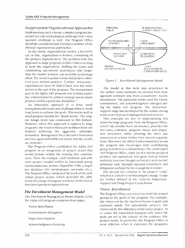
Alpha AXF Program Manage~nent
Inappropriate Organizational Approclcbes PERSONAL PUBLIC
Implementing such a broitd, complex program pre- sented not only technological challenges but a man- agement challenge as well. The Program Office therefore consiclered ant1 rejected a nirmber of tra- ditional organizational approaches.
In the classic organizational model, a hierarchi- cal, or line, organiz:~tion is brnlecl, containing all the primary implenienters. The problem with this aplxoacch to large programs is that it takes too long to form the organization. Staffing the tealus and establishing operational procedures take longer tti;rn the market wintlow and avail;~ble technology allow. Tlie result is grant1 visions ancl projects deliv- ered ye:rrs behind schetlule. Further. "temporary" organizations must be folcled back into the niain- stream at the encl of the progratn. Tlie management goal of the tUpha AX11 program was to keep esper- tise concentratetl to achieve synergy across many projects within a particular tliscipli~ie.~
An alternative approach is to form small entrepreneurial teams ant1 challenge them to work long hours to achieve the goals. This works well in s~iiall projects suititble for "skunk works." The origi- nal design work was concluctecl in this fashion. However, when this approach is applied to large programs, the result is that team members burn out without ;tchieving the aggressive schetlules demancled. Management then becomes frustratetl and tries again with different teams, but the results are no better.
The Program Office est:tblishetl tlie Alpha AX]-' program as an integration of project teams that woi~ld remain within the existing line organiza- tions. Thus, for exitmple. each hardware ant1 soft- ware project resitled within its functional group (semicolitluctors, servers. Openv~MS, IJNIX, compil- ers, database, CPLl development, networks, etc.). The Program Office integr;rted the work of the intli- vitlual project te;tms, which provided the atltli- tional atlv;intage of program resilience in tlie face of functional group reorganiz;rtions.
The Enrollment Managemerct Model Tlle Enroll~~ient Management Model (Figure 1) for the Alpha AXP program conlprises four stages.
Commitment-Delegation
Inspection-Suppost
BUSINESS GOALS PROJECT OBJECTIVES
ENROLLMENT
COMMITMENT DELEGATION
TRUST ACCOUNTABILITY (TASK-OWNER-DATE)
Figure I Bzr-olkrnent Ic.I~~~zage~~ze~?t~LIode/
The model in this form was developed by the ~uthor . Some elements are derived from man- agement seminars ;tnd fro111 consultants' rccom- mendations. 'The particular forms used for vision. coriimitment, and acknowledgment emergetl dur- ing tlie AJpha t\Xll program. The insgection- support stage was developed by the author tluring many years of project management and reviews.
Two concepts are key to implementing this model for large programs. First, the Program Office, which has ;rlreacly bcen ~i~e~it ionet l , provides the necessary cohesion, program vision, and inspec- tion structures, while allowing the skills and resources to remain within their ~lat i~ral organiza- tions. Moreover, the office lends consistency across the progr;Im and encourages each contributing group to holcl to its commitments. The small Alpha AXP Program Office, made up of a diverse group of product and operations rn:inngers. Ii;tcl no formal authority (not even budget autliority); so it exerted influence only through rigorous enrollment and delegation outlined by the ni;lnagerilent model.
The second key concept is the project "cusp," which is a critical event that propels chaligc. < : I I S ~ S
at-e further definetl in the sections Inspection- Supl>ort ant1 Using Project Cusps l>elow.
Vision -Enrollment The Program Office uses vision to enroll the related groups in tlie goals of the program. For example, the vision can be tlie top-level business goals and customer needs. For subordinate projects, the vision can be the objectives of the larger project. In all cases, the enrollment happens only when the goals are set in the contest- of the ;~i~dience (the project team). In particular, the Program Office is most effective when it expresses tlie program3
194 Vd. 4 Nr,. 4 S/~~fal f m e 1392 Digirnl Tecb8ricnl Jorrrnnl

~zt il/Jnn61gelne1it, ~ M L I I I L I ~ ~ I I ~ the Alpha U P Progtzlnz
vision in the terms and language of the group being enrolled. The vision has to be Large enough to encompass all the recluirerl commitments and the ultini;~te results.
Commitment-Delegation As the manager of a project develops plans, he or she delegates the tasks to sub-groups ancl solicits specific commitments to content ant1 schetlule.3 Since these commitments are made within the con- text of the larger vision, the subortlinate commit- ments become qiiite strong for sub-project members. A key element of the delegation process is the explicit specification of the results such that they ;ire measurable ant1 identified with an intlivid- ual owner. The owner is a single indivitlual empow- ered by the committing group and held accountable for the deliverable:' An important point here is that the term "owner" does not neces- sarily refer to the person who actually cloes the work. The owner is responsible ancl therefore accountable for getting the work done on time. In our particular program, the Program Office hat1 to clarify ant1 reinforce this distinction carefully as part of thc enrollment stage.
Inspection-Support The project manager trusts in the comnlitments made and continually inspects the project to ensure delivery on schedule. This inspection strictly takes the form of supportive feedb;ick, thereby encourag- ing people to disclose risks before they become problems. Whenever the projected results are ;it risk of falling short of the commitment, the project manager declares a project "cusp."
The term "cusp" is adapted here from Gleick to clescribe the potential turning points, or critical events, in a project.5 (Other terms in conventional parlance include "gotchas:' setbacks, crises, turning points, project breakdowns, and "calls to action." The ni;inagers i~sed these terms during the propam. For our purposes, we adopt the term cusp as an emotionally neutral term. It is importz~nt that at any point it1 the project the term used be one that gives an opening for the possibility of making a difference and for moving the project forward.) At the point of a C L I S ~ , everyone is ready to embrace change because it furthers the overall program objectives.
The management team col1abor;itecl to take advantage of cusps to propel project momentum toward the established goal. Examples of cusps in the Alpha t\XP program are presented throughout this paper to demonstrate their integral value in the
application of the Enrollment Management Model anel the role they played in the creation of the model itself.
Acknowledgment-Learning At each step of the project, the Program Office acknowledges progress both personally and pub- licly. For each event, the management team repeat- edly asks what was learnetl and how managers ant1 the team can do even better nest time. Teams are frequently coached to improve their methods for better results.
Using the Model 111 principle, the Program Office used the Enroll- ment Management Model in each conlponent proj- ect. Of course in practice, not all groups used this methodology. Early in the program, only a few groups signet! up. As the Alpha AXP Program Office began organizing the overall program, we started formalizing the methoclology. As noted above, we learned extensively as events progressed. We found few useful manuals applicable to running such a large program effectivel}~. Insteael, the Program Office developetl many of the tools "on the job," learning as the project ~~nfoltlecl.~~ This paper exag- gerates a pure model rather than presenting its incremental development. To balance the picture, we show some of the pitfalls and side paths.
Most project managers followed the Enrollment Managemellt Motlel either by instinct (experience) or by example. In several instances, they formally reached outside for training in running projects of this complexity. Depending on the size of the project or sub-project, m;lnagers used the model with varying tlegrecs of rigor. For example, the larger projects anel the program overall used formal inspection meetings and reviews. Subordinnte projects were free to use formal or informal inspec- tion processes. The program team inspected each group's inspection processes to ensure that there would not be any utlfortunate management surprises.
Using Project Cusps As described earliel; cusps are critical project events, or crises. Conve~itional project manage- ment concentrates on rigorous planning to avoid such crises. The Program Office took the opposite approach: We strove to iintlerstand the critical events and nlilestones and used these cusps to increase project momentum, as Figure 2 illustrates. As the project approached each cusp, the Program
Digital Tecbnicnl Journal Vo1. 4 rV0.4 Spclul issue 1992 195

Alpha AXP Program Management
CUSP
Figure 2 Cusps as n Way to Change Directions
Office dealt with the event promptly to ensure that the project continued to move toward the overarch- ing goal. In other words, the managers did not develop a plan just to follow the plan. Instead, they cleveloped a plan to understand the overall project flow and used the milestones and other events as opportunities to adjust the project velocity to keep moving toward the goal.' In many cases, we gener- ated a cusp to propel the necessary change (for example, by creating a schedule crisis). In other cases, we took advantage of a cusp to make a neces- sary change.
As the management team became comfortable with using project cusps constructively, the Program Office actively solicited more of them. These increased the velocity and resulting momen- tum of the program, thereby achieving a "slingshot" effect. The Program Office used each cusp to acknowletlge progress. As the team acknowledged more and more progress, the program's niomentutn moved from very low to break-even, and finally into high gear.
Vision-Enrollment Stage: Magnitude of the Program's Vision The vision for a program or project becomes the ultimate goal or deliverable. Thus, the Alpha AXP
Program Manager's first task was to establish a vision shared by all groups that would contribute to the program. This vision had to be large enough to encompass all the work.
Alpha AXP Systems as Fzyth-generation Computing The Alpha AXP family is at the confluence of five major trends in computing.
1. Nineteen ninety-two is the first year in which it is feasible to achieve 64-bit computing on a single microprocessor.
2. Nineteen ninety-two is the first year in which microprocessors have achieved over 100 MIPS (million instructions per second) of computing.
3. It is now cost-effective to place more than 4 giga- bytes of main menlory on a system; hence 32-bit addressing is insufficient.
4. Networking technology now allows the con- struction of networks with over 100-megabit throughput.
5. Cost-effective storage systems now exceed the many-gigabyte range and are approaching terabytes.
These computing systems will inclucle large amounts of parallelism as compared with classical designs. The levels of performance and connec- tivity finally allow computing to realize greater human productivity: mobile, highly inteructiue computing that supports group work with algo- rithms that intelligently analyze, simulate, and synthesize in szlpport of u zuide variety of human endeavors. The application of this technology clual- ifies as the fifth generation of computing."9
The program vision for Alpha AXP systems, as shown in Figure 3, is to be the first family of systems to implement the technology and applications for the fifth generation of computing. This family is fiilly compatible across all members now and will be into future generations, ensuring that applica- tion binary programs will run unchanged. With no compromise to hlture performance, the initial fam- ily members also maintain a high degree of com- patibility with current systems to allow easy migration for customers as they begin to require this technology. Delivering a family of high-quality systems in a timely fashion reestablishes Digital's reputation for technology and systems leadership.
SAME ARCHITECTURE. COMPATIBLE SYSTEMS
5L!
I 1992
TIME
64-BIT MEMORY TERABYTES STORAGE
Figure 3 Alpha AXP Vision
196 Vol. 4 No. 4 Special Issue I992 Digital Technical Jozrrnal

Enroll~rzent Managenzerzt, Managing the Alpha AXP Progra~rz
Getting Started The Alpha A X P program grew out of research on computing, specifically the teclinology and benefits of different RlSC (reclucetl instruction set computing) architectures, ancl from advanced developmetit in compiler designs, VLSI (very large- scale integration) design, and senliconductor fab- rication. In 1988, Digital's Executive Committee challenged Engineering to tlevelop a system that would meet the customers' needs for competitive performance in all of Digital's computing envi- ronments. Engineering formed ;I cross-disciplinary task force that developed the requisite systems architecture :lnd designs a~itl procluced the above vision and hence the Alpha AXP program. Digital's Executive Committee approved the Alpha AXP pro- gram in October 1989.1°
First Cusp: Executive Challenge to Accelerate Schedule By the end of 1989, Digital had completed the advanced developments and signed off on the archi- tecture and primary design documents. In a major review during January 1990, upper management challenged the program to improve the schedules to capture the market window for this new tech- nology. The project managers understood the rationale for this demand but could see no way to meet the aggressive schedule. The result was a loss of rapport between management ant1 the technical staff, with coninieots such as "Don't talk to me about crazy schedules" and "This is just going to be a lot of hard work.''
The Progr;lm Office viewed this cusp as an opportunity rather than the crisis tlut it appeared to be. The office enrollecl key project managers in the overall vision, i.e., in the business value of a timely execution. For some projects, it was suffi- cient to focus 011 the classic "time-to-market." However, for many, the ship date proved an insuffi- cient motivator. Therefore the Program Office frariied the vision clifferently, as follows. A program becomes profitable when it reacl~es break-even ( i t . , cumul;~tivc revenues meet ant1 then exceed cumulative expenses).
The time taken to achieve this point is known as the 'ctime-to-profit."'l The Program Office estitliatecl tliat the program's schetlule would affect Digital's revenue at the rate of $1 million per hour. That is, for each hour tliat the project could improve (lower) the time-to-profit, Digital would achieve an additional $1 million of revenue. 'The Program
Office pointed out to the project managers that tliis revenue could translate to approximately $0.01 on the stock price for eacli hour of schedule improve- ment. With this concrete business metric in mind, the key project managers were willing to consider new ways to tackle the program's challenge.
Once tlie Alpha AXP program was approved, the I'rogram Office began holding Alpha AXP quarterly review meetings. At these forums, groups reported plans and progress to a wide, cross-disciplinary audience. Initially, the audience was composed of engineering, manufacturing, and service groups. As the program gained momentum, other disciplines such as marketing and sales joined and began to report on their own progress. These forums helped generate belief and solidify enrollment. They also helped tlie Program Office identify problem areas before they became crises.
First Cusp Result We established a program-wide understanding of tlie importance of volume deliveries in 1992.
Commitment-Delegation Stage: Delegating and Eliciting Commitment With the key project managers sharing a common vision, the next step was to establish a work plan and to ensure that eacli group committed to deliver on its parts.
It had been 15 years since Digital attempted to change siniultaneously its architecture, hardware, operating systems, compilers, and other layered products. Since the introduction of the VA;Y systems in tlie fall of 1077, each component had progressed relatively intleyendent of the development sched- ules of tlie others. Fewer than half a dozen project team members had participated in the VA)( design. For most participants, the system had always been in existence, and hence the developer of each sub- system could invoke and depend on tlie existence of all tlie othcr s~~bsystems.
The need for tlie sirnult;~neous development o f multiple hardware and software systems cornpli- catecl the coordination task. The Program Office addressed this complex coortlination in two climen- sions: technical and project management. In the teclmical dimension, the office formed a team of technical leaders from the core engineering groups, known as the EJST, shown in Figure 4. (EJST is an acronym for EVA)( Joint Systems Team. E V X i was an early name for the Alpha AXP program. An earlier forum, the EVAX Technical Team, merged into tlie
Digital Tecbaicrrl Jortrt~nl Vol. 4 No. 4 Special Isstre 1992 197

Alpha AXP Program [Management
I ENGINEERING
I I I I
E,ISI' process over time.) This group met weelily to set tlirections for important cross-group technical
- - I 1L
I PROJECT I I MANAGERS I I - - - - - - A 11
clesign ant1 strategy issues. Since the group's ch;lrter nias to resolve problems and ensurc that solutions "sti~ck," the EJST became a group to which others brought technical problems for resolution.
In the project management dimension, the pro- gram manager formed a team of project managers. ~Menibers of this team were e~npoweretl by their contril>uting engineering tlevelopment groups to 11i;llte commitments and to be account;tble for cleliverables. This team mlas known as the ASl'M
(Alph;~ t\XP System Project M;~n;tgers). Given tlie magnitude of the overall task ant1 the complexity of full!. untlel-standing the interdepentlencies, tlie project m;rn;lgers tended to view tlie l>roject :IS
i~n~x~ssibl!~ complex. At the progr;lni level, the clial- lenge then became to establish the Alpha A X P mas- ter 1>1;11i. A master plan, however. evolvetl mi~ch more slowly than expectetl.
-
Second Cusp: Cannot Choose the Order of the Work
-
I\l;~n;~genient's inability to provide an overall plan induced a crisis of disbelief. Tlie project ni;lnagers threatened to revolt (or move to other projects). The technical leatlers were generating ever-larger design documents. The engineering development group managers tleclaretl that tlie I'rogram Office had a crisis on its Iiantls: \Ye h:lcl to
ALPHA PROGRAM OFFICE
establisl~ a program-wide m~orl< plan that showecl the order in which e;tch sub-project must deliver its contribution.
How does one coordin;~te without a plan:' Tlie Alpha r\X1-' progr;lni rn;ln;lger kept asking the indi- vidual groups for their pl;lns. What do you depend on? How long will it t:tke? What resources do you neecl? Wilnat are your milestones or nietrics of progress? Tlie repeated answer was "I don't know because I don't know what everyone else is doing and m~lien they will I>e clone with their piece." At this time, we hat1 already established the cross- functional hSl'k1 team of experiencetl project man- agers representing most o f tlie development groups. This team was unable to develop the com- ponent plans bec;~i~se they 1;lcked a master plan.
Choosi~zg the Strategy The engineering tlevelop~nent group lnanagers met in a full-clay meeting to establish the over- all paranietersof the Alpha A X P program's plan. First, they est;tblished the business goals and exam- ined the various technical constraints. The group tested the inclusion of each component with the question "Is this coml>onent critical to the over- all business success o f the Alpha A)(P program?" This process established solid reasons for the contents of tlie mastcr pl;~n and kept the respon- sibility for the inclusion or exclusion of a compo- nent with the responsible clevelopment group. The
1'01. 4 \.o. .\/)cciol lss~re 1992 Digital Techrricnl Jorrrrrnl

irilt ~Mc~nnge~neizt, ~\,l~iizaging the Alpha RYP Progr~~iiz
group then tleterminetl the org;~nizational impli- cations of such a work plan. Members of the group balanced the climensions of bus~ness, technolog): and organization to establish the priorities and work order. We institutionalized this group into the Alpha AXP System Board of Directors (ASBOD).
Representing the Plan \With the major program priorities and constraints established, the Alpha U P program manager then set off to establish the master plan. For all groups to see their contributions, he held the master plan to a single page. He established the content during an intense periotl in which lie asked contributors to describe their assumptions :ind tasks and to show where on the overall plan their pieces would fall. The single-page format forcetl the management team to keep the plan to a high-level view ant1 allowecl contributors to see their pieces without aclding the complexity of their own group's tletajls. Furthcr, in review meetings it w:rs easy for everyone in the room to view the same picture so that the results coultl be seen, debated, ;ind agreed upon.
Once the n1;lnagement team h;~tl outlinetl the plan, it was recommentled by tlie project managers (ASPM) and ;~pproved by the engineering clevelop- ment group n1;inagers (ASROI)). Tlii~s team mern- bers knew their goals woultl not change without clearly statetl reasons. Further, others could start building their pl;ins based on ;I consistent set o f ;issuniptions. The resulting single page also becanie a reference, which we called the "straw Iiorse," to establish ancl reinforce constancy of purpose. Figure 5 is an example of the Straw Horse Plan. (We later i~pgraded the name to be the "tin horse" to connote the increasing degree of solidity of the underlying plans ancl commitments.)
Second Cusp Result We agreed on the overall single-page plan upon which teams coi~ld build their own plans.
Enroll~nent and Delegation: Value of Each Contribution With the master plan outlined (the straw horse reviewed ancl approved), the next step was to obtain the commitment of each contributing group. To :iclclress continuing skepticism about tlie necessity of e;~cIi component and its schedule, the program manager walked each group through the overall program and the economic value of its urgency. The group was then askecl to contribute to
the overall system's value. A key prerequisite to this conversation was to establish a fi~ll-time project manager for each component group. who became the coordination point and who was held account- able for each tleliver~ble.
Decide What to Do before How to Do It The Program Office found that each group went through a disbelief process similar to the one seen earlier for tlie program. The program manager urged each group to first focus on the "what" of their de.liverable, before trying to decide the "how." The program manager ensured that tlie group groundecl its overall estimates in reaJity For exam- ple, a software group might count the number o f modules to port and estimate tlie person-days per module. This kind of high-level, clil;intifiable esti- mate allowetl the project manager to make an over- all estimate without needing to understand the order of the specific tasks.
Third Cusp: Need for Project Mnnngenzent Expertise Members of several of the larger projects deter- mined that they tlid not have sufficient project man- agement experience. Previously, this realization woultl have resulted in replanning to move out the target schedule, perhaps repeatedly. Instead, given the group's commitment to the larger result, we founcl ;I much more aggressive behavior. For example, the OpenVMS AXI' group publicly com- mitted to their target schetlule and stated, "We tlon't know how to achieve this, but we commit to finding a way." The next day they went to a project management consultant for training on how to build an aggressive, attainable schedule. This con- sultant conducted the seminar nuny times through- out the project for various groups.I2
Third Cusp Result Groups introtluced education ant1 rigor into project management.
Inspection-Support Stage: Inspection with Supportive Feedbncb One of our vice presidents in the e;lrly 1980s hat1 ;In aphorism: M)u get what you inspect, not what you expect. I11 other words, a conillion failing is that managers obtain someone's promise and expect that the results will be what they expectecl. Unfortunately, tlespite everyone's best intentions, circumstances and unexpected requests can easily
Digital Tecb~ricnl Journnl Vi)i J At). 4 . S /?CC~LI / ISSIIL' 1 0 0 100

Alpha AXP Program Management
Stmw Horse Plan AUg 1990
stasxe 1: Zgchnical DeveZopWst system PO- & c perEamsmce systmt Siwle hm%am platfon W l i s h oaly
Forbwn. C, BUes, Assembler, Debng, License %ant Facilb, CasE tools {TPUt COde aagnt WS't%rB. %St=, PesPa- Cbde Aoal?@er, laagmge Sensitive -tar, Digital Test Mgr) , kqpmnd b m m m L Archit%cture, m e t M e Iv task-to-task. DEWincWws client iTiq tAT S o m e
Stage 2 : -ial De~e1qarent System setcod hardwan? platfonnt f n I : ~ f ~ t i c K l a ; i wrsians follow 3 m3nths later
-, P-, C++r m, CRDIRetjository, m, threads-rtl, RFC, m, ImC' s . Perma System, DBCforms, File cad#, vhxset, Diatr semm (am=, tbz r file, queuing), mate System kr@ager, -u - IN-1 base, CWt mite,
fV end rmde and ~ i x ? m s , m/IP. PATmmw, t81Ptnaster, ABSS Bxrmsims
S b g e 3 : Tscbniebl %ka%t Sptatcem open & H C ~ ; -ic Multi-&-ins
WSP, &/I, user-qrf ttsn &rivers, K1SW, disk shadming. neais, ABk4S, DAS or e(iuivalent, fu l l NAS, aaQlet V end node, x.25 access, ALLIM-I fully supported
Stage c : Camercid *stem A&h C l r t s t e f s r Btematiwal mmsiorus r e l e d 5imuJtanesusLy
New &ttch?Print, $11 Bystem Integrated Prcducts, DECnef V rwtfng node, SWb access
stage 5: 'lmnwetim Wtem
Trmsuction Mbnitctr, thr@d%
Fig~ire 5 Tbe Sirigle#uge Pl~lrz: All Extr~~ct fr-onz the Straz~f Horse Ylun
divert the promiser away from fulfilling the promise. Thus, managers learn to inspect regul;~rly the progress of groups on whose commitments they depencl.
The rnoclel, therefore, incorporates this tr:~di- tional, essential project management practice. Its inclusion was prompted by another project crisis, described below.
Fourth Cusp: Project Slips Motiuate Fornzal Opet-ational Inspection The Program Office knew that it was working with highly motivated teams. On the basis of the earlier planning work, we assumed that they were ;ill tightly focr~sed on the objectives of the Alpha AXl'
program ant1 shared our sense o f scheclule urgency. Suddenly, we were shocl<ecl by a memo stating that a critical project's scheclule hat1 slipped sev- eral months. Since virtually every other project depended upon it, this schedule slip could easily have led to a program disaster. Instead, we used the event to institute a regular operational inspection. Often, instituting such regular reviews is difficult and generally resisted by the reviewees. In this case, every group coulcl see the danger of continu- ing without regul:i~- inspections and reatlillr agreed to this new process.
The Program Office ;~clol,tecl the term "inspec- tion," rather than "reviemi," brc:~use m7e ]rave found this term to be neutral or positive. In the past,
200 W l 4 No. 4 Specirrl lsszte 1992 Digilcrl Tecktricnl Jorrrrrtrl

Evzrolbnent Management, Managing the Alpha AXP Program
reviews had been imposetl by line management ancl tended to encourage the reviewees to cover up issues until it was too late to recover. In contrast, the program manager, operating under the Program Office model, had no line authority ant1 set up the monthly operational inspections in an open and supportive environment. The presenters were the designated project managers from each develop- ment group. The Program Office encouraged all presenters to bring in their risks and problems before it was too late to address them effectively. We used the single-page format again, as shown in Figure 6. Note that the simple, visual history of all
milesto~ies is at the top, so one can readily see any repetitive slips. The emphasis is on critical path events completed last month and those coming up next montll. At the bottom are listed those issues that have been resolved and issues being opened, with clearly inclicated ownership and due dates.
Operational Excellence To ensure that every project implemented the strategies, the Program Office established the prin- ciple of operational excellence across tlle Alpha AXP program. The office consistently recognized teams that accomplished their results on time and
e m : ALPnh/W DATE: April 8 , 1992
SCHEDULE: 1 Qd 1991 1 Q1 1992 1 42 1992 1 Q3 1992 1 Q4 1992 l O c t Nov =!Jan Feb MarlApr M y JunlJul Aug SeplOct N w Dec [---[---[---[---[---[---[---[---[---[---(---[---[---[---[---
8 4 5 1 E I Sep 91 B 4 5 6 I E 1Nav 91 B 4 5 6 I E l Jan 92 B 4 5 6 1 U E IWr 92 B 4 5 6 1 U E l Apr 92
Milestones B -- Base Level 38 (Editor, debugger, TIE, base DECnet) -- mNE 4 -- B a s e L e v e l 4 (More DECnet, utilities, andiMclients) -- DIXSE: 5 -- Base L e v e l 5 (EV4 support, TFF, performance) -- EONE 6 -- 5ase We1 6 (Performance & Tapes) -- DQNE I -- Internal field test & Pilot Porting Activity - FiT U -- Internal field test update - FT2 E - External field test & Early Support Program - FT3 S -- V 1 . 0 suhnit to SSB
CRITICAL PATH EVENTS PAST MCNI'H: Shipped BL6 on March 12 - stable on ADU, Ruby, Cobra, Flamingo Shipped BL6 AEa7 porting tmlkit Achieved FT1 (PPA) rode freeze Received 2 Flamingo systems in Varese, Italy, for W S I X development With SPE (CSSE), delivered worldwide field test support training FT1 stabilization continuing
ACTIVITIES ALONG TKE CRITICAL PATH (NEXT W3QE-I) : Ship FT1; revised target is Ppr 10 Ship ET1 AM2 porting toolkit Complete PPA R-diness Rwiew Begin FI2 stabilization
ISSUES / DEPENDENCIES RESOLED: Flamingo SFB graphics support formally accelerated into Vl. 0
ISSUES / DEPENDENCIES WT RESOLVED: GDI BL24 compilers needed for ESP integration: D.L., May 15 Rollout support staffing is not XI anyone's plan: J.S., May 29
Figure 6 The Single-Page Rev im
Digital Techrricrcl Jouvnal Vol. 4 No. 4 Specla/ Issire 1992 201
Alpha AXP Program Management
predictably. We ;~lso used the monthly program- wide inspections to maintain a published record of progress. Thus. each project was encouraged to excel operationally ant1 to learn froni the esj~eri- ences ancl presentations of the others.
Fo ~ w t b Cusp Result Tlie Progr:t~ii Office established monthly inspec- tions using a consistent single-page document to record pertinent information.
Acknowledgment-Learning Stage: Building Momentum Developing tlie vision ancl pli111 resul~ecl in :I Ken- era1 sense of eupliori;~. SliortljJ ;~t'ter\vards, the real- it!. of the work ahead clescentled like a cloutl of despair. At this point, the primary challenge was to start bi~iltling momentum in the program. In the Enrollment Management Nloclel, building momentum-the ackno\vleclg~i~ent-Imi~ig stage- is tigl~tl!~ intertniinecl with the inspection st;~gc.; that is, events reportecl during inspections wcrc i~secl to built1 momentum, The Program Office rein- forcctl the vision 21ncl usecl niomentiim b~~iltling to mini~llize tlie time period during which tlie team felt despair about the work a h c ~ d .
Fzytb C L L S ~ : Despair Since tlie overall progr;1m h;itl such 21 formicl;~ble goal, man!, of' the contributing teams 11ec:lnie stalled with tlie m;~gnitucle of the task aheacl of tlieni. 'This manifested itself in tlie form of com- ments about the large amount of work. tlie result- ing potenti;il h)r scheclule delays, :~nd a fe:~r of overtime clemands. This syndrome is common in any large project, especi;illy when commitments ;Ire matte that involve taking large risks. The appro;lch the program team took \V;IS to start recog- nizing ei~cli element of progress. As we elistributeel ;Innouncements of progress widely (using I>igit;~l's worltlwicle electronic 11i;lil network), we beg;~n to I)i~iltI momentum around the Alpha AXP progralii. Other groups picket1 up o n this momentum and contributed to it themselves. 'Tl~is effect cascaded throughout the entire program-more groups per- ceived their tasks alie:~d as achievable; r;~pitlly e;~cli group wanted its own progress acknowledgetl; :~nd momentum increasetl.
The I'rogra~ii Office founcl tli;~t the members of a project. :~ppreciatecl ancl were niotivated by tlie simple " t l i ; ~ ~ i k ~ O L I " rel~resentetl by tlie pi~blic
acknowletlgment of their work. This contrasts with the conventional management wisdom that it is necessiiry to give Ereqi~ent monetary rewarcls to motiv;~te lxo],le. Although everyone appreciates tlie fin;lncial rewi~rds, tlie biggest motivator is tlie professional recognition that the contributor tlid a good and necessary job!
The second benefit of the acknowledgment was its effect in creating a sense of momentum throitgll- out all the project teams. Repeateclly, peer man- agers would comment that the Alpha ASP team was ni:~king significant progress. This in turn gave us a sense of ;~ccornplishnient ;IS well. S o the program re;~lized ;I double benefit from the original :rckno\vl- etlg~nent and ;I h~rtlier slingshot effect with recog- nition coming back to the Program Office.
Fzytk! Cusp Result Program-wicle. managers establishetl the norm of fretli~ent acknowletlgment of progress.
As tlie Alpha A S P progr;1m made further prog- ress, the 1'rogr;ini Office ;~ctively solicited third- p;1rtjr ;~nd c ~ ~ s t o ~ i i e r invol\iement. 'T'his invol'clenient pro\.icletl good feedback o n progress and liatl the effect of reinforcing the fact that the program was 011 track to meet customer neetls. 111 some cases, the project teams :rltered the Alpha A S P pl:fns to better help our customers atlclress their business needs. This further contributed to the credibility ;inel monientuni of tlie progr;irn as well as the sense of acconiplishment.
Sixth CZLS~!: Broken Debe~zde~zcies and Replanrzi~~g Like :~ny project, not every ;wsumption ant1 tlepen- tlency proves to be correct or totally accurate. At one point, one of the major Alpha A S P hardwcire systems slipped its scheclule for delivery of proto- types to softw:~re. After considering a number of altern;itives, the oper;~ting system group proposed ;in ;iltern;~te pl:in using ii different hardware system :~ncl a cIi;~iiged order of events. They s:iitl in their management presentation at the time. "The ques- tion is not one of blame. Insteatl our goal is to pre- serve the ultimate schedule goal of the program, specific;~lly its volume availability date."
Sixth Cusp Result Program-wide, teani tnembers established the prin- ciple of focusing on tlie desiretl state of time-to- profit rather than on bl:~niing others for hili~res.
202 Ihl . 4 ,Vo. 4 .S/~eric~l lssi~c 1 9 9 Digilal Techrricnl Jorrrrrnl

Efzrollrnent Management, n'lunci,qing the Albba AXP Yrogrc~nz
At another point, one group was at risk because it neetled a critical skill Ibr ;I week. A (historically) competing hardware group responded by asking what sort of resource, and then freely supplied the resource despite its own very tight schetlule. In the past, these groups woi~ltl compete for the same resource without coll;iborating for the common good.
Seventh Cusp: Incomplete Asst~~nptions and the Need for the Performance Team Less than half way through the Alpha AXP prowam, the program team realizetl that some projects' assumptions were incomplete. RISC systems are notorious for recluiring careful design and tuning to meet aggressive performance goals. Evidence from a related program at Digital suggested that some of our system performance homework was weak. Tlie Program Office quietly asked the appropriate teams to assign some resources to measure key components ant1 subsystetns of the design. This confirmetl the program team's concerns that the curretit plans were incomplete. Quickly, we pulled together ;I cross-disciplinary task force to analyze the infortnation rigorously and to liiake recomnien- dations. These analyses resultecl in changes in the architecturc, the chip design, tlie systems designs, ancl the softw;lre. 'The changes liave proved to increase performance substanti;~ll)l.
Seventh Cusp Result The program e\t;~blialied n performance team to change tllc de51gn and pl'ins ~s necded
Eighth Cz~sp: Prototype Allocation Process As manufilcturing st;irted to deliver prototypes, tlie Program Office fount1 that the early manufiicturing built1 rate was lower tIi;in planned. This was the result of normal st;lrt-up problems. At the same time, initial demand had increased substantially. Nevertheless, the project ;~clministrators continued to ship the systems to engineering and ;ipplications groups in the original orcler. If this had continued, dependent software woultl have been delivered progressively later because of inadequate testing cyclcs. Our impact analysis indicated that the Alpha ASI ' volume ;~v;~ilability would slip by three months.
The review team highlighted this problem in an early program readiness review. Traditionally, Digital uses readiness reviews to establish manufac-
turing's readiness to build systems. The Alph;~ A S P
Program Office broadeneel this process and asked for a program-wide readiness review to identify the "showstopper" risks. As a result, the Program Office celitralized tlie allocation process so that we could maintain tlie prototype alloc;itions in real time. The result was to reestablish sufficient soft- ware test time and maintain momentum with mini- mal program impact.
Eighth Cusp Resz~lt The program teams decided that prototypes would be delivered based on program priorities. not solely on existing plans.
Ninth Cusp: Need for Quality Metric.$ Each g o u p in the Alpha program adopted very high standards for the cluality of its work. The ni;ln- agelnent team repeatedly found reinforcement of Phil Crosby's tlictum: "Quality is free."'{ Ilesults in group after group showed that early ;~ncl con- tinuous attention to quality resulted in held or improved schetlules.
However, the program team noticecl t I i ; ~ t we were not inspecting and rnei~suring progress in quality at the total systems level; customers care about only the quality of the tot;~l result. As tlie projects started integrating into ;I tot;~l s),stelii, the Program Office establishetl ; ~ n indepentlent group to measure overall quality levels. 'fhe classic reac- tion to such independently derived quality metrics is that they are meaningless. Instead, since the program established tlie metrics ;it tlie niollielit when everyone saw the need, the re;iction h;~s been to focus on the total system's cluality without dropping attention on tlie individu;~l component metrics.
Ninth Cusp Result The program formalized system-wide qu;rlity metrics.
Results and Lessons Learned Digital met exactly tlie program's overall schedule to the month (i.e., date for high-volume shipments), despite numerous setbacks ;ilong the W ; I ~ Tlie Alpha AXP systeni is meeting the original per- formance goals, and quality is excellent. Digital's Board of Directors has approved the fill1 Alpha AXP
program business plan and the investments neces- sary to capitalize on the Alpha AXI' family's e:lrly
Digital Technical Joirnral Vol. 4 /Vo. 4 .'il,ecirrl lssrrr 1992 203

Alpha AXP Program management
successes. Initial reactions from customers have been favorable. Third parties have committetl Alpha AXP support for their products in record numbers.
What Worked Well The Program Office in conjunction with the Enrollment Management Model has worked well. If the management team had followed traditional approaches, we would still be getting organized. Using the model, each group has been able to bring its fill( capabilities to bear as problems have arisen. ?'he project teams have accepted the introcluction of multiple levels of inspection, ancl other programs within Digital are copying this aspect of the model. Further, the notion of ~ising project cusps creatively has been an effective tool to huiltl momentum. Finally, a common schedule and inspection disci- pline allowecl the schedule to become an opportu- nitjr to reinforce ;I shared vision. This positive view contrasts with the conventional interpretation of a schetlule as a burden.
As a result, most groups met very aggressive goals on schedule. Several groups accelerated their cleliv-
erables despite having the most complex tasks. For example, the OpenVMS AXP system group not only met its original schedule but also accelerated num- erous tieliverables into earlier base levels or releases. Figure 7 shows the OpenVMS schetlule and actual tlates of availability; footnotes indicate functional ;~ccelerations. The networks group tlelivered DECnet on the AXP system an entire base level early. The clatabase systems group accelerated its schedule by several months and tlemonstrated products four months early at Digital's DECWRLD '92 trade show.
Clearly one of the major lessons was to establish a constancy of purpose and holcl to it while contin- iially learning and updating the detailed plans. The single-page representation of the goals and master plan is a key element in maintaining this constancy.
What We Would Do Differently Loolting back, we would have approached the program differently in two areas. First, project teams would have benefited from broader early education on project methodology. Several projects had significant slips, causing undue hardship on other groups. The Program Office should have
ALPHA/VMS SCHEDULE RESULTS
MILESTONE
Phase 0 closure Alpha VMS minimal lagin BL1 ship - minimal login BL2 ship - RTLS, DW (1 ) & LAT BL3A ship - ISAM, linker BL3B ship - prog devel L T I E (2) , DECnet (3) EL4 ship BL5 ship - functionally complete(4) BL6 ship - Ruby complete(5)
FTIJPPA Phase 1 FT2/PPA FT3/ESP ( 6 ) FT4/ESP V1.0 SSB submission (LRS)
ORIGINAL
Rug 30, 1990 Jun 17, 1991 J u l 15, 1991 Aug 26, 1991 n/a Oct 7, 1991 Nov 18, 1991 Dec 30, 1991 Feb 21, 1992
ACTUAL
Aug 30 Mar 20 May 31 Jul 12 Aug 23 Oct 10 Nov 15 J a n 10 Mar 6
A p r 3, 1992 A p r 10 May 1992 May 20 n/a 1992 May 22 J u l 2 , 1992 Jul 8 n/a 1992 Aug 14 Oct 2, 1992 O c t 26
Notes:
(1) DECwindaws (2) Translated Image Environment (RTL far translated images) ( 3 ) DECnet accelerated from BL4 to BL3B ( 4 ) Full graphics support accelerated from next version to V1.0 (5) Support for multiple h a r d w a r e platforms a c c e l e r a t e d f r o m next
v e r s i o n to V1.O ( 6 ) FDDI support accelerated from next version to V1.O
Figure 7 Original 0penVM.S wiles stone and Deliuery Dates
204 Vol. 4 iVo. .I 5plic-iol lss t~e 1992 Digital Technical Jorrrlznl
Enrolbnent ~Vunugelnent, Managing the Alpha AXP Progrum
introduced Ron LaFleur's project methodology sooner and pervasively. Instead, we waited until each group saw the need and then tried to intro- duce it. For groups such as the OpenVMS AXP system group, the methodology was introduced early. However, other groups needed (and still need) this discipline.
Second, the office would have conducted more pervasive project inspections. Several groups were very late in protlucing schedules and plans that the Program Office could understand. The office was unable to obtain their cooperation to hold detailed and frequent inspections. Eventually, the Program Office was invited to set u p and participate in appropriate inspections of schedule, process, etc. However, we should have insistetl on these much sooner.
The Alpha AXP program is the most con~plex pro- gram in Digital's history and h;w been delivered on schetlulc with high quality. The Alpha AXI' Program Office used a rigorous management me tho do log)^ to build the program-level teamwork necessary to accomplish this breakthrough. The office proved the effectiveness of the Enrollment Management Model: vision-enrollment, commitment-delega- tion, inspection-support, and acknowledgnlent- learning. Integral to this motlel and empowering to the team is to take each cusp head-on and to use them to increase momentum. The management team has been learning as the program progressed and has identified areas needing strengthening for future programs.
Acknowledgments The author thanks the following senior managers for tlemonstrating the importance of good manage- ment: Gordon Bell for architect~~re and a clear strat- egy; Ken Olsen for demanding simple, single-page plans; Jeff Kalb for operational excellence; David Stone for the model of focusing on the tlesiretl state; Bob Supnik for the paradign~ of the Program Office.
The author also thanks key members of the Alpha hXP I'rogram Off ce for their contributions in man- aging the program and developing the Enrollment Management Methodology: Al Avery for systems integration and significant help preparing this paper; Scott Gordon for competitive benchmark- ing; Ellen Salisbury for planning; and Ken Schultz for operations and inspection.
References and Note
1. R. Waterman, T. Peters, and J. Phillips, "Struc- ture is Not Organization," B~lsirless Horizor~s. no. 80302 (June 1980).
2. C. Savage, Fiftlg Generation Manngernent (Burlington, MA: Digital Press, 1990).
3. W. Oncken and D. Wass. "Management Time: Who's got the nionke):" Harrwrd Busirless Reuiew, vol. 18, no. 6 (November 1974): 75-79.
4. M. McMaster ant1 J. Grintlel-, PRECISIOIV: A Neci! A ~ ~ I . O G I C ~ to Co~?zlnu?zicntion (Bonny Doon, CA: Precision Models, 1980).
5. J. Gleick, CHAOS: Making a New Science (New York: Penguin Books, 1987).
6. F? Senge, The F1ytb7 Discipline: The Art ana Practice of tbe Learning Orflrlization (New York: Doubleday, 1990).
7 A. Scherr, "Managing for Breakthroughs in Protluctivity" Hzirnan Resolirce ~VIar7~1ge- ~nerzt, vol. 28, no. 3 (Fal I 1989): 403-424.
8. L. Tesler, "Networked Computing in the 1990s." Scientific A rnericarr (Sep tem ber 1991): 86-93,
9. The five generations of computing are as fol- lows: I950s, standalone; 1960s, batch; 1970s, timesharing; 1980s, personal: 1990s, mobile distributed.
10. R. Comerford, "How UEc: Developed Alph;~," 1E.M Sl,ectr~~~rz (July 1992): 26-31
11. C. House ant1 R. Price, "The Return Map: Tracking Product Teams," Harl~ard Bcisir~ess Rciliezu, vol. 69, no. 1 (January 1991): 92-100.
12. R. LaFleur, "A Seminar in Project manage- ment" (Scituate, MA: Project Management Assist;rnce Co., 1990).
13. F? Crosby, Qualit]) Is Free: The Art of rMaking Q~iul i t j~ Certoitz (New York: McGrnw-Hill, 1979).
General References
E Brooks, The 1I4ytl?icaI ~Ma1z-irzorzth: ESSUJJS O J Z
Softulal-e E~zgineerilzg (Reading. MA: Addison- Wesley, 1975).
R. Neustadt and E. Ma): Thinking In Time: The uses of history for decision makers (New York: 'Tl1e Free Press, 1986).
Digital Technical Journal Vol 4 No. 4 Special Issue 1392 205

I Fwther Readings
The Digital Technicill Journal pu6lishespnpers that explore the tccl?izological foz11zdatiot7s of Digit~il's rnajor.prodrrcts. Ec~cl? Joumalfoc~rses 0 1 2 at le~zst one prod~lcf or*ecl and pr.e.serits ci co~?zpi/~itio~z ofp~if?e)=~ toritten 031 t l~e crr,qilzeers risho d e ~ ~elobecl th7eptv)dr~ct. The collteut for thcJourn;~l is selected Oj l the Jourr?c!l Advisory Board. Digitcil engineers upko rvozrld l ike t o coiztrib~rte ci paper to the Journal should co~ztact the editor- a t KDVAX::RM KE.
Topics coverecl in previous issues of the Iligitnl Technical Joun7ul are as follows:
NVAX-microprocessor VAX Systems I/i,l. 4, No. -3, S~lr?l~?zer 192, EY~1884E-l)I'
Semiconductor Technologies I/i)l. 4, No. 2, Sprilzg 1992, ~ ~ - ~ 5 2 1 ~ - 1 ) 1 '
PATHWORKS: PC Integration Software k l . 4, No. I, Wintel- 1992, EYd825E-111'
Image Processing, Video Terminals, and Printer Technologies Cbl. .?, IVO. 4, FLIII 1991, EY-H889E-DP
Availability in VAXcluster Systems/ Network Performance and Adapters Vol. 3, No. -3, Srr~?~nze~. 1991, EY-H890E-111'
Fiber Distributed Data Interface I/r)l. 3, iVo. 2. S/lrirzg 1991, E Y - H ~ ~ ~ E - I ) ~ '
Transaction Processing, Databases, and Fault-tolerant Systems Val. -3, No. I , Winter IYgI, EY-F588E-Dl'
\'AX 9000 Series Val. 2, NO. 4, I h l1 1990, E Y - E ~ ~ ~ E - D P
DECwindows Program fi/ 2, ivo .j, Siir?11?ze1. 1990, E Y - E ~ ~ ~ c - I ) ~ '
VAX 6000 Model 400 System L'ol. 2, No. 2. .S/)l'ing 1390, T:Y-ClC)7E-I)1'
Con~pound Document Architecture Vol. 5 No. I , Wi~ztel- 1990, E Y - ~ 1 9 6 ~ - D P
Distributed Systems Vol. I , No. 9, June 1989, EY-C17c)E-DP
Storage Technology Vol. I, No. 8, F ~ D I . u L I ~ ~ 1989, EY-(: 1 6 6 ~ - D P
CVAX-based Systems VO~. I , NO. 7, A ~ ~ g u s t 1988, E Y - 6 7 4 2 ~ - ~ ~
Software Productivity Tools Vol. I, No. 6, Febrzrarj~ 1988, EY-&!59E-DP
VAXcluster Systems Vol. I, i\b. 5, Sef!tenzDer 1987, EY-8258E-1)P
VAX 8800 Family Vol. 1, Are. 4, Februury 1987, EY-671 1E-DI-'
Networking Products Vol. I , /\To. 3, Se/!te~nDer 1986; ~ ~ - 6 7 1 5 ~ - ~ 1 '
MicroVAX 11 System Vol. I , No. 2, ~Wclrch 1986, EY-.347413-DP
VAX 8600 Processor f i l . I, No. I, A L I ~ I I S ~ 1985, E Y - ~ ~ ~ ~ E - I I P
Subscriptions to the Digitul Tech~zicalJo~lrrzlrl are avail;tble on a prep:~id basis. The subscription I-ate is $ 4 0 . 0 0 for four issues ant1 $ 7 5 . 0 0 for eight issues. Orders should be sent to Cathy Phillips, Digital Equipment Corpor;~tion. ~ ~ 0 1 - . 3 / / 8 6 8 , 146 1M:lin Street, M;rynartl, M A 01754-2571 , U.S.A.. 'Teleplio~~e: (508) 4 9 3 - 2 8 9 4 , FAX: (508) 493-0637 Inquiries can be sent electronically to [email protected].<:OM. Subscriptions must be paid in 1l.S. dollars, ilntl checks shoultl be made payable to Digital Equipment Corporation.
Single copies and past issues of the Digital Techtlical Jotrrnal are available for $ 1 6 . 0 0 eac1-1 from Digital Press, Department EER, 1 Burlington Woods Drive, Uurlington, MA 0 1 8 3 0 - 4 5 9 7 Single issues can also be orclered by c;~lting DE<;direct at 1-80O-l11GITAI. ( 1 - 8 0 0 - 3 4 4 - 4 8 2 5 ) .
206 Vol. 4 /\'o. 4 Specir~l ls.strr 1992 Digilal Techrricrtl Jourrrd

I Recent Digital U S Patents
Thefollou~i~zgpatents were recently issued to Digital Equi)rneizt Corpomtion Titles and nallzcs s~~f~pliecl to us @ the US Potent and Tr~~~ie~rzc~r.k Oflice c11.e re/!~~ocl~~cccl eLJraclIy as tl7ej' a f ~ f ~ e a r or^ tlge O I * I ~ I I Z L ~ /
plrblishecl /~ate?it
D327,261 K. L. Korellis and R. T. Faranda Front Face Panel Portion for Enclosure Doors for a Computer
D327,477 K. L. Korellis Front Panel for an Integrated Storage Assembly for Computer Storage Units
5.092,631 M. G. M. Masnik ant1 Safety Enclosure for Gas Line Fittings R. C . Martel
5,093,628 1 . T. Chan Current-Pulse Integrating Circuit and Phase-Locked Loop
5,093,775 W. R. Grunclmann, R. E ~Micrococle Control System for Iligital D a t ~ Processing System Boucher, and T. FOSSLI~II
Method for I-'rovicling ;I Metill-Scmicondi~ctor Contrict
5,095,441 D. E Hopper, E. G. Fortmiller, Rule Inference and Localization during Synthesis of Logic S. Kundu, and D. E Wall Circuit Designs
5,095,471 M. D. Siclman
5,095,613 K. R. Hussinger and M. L. Mall;~ry
5,097,370 Y. Hsia
5,037,387 J. L. Griffith
Rotating Priority Encoder Operating by Selectively Masking Inp i~ t Signals to a Fixecl Priority Encoder
Velocity Estimator in a Disk Drive Positioning Sysretn
Thin Film Head Slider Fabrication Process
Subambient Pressure Air Bearing Slicler for Disk Drive
Circuit Chip Package Employing Low Melting Point Solder for Heat Transfer
5,007,411 I? L. Doyle, J. I? Ellenberger, Graphics Workstation for Creating Graphics Data Structure E. 0. Jones, D. C. Carver, Which Are Stored Retrieved and Displayed by a Graphics S. D. Dipirro, B. J. Gerovac, Subsystem for Competing Programs W l? Armstrong, E. S. Gibson, R . E. Shapiro, K. C. Ri~shforth; and Vi! C. Ro;lch
5,097,436 1. H. Zurawski
5.097,468 E. Earlie
5,099,367 M. D. Sidman
High Performance Atlder IJsing Carry Prediction
Testing Asynclironous Processes
Methocl of Autorn;itic Gain Control Basis Selection and Methocl of Half-Track Servoing
multiple Bit Error Detection and Correction System Employing a Modifietl Reed-Solomon Code 1ncorpor:lting Adclress I-';lrit!z and Cat;~strophic Failure Detection
5,099,485 W F. 13ruckert, T. D. Bissett, Fault Tolerant Computer Systems with Rii~lt Isolation D. Mazur, J. Munzer, F. Bernaby, and Repair ant1 J. I-I. Bhatia
5,099,517 A. Gupta, W R. Hawe, Frame Status Encoding for Comrnunic;~tion Networks IM. E Kempf, ant1 C . S. Lee
O O E. E. Cox, Jr. and M. I? Rolla Resonant Technique and Apparatus for TIierrn;~l Cap;icitor Screening
5,101,362 E. Sirnouclis Modul;~r Blackboartl-Based Expert System
5.101.402 D. Chiu and R. Sudama Apparati~s and Method for Realtime Monitoring of Network Sessions in a Loci11 Area Network
5,101,485 F. I... Pe~azzoli, Jr. Virtual k1emo1-y Page Table Paging Appar;~tus and Method
5,101,493 R. L. Travis and W R. Laurune Digital Computer Using Data Structure Including External Reference Arrangement
5,103,352 W Y. Moon and R. Y. Noguclii Phased Series Tunecl Equalizer
Digital Techrrical Journal Vol. 4 IVO -1 .Tf~ectrri 13 \[re I992 207

J . I! Harris. I>. 1-eibholz, ;ind B. Miller
Methocl of I>ynamically Allocating Processors in a Massi\rely Processing System
Rletliod of Making a M;~gtietic Recording IJead
Tunnelled Millticonductor Systeni ancl ~Metliocl
M. M;lllary
W C . Moone): J. R. Santantlreu, ancl K. Kshonze
K. 0. Reck~iian System for Displ;~ying Vitleo from a Plurality of Sources or, a l>isplay
Transverse Positioner for ILadfiVrite Head
Optical Heat1 with Flying Lens
E. I,. Steltzer
N. K. S. Lee, J. W Howard. I? K. Tan, ant1 W Hsjrtsay
D. A. Bailey
W R. Grundmann, V K. Ha): 1.. 0. Herman, ;inel 1). &I. Litwi~ietz
Cooling System for Computers
Self Tiniecl llegister File Having Bit Storage Cells with Emitter-Coul>led Output Selectors for Common Bits Sharing :I Common Pull-Up Resistor ; ~ n d a Common Current Sink
High Blndwidth Reed-Solomon Encoding, Decoding :lnd Error <:orrecting Circuit
Error Tr;ipping Decoding Method ant1 App;lratus
Laminatetl l'oles for Recording Heatls
Continuous-PIils-Embeclded Servo l);it;l l'osition Control System for Miignetic Disk Ikvice
Methotl and Apparati~s IJsing ;I Source Operand List and ;I Source Ol>cr;~ncl Pointcr Queue between the Execution lJnit ;rnd the Instruction Decoding and Operand I'rocessing (.nits of a Pipelinetl Ilata Processor
C . M . Riggle, L. Weng, and I? N. Hui
1.. ,I. W n g ant1 H. A. Leshaty
M. 1~. &lallary
M. Sitlman
D. 13. Fite, T. Fossum, W R. <;rundmann, D. l? M:lnle): E X. McKeen, J. E. Murra\; R. M. Salett, E. Samberg, anel I>. I? Stirling
S. (1. 1);ts ;lnd M. L. NIallar)7
I). I). Donaldson and R. H . Gillett, Jr.
Three-Pole Magnetic He;ccl with Reducetl Flus Leakage
Lookahead Bus Arbitration System with Override of <;onditional Access Grants by Bus Cycle Extensions for Multicycle Data Transfer
U. <:. Eclern, R. I? Helliwell, J. T. Johnston, and R. E Lary
E Tjtcomb ant1 J. Cordova
Q, Y A'g
Data Integrity Features for a Sort Accelerator
Hytlroclyn;lniic Bearing
Methoel for Provicling ;I Lubricant Coating o n the Surbce of :I Magneto-Optical Disk i1nt1 Resulting Optical Dislc
J. I.. Finnerty Integrating the Logical and I-'hysical Design of Electronically Linked Objects
I). H. Fite. K . C. Hetherington, M. M. McKeon, I). I? ,Manle): and J. E. ~Murray
E X. McKeen, T. Fossun~, I). l? Hli:~nd;trk;~c ancl <:. A. Wiecek
M. 1). Sidman
Virtual Instruction Cache S!.stem [.sing Length Responsi\re 1)ecoded Instruction Shifting ant1 Merging with Prefetcli Buffer Outputs to Fill Instruction Buffer
Method ; ~ n d Apparatus for Handling Fai~lts of Vector Instructions <>lusing Memory ivlanagement Exceptions
F ; IL I~~ Tolerilnt Frame. <;i~arclband and Index Detection Methotls
E~libeclded Burst Democli~l;~tion ant1 Tracking Error (;ener;~tion
W A. Samaras. I). 'T. Vnughan, ;inel A. D. Ingraham
1. S. Fitch ancl W I<. Hamburgen
S. Miller
Method and Apparatus for Stabilized Data Tmnsmission
Micro-Channel Wafer (:oolitlg Chuck
Object Identifier Generator for Distributed Conipi~ter System
208 WJI. 4 iVo 4 Spea'rrl l s s~ le 1992 Digital Technical Journal

Copyright © 2022 FDOKUMEN