ALMA MATER STUDIORUM - AMS Dottorato
193
ALMA MATER STUDIORUM – UNIVERSITÀ DI BOLOGNA DOTTORATO DI RICERCA IN I NGEGNERIA ELETTRONICA, TELECOMUNICAZIONI E TECNOLOGIE DELL’INFORMAZIONE Ciclo XXVIII Settore Concorsuale di afferenza: 09/E3 Settore Scientifico disciplinare: ING-INF/01 MICROELECTRONIC DESIGN WITH INTEGRATED MAGNETIC AND PIEZOELECTRIC STRUCTURES Presentata da: CAMARDA ANTONIO Relatori Coordinatore Dottorato Prof. Marco Tartagni Prof. Alessandro Vanelli Coralli Prof. Aldo Romani Esame finale anno 2016
-
Upload
khangminh22 -
Category
Documents
-
view
6 -
download
0
Transcript of ALMA MATER STUDIORUM - AMS Dottorato
AALLMMAA MMAATTEERR SSTTUUDDIIOORRUUMM –– UUNNIIVVEERRSSIITTÀÀ DDII BBOOLLOOGGNNAA
DOTTORATO DI RICERCA IN INGEGNERIA ELETTRONICA, TELECOMUNICAZIONI E
TECNOLOGIE DELL’INFORMAZIONE
Ciclo XXVIII
Settore Concorsuale di afferenza: 09/E3
Settore Scientifico disciplinare: ING-INF/01
MICROELECTRONIC DESIGN WITH INTEGRATED
MAGNETIC AND PIEZOELECTRIC STRUCTURES
Presentata da: CAMARDA ANTONIO
Relatori Coordinatore Dottorato Prof. Marco Tartagni Prof. Alessandro Vanelli Coralli
Prof. Aldo Romani
Esame finale anno 2016

ii
Dedicated to my family and to my sweet love Greta
Antonio Camarda, March 2016

iii
Acknowledgements
Everything that has a beginning comes to an end. So finally I made it.
My first thanks goes to my advisors, Prof. Marco Tartagni and Prof. Aldo Romani for
giving me such opportunity to complete my education with this Ph. D. and to make
me strengthen my knowledge in several fields, like the magnetics and piezoelectric
field, which are one of the most intriguing but at the same time most difficult studies I
have even done.
Thanks also to all the people at the Laboratory of Electronics and
Telecommunications like Michele and Matteo. A special thanks goes to my “third
advisor”, my friend Enrico Macrelli for helping me solving my doubts.
And last, but not the least, thank you to my family, especially to my father for always
supporting my choices. Thank you to my friends and to Lora for always trusting in
me and for helping me during this extremely hard period.
Thank you to my love Greta, for entering in my life and giving me the necessary
serenity to complete this work.
Cesena, March 2016
Antonio Camarda

iv
v
Abstract
This thesis investigates the possibility of integrating the standard CMOS design
process with additional microstructures enhancing circuit functionalities. More
specifically, the thesis faces the problem of miniaturization of magnetic and
piezoelectric devices mostly focused on the application field of EH (Energy
Harvesting) systems and ultra-low power and ultra-low voltage systems.
It shows all the most critical aspects which have to be taken into account during
the design process of miniaturized inductors for PwrSoC (Power System on Chip) or
transformers. Furthermore it shows that it is possible to optimize the inductance value
and also performances by means of a proper choice of the size of the planar core or
choosing a different layout shape such as a serpentine shape in place of the classic
toroidal one. A new formula for the correct evaluation of the MPL (Magnetic Path
Length) was also introduced.
Concerning the piezoelectric counterpart, it is focused on the design and
simulation of various MEMS PTs based on a SOI (Silicon on Insulator) structure with
AlN (Alluminum Nitride) as active piezoelectric element, in perspective of having a
SoC with embedded MEMS devices and circuitry. Furthermore it demonstrates for
the first time the use of a PT (Piezoelectric Transformer) for ultra-low voltage EH
applications. A new boost oscillator based on a discrete PZT (Lead Zirconate
Titanate) PT instead of a MT (Magnetic Transformer) has been modelled and tested
on a circuit made up by discrete devices, showing performances comparable to
commercial solutions like the LTC3108 from Linear. Furthermore this novel boost
oscillator has been designed in a 0.35μm technology by ST Microelectronics,
showing better performances as intuitively expected by the developed mathematical
model of the entire system.

vi
vii
Contents
State Of Art of miniaturized systems with magnetic and piezoelectric
devices xi
1 Magnetic materials and applications 1
1.1 Properties of magnetic materials 1
1.2 Distinction between magnetic materials 4
1.3 Deposition processes for thin film integrated micro-magnetic components 5
1.4 Integrated/MEMS compatible inductors and transformers 6
1.5 Summary 11
2 Modelling of integrated magnetic components 13
2.1 Overview on magnetic relations 14
2.2 Magnetic circuits 15
2.2.1 Air gaps 16
2.3 Modelling of inductors 18
2.4 Magnetic path length (MPL) 19
2.5 Losses 25
2.5.1 Winding losses – resistance 25
2.5.2 Winding losses – skin effect 26
2.5.3 Other sources of losses in the winding – proximity effect 30
2.5.4 Core losses – eddy currents losses 30
2.5.5 Lowering the core losses – lamination 36
2.5.6 Core losses - Hysteresis 36
2.6 Core saturation – minimum working frequency 38
2.7 Demagnetization 38
2.8 Snell magnetic law 40
CONTENTS
viii
2.9 Overview on magnetic transformers 42
2.10 Self – resonant frequency 47
2.11 Summary 48
3 Optimization of square integrated planar core inductors 49
3.1 The L/RDC ratio 50
3.2 Square Shaped Toroidal Core (SSTC) 53
3.3 Serpentine toroidal core 56
3.4 Comparison of the two geometries 58
3.4.1 Peak saturation current 59
3.4.2 L/RDC ratio 59
3.4.3 Minimum work frequency 61
3.4.4 Surface energy density 63
3.5 Summary 66
4 Piezoelectric materials and applications 67
4.1 Properties of piezoelectric materials 68
4.2 Electric and mechanical properties of materials 68
4.3 Piezoelectric relations 72
4.4 Piezoelectric transformers 75
4.5 Other applications of piezoelectric materials 79
4.6 Summary 79
5 Piezoelectric transformers for ultra-low voltage applications 80
5.1 State of art of EH systems 81
5.2 Piezoelectric transformers and equivalent electromechanical circuit 84
5.2.1 Identification of the lumped equivalent circuit 85
5.2.2 Entire system schematic and behaviour 89
5.3 Measurements on the implemented demonstrator 99
5.4 Lowering the activation voltage 106
5.5 Summary on the presented boost oscillator 111
5.6 Custom integrated boost oscillators 112
5.7 A PT based oscillator circuit for energy harvesting applications 115

CONTENTS
ix
5.7.1 Summary on the presented harvesting scheme 120
5.8 Summary 121
6 Design and fabrication of AlN MEMS Piezoelectric Transformers 122
6.1 Theory, design and simulation of AlN PT membranes 123
6.2 Other MEMS IC-compatible techniques 126
6.2.1 Spin coating 126
6.2.2 Spray coating 127
6.2.3 Etching 127
6.2.4 Evaporation 128
6.3 Fabrication of AlN Piezoelectric transformers 129
6.3.1 Photolithography 129
6.3.1.1 Photolithography in detail 129
6.3.1.2 Exposure 130
6.3.1.3 Reverse baking (Hard-baking) and flat exposure 130
6.3.1.4 Developing 130
6.3.2 Top electrode deposition 130
6.3.3 Top electrode patterning 131
6.3.4 Titanium hard mask photolithography 132
6.3.5 Titanium evaporation and lift-off 132
6.3.6 AlN sputtering 133
6.3.7 Titanium protective mask photolithography, sputtering and lift-off 134
6.3.8 Etching with H3PO4 and HF 134
6.3.9 Top electrode photolithography, evaporation and lift-off 136
6.3.10 Front etching mask photolithography and front etching 136
6.3.11 Spray coating, backside etching mask photolithography and
backside etching. 137
6.3.12 BOX etching, backside spray coating and dicing. 138
6.4 Reliability of the process 139
6.5 Mathematical models of the fabricated devices 142
6.6 Summary of the chapter and future works 148
7 Conclusions and future works 150
CONTENTS
x
References 154
Acronyms 161
List of Figures 163
List of Tables 171
Publications of the Author 173
xi
State Of Art of miniaturized systems with magnetic and piezoelectric devices
The scaling of dimensions in IC processes has led towards a continuous reduction
of the power required by electronic systems. The advantages of this relentless
shrinking of dimensions are numerous. First of all, shrunk systems allow a lower
production cost. Furthermore, power requirements are in general directly linked to the
volume of transducers/devices exploiting some physical effects such as the
electromagnetic transduction or the piezoelectric transduction. As a matter of fact, the
most frequently used devices in power conversion systems are inductors (as well as
transformers) or piezoelectric-transducers, given that the power delivered by such
devices is proportional to their dimensions.
Integrated magnetic devices such as inductors and transformers for power
applications are more common but piezoelectric devices have the advantage of the
absence of EMI and higher quality factors, given that the electromechanical
transduction is much more efficient than the electromagnetic one. Hence magnetic
and piezoelectric devices can be considered dual, since piezoelectric elements are
more similar to a variable capacitance, whereas the most used magnetic device is the
inductor. As a matter of fact, the energy conversion from magnetic to electric (for
inductors) and from mechanic to electric (for piezo-devices) can be modelled through
an equivalent lumped parameter circuit which is pretty useful to assess the behavior
and the performances of such devices when they are embedded in a power system.
However, devices exploiting both magnetic and/or piezoelectric effects are
essential not only for power and ultra-low power systems, but also for many
STATE OF ART OF MINIATURIZED SYSTEMS WITH MAGNETIC AND PIEZOELECTRIC DEVICES
xii
application fields such as sensing, transduction and actuation, and overall both
devices offer the possibility to be integrable at package or wafer level together with
the dedicated IC (Integrated Circuit) through MEMS (Micro Electro-Mechanical
Systems) technologies and techniques.
Thanks to this potential integrability, market drivers are pushing towards the
direction of new miniaturized platforms like Power Supply in Package (PwrSiP) and
Power Supply on Chip (PwrSoC) technologies.
In PwrSiP the magnetic (or potentially piezoelectric devices) are put in the same
package together with the integrated power converter, whereas in PwrSoC these
devices are generally integrated at chip level and placed on the top of the IC.
Generally speaking, the integration at wafer level of magnetic and/or piezoelectric
elements is theoretically possible but not always practically feasible. Although the
production of miniaturized piezoelectric and magnetic devices exploits IC compliant
techniques, the integration at wafer level might bring some production issues. A first
production issue that needs to be solved is the presence of unusual chemical elements
in clean room environment, which need to be properly managed to prevent
contaminations in other stages of the process. To cite an additional example, using
several mm2 in a 180nm technology to make the transducer might not be
economically viable, because the IC is likely to be much smaller than the device
itself, thus increasing the whole cost. So an alternative idea could be processing
separately the chip and device, or producing the device (or transducer) as a post-
processing on top of the chip (multi-chip integration).
Generally speaking, the most efficient power conversion systems cannot exclude
the use of magnetic devices such as inductors and transformers [1] [2]. Designers
often prefer to use discrete versions of these components because standard integrated
circuit (IC) processes like BCD (Bipolar, CMOS, DMOS) or CMOS have never been
intended to produce high-performance magnetics (nor piezoelectric devices). As a
matter of fact, even if MEMS technology is considered nowadays something quite
compatible with standard CMOS technology, it is actually something which is
derived as “spin-off” technology from CMOS processes at the beginning of 80s’. The
first inspiring papers by Roylance [3] (1979) and Petersen [4] (1982) are regarded as
the first significant reviews on MEMS technology and its applications. Although the
word “MEMS” can make the reader think about a real moving structure, actually this

STATE OF ART OF MINIATURIZED SYSTEMS WITH MAGNETIC AND PIEZOELECTRIC DEVICES
xiii
is not strictly necessary, given that, for example, a solenoidal inductor can be
produced as a suspended structure [1] in the same way of MEMS piezoelectric
cantilevers.
The primary target of a power conversion system is providing the highest
efficiency conversion possible from input to the output. Linear regulators, do not use
magnetic components, hence they are easily integrable. However the drawback of
such regulators is the low efficiency, intended as the ratio between the output power
and input power, which drops substantially when there is a significant difference
between the input voltage and the output voltage.
Switching capacitor circuits [5] [6] [7] (also known as charge pumps or voltage
multipliers) can achieve an efficiency higher than that of linear regulators.
Furthermore they are easily integrable. The problem is that, every time a switched
capacitor is clocked a fraction of power is lost. Considering that a charge pump is
made by a series of switched capacitors, the power lost is given by Plost=½C(ΔV)2f,
where f is the switching frequency, C is the capacitance, and ΔV is the difference
across the switched capacitor.
DC-DC converters (buck, boost, buck-boost, flyback) make use of magnetic
components: in general to provide a voltage regulation, the energy is exchanged in a
proper way between a magnetic field (inductor or transformer) and an electric field
(capacitor). Along with dimensions scaling and advances in IC technologies,
frequencies have been increased as well, given that this allows to theoretically shrink
also the value as well as dimensions of passive components (L,R,C) used in the
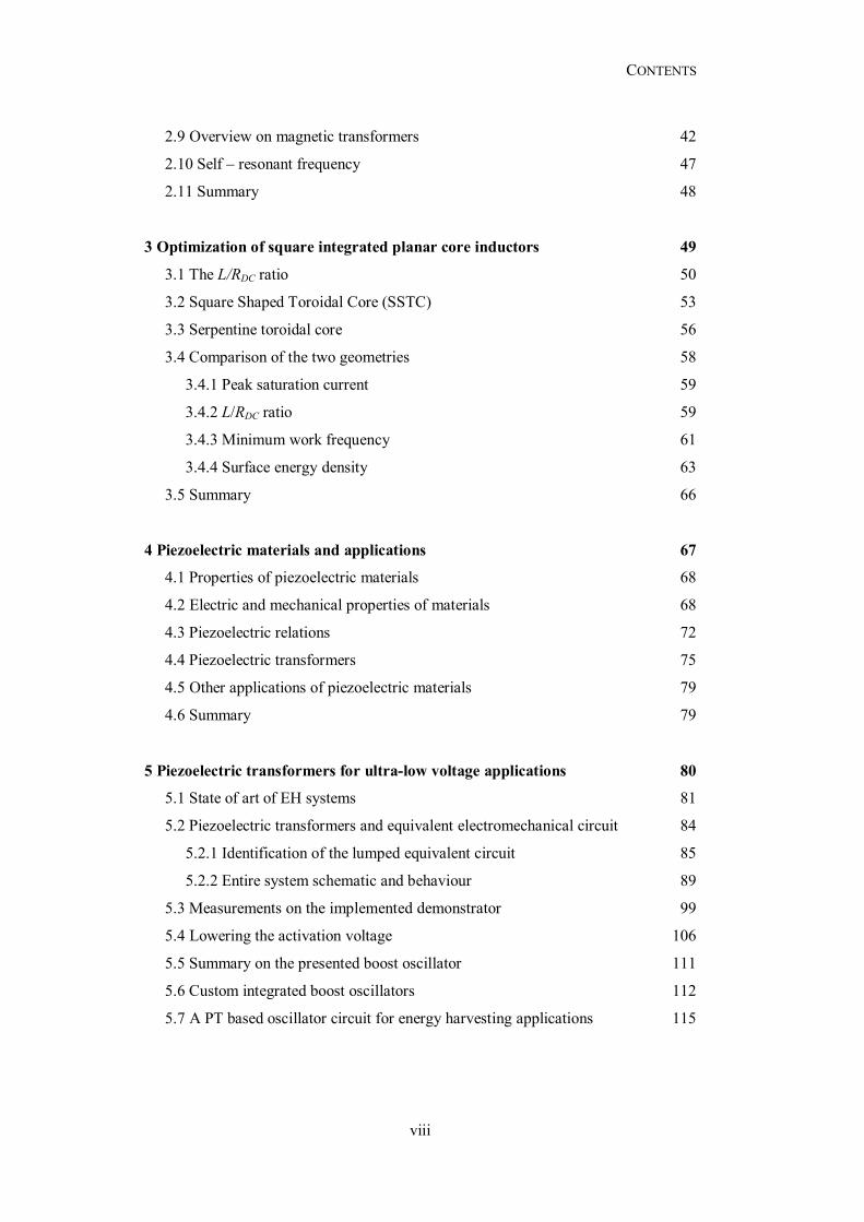
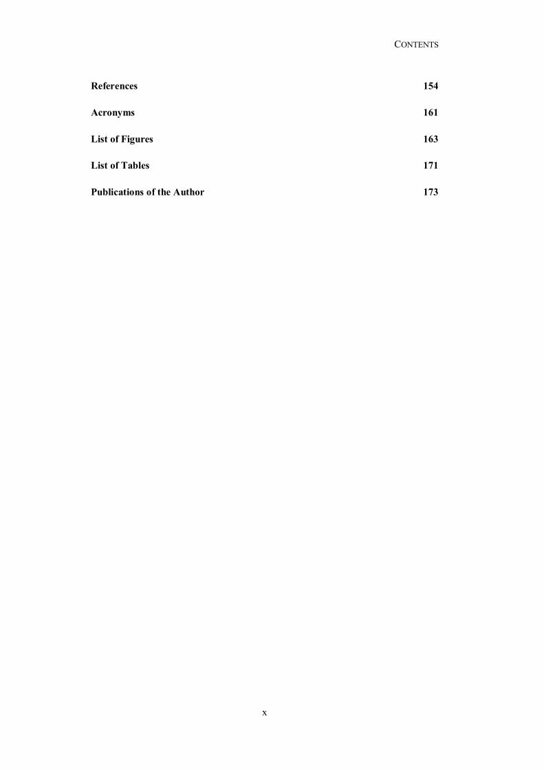
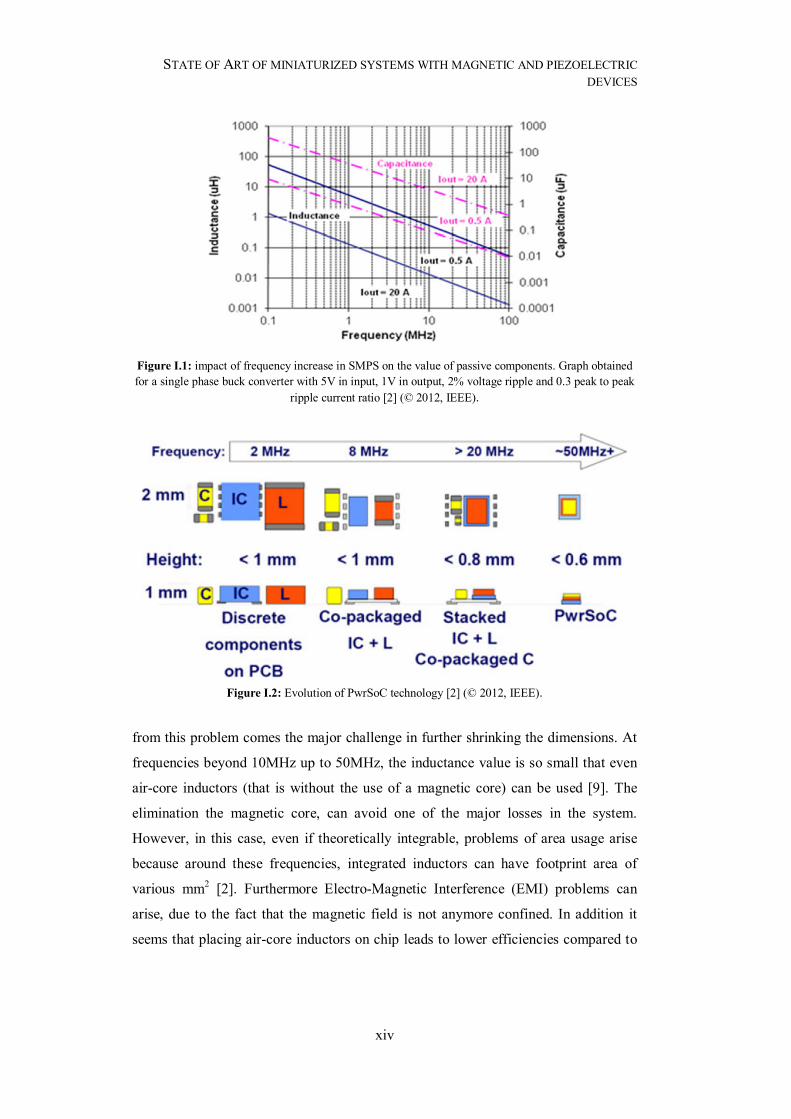
circuit. Figure I.1 shows the trend of link between the size of magnetic components
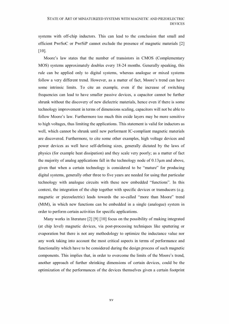
and frequency [2], whilst Figure I.2 [2], shows the evolution of systems from PCB to
PwrSoC. In a conventional low frequency converter (f <1MHz), all components stand
together on a simple PCB, given that in general both capacitors and inductors are too
big for being packaged together with the IC. In the range 1< f <10MHz, the inductor
can be co-packaged with the IC, but still has a huge profile to be stacked. At
frequencies beyond 10MHz, 10< f <20MHz, inductors can be stacked on the top of
the chip, but some components still require to be outside. At frequencies approaching
100MHz, all components can stand together on the same chip [8]. Unfortunately, at
frequencies in the range of 1-10MHz, integrated passive components have not the
same performance, considering the same footprint area, of external passive devices:
STATE OF ART OF MINIATURIZED SYSTEMS WITH MAGNETIC AND PIEZOELECTRIC DEVICES
xiv
from this problem comes the major challenge in further shrinking the dimensions. At
frequencies beyond 10MHz up to 50MHz, the inductance value is so small that even
air-core inductors (that is without the use of a magnetic core) can be used [9]. The
elimination the magnetic core, can avoid one of the major losses in the system.
However, in this case, even if theoretically integrable, problems of area usage arise
because around these frequencies, integrated inductors can have footprint area of
various mm2 [2]. Furthermore Electro-Magnetic Interference (EMI) problems can
arise, due to the fact that the magnetic field is not anymore confined. In addition it
seems that placing air-core inductors on chip leads to lower efficiencies compared to
Figure I.1: impact of frequency increase in SMPS on the value of passive components. Graph obtained for a single phase buck converter with 5V in input, 1V in output, 2% voltage ripple and 0.3 peak to peak
ripple current ratio [2] (© 2012, IEEE).
.
Figure I.2: Evolution of PwrSoC technology [2] (© 2012, IEEE).
STATE OF ART OF MINIATURIZED SYSTEMS WITH MAGNETIC AND PIEZOELECTRIC DEVICES
xv
systems with off-chip inductors. This can lead to the conclusion that small and
efficient PwrSoC or PwrSiP cannot exclude the presence of magnetic materials [2]
[10].
Moore’s law states that the number of transistors in CMOS (Complementary
MOS) systems approximately doubles every 18-24 months. Generally speaking, this
rule can be applied only to digital systems, whereas analogue or mixed systems
follow a very different trend. However, as a matter of fact, Moore’s trend can have
some intrinsic limits. To cite an example, even if the increase of switching
frequencies can lead to have smaller passive devices, a capacitor cannot be further
shrunk without the discovery of new dielectric materials, hence even if there is some
technology improvement in terms of dimensions scaling, capacitors will not be able to
follow Moore’s law. Furthermore too much thin oxide layers may be more sensitive
to high voltages, thus limiting the applications. This statement is valid for inductors as
well, which cannot be shrunk until new performant IC-compliant magnetic materials
are discovered. Furthermore, to cite some other examples, high voltage devices and
power devices as well have self-defining sizes, generally dictated by the laws of
physics (for example heat dissipation) and they scale very poorly; as a matter of fact
the majority of analog applications fall in the technology node of 0.13µm and above,
given that when a certain technology is considered to be “mature” for producing
digital systems, generally other three to five years are needed for using that particular
technology with analogue circuits with these new embedded “functions”. In this
context, the integration of the chip together with specific devices or transducers (e.g.
magnetic or piezoelectric) leads towards the so-called “more than Moore” trend
(MtM), in which new functions can be embedded in a single (analogue) system in
order to perform certain activities for specific applications.
Many works in literature [2] [9] [10] focus on the possibility of making integrated
(at chip level) magnetic devices, via post-processing techniques like sputtering or
evaporation but there is not any methodology to optimize the inductance value nor
any work taking into account the most critical aspects in terms of performance and
functionality which have to be considered during the design process of such magnetic
components. This implies that, in order to overcome the limits of the Moore’s trend,
another approach of further shrinking dimensions of certain devices, could be the
optimization of the performances of the devices themselves given a certain footprint
STATE OF ART OF MINIATURIZED SYSTEMS WITH MAGNETIC AND PIEZOELECTRIC DEVICES
xvi
area. Hence, in this field of applications the major challenge that is still present is the
integration at die level, of magnetic devices such as inductors and magnetic
transformers.
Concerning the dual piezoelectric counterpart, the analysis regarding integration
can be considered valid for it as well. As a matter fact, the power delivered by a
piezoelectric transducer is strictly dependent by its volume; given that the power
requirements are linked by the particular application, it follows that the possibility of
integration at wafer-level is mainly application dependent. To cite an example,
MEMS for energy harvesting purposes are generally much larger than a single chip.
A piezoelectric resonator instead, could be very small, in the order of hundreds of
μm3 [11].
A recent way of integrating piezoelectric materials together with Si-based CMOS
process could be exploiting the piezoelectric properties of GaN (Gallium Nitride)
[12]; even if the lattice constants between Si and GaN are pretty different, using some
buffer layers can improve the growing of such materials on a Si substrate, thus
reducing strain and leakage currents [13], and hence improving the performance of
devices.
Generally speaking, the way of integrating MEMS piezoelectric devices together
with ICs is the same as previously seen with magnetic devices: 1) with separate
processes and then including devices as well as ICs in the same package (SiP), or 2)
integration at wafer level (SoC) [14]. However, piezoelectric materials are one step
forward compared to magnetic materials. To cite an example, inductors typically
require windings, which pose fabrication constraints. Although air-core inductors can
be directly integrated in both ways, generally inductors with magnetic materials as
core are produced with several post-processing steps after the IC, given that many
magnetic materials are not fully clean room compliant. On the other way, there are a
lot of piezoelectric materials such as AlN (Aluminum Nitride), ZnO (Zinc Oxide),
SiN (Silicon Nitride), fully compatible and compliant with IC techniques and clean
rooms [14]. Furthermore, piezoelectric devices do not require windings, and are
typically composed on patterned planar layers, which simplify their production. In
general, these materials are deposited with techniques like sacrificial surface
micromachining, because the devices are produced on the top of the wafer, via
subsequent deposition of different materials, using the so-called sacrificial layers,
STATE OF ART OF MINIATURIZED SYSTEMS WITH MAGNETIC AND PIEZOELECTRIC DEVICES
xvii
which are particular layers (e.g. photoresist) used as base for the deposition of the
materials constituting the structural layer, and then removed to obtain free standing
devices, such as piezoelectric cantilevers or membranes; whereas MOS transistors are
produced “within silicon”, through the definition of the active area. Another
technique for producing MEMS piezoelectric devices is bulk micromachining, by
which devices are produced within the Si substrate, by a real “digging” of the
substrate [15].
In this “piezoelectric” context as well, we fall again in the MtM trend, because
piezoelectric devices can be fully integrated with the IC. Before, we talked about
compact power systems such as PwrSiP or PwrSoC mainly focusing on magnetic
devices. If we contextualize these systems in the application field of Power
conversion or Energy Harvesting (EH), we realize that a challenge arises. Energy
Conversion can be performed by using piezoelectric transformers, which offer better
performance than their magnetic counterparts, but require specific design efforts in
conversion control. If we want to power some Wireless Sensor Nodes (WSN), it
would be desirable if such systems could be fully autonomous by harvesting the
energy present in the environment, given that battery replacement can require too
much effort in many application scenarios. The challenge here is power conversion
from piezoelectric harvesters with output voltages in the order of few tens of mV,
thus insufficient to overcome the threshold voltage of power devices in a typical
PwrSiP or PwrSoC.
Then, the study of application of miniaturized piezoelectric devices, like
transformers, can also benefit this type of applications. In order to exploit and step-up
the ultra-low voltage coming from harvesters such as TEGs (ThermoElectric
Generators) or PhotoVoltaic Cells (PV-C) into a usable voltage, it is necessary to
overcome the threshold voltage of the power devices in power converters, as
previously stated. Until now this was accomplished by means of the so-called boost
(or step-up) oscillators which make use of low-threshold (typically normally-on)
transistors such as Depletion MOSFETs or JFETs coupled with a magnetic
transformer in the classic Armstrong oscillator topology. Then, voltage rectifiers
amplify and rectify the generated growing oscillations. However in the perspective of
having more and more efficient as well as more and more compact systems following
the Moore than Moore’s philosophy, a new type of oscillator made with PTs
STATE OF ART OF MINIATURIZED SYSTEMS WITH MAGNETIC AND PIEZOELECTRIC DEVICES
xviii
(Piezoelectric Transformer) was modelled and tested, showing that it is possible to
reach very low values of minimum activation voltages (the one provided by the
harvester), if the system is integrated. Furthermore, the application of harvesting
systems falls in the μW range, hence the dimensions of the PT as well can be shrunk
down to few mm3, given that discrete PTs are designed and optimized to handle
power in the range of few W and voltages up to hundreds of V. In this context,
MEMS PTs might be useful and integrated at package level with the IC, in order to
make a fully autonomous PwrSiP for EH purposes, since the piezoelectric
transduction can be much more efficient than the electromagnetic one as stated
before. However discrete PTs, are generally made of PZT (Lead Zirconate Titanate,
which is not truly piezoelectric but rather electrostrictive), which is not compatible
with IC techniques and processes, because of the presence of the lead. Alternatively,
MEMS PT can be successfully made in ZnO or AlN, which unfortunately have not a
piezoelectric effect as strong as the PZT. Furthermore, the number of interleaved
layers at the primary side in a PT acts like the turn ratio in a MT (Magnetic
Transformer), so the possibility of having multiple piezoelectric layers in a MEMS
process could be worth future investigations.
This PhD Thesis faces the problems of integration and application of magnetic and
piezoelectric devices, in order to complement the design of CMOS integrated circuits.
This first section is a brief introduction to current state of art (SoA) of MtM
systems which exploit magnetic and piezoelectric devices.
Chapter 1 gives a brief summary of magnetic properties of materials, as well as
some examples of SoA of integrated magnetic inductors and transformers.
Chapter 2 deals with the physics of magnetic field and makes an analysis of how
micro-magnetic inductors and transformers can be modelled, in order to extrapolate
some basic equations useful to assess the performance of magnetic devices. The
chapter gives also some new considerations of the so-called Magnetic Path Length for
square planar toroidal inductors, and gives a new formula for the correct estimation of
its value (from which the inductance value depends) without the aid of time
consuming FEM (Finite Element Methods) simulators.
Chapter 3 deals with the optimization of planar square integrated inductors for
on-chip integration.
STATE OF ART OF MINIATURIZED SYSTEMS WITH MAGNETIC AND PIEZOELECTRIC DEVICES
xix
Chapter 4 deals with the physics of direct and inverse piezoelectric effect, and
with the equivalent lumped electro-mechanical circuit of PTs.
Chapter 5 describes a new type of step-up oscillator which uses discrete PTs in
place of MTs and which can be, in perspective, shrunk in dimensions and improved in
performances if dedicated ICs and MEMS PTs are used, in order to achieve a full and
autonomous PwrSiP or PwrSoC.
Chapter 6 shows the design, fabrication and characterization of MEMS PTs in
AlN performed at the TUW (Technische Universität Wien) during the internship from
February 2015 to August 2015.
Chapter 7 concludes the dissertation with some considerations on the magnetic
and piezoelectric technologies.

1
Chapter 1
Magnetic materials and applications
The miniaturization of electronic systems, together with the increase of
functionality and performance, from portable electronics to high-end computing, is
providing extremely important challenges for engineers and power converters
designers, since in a typical power management system, magnetic components such
as inductors and transformers are still the bulkiest parts.
This chapter presents a brief overview on the magnetic materials, figures of merit
and techniques in order to produce integrated and miniaturized magnetic components
for power applications.
1.1 Properties of magnetic materials
A magnetic material is a material that is able to sense the effect of an external
applied magnetic field. This sensing capability is represented by the so called
magnetic permeability μr which can be considered the dual of the dielectric
permeability εr which represents the capability of a material to sense and amplify an
electrostatic field. To amplify the electric capacitance, materials with εr>1 must be
CHAPTER 1. MAGNETIC MATERIALS AND APPLICATIONS
2
used, and in general to make inductors for power applications, materials with μr >1
must be used. The sensing capability, is essentially due to the fact that magnetic
materials present magnetic dipoles that are able to be fully aligned with an external
magnetic field, thus resulting in an amplification.
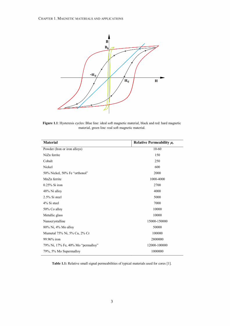
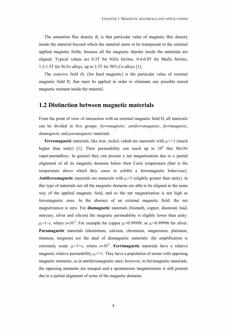
Magnetic materials can be divided in two main groups: hard and soft. Hard
magnetic materials present a B-H static curve which is extremely non-linear, in fact
these materials are generally used to make permanent magnets, given that their B-H
curve presents an important hysteresis (red and black curve in Figure 1.1).
Ideal soft magnetic materials (blue line in Figure 1.1) present a B-H curve that is a
straight line, however even these materials presents a hysteresis curve that is in
general much littler than the hard ones (green curve in Figure 1.1).
The major parameters of interest for magnetic materials are:
Small signal relative magnetic permeability μr
Resistitivity ρC
Losses per unit volume pV
Cutoff frequency (bandwith) fT
Saturation flux density BS
Coercive field HC
A good magnetic material to be used for inductors/transformers for power
applications should have μr→∞, fT→∞, ρC→∞ and pV→0. These quantities are strictly
linked together and we will discuss later on how, for example, the finite value of the
resistivity limits the bandwidth and increases the losses. Unfortunately, the materials
with the highest μr present, at the same time, very low values of ρC. Nanocrystalline,
and amorphous Co-based alloys (e.g. Vitrovac 6025 from Vacuumschmelze) present
the highest values of μr (up to 105 and more), but at the same time a resistivity around
120-140μΩ∙cm. In general, some ferrites (Co based, Mg based, NiZn based) have a
resistivity up to 107 μΩ∙cm. Other types of ferrites (Cu/Mn/MnZn/Zn/ based) have a
resistivity ranging from 105 μΩ∙cm (Cu based) to 102 μΩ∙cm (Zn based). The
Fe-based ferrite has a ρC4∙10-3μΩ∙cm. Alloys presents a resistivity ranging from
hundred to tens of μΩ∙cm. Concerning the permeability, Table 1.1 [1] presents
typical values of small signal permeabilities of magnetic materials.
CHAPTER 1. MAGNETIC MATERIALS AND APPLICATIONS
3
Figure 1.1: Hysteresis cycles: Blue line: ideal soft magnetic material, black and red: hard magnetic material, green line: real soft magnetic material.
Material Relative Permeability μr
Powder (Iron or iron alloys) 10-60
NiZn ferrite 150
Cobalt 250
Nickel 600
50% Nickel, 50% Fe “orthonol” 2000
MnZn ferrite 1000-4000
0.25% Si iron 2700
48% Ni alloy 4000
2.5% Si steel 5000
4% Si steel 7000
50% Co alloy 10000
Metallic glass 10000
Nanocrystalline 15000-150000
80% Ni, 4% Mo alloy 50000
Mumetal 75% Ni, 5% Cu, 2% Cr 100000
99.96% iron 2800000
79% Ni, 17% Fe, 40% Mo “permalloy” 12000-100000
79%, 5% Mo Supermalloy 1000000
Table 1.1: Relative small signal permeabilities of typical materials used for cores [1].
CHAPTER 1. MAGNETIC MATERIALS AND APPLICATIONS
4
The saturation flux density BS is that particular value of magnetic flux density
inside the material beyond which the material starts to be transparent to the external
applied magnetic fields, because all the magnetic dipoles inside the materials are
aligned. Typical values are 0.3T for NiZn ferrites, 0.4-0.8T for MnZn ferrites,
1.2-1.5T for Ni-Fe alloys, up to 2.3T for 50% Co alloys [1].
The coercive field HC (for hard magnetic) is the particular value of external
magnetic field H, that must be applied in order to eliminate any possible stored
magnetic moment inside the material.
1.2 Distinction between magnetic materials
From the point of view of interaction with an external magnetic field H, all materials
can be divided in five groups: ferromagnetic, antiferromagnetic, ferrimagnetic,
diamagnetic and paramagnetic materials.
Ferromagnetic materials, like iron, nickel, cobalt are materials with μr>>1 (much
higher than unity) [1]. Their permeability can reach up to 106 like Mo-Ni
super-permalloys. In general they can present a net magnetization due to a partial
alignment of all its magnetic domains below their Curie temperature (that is the
temperature above which they cease to exhibit a ferromagnetic behaviour).
Antiferromagnetic materials are materials with μr>1 (slightly greater than unity): in
this type of materials not all the magnetic domains are able to be aligned in the same
way of the applied magnetic field, and so the net magnetization is not high as
ferromagnetic ones. In the absence of an external magnetic field, the net
magnetization is zero. For diamagnetic materials (bismuth, copper, diamond, lead,
mercury, silver and silicon) the magnetic permeability is slightly lower than unity:
μr=1–ε, where ε10-5. For example for copper μr=0.99999, or μr=0.99998 for silver.
Paramagnetic materials (aluminium, calcium, chromium, magnesium, platinum,
titanium, tungsten) are the dual of diamagnetic materials: the amplification is
extremely weak: μr=1+ε, where ε10-5. Ferrimagnetic materials have a relative
magnetic relative permeability μr>>1. They have a population of atoms with opposing
magnetic moments, as in antiferromagnetic ones; however, in ferrimagnetic materials,
the opposing moments are unequal and a spontaneous magnetization is still present
due to a partial alignment of some of the magnetic domains.
CHAPTER 1. MAGNETIC MATERIALS AND APPLICATIONS
5
1.3 Deposition processes for thin film integrated
micro-magnetic components
In literature [2], the most diffused techniques for the deposition of thin (from
hundreds of nm up to several μm) magnetic films on chip are: screen printing,
sputtering and electrodeposition.
The screen printing is suitable for the deposition of non-metallic films with a
thickness higher than 1μm. NiZn and MnZn are typical soft magnetic materials
deposited through this technique. In general the material that has to deposited is as the
core materials issuspended in a polymer matrix. This technique has been proved to be
suitable for the microfabrication of core inductors, presenting a good compromise
between core resistivity (>1Ω∙m) and process simplicity. However, because of the
very high temperatures involved during the process, it is not compatible with CMOS
(Complementary MOS) or MEMS (Micro-Electro-Mechanical Systems) processes. The sputtering process is fully compatible with IC processes. Furthermore it has
the advantage of a proper control of the surface and thickness of material that has to
be deposited. A wide range of materials, including oxides and alloys can be deposited
on the chip via this technique, which theoretically allows also the formation of
laminated cores, given that, as said before, oxides as well can be sputtered.
Unfortunately this technique is suitable for the deposition of only few hundreds of nm
of thickness, because beyond this thickness, the technique starts to be slow and too
much expensive.
The electroplating deposition process can provide films with a controlled
thickness; furthermore the process is not expensive and relatively fast compared to
the sputtering process. The most frequently electroplated material is the permalloy [2]
(81% Fe and 19% Ni). Supermalloys and other alloys as well have been reported to
be deposited via this technique [2]. In general materials deposited through this
technique present high saturation flux density (around 1.8T), very high permeability,
but unfortunately very low resistivity. Furthermore [2] presents a brief overview of
materials deposited in literature, including the used technique, permeability, thickness
and resistivity of the material used for the fabrication of micro-inductors.
CHAPTER 1. MAGNETIC MATERIALS AND APPLICATIONS
6
1.4 Integrated/MEMS compatible inductors and
transformers
Advances in technology dimensions scaling together with increasing switching
frequencies in power converters, is leading towards further miniaturizations of
electronic circuits. However, in this field of applications the major challenge that is
still present is the integration at die level of magnetic devices such as inductors and
magnetic transformers.
Integrated inductors can be made by exploiting the metal layers available in IC
processes. These processes, depending on their complexity, can have from three to
eight different metallization levels. The thickness of each layer may typically vary
from ~0.5μm to ~4μm, with the last one being the thicker among the others. The last
metal level of an IC process thus can be theoretically used to make inductors or
transformers due to its lower sheet resistance (less than 10mΩ/). To cite an example,
on-chip planar air-core inductors can be simply made with a spiral metallization,
generally the thicker metal layer of an integrated circuit (IC), in order to reduce the
DC series resistance, as said before. Their applications usually fall in the RF range,
whereas for frequencies under 100 MHz, inductors with a magnetic core are still more
performant than air-core inductors [2], since the AC losses due to skin depth in the
core grow very fast with f b (Steinmetz equation), where f is the frequency and b is a
coefficient ranging between 2 and 3 [9] [10]. Hence at high frequencies the losses due
to the magnetic core become more dominant.
Typical geometries of such type inductors can include the Meander inductor, the
spiral or the single turn planar inductor. These geometries [16] [17] [18], shown in
Figure 1.2, are lacking a magnetic core and are in general used for RF applications,
as stated before. In general the width and the distance between two adjacent stripes in
such inductors must follow certain design rules. These geometries are not intended for
use as power inductors for PwrSoC, because the achieved inductance values are pretty
low and the resistance is very high. Even if a magnetic sheet is deposited on top the
metal, because of the demagnetization of the sheet (cfr. Chapter 2), the inductance
enhancement is very low. In addition, the produced magnetic field goes through the
entire circuit causing possible problems of EMI. Transformers can be formed by

CHAPTER 1. MAGNETIC MATERIALS AND APPLICATIONS
7
using a lower metal line, or a metal at the same level with an interleaved geometry.
In [19] a 20mm2 power IC was produced with a “sandwich” spiral inductor with
metal of huge thickness of 35μm and 9μm of magnetic layers. The achieved
inductance is about 0.96μH at 0.35A of current and 3MHz switching frequency. The
achieved efficiency is around 83%.
In [20] a boost converter with micro-machined inductor was presented. The
inductance was obtained through a MEMS-LIGA (Lithographie, Galvanoformung,
Abformung - Lithography, Electroplating, and Molding) process, which allows
producing structures with a very high aspect ratio. The switching frequency was
varied from 3MHz to 10MHz.
In [21] an inductor exploiting bondwires (Figure 1.3) for making closed currents
turns was presented. The winding is embedded in a glob of magnetic epoxy core that
can be formed to cover the bondwires during the SoC packaging process by various
techniques such as brushing, squeegeeing, dripping, inking, etc. In perspective the
presented device, based on the use of ceramic magnetic material to achieve low losses
and hence good quality factors, is combined with the standard packaging of ICs. The
extreme simplicity of the structure allows a powerful integration for system on chip
(SoC), because an entire circuit such as DC/DC converter, can be integrated with
standard Si technology, whereas the magnetic component is stacked above the chip.
In [22] (cfr. Figure 1.4) a flat toroidal inductor with a laminated Ni80Fe20 magnetic
core was presented. The metal turns are pretty thick (20μm) and obtained via Electro-
Chemical Deposition (ECD). The laminated core is obtained via Physical Vapor
Figure 1.2: Top view of shapes of inductors used in RF applications.
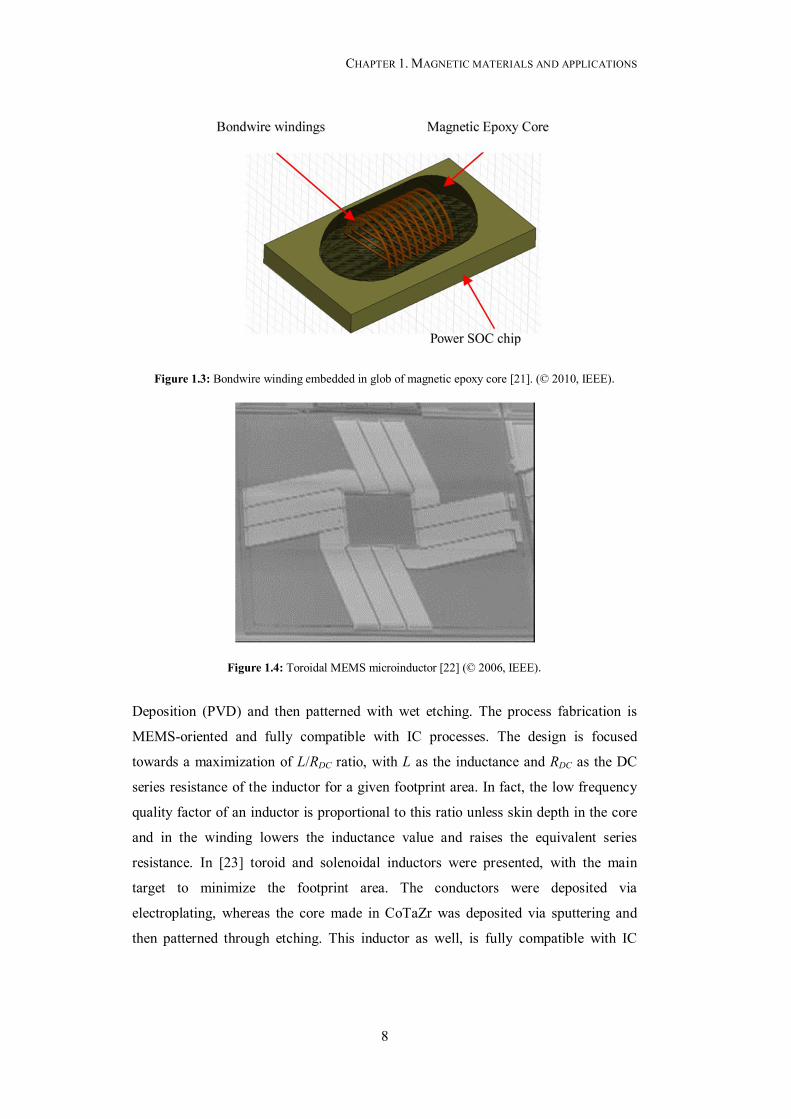
CHAPTER 1. MAGNETIC MATERIALS AND APPLICATIONS
8
Deposition (PVD) and then patterned with wet etching. The process fabrication is
MEMS-oriented and fully compatible with IC processes. The design is focused
towards a maximization of L/RDC ratio, with L as the inductance and RDC as the DC
series resistance of the inductor for a given footprint area. In fact, the low frequency
quality factor of an inductor is proportional to this ratio unless skin depth in the core
and in the winding lowers the inductance value and raises the equivalent series
resistance. In [23] toroid and solenoidal inductors were presented, with the main
target to minimize the footprint area. The conductors were deposited via
electroplating, whereas the core made in CoTaZr was deposited via sputtering and
then patterned through etching. This inductor as well, is fully compatible with IC
Figure 1.3: Bondwire winding embedded in glob of magnetic epoxy core [21]. (© 2010, IEEE).
Figure 1.4: Toroidal MEMS microinductor [22] (© 2006, IEEE).

CHAPTER 1. MAGNETIC MATERIALS AND APPLICATIONS
9
processes. About 70nH were realized with a 34X enhancement factor with respect to
the same inductor with no core. The footprint area is 1mm2, and the DC resistance is
lower than 1Ω. However, because of magnetic losses, the maximum usable frequency
is around 10MHz.
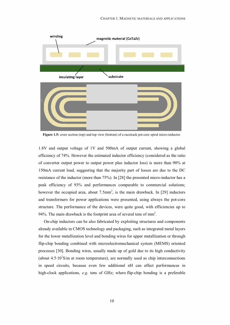
Other geometries include race-track shaped (pot-core) micro-inductors (cfr.
Figure 1.5) in which, instead of wrapping a conductor around a magnetic core the
magnetic material is wrapped around a conductor [24] [25] [26] [27] [28] [29]. In [24]
and [25] on-chip micro-inductors made by exploiting advanced CMOS processes
(130nm [24] and 90nm [25]) that incorporate high-permeability (850-1100) laminated
magnetic materials, and resistivity of about 100μΩ∙cm. In both works, a CoZrTa
magnetic material was used. This particular material has been proved to be usable to
frequencies up to 9.8GHz in case of small inductors [24] with a single lamination
placed above a spiral conductor. In this particular case, the inductance enhancement
with respect to the air-core inductor is only of 10%-30% because of demagnetization
of the material. However, when a sandwich structure is used, depending on magnetic
material thickness, enhancement of 16X-19X can be achieved. The drawback is that
the bandwidth is reduced.
In [26] a micro-fabricated transformer consisting of a racetrack shaped copper
winding of 30μm of thickness is presented. The structure is always a pot-core type
with a magnetic material made up by two layers of Ni45Fe55 (~4.5 μm thick). The
bottom magnetic layer is deposited through electroplating and patterned on native
oxide insulated silicon wafer. The copper electrodes are electroplated on a patterned
BCB which serves as insulation layer between the winding and the bottom magnetic
layer. The upper magnetic layer is deposited and patterned using the same
electroplating process as the bottom one, on a patterned on an epoxy type photoresist
(Su-08), which is 50 μm thick, insulating the top layer from the winding. Both single
(SLM) and double layer (DLM) copper winding were reported. To cite an example,
the DLM presents a magnetizing inductance of 210nH at 20MHz and ~1Ω of DC
resistance. The gain is about -1dB at 50Ω load in the range 5MHz-50MHz. The
footprint area is less than 4mm2.
In [27] footprint areas below 3mm2 were achieved, according to the space used to
make the metallization. 160nH were obtained in 2.5mm2 with a DC resistance of
about ~0.45Ω and tested with a converter operating at 30MHz, with input voltage of
CHAPTER 1. MAGNETIC MATERIALS AND APPLICATIONS
10
1.8V and output voltage of 1V and 500mA of output current, showing a global
efficiency of 74%. However the estimated inductor efficiency (considered as the ratio
of converter output power to output power plus inductor loss) is more than 90% at
150mA current load, suggesting that the majority part of losses are due to the DC
resistance of the inductor (more than 75%). In [28] the presented micro-inductor has a
peak efficiency of 93% and performances comparable to commercial solutions;
however the occupied area, about 7.5mm2, is the main drawback. In [29] inductors
and transformers for power applications were presented, using always the pot-core
structure. The performance of the devices, were quite good, with efficiencies up to
94%. The main drawback is the footprint area of several tens of mm2.
On-chip inductors can be also fabricated by exploiting structures and components
already available in CMOS technology and packaging, such as integrated metal layers
for the lower metallization level and bonding wires for upper metallization or through
flip-chip bonding combined with microelectromechanical system (MEMS) oriented
processes [30]. Bonding wires, usually made up of gold due to its high conductivity
(about 4.5∙107S/m at room temperature), are normally used as chip interconnections
in speed circuits, because even few additional nH can affect performances in
high-clock applications, e.g. tens of GHz; where flip-chip bonding is a preferable
Figure 1.5: cross section (top) and top view (bottom) of a racetrack pot-core spiral micro-inductor.
CHAPTER 1. MAGNETIC MATERIALS AND APPLICATIONS
11
alternative due to the shorter interconnections between chip and package. Typical
inductance of bonding wires is about 1-2nH for every mm of length [29] and they can
be used also as standalone inductors.
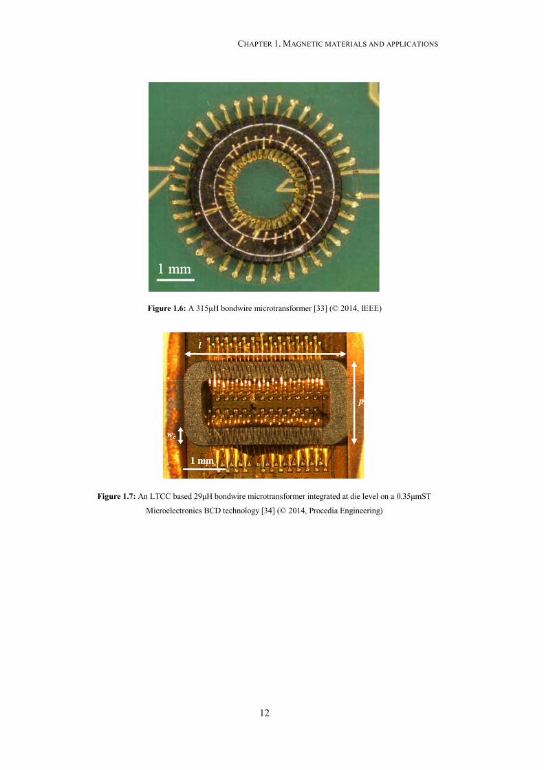
Other types of micro-fabricated magnetic devices, fully compatible with IC
processes, include bondwires inductors/transformers [32] [33] [34] (cfr. Figure 1.6
and Figure 1.7). In this kind of implementation the toroidal core is placed between
the lower metal lines (that could be either on PCB or exploiting the metal levels of an
IC process) and bondwires which are used to close the current turns. In such a way,
inductances up to 315μH [33], with DC resistance of 4.3Ω were obtained in a
footprint area of about 24 mm2. These structures have been proved to be useful for
micro-power conversion such as boost converters for ultra-low voltage step-up
purposes. In [34], an on-chip bond wire transformer for MHz frequency range is
presented, with a Low Temperature Co-fired Ceramic (LTCC) core and in a footprint
area of about 15 mm2.
1.5 Summary
This chapter has presented a brief introduction to the magnetic materials, their
most important parameters like resistivity and relative permeability. Additionally a
short overview on the most diffused techniques used to produce integrated and
miniaturized magnetic components, together with some examples of the state of art of
miniaturized magnetic devices was presented.
CHAPTER 1. MAGNETIC MATERIALS AND APPLICATIONS
12
Figure 1.6: A 315μH bondwire microtransformer [33] (© 2014, IEEE)
Figure 1.7: An LTCC based 29μH bondwire microtransformer integrated at die level on a 0.35μmST
Microelectronics BCD technology [34] (© 2014, Procedia Engineering)
13
Chapter 2
Modelling of integrated magnetic
components
Magnetic components are devices which make use of the magnetic field in order
to store or transfer energy (or power). A typical element which stores the energy in a
magnetic field is the inductor whilst a typical element which transfers/stores energy is
the magnetic transformer, which converts electric energy in the form of a magnetic
field and then back again to electric field. Almost all electronic circuits, such as
power converters or harvesting systems require the use of such magnetic components
which in general are extremely difficult to integrate, and are the bulkiest and most
expensive part of the whole circuit.
In order to understand the behaviour of such components a review of magnetic
properties is needed, in order then to extrapolate basic equations and relationships
useful for the design and optimization of such components.
CHAPTER 2. MODELLING OF INTEGRATED MAGNETIC COMPONENTS
14
2.1 Overview on Magnetic relations
The first equation to introduce is one of Maxwell’s equations: the Ampère’s law:
0 0B r J S Ir r enc
C S
d d (2.1)
which states that the line integral of the magnetic B-field density (measured in Tesla,
T) around the closed curve C is proportional to the current Ienc passing through a
surface S (enclosed by C). The equation can be used to find the value of inductance of
a closed core toroid with magnetic permeability µr >>1 and N turns, in this case (2.1)
becomes:
0
0 0 0
B r B 2 r I
IB2 r
r encC
enc MMr r r
C
d N
N F Hl
(2.2)
in (2.2) the term FMM=N∙Ienc is the MagnetoMotive Force (A·turns), lC=2πr is the
Magnetic Path Length (MPL), whereas the quantity H is the magnetic field intensity.
The quantity µ0 (4π·10-7 H/m) is the vacuum magnetic permeability.
Combining the electromagnetic induction’s law with (2.2) then we have:
0 0r r enc encB MMEM C C C
C C
N dI dId dFdB A A A Ldt dt l dt l dt dt
(2.3)
The parameter AC in (2.3) is the cross section of the closed toroid whereas the
quantity L=A·Nµ0µr/2πr is called self-inductance (H), and indicates the capability of a
conductor to produce an electromotive force across its edges when an AC current
flows into it.
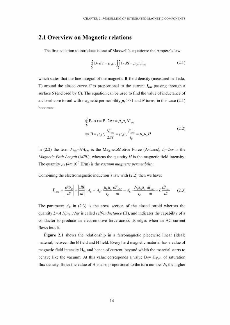
Figure 2.1 shows the relationship in a ferromagnetic piecewise linear (ideal)
material, between the B field and H field. Every hard magnetic material has a value of
magnetic field intensity HS, and hence of current, beyond which the material starts to
behave like the vacuum. At this value corresponds a value BS= HS/µr of saturation
flux density. Since the value of H is also proportional to the turn number N, the higher
CHAPTER 2. MODELLING OF INTEGRATED MAGNETIC COMPONENTS
15
number of turns in an inductor should carry less current in order to prevent core
saturation, because H is related to the MagnetoMotive Force FMM.
2.2 Magnetic circuits
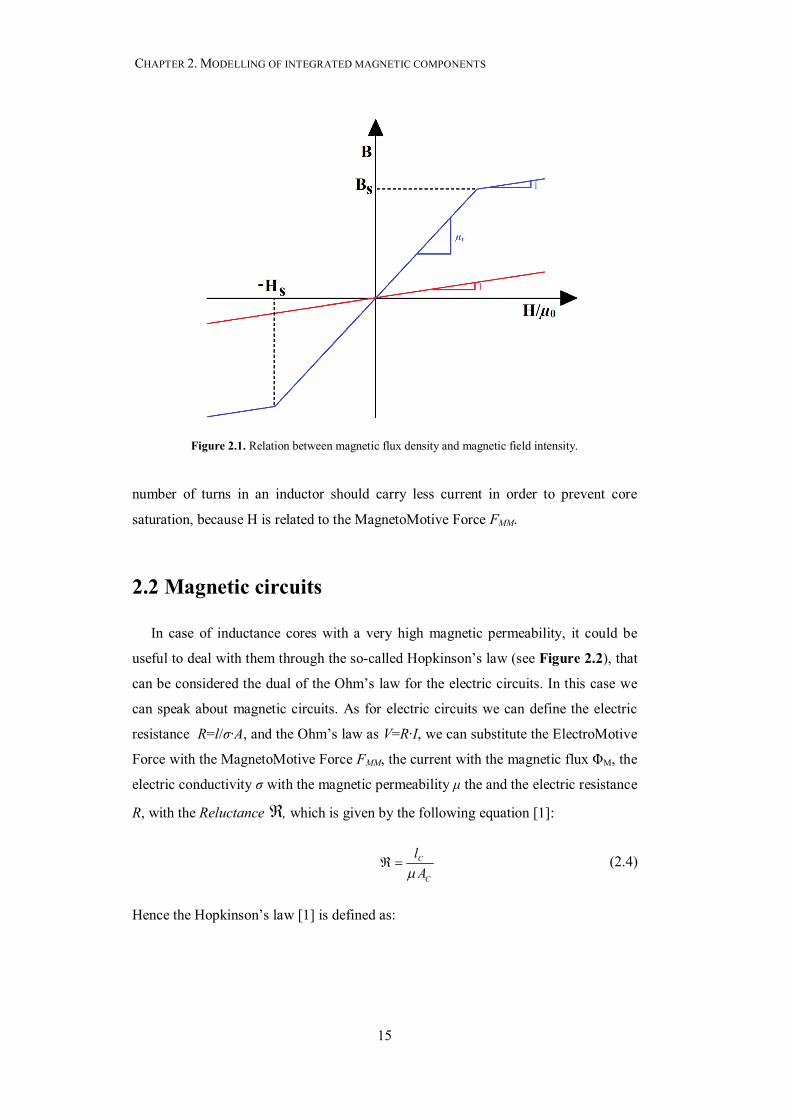
In case of inductance cores with a very high magnetic permeability, it could be
useful to deal with them through the so-called Hopkinson’s law (see Figure 2.2), that
can be considered the dual of the Ohm’s law for the electric circuits. In this case we
can speak about magnetic circuits. As for electric circuits we can define the electric
resistance R=l/σ∙A, and the Ohm’s law as V=R∙I, we can substitute the ElectroMotive
Force with the MagnetoMotive Force FMM, the current with the magnetic flux ΦM, the
electric conductivity σ with the magnetic permeability μ the and the electric resistance
R, with the Reluctance , which is given by the following equation [1]:
C
C
lA
(2.4)
Hence the Hopkinson’s law [1] is defined as:
Figure 2.1. Relation between magnetic flux density and magnetic field intensity.
CHAPTER 2. MODELLING OF INTEGRATED MAGNETIC COMPONENTS
16
MM MF (2.5).
The Reluctance then is a measure of how much the magnetic flux encounters a
“resistance” in flowing in a magnetic core, once a current has been applied to the
inductor’s terminals, as the electric resistance R measures the resistance encountered
by the current in flowing in an electric circuit once a voltage has been applied.
Furthermore, as it can be seen from (2.4), the electric resistance and magnetic
reluctance have a very similar expression. The inverse of the reluctance =1/ is
called Permeance.
2.2.1 Air gaps
Generally, inductors are not used in a closed core configuration. This is because
the inductance value is strictly dependent on the magnetic permeability which in turn
is dependent on frequency, losses, temperature, current value, etc. A way to make the
inductance independent from the magnetic permeability of the material is to introduce
a small air gap of length lG<< lC.
Figure 2.2. Magnetic circuit.
CHAPTER 2. MODELLING OF INTEGRATED MAGNETIC COMPONENTS
17
In order to find the effective inductance, we can use the similarity between the
reluctance and electric resistance. In this case, we have two reluctances in series, the
one of the core, and the one given by the small air gap, hence [1]:
1
1
C G G C Geff
o r o C o C r C
C C r G C
o C r C o C eff
l l l l lA A A l
l l l lA l A
(2.6)
The quantity μeff, given by the following expression:
1
r C reff
GC r Gr
C
lll ll
(2.7)
is called effective magnetic permeability, in fact, if lC/lG << μr, then μeff lC/lG, hence it
depends only by the ratio between the core length and air gap length. In addition, the
presence of the air gap acts like a feedback in the magnetic reluctance, making the
overall reluctance independent from the material parameters.
Once the value of the effective reluctance is known, then the effective inductance
is given by:
2 /eff effL N (2.8)
However it is worth noting that the concept of the reluctance remains valid only
for closed cores with an eventual very small air gap. The air gap essentially takes into
account the demagnetization factor of the material, which is strictly dependent on the
shape the core. As a matter of fact, considering two cores, with same cross section,
length and magnetic permeability, but with different layout like toroidal configuration
and solenoid configuration, will produce extremely different results in terms of
inductance. Furthermore, as the gap length lG increases, the fringing flux leaking
outside the core cross section becomes more and more important, thus partially
invalidating the previous equations. This also happens for capacitor, as a matter of
fact the formula of a two parallel plates capacitor C=Aε0εr/lp (resembling the formula
CHAPTER 2. MODELLING OF INTEGRATED MAGNETIC COMPONENTS
18
of a magnetic permeance) is valid only when lp is small enough such that there is not
any fringing electric field.
2.3 Modelling of inductors
The self-inductance of a closed toroid inductor or an infinite length core solenoidal
inductor, have the same inductance value, which is given by:
2 2
0
C
C rl
C
A N NLl
. (2.9)
However, in general, finite-length solenoids suffer from demagnetization of the core,
which lowers the effective magnetic permeability. This happens because the magnetic
flux density, assuming for simplicity a cylindrical core, along its axis x of simmetry is
not uniform, and has the following expression [35]:
0
2 22 2
2 22 2 4 2 4
r C C
C C
nI l x l xB xl x r l x r
(2.10)
In (2.10), n is the linear turn density wrapped around the core, r is radius of the core.
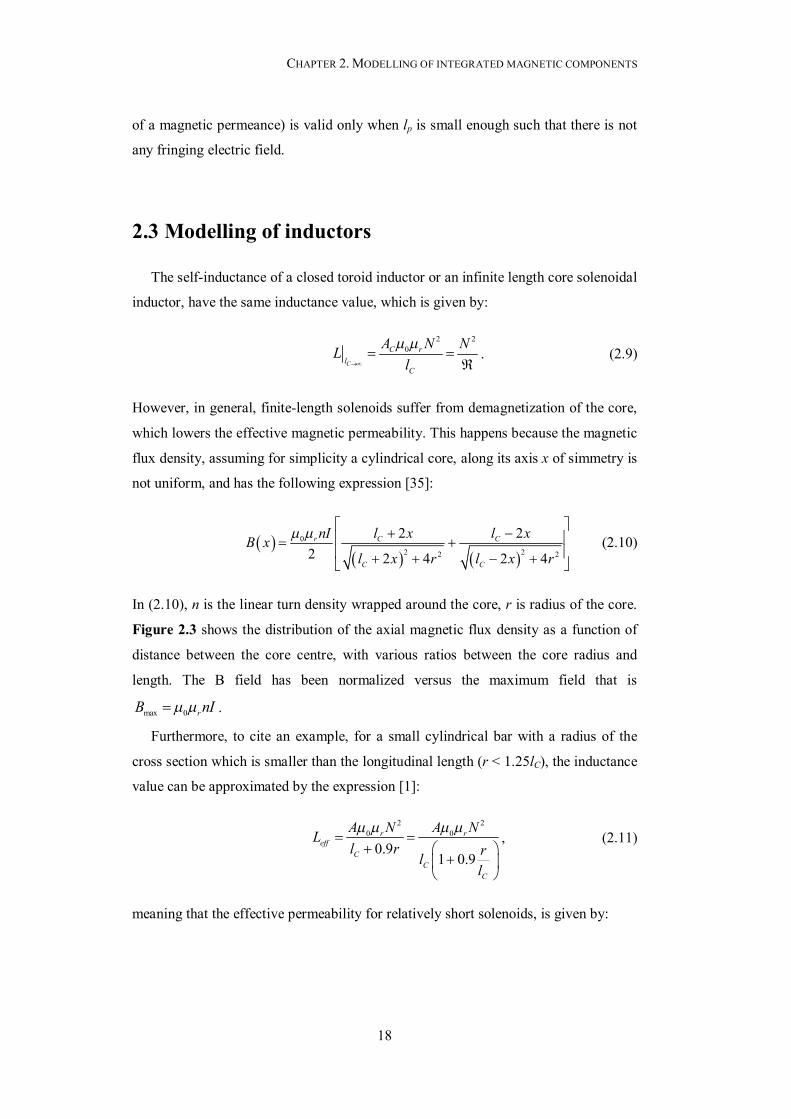
Figure 2.3 shows the distribution of the axial magnetic flux density as a function of
distance between the core centre, with various ratios between the core radius and
length. The B field has been normalized versus the maximum field that is
max 0 rB nI .
Furthermore, to cite an example, for a small cylindrical bar with a radius of the
cross section which is smaller than the longitudinal length (r < 1.25lC), the inductance
value can be approximated by the expression [1]:
2 2
0 0
0.91 0.9
r reff
CC
C
A N A NLl r rl
l
, (2.11)
meaning that the effective permeability for relatively short solenoids, is given by:
CHAPTER 2. MODELLING OF INTEGRATED MAGNETIC COMPONENTS
19
1 0.9
reff
C
rl
(2.12)
2.4 Magnetic Path Length (MPL)
In all the previous expressions the parameter lC was taking into account the so
called magnetic path length (MPL). The reluctance formula (2.4) gives information
about the mean magnetic path length. In literature, in general, a way to find this value
was to simply make the arithmetic average between the internal and the external
perimeter of the core.
Although this can give numerically correct results in many practical cases, the
procedure is conceptually and mathematically wrong because there is the implicit
assumption that the magnetic flux density B is uniform along the entire core
cross-section. Nevertheless, the magnetic flux density follows the lowest reluctance
path (as elctric currents follow the paths with the lowest electric resistance [1]), and
since in a small neighborhood of the internal perimeter, the path length is the shortest,
the magnetic flux density will be much more concentrated closer to the internal
perimeter of the core. This means that the magnetic flux density is not uniform along
the entire cross section of the core, and intuitively the geometric average between
Figure 2.3: Magnetic flux density distribution along the axial direction of the core.
CHAPTER 2. MODELLING OF INTEGRATED MAGNETIC COMPONENTS
20
internal and external perimeter should better predict the magnetic flux density
preferred path.
To cite a simple example, for a cylindrical toroid (Fig. 2.4), with internal radius R1,
and external radius R2, the mean MPL can be found through averaging of the
Ampère’s law:
2
10
2 1
2
10 0
2 1
2
ln
2 2
R
Rr
r r
drr
B N IR R
RR
N I N IR R r
(2.13)
This means that the average MPL for a toroid with cylindrical symmetry is given by:
2 1
2
1
2
ln ln
EXT INTCirc
EXT
INT
R R P PMPLR PR P
(2.14)
The truncated Taylor series expansion of (2.14) when PEXT PINT is
MPL ≈ π(R2 + R1), which can correspond either to the arithmetic or geometric
average between external and internal perimeter: as a matter of fact both of them have
the same truncated Taylor series. Besides, if we cut in j extremely small concentric
slices a circular crown, thanks to the symmetry of the structure, the magnetic flux
density as well has a cylindrical symmetry and this means that the j small concentric
slices can be considered as j reluctances in parallel because there is not any
interaction between them, that is to say that both the reluctances and the magnetic
flux density have the same cylindrical symmetry.
Let’s consider for simplicity a square shaped toroidal core (SSTC) like the one in
Figure 2.5. Be LA and LB the internal and the external sides of the square core
respectively. PA = 4∙LA is the internal perimeter, whilst PB = 4∙LB is the external
perimeter, and W is the core width: obviously it holds that W = (PB – PA) / 8. Now the
core width can be divided in several j+1 slices as shown in Figure 2.5. The value of j
is big enough such that the ratio between the external and the internal perimeter of the
i-th slice is PB,i / PA,i ≈ 1+∆P, with ∆P << 1.

CHAPTER 2. MODELLING OF INTEGRATED MAGNETIC COMPONENTS
21
Figure 2.5. SSTC divided in several slices [36]. (© 2015, IEEE).
Figure 2.4. Top view of a toroidal core divided in several slices [36] (© 2015, IEEE).
CHAPTER 2. MODELLING OF INTEGRATED MAGNETIC COMPONENTS
22
The perimeter length of the i-th slice can be written as:
8i A
WP P ij
(2.15)
The variable i assumes all the j+1 integer values between 0 and j. Thus the reluctance
of the independent i-th slice is:
, 0
ii
C i r
PA μ μ
(2.16)
In (2.15), AC,i = W / j is the normalized cross section against the core thickness t of the
i-th slice.
According to the Hopkinson’s law, more reluctances can be considered in parallel
if the same MagnetoMotive force (FMM) is applied over them. However, due to the
corner effect ([37] [38] [39]), the magnetic flux in each slice is round in the corners
and not right: this means the j+1 slices cannot be considered in parallel because a
small amount of the magnetic flux (arrows in Figure 2.5) flowing in the i-th slice,
leaks in the [i‒1]-th slice, because it is not physically able to follow the right angles of
the corners.
Now let’s assume that the j+1 reluctances are all in parallel, then the total
reluctance would be:
0 1 2, 0
0
0
00 0 0
1 2
1/ / / / / /... / /
11
...
TOT jC i r
j
ii
j j j jr
i i iii i i i
M
A μ μ
Pj
W μ μP P PP
P P P
(2.17)
In the previous equation, the operator “//” means a parallel combination of two
elements (e.g. a//b = (a∙b) / (a+b)). From (2.17) we can state that the effective mean
MPL is:
CHAPTER 2. MODELLING OF INTEGRATED MAGNETIC COMPONENTS
23
0 0
lim lim1 1
8
eff j jj j
i iiA
j jMPL
WP P ij
(2.18)
As j approaches infinity, the quantity 8(W / j)∙i varies with continuity between 0 and
8 W, when i varies from 0 to j. We can put 8(W / j)∙i = x and since ∆i = 1,
dx = 8(W / j)∙∆i => ∆i = dx / [8(W / j)]. So we have:
0 0
8
0
lim lim1 Δ8 8
8 8lim8ln ln
eff j jj j
i iA A
B AWj
A B
A AA
j jMPLi
W WP i P ij j
P PW WP W Pdx
P PP x
(2.19)
Equation (2.19) provides the same results obtained for a circular toroid. This
confirms that a circular toroid as well can be thought as the parallel combination of
smaller concentric reluctances, because (2.19) assumed that there was not any
interaction between the magnetic flux flowing in each slice.
However, as stated before, for a square toroid, the slices in Fig. 2.5, cannot be
considered in parallel because of the corner effect; so the square toroid has to be
transformed into an equivalent circular toroid that includes the corners effect [37],
such that (2.19) is still applicable. Now the problem becomes finding the equivalent
value of the external perimeter PB’ < PB of the equivalent round toroid with same
internal perimeter PA . This operation is valid given that the actual value of the MPL
is closer to that one of the internal perimeter PA according to (2.19) and it is not given
by the arithmetic average between PA and PB, for the reasons shown before.
Following [37] [39] it entails that, when W→0, for a square magnetic circuit, the
actual MPL is: 4 2 0.56 5.76 2.24B B AMPL L W W P W P W (2.20)
CHAPTER 2. MODELLING OF INTEGRATED MAGNETIC COMPONENTS
24
Now we can put W / PA = z and PB’ ‒ PA = a∙W, with a < 8 (according to (2.19)), so
the normalized MPL can be written as:
ln 1A
MPL a zP a z
(2.21)
With a 5.78, (2.20) and (2.21) agree pretty well within few percent of difference
till very high ratios between external and internal sides (LB / LA < 5, that corresponds
to z < 0.5). However, at much bigger ratios, the effect of the non-uniformity of the
flux cannot be neglected anymore and it is summed up with the corner effect. Thus,
the effective magnetic path length for a square toroid, thus, can be written as [38]:
5.785.78ln
effA
A
WMPL P WP
(2.22)
So (2.22) includes the corner effect and the non-uniformity of the magnetic flux
density. From (2.22) we find that the square toroid is equivalent, from a reluctance
point of view, to a round toroid with internal radius RA=PA / 2π and external radius
RB’ equal to [35]:
5.78 0.922
’ A ABR W R W R
. (2.23)
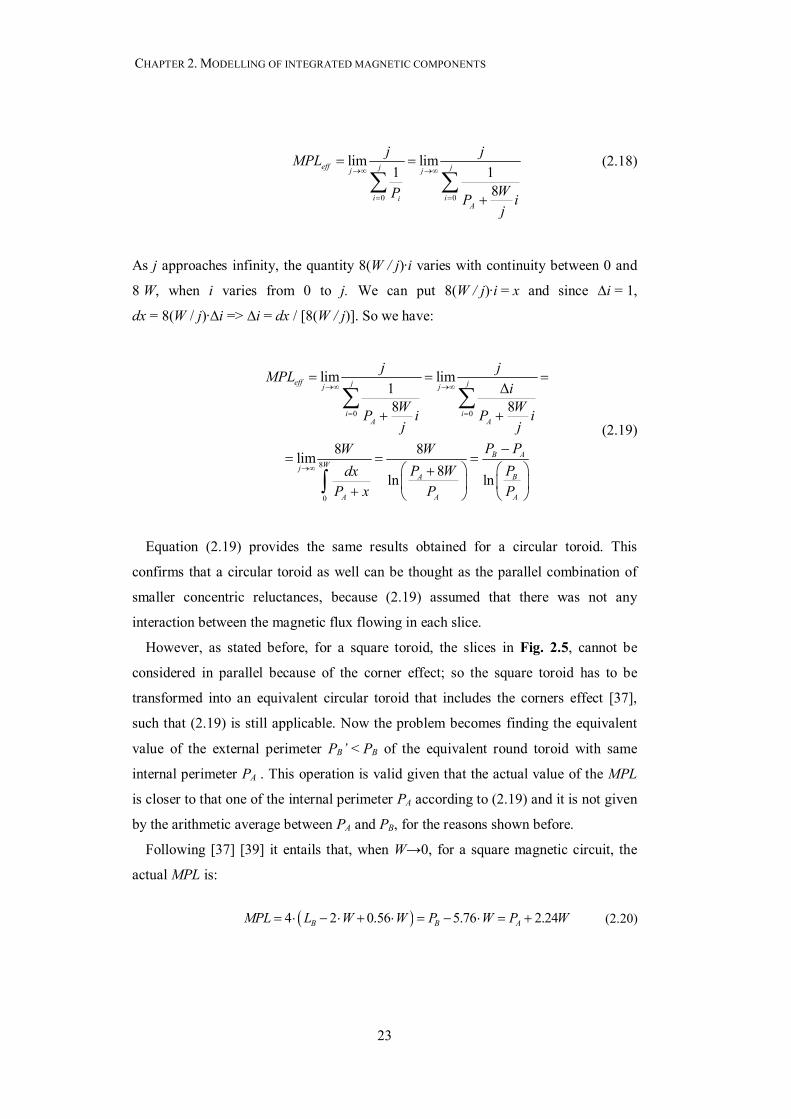
Figure 2.6 presents a comparison between the value of MPL obtained from (2.20)
(blue circles), from (2.22) (red crosses) and from FEM (Finite Element Method, green
triangles). As it can be seen, at very high ratios between external and internal sides,
the contribution of the non-uniformity of magnetic flux becomes as important as the
one due to the corner effect. However for practical cases (generally LB < 3LA) (2.20)
and (2.22) agree pretty well since the corner effect is dominant in general is
predominant.
It should be remarked that it makes sense to use the reluctance concept if the core
magnetic permeability is very high and if the turns are tightly wound around the core,
otherwise the Hopkinson’s law and the magnetic Kirchhoff’s laws [1] are not satisfied
because of flux imbalance due to the flux leaking outside the core, because it is not
CHAPTER 2. MODELLING OF INTEGRATED MAGNETIC COMPONENTS
25
entirely concentrated in the core and it has not a preferred path for flowing. The effect
of the finite value of the permeability can be considered through the introduction of
the coupling factor.
2.5 Losses
Magnetic components such as inductors as well as transformers are not ideal, since
they suffer from losses. There are several types of losses. First of all there are the
losses due to winding losses (DC and AC), and then there are the losses due to the
core like the hysteresis losses and eddy current losses (both AC).
2.5.1 Winding losses - Resistance
The first source of losses in an inductor/transformer is given by the Joule heating
of the conductor because of the finite value of the conductance. The electric
resistance of a coil is given by the well-known formula:
CoilCoil turn
Coil coil
lR NRA
(2.24)
Figure 2.6. Comparison between equations and FEM [36]. (© 2015, IEEE).

CHAPTER 2. MODELLING OF INTEGRATED MAGNETIC COMPONENTS
26
Equation (2.24) states that the higher number of turns, the higher the resistance. Rturn
is the resistance of a single turn, and N is the number of turns wrapped around the
core. Since the inductance value is proportional to the square number of the turns,
apparently it seems that the number N can be increased with no limit, in order to
increase also the (low-frequency) quality factor of the inductor QL= 2πf0L/RDC. We
will see later, through an example that this is not possible, because rather the number
of turns, what is really important is the linear turn density n=dN/dx.
Average losses (W) due to the resistance are given by:
2 2CoilR Coil DC effP R I I , (2.25)
if we assume that the current flowing into the inductor is given by the following
expression:
02 sin 2TOT DC effI I I f t (2.26)
2.5.2 Winding losses – skin effect
Another source of losses in the windings is given the so called skin-effect. The
skin effect is a phenomenon that occurs at a certain critical frequency fc, beyond
which the current starts to flow significantly at the borders of the conductor, instead
of flowing in a uniform way along the entire conductor cross section. In general the
bigger the cross section, the lower will be fc. Thus, increasing AC would produce
lower DC resistance, but at a certain frequency, the increased resistance because of
the skin effect would be much higher, thus losing all the benefits due to a bigger cross
section.
The conductor skin depth δW, defined as the depth below the surface of the
conductor at which the current density has fallen to 1/e (about 37%). Its mathematical
expression is given by [1]:
0
1W
op rf
(2.27)
fop is the frequency at which the inductor/transformer is working. Looking at (2.27) it
is clear that the higher the conductivity of the material constituting the coil, the lower
CHAPTER 2. MODELLING OF INTEGRATED MAGNETIC COMPONENTS
27
the skin depth. If δW is higher than the material thickness, then the skin effect is pretty
negligible. Furthermore (2.27) refers to a mono-dimensional skin effect, that is for
example, like the one occurring in a metal stripe in which the width W is much bigger
than the thickness tW. In this case the shorter dimension is the one subject to the skin
effect. A way instead to mathematically estimate the resistance of a flat conductor, in
which the W >> tW, subject to the skin depth is the Dowell equation [1] [25]:
425 1
145l W
ac dcW
N tR R
, (2.28)
in which Rdc is the DC resistance and Nl is the number of parallel layers.
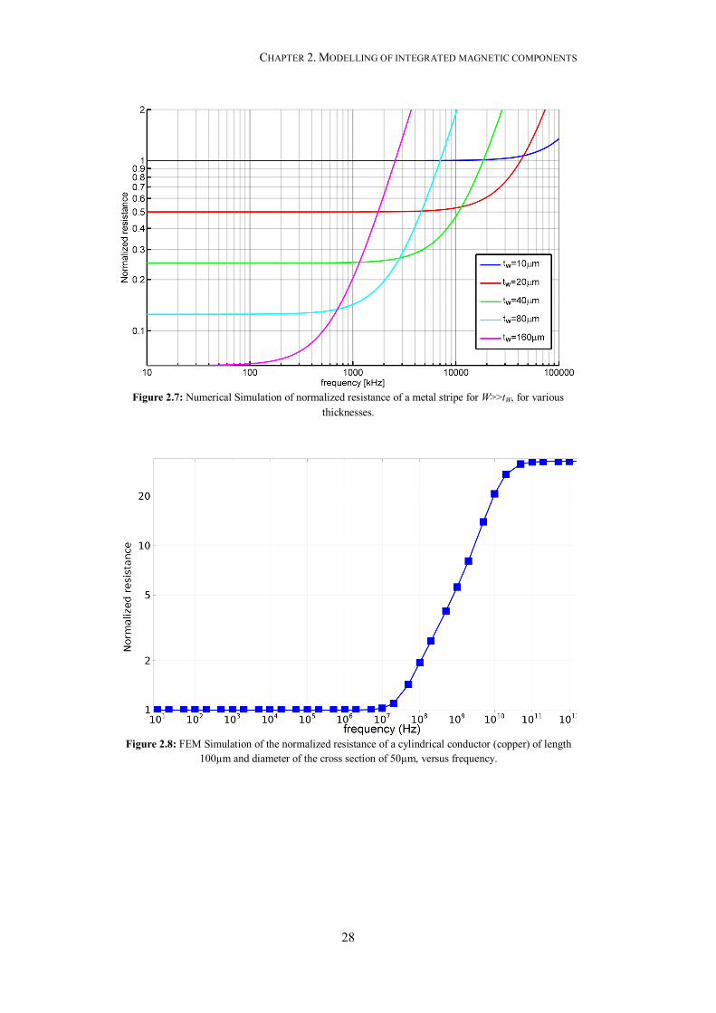
Figure 2.7 presents the numerical plots of (2.28) the normalized resistance for
various conductors with Nl = 1, for thicknesses doubling from 10μm to 160μm.
Thicker conductors, even if present a lower DC resistance, have a cross-over
frequency much lower compared to thinner conductors. Furthermore, beyond this
cross-over frequency, the AC resistance of thicker layers becomes higher than that of
thinner ones. The choice of the right conductor thickness becomes extremely
important in order to design properly magnetic components.
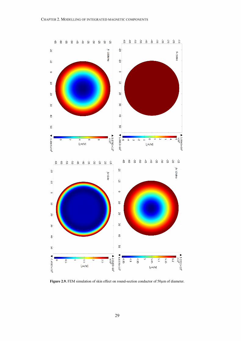
Figure 2.8 shows a picture of a FEM simulation of the normalized resistance of a
cylindrical (copper) conductor of length 100µm and diameter of the cross section
50µm. To cite an example, at 100MHz, the effective resistance has almost doubled
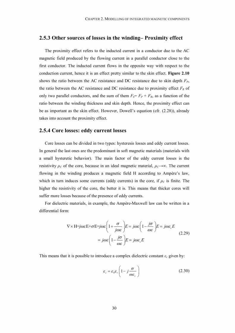
because of the skin effect. Figure 2.9 shows FEM simulation of the longitudinal
current density at four different frequencies 1MHz, 10MHz, 100MHz and a 1GHz. It
can be noted at 1GHz the current is flowing almost at the conductor border.
CHAPTER 2. MODELLING OF INTEGRATED MAGNETIC COMPONENTS
28
Figure 2.7: Numerical Simulation of normalized resistance of a metal stripe for W>>tW, for various thicknesses.
Figure 2.8: FEM Simulation of the normalized resistance of a cylindrical conductor (copper) of length 100µm and diameter of the cross section of 50µm, versus frequency.
CHAPTER 2. MODELLING OF INTEGRATED MAGNETIC COMPONENTS
29
Figure 2.9. FEM simulation of skin effect on round-section conductor of 50µm of diameter.
CHAPTER 2. MODELLING OF INTEGRATED MAGNETIC COMPONENTS
30
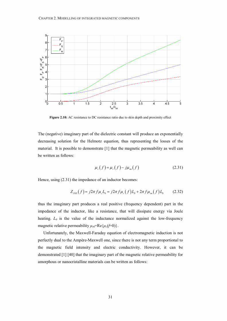
2.5.3 Other sources of losses in the winding– Proximity effect
The proximity effect refers to the inducted current in a conductor due to the AC
magnetic field produced by the flowing current in a parallel conductor close to the
first conductor. The inducted current flows in the opposite way with respect to the
conduction current, hence it is an effect pretty similar to the skin effect. Figure 2.10
shows the ratio between the AC resistance and DC resistance due to skin depth FP,
the ratio between the AC resistance and DC resistance due to proximity effect FR of
only two parallel conductors, and the sum of them FS= FP + FR, as a function of the
ratio between the winding thickness and skin depth. Hence, the proximity effect can
be as important as the skin effect. However, Dowell’s equation (cfr. (2.28)), already
takes into account the proximity effect.
2.5.4 Core losses: eddy current losses
Core losses can be divided in two types: hysteresis losses and eddy current losses.
In general the last ones are the predominant in soft magnetic materials (materials with
a small hysteretic behavior). The main factor of the eddy current losses is the
resistivity ρC of the core, because in an ideal magnetic material, ρC→∞. The current
flowing in the winding produces a magnetic field H according to Ampère’s law,
which in turn induces some currents (eddy currents) in the core, if ρC is finite. The
higher the resistivity of the core, the better it is. This means that thicker cores will
suffer more losses because of the presence of eddy currents. For dielectric materials, in example, the Ampère-Maxwell law can be written in a
differential form:
H= E+ E= 1 1
1
c
c
jj j E j E j Ej
jj E j E
(2.29)
This means that it is possible to introduce a complex dielectric constant εc given by:
0 1c rr
j
(2.30)
CHAPTER 2. MODELLING OF INTEGRATED MAGNETIC COMPONENTS
31
The (negative) imaginary part of the dielectric constant will produce an exponentially
decreasing solution for the Helmotz equation, thus representing the losses of the
material. It is possible to demonstrate [1] that the magnetic permeability as well can
be written as follows:
c r imf f j f (2.31)
Hence, using (2.31) the impedance of an inductor becomes:
0 0 02 2 2IND c r imZ f j f L j f f L f f L (2.32)
thus the imaginary part produces a real positive (frequency dependent) part in the
impedance of the inductor, like a resistance, that will dissipate energy via Joule
heating. L0 is the value of the inductance normalized against the low-frequency
magnetic relative permeability μr0=Reμc(f=0).
Unfortunately, the Maxwell-Faraday equation of electromagnetic induction is not
perfectly dual to the Ampère-Maxwell one, since there is not any term proportional to
the magnetic field intensity and electric conductivity. However, it can be
demonstrated [1] [40] that the imaginary part of the magnetic relative permeability for
amorphous or nanocristalline materials can be written as follows:
Figure 2.10: AC resistance to DC resistance ratio due to skin depth and proximity effect
CHAPTER 2. MODELLING OF INTEGRATED MAGNETIC COMPONENTS
32
0
sinh sin
cosh cos
C C
C CCim r
C c C
C C
t t
ft t t
. (2.33)
The dependence on the frequency is expressed by the fact that the core skin depth δC
is dependent on the frequency (cfr. 2.27). The real part can be modelled instead as
follows:
0
sinh sin
cosh cos
C C
C CCr r
C c C
C C
t t
ft t t
(2.34)
The imaginary part has a second order bandpass filter behavior whereas the real part
has a first order low pass filter with cutoff frequencies equal to [40]:
20
4T
C r
ft
, (2.35)
that is the frequency at which δC=tC/2.
As matter of fact, (2.34) can be approximated by [1]:
0
2
1
rr
T
fff
(2.36)
Figure 2.11 [40] shows the typical behavior of some nanocristalline or Co-based
amorphous materials as a function of the frequency, as well as some ferrites.
Once the imaginary part of the magnetic relative permeability is known, the
following step is to calculate the losses due to the skin depth in the core. For electric
circuits we already know that these can be estimated through the formula
2* *1 1 12 2 2electrS V I Z I I Z I . For magnetic circuits we can do pretty the same
thing, through (2.4) and (2.5), in fact we have that:
CHAPTER 2. MODELLING OF INTEGRATED MAGNETIC COMPONENTS
33
2*M M
1 12 2magn MS (2.37)
But if we analyze (2.37), we find that
22
2 21 12 2magn
N LS I L IL N
(2.38)
So (2.38) is the stored energy in the magnetic field. Hence to find the associated
power, in phasorial terms, we have that:
2M
12magnP j (2.39)
The only way to have a real value of the power, is that the reluctance must be
complex, that is to state that the magnetic permeability must be complex (or that must
have an imaginary part). Hence the power lost in Joule heating, is given by:
2
M
1Im
2magnP (2.40)
But the complex reluctance can be written as:
22 2
0 0 0
C r im C r imC
r im C r im C C C
l j l jlj A A A
(2.41)
Hence substituting the imaginary part of (2.41) in (2.40) we have:
22
0
1 B2
im Cdiss
C
VP
(2.42)
In (2.42) C C CV A l is an approximation of the volume of the core. The losses per unit
volume then are given by:
2 22 2
0 0
1 B B2
im imdiss
C C
fp
(2.43)
The value given in (2.43) is the same given in [40].
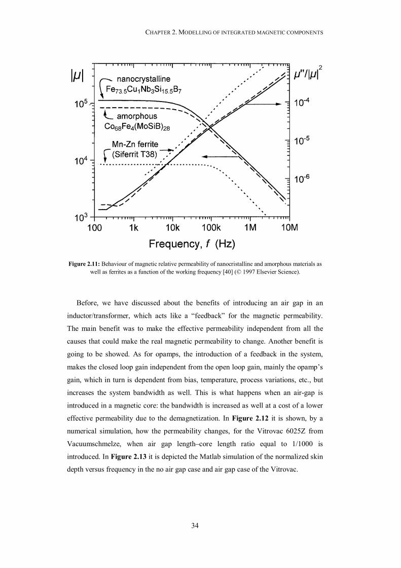
CHAPTER 2. MODELLING OF INTEGRATED MAGNETIC COMPONENTS
34
Before, we have discussed about the benefits of introducing an air gap in an
inductor/transformer, which acts like a “feedback” for the magnetic permeability.
The main benefit was to make the effective permeability independent from all the
causes that could make the real magnetic permeability to change. Another benefit is
going to be showed. As for opamps, the introduction of a feedback in the system,
makes the closed loop gain independent from the open loop gain, mainly the opamp’s
gain, which in turn is dependent from bias, temperature, process variations, etc., but
increases the system bandwidth as well. This is what happens when an air-gap is
introduced in a magnetic core: the bandwidth is increased as well at a cost of a lower
effective permeability due to the demagnetization. In Figure 2.12 it is shown, by a
numerical simulation, how the permeability changes, for the Vitrovac 6025Z from
Vacuumschmelze, when air gap length–core length ratio equal to 1/1000 is
introduced. In Figure 2.13 it is depicted the Matlab simulation of the normalized skin
depth versus frequency in the no air gap case and air gap case of the Vitrovac.
Figure 2.11: Behaviour of magnetic relative permeability of nanocristalline and amorphous materials as well as ferrites as a function of the working frequency [40] (© 1997 Elsevier Science).

CHAPTER 2. MODELLING OF INTEGRATED MAGNETIC COMPONENTS
35
Figure 2.12: Matlab plot of the effective permeability of Vitrovac 6025Z from Vacuumschmelze when air gap is introduced.
Figure 2.13: Matlab plot of the normalized skin depth with and without an air-gap in the Vitrovac.
CHAPTER 2. MODELLING OF INTEGRATED MAGNETIC COMPONENTS
36
Without air-gap the skin depth equals the material thickness tC (25µm) at about
6kHz [41] [42]. With an air gap this frequency is shifted at around 600kHz.
2.5.5 Lowering the core losses - lamination
We have seen thicker cores produce higher losses, however the value of the low
frequency inductance is also proportional to the core thickness. So a way to maintain
thick cores, but at the same time reducing the losses is through lamination.
Lamination (Figure 2.14) consists in dividing the core thickness in several m
electrically isolated slices whose thickness is tC’=tC/m In this case the core will have
the same global equivalent cross section but with skin depth properties of a much
thinner layer. This means L0 remains the same and that in (2.33) and (2.34), tC’ should
be used instead of tC. Furthemore, according to (2.35), fT is shifted at much higher
frequencies, since it is proportional to the square of the core slice thickness. Of
course, combining both air gap and lamination, can give benefits from both
techniques.
2.5.6 Core losses- Hysteresis
Hysteresis losses represent the power lost used to align the magnetic moments of
the core material. The area enclosed by the hysteresis curve represents the work
required to take the magnetic core through the whole hysteresis cycle [1]. Figure 2.15
shows the difference between the inbound power and the released power. At each
cycle some of the energy is kept and dissipated through heating because of the
hysteresis loop. An ideal soft magnetic material should have a hysteresis loop as
small as possible. However in a properly designed device, hysteresis losses are
generally negligible compared to winding losses and eddy currents in the core.
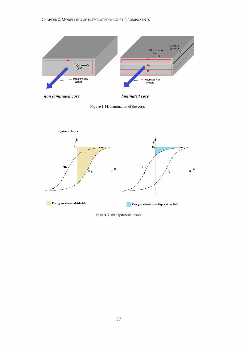
CHAPTER 2. MODELLING OF INTEGRATED MAGNETIC COMPONENTS
37
Figure 2.14: Lamination of the core.
Figure 2.15: Hysteresis losses
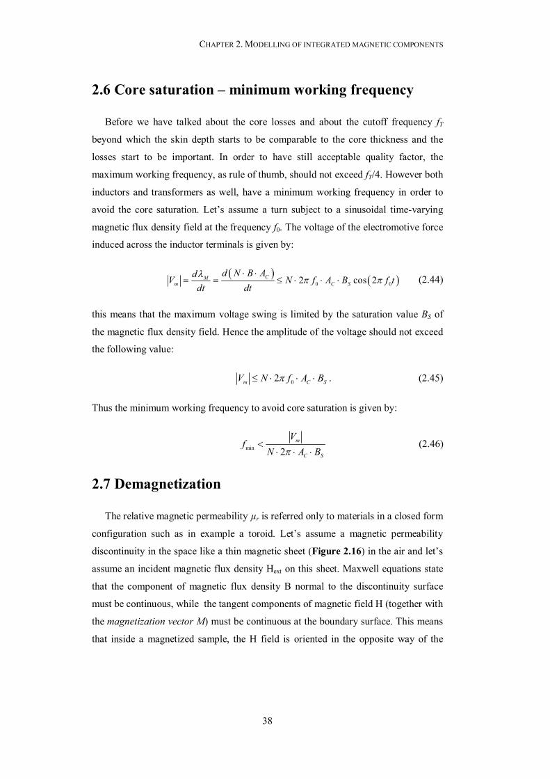
CHAPTER 2. MODELLING OF INTEGRATED MAGNETIC COMPONENTS
38
2.6 Core saturation – minimum working frequency
Before we have talked about the core losses and about the cutoff frequency fT
beyond which the skin depth starts to be comparable to the core thickness and the
losses start to be important. In order to have still acceptable quality factor, the
maximum working frequency, as rule of thumb, should not exceed fT/4. However both
inductors and transformers as well, have a minimum working frequency in order to
avoid the core saturation. Let’s assume a turn subject to a sinusoidal time-varying
magnetic flux density field at the frequency f0. The voltage of the electromotive force
induced across the inductor terminals is given by:
0 02 cos 2CMm C S
d N B AdV N f A B f tdt dt
(2.44)
this means that the maximum voltage swing is limited by the saturation value BS of
the magnetic flux density field. Hence the amplitude of the voltage should not exceed
the following value:
02m C SV N f A B . (2.45)
Thus the minimum working frequency to avoid core saturation is given by:
min 2m
C S
Vf
N A B
(2.46)
2.7 Demagnetization
The relative magnetic permeability µr is referred only to materials in a closed form
configuration such as in example a toroid. Let’s assume a magnetic permeability
discontinuity in the space like a thin magnetic sheet (Figure 2.16) in the air and let’s
assume an incident magnetic flux density Hext on this sheet. Maxwell equations state
that the component of magnetic flux density B normal to the discontinuity surface
must be continuous, while the tangent components of magnetic field H (together with
the magnetization vector M) must be continuous at the boundary surface. This means
that inside a magnetized sample, the H field is oriented in the opposite way of the
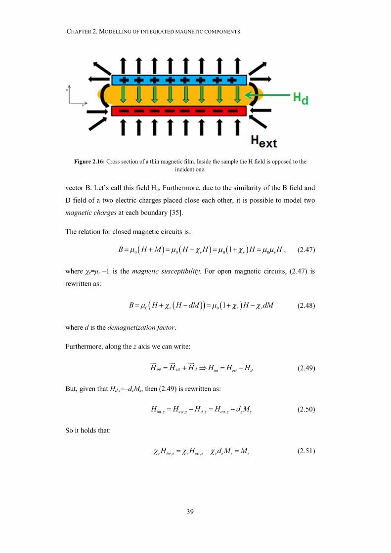
CHAPTER 2. MODELLING OF INTEGRATED MAGNETIC COMPONENTS
39
vector B. Let’s call this field Hd. Furthermore, due to the similarity of the B field and
D field of a two electric charges placed close each other, it is possible to model two
magnetic charges at each boundary [35].
The relation for closed magnetic circuits is:
0 0 0 01r r rB H M H H H H , (2.47)
where χr=μr –1 is the magnetic susceptibility. For open magnetic circuits, (2.47) is
rewritten as:
0 0 1r r rB H H dM H dM (2.48)
where d is the demagnetization factor.
Furthermore, along the z axis we can write:
int ext d int ext dH H H H H H
(2.49)
But, given that Hd,z=–dzMz, then (2.49) is rewritten as:
, , , ,int z ext z d z ext z z zH H H H d M (2.50)
So it holds that:
, ,r int z r ext z r z z zH H d M M (2.51)
Figure 2.16: Cross section of a thin magnetic film. Inside the sample the H field is opposed to the incident one.
CHAPTER 2. MODELLING OF INTEGRATED MAGNETIC COMPONENTS
40
So at the end, we can write:
,, 1
z reff z
ext z z r
MH d
(2.52)
Equation (2.52) shows that in a particular direction there’s an effective susceptibility,
due to the fact that the magnetic circuit is not a closed form configuration.
Furthermore (2.52) is similar to (2.7) for the effective relative permeability: in fact the
ratio between the gap length and core length is a measure of the demagnetization of
the material. In (2.52) if dzχr>>1 then χeff,z1/dz.
The strength of Hd ando so d, dipends on the geometry of the sample, i.e. for a thin
sheet with sides length Lx Ly>> Lz => dx dy << dz, so in the z direction there is not
any real amplification or concentration of the magnetic flux density.
Furthermore, for every magnetic material it holds that:
1x y zd d d (2.53)
If for simplicity we consider a magnetic sphere with μr >> 1, given that the sphere has
not any preferential direction, it must be that dx = dy = dz =1/3 . So if dzχr>>1 then χeff
in any direction is equal to 3.
It is worth to note that χeff ≠ μeff –1, but if χr >>1, then 11effeff
rd
, where d
refers to the particular direction of interest. Intuitively, the demagnetization field Hd,
acts like the internal electric field of a parallel plates capacitor. If the magnetic layer
is thicker, the distance between the positive and negative magnetic charges is higher
and so the strength of Hd is lower. This is why the long solenoidal inductor formula is
similar to the toroidal inductor. The longer the solenoid, the weaker the internal
demagnetization field it is.
2.8 Snell Magnetic law
A consequence of the demagnetization is the reflection law of the magnetic flux
density. Rays theory, states that an incident ray passing from a low refractive index
medium (or dielectric permeability) to a higher refractive index medium, is divided in
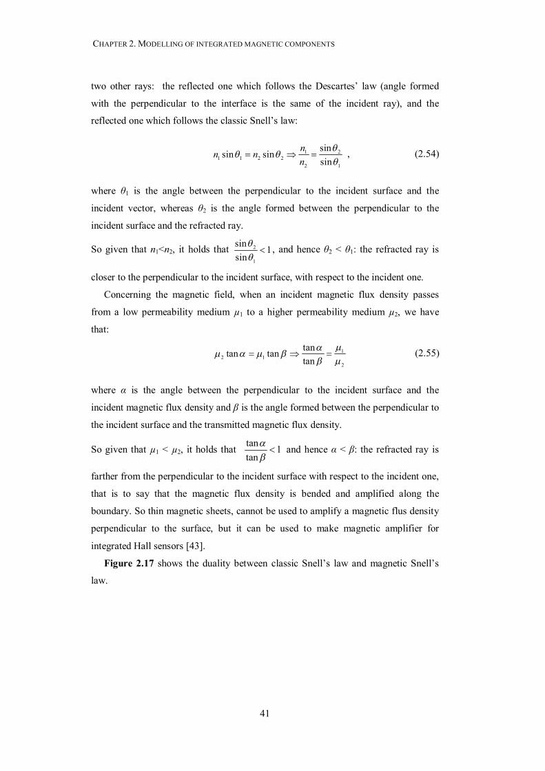
CHAPTER 2. MODELLING OF INTEGRATED MAGNETIC COMPONENTS
41
two other rays: the reflected one which follows the Descartes’ law (angle formed
with the perpendicular to the interface is the same of the incident ray), and the
reflected one which follows the classic Snell’s law:
1 21 1 2 2
2 1
sinsin sinsin
nn nn
, (2.54)
where θ1 is the angle between the perpendicular to the incident surface and the
incident vector, whereas θ2 is the angle formed between the perpendicular to the
incident surface and the refracted ray.
So given that n1<n2, it holds that 2
1
sin 1sin
, and hence θ2 < θ1: the refracted ray is
closer to the perpendicular to the incident surface, with respect to the incident one.
Concerning the magnetic field, when an incident magnetic flux density passes
from a low permeability medium µ1 to a higher permeability medium µ2, we have
that:
12 1
2
tantan tantan
(2.55)
where α is the angle between the perpendicular to the incident surface and the
incident magnetic flux density and β is the angle formed between the perpendicular to
the incident surface and the transmitted magnetic flux density.
So given that µ1 < µ2, it holds that tan 1tan
and hence α < β: the refracted ray is
farther from the perpendicular to the incident surface with respect to the incident one,
that is to say that the magnetic flux density is bended and amplified along the
boundary. So thin magnetic sheets, cannot be used to amplify a magnetic flus density
perpendicular to the surface, but it can be used to make magnetic amplifier for
integrated Hall sensors [43].
Figure 2.17 shows the duality between classic Snell’s law and magnetic Snell’s
law.
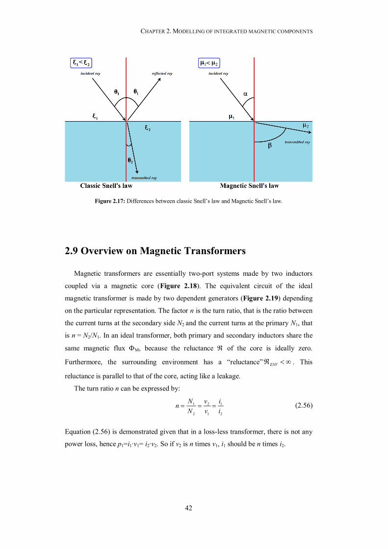
CHAPTER 2. MODELLING OF INTEGRATED MAGNETIC COMPONENTS
42
2.9 Overview on Magnetic Transformers
Magnetic transformers are essentially two-port systems made by two inductors
coupled via a magnetic core (Figure 2.18). The equivalent circuit of the ideal
magnetic transformer is made by two dependent generators (Figure 2.19) depending
on the particular representation. The factor n is the turn ratio, that is the ratio between
the current turns at the secondary side N2 and the current turns at the primary N1, that
is n = N2/N1. In an ideal transformer, both primary and secondary inductors share the
same magnetic flux M, because the reluctance of the core is ideally zero.
Furthermore, the surrounding environment has a “reluctance” ENV . This
reluctance is parallel to that of the core, acting like a leakage.
The turn ratio n can be expressed by:
1 2 1
2 1 2
N v inN v i
(2.56)
Equation (2.56) is demonstrated given that in a loss-less transformer, there is not any
power loss, hence p1=i1∙v1= i2∙v2. So if v2 is n times v1, i1 should be n times i2.
Figure 2.17: Differences between classic Snell’s law and Magnetic Snell’s law.
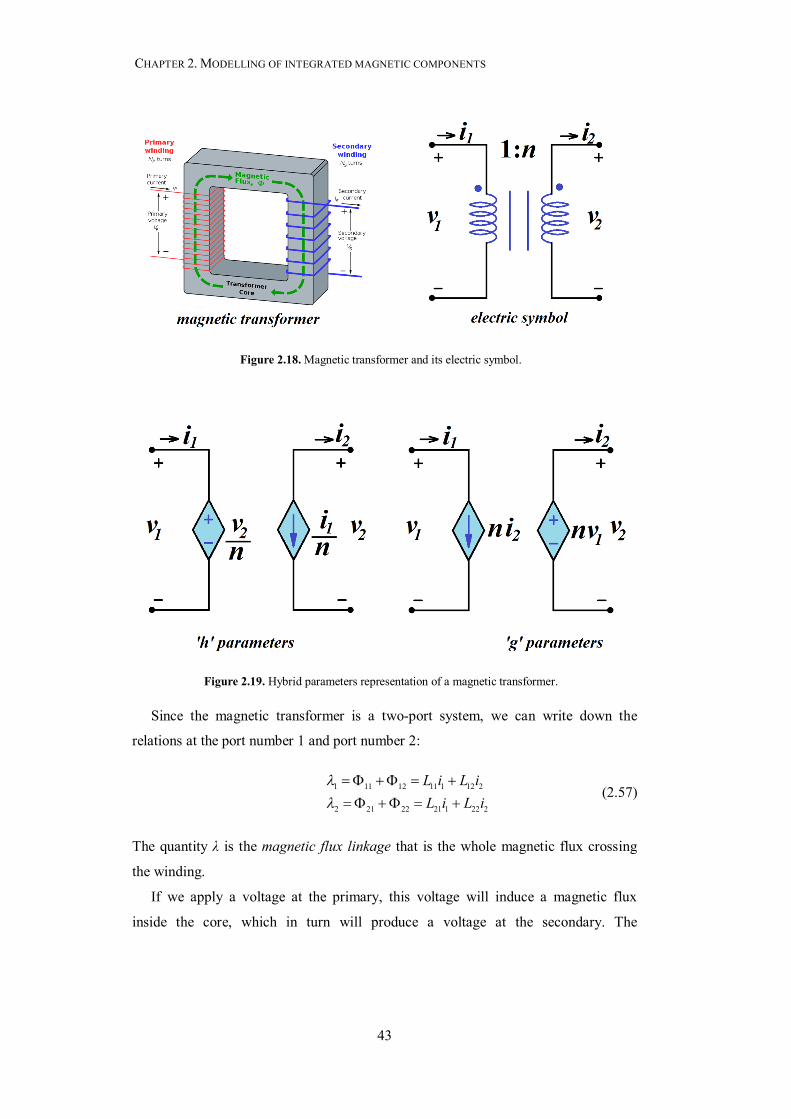
CHAPTER 2. MODELLING OF INTEGRATED MAGNETIC COMPONENTS
43
Since the magnetic transformer is a two-port system, we can write down the
relations at the port number 1 and port number 2:
1 11 12 11 1 12 2
2 21 22 21 1 22 2
L i L iL i L i
(2.57)
The quantity λ is the magnetic flux linkage that is the whole magnetic flux crossing
the winding.
If we apply a voltage at the primary, this voltage will induce a magnetic flux
inside the core, which in turn will produce a voltage at the secondary. The
Figure 2.18. Magnetic transformer and its electric symbol.
Figure 2.19. Hybrid parameters representation of a magnetic transformer.
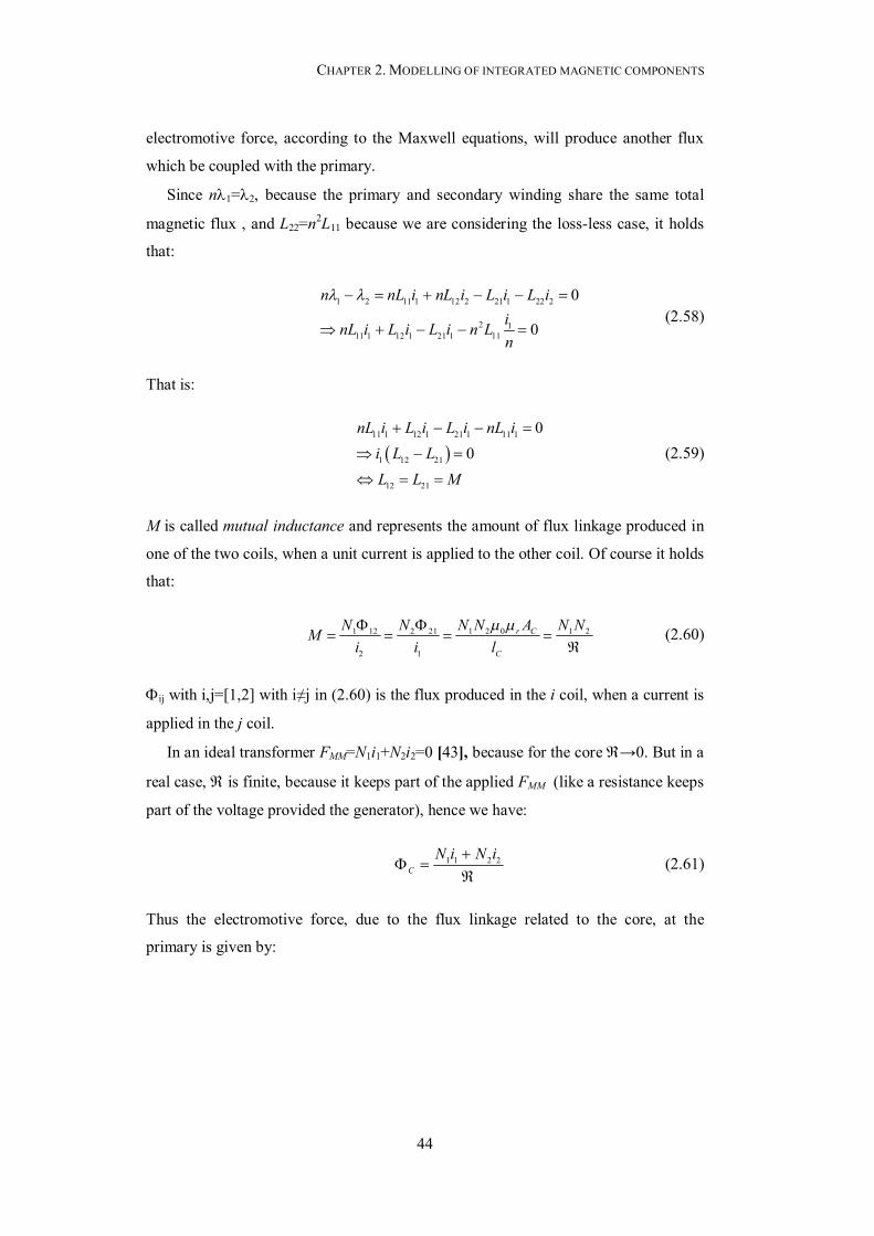
CHAPTER 2. MODELLING OF INTEGRATED MAGNETIC COMPONENTS
44
electromotive force, according to the Maxwell equations, will produce another flux
which be coupled with the primary.
Since n1=2, because the primary and secondary winding share the same total
magnetic flux , and L22=n2L11 because we are considering the loss-less case, it holds
that:
1 2 11 1 12 2 21 1 22 2
2 111 1 12 1 21 1 11
0
0
n nL i nL i L i L iinL i L i L i n Ln
(2.58)
That is:
11 1 12 1 21 1 11 1
1 12 21
12 21
00
nL i L i L i nL ii L LL L M
(2.59)
M is called mutual inductance and represents the amount of flux linkage produced in
one of the two coils, when a unit current is applied to the other coil. Of course it holds
that:
1 2 01 12 2 21 1 2
2 1
r C
C
N N AN N N NMi i l
(2.60)
ij with i,j=[1,2] with i≠j in (2.60) is the flux produced in the i coil, when a current is
applied in the j coil.
In an ideal transformer FMM=N1i1+N2i2=0 [43], because for the core →0. But in a
real case, is finite, because it keeps part of the applied FMM (like a resistance keeps
part of the voltage provided the generator), hence we have:
1 1 2 2C
N i N i
(2.61)
Thus the electromotive force, due to the flux linkage related to the core, at the
primary is given by:
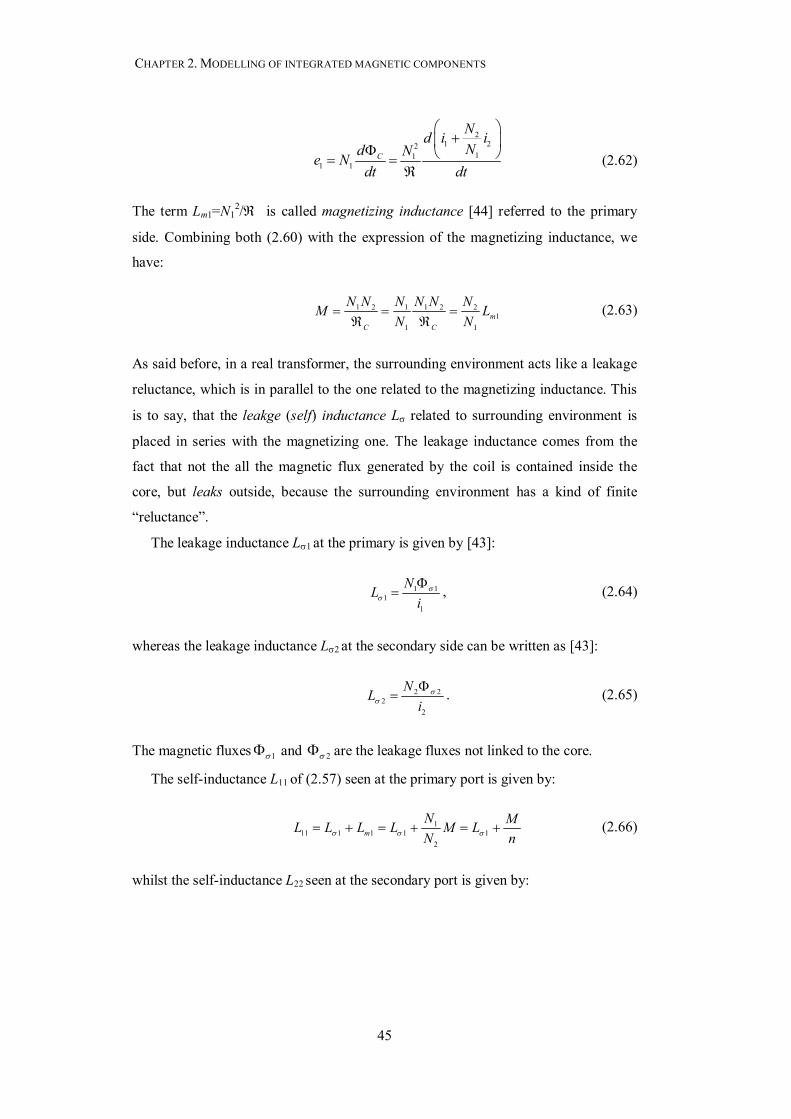
CHAPTER 2. MODELLING OF INTEGRATED MAGNETIC COMPONENTS
45
21 22
111 1
C
Nd i iNd Ne N
dt dt
(2.62)
The term Lm1=N12/ is called magnetizing inductance [44] referred to the primary
side. Combining both (2.60) with the expression of the magnetizing inductance, we
have:
1 2 1 1 2 21
1 1m
C C
N N N N N NM LN N
(2.63)
As said before, in a real transformer, the surrounding environment acts like a leakage
reluctance, which is in parallel to the one related to the magnetizing inductance. This
is to say, that the leakge (self) inductance L related to surrounding environment is
placed in series with the magnetizing one. The leakage inductance comes from the
fact that not the all the magnetic flux generated by the coil is contained inside the
core, but leaks outside, because the surrounding environment has a kind of finite
“reluctance”.
The leakage inductance L1 at the primary is given by [43]:
1 11
1
NLi
, (2.64)
whereas the leakage inductance L2 at the secondary side can be written as [43]:
2 22
2
NLi
. (2.65)
The magnetic fluxes 1 and 2 are the leakage fluxes not linked to the core.
The self-inductance L11 of (2.57) seen at the primary port is given by:
11 1 11 1
21 m
N ML L ML L LN n (2.66)
whilst the self-inductance L22 seen at the secondary port is given by:

CHAPTER 2. MODELLING OF INTEGRATED MAGNETIC COMPONENTS
46
2 2
2 222 2 1 2 2
1 1m
N N ML L L L nMN n
LN
(2.67)
The two leakage inductances are evaluated through the formulas:
1 1 11
2 2 22
1
1
L
L
k L
k L
(2.68)
In which k1 and k2 are called winding coupling factors of the primary and secondary
respectively. The parameters k1 and k2 represent the ratio between the flux linked to
the core and that linked to the whole coil. In general these two factors are not equal
because they depend on how the each winding is wrapped around the core. However
we can write:
1,2iii
Mk iL
(2.69)
The average coupling factor k of the magnetic transformer is defined as:
1 211 22
Mk k kL L
(2.70)
However for simplicity we can assume for both windings the same coupling factor k
given by (2.70).
In an ideal magnetic transformer the turn ratio n and the step-up ratio nsu have the
same value. In a real transformer the step-up ratio nsu is given by:
22
11su
Ln n k kL
(2.71)
Equation (2.71) comes from the fact, that the magnetizing inductance referred to
the primary and the primary leakage inductance make a voltage divider whose
transfer function is equal to k.
Figure 2.20 presents the electromagnetic model of a real magnetic transformer. It
is made up of an ideal magnetic transformer, plus the magnetizing inductance Lm1
referred to the primary and the two leakage inductances L1 and L2.
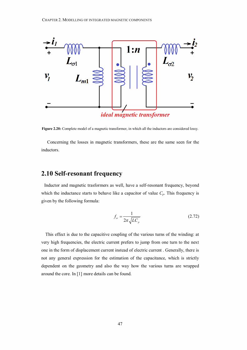
CHAPTER 2. MODELLING OF INTEGRATED MAGNETIC COMPONENTS
47
Concerning the losses in magnetic transformers, these are the same seen for the
inductors.
2.10 Self-resonant frequency
Inductor and magnetic trasformers as well, have a self-resonant frequency, beyond
which the inductance starts to behave like a capacitor of value Cp. This frequency is
given by the following formula:
12sr
p
fLC
(2.72)
This effect is due to the capacitive coupling of the various turns of the winding: at
very high frequencies, the electric current prefers to jump from one turn to the next
one in the form of displacement current instead of electric current . Generally, there is
not any general expression for the estimation of the capacitance, which is strictly
dependent on the geometry and also the way how the various turns are wrapped
around the core. In [1] more details can be found.
Figure 2.20: Complete model of a magnetic transformer, in which all the inductors are considered lossy.
CHAPTER 2. MODELLING OF INTEGRATED MAGNETIC COMPONENTS
48
2.11 Summary
This chapter has presented a review on the mathematical model of integrated
inductors, together with the losses which can occur in a magnetic device. Particular
emphasis has been given to the winding losses and core losses: as a matter of fact,
some particular techniques (like LIGA processes) can allow the deposition of very
thick metal layers. The working frequency of the device should always be kept in
mind, and exploiting the maximum thicknesses allowed by the process, cannot
necessarily be the best choice for the purpose, because of the skin effect in the
winding and eddy currents in the core. Furthermore a new relation giving a more
accurate estimation of the magnetic path length was presented. This allows evaluating
more correctly the reluctance and hence the inductance value of an integrated square
inductor, without the aid of time consuming FEM (Finite Element Methods)
simulations.
49
Chapter 3
Optimization of square integrated
planar core inductors
In the first chapter, various types of micro-inductors or transformers presented in
literature were reviewed. In each work, the main task was to maximize the
performance of the inductor given a certain footprint area. However, very few works
show devices which have a square footprint area, which is the most suitable shape for
on-chip integration. Furthermore, a lot of papers discuss about the possibility of using
such inductors for power conversion without any type of investigation concerning the
core saturation due to, for example, to the limited cross section of the core, as we
have discussed in Chapter 2. In addition, the choice of some important parameters,
like a certain number of current turns or width and thickness of the core is never
justified analytically, In general, specific methodologies for the optimization of the
shape of the magnetic device are still relatively missing in literature. This chapter
describes an optimization technique for square integrated inductors and investigates
the optimum design for on-chip square shaped toroidal inductors for a certain fixed
footprint area. Although the upper part of current turns is assumed to be made by
bond-wires, the presented analysis can be applied independently on the technique
used to close the current turns, e.g. with flip-chip packaging techniques, as long as the
linear turn density is kept constant and the same for all analyzed geometries.
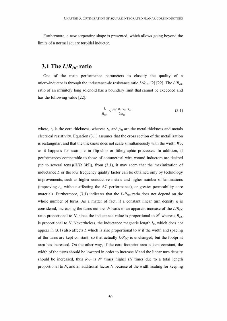
CHAPTER 3. OPTIMIZATION OF SQUARE INTEGRATED PLANAR CORE INDUCTORS
50
Furthermore, a new serpentine shape is presented, which allows going beyond the
limits of a normal square toroidal inductor.
3.1 The L/RDC ratio One of the main performance parameters to classify the quality of a
micro-inductor is through the inductance-dc resistance ratio L/RDC [2] [22]. The L/RDC
ratio of an infinitely long solenoid has a boundary limit that cannot be exceeded and
has the following value [22]:
0
2r C M
DC M
μ μ t tLR ρ
(3.1)
where, tC is the core thickness, whereas tM and ρM are the metal thickness and metals
electrical resistivity. Equation (3.1) assumes that the cross section of the metallization
is rectangular, and that the thickness does not scale simultaneously with the width WC,
as it happens for example in flip-chip or lithographic processes. In addition, if
performances comparable to those of commercial wire-wound inductors are desired
(up to several tens µH/Ω [45]), from (3.1), it may seem that the maximization of
inductance L or the low frequency quality factor can be obtained only by technology
improvements, such as higher conductive metals and higher number of laminations
(improving tC, without affecting the AC performance), or greater permeability core
materials. Furthermore, (3.1) indicates that the L/RDC ratio does not depend on the
whole number of turns. As a matter of fact, if a constant linear turn density n is
considered, increasing the turns number N leads to an apparent increase of the L/RDC
ratio proportional to N, since the inductance value is proportional to N2 whereas RDC
is proportional to N. Nevertheless, the inductance magnetic length lC, which does not
appear in (3.1) also affects L which is also proportional to N if the width and spacing
of the turns are kept constant; so that actually L/RDC is unchanged, but the footprint
area has increased. On the other way, if the core footprint area is kept constant, the
width of the turns should be lowered in order to increase N and the linear turn density
should be increased, thus RDC is N2 times higher (N times due to a total length
proportional to N, and an additional factor N because of the width scaling for keeping
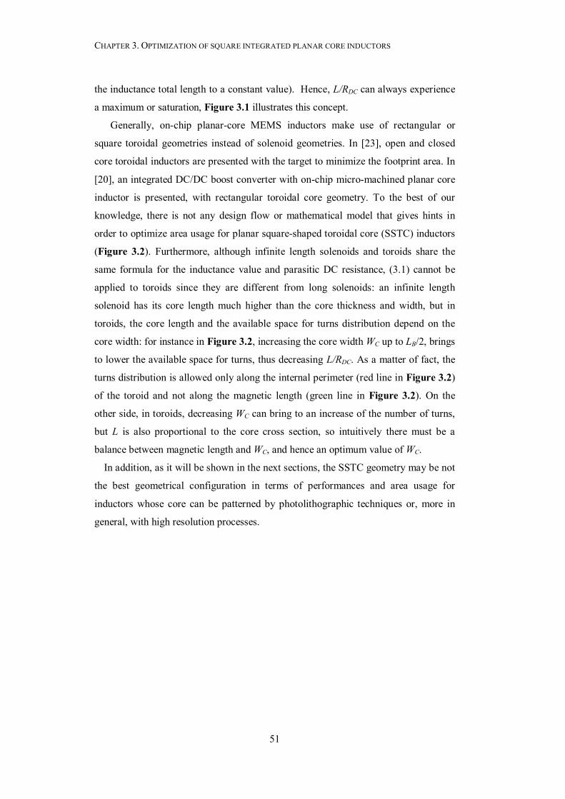
CHAPTER 3. OPTIMIZATION OF SQUARE INTEGRATED PLANAR CORE INDUCTORS
51
the inductance total length to a constant value). Hence, L/RDC can always experience
a maximum or saturation, Figure 3.1 illustrates this concept.
Generally, on-chip planar-core MEMS inductors make use of rectangular or
square toroidal geometries instead of solenoid geometries. In [23], open and closed
core toroidal inductors are presented with the target to minimize the footprint area. In
[20], an integrated DC/DC boost converter with on-chip micro-machined planar core
inductor is presented, with rectangular toroidal core geometry. To the best of our
knowledge, there is not any design flow or mathematical model that gives hints in
order to optimize area usage for planar square-shaped toroidal core (SSTC) inductors
(Figure 3.2). Furthermore, although infinite length solenoids and toroids share the
same formula for the inductance value and parasitic DC resistance, (3.1) cannot be
applied to toroids since they are different from long solenoids: an infinite length
solenoid has its core length much higher than the core thickness and width, but in
toroids, the core length and the available space for turns distribution depend on the
core width: for instance in Figure 3.2, increasing the core width WC up to LB/2, brings
to lower the available space for turns, thus decreasing L/RDC. As a matter of fact, the
turns distribution is allowed only along the internal perimeter (red line in Figure 3.2)
of the toroid and not along the magnetic length (green line in Figure 3.2). On the
other side, in toroids, decreasing WC can bring to an increase of the number of turns,
but L is also proportional to the core cross section, so intuitively there must be a
balance between magnetic length and WC, and hence an optimum value of WC.
In addition, as it will be shown in the next sections, the SSTC geometry may be not
the best geometrical configuration in terms of performances and area usage for
inductors whose core can be patterned by photolithographic techniques or, more in
general, with high resolution processes.
CHAPTER 3. OPTIMIZATION OF SQUARE INTEGRATED PLANAR CORE INDUCTORS
52
Figure 3.2. Top view of an on-chip bond-wire SSTC inductor with N = 3 turns; blue lines are the on-chip metal lines, and the yellow lines are the gold bonding wires. The green line is the mean magnetic path length, whereas the red line marks the internal perimeter [36]. (© 2015, IEEE)
Figure 3.1. Side view of a SSTC inductor. Left: reference. Centre: the number of turns is doubledwhereas the metal width is kept constant Right: the number of turns is doubled and the width is halved to keep the footprint area constant. All the current turns are in series. If the footprint area is maintained constant, there is an increase of the inductance, but it is not possible to increase the quality factor at a certain frequency, by acting only on the windings shape [36]. (© 2015, IEEE)

CHAPTER 3. OPTIMIZATION OF SQUARE INTEGRATED PLANAR CORE INDUCTORS
53
3.2 Square Shaped Toroidal Core (SSTC) Figure 3.2 shows a SSTC inductor. The external side of the core is LB and the core
footprint area is given by LB2; the core width is WC = (LB – LA) / 2 and thus the
internal side can be written as LA= LB ‒ 2∙WC.
The internal perimeter is PA=4∙LA, and the external perimeter is PB=4∙LB.
A constant turn density per unit length n0 (turns/m) is considered in order to
maximize the inductance value given that the footprint area is considered fixed.
In general, a way to find the magnetic path length is to simply make the arithmetic
average between the internal and external perimeters. Nevertheless this is not correct
since this operation assumes that the magnetic flux density is uniform along the core
cross section. In addition, in a square toroid, the effect of the folded structure is
summed up to magnetic non-uniformity and this is the predominant effect at small WC
as it has been shown in the previous chapter. In addition, in [37] [38] [39] there are
simple mathematical expressions which allow to take into account the folding effect
of the core and hence to calculate the corner reluctance. So, by following [37] [39] it
descends that, when WC→0, for a square magnetic circuit, the actual MPL is:
4 2 0.56
4 1.44 5.76B C C
B C B C
MPL L W W
L W P W
. (3.2)
Using (3.2), we can calculate the reluctance of the core:
0 r C
MPLμ μ A
(3.3)
where AC = tC WC is the core cross section. In case of air-gap core inductors, the
effective permeability should replace the relative magnetic permeability as seen in the
previous chapter (cfr. also [1]). Nevertheless, given that the presented method is
based on the optimization of the area usage, we can normalize against tC every
parameter that is dependent from the core thickness. Referring to Figure 3.2, if the
turns are tightly wrapped, the inductance is given by:
2 222
0 0 8A B Cn P n P WNL
(3.4)
CHAPTER 3. OPTIMIZATION OF SQUARE INTEGRATED PLANAR CORE INDUCTORS
54
where N = n0∙PA is the whole number of current turns, that is proportional to the
length of the internal perimeter PA, which in turn depends on WC, given that LB is
maintained constant. If N is low or μr is not adequately high, the way the turns are
wrapped around the core can affect the inductance value: as a consequence the
magnetic flux density leaks outside the core and starts to flow in the air surrounding
each turn, thus a leakage inductance Lσ appears in series to that given by (3.4) as seen
in the previous chapter. In this case finite elements method (FEM) simulators should
be used to make a more precise evaluation of the coupling factor between the turns
and in order to find a more accurate value of the inductance. Nevertheless, for
comparison purposes, the same coupling factor for all the geometries will be
considered.
From (3.3) and (3.4) it entails that L is directly proportional to AC and N2,but
inversely proportional to MPL. The upper limit of the inductance L, combining (3.2),
(3.3) and (3.4) can be simply written as follows:
22
0 04 2( 1.44 )
B C C C r
B C
n L W t W μ μL
L W
(3.5)
From (3.5) it entails that ∂L/∂WC = 0 gives the highest value of inductance for a
certain core footprint area LB2 of the device. ∂L/∂WC is a cubic function of WC, thus
the optimum width Wopt, solving the previous mathematical expression, considering
the solution 0 < WC < LB/2, is given by:
5 0.20824opt B BW L L (3.6)
Hence, by substituting (3.6) in (3.5), the maximum obtainable inductance for unit area
is given by:
2max02 0.509 C r
B
L n t μL
(3.7)
where both tC and LB are expressed in meters whilst Lmax in μH. Equation (3.5) has the
implicit constraint that n0·(LB‒2∙WC) is an integer number. As seen in the previous
chapter later, (3.5) to (3.7) apply only if WC < 0.4 LB, however from (3.6),
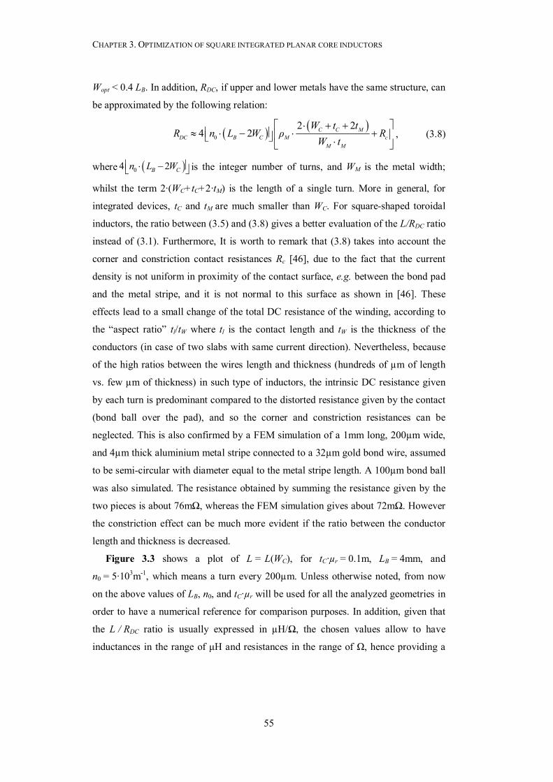
CHAPTER 3. OPTIMIZATION OF SQUARE INTEGRATED PLANAR CORE INDUCTORS
55
Wopt < 0.4 LB. In addition, RDC, if upper and lower metals have the same structure, can
be approximated by the following relation:
0
2 24 2 C C M
MBDC C cM M
WL
t tR n W ρ R
W t
, (3.8)
where 04 2B Cn WL is the integer number of turns, and WM is the metal width;
whilst the term 2∙(WC+tC+2∙tM) is the length of a single turn. More in general, for
integrated devices, tC and tM are much smaller than WC. For square-shaped toroidal
inductors, the ratio between (3.5) and (3.8) gives a better evaluation of the L/RDC ratio
instead of (3.1). Furthermore, It is worth to remark that (3.8) takes into account the
corner and constriction contact resistances Rc [46], due to the fact that the current
density is not uniform in proximity of the contact surface, e.g. between the bond pad
and the metal stripe, and it is not normal to this surface as shown in [46]. These
effects lead to a small change of the total DC resistance of the winding, according to
the “aspect ratio” tl/tW where tl is the contact length and tW is the thickness of the
conductors (in case of two slabs with same current direction). Nevertheless, because
of the high ratios between the wires length and thickness (hundreds of µm of length
vs. few µm of thickness) in such type of inductors, the intrinsic DC resistance given
by each turn is predominant compared to the distorted resistance given by the contact
(bond ball over the pad), and so the corner and constriction resistances can be
neglected. This is also confirmed by a FEM simulation of a 1mm long, 200µm wide,
and 4µm thick aluminium metal stripe connected to a 32µm gold bond wire, assumed
to be semi-circular with diameter equal to the metal stripe length. A 100µm bond ball
was also simulated. The resistance obtained by summing the resistance given by the
two pieces is about 76mΩ, whereas the FEM simulation gives about 72mΩ. However
the constriction effect can be much more evident if the ratio between the conductor
length and thickness is decreased.
Figure 3.3 shows a plot of L = L(WC), for tC∙µr = 0.1m, LB = 4mm, and
n0 = 5∙103m-1, which means a turn every 200µm. Unless otherwise noted, from now
on the above values of LB, n0, and tC∙µr will be used for all the analyzed geometries in
order to have a numerical reference for comparison purposes. In addition, given that
the L / RDC ratio is usually expressed in µH/Ω, the chosen values allow to have
inductances in the range of μH and resistances in the range of Ω, hence providing a
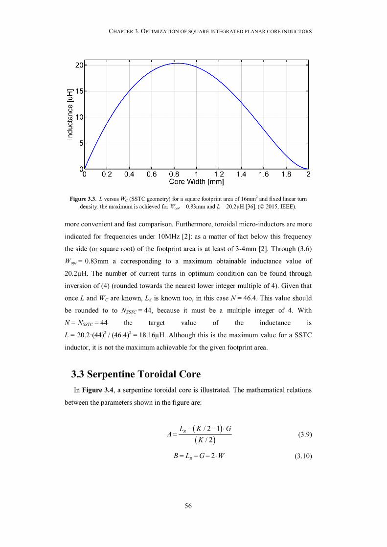
CHAPTER 3. OPTIMIZATION OF SQUARE INTEGRATED PLANAR CORE INDUCTORS
56
more convenient and fast comparison. Furthermore, toroidal micro-inductors are more
indicated for frequencies under 10MHz [2]: as a matter of fact below this frequency
the side (or square root) of the footprint area is at least of 3-4mm [2]. Through (3.6)
Wopt = 0.83mm a corresponding to a maximum obtainable inductance value of
20.2µH. The number of current turns in optimum condition can be found through
inversion of (4) (rounded towards the nearest lower integer multiple of 4). Given that
once L and WC are known, LA is known too, in this case N = 46.4. This value should
be rounded to to NSSTC = 44, because it must be a multiple integer of 4. With
N = NSSTC = 44 the target value of the inductance is
L = 20.2·(44)2 / (46.4)2 = 18.16µH. Although this is the maximum value for a SSTC
inductor, it is not the maximum achievable for the given footprint area.
3.3 Serpentine Toroidal Core In Figure 3.4, a serpentine toroidal core is illustrated. The mathematical relations
between the parameters shown in the figure are:
/ 2 1/ 2
BL K GA
K
(3.9)
2BB L G W (3.10)
Figure 3.3. L versus WC (SSTC geometry) for a square footprint area of 16mm2 and fixed linear turn density: the maximum is achieved for Wopt = 0.83mm and L = 20.2µH [36]. (© 2015, IEEE).
CHAPTER 3. OPTIMIZATION OF SQUARE INTEGRATED PLANAR CORE INDUCTORS
57
( ) / 2W A G (3.11)
So B is dependent on W, which is in turn dependent on A, that is a function of the
even integer number K, indicating the number of encountered parallel arms (along y
direction) producing the serpentine geometry, whereas the parameter G is the distance
(gap) between two consecutive parallel arms. To cite an example K = 2 corresponds
to a SSTC (B = 0 and A = LB). As usual, the inductance L is given by the following
equation:
2
2
004 / 2 1
ITP
ITn x dx n P K W
L
(3.12)
where n(x) is the linear density of the current turns along the inductor length and PIT
is the internal perimeter (function of A, B and W). Referring to Figure 3.4, the
function n(x) assumes the value n0 in light grey areas, and 0 elsewhere. In our case we
Figure 3.4. Top view of the layout of a serpentine toroidal core: the green line represents the external perimeter, while the red line marks the internal perimeter. The footprint area is assumed to be square. The light grey part indicates the distribution of current turns. Blue squares are the bond pads, and yellow lines the gold bonding wires. The pads can be in a gig-gag configuration to allow a bigger pad pitch [36]. (© 2015, IEEE).
CHAPTER 3. OPTIMIZATION OF SQUARE INTEGRATED PLANAR CORE INDUCTORS
58
have considered n0 = 5∙103m-1, that is a turn every 200µm as stated before.
In order to find the magnetic path length to put in the reluctance expression in
(3.12), the simplified relations given in [37] can be used, since the serpentine presents
more or less the two limit cases presented in [37]. Looking at Figure 3.4, we can
write down the MPL taking into account the corner reluctances:
2 3 2
( 1) 2 ( 1) 0.47 2 0.56BMPL K B W W
K G K W WL
(3.13)
In (3.13) the fourth and fifth terms of the sum represent the augmented lengths due to
the corners effect with respect to the internal perimeter [37].
Figure 3.5 shows the plot of the obtained inductance L versus the core width W.
The maximum obtained inductance is about 26.6µH, with W = 0.325mm. The number
of current turns in optimum condition is NSER = 142, in this case the subscript SER
refers to Serpentine. The gap G was fixed to 200μm (hence G = 1/20 of LB), that is a
value that allows sufficient space to put two bond pads in zig-zag configuration. With
the serpentine core, an increase of more than 35% of the maximum obtainable
inductance value has been achieved, if compared to the SSTC inductor. In addition,
there is a further degree of freedom, given that the parameter G has been fixed, but by
changing the value of G, the value of the Wopt changes as well, and it can be
demonstrated that lower values of the ratio G/LB can give higher values of Lmax for
serpentine toroidal cores. Nevertheless, the boundary value of G is constrained by the
particular technology used to pattern the core or the metal stripes, in addition the
value of G must be sufficiently high in order to allow the turns closure.
3.4 Comparison of the two geometries In this chapter, a comparison between the two geometries will be made,
considering the maximum achievable inductance value for both (in optimum
condition). In addition the comparison is made considering the same coupling factor
between the coils and the magnetic core for both geometries, however in the
serpentine configuration, the leakage flux between two parallel cores should be better
evaluated in order to better assess the confinement of the field [47].
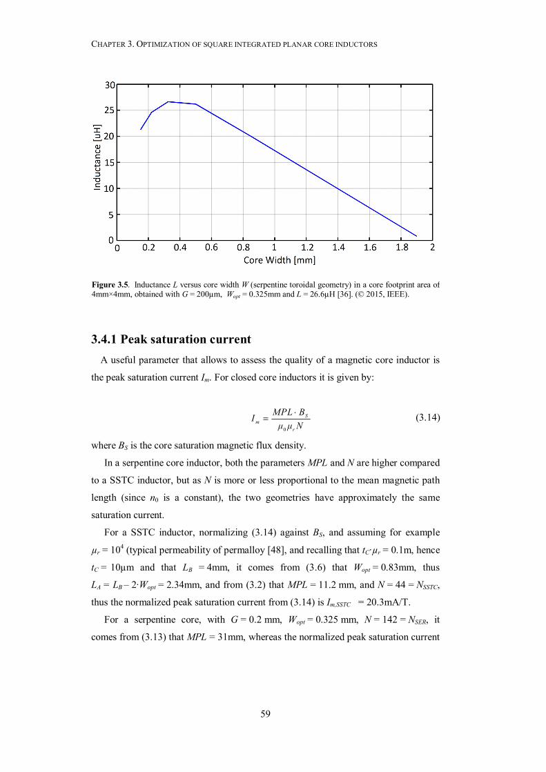
CHAPTER 3. OPTIMIZATION OF SQUARE INTEGRATED PLANAR CORE INDUCTORS
59
3.4.1 Peak saturation current A useful parameter that allows to assess the quality of a magnetic core inductor is
the peak saturation current Im. For closed core inductors it is given by:
0
Sm
r
MPL BIμ μ N
(3.14)
where BS is the core saturation magnetic flux density.
In a serpentine core inductor, both the parameters MPL and N are higher compared
to a SSTC inductor, but as N is more or less proportional to the mean magnetic path
length (since n0 is a constant), the two geometries have approximately the same
saturation current.
For a SSTC inductor, normalizing (3.14) against BS, and assuming for example
µr = 104 (typical permeability of permalloy [48], and recalling that tC∙µr = 0.1m, hence
tC = 10µm and that LB = 4mm, it comes from (3.6) that Wopt = 0.83mm, thus
LA = LB ‒ 2∙Wopt = 2.34mm, and from (3.2) that MPL = 11.2 mm, and N = 44 = NSSTC,
thus the normalized peak saturation current from (3.14) is Im,SSTC = 20.3mA/T.
For a serpentine core, with G = 0.2 mm, Wopt = 0.325 mm, N = 142 = NSER, it
comes from (3.13) that MPL = 31mm, whereas the normalized peak saturation current
Figure 3.5. Inductance L versus core width W (serpentine toroidal geometry) in a core footprint area of 4mm×4mm, obtained with G = 200µm, Wopt = 0.325mm and L = 26.6µH [36]. (© 2015, IEEE).
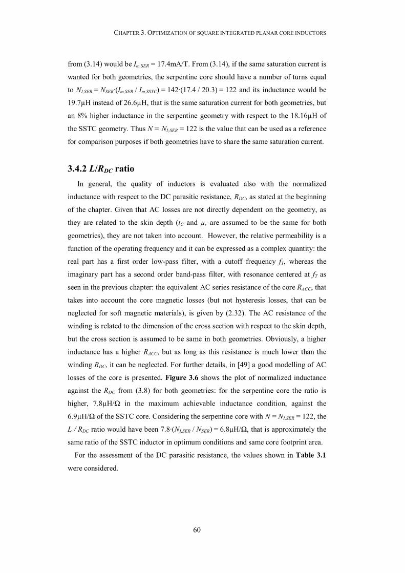
CHAPTER 3. OPTIMIZATION OF SQUARE INTEGRATED PLANAR CORE INDUCTORS
60
from (3.14) would be Im,SER = 17.4mA/T. From (3.14), if the same saturation current is
wanted for both geometries, the serpentine core should have a number of turns equal
to NI,SER = NSER∙(Im,SER / Im,SSTC) = 142∙(17.4 / 20.3) = 122 and its inductance would be
19.7µH instead of 26.6µH, that is the same saturation current for both geometries, but
an 8% higher inductance in the serpentine geometry with respect to the 18.16µH of
the SSTC geometry. Thus N = NI;SER = 122 is the value that can be used as a reference
for comparison purposes if both geometries have to share the same saturation current.
3.4.2 L/RDC ratio In general, the quality of inductors is evaluated also with the normalized
inductance with respect to the DC parasitic resistance, RDC, as stated at the beginning
of the chapter. Given that AC losses are not directly dependent on the geometry, as
they are related to the skin depth (tC and µr are assumed to be the same for both
geometries), they are not taken into account. However, the relative permeability is a
function of the operating frequency and it can be expressed as a complex quantity: the
real part has a first order low-pass filter, with a cutoff frequency fT, whereas the
imaginary part has a second order band-pass filter, with resonance centered at fT as
seen in the previous chapter: the equivalent AC series resistance of the core RACC, that
takes into account the core magnetic losses (but not hysteresis losses, that can be
neglected for soft magnetic materials), is given by (2.32). The AC resistance of the
winding is related to the dimension of the cross section with respect to the skin depth,
but the cross section is assumed to be same in both geometries. Obviously, a higher
inductance has a higher RACC, but as long as this resistance is much lower than the
winding RDC, it can be neglected. For further details, in [49] a good modelling of AC
losses of the core is presented. Figure 3.6 shows the plot of normalized inductance
against the RDC from (3.8) for both geometries: for the serpentine core the ratio is
higher, 7.8µH/Ω in the maximum achievable inductance condition, against the
6.9µH/Ω of the SSTC core. Considering the serpentine core with N = NI,SER = 122, the
L / RDC ratio would have been 7.8∙(NI,SER / NSER) = 6.8µH/Ω, that is approximately the
same ratio of the SSTC inductor in optimum conditions and same core footprint area.
For the assessment of the DC parasitic resistance, the values shown in Table 3.1
were considered.
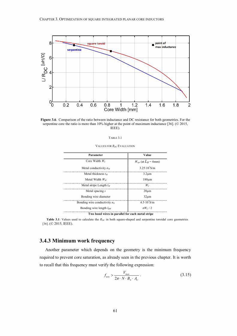
CHAPTER 3. OPTIMIZATION OF SQUARE INTEGRATED PLANAR CORE INDUCTORS
61
3.4.3 Minimum work frequency Another parameter which depends on the geometry is the minimum frequency
required to prevent core saturation, as already seen in the previous chapter. It is worth
to recall that this frequency must verify the following expression:
2
maxmin
S C
Vfπ N B A
. (3.15)
Figure 3.6. Comparison of the ratio between inductance and DC resistance for both geometries. For the serpentine core the ratio is more than 10% higher at the point of maximum inductance [36]. (© 2015,
IEEE).
TABLE 3.1
VALUES FOR RDC EVALUATION
Parameter Value
Core Width WC Wopt (at LB = 4mm)
Metal conductivity σM 3.25∙107S/m
Metal thickness tM 3.2µm
Metal Width WM 180µm
Metal stripe Length lM WC
Metal spacing s 20µm
Bonding wire diameter 32µm
Bonding wire conductivity σG 4.5∙107S/m
Bonding wire length lBW πWC / 2
Two bond wires in parallel for each metal stripe
Table 3.1: Values used to calculate the RDC in both square-shaped and serpentine toroidal core geometries [36]. (© 2015, IEEE).
CHAPTER 3. OPTIMIZATION OF SQUARE INTEGRATED PLANAR CORE INDUCTORS
62
The fmin is an important parameter for thick or non-laminated cores with very high
permeability, given that as the amplitude of the induced voltage increases, this
frequency increases too.
Besides, we recall also the cutoff frequency of the real part of the permeability,
determined by the skin effect, is given by [40]:
2
0
4 cT
r C
ρfπμ μ t
(3.16)
where ρc is the core resistivity. At this frequency an inductor experiences poor quality
factors, because at fT the imaginary part is in the same order of magnitude of the real
part. The maximum usable frequency corresponds as rule of thumb, approximately to
fT / 4, since this is the frequency where the skin depth equals the material thickness. In
(3.16) the permeability µr can be replaced by the effective permeability for magnetic
cores with air-gaps.
To cite an example, considering a very high permeability material such the
Vitrovac 6025 from Vacuumschmelze used in [30], we have µr ≈ 105, tc = 25µm,
ρc ≈ 140µΩ∙cm. Hence, from (3.16) we have that fT ≈ 20kHz, so the maximum usable
frequency is approximately 5-6kHz, as stated in [30] and it follows that fmin << fH,
otherwise the inductor is not usable for any application.
At 1V of amplitude, using Vitrovac 6025, whose saturation is BS ≈ 0.5T, and
assuming NSER = 142 (serpentine inductor with footprint area LB2 = 4 mm × 4 mm),
(3.16) gives fmin,Vitrovac ≈ 276kHz, that is about fifty times greater than fH. In this case
laminations or air-gaps should be used in order to increase the maximum frequency,
or the maximum amplitude of the induced voltage across the inductor terminals
should be decreased in order to decrease fmin, thus limiting the field of application of
the device.
Furthermore, if the inductor voltage is not sinusoidal, such as a square wave
instead, as it is the case in power buck/boost switching DC/DC converters, the factor
2π in (3.16) can be substituted by 4 if the duty cycle is 50% [1]. In a buck or boost
converter, for example, the maximum applicable voltage is related to the amplitude of
input and output voltage. Hence, for fmin, what is extremely important is the N∙AC
product.
Now the two geometries will be compared considering the minimum frequency.
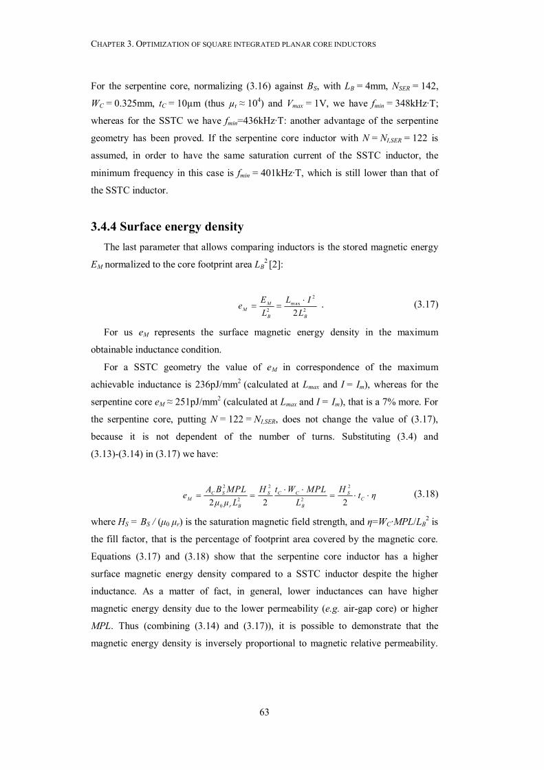
CHAPTER 3. OPTIMIZATION OF SQUARE INTEGRATED PLANAR CORE INDUCTORS
63
For the serpentine core, normalizing (3.16) against BS, with LB = 4mm, NSER = 142,
WC = 0.325mm, tC = 10µm (thus µr ≈ 104) and Vmax = 1V, we have fmin = 348kHz∙T;
whereas for the SSTC we have fmin=436kHz∙T: another advantage of the serpentine
geometry has been proved. If the serpentine core inductor with N = NI,SER = 122 is
assumed, in order to have the same saturation current of the SSTC inductor, the
minimum frequency in this case is fmin = 401kHz∙T, which is still lower than that of
the SSTC inductor.
3.4.4 Surface energy density The last parameter that allows comparing inductors is the stored magnetic energy
EM normalized to the core footprint area LB2 [2]:
2
max2 22M
MB B
L IEeL L
. (3.17)
For us eM represents the surface magnetic energy density in the maximum
obtainable inductance condition.
For a SSTC geometry the value of eM in correspondence of the maximum
achievable inductance is 236pJ/mm2 (calculated at Lmax and I = Im), whereas for the
serpentine core eM ≈ 251pJ/mm2 (calculated at Lmax and I = Im), that is a 7% more. For
the serpentine core, putting N = 122 = NI,SER, does not change the value of (3.17),
because it is not dependent of the number of turns. Substituting (3.4) and
(3.13)-(3.14) in (3.17) we have:
2 2 2
2 202 2 2
C S S C C SM C
r B B
A B MPL H t W MPL He t ημ μ L L
(3.18)
where HS = BS / (μ0 μr) is the saturation magnetic field strength, and η=WC·MPL/LB2 is
the fill factor, that is the percentage of footprint area covered by the magnetic core.
Equations (3.17) and (3.18) show that the serpentine core inductor has a higher
surface magnetic energy density compared to a SSTC inductor despite the higher
inductance. As a matter of fact, in general, lower inductances can have higher
magnetic energy density due to the lower permeability (e.g. air-gap core) or higher
MPL. Thus (combining (3.14) and (3.17)), it is possible to demonstrate that the
magnetic energy density is inversely proportional to magnetic relative permeability.

CHAPTER 3. OPTIMIZATION OF SQUARE INTEGRATED PLANAR CORE INDUCTORS
64
The serpentine core has the main benefit of a more efficient use of the core footprint
area, because since the core has a lower width, the magnetic flux density is “forced”
to be more uniform along the entire cross section. On the contrary, in classical
square-shaped toroids, the magnetic flux density is concentrated near the internal
perimeter, whereas the external boundary of the core gives less contribution for the
flowing of the magnetic flux density, as seen in the previous chapter. Table 3.2
summarizes all the performances of both geometries.
As stated before, in [22] the parameter L / RDC is used to compare the
performances of the presented inductor with respect to prior works. By assuming the
following values, core footprint area LB2= 5.6mm × 5.6mm (as in [22]), core width
WC ≈ 2.05mm, core thickness tC ≈ 16μm, metal conductivity σM = 5.8∙107S/m, metal
thickness tM =20µm, metal width WM ≈450µm, metal stripe length lM = WC, metal
spacing s ≈ 20µm, number of turns N = 12, relative permeability µr = 900, then the
total inductance of a SSTC inductor, using (3.3) and (3.4) is about 503nH, whereas
the inductor DC series resistance, calculated from (3.8) is approximately 95mΩ, that
are approximately the values given in [22]. Using (3.6), (3.7) and (3.8) it is possible
to find that Wopt ≈ 1.165mm and Lmax ≈ 1.05µH, whereas RDC ≈ 144mΩ, and the total
number of turns is NSSTC = 28. We have an increase of +110% of the inductance
despite an increase of +50% of the RDC. Thus the inductance can be increased,
TABLE 3.2 COMPARISON OF GEOMETRIES FOR LB = 4mm, G = 0.2mm, BS = 1T, µr = 104 AND tC = 10µm
Parameter Geometry
SSTC Serpentine
LMAX 18.16µH 26.6µH 19.7µH
Im 20.3mA 17.4mA 20.3mA
fmin @ 1 V 436kHz 34 kHz 401kHz
LMAX / RDC 6.9µH/Ω 7.8µH/Ω 6.8µH/Ω
eM 236pJ/mm2 251pJ/mm2 251pJ/mm2
Wc 0.83mm 0.32 mm 0.325mm
N 48 142 122
Table 3.2. Comparison of two geometries. Despite a loss in the saturation current, the global performances of the serpentine inductor are better than the inductor based on a square-shaped toroidal core. The enhancement of maximum inductance value is about 35% [36]. (© 2015, IEEE).
CHAPTER 3. OPTIMIZATION OF SQUARE INTEGRATED PLANAR CORE INDUCTORS
65
showing also an increased L / RDC ratio even without making any modifications to the
original SSTC geometry.
Figure 3.7 presents the plots of inductance, DC resistance and L / RDC with the
serpentine core design applied to a same core footprint area LB2= 5.6mm × 5.6mm and
gap G = 0.2µm, with all other parameters being equal to the last SSTC case.
As shown in Figure 3.7, the maximum inductance obtained at Wopt = 0.525mm, is
L = 1.46µH, RDC ≈ 144mΩ, and L / RDC ≈ 10µH/Ω (at LMAX) against the 5.25µH/Ω
(0.5µH / 95mΩ) obtained in [22], thus an increase of more than 80% of the ratio
(+45% increase in the inductance value with respect to the SSTC optimum condition).
Finally, the total number of turns is NSER =81. From (3.17), it is possible to note that
the energy capability of the inductor increases, due to a more efficient use of the
footprint area.
Furthermore, it is also worth making an addition consideration about the
comparison between the two geometries: the serpentine shape can be the best
geometrical configuration for core materials showing uniaxial anisotropy, given that
in this case the magnetic flux density should be perpendicular to the hard-axis (or
parallel to easy axis), for high inductance values, or perpendicular to the easy axis
Figure 3.7 Values of estimated inductance, DC resistance and L / RDC ratio for the inductor of [10] with a serpentine core geometry design [36]. (© 2015, IEEE).
CHAPTER 3. OPTIMIZATION OF SQUARE INTEGRATED PLANAR CORE INDUCTORS
66
(parallel to hard axis) to limit the core losses (as it was done in [41]), thus the
presented serpentine geometry allows a square footprint area (which is the shape most
suitable for on-chip integration), whilst the turns are mostly located along the
direction of preference; while in anisotropic SSTC, the turns should be located in both
axis.
3.5 Summary This chapter has presented a way to maximize and optimize the inductance value
once the footprint area has been fixed. The optimization of the square inductor
originated from simple considerations on the magnetic flux density behavior inside a
closed magnetic core. Furthermore, a new example of geometry, the serpentine core,
was introduced: spreading the core all over the surface, with a narrower width, allows
to have a more uniform magnetic flux density inside, hence there’s less “waste” of
used area, since every portion of the core contributes in the same way for the global
reluctance value, compared to the classic square shape where the external borders
give less contribution to the flowing of the internal magnetic field. The serpentine
geometry can be used in processes where high resolution techniques are available.

67
Chapter 4
Piezoelectric materials and
applications
In the previous chapters we have analysed the magnetic materials, properties and
applications mostly focusing on the perspective of integration for ultra-low power
purposes. In addition to magnetic materials, same functions can be achieved through
the help of piezoelectric materials, which in perspective can be highly interesting
since a lot of piezoelectric materials can be processed via standard IC techniques. In
addition, piezoelectric materials have quality factors (Q) much higher than magnetic
materials: this means that the piezoelectric transduction is less lossy compared to the
electromagnetic transduction. Thus piezoelectric materials are more suitable in the
field of application of energy harvesting as well as ultra-low power or autonomous
systems. However, as previously done for magnetic materials, an overview on the
piezoelectric effect, materials and applications is needed in order to better understand
and predict the behaviour of systems in which they are used.
CHAPTER 4. PIEZOELECTRIC MATERIALS AND APPLICATIONS
68
4.1 Properties of piezoelectric materials The piezoelectric effect is a physical property existing in many materials in nature.
The word is composed by two parts; piezo, which comes from the Greek word for
pressure, and electric from electricity. Thus the name suggests that a piezoelectric
material can provide electric charge if subject to a mechanical pressure. This is
known as the direct piezoelectric effect. On the other side, if a voltage is applied to
the same material a change in the mechanical dimensions of the sample can be
obtained. This is known as the indirect piezoelectric effect [50].
Several ceramic materials have been described as presenting a piezoelectric effect.
Among these we can find lead-zirconate-titanate (PZT), lead-titanate (PbTiO2),
lead-zirconate (PbZrO3), barium-titanate (BaTiO3). Nevertheless, these materials are
not really piezoelectric but rather present a polarized electrostrictive effect (a
quadratic dependence of the strain from the electric field [51]). Other materials like
the zinc oxide (ZnO) or Aluminum-nitride (AlN) are truly piezoelectric. The main
difference between piezoelectric materials and electrostrictive materials, is that in the
formers, the sign of the strain changes according to the polarity of the applied voltage,
whereas this does not happen in electrostrictive materials [51]. Furthermore, a
material must be formed as a single crystal to be piezoelectric, whereas ceramic
materials are made up by a multi crystalline structure composed of a great numbers of
randomly orientated crystal grains. The random orientation of the grains results in a
net cancellation of the effect. As a consequence, ceramic materials must be polarized
to align a majority of the individual grain effects (known as poling), whereas this is
not necessary on truly piezoelectric materials. However, the term piezoelectric is
nowadays used to indicate both materials exhibiting a polarized electrostrictive effect
and piezoelectric effect in most works in literature [50].
4.2 Electric and mechanical properties of materials Piezoelectric materials are essentially dielectric materials with piezoelectric
properties. In order to better understand the properties and behaviour of such
materials, it is worth to recall some basic relations regarding dielectric materials. The
capacitance (F) of two parallel metallic plates capacitor can be expressed as:

CHAPTER 4. PIEZOELECTRIC MATERIALS AND APPLICATIONS
69
0 0 0
0 0
rd
A ACx x
(4.1)
where ε0=8.854∙10-12 F/m, is the vacuum dielectric permeability, εr is the relative
dielectric permeability of the medium, A0 is the surface of the metallic plates, and x0
is the distance between the plates. Roughly x0 << A1/2, otherwise the fringing flux
determines a value of the capacitance slightly different from that given by (4.1).
Equation (4.1) resembles the equation of the permeance of a magnetic core, showing
complete duality between dielectric and magnetic materials.
The charge Q (C) placed on one of the two parallel plates is expressed as:
0
0d
A VQ C Vx
(4.2)
where V is the potential difference between the two plates. The quantity V/x0 is the
electric field E (V/m) between the two plates and the quantity εV/x0 is the electric
displacement field D. Like the magnetic flux density B=μH, the relation D=εE, gives
a hint of the amplification of the electric field inside the material due to the relative
dielectric constant. Hence (4.2) can be rewritten as:
0Q A D (4.3)
The previous presented relations can be applied only to all isotropic dielectric
materials. “Piezoelectric” ceramic materials are isotropic only in the non-polarized
state, but they become anisotropic in the polarized (or poled) state. This entails that a
necessary condition for a material, in order to present a piezoelectric effect, is that it
must be anisotropic. In this kind of materials, the relation linking the electric field E
and electric displacement D is represented by a 3 × 3 matrix. This is a direct
consequence of the reliance of the dielectric constant upon the orientation of the
plates of the capacitor to the poled axes. In this case, the relation between E and D is
represented by:
1 11 1 12 2 13 3
2 21 1 22 2 23 3
3 31 1 32 2 33 3
D E E ED E E ED E E E
(4.4)
For most of ceramic materials, like PZT, only ε11, ε22 and ε33 are non-zero.
Furthermore it holds that ε11=ε22.
CHAPTER 4. PIEZOELECTRIC MATERIALS AND APPLICATIONS
70
Concerning piezoelectric materials, the most used convention in literature (and
also by FEM simulators by default) is that the z axis is the poled one. The used
convention in literature is shown in Table 4.1.
In addition to electric properties, it is also worth reviewing the elastic properties of
the materials. All materials, within their linear boundaries, follow the Hooke’s law or
fundamental law of elasticity. Hooke’s law, states that the strain (or relative
elongation) λ=ΔL/L0 is proportional to the stress Σ (applied force over the surface):
i ij jY (4.5)
where Yij is the so called Young modulus. Equation (4.5) is assumed for anisotropic
materials. The Young modulus and stiffness constant kE, in the simplest case of a
straight beam, with one side fixed and the other subject to a uniform stress, are linked
by the following relation:
0
0
1E
E
A YkL C
(4.5)
where A0 and L0 are the cross section and length at rest of the sample. By looking at
(4.5) it can be noted that kE resembles a dielectric capacitance or magnetic permeance
if the Young modulus is modelled as a dielectric constant or magnetic permeability
constant. Be γ the material density, then the mass m (kg) can be represented by the
following equation:
0 0 0m A L W , (4.6)
As stated before, piezoelectric devices, are essentially electromechanical vibrators,
this implies that some of the parameters of their lumped electric circuit come from
some mechanical properties. It is worth to review the electromechanical analogies
Axis number Axis function 1 x 2 y 3 z (poling) 4 shear around x 5 shear around y 6 shear around z 7 radial vibration
Table 4.1 Convention between axis number and function.
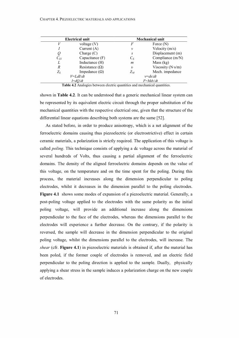
CHAPTER 4. PIEZOELECTRIC MATERIALS AND APPLICATIONS
71
shown in Table 4.2. It can be understood that a generic mechanical linear system can
be represented by its equivalent electric circuit through the proper substitution of the
mechanical quantities with the respective electrical one, given that the structure of the
differential linear equations describing both systems are the same [52].
As stated before, in order to produce anisotropy, which is a net alignment of the
ferroelectric domains causing thus piezoelectric (or electrostrictive) effect in certain
ceramic materials, a polarization is strictly required. The application of this voltage is
called poling. This technique consists of applying a dc voltage across the material of
several hundreds of Volts, thus causing a partial alignment of the ferroelectric
domains. The density of the aligned ferroelectric domains depends on the value of
this voltage, on the temperature and on the time spent for the poling. During this
process, the material increases along the dimension perpendicular to poling
electrodes, whilst it decreases in the dimension parallel to the poling electrodes.
Figure 4.1 shows some modes of expansion of a piezoelectric material. Generally, a
post-poling voltage applied to the electrodes with the same polarity as the initial
poling voltage, will provide an additional increase along the dimensions
perpendicular to the face of the electrodes, whereas the dimensions parallel to the
electrodes will experience a further decrease. On the contrary, if the polarity is
reversed, the sample will decrease in the dimension perpendicular to the original
poling voltage, whilst the dimensions parallel to the electrodes, will increase. The
shear (cfr. Figure 4.1) in piezoelectric materials is obtained if, after the material has
been poled, if the former couple of electrodes is removed, and an electric field
perpendicular to the poling direction is applied to the sample. Dually, physically
applying a shear stress in the sample induces a polarization charge on the new couple
of electrodes.
Electrical unit Mechanical unit V voltage (V) F Force (N) I Current (A) v Velocity (m/s) Q Charge (C) s Displacement (m)
CEl Capacitance (F) CE Compliance (m/N) L Inductance (H) m Mass (kg) R Resistance (Ω) υ Viscosity (N∙s/m) ZE Impedance (Ω) ZM Mech. impedance
V=LdI/dt v=ds/dt I=dQ/dt F=Mdv/dt
Table 4.2 Analogies between electric quantities and mechanical quantities.
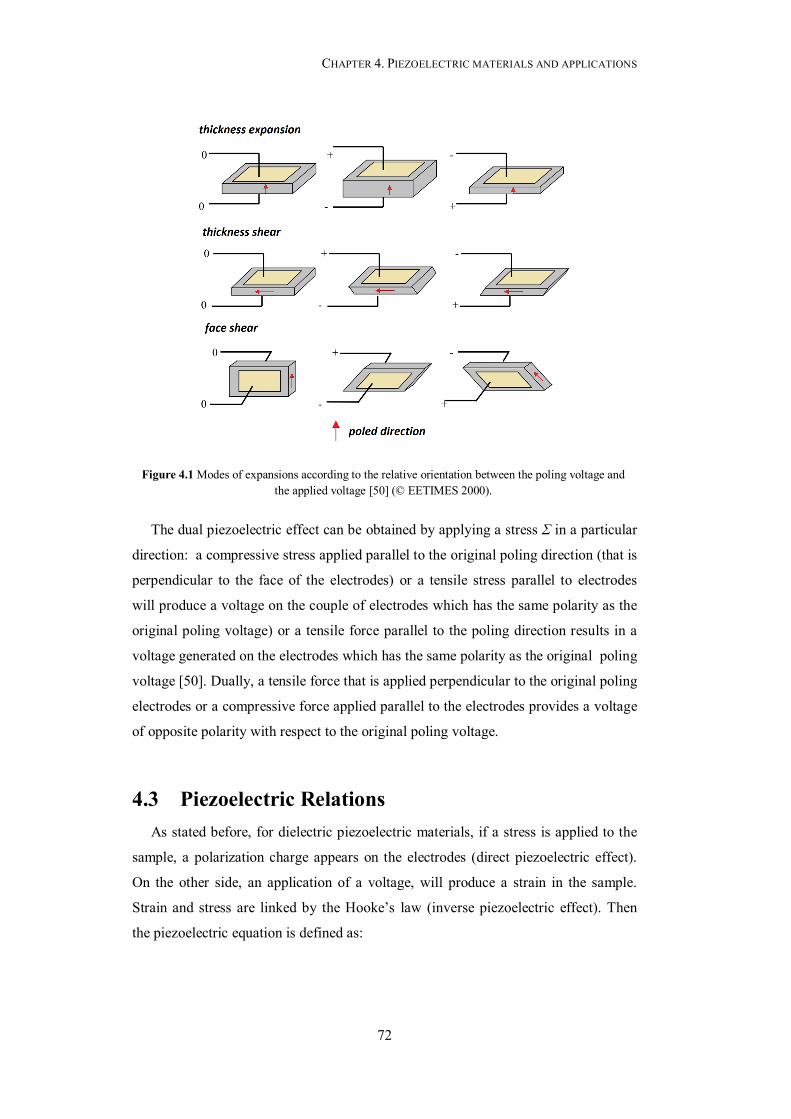
CHAPTER 4. PIEZOELECTRIC MATERIALS AND APPLICATIONS
72
The dual piezoelectric effect can be obtained by applying a stress Σ in a particular
direction: a compressive stress applied parallel to the original poling direction (that is
perpendicular to the face of the electrodes) or a tensile stress parallel to electrodes
will produce a voltage on the couple of electrodes which has the same polarity as the
original poling voltage) or a tensile force parallel to the poling direction results in a
voltage generated on the electrodes which has the same polarity as the original poling
voltage [50]. Dually, a tensile force that is applied perpendicular to the original poling
electrodes or a compressive force applied parallel to the electrodes provides a voltage
of opposite polarity with respect to the original poling voltage.
4.3 Piezoelectric Relations As stated before, for dielectric piezoelectric materials, if a stress is applied to the
sample, a polarization charge appears on the electrodes (direct piezoelectric effect).
On the other side, an application of a voltage, will produce a strain in the sample.
Strain and stress are linked by the Hooke’s law (inverse piezoelectric effect). Then
the piezoelectric equation is defined as:
Figure 4.1 Modes of expansions according to the relative orientation between the poling voltage and the applied voltage [50] (© EETIMES 2000).
CHAPTER 4. PIEZOELECTRIC MATERIALS AND APPLICATIONS
73
i ij jD d , or (4.7)
i ij jd E (4.8)
where dij (m/V or C/N) is the piezoelectric modulus, that is the ratio between the
resulting charge density and the applied stress or the resulting strain and the applied
electric field. Combining (4.7) and (4.8) we have:
ii j
j
DE
(4.9)
Combining, in turn, (4.4) with (4.7) it follows that:
ijij j ij j j j ij j
ij
dE d E g
. (4.10)
Equation (4.10) links the generated electric field in a certain direction and the applied
stress in the same direction. The parameter gij (m2/C) is known as piezoelectric
constant. In order to exploit the correspondence reported in Table 4.2, the relation
between the voltage and the force is mandatory. From (4.10), referring to the straight
beam (Figure 4.2), which oscillates at the 33 mode (that is force applied along the z
direction, and electric field parallel to the z axis)
03 33 3
0 0 0
j ij j
ij
V d F LV g F
L A A (4.11)
Conversely, the relation between force and voltage, is obtained through inversion of
(4.11):
3 01
0 0 3 33 0
j ij j
ij
V d F F AN
L A V g L (4.12)
A generic piezoelectric actuator can be represented by a dielectric capacitance with a
parallel parasitic resistance (see (2.29) and (2.30)) due to the finite electric
conductivity σd of the dielectric, an ideal transformer 1:N1, with N1 representing the
conversion ratio between the resulting force and voltage (cfr. (4.12)), a spring of
compliance CM and a mass m, plus a mechanical resistance due to the “damping” of
the material, that is a friction force proportional to the velocity. Due to the
correspondence in Table 4.2, it is possible to replace the compliance with a capacitor
CM, the mass with an inductance LM, and the damping with an electrical resistance RM.
(cfr. Figure 4.3). The electric capacitance CIN can be represented by (4.1), whereas
the dielectric parasitic resistance is:
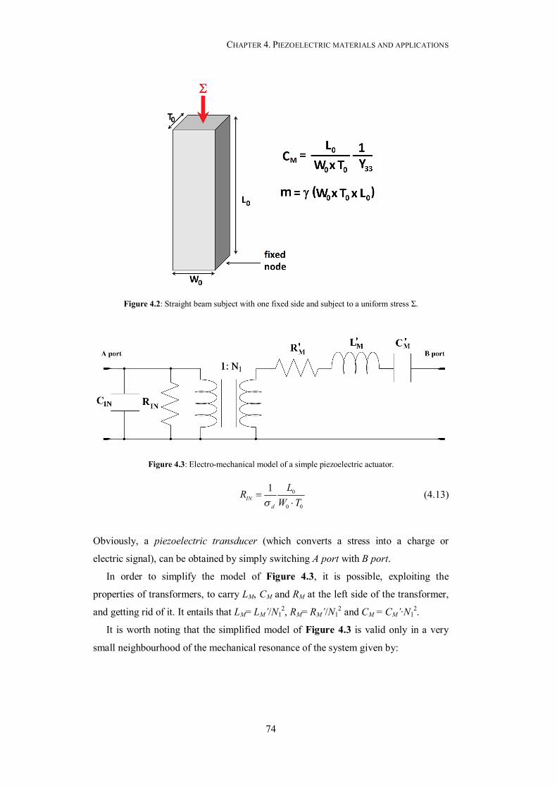
CHAPTER 4. PIEZOELECTRIC MATERIALS AND APPLICATIONS
74
0
0 0
1IN
d
LRW T
(4.13)
Obviously, a piezoelectric transducer (which converts a stress into a charge or
electric signal), can be obtained by simply switching A port with B port.
In order to simplify the model of Figure 4.3, it is possible, exploiting the
properties of transformers, to carry LM, CM and RM at the left side of the transformer,
and getting rid of it. It entails that LM= LM’/N12, RM= RM’/N1
2 and CM = CM’∙N12.
It is worth noting that the simplified model of Figure 4.3 is valid only in a very
small neighbourhood of the mechanical resonance of the system given by:
Figure 4.2: Straight beam subject with one fixed side and subject to a uniform stress Σ.
Figure 4.3: Electro-mechanical model of a simple piezoelectric actuator.
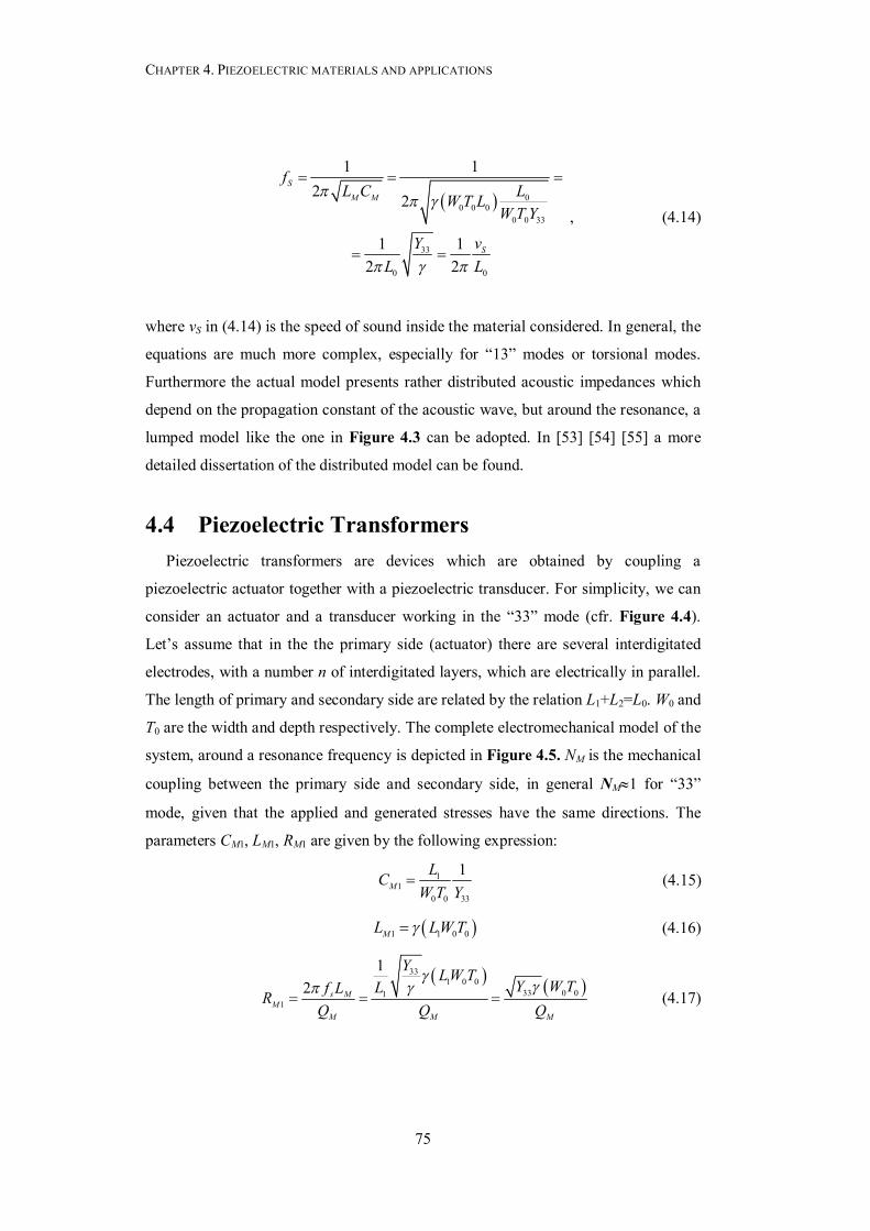
CHAPTER 4. PIEZOELECTRIC MATERIALS AND APPLICATIONS
75
0
0 0 00 0 33
33
0 0
1 12 2
1 12 2
SM M
S
fL C LW T L
W T Y
Y vL L
, (4.14)
where vS in (4.14) is the speed of sound inside the material considered. In general, the
equations are much more complex, especially for “13” modes or torsional modes.
Furthermore the actual model presents rather distributed acoustic impedances which
depend on the propagation constant of the acoustic wave, but around the resonance, a
lumped model like the one in Figure 4.3 can be adopted. In [53] [54] [55] a more
detailed dissertation of the distributed model can be found.
4.4 Piezoelectric Transformers Piezoelectric transformers are devices which are obtained by coupling a
piezoelectric actuator together with a piezoelectric transducer. For simplicity, we can
consider an actuator and a transducer working in the “33” mode (cfr. Figure 4.4).
Let’s assume that in the the primary side (actuator) there are several interdigitated
electrodes, with a number n of interdigitated layers, which are electrically in parallel.
The length of primary and secondary side are related by the relation L1+L2=L0. W0 and
T0 are the width and depth respectively. The complete electromechanical model of the
system, around a resonance frequency is depicted in Figure 4.5. NM is the mechanical
coupling between the primary side and secondary side, in general NM1 for “33”
mode, given that the applied and generated stresses have the same directions. The
parameters CM1, LM1, RM1 are given by the following expression:
11
0 0 33
1M
LCW T Y
(4.15)
1 1 0 0ML LW T (4.16)
331 0 0
33 0 011
12 s M
MM M M
Y LW TY W TLf LR
Q Q Q
(4.17)
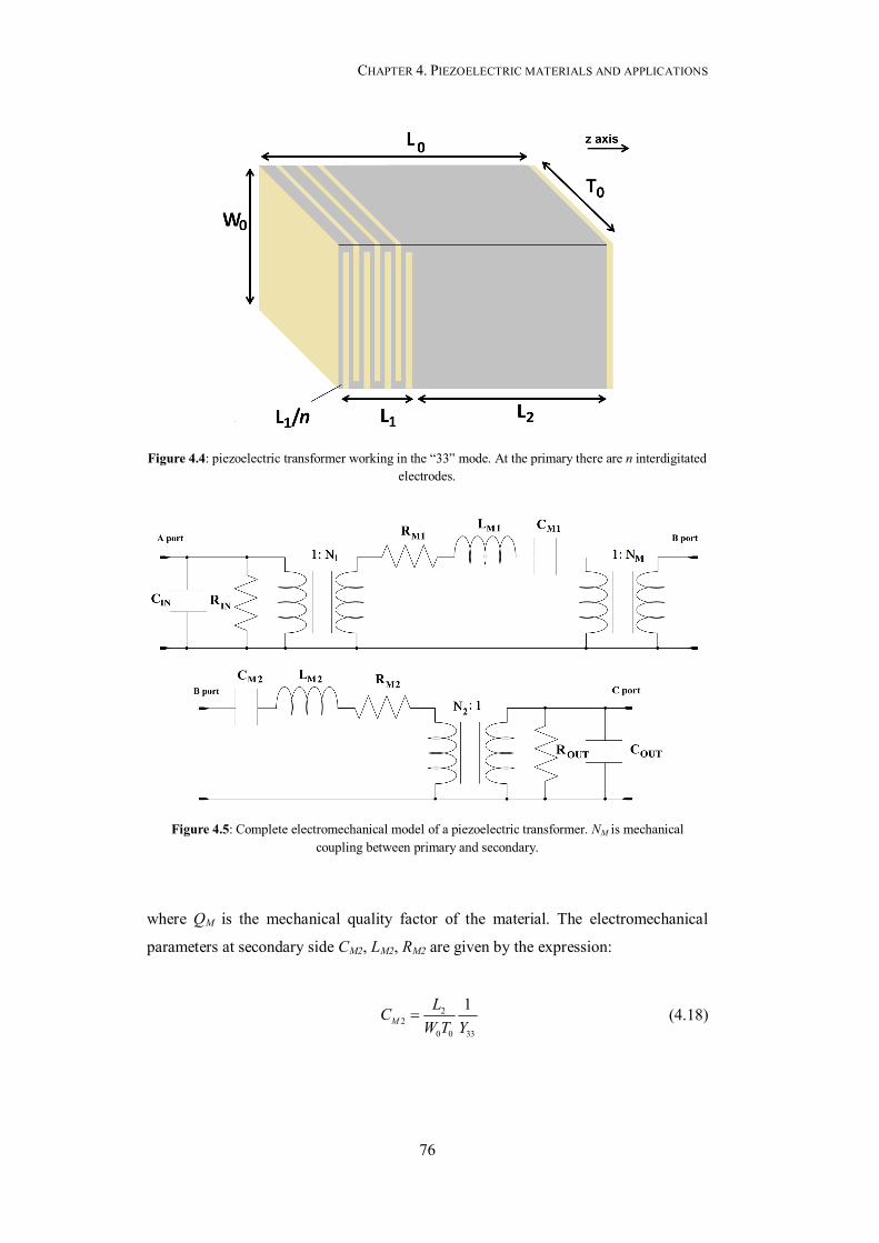
CHAPTER 4. PIEZOELECTRIC MATERIALS AND APPLICATIONS
76
where QM is the mechanical quality factor of the material. The electromechanical
parameters at secondary side CM2, LM2, RM2 are given by the expression:
22
0 0 33
1M
LCW T Y
(4.18)
Figure 4.4: piezoelectric transformer working in the “33” mode. At the primary there are n interdigitated electrodes.
Figure 4.5: Complete electromechanical model of a piezoelectric transformer. NM is mechanical coupling between primary and secondary.
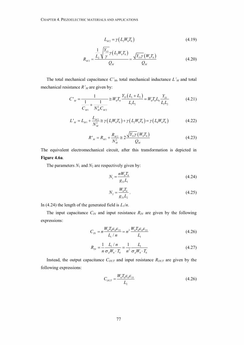
CHAPTER 4. PIEZOELECTRIC MATERIALS AND APPLICATIONS
77
2 2 0 0ML L W T (4.19)
332 0 0
33 0 022
1
MM M
Y L W TY W TLR
Q Q
(4.20)
The total mechanical capacitance C’M, total mechanical inductance L’M and total
mechanical resistance R’M are given by:
33 1 2 33
0 0 0 0 01 2 1 2
21 2
1' 1 1M
M M M
Y L L YC W T W T LL L L L
C N C
(4.21)
21 1 0 0 2 0 0 0 0 02' M
M MM
LL L LW T L W T L W TN
(4.22)
33 0 021 2' 2M
M MM M
Y W TRR RN Q
(4.23)
The equivalent electromechanical circuit, after this transformation is depicted in
Figure 4.6a.
The parameters N1 and N2 are respectively given by:
0 01
33 1
nW TNg L
(4.24)
0 02
33 2
W TNg L
. (4.25)
In (4.24) the length of the generated field is L1/n.
The input capacitance CIN and input resistance RIN are given by the following
expressions:
20 0 0 33 0 0 0 33
1 1/IN
W T W TC n nL n L
(4.26)
1 12
0 0 0 0
/1 1IN
d d
L n LRn W T n W T
(4.27)
Instead, the output capacitance COUT and input resistance ROUT are given by the
following expressions:
0 0 0 33
2OUT
W TCL
(4.26)
CHAPTER 4. PIEZOELECTRIC MATERIALS AND APPLICATIONS
78
2
0 0OUT
d
LRW T
(4.27)
The parameters C’M, L’M and R’M can be brought at the left port of the ideal
transformer 1:N1, thus obtaining the following relations (cfr. Figure 4.6b):
2
2 33 0 01 0 0 0
1 2 33 1
'M M
Y nW TC C N W T LL L g L
(4.28)
2
2 0 01 0 0 0
33 1
'M M
nW TL L N L W Tg L
(4.29)
2
33 0 02 0 01
33 1
2'M M
M
Y W TnW TR R Ng L Q
(4.30)
At the end the turn ratio N, of the transformer can be written as:
1
2M
NN NN
(4.31)
Thus the final circuit of the piezoelectric transformer is depicted in Figure 4.6c. In
this case the vibrational node, of the fundamental node is placed in the mechanical
centre of the structure.
Figure 4.6: Electromechanical circuit of the piezoelectric transformer, after each transformation.

CHAPTER 4. PIEZOELECTRIC MATERIALS AND APPLICATIONS
79
4.5 Other applications of piezoelectric materials Piezoelectric materials are used not only for the fabrication of transformers, but
also for sensors and transducers. To cite an example they can be used in place of
thermal heaters in printers. As a matter of fact, they can be placed in the chamber
filled of ink, behind the nozzle: when the controlling voltage is applied, the
piezoelectric material changes shape, generating a pressure which forces a droplet of
ink from the nozzle. Furthermore they are used in lighters for the ignition of the gas.
Other applications include harvesting energy from environmental vibrations (for
example in trains), in order to transform mechanical energy into electrical energy.
Other types of applications include mechanical resonators for use in oscillators
(quartz oscillators) or detectors for real-time evaluation of fruit firmness [56], as well
as detection of viscosity [52].
4.6 Summary This chapter has presented a brief overview on the physical properties of
piezoelectric materials. Particular emphasis was given to the lumped equivalent
electro-mechanical circuit of the piezoelectric transformer, showing the major
parameters of interest which can be useful in a design phase.

80
Chapter 5
Piezoelectric transformers for
ultra-low voltage applications
This chapter discusses the SoA (state of art) of solutions for stepping-up the
ultra-low DC voltage (tens of mV) coming from harvesters like photovoltaic cells or
thermoelectric generators. Certain approaches are based on custom integrated
solutions coupled with an initial amount of energy (pre-charged capacitor or battery)
that serves as essential “initial condition” to perform the boost of the voltage. Other
approaches rely on the use of MTs in the so-called Armstrong oscillator. However,
the solutions presented in literature are not suitable for compact and integrated
performant systems in the application field of EH systems and ultra-low voltage and
ultra-low power systems. This chapter presents a novel step-up oscillator based on
PTs, which are generally used for high voltage applications. Generally, piezoelectric
devices suffer lower losses compared to magnetic devices, and their performance
(quality factor) is not directly linked to the thickness of metallizations, as it obviously
happens in magnetic devices. Hence, PTs are more suitable for on-chip integration
compared to MTs.
This novel step-up oscillator has been used also in a EH scheme, and it serves as
kick-starter for a classic boost switching DC-DC converter which, once started, is
able to perform a more efficient power conversion.

CHAPTER 5. PIEZOELECTRIC TRANSFORMERS FOR ULTRA-LOW VOLTAGE APPLICATIONS
81
5.1 State of art of EH systems Technology scaling in IC processes has allowed a relentless reduction of the
power required by electronic circuits for performing given tasks [57], which is an
essential feature in order to increase life of mobile, wearable, implantable devices
supplied by electrochemical or biofuel cells [58] [59]. Nevertheless, battery
replacement would require a lot of maintenance effort if ubiquitous sensor networks
or pervasive implantable sensors were deployed. It would be very helpful if these
systems could be fully autonomous by scavenging the energy available in the
environment in several forms, e.g. light, heat, vibrations, etc. A great challenge for
engineers and circuits designers is to exploit the ultra-low output voltage (down to
few tens of mV) provided by energy scavenging transducers, and to pump it to an
enough level (at least 0.6-0.8V) suitable to overcome the threshold voltage of
semiconductor devices, so that a switching converter can be successfully activated.
The most frequently used energy transducers are piezoelectric transducers,
photovoltaic cells, thermoelectric generators (TEGs), and rectennas for RF (Radio
Frequency) energy. Generally, the power density provided by the source to be
harvested is in the range of 10-100µW/cm2 [60]. Besides, for example, thermoelectric
generators (TEGs) provide output voltages of several tens of mV/K [61], whereas
indoor solar cells can provide down to 200mV in low illumination conditions [62].
Unfortunately, these values are not enough to control in an efficient way the gate of
power devices in switching DC/DC converters, or to exceed the diode threshold
voltage in voltage multipliers, e.g. Greinacher topologies, which also require a
transistor-based oscillator for operating. Currently, many works in literature
presenting power converter systems for ultra-low voltage energy scavenging purposes
do not face the problem of battery-less kick-start, and generally need a supply voltage
still higher than that available from the source: to cite an example in [63] and [64]
tens of mV can be exploited, but an initial amount energy (like the voltage in a
pre-charged capacitor or battery) is mandatory to make a power conversion. A first
technique to pump ultra-low voltages consists in the use of capacitive charge pumps,
like in [65] and [66]. Even though some circuit approaches [67] [68] can improve the
performance, unfortunately the minimum activation voltage is still comparable to the
threshold voltage of the semiconductor devices, and hence too much high for
CHAPTER 5. PIEZOELECTRIC TRANSFORMERS FOR ULTRA-LOW VOLTAGE APPLICATIONS
82
handling the output voltage provided by TEGs. With a threshold voltage adjustment,
the minimum activation voltage can be lowered down to 95mV [69]. Another
approach is the use of a motion-activated switch to initially drive a boost converter
[70], which allows input voltages as low as 35mV. In addition, ultra-low activation
voltages are provided by boost oscillators based on magnetic transformers (MTs), a
circuit topology known for long [71], re-proposed in literature [72], and now used
also in commercial products [73]. In such systems (Figure 5.1), an amplifier stage
based on a low threshold voltage transistor is put in a feedback loop together with a
MT. The amplifier should achieve a sufficient gain in order to start oscillation when
biased by the ultra-low voltage provided by the harvester. Once oscillation is started,
a conventional passive voltage multiplier can further boost and charge a storage
capacitor. Putting several MTs in cascade [74] can further lower the minimum
required activation voltage at the expenses of system dimensions. Furthermore, the
MT can also be re-used in a conventional DC/DC converter after the kick-start [75].
The main drawback of this approach is that MTs are difficult to shrink, since a high
turn ratio is required for managing the low output voltage of TEGs. Besides, MTs
suffer from frequency limitations, core losses and saturation [32].
In general, micro-fabricated magnetic transformers (MTs) are suitable for signal or
power isolation [76] and not for voltage boosting purposes, hence they have low turns
ratio (generally 1-2), low voltage gain (lower than 0dB) and low magnetizing
inductances (lower than 1µH). Nevertheless, miniaturized MTs based on bonding
wires [33] for voltage boosting purposes [34] [77] have been recently reported. In
these cases, the device miniaturization significantly limits the quality factor.
Alternatively, transformers based on silicon micro-mechanical resonators and
piezoelectric materials have been already proposed [78], hence facilitating the
possibility of a package-level integration of mixed microelectronic and MEMS
systems. Generally, power conversion in piezoelectric transformers (PTs) can be
much more efficient than in MTs, due to their greater quality factors (more than one
order of magnitude compared to the magnetic counter-part). This is mainly due to the
low mechanical losses in MEMS oscillators. In fact, the quality factors (Q) of
piezo-ceramics may be greater than 1000 [79].
CHAPTER 5. PIEZOELECTRIC TRANSFORMERS FOR ULTRA-LOW VOLTAGE APPLICATIONS
83
This chapter presents a novel battery-less PT voltage boost oscillator suitable for
kick-starting, from fully discharged states, an efficient power conversion system
based on TEGs subject to low temperature gradients or photovoltaic cells in indoor
environment (Figure 5.2) [80] [81]. The main task of this system is to initially give a
sufficient voltage to start an external self-sustaining efficient power converter. Then,
the main target is to achieve a start-up voltage as low as possible, and not necessarily
an efficiency as high as possible. The presented system is compatible with an
inductor-less implementation. Furthermore, the system is compatible with
microelectronic and MEMS implementations integrated at package level. In addition,
it will be shown that lower start-up voltages can be obtained through the insertion of a
small inductor in the input stage. In this specific implementation, based on a
commercial PT designed for Cold Cathode Fluorescent Lamps (CCFL) or Liquid
Crystals Displays (LCD) backlight (hence high-voltage applications), hence not
optimized for ultra-low voltage step-up purposes, the system can boost voltages down
tens of mV up to voltage levels useful to control the power devices of a DC/DC
converter.
Figure 5.1. Schematic of a traditional MT based boost oscillator.
CHAPTER 5. PIEZOELECTRIC TRANSFORMERS FOR ULTRA-LOW VOLTAGE APPLICATIONS
84
5.2 Piezoelectric transformers and equivalent electromechanical circuit
The main purpose of this section is to briefly summarize the operation of the PT
and to recall the equivalent electromechanical circuit used in circuit analysis. PTs are
resonant devices exploiting the direct and inverse piezoelectric effect of certain
materials producing polarization charge on their electrodes when subject to a
mechanical stress. A typical PT like the step-up Rosen transformer [53] [54], is built
by cascading a transverse mode actuator at primary side (that is stress perpendicular
to electric field and polarization) with a longitudinal mode transducer [83] at
secondary side (that is stress parallel to electric field and polarization): when PTs
vibrate at a frequency close to their resonance, an acoustic standing wave is produced
with the generation of nodes and antinodes, so that a lumped electromechanical
equivalent circuit [54] can be used. Figure 5.3 represents the equivalent circuit of a
PT driven in proximity of a particular resonant frequency: Cd1 is the input electrical
capacitance, and in multi-layer transformers it is the parallel of the capacitance of
each layer; the series of CM, LM and RM represents the mechanical impedance; N is
the equivalent turn ratio related to the stress ratio from input to output; and Cd2 is the
output electrical capacitance, which, for commercial PTs, is generally several orders
of magnitude lower than Cd1 because the distance between the electrodes is higher.
Furthermore, PTs are very load-dependent devices [84], in addition their electrical
resonance does not correspond to the mechanical resonance. This means that, a
Figure 5.2. Block diagram of an energy harvesting system, lacking a battery.
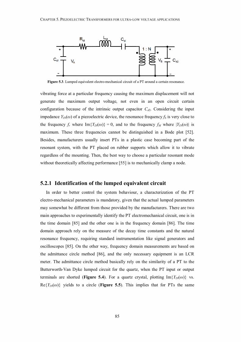
CHAPTER 5. PIEZOELECTRIC TRANSFORMERS FOR ULTRA-LOW VOLTAGE APPLICATIONS
85
vibrating force at a particular frequency causing the maximum displacement will not
generate the maximum output voltage, not even in an open circuit certain
configuration because of the intrinsic output capacitor Cd2. Considering the input
impedance YIN(ω) of a piezoelectric device, the resonance frequency fS is very close to
the frequency fr where ImYIN(ω) = 0, and to the frequency fM where |YIN(ω)| is
maximum. These three frequencies cannot be distinguished in a Bode plot [52].
Besides, manufacturers usually insert PTs in a plastic case becoming part of the
resonant system, with the PT placed on rubber supports which allow it to vibrate
regardless of the mounting. Then, the best way to choose a particular resonant mode
without theoretically affecting performance [55] is to mechanically clamp a node.
5.2.1 Identification of the lumped equivalent circuit In order to better control the system behaviour, a characterization of the PT
electro-mechanical parameters is mandatory, given that the actual lumped parameters
may somewhat be different from those provided by the manufacturers. There are two
main approaches to experimentally identify the PT electromechanical circuit, one is in
the time domain [85] and the other one is in the frequency domain [86]. The time
domain approach rely on the measure of the decay time constants and the natural
resonance frequency, requiring standard instrumentation like signal generators and
oscilloscopes [85]. On the other way, frequency domain measurements are based on
the admittance circle method [86], and the only necessary equipment is an LCR
meter. The admittance circle method basically rely on the similarity of a PT to the
Butterworth-Van Dyke lumped circuit for the quartz, when the PT input or output
terminals are shorted (Figure 5.4). For a quartz crystal, plotting ImYIN(ω) vs.
ReYIN(ω) yields to a circle (Figure 5.5). This implies that for PTs the same
Figure 5.3. Lumped equivalent electro-mechanical circuit of a PT around a certain resonance.
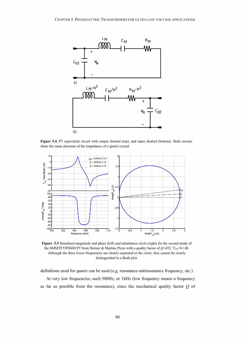
CHAPTER 5. PIEZOELECTRIC TRANSFORMERS FOR ULTRA-LOW VOLTAGE APPLICATIONS
86
definitions used for quartz can be used (e.g. resonance-antiresonance frequency, etc.)
At very low frequencies, such 500Hz, or 1kHz (low frequency means a frequency
as far as possible from the resonance), since the mechanical quality factor Q of
Figure 5.4. PT equivalent circuit with output shorted (top), and input shorted (bottom). Both circuits share the same structure of the impedance of a quartz crystal.
Figure 5.5 Simulated magnitude and phase (left) and admittance circle (right) for the second mode of the SMMTF55P4S80 PT from Steiner & Martins Piezo with a quality factor of Q=452. YIN=G+iB.
Although the three lower frequencies are clearly separated in the circle, they cannot be clearly distinguished in a Bode plot.
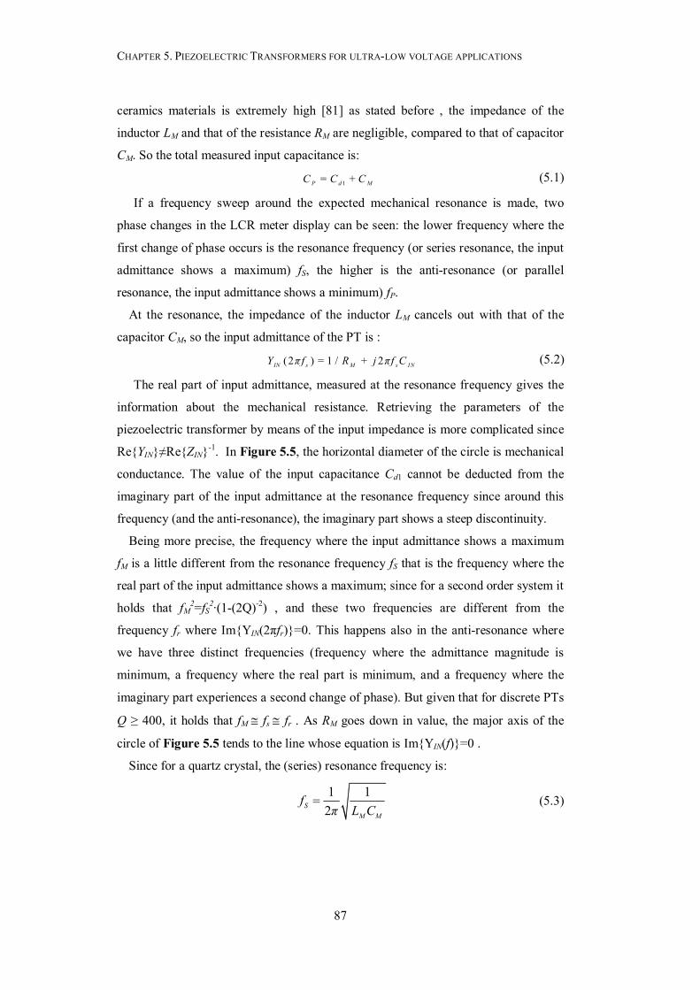
CHAPTER 5. PIEZOELECTRIC TRANSFORMERS FOR ULTRA-LOW VOLTAGE APPLICATIONS
87
ceramics materials is extremely high [81] as stated before , the impedance of the
inductor LM and that of the resistance RM are negligible, compared to that of capacitor
CM. So the total measured input capacitance is:
1= +P d MC C C (5.1)
If a frequency sweep around the expected mechanical resonance is made, two
phase changes in the LCR meter display can be seen: the lower frequency where the
first change of phase occurs is the resonance frequency (or series resonance, the input
admittance shows a maximum) fS, the higher is the anti-resonance (or parallel
resonance, the input admittance shows a minimum) fP.
At the resonance, the impedance of the inductor LM cancels out with that of the
capacitor CM, so the input admittance of the PT is :
(2 ) = 1 / + 2IN s M s INY πf R j πf C (5.2)
The real part of input admittance, measured at the resonance frequency gives the
information about the mechanical resistance. Retrieving the parameters of the
piezoelectric transformer by means of the input impedance is more complicated since
ReYIN≠ReZIN-1. In Figure 5.5, the horizontal diameter of the circle is mechanical
conductance. The value of the input capacitance Cd1 cannot be deducted from the
imaginary part of the input admittance at the resonance frequency since around this
frequency (and the anti-resonance), the imaginary part shows a steep discontinuity.
Being more precise, the frequency where the input admittance shows a maximum
fM is a little different from the resonance frequency fS that is the frequency where the
real part of the input admittance shows a maximum; since for a second order system it
holds that fM2=fS
2∙(1-(2Q)-2) , and these two frequencies are different from the
frequency fr where ImYIN(2πfr)=0. This happens also in the anti-resonance where
we have three distinct frequencies (frequency where the admittance magnitude is
minimum, a frequency where the real part is minimum, and a frequency where the
imaginary part experiences a second change of phase). But given that for discrete PTs
Q ≥ 400, it holds that fM fs fr . As RM goes down in value, the major axis of the
circle of Figure 5.5 tends to the line whose equation is ImYIN(f)=0 .
Since for a quartz crystal, the (series) resonance frequency is:
1 1
2SM M
fπ L C
(5.3)

CHAPTER 5. PIEZOELECTRIC TRANSFORMERS FOR ULTRA-LOW VOLTAGE APPLICATIONS
88
And the anti-resonance (or parallel resonance) frequency is:
1
1
1 12p
M dM
M d
f C Cπ LC C
(5.4)
When dividing (5.3) by (5.4), and squaring we obtain:
2 2
1 1s s
d d M Pp p
f fC C C Cf f
(5.5)
where CP refers to (5.1).
The mechanical capacitance is given by:
1M P dC C C (5.6)
The inductor LM is given by:
2
1
2M
s M
Lπf C
(5.7)
The only parameter left is the turn ratio N of the ideal transformer of Figure 5.3.
We open the output port of the PT, and we short the input. We do the same measures
done with the output shorted, since the circuit is structurally the same.
By looking at Figure 5.3, the turn ratio N is given by:
2
2M M
M M
L N LNL L
(5.8)
where LM2 is the inductance calculated from the output port (input shorted) through
(5.7).
Table 5.1 shows the parameters obtained with the admittance circle approach for
the second resonant mode of the adopted PT sample (SMMTF55P4S80 PT from
Steiner & Martins Piezo) using an Agilent E4980A LCR meter, together with other
characteristic parameters of the system.
According to the model in Figure 5.3, for an unloaded PT the electric resonance
frequency is:
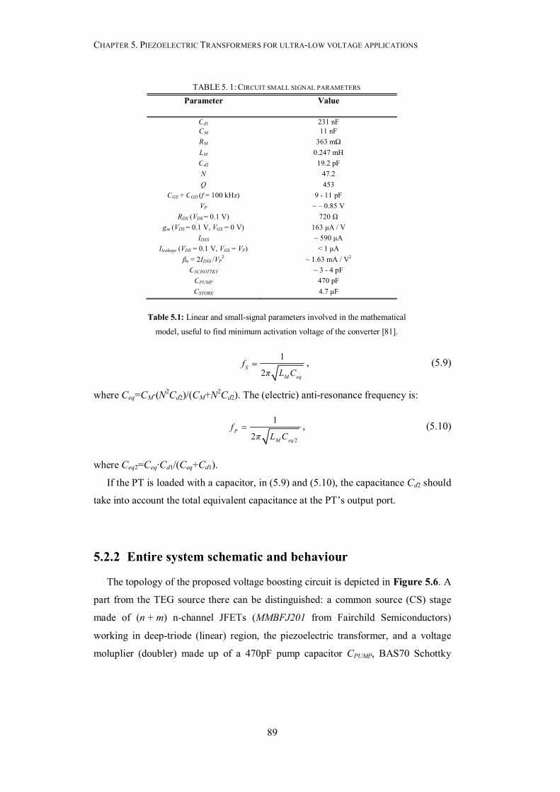
CHAPTER 5. PIEZOELECTRIC TRANSFORMERS FOR ULTRA-LOW VOLTAGE APPLICATIONS
89
1
2S
M eq
fπ L C
, (5.9)
where Ceq=CM∙(N2Cd2)/(CM+N2Cd2). The (electric) anti-resonance frequency is:
2
1
2P
M eq
fπ L C
, (5.10)
where Ceq2=Ceq∙Cd1/(Ceq+Cd1).
If the PT is loaded with a capacitor, in (5.9) and (5.10), the capacitance Cd2 should
take into account the total equivalent capacitance at the PT’s output port.
5.2.2 Entire system schematic and behaviour
The topology of the proposed voltage boosting circuit is depicted in Figure 5.6. A
part from the TEG source there can be distinguished: a common source (CS) stage
made of (n + m) n-channel JFETs (MMBFJ201 from Fairchild Semiconductors)
working in deep-triode (linear) region, the piezoelectric transformer, and a voltage
moluplier (doubler) made up of a 470pF pump capacitor CPUMP, BAS70 Schottky
TABLE 5. 1: CIRCUIT SMALL SIGNAL PARAMETERS Parameter Value
Cd1 231 nF CM 11 nF RM 363 mΩ LM 0.247 mH
Cd2 19.2 pF N 47.2 Q 453
CGS + CGD (f = 100 kHz) 9 - 11 pF VP ~ ‒ 0.85 V
RDS (VDS = 0.1 V) 720 Ω gm (VDS = 0.1 V, VGS = 0 V) 163 μA / V
IDSS ~ 590 μA Ileakage (VDS = 0.1 V, VGS = VP) < 1 μA
βn = 2IDSS /VP2 ~ 1.63 mA / V2
CSCHOTTKY ~ 3 - 4 pF CPUMP 470 pF CSTORE 4.7 μF
Table 5.1: Linear and small-signal parameters involved in the mathematical
model, useful to find minimum activation voltage of the converter [81].
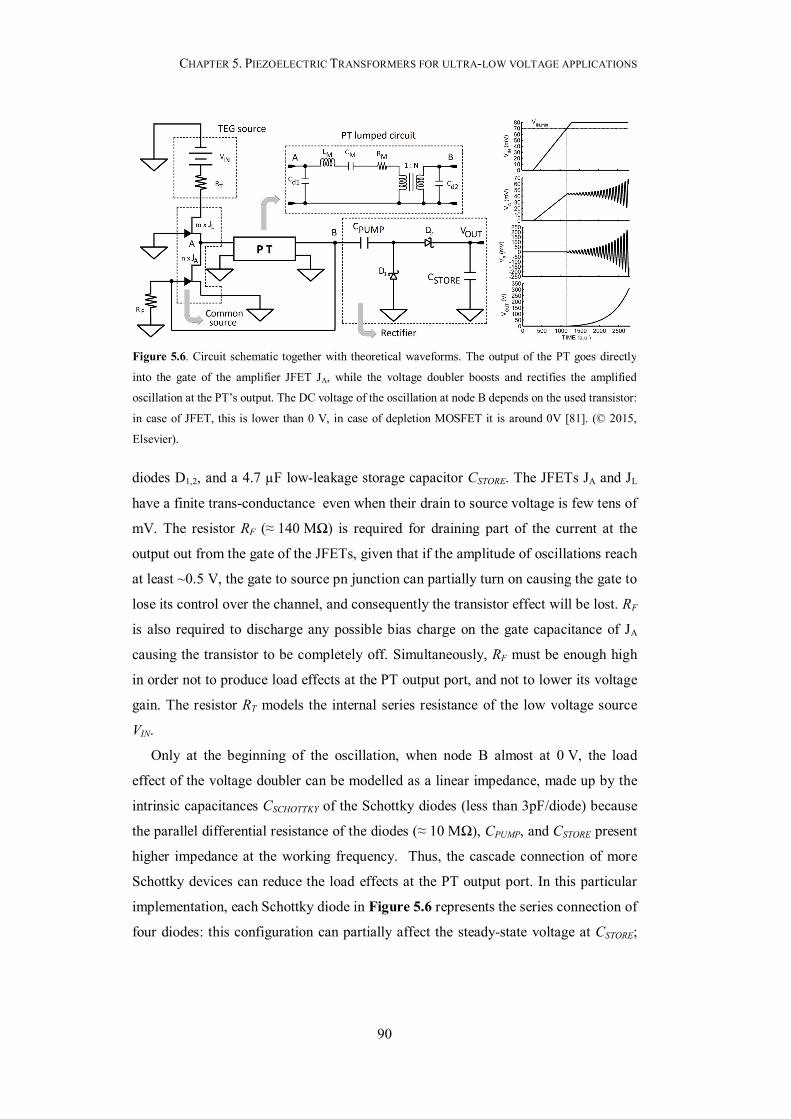
CHAPTER 5. PIEZOELECTRIC TRANSFORMERS FOR ULTRA-LOW VOLTAGE APPLICATIONS
90
diodes D1,2, and a 4.7 µF low-leakage storage capacitor CSTORE. The JFETs JA and JL
have a finite trans-conductance even when their drain to source voltage is few tens of
mV. The resistor RF (≈ 140 MΩ) is required for draining part of the current at the
output out from the gate of the JFETs, given that if the amplitude of oscillations reach
at least ~0.5 V, the gate to source pn junction can partially turn on causing the gate to
lose its control over the channel, and consequently the transistor effect will be lost. RF
is also required to discharge any possible bias charge on the gate capacitance of JA
causing the transistor to be completely off. Simultaneously, RF must be enough high
in order not to produce load effects at the PT output port, and not to lower its voltage
gain. The resistor RT models the internal series resistance of the low voltage source
VIN.
Only at the beginning of the oscillation, when node B almost at 0 V, the load
effect of the voltage doubler can be modelled as a linear impedance, made up by the
intrinsic capacitances CSCHOTTKY of the Schottky diodes (less than 3pF/diode) because
the parallel differential resistance of the diodes (≈ 10 MΩ), CPUMP, and CSTORE present
higher impedance at the working frequency. Thus, the cascade connection of more
Schottky devices can reduce the load effects at the PT output port. In this particular
implementation, each Schottky diode in Figure 5.6 represents the series connection of
four diodes: this configuration can partially affect the steady-state voltage at CSTORE;
Figure 5.6. Circuit schematic together with theoretical waveforms. The output of the PT goes directly
into the gate of the amplifier JFET JA, while the voltage doubler boosts and rectifies the amplified
oscillation at the PT’s output. The DC voltage of the oscillation at node B depends on the used transistor:
in case of JFET, this is lower than 0 V, in case of depletion MOSFET it is around 0V [81]. (© 2015,
Elsevier).

CHAPTER 5. PIEZOELECTRIC TRANSFORMERS FOR ULTRA-LOW VOLTAGE APPLICATIONS
91
nevertheless, due to the low currents involved (in general less than 100nA), the
voltage drop caused by each diode is slightly less than 100mV, so the number of
series diodes comes from a trade-off between minimum activation voltage and
steady-state output voltage. In addition, when the oscillation is in steady state, small
signal analysis is no more valid because of the significant nonlinearities of rectifier
diodes.
Figure 5.6 also shows the theoretical waveforms involved in the system: when VIN
reaches the minimum input voltage VIN,MIN satisfying the Barkhausen gain criterion,
the oscillation is triggered. Before the starting of the oscillation, VA follows VIN with a
scaling factor due to the voltage divider composed by the n amplifier JFETs (nJA) and
the m load JFETs (mJL), whereas during oscillation, VB is almost in opposition of
phase with respect to VA. The steady-state DC voltage of VB depends on the type of
transistor used in the CS stage. In case of JFETs, this DC voltage is few hundreds of
mV under 0 V, given that the system can oscillate only if the gate-source p-n junction
of the JFETs is not forward biased; in case of depletion MOSFET, this DC value is
extremely near to 0 V. VOUT starts growing exponentially until the oscillation at node
B reaches steady-state. After this, VOUT follows the typical charging law of a RC
circuit.
For the determination of the oscillation condition, it is worth performing a
small-signal analysis. In the initial condition, the DC voltage VA depends on the
number of amplifier and load JFETs, respectively n and m: VA = m / (n + m)·VIN. It
can be found out that the transconductance gmA of each amplifier JFET is:
gMa = nVA = gm· m / (n + m), where gm = nVIN is assumed as a reference value, and
n is the current gain factor of the JFET. For JFETs we have that n = 2IDSS / VP2,
where IDSS is the drain current at zero gate voltage and VP is the negative pinch-off (or
threshold) voltage. The transconductance gmL of each load JFET is:
gmL = n(VIN −VA) = gm · n / (n + m). The output conductance gdsA of each amplifier
JFET is gdsA = n (−VP − VA) −nVP, under the real assumption that |VP| >> VIN , as it
happens in this case. The output conductance gdsL of each load JFET is:
gdsL = n (−VP −VIN) −nVP. A unique symbol gds, defined as gds = gdsA = gdsL, can
then be used. In addition, all the JFETs work in their linear region, thus, the small
signal output conductance gds equals the large signal conductance GDS of each device.
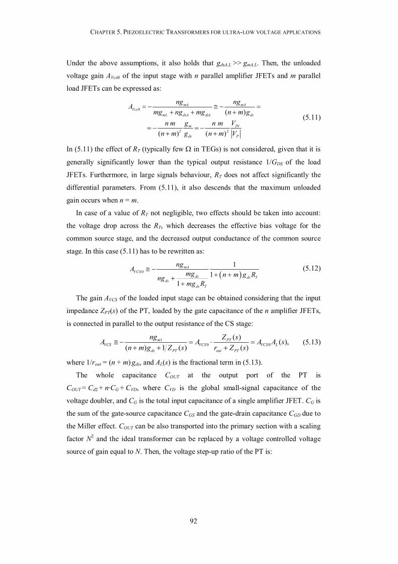
CHAPTER 5. PIEZOELECTRIC TRANSFORMERS FOR ULTRA-LOW VOLTAGE APPLICATIONS
92
Under the above assumptions, it also holds that gdsA,L >> gmA,L. Then, the unloaded
voltage gain AVcs0 of the input stage with n parallel amplifier JFETs and m parallel
load JFETs can be expressed as:
0
2 2
( )
( ) ( )
mA mAVcs
mL dsA dsL ds
m IN
ds P
ng ngAmg ng mg n m g
g Vn m n mn m g n m V
(5.11)
In (5.11) the effect of RT (typically few in TEGs) is not considered, given that it is
generally significantly lower than the typical output resistance 1/GDS of the load
JFETs. Furthermore, in large signals behaviour, RT does not affect significantly the
differential parameters. From (5.11), it also descends that the maximum unloaded
gain occurs when n = m.
In case of a value of RT not negligible, two effects should be taken into account:
the voltage drop across the RT, which decreases the effective bias voltage for the
common source stage, and the decreased output conductance of the common source
stage. In this case (5.11) has to be rewritten as:
0
11
1
mAVCS
ds ds Tds
ds T
ngA mg n m g Rngmg R
(5.12)
The gain AVCS of the loaded input stage can be obtained considering that the input
impedance ZPT(s) of the PT, loaded by the gate capacitance of the n amplifier JFETs,
is connected in parallel to the output resistance of the CS stage:
10 0
( ) ( ),( ) 1 ( ) ( )
m PTVCS VCS VCS L
ds PT out PT
ng Z sA A A A sn m g Z s r Z s
(5.13)
where 1/rout = (n + m) gds, and AL(s) is the fractional term in (5.13).
The whole capacitance COUT at the output port of the PT is
COUT = Cd2 + n∙CG + CVD, where CVD is the global small-signal capacitance of the
voltage doubler, and CG is the total input capacitance of a single amplifier JFET. CG is
the sum of the gate-source capacitance CGS and the gate-drain capacitance CGD due to
the Miller effect. COUT can be also transported into the primary section with a scaling
factor N2 and the ideal transformer can be replaced by a voltage controlled voltage
source of gain equal to N. Then, the voltage step-up ratio of the PT is:
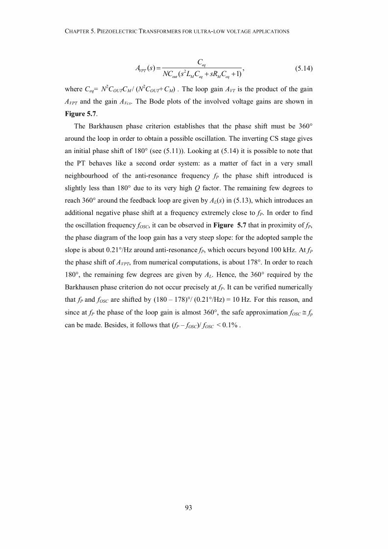
CHAPTER 5. PIEZOELECTRIC TRANSFORMERS FOR ULTRA-LOW VOLTAGE APPLICATIONS
93
2( ) ,( 1)
eqVPT
out M eq M eq
CA s
NC s L C sR C
(5.14)
where Ceq= N2COUTCM / (N2COUT+CM) . The loop gain AVT is the product of the gain
AVPT and the gain AVcs. The Bode plots of the involved voltage gains are shown in
Figure 5.7.
The Barkhausen phase criterion establishes that the phase shift must be 360°
around the loop in order to obtain a possible oscillation. The inverting CS stage gives
an initial phase shift of 180° (see (5.11)). Looking at (5.14) it is possible to note that
the PT behaves like a second order system: as a matter of fact in a very small
neighbourhood of the anti-resonance frequency fP the phase shift introduced is
slightly less than 180° due to its very high Q factor. The remaining few degrees to
reach 360° around the feedback loop are given by AL(s) in (5.13), which introduces an
additional negative phase shift at a frequency extremely close to fP. In order to find
the oscillation frequency fOSC, it can be observed in Figure 5.7 that in proximity of fP,
the phase diagram of the loop gain has a very steep slope: for the adopted sample the
slope is about 0.21°/Hz around anti-resonance fP, which occurs beyond 100 kHz. At fP
the phase shift of AVPT, from numerical computations, is about 178°. In order to reach
180°, the remaining few degrees are given by AL. Hence, the 360° required by the
Barkhausen phase criterion do not occur precisely at fP. It can be verified numerically
that fP and fOSC are shifted by (180 ‒ 178)°/ (0.21°/Hz) = 10 Hz. For this reason, and
since at fP the phase of the loop gain is almost 360°, the safe approximation fOSC fp
can be made. Besides, it follows that (fP ‒ fOSC)/ fOSC < 0.1% .
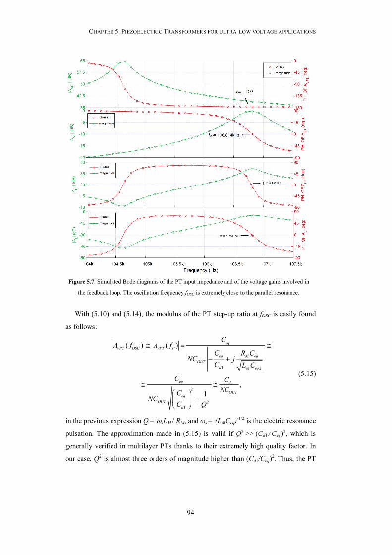
CHAPTER 5. PIEZOELECTRIC TRANSFORMERS FOR ULTRA-LOW VOLTAGE APPLICATIONS
94
With (5.10) and (5.14), the modulus of the PT step-up ratio at fOSC is easily found
as follows:
1 2
1
2
21
( ) ( )
,1
eqVPT OSC VPT P
eq M eqOUT
d M eq
eq d
OUTeq
OUTd
A
CNC
CA f f
C R CNC j
C L C
C
CNC
C Q
(5.15)
in the previous expression Q = sLM / RM, and ωs = (LMCeq)-1/2 is the electric resonance
pulsation. The approximation made in (5.15) is valid if Q2 >> (Cd1 / Ceq)2, which is
generally verified in multilayer PTs thanks to their extremely high quality factor. In
our case, Q2 is almost three orders of magnitude higher than (Cd1/Ceq)2. Thus, the PT
Figure 5.7. Simulated Bode diagrams of the PT input impedance and of the voltage gains involved in
the feedback loop. The oscillation frequency fOSC is extremely close to the parallel resonance.
CHAPTER 5. PIEZOELECTRIC TRANSFORMERS FOR ULTRA-LOW VOLTAGE APPLICATIONS
95
voltage step-up ratio at fP does is independent from the quality factor.
The PT input impedance ZPT(s) can also be calculated:
11
1
2
21 2 2
1( )( )
1( )( 1)
PT
d M M eq
M eq M eq
d eq M eq M eq
Z ssC sL R sC
s L C sR Cs C C s L C sR C
, (5.16)
that is the same mathematical expression of the impedance of the Quartz.
From (5.16), it is possible to note that the poles are very close to the zeros since
Ceq2 Ceq. By switching (5.16) to the frequency domain by putting s = j2πf , we find
out that the modulus of ZPT(s) is maximum when (s2LMCeq2+sRMCeq2+1) is minimum
and this happens at a frequency extremely close to fP=1/2π ·(LMCeq2)-1/2. Hence, given
that Ceq CM, and that the quality factor is very high, from (5.16) it can be found that
|ZPT(s)| is maximum when ZPT(s) is almost a real quantity (see also Figure 5.7):
2
1
( ) Re ( )PT PTeq
P M Peq d
QCZ R Z
C Cf f
(5.17)
By using (5.10), (5.13), (5.15), (5.17), the whole loop gain AVT(f) at fOSC is easily
determined as follows:
12( )
| 1 / [( )( )( )( )
| ( ) ]IN d PT P
VT OSC VT PP OUT PT P ds
V C Zn mA f AV NC Z n m gm n
fff
(5.18)
At this point a further clarification should be done. Being more precise, through
(5.18) we are not evaluating the loop gain, but the so called return-ratio, that is
essentially the one-way gain that an injected signal experiences within the loop. This
method assumes that all blocks constituting the system are unilateral, but in general
this could not correspond to the reality given that in the return ratio, the effect of the
dependent voltage or current generator (according on how the port system is
modelled) driven by the output voltage or current in the input port is neglected in the
common source, whilst in the PT the dependent current or voltage generator is
neglected in the output port (see Figure 5.8).
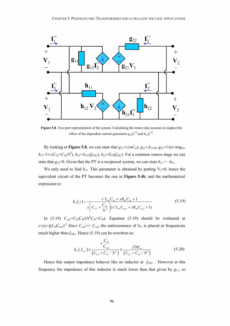
CHAPTER 5. PIEZOELECTRIC TRANSFORMERS FOR ULTRA-LOW VOLTAGE APPLICATIONS
96
By looking at Figure 5.8, we can state that g11=s∙(nCG), g21=AVCS0, g22=1/(n+m)gds,
h11=1/s∙(Cd2+CM/N2), h12=AVPT(fOSC), h22=ZPT(fOSC). For a common source stage we can
state that g12=0. Given that the PT is a reciprocal system, we can state h12 = –h21.
We only need to find h11. This parameter is obtained by putting V2=0, hence the
equivalent circuit of the PT becomes the one in Figure 5.4b, and the mathematical
expression is:
2
112
2 3 32
1
( 1)
M M M M
Md M eq M eq
s L C sR Ch sCs C s L C sR CN
(5.19)
In (5.19) Ceq3=Cd2CM/(N2Cd2+CM). Equation (5.19) should be evaluated at
s=jω=j(LMCeq2)-2 Since Ceq2>> Ceq3, the antiresonance of h11 is placed at frequencies
much higher than fOSC. Hence (5.19) can be rewritten as:
2
11 2 22 2
2/ /
M
eq oscosc
d M d M
CsC j πfh f
C C N C C N
(5.20)
Hence this output impedance behaves like an inductor at fOSC. . However at this
frequency the impedance of this inductor is much lower than that given by g11, so
Figure 5.8. Two port representation of the system. Calculating the return ratio assumes to neglect the
effect of the dependent current generators g12I2CS and h21I1
PT.

CHAPTER 5. PIEZOELECTRIC TRANSFORMERS FOR ULTRA-LOW VOLTAGE APPLICATIONS
97
there is not any load effect from the common source stage to the PT.
From (5.15) and (5.17) it is possible to note that a high value of Cd1 is preferable to
achieve a high gain. Nevertheless, simultaneously, a lower value of Cd1 increases the
PT input impedance and lowers the load effect on the previous stage. This implies
that, if a PT with an extremely high Q (i.e. around 1000) were used, the connection of
an external capacitor in parallel to Cd1 would decrease ZPT according to (5.17),
without affecting too much AL in accordance to equation (5.13), and would enlarge
AVPT according to (5.15). In this particular implementation, the value of (5.18) can be
maximized through a proper selection of the capacitance value of this additional
capacitor.
If |AVT (fOSC)| ≥ 1, the oscillation is then triggered in accordance with the
Barkhausen gain criterion. By solving (5.18) for VIN, the minimum input voltage
required to trigger the oscillation is found to be:
2
2
1, 2
1
) | |1 1( 1( ) 2
OUT dPIN MIN P M
d DSS eq
NCm nV
m n CCVV R
n m I Q C
(5.21)
It is worth to remark that the both Barkhausen criteria were exploited in order to
find the oscillation condition. However, these criteria have not a general validity,
given that they give only necessary but not sufficient conditions [31]. As a matter of
fact, they assess the oscillation condition from steady state response, and not from
transient response. In fact, there are many linear systems that satisfy both Barkhausen
criteria but do not oscillate [87]. These systems are called conditionally stable. Hence,
a more rigorous method, such as root locus, Routh criterion or Nyquist plots, have to
be adopted. In this specific implementation, the mathematical model of the system
was implemented in Matlab, and the root locus showed two complex poles in the right
half plane if VIN > VIN,MIN.
However, an intuitive reason explaining the instability of the system can be found
in (5.16): ZPT(s) has zeros extremely near to its poles. Hence, from a stability point of
view, they almost cancel each other, as a matter of fact in the root locus the poles are
attracted by the nearest zeros. Then, in open loop, the system described by (5.18) is
essentially a system with only complex poles that is always unstable in a feedback
loop with a proper gain that allows satisfying the Barkhausen gain criterion.
Furthermore, we have shown only the full wave mode. Nevertheless, the

CHAPTER 5. PIEZOELECTRIC TRANSFORMERS FOR ULTRA-LOW VOLTAGE APPLICATIONS
98
oscillation at the very beginning might occur simultaneously at first and second mode,
if the loop gains around the frequencies of both modes are greater than unity and
comparable, and if the two modes are approximately separated by an integer number
(two in this specific case). For the adopted PT, the first electrical parallel resonance is
placed at about 55.117 kHz (accounting for all the capacitive load effects due to the
JFETs and voltage doubler), whereas the electrical parallel resonance related to the
second mode occurred at about 106.8 kHz. Other modes have little gain and hence
were neglected in the analysis. The oscillation, at the beginning, might occur at the
first mode, as predicted also also by SPICE simulations performed with the equivalent
electromechanical circuit of the PT. Nevertheless, as the amplitude of the oscillation
grows up in amplitude, the nonlinearities start to produce a harmonic at a double
frequency. Thus, the energy of the first oscillating mode is spread in two bands: the
first is centred on the first mode, whereas the second is placed in a band very close to
the second mode. Thus, energy is gradually removed from the first mode, and injected
into the second mode that gains more and more excitation. At the end of the transient,
the system will be locked at the second mode. Generally, Barkhausen criteria are not
valid if they are satisfied in more than one point, and hence Bode plots become
useless. Placing a filter in the loop, or mechanically clamping some nodes, allows
selecting the desired mode of oscillation.
The values of the components of the lumped circuit of the PT and of the other
devices used in the calculations are reported in Table 5.1. Each value of the
parameters of the JFETs was extracted from a single random selected device sample.
Furthermore, if the parameters change because of environmental variations the
circuit will always self-lock extremeley close to the actual anti-resonance frequency.
This circuit is devised for ultra-low power energy scavenging applications (tens of
μW) and thus, heat dissipation is not necessarirly an issue. However, it is worth to
note that temperatures above 110°C might shift both fS and fP, and worsen the overall
quality factor, because of parameters variations of the PT. At these temperatures,
JFETs as well experience parameter variations, and hence VIN,MIN increases. Besides
the adopted PT, as well as commercial devices, is intended to handle power levels in
the order of several Watts (e.g. backlight for LCD), with maximum input voltages of
18 V (rms) and maximum output voltages of 1800 V (rms). Thus it is not devised for
ultra-low voltage and micro-power applications, given that the presented
CHAPTER 5. PIEZOELECTRIC TRANSFORMERS FOR ULTRA-LOW VOLTAGE APPLICATIONS
99
implementation is not a typical application of PTs. A custom PT design might present
a better performance in a smaller volume. Besides, the adopted JFETs are intended
for audio applications and so there is not any voltage limitation due to these devices.
5.3 Measurements on the implemented demonstrator
Figure 5.9 shows the implementation of the system used for model validation. An
Agilent E3631A power supply was initially used instead of a real TEG, in order to
control in a proper way the input voltage. Data were recorded with a Tektronix
MSO2024 oscilloscope. The optimum values of n and m, 3 and 5 respectively, were
numerically found with the analytical model implemented in Matlab. An external
resistor RT = 2.4Ω was used to emulate the parasitic resistance of a Multicomp
MCPE-071-10-15 TEG source. Nevertheless, this is a worst case assumption, given
that TEGs with parasitic resistances lower than 1 Ω [61] are commercially available.
The current drained by RT was measured with an Agilent 34401A digital multimeter,
and the voltage drop was found to be less than 0.5mV for VIN = 69mV. This very low,
voltage drop does not affect either the JFET small signal parameters or the bias point.
Hence the safe assumption of neglecting RT in the mathematical expressions is
reasonable. In addition, the DC current at start-up was found to be less than 200µA.
The measured waveforms during the kick-start of the system for [n = 3, m = 5] are
reported in Figure 5.10a. The input voltage VIN was increased like a slowly rising
ramp in order to emulate a TEG subject to a slowly varying temperature gradient. The
oscillation is triggered when VIN 69mV, whereas (5.21) predicts 70mV. However, if
different samples of JFETs are used, VIN,MIN can increase up to about 81mV due to the
variations in the discrete device parameters. To cite an example, among the tested
devices, RDS was found to be in the range 663 Ω - 731Ω. The storage capacitor is
charged to about 1.5V when there is not any load connected. Texas Instruments
LMC6482A operational amplifiers were used in a buffer configuration in order to not
have load effects. The JFET parameters used in the equations (Table 5.1) were
extracted from measures performed on the selected samples.

CHAPTER 5. PIEZOELECTRIC TRANSFORMERS FOR ULTRA-LOW VOLTAGE APPLICATIONS
100
Figure 5.10. Measured start-up waveforms with [n = 3, m = 5] obtained with: (a) a power supply with a
series connected resistance of 2.4 Ω; (b) a Multicomp MCPE-071-10-15 TEG source [81].
Figure 5.9. Picture of the experimental setup.
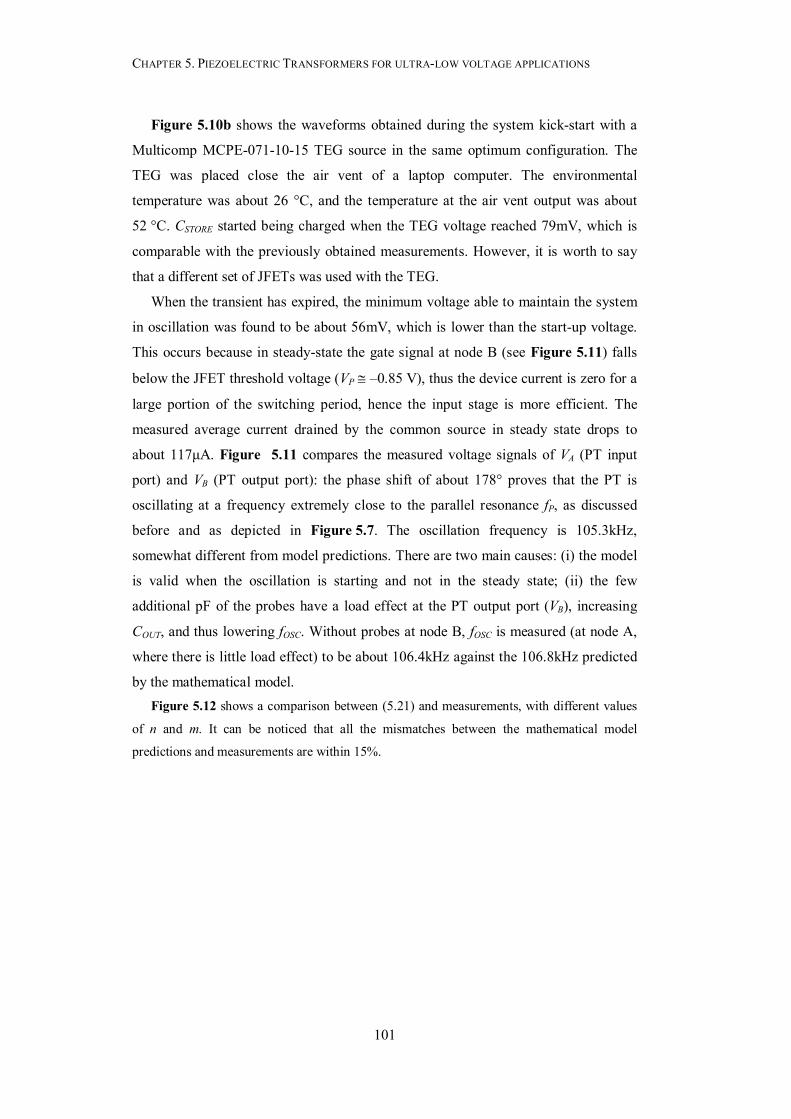
CHAPTER 5. PIEZOELECTRIC TRANSFORMERS FOR ULTRA-LOW VOLTAGE APPLICATIONS
101
Figure 5.10b shows the waveforms obtained during the system kick-start with a
Multicomp MCPE-071-10-15 TEG source in the same optimum configuration. The
TEG was placed close the air vent of a laptop computer. The environmental
temperature was about 26 °C, and the temperature at the air vent output was about
52 °C. CSTORE started being charged when the TEG voltage reached 79mV, which is
comparable with the previously obtained measurements. However, it is worth to say
that a different set of JFETs was used with the TEG.
When the transient has expired, the minimum voltage able to maintain the system
in oscillation was found to be about 56mV, which is lower than the start-up voltage.
This occurs because in steady-state the gate signal at node B (see Figure 5.11) falls
below the JFET threshold voltage (VP ‒0.85 V), thus the device current is zero for a
large portion of the switching period, hence the input stage is more efficient. The
measured average current drained by the common source in steady state drops to
about 117μA. Figure 5.11 compares the measured voltage signals of VA (PT input
port) and VB (PT output port): the phase shift of about 178° proves that the PT is
oscillating at a frequency extremely close to the parallel resonance fP, as discussed
before and as depicted in Figure 5.7. The oscillation frequency is 105.3kHz,
somewhat different from model predictions. There are two main causes: (i) the model
is valid when the oscillation is starting and not in the steady state; (ii) the few
additional pF of the probes have a load effect at the PT output port (VB), increasing
COUT, and thus lowering fOSC. Without probes at node B, fOSC is measured (at node A,
where there is little load effect) to be about 106.4kHz against the 106.8kHz predicted
by the mathematical model. Figure 5.12 shows a comparison between (5.21) and measurements, with different values
of n and m. It can be noticed that all the mismatches between the mathematical model
predictions and measurements are within 15%.
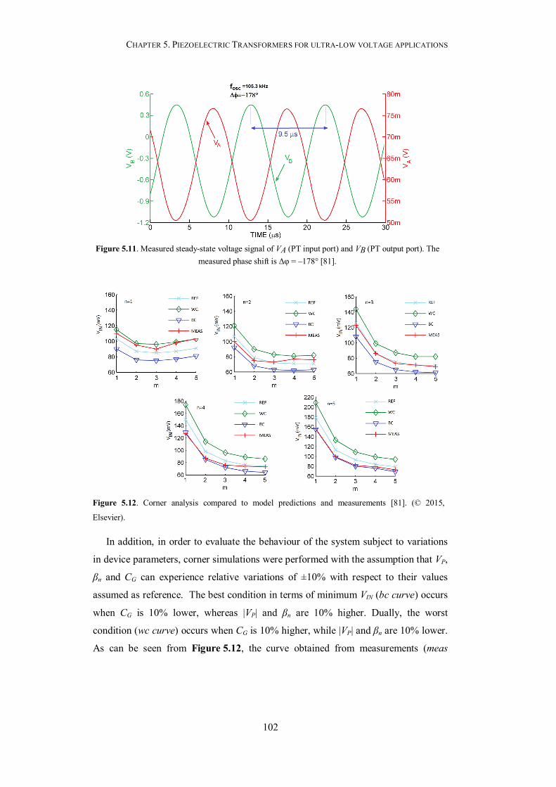
CHAPTER 5. PIEZOELECTRIC TRANSFORMERS FOR ULTRA-LOW VOLTAGE APPLICATIONS
102
In addition, in order to evaluate the behaviour of the system subject to variations
in device parameters, corner simulations were performed with the assumption that VP,
βn and CG can experience relative variations of ±10% with respect to their values
assumed as reference. The best condition in terms of minimum VIN (bc curve) occurs
when CG is 10% lower, whereas |VP| and βn are 10% higher. Dually, the worst
condition (wc curve) occurs when CG is 10% higher, while |VP| and βn are 10% lower.
As can be seen from Figure 5.12, the curve obtained from measurements (meas
Figure 5.12. Corner analysis compared to model predictions and measurements [81]. (© 2015,
Elsevier).
Figure 5.11. Measured steady-state voltage signal of VA (PT input port) and VB (PT output port). The
measured phase shift is Δφ = ‒178° [81].
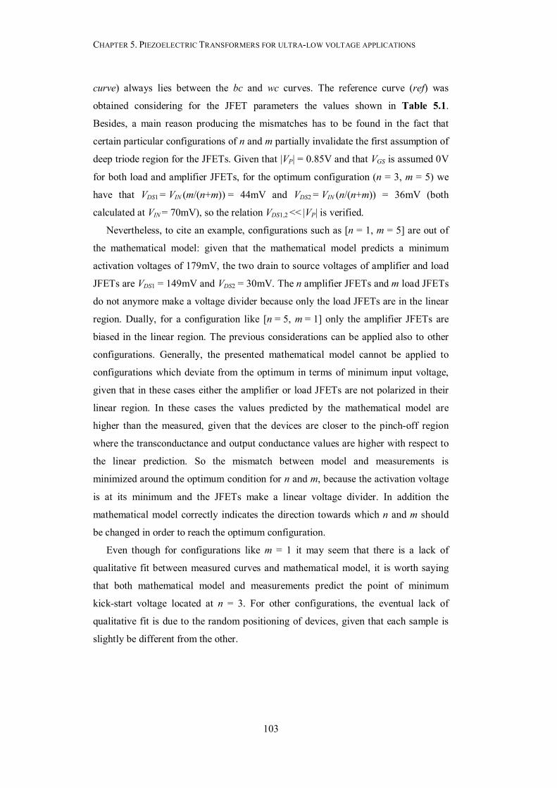
CHAPTER 5. PIEZOELECTRIC TRANSFORMERS FOR ULTRA-LOW VOLTAGE APPLICATIONS
103
curve) always lies between the bc and wc curves. The reference curve (ref) was
obtained considering for the JFET parameters the values shown in Table 5.1.
Besides, a main reason producing the mismatches has to be found in the fact that
certain particular configurations of n and m partially invalidate the first assumption of
deep triode region for the JFETs. Given that |VP| = 0.85V and that VGS is assumed 0V
for both load and amplifier JFETs, for the optimum configuration (n = 3, m = 5) we
have that VDS1 = VIN (m/(n+m)) = 44mV and VDS2 = VIN (n/(n+m)) = 36mV (both
calculated at VIN = 70mV), so the relation VDS1,2 << |VP| is verified.
Nevertheless, to cite an example, configurations such as [n = 1, m = 5] are out of
the mathematical model: given that the mathematical model predicts a minimum
activation voltages of 179mV, the two drain to source voltages of amplifier and load
JFETs are VDS1 = 149mV and VDS2 = 30mV. The n amplifier JFETs and m load JFETs
do not anymore make a voltage divider because only the load JFETs are in the linear
region. Dually, for a configuration like [n = 5, m = 1] only the amplifier JFETs are
biased in the linear region. The previous considerations can be applied also to other
configurations. Generally, the presented mathematical model cannot be applied to
configurations which deviate from the optimum in terms of minimum input voltage,
given that in these cases either the amplifier or load JFETs are not polarized in their
linear region. In these cases the values predicted by the mathematical model are
higher than the measured, given that the devices are closer to the pinch-off region
where the transconductance and output conductance values are higher with respect to
the linear prediction. So the mismatch between model and measurements is
minimized around the optimum condition for n and m, because the activation voltage
is at its minimum and the JFETs make a linear voltage divider. In addition the
mathematical model correctly indicates the direction towards which n and m should
be changed in order to reach the optimum configuration.
Even though for configurations like m = 1 it may seem that there is a lack of
qualitative fit between measured curves and mathematical model, it is worth saying
that both mathematical model and measurements predict the point of minimum
kick-start voltage located at n = 3. For other configurations, the eventual lack of
qualitative fit is due to the random positioning of devices, given that each sample is
slightly be different from the other.
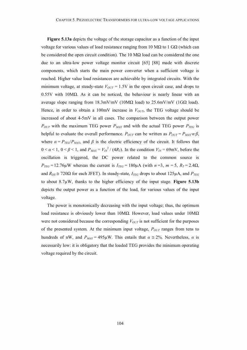
CHAPTER 5. PIEZOELECTRIC TRANSFORMERS FOR ULTRA-LOW VOLTAGE APPLICATIONS
104
Figure 5.13a depicts the voltage of the storage capacitor as a function of the input
voltage for various values of load resistance ranging from 10 MΩ to 1 GΩ (which can
be considered the open circuit condition). The 10 MΩ load can be considered the one
due to an ultra-low power voltage monitor circuit [65] [88] made with discrete
components, which starts the main power converter when a sufficient voltage is
reached. Higher value load resistances are achievable by integrated circuits. With the
minimum voltage, at steady-state VOUT = 1.5V in the open circuit case, and drops to
0.55V with 10MΩ. As it can be noticed, the behaviour is nearly linear with an
average slope ranging from 18.3mV/mV (10MΩ load) to 25.6mV/mV (1GΩ load).
Hence, in order to obtain a 100mV increase in VOUT, the TEG voltage should be
increased of about 4-5mV in all cases. The comparison between the output power
POUT with the maximum TEG power PMAX and with the actual TEG power PTEG is
helpful to evaluate the overall performance. POUT can be written as POUT = PMAX·α·β,
where α = PTEG/PMAX, and β is the electric efficiency of the circuit. It follows that
0 < α < 1, 0 < β < 1, and PMAX = VIN2 / (4RT). In the condition VIN = 69mV, before the
oscillation is triggered, the DC power related to the common source is
PTEG = 12.76µW whereas the current is ITEG = 180µA (with n =3, m = 5, RT = 2.4Ω,
and RDS 720Ω for each JFET). In steady-state, ITEG drops to about 125µA, and PTEG
to about 8.7µW, thanks to the higher efficiency of the input stage. Figure 5.13b
depicts the output power as a function of the load, for various values of the input
voltage.
The power is monotonically decreasing with the input voltage; thus, the optimum
load resistance is obviously lower than 10MΩ. However, load values under 10MΩ
were not considered because the corresponding VOUT is not sufficient for the purposes
of the presented system. At the minimum input voltage, POUT ranges from tens to
hundreds of nW, and PMAX = 495µW. This entails that α 2%. Nevertheless, α is
necessarily low: it is obligatory that the loaded TEG provides the minimum operating
voltage required by the circuit.
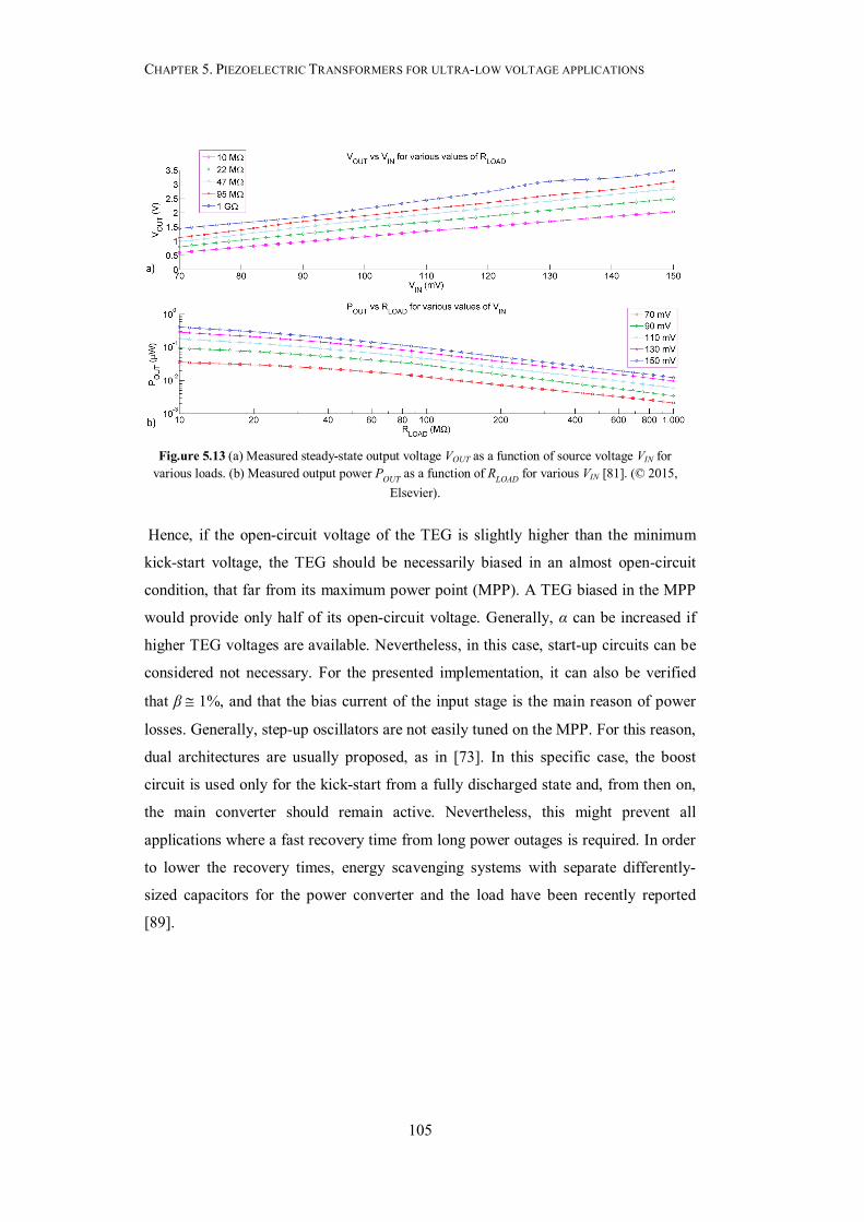
CHAPTER 5. PIEZOELECTRIC TRANSFORMERS FOR ULTRA-LOW VOLTAGE APPLICATIONS
105
Hence, if the open-circuit voltage of the TEG is slightly higher than the minimum
kick-start voltage, the TEG should be necessarily biased in an almost open-circuit
condition, that far from its maximum power point (MPP). A TEG biased in the MPP
would provide only half of its open-circuit voltage. Generally, α can be increased if
higher TEG voltages are available. Nevertheless, in this case, start-up circuits can be
considered not necessary. For the presented implementation, it can also be verified
that β 1%, and that the bias current of the input stage is the main reason of power
losses. Generally, step-up oscillators are not easily tuned on the MPP. For this reason,
dual architectures are usually proposed, as in [73]. In this specific case, the boost
circuit is used only for the kick-start from a fully discharged state and, from then on,
the main converter should remain active. Nevertheless, this might prevent all
applications where a fast recovery time from long power outages is required. In order
to lower the recovery times, energy scavenging systems with separate differently-
sized capacitors for the power converter and the load have been recently reported
[89].
Fig.ure 5.13 (a) Measured steady-state output voltage VOUT as a function of source voltage VIN for various loads. (b) Measured output power POUT as a function of RLOAD for various VIN [81]. (© 2015,
Elsevier).
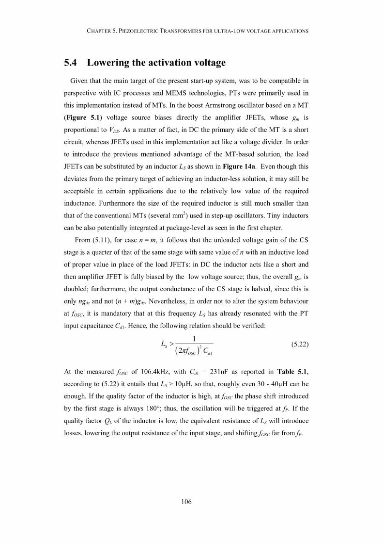
CHAPTER 5. PIEZOELECTRIC TRANSFORMERS FOR ULTRA-LOW VOLTAGE APPLICATIONS
106
5.4 Lowering the activation voltage
Given that the main target of the present start-up system, was to be compatible in
perspective with IC processes and MEMS technologies, PTs were primarily used in
this implementation instead of MTs. In the boost Armstrong oscillator based on a MT
(Figure 5.1) voltage source biases directly the amplifier JFETs, whose gm is
proportional to VDS. As a matter of fact, in DC the primary side of the MT is a short
circuit, whereas JFETs used in this implementation act like a voltage divider. In order
to introduce the previous mentioned advantage of the MT-based solution, the load
JFETs can be substituted by an inductor LS as shown in Figure 14a. Even though this
deviates from the primary target of achieving an inductor-less solution, it may still be
acceptable in certain applications due to the relatively low value of the required
inductance. Furthermore the size of the required inductor is still much smaller than
that of the conventional MTs (several mm2) used in step-up oscillators. Tiny inductors
can be also potentially integrated at package-level as seen in the first chapter.
From (5.11), for case n = m, it follows that the unloaded voltage gain of the CS
stage is a quarter of that of the same stage with same value of n with an inductive load
of proper value in place of the load JFETs: in DC the inductor acts like a short and
then amplifier JFET is fully biased by the low voltage source; thus, the overall gm is
doubled; furthermore, the output conductance of the CS stage is halved, since this is
only ngds and not (n + m)gds. Nevertheless, in order not to alter the system behaviour
at fOSC, it is mandatory that at this frequency LS has already resonated with the PT
input capacitance Cd1. Hence, the following relation should be verified:
2
1
12S
OSC d
Lπf C
(5.22)
At the measured fOSC of 106.4kHz, with Cd1 = 231nF as reported in Table 5.1,
according to (5.22) it entails that LS > 10µH, so that, roughly even 30 - 40µH can be
enough. If the quality factor of the inductor is high, at fOSC the phase shift introduced
by the first stage is always 180°; thus, the oscillation will be triggered at fP. If the
quality factor QL of the inductor is low, the equivalent resistance of LS will introduce
losses, lowering the output resistance of the input stage, and shifting fOSC far from fP.
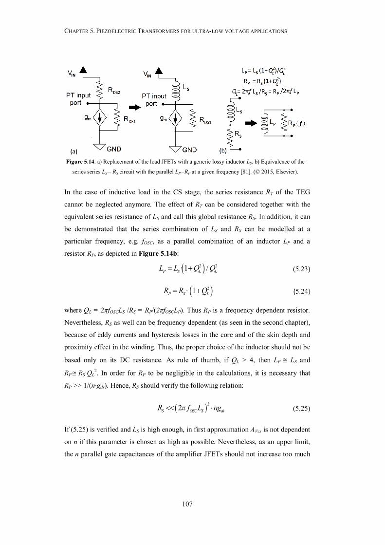
CHAPTER 5. PIEZOELECTRIC TRANSFORMERS FOR ULTRA-LOW VOLTAGE APPLICATIONS
107
In the case of inductive load in the CS stage, the series resistance RT of the TEG
cannot be neglected anymore. The effect of RT can be considered together with the
equivalent series resistance of LS and call this global resistance RS. In addition, it can
be demonstrated that the series combination of LS and RS can be modelled at a
particular frequency, e.g. fOSC, as a parallel combination of an inductor LP and a
resistor RP, as depicted in Figure 5.14b:
2 2· 1 /P S L LL L Q Q (5.23)
2· 1P S LR R Q (5.24)
where QL = 2πfOSCLS /RS = RP/(2πfOSCLP). Thus RP is a frequency dependent resistor.
Nevertheless, RS as well can be frequency dependent (as seen in the second chapter),
because of eddy currents and hysteresis losses in the core and of the skin depth and
proximity effect in the winding. Thus, the proper choice of the inductor should not be
based only on its DC resistance. As rule of thumb, if QL > 4, then LP LS and
RP RS∙QL2. In order for RP to be negligible in the calculations, it is necessary that
RP >> 1/(n∙gds). Hence, RS should verify the following relation:
22S OSC S dsR f L ng (5.25)
If (5.25) is verified and LS is high enough, in first approximation AVcs is not dependent
on n if this parameter is chosen as high as possible. Nevertheless, as an upper limit,
the n parallel gate capacitances of the amplifier JFETs should not increase too much
Figure 5.14. a) Replacement of the load JFETs with a generic lossy inductor LS. b) Equivalence of the
series series LS – RS circuit with the parallel LP –RP at a given frequency [81]. (© 2015, Elsevier).
CHAPTER 5. PIEZOELECTRIC TRANSFORMERS FOR ULTRA-LOW VOLTAGE APPLICATIONS
108
the PT output capacitance COUT, which affects AVPT according to (5.18). Then if n is
too high, the value of AVPT starts to decrease. Increasing n as well relaxes the
condition about RS. The same occurs with LS, if RS is mainly due to the TEG. The
mathematical model can be adapted according to the following mathematical
expression:
1
( )( ) ( )
mVcs
ds ds
g Z sAg Z s ng
, (5.26)
where gm and gds are the transcondutance and output conductance of a single JFET
and Z(s) = (1/ZPT(s) + 1/RP + 1/(sLP))-1. If (5.22) and (5.25) are verified, the effect of
LP and RP can be safely neglected.
Figure 5.15a depicts the simulated Bode plots of the loop gain obtained with
VIN = 70mV (that is about the voltage required to start the inductor-less system) in
different configurations: the loop gain with n = 3 and m = 5 reaches exactly 0dB at 0°
of phase shift. When LS = 37μH and RS = 3.05Ω, a maximum gain of about 4.8dB is
achieved when 4 ≤ n ≤ 6 at the same VIN. This implies that VIN,MIN can be decreased
from 70mV down to about 40mV, since 20log10(40 / 70) ‒4.8dB. In experimental
measurements, as it can be noticed from Figure 5.15b, with n = 4 the minimum
kick-start voltage drops to about 40mV, if a Multicomp MCPE-071-10-15 TEG with
~ 2.4 Ω internal resistance, and a 37μH inductor with ~0.65Ω series resistance at
106kHz are used. In this specific case the TEG was placed close to the AC/DC
adapter of a laptop, whose external temperature was measured to be around 42°C. In
these cases as well, if the measurements are repeated with a random choice of the n
amplifier JFETs, the variations in VIN,MIN are somewhat higher than the deviations
from the theoretical values. In this specific case, measurements show that
32mV ≤ VIN,MIN ≤ 35mV with n = 3 and RS 0.65Ω , whereas with n = 6 and
RS 1.2Ω, the measurements show that 34mV ≤ VIN,MIN ≤ 36mV. Experiments
performed with n = 3 and RS 1.2Ω showed that VIN,MIN can range from 48mV up to
52mV with a random choice of JFETs. However, this also proves that if n is
increased, higher values of RS can be tolerated as predicted by (5.25). Generally,
higher value of RS, considering the same value of n, could be very critical for the
minimum activation voltage.
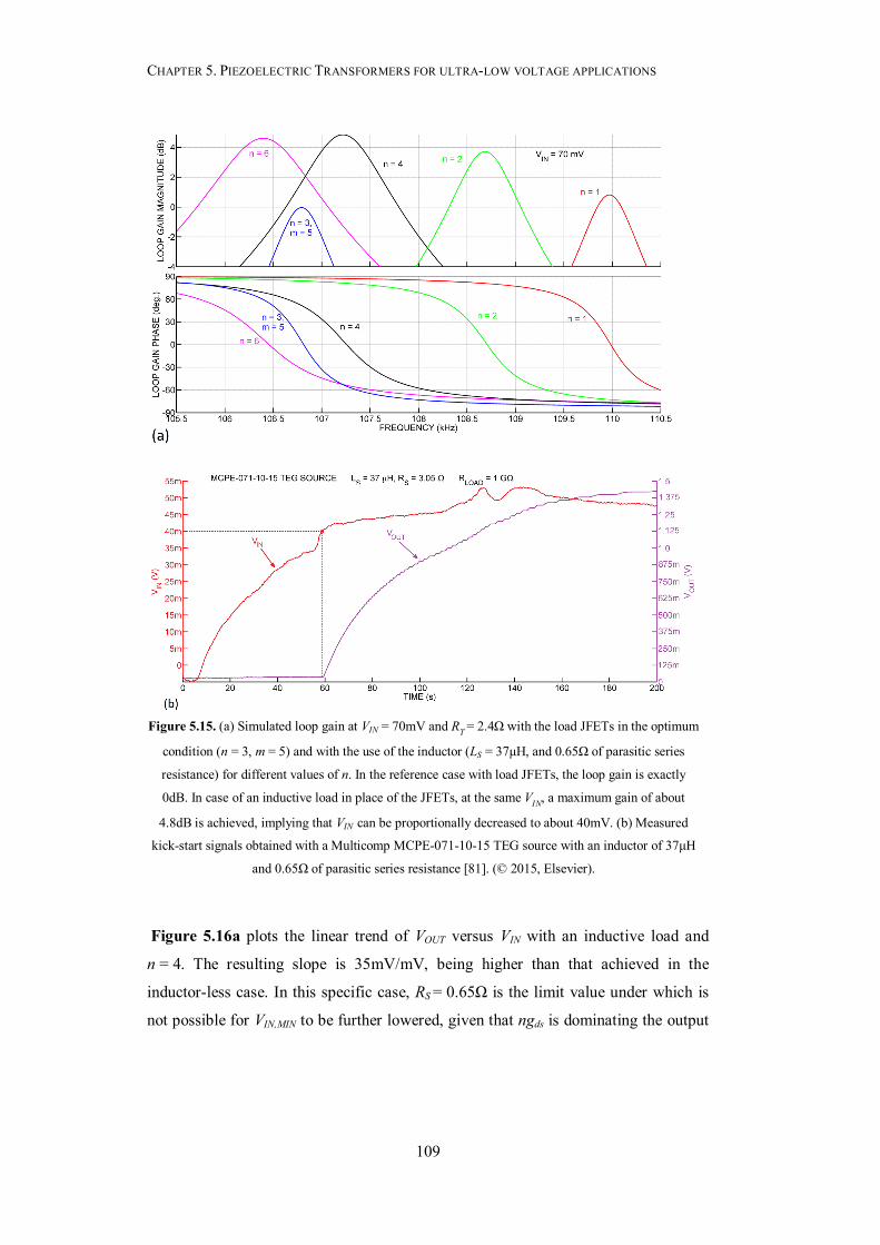
CHAPTER 5. PIEZOELECTRIC TRANSFORMERS FOR ULTRA-LOW VOLTAGE APPLICATIONS
109
Figure 5.16a plots the linear trend of VOUT versus VIN with an inductive load and
n = 4. The resulting slope is 35mV/mV, being higher than that achieved in the
inductor-less case. In this specific case, RS = 0.65Ω is the limit value under which is
not possible for VIN,MIN to be further lowered, given that ngds is dominating the output
Figure 5.15. (a) Simulated loop gain at VIN = 70mV and RT = 2.4Ω with the load JFETs in the optimum
condition (n = 3, m = 5) and with the use of the inductor (LS = 37μH, and 0.65Ω of parasitic series
resistance) for different values of n. In the reference case with load JFETs, the loop gain is exactly
0dB. In case of an inductive load in place of the JFETs, at the same VIN, a maximum gain of about
4.8dB is achieved, implying that VIN can be proportionally decreased to about 40mV. (b) Measured
kick-start signals obtained with a Multicomp MCPE-071-10-15 TEG source with an inductor of 37μH
and 0.65Ω of parasitic series resistance [81]. (© 2015, Elsevier).
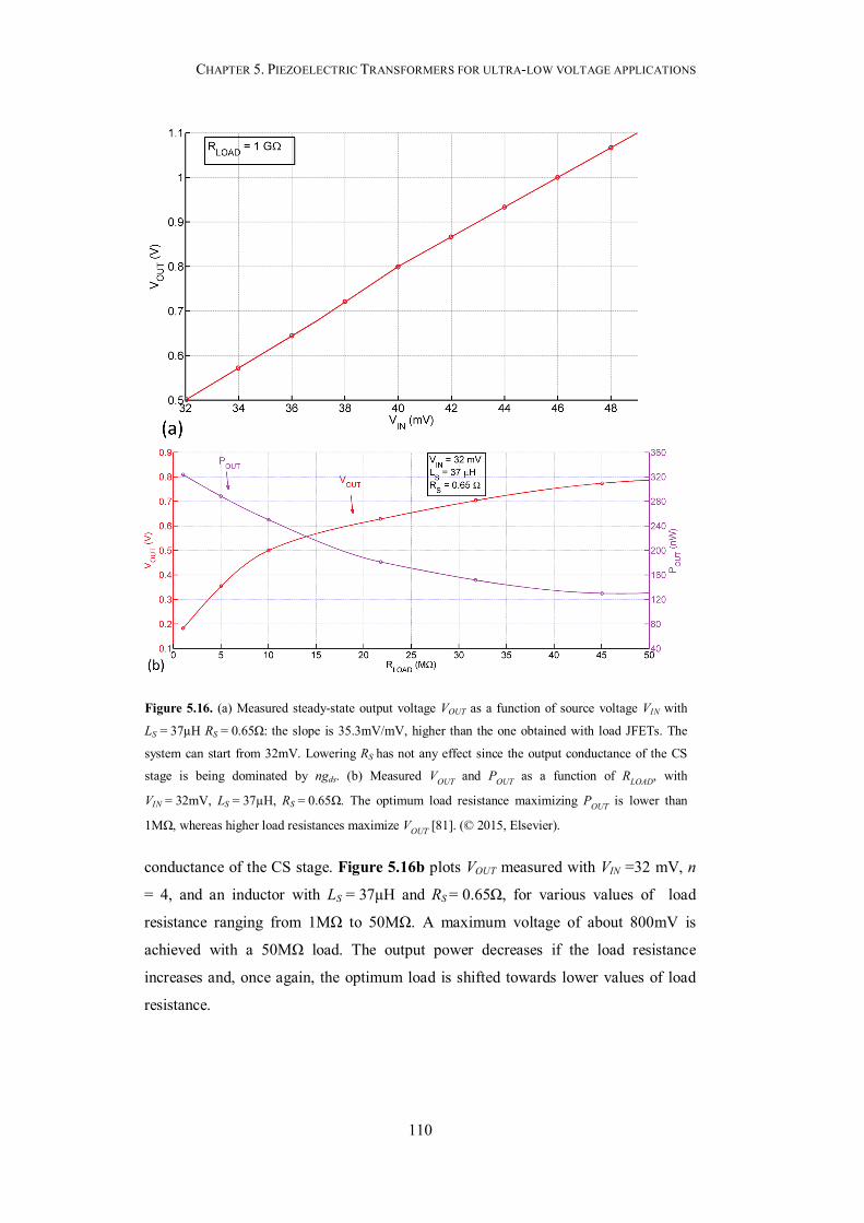
CHAPTER 5. PIEZOELECTRIC TRANSFORMERS FOR ULTRA-LOW VOLTAGE APPLICATIONS
110
conductance of the CS stage. Figure 5.16b plots VOUT measured with VIN =32 mV, n
= 4, and an inductor with LS = 37μH and RS = 0.65Ω, for various values of load
resistance ranging from 1MΩ to 50MΩ. A maximum voltage of about 800mV is
achieved with a 50MΩ load. The output power decreases if the load resistance
increases and, once again, the optimum load is shifted towards lower values of load
resistance.
Figure 5.16. (a) Measured steady-state output voltage VOUT as a function of source voltage VIN with
LS = 37µH RS = 0.65Ω: the slope is 35.3mV/mV, higher than the one obtained with load JFETs. The
system can start from 32mV. Lowering RS has not any effect since the output conductance of the CS
stage is being dominated by ngds. (b) Measured VOUT and POUT as a function of RLOAD, with
VIN = 32mV, LS = 37µH, RS = 0.65Ω. The optimum load resistance maximizing POUT is lower than
1MΩ, whereas higher load resistances maximize VOUT [81]. (© 2015, Elsevier).
CHAPTER 5. PIEZOELECTRIC TRANSFORMERS FOR ULTRA-LOW VOLTAGE APPLICATIONS
111
Considering the inductor, it is worth noting that it has a smaller size than the MTs
adopted in conventional boost oscillators. To cite an example, the Coilcraft XFL2006
and LPO3010 series of inductors achieve inductances up to 100 µH with package
dimensions of 220.6 mm3 and 331 mm3, respectively. The Coilcraft LPR6235,
one the the smallest available MTs with turn-ratios up to 1:100 has a 663.5 mm3
package. Furthermore, a single external inductor may be shared between the proposed
boost oscillator and the main switvhing DC-DC converter. In addition, at higher
packaging costs, a small inductor might be integrated at package level, as in
power-supply-in-package (PwrSiP) devices [2]. Finally, miniaturized TEGs with
footprint area as low as 2 mm2 are also available [90].
5.5 Summary on the presented boost oscillator
The principal advantage of the presented model is the possibility of evaluating and
sizing system components in the initial phases of system design, once the thermal
gradients and the TEG charateritics are known. Furthremore, the model allows to
optimize design parameters and to define the requirements for oscillation. To cite an
example, it predicts lower start-up voltages if PTs with higher quality factors are
used. The influence of variations of transistor parameters on the start-up voltage was
found to be limited, and comparable with the mismatch between model predictions
and measurements. However, these variations can be avoided with a custom IC
design, leading the way towards the system integrability. In perspective,
package-level integration of mixed microelectronic circuits and MEMS PTs can be
devised. MEMS PTs can be implemented in areas as low as few mm2 [91] [92].
Nevertheless, it is mandatory to place storage capacitors in the order of µF off-chip.
For this purpose, thin film supercapacitors are already available for package-level
integration [93] [94]. Conventional tiny SMD packages would also have a limited
impact on area. The current requirements of the particular application put some
constraints on the choice of the value of the storage capacitor. Generally, to cite an
example, in order to sustain a single packet transmission of a wireless node, i.e.
roughly tens of mA for tens of ms, several µF are necessary. Another critical
component for integrability could be the inductor, however, in this specifica case a
CHAPTER 5. PIEZOELECTRIC TRANSFORMERS FOR ULTRA-LOW VOLTAGE APPLICATIONS
112
small inductance of few tens of μH is required to improve circuit performance, as
well in the external DC/DC converter, and commercial solutions in fooprint area less
than 10mm2 are already available.
The presented solution should be devised as a single building block of a more
complex energy scavenging circuit. However , there are other design issues that
designers have to deal with. As a first requirement, a sub-µA voltage monitor should
be implemented, with the purposes of: (i) activating the main effcicient power
switching DC/DC converter, similarly to the circuits presented in [65] [66] [88], and
(ii) of disabling the boost circuit, which could be accomplished by pulling the gate of
the load JFET above its pinch-off voltage. Another challenge would be the design of a
MPPT DC/DC converter able to operate with input voltages as low as tens of mV, as
in [63]. Finally, in the inductor-based solution, a smart possibility is sharing the
inductor with the DC/DC converter.
5.6 Custom Integrated boost oscillators In perspective of increasing performances and shrinking dimensions, custom
integrated boost oscillators were designed and fabricated in a 0.35um microelectronic
process by STMicroelectronics. The schematic of the system is pretty much the same
of that in Figure 5.6. Two different versions of the oscillator were designed: the first
one (IC1, Figure 5.17a) is made up by an input stage composed by a classic common
source stage with n-channel depletion MOSFETs (whose characteristic equations are
similar to those of JFETs, given that a n-channel depletion MOSFET has a negative
threshold). Both amplifier and load MOSFETs were equally sized, with a
W/L =1.5mm/1.5µm. The second designed version (IC2, Figure 5.17b) of the
oscillator is made up by an input stage composed by a NOT port composed by native
(or natural) p-channel (for the pull-up) and n-channel mosfet (for the pull down), with
an L=1.5µm and WpMOS=4mm, whereas WnMOS=16mm. Unfortunately the second
version is not properly working even though SPICE simulations taking into account
the parasitic capacitances and resistances, as well as the effective area of source and
drain of all devices, show a perfect system operation.

CHAPTER 5. PIEZOELECTRIC TRANSFORMERS FOR ULTRA-LOW VOLTAGE APPLICATIONS
113
Figure 5.18 shows the measured waveforms of the system start-up for IC1. The
system is able to self-start at 28mV in inductor-less mode, that is without an inductor
in place of the load FET in the input stage of the oscillator. The output voltage in
no-load condition, using a 4.7µF capacitor, reaches about 3V which means a step-up
ratio greater than 102. This performance is achieved using a PT prototype made by
Noliac and the lower capacitances obtained in the system allow to keep the minimum
activation voltage at low values, as predicted by the developed mathematical model.
Furthermore the high quality factor of the PT, allows using an additional capacitance
of 400nF in parallel to its input port in order to increase its voltage gain without
affecting its input impedance, thus validating the former assumptions concerning the
optimization of the input capacitance.
Figure 5.19 shows the schematic of the oscillator IC2. The common source stage
is replaced by a NOT port made up of native MOSFETs (that is without a doped
channel, hence they have a lower threshold voltage compared to enhancement
MOSFETs). The only external components are CPUMP and CSTORE.
The main difference of IC2 compared to IC1 is that because of its higher loop gain,
the output oscillation of the input stage can reach the linear dynamics of the NOT port,
hence the oscillation can be more similar to a square wave instead of a sinusoid. Since
the following PT acts like a band-pass filter, part of the energy can be filtered out. This
implies that even though the open loop gain can be higher at higher input voltages for
IC2, the output voltage across the storage capacitor can be lower, given that driving a
PT with a square-wave is not an optimum solution.
Figure 5.17a,b: Designed integrated boost oscillators in 0.35µm technology by ST Microelectronics.
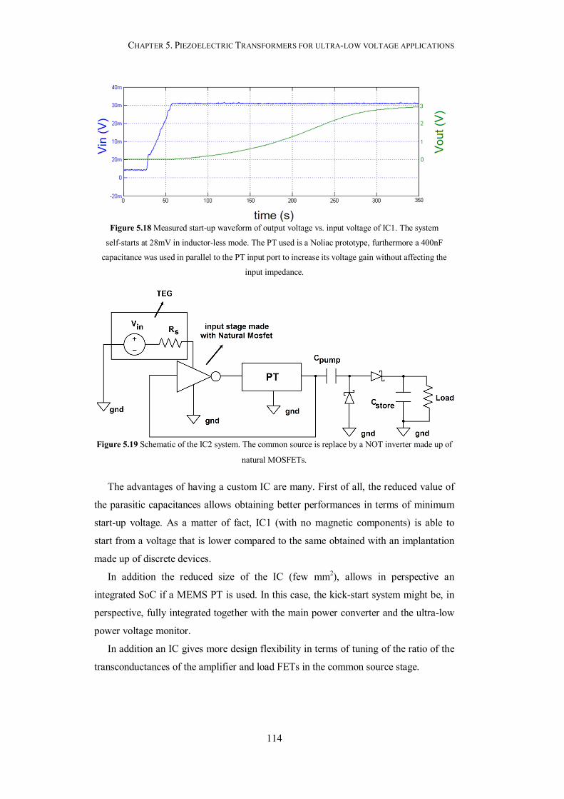
CHAPTER 5. PIEZOELECTRIC TRANSFORMERS FOR ULTRA-LOW VOLTAGE APPLICATIONS
114
The advantages of having a custom IC are many. First of all, the reduced value of
the parasitic capacitances allows obtaining better performances in terms of minimum
start-up voltage. As a matter of fact, IC1 (with no magnetic components) is able to
start from a voltage that is lower compared to the same obtained with an implantation
made up of discrete devices.
In addition the reduced size of the IC (few mm2), allows in perspective an
integrated SoC if a MEMS PT is used. In this case, the kick-start system might be, in
perspective, fully integrated together with the main power converter and the ultra-low
power voltage monitor.
In addition an IC gives more design flexibility in terms of tuning of the ratio of the
transconductances of the amplifier and load FETs in the common source stage.
Figure 5.18 Measured start-up waveform of output voltage vs. input voltage of IC1. The system
self-starts at 28mV in inductor-less mode. The PT used is a Noliac prototype, furthermore a 400nF
capacitance was used in parallel to the PT input port to increase its voltage gain without affecting the
input impedance.
Figure 5.19 Schematic of the IC2 system. The common source is replace by a NOT inverter made up of
natural MOSFETs.
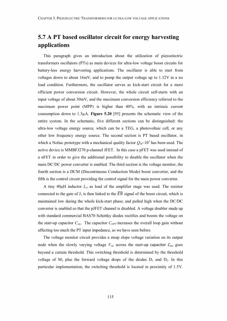
CHAPTER 5. PIEZOELECTRIC TRANSFORMERS FOR ULTRA-LOW VOLTAGE APPLICATIONS
115
5.7 A PT based oscillator circuit for energy harvesting applications
This paragraph gives an introduction about the utilization of piezoelectric
transformers oscillators (PTs) as main devices for ultra-low voltage boost circuits for
battery-less energy harvesting applications. The oscillator is able to start from
voltages down to about 16mV, and to pump the output voltage up to 1.32V in a no
load condition. Furthermore, the oscillator serves as kick-start circuit for a more
efficient power conversion circuit. However, the whole circuit self-starts with an
input voltage of about 30mV, and the maximum conversion efficiency referred to the
maximum power point (MPP) is higher than 40%, with an intrinsic current
consumption down to 1.3µA. Figure 5.20 [95] presents the schematic view of the
entire system. In the schematic, five different sections can be distinguished: the
ultra-low voltage energy source, which can be a TEG, a photovoltaic cell, or any
other low frequency energy source. The second section is PT based oscillator, in
which a Noliac prototype with a mechanical quality factor QM~103 has been used. The
active device is MMBFJ270 p-channel JFET. In this case a pFET was used instead of
a nFET in order to give the additional possibility to disable the oscillator when the
main DC/DC power converter is enabled. The third section is the voltage monitor, the
fourth section is a DCM (Discontinuous Conduction Mode) boost converter, and the
fifth is the control circuit providing the control signal for the main power converter.
A tiny 40μH inductor Lst as load of the amplifier stage was used. The resistor
connected to the gate of J1 is then linked to the ܧതതതത signal of the boost circuit, which is
maintained low during the whole kick-start phase, and pulled high when the DC/DC
converter is enabled so that the pJFET channel is disabled. A voltage doubler made up
with standard commercial BAS70 Schottky diodes rectifies and boosts the voltage on
the start-up capacitor Cstu. The capacitor COPT increases the overall loop gain without
affecting too much the PT input impedance, as we have seen before.
The voltage monitor circuit provides a steep slope voltage variation on its output
node when the slowly varying voltage Vstu across the start-up capacitor Cstu goes
beyond a certain threshold. This switching threshold is determined by the threshold
voltage of M2 plus the forward voltage drops of the diodes D1 and D2. In this
particular implementation, the switching threshold is located in proximity of 1.5V.
CHAPTER 5. PIEZOELECTRIC TRANSFORMERS FOR ULTRA-LOW VOLTAGE APPLICATIONS
116
The devices M3 and M4 were selected for never being conductive at the same time, at
the relative low voltage operating conditions of this circuit. In addition, M3 and M4
were chosen in order for the logic threshold of the inverter M3-M4 to be lower than
the switching threshold of the voltage monitor. For the same reason, the diode D3 as
well was added.
The capacitor CON at the beginning has not any stored charge, and hence provides
approximately 0V to the inverter M3-M4. When Vstu increases and exceeds the
switching threshold, CON starts being charged with the same slope of Vstu.
As M2 turns on, the inverter switches afterwards, because of its lower logic threshold.
The capacitor Cf gives an additional noise margin immediately after switching, in
order to prevent any other unwanted switching phases. As a consequence, the gate of
M1 is pulled down, and M1 turns on. Given that in the initial phase the signal
തതതത = 0 V, M5 is initially on. Then, the supply voltage VDD of the DC/DC converter isܧ
enabled. In order for this to happen very quickly, it is necessary that the CDD << CStu.
Once the DC/DC converter is enabled, the transistor M5 is turned off in order to
completely exclude the start-up oscillator path.
Concerning the control circuit, it is supplied only when thevoltage monitor detects
a sufficient voltage on Cstu. It is composed of a fixed frequency (1kHz) and duty cycle
(50%) square-wave oscillator which provides the PWM signal for the power converter,
and of an enable circuit that manages the generation of the ܧതതതത signal. A
STMicroelectronics TS881 comparator is used in the multivibrator because of its very
low 200nA bias current and of its very low minimum supply voltage down to 1.1V. In
addition, in order to reduce the power consumption, all resistors have relatively large
values: R1ast = R2ast = R3ast = 22MΩ, RON = ROFF = 6.1MΩ. The switching hystheresis
Figure 5.20: Schematic of the proposed energy harvesting circuit, with PT-based start-up and power
management circuitry [95]. (© 2015, IEEE)
CHAPTER 5. PIEZOELECTRIC TRANSFORMERS FOR ULTRA-LOW VOLTAGE APPLICATIONS
117
window is set by R1ast, R2ast, R3ast, and in the presented implementation ranges from
VDD/3 to 2∙VDD/3.
The control circuit also manages the generation of the ܧതതതത signal with the Boost
Enable sub-circuit. In particular, it relies on the detection of oscillations on the control
signal of the power converter. This is accomplished by a half-wave rectifier built with
the diode Den. The MOSFET Men filters away low amplitudes below its threshold
voltage. Cen is sized in order to provide a fast transition on ܧതതതത. When ܧതതതത changes
from low to high, it almost follows VDD. At its high voltage level, the start-up circuit is
disabled, the supply of the control circuit is turned on, and the capacitor CON in the
voltage monitor gets discharged, in order to allow the voltage monitor to enable the
start-up circuit again, in case of shortage of input power.
In order to reduce the power required for control, the DC/DC converter is a boost
switching converter with a constant duty-cycle as said before. This fixed duty-cycle
does not represent an important limitation as long as the operating conditions of the
low-voltage source are known and well defined: to cite an example, in a thermoelectric
energy harvesting application, the available thermal gradients are usually defined, e.g.
the difference between ambient and air vent temperature in a building, or between
ambient and human body temperature. Based on this information, it is possible to
correctly size the duty cycle of the converter. This is of course an acceptable trade-off
with the intrinsic consumption of the converter, which is minimized.
The Load Enable network controls power distribution to the external application
circuits. The load must be supplied only with suitable voltages or, alternatively,
disconnected. The p-channel MOSFET Mstore allows a very fast charge of Cstore when
VDD rises above a minimum threshold voltage.
The presented circuit was characterized with additional measurements in a dual
configuration: in the first one the main DC/DC converter is self-supplied and in the
second one it was supplied externally. These measurements allow to evaluate the
efficiency and the impact of power losses and intrinsic power consumption of control
circuits when the power available from the source is in the micro-power range. In a
first measurements session, the efficiency of the boost converter supplied externally
with VDD = 5V was measured for different input voltages and for variable loads. In this
specific case, the efficiency is intended as the ratio of the output power POUT
transferred to an external load, with the power PAV available from the source in the
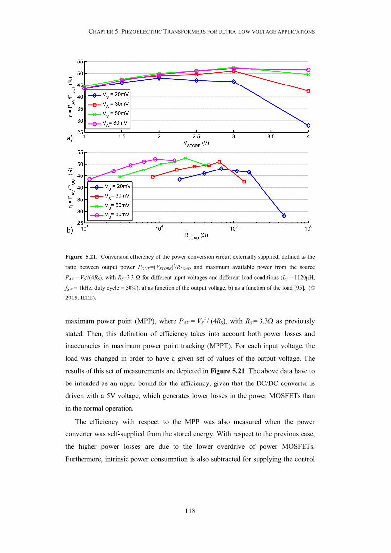
CHAPTER 5. PIEZOELECTRIC TRANSFORMERS FOR ULTRA-LOW VOLTAGE APPLICATIONS
118
maximum power point (MPP), where PAV = VS2 / (4RS), with RS = 3.3Ω as previously
stated. Then, this definition of efficiency takes into account both power losses and
inaccuracies in maximum power point tracking (MPPT). For each input voltage, the
load was changed in order to have a given set of values of the output voltage. The
results of this set of measurements are depicted in Figure 5.21. The above data have to
be intended as an upper bound for the efficiency, given that the DC/DC converter is
driven with a 5V voltage, which generates lower losses in the power MOSFETs than
in the normal operation.
The efficiency with respect to the MPP was also measured when the power
converter was self-supplied from the stored energy. With respect to the previous case,
the higher power losses are due to the lower overdrive of power MOSFETs.
Furthermore, intrinsic power consumption is also subtracted for supplying the control
Figure 5.21. Conversion efficiency of the power conversion circuit externally supplied, defined as the
ratio between output power POUT =(VSTORE)2/RLOAD and maximum available power from the source
PAV = VS2/(4RS), with RS=3.3 Ω for different input voltages and different load conditions (L1 = 1120µH,
fSW = 1kHz, duty cycle = 50%), a) as function of the output voltage, b) as a function of the load [95]. (©
2015, IEEE).

CHAPTER 5. PIEZOELECTRIC TRANSFORMERS FOR ULTRA-LOW VOLTAGE APPLICATIONS
119
circuits. The achieved efficiencies are depicted in Figure 5.22. The achieved
performance is pretty close to that obtained in micro-power harvesting circuits based
on discrete components, as reported in the comparison presented in [32], where
state-of-the-art converters starting from 20-40mV achieve efficiencies ranging from
40% to 61%.
Finally, the overall intrinsic power consumption PINT of the control circuits during
circuit operation was measured when the DC/DC converter was enabled. The results of
the measures are depicted in Figure 5.23. A very low current consumption IINT up to
1.3µA was observed. The corresponding intrinsic power is PINT = VDDIINT. Then, the
circuit is fully compatible with micro-power sources such TEGs or indoor photovoltaic
cells.
Figure 5.22. Conversion efficiency of the self-supplied power conversion circuit, defined as the ratio
between output power POUT =(VSTORE)2/RLOAD and maximum available power from the source
PAV = VS2/(4RS), with RS=3.3 Ω for different input voltages and different load conditions (L1 = 1120 µH,
fSW = 1 kHz, duty cycle = 50%), a) as function of the output voltage, b) as a function of the load [95]. (©
2015, IEEE).
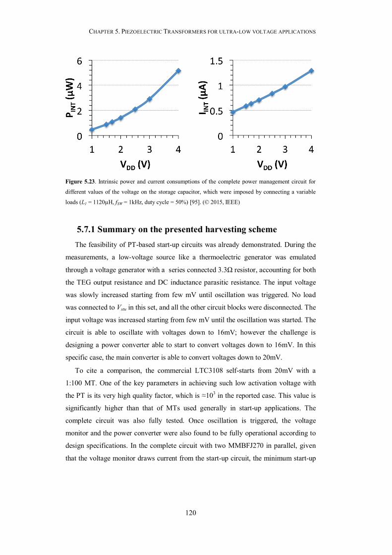
CHAPTER 5. PIEZOELECTRIC TRANSFORMERS FOR ULTRA-LOW VOLTAGE APPLICATIONS
120
5.7.1 Summary on the presented harvesting scheme The feasibility of PT-based start-up circuits was already demonstrated. During the
measurements, a low-voltage source like a thermoelectric generator was emulated
through a voltage generator with a series connected 3.3Ω resistor, accounting for both
the TEG output resistance and DC inductance parasitic resistance. The input voltage
was slowly increased starting from few mV until oscillation was triggered. No load
was connected to Vstu in this set, and all the other circuit blocks were disconnected. The
input voltage was increased starting from few mV until the oscillation was started. The
circuit is able to oscillate with voltages down to 16mV; however the challenge is
designing a power converter able to start to convert voltages down to 16mV. In this
specific case, the main converter is able to convert voltages down to 20mV.
To cite a comparison, the commercial LTC3108 self-starts from 20mV with a
1:100 MT. One of the key parameters in achieving such low activation voltage with
the PT is its very high quality factor, which is ≈103 in the reported case. This value is
significantly higher than that of MTs used generally in start-up applications. The
complete circuit was also fully tested. Once oscillation is triggered, the voltage
monitor and the power converter were also found to be fully operational according to
design specifications. In the complete circuit with two MMBFJ270 in parallel, given
that the voltage monitor draws current from the start-up circuit, the minimum start-up
Figure 5.23. Intrinsic power and current consumptions of the complete power management circuit for
different values of the voltage on the storage capacitor, which were imposed by connecting a variable
loads (L1 = 1120µH, fSW = 1kHz, duty cycle = 50%) [95]. (© 2015, IEEE)
CHAPTER 5. PIEZOELECTRIC TRANSFORMERS FOR ULTRA-LOW VOLTAGE APPLICATIONS
121
voltage that generates a sufficient steady-state output voltage (i.e. VDD > 1.7V in this
implementation) is slightly increased to VIN = 30mV. However, we have also found
that, once the start-up circuit is activated, if the input voltage is decreased oscillations
are sustained down to 20mV, given that the behavior of the oscillator is similar to a
class AB amplifier, given that the current drawn by the oscillator is null for a portion
of the oscillation period and, as a result, it is more efficient. It is important to remark
that a custom integrated solution can allow achieving nanocurrents voltage monitors
which imperceptibly affects the minimum required voltage to start an oscillation.
5.8 Summary
The chapter has presented a novel start-up oscillator based on piezoelectric
transformer. The minimum activation voltage to trigger an oscillation was determined
through the analysis and modelling of the circuit containing the linear model of the
active devices and the electromechanical model of the PT around the resonance. The
mathematical model was validated through a set of experimental measurements
showing a good matching with the developed model.
The chapter presented also the designed ICs in an STM 0.35μm technology, which
showed minimum activation voltages down to about 28mV, with output voltages up to
3V (in no load condition) without the aid of an additional inductor.
Furthermore the PT- based oscillator was used in a harvesting scheme (build-up
with discrete devices), containing a voltage monitor, an astable multivibrator, and a
main power converter with fixed switching frequency of 1kHz and duty cycle 50%.
The PT-based oscillator served as kick-start system for the main power converter once
a sufficient energy was stored on a storage capacitor, showing efficiencies up to 40%,
in line with obtained values in discrete systems for energy harvesting purposes.

122
Chapter 6
Design and fabrication of AlN
MEMS Piezoelectric Transformers
This chapter presents an overview on the design, simulation and fabrication of
AlN MEMS piezoelectric transformers performed in the clean rooms at the
Technische Universität Wien (TUW) of Vienna (Austria) during the internship from
February 2015 to August 2015.
As already discussed in the previous chapters, PTs are used for high-voltage
applications (up to hundreds of V) and medium power applications (up to few W). In
perspective of having more and more compact systems (PwrSoC), according to the
MtM trend, it is possible to shrink dimensions of piezoelectric devices, without
theoretically affecting performances, as instead it occurs in magnetic devices as
extensively discussed in Chapter 2. However, MEMS piezoelectric devices, might be
more sensitive to air damping, which is not predictable FEM simulations, hence the
packaging might play an important role, not only concerning the compactness of the
system, but also regarding the performances.
CHAPTER 6. DESIGN AND FABRICATION OF ALN MEMS PIEZOELECTRIC TRANSFORMERS
123
6.1 Theory, design and simulation of AlN PT
membranes
The first step is the design aided by FEM simulations. In general, the simulation of
high aspect-ratio structures requires a lot of computation and are time consuming. The
frequency of the mechanical resonance of a membrane is given by:
2
,2
12
i ms i
m KfR
(6.1)
where R2 is the full radius of the membrane and mi is a coefficient depending on i-th
mode considered. Table 6.1 gives the values of m for the first three modes.
Furthermore Km is named the membrane bending stiffness, it is homogeneous with the
product of the Young modulus Y by the inertia moment I and generally it is expressed
in N∙m. Km depends from both the mechanical constants of the device layer (Si -
20μm of thickness) and from the active piezo layer (AlN - <1μm), but in this case,
the AlN gives little contribution to the general mechanical properties. In Equation
(6.1) 휌 is the membrane equivalent mass given by:
Si Si AlN AlN Si Sit t t (6.2)
The approximation in (6.2) holds given that the equivalent mass (the product of the
thickness tSi and the mass density ρSi) of the Silicon device layer is much higher than
that of the AlN. An approximation of Km is given by:
3
212 1Si
m
YtK
(6.3)
Y is the Young modulus, and ν is the Poisson’s ratio. Table 6.2 gives some
mechanical and piezoelectric properties of some materials. Generic PZT values are
reported as well just for comparison purposes.
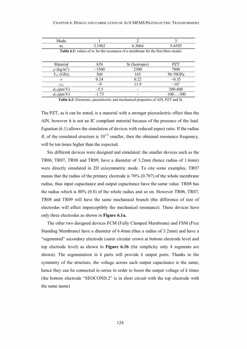
CHAPTER 6. DESIGN AND FABRICATION OF ALN MEMS PIEZOELECTRIC TRANSFORMERS
124
The PZT, as it can be noted, is a material with a stronger piezoelectric effect than the
AlN, however it is not an IC compliant material because of the presence of the lead.
Equation (6.1) allows the simulation of devices with reduced aspect ratio. If the radius
Rs of the simulated structure is 101/2 smaller, then the obtained resonance frequency,
will be ten times higher than the expected.
Six different devices were designed and simulated: the smaller devices such as the
TR06, TR07, TR08 and TR09, have a diameter of 3.2mm (hence radius of 1.6mm)
were directly simulated in 2D axisymmetric mode. To cite some examples, TR07
means that the radius of the primary electrode is 70% (0.707) of the whole membrane
radius, thus input capacitance and output capacitance have the same value. TR08 has
the radius which is 80% (0.8) of the whole radius and so on. However TR06, TR07,
TR08 and TR09 will have the same mechanical branch (the difference of size of
electrodes will affect imperceptibly the mechanical resonance). These devices have
only three electrodes as shown in Figure 6.1a.
The other two designed devices FCM (Fully Clamped Membrane) and FSM (Free
Standing Membrane) have a diameter of 6.4mm (thus a radius of 3.2mm) and have a
“segmented” secondary electrode (outer circular crown at bottom electrode level and
top electrode level) as shown in Figure 6.1b (for simplicity only 4 segments are
shown). The segmentation in k parts will provide k output ports. Thanks to the
symmetry of the structure, the voltage across each output capacitance is the same;
hence they can be connected in series in order to boost the output voltage of k times
(the bottom electrode “SEOCOND.2” is in short circuit with the top electrode with
the same name)
Mode 1 2 3 mi 3.1962 6.3064 9.4395 Table 6.1: values of mi for the resonance of a membrane for the first three modes
Material AlN Si (Isotropic) PZT ρ (kg/m3) ~3300 2300 7800 Y33 (GPa) 360 165 50-70GPa
ν 0.24 0.22 ~0.35 ε33 ~9 11.9 ~103
d33(pm/V) ~5.5 - 200-600 d31(pm/V) -1.73 - -100…-300
Table 6.2: Electronic, piezoelectric and mechanical properties of AlN, PZT and Si.
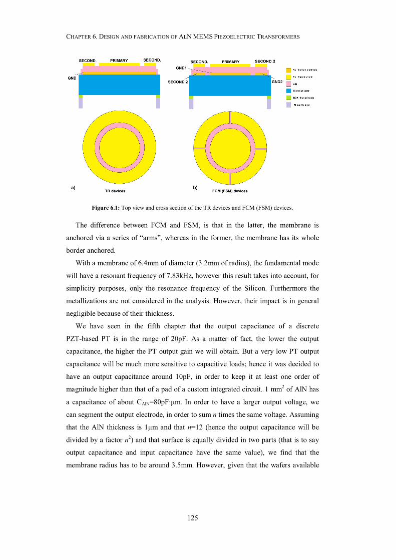
CHAPTER 6. DESIGN AND FABRICATION OF ALN MEMS PIEZOELECTRIC TRANSFORMERS
125
The difference between FCM and FSM, is that in the latter, the membrane is
anchored via a series of “arms”, whereas in the former, the membrane has its whole
border anchored.
With a membrane of 6.4mm of diameter (3.2mm of radius), the fundamental mode
will have a resonant frequency of 7.83kHz, however this result takes into account, for
simplicity purposes, only the resonance frequency of the Silicon. Furthermore the
metallizations are not considered in the analysis. However, their impact is in general
negligible because of their thickness.
We have seen in the fifth chapter that the output capacitance of a discrete
PZT-based PT is in the range of 20pF. As a matter of fact, the lower the output
capacitance, the higher the PT output gain we will obtain. But a very low PT output
capacitance will be much more sensitive to capacitive loads; hence it was decided to
have an output capacitance around 10pF, in order to keep it at least one order of
magnitude higher than that of a pad of a custom integrated circuit. 1 mm2 of AlN has
a capacitance of about CAlN=80pF∙μm. In order to have a larger output voltage, we
can segment the output electrode, in order to sum n times the same voltage. Assuming
that the AlN thickness is 1μm and that n=12 (hence the output capacitance will be
divided by a factor n2) and that surface is equally divided in two parts (that is to say
output capacitance and input capacitance have the same value), we find that the
membrane radius has to be around 3.5mm. However, given that the wafers available
Figure 6.1: Top view and cross section of the TR devices and FCM (FSM) devices.
CHAPTER 6. DESIGN AND FABRICATION OF ALN MEMS PIEZOELECTRIC TRANSFORMERS
126
for the fabrication were 4-inch diameter wafers, and that they were shared in a MPW
(Multi-Project Wafer), in order to have the same die dimensions, and thus simplifying
the dicing process, the radius of the membrane was lowered to 3.2mm. Hence in FEM
simulations, the radius of the membrane was set to 3.2/101/2=1.01mm, in order to have
a lower aspect ratio membrane and hence speeding up the simulation, which was
necessary to optimize the size of electrodes.
Figure 6.2 shows the first fundamental mechanical mode of a membrane with
20µm of device layer, 2.7µm of AlN and radius of 1.6mm. The electrodes are not
modelled. The mode is placed at 38.443kHz, hence the electric resonance will be
placed around this frequency.
Generally in literature, the optimization of the electrodes is made according to the
sign of the stress in order to maximize the power [90], however in order to maximize
the output voltage, the output capacitance should be decreased whereas the input
capacitance should be increased has shown in the fifth chapter. Hence the TR09
device intuitively has higher step-up ratios compared to the TR06 device. This is
confirmed by FEM simulations as well.
6.2 Other MEMS IC-compatible techniques
6.2.1 Spin coating The spin coating technique is the most common technique used to provide a
coating on the substrates with few ml of photoresist onto the substrates rotating at a
speed between 2000 and 4000 rpm. One of the advantages of the spin coating
technique is that it provides a very good homogeneity of the resist film thickness over
the whole wafer, as well as a very high smooth film surface.
Another advantage is that the film thickness is inversely proportional to the
rotating speed of the wafer, hence the film thickness can be modified by properly
trimming the rotating speed. One of the main drawbacks of this technique, is that it is
not efficient (efficiency less than 5%), this means that most of the deposited resist is
lost during the spinning in order to achieve the desired thickness, furthermore it
cannot be used on surfaces which are not “flat”.

CHAPTER 6. DESIGN AND FABRICATION OF ALN MEMS PIEZOELECTRIC TRANSFORMERS
127
6.2.2 Spray coating The spray coating technique is used to provide a coating on the substrates with via
the deposition of millions of μm-sized resist droplets. These resist droplets are
deposited on the substrate by an air stream, where they stick to the surface, and from
a thin resist film. The air stream is used given that the free fall in atmosphere would
take too much time for the film to be formed.
6.2.3 Etching
The etching is the technique that allows to perform an attack of substrates in order
to obtain well defined structures in bulk micromachining processes (that are processes
in which devices are obtained within the wafer, on the contrary surface
micromachining processes rely on the production of the devices on the surface of the
wafer). There are two types of etching: wet etching and dry (or plasma) etching.
The wet etching technique is a pure isotropic chemical process that is isotropic
etch in amorphous materials such as SiO2 (silicon dioxide) or it can be also
anisotropic in crystalline materials such as silicon, depending on the orientation of the
crystals. Contaminants in this type of technique are dependent on the chemical purity
and chemical system cleanliness. In general, agitation of the wet chemical bath is
used to aid the movement of reactants and to speed up the reaction process. Agitation
Figure 6.2: Fundamental mechanical mode of a membrane with 20µm of device layer, 2.7µm of AlN and radius 1.6mm.
CHAPTER 6. DESIGN AND FABRICATION OF ALN MEMS PIEZOELECTRIC TRANSFORMERS
128
can be made by simply putting a small magnetic cylinder rotating in the solution
while the etchant solution is heated (in order to have a faster attack rate).
Agitation also aids etch uniformity because it removes the eventual presence of
gases formed during the heating process. A good wet chemical workbench will have
agitation, temperature, and time controls as well as filtration to remove particulate and
contaminants.
As previously stated, wet-etching methods can also be used on crystalline
materials such as silicon to achieve directional etch profiles. For example, a typical
anisotropic etchant for the silicon is the potassium hydroxide (KOH), which etches
two orders of magnitude faster in the (100) plane than in the (111) plane. Certain
material such as the silicon dioxide or nitride can be used as “etch stops”, that is a
barrier that will not allow the etching to continue. In fact, in MEMS processes, the
BOX (buried oxide) placed between the silicon device layer and silicon handle layer
in SOI wafers, stops the front etching. In case there are not any etch stops in a wet
etching process, one option to achieve a specific etch depth is a timed etch. However,
this requires that the etching rate of the etchant in the particular material that is
wanted to be etched, should be well known and defined, furthermore a timed etch is
extremely difficult to control accurately.
6.2.4 Evaporation The evaporation is a deposition technique. In general it is used for deposition of
metals. Compared to the sputtering technique (see first chapter) it is slower, but
structures present a more defined shape. For the evaporation technique, the wafer is
placed in a very high vacuum chamber at room temperature with a melting pot
containing the material that has to be deposited. A heating source is used to heat the
melting pot which causes the evaporation of the material and condense on all exposed
cool surfaces of the vacuum chamber and substrate. The process is typically
performed on one side of the substrate at a time. The most diffused sources of heating
are: E-beam, Resistive heating, RF-inductive heating. In some systems the
substrate/wafer can be also heated during the process in order to alter the composition
or stress of the evaporated metal.
CHAPTER 6. DESIGN AND FABRICATION OF ALN MEMS PIEZOELECTRIC TRANSFORMERS
129
6.3 Fabrication of AlN piezoelectric transformers
This paragraph gives in more detail, the fabrication process of AlN piezoelectric
transformers at TUW- Vienna.
6.3.1 Photolithography This Section briefly summarizes the photolithography technique useful for the
definition of metal layers.
6.3.1.1 Photolithography in detail The process starts with the deposition of 1.8ml of AZ5214E (from
Microchemicals) image reversal photoresist on the wafer at 3000rpm. The wafer is an
SOI wafer with 20μm of device layer and 350μm of handle layer. Between the device
layer and the handle layer there is a 1μm thick layer of BOX (buried oxide).
The wafer is then baked at 107° C for 5 minutes. This first baking (prebake) is
necessary because the formed film on the wafer’s substrate has a remaining solvent
concentration. The partial elimination of this solvent by the softbaking leads to:
Avoid the mask sticking to the wafer during the exposition process,
Improve the resist adhesion to the wafer’s substrate,
Allow multiple coating without having any impact on the previous deposited
resist films.
Prevent the formation of bubbles by the remaining evaporating solvent
during the successive high-temperature processes such as evaporation or
sputtering of metals.
Increase the softening point (that is the temperature beyond which the resist
profile and edges start to be smoother) of the resist for the subsequent
high-temperature processing steps.
After the softbaking, the wafer again is put on the spin coater, and 2ml of AZ
Aquatar (from Microchemicals) is deposited on the wafer surface. The AZ Aquatar is
a top layer anti-reflective coating. This solution behaves like an optical coating at the
interface between the photoresist film and air, improving the image contrast.
Multiple reflections within the photoresist are also suppressed. Furthermore the use of
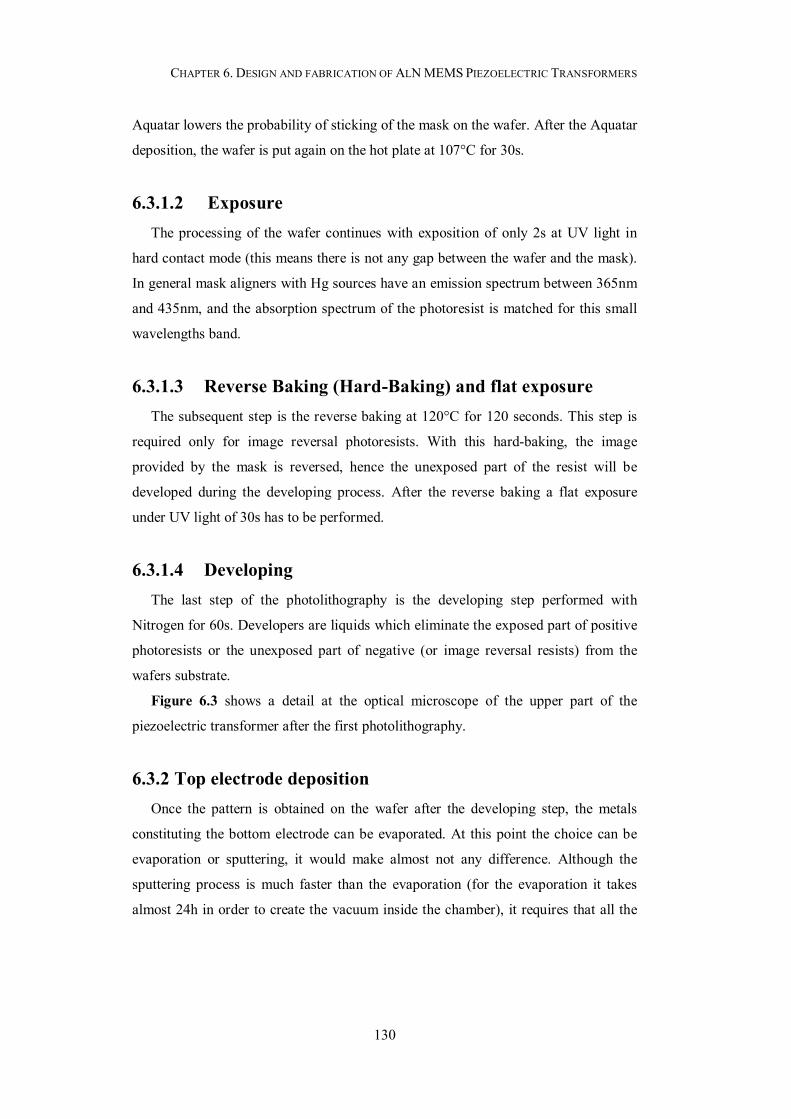
CHAPTER 6. DESIGN AND FABRICATION OF ALN MEMS PIEZOELECTRIC TRANSFORMERS
130
Aquatar lowers the probability of sticking of the mask on the wafer. After the Aquatar
deposition, the wafer is put again on the hot plate at 107°C for 30s.
6.3.1.2 Exposure The processing of the wafer continues with exposition of only 2s at UV light in
hard contact mode (this means there is not any gap between the wafer and the mask).
In general mask aligners with Hg sources have an emission spectrum between 365nm
and 435nm, and the absorption spectrum of the photoresist is matched for this small
wavelengths band.
6.3.1.3 Reverse Baking (Hard-Baking) and flat exposure The subsequent step is the reverse baking at 120°C for 120 seconds. This step is
required only for image reversal photoresists. With this hard-baking, the image
provided by the mask is reversed, hence the unexposed part of the resist will be
developed during the developing process. After the reverse baking a flat exposure
under UV light of 30s has to be performed.
6.3.1.4 Developing The last step of the photolithography is the developing step performed with
Nitrogen for 60s. Developers are liquids which eliminate the exposed part of positive
photoresists or the unexposed part of negative (or image reversal resists) from the
wafers substrate.
Figure 6.3 shows a detail at the optical microscope of the upper part of the
piezoelectric transformer after the first photolithography.
6.3.2 Top electrode deposition Once the pattern is obtained on the wafer after the developing step, the metals
constituting the bottom electrode can be evaporated. At this point the choice can be
evaporation or sputtering, it would make almost not any difference. Although the
sputtering process is much faster than the evaporation (for the evaporation it takes
almost 24h in order to create the vacuum inside the chamber), it requires that all the
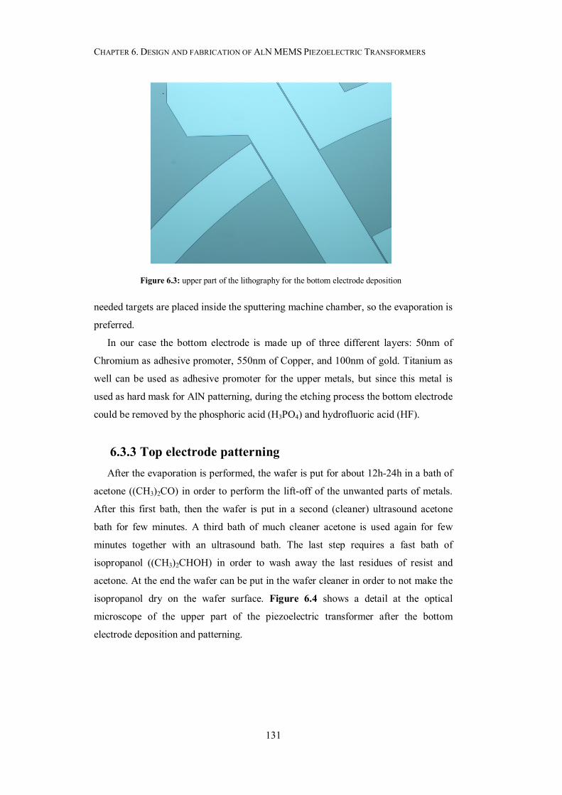
CHAPTER 6. DESIGN AND FABRICATION OF ALN MEMS PIEZOELECTRIC TRANSFORMERS
131
needed targets are placed inside the sputtering machine chamber, so the evaporation is
preferred.
In our case the bottom electrode is made up of three different layers: 50nm of
Chromium as adhesive promoter, 550nm of Copper, and 100nm of gold. Titanium as
well can be used as adhesive promoter for the upper metals, but since this metal is
used as hard mask for AlN patterning, during the etching process the bottom electrode
could be removed by the phosphoric acid (H3PO4) and hydrofluoric acid (HF).
6.3.3 Top electrode patterning After the evaporation is performed, the wafer is put for about 12h-24h in a bath of
acetone ((CH3)2CO) in order to perform the lift-off of the unwanted parts of metals.
After this first bath, then the wafer is put in a second (cleaner) ultrasound acetone
bath for few minutes. A third bath of much cleaner acetone is used again for few
minutes together with an ultrasound bath. The last step requires a fast bath of
isopropanol ((CH3)2CHOH) in order to wash away the last residues of resist and
acetone. At the end the wafer can be put in the wafer cleaner in order to not make the
isopropanol dry on the wafer surface. Figure 6.4 shows a detail at the optical
microscope of the upper part of the piezoelectric transformer after the bottom
electrode deposition and patterning.
Figure 6.3: upper part of the lithography for the bottom electrode deposition
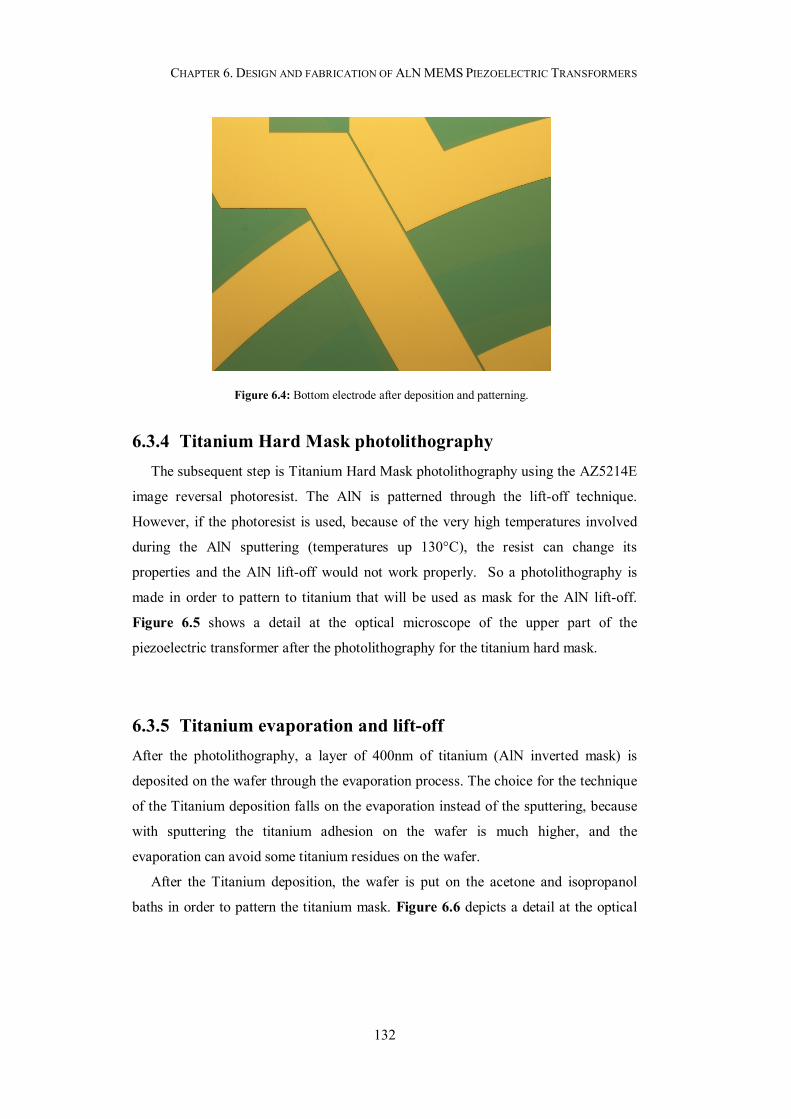
CHAPTER 6. DESIGN AND FABRICATION OF ALN MEMS PIEZOELECTRIC TRANSFORMERS
132
6.3.4 Titanium Hard Mask photolithography The subsequent step is Titanium Hard Mask photolithography using the AZ5214E
image reversal photoresist. The AlN is patterned through the lift-off technique.
However, if the photoresist is used, because of the very high temperatures involved
during the AlN sputtering (temperatures up 130°C), the resist can change its
properties and the AlN lift-off would not work properly. So a photolithography is
made in order to pattern to titanium that will be used as mask for the AlN lift-off.
Figure 6.5 shows a detail at the optical microscope of the upper part of the
piezoelectric transformer after the photolithography for the titanium hard mask.
6.3.5 Titanium evaporation and lift-off After the photolithography, a layer of 400nm of titanium (AlN inverted mask) is
deposited on the wafer through the evaporation process. The choice for the technique
of the Titanium deposition falls on the evaporation instead of the sputtering, because
with sputtering the titanium adhesion on the wafer is much higher, and the
evaporation can avoid some titanium residues on the wafer.
After the Titanium deposition, the wafer is put on the acetone and isopropanol
baths in order to pattern the titanium mask. Figure 6.6 depicts a detail at the optical
Figure 6.4: Bottom electrode after deposition and patterning.
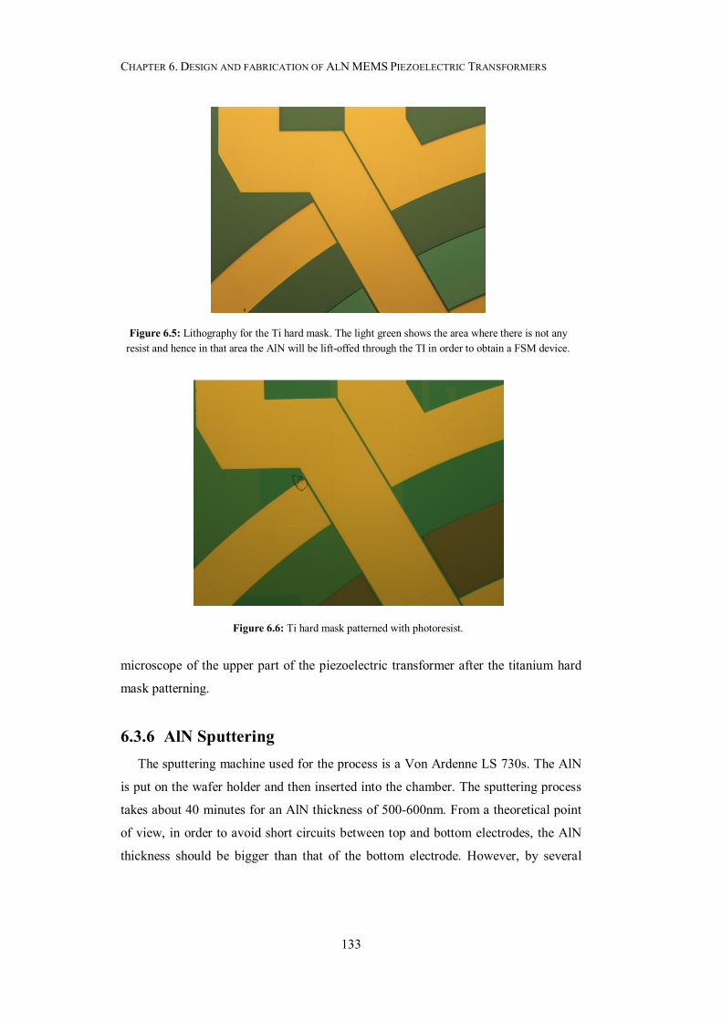
CHAPTER 6. DESIGN AND FABRICATION OF ALN MEMS PIEZOELECTRIC TRANSFORMERS
133
microscope of the upper part of the piezoelectric transformer after the titanium hard
mask patterning.
6.3.6 AlN Sputtering The sputtering machine used for the process is a Von Ardenne LS 730s. The AlN
is put on the wafer holder and then inserted into the chamber. The sputtering process
takes about 40 minutes for an AlN thickness of 500-600nm. From a theoretical point
of view, in order to avoid short circuits between top and bottom electrodes, the AlN
thickness should be bigger than that of the bottom electrode. However, by several
Figure 6.6: Ti hard mask patterned with photoresist.
Figure 6.5: Lithography for the Ti hard mask. The light green shows the area where there is not any resist and hence in that area the AlN will be lift-offed through the TI in order to obtain a FSM device.
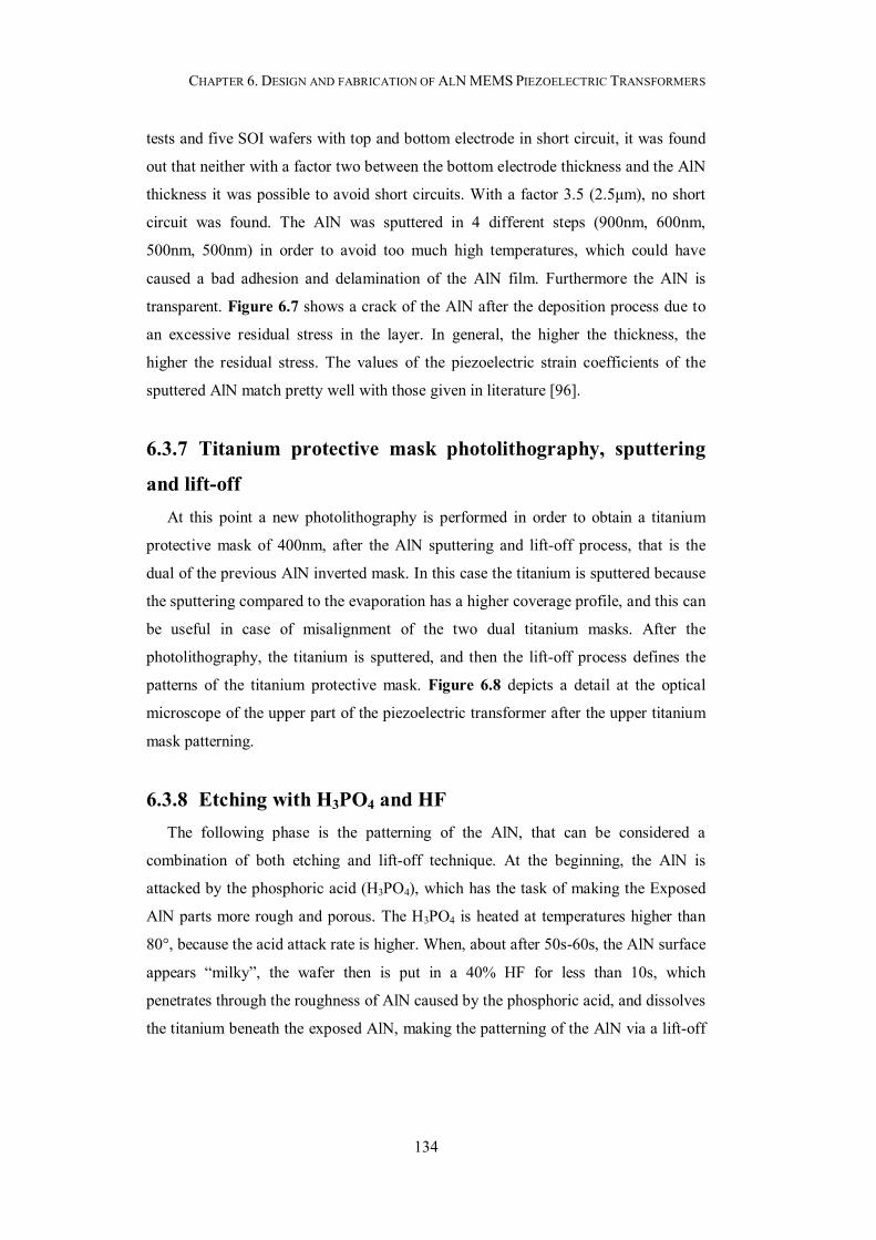
CHAPTER 6. DESIGN AND FABRICATION OF ALN MEMS PIEZOELECTRIC TRANSFORMERS
134
tests and five SOI wafers with top and bottom electrode in short circuit, it was found
out that neither with a factor two between the bottom electrode thickness and the AlN
thickness it was possible to avoid short circuits. With a factor 3.5 (2.5μm), no short
circuit was found. The AlN was sputtered in 4 different steps (900nm, 600nm,
500nm, 500nm) in order to avoid too much high temperatures, which could have
caused a bad adhesion and delamination of the AlN film. Furthermore the AlN is
transparent. Figure 6.7 shows a crack of the AlN after the deposition process due to
an excessive residual stress in the layer. In general, the higher the thickness, the
higher the residual stress. The values of the piezoelectric strain coefficients of the
sputtered AlN match pretty well with those given in literature [96].
6.3.7 Titanium protective mask photolithography, sputtering
and lift-off At this point a new photolithography is performed in order to obtain a titanium
protective mask of 400nm, after the AlN sputtering and lift-off process, that is the
dual of the previous AlN inverted mask. In this case the titanium is sputtered because
the sputtering compared to the evaporation has a higher coverage profile, and this can
be useful in case of misalignment of the two dual titanium masks. After the
photolithography, the titanium is sputtered, and then the lift-off process defines the
patterns of the titanium protective mask. Figure 6.8 depicts a detail at the optical
microscope of the upper part of the piezoelectric transformer after the upper titanium
mask patterning.
6.3.8 Etching with H3PO4 and HF The following phase is the patterning of the AlN, that can be considered a
combination of both etching and lift-off technique. At the beginning, the AlN is
attacked by the phosphoric acid (H3PO4), which has the task of making the Exposed
AlN parts more rough and porous. The H3PO4 is heated at temperatures higher than
80°, because the acid attack rate is higher. When, about after 50s-60s, the AlN surface
appears “milky”, the wafer then is put in a 40% HF for less than 10s, which
penetrates through the roughness of AlN caused by the phosphoric acid, and dissolves
the titanium beneath the exposed AlN, making the patterning of the AlN via a lift-off
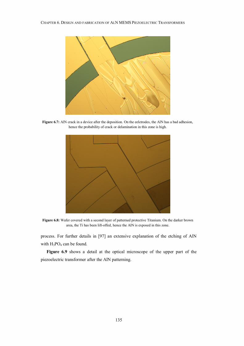
CHAPTER 6. DESIGN AND FABRICATION OF ALN MEMS PIEZOELECTRIC TRANSFORMERS
135
process. For further details in [97] an extensive explanation of the etching of AlN
with H3PO4 can be found.
Figure 6.9 shows a detail at the optical microscope of the upper part of the
piezoelectric transformer after the AlN patterning.
Figure 6.7: AlN crack in a device after the deposition. On the eelctrodes, the AlN has a bad adhesion, hence the probability of crack or delamination in this zone is high.
Figure 6.8: Wafer covered with a second layer of patterned protective Titanium. On the darker brown area, the Ti has been lift-offed, hence the AlN is exposed in this zone.
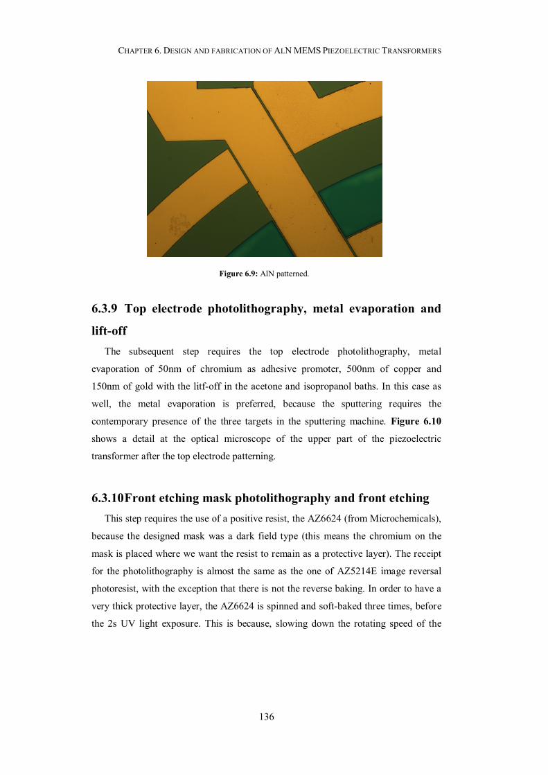
CHAPTER 6. DESIGN AND FABRICATION OF ALN MEMS PIEZOELECTRIC TRANSFORMERS
136
6.3.9 Top electrode photolithography, metal evaporation and
lift-off The subsequent step requires the top electrode photolithography, metal
evaporation of 50nm of chromium as adhesive promoter, 500nm of copper and
150nm of gold with the litf-off in the acetone and isopropanol baths. In this case as
well, the metal evaporation is preferred, because the sputtering requires the
contemporary presence of the three targets in the sputtering machine. Figure 6.10
shows a detail at the optical microscope of the upper part of the piezoelectric
transformer after the top electrode patterning.
6.3.10 Front etching mask photolithography and front etching This step requires the use of a positive resist, the AZ6624 (from Microchemicals),
because the designed mask was a dark field type (this means the chromium on the
mask is placed where we want the resist to remain as a protective layer). The receipt
for the photolithography is almost the same as the one of AZ5214E image reversal
photoresist, with the exception that there is not the reverse baking. In order to have a
very thick protective layer, the AZ6624 is spinned and soft-baked three times, before
the 2s UV light exposure. This is because, slowing down the rotating speed of the
Figure 6.9: AlN patterned.
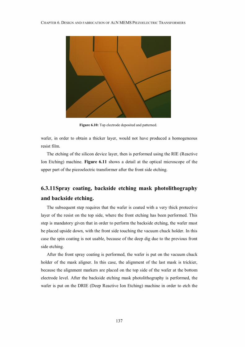
CHAPTER 6. DESIGN AND FABRICATION OF ALN MEMS PIEZOELECTRIC TRANSFORMERS
137
wafer, in order to obtain a thicker layer, would not have produced a homogeneous
resist film.
The etching of the silicon device layer, then is performed using the RIE (Reactive
Ion Etching) machine. Figure 6.11 shows a detail at the optical microscope of the
upper part of the piezoelectric transformer after the front side etching.
6.3.11 Spray coating, backside etching mask photolithography
and backside etching. The subsequent step requires that the wafer is coated with a very thick protective
layer of the resist on the top side, where the front etching has been performed. This
step is mandatory given that in order to perform the backside etching, the wafer must
be placed upside down, with the front side touching the vacuum chuck holder. In this
case the spin coating is not usable, because of the deep dig due to the previous front
side etching.
After the front spray coating is performed, the wafer is put on the vacuum chuck
holder of the mask aligner. In this case, the alignment of the last mask is trickier,
because the alignment markers are placed on the top side of the wafer at the bottom
electrode level. After the backside etching mask photolithography is performed, the
wafer is put on the DRIE (Deep Reactive Ion Etching) machine in order to etch the
Figure 6.10: Top electrode deposited and patterned.

CHAPTER 6. DESIGN AND FABRICATION OF ALN MEMS PIEZOELECTRIC TRANSFORMERS
138
350μm of the wafer handle layer. After the handle layer etching is performed, the
wafer has to be handled with a lot of care, since from now on it is more fragile.
6.3.12 Spray coating, backside etching mask photolithography
and backside etching. The subsequent step requires that the wafer is coated with a very thick protective
layer of the resist on the top side, where the front etching has been performed. This
step is mandatory given that in order to perform the backside etching, the wafer must
be placed upside down, with the front side touching the vacuum chuck holder. In this
case the spin coating is not usable, because of the deep dig due to the previous front
side etching.
After the front spray coating is performed, the wafer is put on the vacuum chuck
holder of the mask aligner. In this case, the alignment of the last mask is trickier,
because the alignment markers are placed on the top side of the wafer at the bottom
electrode level. After the backside etching mask photolithography is performed, the
wafer is put on the DRIE (Deep Reactive Ion Etching) machine in order to etch the
350μm of the wafer handle layer. After the handle layer etching is performed, the
wafer has to be handled with a lot of care, since from now on it is more fragile.
Figure 6.11: Front side etching (brown areas).
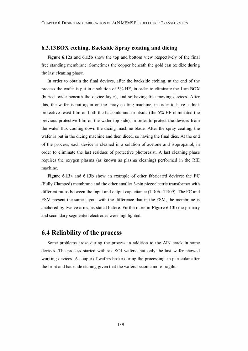
CHAPTER 6. DESIGN AND FABRICATION OF ALN MEMS PIEZOELECTRIC TRANSFORMERS
139
6.3.13 BOX etching, Backside Spray coating and dicing Figure 6.12a and 6.12b show the top and bottom view respectively of the final
free standing membrane. Sometimes the copper beneath the gold can oxidize during
the last cleaning phase.
In order to obtain the final devices, after the backside etching, at the end of the
process the wafer is put in a solution of 5% HF, in order to eliminate the 1μm BOX
(buried oxide beneath the device layer), and so having free moving devices. After
this, the wafer is put again on the spray coating machine, in order to have a thick
protective resist film on both the backside and frontside (the 5% HF eliminated the
previous protective film on the wafer top side), in order to protect the devices from
the water flux cooling down the dicing machine blade. After the spray coating, the
wafer is put in the dicing machine and then diced, so having the final dies. At the end
of the process, each device is cleaned in a solution of acetone and isopropanol, in
order to eliminate the last residues of protective photoresist. A last cleaning phase
requires the oxygen plasma (as known as plasma cleaning) performed in the RIE
machine. Figure 6.13a and 6.13b show an example of other fabricated devices: the FC
(Fully Clamped) membrane and the other smaller 3-pin piezoelectric transformer with
different ratios between the input and output capacitance (TR06...TR09). The FC and
FSM present the same layout with the difference that in the FSM, the membrane is
anchored by twelve arms, as stated before. Furthermore in Figure 6.13b the primary
and secondary segmented electrodes were highlighted.
6.4 Reliability of the process Some problems arose during the process in addition to the AlN crack in some
devices. The process started with six SOI wafers, but only the last wafer showed
working devices. A couple of wafers broke during the processing, in particular after
the front and backside etching given that the wafers become more fragile.
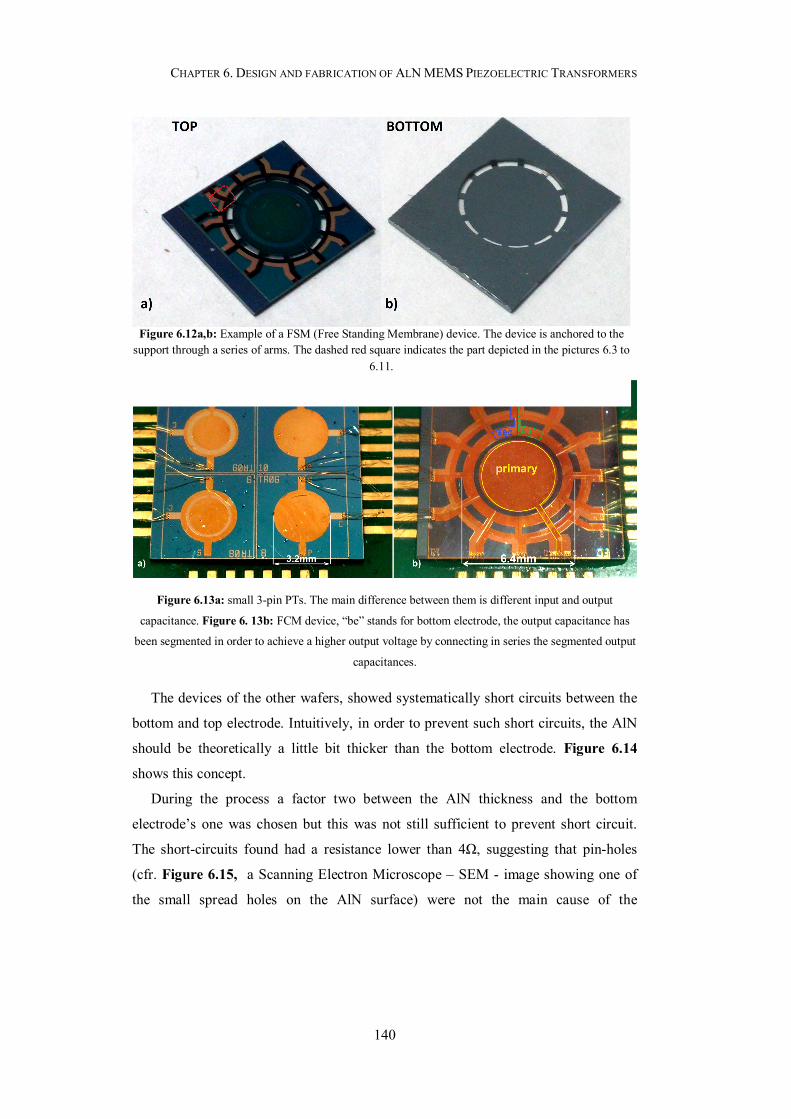
CHAPTER 6. DESIGN AND FABRICATION OF ALN MEMS PIEZOELECTRIC TRANSFORMERS
140
The devices of the other wafers, showed systematically short circuits between the
bottom and top electrode. Intuitively, in order to prevent such short circuits, the AlN
should be theoretically a little bit thicker than the bottom electrode. Figure 6.14
shows this concept.
During the process a factor two between the AlN thickness and the bottom
electrode’s one was chosen but this was not still sufficient to prevent short circuit.
The short-circuits found had a resistance lower than 4Ω, suggesting that pin-holes
(cfr. Figure 6.15, a Scanning Electron Microscope – SEM - image showing one of
the small spread holes on the AlN surface) were not the main cause of the
Figure 6.13a: small 3-pin PTs. The main difference between them is different input and output
capacitance. Figure 6. 13b: FCM device, “be” stands for bottom electrode, the output capacitance has
been segmented in order to achieve a higher output voltage by connecting in series the segmented output
capacitances.
Figure 6.12a,b: Example of a FSM (Free Standing Membrane) device. The device is anchored to the support through a series of arms. The dashed red square indicates the part depicted in the pictures 6.3 to
6.11.
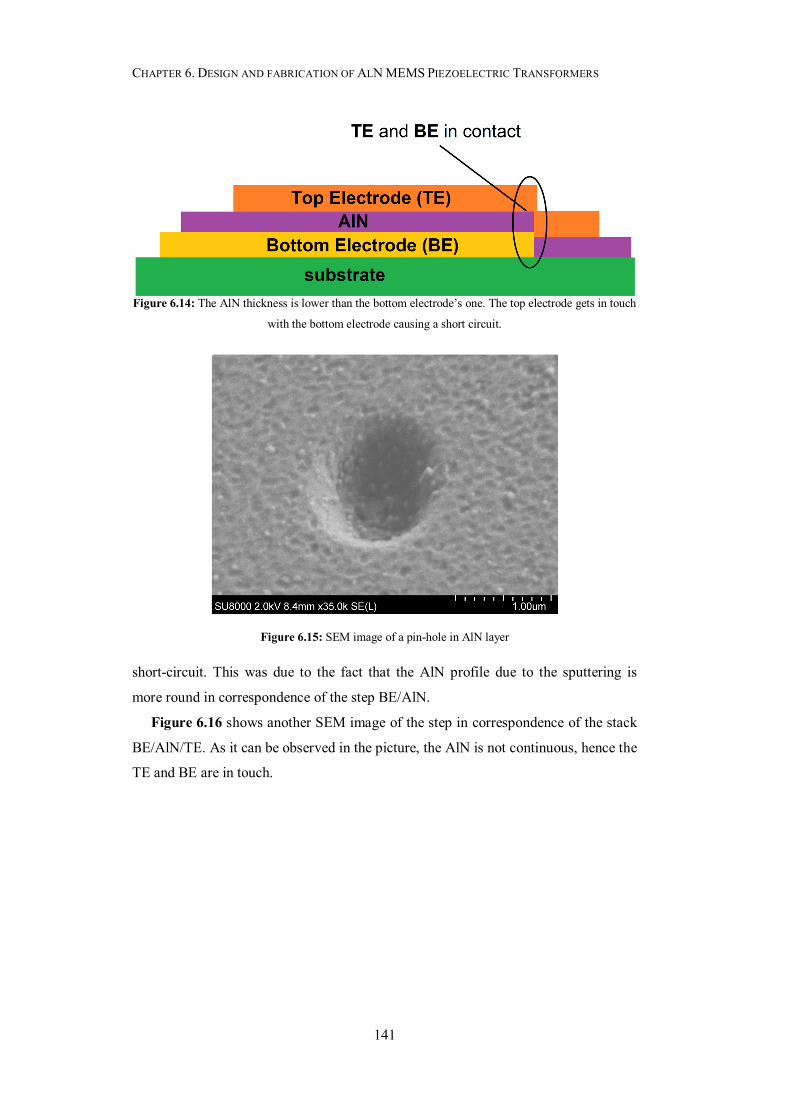
CHAPTER 6. DESIGN AND FABRICATION OF ALN MEMS PIEZOELECTRIC TRANSFORMERS
141
short-circuit. This was due to the fact that the AlN profile due to the sputtering is
more round in correspondence of the step BE/AlN.
Figure 6.16 shows another SEM image of the step in correspondence of the stack
BE/AlN/TE. As it can be observed in the picture, the AlN is not continuous, hence the
TE and BE are in touch.
Figure 6.14: The AlN thickness is lower than the bottom electrode’s one. The top electrode gets in touch
with the bottom electrode causing a short circuit.
Figure 6.15: SEM image of a pin-hole in AlN layer
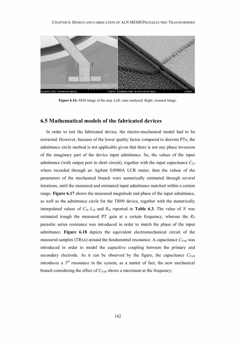
CHAPTER 6. DESIGN AND FABRICATION OF ALN MEMS PIEZOELECTRIC TRANSFORMERS
142
6.5 Mathematical models of the fabricated devices
In order to test the fabricated device, the electro-mechanical model had to be
extracted. However, because of the lower quality factor compared to discrete PTs, the
admittance circle method is not applicable given that there is not any phase inversion
of the imaginary part of the device input admittance. So, the values of the input
admittance (with output port in short circuit), together with the input capacitance CIN
where recorded through an Agilent E4980A LCR meter; then the values of the
parameters of the mechanical branch were numerically estimated through several
iterations, until the measured and estimated input admittance matched within a certain
range. Figure 6.17 shows the measured magnitude and phase of the input admittance,
as well as the admittance circle for the TR09 device, together with the numerically
interpolated values of CM LM and RM reported in Table 6.3. The value of N was
estimated trough the measured PT gain at a certain frequency, whereas the RP
parasitic series resistance was introduced in order to match the phase of the input
admittance. Figure 6.18 depicts the equivalent electromechanical circuit of the
measured samples (TRxx) around the fundamental resonance. A capacitance CPAR was
introduced in order to model the capacitive coupling between the primary and
secondary electrode. As it can be observed by the figure, the capacitance CPAR
introduces a 3rd resonance in the system, as a matter of fact, the new mechanical
branch considering the effect of CPAR shows a maximum at the frequency:
Figure 6.16: SEM image of the step. Left: zone analysed. Right: zoomed image.

CHAPTER 6. DESIGN AND FABRICATION OF ALN MEMS PIEZOELECTRIC TRANSFORMERS
143
2
1
2p
M PARM
M PAR
fC CL
C C
(6.4)
Figure 6.17: Measured vs. interpolated input admittance for the TR09 device.
Figure 6.18: a) Equivalent electro-mechanical circuit. b) Different representation of the same circuit.
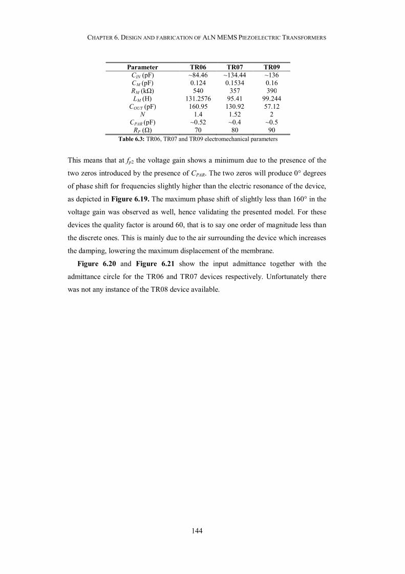
CHAPTER 6. DESIGN AND FABRICATION OF ALN MEMS PIEZOELECTRIC TRANSFORMERS
144
This means that at fp2 the voltage gain shows a minimum due to the presence of the
two zeros introduced by the presence of CPAR. The two zeros will produce 0° degrees
of phase shift for frequencies slightly higher than the electric resonance of the device,
as depicted in Figure 6.19. The maximum phase shift of slightly less than 160° in the
voltage gain was observed as well, hence validating the presented model. For these
devices the quality factor is around 60, that is to say one order of magnitude less than
the discrete ones. This is mainly due to the air surrounding the device which increases
the damping, lowering the maximum displacement of the membrane.
Figure 6.20 and Figure 6.21 show the input admittance together with the
admittance circle for the TR06 and TR07 devices respectively. Unfortunately there
was not any instance of the TR08 device available.
Parameter TR06 TR07 TR09 CIN (pF) ~84.46 ~134.44 ~136 CM (pF) 0.124 0.1534 0.16 RM (kΩ) 540 357 390 LM (H) 131.2576 95.41 99.244
COUT (pF) 160.95 130.92 57.12 N 1.4 1.52 2
CPAR (pF) ~0.52 ~0.4 ~0.5 RP (Ω) 70 80 90
Table 6.3: TR06, TR07 and TR09 electromechanical parameters
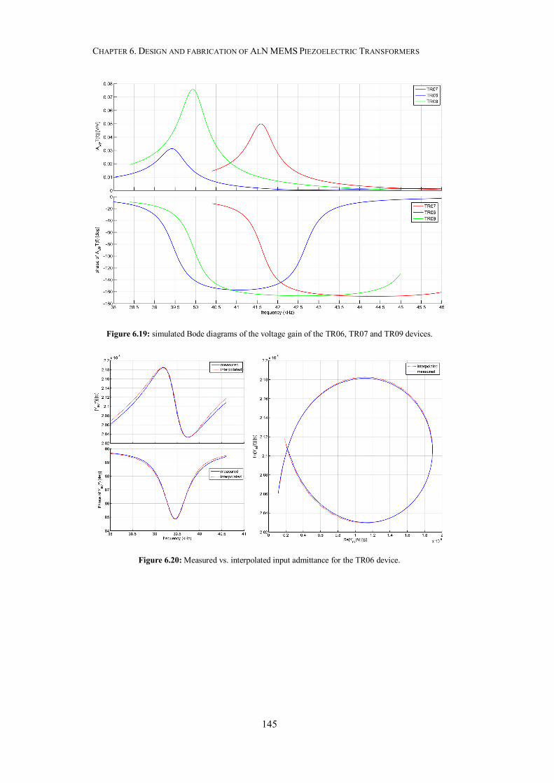
CHAPTER 6. DESIGN AND FABRICATION OF ALN MEMS PIEZOELECTRIC TRANSFORMERS
145
Figure 6.19: simulated Bode diagrams of the voltage gain of the TR06, TR07 and TR09 devices.
Figure 6.20: Measured vs. interpolated input admittance for the TR06 device.
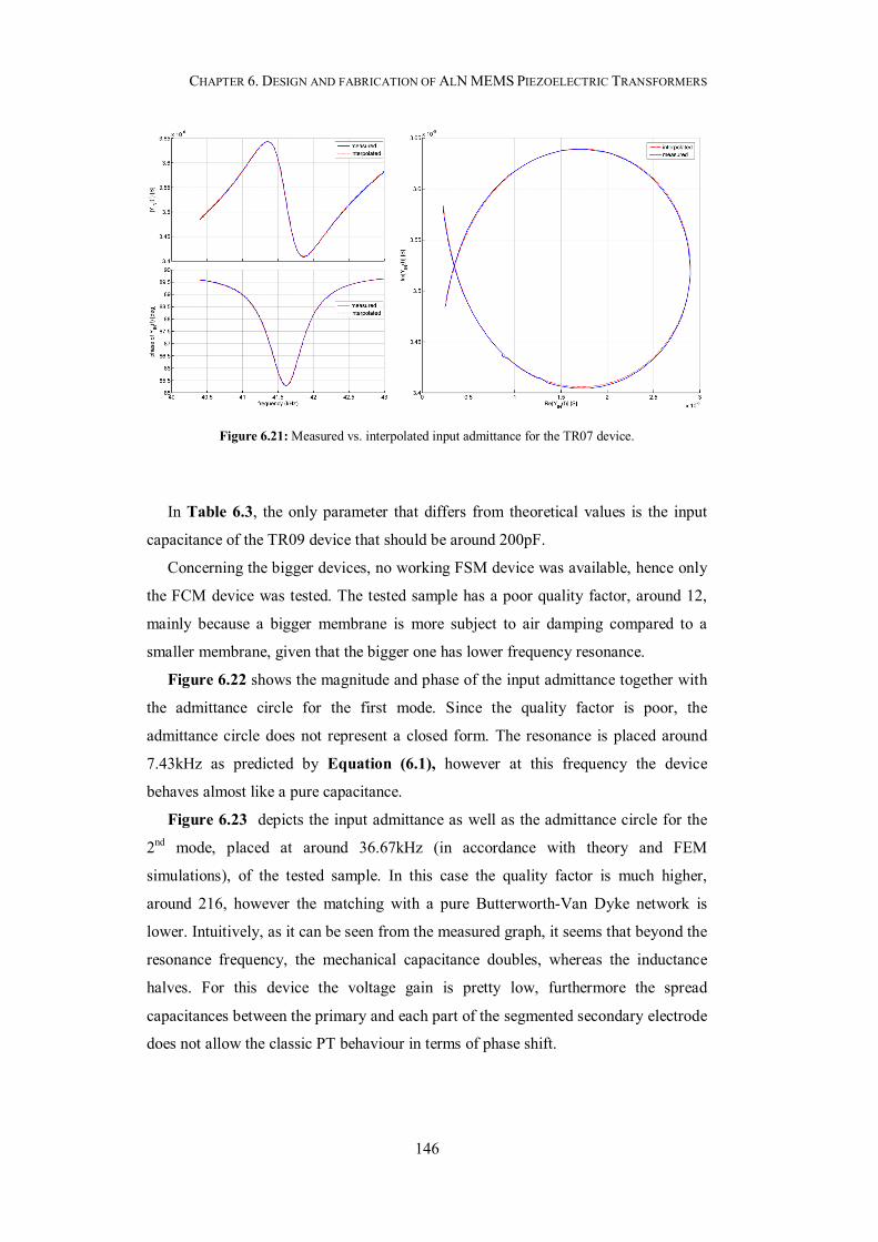
CHAPTER 6. DESIGN AND FABRICATION OF ALN MEMS PIEZOELECTRIC TRANSFORMERS
146
In Table 6.3, the only parameter that differs from theoretical values is the input
capacitance of the TR09 device that should be around 200pF.
Concerning the bigger devices, no working FSM device was available, hence only
the FCM device was tested. The tested sample has a poor quality factor, around 12,
mainly because a bigger membrane is more subject to air damping compared to a
smaller membrane, given that the bigger one has lower frequency resonance.
Figure 6.22 shows the magnitude and phase of the input admittance together with
the admittance circle for the first mode. Since the quality factor is poor, the
admittance circle does not represent a closed form. The resonance is placed around
7.43kHz as predicted by Equation (6.1), however at this frequency the device
behaves almost like a pure capacitance.
Figure 6.23 depicts the input admittance as well as the admittance circle for the
2nd mode, placed at around 36.67kHz (in accordance with theory and FEM
simulations), of the tested sample. In this case the quality factor is much higher,
around 216, however the matching with a pure Butterworth-Van Dyke network is
lower. Intuitively, as it can be seen from the measured graph, it seems that beyond the
resonance frequency, the mechanical capacitance doubles, whereas the inductance
halves. For this device the voltage gain is pretty low, furthermore the spread
capacitances between the primary and each part of the segmented secondary electrode
does not allow the classic PT behaviour in terms of phase shift.
Figure 6.21: Measured vs. interpolated input admittance for the TR07 device.
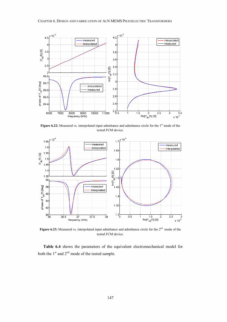
CHAPTER 6. DESIGN AND FABRICATION OF ALN MEMS PIEZOELECTRIC TRANSFORMERS
147
Table 6.4 shows the parameters of the equivalent electromechanical model for
both the 1st and 2nd mode of the tested sample.
Figure 6.22: Measured vs. interpolated input admittance and admittance circle for the 1st mode of the tested FCM device.
Figure 6.23: Measured vs. interpolated input admittance and admittance circle for the 2nd mode of the tested FCM device.
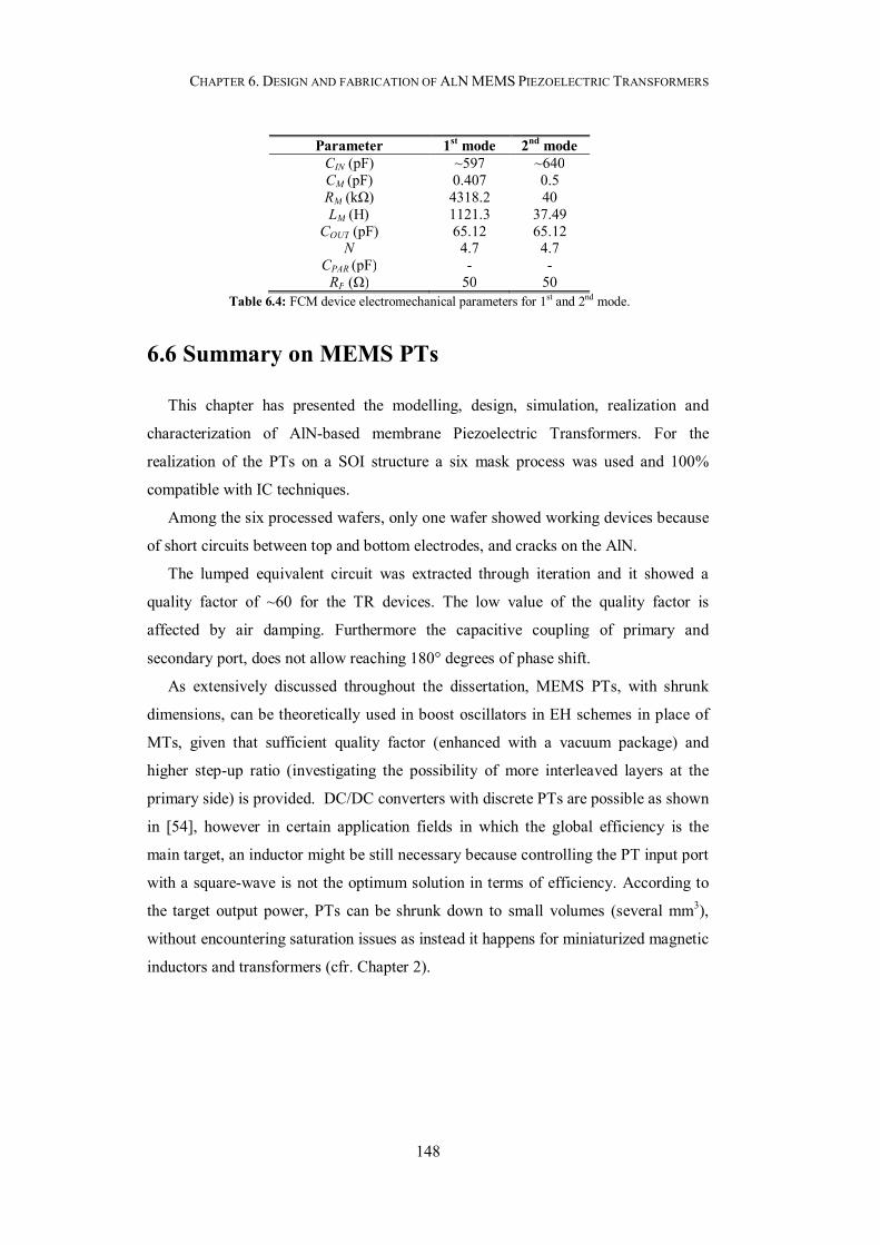
CHAPTER 6. DESIGN AND FABRICATION OF ALN MEMS PIEZOELECTRIC TRANSFORMERS
148
6.6 Summary on MEMS PTs
This chapter has presented the modelling, design, simulation, realization and
characterization of AlN-based membrane Piezoelectric Transformers. For the
realization of the PTs on a SOI structure a six mask process was used and 100%
compatible with IC techniques.
Among the six processed wafers, only one wafer showed working devices because
of short circuits between top and bottom electrodes, and cracks on the AlN.
The lumped equivalent circuit was extracted through iteration and it showed a
quality factor of ~60 for the TR devices. The low value of the quality factor is
affected by air damping. Furthermore the capacitive coupling of primary and
secondary port, does not allow reaching 180° degrees of phase shift.
As extensively discussed throughout the dissertation, MEMS PTs, with shrunk
dimensions, can be theoretically used in boost oscillators in EH schemes in place of
MTs, given that sufficient quality factor (enhanced with a vacuum package) and
higher step-up ratio (investigating the possibility of more interleaved layers at the
primary side) is provided. DC/DC converters with discrete PTs are possible as shown
in [54], however in certain application fields in which the global efficiency is the
main target, an inductor might be still necessary because controlling the PT input port
with a square-wave is not the optimum solution in terms of efficiency. According to
the target output power, PTs can be shrunk down to small volumes (several mm3),
without encountering saturation issues as instead it happens for miniaturized magnetic
inductors and transformers (cfr. Chapter 2).
Parameter 1st mode 2nd mode CIN (pF) ~597 ~640 CM (pF) 0.407 0.5 RM (kΩ) 4318.2 40 LM (H) 1121.3 37.49
COUT (pF) 65.12 65.12 N 4.7 4.7
CPAR (pF) - - RP (Ω) 50 50
Table 6.4: FCM device electromechanical parameters for 1st and 2nd mode.
CHAPTER 6. DESIGN AND FABRICATION OF ALN MEMS PIEZOELECTRIC TRANSFORMERS
149
Another possible application of MEMs PTS could be resonant step-down
converters, which can have higher efficiency thanks to the higher Q factor of
piezoelectric devices compared to magnetic components.
Another advantage of MEMS PTs compared to the magnetic counterpart, is that
they can provide a true signal or power isolation, without EMI. As a matter of fact,
the magnetic field of an inductor might couple with the low-resistance substrate of
CMOS technologies, thus inducing currents that can cause also latch-up in the IC and
an unexpected circuit operation [31].
The major issue with MEMS PTs, is the air-damping which limits the maximum
displacement of devices, and hence the available power. However, this is a limit not
linked to the piezoelectric technology (like the saturation in magnetic devices, which
limits the linear behavior of the component), but rather a packaging issue (a vacuum
package might partially remove the damping due to the surrounding air, improving
the overall performance).
150
Chapter 7
Conclusions and future works
This thesis has faced the problems of miniaturization of magnetic and
piezoelectric devices mainly for ultra-low power and ultra-low voltage applications
such as EH systems, in perspective of having PwrSoC and PwrSiP.
Thanks to technology improvements, which lead to the decrease of switching
frequencies, the miniaturization of magnetic devices is possible, however efficient
power systems must always rely on the presence of a magnetic core, even if the value
of the inductance required is so low, that even air-core inductors might be
theoretically suitable.
Nevertheless, the presence of a magnetic core can significantly limit the working
interval of the device, either because of the saturation of the material or because of
the minimum working frequency. Furthermore, not all the magnetic materials that can
be deposited are fully clean-room compliant because of potential issues of
contamination.
Many works in literature present innovative magnetic devices (inductors or
transformers), in very small footprint areas, however very few works provide some
information in order to assess the effective performances of the device once this is
placed as an energy conversion transducer in a power system.
The work in this thesis has shown that for a planar square toroid inductor, there is
a maximum value of the achievable inductance per unit area that cannot be exceeded
CHAPTER 7. CONCLUSIONS AND FUTURE WORKS
151
once the thickness of the core, linear turn density, and the material (hence the
magnetic permeability) are fixed.
In addition, with the shrinking of dimensions, some very critical parameters must
be taken into account and the effect should be further investigated in order to assess
how they can affect the operation of device. To cite an example, the minimum
working frequency is directly linked to the voltage across the inductor and to the
cross section of the core. Generally, the voltage is dictated by the application
constraints, whereas the core thickness by the particular technology used to deposit
and pattern the magnetic film. This entails that the core width (and hence the footprint
area) must have a minimum value in order to fulfil the particular application.
Furthermore the intrinsic presence of the current turns in inductors and
transformers as well, is a limit that puts an important trade-off between
miniaturization and performance. Miniaturizing a magnetic inductor means also
decreasing the cross section of the current turns, thus increasing the DC resistance,
lowering the low frequency quality factor.
As a consequence of these considerations, instead of trying to further shrink
dimensions of magnetic devices, a better solution might be exploiting the available
footprint area as much as possible, by maximizing the inductance value or the
performances. Until new magnetic materials are discovered, inductors and
transformers cannot be further shrunk, if the particular application constraints of a
PwrSoC (power, voltage, efficiency) have to be taken into account. The maximization
of the inductance value can be based on optimization of classic shapes such the
square toroids, or through the development of new shapes, such as the serpertine
toroid as explained in this dissertation.
Concerning the piezoelectric counterpart, the miniaturization provides
theoretically minor issues. First of all, in piezoelectric devices, like PTs, the absence
of saturation phenomena (in a first approximation when the device is working within
the linear range of the Hooke’s law) linked to the volume of the device eliminates a
major limitation to the miniaturization as it happens for inductors and transformers.
Furthermore the absence of current turns can provide more compact systems and
lower profiles.
In addition, the electro-mechanical conversion is much more efficient compared to
the electromagnetic conversion. This has been extensively demonstrated in Chapter 5,
CHAPTER 7. CONCLUSIONS AND FUTURE WORKS
152
by showing a novel boost oscillator based on a PT, suitable for EH schemes, which is
the dual of the Armstrong oscillator based on a MT: using a dedicated IC designed in
a 0.35μm technology provided by ST Microelectronics, it was possible to step-up
ultra-low voltages down to 28mV, using a Noliac PT prototype, and no magnetic
components. Nevertheless, it is worth noting that this value can be further lowered, if
the devices in the input stage of the common source are mismatched, as extensively
demonstrated through the developed mathematical model. The achieved value is
compatible to the one obtained with commercial solutions.
However discrete PTs are designed for handling powers up to few W and output
voltages of several hundreds of V, and are not optimized to handle powers in the
range of hundreds of μW and output voltages up to few V. This means that PTs can
be arbitrarily shrunk down to fem mm3 with a tailored design, because of the absence
of the aforementioned saturation phenomena linked to the volume of the device. This
means that potentially with MEMS piezoelectric technologies it might be possible to
extend the MtM trend.
However, as already discussed in Chapter 4, the number of interleaved layers at
the primary side of a PT, plays the same role of the turns ratio of a MT. Nevertheless,
MEMS processes are not intended for the deposition of multiple layers (generally
only two levels of metallizations are available, whereas in standard CMOS processes
more than six levels are possible) hence the possibility of extending the process to
multiple AlN/Electrode layers, in order to enhance the voltage step-up ratio of the
transformer, should be further investigated.
Concerning the presented MEMS AlN PTs, the parasitic capacitance between
primary and secondary does not allow the PT to reach the 180° degrees of phase shift
in the voltage gain, because of the two zeros introduced by such capacitance.
However if the quality factor is higher, the phase should be able to reach almost 180°
of phase shift before increasing again towards 0°. However, an improved layout
should necessarily designed by increasing the distance between the primary and
secondary electrode, in order to avoid the aforementioned capacitive coupling
between primary and secondary side.
In addition, the presented devices suffer from air-damping which significantly
limits the maximum displacement of the membrane, and hence limits the energy
conversion capability of the device. Unfortunately the effect of the air-damping is not
CHAPTER 7. CONCLUSIONS AND FUTURE WORKS
153
easily modelled and hence it cannot be predicted even with an extensive FEM
simulation. A vacuum characterization of the devices is necessary in order to assess
the actual performance of the fabricated components.
An alternative solution to enhance the step-up ratio of the MEMS piezoelectric
device could be also spreading a PZT powder (through inkjet printing techniques) on
their surface. This approach might boost the performance of MEMS PTs, given that
the AlN has not a piezoelectric effect as strong as the PZT (which is rather
electrostrictive than truly piezoelectric). As a matter of fact, PTs with different
piezoelectric materials at the primary side and secondary side present higher step-up
ratios compared to a single-material PT [98]. The spreading of the PZT powder can
be thought has a post-processing step, since the PZT is not IC compliant because of
the presence of the lead.
154
References [1] M. K. Kazimierczuk, “High-frequency magnetic components”, John Wiley and Sons, 2009, Chap.
1, pp. 4-5, 22-25, 28-29, 32-33; Chap. 2 pp. 50, 55-58, 80-84, Chap. 3 pp. 91-92, Chap. 5 pp. 189-
192, Chap. 8, pp. 333-336.
[2] C. O’Mathùna, N. Wang, S. Kulkarni, and S. Roy, “Review of integrated magnetics for power
supply on chip (PwrSoC)”, IEEE Trans. Power Electron., Vol. 27, No. 11, pp. 4799-4816, Nov.
2012.
[3] L. M. Roylance, J. B. Angell, “A batch-fabricated silicon accelerometer,” IEEE Trans. on Electr.
Dev.,, vol. 26, no. 12, pp. 1911-1917, Dec 1979.
[4] K. E. Petersen, “Silicon as a mechanical material,” Proceedings of the IEEE, vol.70, no. 5, pp.
420-457, May 1982
[5] M. Seeman and S. Sanders, “Analysis and optimization of switched-capacitor DC-DC
converters,” IEEE Trans. Power Electron., vol. 23, no. 2, pp. 841–851, 2008.
[6] M. S. Makowski and D. Maksimovic, “Performance limits of switched-capacitor dc-dc
converters,” in IEEE Power Electron. Spec. Conf., 1995, pp. 1215–1221.
[7] P. M. Lin and L. O. Chua, “Topological generation and analysis of voltage multiplier circuits,”
IEEE Trans. Circuits Syst., vol. 24, no. 10, pp. 517–530, 1977.
[8] N. Wang, J. Hannon, R. Foley, K. Mccarthy, et al. “Integrated magnetics on silicon for power
supply in package (PSiP) and power supply on chip (PwrSoC)” in: Electronic System-Integration
Technology Conference (ESTC), 2010 3rd. 2010, pp. 1- 6.
[9] C. R. Sullivan, D. V. Harburg, J. Qiu, C. G. Levey, and D. Yao. “Integrating magnetics for on-
chip power: a perspective”. IEEE Trans. Power Electron. 28.9 (2013), pp. 4342-4353.
[10] C. R. Sullivan, “Integrating magnetics for on-chip power: challenges and opportunities”, IEEE
Custom Integrated Circuits Conf. (CICC), pp. 291-298, 2009.
[11] L. Sieben-Xu, J. Pettine, V. Petrescu, M. Vandecasteele, D.M. Karabacak, “System optimization
methodology for integrated piezoelectric MEMS resonator biochemical sensors”, Procedia
Engeneering 47, Proc. of Eurosensors Conf., pp. 635–638, Sep. 2012.
[12] T. E. Kazior, “Beyond CMOS: heterogeneous integration of III–V devices, RF MEMS and other
dissimilar materials/devices with Si CMOS to create intelligent microsystems”, Philos Trans A
Math Phys Eng Sci. 2014 Mar 28; 372(2012): 20130105, doi: 10.1098/rsta.2013.0105
[13] J. Ellis “GaN on silicon: A breakthrough technology for LED lighting” LEDs Magazine, Feb.
2014. Link: http://www.ledsmagazine.com/articles/print/volume-11/issue-2/features/last-
word/gan-on-silicon-a-breakthrough-technology-for-led-lighting-magazine.html.
[14] A. C. Fischer, F. Forsberg, M. Lapisa, S. J. Bleiker, G. Stemm, N. Roxhed, F. Niklaus,
“Integrating MEMS and ICs”, Microsystems & Nanoengineering 1, Article number: 15005
(2015), doi:10.1038/micronano.2015.5
[15] J. J. Allen, “Micro Electro Mechanical System Design”, Chap. 3: MEMS Technologies. 2005,
Taylor & Francis Group.

REFERENCES
155
[16] S.S. Mohan, M. Hershenson, S.P. Boyd and T.H. Lee, "Simple Accurate Expressions for Planar
Spiral Inductances" IEEE Journal of Solid-State Circuits, Oct. 1999, pp. 1419-24.
[17] S. S. Mohan. “The design, modeling and optimization of on-chip inductor and transformer
circuits”. PhD thesis. Stanford University, 1999.
[18] D. Kehrer. “Design of monolithic integrated lumped transformers in silicon-based technologies up
to 20 GHz”. Institute of Communications and Radio-Frequency Engineering of the Vienna
University of Technology, 2000
[19] Y. Katayama, S. Sugahara, H. Nakazawa, and M. Edo. “High-power-density MHz-switching
monolithic DC-DC converter with thin film inductor”, in: Power Electronics Specialists
Conference, 2000. PESC 00. 2000 IEEE 31st Annual.Vol. 3. 2000, pp. 1485-1490.
[20] S. Iyengar, Trifon M. Liakopoulos and C. H. Ahn. “A DC/DC Boost Converter Toward Fully
On-Chip Integration Using New Micromachined Planar Inductors” in Power Electronics
Specialists Conference, 1999. PESC 99. 30th Annual IEEE, June 1999. Vol. 1, pp. 72-76.
[21] J. Lu et al. “Modeling, design, and characterization of multiturn bondwire inductors with ferrite
epoxy glob cores for power supply system-on-chip or system-in-package applications", IEEE
Trans. Power Electr., Vol. 25, No. 8, pp. 2010-2017, Aug. 2010.
[22] B. Orlando et al. “Low-resistance integrated toroidal inductor for power management”, IEEE
Trans. Magn., Vol. 42, No. 10, pp. 3374-3376, Oct. 2006.
[23] D. W. Lee, K. P. Hwang, and S. X. Wang, “Fabrication and analysis of high-performance
integrated solenoid inductor with magnetic core”. IEEE Trans. Magn., Vol. 44, No. 11, pp. 4089-
4095, Nov. 2008.
[24] D. S. Gardner, G. Schrom, P. Hazucha, F. Paillet, et al. “Integrated on-chip inductors using
magnetic material (invited)”. In: Journal of Applied Physics 103.7 (2008), pp. 9271-9276.
[25] D. S. Gardner, G. Schrom, P. Hazucha, F. Paillet, et al “Integrated On-Chip Inductors With
Magnetic Films”. In: IEEE Trans. On Magn. Vol. 43, n. 6 (2007), pp. 2615-2617.
[26] Ningning Wang, Santosh Kulkarni, Brice Jamieson, James Rohan, Declan Casey, Saibal Roy,
Cian O’Mathuna “High Efficiency Si Integrated Micro-transformers Using Stacked Copper
Windings for Power Conversion Applications”. In: Applied Power Electronics Conference and
Exposition (APEC), 2012 27th Annual IEEE. February 2012,pp. 411 – 416. DOI:
10.1109/APEC.2012.6165852.
[27] R. Meere, T. O’Donnell, N. Wang, N. Achotte, S. Kulkarni, S.C. O’ Mathuna. “Size and
performance tradeoffs in micro-inductors for high frequency DC-DC conversion”. In: IEEE
Trans. On Magn. Vol. 45, n.10 (2009), pp. 4234-4237.
[28] R. Meere, T. O’Donnell, H. Jan Bergveld, N. Wang, S. C. O’Mathuna “Analysis of Microinductor
Performance in a 20–100 MHz DC/DC Converter” IEEE Ttrans. Power Electr., Vol. 24, n. 9,
Sept. 2009.
[29] C. R. Sullivan and S. R. Sanders. “Design of microfabricated transformers and inductors for high-
frequency power conversion”. In: IEEE Trans. Power Electr. 11.2 (1996), pp. 228-238.
[30] D. Flynn, N. S. Sudan, A. Toon, and M. P. Y. Desmulliez “Fabrication process of a micro-
inductor utilizing a magnetic thin film core”. J. of Microsystem Technologies, Vol. 12, No. 10-11,
pp. 923-933, Sep. 2006.
REFERENCES
156
[31] B. Razavi, “Design of analog CMOS integrated circuits”. McGraw-Hill International Ed., Chap.
18, pp. 631-675, 2001.
[32] E. Macrelli, A. Romani, R. P. Paganelli, M. Tartagni,. "Modeling, design, and fabrication of high-
inductance bond wire microtransformers with toroidal ferrite core". In: IEEE Trans. Power
Electron. Vol. 30, n. 10 (2014), pp. 5724 – 5737.
[33] E. Macrelli et al. "Design and fabrication of a 315 µH bondwire micro-transformer for ultra-low
voltage energy harvesting," Proc. of Design, Automation and Test in Europe Conf., pp.1-4, 2014.
[34] E. Macrelli et al. "Design and fabrication of a 29 μH bondwire micro-transformer with LTCC
magnetic core on silicon for energy harvesting applications,"Procedia Engeneering, Proc. of
Eurosensors Conf., pp. 1–4, Sep. 2014.
[35] P. Mazzoldi, M. Nigro, C. Voci. “Fisica. Volume II- Elettromagnetismo e Onde”. 2nd Edition
EdiSES 2003. Chap. 8, pp. 248-249.
[36] A. Camarda, E. Macrelli, A. Romani, M. Tartagni, “Design Optimization of Integrated Magnetic
Core Inductors”, IEEE Trans. Magn., Vol. 51, No. 7, July 2015.
[37] G. A. Cividjian, A. G. Cividjian and N. G. Silvis- Cividjian, “Some formulas for two-dimensional
permeances”, IEEE Trans. Magn., Vol. 32, No. 5, pp. 3754- 3758, Sep. 2000.
[38] G. A. Cividjian, A. G. Cividjian “Constriction and Corner Permeances for finite domains”, IEEE
Trans. Magn., Vol. 42, No. 12, pp. 3825- 3831, Dec. 2006.
[39] E. Matagne, G. A. Cividjian and V. Kluyskens “Exact expression of corner reluctances in a
magnetic circuit of rectangular section” in Computer field models of electromagnetic devices (S.
Wiak, E. Napieralska-Juszczak). IOS Press, 2010.
[40] K.H.J. Buschow, “Handbook of magnetic materials”, Chap. 3 Nanocrystalline soft magnetic
alloys, 1997 Elsevier Science, pp. 415-462.
[41] D. Flynn, R. S. Dhariwal, and M. P. Y. Desmulliez, “A design study of microscale magnetic
components for operation in the MHz frequency range”, J. of Micromech. and Microeng., Vol.
16, No. 9, pp. 1811-1818, 2006.
[42] D. Flynn, A. Toon and M.P.Y. Desmulliez,”Manufacture and characterisation of micro-
engineered DC-DC power converterusing UV-LIGA process” ELECTRONICS LETTERS 24th
November 2005 Vol. 41 No. 24.
[43] V. Palumbo, M. Marchesi, V. Chiesi, D. Paci, P. Iuliano, F. Toia, F. Casoli, P. Ranzieri, F.
Albertin, and M. Morelli, “Hall current sensor IC with integrated Co-based alloy thin film
magnetic concentrator”, EPJ Web of Conferences, Vol. 40 (2013), n. 16002. DOI:
10.1051/epjconf/20134016002.
[44] A. Van den Bossche, V. C. Valchev “Inductors and transformers for power electronics”. Taylor &
Francis (2005), Chap. 1 Fundamentals of magnetic theory.
[45] C. O’Mathùna, T. O’ Donnell, N. Wang, and K. Rinne, “Magnetics on silicon: an enabling
technology for power supply on chip”, IEEE Trans. Power Electron., Vol. 20, No. 3, pp.585-592,
May 2005.
[46] G. A. Cividjian, “Distorted constriction contact resistance between clamped slabs”, Compel, Vol.
33, No.4, pp. 1366-1378, 2014.
REFERENCES
157
[47] G. A. Civdjian, “Permeance of fringing flux”, IEEE Trans. Magn., Vol. 45, No. 2, pp. 694-700,
Feb. 2009.
[48] H. D. Arnold, and G. W. Elmen, “Permalloy, a new magnetic material of very high permeability”,
Bell system technical J., Vol. 2, No. 3, pp. 101-111, July 1923.
[49] G. Grandi, M. K. Kazimierczuk, A. Massarini, U. Reggiani, and G. Sancineto, “Model of
laminated iron-core inductors for high frequencies”, IEEE Trans. Magn., Vol. 40, No. 4, pp.
1839-1845, July 2004.
[50] J. R. Phillips. “Piezoelectric Technology: A Primer”.
http://www.eetimes.com/document.asp?doc_id=1255166 .
[51] F. Li, L. Jin, Z. Xu, S.Zhang, “Electrostrictive effect in ferroelectrics: An alternative approach to
improve piezoelectricity”, Appl. Phys. Rev. 1, 011103 (2014); doi:
http://dx.doi.org/10.1063/1.4861260.
[52] R. Paganelli, A. Romani, A. Golfarelli, M. Magi, E. Sangiorgi and Marco Tartagni, “Modeling
and characterization of piezoelectric transducers by means of scattering parameters. Part I:
Theory”, Sens. Actuator A-Phys. 160 (1-2) (2010), pp 9-18.
[53] Ray-Lee Lin. “Piezoelectric transformer characterization and application of electronic ballast”,
PhD dissertation, Virginia Polytechnic Institute and State University, Blacksburg, Virginia
November 2001.
[54] C-Yi. Lin “Design and analysis of piezoelectric transformer converters”, Ph.D. Dissertation. Dept.
of Elect. Eng. Virginia Pol. Inst., Blacksburg, VA, 1997.
[55] J. Yang, “Piezoelectric Transformer Structural Modeling – A review”, IEEE Trans. Ultrason.
Ferroelectr. Freq. Control 54 (6) (2007), pp. 1154-1170.
[56] E. Macrelli, A. Romani, R. Paganelli, E. Sangiorgi, M. Tartagni, “Piezoelectric transducers for
real-time evaluation of fruit firmness. Part I: Theory and development of acoustic techniques”, in:
Sensors & Actuators A: physical. Vol. 201, 10.2012, pp. 487-496.
[57] G. Frantz, Digital signal processor trends, IEEE Micro 20 (6) (2000), pp. 52–59.
[58] CATRENE, Report on “Energy Autonomous Systems: Future Trends in Devices, Technology,
and Systems”, 2009, http://www.imec-nl.nl/content/user/File/EAS_report_v28.pdf. ISBN: 978-
88-904-399-0-2.
[59] Y. Zhang, B. Min, L. Huang, and I. Angelidaki, “Electricity generation and microbial community
response to substrate changes in microbial fuel cell”,in: Bioresource Technology, vol. 102, pp.
1166-1173, 2011.
[60] J. M. Vullers, R. Van Schaijk, I. Doms, C. Van Hoof, and R. Mertens, “Micropower energy
harvesting,” Solid. State. Electron., vol. 53, no. 7, pp. 684–693, 2009.
[61] Laird Technologies. CP14 TEG module datasheet.
http://lairdtech.com/WorkArea/DownloadAsset.aspx?id=2147483755.
[62] J. Gilbert, F. Balouchi, “Comparison of Energy Harvesting Systems For Wireless Sensor
Networks”. International Journal of Automation and Computing 5 (4) (2008), pp 334-347.
[63] E. J. Carlson, K. Strunz, B.P. Otis, “A 20 mV Input Boost Converter With Efficient Digital
Control for Thermoelectric Energy Harvesting”, IEEE J. Solid-St. Circuits 45 (2010) 741–750.
doi:10.1109/JSSC.2010.2042251..
REFERENCES
158
[64] I. Doms, P. Merken, R. Mertens, C. Van Hoof, Integrated capacitive power-management circuit
for thermal harvesters with output power 10 to 1000µW. 2009 IEEE Int. Solid-state Circ. Conf.
(ISSCC) Dig. Tech. Pap. (2009) 300-301
[65] D. Masotti, A. Costanzo, P. Francia, M. Filippi, A. Romani, “A Load-Modulated Rectifier for RF
Micropower Harvesting With Start-Up Strategies”, IEEE Trans. Microw. Theory Tech. (2014) 1–
11. doi:10.1109/TMTT.2014.2304703.
[66] K. Kadirvel, Y. Ramadass, U. Lyles, J. Carpenter, V. Ivanov, V. McNeil, et al., “A 330nA
energy-harvesting charger with battery management for solar and thermoelectric energy
harvesting”, 2012 IEEE Int. Solid-State Circ. Conf. Dig. Tech Pap. (2012) 106-108.
doi:10.1109/ISSCC.2012.6176896.
[67] J. Kim, P.K.T. Mok, C. Kim, “A 0.15 V Input Energy Harvesting Charge Pump With Dynamic
Body Biasing and Adaptive Dead-Time for Efficiency Improvement”, IEEE J. Solid-State
Circuits 50 (2) (2014) 414-425. doi:10.1109/JSSC.2014.2375824.
[68] P-H, Chen, K. Ishida, Y. Okuma, Y. Ryu, M. Takamiya, T. Sakurai, “0.18V input charge pump
with forward body biasing in startup circuit using 65nm CMOS”, in: IEEE Cust. Integr. Circuits
Conf. 2010, IEEE, 2010: pp. 1–4. doi:10.1109/CICC.2010.5617444.
[69] P-H, Chen, K. Ishida, K. Ikeuchi, X. Zhang, K. Honda, Y. Okuma, Y. Ryu, M, Takamiya, T.
Sakurai, “Startup Techniques for 95 mV Step-Up Converter by Capacitor Pass-On Scheme
and VTH -Tuned Oscillator With Fixed Charge Programming”, IEEE J. Solid-State Circuits 47
(45) (2002), pp. 1252-1260.
[70] Y. K. Ramadass, P. Chandrakasan, “A battery-less thermoelectric energy harvesting interface
circuit with 35mV start-up voltage”, IEEE J. Solid-State Circ. 46(1) (2011), pp. 333-341.
[71] J.M. Damaschke, “Design of a low-input-voltage converter for thermoelectric generator”, IEEE
Trans. Ind. Appl. 33 (5) (1997), pp.1203-1207.
[72] S.-E. Adami, N. Degrenne, C. Vollaire, B. Allard, and F. Costa, “Ultra-low power, low voltage,
autonomous resonant DC-DC converter for low power applications,” in 4th International
Conference on Power Engineering, Energy and Electrical Drives, 2013, pp. 1222–1228.
[73] Linear Technology. Ultralow voltage step-up converter and power manager – LTC3108. url:
http://cds.linear.com/docs/en/datasheet/3108fc.pdf
[74] D. Grgic, T. Ungan,M. Kostic, L. M. Reindl, “Ultra-low input voltage DC-DC converter for
micro energy harvesting”, Proceedings of PowerMEMS 2009, Washington DC, USA, December
1-4, 2009, pp. 265-268.
[75] Jong-Pil Im; Se-Won Wang; Seung-Tak Ryu; Gyu-Hyeong Cho, “A 40 mV Transformer-Reuse
Self-Start-up Boost Converter With MPPT Control for Thermoelectric Energy Harvesting”, IEEE
J. Solid-State Circuits 47(12) (2012), pp.3055-3067
[76] N. Wang, T. O’ Donnell, S. Roy, S. Kulakarni, P. Mccloskey, C. O’ Mathuna, “Thin film
microtransformer integrated on silicon for signal isolation”. IEEE Trans. Magn. 43(6) (2007),
pp.2719-2721.
[77] E. Macrelli, A. Romani, R. P. Paganelli, A. Camarda, M. Tartagni, “Design of low-voltage
integrated Step-up oscillators with microtransformers for energy harvesting applications”, in:
IEEE Trans. Circ. And Syst.:I, Vol. 62, n. 7, (2015), pp. 1747 – 1756.
REFERENCES
159
[78] G. K. Ho, R. Abdolvand, A. Sivapurapu, S. Humad, F. Ayazi: “Piezoelectric-on-Silicon Lateral
Bulk Acoustic Wave Micromechanical Resonators”, IEEE J. Microelectromech. Syst. 17 (2)
(2008), pp 512-520.
[79] S. Bedair, J. Pulskamp, B. Morgan and R. G. Polcawich, Performance model of electrode tailored
thin film piezoelectric transformers for high frequency switched mode power supply, Proceedings
of PowerMEMS 2009, Washington DC, USA, December 1-4, 2009, pp 435-438.
[80] A. Camarda, A. Romani, M. Tartagni, “Piezoelectric Transformers for Ultra-low Voltage Energy
Harvesting Applications”, Procedia Engineering 87 (2014), pp. 1521-1524.
[81] A. Camarda, A. Romani, E. Macrelli, M. Tartagni “A 32mV/69mV input voltage booster based
on a piezoelectric transformer for energy harvesting applications”, in: Sensors & Actuators A:
physical. Vol. 232, 8.2015, pp. 341–352.
[82] E. M. Syed, F.P. Dawson, E.S. Rogers, “Analysis and modeling of a Rosen Piezoelectric
Transformer”, in: IEEE Power Electronics Specialists Conference (PESC), 2001.32nd Annual,
Vol. 4, pp. 1761- 1766.
[83] A. Romani, E. Sangiorgi, M. Tartagni, R. P. Paganelli, “Joint modeling of piezoelectric
transducers and power conversion circuits for energy harvesting applications”, IEEE Sens. J. 13
(3) (2013), pp. 916-925.
[84] K. T. Chang, “Effects of load resistances on step-up voltage gains of Rosen-type piezoelectric
transformers”, IEEE Intern. Conf. on Industrial Technology, 2005, pp. 1080-1085.
[85] S. Ozeri, “Piezoelectric transformers model parameters extraction based on time domain
measurements”, Applied Power electronics Conference and Exposition, 2006, APEC’ 06. Twenty-
first Annual IEEE, pp. 1565-1569.
[86] J. Zerong, J. Lingling, L Huabo and W. Ting, “Measurement of PT equivalent circuit model
parameters based on admittance circle”, China International Conference on Mechatronic Science,
Electric Engineering and Computer, August 19-22, 2011, Jilin; pp 21-23.
[87] F. He, R. Ribas, C. Lahuec, “Discussion on the general oscillation startup condition and the
Barkhausen criterion”, Analog Integrated Circuits and Signal Processing 59 (2) (2009), pp 215-
221.
[88] A. Romani, M. Filippi, M. Tartagni, “Micropower Design of a Fully Autonomous Energy
Harvesting Circuit for Arrays of Piezoelectric Transducers”, IEEE Trans. Power Electron. 29 (2)
(2014), pp.729,739.
[89] M. Dini, M. Filippi, M. Tartagni, A. Romani, “A nano-power power management IC for
piezoelectric energy harvesting applications”, in: Proc. Of 9th Conf. Ph.D. Research on
Microelectronics and Electronics (PRIME) (2013), pp. 269–272.
doi:10.1109/PRIME.2013.6603169.
[90] Laird Technologies, eTEC Series HV14,18,F0,0102,GG Thin Film Thermoelectric Module, url:
http://www.lairdtech.com/brandworld/library/THR-DS-eTEC-HV14%201113.pdf
[91] D. Vasic, E. Sarraute, F. Costa, P. Sangouard, E. Cattan, “Piezoelectric micro-transformer based
on PZT unimorph membrane”, J. Micromech. Microeng. 14 (2004) S90–S96. doi:10.1088/0960-
1317/14/9/016.
REFERENCES
160
[92] D. Vasic, E. Sarraute, F. Costa, P. Sangouard, E. Cattan, “Piezoelectric micro-transformer based
on SOI structure”, Sens. Actuator A-Phys. 117 (2005) 317–324. doi:10.1016/j.sna.2004.06.009.
[93] Y. Chuo, B. Omrane, C. Landrock, J. Aristizabal, D. Hohertz, S. V. Grayli, et al., “Powering the
Future: Organic Solar Cells with Polymer Energy Storage”, IEEE Des. Test Comput. 28 (2011)
32–40. doi:10.1109/MDT.2011.93.
[94] "CMP Chooses I|D|ME Organic Solar Cell Technology for Integration with CMOS," CMP Press
Release, 2 Mar. 2011; http://id-me.careadnews.php?newsID=17.
[95] A. Romani, A. Camarda, A. Baldazzi, M. Tartagni, “A Micropower Energy Harvesting Circuit
with Piezoelectric Transformer-Based Ultra-low Voltage Start-up”. 2015Intern. Symp. On Low
Power Electr. And Design (ISLPED), pp. 279-284.
[96] M. Kucera, E. Wistrela, G. Pfusterschmied, V. Ruiz-Diez, T. Manzaneque, J. Hernando-Garcìa, J.
L. Sànchez-Rojas, A. Jachimowicz, J. Schalko, A. Bittner, U. Schmid, “Design-dependent
performance of self-actuated and self-sensingpiezoelectric-AlN cantilevers in liquid media
oscillating in thefundamental in-plane bending mode”, Sens. & Act. B: Chem., Vol. 200 (2014),
pp. 235-244. [97] A. Ababneh, H. Kreher, U. Schmid, “Etching behavior of sputter-deposited aluminum nitride thin
films in H3PO4 and KOH solutions”, Microsyst. Techn., Vol. 14, n. 4, pp. 567-573 (2008).
[98] P. Sangouard, G. Lissorgues, T. Bourouina, “A Novel piezoelectric Microtransformer for
autonomous sensors applications”. DTIP 2008. Int. Symp. On Design, Test, Integ. and Packag. of
MEMS/MOEMS, pp. 42-45, doi: 10.1109/DTIP.2008.4752948.
161
Acronyms
AC Alternating Current
AlN Aluminum Nitride
BCD Bipolar, CMOS, DMOS
CMOS Complementary Metal Oxide Semicondutor
DC Direct Current
EH Energy Harvesting
EMI ElectroMagnetic Interference
FCM Fully Clamped Membrane
FEM Finite Element Methods
FET Field Effect Transistor
FSM Free Standing Membrane
IC Integrated Circuit
LTCC Low Temperature Co-fired Ceramic
MEMS Micro- Electro-Mechanical System
MPL Magnetic Path Length
MMPT Minimum Power Point Tracking
MT Magnetic Transformer
MtM More than Moore
PCB Printed Circuit Board
PT Piezoelectric Transformer

ACRONYMS
162
PVC Photovoltaic Cell
PwrSiP Power System in Package
PwrSoC Power System on Chip
PZT Lead Zirconate Titanate
RF Radio Frequency
SEM Scanning Electron Microscope
SER Serpentine
SoA State of Art
SSTC Square Shaped Toroidal Inductor
TEG Thermo – Electric Generator
WSN Wireless Sensor Nodes
ZnO Zinc Oxide
163
List of Figures
Figure I.1 Impact of frequency increase in SMPS on the value of passive
components. Graph obtained for a single phase buck converter
with 5V in input, 1V in output, 2% voltage ripple and 0.3 peak to
peak ripple current ratio [2] (© 2012, IEEE). xiv
Figure I.2 Evolution of PwrSoC technology [2] (© 2012, IEEE). xiv
Figure 1.1 Hysteresis cycles: Blue line: ideal soft magnetic material, black
and red: hard magnetic material, green line: real soft magnetic
material. 3
Figure 1.2 Top view of shapes of inductors used in RF applications. 7
Figure 1.3 Bondwire winding embedded in glob of magnetic epoxy core
[21]. (© 2010, IEEE). 8
Figure 1.4 Toroidal MEMS microinductor [22] (© 2006, IEEE). 8
Figure 1.5 Cross section (top) and top view (bottom) of a racetrack pot-core
spiral micro-inductor. 10
Figure 1.6 A 315μH bondwire microtransformer [33] (© 2014, IEEE). 12
Figure 1.7 A LTCC based 29μH bondwire microtransformer integrated at
die level on a 0.35μmST Microelectronics BCD technology [34]
(© 2014, Procedia Engineering). 12
Figure 2.1 Relation between magnetic flux density and magnetic field
intensity. 15
Figure 2.2 Magnetic circuit. 16
Figure 2.3 Magnetic flux density distribution along the axial direction of the
core. 19
Figure 2.4 Top view of a toroidal core divided in several slices [36] (©
2015, IEEE). 21

LIST OF FIGURES
164
Figure 2.5 SSTC divided in several slices [36]. (© 2015, IEEE). 21
Figure 2.6 Comparison between equations and FEM [36]. (© 2015, IEEE). 25
Figure 2.7 Numerical Simulation of normalized resistance of a metal stripe
for W>>tW, for various thicknesses. 28
Figure 2.8 FEM Simulation of the normalized resistance of a cylindrical
conductor (copper) of length 100µm and diameter of the cross
section of 50µm, versus frequency. 28
Figure 2.9 FEM simulation of skin effect on round-section conductor of
50µm of diameter. 29
Figure 2.10 AC resistance to DC resistance ratio due to skin depth and
proximity effect 31
Figure 2.11 Behaviour of magnetic relative permeability of nanocristalline
and amorphous materials as well as ferrites as a function of the
working frequency [40]. 34
Figure 2.12 Matlab plot of the effective permeability of Vitrovac 6025Z from
Vacuumschmelze when air gap is introduced. 35
Figure 2.13 Matlab plot of the normalized skin depth with and without an air-
gap in the Vitrovac. 35
Figure 2.14 Lamination of the core. 37
Figure 2.15 Hysteresis losses. 37
Figure 2.16 Cross section of a thin magnetic film. Inside the sample the H
field is opposed to the incident one. 39
Figure 2.17 Differences between classic Snell’s law and Magnetic Snell’s
law. 42
Figure 2.18 Magnetic transformer and its electric symbol. 43
Figure 2.19 Hybrid parameters representation of a magnetic transformer. 43
Figure 2.20 Complete model of a magnetic transformer, in which all the
inductors are considered lossy. 47
Figure 3.1 Side view of a SSTC inductor. Left: reference. Centre: the
number of turns is doubled whereas the metal width is kept
constant Right: the number of turns is doubled and the width is
halved to keep the footprint area constant. All the current turns
are in series. If the footprint area is maintained constant, there is

LIST OF FIGURES
165
an increase of the inductance, but it is not possible to increase the
quality factor at a certain frequency, by acting only on the
windings shape [36]. (© 2015, IEEE). 52
Figure 3.2 Top view of an on-chip bond-wire SSTC inductor with N = 3
turns; blue lines are the on-chip metal lines, and the yellow lines
are the gold bonding wires. The green line is the mean magnetic
path length, whereas the red line marks the internal perimeter
[36]. (© 2015, IEEE). 52
Figure 3.3 L versus WC (SSTC geometry) for a square footprint area of
16mm2 and fixed linear turn density: the maximum is achieved
for Wopt = 0.83mm and L = 20.2µH [36]. (© 2015, IEEE). 56
Figure 3.4 Top view of the layout of a serpentine toroidal core: the green
line represents the external perimeter, while the red line marks
the internal perimeter. The footprint area is assumed to be square.
The light grey part indicates the distribution of current turns. Blue
squares are the bond pads, and yellow lines the gold bonding
wires. The pads can be in a gig-gag configuration to allow a
bigger pad pitch [36]. (© 2015, IEEE). 57
Figure 3.5 Inductance L versus core width W (serpentine toroidal geometry)
in a core footprint area of 4mm×4mm, obtained with G = 200µm,
Wopt = 0.325mm and L = 26.6µH [36]. (© 2015, IEEE). 59
Figure 3.6 Comparison of the ratio between inductance and DC resistance
for both geometries. For the serpentine core the ratio is more than
10% higher at the point of maximum inductance [36]. (© 2015,
IEEE). 61
Figure 3.7 Values of estimated inductance, DC resistance and L / RDC ratio
for the inductor of [10] with a serpentine core geometry design
[36]. (© 2015, IEEE). 65
Figure 4.1 Modes of expansions according to the relative orientation
between the poling voltage and the applied voltage. 72
Figure 4.2 Straight beam subject with one fixed side and subject to a
uniform stress Σ. 74
Figure 4.3 Electro-mechanical model of a simple piezoelectric actuator. 74
LIST OF FIGURES
166
Figure 4.4 Piezoelectric transformer working in the “33” mode. At the
primary there are n interdigitated electrodes. 76
Figure 4.5 Complete electromechanical model of a piezoelectric
transformer. NM is mechanical coupling between primary and
secondary. 76
Figure 4.6 Electromechanical circuit of the piezoelectric transformer, after
each transformation. 78
Figure 5.1 Schematic of a traditional MT based boost oscillator. 83
Figure 5.2 Block diagram of an energy harvesting system, lacking of a
battery. 84
Figure 5.3 Lumped equivalent electro-mechanical circuit of a PT around a
certain resonance. 85
Figure 5.4 PT equivalent circuit with output shorted (top), and input shorted
(bottom). Both circuits share the same structure of the impedance
of a quartz crystal. 86
Figure 5.5 Simulated magnitude and phase (left) and admittance circle
(right) for the second mode of the SMMTF55P4S80 PT from
Steiner & Martins Piezo with a quality factor of Q=452.
YIN=G+iB. Although the three lower frequencies are clearly
separated in the circle, they cannot be clearly distinguished in a
Bode plot. 86
Figure 5.6 Circuit schematic together with theoretical waveforms. The
output of the PT goes directly into the gate of the amplifier JFET
JA, while the voltage doubler boosts and rectifies the amplified
oscillation at the PT’s output. The DC voltage of the oscillation at
node B depends on the used transistor: in case of JFET, this is
lower than 0 V, in case of depletion MOSFET it is around 0 V
[81]. (© 2015, Elsevier). 90
Figure 5.7 Simulated Bode diagrams of the PT input impedance and of the
voltage gains involved in the feedback loop. The oscillation
frequency fOSC is extremely close to the parallel resonance. 94
Figure 5.8 Two port representation of the system. Calculating the return
ratio assumes to neglect the effect of the dependent current
LIST OF FIGURES
167
generators g12I2CS and h21I1
PT. 96
Figure 5.9. Picture of the experimental setup. 100
Figure 5.10 Measured start-up waveforms with [n = 3, m = 5] obtained with:
(a) a power supply with a series connected resistance of 2.4 Ω;
(b) a Multicomp MCPE-071-10-15 TEG source [81]. 100
Figure 5.11 Measured steady-state voltage signal of VA (PT input port) and
VB (PT output port). The measured phase shift is Δφ = ‒178°
[81]. 102
Figure 5.12. Corner analysis compared to model predictions and
measurements [81]. (© 2015, Elsevier). 102
Fig.ure 5.13 (a) Measured steady-state output voltage VOUT as a function of
source voltage VIN for various loads. (b) Measured output power
POUT as a function of RLOAD for various VIN [81]. (© 2015,
Elsevier). 105
Figure 5.14 a) Replacement of the load JFETs with a generic lossy inductor
LS. b) Equivalence of the series series LS – RS circuit with the
parallel LP –RP at a given frequency [81]. (© 2015, Elsevier). 107
Figure 5.15 (a) Simulated loop gain at VIN = 70mV and RT = 2.4Ω with the
load JFETs in the optimum condition (n = 3, m = 5) and with the
use of the inductor (LS = 37μH, and 0.65Ω of parasitic series
resistance) for different values of n. In the reference case with
load JFETs, the loop gain is exactly 0dB. In case of an inductive
load in place of the JFETs, at the same VIN, a maximum gain of
about 4.8dB is achieved, implying that VIN can be proportionally
decreased to about 40mV. (b) Measured kick-start signals
obtained with a Multicomp MCPE-071-10-15 TEG source with
an inductor of 37μH and 0.65Ω of parasitic series resistance. [81].
(© 2015, Elsevier). 109
Figure 5.16 (a) Measured steady-state output voltage VOUT as a function of
source voltage VIN with LS = 37µH RS = 0.65Ω: the slope is
35.3mV/mV, higher than the one obtained with load JFETs. The
system can start from 32mV. Lowering RS has not any effect
LIST OF FIGURES
168
since the output conductance of the CS stage is being dominated
by ngds. (b) Measured VOUT and POUT as a function of RLOAD, with
VIN = 32mV, LS = 37µH, RS = 0.65Ω. The optimum load
resistance maximizing POUT is lower than 1MΩ, whereas higher
load resistances maximize VOUT [81]. (© 2015, Elsevier). 110
Figure 5.17 Designed integrated boost oscillators in BCD 0.35µm technology
by ST Microelectronics. 113
Figure 5.18 Measured start-up waveform of output voltage vs. input voltage
of IC1. The system self-starts at 28mV in inductor-less mode.
The PT used is a Noliac prototype, furthermore a 400nF
capacitance was used in parallel to the PT input port to increase
its voltage gain without affecting the input impedance. 114
Figure 5.19
Schematic of the IC2 system. The common source is replace by a
NOT inverter made up of natural MOSFETs. 114
Figure 5.20 Schematic of the proposed energy harvesting circuit, with
PT-based start-up and power management circuitry [95]. (©
2015, IEEE). 116
Figure 5.21 Conversion efficiency of the power conversion circuit externally
supplied, defined as the ratio between output power
POUT =(VSTORE)2/RLOAD and maximum available power from the
source PAV = VS2/(4RS), with RS=3.3 Ω for different input voltages
and different load conditions (L1 = 1120µH, fSW = 1kHz, duty
cycle = 50%), a) as function of the output voltage, b) as a
function of the load [95]. (© 2015, IEEE). 118
Figure 5.22 Conversion efficiency of the self-supplied power conversion
circuit, defined as the ratio between output power
POUT =(VSTORE)2/RLOAD and maximum available power from the
source PAV = VS2/(4RS), with RS=3.3 Ω for different input voltages
and different load conditions (L1 = 1120 µH, fSW = 1 kHz, duty
cycle = 50%), a) as function of the output voltage, b) as a
function of the load [95]. (© 2015, IEEE). 119
Figure 5.23 Intrinsic power and current consumptions of the complete power
LIST OF FIGURES
169
management circuit for different values of the voltage on the
storage capacitor, which were imposed by connecting a variable
loads (L1 = 1120µH, fSW = 1kHz, duty cycle = 50%) [95]. (©
2015, IEEE). 120
Figure 6.1 Top view and cross section of the TR devices and FCM (FSM)
devices. 125
Figure 6.2 Fundamental mechanical mode of a membrane with 20µm of
device layer, 2.7µm of AlN and radius 1.6mm. 127
Figure 6.3 Upper part of the lithography for the bottom electrode deposition. 131
Figure 6.4 Bottom electrode after deposition and patterning. 132
Figure 6.5 Lithography for the Ti hard mask. The light green shows the area
where there is not any resist and hence in that area the AlN will
be lift-offed through the TI in order to obtain a FSM device. 133
Figure 6.6 Ti hard mask patterned with photoresist. 133
Figure 6.7 AlN crack in a device after the deposition. On the elctrodes, the
AlN has a bad adhesion, hence the probability of crack or
delamination in this zone is high. 135
Figure 6.8 Wafer covered with a second layer of patterned protective
Titanium. On the darker brown area, the Ti has been lift-offed,
hence the AlN is exposed in this zone. 135
Figure 6.9 AlN patterned. 136
Figure 6.10 Top electrode deposited and patterned. 137
Figure 6.11 Front side etching (brown areas). 138
Figure 6.12 Example of a FSM (Free Standing Membrane) device. The
device is anchored to the support through a series of arms. The
dashed red square indicates the part depicted in the pictures 6.3 to
6.11. 140
Figure 6.13 a) small 3-pin PTs. The main difference between them is different
input and output capacitance. b) FC device, “be” stands for
bottom electrode, the output capacitance has been segmented in
order to achieve a higher output voltage by connecting in series
the segmented output capacitances. 140
LIST OF FIGURES
170
Figure 6.14 The AlN thickness is lower than the bottom electrode’s one. The
top electrode gets in touch with the bottom electrode causing a
short circuit. 141
Figure 6.15 SEM image of a pin-hole in AlN layer. 141
Figure 6.16 SEM image of the step. Left: zone analysed. Right: zoomed
image. 142
Figure 6.17 Measured vs. interpolated input admittance for the TR09 device. 143
Figure 6.18 a) Equivalent electro-mechanical circuit. b) Different
representation of the same circuit. 143
Figure 6.19 Simulated Bode diagrams of the voltage gain of the TR06, TR07
and TR09 devices. 145
Figure 6.20 Measured vs. interpolated input admittance for the TR06 device. 145
Figure 6.21 Measured vs. interpolated input admittance for the TR07 device. 146
Figure 6.22 Measured vs. interpolated input admittance and admittance circle
for the 1st mode of the tested FCM device. 147
Figure 6.23 Measured vs. interpolated input admittance and admittance circle
for the 2nd mode of the tested FCM device. 147

171
List of Tables
Table 1.1 Relative small signal permeabilities of typical materials used
for cores [1]. 3
Table 3.1 Values used to calculate the RDC in both square-shaped and
serpentine toroidal core geometries [36]. (© 2015, IEEE). 61
Table 3.2 Comparison of two geometries. Despite a loss in the saturation
current, the global performances of the serpentine inductor are
better than the inductor based on a square-shaped toroidal core.
The enhancement of maximum inductance value is about 35%
[36]. (© 2015, IEEE). 64
Table 4.1 Convention between axis number and function. 70
Table 4.2 Analogies between electric quantities and mechanical
quantities. 71
Table 5.1 Linear and small-signal parameters involved in the
mathematical model, useful to find minimum activation voltage
of the converter [81]. 89
Table 6.1 values of mi for the resonance of a membrane for the first three
modes. 124
Table 6.2 Electronic, piezoelectric and mechanical properties of AlN,
PZT and Si. 124
Table 6.3 TR06, TR07 and TR09 electromechanical parameters. 144
Table 6.4 FCM device electromechanical parameters for 1st and 2nd mode. 148

LIST OF TABLES
172

173
Publications of the Author
[1] A. Camarda, E. Macrelli, A. Romani, M. Tartagni, “Design Optimization of
Integrated Magnetic Core Inductors”, IEEE Trans. Magn., Vol. 51, No. 7, July
2015.
[2] E. Macrelli, A. Romani, R. P. Paganelli, A. Camarda, M. Tartagni, “Design of
low-voltage integrated Step-up oscillators with microtransformers for energy
harvesting applications”, in: IEEE Trans. Circ. And Syst.:I, Vol. 62, n. 7, (2015),
pp. 1747 – 1756.
[3] A. Camarda, A. Romani, M. Tartagni, “Piezoelectric Transformers for Ultra-low
Voltage Energy Harvesting Applications”, Procedia Engineering 87 (2014), pp.
1521-1524.
[4] A. Camarda, A. Romani, E. Macrelli, M. Tartagni “A 32mV/69mV input voltage
booster based on a piezoelectric transformer for energy harvesting applications”,
in: Sensors & Actuators A: physical. Vol. 232, 8.2015, pp. 341–352.
[5] A. Romani, A. Camarda, A. Baldazzi, M. Tartagni, “A Micropower Energy
Harvesting Circuit with Piezoelectric Transformer-Based Ultra-low Voltage Start-
up”. 2015Intern. Symp. On Low Power Electr. And Design (ISLPED), pp. 279-
284.
[6] A. Romani, M. Dini, E. Macrelli, M. Filippi, A. Camarda, E. Bennati, M.
Crescentini, F. Thei, M. Rossi, E. Sangiorgi, M. Tartagni. “Towards energy
autonomous ICs”. Proceedings of GE 2013 45th Conf. – UDINE. pp. 19-20.
[7] A. Romani, M. Dini, M. Filippi, A. Camarda, M. Crescentini, M. Pizzotti, R.
Canegallo, E. Sangiorgi, M. Tartagni, “Nano-power ICs for Energy Harvesting
applications in the Internet-of-Things”. Proceedings OF GE 2015 47h Conf. –
SIENA. pp. 23-24.

PUBLICATIONS OF THE AUTHOR
174