All-Optical Clock Recovery for 20 Gb/s Using an Amplified Feedback DFB Laser
7
All Optical Clock Recovery for 40Gbs using an Amplified Feedback DFB Laser Y. Sun 1 , J. Q. Pan 1 , L. J. Zhao 1 , W. X. Chen 1 , W. Wang 1 L. Wang 2 , X. F. Zhao 2 , C. Y. Lou 2 1 Key Laboratory of Semiconductor Materials Science, Institute of semiconductors, Chinese Academy of Science, P.O.BOX 912, Beijing, 100083 China 2 Department of Electronic Engineering, Tsinghua University, Beijing 100084 China ABSTRACT All-optical clock recovery is a key technology in all-optical 3R signal regeneration (Re-amplification, Retiming, and Reshaping) process. In this paper, a monolithic integrated three-section amplified feedback semiconductor laser (AFL) is demonstrated as an all optical clock regenerator. We fabricated a three-section AFL using quantum well intermixing process without regrowth instead of butt-joint process. The tunable characteristics of three-section AFL were investigated, and all optical clock recovery for 40Gb/s return to zero (RZ) 2 31 -1 pseudorandom binary sequence (PRBS) is demonstrated experimentally using AFL with time jitter about 689.2fs. Keywords: all optical clock recovery, semiconductor laser, DFB, short external cavity laser 1. INTRODUCTION All-optical 3R signal regeneration (Re-amplification, Retiming, and Reshaping) is a key function for ultra-long-haul transmission and for scalable networks with optical switching nodes. The 3R regeneration is important to repair signals that are degraded due to accumulated noises through data transmission. The degraded signal amplified using optical amplifier, compared with the recovered clock, and became a fine signal output. Clock recovery is a key technology in all optical 3R regeneration. As high-speed optical transmission such as all-optical packet routing systems requires high-speed operation and data transparency, all-optical 3R regeneration has advantages compared to electrical 3R regeneration. Monolithic InP self-pulsation laser devices realize all optical clock recovery using injection locking mechanism. These devices with lots of advantages such as compactness, low-power consumption, reliability, driven by direct current and low cost, have been studied widely. There are three kinds of compact devices such as mode-locked laser diodes (MLLD) [1], dual-mode laser with two different DFB-sections (TS-DFB) [2] and amplified feedback DFB lasers (AFL) [3,4,5,6] reported as all-optical clock recovery devices. The oscillating frequency of MLLDs is almost fixed by the lengths of their cavity, so the limitation of the fabrication accuracy makes it difficult to achieving Optoelectronic Materials and Devices IV, edited by Jian-Jun He, Guang-Hua Duan, Fumio Koyama, Ming C. Wu, Proc. of SPIE-OSA-IEEE Asia Communications and Photonics, SPIE Vol. 7631, 76310E · © 2009 SPIE-OSA-IEEE CCC code: 0277-786X/09/$18 · doi: 10.1117/12.852954 SPIE-OSA-IEEE Vol. 7631 76310E-1
-
Upload
independent -
Category
Documents
-
view
0 -
download
0
Transcript of All-Optical Clock Recovery for 20 Gb/s Using an Amplified Feedback DFB Laser
All Optical Clock Recovery for 40Gbs using an
Amplified Feedback DFB Laser Y. Sun1, J. Q. Pan1, L. J. Zhao1, W. X. Chen1, W. Wang1
L. Wang2, X. F. Zhao2, C. Y. Lou2 1Key Laboratory of Semiconductor Materials Science, Institute of semiconductors, Chinese Academy of Science, P.O.BOX 912,
Beijing, 100083 China 2Department of Electronic Engineering, Tsinghua University, Beijing 100084 China
ABSTRACT
All-optical clock recovery is a key technology in all-optical 3R signal regeneration (Re-amplification, Retiming, and Reshaping) process. In this paper, a monolithic integrated three-section amplified feedback semiconductor laser (AFL) is demonstrated as an all optical clock regenerator. We fabricated a three-section AFL using quantum well intermixing process without regrowth instead of butt-joint process. The tunable characteristics of three-section AFL were investigated, and all optical clock recovery for 40Gb/s return to zero (RZ) 231-1 pseudorandom binary sequence (PRBS) is demonstrated experimentally using AFL with time jitter about 689.2fs.
Keywords: all optical clock recovery, semiconductor laser, DFB, short external cavity laser
1. INTRODUCTION
All-optical 3R signal regeneration (Re-amplification, Retiming, and Reshaping) is a key function for ultra-long-haul transmission and for scalable networks with optical switching nodes. The 3R regeneration is important to repair signals that are degraded due to accumulated noises through data transmission. The degraded signal amplified using optical amplifier, compared with the recovered clock, and became a fine signal output. Clock recovery is a key technology in all optical 3R regeneration. As high-speed optical transmission such as all-optical packet routing systems requires high-speed operation and data transparency, all-optical 3R regeneration has advantages compared to electrical 3R regeneration. Monolithic InP self-pulsation laser devices realize all optical clock recovery using injection locking mechanism. These devices with lots of advantages such as compactness, low-power consumption, reliability, driven by direct current and low cost, have been studied widely. There are three kinds of compact devices such as mode-locked laser diodes (MLLD) [1], dual-mode laser with two different DFB-sections (TS-DFB) [2] and amplified feedback DFB lasers (AFL) [3,4,5,6] reported as all-optical clock recovery devices. The oscillating frequency of MLLDs is almost fixed by the lengths of their cavity, so the limitation of the fabrication accuracy makes it difficult to achieving
Optoelectronic Materials and Devices IV, edited by Jian-Jun He, Guang-Hua Duan, Fumio Koyama, Ming C. Wu, Proc. of SPIE-OSA-IEEE Asia Communications and Photonics, SPIE Vol. 7631, 76310E · © 2009 SPIE-OSA-IEEE
CCC code: 0277-786X/09/$18 · doi: 10.1117/12.852954
SPIE-OSA-IEEE Vol. 7631 76310E-1

precise frequency control. Well the oscillating frequencies of TS-DFB and AFL is tunable. Because there are two DFB sections in TS-DFB lasers, the technology process is complicated. And this kind of devices worked basically based on a well-balanced competition of dual lasing modes from different DFB sections, which require precise adjustments of device structures and driving conditions. Compared to TS-DFB, AFLs are easier to fabricate cause there is only one DFB section in AFL. The basic idea of AFLs is a compound cavity which allows the adjustment of two longitudinal modes having the same threshold gain. The frequency separation of the modes determines the microwave frequency. [3] In 1994, Alexei A. Tager theoretically predicted that compound cavity semiconductor lasers could generate dual longitudital modes.[7]in 2002, S. Bauer, et.al fabricated amplified external cavity feedback lasers as microwave sources, which generated 28GHz to 41GHz tunable frequency microwave.[3] in 2006, Dae-Su Yee, Y. A. Leem et al. fabricated a three-section AFL realized 10Gbs clock recovery based on passive mode locking mechanism.[4]In 2007, they published [5], which reported a three-section AFL as a 33Gbs clock regenerator. The difficulty of fabrication process is how to separate the material band-gap wavelengths between the DFB section and the phase control section. The previous work used butt-joint selective area growth (BJ-SAG) technique which involves the selective removal of waveguide core material, followed by the regrowth of an alternate waveguide core using different material composition. This process enables people to optimize each component material independently, but it is inherently difficult and the reproducibility and controllability are poor in that it involves complex growth steps, excessive processing steps and strict process tolerance. Quantum well intermixing (QWI) is another technique which could widen selectively the bandgap of phase control section and do not need material regrowth. Compared to BJ-SAG, the QWI technique is much easier and has higher yield. Furthermore, the use of QWI ensures perfect alignment between the active and passive sections of the device and results in a negligibly small reflection at the interface. In this paper, we fabricated a three-section AFL using QWI technique. And 40Gbit/s clock recovery characteristics of three-section AFL were demonstrated. In section 2, the structure of AFL and the manufactory progress are demonstrated. Section 3 describes the characteristic of the AFL, and optical clock recovery experiment results are presented in Section 4. The conclusion was in section 5.
2. STRUCTURE AND FABRICATION
A schematic illustration of the AFL chip is shown in Figure 1. The device consists of three separate sections: a 220μm long DFB section, a 240μm long phase section, and 320μm long amplifier section. Trenched isolation regions separating each section were all the same wide of 20μm. Gain-coupled grating is adopted in the DFB section in order to reach stable single mode operation. The phase control and the amplifier section form an integrated feedback cavity. The device material was grown on InP substrate by one step metal–organic chemical vapor deposition (MOCVD). The active region has a graded-index separate confinement heterostructure with strain-compensated InGaAsP-InGaAsP
SPIE-OSA-IEEE Vol. 7631 76310E-2

multiple quantum wells.
Figure 1. Schematic diagram of AFL
The lasing wavelength of DFB section is 1553nm, and the amplifier section is the same material as the DFB section except for grating. The phase control section is a passive region which required low absorption at the lasing wavelength. By using QWI technique, which involved P+ ion implantation with a dose of 5×10¹³ /cm3 and a rapid thermal annealing (RTA), the peak photoluminescence (PL) wavelength of phase control and transparency section are blue shift to 1455nm. 100nm blue shift makes sure that there is low absorption and the phase could still be controlled. Thus, different wavelength regions were accomplished to meet the need of different functional sections on the same single epi-wafer without regrowth. The front and the end facets are as cleaved with the reflectivity of 0.3. Currents IDFB, IP and IA are applied respectively to DFB section, phase control section, and the amplifier sections.
3. THE OPTICAL CHARACTERISTICS OF THREE-SECTION AFL
The threshold of AFL is IDFB=25mA and the wavelength of AFL is 1543.5nm. Self-pulsation occurred with IA and IP changed. Figure 2 shows the optical spectra when IA=67.9mA, IDFB=100.3mA, and no
current applied to phase control section. The wavelength detuning ( λΔ ) between the two modes is 0.32nm, and according to the relationship between frequency domain and wavelength domain, the beat-frequency is about 40GHz. The beat frequency changes with the currents injected into the amplifier section, DFB section, and phase control section.[6] Figure 3 shows the sample beat frequency scatter gram. The solid points were tested when IDFB was kept at 70mA, 72mA, 74mA…100mA, 50mA,
60mA, and 110mA, and the IA was 50mA, 60mA…100mA. The frequency tunability in a range of
32GHz-51GHz could be observed.
SPIE-OSA-IEEE Vol. 7631 76310E-3

Figure 2. The optical spectrum of AFL
50 60 70 80 90 100 11030
35
40
45
50
55
beat
freq
uenc
y
IDFB
Figure 3. The sample beat frequency scatter gram
4. OPTICAL CLOCK RECOVERY
The concept of AFL is that DFB lasers with short external cavities allow the adjustment of two longitudinal modes having the same threshold gain. [3] And AFL can realize all optical clock recovery using injection locking mechanism. The optical spectrum of free-running AFL was showed in Figure 2.
SPIE-OSA-IEEE Vol. 7631 76310E-4
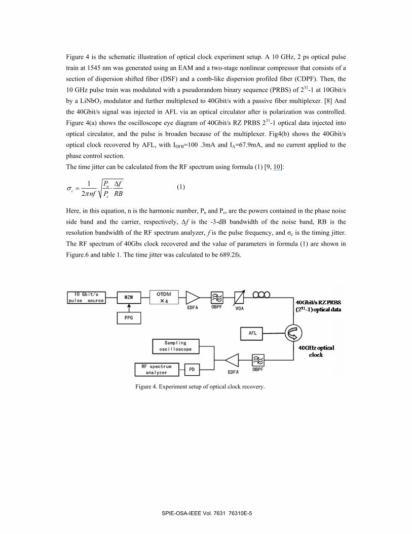
Figure 4 is the schematic illustration of optical clock experiment setup. A 10 GHz, 2 ps optical pulse train at 1545 nm was generated using an EAM and a two-stage nonlinear compressor that consists of a section of dispersion shifted fiber (DSF) and a comb-like dispersion profiled fiber (CDPF). Then, the 10 GHz pulse train was modulated with a pseudorandom binary sequence (PRBS) of 231-1 at 10Gbit/s by a LiNbO3 modulator and further multiplexed to 40Gbit/s with a passive fiber multiplexer. [8] And the 40Gbit/s signal was injected in AFL via an optical circulator after is polarization was controlled. Figure 4(a) shows the oscilloscope eye diagram of 40Gbit/s RZ PRBS 231-1 optical data injected into optical circulator, and the pulse is broaden because of the multiplexer. Fig4(b) shows the 40Gbit/s optical clock recovered by AFL, with IDFB=100 .3mA and IA=67.9mA, and no current applied to the phase control section. The time jitter can be calculated from the RF spectrum using formula (1) [9, 10]:
12
nc
c
P fnf P RB
σπ
Δ= ⋅ (1)
Here, in this equation, n is the harmonic number, Pn and Pc, are the powers contained in the phase noise side band and the carrier, respectively, Δf is the -3-dB bandwidth of the noise band, RB is the resolution bandwidth of the RF spectrum analyzer, f is the pulse frequency, and σc is the timing jitter.
The RF spectrum of 40Gbs clock recovered and the value of parameters in formula (1) are shown in Figure.6 and table 1. The time jitter was calculated to be 689.2fs.
Figure 4. Experiment setup of optical clock recovery.
SPIE-OSA-IEEE Vol. 7631 76310E-5

(a) (b) Figure 5 (a) 40Gbit/s RZ PRBS (231-1) optical data, (b) The 40Gbit/s optical clock recovered from
40Gbit/s RZ PRBS (231-1) optical data
Figure 6 The RF spectra of the optical clock recovered from 40Gbit/s RZ PRBS (231-1) optical data
Table 1. The value of parameters in formula (1).
n f Pn/Pc Δf RB
4 10GHz 1/103(Pc/Pn=30dB) 3MHz 100kHz
5. CONCLUSION
A three-section InP based monolithic dual-mode AFL is fabricated using QWI process as an 40Gbit/s all-optical clock regenerator. The beat frequency tunable range is 32GHz-51GHz. 40Gbit/s RZ PRBS(231-1) data all optical clock recovery using a three-section amplified feedback DFB laser was experimentally demonstrated with time jitter about 689.2fs.
SPIE-OSA-IEEE Vol. 7631 76310E-6

6. ACKNOWLEDGMENT
The authors would like to thank Zhou Fan, Wang Bao-jun, Shu Hui-yun for their experimental help, and Wang Lu-feng, Bian Jing, An Xin for their support on the device test.
The work is supported by the National Natural Science Foundation of China (Grant No.60736036,
60706009, 60777021),the National 973 Program of China (Grant No 2006CB604901,
2006CB604902) and the National 863 project (Grant No.2007AA03Z419,2007AA03Z417).
7. REFERENCES
[1] I. Ogura, T. Sasaki, H. Yamada, et al. “Precise SDH frequency operation of monolithic mode locked laser diodes with
frequency tuning function,” Electron. Lett., vol. 35, pp. 1275–1277, 1999.
[2] B. Sartorius. “3R Regeneration for All-Optical Networks” Transparent Optical Networks, 2001. Proceedings of 2001 3rd
International Conference on 18-21 June 2001 pp:333 – 337
[3] S. Bauer, 0. Brox, J. Kreissl,et al. “Optical microwave source,” Electron. Lett.,vol. 38 pp.334-335, 2002
[4] Y. A. Leem, et al. “The Characterization of All-Optical 3R Regeneration Based on InP-Related Semiconductor Optical
Devices,” IEEE Journal of Selected Topics in Quantum Electronics, VOL. 12, pp726-735, 2006
[5] D.-S. Yee, Y. A. Leem, K.H. Park, et al. “Influence of free-running characteristics on optical clock in all-optical clock
recovery using a self-pulsating semiconductor laser” Optics Communications, vol.278, pp.285–290, 2007
[6]Y. Sun, Y. B. Chen, Y. Wang, et al. “Widely Frequency-Tunable Optical Microwave Source based on Amplified Feedback
laser,” PhotonicsGlobal@Singapore, 2008. IPGC 2008. IEEE, pp:1 - 4, 8-11 Dec. 2008
[7] A. A. Tager and K. Petermann, “High-Frequency Oscillations and Self-Mode Locking in Short External-Cavity Laser
Diodes,” IEEE J. of Electron. Lett.,vol. 30, pp.1553-1561, 1994
[8] L.Huo, S. L.Pan, Z. X.Wang, et al. “Optical 3R regeneration of 40 Gbit/s degraded data signals” Optics Communications
vol.266, pp290-295,2006
[9] Delfyett, P. J., "Optical Clock Distribution Using a Mode-Locked Semiconductor-Laser Diode System." Journal of
Lightwave Technology 9(12): 1646-1649 1991
[10] D. von der Linde, “Characterization of noise in continuously operating mode locked lasers,” Appl. Phys. B., vol. 39, p. 201,
1986.
SPIE-OSA-IEEE Vol. 7631 76310E-7