Advanced methods for the analysis of nanocrystals in nm ...
53
Thanos Galanis Application Specialist Advanced methods for the analysis of nanocrystals in nm-scale using Precession Electron Diffraction techniques in TEM
-
Upload
khangminh22 -
Category
Documents
-
view
5 -
download
0
Transcript of Advanced methods for the analysis of nanocrystals in nm ...
Thanos GalanisApplication Specialist
Advanced methods for the analysis of
nanocrystals in nm-scale using
Precession Electron Diffraction
techniques in TEM
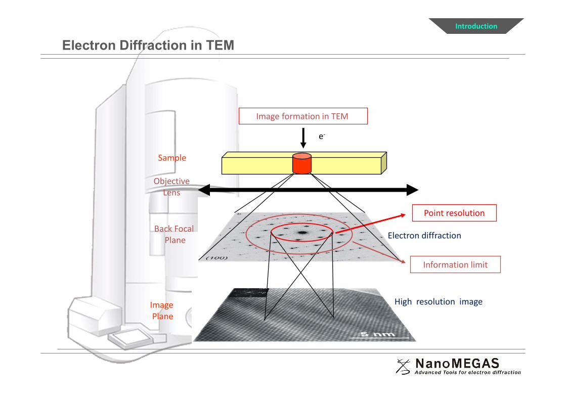
Electron Diffraction in TEM
Image formation in TEM
Back FocalPlane
ImagePlane
ObjectiveLens
Sample
e-
Point resolution
Information limit
Electron diffraction
High resolution image
Introduction
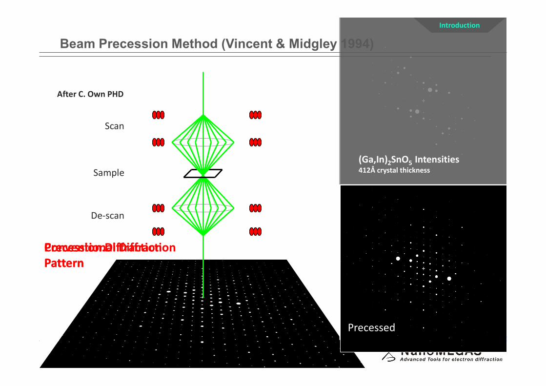
De-scan
Scan
Sample Non-precessed
After C. Own PHD
Precessed
Conventional Diffraction PatternPrecession…Precession Diffraction Pattern
(Ga,In)2SnO5 Intensities412Å crystal thickness
Beam Precession Method (Vincent & Midgley 1994)
Introduction
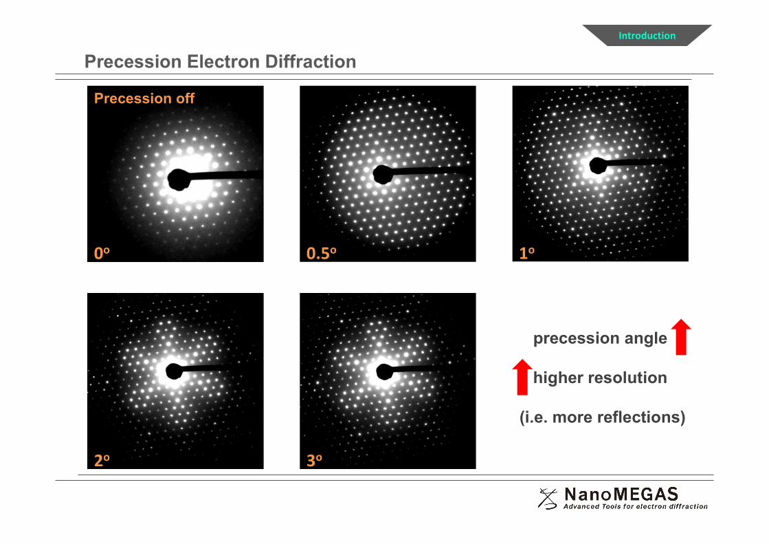
1o
3o2o
0.5o0o
Precession off
Precession Electron Diffraction
precession angle
higher resolution
(i.e. more reflections)
Introduction
www.nanomegas.comtopspin
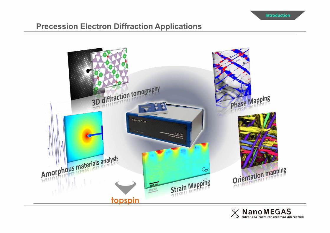
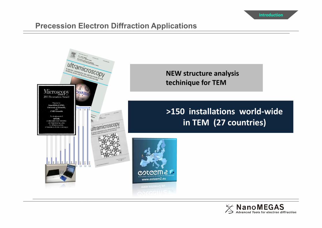
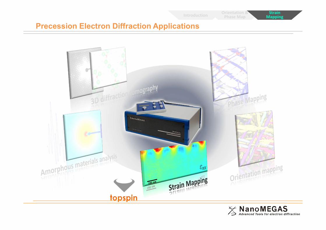
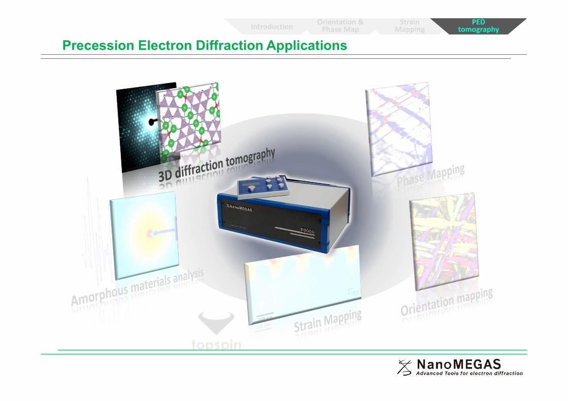
Precession Electron Diffraction Applications
Introduction
www.nanomegas.com
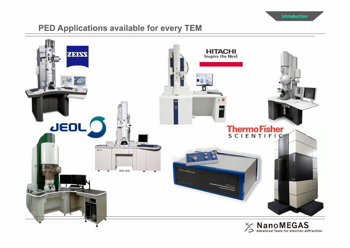
PED Applications available for every TEM
Introduction
www.nanomegas.com
>150 installations world-wide in TEM (27 countries)
NEW structure analysistechinique for TEM
Precession Electron Diffraction Applications
Introduction
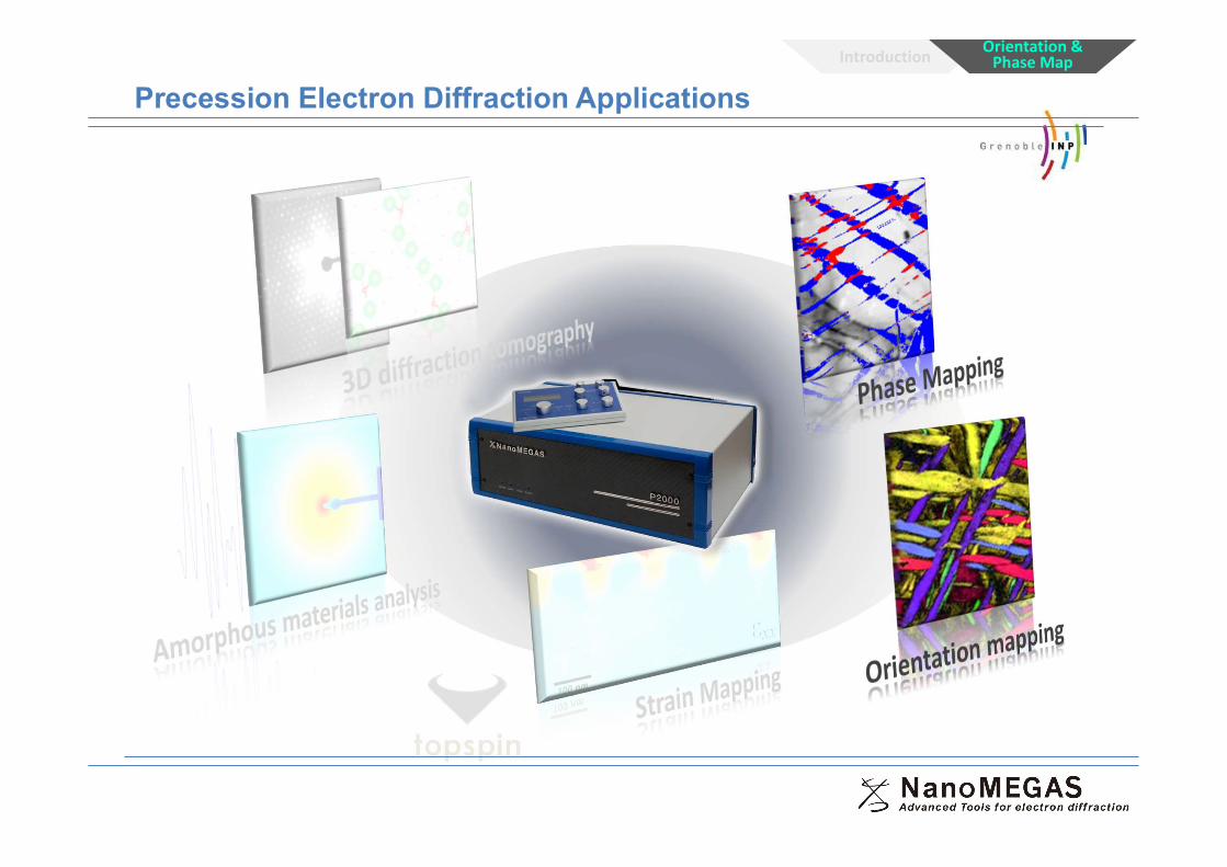
www.nanomegas.comtopspin
Precession Electron Diffraction Applications
Introduction Orientation & Phase Map
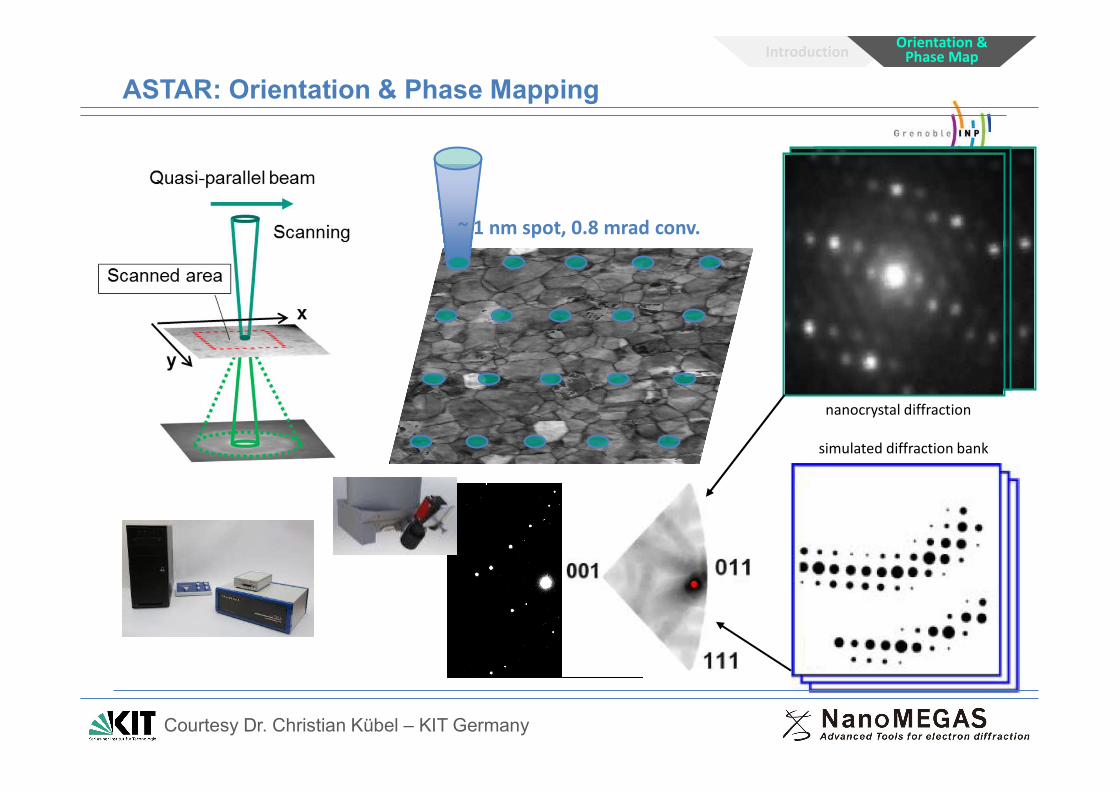
www.nanomegas.com
~ 1 nm spot, 0.8 mrad conv.
nanocrystal diffraction
simulated diffraction bank
ASTAR: Orientation & Phase Mapping
Introduction Orientation & Phase Map
Courtesy Dr. Christian Kübel – KIT Germany
www.nanomegas.com
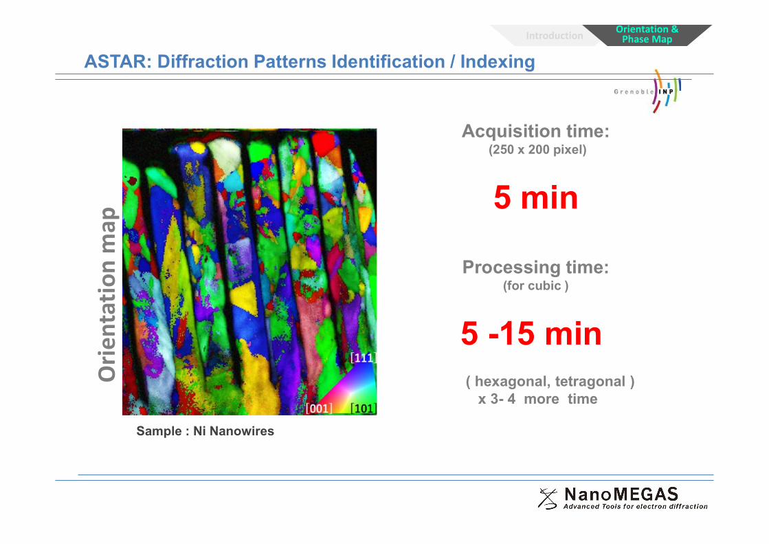
Acquisition time:(250 x 200 pixel)
5 min
Processing time:(for cubic )
5 -15 min ( hexagonal, tetragonal )
x 3- 4 more time
Sample : Ni Nanowires
Orie
ntat
ion
map
ASTAR: Diffraction Patterns Identification / Indexing
Introduction Orientation & Phase Map
www.nanomegas.com
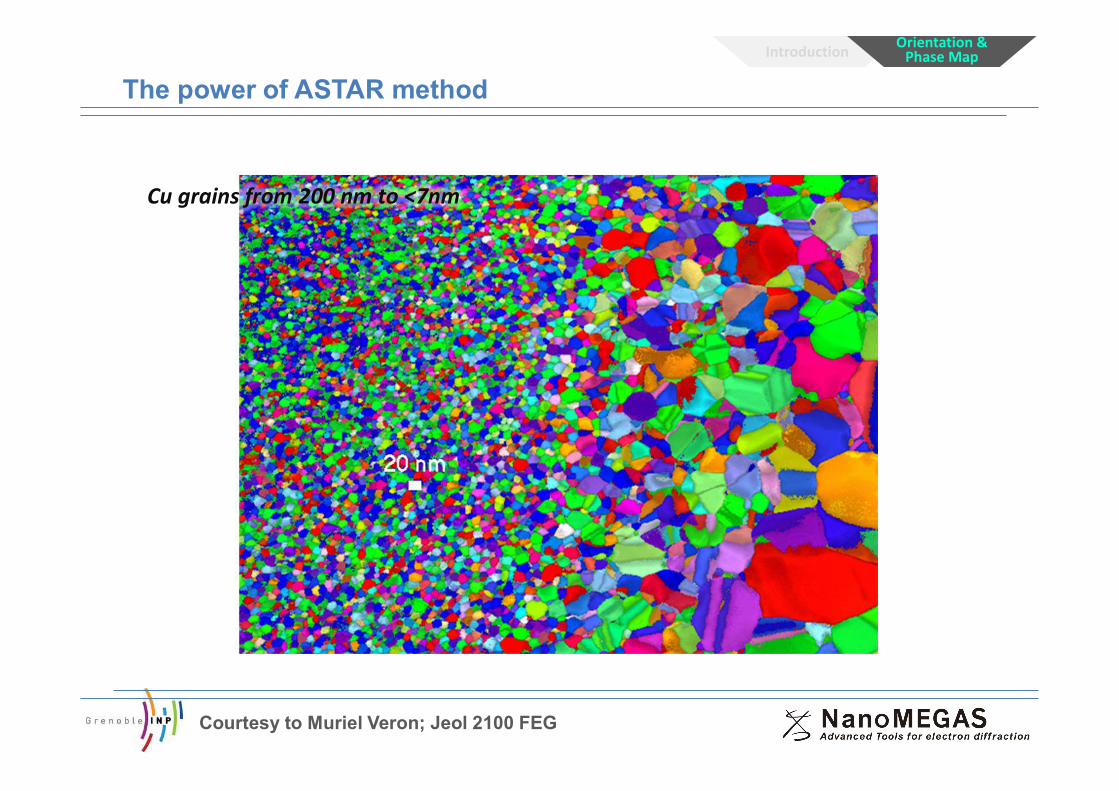
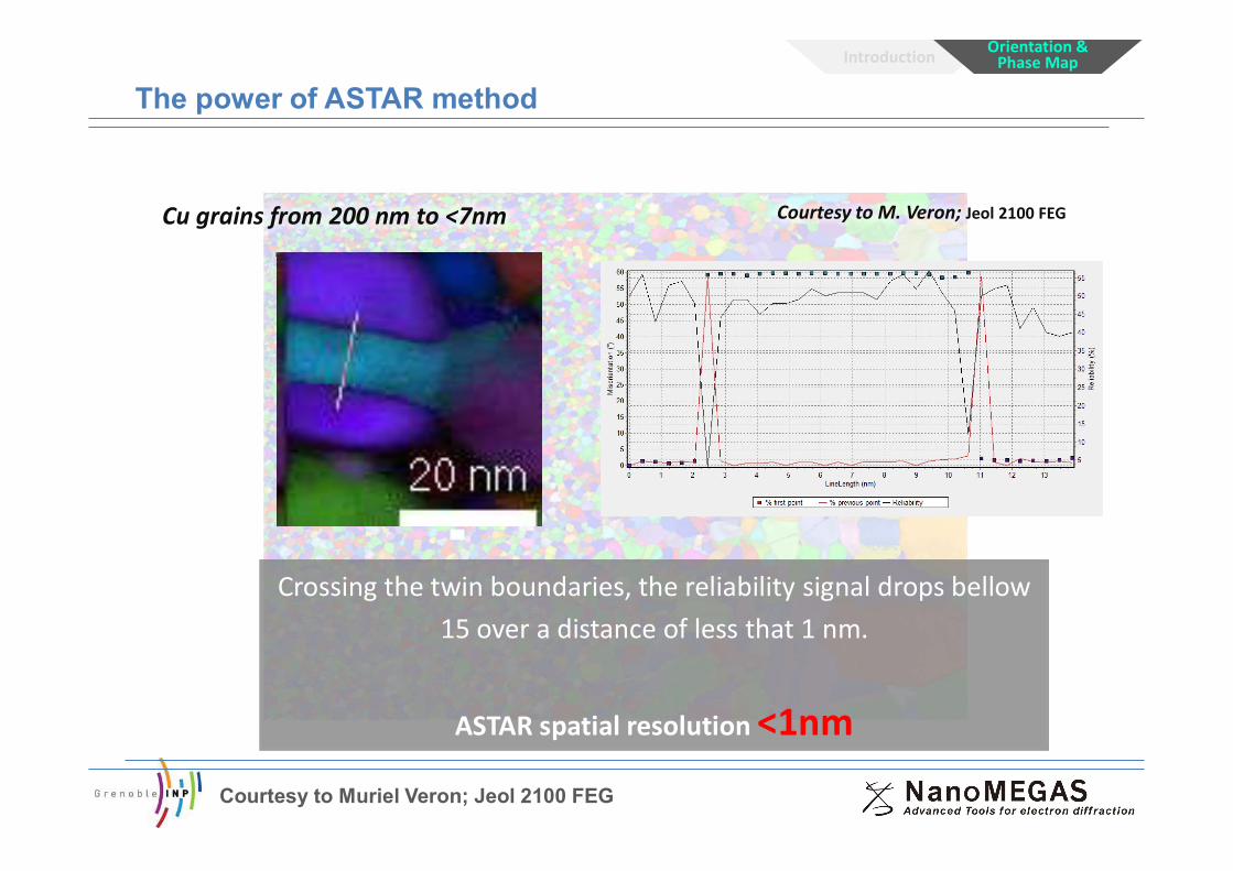
Cu grains from 200 nm to <7nm
Courtesy to Muriel Veron; Jeol 2100 FEG
The power of ASTAR method
Introduction Orientation & Phase Map
www.nanomegas.com
Crossing the twin boundaries, the reliability signal drops bellow 15 over a distance of less that 1 nm.
ASTAR spatial resolution <1nm
Cu grains from 200 nm to <7nm Courtesy to M. Veron; Jeol 2100 FEG
Courtesy to Muriel Veron; Jeol 2100 FEG
The power of ASTAR method
Introduction Orientation & Phase Map
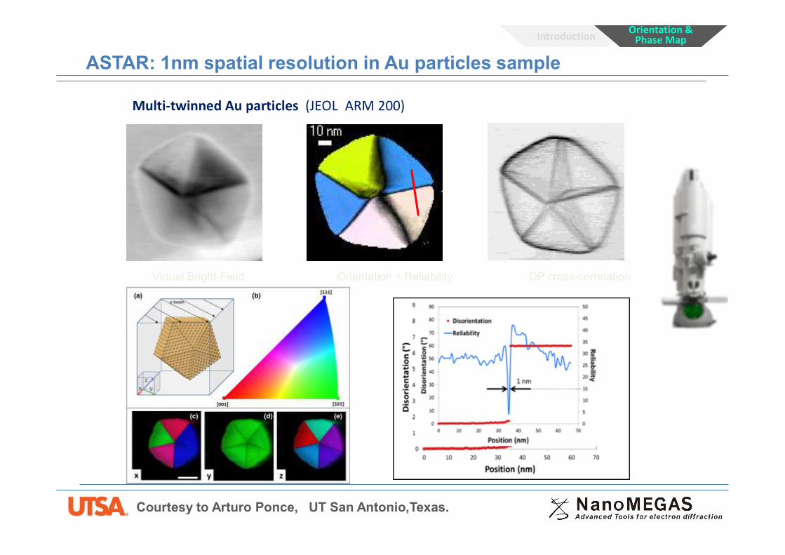
Multi-twinned Au particles (JEOL ARM 200)
Virtual Bright-Field Orientation + Reliability DP cross-correlation
Courtesy to Arturo Ponce, UT San Antonio,Texas.
ASTAR: 1nm spatial resolution in Au particles sample
Introduction Orientation & Phase Map
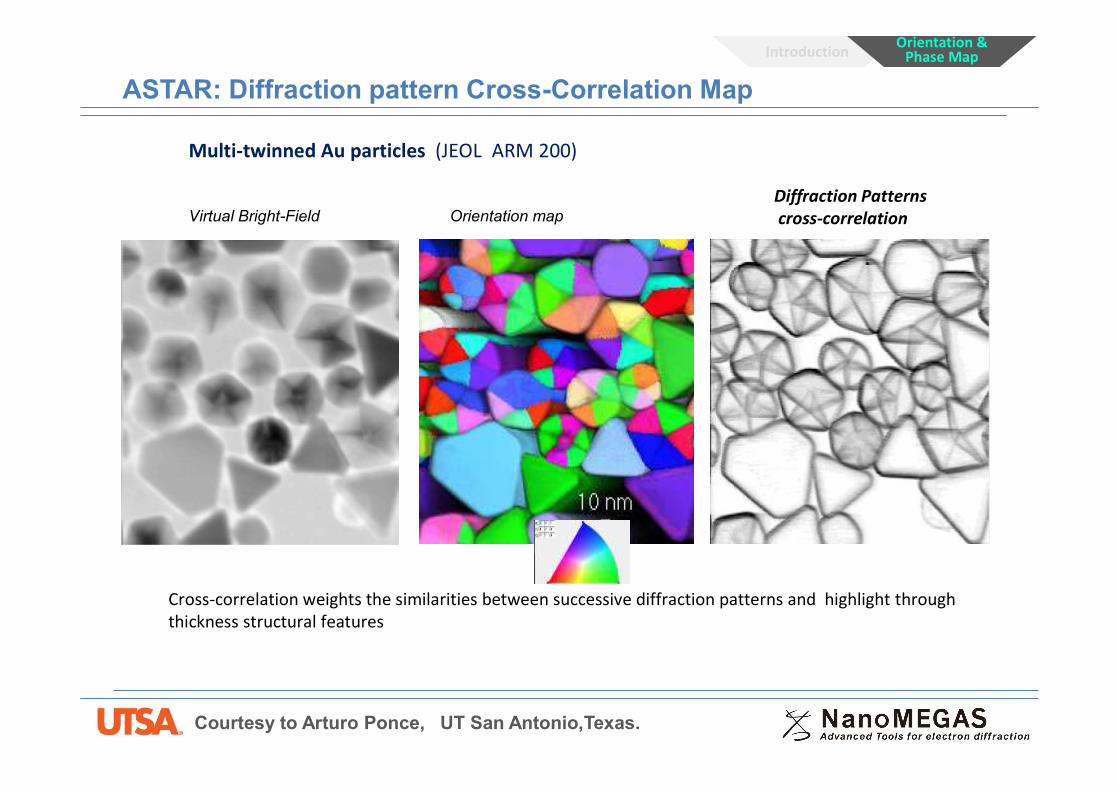
Orientation mapVirtual Bright-FieldDiffraction Patterns cross-correlation
Cross-correlation weights the similarities between successive diffraction patterns and highlight through thickness structural features
Courtesy to Arturo Ponce, UT San Antonio,Texas.
ASTAR: Diffraction pattern Cross-Correlation Map
Introduction Orientation & Phase Map
Multi-twinned Au particles (JEOL ARM 200)

www.nanomegas.com
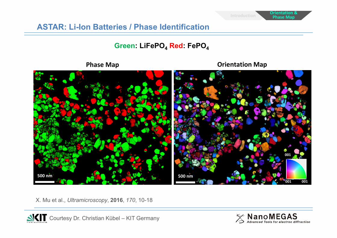
Li0.5FePO4
Li+
Li+
+_
e.g. LixC6 e.g. Li1-xFePO4
ElectrolyteAnode Cathode
hkl LiFePO4 FePO4 Difference
100 10.33 9.81 5.0 %
010 6.01 5.79 3.8 %
001 4.69 4.78 1.8 %
Lattice Spacings [Å]FPLFP
Q1:1201 Q2: 985
ASTAR: Li-Ion Batteries / Phase Identification
Introduction Orientation & Phase Map
Courtesy Dr. Christian Kübel – KIT Germany
www.nanomegas.com
X. Mu et al., Ultramicroscopy, 2016, 170, 10-18
500 nm500 nm001
001
001
Phase Map Orientation Map
Green: LiFePO4 Red: FePO4
ASTAR: Li-Ion Batteries / Phase Identification
Introduction Orientation & Phase Map
Courtesy Dr. Christian Kübel – KIT Germany
www.nanomegas.com
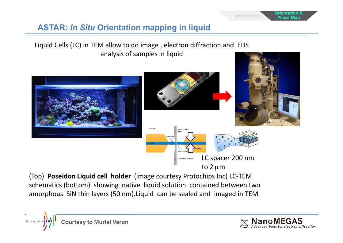
ASTAR: In Situ Orientation mapping in liquid
Introduction Orientation & Phase Map
(Top) Poseidon Liquid cell holder (image courtesy Protochips Inc) LC-TEMschematics (bottom) showing native liquid solution contained between twoamorphous SiN thin layers (50 nm).Liquid can be sealed and imaged in TEM
Liquid Cells (LC) in TEM allow to do image , electron diffraction and EDS analysis of samples in liquid
LC spacer 200 nm to 2 mm
Courtesy to Muriel Veron

www.nanomegas.com
www.nanomegas.com
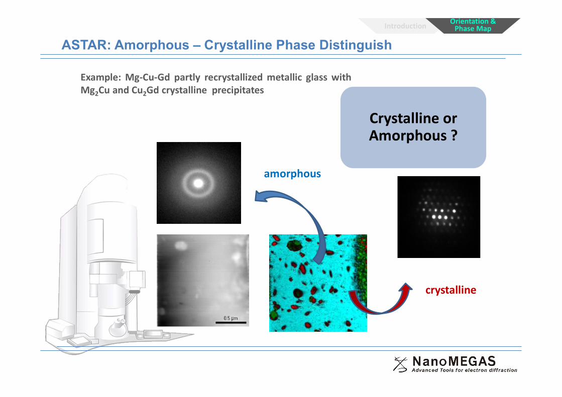
Example: Mg-Cu-Gd partly recrystallized metallic glass withMg2Cu and Cu2Gd crystalline precipitates
Crystalline or Amorphous ?
crystalline
amorphous
ASTAR: Amorphous – Crystalline Phase Distinguish
Introduction Orientation & Phase Map
www.nanomegas.comtopspin
Precession Electron Diffraction Applications
Introduction Orientation & Phase Map
Strain Mapping
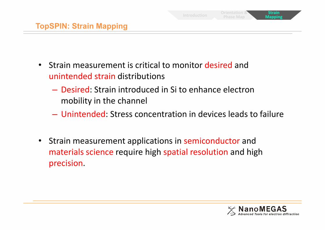
• Strain measurement is critical to monitor desired and unintended strain distributions– Desired: Strain introduced in Si to enhance electron
mobility in the channel– Unintended: Stress concentration in devices leads to failure
• Strain measurement applications in semiconductor and materials science require high spatial resolution and high precision.
TopSPIN: Strain Mapping
Introduction Orientation & Phase Map
Strain Mapping
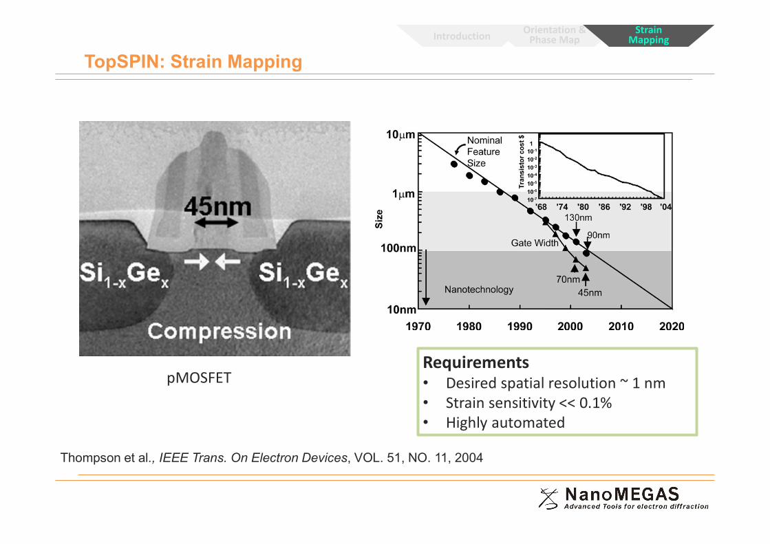
Thompson et al., IEEE Trans. On Electron Devices, VOL. 51, NO. 11, 2004
pMOSFETRequirements• Desired spatial resolution ~ 1 nm• Strain sensitivity << 0.1%• Highly automated
TopSPIN: Strain Mapping
Introduction Orientation & Phase Map
Strain Mapping
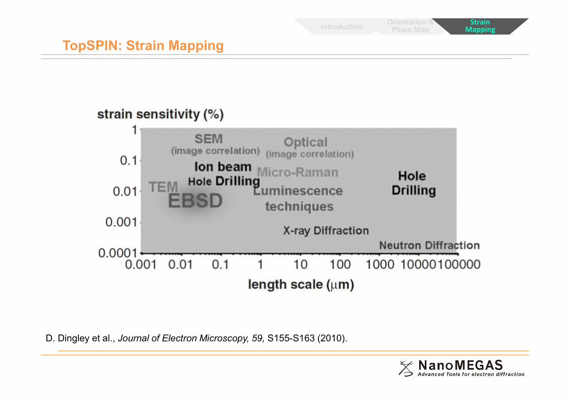
Introduction Orientation & Phase Map
Strain Mapping
D. Dingley et al., Journal of Electron Microscopy, 59, S155-S163 (2010).
TopSPIN: Strain Mapping
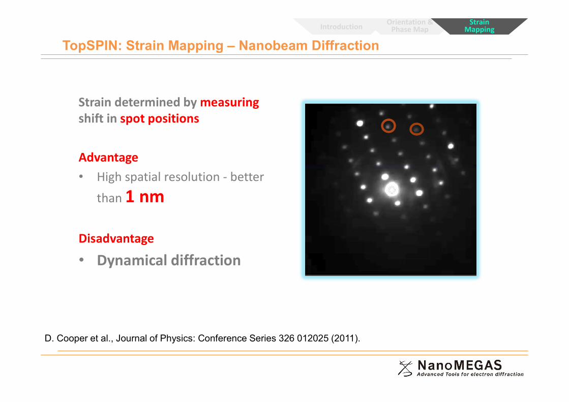
Strain determined by measuringshift in spot positions
Advantage• High spatial resolution - better
than 1 nm
Disadvantage
• Dynamical diffraction
D. Cooper et al., Journal of Physics: Conference Series 326 012025 (2011).
Introduction Orientation & Phase Map
Strain Mapping
TopSPIN: Strain Mapping – Nanobeam Diffraction
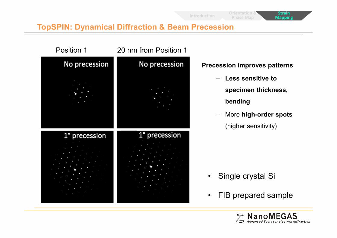
• Single crystal Si
• FIB prepared sample
Position 1 20 nm from Position 1
Introduction Orientation & Phase Map
Strain Mapping
TopSPIN: Dynamical Diffraction & Beam Precession
Precession improves patterns
– Less sensitive to
specimen thickness,
bending
– More high-order spots
(higher sensitivity)

Introduction Orientation & Phase Map
Strain Mapping
TopSPIN: Data acquisition – Optimum conditions
Typically use spot positions in nanobeam diffraction (NBD) patterns
Reference
Strain
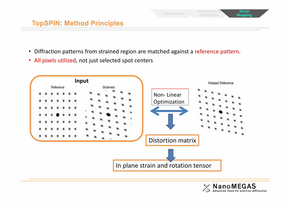
• Diffraction patterns from strained region are matched against a reference pattern. • All pixels utilized, not just selected spot centers
Distortion matrix
In plane strain and rotation tensor
Input
Non- Linear Optimization
Introduction Orientation & Phase Map
Strain Mapping
TopSPIN: Method Principles
www.nanomegas.com
x
A
B
A
B
A
B
A
B
y
B
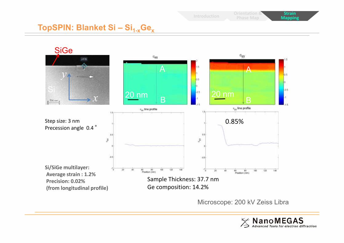
Step size: 3 nmPrecession angle 0.4 °
0.85%
Sample Thickness: 37.7 nmGe composition: 14.2%
20 nm20 nm
Microscope: 200 kV Zeiss Libra
SiGe
Si
Si/SiGe multilayer:Average strain : 1.2%Precision: 0.02%(from longitudinal profile)
Introduction Orientation & Phase Map
Strain Mapping
TopSPIN: Blanket Si – Si1-xGex
www.nanomegas.com
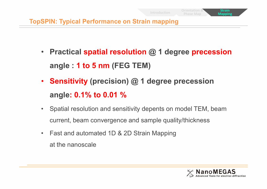
• Practical spatial resolution @ 1 degree precession
angle : 1 to 5 nm (FEG TEM)
• Sensitivity (precision) @ 1 degree precession
angle: 0.1% to 0.01 %
• Spatial resolution and sensitivity depents on model TEM, beam
current, beam convergence and sample quality/thickness
• Fast and automated 1D & 2D Strain Mapping
at the nanoscale
Introduction Orientation & Phase Map
Strain Mapping
TopSPIN: Typical Performance on Strain mapping
www.nanomegas.com
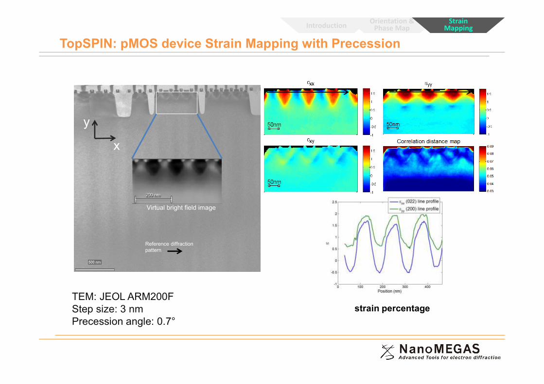
Reference diffraction pattern
Topspin bright field STEM
x
y
Virtual bright field image
TEM: JEOL ARM200FStep size: 3 nmPrecession angle: 0.7°
strain percentage
Introduction Orientation & Phase Map
Strain Mapping
TopSPIN: pMOS device Strain Mapping with Precession
www.nanomegas.com
0 100 200 300 400-1.5
-1
-0.5
0
0.5
1
1.5
2
2.5
Position (nm)
xx (022) line profile
yy (200) line profile
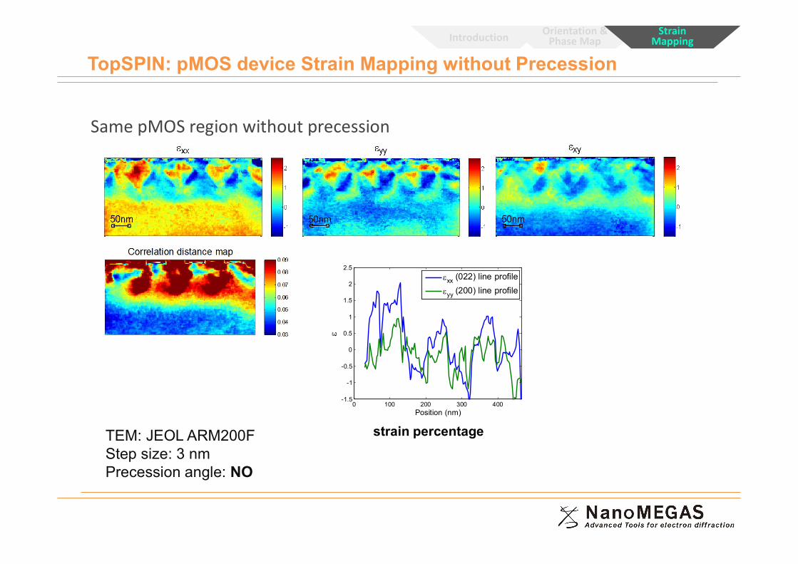
Same pMOS region without precession
Introduction Orientation & Phase Map
Strain Mapping
TopSPIN: pMOS device Strain Mapping without Precession
TEM: JEOL ARM200FStep size: 3 nmPrecession angle: NO
strain percentage
www.nanomegas.com
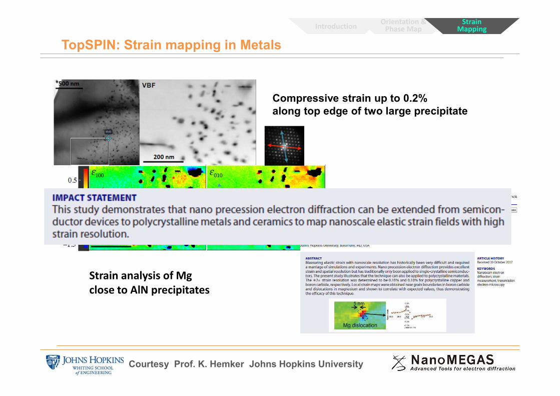
Strain analysis of Mg close to AlN precipitates
Compressive strain up to 0.2%along top edge of two large precipitate
Courtesy Prof. K. Hemker Johns Hopkins University
Introduction Orientation & Phase Map
Strain Mapping
TopSPIN: Strain mapping in Metals
www.nanomegas.comtopspin
Precession Electron Diffraction Applications
Introduction Orientation & Phase Map
Strain Mapping
PED tomography
www.nanomegas.com
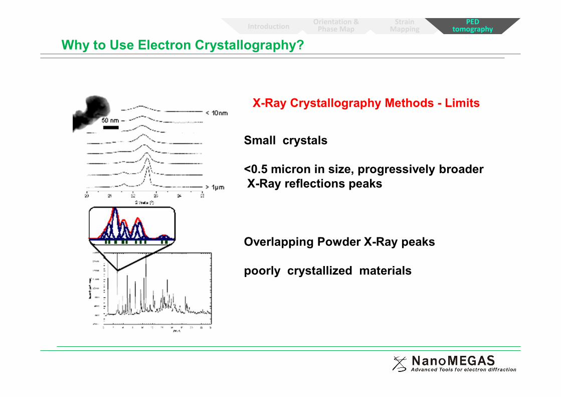
Why to Use Electron Crystallography?
Introduction Orientation & Phase Map
Strain Mapping
PED tomography
Small crystals
<0.5 micron in size, progressively broaderX-Ray reflections peaks
Overlapping Powder X-Ray peaks
poorly crystallized materials
X-Ray Crystallography Methods - Limits
www.nanomegas.com
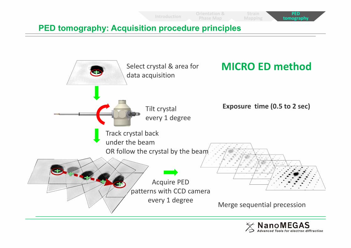
Select crystal & area for data acquisition
Tilt crystal every 1 degree
Track crystal backunder the beamOR follow the crystal by the beam
Merge sequential precession diffraction patterns
Acquire PEDpatterns with CCD camera
every 1 degree
Exposure time (0.5 to 2 sec)
PED tomography: Acquisition procedure principles
Introduction Orientation & Phase Map
Strain Mapping
PED tomography
MICRO ED method
www.nanomegas.com
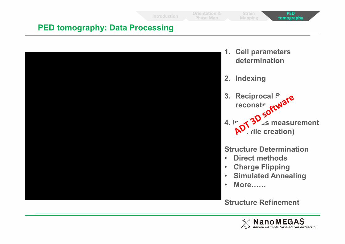
1. Cell parameters determination
2. Indexing
3. Reciprocal Space reconstruction
4. Intensities measurement(hkl file creation)
Structure Determination• Direct methods• Charge Flipping • Simulated Annealing• More……
Structure Refinement
PED tomography: Data Processing
Introduction Orientation & Phase Map
Strain Mapping
PED tomography
www.nanomegas.com
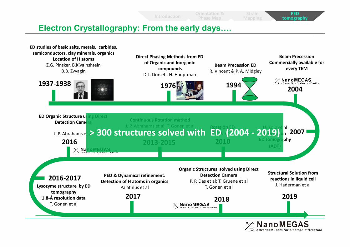
Electron Crystallography: From the early days….
Introduction Orientation & Phase Map
Strain Mapping
PED tomography
ED studies of basic salts, metals, carbides, semiconductors, clay minerals, organics
Location of H atomsZ.G. Pinsker, B.K.Vainshtein
B.B. Zvyagin
1937-1938 1976
Direct Phasing Methods from ED of Organic and Inorganic
compoundsD.L. Dorset , H. Hauptman
Beam Precession EDR. Vincent & P. A. Midgley
1994 2004
Beam Precession Commercially available for
every TEM
2007U. Kolb et alPrecession
ED tomography (ADT)
Rotation EDX. Zou et al
2010
Continuous Rotation methodJ. P. Abrahams et al; T. Gonen et al
M. Gemmi et al
2013-2015
ED Organic Structure using Direct Detection Camera
J. P. Abrahams et al
2016
Lysozyme structure by ED tomography
1.8-Å resolution dataT. Gonen et al
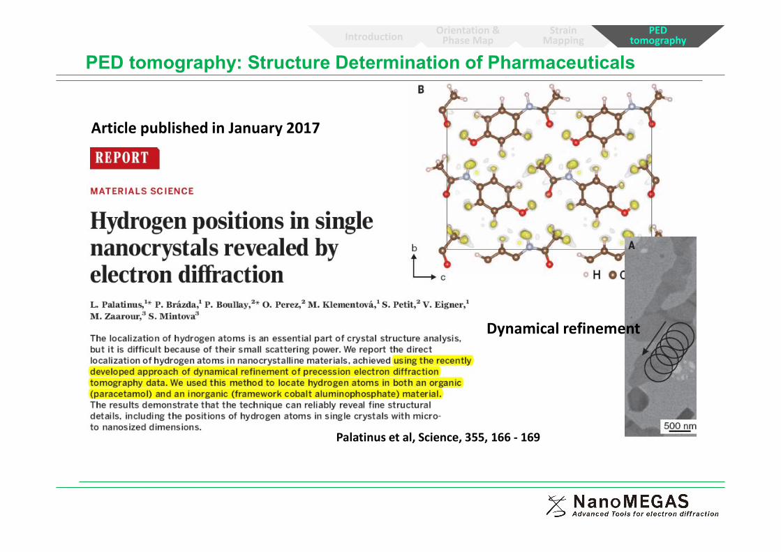
2016-2017 PED & Dynamical refinement. Detection of H atoms in organics
Palatinus et al
2017
Organic Structures solved using Direct Detection Camera
P. P. Das et al; T. Gruene et alT. Gonen et al
2018
Structural Solution fromreactions in liquid cell
J. Haderman et al
2019
> 300 structures solved with ED (2004 - 2019)
www.nanomegas.com
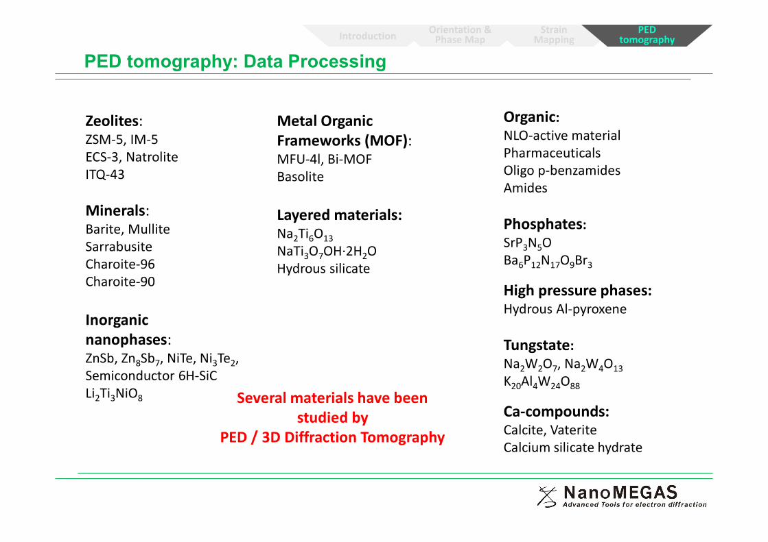
Zeolites:ZSM-5, IM-5ECS-3, NatroliteITQ-43
Minerals:Barite, MulliteSarrabusiteCharoite-96Charoite-90
Inorganic nanophases:ZnSb, Zn8Sb7, NiTe, Ni3Te2,Semiconductor 6H-SiCLi2Ti3NiO8
Organic:NLO-active materialPharmaceuticalsOligo p-benzamidesAmides
Phosphates:SrP3N5OBa6P12N17O9Br3
High pressure phases:Hydrous Al-pyroxene
Tungstate:Na2W2O7, Na2W4O13 K20Al4W24O88
Ca-compounds:Calcite, VateriteCalcium silicate hydrate
Several materials have beenstudied by
PED / 3D Diffraction Tomography
Metal Organic Frameworks (MOF):MFU-4l, Bi-MOFBasolite
Layered materials:Na2Ti6O13NaTi3O7OH·2H2OHydrous silicate
PED tomography: Data Processing
Introduction Orientation & Phase Map
Strain Mapping
PED tomography
www.nanomegas.com
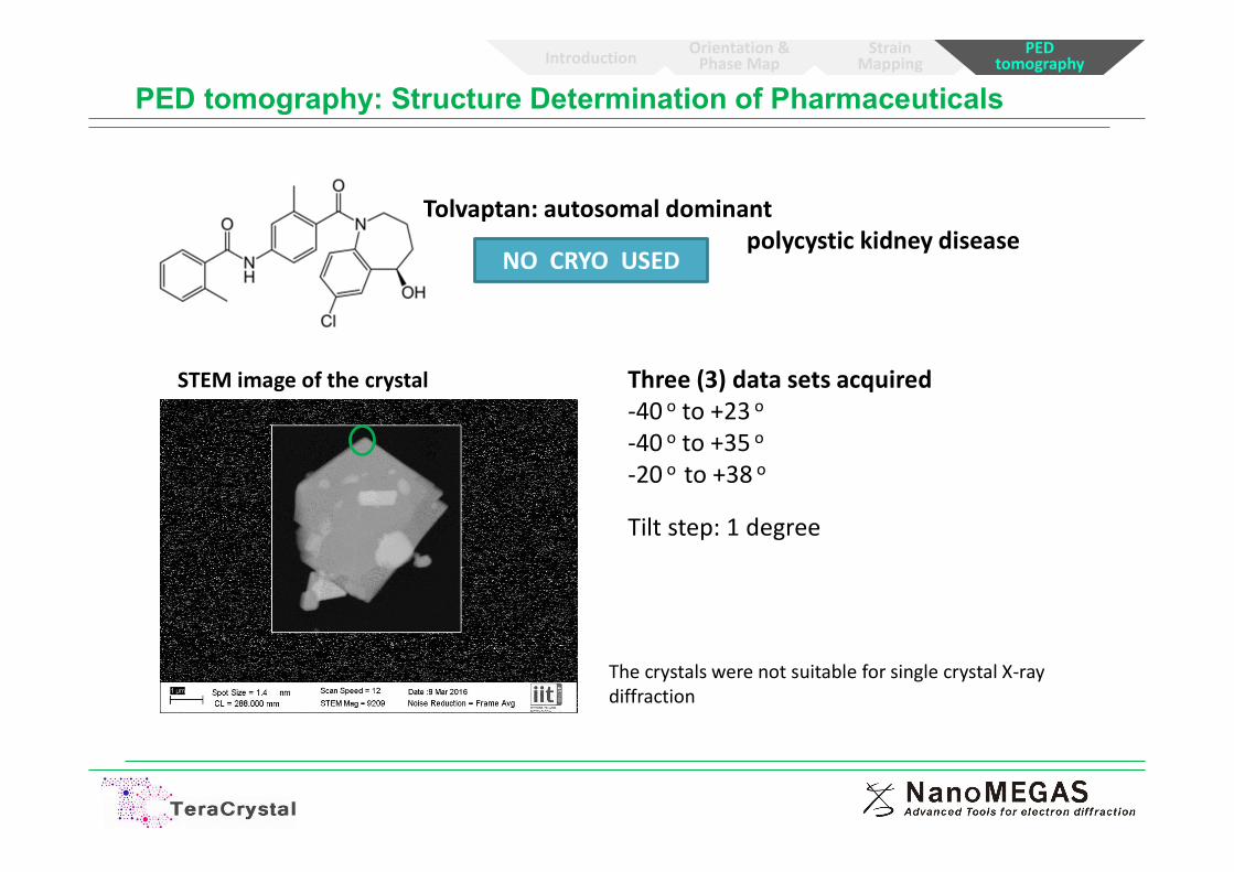
Three (3) data sets acquired-40 o to +23 o
-40 o to +35 o
-20 o to +38 o
Tilt step: 1 degree
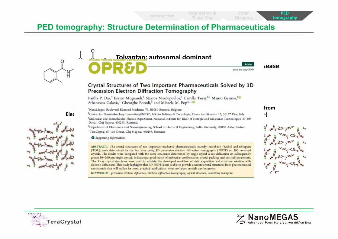
The crystals were not suitable for single crystal X-ray diffraction
NO CRYO USED
Tolvaptan: autosomal dominantpolycystic kidney disease
STEM image of the crystal
PED tomography: Structure Determination of Pharmaceuticals
Introduction Orientation & Phase Map
Strain Mapping
PED tomography
www.nanomegas.com
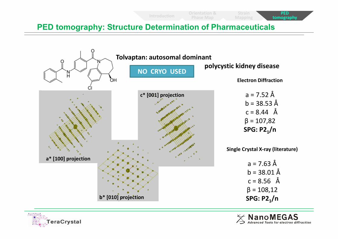
a* [100] projection
c* [001] projection
Electron Diffraction
a = 7.52 Åb = 38.53 Åc = 8.44 Åβ = 107,82SPG: P21/n
Single Crystal X-ray (literature)
a = 7.63 Åb = 38.01 Åc = 8.56 Åβ = 108,12SPG: P21/n
NO CRYO USED
Tolvaptan: autosomal dominantpolycystic kidney disease
b* [010] projection
PED tomography: Structure Determination of Pharmaceuticals
Introduction Orientation & Phase Map
Strain Mapping
PED tomography
www.nanomegas.com
NO CRYO USED
Tolvaptan: autosomal dominantpolycystic kidney disease
SA Structure fromElectron Diffraction Data
Direct Method Structure fromSCXRD data (literature)
PED tomography: Structure Determination of Pharmaceuticals
Introduction Orientation & Phase Map
Strain Mapping
PED tomography
www.nanomegas.com
Dynamical refinement
Palatinus et al, Science, 355, 166 - 169
Article published in January 2017
PED tomography: Structure Determination of Pharmaceuticals
Introduction Orientation & Phase Map
Strain Mapping
PED tomography
www.nanomegas.comtopspin
Precession Electron Diffraction Applications
Introduction Orientation & Phase Map
Strain Mapping
PED tomography e-PDF
www.nanomegas.com
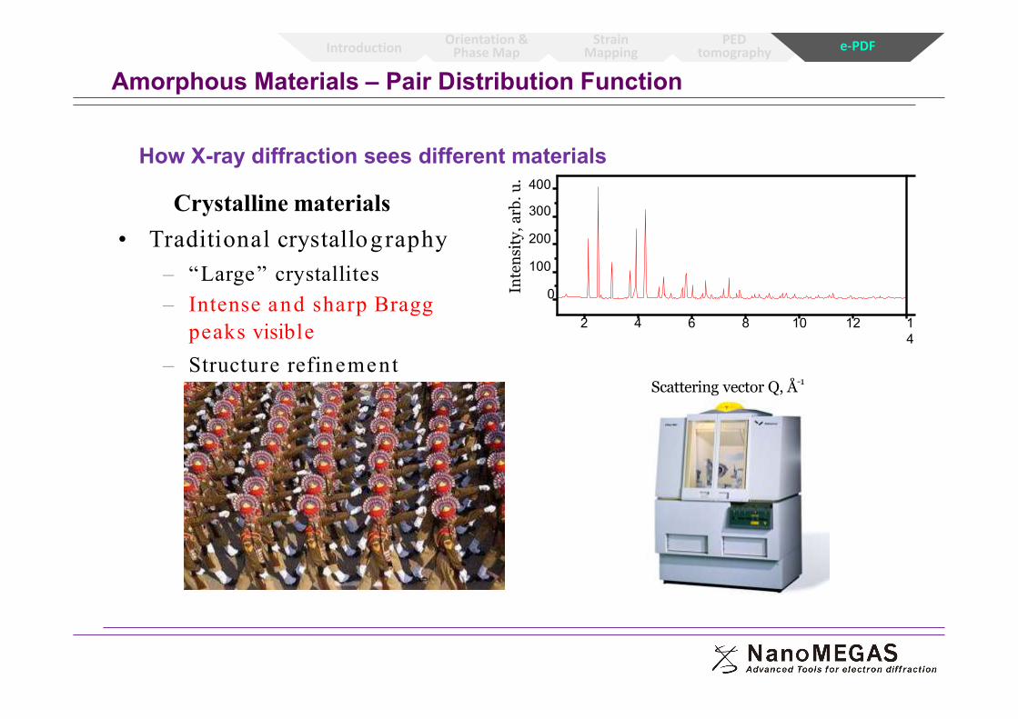
• Traditional crystallography
– “Large” crystallites
– Intense and sharp Braggpeaks visible
– Structure refinementScattering vector Q, Å-1
Intensity,a
rb.u
.
Crystalline materials400
300
200
100
0
2 4 6 8 10 12 14
How X-ray diffraction sees different materials
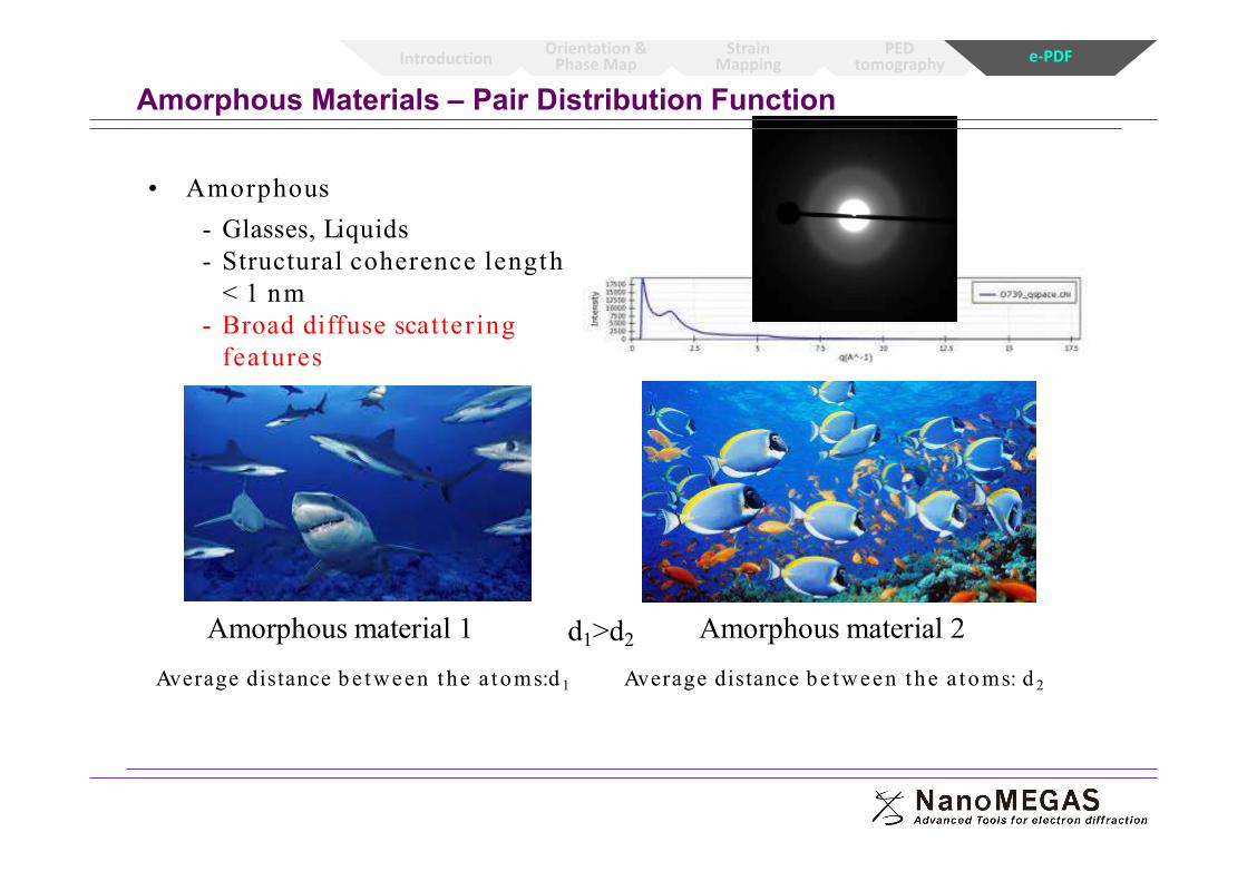
Amorphous Materials – Pair Distribution Function
Introduction Orientation & Phase Map
Strain Mapping
PED tomography e-PDF
www.nanomegas.com
• Amorphous
- Glasses, Liquids- Structural coherence length
< 1 nm- Broad diffuse scattering
features
Amorphous material 2
Average distance b e tween the a to ms: d 2
Amorphous material 1
Average distance b e tween the a toms:d 1
d1>d2
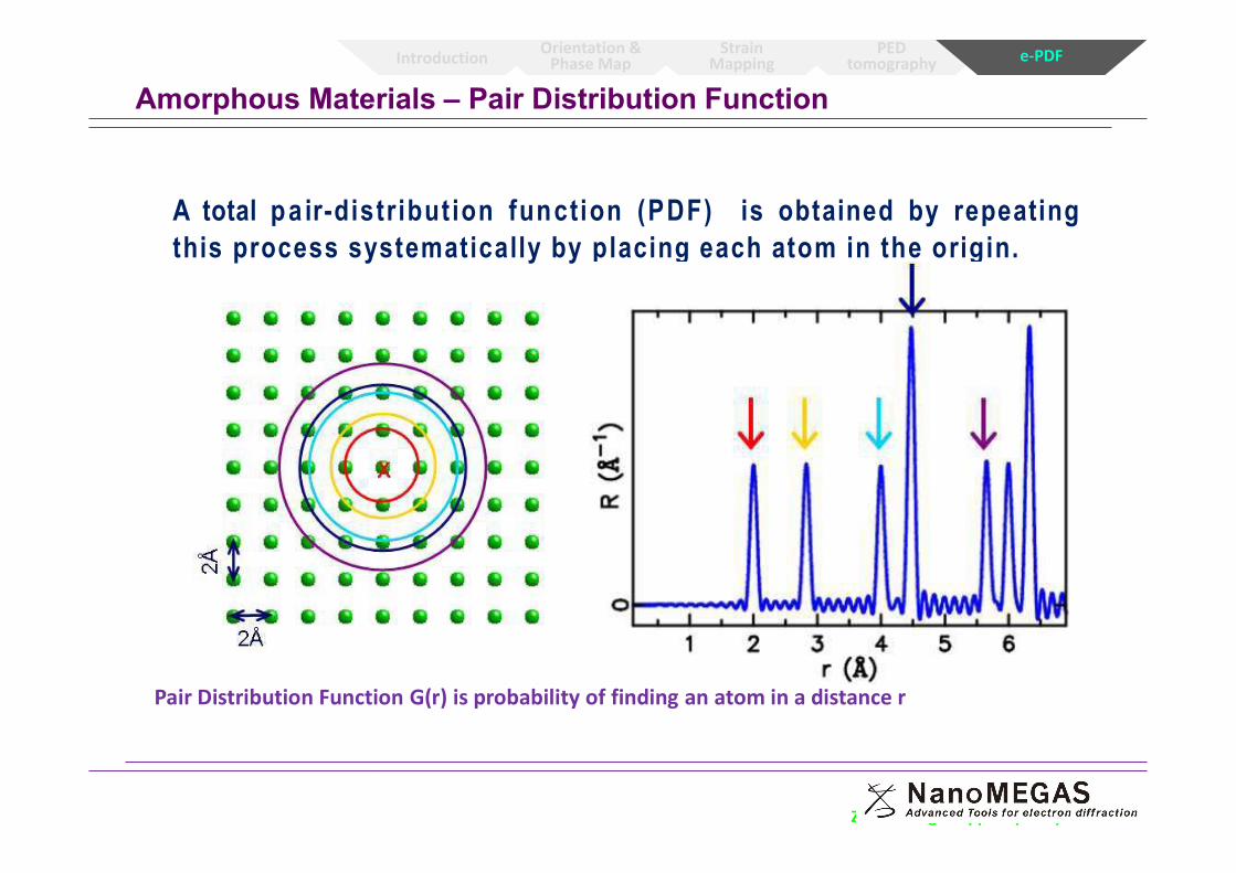
Amorphous Materials – Pair Distribution Function
Introduction Orientation & Phase Map
Strain Mapping
PED tomography e-PDF
www.nanomegas.com
A total pa ir-distribut ion function (PDF) is obtained by repeatingthis process systematically by placing each atom in the origin.
Z. Kristallogr. Supp. 26(2007) 17-26
Pair Distribution Function G(r) is probability of finding an atom in a distance r
Amorphous Materials – Pair Distribution Function
Introduction Orientation & Phase Map
Strain Mapping
PED tomography e-PDF
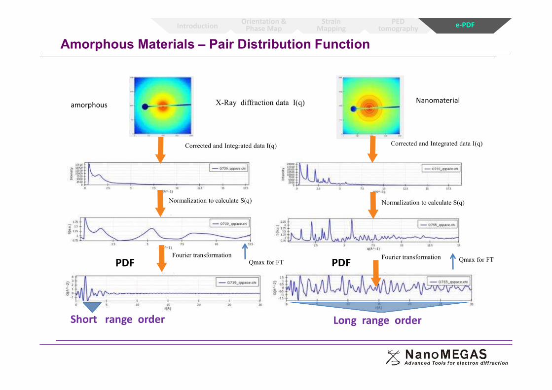
www.nanomegas.com
Normalization to calculate S(q)
Corrected and Integrated data I(q)
Fourier transformation
Corrected and Integrated data I(q)
Normalization to calculate S(q)
Fourier transformationQmax for FT Qmax for FT
Long range orderShort range order
X-Ray diffraction data I(q)amorphous Nanomaterial
PDF PDF
Amorphous Materials – Pair Distribution Function
Introduction Orientation & Phase Map
Strain Mapping
PED tomography e-PDF
www.nanomegas.com
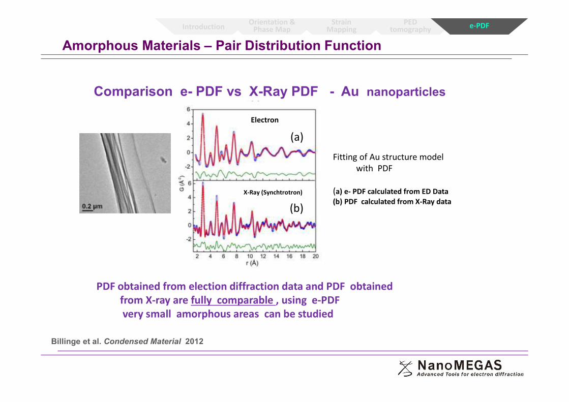
Comparison e- PDF vs X-Ray PDF - Au nanoparticles
Billinge et al. Condensed Material 2012
Fitting of Au structure model with PDF
(a) e- PDF calculated from ED Data (b) PDF calculated from X-Ray data
PDF obtained from election diffraction data and PDF obtained from X-ray are fully comparable , using e-PDF very small amorphous areas can be studied
(b)
Electron
X-Ray (Synchtrotron)
(a)
Amorphous Materials – Pair Distribution Function
Introduction Orientation & Phase Map
Strain Mapping
PED tomography e-PDF
www.nanomegas.com
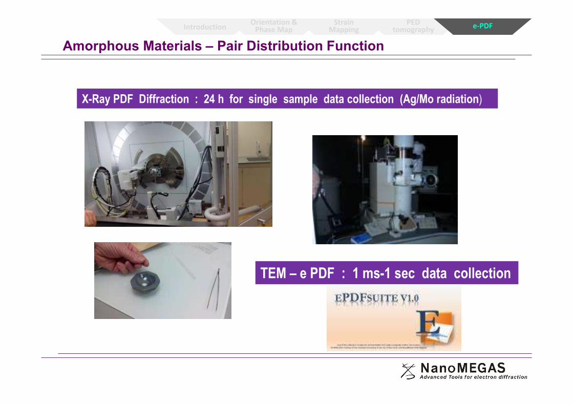
X-Ray PDF Diffraction : 24 h for single sample data collection (Ag/Mo radiation)
TEM – e PDF : 1 ms-1 sec data collection
Amorphous Materials – Pair Distribution Function
Introduction Orientation & Phase Map
Strain Mapping
PED tomography e-PDF
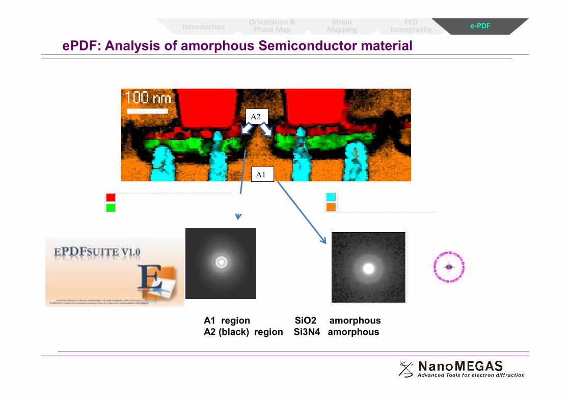
A2
A1
A1 region SiO2 amorphousA2 (black) region Si3N4 amorphous
ePDF: Analysis of amorphous Semiconductor material
Introduction Orientation & Phase Map
Strain Mapping
PED tomography e-PDF
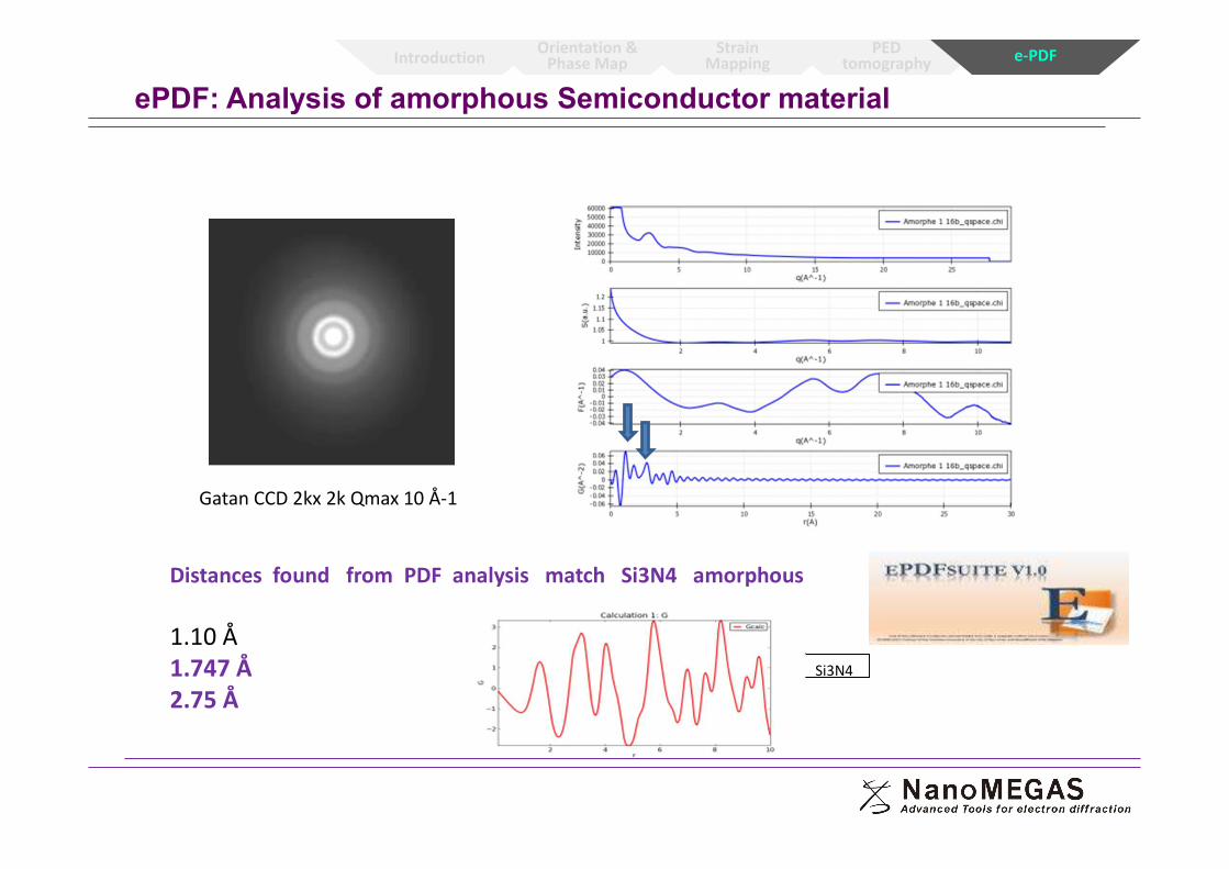
Distances found from PDF analysis match Si3N4 amorphous
1.10 Å 1.747 Å2.75 Å
Si3N4
Gatan CCD 2kx 2k Qmax 10 Å-1
ePDF: Analysis of amorphous Semiconductor material
Introduction Orientation & Phase Map
Strain Mapping
PED tomography e-PDF
52
ESTEEM 3 in a nutshell
Freetransnationalaccessto the most advanced TEM equipment and skilled operators for HR(S)TEM, EELS, EDX, Tomography, Holography and various in-situ state-of-the-art experiments
Now available to any researcher in the world!
More information at:
esteem3.eu
www.nanomegas.com
Thank you!
www.nanomegas.com