Advanced Chemical Vapor Deposition Methods for All-Solid ...
297
Advanced Chemical Vapor Deposition Methods for All-Solid-State, Conversion-Type and 3D Li-Ion Battery Concepts Zur Erlangung des akademischen Grades Doktor-Ingenieur (Dr.-Ing.) genehmigte Dissertation von Dipl.-Ing. Christoph Loho aus Hanau
-
Upload
khangminh22 -
Category
Documents
-
view
0 -
download
0
Transcript of Advanced Chemical Vapor Deposition Methods for All-Solid ...
Advanced Chemical Vapor Deposition Methods
for All-Solid-State, Conversion-Type and 3D Li-Ion Battery Concepts Zur Erlangung des akademischen Grades Doktor-Ingenieur (Dr.-Ing.) genehmigte Dissertation von Dipl.-Ing. Christoph Loho aus Hanau


Advanced Chemical Vapor Deposition Methods for All-Solid-State, Conversion-Type and 3D Li-Ion Battery Concepts Vom Fachbereich Material- und Geowissenschaften der Technischen Universität Darmstadt zur Erlangung des akademischen Grades Doktor-Ingenieur (Dr.-Ing.) genehmigte Dissertation von Dipl.-Ing. Christoph Loho aus Hanau 1. Gutachter: Prof. Dr.-Ing. Horst Hahn 2. Gutachter: Prof. Dr. Jürgen Janek Tag der Einreichung: 17.04.2018 Tag der Prüfung: 06.07.2018 Darmstadt 2018 D17
Bitte zitieren Sie dieses Dokument als: URN: urn:nbn:de:tuda-tuprints-75775 URL: http://tuprints.ulb.tu-darmstadt.de/7577 Dieses Dokument wird bereitgestellt von tuprints, E-Publishing Service der TU Darmstadt http://tuprints.ulb.tu-darmstadt.de [email protected]
Die Veröffentlichung steht unter folgender Creative Commons Lizenz: CC BY-NC-ND 4.0 International Attribution-NonCommerical-NoDerivatives 4.0 International https://creativecommons.org/licenses/

In Loving Memory of my Grandparents.


There’s Plenty of Room at the Bottom. (Richard P. Feynman, 1959)

Seite I
Abstract The newly established CO2-laser assisted chemical vapor deposition (LA-CVD) is applied to research multicomponent Li-ion battery materials, which are very difficult to prepare with conventional CVD precursor delivery systems. The capabilities of LA-CVD to grow functional thin films for application in next generation Li-ion batteries, i.e., all-solid-state, conversion-type, and 3D architecture concepts, are assessed in comparison with aerosol assisted chemical vapor deposition (AA-CVD), which is another advanced precursor delivery method. The growth of high quality, well-performing battery materials is successfully achieved with both CVD techniques. AA-CVD allows for a more precise control over the stoichiometry of the films, exemplified by depositions of LiCoO2, LiCo1-xNixO2, and Li(Ni1/3Mn1/3Co1/3)O2 (NMC) cathodes. But with LA-CVD the microstructure of the films can be tailored between highly dense and porous providing more flexibility towards application. Both CVD processes make conformal coatings of 3D architectures possible with structure sizes down to several 10 μm (AA-CVD) and 1.5 μm (LA-CVD), thus have high potential for coatings in 3D battery concepts. Efforts are made to develop thin films of garnet-type oxide solid electrolytes due to their high Li-ion conductivity paired with a wide electrochemical stability window qualifying them for the use in all-solid-state batteries (ASSBs). It is found that AA-CVD is unsuited for the growth of garnet-type solid electrolytes, whereas LA-CVD is capable of growing garnet-type thin films of composition Li5La3Ta2O12 (LLTaO) and Li7La3Zr2O12 (LLZrO). The result that cubic LLTaO can be stabilized easier than cubic LLZrO via LA-CVD is exploited to study the influence of grain boundaries in fine-grained and coarse-grained LLTaO thin films. Furthermore, the chemical stability between LLTaO and Li on the atomic level is proven experimentally for the first time resolving a recent debate on their interfacial stability. Both CVD methods are well suited for the growth of conversion-type transition metal (TM) oxide anodes. By investigating the kinetics and degradation mechanisms of TM-oxide films (TM = Co, Ni, Mn) a clear correlation between microstructure and performance is found. Higher porosity and smaller structure size lead to increased rate capability and higher specific capacity. Therefore, TM-oxide thin film anodes with nanoparticulate microstructure grown by AA-CVD and LA-CVD bear great potential for application in conversion-type battery concepts. Having accomplished every battery component individually, model experiments on different garnet based ASSBs are pursued. Cycling a thin film battery based on LiCoO2 | LLTaO grown consecutively by LA-CVD failed, however, a hybrid cell with additional liquid electrolyte could be cycled successfully. Moreover, ASSBs combining pelletized LLZrO with a LiCoO2 thin film grown by LA-CVD, with and without interface modification by Nb, can be reversibly cycled at 25 °C with superior performance to the majority of literature reports on garnet based ASSBs. Several of the investigated Li-ion battery materials are grown for the first time via CVD such as thin films of LiNiO2, LiCo1-xNixO2 and NMC cathodes, LLTaO and LLZrO solid electrolytes as well as Ni- and Mn-oxide anodes. Besides, garnet-type LLTaO and LLZrO grown by LA-CVD and NiO grown by AA-CVD show best-in-class performances indicating the high quality of thin films grown by either method. Consequently, this dissertation demonstrates that the use of advanced CVD precursor delivery methods opens up a powerful playground for Li-ion battery applications in terms of material development, fundamental research, and realization of next generation Li-ion battery concepts.

Seite II
Seite III
Zusammenfassung Mit Hilfe der neu etablierten CO2-Laser unterstützten chemischen Gasphasenabscheidung (LA-CVD) werden mehrkomponentige Materialien für Li-Ionen Batterien erforscht, welche mit herkömmlichen Systemen der CVD Präkursorzufuhr nur sehr schwer herstellbar sind. Das Potenzial der LA-CVD zur Materialentwicklung für Li-Ionen Batterien der nächsten Generation, basierend auf Feststoff-, Konversions- und 3D-Architektur-Konzepten, wird im Vergleich zu Aerosol unterstützter chemischer Gasphasenabscheidung (AA-CVD) beurteilt. Mit beiden CVD Verfahren konnten leistungsfähige Batteriematerialien abgeschieden werden. Die Stöchiometrie der Dünnschichten ist mit AA-CVD genauer kontrollierbar als mit LA-CVD, wie Wachstumsstudien an LiCoO2, LiCo1-xNixO2 und Li(Ni1/3Mn1/3Co1/3)O2 (NMC) Kathoden zeigen. Dafür kann mit LA-CVD die Mikrostruktur der Filme gezielt zwischen dicht und porös eingesellt werden, woraus sich eine höhere Flexibilität in der Anwendung ergibt. Beide CVD Techniken ermöglichen die Beschichtung von 3D-Architekturen mit Strukturgrößen von einigen 10 μm (AA-CVD) und 1,5 μm (LA-CVD), was großes Potenzial für 3D-Batterien bietet. Die Entwicklung dünner oxidischer Feststoffelektrolyte mit Granatstruktur wurde aufgrund ihrer guten Eigenschaften für Feststoffbatterien, etwa hohe Li-Ionen Leitfähigkeit und weites elektrochemisches Stabilitätsfenster, vorangetrieben. AA-CVD hat sich für das Wachstum von Feststoffelektrolyten mit Granatstruktur als ungeeignet herausgestellt, wohingegen LA-CVD die Präparation von sowohl Li5La3Ta2O12 (LLTaO) als auch Li7La3Zr2O12 (LLZrO) erlaubt. Hierbei konnte kubisches LLTaO leichter stabilisiert werden als kubisches LLZrO, was ausgenutzt wurde um den Einfluss von Korngrenzen in fein- und grobkörnigen LLTaO Dünnschichten zu untersuchen. Außerdem konnte erstmals die chemische Stabilität zwischen LLTaO und Li auf atomarer Ebene experimentell nachgewiesen werden. Beide CVD Verfahren eignen sich gut für das Wachstum von Übergangsmetall- (TM-) Oxiden als Konversionsanoden. Die Analyse der Degradationsmechanismen sowie Kinetik in TM-Oxid Dünnschichten (TM = Co, Ni, Mn) zeigt eine deutliche Korrelation zwischen Mikrostruktur und Leistungsfähigkeit. Eine höhere Porosität und kleinere Strukturgrößen führen zu besserer Schnellladefähigkeit und höherer spezifischer Kapazität. Entsprechend bieten nanopartikuläre Dünnschichten, hergestellt mittels AA-CVD und LA-CVD, ein großes Potenzial für die Anwendung in Batteriekonzepten basierend auf Konversionsmaterialien. Die Untersuchungen an einzelnen Batteriematerialien wurden durch Modellversuche an Feststoffbatterien ergänzt. Das Zyklieren einer Dünnschichtbatterie aus LiCoO2 | LLTaO, abgeschieden mit LA-CVD, hat nicht funktioniert. Allerdings konnte eine Hybridzelle mit flüssigem Elektrolyt erfolgreich zykliert werden. Darüber hinaus zeigen Feststoffbatterien aus einer LLZrO Tablette und LiCoO2 Dünnschicht reversible Zyklierfähigkeit bei 25 °C, sowohl mit als auch ohne Grenzflächenmodifikation durch Nb. Deren Leistungsfähigkeit übersteigt die der meisten Feststoffbatterien auf Granatbasis in aktueller Literatur. Einige der untersuchten Batteriematerialien wurden erstmals mittels CVD hergestellt, etwa LiNiO2, LiCo1-xNixO2 und NMC Kathoden, LLTaO und LLZrO Feststoffelektrolyte sowie Ni- und Mn-oxid Anoden. Desweiteren zeigen LLTaO und LLZrO (LA-CVD) sowie NiO (AA-CVD) die besten Leistungen innerhalb ihrer Peergroup, was die hohe Filmqualität beider CVD Verfahren widerspiegelt. Folglich demonstriert diese Dissertation das Potenzial innovativer Methoden der CVD Präkursorzufuhr für zahlreiche Anwendungen im Bereich der Materialentwicklung, Grundlagenforschung und Realisierung von Li-Ionen Batterien der nächsten Generation.

Seite IV
Seite V
Table of Contents 1 Introduction 1 2 General Concepts 7 2.1. Lithium-Ion Batteries .................................................................................................... 7
2.1.1. Operating Principle .......................................................................................... 7 2.1.2. Theory, Characteristics and Definitions ........................................................... 9 2.1.3. Thin Film Batteries......................................................................................... 13 2.2. Investigated Materials ................................................................................................ 14 2.2.1. Lithium Transition Metal Oxide Cathodes ..................................................... 14 2.2.2. Lithium-Ion Conducting Garnet-Type Solid Electrolytes ............................... 17 2.2.3. Transition Metal Oxide Anodes...................................................................... 21 2.3. Chemical Vapor Deposition ........................................................................................22 2.3.1. Process Fundamentals and Theoretical Aspects............................................. 23 2.3.2. Process-Structure-Property Relations.............................................................26 2.3.3. Precursor Delivery Systems ............................................................................ 28
3 Material and Device Characterization 31 3.1. Scanning Electron Microscopy and Energy Dispersive X-Ray Spectroscopy............... 31 3.2. X-ray Diffraction ......................................................................................................... 33 3.3. Raman Spectroscopy .................................................................................................. 36 3.4. X-ray Photoelectron Spectroscopy .............................................................................. 37 3.5. Galvanostatic Cycling and Cyclic Voltammetry .......................................................... 40 3.6. Electrochemical Impedance Spectroscopy .................................................................. 42 3.7. Further Analytical Methods ........................................................................................ 48
4 Experimental Implementation 51 4.1. Choice and Preparation of Substrates ........................................................................ 51 4.2. Thin Film Processing and Handling............................................................................ 52 4.3. Aerosol Assisted Chemical Vapor Deposition (AA-CVD) ............................................ 53 4.3.1. Key Features of the Aerosol Assistance .......................................................... 53 4.3.2. Experimental Setup and Operation Mode ..................................................... 55 4.4. CO2-Laser Assisted Chemical Vapor Deposition (LA-CVD)......................................... 57 4.4.1. Key Features of the CO2-Laser Assistance ...................................................... 57 4.4.2. Experimental Setup and Operation Mode ..................................................... 59 4.4.3. LA-CVD Process Optimization ........................................................................62 4.5. Darmstadt Integrated System for Battery Research (DAISY-Bat)...............................66 4.6. Further Thin Film Preparation Techniques ................................................................ 67
Seite VI
5 Lithium Transition Metal Oxide Thin Film Cathodes 69 5.1. Introduction and Motivation.......................................................................................69 5.2. LiCoO2 Thin Films Grown by AA-CVD – Growth Parameter Study ............................ 73 5.2.1. Microstructure ................................................................................................ 73 5.2.2. Phase Composition and Texture..................................................................... 75 5.2.3. Electrochemical Performance ......................................................................... 81 5.3. LiCoO2 Thin Films Grown by LA-CVD – Growth Parameter Study ............................. 84 5.3.1. Microstructure ................................................................................................ 84 5.3.2. Phase Composition and Texture.....................................................................86 5.3.3. Electrochemical Performance .........................................................................92 5.3.4. Comparison to Literature ............................................................................... 94 5.4. Li(TM)O2 Thin Films Grown by AA-CVD and LA-CVD – A Comparison ..................... 95 5.4.1. The Quaternary Compounds LiCo1-xNixO2...................................................... 95 5.4.2. The Quinary Compound Li(Ni1/3Mn1/3Co1/3)O2 ........................................... 101
5.5. Strategies To Improve the Cycling Performance ...................................................... 108 5.5.1. Growth on 3D Architectures......................................................................... 108 5.5.2. Artificial Solid Electrolyte Interface (aSEI) .................................................. 114 5.6. Conclusion and Outlook ...........................................................................................116 6 Garnet-Type Thin Film Solid Electrolytes 119 6.1. Introduction and Motivation..................................................................................... 119 6.2. Li7La3Zr2O12 Thin Films Grown by AA-CVD - Growth Parameter Study ...................124 6.2.1. Microstructure ..............................................................................................124 6.2.2. Phase Composition ...................................................................................... 126
6.3. Li7La3Zr2O12 Thin Films Grown by LA-CVD - Growth Parameter Study ...................127 6.3.1. Microstructure ..............................................................................................127 6.3.2. Phase and Element Composition ..................................................................129 6.3.3. Phase and Element Distribution ...................................................................132 6.3.4. Electrochemical Properties ........................................................................... 133 6.3.5. Stabilization of Cubic Li7La3Zr2O12 Thin Films via Doping .......................... 137 6.4. Li5La3Ta2O12 Thin Films Grown by LA-CVD - Growth Parameter Study ................... 140 6.4.1. Microstructure .............................................................................................. 140 6.4.2. Phase and Element Composition ..................................................................142 6.4.3. Electrochemical Properties in Relation to Structure and Processing ...........146 6.4.4. Chemical Stability of Li5La3Ta2O12 towards Lithium .................................... 157 6.5. Impact and Potential of LA-CVD Grown Garnet-Type Thin Films ............................160 6.6. Conclusion and Outlook .......................................................................................... 162
Seite VII
7 Transition Metal Oxide Thin Film Anodes 167 7.1. Introduction and Motivation .................................................................................... 167 7.2. Co-Oxide Thin Films Grown by AA-CVD - Growth Temperature Study ................... 169 7.2.1. Microstructure and Phase Composition ....................................................... 169 7.2.2. Electrochemical Performance....................................................................... 171 7.2.3. Comparison to Literature ............................................................................. 175 7.3. Ni-Oxide Thin Films Grown by AA-CVD at 1073 K .................................................. 177 7.3.1. Microstructure and Phase Composition ....................................................... 177 7.3.2. Electrochemical Performance....................................................................... 178 7.3.3. Comparison to Literature ............................................................................. 180 7.4. Mn-Oxide Thin Films Grown by AA-CVD at 1073 K................................................. 182 7.4.1. Microstructure and Phase Composition ....................................................... 182 7.4.2. Electrochemical Performance....................................................................... 183 7.4.3. Comparison to Literature ............................................................................. 185
7.5. Co-Oxide Thin Films Grown by LA-CVD - Growth Temperature Study ................... 187 7.5.1. Microstructure and Phase Composition ....................................................... 187 7.5.2. Electrochemical Performance....................................................................... 189 7.6. Comparison of Performance, Kinetics and Degradation........................................... 192 7.6.1. Relation between Microstructure, Kinetics and Performance ...................... 192 7.6.2. Insight into Possible Degradation Mechanisms............................................ 197 7.7. Conclusion and Outlook ........................................................................................... 200
8 Towards a Garnet Based All-Solid-State Lithium-Ion Battery 203 8.1. Introduction and Motivation .................................................................................... 203 8.2. Thin Film Batteries ................................................................................................... 207 8.2.1. Design, Processing and Assembly ................................................................ 207 8.2.2. LA-CVD Grown LiCoO2 | Sputtered LiPON.................................................. 209 8.2.3. LA-CVD Grown LiCoO2 | LA-CVD Grown Li5La3Ta2O12 ............................... 211 8.3. All-Solid-State Cells Combining Bulk and Thin Film Materials ................................ 218 8.3.1. LA-CVD Grown LiCoO2 | Hot-Pressed Al-doped Li7La3Zr2O12...................... 218 8.3.2. LA-CVD Grown LiCoO2 | FAST Al-doped Li7La3Zr2O12 ................................220 8.3.3. Comparison to Literature .............................................................................224 8.4. Further Developments To Establish Garnet Based Thin Film Batteries ....................225
8.4.1. Installation of Stepper Motor ...................................................................... 226 8.4.2. Lithium Anode by Thermal Evaporation ......................................................227 8.5. Conclusion and Outlook ...........................................................................................229 9 Concluding Remarks and Outlook 231

Seite VIII
Bibliography 239 List of Own Publications 275 Acknowledgments 277 Curriculum Vitae 279 Erklärung zur Dissertation 281
Seite 1
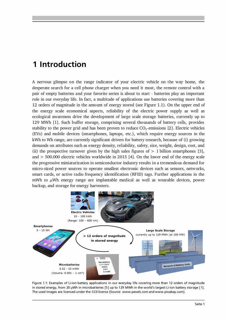
1 Introduction A nervous glimpse on the range indicator of your electric vehicle on the way home, the desperate search for a cell phone charger when you need it most, the remote control with a pair of empty batteries and your favorite series is about to start - batteries play an important role in our everyday life. In fact, a multitude of applications use batteries covering more than 12 orders of magnitude in the amount of energy stored (see Figure 1.1). On the upper end of the energy scale economical aspects, reliability of the electric power supply as well as ecological awareness drive the development of large scale storage batteries, currently up to 129 MWh [1]. Such buffer storage, comprising several thousands of battery cells, provides stability to the power grid and has been proven to reduce CO2-emissions [2]. Electric vehicles (EVs) and mobile devices (smartphones, laptops, etc.), which require energy sources in the kWh to Wh range, are currently significant drivers for battery research, because of (i) growing demands on attributes such as energy density, reliability, safety, size, weight, design, cost, and (ii) the prospective turnover given by the high sales figures of > 1 billion smartphones [3], and > 500.000 electric vehicles worldwide in 2015 [4]. On the lower end of the energy scale the progressive miniaturization in semiconductor industry results in a tremendous demand for micro-sized power sources to operate smallest electronic devices such as sensors, networks, smart cards, or active radio frequency identification (RFID) tags. Further applications in the mWh to μWh energy range are implantable medical as well as wearable devices, power backup, and storage for energy harvesters.
Figure 1.1: Examples of Li-ion battery applications in our everyday life covering more than 12 orders of magnitude in stored energy, from 20 µWh in microbatteries [5] up to 129 MWh in the world’s largest Li-ion battery storage [1]. The used images are licensed under the CC0 license (Source: www.pexels.com and www.pixabay.com).
Seite 2
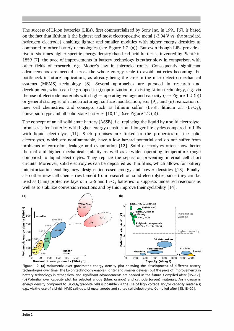
The success of Li-ion batteries (LiBs), first commercialized by Sony Inc. in 1991 [6], is based on the fact that lithium is the lightest and most electropositive metal (-3.04 V vs. the standard hydrogen electrode) enabling lighter and smaller modules with higher energy densities as compared to other battery technologies (see Figure 1.2 (a)). But even though LiBs provide a five to six times higher specific energy density than lead-acid batteries, invented by Planté in 1859 [7], the pace of improvements in battery technology is rather slow in comparison with other fields of research, e.g. Moore’s law in microelectronics. Consequently, significant advancements are needed across the whole energy scale to avoid batteries becoming the bottleneck in future applications, as already being the case in the micro-electro-mechanical systems (MEMS) technology [8]. Several approaches are pursued in research and development, which can be grouped in (i) optimization of existing Li-ion technology, e.g. via the use of electrode materials with higher operating voltage and capacity (see Figure 1.2 (b)) or general strategies of nanostructuring, surface modification, etc. [9], and (ii) realization of new cell chemistries and concepts such as lithium sulfur (Li-S), lithium air (Li-O2), conversion-type and all-solid-state batteries [10,11] (see Figure 1.2 (a)). The concept of an all-solid-state battery (ASSB), i.e. replacing the liquid by a solid electrolyte, promises safer batteries with higher energy densities and longer life cycles compared to LiBs with liquid electrolyte [11]. Such promises are linked to the properties of the solid electrolytes, which are nonflammable, have a low hazard potential and do not suffer from problems of corrosion, leakage and evaporation [12]. Solid electrolytes often show better thermal and higher mechanical stability as well as a wider operating temperature range compared to liquid electrolytes. They replace the separator preventing internal cell short circuits. Moreover, solid electrolytes can be deposited as thin films, which allows for battery miniaturization enabling new designs, increased energy and power densities [13]. Finally, also other new cell chemistries benefit from research on solid electrolytes, since they can be used as (thin) protective layers in Li-S and Li-O2 batteries to suppress undesired reactions as well as to stabilize conversion reactions and by this improve their cyclability [14].
Figure 1.2: (a) Volumetric over gravimetric energy density plot showing the development of different battery technologies over time. The Li-ion technology enables lighter and smaller devices, but the pace of improvements in battery technology is rather slow and significant advancements are needed in the future. Compiled after [15–17]. (b) Potential over capacity plot for selected anode (blue, orange) and cathode (green) materials. An increase in energy density compared to LiCoO2/graphite cells is possible via the use of high voltage and/or capacity materials; e.g., via the use of a Li-rich NMC cathode, Li metal anode and suited solid electrolyte. Compiled after [15,18–20].
Seite 3
In practice, however, the use of ASSBs is still limited to very specific applications such as the lithium iodide (LiI) primary battery, commercialized in heart pacemakers and for preserving volatile computer memory since the 1970’s [21]. This cell apparently fulfills high safety requirements, has excellent reliability and very low self-discharge, but can only be used in low power applications with practical current densities in the μA·cm-2 range due to the rather low ionic conductivity of LiI of about 10-7 S·cm-1 [7]. In comparison, state-of-the-art liquid electrolytes have 5 orders of magnitude higher Li-ion conductivities of about 10-2 S·cm-1 [22]. The limited Li-ion conductivity results in high cell impedance and low power density, which is one of the drawbacks of solid electrolytes. Two strategies for improvement are (i) material development to design and engineer materials with higher ionic conductivities, and (ii) the reduction in thickness via thin film deposition since the impedance scales inversely with the thickness of a material. A good example for material development is the new class of Li-ion conducting garnets, first reported in 2003 [23]. Via chemical substitutions in the garnet structure, the Li-ion conductivity could be increased by 3 orders of magnitude from ~ 10-6 S·cm-1 in 2003 [23] to ~ 10-3 S·cm-1 in 2012 [24]. In addition, garnets show advantages over other solid electrolytes such as good mechanical strength and thermal stability, a wide electrochemical stability window up to 6 V as well as chemical stability against lithium metal [12,25]. These properties attracted a lot of attention, because the replacement of graphite by a Li metal anode and the use of high voltage cathode materials could boost the energy density of a garnet ASSB compared to a battery with liquid electrolyte (see Figure 1.2). In 2012, researchers from Toyota reported on an ASSB with LiCoO2 cathode, garnet-type Li6.75La3Zr1.75Nb0.25O12 solid electrolyte and Li metal anode with capacity retention of 98 % after 100 cycles at 25 °C [26]. This is among the best reported performances of ASSBs up to date [27], however, the used cycling rate of C/10 (3.5 μA·cm-2) is too low for most practical applications. Moreover, other reports on similar garnet ASSBs show a much worse performance [28–32], which indicates that the overall system, including the garnet solid electrolyte (composition, density), its interfaces to the electrodes as well as synthesis, processing and cycling conditions, is rather complex and still far from understood. In this context, thin films can act as model systems to study fundamental processing-structure-property relations, because thin film growth typically allows for better control over microstructural features (density, crystallinity, etc.), phase and element composition compared to powder synthesis routes. Thus, thin film research may help to better understand and further improve future ASSBs from the individual material up to the cell level. Another advantage of thin films is the possibility to apply surface sensitive techniques to investigate the interfacial stability of two (thin film) materials. By this approach, viable material combinations for low impedance interfaces in ASSBs can be identified. Furthermore, employing thin film solid electrolytes is one strategy to lower the impedance in the battery cell as outlined earlier. This is successfully demonstrated by the use of lithium phosphorus oxynitride (LiPON) with an ionic conductivity of (only) 2·10-6 S·cm-1 [33]; namely in thin film batteries with LiCoO2 cathode, LiPON solid electrolyte and Li metal anode that show a capacity retention of more than 98 % after 4000 cycles at current densities of 0.1 mA·cm-2 and 0.6 mA·cm-2 [34]. Even at a rate of 1 mA·cm-2 less than 0.1 V overpotential and a capacity loss per cycle of 0.02 % can be achieved [34], which is comparable to a conventional cylindrical battery with LiCoO2 cathode, liquid electrolyte and graphite anode cycled at 1C [7].
Seite 4
This is a good example on how a well-performing thin film battery can be developed including processing, encapsulation, etc. within about one decade (1992 to 2000) after a promising thin film solid electrolyte material was identified. Thinking of next generation technology, garnet-type thin film solid electrolytes with potential Li-ion conductivities up to 10-3 S·cm-1 would be promising candidates to significantly increase the power density of future ASSBs. Despite all the favorable prospects of garnets, there have been no publications on garnet-type thin film solid electrolytes at the beginning of this PhD studies. Either no scientific interest in Li-ion conducting garnet thin films arose during the first decade after their discovery, or garnet thin film deposition was too difficult a task. Consequently, the deposition and thorough characterization of garnet-type thin film solid electrolytes will be one major subject of this thesis to pave the way for garnet based thin film batteries in the future. Once research and development efforts result in implementable devices, upscaling is a necessary next step towards commercially viable products. To this end, an integration of the entire battery fabrication, or parts of it, into existing, scalable manufacturing processes would be desirable. For example, in semiconductor and nanotechnology industries the fabrication of functional thin films based on physical vapor deposition (PVD) and chemical vapor deposition (CVD) is matured for many years. Thus, it should be advantageous to develop relevant PVD and CVD processes already on the research and development level in order to simplify the upscaling. The possibility of CVD to grow uniform films over large areas at reasonably high deposition rates and with high purity [35] offers great potential for industrial battery fabrication. Moreover, the unique ability of CVD to realize conformal coatings allows for three dimensional (3D) battery concepts with high aspect ratio structures that combine an increased energy density per footprint area with fast rate capability [36]. Despite its good characteristics and high versatility, CVD is still a relatively immature technique for the fabrication of thin film batteries [13]. At the time this PhD project started, the growth of Li-containing battery materials by CVD has not been covered much. Only a few publications on LiCoO2 thin film cathodes grown by CVD existed, with reported specific capacities not exceeding 50 % of the theoretical capacity [6]. Furthermore, the most complex electrochemically active thin film cathodes grown by CVD up to date are LiCoO2 [37,38] and LiMn2O4 spinel [39]. The precursor delivery system is most likely the main bottleneck in extending CVD to battery materials with more complex structure and stoichiometry due to difficulties in matching the different vapor pressures of multi-source precursors via conventional bubblers and direct vaporization. Consequently, the study of advanced CVD precursor delivery systems for the deposition of multicomponent functional thin films for Li-ion battery applications will be another major subject of this thesis. One approach will be a rather conventional, low cost aerosol assisted precursor delivery (so-called AA-CVD), and the other approach will deal with an innovative precursor delivery system based on CO2-laser flash evaporation (so-called LA-CVD).
Seite 5
Objectives and Scope of this PhD Project The objectives of this PhD project result from the described state of research and defined problems of (i) inadequate CVD precursor delivery systems for the growth of multicomponent Li-ion battery materials and (ii) absence of garnet-type thin film solid electrolytes despite their potential for future ASSBs based on promising results from garnet powder studies. These are:
Implementation of an innovative CVD precursor delivery system based on CO2-laser flash evaporation, called CO2-laser assisted chemical vapor deposition (LA-CVD). Exploration of the possibilities and limitations of existing AA-CVD and novel LA-CVD to grow multicomponent, functional thin films for Li-ion battery applications. Growth of Li-ion conducting garnet-type thin films via CVD and assessment of their suitability for future garnet based all-solid-state batteries. Investigation of processing-structure-property relations making use of thin film model systems to improve the current understanding on the material as well as cell level.
In the following, the course of action and important milestones are described, which define the scope of this thesis. Two advanced CVD precursor delivery methods based on aerosol assistance (AA-CVD) and CO2-laser assistance (LA-CVD) served as starting point to tackle the defined problems. The custom-built AA-CVD setup was already established in the group and ready to use, whereas the custom-built LA-CVD setup was close to completion at the time this PhD project started. Upon completion, the first milestone was to establish the novel LA-CVD technique and to prove its functionality. This was done via the deposition of LiCoO2 thin films, because LiCoO2 is a well-known cathode material and literature on CVD of LiCoO2 existed for benchmarking. In the next step, the growth of more complex, multicomponent thin films was targeted such as the advanced cathode materials LiCo1-xNixO2 and Li(Ni1/3Mn1/3Co1/3)O2 as well as garnet-type solid electrolytes of composition Li7La3Zr2O12 and Li5La3Ta2O12. In the case of LiCoO2 and garnet-type thin films thorough growth parameter studies with both CVD techniques were performed, including a detailed characterization of the deposited films’ microstructure, phase and element composition as well as electrochemical performance. The aim was to derive processing-structure-property relations and to conduct a comparative study on the possibilities and limitations of the two different precursor delivery systems. In addition, the capability of both CVD techniques (i) to coat 3D objects and (ii) to deposit nanostructured (conversion-type) transition metal oxide thin film anodes was tested in order to comprehensively assess their potential for prospective use in next generation Li-ion battery concepts (i.e., all-solid-state, conversion-type, 3D microstructures). In the final step, first attempts were made to design, process, and assemble garnet based ASSBs using knowledge from the preceding investigations in order to build a foundation for further developments in future research.
Seite 6
Structure of this PhD Thesis In Chapter 2 the basic concepts of Li-ion batteries and chemical vapor deposition are presented and the investigated materials are introduced. Scientific as well as theoretical fundamentals needed throughout this thesis are provided and the importance of the CVD precursor delivery system is discussed. Chapter 3 summarizes the basics of the used characterization methods and explains details on the microcontact impedance spectroscopy setup and the temperature cabinet used for cycling experiments, which both have been established in the course of this thesis. Chapter 4 describes the experimental implementation including choice and preparation of substrates and precursors, thin film processing, handling and all deposition techniques. Special emphasis is placed on the key features of the AA-CVD and LA-CVD methods and detailed information on an essential improvement in the LA-CVD process is given. Moreover, the integrated UHV-cluster Darmstadt Integrated System for Battery Research (DAISY-Bat) is introduced. In Chapter 5 the focus is on a profound growth parameter study of LiCoO2 thin film cathodes. Results on further lithium transition metal oxide thin film cathodes are critically discussed. Moreover, two strategies to enhance the cycling performance, which go beyond the optimization of material properties, are presented, namely thin film deposition on 3D architectures and the use of an artificial solid electrolyte interface layer. Chapter 6 covers in-depth analyses of two different garnet-type thin film solid electrolytes, tetragonal Li7La3Zr2O12 and cubic Li5La3Ta2O12. In addition, the stabilization of cubic Li7La3Zr2O12 thin films via doping with Al and Ga is reported. Another topic addressed is the chemical stability of garnet-type Li5La3Ta2O12 towards lithium. The chapter closes with a discussion on the impact and potential of garnet-type thin film solid electrolytes grown by LA-CVD. Chapter 7 deals with the preparation of different transition metal oxide thin film anodes. A model to explain the relation between microstructure, kinetics and performance is derived from the electrochemical cycling and impedance spectroscopy analyses performed in this study. In Chapter 8 several approaches to realize a garnet based all-solid-state Li-ion battery are presented. Results on different concepts in design, processing and assembly are discussed and recommendations for further developments are given. Chapter 9 concludes this thesis with a final evaluation and perspectives for future research strategies.
Seite 7
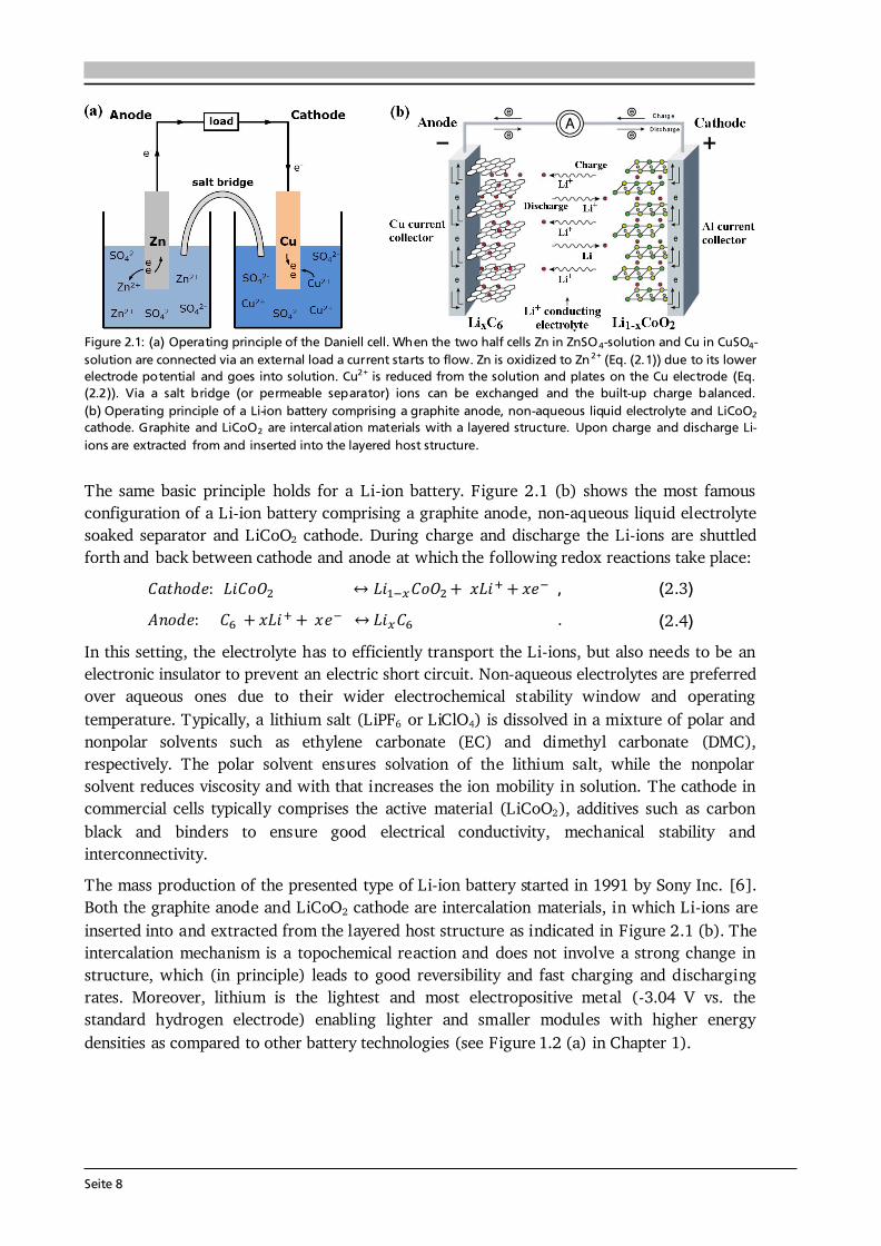
2 General Concepts 2.1. Lithium-Ion Batteries Battery is an umbrella term and in its widest sense a battery can be understood as an electrochemical cell with the functions to store and supply energy. The term battery can refer to a single or multiple cells and one has to differentiate between primary and secondary batteries. Primary batteries rely on irreversible chemical reactions, thus are intended for one-time use. In contrast, secondary batteries, or accumulators, can repeatedly convert chemical to electrical energy and vice versa, thus are rechargeable. In this thesis, if not further specified, the term Li-ion battery stands for a Li-ion secondary battery. 2.1.1. Operating Principle The basic principle of an electrochemical cell is demonstrated in Figure 2.1 (a) by means of the Daniell cell. If two separated half cells, here Zn in ZnSO4-solution and Cu in CuSO4-solution, are electrically connected via an external load, an electric current will start to flow due to self-discharge of the active materials: , (2.1) . (2.2) The driving force for these redox reactions is the difference in chemical potential of the two metals (see Section 2.1.2). Zinc has the lower electrode potential and therefore oxidizes, goes into solution and the provided electrons flow to the copper electrode, at which copper plates as Cu-ions are reduced from the solution. Eventually the difference in electrochemical potential is balanced by the (opposite) charge that builds up at the electrodes and the process comes to a halt, i.e. the system is equilibrated. Connecting the two half cells via an ionic conductor, e.g., a salt bridge or permeable separator, which allows for the ionic species in solution to be exchanged, can keep the current flow upright until one of the cell components is depleted. The nomenclature is based on the convention that during discharge oxidation takes place at the anode (negative electrode) and reduction takes place at the cathode (positive electrode). Accordingly, Eq. (2.1) and (2.2) describe anode and cathode reactions.
Seite 8
Figure 2.1: (a) Operating principle of the Daniell cell. When the two half cells Zn in ZnSO4-solution and Cu in CuSO4-solution are connected via an external load a current starts to flow. Zn is oxidized to Zn 2+ (Eq. (2.1)) due to its lower electrode potential and goes into solution. Cu2+ is reduced from the solution and plates on the Cu electrode (Eq. (2.2)). Via a salt bridge (or permeable separator) ions can be exchanged and the built-up charge balanced. (b) Operating principle of a Li-ion battery comprising a graphite anode, non-aqueous liquid electrolyte and LiCoO2 cathode. Graphite and LiCoO2 are intercalation materials with a layered structure. Upon charge and discharge Li-ions are extracted from and inserted into the layered host structure. The same basic principle holds for a Li-ion battery. Figure 2.1 (b) shows the most famous configuration of a Li-ion battery comprising a graphite anode, non-aqueous liquid electrolyte soaked separator and LiCoO2 cathode. During charge and discharge the Li-ions are shuttled forth and back between cathode and anode at which the following redox reactions take place: , (2.3) . (2.4) In this setting, the electrolyte has to efficiently transport the Li-ions, but also needs to be an electronic insulator to prevent an electric short circuit. Non-aqueous electrolytes are preferred over aqueous ones due to their wider electrochemical stability window and operating temperature. Typically, a lithium salt (LiPF6 or LiClO4) is dissolved in a mixture of polar and nonpolar solvents such as ethylene carbonate (EC) and dimethyl carbonate (DMC), respectively. The polar solvent ensures solvation of the lithium salt, while the nonpolar solvent reduces viscosity and with that increases the ion mobility in solution. The cathode in commercial cells typically comprises the active material (LiCoO2), additives such as carbon black and binders to ensure good electrical conductivity, mechanical stability and interconnectivity. The mass production of the presented type of Li-ion battery started in 1991 by Sony Inc. [6]. Both the graphite anode and LiCoO2 cathode are intercalation materials, in which Li-ions are inserted into and extracted from the layered host structure as indicated in Figure 2.1 (b). The intercalation mechanism is a topochemical reaction and does not involve a strong change in structure, which (in principle) leads to good reversibility and fast charging and discharging rates. Moreover, lithium is the lightest and most electropositive metal (-3.04 V vs. the standard hydrogen electrode) enabling lighter and smaller modules with higher energy densities as compared to other battery technologies (see Figure 1.2 (a) in Chapter 1).
Seite 9
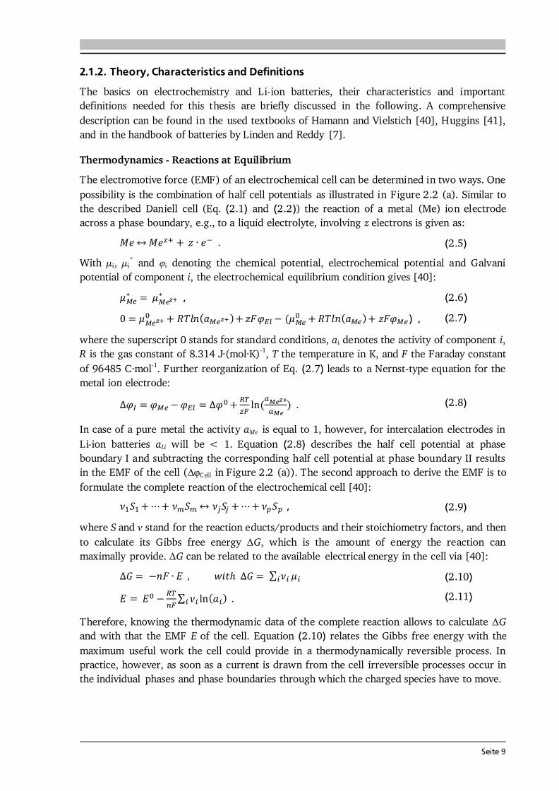
2.1.2. Theory, Characteristics and Definitions The basics on electrochemistry and Li-ion batteries, their characteristics and important definitions needed for this thesis are briefly discussed in the following. A comprehensive description can be found in the used textbooks of Hamann and Vielstich [40], Huggins [41], and in the handbook of batteries by Linden and Reddy [7]. Thermodynamics - Reactions at Equilibrium The electromotive force (EMF) of an electrochemical cell can be determined in two ways. One possibility is the combination of half cell potentials as illustrated in Figure 2.2 (a). Similar to the described Daniell cell (Eq. (2.1) and (2.2)) the reaction of a metal (Me) ion electrode across a phase boundary, e.g., to a liquid electrolyte, involving z electrons is given as: . (2.5) With μi, μi* and φi denoting the chemical potential, electrochemical potential and Galvani potential of component i, the electrochemical equilibrium condition gives [40]: , (2.6) ) , (2.7) where the superscript 0 stands for standard conditions, ai denotes the activity of component i, R is the gas constant of 8.314 J·(mol·K)-1, T the temperature in K, and F the Faraday constant of 96485 C·mol-1. Further reorganization of Eq. (2.7) leads to a Nernst-type equation for the metal ion electrode: . (2.8) In case of a pure metal the activity aMe is equal to 1, however, for intercalation electrodes in Li-ion batteries aLi will be < 1. Equation (2.8) describes the half cell potential at phase boundary I and subtracting the corresponding half cell potential at phase boundary II results in the EMF of the cell (ΔφC ell in Figure 2.2 (a)). The second approach to derive the EMF is to formulate the complete reaction of the electrochemical cell [40]: , (2.9) where S and ν stand for the reaction educts/products and their stoichiometry factors, and then to calculate its Gibbs free energy ΔG, which is the amount of energy the reaction can maximally provide. ΔG can be related to the available electrical energy in the cell via [40]: ∑ (2.10) ∑ . (2.11) Therefore, knowing the thermodynamic data of the complete reaction allows to calculate ΔG and with that the EMF E of the cell. Equation (2.10) relates the Gibbs free energy with the maximum useful work the cell could provide in a thermodynamically reversible process. In practice, however, as soon as a current is drawn from the cell irreversible processes occur in the individual phases and phase boundaries through which the charged species have to move.
Seite 10
Figure 2.2: (a) Determination of the electromotive force of an electrochemical cell by means of the difference of the two half cell potentials ΔφI and ΔφII under equilibrium conditions. It is assumed that there is no potential drop in the electrolyte. After [40]. (b) Schematic of the discharge profile of a battery under the influence of activation, ohmic and concentration polarization. The I·R drop is followed by a discharge plateau, which is influenced by the applied current, and a steep drop in voltage at the end of discharge. Compiled after [41,42].
Electrode Kinetics The equilibrium voltage of a battery is called open circuit voltage (OCV) and corresponds to the EMF without current flow (ΔφCell at I = 0). When a current is drawn from the battery, kinetic limitations alter the electrode potentials and with that the overall cell voltage. The difference between cell potential under load and in equilibrium: , (2.12) is called polarization, or overpotential, or overvoltage. The influence of several polarization effects, such as activation, ohmic and concentration polarization, on the discharge profile of a battery is schematically plotted in Figure 2.2 (b). Concentration polarization originates from mass-transport (diffusion) limitations of oxidized/reduced species to the electrode surface, at which the electrode reactions take place. Ohmic polarization is related to resistances in and between the individual cell components as well as to contact resistance. It follows Ohm’s law: , (2.13) and, as illustrated in Figure 2.2 (b), reduces the voltage of the discharge plateau of a battery the more the higher the applied current. Activation polarization is always present, because it arises from the actual electrochemical redox reactions and their charge-transfer kinetics at the electrode surfaces. The charge-transfer kinetics of an electrochemical cell with the transfer of n electrons in one single step are given by the Butler-Volmer equation [40]: { [ ] [ ]} . (2.14) The factors α and j0 are the charge-transfer coefficient, which is also called asymmetry factor, and the exchange current density, which corresponds to the reaction rate in equilibrium, respectively. The Butler-Volmer equation describes the net current density jD of the cell, i.e. the sum of anodic (jan) and cathodic (jcath) currents, as a function of the charge-transfer overpotential D.
Seite 11
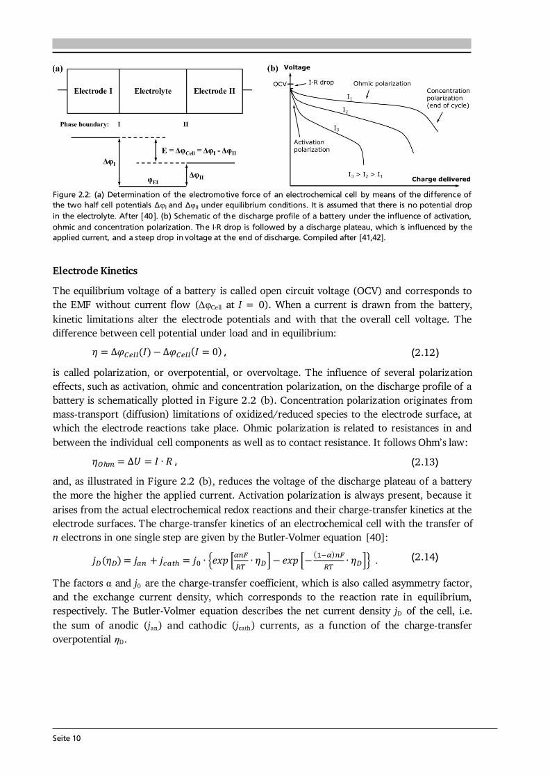
Figure 2.3: (a) Graphical representation of the Butler-Volmer equation (Eq. (2.14)) with typical parameters as indicated. The anodic (red) and cathodic (blue) branches dominate the current density for high positive and negative overpotentials, respectively. (b) Tafel plot (Eq.s (2.15) and (2.16)) as derived from the Butler-Volmer equation in the limiting case of high overpotentials. From the slope and intercept of the Tafel plot the transfer coefficient α and the exchange current density j0 can be estimated, respectively. After [40]. The graphical representation of Eq. (2.14) is given in Figure 2.3 (a). For a value of α = 0.5 the anodic (red) and cathodic (blue) branches are symmetric. There are two regions of interest (black frames) in Figure 2.3 (a), namely (i) for overpotentials | D| much larger than the thermal energy (e.g., 25.7 mV at 298 K), and (ii) for very low overpotentials of | D|< 10 mV. In case (i) either the anodic or cathodic reaction dominates, while the other one is negligible. Therefore, taking the logarithm of Eq. (2.14) leads to [40]: , (2.15) . (2.16) This linear equation is called Tafel equation, and its semi-logarithmic representation (Figure 2.3 (b)) is called Tafel plot. The slope and the intercept of the Tafel plot provide an estimation of the transfer coefficient α and exchange current density j0, respectively. In case (ii) the arguments of both exponential functions in Eq. (2.14) are small and via a Taylor expansion (ex ≈ 1 + x) the following linear relation results [40]: . (2.17) Here, RD is defined as charge-transfer or polarization resistance. According to Eq. (2.17), the exchange current density j0 can be determined when the relation between current density and very low overpotentials is known. It shall be noted that the increase in current density for an increase in overpotential, as suggested in Figure 2.3, becomes limited in application by other polarization effects, e.g. mass-transport limitation, as discussed in Section 7.6 by means of thin film anodes. Further Definitions It is common practice to define the capacity C of a battery as the amount of charge Q it can store and which has flowed within a time period t between its two electrodes: ∫ . (2.18)
Seite 12
Thus, battery capacity corresponds to the physical quantity of charge. It shall be noted that the symbol C is also used in impedance spectroscopy analysis (Section 3.6), however, in its true physical meaning with the SI unit Farad. Battery capacity is typically expressed in mAh, or as mass specific capacity in mAh·g-1. At a constant current, Eq. (2.18) simplifies to the product C = I·t. The theoretical (mass) specific capacity of a battery material can be calculated knowing its molar mass M and the number of electrons transferred n according to: . (2.19) The given example in Eq. (2.19) refers to the cathode material Li1-xCoO2, which can reversibly extract and insert x = 0.5 Li-ions per formula unit and with that has a theoretical specific capacity of about 140 mAh·g-1. Based on the theoretical specific capacity of the material, it is possible to calculate the theoretical (absolute) capacity of a (100 %) dense thin film via: , (2.20) where A and d are the estimated area and thickness of the thin film, and ρtheo denotes the theoretical density of the respective material. The value Cfilm is used to estimate the initial charge and discharge currents in cycling experiments (Section 3.5). Moreover, by rearranging Eq. (2.20), the specific capacity of the thin film (Cm,film) can be estimated based on its measured absolute capacity. Naturally, the estimated quantities A and d have errors and the actual density of the thin film could not be quantified in this thesis. Assuming for each of the quantities A, d and ρ (in relation to ρtheo) a relative error of 5 - 10 % and applying the error propagation law results in 9 - 17 % relative error in the capacity estimation of the thin film material. Furthermore, it can be assumed that the estimated mass (m = A·d·ρtheo) used for all calculations throughout this thesis is higher than the true mass of the film, because (i) the coated area is smaller than the (measured) area of the substrate, (ii) the thickness is estimated via SEM close to the centre of the sample and typically the coating thickness reduces towards the edges, and (iii) ρtheo ≥ ρreal holds. Consequently, the calculated C-rates most likely underestimate the actual C-rates. In other words, the applied currents to the thin films are higher than needed to realize the specified C-rates. Likewise, the calculated thin films’ specific capacities Cm,film in mAh·g-1 most likely underestimate the actual capacities and therefore are considered as their lower limits. The coulombic efficiency, or faradaic efficiency, of a battery is the ratio between the charge capacity and discharge capacity, multiplied by 100 to express the efficiency in percent. In commercial Li-ion batteries the coulombic efficiency exceeds 99 %, in some cases even 99.9 % [43]. Such extreme efficiency is necessary considering the need for several hundred full cycles and the definition of a battery’s end of life as 80 % of its original capacity [44]. For example, after 200 cycles with 99.9 % coulombic efficiency 82 % of the original capacity is available. The energy density of a battery is the amount of energy stored per weight (gravimetric) or volume (volumetric) and given by: ∫ ∫ . (2.21) Here, U stands for the voltage mean value over charge/discharge time, which is typically given by the value of the voltage plateau and termed nominal voltage. For galvanostatic cycling experiments with constant current Eq. (2.21) simplifies to the product of I·t· U divided by either weight or volume.
Seite 13
2.1.3. Thin Film Batteries There is an increasing demand for thin film batteries. Recently, analysts forecast the thin film battery market volume to reach $1.72 billion by 2025 [45], with the global Li-ion battery market surpassing $77 billion about that time [46]. Safety aspects such as no leakage and no risk of explosion as well as the small size and resulting flexibility are reasons for an increasing number of thin film battery applications, which are further discussed in Section 8.1. This subsection is devoted to the fundamental differences, advantages and challenges compared to bulk-type batteries. A thin film battery is composed of solid state materials sequentially deposited as thin films on a substrate. As such, the electrodes of thin film batteries are made of pure active material, in contrast to bulk-type batteries, which additionally comprise conductive additives and binders that are inactive mass. Moreover, the thickness of a thin film battery including protective coating and encapsulation is of the order of 10 μm, and individual components can be as thin as several 100 nm. In comparison, typical thicknesses of bulk-type batteries range from 100 μm to 1 mm depending on the used technology. According to Ohm’s law, the reduced thickness d directly translates into a lower cell resistance R as long as the area A and conductivity of each component i are the same: ∑ ∑ . (2.22) The cell resistance is the sum of resistances in each layer (anode, electrolyte, cathode), between the layers as well as of the contact resistances to the current collectors. The major challenges in thin film batteries with respect to cell resistance arise from limited ionic conductivities of (i) the solid electrolyte layer and (ii) its interfaces to the electrodes as further discussed in Chapters 6 and 8. These challenges are subject of current research and especially high interfacial resistances impede a breakthrough in thin film battery performance. In principle, thin film batteries have the advantage of a much wider operational temperature range than cells with liquid electrolyte. The solid electrolyte does not freeze out and limits the risk of thermal runaway. While at low temperatures thermally activated diffusion and conduction processes may limit high rate applications, the practical operating temperature of commercial thin film batteries ranges from -40 °C to 150 °C [47]. The fabrication of a thin film battery poses some challenges, which are non-existent or to a lesser extent in bulk-type batteries. Since the solid electrolyte layer in a thin film battery acts as ionic conductor and separator at the same time, it should be extremely dense and has to be free of cracks and pinholes. Moreover, sequential deposition of all components may lead to undesired chemical reactions, interdiffusion of elements and the like. In this respect, the used atmosphere and temperature during deposition play a crucial role. In this thesis, chemical vapor deposition is used, which in comparison to other deposition techniques such as sputtering or pulsed laser deposition always requires a certain minimum deposition temperature in order to trigger the decomposition and reaction of precursors. Consequently, the major aim of every growth parameter study presented in this thesis is to optimize the thin film properties at a growth temperature as low as possible.
Seite 14
2.2. Investigated Materials In this section the investigated material classes are introduced by means of their structure and basic properties. An application related introduction as well as a motivation for why to study each of the investigated cathode, solid electrolyte and anode materials is given in Sections 5.1, 6.1 and 7.1, respectively. 2.2.1. Lithium Transition Metal Oxide Cathodes Lithium transition metal oxides are most frequently used as cathodes in commercial Li-ion batteries to date. Their general chemical formula is Li(TM)O2, where TM stands for one or several transition metal(s). They typically crystallize in the rhombohedral system with space group R-3m and are isostructural to the α-NaFeO2-type structure [48]. Within this α-NaFeO2-type structure Li- and TM-ions occupy octahedral 3a and 3b sites in alternating layers and O-ions occupy 6c sites of the cubic close packing. The layered nature of lithium transition metal oxides provides (fast) diffusion pathways for reversible insertion and extraction of the Li-ions, thus Li(TM)O2 cathodes are intercalation based materials. In Chapter 5, three different classes of Li(TM)O2 thin film cathodes are investigated, namely (i) LiCoO2, (ii) a series of quaternary compounds LiCo1-xNixO2, and (iii) the quinary compound Li(Ni1/3Mn1/3Co1/3)O2. Most of the work is devoted to LiCoO2, which was first reported by the group of John Goodenough in 1980 [49]. Depending on the synthesis method and used process parameters two different modifications of LiCoO2 can be prepared, so-called high temperature (HT-) and low temperature (LT-) LiCoO2. The naming goes back to the observations in early works that LT- and HT-LiCoO2 forms via synthesis at low (~ 400 °C) and high (~ 800 °C) temperatures, however, it is also possible to stabilize the HT-LiCoO2 phase at low temperatures [50]. The difference between both structures is shown in Figure 2.4. The HT-LiCoO2 (Figure 2.4 (a)) has the just described layered structure with a cubic close packing of O-ions, in which Li-ions and Co-ions occupy alternating layers parallel to the (111) plane. In the hexagonal framework lattice parameters of a = 2.815 - 2.816 Å and c = 14.05 - 14.08 Å are reported, resulting in a c/a ratio of 4.98 - 5.00 [50].
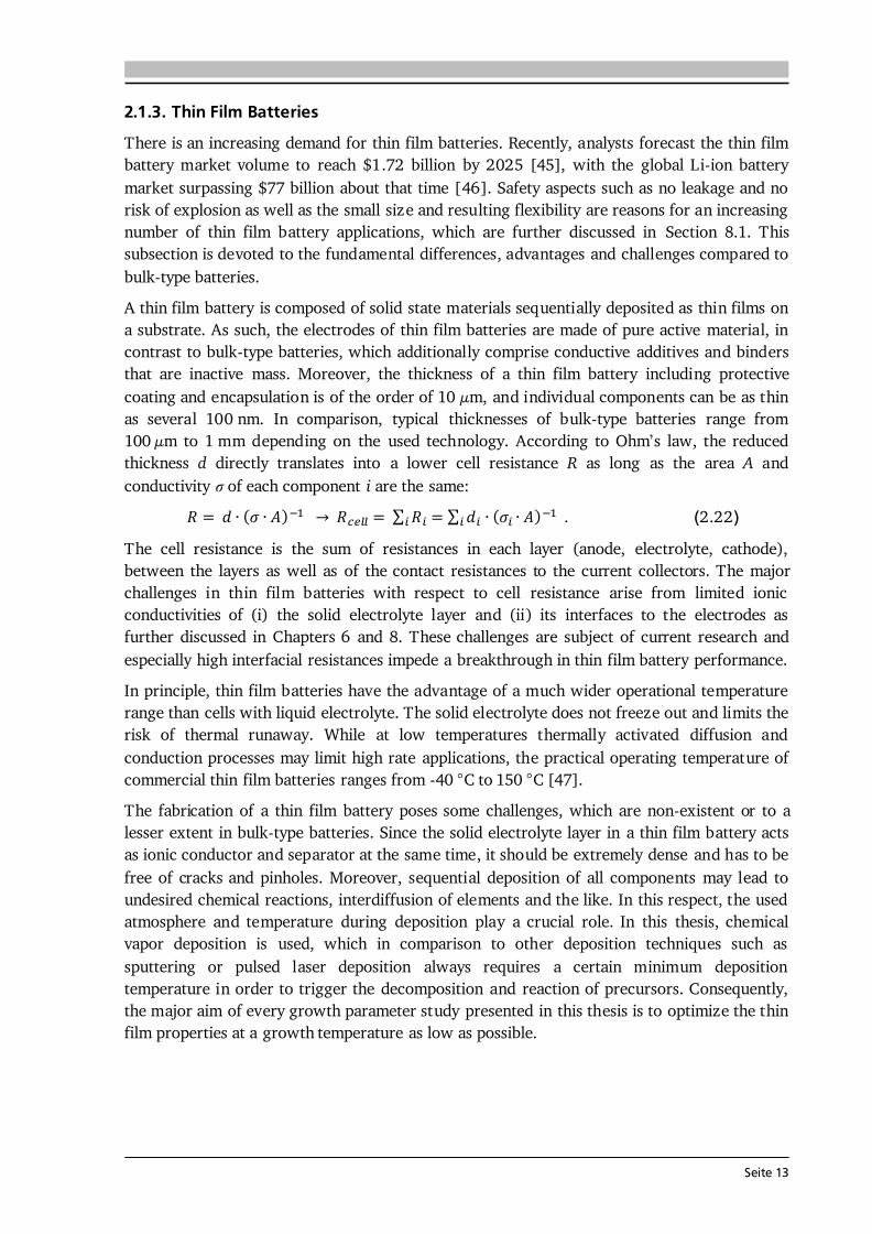
Figure 2.4: Schematic of the structure of (a) HT-LiCoO2 and (b) LT-LiCoO2. The stacking sequence of Li-, O- and Co-layers along the (111) direction is shown. The structure of HT-LiCoO2 is described by Li- and Co-ions residing in octahedral sites of alternating layers between planes of O-ions. In contrast, the LT-LiCoO2 has one quarter of the Li-ions located in the octahedral sites of the Co-layer and vice versa. (c) Cyclic voltammetry of the HT- and LT-LiCoO2 phase. The LT-LiCoO2 has a lower operating voltage, higher polarization and inferior cyclability compared to HT-LiCoO2. Figure reprinted with permission from [51]. Copyright 1997, The Electrochemical Society.

Seite 15
The structure of LT-LiCoO2 (Figure 2.4 (b)) is not ideally layered. Gummow et al. [52] showed that LT-LiCoO2 has about 6 % cobalt residing in the lithium layers. Moreover, they reported lattice parameters of a = 2.8297 Å and c = 13.868 Å resulting in a c/a ratio of 4.901 [52], which is close to the ideal value of cubic close oxygen packing of c/a = 4.899. Other reports describe the LT-LiCoO2 using a spinel-related structure with space group Fd-3m, which is based on cubic close packed oxygen with alternating cation layers parallel to the (111) plane of composition (0.75 Co, 0.25 Li) and (0.75 Li, 0.25 Co) [51,53]. Thus, the LT-LiCoO2 phase is referred to as cubic spinel-related or quasi-spinel, because the cation distribution lies in between the ones of hexagonal layered and spinel structures. The consequences of the distorted structure on the electrochemical properties are presented in Figure 2.4 (c) by means of cyclic voltammetry. HT-LiCoO2 shows a redox couple around 3.9 V with rather low overpotential (upper graph), whereas broad anodic and cathodic peaks centered around 3.6 V with a much higher polarization (> 0.2 V) are observed in case of LT-LiCoO2 (lower graph) [51]. Furthermore, LT-LiCoO2 has a significantly lower practical discharge capacity of about 80 mAh·g-1 compared to 140 mAh·g-1 for HT-LiCoO2, and its cyclability is very poor [50]. Consequently, LT-LiCoO2 is undesired for application.
Figure 2.5: (a) Simulated XRD patterns of layered HT- (R-3m) and spinel LT- (Fd-3m) LiCoO2. Identical peak shape parameters and no temperature factors were used in each simulation. The lattice parameter of the spinel material is a = 8.000 Å and for the layered phase c/a = 4.90 was chosen. Both patterns are identical. Reprinted from [53], Copyright 1993, with permission from Elsevier. (b) Raman spectra (wavelength: 514.5 nm) of layered HT- (R-3m) and spinel LT- (Fd-3m) LiCoO2 as well as Co3O4, an often found impurity phase in LiCoO2 synthesis. Raman spectroscopy provides a fast, easy and reliable checkup on the obtained LiCoO2 modification. Reprinted from [54], Copyright 2012, with permission from Elsevier. In Figure 2.5 (a) simulated XRD patterns of layered HT- (R-3m) and spinel LT- (Fd-3m) LiCoO2 are compared, using identical peak shape parameters and no temperature factors in each simulation [53]. Both patterns are identical when the lattice parameter of the spinel material is chosen to be a = 8.000 Å and a value of c/a = 4.90 is set for the layered phase [53]. This illustrates a possible difficulty to distinguish both phases via XRD. However, the Raman active vibrational modes of crystalline LiCoO2 with space groups R-3m and Fd-3m can be predicted by factor group analysis to be [55]: 486 cm-1, 595 cm-1 and 445 cm-1, 478 cm-1, 583 cm-1, 603 cm-1, respectively. Thus, both modifications can be easily distinguished from another only by the number of observed Raman modes as illustrated in Figure 2.5 (b). The two Raman shifts of HT-LiCoO2 originate from oxygen displacements perpendicular to (Eg mode, 486 cm-1) and along (A1g mode, 595 cm-1) the c-axis and are also called O-Co-O bending and Co-O stretching modes, respectively. Furthermore, Raman spectroscopy allows to detect traces of Co3O4 (Figure 2.5 (b)), which is an often observed impurity phase in LiCoO2 synthesis. Co3O4 has a strong scattering intensity and 5 Raman bands, most of which do not
Seite 16
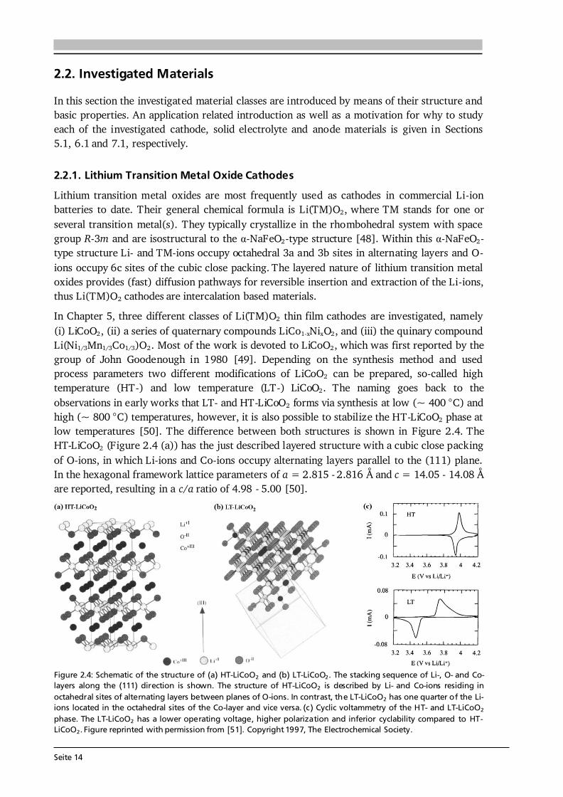
overlap with the Raman shifts of LT- and HT-LiCoO2 [54]. Therefore, Raman spectroscopy provides a fast, easy and reliable checkup on the synthesized LiCoO2 modification. In electrochemical cycling experiments HT-LiCoO2 undergoes several phase transformations (see Figure 2.6). Assuming a stoichiometric compound after synthesis, LiCoO2 is in the discharged state and has an OCV of about 3 V against metallic Li. Extraction of (1 - x) Li-ions from the LixCoO2 host increases the cell voltage, and up to about 4.3 V three distinct plateaus are observed in the charge profile (a, b and c in Figure 2.6 (a)). In the region 0.75 < x < 1, LixCoO2 undergoes a topotactic reaction and two hexagonal phases (I + II in Figure 2.6 (b)) are observed via in situ XRD studies [56]. In this two-phase region, which corresponds to the main oxidation reaction (plateau a in Figure 2.6 (a)), a semiconductor to metal transition takes place [57,58]. This significantly increases the electrical conductivity of LixCoO2 compared to the stoichiometric compound. Upon further Li extraction, at around x = 0.5, transitions from a hexagonal (R-3m) to monoclinic (C2/m) phase and back take place, which correspond to the two small plateaus at 4.05 V and 4.20 V (Figure 2.6 (a)). The formation of the monoclinic phase is due to an order/disorder transition of the Li-ions [56]. Delithiation goes along with an increase in lattice parameter c and decrease in lattice parameter a (see Figure 2.6 (b)). The former results from increased repulsion between the oxygen layers as less Li-ions are present to shield their charge, while the latter is due to oxidation of Co3+ to Co4+.
Figure 2.6: (a) Cell voltage as function of x in HT-LixCoO2 for the first charge and discharge. The labels a, b and c mark three plateau-like features, which are further described in the text. (b) Lattice parameters a and c (upper graphs) as a function of x in HT-LixCoO2. Combined with the results in (a) the phase diagram (lower graph) of HT-LixCoO2 is derived. Figure reprinted with permission from [56]. Copyright 1997, The Electrochemical Society. In principle, for deep delithiation up to x = 0, a capacity and voltage of about 270 mAh·g-1 and 5 V can be obtained, however, further phase transitions cause irreversible damage to the structure of LixCoO2 leading to fast capacity fade, hence poor cyclability [59]. It was shown that LiCoO2 can be reversibly cycled up to 4.5 V with a capacity of about 180 mAh·g-1 [59]. Nevertheless, most practical applications limit delithiation to about x = 0.5, or 140 mAh·g-1, for reasons of (better) cyclability and also thermal stability [18].
Seite 17
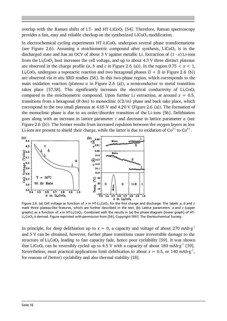
2.2.2. Lithium-Ion Conducting Garnet-Type Solid Electrolytes The general formula of oxide garnets is given as A3B2C3O12 with the cations A, B and C having 8-fold, 6-fold and 4-fold coordination in the oxygen framework. They crystallize in a body centered cubic structure with the space group Ia-3d [25]. Moreover, each of the cation sites A, B and C is fully occupied in conventional (i.e., stoichiometric) garnets, such as the case in Li3Nd3W2O12 (see later this section). Consequently, after the first report on fast Li-ion conducting garnet-type Li5La3M2O12 (M = Nb, Ta) [23] several works investigated the possible location of the two extra Li-ions per formula unit. It was shown that the [La3M2O12]5- framework potentially offers two trigonal prismatic and six octahedral coordination sites for Li-ion occupation in addition to the three tetrahedral sites of stoichiometric garnets [60]. Compounds with more than three Li+ cations are often referred to as lithium-stuffed garnets.
Figure 2.7: (a) Crystal structure of cubic Li5La3Ta2O12 ([60], ICSD #154400). The La3+ and Ta5+ cations are in dodecahedral (blue) and octahedral (grey) coordination, respectively. The Li+ cations are distributed over tetrahedral (orange, 24d), octahedral (magenta, 48g) and distorted octahedral (green, 96h) sites and form a 3D network. (b) Li occupancy in the garnet-type structure Li5+xLa3-xAxM2-yByO12 with A, B and M being divalent, tri-/tetravalent and pentavalent ions, respectively. Possible configurations are: (I) Li+ occupies only the octahedral position, (II) one Li+ occupies a tetrahedral position and one a distorted octahedral position, and (III) two Li+ occupy each one tetrahedral site. Compiled after [25,61]. Figure 2.7 (a) shows the crystal structure of cubic Li5La3Ta2O12 ([60], ICSD #154400) with the La3+ and Ta5+ cations in dodecahedral (blue) and octahedral (grey) coordination, respectively. The Li+ cations are distributed over tetrahedral (orange, 24d), octahedral (magenta, 48g) and distorted (or displaced) octahedral (green, 96h) sites and form a 3D network. In this 3D network, each LiO6 octahedron is connected to two LiO4 tetrahedra and each tetrahedron is connected to four octahedra. As a result, the energetically most favorable Li sites, schematically illustrated in Figure 2.7 (b), are [61]: (I) Li+ occupies only the octahedral position leaving the adjacent tetrahedra empty, (II) one Li+ occupies a tetrahedral position shifting the other Li-ion away from the center of the octahedron towards a distorted octahedral position, and (III) two Li+ occupy each of the two tetrahedra leaving the octahedron empty. In lithium stuffed garnets of composition Li5+xLa3-xAxM2-yByO12, with A, B and M being divalent, tri-/tetravalent and pentavalent ions, all of the just described sites are (partially) occupied. In fact, a nearly linear relationship between the occupation of octahedral as well as tetrahedral sites and the Li content per formula unit in garnets is found [62] (see Figure 2.8 (a)). The end members with a Li content of 3 and 7 such as Li3Nd2W2O12 (filled square) and Li7La3Zr2O12 (filled triangle) show full occupancy of the tetrahedral and octahedral sites, respectively.
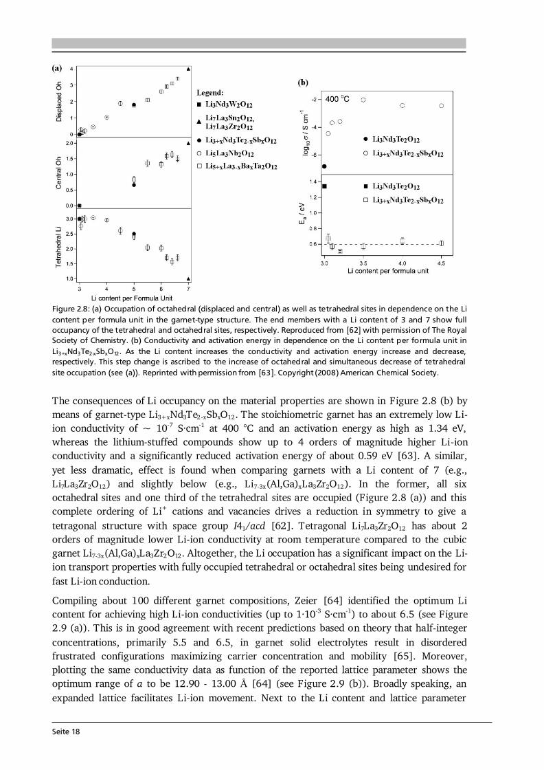
Seite 18
Figure 2.8: (a) Occupation of octahedral (displaced and central) as well as tetrahedral sites in dependence on the Li content per formula unit in the garnet-type structure. The end members with a Li content of 3 and 7 show full occupancy of the tetrahedral and octahedral sites, respectively. Reproduced from [62] with permission of The Royal Society of Chemistry. (b) Conductivity and activation energy in dependence on the Li content per formula unit in Li3+xNd3Te2-xSbxO12. As the Li content increases the conductivity and activation energy increase and decrease, respectively. This step change is ascribed to the increase of octahedral and simultaneous decrease of tetrahedral site occupation (see (a)). Reprinted with permission from [63]. Copyright (2008) American Chemical Society. The consequences of Li occupancy on the material properties are shown in Figure 2.8 (b) by means of garnet-type Li3+xNd3Te2-xSbxO12. The stoichiometric garnet has an extremely low Li-ion conductivity of ~ 10-7 S·cm-1 at 400 °C and an activation energy as high as 1.34 eV, whereas the lithium-stuffed compounds show up to 4 orders of magnitude higher Li-ion conductivity and a significantly reduced activation energy of about 0.59 eV [63]. A similar, yet less dramatic, effect is found when comparing garnets with a Li content of 7 (e.g., Li7La3Zr2O12) and slightly below (e.g., Li7-3x(Al,Ga)xLa3Zr2O12). In the former, all six octahedral sites and one third of the tetrahedral sites are occupied (Figure 2.8 (a)) and this complete ordering of Li+ cations and vacancies drives a reduction in symmetry to give a tetragonal structure with space group I41/acd [62]. Tetragonal Li7La3Zr2O12 has about 2 orders of magnitude lower Li-ion conductivity at room temperature compared to the cubic garnet Li7-3x(Al,Ga)xLa3Zr2O12. Altogether, the Li occupation has a significant impact on the Li-ion transport properties with fully occupied tetrahedral or octahedral sites being undesired for fast Li-ion conduction. Compiling about 100 different garnet compositions, Zeier [64] identified the optimum Li content for achieving high Li-ion conductivities (up to 1·10-3 S·cm-1) to about 6.5 (see Figure 2.9 (a)). This is in good agreement with recent predictions based on theory that half-integer concentrations, primarily 5.5 and 6.5, in garnet solid electrolytes result in disordered frustrated configurations maximizing carrier concentration and mobility [65]. Moreover, plotting the same conductivity data as function of the reported lattice parameter shows the optimum range of a to be 12.90 - 13.00 Å [64] (see Figure 2.9 (b)). Broadly speaking, an expanded lattice facilitates Li-ion movement. Next to the Li content and lattice parameter
Seite 19
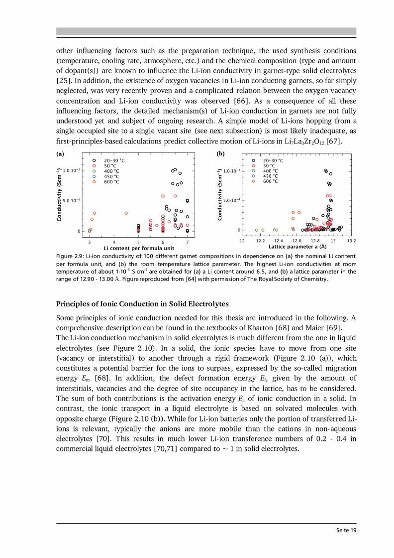
other influencing factors such as the preparation technique, the used synthesis conditions (temperature, cooling rate, atmosphere, etc.) and the chemical composition (type and amount of dopant(s)) are known to influence the Li-ion conductivity in garnet-type solid electrolytes [25]. In addition, the existence of oxygen vacancies in Li-ion conducting garnets, so far simply neglected, was very recently proven and a complicated relation between the oxygen vacancy concentration and Li-ion conductivity was observed [66]. As a consequence of all these influencing factors, the detailed mechanism(s) of Li-ion conduction in garnets are not fully understood yet and subject of ongoing research. A simple model of Li-ions hopping from a single occupied site to a single vacant site (see next subsection) is most likely inadequate, as first-principles-based calculations predict collective motion of Li-ions in Li7La3Zr2O12 [67].
Figure 2.9: Li-ion conductivity of 100 different garnet compositions in dependence on (a) the nominal Li content per formula unit, and (b) the room temperature lattice parameter. The highest Li-ion conductivities at room temperature of about 1·10 -3 S·cm-1 are obtained for (a) a Li content around 6.5, and (b) a lattice parameter in the range of 12.90 - 13.00 Å. Figure reproduced from [64] with permission of The Royal Society of Chemistry.
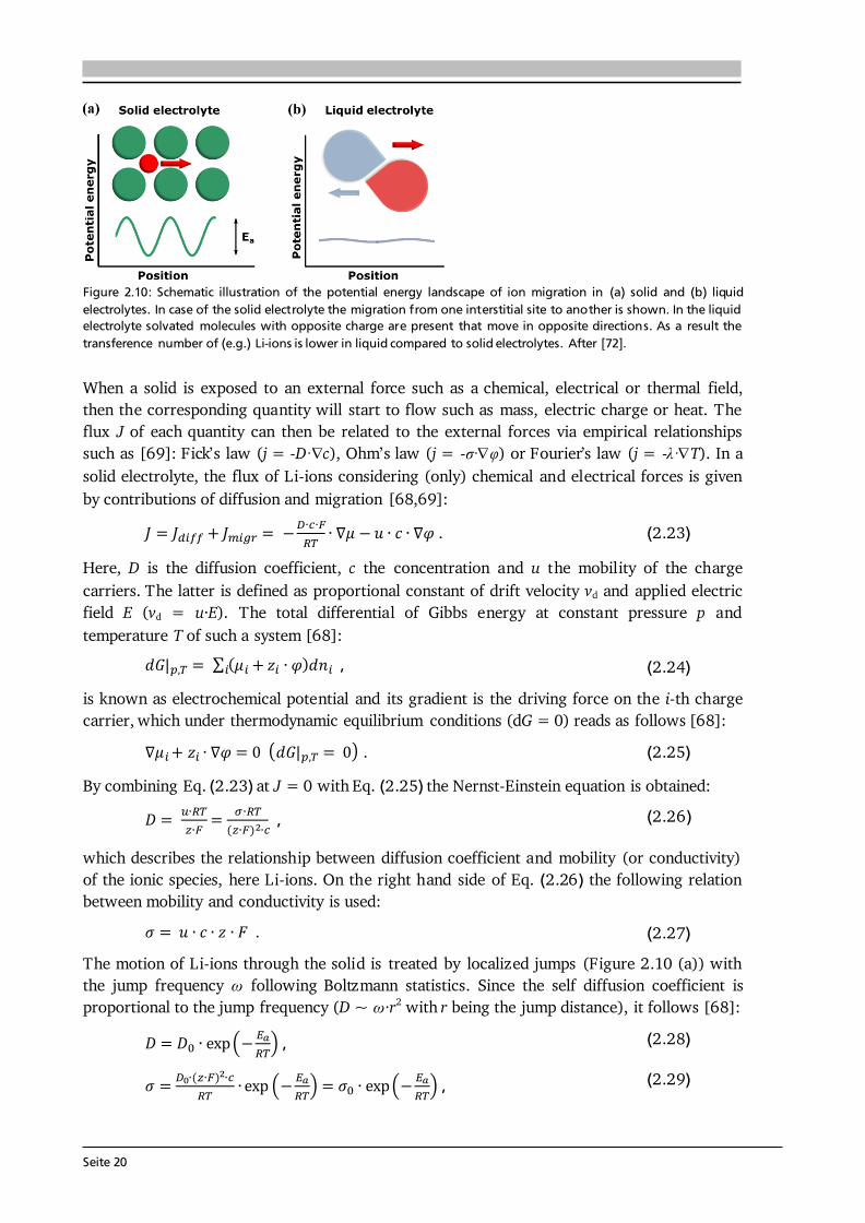
Principles of Ionic Conduction in Solid Electrolytes Some principles of ionic conduction needed for this thesis are introduced in the following. A comprehensive description can be found in the textbooks of Kharton [68] and Maier [69]. The Li-ion conduction mechanism in solid electrolytes is much different from the one in liquid electrolytes (see Figure 2.10). In a solid, the ionic species have to move from one site (vacancy or interstitial) to another through a rigid framework (Figure 2.10 (a)), which constitutes a potential barrier for the ions to surpass, expressed by the so-called migration energy Em [68]. In addition, the defect formation energy Ef, given by the amount of interstitials, vacancies and the degree of site occupancy in the lattice, has to be considered. The sum of both contributions is the activation energy Ea of ionic conduction in a solid. In contrast, the ionic transport in a liquid electrolyte is based on solvated molecules with opposite charge (Figure 2.10 (b)). While for Li-ion batteries only the portion of transferred Li-ions is relevant, typically the anions are more mobile than the cations in non-aqueous electrolytes [70]. This results in much lower Li-ion transference numbers of 0.2 - 0.4 in commercial liquid electrolytes [70,71] compared to ~ 1 in solid electrolytes.
Seite 20
Figure 2.10: Schematic illustration of the potential energy landscape of ion migration in (a) solid and (b) liquid electrolytes. In case of the solid electrolyte the migration from one interstitial site to another is shown. In the liquid electrolyte solvated molecules with opposite charge are present that move in opposite directions. As a result the transference number of (e.g.) Li-ions is lower in liquid compared to solid electrolytes. After [72]. When a solid is exposed to an external force such as a chemical, electrical or thermal field, then the corresponding quantity will start to flow such as mass, electric charge or heat. The flux J of each quantity can then be related to the external forces via empirical relationships such as [69]: Fick’s law (j = -D·c), Ohm’s law (j = - ·φ) or Fourier’s law (j = -λ·T). In a solid electrolyte, the flux of Li-ions considering (only) chemical and electrical forces is given by contributions of diffusion and migration [68,69]: . (2.23) Here, D is the diffusion coefficient, c the concentration and u the mobility of the charge carriers. The latter is defined as proportional constant of drift velocity vd and applied electric field E (vd = u·E). The total differential of Gibbs energy at constant pressure p and temperature T of such a system [68]: ∑ , (2.24) is known as electrochemical potential and its gradient is the driving force on the i-th charge carrier, which under thermodynamic equilibrium conditions (dG = 0) reads as follows [68]: ( ) . (2.25) By combining Eq. (2.23) at J = 0 with Eq. (2.25) the Nernst-Einstein equation is obtained: , (2.26) which describes the relationship between diffusion coefficient and mobility (or conductivity) of the ionic species, here Li-ions. On the right hand side of Eq. (2.26) the following relation between mobility and conductivity is used: . (2.27) The motion of Li-ions through the solid is treated by localized jumps (Figure 2.10 (a)) with the jump frequency ω following Boltzmann statistics. Since the self diffusion coefficient is proportional to the jump frequency (D ~ ω·r2 with r being the jump distance), it follows [68]: , (2.28)
, (2.29)
Seite 21
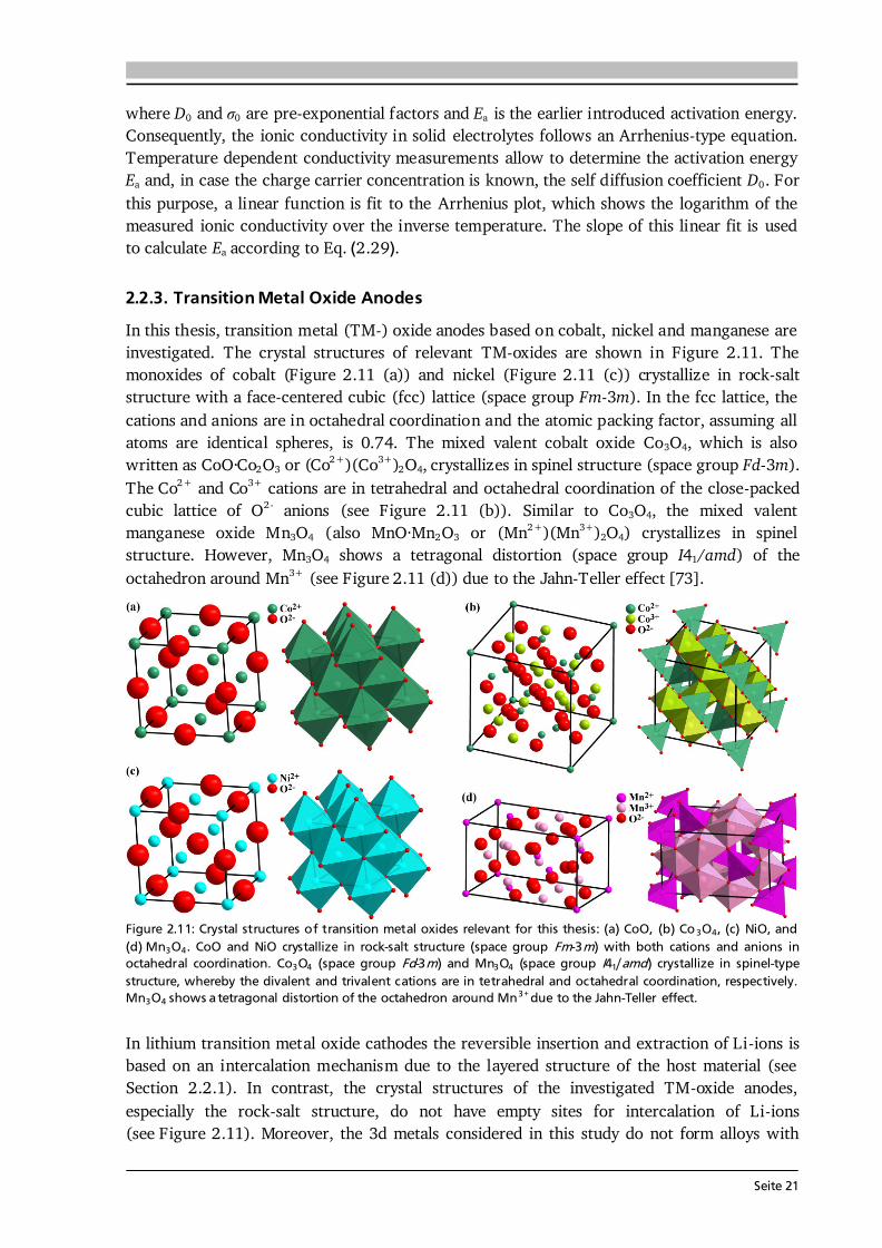
where D0 and 0 are pre-exponential factors and Ea is the earlier introduced activation energy. Consequently, the ionic conductivity in solid electrolytes follows an Arrhenius-type equation. Temperature dependent conductivity measurements allow to determine the activation energy Ea and, in case the charge carrier concentration is known, the self diffusion coefficient D0. For this purpose, a linear function is fit to the Arrhenius plot, which shows the logarithm of the measured ionic conductivity over the inverse temperature. The slope of this linear fit is used to calculate Ea according to Eq. (2.29). 2.2.3. Transition Metal Oxide Anodes In this thesis, transition metal (TM-) oxide anodes based on cobalt, nickel and manganese are investigated. The crystal structures of relevant TM-oxides are shown in Figure 2.11. The monoxides of cobalt (Figure 2.11 (a)) and nickel (Figure 2.11 (c)) crystallize in rock-salt structure with a face-centered cubic (fcc) lattice (space group Fm-3m). In the fcc lattice, the cations and anions are in octahedral coordination and the atomic packing factor, assuming all atoms are identical spheres, is 0.74. The mixed valent cobalt oxide Co3O4, which is also written as CoO·Co2O3 or (Co2+)(Co3+)2O4, crystallizes in spinel structure (space group Fd-3m). The Co2+ and Co3+ cations are in tetrahedral and octahedral coordination of the close-packed cubic lattice of O2- anions (see Figure 2.11 (b)). Similar to Co3O4, the mixed valent manganese oxide Mn3O4 (also MnO·Mn2O3 or (Mn2+)(Mn3+)2O4) crystallizes in spinel structure. However, Mn3O4 shows a tetragonal distortion (space group I41/amd) of the octahedron around Mn3+ (see Figure 2.11 (d)) due to the Jahn-Teller effect [73].
Figure 2.11: Crystal structures of transition metal oxides relevant for this thesis: (a) CoO, (b) Co 3O4, (c) NiO, and (d) Mn3O4. CoO and NiO crystallize in rock-salt structure (space group Fm-3m) with both cations and anions in octahedral coordination. Co3O4 (space group Fd-3m) and Mn3O4 (space group I41/amd) crystallize in spinel-type structure, whereby the divalent and trivalent cations are in tetrahedral and octahedral coordination, respectively. Mn3O4 shows a tetragonal distortion of the octahedron around Mn3+ due to the Jahn-Teller effect. In lithium transition metal oxide cathodes the reversible insertion and extraction of Li-ions is based on an intercalation mechanism due to the layered structure of the host material (see Section 2.2.1). In contrast, the crystal structures of the investigated TM-oxide anodes, especially the rock-salt structure, do not have empty sites for intercalation of Li-ions (see Figure 2.11). Moreover, the 3d metals considered in this study do not form alloys with
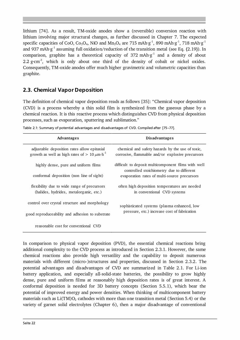
Seite 22
lithium [74]. As a result, TM-oxide anodes show a (reversible) conversion reaction with lithium involving major structural changes, as further discussed in Chapter 7. The expected specific capacities of CoO, Co3O4, NiO and Mn3O4 are 715 mAh·g-1, 890 mAh·g-1, 718 mAh·g-1 and 937 mAh·g-1 assuming full oxidation/reduction of the transition metal (see Eq. (2.19)). In comparison, graphite has a theoretical capacity of 372 mAh·g-1 and a density of about 2.2 g·cm-3, which is only about one third of the density of cobalt or nickel oxides. Consequently, TM-oxide anodes offer much higher gravimetric and volumetric capacities than graphite. 2.3. Chemical Vapor Deposition The definition of chemical vapor deposition reads as follows [35]: “Chemical vapor deposition (CVD) is a process whereby a thin solid film is synthesized from the gaseous phase by a chemical reaction. It is this reactive process which distinguishes CVD from physical deposition processes, such as evaporation, sputtering and sublimation.” Table 2.1: Summary of potential advantages and disadvantages of CVD. Compiled after [75–77].
Advantages Disadvantages adjustable deposition rates allow epitaxial growth as well as high rates of > 10 μm·h-1 chemical and safety hazards by the use of toxic, corrosive, flammable and/or explosive precursors
highly dense, pure and uniform films difficult to deposit multicomponent films with well controlled stoichiometry due to different evaporation rates of multi-source precursors conformal deposition (non line of sight) flexibility due to wide range of precursors (halides, hydrides, metalorganic, etc.) often high deposition temperatures are needed in conventional CVD systems
control over crystal structure and morphology sophisticated systems (plasma enhanced, low pressure, etc.) increase cost of fabrication good reproduceability and adhesion to substrate reasonable cost for conventional CVD
In comparison to physical vapor deposition (PVD), the essential chemical reactions bring additional complexity to the CVD process as introduced in Section 2.3.1. However, the same chemical reactions also provide high versatility and the capability to deposit numerous materials with different (micro-)structures and properties, discussed in Section 2.3.2. The potential advantages and disadvantages of CVD are summarized in Table 2.1. For Li-ion battery application, and especially all-solid-state batteries, the possibility to grow highly dense, pure and uniform films at reasonably high deposition rates is of great interest. A conformal deposition is needed for 3D battery concepts (Section 5.5.1), which bear the potential of improved energy and power densities. When thinking of multicomponent battery materials such as Li(TM)O2 cathodes with more than one transition metal (Section 5.4) or the variety of garnet solid electrolytes (Chapter 6), then a major disadvantage of conventional
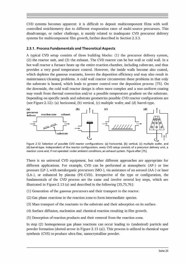
Seite 23
CVD systems becomes apparent: it is difficult to deposit multicomponent films with well controlled stoichiometry due to different evaporation rates of multi-source precursors. This disadvantage, or rather challenge, is mainly related to inadequate CVD precursor delivery systems for multicomponent film growth, further described in Section 2.3.3. 2.3.1. Process Fundamentals and Theoretical Aspects A typical CVD setup consists of three building blocks: (1) the precursor delivery system, (2) the reactor unit, and (3) the exhaust. The CVD reactor can be hot wall or cold wall. In a hot wall reactor a furnace heats up the entire reaction chamber, including substrate, and thus provides a very good temperature control. However, the inside walls become also coated, which depletes the gaseous reactants, lowers the deposition efficiency and may also result in maintenance/cleaning problems. A cold wall reactor circumvents these problems in that only the substrate is heated, which leads to greater control over the deposition process [75]. On the downside, the cold wall reactor design is often more complex and a non-uniform coating may result from thermal convection and/or a possible temperature gradient on the substrate. Depending on specific needs and substrate geometries possible CVD reactor configurations are (see Figure 2.12): (a) horizontal, (b) vertical, (c) multiple wafer, and (d) barrel-type.
Figure 2.12: Selection of possible CVD reactor configurations: (a) horizontal, (b) vertical, (c) multiple wafer, and (d) barrel-type. Independent of the reactor configuration, every CVD setup consists of a precursor delivery unit, a reaction zone and, if not operated under ambient conditions, an exhaust system. Figure after [75]. There is no universal CVD equipment, but rather different approaches are appropriate for different applications. For example, CVD can be performed at atmospheric (AP-) or low pressure (LP-), with metalorganic precursors (MO-), via assistance of an aerosol (AA-) or laser (LA-), or enhanced by plasma (PE-CVD). Irrespective of the type or configuration, the fundamentals of the CVD process are the same and involve several key steps, which are illustrated in Figure 2.13 (a) and described in the following [35,75,76]: (1) Generation of the gaseous precursors and their transport to the reactor. (2) Gas phase reactions in the reaction zone to form intermediate species. (3) Mass transport of the reactants to the substrate and their adsorption on its surface. (4) Surface diffusion, nucleation and chemical reaction resulting in film growth. (5) Desorption of reaction products and their removal from the reaction zone. In step (2) homogeneous gas phase reactions can occur leading to (undesired) particle and powder formation (dotted arrow in Figure 2.13 (a)). This process is utilized in chemical vapor synthesis (CVS) to produce ultra fine, nanocrystalline powder.
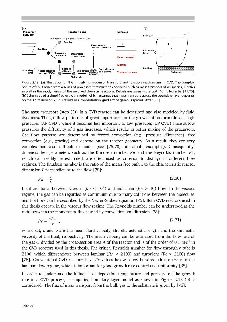
Seite 24
Figure 2.13: (a) Illustration of the underlying precursor transport and reaction mechanisms in CVD. The complex nature of CVD arises from a series of processes that must be controlled such as mass transport of all species, kinetics as well as thermodynamics of the involved chemical reactions. Details are given in the text. Compiled after [35,75]. (b) Schematic of a simplified growth model, which assumes that mass transport across the boundary layer depends on mass diffusion only. This results in a concentration gradient of gaseous species. After [76]. The mass transport (step (3)) in a CVD reactor can be described and also modeled by fluid dynamics. The gas flow pattern is of great importance for the growth of uniform films at high pressures (AP-CVD), while it becomes less important at low pressures (LP-CVD) since at low pressures the diffusivity of a gas increases, which results in better mixing of the precursors. Gas flow patterns are determined by forced convection (e.g., pressure difference), free convection (e.g., gravity) and depend on the reactor geometry. As a result, they are very complex and also difficult to model (see [76,78] for simple examples). Consequently, dimensionless parameters such as the Knudsen number Kn and the Reynolds number Re, which can readily be estimated, are often used as criterion to distinguish different flow regimes. The Knudsen number is the ratio of the mean free path λ to the characteristic reactor dimension L perpendicular to the flow [78]: . (2.30) It differentiates between viscous (Kn < 10-2) and molecular (Kn > 10) flow. In the viscous regime, the gas can be regarded as continuum due to many collisions between the molecules and the flow can be described by the Navier-Stokes equation [76]. Both CVD reactors used in this thesis operate in the viscous flow regime. The Reynolds number can be understood as the ratio between the momentum flux caused by convection and diffusion [78]: , (2.31) where u , L and ν are the mean fluid velocity, the characteristic length and the kinematic viscosity of the fluid, respectively. The mean velocity can be estimated from the flow rate of the gas Q divided by the cross-section area A of the reactor and is of the order of 0.1 m·s-1 in the CVD reactors used in this thesis. The critical Reynolds number for flow through a tube is 2100, which differentiates between laminar (Re < 2100) and turbulent (Re > 2100) flow [76]. Conventional CVD reactors have Re values below a few hundred, thus operate in the laminar flow regime, which is important for good growth rate control and uniformity [35]. In order to understand the influence of deposition temperature and pressure on the growth rate in a CVD process, a simplified boundary layer model as shown in Figure 2.13 (b) is considered. The flux of mass transport from the bulk gas to the substrate is given by [76]:
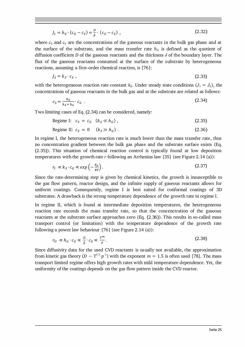
Seite 25
, (2.32) where cG and cS are the concentrations of the gaseous reactants in the bulk gas phase and at the surface of the substrate, and the mass transfer rate hG is defined as the quotient of diffusion coefficient D of the gaseous reactants and the thickness of the boundary layer. The flux of the gaseous reactants consumed at the surface of the substrate by heterogeneous reactions, assuming a first-order chemical reaction, is [76]: , (2.33) with the heterogeneous reaction rate constant kS. Under steady state conditions (J1 = J2), the concentrations of gaseous reactants in the bulk gas and at the substrate are related as follows: . (2.34) Two limiting cases of Eq. (2.34) can be considered, namely:
Regime I: , (2.35) Regime II: . (2.36)
In regime I, the heterogeneous reaction rate is much lower than the mass transfer rate, thus no concentration gradient between the bulk gas phase and the substrate surface exists (Eq. (2.35)). This situation of chemical reaction control is typically found at low deposition temperatures with the growth rate r following an Arrhenius law [35] (see Figure 2.14 (a)): . (2.37) Since the rate-determining step is given by chemical kinetics, the growth is insusceptible to the gas flow pattern, reactor design, and the infinite supply of gaseous reactants allows for uniform coatings. Consequently, regime I is best suited for conformal coatings of 3D substrates. A drawback is the strong temperature dependence of the growth rate in regime I. In regime II, which is found at intermediate deposition temperatures, the heterogeneous reaction rate exceeds the mass transfer rate, so that the concenctration of the gaseous reactants at the substrate surface approaches zero (Eq. (2.36)). This results in so-called mass transport control (or limitation) with the temperature dependence of the growth rate following a power law behaviour [76] (see Figure 2.14 (a)): . (2.38) Since diffusivity data for the used CVD reactants is usually not available, the approximation from kinetic gas theory (D ~ T1.5·p-1) with the exponent m = 1.5 is often used [78]. The mass transport limited regime offers high growth rates with mild temperature dependence. Yet, the uniformity of the coatings depends on the gas flow pattern inside the CVD reactor.
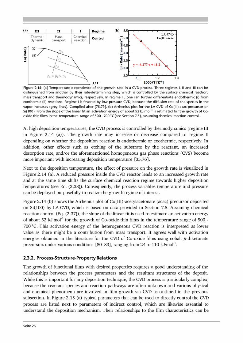
Seite 26
Figure 2.14: (a) Temperature dependence of the growth rate in a CVD process. Three regimes I, II and III can be distinguished from another by their rate-determining step, which is controlled by the surface chemical reaction, mass transport and thermodynamics, respectively. In regime III, one can further differentiate endothermic (i) from exothermic (ii) reactions. Regime I is favored by low pressure CVD, because the diffusion rate of the species in the vapor increases (grey lines). Compiled after [76,79]. (b) Arrhenius plot for the LA-CVD of Co(III)-acac precursor on Si(100). From the slope of the linear fit an activation energy of about 52 kJ·mol -1 is estimated for the growth of Co-oxide thin films in the temperature range of 500 - 700 °C (see Section 7.5), assuming chemical reaction control. At high deposition temperatures, the CVD process is controlled by thermodynamics (regime III in Figure 2.14 (a)). The growth rate may increase or decrease compared to regime II depending on whether the deposition reaction is endothermic or exothermic, respectively. In addition, other effects such as etching of the substrate by the reactant, an increased desorption rate, and/or the aforementioned homogeneous gas phase reactions (CVS) become more important with increasing deposition temperature [35,76]. Next to the deposition temperature, the effect of pressure on the growth rate is visualized in Figure 2.14 (a). A reduced pressure inside the CVD reactor leads to an increased growth rate and at the same time shifts the surface chemical reaction regime towards higher deposition temperatures (see Eq. (2.38)). Consequently, the process variables temperature and pressure can be deployed purposefully to realize the growth regime of interest. Figure 2.14 (b) shows the Arrhenius plot of Co(III)-acetylacetonate (acac) precursor deposited on Si(100) by LA-CVD, which is based on data provided in Section 7.5. Assuming chemical reaction control (Eq. (2.37)), the slope of the linear fit is used to estimate an activation energy of about 52 kJ·mol-1 for the growth of Co-oxide thin films in the temperature range of 500 - 700 °C. This activation energy of the heterogeneous CVD reaction is interpreted as lower value as there might be a contribution from mass transport. It agrees well with activation energies obtained in the literature for the CVD of Co-oxide films using cobalt -diketonate precursors under various conditions [80–83], ranging from 24 to 110 kJ·mol-1. 2.3.2. Process-Structure-Property Relations The growth of functional films with desired properties requires a good understanding of the relationships between the process parameters and the resultant structures of the deposit. While this is important for any deposition technique, the CVD process is particularly complex, because the reactant species and reaction pathways are often unknown and various physical and chemical phenomena are involved in film growth via CVD as outlined in the previous subsection. In Figure 2.15 (a) typical parameters that can be used to directly control the CVD process are listed next to parameters of indirect control, which are likewise essential to understand the deposition mechanism. Their relationships to the film characteristics can be
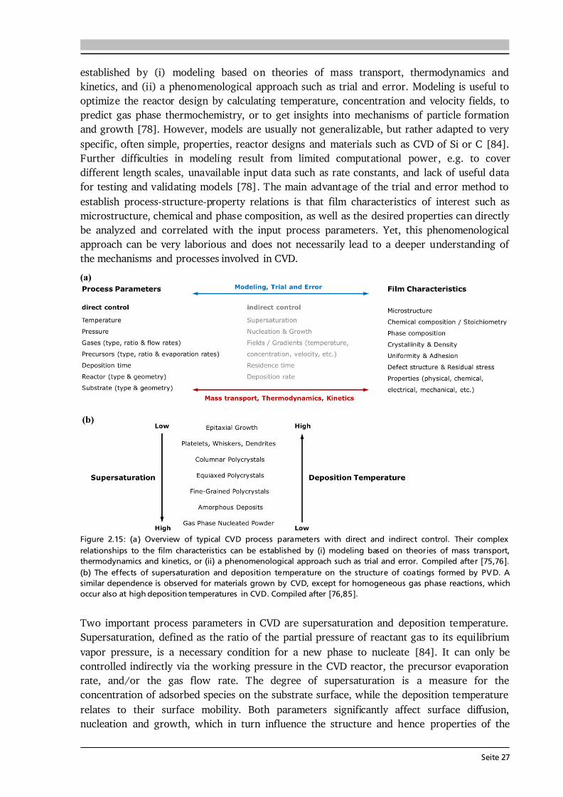
Seite 27
established by (i) modeling based on theories of mass transport, thermodynamics and kinetics, and (ii) a phenomenological approach such as trial and error. Modeling is useful to optimize the reactor design by calculating temperature, concentration and velocity fields, to predict gas phase thermochemistry, or to get insights into mechanisms of particle formation and growth [78]. However, models are usually not generalizable, but rather adapted to very specific, often simple, properties, reactor designs and materials such as CVD of Si or C [84]. Further difficulties in modeling result from limited computational power, e.g. to cover different length scales, unavailable input data such as rate constants, and lack of useful data for testing and validating models [78]. The main advantage of the trial and error method to establish process-structure-property relations is that film characteristics of interest such as microstructure, chemical and phase composition, as well as the desired properties can directly be analyzed and correlated with the input process parameters. Yet, this phenomenological approach can be very laborious and does not necessarily lead to a deeper understanding of the mechanisms and processes involved in CVD.
Figure 2.15: (a) Overview of typical CVD process parameters with direct and indirect control. Their complex relationships to the film characteristics can be established by (i) modeling based on theories of mass transport, thermodynamics and kinetics, or (ii) a phenomenological approach such as trial and error. Compiled after [75,76]. (b) The effects of supersaturation and deposition temperature on the structure of coatings formed by PVD. A similar dependence is observed for materials grown by CVD, except for homogeneous gas phase reactions, which occur also at high deposition temperatures in CVD. Compiled after [76,85]. Two important process parameters in CVD are supersaturation and deposition temperature. Supersaturation, defined as the ratio of the partial pressure of reactant gas to its equilibrium vapor pressure, is a necessary condition for a new phase to nucleate [84]. It can only be controlled indirectly via the working pressure in the CVD reactor, the precursor evaporation rate, and/or the gas flow rate. The degree of supersaturation is a measure for the concentration of adsorbed species on the substrate surface, while the deposition temperature relates to their surface mobility. Both parameters significantly affect surface diffusion, nucleation and growth, which in turn influence the structure and hence properties of the
Seite 28
deposited film [75]. Figure 2.15 (b) shows the effects of supersaturation and deposition temperature on the structure of coatings. Originally established for coatings formed by PVD [85], a similar dependence exists for materials grown by CVD as shown by Bryant [86]. Epitaxial growth takes place at conditions that provide fast surface diffusion in relation to the arrival of new growth initiating species on the surface, i.e. high deposition temperature and low supersaturation. Moreover, epitaxy requires the substrate to be free from defects and surface contaminations, so that it is often carried out under low pressure. Polycrystalline films grow over a wide range of intermediate supersaturation and deposition temperature. Depending on the relation between growth rate (i.e., supersaturation) and surface mobility (i.e., temperature) columnar, equiaxed or fine-grained polycrystals may form. At high supersaturation and low deposition temperature the adsorbed species cannot migrate to energetic more favorable sites where nucleation can occur resulting in amorphous deposits. Furthermore, a high degree of supersaturation promotes homogeneous gas phase reactions, because of the high frequency of molecular collisions in the gas phase. Gas phase nucleated particles are undesired for film growth as they lead to particulate (or powdery) deposits on the substrate, which interrupt surface nucleation and growth, hence can lead to an irregular coating with poor adhesion to the substrate [75]. In CVD, homogeneous gas phas reactions are also observed at high deposition temperatures [85,86], which is in contrast to PVD processes and needs to be considered in Figure 2.15 (b). 2.3.3. Precursor Delivery Systems Two of the major challenges in CVD are the deposition of multicomponent films and the use of precursors that pose chemical and safety hazards (see Table 2.1). Both issues are strongly related to the precursor delivery system as described in the following. The commercial use of CVD in several multi-billion dollar industries demonstrates its versatility and also importance for society. Examples are protective and anti-reflective coatings on glass and metals (titanium and silicon oxides, refractory metals), performance coatings on tools (molybdenum, tungsten, boron nitride), III-V semiconductors (GaAs, InP, GaN) and high-k dielectric materials (hafnium and zirconium oxides). Apparently, all these applications rely on materials with rather simple composition, mainly binary compounds AxBy, which require two precursor feeding lines A and B at most (see Figure 2.16 (a)). However, driven by technological progress the development of materials with novel functional properties leads to a greater need in deposition of multicomponent coatings and films. Examples are the high-temperature superconductor YBa2Cu3O7-δ [87] and Li-ion conducting garnet solid electrolytes investigated in Chapter 6 of this thesis. CVD of such multicomponent (quaternary or higher) materials requires precise control over the composition of the delivered precursors throughout the entire deposition process. A high degree of control is easy to achieve with gaseous precursors, such as phosphine (PH3), hydrogen selenide (H2Se) or hydrogen sulfide (H2S), by the use of conventional mass-flow controllers (MFCs). However, despite the fact that the just mentioned precursors are highly toxic, not many gaseous precursors are available for metal CVD [88]. Therefore, liquids and solids, delivered via bubblers (Figure 2.16 (b)) and direct vaporization (Figure 2.16 (c)), are most often used. In a bubbler, the carrier gas should become (fully) saturated with reactant vapor when passing through the liquid precursor. However, liquid precursors with too low or
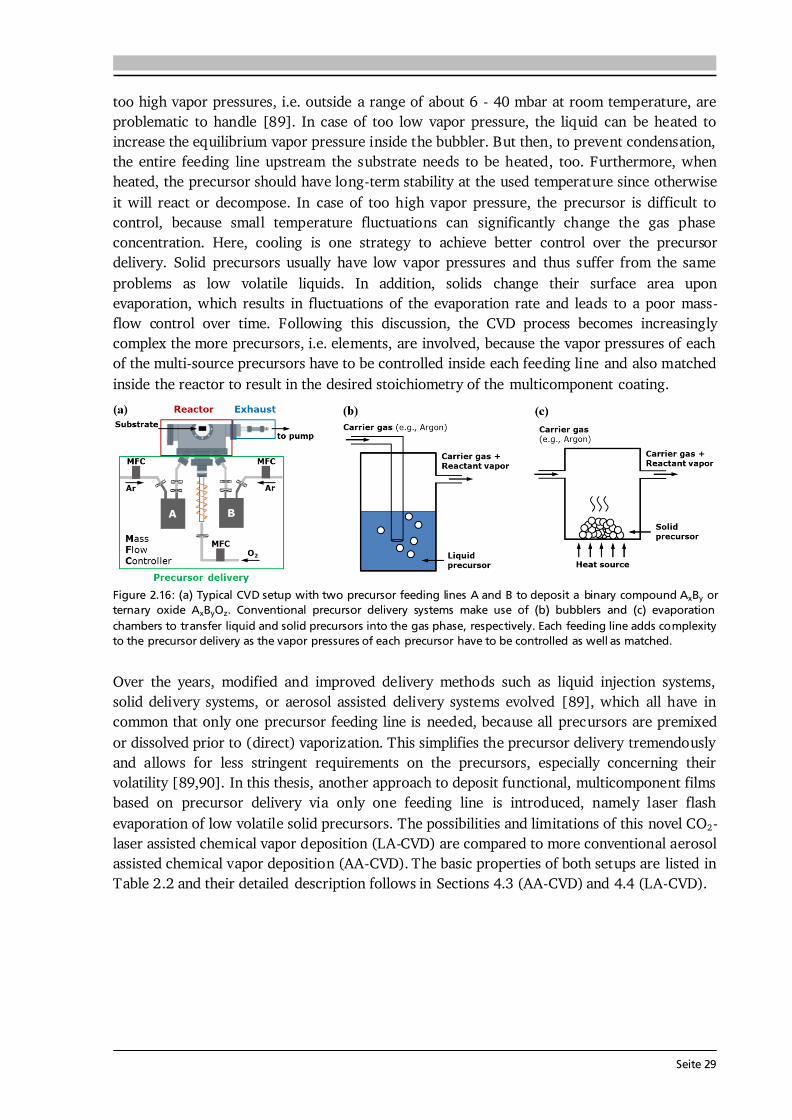
Seite 29
too high vapor pressures, i.e. outside a range of about 6 - 40 mbar at room temperature, are problematic to handle [89]. In case of too low vapor pressure, the liquid can be heated to increase the equilibrium vapor pressure inside the bubbler. But then, to prevent condensation, the entire feeding line upstream the substrate needs to be heated, too. Furthermore, when heated, the precursor should have long-term stability at the used temperature since otherwise it will react or decompose. In case of too high vapor pressure, the precursor is difficult to control, because small temperature fluctuations can significantly change the gas phase concentration. Here, cooling is one strategy to achieve better control over the precursor delivery. Solid precursors usually have low vapor pressures and thus suffer from the same problems as low volatile liquids. In addition, solids change their surface area upon evaporation, which results in fluctuations of the evaporation rate and leads to a poor mass-flow control over time. Following this discussion, the CVD process becomes increasingly complex the more precursors, i.e. elements, are involved, because the vapor pressures of each of the multi-source precursors have to be controlled inside each feeding line and also matched inside the reactor to result in the desired stoichiometry of the multicomponent coating.
Figure 2.16: (a) Typical CVD setup with two precursor feeding lines A and B to deposit a binary compound AxBy or ternary oxide AxByOz. Conventional precursor delivery systems make use of (b) bubblers and (c) evaporation chambers to transfer liquid and solid precursors into the gas phase, respectively. Each feeding line adds complexity to the precursor delivery as the vapor pressures of each precursor have to be controlled as well as matched. Over the years, modified and improved delivery methods such as liquid injection systems, solid delivery systems, or aerosol assisted delivery systems evolved [89], which all have in common that only one precursor feeding line is needed, because all precursors are premixed or dissolved prior to (direct) vaporization. This simplifies the precursor delivery tremendously and allows for less stringent requirements on the precursors, especially concerning their volatility [89,90]. In this thesis, another approach to deposit functional, multicomponent films based on precursor delivery via only one feeding line is introduced, namely laser flash evaporation of low volatile solid precursors. The possibilities and limitations of this novel CO2-laser assisted chemical vapor deposition (LA-CVD) are compared to more conventional aerosol assisted chemical vapor deposition (AA-CVD). The basic properties of both setups are listed in Table 2.2 and their detailed description follows in Sections 4.3 (AA-CVD) and 4.4 (LA-CVD).
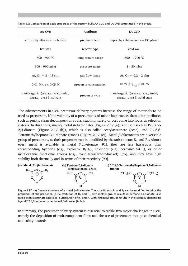
Seite 30
Table 2.2: Comparison of basic properties of the custom-built AA-CVD and LA-CVD setups used in this thesis. AA-CVD Attribute LA-CVD
aerosol by ultrasonic nebulizer precursor feed vapor by sublimation via CO2-laser hot wall reactor type cold wall
500 - 900 °C temperature range 500 - 1200 °C 300 - 900 mbar pressure range 1 - 50 mbar
Ar, O2 ~ 3 - 15 slm gas flow range Ar, O2 ~ 0.2 - 2 slm 0.01 M ≤ c ≤ 0.05 M precursor concentration 10 W ≤ PC O2 ≤ 100 W
metalorganic (acetate, acac, tmhd, nitrate, etc.) in solvent precursor type metalorganic (acetate, acac, tmhd, nitrate, etc.) in solid state The advancements in CVD precursor delivery systems increase the range of materials to be used as precursors. If the volatility of a precursor is of minor importance, then other attributes such as purity, clean decomposition route, stability, safety or cost come into focus as selection criteria. In this thesis, mainly metal -diketonates (Figure 2.17 (a)) are used such as Pentane-2,4-dionate (Figure 2.17 (b)), which is also called acetylacetonate (acac), and 2,2,6,6-Tetramethylheptane-3,5-dionate (tmhd) (Figure 2.17 (c)). Metal -diketonates are a versatile group of precursors, as their properties can be modified by the substituents R1 and R2. Almost every metal is available as metal -diketonate [91], they are less hazardous than corresponding hydrides (e.g., explosive B2H6), chlorides (e.g., corrosive SiCl4), or other metalorganic functional groups (e.g., toxic tetracarbonylnickel) [76], and they have high stability both thermally and in terms of their reactivity [90].
Figure 2.17: (a) General structure of a metal -diketonate. The substituents R1 and R2 can be modified to tailor the properties of the precursor. (b) Substitution of R1 and R2 with methyl groups results in pentane-2,4-dionate, also called acetylacetonate (acac). (c) Substitution of R1 and R2 with tert-butyl groups results in the sterically demanding ligand 2,2,6,6-tetramethylheptane-3,5-dionate (tmhd). In summary, the precursor delivery system is essential to tackle two major challenges in CVD, namely the deposition of multicomponent films and the use of precursors that pose chemical and safety hazards.
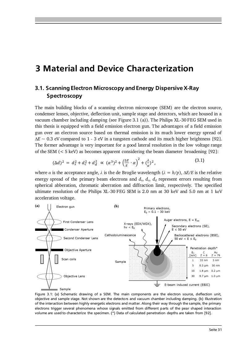
Seite 31
3 Material and Device Characterization 3.1. Scanning Electron Microscopy and Energy Dispersive X-Ray Spectroscopy The main building blocks of a scanning electron microscope (SEM) are the electron source, condenser lenses, objective, deflection unit, sample stage and detectors, which are housed in a vacuum chamber including damping (see Figure 3.1 (a)). The Philips XL-30 FEG SEM used in this thesis is equipped with a field emission electron gun. The advantages of a field emission gun over an electron source based on thermal emission is its much lower energy spread of ∆E ~ 0.3 eV compared to 1 - 3 eV in a tungsten cathode and its much higher brightness [92]. The former advantage is very important for a good lateral resolution in the low voltage range of the SEM (< 5 keV) as becomes apparent considering the beam diameter broadening [92]: , (3.1) where α is the acceptance angle, λ is the de Broglie wavelength (λ = h/p), ∆E/E is the relative energy spread of the primary beam electrons and ds, dc, dd represent errors resulting from spherical abberation, chromatic aberration and diffraction limit, respectively. The specified ultimate resolution of the Philips XL-30 FEG SEM is 2.0 nm at 30 keV and 5.0 nm at 1 keV acceleration voltage.
Figure 3.1: (a) Schematic drawing of a SEM. The main components are the electron source, deflection unit, objective and sample stage. Not shown are the detectors and vacuum chamber including damping. (b) Illustration of the interaction between highly energetic electrons and matter. Along their way through the sample, the primary electrons trigger several phenomena whose signals emitted from different parts of the pear shaped interaction volume are used to characterize the specimen. (*) Data of calculated penetration depths are taken from [92].
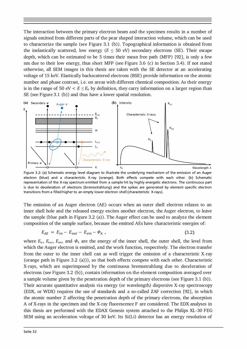
Seite 32
The interaction between the primary electron beam and the specimen results in a number of signals emitted from different parts of the pear shaped interaction volume, which can be used to characterize the sample (see Figure 3.1 (b)). Topographical information is obtained from the inelastically scattered, low energy (E ≤ 50 eV) secondary electrons (SE). Their escape depth, which can be estimated to be 5 times their mean free path (MFP) [92], is only a few nm due to their low energy, thus short MFP (see Figure 3.6 (c) in Section 3.4). If not stated otherwise, all SEM images in this thesis are taken with the SE detector at an accelerating voltage of 15 keV. Elastically backscattered electrons (BSE) provide information on the atomic number and phase contrast, i.e. on areas with different chemical composition. As their energy is in the range of 50 eV < E ≤ E0 by definition, they carry information on a larger region than SE (see Figure 3.1 (b)) and thus have a lower spatial resolution.
Figure 3.2: (a) Schematic energy level diagram to illustrate the underlying mechanism of the emission of an Auger electron (blue) and a characteristic X-ray (orange). Both effects compete with each other. (b) Schematic representation of the X-ray spectrum emitted from a sample hit by highly energetic electrons. The continuous part is due to deceleration of electrons (bremsstrahlung) and the spikes are generated by element specific electron transitions from a filled higher to an empty lower electron shell (characteristic X-rays). The emission of an Auger electron (AE) occurs when an outer shell electron relaxes to an inner shell hole and the released energy excites another electron, the Auger electron, to leave the sample (blue path in Figure 3.2 (a)). The Auger effect can be used to analyze the element composition of the sample surface, because the emitted AEs have characteristic energies of: , (3.2) where Ein, Eout, Eem, and ΦA are the energy of the inner shell, the outer shell, the level from which the Auger electron is emitted, and the work function, respectively. The electron transfer from the outer to the inner shell can as well trigger the emission of a characteristic X-ray (orange path in Figure 3.2 (a))), so that both effects compete with each other. Characteristic X-rays, which are superimposed by the continuous bremsstrahlung due to deceleration of electrons (see Figure 3.2 (b)), contain information on the element composition averaged over a sample volume given by the penetration depth of the primary electrons (see Figure 3.1 (b)). Their accurate quantitative analysis via energy (or wavelength) dispersive X-ray spectroscopy (EDX, or WDX) requires the use of standards and a so-called ZAF correction [92], in which the atomic number Z affecting the penetration depth of the primary electrons, the absorption A of X-rays in the specimen and the X-ray fluorescence F are considered. The EDX analyses in this thesis are performed with the EDAX Genesis system attached to the Philips XL-30 FEG SEM using an acceleration voltage of 30 keV. Its Si(Li) detector has an energy resolution of
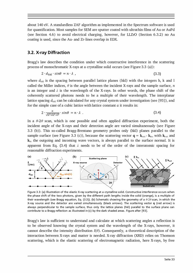
Seite 33
about 140 eV. A standardless ZAF algorithm as implemented in the Spectrum software is used for quantification. Most samples for SEM are sputter coated with ultrathin films of Au or AuPd (see Section 4.6) to avoid electrical charging, however, for LLZrO (Section 6.3.2) no Au coating is used, since the Au- and Zr-lines overlap in EDX. 3.2. X-ray Diffraction Bragg’s law describes the condition under which constructive interference in the scattering process of monochromatic X-rays at a crystalline solid occurs (see Figure 3.3 (a)): , (3.3) where dhkl is the spacing between parallel lattice planes (hkl) with the integers h, k and l called the Miller indices, is the angle between the incident X-rays and the sample surface, n is an integer and λ is the wavelength of the X-rays. In other words, the phase shift of the coherently scattered photons needs to be a multiple of their wavelength. The interplanar lattice spacing dhkl can be calculated for any crystal system under investigation (see [93]), and for the simple case of a cubic lattice with lattice constant a it results in: √ . (3.4) In a -2 scan, which is one possible and often applied diffraction experiment, both the incident angle of the X-rays and their detection angle are varied simultaneously (see Figure 3.3 (b)). This so-called Bragg-Brentano geometry probes only (hkl) planes parallel to the sample surface (see Figure 3.3 (c)), because the scattering vector q = kout - kin, with kout and kin the outgoing and incoming wave vectors, is always parallel to the surface normal. It is apparent from Eq. (3.4) that λ needs to be of the order of the interatomic spacing for reasonable diffraction experiments.
Figure 3.3: (a) Illustration of the elastic X-ray scattering at a crystalline solid. Constructive interference occurs when the phase shift of the two photons, given by the different path lengths inside the solid (orange), is a multiple of their wavelength (see Bragg equation, Eq. (3.3)). (b) Schematic showing the geometry of a -2 scan, in which the X-ray source and the detector are varied simultaneously (black arrows). The scattering vector q (red arrow) is always perpendicular to the sample surface, thus only the lattice planes (hkl) parallel to the surface plane can contribute to a Bragg reflection as illustrated in (c) by the dark shaded areas. Figure after [93].
Bragg’s law is sufficient to understand and calculate at which scattering angles a reflection is to be observed knowing the crystal system and the wavelength of the X-rays, however, it cannot describe the intensity distribution I( ). Consequently, a theoretical description of the interaction between X-rays and matter is needed. X-ray diffraction (XRD) relies on Thomson scattering, which is the elastic scattering of electromagnetic radiation, here X-rays, by free
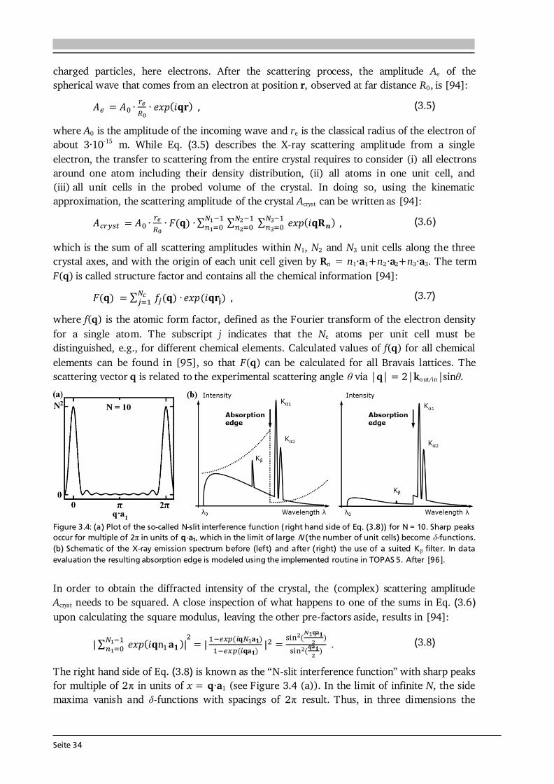
Seite 34
charged particles, here electrons. After the scattering process, the amplitude Ae of the spherical wave that comes from an electron at position r, observed at far distance R0, is [94]: , (3.5) where A0 is the amplitude of the incoming wave and re is the classical radius of the electron of about 3·10-15 m. While Eq. (3.5) describes the X-ray scattering amplitude from a single electron, the transfer to scattering from the entire crystal requires to consider (i) all electrons around one atom including their density distribution, (ii) all atoms in one unit cell, and (iii) all unit cells in the probed volume of the crystal. In doing so, using the kinematic approximation, the scattering amplitude of the crystal Acryst can be written as [94]: ∑ ∑ ∑ , (3.6) which is the sum of all scattering amplitudes within N1, N2 and N3 unit cells along the three crystal axes, and with the origin of each unit cell given by Rn = n1·a1+n2·a2+n3·a3. The term F(q) is called structure factor and contains all the chemical information [94]: ∑ , (3.7) where f(q) is the atomic form factor, defined as the Fourier transform of the electron density for a single atom. The subscript j indicates that the Nc atoms per unit cell must be distinguished, e.g., for different chemical elements. Calculated values of f(q) for all chemical elements can be found in [95], so that F(q) can be calculated for all Bravais lattices. The scattering vector q is related to the experimental scattering angle via |q| = 2|kout/in|sin .
Figure 3.4: (a) Plot of the so-called N-slit interference function (right hand side of Eq. (3.8)) for N = 10. Sharp peaks occur for multiple of 2π in units of q ·a1, which in the limit of large N (the number of unit cells) become -functions. (b) Schematic of the X-ray emission spectrum before (left) and after (right) the use of a suited K filter. In data evaluation the resulting absorption edge is modeled using the implemented routine in TOPAS 5. After [96]. In order to obtain the diffracted intensity of the crystal, the (complex) scattering amplitude Acryst needs to be squared. A close inspection of what happens to one of the sums in Eq. (3.6) upon calculating the square modulus, leaving the other pre-factors aside, results in [94]: ∑ . (3.8) The right hand side of Eq. (3.8) is known as the “N-slit interference function” with sharp peaks for multiple of 2π in units of x = q·a1 (see Figure 3.4 (a)). In the limit of infinite N, the side maxima vanish and -functions with spacings of 2π result. Thus, in three dimensions the
Seite 35
diffracted intensity is the product of three perpendicular arrays of -functions leading to the following conditions that must be fulfilled simultaneously for constructive interference: . (3.9) These are the Laue equations with the Miller indices h, k and l that are integral numbers. The Laue equations are fulfilled by the following scattering vector: . (3.10) Combining Eq.s (3.6), (3.8) and (3.10) results in the following expression for the diffracted intensity in a crystal, which is zero except at discrete (hkl) points in the reciprocal space [94]: . (3.11) The diffracted intensity as given by Eq. (3.11) still lacks several effects. For example, thermal vibrations of the atoms entail a reduction in phase coherence in the scattered wave, thus reduce the intensity, which can be accounted for by temperature dependent atomic form factors f(q, T) to describe the damping [93]. Other influencing factors on the measured integral intensity are [93,96]: multiplicity factor mhkl, Lorentz, geometry and polarization factor Lp, absorption factor Aθ2θ and preferred orientation factor Thkl. Moreover, a scaling factor s, which includes all constants and instrumental settings, is introduced in order to allow a comparison of different diffraction patterns on a relative scale: . (3.12) XRD Measurements XRD patterns of all deposited films are recorded on a Bruker D8 Advance diffractometer in Bragg-Brentano geometry with a fine-focusing Cu anode (λKα = 0.154 nm) in a 2 -range from 10° to 80°. A step size of 0.0075° in 2 and a scan speed of 1 s per step are used. No primary beam monochromator is attached. K radiation is removed by a Ni filter (see Figure 3.4 (b)), but remains present to a very small fraction of the overall beam intensity (< 0.1 %). A VANTEC detector and a variable divergence slit are used for data acquisition. The whole 2 -range is used for Rietveld analysis with the program TOPAS 5 [97,98]. The instrumental intensity distribution for the X-ray data is determined empirically from a fundamental parameters set [99], using a reference scan of LaB6 (NIST 660a). The absorption edge resulting from the Ni filter (Figure 3.4 (b)) is modeled using the implemented routine in TOPAS 5. For refinement of the peak shape a double Voigt model with a cos -1( ) angular dependence for crystallite size and a tan( ) angular dependence for microstrain broadening is used. Reflections belonging to the identified phases are fit using the Rietveld method, whereas intensities of the reflections belonging to the Pt substrate and the sputtered Au contacts are modeled by Pawley-type fits. Only lattice parameters, but no atomic position parameters, are refined for each phase. Since a strong correlation of thermal parameters with the background function is observed, the former is fixed to a value of 1 Å2. The model of March and Dollase [100] is applied to describe intensity changes resulting from texturing of the thin film samples, with the preferred orientation factor given by [96]: ∑ [ ( ) ] , (3.13)
Seite 36
where N is the number of symmetrically equivalent reciprocal lattice points, is the March-Dollase (MD) parameter describing the degree of texturing, and Φihkl is defined as the angle between the direction of the Bragg peak (hkl) and the preferred orientation direction. For MD parameters of < 1, = 1, and > 1 the amount of crystallites with (hkl) planes parallel to the sample surface is increased, the same and decreased compared to a random distribution, respectively. Several different orientations are tested to determine the best fit to the pattern. 3.3. Raman Spectroscopy Raman spectroscopy (RS) relies on the inelastic Raman scattering of photons by particles that are much smaller than the wavelength of the used electromagnetic radiation, which is typically a laser in the ultraviolet (UV), visible (VIS), or infrared (IR) region. Raman scattering involves the excitation of an electron to a virtual energy state along with a transfer of vibrational energy, as shown in the energy level diagram in Figure 3.5 (a). The energy of the scattered photon can be lower or higher than the energy of the incident photon depending on whether the transfer of vibrational energy is from the photon to the sample (orange path in Figure 3.5 (a)) or from the sample to the photon (blue path in Figure 3.5 (a)) called Stokes or anti-Stokes Raman scattering, respectively. The population of the vibrational ground state (ν = 0) is much larger than the one of the excited state (ν = 1), as given by the Boltzmann distribution, resulting in higher probability of the Stokes compared to the anti-Stokes transition. Both transitions contain the same information, thus the more intense Stokes shift is usually measured in RS (see Figure 3.5 (b)). Raman shifts are independent of the wavelength of the incident photon and often given in wavenumbers in cm-1: ̃ , (3.14) where λi and λs are the wavelengths of the incident and scattered photons, respectively. Only a small fraction of the incoming photons (about 10-7) is scattered inelastically [101], while the majority is scattered elastically (Rayleigh scattering).
Figure 3.5: (a) Schematic energy level diagram for different interactions between light (UV/VIS/IR) and matter such as infrared absorption (IR), fluorescence, Rayleigh scattering, Stokes and anti-Stokes Raman scattering. (b) Elastic Rayleigh scattering is much more likely than inelastic Raman scattering leading to a much lower intensity of the latter. Moreover, the Stokes transition delivers higher intensity compared to the anti -Stokes transition, because the population at ν = 0 (ground state) is much larger than at ν = 1.
Seite 37
In the classical description of the Raman effect the incoming electromagnetic wave induces a dipole moment in the molecule, which is proportional to the electric field E of the laser [102]: ̃ , (3.15) where p0 stands for a possible pre-existing permanent dipole moment and ̃ is the polarizability tensor, which in normal Raman scattering is symmetric. According to quantum mechanics, the selection rule for a Raman active vibration is that one of the components of the polarizability tensor changes during the scattering process [102]. Consequently, RS is complementary to infrared (IR) spectroscopy for which the selection rule is a change in dipole moment during the absorption process. RS is applicable to gases, liquids and solids for which a wealth of chemical and structural information can be obtained. With respect to the Li-ion battery materials investigated in this thesis it is important that the Raman shifts are sensitive to the crystal symmetry, coordination geometry and oxidation state, which allows to distinguish [101]: (i) metal oxides whose atomic arrangements are closely related to one another (e.g., TM-oxides with TM = Co, Ni, Mn in Chapter 7), (ii) between metal oxides with same elements (e.g., manganse oxides MnO2, Mn3O4 and Mn2O3 in Section 7.4), and (iii) compounds that have the same stoichiometry but different structures (e.g., HT-/LT-LiCoO2 in Chapter 5). Moreover, RS probes the microscopic scale and as such is complementary to XRD, which averages over the entire sample volume. On the downside, it is very difficult to quantify the data obtained with RS due to the experimental effort needed to measure and calibrate the Raman band intensities of different materials and phases [101]. Consequently, no phase quantification is attempted in this thesis. Raman spectra (8 - 10 scans, each lasting 8 - 10 s) are recorded with a Horiba Jobin Yvon HR800 micro-Raman spectrometer equipped with a He-Ne laser (λ = 632.8 nm, P = 25 mW). A grating of 600 g·mm-1 and a confocal microscope (magnification 50x, NA = 0.5) with a 100 μm aperture are used, which results in a spatial resolution of a few μm. All Raman spectra are referenced to the Raman shift of silicon at 521 cm-1 [103]. 3.4. X-ray Photoelectron Spectroscopy Photoelectron spectroscopy (PES) relies on the photoelectric effect in which a material irradiated by photons emits electrons. The emitted (photo-)electrons can be sorted according to their kinetic energy as well as escape angle by an electrostatic analyzer (see Figure 3.6 (a)), and in this way provide information on the chemistry as well as electronic structure of the sample. A precondition for the electron to escape the sample is that the energy of the incident photon hν is greater than the electron’s binding energy EB plus the work function of the sample ΦS. The relation between the measured kinetic energy of the electrons: , (3.16) and the energy levels of the sample is schematically drawn in Figure 3.6 (b). Here, EB and Ekin are related to the Fermi level EF and the vacuum level Evac, respectively. Since the work function of the sample is usually unknown, the work function of the analyzer ΦA is used instead in Eq. (3.16) provided sample and analyzer have an electroconductive connection. In dependence on the energy of the used excitation source one can distinguish ultraviolet
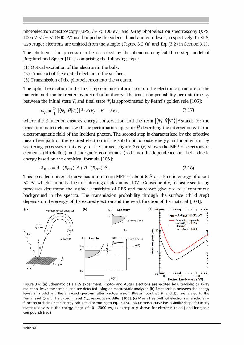
Seite 38
photoelectron spectroscopy (UPS, hν < 100 eV) and X-ray photoelectron spectroscopy (XPS, 100 eV < hν < 1500 eV) used to probe the valence band and core levels, respectively. In XPS, also Auger electrons are emitted from the sample (Figure 3.2 (a) and Eq. (3.2) in Section 3.1). The photoemission process can be described by the phenomenological three-step model of Berglund and Spicer [104] comprising the following steps: (1) Optical excitation of the electron in the bulk. (2) Transport of the excited electron to the surface. (3) Transmission of the photoelectron into the vacuum. The optical excitation in the first step contains information on the electronic structure of the material and can be treated by perturbation theory. The transition probability per unit time wfi between the initial state i and final state f is approximated by Fermi’s golden rule [105]: |⟨ | ̂| ⟩| , (3.17) where the -function ensures energy conservation and the term |⟨ | ̂| ⟩| stands for the transition matrix element with the perturbation operator ̂ describing the interaction with the electromagnetic field of the incident photon. The second step is characterized by the effective mean free path of the excited electron in the solid not to loose energy and momentum by scattering processes on its way to the surface. Figure 3.6 (c) shows the MFP of electrons in elements (black line) and inorganic compounds (red line) in dependence on their kinetic energy based on the empirical formula [106]: . (3.18) This so-called universal curve has a minimum MFP of about 5 Å at a kinetic energy of about 50 eV, which is mainly due to scattering at plasmons [107]. Consequently, inelastic scattering processes determine the surface sensitivity of PES and moreover give rise to a continuous background in the spectra. The transmission probability through the surface (third step) depends on the energy of the excited electron and the work function of the material [108].
Figure 3.6: (a) Schematic of a PES experiment. Photo- and Auger electrons are excited by ultraviolet or X-ray radiation, leave the sample, and are detected using an electrostatic analyzer. (b) Relationship between the energy levels in a solid and the analyzed spectrum after photoemission. Please note that EB and Ekin are related to the Fermi level EF and the vacuum level Evac, respectively. After [108]. (c) Mean free path of electrons in a solid as a function of their kinetic energy calculated according to Eq. (3.18). This universal curve has a similar shape for many material classes in the energy range of 10 - 2000 eV, as exemplarily shown for elements (black) and inorganic compounds (red).
Seite 39
The integrated intensity I of a specific XPS core level peak is directly proportional to the number of atoms N of the corresponding element per volume of analyzed sample [109]: , (3.19) where and L are the photoionization cross-section and asymmetry function related to the excited atomic orbital, J is the incident photon flux, λ is the effective MFP of the photoelectrons, D is the detection efficiency of the analyzer and T its transmission function. In principle, via Eq. (3.19) a quantitative analysis of the XPS spectrum is possible, because λ can be calculated using the TPP-2M formalism [110] or Eq. (3.18), values for and L are tabulated for free atoms [111,112], and functions of J, D and T might be provided by the manufacturers of the PES equipment. In practice, often all quantities are summarized in so-called atomic sensitivity factors (ASF), which allow to determine the atom fraction cx of any constituent in a sample as follows [113]: ∑ ∑ . (3.20) Here, the main idea is that while the absolute value of the ASF may vary strongly for samples with different matrix, the relative values will vary only slightly [114]. The quantification of XPS spectra via atomic sensitivity factors utilizing peak areas of intense lines after background substraction typically results in errors of 10 - 20 % [113]. XPS Measurements The XPS sputter depth profiling study in Section 6.3.3 is performed on a K-Alpha+ XPS spectrometer (Thermo Fisher Scientific). For data acquisition and processing the Thermo Avantage software is used. The sample is analyzed using a micro-focused, monochromatic Al Kα X-ray source (hν = 1486.6 eV) with 300 µm spot size. To prevent any localized charge build-up during analysis, the K-Alpha charge compensation system is employed with electrons of 8 eV energy and low-energy argon ions. The spectra are fit with one or more Voigt profiles. The analyzer transmission function, Scofield photoionization cross-sections [111] and effective attenuation lengths for photoelectrons, calculated via the TPP-2M formalism [110], are applied for quantification. All spectra are referenced to the C 1s peak of hydrocarbon at a binding energy of 285.0 eV and controlled by means of the well-known photoelectron peaks of metallic Cu, Ag, and Au. The sputter depth profile is obtained using an Ar+ ion beam with a current of 2.3 µA at 3 keV, 30° angle of incidence and a 1 mm by 2 mm raster size. All other XPS spectra in this thesis are measured with a PHI 5000 spectrometer (Physical Electronics). The spectra are taken with monochromatic Al Kα radiation (hν = 1486.6 eV) at a constant pass energy of Ep = 23.5 eV and energy steps of ΔE = 0.050 - 0.100 eV under an electron escape angle of 45°. A spot size of either 100 μm or 200 μm is chosen. For quantitative analyses the software PHI MultiPak Version 9 is employed [115], which uses empirical ASF based on [114]. The background of the core level peaks is subtracted applying the Shirley method [116]. For the analysis in Section 6.4.4, the peaks are fit using a pseudo-Voigt function V(x), which is a linear combination of Gaussian line shape G(x) (e.g., resolution broadening) and Lorentzian line shape L(x) (e.g., lifetime broadening).
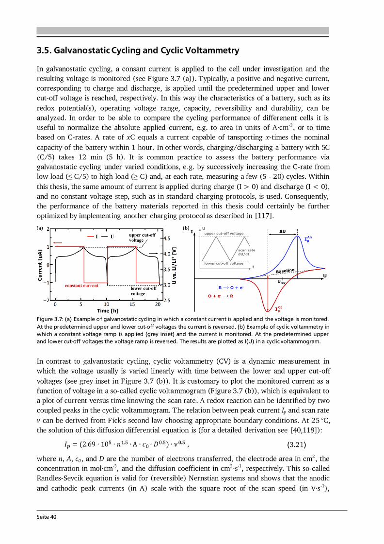
Seite 40
3.5. Galvanostatic Cycling and Cyclic Voltammetry In galvanostatic cycling, a consant current is applied to the cell under investigation and the resulting voltage is monitored (see Figure 3.7 (a)). Typically, a positive and negative current, corresponding to charge and discharge, is applied until the predetermined upper and lower cut-off voltage is reached, respectively. In this way the characteristics of a battery, such as its redox potential(s), operating voltage range, capacity, reversibility and durability, can be analyzed. In order to be able to compare the cycling performance of differenent cells it is useful to normalize the absolute applied current, e.g. to area in units of A·cm-2, or to time based on C-rates. A rate of xC equals a current capable of tansporting x-times the nominal capacity of the battery within 1 hour. In other words, charging/discharging a battery with 5C (C/5) takes 12 min (5 h). It is common practice to assess the battery performance via galvanostatic cycling under varied conditions, e.g. by successively increasing the C-rate from low load (≤ C/5) to high load (≥ C) and, at each rate, measuring a few (5 - 20) cycles. Within this thesis, the same amount of current is applied during charge (I > 0) and discharge (I < 0), and no constant voltage step, such as in standard charging protocols, is used. Consequently, the performance of the battery materials reported in this thesis could certainly be further optimized by implementing another charging protocol as described in [117].
Figure 3.7: (a) Example of galvanostatic cycling in which a constant current is applied and the voltage is monitored. At the predetermined upper and lower cut-off voltages the current is reversed. (b) Example of cyclic voltammetry in which a constant voltage ramp is applied (grey inset) and the current is monitored. At the predetermined upper and lower cut-off voltages the voltage ramp is reversed. The results are plotted as I(U) in a cyclic voltammogram. In contrast to galvanostatic cycling, cyclic voltammetry (CV) is a dynamic measurement in which the voltage usually is varied linearly with time between the lower and upper cut-off voltages (see grey inset in Figure 3.7 (b)). It is customary to plot the monitored current as a function of voltage in a so-called cyclic voltammogram (Figure 3.7 (b)), which is equivalent to a plot of current versus time knowing the scan rate. A redox reaction can be identified by two coupled peaks in the cyclic voltammogram. The relation between peak current Ip and scan rate v can be derived from Fick’s second law choosing appropriate boundary conditions. At 25 °C, the solution of this diffusion differential equation is (for a detailed derivation see [40,118]): , (3.21) where n, A, c0, and D are the number of electrons transferred, the electrode area in cm2, the concentration in mol·cm-3, and the diffusion coefficient in cm2·s-1, respectively. This so-called Randles-Sevcik equation is valid for (reversible) Nernstian systems and shows that the anodic and cathodic peak currents (in A) scale with the square root of the scan speed (in V·s-1),
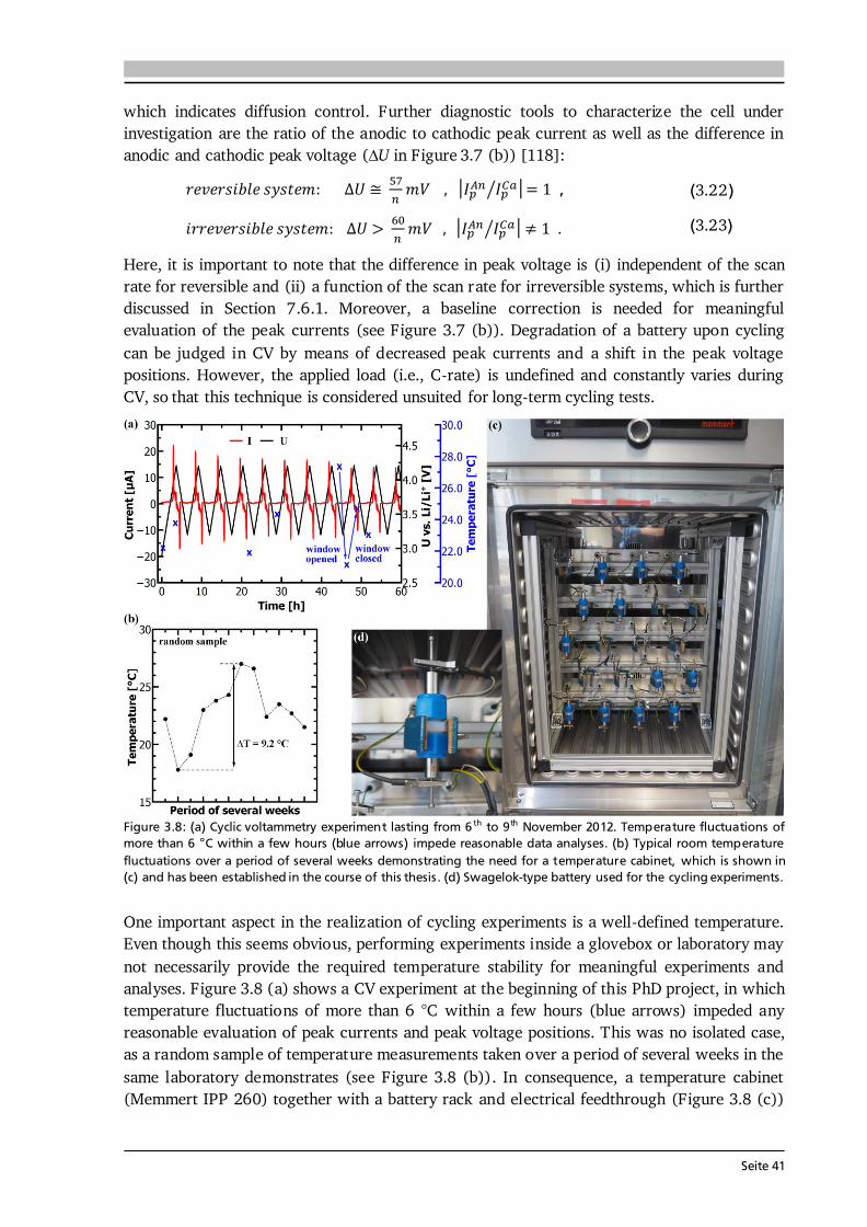
Seite 41
which indicates diffusion control. Further diagnostic tools to characterize the cell under investigation are the ratio of the anodic to cathodic peak current as well as the difference in anodic and cathodic peak voltage (∆U in Figure 3.7 (b)) [118]: | ⁄ | , (3.22) | ⁄ | . (3.23) Here, it is important to note that the difference in peak voltage is (i) independent of the scan rate for reversible and (ii) a function of the scan rate for irreversible systems, which is further discussed in Section 7.6.1. Moreover, a baseline correction is needed for meaningful evaluation of the peak currents (see Figure 3.7 (b)). Degradation of a battery upon cycling can be judged in CV by means of decreased peak currents and a shift in the peak voltage positions. However, the applied load (i.e., C-rate) is undefined and constantly varies during CV, so that this technique is considered unsuited for long-term cycling tests.
Figure 3.8: (a) Cyclic voltammetry experiment lasting from 6 th to 9th November 2012. Temperature fluctuations of more than 6 °C within a few hours (blue arrows) impede reasonable data analyses. (b) Typical room temperature fluctuations over a period of several weeks demonstrating the need for a temperature cabinet, which is shown in (c) and has been established in the course of this thesis. (d) Swagelok-type battery used for the cycling experiments. One important aspect in the realization of cycling experiments is a well-defined temperature. Even though this seems obvious, performing experiments inside a glovebox or laboratory may not necessarily provide the required temperature stability for meaningful experiments and analyses. Figure 3.8 (a) shows a CV experiment at the beginning of this PhD project, in which temperature fluctuations of more than 6 °C within a few hours (blue arrows) impeded any reasonable evaluation of peak currents and peak voltage positions. This was no isolated case, as a random sample of temperature measurements taken over a period of several weeks in the same laboratory demonstrates (see Figure 3.8 (b)). In consequence, a temperature cabinet (Memmert IPP 260) together with a battery rack and electrical feedthrough (Figure 3.8 (c))
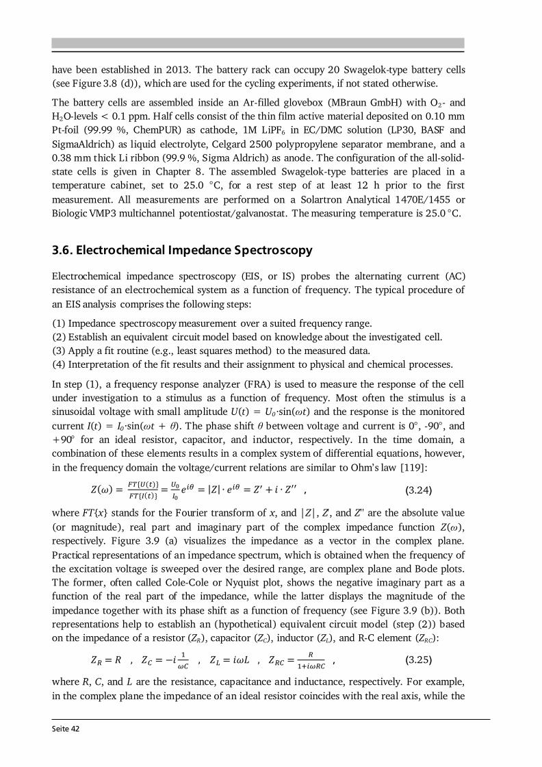
Seite 42
have been established in 2013. The battery rack can occupy 20 Swagelok-type battery cells (see Figure 3.8 (d)), which are used for the cycling experiments, if not stated otherwise. The battery cells are assembled inside an Ar-filled glovebox (MBraun GmbH) with O2- and H2O-levels < 0.1 ppm. Half cells consist of the thin film active material deposited on 0.10 mm Pt-foil (99.99 %, ChemPUR) as cathode, 1M LiPF6 in EC/DMC solution (LP30, BASF and SigmaAldrich) as liquid electrolyte, Celgard 2500 polypropylene separator membrane, and a 0.38 mm thick Li ribbon (99.9 %, Sigma Aldrich) as anode. The configuration of the all-solid-state cells is given in Chapter 8. The assembled Swagelok-type batteries are placed in a temperature cabinet, set to 25.0 °C, for a rest step of at least 12 h prior to the first measurement. All measurements are performed on a Solartron Analytical 1470E/1455 or Biologic VMP3 multichannel potentiostat/galvanostat. The measuring temperature is 25.0 °C. 3.6. Electrochemical Impedance Spectroscopy Electrochemical impedance spectroscopy (EIS, or IS) probes the alternating current (AC) resistance of an electrochemical system as a function of frequency. The typical procedure of an EIS analysis comprises the following steps: (1) Impedance spectroscopy measurement over a suited frequency range. (2) Establish an equivalent circuit model based on knowledge about the investigated cell. (3) Apply a fit routine (e.g., least squares method) to the measured data. (4) Interpretation of the fit results and their assignment to physical and chemical processes. In step (1), a frequency response analyzer (FRA) is used to measure the response of the cell under investigation to a stimulus as a function of frequency. Most often the stimulus is a sinusoidal voltage with small amplitude U(t) = U0·sin(ωt) and the response is the monitored current I(t) = I0·sin(ωt + ). The phase shift between voltage and current is 0°, -90°, and +90° for an ideal resistor, capacitor, and inductor, respectively. In the time domain, a combination of these elements results in a complex system of differential equations, however, in the frequency domain the voltage/current relations are similar to Ohm’s law [119]: , (3.24) where FT{x} stands for the Fourier transform of x, and |Z|, Z', and Z'' are the absolute value (or magnitude), real part and imaginary part of the complex impedance function Z(ω), respectively. Figure 3.9 (a) visualizes the impedance as a vector in the complex plane. Practical representations of an impedance spectrum, which is obtained when the frequency of the excitation voltage is sweeped over the desired range, are complex plane and Bode plots. The former, often called Cole-Cole or Nyquist plot, shows the negative imaginary part as a function of the real part of the impedance, while the latter displays the magnitude of the impedance together with its phase shift as a function of frequency (see Figure 3.9 (b)). Both representations help to establish an (hypothetical) equivalent circuit model (step (2)) based on the impedance of a resistor (ZR), capacitor (ZC), inductor (ZL), and R-C element (ZRC): , (3.25) where R, C, and L are the resistance, capacitance and inductance, respectively. For example, in the complex plane the impedance of an ideal resistor coincides with the real axis, while the
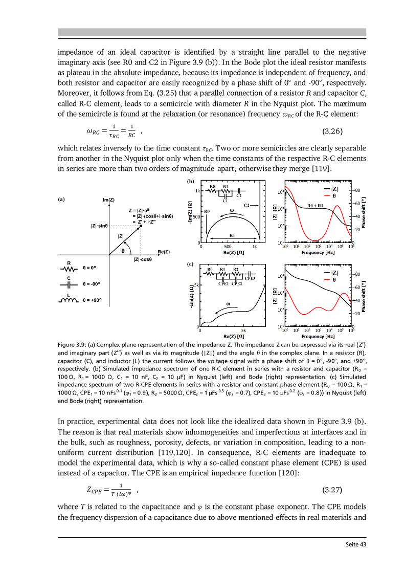
Seite 43
impedance of an ideal capacitor is identified by a straight line parallel to the negative imaginary axis (see R0 and C2 in Figure 3.9 (b)). In the Bode plot the ideal resistor manifests as plateau in the absolute impedance, because its impedance is independent of frequency, and both resistor and capacitor are easily recognized by a phase shift of 0° and -90°, respectively. Moreover, it follows from Eq. (3.25) that a parallel connection of a resistor R and capacitor C, called R-C element, leads to a semicircle with diameter R in the Nyquist plot. The maximum of the semicircle is found at the relaxation (or resonance) frequency ωRC of the R-C element: , (3.26) which relates inversely to the time constant RC. Two or more semicircles are clearly separable from another in the Nyquist plot only when the time constants of the respective R-C elements in series are more than two orders of magnitude apart, otherwise they merge [119].
Figure 3.9: (a) Complex plane representation of the impedance Z. The impedance Z can be expressed via its real (Z’) and imaginary part (Z’’) as well as via its magnitude (|Z|) and the angle θ in the complex plane. In a resistor (R), capacitor (C), and inductor (L) the current follows the voltage signal with a phase shift of θ = 0°, -90°, and +90°, respectively. (b) Simulated impedance spectrum of one R-C element in series with a resistor and capacitor (R0 = 100 Ω, R1 = 1000 Ω, C1 = 10 nF, C2 = 10 μF) in Nyquist (left) and Bode (right) representation. (c) Simulated impedance spectrum of two R-CPE elements in series with a resistor and constant phase element (R0 = 100 Ω, R1 = 1000 Ω, CPE1 = 10 nFs-0.1 (φ1 = 0.9), R2 = 5000 Ω, CPE2 = 1 μFs-0.3 (φ2 = 0.7), CPE3 = 10 μFs-0.2 (φ3 = 0.8)) in Nyquist (left) and Bode (right) representation. In practice, experimental data does not look like the idealized data shown in Figure 3.9 (b). The reason is that real materials show inhomogeneities and imperfections at interfaces and in the bulk, such as roughness, porosity, defects, or variation in composition, leading to a non-uniform current distribution [119,120]. In consequence, R-C elements are inadequate to model the experimental data, which is why a so-called constant phase element (CPE) is used instead of a capacitor. The CPE is an empirical impedance function [120]: , (3.27) where T is related to the capacitance and φ is the constant phase exponent. The CPE models the frequency dispersion of a capacitance due to above mentioned effects in real materials and
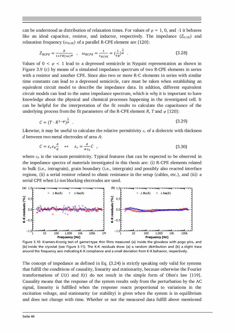
Seite 44
can be understood as distribution of relaxation times. For values of φ = 1, 0, and -1 it behaves like an ideal capacitor, resistor, and inductor, respectively. The impedance (ZR CPE) and relaxation frequency (ωRCPE) of a parallel R-CPE element are [120]: . (3.28) Values of 0 < φ < 1 lead to a depressed semicircle in Nyquist representation as shown in Figure 3.9 (c) by means of a simulated impedance spectrum of two R-CPE elements in series with a resistor and another CPE. Since also two or more R-C elements in series with similar time constants can lead to a depressed semicircle, care must be taken when establishing an equivalent circuit model to describe the impedance data. In addtion, different equivalent circuit models can lead to the same impedance spectrum, which is why it is important to have knowledge about the physical and chemical processes happening in the investigated cell. It can be helpful for the interpretation of the fit results to calculate the capacitance of the underlying process from the fit parameters of the R-CPE element R, T and φ [120]: . (3.29) Likewise, it may be useful to calculate the relative permittivity r of a dielectric with thickness d between two metal electrodes of area A: , (3.30) where 0 is the vacuum permittivity. Typical features that can be expected to be observed in the impedance spectra of materials investigated in this thesis are: (i) R-CPE elements related to bulk (i.e., intragrain), grain boundary (i.e., intergrain) and possibly also reacted interface regions, (ii) a serial resistor related to ohmic resistance in the setup (cables, etc.), and (iii) a serial CPE when Li-ion blocking electrodes are used.
Figure 3.10: Kramers-Kronig test of garnet-type thin films measured (a) inside the glovebox with pogo pins, and (b) inside the cryostat (see Figure 3.11). The K-K residuals show (a) a random distribution and (b) a slight trace around the frequency axis indicating K-K compliance and a small deviation from K-K behavior, respectively. The concept of impedance as defined in Eq. (3.24) is strictly speaking only valid for systems that fulfill the conditions of causality, linearity and stationarity, because otherwise the Fourier transformations of U(t) and I(t) do not result in the simple form of Ohm’s law [119]. Causality means that the response of the system results only from the perturbation by the AC signal, linearity is fulfilled when the response reacts proportional to variations in the excitation voltage, and stationarity (or stability) is given when the system is in equilibrium and does not change with time. Whether or not the measured data fulfill above mentioned

Seite 45
conditions can be checked by the Kramers-Kronig test [121,122]. The test relies on the Kramers-Kronig (K-K) relations, which connect real and imaginary parts of any complex function that is analytic in the upper half of the complex plane (for details see [123]). This means that the real part Z' can be calculated from the imaginary part Z'' and vice versa: ∫ ∫ (3.31) given that Z' and Z'' are known over the total frequency domain and that the above mentioned conditions of causality, linearity and stability are fulfilled. A frequency range from zero to infinity cannot be accessed experimentally, however, Boukamp [122] developed a method to perform the Kramers-Kronig test on impedance data in a limited frequency region. The method is implemented in a computer program [121,122,124], which is used to calculate the K-K residuals of impedance data on garnet-type thin films (Figure 3.10). The K-K residuals are defined as relative difference between the original and the K-K transformed data of real and imaginary part of the impedance function and are a measure for the K-K compliance. In case the residuals show a random distribution around the frequency axis the data is K-K compliant, whereas a systematic trace indicates deviations from K-K behavior [122]. Compliance with the Kramers-Kronig test is typically observed for impedance data of garnet-type thin films measured inside the glovebox (see Figure 3.10 (a)), however, when measured inside the cryostat a small deviation from K-K behavior is found (see Figure 3.10 (b)). It is assumed that a systematic error is introduced by the measurement system of the cryostat, possibly caused by the temperature control system and/or by the comparatively large voltage amplitude of 50 mV leading to a violation of the stationarity and/or linearity condition, respectively. Nevertheless, based on the quite small residuals of less than 0.2 % it is concluded that the quality of the impedance data discussed in this thesis is good. Considerations on Measurement Geometry, Frequency and Impedance Range Preliminary considerations on the measurement geometry, the accessible frequency and expected impedance range are useful in order to perform expedient EIS measurements. Two possible measurement geometries suited for the investigation of the Li-ion conductivity in solid electrolyte thin films are through-plane and in-plane (see Figure 3.11 (a)). In through-plane measurements the solid electrolyte is sandwiched between two opposite contacts, one being the conductive substrate (bottom contact), the other a deposited metal (top contact). The in-plane geometry makes use of two top contacts running in parallel to each other and requires the substrtate to be insulating with respect to the solid electrolyte in order to obtain meaningful results. The two geometries have significantly different d/A ratios, also called cell constant or geometric factor. The through-plane geometric factor is of the order of 1·10-3 cm-1 (dt ~ 1 μm, At ~ 0.1 cm2), whereas the in-plane geometric factor is of the order of 1·103 cm-1 (di ~ 1 mm, Ai ~ 1 μm · 1 cm). As a result, the two geometries lead to impedances that are by 6 orders of magnitude apart from each other (see Eq. (2.22)). The expected impedance range of garnet solid electrolyte thin films investigated in this thesis is given in Table 3.1, assuming a Li-ion conductivity at 25 °C between 10-6 S·cm-1 and 10-3 S·cm-1 as observed for tetragonal and cubic (bulk) garnets [25]. Impedances as low as 1 Ω are difficult to differentiate from the impedance of the measurement setup, while impedances as high as 1 GΩ exceed the capabilities of the used FRAs. This means that, at 25 °C, thin films with low and high ionic conductivities should be measured via through-plane and in-plane geometries, respectively. Since there is little wiggle room in adjusting the geometric factor (see later this section) the
Seite 46
most effective way to bring the impedance in a well accessible range is by a change in temperature, i.e. cooling for through-plane and heating for in-plane measurements.
Figure 3.11: (a) Illustration of through-plane (left) and in-plane (right) measurement geometries. In-plane measurements require the substrate to be insulating with respect to the solid electrolyte. (b) Microcontact impedance spectroscopy setup established in the course of this thesis. The micropositioner and a flat Si 3N4 heater are flexible in their use, e.g. inside or outside the glovebox, and exchangeable probe tips allow through-plane and in-plane EIS measurements of structure sizes down to 100 μm. (c) Cryostat used for temperature dependent EIS measurements in through-plane geometry. The insets show a magnification of the sample stage in mounting (lower image) and measurement (upper image) position. In order to contact the solid electrolyte thin film deposited on Pt-foil reliably and without mechanical damage from the macrocontact a thin Cu spacer is used. The frequency range to be chosen in EIS can be estimated based on the relaxation frequencies that are present in the sample under investigation. The highest relaxation frequency is usually observed for the grain interior (bulk ionic conduction) [119]. Substituting the values of R (Eq. (2.22)) and C (Eq. (3.30)) in Eq. (3.26) shows that the frequency depends on the relative permittivity and the ionic conductivity only. Assuming r = 50, as reported for garnet-type LLZrO [125], leads to resonance frequencies of 36 MHz and 36 kHz to be expected for Li-ion conductivities of 10-3 S·cm-1 and 10-6 S·cm-1 at 25 °C, respectively (see Table 3.1). The former value lies outside the specified frequency range of the FRAs used in this thesis, so that thin films with high ionic conductivities need to be measured at temperatures below 25 °C. The low frequency region is limited by practical considerations rather than device limitations, because frequencies much below 1 Hz need extremely long integration times.
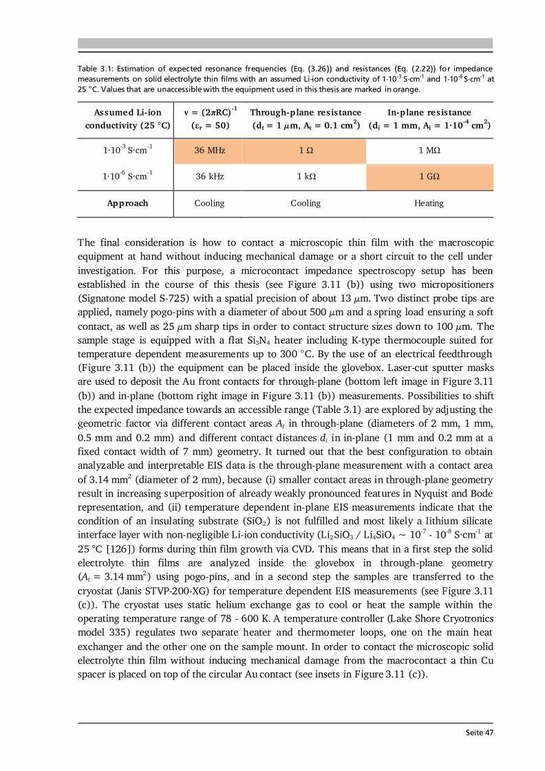
Seite 47
Table 3.1: Estimation of expected resonance frequencies (Eq. (3.26)) and resistances (Eq. (2.22)) for impedance measurements on solid electrolyte thin films with an assumed Li -ion conductivity of 1·10 -3 S·cm-1 and 1·10 -6 S·cm-1 at 25 °C. Values that are unaccessible with the equipment used in this thesis are marked in orange. Assumed Li-ion conductivity (25 °C) ν = (2πRC)-1 (εr = 50) Through-plane resistance (dt = 1 μm, At = 0.1 cm2) In-plane resistance (di = 1 mm, Ai = 1·10-4 cm2)
1·10-3 S·cm-1 36 MHz 1 Ω 1 MΩ 1·10-6 S·cm-1 36 kHz 1 kΩ 1 GΩ Approach Cooling Cooling Heating
The final consideration is how to contact a microscopic thin film with the macroscopic equipment at hand without inducing mechanical damage or a short circuit to the cell under investigation. For this purpose, a microcontact impedance spectroscopy setup has been established in the course of this thesis (see Figure 3.11 (b)) using two micropositioners (Signatone model S-725) with a spatial precision of about 13 μm. Two distinct probe tips are applied, namely pogo-pins with a diameter of about 500 μm and a spring load ensuring a soft contact, as well as 25 μm sharp tips in order to contact structure sizes down to 100 μm. The sample stage is equipped with a flat Si3N4 heater including K-type thermocouple suited for temperature dependent measurements up to 300 °C. By the use of an electrical feedthrough (Figure 3.11 (b)) the equipment can be placed inside the glovebox. Laser-cut sputter masks are used to deposit the Au front contacts for through-plane (bottom left image in Figure 3.11 (b)) and in-plane (bottom right image in Figure 3.11 (b)) measurements. Possibilities to shift the expected impedance towards an accessible range (Table 3.1) are explored by adjusting the geometric factor via different contact areas At in through-plane (diameters of 2 mm, 1 mm, 0.5 mm and 0.2 mm) and different contact distances di in in-plane (1 mm and 0.2 mm at a fixed contact width of 7 mm) geometry. It turned out that the best configuration to obtain analyzable and interpretable EIS data is the through-plane measurement with a contact area of 3.14 mm2 (diameter of 2 mm), because (i) smaller contact areas in through-plane geometry result in increasing superposition of already weakly pronounced features in Nyquist and Bode representation, and (ii) temperature dependent in-plane EIS measurements indicate that the condition of an insulating substrate (SiO2) is not fulfilled and most likely a lithium silicate interface layer with non-negligible Li-ion conductivity (Li2SiO3 / Li4SiO4 ~ 10-7 - 10-8 S·cm-1 at 25 °C [126]) forms during thin film growth via CVD. This means that in a first step the solid electrolyte thin films are analyzed inside the glovebox in through-plane geometry (At = 3.14 mm2) using pogo-pins, and in a second step the samples are transferred to the cryostat (Janis STVP-200-XG) for temperature dependent EIS measurements (see Figure 3.11 (c)). The cryostat uses static helium exchange gas to cool or heat the sample within the operating temperature range of 78 - 600 K. A temperature controller (Lake Shore Cryotronics model 335) regulates two separate heater and thermometer loops, one on the main heat exchanger and the other one on the sample mount. In order to contact the microscopic solid electrolyte thin film without inducing mechanical damage from the macrocontact a thin Cu spacer is placed on top of the circular Au contact (see insets in Figure 3.11 (c)).
Seite 48
EIS Measurements All EIS measurements on solid electrolyte thin films reported in Chapter 6 are performed inside the cryostat under helium atmosphere. After loading the thin film sample the cryostat is purged with helium (Air Liquide GmbH, 99.999 %) twice. Impedance spectra are recorded on a Solartron Analytical 1260A impedance/gain-phase analyzer over a frequency range of 1 MHz - 1 Hz (50 steps per decade) with 50 mV amplitude. A least squares fit is applied to the impedance data using the software ZView version 3.4b (Scribner Associates). The activation energy is determined from the slope of the Arrhenius plot (Eq. (2.29)). The EIS measurements on the NiO thin film anode reported in Section 7.6.2 are performed in a Swagelok-type battery cell placed in the temperature cabinet (Figure 3.8 (c)) at 25.0 °C. The spectra are recorded on a Solartron Analytical 1455 FRA connected to a 1470E multichannel potentiostat/galvanostat over a frequency range of 600 kHz - 1 Hz (40 steps per decade) with 50 mV amplitude. A least squares fit is applied to the impedance data using the software ZView version 3.4b (Scribner Associates). Also the EIS measurements on the hybrid thin film battery in Section 8.2.3 are performed in a Swagelok-type battery cell at 25.0 °C on the 1470E/1455 CellTest system, but over a frequency range of 1 MHz - 1 Hz (20 steps per decade) with 50 mV amplitude. The EIS investigations on all-solid-state (Swagelok-type) cells in Section 8.3.2 are performed on the Solartron Analytical 1287A potentiostat/galvanostat connected to the 1260A FRA over a frequency range of 1 MHz - 1 Hz (50 steps per decade) with 20 mV amplitude. 3.7. Further Analytical Methods Atomic Force Microscopy (AFM) The topography of two Li5La3Ta2O12 thin film solid electrolytes (see Section 6.4.3) is probed by an Oxford Instruments Asylum Research MFP-3D atomic force microscope, operated with HQ:NSC19/AL BS (MikroMasch Europe) probe tips in non-contact mode. Inductively Coupled Plasma Optical Emission Spectroscopy (ICP-OES) The Li to Co molar ratio of four LiCoO2 thin film cathodes is determined by ICP-OES (see Section 5.3). ICP-OES is used complementary to the XPS analysis, because the former averages over the entire volume of the film, while the latter only probes its surface. The analysis was done by Mikroanalytisches Labor Pascher. The mass of the LiCoO2 provided for analysis was in the range of 50 - 100 g. Fourier Transform Infrared Spectroscopy (FTIR) The precursor materials used for the LA-CVD are investigated via FTIR for their absorbance in the excitation range of the CO2-laser (see Section 4.4.1). About 1 mg of metal- -diketonate precursor is mixed with about 100 mg of KBr and pressed into a pellet. Additionally, a KBr pellet (without precursor) is produced in the same way, which is needed for background measurement and substraction. The FTIR spectra are recorded in a range of 400 - 4000 cm-1 with a step size of 4 cm-1 using a Bruker Vertex 70 spectrometer (Bruker, USA).
Seite 49
Rutherford Backscattering Spectroscopy (RBS) The Li5La3Ta2O12 thin film solid electrolyte grown at 973 K, 20 mbar (see Section 6.4.2) is analyzed by RBS using a 3 MeV H+ beam. The beam is focused to about 8 μm by 4 μm and scanned over the sample with a size of about 250 μm by 250 μm. The silicon strip detector is positioned at a scattering angle of 174°. The RBS spectrum is fit using the program NDF [127]. The collisions of ions on the target atoms are elastic scattering based on Coulomb repulsion. In first order, the cross-sections in this Rutherford regime scale with the atomic number squared making RBS analysis more sensitive for heavy elements. Because the collisions of protons on light elements are non-Rutherford, experimental cross-sections for Li [128], C [129] and O [129] are used. The data are retrieved from the IBANDL database [130]. The advantage of these non-Rutherford cross-sections is that they are much higher than the Rutherford cross-sections making the analysis possible but still difficult. The following four layer model is adopted for the fit: (1) surface layer of Li2CO3, (2) main layer of LixLay1Tay2Oz, (3) interface layer of Li2PtO3, and (4) Pt-substrate. Time of Flight Secondary Ion Mass Spectroscopy (ToF-SIMS) The ToF-SIMS study in Section 6.3.3 is performed on a TOF.SIMS5 instrument (ION-TOF GmbH), equipped with a Bi cluster liquid metal primary ion source and a non-linear time of flight analyzer. The Bi source is operated in the “bunched” mode providing 0.7 ns Bi1+ ion pulses at 25 keV energy. The analyzed area is 100 μm by 100 μm, and the lateral resolution approximately 4 µm. For data acquisition and processing the ION-TOF SurfaceLab 6 software is used. Negative polarity spectra are calibrated on the C-, C2-, C3-, and C4- peaks. Sputter depth profiles are performed using a 2 keV Cs+ ion beam and a raster size of 500 μm by 500 μm with a beam current of 145 nA.

Seite 50
Seite 51
4 Experimental Implementation Selected parts of Section 4.4 and 4.5 are published in [131–133] and [134,135], respectively. Within the framework of this thesis small modifications are included.
4.1. Choice and Preparation of Substrates In this thesis, mainly Si(100) wafers from CrysTec GmbH and Pt-foil from ChemPur GmbH are used as substrates. The Si(100) wafers have a thickness of 275 μm, are single-side polished, have a protective photoresist, and are formatted into pieces of 5 mm x 10 mm as well as 10 mm x 10 mm (see Figure 4.1 (a)). The main purpose of using silicon substrates is to analyze the microstructure of the grown thin films in SEM, because cleavage of the silicon is easily possible resulting in a clear edge to image the cross-section. Moreover, Si(100) wafers are relatively cheap and therefore are used for extensive studies of the growth parameters. The Pt-foil is typically ordered with an area of 50 mm x 50 mm, a thickness of 100 μm and a purity of 99.99 %. This represents the best economic and scientific compromise in terms of cost and handling of the substrates. Smaller pieces of 5 mm x 10 mm and 10 mm x 10 mm are either cut with a pair of scissors or, preferably, formatted by laser (Trumpf TruMicro 5000, available at the INT in Karlsruhe). The main purpose of a metallic substrate is its direct use as (i) current collector in cycling experiments, and (ii) contact in impedance spectroscopy. The main advantage of rather expensive platinum substrates is their superior chemical stability compared to other, cheaper metal substrates (e.g., Ti) under the growth conditions used in both chemical vapor deposition techniques in this thesis. For testing purposes many other substrates have been examined within this PhD studies. Even though results achieved with these substrates are not directly incorporated into this thesis, they still contributed to its success and shall therefore be briefly introduced: (1) Platinized Si-wafers (so-called GMEK wafers) from GMEK Inc., which have a stacking sequence of 525 μm p-type Si | 300 nm SiO2 | 20 nm TiO2 | 150 nm Pt(111). Their intended use is to combine the advantages of the Si-wafer (easy cleavage for cross-sectional imaging via SEM) and Pt-foil (electrical contact). The drawback is the need for a TiO2 adhesive agent between Si and Pt. At times it happened that the Pt layer peeled off (during ultrasonication or after cleavage), and that Ti diffused through the Pt layer (at deposition temperatures 800 °C). (2) Ti-, Ta-, Nb- and W-foils (as cheap alternatives to Pt) and also Au-foil (for corrosion tests towards Li) were tested, but they altogether showed a higher amount of substrate-related secondary phases during cathode and solid electrolyte growth in comparison to Pt-foil. (3) MgO(100) single crystals were examined as possible insulating substrate for in-plane IS measurements of solid electrolyte films. While the MgO reacted only slightly during
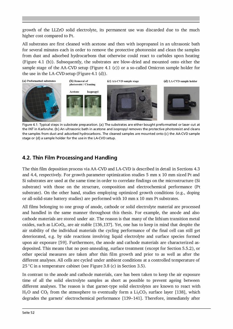
Seite 52
growth of the LLZrO solid electrolyte, its permanent use was discarded due to the much higher cost compared to Pt. All substrates are first cleaned with acetone and then with isopropanol in an ultrasonic bath for several minutes each in order to remove the protective photoresist and clean the samples from dust and adsorbed hydrocarbons that otherwise could react to carbides upon heating (Figure 4.1 (b)). Subsequently, the substrates are blow-dried and mounted onto either the sample stage of the AA-CVD setup (Figure 4.1 (c)) or a so-called Omicron sample holder for the use in the LA-CVD setup (Figure 4.1 (d)).
Figure 4.1: Typical steps in substrate preparation. (a) The substrates are either bought preformatted or laser-cut at the INT in Karlsruhe. (b) An ultrasonic bath in acetone and isopropyl removes the protective photoresist and cleans the samples from dust and adsorbed hydrocarbons. The cleaned samples are mounted onto (c) the AA-CVD sample stage or (d) a sample holder for the use in the LA-CVD setup.
4.2. Thin Film Processing and Handling The thin film deposition process via AA-CVD and LA-CVD is described in detail in Sections 4.3 and 4.4, respectively. For growth parameter optimization studies 5 mm x 10 mm sized Pt and Si substrates are used at the same time in order to correlate findings on the microstructure (Si substrate) with those on the structure, composition and electrochemical performance (Pt substrate). On the other hand, studies employing optimized growth conditions (e.g., doping or all-solid-state battery studies) are performed with 10 mm x 10 mm Pt substrates. All films belonging to one group of anode, cathode or solid electrolyte material are processed and handled in the same manner throughout this thesis. For example, the anode and also cathode materials are stored under air. The reason is that many of the lithium transition metal oxides, such as LiCoO2, are air stable [136,137]. Yet, one has to keep in mind that despite the air stability of the individual materials the cycling performance of the final cell can still get deteriorated, e.g. by side reactions involving liquid electrolyte and surface species formed upon air exposure [59]. Furthermore, the anode and cathode materials are characterized as-deposited. This means that no post-annealing, surface treatment (except for Section 5.5.2), or other special measures are taken after thin film growth and prior to as well as after the different analyses. All cells are cycled under ambient conditions at a controlled temperature of 25 °C in a temperature cabinet (see Figure 3.8 (c) in Section 3.5). In contrast to the anode and cathode materials, care has been taken to keep the air exposure time of all the solid electrolyte samples as short as possible to prevent ageing between different analyses. The reason is that garnet-type solid electrolytes are known to react with H2O and CO2 from the atmosphere to eventually form a Li2CO3 surface layer [138], which degrades the garnets’ electrochemical performance [139–141]. Therefore, immediately after
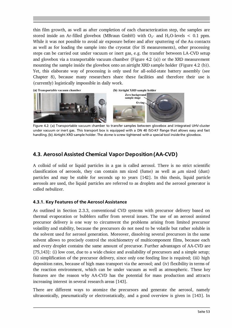
Seite 53
thin film growth, as well as after completion of each characterization step, the samples are stored inside an Ar-filled glovebox (MBraun GmbH) with O2- and H2O-levels < 0.1 ppm. While it was not possible to avoid air exposure before and after sputtering of the Au contacts as well as for loading the sample into the cryostat (for IS measurements), other processing steps can be carried out under vacuum or inert gas, e.g. the transfer between LA-CVD setup and glovebox via a transportable vacuum chamber (Figure 4.2 (a)) or the XRD measurement mounting the sample inside the glovebox onto an airtight XRD sample holder (Figure 4.2 (b)). Yet, this elaborate way of processing is only used for all-solid-state battery assembly (see Chapter 8), because many researchers share these facilities and therefore their use is (currently) logistically impossible in daily work.
Figure 4.2: (a) Transportable vacuum chamber to transfer samples between glovebox and integrated UHV-cluster under vacuum or inert gas. This transport box is equipped with a DN 40 ISO-KF flange that allows easy and fast handling. (b) Airtight XRD sample holder. The dome is screw tightened with a special tool inside the glovebox.
4.3. Aerosol Assisted Chemical Vapor Deposition (AA-CVD) A colloid of solid or liquid particles in a gas is called aerosol. There is no strict scientific classification of aerosols, they can contain nm sized (fume) as well as μm sized (dust) particles and may be stable for seconds up to years [142]. In this thesis, liquid particle aerosols are used, the liquid particles are referred to as droplets and the aerosol generator is called nebulizer. 4.3.1. Key Features of the Aerosol Assistance As outlined in Section 2.3.3, conventional CVD systems with precursor delivery based on thermal evaporation or bubblers suffer from several issues. The use of an aerosol assisted precursor delivery is one way to circumvent the problems arising from limited precursor volatility and stability, because the precursors do not need to be volatile but rather soluble in the solvent used for aerosol generation. Moreover, dissolving several precursors in the same solvent allows to precisely control the stoichiometry of multicomponent films, because each and every droplet contains the same amount of precursor. Further advantages of AA-CVD are [75,143]: (i) low cost, due to a wide choice and availability of precursors and a simple setup; (ii) simplification of the precursor delivery, since only one feeding line is required; (iii) high deposition rates, because of high mass transport via the aerosol; and (iv) flexibility in terms of the reaction environment, which can be under vacuum as well as atmospheric. These key features are the reason why AA-CVD has the potential for mass production and attracts increasing interest in several research areas [143]. There are different ways to atomize the precursors and generate the aerosol, namely ultrasonically, pneumatically or electrostatically, and a good overview is given in [143]. In
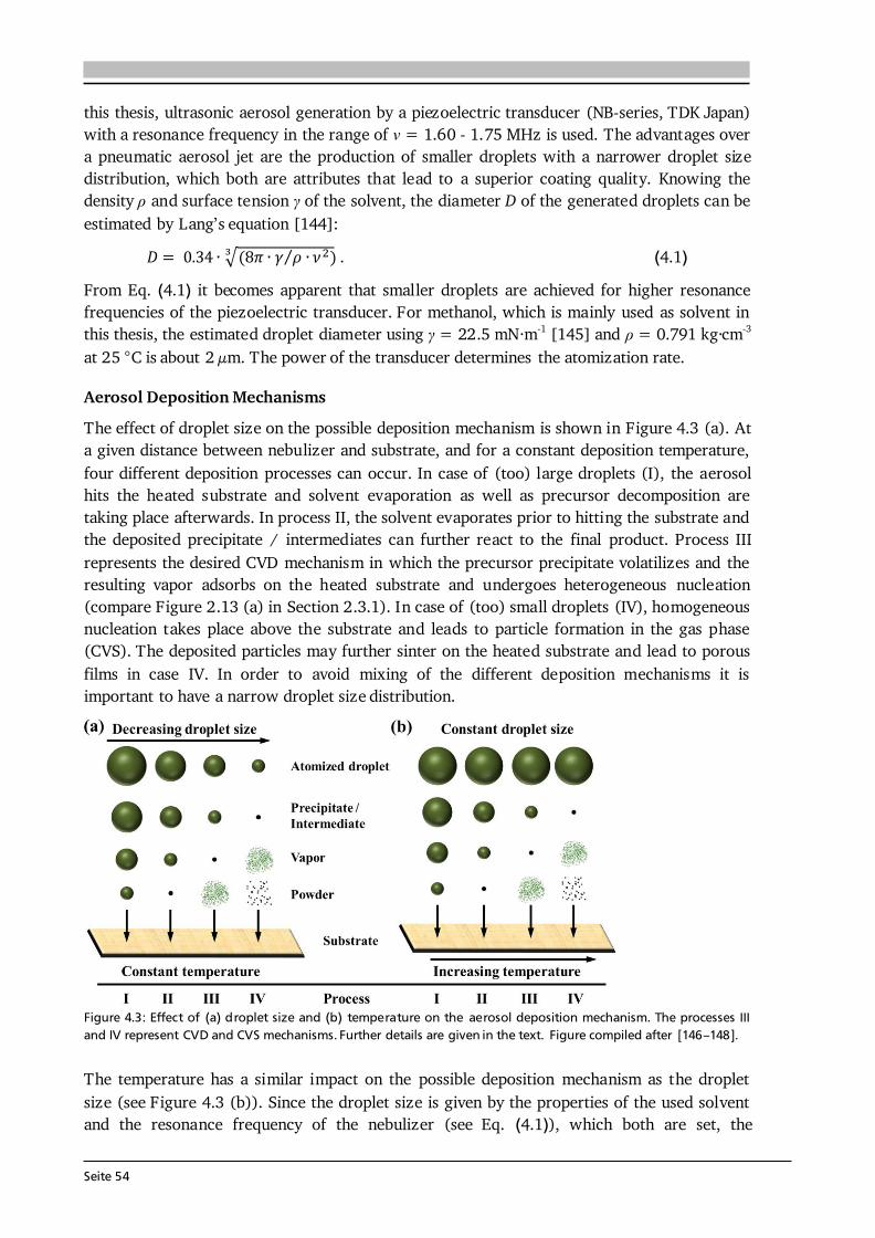
Seite 54
this thesis, ultrasonic aerosol generation by a piezoelectric transducer (NB-series, TDK Japan) with a resonance frequency in the range of ν = 1.60 - 1.75 MHz is used. The advantages over a pneumatic aerosol jet are the production of smaller droplets with a narrower droplet size distribution, which both are attributes that lead to a superior coating quality. Knowing the density ρ and surface tension of the solvent, the diameter D of the generated droplets can be estimated by Lang’s equation [144]: √ ⁄ . (4.1) From Eq. (4.1) it becomes apparent that smaller droplets are achieved for higher resonance frequencies of the piezoelectric transducer. For methanol, which is mainly used as solvent in this thesis, the estimated droplet diameter using = 22.5 mN·m-1 [145] and ρ = 0.791 kg·cm-3 at 25 °C is about 2 μm. The power of the transducer determines the atomization rate. Aerosol Deposition Mechanisms The effect of droplet size on the possible deposition mechanism is shown in Figure 4.3 (a). At a given distance between nebulizer and substrate, and for a constant deposition temperature, four different deposition processes can occur. In case of (too) large droplets (I), the aerosol hits the heated substrate and solvent evaporation as well as precursor decomposition are taking place afterwards. In process II, the solvent evaporates prior to hitting the substrate and the deposited precipitate / intermediates can further react to the final product. Process III represents the desired CVD mechanism in which the precursor precipitate volatilizes and the resulting vapor adsorbs on the heated substrate and undergoes heterogeneous nucleation (compare Figure 2.13 (a) in Section 2.3.1). In case of (too) small droplets (IV), homogeneous nucleation takes place above the substrate and leads to particle formation in the gas phase (CVS). The deposited particles may further sinter on the heated substrate and lead to porous films in case IV. In order to avoid mixing of the different deposition mechanisms it is important to have a narrow droplet size distribution.
Figure 4.3: Effect of (a) droplet size and (b) temperature on the aerosol deposition mechanism. The processes III and IV represent CVD and CVS mechanisms. Further details are given in the text. Figure compiled after [146–148]. The temperature has a similar impact on the possible deposition mechanism as the droplet size (see Figure 4.3 (b)). Since the droplet size is given by the properties of the used solvent and the resonance frequency of the nebulizer (see Eq. (4.1)), which both are set, the
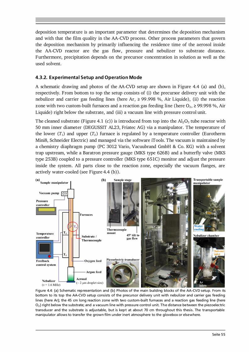
Seite 55
deposition temperature is an important parameter that determines the deposition mechanism and with that the film quality in the AA-CVD process. Other process parameters that govern the deposition mechanism by primarily influencing the residence time of the aerosol inside the AA-CVD reactor are the gas flow, pressure and nebulizer to substrate distance. Furthermore, precipitation depends on the precursor concentration in solution as well as the used solvent. 4.3.2. Experimental Setup and Operation Mode A schematic drawing and photos of the AA-CVD setup are shown in Figure 4.4 (a) and (b), respectively. From bottom to top the setup consists of (i) the precursor delivery unit with the nebulizer and carrier gas feeding lines (here Ar, 99.998 %, Air Liquide), (ii) the reaction zone with two custom-built furnaces and a reaction gas feeding line (here O2, 99.998 %, Air Liquide) right below the substrate, and (iii) a vacuum line with pressure control unit. The cleaned substrate (Figure 4.1 (c)) is introduced from top into the Al2O3 tube reactor with 50 mm inner diameter (DEGUSSIT AL23, Friatec AG) via a manipulator. The temperature of the lower (T1) and upper (T2) furnace is regulated by a temperature controller (Eurotherm Mini8, Schneider Electric) and managed via the software iTools. The vacuum is maintained by a chemistry diaphragm pump (PC 3012 Vario, Vacuubrand GmbH & Co. KG) with a solvent trap upstream, while a Baratron pressure gauge (MKS type 626B) and a butterfly valve (MKS type 253B) coupled to a pressure controller (MKS type 651C) monitor and adjust the pressure inside the system. All parts close to the reaction zone, especially the vacuum flanges, are actively water-cooled (see Figure 4.4 (b)).
Figure 4.4: (a) Schematic representation and (b) Photos of the main building blocks of the AA-CVD setup. From its bottom to its top the AA-CVD setup consists of the precursor delivery unit with nebulizer and carrier gas feeding lines (here Ar); the 45 cm long reaction zone with two custom-built furnaces and a reaction gas feeding line (here O2) right below the substrate; and a vacuum line with pressure control unit. The distance between the piezoelectric transducer and the substrate is adjustable, but is kept at about 70 cm throughout this thesis. The transportable manipulator allows to transfer the grown film under inert atmosphere to the glovebox or elsewhere.
Seite 56
Feedback Control System The core of the AA-CVD setup is the feedback control system, which couples the power of the nebulizer to the substrate temperature TS, which is also referred to as deposition temperature. After mounting the sample and heating up the reaction zone to its setpoint (e.g., T1 = T2 = 800 °C) the substrate is at a lower temperature than the furnaces (~ 50 - 100 °C depending on T1, T2). In order to start an automatically controlled thin film deposition, the setpoint for TS is chosen in such a way that TS > T1, T2 holds (e.g., TS = 850 °C). The temperature controller then starts to power the nebulizer, which generates the aerosol. The aerosol is transported into the reaction zone by the carrier gas and the applied vacuum. Inside the reactor, the solvent (here methanol) combusts with the reaction gas and releases a significant amount of combustion heat. This leads to an increase of the substrate temperature and as soon as TS reaches the setpoint, defined as deposition temperature, the feedback control system throttles the power applied to the nebulizer and with that reduces the aerosol flux. As a result of the reduced flux, hence combustion heat, the sample holder slowly cools down. Once TS falls below the setpoint the feedback loop starts over again. Depending on the used process parameters it takes about 3 - 5 min until steady state is reached, i.e. the deposition temperature fluctuates by less than 5 °C, or in the given example TS = (850 ± 2) °C. The feedback control system ensures a highly reliable and reproducible thin film growth via this custom-built AA-CVD setup. Typical Growth Parameters More than 85 thin film depositions via AA-CVD build the foundation of this thesis, and a typical range of process parameters is listed in Table 2.2 in Section 2.3.3. More than half of the depositions can be considered as pilot study. Its outcome is a set of certain growth parameters that turned out to be best suited for the reliable and reproducible growth of thin films for Li-ion battery application via the custom-built AA-CVD setup. In short, criteria such as the stability of the vacuum and the feedback control system, precision of the gas flow, purity of the atmosphere inside the reactor as well as the aerosol deposition mechanism (Section 4.3.1) have been considered. The resultant growth parameters are a pressure of p = 900 mbar, a gas flow of QAr = 15 slm and QO2 = 3 slm, equal furnace temperatures TF = T1 = T2, a temperature difference of ΔT = TS - TF = 50 °C and a nebulizer (i.e., piezoelectric transducer) to substrate distance of about 70 cm. In case deviations from this set of growth parameters are used, they are explicitly mentioned, justified and discussed. Furthermore, from the pilot study it is known that the deposition temperature (= TS or just T) as well as the precursor concentration c have the strongest impact on microstructure and phase composition of the deposited films and therefore are the main growth parameters optimized in this thesis. Table 4.1 provides an overview of precursor materials and solvents used for cathode, solid electrolyte and anode thin film deposition. Stoichiometric amounts of precursor are dissolved in methanol and in case of the cathode materials a lithium excess of 20 % is used. For depositions of solid electrolyte and cathode films the concentration refers to the total amount of metal ions and transition metal ions in the precursor solution, respectively. The La-acac precursor could not be dissolved in methanol, so that La-nitrate dissolved in small amounts of deionized water was used instead and added to the precursor solution. At the beginning of the deposition about 50 ml of precursor solution can be filled into the nebulizer chamber by a syringe and, depending on the desired film thickness and aerosol generation rate, the
Seite 57
chamber has to be refilled once in a while. As an example, a typical deposition at 850 °C consumes 80 ml of precursor solution in 50 min resulting in a spray rate of 1.6 ml·min-1. Table 4.1: Precursor materials and solvents used for cathode, solid electrolyte and anode thi n film deposition via AA-CVD. The supplier of the La-nitrate precursor is Alfa Aesar and all other chemicals are from Sigma Aldrich.
Precursor Purity [%] Solvent Application Li-acac 97 Methanol, ≥ 99.8 % Cathode & Solid electrolyte
Co(III)-(acac)3 98 Methanol, ≥ 99.8 % Cathode & Anode Ni(II)-(acac)2 95 Methanol, ≥ 99.8 % Cathode & Anode Mn(II)-(acac)2 98 Methanol, ≥ 99.8 % Cathode & Anode
La(III)-(NO3)3·6H2O 99 Water, deionized Solid electrolyte Zr(IV)-(acac)4 97 Methanol, ≥ 99.8 % Solid electrolyte
4.4. CO2-Laser Assisted Chemical Vapor Deposition (LA-CVD) CO2-laser assisted chemical vapor deposition is based on an innovative precursor delivery system using laser flash evaporation of solid metalorganic precursors. So far, non-equilibrium flash evaporation as precursor delivery has only been used to produce nanocrystalline multinary oxide particles by CVS [149,150], but not to produce thin films via CVD. The LA-CVD method introduced in this thesis shall not be mistaken for “laser-assistance” in photo-assisted CVD (PA-CVD). In PA-CVD a laser (or other light source) is used to modify the deposition kinetics by photocatalytic or photothermal processes [35,75], thus it is used to lower the deposition temperature in the reaction zone and not for the purpose of precursor delivery. 4.4.1. Key Features of the CO2-Laser Assistance The LA-CVD process is illustrated in Figure 4.5 (a). Metalorganic precursors (green and blue) absorb the energy of the CO2-laser (yellow), evaporate instantaneously, are transported by carrier gas (purple) and the applied vacuum, decompose and react at the heated substrate (orange). Optionally, a reaction gas (red) can be fed into the LA-CVD reactor. The precondition for a precursor material to be used in LA-CVD is a non-zero absorbance at the CO2-laser wavelength of about 10.6 μm corresponding to a wavenumber of 943 cm-1. This requirement is fulfilled by several organic groups, thus a variety of precursors are available to the LA-CVD approach. The active medium of a CO2-laser is a gas mixture of He, N2 and CO2. A simplified energy-level diagram of relevant states in the CO2-laser medium is shown in Figure 4.5 (b). Via glow discharge the gases are excited, however, the direct electronic excitation of CO2 molecules to the upper energy levels is negligible [151]. Instead, the vibrational mode 3 (and multiples
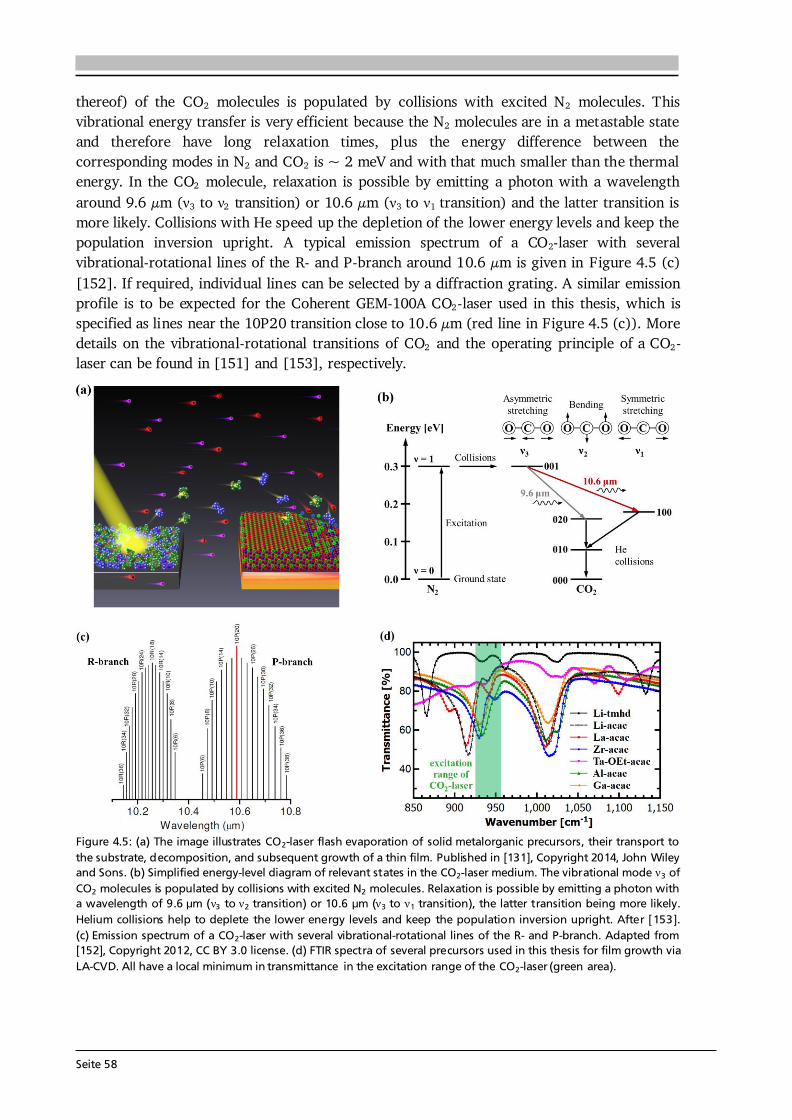
Seite 58
thereof) of the CO2 molecules is populated by collisions with excited N2 molecules. This vibrational energy transfer is very efficient because the N2 molecules are in a metastable state and therefore have long relaxation times, plus the energy difference between the corresponding modes in N2 and CO2 is ~ 2 meV and with that much smaller than the thermal energy. In the CO2 molecule, relaxation is possible by emitting a photon with a wavelength around 9.6 μm ( 3 to 2 transition) or 10.6 μm ( 3 to 1 transition) and the latter transition is more likely. Collisions with He speed up the depletion of the lower energy levels and keep the population inversion upright. A typical emission spectrum of a CO2-laser with several vibrational-rotational lines of the R- and P-branch around 10.6 μm is given in Figure 4.5 (c) [152]. If required, individual lines can be selected by a diffraction grating. A similar emission profile is to be expected for the Coherent GEM-100A CO2-laser used in this thesis, which is specified as lines near the 10P20 transition close to 10.6 μm (red line in Figure 4.5 (c)). More details on the vibrational-rotational transitions of CO2 and the operating principle of a CO2-laser can be found in [151] and [153], respectively.
Figure 4.5: (a) The image illustrates CO2-laser flash evaporation of solid metalorganic precursors, their transport to the substrate, decomposition, and subsequent growth of a thin film. Published in [131], Copyright 2014, John Wiley and Sons. (b) Simplified energy-level diagram of relevant states in the CO2-laser medium. The vibrational mode 3 of CO2 molecules is populated by collisions with excited N2 molecules. Relaxation is possible by emitting a photon with a wavelength of 9.6 μm ( 3 to 2 transition) or 10.6 μm ( 3 to 1 transition), the latter transition being more likely. Helium collisions help to deplete the lower energy levels and keep the population inversion upright. After [153]. (c) Emission spectrum of a CO2-laser with several vibrational-rotational lines of the R- and P-branch. Adapted from [152], Copyright 2012, CC BY 3.0 license. (d) FTIR spectra of several precursors used in this thesis for film growth via LA-CVD. All have a local minimum in transmittance in the excitation range of the CO2-laser (green area).
Seite 59
Fourier-transform infrared spectroscopy (FTIR) provides an easy and fast checkup on the absorbance of a material in the (mid-)infrared region, thus on its suitability for the LA-CVD approach. Figure 4.5 (d) shows FTIR spectra of several precursors used for thin film growth via LA-CVD. Here, Ta-OEt-acac stands for the mixed alkoxide- -diketonate complex tantalum(V)tetraethoxyacetylacetonate. All precursors have a local minimum in transmittance in the excitation range of the CO2-laser (green area) and therefore can be expected to absorb the laser radiation. In principle, one could estimate the relative evaporation rates of one precursor to another based on Figure 4.5 (d). For example, Li-acac (black dotted line) shows a lower transmittance than Li-tmhd (black solid line), and hence should evaporate at a higher rate. Nevertheless, the stoichiometry of the deposited film needs to be optimized once for each new composition in LA-CVD by empirically adjusting the precursor mixture. This is a laborious task and comparable to conventional CVD precursor delivery systems for which the vapor pressures of the precursors have to be matched for each new composition. Still the precursor delivery via CO2-laser flash evaporation is advantageous, because once the correct precursor mixture is found it will be valid and reproducible for each future deposition, whereas the conventional precursor delivery systems may suffer from decomposition and/or fluctuating evaporation rates (e.g., by a change in surface area) over time (see Section 2.3.3). The striking advantage of CO2-laser flash evaporation over conventional CVD precursor delivery systems based on thermal evaporation or bubblers is the possibility to use several solid precursors with low volatility in one feeding line and without dissolving them in a liquid. In LA-CVD the evaporation process relies on the energy uptake via laser excitation of vibrational-rotational states in the metalorganic precursor molecules, which is a non-equilibrium process. Thus, it does not depend on the (equilibrium) vapor pressures of the precursors, in contrast to conventional CVD. This simplifies the precursor delivery for the growth of multicomponent films tremendously, because several solid precursors can be evaporated at the same time by CO2-laser irradiation regardless of their individual (and typically low) vapor pressures. It is possible to deliver the precursor continuously as well as pulsed. Another advantage of LA-CVD is the low heat load on the precursors. The bulk of the material stays at low temperature, while only precursor exposed to the laser beam is heated up locally. Therefore, the precursors do not suffer from thermal decomposition, which is a great advancement over conventional delivery systems, and also materials with low thermal stability can be used in LA-CVD, as proven by the use of Ta-OEt-acac (in Section 6.4) with a melting and boiling point of 44 °C [154] and 95 °C [154], respectively. All in all, two major problems of CVD, namely (1) the difficulty to deposit multicomponent materials with well controlled stoichiometry, and (2) the use of precursors that pose chemical and safety hazards (see Table 2.1 in Section 2.3), are tackled by the novel LA-CVD approach, and also solved as the upcoming chapters will show. 4.4.2. Experimental Setup and Operation Mode A schematic drawing and photos of the LA-CVD setup are shown in Figure 4.6 (a) and (b), respectively. The main building blocks of the setup are from left to right (see Figure 4.6 (a)): (i) the precursor delivery unit with the laser flash evaporator and gas feeding lines, (ii) the cold wall reactor with sample holder mount and diode laser heating, and (iii) a vacuum line with pressure control unit.
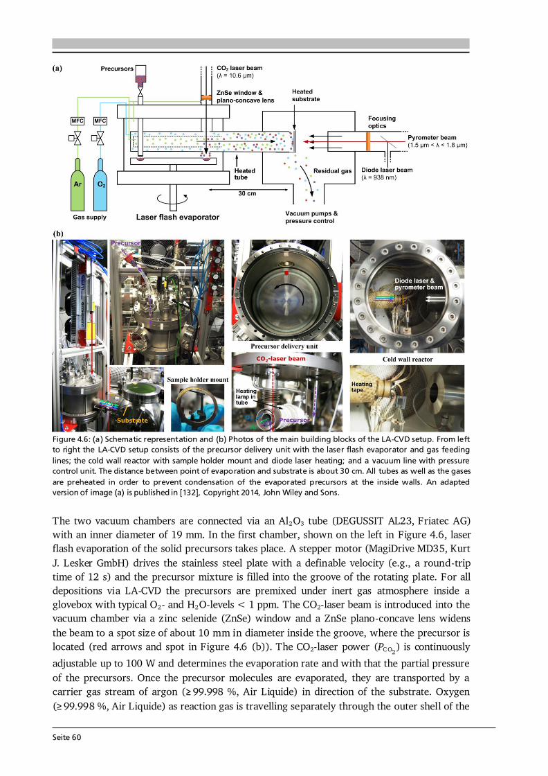
Seite 60
Figure 4.6: (a) Schematic representation and (b) Photos of the main building blocks of the LA-CVD setup. From left to right the LA-CVD setup consists of the precursor delivery unit with the laser flash evaporator and gas feeding lines; the cold wall reactor with sample holder mount and diode laser heating; and a vacuum line with pressure control unit. The distance between point of evaporation and substrate is about 30 cm. All tubes as well as the gases are preheated in order to prevent condensation of the evaporated precursors at the inside walls. An adapted version of image (a) is published in [132], Copyright 2014, John Wiley and Sons. The two vacuum chambers are connected via an Al2O3 tube (DEGUSSIT AL23, Friatec AG) with an inner diameter of 19 mm. In the first chamber, shown on the left in Figure 4.6, laser flash evaporation of the solid precursors takes place. A stepper motor (MagiDrive MD35, Kurt J. Lesker GmbH) drives the stainless steel plate with a definable velocity (e.g., a round-trip time of 12 s) and the precursor mixture is filled into the groove of the rotating plate. For all depositions via LA-CVD the precursors are premixed under inert gas atmosphere inside a glovebox with typical O2- and H2O-levels < 1 ppm. The CO2-laser beam is introduced into the vacuum chamber via a zinc selenide (ZnSe) window and a ZnSe plano-concave lens widens the beam to a spot size of about 10 mm in diameter inside the groove, where the precursor is located (red arrows and spot in Figure 4.6 (b)). The CO2-laser power (PC O2) is continuously adjustable up to 100 W and determines the evaporation rate and with that the partial pressure of the precursors. Once the precursor molecules are evaporated, they are transported by a carrier gas stream of argon ( 99.998 %, Air Liquide) in direction of the substrate. Oxygen ( 99.998 %, Air Liquide) as reaction gas is travelling separately through the outer shell of the
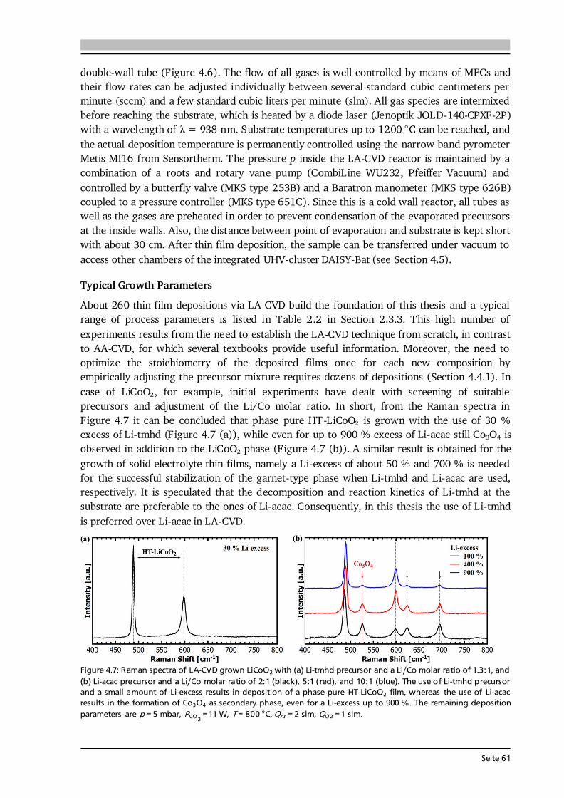
Seite 61
double-wall tube (Figure 4.6). The flow of all gases is well controlled by means of MFCs and their flow rates can be adjusted individually between several standard cubic centimeters per minute (sccm) and a few standard cubic liters per minute (slm). All gas species are intermixed before reaching the substrate, which is heated by a diode laser (Jenoptik JOLD-140-CPXF-2P) with a wavelength of = 938 nm. Substrate temperatures up to 1200 °C can be reached, and the actual deposition temperature is permanently controlled using the narrow band pyrometer Metis MI16 from Sensortherm. The pressure p inside the LA-CVD reactor is maintained by a combination of a roots and rotary vane pump (CombiLine WU232, Pfeiffer Vacuum) and controlled by a butterfly valve (MKS type 253B) and a Baratron manometer (MKS type 626B) coupled to a pressure controller (MKS type 651C). Since this is a cold wall reactor, all tubes as well as the gases are preheated in order to prevent condensation of the evaporated precursors at the inside walls. Also, the distance between point of evaporation and substrate is kept short with about 30 cm. After thin film deposition, the sample can be transferred under vacuum to access other chambers of the integrated UHV-cluster DAISY-Bat (see Section 4.5). Typical Growth Parameters About 260 thin film depositions via LA-CVD build the foundation of this thesis and a typical range of process parameters is listed in Table 2.2 in Section 2.3.3. This high number of experiments results from the need to establish the LA-CVD technique from scratch, in contrast to AA-CVD, for which several textbooks provide useful information. Moreover, the need to optimize the stoichiometry of the deposited films once for each new composition by empirically adjusting the precursor mixture requires dozens of depositions (Section 4.4.1). In case of LiCoO2, for example, initial experiments have dealt with screening of suitable precursors and adjustment of the Li/Co molar ratio. In short, from the Raman spectra in Figure 4.7 it can be concluded that phase pure HT-LiCoO2 is grown with the use of 30 % excess of Li-tmhd (Figure 4.7 (a)), while even for up to 900 % excess of Li-acac still Co3O4 is observed in addition to the LiCoO2 phase (Figure 4.7 (b)). A similar result is obtained for the growth of solid electrolyte thin films, namely a Li-excess of about 50 % and 700 % is needed for the successful stabilization of the garnet-type phase when Li-tmhd and Li-acac are used, respectively. It is speculated that the decomposition and reaction kinetics of Li-tmhd at the substrate are preferable to the ones of Li-acac. Consequently, in this thesis the use of Li-tmhd is preferred over Li-acac in LA-CVD.
Figure 4.7: Raman spectra of LA-CVD grown LiCoO2 with (a) Li-tmhd precursor and a Li/Co molar ratio of 1.3:1, and (b) Li-acac precursor and a Li/Co molar ratio of 2:1 (black), 5:1 (red), and 10:1 (blue). The use of Li-tmhd precursor and a small amount of Li-excess results in deposition of a phase pure HT-LiCoO2 film, whereas the use of Li-acac results in the formation of Co3O4 as secondary phase, even for a Li-excess up to 900 %. The remaining deposition parameters are p = 5 mbar, PCO 2 = 11 W, T = 800 °C, QAr = 2 slm, QO 2 = 1 slm.
Seite 62
The precursor materials for cathode, solid electrolyte and anode thin film deposition are listed in Table 4.2. If not stated otherwise stoichiometric amounts of the listed precursors are mixed inside an Ar-filled glovebox, and for cathode and solid electrolyte materials an excess of 30 % and 50 % Li-tmhd is used, respectively. For example, the Li/La/Zr molar ratio in the precursor mixture for the growth of garnet-type Li7La3Zr2O12 thin film solid electrolytes is set to 10.5:3:2. Lithium excess is used to compensate for possible loss of lithium during synthesis at elevated temperatures. All films reported in this thesis have a deposition time of 15 min after which the CO2-laser, and with that the precursor delivery, is switched off. Anode and cathode samples are directly cooled down with a rate of about 1 °C·s-1. Solid electrolyte samples are kept at their deposition temperature for additional 15 min under the same conditions as used during deposition, followed by cooling with a rate of about 1 °C·s -1. This procedure improves the quality of the deposited solid electrolyte thin films. Table 4.2: Precursor materials used for cathode, solid electrolyte, anode and current collector growth via LA-CVD.
Precursor Purity [%] Supplier Application Li-tmhd 98 Sigma Aldrich, Alfa Aesar Cathode & Solid electrolyte Li-acac 97 Sigma Aldrich Cathode & Solid electrolyte
Co(III)-(acac)3 98 Sigma Aldrich Cathode & Anode Ni(II)-(acac)2 95 Sigma Aldrich Cathode
Mn(III)-(acac)3 95 Sigma Aldrich Cathode La(III)-(acac)3·4H2O 99.9 abcr Solid electrolyte
Zr-(acac)4 97 Sigma Aldrich Solid electrolyte Ta-(OEt)4(acac) 99.99 abcr Solid electrolyte Al(III)-(acac)3 99.999 Sigma Aldrich Solid electrolyte Ga(III)-(acac)3 99.99 Sigma Aldrich Solid electrolyte Pt(II)-(acac)2 49.6 Alfa Aesar Current collector
4.4.3. LA-CVD Process Optimization In the course of this thesis, a constant development of the AA-CVD and LA-CVD techniques was carried out in order to optimize the processes, their reliability and reproducibility. Most of these developments are of minor importance and not necessarily worth mentioning. In the following, the most important modification to the LA-CVD setup is discussed, because it is essential for the success of this PhD project in the area of garnet solid electrolyte thin films.
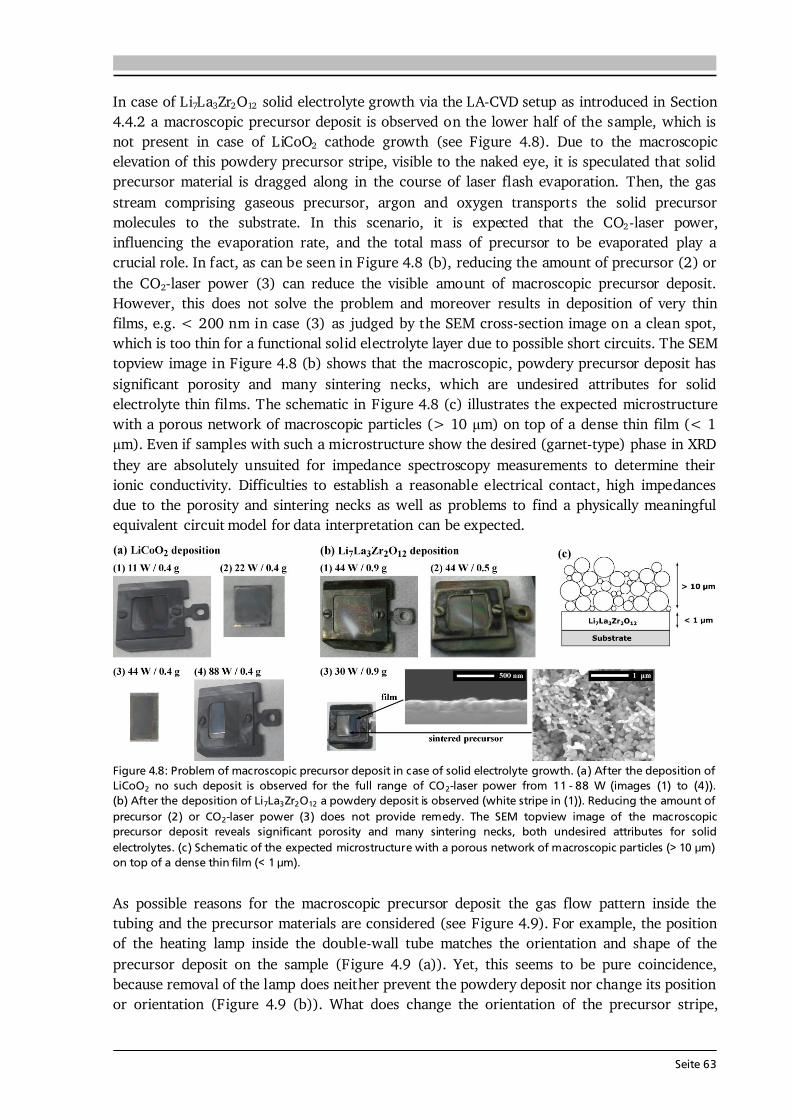
Seite 63
In case of Li7La3Zr2O12 solid electrolyte growth via the LA-CVD setup as introduced in Section 4.4.2 a macroscopic precursor deposit is observed on the lower half of the sample, which is not present in case of LiCoO2 cathode growth (see Figure 4.8). Due to the macroscopic elevation of this powdery precursor stripe, visible to the naked eye, it is speculated that solid precursor material is dragged along in the course of laser flash evaporation. Then, the gas stream comprising gaseous precursor, argon and oxygen transports the solid precursor molecules to the substrate. In this scenario, it is expected that the CO2-laser power, influencing the evaporation rate, and the total mass of precursor to be evaporated play a crucial role. In fact, as can be seen in Figure 4.8 (b), reducing the amount of precursor (2) or the CO2-laser power (3) can reduce the visible amount of macroscopic precursor deposit. However, this does not solve the problem and moreover results in deposition of very thin films, e.g. < 200 nm in case (3) as judged by the SEM cross-section image on a clean spot, which is too thin for a functional solid electrolyte layer due to possible short circuits. The SEM topview image in Figure 4.8 (b) shows that the macroscopic, powdery precursor deposit has significant porosity and many sintering necks, which are undesired attributes for solid electrolyte thin films. The schematic in Figure 4.8 (c) illustrates the expected microstructure with a porous network of macroscopic particles (> 10 m) on top of a dense thin film (< 1 m). Even if samples with such a microstructure show the desired (garnet-type) phase in XRD they are absolutely unsuited for impedance spectroscopy measurements to determine their ionic conductivity. Difficulties to establish a reasonable electrical contact, high impedances due to the porosity and sintering necks as well as problems to find a physically meaningful equivalent circuit model for data interpretation can be expected.
Figure 4.8: Problem of macroscopic precursor deposit in case of solid electrolyte growth. (a) After the deposition of LiCoO2 no such deposit is observed for the full range of CO2-laser power from 11 - 88 W (images (1) to (4)). (b) After the deposition of Li7La3Zr2O12 a powdery deposit is observed (white stripe in (1)). Reducing the amount of precursor (2) or CO2-laser power (3) does not provide remedy. The SEM topview image of the macroscopic precursor deposit reveals significant porosity and many sintering necks, both undesired attributes for solid electrolytes. (c) Schematic of the expected microstructure with a porous network of macroscopic particles (> 10 μm) on top of a dense thin film (< 1 μm). As possible reasons for the macroscopic precursor deposit the gas flow pattern inside the tubing and the precursor materials are considered (see Figure 4.9). For example, the position of the heating lamp inside the double-wall tube matches the orientation and shape of the precursor deposit on the sample (Figure 4.9 (a)). Yet, this seems to be pure coincidence, because removal of the lamp does neither prevent the powdery deposit nor change its position or orientation (Figure 4.9 (b)). What does change the orientation of the precursor stripe,
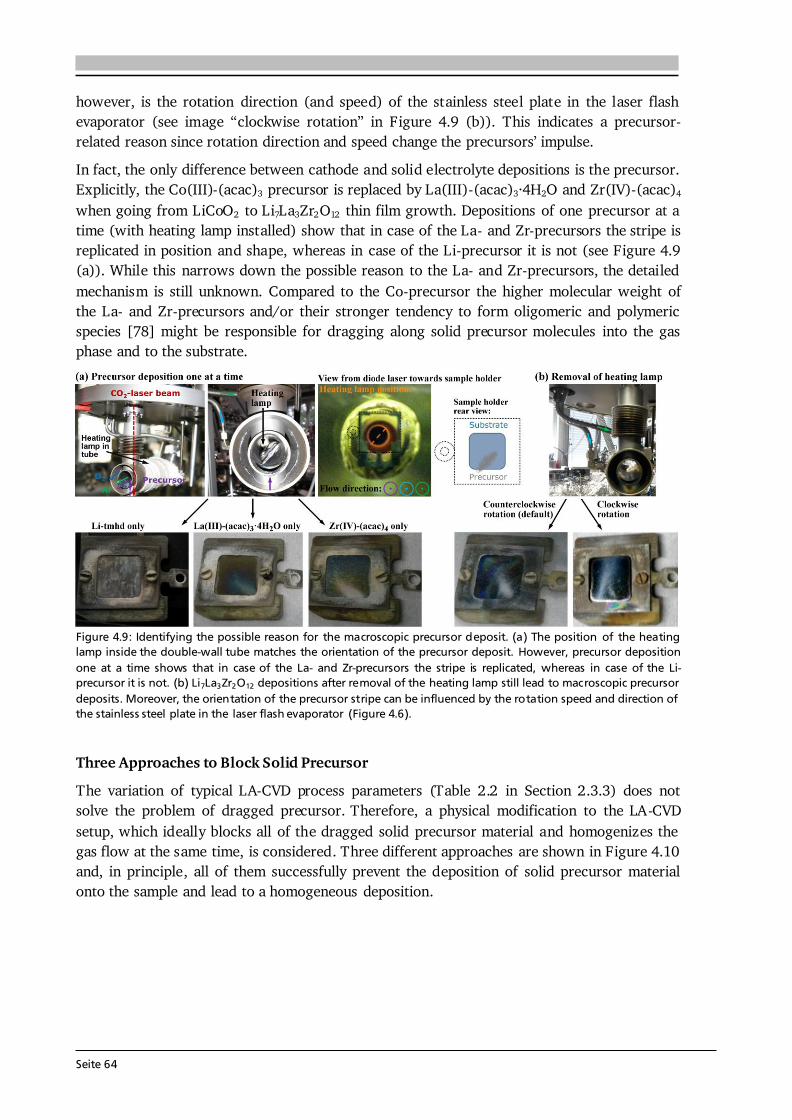
Seite 64
however, is the rotation direction (and speed) of the stainless steel plate in the laser flash evaporator (see image “clockwise rotation” in Figure 4.9 (b)). This indicates a precursor-related reason since rotation direction and speed change the precursors’ impulse. In fact, the only difference between cathode and solid electrolyte depositions is the precursor. Explicitly, the Co(III)-(acac)3 precursor is replaced by La(III)-(acac)3·4H2O and Zr(IV)-(acac)4 when going from LiCoO2 to Li7La3Zr2O12 thin film growth. Depositions of one precursor at a time (with heating lamp installed) show that in case of the La- and Zr-precursors the stripe is replicated in position and shape, whereas in case of the Li-precursor it is not (see Figure 4.9 (a)). While this narrows down the possible reason to the La- and Zr-precursors, the detailed mechanism is still unknown. Compared to the Co-precursor the higher molecular weight of the La- and Zr-precursors and/or their stronger tendency to form oligomeric and polymeric species [78] might be responsible for dragging along solid precursor molecules into the gas phase and to the substrate.
Figure 4.9: Identifying the possible reason for the macroscopic precursor deposit. (a) The position of the heating lamp inside the double-wall tube matches the orientation of the precursor deposit. However, precursor deposition one at a time shows that in case of the La- and Zr-precursors the stripe is replicated, whereas in case of the Li-precursor it is not. (b) Li7La3Zr2O12 depositions after removal of the heating lamp still lead to macroscopic precursor deposits. Moreover, the orientation of the precursor stripe can be influenced by the rotation speed and direction of the stainless steel plate in the laser flash evaporator (Figure 4.6).
Three Approaches to Block Solid Precursor The variation of typical LA-CVD process parameters (Table 2.2 in Section 2.3.3) does not solve the problem of dragged precursor. Therefore, a physical modification to the LA-CVD setup, which ideally blocks all of the dragged solid precursor material and homogenizes the gas flow at the same time, is considered. Three different approaches are shown in Figure 4.10 and, in principle, all of them successfully prevent the deposition of solid precursor material onto the sample and lead to a homogeneous deposition.
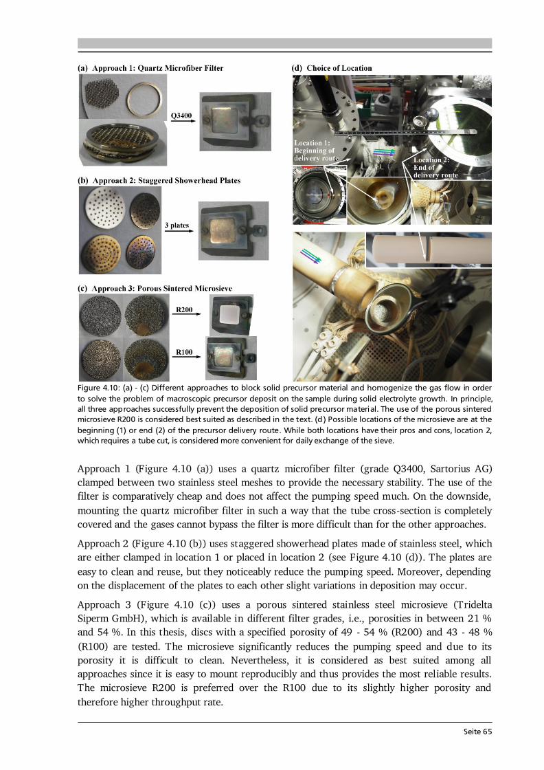
Seite 65
Figure 4.10: (a) - (c) Different approaches to block solid precursor material and homogenize the gas flow in order to solve the problem of macroscopic precursor deposit on the sample during solid electrolyte growth. In principle, all three approaches successfully prevent the deposition of solid precursor material. The use of the porous sintered microsieve R200 is considered best suited as described in the text. (d) Possible locations of the microsieve are at the beginning (1) or end (2) of the precursor delivery route. While both locations have their pros and cons, location 2, which requires a tube cut, is considered more convenient for daily exchange of the sieve. Approach 1 (Figure 4.10 (a)) uses a quartz microfiber filter (grade Q3400, Sartorius AG) clamped between two stainless steel meshes to provide the necessary stability. The use of the filter is comparatively cheap and does not affect the pumping speed much. On the downside, mounting the quartz microfiber filter in such a way that the tube cross-section is completely covered and the gases cannot bypass the filter is more difficult than for the other approaches. Approach 2 (Figure 4.10 (b)) uses staggered showerhead plates made of stainless steel, which are either clamped in location 1 or placed in location 2 (see Figure 4.10 (d)). The plates are easy to clean and reuse, but they noticeably reduce the pumping speed. Moreover, depending on the displacement of the plates to each other slight variations in deposition may occur. Approach 3 (Figure 4.10 (c)) uses a porous sintered stainless steel microsieve (Tridelta Siperm GmbH), which is available in different filter grades, i.e., porosities in between 21 % and 54 %. In this thesis, discs with a specified porosity of 49 - 54 % (R200) and 43 - 48 % (R100) are tested. The microsieve significantly reduces the pumping speed and due to its porosity it is difficult to clean. Nevertheless, it is considered as best suited among all approaches since it is easy to mount reproducibly and thus provides the most reliable results. The microsieve R200 is preferred over the R100 due to its slightly higher porosity and therefore higher throughput rate.
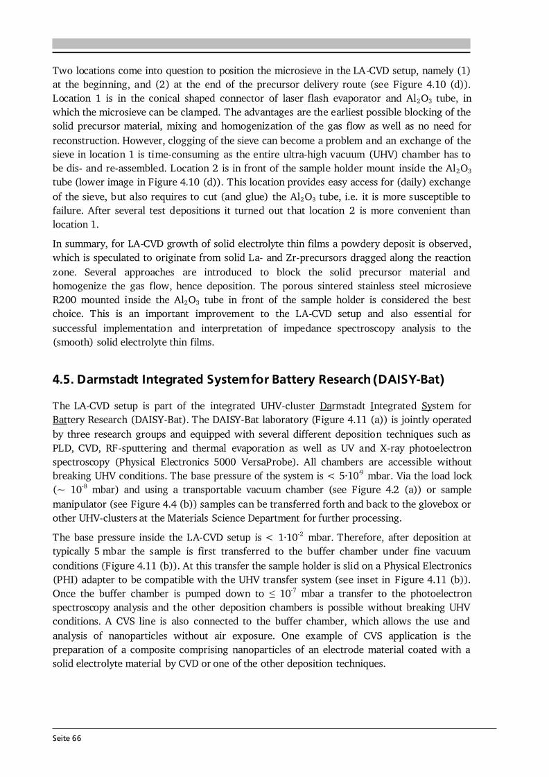
Seite 66
Two locations come into question to position the microsieve in the LA-CVD setup, namely (1) at the beginning, and (2) at the end of the precursor delivery route (see Figure 4.10 (d)). Location 1 is in the conical shaped connector of laser flash evaporator and Al2O3 tube, in which the microsieve can be clamped. The advantages are the earliest possible blocking of the solid precursor material, mixing and homogenization of the gas flow as well as no need for reconstruction. However, clogging of the sieve can become a problem and an exchange of the sieve in location 1 is time-consuming as the entire ultra-high vacuum (UHV) chamber has to be dis- and re-assembled. Location 2 is in front of the sample holder mount inside the Al2O3 tube (lower image in Figure 4.10 (d)). This location provides easy access for (daily) exchange of the sieve, but also requires to cut (and glue) the Al2O3 tube, i.e. it is more susceptible to failure. After several test depositions it turned out that location 2 is more convenient than location 1. In summary, for LA-CVD growth of solid electrolyte thin films a powdery deposit is observed, which is speculated to originate from solid La- and Zr-precursors dragged along the reaction zone. Several approaches are introduced to block the solid precursor material and homogenize the gas flow, hence deposition. The porous sintered stainless steel microsieve R200 mounted inside the Al2O3 tube in front of the sample holder is considered the best choice. This is an important improvement to the LA-CVD setup and also essential for successful implementation and interpretation of impedance spectroscopy analysis to the (smooth) solid electrolyte thin films. 4.5. Darmstadt Integrated System for Battery Research (DAISY-Bat) The LA-CVD setup is part of the integrated UHV-cluster Darmstadt Integrated System for Battery Research (DAISY-Bat). The DAISY-Bat laboratory (Figure 4.11 (a)) is jointly operated by three research groups and equipped with several different deposition techniques such as PLD, CVD, RF-sputtering and thermal evaporation as well as UV and X-ray photoelectron spectroscopy (Physical Electronics 5000 VersaProbe). All chambers are accessible without breaking UHV conditions. The base pressure of the system is < 5·10-9 mbar. Via the load lock (~ 10-8 mbar) and using a transportable vacuum chamber (see Figure 4.2 (a)) or sample manipulator (see Figure 4.4 (b)) samples can be transferred forth and back to the glovebox or other UHV-clusters at the Materials Science Department for further processing. The base pressure inside the LA-CVD setup is < 1·10-2 mbar. Therefore, after deposition at typically 5 mbar the sample is first transferred to the buffer chamber under fine vacuum conditions (Figure 4.11 (b)). At this transfer the sample holder is slid on a Physical Electronics (PHI) adapter to be compatible with the UHV transfer system (see inset in Figure 4.11 (b)). Once the buffer chamber is pumped down to ≤ 10-7 mbar a transfer to the photoelectron spectroscopy analysis and the other deposition chambers is possible without breaking UHV conditions. A CVS line is also connected to the buffer chamber, which allows the use and analysis of nanoparticles without air exposure. One example of CVS application is the preparation of a composite comprising nanoparticles of an electrode material coated with a solid electrolyte material by CVD or one of the other deposition techniques.
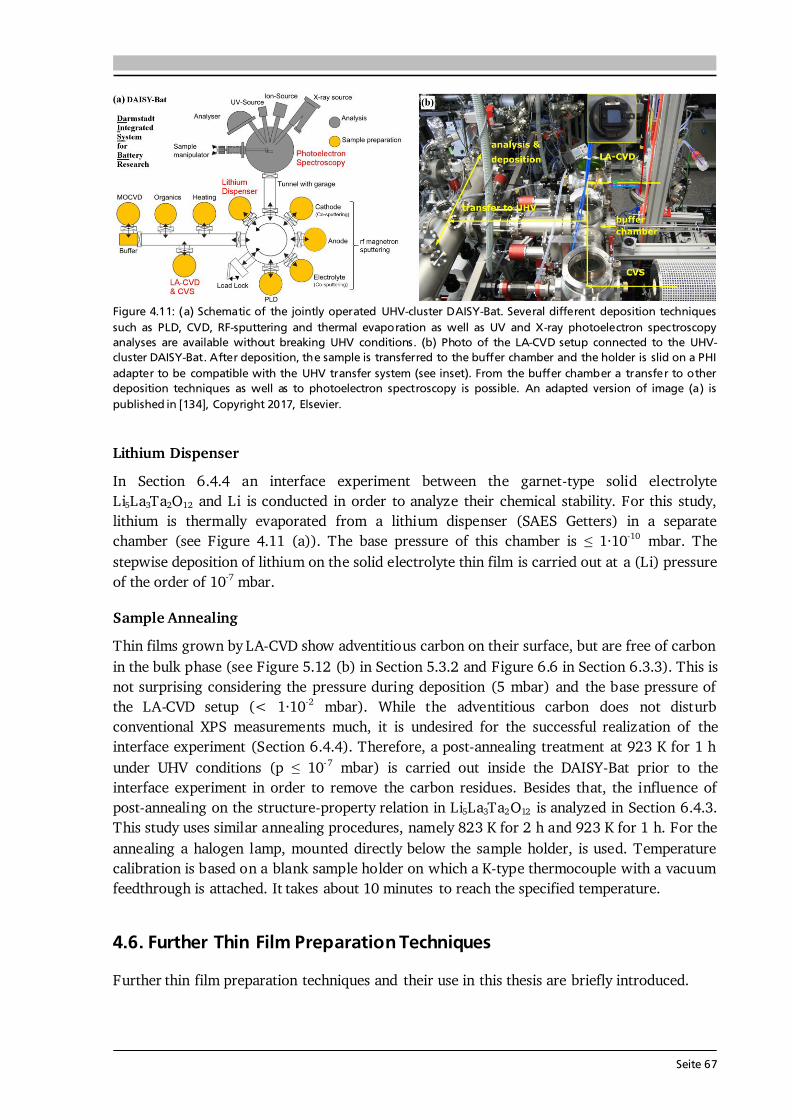
Seite 67
Figure 4.11: (a) Schematic of the jointly operated UHV-cluster DAISY-Bat. Several different deposition techniques such as PLD, CVD, RF-sputtering and thermal evaporation as well as UV and X-ray photoelectron spectroscopy analyses are available without breaking UHV conditions. (b) Photo of the LA-CVD setup connected to the UHV-cluster DAISY-Bat. After deposition, the sample is transferred to the buffer chamber and the holder is slid on a PHI adapter to be compatible with the UHV transfer system (see inset). From the buffer chamber a transfer to other deposition techniques as well as to photoelectron spectroscopy is possible. An adapted version of image (a) is published in [134], Copyright 2017, Elsevier.
Lithium Dispenser In Section 6.4.4 an interface experiment between the garnet-type solid electrolyte Li5La3Ta2O12 and Li is conducted in order to analyze their chemical stability. For this study, lithium is thermally evaporated from a lithium dispenser (SAES Getters) in a separate chamber (see Figure 4.11 (a)). The base pressure of this chamber is ≤ 1·10-10 mbar. The stepwise deposition of lithium on the solid electrolyte thin film is carried out at a (Li) pressure of the order of 10-7 mbar. Sample Annealing Thin films grown by LA-CVD show adventitious carbon on their surface, but are free of carbon in the bulk phase (see Figure 5.12 (b) in Section 5.3.2 and Figure 6.6 in Section 6.3.3). This is not surprising considering the pressure during deposition (5 mbar) and the base pressure of the LA-CVD setup (< 1·10-2 mbar). While the adventitious carbon does not disturb conventional XPS measurements much, it is undesired for the successful realization of the interface experiment (Section 6.4.4). Therefore, a post-annealing treatment at 923 K for 1 h under UHV conditions (p ≤ 10-7 mbar) is carried out inside the DAISY-Bat prior to the interface experiment in order to remove the carbon residues. Besides that, the influence of post-annealing on the structure-property relation in Li5La3Ta2O12 is analyzed in Section 6.4.3. This study uses similar annealing procedures, namely 823 K for 2 h and 923 K for 1 h. For the annealing a halogen lamp, mounted directly below the sample holder, is used. Temperature calibration is based on a blank sample holder on which a K-type thermocouple with a vacuum feedthrough is attached. It takes about 10 minutes to reach the specified temperature. 4.6. Further Thin Film Preparation Techniques Further thin film preparation techniques and their use in this thesis are briefly introduced.
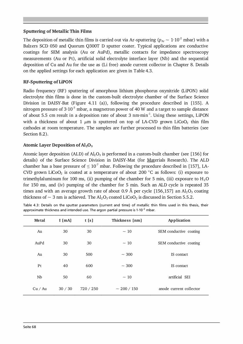
Seite 68
Sputtering of Metallic Thin Films The deposition of metallic thin films is carried out via Ar-sputtering (pAr ~ 1·10-2 mbar) with a Balzers SCD 050 and Quorum Q300T D sputter coater. Typical applications are conductive coatings for SEM analysis (Au or AuPd), metallic contacts for impedance spectroscopy measurements (Au or Pt), artificial solid electrolyte interface layer (Nb) and the sequential deposition of Cu and Au for the use as (Li free) anode current collector in Chapter 8. Details on the applied settings for each application are given in Table 4.3. RF-Sputtering of LiPON Radio frequency (RF) sputtering of amorphous lithium phosphorus oxynitride (LiPON) solid electrolyte thin films is done in the custom-built electrolyte chamber of the Surface Science Division in DAISY-Bat (Figure 4.11 (a)), following the procedure described in [155]. A nitrogen pressure of 3·10-3 mbar, a magnetron power of 40 W and a target to sample distance of about 5.5 cm result in a deposition rate of about 3 nm·min-1. Using these settings, LiPON with a thickness of about 1 μm is sputtered on top of LA-CVD grown LiCoO2 thin film cathodes at room temperature. The samples are further processed to thin film batteries (see Section 8.2). Atomic Layer Deposition of Al2O3 Atomic layer deposition (ALD) of Al2O3 is performed in a custom-built chamber (see [156] for details) of the Surface Science Division in DAISY-Mat (for Materials Research). The ALD chamber has a base pressure of ≤ 10-7 mbar. Following the procedure described in [157], LA-CVD grown LiCoO2 is coated at a temperature of about 200 °C as follows: (i) exposure to trimethylaluminum for 100 ms, (ii) pumping of the chamber for 5 min, (iii) exposure to H2O for 150 ms, and (iv) pumping of the chamber for 5 min. Such an ALD cycle is repeated 35 times and with an average growth rate of about 0.9 Å per cycle [156,157] an Al2O3 coating thickness of ~ 3 nm is achieved. The Al2O3 coated LiCoO2 is discussed in Section 5.5.2. Table 4.3: Details on the sputter parameters (current and time) of metallic thin films used in this thesis, their approximate thickness and intended use. The argon partial pressure is 1·10 -2 mbar.
Metal I [mA] t [s] Thickness [nm] Application Au 30 30 ~ 10 SEM conductive coating
AuPd 30 30 ~ 10 SEM conductive coating Au 30 500 ~ 300 IS contact Pt 40 600 ~ 300 IS contact Nb 50 60 ~ 10 artificial SEI
Cu / Au 30 / 30 720 / 250 ~ 200 / 150 anode current collector
Seite 69
5 Lithium Transition Metal Oxide Thin Film Cathodes Major parts of Section 5.3 are published in [132]. Selected parts of Section 5.2 and Section 5.4.1 are published in [158]. Within the framework of this thesis small modifications are included. 5.1. Introduction and Motivation In recent years strong developments in different classes of cathode materials for batteries (oxides, sulfides, phosphates, etc.) have been achieved leading to new opportunities as well as challenges regarding the energy density, lifetime, cost, reliability, safety, size, design, environmental impact, etc. [9,15,159,160]. Apart from novel concepts for next generation batteries [9,161–163], which are based on Li-S, Li-air, conversion materials or all-solid-state, already commercialized layered lithium transition metal oxide cathodes, Li(TM)O2 with TM = Ni, Mn, Co, are currently further developed towards Ni-rich [164] and Li-rich [19,165] compounds to enhance the capacity and lower the cost of future Li-ion batteries. In Figure 5.1 (a) the phase diagram of the layered lithium transition metal oxide systems LiNiO2 - LiMnO2 - LiCoO2 - Li2MnO3 is illustrated as a tetrahedron. Its front face (green triangle) and transverse section (orange triangle) represent the Li-stoichiometric and Li-rich transition metal oxides, respectively. The former is shown in enlarged view in Figure 5.1 (b). In the following, the single Li(TM)O2 cathode materials are briefly introduced. Table 5.1 summarizes the characteristics of the described layered intercalation compounds. LiCoO2 - Commercialized by Sony Inc. in 1991 [6], LiCoO2 was the benchmark for a long time. For reasons of cyclability its cut-off potential is typically limited to ~ 4.2 V corresponding to an amount of x = 0.5 Li-ions in LixCoO2 and a capacity of about 140 mAh·g-1. Ways to improve the capacity retention at an increased cut-off potential of 4.5 V and with that increased capacity are [59]: surface coatings, cleaning the surface by grinding or re-heating prior to cell assembly and the use of advanced liquid electrolytes. Yet, a higher delithiation (x < 0.5) reduces the thermal stability of LixCoO2 and poses a safety risk with thermal runaway starting already at 130 °C for x = 0.5 [59,166]. LiNiO2 - Nickel is less expensive and toxic than cobalt and the possibility to reversibly extract up to (1 - x) = 0.75 Li in LixNiO2 enabling a capacity of about 200 mAh·g-1 makes LiNiO2 appear as a good alternative to LiCoO2 [18]. However, the preparation of ordered LiNiO2, i.e. without Ni residing in Li layers, is extremely difficult and dependent on the synthesis conditions [167]. In turn, disordered LiNiO2 shows poor cycling performance. Other drawbacks are Jahn-Teller distortion, irreversible phase transitions and safety issues when
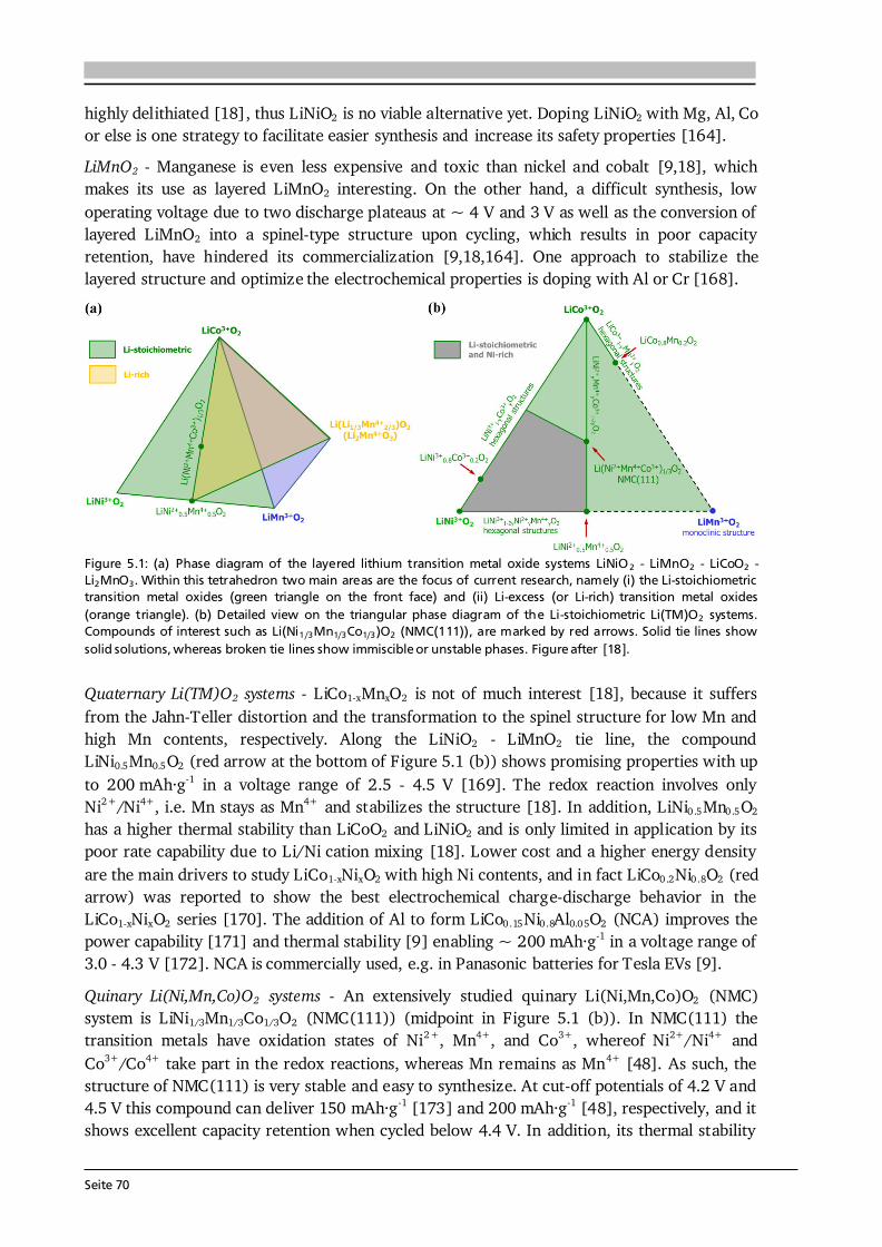
Seite 70
highly delithiated [18], thus LiNiO2 is no viable alternative yet. Doping LiNiO2 with Mg, Al, Co or else is one strategy to facilitate easier synthesis and increase its safety properties [164]. LiMnO2 - Manganese is even less expensive and toxic than nickel and cobalt [9,18], which makes its use as layered LiMnO2 interesting. On the other hand, a difficult synthesis, low operating voltage due to two discharge plateaus at ~ 4 V and 3 V as well as the conversion of layered LiMnO2 into a spinel-type structure upon cycling, which results in poor capacity retention, have hindered its commercialization [9,18,164]. One approach to stabilize the layered structure and optimize the electrochemical properties is doping with Al or Cr [168].
Figure 5.1: (a) Phase diagram of the layered lithium transition metal oxide systems LiNiO 2 - LiMnO2 - LiCoO2 - Li2MnO3. Within this tetrahedron two main areas are the focus of current research, namely (i) the Li-stoichiometric transition metal oxides (green triangle on the front face) and (ii) Li-excess (or Li-rich) transition metal oxides (orange triangle). (b) Detailed view on the triangular phase diagram of the Li -stoichiometric Li(TM)O2 systems. Compounds of interest such as Li(Ni1/3Mn1/3Co1/3)O2 (NMC(111)), are marked by red arrows. Solid tie lines show solid solutions, whereas broken tie lines show immiscible or unstable phases. Figure after [18]. Quaternary Li(TM)O2 systems - LiCo1-xMnxO2 is not of much interest [18], because it suffers from the Jahn-Teller distortion and the transformation to the spinel structure for low Mn and high Mn contents, respectively. Along the LiNiO2 - LiMnO2 tie line, the compound LiNi0.5Mn0.5O2 (red arrow at the bottom of Figure 5.1 (b)) shows promising properties with up to 200 mAh·g-1 in a voltage range of 2.5 - 4.5 V [169]. The redox reaction involves only Ni2+/Ni4+, i.e. Mn stays as Mn4+ and stabilizes the structure [18]. In addition, LiNi0.5Mn0.5O2 has a higher thermal stability than LiCoO2 and LiNiO2 and is only limited in application by its poor rate capability due to Li/Ni cation mixing [18]. Lower cost and a higher energy density are the main drivers to study LiCo1-xNixO2 with high Ni contents, and in fact LiCo0.2Ni0.8O2 (red arrow) was reported to show the best electrochemical charge-discharge behavior in the LiCo1-xNixO2 series [170]. The addition of Al to form LiCo0.15Ni0.8Al0.05O2 (NCA) improves the power capability [171] and thermal stability [9] enabling ~ 200 mAh·g-1 in a voltage range of 3.0 - 4.3 V [172]. NCA is commercially used, e.g. in Panasonic batteries for Tesla EVs [9]. Quinary Li(Ni,Mn,Co)O2 systems - An extensively studied quinary Li(Ni,Mn,Co)O2 (NMC) system is LiNi1/3Mn1/3Co1/3O2 (NMC(111)) (midpoint in Figure 5.1 (b)). In NMC(111) the transition metals have oxidation states of Ni2+, Mn4+, and Co3+, whereof Ni2+/Ni4+ and Co3+/Co4+ take part in the redox reactions, whereas Mn remains as Mn4+ [48]. As such, the structure of NMC(111) is very stable and easy to synthesize. At cut-off potentials of 4.2 V and 4.5 V this compound can deliver 150 mAh·g-1 [173] and 200 mAh·g-1 [48], respectively, and it shows excellent capacity retention when cycled below 4.4 V. In addition, its thermal stability
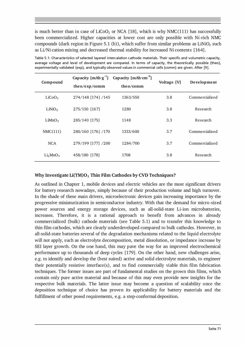
Seite 71
is much better than in case of LiCoO2 or NCA [18], which is why NMC(111) has successfully been commercialized. Higher capacities at lower cost are only possible with Ni-rich NMC compounds (dark region in Figure 5.1 (b)), which suffer from similar problems as LiNiO2 such as Li/Ni cation mixing and decreased thermal stability for increased Ni contents [164]. Table 5.1: Characteristics of selected layered intercalation cathode materials. Their specific and volumetric capacity, average voltage and level of development are compared. In terms of capacity, the theoretically possible (theo), experimentally validated (exp), and typically observed values in commercial cells (comm) are given. After [9].
Compound Capacity [mAh·g -1] theo/exp/comm
Capacity [mAh·cm-3] theo/comm Voltage [V] Development
LiCoO2 274/148 [174] /145 1363/550 3.8 Commercialized LiNiO2 275/150 [167] 1280 3.8 Research LiMnO2 285/140 [175] 1148 3.3 Research
NMC(111) 280/160 [176] /170 1333/600 3.7 Commercialized NCA 279/199 [177] /200 1284/700 3.7 Commercialized
Li2MnO3 458/180 [178] 1708 3.8 Research Why Investigate Li(TM)O2 Thin Film Cathodes by CVD Techniques? As outlined in Chapter 1, mobile devices and electric vehicles are the most significant drivers for battery research nowadays, simply because of their production volume and high turnover. In the shade of these main drivers, microelectronic devices gain increasing importance by the progressive miniaturization in semiconductor industry. With that the demand for micro-sized power sources and energy storage devices, such as all-solid-state Li-ion microbatteries, increases. Therefore, it is a rational approach to benefit from advances in already commercialized (bulk) cathode materials (see Table 5.1) and to transfer this knowledge to thin film cathodes, which are clearly underdeveloped compared to bulk cathodes. However, in all-solid-state batteries several of the degradation mechanisms related to the liquid electrolyte will not apply, such as electrolyte decomposition, metal dissolution, or impedance increase by SEI layer growth. On the one hand, this may pave the way for an improved electrochemical performance up to thousands of deep cycles [179]. On the other hand, new challenges arise, e.g. to identify and develop the (best suited) active and solid electrolyte materials, to engineer their potentially resistive interface(s), and to find commercially viable thin film fabrication techniques. The former issues are part of fundamental studies on the grown thin films, which contain only pure active material and because of this may even provide new insights for the respective bulk materials. The latter issue may become a question of scalability once the deposition technique of choice has proven its applicability for battery materials and the fulfillment of other posed requirements, e.g. a step-conformal deposition.
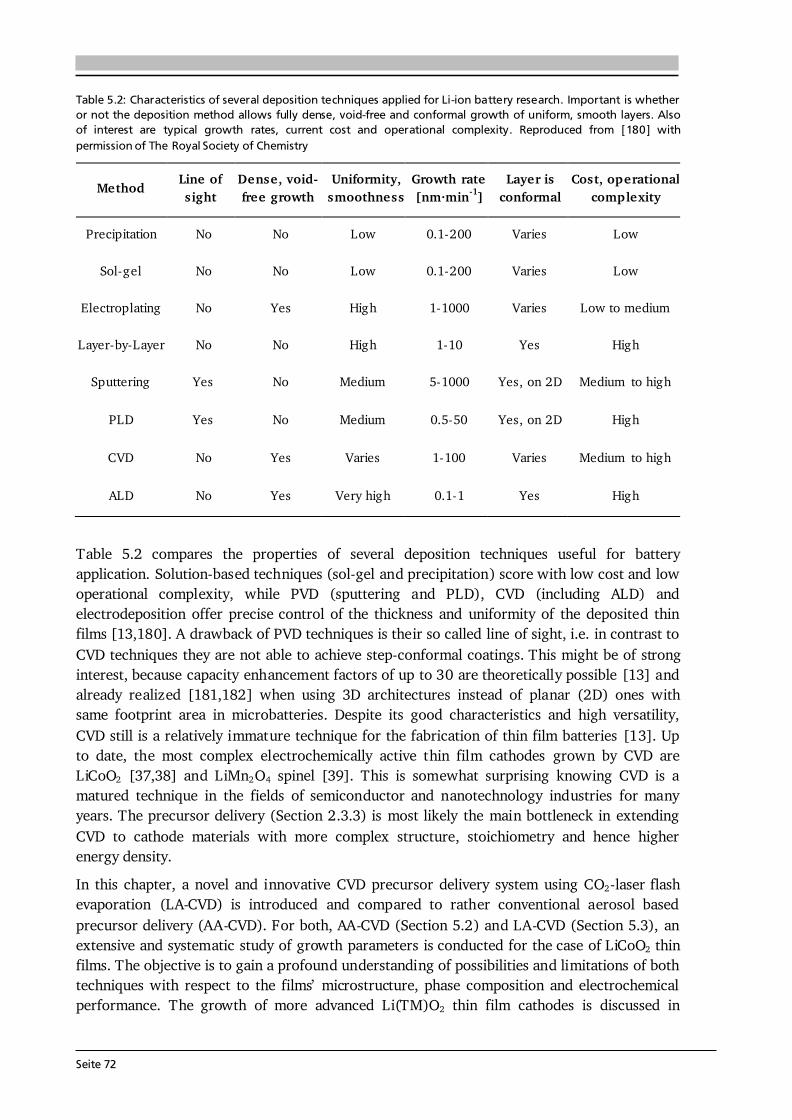
Seite 72
Table 5.2: Characteristics of several deposition techniques applied for Li -ion battery research. Important is whether or not the deposition method allows fully dense, void-free and conformal growth of uniform, smooth layers. Also of interest are typical growth rates, current cost and operational complexity. Reproduced from [180] with permission of The Royal Society of Chemistry Method Line of sight Dense, void- free growth Uniformity, smoothness Growth rate [nm·min-1] Layer is conformal Cost, operational complexity
Precipitation No No Low 0.1-200 Varies Low Sol-gel No No Low 0.1-200 Varies Low
Electroplating No Yes High 1-1000 Varies Low to medium Layer-by-Layer No No High 1-10 Yes High
Sputtering Yes No Medium 5-1000 Yes, on 2D Medium to high PLD Yes No Medium 0.5-50 Yes, on 2D High CVD No Yes Varies 1-100 Varies Medium to high ALD No Yes Very high 0.1-1 Yes High
Table 5.2 compares the properties of several deposition techniques useful for battery application. Solution-based techniques (sol-gel and precipitation) score with low cost and low operational complexity, while PVD (sputtering and PLD), CVD (including ALD) and electrodeposition offer precise control of the thickness and uniformity of the deposited thin films [13,180]. A drawback of PVD techniques is their so called line of sight, i.e. in contrast to CVD techniques they are not able to achieve step-conformal coatings. This might be of strong interest, because capacity enhancement factors of up to 30 are theoretically possible [13] and already realized [181,182] when using 3D architectures instead of planar (2D) ones with same footprint area in microbatteries. Despite its good characteristics and high versatility, CVD still is a relatively immature technique for the fabrication of thin film batteries [13]. Up to date, the most complex electrochemically active thin film cathodes grown by CVD are LiCoO2 [37,38] and LiMn2O4 spinel [39]. This is somewhat surprising knowing CVD is a matured technique in the fields of semiconductor and nanotechnology industries for many years. The precursor delivery (Section 2.3.3) is most likely the main bottleneck in extending CVD to cathode materials with more complex structure, stoichiometry and hence higher energy density. In this chapter, a novel and innovative CVD precursor delivery system using CO2-laser flash evaporation (LA-CVD) is introduced and compared to rather conventional aerosol based precursor delivery (AA-CVD). For both, AA-CVD (Section 5.2) and LA-CVD (Section 5.3), an extensive and systematic study of growth parameters is conducted for the case of LiCoO2 thin films. The objective is to gain a profound understanding of possibilities and limitations of both techniques with respect to the films’ microstructure, phase composition and electrochemical performance. The growth of more advanced Li(TM)O2 thin film cathodes is discussed in
Seite 73
Section 5.4, starting with the successive replacement of Co by Ni and having the commercialized NMC(111) as final target. Finally, strategies to improve the thin films’ cycling performance, which go beyond the optimization of intrinsic material properties but are strongly related to the advantages of CVD, are presented in Section 5.5. 5.2. LiCoO2 Thin Films Grown by AA-CVD – Growth Parameter Study The aims of the AA-CVD growth parameter study are: (i) to determine the growth conditions for electrochemically well-performing LiCoO2 thin film cathodes, (ii) to evaluate the capability of AA-CVD to control microstructural features (density, crystallinity, etc.), phase purity and chemical composition for the well-known material system LiCoO2, and (iii) to derive structure-property relationships that may help to further improve functional thin film growth by AA-CVD for Li-ion battery application. 5.2.1. Microstructure The influence of precursor concentration in solution c and deposition temperature T on the microstructure is shown in Figure 5.2 by means of secondary electron micrographs. At 600 °C, a very smooth surface is visible in topview (Figure 5.2 (a)) and via cross-sectional imaging (Figure 5.2 (b)) a very thin film with a thickness 100 nm is observed for the two precursor concentrations of 0.01 M and 0.025 M. It is likely that the temperature and mean residence time of the nebulized solvent inside the reactor are too low and short, respectively, in order to trigger the autoignition of methanol, which is reported in [183] to typically start at 433 °C after a delay time of 53.3 s. In such a case the majority of the sprayed precursor solution will not react at the substrate. Therefore, it is concluded that under the given growth conditions and for T 600 °C no substantial film growth takes place in AA-CVD. For deposition temperatures 700 °C different microstructures evolve, depending on the precursor concentration, which may be classified as follows. For high concentrations and/or low temperatures a fractal-/cauliflower-like microstructure is observed as result of homogeneous nucleation in the gas phase, while for low concentrations and/or high temperatures a dense film forms, best traceable in the cross-section micrographs (Figure 5.2 (b)). The topview micrographs in Figure 5.2 (a) additionally show that at a given concentration c grain coarsening takes place with increasing growth temperature T. Moreover, it can be seen that the dense films are composed of polycrystals with partially irregular size and shape resulting in films with a comparatively rough surface. Assuming the precursor concentration is the main driver for supersaturation in the gas phase, this microstructural evolution nicely illustrates experimentally for one and the same material the (counteractive) effects of both supersaturation and temperature on the structure formed in a CVD process (see Figure 2.15 (b) in Section 2.3.2) and thus is in good agreement with CVD growth theory [85]. In case a high volumetric energy density needs to be achieved, growth conditions that result in the dense microstructure are preferred. On the other hand, the fractal-/cauliflower-like microstructure offers higher porosity and surface area and therefore could be used in respective applications.
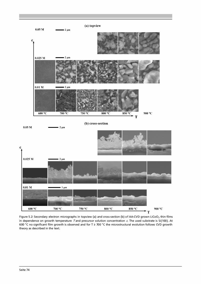
Seite 74
Figure 5.2: Secondary electron micrographs in topview (a) and cross-section (b) of AA-CVD grown LiCoO2 thin films in dependence on growth temperature T and precursor solution concentration c. The used substrate is Si(100). At 600 °C no significant film growth is observed and for T ≥ 700 °C the microstructural evolution follows CVD growth theory as described in the text.
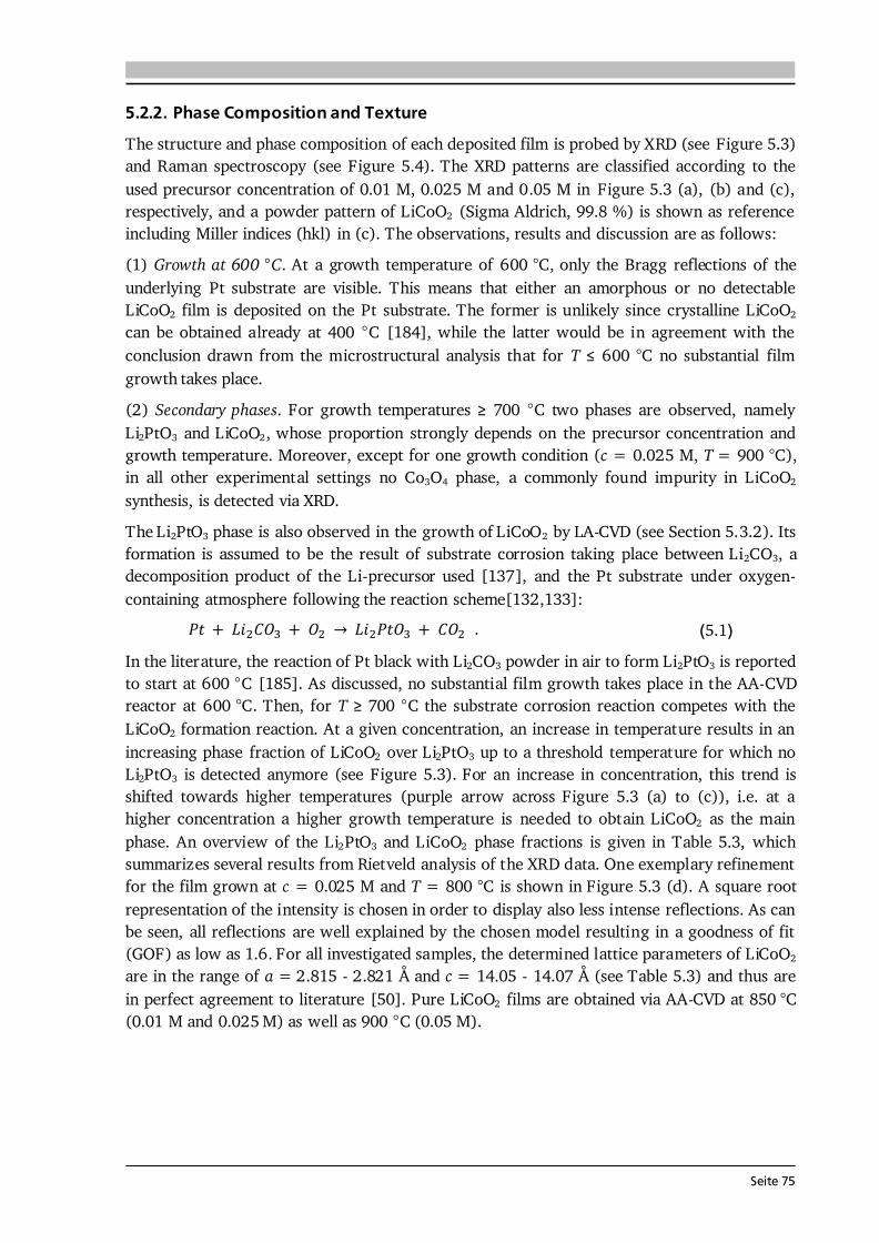
Seite 75
5.2.2. Phase Composition and Texture The structure and phase composition of each deposited film is probed by XRD (see Figure 5.3) and Raman spectroscopy (see Figure 5.4). The XRD patterns are classified according to the used precursor concentration of 0.01 M, 0.025 M and 0.05 M in Figure 5.3 (a), (b) and (c), respectively, and a powder pattern of LiCoO2 (Sigma Aldrich, 99.8 %) is shown as reference including Miller indices (hkl) in (c). The observations, results and discussion are as follows: (1) Growth at 600 °C. At a growth temperature of 600 °C, only the Bragg reflections of the underlying Pt substrate are visible. This means that either an amorphous or no detectable LiCoO2 film is deposited on the Pt substrate. The former is unlikely since crystalline LiCoO2 can be obtained already at 400 °C [184], while the latter would be in agreement with the conclusion drawn from the microstructural analysis that for T 600 °C no substantial film growth takes place. (2) Secondary phases. For growth temperatures 700 °C two phases are observed, namely Li2PtO3 and LiCoO2, whose proportion strongly depends on the precursor concentration and growth temperature. Moreover, except for one growth condition (c = 0.025 M, T = 900 °C), in all other experimental settings no Co3O4 phase, a commonly found impurity in LiCoO2 synthesis, is detected via XRD. The Li2PtO3 phase is also observed in the growth of LiCoO2 by LA-CVD (see Section 5.3.2). Its formation is assumed to be the result of substrate corrosion taking place between Li2CO3, a decomposition product of the Li-precursor used [137], and the Pt substrate under oxygen-containing atmosphere following the reaction scheme[132,133]: . (5.1) In the literature, the reaction of Pt black with Li2CO3 powder in air to form Li2PtO3 is reported to start at 600 °C [185]. As discussed, no substantial film growth takes place in the AA-CVD reactor at 600 °C. Then, for T 700 °C the substrate corrosion reaction competes with the LiCoO2 formation reaction. At a given concentration, an increase in temperature results in an increasing phase fraction of LiCoO2 over Li2PtO3 up to a threshold temperature for which no Li2PtO3 is detected anymore (see Figure 5.3). For an increase in concentration, this trend is shifted towards higher temperatures (purple arrow across Figure 5.3 (a) to (c)), i.e. at a higher concentration a higher growth temperature is needed to obtain LiCoO2 as the main phase. An overview of the Li2PtO3 and LiCoO2 phase fractions is given in Table 5.3, which summarizes several results from Rietveld analysis of the XRD data. One exemplary refinement for the film grown at c = 0.025 M and T = 800 °C is shown in Figure 5.3 (d). A square root representation of the intensity is chosen in order to display also less intense reflections. As can be seen, all reflections are well explained by the chosen model resulting in a goodness of fit (GOF) as low as 1.6. For all investigated samples, the determined lattice parameters of LiCoO2 are in the range of a = 2.815 - 2.821 Å and c = 14.05 - 14.07 Å (see Table 5.3) and thus are in perfect agreement to literature [50]. Pure LiCoO2 films are obtained via AA-CVD at 850 °C (0.01 M and 0.025 M) as well as 900 °C (0.05 M).
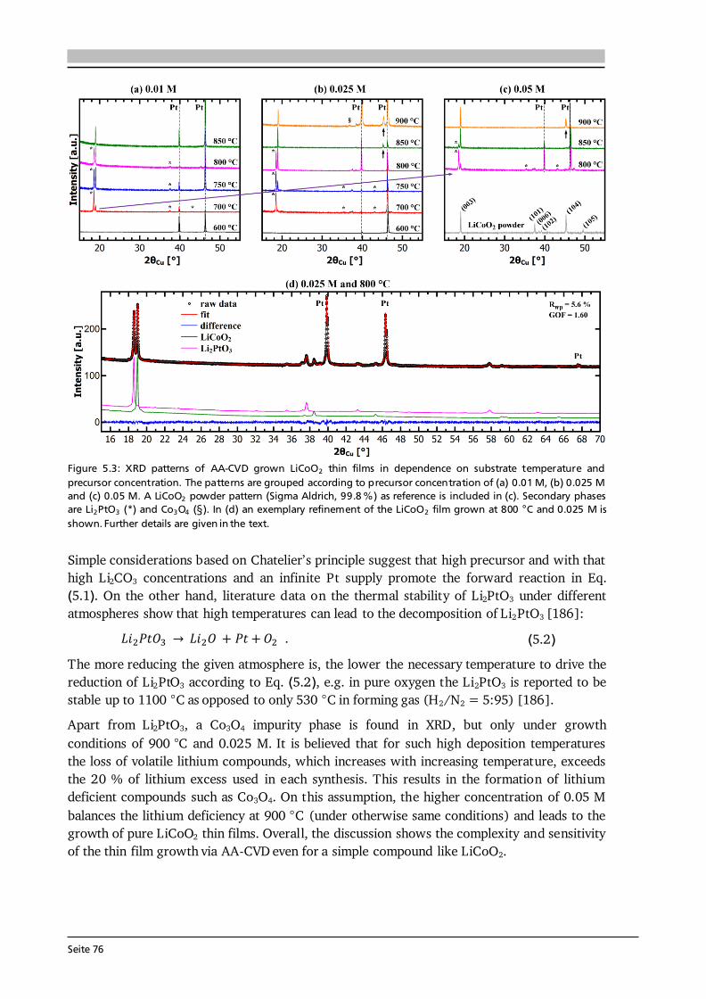
Seite 76
Figure 5.3: XRD patterns of AA-CVD grown LiCoO2 thin films in dependence on substrate temperature and precursor concentration. The patterns are grouped according to precursor concentration of (a) 0.01 M, (b) 0.025 M and (c) 0.05 M. A LiCoO2 powder pattern (Sigma Aldrich, 99.8 %) as reference is included in (c). Secondary phases are Li2PtO3 (*) and Co3O4 (§). In (d) an exemplary refinement of the LiCoO2 film grown at 800 °C and 0.025 M is shown. Further details are given in the text. Simple considerations based on Chatelier’s principle suggest that high precursor and with that high Li2CO3 concentrations and an infinite Pt supply promote the forward reaction in Eq. (5.1). On the other hand, literature data on the thermal stability of Li2PtO3 under different atmospheres show that high temperatures can lead to the decomposition of Li2PtO3 [186]: . (5.2) The more reducing the given atmosphere is, the lower the necessary temperature to drive the reduction of Li2PtO3 according to Eq. (5.2), e.g. in pure oxygen the Li2PtO3 is reported to be stable up to 1100 °C as opposed to only 530 °C in forming gas (H2/N2 = 5:95) [186]. Apart from Li2PtO3, a Co3O4 impurity phase is found in XRD, but only under growth conditions of 900 °C and 0.025 M. It is believed that for such high deposition temperatures the loss of volatile lithium compounds, which increases with increasing temperature, exceeds the 20 % of lithium excess used in each synthesis. This results in the formation of lithium deficient compounds such as Co3O4. On this assumption, the higher concentration of 0.05 M balances the lithium deficiency at 900 °C (under otherwise same conditions) and leads to the growth of pure LiCoO2 thin films. Overall, the discussion shows the complexity and sensitivity of the thin film growth via AA-CVD even for a simple compound like LiCoO2.
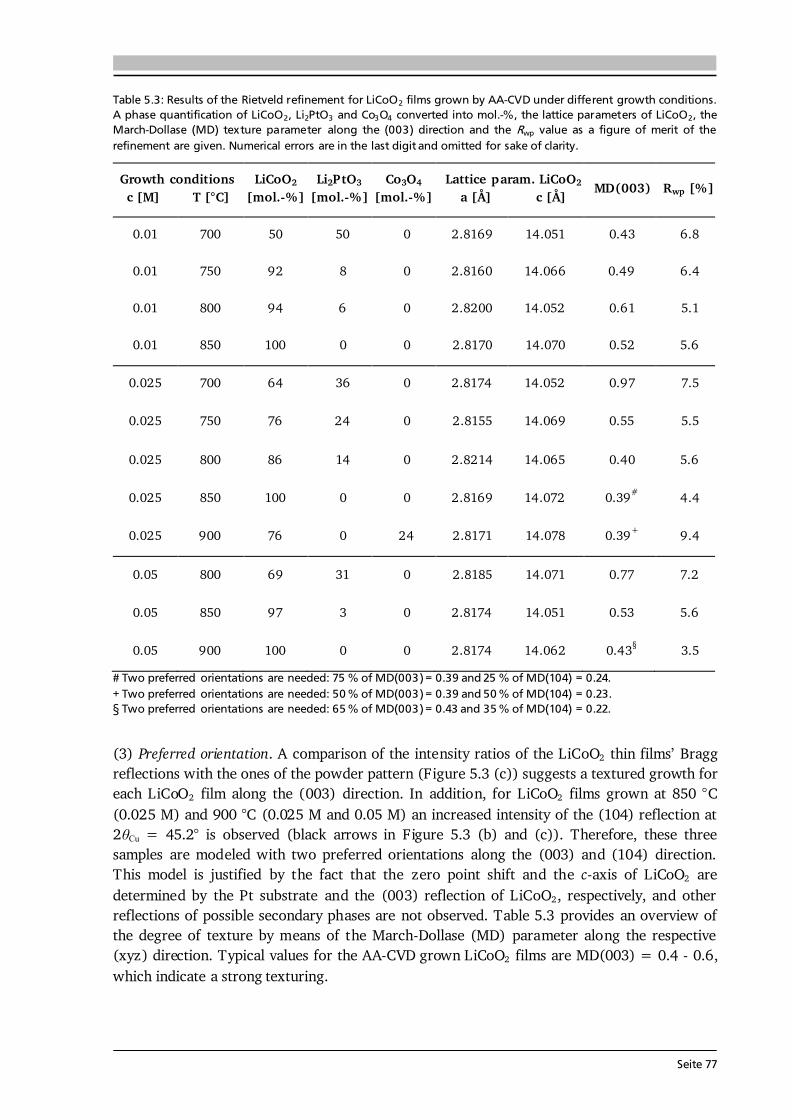
Seite 77
Table 5.3: Results of the Rietveld refinement for LiCoO2 films grown by AA-CVD under different growth conditions. A phase quantification of LiCoO2, Li2PtO3 and Co3O4 converted into mol.-%, the lattice parameters of LiCoO2, the March-Dollase (MD) texture parameter along the (003) direction and the Rwp value as a figure of merit of the refinement are given. Numerical errors are in the last digit and omitted for sake of clarity. Growth conditions c [M] T [°C] LiCoO2 [mol.-%] Li2PtO3 [mol.-%] Co3O4 [mol.-%] Lattice param. LiCoO2 a [Å] c [Å] MD(003) Rwp [%]
0.01 700 50 50 0 2.8169 14.051 0.43 6.8 0.01 750 92 8 0 2.8160 14.066 0.49 6.4 0.01 800 94 6 0 2.8200 14.052 0.61 5.1 0.01 850 100 0 0 2.8170 14.070 0.52 5.6
0.025 700 64 36 0 2.8174 14.052 0.97 7.5 0.025 750 76 24 0 2.8155 14.069 0.55 5.5 0.025 800 86 14 0 2.8214 14.065 0.40 5.6 0.025 850 100 0 0 2.8169 14.072 0.39# 4.4 0.025 900 76 0 24 2.8171 14.078 0.39+ 9.4 0.05 800 69 31 0 2.8185 14.071 0.77 7.2 0.05 850 97 3 0 2.8174 14.051 0.53 5.6 0.05 900 100 0 0 2.8174 14.062 0.43§ 3.5
# Two preferred orientations are needed: 75 % of MD(003) = 0.39 and 25 % of MD(104) = 0.24. + Two preferred orientations are needed: 50 % of MD(003) = 0.39 and 50 % of MD(104) = 0.23. § Two preferred orientations are needed: 65 % of MD(003) = 0.43 and 35 % of MD(104) = 0.22. (3) Preferred orientation. A comparison of the intensity ratios of the LiCoO2 thin films’ Bragg reflections with the ones of the powder pattern (Figure 5.3 (c)) suggests a textured growth for each LiCoO2 film along the (003) direction. In addition, for LiCoO2 films grown at 850 °C (0.025 M) and 900 °C (0.025 M and 0.05 M) an increased intensity of the (104) reflection at 2 Cu = 45.2° is observed (black arrows in Figure 5.3 (b) and (c)). Therefore, these three samples are modeled with two preferred orientations along the (003) and (104) direction. This model is justified by the fact that the zero point shift and the c-axis of LiCoO2 are determined by the Pt substrate and the (003) reflection of LiCoO2, respectively, and other reflections of possible secondary phases are not observed. Table 5.3 provides an overview of the degree of texture by means of the March-Dollase (MD) parameter along the respective (xyz) direction. Typical values for the AA-CVD grown LiCoO2 films are MD(003) = 0.4 - 0.6, which indicate a strong texturing.
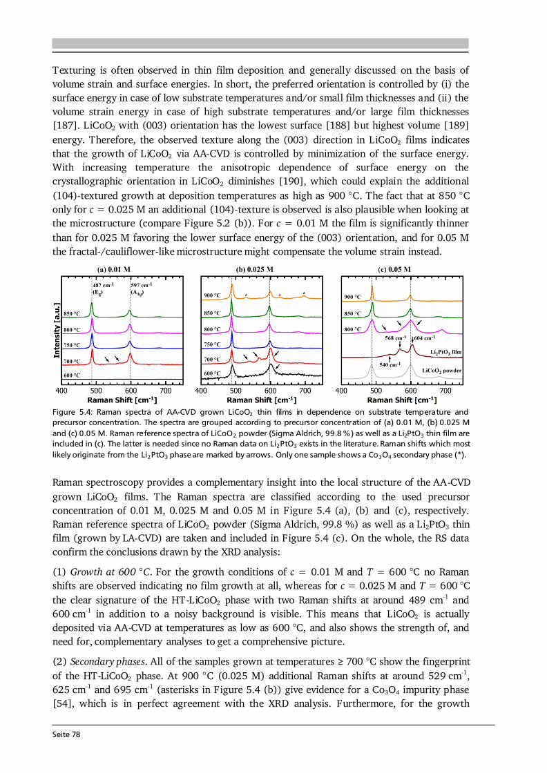
Seite 78
Texturing is often observed in thin film deposition and generally discussed on the basis of volume strain and surface energies. In short, the preferred orientation is controlled by (i) the surface energy in case of low substrate temperatures and/or small film thicknesses and (ii) the volume strain energy in case of high substrate temperatures and/or large film thicknesses [187]. LiCoO2 with (003) orientation has the lowest surface [188] but highest volume [189] energy. Therefore, the observed texture along the (003) direction in LiCoO2 films indicates that the growth of LiCoO2 via AA-CVD is controlled by minimization of the surface energy. With increasing temperature the anisotropic dependence of surface energy on the crystallographic orientation in LiCoO2 diminishes [190], which could explain the additional (104)-textured growth at deposition temperatures as high as 900 °C. The fact that at 850 °C only for c = 0.025 M an additional (104)-texture is observed is also plausible when looking at the microstructure (compare Figure 5.2 (b)). For c = 0.01 M the film is significantly thinner than for 0.025 M favoring the lower surface energy of the (003) orientation, and for 0.05 M the fractal-/cauliflower-like microstructure might compensate the volume strain instead.
Figure 5.4: Raman spectra of AA-CVD grown LiCoO2 thin films in dependence on substrate temperature and precursor concentration. The spectra are grouped according to precursor concentration of (a) 0.01 M, (b) 0.025 M and (c) 0.05 M. Raman reference spectra of LiCoO2 powder (Sigma Aldrich, 99.8 %) as well as a Li2PtO3 thin film are included in (c). The latter is needed since no Raman data on Li2PtO3 exists in the literature. Raman shifts which most likely originate from the Li2PtO3 phase are marked by arrows. Only one sample shows a Co3O4 secondary phase (*). Raman spectroscopy provides a complementary insight into the local structure of the AA-CVD grown LiCoO2 films. The Raman spectra are classified according to the used precursor concentration of 0.01 M, 0.025 M and 0.05 M in Figure 5.4 (a), (b) and (c), respectively. Raman reference spectra of LiCoO2 powder (Sigma Aldrich, 99.8 %) as well as a Li2PtO3 thin film (grown by LA-CVD) are taken and included in Figure 5.4 (c). On the whole, the RS data confirm the conclusions drawn by the XRD analysis: (1) Growth at 600 °C. For the growth conditions of c = 0.01 M and T = 600 °C no Raman shifts are observed indicating no film growth at all, whereas for c = 0.025 M and T = 600 °C the clear signature of the HT-LiCoO2 phase with two Raman shifts at around 489 cm-1 and 600 cm-1 in addition to a noisy background is visible. This means that LiCoO2 is actually deposited via AA-CVD at temperatures as low as 600 °C, and also shows the strength of, and need for, complementary analyses to get a comprehensive picture. (2) Secondary phases. All of the samples grown at temperatures 700 °C show the fingerprint of the HT-LiCoO2 phase. At 900 °C (0.025 M) additional Raman shifts at around 529 cm-1, 625 cm-1 and 695 cm-1 (asterisks in Figure 5.4 (b)) give evidence for a Co3O4 impurity phase [54], which is in perfect agreement with the XRD analysis. Furthermore, for the growth
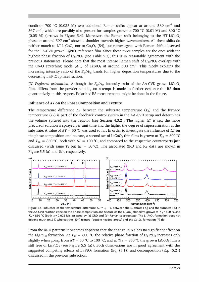
Seite 79
condition 700 °C (0.025 M) two additional Raman shifts appear at around 539 cm-1 and 567 cm-1, which are possibly also present for samples grown at 700 °C (0.01 M) and 800 °C (0.05 M) (arrows in Figure 5.4). Moreover, the Raman shift belonging to the HT-LiCoO2 phase at around 597 cm-1 shows a shoulder towards higher wavenumbers. All these shifts do neither match to LT-LiCoO2 nor to Co3O4 [54], but rather agree with Raman shifts observed for the LA-CVD grown Li2PtO3 reference film. Since these three samples are the ones with the highest phase fraction of Li2PtO3 (see Table 5.3), this is in reasonable agreement with the previous statements. Please note that the most intense Raman shift of Li2PtO3 overlaps with the Co-O stretching mode (A1g) of LiCoO2 at around 600 cm-1. This nicely explains the increasing intensity ratio of the Eg/A1g bands for higher deposition temperatures due to the decreasing Li2PtO3 phase fraction. (3) Preferred orientation. Although the Eg/A1g intensity ratio of the AA-CVD grown LiCoO2 films differs from the powder sample, no attempt is made to further evaluate the RS data quantitatively in this respect. Polarized RS measurements might be done in the future. Influence of ΔT on the Phase Composition and Texture The temperature difference ΔT between the substrate temperature (TS) and the furnace temperature (TF) is part of the feedback control system in the AA-CVD setup and determines the volume sprayed into the reactor (see Section 4.3.2). The higher ΔT is set, the more precursor solution is sprayed per unit time and the higher the degree of supersaturation at the substrate. A value of ΔT = 50 °C was used so far. In order to investigate the influence of ΔT on the phase composition and texture, a second set of LiCoO2 thin films is grown at TS1 = 800 °C and TS2 = 850 °C, both with ΔT = 100 °C, and compared to the respective counterparts just discussed (with same TS but ΔT = 50 °C). The associated XRD and RS data are shown in Figure 5.5 (a) and (b), respectively.
Figure 5.5: Influence of the temperature difference ΔT = TS - TF between the substrate (TS) and the furnaces (TF) in the AA-CVD reaction zone on the phase composition and texture of the LiCoO2 thin films grown at TS 1 = 800 °C and TS2 = 850 °C (both c = 0.025 M), assessed by (a) XRD and (b) Raman spectroscopy. The Li2PtO3 formation does not depend much on ΔT, whereas the (104)-texture (double-headed arrow) and the Co3O4 formation (*) do. From the XRD patterns it becomes apparent that the change in ΔT has no significant effect on the Li2PtO3 formation. At TS1 = 800 °C the relative phase fraction of Li2PtO3 increases only slightly when going from ΔT = 50 °C to 100 °C, and at TS2 = 850 °C the grown LiCoO2 film is still free of Li2PtO3 (see Figure 5.5 (a)). Both observations are in good agreement with the suggested competing effects of Li2PtO3 formation (Eq. (5.1)) and decomposition (Eq. (5.2)) discussed in the previous subsection.
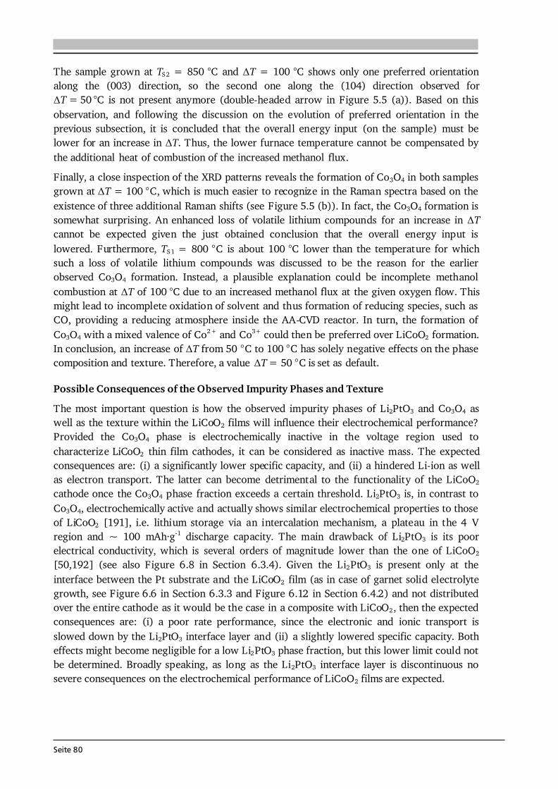
Seite 80
The sample grown at TS2 = 850 °C and ΔT = 100 °C shows only one preferred orientation along the (003) direction, so the second one along the (104) direction observed for ΔT = 50 °C is not present anymore (double-headed arrow in Figure 5.5 (a)). Based on this observation, and following the discussion on the evolution of preferred orientation in the previous subsection, it is concluded that the overall energy input (on the sample) must be lower for an increase in ΔT. Thus, the lower furnace temperature cannot be compensated by the additional heat of combustion of the increased methanol flux. Finally, a close inspection of the XRD patterns reveals the formation of Co3O4 in both samples grown at ΔT = 100 °C, which is much easier to recognize in the Raman spectra based on the existence of three additional Raman shifts (see Figure 5.5 (b)). In fact, the Co3O4 formation is somewhat surprising. An enhanced loss of volatile lithium compounds for an increase in ΔT cannot be expected given the just obtained conclusion that the overall energy input is lowered. Furthermore, TS1 = 800 °C is about 100 °C lower than the temperature for which such a loss of volatile lithium compounds was discussed to be the reason for the earlier observed Co3O4 formation. Instead, a plausible explanation could be incomplete methanol combustion at ΔT of 100 °C due to an increased methanol flux at the given oxygen flow. This might lead to incomplete oxidation of solvent and thus formation of reducing species, such as CO, providing a reducing atmosphere inside the AA-CVD reactor. In turn, the formation of Co3O4 with a mixed valence of Co2+ and Co3+ could then be preferred over LiCoO2 formation. In conclusion, an increase of ΔT from 50 °C to 100 °C has solely negative effects on the phase composition and texture. Therefore, a value ΔT = 50 °C is set as default. Possible Consequences of the Observed Impurity Phases and Texture The most important question is how the observed impurity phases of Li2PtO3 and Co3O4 as well as the texture within the LiCoO2 films will influence their electrochemical performance? Provided the Co3O4 phase is electrochemically inactive in the voltage region used to characterize LiCoO2 thin film cathodes, it can be considered as inactive mass. The expected consequences are: (i) a significantly lower specific capacity, and (ii) a hindered Li-ion as well as electron transport. The latter can become detrimental to the functionality of the LiCoO2 cathode once the Co3O4 phase fraction exceeds a certain threshold. Li2PtO3 is, in contrast to Co3O4, electrochemically active and actually shows similar electrochemical properties to those of LiCoO2 [191], i.e. lithium storage via an intercalation mechanism, a plateau in the 4 V region and ~ 100 mAh·g-1 discharge capacity. The main drawback of Li2PtO3 is its poor electrical conductivity, which is several orders of magnitude lower than the one of LiCoO2 [50,192] (see also Figure 6.8 in Section 6.3.4). Given the Li2PtO3 is present only at the interface between the Pt substrate and the LiCoO2 film (as in case of garnet solid electrolyte growth, see Figure 6.6 in Section 6.3.3 and Figure 6.12 in Section 6.4.2) and not distributed over the entire cathode as it would be the case in a composite with LiCoO2, then the expected consequences are: (i) a poor rate performance, since the electronic and ionic transport is slowed down by the Li2PtO3 interface layer and (ii) a slightly lowered specific capacity. Both effects might become negligible for a low Li2PtO3 phase fraction, but this lower limit could not be determined. Broadly speaking, as long as the Li2PtO3 interface layer is discontinuous no severe consequences on the electrochemical performance of LiCoO2 films are expected.
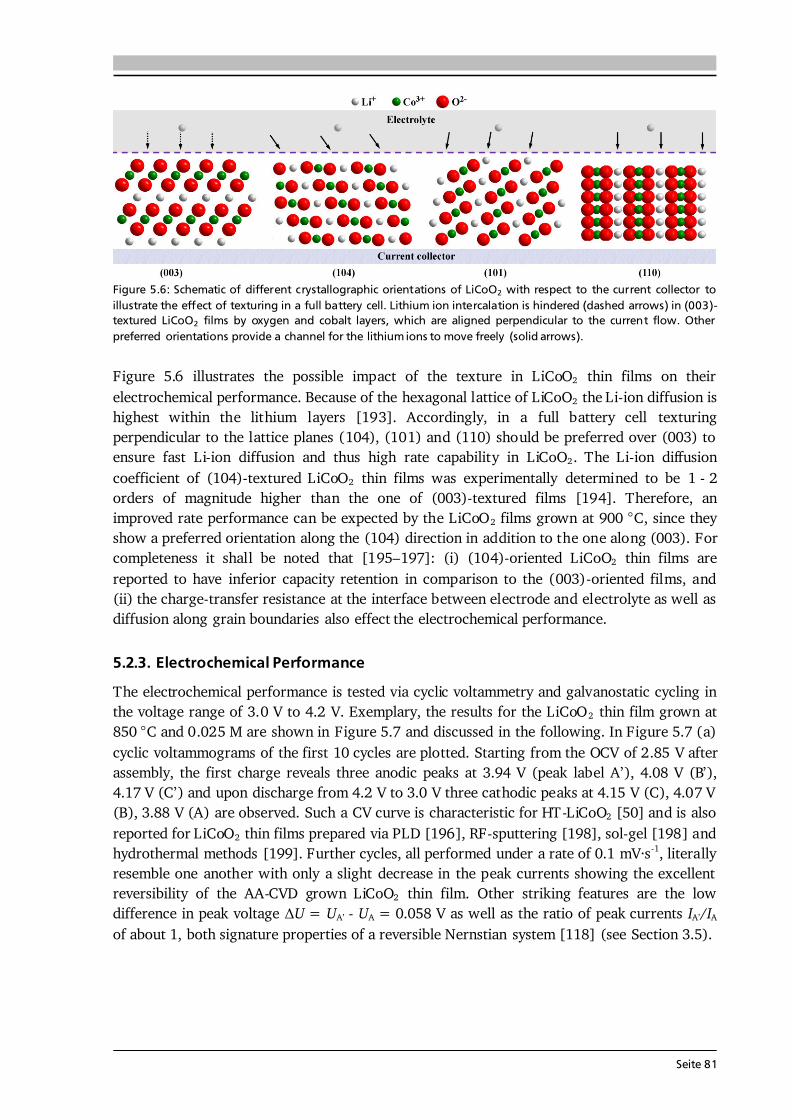
Seite 81
Figure 5.6: Schematic of different crystallographic orientations of LiCoO2 with respect to the current collector to illustrate the effect of texturing in a full battery cell. Lithium ion intercalation is hindered (dashed arrows) in (003)-textured LiCoO2 films by oxygen and cobalt layers, which are aligned perpendicular to the current flow. Other preferred orientations provide a channel for the lithium ions to move freely (solid arrows). Figure 5.6 illustrates the possible impact of the texture in LiCoO2 thin films on their electrochemical performance. Because of the hexagonal lattice of LiCoO2 the Li-ion diffusion is highest within the lithium layers [193]. Accordingly, in a full battery cell texturing perpendicular to the lattice planes (104), (101) and (110) should be preferred over (003) to ensure fast Li-ion diffusion and thus high rate capability in LiCoO2. The Li-ion diffusion coefficient of (104)-textured LiCoO2 thin films was experimentally determined to be 1 - 2 orders of magnitude higher than the one of (003)-textured films [194]. Therefore, an improved rate performance can be expected by the LiCoO2 films grown at 900 °C, since they show a preferred orientation along the (104) direction in addition to the one along (003). For completeness it shall be noted that [195–197]: (i) (104)-oriented LiCoO2 thin films are reported to have inferior capacity retention in comparison to the (003)-oriented films, and (ii) the charge-transfer resistance at the interface between electrode and electrolyte as well as diffusion along grain boundaries also effect the electrochemical performance. 5.2.3. Electrochemical Performance The electrochemical performance is tested via cyclic voltammetry and galvanostatic cycling in the voltage range of 3.0 V to 4.2 V. Exemplary, the results for the LiCoO2 thin film grown at 850 °C and 0.025 M are shown in Figure 5.7 and discussed in the following. In Figure 5.7 (a) cyclic voltammograms of the first 10 cycles are plotted. Starting from the OCV of 2.85 V after assembly, the first charge reveals three anodic peaks at 3.94 V (peak label A’), 4.08 V (B’), 4.17 V (C’) and upon discharge from 4.2 V to 3.0 V three cathodic peaks at 4.15 V (C), 4.07 V (B), 3.88 V (A) are observed. Such a CV curve is characteristic for HT-LiCoO2 [50] and is also reported for LiCoO2 thin films prepared via PLD [196], RF-sputtering [198], sol-gel [198] and hydrothermal methods [199]. Further cycles, all performed under a rate of 0.1 mV·s-1, literally resemble one another with only a slight decrease in the peak currents showing the excellent reversibility of the AA-CVD grown LiCoO2 thin film. Other striking features are the low difference in peak voltage ΔU = UA’ - UA = 0.058 V as well as the ratio of peak currents IA’/IA of about 1, both signature properties of a reversible Nernstian system [118] (see Section 3.5).
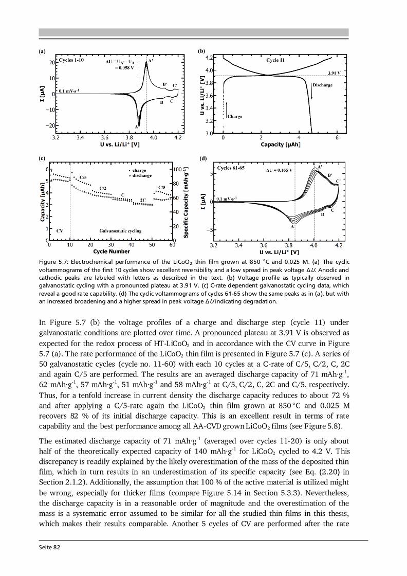
Seite 82
Figure 5.7: Electrochemical performance of the LiCoO2 thin film grown at 850 °C and 0.025 M. (a) The cyclic voltammograms of the first 10 cycles show excellent reversibility and a low spread in peak voltage ΔU. Anodic and cathodic peaks are labeled with letters as described in the text. (b) Voltage profile as typically observed in galvanostatic cycling with a pronounced plateau at 3.91 V. (c) C-rate dependent galvanostatic cycling data, which reveal a good rate capability. (d) The cyclic voltammograms of cycles 61-65 show the same peaks as in (a), but with an increased broadening and a higher spread in peak voltage ΔU indicating degradation. In Figure 5.7 (b) the voltage profiles of a charge and discharge step (cycle 11) under galvanostatic conditions are plotted over time. A pronounced plateau at 3.91 V is observed as expected for the redox process of HT-LiCoO2 and in accordance with the CV curve in Figure 5.7 (a). The rate performance of the LiCoO2 thin film is presented in Figure 5.7 (c). A series of 50 galvanostatic cycles (cycle no. 11-60) with each 10 cycles at a C-rate of C/5, C/2, C, 2C and again C/5 are performed. The results are an averaged discharge capacity of 71 mAh·g-1, 62 mAh·g-1, 57 mAh·g-1, 51 mAh·g-1 and 58 mAh·g-1 at C/5, C/2, C, 2C and C/5, respectively. Thus, for a tenfold increase in current density the discharge capacity reduces to about 72 % and after applying a C/5-rate again the LiCoO2 thin film grown at 850 °C and 0.025 M recovers 82 % of its initial discharge capacity. This is an excellent result in terms of rate capability and the best performance among all AA-CVD grown LiCoO2 films (see Figure 5.8). The estimated discharge capacity of 71 mAh·g-1 (averaged over cycles 11-20) is only about half of the theoretically expected capacity of 140 mAh·g-1 for LiCoO2 cycled to 4.2 V. This discrepancy is readily explained by the likely overestimation of the mass of the deposited thin film, which in turn results in an underestimation of its specific capacity (see Eq. (2.20) in Section 2.1.2). Additionally, the assumption that 100 % of the active material is utilized might be wrong, especially for thicker films (compare Figure 5.14 in Section 5.3.3). Nevertheless, the discharge capacity is in a reasonable order of magnitude and the overestimation of the mass is a systematic error assumed to be similar for all the studied thin films in this thesis, which makes their results comparable. Another 5 cycles of CV are performed after the rate
Seite 83
capability test (see Figure 5.7 (d)), which show the same features as the initial CV. However, the peaks are much broader, the difference in peak voltage ΔU is almost tripled and the peak currents are much lower. All in all this shows that the LiCoO2 thin film is still electrochemically active, but its performance has much degraded. Figure 5.8 (a) compares the average initial discharge capacity under galvanostatic conditions of the AA-CVD grown LiCoO2 thin films. The observed capacities lie in between 17 mAh·g-1 and 71 mAh·g-1 and follow in first approximation the trend of phase composition, i.e. the higher the phase fraction of LiCoO2 the higher the observed discharge capacity. This is easily traceable by the results obtained for films grown at c = 0.025 M in alignment with Table 5.3. Furthermore, the presence of 24 mol.-% Co3O4 (19 mAh·g-1, sample 900 °C (0.025 M)) appears to be more detrimental for the electrochemical performance than the presence of 24 mol.-% Li2PtO3 (41 mAh·g-1, sample 750 °C (0.025 M)) in the LiCoO2 films, which agrees with the discussion in the preceding subsection. The samples with the highest specific capacity of more than 70 mAh·g-1 are the ones grown at 850 °C (0.025 M) and 900 °C (0.05 M). They both share attributes such as a dense microstructure, a high phase purity and a (second) preferred orientation along the (104) direction.
Figure 5.8: (a) Discharge capacity of LiCoO2 thin films grown via AA-CVD, averaged over the first cycles (depending on the sample either 5 or 10) at a C/5-rate. The data indicate a correlation between high phase purity (see Table 5.3) and good electrochemical performance. (b) Comparison of the rate capability of selected LiCoO2 thin films. The discharge capacities are averaged over 10 cycles at each C-rate of C/5, C/2, C, 2C and again C/5. Relative discharge capacities with respect to the first 10 cycles at C/5 (set to 100 %) are given above each bar. (*) Corrupted data. Results on the rate performance of selected LiCoO2 thin films obtained under galvanostatic cycling conditions are shown in Figure 5.8 (b). The averaged discharge capacity of 10 cycles at each rate is displayed. The numbers given on top of each bar represent the relative capacity
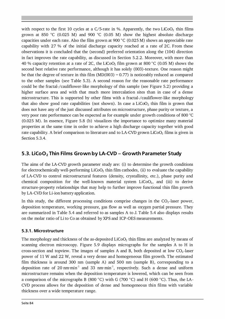
Seite 84
with respect to the first 10 cycles at a C/5-rate in %. Apparently, the two LiCoO2 thin films grown at 850 °C (0.025 M) and 900 °C (0.05 M) show the highest absolute discharge capacities under each rate. Also the film grown at 900 °C (0.025 M) shows an appreciable rate capability with 27 % of the initial discharge capacity reached at a rate of 2C. From these observations it is concluded that the (second) preferred orientation along the (104) direction in fact improves the rate capability, as discussed in Section 5.2.2. Moreover, with more than 40 % capacity retention at a rate of 2C, the LiCoO2 film grown at 800 °C (0.05 M) shows the second best relative rate performance, although it has solely (003)-texture. One reason might be that the degree of texture in this film (MD(003) = 0.77) is noticeably reduced as compared to the other samples (see Table 5.3). A second reason for the reasonable rate performance could be the fractal-/cauliflower-like morphology of this sample (see Figure 5.2) providing a higher surface area and with that much more intercalation sites than in case of a dense microstructure. This is supported by other films with a fractal-/cauliflower-like morphology that also show good rate capabilities (not shown). In case a LiCoO2 thin film is grown that does not have any of the just discussed attributes on microstructure, phase purity or texture, a very poor rate performance can be expected as for example under growth conditions of 800 °C (0.025 M). In essence, Figure 5.8 (b) visualizes the importance to optimize many material properties at the same time in order to achieve a high discharge capacity together with good rate capability. A brief comparison to literature and to LA-CVD grown LiCoO2 films is given in Section 5.3.4. 5.3. LiCoO2 Thin Films Grown by LA-CVD – Growth Parameter Study The aims of the LA-CVD growth parameter study are: (i) to determine the growth conditions for electrochemically well-performing LiCoO2 thin film cathodes, (ii) to evaluate the capability of LA-CVD to control microstructural features (density, crystallinity, etc.), phase purity and chemical composition for the well-known material system LiCoO2, and (iii) to derive structure-property relationships that may help to further improve functional thin film growth by LA-CVD for Li-ion battery application. In this study, the different processing conditions comprise changes in the CO2-laser power, deposition temperature, working pressure, gas flow as well as oxygen partial pressure. They are summarized in Table 5.4 and referred to as samples A to J. Table 5.4 also displays results on the molar ratio of Li to Co as obtained by XPS and ICP-OES measurements. 5.3.1. Microstructure The morphology and thickness of the as-deposited LiCoO2 thin films are analyzed by means of scanning electron microscopy. Figure 5.9 displays micrographs for the samples A to H in cross-section and topview. The images of samples A and B, both deposited at low CO2-laser power of 11 W and 22 W, reveal a very dense and homogeneous film growth. The estimated film thickness is around 300 nm (sample A) and 500 nm (sample B), corresponding to a deposition rate of 20 nm·min-1 and 33 nm·min-1, respectively. Such a dense and uniform microstructure remains when the deposition temperature is lowered, which can be seen from a comparison of the micrographs B (800 °C) with G (700 °C) and H (600 °C). Thus, the LA-CVD process allows for the deposition of dense and homogeneous thin films with variable thickness over a wide temperature range.
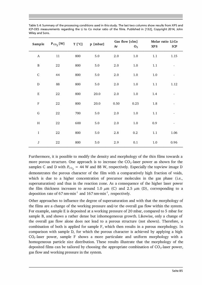
Seite 85
Table 5.4: Summary of the processing conditions used in this study. The last two columns show results from XPS and ICP-OES measurements regarding the Li to Co molar ratio of the films. Published in [132], Copyright 2014, John Wiley and Sons. Sample PCO2 [W] T [°C] p [mbar] Gas flow [slm] Ar O2 Molar ratio Li:Co XPS ICP
A 11 800 5.0 2.0 1.0 1.1 1.15 B 22 800 5.0 2.0 1.0 1.1 - C 44 800 5.0 2.0 1.0 1.0 - D 88 800 5.0 2.0 1.0 1.1 1.12 E 22 800 20.0 2.0 1.0 1.4 - F 22 800 20.0 0.50 0.25 1.8 - G 22 700 5.0 2.0 1.0 1.1 - H 22 600 5.0 2.0 1.0 0.9 - I 22 800 5.0 2.8 0.2 1.1 1.06 J 22 800 5.0 2.9 0.1 1.0 0.96
Furthermore, it is possible to modify the density and morphology of the thin films towards a more porous structure. One approach is to increase the CO2-laser power as shown for the samples C and D with PC O2 = 44 W and 88 W, respectively. Especially the topview image D demonstrates the porous character of the film with a comparatively high fraction of voids, which is due to a higher concentration of precursor molecules in the gas phase (i.e., supersaturation) and thus in the reaction zone. As a consequence of the higher laser power the film thickness increases to around 1.0 μm (C) and 2.5 μm (D), corresponding to a deposition rate of 67 nm·min-1 and 167 nm·min-1, respectively. Other approaches to influence the degree of supersaturation and with that the morphology of the films are a change of the working pressure and/or the overall gas flow within the system. For example, sample E is deposited at a working pressure of 20 mbar, compared to 5 mbar for sample B, and shows a rather dense but inhomogeneous growth. Likewise, only a change of the overall gas flow alone does not lead to a porous structure (not shown). Therefore, a combination of both is applied for sample F, which then results in a porous morphology. In comparison with sample D, for which the porous character is achieved by applying a high CO2-laser power, sample F shows a more particulate and uniform morphology with a homogeneous particle size distribution. These results illustrate that the morphology of the deposited films can be tailored by choosing the appropriate combination of CO2-laser power, gas flow and working pressure in the system.
Seite 86
Figure 5.9: Scanning electron micrographs of the as-deposited LiCoO2 thin films in cross-section and topview to illustrate different thicknesses and morphologies. The used processing conditions for samples A to H are given in Table 5.4. Underlying substrate in all cases: Si(100). Published in [132], Copyright 2014, John Wiley and Sons. The realization of different morphologies is one aspect that demonstrates the flexibility of the newly established LA-CVD approach for many fields of application. Very dense films are needed in electrode materials to achieve a high volumetric energy density and also in solid electrolyte materials to prevent an internal short circuit (see Chapter 6). Likewise, (nano)porous thin films are beneficial for many applications. For example, their high surface area enhances catalyzing effects as demonstrated in solid oxide fuel cells [200]. Moreover, an improved diffusivity of the ionic species observed in the cathode material LiFePO4 is due to nanosize effects [201], and to achieve reversibility in conversion-type anodes requires a nanoparticulate microstructure, too (see Chapter 7). Although the films presented in Figure 5.9 D and F are far from being nanoscaled, an optimization of the process parameters is possible and could lead to a nanograined thin film. The laser flash evaporation approach holds this potential, as shown in the example of nanocrystalline perovskite chemical vapor synthesis [149]. In the perovskite studies, a similar experimental setup was used and grain sizes below 10 nm have been reported. 5.3.2. Phase Composition and Texture In order to probe the structure and composition of the deposited films X-ray diffraction, Raman spectroscopy, X-ray photoelectron spectroscopy and inductively coupled plasma optical emission spectrometry studies are performed. The XRD pattern of the as-deposited LiCoO2 thin film B is plotted in Figure 5.10 (a) and is discussed as a representative for the other films. Besides the strong intensities of the underlying platinum substrate (Pt) the diffraction pattern shows a polycrystalline structure matching the one of stoichiometric LiCoO2 [56] with lattice parameters of a = 2.8159(3) Å and c = 14.050(8) Å (see Table 5.5). Furthermore, a detailed investigation of the peak
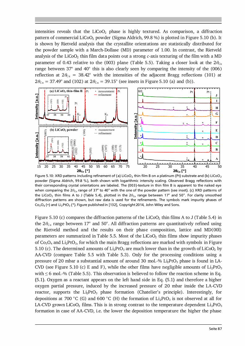
Seite 87
intensities reveals that the LiCoO2 phase is highly textured. As comparison, a diffraction pattern of commercial LiCoO2 powder (Sigma Aldrich, 99.8 %) is plotted in Figure 5.10 (b). It is shown by Rietveld analysis that the crystallite orientations are statistically distributed for the powder sample with a March-Dollase (MD) parameter of 1.00. In contrast, the Rietveld analysis of the LiCoO2 thin film data points out a strong c-axis texturing of the film with a MD parameter of 0.43 relative to the (003) plane (Table 5.5). Taking a closer look at the 2 Cu range between 37° and 40° this is also clearly seen by comparing the intensity of the (006) reflection at 2 C u = 38.42° with the intensities of the adjacent Bragg reflections (101) at 2 C u = 37.49° and (102) at 2 C u = 39.15° (see insets in Figure 5.10 (a) and (b)).
Figure 5.10: XRD patterns including refinement of (a) LiCoO2 thin film B on a platinum (Pt) substrate and (b) LiCoO2 powder (Sigma Aldrich, 99.8 %), both shown with logarithmic intensity scaling. Observed Bragg reflections with their corresponding crystal orientations are labeled. The (003)-texture in thin film B is apparent to the naked eye when comparing the 2 Cu range of 37° to 40° with the one of the powder pattern (see inset). (c) XRD patterns of the LiCoO2 thin films A to J (Table 5.4), plotted in the 2 Cu range between 17° and 50°. For clarity smoothed diffraction patterns are shown, but raw data is used for the refinements. The symbols mark impurity phases of Co3O4 (+) and Li2PtO3 (*). Figure published in [132], Copyright 2014, John Wiley and Sons. Figure 5.10 (c) compares the diffraction patterns of the LiCoO2 thin films A to J (Table 5.4) in the 2 C u range between 17° and 50°. All diffraction patterns are quantitatively refined using the Rietveld method and the results on their phase composition, lattice and MD(00l) parameters are summarized in Table 5.5. Most of the LiCoO2 thin films show impurity phases of Co3O4 and Li2PtO3, for which the main Bragg reflections are marked with symbols in Figure 5.10 (c). The determined amounts of Li2PtO3 are much lower than in the growth of LiCoO2 by AA-CVD (compare Table 5.5 with Table 5.3). Only for the processing conditions using a pressure of 20 mbar a substantial amount of around 30 mol.-% Li2PtO3 phase is found in LA-CVD (see Figure 5.10 (c) E and F), while the other films have negligible amounts of Li2PtO3 with ≤ 6 mol.-% (Table 5.5). This observation is believed to follow the reaction scheme in Eq. (5.1). Oxygen as a reactant appears on the left hand side in Eq. (5.1) and therefore a higher oxygen partial pressure, induced by the increased pressure of 20 mbar inside the LA-CVD reactor, supports the Li2PtO3 phase formation (Chatelier’s principle). Interestingly, for depositions at 700 °C (G) and 600 °C (H) the formation of Li2PtO3 is not observed at all for LA-CVD grown LiCoO2 films. This is in strong contrast to the temperature dependent Li2PtO3 formation in case of AA-CVD, i.e. the lower the deposition temperature the higher the phase
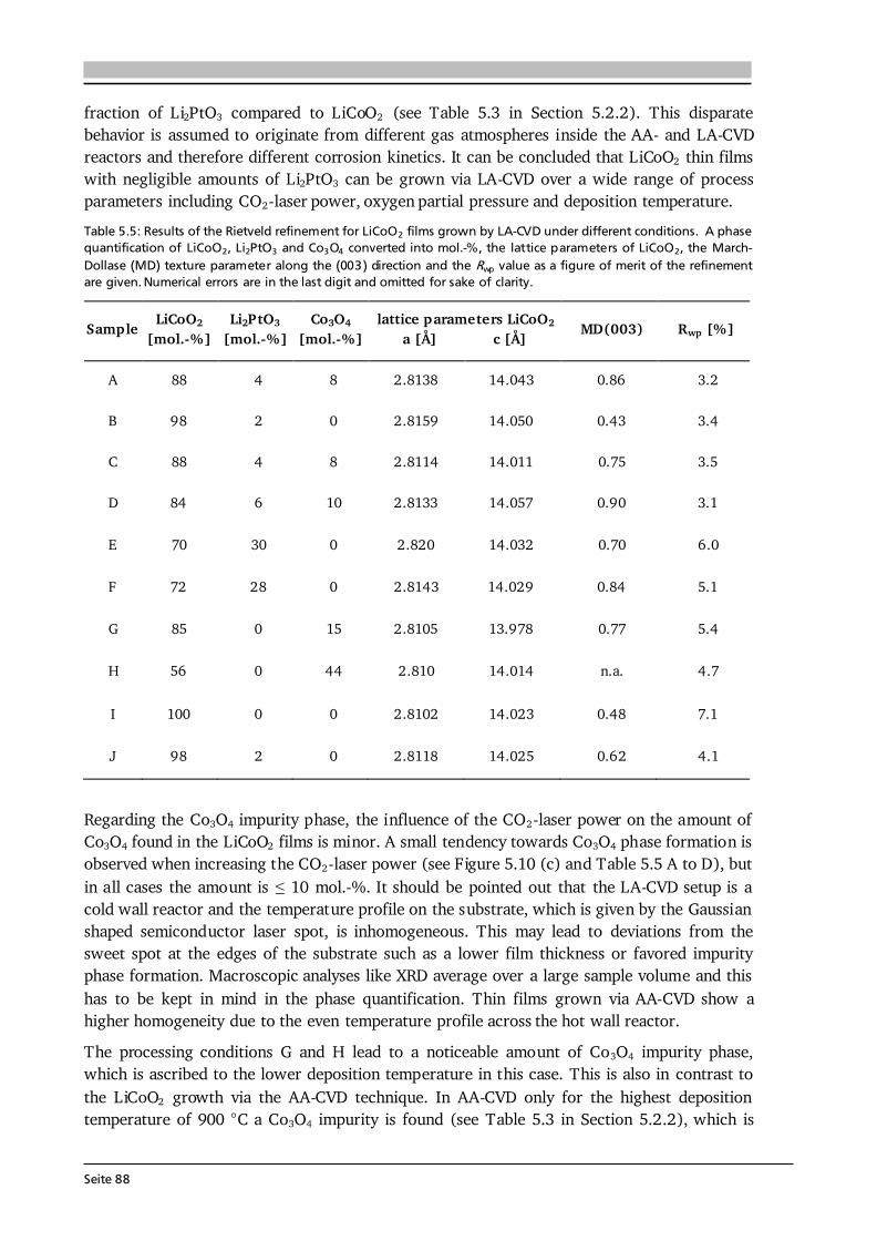
Seite 88
fraction of Li2PtO3 compared to LiCoO2 (see Table 5.3 in Section 5.2.2). This disparate behavior is assumed to originate from different gas atmospheres inside the AA- and LA-CVD reactors and therefore different corrosion kinetics. It can be concluded that LiCoO2 thin films with negligible amounts of Li2PtO3 can be grown via LA-CVD over a wide range of process parameters including CO2-laser power, oxygen partial pressure and deposition temperature. Table 5.5: Results of the Rietveld refinement for LiCoO2 films grown by LA-CVD under different conditions. A phase quantification of LiCoO2, Li2PtO3 and Co3O4 converted into mol.-%, the lattice parameters of LiCoO2, the March-Dollase (MD) texture parameter along the (003) direction and the Rwp value as a figure of merit of the refinement are given. Numerical errors are in the last digit and omitted for sake of clarity. Sample LiCoO2 [mol.-%] Li2PtO3 [mol.-%] Co3O4 [mol.-%] lattice parameters LiCoO2 a [Å] c [Å] MD(003) Rwp [%]
A 88 4 8 2.8138 14.043 0.86 3.2 B 98 2 0 2.8159 14.050 0.43 3.4 C 88 4 8 2.8114 14.011 0.75 3.5 D 84 6 10 2.8133 14.057 0.90 3.1 E 70 30 0 2.820 14.032 0.70 6.0 F 72 28 0 2.8143 14.029 0.84 5.1 G 85 0 15 2.8105 13.978 0.77 5.4 H 56 0 44 2.810 14.014 n.a. 4.7 I 100 0 0 2.8102 14.023 0.48 7.1 J 98 2 0 2.8118 14.025 0.62 4.1
Regarding the Co3O4 impurity phase, the influence of the CO2-laser power on the amount of Co3O4 found in the LiCoO2 films is minor. A small tendency towards Co3O4 phase formation is observed when increasing the CO2-laser power (see Figure 5.10 (c) and Table 5.5 A to D), but in all cases the amount is ≤ 10 mol.-%. It should be pointed out that the LA-CVD setup is a cold wall reactor and the temperature profile on the substrate, which is given by the Gaussian shaped semiconductor laser spot, is inhomogeneous. This may lead to deviations from the sweet spot at the edges of the substrate such as a lower film thickness or favored impurity phase formation. Macroscopic analyses like XRD average over a large sample volume and this has to be kept in mind in the phase quantification. Thin films grown via AA-CVD show a higher homogeneity due to the even temperature profile across the hot wall reactor. The processing conditions G and H lead to a noticeable amount of Co3O4 impurity phase, which is ascribed to the lower deposition temperature in this case. This is also in contrast to the LiCoO2 growth via the AA-CVD technique. In AA-CVD only for the highest deposition temperature of 900 °C a Co3O4 impurity is found (see Table 5.3 in Section 5.2.2), which is
Seite 89
attributed to the loss of volatile lithium compounds at such high temperature. However, at 600 °C this argument appears implausible, and other factors must promote the Co3O4 formation in the LA-CVD process. One possibility is limited diffusion on the substrate at lower deposition temperatures. In the aerosol assisted precursor delivery the correct stoichiometry is given in each and every droplet that reaches the substrate and therefore less surface diffusion is needed. In the precursor delivery via CO2-laser flash evaporation the element distribution in the gas phase is strongly dependent on external factors such as the gas stream and heat profile in the reactor, gravity, and so on. These effects might lead to an inhomogeneous element distribution on the substrate when diffusion is inhibited by an inadequately low deposition temperature, resulting in Co3O4 formation. Also the reaction kinetics may play a role in this respect as LiCoO2 synthesis may start from different intermediates as a result of the Li-tmhd and Co-acac decomposition [137,202], which may vary for the AA-CVD and LA-CVD process. The lack of oxygen or oxidizing atmosphere to completely oxidize cobalt (from Co2+/3+ in Co3O4 to Co3+ in LiCoO2) as possible explanation for the presence of Co3O4 in LA-CVD grown LiCoO2 films is excluded. In comparison to AA-CVD, no oxygen is needed to combust the solvent in LA-CVD. Furthermore, even for very low oxygen partial pressures LiCoO2 films free of Co3O4 can be grown (samples I and J). Concerning the texture of the LiCoO2 thin films, it is observed that the practically phase pure samples B, I and J are highly textured with MD(003) parameters of 0.43, 0.48 and 0.62, respectively (see Table 5.5). The other samples grown by LA-CVD have MD(003) values in the range of 0.70 to 0.90, so they are less textured. Here, one could only speculate whether or not the degree of texture depends on the phase purity. Assuming such a correlation exists, one would assume that Co3O4 lowers the (003) oriented growth of LiCoO2 far more than Li2PtO3 does based on the crystal structures of Co3O4, Li2PtO3 and LiCoO2. They can all be derived from a cubic close packing of oxygen anions, which might be considered as a common building block for the crystal growth during the LA-CVD process. In contrast to LiCoO2, the cation sublattice of Co3O4 has a higher symmetry resulting in the fact that differently oriented directions such as [111] and [-111] are symmetrically equivalent. Thus, the higher symmetry favors multidirectional growth and might therefore lower the (003) oriented growth of LiCoO2. Li2PtO3 is structurally related to LiCoO2 and hence should support a directional growth [186,203]. Yet, other effects such as the film thickness [195] can influence the preferred orientation in LiCoO2 as well, so that more research would be necessary to clarify the role of impurity phases on the texture. In summary, under all processing conditions studied the preferred orientation in LA-CVD grown LiCoO2 films is (exclusively) along the (003) direction. In comparison to AA-CVD grown LiCoO2 films the degree of texture is comparable or slightly lower with all the consequences already discussed in Section 5.2.2. Figure 5.11 (a) summarizes the Raman spectra of the LiCoO2 thin films A to J, while Figure 5.11 (b) provides reference spectra of a Li2PtO3 thin film grown by LA-CVD and commercial LiCoO2 powder (Sigma Aldrich, 99.8 %). All Raman spectra are referenced to the Raman shift of single-crystal silicon at νSi = 521 cm-1 [103]. At ν1 = 488 cm-1 and ν2 = 597 cm-1 typical Raman shifts for HT-LiCoO2 are observed in all cases. Note that, except for sample H, no indications for impurity phases such as Co3O4 or LT-LiCoO2 or Li2PtO3 are detected, independent of the processing conditions used. As the configuration of the Raman spectrometer probes an area of a few square micrometers this result implies that under many different processing conditions, including changes in the CO2-laser power, deposition
Seite 90
temperature, working pressure, gas flow as well as the oxygen partial pressure, phase pure HT-LiCoO2 is synthesized on a local scale. The apparent discrepancy between the Raman and XRD results is ascribed to the fact that XRD averages over a far larger sample volume. Especially at the edges of the thin films, where the processing conditions may slightly deviate from the sweet spot, impurity phase formation can be more likely as result of the inhomogeneous temperature profile discussed earlier in this section. In the case of sample H the additional Raman shifts located at 526 cm-1, 625 cm-1 and 696 cm-1 are assigned to a Co3O4 impurity phase. This finding is consistent with the XRD data and indicates that for a deposition temperature of 600 °C small fractions of Co3O4 impurity phase are distributed over the whole volume of the film.
Figure 5.11: (a) Raman spectra of the LiCoO2 thin films A to J (Table 5.4). Typical Raman shifts for the HT-LiCoO2 phase are observed at 488 cm-1 and 597 cm-1. To allow an easy comparison normalized raw data is shown and Raman shifts of Co3O4 are marked (*). Published in [132], Copyright 2014, John Wiley and Sons. (b) Raman reference spectra of a Li2PtO3 thin film grown by LA-CVD and commercial LiCoO2 powder (Sigma Aldrich, 99.8 %). In order to check the chemical composition of the deposited thin films on an atomic level, XPS measurements are performed on all LiCoO2 films A to J. As an example the Co 2p core level spectra are shown in Figure 5.12 (a). Two main components due to spin-orbit splitting at binding energies of 795.3 eV (2p1/2) and 780.2 eV (2p3/2) are observed, with the splitting of 15.1 eV being consistent with literature values [113]. Additionally, satellite states with an energy shift towards higher binding energies of about 9.9 eV are visible that are characteristic for a Co3+ valence [204,205], as it is expected for stoichiometric LiCoO2. Although a small shoulder on the high binding energy side of the Co 2p3/2 emission can be seen, the spectra lack the corresponding satellite emissions from valences other than Co3+. Therefore, it is assumed that either the contribution from other valences than Co3+ is negligible or the observed shoulder is even originating from other effects such as non-local screening [206]. Furthermore, a quantitative analysis of the Co 2p as well as the Li 1s, C 1s, O 1s photoelectron spectra is applied and the Li to Co molar ratio for every sample A to J is calculated. The results, listed in Table 5.4, represent only the first atomic layers as XPS is a surface sensitive technique. For all samples, except E and F, the Li to Co molar ratio is in the range of 0.9 to 1.1. This indicates the deposition of stoichiometric LiCoO2 within the error margins of this technique [113] and supports the discussion for the cobalt valence given above. The XPS
Seite 91
results show that sample H has the lowest Li to Co molar ratio of 0.9, which is consistent with the XRD and Raman spectroscopy results since small fractions of the Co3O4 impurity phase are found to be distributed over the whole volume of the film. Likewise, XRD reveals a substantial amount of the Li2PtO3 impurity phase for the samples E and F (see Figure 5.10 (c)), which is confirmed by the XPS analysis with Li to Co molar ratios of about 1.4 and 1.8, respectively. The XPS survey spectra of the samples E and F show emission lines of Pt (not shown) leading to the conclusion that the LiCoO2 coating is non-uniform in these two samples. This agrees with the observations in SEM of a porous film (see Figure 5.9).
Figure 5.12: (a) Co 2p photoelectron spectra of the LiCoO2 thin films A to J (Table 5.4). The two main components 2p1/2 and 2p3/2 are observed at binding energies of 795.3 eV and 780.2 eV, respectively. Their corresponding satellite states are shifted about 9.9 eV towards higher binding energies, which is characteristic for a Co 3+ valence. For clarity normalized and smoothed spectra are shown. Published in [132], Copyright 2014, John Wiley and Sons. (b) Li 1s, C 1s, O 1s and Co 2p spectra of the LiCoO2 film A, pristine (black) and after 4 times Ar-ion bombardment with 1 keV for 5 min each (in color). Already after the first sputtering (5 min) no carbon signal is detected anymore, indicating the LiCoO2 film is free of carbon. Upon sputtering cobalt is reduced from Co3+ to Co2+ (black arrows). Argon ion etching is used in order to get information on the chemical composition of the LiCoO2 films A to J as a function of sputter time (Figure 5.12 (b)). Unfortunately, preferential sputtering, most likely of lithium ions [207], takes place so that from the depth profiling no reliable conclusions on the chemical composition can be drawn. Moreover, upon sputtering cobalt is reduced from Co3+ to Co2+ as can be seen by the CoO-like satellite structure and which is in agreement with literature [208,209]. The atomic concentration of carbon, which is determined to be around 10 at.-% at the surface of the thin films, reduces after argon ion etching to ≤ 1 at.-% (see Figure 5.12 (b)). Therefore, it is concluded that after removing carbon residues from the surface no carbon impurities persist within the thin films, which holds true independent of the used processing conditions. Consequently, the LA-CVD approach allows for a highly controlled growth of LiCoO2 thin films with a high degree of purity over the entire growth period. As an additional analysis tool to probe the chemical composition of the films ICP-OES measurements are performed on selected samples A, D, I and J (see Section 3.7). This technique averages over the whole volume of the film, in contrast to XPS, and therefore gives a complementary insight into the chemical composition. The LiCoO2 thin films I and J, both
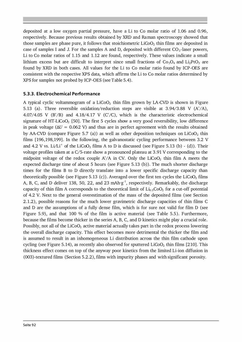
Seite 92
deposited at a low oxygen partial pressure, have a Li to Co molar ratio of 1.06 and 0.96, respectively. Because previous results obtained by XRD and Raman spectroscopy showed that those samples are phase pure, it follows that stoichiometric LiCoO2 thin films are deposited in case of samples I and J. For the samples A and D, deposited with different CO2-laser powers, Li to Co molar ratios of 1.15 and 1.12 are found, respectively. These values indicate a small lithium excess but are difficult to interpret since small fractions of Co3O4 and Li2PtO3 are found by XRD in both cases. All values for the Li to Co molar ratio found by ICP-OES are consistent with the respective XPS data, which affirms the Li to Co molar ratios determined by XPS for samples not probed by ICP-OES (see Table 5.4). 5.3.3. Electrochemical Performance A typical cyclic voltammogram of a LiCoO2 thin film grown by LA-CVD is shown in Figure 5.13 (a). Three reversible oxidation/reduction steps are visible at 3.94/3.88 V (A’/A), 4.07/4.05 V (B’/B) and 4.18/4.17 V (C’/C), which is the characteristic electrochemical signature of HT-LiCoO2 [50]. The first 5 cycles show a very good reversibility, low difference in peak voltage (ΔU = 0.062 V) and thus are in perfect agreement with the results obtained by AA-CVD (compare Figure 5.7 (a)) as well as other deposition techniques on LiCoO2 thin films [196,198,199]. In the following, the galvanostatic cycling performance between 3.2 V and 4.2 V vs. Li/Li+ of the LiCoO2 films A to D is discussed (see Figure 5.13 (b) - (d)). Their voltage profiles taken at a C/5-rate show a pronounced plateau at 3.91 V corresponding to the midpoint voltage of the redox couple A’/A in CV. Only the LiCoO2 thin film A meets the expected discharge time of about 5 hours (see Figure 5.13 (b)). The much shorter discharge times for the films B to D directly translate into a lower specific discharge capacity than theoretically possible (see Figure 5.13 (c)). Averaged over the first ten cycles the LiCoO2 films A, B, C, and D deliver 138, 50, 22, and 23 mAh·g-1, respectively. Remarkably, the discharge capacity of thin film A corresponds to the theoretical limit of Li0.5CoO2 for a cut-off potential of 4.2 V. Next to the general overestimation of the mass of the deposited films (see Section 2.1.2), possible reasons for the much lower gravimetric discharge capacities of thin films C and D are the assumptions of a fully dense film, which is for sure not valid for film D (see Figure 5.9), and that 100 % of the film is active material (see Table 5.5). Furthermore, because the films become thicker in the series A, B, C, and D kinetics might play a crucial role. Possibly, not all of the LiCoO2 active material actually takes part in the redox process lowering the overall discharge capacity. This effect becomes more detrimental the thicker the film and is assumed to result in an inhomogeneous Li distribution across the thin film cathode upon cycling (see Figure 5.14), as recently also observed for sputtered LiCoO2 thin films [210]. This thickness effect comes on top of the anyway poor kinetics from the limited Li-ion diffusion in (003)-textured films (Section 5.2.2), films with impurity phases and with significant porosity.
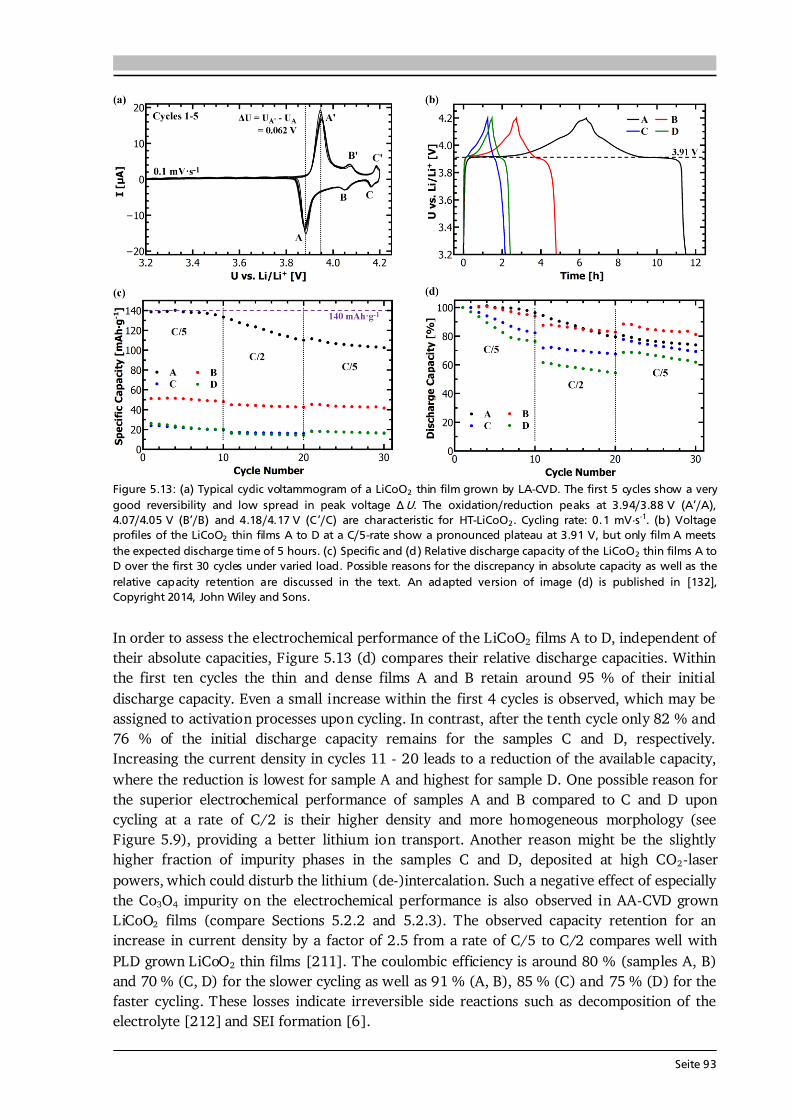
Seite 93
Figure 5.13: (a) Typical cyclic voltammogram of a LiCoO2 thin film grown by LA-CVD. The first 5 cycles show a very good reversibility and low spread in peak voltage ΔU. The oxidation/reduction peaks at 3.94/3.88 V (A’/A), 4.07/4.05 V (B’/B) and 4.18/4.17 V (C’/C) are characteristic for HT-LiCoO2. Cycling rate: 0.1 mV·s-1. (b) Voltage profiles of the LiCoO2 thin films A to D at a C/5-rate show a pronounced plateau at 3.91 V, but only film A meets the expected discharge time of 5 hours. (c) Specific and (d) Relative discharge capacity of the LiCoO2 thin films A to D over the first 30 cycles under varied load. Possible reasons for the discrepancy in absolute capacity as well as the relative capacity retention are discussed in the text. An adapted version of image (d) is published in [132], Copyright 2014, John Wiley and Sons. In order to assess the electrochemical performance of the LiCoO2 films A to D, independent of their absolute capacities, Figure 5.13 (d) compares their relative discharge capacities. Within the first ten cycles the thin and dense films A and B retain around 95 % of their initial discharge capacity. Even a small increase within the first 4 cycles is observed, which may be assigned to activation processes upon cycling. In contrast, after the tenth cycle only 82 % and 76 % of the initial discharge capacity remains for the samples C and D, respectively. Increasing the current density in cycles 11 - 20 leads to a reduction of the available capacity, where the reduction is lowest for sample A and highest for sample D. One possible reason for the superior electrochemical performance of samples A and B compared to C and D upon cycling at a rate of C/2 is their higher density and more homogeneous morphology (see Figure 5.9), providing a better lithium ion transport. Another reason might be the slightly higher fraction of impurity phases in the samples C and D, deposited at high CO2-laser powers, which could disturb the lithium (de-)intercalation. Such a negative effect of especially the Co3O4 impurity on the electrochemical performance is also observed in AA-CVD grown LiCoO2 films (compare Sections 5.2.2 and 5.2.3). The observed capacity retention for an increase in current density by a factor of 2.5 from a rate of C/5 to C/2 compares well with PLD grown LiCoO2 thin films [211]. The coulombic efficiency is around 80 % (samples A, B) and 70 % (C, D) for the slower cycling as well as 91 % (A, B), 85 % (C) and 75 % (D) for the faster cycling. These losses indicate irreversible side reactions such as decomposition of the electrolyte [212] and SEI formation [6].
Seite 94
Figure 5.14: Illustration of a possible inhomogeneous Li distribution (black dotted line) across the thin film cathode (yellow) upon charging due to limited Li diffusion and/or too fast charging of thick films. In thick films the cut-off potential, here 4.2 V corresponding to a Li concenctration of x = 0.5, might be reached before Li located close to the current collector is depleted leading to unused charge and thus reduced (discharge) capacity (red arrow). In contrast, the Li concentration equilibrates faster in thin films. This sketch is only for illustration and does not necessarily represent a physically correct and complete model to describe the Li distribution in thin film cathodes. After 30 cycles the LiCoO2 thin films A, B, C and D retain 73 %, 81 %, 70 % and 62 % of their initial discharge capacity, corresponding to an average capacity fade per cycle of 1.0 %, 0.7 %, 1.2 % and 1.6 %, respectively. The fact that sample B shows the best electrochemical performance after 30 cycles is unexpected, because sample A recovered slightly more capacity after 10 cycles. Sample B is practically phase pure compared to sample A, which has small fractions of Li2PtO3 and Co3O4 impurity phases (see Table 5.5). Thus, it can be concluded that the better electrochemical performance of LiCoO2 thin film B in the long run results from its phase purity. It shall be noted that SEM analyses of all films after electrochemical cycling (not shown) rule out delamination of the films. 5.3.4. Comparison to Literature Many deposition techniques are available to grow LiCoO2 thin films [6,13], with sputtering and PLD being more widely used than sol-gel, CVD or electrochemical routes. Most of the literature, especially on sputtering, PLD and sol-gel, report an additional post-annealing treatment required to achieve certain material properties such as good crystallinity, phase purity, desired microstructure and with that reasonable electrochemical performance [6]. In contrast, the LiCoO2 thin films described within this thesis are characterized as-deposited and cycled under ambient conditions. Among all deposition techniques, one of the best performing LiCoO2 thin films is grown via RF-sputtering [213] with an initial discharge capacity of 50 μAh·cm-2·μm-1 and a capacity retention of 90 % after 50 cycles (see Table 5.6). To date, its performance can be considered as benchmark. So far, only the two groups of Notten et al. [38,214] and Yoon et al. [37,215–217] have published results on the electrochemical performance of LiCoO2 thin films grown by CVD/ALD. The best performing LiCoO2 films grown via AA-CVD and LA-CVD in this thesis are comparable to their top results (see Table 5.6), especially considering that no post-annealing was applied. Unfortunately, the comparison is hampered by the different test conditions used, such as the current density, cut-off voltage, or number of cycles, which are factors influencing the electrochemical performance and ageing of the cells. Nevertheless, it shows the potential of AA-CVD and LA-CVD grown LiCoO2 films for Li-ion battery application. Further performance improvements are expected for the use of a surface coating (see Section 5.5.2) and when air exposure of the LiCoO2 films is avoided during the entire processing [59].
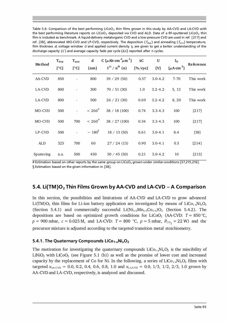
Seite 95
Table 5.6: Comparison of the best performing LiCoO2 thin films grown in this study by AA-CVD and LA-CVD with the best performing literature reports on LiCoO2 deposited via CVD and ALD. Data of a RF-sputtered LiCoO2 thin film is included as benchmark. A liquid-delivery metalorganic CVD and a low-pressure CVD are used in ref. [217] and ref. [38], abbreviated MO-CVD and LP-CVD, respectively. The deposition (Tdep ) and annealing (Tann) temperature, film thickness d, voltage window U and applied current density ID are given to get a better understanding of the discharge capacity (C ) and average capacity fade per cycle (ΔC) reported after n cycles. Method Tdep
[°C] Tann [°C]
d [nm]
C [μAh·cm-2μm-1] 1st / nth (n)
ΔC [%/cyc]
U [V]
ID [μA·cm-2] Reference
AA-CVD 850 - 800 39 / 29 (50) 0.57 3.0-4.2 7-70 This work LA-CVD 800 - 300 70 / 51 (30) 1.0 3.2-4.2 5, 13 This work LA-CVD 800 - 500 26 / 21 (30) 0.69 3.2-4.2 8, 20 This work MO-CVD 500 - < 260# 38 / 18 (100) 0.74 3.3-4.3 100 [217] MO-CVD 500 700 < 260# 38 / 27 (100) 0.34 3.3-4.3 100 [217] LP-CVD 500 - ~ 180§ 18 / 13 (50) 0.61 3.0-4.1 8.4 [38]
ALD 325 700 60 27 / 24 (13) 0.90 3.0-4.1 0.5 [214] Sputtering n.a. 500 450 50 / 45 (50) 0.21 3.0-4.2 10 [213]
# Estimation based on other reports by the same group on LiCoO2 grown under similar conditions [37,215,216]. § Estimation based on the given information in [38].
5.4. Li(TM)O2 Thin Films Grown by AA-CVD and LA-CVD – A Comparison In this section, the possibilities and limitations of AA-CVD and LA-CVD to grow advanced Li(TM)O2 thin films for Li-ion battery application are investigated by means of LiCo1-xNixO2 (Section 5.4.1) and commercially successful Li(Ni1/3Mn1/3Co1/3)O2 (Section 5.4.2). The depositions are based on optimized growth conditions for LiCoO2 (AA-CVD: T = 850 °C, p = 900 mbar, c = 0.025 M, and LA-CVD: T = 800 °C, p = 5 mbar, PC O2 = 22 W) and the precursor mixture is adjusted according to the targeted transition metal stoichiometry. 5.4.1. The Quaternary Compounds LiCo1-xNixO2 The motivation for investigating the quaternary compounds LiCo1-xNixO2 is the miscibility of LiNiO2 with LiCoO2 (see Figure 5.1 (b)) as well as the promise of lower cost and increased capacity by the replacement of Co for Ni. In the following, a series of LiCo1-xNixO2 films with targeted xAA-C VD = 0.0, 0.2, 0.4, 0.6, 0.8, 1.0 and xL A-C VD = 0.0, 1/3, 1/2, 2/3, 1.0 grown by AA-CVD and LA-CVD, respectively, is analyzed and discussed.

Seite 96
Microstructure and Element Composition The microstructure of the LiCo1-xNixO2 thin films is characterized by SEM and the topview images are shown in Figure 5.15 (a). For both growth methods, AA-CVD (upper panel) and LA-CVD (lower panel), the films’ microstructure becomes more fine-grained with increasing x, which is evident by a comparison of the end members x = 0 (LiCoO2) and x = 1. Moreover, in case of AA-CVD grown LiCo1-xNixO2 films, a lower fraction of voids is observed with increasing x leading to the conclusion of increased density in such films. At the same time the morphology of the grains changes in AA-CVD grown films as opposed to the LA-CVD grown films, for which the morphology stays similar along the LiCo1-xNixO2 series. It is believed that the described evolution in microstructure is directly related to the evolution in phase composition, which is different for both growth methods and discussed in the next subsection.
Figure 5.15: (a) SEM topview images of LiCo1-xNixO2 thin films grown by AA-CVD (upper panel) and LA-CVD (lower panel). With increasing x the films’ microstructure becomes more fine-grained. (b) EDX spectra of LiCo1-xNixO2 thin films grown by AA-CVD (left graph) and LA-CVD (right graph). The evolution of the nickel and cobalt proportion is nicely traceable in the spectra and the determined transition metal composition agrees well with the targeted one (middle graph). The transition metal composition of the LiCo1-xNixO2 thin films is examined by EDX (see Figure 5.15 (b)). The replacement of Co by Ni is easy to follow on the basis of the Kα- and Lα-lines of Co and Ni in the EDX spectra of AA-CVD (left graph) and LA-CVD (right graph) grown films. The Ni fraction is determined by a fit to the EDX spectra and plotted over the targeted Ni content in the middle graph of Figure 5.15 (b). In first approximation both methods follow the ideal curve (black dotted line). Upon close inspection, for AA-CVD an excellent agreement between the determined and targeted transition metal composition is reproducibly achieved over the entire compositional range, whereas for LA-CVD small deviations occur, e.g. for x = 2/3 the Ni fraction is identified as 60 % only. The reason for this deviation lies in the
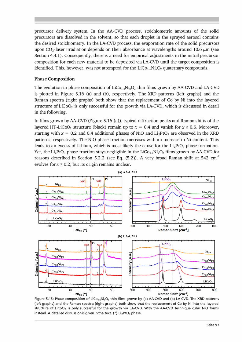
Seite 97
precursor delivery system. In the AA-CVD process, stoichiometric amounts of the solid precursors are dissolved in the solvent, so that each droplet in the sprayed aerosol contains the desired stoichiometry. In the LA-CVD process, the evaporation rate of the solid precursors upon CO2-laser irradiation depends on their absorbance at wavelengths around 10.6 μm (see Section 4.4.1). Consequently, there is a need for empirical adjustments in the initial precursor composition for each new material to be deposited via LA-CVD until the target composition is identified. This, however, was not attempted for the LiCo1-xNixO2 quaternary compounds. Phase Composition The evolution in phase composition of LiCo1-xNixO2 thin films grown by AA-CVD and LA-CVD is plotted in Figure 5.16 (a) and (b), respectively. The XRD patterns (left graphs) and the Raman spectra (right graphs) both show that the replacement of Co by Ni into the layered structure of LiCoO2 is only successful for the growth via LA-CVD, which is discussed in detail in the following. In films grown by AA-CVD (Figure 5.16 (a)), typical diffraction peaks and Raman shifts of the layered HT-LiCoO2 structure (black) remain up to x = 0.4 and vanish for x ≥ 0.6. Moreover, starting with x = 0.2 and 0.4 additional phases of NiO and Li2PtO3 are observed in the XRD patterns, respectively. The NiO phase fraction increases with an increase in Ni content. This leads to an excess of lithium, which is most likely the cause for the Li2PtO3 phase formation. Yet, the Li2PtO3 phase fraction stays negligible in the LiCo1-xNixO2 films grown by AA-CVD for reasons described in Section 5.2.2 (see Eq. (5.2)). A very broad Raman shift at 542 cm-1 evolves for x ≥ 0.2, but its origin remains unclear.
Figure 5.16: Phase composition of LiCo1-xNixO2 thin films grown by (a) AA-CVD and (b) LA-CVD. The XRD patterns (left graphs) and the Raman spectra (right graphs) both show that the replacement of Co by Ni into the layered structure of LiCoO2 is only successful for the growth via LA-CVD. With the AA-CVD technique cubic NiO forms instead. A detailed discussion is given in the text. (*) Li2PtO3 phase.
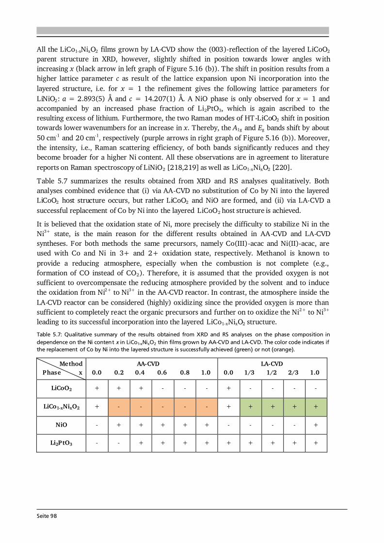
Seite 98
All the LiCo1-xNixO2 films grown by LA-CVD show the (003)-reflection of the layered LiCoO2 parent structure in XRD, however, slightly shifted in position towards lower angles with increasing x (black arrow in left graph of Figure 5.16 (b)). The shift in position results from a higher lattice parameter c as result of the lattice expansion upon Ni incorporation into the layered structure, i.e. for x = 1 the refinement gives the following lattice parameters for LiNiO2: a = 2.893(5) Å and c = 14.207(1) Å. A NiO phase is only observed for x = 1 and accompanied by an increased phase fraction of Li2PtO3, which is again ascribed to the resulting excess of lithium. Furthermore, the two Raman modes of HT-LiCoO2 shift in position towards lower wavenumbers for an increase in x. Thereby, the A1g and Eg bands shift by about 50 cm-1 and 20 cm-1, respectively (purple arrows in right graph of Figure 5.16 (b)). Moreover, the intensity, i.e., Raman scattering efficiency, of both bands significantly reduces and they become broader for a higher Ni content. All these observations are in agreement to literature reports on Raman spectroscopy of LiNiO2 [218,219] as well as LiCo1-xNixO2 [220]. Table 5.7 summarizes the results obtained from XRD and RS analyses qualitatively. Both analyses combined evidence that (i) via AA-CVD no substitution of Co by Ni into the layered LiCoO2 host structure occurs, but rather LiCoO2 and NiO are formed, and (ii) via LA-CVD a successful replacement of Co by Ni into the layered LiCoO2 host structure is achieved. It is believed that the oxidation state of Ni, more precisely the difficulty to stabilize Ni in the Ni3+ state, is the main reason for the different results obtained in AA-CVD and LA-CVD syntheses. For both methods the same precursors, namely Co(III)-acac and Ni(II)-acac, are used with Co and Ni in 3+ and 2+ oxidation state, respectively. Methanol is known to provide a reducing atmosphere, especially when the combustion is not complete (e.g., formation of CO instead of CO2). Therefore, it is assumed that the provided oxygen is not sufficient to overcompensate the reducing atmosphere provided by the solvent and to induce the oxidation from Ni2+ to Ni3+ in the AA-CVD reactor. In contrast, the atmosphere inside the LA-CVD reactor can be considered (highly) oxidizing since the provided oxygen is more than sufficient to completely react the organic precursors and further on to oxidize the Ni2+ to Ni3+ leading to its successful incorporation into the layered LiCo1-xNixO2 structure. Table 5.7: Qualitative summary of the results obtained from XRD and RS analyses on the phase composition in dependence on the Ni content x in LiCo1-xNixO2 thin films grown by AA-CVD and LA-CVD. The color code indicates if the replacement of Co by Ni into the layered structure is successfully achieved (green) or not (orange). Method Phase x AA-CVD 0.0 0.2 0.4 0.6 0.8 1.0 LA-CVD 0.0 1/3 1/2 2/3 1.0
LiCoO2 + + + - - - + - - - - LiCo1-xNixO2 + - - - - - + + + + +
NiO - + + + + + - - - - + Li2PtO3 - - + + + + + + + + +
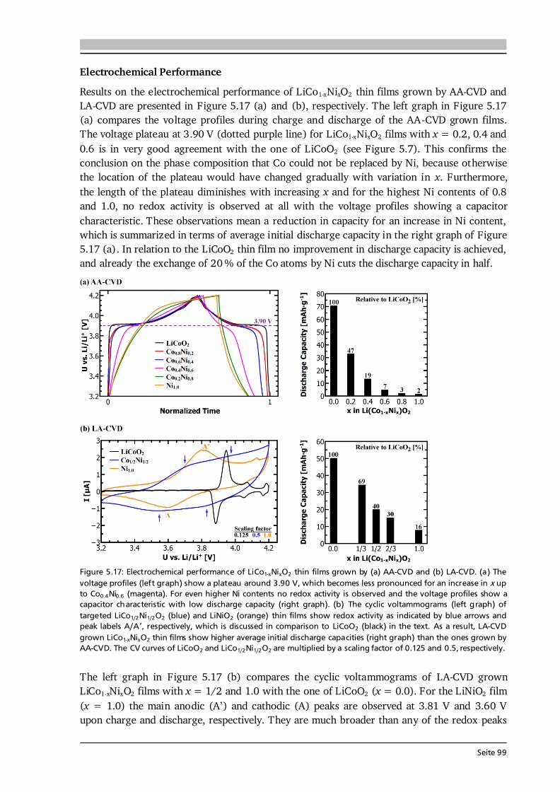
Seite 99
Electrochemical Performance Results on the electrochemical performance of LiCo1-xNixO2 thin films grown by AA-CVD and LA-CVD are presented in Figure 5.17 (a) and (b), respectively. The left graph in Figure 5.17 (a) compares the voltage profiles during charge and discharge of the AA-CVD grown films. The voltage plateau at 3.90 V (dotted purple line) for LiCo1-xNixO2 films with x = 0.2, 0.4 and 0.6 is in very good agreement with the one of LiCoO2 (see Figure 5.7). This confirms the conclusion on the phase composition that Co could not be replaced by Ni, because otherwise the location of the plateau would have changed gradually with variation in x. Furthermore, the length of the plateau diminishes with increasing x and for the highest Ni contents of 0.8 and 1.0, no redox activity is observed at all with the voltage profiles showing a capacitor characteristic. These observations mean a reduction in capacity for an increase in Ni content, which is summarized in terms of average initial discharge capacity in the right graph of Figure 5.17 (a). In relation to the LiCoO2 thin film no improvement in discharge capacity is achieved, and already the exchange of 20 % of the Co atoms by Ni cuts the discharge capacity in half.
Figure 5.17: Electrochemical performance of LiCo1-xNixO2 thin films grown by (a) AA-CVD and (b) LA-CVD. (a) The voltage profiles (left graph) show a plateau around 3.90 V, which becomes less pronounced for an increase in x up to Co0.4Ni0.6 (magenta). For even higher Ni contents no redox activity is observed and the voltage profiles show a capacitor characteristic with low discharge capacity (right graph). (b) The cyclic voltammograms (left graph) of targeted LiCo1/2Ni1/2O2 (blue) and LiNiO2 (orange) thin films show redox activity as indicated by blue arrows and peak labels A/A’, respectively, which is discussed in comparison to LiCoO2 (black) in the text. As a result, LA-CVD grown LiCo1-xNixO2 thin films show higher average initial discharge capacities (right graph) than the ones grown by AA-CVD. The CV curves of LiCoO2 and LiCo1/2Ni1/2O2 are multiplied by a scaling factor of 0.125 and 0.5, respectively. The left graph in Figure 5.17 (b) compares the cyclic voltammograms of LA-CVD grown LiCo1-xNixO2 films with x = 1/2 and 1.0 with the one of LiCoO2 (x = 0.0). For the LiNiO2 film (x = 1.0) the main anodic (A’) and cathodic (A) peaks are observed at 3.81 V and 3.60 V upon charge and discharge, respectively. They are much broader than any of the redox peaks
Seite 100
of LiCoO2 and have a significantly lower peak current (see scaling factor). Also the difference in peak voltage of ΔU = 0.21 V is comparatively high. In theory, LiNiO2 is expected to undergo similar structural transformations as LiCoO2 during charge and discharge due to its similar structure. Some literature on LiNiO2 show three characteristic redox potentials at around 3.65 V, 4.00 V and 4.20 V [167,221–223], whereas other studies report only one anodic and cathodic peak at 3.7 V and 3.4 V [224] as well as 3.85 V and 3.45 V [225], respectively, without giving an explanation for this deviation. The observed peak separation (ΔU) in CV varies as well from about 0.25 - 0.30 V [221,222,224] up to 0.4 V [225], thus is much larger than the one observed in Figure 5.17 (b). One could speculate that depending on the synthesis and processing the (three) redox peaks of LiNiO2 superimpose each other due to their enormous breadth. The breadth, in turn, may result from several sources of overpotential such as small amounts of structural disorder [167], a poorly conducting surface layer like Li2CO3 [226] or the presence of a secondary phase like NiO (see Figure 5.16 (b)). The cyclic voltammogram of the LiCo1/2Ni1/2O2 film (x = 1/2) does not show clear anodic or cathodic peaks. The blue arrows mark voltages at which changes in the slope possibly indicate peak maxima (~ 3.70 V and 3.97 V) and minima (~ 3.55 V and 3.83 V). In first approximation one could interpret the CV curve of the LiCo1/2Ni1/2O2 film as the superposition of the ones of LiCoO2 and LiNiO2. But some deviations remain, e.g. the lower onset potential for oxidation by about 0.1 V in comparison to the LiNiO2 thin film, which is actually in good agreement with literature reports [225,227]. Further comparison to literature is difficult, since the reported CV curves vary strongly in number, position as well as breadth of observed redox peaks [225,227–229] indicating a strong dependence on processing conditions. In fact, Cherkashinin et al. [228] report CV characteristics for three differently processed LiCo1/2Ni1/2O2 thin films and the oxidation and reduction potentials vary from 3.67 V to 3.99 V and 3.60 to 3.87 V, respectively. This discrepancy in the literature is a further motivation to develop methods to grow and then analyze thin films of pure active material in order to achieve a profound understanding of the quaternary LiCo1-xNixO2 compounds. Altogether, the LiCo1-xNixO2 thin films grown by LA-CVD show a reasonable CV characteristic, which is also reflected in their average initial discharge capacity (see bar diagram in Figure 5.17 (b)). The absolute discharge capacities, and also relative to the LiCoO2 reference film, are higher for LA-CVD grown LiCo1-xNixO2 films than for the respective AA-CVD grown films along the entire compositional range. This superior performance is readily explained by the successful growth of layered LiCo1-xNixO2 films via LA-CVD. Yet, no performance improvement compared to LiCoO2 films is achieved. While this is plausible for the LiNiO2 film (x = 1.0), which contains a significant amount of inactive NiO secondary phase reducing its specific capacity, the effects limiting the electrochemical performance in LiCo1-xNixO2 films with 0 < x < 1 require further investigations in the future. Only two literature reports on the electrochemical performance of LiNiO2 films exist. One report on a 10.3 μm thick LiNiO2 film grown by electrostatic spray deposition is limited to 5 cycles of CV [225]. The second report on a 0.62 μm thin LiNiO2 film shows also just 18 cycles with a capacity of 8 μAh·cm-2 [230], which is equivalent to 27 mAh·g-1 assuming full density. The voltage profile and C-rate dependent cycling of the LiNiO2 thin film grown by LA-CVD is shown in Figure 5.18 (a) and (b), respectively. The charge and discharge plateaus at around 3.7 V agree with the CV measurement (Figure 5.17 (b)). The specific capacity and rate performance of this LiNiO2 thin film are poor. Nevertheless, the results can be considered as
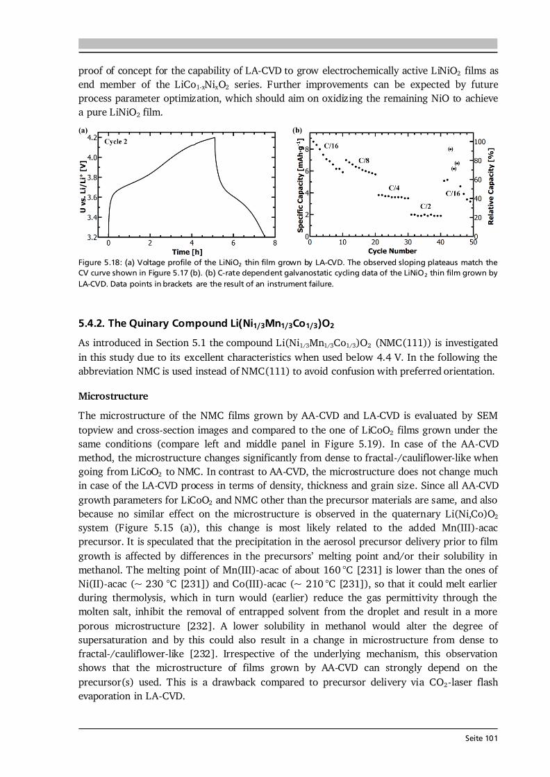
Seite 101
proof of concept for the capability of LA-CVD to grow electrochemically active LiNiO2 films as end member of the LiCo1-xNixO2 series. Further improvements can be expected by future process parameter optimization, which should aim on oxidizing the remaining NiO to achieve a pure LiNiO2 film.
Figure 5.18: (a) Voltage profile of the LiNiO2 thin film grown by LA-CVD. The observed sloping plateaus match the CV curve shown in Figure 5.17 (b). (b) C-rate dependent galvanostatic cycling data of the LiNiO2 thin film grown by LA-CVD. Data points in brackets are the result of an instrument failure.
5.4.2. The Quinary Compound Li(Ni1/3Mn1/3Co1/3)O2 As introduced in Section 5.1 the compound Li(Ni1/3Mn1/3Co1/3)O2 (NMC(111)) is investigated in this study due to its excellent characteristics when used below 4.4 V. In the following the abbreviation NMC is used instead of NMC(111) to avoid confusion with preferred orientation. Microstructure The microstructure of the NMC films grown by AA-CVD and LA-CVD is evaluated by SEM topview and cross-section images and compared to the one of LiCoO2 films grown under the same conditions (compare left and middle panel in Figure 5.19). In case of the AA-CVD method, the microstructure changes significantly from dense to fractal-/cauliflower-like when going from LiCoO2 to NMC. In contrast to AA-CVD, the microstructure does not change much in case of the LA-CVD process in terms of density, thickness and grain size. Since all AA-CVD growth parameters for LiCoO2 and NMC other than the precursor materials are same, and also because no similar effect on the microstructure is observed in the quaternary Li(Ni,Co)O2 system (Figure 5.15 (a)), this change is most likely related to the added Mn(III)-acac precursor. It is speculated that the precipitation in the aerosol precursor delivery prior to film growth is affected by differences in the precursors’ melting point and/or their solubility in methanol. The melting point of Mn(III)-acac of about 160 °C [231] is lower than the ones of Ni(II)-acac (~ 230 °C [231]) and Co(III)-acac (~ 210 °C [231]), so that it could melt earlier during thermolysis, which in turn would (earlier) reduce the gas permittivity through the molten salt, inhibit the removal of entrapped solvent from the droplet and result in a more porous microstructure [232]. A lower solubility in methanol would alter the degree of supersaturation and by this could also result in a change in microstructure from dense to fractal-/cauliflower-like [232]. Irrespective of the underlying mechanism, this observation shows that the microstructure of films grown by AA-CVD can strongly depend on the precursor(s) used. This is a drawback compared to precursor delivery via CO2-laser flash evaporation in LA-CVD.
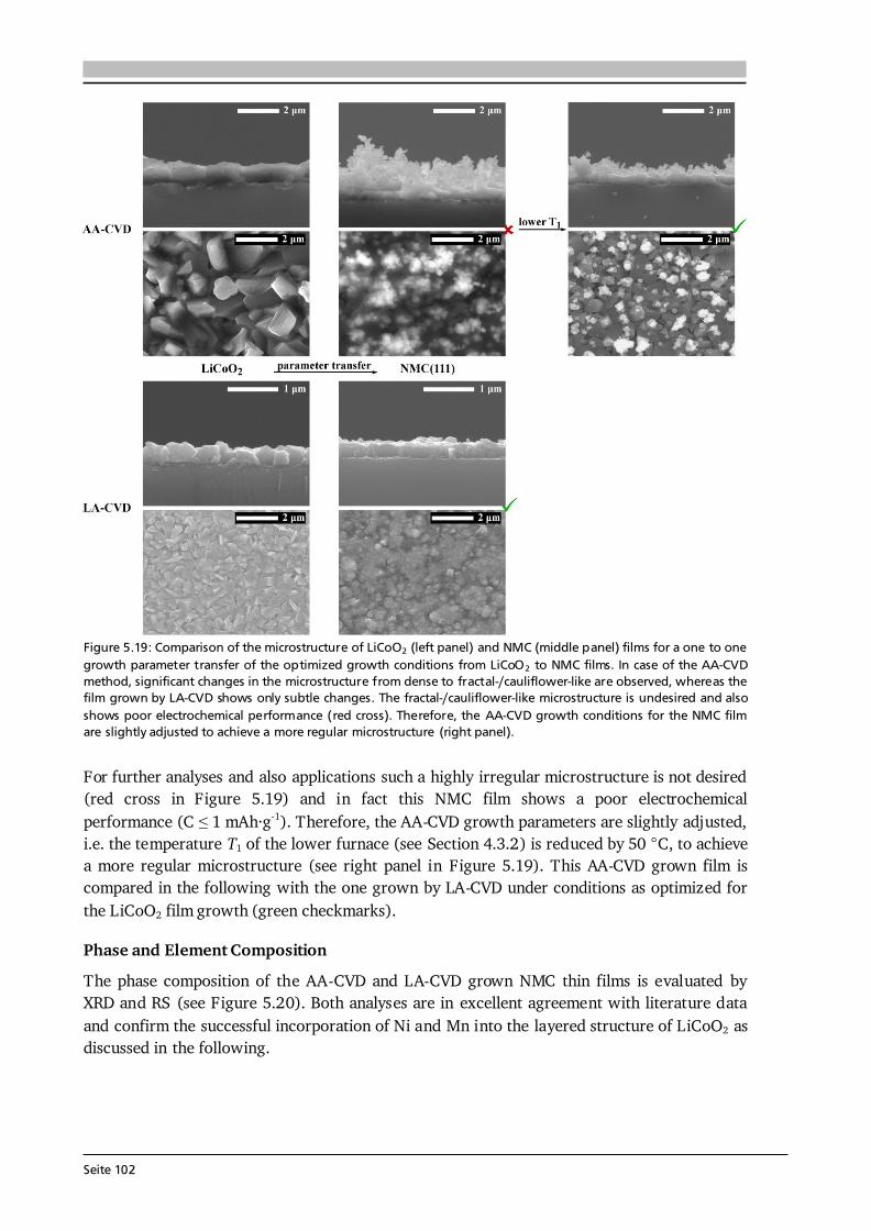
Seite 102
Figure 5.19: Comparison of the microstructure of LiCoO2 (left panel) and NMC (middle panel) films for a one to one growth parameter transfer of the optimized growth conditions from LiCoO2 to NMC films. In case of the AA-CVD method, significant changes in the microstructure from dense to fractal-/cauliflower-like are observed, whereas the film grown by LA-CVD shows only subtle changes. The fractal-/cauliflower-like microstructure is undesired and also shows poor electrochemical performance (red cross). Therefore, the AA-CVD growth conditions for the NMC film are slightly adjusted to achieve a more regular microstructure (right panel). For further analyses and also applications such a highly irregular microstructure is not desired (red cross in Figure 5.19) and in fact this NMC film shows a poor electrochemical performance (C ≤ 1 mAh·g-1). Therefore, the AA-CVD growth parameters are slightly adjusted, i.e. the temperature T1 of the lower furnace (see Section 4.3.2) is reduced by 50 °C, to achieve a more regular microstructure (see right panel in Figure 5.19). This AA-CVD grown film is compared in the following with the one grown by LA-CVD under conditions as optimized for the LiCoO2 film growth (green checkmarks). Phase and Element Composition The phase composition of the AA-CVD and LA-CVD grown NMC thin films is evaluated by XRD and RS (see Figure 5.20). Both analyses are in excellent agreement with literature data and confirm the successful incorporation of Ni and Mn into the layered structure of LiCoO2 as discussed in the following.
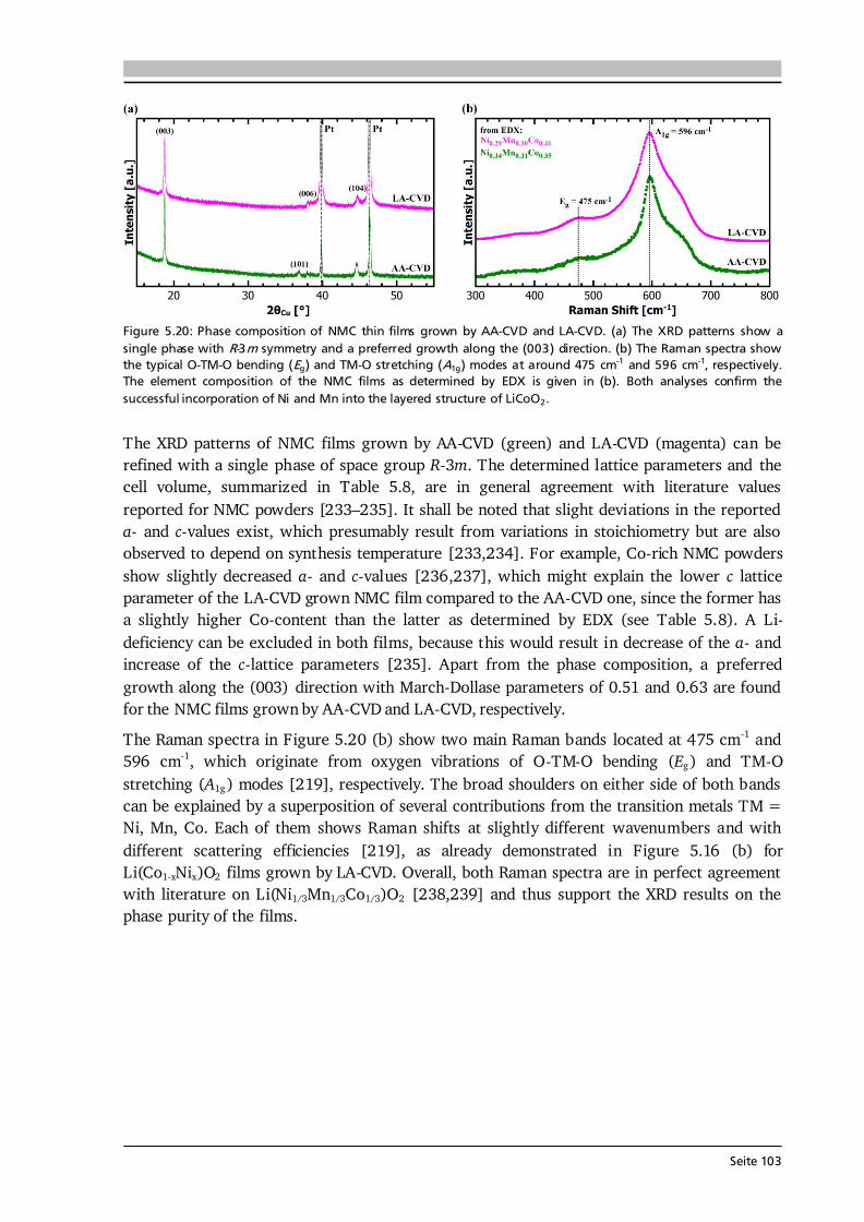
Seite 103
Figure 5.20: Phase composition of NMC thin films grown by AA-CVD and LA-CVD. (a) The XRD patterns show a single phase with R-3m symmetry and a preferred growth along the (003) direction. (b) The Raman spectra show the typical O-TM-O bending (Eg) and TM-O stretching (A1g) modes at around 475 cm-1 and 596 cm-1, respectively. The element composition of the NMC films as determined by EDX is given in (b). Both analyses confirm the successful incorporation of Ni and Mn into the layered structure of LiCoO2. The XRD patterns of NMC films grown by AA-CVD (green) and LA-CVD (magenta) can be refined with a single phase of space group R-3m. The determined lattice parameters and the cell volume, summarized in Table 5.8, are in general agreement with literature values reported for NMC powders [233–235]. It shall be noted that slight deviations in the reported a- and c-values exist, which presumably result from variations in stoichiometry but are also observed to depend on synthesis temperature [233,234]. For example, Co-rich NMC powders show slightly decreased a- and c-values [236,237], which might explain the lower c lattice parameter of the LA-CVD grown NMC film compared to the AA-CVD one, since the former has a slightly higher Co-content than the latter as determined by EDX (see Table 5.8). A Li-deficiency can be excluded in both films, because this would result in decrease of the a- and increase of the c-lattice parameters [235]. Apart from the phase composition, a preferred growth along the (003) direction with March-Dollase parameters of 0.51 and 0.63 are found for the NMC films grown by AA-CVD and LA-CVD, respectively. The Raman spectra in Figure 5.20 (b) show two main Raman bands located at 475 cm-1 and 596 cm-1, which originate from oxygen vibrations of O-TM-O bending (Eg) and TM-O stretching (A1g) modes [219], respectively. The broad shoulders on either side of both bands can be explained by a superposition of several contributions from the transition metals TM = Ni, Mn, Co. Each of them shows Raman shifts at slightly different wavenumbers and with different scattering efficiencies [219], as already demonstrated in Figure 5.16 (b) for Li(Co1-xNix)O2 films grown by LA-CVD. Overall, both Raman spectra are in perfect agreement with literature on Li(Ni1/3Mn1/3Co1/3)O2 [238,239] and thus support the XRD results on the phase purity of the films.
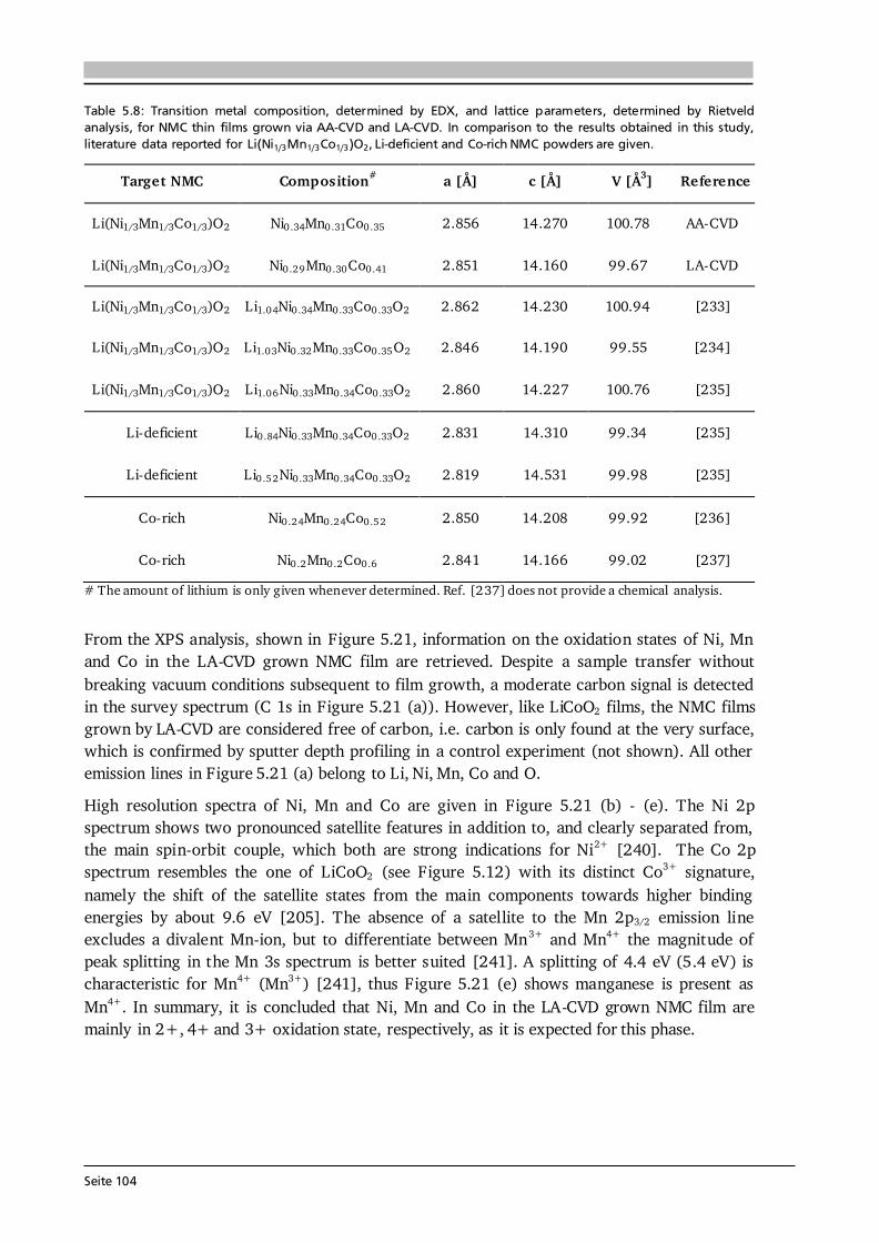
Seite 104
Table 5.8: Transition metal composition, determined by EDX, and lattice parameters, determined by Rietveld analysis, for NMC thin films grown via AA-CVD and LA-CVD. In comparison to the results obtained in this study, literature data reported for Li(Ni1/3Mn1/3Co1/3)O2, Li-deficient and Co-rich NMC powders are given. Target NMC Composition# a [Å] c [Å] V [Å3] Reference
Li(Ni1/3Mn1/3Co1/3)O2 Ni0.34Mn0.31Co0.35 2.856 14.270 100.78 AA-CVD Li(Ni1/3Mn1/3Co1/3)O2 Ni0.29Mn0.30Co0.41 2.851 14.160 99.67 LA-CVD Li(Ni1/3Mn1/3Co1/3)O2 Li1.04Ni0.34Mn0.33Co0.33O2 2.862 14.230 100.94 [233] Li(Ni1/3Mn1/3Co1/3)O2 Li1.03Ni0.32Mn0.33Co0.35O2 2.846 14.190 99.55 [234] Li(Ni1/3Mn1/3Co1/3)O2 Li1.06Ni0.33Mn0.34Co0.33O2 2.860 14.227 100.76 [235]
Li-deficient Li0.84Ni0.33Mn0.34Co0.33O2 2.831 14.310 99.34 [235] Li-deficient Li0.52Ni0.33Mn0.34Co0.33O2 2.819 14.531 99.98 [235]
Co-rich Ni0.24Mn0.24Co0.52 2.850 14.208 99.92 [236] Co-rich Ni0.2Mn0.2Co0.6 2.841 14.166 99.02 [237]
# The amount of lithium is only given whenever determined. Ref. [237] does not provide a chemical analysis. From the XPS analysis, shown in Figure 5.21, information on the oxidation states of Ni, Mn and Co in the LA-CVD grown NMC film are retrieved. Despite a sample transfer without breaking vacuum conditions subsequent to film growth, a moderate carbon signal is detected in the survey spectrum (C 1s in Figure 5.21 (a)). However, like LiCoO2 films, the NMC films grown by LA-CVD are considered free of carbon, i.e. carbon is only found at the very surface, which is confirmed by sputter depth profiling in a control experiment (not shown). All other emission lines in Figure 5.21 (a) belong to Li, Ni, Mn, Co and O. High resolution spectra of Ni, Mn and Co are given in Figure 5.21 (b) - (e). The Ni 2p spectrum shows two pronounced satellite features in addition to, and clearly separated from, the main spin-orbit couple, which both are strong indications for Ni2+ [240]. The Co 2p spectrum resembles the one of LiCoO2 (see Figure 5.12) with its distinct Co3+ signature, namely the shift of the satellite states from the main components towards higher binding energies by about 9.6 eV [205]. The absence of a satellite to the Mn 2p3/2 emission line excludes a divalent Mn-ion, but to differentiate between Mn3+ and Mn4+ the magnitude of peak splitting in the Mn 3s spectrum is better suited [241]. A splitting of 4.4 eV (5.4 eV) is characteristic for Mn4+ (Mn3+) [241], thus Figure 5.21 (e) shows manganese is present as Mn4+. In summary, it is concluded that Ni, Mn and Co in the LA-CVD grown NMC film are mainly in 2+, 4+ and 3+ oxidation state, respectively, as it is expected for this phase.
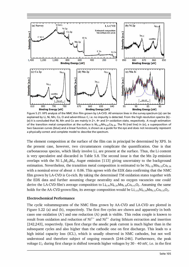
Seite 105
Figure 5.21: XPS analysis of the NMC thin film grown by LA-CVD. All emission lines in the survey spectrum (a) can be explained by Li, Ni, Mn, Co, O and adventitious C, i.e. no impurity is detected. From the high resolution spectra (b) - (e) it is concluded that Ni, Mn and Co are mainly in 2+, 4+ and 3+ oxidation state, respectively. A rough estimation of the transition metal composition at the surface is Ni0.32Mn0.32Co0.36. The fit (red line) in (e), a superposition of two Gaussian curves (blue) and a linear function, is shown as a guide for the eye and does not necessarily represent a physically correct and complete model to describe the spectrum. The element composition at the surface of the film can in principal be determined by XPS. In the present case, however, two circumstances complicate the quantification. One is that carbonaceous species, which likely involve Li, are present at the surface. Thus, the Li content is very speculative and discarded in Table 5.8. The second issue is that the Mn 2p emission overlaps with the Ni L2M23M45 Auger emission [113] giving uncertainty to the background estimation. Nevertheless, the transition metal composition is estimated to be Ni0.32Mn0.32Co0.36 with a nominal error of about ± 0.06. This agrees with the EDX data confirming that the NMC film grown by LA-CVD is Co-rich. By taking the determined TM oxidation states together with the EDX data and further assuming charge neutrality and no oxygen vacancies one could derive the LA-CVD film’s average composition to Li0.99Ni0.29Mn0.30Co0.41O2. Assuming the same holds for the AA-CVD grown film, its average composition would be Li1.03Ni0.34Mn0.31Co0.35O2. Electrochemical Performance The cyclic voltammograms of the NMC films grown by AA-CVD and LA-CVD are plotted in Figure 5.22 (a) and (b), respectively. The first five cycles are shown and apparently in both cases one oxidation (A’) and one reduction (A) peak is visible. This redox couple is known to result from oxidation and reduction of Ni2+ and Ni4+ during lithium extraction and insertion [242,243], respectively. Upon first charge the anodic peak current is much higher than in the subsequent cycles and also higher than the cathodic one on first discharge. This leads to a high initial capacity loss (ICL), which is usually observed in NMC cathodes, but not well understood and therefore subject of ongoing research [244–246]. Furthermore, the peak voltage UA’ during first charge is shifted towards higher voltages by 30 - 40 mV, i.e. in the first
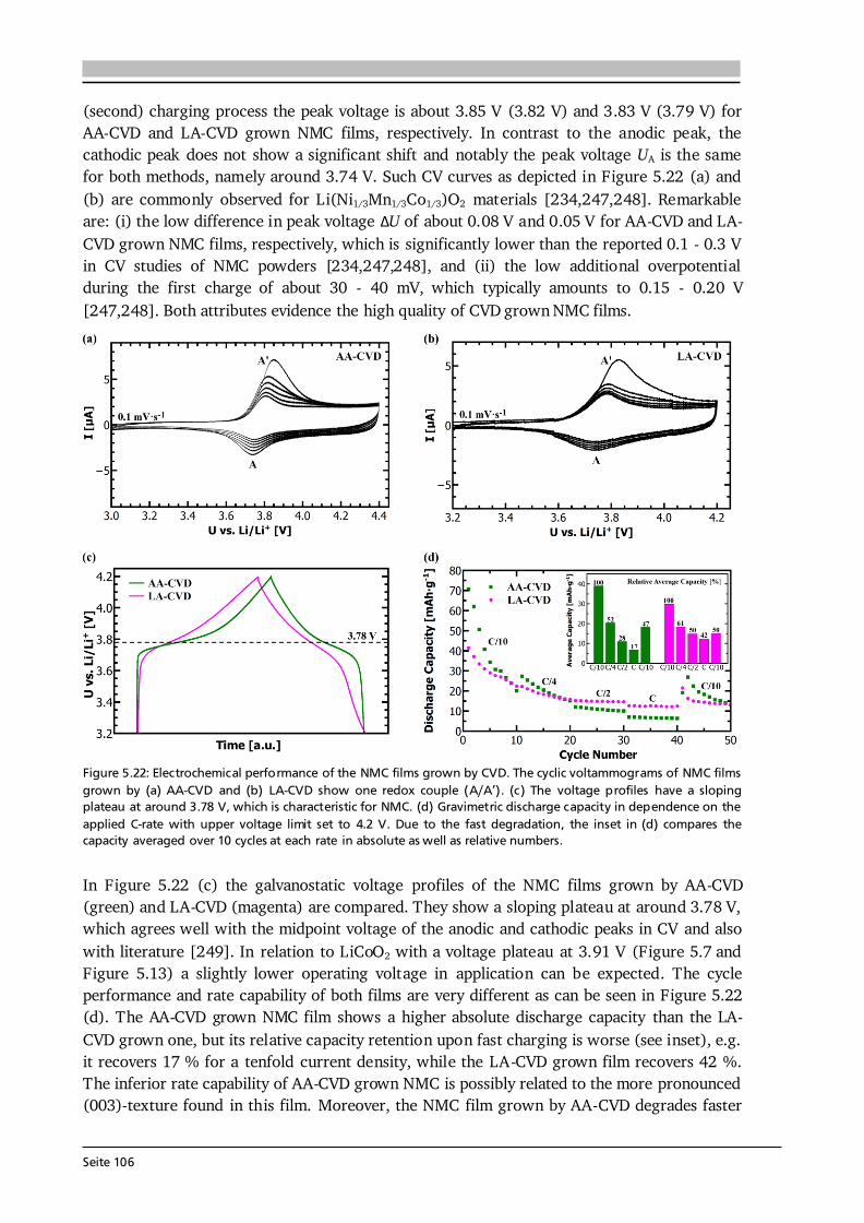
Seite 106
(second) charging process the peak voltage is about 3.85 V (3.82 V) and 3.83 V (3.79 V) for AA-CVD and LA-CVD grown NMC films, respectively. In contrast to the anodic peak, the cathodic peak does not show a significant shift and notably the peak voltage UA is the same for both methods, namely around 3.74 V. Such CV curves as depicted in Figure 5.22 (a) and (b) are commonly observed for Li(Ni1/3Mn1/3Co1/3)O2 materials [234,247,248]. Remarkable are: (i) the low difference in peak voltage ΔU of about 0.08 V and 0.05 V for AA-CVD and LA-CVD grown NMC films, respectively, which is significantly lower than the reported 0.1 - 0.3 V in CV studies of NMC powders [234,247,248], and (ii) the low additional overpotential during the first charge of about 30 - 40 mV, which typically amounts to 0.15 - 0.20 V [247,248]. Both attributes evidence the high quality of CVD grown NMC films.
Figure 5.22: Electrochemical performance of the NMC films grown by CVD. The cyclic voltammograms of NMC films grown by (a) AA-CVD and (b) LA-CVD show one redox couple (A/A’). (c) The voltage profiles have a sloping plateau at around 3.78 V, which is characteristic for NMC. (d) Gravimetric discharge capacity in dependence on the applied C-rate with upper voltage limit set to 4.2 V. Due to the fast degradation, the inset in (d) compares the capacity averaged over 10 cycles at each rate in absolute as well as relative numbers. In Figure 5.22 (c) the galvanostatic voltage profiles of the NMC films grown by AA-CVD (green) and LA-CVD (magenta) are compared. They show a sloping plateau at around 3.78 V, which agrees well with the midpoint voltage of the anodic and cathodic peaks in CV and also with literature [249]. In relation to LiCoO2 with a voltage plateau at 3.91 V (Figure 5.7 and Figure 5.13) a slightly lower operating voltage in application can be expected. The cycle performance and rate capability of both films are very different as can be seen in Figure 5.22 (d). The AA-CVD grown NMC film shows a higher absolute discharge capacity than the LA-CVD grown one, but its relative capacity retention upon fast charging is worse (see inset), e.g. it recovers 17 % for a tenfold current density, while the LA-CVD grown film recovers 42 %. The inferior rate capability of AA-CVD grown NMC is possibly related to the more pronounced (003)-texture found in this film. Moreover, the NMC film grown by AA-CVD degrades faster
Seite 107
than the one grown by LA-CVD. For both CVD methods the absolute discharge capacity of the NMC films is slightly lower than the one achieved for the respective LiCoO2 films. Comparison to Literature There are four literature reports on NMC films grown by sputtering [250], PLD [251,252] and aerosol deposition [253], but only the report by Deng et al. [251] shows extended cycling performance of in total 50 cycles under different C-rates. In a voltage range of 2.8 - 4.5 V, their best performing film delivers about 175 mAh·g-1 and 75 mAh·g-1 at rates of C/10 and C, respectively, which corresponds to 43 % capacity retention for a tenfold current density. Consequently, the rate performance of the LA-CVD grown NMC film compares well with the best performing one grown by PLD, even though no optimization of the LA-CVD growth parameters has been carried out yet. On the other hand, cathodes based on Li(Ni1/3Mn1/3Co1/3)O2 powder can easily deliver more than 70 % of their theoretical capacity at rates as high as 8C [249] or 10C [254]. Of course, additives such as binder and carbon black help to ensure a conductive network in these NMC powder processed cathodes. But besides these additives, the properties of the pure active material play a crucial role in achieving high electrochemical performance. On the basis of NMC thin films, intrinsic material properties can be studied fundamentally and further optimized. One example is the films’ texture, which recently was shown to strongly affect the discharge capacity and average discharge voltage [252], e.g. epitaxial NMC films with (104)- and (003)-orientation had initial discharge capacities of 123 mAh·g -1 and 106 mAh·g-1, respectively. Furthermore, a cut-off voltage of 4.5 V already leads to a drastic decrease in the average discharge voltage by about 0.15 V in case of the (003)-oriented film and shows no effect on the (104)-oriented film [252], attesting the latter a higher electrochemical stability. Consequently, the control over the preferred orientation in CVD grown NMC films should be subject to future research based on first results for LiCoO2, discussed in Section 5.2.2. Another field of interest is cation mixing [254–256], which is known to influence the electrochemical properties. Cation mixing refers to a partial interchange between Li+ (ionic radius of 0.76 Å in six-fold coordination [257]) and nearest neighbor Ni2+ (ionic radius of 0.69 Å in six-fold coordination [257]) on the crystallographic 3a and 3b sites of the NMC lattice, leading to partial blocking of lithium ion diffusion pathways [255]. One approach to reduce the cation mixing is to use a lower Ni content as shown for Co-rich NMC(226) [258]. This possibly explains why the slightly Co-rich NMC film grown by LA-CVD performs better than the AA-CVD grown one. Unfortunately, it is not possible to gain information on the cation disorder in the CVD grown NMC films by the given XRD data to confirm this correlation. While Zhang et al. [255] consider cation mixing below 2 % as threshold for an unaffected electrochemical performance, Shaju et al. [254] demonstrate excellent cycling performance with 4 % cation mixing in their NMC cathode. Such deviating observations could point to further influencing factors, e.g. synthesis route [256], temperature [233,234], powder processing, chemical composition [256,258], and so on, which affect the cation disorder but at the same time may affect other material properties, which in turn influence the electrochemical performance. Therefore, it might be beneficial to investigate such phenomena on thin film model systems with pure NMC active material for which individual material properties can be tailored as demonstrated in this chapter.
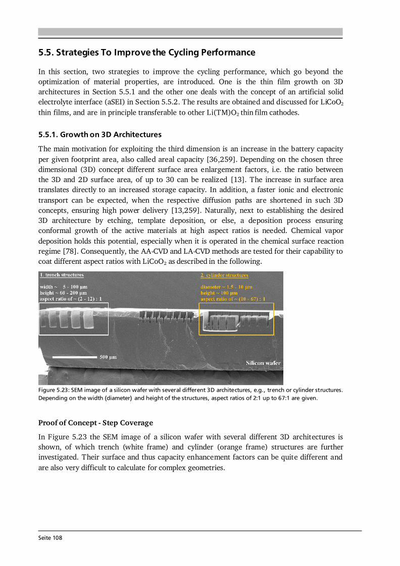
Seite 108
5.5. Strategies To Improve the Cycling Performance In this section, two strategies to improve the cycling performance, which go beyond the optimization of material properties, are introduced. One is the thin film growth on 3D architectures in Section 5.5.1 and the other one deals with the concept of an artificial solid electrolyte interface (aSEI) in Section 5.5.2. The results are obtained and discussed for LiCoO2 thin films, and are in principle transferable to other Li(TM)O2 thin film cathodes. 5.5.1. Growth on 3D Architectures The main motivation for exploiting the third dimension is an increase in the battery capacity per given footprint area, also called areal capacity [36,259]. Depending on the chosen three dimensional (3D) concept different surface area enlargement factors, i.e. the ratio between the 3D and 2D surface area, of up to 30 can be realized [13]. The increase in surface area translates directly to an increased storage capacity. In addition, a faster ionic and electronic transport can be expected, when the respective diffusion paths are shortened in such 3D concepts, ensuring high power delivery [13,259]. Naturally, next to establishing the desired 3D architecture by etching, template deposition, or else, a deposition process ensuring conformal growth of the active materials at high aspect ratios is needed. Chemical vapor deposition holds this potential, especially when it is operated in the chemical surface reaction regime [78]. Consequently, the AA-CVD and LA-CVD methods are tested for their capability to coat different aspect ratios with LiCoO2 as described in the following.
Figure 5.23: SEM image of a silicon wafer with several different 3D architectures, e.g., trench or cylinder structures. Depending on the width (diameter) and height of the structures, aspect ratios of 2:1 up to 67:1 are given.
Proof of Concept - Step Coverage In Figure 5.23 the SEM image of a silicon wafer with several different 3D architectures is shown, of which trench (white frame) and cylinder (orange frame) structures are further investigated. Their surface and thus capacity enhancement factors can be quite different and are also very difficult to calculate for complex geometries.
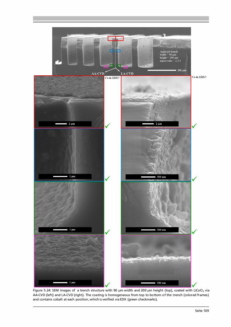
Seite 109
Figure 5.24: SEM images of a trench structure with 90 μm width and 200 μm height (top), coated with LiCoO2 via AA-CVD (left) and LA-CVD (right). The coating is homogeneous from top to bottom of the trench (colored frames) and contains cobalt at each position, which is verified via EDX (green checkmarks).
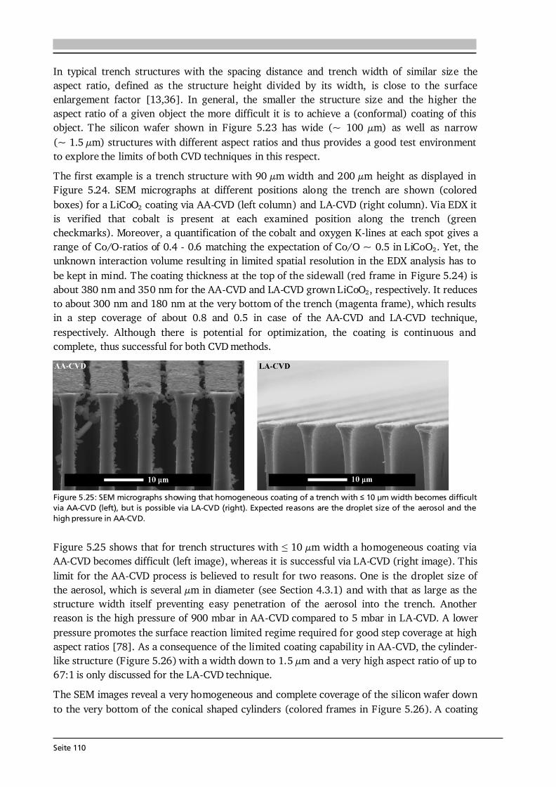
Seite 110
In typical trench structures with the spacing distance and trench width of similar size the aspect ratio, defined as the structure height divided by its width, is close to the surface enlargement factor [13,36]. In general, the smaller the structure size and the higher the aspect ratio of a given object the more difficult it is to achieve a (conformal) coating of this object. The silicon wafer shown in Figure 5.23 has wide (~ 100 μm) as well as narrow (~ 1.5 μm) structures with different aspect ratios and thus provides a good test environment to explore the limits of both CVD techniques in this respect. The first example is a trench structure with 90 μm width and 200 μm height as displayed in Figure 5.24. SEM micrographs at different positions along the trench are shown (colored boxes) for a LiCoO2 coating via AA-CVD (left column) and LA-CVD (right column). Via EDX it is verified that cobalt is present at each examined position along the trench (green checkmarks). Moreover, a quantification of the cobalt and oxygen K-lines at each spot gives a range of Co/O-ratios of 0.4 - 0.6 matching the expectation of Co/O ~ 0.5 in LiCoO2. Yet, the unknown interaction volume resulting in limited spatial resolution in the EDX analysis has to be kept in mind. The coating thickness at the top of the sidewall (red frame in Figure 5.24) is about 380 nm and 350 nm for the AA-CVD and LA-CVD grown LiCoO2, respectively. It reduces to about 300 nm and 180 nm at the very bottom of the trench (magenta frame), which results in a step coverage of about 0.8 and 0.5 in case of the AA-CVD and LA-CVD technique, respectively. Although there is potential for optimization, the coating is continuous and complete, thus successful for both CVD methods.
Figure 5.25: SEM micrographs showing that homogeneous coating of a trench with ≤ 10 μm width becomes difficult via AA-CVD (left), but is possible via LA-CVD (right). Expected reasons are the droplet size of the aerosol and the high pressure in AA-CVD. Figure 5.25 shows that for trench structures with ≤ 10 μm width a homogeneous coating via AA-CVD becomes difficult (left image), whereas it is successful via LA-CVD (right image). This limit for the AA-CVD process is believed to result for two reasons. One is the droplet size of the aerosol, which is several μm in diameter (see Section 4.3.1) and with that as large as the structure width itself preventing easy penetration of the aerosol into the trench. Another reason is the high pressure of 900 mbar in AA-CVD compared to 5 mbar in LA-CVD. A lower pressure promotes the surface reaction limited regime required for good step coverage at high aspect ratios [78]. As a consequence of the limited coating capability in AA-CVD, the cylinder-like structure (Figure 5.26) with a width down to 1.5 μm and a very high aspect ratio of up to 67:1 is only discussed for the LA-CVD technique. The SEM images reveal a very homogeneous and complete coverage of the silicon wafer down to the very bottom of the conical shaped cylinders (colored frames in Figure 5.26). A coating
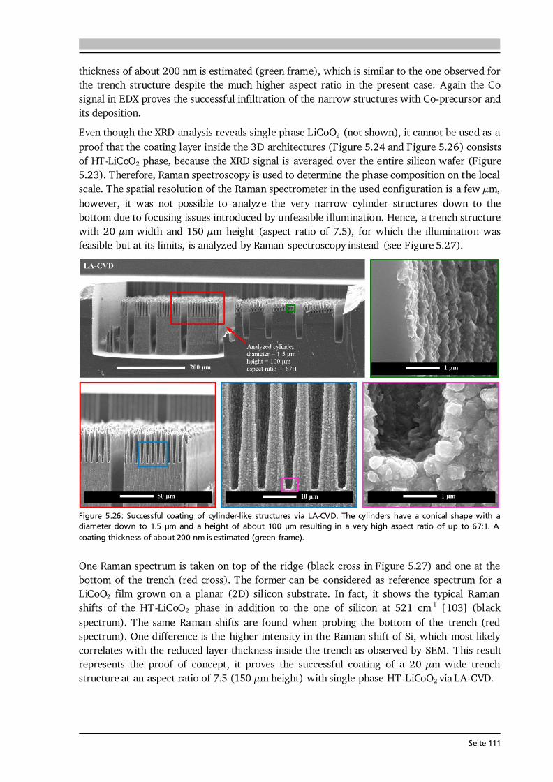
Seite 111
thickness of about 200 nm is estimated (green frame), which is similar to the one observed for the trench structure despite the much higher aspect ratio in the present case. Again the Co signal in EDX proves the successful infiltration of the narrow structures with Co-precursor and its deposition. Even though the XRD analysis reveals single phase LiCoO2 (not shown), it cannot be used as a proof that the coating layer inside the 3D architectures (Figure 5.24 and Figure 5.26) consists of HT-LiCoO2 phase, because the XRD signal is averaged over the entire silicon wafer (Figure 5.23). Therefore, Raman spectroscopy is used to determine the phase composition on the local scale. The spatial resolution of the Raman spectrometer in the used configuration is a few μm, however, it was not possible to analyze the very narrow cylinder structures down to the bottom due to focusing issues introduced by unfeasible illumination. Hence, a trench structure with 20 μm width and 150 μm height (aspect ratio of 7.5), for which the illumination was feasible but at its limits, is analyzed by Raman spectroscopy instead (see Figure 5.27).
Figure 5.26: Successful coating of cylinder-like structures via LA-CVD. The cylinders have a conical shape with a diameter down to 1.5 μm and a height of about 100 μm resulting in a very high aspect ratio of up to 67:1. A coating thickness of about 200 nm is estimated (green frame). One Raman spectrum is taken on top of the ridge (black cross in Figure 5.27) and one at the bottom of the trench (red cross). The former can be considered as reference spectrum for a LiCoO2 film grown on a planar (2D) silicon substrate. In fact, it shows the typical Raman shifts of the HT-LiCoO2 phase in addition to the one of silicon at 521 cm-1 [103] (black spectrum). The same Raman shifts are found when probing the bottom of the trench (red spectrum). One difference is the higher intensity in the Raman shift of Si, which most likely correlates with the reduced layer thickness inside the trench as observed by SEM. This result represents the proof of concept, it proves the successful coating of a 20 μm wide trench structure at an aspect ratio of 7.5 (150 μm height) with single phase HT-LiCoO2 via LA-CVD.
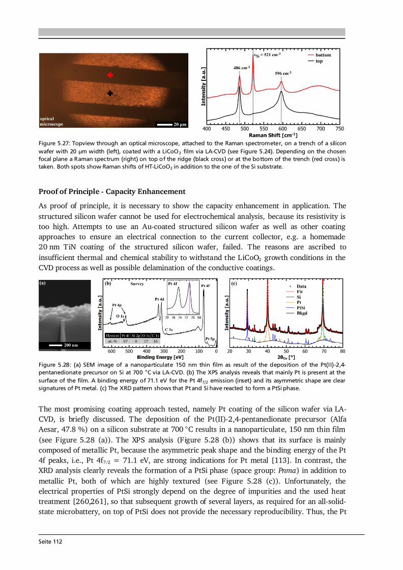
Seite 112
Figure 5.27: Topview through an optical microscope, attached to the Raman spectrometer, on a trench of a silicon wafer with 20 μm width (left), coated with a LiCoO2 film via LA-CVD (see Figure 5.24). Depending on the chosen focal plane a Raman spectrum (right) on top of the ridge (black cross) or at the bottom of the trench (red cross) is taken. Both spots show Raman shifts of HT-LiCoO2 in addition to the one of the Si substrate.
Proof of Principle - Capacity Enhancement As proof of principle, it is necessary to show the capacity enhancement in application. The structured silicon wafer cannot be used for electrochemical analysis, because its resistivity is too high. Attempts to use an Au-coated structured silicon wafer as well as other coating approaches to ensure an electrical connection to the current collector, e.g. a homemade 20 nm TiN coating of the structured silicon wafer, failed. The reasons are ascribed to insufficient thermal and chemical stability to withstand the LiCoO2 growth conditions in the CVD process as well as possible delamination of the conductive coatings.
Figure 5.28: (a) SEM image of a nanoparticulate 150 nm thin film as result of the deposition of the Pt(II) -2,4-pentanedionate precursor on Si at 700 °C via LA-CVD. (b) The XPS analysis reveals that mainly Pt is present at the surface of the film. A binding energy of 71.1 eV for the Pt 4f7/2 emission (inset) and its asymmetric shape are clear signatures of Pt metal. (c) The XRD pattern shows that Pt and Si have reacted to form a PtSi phase. The most promising coating approach tested, namely Pt coating of the silicon wafer via LA-CVD, is briefly discussed. The deposition of the Pt(II)-2,4-pentanedionate precursor (Alfa Aesar, 47.8 %) on a silicon substrate at 700 °C results in a nanoparticulate, 150 nm thin film (see Figure 5.28 (a)). The XPS analysis (Figure 5.28 (b)) shows that its surface is mainly composed of metallic Pt, because the asymmetric peak shape and the binding energy of the Pt 4f peaks, i.e., Pt 4f7/2 = 71.1 eV, are strong indications for Pt metal [113]. In contrast, the XRD analysis clearly reveals the formation of a PtSi phase (space group: Pnma) in addition to metallic Pt, both of which are highly textured (see Figure 5.28 (c)). Unfortunately, the electrical properties of PtSi strongly depend on the degree of impurities and the used heat treatment [260,261], so that subsequent growth of several layers, as required for an all-solid-state microbattery, on top of PtSi does not provide the necessary reproducibility. Thus, the Pt
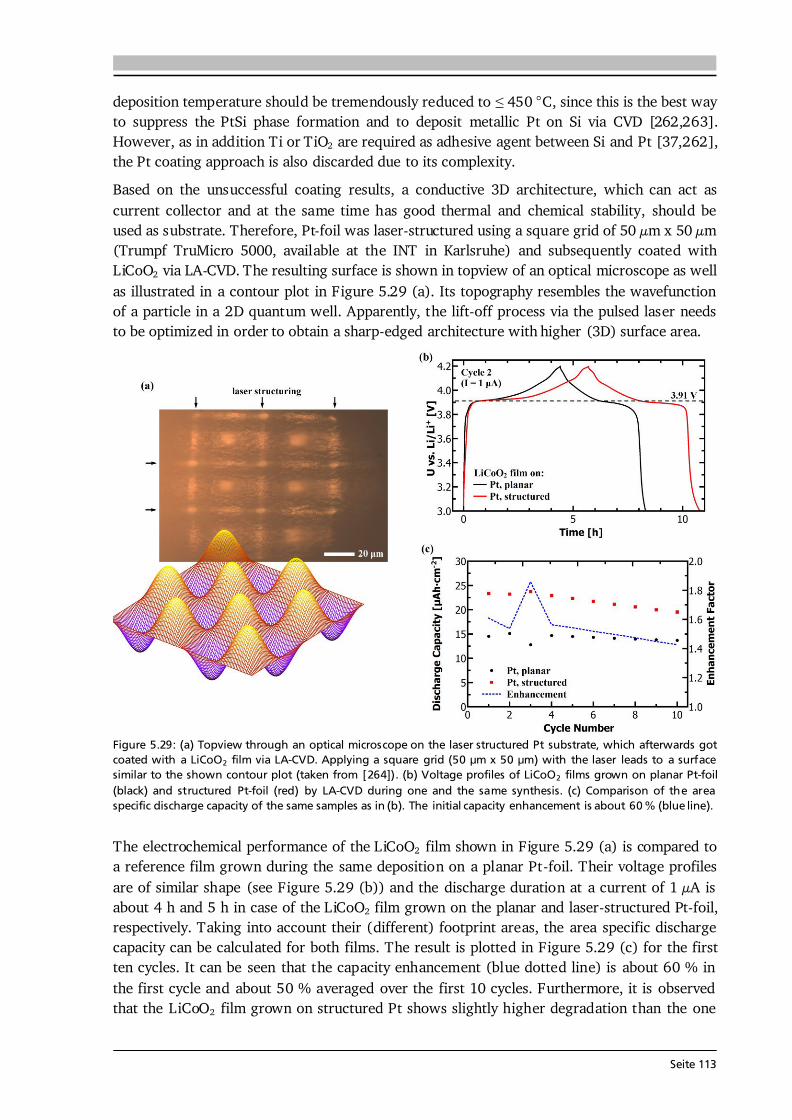
Seite 113
deposition temperature should be tremendously reduced to ≤ 450 °C, since this is the best way to suppress the PtSi phase formation and to deposit metallic Pt on Si via CVD [262,263]. However, as in addition Ti or TiO2 are required as adhesive agent between Si and Pt [37,262], the Pt coating approach is also discarded due to its complexity. Based on the unsuccessful coating results, a conductive 3D architecture, which can act as current collector and at the same time has good thermal and chemical stability, should be used as substrate. Therefore, Pt-foil was laser-structured using a square grid of 50 μm x 50 μm (Trumpf TruMicro 5000, available at the INT in Karlsruhe) and subsequently coated with LiCoO2 via LA-CVD. The resulting surface is shown in topview of an optical microscope as well as illustrated in a contour plot in Figure 5.29 (a). Its topography resembles the wavefunction of a particle in a 2D quantum well. Apparently, the lift-off process via the pulsed laser needs to be optimized in order to obtain a sharp-edged architecture with higher (3D) surface area.
Figure 5.29: (a) Topview through an optical microscope on the laser structured Pt substrate, which afterwards got coated with a LiCoO2 film via LA-CVD. Applying a square grid (50 μm x 50 μm) with the laser leads to a surface similar to the shown contour plot (taken from [264]). (b) Voltage profiles of LiCoO2 films grown on planar Pt-foil (black) and structured Pt-foil (red) by LA-CVD during one and the same synthesis. (c) Comparison of the area specific discharge capacity of the same samples as in (b). The initial capacity enhancement is about 60 % (blue line). The electrochemical performance of the LiCoO2 film shown in Figure 5.29 (a) is compared to a reference film grown during the same deposition on a planar Pt-foil. Their voltage profiles are of similar shape (see Figure 5.29 (b)) and the discharge duration at a current of 1 μA is about 4 h and 5 h in case of the LiCoO2 film grown on the planar and laser-structured Pt-foil, respectively. Taking into account their (different) footprint areas, the area specific discharge capacity can be calculated for both films. The result is plotted in Figure 5.29 (c) for the first ten cycles. It can be seen that the capacity enhancement (blue dotted line) is about 60 % in the first cycle and about 50 % averaged over the first 10 cycles. Furthermore, it is observed that the LiCoO2 film grown on structured Pt shows slightly higher degradation than the one
Seite 114
grown on the planar Pt. This could be related to the higher surface area of this film, which might enhance irreversible side reactions with the liquid electrolyte or else, but definitely needs further investigation. The observed enhancement factor of 1.6 is the proof of principle that an increase in discharge capacity is possible by coating a structured Pt-foil with LiCoO2 via LA-CVD. In fact, literature on the performance of 3D architectures coated by LiCoO2 thin films is very limited and so far no significant higher capacity enhancement has been reported. A very recent report on 3D pyramid structures coated with LiCoO2 by a combined electrochemical and hydrothermal process shows no capacity enhancement at all compared to a planar substrate [265]. And the reports by the group of Yoon [37,216] show under optimized growth conditions a capacity enhancement factor of 1.3 [37]. Based on the results in the present study, future research has to focus on the substrate, i.e. find a conductive 3D architecture with a high aspect ratio and good corrosion resistance at high temperatures. Moreover, adjusting the process parameters in favor of the chemical surface reaction regime in CVD should increase the step coverage and thus enhance the capacity further. 5.5.2. Artificial Solid Electrolyte Interface (aSEI) The first report on Al2O3 coated LiCoO2 in 2000 [266] showed excellent capacity retention of 97 % after 50 cycles at an increased cut-off potential of 4.4 V. Since then, several material classes have been investigated as artificial solid electrolyte interface (aSEI) layers [267,268], which can significantly enhance the (cathode) performance by suppressing phase transitions and metal dissolution, decreasing the disorder of cations and the amount of side reactions, etc. Artificial SEI layers based on oxides, especially Al2O3 and ZrO2, show one of the best performance improvements [268]. Regarding the optimum coating thickness, diverging results are reported, which range from a thickness independent improvement of the electrochemical properties up to 300 nm Al2O3 coating via sputtering [269] to very thickness sensitive properties, namely the decrease in discharge capacity and electronic conductivity for > 1 nm Al2O3 coating via ALD [270] and a large overpotential due to an increase in diffusion resistance for > 10 nm ZrO2 coating via PLD [271]. The latter observation is intuitive, since a dense oxide layer should act as a diffusion barrier for Li-ions. One influencing factor in this respect is the coating technique, which determines the density and uniformity of the aSEI. Another one is the used temperature during deposition and/or post-treatments, which may lead to the formation of a solid solution of LiCo1-x(Al,Zr)xO2 instead of a defined coating [267,268]. The solid solution is reported to enhance the structural stability suppressing the phase transition from a hexagonal to monoclinic phase [266,267,272]. A third reason that possibly plays a role in explaining the diverging observations is whether the studies are based on pure active material, e.g., thin films [269,271], or on a further processed composite cathode [270]. In this thesis, Al2O3 is chosen because its deposition via an established ALD process is available at the Materials Science Department with the possibility to transfer the sample under vacuum conditions. A coating thickness of ~ 3 nm Al2O3 (see Section 4.6) is chosen and no further processing (post-annealing or else) is used.
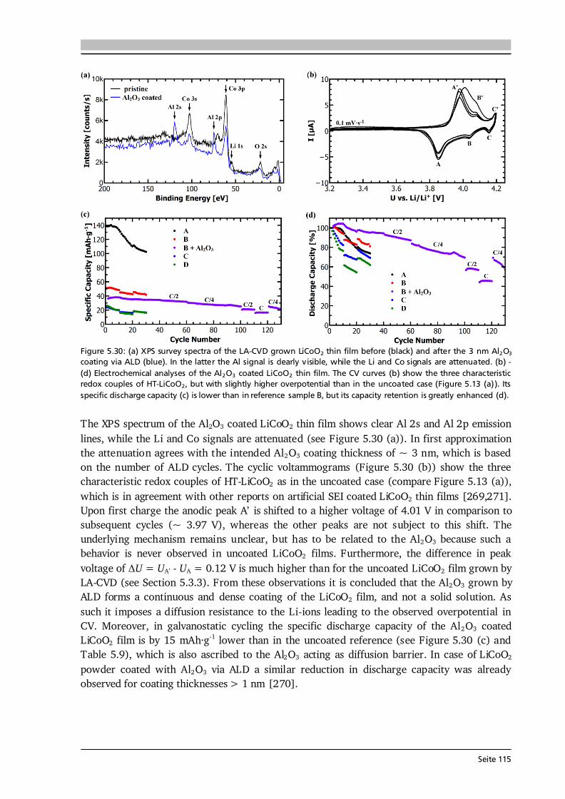
Seite 115
Figure 5.30: (a) XPS survey spectra of the LA-CVD grown LiCoO2 thin film before (black) and after the 3 nm Al2O3 coating via ALD (blue). In the latter the Al signal is clearly v isible, while the Li and Co signals are attenuated. (b) - (d) Electrochemical analyses of the Al2O3 coated LiCoO2 thin film. The CV curves (b) show the three characteristic redox couples of HT-LiCoO2, but with slightly higher overpotential than in the uncoated case (Figure 5.13 (a)). Its specific discharge capacity (c) is lower than in reference sample B, but its capacity retention is greatly enhanced (d). The XPS spectrum of the Al2O3 coated LiCoO2 thin film shows clear Al 2s and Al 2p emission lines, while the Li and Co signals are attenuated (see Figure 5.30 (a)). In first approximation the attenuation agrees with the intended Al2O3 coating thickness of ~ 3 nm, which is based on the number of ALD cycles. The cyclic voltammograms (Figure 5.30 (b)) show the three characteristic redox couples of HT-LiCoO2 as in the uncoated case (compare Figure 5.13 (a)), which is in agreement with other reports on artificial SEI coated LiCoO2 thin films [269,271]. Upon first charge the anodic peak A’ is shifted to a higher voltage of 4.01 V in comparison to subsequent cycles (~ 3.97 V), whereas the other peaks are not subject to this shift. The underlying mechanism remains unclear, but has to be related to the Al2O3 because such a behavior is never observed in uncoated LiCoO2 films. Furthermore, the difference in peak voltage of ΔU = UA’ - UA = 0.12 V is much higher than for the uncoated LiCoO2 film grown by LA-CVD (see Section 5.3.3). From these observations it is concluded that the Al2O3 grown by ALD forms a continuous and dense coating of the LiCoO2 film, and not a solid solution. As such it imposes a diffusion resistance to the Li-ions leading to the observed overpotential in CV. Moreover, in galvanostatic cycling the specific discharge capacity of the Al2O3 coated LiCoO2 film is by 15 mAh·g-1 lower than in the uncoated reference (see Figure 5.30 (c) and Table 5.9), which is also ascribed to the Al2O3 acting as diffusion barrier. In case of LiCoO2 powder coated with Al2O3 via ALD a similar reduction in discharge capacity was already observed for coating thicknesses > 1 nm [270].
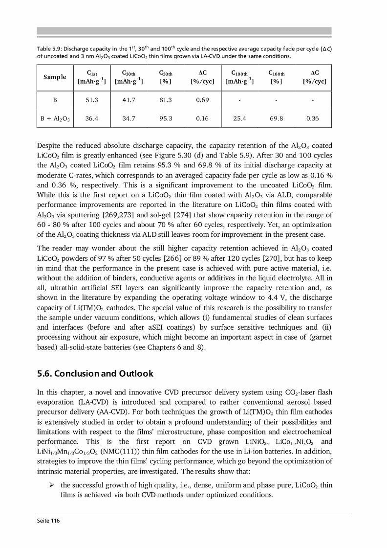
Seite 116
Table 5.9: Discharge capacity in the 1s t, 30th and 100th cycle and the respective average capacity fade per cycle (ΔC) of uncoated and 3 nm Al2O3 coated LiCoO2 thin films grown via LA-CVD under the same conditions. Sample C1st [mAh·g -1] C30th [mAh·g -1] C30th [%] ΔC [%/cyc] C100th [mAh·g -1] C100th [%] ΔC [%/cyc]
B 51.3 41.7 81.3 0.69 - - - B + Al2O3 36.4 34.7 95.3 0.16 25.4 69.8 0.36
Despite the reduced absolute discharge capacity, the capacity retention of the Al2O3 coated LiCoO2 film is greatly enhanced (see Figure 5.30 (d) and Table 5.9). After 30 and 100 cycles the Al2O3 coated LiCoO2 film retains 95.3 % and 69.8 % of its initial discharge capacity at moderate C-rates, which corresponds to an averaged capacity fade per cycle as low as 0.16 % and 0.36 %, respectively. This is a significant improvement to the uncoated LiCoO2 film. While this is the first report on a LiCoO2 thin film coated with Al2O3 via ALD, comparable performance improvements are reported in the literature on LiCoO2 thin films coated with Al2O3 via sputtering [269,273] and sol-gel [274] that show capacity retention in the range of 60 - 80 % after 100 cycles and about 70 % after 60 cycles, respectively. Yet, an optimization of the Al2O3 coating thickness via ALD still leaves room for improvement in the present case. The reader may wonder about the still higher capacity retention achieved in Al2O3 coated LiCoO2 powders of 97 % after 50 cycles [266] or 89 % after 120 cycles [270], but has to keep in mind that the performance in the present case is achieved with pure active material, i.e. without the addition of binders, conductive agents or additives in the liquid electrolyte. All in all, ultrathin artificial SEI layers can significantly improve the capacity retention and, as shown in the literature by expanding the operating voltage window to 4.4 V, the discharge capacity of Li(TM)O2 cathodes. The special value of this research is the possibility to transfer the sample under vacuum conditions, which allows (i) fundamental studies of clean surfaces and interfaces (before and after aSEI coatings) by surface sensitive techniques and (ii) processing without air exposure, which might become an important aspect in case of (garnet based) all-solid-state batteries (see Chapters 6 and 8). 5.6. Conclusion and Outlook In this chapter, a novel and innovative CVD precursor delivery system using CO2-laser flash evaporation (LA-CVD) is introduced and compared to rather conventional aerosol based precursor delivery (AA-CVD). For both techniques the growth of Li(TM)O2 thin film cathodes is extensively studied in order to obtain a profound understanding of their possibilities and limitations with respect to the films’ microstructure, phase composition and electrochemical performance. This is the first report on CVD grown LiNiO2, LiCo1-xNixO2 and LiNi1/3Mn1/3Co1/3O2 (NMC(111)) thin film cathodes for the use in Li-ion batteries. In addition, strategies to improve the thin films’ cycling performance, which go beyond the optimization of intrinsic material properties, are investigated. The results show that:
the successful growth of high quality, i.e., dense, uniform and phase pure, LiCoO2 thin films is achieved via both CVD methods under optimized conditions.
Seite 117
tailoring of the films’ microstructure is possible via LA-CVD and limited via AA-CVD, lending the LA-CVD technique more flexibility towards application. Li(TM)O2 films grow mainly with (003)-texture independent of the CVD method, and in AA-CVD an additional (104)-texture is observed for growth temperatures 850 °C. the Pt surface corrodes to Li2PtO3 under many of the investigated growth conditions. several film properties such as microstructure, phase composition and texture have to be optimized at the same time in order to achieve good electrochemical performance. pristine LiCoO2 thin films grown under optimized conditions via AA-CVD and LA-CVD show an average capacity fade per cycle of 0.57 % and 0.69 %, respectively, which is competitive to literature reports on LiCoO2 films grown by CVD. the best performing AA-CVD grown LiCoO2 film has a remarkable rate capability, i.e. relative to its discharge capacity at a C/5-rate it keeps 72 % at a tenfold rate of 2C. the replacement of Co by Ni into layered, electrochemically active LiCo1-xNixO2 films is successful via LA-CVD, whereas electrochemically inactive NiO forms using AA-CVD. it is easy to grow Li(TM)O2 thin films with desired stoichiometry via AA-CVD, whereas via LA-CVD the stoichiometry needs to be optimized once for each new composition. both methods allow for the growth of high quality NMC thin films with reasonable electrochemical performance and room for further improvement by means of a growth parameter optimization, which has not been carried out yet. conformal coating of 3D architectures with structure sizes down to several 10 μm and
1.5 μm is possible via AA-CVD and LA-CVD, respectively, and that for a 20 μm wide trench with an aspect ratio of 7.5 the coating via LA-CVD is single phase HT-LiCoO2. a capacity enhancement factor of 1.6 is achieved using laser-structured Pt coated with LiCoO2 via LA-CVD, which is superior to earlier CVD reports on 3D LiCoO2 coatings. an ultrathin (~ 3 nm) Al2O3 coating via ALD reduces the average capacity fade per cycle in LiCoO2 films grown by LA-CVD from 0.69 % down to 0.16 %.
For future research the following main topics are identified:
Growth of Advanced Li(TM)O2 Thin Film Cathodes NCA. As introduced in Section 5.1, the commercial success of LiCo0.15Ni0.8Al0.05O2 (NCA) is due to its high power capability [171], thermal stability [9] and high capacity of ~ 200 mAh·g-1 in a voltage range of 3.0 - 4.3 V [172]. Thus, this compound is worthwhile to study in future experiments. However, the Ni-rich LiCo1-xNixO2 compounds could not be stabilized in their layered, electrochemically active structure via AA-CVD, but only via LA-CVD. It is believed that the reducing atmosphere inside the AA-CVD reactor hinders the oxidation of Ni2+ to Ni3+ and with that its successful incorporation into the layered structure. First results on NCA growth via AA-CVD with 56 % O2 of a total gas flow of 18 slm (instead of 17 % O2 at 18 slm, rest Ar) show the formation of the layered structure in addition to NiO. This gives a good starting point for the growth of NCA thin film cathodes by AA-CVD.
Seite 118
NMC. As shown in Section 5.4.2, high quality NMC thin films are obtained by both CVD methods without much need for optimization. Future experiments should exploit this great phase stability and try to improve the electrochemical performance of NMC thin film cathodes by means of a growth parameter study. In addition, the Ni-content in Li(Ni,Mn,Co)O2 thin films could successively be increased to gain higher capacity at lower cost, but at the risk to lose the excellent phase stability of balanced NMC films (see Section 5.1). Fundamental studies. The growth of high quality Li(TM)O2 thin film cathodes by CVD allows to study fundamental properties of the pure active material in cycling experiments without the influence of binder or other additives. In doing so, a deeper understanding of effects such as cation mixing (see discussion in Section 5.4.2) could be achieved in the future.
Further Development of LA-CVD The main advantage of the LA-CVD over other CVD configurations is the precursor delivery via CO2-laser flash evaporation. The main drawback of the used LA-CVD setup with respect to Li-ion battery application is the high deposition temperature. Consequently, further development needs to combine the advantageous precursor delivery with ways to significantly lower the deposition temperature such as photo-induced or plasma-enhanced CVD [78]. Such a combination is easily possible since reaction zone and precursor delivery are independent parts of a CVD system, however, designing the experimental setup is time consuming.
3D Architectures There is a great potential to increase the capacity per footprint area by the use of CVD techniques as proven in this study, especially via LA-CVD. In fact, there is a need for a conductive 3D architecture with a high aspect ratio and good corrosion resistance under typical (LA-) CVD growth conditions. As soon as a suitable 3D substrate is found much higher capacity enhancement factors are expected in future experiments. Moreover, adjusting the process parameters in favor of the chemical surface reaction regime in CVD should increase the step coverage and thus enhance the capacity further.
Artificial SEI In the present study, coating of a LiCoO2 thin film with Al2O3 via ALD significantly improved its capacity retention when tested in a half cell with liquid electrolyte. Next to an optimization of the coating thickness and/or material for the use in batteries with liquid electrolyte, the behavior of such an artificial SEI in all-solid-state batteries is of special interest and needs to be investigated. Some solid electrolytes form highly resistive interphases at their interfaces to the electrode materials and artificial SEIs can reduce the interface resistance and improve the cyclability, as it was shown for Nb in between garnet-type Li7La3Zr2O12 and LiCoO2 [275] (see Section 8.3.2). The value of the facilities at TU Darmstadt is that via the integrated UHV-cluster DAISY-Bat (Section 4.5) several thin film deposition and surface sensitive characterization techniques can be combined without breaking vacuum conditions. Thus, the results in this thesis pave the way for future fundamental studies in various research topics.

Seite 119
6 Garnet-Type Thin Film Solid Electrolytes Major parts of this chapter are published in [133] (Sections 6.1 and 6.3) and [135] (Sections 6.4 and 6.5). Furthermore, Section 6.4.4 is part of a cooperation with Mathias Fingerle (Surface Science Division), the result of our joint efforts and published in [134]. Within the framework of this thesis small modifications are included.
6.1. Introduction and Motivation The development of suitable solid electrolytes for the commercial application in next generation batteries (all-solid-state, Li-S, Li-O2) is a major challenge due to several requirements the material of choice must fulfill. The most important ones are [160]: (i) high room temperature Li-ion conductivity (> 10-4 S·cm-1) paired with negligible electronic conductivity (< 10-10 S·cm-1), so that the Li transference number reaches 1; (ii) chemical, electrochemical and mechanical stability during cycling and under operating conditions; (iii) good safety properties (if short-circuited), i.e. the electrolyte should be non-flammable, non-explosive and preferably non-toxic; and (iv) the required raw materials should be available and processible at low cost. Among these requirements, the safety aspect is the prime advantage of solid over liquid electrolytes as solid electrolytes are considered inherently safe. Point (iv) will come more into focus once the requirements (i) and (ii) are satisfied. In recent years, the room temperature ionic conductivity has progressed significantly by several orders of magnitude for many material classes (see Figure 6.1 (a)). Meanwhile, an increasing number of solid electrolytes fulfills the requirement for high room temperature Li-ion conductivity (point (i)). Despite this promising progress in ionic conductivity, no real breakthrough in the performance of all-solid-state batteries could be achieved yet. Therefore, more attention is currently paid to point (ii), the electrochemical stability window of the solid electrolyte and its interfaces to the active materials. Theoretical studies [276–279] give valuable insights into which material combinations may work out together in an all-solid-state cell. Of importance is here, which type of interface will form [277,280]: a non-reactive and thermodynamically stable one (type 1); a reactive one with mixed conducting interphases (type 2); or a reactive one with electronically insulating interphases, which are stable during cycling (type 3). Type 1 interfaces, which can also be kinetically stabilized, are expected to have a good interfacial ionic conductivity and therefore are desired. Yet, according to current knowledge it is unrealistic to have a solid electrolyte with type 1 interfaces against both a Li metal anode and a high voltage cathode [277]. Unsuited for application are type 2 interfaces with mixed (ionically and electronically) conducting interphases, which can be considered as growing SEI layers due to continuous decomposition reactions eventually leading to electron transport through the solid electrolyte [277,280]. Such interfaces need a passivation layer,

Seite 120
also called artificial SEI, which stops the decomposition reactions and transforms type 2 into type 3 interfaces. Type 3 interfaces have electronically insulating interphases, whose ionic conductivity determine the interfacial resistance and with that the practical applicability.
Figure 6.1: (a) Development of the room temperature Li-ion conductivity within several solid electrolyte material classes: LISICON-like (including LISICON [281], thio-LISICON [282–284], and Li10GeP2S12 [285]), garnet [286–290], Li-nitride [291–293], NASICON-like [294,295] and perovskite [296–299]. The room temperature Li-ion conductivity of conventional liquid electrolyte 1 M LiPF6 dissolved in EC/DMC (3:7) [22] is shown as benchmark (dashed line). After [72]. (b) Arrhenius plot of state-of-the-art solid electrolytes: Li10GeP2S12 [285], Li6.4La3Zr1.4Ta0.6O12 [24], Li3N [300], Li1.3Al0.3Ti1.7(PO4)3 [294] and Li0.33La0.58TiO3 [301]. As comparison, data of liquid electrolyte 1 M LiPF6 in EC/DMC [302] and LiPON [303] are plotted, because most of the commercialized ASSBs are based on LiPON (see Chapter 8).
Inorganic Bulk-Type Solid Electrolytes - A Brief Overview The development and characteristics of each material class shown in Figure 6.1 (a) are briefly introduced. If not stated otherwise all ionic conductivity values refer to room temperature. The Arrhenius plot (Figure 6.1 (b)) compares the Li-ion conductivity of prominent solid electrolytes with the one of conventional liquid electrolyte as a function of temperature. Perovskite-type - The most prominent Li-ion conducting solid electrolyte with perovskite-type structure (ABO3) is lithium lanthanum titanate (LLT). Its bulk Li-ion conductivity is highly sensitive to the lithium content within the composition of Li3xLa2/3-x□1/3-2xTiO3 (0 < x < 1/6, □ represents a vacancy) and can reach 10-3 S·cm-1 [12]. However, LLT suffers from high grain boundary resistance, so that the highest reported total (bulk + grain-boundary) Li-ion conductivities are 7·10-5 S·cm-1 for Li0.34La0.56TiO3 [72] and 1.6·10-4 S·cm-1 for Li0.33La0.58TiO3 [301]. Another drawback of LLT is the reduction of Ti4+ at potentials below 1.7 V (type 2 interface) [277], which excludes its use with lithium and graphite as negative electrodes. Li-Nitride - Among the lithium nitrides the compound Li3N (space group: P6/mmm) shows a high, yet anisotropic, Li-ion conductivity. Single crystalline Li3N, measured perpendicular to the c-axis, and polycrystalline Li3N show conductivities of 1.2·10-3 S·cm-1 and 6.6·10-4 S·cm-1, respectively [300]. The very narrow electrochemical stability window of Li3N of about 0.0 - 0.5 V makes its use as solid electrolyte unlikely, but it plays an important role in the interphase formation at the Li | LiPON interface (type 3). NASICON-like - The replacement of sodium by lithium in the typical NASICON (sodium super ionic conductor) structure with the general formula LiM2(PO4)3 and M = Ti, Ge, Hf at first
Seite 121
resulted in much lower Li-ion conductivities as compared to sodium [12]. The substitution of M4+ by trivalent ions enhanced the Li-ion conductivity up to 7·10-4 S·cm-1 in case of Li1.3Al0.3Ti1.7(PO4)3 (LATP), which is mainly ascribed to a dramatically increased density and grain boundary conductivity [294]. LATP is stable at high potentials, forms a type 1 interface with LiCoO2, but suffers from the reduction of Ti4+ at potentials below 2.2 V (type 2 interface) [277], similar to the perovskite-type solid electrolyte LLT. Garnet-type - Li-ion conducting solid electrolytes with garnet-type structure (A3B2(XO4)3) are relatively new with their most prominent representative Li7La3Zr2O12 (LLZrO) developed in 2007 [304]. Tetragonal LLZrO shows only moderate Li-ion conductivity in the range of 10-7 - 10-5 S·cm-1 [305,306], but stabilization of its cubic phase via doping with Al, Ga, Ta, etc. enhances the Li-ion conductivity by 2 orders of magnitude up to 10-3 S·cm-1 [24,286,307]. Some discrepancies on the reported conductivities for similar compositions remain [12], so that further research is necessary to fully understand the factors influencing the ionic conductivity during synthesis and processing. LLZrO has a comparatively wide electrochemical stability window, can be used in combination with a lithium anode (type 1 interface) and forms a type 3 SEI with LiCoO2 [277]. LISICON-like - The term lithium super ionic conductors (LISICON) refers to systems like Li2+2xZn1-xGeO4, which are related to the -Li3PO4 crystal structure and show Li-ion conductivities up to 10-6 S·cm-1 [308]. Higher Li-ion conductivities are found in the thio-LISICON family, in which oxygen is replaced by larger and more polarizable sulfur [308], as for example 6.4·10-4 S·cm-1 in Li3.4Si0.4P0.6S4 [282]. A Li-ion conductivity that exceeds the one of conventional liquid electrolyte is reported for the compound Li10GeP2S12 (LGPS) [285]. These sulfides are water-sensitive and must be handled under inert atmosphere [72]. In general, sulfides are less stable than other material classes [278], e.g. LGPS has a very narrow electrochemical stability window of 1.7 - 2.1 V [309]. In summary, several solid electrolytes fulfill or even surpass the requirement on the Li-ion conductivity, but suffer from chemical (water-sensitivity), electrochemical (reduction of Ti4+) or mechanical (low density) issues. The promise of garnet-type solid electrolytes is the combination of high total (bulk + grain boundary) Li-ion conductivity with chemical stability and the possibility to use lithium as negative electrode. By the latter the energy density of an all-solid-state cell can be increased compared to a cell with conventional liquid electrolyte. These positive attributes are the main reason to investigate garnet-type thin film solid electrolytes in this PhD project. Another reason is the good availability of non-toxic precursors for the thin film growth via CVD. Finally, first results on a functioning bulk-type all-solid-state battery with Li anode, LiCoO2 cathode and garnet-type solid electrolyte (Li5La3Ta2O12 [310] and Li7La3Zr2O12 [311]) are encouraging for the development of garnet-based thin film all-solid-state batteries. Garnet-Type Thin Film Solid Electrolytes - A Major Challenge Literature reports suggest that solely Ta- and Zr-based garnets are stable towards lithium metal [25] and therefore garnets with nominal composition of Li5La3Ta2O12 (LLTaO) and Li7La3Zr2O12 (LLZrO) are analyzed in this chapter. It is important to note that several factors such as composition, density and crystallinity are known to influence the Li-ion conductivity of garnet-type solid electrolytes. For example, in the early development stage a room temperature Li-ion conductivity of cubic LLTaO, tetragonal LLZrO and cubic LLZrO bulk
Seite 122
ceramics on the order of 10-6 S·cm-1 [23], 10-7 S·cm-1 [305], and 10-4 S·cm-1 [304] was reported, respectively. Later on, optimized by chemical substitution, Li-ion conductivities of up to 5.0·10-5 S·cm-1 [312] and 1.2·10-3 S·cm-1 [24,313] were achieved for the cubic Ta-based (Li6BaLa2Ta2O12) and Zr-based (Li6.4Ga0.2La3Zr2O12) bulk solid electrolytes, respectively. On the other hand, cubic Li5La3Ta2O12 [310,314,315] and tetragonal Li7La3Zr2O12 [306] bulk ceramics with relative densities of 93 - 98 % and 98 % showed Li-ion conductivities of 2.0·10-5 - 1.3·10-4 S·cm-1 and 2.3·10-5 S·cm-1, respectively. In both cases (optimized composition and density) an increase in L i by two orders of magnitude is possible. Therefore, the control over microstructural features (density, crystallinity, etc.), phase purity, and element composition is essential to obtain high Li-ion conductivities, and with that low electrolyte resistances. The advantage of thin films over bulk materials is their much lower thickness, which reduces the electrolyte resistance according to Ohm’s law (see Eq. (2.22) in Section 2.1.3). Compared to a bulk solid electrolyte with a typical thickness between 0.1 - 1 mm and a required Li-ion conductivity > 10-4 S·cm-1 (point (i)), a thin film solid electrolyte with a typical thickness of ~ 1 μm only needs to have a Li-ion conductivity > 10-6 S·cm-1 in order to achieve a similar electrolyte resistance. Furthermore, if thin film solid electrolytes with much higher Li-ion conductivity were available, e.g. with ≥ 10-3 S·cm-1 as expected by garnet-type bulk ceramics, then this would offer new opportunities in future LiBs, such as high power delivery due to significantly lowered electrolyte resistance provided the interfaces go along. In addition, thin films can act as model systems to study fundamental structure-property relations that may help to further improve future LiBs, given that the used deposition technique allows to control above mentioned features (composition, density, crystallinity, etc.). So far, it seems to be difficult to gain control over the growth of Li-ion conducting garnet-type thin film solid electrolytes as judged by the few publications that succeeded in garnet-type thin film growth as well as by their reported (low) ionic conductivities (see Table 6.1). Up to now, PLD [316–318], sputtering [319,320], sol-gel based methods [321,322] and MO-CVD [323] have been used to deposit LLZrO thin films. However, the only report on LLZrO thin film fabrication via CVD does not provide any electrochemical characterization of the films. Undoped and amorphous LLZrO films exhibit a Li-ion conductivity on the order of 10-7 S·cm-1 [316,319] and Al-doped LLZrO films show a range of 10-6 - 10-5 S·cm-1 [317,318,321,322]. Only one study on cubic LLZrO thin films, co-doped with Al and Ta [320], reports a conductivity value that is comparable to values reported for bulk ceramics. However, this value of 1.2·10-4 S·cm-1 is debatable since it is obtained via an in-plane measurement [320], which is not valid under the circumstances described in [320] (see Section 3.6); and the conductivity measured through the solid electrolyte film is as low as 2.0·10-9 S·cm-1. The reported activation energies (Ea) vary strongly from 0.18 eV up to 0.70 eV (Table 6.1), but the origin for this broad range of Ea remains unclear. In conclusion, so far reported Li-ion conductivities of LLZrO thin films stay at least one and up to three orders of magnitude below the values reported for their bulk ceramic counterparts, independent of the deposition technique used; and the same holds true for the exclusive LLTaO thin film report [312]. Reinacher et al. [312] deposited cubic Li6BaLa2Ta2O12 films by PLD and reported a Li-ion conductivity of 2·10-6 S·cm-1 at 298 K, which is 25 times lower than the Li-ion conductivity of their bulk Li6BaLa2Ta2O12 [312]. Therefore, more research on the growth of garnet-type thin films is required to gain a better understanding of the processes that lead to such low RT and this broad range of Ea compared to bulk ceramics.
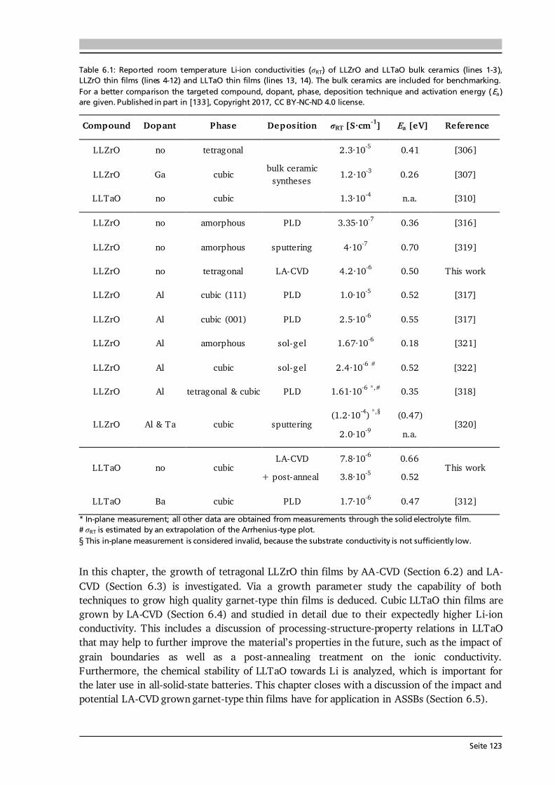
Seite 123
Table 6.1: Reported room temperature Li-ion conductivities ( RT) of LLZrO and LLTaO bulk ceramics (lines 1-3), LLZrO thin films (lines 4-12) and LLTaO thin films (lines 13, 14). The bulk ceramics are included for benchmarking. For a better comparison the targeted compound, dopant, phase, deposition technique and activation energy (Ea) are given. Published in part in [133], Copyright 2017, CC BY-NC-ND 4.0 license. Compound Dopant Phase Deposition σRT [S·cm-1] Ea [eV] Reference
LLZrO no tetragonal bulk ceramic syntheses
2.3·10-5 0.41 [306] LLZrO Ga cubic 1.2·10-3 0.26 [307] LLTaO no cubic 1.3·10-4 n.a. [310] LLZrO no amorphous PLD 3.35·10-7 0.36 [316] LLZrO no amorphous sputtering 4·10-7 0.70 [319] LLZrO no tetragonal LA-CVD 4.2·10-6 0.50 This work LLZrO Al cubic (111) PLD 1.0·10-5 0.52 [317] LLZrO Al cubic (001) PLD 2.5·10-6 0.55 [317] LLZrO Al amorphous sol-gel 1.67·10-6 0.18 [321] LLZrO Al cubic sol-gel 2.4·10-6 # 0.52 [322] LLZrO Al tetragonal & cubic PLD 1.61·10-6 *,# 0.35 [318] LLZrO Al & Ta cubic sputtering (1.2·10-4) *,§
2.0·10-9 (0.47) n.a. [320]
LLTaO no cubic LA-CVD + post-anneal
7.8·10-6 3.8·10-5
0.66 0.52 This work
LLTaO Ba cubic PLD 1.7·10-6 0.47 [312] * In-plane measurement; all other data are obtained from measurements through the solid electrolyte film. # RT is estimated by an extrapolation of the Arrhenius-type plot. § This in-plane measurement is considered invalid, because the substrate conductivity is not sufficiently low. In this chapter, the growth of tetragonal LLZrO thin films by AA-CVD (Section 6.2) and LA-CVD (Section 6.3) is investigated. Via a growth parameter study the capability of both techniques to grow high quality garnet-type thin films is deduced. Cubic LLTaO thin films are grown by LA-CVD (Section 6.4) and studied in detail due to their expectedly higher Li-ion conductivity. This includes a discussion of processing-structure-property relations in LLTaO that may help to further improve the material’s properties in the future, such as the impact of grain boundaries as well as a post-annealing treatment on the ionic conductivity. Furthermore, the chemical stability of LLTaO towards Li is analyzed, which is important for the later use in all-solid-state batteries. This chapter closes with a discussion of the impact and potential LA-CVD grown garnet-type thin films have for application in ASSBs (Section 6.5).
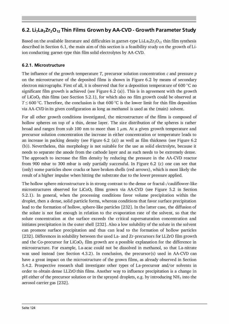
Seite 124
6.2. Li7La3Zr2O12 Thin Films Grown by AA-CVD - Growth Parameter Study Based on the available literature and difficulties in garnet-type Li7La3Zr2O12 thin film synthesis described in Section 6.1, the main aim of this section is a feasibility study on the growth of Li-ion conducting garnet-type thin film solid electrolytes by AA-CVD. 6.2.1. Microstructure The influence of the growth temperature T, precursor solution concentration c and pressure p on the microstructure of the deposited films is shown in Figure 6.2 by means of secondary electron micrographs. First of all, it is observed that for a deposition temperature of 600 °C no significant film growth is achieved (see Figure 6.2 (a)). This is in agreement with the growth of LiCoO2 thin films (see Section 5.2.1), for which also no film growth could be observed at T ≤ 600 °C. Therefore, the conclusion is that 600 °C is the lower limit for thin film deposition via AA-CVD in its given configuration as long as methanol is used as the (main) solvent. For all other growth conditions investigated, the microstructure of the films is composed of hollow spheres on top of a thin, dense layer. The size distribution of the spheres is rather broad and ranges from sub 100 nm to more than 1 μm. At a given growth temperature and precursor solution concentration the increase in either concentration or temperature leads to an increase in packing density (see Figure 6.2 (a)) as well as film thickness (see Figure 6.2 (b)). Nevertheless, this morphology is not suitable for the use as solid electrolyte, because it needs to separate the anode from the cathode layer and as such needs to be extremely dense. The approach to increase the film density by reducing the pressure in the AA-CVD reactor from 900 mbar to 300 mbar is only partially successful. In Figure 6.2 (c) one can see that (only) some particles show cracks or have broken shells (red arrows), which is most likely the result of a higher impulse when hitting the substrate due to the lower pressure applied. The hollow sphere microstructure is in strong contrast to the dense or fractal-/cauliflower-like microstructures observed for LiCoO2 films grown via AA-CVD (see Figure 5.2 in Section 5.2.1). In general, when the processing conditions favor volume precipitation within the droplet, then a dense, solid particle forms, whereas conditions that favor surface precipitation lead to the formation of hollow, sphere-like particles [232]. In the latter case, the diffusion of the solute is not fast enough in relation to the evaporation rate of the solvent, so that the solute concentration at the surface exceeds the critical supersaturation concentration and initiates precipitation in the outer shell [232]. Also a low solubility of the solute in the solvent can promote surface precipitation and thus can lead to the formation of hollow particles [232]. Differences in solubility between the used La- and Zr-precursors for LLZrO film growth and the Co-precursor for LiCoO2 film growth are a possible explanation for the difference in microstructure. For example, La-acac could not be dissolved in methanol, so that La-nitrate was used instead (see Section 4.3.2). In conclusion, the precursor(s) used in AA-CVD can have a great impact on the microstructure of the grown films, as already observed in Section 5.4.2. Prospective research shall investigate other types of La-precursor and/or solvents in order to obtain dense LLZrO thin films. Another way to influence precipitation is a change in pH either of the precursor solution or in the sprayed droplets, e.g. by introducing NH3 into the aerosol carrier gas [232].
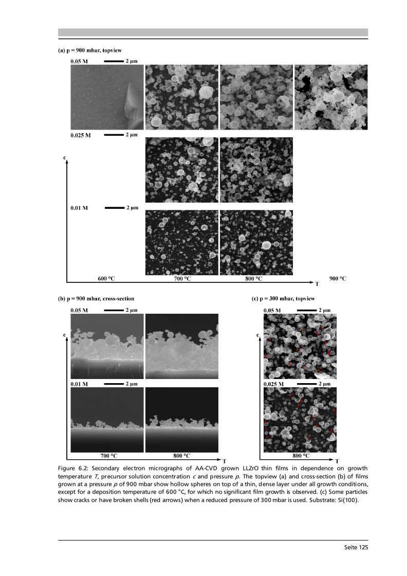
Seite 125
Figure 6.2: Secondary electron micrographs of AA-CVD grown LLZrO thin films in dependence on growth temperature T, precursor solution concentration c and pressure p. The topview (a) and cross-section (b) of films grown at a pressure p of 900 mbar show hollow spheres on top of a thin, dense layer under all growth conditions, except for a deposition temperature of 600 °C, for which no significant film growth is observed. (c) Some particles show cracks or have broken shells (red arrows) when a reduced pressure of 300 mbar is used. Substrate: Si(100).
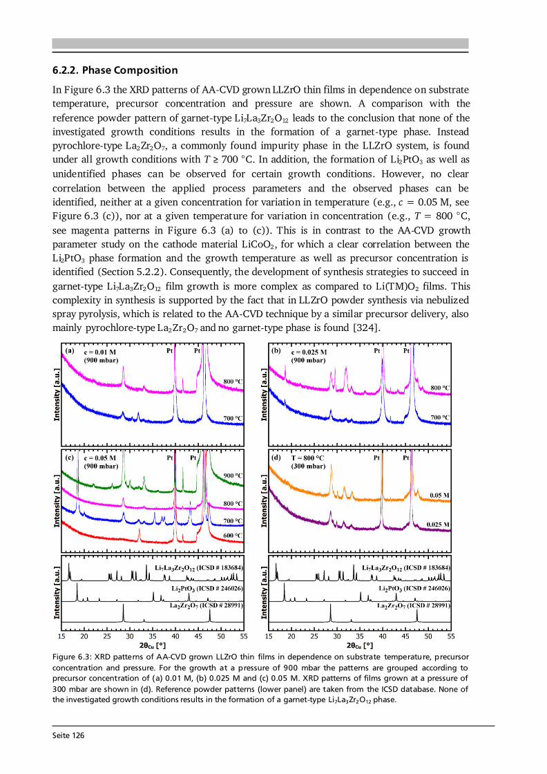
Seite 126
6.2.2. Phase Composition In Figure 6.3 the XRD patterns of AA-CVD grown LLZrO thin films in dependence on substrate temperature, precursor concentration and pressure are shown. A comparison with the reference powder pattern of garnet-type Li7La3Zr2O12 leads to the conclusion that none of the investigated growth conditions results in the formation of a garnet-type phase. Instead pyrochlore-type La2Zr2O7, a commonly found impurity phase in the LLZrO system, is found under all growth conditions with T 700 °C. In addition, the formation of Li2PtO3 as well as unidentified phases can be observed for certain growth conditions. However, no clear correlation between the applied process parameters and the observed phases can be identified, neither at a given concentration for variation in temperature (e.g., c = 0.05 M, see Figure 6.3 (c)), nor at a given temperature for variation in concentration (e.g., T = 800 °C, see magenta patterns in Figure 6.3 (a) to (c)). This is in contrast to the AA-CVD growth parameter study on the cathode material LiCoO2, for which a clear correlation between the Li2PtO3 phase formation and the growth temperature as well as precursor concentration is identified (Section 5.2.2). Consequently, the development of synthesis strategies to succeed in garnet-type Li7La3Zr2O12 film growth is more complex as compared to Li(TM)O2 films. This complexity in synthesis is supported by the fact that in LLZrO powder synthesis via nebulized spray pyrolysis, which is related to the AA-CVD technique by a similar precursor delivery, also mainly pyrochlore-type La2Zr2O7 and no garnet-type phase is found [324].
Figure 6.3: XRD patterns of AA-CVD grown LLZrO thin films in dependence on substrate temperature, precursor concentration and pressure. For the growth at a pressure of 900 mbar the patterns are grouped according to precursor concentration of (a) 0.01 M, (b) 0.025 M and (c) 0.05 M. XRD patterns of films grown at a pressure of 300 mbar are shown in (d). Reference powder patterns (lower panel) are taken from the ICSD database. None of the investigated growth conditions results in the formation of a garnet-type Li7La3Zr2O12 phase.
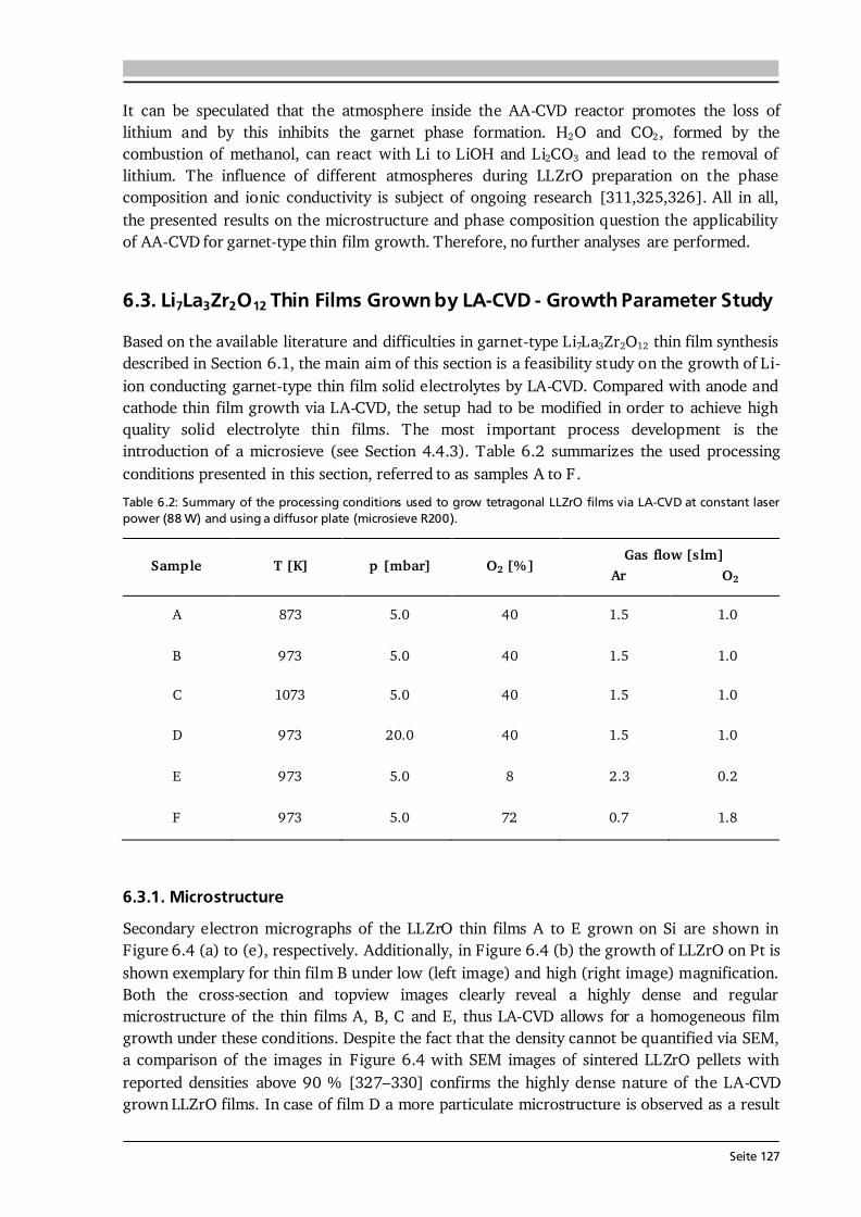
Seite 127
It can be speculated that the atmosphere inside the AA-CVD reactor promotes the loss of lithium and by this inhibits the garnet phase formation. H2O and CO2, formed by the combustion of methanol, can react with Li to LiOH and Li2CO3 and lead to the removal of lithium. The influence of different atmospheres during LLZrO preparation on the phase composition and ionic conductivity is subject of ongoing research [311,325,326]. All in all, the presented results on the microstructure and phase composition question the applicability of AA-CVD for garnet-type thin film growth. Therefore, no further analyses are performed. 6.3. Li7La3Zr2O12 Thin Films Grown by LA-CVD - Growth Parameter Study Based on the available literature and difficulties in garnet-type Li7La3Zr2O12 thin film synthesis described in Section 6.1, the main aim of this section is a feasibility study on the growth of Li-ion conducting garnet-type thin film solid electrolytes by LA-CVD. Compared with anode and cathode thin film growth via LA-CVD, the setup had to be modified in order to achieve high quality solid electrolyte thin films. The most important process development is the introduction of a microsieve (see Section 4.4.3). Table 6.2 summarizes the used processing conditions presented in this section, referred to as samples A to F. Table 6.2: Summary of the processing conditions used to grow tetragonal LLZrO films via LA-CVD at constant laser power (88 W) and using a diffusor plate (microsieve R200).
Sample T [K] p [mbar] O2 [%] Gas flow [slm] Ar O2 A 873 5.0 40 1.5 1.0 B 973 5.0 40 1.5 1.0 C 1073 5.0 40 1.5 1.0 D 973 20.0 40 1.5 1.0 E 973 5.0 8 2.3 0.2 F 973 5.0 72 0.7 1.8
6.3.1. Microstructure Secondary electron micrographs of the LLZrO thin films A to E grown on Si are shown in Figure 6.4 (a) to (e), respectively. Additionally, in Figure 6.4 (b) the growth of LLZrO on Pt is shown exemplary for thin film B under low (left image) and high (right image) magnification. Both the cross-section and topview images clearly reveal a highly dense and regular microstructure of the thin films A, B, C and E, thus LA-CVD allows for a homogeneous film growth under these conditions. Despite the fact that the density cannot be quantified via SEM, a comparison of the images in Figure 6.4 with SEM images of sintered LLZrO pellets with reported densities above 90 % [327–330] confirms the highly dense nature of the LA-CVD grown LLZrO films. In case of film D a more particulate microstructure is observed as a result
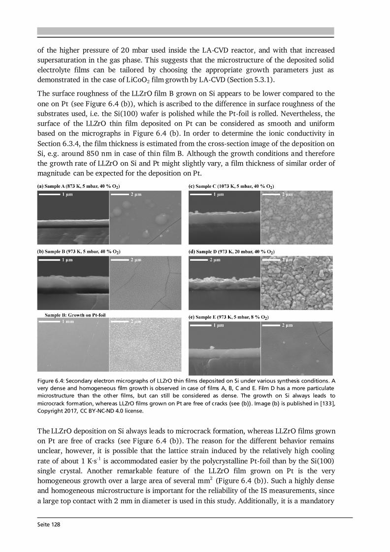
Seite 128
of the higher pressure of 20 mbar used inside the LA-CVD reactor, and with that increased supersaturation in the gas phase. This suggests that the microstructure of the deposited solid electrolyte films can be tailored by choosing the appropriate growth parameters just as demonstrated in the case of LiCoO2 film growth by LA-CVD (Section 5.3.1). The surface roughness of the LLZrO film B grown on Si appears to be lower compared to the one on Pt (see Figure 6.4 (b)), which is ascribed to the difference in surface roughness of the substrates used, i.e. the Si(100) wafer is polished while the Pt-foil is rolled. Nevertheless, the surface of the LLZrO thin film deposited on Pt can be considered as smooth and uniform based on the micrographs in Figure 6.4 (b). In order to determine the ionic conductivity in Section 6.3.4, the film thickness is estimated from the cross-section image of the deposition on Si, e.g. around 850 nm in case of thin film B. Although the growth conditions and therefore the growth rate of LLZrO on Si and Pt might slightly vary, a film thickness of similar order of magnitude can be expected for the deposition on Pt.
Figure 6.4: Secondary electron micrographs of LLZrO thin films deposited on Si under various synthesis conditions. A very dense and homogeneous film growth is observed in case of films A, B, C and E. Film D has a more particulate microstructure than the other films, but can still be considered as dense. The growth on Si always leads to microcrack formation, whereas LLZrO films grown on Pt are free of cracks (see (b)). Image (b) is published in [133], Copyright 2017, CC BY-NC-ND 4.0 license. The LLZrO deposition on Si always leads to microcrack formation, whereas LLZrO films grown on Pt are free of cracks (see Figure 6.4 (b)). The reason for the different behavior remains unclear, however, it is possible that the lattice strain induced by the relatively high cooling rate of about 1 K·s-1 is accommodated easier by the polycrystalline Pt-foil than by the Si(100) single crystal. Another remarkable feature of the LLZrO film grown on Pt is the very homogeneous growth over a large area of several mm2 (Figure 6.4 (b)). Such a highly dense and homogeneous microstructure is important for the reliability of the IS measurements, since a large top contact with 2 mm in diameter is used in this study. Additionally, it is a mandatory
Seite 129
requirement for the application in an all-solid-state thin film Li-ion battery in order to avoid a short circuit due to pinholes and to allow for the use of a very thin solid electrolyte layer. 6.3.2. Phase and Element Composition The XRD patterns of the LLZrO thin films A to F grown on Pt are shown in Figure 6.5 (a). Besides the strong intensities of the underlying Pt substrate, the diffraction patterns reveal considerable differences depending on the growth conditions used. While at a deposition temperature of 873 K (sample A) the film is amorphous, crystalline thin films are obtained at higher deposition temperatures of 973 K (samples B, D, E, F) and 1073 K (sample C). All polycrystalline films show reflections that can be assigned to the garnet-type Li7La3Zr2O12 phase, which is a great advancement compared to the growth via AA-CVD for which the garnet-type phase could not be stabilized at all (Section 6.2.2). However, a closer examination by Rietveld analysis demonstrates that only thin film B (973 K, 5 mbar, 40 % O2) contains garnet-type Li7La3Zr2O12 as the main phase and has low amounts of secondary phases (see Figure 6.5 (b) and Table 6.3). Remarkably, even small deviations in synthesis parameters from this sweet spot lead to the formation of mainly undesired phases (see Figure 6.5 (c)). For example, reducing the oxygen partial pressure (sample E) results in the formation of a fluorite-type related structure with a lattice parameter of ~ 5.51 Å as the main phase. Choosing a higher deposition temperature (sample C) leads to the formation of a fluorite-type related structure with a lattice parameter of ~ 5.31 Å as the main phase. The pyrochlore-type La2Zr2O7, a commonly found impurity phase in the LLZrO system, with a pseudo-cubic lattice parameter of ~ 5.4 Å is closely related to the observed fluorite-type structure and depending on the detailed La to Zr ratio and their occupation in the structure the lattice parameter varies. The La2Zr2O7 phase is well-known to impede the Li-ion movement tremendously and to result in decreased Li-ion conductivity as well as increased activation energy [318]. Using a higher pressure inside the LA-CVD reactor for the film growth (sample D) leads also to a significantly higher phase fraction of undesired phases (mainly La2O3). Consequently, only thin films grown under optimized conditions (973 K, 5 mbar, 40 % O2) will be studied and discussed in detail in the following sections. By applying the Rietveld method [98], a quantification of the crystalline phases in thin film B is achieved (Figure 6.5 (b)). The results are summarized in Table 6.3. Tetragonal Li7La3Zr2O12 is present as main phase (89 vol.-%), with small amounts of Li2PtO3 (7 vol.-%) and La2O3 (4 vol.-%) as secondary phases. The lattice parameters of the LLZrO phase agree well with previously reported values of a = 13.077(1) Å and c = 12.715(4) Å for a tetragonal LLZrO bulk ceramic with 98 % relative density [306]. The Li2PtO3 phase, already observed in the growth of LiCoO2 by AA-CVD (Section 5.2.2) as well as by LA-CVD (Section 5.3.2), is formed only on the surface of the Pt substrate, which is proven in Section 6.3.3. Two ways to suppress the Li2PtO3 phase formation in LA-CVD of LiCoO2 were investigated (see Section 5.3.2), which are both based on the reaction scheme in Eq. (5.1). One strategy was a reduction of the deposition temperature in order to inhibit the kinetics of the corrosion reaction. The second approach to suppress the Li2PtO3 phase formation was a reduction of the oxygen partial pressure to prevent the oxidation of Pt0 to Pt4+ in Li2PtO3 (see Eq. (5.1)). While the first approach was successfully applied in the case of LiCoO2 deposition on Pt by LA-CVD, the second approach showed only a minor effect on the suppression of Li2PtO3 phase formation (see Section 5.3.2). However, in the case of LLZrO
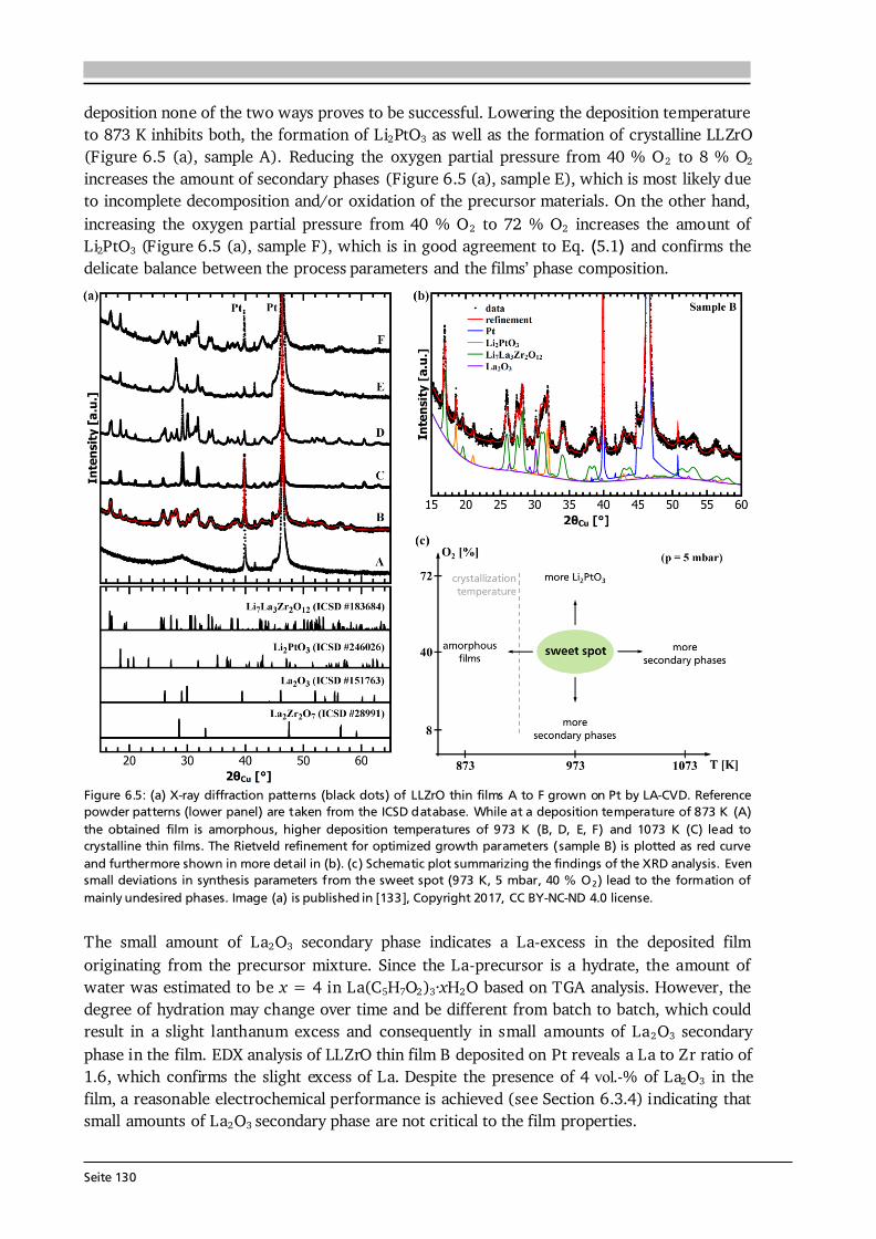
Seite 130
deposition none of the two ways proves to be successful. Lowering the deposition temperature to 873 K inhibits both, the formation of Li2PtO3 as well as the formation of crystalline LLZrO (Figure 6.5 (a), sample A). Reducing the oxygen partial pressure from 40 % O2 to 8 % O2 increases the amount of secondary phases (Figure 6.5 (a), sample E), which is most likely due to incomplete decomposition and/or oxidation of the precursor materials. On the other hand, increasing the oxygen partial pressure from 40 % O2 to 72 % O2 increases the amount of Li2PtO3 (Figure 6.5 (a), sample F), which is in good agreement to Eq. (5.1) and confirms the delicate balance between the process parameters and the films’ phase composition.
Figure 6.5: (a) X-ray diffraction patterns (black dots) of LLZrO thin films A to F grown on Pt by LA-CVD. Reference powder patterns (lower panel) are taken from the ICSD database. While at a deposition temperature of 873 K (A) the obtained film is amorphous, higher deposition temperatures of 973 K (B, D, E, F) and 1073 K (C) lead to crystalline thin films. The Rietveld refinement for optimized growth parameters (sample B) is plotted as red curve and furthermore shown in more detail in (b). (c) Schematic plot summarizing the findings of the XRD analysis. Even small deviations in synthesis parameters from the sweet spot (973 K, 5 mbar, 40 % O2) lead to the formation of mainly undesired phases. Image (a) is published in [133], Copyright 2017, CC BY-NC-ND 4.0 license. The small amount of La2O3 secondary phase indicates a La-excess in the deposited film originating from the precursor mixture. Since the La-precursor is a hydrate, the amount of water was estimated to be x = 4 in La(C5H7O2)3·xH2O based on TGA analysis. However, the degree of hydration may change over time and be different from batch to batch, which could result in a slight lanthanum excess and consequently in small amounts of La2O3 secondary phase in the film. EDX analysis of LLZrO thin film B deposited on Pt reveals a La to Zr ratio of 1.6, which confirms the slight excess of La. Despite the presence of 4 vol.-% of La2O3 in the film, a reasonable electrochemical performance is achieved (see Section 6.3.4) indicating that small amounts of La2O3 secondary phase are not critical to the film properties.
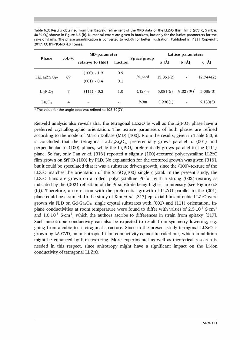
Seite 131
Table 6.3: Results obtained from the Rietveld refinement of the XRD data of the LLZrO thin film B (973 K, 5 mbar, 40 % O2) shown in Figure 6.5 (b). Numerical errors are given in brackets, but only for the lattice parameters for the sake of clarity. The phase quantification is converted to vol.-% for better illustration. Published in [133], Copyright 2017, CC BY-NC-ND 4.0 license. Phase vol.-% MD-parameter
relative to (hkl) fraction Space group Lattice parameters
a [Å] b [Å] c [Å] Li7La3Zr2O12 89 (100) - 1.9 0.9
(001) - 0.4 0.1 I41/acd 13.061(2) - 12.744(2) Li2PtO3 7 (111) - 0.3 1.0 C12/m 5.081(6) 9.028(9)* 5.086(3) La2O3 4 - - P-3m 3.930(1) - 6.130(3)
* The value for the angle beta was refined to 108.50(7)°. Rietveld analysis also reveals that the tetragonal LLZrO as well as the Li2PtO3 phase have a preferred crystallographic orientation. The texture parameters of both phases are refined according to the model of March-Dollase (MD) [100]. From the results, given in Table 6.3, it is concluded that the tetragonal Li7La3Zr2O12 preferentially grows parallel to (001) and perpendicular to (100) planes, while the Li2PtO3 preferentially grows parallel to the (111) plane. So far, only Tan et al. [316] reported a slightly (100)-textured polycrystalline LLZrO film grown on SrTiO3(100) by PLD. No explanation for the textured growth was given [316], but it could be speculated that it was a substrate driven growth, since the (100)-texture of the LLZrO matches the orientation of the SrTiO3(100) single crystal. In the present study, the LLZrO films are grown on a rolled, polycrystalline Pt-foil with a strong (002)-texture, as indicated by the (002) reflection of the Pt substrate being highest in intensity (see Figure 6.5 (b)). Therefore, a correlation with the preferential growth of LLZrO parallel to the (001) plane could be assumed. In the study of Kim et al. [317] epitaxial films of cubic LLZrO were grown via PLD on Gd3Ga5O12 single crystal substrates with (001) and (111) orientation. In-plane conductivities at room temperature were found to differ with values of 2.5·10 -6 S·cm-1 and 1.0·10-5 S·cm-1, which the authors ascribe to differences in strain from epitaxy [317]. Such anisotropic conductivity can also be expected to result from symmetry lowering, e.g. going from a cubic to a tetragonal structure. Since in the present study tetragonal LLZrO is grown by LA-CVD, an anisotropic Li-ion conductivity cannot be ruled out, which in addition might be enhanced by film texturing. More experimental as well as theoretical research is needed in this respect, since anisotropy might have a significant impact on the Li-ion conductivity of tetragonal LLZrO.
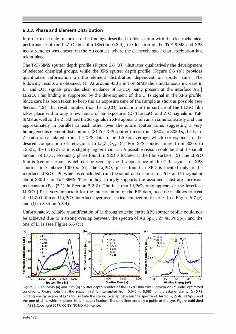
Seite 132
6.3.3. Phase and Element Distribution In order to be able to correlate the findings described in this section with the electrochemical performance of the LLZrO thin film (Section 6.3.4), the location of the ToF-SIMS and XPS measurements was chosen on the Au contact, where the electrochemical characterization had taken place. The ToF-SIMS sputter depth profile (Figure 6.6 (a)) illustrates qualitatively the development of selected chemical groups, while the XPS sputter depth profile (Figure 6.6 (b)) provides quantitative information on the element distribution dependent on sputter time. The following results are obtained: (1) At around 450 s in ToF-SIMS the simultaneous increase in Li- and CO3- signals provides clear evidence of Li2CO3 being present at the interface Au | LLZrO. This finding is supported by the development of the C 1s signal in the XPS profile. Since care has been taken to keep the air exposure time of the sample as short as possible (see Section 4.2), this result implies that the Li2CO3 formation at the surface of the LLZrO film takes place within only a few hours of air exposure. (2) The LaO- and ZrO- signals in ToF-SIMS as well as the Zr 3d and La 3d signals in XPS appear and vanish simultaneously and run approximately in parallel to each other over the entire sputter time, suggesting a very homogeneous element distribution. (3) For XPS sputter times from 1550 s to 3050 s, the La to Zr ratio is calculated from the XPS data to be 1.5 on average, which corresponds to the desired composition of tetragonal Li7La3Zr2O12. (4) For XPS sputter times from 800 s to 1550 s, the La to Zr ratio is slightly higher than 1.5. A possible reason could be that the small amount of La2O3 secondary phase found in XRD is located at the film surface. (5) The LLZrO film is free of carbon, which can be seen by the disappearance of the C 1s signal for XPS sputter times above 1000 s. (6) The Li2PtO3 phase found in XRD is located only at the interface LLZrO | Pt, which is concluded from the simultaneous onset of PtO- and Pt- signal at about 3300 s in ToF-SIMS. This finding strongly supports the assumed substrate corrosion mechanism (Eq. (5.1) in Section 5.2.2). The fact that Li2PtO3 only appears at the interface LLZrO | Pt is very important for the interpretation of the EIS data, because it allows to treat the LLZrO film and Li2PtO3 interface layer as electrical connection in series (see Figure 6.7 (e) and (f) in Section 6.3.4). Unfortunately, reliable quantification of Li throughout the entire XPS sputter profile could not be achieved due to a strong overlap between the spectra of Au 5p1/2, Zr 4s, Pt 5p3/2 and the one of Li 1s (see Figure 6.6 (c)).
Figure 6.6: ToF-SIMS (a) and XPS (b) sputter depth profiles of the LLZrO thin film B grown on Pt under optimized conditions. Please note that the y-axis in (a) is interrupted from 0.045 to 0.085 for the sake of clarity. (c) XPS binding energy region of Li 1s to illustrate the strong overlap between the spectra of Au 5p1/2, Zr 4s, Pt 5p3/2 and the one of Li 1s, which impedes lithium quantification. The solid lines are only a guide to the eye. Figure published in [133], Copyright 2017, CC BY-NC-ND 4.0 license.
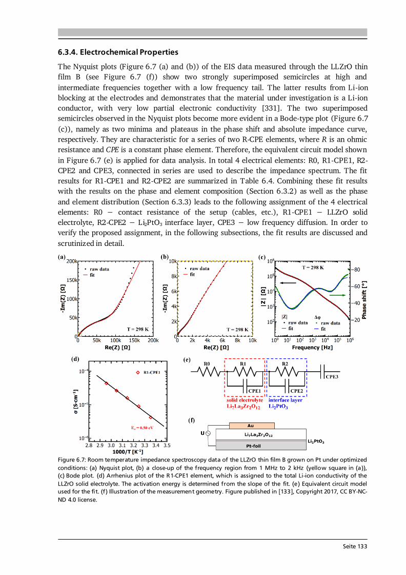
Seite 133
6.3.4. Electrochemical Properties The Nyquist plots (Figure 6.7 (a) and (b)) of the EIS data measured through the LLZrO thin film B (see Figure 6.7 (f)) show two strongly superimposed semicircles at high and intermediate frequencies together with a low frequency tail. The latter results from Li-ion blocking at the electrodes and demonstrates that the material under investigation is a Li-ion conductor, with very low partial electronic conductivity [331]. The two superimposed semicircles observed in the Nyquist plots become more evident in a Bode-type plot (Figure 6.7 (c)), namely as two minima and plateaus in the phase shift and absolute impedance curve, respectively. They are characteristic for a series of two R-CPE elements, where R is an ohmic resistance and CPE is a constant phase element. Therefore, the equivalent circuit model shown in Figure 6.7 (e) is applied for data analysis. In total 4 electrical elements: R0, R1-CPE1, R2-CPE2 and CPE3, connected in series are used to describe the impedance spectrum. The fit results for R1-CPE1 and R2-CPE2 are summarized in Table 6.4. Combining these fit results with the results on the phase and element composition (Section 6.3.2) as well as the phase and element distribution (Section 6.3.3) leads to the following assignment of the 4 electrical elements: R0 − contact resistance of the setup (cables, etc.), R1-CPE1 − LLZrO solid electrolyte, R2-CPE2 − Li2PtO3 interface layer, CPE3 − low frequency diffusion. In order to verify the proposed assignment, in the following subsections, the fit results are discussed and scrutinized in detail.
Figure 6.7: Room temperature impedance spectroscopy data of the LLZrO thin film B grown on Pt under optimized conditions: (a) Nyquist plot, (b) a close-up of the frequency region from 1 MHz to 2 kHz (yellow square in (a)), (c) Bode plot. (d) Arrhenius plot of the R1-CPE1 element, which is assigned to the total Li-ion conductivity of the LLZrO solid electrolyte. The activation energy is determined from the slope of the fit. (e) Equivalent circuit model used for the fi t. (f) Illustration of the measurement geometry. Figure published in [133], Copyright 2017, CC BY-NC-ND 4.0 license.
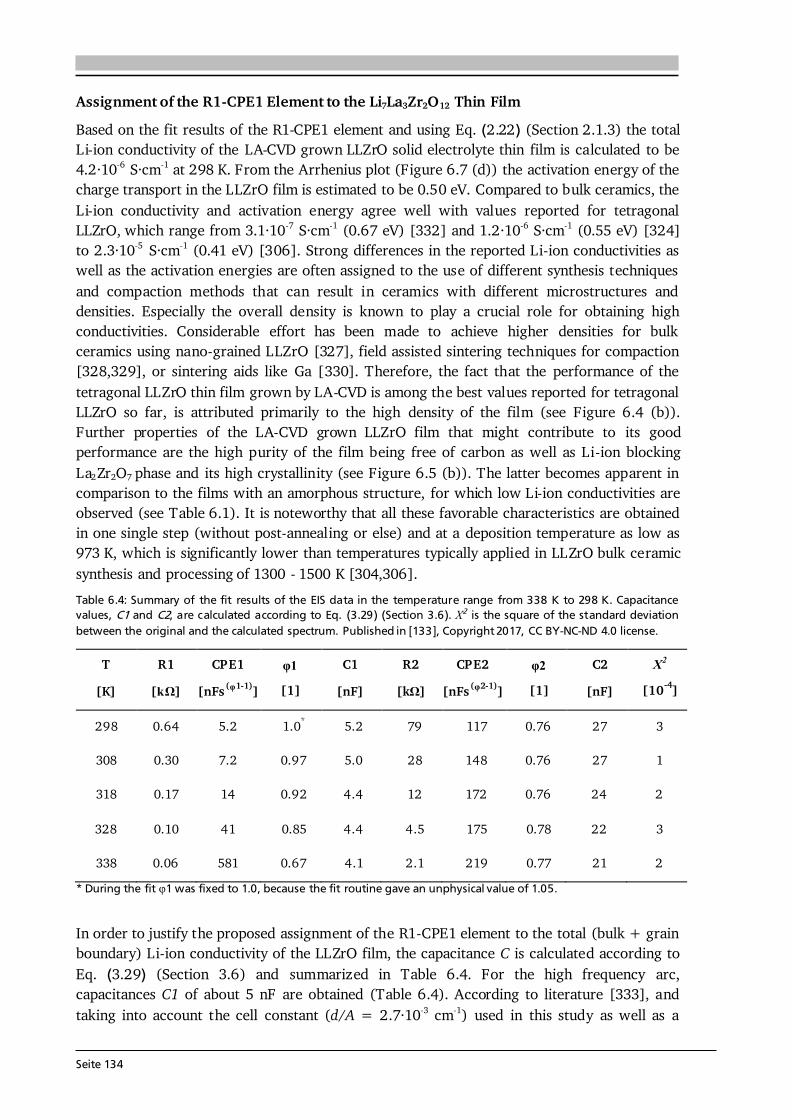
Seite 134
Assignment of the R1-CPE1 Element to the Li7La3Zr2O12 Thin Film Based on the fit results of the R1-CPE1 element and using Eq. (2.22) (Section 2.1.3) the total Li-ion conductivity of the LA-CVD grown LLZrO solid electrolyte thin film is calculated to be 4.2·10-6 S·cm-1 at 298 K. From the Arrhenius plot (Figure 6.7 (d)) the activation energy of the charge transport in the LLZrO film is estimated to be 0.50 eV. Compared to bulk ceramics, the Li-ion conductivity and activation energy agree well with values reported for tetragonal LLZrO, which range from 3.1·10-7 S·cm-1 (0.67 eV) [332] and 1.2·10-6 S·cm-1 (0.55 eV) [324] to 2.3·10-5 S·cm-1 (0.41 eV) [306]. Strong differences in the reported Li-ion conductivities as well as the activation energies are often assigned to the use of different synthesis techniques and compaction methods that can result in ceramics with different microstructures and densities. Especially the overall density is known to play a crucial role for obtaining high conductivities. Considerable effort has been made to achieve higher densities for bulk ceramics using nano-grained LLZrO [327], field assisted sintering techniques for compaction [328,329], or sintering aids like Ga [330]. Therefore, the fact that the performance of the tetragonal LLZrO thin film grown by LA-CVD is among the best values reported for tetragonal LLZrO so far, is attributed primarily to the high density of the film (see Figure 6.4 (b)). Further properties of the LA-CVD grown LLZrO film that might contribute to its good performance are the high purity of the film being free of carbon as well as Li-ion blocking La2Zr2O7 phase and its high crystallinity (see Figure 6.5 (b)). The latter becomes apparent in comparison to the films with an amorphous structure, for which low Li-ion conductivities are observed (see Table 6.1). It is noteworthy that all these favorable characteristics are obtained in one single step (without post-annealing or else) and at a deposition temperature as low as 973 K, which is significantly lower than temperatures typically applied in LLZrO bulk ceramic synthesis and processing of 1300 - 1500 K [304,306]. Table 6.4: Summary of the fit results of the EIS data in the temperature range from 338 K to 298 K. Capacitance values, C1 and C2, are calculated according to Eq. (3.29) (Section 3.6). 2 is the square of the standard deviation between the original and the calculated spectrum. Published in [133], Copyright 2017, CC BY-NC-ND 4.0 license.
T [K]
R1 [kΩ]
CPE1 [nFs (φ1-1)]
φ1 [1]
C1 [nF]
R2 [kΩ]
CPE2 [nFs (φ2-1)]
φ2 [1]
C2 [nF]
Χ2 [10-4]
298 0.64 5.2 1.0* 5.2 79 117 0.76 27 3 308 0.30 7.2 0.97 5.0 28 148 0.76 27 1 318 0.17 14 0.92 4.4 12 172 0.76 24 2 328 0.10 41 0.85 4.4 4.5 175 0.78 22 3 338 0.06 581 0.67 4.1 2.1 219 0.77 21 2
* During the fit φ1 was fixed to 1.0, because the fit routine gave an unphysical value of 1.05. In order to justify the proposed assignment of the R1-CPE1 element to the total (bulk + grain boundary) Li-ion conductivity of the LLZrO film, the capacitance C is calculated according to Eq. (3.29) (Section 3.6) and summarized in Table 6.4. For the high frequency arc, capacitances C1 of about 5 nF are obtained (Table 6.4). According to literature [333], and taking into account the cell constant (d/A = 2.7·10-3 cm-1) used in this study as well as a
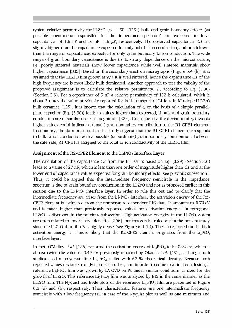
Seite 135
typical relative permittivity for LLZrO ( r ~ 50, [125]) bulk and grain boundary effects (as possible phenomena responsible for the impedance spectrum) are expected to have capacitances of 1.6 nF and 16 nF - 16 μF, respectively. The observed capacitances C1 are slightly higher than the capacitance expected for only bulk Li-ion conduction, and much lower than the range of capacitances expected for only grain boundary Li-ion conduction. The wide range of grain boundary capacitance is due to its strong dependence on the microstructure, i.e. poorly sintered materials show lower capacitance while well sintered materials show higher capacitance [333]. Based on the secondary electron micrographs (Figure 6.4 (b)) it is assumed that the LLZrO film grown at 973 K is well sintered, hence the capacitance C1 of the high frequency arc is most likely bulk dominated. Another approach to test the validity of the proposed assignment is to calculate the relative permittivity, r, according to Eq. (3.30) (Section 3.6). For a capacitance of 5 nF a relative permittivity of 152 is calculated, which is about 3 times the value previously reported for bulk transport of Li-ions in Mo-doped LLZrO bulk ceramics [125]. It is known that the calculation of r on the basis of a simple parallel-plate capacitor (Eq. (3.30)) leads to values higher than expected, if bulk and grain boundary conduction are of similar order of magnitude [334]. Consequently, the deviation of r towards higher values could indicate a (small) grain boundary contribution to the R1-CPE1 element. In summary, the data presented in this study suggest that the R1-CPE1 element corresponds to bulk Li-ion conduction with a possible (subordinate) grain boundary contribution. To be on the safe side, R1-CPE1 is assigned to the total Li-ion conductivity of the LLZrO film. Assignment of the R2-CPE2 Element to the Li2PtO3 Interface Layer The calculation of the capacitance C2 from the fit results based on Eq. (3.29) (Section 3.6) leads to a value of 27 nF, which is less than one order of magnitude higher than C1 and at the lower end of capacitance values expected for grain boundary effects (see previous subsection). Thus, it could be argued that the intermediate frequency semicircle in the impedance spectrum is due to grain boundary conduction in the LLZrO and not as proposed earlier in this section due to the Li2PtO3 interface layer. In order to rule this out and to clarify that the intermediate frequency arc arises from the Li2PtO3 interface, the activation energy of the R2-CPE2 element is estimated from the temperature dependent EIS data. It amounts to 0.79 eV and is much higher than previously reported values for activation energies in tetragonal LLZrO as discussed in the previous subsection. High activation energies in the LLZrO system are often related to low relative densities [306], but this can be ruled out in the present study since the LLZrO thin film B is highly dense (see Figure 6.4 (b)). Therefore, based on the high activation energy it is more likely that the R2-CPE2 element originates from the Li2PtO3 interface layer. In fact, O’Malley et al. [186] reported the activation energy of Li2PtO3 to be 0.92 eV, which is almost twice the value of 0.49 eV previously reported by Okada et al. [192], although both studies used a polycrystalline Li2PtO3 pellet with 63 % theoretical density. Because both reported values deviate strongly from each other, and in order to come to a final conclusion, a reference Li2PtO3 film was grown by LA-CVD on Pt under similar conditions as used for the growth of LLZrO. This reference Li2PtO3 film was analyzed by EIS in the same manner as the LLZrO film. The Nyquist and Bode plots of the reference Li2PtO3 film are presented in Figure 6.8 (a) and (b), respectively. Their characteristic features are one intermediate frequency semicircle with a low frequency tail in case of the Nyquist plot as well as one minimum and
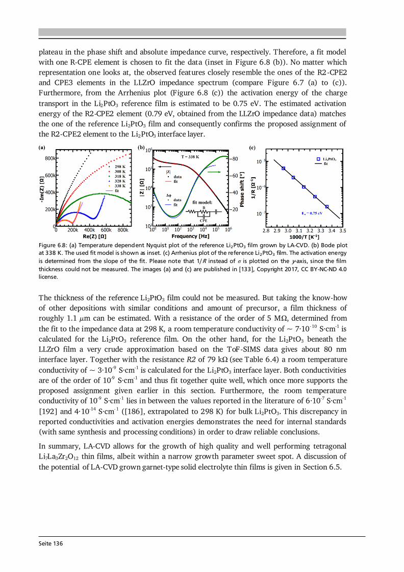
Seite 136
plateau in the phase shift and absolute impedance curve, respectively. Therefore, a fit model with one R-CPE element is chosen to fit the data (inset in Figure 6.8 (b)). No matter which representation one looks at, the observed features closely resemble the ones of the R2-CPE2 and CPE3 elements in the LLZrO impedance spectrum (compare Figure 6.7 (a) to (c)). Furthermore, from the Arrhenius plot (Figure 6.8 (c)) the activation energy of the charge transport in the Li2PtO3 reference film is estimated to be 0.75 eV. The estimated activation energy of the R2-CPE2 element (0.79 eV, obtained from the LLZrO impedance data) matches the one of the reference Li2PtO3 film and consequently confirms the proposed assignment of the R2-CPE2 element to the Li2PtO3 interface layer.
Figure 6.8: (a) Temperature dependent Nyquist plot of the reference Li2PtO3 film grown by LA-CVD. (b) Bode plot at 338 K. The used fit model is shown as inset. (c) Arrhenius plot of the reference Li2PtO3 film. The activation energy is determined from the slope of the fit. Please note that 1/R instead of is plotted on the y-axis, since the film thickness could not be measured. The images (a) and (c) are published in [133], Copyright 2017, CC BY-NC-ND 4.0 license. The thickness of the reference Li2PtO3 film could not be measured. But taking the know-how of other depositions with similar conditions and amount of precursor, a film thickness of roughly 1.1 μm can be estimated. With a resistance of the order of 5 MΩ, determined from the fit to the impedance data at 298 K, a room temperature conductivity of ~ 7·10-10 S·cm-1 is calculated for the Li2PtO3 reference film. On the other hand, for the Li2PtO3 beneath the LLZrO film a very crude approximation based on the ToF-SIMS data gives about 80 nm interface layer. Together with the resistance R2 of 79 kΩ (see Table 6.4) a room temperature conductivity of ~ 3·10-9 S·cm-1 is calculated for the Li2PtO3 interface layer. Both conductivities are of the order of 10-9 S·cm-1 and thus fit together quite well, which once more supports the proposed assignment given earlier in this section. Furthermore, the room temperature conductivity of 10-9 S·cm-1 lies in between the values reported in the literature of 6·10-7 S·cm-1 [192] and 4·10-14 S·cm-1 ([186], extrapolated to 298 K) for bulk Li2PtO3. This discrepancy in reported conductivities and activation energies demonstrates the need for internal standards (with same synthesis and processing conditions) in order to draw reliable conclusions. In summary, LA-CVD allows for the growth of high quality and well performing tetragonal Li7La3Zr2O12 thin films, albeit within a narrow growth parameter sweet spot. A discussion of the potential of LA-CVD grown garnet-type solid electrolyte thin films is given in Section 6.5.
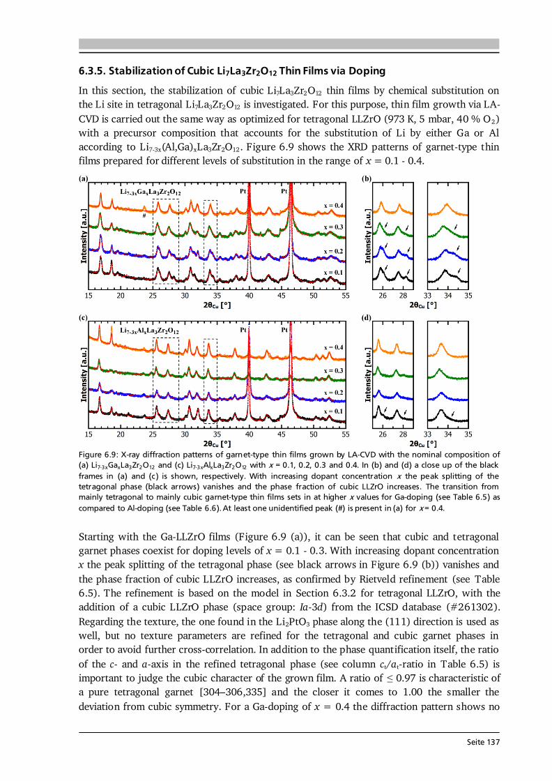
Seite 137
6.3.5. Stabilization of Cubic Li7La3Zr2O12 Thin Films via Doping In this section, the stabilization of cubic Li7La3Zr2O12 thin films by chemical substitution on the Li site in tetragonal Li7La3Zr2O12 is investigated. For this purpose, thin film growth via LA-CVD is carried out the same way as optimized for tetragonal LLZrO (973 K, 5 mbar, 40 % O2) with a precursor composition that accounts for the substitution of Li by either Ga or Al according to Li7-3x(Al,Ga)xLa3Zr2O12. Figure 6.9 shows the XRD patterns of garnet-type thin films prepared for different levels of substitution in the range of x = 0.1 - 0.4.
Figure 6.9: X-ray diffraction patterns of garnet-type thin films grown by LA-CVD with the nominal composition of (a) Li7-3xGaxLa3Zr2O12 and (c) Li7-3xAlxLa3Zr2O12 with x = 0.1, 0.2, 0.3 and 0.4. In (b) and (d) a close up of the black frames in (a) and (c) is shown, respectively. With increasing dopant concentration x the peak splitting of the tetragonal phase (black arrows) vanishes and the phase fraction of cubic LLZrO increases. The transition from mainly tetragonal to mainly cubic garnet-type thin films sets in at higher x values for Ga-doping (see Table 6.5) as compared to Al-doping (see Table 6.6). At least one unidentified peak (#) is present in (a) for x = 0.4. Starting with the Ga-LLZrO films (Figure 6.9 (a)), it can be seen that cubic and tetragonal garnet phases coexist for doping levels of x = 0.1 - 0.3. With increasing dopant concentration x the peak splitting of the tetragonal phase (see black arrows in Figure 6.9 (b)) vanishes and the phase fraction of cubic LLZrO increases, as confirmed by Rietveld refinement (see Table 6.5). The refinement is based on the model in Section 6.3.2 for tetragonal LLZrO, with the addition of a cubic LLZrO phase (space group: Ia-3d) from the ICSD database (#261302). Regarding the texture, the one found in the Li2PtO3 phase along the (111) direction is used as well, but no texture parameters are refined for the tetragonal and cubic garnet phases in order to avoid further cross-correlation. In addition to the phase quantification itself, the ratio of the c- and a-axis in the refined tetragonal phase (see column ct/at-ratio in Table 6.5) is important to judge the cubic character of the grown film. A ratio of ≤ 0.97 is characteristic of a pure tetragonal garnet [304–306,335] and the closer it comes to 1.00 the smaller the deviation from cubic symmetry. For a Ga-doping of x = 0.4 the diffraction pattern shows no
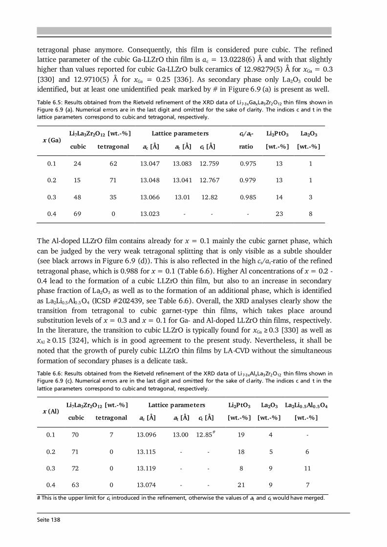
Seite 138
tetragonal phase anymore. Consequently, this film is considered pure cubic. The refined lattice parameter of the cubic Ga-LLZrO thin film is ac = 13.0228(6) Å and with that slightly higher than values reported for cubic Ga-LLZrO bulk ceramics of 12.98279(5) Å for xGa = 0.3 [330] and 12.9710(5) Å for xGa = 0.25 [336]. As secondary phase only La2O3 could be identified, but at least one unidentified peak marked by # in Figure 6.9 (a) is present as well. Table 6.5: Results obtained from the Rietveld refinement of the XRD data of Li7-3xGaxLa3Zr2O12 thin films shown in Figure 6.9 (a). Numerical errors are in the last digit and omitted for the sake of clarity. The indices c and t in the lattice parameters correspond to cubic and tetragonal, respectively.
x (Ga) Li7La3Zr2O12 [wt.-%] cubic tetragonal
Lattice parameters ac [Å] at [Å] ct [Å]
ct/at- ratio
Li2PtO3 [wt.-%]
La2O3 [wt.-%]
0.1 24 62 13.047 13.083 12.759 0.975 13 1 0.2 15 71 13.048 13.041 12.767 0.979 13 1 0.3 48 35 13.066 13.01 12.82 0.985 14 3 0.4 69 0 13.023 - - - 23 8
The Al-doped LLZrO film contains already for x = 0.1 mainly the cubic garnet phase, which can be judged by the very weak tetragonal splitting that is only visible as a subtle shoulder (see black arrows in Figure 6.9 (d)). This is also reflected in the high ct/at-ratio of the refined tetragonal phase, which is 0.988 for x = 0.1 (Table 6.6). Higher Al concentrations of x = 0.2 - 0.4 lead to the formation of a cubic LLZrO thin film, but also to an increase in secondary phase fraction of La2O3 as well as to the formation of an additional phase, which is identified as La2Li0.5Al0.5O4 (ICSD #202439, see Table 6.6). Overall, the XRD analyses clearly show the transition from tetragonal to cubic garnet-type thin films, which takes place around substitution levels of x = 0.3 and x = 0.1 for Ga- and Al-doped LLZrO thin films, respectively. In the literature, the transition to cubic LLZrO is typically found for xGa 0.3 [330] as well as xAl 0.15 [324], which is in good agreement to the present study. Nevertheless, it shall be noted that the growth of purely cubic LLZrO thin films by LA-CVD without the simultaneous formation of secondary phases is a delicate task. Table 6.6: Results obtained from the Rietveld refinement of the XRD data of Li 7-3xAlxLa3Zr2O12 thin films shown in Figure 6.9 (c). Numerical errors are in the last digit and omitted for the sake of clarity. The indices c and t in the lattice parameters correspond to cubic and tetragonal, respectively.
x (Al) Li7La3Zr2O12 [wt.-%] cubic tetragonal
Lattice parameters ac [Å] at [Å] ct [Å]
Li2PtO3 [wt.-%]
La2O3 [wt.-%]
La2Li0.5Al0.5O4 [wt.-%]
0.1 70 7 13.096 13.00 12.85# 19 4 - 0.2 71 0 13.115 - - 18 5 6 0.3 72 0 13.119 - - 8 9 11 0.4 63 0 13.074 - - 21 9 7
# This is the upper limit for ct introduced in the refinement, otherwise the values of at and ct would have merged.

Seite 139
The refined lattice parameter of the cubic Al-LLZrO thin film is ac = 13.0744(6) Å and therefore surprisingly high compared to values reported for cubic Al-LLZrO bulk ceramics of 12.9682(6) Å [304]. Furthermore, one would expect a higher lattice parameter for the Ga- than for the Al-substitution based on the ionic radii of Ga3+ and Al3+ in four-/six-fold coordination of 0.47/0.62 Å and 0.39/0.53 Å [257], respectively. Two explanations come into question based on a comparison to literature. Large cubic lattice parameters could originate from the exchange of Li- by H-ions in the garnet structure. Orera et al. [337] intentionally hydrated their tetragonal garnet via air exposure for 24 h at 150 °C and obtained Li2.3H4.7La3Zr2O12 with cubic structure (space group: I-43d) and a lattice parameter of 13.087 Å. Assuming that the degree of hydration correlates with the increase in lattice parameter this would mean that the Ga-LLZrO thin films are less prone to hydration than the Al-LLZrO films, since all samples have been treated in the same manner. However, such a high exchange of Li- by H-ions seems unlikely in the present case because of two reasons: (i) the air exposure time is limited to a few hours at 25 °C, and (ii) the tetragonal LLZrO films, also treated in the same manner, do not show a transformation to cubic phase (see Section 6.3.2) as observed by Orera et al. [337] upon intentional hydration at elevated temperatures. Another possible explanation of the observed large lattice parameter might be related to a non-equilibrated, metastable garnet-type structure as explained in the following. Garnet-type thin film growth by LA-CVD takes place at a rather low temperature of 973 K and for a short time (30 min), whereas bulk ceramic synthesis typically involves several hours of sintering at temperatures > 1400 K [25]. The latter provides sufficient time and energy for the aluminum to diffuse within the garnet structure and to reach equilibrium. For example, Al3+ in cubic LLZrO is preferably located at 24d sites, but could potentially be incorporated at metastable 96h and 48g sites as suggested by similar site energies calculated with DFT [338]. Experimentally, Hubaud et al. [339] studied the role of Al during the formation of cubic Li7-3xAlxLa3Zr2O12 bulk ceramics synthesized in a sol-gel process at low temperatures of 973 K followed by annealing at 1123 K for up to 25 hours. By means of high resolution synchrotron XRD they found that a best-fit Rietveld refinement to their data was only possible using 3 cubic garnet phases with (also) relatively high lattice constants of 13.064 Å, 13.048 Å and 13.016 Å [339]. With the help of 27Al and 7Li nuclear magnetic resonance (NMR) spectroscopy, they concluded that even if the sample is single phase cubic as seen in powder XRD it may still not be equilibrated and contain a series of phases each with a different Al content and cell parameter as a result of slow Al3+ diffusion at the low temperatures used. This “low temperature” cubic Al-LLZrO showed a conductivity of 2.12·10-5 S·cm-1 [339], which is far below values observed in conventionally synthesized cubic LLZrO [25] and in fact not even superior to dense tetragonal LLZrO [306]. Apparently, the low temperature or non-equilibrated cubic LLZrO does not provide pathways for fast Li-ion movement in the crystal structure. Of course, the detailed reactions and intermediates in thin film growth via LA-CVD may differ from the sol-gel synthesis in [339], yet the resulting lattice parameters and temperatures used are comparable. Assuming the given discussion is valid and the cubic Al-LLZrO thin film is in a metastable state, then this would imply that the cubic Ga-LLZrO film is closer to equilibrium, as judged by its lattice parameter, and therefore Ga should have a higher diffusivity in LLZrO than Al under the given experimental conditions. This, in turn, might be related to the higher solubility of Ga in LLZrO as compared to Al [340] or to the difference between the ionic radii,
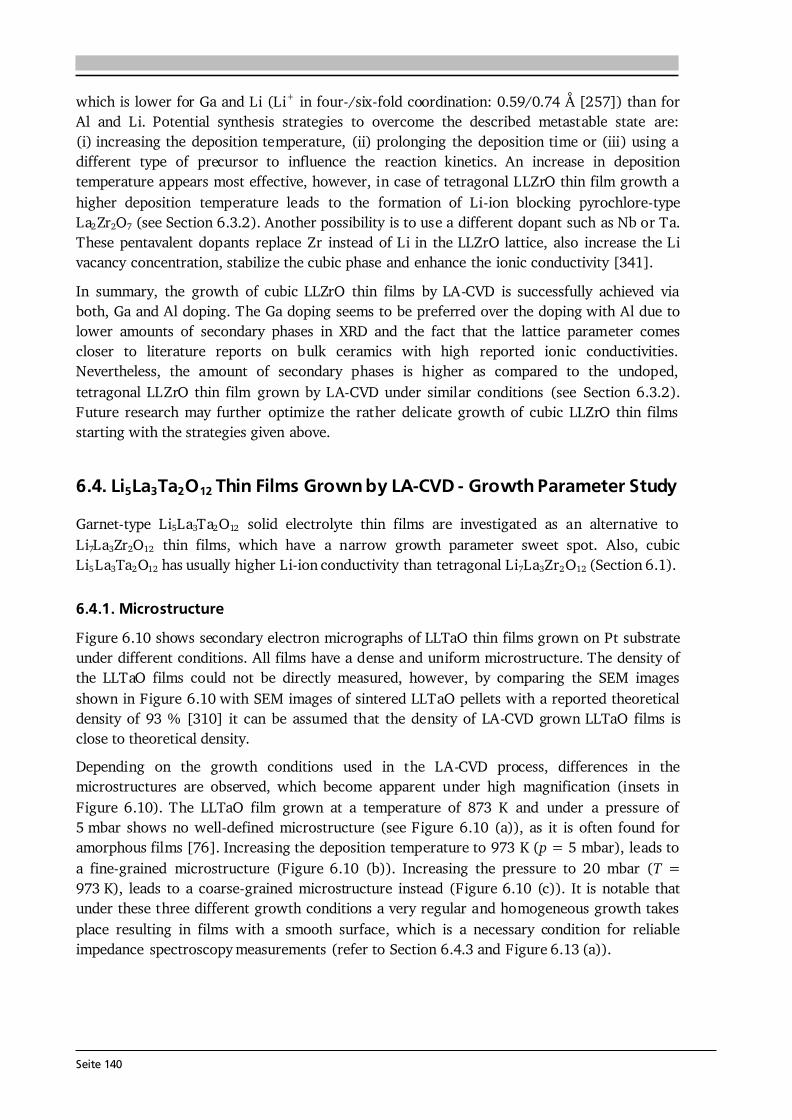
Seite 140
which is lower for Ga and Li (Li+ in four-/six-fold coordination: 0.59/0.74 Å [257]) than for Al and Li. Potential synthesis strategies to overcome the described metastable state are: (i) increasing the deposition temperature, (ii) prolonging the deposition time or (iii) using a different type of precursor to influence the reaction kinetics. An increase in deposition temperature appears most effective, however, in case of tetragonal LLZrO thin film growth a higher deposition temperature leads to the formation of Li-ion blocking pyrochlore-type La2Zr2O7 (see Section 6.3.2). Another possibility is to use a different dopant such as Nb or Ta. These pentavalent dopants replace Zr instead of Li in the LLZrO lattice, also increase the Li vacancy concentration, stabilize the cubic phase and enhance the ionic conductivity [341]. In summary, the growth of cubic LLZrO thin films by LA-CVD is successfully achieved via both, Ga and Al doping. The Ga doping seems to be preferred over the doping with Al due to lower amounts of secondary phases in XRD and the fact that the lattice parameter comes closer to literature reports on bulk ceramics with high reported ionic conductivities. Nevertheless, the amount of secondary phases is higher as compared to the undoped, tetragonal LLZrO thin film grown by LA-CVD under similar conditions (see Section 6.3.2). Future research may further optimize the rather delicate growth of cubic LLZrO thin films starting with the strategies given above. 6.4. Li5La3Ta2O12 Thin Films Grown by LA-CVD - Growth Parameter Study Garnet-type Li5La3Ta2O12 solid electrolyte thin films are investigated as an alternative to Li7La3Zr2O12 thin films, which have a narrow growth parameter sweet spot. Also, cubic Li5La3Ta2O12 has usually higher Li-ion conductivity than tetragonal Li7La3Zr2O12 (Section 6.1). 6.4.1. Microstructure Figure 6.10 shows secondary electron micrographs of LLTaO thin films grown on Pt substrate under different conditions. All films have a dense and uniform microstructure. The density of the LLTaO films could not be directly measured, however, by comparing the SEM images shown in Figure 6.10 with SEM images of sintered LLTaO pellets with a reported theoretical density of 93 % [310] it can be assumed that the density of LA-CVD grown LLTaO films is close to theoretical density. Depending on the growth conditions used in the LA-CVD process, differences in the microstructures are observed, which become apparent under high magnification (insets in Figure 6.10). The LLTaO film grown at a temperature of 873 K and under a pressure of 5 mbar shows no well-defined microstructure (see Figure 6.10 (a)), as it is often found for amorphous films [76]. Increasing the deposition temperature to 973 K (p = 5 mbar), leads to a fine-grained microstructure (Figure 6.10 (b)). Increasing the pressure to 20 mbar (T = 973 K), leads to a coarse-grained microstructure instead (Figure 6.10 (c)). It is notable that under these three different growth conditions a very regular and homogeneous growth takes place resulting in films with a smooth surface, which is a necessary condition for reliable impedance spectroscopy measurements (refer to Section 6.4.3 and Figure 6.13 (a)).
Seite 141
Figure 6.10: Secondary electron micrographs of LLTaO thin films grown on Pt under different conditions as indicated in each micrograph. All films are very dense and have a uniform microstructure. Observed microstructures are (a) amorphous-like, (b) fine-grained, (c) coarse-grained, and (d, e) coarse-grained with particulate deposits. Figure published in [135], Copyright 2017, Elsevier. A further increase in deposition temperature to 1073 K and 1173 K (p = 5 mbar) leads to the growth of coarse-grained LLTaO films with particulate deposits on top as observed in Figure 6.10 (d) and (e), respectively. Thereby, the amount of particulate deposits increases with increasing deposition temperature. Moreover, an increase in deposition temperature leads to grain growth as can be clearly seen by a comparison of the high magnification micrographs in Figure 6.10 (b) and (d). The process parameters, especially deposition temperature and pressure, affect nucleation, coalescence and subsequent growth, which in turn influence the microstructure of the films [75,76]. In this respect, the observed evolution of the microstructure from amorphous-like via fine- to coarse-grained films with increasing deposition temperature is in good agreement with CVD growth theory (see Figure 2.15 (b) in Section 2.3.2). Furthermore, for the sample grown at 973 K and 20 mbar the grains appear less coalesced as compared to other growth conditions (Figure 6.10), which is readily explained by increased supersaturation in the gas phase as a result of the increased pressure used for the growth of this film. As a consequence of the less coalesced microstructure a poor intergranular contact can be expected, which is important for the discussion in Section 6.4.3. The particulate deposits, observed at high
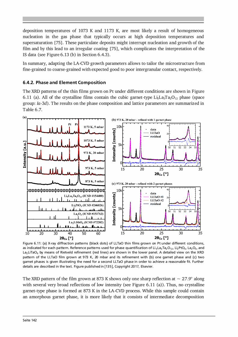
Seite 142
deposition temperatures of 1073 K and 1173 K, are most likely a result of homogeneous nucleation in the gas phase that typically occurs at high deposition temperatures and supersaturation [75]. These particulate deposits might interrupt nucleation and growth of the film and by this lead to an irregular coating [75], which complicates the interpretation of the IS data (see Figure 6.13 (b) in Section 6.4.3). In summary, adapting the LA-CVD growth parameters allows to tailor the microstructure from fine-grained to coarse-grained with expected good to poor intergranular contact, respectively. 6.4.2. Phase and Element Composition The XRD patterns of the thin films grown on Pt under different conditions are shown in Figure 6.11 (a). All of the crystalline films contain the cubic garnet-type Li5La3Ta2O12 phase (space group: Ia-3d). The results on the phase composition and lattice parameters are summarized in Table 6.7.
Figure 6.11: (a) X-ray diffraction patterns (black dots) of LLTaO thin films grown on Pt under different conditions, as indicated for each pattern. Reference patterns used for phase quantification of Li 5La3Ta2O12, Li2PtO3, La2O3, and La2LiTaO6 by means of Rietveld refinement (red lines) are shown in the lower panel. A detailed view on the XRD pattern of the LLTaO film grown at 973 K, 20 mbar and its refinement with (b) one garnet phase and (c) two garnet phases is given illustrating the need for a second LLTaO phase in order to achieve a reasonable fit. Further details are described in the text. Figure published in [135], Copyright 2017, Elsevier. The XRD pattern of the film grown at 873 K shows only one sharp reflection at ~ 27.9° along with several very broad reflections of low intensity (see Figure 6.11 (a)). Thus, no crystalline garnet-type phase is formed at 873 K in the LA-CVD process. While this sample could contain an amorphous garnet phase, it is more likely that it consists of intermediate decomposition
Seite 143
products of the precursor materials used. Due to the partially amorphous character of this pattern no refinement was possible. A minor phase that is present in all of the LLTaO films is Li2PtO3, which is a result of substrate corrosion and was already observed in Li-containing systems other than LLTaO grown by LA-CVD at elevated temperatures [132,133]. Combined ToF-SIMS and XPS depth profiling on Li7La3Zr2O12 thin films (Section 6.3.3) prove that the Li2PtO3 phase is exclusively found at the surface of the Pt substrate and thus can be considered as interface layer between the Pt substrate and the solid electrolyte film. Due to similar growth conditions the conclusions obtained in Section 6.3.3 are applied to the present study allowing to interpret the EIS data in Section 6.4.3 as electrical connection in series of the Li2PtO3 interface layer and the LLTaO film (Figure 6.13 (a)). Table 6.7: Summary of the results obtained from the Rietveld refinements of the XRD data shown i n Figure 6.11 (a). Two cubic Li5La3Ta2O12 phases with different lattice parameters (a1 and a2) are needed to fit the XRD patterns accurately (Figure 6.11 (b) and (c)). Numerical errors are given in brackets, but only for the lattice parameters for the sake of clarity. The phase quantification is converted to vol.-% for better illustration. Films grown at 973 K, 20 mbar and 1073 K, 5 mbar are considered as pure Li5La3Ta2O12. Published in [135], Copyright 2017, Elsevier.
Growth conditions Li5La3Ta2O12
vol.-% a1 [Å] vol.-% a2 [Å] Li2PtO3 vol.-%
La2O3 vol.-%
La2LiTaO6 vol.-%
973 K, 5 mbar 60 12.7854(5) 5 12.858(4) 2* 33 - 973 K, 20 mbar 73 12.7965(3) 20 12.893(1) 7* - - 1073 K, 5 mbar 90 12.8237(4) 3 12.927(7) 7* - - 1173 K, 5 mbar 75 12.8235(6) 18 12.896(1) 3* 1 3
* The Li2PtO3 phase is included for a meaningful refinement; however, since Li2PtO3 is an interface layer between the Pt substrate and the garnet-type Li5La3Ta2O12 film (see Figure 6.13) it shall not be mistaken as impurity phase. In case of the sample deposited at 973 K, 5 mbar a rather large phase fraction of La2O3 (33 vol.-%) is found, which is not present at all if either the pressure is increased to 20 mbar, or the deposition temperature is increased to 1073 K. This indicates that limited diffusion at lower temperature (973 K) and pressure (5 mbar) might be the reason for the La2O3 formation, which is supported by the observed decrease in the amount of La2O3 upon annealing (discussed in Section 6.4.3). The film grown at 1173 K, 5 mbar contains small amounts of perovskite-type La2LiTaO6 (Figure 6.11 (a) and Table 6.7). Since the perovskite-type phase is a Li-poor phase, an increased loss of lithium for higher deposition temperatures is assumed. This is in agreement with (i) data from LLTaO bulk ceramic synthesis [342], where this perovskite-type phase was found after calcination at 1173 K, and (ii) another study [23] that reported the decomposition of Li5La3M2O12 (M = Nb, Ta) to perovskite-type La2LiMO6 upon annealing above 1323 K. Consequently, it is concluded that deposition temperatures above 1173 K are unfavorable for LLTaO thin film growth. For two growth conditions, 973 K, 20 mbar and 1173 K, 5 mbar, a pronounced asymmetry of all the LLTaO reflections towards lower angles is observed, which becomes stronger for high angle reflections (Figure 6.11 (b) and (c)). Using only one garnet phase to model such an XRD pattern would result in a significant discrepancy between the measured and the modeled
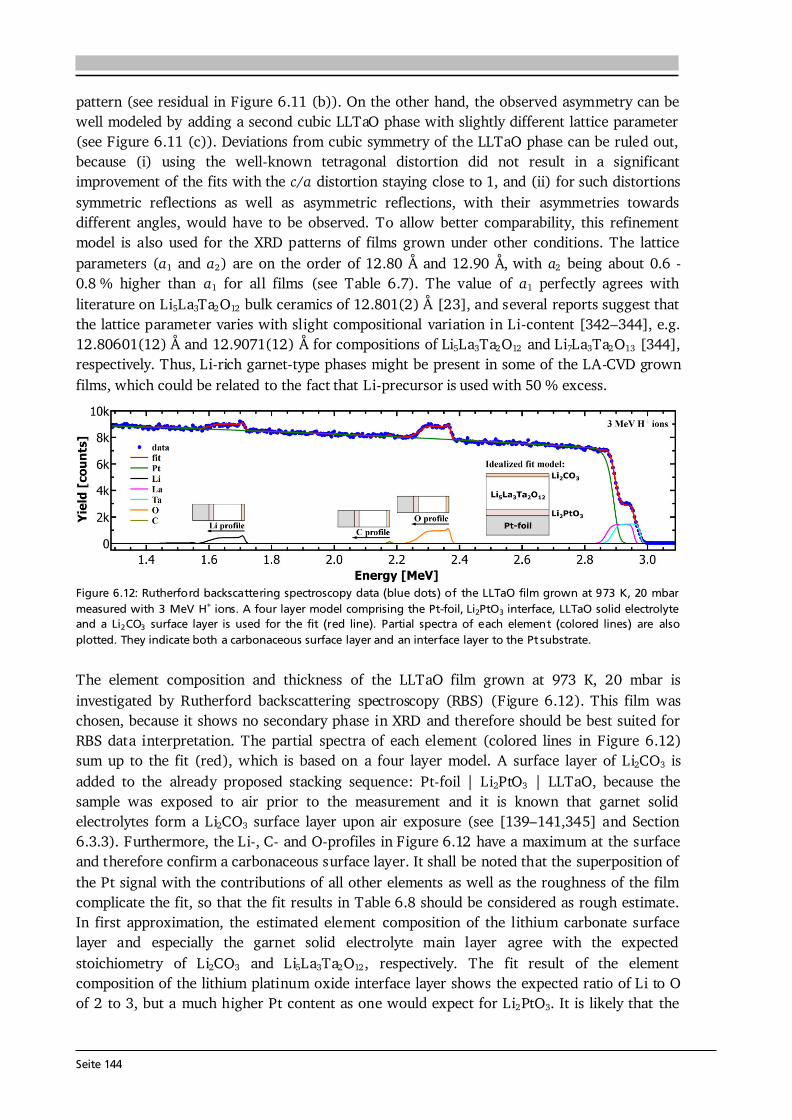
Seite 144
pattern (see residual in Figure 6.11 (b)). On the other hand, the observed asymmetry can be well modeled by adding a second cubic LLTaO phase with slightly different lattice parameter (see Figure 6.11 (c)). Deviations from cubic symmetry of the LLTaO phase can be ruled out, because (i) using the well-known tetragonal distortion did not result in a significant improvement of the fits with the c/a distortion staying close to 1, and (ii) for such distortions symmetric reflections as well as asymmetric reflections, with their asymmetries towards different angles, would have to be observed. To allow better comparability, this refinement model is also used for the XRD patterns of films grown under other conditions. The lattice parameters (a1 and a2) are on the order of 12.80 Å and 12.90 Å, with a2 being about 0.6 - 0.8 % higher than a1 for all films (see Table 6.7). The value of a1 perfectly agrees with literature on Li5La3Ta2O12 bulk ceramics of 12.801(2) Å [23], and several reports suggest that the lattice parameter varies with slight compositional variation in Li-content [342–344], e.g. 12.80601(12) Å and 12.9071(12) Å for compositions of Li5La3Ta2O12 and Li7La3Ta2O13 [344], respectively. Thus, Li-rich garnet-type phases might be present in some of the LA-CVD grown films, which could be related to the fact that Li-precursor is used with 50 % excess.
Figure 6.12: Rutherford backscattering spectroscopy data (blue dots) of the LLTaO film grown at 973 K, 20 mbar measured with 3 MeV H+ ions. A four layer model comprising the Pt-foil, Li2PtO3 interface, LLTaO solid electrolyte and a Li2CO3 surface layer is used for the fit (red line). Partial spectra of each element (colored lines) are also plotted. They indicate both a carbonaceous surface layer and an interface layer to the Pt substrate. The element composition and thickness of the LLTaO film grown at 973 K, 20 mbar is investigated by Rutherford backscattering spectroscopy (RBS) (Figure 6.12). This film was chosen, because it shows no secondary phase in XRD and therefore should be best suited for RBS data interpretation. The partial spectra of each element (colored lines in Figure 6.12) sum up to the fit (red), which is based on a four layer model. A surface layer of Li2CO3 is added to the already proposed stacking sequence: Pt-foil | Li2PtO3 | LLTaO, because the sample was exposed to air prior to the measurement and it is known that garnet solid electrolytes form a Li2CO3 surface layer upon air exposure (see [139–141,345] and Section 6.3.3). Furthermore, the Li-, C- and O-profiles in Figure 6.12 have a maximum at the surface and therefore confirm a carbonaceous surface layer. It shall be noted that the superposition of the Pt signal with the contributions of all other elements as well as the roughness of the film complicate the fit, so that the fit results in Table 6.8 should be considered as rough estimate. In first approximation, the estimated element composition of the lithium carbonate surface layer and especially the garnet solid electrolyte main layer agree with the expected stoichiometry of Li2CO3 and Li5La3Ta2O12, respectively. The fit result of the element composition of the lithium platinum oxide interface layer shows the expected ratio of Li to O of 2 to 3, but a much higher Pt content as one would expect for Li2PtO3. It is likely that the
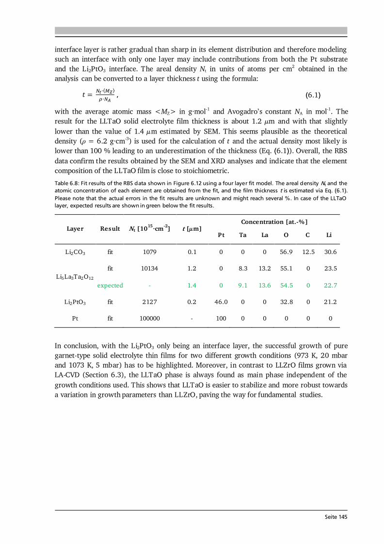
Seite 145
interface layer is rather gradual than sharp in its element distribution and therefore modeling such an interface with only one layer may include contributions from both the Pt substrate and the Li2PtO3 interface. The areal density Nt in units of atoms per cm2 obtained in the analysis can be converted to a layer thickness t using the formula: , (6.1) with the average atomic mass <MZ> in g·mol-1 and Avogadro’s constant NA in mol-1. The result for the LLTaO solid electrolyte film thickness is about 1.2 μm and with that slightly lower than the value of 1.4 μm estimated by SEM. This seems plausible as the theoretical density (ρ = 6.2 g·cm-3) is used for the calculation of t and the actual density most likely is lower than 100 % leading to an underestimation of the thickness (Eq. (6.1)). Overall, the RBS data confirm the results obtained by the SEM and XRD analyses and indicate that the element composition of the LLTaO film is close to stoichiometric. Table 6.8: Fit results of the RBS data shown in Figure 6.12 using a four layer fit model. The areal density Nt and the atomic concentration of each element are obtained from the fit, and the film thickness t is estimated via Eq. (6.1). Please note that the actual errors in the fit results are unknown and might reach several %. In case of the LLTaO layer, expected results are shown in green below the fit results.
Layer Result Nt [1015·cm-2] t [μm] Concentration [at.-%] Pt Ta La O C Li
Li2CO3 fit 1079 0.1 0 0 0 56.9 12.5 30.6 Li5La3Ta2O12 fit 10134 1.2 0 8.3 13.2 55.1 0 23.5
expected - 1.4 0 9.1 13.6 54.5 0 22.7 Li2PtO3 fit 2127 0.2 46.0 0 0 32.8 0 21.2
Pt fit 100000 - 100 0 0 0 0 0 In conclusion, with the Li2PtO3 only being an interface layer, the successful growth of pure garnet-type solid electrolyte thin films for two different growth conditions (973 K, 20 mbar and 1073 K, 5 mbar) has to be highlighted. Moreover, in contrast to LLZrO films grown via LA-CVD (Section 6.3), the LLTaO phase is always found as main phase independent of the growth conditions used. This shows that LLTaO is easier to stabilize and more robust towards a variation in growth parameters than LLZrO, paving the way for fundamental studies.
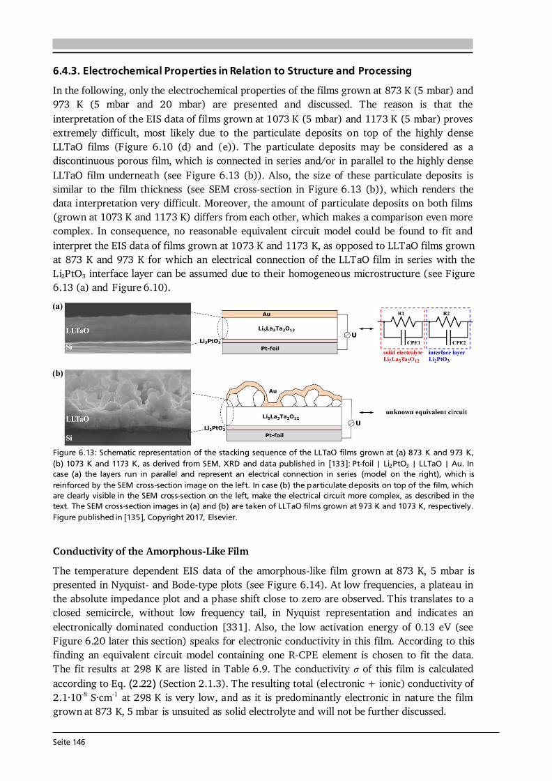
Seite 146
6.4.3. Electrochemical Properties in Relation to Structure and Processing In the following, only the electrochemical properties of the films grown at 873 K (5 mbar) and 973 K (5 mbar and 20 mbar) are presented and discussed. The reason is that the interpretation of the EIS data of films grown at 1073 K (5 mbar) and 1173 K (5 mbar) proves extremely difficult, most likely due to the particulate deposits on top of the highly dense LLTaO films (Figure 6.10 (d) and (e)). The particulate deposits may be considered as a discontinuous porous film, which is connected in series and/or in parallel to the highly dense LLTaO film underneath (see Figure 6.13 (b)). Also, the size of these particulate deposits is similar to the film thickness (see SEM cross-section in Figure 6.13 (b)), which renders the data interpretation very difficult. Moreover, the amount of particulate deposits on both films (grown at 1073 K and 1173 K) differs from each other, which makes a comparison even more complex. In consequence, no reasonable equivalent circuit model could be found to fit and interpret the EIS data of films grown at 1073 K and 1173 K, as opposed to LLTaO films grown at 873 K and 973 K for which an electrical connection of the LLTaO film in series with the Li2PtO3 interface layer can be assumed due to their homogeneous microstructure (see Figure 6.13 (a) and Figure 6.10).
Figure 6.13: Schematic representation of the stacking sequence of the LLTaO films grown at (a) 873 K and 973 K, (b) 1073 K and 1173 K, as derived from SEM, XRD and data published in [133]: Pt-foil | Li2PtO3 | LLTaO | Au. In case (a) the layers run in parallel and represent an electrical connection in series (model on the right), which is reinforced by the SEM cross-section image on the left. In case (b) the particulate deposits on top of the film, which are clearly visible in the SEM cross-section on the left, make the electrical circuit more complex, as described in the text. The SEM cross-section images in (a) and (b) are taken of LLTaO films grown at 973 K and 1073 K, respectively. Figure published in [135], Copyright 2017, Elsevier.
Conductivity of the Amorphous-Like Film The temperature dependent EIS data of the amorphous-like film grown at 873 K, 5 mbar is presented in Nyquist- and Bode-type plots (see Figure 6.14). At low frequencies, a plateau in the absolute impedance plot and a phase shift close to zero are observed. This translates to a closed semicircle, without low frequency tail, in Nyquist representation and indicates an electronically dominated conduction [331]. Also, the low activation energy of 0.13 eV (see Figure 6.20 later this section) speaks for electronic conductivity in this film. According to this finding an equivalent circuit model containing one R-CPE element is chosen to fit the data. The fit results at 298 K are listed in Table 6.9. The conductivity of this film is calculated according to Eq. (2.22) (Section 2.1.3). The resulting total (electronic + ionic) conductivity of 2.1·10-8 S·cm-1 at 298 K is very low, and as it is predominantly electronic in nature the film grown at 873 K, 5 mbar is unsuited as solid electrolyte and will not be further discussed.
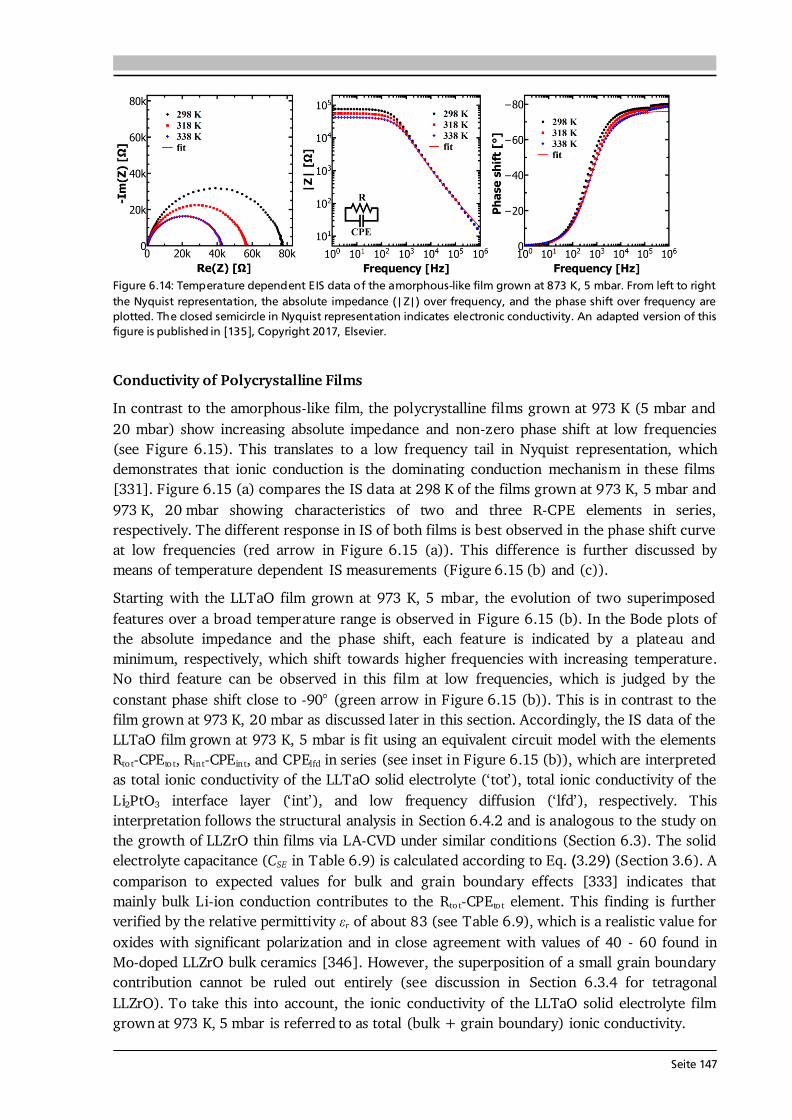
Seite 147
Figure 6.14: Temperature dependent EIS data of the amorphous-like film grown at 873 K, 5 mbar. From left to right the Nyquist representation, the absolute impedance (|Z|) over frequency, and the phase shift over frequency are plotted. The closed semicircle in Nyquist representation indicates electronic conductivity. An adapted version of this figure is published in [135], Copyright 2017, Elsevier.
Conductivity of Polycrystalline Films In contrast to the amorphous-like film, the polycrystalline films grown at 973 K (5 mbar and 20 mbar) show increasing absolute impedance and non-zero phase shift at low frequencies (see Figure 6.15). This translates to a low frequency tail in Nyquist representation, which demonstrates that ionic conduction is the dominating conduction mechanism in these films [331]. Figure 6.15 (a) compares the IS data at 298 K of the films grown at 973 K, 5 mbar and 973 K, 20 mbar showing characteristics of two and three R-CPE elements in series, respectively. The different response in IS of both films is best observed in the phase shift curve at low frequencies (red arrow in Figure 6.15 (a)). This difference is further discussed by means of temperature dependent IS measurements (Figure 6.15 (b) and (c)). Starting with the LLTaO film grown at 973 K, 5 mbar, the evolution of two superimposed features over a broad temperature range is observed in Figure 6.15 (b). In the Bode plots of the absolute impedance and the phase shift, each feature is indicated by a plateau and minimum, respectively, which shift towards higher frequencies with increasing temperature. No third feature can be observed in this film at low frequencies, which is judged by the constant phase shift close to -90° (green arrow in Figure 6.15 (b)). This is in contrast to the film grown at 973 K, 20 mbar as discussed later in this section. Accordingly, the IS data of the LLTaO film grown at 973 K, 5 mbar is fit using an equivalent circuit model with the elements Rto t-CPEto t, Rint-CPEint, and CPElfd in series (see inset in Figure 6.15 (b)), which are interpreted as total ionic conductivity of the LLTaO solid electrolyte (‘tot’), total ionic conductivity of the Li2PtO3 interface layer (‘int’), and low frequency diffusion (‘lfd’), respectively. This interpretation follows the structural analysis in Section 6.4.2 and is analogous to the study on the growth of LLZrO thin films via LA-CVD under similar conditions (Section 6.3). The solid electrolyte capacitance (CSE in Table 6.9) is calculated according to Eq. (3.29) (Section 3.6). A comparison to expected values for bulk and grain boundary effects [333] indicates that mainly bulk Li-ion conduction contributes to the Rto t-CPEto t element. This finding is further verified by the relative permittivity r of about 83 (see Table 6.9), which is a realistic value for oxides with significant polarization and in close agreement with values of 40 - 60 found in Mo-doped LLZrO bulk ceramics [346]. However, the superposition of a small grain boundary contribution cannot be ruled out entirely (see discussion in Section 6.3.4 for tetragonal LLZrO). To take this into account, the ionic conductivity of the LLTaO solid electrolyte film grown at 973 K, 5 mbar is referred to as total (bulk + grain boundary) ionic conductivity.
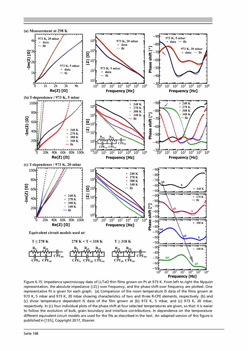
Seite 148
Figure 6.15: Impedance spectroscopy data of LLTaO thin films grown on Pt at 973 K. From left to right the Nyquist representation, the absolute impedance (|Z|) over frequency, and the phase shift over frequency are plotted. One representative fit is given for each graph. (a) Comparison of the room temperature IS data of the films grown at 973 K, 5 mbar and 973 K, 20 mbar showing characteristics of two and three R-CPE elements, respectively. (b) and (c) show temperature dependent IS data of the film grown at (b) 973 K, 5 mbar, and (c) 973 K, 20 mbar, respectively. In (c) four individual plots of the phase shift at four selected temperatures are given, so that it is easier to follow the evolution of bulk, grain boundary and interface contributions. In dependence on the temperature different equivalent circuit models are used for the fits as described in the text. An adapted version of this figure is published in [135], Copyright 2017, Elsevier.
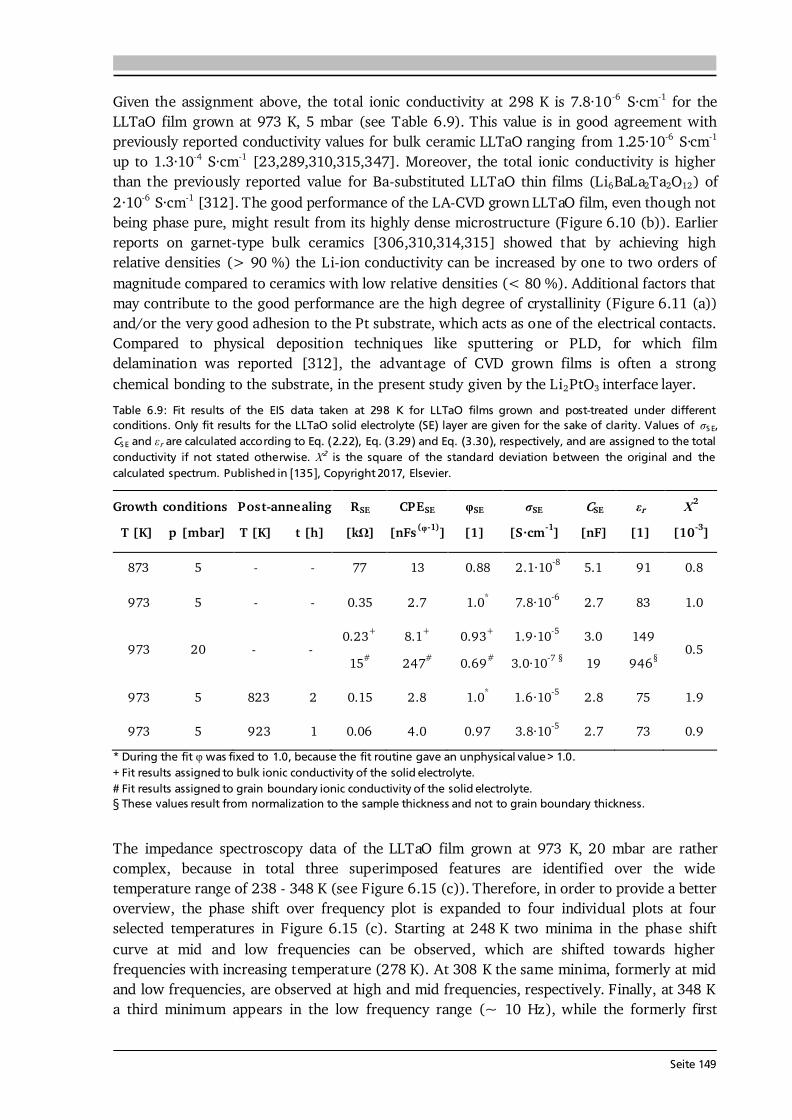
Seite 149
Given the assignment above, the total ionic conductivity at 298 K is 7.8·10-6 S·cm-1 for the LLTaO film grown at 973 K, 5 mbar (see Table 6.9). This value is in good agreement with previously reported conductivity values for bulk ceramic LLTaO ranging from 1.25·10-6 S·cm-1 up to 1.3·10-4 S·cm-1 [23,289,310,315,347]. Moreover, the total ionic conductivity is higher than the previously reported value for Ba-substituted LLTaO thin films (Li6BaLa2Ta2O12) of 2·10-6 S·cm-1 [312]. The good performance of the LA-CVD grown LLTaO film, even though not being phase pure, might result from its highly dense microstructure (Figure 6.10 (b)). Earlier reports on garnet-type bulk ceramics [306,310,314,315] showed that by achieving high relative densities (> 90 %) the Li-ion conductivity can be increased by one to two orders of magnitude compared to ceramics with low relative densities (< 80 %). Additional factors that may contribute to the good performance are the high degree of crystallinity (Figure 6.11 (a)) and/or the very good adhesion to the Pt substrate, which acts as one of the electrical contacts. Compared to physical deposition techniques like sputtering or PLD, for which film delamination was reported [312], the advantage of CVD grown films is often a strong chemical bonding to the substrate, in the present study given by the Li2PtO3 interface layer. Table 6.9: Fit results of the EIS data taken at 298 K for LLTaO films grown and post-treated under different conditions. Only fit results for the LLTaO solid electrolyte (SE) layer are given for the sake of clarity. Values of S E, CS E and r are calculated according to Eq. (2.22), Eq. (3.29) and Eq. (3.30), respectively, and are assigned to the total conductivity if not stated otherwise. 2 is the square of the standard deviation between the original and the calculated spectrum. Published in [135], Copyright 2017, Elsevier. Growth conditions
T [K] p [mbar] Post-annealing T [K] t [h]
RSE [kΩ]
CPESE [nFs (φ-1)]
φSE [1]
σSE [S·cm-1]
CSE [nF]
εr [1]
Χ2 [10-3]
873 5 - - 77 13 0.88 2.1·10-8 5.1 91 0.8
973 5 - - 0.35 2.7 1.0* 7.8·10-6 2.7 83 1.0 973 20 - - 0.23+
15# 8.1+ 247#
0.93+ 0.69#
1.9·10-5 3.0·10-7 §
3.0 19
149 946§ 0.5
973 5 823 2 0.15 2.8 1.0* 1.6·10-5 2.8 75 1.9 973 5 923 1 0.06 4.0 0.97 3.8·10-5 2.7 73 0.9 * During the fit φ was fixed to 1.0, because the fit routine gave an unphysical value > 1.0. + Fit results assigned to bulk ionic conductivity of the solid electrolyte. # Fit results assigned to grain boundary ionic conductivity of the solid electrolyte. § These values result from normalization to the sample thickness and not to grain boundary thickness. The impedance spectroscopy data of the LLTaO film grown at 973 K, 20 mbar are rather complex, because in total three superimposed features are identified over the wide temperature range of 238 - 348 K (see Figure 6.15 (c)). Therefore, in order to provide a better overview, the phase shift over frequency plot is expanded to four individual plots at four selected temperatures in Figure 6.15 (c). Starting at 248 K two minima in the phase shift curve at mid and low frequencies can be observed, which are shifted towards higher frequencies with increasing temperature (278 K). At 308 K the same minima, formerly at mid and low frequencies, are observed at high and mid frequencies, respectively. Finally, at 348 K a third minimum appears in the low frequency range (~ 10 Hz), while the formerly first
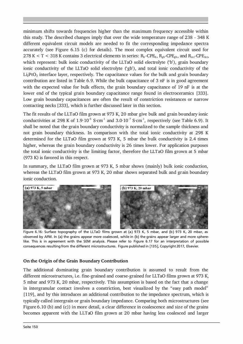
Seite 150
minimum shifts towards frequencies higher than the maximum frequency accessible within this study. The described changes imply that over the wide temperature range of 238 - 348 K different equivalent circuit models are needed to fit the corresponding impedance spectra accurately (see Figure 6.15 (c) for details). The most complex equivalent circuit used for 278 K < T < 318 K contains 3 electrical elements in series: Rb-CPEb, Rgb-CPEgb, and Rint-CPEint, which represent: bulk ionic conductivity of the LLTaO solid electrolyte (‘b’), grain boundary ionic conductivity of the LLTaO solid electrolyte (‘gb’), and total ionic conductivity of the Li2PtO3 interface layer, respectively. The capacitance values for the bulk and grain boundary contribution are listed in Table 6.9. While the bulk capacitance of 3 nF is in good agreement with the expected value for bulk effects, the grain boundary capacitance of 19 nF is at the lower end of the typical grain boundary capacitance range found in electroceramics [333]. Low grain boundary capacitances are often the result of constriction resistances or narrow contacting necks [333], which is further discussed later in this section. The fit results of the LLTaO film grown at 973 K, 20 mbar give bulk and grain boundary ionic conductivities at 298 K of 1.9·10-5 S·cm-1 and 3.0·10-7 S·cm-1, respectively (see Table 6.9). It shall be noted that the grain boundary conductivity is normalized to the sample thickness and not grain boundary thickness. In comparison with the total ionic conductivity at 298 K determined for the LLTaO film grown at 973 K, 5 mbar the bulk conductivity is 2.4 times higher, whereas the grain boundary conductivity is 26 times lower. For application purposes the total ionic conductivity is the limiting factor, therefore the LLTaO film grown at 5 mbar (973 K) is favored in this respect. In summary, the LLTaO film grown at 973 K, 5 mbar shows (mainly) bulk ionic conduction, whereas the LLTaO film grown at 973 K, 20 mbar shows separated bulk and grain boundary ionic conduction.
Figure 6.16: Surface topography of the LLTaO films grown at (a) 973 K, 5 mbar, and (b) 973 K, 20 mbar, as observed by AFM. In (a) the grains appear more coalesced, while in (b) the grains appear larger and more sphere-like. This is in agreement with the SEM analysis. Please refer to Figure 6.17 for an interpretation of possible consequences resulting from the different microstructures. Figure published in [135], Copyright 2017, Elsevier.
On the Origin of the Grain Boundary Contribution The additional dominating grain boundary contribution is assumed to result from the different microstructures, i.e. fine-grained and coarse-grained for LLTaO films grown at 973 K, 5 mbar and 973 K, 20 mbar, respectively. This assumption is based on the fact that a change in intergranular contact involves a constriction, best visualized by the “easy path model” [119], and by this introduces an additional contribution to the impedance spectrum, which is typically called intergrain or grain boundary impedance. Comparing both microstructures (see Figure 6.10 (b) and (c)) in more detail, a clear difference in coalescence and size of the grains becomes apparent with the LLTaO film grown at 20 mbar having less coalesced and larger
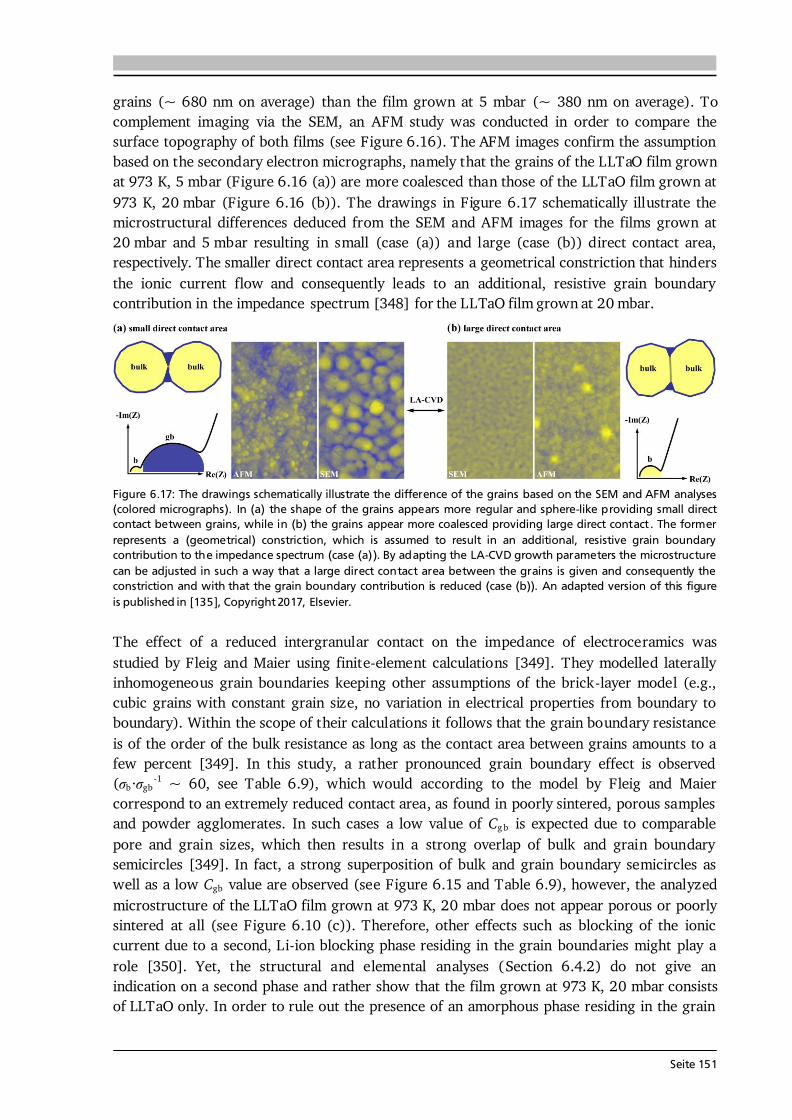
Seite 151
grains (~ 680 nm on average) than the film grown at 5 mbar (~ 380 nm on average). To complement imaging via the SEM, an AFM study was conducted in order to compare the surface topography of both films (see Figure 6.16). The AFM images confirm the assumption based on the secondary electron micrographs, namely that the grains of the LLTaO film grown at 973 K, 5 mbar (Figure 6.16 (a)) are more coalesced than those of the LLTaO film grown at 973 K, 20 mbar (Figure 6.16 (b)). The drawings in Figure 6.17 schematically illustrate the microstructural differences deduced from the SEM and AFM images for the films grown at 20 mbar and 5 mbar resulting in small (case (a)) and large (case (b)) direct contact area, respectively. The smaller direct contact area represents a geometrical constriction that hinders the ionic current flow and consequently leads to an additional, resistive grain boundary contribution in the impedance spectrum [348] for the LLTaO film grown at 20 mbar.
Figure 6.17: The drawings schematically illustrate the difference of the grains based on the SEM and AFM analyses (colored micrographs). In (a) the shape of the grains appears more regular and sphere-like providing small direct contact between grains, while in (b) the grains appear more coalesced providing large direct contact . The former represents a (geometrical) constriction, which is assumed to result in an additional, resistive grain boundary contribution to the impedance spectrum (case (a)). By adapting the LA-CVD growth parameters the microstructure can be adjusted in such a way that a large direct contact area between the grains is given and consequently the constriction and with that the grain boundary contribution is reduced (case (b)). An adapted version of this figure is published in [135], Copyright 2017, Elsevier. The effect of a reduced intergranular contact on the impedance of electroceramics was studied by Fleig and Maier using finite-element calculations [349]. They modelled laterally inhomogeneous grain boundaries keeping other assumptions of the brick-layer model (e.g., cubic grains with constant grain size, no variation in electrical properties from boundary to boundary). Within the scope of their calculations it follows that the grain boundary resistance is of the order of the bulk resistance as long as the contact area between grains amounts to a few percent [349]. In this study, a rather pronounced grain boundary effect is observed ( b· gb -1 ~ 60, see Table 6.9), which would according to the model by Fleig and Maier correspond to an extremely reduced contact area, as found in poorly sintered, porous samples and powder agglomerates. In such cases a low value of Cg b is expected due to comparable pore and grain sizes, which then results in a strong overlap of bulk and grain boundary semicircles [349]. In fact, a strong superposition of bulk and grain boundary semicircles as well as a low Cgb value are observed (see Figure 6.15 and Table 6.9), however, the analyzed microstructure of the LLTaO film grown at 973 K, 20 mbar does not appear porous or poorly sintered at all (see Figure 6.10 (c)). Therefore, other effects such as blocking of the ionic current due to a second, Li-ion blocking phase residing in the grain boundaries might play a role [350]. Yet, the structural and elemental analyses (Section 6.4.2) do not give an indication on a second phase and rather show that the film grown at 973 K, 20 mbar consists of LLTaO only. In order to rule out the presence of an amorphous phase residing in the grain
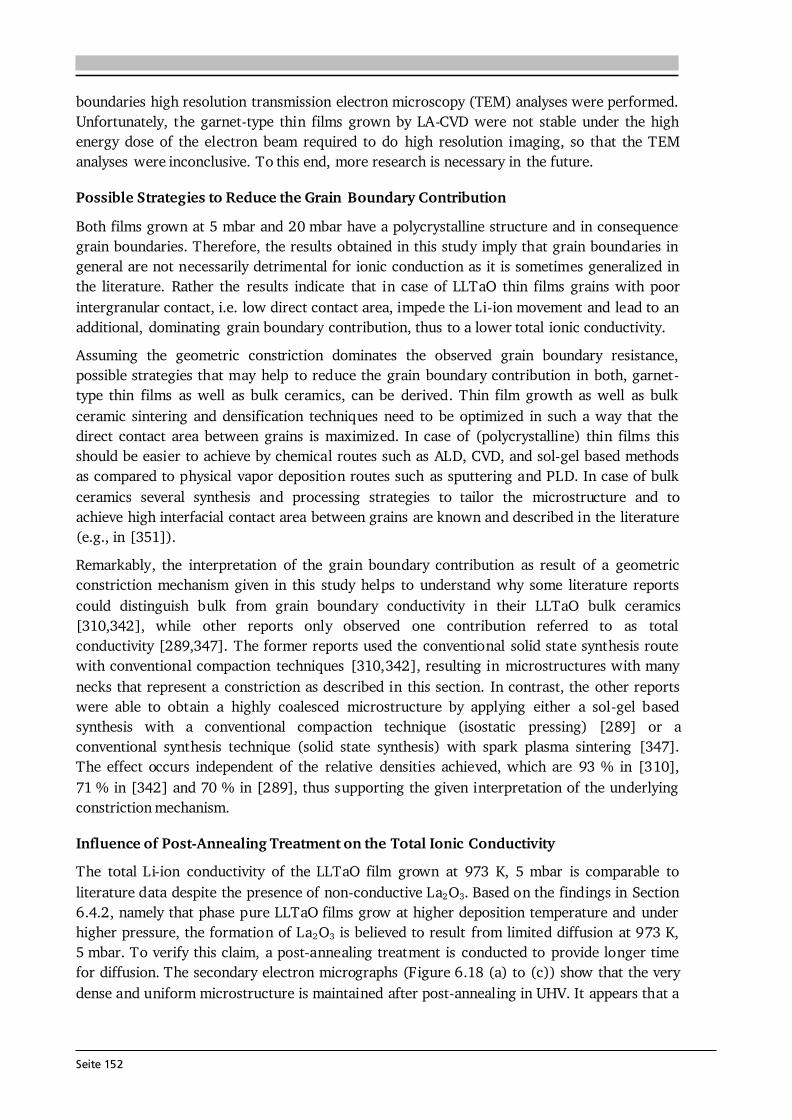
Seite 152
boundaries high resolution transmission electron microscopy (TEM) analyses were performed. Unfortunately, the garnet-type thin films grown by LA-CVD were not stable under the high energy dose of the electron beam required to do high resolution imaging, so that the TEM analyses were inconclusive. To this end, more research is necessary in the future. Possible Strategies to Reduce the Grain Boundary Contribution Both films grown at 5 mbar and 20 mbar have a polycrystalline structure and in consequence grain boundaries. Therefore, the results obtained in this study imply that grain boundaries in general are not necessarily detrimental for ionic conduction as it is sometimes generalized in the literature. Rather the results indicate that in case of LLTaO thin films grains with poor intergranular contact, i.e. low direct contact area, impede the Li-ion movement and lead to an additional, dominating grain boundary contribution, thus to a lower total ionic conductivity. Assuming the geometric constriction dominates the observed grain boundary resistance, possible strategies that may help to reduce the grain boundary contribution in both, garnet-type thin films as well as bulk ceramics, can be derived. Thin film growth as well as bulk ceramic sintering and densification techniques need to be optimized in such a way that the direct contact area between grains is maximized. In case of (polycrystalline) thin films this should be easier to achieve by chemical routes such as ALD, CVD, and sol-gel based methods as compared to physical vapor deposition routes such as sputtering and PLD. In case of bulk ceramics several synthesis and processing strategies to tailor the microstructure and to achieve high interfacial contact area between grains are known and described in the literature (e.g., in [351]). Remarkably, the interpretation of the grain boundary contribution as result of a geometric constriction mechanism given in this study helps to understand why some literature reports could distinguish bulk from grain boundary conductivity in their LLTaO bulk ceramics [310,342], while other reports only observed one contribution referred to as total conductivity [289,347]. The former reports used the conventional solid state synthesis route with conventional compaction techniques [310,342], resulting in microstructures with many necks that represent a constriction as described in this section. In contrast, the other reports were able to obtain a highly coalesced microstructure by applying either a sol-gel based synthesis with a conventional compaction technique (isostatic pressing) [289] or a conventional synthesis technique (solid state synthesis) with spark plasma sintering [347]. The effect occurs independent of the relative densities achieved, which are 93 % in [310], 71 % in [342] and 70 % in [289], thus supporting the given interpretation of the underlying constriction mechanism. Influence of Post-Annealing Treatment on the Total Ionic Conductivity The total Li-ion conductivity of the LLTaO film grown at 973 K, 5 mbar is comparable to literature data despite the presence of non-conductive La2O3. Based on the findings in Section 6.4.2, namely that phase pure LLTaO films grow at higher deposition temperature and under higher pressure, the formation of La2O3 is believed to result from limited diffusion at 973 K, 5 mbar. To verify this claim, a post-annealing treatment is conducted to provide longer time for diffusion. The secondary electron micrographs (Figure 6.18 (a) to (c)) show that the very dense and uniform microstructure is maintained after post-annealing in UHV. It appears that a
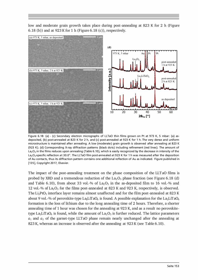
Seite 153
low and moderate grain growth takes place during post-annealing at 823 K for 2 h (Figure 6.18 (b)) and at 923 K for 1 h (Figure 6.18 (c)), respectively.
Figure 6.18: (a) - (c) Secondary electron micrographs of LLTaO thin films grown on Pt at 973 K, 5 mbar: (a) as-deposited, (b) post-annealed at 823 K for 2 h, and (c) post-annealed at 923 K for 1 h. The very dense and uniform microstructure is maintained after annealing. A low (moderate) grain growth is observed after annealing at 823 K (923 K). (d) Corresponding X-ray diffraction patterns (black dots) including refinement (red lines). The amount of La2O3 in the films reduces upon annealing (Table 6.10), which is easily recognized by the decrease in intensity of the La2O3-specific reflection at 30.0°. The LLTaO film post-annealed at 923 K for 1 h was measured after the deposition of Au contacts, thus its diffraction pattern contains one additional reflection of Au as indicated. Figure published in [135], Copyright 2017, Elsevier. The impact of the post-annealing treatment on the phase composition of the LLTaO films is probed by XRD and a tremendous reduction of the La2O3 phase fraction (see Figure 6.18 (d) and Table 6.10), from about 33 vol.-% of La2O3 in the as-deposited film to 16 vol.-% and 12 vol.-% of La2O3 for the films post-annealed at 823 K and 923 K, respectively, is observed. The Li2PtO3 interface layer remains almost unaffected and for the film post-annealed at 823 K about 9 vol.-% of perovskite-type La2LiTaO6 is found. A possible explanation for the La2LiTaO6 formation is the loss of lithium due to the long annealing time of 2 hours. Therefore, a shorter annealing time of 1 hour was chosen for the annealing at 923 K, and as a result no perovskite-type La2LiTaO6 is found, while the amount of La2O3 is further reduced. The lattice parameters a1 and a2 of the garnet-type LLTaO phase remain nearly unchanged after the annealing at 823 K, whereas an increase is observed after the annealing at 923 K (see Table 6.10).
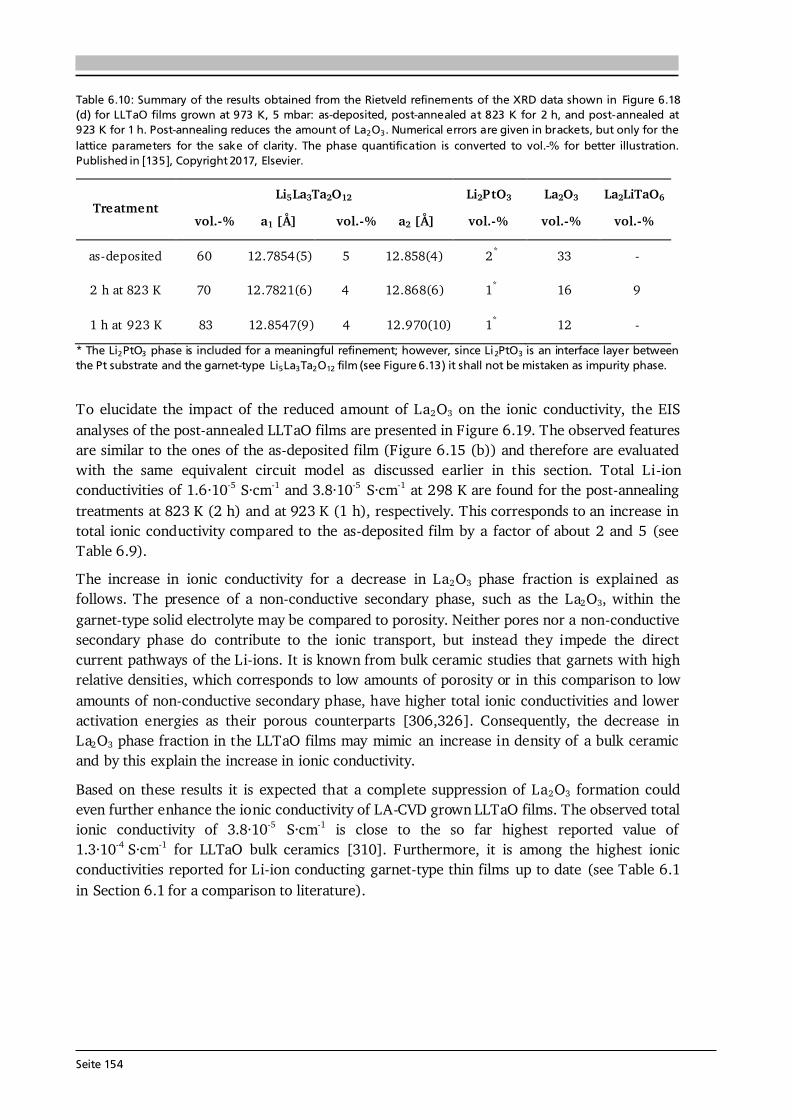
Seite 154
Table 6.10: Summary of the results obtained from the Rietveld refinements of the XRD data shown in Figure 6.18 (d) for LLTaO films grown at 973 K, 5 mbar: as-deposited, post-annealed at 823 K for 2 h, and post-annealed at 923 K for 1 h. Post-annealing reduces the amount of La2O3. Numerical errors are given in brackets, but only for the lattice parameters for the sake of clarity. The phase quantification is converted to vol.-% for better illustration. Published in [135], Copyright 2017, Elsevier. Treatment Li5La3Ta2O12
vol.-% a1 [Å] vol.-% a2 [Å] Li2PtO3 vol.-%
La2O3 vol.-%
La2LiTaO6 vol.-%
as-deposited 60 12.7854(5) 5 12.858(4) 2* 33 - 2 h at 823 K 70 12.7821(6) 4 12.868(6) 1* 16 9 1 h at 923 K 83 12.8547(9) 4 12.970(10) 1* 12 -
* The Li2PtO3 phase is included for a meaningful refinement; however, since Li2PtO3 is an interface layer between the Pt substrate and the garnet-type Li5La3Ta2O12 film (see Figure 6.13) it shall not be mistaken as impurity phase. To elucidate the impact of the reduced amount of La2O3 on the ionic conductivity, the EIS analyses of the post-annealed LLTaO films are presented in Figure 6.19. The observed features are similar to the ones of the as-deposited film (Figure 6.15 (b)) and therefore are evaluated with the same equivalent circuit model as discussed earlier in this section. Total Li-ion conductivities of 1.6·10-5 S·cm-1 and 3.8·10-5 S·cm-1 at 298 K are found for the post-annealing treatments at 823 K (2 h) and at 923 K (1 h), respectively. This corresponds to an increase in total ionic conductivity compared to the as-deposited film by a factor of about 2 and 5 (see Table 6.9). The increase in ionic conductivity for a decrease in La2O3 phase fraction is explained as follows. The presence of a non-conductive secondary phase, such as the La2O3, within the garnet-type solid electrolyte may be compared to porosity. Neither pores nor a non-conductive secondary phase do contribute to the ionic transport, but instead they impede the direct current pathways of the Li-ions. It is known from bulk ceramic studies that garnets with high relative densities, which corresponds to low amounts of porosity or in this comparison to low amounts of non-conductive secondary phase, have higher total ionic conductivities and lower activation energies as their porous counterparts [306,326]. Consequently, the decrease in La2O3 phase fraction in the LLTaO films may mimic an increase in density of a bulk ceramic and by this explain the increase in ionic conductivity. Based on these results it is expected that a complete suppression of La2O3 formation could even further enhance the ionic conductivity of LA-CVD grown LLTaO films. The observed total ionic conductivity of 3.8·10-5 S·cm-1 is close to the so far highest reported value of 1.3·10-4 S·cm-1 for LLTaO bulk ceramics [310]. Furthermore, it is among the highest ionic conductivities reported for Li-ion conducting garnet-type thin films up to date (see Table 6.1 in Section 6.1 for a comparison to literature).
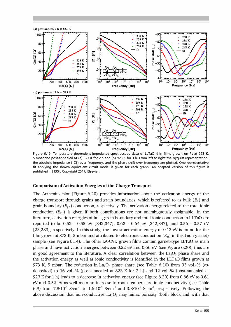
Seite 155
Figure 6.19: Temperature dependent impedance spectroscopy data of LLTaO thin films grown on Pt at 973 K, 5 mbar and post-annealed at (a) 823 K for 2 h and (b) 923 K for 1 h. From left to right the Nyquist representation, the absolute impedance (|Z|) over frequency, and the phase shift over frequency are plotted. One representative fit applying the shown equivalent circuit model is given for each graph. An adapted version of this figure is published in [135], Copyright 2017, Elsevier.
Comparison of Activation Energies of the Charge Transport The Arrhenius plot (Figure 6.20) provides information about the activation energy of the charge transport through grains and grain boundaries, which is referred to as bulk (Eb) and grain boundary (Eg b) conduction, respectively. The activation energy related to the total ionic conduction (Eto t) is given if both contributions are not unambiguously assignable. In the literature, activation energies of bulk, grain boundary and total ionic conduction in LLTaO are reported to be 0.52 - 0.55 eV [342,347], 0.62 - 0.64 eV [342,347], and 0.56 - 0.57 eV [23,289], respectively. In this study, the lowest activation energy of 0.13 eV is found for the film grown at 873 K, 5 mbar and attributed to electronic conduction (Eel) in this (non-garnet) sample (see Figure 6.14). The other LA-CVD grown films contain garnet-type LLTaO as main phase and have activation energies between 0.52 eV and 0.66 eV (see Figure 6.20), thus are in good agreement to the literature. A clear correlation between the La2O3 phase share and the activation energy as well as ionic conductivity is identified in the LLTaO films grown at 973 K, 5 mbar. The reduction in La2O3 phase share (see Table 6.10) from 33 vol.-% (as-deposited) to 16 vol.-% (post-annealed at 823 K for 2 h) and 12 vol.-% (post-annealed at 923 K for 1 h) leads to a decrease in activation energy (see Figure 6.20) from 0.66 eV to 0.61 eV and 0.52 eV as well as to an increase in room temperature ionic conductivity (see Table 6.9) from 7.8·10-6 S·cm-1 to 1.6·10-5 S·cm-1 and 3.8·10-5 S·cm-1, respectively. Following the above discussion that non-conductive La2O3 may mimic porosity (both block and with that
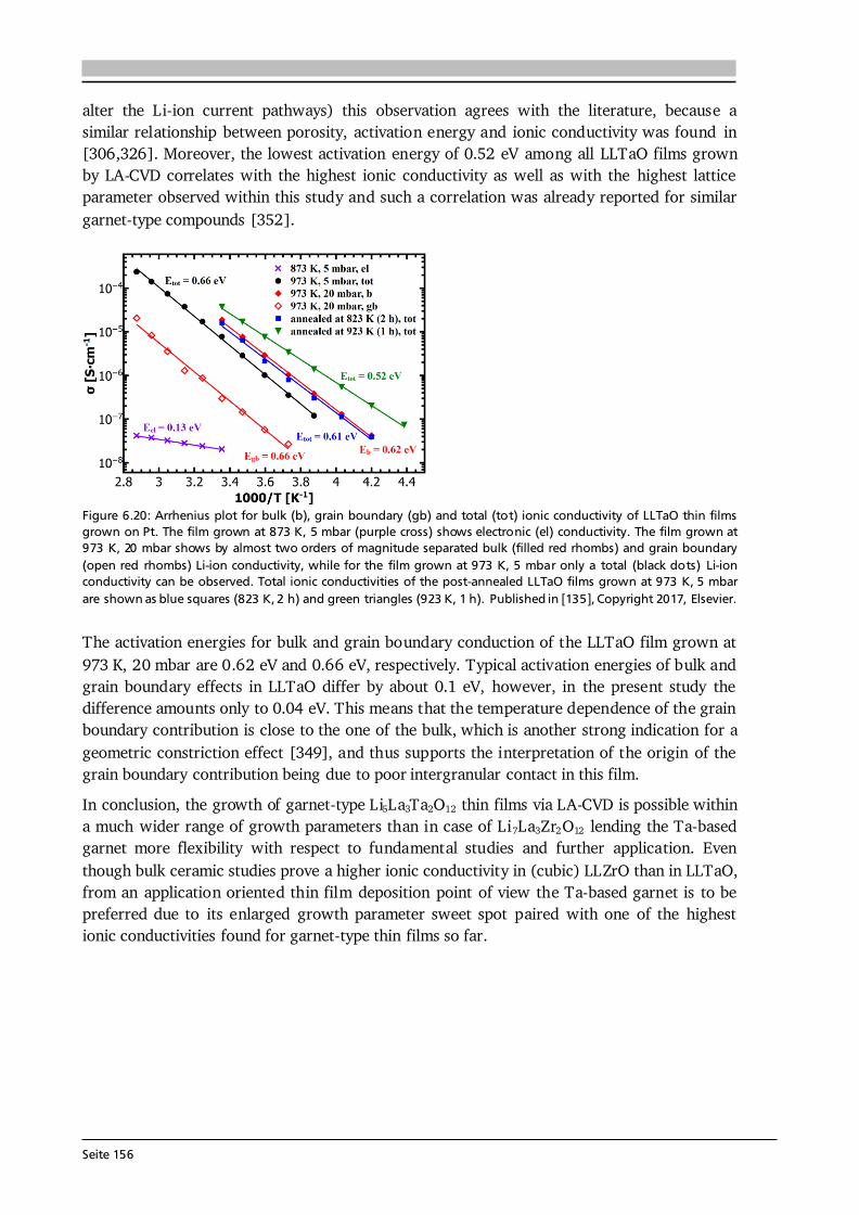
Seite 156
alter the Li-ion current pathways) this observation agrees with the literature, because a similar relationship between porosity, activation energy and ionic conductivity was found in [306,326]. Moreover, the lowest activation energy of 0.52 eV among all LLTaO films grown by LA-CVD correlates with the highest ionic conductivity as well as with the highest lattice parameter observed within this study and such a correlation was already reported for similar garnet-type compounds [352].
Figure 6.20: Arrhenius plot for bulk (b), grain boundary (gb) and total (tot) ionic conductivity of LLTaO thin films grown on Pt. The film grown at 873 K, 5 mbar (purple cross) shows electronic (el) conductivity. The film grown at 973 K, 20 mbar shows by almost two orders of magnitude separated bulk (filled red rhombs) and grain boundary (open red rhombs) Li-ion conductivity, while for the film grown at 973 K, 5 mbar only a total (black dots) Li-ion conductivity can be observed. Total ionic conductivities of the post-annealed LLTaO films grown at 973 K, 5 mbar are shown as blue squares (823 K, 2 h) and green triangles (923 K, 1 h). Published in [135], Copyright 2017, Elsevier. The activation energies for bulk and grain boundary conduction of the LLTaO film grown at 973 K, 20 mbar are 0.62 eV and 0.66 eV, respectively. Typical activation energies of bulk and grain boundary effects in LLTaO differ by about 0.1 eV, however, in the present study the difference amounts only to 0.04 eV. This means that the temperature dependence of the grain boundary contribution is close to the one of the bulk, which is another strong indication for a geometric constriction effect [349], and thus supports the interpretation of the origin of the grain boundary contribution being due to poor intergranular contact in this film. In conclusion, the growth of garnet-type Li5La3Ta2O12 thin films via LA-CVD is possible within a much wider range of growth parameters than in case of Li7La3Zr2O12 lending the Ta-based garnet more flexibility with respect to fundamental studies and further application. Even though bulk ceramic studies prove a higher ionic conductivity in (cubic) LLZrO than in LLTaO, from an application oriented thin film deposition point of view the Ta-based garnet is to be preferred due to its enlarged growth parameter sweet spot paired with one of the highest ionic conductivities found for garnet-type thin films so far.
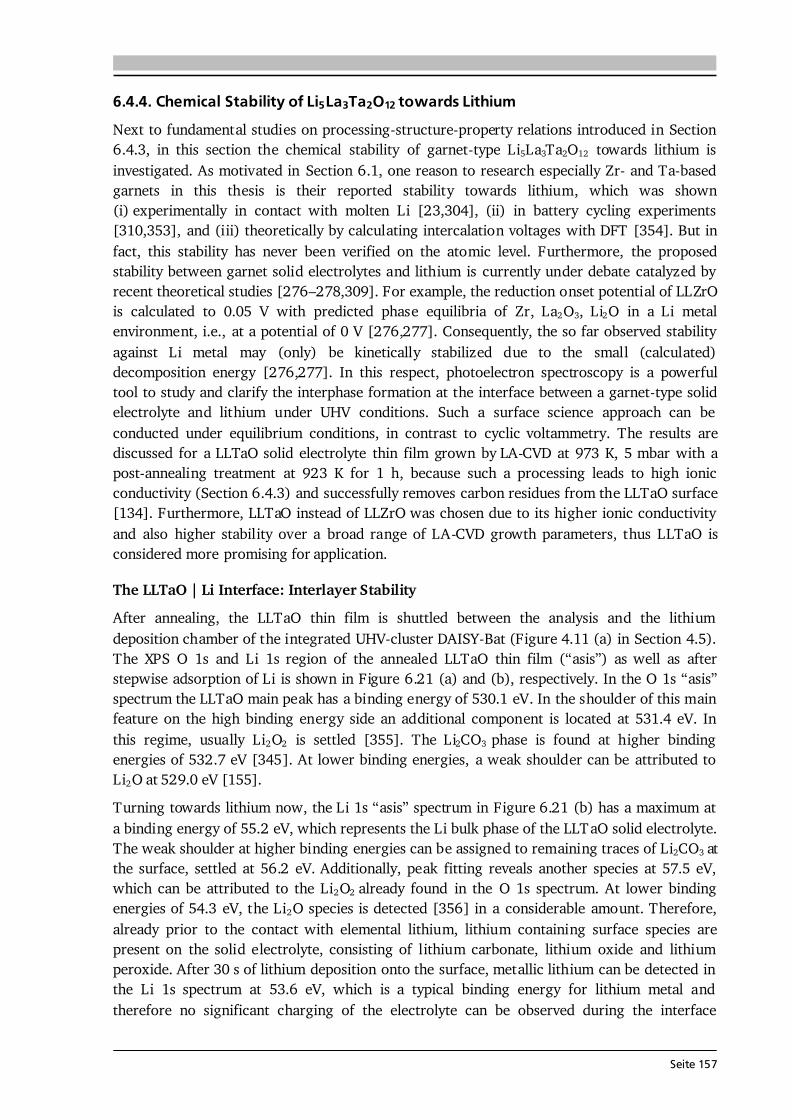
Seite 157
6.4.4. Chemical Stability of Li5La3Ta2O12 towards Lithium Next to fundamental studies on processing-structure-property relations introduced in Section 6.4.3, in this section the chemical stability of garnet-type Li5La3Ta2O12 towards lithium is investigated. As motivated in Section 6.1, one reason to research especially Zr- and Ta-based garnets in this thesis is their reported stability towards lithium, which was shown (i) experimentally in contact with molten Li [23,304], (ii) in battery cycling experiments [310,353], and (iii) theoretically by calculating intercalation voltages with DFT [354]. But in fact, this stability has never been verified on the atomic level. Furthermore, the proposed stability between garnet solid electrolytes and lithium is currently under debate catalyzed by recent theoretical studies [276–278,309]. For example, the reduction onset potential of LLZrO is calculated to 0.05 V with predicted phase equilibria of Zr, La2O3, Li2O in a Li metal environment, i.e., at a potential of 0 V [276,277]. Consequently, the so far observed stability against Li metal may (only) be kinetically stabilized due to the small (calculated) decomposition energy [276,277]. In this respect, photoelectron spectroscopy is a powerful tool to study and clarify the interphase formation at the interface between a garnet-type solid electrolyte and lithium under UHV conditions. Such a surface science approach can be conducted under equilibrium conditions, in contrast to cyclic voltammetry. The results are discussed for a LLTaO solid electrolyte thin film grown by LA-CVD at 973 K, 5 mbar with a post-annealing treatment at 923 K for 1 h, because such a processing leads to high ionic conductivity (Section 6.4.3) and successfully removes carbon residues from the LLTaO surface [134]. Furthermore, LLTaO instead of LLZrO was chosen due to its higher ionic conductivity and also higher stability over a broad range of LA-CVD growth parameters, thus LLTaO is considered more promising for application. The LLTaO | Li Interface: Interlayer Stability After annealing, the LLTaO thin film is shuttled between the analysis and the lithium deposition chamber of the integrated UHV-cluster DAISY-Bat (Figure 4.11 (a) in Section 4.5). The XPS O 1s and Li 1s region of the annealed LLTaO thin film (“asis”) as well as after stepwise adsorption of Li is shown in Figure 6.21 (a) and (b), respectively. In the O 1s “asis” spectrum the LLTaO main peak has a binding energy of 530.1 eV. In the shoulder of this main feature on the high binding energy side an additional component is located at 531.4 eV. In this regime, usually Li2O2 is settled [355]. The Li2CO3 phase is found at higher binding energies of 532.7 eV [345]. At lower binding energies, a weak shoulder can be attributed to Li2O at 529.0 eV [155]. Turning towards lithium now, the Li 1s “asis” spectrum in Figure 6.21 (b) has a maximum at a binding energy of 55.2 eV, which represents the Li bulk phase of the LLTaO solid electrolyte. The weak shoulder at higher binding energies can be assigned to remaining traces of Li2CO3 at the surface, settled at 56.2 eV. Additionally, peak fitting reveals another species at 57.5 eV, which can be attributed to the Li2O2 already found in the O 1s spectrum. At lower binding energies of 54.3 eV, the Li2O species is detected [356] in a considerable amount. Therefore, already prior to the contact with elemental lithium, lithium containing surface species are present on the solid electrolyte, consisting of lithium carbonate, lithium oxide and lithium peroxide. After 30 s of lithium deposition onto the surface, metallic lithium can be detected in the Li 1s spectrum at 53.6 eV, which is a typical binding energy for lithium metal and therefore no significant charging of the electrolyte can be observed during the interface
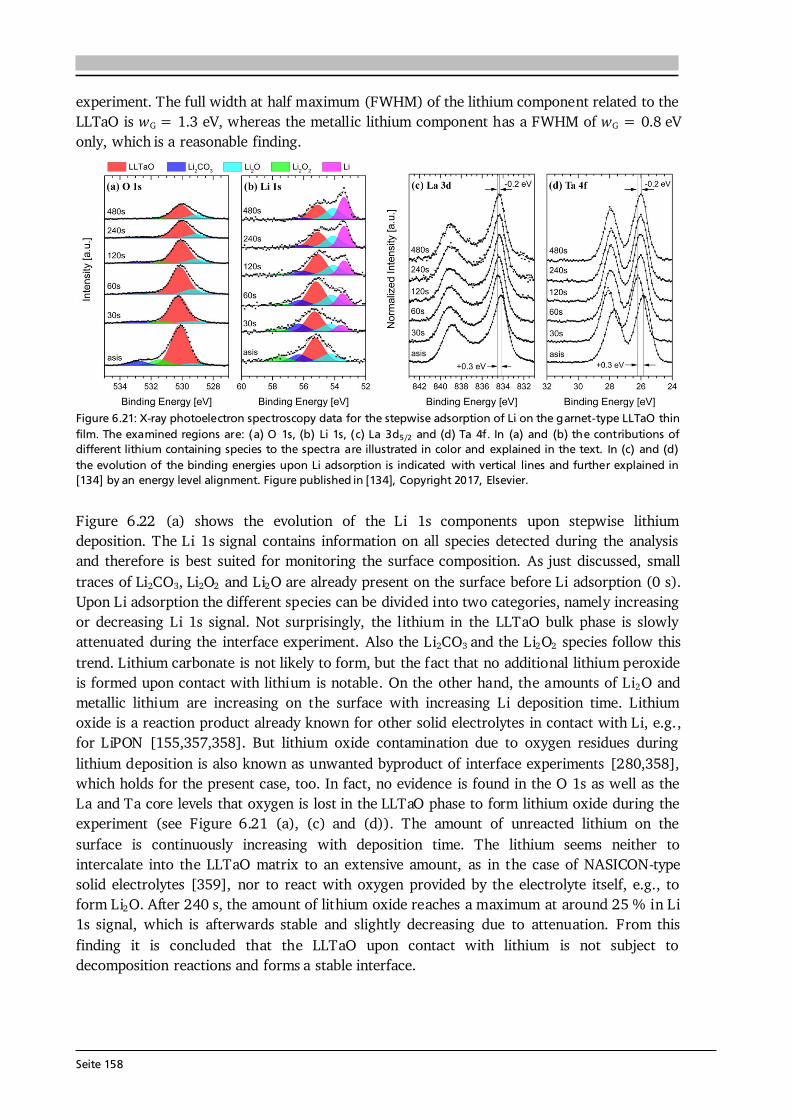
Seite 158
experiment. The full width at half maximum (FWHM) of the lithium component related to the LLTaO is wG = 1.3 eV, whereas the metallic lithium component has a FWHM of wG = 0.8 eV only, which is a reasonable finding.
Figure 6.21: X-ray photoelectron spectroscopy data for the stepwise adsorption of Li on the garnet-type LLTaO thin film. The examined regions are: (a) O 1s, (b) Li 1s, (c) La 3d5/2 and (d) Ta 4f. In (a) and (b) the contributions of different lithium containing species to the spectra are illustrated in color and explained in the text. In (c) and (d) the evolution of the binding energies upon Li adsorption is indicated with vertical lines and further explained in [134] by an energy level alignment. Figure published in [134], Copyright 2017, Elsevier. Figure 6.22 (a) shows the evolution of the Li 1s components upon stepwise lithium deposition. The Li 1s signal contains information on all species detected during the analysis and therefore is best suited for monitoring the surface composition. As just discussed, small traces of Li2CO3, Li2O2 and Li2O are already present on the surface before Li adsorption (0 s). Upon Li adsorption the different species can be divided into two categories, namely increasing or decreasing Li 1s signal. Not surprisingly, the lithium in the LLTaO bulk phase is slowly attenuated during the interface experiment. Also the Li2CO3 and the Li2O2 species follow this trend. Lithium carbonate is not likely to form, but the fact that no additional lithium peroxide is formed upon contact with lithium is notable. On the other hand, the amounts of Li2O and metallic lithium are increasing on the surface with increasing Li deposition time. Lithium oxide is a reaction product already known for other solid electrolytes in contact with Li, e.g., for LiPON [155,357,358]. But lithium oxide contamination due to oxygen residues during lithium deposition is also known as unwanted byproduct of interface experiments [280,358], which holds for the present case, too. In fact, no evidence is found in the O 1s as well as the La and Ta core levels that oxygen is lost in the LLTaO phase to form lithium oxide during the experiment (see Figure 6.21 (a), (c) and (d)). The amount of unreacted lithium on the surface is continuously increasing with deposition time. The lithium seems neither to intercalate into the LLTaO matrix to an extensive amount, as in the case of NASICON-type solid electrolytes [359], nor to react with oxygen provided by the electrolyte itself, e.g., to form Li2O. After 240 s, the amount of lithium oxide reaches a maximum at around 25 % in Li 1s signal, which is afterwards stable and slightly decreasing due to attenuation. From this finding it is concluded that the LLTaO upon contact with lithium is not subject to decomposition reactions and forms a stable interface.
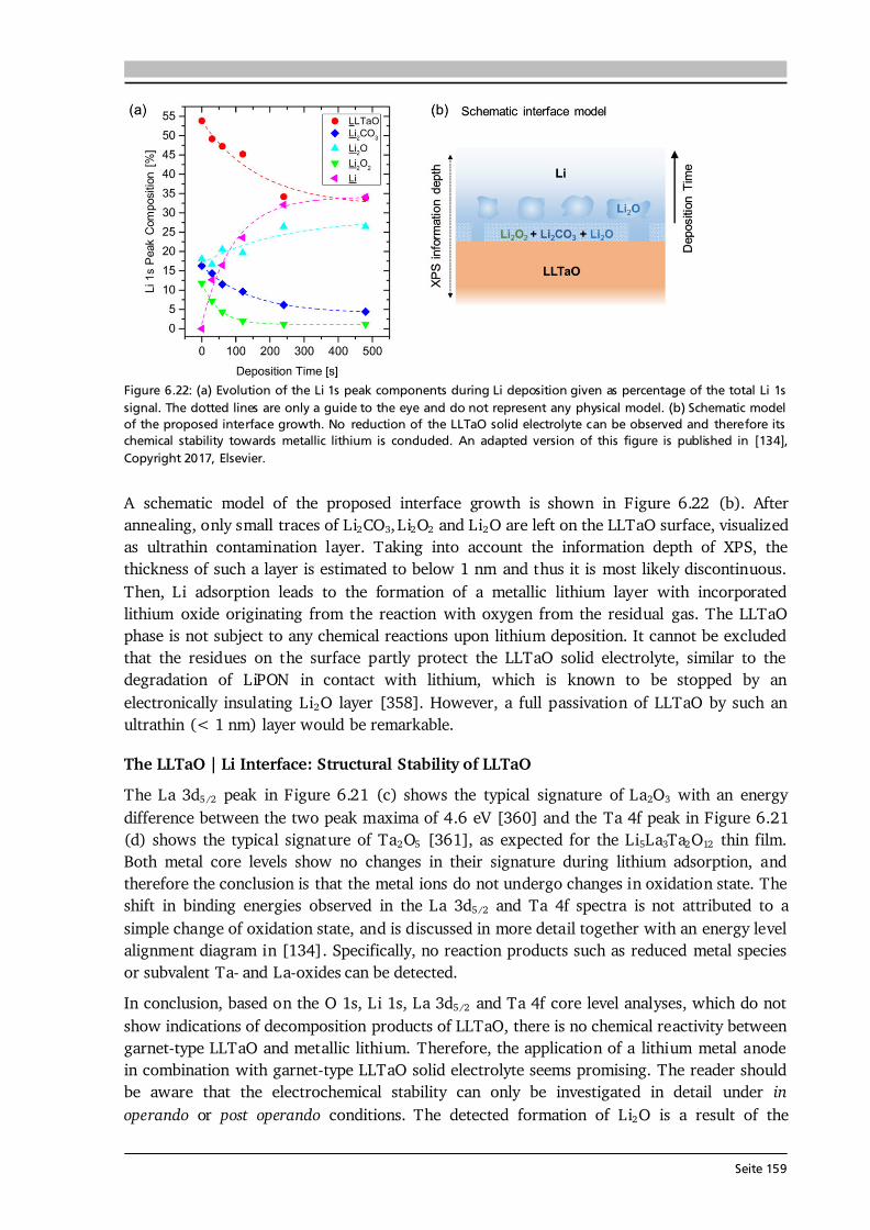
Seite 159
Figure 6.22: (a) Evolution of the Li 1s peak components during Li deposition given as percentage of the total Li 1s signal. The dotted lines are only a guide to the eye and do not represent any physical model. (b) Schematic model of the proposed interface growth. No reduction of the LLTaO solid electrolyte can be observed and therefore its chemical stability towards metallic lithium is concluded. An adapted version of this figure is published in [134], Copyright 2017, Elsevier. A schematic model of the proposed interface growth is shown in Figure 6.22 (b). After annealing, only small traces of Li2CO3, Li2O2 and Li2O are left on the LLTaO surface, visualized as ultrathin contamination layer. Taking into account the information depth of XPS, the thickness of such a layer is estimated to below 1 nm and thus it is most likely discontinuous. Then, Li adsorption leads to the formation of a metallic lithium layer with incorporated lithium oxide originating from the reaction with oxygen from the residual gas. The LLTaO phase is not subject to any chemical reactions upon lithium deposition. It cannot be excluded that the residues on the surface partly protect the LLTaO solid electrolyte, similar to the degradation of LiPON in contact with lithium, which is known to be stopped by an electronically insulating Li2O layer [358]. However, a full passivation of LLTaO by such an ultrathin (< 1 nm) layer would be remarkable. The LLTaO | Li Interface: Structural Stability of LLTaO The La 3d5/2 peak in Figure 6.21 (c) shows the typical signature of La2O3 with an energy difference between the two peak maxima of 4.6 eV [360] and the Ta 4f peak in Figure 6.21 (d) shows the typical signature of Ta2O5 [361], as expected for the Li5La3Ta2O12 thin film. Both metal core levels show no changes in their signature during lithium adsorption, and therefore the conclusion is that the metal ions do not undergo changes in oxidation state. The shift in binding energies observed in the La 3d5/2 and Ta 4f spectra is not attributed to a simple change of oxidation state, and is discussed in more detail together with an energy level alignment diagram in [134]. Specifically, no reaction products such as reduced metal species or subvalent Ta- and La-oxides can be detected. In conclusion, based on the O 1s, Li 1s, La 3d5/2 and Ta 4f core level analyses, which do not show indications of decomposition products of LLTaO, there is no chemical reactivity between garnet-type LLTaO and metallic lithium. Therefore, the application of a lithium metal anode in combination with garnet-type LLTaO solid electrolyte seems promising. The reader should be aware that the electrochemical stability can only be investigated in detail under in operando or post operando conditions. The detected formation of Li2O is a result of the
Seite 160
reaction of the deposited lithium with residual oxygen in the vacuum and is not related to changes in the LLTaO phase. Prospective interface experiments could investigate the stability of tetragonal and cubic (e.g., Al-doped) LLZrO towards Li to complement the recent theoretical studies [276–278,309]. 6.5. Impact and Potential of LA-CVD Grown Garnet-Type Thin Films Bulk-type all-solid-state batteries require a Li-ion conductivity of the solid electrolyte material of > 10-4 S·cm-1 in order to achieve a low internal resistance of the battery, whereas in case of thin film solid electrolytes values > 10-6 S·cm-1 are sufficient, as described in Section 6.1. A prominent example and benchmark is amorphous lithium phosphorus oxynitride (LiPON), with a room temperature Li-ion conductivity of 2·10-6 S·cm-1 [33], which is most frequently employed in current all-solid-state thin film LiBs [13]. In comparison to LiPON, tetragonal LLZrO and cubic LLTaO thin films grown by LA-CVD show a higher Li-ion conductivity of 4.2·10-6 S·cm-1 and 7.8·10-6 S·cm-1, respectively. Moreover, a further increase in their ionic conductivity is achievable via post-annealing (LLTaO, 3.8·10-5 S·cm-1, see Section 6.4.3) and most likely also via chemical substitution, e.g. Ba- or Sr-doping in LLTaO and Al-, Ga- or Ta-doping in LLZrO films. Accordingly, from a conductivity point of view, these films should be applicable for the use in all-solid-state thin film Li-ion batteries like LiPON. However, the high impedance across the interfaces of the garnet-type solid electrolyte to the electrodes is currently a major problem addressed in recent experimental as well as theoretical studies [26,30,275,277,279,310,311]. The high impedance is a result of (non-conductive) interphases formed at the interfaces due to [277]: chemical instability (during cell fabrication) between solid electrolyte and electrode material, and/or electrochemical instability (during cycling) of the solid electrolyte itself and/or between solid electrolyte and electrode material. In terms of chemical stability, Al-substituted LLZrO and LiCoO2 were shown to react with each other at 973 K [30], whereas Ba-substituted LLTaO and LiCoO2 were reported to be chemically stable up to 1173 K [362]. Furthermore, Kotobuki and co-workers fabricated all-solid-state batteries with a Li anode, LiCoO2 cathode and LLZrO [311] as well as LLTaO [310] solid electrolyte under otherwise identical processing and the cell with LLTaO performed much better, i.e. it showed a clearer redox couple of LiCoO2 with lower overpotential. These results suggest that in addition to the higher chemical stability, the electrochemical stability during cycling towards LiCoO2 is better for LLTaO than for LLZrO, which is supported by theory [279]. Together with the results on the enlarged LA-CVD growth parameter sweet spot of LLTaO (Section 6.4) compared to LLZrO (Section 6.3), it is proposed that Li-conducting garnets based on Ta are more promising than Zr-based systems for application in all-solid-state thin film LiBs containing LiCoO2 as cathode. The introduction of an artificial SEI on the cathode side such as Al2O3 (Section 5.5.2) or Nb (Section 8.3) may still be necessary and applied to further improve the all-solid-state battery performance. The growth of Li(TM)O2 thin films by LA-CVD and their successful application as cathode materials has been demonstrated in Sections 5.3 and 5.4. Together with the results on garnet-type thin film solid electrolytes presented in Sections 6.3 and 6.4, an all-solid-state thin film Li-ion battery by LA-CVD comes into reach, growing solid electrolyte and cathode films on top of each other. Such an exclusive LA-CVD battery concept could either make use of an in situ plated Li anode [363] (see Section 8.2.3), or employ a simple metal oxide thin film anode
Seite 161
(Chapter 7). The latter would have the advantage that the garnet solid electrolyte film was sandwiched between the cathode and the anode layer and therefore could be further processed under ambient conditions without degradation. Additionally, if the solid electrolyte was deposited on top of the electrode material, then the Li2PtO3 formation could be suppressed (see Section 5.3.2). This is of great importance to obtain a functioning all-solid-state battery, because of the large impedance that even a thin Li2PtO3 interface layer would contribute to the overall impedance (Figure 6.8 in Section 6.3.4). A further advantage of an exclusively LA-CVD grown all-solid-state thin film Li-ion battery would be the realization of a 3D-microbattery design due to the LA-CVD’s capability of conformal deposition as proven by means of LiCoO2 in Section 5.5.1. This would result in an additional increase of the (footprint)area specific energy density and ensure a high power capability for the 3D-microbattery cell [13]. The ionic conductivity in garnet-type solid electrolytes depends on microstructural features (density, crystallinity, etc.), phase purity, and element composition. By adapting the LA-CVD process parameters the microstructure of the LLTaO films can be tailored, while at the same time the garnet-type phase is preserved (Section 6.4.2). This is a great enhancement to LLZrO films, which only showed a very narrow LA-CVD growth parameter sweet spot (Section 6.3.2), as well as a great advantage compared to bulk ceramic synthesis, in which direct control over the microstructure is much more difficult to achieve. The direct control over the microstructure allows to specifically suppress the grain boundary contribution in order to improve the total ionic conductivity of LLTaO films as shown in Section 6.4.3. Furthermore, it allows to study the grain boundary effect in more detail, i.e. to narrow its origin down to a constriction caused by low direct contact area between grains. The stability of the garnet-type LLTaO phase over a broad range of LA-CVD growth parameters provides a playground for further fundamental structure-property relation studies. Even more, in combination with the possibility to grow thin film anodes, cathodes and solid electrolytes, also consecutively, by LA-CVD and the fact that the LA-CVD setup is part of the integrated UHV-cluster DAISY-Bat with in situ access to other deposition techniques as well as to photoelectron spectroscopy offers a powerful playground for fundamental studies of the interphase formation at the interfaces of (e.g.) garnet-type solid electrolytes. As a first example, the chemical stability of LLTaO towards lithium is proven by such an interface experiment (Section 6.4.4). Following this approach a better understanding on how to engineer interfaces of (e.g.) garnet-type solid electrolytes is expected that may help to further improve future all-solid-state LiBs, especially when correlated with theoretical studies on the chemical reactivity of such interfaces. Recently, it was reported that by interface-engineering based on a nanoporous garnet-type LLZrO solid electrolyte interface structure the cycling properties of an all-solid-state LiB could be improved due to the high interfacial surface area at the electrode-electrolyte interface [364]. In Section 6.4, the electrochemical performance of LLTaO films grown at 1073 K and 1173 K were not reported due to the particulate deposits on top of the highly dense LLTaO film (Figure 6.10 (d) and (e)), which do not allow a clear interpretation of the EIS data (Figure 6.13 (b)). However, these films show excellent phase purity and a high crystallinity (Table 6.7 and Figure 6.11 (a)), so that the highly dense LLTaO film beneath the particulate deposits is expected to have an ionic conductivity similar or even superior to the post-annealed films in Section 6.4.3. Therefore, LLTaO films grown at 1073 K and 1173 K could be interesting for an all-solid-state battery concept, since the particulate deposits should provide
Seite 162
a high interfacial surface area to the applied electrode material, similar to a composite. The advantage over the approach taken in [364] would be a one-step deposition via LA-CVD, hence a much simpler and faster processing. Another potential of LA-CVD grown solid electrolyte films is to prevent short circuits due to Li dendrite growth as discussed in the following. Solid electrolytes are often considered to be resistant towards Li dendrite growth, however, garnet-type LLZrO was shown to suffer from short circuits due to Li dendrite formation [365,366], especially at high current densities required to compete with conventional LiBs (≥ 0.5 mA·cm-2). Among the reported strategies to suppress the Li dendrite formation are the use of highly dense LLZrO (99.1 % relative density, [367]) and the reduction of the interfacial resistance between Li metal and the solid electrolyte by employing small-grained (grain sizes ~ 20 - 40 µm) LLZrO [366]. As discussed in Section 6.4.1, the LA-CVD grown LLTaO films can be considered as highly dense and contain much smaller grains (< 1 µm) than LLTaO bulk ceramics after sintering, thus they combine two important strategies to suppress Li dendrite formation. The same holds true for LA-CVD grown LLZrO (Figure 6.4 in Section 6.3.1). Consequently, it is proposed that LA-CVD grown garnet-type solid electrolyte films have the potential to prevent Li dendrite formation and therefore might allow the safe use of a Li metal anode in future all-solid-state LiBs. Preliminary tests to investigate the dendrite formation through LLZrO pellets, uncoated and coated with a thin LLZrO protective layer by LA-CVD, in cooperation with the research group of Peter Bruce (University of Oxford) are under way. The final comment is about the potential of using CVD in industrial battery fabrication processes. In the fields of semiconductor and nanotechnology industries, CVD in various configurations such as MO-CVD, plasma enhanced (PE) CVD and low pressure (LP) CVD are matured techniques for many years. The novel CO2-laser assisted CVD, established in the course of this thesis, has the striking advantage that the film growth does not depend on the individual vapor pressure of the solid precursors, which is unique for a CVD process (see Section 2.3.3). This simplifies the precursor delivery tremendously and allows for the controlled growth of high quality multicomponent films with a dense and homogeneous microstructure, free of cracks. The LA-CVD grown films show a homogeneous element distribution and are free of carbon. Therefore, the LA-CVD technique might be of interest for industrial battery fabrication. 6.6. Conclusion and Outlook In this chapter, the possibilities and limitations of AA-CVD and LA-CVD in the growth of Li-ion conducting garnet-type thin film solid electrolytes are investigated. The two garnets with nominal composition of Li5La3Ta2O12 (LLTaO) and Li7La3Zr2O12 (LLZrO) are studied due to their proposed applicability together with a Li anode in all-solid-state LiBs [25,277,310,311]. This is the first report on electrochemical properties of CVD grown Li-ion conducting garnet-type thin film solid electrolytes, which also includes a detailed characterization of the films’ microstructure, phase and element composition. The identified processing-structure-property relationships are used to improve the thin films’ ionic conductivity and are possibly also valuable for garnet-type bulk ceramic synthesis. The results of this study show that:
Seite 163
the applicability of AA-CVD for garnet-type thin film growth is questionable, because under all investigated growth conditions films with a hollow sphere microstructure and no indication for a garnet-type phase are grown. the growth of tetragonal LLZrO thin films by LA-CVD is successful within a narrow growth parameter sweet spot and that under optimized conditions a high quality film, which is dense, uniform and free of cracks, is grown on Pt with a phase composition of tetragonal LLZrO (89 vol.-%), Li2PtO3 (7 vol.-%) and La2O3 (4 vol.-%). Li2PtO3 is exclusively found at the interface to the Pt substrate, so that the LLZrO and Li2PtO3 interface layer can be treated as electrical connection in series in EIS. a Li2CO3 layer forms at the surface of the LLZrO film, even though the air exposure time is reduced to a minimum and apart from that the LLZrO film is free of carbon and has a La/Zr molar ratio of ~ 1.5 on average as expected by its nominal composition. combining several analyses allows to distinguish the signature of the Li2PtO3 interface layer from the one of the LLZrO solid electrolyte in EIS. the high quality LLZrO thin film grown by LA-CVD has a total ionic conductivity of 4.2·10-6 S·cm-1 at 298 K (Ea = 0.50 eV), which is the highest conductivity value reported for tetragonal LLZrO thin films so far and only about 5 times lower than the highest reported value for tetragonal LLZrO bulk ceramics [306]. the growth of cubic LLZrO thin films by LA-CVD is possible via doping with Ga or Al. cubic LLTaO films grow within a much wider range of LA-CVD growth parameters than LLZrO films and therefore cubic LLTaO is easier to stabilize than cubic LLZrO. this enlarged sweet spot of growth conditions enables fundamental structure-property relation studies such as the growth of fine-grained and coarse-grained LLTaO films: fine-grained LLTaO films exhibit mainly bulk ionic conduction, whereas coarse-grained LLTaO films have an additional, resistive grain boundary contribution to the EIS spectrum, which is ascribed to a geometrical constriction impeding ionic current flow. the as-deposited (fine-grained) LLTaO film has an ionic conductivity of 7.8·10-6 S·cm-1 at 298 K (Ea = 0.66 eV), despite the presence of La2O3 secondary phase (33 vol.-%). post-annealing in UHV reduces the amount of La2O3 secondary phase (12 vol.-%) and by this increases the ionic conductivity up to 3.8·10-5 S·cm-1 at 298 K (Ea = 0.52 eV). LLTaO is chemically stable and does not decompose in contact with metallic lithium. the Li-ion conductivities found in this study are among the highest values reported for garnet-type thin films so far (Table 6.1), thus LA-CVD grown garnet-type thin films are interesting candidates for the use in all-solid-state thin film LiBs. LLTaO films are better suited for fundamental as well as application related research than LLZrO films, because of their higher total ionic conductivity and better phase stability during LA-CVD growth.
Seite 164
For future research the following main topics are identified: Improvements in Li-ion conductivity
AA-CVD. Neither a dense microstructure nor formation of a garnet-type phase could be achieved via AA-CVD questioning its applicability for garnet-type solid electrolyte growth. Regarding the microstructure, the processing conditions have to be changed in such a way that favors volume precipitation within the droplets of the aerosol in order to inhibit hollow sphere formation and to promote the growth of a dense film instead [232]. Possible strategies comprise a change in solvent, type of precursor(s) and/or atmosphere inside the AA-CVD reactor. Regarding the structure, sintering experiments after film deposition could be performed following the processing of LLZrO powder synthesized via NSP [324]. For example, by using the high temperature XRD chamber the films’ structure can be analyzed at temperatures up to 1200 °C in reducing or oxidizing atmosphere, or under vacuum. LA-CVD, LLTaO. As described in Section 6.4, the formation of La2O3 secondary phase is assumed to result from limited surface diffusion during the growth at rather low deposition temperatures of 973 K. Furthermore, a significant reduction in La2O3 phase fraction upon annealing supports this assumption. A reduced amount of La2O3 goes along with an enhanced ionic conductivity, so that further improvements in Li-ion conductivity should be possible in case pure LLTaO thin films could be obtained. Potential synthesis strategies are: (i) slightly increasing the deposition temperature, e.g., by 50 K to 1023 K, (ii) prolonging the deposition time, or (iii) using a different type of precursor to influence the reaction kinetics. The post-annealing treatment can also be optimized, e.g., shorter time at higher temperature, however, it would be more convenient to obtain a phase pure LLTaO thin film in a single step. LA-CVD, LLZrO. The current knowledge from bulk ceramic studies is that optimized cubic LLZrO has by one order of magnitude higher Li-ion conductivity than cubic LLTaO (Table 6.1). Therefore, if higher Li-ion conductivities than already achieved with LLTaO thin films are required in the future, the stabilization of cubic LLZrO thin films via LA-CVD could be followed up. During the necessary growth parameter optimization careful attention must be paid to the dopant concentration and its site occupancy in the LLZrO lattice, which might not be easy to investigate in thin films.
Interface study and engineering Interface experiments in UHV can give valuable insights into the interphase formation at the solid electrolyte interfaces and, complemented by theory, can provide strategies on how to best engineer such. On the anode side, the chemical stability of LLTaO towards lithium is verified for the first time on the atomic level by such a surface science approach (Section 6.4.4). As next step, the LLTaO | LiCoO2 interface on the cathode side is worthwhile to investigate. An LLTaO solid electrolyte thin film should be grown by LA-CVD. Then, the stepwise deposition of LiCoO2 via sputtering followed by PES analyses after each deposition should be accomplished in the integrated UHV-cluster DAISY-Bat in order to study the interphase formation. Another interface experiment could address the LLTaO | aSEI | LiCoO2 interface, conducted in the same manner, just with an ultrathin oxide (Al2O3) or metal (Nb, Ta) layer coated on LA-CVD grown LLTaO, preferably by ALD to achieve a conformal coating. The purpose of the aSEI is either to protect the solid electrolyte (oxide) from a reaction with the electrode material or to intentionally react with the solid electrolyte (metal) to form a Li-ion conductive interphase, both of which can be analyzed in the interface experiment.
Seite 165
LA-CVD battery concept A major weakness of the exclusive LA-CVD battery concept is the high temperature needed for the growth of each component, so that chemical reactions between solid electrolyte and electrode material are inevitable. Here it is important which type of interface forms in such a reaction (Section 6.1). Either a type 1 interface, as observed between LLTaO and Li, or a highly conductive type 3 interface, as observed between LiPON and Li, is desired. One approach to identify such interfaces is the above mentioned interface experiment, including interface engineering by the introduction of an artificial SEI. This is a very laborious task, as it is a trial and error approach of different material combinations with additional cycling experiments of full all-solid-state battery cells. Theoretical studies can provide valuable insights into promising material combinations, however, cannot adequately map the experimental conditions. Therefore, further development of the LA-CVD setup to significantly lower the deposition temperature should be considered in order to avoid undesired interphase formation during consecutive thin film growth. This can be realized by introducing a photo-induced or plasma-enhanced reaction zone [78]. Plasma enhancement is inexpensive [180] and well established in research as well as industry.

Seite 166
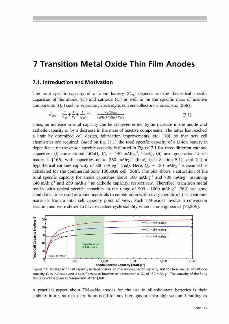
Seite 167
7 Transition Metal Oxide Thin Film Anodes 7.1. Introduction and Motivation The total specific capacity of a Li-ion battery (Ctot) depends on the theoretical specific capacities of the anode (Ca) and cathode (Cc) as well as on the specific mass of inactive components (Qm) such as separator, electrolyte, current collectors, chassis, etc. [368]: . (7.1) Thus, an increase in total capacity can be achieved either by an increase in the anode and cathode capacity or by a decrease in the mass of inactive components. The latter has reached a limit by optimized cell design, fabrication improvements, etc. [10], so that new cell chemistries are required. Based on Eq. (7.1) the total specific capacity of a Li-ion battery in dependence on the anode specific capacity is plotted in Figure 7.1 for three different cathode capacities: (i) conventional LiCoO2 (Cc ~ 140 mAh·g-1, black), (ii) next generation Li-rich materials [165] with capacities up to 250 mAh·g-1 (blue) (see Section 5.1), and (iii) a hypothetical cathode capacity of 500 mAh·g-1 (red). Here, Qm ~ 130 mAh·g-1 is assumed as calculated for the commercial Sony 18650G8 cell [368]. The plot shows a saturation of the total specific capacity for anode capacities above 500 mAh·g-1 and 700 mAh·g-1 assuming 140 mAh·g-1 and 250 mAh·g-1 as cathode capacity, respectively. Therefore, transition metal oxides with typical specific capacities in the range of 500 - 1000 mAh·g-1 [369] are good candidates to be used as anode materials in combination with next generation Li-rich cathode materials from a total cell capacity point of view. Such TM-oxides involve a conversion reaction and were shown to have excellent cycle stability when nano-engineered [74,369].
Figure 7.1: Total specific cell capacity in dependence on the anode specific capacity and for fixed values of cathode capacity Cc as indicated and a specific mass of inactive cell components Qm of 130 mAh·g-1. The capacity of the Sony 18650G8 cell is given as comparison. After [368]. A practical aspect about TM-oxide anodes for the use in all-solid-state batteries is their stability in air, so that there is no need for any inert gas or ultra-high vacuum handling as
Seite 168
compared to a lithium metal anode. Moreover, once the air-sensitive garnet-type solid electrolyte film (Chapter 6) is sandwiched between a Li(TM)O2 cathode and TM-oxide anode, further processing and analyses can be carried out in air without too much degradation to be expected. In this chapter, conversion-type TM-oxides with TM = Co, Ni, Mn were specifically chosen to investigate due to (i) their high theoretical specific capacities of at least 700 mAh·g -1 depending on the oxidation state and (ii) the similarity of the deposition process to the investigated Li(TM)O2 thin film cathodes (Chapter 5), which leverages the existing knowledge and leads to an ease of deposition. Conversion Mechanism and Need for Nanostructuring Anode materials for Li-ion batteries can be classified according to their reaction mechanism as [369]: intercalation (e.g., graphite, LiTi4O5), alloying (e.g., Si, Ge, Sn) or conversion (several metal oxides / phosphides / sulfides / nitrides) materials. Intercalation - The most frequently used anode material nowadays, graphite, is based on intercalation of one Li-ion per six carbon atoms into the graphite host structure providing a theoretical specific capacity of 372 mAh·g-1 for LiC6. Among the advantages of graphite, which have led to its widespread use, are low cost, good working potential, good capacity retention (only after the first cycle) and high safety [369]. Alloying - In search of anodes with much higher specific capacity and energy density, materials that reversibly alloy with Li are considered as next generation anodes and have been studied intensively [369,370]. Among others, silicon with its natural abundance and very high specific capacity of 3578 mAh·g-1 for Li15Si4 is worth to investigate as alternative to graphite. However, the major drawback of alloying materials is their volume expansion upon lithiation (e.g., 300 % for Si/Li15Si4) building up internal mechanical stress that eventually destroys the structural integrity and leads to huge capacity fading [369,370]. Conversion - The specific capacity of conversion-type anode materials based on TM-oxides lies in between graphite and silicon, but is more than sufficient with respect to the total cell capacity in case no breakthrough in cathode capacity is achieved at the same time (see Figure 7.1). Further advantages of TM-oxides are low cost and environmental compatibility due to their non-toxicity and natural abundance, depending on which metal oxide is used [369]. Among the drawbacks of conversion-type materials are low electrical conductivity, slow diffusion of Li-ions and large potential hysteresis which together result in poor cycling performance. However, since it was demonstrated that nano-sized TM-oxides show excellent capacity retention, namely 100 % for up to 100 cycles [74], the class of conversion materials has gained a lot of interest. In general, nanostructural engineering such as the use of nano-particles, -wires, -tubes, core-shell and yolk-shell structures or thin films allowed to resolve many problems and limitations encountered in anode materials [369], especially Si [371]. Such nanostructures can reduce the diffusion distance of Li-ions, increase the contact area of active material and by this enhance the electrochemical reactivity, but also help to accommodate mechanical stress. In this respect, thin films offer distinct advantages over nanostructured bulk materials. One advantage is that thin film deposition techniques allow to control certain microstructural features, such as the morphology, density, crystallinity, etc., on the nano-scale. Furthermore,
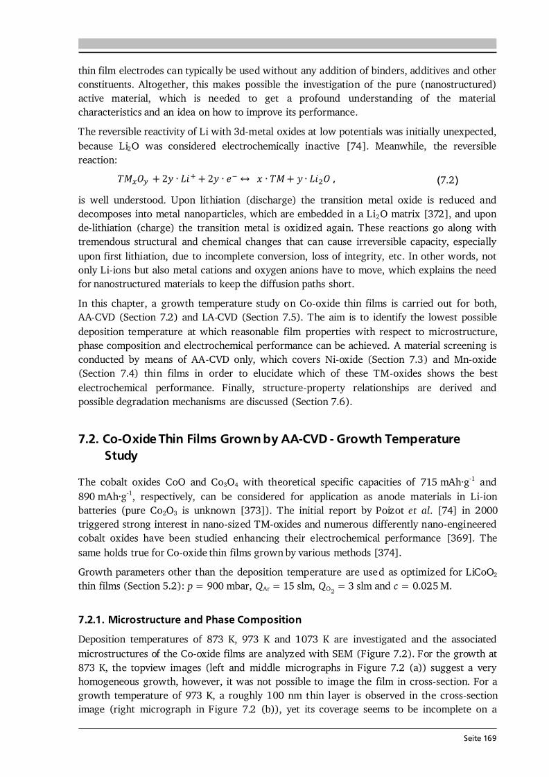
Seite 169
thin film electrodes can typically be used without any addition of binders, additives and other constituents. Altogether, this makes possible the investigation of the pure (nanostructured) active material, which is needed to get a profound understanding of the material characteristics and an idea on how to improve its performance. The reversible reactivity of Li with 3d-metal oxides at low potentials was initially unexpected, because Li2O was considered electrochemically inactive [74]. Meanwhile, the reversible reaction: , (7.2) is well understood. Upon lithiation (discharge) the transition metal oxide is reduced and decomposes into metal nanoparticles, which are embedded in a Li2O matrix [372], and upon de-lithiation (charge) the transition metal is oxidized again. These reactions go along with tremendous structural and chemical changes that can cause irreversible capacity, especially upon first lithiation, due to incomplete conversion, loss of integrity, etc. In other words, not only Li-ions but also metal cations and oxygen anions have to move, which explains the need for nanostructured materials to keep the diffusion paths short. In this chapter, a growth temperature study on Co-oxide thin films is carried out for both, AA-CVD (Section 7.2) and LA-CVD (Section 7.5). The aim is to identify the lowest possible deposition temperature at which reasonable film properties with respect to microstructure, phase composition and electrochemical performance can be achieved. A material screening is conducted by means of AA-CVD only, which covers Ni-oxide (Section 7.3) and Mn-oxide (Section 7.4) thin films in order to elucidate which of these TM-oxides shows the best electrochemical performance. Finally, structure-property relationships are derived and possible degradation mechanisms are discussed (Section 7.6). 7.2. Co-Oxide Thin Films Grown by AA-CVD - Growth Temperature Study The cobalt oxides CoO and Co3O4 with theoretical specific capacities of 715 mAh·g-1 and 890 mAh·g-1, respectively, can be considered for application as anode materials in Li-ion batteries (pure Co2O3 is unknown [373]). The initial report by Poizot et al. [74] in 2000 triggered strong interest in nano-sized TM-oxides and numerous differently nano-engineered cobalt oxides have been studied enhancing their electrochemical performance [369]. The same holds true for Co-oxide thin films grown by various methods [374]. Growth parameters other than the deposition temperature are used as optimized for LiCoO2 thin films (Section 5.2): p = 900 mbar, QAr = 15 slm, QO2 = 3 slm and c = 0.025 M. 7.2.1. Microstructure and Phase Composition Deposition temperatures of 873 K, 973 K and 1073 K are investigated and the associated microstructures of the Co-oxide films are analyzed with SEM (Figure 7.2). For the growth at 873 K, the topview images (left and middle micrographs in Figure 7.2 (a)) suggest a very homogeneous growth, however, it was not possible to image the film in cross-section. For a growth temperature of 973 K, a roughly 100 nm thin layer is observed in the cross-section image (right micrograph in Figure 7.2 (b)), yet its coverage seems to be incomplete on a
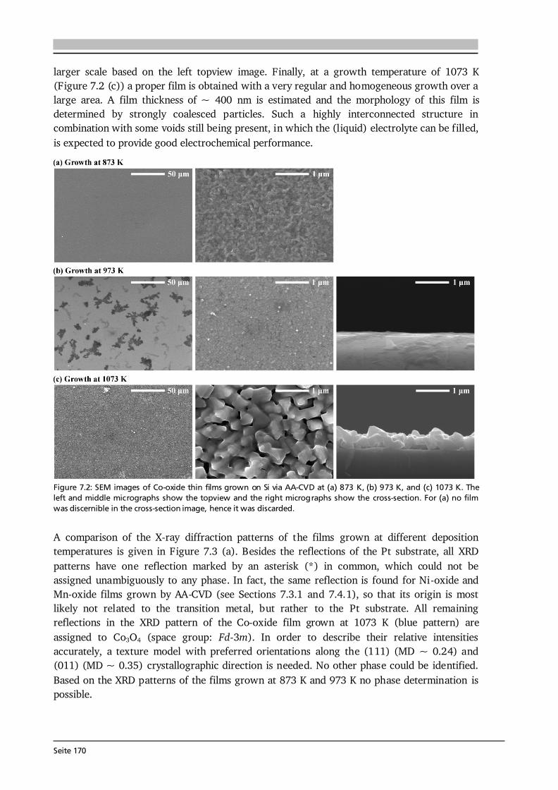
Seite 170
larger scale based on the left topview image. Finally, at a growth temperature of 1073 K (Figure 7.2 (c)) a proper film is obtained with a very regular and homogeneous growth over a large area. A film thickness of ~ 400 nm is estimated and the morphology of this film is determined by strongly coalesced particles. Such a highly interconnected structure in combination with some voids still being present, in which the (liquid) electrolyte can be filled, is expected to provide good electrochemical performance.
Figure 7.2: SEM images of Co-oxide thin films grown on Si via AA-CVD at (a) 873 K, (b) 973 K, and (c) 1073 K. The left and middle micrographs show the topview and the right micrographs show the cross-section. For (a) no film was discernible in the cross-section image, hence it was discarded. A comparison of the X-ray diffraction patterns of the films grown at different deposition temperatures is given in Figure 7.3 (a). Besides the reflections of the Pt substrate, all XRD patterns have one reflection marked by an asterisk (*) in common, which could not be assigned unambiguously to any phase. In fact, the same reflection is found for Ni-oxide and Mn-oxide films grown by AA-CVD (see Sections 7.3.1 and 7.4.1), so that its origin is most likely not related to the transition metal, but rather to the Pt substrate. All remaining reflections in the XRD pattern of the Co-oxide film grown at 1073 K (blue pattern) are assigned to Co3O4 (space group: Fd-3m). In order to describe their relative intensities accurately, a texture model with preferred orientations along the (111) (MD ~ 0.24) and (011) (MD ~ 0.35) crystallographic direction is needed. No other phase could be identified. Based on the XRD patterns of the films grown at 873 K and 973 K no phase determination is possible.
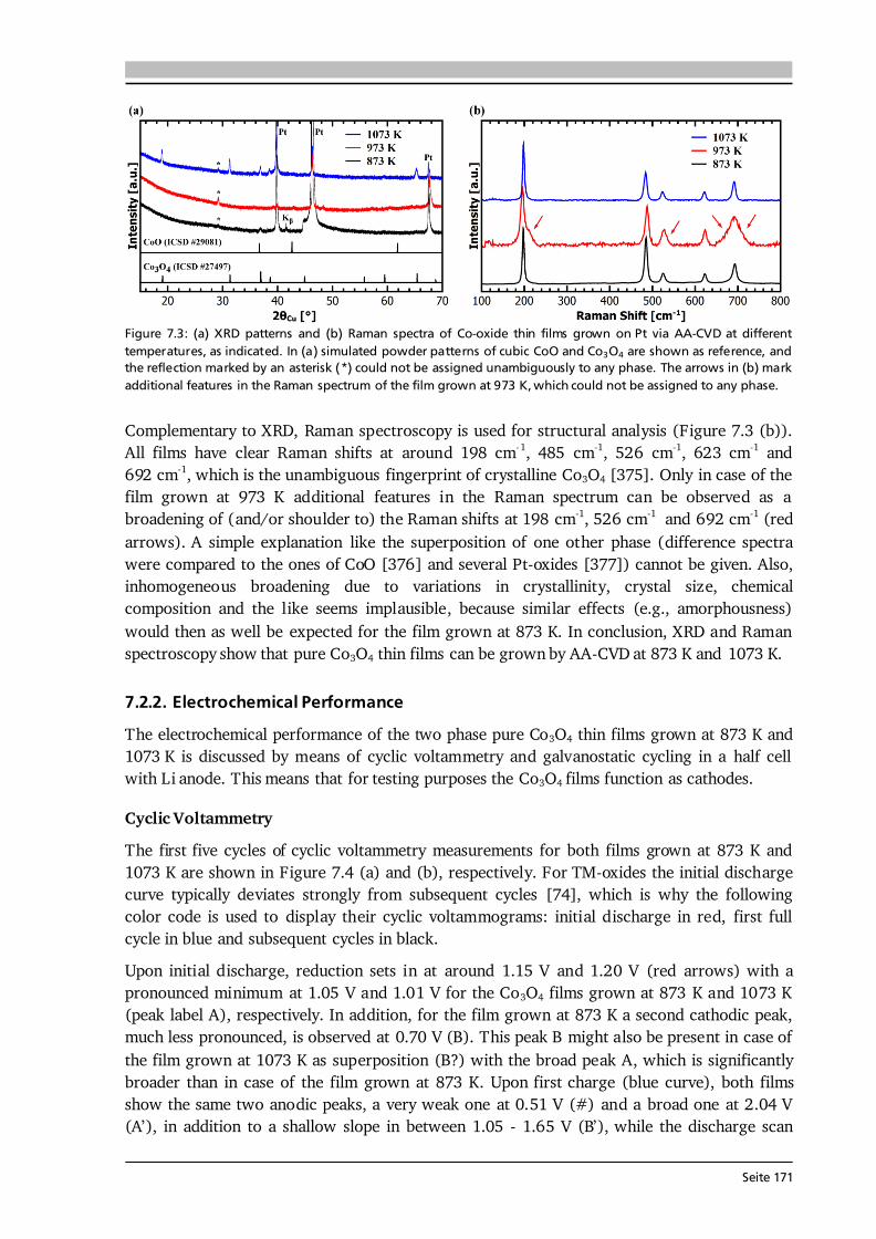
Seite 171
Figure 7.3: (a) XRD patterns and (b) Raman spectra of Co-oxide thin films grown on Pt via AA-CVD at different temperatures, as indicated. In (a) simulated powder patterns of cubic CoO and Co3O4 are shown as reference, and the reflection marked by an asterisk (*) could not be assigned unambiguously to any phase. The arrows in (b) mark additional features in the Raman spectrum of the film grown at 973 K, which could not be assigned to any phase. Complementary to XRD, Raman spectroscopy is used for structural analysis (Figure 7.3 (b)). All films have clear Raman shifts at around 198 cm-1, 485 cm-1, 526 cm-1, 623 cm-1 and 692 cm-1, which is the unambiguous fingerprint of crystalline Co3O4 [375]. Only in case of the film grown at 973 K additional features in the Raman spectrum can be observed as a broadening of (and/or shoulder to) the Raman shifts at 198 cm-1, 526 cm-1 and 692 cm-1 (red arrows). A simple explanation like the superposition of one other phase (difference spectra were compared to the ones of CoO [376] and several Pt-oxides [377]) cannot be given. Also, inhomogeneous broadening due to variations in crystallinity, crystal size, chemical composition and the like seems implausible, because similar effects (e.g., amorphousness) would then as well be expected for the film grown at 873 K. In conclusion, XRD and Raman spectroscopy show that pure Co3O4 thin films can be grown by AA-CVD at 873 K and 1073 K. 7.2.2. Electrochemical Performance The electrochemical performance of the two phase pure Co3O4 thin films grown at 873 K and 1073 K is discussed by means of cyclic voltammetry and galvanostatic cycling in a half cell with Li anode. This means that for testing purposes the Co3O4 films function as cathodes. Cyclic Voltammetry The first five cycles of cyclic voltammetry measurements for both films grown at 873 K and 1073 K are shown in Figure 7.4 (a) and (b), respectively. For TM-oxides the initial discharge curve typically deviates strongly from subsequent cycles [74], which is why the following color code is used to display their cyclic voltammograms: initial discharge in red, first full cycle in blue and subsequent cycles in black. Upon initial discharge, reduction sets in at around 1.15 V and 1.20 V (red arrows) with a pronounced minimum at 1.05 V and 1.01 V for the Co3O4 films grown at 873 K and 1073 K (peak label A), respectively. In addition, for the film grown at 873 K a second cathodic peak, much less pronounced, is observed at 0.70 V (B). This peak B might also be present in case of the film grown at 1073 K as superposition (B?) with the broad peak A, which is significantly broader than in case of the film grown at 873 K. Upon first charge (blue curve), both films show the same two anodic peaks, a very weak one at 0.51 V (#) and a broad one at 2.04 V (A’), in addition to a shallow slope in between 1.05 - 1.65 V (B’), while the discharge scan
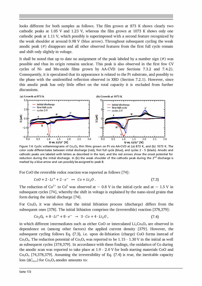
Seite 172
looks different for both samples as follows. The film grown at 873 K shows clearly two cathodic peaks at 1.05 V and 1.23 V, whereas the film grown at 1073 K shows only one cathodic peak at 1.11 V, which possibly is superimposed with a second feature recognized by the weak shoulder at around 0.98 V (blue arrow). Throughout subsequent cycling the weak anodic peak (#) disappears and all other observed features from the first full cycle remain and shift only slightly in voltage. It shall be noted that up to date no assignment of the peak labeled by a number sign (#) was possible and thus its origin remains unclear. This peak is also observed in the first few CV cycles of Ni- and Mn-oxide films grown by AA-CVD (see Sections 7.3.2 and 7.4.2). Consequently, it is speculated that its appearance is related to the Pt substrate, and possibly to the phase with the unidentified reflection observed in XRD (Section 7.2.1). However, since this anodic peak has only little effect on the total capacity it is excluded from further discussions.
Figure 7.4: Cyclic voltammograms of Co3O4 thin films grown on Pt via AA-CVD at (a) 873 K, and (b) 1073 K. The color code differentiates between initial discharge (red), first full cycle (blue), and cycles 2 - 5 (black). Anodic and cathodic peaks are labeled with letters as described in the text, and the red arrows show the onset potential for reduction during the initial discharge. In (b) the weak shoulder of the cathodic peak during the 2nd discharge is marked by a blue arrow and can possibly be assigned to peak B. For CoO the reversible redox reaction was reported as follows [74]: . (7.3) The reduction of Co2+ to Co0 was observed at ~ 0.8 V in the initial cycle and at ~ 1.5 V in subsequent cycles [74], whereby the shift in voltage is explained by the nano-sized grains that form during the initial discharge [74]. For Co3O4 it was shown that the initial lithiation process (discharge) differs from the subsequent ones [378]. The initial lithiation comprises the (irreversible) reaction [378,379]: , (7.4) in which different intermediates such as either CoO or intercalated LixCo3O4 are observed in dependence on (among other factors) the applied current density [379]. However, the subsequent cycling follows Eq. (7.3), i.e. upon de-lithiation (charge) CoO forms instead of Co3O4. The reduction potential of Co3O4 was reported to be 1.15 - 1.30 V in the initial as well as subsequent cycles [378,379]. In accordance with these findings, the oxidation of Co during the anodic scan was reported to take place at 1.9 - 2.0 V for both starting materials CoO and Co3O4 [74,378,379]. Assuming the irreversibility of Eq. (7.4) is true, the inevitable capacity loss (ΔCinev) for Co3O4 anodes amounts to:
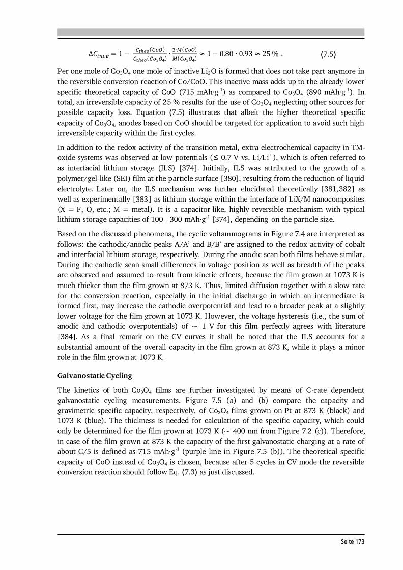
Seite 173
. (7.5) Per one mole of Co3O4 one mole of inactive Li2O is formed that does not take part anymore in the reversible conversion reaction of Co/CoO. This inactive mass adds up to the already lower specific theoretical capacity of CoO (715 mAh·g-1) as compared to Co3O4 (890 mAh·g-1). In total, an irreversible capacity of 25 % results for the use of Co3O4 neglecting other sources for possible capacity loss. Equation (7.5) illustrates that albeit the higher theoretical specific capacity of Co3O4, anodes based on CoO should be targeted for application to avoid such high irreversible capacity within the first cycles. In addition to the redox activity of the transition metal, extra electrochemical capacity in TM-oxide systems was observed at low potentials (≤ 0.7 V vs. Li/Li+), which is often referred to as interfacial lithium storage (ILS) [374]. Initially, ILS was attributed to the growth of a polymer/gel-like (SEI) film at the particle surface [380], resulting from the reduction of liquid electrolyte. Later on, the ILS mechanism was further elucidated theoretically [381,382] as well as experimentally [383] as lithium storage within the interface of LiX/M nanocomposites (X = F, O, etc.; M = metal). It is a capacitor-like, highly reversible mechanism with typical lithium storage capacities of 100 - 300 mAh·g-1 [374], depending on the particle size. Based on the discussed phenomena, the cyclic voltammograms in Figure 7.4 are interpreted as follows: the cathodic/anodic peaks A/A’ and B/B’ are assigned to the redox activity of cobalt and interfacial lithium storage, respectively. During the anodic scan both films behave similar. During the cathodic scan small differences in voltage position as well as breadth of the peaks are observed and assumed to result from kinetic effects, because the film grown at 1073 K is much thicker than the film grown at 873 K. Thus, limited diffusion together with a slow rate for the conversion reaction, especially in the initial discharge in which an intermediate is formed first, may increase the cathodic overpotential and lead to a broader peak at a slightly lower voltage for the film grown at 1073 K. However, the voltage hysteresis (i.e., the sum of anodic and cathodic overpotentials) of ~ 1 V for this film perfectly agrees with literature [384]. As a final remark on the CV curves it shall be noted that the ILS accounts for a substantial amount of the overall capacity in the film grown at 873 K, while it plays a minor role in the film grown at 1073 K. Galvanostatic Cycling The kinetics of both Co3O4 films are further investigated by means of C-rate dependent galvanostatic cycling measurements. Figure 7.5 (a) and (b) compare the capacity and gravimetric specific capacity, respectively, of Co3O4 films grown on Pt at 873 K (black) and 1073 K (blue). The thickness is needed for calculation of the specific capacity, which could only be determined for the film grown at 1073 K (~ 400 nm from Figure 7.2 (c)). Therefore, in case of the film grown at 873 K the capacity of the first galvanostatic charging at a rate of about C/5 is defined as 715 mAh·g-1 (purple line in Figure 7.5 (b)). The theoretical specific capacity of CoO instead of Co3O4 is chosen, because after 5 cycles in CV mode the reversible conversion reaction should follow Eq. (7.3) as just discussed.
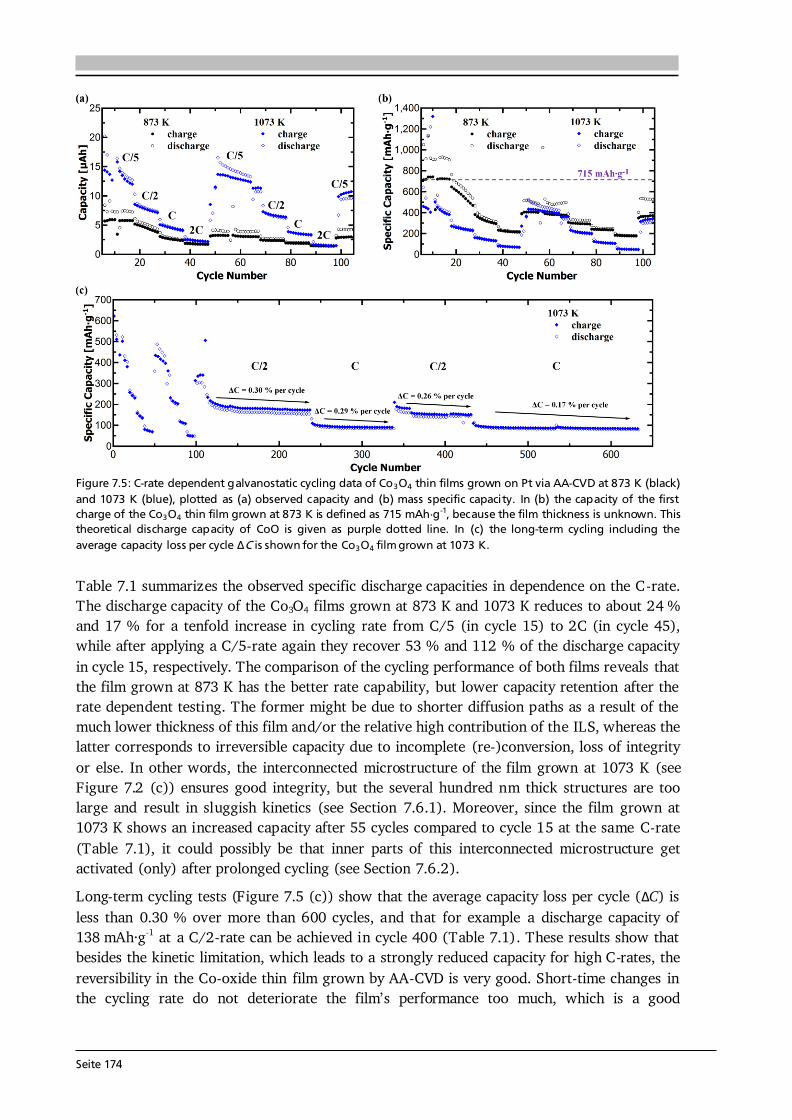
Seite 174
Figure 7.5: C-rate dependent galvanostatic cycling data of Co3O4 thin films grown on Pt via AA-CVD at 873 K (black) and 1073 K (blue), plotted as (a) observed capacity and (b) mass specific capacity. In (b) the capacity of the first charge of the Co3O4 thin film grown at 873 K is defined as 715 mAh·g -1, because the film thickness is unknown. This theoretical discharge capacity of CoO is given as purple dotted line. In (c) the long-term cycling including the average capacity loss per cycle ΔC is shown for the Co3O4 film grown at 1073 K. Table 7.1 summarizes the observed specific discharge capacities in dependence on the C-rate. The discharge capacity of the Co3O4 films grown at 873 K and 1073 K reduces to about 24 % and 17 % for a tenfold increase in cycling rate from C/5 (in cycle 15) to 2C (in cycle 45), while after applying a C/5-rate again they recover 53 % and 112 % of the discharge capacity in cycle 15, respectively. The comparison of the cycling performance of both films reveals that the film grown at 873 K has the better rate capability, but lower capacity retention after the rate dependent testing. The former might be due to shorter diffusion paths as a result of the much lower thickness of this film and/or the relative high contribution of the ILS, whereas the latter corresponds to irreversible capacity due to incomplete (re-)conversion, loss of integrity or else. In other words, the interconnected microstructure of the film grown at 1073 K (see Figure 7.2 (c)) ensures good integrity, but the several hundred nm thick structures are too large and result in sluggish kinetics (see Section 7.6.1). Moreover, since the film grown at 1073 K shows an increased capacity after 55 cycles compared to cycle 15 at the same C-rate (Table 7.1), it could possibly be that inner parts of this interconnected microstructure get activated (only) after prolonged cycling (see Section 7.6.2). Long-term cycling tests (Figure 7.5 (c)) show that the average capacity loss per cycle (ΔC) is less than 0.30 % over more than 600 cycles, and that for example a discharge capacity of 138 mAh·g-1 at a C/2-rate can be achieved in cycle 400 (Table 7.1). These results show that besides the kinetic limitation, which leads to a strongly reduced capacity for high C-rates, the reversibility in the Co-oxide thin film grown by AA-CVD is very good. Short-time changes in the cycling rate do not deteriorate the film’s performance too much, which is a good
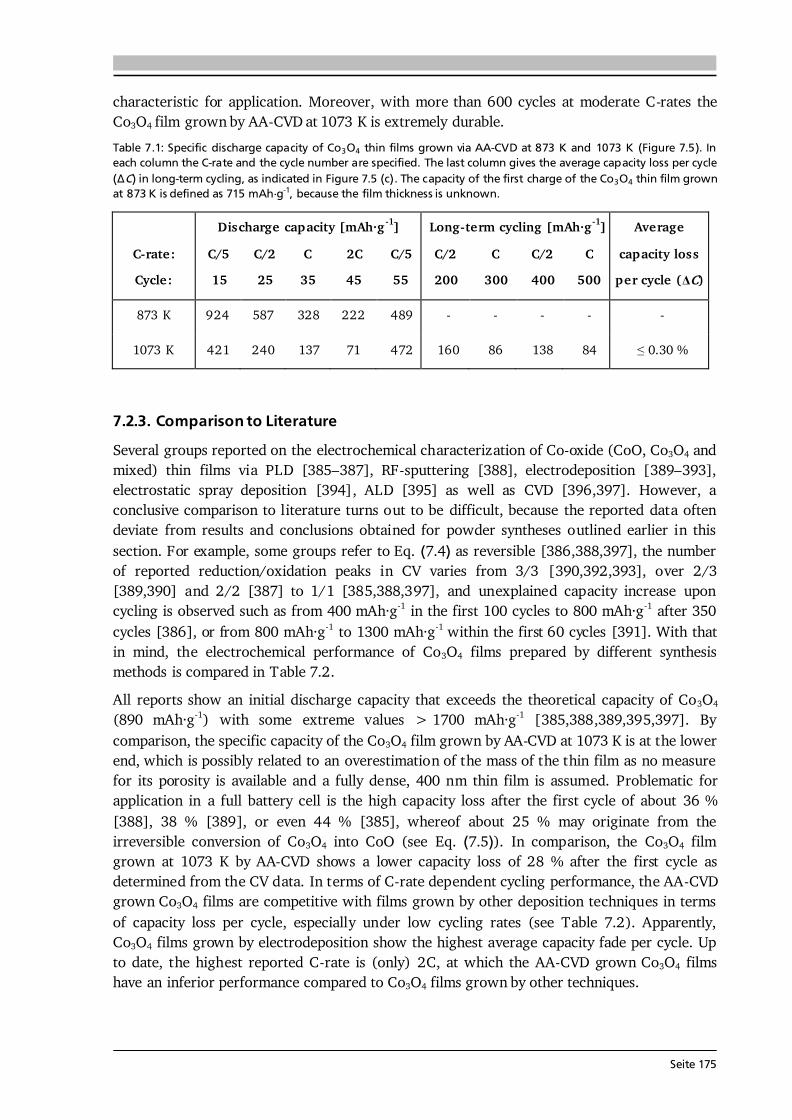
Seite 175
characteristic for application. Moreover, with more than 600 cycles at moderate C-rates the Co3O4 film grown by AA-CVD at 1073 K is extremely durable. Table 7.1: Specific discharge capacity of Co3O4 thin films grown via AA-CVD at 873 K and 1073 K (Figure 7.5). In each column the C-rate and the cycle number are specified. The last column gives the average capacity loss per cycle (ΔC) in long-term cycling, as indicated in Figure 7.5 (c). The capacity of the first charge of the Co3O4 thin film grown at 873 K is defined as 715 mAh·g-1, because the film thickness is unknown.
C-rate: Cycle:
Discharge capacity [mAh·g -1] C/5 C/2 C 2C C/5 15 25 35 45 55
Long-term cycling [mAh·g -1] C/2 C C/2 C 200 300 400 500
Average capacity loss
per cycle (ΔC) 873 K 924 587 328 222 489 - - - - -
1073 K 421 240 137 71 472 160 86 138 84 ≤ 0.30 % 7.2.3. Comparison to Literature Several groups reported on the electrochemical characterization of Co-oxide (CoO, Co3O4 and mixed) thin films via PLD [385–387], RF-sputtering [388], electrodeposition [389–393], electrostatic spray deposition [394], ALD [395] as well as CVD [396,397]. However, a conclusive comparison to literature turns out to be difficult, because the reported data often deviate from results and conclusions obtained for powder syntheses outlined earlier in this section. For example, some groups refer to Eq. (7.4) as reversible [386,388,397], the number of reported reduction/oxidation peaks in CV varies from 3/3 [390,392,393], over 2/3 [389,390] and 2/2 [387] to 1/1 [385,388,397], and unexplained capacity increase upon cycling is observed such as from 400 mAh·g-1 in the first 100 cycles to 800 mAh·g-1 after 350 cycles [386], or from 800 mAh·g-1 to 1300 mAh·g-1 within the first 60 cycles [391]. With that in mind, the electrochemical performance of Co3O4 films prepared by different synthesis methods is compared in Table 7.2. All reports show an initial discharge capacity that exceeds the theoretical capacity of Co3O4 (890 mAh·g-1) with some extreme values > 1700 mAh·g-1 [385,388,389,395,397]. By comparison, the specific capacity of the Co3O4 film grown by AA-CVD at 1073 K is at the lower end, which is possibly related to an overestimation of the mass of the thin film as no measure for its porosity is available and a fully dense, 400 nm thin film is assumed. Problematic for application in a full battery cell is the high capacity loss after the first cycle of about 36 % [388], 38 % [389], or even 44 % [385], whereof about 25 % may originate from the irreversible conversion of Co3O4 into CoO (see Eq. (7.5)). In comparison, the Co3O4 film grown at 1073 K by AA-CVD shows a lower capacity loss of 28 % after the first cycle as determined from the CV data. In terms of C-rate dependent cycling performance, the AA-CVD grown Co3O4 films are competitive with films grown by other deposition techniques in terms of capacity loss per cycle, especially under low cycling rates (see Table 7.2). Apparently, Co3O4 films grown by electrodeposition show the highest average capacity fade per cycle. Up to date, the highest reported C-rate is (only) 2C, at which the AA-CVD grown Co3O4 films have an inferior performance compared to Co3O4 films grown by other techniques.
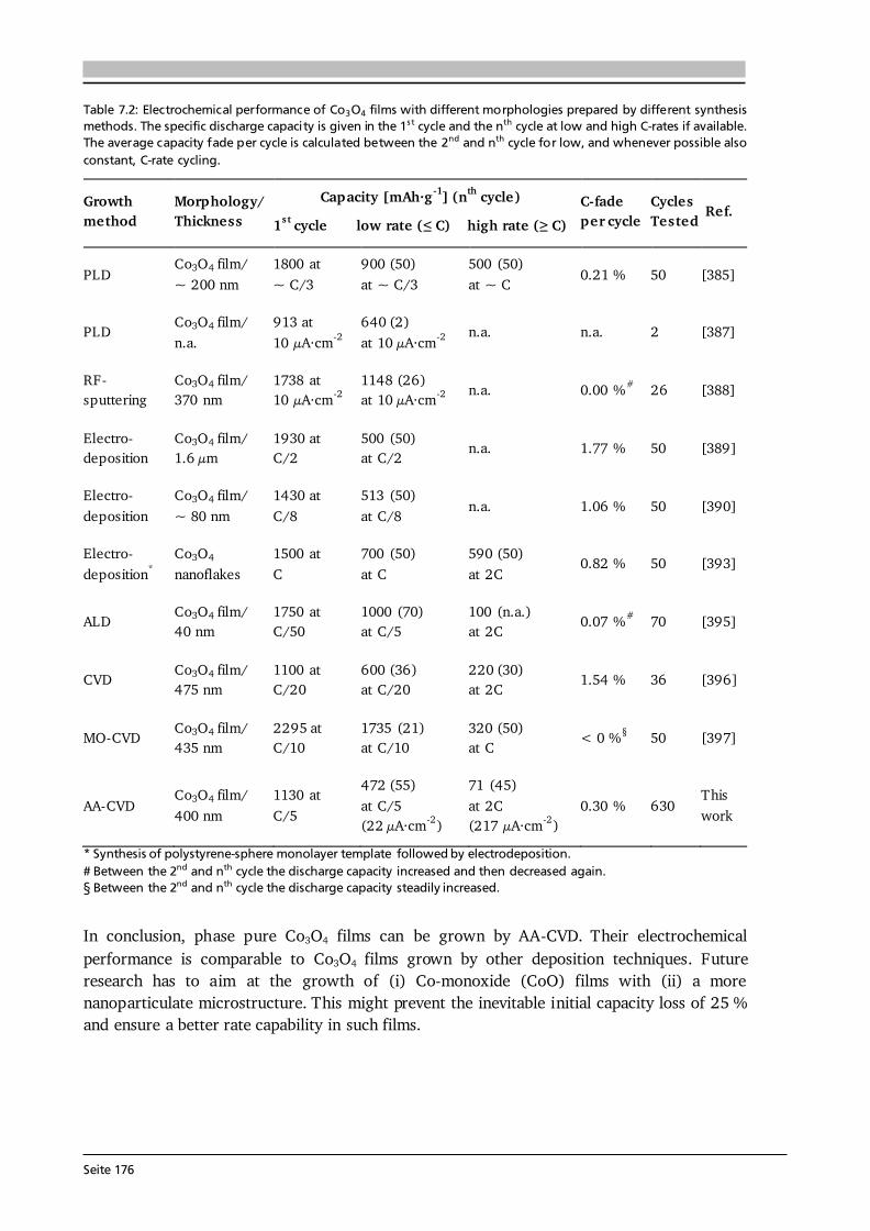
Seite 176
Table 7.2: Electrochemical performance of Co3O4 films with different morphologies prepared by different synthesis methods. The specific discharge capacity is given in the 1s t cycle and the nth cycle at low and high C-rates if available. The average capacity fade per cycle is calculated between the 2nd and nth cycle for low, and whenever possible also constant, C-rate cycling. Growth method Morphology/ Thickness
Capacity [mAh·g -1] (nth cycle) 1st cycle low rate (≤ C) high rate (≥ C)
C-fade per cycle Cycles Tested Ref.
PLD Co3O4 film/ ~ 200 nm 1800 at ~ C/3 900 (50) at ~ C/3 500 (50) at ~ C 0.21 % 50 [385] PLD Co3O4 film/ n.a. 913 at
10 μA·cm-2 640 (2) at 10 μA·cm-2 n.a. n.a. 2 [387]
RF- sputtering Co3O4 film/ 370 nm 1738 at 10 μA·cm-2 1148 (26)
at 10 μA·cm-2 n.a. 0.00 %# 26 [388] Electro- deposition Co3O4 film/
1.6 μm 1930 at C/2 500 (50) at C/2 n.a. 1.77 % 50 [389] Electro- deposition Co3O4 film/ ~ 80 nm 1430 at C/8 513 (50) at C/8 n.a. 1.06 % 50 [390] Electro-deposition* Co3O4 nanoflakes 1500 at C 700 (50) at C 590 (50) at 2C 0.82 % 50 [393] ALD Co3O4 film/ 40 nm 1750 at C/50 1000 (70) at C/5 100 (n.a.) at 2C 0.07 %# 70 [395] CVD Co3O4 film/ 475 nm 1100 at C/20 600 (36) at C/20 220 (30) at 2C 1.54 % 36 [396] MO-CVD Co3O4 film/ 435 nm 2295 at C/10 1735 (21) at C/10 320 (50) at C < 0 %§ 50 [397]
AA-CVD Co3O4 film/ 400 nm 1130 at C/5 472 (55) at C/5 (22 μA·cm-2)
71 (45) at 2C (217 μA·cm-2) 0.30 % 630 This work
* Synthesis of polystyrene-sphere monolayer template followed by electrodeposition. # Between the 2nd and nth cycle the discharge capacity increased and then decreased again. § Between the 2nd and nth cycle the discharge capacity steadily increased. In conclusion, phase pure Co3O4 films can be grown by AA-CVD. Their electrochemical performance is comparable to Co3O4 films grown by other deposition techniques. Future research has to aim at the growth of (i) Co-monoxide (CoO) films with (ii) a more nanoparticulate microstructure. This might prevent the inevitable initial capacity loss of 25 % and ensure a better rate capability in such films.
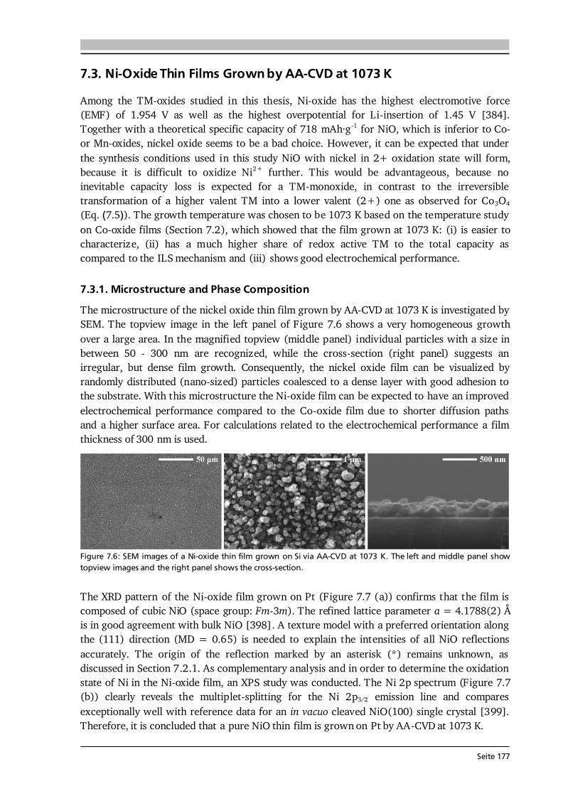
Seite 177
7.3. Ni-Oxide Thin Films Grown by AA-CVD at 1073 K Among the TM-oxides studied in this thesis, Ni-oxide has the highest electromotive force (EMF) of 1.954 V as well as the highest overpotential for Li-insertion of 1.45 V [384]. Together with a theoretical specific capacity of 718 mAh·g -1 for NiO, which is inferior to Co- or Mn-oxides, nickel oxide seems to be a bad choice. However, it can be expected that under the synthesis conditions used in this study NiO with nickel in 2+ oxidation state will form, because it is difficult to oxidize Ni2+ further. This would be advantageous, because no inevitable capacity loss is expected for a TM-monoxide, in contrast to the irreversible transformation of a higher valent TM into a lower valent (2+) one as observed for Co3O4 (Eq. (7.5)). The growth temperature was chosen to be 1073 K based on the temperature study on Co-oxide films (Section 7.2), which showed that the film grown at 1073 K: (i) is easier to characterize, (ii) has a much higher share of redox active TM to the total capacity as compared to the ILS mechanism and (iii) shows good electrochemical performance. 7.3.1. Microstructure and Phase Composition The microstructure of the nickel oxide thin film grown by AA-CVD at 1073 K is investigated by SEM. The topview image in the left panel of Figure 7.6 shows a very homogeneous growth over a large area. In the magnified topview (middle panel) individual particles with a size in between 50 - 300 nm are recognized, while the cross-section (right panel) suggests an irregular, but dense film growth. Consequently, the nickel oxide film can be visualized by randomly distributed (nano-sized) particles coalesced to a dense layer with good adhesion to the substrate. With this microstructure the Ni-oxide film can be expected to have an improved electrochemical performance compared to the Co-oxide film due to shorter diffusion paths and a higher surface area. For calculations related to the electrochemical performance a film thickness of 300 nm is used.
Figure 7.6: SEM images of a Ni-oxide thin film grown on Si via AA-CVD at 1073 K. The left and middle panel show topview images and the right panel shows the cross-section. The XRD pattern of the Ni-oxide film grown on Pt (Figure 7.7 (a)) confirms that the film is composed of cubic NiO (space group: Fm-3m). The refined lattice parameter a = 4.1788(2) Å is in good agreement with bulk NiO [398]. A texture model with a preferred orientation along the (111) direction (MD = 0.65) is needed to explain the intensities of all NiO reflections accurately. The origin of the reflection marked by an asterisk (*) remains unknown, as discussed in Section 7.2.1. As complementary analysis and in order to determine the oxidation state of Ni in the Ni-oxide film, an XPS study was conducted. The Ni 2p spectrum (Figure 7.7 (b)) clearly reveals the multiplet-splitting for the Ni 2p3/2 emission line and compares exceptionally well with reference data for an in vacuo cleaved NiO(100) single crystal [399]. Therefore, it is concluded that a pure NiO thin film is grown on Pt by AA-CVD at 1073 K.
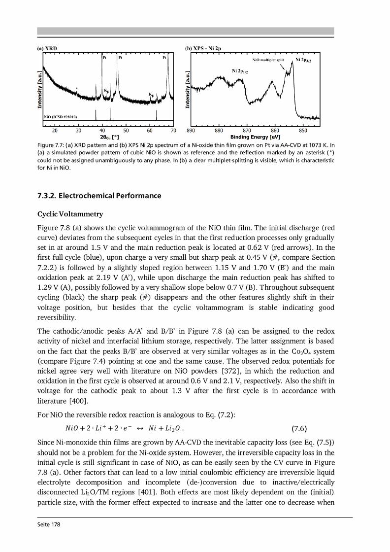
Seite 178
Figure 7.7: (a) XRD pattern and (b) XPS Ni 2p spectrum of a Ni-oxide thin film grown on Pt via AA-CVD at 1073 K. In (a) a simulated powder pattern of cubic NiO is shown as reference and the reflection marked by an asterisk (*) could not be assigned unambiguously to any phase. In (b) a clear multiplet-splitting is visible, which is characteristic for Ni in NiO.
7.3.2. Electrochemical Performance Cyclic Voltammetry Figure 7.8 (a) shows the cyclic voltammogram of the NiO thin film. The initial discharge (red curve) deviates from the subsequent cycles in that the first reduction processes only gradually set in at around 1.5 V and the main reduction peak is located at 0.62 V (red arrows). In the first full cycle (blue), upon charge a very small but sharp peak at 0.45 V (#, compare Section 7.2.2) is followed by a slightly sloped region between 1.15 V and 1.70 V (B’) and the main oxidation peak at 2.19 V (A’), while upon discharge the main reduction peak has shifted to 1.29 V (A), possibly followed by a very shallow slope below 0.7 V (B). Throughout subsequent cycling (black) the sharp peak (#) disappears and the other features slightly shift in their voltage position, but besides that the cyclic voltammogram is stable indicating good reversibility. The cathodic/anodic peaks A/A’ and B/B’ in Figure 7.8 (a) can be assigned to the redox activity of nickel and interfacial lithium storage, respectively. The latter assignment is based on the fact that the peaks B/B’ are observed at very similar voltages as in the Co3O4 system (compare Figure 7.4) pointing at one and the same cause. The observed redox potentials for nickel agree very well with literature on NiO powders [372], in which the reduction and oxidation in the first cycle is observed at around 0.6 V and 2.1 V, respectively. Also the shift in voltage for the cathodic peak to about 1.3 V after the first cycle is in accordance with literature [400]. For NiO the reversible redox reaction is analogous to Eq. (7.2): . (7.6) Since Ni-monoxide thin films are grown by AA-CVD the inevitable capacity loss (see Eq. (7.5)) should not be a problem for the Ni-oxide system. However, the irreversible capacity loss in the initial cycle is still significant in case of NiO, as can be easily seen by the CV curve in Figure 7.8 (a). Other factors that can lead to a low initial coulombic efficiency are irreversible liquid electrolyte decomposition and incomplete (de-)conversion due to inactive/electrically disconnected Li2O/TM regions [401]. Both effects are most likely dependent on the (initial) particle size, with the former effect expected to increase and the latter one to decrease when
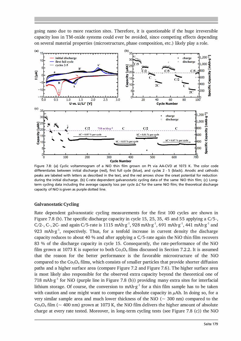
Seite 179
going nano due to more reaction sites. Therefore, it is questionable if the huge irreversible capacity loss in TM-oxide systems could ever be avoided, since competing effects depending on several material properties (microstructure, phase composition, etc.) likely play a role.
Figure 7.8: (a) Cyclic voltammogram of a NiO thin film grown on Pt via AA-CVD at 1073 K. The color code differentiates between initial discharge (red), first full cycle (blue), and cycles 2 - 5 (black). Anodic and cathodic peaks are labeled with letters as described in the text, and the red arrows show the onset potential for reduction during the initial discharge. (b) C-rate dependent galvanostatic cycling data of the same NiO thin film; (c) Long-term cycling data including the average capacity loss per cycle ΔC for the same NiO film; the theoretical discharge capacity of NiO is given as purple dotted line.
Galvanostatic Cycling Rate dependent galvanostatic cycling measurements for the first 100 cycles are shown in Figure 7.8 (b). The specific discharge capacity in cycle 15, 25, 35, 45 and 55 applying a C/5-, C/2-, C-, 2C- and again C/5-rate is 1115 mAh·g-1, 928 mAh·g-1, 691 mAh·g-1, 441 mAh·g-1 and 923 mAh·g-1, respectively. Thus, for a tenfold increase in current density the discharge capacity reduces to about 40 % and after applying a C/5-rate again the NiO thin film recovers 83 % of the discharge capacity in cycle 15. Consequently, the rate-performance of the NiO film grown at 1073 K is superior to both Co3O4 films discussed in Section 7.2.2. It is assumed that the reason for the better performance is the favorable microstructure of the NiO compared to the Co3O4 films, which consists of smaller particles that provide shorter diffusion paths and a higher surface area (compare Figure 7.2 and Figure 7.6). The higher surface area is most likely also responsible for the observed extra capacity beyond the theoretical one of 718 mAh·g-1 for NiO (purple line in Figure 7.8 (b)) providing many extra sites for interfacial lithium storage. Of course, the conversion to mAh·g-1 for a thin film sample has to be taken with caution and one might want to compare the absolute capacity in μAh. In doing so, for a very similar sample area and much lower thickness of the NiO (~ 300 nm) compared to the Co3O4 film (~ 400 nm) grown at 1073 K, the NiO film delivers the higher amount of absolute charge at every rate tested. Moreover, in long-term cycling tests (see Figure 7.8 (c)) the NiO

Seite 180
film performs superior to the Co3O4 film. After several hundred cycles remarkable discharge capacities of ~ 500 mAh·g-1 and ~ 300 mAh·g-1 at C-rates of C/2 and C are achieved, respectively. The average capacity fade per cycle is 0.15 % or lower (see Figure 7.8 (c)) and with more than 700 cycles tested this NiO film shows excellent durability. 7.3.3. Comparison to Literature As for Co3O4 thin films (see Section 7.2.3), the comparison to literature on NiO films turns out to be very difficult due to a large spread and scattering of values reported for rate capability and long-term cycling depending on the growth method. For example, NiO films grown by electrodeposition show two or three redox couples [402–405], although only one is expected for the conversion reaction in NiO and maybe a second one for the ILS, thus leaving the third one unexplained. Moreover, some excellent, yet controversial, performances of about 3500 mAh·g-1 (~ 1700 mAh·g-1) as initial (reversible) discharge capacity [404] as well as capacities of 990 mAh·g-1 [404] and 695 mAh·g-1 [406] at C-rates as high as 15C and 14C, respectively, are reported (see Table 7.3). Such high capacities and rate capabilities are typically (only) achieved for films grown on 3D substrates like Ni mesh [406], Ni foam [403,407,408], or a nanostructured, polystyrene-sphere monolayer template [404,405] (lower half of Table 7.3). Among the few reports dealing with NiO films grown on planar (2D) substrates by PLD [409], thermal evaporation [410] and RF-sputtering [411] (upper half of Table 7.3), the NiO film grown at 1073 K by AA-CVD performs quite well in terms of long-term cycling as well as rate capability. For example, it delivers a similar capacity to the NiO film grown by thermal evaporation (440 mAh·g-1, [410]) at a 5.5 times higher current density of 445 μA·cm-2. In conclusion, phase pure NiO films can be grown by AA-CVD. Their electrochemical performance is superior to NiO films grown by other deposition techniques on 2D substrates. Here, it has to be considered that the “optimized growth parameters” of LiCoO2 film growth are used, thus a further optimization in terms of microstructure and consequently electrochemical performance seems possible. Also the use of 3D substrates may be targeted in future experiments in order to shorten Li-ion diffusion paths and by this increase the rate capability, motivated by excellent results reported in the literature (lower half of Table 7.3).
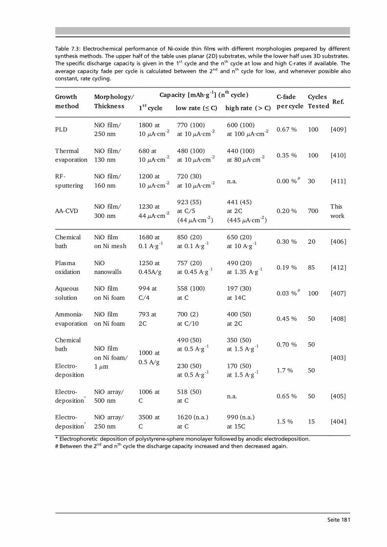
Seite 181
Table 7.3: Electrochemical performance of Ni-oxide thin films with different morphologies prepared by different synthesis methods. The upper half of the table uses planar (2D) substrates, while the lower half uses 3D substrates. The specific discharge capacity is given in the 1s t cycle and the nth cycle at low and high C-rates if available. The average capacity fade per cycle is calculated between the 2nd and nth cycle for low, and whenever possible also constant, rate cycling. Growth method Morphology/ Thickness
Capacity [mAh·g -1] (nth cycle) 1st cycle low rate (≤ C) high rate (> C)
C-fade per cycle Cycles Tested Ref.
PLD NiO film/ 250 nm 1800 at 10 μA·cm-2 770 (100) at 10 μA·cm-2 600 (100) at 100 μA·cm-2 0.67 % 100 [409]
Thermal evaporation NiO film/ 130 nm 680 at 10 μA·cm-2 480 (100) at 10 μA·cm-2 440 (100) at 80 μA·cm-2 0.35 % 100 [410] RF- sputtering NiO film/ 160 nm 1200 at 10 μA·cm-2 720 (30) at 10 μA·cm-2 n.a. 0.00 %# 30 [411]
AA-CVD NiO film/ 300 nm 1230 at 44 μA·cm-2
923 (55) at C/5 (44 μA·cm-2) 441 (45) at 2C (445 μA·cm-2) 0.20 % 700 This work
Chemical bath NiO film on Ni mesh 1680 at 0.1 A·g -1 850 (20) at 0.1 A·g -1 650 (20) at 10 A·g -1 0.30 % 20 [406] Plasma oxidation NiO nanowalls 1250 at 0.45A/g 757 (20) at 0.45 A·g -1 490 (20) at 1.35 A·g -1 0.19 % 85 [412] Aqueous solution NiO film on Ni foam 994 at C/4 558 (100) at C 197 (30) at 14C 0.03 %# 100 [407] Ammonia- evaporation NiO film on Ni foam 793 at 2C 700 (2) at C/10 400 (50) at 2C 0.45 % 50 [408] Chemical bath NiO film on Ni foam/
1 μm 1000 at 0.5 A/g
490 (50) at 0.5 A·g -1 350 (50) at 1.5 A·g -1 0.70 % 50 [403] Electro- deposition 230 (50) at 0.5 A·g -1 170 (50) at 1.5 A·g -1 1.7 % 50
Electro-deposition* NiO array/ 500 nm 1006 at C 518 (50) at C n.a. 0.65 % 50 [405] Electro-deposition* NiO array/ 250 nm 3500 at C 1620 (n.a.) at C 990 (n.a.) at 15C 1.5 % 15 [404] * Electrophoretic deposition of polystyrene-sphere monolayer followed by anodic electrodeposition. # Between the 2nd and nth cycle the discharge capacity increased and then decreased again.
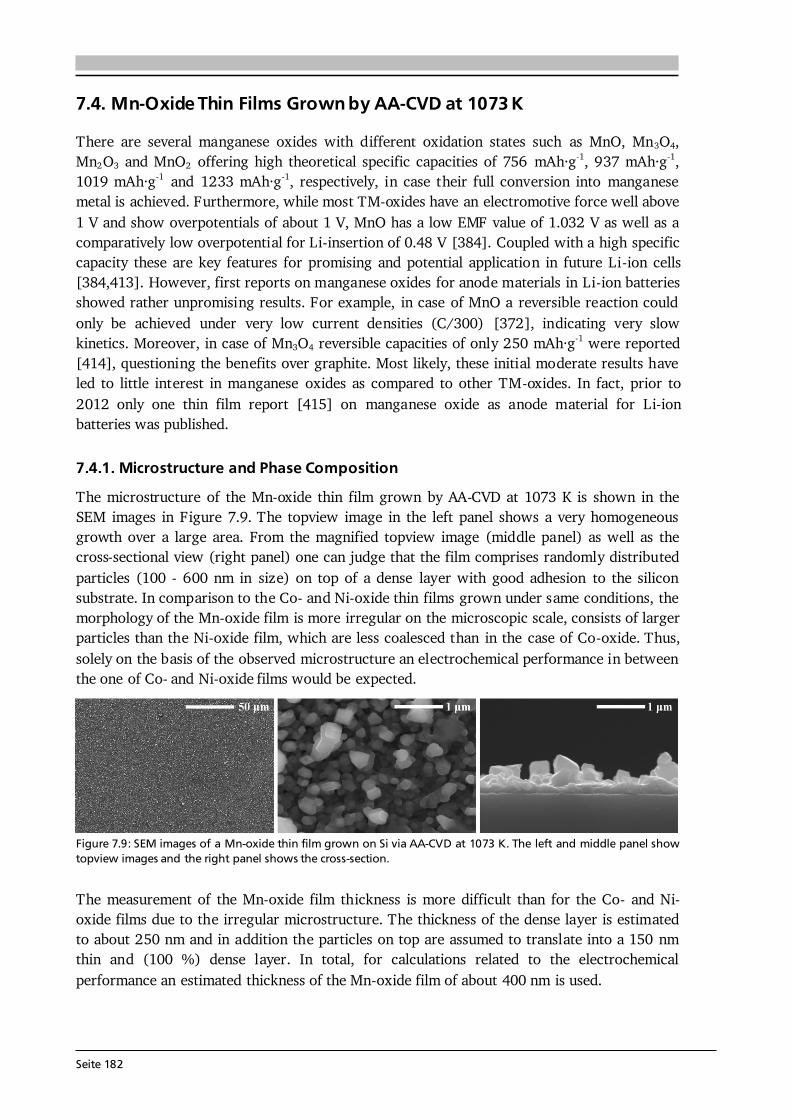
Seite 182
7.4. Mn-Oxide Thin Films Grown by AA-CVD at 1073 K There are several manganese oxides with different oxidation states such as MnO, Mn3O4, Mn2O3 and MnO2 offering high theoretical specific capacities of 756 mAh·g-1, 937 mAh·g-1, 1019 mAh·g-1 and 1233 mAh·g-1, respectively, in case their full conversion into manganese metal is achieved. Furthermore, while most TM-oxides have an electromotive force well above 1 V and show overpotentials of about 1 V, MnO has a low EMF value of 1.032 V as well as a comparatively low overpotential for Li-insertion of 0.48 V [384]. Coupled with a high specific capacity these are key features for promising and potential application in future Li-ion cells [384,413]. However, first reports on manganese oxides for anode materials in Li-ion batteries showed rather unpromising results. For example, in case of MnO a reversible reaction could only be achieved under very low current densities (C/300) [372], indicating very slow kinetics. Moreover, in case of Mn3O4 reversible capacities of only 250 mAh·g-1 were reported [414], questioning the benefits over graphite. Most likely, these initial moderate results have led to little interest in manganese oxides as compared to other TM-oxides. In fact, prior to 2012 only one thin film report [415] on manganese oxide as anode material for Li-ion batteries was published. 7.4.1. Microstructure and Phase Composition The microstructure of the Mn-oxide thin film grown by AA-CVD at 1073 K is shown in the SEM images in Figure 7.9. The topview image in the left panel shows a very homogeneous growth over a large area. From the magnified topview image (middle panel) as well as the cross-sectional view (right panel) one can judge that the film comprises randomly distributed particles (100 - 600 nm in size) on top of a dense layer with good adhesion to the silicon substrate. In comparison to the Co- and Ni-oxide thin films grown under same conditions, the morphology of the Mn-oxide film is more irregular on the microscopic scale, consists of larger particles than the Ni-oxide film, which are less coalesced than in the case of Co-oxide. Thus, solely on the basis of the observed microstructure an electrochemical performance in between the one of Co- and Ni-oxide films would be expected.
Figure 7.9: SEM images of a Mn-oxide thin film grown on Si via AA-CVD at 1073 K. The left and middle panel show topview images and the right panel shows the cross-section. The measurement of the Mn-oxide film thickness is more difficult than for the Co- and Ni-oxide films due to the irregular microstructure. The thickness of the dense layer is estimated to about 250 nm and in addition the particles on top are assumed to translate into a 150 nm thin and (100 %) dense layer. In total, for calculations related to the electrochemical performance an estimated thickness of the Mn-oxide film of about 400 nm is used.
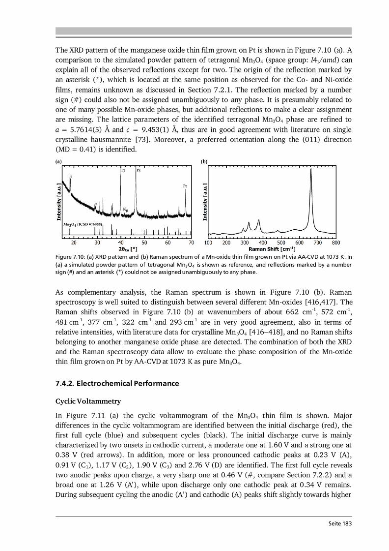
Seite 183
The XRD pattern of the manganese oxide thin film grown on Pt is shown in Figure 7.10 (a). A comparison to the simulated powder pattern of tetragonal Mn3O4 (space group: I41/amd) can explain all of the observed reflections except for two. The origin of the reflection marked by an asterisk (*), which is located at the same position as observed for the Co- and Ni-oxide films, remains unknown as discussed in Section 7.2.1. The reflection marked by a number sign (#) could also not be assigned unambiguously to any phase. It is presumably related to one of many possible Mn-oxide phases, but additional reflections to make a clear assignment are missing. The lattice parameters of the identified tetragonal Mn3O4 phase are refined to a = 5.7614(5) Å and c = 9.453(1) Å, thus are in good agreement with literature on single crystalline hausmannite [73]. Moreover, a preferred orientation along the (011) direction (MD = 0.41) is identified.
Figure 7.10: (a) XRD pattern and (b) Raman spectrum of a Mn-oxide thin film grown on Pt via AA-CVD at 1073 K. In (a) a simulated powder pattern of tetragonal Mn3O4 is shown as reference, and reflections marked by a number sign (#) and an asterisk (*) could not be assigned unambiguously to any phase. As complementary analysis, the Raman spectrum is shown in Figure 7.10 (b). Raman spectroscopy is well suited to distinguish between several different Mn-oxides [416,417]. The Raman shifts observed in Figure 7.10 (b) at wavenumbers of about 662 cm-1, 572 cm-1, 481 cm-1, 377 cm-1, 322 cm-1 and 293 cm-1 are in very good agreement, also in terms of relative intensities, with literature data for crystalline Mn3O4 [416–418], and no Raman shifts belonging to another manganese oxide phase are detected. The combination of both the XRD and the Raman spectroscopy data allow to evaluate the phase composition of the Mn-oxide thin film grown on Pt by AA-CVD at 1073 K as pure Mn3O4. 7.4.2. Electrochemical Performance Cyclic Voltammetry In Figure 7.11 (a) the cyclic voltammogram of the Mn3O4 thin film is shown. Major differences in the cyclic voltammogram are identified between the initial discharge (red), the first full cycle (blue) and subsequent cycles (black). The initial discharge curve is mainly characterized by two onsets in cathodic current, a moderate one at 1.60 V and a strong one at 0.38 V (red arrows). In addition, more or less pronounced cathodic peaks at 0.23 V (A), 0.91 V (C1), 1.17 V (C2), 1.90 V (C3) and 2.76 V (D) are identified. The first full cycle reveals two anodic peaks upon charge, a very sharp one at 0.46 V (#, compare Section 7.2.2) and a broad one at 1.26 V (A’), while upon discharge only one cathodic peak at 0.34 V remains. During subsequent cycling the anodic (A’) and cathodic (A) peaks shift slightly towards higher
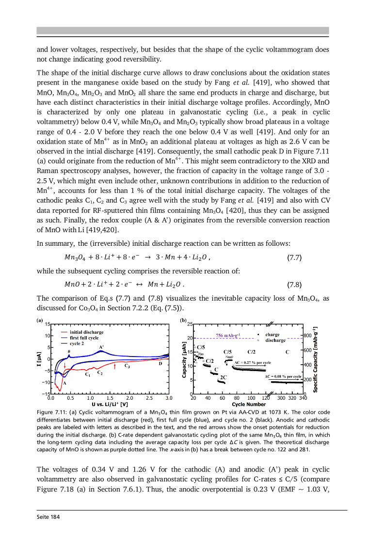
Seite 184
and lower voltages, respectively, but besides that the shape of the cyclic voltammogram does not change indicating good reversibility. The shape of the initial discharge curve allows to draw conclusions about the oxidation states present in the manganese oxide based on the study by Fang et al. [419], who showed that MnO, Mn3O4, Mn2O3 and MnO2 all share the same end products in charge and discharge, but have each distinct characteristics in their initial discharge voltage profiles. Accordingly, MnO is characterized by only one plateau in galvanostatic cycling (i.e., a peak in cyclic voltammetry) below 0.4 V, while Mn3O4 and Mn2O3 typically show broad plateaus in a voltage range of 0.4 - 2.0 V before they reach the one below 0.4 V as well [419]. And only for an oxidation state of Mn4+ as in MnO2 an additional plateau at voltages as high as 2.6 V can be observed in the intial discharge [419]. Consequently, the small cathodic peak D in Figure 7.11 (a) could originate from the reduction of Mn4+. This might seem contradictory to the XRD and Raman spectroscopy analyses, however, the fraction of capacity in the voltage range of 3.0 - 2.5 V, which might even include other, unknown contributions in addition to the reduction of Mn4+, accounts for less than 1 % of the total initial discharge capacity. The voltages of the cathodic peaks C1, C2 and C3 agree well with the study by Fang et al. [419] and also with CV data reported for RF-sputtered thin films containing Mn3O4 [420], thus they can be assigned as such. Finally, the redox couple (A & A’) originates from the reversible conversion reaction of MnO with Li [419,420]. In summary, the (irreversible) initial discharge reaction can be written as follows: , (7.7) while the subsequent cycling comprises the reversible reaction of: . (7.8) The comparison of Eq.s (7.7) and (7.8) visualizes the inevitable capacity loss of Mn3O4, as discussed for Co3O4 in Section 7.2.2 (Eq. (7.5)).
Figure 7.11: (a) Cyclic voltammogram of a Mn3O4 thin film grown on Pt via AA-CVD at 1073 K. The color code differentiates between initial discharge (red), first full cycle (blue), and cycle no. 2 (black). Anodic and cathodic peaks are labeled with letters as described in the text, and the red arrows show the onset potentials for reduction during the initial discharge. (b) C-rate dependent galvanostatic cycling plot of the same Mn3O4 thin film, in which the long-term cycling data including the average capacity loss per cycle ΔC is given. The theoretical discharge capacity of MnO is shown as purple dotted line. The x-axis in (b) has a break between cycle no. 122 and 281.
The voltages of 0.34 V and 1.26 V for the cathodic (A) and anodic (A’) peak in cyclic voltammetry are also observed in galvanostatic cycling profiles for C-rates C/5 (compare Figure 7.18 (a) in Section 7.6.1). Thus, the anodic overpotential is 0.23 V (EMF ~ 1.03 V,
Seite 185
[384]) and as such in very good agreement with results reported for other manganese oxide thin films [418,420–422]. However, the voltage hysteresis (i.e., the sum of anodic and cathodic overpotentials) is 0.92 V for the AA-CVD grown Mn3O4 film and with that much higher than the 0.60 - 0.75 V observed in the literature for Mn-oxide films [418,420–422]. This voltage hysteresis has a thermodynamic (so-called zero-current overpotential, [423]) as well as kinetic contribution, and the former was determined to account for 0.6 V and 0.8 V in PLD-grown MnO thin films [421] and porous MnO powder samples [424], respectively. Apparently, thin films can be beneficial to reduce the voltage hysteresis in Mn-oxide, but the conclusion for the AA-CVD grown Mn-oxide film discussed here is that the lithiation process is kinetically inhibited. Galvanostatic Cycling In order to assess how strong the kinetics affect the cycling performance C-rate dependent galvanostatic cycling measurements are performed (Figure 7.11 (b)). The discharge capacity in cycle 25, 35, 45, 55 and 65 applying a C/5-, C/2-, C-, 2C- and again C/5-rate is 574 mAh·g-1, 408 mAh·g-1, 292 mAh·g-1, 172 mAh·g-1 and 510 mAh·g-1, respectively. Thus, for a tenfold increase in current density the discharge capacity reduces to about 30 % and after applying a C/5-rate again this Mn3O4 thin film recovers 89 % of the discharge capacity in cycle 25. On average the cell lost 0.30 % of its capacity per cycle during the C-rate dependent testing between cycle 25 and 65, which compares quite well with the Co3O4 and NiO thin films grown under similar conditions. In fact, the performance of the Mn3O4 film lies in between the ones of the Co3O4 and NiO films, just as its microstructure lies in between the ones of the Co- and Ni-oxide films in terms of nanostructure. In long-term cycling tests (see Figure 7.11 (b)), the average capacity loss per cycle is 0.27 % (cycles 75 - 174) and 0.08 % (cycles 175 - 345) at a rate of C/2 and C, respectively. Discharge capacities of ~ 340 mAh·g-1 (at C/2) and ~ 170 mAh·g-1 (at C) are achieved. These results show that besides the kinetic limitation, which leads to a strongly reduced capacity for high C-rates, the capacity retention in the Mn-oxide thin film grown by AA-CVD is very good. With more than 300 cycles tested this Mn-oxide film is highly durable. 7.4.3. Comparison to Literature In contrast to Co3O4 and NiO thin films, there is only one literature report [420] on a RF-sputtered Mn3O4 thin film to compare the present study with (see Table 7.4). Because this film was only tested for 15 cycles [420], Table 7.4 lists also two more Mn-monoxide thin films as well as literature data on Mn3O4 powders. Overall, the AA-CVD grown Mn3O4 thin film compares well with literature. With a discharge capacity of 510 mAh·g-1 measured at a rate of C/5 in cycle 65 it performs superior to the sputtered Mn3O4 thin film [420], the first MnO thin film report by Yu et al. [415], and the Mn3O4 powder [414] as well as nanorods [425]. On the other hand, for high cycling rates the performance of the AA-CVD grown Mn3O4 thin film is inferior to the MnO thin films and the Mn3O4 octahedra (see Table 7.4). It shall be noted that there are several studies on Mn-oxide powders using different microstructures and also (nanostructured) composites with carbon (see [426] for a review). The few so far reported Mn-oxide thin film anodes (e.g., 4 of MnO [415,420–422] and 2 of Mn3O4 [420], including this work) all perform quite well in comparison to many nanostructured and/or carbonaceous composite Mn-oxide powders (see [426]). This is an encouraging observation for further thin
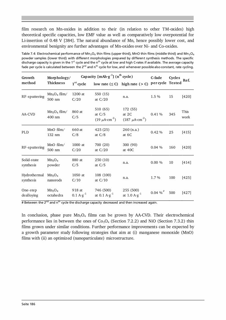
Seite 186
film research on Mn-oxides in addition to their (in relation to other TM-oxides) high theoretical specific capacities, low EMF value as well as comparatively low overpotential for Li-insertion of 0.48 V [384]. The natural abundance of Mn, hence possibly lower cost, and environmental benignity are further advantages of Mn-oxides over Ni- and Co-oxides. Table 7.4: Electrochemical performance of Mn3O4 thin films (upper third), MnO thin films (middle third) and Mn3O4 powder samples (lower third) with different morphologies prepared by different synthesis methods. The specific discharge capacity is given in the 1s t cycle and the nth cycle at low and high C-rates if available. The average capacity fade per cycle is calculated between the 2nd and nth cycle for low, and whenever possible also constant, rate cycling. Growth method Morphology/ Thickness
Capacity [mAh·g -1] (nth cycle) 1st cycle low rate (≤ C) high rate (> C)
C-fade per cycle Cycles Tested Ref.
RF-sputtering Mn3O4 film/ 500 nm 1200 at C/20 550 (15) at C/20 n.a. 1.5 % 15 [420]
AA-CVD Mn3O4 film/ 400 nm 860 at C/5 510 (65) at C/5 (19 μA·cm-2)
172 (55) at 2C (187 μA·cm-2) 0.41 % 345 This work PLD MnO film/ 132 nm 660 at C/8 425 (25) at C/8 260 (n.a.) at 6C 0.42 % 25 [415] RF-sputtering MnO film/ 500 nm 1000 at C/20 700 (20) at C/20 300 (90) at 40C 0.04 % 160 [420] Solid-state synthesis Mn3O4 powder 880 at C/5 250 (10) at C/5 n.a. 0.00 % 10 [414] Hydrothermal synthesis Mn3O4 nanorods 1050 at C/10 108 (100) at C/10 n.a. 1.7 % 100 [425] One-step dealloying Mn3O4 octahedra 918 at 0.1 A·g -1 746 (500) at 0.1 A·g -1 255 (500) at 1.0 A·g -1 0.04 %# 500 [427] # Between the 2nd and nth cycle the discharge capacity decreased and then increased again. In conclusion, phase pure Mn3O4 films can be grown by AA-CVD. Their electrochemical performance lies in between the ones of Co3O4 (Section 7.2.2) and NiO (Section 7.3.2) thin films grown under similar conditions. Further performance improvements can be expected by a growth parameter study following strategies that aim at (i) manganese monoxide (MnO) films with (ii) an optimized (nanoparticulate) microstructure.
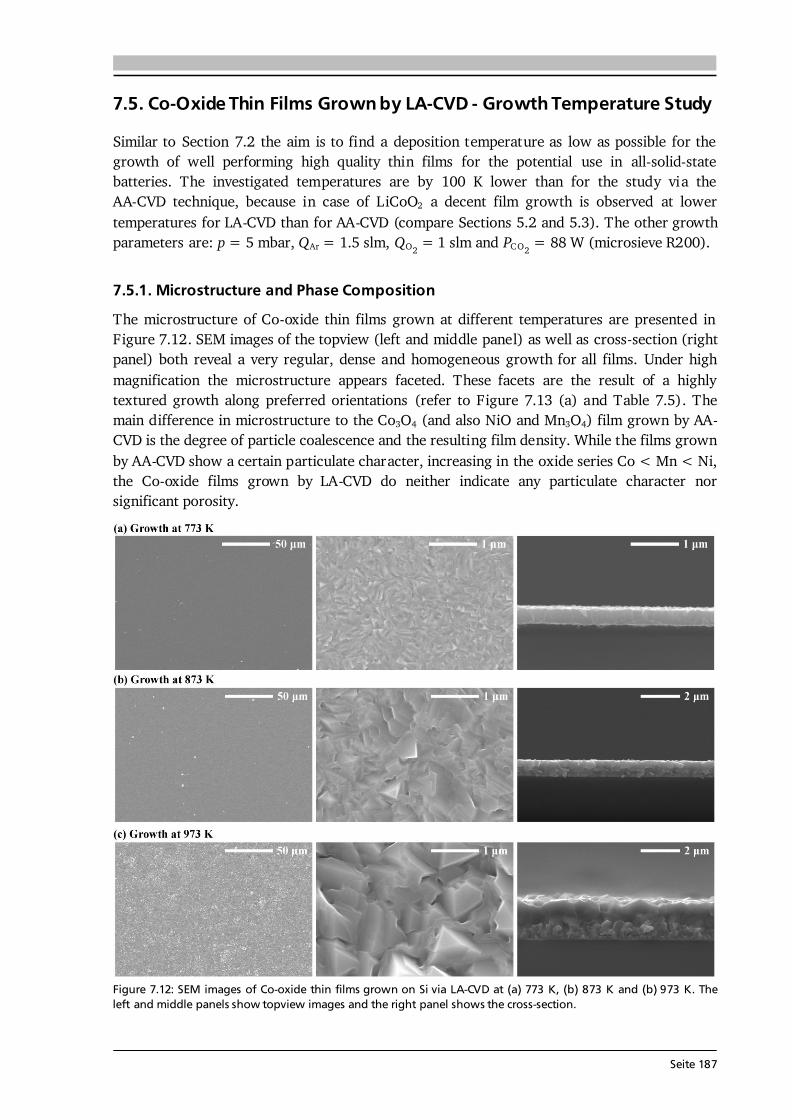
Seite 187
7.5. Co-Oxide Thin Films Grown by LA-CVD - Growth Temperature Study Similar to Section 7.2 the aim is to find a deposition temperature as low as possible for the growth of well performing high quality thin films for the potential use in all-solid-state batteries. The investigated temperatures are by 100 K lower than for the study via the AA-CVD technique, because in case of LiCoO2 a decent film growth is observed at lower temperatures for LA-CVD than for AA-CVD (compare Sections 5.2 and 5.3). The other growth parameters are: p = 5 mbar, QAr = 1.5 slm, QO2 = 1 slm and PC O2 = 88 W (microsieve R200). 7.5.1. Microstructure and Phase Composition The microstructure of Co-oxide thin films grown at different temperatures are presented in Figure 7.12. SEM images of the topview (left and middle panel) as well as cross-section (right panel) both reveal a very regular, dense and homogeneous growth for all films. Under high magnification the microstructure appears faceted. These facets are the result of a highly textured growth along preferred orientations (refer to Figure 7.13 (a) and Table 7.5). The main difference in microstructure to the Co3O4 (and also NiO and Mn3O4) film grown by AA-CVD is the degree of particle coalescence and the resulting film density. While the films grown by AA-CVD show a certain particulate character, increasing in the oxide series Co < Mn < Ni, the Co-oxide films grown by LA-CVD do neither indicate any particulate character nor significant porosity.
Figure 7.12: SEM images of Co-oxide thin films grown on Si via LA-CVD at (a) 773 K, (b) 873 K and (b) 973 K. The left and middle panels show topview images and the right panel shows the cross-section.
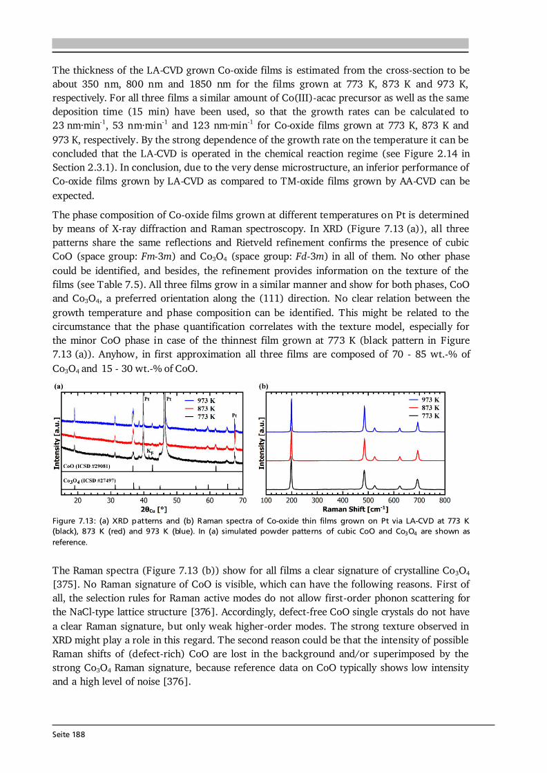
Seite 188
The thickness of the LA-CVD grown Co-oxide films is estimated from the cross-section to be about 350 nm, 800 nm and 1850 nm for the films grown at 773 K, 873 K and 973 K, respectively. For all three films a similar amount of Co(III)-acac precursor as well as the same deposition time (15 min) have been used, so that the growth rates can be calculated to 23 nm·min-1, 53 nm·min-1 and 123 nm·min-1 for Co-oxide films grown at 773 K, 873 K and 973 K, respectively. By the strong dependence of the growth rate on the temperature it can be concluded that the LA-CVD is operated in the chemical reaction regime (see Figure 2.14 in Section 2.3.1). In conclusion, due to the very dense microstructure, an inferior performance of Co-oxide films grown by LA-CVD as compared to TM-oxide films grown by AA-CVD can be expected. The phase composition of Co-oxide films grown at different temperatures on Pt is determined by means of X-ray diffraction and Raman spectroscopy. In XRD (Figure 7.13 (a)), all three patterns share the same reflections and Rietveld refinement confirms the presence of cubic CoO (space group: Fm-3m) and Co3O4 (space group: Fd-3m) in all of them. No other phase could be identified, and besides, the refinement provides information on the texture of the films (see Table 7.5). All three films grow in a similar manner and show for both phases, CoO and Co3O4, a preferred orientation along the (111) direction. No clear relation between the growth temperature and phase composition can be identified. This might be related to the circumstance that the phase quantification correlates with the texture model, especially for the minor CoO phase in case of the thinnest film grown at 773 K (black pattern in Figure 7.13 (a)). Anyhow, in first approximation all three films are composed of 70 - 85 wt.-% of Co3O4 and 15 - 30 wt.-% of CoO.
Figure 7.13: (a) XRD patterns and (b) Raman spectra of Co-oxide thin films grown on Pt via LA-CVD at 773 K (black), 873 K (red) and 973 K (blue). In (a) simulated powder patterns of cubic CoO and Co3O4 are shown as reference. The Raman spectra (Figure 7.13 (b)) show for all films a clear signature of crystalline Co3O4 [375]. No Raman signature of CoO is visible, which can have the following reasons. First of all, the selection rules for Raman active modes do not allow first-order phonon scattering for the NaCl-type lattice structure [376]. Accordingly, defect-free CoO single crystals do not have a clear Raman signature, but only weak higher-order modes. The strong texture observed in XRD might play a role in this regard. The second reason could be that the intensity of possible Raman shifts of (defect-rich) CoO are lost in the background and/or superimposed by the strong Co3O4 Raman signature, because reference data on CoO typically shows low intensity and a high level of noise [376].
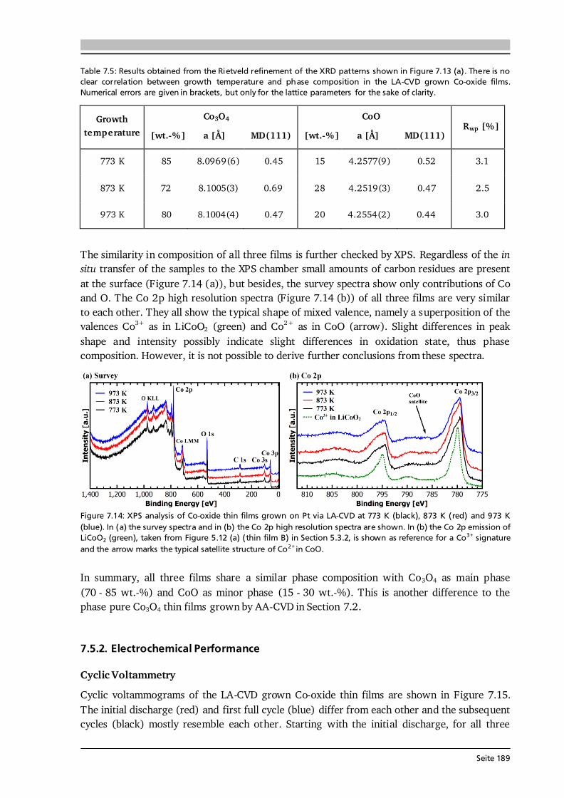
Seite 189
Table 7.5: Results obtained from the Rietveld refinement of the XRD patterns shown in Figure 7.13 (a). There is no clear correlation between growth temperature and phase composition in the LA-CVD grown Co-oxide films. Numerical errors are given in brackets, but only for the lattice parameters for the sake of clarity. Growth temperature
Co3O4 [wt.-%] a [Å] MD(111)
CoO [wt.-%] a [Å] MD(111) Rwp [%]
773 K 85 8.0969(6) 0.45 15 4.2577(9) 0.52 3.1 873 K 72 8.1005(3) 0.69 28 4.2519(3) 0.47 2.5 973 K 80 8.1004(4) 0.47 20 4.2554(2) 0.44 3.0
The similarity in composition of all three films is further checked by XPS. Regardless of the in situ transfer of the samples to the XPS chamber small amounts of carbon residues are present at the surface (Figure 7.14 (a)), but besides, the survey spectra show only contributions of Co and O. The Co 2p high resolution spectra (Figure 7.14 (b)) of all three films are very similar to each other. They all show the typical shape of mixed valence, namely a superposition of the valences Co3+ as in LiCoO2 (green) and Co2+ as in CoO (arrow). Slight differences in peak shape and intensity possibly indicate slight differences in oxidation state, thus phase composition. However, it is not possible to derive further conclusions from these spectra.
Figure 7.14: XPS analysis of Co-oxide thin films grown on Pt via LA-CVD at 773 K (black), 873 K (red) and 973 K (blue). In (a) the survey spectra and in (b) the Co 2p high resolution spectra are shown. In (b) the Co 2p emission of LiCoO2 (green), taken from Figure 5.12 (a) (thin film B) in Section 5.3.2, is shown as reference for a Co3+ signature and the arrow marks the typical satellite structure of Co2+ in CoO. In summary, all three films share a similar phase composition with Co3O4 as main phase (70 - 85 wt.-%) and CoO as minor phase (15 - 30 wt.-%). This is another difference to the phase pure Co3O4 thin films grown by AA-CVD in Section 7.2.
7.5.2. Electrochemical Performance Cyclic Voltammetry Cyclic voltammograms of the LA-CVD grown Co-oxide thin films are shown in Figure 7.15. The initial discharge (red) and first full cycle (blue) differ from each other and the subsequent cycles (black) mostly resemble each other. Starting with the initial discharge, for all three

Seite 190
films reduction sets in at around 1.15 V (red arrows) followed by two to three local minima (A1, A2, B) depending on the growth temperature. In the first full cycle all films share a more or less pronounced sloping range (B’) in the anodic scan as well as one anodic and one cathodic peak at ~ 2.03 V (A’) and ~ 1.07 V (A), respectively. Furthermore, they differ from each other in the cathodic region below 0.8 V (B). In the cycles 2 - 5 all Co-oxide films show similar signatures in the CV curve, i.e. an anodic peak at 2.05 - 2.10 V and a cathodic one at 0.97 - 1.08 V, both slightly shifting in their voltage position upon further cycling.
Figure 7.15: Cyclic voltammograms of Co-oxide thin films grown on Pt via LA-CVD at (a) 773 K, (b) 873 K, and (c) 973 K. The color code differentiates between initial discharge (red), first full cycle (blue), and cycles 2-5 (black). Anodic and cathodic peaks are labeled with letters as described in the text, and the red arrows show the onset potential for reduction during the initial discharge. Following the extensive discussion in Section 7.2.2, the observed features can be explained by, and assigned to, the two phases CoO and Co3O4 being present in these films. In the initial discharge, first the partial reduction of Co3O4 starts in the voltage range 1.15 - 1.30 V (peak A1) [378,379], which is then superimposed by the reduction of CoO (peak A2) typically observed at ~ 0.8 V in the initial cycle [74]. The fact that it takes the first full cycle in addition until the cyclic voltammograms stabilize is ascribed to the thickness and microstructure of the films. As opposed to the investigated AA-CVD grown films, the LA-CVD grown Co-oxide films are thicker and have no significant porosity for the liquid electrolyte to infiltrate. Consequently, they do provide neither short diffusion paths nor a high surface area for reaction sites, producing a kinetic and mass-transport limitation (see Section 7.6.1). This might also explain why the anodic as well as cathodic peak currents (see Figure 7.15), and also the total capacities (see Figure 7.16 (a)), do not scale with the film thickness. It is likely that not all the active material for such thick films is taking part in the reversible conversion reaction according to Eq. (7.3) (peaks A/A’). The peaks B/B’, assigned to interfacial lithium storage, do not contribute much to the total capacity as observed by cyclic voltammetry (Figure 7.15), which is expected due to the dense microstructure and with that low surface area of the films as discussed earlier. Galvanostatic Cycling The C-rate dependent galvanostatic cycling data (Figure 7.16) further illustrate the kinetic limitations in the Co-oxide films grown by LA-CVD. Between cycles 6 and 56 for each ten cycles a current of 10 μA, 20 μA, 50 μA, 100 μA and again 10 μA is applied resulting in different C-rates as it is indicated for each sample. Figure 7.16 (a) compares the absolute capacity for all three films, while in (b) the mass specific capacity is plotted. Remarkably, all films deliver roughly the same amount of charge at each current (Figure 7.16 (a)), even
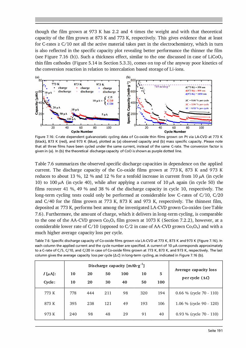
Seite 191
though the film grown at 973 K has 2.2 and 4 times the weight and with that theoretical capacity of the film grown at 873 K and 773 K, respectively. This gives evidence that at least for C-rates C/10 not all the active material takes part in the electrochemistry, which in turn is also reflected in the specific capacity plot revealing better performance the thinner the film (see Figure 7.16 (b)). Such a thickness effect, similar to the one discussed in case of LiCoO2 thin film cathodes (Figure 5.14 in Section 5.3.3), comes on top of the anyway poor kinetics of the conversion reaction in relation to intercalation based storage of Li-ions.
Figure 7.16: C-rate dependent galvanostatic cycling data of Co-oxide thin films grown on Pt via LA-CVD at 773 K (black), 873 K (red), and 973 K (blue), plotted as (a) observed capacity and (b) mass specific capacity. Please note that all three films have been cycled under the same current, instead of the same C-rate. The conversion factor is given in (a). In (b) the theoretical discharge capacity of CoO is shown as purple dotted line. Table 7.6 summarizes the observed specific discharge capacities in dependence on the applied current. The discharge capacity of the Co-oxide films grown at 773 K, 873 K and 973 K reduces to about 13 %, 12 % and 12 % for a tenfold increase in current from 10 μA (in cycle 10) to 100 μA (in cycle 40), while after applying a current of 10 μA again (in cycle 50) the films recover 41 %, 49 % and 38 % of the discharge capacity in cycle 10, respectively. The long-term cycling tests could only be performed at considerable low C-rates of C/10, C/20 and C/40 for the films grown at 773 K, 873 K and 973 K, respectively. The thinnest film, deposited at 773 K, performs best among the investigated LA-CVD grown Co-oxides (see Table 7.6). Furthermore, the amount of charge, which it delivers in long-term cycling, is comparable to the one of the AA-CVD grown Co3O4 film grown at 1073 K (Section 7.2.2), however, at a considerable lower rate of C/10 (opposed to C/2 in case of AA-CVD grown Co3O4) and with a much higher average capacity loss per cycle. Table 7.6: Specific discharge capacity of Co-oxide films grown via LA-CVD at 773 K, 873 K and 973 K (Figure 7.16). In each column the applied current and the cycle number are specified. A current of 10 μA corresponds approximately to a C-rate of C/5, C/10, and C/20 in case of Co-oxide films grown at 773 K, 873 K, and 973 K, respectively. The last column gives the average capacity loss per cycle (ΔC) in long-term cycling, as indicated in Figure 7.16 (b).
I [μA]: Cycle:
Discharge capacity [mAh·g -1] 10 20 50 100 10 5 10 20 30 40 50 100
Average capacity loss per cycle (ΔC)
773 K 778 444 211 98 320 194 0.66 % (cycle 70 - 110) 873 K 395 238 121 49 193 106 1.06 % (cycle 90 - 120) 973 K 240 98 48 29 91 40 0.93 % (cycle 70 - 110)
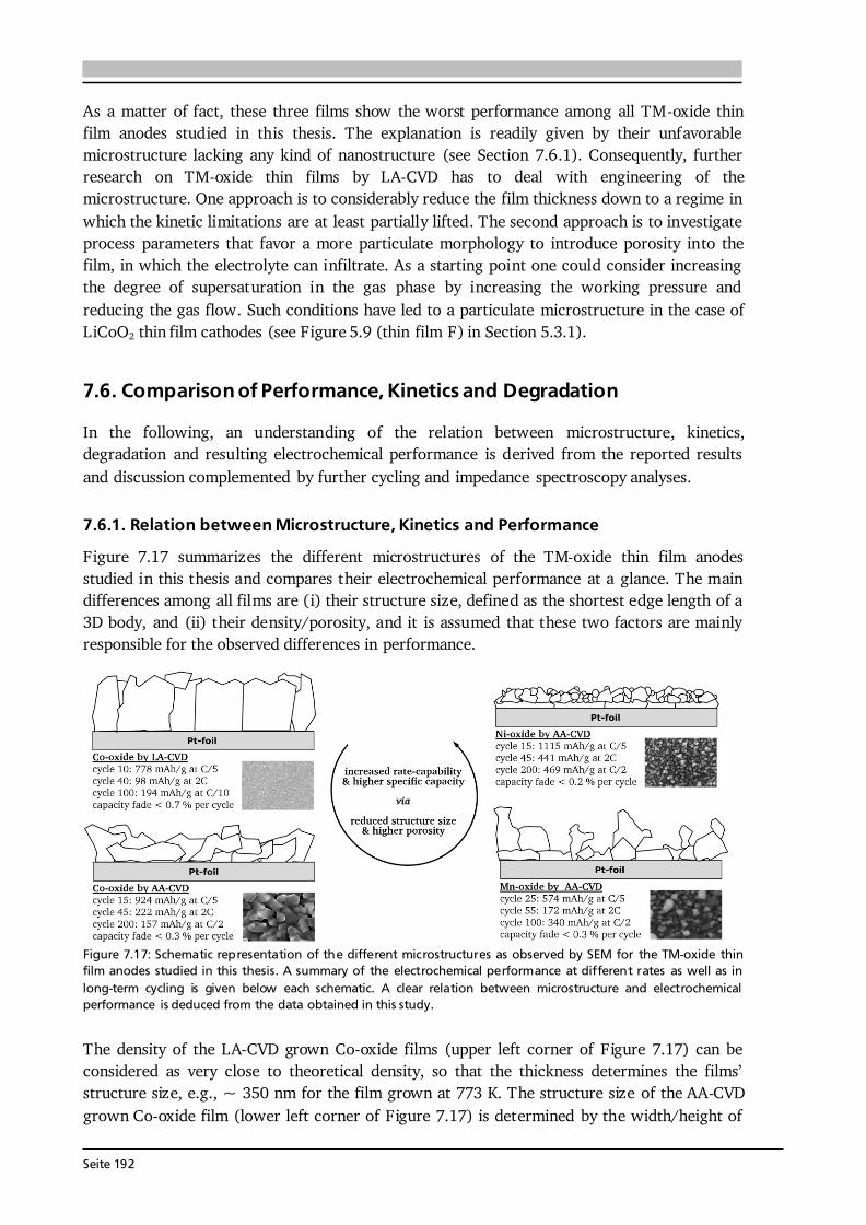
Seite 192
As a matter of fact, these three films show the worst performance among all TM-oxide thin film anodes studied in this thesis. The explanation is readily given by their unfavorable microstructure lacking any kind of nanostructure (see Section 7.6.1). Consequently, further research on TM-oxide thin films by LA-CVD has to deal with engineering of the microstructure. One approach is to considerably reduce the film thickness down to a regime in which the kinetic limitations are at least partially lifted. The second approach is to investigate process parameters that favor a more particulate morphology to introduce porosity into the film, in which the electrolyte can infiltrate. As a starting point one could consider increasing the degree of supersaturation in the gas phase by increasing the working pressure and reducing the gas flow. Such conditions have led to a particulate microstructure in the case of LiCoO2 thin film cathodes (see Figure 5.9 (thin film F) in Section 5.3.1). 7.6. Comparison of Performance, Kinetics and Degradation In the following, an understanding of the relation between microstructure, kinetics, degradation and resulting electrochemical performance is derived from the reported results and discussion complemented by further cycling and impedance spectroscopy analyses. 7.6.1. Relation between Microstructure, Kinetics and Performance Figure 7.17 summarizes the different microstructures of the TM-oxide thin film anodes studied in this thesis and compares their electrochemical performance at a glance. The main differences among all films are (i) their structure size, defined as the shortest edge length of a 3D body, and (ii) their density/porosity, and it is assumed that these two factors are mainly responsible for the observed differences in performance.
Figure 7.17: Schematic representation of the different microstructures as observed by SEM for the TM-oxide thin film anodes studied in this thesis. A summary of the electrochemical performance at different rates as well as in long-term cycling is given below each schematic. A clear relation between microstructure and electrochemical performance is deduced from the data obtained in this study. The density of the LA-CVD grown Co-oxide films (upper left corner of Figure 7.17) can be considered as very close to theoretical density, so that the thickness determines the films’ structure size, e.g., ~ 350 nm for the film grown at 773 K. The structure size of the AA-CVD grown Co-oxide film (lower left corner of Figure 7.17) is determined by the width/height of
Seite 193
the tube shaped, highly coalesced particles of about 300 - 400 nm. Despite similar structure sizes of Co-oxide films grown by the two CVD techniques, the AA-CVD grown Co-oxide film performs better, especially under high C-rates, which is ascribed to the porosity being present in this film providing a better infiltration by the liquid electrolyte and thus reduces the diffusion distance of the Li-ions. The microstructure of the Mn-oxide film grown by AA-CVD (lower right corner of Figure 7.17) is irregular with particle sizes of 100 - 600 nm on top of a ~ 250 nm dense layer. It is assumed that the majority of particles has a size below 300 nm (see Figure 7.9), which would explain the superior performance compared to the Co-oxide film grown by AA-CVD under similar conditions. Best performing is the Ni-oxide film grown by AA-CVD (upper right corner of Figure 7.17), which consists of 50 - 300 nm sized particles coalesced to a dense layer. Overall, this study demonstrates a clear relation between microstructure and electrochemical performance of TM-oxide thin film anodes. In order to obtain a more detailed understanding of the rate-determining step, the charge-transfer kinetics are further investigated. C-rate Dependent Galvanostatic Cycling Figure 7.18 shows the voltage over capacity plots of rate dependent galvanostatic cycling data of all the TM-oxide thin film anodes discussed in the previous sections, (a) grown by AA-CVD and (b) grown by LA-CVD. On the whole, the voltage profiles are consistent with the cyclic voltammetry data extensively discussed in each of the previous sections. Here, more details on the charge-transfer kinetics shall be derived from the data. For this purpose, at selected capacities (black arrows) of the discharge voltage profiles in Figure 7.18, current-voltage pair of values are read off (black dashed lines) and plotted in a semi-logarithmic representation: , (7.9) which is a reorganized form of the Butler-Volmer equation (Eq. (2.14) in Section 2.1.2). The respective Tafel-type plots (Eq. (2.16) in Section 2.1.2) are shown in the two graphs at the bottom of Figure 7.18. At first, the graphical representation of Eq. (7.9) is discussed for the AA-CVD grown films (graph at the bottom left). In case of the NiO film a linear dependence (red dotted line) up to a rate of C is observed, before a deviation from linearity sets in at a rate of 2C. From this behavior the rate-determining step may be interpreted as [118]: (i) the charge-transfer reaction at the NiO electrode | liquid electrolyte interface up to a rate of C, and (ii) the mass-transport inside the thin film for rates higher than C. Following this interpretation, the mass-transport limited regime starts at rates higher than C/2 for Co3O4 and Mn3O4 films, because in their case the linear regime is only observed up to a rate of C/2 (black and blue dotted lines). This is in agreement with the observation of superior rate performance in the NiO film compared to Co3O4 and Mn3O4 films. It shall be noted that the linear fit to the Co3O4 and Mn3O4 data relies only on two data points, however, is justified by the very similar slopes in relation to the fit of the NiO data. A similar slope is expected due to the comparable reaction mechanism in all three TM-oxide anodes.
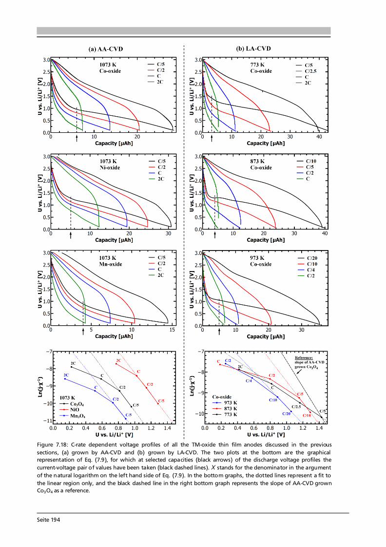
Seite 194
Figure 7.18: C-rate dependent voltage profiles of all the TM-oxide thin film anodes discussed in the previous sections, (a) grown by AA-CVD and (b) grown by LA-CVD. The two plots at the bottom are the graphical representation of Eq. (7.9), for which at selected capacities (black arrows) of the discharge voltage profiles the current-voltage pair of values have been taken (black dashed lines). Χ stands for the denominator in the argument of the natural logarithm on the left hand side of Eq. (7.9). In the bottom graphs, the dotted lines represent a fit to the linear region only, and the black dashed line in the right bottom graph represents the slope of AA-CVD grown Co3O4 as a reference.

Seite 195
The Tafel-type plots for the LA-CVD grown Co-oxide films are shown at the bottom right of Figure 7.18. Their interpretation is more difficult, therefore the slope of the linear fit to the AA-CVD grown Co3O4 film is given as reference (black dashed line). In relation to this reference, the linear fits of the LA-CVD grown Co-oxide films have a lower slope. There is only a small deviation in slope for films grown at 973 K (blue dotted line) and 873 K (red dotted line), whereas the film grown at 773 K (black dotted line) shows a much different linear fit. Thus, it can be speculated that the film grown at 773 K leaves the linear regime already at a cycling rate of ≤ C/5. Overall, the data reveal that the mass-transport limitation sets in at much lower C-rates as compared to the AA-CVD grown films. The thickest film, grown at 973 K, shows already a deviation from the linear regime for C-rates higher than C/10, and reducing the film thickness shifts the transition between charge-transfer and mass-transport regime to slightly higher C-rates, possibly to about C/5 for the films grown at 873 K and 773 K. Prospective studies should investigate a wider range of C-rates in order to improve the significance of the linear fits. Literature results on a Co3O4 thin film grown by ALD show a linear dependence in the Butler-Volmer data up to a discharge rate of 0.22C [395]. The ALD grown Co3O4 film is extremely dense (≥ 95 %, [395]). Since the LA-CVD grown films are also very dense (Figure 7.12), the results obtained in this study are in good agreement with [395]. In other words, the results imply that the porosity and more particulate microstructure of the AA-CVD grown films is beneficial for achieving a higher rate capability by shifting the mass-transport limitation towards higher C-rates. Consequently, the charge-transfer kinetics support the conclusion drawn in Figure 7.17 on the relation between microstructure, kinetics and performance. A further reduction in structure size and increase in porosity could shift the mass-transport limitation to higher C-rates and by this improve the rate capability of TM-oxide thin films. The intercept of the linear fit to the data in Figure 7.18 allows to estimate the exchange current density j0 at the selected discharge capacity and the slope of the fit gives information on the asymmetry factor α [40,118]. Taking the equilibrium voltages (Ueq) from [372] results in a range of j0 ~ 0.2 - 8 μA/cm2 and α ~ 0.1 for the TM-oxide thin films at the selected capacities, i.e., stages of conversion (black arrows in Figure 7.18). Such small exchange current densities stand for sluggish kinetics, i.e. no significant current flows unless a large overpotential is applied [118], which is not surprising for a conversion reaction involving structural changes preceding and/or following the electron transfer. This becomes apparent considering the exchange current densities at the electrode | liquid electrolyte interface of (i) alloying materials such as Si (j0 ~ 0.1 mA/cm2, [428]), and (ii) intercalation based materials such as graphite (j0 ~ 1.0 - 2.3 mA/cm2, [429]) or LiCoO2 (j0 ~ 0.2 - 6 mA/cm2, [430]), which are much higher than those of conversion materials. Scan Rate Dependent Cyclic Voltammetry As additional analysis, scan rate dependent cyclic voltammetry measurements are conducted on the TM-oxide thin film anodes. As an example, the scan rate dependent cyclic voltammograms of the Ni-oxide film grown by AA-CVD are shown in Figure 7.19 (a). Two redox couples A/A’ and B/B’, earlier identified as NiO conversion reaction and ILS mechanism (see Section 7.3.2), are clearly visible. A large peak separation ΔU = UA’/B’ - UA/B is observed and the peak positions change with scan rate (black arrows), which are both indications for an irreversible system [40,118].
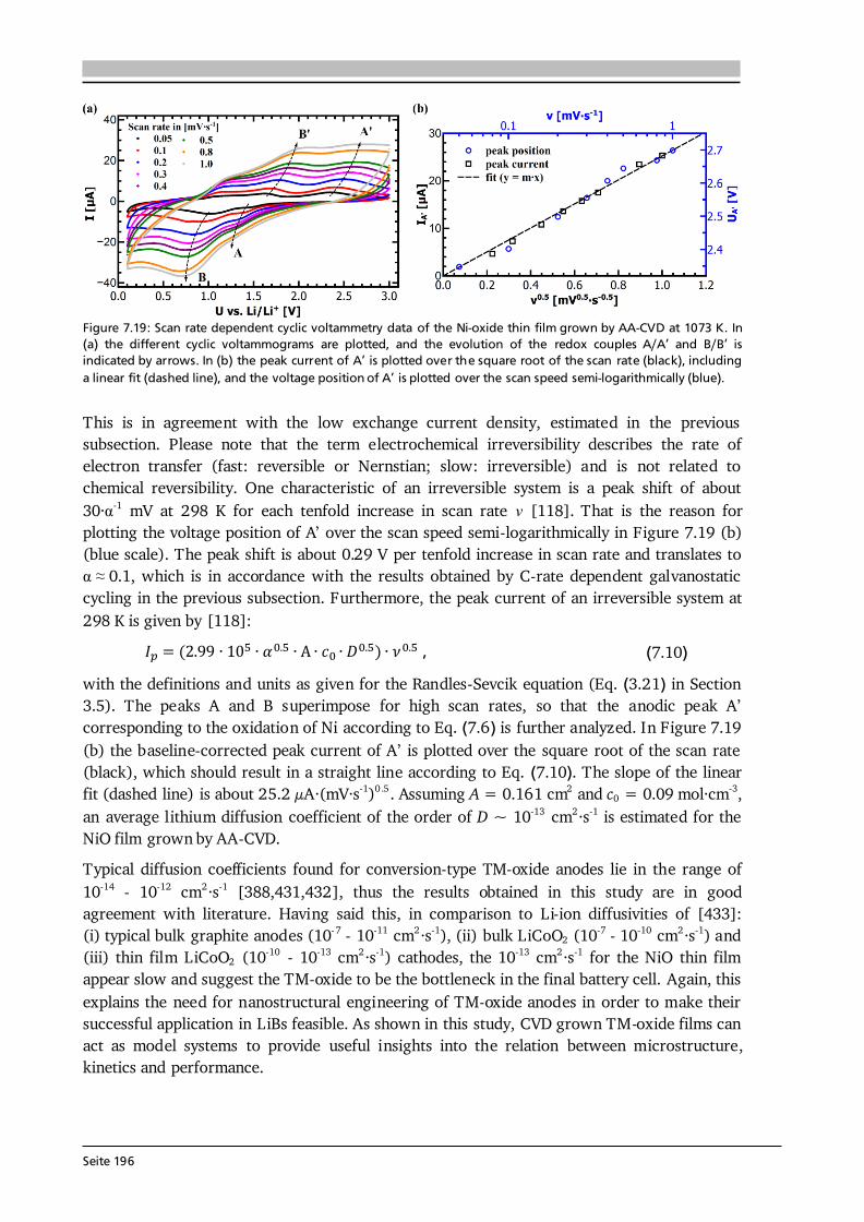
Seite 196
Figure 7.19: Scan rate dependent cyclic voltammetry data of the Ni-oxide thin film grown by AA-CVD at 1073 K. In (a) the different cyclic voltammograms are plotted, and the evolution of the redox couples A/A’ and B/B’ is indicated by arrows. In (b) the peak current of A’ is plotted over the square root of the scan rate (black), including a linear fit (dashed line), and the voltage position of A’ is plotted over the scan speed semi-logarithmically (blue). This is in agreement with the low exchange current density, estimated in the previous subsection. Please note that the term electrochemical irreversibility describes the rate of electron transfer (fast: reversible or Nernstian; slow: irreversible) and is not related to chemical reversibility. One characteristic of an irreversible system is a peak shift of about 30·α-1 mV at 298 K for each tenfold increase in scan rate ν [118]. That is the reason for plotting the voltage position of A’ over the scan speed semi-logarithmically in Figure 7.19 (b) (blue scale). The peak shift is about 0.29 V per tenfold increase in scan rate and translates to α ≈ 0.1, which is in accordance with the results obtained by C-rate dependent galvanostatic cycling in the previous subsection. Furthermore, the peak current of an irreversible system at 298 K is given by [118]: , (7.10) with the definitions and units as given for the Randles-Sevcik equation (Eq. (3.21) in Section 3.5). The peaks A and B superimpose for high scan rates, so that the anodic peak A’ corresponding to the oxidation of Ni according to Eq. (7.6) is further analyzed. In Figure 7.19 (b) the baseline-corrected peak current of A’ is plotted over the square root of the scan rate (black), which should result in a straight line according to Eq. (7.10). The slope of the linear fit (dashed line) is about 25.2 μA·(mV·s-1)0.5. Assuming A = 0.161 cm2 and c0 = 0.09 mol·cm-3, an average lithium diffusion coefficient of the order of D ~ 10-13 cm2·s-1 is estimated for the NiO film grown by AA-CVD. Typical diffusion coefficients found for conversion-type TM-oxide anodes lie in the range of 10-14 - 10-12 cm2·s-1 [388,431,432], thus the results obtained in this study are in good agreement with literature. Having said this, in comparison to Li-ion diffusivities of [433]: (i) typical bulk graphite anodes (10-7 - 10-11 cm2·s-1), (ii) bulk LiCoO2 (10-7 - 10-10 cm2·s-1) and (iii) thin film LiCoO2 (10-10 - 10-13 cm2·s-1) cathodes, the 10-13 cm2·s-1 for the NiO thin film appear slow and suggest the TM-oxide to be the bottleneck in the final battery cell. Again, this explains the need for nanostructural engineering of TM-oxide anodes in order to make their successful application in LiBs feasible. As shown in this study, CVD grown TM-oxide films can act as model systems to provide useful insights into the relation between microstructure, kinetics and performance.

Seite 197
7.6.2. Insight into Possible Degradation Mechanisms In the previous sections for each material and deposition technique the relation between microstructure, phase composition and electrochemical performance was evaluated and possible degradation mechanisms, parts of which are summarized in Figure 7.20, were discussed. Of great value are the results of the LA-CVD deposition temperature study by means of Co-oxide films (Section 7.5), because they clearly show that the pristine TM-oxide (see Figure 7.20 sketch on the left) cannot be fully lithiated (sketch at the bottom) and consequently de-lithiated (sketch on the right) in the case of thick, dense films. This means that plenty of the anode material stays “inactive” and significantly reduces the specific capacity (refer to Figure 7.16 (b)), all the more the thicker the pristine film. In fact, a ToF-SIMS depth profiling study on related Fe-oxide thin film anodes reveals that the Li-rich surface layer upon first lithiation is only about 30 nm, followed by a Li-poor “conversion front” of about 65 nm [432]. With prolonged cycling it can be expected that the inactive material is activated step by step. Simultaneously, the repeated volume changes will pulverize the active material and lead to loss of integrity (see Figure 7.20 sketch at the top), so that again inactive material (e.g., isolated Li2O/TM fragments) forms and no increase in specific capacity is observed. This pulverization will occur faster for very dense films as compared to particulate films, since they are inferior in accommodating the mechanical stresses that build up. In addition, other effects such as SEI-formation and -growth may play a role in degradation, which can either be beneficial (buffer layer for mechanical stress) or detrimental (isolation/inclusion of active material) for the battery performance.
Figure 7.20: Schematic representation of supposed degradation mechanisms that lead to performance losses in the conversion-type TM-oxide thin film anodes as observed in this study. Too thick and too dense TM-oxide films show incomplete lithiation and (early) loss of integrity, which both lead to poor cycling performance. Plenty of “inactive” material reduces the specific capacity. For reasons of simplicity, effects related to the SEI (formation, growth, etc.) and ILS mechanism are not illustrated. To gain further insight into the processes and related resistances occurring inside the conversion-type TM-oxide thin film anodes, electrochemical impedance spectroscopy studies are performed. Both the cycle-dependent (Figure 7.21) and voltage-dependent (Figure 7.22) EIS data is discussed by means of the Ni-oxide film grown by AA-CVD at 1073 K.
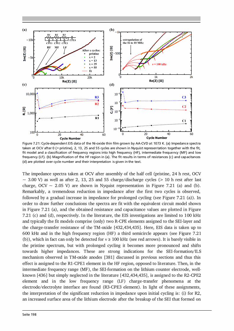
Seite 198
Figure 7.21: Cycle-dependent EIS data of the Ni-oxide thin film grown by AA-CVD at 1073 K. (a) Impedance spectra taken at OCV after 0 (= pristine), 2, 13, 25 and 55 cycles are shown in Nyquist representation together with the fit, fit model and a classification of frequency regions into high frequency (HF), intermediate frequency (MF) and low frequency (LF). (b) Magnification of the HF region in (a). The fit results in terms of resistances (c) and capacitances (d) are plotted over cycle number and their interpretation is given in the text. The impedance spectra taken at OCV after assembly of the half cell (pristine, 24 h rest, OCV ~ 3.00 V) as well as after 2, 13, 25 and 55 charge/discharge cycles (> 10 h rest after last charge, OCV ~ 2.05 V) are shown in Nyquist representation in Figure 7.21 (a) and (b). Remarkably, a tremendous reduction in impedance after the first two cycles is observed, followed by a gradual increase in impedance for prolonged cycling (see Figure 7.21 (a)). In order to draw further conclusions the spectra are fit with the equivalent circuit model shown in Figure 7.21 (a), and the obtained resistance and capacitance values are plotted in Figure 7.21 (c) and (d), respectively. In the literature, the EIS investigations are limited to 100 kHz and typically the fit models comprise (only) two R-CPE elements assigned to the SEI-layer and the charge-transfer resistance of the TM-oxide [432,434,435]. Here, EIS data is taken up to 600 kHz and in the high frequency region (HF) a third semicircle appears (see Figure 7.21 (b)), which in fact can only be detected for 100 kHz (see red arrows). It is barely visible in the pristine spectrum, but with prolonged cycling it becomes more pronounced and shifts towards higher impedances. These are strong indications for the SEI-formation/ILS mechanism observed in TM-oxide anodes [381] discussed in previous sections and thus this effect is assigned to the R1-CPE1 element in the HF region, opposed to literature. Then, in the intermediate frequency range (MF), the SEI-formation on the lithium counter electrode, well-known [436] but simply neglected in the literature [432,434,435], is assigned to the R2-CPE2 element and in the low frequency range (LF) charge-transfer phenomena at the electrode/electrolyte interface are found (R3-CPE3 element). In light of these assignments, the interpretation of the significant reduction in impedance upon initial cycling is: (i) for R2, an increased surface area of the lithium electrode after the breakup of the SEI that formed on
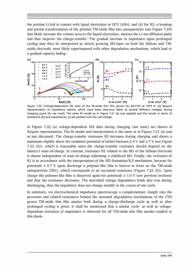
Seite 199
the pristine Li-foil in contact with liquid electrolyte at OCV [436]; and (ii) for R3, a breakup and partial transformation of the pristine TM-oxide film into nanoparticles (see Figure 7.20) that likely increase the contact area to the liquid electrolyte, shorten the Li-ion diffusion paths and thus improve the charge-transfer. The gradual increase in impedance upon prolonged cycling may then be interpreted as slowly growing SEI-layer on both the lithium and TM-oxide electrode, most likely superimposed with other degradation mechanisms, which lead to a gradual capacity fading.
Figure 7.22: Voltage-dependent EIS data of the Ni-oxide thin film grown by AA-CVD at 1073 K. (a) Nyquist representation of impedance spectra, which have been step-wise taken at several different voltages during charging (cycle 56, see inset). The same fit model as in Figure 7.21 (a) was applied and the results in terms of resistances (b) and capacitances (c) are plotted over the cell voltage. In Figure 7.22 (a) voltage-dependent EIS data during charging (see inset) are shown in Nyquist representation. The fit model and interpretation is the same as in Figure 7.21 (a) and as just discussed. The charge-transfer resistance R3 increases during charging and shows a maximum slightly above the oxidation potential of nickel between 2.4 V and 2.7 V (see Figure 7.22 (b)), which is reasonable since the charge-transfer resistance should depend on the battery’s state-of-charge. In contrast, resistance R2 related to the SEI of the lithium electrode is almost independent of state-of-charge indicating a stabilized SEI. Finally, the evolution of R1 is in accordance with the interpretation of the SEI-formation/ILS mechanism, because for potentials 0.7 V upon discharge a polymer-like film is known to form on the TM-oxide nanoparticles [381], which corresponds to an increased resistance (Figure 7.22 (b)). Upon charge this polymer-like film is dissolved again for potentials 1.0 V (see previous sections) and thus the resistance decreases. The described voltage dependence holds also true during discharging, thus the impedance does not change notably in the course of one cycle. In summary, via electrochemical impedance spectroscopy a complementary insight into the processes and related resistances behind the assumed degradation mechanisms of the CVD grown TM-oxide thin film anodes both during a charge/discharge cycle as well as after prolonged cycling is given. It shall be mentioned that a similar cycle- as well as voltage-dependent evolution of impedance is observed for all TM-oxide thin film anodes studied in this thesis.
Seite 200
7.7. Conclusion and Outlook In this chapter, the successful growth of TM-oxide (TM = Ni, Mn, Co) thin films by AA-CVD and LA-CVD as viable alternatives to thin film anodes for Li-ion batteries based on lithium metal, graphite or silicon is demonstrated. Their microstructure, phase composition and electrochemical performance is discussed, compared and put in relation to their kinetics as well as possible degradation mechanisms. This is the first report on CVD grown Ni- and Mn-oxide thin film anodes for the use in Li-ion batteries. Furthermore, the results of this fundamental work show that:
pure Co3O4, NiO, and Mn3O4 thin films are grown by AA-CVD at 1073 K, which all can be cycled several hundred times at moderate C-rates of C/2 and C. Co-oxide films grown by LA-CVD at 773 K, 873 K and 973 K are composed of Co3O4 (70 - 85 wt.-%) and CoO (15 - 30 wt.-%). the best electrochemical performance is found for the NiO thin film, mainly due to its microstructure approaching a nanoparticulate character (50 - 300 nm). the NiO film is extremely durable with > 700 cycles tested, in which it delivers very high specific capacities of 500 mAh·g-1 at C/2 and 300 mAh·g-1 at C. the Mn3O4 film shows the lowest working potential and lowest overpotential among all investigated films, both beneficial to achieve high energy densities in a full battery cell. in dependence on the microstructure of the films the rate-determining step is mass-transport or charge-transfer related, and that the transition between mass-transport and charge-transfer limitation shifts with smaller structure size and higher porosity to higher C-rates leading to increased rate capability and higher specific capacity. thick and dense TM-oxide films promote performance losses due to incomplete lithiation and (early) loss of integrity, thus are not desired for application. the lowest growth temperature realized in this study is 773 K for Co-oxide films by LA-CVD, with further reduction in temperature and transfer to other TM-oxides feasible. performance improvements can be expected by growth parameter optimization for each material, since only the growth temperature for Co-oxide was studied so far. TM-oxides show a high irreversible capacity loss in the initial cycles, even when the inevitable capacity loss (Eq. (7.5)) is prevented (as for NiO), indicating other effects such as irreversible electrolyte decomposition and incomplete (de-)conversion due to electrically disconnected Li2O/TM regions [401] dominate this initial capacity loss.
For future research the following main topics are identified:
Performance improvements Oxidation state. As part of the irreversible capacity loss in the initial cycles the inevitable capacity loss (Eq. (7.5)) is understood and could be avoided, e.g. by using a TM-monoxide thin film with the TM in 2+ oxidation state. While this aim is already achieved in case of NiO thin films grown by AA-CVD, a method is needed to reduce Co and Mn in the Co- and Mn-
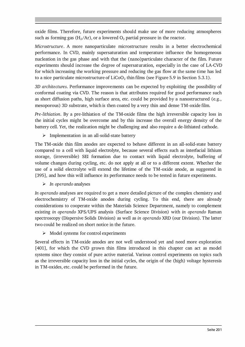
Seite 201
oxide films. Therefore, future experiments should make use of more reducing atmospheres such as forming gas (H2/Ar), or a lowered O2 partial pressure in the reactor. Microstructure. A more nanoparticulate microstructure results in a better electrochemical performance. In CVD, mainly supersaturation and temperature influence the homogeneous nucleation in the gas phase and with that the (nano)particulate character of the film. Future experiments should increase the degree of supersaturation, especially in the case of LA-CVD for which increasing the working pressure and reducing the gas flow at the same time has led to a nice particulate microstructure of LiCoO2 thin films (see Figure 5.9 in Section 5.3.1). 3D architectures. Performance improvements can be expected by exploiting the possibility of conformal coating via CVD. The reason is that attributes required for good performance such as short diffusion paths, high surface area, etc. could be provided by a nanostructured (e.g., mesoporous) 3D substrate, which is then coated by a very thin and dense TM-oxide film. Pre-lithiation. By a pre-lithiation of the TM-oxide films the high irreversible capacity loss in the initial cycles might be overcome and by this increase the overall energy density of the battery cell. Yet, the realization might be challenging and also require a de-lithiated cathode.
Implementation in an all-solid-state battery The TM-oxide thin film anodes are expected to behave different in an all-solid-state battery compared to a cell with liquid electrolyte, because several effects such as interfacial lithium storage, (irreversible) SEI formation due to contact with liquid electrolyte, buffering of volume changes during cycling, etc. do not apply at all or to a different extent. Whether the use of a solid electrolyte will extend the lifetime of the TM-oxide anode, as suggested in [395], and how this will influence its performance needs to be tested in future experiments.
In operando analyses In operando analyses are required to get a more detailed picture of the complex chemistry and electrochemistry of TM-oxide anodes during cycling. To this end, there are already considerations to cooperate within the Materials Science Department, namely to complement existing in operando XPS/UPS analysis (Surface Science Division) with in operando Raman spectroscopy (Dispersive Solids Division) as well as in operando XRD (our Division). The latter two could be realized on short notice in the future.
Model systems for control experiments Several effects in TM-oxide anodes are not well understood yet and need more exploration [401], for which the CVD grown thin films introduced in this chapter can act as model systems since they consist of pure active material. Various control experiments on topics such as the irreversible capacity loss in the initial cycles, the origin of the (high) voltage hysteresis in TM-oxides, etc. could be performed in the future.

Seite 202
Seite 203
8 Towards a Garnet Based All-Solid-State Lithium-Ion Battery 8.1. Introduction and Motivation One of the main drivers for investigating all-solid-state Li-ion batteries (ASSB) is certainly the gain in safety replacing the toxic, inflammable liquid electrolyte by a solid one. Recent media-effective incidents such as Boeing’s grounded Dreamliner [437], the fire in Samsung’s Galaxy Note 7 series [438], a small number of exploding e-cigarettes [439] along with earlier recalls of laptop batteries [440,441] and potential Li-ion battery based hazards in upcoming e-mobility [442–444] altogether underline the safety risk in everyday life. Therefore, safety is of importance for society, and in turn for the involved companies not to damage their image and risk economic losses like the approximate cost of $5 billion for the two recalls of Samsung’s Galaxy Note 7 series [438]. Next to the safety aspect, potential advantages of ASSBs are [11,27]: higher energy and power density, larger operating temperature range, longer cycle life, more flexibility in design and less requirements on packaging as well as state-of-charge monitoring. Up to date, however, most of these value propositions still need to be substantiated by relevant data as the critical review by Kerman et al. [27] reminds. The recent advances in solid electrolytes across several material classes (see Section 6.1) result in as many ASSB chemistries on the R & D level and a good overview is provided in [11,27,445]. Soon after its discovery, the compatibility of garnet-type Li7La3Zr2O12 solid electrolyte to all-solid-state batteries using Li metal anode was proven [28]. In this pioneering study of a LiCoO2 | LLZrO | Li cell only 3 cycles with a discharge capacity of 15 μAh·cm-2 were reported [28]. Two years later, in 2012, researchers from Toyota showed encouraging results by employing a Nb-doped Li6.75La3Zr1.75Nb0.25O12 solid electrolyte pellet with PLD grown LiCoO2 cathode and Li metal foil anode [26]. This cell showed an initial discharge capacity of 129 mAh·g-1 (~ 93 % of the theoretical capacity) and retained 127 mAh·g-1 after 100 cycles at a C/10-rate in a voltage range of 2.5 - 4.2 V at 25 °C [26]. This remarkable capacity retention of 98 %, equivalent to a capacity loss per cycle of 0.015 %, is still one of the best reported, not only with respect to garnet based ASSBs [446], but also compared to sulfide, hydride, nitride and anti-perovskite based ASSBs [27]. Only the cycling rate of C/10 is too low for most practical applications. With respect to high power delivery a sulfide based ASSB showed promising results retaining 75 % of its initial discharge capacity of 115 mAh·g -1 after 500 cycles at a remarkable rate of 18C, yet at elevated temperature of 100 °C [447]. Apart from these flagship projects, disparate literature results for similar ASSB chemistries show that the overall system including the materials, their interfaces, synthesis, processing and cycling is rather complex and still far from understood. A prominent example is the LiCoO2 | LLZrO interface, at which a reaction zone of about 100 nm with mutual element diffusion is found in
Seite 204
some studies [30,275], while another study could not observe element diffusion [26]. The former studies report poor cyclability of their ASSBs [30,275] with an improvement by interface modification [275], while the latter study reports excellent cyclability [26]. The explanation lies in different synthesis and processing conditions and probably also variation of the LLZrO composition. Consequently, further research and development is necessary to obtain a fundamental understanding of the processing-structure-property relations on the cell level in order to move away from the stage of trial-and-error. Meanwhile, first prototype cells to be used in electric vehicles (EVs) arrange for commercialization (see [11] for examples), and Toyota recently affirmed plans to commercialize all-solid-state EV batteries by the early 2020s [448,449].
Figure 8.1: Schematic of possible 2D thin film battery geometries, (a) planar and (b) stacked. The planar geometry suffers from inhomogeneous current density distribution and a large footprint area in comparison to the stacked geometry. In (b) some important aspects are listed, which should be considered during battery fabrication. (c) Concept of a 3D thin film battery design with trench structure to enlarge the surface area. (d) Illustration of the Li-free battery concept. Upon first charge metallic Li (green) is plated at the Cu metal anode. Image (c) is reprinted in part by permission from Macmillan Publishers Ltd: Nature [161], Copyright 2008. (Courtesy of P. H. L. Notten, R. A. H. Niessen and L. Baggetto, Philips Research Laboratories and Eindhoven University of Technology.)
Need for Thin Film Battery Research In general, thin film batteries can act as model systems to study such fundamental processing-structure-property relations and doing so may help to further improve future ASSBs. For example, intrinsic material properties such as conductivity, chemical and electrochemical stability in dependence on different treatments (temperature, atmosphere) can be determined by studying the pure active materials. Also viable material combinations for ASSBs based on their interfacial stability, and investigated by a surface science approach (see Sections 6.1 and 6.4.4), can be identified. A further need to develop thin film batteries is the increasing demand for micro-sized power sources driven by the progressive miniaturization in electronic devices. Among the applications are medical and implantable devices (hearing aids, lab on a chip, pacemakers, defibrillators) [450], consumer and industry products (thin portable devices, non-volatile memory backup, miniature transmitters, sensors and actuators) [17], and the fast growing market of micro-electro-mechanical systems (MEMS) [8]. In fact, the application of MEMS technology is presently limited by the lack of adequate micro-sized power supplies [8].
Seite 205
A typical 2D thin film battery has a thickness of the order of 10 μm and is grown step by step in a planar (Figure 8.1 (a)) or stacked (Figure 8.1 (b)) geometry. The planar geometry suffers from inhomogeneous current density distribution and a larger footprint area in comparison to the stacked geometry. As already described for bulk ASSBs the overall system is rather complex and several important aspects, often simultaneously, should be considered during battery fabrication (see examples in Figure 8.1 (b)). One shortcoming of thin film batteries is their low capacity due to a low amount of active material, which depends on the electrode thickness. Thicker electrodes result in higher energy density at the cost of power density due to longer diffusion pathways for the Li-ions, and vice versa. Furthermore, when scaling down a battery system in size, then the relative contribution of inactive materials (substrate, encapsulation, packaging, etc.) increases, so that the specific capacity decreases (see Table 8.1). Consequently, new designs which increase the capacity per footprint area are required and several concepts have been suggested to exploit the third dimension [13,259,451], among which conformal coating via CVD is a valid approach (see Sections 5.1 and 5.5.1). For example, the surface area enlargement (A’) of a 3D trench structure as shown in Figure 8.1 (c) is [36]: , (8.1) where w is the trench width, d is the trench depth, s is the spacing between the trenches and L represents the footprint length. It is assumed [36] that aspect ratios (d/w) up to 27 are easy to achieve, e.g. via a trench depth, width and spacing of 135 μm, 5 μm and 5 μm, respectively. This would allow a surface area, and with that capacity per footprint area, enlargement of 28. At the same time, 3D architectures can promote a high power density due to shortened Li-ion diffusion pathways. Explicitly, Pikul et al. [452] report on a 3D microbattery based on nanoporous electrodes with 2000 times higher power density than other microbatteries, which equals the best supercapacitors in performance. Yet, their battery uses a liquid electrolyte. It is not the objective of this thesis to develop a 3D battery, but once the growth of garnet based thin film batteries by LA-CVD is successful on 2D substrates, the growth on 3D architectures seems readily possible as shown by means of LiCoO2 in Section 5.5.1. The Benchmark is LiPON - Despite Its Moderate Ionic Conductivity Many different anode and cathode material combinations for thin film Li-ion batteries are reported to date, which employ one of the following inorganic solid electrolytes [374,451]: Li4SiO4 derivatives, NASICON-like, LISICON-like, perovskite-type LLT, or LiPON. Despite these numerous combinations and studies, LiPON is the solid electrolyte of choice among the few commercially available microbatteries with inorganic solid electrolyte (see Table 8.1). LiPON based thin film batteries deliver the best overall performance [451], and in particular a LiNi0.5Mn1.5O4 | LiPON | Li thin film battery delivered 90 % of its initial discharge capacity after outstanding 10000 cycles at a 5C-rate at 23 °C [453]. However, compared with a cell using liquid electrolyte and an identical cathode, the rate performance of this all-solid-state battery is still inferior [453], which can be ascribed to the moderate ionic conductivity of LiPON of the order of 10-6 S·cm-1. Therefore, thin film batteries based on solid electrolytes with higher ionic conductivity are needed to ensure high power performance. As discussed in Section 6.1, cubic garnets offer significantly higher ionic conductivities compared to LiPON, namely about 3 orders of magnitude in case of bulk material, paired with good electrochemical stability. But garnets are difficult to stabilize in thin film form, which might
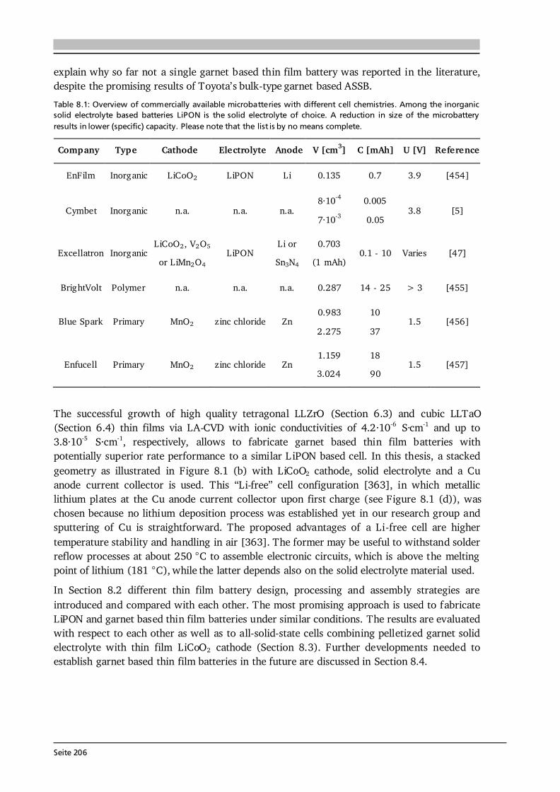
Seite 206
explain why so far not a single garnet based thin film battery was reported in the literature, despite the promising results of Toyota’s bulk-type garnet based ASSB. Table 8.1: Overview of commercially available microbatteries with different cell chemistries. Among the inorganic solid electrolyte based batteries LiPON is the solid electrolyte of choice. A reduction in size of the microbattery results in lower (specific) capacity. Please note that the list is by no means complete. Company Type Cathode Electrolyte Anode V [cm3] C [mAh] U [V] Reference
EnFilm Inorganic LiCoO2 LiPON Li 0.135 0.7 3.9 [454] Cymbet Inorganic n.a. n.a. n.a. 8·10-4
7·10-3 0.005 0.05 3.8 [5]
Excellatron Inorganic LiCoO2, V2O5 or LiMn2O4 LiPON Li or
Sn3N4 0.703
(1 mAh) 0.1 - 10 Varies [47] BrightVolt Polymer n.a. n.a. n.a. 0.287 14 - 25 > 3 [455] Blue Spark Primary MnO2 zinc chloride Zn 0.983
2.275 10 37 1.5 [456]
Enfucell Primary MnO2 zinc chloride Zn 1.159 3.024
18 90 1.5 [457]
The successful growth of high quality tetragonal LLZrO (Section 6.3) and cubic LLTaO (Section 6.4) thin films via LA-CVD with ionic conductivities of 4.2·10-6 S·cm-1 and up to 3.8·10-5 S·cm-1, respectively, allows to fabricate garnet based thin film batteries with potentially superior rate performance to a similar L iPON based cell. In this thesis, a stacked geometry as illustrated in Figure 8.1 (b) with LiCoO2 cathode, solid electrolyte and a Cu anode current collector is used. This “Li-free” cell configuration [363], in which metallic lithium plates at the Cu anode current collector upon first charge (see Figure 8.1 (d)), was chosen because no lithium deposition process was established yet in our research group and sputtering of Cu is straightforward. The proposed advantages of a Li-free cell are higher temperature stability and handling in air [363]. The former may be useful to withstand solder reflow processes at about 250 °C to assemble electronic circuits, which is above the melting point of lithium (181 °C), while the latter depends also on the solid electrolyte material used. In Section 8.2 different thin film battery design, processing and assembly strategies are introduced and compared with each other. The most promising approach is used to fabricate LiPON and garnet based thin film batteries under similar conditions. The results are evaluated with respect to each other as well as to all-solid-state cells combining pelletized garnet solid electrolyte with thin film LiCoO2 cathode (Section 8.3). Further developments needed to establish garnet based thin film batteries in the future are discussed in Section 8.4.

Seite 207
8.2. Thin Film Batteries 8.2.1. Design, Processing and Assembly Three different strategies of microbattery design, processing and assembly pursued in the course of this PhD project are shown in Figure 8.2. Their realization is based on the Li-free battery concept (Figure 8.1 (d)), but in principle the presented strategies can also make use of TM-oxides as introduced in Chapter 7, lithium metal, or other anode materials. Likewise, any reasonable combination of materials and/or deposition techniques available in DAISY-Bat (see Figure 4.11 (a) in Section 4.5) may be used in the future.
Figure 8.2: Illustration of different design, processing and assembly strategies. (a) Shadow mask system developed by the Surface Science Division for sputter deposition on 2 x 2 cm2 glass substrates mounted on PHI sample holders [458]. Its adapted use in this PhD project requires the following processing steps: 1. Sputtering of four Au stripes as back contacts on top of a glass substrate (Eagle XG, Corning Inc.); 2. LA-CVD of the cathode on Pt-foil using a 8 x 8 mm2 shadow mask; 3. LA-CVD of the solid electrolyte on top of the cathode using a 9 x 9 mm2 shadow mask; 4. Sputtering of four Cu anodes (3 x 3 mm2 each); 5. Placing the four Pt | cathode | solid electrolyte | Cu stacks on the Au back contacts and sputtering of four Au stripes as front contacts. The resulting cells can be contacted individually using a custom-built holder with integrated (macroscopic) copper rails. (b) The one-step LA-CVD growth concept uses a sample holder with a 9 x 9 mm2 shadow mask to grow the cathode and subsequently the solid electrolyte film on Pt-foil without break. The second step is a sputter deposition of Cu and subsequently Au (in one step without breaking vacuum) using a shadow mask with 4 holes of 2 mm in diameter. (c) The third design comprises 3 steps: 1. LA-CVD of the cathode on Pt-foil using a shadow mask with 4 holes of 2 mm in diameter; 2. LA-CVD of the solid electrolyte on top of the cathode using a 9 x 9 mm2 shadow mask; 3. Cu and subsequent Au deposition congruent to the 4 circular cathodes.
PHI Sample Holder Shadow Mask System The first strategy is to adapt an existing shadow mask system for thin film battery growth developed by the Surface Science Division (see [458] for details). It is optimized for sputter deposition on 2 x 2 cm2 glass substrates mounted on PHI sample holders. This system works very reliably when all layers are grown on top of each other on the glass substrate, however, it does not provide much flexibility since the geometric dimensions have to be strictly fulfilled and a PHI sample holder is needed. The latter is not compatible with the LA-CVD setup. Also the 2 x 2 cm2 glass substrate is too large for the LA-CVD sample holder and not an ideal substrate to be used with the high temperature, heating and cooling rates applied in optimized LA-CVD cathode and solid electrolyte growth. Consequently, the cathode and solid electrolyte layers are grown on top of each other on Pt-foil in individual LA-CVD syntheses as introduced in Chapters 5 and 6, respectively (step 2 and 3 in Figure 8.2 (a)). Four of those Pt | cathode | solid electrolyte stacks are sputtered with Cu and then glued on top of the four
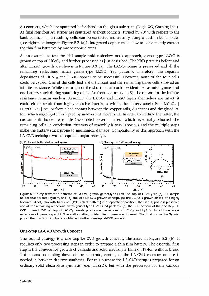
Seite 208
Au contacts, which are sputtered beforehand on the glass substrate (Eagle XG, Corning Inc.). As final step four Au stripes are sputtered as front contacts, turned by 90° with respect to the back contacts. The resulting cells can be contacted individually using a custom-built holder (see rightmost image in Figure 8.2 (a)). Integrated copper rails allow to conveniently contact the thin film batteries by macroscopic clamps. As an example to test the PHI sample holder shadow mask approach, garnet-type LLZrO is grown on top of LiCoO2 and further processed as just described. The XRD patterns before and after LLZrO growth are shown in Figure 8.3 (a). The LiCoO2 phase is preserved and all the remaining reflections match garnet-type LLZrO (red pattern). Therefore, the separate depositions of LiCoO2 and LLZrO appear to be successful. However, none of the four cells could be cycled. One of the cells had a short circuit and the remaining three cells showed an infinite resistance. While the origin of the short circuit could be identified as misalignment of one battery stack during sputtering of the Au front contact (step 5), the reason for the infinite resistance remains unclear. Assuming the LiCoO2 and LLZrO layers themselves are intact, it could either result from highly resistive interfaces within the battery stack: Pt | LiCoO2 | LLZrO | Cu | Au, or from a bad contact between the copper rails, Au stripes and the glued Pt-foil, which might got interrupted by inadvertent movement. In order to exclude the latter, the custom-built holder was (dis-)assembled several times, which eventually shorted the remaining cells. In conclusion, this way of assembly is very laborious and the multiple steps make the battery stack prone to mechanical damage. Compatibility of this approach with the LA-CVD technique would require a major redesign.
Figure 8.3: X-ray diffraction patterns of LA-CVD grown garnet-type LLZrO on top of LiCoO2 via (a) PHI sample holder shadow mask system, and (b) one-step LA-CVD growth concept. (a) The LLZrO is grown on top of a highly textured LiCoO2 film with traces of Li2PtO3 (black pattern) in a separate deposition. The LiCoO2 phase is preserved and all the remaining reflections match garnet-type LLZrO (red pattern). (b) The XRD pattern of the one-step LA-CVD grown LLZrO on top of LiCoO2 reveals pronounced reflections of LiCoO2 and Li2PtO3. In addition, weak reflections of garnet-type LLZrO as well as other, unidentified phases are observed. The inset shows the Nyquist plot of the thin film microbattery obtained via the one-step LA-CVD concept.
One-Step LA-CVD Growth Concept The second strategy is a one-step LA-CVD growth concept, illustrated in Figure 8.2 (b). It requires only two processing steps in order to prepare a thin film battery. The essential first step is the consecutive growth of cathode and solid electrolyte films on Pt-foil without break. This means no cooling down of the substrate, venting of the LA-CVD chamber or else is needed in between the two syntheses. For this purpose the LA-CVD setup is prepared for an ordinary solid electrolyte synthesis (e.g., LLZrO), but with the precursors for the cathode
Seite 209
growth (e.g., LiCoO2) already filled into the groove of the stainless steel plate (see Figure 4.6 in Section 4.4.2). Once the cathode growth is completed, the processing conditions (substrate temperature, gas flow, etc.) are immediately adjusted to the solid electrolyte growth parameters and the respective precursors are filled from the flask as usual. Sputter deposition of Cu and Au (also in one step without breaking vacuum) using a shadow mask with 4 holes of 2 mm in diameter completes the battery stack. Then, the sample can be cut into 4 Li-free all-solid-state batteries for electrochemical analysis via pogo-pins (see Section 3.6) or in a Swagelok-type battery (see Section 3.5). As an example, LLZrO is grown on top of LiCoO2 in one step via LA-CVD. The XRD pattern (Figure 8.3 (b)) reveals pronounced reflections of LiCoO2 and Li2PtO3 as well as weak reflections of garnet-type LLZrO and unidentified secondary phase(s). Also cobalt is found at the film’s surface via XPS (not shown). Obviously, the phase formation in the one-step LA-CVD approach strongly differs from the separate growth of LiCoO2 and LLZrO. One possible reason is the lack of a cooling down step in between the two syntheses, which may promote cation mixing by mutual diffusion between the LLZrO and LiCoO2. Furthermore, during the LLZrO deposition parts of the LiCoO2 precursors, even though buried below the LLZrO precursors, might still evaporate continuously (see Figure 8.17 (a) in Section 8.4.2). This would explain the presence of Co at the surface of the film and possibly lead to unexpected (and undesired) secondary phase(s) in the Li-La-Zr-Co-O system. The electrochemical analysis shows that this thin film battery is electronically conductive as illustrated by the closed semicircle in the Nyquist plot (inset in Figure 8.3 (b)). Further spatially resolved (phase) analyses are required in order to clarify the origin of the electronic conductivity. In conclusion, the one-step LA-CVD growth concept in its current form is prone to secondary phase formation. Further development of this concept, e.g. by introducing a stepper motor (see Section 8.4.1), might be worthwhile due to its easy processing combined with exclusion of air exposure to the sample in between syntheses. Two-Step LA-CVD Growth with Shadow Mask The third strategy is to use different shadow masks for cathode and solid electrolyte growth (see Figure 8.2 (c)). Four circular cathodes with 2 mm in diameter are grown on Pt in the first step. Then, a 9 x 9 mm2 shadow mask is used for the solid electrolyte growth, which shall ensure the complete coverage of the four cathodes. In a third step Cu and Au are sputter deposited congruent to the 4 circular cathodes. Again, the sample can be cut into 4 Li-free all-solid-state batteries for electrochemical analysis via pogo-pins or in a Swagelok-type battery. This concept turned out to be best suited for thin film battery preparation in this thesis, because it combines easy processing with the separate growth of cathode and solid electrolyte. Therefore, it is used in the following to study thin film batteries based on LiPON and garnet-type LLTaO solid electrolytes in Section 8.2.2 and 8.2.3, respectively. 8.2.2. LA-CVD Grown LiCoO2 | Sputtered LiPON The motivation to study a LiPON based thin film battery is to prove the functionality of all the processing steps as well as the in situ plating of the Li anode by means of established material systems before rather unknown garnet based thin film batteries are investigated. Therefore, LA-CVD grown LiCoO2 and sputtered LiPON are used as cathode and solid electrolyte,
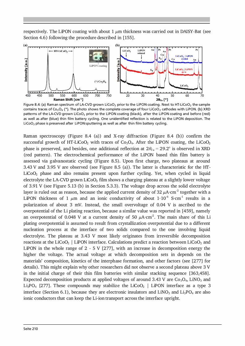
Seite 210
respectively. The LiPON coating with about 1 μm thickness was carried out in DAISY-Bat (see Section 4.6) following the procedure described in [155].
Figure 8.4: (a) Raman spectrum of LA-CVD grown LiCoO2 prior to the LiPON coating. Next to HT-LiCoO2 the sample contains traces of Co3O4 (*). The photo shows the complete coverage of four LiCoO2 cathodes with LiPON. (b) XRD patterns of the LA-CVD grown LiCoO2 prior to the LiPON coating (black), after the LiPON coating and before (red) as well as after (blue) thin film battery cycling. One unidentified reflection is related to the LiPON deposition. The LiCoO2 phase is preserved after LiPON sputtering as well as after thin film battery cycling. Raman spectroscopy (Figure 8.4 (a)) and X-ray diffraction (Figure 8.4 (b)) confirm the successful growth of HT-LiCoO2 with traces of Co3O4. After the LiPON coating, the LiCoO2 phase is preserved, and besides, one additional reflection at 2 Cu = 29.2° is observed in XRD (red pattern). The electrochemical performance of the LiPON based thin film battery is assessed via galvanostatic cycling (Figure 8.5). Upon first charge, two plateaus at around 3.43 V and 3.95 V are observed (see Figure 8.5 (a)). The latter is characteristic for the HT-LiCoO2 phase and also remains present upon further cycling. Yet, when cycled in liquid electrolyte the LA-CVD grown LiCoO2 film shows a charging plateau at a slightly lower voltage of 3.91 V (see Figure 5.13 (b) in Section 5.3.3). The voltage drop across the solid electrolyte layer is ruled out as reason, because the applied current density of 32 μA·cm-2 together with a LiPON thickness of 1 μm and an ionic conductivity of about 1·10-6 S·cm-1 results in a polarization of about 3 mV. Instead, the small overvoltage of 0.04 V is ascribed to the overpotential of the Li plating reaction, because a similar value was reported in [459], namely an overpotential of 0.048 V at a current density of 50 μA·cm-2. The main share of this Li plating overpotential is assumed to result from crystallization overpotential due to a different nucleation process at the interface of two solids compared to the one involving liquid electrolyte. The plateau at 3.43 V most likely originates from irreversible decomposition reactions at the LiCoO2 | LiPON interface. Calculations predict a reaction between LiCoO2 and LiPON in the whole range of 2 - 5 V [277], with an increase in decomposition energy the higher the voltage. The actual voltage at which decomposition sets in depends on the materials’ composition, kinetics of the interphase formation, and other factors (see [277] for details). This might explain why other researchers did not observe a second plateau above 3 V in the initial charge of their thin film batteries with similar stacking sequence [363,458]. Expected decomposition products at applied voltages of around 3.43 V are Co3O4, LiNO3 and Li3PO4 [277]. These compounds may stabilize the LiCoO2 | LiPON interface as a type 3 interface (Section 6.1), because they are electronic insulators and LiNO3 and Li3PO4 are also ionic conductors that can keep the Li-ion transport across the interface upright.
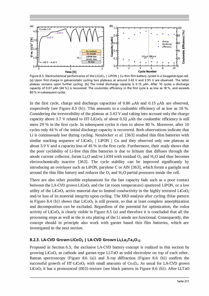
Seite 211
Figure 8.5: Electrochemical performance of the LiCoO2 | LiPON | Cu thin film battery cycled in a Swagelok-type cell. (a) Upon first charge in galvanostatic cycling two plateaus at around 3.43 V and 3.95 V are observed. The latter plateau remains upon further cycling. (b) The initial discharge capacity is 0.15 μAh. After 10 cycles a discharge capacity of 0.07 μAh (44 %) is recovered. The coulombic efficiency in the first cycle is as low as 18 %, and exceeds 80 % in subsequent cycles. In the first cycle, charge and discharge capacities of 0.86 μAh and 0.15 μAh are observed, respectively (see Figure 8.5 (b)). This amounts to a coulombic efficiency of as low as 18 %. Considering the irreversibility of the plateau at 3.43 V and taking into account only the charge capacity above 3.7 V related to HT-LiCoO2 of about 0.52 μAh the coulombic efficiency is still mere 29 % in the first cycle. In subsequent cycles it rises to above 80 %. Moreover, after 10 cycles only 44 % of the initial discharge capacity is recovered. Both observations indicate that Li is continuously lost during cycling. Neudecker et al. [363] studied thin film batteries with similar stacking sequence of LiCoO2 | LiPON | Cu and they observed only one plateau at about 3.9 V and a capacity loss of 45 % in the first cycle. Furthermore, their study shows that the poor cyclability of Li-free thin film batteries is due to lithium that diffuses through the anode current collector, forms Li2O and/or LiOH with residual O2 and H2O and thus becomes electrochemically inactive [363]. The cycle stability can be improved significantly by introducing an overlayer such as LiPON, parylene C or AlN [363], which forms a gastight seal around the thin film battery and reduces the O2 and H2O partial pressures inside the cell. There are also other possible explanations for the fast capacity fade such as a poor contact between the LA-CVD grown LiCoO2 and the (at room temperature) sputtered LiPON, or a low utility of the LiCoO2 active material due to limited conductivity in the highly textured LiCoO2 and/or loss of its material integrity upon cycling. The XRD analysis after cycling (blue pattern in Figure 8.4 (b)) shows that LiCoO2 is still present, so that at least complete amorphization and decomposition can be excluded. Regardless of the potential for optimization, the redox activity of LiCoO2 is clearly visible in Figure 8.5 (a) and therefore it is concluded that all the processing steps as well as the in situ plating of the Li anode are functional. Consequently, this concept should in principle also work with garnet based thin film batteries, which are investigated in the next section. 8.2.3. LA-CVD Grown LiCoO2 | LA-CVD Grown Li5La3Ta2O12 Proposed in Section 6.5, the exclusive LA-CVD battery concept is realized in this section by growing LiCoO2 as cathode and garnet-type LLTaO as solid electrolyte on top of each other. Raman spectroscopy (Figure 8.6 (a)) and X-ray diffraction (Figure 8.6 (b)) confirm the successful growth of HT-LiCoO2 with small amounts of Co3O4. As usual for LA-CVD grown LiCoO2 it has a pronounced (003)-texture (see black pattern in Figure 8.6 (b)). After LLTaO
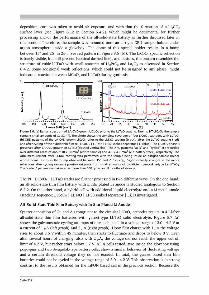
Seite 212
deposition, care was taken to avoid air exposure and with that the formation of a Li2CO3 surface layer (see Figure 6.12 in Section 6.4.2), which might be detrimental for further processing and/or the performance of the all-solid-state battery as further discussed later in this section. Therefore, the sample was mounted onto an airtight XRD sample holder under argon atmosphere inside a glovebox. The dome of this special holder results in a hump between 15° and 25° in 2 C u (see red pattern in Figure 8.6 (b)). The LiCoO2 specific reflection is barely visible, but still present (vertical dashed line), and besides, the pattern resembles the structure of cubic LLTaO with small amounts of Li2PtO3 and La2O3 as discussed in Section 6.4.2. Some additional weak reflections, which could not be assigned to any phase, might indicate a reaction between LiCoO2 and LLTaO during synthesis.
Figure 8.6: (a) Raman spectrum of LA-CVD grown LiCoO2 prior to the LLTaO coating. Next to HT-LiCoO2 the sample contains small amounts of Co3O4 (*). The photo shows the complete coverage of four LiCoO2 cathodes with LLTaO. (b) XRD patterns of the LA-CVD grown LiCoO2 prior to the LLTaO coating (black), after the LLTaO coating (red) and after cycling of the hybrid thin film cell LiCoO2 | LLTaO | LP30 soaked separator | Li (blue). The LiCoO2 phase is preserved after LA-CVD growth of LLTaO (dashed vertical line). The XRD patterns “as is” and “cycled” are recorded over different areas of about 10 x 10 mm2 (entire sample) and 4.5 x 4.5 mm2 (cut battery stack), respectively. The XRD measurement after LLTaO coating was performed with the sample being inside an airtight sample holder whose dome results in the hump observed between 15° and 25° in 2 Cu. Slight intensity changes in the minor reflections after cycling (arrows) possibly originate from small amounts of Li -deficient perovskite-type La2LiTaO6. The “cycled” pattern was taken after more than 100 cycles and 8 months of storage. The Pt | LiCoO2 | LLTaO stacks are further processed in two different ways. On the one hand, an all-solid-state thin film battery with in situ plated Li anode is studied analogous to Section 8.2.2. On the other hand, a hybrid cell with additional liquid electrolyte and a Li metal anode (stacking sequence: LiCoO2 | LLTaO | LP30 soaked separator | Li) is investigated. All-Solid-State Thin Film Battery with In Situ Plated Li Anode Sputter deposition of Cu and Au congruent to the circular LiCoO2 cathodes results in 4 Li-free all-solid-state thin film batteries with garnet-type LLTaO solid electrolyte. Figure 8.7 (a) shows the galvanostatic cycling attempts of one such a cell in a voltage range of 3.0 - 4.2 V at a current of 1 μA (left graph) and 2 μA (right graph) . Upon first charge with 1 μA the voltage rises to about 3.6 V within 45 minutes, then starts to fluctuate and drops to below 3 V. Even after several hours of charging, also with 2 μA, the voltage did not reach the upper cut-off limit of 4.2 V, but rather stays below 3.7 V. All 4 cells tested, two inside the glovebox using pogo-pins and two Swagelok-type battery cells, show a similar behavior of fluctuating voltage and a certain threshold voltage they do not exceed. In total, the garnet based thin film batteries could not be cycled in the voltage range of 3.0 - 4.2 V. This observation is in strong contrast to the results obtained for the LiPON based cell in the previous section. Because the
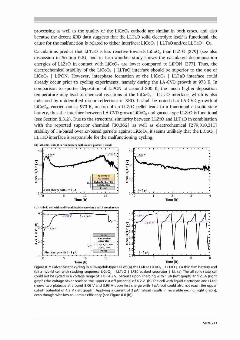
Seite 213
processing as well as the quality of the LiCoO2 cathode are similar in both cases, and also because the decent XRD data suggests that the LLTaO solid electrolyte itself is functional, the cause for the malfunction is related to either interface: LiCoO2 | LLTaO and/or LLTaO | Cu. Calculations predict that LLTaO is less reactive towards LiCoO2 than LLZrO [279] (see also discussion in Section 6.5), and in turn another study shows the calculated decomposition energies of LLZrO in contact with LiCoO2 are lower compared to LiPON [277]. Thus, the electrochemical stability of the LiCoO2 | LLTaO interface should be superior to the one of LiCoO2 | LiPON. However, interphase formation at the LiCoO2 | LLTaO interface could already occur prior to cycling experiments, namely during the LA-CVD growth at 973 K. In comparison to sputter deposition of LiPON at around 300 K, the much higher deposition temperature may lead to chemical reactions at the LiCoO2 | LLTaO interface, which is also indicated by unidentified minor reflections in XRD. It shall be noted that LA-CVD growth of LiCoO2, carried out at 973 K, on top of an LLZrO pellet leads to a functional all-solid-state battery, thus the interface between LA-CVD grown LiCoO2 and garnet-type LLZrO is functional (see Section 8.3.2). Due to the structural similarity between LLZrO and LLTaO in combination with the reported superior chemical [30,362] as well as electrochemical [279,310,311] stability of Ta-based over Zr-based garnets against LiCoO2, it seems unlikely that the LiCoO2 | LLTaO interface is responsible for the malfunctioning cycling.
Figure 8.7: Galvanostatic cycling in a Swagelok-type cell of (a) the Li-free LiCoO2 | LLTaO | Cu thin film battery and (b) a hybrid cell with stacking sequence LiCoO2 | LLTaO | LP30 soaked separator | Li. (a) The all-solid-state cell could not be cycled in a voltage range of 3.0 - 4.2 V, because upon charging with 1 μA (left graph) and 2 μA (right graph) the voltage never reached the upper cut-off potential of 4.2 V. (b) The cell with liquid electrolyte and Li -foil shows two plateaus at around 3.06 V and 3.93 V upon first charge with 1 μA, but could also not reach the upper cut-off potential of 4.2 V (left graph). Applying a current of 2 μA instead results in reversible cycling (right graph), even though with low coulombic efficiency (see Figure 8.8 (b)).
Seite 214
Regarding the LLTaO | Cu interface, the sputter deposition process of Cu on top of LLTaO is carried out in the same manner as onto LiPON. A potential difference between both interfaces is the adherence of Cu to the solid electrolyte layer. In this respect, surface roughness might play a role, which is higher in case of the LA-CVD grown LLTaO than for sputtered LiPON. In this case possibly no intimate contact is achieved between LLTaO and Cu and the consequences could be a high overpotential due to high interfacial resistance, localized Li plating (hot spots), and/or a facilitated reaction with residual air to form electrochemically inactive Li2O, LiOH and Li2CO3. Also, surface contaminations on the garnet solid electrolyte such as Li2CO3 and LiOH, which potentially formed upon air exposure prior to the Cu deposition, could be disadvantageous for achieving a good adherence of Cu to the LLTaO layer. A recent study on the Li wettability of LLZrO [460] reports on a decrease in interfacial resistance by more than two orders of magnitude upon surface conditioning, i.e. removing Li2CO3 and LiOH contaminations. While one may argue on the comparability between the LLZrO | Li and LLTaO | Cu interfaces, this example illustrates the possible impact of surface chemistry on the quality of the contact. Care was taken to avoid air exposure to the Pt | LiCoO2 | LLTaO stack, e.g. by using an airtight XRD sample holder, however, a short exposure time prior to the sputtering of Cu and Au was unavoidable. It could be speculated that such contaminations at the LLTaO | Cu interface (regardless of their origin) lead to side reactions upon first charge (e.g., 2 LiOH + 2 Li+ + 2 e- → 2 Li2O + H2) and by this possibly explain the fluctuating voltage observed (Figure 8.7 (a)). In summary, it remains unclear why the garnet based thin film battery could not be cycled in the voltage range of 3.0 - 4.2 V. Too many possible sources of error come into question and are worth considering in future experiments by more detailed and sophisticated (e.g., in operando) analyses. In order to rule out some of the possibilities by simple means, control experiments such as the addition of liquid electrolyte (next subsection) as well as a garnet based all-solid-state cell combining bulk and thin film techniques (Section 8.3) are investigated. Hybrid Cell with Additional Liquid Electrolyte and Li Metal Anode The motivation to use liquid electrolyte in addition to the solid electrolyte is its good wettability, which ensures a reasonable contact between solid electrolyte and anode. This allows to test the functionality of a reversible Li-ion transfer across the LiCoO2 | LLTaO interface without the interference by a second solid | solid interface. Moreover, the Li metal anode can compensate lithium losses (due to irreversible side reactions) and with that potentially maintain the cyclability of the hybrid cell. In total, two hybrid cells were tested, which both show a comparable behavior as described in the following. Upon first charge with a current of 1 μA (left graph in Figure 8.7 (b)) two plateaus at around 3.06 V and 3.93 V are observed, before the voltage stagnates at 4.00 V and drops to about 3.6 V in the following. Similar to the all-solid-state thin film battery, the hybrid cell could not reach the upper cut-off limit of 4.2 V in the first charge with 1 μA indicating side reactions. However, applying a current of 2 μA (right graph in Figure 8.7 (b)) leads to reversible cycling with a plateau at around 3.93 V, which is characteristic for HT-LiCoO2. Therefore, it can be concluded that the Li-ion transfer across the LiCoO2 | LLTaO interface works in both directions, provided that the LiCoO2 cathode is completely covered by LLTaO solid electrolyte and not in direct contact with the liquid electrolyte. This assumption seems plausible, because
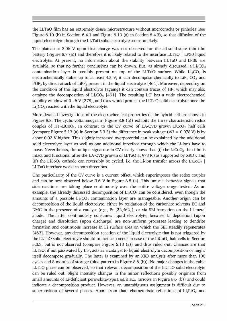
Seite 215
the LLTaO film has an extremely dense microstructure without microcracks or pinholes (see Figure 6.10 (b) in Section 6.4.1 and Figure 6.13 (a) in Section 6.4.3), so that diffusion of the liquid electrolyte through the LLTaO solid electrolyte seems unlikely. The plateau at 3.06 V upon first charge was not observed for the all-solid-state thin film battery (Figure 8.7 (a)) and therefore it is likely related to the interface LLTaO | LP30 liquid electrolyte. At present, no information about the stability between LLTaO and LP30 are available, so that no further conclusions can be drawn. But, as already discussed, a Li2CO3 contamination layer is possibly present on top of the LLTaO surface. While Li2CO3 is electrochemically stable up to at least 4.5 V, it can decompose chemically to LiF, CO2 and POF3 by direct attack of LiPF6 present in the liquid electrolyte [461]. Moreover, depending on the condition of the liquid electrolyte (ageing) it can contain traces of HF, which may also catalyze the decomposition of Li2CO3 [461]. The resulting LiF has a wide electrochemical stability window of 0 - 6 V [278], and thus would protect the LLTaO solid electrolyte once the Li2CO3 reacted with the liquid electrolyte. More detailed investigations of the electrochemical properties of the hybrid cell are shown in Figure 8.8. The cyclic voltammogram (Figure 8.8 (a)) exhibits the three characteristic redox couples of HT-LiCoO2. In contrast to the CV curve of LA-CVD grown LiCoO2 half cells (compare Figure 5.13 (a) in Section 5.3.3) the difference in peak voltage (ΔU = 0.078 V) is by about 0.02 V higher. This slightly increased overpotential can be explained by the additional solid electrolyte layer as well as one additional interface through which the Li-ions have to move. Nevertheless, the unique signature in CV clearly shows that (i) the LiCoO2 thin film is intact and functional after the LA-CVD growth of LLTaO at 973 K (as supported by XRD), and (ii) the LiCoO2 cathode can reversibly be cycled, i.e. the Li-ion transfer across the LiCoO2 | LLTaO interface works in both directions. One particularity of the CV curve is a current offset, which superimposes the redox couples and can be best observed below 3.6 V in Figure 8.8 (a). This unusual behavior signals that side reactions are taking place continuously over the entire voltage range tested. As an example, the already discussed decomposition of Li2CO3 can be considered, even though the amounts of a possible Li2CO3 contamination layer are manageable. Another origin can be decomposition of the liquid electrolyte, either by oxidation of the carbonate solvents EC and DMC in the presence of a catalyst (e.g., Pt [22,462]), or via SEI formation on the Li metal anode. The latter continuously consumes liquid electrolyte, because Li deposition (upon charge) and dissolution (upon discharge) are non-uniform processes leading to dendrite formation and continuous increase in Li surface area on which the SEI steadily regenerates [463]. However, any decomposition reaction of the liquid electrolyte that is not triggered by the LLTaO solid electrolyte should in fact also occur in case of the LiCoO2 half cells in Section 5.3.3, but is not observed (compare Figure 5.13 (a)) and thus ruled out. Chances are that LLTaO, if not passivated by LiF, acts as a catalyst to liquid electrolyte decomposition or might itself decompose gradually. The latter is examined by an XRD analysis after more than 100 cycles and 8 months of storage (blue pattern in Figure 8.6 (b)). No major changes in the cubic LLTaO phase can be observed, so that relevant decomposition of the LLTaO solid electrolyte can be ruled out. Slight intensity changes in the minor reflections possibly originate from small amounts of Li-deficient perovskite-type La2LiTaO6 (arrows in Figure 8.6 (b)) and could indicate a decomposition product. However, an unambiguous assignment is difficult due to superposition of several phases. Apart from that, characteristic reflections of Li2PtO3 and
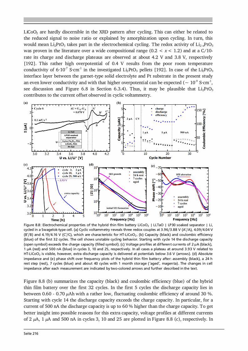
Seite 216
LiCoO2 are hardly discernible in the XRD pattern after cycling. This can either be related to the reduced signal to noise ratio or explained by amorphization upon cycling. In turn, this would mean Li2PtO3 takes part in the electrochemical cycling. The redox activity of Li2-xPtO3 was proven in the literature over a wide compositional range (0.2 < x < 1.2) and at a C/10-rate its charge and discharge plateaus are observed at about 4.2 V and 3.8 V, respectively [192]. This rather high overpotential of 0.4 V results from the poor room temperature conductivity of 6·10-7 S·cm-1 in the investigated Li2PtO3 pellets [192]. In case of the Li2PtO3 interface layer between the garnet-type solid electrolyte and Pt substrate in the present study an even lower conductivity and with that higher overpotential can be expected (~ 10-9 S·cm-1, see discussion and Figure 6.8 in Section 6.3.4). Thus, it may be plausible that Li2PtO3 contributes to the current offset observed in cyclic voltammetry.
Figure 8.8: Electrochemical properties of the hybrid thin film battery LiCoO2 | LLTaO | LP30 soaked separator | Li, cycled in a Swagelok-type cell. (a) Cyclic voltammetry reveals three redox couples at 3.96/3.88 V (A’/A), 4.09/4.04 V (B’/B) and 4.19/4.16 V (C’/C), which are characteristic for HT-LiCoO2. (b) Capacity (black) and coulombic efficiency (blue) of the first 32 cycles. The cell shows unstable cycling behavior. Starting with cycle 14 the discharge capacity (open symbol) exceeds the charge capacity (filled symbol). (c) Voltage profiles at different currents of 2 μA (black), 1 μA (red) and 500 nA (blue) in cycles 3, 10 and 25, respectively. In all cases a plateau at around 3.93 V related to HT-LiCoO2 is visible, however, extra discharge capacity is delivered at potentials below 3.6 V (arrows). (d) Absolute impedance and (e) phase shift over frequency plots of the hybrid thin film battery after: assembly (black), a 24 h rest step (red), 7 cycles (blue) and about 40 cycles with 1 month storage (‘aged’, magenta). The changes in cell impedance after each measurement are indicated by two-colored arrows and further described in the text. Figure 8.8 (b) summarizes the capacity (black) and coulombic efficiency (blue) of the hybrid thin film battery over the first 32 cycles. In the first 5 cycles the discharge capacity lies in between 0.60 - 0.70 μAh with a rather low, fluctuating coulombic efficiency of around 30 %. Starting with cycle 14 the discharge capacity exceeds the charge capacity. In particular, for a current of 500 nA the discharge capacity is up to 60 % higher than the charge capacity. To get better insight into possible reasons for this extra capacity, voltage profiles at different currents of 2 μA, 1 μA and 500 nA in cycles 3, 10 and 25 are plotted in Figure 8.8 (c), respectively. In
Seite 217
all cases a plateau at around 3.93 V related to HT-LiCoO2 is visible during charging and discharging. Yet, the majority of discharge capacity is delivered at potentials below 3.6 V (arrows). Among the above discussed possibilities, it seems likely that Li intercalation into the Li2-xPtO3 interface layer is the main supplier of this extra capacity. The reason is that the additional plateau in the discharge profiles shifts to higher voltages the lower the applied current. In other words, lower currents reduce the overpotential for Li intercalation into Li2-xPtO3 and shift its reduction potential into the investigated voltage range of 3.0 - 4.2 V. This would also explain why only extra capacity upon discharge and not upon charge is observed. Assuming symmetric anodic and cathodic overpotentials around a mean value of 4.0 V for Li2-xPtO3 (according to [192]) and estimating the reduction potential at a current of 500 nA to 3.4 V (blue arrow in Figure 8.8 (c)) allows to assign the oxidation potential to about 4.6 V in the present case. Thus, Li cannot be extracted from the Li2-xPtO3 upon charging to (only) 4.2 V. Still it is questionable how all the Li (supplied by the Li metal anode) is inserted into the Li2-xPtO3 interface if it is never withdrawn again. The larger area (ALPO) of the Li2-xPtO3 interface layer sandwiched between LLTaO solid electrolyte and Pt-foil (ALPO = APt - ALC O ≈ 17.11 mm2) compared to the area of the LiCoO2 cathode (ALC O ≈ 3.14 mm2) can hardly answer this question. Impedance spectroscopy (Figure 8.8 (d) and (e)) is used to monitor the changes in cell impedance and discussed qualitatively in the following. Comparing the IS measurements directly after cell assembly (black) and after a 24 h rest step (red) reveals the first change, namely a lowering of the cell impedance, which is ascribed to initial SEI formation on the Li metal anode (see Figure 8.8 (d)). After 7 cycles (blue) the absolute impedance is almost unchanged, but the phase shift curve clearly shows an additional contribution at a frequency of about 100 Hz (see Figure 8.8 (e)). Plausible explanations are either the alteration of the existing SEI on the Li metal anode, or the formation of a new SEI layer on top of the LLTaO solid electrolyte after initial cycling. After about 40 cycles and 1 month of storage (aged, magenta) the impedance of the hybrid cell is significantly increased and such an increase can be assigned to SEI growth. The earlier described process of continuous SEI reformation on the Li metal anode upon cycling is accompanied by liquid electrolyte decomposition, which can be expected to deteriorate the liquid electrolyte’s properties such as its ionic conductivity. This effect is observable in the high frequency region ( 105 Hz) by an increase in both absolute impedance and phase shift. In summary, the hybrid cell with liquid electrolyte in addition to the solid electrolyte and with Li metal anode could be cycled successfully. The analyses show that the LiCoO2 thin film is intact and functional after the LA-CVD growth of LLTaO despite the rather high deposition temperature of 973 K. Furthermore, the Li-ion transfer across the LiCoO2 | LLTaO interface works reversibly. Based on these findings it is suggested that the LLTaO | Cu interface of the dysfunctional all-solid-state thin film battery should be tackled with highest priority. One may work on improving the interfacial contact between LLTaO and Cu, or switch to a Li metal anode, e.g., by thermal evaporation (see Section 8.4.2).
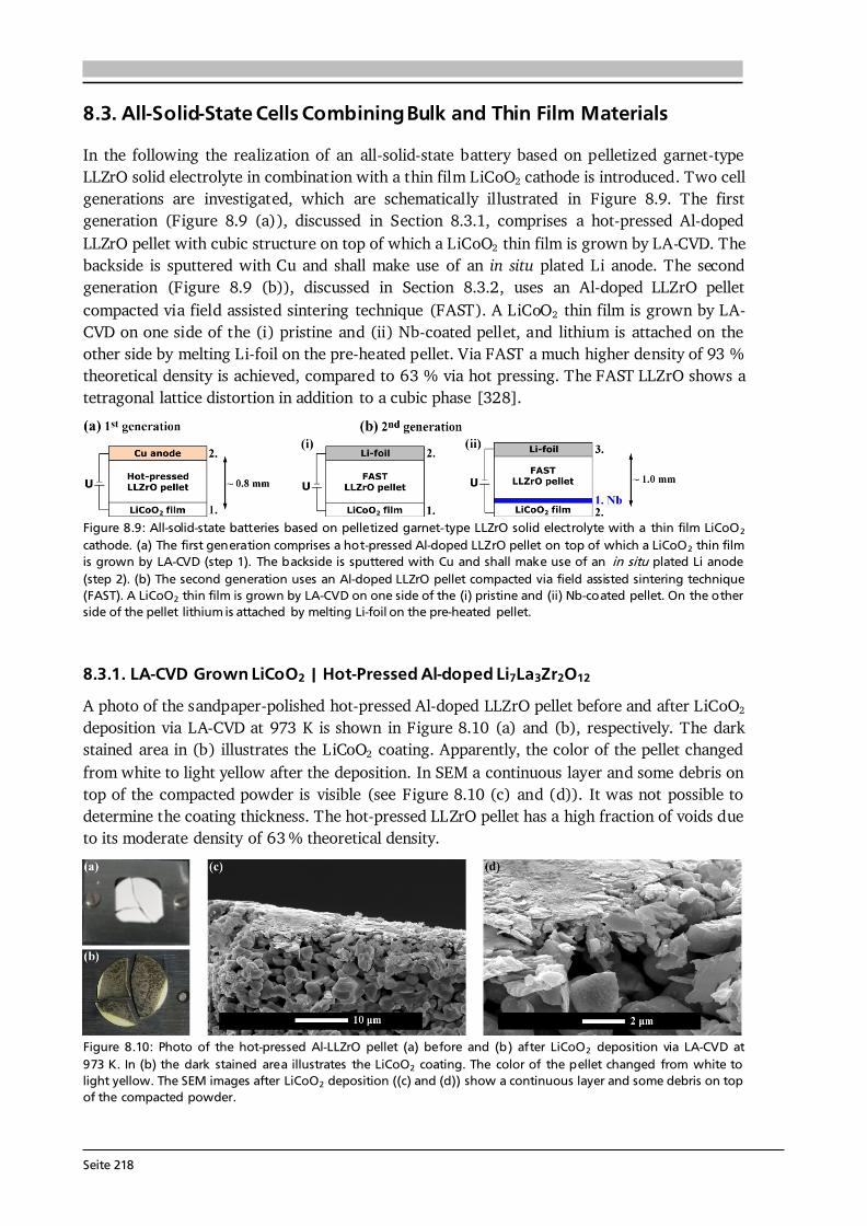
Seite 218
8.3. All-Solid-State Cells Combining Bulk and Thin Film Materials In the following the realization of an all-solid-state battery based on pelletized garnet-type LLZrO solid electrolyte in combination with a thin film LiCoO2 cathode is introduced. Two cell generations are investigated, which are schematically illustrated in Figure 8.9. The first generation (Figure 8.9 (a)), discussed in Section 8.3.1, comprises a hot-pressed Al-doped LLZrO pellet with cubic structure on top of which a LiCoO2 thin film is grown by LA-CVD. The backside is sputtered with Cu and shall make use of an in situ plated Li anode. The second generation (Figure 8.9 (b)), discussed in Section 8.3.2, uses an Al-doped LLZrO pellet compacted via field assisted sintering technique (FAST). A LiCoO2 thin film is grown by LA-CVD on one side of the (i) pristine and (ii) Nb-coated pellet, and lithium is attached on the other side by melting Li-foil on the pre-heated pellet. Via FAST a much higher density of 93 % theoretical density is achieved, compared to 63 % via hot pressing. The FAST LLZrO shows a tetragonal lattice distortion in addition to a cubic phase [328].
Figure 8.9: All-solid-state batteries based on pelletized garnet-type LLZrO solid electrolyte with a thin film LiCoO2 cathode. (a) The first generation comprises a hot-pressed Al-doped LLZrO pellet on top of which a LiCoO2 thin film is grown by LA-CVD (step 1). The backside is sputtered with Cu and shall make use of an in situ plated Li anode (step 2). (b) The second generation uses an Al-doped LLZrO pellet compacted via field assisted sintering technique (FAST). A LiCoO2 thin film is grown by LA-CVD on one side of the (i) pristine and (ii) Nb-coated pellet. On the other side of the pellet lithium is attached by melting Li-foil on the pre-heated pellet.
8.3.1. LA-CVD Grown LiCoO2 | Hot-Pressed Al-doped Li7La3Zr2O12 A photo of the sandpaper-polished hot-pressed Al-doped LLZrO pellet before and after LiCoO2 deposition via LA-CVD at 973 K is shown in Figure 8.10 (a) and (b), respectively. The dark stained area in (b) illustrates the LiCoO2 coating. Apparently, the color of the pellet changed from white to light yellow after the deposition. In SEM a continuous layer and some debris on top of the compacted powder is visible (see Figure 8.10 (c) and (d)). It was not possible to determine the coating thickness. The hot-pressed LLZrO pellet has a high fraction of voids due to its moderate density of 63 % theoretical density.
Figure 8.10: Photo of the hot-pressed Al-LLZrO pellet (a) before and (b) after LiCoO2 deposition via LA-CVD at 973 K. In (b) the dark stained area illustrates the LiCoO2 coating. The color of the pellet changed from white to light yellow. The SEM images after LiCoO2 deposition ((c) and (d)) show a continuous layer and some debris on top of the compacted powder.
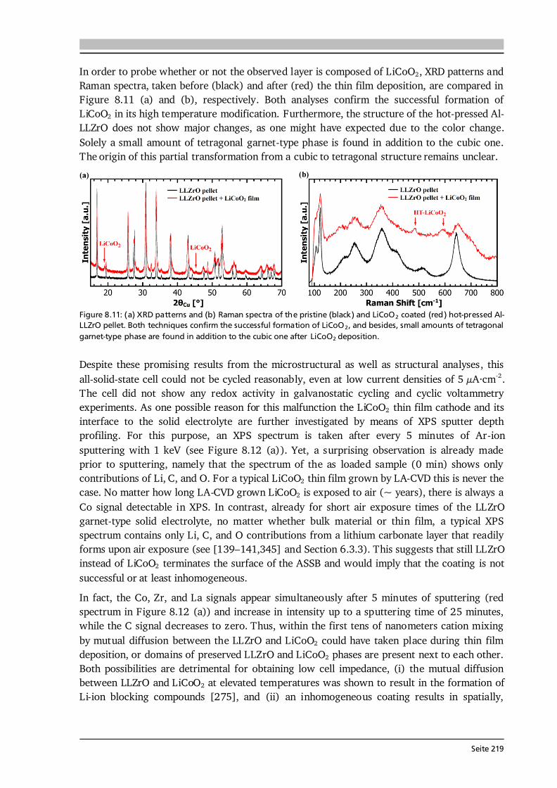
Seite 219
In order to probe whether or not the observed layer is composed of LiCoO2, XRD patterns and Raman spectra, taken before (black) and after (red) the thin film deposition, are compared in Figure 8.11 (a) and (b), respectively. Both analyses confirm the successful formation of LiCoO2 in its high temperature modification. Furthermore, the structure of the hot-pressed Al-LLZrO does not show major changes, as one might have expected due to the color change. Solely a small amount of tetragonal garnet-type phase is found in addition to the cubic one. The origin of this partial transformation from a cubic to tetragonal structure remains unclear.
Figure 8.11: (a) XRD patterns and (b) Raman spectra of the pristine (black) and LiCoO2 coated (red) hot-pressed Al-LLZrO pellet. Both techniques confirm the successful formation of LiCoO2, and besides, small amounts of tetragonal garnet-type phase are found in addition to the cubic one after LiCoO2 deposition. Despite these promising results from the microstructural as well as structural analyses, this all-solid-state cell could not be cycled reasonably, even at low current densities of 5 μA·cm-2. The cell did not show any redox activity in galvanostatic cycling and cyclic voltammetry experiments. As one possible reason for this malfunction the LiCoO2 thin film cathode and its interface to the solid electrolyte are further investigated by means of XPS sputter depth profiling. For this purpose, an XPS spectrum is taken after every 5 minutes of Ar-ion sputtering with 1 keV (see Figure 8.12 (a)). Yet, a surprising observation is already made prior to sputtering, namely that the spectrum of the as loaded sample (0 min) shows only contributions of Li, C, and O. For a typical LiCoO2 thin film grown by LA-CVD this is never the case. No matter how long LA-CVD grown LiCoO2 is exposed to air (~ years), there is always a Co signal detectable in XPS. In contrast, already for short air exposure times of the LLZrO garnet-type solid electrolyte, no matter whether bulk material or thin film, a typical XPS spectrum contains only Li, C, and O contributions from a lithium carbonate layer that readily forms upon air exposure (see [139–141,345] and Section 6.3.3). This suggests that still LLZrO instead of LiCoO2 terminates the surface of the ASSB and would imply that the coating is not successful or at least inhomogeneous. In fact, the Co, Zr, and La signals appear simultaneously after 5 minutes of sputtering (red spectrum in Figure 8.12 (a)) and increase in intensity up to a sputtering time of 25 minutes, while the C signal decreases to zero. Thus, within the first tens of nanometers cation mixing by mutual diffusion between the LLZrO and LiCoO2 could have taken place during thin film deposition, or domains of preserved LLZrO and LiCoO2 phases are present next to each other. Both possibilities are detrimental for obtaining low cell impedance, (i) the mutual diffusion between LLZrO and LiCoO2 at elevated temperatures was shown to result in the formation of Li-ion blocking compounds [275], and (ii) an inhomogeneous coating results in spatially,
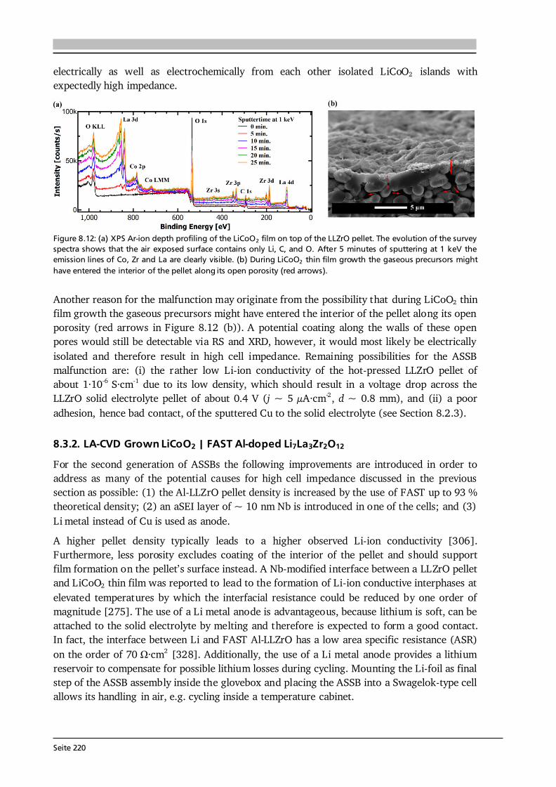
Seite 220
electrically as well as electrochemically from each other isolated LiCoO2 islands with expectedly high impedance.
Figure 8.12: (a) XPS Ar-ion depth profiling of the LiCoO2 film on top of the LLZrO pellet. The evolution of the survey spectra shows that the air exposed surface contains only Li, C, and O. After 5 minutes of sputtering at 1 keV the emission lines of Co, Zr and La are clearly visible. (b) During LiCoO2 thin film growth the gaseous precursors might have entered the interior of the pellet along its open porosity (red arrows). Another reason for the malfunction may originate from the possibility that during LiCoO2 thin film growth the gaseous precursors might have entered the interior of the pellet along its open porosity (red arrows in Figure 8.12 (b)). A potential coating along the walls of these open pores would still be detectable via RS and XRD, however, it would most likely be electrically isolated and therefore result in high cell impedance. Remaining possibilities for the ASSB malfunction are: (i) the rather low Li-ion conductivity of the hot-pressed LLZrO pellet of about 1·10-6 S·cm-1 due to its low density, which should result in a voltage drop across the LLZrO solid electrolyte pellet of about 0.4 V (j ~ 5 μA·cm-2, d ~ 0.8 mm), and (ii) a poor adhesion, hence bad contact, of the sputtered Cu to the solid electrolyte (see Section 8.2.3). 8.3.2. LA-CVD Grown LiCoO2 | FAST Al-doped Li7La3Zr2O12 For the second generation of ASSBs the following improvements are introduced in order to address as many of the potential causes for high cell impedance discussed in the previous section as possible: (1) the Al-LLZrO pellet density is increased by the use of FAST up to 93 % theoretical density; (2) an aSEI layer of ~ 10 nm Nb is introduced in one of the cells; and (3) Li metal instead of Cu is used as anode. A higher pellet density typically leads to a higher observed Li-ion conductivity [306]. Furthermore, less porosity excludes coating of the interior of the pellet and should support film formation on the pellet’s surface instead. A Nb-modified interface between a LLZrO pellet and LiCoO2 thin film was reported to lead to the formation of Li-ion conductive interphases at elevated temperatures by which the interfacial resistance could be reduced by one order of magnitude [275]. The use of a Li metal anode is advantageous, because lithium is soft, can be attached to the solid electrolyte by melting and therefore is expected to form a good contact. In fact, the interface between Li and FAST Al-LLZrO has a low area specific resistance (ASR) on the order of 70 Ω·cm2 [328]. Additionally, the use of a Li metal anode provides a lithium reservoir to compensate for possible lithium losses during cycling. Mounting the Li-foil as final step of the ASSB assembly inside the glovebox and placing the ASSB into a Swagelok-type cell allows its handling in air, e.g. cycling inside a temperature cabinet.
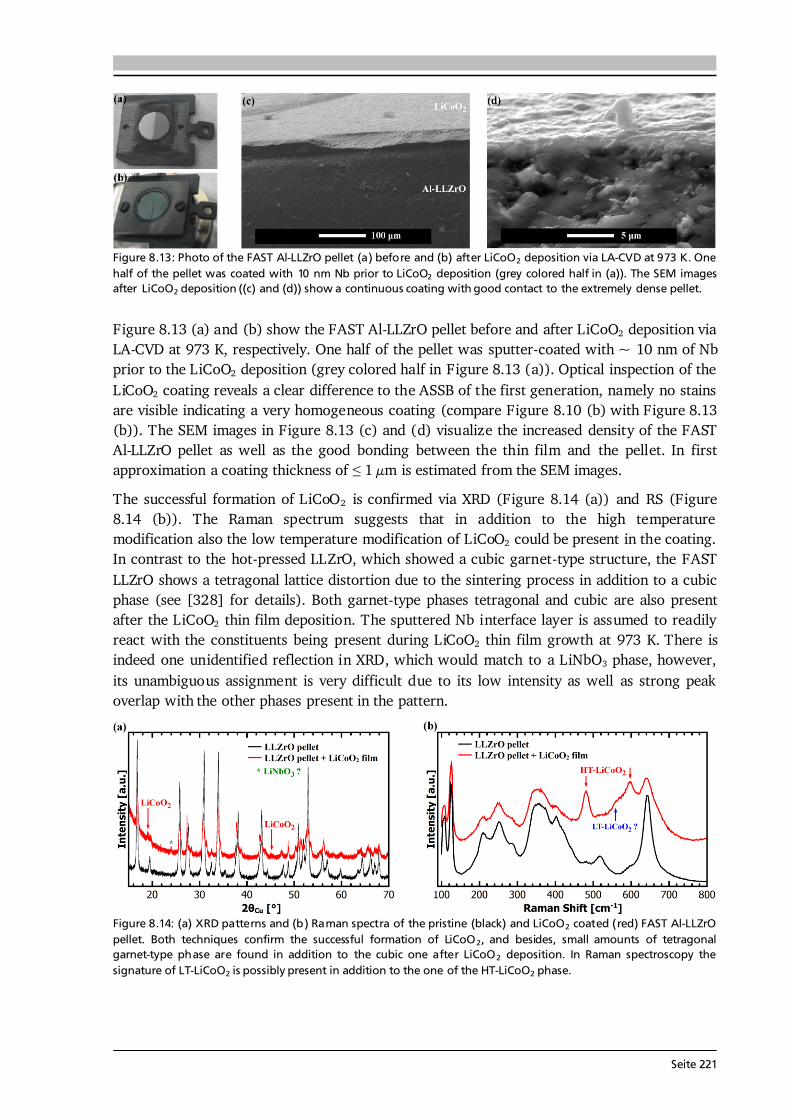
Seite 221
Figure 8.13: Photo of the FAST Al-LLZrO pellet (a) before and (b) after LiCoO2 deposition via LA-CVD at 973 K. One half of the pellet was coated with 10 nm Nb prior to LiCoO2 deposition (grey colored half in (a)). The SEM images after LiCoO2 deposition ((c) and (d)) show a continuous coating with good contact to the extremely dense pellet. Figure 8.13 (a) and (b) show the FAST Al-LLZrO pellet before and after LiCoO2 deposition via LA-CVD at 973 K, respectively. One half of the pellet was sputter-coated with ~ 10 nm of Nb prior to the LiCoO2 deposition (grey colored half in Figure 8.13 (a)). Optical inspection of the LiCoO2 coating reveals a clear difference to the ASSB of the first generation, namely no stains are visible indicating a very homogeneous coating (compare Figure 8.10 (b) with Figure 8.13 (b)). The SEM images in Figure 8.13 (c) and (d) visualize the increased density of the FAST Al-LLZrO pellet as well as the good bonding between the thin film and the pellet. In first approximation a coating thickness of ≤ 1 μm is estimated from the SEM images. The successful formation of LiCoO2 is confirmed via XRD (Figure 8.14 (a)) and RS (Figure 8.14 (b)). The Raman spectrum suggests that in addition to the high temperature modification also the low temperature modification of LiCoO2 could be present in the coating. In contrast to the hot-pressed LLZrO, which showed a cubic garnet-type structure, the FAST LLZrO shows a tetragonal lattice distortion due to the sintering process in addition to a cubic phase (see [328] for details). Both garnet-type phases tetragonal and cubic are also present after the LiCoO2 thin film deposition. The sputtered Nb interface layer is assumed to readily react with the constituents being present during LiCoO2 thin film growth at 973 K. There is indeed one unidentified reflection in XRD, which would match to a LiNbO3 phase, however, its unambiguous assignment is very difficult due to its low intensity as well as strong peak overlap with the other phases present in the pattern.
Figure 8.14: (a) XRD patterns and (b) Raman spectra of the pristine (black) and LiCoO2 coated (red) FAST Al-LLZrO pellet. Both techniques confirm the successful formation of LiCoO2, and besides, small amounts of tetragonal garnet-type phase are found in addition to the cubic one after LiCoO2 deposition. In Raman spectroscopy the signature of LT-LiCoO2 is possibly present in addition to the one of the HT-LiCoO2 phase.
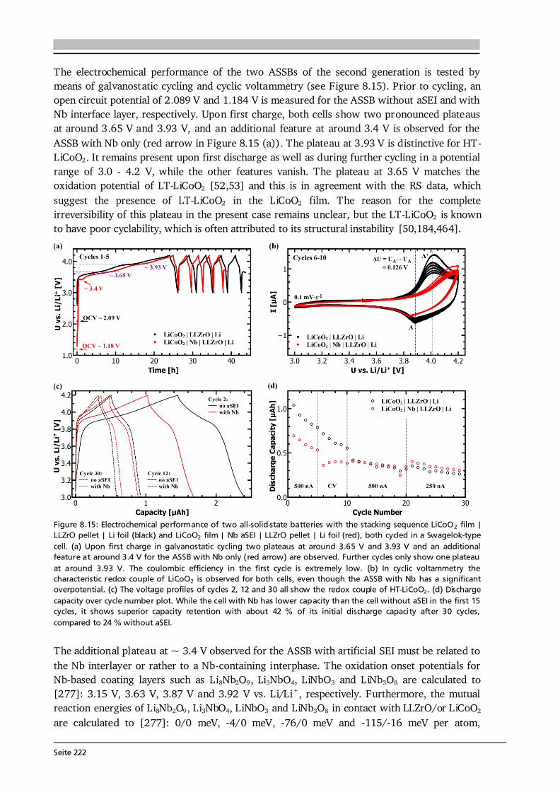
Seite 222
The electrochemical performance of the two ASSBs of the second generation is tested by means of galvanostatic cycling and cyclic voltammetry (see Figure 8.15). Prior to cycling, an open circuit potential of 2.089 V and 1.184 V is measured for the ASSB without aSEI and with Nb interface layer, respectively. Upon first charge, both cells show two pronounced plateaus at around 3.65 V and 3.93 V, and an additional feature at around 3.4 V is observed for the ASSB with Nb only (red arrow in Figure 8.15 (a)). The plateau at 3.93 V is distinctive for HT-LiCoO2. It remains present upon first discharge as well as during further cycling in a potential range of 3.0 - 4.2 V, while the other features vanish. The plateau at 3.65 V matches the oxidation potential of LT-LiCoO2 [52,53] and this is in agreement with the RS data, which suggest the presence of LT-LiCoO2 in the LiCoO2 film. The reason for the complete irreversibility of this plateau in the present case remains unclear, but the LT-LiCoO2 is known to have poor cyclability, which is often attributed to its structural instability [50,184,464].
Figure 8.15: Electrochemical performance of two all-solid-state batteries with the stacking sequence LiCoO2 film | LLZrO pellet | Li foil (black) and LiCoO2 film | Nb aSEI | LLZrO pellet | Li foil (red), both cycled in a Swagelok-type cell. (a) Upon first charge in galvanostatic cycling two plateaus at around 3.65 V and 3.93 V and an additional feature at around 3.4 V for the ASSB with Nb only (red arrow) are observed. Further cycles only show one plateau at around 3.93 V. The coulombic efficiency in the first cycle is extremely low. (b) In cyclic voltammetry the characteristic redox couple of LiCoO2 is observed for both cells, even though the ASSB with Nb has a significant overpotential. (c) The voltage profiles of cycles 2, 12 and 30 all show the redox couple of HT-LiCoO2. (d) Discharge capacity over cycle number plot. While the cell with Nb has lower capacity than the cell without aSEI in the first 15 cycles, it shows superior capacity retention with about 42 % of its initial discharge capacity after 30 cycles, compared to 24 % without aSEI. The additional plateau at ~ 3.4 V observed for the ASSB with artificial SEI must be related to the Nb interlayer or rather to a Nb-containing interphase. The oxidation onset potentials for Nb-based coating layers such as Li8Nb2O9, Li3NbO4, LiNbO3 and LiNb3O8 are calculated to [277]: 3.15 V, 3.63 V, 3.87 V and 3.92 V vs. Li/Li+, respectively. Furthermore, the mutual reaction energies of Li8Nb2O9, Li3NbO4, LiNbO3 and LiNb3O8 in contact with LLZrO/or LiCoO2 are calculated to [277]: 0/0 meV, -4/0 meV, -76/0 meV and -115/-16 meV per atom,
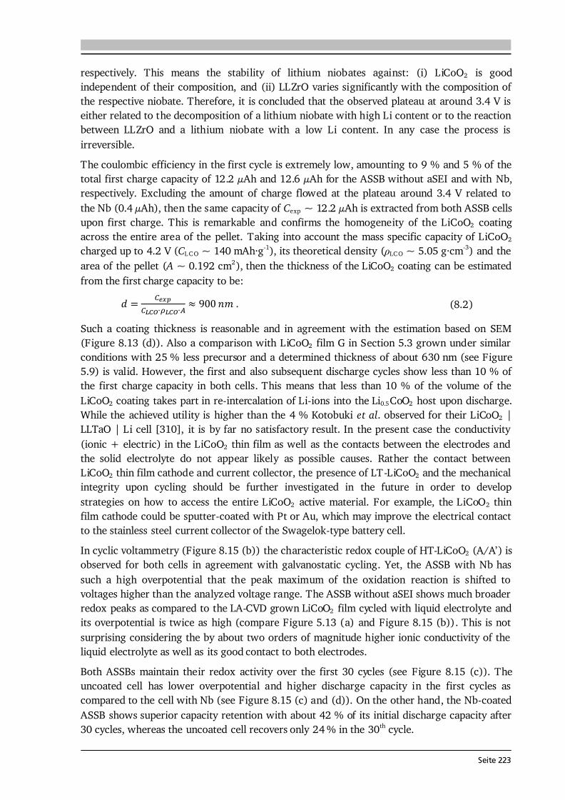
Seite 223
respectively. This means the stability of lithium niobates against: (i) LiCoO2 is good independent of their composition, and (ii) LLZrO varies significantly with the composition of the respective niobate. Therefore, it is concluded that the observed plateau at around 3.4 V is either related to the decomposition of a lithium niobate with high Li content or to the reaction between LLZrO and a lithium niobate with a low Li content. In any case the process is irreversible. The coulombic efficiency in the first cycle is extremely low, amounting to 9 % and 5 % of the total first charge capacity of 12.2 μAh and 12.6 μAh for the ASSB without aSEI and with Nb, respectively. Excluding the amount of charge flowed at the plateau around 3.4 V related to the Nb (0.4 μAh), then the same capacity of Cexp ~ 12.2 μAh is extracted from both ASSB cells upon first charge. This is remarkable and confirms the homogeneity of the LiCoO2 coating across the entire area of the pellet. Taking into account the mass specific capacity of LiCoO2 charged up to 4.2 V (CL C O ~ 140 mAh·g-1), its theoretical density (ρLC O ~ 5.05 g·cm-3) and the area of the pellet (A ~ 0.192 cm2), then the thickness of the LiCoO2 coating can be estimated from the first charge capacity to be: . (8.2) Such a coating thickness is reasonable and in agreement with the estimation based on SEM (Figure 8.13 (d)). Also a comparison with LiCoO2 film G in Section 5.3 grown under similar conditions with 25 % less precursor and a determined thickness of about 630 nm (see Figure 5.9) is valid. However, the first and also subsequent discharge cycles show less than 10 % of the first charge capacity in both cells. This means that less than 10 % of the volume of the LiCoO2 coating takes part in re-intercalation of Li-ions into the Li0.5CoO2 host upon discharge. While the achieved utility is higher than the 4 % Kotobuki et al. observed for their LiCoO2 | LLTaO | Li cell [310], it is by far no satisfactory result. In the present case the conductivity (ionic + electric) in the LiCoO2 thin film as well as the contacts between the electrodes and the solid electrolyte do not appear likely as possible causes. Rather the contact between LiCoO2 thin film cathode and current collector, the presence of LT-LiCoO2 and the mechanical integrity upon cycling should be further investigated in the future in order to develop strategies on how to access the entire LiCoO2 active material. For example, the LiCoO2 thin film cathode could be sputter-coated with Pt or Au, which may improve the electrical contact to the stainless steel current collector of the Swagelok-type battery cell. In cyclic voltammetry (Figure 8.15 (b)) the characteristic redox couple of HT-LiCoO2 (A/A’) is observed for both cells in agreement with galvanostatic cycling. Yet, the ASSB with Nb has such a high overpotential that the peak maximum of the oxidation reaction is shifted to voltages higher than the analyzed voltage range. The ASSB without aSEI shows much broader redox peaks as compared to the LA-CVD grown LiCoO2 film cycled with liquid electrolyte and its overpotential is twice as high (compare Figure 5.13 (a) and Figure 8.15 (b)). This is not surprising considering the by about two orders of magnitude higher ionic conductivity of the liquid electrolyte as well as its good contact to both electrodes. Both ASSBs maintain their redox activity over the first 30 cycles (see Figure 8.15 (c)). The uncoated cell has lower overpotential and higher discharge capacity in the first cycles as compared to the cell with Nb (see Figure 8.15 (c) and (d)). On the other hand, the Nb-coated ASSB shows superior capacity retention with about 42 % of its initial discharge capacity after 30 cycles, whereas the uncoated cell recovers only 24 % in the 30th cycle.
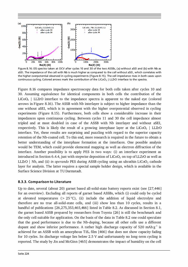
Seite 224
Figure 8.16: EIS spectra taken at OCV after cycles 10 and 30 of the two ASSBs, (a) without aSEI and (b) with Nb as aSEI. The impedance of the cell with Nb is much higher as compared to the cell without aSEI, which correlates with the higher overpotential observed in cycling experiments (Figure 8.15). The cell impedance rises in both cases upon continuous cycling. Colored arrows mark the contribution of the LiCoO2 | LLZrO interface to the spectra. Figure 8.16 compares impedance spectroscopy data for both cells taken after cycles 10 and 30. Assuming equivalence for identical components in both cells the contribution of the LiCoO2 | LLZrO interface to the impedance spectra is apparent to the naked eye (colored arrows in Figure 8.16). The ASSB with Nb interlayer is subject to higher impedance than the one without aSEI, which is in agreement with the higher overpotential observed in cycling experiments (Figure 8.15). Furthermore, both cells show a considerable increase in their impedances upon continuous cycling. Between cycles 11 and 30 the cell impedance almost tripled and at most doubled in case of the ASSB with Nb interlayer and without aSEI, respectively. This is likely the result of a growing interphase layer at the LiCoO2 | LLZrO interface. Yet, these results are surprising and puzzling with regard to the superior capacity retention of the Nb-coated cell. To this end, more research is required in the future to obtain a better understanding of the interphase formation at the interfaces. One possible analysis would be TEM, which could provide elemental mapping as well as electron diffraction of the interface. Another possibility is to apply PES in two ways: (i) an interface experiment as introduced in Section 6.4.4, just with stepwise deposition of LiCoO2 on top of LLZrO as well as LLZrO | Nb, and (ii) in operando PES during ASSB cycling using an ultrathin LiCoO2 cathode layer for analysis. The latter requires a special sample holder design, which is available in the Surface Science Division at TU Darmstadt. 8.3.3. Comparison to Literature Up to date, several (about 20) garnet based all-solid-state battery reports exist (see [27,446] for an overview). Excluding all reports of garnet based ASSBs, which (i) could only be cycled at elevated temperatures (> 25 °C), (ii) include the addition of liquid electrolyte and therefore are no true all-solid-state cells, and (iii) show less than 10 cycles, results in a handful of publications [26,275,353,465,466] listed in Table 8.2. As discussed in Section 8.1, the garnet based ASSB prepared by researchers from Toyota [26] is still the benchmark and the only cell suitable for application. On the basis of the data in Table 8.2 one could speculate that the good performance is due to the Nb-doping, because all other cells use a different dopant and show inferior performance. A rather high discharge capacity of 520 mAh·g-1 is achieved for an ASSB with an amorphous TiS4 film [466] that does not show capacity fading for 10 cycles. Its discharge voltage lies below 2.5 V and unfortunately no long-term cycling is reported. The study by Jin and McGinn [465] demonstrates the impact of humidity on the cell
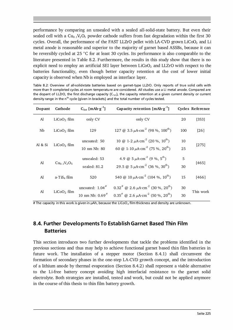
Seite 225
performance by comparing an unsealed with a sealed all-solid-state battery. But even their sealed cell with a Cu0.1V2O5 powder cathode suffers from fast degradation within the first 30 cycles. Overall, the performance of the FAST LLZrO pellet with LA-CVD grown LiCoO2 and Li metal anode is reasonable and superior to the majority of garnet based ASSBs, because it can be reversibly cycled at 25 °C for at least 30 cycles. Its performance is also comparable to the literature presented in Table 8.2. Furthermore, the results in this study show that there is no explicit need to employ an artificial SEI layer between LiCoO2 and LLZrO with respect to the batteries functionality, even though better capacity retention at the cost of lower initial capacity is observed when Nb is employed as interface layer. Table 8.2: Overview of all-solid-state batteries based on garnet-type LLZrO. Only reports of true solid cells with more than 9 completed cycles at room temperature are considered. All studies use a Li metal anode. Compared are the dopant of LLZrO, the first discharge capacity (C1st), the capacity retention at a given current density or current density range in the nth cycle (given in brackets) and the total number of cycles tested.
Dopant Cathode C1st [mAh·g -1] Capacity retention [mAh·g -1] Cycles Reference Al LiCoO2 film only CV only CV 20 [353] Nb LiCoO2 film 129 127 @ 3.5 μA·cm-2 (98 %, 100th) 100 [26]
Al & Si LiCoO2 film uncoated: 50 10 nm Nb: 80
10 @ 1-2 μA·cm-2 (20 %, 10th) 60 @ 1-10 μA·cm-2 (75 %, 20th)
10 25 [275]
Al Cu0.1V2O5 unsealed: 53 sealed: 81.2
4.9 @ 5 μA·cm-2 (9 %, 5th) 29.5 @ 5 μA·cm-2 (36 %, 30th)
5 30 [465]
Al a-TiS4 film 520 540 @ 10 μA·cm-2 (104 %, 10th) 15 [466] Al LiCoO2 film uncoated: 1.04#
10 nm Nb: 0.69# 0.32# @ 2.6 μA·cm-2 (30 %, 20th) 0.35# @ 2.6 μA·cm-2 (50 %, 20th)
30 30 This work
# The capacity in this work is given in μAh, because the LiCoO2 film thickness and density are unknown.
8.4. Further Developments To Establish Garnet Based Thin Film Batteries This section introduces two further developments that tackle the problems identified in the previous sections and thus may help to achieve functional garnet based thin film batteries in future work. The installation of a stepper motor (Section 8.4.1) shall circumvent the formation of secondary phases in the one-step LA-CVD growth concept, and the introduction of a lithium anode by thermal evaporation (Section 8.4.2) shall represent a viable alternative to the Li-free battery concept avoiding high interfacial resistance to the garnet solid electrolyte. Both strategies are installed, tested and work, but could not be applied anymore in the course of this thesis to thin film battery growth.
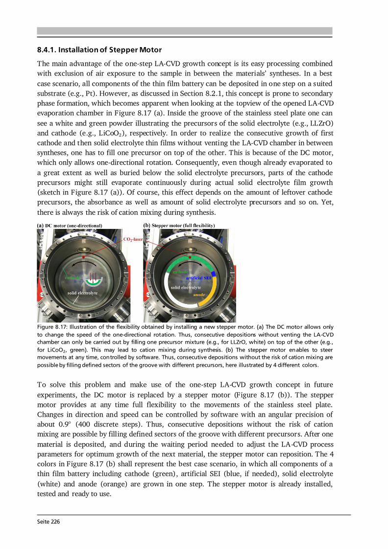
Seite 226
8.4.1. Installation of Stepper Motor The main advantage of the one-step LA-CVD growth concept is its easy processing combined with exclusion of air exposure to the sample in between the materials’ syntheses. In a best case scenario, all components of the thin film battery can be deposited in one step on a suited substrate (e.g., Pt). However, as discussed in Section 8.2.1, this concept is prone to secondary phase formation, which becomes apparent when looking at the topview of the opened LA-CVD evaporation chamber in Figure 8.17 (a). Inside the groove of the stainless steel plate one can see a white and green powder illustrating the precursors of the solid electrolyte (e.g., LLZrO) and cathode (e.g., LiCoO2), respectively. In order to realize the consecutive growth of first cathode and then solid electrolyte thin films without venting the LA-CVD chamber in between syntheses, one has to fill one precursor on top of the other. This is because of the DC motor, which only allows one-directional rotation. Consequently, even though already evaporated to a great extent as well as buried below the solid electrolyte precursors, parts of the cathode precursors might still evaporate continuously during actual solid electrolyte film growth (sketch in Figure 8.17 (a)). Of course, this effect depends on the amount of leftover cathode precursors, the absorbance as well as amount of solid electrolyte precursors and so on. Yet, there is always the risk of cation mixing during synthesis.
Figure 8.17: Illustration of the flexibility obtained by installing a new stepper motor. (a) The DC motor allows only to change the speed of the one-directional rotation. Thus, consecutive depositions without venting the LA-CVD chamber can only be carried out by filling one precursor mixture (e.g., for LLZrO, white) on top of the other (e.g., for LiCoO2, green). This may lead to cation mixing during synthesis. (b) The stepper motor enables to steer movements at any time, controlled by software. Thus, consecutive depositions without the risk of cation mixing are possible by filling defined sectors of the groove with different precursors, here illustrated by 4 different colors. To solve this problem and make use of the one-step LA-CVD growth concept in future experiments, the DC motor is replaced by a stepper motor (Figure 8.17 (b)). The stepper motor provides at any time full flexibility to the movements of the stainless steel plate. Changes in direction and speed can be controlled by software with an angular precision of about 0.9° (400 discrete steps). Thus, consecutive depositions without the risk of cation mixing are possible by filling defined sectors of the groove with different precursors. After one material is deposited, and during the waiting period needed to adjust the LA-CVD process parameters for optimum growth of the next material, the stepper motor can reposition. The 4 colors in Figure 8.17 (b) shall represent the best case scenario, in which all components of a thin film battery including cathode (green), artificial SEI (blue, if needed), solid electrolyte (white) and anode (orange) are grown in one step. The stepper motor is already installed, tested and ready to use.
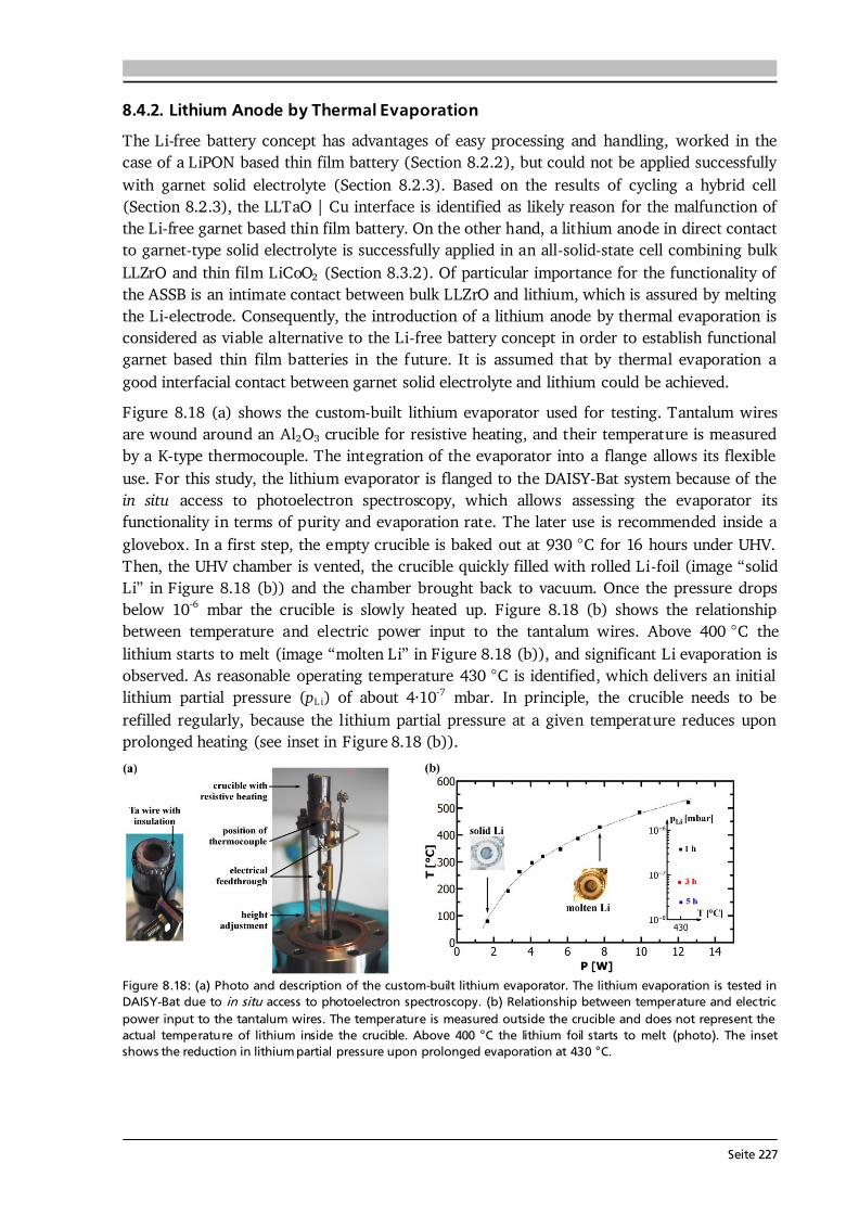
Seite 227
8.4.2. Lithium Anode by Thermal Evaporation The Li-free battery concept has advantages of easy processing and handling, worked in the case of a LiPON based thin film battery (Section 8.2.2), but could not be applied successfully with garnet solid electrolyte (Section 8.2.3). Based on the results of cycling a hybrid cell (Section 8.2.3), the LLTaO | Cu interface is identified as likely reason for the malfunction of the Li-free garnet based thin film battery. On the other hand, a lithium anode in direct contact to garnet-type solid electrolyte is successfully applied in an all-solid-state cell combining bulk LLZrO and thin film LiCoO2 (Section 8.3.2). Of particular importance for the functionality of the ASSB is an intimate contact between bulk LLZrO and lithium, which is assured by melting the Li-electrode. Consequently, the introduction of a lithium anode by thermal evaporation is considered as viable alternative to the Li-free battery concept in order to establish functional garnet based thin film batteries in the future. It is assumed that by thermal evaporation a good interfacial contact between garnet solid electrolyte and lithium could be achieved. Figure 8.18 (a) shows the custom-built lithium evaporator used for testing. Tantalum wires are wound around an Al2O3 crucible for resistive heating, and their temperature is measured by a K-type thermocouple. The integration of the evaporator into a flange allows its flexible use. For this study, the lithium evaporator is flanged to the DAISY-Bat system because of the in situ access to photoelectron spectroscopy, which allows assessing the evaporator its functionality in terms of purity and evaporation rate. The later use is recommended inside a glovebox. In a first step, the empty crucible is baked out at 930 °C for 16 hours under UHV. Then, the UHV chamber is vented, the crucible quickly filled with rolled Li-foil (image “solid Li” in Figure 8.18 (b)) and the chamber brought back to vacuum. Once the pressure drops below 10-6 mbar the crucible is slowly heated up. Figure 8.18 (b) shows the relationship between temperature and electric power input to the tantalum wires. Above 400 °C the lithium starts to melt (image “molten Li” in Figure 8.18 (b)), and significant Li evaporation is observed. As reasonable operating temperature 430 °C is identified, which delivers an initial lithium partial pressure (pL i) of about 4·10-7 mbar. In principle, the crucible needs to be refilled regularly, because the lithium partial pressure at a given temperature reduces upon prolonged heating (see inset in Figure 8.18 (b)).
Figure 8.18: (a) Photo and description of the custom-built lithium evaporator. The lithium evaporation is tested in DAISY-Bat due to in situ access to photoelectron spectroscopy. (b) Relationship between temperature and electric power input to the tantalum wires. The temperature is measured outside the crucible and does not represent the actual temperature of lithium inside the crucible. Above 400 °C the lithium foil starts to melt (photo). The inset shows the reduction in lithium partial pressure upon prolonged evaporation at 430 °C.
Seite 228
The stepwise deposition of Li on Cu-foil at a lithium partial pressure of pL i ≈ 3·10-8 mbar is investigated by XPS (Figure 8.19). Prior to the deposition, the Cu-foil is cleaned via Ar-ion sputtering at 2 keV for 10 minutes (black spectra). Residual carbon is completely removed and only traces of Cu2O are left. Successive deposition of lithium attenuates the Cu signal and eventually leads to the growth of a metallic lithium layer, which can be judged by the sharp Li 1s emission line (green spectrum in (d), FWHM ~ 0.7 eV). Besides, no carbon is detected and the oxygen concentration at the surface does not change significantly upon lithium deposition. The remaining oxygen (4 - 8 at.-%) is a result of the residual gas reacting to Cu2O and/or Li2O. Figure 8.19 (e) summarizes the element concentration in dependence on the lithium deposition time. It is concluded that metallic lithium with a high level of purity is deposited via the custom-built evaporator. An estimation of the surface coverage in monolayers (ML) based on the Langmuir approximation assuming a sticking coefficient of 1 leads to: . (8.3) With approximately 3.5 Å·ML -1 a 77 Å thin lithium layer is deposited in 16 minutes. It shall be noted that the thickness estimation of 77 Å agrees well with the observed attenuation of the XPS signal. This deposition rate of about 5 Å·min-1 is already 5 times as high as the typical deposition rate achieved with the Li-dispenser used for the interface experiment in Section 6.4.4, despite the fact that lithium was already depleted (pL i ≈ 3·10-8 mbar). Next to refilling the crucible, the use of a crucible with larger diameter, an increase in temperature and a decrease in the sample to evaporator distance are ways to further increase the deposition rate.
Figure 8.19: XPS spectra for the stepwise deposition of Li on Cu-foil: (a) Cu 2p, (b) O 1s, (c) C 1s and (d) Li 1s. Prior to Li deposition, the Cu-foil is cleaned via Ar-ion sputtering at 2 keV for 10 minutes (black spectra). Residual carbon is completely removed and only traces of Cu2O are left. Successive deposition of lithium (red: 60 s, blue: 360 s, green: 960 s) attenuates the Cu signal and eventually leads to the growth of a metallic lithium layer. (e) Summary of the element concentration in dependence on the lithium deposition time. In order to deposit well defined lithium anodes, e.g., congruent to the circular LiCoO2 cathodes, existing shadow masks can be used. It is recommended to install the thermal Li evaporator inside the glovebox due to (i) the need for a regular refill with lithium, (ii) the possibility to remove residues on the Li-foil prior to filling, which otherwise might float on top of the molten Li and reduce the effective surface area for evaporation, and (iii) further processing of the final thin film battery under inert gas. The necessary equipment such as a vacuum line to the inside of the glovebox, a small evaporation chamber, power supply and temperature control unit are either already installed or readily available. Because an ultra-low resistance between garnet-type solid electrolyte and lithium may (only) be achieved by
Seite 229
interfaces free of Li2CO3 and LiOH [460], future work shall also make use of the possibility to transfer the sample under inert gas or under vacuum from DAISY-Bat to the glovebox. 8.5. Conclusion and Outlook In this chapter, garnet based ASSBs are investigated in form of thin film batteries and by combining bulk LLZrO with thin film LiCoO2. Moreover, the study comprises (i) battery design, processing and assembly aspects, (ii) the investigation of a reference LiPON thin film battery as well as a hybrid cell with liquid electrolyte in addition to the solid electrolyte, and (iii) further developments needed to establish garnet based thin film batteries in the future. The results show that:
the one-step LA-CVD growth concept in its current form is prone to secondary phase formation and needs further development. a two-step growth of 4 circular cathodes of 2 mm in diameter covered by a 9 x 9 mm2 solid electrolyte layer is currently best suited for thin film battery preparation. the Li-free battery concept is functional as proven by a LiPON based thin film battery. the LiCoO2 phase is preserved upon LA-CVD growth of LLTaO at 973 K, but nevertheless the LiCoO2 | LLTaO thin film battery could not be cycled. a hybrid cell with stacking sequence LiCoO2 | LLTaO | LP30 soaked separator | Li could be cycled successfully, which confirms that the LiCoO2 thin film is functional and indicates that Li-ion transfer across the LiCoO2 | LLTaO interface works reversibly. a Li-free ASSB combining hot-pressed Al-LLZrO solid electrolyte (63 % density) with LA-CVD grown LiCoO2 cathode could not be cycled. ASSBs comprising Al-LLZrO solid electrolyte sintered by FAST (93 % density), LA-CVD grown LiCoO2 cathode and Li metal anode show reasonable cycling performance at 298 K, with and without the application of an artificial SEI of Nb. applying 10 nm of Nb as artificial SEI results in lower initial discharge capacity, higher overpotential due to higher interfacial resistance, but also in better capacity retention. installation of a stepper motor provides more flexibility in thin film battery growth. via a custom-built Li evaporator layers of metallic lithium can be deposited with a rate of at least 5 Å·min-1, enabling the use of highly pure lithium anodes in the future.
For future research the following main topics are identified:
LiCoO2 | LLTaO | Li thin film battery Based on the findings of successful cycling a hybrid cell it is concluded that the LiCoO2 | LLTaO interface is functional and therefore the LLTaO | Cu interface of the Li-free thin film battery needs to be improved. While improving the interfacial contact between LLTaO and Cu is possible via a bonding agent or by applying post-annealing, external pressure and the like, it is recommended to better switch to a Li metal anode. Efforts should be made to transfer the Li evaporator tested under UHV conditions in Section 8.4.2 into a glovebox. Then, one could
Seite 230
either make use of a Li thin film anode, or attach Li-foil onto the Li thin film in addition. The latter might be of particular interest for bulk-type ASSBs using pellets. In any case, an ultra-low interfacial resistance between garnet-type solid electrolyte and Li metal anode becomes possible, because of an ultra-clean interface (see [460]). In order to avoid Li2CO3, LiOH and other contaminations, the sample transfer between DAISY-Bat and glovebox can, and for thin film battery application also should, be carried out under inert gas or under vacuum. One-step LA-CVD growth concept
The potential advantage of this concept is its easy processing with thin film battery fabrication in one step combined with the exclusion of air exposure to the sample in between syntheses. The installation of a stepper motor (Section 8.4.1) ensures that this concept can be realized in the future. As described in Section 8.2.1, there might still be the risk of easier secondary phase formation compared to the two-step concept. However, in case a clean surface of the cathode (when depositing the garnet solid electrolyte) is as important as in the case of the garnet solid electrolyte (when depositing the Li anode) for achieving a low interfacial resistance [460], then the one-step LA-CVD growth concept would be of great advantage. A comparative study between the one-step and two-step concepts by using the same materials, e.g., LiCoO2 and LLTaO thin films, can clarify potential benefits of either method. Investigation of Nb-based garnet ASSBs
It is surprising that, despite the massive research and development activities in recent years, the garnet ASSB based on Nb-doped LLZrO [26], already developed in 2012, is still the benchmark. Whether this is related to the properties of Nb or not could be further investigated in the future. Two kinds of Nb-based garnet ASSBs come into question, namely the use of either Li5La3Nb2O12 or Li6.75La3Zr1.75Nb0.25O12 solid electrolyte. Li5La3Nb2O12 has a higher ionic conductivity, lower activation energy and is more reducible than its Ta-based counterpart [23]. Therefore, an LA-CVD growth parameter study should be carried out in order to evaluate whether the Li5La3Nb2O12 phase is as robust as Li5La3Ta2O12 (Section 6.4), or as delicate as Li7La3Zr2O12 (Section 6.3) with respect to the growth conditions. Also, the growth of cubic Li6.75La3Zr1.75Nb0.25O12 may be investigated, similarly to the doping studies in Section 6.3.5. Chances are reasonable that the Nb-based garnets promote the formation of conductive interphases at their interfaces, especially on the cathode side, more than other dopants do and by this enhance the battery performance. Interface experiments (see next point) can give valuable insights in this respect. Interface study and in operando PES
As already proposed in Section 6.6, interfaces on the cathode side are worth to be investigated in future experiments by a surface science approach within DAISY-Bat. One could start with already established material systems such as the LLTaO | LiCoO2, LLZrO | LiCoO2 or Al-doped LLZrO | LiCoO2 interfaces and compare their interphase chemistries. Complemented by theory, further promising material combinations should be identified, their interfaces studied and their application tested in thin film batteries. In DAISY-Bat it is also possible to do in operando PES measurements during ASSB cycling, which requires ultrathin films of the active material to be investigated. The aim is to get a fundamental understanding of the (electro-) chemistry at the interface and by this to establish ASSBs with stable type 1 or at least type 3 interfaces (electronic insulator, Li-ion conductor) in the future.
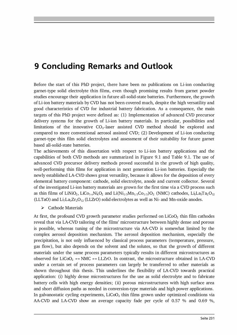
Seite 231
9 Concluding Remarks and Outlook Before the start of this PhD project, there have been no publications on Li-ion conducting garnet-type solid electrolyte thin films, even though promising results from garnet powder studies encourage their application in future all-solid-state batteries. Furthermore, the growth of Li-ion battery materials by CVD has not been covered much, despite the high versatility and good characteristics of CVD for industrial battery fabrication. As a consequence, the main targets of this PhD project were defined as: (1) Implementation of advanced CVD precursor delivery systems for the growth of Li-ion battery materials. In particular, possibilities and limitations of the innovative CO2-laser assisted CVD method should be explored and compared to more conventional aerosol assisted CVD; (2) Development of Li-ion conducting garnet-type thin film solid electrolytes and assessment of their suitability for future garnet based all-solid-state batteries. The achievements of this dissertation with respect to Li-ion battery applications and the capabilities of both CVD methods are summarized in Figure 9.1 and Table 9.1. The use of advanced CVD precursor delivery methods proved successful in the growth of high quality, well-performing thin films for application in next generation Li-ion batteries. Especially the newly established LA-CVD shows great versatility, because it allows for the deposition of every elemental battery component: cathode, solid electrolyte, anode and current collector. Several of the investigated Li-ion battery materials are grown for the first time via a CVD process such as thin films of LiNiO2, LiCo1-xNixO2 and Li(Ni1/3Mn1/3Co1/3)O2 (NMC) cathodes, Li5La3Ta2O12 (LLTaO) and Li7La3Zr2O12 (LLZrO) solid electrolytes as well as Ni- and Mn-oxide anodes.
Cathode Materials At first, the profound CVD growth parameter studies performed on LiCoO2 thin film cathodes reveal that via LA-CVD tailoring of the films’ microstructure between highly dense and porous is possible, whereas tuning of the microstructure via AA-CVD is somewhat limited by the complex aerosol deposition mechanism. The aerosol deposition mechanism, especially the precipitation, is not only influenced by classical process parameters (temperature, pressure, gas flow), but also depends on the solvent and the solutes, so that the growth of different materials under the same process parameters typically results in different microstructures as observed for LiCoO2 ↔ NMC ↔ LLZrO. In contrast, the microstructure obtained in LA-CVD under a certain set of process parameters can largely be transferred to other materials as shown throughout this thesis. This underlines the flexibility of LA-CVD towards practical application: (i) highly dense microstructures for the use as solid electrolyte and to fabricate battery cells with high energy densities; (ii) porous microstructures with high surface area and short diffusion paths as needed in conversion-type materials and high power applications. In galvanostatic cycling experiments, LiCoO2 thin films grown under optimized conditions via AA-CVD and LA-CVD show an average capacity fade per cycle of 0.57 % and 0.69 %,
Seite 232
respectively. This compares well with literature reports, especially considering that the LiCoO2 films in this study are stored under air and that no post-annealing treatment is applied. The replacement of Co by Ni into layered, electrochemically active LiCo1-xNixO2 films, motivated by lower cost and increased capacity, is successfully achieved via LA-CVD, whereas electrochemically inactive NiO forms using AA-CVD. Yet, no performance improvements compared to LiCoO2 films are realized. The cathode material with most complex composition investigated in this thesis is NMC, which is well-known for its excellent capacity retention. Both CVD methods allow for the growth of high quality NMC thin films with reasonable performance, i.e. comparable to the one of LiCoO2 films grown under similar conditions as well as to literature. There are only a few reports on NMC thin film deposition and the present study represents the first one via CVD. This demonstrates the capability of both methods to grow multicomponent, functional Li(TM)O2 thin film cathodes. In fact, this study shows that it is easy to grow multicomponent thin films with any desired stoichiometry via AA-CVD, whereas the stoichiometry needs to be optimized once for each new composition via LA-CVD. Another finding is that all Li(TM)O2 films grow with (003)-texture independent of the CVD method. This texture is unfavored due to slow Li-ion diffusion along the (003) direction and it is held responsible for the poor high rate performance of the CVD grown Li(TM)O2 thin films in comparison to their bulk ceramic counterparts. The observed corrosion of the Pt substrate, which leads to Li2PtO3 formation in both CVD methods, is also unfavored. A clear correlation of Li2PtO3 formation with the applied process parameters could be identified in AA-CVD, and in LA-CVD it is possible to suppress the Li2PtO3 formation when growing Li(TM)O2 films. Nonetheless, among several substrates tested Pt is considered the best choice.
Figure 9.1: Graphic summary of the results achieved in this PhD project via aerosol and CO2-laser assisted chemical vapor deposition paving the way for several next generation Li -ion battery concepts. The color code on the left (AA-CVD) and right (LA-CVD) of each battery component represents the status reached (see legend).
Solid Electrolyte Materials Taking the next step, the garnet-type solid electrolytes LLTaO and LLZrO are studied due to their high ionic conductivity and proposed stability towards Li. In AA-CVD, under all investigated growth conditions, films with a hollow sphere microstructure and no indication
Seite 233
for a garnet-type phase are grown. Based on these findings it is concluded that AA-CVD is unsuited for garnet-type thin film growth, at least in its given configuration. In contrast, LA-CVD is capable of growing high quality garnet-type thin films that are dense, uniform, free of cracks and free of carbon. While the growth of tetragonal LLZrO is successful only within a narrow growth parameter sweet spot, cubic LLTaO films grow within a much wider range of LA-CVD growth parameters. Furthermore, the growth of cubic LLZrO thin films via LA-CVD could be achieved by means of doping studies with Al and Ga. Two important milestones for proper analyses of the ionic conductivity of the grown solid electrolyte films are: (i) establishing the microcontact impedance spectroscopy measurement setup inside the glovebox; and (ii) the proof that Li2PtO3, whose formation could not be suppressed in garnet thin film growth, exclusively forms at the interface to the Pt substrate, so that garnet solid electrolyte film and Li2PtO3 interface layer can be interpreted as series connection. The ionic conductivity at 298 K of as-deposited tetragonal LLZrO and cubic LLTaO films is determined to 4.2·10-6 S·cm-1 (Ea = 0.50 eV) and 7.8·10-6 S·cm-1 (Ea = 0.66 eV), respectively. Moreover, the ionic conductivity of cubic LLTaO films could be enhanced up to 3.8·10-5 S·cm-1 (Ea = 0.52 eV) via post-annealing. For both garnet compounds the achieved conductivities are close to the highest values reported for bulk ceramic studies and they are among the highest values reported for respective garnet-type thin films up to date (Table 6.1). These results indicate the high quality of the garnet-type thin films grown by LA-CVD and qualify them as suitable candidates for the use in all-solid-state thin film LiBs. The finding that cubic LLTaO has a larger growth parameter sweet spot and is easier to stabilize than cubic LLZrO provides a playground for fundamental studies. One example is the study of the influence of grain boundaries in fine-grained and coarse-grained LLTaO films on their conductivity: the fine-grained film exhibits mainly bulk ionic conduction, whereas the coarse-grained film shows an additional grain boundary contribution, which is ascribed to a geometrical constriction impeding the ionic current flow. By another study, the chemical stability between LLTaO and Li is proven experimentally for the first time, i.e. in an interface experiment no reaction products related to decomposition of LLTaO as well as no structural changes in the LLTaO matrix are detected upon stepwise adsorption of Li. This is a valuable contribution to the recent debate on the stability between garnet solid electrolytes and Li. Anode Materials
Conversion-type TM-oxide thin film anodes, studied due to their promising attributes for next generation LiBs such as high theoretical specific capacities (> 700 mAh·g-1), non-toxicity and natural abundance, are grown under optimized conditions of LiCoO2. As a result, the Co-oxide films grown by LA-CVD are composed of Co3O4 and CoO, whereas phase pure Co3O4, NiO, and Mn3O4 thin films are grown by AA-CVD. The Co-oxide films deposited via LA-CVD are highly dense, show a relatively fast capacity fade and poor rate capability, which is ascribed to typical limitations in conversion-type materials like low electrical conductivity and slow Li-ion diffusion. Moreover, it is found that thick and dense TM-oxide films promote performance losses due to incomplete lithiation and (early) loss of integrity, thus are unsuited for application. The TM-oxide films grown by AA-CVD show a more porous microstructure and can be cycled several hundred times at moderate C-rates of C/2 and C. The best electrochemical performance is found for the NiO film with > 700 cycles tested, in which it delivers specific capacities of 500 mAh·g-1 at C/2 and 300 mAh·g-1 at C. The good performance of the NiO film
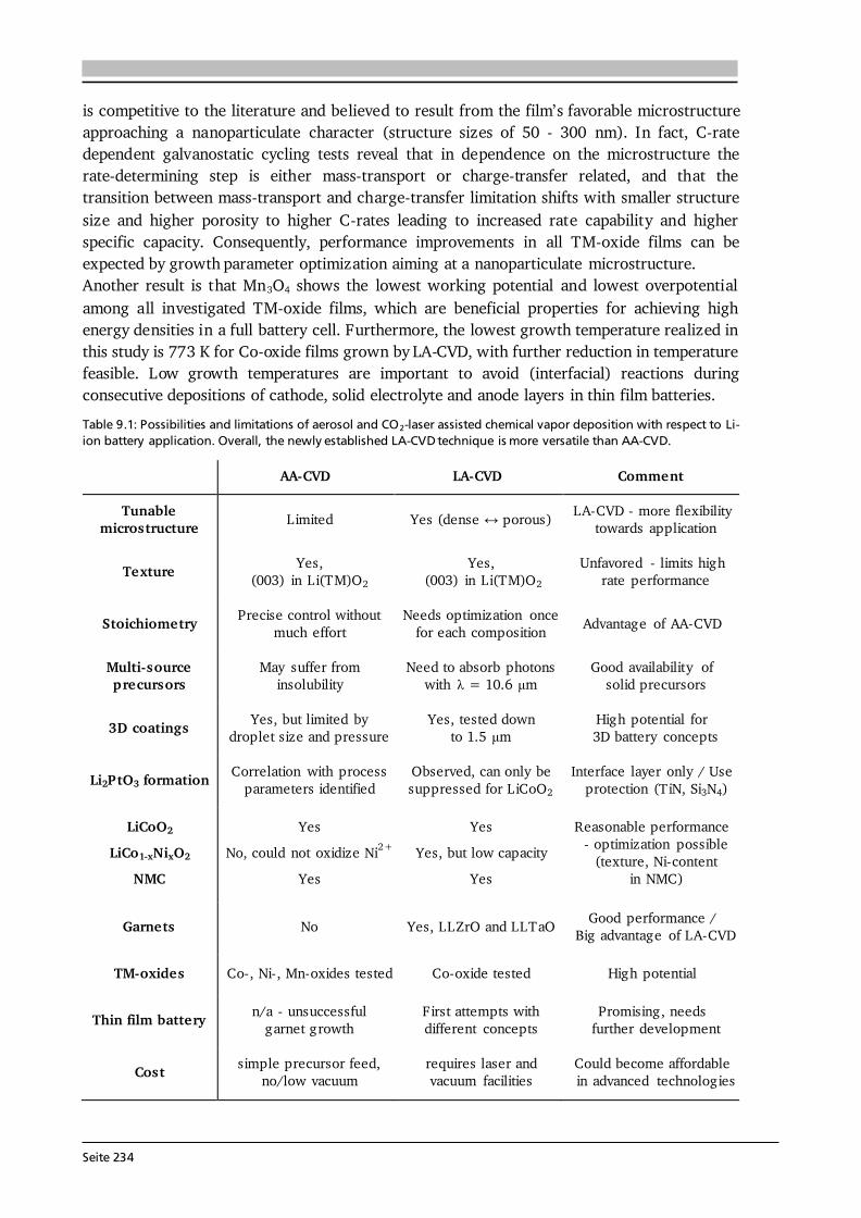
Seite 234
is competitive to the literature and believed to result from the film’s favorable microstructure approaching a nanoparticulate character (structure sizes of 50 - 300 nm). In fact, C-rate dependent galvanostatic cycling tests reveal that in dependence on the microstructure the rate-determining step is either mass-transport or charge-transfer related, and that the transition between mass-transport and charge-transfer limitation shifts with smaller structure size and higher porosity to higher C-rates leading to increased rate capability and higher specific capacity. Consequently, performance improvements in all TM-oxide films can be expected by growth parameter optimization aiming at a nanoparticulate microstructure. Another result is that Mn3O4 shows the lowest working potential and lowest overpotential among all investigated TM-oxide films, which are beneficial properties for achieving high energy densities in a full battery cell. Furthermore, the lowest growth temperature realized in this study is 773 K for Co-oxide films grown by LA-CVD, with further reduction in temperature feasible. Low growth temperatures are important to avoid (interfacial) reactions during consecutive depositions of cathode, solid electrolyte and anode layers in thin film batteries. Table 9.1: Possibilities and limitations of aerosol and CO2-laser assisted chemical vapor deposition with respect to Li-ion battery application. Overall, the newly established LA-CVD technique is more versatile than AA-CVD.
AA-CVD LA-CVD Comment Tunable microstructure Limited Yes (dense ↔ porous) LA-CVD - more flexibility towards application Texture Yes, (003) in Li(TM)O2
Yes, (003) in Li(TM)O2 Unfavored - limits high rate performance Stoichiometry Precise control without much effort Needs optimization once for each composition Advantage of AA-CVD Multi-source precursors May suffer from insolubility Need to absorb photons with = 10.6 m Good availability of solid precursors 3D coatings Yes, but limited by droplet size and pressure Yes, tested down to 1.5 m High potential for 3D battery concepts
Li2PtO3 formation Correlation with process parameters identified Observed, can only be suppressed for LiCoO2 Interface layer only / Use protection (TiN, Si3N4) LiCoO2
LiCo1-xNixO2 NMC
Yes No, could not oxidize Ni2+
Yes Yes
Yes, but low capacity Yes
Reasonable performance - optimization possible (texture, Ni-content in NMC) Garnets No Yes, LLZrO and LLTaO Good performance / Big advantage of LA-CVD
TM-oxides Co-, Ni-, Mn-oxides tested Co-oxide tested High potential Thin film battery n/a - unsuccessful garnet growth First attempts with different concepts Promising, needs further development
Cost simple precursor feed, no/low vacuum requires laser and vacuum facilities Could become affordable in advanced technologies
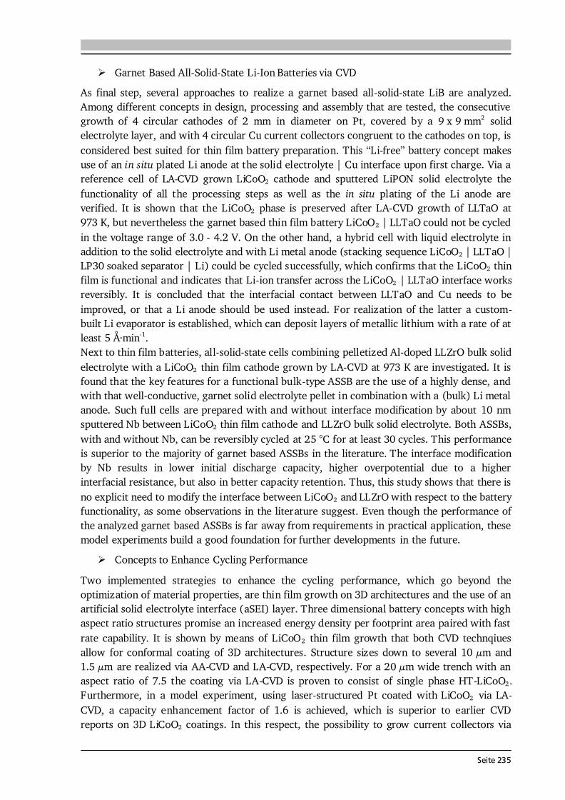
Seite 235
Garnet Based All-Solid-State Li-Ion Batteries via CVD As final step, several approaches to realize a garnet based all-solid-state LiB are analyzed. Among different concepts in design, processing and assembly that are tested, the consecutive growth of 4 circular cathodes of 2 mm in diameter on Pt, covered by a 9 x 9 mm2 solid electrolyte layer, and with 4 circular Cu current collectors congruent to the cathodes on top, is considered best suited for thin film battery preparation. This “Li-free” battery concept makes use of an in situ plated Li anode at the solid electrolyte | Cu interface upon first charge. Via a reference cell of LA-CVD grown LiCoO2 cathode and sputtered LiPON solid electrolyte the functionality of all the processing steps as well as the in situ plating of the Li anode are verified. It is shown that the LiCoO2 phase is preserved after LA-CVD growth of LLTaO at 973 K, but nevertheless the garnet based thin film battery LiCoO2 | LLTaO could not be cycled in the voltage range of 3.0 - 4.2 V. On the other hand, a hybrid cell with liquid electrolyte in addition to the solid electrolyte and with Li metal anode (stacking sequence LiCoO2 | LLTaO | LP30 soaked separator | Li) could be cycled successfully, which confirms that the LiCoO2 thin film is functional and indicates that Li-ion transfer across the LiCoO2 | LLTaO interface works reversibly. It is concluded that the interfacial contact between LLTaO and Cu needs to be improved, or that a Li anode should be used instead. For realization of the latter a custom-built Li evaporator is established, which can deposit layers of metallic lithium with a rate of at least 5 Å·min-1. Next to thin film batteries, all-solid-state cells combining pelletized Al-doped LLZrO bulk solid electrolyte with a LiCoO2 thin film cathode grown by LA-CVD at 973 K are investigated. It is found that the key features for a functional bulk-type ASSB are the use of a highly dense, and with that well-conductive, garnet solid electrolyte pellet in combination with a (bulk) Li metal anode. Such full cells are prepared with and without interface modification by about 10 nm sputtered Nb between LiCoO2 thin film cathode and LLZrO bulk solid electrolyte. Both ASSBs, with and without Nb, can be reversibly cycled at 25 °C for at least 30 cycles. This performance is superior to the majority of garnet based ASSBs in the literature. The interface modification by Nb results in lower initial discharge capacity, higher overpotential due to a higher interfacial resistance, but also in better capacity retention. Thus, this study shows that there is no explicit need to modify the interface between LiCoO2 and LLZrO with respect to the battery functionality, as some observations in the literature suggest. Even though the performance of the analyzed garnet based ASSBs is far away from requirements in practical application, these model experiments build a good foundation for further developments in the future.
Concepts to Enhance Cycling Performance Two implemented strategies to enhance the cycling performance, which go beyond the optimization of material properties, are thin film growth on 3D architectures and the use of an artificial solid electrolyte interface (aSEI) layer. Three dimensional battery concepts with high aspect ratio structures promise an increased energy density per footprint area paired with fast rate capability. It is shown by means of LiCoO2 thin film growth that both CVD technqiues allow for conformal coating of 3D architectures. Structure sizes down to several 10 μm and 1.5 μm are realized via AA-CVD and LA-CVD, respectively. For a 20 μm wide trench with an aspect ratio of 7.5 the coating via LA-CVD is proven to consist of single phase HT-LiCoO2. Furthermore, in a model experiment, using laser-structured Pt coated with LiCoO2 via LA-CVD, a capacity enhancement factor of 1.6 is achieved, which is superior to earlier CVD reports on 3D LiCoO2 coatings. In this respect, the possibility to grow current collectors via
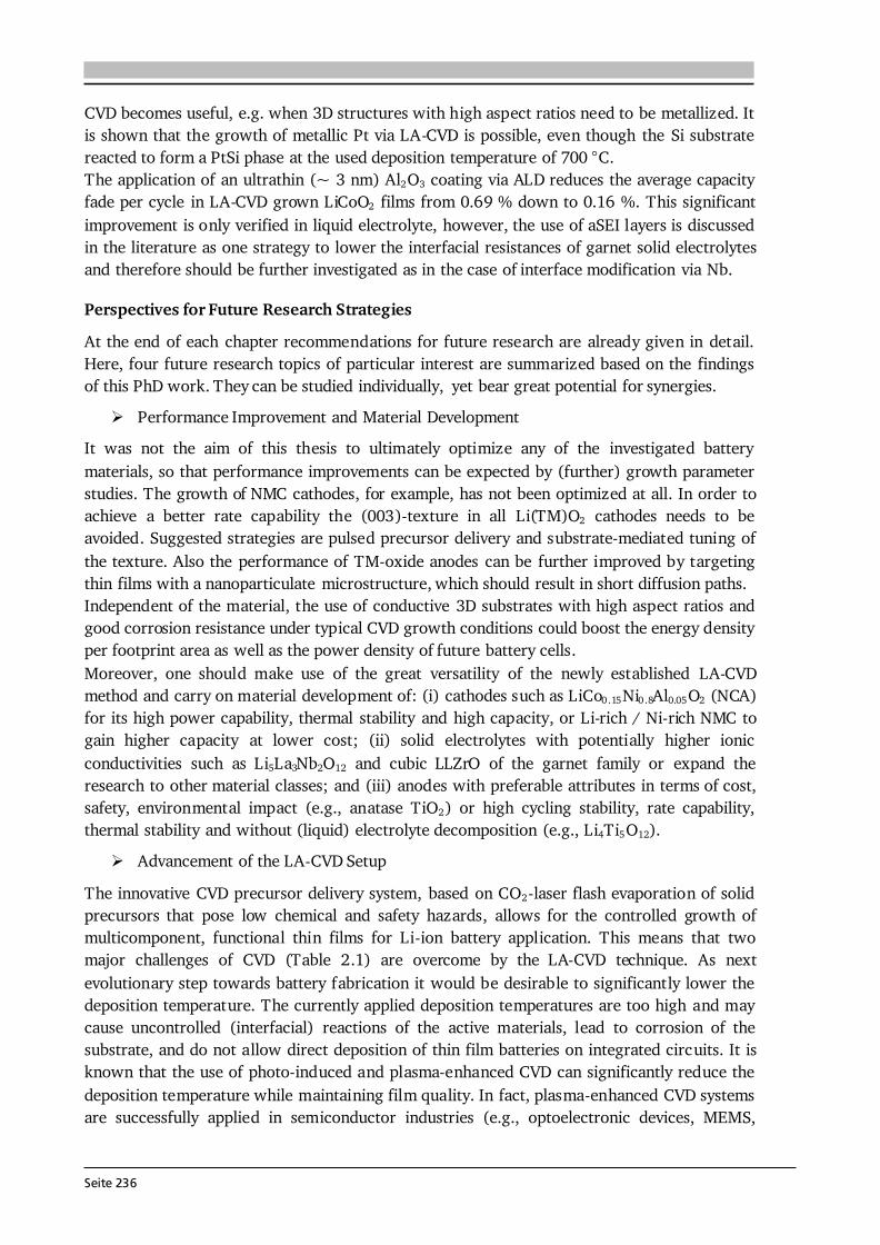
Seite 236
CVD becomes useful, e.g. when 3D structures with high aspect ratios need to be metallized. It is shown that the growth of metallic Pt via LA-CVD is possible, even though the Si substrate reacted to form a PtSi phase at the used deposition temperature of 700 °C. The application of an ultrathin (~ 3 nm) Al2O3 coating via ALD reduces the average capacity fade per cycle in LA-CVD grown LiCoO2 films from 0.69 % down to 0.16 %. This significant improvement is only verified in liquid electrolyte, however, the use of aSEI layers is discussed in the literature as one strategy to lower the interfacial resistances of garnet solid electrolytes and therefore should be further investigated as in the case of interface modification via Nb. Perspectives for Future Research Strategies At the end of each chapter recommendations for future research are already given in detail. Here, four future research topics of particular interest are summarized based on the findings of this PhD work. They can be studied individually, yet bear great potential for synergies.
Performance Improvement and Material Development It was not the aim of this thesis to ultimately optimize any of the investigated battery materials, so that performance improvements can be expected by (further) growth parameter studies. The growth of NMC cathodes, for example, has not been optimized at all. In order to achieve a better rate capability the (003)-texture in all Li(TM)O2 cathodes needs to be avoided. Suggested strategies are pulsed precursor delivery and substrate-mediated tuning of the texture. Also the performance of TM-oxide anodes can be further improved by targeting thin films with a nanoparticulate microstructure, which should result in short diffusion paths. Independent of the material, the use of conductive 3D substrates with high aspect ratios and good corrosion resistance under typical CVD growth conditions could boost the energy density per footprint area as well as the power density of future battery cells. Moreover, one should make use of the great versatility of the newly established LA-CVD method and carry on material development of: (i) cathodes such as LiCo0.15Ni0.8Al0.05O2 (NCA) for its high power capability, thermal stability and high capacity, or Li-rich / Ni-rich NMC to gain higher capacity at lower cost; (ii) solid electrolytes with potentially higher ionic conductivities such as Li5La3Nb2O12 and cubic LLZrO of the garnet family or expand the research to other material classes; and (iii) anodes with preferable attributes in terms of cost, safety, environmental impact (e.g., anatase TiO2) or high cycling stability, rate capability, thermal stability and without (liquid) electrolyte decomposition (e.g., Li4Ti5O12).
Advancement of the LA-CVD Setup The innovative CVD precursor delivery system, based on CO2-laser flash evaporation of solid precursors that pose low chemical and safety hazards, allows for the controlled growth of multicomponent, functional thin films for Li-ion battery application. This means that two major challenges of CVD (Table 2.1) are overcome by the LA-CVD technique. As next evolutionary step towards battery fabrication it would be desirable to significantly lower the deposition temperature. The currently applied deposition temperatures are too high and may cause uncontrolled (interfacial) reactions of the active materials, lead to corrosion of the substrate, and do not allow direct deposition of thin film batteries on integrated circuits. It is known that the use of photo-induced and plasma-enhanced CVD can significantly reduce the deposition temperature while maintaining film quality. In fact, plasma-enhanced CVD systems are successfully applied in semiconductor industries (e.g., optoelectronic devices, MEMS,
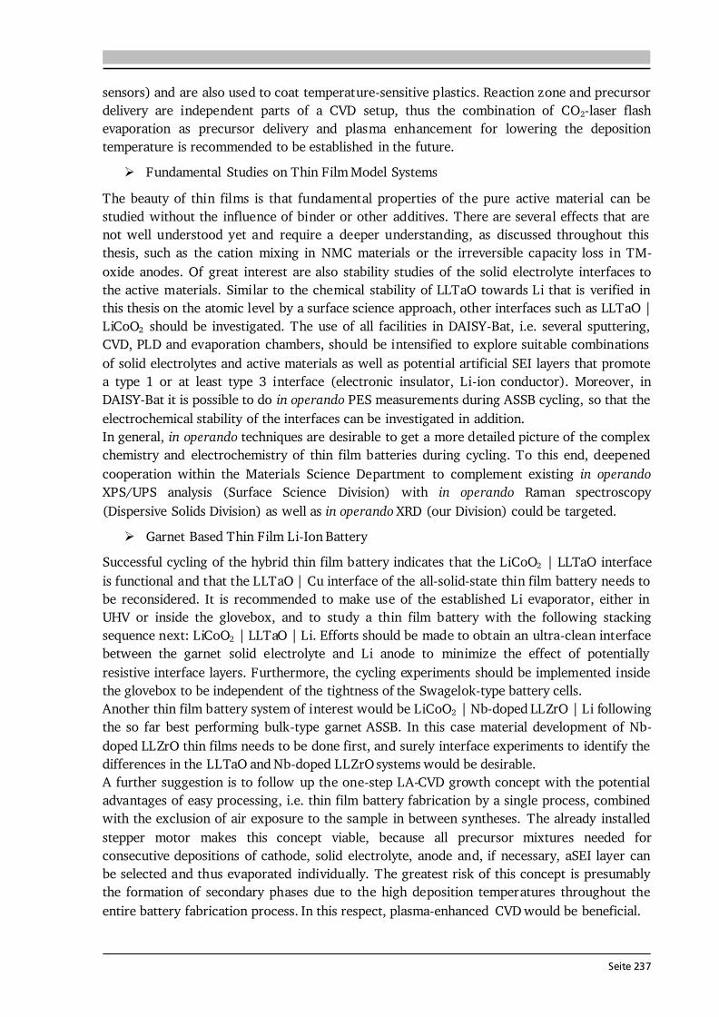
Seite 237
sensors) and are also used to coat temperature-sensitive plastics. Reaction zone and precursor delivery are independent parts of a CVD setup, thus the combination of CO2-laser flash evaporation as precursor delivery and plasma enhancement for lowering the deposition temperature is recommended to be established in the future. Fundamental Studies on Thin Film Model Systems
The beauty of thin films is that fundamental properties of the pure active material can be studied without the influence of binder or other additives. There are several effects that are not well understood yet and require a deeper understanding, as discussed throughout this thesis, such as the cation mixing in NMC materials or the irreversible capacity loss in TM-oxide anodes. Of great interest are also stability studies of the solid electrolyte interfaces to the active materials. Similar to the chemical stability of LLTaO towards Li that is verified in this thesis on the atomic level by a surface science approach, other interfaces such as LLTaO | LiCoO2 should be investigated. The use of all facilities in DAISY-Bat, i.e. several sputtering, CVD, PLD and evaporation chambers, should be intensified to explore suitable combinations of solid electrolytes and active materials as well as potential artificial SEI layers that promote a type 1 or at least type 3 interface (electronic insulator, Li-ion conductor). Moreover, in DAISY-Bat it is possible to do in operando PES measurements during ASSB cycling, so that the electrochemical stability of the interfaces can be investigated in addition. In general, in operando techniques are desirable to get a more detailed picture of the complex chemistry and electrochemistry of thin film batteries during cycling. To this end, deepened cooperation within the Materials Science Department to complement existing in operando XPS/UPS analysis (Surface Science Division) with in operando Raman spectroscopy (Dispersive Solids Division) as well as in operando XRD (our Division) could be targeted. Garnet Based Thin Film Li-Ion Battery
Successful cycling of the hybrid thin film battery indicates that the LiCoO2 | LLTaO interface is functional and that the LLTaO | Cu interface of the all-solid-state thin film battery needs to be reconsidered. It is recommended to make use of the established Li evaporator, either in UHV or inside the glovebox, and to study a thin film battery with the following stacking sequence next: LiCoO2 | LLTaO | Li. Efforts should be made to obtain an ultra-clean interface between the garnet solid electrolyte and Li anode to minimize the effect of potentially resistive interface layers. Furthermore, the cycling experiments should be implemented inside the glovebox to be independent of the tightness of the Swagelok-type battery cells. Another thin film battery system of interest would be LiCoO2 | Nb-doped LLZrO | Li following the so far best performing bulk-type garnet ASSB. In this case material development of Nb-doped LLZrO thin films needs to be done first, and surely interface experiments to identify the differences in the LLTaO and Nb-doped LLZrO systems would be desirable. A further suggestion is to follow up the one-step LA-CVD growth concept with the potential advantages of easy processing, i.e. thin film battery fabrication by a single process, combined with the exclusion of air exposure to the sample in between syntheses. The already installed stepper motor makes this concept viable, because all precursor mixtures needed for consecutive depositions of cathode, solid electrolyte, anode and, if necessary, aSEI layer can be selected and thus evaporated individually. The greatest risk of this concept is presumably the formation of secondary phases due to the high deposition temperatures throughout the entire battery fabrication process. In this respect, plasma-enhanced CVD would be beneficial.

Seite 238
Seite 239
Bibliography [1] R. Smith, Elon Musk makes good on his promise to build world’s biggest battery, (2017). http://www.businessinsider.de/elon-musk-makes-good-on-his-promise-to-build-worlds-biggest-battery-2017-12 (accessed January 01, 2018). [2] LESSY - Lithium Elektrizitäts-Speicher System, Press Release. (2009). https://www.saarland.de/116944.htm (accessed March 01, 2017). [3] GfK, Global smartphone sales hit a quarterly high in Q4 2015, Press Release. (2016). http://www.gfk.com/fileadmin/user_upload/dyna_content/Global/documents/Press_Releases/2016/20160302_GfK_global_smartphone_release_Q42015_vfinal_English_V2.pdf (accessed March 01, 2017). [4] ZSW, Zahl der Elektroautos weltweit auf 1,3 Millionen gestiegen, Press Release. (2016). https://www.zsw-bw.de/fileadmin/user_upload/PDFs/Pressemitteilungen/ 2016/pi05-2016-ZSW-ZahlenElektromobilitaet_01.pdf (accessed March 01, 2017). [5] EnerChip Solid State Batteries, Homepage. (2017). http://www.cymbet.com/products/ enerchip-solid-state-batteries.php (accessed September 19, 2017). [6] K. Ozawa, ed., Lithium ion rechargeable batteries, Wiley-VCH, Weinheim, 2009. [7] D. Linden, T.B. Reddy, eds., Handbook of batteries, 3rd ed., McGraw-Hill, New York, 2001. [8] K.A. Cook-Chennault, N. Thambi, A.M. Sastry, Powering MEMS portable devices — a review of non-regenerative and regenerative power supply systems with special emphasis on piezoelectric energy, Smart Mater. Struct. 17 (2008) 043001. doi:10.1088/0964-1726/17/4/043001. [9] N. Nitta, F. Wu, J.T. Lee, G. Yushin, Li-ion battery materials: present and future, Mater. Today. 18 (2015) 252–264. doi:10.1016/j.mattod.2014.10.040. [10] B. Scrosati, J. Garche, Lithium batteries: Status, prospects and future, J. Power Sources. 195 (2010) 2419–2430. doi:10.1016/j.jpowsour.2009.11.048. [11] C. Sun, J. Liu, Y. Gong, D.P. Wilkinson, J. Zhang, Recent advances in all-solid-state rechargeable lithium batteries, Nano Energy. 33 (2017) 363–386. doi:10.1016/j.nanoen.2017.01.028. [12] Y. Ren, K. Chen, R. Chen, T. Liu, Y. Zhang, C.-W. Nan, Oxide electrolytes for lithium batteries, J. Am. Ceram. Soc. 98 (2015) 3603–3623. doi:10.1111/jace.13844.
Seite 240
[13] J.F.M. Oudenhoven, L. Baggetto, P.H.L. Notten, All-solid-state lithium-ion microbatteries: A review of various three-dimensional concepts, Adv. Energy Mater. 1 (2011) 10–33. doi:10.1002/aenm.201000002. [14] K. Takada, Progress and prospective of solid-state lithium batteries, Acta Mater. 61 (2013) 759–770. doi:10.1016/j.actamat.2012.10.034. [15] J.M. Tarascon, M. Armand, Issues and challenges facing rechargeable lithium batteries., Nature. 414 (2001) 359–67. doi:10.1038/35104644. [16] P.G. Bruce, S.A. Freunberger, L.J. Hardwick, J.-M. Tarascon, Li–O2 and Li–S batteries with high energy storage, Nat. Mater. 11 (2012) 19–29. doi:10.1038/NMAT3191. [17] A. Patil, V. Patil, D. Wook Shin, J.-W. Choi, D.-S. Paik, S.-J. Yoon, Issue and challenges facing rechargeable thin film lithium batteries, Mater. Res. Bull. 43 (2008) 1913–1942. doi:10.1016/j.materresbull.2007.08.031. [18] P. He, H. Yu, D. Li, H. Zhou, Layered lithium transition metal oxide cathodes towards high energy lithium-ion batteries, J. Mater. Chem. 22 (2012) 3680. doi:10.1039/c2jm14305d. [19] J. Yan, X. Liu, B. Li, Recent progress in Li-rich layered oxides as cathode materials for Li-ion batteries, RSC Adv. 4 (2014) 63268–63284. doi:10.1039/C4RA12454E. [20] P. Rozier, J.M. Tarascon, Review — Li-Rich Layered Oxide Cathodes for Next-Generation Li-Ion Batteries: Chances and Challenges, J. Electrochem. Soc. 162 (2015) 2490–2499. doi:10.1149/2.0111514jes. [21] A.A. Schneider, D.E. Harney, M.J. Harney, The lithium-iodine cell for medical and commercial applications, J. Power Sources. 5 (1980) 15–23. [22] W. Xu, X. Chen, F. Ding, J. Xiao, D. Wang, A. Pan, J. Zheng, X.S. Li, A.B. Padmaperuma, J.-G. Zhang, Reinvestigation on the state-of-the-art nonaqueous carbonate electrolytes for 5 V Li-ion battery applications, J. Power Sources. 213 (2012) 304–316. doi:10.1016/j.jpowsour.2012.04.031. [23] V. Thangadurai, H. Kaack, W.J.F. Weppner, Novel fast lithium ion conduction in garnet-type Li5La3M2O12, J. Am. Ceram. Soc. 40 (2003) 437–440. [24] Y. Li, J.-T. Han, C.-A. Wang, H. Xie, J.B. Goodenough, Optimizing Li+ conductivity in a garnet framework, J. Mater. Chem. 22 (2012) 15357–15361. doi:10.1039/C2JM31413D. [25] V. Thangadurai, S. Narayanan, D. Pinzaru, Garnet-type solid-state fast Li ion conductors for Li batteries: critical review, Chem. Soc. Rev. 43 (2014) 4714–4727. doi:10.1039/C4CS00020J. [26] S. Ohta, T. Kobayashi, J. Seki, T. Asaoka, Electrochemical performance of an all-solid-state lithium ion battery with garnet-type oxide electrolyte, J. Power Sources. 202 (2012) 332–335. doi:10.1016/j.jpowsour.2011.10.064.
Seite 241
[27] K. Kerman, A. Luntz, V. Viswanathan, Y. Chiang, Z. Chen, Review — Practical Challenges Hindering the Development of Solid State Li Ion Batteries, J. Electrochem. Soc. 164 (2017) A1731–A1744. doi:10.1149/2.1571707jes. [28] M. Kotobuki, H. Munakata, K. Kanamura, Y. Sato, T. Yoshida, Compatibility of Li7La3Zr2O12 Solid Electrolyte to All-Solid-State Battery Using Li Metal Anode, J. Electrochem. Soc. 157 (2010) A1076–A1079. doi:10.1149/1.3474232. [29] T. Kato, T. Hamanaka, K. Yamamoto, T. Hirayama, F. Sagane, M. Motoyama, Y. Iriyama, In-situ Li7La3Zr2O12/LiCoO2 interface modification for advanced all-solid-state battery, J. Power Sources. 260 (2014) 292–298. doi:10.1016/j.jpowsour.2014.02.102. [30] K.H. Kim, Y. Iriyama, K. Yamamoto, S. Kumazaki, T. Asaka, K. Tanabe, C. a. J. Fisher, T. Hirayama, R. Murugan, Z. Ogumi, Characterization of the interface between LiCoO2 and Li7La3Zr2O12 in an all-solid-state rechargeable lithium battery, J. Power Sources. 196 (2011) 764–767. doi:10.1016/j.jpowsour.2010.07.073. [31] S. Ohta, S. Komagata, J. Seki, T. Saeki, S. Morishita, T. Asaoka, All-solid-state lithium ion battery using garnet-type oxide and Li3BO3 solid eletrolytes fabricated by screen-printing, J. Power Sources. 238 (2013) 53–56. doi:10.1016/j.jpowsour.2013.02.073. [32] S. Ohta, J. Seki, Y. Yagi, Y. Kihira, T. Tani, T. Asaoka, Co-sinterable lithium garnet-type oxide electrolyte with cathode for all-solid-state lithium ion battery, J. Power Sources. 265 (2014) 40–44. doi:10.1016/j.jpowsour.2014.04.065. [33] J.B. Bates, N.J. Dudney, G.R. Gruzalski, R.A. Zuhr, A. Choudhary, C.F. Luck, J.D. Robertson, Electrical properties of amorphous lithium electrolyte thin films, Solid State Ionics. 53-56 (1992) 647–654. [34] J.B. Bates, N.J. Dudney, B. Neudecker, A. Ueda, C.D. Evans, Thin-film lithium and lithium-ion batteries, Solid State Ionics. 135 (2000) 33–45. [35] M.L. Hitchman, K.F. Jensen, eds., Chemical vapor deposition: Principles and applications., Academic Press, London, 1993. [36] L. Baggetto, R.A.H. Niessen, F. Roozeboom, P.H.L. Notten, High Energy Density All-Solid-State Batteries: A Challenging Concept Towards 3D Integration, Adv. Funct. Mater. 18 (2008) 1057–1066. doi:10.1002/adfm.200701245. [37] W.-G. Choi, S.-G. Yoon, Structural and electrical properties of LiCoO2 thin-film cathodes deposited on planar and trench structures by liquid-delivery metalorganic chemical vapour deposition, J. Power Sources. 125 (2004) 236–241. doi:10.1016/j.jpowsour.2003.08.014. [38] J.F.M. Oudenhoven, T. van Dongen, R.A.H. Niessen, M.H.J.M. de Croon, P.H.L. Notten, Low-Pressure Chemical Vapor Deposition of LiCoO2 Thin Films: A Systematic Investigation of the Deposition Parameters, J. Electrochem. Soc. 156 (2009) D169–D174. doi:10.1149/1.3082374. [39] K. Tadanaga, A. Yamaguchi, A. Sakuda, A. Hayashi, M. Tatsumisago, A. Duran, M. Aparacio, Preparation of LiMn2O4 cathode thin films for thin film lithium secondary
Seite 242
batteries by a mist CVD process, Mater. Res. Bull. 53 (2014) 196–198. doi:10.1016/j.materresbull.2014.01.032. [40] C.H. Hamann, W. Vielstich, eds., Elektrochemie, Wiley-VCH Verlag GmbH & Co. KGaA, Weinheim, 2005. [41] R.A. Huggins, ed., Advanced Batteries: Materials Science Aspects, Springer Boston, 2009. [42] M. Winter, R.J. Brodd, What are batteries, fuel cells, and supercapacitors?, Chem. Rev. 104 (2004) 4245–69. http://www.ncbi.nlm.nih.gov/pubmed/15669155. [43] Smart Battery, Homepage. (2017). https://www.lithiumion-batteries.com/ (accessed November 15, 2017). [44] J.B. Goodenough, P. Singh, Review—Solid Electrolytes in Rechargeable Electrochemical Cells, J. Electrochem. Soc. 162 (2015) A2387–A2392. doi:10.1149/2.0021514jes. [45] J. Twentyman, Thin film batteries set for solid (state) growth, Web Ref. (2017). https://internetofbusiness.com/thin-film-batteries-set-solid-state-growth/ (accessed November 16, 2017). [46] Lithium-ion Battery Market is Projected to Reach US $77.42 bn in 2024; Global Industry Analysis, Size, Share, Growth, Trends and Forecast 2016 - 2024: TMR, (2016). https://www.marketwatch.com/story/lithium-ion-battery-market-is-projected-to-reach-us-7742-bn-in-2024-global-industry-analysis-size-share-growth-trends-and-forecast-2016---2024-tmr-2016-09-19 (accessed November 16, 2017). [47] Excellatron, Homepage. (2017). https://www.excellatron.com/overview.htm (accessed September 19, 2017). [48] R. Robert, C. Villevieille, P. Novák, Enhancement of the high potential specific charge in layered electrode materials for lithium-ion batteries, J. Mater. Chem. A. 2 (2014) 8589–8598. doi:10.1039/c3ta12643a. [49] K. Mizushima, P.C. Jones, P.J. Wiseman, J.B. Goodenough, LixCoO2 (0<x<-1): A new cathode material for batteries of high energy density, Mater. Res. Bull. 15 (1980) 783–789. doi:http://dx.doi.org/10.1016/0025-5408(80)90012-4. [50] E. Antolini, LiCoO2: formation, structure, lithium and oxygen nonstoichiometry, electrochemical behaviour and transport properties, Solid State Ionics. 170 (2004) 159–171. doi:10.1016/j.ssi.2004.04.003. [51] B. Garcia, J. Farcy, J.P. Pereira-Ramos, N. Baffier, Electrochemical properties of low temperature crystallized LiCoO2, J. Electrochem. Soc. 144 (1997) 1179–1184. [52] R.J. Gummow, M.M. Thackeray, W.I.F. David, S. Hull, Structure and electrochemistry of lithium cobalt oxide synthesised at 400°C, Mater. Res. Bull. 27 (1992) 327–337. doi:http://dx.doi.org/10.1016/0025-5408(92)90062-5.

Seite 243
[53] E. Rossen, J.N. Reimers, J.R. Dahn, Synthesis and electrochemistry of spinel LT-LiCoO2, Solid State Ionics. 62 (1993) 53–60. [54] S. Tintignac, R. Baddour-Hadjean, J.-P. Pereira-Ramos, R. Salot, High performance sputtered LiCoO2 thin films obtained at a moderate annealing treatment combined to a bias effect, Electrochim. Acta. 60 (2012) 121–129. doi:10.1016/j.electacta.2011.11.033. [55] W. Huang, R. Frech, Vibrational spectroscopic and electrochemical studies of the low and high temperature phases of LiCo1-xMxO2 (M = Ni or Ti), Solid State Ionics. 86-88 (1996) 395–400. [56] J.N. Reimers, J.R. Dahn, Electrochemical and in situ X-ray diffraction studies of lithium intercalation in LixCoO2, J. Electrochem. Soc. 139 (1992) 2091–2097. [57] J. Molenda, A. Stoklosa, T. Bak, Modification in the electronic structure of cobalt bronze LixCoO2 and the resulting electrochemical properties, Solid State Ionics. 36 (1989) 53–58. [58] M. Ménétrier, I. Saadoune, S. Levasseur, C. Delmas, The insulator – metal transition upon lithium deintercalation from LiCoO2: electronic properties and 7Li NMR study, J. Mater. Chem. 9 (1999) 1135–1140. [59] Z. Chen, J.R. Dahn, Methods to obtain excellent capacity retention in LiCoO2 cycled to 4.5 V, Electrochim. Acta. 49 (2004) 1079–1090. doi:10.1016/j.electacta.2003.10.019. [60] E.J. Cussen, The structure of lithium garnets: cation disorder and clustering in a new family of fast Li+ conductors, Chem. Commun. (2006) 412–413. doi:10.1039/B514640B. [61] M.P. O’Callaghan, E.J. Cussen, Lithium dimer formation in the Li-conducting garnets Li5+xBaxLa3-xTa2O12 (0 < x < 1.6), Chem. Commun. (2007) 2048–2050. doi:10.1039/B700369B. [62] E.J. Cussen, Structure and ionic conductivity in lithium garnets, J. Mater. Chem. 20 (2010) 5167–5173. doi:10.1039/b925553b. [63] M.P. O’Callaghan, A.S. Powell, J.J. Titman, G.Z. Chen, E.J. Cussen, Switching on Fast Lithium Ion Conductivity in Garnets: The Structure and Transport Properties of Li3+xNd3Te2-xSbxO12, Chem. Mater. 20 (2008) 2360–2369. [64] W.G. Zeier, Structural limitations for optimizing garnet-type solid electrolytes: a perspective, Dalt. Trans. 43 (2014) 16133–16138. doi:10.1039/c4dt02162b. [65] B. Kozinsky, S.A. Akhade, P. Hirel, A. Hashibon, C. Elsässer, P. Mehta, A. Logeat, U. Eisele, Effects of Sublattice Symmetry and Frustration on Ionic Transport in Garnet Solid Electrolytes, Phys. Rev. Lett. 116 (2016) 1–5. doi:10.1103/PhysRevLett.116.055901. [66] M. Kubicek, A. Wachter-Welzl, D. Rettenwander, R. Wagner, S. Berendts, R. Uecker, G. Amthauer, H. Hutter, J. Fleig, Oxygen Vacancies in Fast Lithium-Ion Conducting Garnets, Chem. Mater. 29 (2017) 7189–7196. doi:10.1021/acs.chemmater.7b01281.
Seite 244
[67] K. Meier, T. Laino, A. Curioni, Solid-State Electrolytes: Revealing the Mechanisms of Li-Ion Conduction in Tetragonal and Cubic LLZO by First-Principles Calculations, J. Phys. Chem. C. 118 (2014) 6668–6679. [68] V. V. Kharton, ed., Solid State Electrochemistry I - Fundamentals, Methodologies, Applications, Wiley-VCH Verlag GmbH & Co. KGaA, Weinheim, 2009. [69] J. Maier, ed., Physical Chemistry of Ionic Materials: Ions and Electrons in Solids, John Wiley & Sons Ltd., Stuttgart, 2004. doi:10.1002/0470020229. [70] K. Xu, Nonaqueous Liquid Electrolytes for Lithium-Based Rechargeable Batteries, Chem. Rev. 104 (2004) 4303–4417. [71] S. Zugmann, M. Fleischmann, M. Amereller, R.M. Gschwind, H.D. Wiemhöfer, H.J. Gores, Measurement of transference numbers for lithium ion electrolytes via four different methods, a comparative study, Electrochim. Acta. 56 (2011) 3926–3933. doi:10.1016/j.electacta.2011.02.025. [72] J.C. Bachman, S. Muy, A. Grimaud, H. Chang, N. Pour, S.F. Lux, O. Paschos, F. Maglia, S. Lupart, P. Lamp, L. Giordano, Y. Shao-Horn, Inorganic Solid-State Electrolytes for Lithium Batteries: Mechanisms and Properties Governing Ion Conduction, Chem. Rev. 116 (2016) 140–162. doi:10.1021/acs.chemrev.5b00563. [73] D. Jarosch, Crystal Structure Refinement and Reflectance Measurements of Hausmannite, Mn304, Mineral. Petrol. 37 (1987) 15–23. [74] P. Poizot, S. Laruelle, S. Grugeon, L. Dupont, J.M. Tarascon, Nano-sized transition-metal oxides as negative-electrode materials for lithium-ion batteries., Nature. 407 (2000) 496–9. doi:10.1038/35035045. [75] K. Choy, Chemical vapour deposition of coatings, Prog. Mater. Sci. 48 (2003) 57–170. doi:10.1016/S0079-6425(01)00009-3. [76] Y. Xu, X.-T. Yan, eds., Chemical Vapour Deposition - An Integrated Engineering Design for Advanced Materials, Springer London, London, 2010. doi:10.1007/978-1-84882-894-0. [77] H.O. Pierson, ed., HANDBOOK OF CHEMICAL VAPOR DEPOSITION (CVD) Principles, Technology, and Applications, William Andrew Publishing, New York, 1999. [78] A.C. Jones, M.L. Hitchman, eds., Chemical Vapour Deposition: Precursors, Processes and Application, Royal Society of Chemistry, Cambridge, 2008. doi:10.1039/9781847558794. [79] P.M. Martin, ed., Handbook of Deposition Technologies for Films and Coatings, William Andrew Publishing, Boston, 2010. doi:https://doi.org/10.1016/B978-0-8155-2031-3.00007-7. [80] K. Shalini, A.U. Mane, S.A. Shivashankar, M. Rajeswari, S. Choopun, Epitaxial growth of Co3O4 films by low temperature, low pressure chemical vapour deposition, J. Cryst. Growth. 231 (2001) 242–247.
Seite 245
[81] M. Burriel, G. Garcia, J. Santiso, A.N. Hansson, S. Linderoth, A. Figueras, Co3O4 protective coatings prepared by Pulsed Injection Metal Organic Chemical Vapour Deposition, Thin Solid Films. 473 (2005) 98–103. doi:10.1016/j.tsf.2004.07.081. [82] A.U. Mane, S.A. Shivashankar, MOCVD of cobalt oxide thin films: dependence of growth, microstructure, and optical properties on the source of oxidation, J. Cryst. Growth. 254 (2003) 368–377. doi:10.1016/S0022-0248(03)01156-4. [83] N. Bahlawane, E. Fischer Rivera, K. Kohse-Höinghaus, A. Brechling, U. Kleineberg, Characterization and tests of planar Co3O4 model catalysts prepared by chemical vapor deposition, Appl. Catal. B Environ. 53 (2004) 245–255. doi:10.1016/j.apcatb.2004.06.001. [84] N.M. Hwang, ed., Non-Classical Crystallization of Thin Films and Nanostructures in CVD and PVD Processes, Springer Netherlands, 2016. doi:10.1007/978-94-017-7616-5. [85] J.M. Blocher, Structure/property/process relationships in chemical vapor deposition CVD, J. Vac. Sci. Technol. 11 (1974) 680–686. [86] W.A. Bryant, The fundamentals of chemical vapour deposition, J. Mater. Sci. 12 (1977) 1285–1306. doi:10.1007/BF00540843. [87] I.M. Watson, Metal-Organic CVD of the High-Tc Superconductor YBa2Cu3O7-δ, Chem. Vap. Depos. 3 (1997) 9–26. [88] T.T. Kodas, M.J. Hampden-Smith, eds., The Chemistry of Metal CVD, Wiley-VCH, Weinheim, 1994. [89] P. O’Brien, N.L. Pickett, D.J. Otway, Developments in CVD Delivery Systems: A
Chemist’s Perspective on the Chemical and Physical Interactions Between Precursors, Chem. Vap. Depos. 8 (2002) 237–249. doi:10.1002/1521-3862(20021203)8:6<237::AID-CVDE237>3.0.CO;2-O. [90] P.J. Wright, M.J. Crosbie, P.A. Lane, D.J. Williams, A.C. Jones, T.J. Leedham, H.O. Davies, Metal organic chemical vapor deposition (MOCVD) of oxides and ferroelectric materials, J. Mater. Sci. Mater. Electron. 13 (2002) 671–678. [91] M. Tiitta, L. Niinistö, Volatile Metal -Diketonates: ALE and CVD Precursors for Electroluminescent Device Thin Films, Chem. Vap. Depos. 3 (1997) 167–182. [92] P.W. Hawkes, J.C.H. Spence, eds., Science of Microscopy, Springer Science+Business Media, New York, 2007. [93] M. Birkholz, ed., Thin Film Analysis by X-Ray Scattering, Wiley-VCH Verlag GmbH & Co. KGaA, Weinheim, 2006. [94] I.K. Robinson, D.J. Tweet, Surface x-ray diffraction, Reports Prog. Phys. 55 (1992) 599–651. [95] E. Prince, ed., International tables for crystallography - Volume C, Kluwer Academic Publishers, Dordrecht, 2004.
Seite 246
[96] V.K. Pecharsky, P.Y. Zavalij, eds., Fundamentals of powder diffraction and structural characterization of materials, Springer Science+Business Media, 2005. [97] Topas V5, General profile and structure analysis software for powder diffraction data,
User’s Manual, Bruker AXS, Karlsruhe, Germany, (2014). [98] H.M. Rietveld, A profile refinement method for nuclear and magnetic structures, J. Appl. Crystallogr. 2 (1969) 65–71. doi:10.1107/S0021889869006558. [99] R.W. Cheary, A.A. Coelho, J.P. Cline, Fundamental parameters line profile fitting in laboratory diffractometers, J. Res. Natl. Inst. Stand. Technol. 109 (2004) 1–25. [100] W.A. Dollase, Correction of intensities for preferred orientation in powder diffractometry: Application of the March model, J. Appl. Crystallogr. 19 (1986) 267–272. [101] R. Baddour-Hadjean, J.-P. Pereira-Ramos, Raman microspectrometry applied to the study of electrode materials for lithium batteries., Chem. Rev. 110 (2010) 1278–319. doi:10.1021/cr800344k. [102] J.R. Ferraro, K. Nakamoto, C.W. Brown, eds., Introductory Raman Spectroscopy, Academic Press, 2003. [103] J.H. Parker, D.W. Feldman, M. Ashkin, Raman Scattering by Silicon and Germanium, Phys. Rev. 155 (1967) 712–714. [104] C.N. Berglund, W.E. Spicer, Photoemission Studies of Copper and Silver: Theory, Phys. Rev. 136 (1964) A1030–A1044. [105] F. Schwabl, ed., Quantenmechanik, Springer Science+Business Media, 2007. [106] M.P. Seah, W.A. Dench, Quantitative Electron Spectroscopy of Surfaces: A Standard Data Base for Electron Inelastic Mean Free Paths in Solids, Surf. Interface Anal. 1 (1979) 2–11. [107] S. Hüfner, ed., Photoelectron Spectroscopy, Springer-Verlag Berlin Heidelberg, 2003. [108] A. Damascelli, Z. Hussain, Z.-X. Shen, Angle-resolved photoemission studies of the cuprate superconductors, Rev. Mod. Phys. 75 (2003) 473–541. doi:10.1103/RevModPhys.75.473. [109] D. Briggs, M.P. Seah, eds., Practical Surface Analysis Volume 1 - Auger and X-ray Photoelectron Spectroscopy, John Wiley & Sons Ltd., 1990. [110] S. Tanuma, C.J. Powell, P.D. R., Calculations of Electron Inelastic Mean Free Paths., Surf. Interface Anal. 21 (1993) 165–176. [111] J.H. Scofield, Hartree-Slater Subshell Photoionization Cross-Sections at 1254 and 1487 eV, J. Electron Spectros. Relat. Phenomena. 8 (1976) 129–137. [112] J.J. Yeh, I. Lindau, Atomic subshell photoionization cross sections and asymmetry parameters: 1 < Z < 103, At. Data Nucl. Data Tables. 32 (1985) 1–155.

Seite 247
[113] J.F. Moulder, W.F. Stickle, P.E. Sobol, K.D. Bomben, Handbook of X-ray photoelectron spectroscopy - A reference book of standard spectra for identifcation and interpretation of XPS data, Physical Electronics, Inc., Eden Prairie, 1995. [114] C.D. Wagner, L.E. Davis, M. V. Zeller, J. a. Taylor, R.H. Raymond, L.H. Gale, Empirical atomic sensitivity factors for quantitative analysis by electron spectroscopy for chemical analysis, Surf. Interface Anal. 3 (1981) 211–225. doi:10.1002/sia.740030506. [115] PHI MultiPak Software Manual, ULVAC-PHI Inc., Japan, 2010. [116] D.A. Shirley, High-Resolution X-Ray Photoemission Spectrum of the Valence Bands of Gold, Phys. Rev. B. 5 (1972) 4709–4714. [117] P. Keil, A. Jossen, Charging protocols for lithium-ion batteries and their impact on cycle life — An experimental study with different 18650 high-power cells, J. Energy Storage. 6 (2016) 125–141. doi:10.1016/j.est.2016.02.005. [118] A.J. Bard, L.R. Faulkner, Electrochemical Methods - Fundamentals and Applications, 2nd ed., John Wiley & Sons, Inc., New York, 2001. [119] E. Barsoukov, J.R. Macdonald, eds., Impedance Spectroscopy, John Wiley & Sons, Inc., Hoboken, NJ, USA, 2005. doi:10.1002/0471716243. [120] A. Lasia, Electrochemical impedance spectroscopy and its applications, Springer New York, New York, 2014. doi:10.1007/978-1-4614-8933-7. [121] B.A. Boukamp, Electrochemical impedance spectroscopy in solid state ionics: recent advances, Solid State Ionics. 169 (2004) 65–73. doi:10.1016/j.ssi.2003.07.002. [122] B.A. Boukamp, A Linear Kronig-Kramers Transform Test for Immittance Data Validation, J. Electrochem. Soc. 142 (1995) 1885–1894. [123] J.D. Jackson, Klassische Elektrodynamik, John Wiley & Sons, Inc., 2006. [124] B.A. Boukamp, Kramers-Kronig test for Windows, (n.d.). https://www.utwente.nl/en/tnw/ims/publications/downloads/KK-windows.zip (accessed June 12, 2014). [125] D. Rettenwander, A. Welzl, L. Cheng, J. Fleig, M. Musso, E. Suard, M.M. Doeff, G.J. Redhammer, G. Amthauer, Synthesis, crystal chemistry, and electrochemical properties of Li7–2xLa3Zr2–xMoxO12 (x = 0.1–0.4): Stabilization of the cubic garnet polymorph via substitution of Zr4+ by Mo6+, Inorg. Chem. 54 (2015) 10440–10449. doi:10.1021/acs.inorgchem.5b01895. [126] A. Nakagawa, N. Kuwata, Y. Matsuda, J. Kawamura, Characterization of Stable Solid Electrolyte Lithium Silicate for Thin Film Lithium Battery, J. Phys. Soc. Jpn. 79 (2010) 98–101. [127] N.P. Barradas, C. Jeynes, R.P. Webb, Simulated annealing analysis of Rutherford backscattering data, Appl. Phys. Lett. 71 (1997) 291.
Seite 248
[128] S. Bashkin, H.T. Richards, Proton Bombardment of the Lithium Isotopes, Phys. Rev. 84 (1951) 1124–1129. [129] A.F. Gurbich, SigmaCalc recent development and present status of the evaluated cross-sections for IBA, Nucl. Instruments Methods Phys. Res. B. 371 (2016) 27–32. doi:10.1016/j.nimb.2015.09.035. [130] IBANDL database, (2017). https://www-nds.iaea.org/exfor/ibandl.htm (accessed February 27, 2017). [131] Cover image from C. Loho and co-workers (Chem. Vap. Deposition 2014, 20, 152), Chem. Vap. Depos. 20 (2014). doi:10.1002/cvde.201474561. [132] C. Loho, A.J. Darbandi, R. Djenadic, O. Clemens, H. Hahn, CO2-laser flash evaporation as novel CVD precursor delivery system for functional thin film growth, Chem. Vap. Depos. 20 (2014) 152–160. doi:10.1002/cvde.201307089. [133] C. Loho, R. Djenadic, M. Bruns, O. Clemens, H. Hahn, Garnet-type Li7La3Zr2O12 solid electrolyte thin films grown by CO2-laser assisted CVD for all-solid-state batteries, J. Electrochem. Soc. 164 (2017) A6131–A6139. doi:10.1149/2.0201701jes. [134] M. Fingerle, C. Loho, T. Ferber, H. Hahn, R. Hausbrand, Evidence of the chemical stability of the garnet-type solid electrolyte Li5La3Ta2O12 towards lithium by a surface science approach, J. Power Sources. 366 (2017) 72–79. [135] C. Loho, R. Djenadic, P. Mundt, O. Clemens, H. Hahn, On processing-structure-property relations and high ionic conductivity in garnet-type Li5La3Ta2O12 solid electrolyte thin films grown by CO2-laser assisted CVD, Solid State Ionics. 313 (2017) 32–44. [136] W. Li, W.R. Mckinnon, J.R. Dahn, Lithium Intercalation from Aqueous Solutions, J. Electrochem. Soc. 141 (1994) 2310–2316. [137] P. Fragnaud, R. Nagarajan, D.M. Schleich, D. Vujic, Thin-film cathodes for secondary lithium batteries, J. Power Sources. 54 (1995) 362–366. [138] G. Larraz, A. Orera, M.L. Sanjuán, Cubic phases of garnet-type Li7La3Zr2O12: The role of hydration, J. Mater. Chem. A. 1 (2013) 11419–11428. doi:10.1039/c3ta11996c. [139] L. Cheng, C.H. Wu, A. Jarry, W. Chen, Y. Ye, J. Zhu, R. Kostecki, K. Persson, J. Guo, M. Salmeron, G. Chen, M. Doe, Interrelationships among Grain Size, Surface Composition, Air Stability, and Interfacial Resistance of Al-Substituted Li7La3Zr2O12 Solid Electrolytes, Appl. Mater. Interfaces. 7 (2015) 17649–17655. doi:10.1021/acsami.5b02528. [140] W. Xia, B. Xu, H. Duan, Y. Guo, H. Kang, H. Li, H. Liu, Ionic Conductivity and Air Stability of Al-Doped Li7La3Zr2O12 Sintered in Alumina and Pt Crucibles, Appl. Mater. Interfaces. 8 (2016) 5335–5342. doi:10.1021/acsami.5b12186. [141] W. Xia, B. Xu, H. Duan, T. Xiaoyi, Y. Guo, H. Kang, H. Li, H. Liu, Reaction mechanisms of lithium garnet pellets in ambient air: The effect of humidity and CO2, J. Am. Ceram. Soc. 100 (2017) 2832–2839. doi:10.1111/jace.14865.
Seite 249
[142] W. Hinds, Aerosol Technology-properties, behavior, and measurement of airborne particles, John Wiley & Sons, Inc., 1982. [143] X. Hou, K.-L. Choy, Processing and Applications of Aerosol-Assisted Chemical Vapor Deposition, Chem. Vap. Depos. 12 (2006) 583–596. doi:10.1002/cvde.200600033. [144] R.J. Lang, Ultrasonic Atomization of Liquids, J. Acoust. Soc. Am. 34 (1962) 6–8. doi:10.1121/1.1909020. [145] G. Vazquez, E. Alvarez, J.M. Navaza, Surface Tension of Alcohol Water + Water from 20 to 50 °C, J. Chem. Eng. Data. 40 (1995) 611–614. doi:10.1021/je00019a016. [146] J.C. Viguié, J. Spitz, Chemical Vapor Deposition at Low Temperatures, J. Electrochem. Soc. 122 (1975) 585–588. [147] W. Siefert, Properties of thin In2O3 and SnO2 films prepared by corona spray pyrolysis, and a discussion of the spray pyrolysis process, Thin Solid Films. 121 (1984) 275–282. [148] L. Filipovic, S. Selberherr, G.C. Mutinati, E. Brunet, S. Steinhauer, A. Köck, J. Teva, J. Kraft, J. Siegert, F. Schrank, Modeling Spray Pyrolysis Deposition, Proc. World Congr. Eng. II (2013). [149] M. Winterer, V. V Srdic, R. Djenadic, A. Kompch, T.E. Weirich, Chemical vapor synthesis of nanocrystalline perovskites using laser flash evaporation of low volatility solid precursors, Rev. Sci. Instrum. 78 (2007) 123903. doi:10.1063/1.2821234. [150] R. Djenadic, G. Akgül, K. Attenkofer, M. Winterer, Chemical Vapor Synthesis and Structural Characterization of Nanocrystalline Zn1-xCoxO (x = 0-0.50) Particles by X-ray Diffraction and X-ray Absorption Spectroscopy, J. Phys. Chem. C. 114 (2010) 9207–9215. [151] C.K.N. Patel, Continuous-Wave Laser Action on Vibrational-Rotational Transitions of CO2, Phys. Rev. 136 (1964) A1187 – A1193. [152] D.C. Dumitras, A.M. Bratu, C. Popa, CO2 Laser Photoacoustic Spectroscopy: II. Instrumentation and Applications, in: D.C. Dumitras (Ed.), CO2 Laser - Optim. Appl., InTech, 2012. doi:10.5772/39289. [153] K. Uno, Longitudinally Excited CO2 Laser, in: I. Peshko (Ed.), Laser Pulses - Theory, Technol. Appl., InTech, 2012. doi:10.5772/48525. [154] abcr GmbH, Tantalum(V) tetraethoxide pentanedionate, Saf. Data Sheet. (2017). https://www.abcr.de/shop/de/Tantalum-V-tetraethoxide-pentanedionate-23102.html/ (accessed October 26, 2017). [155] A. Schwöbel, R. Hausbrand, W. Jaegermann, Interface reactions between LiPON and lithium studied by in-situ X-ray photoemission, Solid State Ionics. 273 (2015) 51–54. doi:10.1016/j.ssi.2014.10.017. [156] T.J.M. Bayer, A. Wachau, A. Fuchs, J. Deuermeier, A. Klein, Atomic Layer Deposition of Al2O3 onto Sn-Doped In2O3: Absence of Self-Limited Adsorption during Initial Growth
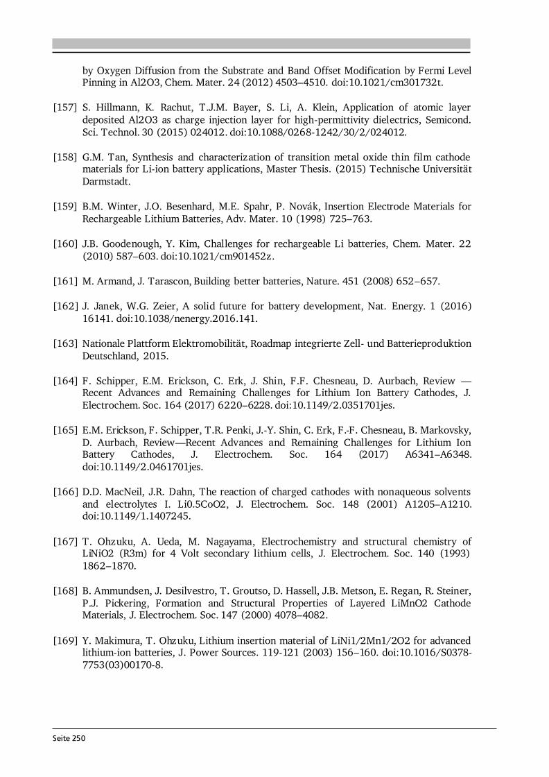
Seite 250
by Oxygen Diffusion from the Substrate and Band Offset Modification by Fermi Level Pinning in Al2O3, Chem. Mater. 24 (2012) 4503–4510. doi:10.1021/cm301732t. [157] S. Hillmann, K. Rachut, T.J.M. Bayer, S. Li, A. Klein, Application of atomic layer deposited Al2O3 as charge injection layer for high-permittivity dielectrics, Semicond. Sci. Technol. 30 (2015) 024012. doi:10.1088/0268-1242/30/2/024012. [158] G.M. Tan, Synthesis and characterization of transition metal oxide thin film cathode materials for Li-ion battery applications, Master Thesis. (2015) Technische Universität Darmstadt. [159] B.M. Winter, J.O. Besenhard, M.E. Spahr, P. Novák, Insertion Electrode Materials for Rechargeable Lithium Batteries, Adv. Mater. 10 (1998) 725–763. [160] J.B. Goodenough, Y. Kim, Challenges for rechargeable Li batteries, Chem. Mater. 22 (2010) 587–603. doi:10.1021/cm901452z. [161] M. Armand, J. Tarascon, Building better batteries, Nature. 451 (2008) 652–657. [162] J. Janek, W.G. Zeier, A solid future for battery development, Nat. Energy. 1 (2016) 16141. doi:10.1038/nenergy.2016.141. [163] Nationale Plattform Elektromobilität, Roadmap integrierte Zell- und Batterieproduktion Deutschland, 2015. [164] F. Schipper, E.M. Erickson, C. Erk, J. Shin, F.F. Chesneau, D. Aurbach, Review — Recent Advances and Remaining Challenges for Lithium Ion Battery Cathodes, J. Electrochem. Soc. 164 (2017) 6220–6228. doi:10.1149/2.0351701jes. [165] E.M. Erickson, F. Schipper, T.R. Penki, J.-Y. Shin, C. Erk, F.-F. Chesneau, B. Markovsky, D. Aurbach, Review—Recent Advances and Remaining Challenges for Lithium Ion Battery Cathodes, J. Electrochem. Soc. 164 (2017) A6341–A6348. doi:10.1149/2.0461701jes. [166] D.D. MacNeil, J.R. Dahn, The reaction of charged cathodes with nonaqueous solvents and electrolytes I. Li0.5CoO2, J. Electrochem. Soc. 148 (2001) A1205–A1210. doi:10.1149/1.1407245. [167] T. Ohzuku, A. Ueda, M. Nagayama, Electrochemistry and structural chemistry of LiNiO2 (R3m) for 4 Volt secondary lithium cells, J. Electrochem. Soc. 140 (1993) 1862–1870. [168] B. Ammundsen, J. Desilvestro, T. Groutso, D. Hassell, J.B. Metson, E. Regan, R. Steiner, P.J. Pickering, Formation and Structural Properties of Layered LiMnO2 Cathode Materials, J. Electrochem. Soc. 147 (2000) 4078–4082. [169] Y. Makimura, T. Ohzuku, Lithium insertion material of LiNi1/2Mn1/2O2 for advanced lithium-ion batteries, J. Power Sources. 119-121 (2003) 156–160. doi:10.1016/S0378-7753(03)00170-8.
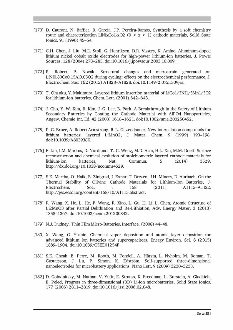
Seite 251
[170] D. Caurant, N. Baffier, B. Garcia, J.P. Pereira-Ramos, Synthesis by a soft chemistry route and characterization LiNixCo1-xO2 (0 < x < 1) cathode materials, Solid State Ionics. 91 (1996) 45–54. [171] C.H. Chen, J. Liu, M.E. Stoll, G. Henriksen, D.R. Vissers, K. Amine, Aluminum-doped lithium nickel cobalt oxide electrodes for high-power lithium-ion batteries, J. Power Sources. 128 (2004) 278–285. doi:10.1016/j.jpowsour.2003.10.009. [172] R. Robert, P. Novák, Structural changes and microstrain generated on LiNi0.80Co0.15Al0.05O2 during cycling: effects on the electrochemical performance, J. Electrochem. Soc. 162 (2015) A1823–A1828. doi:10.1149/2.0721509jes. [173] T. Ohzuku, Y. Makimura, Layered lithium insertion material of LiCo1/3Ni1/3Mn1/3O2 for lithium-ion batteries, Chem. Lett. (2001) 642–643. [174] J. Cho, Y.-W. Kim, B. Kim, J.-G. Lee, B. Park, A Breakthrough in the Safety of Lithium Secondary Batteries by Coating the Cathode Material with AlPO4 Nanoparticles, Angew. Chemie Int. Ed. 42 (2003) 1618–1621. doi:10.1002/anie.200250452. [175] P. G. Bruce, A. Robert Armstrong, R. L. Gitzendanner, New intercalation compounds for lithium batteries: layered LiMnO2, J. Mater. Chem. 9 (1999) 193–198. doi:10.1039/A803938K. [176] F. Lin, I.M. Markus, D. Nordlund, T.-C. Weng, M.D. Asta, H.L. Xin, M.M. Doeff, Surface reconstruction and chemical evolution of stoichiometric layered cathode materials for lithium-ion batteries, Nat. Commun. 5 (2014) 3529. http://dx.doi.org/10.1038/ncomms4529. [177] S.K. Martha, O. Haik, E. Zinigrad, I. Exnar, T. Drezen, J.H. Miners, D. Aurbach, On the Thermal Stability of Olivine Cathode Materials for Lithium-Ion Batteries, J. Electrochem. Soc. . 158 (2011) A1115–A1122. http://jes.ecsdl.org/content/158/10/A1115.abstract. [178] R. Wang, X. He, L. He, F. Wang, R. Xiao, L. Gu, H. Li, L. Chen, Atomic Structure of Li2MnO3 after Partial Delithiation and Re-Lithiation, Adv. Energy Mater. 3 (2013) 1358–1367. doi:10.1002/aenm.201200842. [179] N.J. Dudney, Thin Film Micro-Batteries, Interface. (2008) 44–48. [180] X. Wang, G. Yushin, Chemical vapor deposition and atomic layer deposition for advanced lithium ion batteries and supercapacitors, Energy Environ. Sci. 8 (2015) 1889–1904. doi:10.1039/C5EE01254F. [181] S.K. Cheah, E. Perre, M. Rooth, M. Fondell, A. Hårsta, L. Nyholm, M. Boman, T. Gustafsson, J. Lu, P. Simon, K. Edström, Self-supported three-dimensional nanoelectrodes for microbattery applications, Nano Lett. 9 (2009) 3230–3233. [182] D. Golodnitsky, M. Nathan, V. Yufit, E. Strauss, K. Freedman, L. Burstein, A. Gladkich, E. Peled, Progress in three-dimensional (3D) Li-ion microbatteries, Solid State Ionics. 177 (2006) 2811–2819. doi:10.1016/j.ssi.2006.02.048.
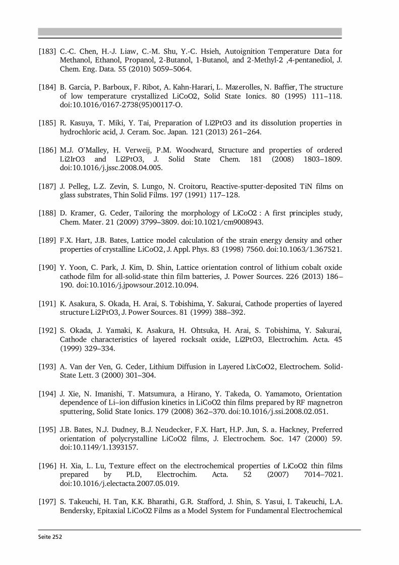
Seite 252
[183] C.-C. Chen, H.-J. Liaw, C.-M. Shu, Y.-C. Hsieh, Autoignition Temperature Data for Methanol, Ethanol, Propanol, 2-Butanol, 1-Butanol, and 2-Methyl-2 ,4-pentanediol, J. Chem. Eng. Data. 55 (2010) 5059–5064. [184] B. Garcia, P. Barboux, F. Ribot, A. Kahn-Harari, L. Mazerolles, N. Baffier, The structure of low temperature crystallized LiCoO2, Solid State Ionics. 80 (1995) 111–118. doi:10.1016/0167-2738(95)00117-O. [185] R. Kasuya, T. Miki, Y. Tai, Preparation of Li2PtO3 and its dissolution properties in hydrochloric acid, J. Ceram. Soc. Japan. 121 (2013) 261–264. [186] M.J. O’Malley, H. Verweij, P.M. Woodward, Structure and properties of ordered Li2IrO3 and Li2PtO3, J. Solid State Chem. 181 (2008) 1803–1809. doi:10.1016/j.jssc.2008.04.005. [187] J. Pelleg, L.Z. Zevin, S. Lungo, N. Croitoru, Reactive-sputter-deposited TiN films on glass substrates, Thin Solid Films. 197 (1991) 117–128. [188] D. Kramer, G. Ceder, Tailoring the morphology of LiCoO2 : A first principles study, Chem. Mater. 21 (2009) 3799–3809. doi:10.1021/cm9008943. [189] F.X. Hart, J.B. Bates, Lattice model calculation of the strain energy density and other properties of crystalline LiCoO2, J. Appl. Phys. 83 (1998) 7560. doi:10.1063/1.367521. [190] Y. Yoon, C. Park, J. Kim, D. Shin, Lattice orientation control of lithium cobalt oxide cathode film for all-solid-state thin film batteries, J. Power Sources. 226 (2013) 186–190. doi:10.1016/j.jpowsour.2012.10.094. [191] K. Asakura, S. Okada, H. Arai, S. Tobishima, Y. Sakurai, Cathode properties of layered structure Li2PtO3, J. Power Sources. 81 (1999) 388–392. [192] S. Okada, J. Yamaki, K. Asakura, H. Ohtsuka, H. Arai, S. Tobishima, Y. Sakurai, Cathode characteristics of layered rocksalt oxide, Li2PtO3, Electrochim. Acta. 45 (1999) 329–334. [193] A. Van der Ven, G. Ceder, Lithium Diffusion in Layered LixCoO2, Electrochem. Solid-State Lett. 3 (2000) 301–304. [194] J. Xie, N. Imanishi, T. Matsumura, a Hirano, Y. Takeda, O. Yamamoto, Orientation dependence of Li–ion diffusion kinetics in LiCoO2 thin films prepared by RF magnetron sputtering, Solid State Ionics. 179 (2008) 362–370. doi:10.1016/j.ssi.2008.02.051. [195] J.B. Bates, N.J. Dudney, B.J. Neudecker, F.X. Hart, H.P. Jun, S. a. Hackney, Preferred orientation of polycrystalline LiCoO2 films, J. Electrochem. Soc. 147 (2000) 59. doi:10.1149/1.1393157. [196] H. Xia, L. Lu, Texture effect on the electrochemical properties of LiCoO2 thin films prepared by PLD, Electrochim. Acta. 52 (2007) 7014–7021. doi:10.1016/j.electacta.2007.05.019. [197] S. Takeuchi, H. Tan, K.K. Bharathi, G.R. Stafford, J. Shin, S. Yasui, I. Takeuchi, L.A. Bendersky, Epitaxial LiCoO2 Films as a Model System for Fundamental Electrochemical
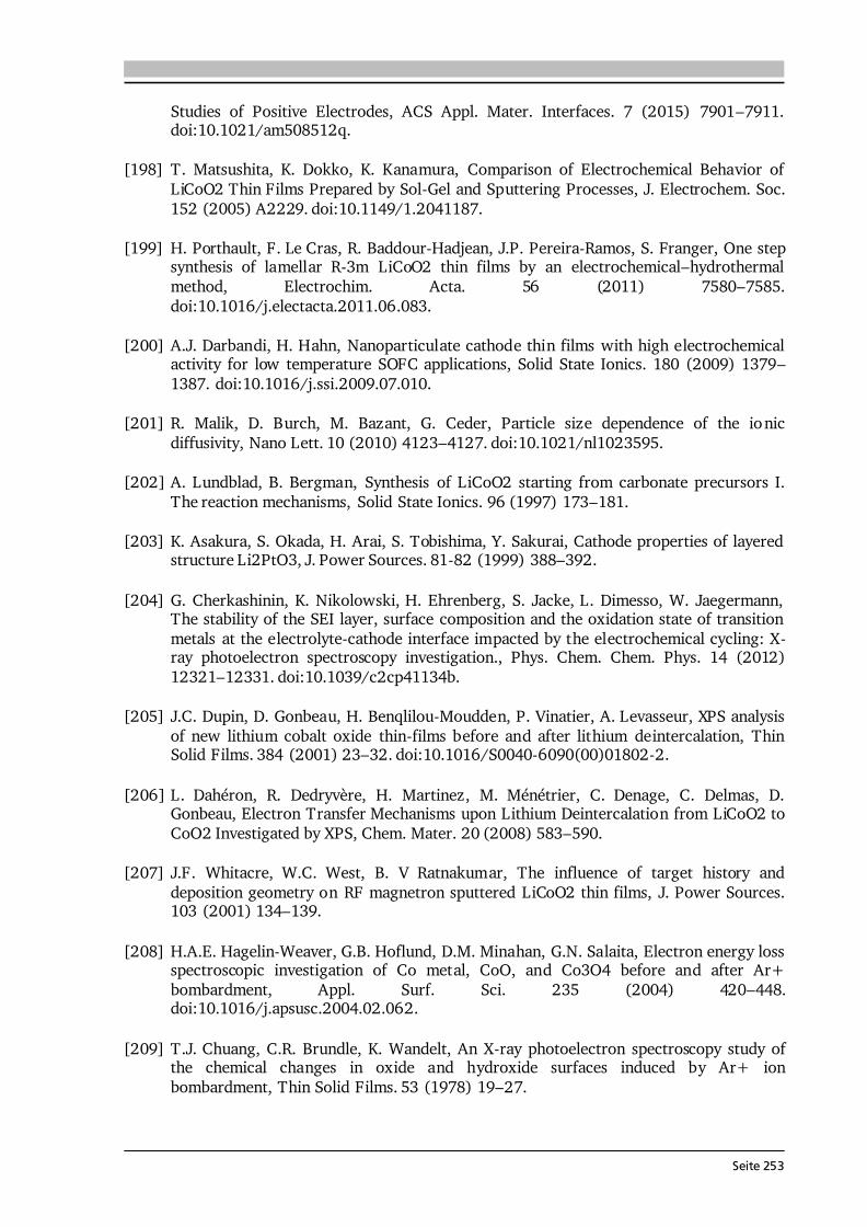
Seite 253
Studies of Positive Electrodes, ACS Appl. Mater. Interfaces. 7 (2015) 7901–7911. doi:10.1021/am508512q. [198] T. Matsushita, K. Dokko, K. Kanamura, Comparison of Electrochemical Behavior of LiCoO2 Thin Films Prepared by Sol-Gel and Sputtering Processes, J. Electrochem. Soc. 152 (2005) A2229. doi:10.1149/1.2041187. [199] H. Porthault, F. Le Cras, R. Baddour-Hadjean, J.P. Pereira-Ramos, S. Franger, One step synthesis of lamellar R-3m LiCoO2 thin films by an electrochemical–hydrothermal method, Electrochim. Acta. 56 (2011) 7580–7585. doi:10.1016/j.electacta.2011.06.083. [200] A.J. Darbandi, H. Hahn, Nanoparticulate cathode thin films with high electrochemical activity for low temperature SOFC applications, Solid State Ionics. 180 (2009) 1379–1387. doi:10.1016/j.ssi.2009.07.010. [201] R. Malik, D. Burch, M. Bazant, G. Ceder, Particle size dependence of the ionic diffusivity, Nano Lett. 10 (2010) 4123–4127. doi:10.1021/nl1023595. [202] A. Lundblad, B. Bergman, Synthesis of LiCoO2 starting from carbonate precursors I. The reaction mechanisms, Solid State Ionics. 96 (1997) 173–181. [203] K. Asakura, S. Okada, H. Arai, S. Tobishima, Y. Sakurai, Cathode properties of layered structure Li2PtO3, J. Power Sources. 81-82 (1999) 388–392. [204] G. Cherkashinin, K. Nikolowski, H. Ehrenberg, S. Jacke, L. Dimesso, W. Jaegermann, The stability of the SEI layer, surface composition and the oxidation state of transition metals at the electrolyte-cathode interface impacted by the electrochemical cycling: X-ray photoelectron spectroscopy investigation., Phys. Chem. Chem. Phys. 14 (2012) 12321–12331. doi:10.1039/c2cp41134b. [205] J.C. Dupin, D. Gonbeau, H. Benqlilou-Moudden, P. Vinatier, A. Levasseur, XPS analysis of new lithium cobalt oxide thin-films before and after lithium deintercalation, Thin Solid Films. 384 (2001) 23–32. doi:10.1016/S0040-6090(00)01802-2. [206] L. Dahéron, R. Dedryvère, H. Martinez, M. Ménétrier, C. Denage, C. Delmas, D. Gonbeau, Electron Transfer Mechanisms upon Lithium Deintercalation from LiCoO2 to CoO2 Investigated by XPS, Chem. Mater. 20 (2008) 583–590. [207] J.F. Whitacre, W.C. West, B. V Ratnakumar, The influence of target history and deposition geometry on RF magnetron sputtered LiCoO2 thin films, J. Power Sources. 103 (2001) 134–139. [208] H.A.E. Hagelin-Weaver, G.B. Hoflund, D.M. Minahan, G.N. Salaita, Electron energy loss spectroscopic investigation of Co metal, CoO, and Co3O4 before and after Ar+ bombardment, Appl. Surf. Sci. 235 (2004) 420–448. doi:10.1016/j.apsusc.2004.02.062. [209] T.J. Chuang, C.R. Brundle, K. Wandelt, An X-ray photoelectron spectroscopy study of the chemical changes in oxide and hydroxide surfaces induced by Ar+ ion bombardment, Thin Solid Films. 53 (1978) 19–27.
Seite 254
[210] C. Dellen, H.-G. Gehrke, S. Möller, C.-L. Tsai, U. Breuer, S. Uhlenbruck, O. Guillon, M. Finsterbusch, M. Bram, Time-of-flight secondary ion mass spectrometry study of lithium intercalation process in LiCoO2 thin film, J. Power Sources. 321 (2016) 241–247. doi:10.1016/j.jpowsour.2016.04.084. [211] H. Xia, L. Lu, Texture effect on the electrochemical properties of LiCoO2 thin films prepared by PLD, Electrochim. Acta. 52 (2007) 7014–7021. doi:10.1016/j.electacta.2007.05.019. [212] H. Yoshida, T. Fukunaga, T. Hazama, M. Terasaki, M. Mizutani, M. Yamachi, Degradation mechanism of alkyl carbonate solvents used in lithium-ion cells during initial charging, J. Power Sources. 68 (1997) 311–315. doi:10.1016/S0378-7753(97)02635-9. [213] S. Tintignac, R. Baddour-Hadjean, J.P. Pereira-Ramos, R. Salot, Electrochemical properties of high rate bias sputtered LiCoO2 thin films in liquid electrolyte, J. Power Sources. 245 (2014) 76–82. doi:10.1016/j.jpowsour.2013.06.047. [214] M.E. Donders, W.M. Arnoldbik, H.C.M. Knoops, W.M.M. Kessels, P.H.L. Notten, Atomic Layer Deposition of LiCoO2 Thin-Film Electrodes for All-Solid-State Li-Ion Micro-Batteries, J. Electrochem. Soc. 160 (2013) A3066–A3071. doi:10.1149/2.011305jes. [215] S. Cho, S. Yoon, Characterization of LiCoO2 Thin Film Cathodes Deposited by Liquid-Delivery Metallorganic Chemical Vapor Deposition for Rechargeable Lithium Batteries, J. Electrochem. Soc. 149 (2002) A1584–A1588. doi:10.1149/1.1517283. [216] S.-I. Cho, S.-G. Yoon, Improvement of discharge capacity of LiCoO2 thin-film cathodes deposited in trench structure by liquid-delivery metalorganic chemical vapor deposition, Appl. Phys. Lett. 82 (2003) 3345. doi:10.1063/1.1571958. [217] W. Choi, S. Yoon, Improvement of electrochemical properties in LiCoO2 cathode films grown on Pt/TiO2/SiO2/Si substrates by liquid-delivery metalorganic chemical vapor depostion, J. Vac. Sci. Technol. A. 22 (2004) 2356. doi:10.1116/1.1798791. [218] P. Kalyani, N. Kalaiselvi, Various aspects of LiNiO2 chemistry: A review, Sci. Technol. Adv. Mater. 6 (2005) 689–703. doi:10.1016/j.stam.2005.06.001. [219] C.M. Julien, Lithium intercalated compounds: Charge transfer and related properties, Mater. Sci. Eng. R. 40 (2003) 47–102. [220] M. Inaba, Y. Todzuka, H. Yoshida, Y. Grincourt, A. Tasaka, Y. Tomida, Z. Ogumi, Raman spectra of LiCo1-yNiyO2, Chem. Lett. (1995) 889–890. [221] S.P. Sheu, I.C. Shih, C.Y. Yao, J.M. Chen, W.M. Hurng, Studies of LiNiO2 in lithium-ion batteries, J. Power Sources. 68 (1997) 558–560. [222] J. Cho, T. Kim, Y.J. Kim, B. Park, High-performance ZrO2-coated LiNiO2 cathode material, Electrochem. Solid-State Lett. 4 (2001) A159–A161. doi:10.1149/1.1398556. [223] K. Kubo, M. Fujiwara, S. Yamada, S. Arai, M. Kanda, Synthesis and electrochemical properties for LiNiO2 substituted by other elements, J. Power Sources. 68 (1997) 553–557.
Seite 255
[224] C. Han, J. Kim, S. Paeng, D. Kwak, Y. Sung, Electrochemical characteristics of LiNiO2 films prepared for charge storable electrode application, Thin Solid Films. 517 (2009) 4215–4217. doi:10.1016/j.tsf.2009.02.046. [225] K. Yamada, N. Sato, T. Fujino, C.G. Lee, I. Uchida, J.R. Selman, Preparation of LiNiO2 and LiMyNi1-yO2 (M =ˆ Co, Al) films by electrostatic spray deposition, J Solid State Electrochem. 3 (1999) 148–153. [226] H. Liu, Y. Yang, J. Zhang, Reaction mechanism and kinetics of lithium ion battery cathode material LiNiO2 with CO2, J. Power Sources. 173 (2007) 556–561. doi:10.1016/j.jpowsour.2007.04.083. [227] M. V Reddy, G.V.S. Rao, B.V.R. Chowdari, Preparation and characterization of LiNi0.5Co0.5O2 and LiNi0.5Co0.4Al0.1O2 by molten salt synthesis for Li-ion batteries, J. Phys. Chem. C. 111 (2007) 11712–11720. [228] G. Cherkashinin, D. Ensling, W. Jaegermann, LiMO2 (M = Ni, Co) thin film cathode materials: a correlation between the valence state of transition metals and the electrochemical properties, J. Mater. Chem. A. 2 (2014) 3571. doi:10.1039/c3ta14509c. [229] C. Liao, Y. Lee, H. Yu, K. Fung, Structure characterization and electrochemical properties of RF sputtered lithium nickel cobalt oxide thin films, Electrochim. Acta. 50 (2004) 461–466. doi:10.1016/j.electacta.2004.03.054. [230] G. Cho, T. Kwon, T. Nam, S. Huh, B. Choi, H. Jeong, J. Noh, Structural and Electrochemical Properties of Lithium Nickel Oxide Thin Films, J. Chem. 2014 (2014) 5. doi:http://dx.doi.org/10.1155/2014/824083. [231] Sigma Aldrich, Safety Data Sheet, Prod. Cat. (2017). http://www.sigmaaldrich.com/catalog/product/aldrich/~. [232] G.L. Messing, S.-C. Zhang, G. V. Jayanthi, Ceramic Powder Synthesis by Spray Pyrolysis, J. Am. Ceram. Soc. 76 (1993) 2707–2726. [233] Y. Fujii, H. Miura, N. Suzuki, T. Shoji, N. Nakayama, Structural and electrochemical properties of LiNi1/3Co1/3Mn1/3O2: Calcination temperature dependence, J. Power Sources. 171 (2007) 894–903. doi:10.1016/j.jpowsour.2007.06.017. [234] E. Shinova, R. Stoyanova, E. Zhecheva, G.F. Ortiz, P. Lavela, J.L. Tirado, Cationic distribution and electrochemical performance of LiCo1/3Ni1/3Mn1/3O2 electrodes for lithium-ion batteries, Solid State Ionics. 179 (2008) 2198–2208. doi:10.1016/j.ssi.2008.07.026. [235] S.-C. Yin, Y.-H. Rho, I. Swainson, L.F. Nazar, X-ray/Neutron diffraction and electrochemical studies of Lithium de/re-intercalation in Li1-xCo1/3Ni1/3Mn1/3O2 (x = 0 - 1), Chem. Mater. 18 (2006) 1901–1910. [236] K.S. Park, M.H. Cho, S.J. Jin, K.S. Nahm, Y.S. Hong, Effect of Li ion in transition metal sites on electrochemical behavior of layered lithium manganese oxides solid solutions, Solid State Ionics. 171 (2004) 141–146. doi:10.1016/j.ssi.2004.04.016.
Seite 256
[237] J. Jiang, K.W. Eberman, L.J. Krause, J.R. Dahn, Structure, Electrochemical Properties, and Thermal Stability Studies of Li[Ni0.2Co0.6Mn0.2]O2 - Effect of Synthesis Route, J. Electrochem. Soc. 152 (2005) A1874–A1878. doi:10.1149/1.1990532. [238] M. Otoyama, Y. Ito, A. Hayashi, M. Tatsumisago, Raman spectroscopy for LiNi1/3Mn1/3Co1/3O2 composite positive electrodes in all-solid-state lithium batteries, Electrochemistry. 84 (2016) 812–814. [239] M. Kerlau, M. Marcinek, V. Srinivasan, R.M. Kostecki, Reprint of “Studies of local degradation phenomena in composite cathodes for lithium-ion batteries,” Electrochim. Acta. 53 (2007) 1385–1392. doi:10.1016/j.electacta.2007.10.009. [240] G. Cherkashinin, D. Ensling, P. Komissinskiy, R. Hausbrand, W. Jaegermann, Temperature induced reduction of the trivalent Ni ions in LiMO2 (M=Ni, Co) thin films, Surf. Sci. 608 (2013) L1–L4. doi:10.1016/j.susc.2012.09.023. [241] E.S. Ilton, J.E. Post, P.J. Heaney, F.T. Ling, S.N. Kerisit, Applied Surface Science XPS determination of Mn oxidation states in Mn (hydr) oxides, Appl. Surf. Sci. 366 (2016) 475–485. doi:10.1016/j.apsusc.2015.12.159. [242] W.-S. Yoon, C.P. Grey, M. Balasubramanian, X.-Q. Yang, D.A. Fischer, J. McBreen, Combined NMR and XAS Study on Local Environments and Electronic Structures of Electrochemically Li-Ion Deintercalated Li1-xCo1/3Ni1/3Mn1/3O2 Electrode System, Electrochem. Solid-State Lett. 7 (2004) A53–A55. doi:10.1149/1.1643592. [243] M.G. Kim, J. Shin, J. Kim, S. Park, Y. Sun, XAS Investigation of Inhomogeneous Metal-Oxygen Bond Covalency in Bulk and Surface for Charge Compensation in Li-Ion Battery Cathode Li[Ni1/3Co1/3Mn1/3]O2 Material, J. Electrochem. Soc. 152 (2005) A1320–A1328. doi:10.1149/1.1926647. [244] S. Kang, W. Yoon, K. Nam, X. Yang, D.P. Abraham, Investigating the first-cycle irreversibility of lithium metal oxide cathodes for Li batteries, J Mater Sci. 43 (2008) 4701–4706. doi:10.1007/s10853-007-2355-6. [245] K.C. Kam, A. Mehta, J.T. Heron, M.M. Doeff, Electrochemical and Physical Properties of Ti-Substituted Layered Nickel Manganese Cobalt Oxide (NMC) Cathode Materials, J. Electrochem. Soc. 159 (2012) A1383–A1392. doi:10.1149/2.060208jes. [246] I. Buchberger, S. Seidlmayer, A. Pokharel, M. Piana, J. Hattendorff, P. Kudejova, R. Gilles, H.A. Gasteiger, Ageing analysis of graphite/LiNi1/3Mn1/3Co1/3O2 cells using XRD, PGAA, and AC impedance, J. Electrochem. Soc. 162 (2015) A2737–A2746. doi:10.1149/2.0721514jes. [247] K.M. Shaju, G.V.S. Rao, B.V.R. Chowdari, Performance of layered Li(Ni1/3Co1/3Mn1/3)O2 as cathode for Li-ion batteries, Electrochim. Acta. 48 (2002) 145–151. [248] F. Wu, M. Wang, Y. Su, L. Bao, S. Chen, A novel layered material of LiNi0.32Mn0.33Co0.33Al0.01O2 for advanced lithium-ion batteries, J. Power Sources. 195 (2010) 2900–2904. doi:10.1016/j.jpowsour.2009.11.041.
Seite 257
[249] N. Yabuuchi, T. Ohzuku, Novel lithium insertion material of LiCo1/3Ni1/3Mn1/3O2 for advanced lithium-ion batteries, J. Power Sources. 119-121 (2003) 171–174. doi:10.1016/S0378-7753(03)00173-3. [250] J. Xie, N. Imanishi, T. Zhang, A. Hirano, Y. Takeda, O. Yamamoto, An amorphous LiCo1/3Mn1/3Ni1/3O2 thin film deposited on NASICON-type electrolyte for all-solid-state Li-ion batteries, J. Power Sources. 195 (2010) 5780–5783. doi:10.1016/j.jpowsour.2010.03.040. [251] J. Deng, L. Xi, L. Wang, Z. Wang, C.Y. Chung, X. Han, H. Zhou, Electrochemical performance of LiNi1/3Co1/3Mn1/3O2 thin film electrodes prepared by pulsed laser deposition, J. Power Sources. 217 (2012) 491–497. doi:10.1016/j.jpowsour.2012.06.006. [252] M. Hirayama, M. Abe, S. Taminato, Y. Araki, K. Suzuki, R. Kanno, Lithium intercalation in the surface region of an LiNi1/3Mn1/3Co1/3O2 cathode through different crystal planes, RSC Adv. 6 (2016) 78963–78969. doi:10.1039/C6RA17390J. [253] S. Iwasaki, T. Hamanaka, T. Yamakawa, W.C. West, K. Yamamoto, M. Motoyama, T. Hirayama, Y. Iriyama, Preparation of thick-film LiNi1/3Co1/3Mn1/3O2 electrodes by aerosol deposition and its application to all-solid-state batteries, J. Power Sources. 272 (2014) 1086–1090. doi:10.1016/j.jpowsour.2014.09.038. [254] K.M. Shaju, P.G. Bruce, Macroporous Li(Ni1/3Co1/3Mn1/3)O2: A high-rate positive electrode for rechargeable lithium batteries, J. Power Sources. 174 (2007) 1201–1205. doi:10.1016/j.jpowsour.2007.06.091. [255] X. Zhang, W.J. Jiang, A. Mauger, Qilu, F. Gendron, C.M. Julien, Minimization of the
cation mixing in Li1+x(NMC)1−xO2 as cathode material, J. Power Sources. 195 (2010) 1292–1301. doi:10.1016/j.jpowsour.2009.09.029. [256] Y. Shin, W. Choi, Y. Hong, S. Yoon, W.S. Ryu, S.H. Chang, Investigation on the microscopic features of layered oxide Li[Ni1/3Co1/3M1/3]O2 and their influences on the cathode properties, Solid State Ionics. 177 (2006) 515–521. doi:10.1016/j.ssi.2005.11.019. [257] R.D. Shannon, C.T. Prewitt, Effective Ionic Radii in Oxides and Fluorides, Acta Crystallogr. B25 (1969) 925. doi:10.1107/S0567740869003220. [258] Y. Bentaleb, I. Saadoune, K. Maher, L. Saadi, K. Fujimoto, S. Ito, On the LiNi0.2Mn0.2Co0.6O2 positive electrode material, J. Power Sources. 195 (2010) 1510–1515. doi:10.1016/j.jpowsour.2009.09.026. [259] S. Ferrari, M. Loveridge, S.D. Beattie, M. Jahn, R.J. Dashwood, R. Bhagat, Latest advances in the manufacturing of 3D rechargeable lithium microbatteries, J. Power Sources. 286 (2015) 25–46. doi:10.1016/j.jpowsour.2015.03.133. [260] M.J. Rand, I-V Characteristics of PtSi-Si Contacts Made from CVD Platinum, J. Electrochem. Soc. 122 (1975) 811–815.
Seite 258
[261] R.M. Anderson, T.M. Reith, Microstructural and Electrical Properties of Thin PtSi Films and Their Relationships to Deposition Parameters, J. Electrochem. Soc. 122 (1975) 1337–1347. [262] O. Valet, P. Doppelt, P.K. Baumann, M. Schumacher, E. Balnois, F. Bonnet, H. Guillon, Study of platinum thin films deposited by MOCVD as electrodes for oxide applications, Microelectron. Eng. 64 (2002) 457–463. [263] C. Thurier, P. Doppelt, Platinum OMCVD processes and precursor chemistry, Coord. Chem. Rev. 252 (2008) 155–169. doi:10.1016/j.ccr.2007.04.005. [264] The wavefunction of a 2D well with nx=4 and ny=4, Web Ref. (2008). https://en.wikipedia.org/wiki/Particle_in_a_box#/media/File:Particle2D.svg (accessed September 17, 2017). [265] H. Porthault, F. Le Cras, J.-M. Duffault, S. Franger, Fast deposition of conformal LiCoO2 thin film electrodes for high capacity 3D batteries, Mater. Sci. Eng. B. 213 (2016) 163–168. doi:10.1016/j.mseb.2016.05.001. [266] J. Cho, Y.J. Kim, B. Park, Novel LiCoO2 cathode material with Al2O3 coating for a Li-ion cell, Chem. Mater. 12 (2010) 3788–3791. [267] C. Li, H.P. Zhang, L.J. Fu, H. Liu, Y.P. Wu, E. Rahm, R. Holze, H.Q. Wu, Cathode materials modified by surface coating for lithium ion batteries, Electrochim. Acta. 51 (2006) 3872–3883. doi:10.1016/j.electacta.2005.11.015. [268] Y. Oh, S. Nam, S. Wi, S. Hong, B. Park, Review paper: Nanoscale interface control for high-performance Li-ion batteries, Electron. Mater. Lett. 8 (2012) 91–105. doi:10.1007/s13391-012-2058-2. [269] Y.J. Kim, H. Kim, B. Kim, D. Ahn, J. Lee, T. Kim, D. Son, J. Cho, Y. Kim, B. Park, Electrochemical stability of thin-film LiCoO2 cathodes by aluminum-oxide coating, Chem. Mater. 15 (2003) 1505–1511. [270] Y.S. Jung, A.S. Cavanagh, A.C. Dillon, M.D. Groner, S.M. George, S. Lee, Enhanced Stability of LiCoO2 Cathodes in Lithium-Ion Batteries Using Surface Modification by Atomic Layer Deposition, J. Electrochem. Soc. 157 (2010) A75–A81. doi:10.1149/1.3258274. [271] D. Takamatsu, S. Mori, Y. Orikasa, T. Nakatsutsumi, Y. Koyama, H. Tanida, H. Arai, Y. Uchimoto, Z. Ogumi, Effects of ZrO2 Coating on LiCoO2 Thin-Film Electrode Studied by In Situ X-ray Absorption Spectroscopy, J. Electrochem. Soc. 160 (2013) 3054–3060. doi:10.1149/2.006305jes. [272] J. Cho, Y.J. Kim, B. Park, LiCoO2 Cathode Material That Does Not Show a Phase Transition from Hexagonal to Monoclinic Phase, J. Electrochem. Soc. 148 (2001) A1110. doi:10.1149/1.1397772. [273] Y. Oh, D. Ahn, S. Nam, B. Park, The effect of Al2O3-coating coverage on the electrochemical properties in LiCoO2 thin films, J Solid State Electrochem. 14 (2010) 1235–1240. doi:10.1007/s10008-009-0946-7.
Seite 259
[274] E. Jung, Y.J. Park, Suppression of interface reaction of LiCoO2 thin films by Al2O3-coating, J. Electroceramics. 29 (2012) 23–28. doi:10.1007/s10832-012-9732-5. [275] T. Kato, T. Hamanaka, K. Yamamoto, T. Hirayama, F. Sagane, M. Motoyama, Y. Iriyama, In-situ Li7La3Zr2O12/LiCoO2 interface modification for advanced all-solid-state battery, J. Power Sources. 260 (2014) 292–298. doi:10.1016/j.jpowsour.2014.02.102. [276] Y. Zhu, X. He, Y. Mo, Origin of Outstanding Stability in the Lithium Solid Electrolyte Materials: Insights from Thermodynamic Analyses Based on First-Principles Calculations., ACS Appl. Mater. Interfaces. 7 (2015) 23685–93. doi:10.1021/acsami.5b07517. [277] Y. Zhu, X. He, Y. Mo, First principles study on electrochemical and chemical stability of solid electrolyte–electrode interfaces in all-solid-state Li-ion batteries, J. Mater. Chem. A. 4 (2016) 3253–3266. doi:10.1039/C5TA08574H. [278] W.D. Richards, L.J. Miara, Y. Wang, J.C. Kim, G. Ceder, Interface Stability in Solid-State Batteries, Chem. Mater. 28 (2016) 266–273. doi:10.1021/acs.chemmater.5b04082. [279] L.J. Miara, W.D. Richards, Y.E. Wang, G. Ceder, First-principles studies on cation dopants and electrolyte|cathode interphases for lithium garnets, Chem. Mater. 27 (2015) 4040–4047. doi:10.1021/acs.chemmater.5b01023. [280] S. Wenzel, T. Leichtweiss, D. Krüger, J. Sann, J. Janek, Interphase formation on lithium solid electrolytes — An in situ approach to study interfacial reactions by photoelectron spectroscopy, Solid State Ionics. 278 (2015) 98–105. doi:10.1016/j.ssi.2015.06.001. [281] Y. Deng, C. Eames, J.-N. Chotard, F. Lalère, V. Seznec, S. Emge, O. Pecher, C.P. Grey, C. Masquelier, M.S. Islam, Structural and Mechanistic Insights into Fast Lithium-Ion Conduction in Li4SiO4–Li3PO4 Solid Electrolytes, J. Am. Chem. Soc. 137 (2015) 9136–9145. doi:10.1021/jacs.5b04444. [282] M. Murayama, R. Kanno, M. Irie, S. Ito, T. Hata, N. Sonoyama, Y. Kawamoto, Synthesis of New Lithium Ionic Conductor Thio-LISICON - Lithium Silicon Sulfides System, J. Solid State Chem. 168 (2002) 140–148. doi:10.1006/jssc.2002.9701. [283] M. Tachez, J.-P. Malugani, R. Mercier, G. Robert, Ionic conductivity of and phase transition in lithium thiophosphate Li3PS4, Solid State Ionics. 14 (1984) 181–185. doi:https://doi.org/10.1016/0167-2738(84)90097-3. [284] R. Kanno, M. Murayama, Lithium Ionic Conductor Thio-LISICON: The Li2S-GeS2-P2S5 System, J. Electrochem. Soc. 148 (2001) A742–A746. doi:10.1149/1.1379028. [285] N. Kamaya, K. Homma, Y. Yamakawa, M. Hirayama, R. Kanno, M. Yonemura, T. Kamiyama, Y. Kato, S. Hama, K. Kawamoto, A. Mitsui, A lithium superionic conductor, Nat. Mater. 10 (2011) 682–686. doi:10.1038/nmat3066. [286] C. Bernuy-Lopez, W. Manalastas, J.M. Lopez del Amo, A. Aguadero, F. Aguesse, J.A. Kilner, Atmosphere Controlled Processing of Ga-Substituted Garnets for High Li-Ion Conductivity Ceramics, Chem. Mater. 26 (2014) 3610–3617.
Seite 260
[287] H. Buschmann, J. Dölle, S. Berendts, A. Kuhn, P. Bottke, M. Wilkening, P. Heitjans, A. Senyshyn, H. Ehrenberg, A. Lotnyk, V. Duppel, L. Kienle, J. Janek, Structure and dynamics of the fast lithium ion conductor “Li7La3Zr2O12”., Phys. Chem. Chem. Phys. 13 (2011) 19378–92. doi:10.1039/c1cp22108f.
[288] B.V. Thangadurai, W. Weppner, Li6ALa2Ta2O12 (A = Sr, Ba): Novel Garnet-Like Oxides for Fast Lithium Ion Conduction, Adv. Funct. Mater. 15 (2005) 107–112. doi:10.1002/adfm.200400044. [289] Y.X. Gao, X.P. Wang, W.G. Wang, Q.F. Fang, Sol – gel synthesis and electrical properties of Li5La3Ta2O12 lithium ionic conductors, Solid State Ionics. 181 (2010) 33–36. doi:10.1016/j.ssi.2009.11.015. [290] H. Peng, Q. Wu, L. Xiao, Low temperature synthesis of Li5La3Nb2O12 with cubic garnet-type structure by sol – gel process, J Sol-Gel Sci Technol. 66 (2013) 175–179. doi:10.1007/s10971-013-2984-y. [291] W. Schnick, J. Luecke, Lithium ion conductivity of LiPN2 and Li7PN4, Solid State Ionics. 38 (1990) 271–273. [292] H. Yamane, S. Kikkawa, M. Koizumi, Preparation of lithium silicon nitrides and their lithium ion conductivity, Solid State Ionics. 25 (1987) 183–191. [293] B.A. Boukamp, R.A. Huggins, Fast ionic conductivity in lithium nitride, Mater. Res. Bull. 13 (1978) 23–32. doi:https://doi.org/10.1016/0025-5408(78)90023-5. [294] H. Aono, E. Sugimoto, Y. Sadaoka, N. Imanaka, G. Adachi, Ionic Conductivity of Solid Electrolytes Based on Lithium Titanium Phosphate, J. Electrochem. Soc. 137 (1990) 1023–1027. [295] H. Aono, E. Sugimoto, Y. Sadaoka, N. Imanaka, G. Adachi, The Electrical Properties of
Ceramic Electrolytes for LiMxTi2−x(PO4)3 + yLi2O, M = Ge, Sn, Hf, and Zr Systems, J. Electrochem. Soc. 140 (1993) 1827–1833. doi:10.1149/1.2220723. [296] M. Itoh, Y. Inaguma, W.-H. Jung, L. Chen, T. Nakamura, High lithium ion conductivity in the perovskite-type compounds Ln12Li12TiO3 (Ln = La, Pr, Nd, Sm), Solid State Ionics. 70 (1994) 203–207. doi:https://doi.org/10.1016/0167-2738(94)90310-7. [297] V. Thangadurai, A.K. Shukla, J. Gopalakrishnan, LiSr1.650.35B1.3B‘1.7O9 (B = Ti, Zr;
B‘ = Nb, Ta): New Lithium Ion Conductors Based on the Perovskite Structure, Chem. Mater. 11 (1999) 835–839. doi:10.1021/cm9810382. [298] Y. Inaguma, C. Liquan, M. Itoh, T. Nakamura, T. Uchida, H. Ikuta, M. Wakihara, High ionic conductivity in lithium lanthanum titanate, Solid State Commun. 86 (1993) 689–693. doi:https://doi.org/10.1016/0038-1098(93)90841-A. [299] A. Morata-Orrantia, S. García-Martín, E. Morán, M.Á. Alario-Franco, A New La2/3LixTi1-xAlxO3 Solid Solution: Structure, Microstructure, and Li+ Conductivity, Chem. Mater. 14 (2002) 2871–2875. doi:10.1021/cm011149s. [300] A. Rabenau, Lithium nitride and related materials - Case study of the use of modern solid state research techniques, Solid State Ionics. 6 (1982) 277–293.
Seite 261
[301] H. Geng, J. Lan, A. Mei, Y. Lin, C.W. Nan, Effect of sintering temperature on microstructure and transport properties of Li3xLa2/3−xTiO3 with different lithium contents, Electrochim. Acta. 56 (2011) 3406–3414. doi:10.1016/j.electacta.2010.06.031.
[302] G.A. Nazri, G. Pistoia, Lithium Batteries: Science and Technology, Springer New York, New York, 2009. [303] X. Yu, J.B. Bates, G.E. Jellison, F.X. Hart, A Stable Thin-Film Lithium Electrolyte: Lithium Phosphorus Oxynitride, J. Electrochem. Soc. 144 (1997) 524–532. [304] R. Murugan, V. Thangadurai, W. Weppner, Fast lithium ion conduction in garnet-type Li7La3Zr2O12., Angew. Chem. Int. Ed. Engl. 46 (2007) 7778–81. doi:10.1002/anie.200701144. [305] J. Awaka, N. Kijima, H. Hayakawa, J. Akimoto, Synthesis and structure analysis of tetragonal Li7La3Zr2O12 with the garnet-related type structure, J. Solid State Chem. 182 (2009) 2046–2052. doi:10.1016/j.jssc.2009.05.020. [306] J. Wolfenstine, E. Rangasamy, J.L. Allen, J. Sakamoto, High conductivity of dense tetragonal Li7La3Zr2O12, J. Power Sources. 208 (2012) 193–196. doi:10.1016/j.jpowsour.2012.02.031. [307] D. Rettenwander, G. Redhammer, F. Preishuber-Pflügl, L. Cheng, L. Miara, R. Wagner, A. Welzl, E. Suard, M.M. Doeff, M. Wilkening, J. Fleig, G. Amthauer, Structural and Electrochemical Consequences of Al and Ga Cosubstitution in Li7La3Zr2O12 Solid Electrolytes, Chem. Mater. 28 (2016) 2384–2392. doi:10.1021/acs.chemmater.6b00579. [308] P. Knauth, Inorganic solid Li ion conductors: An overview, Solid State Ionics. 180 (2009) 911–916. doi:10.1016/j.ssi.2009.03.022. [309] F. Han, Y. Zhu, X. He, Y. Mo, C. Wang, Electrochemical stability of Li10GeP2S12 and Li7La3Zr2O12 solid electrolytes, Adv. Energy Mater. 6 (2016) 1501590. doi:10.1002/aenm.201501590. [310] M. Kotobuki, K. Kanamura, Fabrication of all-solid-state battery using Li5La3Ta2O12 ceramic electrolyte, Ceram. Int. 39 (2013) 6481–6487. doi:10.1016/j.ceramint.2013.01.079. [311] M. Kotobuki, K. Kanamura, Y. Sato, K. Yamamoto, T. Yoshida, Electrochemical properties of Li7La3Zr2O12 solid electrolyte prepared in argon atmosphere, J. Power Sources. 199 (2012) 346–349. doi:10.1016/j.jpowsour.2011.10.060. [312] J. Reinacher, S. Berendts, J. Janek, Preparation and electrical properties of garnet-type Li6BaLa2Ta2O12 lithium solid electrolyte thin films prepared by pulsed laser deposition, Solid State Ionics. 258 (2014) 1–7. doi:10.1016/j.ssi.2014.01.046. [313] D. Rettenwander, G. Redhammer, F. Preishuber-Pflügl, L. Cheng, L. Miara, R. Wagner, A. Welzl, E. Suard, M.M. Doeff, M. Wilkening, J. Fleig, G. Amthauer, Structural and electrochemical consequences of Al and Ga cosubstitution in Li7La3Zr2O12 solid
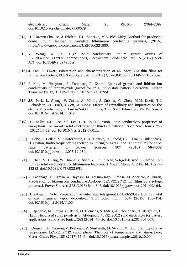
Seite 262
electrolytes, Chem. Mater. 28 (2016) 2384–2392. doi:10.1021/acs.chemmater.6b00579. [314] H.J. Brown-Shaklee, J. Ihlefeld, E.D. Spoerke, M.A. Blea-Kirby, Method for producing dense lithium lanthanum tantalate lithium-ion conducting ceramics, (2016). https://www.google.com/patents/US20160221880. [315] Y. Wang, W. Lai, High ionic conductivity lithium garnet oxides of Li7−xLa3Zr2−xTaxO12 compositions, Electrochem. Solid-State Lett. 15 (2012) A68–A71. doi:10.1149/2.024205esl. [316] J. Tan, A. Tiwari, Fabrication and characterization of Li7La3Zr2O12 thin films for lithium ion battery, ECS Solid State Lett. 1 (2012) Q57–Q60. doi:10.1149/2.013206ssl. [317] S. Kim, M. Hirayama, S. Taminato, R. Kanno, Epitaxial growth and lithium ion conductivity of lithium-oxide garnet for an all solid-state battery electrolyte., Dalton Trans. 42 (2013) 13112–7. doi:10.1039/c3dt51795k. [318] J.S. Park, L. Cheng, V. Zorba, A. Mehta, J. Cabana, G. Chen, M.M. Doeff, T.J. Richardson, J.H. Park, J. Son, W. Hong, Effects of crystallinity and impurities on the electrical conductivity of Li–La–Zr–O thin films, Thin Solid Films. 576 (2015) 55–60. doi:10.1016/j.tsf.2014.11.019. [319] D.J. Kalita, S.H. Lee, K.S. Lee, D.H. Ko, Y.S. Yoon, Ionic conductivity properties of amorphous Li–La–Zr–O solid electrolyte for thin film batteries, Solid State Ionics. 229 (2012) 14–19. doi:10.1016/j.ssi.2012.09.011. [320] S. Lobe, C. Dellen, M. Finsterbusch, H.-G. Gehrke, D. Sebold, C.-L. Tsai, S. Uhlenbruck, O. Guillon, Radio frequency magnetron sputtering of Li7La3Zr2O12 thin films for solid-state batteries, J. Power Sources. 307 (2016) 684–689. doi:10.1016/j.jpowsour.2015.12.054. [321] R. Chen, M. Huang, W. Huang, Y. Shen, Y. Lin, C. Nan, Sol-gel derived Li-La-Zr-O thin films as solid electrolytes for lithium-ion batteries, J. Mater. Chem. A. 2 (2014) 13277–13282. doi:10.1039/C4TA02289K. [322] K. Tadanaga, H. Egawa, A. Hayashi, M. Tatsumisago, J. Mosa, M. Aparicio, A. Duran, Preparation of lithium ion conductive Al-doped Li7La3Zr2O12 thin films by a sol–gel process, J. Power Sources. 273 (2015) 844–847. doi:10.1016/j.jpowsour.2014.09.164. [323] H. Katsui, T. Goto, Preparation of cubic and tetragonal Li7La3Zr2O12 film by metal organic chemical vapor deposition, Thin Solid Films. 584 (2015) 130–134. doi:10.1016/j.tsf.2014.11.094. [324] R. Djenadic, M. Botros, C. Benel, O. Clemens, S. Indris, A. Choudhary, T. Bergfeldt, H. Hahn, Nebulized spray pyrolysis of Al-doped Li7La3Zr2O12 solid electrolyte for battery applications, Solid State Ionics. 263 (2014) 49–56. doi:10.1016/j.ssi.2014.05.007. [325] I. Quinzeni, D. Capsoni, V. Berbenni, P. Mustarelli, M. Sturini, M. Bini, Stability of low-temperature Li7La3Zr2O12 cubic phase: The role of temperature and atmosphere, Mater. Chem. Phys. 185 (2017) 55–64. doi:10.1016/j.matchemphys.2016.10.004.
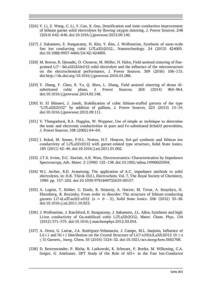
Seite 263
[326] Y. Li, Z. Wang, C. Li, Y. Cao, X. Guo, Densification and ionic-conduction improvement of lithium garnet solid electrolytes by flowing oxygen sintering, J. Power Sources. 248 (2014) 642–646. doi:10.1016/j.jpowsour.2013.09.140. [327] J. Sakamoto, E. Rangasamy, H. Kim, Y. Kim, J. Wolfenstine, Synthesis of nano-scale fast ion conducting cubic Li7La3Zr2O12., Nanotechnology. 24 (2013) 424005. doi:10.1088/0957-4484/24/42/424005. [328] M. Botros, R. Djenadic, O. Clemens, M. Möller, H. Hahn, Field assisted sintering of fine-
grained Li7−3xLa3Zr2AlxO12 solid electrolyte and the influence of the microstructure on the electrochemical performance, J. Power Sources. 309 (2016) 108–115. doi:http://dx.doi.org/10.1016/j.jpowsour.2016.01.086. [329] Y. Zhang, F. Chen, R. Tu, Q. Shen, L. Zhang, Field assisted sintering of dense Al-substituted cubic phase, J. Power Sources. 268 (2014) 960–964. doi:10.1016/j.jpowsour.2014.03.148. [330] H. El Shinawi, J. Janek, Stabilization of cubic lithium-stuffed garnets of the type
“Li7La3Zr2O12” by addition of gallium, J. Power Sources. 225 (2013) 13–19. doi:10.1016/j.jpowsour.2012.09.111. [331] V. Thangadurai, R.A. Huggins, W. Weppner, Use of simple ac technique to determine the ionic and electronic conductivities in pure and Fe-substituted SrSnO3 perovskites, J. Power Sources. 108 (2002) 64–69. [332] I. Kokal, M. Somer, P.H.L. Notten, H.T. Hintzen, Sol–gel synthesis and lithium ion conductivity of Li7La3Zr2O12 with garnet-related type structure, Solid State Ionics. 185 (2011) 42–46. doi:10.1016/j.ssi.2011.01.002. [333] J.T.S. Irvine, D.C. Sinclair, A.R. West, Electroceramics: Characterization by Impedance Spectroscopy, Adv. Mater. 2 (1990) 132–138. doi:10.1002/adma.19900020304. [334] W.I. Archer, R.D. Armstrong, The application of A.C. impedance methods to solid electrolytes, in: H.R. Thirsk (Ed.), Electrochem. Vol. 7, The Royal Society of Chemistry, 1980: pp. 157–202. doi:10.1039/9781849732635-00157. [335] A. Logéat, T. Köhler, U. Eisele, B. Stiaszny, A. Harzer, M. Tovar, A. Senyshyn, H. Ehrenberg, B. Kozinsky, From order to disorder: The structure of lithium-conducting garnets Li7-xLa3TaxZr2-xO12 (x = 0 - 2), Solid State Ionics. 206 (2012) 33–38. doi:10.1016/j.ssi.2011.10.023. [336] J. Wolfenstine, J. Ratchford, E. Rangasamy, J. Sakamoto, J.L. Allen, Synthesis and high Li-ion conductivity of Ga-stabilized cubic Li7La3Zr2O12, Mater. Chem. Phys. 134 (2012) 571–575. doi:10.1016/j.matchemphys.2012.03.054. [337] A. Orera, G. Larraz, J.A. Rodríguez-Velamazán, J. Campo, M.L. Sanjuán, Influence of Li(+) and H(+) Distribution on the Crystal Structure of Li(7-x)H(x)La3Zr2O12 (0 ≤ x
≤ 5) Garnets., Inorg. Chem. 55 (2016) 1324–32. doi:10.1021/acs.inorgchem.5b02708. [338] D. Rettenwander, P. Blaha, R. Laskowski, K. Schwarz, P. Bottke, M. Wilkening, C.A. Geiger, G. Amthauer, DFT Study of the Role of Al3+ in the Fast Ion-Conductor
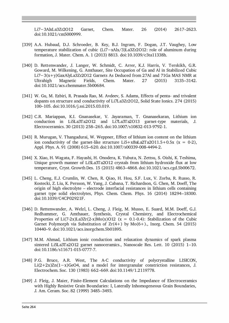
Seite 264
Li7−3AlxLa3Zr2O12 Garnet, Chem. Mater. 26 (2014) 2617–2623. doi:10.1021/cm5000999. [339] A.A. Hubaud, D.J. Schroeder, B. Key, B.J. Ingram, F. Dogan, J.T. Vaughey, Low
temperature stabilization of cubic (Li7−xAlx/3)La3Zr2O12: role of aluminum during formation, J. Mater. Chem. A. 1 (2013) 8813. doi:10.1039/c3ta11338h. [340] D. Rettenwander, J. Langer, W. Schmidt, C. Arrer, K.J. Harris, V. Terskikh, G.R. Goward, M. Wilkening, G. Amthauer, Site Occupation of Ga and Al in Stabilized Cubic
Li7−3(x+y)GaxAlyLa3Zr2O12 Garnets As Deduced from 27Al and 71Ga MAS NMR at Ultrahigh Magnetic Fields, Chem. Mater. 27 (2015) 3135–3142. doi:10.1021/acs.chemmater.5b00684. [341] W. Gu, M. Ezbiri, R. Prasada Rao, M. Avdeev, S. Adams, Effects of penta- and trivalent dopants on structure and conductivity of Li7La3Zr2O12, Solid State Ionics. 274 (2015) 100–105. doi:10.1016/j.ssi.2015.03.019. [342] C.R. Mariappan, K.I. Gnanasekar, V. Jayaraman, T. Gnanasekaran, Lithium ion conduction in Li5La3Ta2O12 and Li7La3Ta2O13 garnet-type materials, J. Electroceramics. 30 (2013) 258–265. doi:10.1007/s10832-013-9792-1. [343] R. Murugan, V. Thangadurai, W. Weppner, Effect of lithium ion content on the lithium ion conductivity of the garnet-like structure Li5+xBaLa2Ta2O11.5+0.5x (x = 0-2), Appl. Phys. A. 91 (2008) 615–620. doi:10.1007/s00339-008-4494-2. [344] X. Xiao, H. Wagata, F. Hayashi, H. Onodera, K. Yubuta, N. Zettsu, S. Oishi, K. Teshima, Unique growth manner of Li5La3Ta2O12 crystals from lithium hydroxide flux at low temperature, Cryst. Growth Des. 15 (2015) 4863–4868. doi:10.1021/acs.cgd.5b00672. [345] L. Cheng, E.J. Crumlin, W. Chen, R. Qiao, H. Hou, S.F. Lux, V. Zorba, R. Russo, R. Kostecki, Z. Liu, K. Persson, W. Yang, J. Cabana, T. Richardson, G. Chen, M. Doeff, The origin of high electrolyte – electrode interfacial resistances in lithium cells containing garnet type solid electrolytes, Phys. Chem. Chem. Phys. 16 (2014) 18294–18300. doi:10.1039/C4CP02921F. [346] D. Rettenwander, A. Welzl, L. Cheng, J. Fleig, M. Musso, E. Suard, M.M. Doeff, G.J. Redhammer, G. Amthauer, Synthesis, Crystal Chemistry, and Electrochemical Properties of Li(7-2x)La3Zr(2-x)Mo(x)O12 (x = 0.1-0.4): Stabilization of the Cubic Garnet Polymorph via Substitution of Zr(4+) by Mo(6+)., Inorg. Chem. 54 (2015) 10440–9. doi:10.1021/acs.inorgchem.5b01895. [347] M.M. Ahmad, Lithium ionic conduction and relaxation dynamics of spark plasma sintered Li5La3Ta2O12 garnet nanoceramics., Nanoscale Res. Lett. 10 (2015) 1–10. doi:10.1186/s11671-015-0777-7. [348] P.G. Bruce, A.R. West, The A-C conductivity of polycrystalline LISICON,
Li(2+2x)Zn(1−x)GeO4, and a model for intergranular constriction resistances, J. Electrochem. Soc. 130 (1983) 662–669. doi:10.1149/1.2119778. [349] J. Fleig, J. Maier, Finite-Element Calculations on the Impedance of Electroceramics with Highly Resistive Grain Boundaries: I, Laterally Inhomogeneous Grain Boundaries, J. Am. Ceram. Soc. 82 (1999) 3485–3493.

Seite 265
[350] J.E. Bauerle, Study of solid electrolyte polarization by a complex admittance method, J. Phys. Chem. Solids. 30 (1969) 2657–2670. [351] R. Riedel, I.W. Chen, Ceramics Science and Technology, Materials and Properties, Wiley, 2011. https://books.google.com.mx/books?id=hOJtv7CKWUIC. [352] R. Murugan, V. Thangadurai, W. Weppner, Lattice parameter and sintering temperature dependence of bulk and grain-boundary conduction of garnet-like solid Li-electrolytes, J. Electrochem. Soc. 155 (2008) A90–A101. doi:10.1149/1.2800764. [353] M. Kotobuki, K. Kanamura, Y. Sato, T. Yoshida, Fabrication of all-solid-state lithium battery with lithium metal anode using Al2O3-added Li7La3Zr2O12 solid electrolyte, J. Power Sources. 196 (2011) 7750–7754. doi:10.1016/j.jpowsour.2011.04.047. [354] M. Nakayama, M. Kotobuki, H. Munakata, M. Nogami, K. Kanamura, First-principles density functional calculation of electrochemical stability of fast Li ion conducting garnet-type oxides., Phys. Chem. Chem. Phys. 14 (2012) 10008–14. doi:10.1039/c2cp40634a. [355] D. Ensling, A. Thissen, W. Jaegermann, On the formation of lithium oxides and carbonates on Li metal electrodes in comparison to LiCoO2 surface phases investigated by photoelectron spectroscopy, Appl. Surf. Sci. 255 (2008) 2517–2523. doi:10.1016/j.apsusc.2008.07.196. [356] M. Motzko, M.A. Carrillo Solano, W. Jaegermann, R. Hausbrand, Photoemission Study on the Interaction Between LiCoO2 Thin Films and Adsorbed Water, J. Phys. Chem. C. 119 (2015) 23407–23412. doi:10.1021/acs.jpcc.5b05793. [357] A. Schwöbel, W. Jaegermann, R. Hausbrand, Interfacial energy level alignment and energy level diagrams for all-solid Li-ion cells: Impact of Li-ion transfer and double layer formation, Solid State Ionics. 288 (2016) 224–228. doi:10.1016/j.ssi.2015.12.029. [358] S. Sicolo, M. Fingerle, R. Hausbrand, K. Albe, Interfacial instability of amorphous LiPON against lithium: A combined Density Functional Theory and spectroscopic study, J. Power Sources. 354 (2017) 124–133. doi:10.1016/j.jpowsour.2017.04.005. [359] C. Guhl, M. Fingerle, R. Hausbrand, Process related effects upon formation of composite electrolyte interfaces: Nitridation and reduction of NASICON-type electrolytes by deposition of LiPON, J. Power. 362 (2017) 299–307. doi:10.1016/j.jpowsour.2017.07.051. [360] D.D. Sarma, C.N.R. Rao, Xpes studies of oxides of second- and third-row transition metals including rare earths, J. Electron Spectros. Relat. Phenomena. 20 (1980) 25–45. [361] P. Prieto, L. Galán, J.M. Sanz, Changes induced in the secondary electron emission properties of tantalum nitride by Ar+ bombardment and oxygen exposure, Appl. Surf. Sci. 71 (1993) 186–190. [362] V. Thangadurai, W. Weppner, Investigations on electrical conductivity and chemical compatibility between fast lithium ion conducting garnet-like Li6BaLa2Ta2O12 and
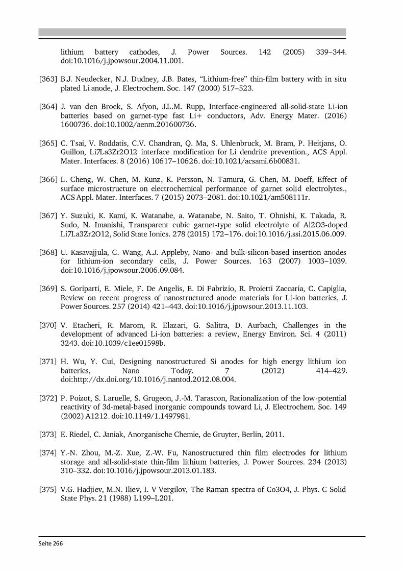
Seite 266
lithium battery cathodes, J. Power Sources. 142 (2005) 339–344. doi:10.1016/j.jpowsour.2004.11.001. [363] B.J. Neudecker, N.J. Dudney, J.B. Bates, “Lithium-free” thin-film battery with in situ plated Li anode, J. Electrochem. Soc. 147 (2000) 517–523. [364] J. van den Broek, S. Afyon, J.L.M. Rupp, Interface-engineered all-solid-state Li-ion batteries based on garnet-type fast Li+ conductors, Adv. Energy Mater. (2016) 1600736. doi:10.1002/aenm.201600736. [365] C. Tsai, V. Roddatis, C.V. Chandran, Q. Ma, S. Uhlenbruck, M. Bram, P. Heitjans, O. Guillon, Li7La3Zr2O12 interface modification for Li dendrite prevention., ACS Appl. Mater. Interfaces. 8 (2016) 10617–10626. doi:10.1021/acsami.6b00831. [366] L. Cheng, W. Chen, M. Kunz, K. Persson, N. Tamura, G. Chen, M. Doeff, Effect of surface microstructure on electrochemical performance of garnet solid electrolytes., ACS Appl. Mater. Interfaces. 7 (2015) 2073–2081. doi:10.1021/am508111r. [367] Y. Suzuki, K. Kami, K. Watanabe, a. Watanabe, N. Saito, T. Ohnishi, K. Takada, R. Sudo, N. Imanishi, Transparent cubic garnet-type solid electrolyte of Al2O3-doped Li7La3Zr2O12, Solid State Ionics. 278 (2015) 172–176. doi:10.1016/j.ssi.2015.06.009. [368] U. Kasavajjula, C. Wang, A.J. Appleby, Nano- and bulk-silicon-based insertion anodes for lithium-ion secondary cells, J. Power Sources. 163 (2007) 1003–1039. doi:10.1016/j.jpowsour.2006.09.084. [369] S. Goriparti, E. Miele, F. De Angelis, E. Di Fabrizio, R. Proietti Zaccaria, C. Capiglia, Review on recent progress of nanostructured anode materials for Li-ion batteries, J. Power Sources. 257 (2014) 421–443. doi:10.1016/j.jpowsour.2013.11.103. [370] V. Etacheri, R. Marom, R. Elazari, G. Salitra, D. Aurbach, Challenges in the development of advanced Li-ion batteries: a review, Energy Environ. Sci. 4 (2011) 3243. doi:10.1039/c1ee01598b. [371] H. Wu, Y. Cui, Designing nanostructured Si anodes for high energy lithium ion batteries, Nano Today. 7 (2012) 414–429. doi:http://dx.doi.org/10.1016/j.nantod.2012.08.004. [372] P. Poizot, S. Laruelle, S. Grugeon, J.-M. Tarascon, Rationalization of the low-potential reactivity of 3d-metal-based inorganic compounds toward Li, J. Electrochem. Soc. 149 (2002) A1212. doi:10.1149/1.1497981. [373] E. Riedel, C. Janiak, Anorganische Chemie, de Gruyter, Berlin, 2011. [374] Y.-N. Zhou, M.-Z. Xue, Z.-W. Fu, Nanostructured thin film electrodes for lithium storage and all-solid-state thin-film lithium batteries, J. Power Sources. 234 (2013) 310–332. doi:10.1016/j.jpowsour.2013.01.183. [375] V.G. Hadjiev, M.N. Iliev, I. V Vergilov, The Raman spectra of Co3O4, J. Phys. C Solid State Phys. 21 (1988) L199–L201.
Seite 267
[376] Y. Li, W. Qiu, F. Qin, H. Fang, V.G. Hadjiev, D. Litvinov, J. Bao, Identification of cobalt oxides with Raman scattering and Fourier Transform Infrared Spectroscopy, J. Phys. Chem. C. 120 (2016) 4511–4516. doi:10.1021/acs.jpcc.5b11185. [377] G.W. Graham, W.H. Weber, J.R. McBride, C.R. Peters, Raman investigation of simple and complex oxides of platinum, J. Raman Spectrosc. 22 (1991) 1–9. [378] P.A. Connor, J.T.S. Irvine, Combined X-ray study of lithium (tin) cobalt oxide matrix negative electrodes for Li-ion batteries, Electrochim. Acta. 47 (2002) 2885–2892. [379] D. Larcher, G. Sudant, J.-B. Leriche, Y. Chabre, J.-M. Tarascon, The electrochemical reduction of Co3O4 in a lithium cell, J. Electrochem. Soc. 149 (2002) A234. doi:10.1149/1.1435358. [380] J. Jamnik, J. Maier, Nanocrystallinity effects in lithium battery materials, Phys. Chem. Chem. Phys. 5 (2003) 5215. doi:10.1039/b309130a. [381] S. Laruelle, S. Grugeon, P. Poizot, M. Dolle , L. Dupont, J.-M. Tarascon, On the origin of the extra electrochemical capacity displayed by MO/Li cells at low potential, J. Electrochem. Soc. 149 (2002) A627. doi:10.1149/1.1467947. [382] Y.F. Zhukovskii, P. Balaya, E. a Kotomin, J. Maier, Evidence for interfacial-storage anomaly in nanocomposites for lithium batteries from first-principles simulations., Phys. Rev. Lett. 96 (2006) 058302. doi:10.1103/PhysRevLett.96.058302. [383] E. Bekaert, P. Balaya, S. Murugavel, J. Maier, M. Ménétrier, Li MAS NMR investigation of electrochemical lithiation of RuO2: Evidence for an interfacial storage mechanism, Chem. Mater. 21 (2009) 856–861. [384] H. Li, P. Balaya, J. Maier, Li-storage via heterogeneous reaction in selected binary metal fluorides and oxides, J. Electrochem. Soc. 151 (2004) A1878. doi:10.1149/1.1801451. [385] Y. Wang, Z.-W. Fu, Q.-Z. Qin, A nanocrystalline Co3O4 thin film electrode for Li-ion batteries, Thin Solid Films. 441 (2003) 19–24. doi:10.1016/S0040-6090(03)00918-0. [386] V. Pralong, J.-B. Leriche, B. Beaudoin, E. Naudin, M. Morcrette, J.-M. Tarascon, Electrochemical study of nanometer Co3O4, Co, CoSb3 and Sb thin films toward lithium, Solid State Ionics. 166 (2004) 295–305. doi:10.1016/j.ssi.2003.11.018. [387] Z. Fu, Y. Wang, Y. Zhang, Q. Qin, Electrochemical reaction of nanocrystalline Co3O4 thin film with Lithium, Solid State Ionics. 170 (2004) 105–109. doi:10.1016/j.ssi.2004.02.020. [388] C.L. Liao, Y.H. Lee, S.T. Chang, K.Z. Fung, Structural characterization and electrochemical properties of RF-sputtered nanocrystalline Co3O4 thin-film anode, J. Power Sources. 158 (2006) 1379–1385. doi:10.1016/j.jpowsour.2005.10.014. [389] H.-C. Liu, S.-K. Yen, Characterization of electrolytic Co3O4 thin films as anodes for lithium-ion batteries, J. Power Sources. 166 (2007) 478–484. doi:10.1016/j.jpowsour.2007.01.072.
Seite 268
[390] S.-L. Chou, J.-Z. Wang, H.-K. Liu, S.-X. Dou, Electrochemical deposition of porous Co3O4 nanostructured thin film for lithium-ion battery, J. Power Sources. 182 (2008) 359–364. doi:10.1016/j.jpowsour.2008.03.083. [391] J.-S. Do, R.-F. Dai, Cobalt oxide thin film prepared by an electrochemical route for Li-ion battery, J. Power Sources. 189 (2009) 204–210. doi:10.1016/j.jpowsour.2008.09.093. [392] A. Xiao, J. Yang, W. Zhang, Mesoporous cobalt oxide film prepared by electrodeposition as anode material for Li ion batteries, J. Porous Mater. 17 (2010) 583–588. doi:10.1007/s10934-009-9327-y. [393] X.H. Xia, J.P. Tu, J.Y. Xiang, X.H. Huang, X.L. Wang, X.B. Zhao, Hierarchical porous cobalt oxide array films prepared by electrodeposition through polystyrene sphere template and their applications for lithium ion batteries, J. Power Sources. 195 (2010) 2014–2022. doi:10.1016/j.jpowsour.2009.11.009. [394] Y. Sun, X.-Y. Feng, C.-H. Chen, Hollow Co3O4 thin films as high performance anodes for lithium-ion batteries, J. Power Sources. 196 (2011) 784–787. doi:10.1016/j.jpowsour.2010.07.065. [395] M.E. Donders, H.C.M. Knoops, W.M.M. Kessels, P.H.L. Notten, Co3O4 as anode material for thin film micro-batteries prepared by remote plasma atomic layer deposition, J. Power Sources. 203 (2012) 72–77. doi:10.1016/j.jpowsour.2011.12.020. [396] D. Barreca, M. Cruz-Yusta, A. Gasparotto, C. Maccato, J. Morales, A. Pozza, C. Sada, L. Sánchez, E. Tondello, Cobalt oxide nanomaterials by vapor-phase synthesis for fast and reversible lithium storage, J. Phys. Chem. C. 114 (2010) 10054–10060. [397] A. Jena, N. Munichandraiah, S.A. Shivashankar, Metal-organic chemical vapor-deposited cobalt oxide films as negative electrodes for thin film Li-ion battery, J. Power Sources. 277 (2015) 198–204. doi:10.1016/j.jpowsour.2014.11.091. [398] F. Fievet, P. Germi, F. de Bergevin, M. Figlarz, Lattice Parameter, Microstrains and Non-Stoichiometry in NiO. Comparison between Mosaic Microcrystals and Quasi-Perfect Single Microcrystals, J. Appl. Crystallogr. 12 (1979) 387–394. [399] S. Uhlenbrock, C. Scharfschwerdt, M. Neumann, G. Illing, H.-J. Freund, The influence of defects on the Ni 2p and O 1s XPS of NiO, J. Phys. Condens. Matter. 4 (1992) 7973–7978. doi:10.1088/0953-8984/4/40/009. [400] X. Wang, X. Li, X. Sun, F. Li, Q. Liu, Q. Wang, D. He, Nanostructured NiO electrode for high rate Li-ion batteries, J. Mater. Chem. 21 (2011) 3571. doi:10.1039/c0jm04356g. [401] J. Cabana, L. Monconduit, D. Larcher, M.R. Palacín, Beyond intercalation-based Li-ion batteries: the state of the art and challenges of electrode materials reacting through conversion reactions., Adv. Energy Mater. 22 (2010) E170–92. doi:10.1002/adma.201000717. [402] H. Wang, Q. Pan, X. Wang, G. Yin, J. Zhao, Improving electrochemical performance of NiO films by electrodeposition on foam nickel substrates, J. Appl. Electrochem. 39 (2009) 1597–1602. doi:10.1007/s10800-009-9848-8.
Seite 269
[403] X.H. Huang, J.P. Tu, X.H. Xia, X.L. Wang, J.Y. Xiang, L. Zhang, Y. Zhou, Morphology effect on the electrochemical performance of NiO films as anodes for lithium ion batteries, J. Power Sources. 188 (2009) 588–591. doi:10.1016/j.jpowsour.2008.11.111. [404] M.-S. Wu, Y.-P. Lin, Monodispersed macroporous architecture of nickel-oxide film as an anode material for thin-film lithium-ion batteries, Electrochim. Acta. 56 (2011) 2068–2073. doi:10.1016/j.electacta.2010.11.089. [405] Y.F. Yuan, X.H. Xia, J.B. Wu, J.L. Yang, Y.B. Chen, S.Y. Guo, Hierarchically ordered porous nickel oxide array film with enhanced electrochemical properties for lithium ion batteries, Electrochem. Commun. 12 (2010) 890–893. doi:10.1016/j.elecom.2010.04.013. [406] E. Hosono, S. Fujihara, I. Honma, H. Zhou, The high power and high energy densities Li ion storage device by nanocrystalline and mesoporous Ni/NiO covered structure, Electrochem. Commun. 8 (2006) 284–288. doi:10.1016/j.elecom.2005.11.023. [407] Q. Pan, J. Liu, Facile fabrication of porous NiO films for lithium-ion batteries with high reversibility and rate capability, J. Solid State Electrochem. 13 (2008) 1591–1597. doi:10.1007/s10008-008-0740-y. [408] J. Zhong, X.L. Wang, X.H. Xia, C.D. Gu, J.Y. Xiang, J. Zhang, J.P. Tu, Self-assembled sandwich-like NiO film and its application for Li-ion batteries, J. Alloys Compd. 509 (2011) 3889–3893. doi:10.1016/j.jallcom.2010.12.151. [409] Y. Wang, Q.-Z. Qin, A Nanocrystalline NiO Thin-Film Electrode Prepared by Pulsed Laser Ablation for Li-Ion Batteries, J. Electrochem. Soc. 149 (2002) A873. doi:10.1149/1.1481715. [410] Y. Nuli, S. Zhao, Q. Qin, Nanocrystalline tin oxides and nickel oxide film anodes for Li-ion batteries, J. Power Sources. 114 (2003) 113–120. doi:10.1016/S0378-7753(02)00531-1. [411] K.-F. Chiu, C.Y. Chang, C.M. Lin, The Electrochemical Performance of Bias-Sputter-Deposited Nanocrystalline Nickel Oxide Thin Films Toward Lithium, J. Electrochem. Soc. 152 (2005) A1188. doi:10.1149/1.1906024. [412] B. Varghese, M. V Reddy, Z. Yanwu, C.S. Lit, T.C. Hoong, G. V. Subba Rao, B.V.R. Chowdari, A.T.S. Wee, C.T. Lim, C.-H. Sow, Fabrication of NiO nanowall electrodes for high performance lithium ion battery, Chem. Mater. 20 (2008) 3360–3367. doi:10.1021/cm703512k. [413] F. Badway, I. Plitz, S. Grugeon, S. Laruelle, M. Dolle , A.S. Gozdz, J.-M. Tarascon, Metal oxides as negative electrode materials in Li-ion cells, Electrochem. Solid-State Lett. 5 (2002) A115. doi:10.1149/1.1472303. [414] D. Pasero, N. Reeves, A.R. West, Co-doped Mn3O4: a possible anode material for lithium batteries, J. Power Sources. 141 (2005) 156–158. doi:10.1016/j.jpowsour.2004.07.037.
Seite 270
[415] X.Q. Yu, Y. He, J.P. Sun, K. Tang, H. Li, L.Q. Chen, X.J. Huang, Nanocrystalline MnO thin film anode for lithium ion batteries with low overpotential, Electrochem. Commun. 11 (2009) 791–794. doi:10.1016/j.elecom.2009.01.040. [416] M. Bernard, A.H. Goff, B.V. Thi, S.C. De Torresi, Electrochromic reactions in manganese oxides - Part I. Raman analysis, J. Electrochem. 140 (1993) 3065. [417] C.M. Julien, M. Massot, C. Poinsignon, Lattice vibrations of manganese oxides - Part I. Periodic structures, Spectrochim. Acta Part A Mol. Biomol. Spectrosc. 60 (2004) 689–700. doi:10.1016/S1386-1425(03)00279-8. [418] J. Gao, M.A. Lowe, H.D. Abruna, Spongelike nanosized Mn3O4 as a high-capacity anode material for rechargeable lithium batteries, Chem. Mater. 23 (2011) 3223–3227. [419] X. Fang, X. Lu, X. Guo, Y. Mao, Y.-S. Hu, J. Wang, Z. Wang, F. Wu, H. Liu, L. Chen, Electrode reactions of manganese oxides for secondary lithium batteries, Electrochem. Commun. 12 (2010) 1520–1523. doi:10.1016/j.elecom.2010.08.023. [420] Z. Cui, X. Guo, H. Li, High performance MnO thin-film anodes grown by radio-frequency sputtering for lithium ion batteries, J. Power Sources. 244 (2013) 731–735. doi:10.1016/j.jpowsour.2012.11.071. [421] Z. Cui, X. Guo, H. Li, Improved electrochemical properties of MnO thin film anodes by elevated deposition temperatures: Study of conversion reactions, Electrochim. Acta. 89 (2013) 229–238. doi:10.1016/j.electacta.2012.10.164. [422] X.-H. Ma, Q.-Y. Wan, X. Huang, C.-X. Ding, Y. Jin, Y.-B. Guan, C.-H. Chen, Synthesis of three-dimensionally porous MnO thin films for lithium-ion batteries by improved Electrostatic Spray Deposition technique, Electrochim. Acta. 121 (2014) 15–20. doi:10.1016/j.electacta.2013.12.004. [423] W. Dreyer, J. Jamnik, C. Guhlke, R. Huth, J. Moskon, M. Gaberscek, The thermodynamic origin of hysteresis in insertion batteries., Nat. Mater. 9 (2010) 448–53. doi:10.1038/nmat2730. [424] K. Zhong, B. Zhang, S. Luo, W. Wen, H. Li, X. Huang, L. Chen, Investigation on porous MnO microsphere anode for lithium ion batteries, J. Power Sources. 196 (2011) 6802–6808. doi:10.1016/j.jpowsour.2010.10.031. [425] X. Shen, Z. Ji, H. Miao, J. Yang, K. Chen, Hydrothermal synthesis of MnCO3 nanorods and their thermal transformation into Mn2O3 and Mn3O4 nanorods with single crystalline structure, J. Alloys Compd. 509 (2011) 5672–5676. doi:10.1016/j.jallcom.2011.02.119. [426] Y. Deng, L. Wan, Y. Xie, X. Qin, G. Chen, Recent advances in Mn-based oxides as anode materials for lithium ion batteries, RSC Adv. 4 (2014) 23914–23935. doi:10.1039/c4ra02686a. [427] Q. Hao, J. Wang, C. Xu, Facile preparation of Mn3O4 octahedra and their long-term cycle life as an anode material for Li-ion batteries, J. Mater. Chem. A. 2 (2014) 87–93. doi:10.1039/c3ta13510a.
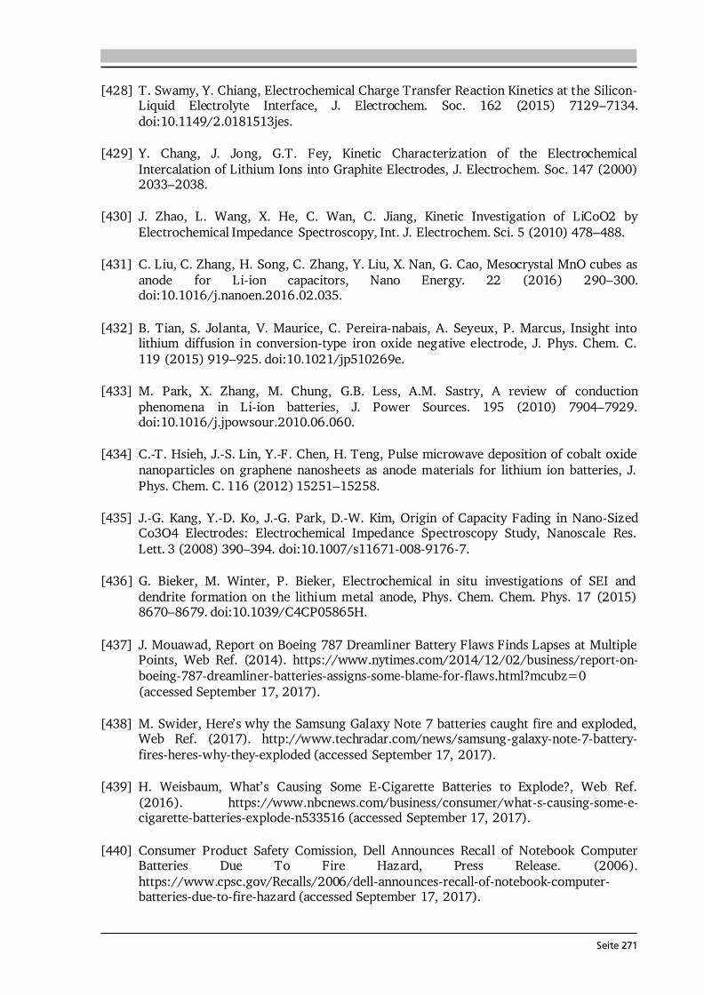
Seite 271
[428] T. Swamy, Y. Chiang, Electrochemical Charge Transfer Reaction Kinetics at the Silicon-Liquid Electrolyte Interface, J. Electrochem. Soc. 162 (2015) 7129–7134. doi:10.1149/2.0181513jes. [429] Y. Chang, J. Jong, G.T. Fey, Kinetic Characterization of the Electrochemical Intercalation of Lithium Ions into Graphite Electrodes, J. Electrochem. Soc. 147 (2000) 2033–2038. [430] J. Zhao, L. Wang, X. He, C. Wan, C. Jiang, Kinetic Investigation of LiCoO2 by Electrochemical Impedance Spectroscopy, Int. J. Electrochem. Sci. 5 (2010) 478–488. [431] C. Liu, C. Zhang, H. Song, C. Zhang, Y. Liu, X. Nan, G. Cao, Mesocrystal MnO cubes as anode for Li-ion capacitors, Nano Energy. 22 (2016) 290–300. doi:10.1016/j.nanoen.2016.02.035. [432] B. Tian, S. Jolanta, V. Maurice, C. Pereira-nabais, A. Seyeux, P. Marcus, Insight into lithium diffusion in conversion-type iron oxide negative electrode, J. Phys. Chem. C. 119 (2015) 919–925. doi:10.1021/jp510269e. [433] M. Park, X. Zhang, M. Chung, G.B. Less, A.M. Sastry, A review of conduction phenomena in Li-ion batteries, J. Power Sources. 195 (2010) 7904–7929. doi:10.1016/j.jpowsour.2010.06.060. [434] C.-T. Hsieh, J.-S. Lin, Y.-F. Chen, H. Teng, Pulse microwave deposition of cobalt oxide nanoparticles on graphene nanosheets as anode materials for lithium ion batteries, J. Phys. Chem. C. 116 (2012) 15251–15258. [435] J.-G. Kang, Y.-D. Ko, J.-G. Park, D.-W. Kim, Origin of Capacity Fading in Nano-Sized Co3O4 Electrodes: Electrochemical Impedance Spectroscopy Study, Nanoscale Res. Lett. 3 (2008) 390–394. doi:10.1007/s11671-008-9176-7. [436] G. Bieker, M. Winter, P. Bieker, Electrochemical in situ investigations of SEI and dendrite formation on the lithium metal anode, Phys. Chem. Chem. Phys. 17 (2015) 8670–8679. doi:10.1039/C4CP05865H. [437] J. Mouawad, Report on Boeing 787 Dreamliner Battery Flaws Finds Lapses at Multiple Points, Web Ref. (2014). https://www.nytimes.com/2014/12/02/business/report-on-boeing-787-dreamliner-batteries-assigns-some-blame-for-flaws.html?mcubz=0 (accessed September 17, 2017). [438] M. Swider, Here’s why the Samsung Galaxy Note 7 batteries caught fire and exploded, Web Ref. (2017). http://www.techradar.com/news/samsung-galaxy-note-7-battery-fires-heres-why-they-exploded (accessed September 17, 2017). [439] H. Weisbaum, What’s Causing Some E-Cigarette Batteries to Explode?, Web Ref. (2016). https://www.nbcnews.com/business/consumer/what-s-causing-some-e-cigarette-batteries-explode-n533516 (accessed September 17, 2017). [440] Consumer Product Safety Comission, Dell Announces Recall of Notebook Computer Batteries Due To Fire Hazard, Press Release. (2006). https://www.cpsc.gov/Recalls/2006/dell-announces-recall-of-notebook-computer-batteries-due-to-fire-hazard (accessed September 17, 2017).
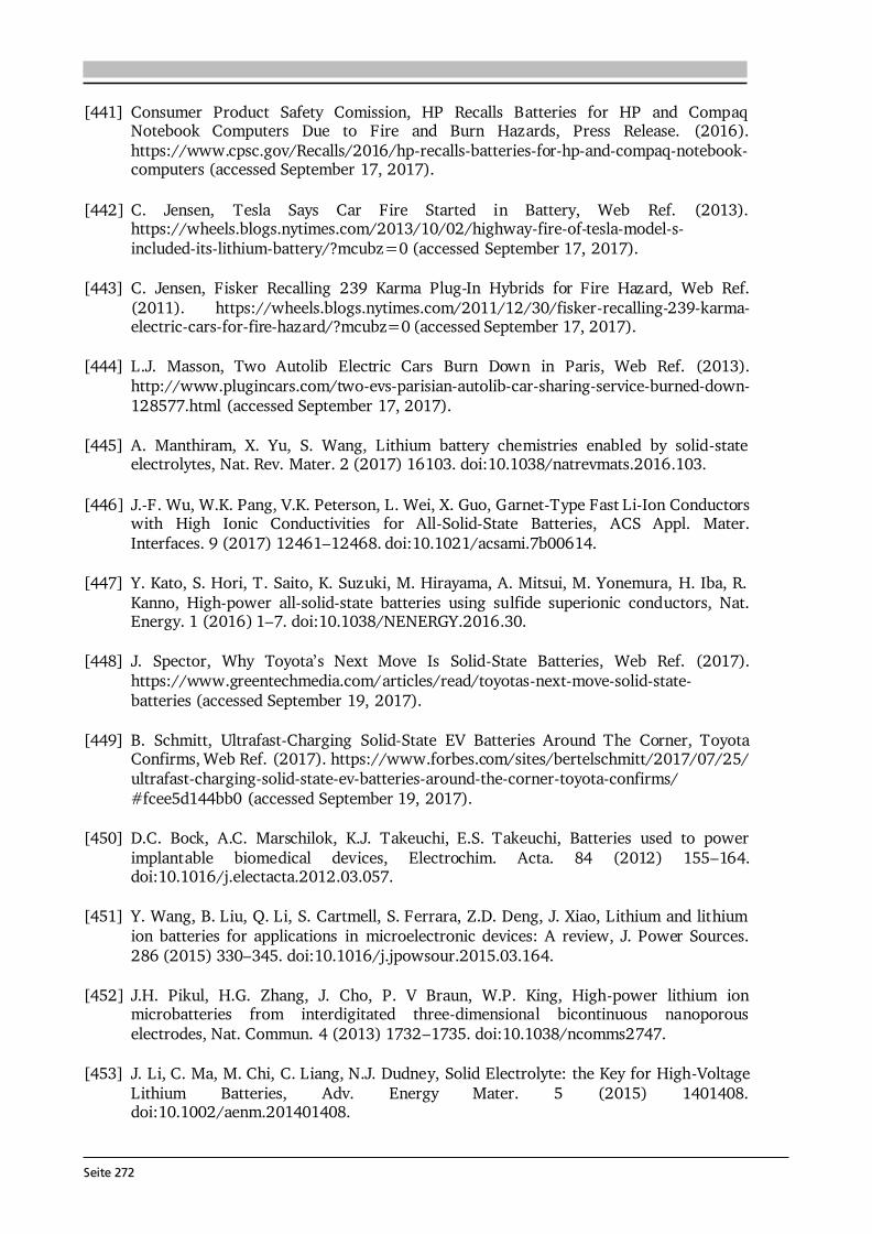
Seite 272
[441] Consumer Product Safety Comission, HP Recalls Batteries for HP and Compaq Notebook Computers Due to Fire and Burn Hazards, Press Release. (2016). https://www.cpsc.gov/Recalls/2016/hp-recalls-batteries-for-hp-and-compaq-notebook-computers (accessed September 17, 2017). [442] C. Jensen, Tesla Says Car Fire Started in Battery, Web Ref. (2013). https://wheels.blogs.nytimes.com/2013/10/02/highway-fire-of-tesla-model-s-included-its-lithium-battery/?mcubz=0 (accessed September 17, 2017). [443] C. Jensen, Fisker Recalling 239 Karma Plug-In Hybrids for Fire Hazard, Web Ref. (2011). https://wheels.blogs.nytimes.com/2011/12/30/fisker-recalling-239-karma-electric-cars-for-fire-hazard/?mcubz=0 (accessed September 17, 2017). [444] L.J. Masson, Two Autolib Electric Cars Burn Down in Paris, Web Ref. (2013). http://www.plugincars.com/two-evs-parisian-autolib-car-sharing-service-burned-down-128577.html (accessed September 17, 2017). [445] A. Manthiram, X. Yu, S. Wang, Lithium battery chemistries enabled by solid-state electrolytes, Nat. Rev. Mater. 2 (2017) 16103. doi:10.1038/natrevmats.2016.103. [446] J.-F. Wu, W.K. Pang, V.K. Peterson, L. Wei, X. Guo, Garnet-Type Fast Li-Ion Conductors with High Ionic Conductivities for All-Solid-State Batteries, ACS Appl. Mater. Interfaces. 9 (2017) 12461–12468. doi:10.1021/acsami.7b00614. [447] Y. Kato, S. Hori, T. Saito, K. Suzuki, M. Hirayama, A. Mitsui, M. Yonemura, H. Iba, R. Kanno, High-power all-solid-state batteries using sulfide superionic conductors, Nat. Energy. 1 (2016) 1–7. doi:10.1038/NENERGY.2016.30. [448] J. Spector, Why Toyota’s Next Move Is Solid-State Batteries, Web Ref. (2017). https://www.greentechmedia.com/articles/read/toyotas-next-move-solid-state-batteries (accessed September 19, 2017). [449] B. Schmitt, Ultrafast-Charging Solid-State EV Batteries Around The Corner, Toyota Confirms, Web Ref. (2017). https://www.forbes.com/sites/bertelschmitt/2017/07/25/ ultrafast-charging-solid-state-ev-batteries-around-the-corner-toyota-confirms/ #fcee5d144bb0 (accessed September 19, 2017). [450] D.C. Bock, A.C. Marschilok, K.J. Takeuchi, E.S. Takeuchi, Batteries used to power implantable biomedical devices, Electrochim. Acta. 84 (2012) 155–164. doi:10.1016/j.electacta.2012.03.057. [451] Y. Wang, B. Liu, Q. Li, S. Cartmell, S. Ferrara, Z.D. Deng, J. Xiao, Lithium and lithium ion batteries for applications in microelectronic devices: A review, J. Power Sources. 286 (2015) 330–345. doi:10.1016/j.jpowsour.2015.03.164. [452] J.H. Pikul, H.G. Zhang, J. Cho, P. V Braun, W.P. King, High-power lithium ion microbatteries from interdigitated three-dimensional bicontinuous nanoporous electrodes, Nat. Commun. 4 (2013) 1732–1735. doi:10.1038/ncomms2747. [453] J. Li, C. Ma, M. Chi, C. Liang, N.J. Dudney, Solid Electrolyte: the Key for High-Voltage Lithium Batteries, Adv. Energy Mater. 5 (2015) 1401408. doi:10.1002/aenm.201401408.
Seite 273
[454] EnFilm: Thin-film batteries, Homepage. (2017). http://www.st.com/en/power-management/enfilm-thin-film-batteries.html?querycriteria=productId=SC1107 (accessed September 19, 2017). [455] BrightVolt Batteries, Homepage. (2017). http://www.brightvolt.com/ (accessed September 19, 2017). [456] Blue Spark, Homepage. (2017). http://www.bluesparktechnologies.com/ (accessed September 19, 2017). [457] Enfucell, Homepage. (2017). https://www.enfucell.com/ (accessed September 19, 2017). [458] A. Schwöbel, Präparation und Charakterisierung von LiPON Feststoffelektrolyt-Dünnschichten und deren Grenzflächen, Dissertation. (2015) Technische Universität Darmstadt. http://tuprints.ulb.tu-darmstadt.de/5188/. [459] F. Sagane, K. Ikeda, K. Okita, H. Sano, H. Sakaebe, Y. Iriyama, Effects of current densities on the lithium plating morphology at a lithium phosphorus oxynitride glass electrolyte/copper thin film interface, J. Power Sources. 233 (2013) 34–42. doi:10.1016/j.jpowsour.2013.01.051. [460] A. Sharafi, E. Kazyak, A.L. Davis, S. Yu, T. Thompson, D.J. Siegel, N.P. Dasgupta, J. Sakamoto, Surface Chemistry Mechanism of Ultra-Low Interfacial Resistance in the Solid-State Electrolyte Li7La3Zr2O12, Chem. Mater. 29 (2017) 7961–7968. doi:10.1021/acs.chemmater.7b03002. [461] Y. Bi, T. Wang, M. Liu, R. Du, W. Yang, Z. Liu, Z. Peng, Y. Liu, D. Wang, X. Sun, Stability of Li2CO3 in cathode of lithium ion battery and its influence on electrochemical performance, RSC Adv. 6 (2016) 19233–19237. doi:10.1039/C6RA00648E. [462] M. Moshkovich, M. Cojocaru, H.E. Gottlieb, D. Aurbach, The study of the anodic stability of alkyl carbonate solutions by in situ FTIR spectroscopy, EQCM, NMR and MS, J. Electroanal. Chem. 497 (2001) 84–96. [463] D. Aurbach, E. Zinigrad, Y. Cohen, H. Teller, A short review of failure mechanisms of lithium metal and lithiated graphite anodes in liquid electrolyte solutions, Solid State Ionics. 148 (2002) 405–416. [464] K. Adhikary, M. Takahashi, S. Kikkawa, Some new aspects of low-temperature lithium cobald oxides prepared through citric acid precursor route, Mater. Res. Bull. 33 (1998) 1845–1856. [465] Y. Jin, P.J. McGinn, Li7La3Zr2O12 electrolyte stability in air and fabrication of a Li/Li7La3Zr2O12/Cu0.1V2O5 solid-state battery, J. Power Sources. 239 (2013) 326–331. doi:10.1016/j.jpowsour.2013.03.155. [466] T. Matsuyama, R. Takano, K. Tadanaga, A. Hayashi, M. Tatsumisago, Fabrication of all-solid-state lithium secondary batteries with amorphous TiS4 positive electrodes and Li7La3Zr2O12 solid electrolytes, Solid State Ionics. 285 (2016) 122–125. doi:10.1016/j.ssi.2015.05.025.

Seite 274

Seite 275
List of Own Publications [I] C. Loho, R. Djenadic, P. Mundt, O. Clemens, H. Hahn, On processing-structure-property relations and high ionic conductivity in garnet-type Li5La3Ta2O12 solid electrolyte thin films grown by CO2-laser assisted CVD, Solid State Ionics. 313 (2017) 32–44. [II] M. Fingerle, C. Loho, T. Ferber, H. Hahn, R. Hausbrand, Evidence of the chemical stability of the garnet-type solid electrolyte Li5La3Ta2O12 towards lithium by a surface science approach, J. Power Sources. 366 (2017) 72–79. [III] C. Loho, R. Djenadic, M. Bruns, O. Clemens, H. Hahn, Garnet-type Li7La3Zr2O12 solid electrolyte thin films grown by CO2-laser assisted CVD for all-solid-state batteries, J. Electrochem. Soc. 164 (2017) A6131–A6139. [IV] A. Sarkar, C. Loho, L. Velasco, T. Thomas, S.S. Bhattacharya, H. Hahn, R. Djenadic, Multicomponent equiatomic rare earth oxides with a narrow band gap and associated praseodymium multivalency, Dalt. Trans. 46 (2017) 12167–12176. [V] P.A. Sukkurji, A. Molinari, A. Benes, C. Loho, V.S.K. Chakravadhanula, S.K. Garlapati, R. Kruk, O. Clemens, Structure and conductivity of epitaxial thin films of barium ferrite and its hydrated form BaFeO2.5-x+delta(OH)(2x), J. Phys. D-Applied Phys. 50 (2017) 115302. [VI] R. Djenadic, A. Sarkar, O. Clemens, C. Loho, M. Botros, V.S.K. Chakravadhanula, C. Kübel, S.S. Bhattacharya, A.S. Gandhi, H. Hahn, Multicomponent equiatomic rare earth oxides, Mater. Res. Lett. 5:2 (2016) 102–109. [VII] P.L. Knoechel, P.J. Keenan, C. Loho, C. Reitz, R. Witte, K.S. Knight, A.J. Wright, H. Hahn, P.R. Slater, O. Clemens, Synthesis, structural characterisation and proton conduction of two new hydrated phases of barium ferrite BaFeO2.5-x(OH)(2x), J. Mater. Chem. A. 4 (2016) 3415–3430.

Seite 276
[VIII] C. Loho, A.J. Darbandi, R. Djenadic, O. Clemens, H. Hahn, CO2-Laser Flash Evaporation as Novel CVD Precursor Delivery System for Functional Thin Film Growth, Chem. Vap. Depos. 20 (2014) 152–160. Cover image in Chem. Vap. Deposition 20 (2014) 152. [IX] O. Clemens, R. Kruk, E.A. Patterson, C. Loho, C. Reitz, A.J. Wright, K.S. Knight, H. Hahn, P.R. Slater, Introducing a Large Polar Tetragonal Distortion into Ba-Doped BiFeO3 by Low-Temperature Fluorination, Inorg. Chem. 53 (2014) 12572–12583. [X] O. Clemens, M. Groeting, R. Witte, J. Manuel Perez-Mato, C. Loho, F.J. Berry, R. Kruk, K.S. Knight, A.J. Wright, H. Hahn, P.R. Slater, Crystallographic and Magnetic Structure of the Perovskite-Type Compound BaFeO2.5: Unrivaled Complexity in Oxygen Vacancy Ordering, Inorg. Chem. 53 (2014) 5911–5921. [XI] J. Aulbach, J. Schaefer, S.C. Erwin, S. Meyer, C. Loho, J. Settelein, R. Claessen, Evidence for Long-Range Spin Order Instead of a Peierls Transition in Si(553)-Au Chains, Phys. Rev. Lett. 111 (2013) 137203. [XII] P. Hoepfner, J. Schaefer, A. Fleszar, J.H. Dil, B. Slomski, F. Meier, C. Loho, C. Blumenstein, L. Patthey, W. Hanke, R. Claessen, Three-Dimensional Spin Rotations at the Fermi Surface of a Strongly Spin-Orbit Coupled Surface System, Phys. Rev. Lett. 108 (2012) 186801.
Seite 277
Acknowledgments I would like to thank numerous people, too many to list them all here, for their inspiration, motivation and support throughout my life culminating, for now, in the success of this project. First and foremost I would like to thank Horst Hahn for giving me the opportunity to work on cutting-edge research under excellent conditions. I particularly appreciate the freedom you provided me to pursue my personal research interests and your trust in my work. Moreover, I am deeply grateful for your support to travel around the world to discuss my results and initiate collaborations with leading scientists. Azad Darbandi is acknowledged for his strategic support at the beginning of this PhD project. I am truly thankful for the ongoing support of Ruzica Djenadic and Oliver Clemens; for sharing their knowledge and ideas, lots of fruitful, and sometimes heated, discussions, hands-on assistance in the lab, proof-reading my thesis and fun off the job - you are not only great scientists, but great people, too. Many thanks go to all colleagues of the JRLNano and also MDbS group for the joyful time in the office, lab and on conferences. Especially valuable time I shared with my PhD companions Cahit Benel, Miriam Botros and Alexander Beneš - it was a great pleasure to hang around with you guys, thanks a lot for the superb working atmosphere. Special thanks go to several colleagues at the INT in Karlsruhe, namely Philipp Leufke and Thomas Reisinger for laser-cutting my substrates, Ralf Witte for RBS measurements and Christian Reitz for ALD coatings (Al2O3 and TiN). I have learned a great deal from their expertise, even though neither the RBS nor the ALD results found their way into this thesis. I would like to thank several people from the Materials Science Department at TU Darmstadt for their kind cooperation: Stephan Hillmann (Al2O3 coating via ALD), Philipp Komissinskiy (SEM introduction and help with laser issues), Jan Kaspar and Mirko Reinold (FTIR and Raman introduction and delightful coffee), Dragoljub Vrankovic and Magdalena Graczyk-Zajac (providing slots on their potentiostats), Paul Mundt (AFM measurements and amusing coffee breaks), André Schwöbel and Conrad Guhl (LiPON and ZrO2 sputtering), Mathias Fingerle (interface experiment), Markus Motzko (mastering DAISY-Bat with me), Mirko Weidner and Philip Reckers (legionary time). Moreover, this PhD project would not have been feasible without the assistance and brilliant work of Michael Weber (electrical workshop) as well as Jochen Rank and his team (mechanical workshop), which is highly appreciated. I also had the chance to work together with highly motivated students: Christian Heidorn, Matheus Wanior, Geoffrey Tan, Marcel Sadowski. Geoffrey and Marcel, thank you for all your work and effort to operate the lab at full capacity. I hope you learned as much as I did. I am very grateful to Renate Hernichel for everything not related to science. Thank you for taking over all administrative tasks, lots of organization and for your constant moral support.
Seite 278
Parts of this work were carried out with the support of the Karlsruhe Nano Micro Facility (KNMF, www.knmf.kit.edu), a Helmholtz Research Infrastructure at Karlsruhe Institute of Technology (KIT, www.kit.edu). I acknowledge the KNMF for provision of access to the ToF-SIMS, XPS, FIB and TEM instruments. Here, I would like to thank Michael Bruns for his very good support with the ToF-SIMS and XPS measurements. I also thank Mohammed Hammad Fawey, Venkata Sai Kiran Chakravadhanula, Di Wang and Christian Kübel for FIB preparation and TEM analyses, even though the results were not included into this thesis. Furthermore, parts of this research were carried out at IBC at the Helmholtz -Zentrum Dresden - Rossendorf e.V., a member of the Helmholtz Association. I would like to thank Frans Munnik very much for the RBS measurements and assistance with data interpretation. In this respect, many thanks go also to the group of Elke Wendler (Friedrich Schiller University Jena), especially to Marie Mende and Emanuel Schmidt, for their RBS measurements and fruitful discussions, even though the results were not incorporated into this thesis. Moreover, invaluable discussions with the group of Jürgen Fleig (TU Wien), especially Daniel Rettenwander and Andreas Welzl, as well as with the group of Peter Bruce (University of Oxford), especially Jitti Kasemchainan and Stefanie Zekoll, are acknowledged. Regarding funding, a major equipment grant “Competence South – Electrochemistry for Electromobility” from the Federal Ministry of Education and Research (contract no. 6091/89161/03KP801), an equipment grant by the State of Hesse as well as the financial support via the Portfolio project “Electrochemical storage in systems” provided by the Helmholtz Association are gratefully acknowledged. I would like to express my gratitude to my family and friends. The enthusiasm of my friends about my research on the whole kept my motivation high to search for the solution in detail. Besides, they made a good job to take my mind off science once in a while. I highly appreciate that my parents and my brother supported me all times, it really means a lot to me. Last but not least my wife Olga deserves my sincerest appreciation. She, and lately also our beloved son Alexander, suffered most from me working long hours and on weekends. It was no easy period, I admit, and I thank you so much for your endless support and understanding. I love you!

Seite 279
Curriculum Vitae
Personal Data Name Christoph Loho Date/Place of birth 18.06.1987 in Hanau Nationality German
Education Since 06/2012 PhD studies in Materials Science, Technische Universität Darmstadt 10/2011 Diploma in Nanostructural Engineering 10/2006 - 10/2011 Diploma studies in Nanostructural Engineering, University of Würzburg 06/2006 Abitur, Einhardschule Seligenstadt
Work Experience Since 06/2012 Researcher at the Joint Research Laboratory Nanomaterials, Darmstadt 12/2011 - 05/2012 Researcher at the chair of Experimental Physics 4, Würzburg 03/2010 - 05/2010 Internship at KPMG AG auditing company, Frankfurt 02/2009 - 03/2009 Scientific internship at Bruker EAS GmbH, Hanau 07/2008 - 08/2008 Working student at EAS GmbH & Co. KG, Hanau 03/2008 - 04/2008 Internship at EAS GmbH & Co. KG, Hanau

Seite 280
Seite 281
Erklärung zur Dissertation Hiermit versichere ich, die vorliegende Dissertation ohne Hilfe Dritter und nur mit den angegebenen Quellen und Hilfsmitteln angefertigt zu haben. Alle Stellen, die Quellen entnommen wurden, sind als solche kenntlich gemacht worden. Diese Arbeit hat in gleicher oder ähnlicher Form noch keiner Prüfungsbehörde vorgelegen. Darmstadt, den ______________________________________ (Christoph Loho)