ADS126x 32-Bit, Precision, 38-kSPS, Analog-to-Digital ...
134
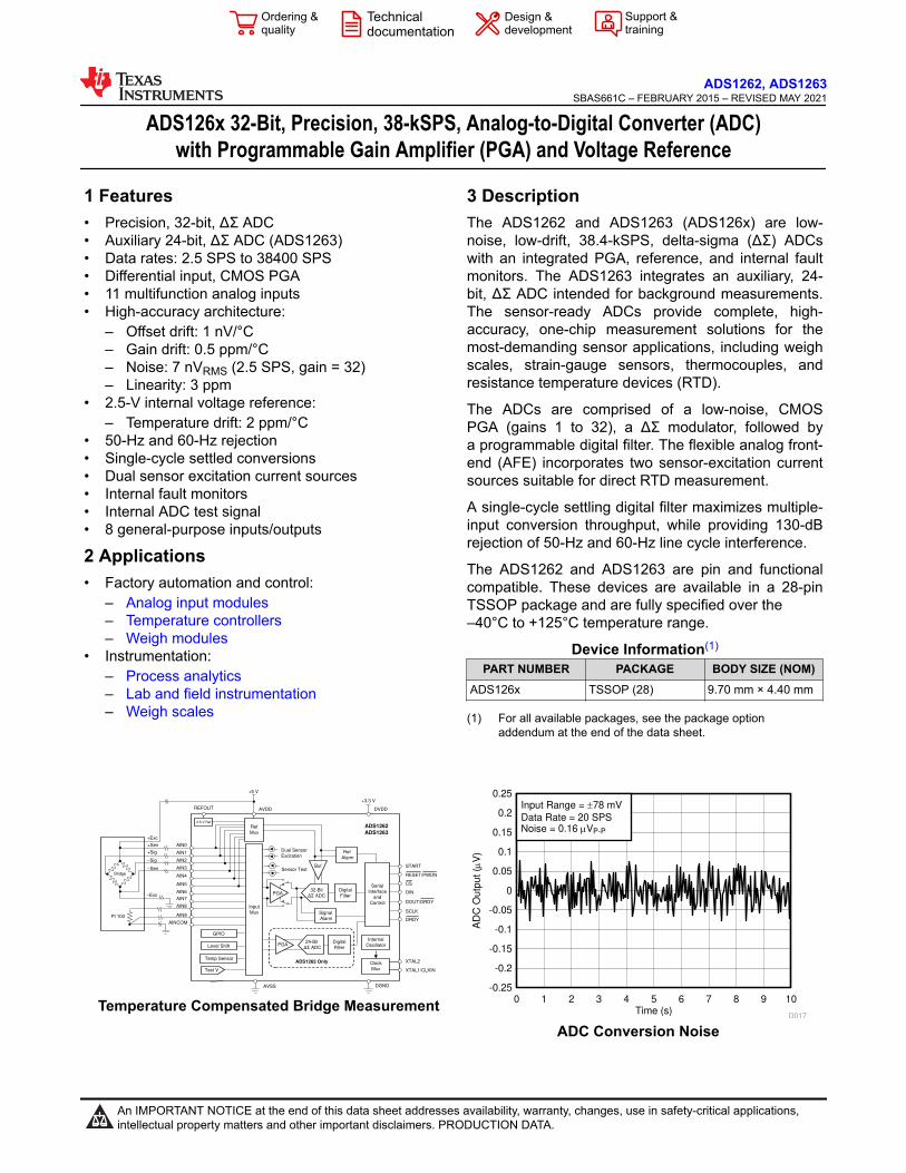
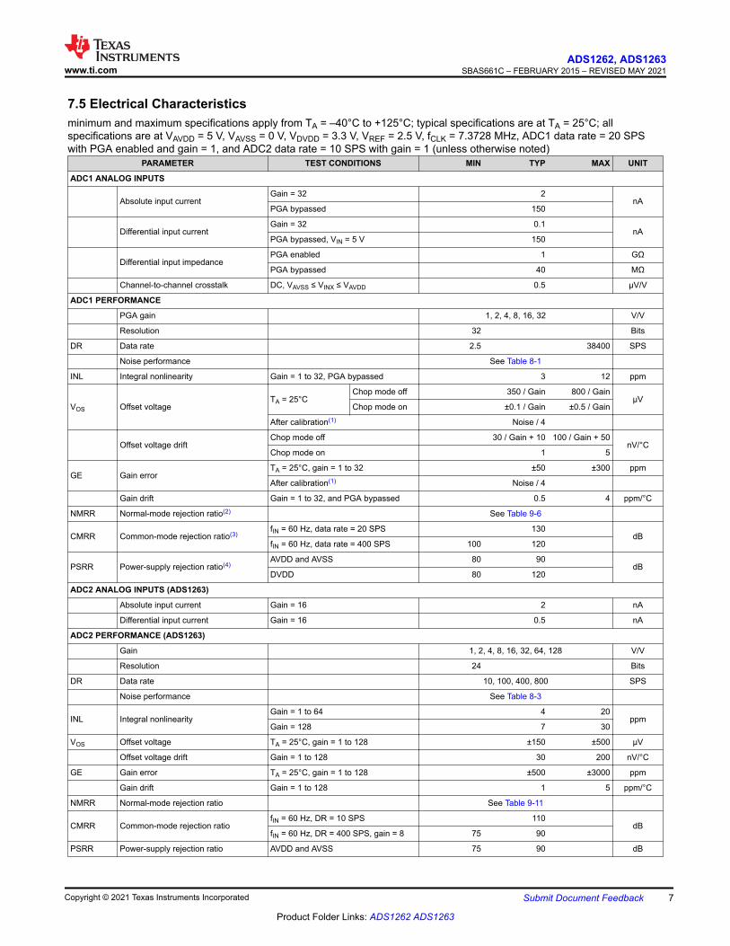
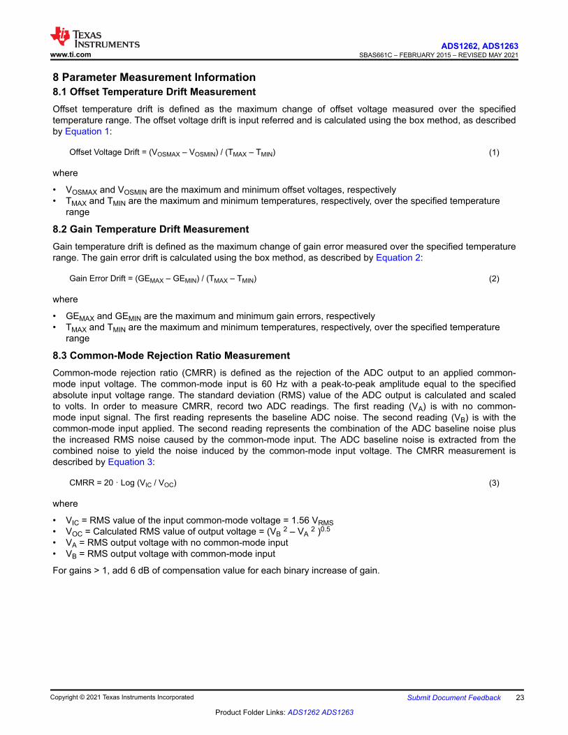
ADS126x 32-Bit, Precision, 38-kSPS, Analog-to-Digital Converter (ADC) with Programmable Gain Amplifier (PGA) and Voltage Reference 1 Features • Precision, 32-bit, ΔΣ ADC • Auxiliary 24-bit, ΔΣ ADC (ADS1263) • Data rates: 2.5 SPS to 38400 SPS • Differential input, CMOS PGA • 11 multifunction analog inputs • High-accuracy architecture: – Offset drift: 1 nV/°C – Gain drift: 0.5 ppm/°C – Noise: 7 nV RMS (2.5 SPS, gain = 32) – Linearity: 3 ppm • 2.5-V internal voltage reference: – Temperature drift: 2 ppm/°C • 50-Hz and 60-Hz rejection • Single-cycle settled conversions • Dual sensor excitation current sources • Internal fault monitors • Internal ADC test signal • 8 general-purpose inputs/outputs 2 Applications • Factory automation and control: – Analog input modules – Temperature controllers – Weigh modules • Instrumentation: – Process analytics – Lab and field instrumentation – Weigh scales 3 Description The ADS1262 and ADS1263 (ADS126x) are low- noise, low-drift, 38.4-kSPS, delta-sigma (ΔΣ) ADCs with an integrated PGA, reference, and internal fault monitors. The ADS1263 integrates an auxiliary, 24- bit, ΔΣ ADC intended for background measurements. The sensor-ready ADCs provide complete, high- accuracy, one-chip measurement solutions for the most-demanding sensor applications, including weigh scales, strain-gauge sensors, thermocouples, and resistance temperature devices (RTD). The ADCs are comprised of a low-noise, CMOS PGA (gains 1 to 32), a ΔΣ modulator, followed by a programmable digital filter. The flexible analog front- end (AFE) incorporates two sensor-excitation current sources suitable for direct RTD measurement. A single-cycle settling digital filter maximizes multiple- input conversion throughput, while providing 130-dB rejection of 50-Hz and 60-Hz line cycle interference. The ADS1262 and ADS1263 are pin and functional compatible. These devices are available in a 28-pin TSSOP package and are fully specified over the –40°C to +125°C temperature range. Device Information (1) PART NUMBER PACKAGE BODY SIZE (NOM) ADS126x TSSOP (28) 9.70 mm × 4.40 mm (1) For all available packages, see the package option addendum at the end of the data sheet. 32-Bit ß ADC PGA Input Mux Digital Filter Serial Interface and Control CS DOUT/DRDY SCLK DRDY START Clock Mux XTAL2 XTAL1/CLKIN REFOUT Ref Alarm Signal Alarm Buf AIN0 AIN1 AIN2 AINCOM GPIO Level Shift Temp Sensor ADS1262 ADS1263 +5 V DVDD DGND Ref Mux 2.5-V Ref AIN3 AIN4 AIN5 AIN6 AIN7 AIN8 AIN9 PGA ADS1263 Only Digital Filter Dual Sensor Excitation Test V Internal Oscillator 24-Bit ß ADC RESET/PWDN DIN AVSS AVDD +Exc –Exc –Sig +Sig –Sen +Sen Sensor Test PGA Pt 100 Bridge +3.3 V Temperature Compensated Bridge Measurement Time (s) ADC Output (PV) 0 1 2 3 4 5 6 7 8 9 10 -0.25 -0.2 -0.15 -0.1 -0.05 0 0.05 0.1 0.15 0.2 0.25 D017 Input Range = r78 mV Data Rate = 20 SPS Noise = 0.16 PV P-P ADC Conversion Noise ADS1262, ADS1263 SBAS661C – FEBRUARY 2015 – REVISED MAY 2021 An IMPORTANT NOTICE at the end of this data sheet addresses availability, warranty, changes, use in safety-critical applications, intellectual property matters and other important disclaimers. PRODUCTION DATA.
-
Upload
khangminh22 -
Category
Documents
-
view
2 -
download
0
Transcript of ADS126x 32-Bit, Precision, 38-kSPS, Analog-to-Digital ...
ADS126x 32-Bit, Precision, 38-kSPS, Analog-to-Digital Converter (ADC)with Programmable Gain Amplifier (PGA) and Voltage Reference
1 Features• Precision, 32-bit, ΔΣ ADC• Auxiliary 24-bit, ΔΣ ADC (ADS1263)• Data rates: 2.5 SPS to 38400 SPS• Differential input, CMOS PGA• 11 multifunction analog inputs• High-accuracy architecture:
– Offset drift: 1 nV/°C– Gain drift: 0.5 ppm/°C– Noise: 7 nVRMS (2.5 SPS, gain = 32)– Linearity: 3 ppm
• 2.5-V internal voltage reference:– Temperature drift: 2 ppm/°C
• 50-Hz and 60-Hz rejection• Single-cycle settled conversions• Dual sensor excitation current sources• Internal fault monitors• Internal ADC test signal• 8 general-purpose inputs/outputs
2 Applications• Factory automation and control:
– Analog input modules– Temperature controllers– Weigh modules
• Instrumentation:– Process analytics– Lab and field instrumentation– Weigh scales
3 DescriptionThe ADS1262 and ADS1263 (ADS126x) are low-noise, low-drift, 38.4-kSPS, delta-sigma (ΔΣ) ADCswith an integrated PGA, reference, and internal faultmonitors. The ADS1263 integrates an auxiliary, 24-bit, ΔΣ ADC intended for background measurements.The sensor-ready ADCs provide complete, high-accuracy, one-chip measurement solutions for themost-demanding sensor applications, including weighscales, strain-gauge sensors, thermocouples, andresistance temperature devices (RTD).
The ADCs are comprised of a low-noise, CMOSPGA (gains 1 to 32), a ΔΣ modulator, followed bya programmable digital filter. The flexible analog front-end (AFE) incorporates two sensor-excitation currentsources suitable for direct RTD measurement.
A single-cycle settling digital filter maximizes multiple-input conversion throughput, while providing 130-dBrejection of 50-Hz and 60-Hz line cycle interference.
The ADS1262 and ADS1263 are pin and functionalcompatible. These devices are available in a 28-pinTSSOP package and are fully specified over the–40°C to +125°C temperature range.
Device Information(1)
PART NUMBER PACKAGE BODY SIZE (NOM)ADS126x TSSOP (28) 9.70 mm × 4.40 mm
(1) For all available packages, see the package optionaddendum at the end of the data sheet.
32-Bit
û��ADCPGA
Input
Mux
Digital
Filter
Serial
Interface
and
Control
CS
DOUT/DRDY
SCLK
DRDY
START
Clock
Mux
XTAL2
XTAL1/CLKIN
REFOUT
Ref
Alarm
Signal
Alarm
Buf
AIN0
AIN1
AIN2
AINCOM
GPIO
Level Shift
Temp Sensor
ADS1262
ADS1263
+5 V
DVDD
DGND
Ref
Mux
2.5-V Ref
AIN3
AIN4
AIN5
AIN6
AIN7
AIN8
AIN9
PGA
ADS1263 Only
Digital
Filter
Dual Sensor
Excitation
Test V
Internal
Oscillator 24-Bit
û��ADC
RESET/PWDN
DIN
AVSS
AVDD
+Exc
±Exc
±Sig
+Sig
±Sen
+Sen
Sensor Test
PGA
Pt 100
Bridge
+3.3 V
Temperature Compensated Bridge Measurement Time (s)
AD
C O
utp
ut (P
V)
0 1 2 3 4 5 6 7 8 9 10-0.25
-0.2
-0.15
-0.1
-0.05
0
0.05
0.1
0.15
0.2
0.25
D017
Input Range = r78 mV
Data Rate = 20 SPSNoise = 0.16 PVP-P
ADC Conversion Noise
ADS1262, ADS1263SBAS661C – FEBRUARY 2015 – REVISED MAY 2021
An IMPORTANT NOTICE at the end of this data sheet addresses availability, warranty, changes, use in safety-critical applications,intellectual property matters and other important disclaimers. PRODUCTION DATA.
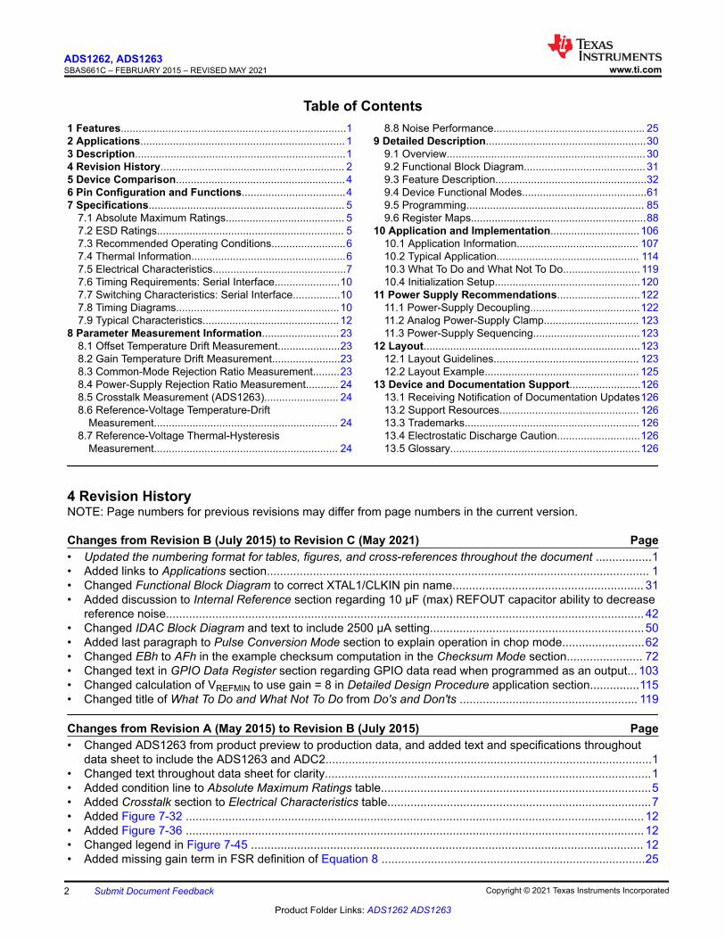
Table of Contents1 Features............................................................................12 Applications..................................................................... 13 Description.......................................................................14 Revision History.............................................................. 25 Device Comparison......................................................... 46 Pin Configuration and Functions...................................47 Specifications.................................................................. 5
7.1 Absolute Maximum Ratings........................................ 57.2 ESD Ratings............................................................... 57.3 Recommended Operating Conditions.........................67.4 Thermal Information....................................................67.5 Electrical Characteristics.............................................77.6 Timing Requirements: Serial Interface......................107.7 Switching Characteristics: Serial Interface................107.8 Timing Diagrams.......................................................107.9 Typical Characteristics.............................................. 12
8 Parameter Measurement Information.......................... 238.1 Offset Temperature Drift Measurement.....................238.2 Gain Temperature Drift Measurement.......................238.3 Common-Mode Rejection Ratio Measurement.........238.4 Power-Supply Rejection Ratio Measurement........... 248.5 Crosstalk Measurement (ADS1263)......................... 248.6 Reference-Voltage Temperature-Drift
Measurement.............................................................. 248.7 Reference-Voltage Thermal-Hysteresis
Measurement.............................................................. 24
8.8 Noise Performance................................................... 259 Detailed Description......................................................30
9.1 Overview................................................................... 309.2 Functional Block Diagram......................................... 319.3 Feature Description...................................................329.4 Device Functional Modes..........................................619.5 Programming............................................................ 859.6 Register Maps...........................................................88
10 Application and Implementation.............................. 10610.1 Application Information......................................... 10710.2 Typical Application................................................ 11410.3 What To Do and What Not To Do.......................... 11910.4 Initialization Setup.................................................120
11 Power Supply Recommendations............................12211.1 Power-Supply Decoupling.....................................12211.2 Analog Power-Supply Clamp................................ 12311.3 Power-Supply Sequencing....................................123
12 Layout.........................................................................12312.1 Layout Guidelines................................................. 12312.2 Layout Example.................................................... 125
13 Device and Documentation Support........................12613.1 Receiving Notification of Documentation Updates12613.2 Support Resources............................................... 12613.3 Trademarks...........................................................12613.4 Electrostatic Discharge Caution............................12613.5 Glossary................................................................126
4 Revision HistoryNOTE: Page numbers for previous revisions may differ from page numbers in the current version.
Changes from Revision B (July 2015) to Revision C (May 2021) Page• Updated the numbering format for tables, figures, and cross-references throughout the document .................1• Added links to Applications section.................................................................................................................... 1• Changed Functional Block Diagram to correct XTAL1/CLKIN pin name.......................................................... 31• Added discussion to Internal Reference section regarding 10 μF (max) REFOUT capacitor ability to decrease
reference noise................................................................................................................................................. 42• Changed IDAC Block Diagram and text to include 2500 μA setting.................................................................50• Added last paragraph to Pulse Conversion Mode section to explain operation in chop mode.........................62• Changed EBh to AFh in the example checksum computation in the Checksum Mode section....................... 72• Changed text in GPIO Data Register section regarding GPIO data read when programmed as an output... 103• Changed calculation of VREFMIN to use gain = 8 in Detailed Design Procedure application section...............115• Changed title of What To Do and What Not To Do from Do's and Don'ts ...................................................... 119
Changes from Revision A (May 2015) to Revision B (July 2015) Page• Changed ADS1263 from product preview to production data, and added text and specifications throughout
data sheet to include the ADS1263 and ADC2...................................................................................................1• Changed text throughout data sheet for clarity...................................................................................................1• Added condition line to Absolute Maximum Ratings table..................................................................................5• Added Crosstalk section to Electrical Characteristics table................................................................................7• Added Figure 7-32 ........................................................................................................................................... 12• Added Figure 7-36 ........................................................................................................................................... 12• Changed legend in Figure 7-45 ....................................................................................................................... 12• Added missing gain term in FSR definition of Equation 8 ................................................................................25
ADS1262, ADS1263SBAS661C – FEBRUARY 2015 – REVISED MAY 2021 www.ti.com
2 Submit Document Feedback Copyright © 2021 Texas Instruments Incorporated
Product Folder Links: ADS1262 ADS1263
• Changed text in fourth paragraph of Noise Performance section to clarify conditions to achieve maximumENOB................................................................................................................................................................25
• Changed bit names from PGAH and PGAL to PGAH_ALM and PGAL_ALM, respectively, in PGA AbsoluteOutput-Voltage Monitor section........................................................................................................................ 40
• Changed Figure 9-12 to show correct name of bit 4.........................................................................................41• Changed RMUX to RMUXP in second paragraph of ADC Reference Voltage section.................................... 41• Changed text in last paragraph of ADC Reference Voltage section to show correct name of bit 4..................41• Changed text in External Reference section to clarify external reference inputs, polarity reversal switch,
reference input current, and external reference buffer..................................................................................... 42• Changed text in Power-Supply Reference section to clarify use of power-supply reference in critical
applications.......................................................................................................................................................42• Added ADC1 Modulator section....................................................................................................................... 42• Changed text in last paragraph of Sensor-Excitation Current Sources (IDAC1 and IDAC2) section to clarify
settling time in IDAC rotation mode.................................................................................................................. 50• Changed text in General-Purpose Input/Output (GPIO) section regarding GPIO data readback when
programmed as an output.................................................................................................................................52• Changed Figure 9-27 .......................................................................................................................................52• Changed TSIGP and TSIGN to TDACP and TDACN, respectively, in the last paragraph of the Test DAC
(TDAC) section................................................................................................................................................. 53• Changed text in Test DAC (TDAC) section allowing for any common-mode value instead of 0 V................... 53• Added note (1) to Figure 9-30 ..........................................................................................................................57• Changed th(DRSP) value of 16 from max to min................................................................................................. 61• Added stop-start sequence text to restart conversions in Continuous Conversion Mode section.................... 61• Deleted software polling text from Data Ready ( DRDY) section..................................................................... 67• Added Conversion Data Software Polling section............................................................................................ 67• Added text to clarify data reset at conversion restart........................................................................................68• Added text to Read Data Direct (ADC1) section to clarify conversion restart...................................................68• Changed Figure 9-43 to show complete list of CRC bit settings...................................................................... 68• Changed text in Read Data by Command section to clarify software polling................................................... 69• Changed Figure 9-44 to show complete list of CRC bit settings...................................................................... 69• Added text to Offset Calibration Registers section regarding offset calibration disabled in chop mode...........76• Added new step 1 to Calibration Command Procedure section....................................................................... 79• Added text to WREG Command section regarding conversion restart.............................................................87• Changed text in 2nd paragraph of Register Map section................................................................................. 88• Changed Group Update column of Table 9-34 ................................................................................................ 88• Added software polling to Figure 10-16 ......................................................................................................... 120
www.ti.comADS1262, ADS1263
SBAS661C – FEBRUARY 2015 – REVISED MAY 2021
Copyright © 2021 Texas Instruments Incorporated Submit Document Feedback 3
Product Folder Links: ADS1262 ADS1263
5 Device ComparisonPRODUCT INPUTS AUXILIARY 24-BIT ADCADS1262 11 No
ADS1263 11 Yes
6 Pin Configuration and Functions
AIN8
AIN9
AINCOM
CAPP
AIN7
AIN6
AIN5
AIN4
CAPN
AVDD
AVSS
REFOUT
START
CS
SCLK
DIN
DOUT/DRDY
DRDY
AIN3
AIN2
AIN1
AIN0
RESET/PWDN
DVDD
DGND
BYPASS
XTAL1/CLKIN
XTAL2
1
2
3
4
5
6
7
8
9
10
11
12
13
14
28
27
26
25
24
23
22
21
20
19
18
17
16
15
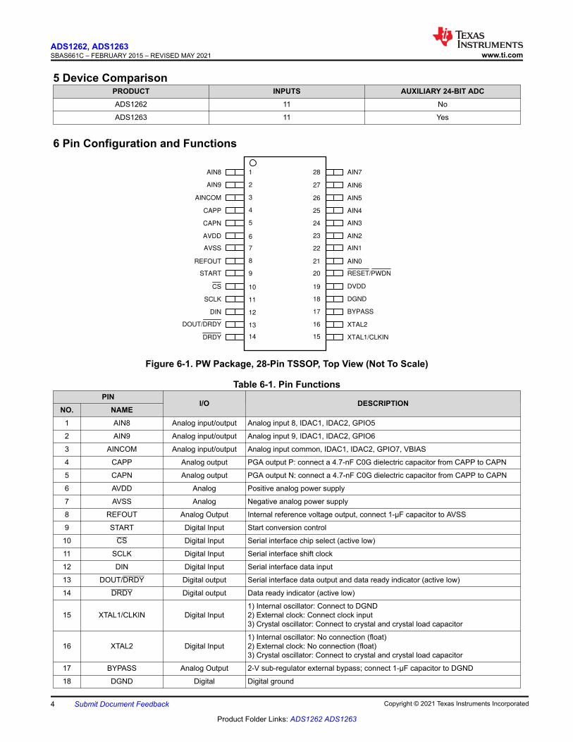
Figure 6-1. PW Package, 28-Pin TSSOP, Top View (Not To Scale)
Table 6-1. Pin FunctionsPIN
I/O DESCRIPTIONNO. NAME
1 AIN8 Analog input/output Analog input 8, IDAC1, IDAC2, GPIO5
2 AIN9 Analog input/output Analog input 9, IDAC1, IDAC2, GPIO6
3 AINCOM Analog input/output Analog input common, IDAC1, IDAC2, GPIO7, VBIAS
4 CAPP Analog output PGA output P: connect a 4.7-nF C0G dielectric capacitor from CAPP to CAPN
5 CAPN Analog output PGA output N: connect a 4.7-nF C0G dielectric capacitor from CAPP to CAPN
6 AVDD Analog Positive analog power supply
7 AVSS Analog Negative analog power supply
8 REFOUT Analog Output Internal reference voltage output, connect 1-µF capacitor to AVSS
9 START Digital Input Start conversion control
10 CS Digital Input Serial interface chip select (active low)
11 SCLK Digital Input Serial interface shift clock
12 DIN Digital Input Serial interface data input
13 DOUT/DRDY Digital output Serial interface data output and data ready indicator (active low)
14 DRDY Digital output Data ready indicator (active low)
15 XTAL1/CLKIN Digital Input1) Internal oscillator: Connect to DGND2) External clock: Connect clock input3) Crystal oscillator: Connect to crystal and crystal load capacitor
16 XTAL2 Digital Input1) Internal oscillator: No connection (float)2) External clock: No connection (float)3) Crystal oscillator: Connect to crystal and crystal load capacitor
17 BYPASS Analog Output 2-V sub-regulator external bypass; connect 1-µF capacitor to DGND
18 DGND Digital Digital ground
ADS1262, ADS1263SBAS661C – FEBRUARY 2015 – REVISED MAY 2021 www.ti.com
4 Submit Document Feedback Copyright © 2021 Texas Instruments Incorporated
Product Folder Links: ADS1262 ADS1263

Table 6-1. Pin Functions (continued)PIN
I/O DESCRIPTIONNO. NAME19 DVDD Digital Digital power supply
20 RESET/PWDN Digital input Reset (active low); hold low to power down the ADC
21 AIN0 Analog input/output Analog input 0, REFP1, IDAC1, IDAC2
22 AIN1 Analog input/output Analog input 1, REFN1, IDAC1, IDAC2
23 AIN2 Analog input/output Analog input 2 ,REFP2, IDAC1, IDAC2
24 AIN3 Analog input/output Analog input 3, REFN2, IDAC1, IDAC2, GPIO0
25 AIN4 Analog input/output Analog input 4, REFP3, IDAC1, IDAC2, GPIO1
26 AIN5 Analog input/output Analog input 5, REFN3, IDAC1, IDAC2, GPIO2
27 AIN6 Analog input/output Analog input 6, IDAC1, IDAC2, GPIO3, TDACP
28 AIN7 Analog input/output Analog input 7, IDAC1, IDAC2, GPIO4, TDACN
7 Specifications7.1 Absolute Maximum Ratingsover operating free-air temperature range (unless otherwise noted)(1)
MIN MAX UNIT
Voltage
AVDD to AVSS –0.3 7 V
AVSS to DGND –3 0.3 V
DVDD to DGND –0.3 7 V
Analog input VAVSS – 0.3 VAVDD + 0.3 V
Digital input VDGND – 0.3 VDVDD + 0.3 V
Current Input(2) –10 10 mA
TemperatureJunction, TJ –50 150 °C
Storage, Tstg -60 150 °C
(1) Stresses beyond those listed under Absolute Maximum Ratings may cause permanent damage to the device. These are stressratings only, which do not imply functional operation of the device at these or any other conditions beyond those indicated underRecommended Operating Conditions. Exposure to absolute-maximum-rated conditions for extended periods may affect devicereliability.
(2) Input pins are diode-clamped to the power supply rails. Limit the input current to 10 mA or less if the analog input voltage exceedsVAVDD + 0.3 V or is below VAVSS – 0.3 V, or if the digital input voltage exceeds VDVDD + 0.3 V or is below VDGND – 0.3 V.
7.2 ESD RatingsVALUE UNIT
V(ESD) Electrostatic dischargeHuman-body model (HBM), per ANSI/ESDA/JEDEC JS-001(1) ±2000
VCharged-device model (CDM), per JEDEC specification JESD22-C101(2) ±500
(1) JEDEC document JEP155 states that 500-V HBM allows safe manufacturing with a standard ESD control process.(2) JEDEC document JEP157 states that 250-V CDM allows safe manufacturing with a standard ESD control process.
www.ti.comADS1262, ADS1263
SBAS661C – FEBRUARY 2015 – REVISED MAY 2021
Copyright © 2021 Texas Instruments Incorporated Submit Document Feedback 5
Product Folder Links: ADS1262 ADS1263
7.3 Recommended Operating Conditionsover operating ambient temperature range (unless otherwise noted)
MIN NOM MAX UNITPOWER SUPPLY
Analog power supplyVAVDD to VAVSS 4.75 5 5.25
VVAVSS to VDGND –2.6 0
Digital power supply VDVDD to VDGND 2.7 5.25 V
ADC1 ANALOG INPUTSFSR Full-scale differential input voltage range(1) –VREF / Gain VREF / Gain V
VINP,VINN Absolute input voltage(2)PGA enabled See Equation 12
VPGA bypassed VAVSS – 0.1 VAVDD + 0.1
ADC2 ANALOG INPUTS (ADS1263)Full-scale differential input voltage range –VREF / Gain VREF / Gain V
Absolute input voltageGain = 1, 2 and 4 VAVSS – 0.1 VAVDD + 0.1
VGain = 8 to 128 See Equation 15
VOLTAGE REFERENCE INPUTS
VREF Differential reference voltage VREF = VREFP – VREFN 0.9 VAVDD – VAVSS+ 0.2 V
VREFN Negative reference voltage VAVSS – 0.1 VREFP – 0.9 V
VREFP Positive reference voltage VREFN + 0.9 VAVDD + 0.1 V
CLOCK INPUT
fCLK
External clock frequency 1 7.3728 8 MHz
External clock duty cycle 30% 70%
External crystal frequency 1 7.3728 8 MHz
GENERAL-PURPOSE INPUT/OUTPUT (GPIO)Input voltage VAVSS VAVDD V
DIGITAL INPUTS (other than GPIO)Input voltage VDGND VDVDD V
TEMPERATURETA Operating ambient temperature –40 125 °C
(1) FSR is the ideal full-scale differential input voltage range, excluding noise, offset and gain errors. For ADC1, the maximum FSR isachieved with VREF = 5 V and the PGA bypassed. If the PGA is enabled and VREF = 5 V, the FSR is limited by the PGA input range.For ADC2, if VREF = 5 V and gains = 8 to 128 then FSR is limited by the PGA input range.
(2) VINP, VINN = Absolute Input Voltage. VIN = Differential Input Voltage = VINP – VINN.
7.4 Thermal Information
THERMAL METRIC(1)
ADS126xUNITPW (TSSOP)
28 PINSRθJA Junction-to-ambient thermal resistance 65.2 °C/W
RθJC(top) Junction-to-case (top) thermal resistance 13.6 °C/W
RθJB Junction-to-board thermal resistance 23.6 °C/W
ψJT Junction-to-top characterization parameter 0.5 °C/W
ψJB Junction-to-board characterization parameter 23.1 °C/W
RθJC(bot) Junction-to-case (bottom) thermal resistance N/A °C/W
(1) For more information about traditional and new thermal metrics, see the Semiconductor and IC Package Thermal Metrics applicationreport.
ADS1262, ADS1263SBAS661C – FEBRUARY 2015 – REVISED MAY 2021 www.ti.com
6 Submit Document Feedback Copyright © 2021 Texas Instruments Incorporated
Product Folder Links: ADS1262 ADS1263
7.5 Electrical Characteristicsminimum and maximum specifications apply from TA = –40°C to +125°C; typical specifications are at TA = 25°C; allspecifications are at VAVDD = 5 V, VAVSS = 0 V, VDVDD = 3.3 V, VREF = 2.5 V, fCLK = 7.3728 MHz, ADC1 data rate = 20 SPSwith PGA enabled and gain = 1, and ADC2 data rate = 10 SPS with gain = 1 (unless otherwise noted)
PARAMETER TEST CONDITIONS MIN TYP MAX UNIT
ADC1 ANALOG INPUTS
Absolute input currentGain = 32 2
nAPGA bypassed 150
Differential input currentGain = 32 0.1
nAPGA bypassed, VIN = 5 V 150
Differential input impedancePGA enabled 1 GΩ
PGA bypassed 40 MΩ
Channel-to-channel crosstalk DC, VAVSS ≤ VINX ≤ VAVDD 0.5 μV/V
ADC1 PERFORMANCE
PGA gain 1, 2, 4, 8, 16, 32 V/V
Resolution 32 Bits
DR Data rate 2.5 38400 SPS
Noise performance See Table 8-1
INL Integral nonlinearity Gain = 1 to 32, PGA bypassed 3 12 ppm
VOS Offset voltageTA = 25°C
Chop mode off 350 / Gain 800 / GainμV
Chop mode on ±0.1 / Gain ±0.5 / Gain
After calibration(1) Noise / 4
Offset voltage driftChop mode off 30 / Gain + 10 100 / Gain + 50
nV/°CChop mode on 1 5
GE Gain errorTA = 25°C, gain = 1 to 32 ±50 ±300 ppm
After calibration(1) Noise / 4
Gain drift Gain = 1 to 32, and PGA bypassed 0.5 4 ppm/°C
NMRR Normal-mode rejection ratio(2) See Table 9-6
CMRR Common-mode rejection ratio(3)fIN = 60 Hz, data rate = 20 SPS 130
dBfIN = 60 Hz, data rate = 400 SPS 100 120
PSRR Power-supply rejection ratio(4)AVDD and AVSS 80 90
dBDVDD 80 120
ADC2 ANALOG INPUTS (ADS1263)
Absolute input current Gain = 16 2 nA
Differential input current Gain = 16 0.5 nA
ADC2 PERFORMANCE (ADS1263)
Gain 1, 2, 4, 8, 16, 32, 64, 128 V/V
Resolution 24 Bits
DR Data rate 10, 100, 400, 800 SPS
Noise performance See Table 8-3
INL Integral nonlinearityGain = 1 to 64 4 20
ppmGain = 128 7 30
VOS Offset voltage TA = 25°C, gain = 1 to 128 ±150 ±500 μV
Offset voltage drift Gain = 1 to 128 30 200 nV/°C
GE Gain error TA = 25°C, gain = 1 to 128 ±500 ±3000 ppm
Gain drift Gain = 1 to 128 1 5 ppm/°C
NMRR Normal-mode rejection ratio See Table 9-11
CMRR Common-mode rejection ratiofIN = 60 Hz, DR = 10 SPS 110
dBfIN = 60 Hz, DR = 400 SPS, gain = 8 75 90
PSRR Power-supply rejection ratio AVDD and AVSS 75 90 dB
www.ti.comADS1262, ADS1263
SBAS661C – FEBRUARY 2015 – REVISED MAY 2021
Copyright © 2021 Texas Instruments Incorporated Submit Document Feedback 7
Product Folder Links: ADS1262 ADS1263
7.5 Electrical Characteristics (continued)minimum and maximum specifications apply from TA = –40°C to +125°C; typical specifications are at TA = 25°C; allspecifications are at VAVDD = 5 V, VAVSS = 0 V, VDVDD = 3.3 V, VREF = 2.5 V, fCLK = 7.3728 MHz, ADC1 data rate = 20 SPSwith PGA enabled and gain = 1, and ADC2 data rate = 10 SPS with gain = 1 (unless otherwise noted)
PARAMETER TEST CONDITIONS MIN TYP MAX UNIT
CROSSTALK
CrosstalkADC1 to ADC2 20
μV/VADC2 to ADC1 1
EXTERNAL VOLTAGE REFERENCE INPUTS
Reference input current(5)ADC1 150
nAADC2 1
Input current vs voltage VREF = 2 V to 4.8 V, ADC1 10 nA/V
Input current drift ADC1 0.1 nA/°C
Input impedance Differential, ADC1 50 MΩ
Low reference monitor Threshold, ADC1 0.4 0.6 V
INTERNAL VOLTAGE REFERENCE
Reference voltage 2.5 V
Initial accuracy TA = 25°C ±0.1% ±0.2%
Reference voltage temperature driftTA = 0°C to +85°C 2 6
ppm/°CTA = –40°C to +105°C 4 12
Reference voltage long term drift TA = 85°C, 1st 1000 hr 50 ppm
Thermal hysteresis First 0°C to 85°C cycle 50 ppm
Output current -10 10 mA
Load regulation 40 μV/mA
Start-up time Settling time to ±0.001% final value 50 ms
TEMPERATURE SENSOR
Voltage TA = 25°C 122.4 mV
Temperature coefficient 420 μV/°C
CURRENT SOURCES (IDAC1, IDAC2)
Currents 50, 100, 250, 500, 750,1000, 1500, 2000, 2500, 3000 μA
Compliance range All currents VAVSS VAVDD – 1.1 V
Absolute error All currents ±0.7% ±4%
Match errorIDAC1 current = IDAC2 current ±0.1% ±1%
IDAC1 current ≠ IDAC2 current ±1%
Temperature driftAbsolute 50
ppm/°CMatch 5 20
LEVEL-SHIFT VOLTAGE
Voltage (VAVDD + VAVSS) / 2 V
Output impedance 100 Ω
SENSOR BIAS
Currents ±0.5, ±2, ±10, ±50, ±200 μA
Pull-up/pull-down resistor 10 MΩ
TEST DAC (TDAC)
DAC reference voltage VAVDD – VAVSS V
Differential output voltage 18 binary weighted settings –4 4 V
Absolute output voltage To VAVSS 0.5 4.5 V
Accuracy ±0.1% ±1.5%
Output impedance See Table 9-8
ADS1262, ADS1263SBAS661C – FEBRUARY 2015 – REVISED MAY 2021 www.ti.com
8 Submit Document Feedback Copyright © 2021 Texas Instruments Incorporated
Product Folder Links: ADS1262 ADS1263
7.5 Electrical Characteristics (continued)minimum and maximum specifications apply from TA = –40°C to +125°C; typical specifications are at TA = 25°C; allspecifications are at VAVDD = 5 V, VAVSS = 0 V, VDVDD = 3.3 V, VREF = 2.5 V, fCLK = 7.3728 MHz, ADC1 data rate = 20 SPSwith PGA enabled and gain = 1, and ADC2 data rate = 10 SPS with gain = 1 (unless otherwise noted)
PARAMETER TEST CONDITIONS MIN TYP MAX UNIT
PGA OVER-RANGE MONITOR
Differential alarm Threshold ±105% FSR
Differential alarm accuracy ±1% ±3%
Absolute alarm thresholdsLow threshold VAVSS + 0.2 V
High threshold VAVDD – 0.2 V
ADC CLOCK
fCLK Internal oscillator frequency 7.3728 MHz
Internal oscillator accuracy ±0.5% ±2%
External crystal start-up time See Table 9-21 for recommendedcrystals 20 ms
GENERAL-PURPOSE INPUT/OUTPUTS (GPIO)(6)
VOH High-level output voltage IOH = 1 mA 0.8 · VAVDD V
VOL Low-level output voltage IOL = –1 mA 0.2 · VAVDD V
VIH High-level input voltage 0.7 · VAVDD VAVDD V
VIL Low-level input voltage VAVSS 0.3 · VAVDD V
Input hysteresis 0.5 V
DIGITAL INPUT/OUTPUT (Other Than GPIO)
VOH High-level output voltageIOH = 1 mA 0.8 · VDVDD
VIOH = 8 mA 0.75 · VDVDD
VOL Low-level output voltageIOL = –1 mA 0.2 · VDVDD
VIOL = –8 mA 0.2 · VDVDD
VIH High-level input voltage 0.7 · VDVDD VDVDD V
VIL Low-level input voltage VDGND 0.3 · VDVDD V
Input hysteresis 0.1 V
Input leakage ±10 μA
POWER SUPPLY
IAVDD IAVSS
Analog supply current
Active mode,voltage reference off ADS1262 4
mAActive mode,voltage reference on ADS1262 4.2 6.5
Active mode,voltage reference on ADS1263 4.3 6.5
Power-down mode 2 15 μA
IDVDD Digital supply currentActive mode ADS1262
ADS1263 1 1.25 mA
Power-down mode(7) 25 50 μA
PD Power dissipation
Active mode,voltage reference on ADS1262 24 37
mWActive mode,voltage reference on ADS1263 25 37
Power-down mode 90 240 μW
(1) Offset and gain calibration accuracy on the order of ADC conversion noise / 4. Conversion noise depends on data rate and PGA gain.(2) Normal-mode rejection ratio depends on the digital filter setting.(3) Common-mode rejection ratio is specified at date rate 20 SPS and 400 SPS.(4) Power-supply rejection ratio is specified at dc.(5) Specified with VAVSS ≤ VREFN and VREFP ≤ VAVDD. For reference input voltage exceeding VAVDD or VAVSS, the ADC1 reference input
current = 10 nA/ mV.(6) GPIO input and output voltages are referenced to VAVSS.(7) External CLK input stopped. All other digital inputs maintained at VDVDD or VDGND.
www.ti.comADS1262, ADS1263
SBAS661C – FEBRUARY 2015 – REVISED MAY 2021
Copyright © 2021 Texas Instruments Incorporated Submit Document Feedback 9
Product Folder Links: ADS1262 ADS1263
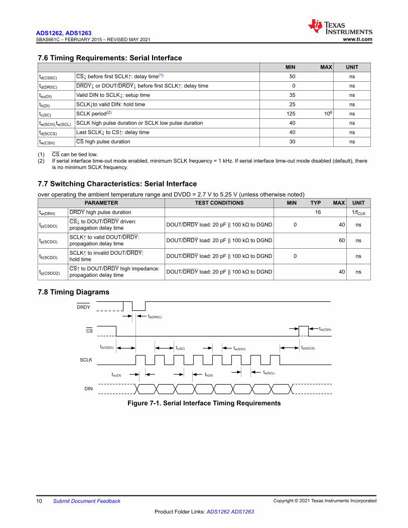
7.6 Timing Requirements: Serial InterfaceMIN MAX UNIT
td(CSSC) CS↓ before first SCLK↑: delay time(1) 50 ns
td(DRSC) DRDY↓ or DOUT/DRDY↓ before first SCLK↑: delay time 0 ns
tsu(DI) Valid DIN to SCLK↓: setup time 35 ns
th(DI) SCLK↓to valid DIN: hold time 25 ns
tc(SC) SCLK period(2) 125 106 ns
tw(SCH),tw(SCL) SCLK high pulse duration or SCLK low pulse duration 40 ns
td(SCCS) Last SCLK↓ to CS↑: delay time 40 ns
tw(CSH) CS high pulse duration 30 ns
(1) CS can be tied low.(2) If serial interface time-out mode enabled, minimum SCLK frequency = 1 kHz. If serial interface time-out mode disabled (default), there
is no minimum SCLK frequency.
7.7 Switching Characteristics: Serial Interfaceover operating the ambient temperature range and DVDD = 2.7 V to 5.25 V (unless otherwise noted)
PARAMETER TEST CONDITIONS MIN TYP MAX UNITtw(DRH) DRDY high pulse duration 16 1/fCLK
tp(CSDO)CS↓ to DOUT/DRDY driven:propagation delay time DOUT/DRDY load: 20 pF || 100 kΩ to DGND 0 40 ns
tp(SCDO)SCLK↑ to valid DOUT/DRDY:propagation delay time DOUT/DRDY load: 20 pF || 100 kΩ to DGND 60 ns
th(SCDO)SCLK↑ to invalid DOUT/DRDY:hold time DOUT/DRDY load: 20 pF || 100 kΩ to DGND 0 ns
tp(CSDOZ)CS↑ to DOUT/DRDY high impedance:propagation delay time DOUT/DRDY load: 20 pF || 100 kΩ to DGND 40 ns
7.8 Timing Diagrams
CS
SCLK
DIN
tw(CSH)
tc(SC) tw(SCH)
tsu(DI) th(DI)tw(SCL)
td(SCCS)td(CSSC)
DRDY
td(DRSC)
Figure 7-1. Serial Interface Timing Requirements
ADS1262, ADS1263SBAS661C – FEBRUARY 2015 – REVISED MAY 2021 www.ti.com
10 Submit Document Feedback Copyright © 2021 Texas Instruments Incorporated
Product Folder Links: ADS1262 ADS1263
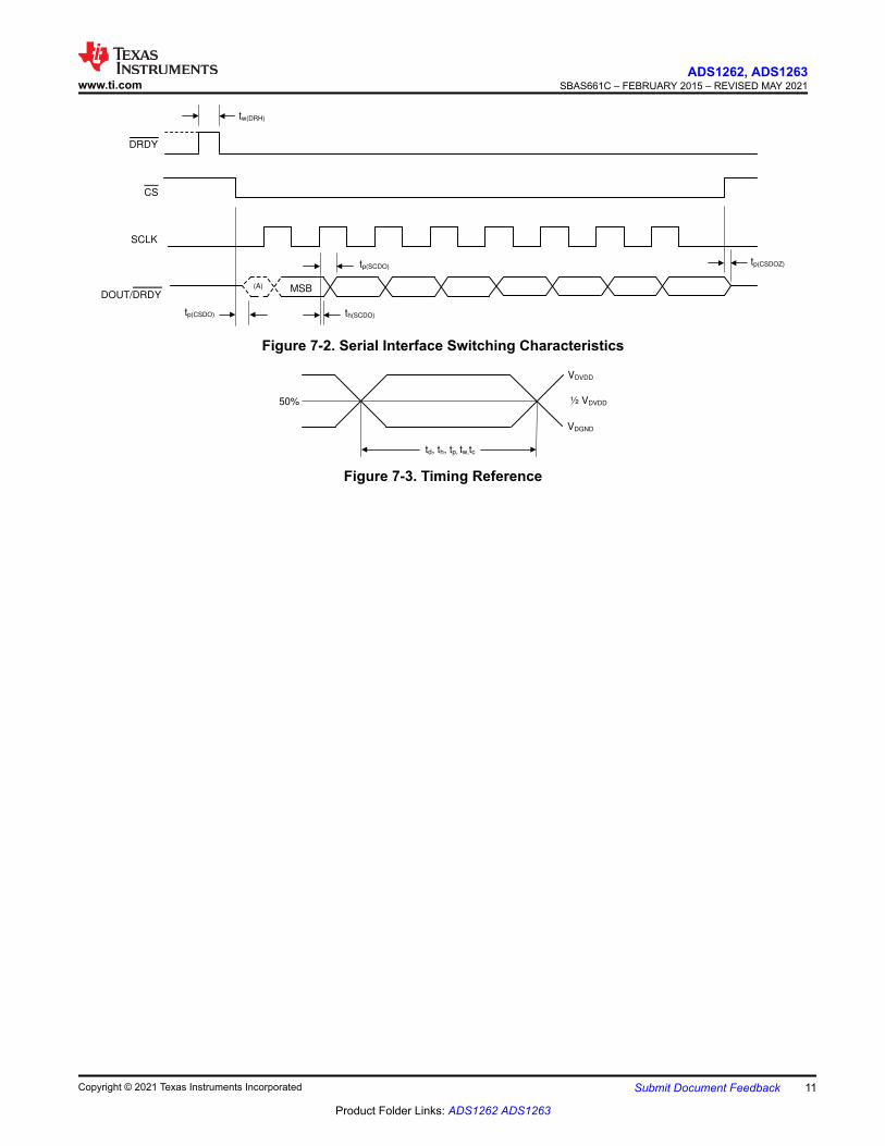
SCLK
CS
DOUT/DRDY
tp(CSDO)
tp(CSDOZ)
th(SCDO)
tp(SCDO)
MSB
DRDY
tw(DRH)
(A)
Figure 7-2. Serial Interface Switching Characteristics
VDVDD
VDGND
½ VDVDD50%
td, th, tp, tw,tc
Figure 7-3. Timing Reference
www.ti.comADS1262, ADS1263
SBAS661C – FEBRUARY 2015 – REVISED MAY 2021
Copyright © 2021 Texas Instruments Incorporated Submit Document Feedback 11
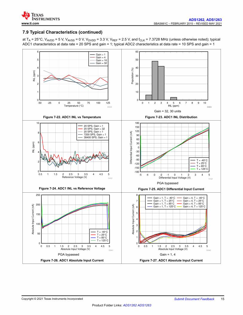
Product Folder Links: ADS1262 ADS1263
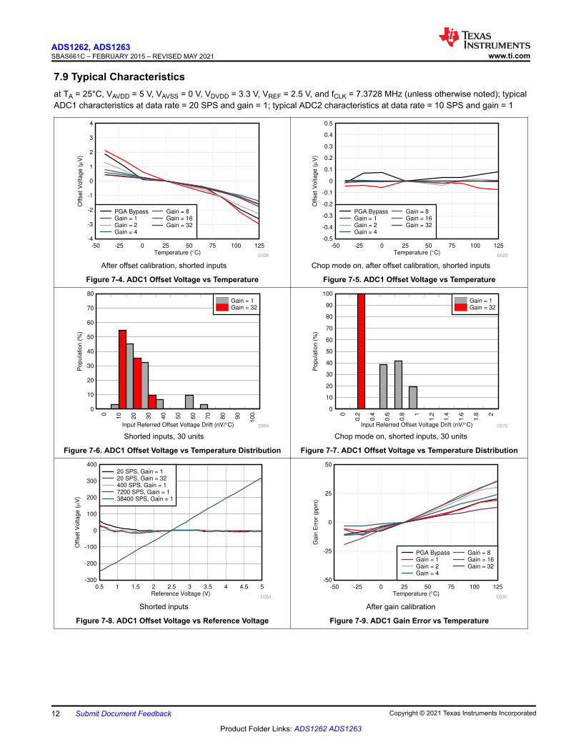
7.9 Typical Characteristicsat TA = 25°C, VAVDD = 5 V, VAVSS = 0 V, VDVDD = 3.3 V, VREF = 2.5 V, and fCLK = 7.3728 MHz (unless otherwise noted); typicalADC1 characteristics at data rate = 20 SPS and gain = 1; typical ADC2 characteristics at data rate = 10 SPS and gain = 1
Temperature (qC)
Offset V
oltage
(P
V)
-50 -25 0 25 50 75 100 125-4
-3
-2
-1
0
1
2
3
4
D028
PGA BypassGain = 1Gain = 2Gain = 4
Gain = 8Gain = 16Gain = 32
After offset calibration, shorted inputs
Figure 7-4. ADC1 Offset Voltage vs Temperature
Temperature (qC)
Offset V
oltag
e (P
V)
-50 -25 0 25 50 75 100 125-0.5
-0.4
-0.3
-0.2
-0.1
0
0.1
0.2
0.3
0.4
0.5
D029
PGA BypassGain = 1Gain = 2Gain = 4
Gain = 8Gain = 16Gain = 32
Chop mode on, after offset calibration, shorted inputs
Figure 7-5. ADC1 Offset Voltage vs Temperature
Input Referred Offset Voltage Drift (nV/qC)
Po
pu
latio
n (
%)
0
10
20
30
40
50
60
70
80
0
10
20
30
40
50
60
70
80
90
10
0
D064
Gain = 1Gain = 32
Shorted inputs, 30 units
Figure 7-6. ADC1 Offset Voltage vs Temperature Distribution
Input Referred Offset Voltage Drift (nV/qC)
Po
pu
lation
(%
)
0
10
20
30
40
50
60
70
80
90
100
0
0.2
0.4
0.6
0.8 1
1.2
1.4
1.6
1.8 2
D072
Gain = 1Gain = 32
Chop mode on, shorted inputs, 30 units
Figure 7-7. ADC1 Offset Voltage vs Temperature Distribution
Reference Voltage (V)
Offset V
oltage (P
V)
0.5 1 1.5 2 2.5 3 3.5 4 4.5 5-300
-200
-100
0
100
200
300
400
D054
20 SPS, Gain = 120 SPS, Gain = 32400 SPS, Gain = 17200 SPS, Gain = 138400 SPS, Gain = 1
Shorted inputs
Figure 7-8. ADC1 Offset Voltage vs Reference Voltage
Temperature (qC)
Ga
in E
rro
r (p
pm
)
-50 -25 0 25 50 75 100 125-50
-25
0
25
50
D030
PGA BypassGain = 1Gain = 2Gain = 4
Gain = 8Gain = 16Gain = 32
After gain calibration
Figure 7-9. ADC1 Gain Error vs Temperature
ADS1262, ADS1263SBAS661C – FEBRUARY 2015 – REVISED MAY 2021 www.ti.com
12 Submit Document Feedback Copyright © 2021 Texas Instruments Incorporated
Product Folder Links: ADS1262 ADS1263
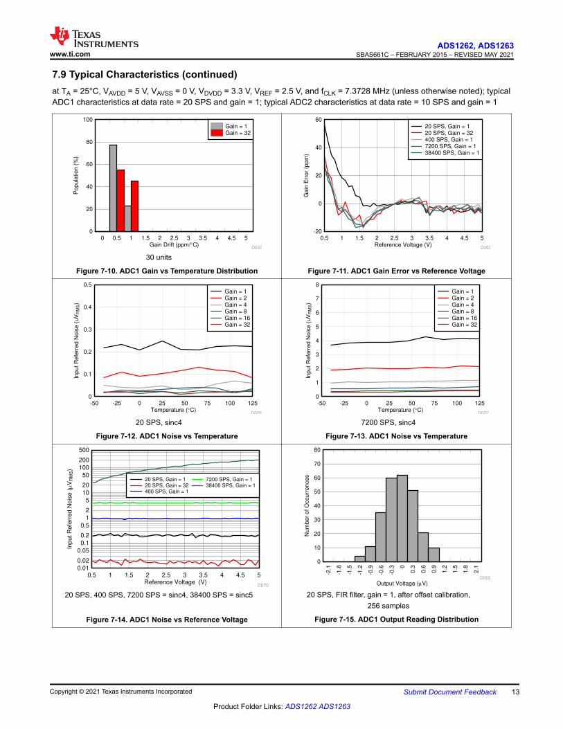
7.9 Typical Characteristics (continued)at TA = 25°C, VAVDD = 5 V, VAVSS = 0 V, VDVDD = 3.3 V, VREF = 2.5 V, and fCLK = 7.3728 MHz (unless otherwise noted); typicalADC1 characteristics at data rate = 20 SPS and gain = 1; typical ADC2 characteristics at data rate = 10 SPS and gain = 1
Gain Drift (ppm/qC)
Popula
tion
(%
)
0
20
40
60
80
100
0 0.5 1 1.5 2 2.5 3 3.5 4 4.5 5
D037
Gain = 1Gain = 32
30 units
Figure 7-10. ADC1 Gain vs Temperature Distribution
Reference Voltage (V)
Gain
Err
or
(ppm
)
0.5 1 1.5 2 2.5 3 3.5 4 4.5 5-20
0
20
40
60
D053
20 SPS, Gain = 120 SPS, Gain = 32400 SPS, Gain = 17200 SPS, Gain = 138400 SPS, Gain = 1
Figure 7-11. ADC1 Gain Error vs Reference Voltage
Temperature (qC)
Input R
efe
rred N
ois
e (
uV
RM
S)
-50 -25 0 25 50 75 100 1250
0.1
0.2
0.3
0.4
0.5
D026
Gain = 1Gain = 2Gain = 4Gain = 8Gain = 16Gain = 32
20 SPS, sinc4
Figure 7-12. ADC1 Noise vs Temperature
Temperature (qC)
Input R
efe
rred N
ois
e (
uV
RM
S)
-50 -25 0 25 50 75 100 1250
1
2
3
4
5
6
7
8
D027
Gain = 1Gain = 2Gain = 4Gain = 8Gain = 16Gain = 32
7200 SPS, sinc4
Figure 7-13. ADC1 Noise vs Temperature
Reference Voltage (V)
Inpu
t R
efe
rred
No
ise
(P
VR
MS)
0.5 1 1.5 2 2.5 3 3.5 4 4.5 50.01
0.02
0.05
0.1
0.2
0.5
1
2
5
10
20
50
100
200
500
D070
20 SPS, Gain = 120 SPS, Gain = 32400 SPS, Gain = 1
7200 SPS, Gain = 138400 SPS, Gain = 1
20 SPS, 400 SPS, 7200 SPS = sinc4, 38400 SPS = sinc5
Figure 7-14. ADC1 Noise vs Reference Voltage
Output Voltage (PV)
Num
ber
of O
ccu
rren
ces
0
10
20
30
40
50
60
70
80
-2.1
-1.8
-1.5
-1.2
-0.9
-0.6
-0.3 0
0.3
0.6
0.9
1.2
1.5
1.8
2.1
D055
20 SPS, FIR filter, gain = 1, after offset calibration,256 samples
Figure 7-15. ADC1 Output Reading Distribution
www.ti.comADS1262, ADS1263
SBAS661C – FEBRUARY 2015 – REVISED MAY 2021
Copyright © 2021 Texas Instruments Incorporated Submit Document Feedback 13
Product Folder Links: ADS1262 ADS1263
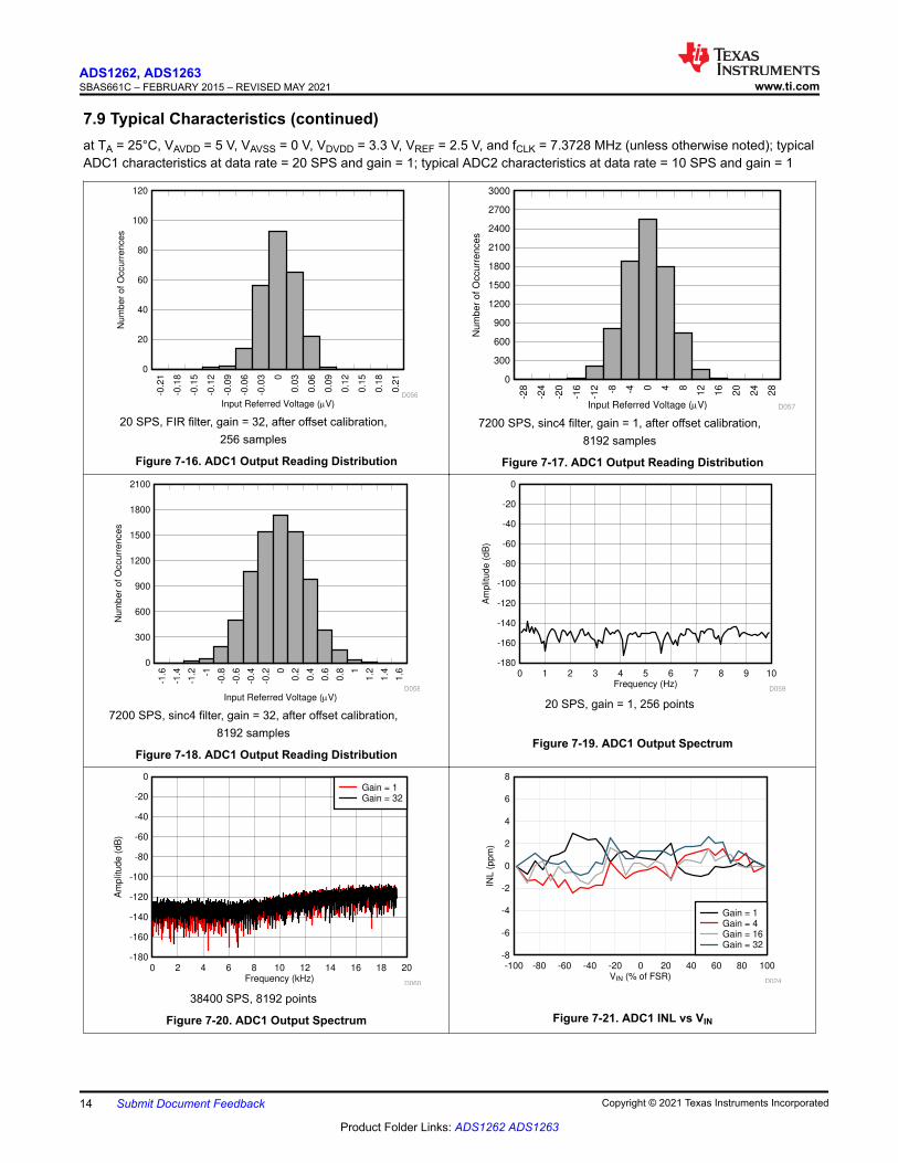
7.9 Typical Characteristics (continued)at TA = 25°C, VAVDD = 5 V, VAVSS = 0 V, VDVDD = 3.3 V, VREF = 2.5 V, and fCLK = 7.3728 MHz (unless otherwise noted); typicalADC1 characteristics at data rate = 20 SPS and gain = 1; typical ADC2 characteristics at data rate = 10 SPS and gain = 1
Input Referred Voltage (PV)
Num
ber
of O
ccu
rre
nces
0
20
40
60
80
100
120
-0.2
1
-0.1
8
-0.1
5
-0.1
2
-0.0
9
-0.0
6
-0.0
3 0
0.0
3
0.0
6
0.0
9
0.1
2
0.1
5
0.1
8
0.2
1D056
20 SPS, FIR filter, gain = 32, after offset calibration,256 samples
Figure 7-16. ADC1 Output Reading Distribution
Input Referred Voltage (PV)
Nu
mb
er
of O
ccu
rre
nce
s
0
300
600
900
1200
1500
1800
2100
2400
2700
3000
-28
-24
-20
-16
-12 -8 -4 0 4 8
12
16
20
24
28
D057
7200 SPS, sinc4 filter, gain = 1, after offset calibration,8192 samples
Figure 7-17. ADC1 Output Reading Distribution
Input Referred Voltage (PV)
Num
ber
of O
ccu
rre
nces
0
300
600
900
1200
1500
1800
2100
-1.6
-1.4
-1.2 -1
-0.8
-0.6
-0.4
-0.2 0
0.2
0.4
0.6
0.8 1
1.2
1.4
1.6
D058
7200 SPS, sinc4 filter, gain = 32, after offset calibration,8192 samples
Figure 7-18. ADC1 Output Reading Distribution
Frequency (Hz)
Am
plit
ude (
dB
)
0 1 2 3 4 5 6 7 8 9 10-180
-160
-140
-120
-100
-80
-60
-40
-20
0
D059
20 SPS, gain = 1, 256 points
Figure 7-19. ADC1 Output Spectrum
Frequency (kHz)
Am
plit
ude (
dB
)
0 2 4 6 8 10 12 14 16 18 20-180
-160
-140
-120
-100
-80
-60
-40
-20
0
D060
Gain = 1Gain = 32
38400 SPS, 8192 points
Figure 7-20. ADC1 Output Spectrum
VIN (% of FSR)
INL
(ppm
)
-100 -80 -60 -40 -20 0 20 40 60 80 100-8
-6
-4
-2
0
2
4
6
8
D024
Gain = 1Gain = 4Gain = 16Gain = 32
Figure 7-21. ADC1 INL vs VIN
ADS1262, ADS1263SBAS661C – FEBRUARY 2015 – REVISED MAY 2021 www.ti.com
14 Submit Document Feedback Copyright © 2021 Texas Instruments Incorporated
Product Folder Links: ADS1262 ADS1263
7.9 Typical Characteristics (continued)at TA = 25°C, VAVDD = 5 V, VAVSS = 0 V, VDVDD = 3.3 V, VREF = 2.5 V, and fCLK = 7.3728 MHz (unless otherwise noted); typicalADC1 characteristics at data rate = 20 SPS and gain = 1; typical ADC2 characteristics at data rate = 10 SPS and gain = 1
Temperature (qC)
INL
(ppm
)
-50 -25 0 25 50 75 100 1250
1
2
3
4
5
6
D033
Gain = 1Gain = 4Gain = 16Gain = 32
Figure 7-22. ADC1 INL vs Temperature
INL (ppm)
Popu
lation
(%
)
0
10
20
30
40
50
60
0 1 2 3 4 5 6 7 8 9 10
D034D001
Gain = 32, 30 units
Figure 7-23. ADC1 INL Distribution
Reference Voltage (V)
INL
(ppm
)
0.5 1 1.5 2 2.5 3 3.5 4 4.5 50
2
4
6
8
10
D052
20 SPS, Gain = 120 SPS, Gain = 3220 SPS, Gain = 17200 SPS, Gain = 138400 SPS, Gain = 1
Figure 7-24. ADC1 INL vs Reference Voltage
Differential Input Voltage (V)
Diffe
rential In
put C
urr
ent (n
A)
-5 -4 -3 -2 -1 0 1 2 3 4 5-180
-150
-120
-90
-60
-30
0
30
60
90
120
150
180
D040
T = -40qCT = 25qCT = 85qCT = 125qC
PGA bypassed
Figure 7-25. ADC1 Differential Input Current
Absolute Input Voltage (V)
Absolu
te Inp
ut C
urr
ent (n
A)
0 0.5 1 1.5 2 2.5 3 3.5 4 4.5 50
50
100
150
200
250
D041
T = -40qCT = 25qCT = 85qCT = 125qC
PGA bypassed
Figure 7-26. ADC1 Absolute Input Current
Absolute Input Voltage (V)
Absolu
te Inp
ut C
urr
ent (n
A)
0 0.5 1 1.5 2 2.5 3 3.5 4 4.5 50
1
2
3
4
5
6
7
8
D042
Gain = 1, T = -40qCGain = 1, T = 25qCGain = 1, T = 85qCGain = 1, T = 125qC
Gain = 4, T = -40qCGain = 4, T = 25qCGain = 4, T = 85qCGain = 4, T = 125qC
Gain = 1, 4
Figure 7-27. ADC1 Absolute Input Current
www.ti.comADS1262, ADS1263
SBAS661C – FEBRUARY 2015 – REVISED MAY 2021
Copyright © 2021 Texas Instruments Incorporated Submit Document Feedback 15
Product Folder Links: ADS1262 ADS1263
7.9 Typical Characteristics (continued)at TA = 25°C, VAVDD = 5 V, VAVSS = 0 V, VDVDD = 3.3 V, VREF = 2.5 V, and fCLK = 7.3728 MHz (unless otherwise noted); typicalADC1 characteristics at data rate = 20 SPS and gain = 1; typical ADC2 characteristics at data rate = 10 SPS and gain = 1
Absolute Input Voltage (V)
Absolu
te Inp
ut C
urr
ent (n
A)
0 0.5 1 1.5 2 2.5 3 3.5 4 4.5 50
1
2
3
4
5
6
7
8
D043
Gain = 16, T = -40qCGain = 16, T = 25qCGain = 16, T = 85qCGain = 16, T = 125qC
Gain = 32, T = -40qCGain = 32, T = 25qCGain = 32, T = 85qCGain = 32, T = 125qC
Gain = 16, 32
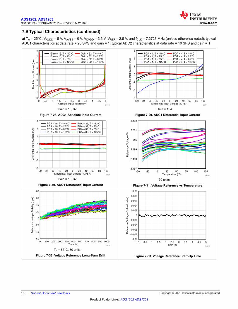
Figure 7-28. ADC1 Absolute Input Current
Differential Input Voltage (% FSR)
Diffe
rentia
l In
put C
urr
en
t (n
A)
-100 -80 -60 -40 -20 0 20 40 60 80 100-3
-2
-1
0
1
2
3
D044
PGA = 1, T = -40qCPGA = 1, T = 25qCPGA = 1, T = 85qCPGA = 1, T = 125qC
PGA = 4, T = -40qCPGA = 4, T = 25qCPGA = 4, T = 85qCPGA = 4, T = 125qC
Gain = 1, 4
Figure 7-29. ADC1 Differential Input Current
Differential Input Voltage (% FSR)
Diffe
rentia
l In
put C
urr
en
t (n
A)
-100 -80 -60 -40 -20 0 20 40 60 80 100-3
-2
-1
0
1
2
3
D045
PGA = 16, T = -40qCPGA = 16, T = 25qCPGA = 16, T = 85qCPGA = 16, T = 125qC
PGA = 32, T = -40qCPGA = 32, T = 25qCPGA = 32, T = 85qCPGA = 32, T = 125qC
Gain = 16, 32
Figure 7-30. ADC1 Differential Input Current
Temperature (qC)
Refe
ren
ce
Voltage
(V
)
-50 -25 0 25 50 75 100 1252.497
2.498
2.499
2.5
2.501
2.502
D035D030
30 units
Figure 7-31. Voltage Reference vs Temperature
Time (hr)
Refe
rence V
oltage S
tabili
ty (
ppm
)
0 100 200 300 400 500 600 700 800 900 1000-60
-40
-20
0
20
40
60
80
D086
TA = 85°C, 30 units
Figure 7-32. Voltage Reference Long-Term Drift
Time (s)
Refe
rence V
oltage (
% fin
al valu
e)
0 0.5 1 1.5 2 2.5 3 3.5 4 4.5 5-0.01
-0.008
-0.006
-0.004
-0.002
0
0.002
0.004
0.006
0.008
0.01
D025
Figure 7-33. Voltage Reference Start-Up Time
ADS1262, ADS1263SBAS661C – FEBRUARY 2015 – REVISED MAY 2021 www.ti.com
16 Submit Document Feedback Copyright © 2021 Texas Instruments Incorporated
Product Folder Links: ADS1262 ADS1263
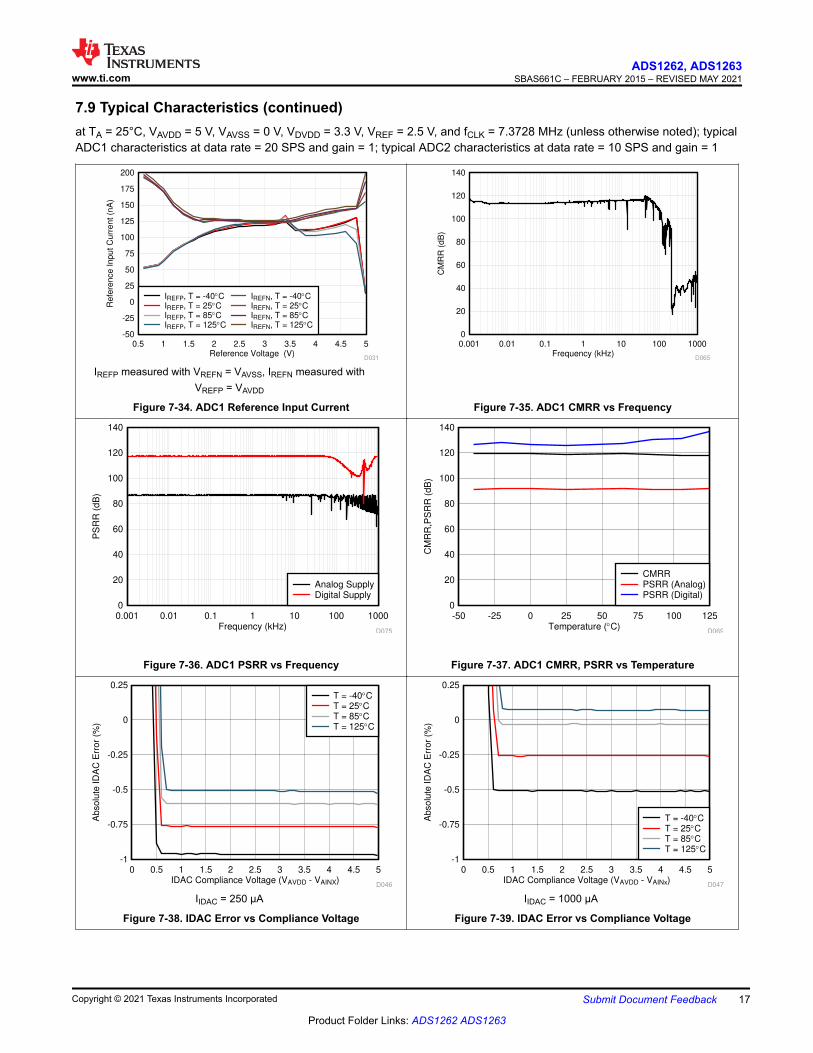
7.9 Typical Characteristics (continued)at TA = 25°C, VAVDD = 5 V, VAVSS = 0 V, VDVDD = 3.3 V, VREF = 2.5 V, and fCLK = 7.3728 MHz (unless otherwise noted); typicalADC1 characteristics at data rate = 20 SPS and gain = 1; typical ADC2 characteristics at data rate = 10 SPS and gain = 1
Reference Voltage (V)
Refe
rence
Input C
urr
en
t (n
A)
0.5 1 1.5 2 2.5 3 3.5 4 4.5 5-50
-25
0
25
50
75
100
125
150
175
200
D031
IREFP, T = -40qCIREFP, T = 25qCIREFP, T = 85qCIREFP, T = 125qC
IREFN, T = -40qCIREFN, T = 25qCIREFN, T = 85qCIREFN, T = 125qC
IREFP measured with VREFN = VAVSS, IREFN measured withVREFP = VAVDD
Figure 7-34. ADC1 Reference Input Current
Frequency (kHz)
CM
RR
(d
B)
0.001 0.01 0.1 1 10 100 10000
20
40
60
80
100
120
140
D065
Figure 7-35. ADC1 CMRR vs Frequency
Frequency (kHz)
PS
RR
(d
B)
0.001 0.01 0.1 1 10 100 10000
20
40
60
80
100
120
140
D075
Analog SupplyDigital Supply
Figure 7-36. ADC1 PSRR vs Frequency
Temperature (qC)
CM
RR
,PS
RR
(d
B)
-50 -25 0 25 50 75 100 1250
20
40
60
80
100
120
140
D069
CMRRPSRR (Analog)PSRR (Digital)
Figure 7-37. ADC1 CMRR, PSRR vs Temperature
IDAC Compliance Voltage (VAVDD - VAINX)
Ab
so
lute
ID
AC
Err
or
(%)
0 0.5 1 1.5 2 2.5 3 3.5 4 4.5 5-1
-0.75
-0.5
-0.25
0
0.25
D046
T = -40qCT = 25qCT = 85qCT = 125qC
IIDAC = 250 μA
Figure 7-38. IDAC Error vs Compliance Voltage
IDAC Compliance Voltage (VAVDD - VAINx)
Absolu
te ID
AC
Err
or
(%)
0 0.5 1 1.5 2 2.5 3 3.5 4 4.5 5-1
-0.75
-0.5
-0.25
0
0.25
D047
T = -40qCT = 25qCT = 85qCT = 125qC
IIDAC = 1000 μA
Figure 7-39. IDAC Error vs Compliance Voltage
www.ti.comADS1262, ADS1263
SBAS661C – FEBRUARY 2015 – REVISED MAY 2021
Copyright © 2021 Texas Instruments Incorporated Submit Document Feedback 17
Product Folder Links: ADS1262 ADS1263
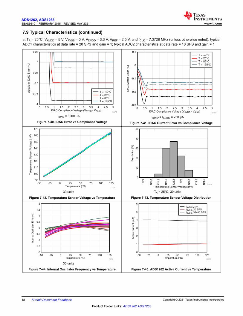
7.9 Typical Characteristics (continued)at TA = 25°C, VAVDD = 5 V, VAVSS = 0 V, VDVDD = 3.3 V, VREF = 2.5 V, and fCLK = 7.3728 MHz (unless otherwise noted); typicalADC1 characteristics at data rate = 20 SPS and gain = 1; typical ADC2 characteristics at data rate = 10 SPS and gain = 1
IDAC Compliance Voltage (VAVDD - VAINX)
Ab
so
lute
ID
AC
Err
or
(%)
0 0.5 1 1.5 2 2.5 3 3.5 4 4.5 5-1
-0.75
-0.5
-0.25
0
0.25
D048
T = -40qCT = 25qCT = 85qCT = 125qC
IIDAC = 3000 μA
Figure 7-40. IDAC Error vs Compliance Voltage
IDAC Compliance Voltage (VAVDD - VAINX)
IDA
C M
atc
h E
rro
r (%
)
0 0.5 1 1.5 2 2.5 3 3.5 4 4.5 5-0.3
-0.2
-0.1
0
0.1
D049
T = -40qCT = 25qCT = 85qCT = 125qC
IIDAC1= IIDAC2 = 250 μA
Figure 7-41. IDAC Current Error vs Compliance Voltage
Temperature (qC)
Te
mp
era
ture
Se
nso
r V
oltag
e (
mV
)
-50 -25 0 25 50 75 100 12590
100
110
120
130
140
150
160
170
D038
30 units
Figure 7-42. Temperature Sensor Voltage vs Temperature
Temperature Sensor Voltage (mV)
Popu
lation
(%
)
0
10
20
30
40
50
121
121
.4
121
.8
122
.2
122
.6
123
123
.4
123
.8
124
.2
D039
TA = 25°C, 30 units
Figure 7-43. Temperature Sensor Voltage Distribution
Temperature (qC)
Inte
rnal O
scill
ato
r E
rror
(%)
-50 -25 0 25 50 75 100 125-2
-1.5
-1
-0.5
0
0.5
1
1.5
2
D036
30 units
Figure 7-44. Internal Oscillator Frequency vs Temperature
Temperature (qC)
Active
Cu
rre
nt (m
A)
-50 -25 0 25 50 75 100 1250
1
2
3
4
5
6
D032
IAVDD,IAVSS
IDVDD, 20 SPSIDVDD, 38400 SPS
Figure 7-45. ADS1262 Active Current vs Temperature
ADS1262, ADS1263SBAS661C – FEBRUARY 2015 – REVISED MAY 2021 www.ti.com
18 Submit Document Feedback Copyright © 2021 Texas Instruments Incorporated
Product Folder Links: ADS1262 ADS1263
7.9 Typical Characteristics (continued)at TA = 25°C, VAVDD = 5 V, VAVSS = 0 V, VDVDD = 3.3 V, VREF = 2.5 V, and fCLK = 7.3728 MHz (unless otherwise noted); typicalADC1 characteristics at data rate = 20 SPS and gain = 1; typical ADC2 characteristics at data rate = 10 SPS and gain = 1
Temperature (qC)
Diffe
rentia
l A
larm
Th
resh
old
(r%
of F
SR
)
-50 -25 0 25 50 75 100 125100
102
104
106
108
110
D001
30 units
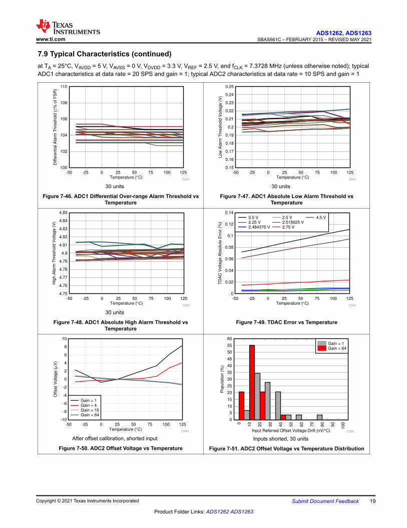
Figure 7-46. ADC1 Differential Over-range Alarm Threshold vsTemperature
Temperature (qC)
Low
Ala
rm T
hre
sh
old
Voltage
(V
)
-50 -25 0 25 50 75 100 1250.15
0.16
0.17
0.18
0.19
0.2
0.21
0.22
0.23
0.24
0.25
D061
30 units
Figure 7-47. ADC1 Absolute Low Alarm Threshold vsTemperature
Temperature (qC)
Hig
h A
larm
Th
resh
old
Vo
ltag
e (
V)
-50 -25 0 25 50 75 100 1254.75
4.76
4.77
4.78
4.79
4.8
4.81
4.82
4.83
4.84
4.85
D062
30 units
Figure 7-48. ADC1 Absolute High Alarm Threshold vsTemperature
Temperature (qC)
TD
AC
Voltage A
bso
lute
Err
or
(%)
-50 -25 0 25 50 75 100 1250
0.02
0.04
0.06
0.08
0.1
0.12
0.14
D067
0.5 V2.25 V2.484375 V
2.5 V2.515625 V2.75 V
4.5 V
Figure 7-49. TDAC Error vs Temperature
Temperature (qC)
Offset V
oltage (P
V)
-50 -25 0 25 50 75 100 125-10
-8
-6
-4
-2
0
2
4
6
8
10
D080
Gain = 1Gain = 4Gain = 16Gain = 64
After offset calibration, shorted input
Figure 7-50. ADC2 Offset Voltage vs Temperature
Input Referred Offset Voltage Drift (nV/°C)
Po
pu
latio
n (
%)
0
5
10
15
20
25
30
35
40
45
50
55
60
0
10
20
30
40
50
60
70
80
90
10
0
D081
Gain = 1Gain = 64
Inputs shorted, 30 units
Figure 7-51. ADC2 Offset Voltage vs Temperature Distribution
www.ti.comADS1262, ADS1263
SBAS661C – FEBRUARY 2015 – REVISED MAY 2021
Copyright © 2021 Texas Instruments Incorporated Submit Document Feedback 19
Product Folder Links: ADS1262 ADS1263
7.9 Typical Characteristics (continued)at TA = 25°C, VAVDD = 5 V, VAVSS = 0 V, VDVDD = 3.3 V, VREF = 2.5 V, and fCLK = 7.3728 MHz (unless otherwise noted); typicalADC1 characteristics at data rate = 20 SPS and gain = 1; typical ADC2 characteristics at data rate = 10 SPS and gain = 1
Temperature (qC)
Gain
Err
or
(ppm
)
-50 -25 0 25 50 75 100 125-100
-75
-50
-25
0
25
50
75
100
D078
Gain = 1Gain = 4Gain = 16Gain = 64
After gain calibration
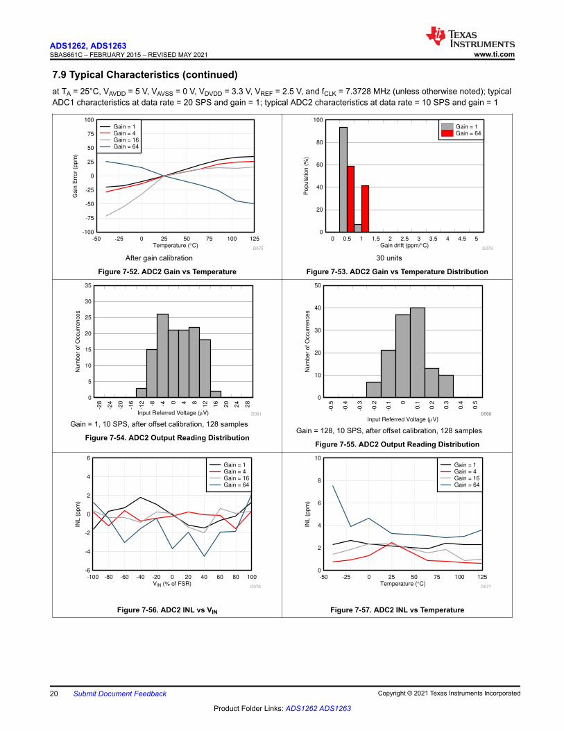
Figure 7-52. ADC2 Gain vs Temperature
Gain drift (ppm/qC)
Popula
tion
(%
)
0
20
40
60
80
100
0 0.5 1 1.5 2 2.5 3 3.5 4 4.5 5
D079
Gain = 1Gain = 64
30 units
Figure 7-53. ADC2 Gain vs Temperature Distribution
Input Referred Voltage (PV)
Nu
mb
er
of O
ccu
rre
nce
s
0
5
10
15
20
25
30
35
-28
-24
-20
-16
-12 -8 -4 0 4 8
12
16
20
24
28
D091
Gain = 1, 10 SPS, after offset calibration, 128 samples
Figure 7-54. ADC2 Output Reading Distribution
Input Referred Voltage (PV)
Num
ber
of O
ccu
rren
ces
0
10
20
30
40
50
-0.5
-0.4
-0.3
-0.2
-0.1 0
0.1
0.2
0.3
0.4
0.5
D056D092
Gain = 128, 10 SPS, after offset calibration, 128 samples
Figure 7-55. ADC2 Output Reading Distribution
VIN (% of FSR)
INL
(ppm
)
-100 -80 -60 -40 -20 0 20 40 60 80 100-6
-4
-2
0
2
4
6
D076
Gain = 1Gain = 4Gain = 16Gain = 64
Figure 7-56. ADC2 INL vs VIN
Temperature (qC)
INL
(ppm
)
-50 -25 0 25 50 75 100 1250
2
4
6
8
10
D077
Gain = 1Gain = 4Gain = 16Gain = 64
Figure 7-57. ADC2 INL vs Temperature
ADS1262, ADS1263SBAS661C – FEBRUARY 2015 – REVISED MAY 2021 www.ti.com
20 Submit Document Feedback Copyright © 2021 Texas Instruments Incorporated
Product Folder Links: ADS1262 ADS1263
7.9 Typical Characteristics (continued)at TA = 25°C, VAVDD = 5 V, VAVSS = 0 V, VDVDD = 3.3 V, VREF = 2.5 V, and fCLK = 7.3728 MHz (unless otherwise noted); typicalADC1 characteristics at data rate = 20 SPS and gain = 1; typical ADC2 characteristics at data rate = 10 SPS and gain = 1
Temperature (qC)
Inp
ut
Re
ferr
ed
No
ise
(u
VR
MS)
-50 -25 0 25 50 75 100 1250.1
0.20.3
0.5
1
23
5
10
2030
50
100
D090
Gain = 1Gain = 4Gain = 16Gain = 64
10 SPS
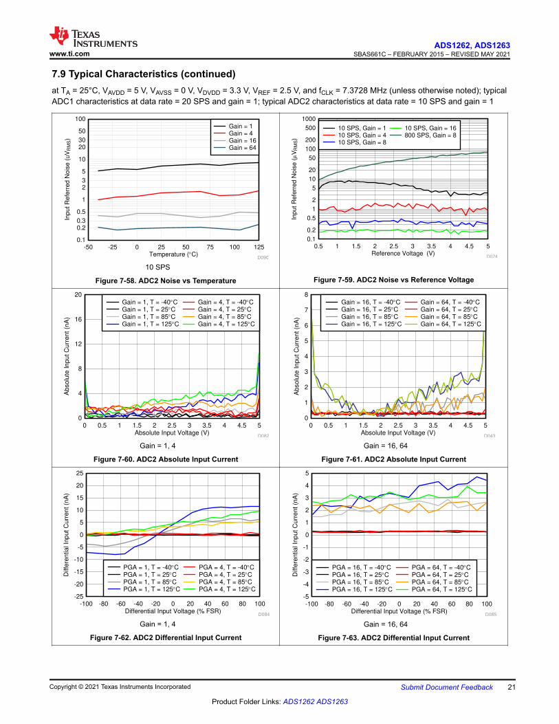
Figure 7-58. ADC2 Noise vs Temperature
Reference Voltage (V)
Inp
ut
Refe
rre
d N
ois
e (P
VR
MS)
0.5 1 1.5 2 2.5 3 3.5 4 4.5 50.1
0.2
0.5
1
2
5
10
20
50
100
200
500
1000
D074
10 SPS, Gain = 110 SPS, Gain = 410 SPS, Gain = 8
10 SPS, Gain = 16800 SPS, Gain = 8
Figure 7-59. ADC2 Noise vs Reference Voltage
Absolute Input Voltage (V)
Ab
so
lute
In
pu
t C
urr
en
t (n
A)
0 0.5 1 1.5 2 2.5 3 3.5 4 4.5 50
4
8
12
16
20
D082
Gain = 1, T = -40qCGain = 1, T = 25qCGain = 1, T = 85qCGain = 1, T = 125qC
Gain = 4, T = -40qCGain = 4, T = 25qCGain = 4, T = 85qCGain = 4, T = 125qC
Gain = 1, 4
Figure 7-60. ADC2 Absolute Input Current
Absolute Input Voltage (V)
Ab
so
lute
Inp
ut C
urr
en
t (n
A)
0 0.5 1 1.5 2 2.5 3 3.5 4 4.5 50
1
2
3
4
5
6
7
8
D043
Gain = 16, T = -40qCGain = 16, T = 25qCGain = 16, T = 85qCGain = 16, T = 125qC
Gain = 64, T = -40qCGain = 64, T = 25qCGain = 64, T = 85qCGain = 64, T = 125qC
Gain = 16, 64
Figure 7-61. ADC2 Absolute Input Current
Differential Input Voltage (% FSR)
Diffe
ren
tia
l In
pu
t C
urr
en
t (n
A)
-100 -80 -60 -40 -20 0 20 40 60 80 100-25
-20
-15
-10
-5
0
5
10
15
20
25
D084
PGA = 1, T = -40qCPGA = 1, T = 25qCPGA = 1, T = 85qCPGA = 1, T = 125qC
PGA = 4, T = -40qCPGA = 4, T = 25qCPGA = 4, T = 85qCPGA = 4, T = 125qC
Gain = 1, 4
Figure 7-62. ADC2 Differential Input Current
Differential Input Voltage (% FSR)
Diffe
ren
tia
l In
pu
t C
urr
en
t (n
A)
-100 -80 -60 -40 -20 0 20 40 60 80 100-5
-4
-3
-2
-1
0
1
2
3
4
5
D085
PGA = 16, T = -40qCPGA = 16, T = 25qCPGA = 16, T = 85qCPGA = 16, T = 125qC
PGA = 64, T = -40qCPGA = 64, T = 25qCPGA = 64, T = 85qCPGA = 64, T = 125qC
Gain = 16, 64
Figure 7-63. ADC2 Differential Input Current
www.ti.comADS1262, ADS1263
SBAS661C – FEBRUARY 2015 – REVISED MAY 2021
Copyright © 2021 Texas Instruments Incorporated Submit Document Feedback 21
Product Folder Links: ADS1262 ADS1263
7.9 Typical Characteristics (continued)at TA = 25°C, VAVDD = 5 V, VAVSS = 0 V, VDVDD = 3.3 V, VREF = 2.5 V, and fCLK = 7.3728 MHz (unless otherwise noted); typicalADC1 characteristics at data rate = 20 SPS and gain = 1; typical ADC2 characteristics at data rate = 10 SPS and gain = 1
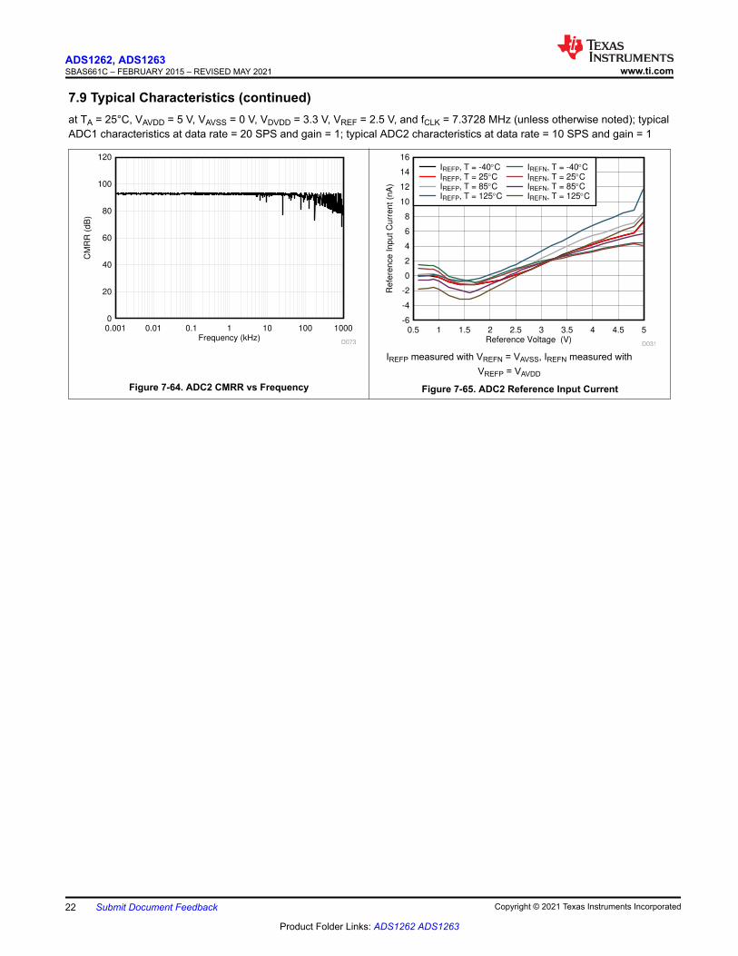
Frequency (kHz)
CM
RR
(d
B)
0.001 0.01 0.1 1 10 100 10000
20
40
60
80
100
120
D073
Figure 7-64. ADC2 CMRR vs Frequency
Reference Voltage (V)
Re
fere
nce
In
pu
t C
urr
en
t (n
A)
0.5 1 1.5 2 2.5 3 3.5 4 4.5 5-6
-4
-2
0
2
4
6
8
10
12
14
16
D031
IREFP, T = -40qCIREFP, T = 25qCIREFP, T = 85qCIREFP, T = 125qC
IREFN, T = -40qCIREFN, T = 25qCIREFN, T = 85qCIREFN, T = 125qC
IREFP measured with VREFN = VAVSS, IREFN measured withVREFP = VAVDD
Figure 7-65. ADC2 Reference Input Current
ADS1262, ADS1263SBAS661C – FEBRUARY 2015 – REVISED MAY 2021 www.ti.com
22 Submit Document Feedback Copyright © 2021 Texas Instruments Incorporated
Product Folder Links: ADS1262 ADS1263
8 Parameter Measurement Information8.1 Offset Temperature Drift MeasurementOffset temperature drift is defined as the maximum change of offset voltage measured over the specifiedtemperature range. The offset voltage drift is input referred and is calculated using the box method, as describedby Equation 1:
Offset Voltage Drift = (VOSMAX – VOSMIN) / (TMAX – TMIN) (1)
where
• VOSMAX and VOSMIN are the maximum and minimum offset voltages, respectively• TMAX and TMIN are the maximum and minimum temperatures, respectively, over the specified temperature
range
8.2 Gain Temperature Drift MeasurementGain temperature drift is defined as the maximum change of gain error measured over the specified temperaturerange. The gain error drift is calculated using the box method, as described by Equation 2:
Gain Error Drift = (GEMAX – GEMIN) / (TMAX – TMIN) (2)
where
• GEMAX and GEMIN are the maximum and minimum gain errors, respectively• TMAX and TMIN are the maximum and minimum temperatures, respectively, over the specified temperature
range
8.3 Common-Mode Rejection Ratio MeasurementCommon-mode rejection ratio (CMRR) is defined as the rejection of the ADC output to an applied common-mode input voltage. The common-mode input is 60 Hz with a peak-to-peak amplitude equal to the specifiedabsolute input voltage range. The standard deviation (RMS) value of the ADC output is calculated and scaledto volts. In order to measure CMRR, record two ADC readings. The first reading (VA) is with no common-mode input signal. The first reading represents the baseline ADC noise. The second reading (VB) is with thecommon-mode input applied. The second reading represents the combination of the ADC baseline noise plusthe increased RMS noise caused by the common-mode input. The ADC baseline noise is extracted from thecombined noise to yield the noise induced by the common-mode input voltage. The CMRR measurement isdescribed by Equation 3:
CMRR = 20 · Log (VIC / VOC) (3)
where
• VIC = RMS value of the input common-mode voltage = 1.56 VRMS• VOC = Calculated RMS value of output voltage = (VB 2 – VA 2 )0.5
• VA = RMS output voltage with no common-mode input• VB = RMS output voltage with common-mode input
For gains > 1, add 6 dB of compensation value for each binary increase of gain.
www.ti.comADS1262, ADS1263
SBAS661C – FEBRUARY 2015 – REVISED MAY 2021
Copyright © 2021 Texas Instruments Incorporated Submit Document Feedback 23
Product Folder Links: ADS1262 ADS1263
8.4 Power-Supply Rejection Ratio MeasurementPower-supply rejection ratio (PSRR) is defined as the rejection of the ADC output to the DC change of thepower supply voltage referred to the input range. PSRR is calculated using two ADC mean-value readings withinputs shorted, scaled to volts. The first ADC reading (VOA) is acquired at one power-supply voltage, and thesecond ADC reading (VOB) is acquired after changing the power-supply voltage by 0.5 V. The PSRR calculationis described by Equation 4:
PSRR = 20 · Log |(VPSA– VPSB )/ (VOA – VOB)| – 20 dB (4)
where
• VPSA– VPSB = power-supply DC voltage change = 0.5 V• VOA – VOB = ADC DC output voltage change (V)• Range compensation factor = 20 · log (0.5 V / 5 V) = –20 dB for gain = 1
For gains > 1, add an additional 6 dB of compensation value for each binary increase of gain.
8.5 Crosstalk Measurement (ADS1263)Crosstalk is defined as the unintended coupling of signals between ADC1 and ADC2. Measure crosstalk bychanging the dc input voltage of one ADC and measuring the rejection of the other ADC. The dc input voltagechange is 0.3 V, and the gain of the affected ADC is 16. Acquire two mean-value readings of the affected ADCwith inputs shorted. Take the first ADC reading (VOA) with VIN = 0 V, and take the second ADC reading (VOB)after changing the input voltage by 0.3 V. The crosstalk calculation is described by Equation 5:
Crosstalk = |(VOA – VOB) / (VINA – VINB)| · 106 (µV/V) (5)
where
• VOA – VOB = DC output voltage change of the affected ADC• VINA – VINB = DC input voltage change of the driven ADC = 0.3 V
8.6 Reference-Voltage Temperature-Drift MeasurementInternal reference-voltage temperature drift is defined as the maximum change in reference voltage measuredover the specified temperature range. The reference voltage drift is calculated using the box method, asdescribed by Equation 6:
Reference Drift = (VREFMAX – VREFMIN) / (VREFNOM · (TMAX – TMIN) ) · 106 (ppm) (6)
where
• VREFMAX, VREFMIN and VREFNOM are the maximum, minimum and nominal (TA = 25°C) reference voltages,respectively
• TMAX and TMIN are the maximum and minimum temperatures, respectively, over the specified temperaturerange
8.7 Reference-Voltage Thermal-Hysteresis MeasurementInternal reference-voltage thermal hysteresis is defined as the change in reference voltage after operating thedevice at TA = 25°C, cycling the device through the TA = 0°C to 85°C temperature range for ten minutes at eachtemperature and returning to TA = 25°C. The internal reference thermal hysteresis is defined in Equation 7:
Reference Thermal Hysteresis = |VREFPRE – VREFPOST| / VREFPRE · 106 (ppm) (7)
where
• VREFPRE and VREFPOST are the reference voltages before and after the temperature cycle, respectively
ADS1262, ADS1263SBAS661C – FEBRUARY 2015 – REVISED MAY 2021 www.ti.com
24 Submit Document Feedback Copyright © 2021 Texas Instruments Incorporated
Product Folder Links: ADS1262 ADS1263
8.8 Noise PerformanceThe ADC noise performance depends on the following ADC settings: PGA gain, data rate, digital filter mode, andchop mode. Generally, the lowest input-referred noise is achieved using the highest gain possible, consistentwith the input signal range. Do not set the gain too high or the result is ADC overrange. Noise also depends onthe output data rate and mode of the digital filter. As the data rate reduces, the ADC bandwidth correspondinglyreduces. As the order of the digital filter mode increases, the ADC bandwidth also reduces. This reduction intotal bandwidth results in lower overall noise. The ADC noise is reduced by a factor of 1.4 with chop modeenabled.
Table 8-1 lists ADC1 noise performance in units of μVRMS (RMS = root mean square) under the conditionsshown. The values in parenthesis are peak-to-peak values. Table 8-2 lists the noise performance in effectivenumber of bits (ENOB) with an external 5-V reference voltage. The values shown in parenthesis are noise-freebits. The definition of noise-free bits is the resolution of the ADC with no code flicker. The noise-free bits data arebased on the µVPP values. Note that for data rate = 38400 SPS, noise scales with increased reference voltage.For all other data rates, noise does not scale with reference voltage.
Table 8-3 lists the noise performance of ADC2 (ADS1263) in units of μVRMS and (µVP–P). The values inparenthesis are peak-to-peak values. Table 8-4 lists the ENOB and noise-free bits of ADC2.
The ENOB and noise-free bits shown in the tables are calculated using Equation 8:
ENOB = ln (FSR / VNRMS) / ln (2) (8)
where
• FSR = full scale range = 2 · VREF/Gain• VNRMS = Input referred noise voltage
Achieve maximum ENOB with maximum FSR. For ADC1, achieve maximum FSR with VREF = 5 V and the PGAbypassed. If the PGA is enabled, the FSR is limited by the PGA input range (see the Electrical Characteristicstable.) For ADC2, achieve maximum FSR with VREF = 5 V and gains = 1, 2, or 4. If gain = 8 to 128, then FSR islimited by the PGA input range (see the Electrical Characteristics table).
For ADC1 operation, if the reference voltage is equal to 5 V and the PGA is enabled, the available FSR isrestricted because of the limited PGA range specification. For ADC2 operation, if the reference voltage is equalto 5 V, The FSR is reduced for ADC2 gains equal to or greater than eight because of the limited PGA range.
The data shown in the noise performance tables represent typical ADC performance at TA = 25°C. The noise-performance data are the standard deviation and peak-to-peak computations of the ADC data. Because of thestatistical nature of noise, repeated noise measurements may yield higher or lower noise results. The noisedata are acquired with inputs shorted, from consecutive ADC readings for a period of ten seconds or 8192 datapoints, whichever occurs first.
www.ti.comADS1262, ADS1263
SBAS661C – FEBRUARY 2015 – REVISED MAY 2021
Copyright © 2021 Texas Instruments Incorporated Submit Document Feedback 25
Product Folder Links: ADS1262 ADS1263
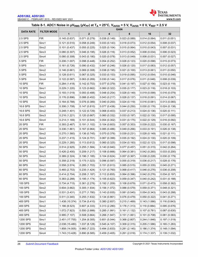
Table 8-1. ADC1 Noise in µVRMS (µVPP) at TA = 25°C, VAVDD = 5 V, VAVSS = 0 V, VREF = 2.5 V
DATA RATE FILTER MODEGAIN
1 2 4 8 16 322.5 SPS FIR 0.145 (0.637) 0.071 (0.279) 0.038 (0.149) 0.023 (0.089) 0.014 (0.064) 0.011 (0.051)
2.5 SPS Sinc1 0.121 (0.510) 0.058 (0.249) 0.033 (0.143) 0.018 (0.073) 0.012 (0.054) 0.008 (0.037)
2.5 SPS Sinc2 0.101 (0.437) 0.055 (0.225) 0.025 (0.104) 0.015 (0.064) 0.010 (0.043) 0.007 (0.031)
2.5 SPS Sinc3 0.080 (0.307) 0.046 (0.195) 0.026 (0.116) 0.013 (0.052) 0.008 (0.034) 0.006 (0.023)
2.5 SPS Sinc4 0.080 (0.308) 0.043 (0.180) 0.020 (0.078) 0.013 (0.049) 0.008 (0.031) 0.007 (0.027)
5 SPS FIR 0.206 (1.007) 0.098 (0.448) 0.054 (0.252) 0.028 (0.123) 0.020 (0.098) 0.015 (0.073)
5 SPS Sinc1 0.161 (0.726) 0.090 (0.432) 0.047 (0.246) 0.026 (0.120) 0.017 (0.083) 0.012 (0.057)
5 SPS Sinc2 0.146 (0.661) 0.069 (0.308) 0.038 (0.195) 0.021 (0.100) 0.013 (0.061) 0.011 (0.050)
5 SPS Sinc3 0.128 (0.611) 0.067 (0.325) 0.033 (0.153) 0.019 (0.095) 0.012 (0.054) 0.010 (0.046)
5 SPS Sinc4 0.122 (0.587) 0.063 (0.269) 0.030 (0.144) 0.017 (0.076) 0.011 (0.048) 0.008 (0.039)
10 SPS FIR 0.284 (1.418) 0.142 (0.753) 0.077 (0.379) 0.041 (0.197) 0.027 (0.156) 0.023 (0.118)
10 SPS Sinc1 0.229 (1.220) 0.123 (0.662) 0.060 (0.322) 0.035 (0.177) 0.023 (0.118) 0.018 (0.103)
10 SPS Sinc2 0.193 (1.019) 0.093 (0.488) 0.048 (0.254) 0.028 (0.149) 0.019 (0.099) 0.016 (0.079)
10 SPS Sinc3 0.176 (0.896) 0.088 (0.452) 0.043 (0.217) 0.028 (0.137) 0.018 (0.091) 0.014 (0.067)
10 SPS Sinc4 0.164 (0.788) 0.076 (0.389) 0.040 (0.200) 0.024 (0.119) 0.016 (0.081) 0.013 (0.065)
16.6 SPS Sinc1 0.306 (1.708) 0.147 (0.810) 0.077 (0.436) 0.044 (0.250) 0.030 (0.176) 0.024 (0.138)
16.6 SPS Sinc2 0.248 (1.401) 0.122 (0.729) 0.068 (0.403) 0.037 (0.213) 0.024 (0.136) 0.020 (0.111)
16.6 SPS Sinc3 0.216 (1.221) 0.120 (0.667) 0.060 (0.332) 0.033 (0.197) 0.022 (0.130) 0.017 (0.095)
16.6 SPS Sinc4 0.214 (1.169) 0.101 (0.544) 0.054 (0.302) 0.031 (0.175) 0.022 (0.129) 0.016 (0.092)
20 SPS FIR 0.393 (2.467) 0.191 (1.102) 0.104 (0.603) 0.057 (0.353) 0.039 (0.222) 0.030 (0.167)
20 SPS Sinc1 0.336 (1.861) 0.167 (0.964) 0.085 (0.486) 0.049 (0.266) 0.033 (0.191) 0.026 (0.138)
20 SPS Sinc2 0.270 (1.560) 0.136 (0.745) 0.070 (0.376) 0.039 (0.231) 0.028 (0.149) 0.021 (0.111)
20 SPS Sinc3 0.237 (1.415) 0.124 (0.701) 0.067 (0.399) 0.035 (0.192) 0.024 (0.130) 0.020 (0.109)
20 SPS Sinc4 0.229 (1.285) 0.113 (0.612) 0.060 (0.325) 0.034 (0.193) 0.022 (0.123) 0.017 (0.098)
50 SPS Sinc1 0.514 (2.925) 0.255 (1.584) 0.140 (0.940) 0.077 (0.457) 0.051 (0.315) 0.042 (0.264)
50 SPS Sinc2 0.426 (2.400) 0.209 (1.217) 0.108 (0.666) 0.064 (0.381) 0.042 (0.265) 0.033 (0.200)
50 SPS Sinc3 0.389 (2.324) 0.196 (1.185) 0.104 (0.624) 0.057 (0.367) 0.038 (0.228) 0.030 (0.179)
50 SPS Sinc4 0.358 (2.319) 0.175 (1.023) 0.096 (0.597) 0.055 (0.319) 0.036 (0.217) 0.028 (0.176)
60 SPS Sinc1 0.558 (3.574) 0.285 (1.703) 0.151 (0.913) 0.085 (0.515) 0.055 (0.335) 0.045 (0.271)
60 SPS Sinc2 0.465 (2.753) 0.235 (1.424) 0.121 (0.760) 0.068 (0.417) 0.046 (0.276) 0.036 (0.208)
60 SPS Sinc3 0.414 (2.704) 0.208 (1.187) 0.112 (0.655) 0.064 (0.396) 0.042 (0.276) 0.034 (0.197)
60 SPS Sinc4 0.383 (2.288) 0.195 (1.174) 0.105 (0.623) 0.059 (0.347) 0.040 (0.242) 0.031 (0.188)
100 SPS Sinc1 0.734 (4.715) 0.361 (2.276) 0.192 (1.209) 0.108 (0.679) 0.071 (0.473) 0.058 (0.362)
100 SPS Sinc2 0.604 (3.662) 0.305 (1.934) 0.156 (1.072) 0.088 (0.579) 0.059 (0.371) 0.048 (0.321)
100 SPS Sinc3 0.531 (3.431) 0.277 (1.780) 0.143 (0.935) 0.081 (0.545) 0.054 (0.343) 0.043 (0.288)
100 SPS Sinc4 0.511 (3.340) 0.255 (1.632) 0.134 (0.861) 0.076 (0.479) 0.050 (0.322) 0.041 (0.271)
400 SPS Sinc1 1.438 (10.374) 0.734 (5.410) 0.380 (2.657) 0.215 (1.469) 0.143 (1.066) 0.116 (0.843)
400 SPS Sinc2 1.186 (8.523) 0.607 (4.333) 0.313 (2.280) 0.178 (1.313) 0.119 (0.884) 0.095 (0.676)
400 SPS Sinc3 1.072 (7.923) 0.550 (3.999) 0.285 (1.991) 0.161 (1.132) 0.107 (0.781) 0.087 (0.630)
400 SPS Sinc4 0.995 (7.107) 0.508 (3.664) 0.266 (1.947) 0.151 (1.061) 0.101 (0.708) 0.081 (0.583)
1200 SPS Sinc1 2.451 (17.755) 1.254 (9.305) 0.651 (5.044) 0.368 (2.807) 0.244 (1.846) 0.197 (1.519)
1200 SPS Sinc2 2.038 (15.480) 1.037 (8.128) 0.545 (4.107) 0.309 (2.315) 0.205 (1.586) 0.165 (1.283)
1200 SPS Sinc3 1.858 (14.005) 0.960 (7.223) 0.494 (3.833) 0.281 (2.145) 0.186 (1.374) 0.148 (1.094)
1200 SPS Sinc4 1.743 (13.428) 0.890 (6.585) 0.459 (3.405) 0.261 (2.018) 0.174 (1.337) 0.139 (1.032)
ADS1262, ADS1263SBAS661C – FEBRUARY 2015 – REVISED MAY 2021 www.ti.com
26 Submit Document Feedback Copyright © 2021 Texas Instruments Incorporated
Product Folder Links: ADS1262 ADS1263
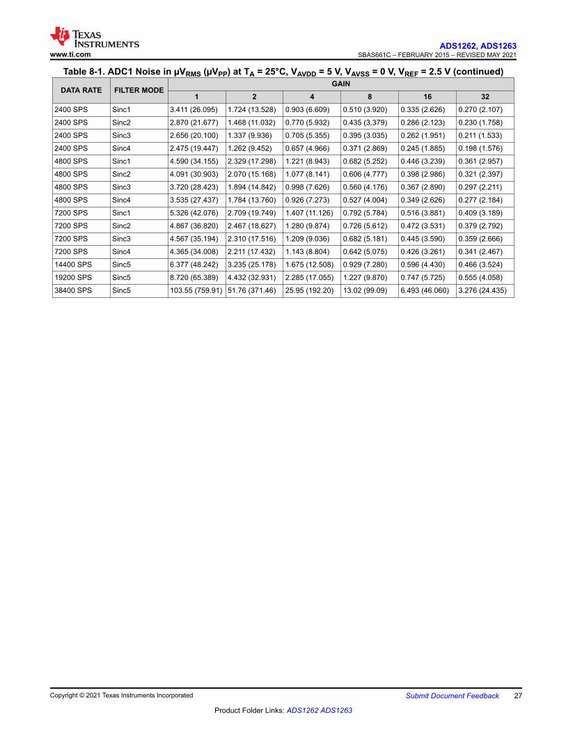
Table 8-1. ADC1 Noise in µVRMS (µVPP) at TA = 25°C, VAVDD = 5 V, VAVSS = 0 V, VREF = 2.5 V (continued)
DATA RATE FILTER MODEGAIN
1 2 4 8 16 322400 SPS Sinc1 3.411 (26.095) 1.724 (13.528) 0.903 (6.609) 0.510 (3.920) 0.335 (2.626) 0.270 (2.107)
2400 SPS Sinc2 2.870 (21.677) 1.468 (11.032) 0.770 (5.932) 0.435 (3.379) 0.286 (2.123) 0.230 (1.758)
2400 SPS Sinc3 2.656 (20.100) 1.337 (9.936) 0.705 (5.355) 0.395 (3.035) 0.262 (1.951) 0.211 (1.533)
2400 SPS Sinc4 2.475 (19.447) 1.262 (9.452) 0.657 (4.966) 0.371 (2.869) 0.245 (1.885) 0.198 (1.576)
4800 SPS Sinc1 4.590 (34.155) 2.329 (17.298) 1.221 (8.943) 0.682 (5.252) 0.446 (3.239) 0.361 (2.957)
4800 SPS Sinc2 4.091 (30.903) 2.070 (15.168) 1.077 (8.141) 0.606 (4.777) 0.398 (2.986) 0.321 (2.397)
4800 SPS Sinc3 3.720 (28.423) 1.894 (14.842) 0.998 (7.626) 0.560 (4.176) 0.367 (2.890) 0.297 (2.211)
4800 SPS Sinc4 3.535 (27.437) 1.784 (13.760) 0.926 (7.273) 0.527 (4.004) 0.349 (2.626) 0.277 (2.184)
7200 SPS Sinc1 5.326 (42.076) 2.709 (19.749) 1.407 (11.126) 0.792 (5.784) 0.516 (3.881) 0.409 (3.189)
7200 SPS Sinc2 4.867 (36.820) 2.467 (18.627) 1.280 (9.874) 0.726 (5.612) 0.472 (3.531) 0.379 (2.792)
7200 SPS Sinc3 4.567 (35.194) 2.310 (17.516) 1.209 (9.036) 0.682 (5.181) 0.445 (3.590) 0.359 (2.666)
7200 SPS Sinc4 4.365 (34.008) 2.211 (17.432) 1.143 (8.804) 0.642 (5.075) 0.426 (3.261) 0.341 (2.467)
14400 SPS Sinc5 6.377 (48.242) 3.235 (25.178) 1.675 (12.508) 0.929 (7.280) 0.596 (4.430) 0.466 (3.524)
19200 SPS Sinc5 8.720 (65.389) 4.432 (32.931) 2.285 (17.055) 1.227 (9.870) 0.747 (5.725) 0.555 (4.058)
38400 SPS Sinc5 103.55 (759.91) 51.76 (371.46) 25.95 (192.20) 13.02 (99.09) 6.493 (46.060) 3.276 (24.435)
www.ti.comADS1262, ADS1263
SBAS661C – FEBRUARY 2015 – REVISED MAY 2021
Copyright © 2021 Texas Instruments Incorporated Submit Document Feedback 27
Product Folder Links: ADS1262 ADS1263
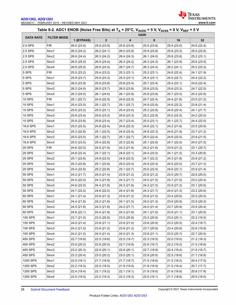
Table 8-2. ADC1 ENOB (Noise Free Bits) at TA = 25°C, VAVDD = 5 V, VAVSS = 0 V, VREF = 5 V
DATA RATE FILTER MODEGAIN
1 (BYPASS) 2 4 8 16 322.5 SPS FIR 26.0 (23.9) 25.9 (23.9) 25.8 (23.8) 25.5 (23.6) 25.4 (23.0) 24.6 (22.4)
2.5 SPS Sinc1 26.3 (24.2) 26.2 (24.1) 26.0 (23.9) 25.9 (23.8) 25.6 (23.3) 25.0 (22.8)
2.5 SPS Sinc2 26.6 (24.4) 26.3 (24.2) 26.4 (24.3) 26.1 (24.0) 25.8 (23.6) 25.2 (23.1)
2.5 SPS Sinc3 26.9 (25.0) 26.5 (24.4) 26.3 (24.2) 26.3 (24.3) 26.1 (23.9) 25.6 (23.5)
2.5 SPS Sinc4 26.9 (25.0) 26.6 (24.5) 26.7 (24.7) 26.3 (24.4) 26.2 (24.1) 25.2 (23.3)
5 SPS FIR 25.5 (23.2) 25.4 (23.2) 25.3 (23.1) 25.2 (23.1) 24.8 (22.4) 24.1 (21.9)
5 SPS Sinc1 25.9 (23.7) 25.5 (23.3) 25.5 (23.1) 25.4 (23.1) 25.0 (22.7) 24.4 (22.2)
5 SPS Sinc2 26.0 (23.9) 25.9 (23.8) 25.8 (23.4) 25.7 (23.4) 25.4 (23.1) 24.6 (22.4)
5 SPS Sinc3 26.2 (24.0) 26.0 (23.7) 26.0 (23.8) 25.8 (23.5) 25.6 (23.3) 24.7 (22.5)
5 SPS Sinc4 26.3 (24.0) 26.1 (24.0) 26.1 (23.9) 25.9 (23.8) 25.7 (23.5) 25.0 (22.8)
10 SPS FIR 25.1 (22.7) 24.9 (22.5) 24.8 (22.5) 24.7 (22.4) 24.4 (21.8) 23.5 (21.2)
10 SPS Sinc1 25.4 (23.0) 25.1 (22.7) 25.1 (22.7) 24.9 (22.6) 24.6 (22.2) 23.8 (21.4)
10 SPS Sinc2 25.6 (23.2) 25.5 (23.1) 25.4 (23.0) 25.2 (22.8) 24.9 (22.4) 24.1 (21.7)
10 SPS Sinc3 25.8 (23.4) 25.6 (23.2) 25.6 (23.3) 25.2 (22.9) 25.0 (22.5) 24.2 (22.0)
10 SPS Sinc4 25.9 (23.6) 25.8 (23.4) 25.7 (23.4) 25.5 (23.1) 25.1 (22.7) 24.4 (22.0)
16.6 SPS Sinc1 25.0 (22.5) 24.8 (22.4) 24.8 (22.3) 24.6 (22.1) 24.2 (21.6) 23.5 (20.9)
16.6 SPS Sinc2 25.3 (22.8) 25.1 (22.5) 24.9 (22.4) 24.8 (22.3) 24.6 (21.9) 23.7 (21.2)
16.6 SPS Sinc3 25.5 (23.0) 25.1 (22.7) 25.1 (22.7) 25.0 (22.4) 24.6 (22.0) 23.9 (21.5)
16.6 SPS Sinc4 25.5 (23.0) 25.4 (22.9) 25.3 (22.8) 25.1 (22.6) 24.7 (22.0) 24.0 (21.5)
20 SPS FIR 24.6 (22.0) 24.5 (21.9) 24.3 (21.8) 24.2 (21.6) 23.9 (21.2) 23.1 (20.7)
20 SPS Sinc1 24.8 (22.4) 24.7 (22.1) 24.6 (22.1) 24.4 (22.0) 24.1 (21.5) 23.3 (20.9)
20 SPS Sinc2 25.1 (22.6) 24.9 (22.5) 24.9 (22.5) 24.7 (22.2) 24.3 (21.8) 23.6 (21.2)
20 SPS Sinc3 25.3 (22.8) 25.1 (22.6) 25.0 (22.4) 24.9 (22.4) 24.5 (22.0) 23.7 (21.3)
20 SPS Sinc4 25.4 (22.9) 25.2 (22.8) 25.1 (22.7) 25.0 (22.4) 24.6 (22.1) 23.9 (21.4)
50 SPS Sinc1 24.2 (21.7) 24.0 (21.4) 23.9 (21.2) 23.8 (21.2) 23.5 (20.7) 22.6 (20.0)
50 SPS Sinc2 24.5 (22.0) 24.3 (21.8) 24.3 (21.7) 24.0 (21.5) 23.7 (21.0) 23.0 (20.4)
50 SPS Sinc3 24.6 (22.0) 24.4 (21.8) 24.3 (21.8) 24.2 (21.5) 23.9 (21.2) 23.1 (20.6)
50 SPS Sinc4 24.7 (22.0) 24.6 (22.0) 24.4 (21.8) 24.3 (21.7) 24.0 (21.3) 23.2 (20.6)
60 SPS Sinc1 24.1 (21.4) 23.9 (21.3) 23.8 (21.2) 23.6 (21.0) 23.4 (20.6) 22.5 (20.0)
60 SPS Sinc2 24.4 (21.8) 24.2 (21.6) 24.1 (21.5) 24.0 (21.3) 23.6 (20.9) 22.9 (20.3)
60 SPS Sinc3 24.5 (21.8) 24.3 (21.8) 24.2 (21.7) 24.0 (21.4) 23.7 (20.9) 23.0 (20.4)
60 SPS Sinc4 24.6 (22.1) 24.4 (21.8) 24.3 (21.8) 24.1 (21.6) 23.8 (21.1) 23.1 (20.5)
100 SPS Sinc1 23.7 (21.0) 23.5 (20.9) 23.5 (20.8) 23.3 (20.6) 23.0 (20.1) 22.2 (19.5)
100 SPS Sinc2 24.0 (21.4) 23.8 (21.1) 23.8 (21.0) 23.6 (20.9) 23.2 (20.5) 22.4 (19.7)
100 SPS Sinc3 24.2 (21.5) 23.9 (21.2) 23.9 (21.2) 23.7 (20.9) 23.4 (20.6) 22.6 (19.9)
100 SPS Sinc4 24.2 (21.5) 24.0 (21.4) 24.0 (21.3) 23.8 (21.1) 23.5 (20.7) 22.7 (20.0)
400 SPS Sinc1 22.7 (19.9) 22.5 (19.6) 22.5 (19.7) 22.3 (19.5) 22.0 (19.0) 21.2 (18.3)
400 SPS Sinc2 23.0 (20.2) 22.8 (20.0) 22.7 (19.9) 22.6 (19.7) 22.2 (19.2) 21.5 (18.6)
400 SPS Sinc3 23.2 (20.3) 22.9 (20.1) 22.9 (20.1) 22.7 (19.9) 22.4 (19.4) 21.6 (18.7)
400 SPS Sinc4 23.3 (20.4) 23.0 (20.2) 23.0 (20.1) 22.8 (20.0) 22.5 (19.6) 21.7 (18.8)
1200 SPS Sinc1 22.0 (19.1) 21.7 (18.9) 21.7 (18.7) 21.5 (18.6) 21.2 (18.2) 20.4 (17.5)
1200 SPS Sinc2 22.2 (19.3) 22.0 (19.0) 21.9 (19.0) 21.8 (18.9) 21.5 (18.4) 20.7 (17.7)
1200 SPS Sinc3 22.4 (19.4) 22.1 (19.2) 22.1 (19.1) 21.9 (19.0) 21.6 (18.6) 20.8 (17.9)
1200 SPS Sinc4 22.5 (19.5) 22.2 (19.3) 22.2 (19.3) 22.0 (19.1) 21.7 (18.6) 20.9 (18.0)
ADS1262, ADS1263SBAS661C – FEBRUARY 2015 – REVISED MAY 2021 www.ti.com
28 Submit Document Feedback Copyright © 2021 Texas Instruments Incorporated
Product Folder Links: ADS1262 ADS1263
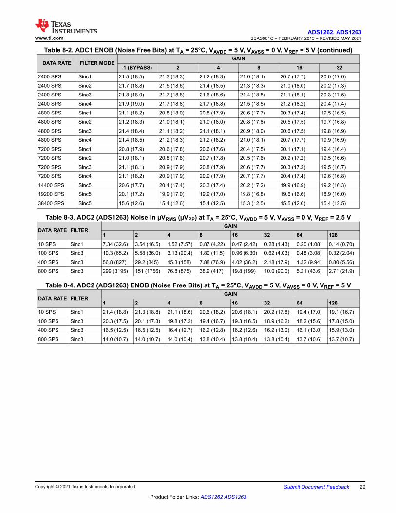
Table 8-2. ADC1 ENOB (Noise Free Bits) at TA = 25°C, VAVDD = 5 V, VAVSS = 0 V, VREF = 5 V (continued)
DATA RATE FILTER MODEGAIN
1 (BYPASS) 2 4 8 16 322400 SPS Sinc1 21.5 (18.5) 21.3 (18.3) 21.2 (18.3) 21.0 (18.1) 20.7 (17.7) 20.0 (17.0)
2400 SPS Sinc2 21.7 (18.8) 21.5 (18.6) 21.4 (18.5) 21.3 (18.3) 21.0 (18.0) 20.2 (17.3)
2400 SPS Sinc3 21.8 (18.9) 21.7 (18.8) 21.6 (18.6) 21.4 (18.5) 21.1 (18.1) 20.3 (17.5)
2400 SPS Sinc4 21.9 (19.0) 21.7 (18.8) 21.7 (18.8) 21.5 (18.5) 21.2 (18.2) 20.4 (17.4)
4800 SPS Sinc1 21.1 (18.2) 20.8 (18.0) 20.8 (17.9) 20.6 (17.7) 20.3 (17.4) 19.5 (16.5)
4800 SPS Sinc2 21.2 (18.3) 21.0 (18.1) 21.0 (18.0) 20.8 (17.8) 20.5 (17.5) 19.7 (16.8)
4800 SPS Sinc3 21.4 (18.4) 21.1 (18.2) 21.1 (18.1) 20.9 (18.0) 20.6 (17.5) 19.8 (16.9)
4800 SPS Sinc4 21.4 (18.5) 21.2 (18.3) 21.2 (18.2) 21.0 (18.1) 20.7 (17.7) 19.9 (16.9)
7200 SPS Sinc1 20.8 (17.9) 20.6 (17.8) 20.6 (17.6) 20.4 (17.5) 20.1 (17.1) 19.4 (16.4)
7200 SPS Sinc2 21.0 (18.1) 20.8 (17.8) 20.7 (17.8) 20.5 (17.6) 20.2 (17.2) 19.5 (16.6)
7200 SPS Sinc3 21.1 (18.1) 20.9 (17.9) 20.8 (17.9) 20.6 (17.7) 20.3 (17.2) 19.5 (16.7)
7200 SPS Sinc4 21.1 (18.2) 20.9 (17.9) 20.9 (17.9) 20.7 (17.7) 20.4 (17.4) 19.6 (16.8)
14400 SPS Sinc5 20.6 (17.7) 20.4 (17.4) 20.3 (17.4) 20.2 (17.2) 19.9 (16.9) 19.2 (16.3)
19200 SPS Sinc5 20.1 (17.2) 19.9 (17.0) 19.9 (17.0) 19.8 (16.8) 19.6 (16.6) 18.9 (16.0)
38400 SPS Sinc5 15.6 (12.6) 15.4 (12.6) 15.4 (12.5) 15.3 (12.5) 15.5 (12.6) 15.4 (12.5)
Table 8-3. ADC2 (ADS1263) Noise in µVRMS (µVPP) at TA = 25°C, VAVDD = 5 V, VAVSS = 0 V, VREF = 2.5 V
DATA RATE FILTERGAIN
1 2 4 8 16 32 64 12810 SPS Sinc1 7.34 (32.6) 3.54 (16.5) 1.52 (7.57) 0.87 (4.22) 0.47 (2.42) 0.28 (1.43) 0.20 (1.08) 0.14 (0.70)
100 SPS Sinc3 10.3 (65.2) 5.58 (36.0) 3.13 (20.4) 1.80 (11.5) 0.96 (6.30) 0.62 (4.03) 0.48 (3.08) 0.32 (2.04)
400 SPS Sinc3 56.8 (827) 29.2 (345) 15.3 (158) 7.88 (76.9) 4.02 (36.2) 2.18 (17.9) 1.32 (9.94) 0.80 (5.56)
800 SPS Sinc3 299 (3195) 151 (1756) 76.8 (875) 38.9 (417) 19.8 (199) 10.0 (90.0) 5.21 (43.6) 2.71 (21.9)
Table 8-4. ADC2 (ADS1263) ENOB (Noise Free Bits) at TA = 25°C, VAVDD = 5 V, VAVSS = 0 V, VREF = 5 V
DATA RATE FILTERGAIN
1 2 4 8 16 32 64 12810 SPS Sinc1 21.4 (18.8) 21.3 (18.8) 21.1 (18.6) 20.6 (18.2) 20.6 (18.1) 20.2 (17.8) 19.4 (17.0) 19.1 (16.7)
100 SPS Sinc3 20.3 (17.5) 20.1 (17.3) 19.8 (17.2) 19.4 (16.7) 19.3 (16.5) 18.9 (16.2) 18.2 (15.6) 17.8 (15.0)
400 SPS Sinc3 16.5 (12.5) 16.5 (12.5) 16.4 (12.7) 16.2 (12.8) 16.2 (12.6) 16.2 (13.0) 16.1 (13.0) 15.9 (13.0)
800 SPS Sinc3 14.0 (10.7) 14.0 (10.7) 14.0 (10.4) 13.8 (10.4) 13.8 (10.4) 13.8 (10.4) 13.7 (10.6) 13.7 (10.7)
www.ti.comADS1262, ADS1263
SBAS661C – FEBRUARY 2015 – REVISED MAY 2021
Copyright © 2021 Texas Instruments Incorporated Submit Document Feedback 29
Product Folder Links: ADS1262 ADS1263
9 Detailed Description9.1 OverviewThe ADS1262 and ADS1263 are precision 32-bit, delta-sigma (ΔΣ) ADCs with an integrated analog front end(AFE) to simplify connection to sensors. A 32-bit ADC (ADC1) provides output data rates from 2.5 SPS to 38400SPS for flexibility in resolution and data rates over a wide range of applications. The ADC low noise and lowdrift architecture make these devices suitable for precise digitization of low-level transducers, such as load cellbridges and temperature sensors. The ADS1263 includes an auxiliary 24-bit delta-sigma ADC (ADC2).
The ADS1262 and the ADS1263 incorporate several functions that provide increased utility. The key integratedfunctions include:
• Low-drift voltage reference• Dual, matched, sensor-excitation current sources (IDAC)• Input-level-shift voltage• Eight GPIOs• Dual-sensor, bias current sources• Low-noise, CMOS PGA with integrated signal fault detection• Internal test signal source (TDAC)• Temperature sensor• Internal oscillator• Three sets of buffered external reference inputs with low reference voltage alarm
As shown in the Functional Block Diagram, these devices feature 11 analog inputs that are configurable as eitherten single-ended inputs, five differential inputs, or any combination, to either ADC1 or ADC2. Many of the analoginputs are multifunction as programmed by the user. The analog inputs can be programmed to the followingextended functions:
• Three external reference inputs: pins AIN0, AIN1, AIN2, AIN3, AIN4 and AIN5• Two sensor excitation current source: all analog input pins• Level shift (VBIAS): AINCOM pin• Eight GPIO: pins AIN3, AIN4, AIN5, AIN6, AIN7, AIN8, AIN9, AINCOM• Sensor break current source: all analog input pins• Two test signal output: pins AIN6, AIN7
Following the input multiplexer (mux), ADC1 features a high-impedance, CMOS, programmable gain amplifier(PGA). The PGA provides very low voltage and current noise, enabling direct connection to low-leveltransducers, and in many cases, eliminating the need for an external amplifier. The PGA gain is programmablefrom 1 V/V to 32 V/V in binary steps. The PGA can be bypassed to allow the input range to extend belowground. The PGA has voltage overrange monitors to improve the integrity of the conversion result. ThePGA overrange alarm is latched during the conversion phase and appended to the conversion data. Theprogrammable sensor bias uses a test current to help detect a failed sensor or sensor connection.
An inherently stable delta-sigma modulator measures the ratio of the input voltage to the reference voltageto provide the ADC result. The ADC operates with the internal 2.5-V reference, or with up to three externalreference inputs. The external reference inputs are continuously monitored for low (or missing) voltage. Thereference alarm status is latched during the conversion phase and appended to the conversion data. TheREFOUT pin is the buffered 2.5-V internal voltage reference output.
Dual excitation current sources (IDAC) provide bias to resistance sensors (such as 3-wire RTD). The ADCintegrates several system monitors for readback, such as temperature sensor and supply monitor. The ADCfeatures an internal test signal voltage (TDAC) that is used to verify the ADC operation across all gains. TheTDAC has two outputs to provide test voltages for single-ended and differential input configurations. Eight GPIOports are available on the analog input pins.
The digital filter provides two functional modes, sinc and FIR, allowing optimization of settling time and line-cyclerejection. The sinx/x (sinc) filter is programmable to sinc orders one through four to tradeoff filter settling timeand 50-Hz and 60-Hz line-cycle rejection. The finite impulse response (FIR) filter mode provides single-cyclesettled data with 50-Hz and 60-Hz line cycle rejection at data rates up to 20 SPS.
ADS1262, ADS1263SBAS661C – FEBRUARY 2015 – REVISED MAY 2021 www.ti.com
30 Submit Document Feedback Copyright © 2021 Texas Instruments Incorporated
Product Folder Links: ADS1262 ADS1263
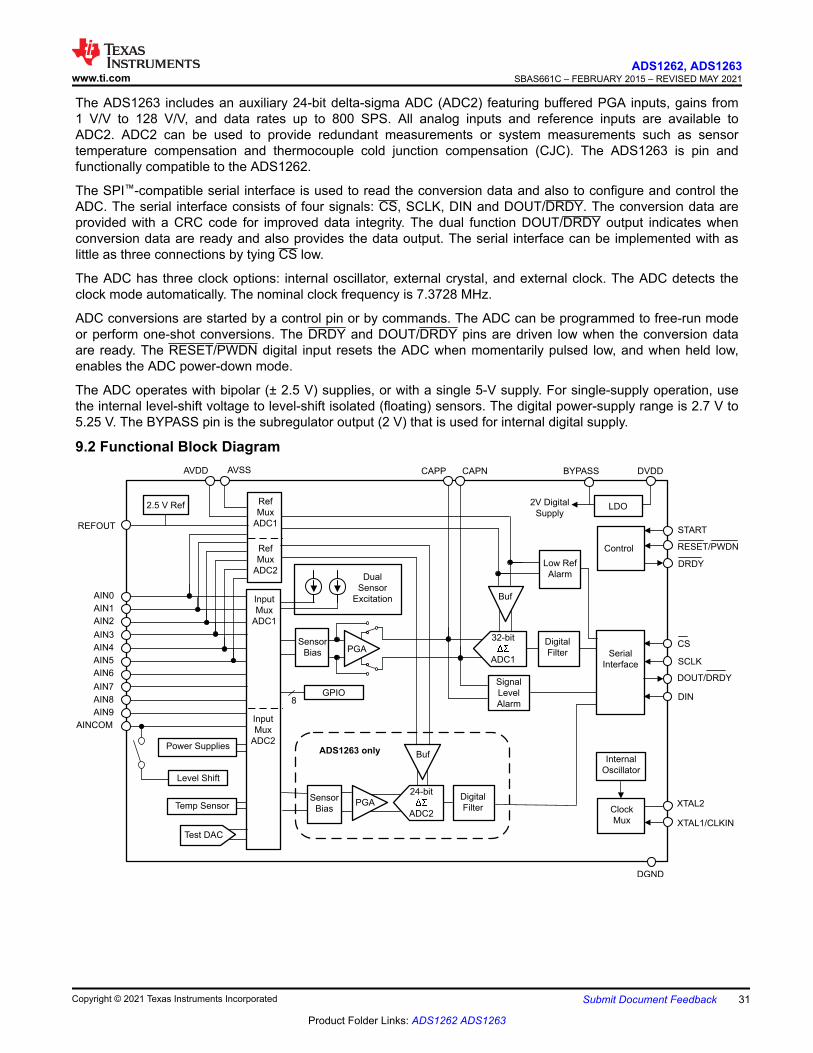
The ADS1263 includes an auxiliary 24-bit delta-sigma ADC (ADC2) featuring buffered PGA inputs, gains from1 V/V to 128 V/V, and data rates up to 800 SPS. All analog inputs and reference inputs are available toADC2. ADC2 can be used to provide redundant measurements or system measurements such as sensortemperature compensation and thermocouple cold junction compensation (CJC). The ADS1263 is pin andfunctionally compatible to the ADS1262.
The SPI™-compatible serial interface is used to read the conversion data and also to configure and control theADC. The serial interface consists of four signals: CS, SCLK, DIN and DOUT/DRDY. The conversion data areprovided with a CRC code for improved data integrity. The dual function DOUT/DRDY output indicates whenconversion data are ready and also provides the data output. The serial interface can be implemented with aslittle as three connections by tying CS low.
The ADC has three clock options: internal oscillator, external crystal, and external clock. The ADC detects theclock mode automatically. The nominal clock frequency is 7.3728 MHz.
ADC conversions are started by a control pin or by commands. The ADC can be programmed to free-run modeor perform one-shot conversions. The DRDY and DOUT/DRDY pins are driven low when the conversion dataare ready. The RESET/PWDN digital input resets the ADC when momentarily pulsed low, and when held low,enables the ADC power-down mode.
The ADC operates with bipolar (± 2.5 V) supplies, or with a single 5-V supply. For single-supply operation, usethe internal level-shift voltage to level-shift isolated (floating) sensors. The digital power-supply range is 2.7 V to5.25 V. The BYPASS pin is the subregulator output (2 V) that is used for internal digital supply.
9.2 Functional Block Diagram
32-bit
��
ADC1
Input
Mux
ADC1
Digital
Filter Serial
Interface
CS
DOUT/DRDY
DIN
START
RESET/PWDN
Clock
Mux
XTAL2
XTAL1/CLKIN
REFOUT
BufAIN0
AIN1
GPIO
Level Shift
AVDD AVSS DVDD
DGND
LDO
BYPASS
Control
Sensor
Bias
AIN2
AIN3
AIN4
AIN5
AIN6
AIN7
AIN8
AIN9
AINCOM
Ref
Mux
ADC1
2.5 V Ref
CAPP CAPN
Low Ref
Alarm
Signal
Level
Alarm
Internal
Oscillator
Dual
Sensor
Excitation
2V Digital
Supply
Test DAC
Power Supplies
SCLK
ADS1263 only
Digital
Filter
Buf
PGA
24-bit
��
ADC2
Sensor
BiasTemp Sensor
8
Input
Mux
ADC2
Ref
Mux
ADC2
PGA
DRDY
www.ti.comADS1262, ADS1263
SBAS661C – FEBRUARY 2015 – REVISED MAY 2021
Copyright © 2021 Texas Instruments Incorporated Submit Document Feedback 31
Product Folder Links: ADS1262 ADS1263
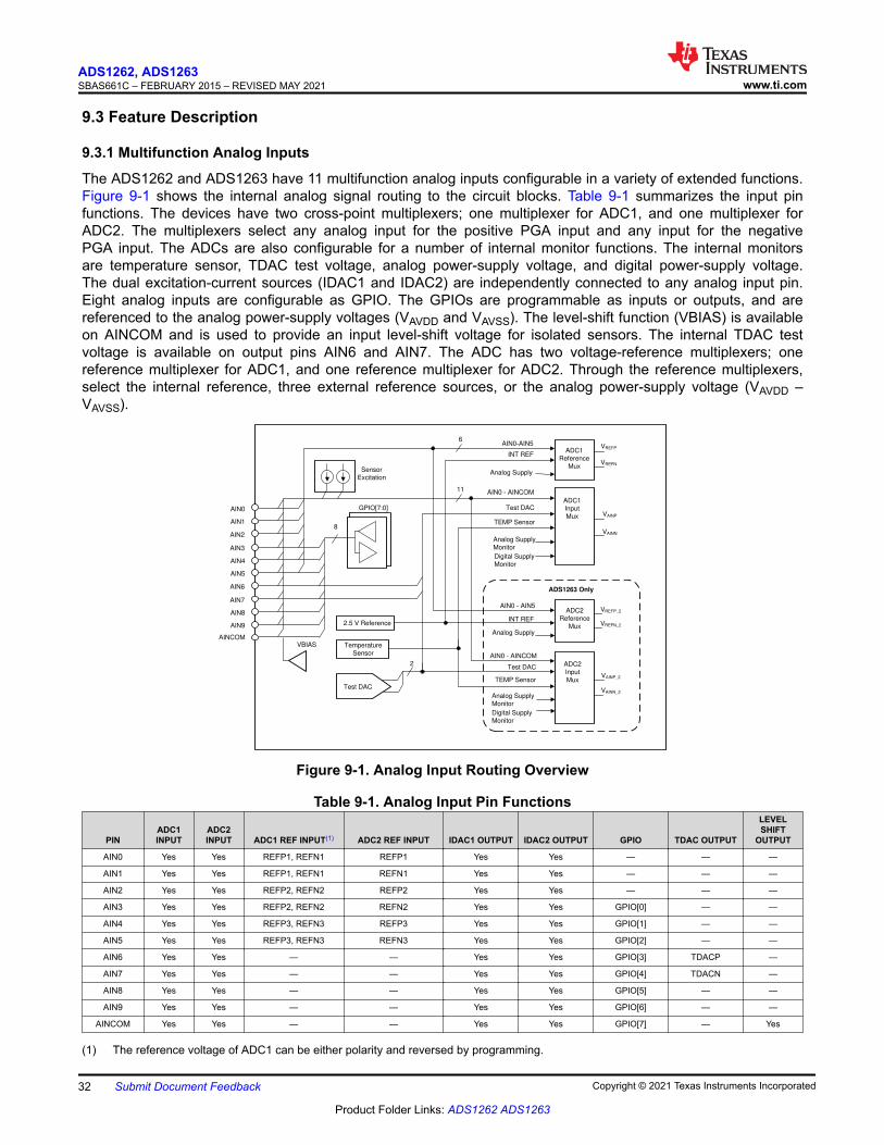
9.3 Feature Description
9.3.1 Multifunction Analog Inputs
The ADS1262 and ADS1263 have 11 multifunction analog inputs configurable in a variety of extended functions.Figure 9-1 shows the internal analog signal routing to the circuit blocks. Table 9-1 summarizes the input pinfunctions. The devices have two cross-point multiplexers; one multiplexer for ADC1, and one multiplexer forADC2. The multiplexers select any analog input for the positive PGA input and any input for the negativePGA input. The ADCs are also configurable for a number of internal monitor functions. The internal monitorsare temperature sensor, TDAC test voltage, analog power-supply voltage, and digital power-supply voltage.The dual excitation-current sources (IDAC1 and IDAC2) are independently connected to any analog input pin.Eight analog inputs are configurable as GPIO. The GPIOs are programmable as inputs or outputs, and arereferenced to the analog power-supply voltages (VAVDD and VAVSS). The level-shift function (VBIAS) is availableon AINCOM and is used to provide an input level-shift voltage for isolated sensors. The internal TDAC testvoltage is available on output pins AIN6 and AIN7. The ADC has two voltage-reference multiplexers; onereference multiplexer for ADC1, and one reference multiplexer for ADC2. Through the reference multiplexers,select the internal reference, three external reference sources, or the analog power-supply voltage (VAVDD –VAVSS).
Sensor
Excitation
ADC1
Input
Mux
ADC1
Reference
Mux
AIN0
TEMP Sensor
Analog Supply
AIN0 - AINCOM
AIN1
AIN2
AIN3
AIN4
AIN5
AIN6
AIN7
AIN8
AIN9
AINCOMVBIAS
Test DACGPIO[7:0]
Analog Supply
Monitor
Digital Supply
Monitor
AIN0-AIN5
ADC2
Input
Mux
ADC2
Reference
Mux
TEMP Sensor
Test DAC
INT REF
Analog Supply
AIN0 - AINCOM
AIN0 - AIN5
ADS1263 Only
Analog Supply
Monitor
Digital Supply
Monitor
Test DAC
2.5 V Reference
INT REF
Temperature
Sensor
VAINP
VAINN
VAINP_2
VAINN_2
VREFP
VREFN
VREFP_2
VREFN_2
6
11
2
8
Figure 9-1. Analog Input Routing Overview
Table 9-1. Analog Input Pin Functions
PINADC1INPUT
ADC2INPUT ADC1 REF INPUT(1) ADC2 REF INPUT IDAC1 OUTPUT IDAC2 OUTPUT GPIO TDAC OUTPUT
LEVELSHIFT
OUTPUT
AIN0 Yes Yes REFP1, REFN1 REFP1 Yes Yes — — —
AIN1 Yes Yes REFP1, REFN1 REFN1 Yes Yes — — —
AIN2 Yes Yes REFP2, REFN2 REFP2 Yes Yes — — —
AIN3 Yes Yes REFP2, REFN2 REFN2 Yes Yes GPIO[0] — —
AIN4 Yes Yes REFP3, REFN3 REFP3 Yes Yes GPIO[1] — —
AIN5 Yes Yes REFP3, REFN3 REFN3 Yes Yes GPIO[2] — —
AIN6 Yes Yes — — Yes Yes GPIO[3] TDACP —
AIN7 Yes Yes — — Yes Yes GPIO[4] TDACN —
AIN8 Yes Yes — — Yes Yes GPIO[5] — —
AIN9 Yes Yes — — Yes Yes GPIO[6] — —
AINCOM Yes Yes — — Yes Yes GPIO[7] — Yes
(1) The reference voltage of ADC1 can be either polarity and reversed by programming.
ADS1262, ADS1263SBAS661C – FEBRUARY 2015 – REVISED MAY 2021 www.ti.com
32 Submit Document Feedback Copyright © 2021 Texas Instruments Incorporated
Product Folder Links: ADS1262 ADS1263
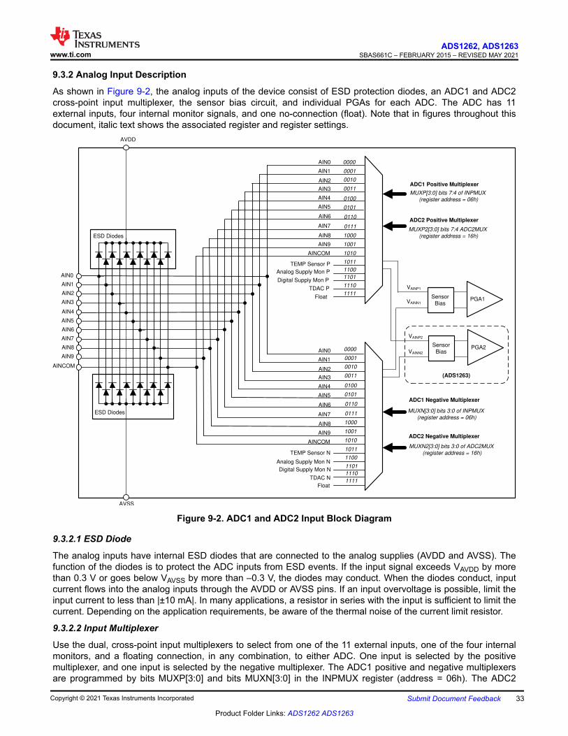
9.3.2 Analog Input Description
As shown in Figure 9-2, the analog inputs of the device consist of ESD protection diodes, an ADC1 and ADC2cross-point input multiplexer, the sensor bias circuit, and individual PGAs for each ADC. The ADC has 11external inputs, four internal monitor signals, and one no-connection (float). Note that in figures throughout thisdocument, italic text shows the associated register and register settings.
AIN0
TEMP Sensor P
AVSS
AIN1
AIN2
AIN3
AIN4
AIN5
AIN6
AIN7
AIN8
AIN9
AVDD
AINCOM
ESD Diodes
ESD Diodes
0000
0001
0010
0011
0100
0101
0110
0111
1000
1001
1010
ADC1 Positive Multiplexer
Analog Supply Mon P
Digital Supply Mon P
TDAC P
Float
TEMP Sensor N
Analog Supply Mon N
Digital Supply Mon N
TDAC N
Float
0000
0001
0010
0011
0100
0101
0110
0111
1000
1001
1010
1011
1100
1101
1110
1111
1011
1100
1101
1110
1111
VAINP1
VAINN1PGA1Sensor
Bias
AIN0
AIN1
AIN2
AIN3
AIN4
AIN5
AIN6
AIN7
AIN8
AIN9
AINCOM
AIN0
AIN1
AIN2
AIN3
AIN4
AIN5
AIN6
AIN7
AIN8
AIN9
AINCOM
MUXP[3:0] bits 7:4 of INPMUX
(register address = 06h)
MUXN2[3:0] bits 3:0 of ADC2MUX
(register address = 16h)
MUXP2[3:0] bits 7:4 ADC2MUX
(register address = 16h)
MUXN[3:0] bits 3:0 of INPMUX
(register address = 06h)
PGA2Sensor
Bias
VAINP2
VAINN2
(ADS1263)
ADC2 Positive Multiplexer
ADC1 Negative Multiplexer
ADC2 Negative Multiplexer
Figure 9-2. ADC1 and ADC2 Input Block Diagram
9.3.2.1 ESD Diode
The analog inputs have internal ESD diodes that are connected to the analog supplies (AVDD and AVSS). Thefunction of the diodes is to protect the ADC inputs from ESD events. If the input signal exceeds VAVDD by morethan 0.3 V or goes below VAVSS by more than –0.3 V, the diodes may conduct. When the diodes conduct, inputcurrent flows into the analog inputs through the AVDD or AVSS pins. If an input overvoltage is possible, limit theinput current to less than |±10 mA|. In many applications, a resistor in series with the input is sufficient to limit thecurrent. Depending on the application requirements, be aware of the thermal noise of the current limit resistor.
9.3.2.2 Input Multiplexer
Use the dual, cross-point input multiplexers to select from one of the 11 external inputs, one of the four internalmonitors, and a floating connection, in any combination, to either ADC. One input is selected by the positivemultiplexer, and one input is selected by the negative multiplexer. The ADC1 positive and negative multiplexersare programmed by bits MUXP[3:0] and bits MUXN[3:0] in the INPMUX register (address = 06h). The ADC2
www.ti.comADS1262, ADS1263
SBAS661C – FEBRUARY 2015 – REVISED MAY 2021
Copyright © 2021 Texas Instruments Incorporated Submit Document Feedback 33
Product Folder Links: ADS1262 ADS1263
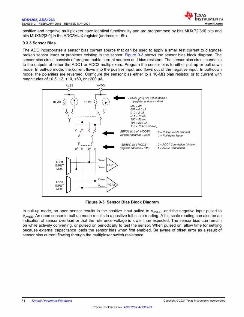
positive and negative multiplexers have identical functionality and are programmed by bits MUXP2[3:0] bits andbits MUXN2[3:0] in the ADC2MUX register (address = 16h).
9.3.3 Sensor Bias
The ADC incorporates a sensor bias current source that can be used to apply a small test current to diagnosebroken sensor leads or problems existing in the sensor. Figure 9-3 shows the sensor bias block diagram. Thesensor bias circuit consists of programmable current sources and bias resistors. The sensor bias circuit connectsto the outputs of either the ADC1 or ADC2 multiplexers. Program the sensor bias to either pull-up or pull-downmode. In pull-up mode, the current flows into the positive input and flows out of the negative input. In pull-downmode, the polarities are reversed. Configure the sensor bias either to a 10-MΩ bias resistor, or to current withmagnitudes of ±0.5, ±2, ±10, ±50, or ±200 µA.
SBMAG[2:0] bits 2:0 of MODE1
(register address = 04h)
ADC1
INPUT
MUX
10 M�
AVDD
000 = off
001 = 0.5 uA
010 = 2 uA
011 = 10 uA
100 = 50 uA
101 = 200 uA
110 = 10 0��(shown)
PGA1
ADC2
INPUT
MUX
PGA2
10 M�
AVSS
SBPOL bit 3 of MODE1
(register address = 04h)0 = Pull-up mode (shown)
1 = Pull-down Mode
SBADC bit 4 MODE1
(register address = 04h)
0 = ADC1 Connection (shown)
1 = ADC2 Connection
VAINP1
VAINN1
VAINN2
VAINP2
Figure 9-3. Sensor Bias Block Diagram
In pull-up mode, an open sensor results in the positive input pulled to VAVDD, and the negative input pulled toVAVSS. An open sensor in pull-up mode results in a positive full-scale reading. A full-scale reading can also be anindication of sensor overload or that the reference voltage is lower than expected. The sensor bias can remainon while actively converting, or pulsed on periodically to test the sensor. When pulsed on, allow time for settlingbecause external capacitance loads the sensor bias when first enabled. Be aware of offset error as a result ofsensor bias current flowing through the multiplexer switch resistance.
ADS1262, ADS1263SBAS661C – FEBRUARY 2015 – REVISED MAY 2021 www.ti.com
34 Submit Document Feedback Copyright © 2021 Texas Instruments Incorporated
Product Folder Links: ADS1262 ADS1263
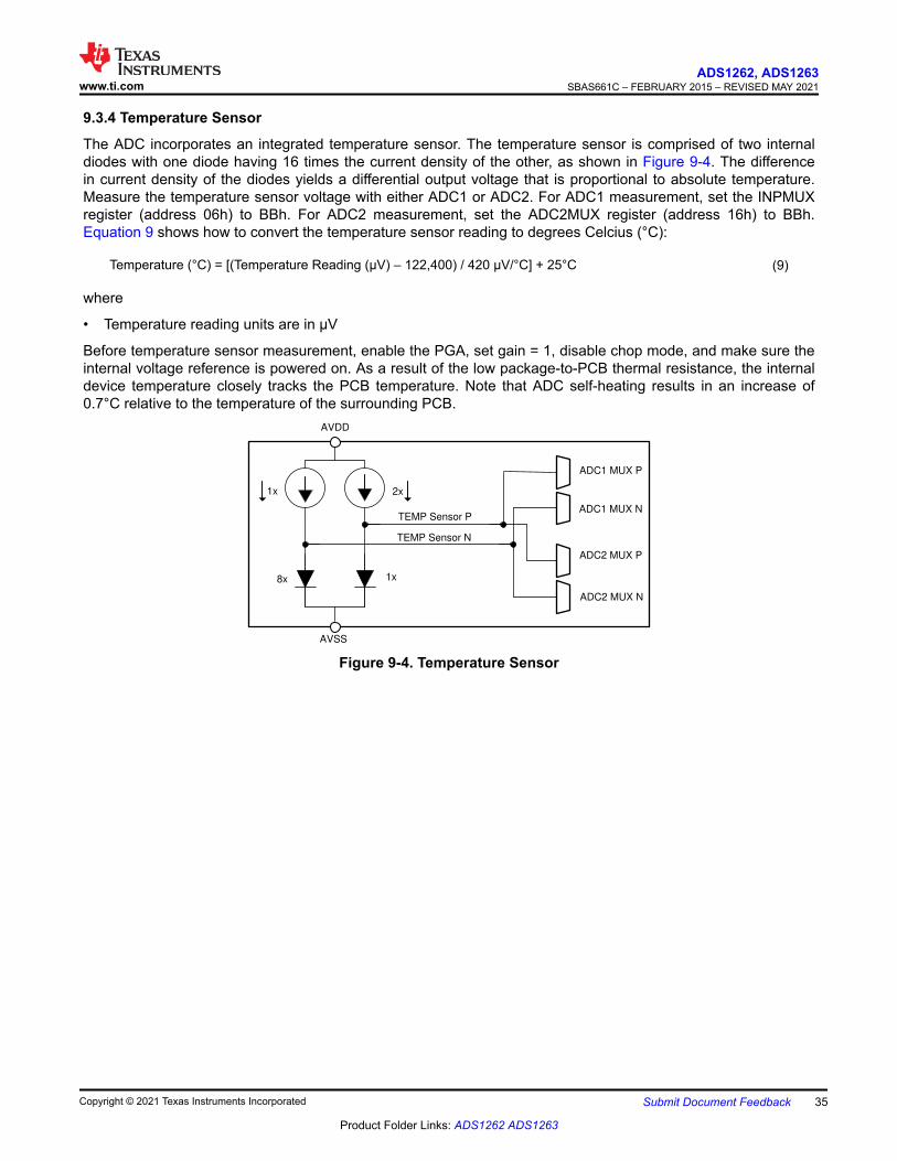
9.3.4 Temperature Sensor
The ADC incorporates an integrated temperature sensor. The temperature sensor is comprised of two internaldiodes with one diode having 16 times the current density of the other, as shown in Figure 9-4. The differencein current density of the diodes yields a differential output voltage that is proportional to absolute temperature.Measure the temperature sensor voltage with either ADC1 or ADC2. For ADC1 measurement, set the INPMUXregister (address 06h) to BBh. For ADC2 measurement, set the ADC2MUX register (address 16h) to BBh.Equation 9 shows how to convert the temperature sensor reading to degrees Celcius (°C):
Temperature (°C) = [(Temperature Reading (µV) – 122,400) / 420 µV/°C] + 25°C (9)
where
• Temperature reading units are in µV
Before temperature sensor measurement, enable the PGA, set gain = 1, disable chop mode, and make sure theinternal voltage reference is powered on. As a result of the low package-to-PCB thermal resistance, the internaldevice temperature closely tracks the PCB temperature. Note that ADC self-heating results in an increase of0.7°C relative to the temperature of the surrounding PCB.
1x 2x
8x 1x
AVDD
AVSS
ADC1 MUX P
TEMP Sensor P
TEMP Sensor N
ADC1 MUX N
ADC2 MUX P
ADC2 MUX N
Figure 9-4. Temperature Sensor
www.ti.comADS1262, ADS1263
SBAS661C – FEBRUARY 2015 – REVISED MAY 2021
Copyright © 2021 Texas Instruments Incorporated Submit Document Feedback 35
Product Folder Links: ADS1262 ADS1263
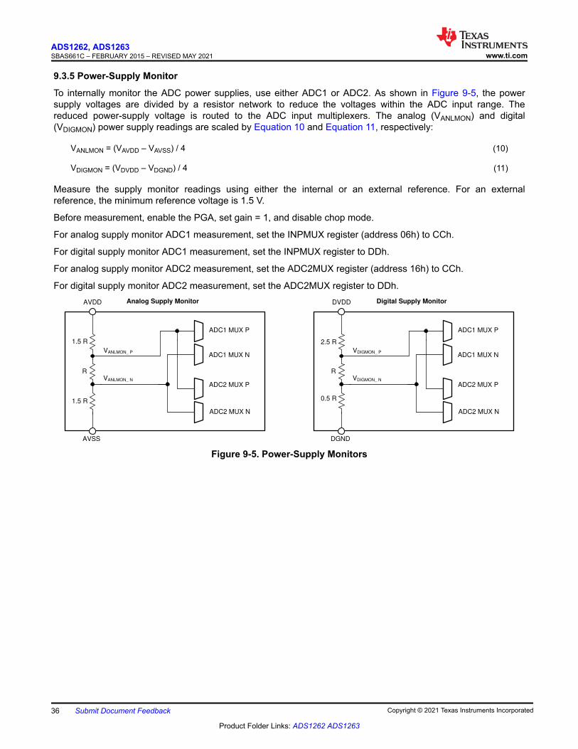
9.3.5 Power-Supply Monitor
To internally monitor the ADC power supplies, use either ADC1 or ADC2. As shown in Figure 9-5, the powersupply voltages are divided by a resistor network to reduce the voltages within the ADC input range. Thereduced power-supply voltage is routed to the ADC input multiplexers. The analog (VANLMON) and digital(VDIGMON) power supply readings are scaled by Equation 10 and Equation 11, respectively:
VANLMON = (VAVDD – VAVSS) / 4 (10)
VDIGMON = (VDVDD – VDGND) / 4 (11)
Measure the supply monitor readings using either the internal or an external reference. For an externalreference, the minimum reference voltage is 1.5 V.
Before measurement, enable the PGA, set gain = 1, and disable chop mode.
For analog supply monitor ADC1 measurement, set the INPMUX register (address 06h) to CCh.
For digital supply monitor ADC1 measurement, set the INPMUX register to DDh.
For analog supply monitor ADC2 measurement, set the ADC2MUX register (address 16h) to CCh.
For digital supply monitor ADC2 measurement, set the ADC2MUX register to DDh.AVDD
AVSS
ADC1 MUX P
ADC1 MUX N
ADC2 MUX P
ADC2 MUX N
1.5 R
1.5 R
R
Analog Supply Monitor
VANLMON_ N
VANLMON_ P
DVDD
DGND
ADC1 MUX P
ADC1 MUX N
ADC2 MUX P
ADC2 MUX N
2.5 R
0.5 R
R
Digital Supply Monitor
VDIGMON_ N
VDIGMON_ P
Figure 9-5. Power-Supply Monitors
ADS1262, ADS1263SBAS661C – FEBRUARY 2015 – REVISED MAY 2021 www.ti.com
36 Submit Document Feedback Copyright © 2021 Texas Instruments Incorporated
Product Folder Links: ADS1262 ADS1263
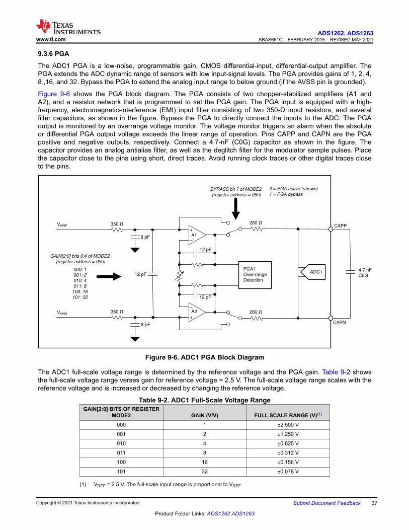
9.3.6 PGA
The ADC1 PGA is a low-noise, programmable gain, CMOS differential-input, differential-output amplifier. ThePGA extends the ADC dynamic range of sensors with low input-signal levels. The PGA provides gains of 1, 2, 4,8 ,16, and 32. Bypass the PGA to extend the analog input range to below ground (if the AVSS pin is grounded).
Figure 9-6 shows the PGA block diagram. The PGA consists of two chopper-stabilized amplifiers (A1 andA2), and a resistor network that is programmed to set the PGA gain. The PGA input is equipped with a high-frequency, electromagnetic-interference (EMI) input filter consisting of two 350-Ω input resistors, and severalfilter capacitors, as shown in the figure. Bypass the PGA to directly connect the inputs to the ADC. The PGAoutput is monitored by an overrange voltage monitor. The voltage monitor triggers an alarm when the absoluteor differential PGA output voltage exceeds the linear range of operation. Pins CAPP and CAPN are the PGApositive and negative outputs, respectively. Connect a 4.7-nF (C0G) capacitor as shown in the figure. Thecapacitor provides an analog antialias filter, as well as the deglitch filter for the modulator sample pulses. Placethe capacitor close to the pins using short, direct traces. Avoid running clock traces or other digital traces closeto the pins.
CAPP
000: 1
001: 2
010: 4
011: 8
100: 16
101: 32
+
±
12 pF
+
±
12 pF
VAINP
VAINN
ADC1
CAPN
280 �
280 �
GAIN[2:0] bits 6:4 of MODE2
(register address = 05h)
PGA1
Over-range
Detection
BYPASS bit 7 of MODE2
(register address = 05h)
350 �
350 �
8 pF
8 pF
12 pF
A1
A2
0 = PGA active (shown)
1 = PGA bypass
4.7 nF
C0G
Figure 9-6. ADC1 PGA Block Diagram
The ADC1 full-scale voltage range is determined by the reference voltage and the PGA gain. Table 9-2 showsthe full-scale voltage range verses gain for reference voltage = 2.5 V. The full-scale voltage range scales with thereference voltage and is increased or decreased by changing the reference voltage.
Table 9-2. ADC1 Full-Scale Voltage RangeGAIN[2:0] BITS OF REGISTER
MODE2 GAIN (V/V) FULL SCALE RANGE (V)(1)
000 1 ±2.500 V
001 2 ±1.250 V
010 4 ±0.625 V
011 8 ±0.312 V
100 16 ±0.156 V
101 32 ±0.078 V
(1) VREF = 2.5 V. The full-scale input range is proportional to VREF
www.ti.comADS1262, ADS1263
SBAS661C – FEBRUARY 2015 – REVISED MAY 2021
Copyright © 2021 Texas Instruments Incorporated Submit Document Feedback 37
Product Folder Links: ADS1262 ADS1263
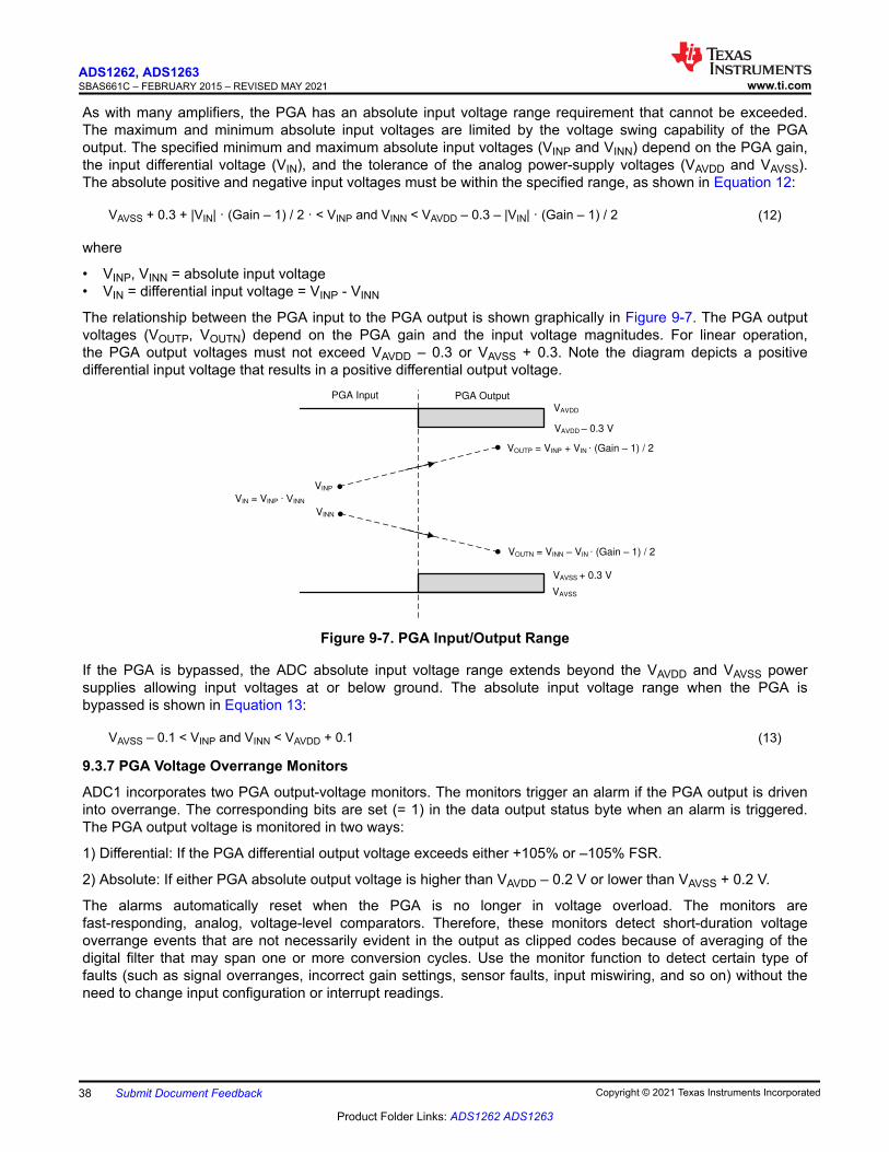
As with many amplifiers, the PGA has an absolute input voltage range requirement that cannot be exceeded.The maximum and minimum absolute input voltages are limited by the voltage swing capability of the PGAoutput. The specified minimum and maximum absolute input voltages (VINP and VINN) depend on the PGA gain,the input differential voltage (VIN), and the tolerance of the analog power-supply voltages (VAVDD and VAVSS).The absolute positive and negative input voltages must be within the specified range, as shown in Equation 12:
VAVSS + 0.3 + |VIN| · (Gain – 1) / 2 · < VINP and VINN < VAVDD – 0.3 – |VIN| · (Gain – 1) / 2 (12)
where
• VINP, VINN = absolute input voltage• VIN = differential input voltage = VINP - VINN
The relationship between the PGA input to the PGA output is shown graphically in Figure 9-7. The PGA outputvoltages (VOUTP, VOUTN) depend on the PGA gain and the input voltage magnitudes. For linear operation,the PGA output voltages must not exceed VAVDD – 0.3 or VAVSS + 0.3. Note the diagram depicts a positivedifferential input voltage that results in a positive differential output voltage.
VAVSS
VAVDD ± 0.3 V
VAVSS + 0.3 V
VOUTP = VINP + VIN Â�(Gain ± 1) / 2
VOUTN = VINN ± VIN Â�(Gain ± 1) / 2
VINN
VINP
VIN = VINP �9INN
PGA Input PGA OutputVAVDD
Figure 9-7. PGA Input/Output Range
If the PGA is bypassed, the ADC absolute input voltage range extends beyond the VAVDD and VAVSS powersupplies allowing input voltages at or below ground. The absolute input voltage range when the PGA isbypassed is shown in Equation 13:
VAVSS – 0.1 < VINP and VINN < VAVDD + 0.1 (13)
9.3.7 PGA Voltage Overrange Monitors
ADC1 incorporates two PGA output-voltage monitors. The monitors trigger an alarm if the PGA output is driveninto overrange. The corresponding bits are set (= 1) in the data output status byte when an alarm is triggered.The PGA output voltage is monitored in two ways:
1) Differential: If the PGA differential output voltage exceeds either +105% or –105% FSR.
2) Absolute: If either PGA absolute output voltage is higher than VAVDD – 0.2 V or lower than VAVSS + 0.2 V.
The alarms automatically reset when the PGA is no longer in voltage overload. The monitors arefast-responding, analog, voltage-level comparators. Therefore, these monitors detect short-duration voltageoverrange events that are not necessarily evident in the output as clipped codes because of averaging of thedigital filter that may span one or more conversion cycles. Use the monitor function to detect certain type offaults (such as signal overranges, incorrect gain settings, sensor faults, input miswiring, and so on) without theneed to change input configuration or interrupt readings.
ADS1262, ADS1263SBAS661C – FEBRUARY 2015 – REVISED MAY 2021 www.ti.com
38 Submit Document Feedback Copyright © 2021 Texas Instruments Incorporated
Product Folder Links: ADS1262 ADS1263
9.3.7.1 PGA Differential Output Monitor
ADC1 incorporates a differential PGA output voltage monitor. This voltage monitor triggers an alarm when themagnitude of the differential PGA output voltage is more positive than +105% or more negative than –105%of full scale, but only during a conversion cycle. The alarm event, corresponding to the conversion cycle whenthe alarm occurred, is set in the status byte (PGAD_ALM). For the next conversion, the alarm resets. If themagnitude of differential output voltage is within the range of ±105% of full-scale range, the alarm remains reset.The PGA differential monitor block diagram is shown in Figure 9-8.
+105% VREF
VOUTP
VOUTN
S Q
QR
+
±
+
±
ADC
PGA ADCDigital
Filter
+
±
-105% VREF Conversion
Start Reset
STATUS DATA 1 DATA 2 DATA 3 DATA 4
PGAD_ALM
Bit 1 of STATUS byte
Latch
VREF Comparators
PGA Output
difference amplifier
Data Bytes
CRC/CHK
Figure 9-8. PGA Differential Overload Monitor
Figure 9-9 shows an example of the differential overrange monitor event.
Conversions (DRDY)
PG
A D
iffe
ren
tia
l O
utp
ut (F
SR
)
+ 105%
PGAD_ALM bit
Alarms latched during
conversion cycle
- 105%
Figure 9-9. PGA Differential Alarm
www.ti.comADS1262, ADS1263
SBAS661C – FEBRUARY 2015 – REVISED MAY 2021
Copyright © 2021 Texas Instruments Incorporated Submit Document Feedback 39
Product Folder Links: ADS1262 ADS1263
9.3.7.2 PGA Absolute Output-Voltage Monitor
ADC1 contains an integrated a PGA absolute output-voltage monitor. If the absolute level of the PGA positive ornegative output exceeds VAVDD – 0.2 V, the PGA high alarm triggers (PGAH_ALM). If the absolute level of thePGA positive or negative output voltage is less than VAVSS + 0.2 V, the PGA low alarm triggers (PGAL_ALM).The alarms are set in the status byte corresponding to the conversion cycle when the alarms occurred. Forthe next conversion cycle, the alarms reset. If the magnitude of PGA output voltages remains within the range(VAVDD – 0.2 V and VAVSS + 0.2 V), the alarms remain reset. The PGA absolute output-voltage monitor blockdiagram is shown in Figure 9-10.
VAVDD ± 0.2 V
VOUTP
VOUTN
S Q
QR
+
±
ADC
PGA ADCDigital
Filter
VAVSS + 0.2 V
STATUS DATA 1 DATA 2 DATA 3 DATA 4
PGAH_ALM
Bit 2 of STATUS byte
Latch
Supply Rail
Comparators
Data Bytes
CRC/CHK
S Q
QR
+
±
+
±
Conversion
Start Reset
PGAL_ALM
Bit 3 of STATUS byte
Latch
+
±
Figure 9-10. PGA Absolute Output-Voltage Monitor
Figure 9-11 shows an example of the PGA absolute output-voltage monitor overrange event.
Conversions (DRDY)
PG
A A
bso
lute
Ou
tpu
t (V
)
VAVDD - 0.2
PGAH_ALM bit
Alarms latched during
conversion cycle
VAVSS + 0.2
PGAL_ALM bit
VO
UT
P o
r V
OU
TN
Figure 9-11. PGA Absolute Alarm
ADS1262, ADS1263SBAS661C – FEBRUARY 2015 – REVISED MAY 2021 www.ti.com
40 Submit Document Feedback Copyright © 2021 Texas Instruments Incorporated
Product Folder Links: ADS1262 ADS1263
9.3.8 ADC Reference Voltage
These devices require a reference voltage for operation. Both ADCs default to the same internal reference,however, the reference voltage of ADC1 is independent of the ADC2 reference voltage. The reference voltageis provided internally by the internal 2.5-V reference, or externally, by one of the three external reference inputs.The specified external reference voltage range is 0.9 V to 5 V. The reference voltage is defined as VREF =VREFP – VREFN, where VREFP and VREFN are the absolute positive and absolute negative reference voltages,respectively. The polarity of the reference voltage internal to the ADC must be always positive. The magnitudeof the reference voltage together with the PGA gain establishes the ADC full-scale differential input range asdefined by VIN = ±VREF / gain. Figure 9-12 shows the block diagram of the ADC1 reference multiplexer. Use thereference multiplexer to select the internal reference, one of three external reference inputs, or the analog powersupply.
AIN0
AIN2
AIN4
AIN1
AIN3
AIN5
AVSS
REFOUT REFREV b it 7 of MODE0
(register address = 03h)
1 PF1 PF
+2.5 V
Reference
+2.5 V
ReferenceAVDD
RMUXN[2:0] bits 2:0 of REFMUX
(register address = 0Fh)
RMUXP[2:0] b its 5:3 of REFMUX
(register address = 0Fh)
INTREF bi t 0 of POWER
(reg ister address = 01h)
ADC1
VVREFP
VVREFN
S Q
QR
+0.4 V
Start Conversion Reset
REF_ALM bit of status byte
(bit 4)Low Reference
Monitor(A)REF_MUXP
REF_MUXN
000
001
010
011
100
001
010
011
100
000
0 = normal
1 = reverse
0 = no alarm
1 = alarm
0 = reference off
1 = reference on
+
±
+
±
+
±
A. The internal reference requires a 1-µF capacitor connected to pins REFOUT and AVSS.
Figure 9-12. ADC1 Reference Multiplexer Block Diagram
The ADC1 reference multiplexer consists of a positive multiplexer and a negative multiplexer. The positive andnegative multiplexers are programmed by the RMUXP[2:0] and RMUXN[2:0] bits, respectively, of the REFMUXregister. The positive reference input is either internal (2.5 V), external (pins AIN0, AIN2, AIN4), or the analogpower-supply voltage (VAVDD). The negative reference input is either internal (2.5 V), external (pins AIN1, AIN3,AIN5), or the analog power-supply voltage (VAVSS). A reference polarity-reversal switch changes the referencepolarity from negative to positive. The polarity switch allows either positive or negative external referencepolarity. Set the reversal switch to the normal position (REFREV = 0) when using the internal reference or analogpower supplies.
The ADC also contains and integrated low-reference voltage monitor. This monitor provides continuous detectionof a low or missing reference during the conversion cycle. The low reference alarm is appended to the dataoutput status byte (REF_ALM, bit 4 of the status byte).
www.ti.comADS1262, ADS1263
SBAS661C – FEBRUARY 2015 – REVISED MAY 2021
Copyright © 2021 Texas Instruments Incorporated Submit Document Feedback 41
Product Folder Links: ADS1262 ADS1263
9.3.8.1 Internal Reference
The ADC incorporates an integrated, precision, 2.5-V reference featuring very low drift. The internal referenceis enabled by setting INTREF equal to 1 (default is on). To select the internal reference for use with ADC1, setthe RMUXP and RMUXN bits of register REFMUX to 0h. The REFOUT pin provides a buffered reference outputvoltage. The negative reference (return) is the AVSS pin, as shown in Figure 9-12. Be careful when laying outthe REFOUT return to the AVSS pin. Connect a 1-uF capacitor from the REFOUT pin to the AVSS pin. Thecapacitor can be increased up to 10 μF (maximum) to decrease the reference noise, but results in increasedreference start-up time. The capacitor is not required if the internal reference is not used. The internal referencemust be powered if using the IDACs or the internal temperature sensor. After internal reference start-up, thereference requires start-up time before beginning the first conversion; see Figure 7-33.
9.3.8.2 External Reference
The ADC provides three external reference inputs. The reference inputs are differential with independent positiveand negative inputs. The reference inputs are the analog pins, AIN0 to AIN5. Typically, the positive referenceis applied to pin AIN0, AIN2, or AIN4, and the negative reference is applied to pin AIN1, AIN2, or AIN3. Thereference polarity can be negative, but the ADC requires a positive voltage reference. In this case, reverse thepolarity using the internal polarity-reversal switch (ADC1 reference only). The reference polarity-reversal switchchanges the reference polarity from negative to positive, and is controlled by REFREV (bit 7 of MODE0).
The reference inputs are high impedance. A reference input current flowing through a reference-voltage sourceimpedance leads to possible loading errors (see Figure 7-34). To reduce the input current, use an externalreference buffer; however, in most applications, an external reference buffer is not necessary.
Connect a 100-nF bypass capacitor across the external reference input pins. Follow the specified absolute anddifferential reference voltage requirements.
9.3.8.3 Power-Supply Reference
A third option for ADC reference is the internal analog power supply. However, an increase of linearity errorresults with this connection, and therefore, use this option only for less-critical applications, such as ADCself-diagnostics.
For critical applications, do not use the power-supply reference option. For applications that use the power-supply voltage as the reference voltage, connect the power-supply voltage to the external reference inputs,and select the appropriate external reference bits in the REFMUX register. For example, to measure a 6-wireload-cell, connect the bridge excitation voltages to the external reference inputs, and select the appropriateREFMUX bits.
9.3.8.4 Low-Reference Monitor
ADC1 incorporates a low-reference monitor to detect a low or missing reference. If the differential referencevoltage (VREF = VREFP – VREFN) falls below 0.4 V (typical), the low reference alarm triggers (REF_ALM). Thelow-reference monitor sets the corresponding alarm bit in the conversion data status byte. The alarm resets atthe start of each new conversion. Use the low-reference monitor to detect a missing or failed reference voltageconnection. Connect a 100-kΩ resistor across the reference inputs to provide the necessary bias. If eitherreference input is missing or unconnected, this external resistor biases the reference inputs to each other. Thelow-reference monitor is a fast-responding analog comparator; therefore, transients in the reference voltage maytrigger the alarm.
9.3.9 ADC1 Modulator
The ADC1 modulator is an inherently stable, fourth-order, 2 + 2 pipelined ΔΣ modulator. The modulator samplesthe analog input voltage at a high sample rate (fMOD = fCLK / 8 = 921.6 kHz) and converts the analog inputto a ones density bit stream. The digital filter receives the ones density bit stream output, and then filters anddecimates the data to yield the final conversion result.
ADS1262, ADS1263SBAS661C – FEBRUARY 2015 – REVISED MAY 2021 www.ti.com
42 Submit Document Feedback Copyright © 2021 Texas Instruments Incorporated
Product Folder Links: ADS1262 ADS1263
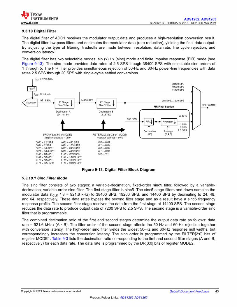
9.3.10 Digital Filter
The digital filter of ADC1 receives the modulator output data and produces a high-resolution conversion result.The digital filter low-pass filters and decimates the modulator data (rate reduction), yielding the final data output.By adjusting the type of filtering, tradeoffs are made between resolution, data rate, line cycle rejection, andconversion latency.
The digital filter has two selectable modes: sin (x) / x (sinc) mode and finite impulse response (FIR) mode (seeFigure 9-13). The sinc mode provides data rates of 2.5 SPS though 38400 SPS with selectable sinc orders of1 through 5. The FIR filter provides simultaneous rejection of 50-Hz and 60-Hz power-line frequencies with datarates 2.5 SPS through 20 SPS with single-cycle settled conversions.
1st Stage
Sinc5 Filter
Decimation A
(24, 48, 64)
2nd Stage
SincN Filter
Decimation B
(2...5760)
38400 SPS
19200 SPS
14400 SPS
921.6 kHz 2.5 SPS...7200 SPS
fCLK: 7.3728 MHz
fCLK/8
fMOD: 921.6 kHz
Modulator
FIR
14400 SPS
20 SPS
Averager
Average
(2,4,8)
Decimation
(30)
Filter OutputFIR Filter Section
600 SPS
10 SPS
5 SPS
2.5 SPS
FILTER[2:0] bits 7:5 of MODE1
(register address = 04h)
DR[3:0] bits 3:0 of MODE2
(register address = 05h)
000 = sinc1
001 = sinc2
010 = sinc3
011 = sinc4
100 = FIR
0000 = 2.5 SPS
0001 = 5 SPS
0010 = 10 SPS
0011 = 16.6 SPS
0100 = 20 SPS
0101 = 50 SPS
0110 = 60 SPS
0111 = 100 SPS
1000 = 400 SPS
1001 = 1200 SPS
1010 = 2400 SPS
1011 = 4800 SPS
1100 = 7200 SPS
1101 = 14400 SPS
1110 = 19200 SPS
1111 = 38400 SPS
Figure 9-13. Digital Filter Block Diagram
9.3.10.1 Sinc Filter Mode
The sinc filter consists of two stages: a variable-decimation, fixed-order sinc5 filter, followed by a variable-decimation, variable-order sinc filter. The first-stage filter is sinc5. The sinc5 stage filters and down-samples themodulator data (fCLK / 8 = 921.6 kHz) to 38400 SPS, 19200 SPS, and 14400 SPS by decimating to 24, 48,and 64, respectively. These data rates bypass the second filter stage and as a result have a sinc5 frequencyresponse profile. The second filter stage receives the data from the first stage at 14400 SPS. The second stagereduces the data rate to produce output data of 7200 SPS to 2.5 SPS. The second stage is a variable-order sincfilter that is programmable.
The combined decimation ratio of the first and second stages determine the output data rate as follows: datarate = 921.6 kHz / (A · B). The filter order of the second stage affects the 50-Hz and 60-Hz rejection togetherwith conversion latency. The high-order sinc filter yields the widest 50-Hz and 60-Hz response null widths, butcorrespondingly increases the conversion latency. The sinc order is programmed by the FILTER[2:0] bits ofregister MODE1. Table 9-3 lists the decimation ratio corresponding to the first and second filter stages (A and B,respectively) for each data rate. The data rate is programmed by the DR[3:0] bits of register MODE2.
www.ti.comADS1262, ADS1263
SBAS661C – FEBRUARY 2015 – REVISED MAY 2021
Copyright © 2021 Texas Instruments Incorporated Submit Document Feedback 43
Product Folder Links: ADS1262 ADS1263
Table 9-3. Sinc Filter Mode Data Rates and Decimation RatioDATA RATE
(SPS)(1)DR[3:0] BITS OF
REGISTER MODE2FIRST-STAGE
DECIMATION RATIO ASECOND-STAGE
DECIMATION RATIO B2.5 0000 64 5760
5 0001 64 2880
10 0010 64 1440
16.6 0011 64 864
20 0100 64 720
50 0101 64 288
60 0110 64 240
100 0111 64 144
400 1000 64 36
1200 1001 64 12
2400 1010 64 6
4800 1011 64 3
7200 1100 64 2
14400 1101 64 1
19200 1110 48 1
38400 1111 24 1
(1) fCLK = 7.3728 MHz. Data rate scales with fCLK
9.3.10.1.1 Sinc Filter Frequency Response
The low-pass filtering effect of the sinc filter sets the overall frequency response of the ADC. The frequencyresponse of data rates 14400 SPS, 19200 SPS and 38400 SPS is that of the first filter stage. The frequencyresponse of data rates 2.5 SPS ranging to 7200 SPS is the product of the first and second stage individualfrequency responses. The overall filter response is given in Equation 14:
� � � � � �
N
CLK
CLK
CLK
CLK
f
f
�I
f
�I
f
f
f
�I
ff
»¼
º«¬
ªu
»¼
º«¬
ª
u
»¼
º«¬
ªu
»¼
º«¬
ª
u 512
sinB
B512sin
�8sinA
A8sin
HHH
5
sincsincN5
(14)
where
• f = signal frequency• fCLK = ADC clock frequency• A = First-stage decimation ratio (see Table 9-3)• B = Second-stage decimation ratio (see Table 9-3)• N = Second-stage filter order where N = 1 (sinc1), 2 (sinc2), 3 (sinc3), or 4 (sinc4)
The digital filter attenuates out-of-band noise that is present in the signal, and noise within the PGA and ADCmodulator. Adjusting the filter by changing the decimation ratio and sinc order changes the filter bandwidth.Tradeoffs are made between signal bandwidth, noise, and filter latency.
ADS1262, ADS1263SBAS661C – FEBRUARY 2015 – REVISED MAY 2021 www.ti.com
44 Submit Document Feedback Copyright © 2021 Texas Instruments Incorporated
Product Folder Links: ADS1262 ADS1263

As shown in Figure 9-14 and Figure 9-15, the first-stage sinc5 filter has frequency response nulls occurring atthe data rate (fMOD / A) and at data rate multiples. At the null frequencies, the filter has zero gain.
Frequency (kHz)
Am
plit
ude (
dB
)
0 10 20 30 40 50 60 70 80 90 100 110 120-160
-140
-120
-100
-80
-60
-40
-20
0
D001
Figure 9-14. Sinc Frequency Response(38400 SPS)
Frequency (kHz)
Am
plit
ude (
dB
)
0 10 20 30 40 50 60 70 80 90 100 110 120-160
-140
-120
-100
-80
-60
-40
-20
0
D002
Figure 9-15. Sinc Frequency Response(14400 SPS)
The second stage superimposes new nulls in the frequency response over the nulls produced by the first stage.The first of the superimposed frequency response nulls occur at the output data rate, followed by nulls occurringat data rate multiples.
Figure 9-16 illustrates the frequency response of data rate 2400 SPS produced by the combined filter stages.This data rate has five equally-spaced nulls between the larger nulls produced by the first stage. The frequencyresponse is also characteristic of data rates 2.5 SPS to 7200 SPS that are also produced by the second-stagefilter. Figure 9-17 shows the frequency response nulls for 10 SPS.
Frequency (kHz)
Am
plit
ude (
dB
)
0 5 10 15 20 25 30 35 40 45-160
-140
-120
-100
-80
-60
-40
-20
0
D003
sinc1sinc2sinc3sinc4
Figure 9-16. Sinc Frequency Response (2400 SPS)Frequency (Hz)
Am
plit
ude (
dB
)
0 10 20 30 40 50 60 70 80 90 100 110 120-160
-140
-120
-100
-80
-60
-40
-20
0
D004
sinc1sinc2sinc3sinc4
Figure 9-17. Sinc Frequency Response (10 SPS)
www.ti.comADS1262, ADS1263
SBAS661C – FEBRUARY 2015 – REVISED MAY 2021
Copyright © 2021 Texas Instruments Incorporated Submit Document Feedback 45
Product Folder Links: ADS1262 ADS1263
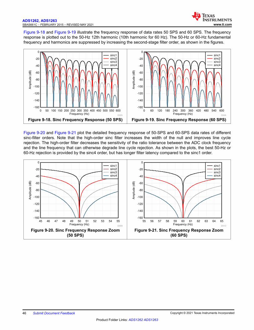
Figure 9-18 and Figure 9-19 illustrate the frequency response of data rates 50 SPS and 60 SPS. The frequencyresponse is plotted out to the 50-Hz 12th harmonic (10th harmonic for 60 Hz). The 50-Hz or 60-Hz fundamentalfrequency and harmonics are suppressed by increasing the second-stage filter order, as shown in the figures.
Frequency (Hz)
Am
plit
ude (
dB
)
0 50 100 150 200 250 300 350 400 450 500 550 600-160
-140
-120
-100
-80
-60
-40
-20
0
D005
sinc1sinc2sinc3sinc4
Figure 9-18. Sinc Frequency Response (50 SPS)Frequency (Hz)
Am
plit
ude (
dB
)
0 60 120 180 240 300 360 420 480 540 600-160
-140
-120
-100
-80
-60
-40
-20
0
D006
sinc1sinc2sinc3sinc4
Figure 9-19. Sinc Frequency Response (60 SPS)
Figure 9-20 and Figure 9-21 plot the detailed frequency response of 50-SPS and 60-SPS data rates of differentsinc-filter orders. Note that the high-order sinc filter increases the width of the null and improves line cyclerejection. The high-order filter decreases the sensitivity of the ratio tolerance between the ADC clock frequencyand the line frequency that can otherwise degrade line cycle rejection. As shown in the plots, the best 50-Hz or60-Hz rejection is provided by the sinc4 order, but has longer filter latency compared to the sinc1 order.
Frequency (Hz)
Am
plit
ude (
dB
)
45 46 47 48 49 50 51 52 53 54 55-160
-140
-120
-100
-80
-60
-40
-20
0
D009
sinc1sinc2sinc3sinc4
Figure 9-20. Sinc Frequency Response Zoom(50 SPS)
Frequency (Hz)
Am
pliu
de (
dB
)
55 56 57 58 59 60 61 62 63 64 65-160
-140
-120
-100
-80
-60
-40
-20
0
D010
sinc1sinc2sinc3sinc4
Figure 9-21. Sinc Frequency Response Zoom(60 SPS)
ADS1262, ADS1263SBAS661C – FEBRUARY 2015 – REVISED MAY 2021 www.ti.com
46 Submit Document Feedback Copyright © 2021 Texas Instruments Incorporated
Product Folder Links: ADS1262 ADS1263
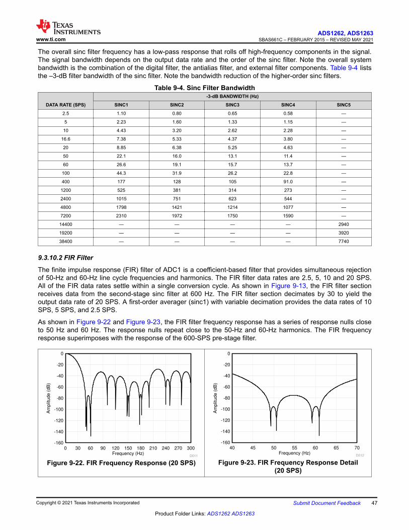
The overall sinc filter frequency has a low-pass response that rolls off high-frequency components in the signal.The signal bandwidth depends on the output data rate and the order of the sinc filter. Note the overall systembandwidth is the combination of the digital filter, the antialias filter, and external filter components. Table 9-4 liststhe –3-dB filter bandwidth of the sinc filter. Note the bandwidth reduction of the higher-order sinc filters.
Table 9-4. Sinc Filter Bandwidth
DATA RATE (SPS)
-3-dB BANDWIDTH (Hz)
SINC1 SINC2 SINC3 SINC4 SINC5
2.5 1.10 0.80 0.65 0.58 —
5 2.23 1.60 1.33 1.15 —
10 4.43 3.20 2.62 2.28 —
16.6 7.38 5.33 4.37 3.80 —
20 8.85 6.38 5.25 4.63 —
50 22.1 16.0 13.1 11.4 —
60 26.6 19.1 15.7 13.7 —
100 44.3 31.9 26.2 22.8 —
400 177 128 105 91.0 —
1200 525 381 314 273 —
2400 1015 751 623 544 —
4800 1798 1421 1214 1077 —
7200 2310 1972 1750 1590 —
14400 — — — — 2940
19200 — — — — 3920
38400 — — — — 7740
9.3.10.2 FIR Filter
The finite impulse response (FIR) filter of ADC1 is a coefficient-based filter that provides simultaneous rejectionof 50-Hz and 60-Hz line cycle frequencies and harmonics. The FIR filter data rates are 2.5, 5, 10 and 20 SPS.All of the FIR data rates settle within a single conversion cycle. As shown in Figure 9-13, the FIR filter sectionreceives data from the second-stage sinc filter at 600 Hz. The FIR filter section decimates by 30 to yield theoutput data rate of 20 SPS. A first-order averager (sinc1) with variable decimation provides the data rates of 10SPS, 5 SPS, and 2.5 SPS.
As shown in Figure 9-22 and Figure 9-23, the FIR filter frequency response has a series of response nulls closeto 50 Hz and 60 Hz. The response nulls repeat close to the 50-Hz and 60-Hz harmonics. The FIR frequencyresponse superimposes with the response of the 600-SPS pre-stage filter.
Frequency (Hz)
Am
plit
ude (
dB
)
0 30 60 90 120 150 180 210 240 270 300-160
-140
-120
-100
-80
-60
-40
-20
0
D011
Figure 9-22. FIR Frequency Response (20 SPS)Frequency (Hz)
Am
plit
ude (
dB
)
40 45 50 55 60 65 70-160
-140
-120
-100
-80
-60
-40
-20
0
D012
Figure 9-23. FIR Frequency Response Detail(20 SPS)
www.ti.comADS1262, ADS1263
SBAS661C – FEBRUARY 2015 – REVISED MAY 2021
Copyright © 2021 Texas Instruments Incorporated Submit Document Feedback 47
Product Folder Links: ADS1262 ADS1263
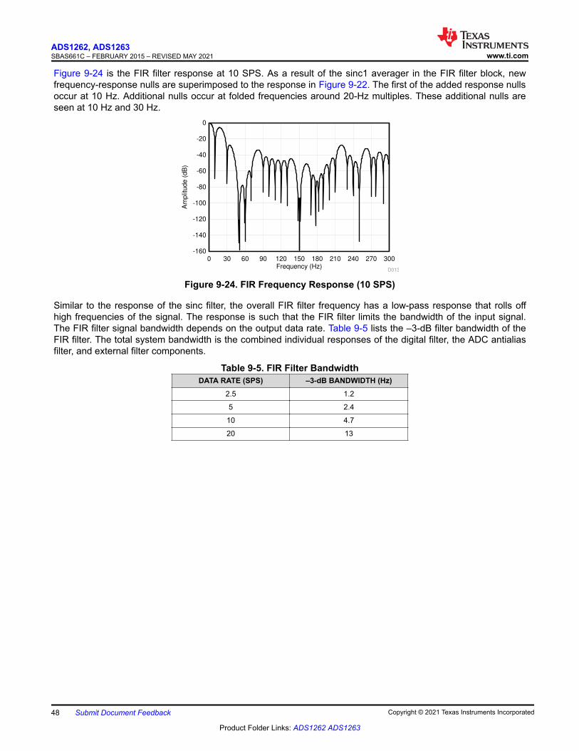
Figure 9-24 is the FIR filter response at 10 SPS. As a result of the sinc1 averager in the FIR filter block, newfrequency-response nulls are superimposed to the response in Figure 9-22. The first of the added response nullsoccur at 10 Hz. Additional nulls occur at folded frequencies around 20-Hz multiples. These additional nulls areseen at 10 Hz and 30 Hz.
Frequency (Hz)
Am
plit
ude (
dB
)
0 30 60 90 120 150 180 210 240 270 300-160
-140
-120
-100
-80
-60
-40
-20
0
D013
Figure 9-24. FIR Frequency Response (10 SPS)
Similar to the response of the sinc filter, the overall FIR filter frequency has a low-pass response that rolls offhigh frequencies of the signal. The response is such that the FIR filter limits the bandwidth of the input signal.The FIR filter signal bandwidth depends on the output data rate. Table 9-5 lists the –3-dB filter bandwidth of theFIR filter. The total system bandwidth is the combined individual responses of the digital filter, the ADC antialiasfilter, and external filter components.
Table 9-5. FIR Filter BandwidthDATA RATE (SPS) –3-dB BANDWIDTH (Hz)
2.5 1.2
5 2.4
10 4.7
20 13
ADS1262, ADS1263SBAS661C – FEBRUARY 2015 – REVISED MAY 2021 www.ti.com
48 Submit Document Feedback Copyright © 2021 Texas Instruments Incorporated
Product Folder Links: ADS1262 ADS1263
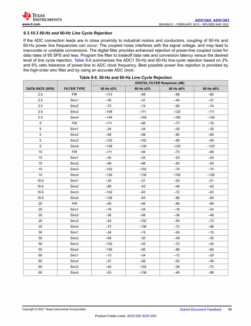
9.3.10.3 50-Hz and 60-Hz Line Cycle Rejection
If the ADC connection leads are in close proximity to industrial motors and conductors, coupling of 50-Hz and60-Hz power line frequencies can occur. The coupled noise interferes with the signal voltage, and may lead toinaccurate or unstable conversions. The digital filter provides enhanced rejection of power-line coupled noise fordata rates of 60 SPS and less. Program the filter to tradeoff data rate and conversion latency versus the desiredlevel of line cycle rejection. Table 9-6 summarizes the ADC1 50-Hz and 60-Hz line-cycle rejection based on 2%and 6% ratio tolerance of power-line to ADC clock frequency. Best possible power line rejection is provided bythe high-order sinc filter and by using an accurate ADC clock.
Table 9-6. 50-Hz and 60-Hz Line Cycle Rejection
DATA RATE (SPS) FILTER TYPEDIGITAL FILTER Response (dB)
50 Hz ±2% 60 Hz ±2% 50 Hz ±6% 60 Hz ±6%2.5 FIR –113 –99 –88 –80
2.5 Sinc1 –36 –37 –40 –37
2.5 Sinc2 –72 –74 –80 –74
2.5 Sinc3 –108 –111 –120 –111
2.5 Sinc4 –144 –148 –160 –148
5 FIR –111 –95 –77 –76
5 Sinc1 –34 –34 –30 –30
5 Sinc2 –68 –68 –60 –60
5 Sinc3 –102 –102 –90 –90
5 Sinc4 –136 –136 –120 –120
10 FIR –111 –94 –73 –68
10 Sinc1 –34 –34 –25 –25
10 Sinc2 –68 –68 –50 –50
10 Sinc3 –102 –102 –75 –75
10 Sinc4 –136 –136 –100 –100
16.6 Sinc1 –34 –21 –24 –21
16.6 Sinc2 –68 –42 –48 –42
16.6 Sinc3 –102 –63 –72 –63
16.6 Sinc4 –136 –84 –96 –84
20 FIR –95 –94 –66 –66
20 Sinc1 –18 –34 –18 –24
20 Sinc2 –36 –68 –36 –48
20 Sinc3 –54 –102 –54 –72
20 Sinc4 –72 –136 –72 –96
50 Sinc1 –34 –15 –24 –15
50 Sinc2 –68 –30 –48 –30
50 Sinc3 –102 –45 –72 –45
50 Sinc4 –136 –60 –96 –60
60 Sinc1 –13 –34 –12 –24
60 Sinc2 –27 –68 –24 –48
60 Sinc3 –40 –102 –36 –72
60 Sinc4 –53 –136 –48 –96
www.ti.comADS1262, ADS1263
SBAS661C – FEBRUARY 2015 – REVISED MAY 2021
Copyright © 2021 Texas Instruments Incorporated Submit Document Feedback 49
Product Folder Links: ADS1262 ADS1263
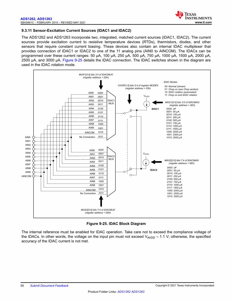
9.3.11 Sensor-Excitation Current Sources (IDAC1 and IDAC2)
The ADS1262 and ADS1263 incorporate two, integrated, matched current sources (IDAC1, IDAC2). The currentsources provide excitation current to resistive temperature devices (RTDs), thermistors, diodes, and othersensors that require constant current biasing. These devices also contain an internal IDAC multiplexer thatprovides connection of IDAC1 or IDAC2 to one of the 11 analog pins (AIN0 to AINCOM). The IDACs can beprogrammed over these current ranges: 50 μA, 100 μA, 250 μA, 500 μA, 750 μA, 1000 μA, 1500 μA, 2000 μA,2500 μA, and 3000 μA. Figure 9-25 details the IDAC connection. The IDAC switches shown in the diagram areused in the IDAC rotation mode.
AIN0
AIN1
AIN2
AIN3
AIN4
AIN5
AIN6
AIN7
AIN8
AIN9
AINCOM
0000
0001
0010
0011
0100
0101
0110
0111
1000
1001
1010
`
0000
0001
0010
0011
0100
0101
0110
0111
1000
1001
1010
MUX1[3:0] bits 3:0 of IDACMUX
(register address = 0Dh)
0000: off
0001: 50 µA
0010: 100 µA
0011: 250 µA
0100: 500 µA
0101: 750 µA
0110: 1000 µA
0111: 1500 µA
1000: 2000 µA
1001: 2500 µA
1010: 3000 µA
IDAC1
MUX
IDAC2
MUX
MUX2[3:0] bits 7:4 of IDACMUX
(register address = 0Dh)
CHOP[1:0] bits 5:4 of register MODE0
(register address = 03h)
MAG1[3:0] bits 3:0 of IDACMAG
(register address = 0Eh)
MAG2[3:0] bits 7:4 of IDACMAG
(register address = 0Eh)
0000: off
0001: 50 µA
0010: 100 µA
0011: 250 µA
0100: 500 µA
0101: 750 µA
0110: 1000 µA
0111: 1500 µA
1000: 2000 µA
1001: 2500 µA
1010: 3000 µA
1011No Connection
VAVDD
VAVDD
1011No Connection
00: Normal (shown)
01: Chop on (see Chop section)
10: IDAC rotation (automated)
11: Chop on and IDAC rotationAIN0
AIN1
AIN2
AIN3
AIN4
AIN5
AIN6
AIN7
AIN8
AIN9
AINCOM
AIN0
AIN1
AIN2
AIN3
AIN4
AIN5
AIN6
AIN7
AIN8
AIN9
AINCOM
IDAC1
IDAC2
IDAC Modes
Figure 9-25. IDAC Block Diagram
The internal reference must be enabled for IDAC operation. Take care not to exceed the compliance voltage ofthe IDACs. In other words, the voltage on the input pin must not exceed VAVDD – 1.1 V; otherwise, the specifiedaccuracy of the IDAC current is not met.
ADS1262, ADS1263SBAS661C – FEBRUARY 2015 – REVISED MAY 2021 www.ti.com
50 Submit Document Feedback Copyright © 2021 Texas Instruments Incorporated
Product Folder Links: ADS1262 ADS1263
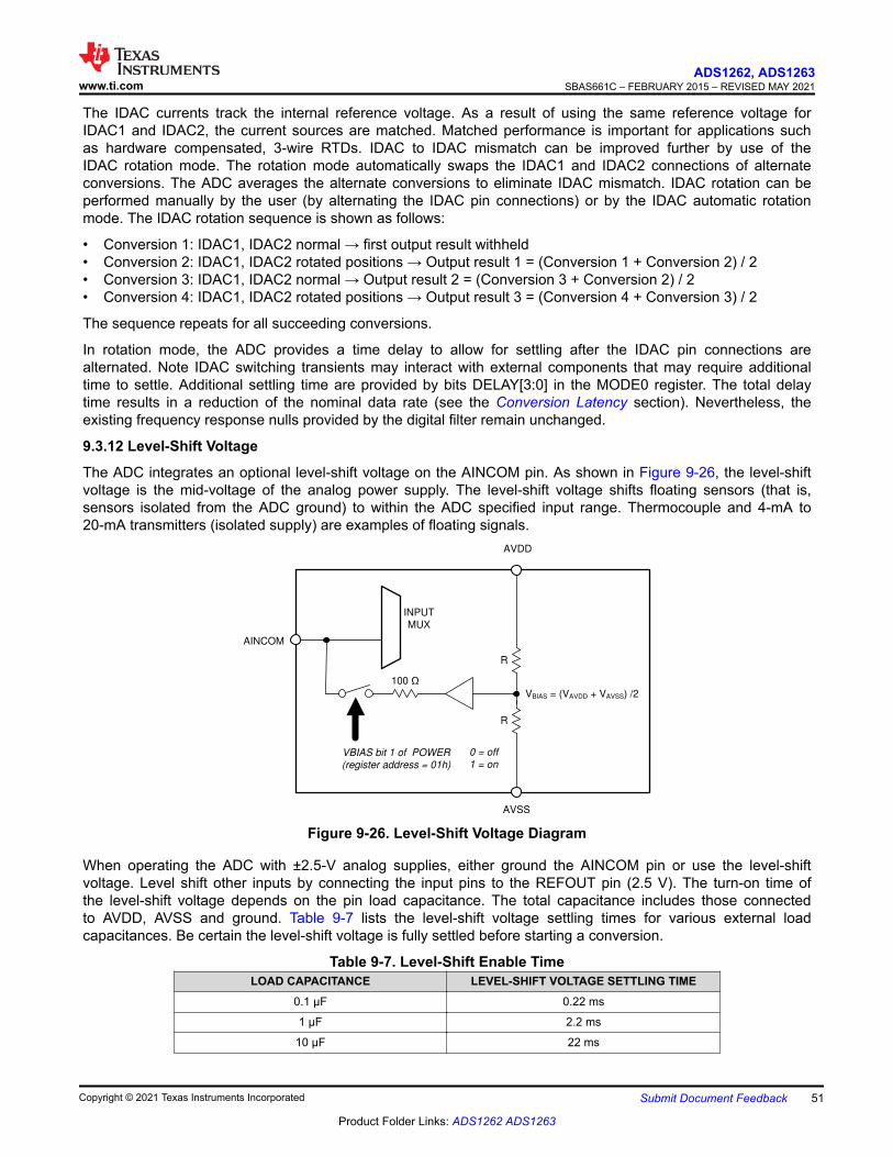
The IDAC currents track the internal reference voltage. As a result of using the same reference voltage forIDAC1 and IDAC2, the current sources are matched. Matched performance is important for applications suchas hardware compensated, 3-wire RTDs. IDAC to IDAC mismatch can be improved further by use of theIDAC rotation mode. The rotation mode automatically swaps the IDAC1 and IDAC2 connections of alternateconversions. The ADC averages the alternate conversions to eliminate IDAC mismatch. IDAC rotation can beperformed manually by the user (by alternating the IDAC pin connections) or by the IDAC automatic rotationmode. The IDAC rotation sequence is shown as follows:
• Conversion 1: IDAC1, IDAC2 normal → first output result withheld• Conversion 2: IDAC1, IDAC2 rotated positions → Output result 1 = (Conversion 1 + Conversion 2) / 2• Conversion 3: IDAC1, IDAC2 normal → Output result 2 = (Conversion 3 + Conversion 2) / 2• Conversion 4: IDAC1, IDAC2 rotated positions → Output result 3 = (Conversion 4 + Conversion 3) / 2
The sequence repeats for all succeeding conversions.
In rotation mode, the ADC provides a time delay to allow for settling after the IDAC pin connections arealternated. Note IDAC switching transients may interact with external components that may require additionaltime to settle. Additional settling time are provided by bits DELAY[3:0] in the MODE0 register. The total delaytime results in a reduction of the nominal data rate (see the Conversion Latency section). Nevertheless, theexisting frequency response nulls provided by the digital filter remain unchanged.
9.3.12 Level-Shift Voltage
The ADC integrates an optional level-shift voltage on the AINCOM pin. As shown in Figure 9-26, the level-shiftvoltage is the mid-voltage of the analog power supply. The level-shift voltage shifts floating sensors (that is,sensors isolated from the ADC ground) to within the ADC specified input range. Thermocouple and 4-mA to20-mA transmitters (isolated supply) are examples of floating signals.
AINCOM
INPUT
MUX
100 �
R
R
AVDD
AVSS
VBIAS = (VAVDD + VAVSS) /2
0 = off
1 = onVBIAS bit 1 of POWER
(register address = 01h)
Figure 9-26. Level-Shift Voltage Diagram
When operating the ADC with ±2.5-V analog supplies, either ground the AINCOM pin or use the level-shiftvoltage. Level shift other inputs by connecting the input pins to the REFOUT pin (2.5 V). The turn-on time ofthe level-shift voltage depends on the pin load capacitance. The total capacitance includes those connectedto AVDD, AVSS and ground. Table 9-7 lists the level-shift voltage settling times for various external loadcapacitances. Be certain the level-shift voltage is fully settled before starting a conversion.
Table 9-7. Level-Shift Enable TimeLOAD CAPACITANCE LEVEL-SHIFT VOLTAGE SETTLING TIME
0.1 µF 0.22 ms
1 µF 2.2 ms
10 µF 22 ms
www.ti.comADS1262, ADS1263
SBAS661C – FEBRUARY 2015 – REVISED MAY 2021
Copyright © 2021 Texas Instruments Incorporated Submit Document Feedback 51
Product Folder Links: ADS1262 ADS1263
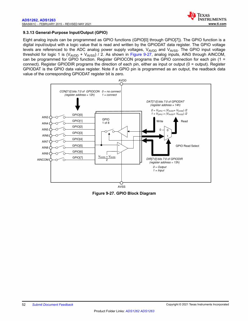
9.3.13 General-Purpose Input/Output (GPIO)
Eight analog inputs can be programmed as GPIO functions (GPIO[0] through GPIO[7]). The GPIO function is adigital input/output with a logic value that is read and written by the GPIODAT data register. The GPIO voltagelevels are referenced to the ADC analog power supply voltages, VAVDD and VAVSS. The GPIO input voltagethreshold for logic 1 is (VAVDD + VAVSS) / 2. As shown in Figure 9-27, analog inputs, AIN3 through AINCOM,can be programmed for GPIO function. Register GPIOCON programs the GPIO connection for each pin (1 =connect). Register GPIODIR programs the direction of each pin, either as input or output (0 = output). RegisterGPIODAT is the GPIO data value register. Note if a GPIO pin is programmed as an output, the readback datavalue of the corresponding GPIODAT register bit is zero.
AIN3
CON[7:0] bits 7:0 of GPIOCON
(register address = 12h)
DIR[7:0] bits 7:0 of GPIODIR
(register address = 13h)
DAT[7:0] bits 7:0 of GPIODAT
(register address = 14h)
AIN4
AIN5
AIN6
AIN7
AIN8
AIN9
AINCOM
GPIO[0]
GPIO[1]
GPIO[2]
GPIO[3]
GPIO[4]
GPIO[5]
GPIO[6]
GPIO[7]
+
±
VAVDD + VAVSS
2
GPIO
1 of 8
AVSS
AVDD
Write Read
GPIO Read Select
1
0
0 = no connect
1 = connect
0 = Output
1 = Input
0 = VGPIO < (VAVDD+ VAVSS) /2
1 = VGPIO > (VAVDD+ VAVSS) /2
0
Figure 9-27. GPIO Block Diagram
ADS1262, ADS1263SBAS661C – FEBRUARY 2015 – REVISED MAY 2021 www.ti.com
52 Submit Document Feedback Copyright © 2021 Texas Instruments Incorporated
Product Folder Links: ADS1262 ADS1263
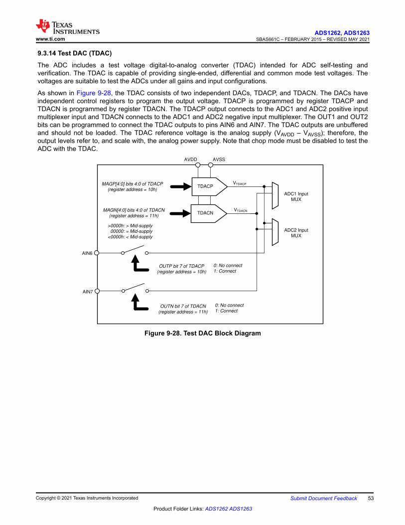
9.3.14 Test DAC (TDAC)
The ADC includes a test voltage digital-to-analog converter (TDAC) intended for ADC self-testing andverification. The TDAC is capable of providing single-ended, differential and common mode test voltages. Thevoltages are suitable to test the ADCs under all gains and input configurations.
As shown in Figure 9-28, the TDAC consists of two independent DACs, TDACP, and TDACN. The DACs haveindependent control registers to program the output voltage. TDACP is programmed by register TDACP andTDACN is programmed by register TDACN. The TDACP output connects to the ADC1 and ADC2 positive inputmultiplexer input and TDACN connects to the ADC1 and ADC2 negative input multiplexer. The OUT1 and OUT2bits can be programmed to connect the TDAC outputs to pins AIN6 and AIN7. The TDAC outputs are unbufferedand should not be loaded. The TDAC reference voltage is the analog supply (VAVDD – VAVSS); therefore, theoutput levels refer to, and scale with, the analog power supply. Note that chop mode must be disabled to test theADC with the TDAC.
AVSSAVDD
MAGP[4:0] bits 4:0 of TDACP
(register address = 10h)ADCTDACP
MAGN[4:0] bits 4:0 of TDACN
(register address = 11h) ADCTDACN
AIN6
AIN7
ADC1 Input
MUX
ADC2 Input
MUX
VTDACP
VTDACN
OUTN bit 7 of TDACN
(register address = 11h)
OUTP bit 7 of TDACP
(register address = 10h)
>0000h: > Mid-supply
00000: = Mid-supply
<0000h: < Mid-supply
0: No connect
1: Connect
0: No connect
1: Connect
Figure 9-28. Test DAC Block Diagram
www.ti.comADS1262, ADS1263
SBAS661C – FEBRUARY 2015 – REVISED MAY 2021
Copyright © 2021 Texas Instruments Incorporated Submit Document Feedback 53
Product Folder Links: ADS1262 ADS1263
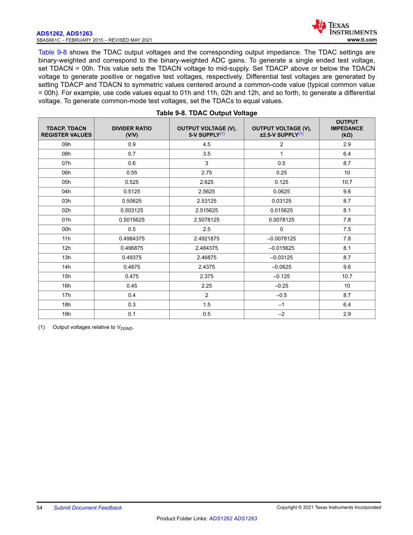
Table 9-8 shows the TDAC output voltages and the corresponding output impedance. The TDAC settings arebinary-weighted and correspond to the binary-weighted ADC gains. To generate a single ended test voltage,set TDACN = 00h. This value sets the TDACN voltage to mid-supply. Set TDACP above or below the TDACNvoltage to generate positive or negative test voltages, respectively. Differential test voltages are generated bysetting TDACP and TDACN to symmetric values centered around a common-code value (typical common value= 00h). For example, use code values equal to 01h and 11h, 02h and 12h, and so forth, to generate a differentialvoltage. To generate common-mode test voltages, set the TDACs to equal values.
Table 9-8. TDAC Output Voltage
TDACP, TDACNREGISTER VALUES
DIVIDER RATIO(V/V)
OUTPUT VOLTAGE (V),5-V SUPPLY(1)
OUTPUT VOLTAGE (V),±2.5-V SUPPLY(1)
OUTPUTIMPEDANCE
(kΩ)09h 0.9 4.5 2 2.9
08h 0.7 3.5 1 6.4
07h 0.6 3 0.5 8.7
06h 0.55 2.75 0.25 10
05h 0.525 2.625 0.125 10.7
04h 0.5125 2.5625 0.0625 9.6
03h 0.50625 2.53125 0.03125 8.7
02h 0.503125 2.515625 0.015625 8.1
01h 0.5015625 2.5078125 0.0078125 7.8
00h 0.5 2.5 0 7.5
11h 0.4984375 2.4921875 –0.0078125 7.8
12h 0.496875 2.484375 –0.015625 8.1
13h 0.49375 2.46875 –0.03125 8.7
14h 0.4875 2.4375 –0.0625 9.6
15h 0.475 2.375 –0.125 10.7
16h 0.45 2.25 –0.25 10
17h 0.4 2 –0.5 8.7
18h 0.3 1.5 –1 6.4
19h 0.1 0.5 –2 2.9
(1) Output voltages relative to VDGND.
ADS1262, ADS1263SBAS661C – FEBRUARY 2015 – REVISED MAY 2021 www.ti.com
54 Submit Document Feedback Copyright © 2021 Texas Instruments Incorporated
Product Folder Links: ADS1262 ADS1263
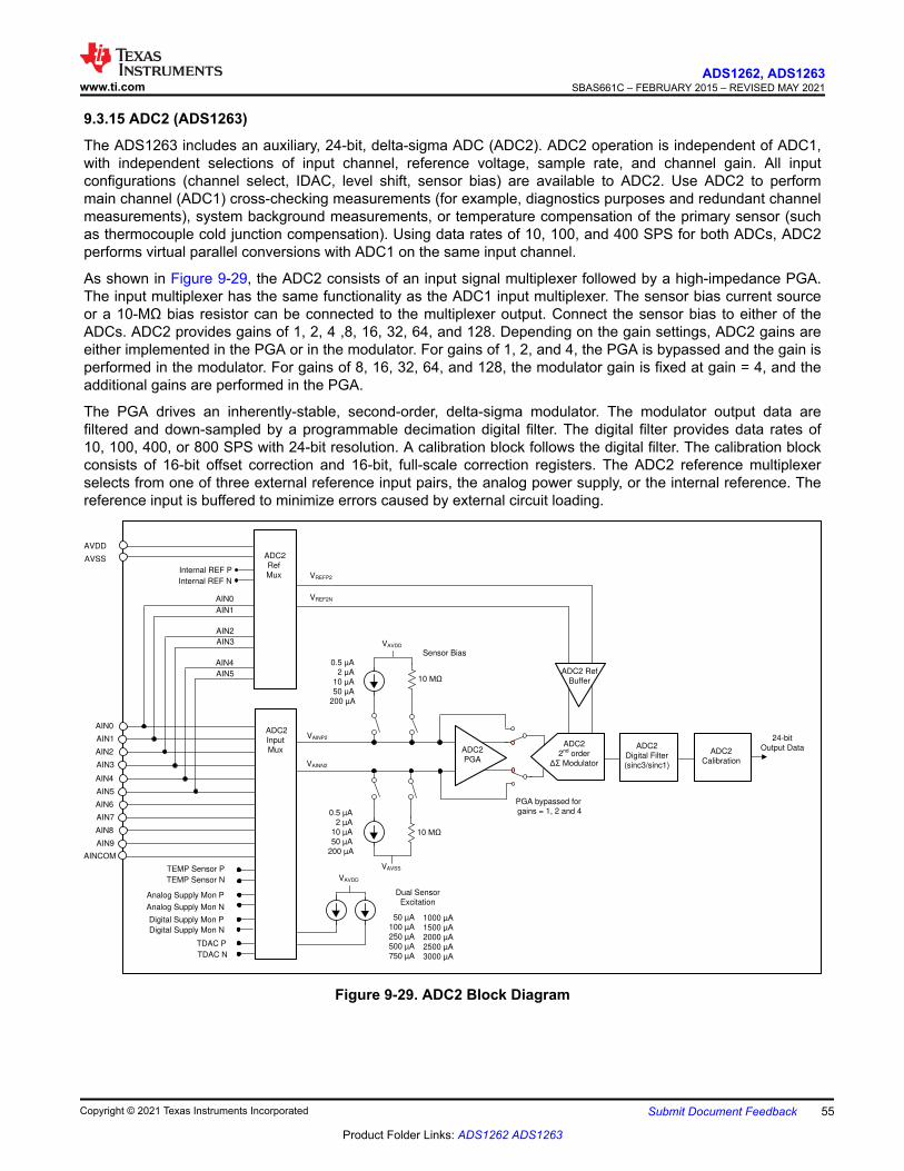
9.3.15 ADC2 (ADS1263)
The ADS1263 includes an auxiliary, 24-bit, delta-sigma ADC (ADC2). ADC2 operation is independent of ADC1,with independent selections of input channel, reference voltage, sample rate, and channel gain. All inputconfigurations (channel select, IDAC, level shift, sensor bias) are available to ADC2. Use ADC2 to performmain channel (ADC1) cross-checking measurements (for example, diagnostics purposes and redundant channelmeasurements), system background measurements, or temperature compensation of the primary sensor (suchas thermocouple cold junction compensation). Using data rates of 10, 100, and 400 SPS for both ADCs, ADC2performs virtual parallel conversions with ADC1 on the same input channel.
As shown in Figure 9-29, the ADC2 consists of an input signal multiplexer followed by a high-impedance PGA.The input multiplexer has the same functionality as the ADC1 input multiplexer. The sensor bias current sourceor a 10-MΩ bias resistor can be connected to the multiplexer output. Connect the sensor bias to either of theADCs. ADC2 provides gains of 1, 2, 4 ,8, 16, 32, 64, and 128. Depending on the gain settings, ADC2 gains areeither implemented in the PGA or in the modulator. For gains of 1, 2, and 4, the PGA is bypassed and the gain isperformed in the modulator. For gains of 8, 16, 32, 64, and 128, the modulator gain is fixed at gain = 4, and theadditional gains are performed in the PGA.
The PGA drives an inherently-stable, second-order, delta-sigma modulator. The modulator output data arefiltered and down-sampled by a programmable decimation digital filter. The digital filter provides data rates of10, 100, 400, or 800 SPS with 24-bit resolution. A calibration block follows the digital filter. The calibration blockconsists of 16-bit offset correction and 16-bit, full-scale correction registers. The ADC2 reference multiplexerselects from one of three external reference input pairs, the analog power supply, or the internal reference. Thereference input is buffered to minimize errors caused by external circuit loading.
ADC2PGA
ADC2Digital Filter (sinc3/sinc1)
ADC22nd order
û��Modulator
VAVSS
0.5 µA 2 µA 10 µA 50 µA200 µA
Sensor Bias
ADC2InputMux
AIN0
AIN1
AIN2
AIN3
AIN4
AIN5
AIN6
AIN7
AIN8
AIN9
AINCOM
TDAC P
TEMP Sensor P
Analog Supply Mon P
Internal REF P
AIN0
ADC2RefMux
VAINN2
VAINP2
VREFP2
VREF2N
10 0��
10 0��
AVDD
AVSS
VAVDD
VAVDD
Dual Sensor Excitation
TEMP Sensor N
TDAC N
Analog Supply Mon N
Digital Supply Mon P
Digital Supply Mon N
Internal REF N
24-bit Output Data
AIN1
AIN2
AIN3
AIN4
AIN5 ADC2 RefBuffer
0.5 µA 2 µA 10 µA 50 µA200 µA
50 µA100 µA250 µA500 µA750 µA
1000 µA1500 µA2000 µA2500 µA3000 µA
PGA bypassed for gains = 1, 2 and 4
ADC2Calibration
Figure 9-29. ADC2 Block Diagram
www.ti.comADS1262, ADS1263
SBAS661C – FEBRUARY 2015 – REVISED MAY 2021
Copyright © 2021 Texas Instruments Incorporated Submit Document Feedback 55
Product Folder Links: ADS1262 ADS1263
9.3.15.1 ADC2 Inputs
ADC2 features an independent input multiplexer with identical channel selections of ADC1. As shown in Figure9-2, all the external and internal inputs are available to ADC2. The ADC2 positive input is programmed bythe value of MUXP2[3:0] bits (register ADC2MUX) and the negative input is programmed by the value of theMUXN2[3:0] bits of same ADC2MUX register. The ADC2MUX register address is 16h.
9.3.15.2 ADC2 PGA
ADC2 features a low-drift, low-noise CMOS PGA. The ADC2 PGA is bypassed for gains = 1, 2 and 4. Therefore,for these gains the input signal is connected directly to the buffered modulator input.
The full-scale voltage range of ADC2 is determined by the reference voltage and gain. Table 9-9 shows theADC2 full-scale voltage range versus gain using reference voltage = 2.5 V. The full-scale voltage range scaleswith the reference voltage and is increased or decreased by changing the reference voltage.
Table 9-9. ADC2 Full-Scale Voltage RangeGAIN2[2:0] BITS
OF ADC2CFG REGISTER GAIN (V/V)FULL-SCALE INPUT RANGE
(V)(1)
000 1 ±2.500 V
001 2 ±1.250 V
010 4 ±0.625 V
011 8 ±0.312 V
100 16 ±0.156 V
101 32 ±0.078 V
110 64 ±0.039 V
111 128 ±0.0195 V
(1) VREF = 2.5 V. The full-scale voltage range is proportional to VREF.
As with many amplifiers, do not exceed the PGA absolute input voltage requirement. For gains ≥ 8 (PGAactive), the absolute input voltage is limited by the PGA output voltage swing range. The specified minimum andmaximum absolute input voltages (VINP2 and VINN2) depend on the PGA gain, the input differential voltage (VIN2),and the tolerance of the analog power supply voltages (VAVDD, VAVSS). If using ADC2 in an overall gain ≥ 8, theabsolute positive and negative input voltage must be within the specified range, as shown in Equation 15:
VAVSS + 0.3 + |VIN2| · (Gain – 1) / 2 · < VINP2 and VINN2 < VAVDD – 0.3 – |VIN2| · (Gain – 1) / 2 (15)
where
• VINP2, VINN2 = ADC2 absolute input voltage• VIN2 = ADC2 differential input voltage = VINP2 - VINN2• Gain = 8, 16, 32, 64 or 128
For gains 1, 2, or 4, the ADC2 absolute input voltage range extends beyond the VAVDD and VAVSS supplyvoltages, allowing voltage inputs at or below ground. The absolute input voltage range corresponding to gains 1,2 and 4 is shown in Equation 16:
VAVSS – 0.1 < VINP2 and VINN2 < VAVDD + 0.1 (16)
ADS1262, ADS1263SBAS661C – FEBRUARY 2015 – REVISED MAY 2021 www.ti.com
56 Submit Document Feedback Copyright © 2021 Texas Instruments Incorporated
Product Folder Links: ADS1262 ADS1263
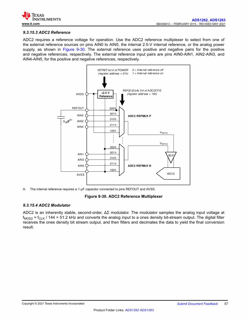
9.3.15.3 ADC2 Reference
ADC2 requires a reference voltage for operation. Use the ADC2 reference multiplexer to select from one ofthe external reference sources on pins AIN0 to AIN5, the internal 2.5-V internal reference, or the analog powersupply, as shown in Figure 9-30. The external reference uses positive and negative pairs for the positiveand negative references, respectively. The external reference input pairs are pins AIN0-AIN1, AIN2-AIN3, andAIN4-AIN5, for the positive and negative references, respectively.
AIN0
AIN2
AIN4
AIN1
AIN3
AIN5
AVSS
REFOUT
1 PF1 PF
+2.5 V
Reference
+2.5 V
ReferenceAVDD
REF[2:0] b its 5:4 of ADC2CFG
(register address = 15h)
INTREF bi t 0 of POWER
(reg ister address = 01h)
ADC2
VREFP2
VREFN2
(A)
ADC2 REFMUX P
000h
001h
010h
011h
100h
001h
010h
011h
100h
000h
0 = In ternal reference off
1 = Internal reference on
ADC2 REFMUX N
BUF
A. The internal reference requires a 1-μF capacitor connected to pins REFOUT and AVSS.
Figure 9-30. ADC2 Reference Multiplexer
9.3.15.4 ADC2 Modulator
ADC2 is an inherently stable, second-order, ΔΣ modulator. The modulator samples the analog input voltage atfMOD2 = fCLK / 144 = 51.2 kHz and converts the analog input to a ones density bit-stream output. The digital filterreceives the ones density bit stream output, and then filters and decimates the data to yield the final conversionresult.
www.ti.comADS1262, ADS1263
SBAS661C – FEBRUARY 2015 – REVISED MAY 2021
Copyright © 2021 Texas Instruments Incorporated Submit Document Feedback 57
Product Folder Links: ADS1262 ADS1263
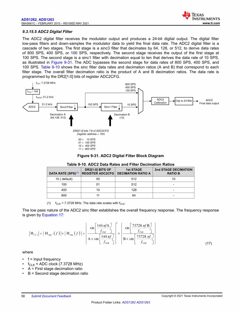
9.3.15.5 ADC2 Digital Filter
The ADC2 digital filter receives the modulator output and produces a 24-bit digital output. The digital filterlow-pass filters and down-samples the modulator data to yield the final data rate. The ADC2 digital filter is acascade of two stages. The first stage is a sinc3 filter that decimates by 64, 128, or 512, to derive data ratesof 800 SPS, 400 SPS, or 100 SPS, respectively. The second stage receives the output of the first stage at100 SPS. The second stage is a sinc1 filter with decimation equal to ten that derives the data rate of 10 SPS,as illustrated in Figure 9-31. The ADC bypasses the second stage for data rates of 800 SPS, 400 SPS, and100 SPS. Table 9-10 shows the sinc filter data rates and decimation ratios (A and B) that correspond to eachfilter stage. The overall filter decimation ratio is the product of A and B decimation ratios. The data rate isprogrammed by the DR2[1:0] bits of register ADC2CFG.
Sinc3 Filter
Decimation B
(10)
51.2 kHz
fCLK: 7.3728 MHz
fCLK / 144
fMOD2: 51.2 kHz
ADC2
00 = 10 SPS
01 = 100 SPS
10 = 400 SPS
11 = 800 SPS
ADC2
Calibration
DR2[1:0] bits 7:6 of ADC2CFG
(register address = 15h)
Clip to 24 Bits ADC2
Final data output
800 SPS
400 SPS
100 SPS
10 SPSSinc1 Filter
Decimation A
(64,128, 512)
100 SPS
Figure 9-31. ADC2 Digital Filter Block Diagram
Table 9-10. ADC2 Data Rates and Filter Decimation Ratios
DATA RATE (SPS)(1)DR2[1:0] BITS OF
REGISTER ADC2CFG1st STAGE
DECIMATION RATIO A2nd STAGE DECIMATION
RATIO B10 ( default) 00 512 10
100 01 512 -
400 10 128 -
800 11 64 -
(1) fCLK = 7.3728 MHz. The data rate scales with fCLK.
The low pass nature of the ADC2 sinc filter establishes the overall frequency response. The frequency responseis given by Equation 17:
� � � � � �»¼
º«¬
ªu
»¼
º«¬
ª
u
»¼
º«¬
ªu
»¼
º«¬
ª $
u
CLK
CLK
CLK
CLK
f
f
�I
f
�I
f
f
f
�I
ff73728
sinB
B73728sin
�144sinA
144sin
HHH
3
sincsinc3
(17)
where
• f = Input frequency• fCLK = ADC clock (7.3728 MHz)• A = First stage decimation ratio• B = Second stage decimation ratio
ADS1262, ADS1263SBAS661C – FEBRUARY 2015 – REVISED MAY 2021 www.ti.com
58 Submit Document Feedback Copyright © 2021 Texas Instruments Incorporated
Product Folder Links: ADS1262 ADS1263
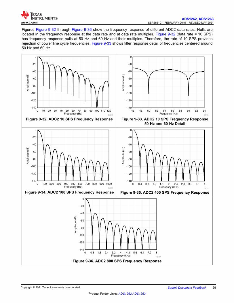
Figures Figure 9-32 through Figure 9-36 show the frequency response of different ADC2 data rates. Nulls arelocated in the frequency response at the data rate and at data rate multiples. Figure 9-32 (data rate = 10 SPS)has frequency response nulls at 50 Hz and 60 Hz and their multiples. Therefore, the rate of 10 SPS providesrejection of power line cycle frequencies. Figure 9-33 shows filter response detail of frequencies centered around50 Hz and 60 Hz.
Frequency (Hz)
Am
plit
ude (
dB
)
0 10 20 30 40 50 60 70 80 90 100 110 120-140
-120
-100
-80
-60
-40
-20
0
D018
Figure 9-32. ADC2 10 SPS Frequency ResponseFrequency (Hz)
Am
plit
ude (
dB
)
46 48 50 52 54 56 58 60 62 64-140
-120
-100
-80
-60
-40
-20
0
D019
Figure 9-33. ADC2 10 SPS Frequency Response50-Hz and 60-Hz Detail
Frequency (Hz)
Am
plit
ude (
dB
)
0 100 200 300 400 500 600 700 800 900 1000-140
-120
-100
-80
-60
-40
-20
0
D020
Figure 9-34. ADC2 100 SPS Frequency ResponseFrequency (kHz)
Am
plit
ude (
dB
)
0 0.4 0.8 1.2 1.6 2 2.4 2.8 3.2 3.6 4-140
-120
-100
-80
-60
-40
-20
0
D021
Figure 9-35. ADC2 400 SPS Frequency Response
Frequency (kHz)
Am
plit
ude (
dB
)
0 0.8 1.6 2.4 3.2 4 4.8 5.6 6.4 7.2 8-140
-120
-100
-80
-60
-40
-20
0
D022
Figure 9-36. ADC2 800 SPS Frequency Response
www.ti.comADS1262, ADS1263
SBAS661C – FEBRUARY 2015 – REVISED MAY 2021
Copyright © 2021 Texas Instruments Incorporated Submit Document Feedback 59
Product Folder Links: ADS1262 ADS1263
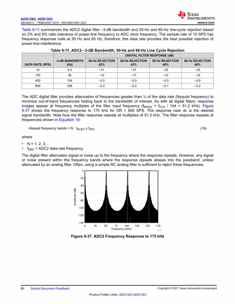
Table 9-11 summarizes the ADC2 digital filter –3-dB bandwidth and 50-Hz and 60-Hz line-cycle rejection basedon 2% and 6% ratio tolerance of power-line frequency to ADC clock frequency. The sample rate of 10 SPS hasfrequency response nulls at 50 Hz and 60 Hz; therefore, this data rate provides the best possible rejection ofpower-line interference.
Table 9-11. ADC2 –3-dB Bandwidth, 50-Hz and 60-Hz Line Cycle Rejection
DATA RATE (SPS)-3-dB BANDWIDTH
(Hz)
DIGITAL FILTER RESPONSE (dB)50-Hz REJECTION
±2%60-Hz REJECTION
±2%50-Hz REJECTION
±6%60-Hz REJECTION
±6%10 4.4 –41 –47 –32 –36
100 26 –12 –17 –10 –16
400 104 –0.5 –0.9 –0.5 –0.9
800 208 –0.2 –0.2 –0.1 –0.2
The ADC digital filter provides attenuation of frequencies greater than ½ of the data rate (Nyquist frequency) tominimize out-of-band frequencies folding back to the bandwidth of interest. As with all digital filters, responseimages appear at frequency multiples of the filter input frequency (fMOD2 = fCLK / 144 = 51.2 kHz). Figure9-37 shows the frequency response to 175 kHz for DR = 800 SPS. The response near dc is the desiredsignal bandwidth. Note how the filter response repeats at multiplies of 51.2 kHz. The filter response repeats atfrequencies shown in Equation 18:
Aliased frequency bands = N · fMOD2 ± fDR2 (18)
where
• N = 1, 2, 3...• fDR2 = ADC2 data-rate frequency
The digital filter attenuates signal or noise up to the frequency where the response repeats. However, any signalor noise present within the frequency bands where the response repeats aliases into the passband, unlessattenuated by an analog filter. Often, using a simple RC analog filter is sufficient to reject these frequencies.
Frequency (kHz)
Am
plit
ude (
dB
)
0 25 50 75 100 125 150 175-140
-120
-100
-80
-60
-40
-20
0
D023
Figure 9-37. ADC2 Frequency Response to 175 kHz
ADS1262, ADS1263SBAS661C – FEBRUARY 2015 – REVISED MAY 2021 www.ti.com
60 Submit Document Feedback Copyright © 2021 Texas Instruments Incorporated
Product Folder Links: ADS1262 ADS1263
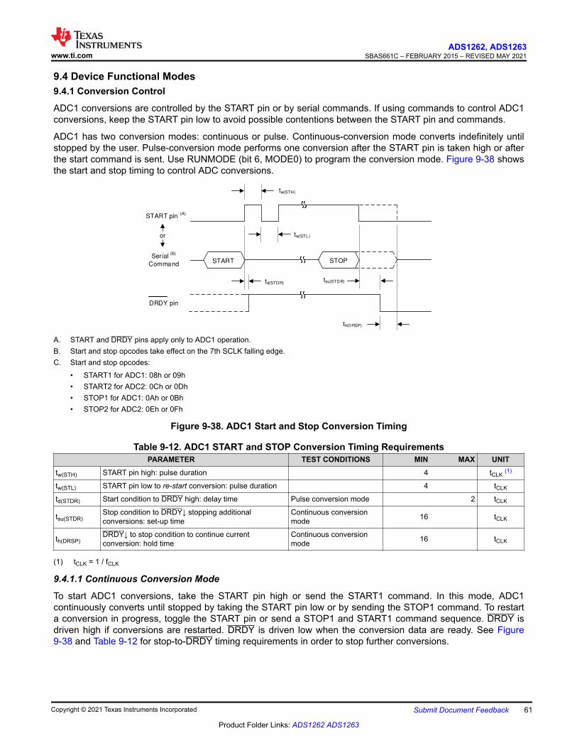
9.4 Device Functional Modes9.4.1 Conversion Control
ADC1 conversions are controlled by the START pin or by serial commands. If using commands to control ADC1conversions, keep the START pin low to avoid possible contentions between the START pin and commands.
ADC1 has two conversion modes: continuous or pulse. Continuous-conversion mode converts indefinitely untilstopped by the user. Pulse-conversion mode performs one conversion after the START pin is taken high or afterthe start command is sent. Use RUNMODE (bit 6, MODE0) to program the conversion mode. Figure 9-38 showsthe start and stop timing to control ADC conversions.
Ser ial (B)
Command START STOP
START pin (A)
DRDY pin
tw(STH)
tw(STL)
td(STDR)tsu(STDR)
th(DRSP)
or
A. START and DRDY pins apply only to ADC1 operation.B. Start and stop opcodes take effect on the 7th SCLK falling edge.C. Start and stop opcodes:
• START1 for ADC1: 08h or 09h• START2 for ADC2: 0Ch or 0Dh• STOP1 for ADC1: 0Ah or 0Bh• STOP2 for ADC2: 0Eh or 0Fh
Figure 9-38. ADC1 Start and Stop Conversion Timing
Table 9-12. ADC1 START and STOP Conversion Timing RequirementsPARAMETER TEST CONDITIONS MIN MAX UNIT
tw(STH) START pin high: pulse duration 4 tCLK (1)
tw(STL) START pin low to re-start conversion: pulse duration 4 tCLK
td(STDR) Start condition to DRDY high: delay time Pulse conversion mode 2 tCLK
tsu(STDR)Stop condition to DRDY↓ stopping additionalconversions: set-up time
Continuous conversionmode 16 tCLK
th(DRSP)DRDY↓ to stop condition to continue currentconversion: hold time
Continuous conversionmode 16 tCLK
(1) tCLK = 1 / fCLK
9.4.1.1 Continuous Conversion Mode
To start ADC1 conversions, take the START pin high or send the START1 command. In this mode, ADC1continuously converts until stopped by taking the START pin low or by sending the STOP1 command. To restarta conversion in progress, toggle the START pin or send a STOP1 and START1 command sequence. DRDY isdriven high if conversions are restarted. DRDY is driven low when the conversion data are ready. See Figure9-38 and Table 9-12 for stop-to-DRDY timing requirements in order to stop further conversions.
www.ti.comADS1262, ADS1263
SBAS661C – FEBRUARY 2015 – REVISED MAY 2021
Copyright © 2021 Texas Instruments Incorporated Submit Document Feedback 61
Product Folder Links: ADS1262 ADS1263
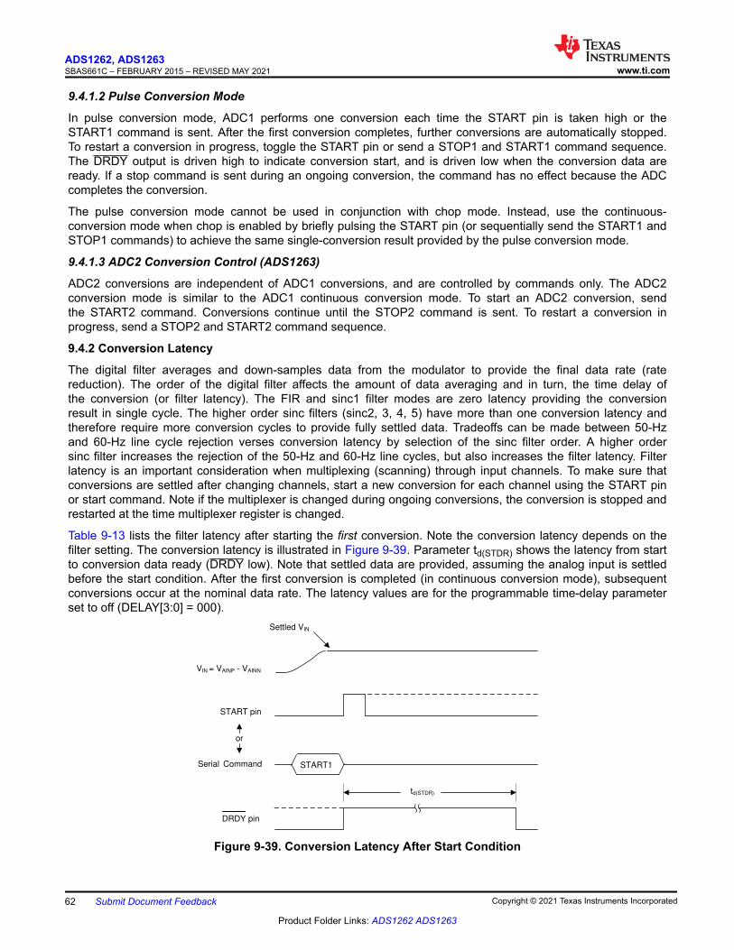
9.4.1.2 Pulse Conversion Mode
In pulse conversion mode, ADC1 performs one conversion each time the START pin is taken high or theSTART1 command is sent. After the first conversion completes, further conversions are automatically stopped.To restart a conversion in progress, toggle the START pin or send a STOP1 and START1 command sequence.The DRDY output is driven high to indicate conversion start, and is driven low when the conversion data areready. If a stop command is sent during an ongoing conversion, the command has no effect because the ADCcompletes the conversion.
The pulse conversion mode cannot be used in conjunction with chop mode. Instead, use the continuous-conversion mode when chop is enabled by briefly pulsing the START pin (or sequentially send the START1 andSTOP1 commands) to achieve the same single-conversion result provided by the pulse conversion mode.
9.4.1.3 ADC2 Conversion Control (ADS1263)
ADC2 conversions are independent of ADC1 conversions, and are controlled by commands only. The ADC2conversion mode is similar to the ADC1 continuous conversion mode. To start an ADC2 conversion, sendthe START2 command. Conversions continue until the STOP2 command is sent. To restart a conversion inprogress, send a STOP2 and START2 command sequence.
9.4.2 Conversion Latency
The digital filter averages and down-samples data from the modulator to provide the final data rate (ratereduction). The order of the digital filter affects the amount of data averaging and in turn, the time delay ofthe conversion (or filter latency). The FIR and sinc1 filter modes are zero latency providing the conversionresult in single cycle. The higher order sinc filters (sinc2, 3, 4, 5) have more than one conversion latency andtherefore require more conversion cycles to provide fully settled data. Tradeoffs can be made between 50-Hzand 60-Hz line cycle rejection verses conversion latency by selection of the sinc filter order. A higher ordersinc filter increases the rejection of the 50-Hz and 60-Hz line cycles, but also increases the filter latency. Filterlatency is an important consideration when multiplexing (scanning) through input channels. To make sure thatconversions are settled after changing channels, start a new conversion for each channel using the START pinor start command. Note if the multiplexer is changed during ongoing conversions, the conversion is stopped andrestarted at the time multiplexer register is changed.
Table 9-13 lists the filter latency after starting the first conversion. Note the conversion latency depends on thefilter setting. The conversion latency is illustrated in Figure 9-39. Parameter td(STDR) shows the latency from startto conversion data ready (DRDY low). Note that settled data are provided, assuming the analog input is settledbefore the start condition. After the first conversion is completed (in continuous conversion mode), subsequentconversions occur at the nominal data rate. The latency values are for the programmable time-delay parameterset to off (DELAY[3:0] = 000).
Serial Command START1
START pin
DRDY pin
td(STDR)
or
VIN = VAINP - VAINN
Settled VIN
Figure 9-39. Conversion Latency After Start Condition
ADS1262, ADS1263SBAS661C – FEBRUARY 2015 – REVISED MAY 2021 www.ti.com
62 Submit Document Feedback Copyright © 2021 Texas Instruments Incorporated
Product Folder Links: ADS1262 ADS1263
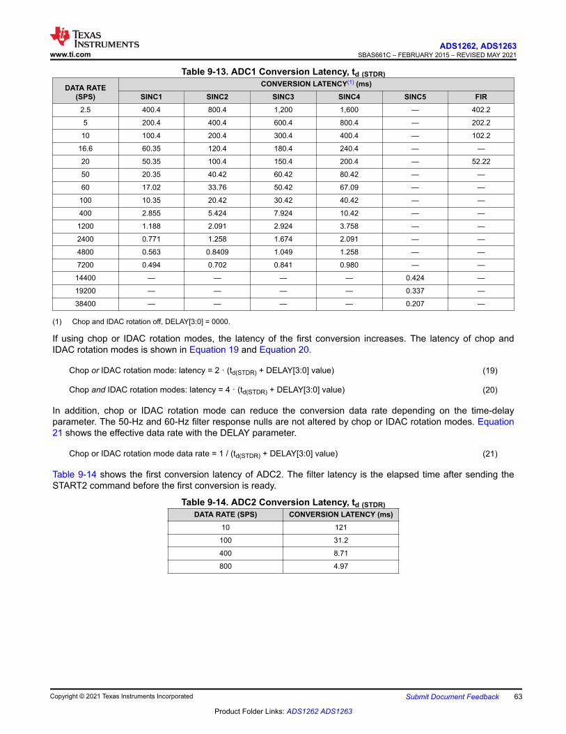
Table 9-13. ADC1 Conversion Latency, td (STDR)
DATA RATE(SPS)
CONVERSION LATENCY(1) (ms)SINC1 SINC2 SINC3 SINC4 SINC5 FIR
2.5 400.4 800.4 1,200 1,600 — 402.2
5 200.4 400.4 600.4 800.4 — 202.2
10 100.4 200.4 300.4 400.4 — 102.2
16.6 60.35 120.4 180.4 240.4 — —
20 50.35 100.4 150.4 200.4 — 52.22
50 20.35 40.42 60.42 80.42 — —
60 17.02 33.76 50.42 67.09 — —
100 10.35 20.42 30.42 40.42 — —
400 2.855 5.424 7.924 10.42 — —
1200 1.188 2.091 2.924 3.758 — —
2400 0.771 1.258 1.674 2.091 — —
4800 0.563 0.8409 1.049 1.258 — —
7200 0.494 0.702 0.841 0.980 — —
14400 — — — — 0.424 —
19200 — — — — 0.337 —
38400 — — — — 0.207 —
(1) Chop and IDAC rotation off, DELAY[3:0] = 0000.
If using chop or IDAC rotation modes, the latency of the first conversion increases. The latency of chop andIDAC rotation modes is shown in Equation 19 and Equation 20.
Chop or IDAC rotation mode: latency = 2 · (td(STDR) + DELAY[3:0] value) (19)
Chop and IDAC rotation modes: latency = 4 · (td(STDR) + DELAY[3:0] value) (20)
In addition, chop or IDAC rotation mode can reduce the conversion data rate depending on the time-delayparameter. The 50-Hz and 60-Hz filter response nulls are not altered by chop or IDAC rotation modes. Equation21 shows the effective data rate with the DELAY parameter.
Chop or IDAC rotation mode data rate = 1 / (td(STDR) + DELAY[3:0] value) (21)
Table 9-14 shows the first conversion latency of ADC2. The filter latency is the elapsed time after sending theSTART2 command before the first conversion is ready.
Table 9-14. ADC2 Conversion Latency, td (STDR)DATA RATE (SPS) CONVERSION LATENCY (ms)
10 121
100 31.2
400 8.71
800 4.97
www.ti.comADS1262, ADS1263
SBAS661C – FEBRUARY 2015 – REVISED MAY 2021
Copyright © 2021 Texas Instruments Incorporated Submit Document Feedback 63
Product Folder Links: ADS1262 ADS1263

If the input signal changes while the ADC is continuously converting, the output data are a mix of old and newdata, as shown in Figure 9-40. The filter latency values for settled data (td(STDR)) with an input step change whilecontinuously converting is shown in Table 9-15. The filter latency values listed in the table (td(STDR)) assume theanalog input is settled before the start of the first whole conversion period.
DRDY pin
td(DRDR)
VIN = VAINP - VAINN
Old VIN
New VIN
Old dataMix of old data
and new data
Fully settled
new data
Figure 9-40. ADC1 Latency Timing While Continuously Converting
Table 9-15. Fully-Settled Conversion Values forFigure 9-40
DIGITAL FILTER
FULLY SETTLED CONVERSIONtd(DRDR)
(1 / DR)(1)
FIR 1
Sinc1 1
Sinc2 2
Sinc3 3
Sinc4 4
Sinc5 5
(1) Chop and IDAC rotation modes off.
9.4.3 Programmable Time Delay
When a new conversion is started, the ADC provides an internal delay of 52 µs before the actual start ofthe conversion. This timed delay is provided to allow for the integrated, analog, antialias filter to settle. Insome cases, more delay is required to allow for external settling effects. Program additional time by using bitsDELAY[3:0] of the MODE register. The programable range is 8.7 µs to 8.8 ms in binary steps. As an alternativeto using the programmable time delay, the initiation of the start condition can also be delayed as needed after anADC configuration change. For CHOP or IDAC rotation modes, additional time delay may be necessary to allowfor external settling effects, and can only be provided by the DELAY bits; see Table 9-38 for the delay settings.
ADS1262, ADS1263SBAS661C – FEBRUARY 2015 – REVISED MAY 2021 www.ti.com
64 Submit Document Feedback Copyright © 2021 Texas Instruments Incorporated
Product Folder Links: ADS1262 ADS1263
9.4.4 Serial Interface
The ADC has an SPI-compatible, bidirectional serial interface that is used to read the conversion data as wellas configure and control the ADC. The serial interface consists of four control lines: CS, SCLK, DIN, and DOUT/DRDY. If the ADS1262 or ADS1263 is the only device connected to the SPI bus, the CS input can be tied low,resulting in a minimum of three control signals for communications: SCLK, DIN, and DOUT/DRDY. The ADC hasa data ready output signal (DRDY) that asserts regardless of interface selection. The DRDY functionality is alsointegrated with the DOUT/DRDY pin.
9.4.4.1 Chip Select (CS)
The CS pin is an active low input that enables the ADC serial interface for communication. CS must be lowduring the entire data transaction. When CS is high, the serial interface is reset, SCLK input activity is ignored(blocking input commands), and the DOUT/DRDY output pin enters a high-impedance state. ADC conversionsare not affected by the state of CS. If the serial bus is dedicated to the ADC, the CS pin can be optionally tiedlow to reduce the serial interface from four I/Os to three I/Os. Tying the CS pin low permanently enables the ADCserial interface. The DRDY output asserts low when conversion data are ready and is not affected by CS.
9.4.4.2 Serial Clock (SCLK)
The serial interface clock is a noise-filtered, Schmidt-triggered input used to clock data into and out of the ADC.Input data to the ADC is latched on the falling SCLK edge and data output from the ADC is updated on the risingSCLK edge. Return SCLK low after the data sequence is complete. Even though the SCLK is a noise-immune,keep SCLK as clean as possible to prevent unintentional SCLK transitions. Avoid ringing and voltage overshooton the SCLK input. Place a series termination resistor at the SCLK drive pin to help reduce ringing.
9.4.4.3 Data Input (DIN)
The DIN pin is the serial data input to the ADC. DIN is used to input commands and register data to the ADC.The ADC latches input data on the falling edge of SCLK. During direct-mode data readback, when no commandis intended, keep DIN low.
9.4.4.4 Data Output/Data Ready (DOUT/DRDY)
The DOUT/DRDY pin is a dual-function output. The pin functions as the digital data output and the ADC1data-ready indication. When CS is high, the DOUT/DRDY pin is in high-impedance mode (tri-state). Output dataare updated on the rising edge of SCLK. As a data-ready indicator, the DOUT/DRDY pin transitions low at thesame time as the DRDY pin. Therefore, monitor either the DOUT/DRDY pin or the DRDY pin to determine whenADC1 data are ready. CS must be low to monitor DOUT/DRDY as a data-ready indicator.
www.ti.comADS1262, ADS1263
SBAS661C – FEBRUARY 2015 – REVISED MAY 2021
Copyright © 2021 Texas Instruments Incorporated Submit Document Feedback 65
Product Folder Links: ADS1262 ADS1263
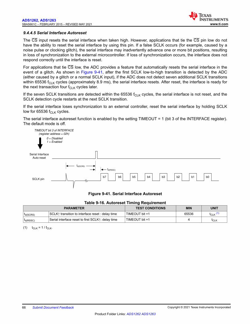
9.4.4.5 Serial Interface Autoreset
The CS input resets the serial interface when taken high. However, applications that tie the CS pin low do nothave the ability to reset the serial interface by using this pin. If a false SCLK occurs (for example, caused by anoise pulse or clocking glitch), the serial interface may inadvertently advance one or more bit positions, resultingin loss of synchronization to the external microcontroller. If loss of synchronization occurs, the interface does notrespond correctly until the interface is reset.
For applications that tie CS low, the ADC provides a feature that automatically resets the serial interface in theevent of a glitch. As shown in Figure 9-41, after the first SCLK low-to-high transition is detected by the ADC(either caused by a glitch or a normal SCLK input), if the ADC does not detect seven additional SCLK transitionswithin 65536 fCLK cycles (approximately 8.9 ms), the serial interface resets. After reset, the interface is ready forthe next transaction four fCLK cycles later.
If the seven SCLK transitions are detected within the 65536 fCLK cycles, the serial interface is not reset, and theSCLK detection cycle restarts at the next SCLK transition.
If the serial interface loses synchronization to an external controller, reset the serial interface by holding SCLKlow for 65536 fCLK cycles.
The serial interface autoreset function is enabled by the setting TIMEOUT = 1 (bit 3 of the INTERFACE register).The default mode is off.
Serial Interface
Auto-reset
SCLK pin
td(SCRS)
td(RSSC)
b7 b6 b5 b4 b3 b2 b1 b0
TIMEOUT bit 3 of INTERFACE
(register address = 02h)
0 = Disabled
1 = Enabled
Figure 9-41. Serial Interface Autoreset
Table 9-16. Autoreset Timing RequirementPARAMETER TEST CONDITIONS MIN UNIT
td(SCRS) SCLK↑ transition to interface reset : delay time TIMEOUT bit =1 65536 tCLK (1)
td(RSSC) Serial interface reset to first SCLK↑: delay time TIMEOUT bit =1 4 tCLK
(1) tCLK = 1 / fCLK.
ADS1262, ADS1263SBAS661C – FEBRUARY 2015 – REVISED MAY 2021 www.ti.com
66 Submit Document Feedback Copyright © 2021 Texas Instruments Incorporated
Product Folder Links: ADS1262 ADS1263
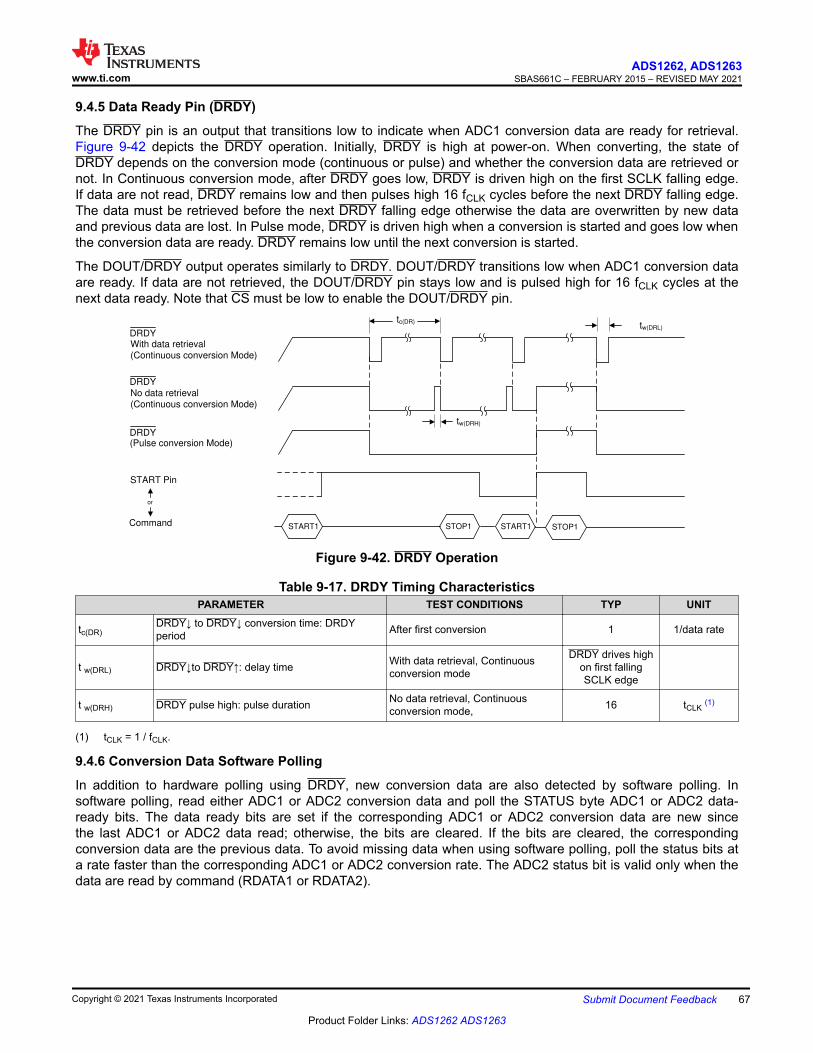
9.4.5 Data Ready Pin (DRDY)
The DRDY pin is an output that transitions low to indicate when ADC1 conversion data are ready for retrieval.Figure 9-42 depicts the DRDY operation. Initially, DRDY is high at power-on. When converting, the state ofDRDY depends on the conversion mode (continuous or pulse) and whether the conversion data are retrieved ornot. In Continuous conversion mode, after DRDY goes low, DRDY is driven high on the first SCLK falling edge.If data are not read, DRDY remains low and then pulses high 16 fCLK cycles before the next DRDY falling edge.The data must be retrieved before the next DRDY falling edge otherwise the data are overwritten by new dataand previous data are lost. In Pulse mode, DRDY is driven high when a conversion is started and goes low whenthe conversion data are ready. DRDY remains low until the next conversion is started.
The DOUT/DRDY output operates similarly to DRDY. DOUT/DRDY transitions low when ADC1 conversion dataare ready. If data are not retrieved, the DOUT/DRDY pin stays low and is pulsed high for 16 fCLK cycles at thenext data ready. Note that CS must be low to enable the DOUT/DRDY pin.
With data retrieval
(Continuous conversion Mode)
START Pin
No data retrieval
(Continuous conversion Mode)
(Pulse conversion Mode)
tw(DRH)
Command START1 START1STOP1
DRDY
DRDY
DRDY
STOP1
tc(DR)tw(DRL)
or
Figure 9-42. DRDY Operation
Table 9-17. DRDY Timing CharacteristicsPARAMETER TEST CONDITIONS TYP UNIT
tc(DR)DRDY↓ to DRDY↓ conversion time: DRDYperiod After first conversion 1 1/data rate
t w(DRL) DRDY↓to DRDY↑: delay time With data retrieval, Continuousconversion mode
DRDY drives highon first fallingSCLK edge
t w(DRH) DRDY pulse high: pulse duration No data retrieval, Continuousconversion mode, 16 tCLK (1)
(1) tCLK = 1 / fCLK.
9.4.6 Conversion Data Software Polling
In addition to hardware polling using DRDY, new conversion data are also detected by software polling. Insoftware polling, read either ADC1 or ADC2 conversion data and poll the STATUS byte ADC1 or ADC2 data-ready bits. The data ready bits are set if the corresponding ADC1 or ADC2 conversion data are new sincethe last ADC1 or ADC2 data read; otherwise, the bits are cleared. If the bits are cleared, the correspondingconversion data are the previous data. To avoid missing data when using software polling, poll the status bits ata rate faster than the corresponding ADC1 or ADC2 conversion rate. The ADC2 status bit is valid only when thedata are read by command (RDATA1 or RDATA2).
www.ti.comADS1262, ADS1263
SBAS661C – FEBRUARY 2015 – REVISED MAY 2021
Copyright © 2021 Texas Instruments Incorporated Submit Document Feedback 67
Product Folder Links: ADS1262 ADS1263
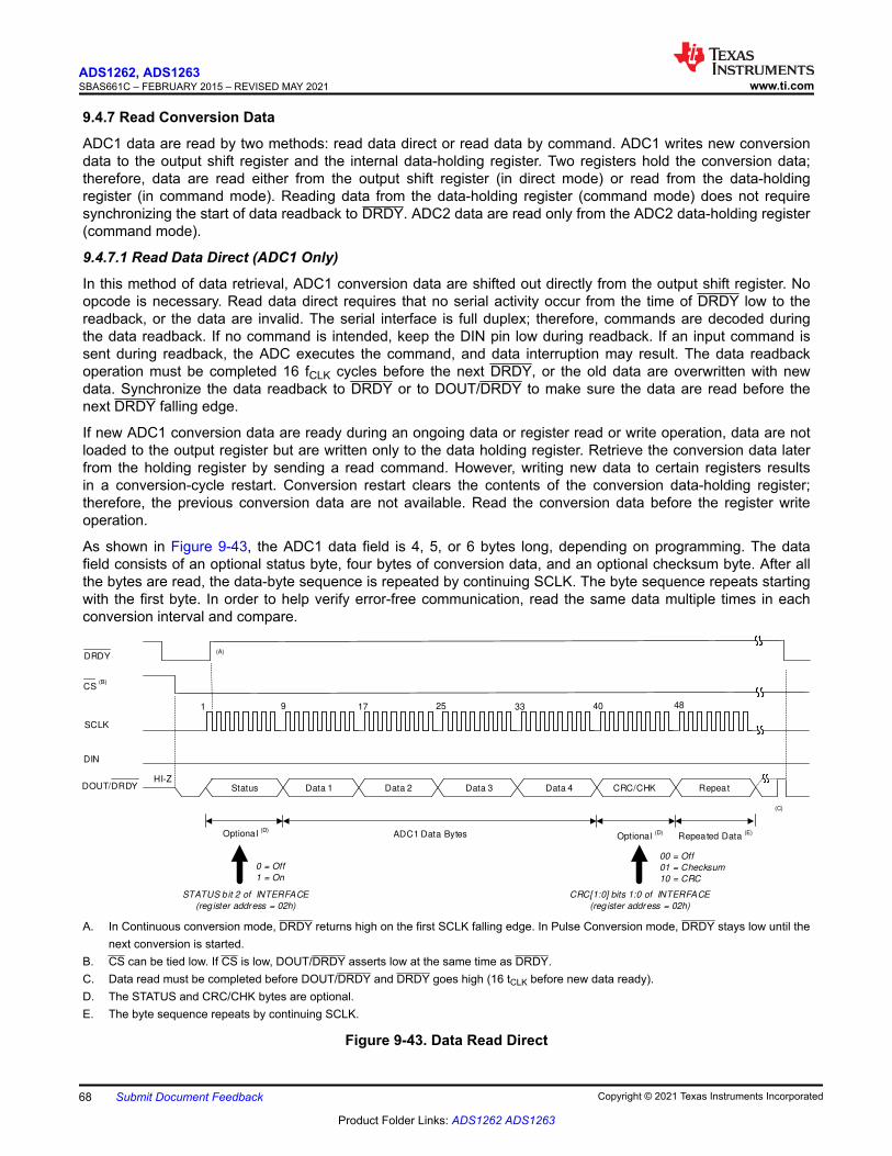
9.4.7 Read Conversion Data
ADC1 data are read by two methods: read data direct or read data by command. ADC1 writes new conversiondata to the output shift register and the internal data-holding register. Two registers hold the conversion data;therefore, data are read either from the output shift register (in direct mode) or read from the data-holdingregister (in command mode). Reading data from the data-holding register (command mode) does not requiresynchronizing the start of data readback to DRDY. ADC2 data are read only from the ADC2 data-holding register(command mode).
9.4.7.1 Read Data Direct (ADC1 Only)
In this method of data retrieval, ADC1 conversion data are shifted out directly from the output shift register. Noopcode is necessary. Read data direct requires that no serial activity occur from the time of DRDY low to thereadback, or the data are invalid. The serial interface is full duplex; therefore, commands are decoded duringthe data readback. If no command is intended, keep the DIN pin low during readback. If an input command issent during readback, the ADC executes the command, and data interruption may result. The data readbackoperation must be completed 16 fCLK cycles before the next DRDY, or the old data are overwritten with newdata. Synchronize the data readback to DRDY or to DOUT/DRDY to make sure the data are read before thenext DRDY falling edge.
If new ADC1 conversion data are ready during an ongoing data or register read or write operation, data are notloaded to the output register but are written only to the data holding register. Retrieve the conversion data laterfrom the holding register by sending a read command. However, writing new data to certain registers resultsin a conversion-cycle restart. Conversion restart clears the contents of the conversion data-holding register;therefore, the previous conversion data are not available. Read the conversion data before the register writeoperation.
As shown in Figure 9-43, the ADC1 data field is 4, 5, or 6 bytes long, depending on programming. The datafield consists of an optional status byte, four bytes of conversion data, and an optional checksum byte. After allthe bytes are read, the data-byte sequence is repeated by continuing SCLK. The byte sequence repeats startingwith the first byte. In order to help verify error-free communication, read the same data multiple times in eachconversion interval and compare.
Status Data 1
ADC1 Data BytesOptional (D)
Optional (D)
DIN
SCLK
CS
HI-Z
DRDY
(C)
(A)
(B)
Repeat
Repeated Data (E)
DOUT/DRDY Data 2 Data 3 Data 4 CRC/CHK
1 9 17 25 33 40 48
STATUS bit 2 of INTERFACE
(reg ister address = 02h)
CRC[1:0] bits 1:0 of INTERFACE
(reg ister address = 02h)
0 = Off
1 = On
00 = Off
01 = Checksum
10 = CRC
A. In Continuous conversion mode, DRDY returns high on the first SCLK falling edge. In Pulse Conversion mode, DRDY stays low until thenext conversion is started.
B. CS can be tied low. If CS is low, DOUT/DRDY asserts low at the same time as DRDY.C. Data read must be completed before DOUT/DRDY and DRDY goes high (16 tCLK before new data ready).D. The STATUS and CRC/CHK bytes are optional.E. The byte sequence repeats by continuing SCLK.
Figure 9-43. Data Read Direct
ADS1262, ADS1263SBAS661C – FEBRUARY 2015 – REVISED MAY 2021 www.ti.com
68 Submit Document Feedback Copyright © 2021 Texas Instruments Incorporated
Product Folder Links: ADS1262 ADS1263
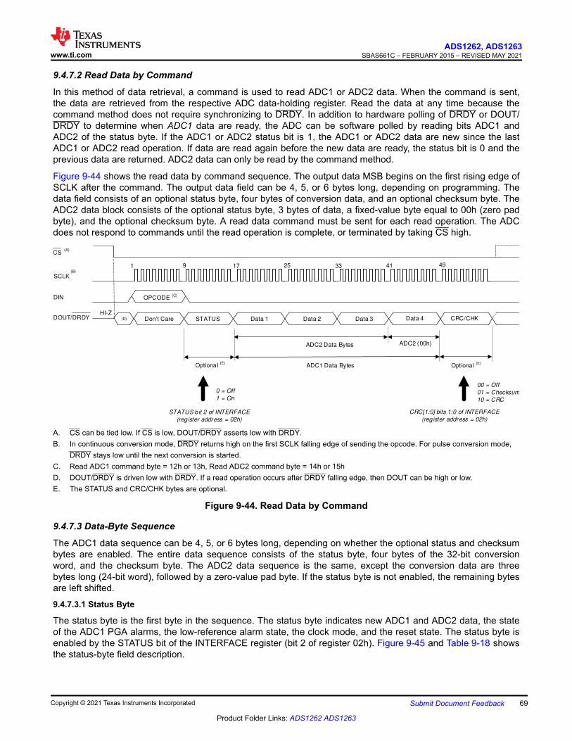
9.4.7.2 Read Data by Command
In this method of data retrieval, a command is used to read ADC1 or ADC2 data. When the command is sent,the data are retrieved from the respective ADC data-holding register. Read the data at any time because thecommand method does not require synchronizing to DRDY. In addition to hardware polling of DRDY or DOUT/DRDY to determine when ADC1 data are ready, the ADC can be software polled by reading bits ADC1 andADC2 of the status byte. If the ADC1 or ADC2 status bit is 1, the ADC1 or ADC2 data are new since the lastADC1 or ADC2 read operation. If data are read again before the new data are ready, the status bit is 0 and theprevious data are returned. ADC2 data can only be read by the command method.
Figure 9-44 shows the read data by command sequence. The output data MSB begins on the first rising edge ofSCLK after the command. The output data field can be 4, 5, or 6 bytes long, depending on programming. Thedata field consists of an optional status byte, four bytes of conversion data, and an optional checksum byte. TheADC2 data block consists of the optional status byte, 3 bytes of data, a fixed-value byte equal to 00h (zero padbyte), and the optional checksum byte. A read data command must be sent for each read operation. The ADCdoes not respond to commands until the read operation is complete, or terminated by taking CS high.
Don¶t Care STATUS
ADC1 Data BytesOptional (E)
Optional (E)
DIN
SCLK
CS
HI-Z
(B)
(A)
DOUT/DRDY Data 1 Data 2 Data 3 CRC/CHK
1 9 17 25 33 41 49
STATUS bit 2 of INTERFACE
(register address = 02h)
CRC[1:0] bits 1:0 of INTERFACE
(reg ister address = 02h)
ADC2 Data Bytes
OPCODE (C)
Data 4(D)
00 = Off
01 = Checksum
10 = CRC
0 = Off
1 = On
ADC2 (00h)
A. CS can be tied low. If CS is low, DOUT/DRDY asserts low with DRDY.B. In continuous conversion mode, DRDY returns high on the first SCLK falling edge of sending the opcode. For pulse conversion mode,
DRDY stays low until the next conversion is started.C. Read ADC1 command byte = 12h or 13h, Read ADC2 command byte = 14h or 15hD. DOUT/DRDY is driven low with DRDY. If a read operation occurs after DRDY falling edge, then DOUT can be high or low.E. The STATUS and CRC/CHK bytes are optional.
Figure 9-44. Read Data by Command
9.4.7.3 Data-Byte Sequence
The ADC1 data sequence can be 4, 5, or 6 bytes long, depending on whether the optional status and checksumbytes are enabled. The entire data sequence consists of the status byte, four bytes of the 32-bit conversionword, and the checksum byte. The ADC2 data sequence is the same, except the conversion data are threebytes long (24-bit word), followed by a zero-value pad byte. If the status byte is not enabled, the remaining bytesare left shifted.
9.4.7.3.1 Status Byte
The status byte is the first byte in the sequence. The status byte indicates new ADC1 and ADC2 data, the stateof the ADC1 PGA alarms, the low-reference alarm state, the clock mode, and the reset state. The status byte isenabled by the STATUS bit of the INTERFACE register (bit 2 of register 02h). Figure 9-45 and Table 9-18 showsthe status-byte field description.
www.ti.comADS1262, ADS1263
SBAS661C – FEBRUARY 2015 – REVISED MAY 2021
Copyright © 2021 Texas Instruments Incorporated Submit Document Feedback 69
Product Folder Links: ADS1262 ADS1263
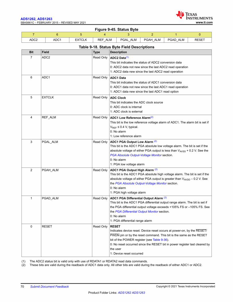
Figure 9-45. Status Byte7 6 5 4 3 2 1 0
ADC2 ADC1 EXTCLK REF_ALM PGAL_ALM PGAH_ALM PGAD_ALM RESET
Table 9-18. Status Byte Field DescriptionsBit Field Type Description7 ADC2 Read Only ADC2 Data(1)
This bit indicates the status of ADC2 conversion data0: ADC2 data not new since the last ADC2 read operation1: ADC2 data new since the last ADC2 read operation
6 ADC1 Read Only ADC1 DataThis bit indicates the status of ADC1 conversion data0: ADC1 data not new since the last ADC1 read operation1: ADC1 data new since the last ADC1 read option
5 EXTCLK Read Only ADC ClockThis bit indicates the ADC clock source0: ADC clock is internal1: ADC clock is external
4 REF_ALM Read Only ADC1 Low Reference Alarm(2)
This bit is the low reference voltage alarm of ADC1. The alarm bit is set ifVREF ≤ 0.4 V, typical.0: No alarm1: Low reference alarm
3 PGAL_ALM Read Only ADC1 PGA Output Low Alarm (2)
This bit is the ADC1 PGA absolute low voltage alarm. The bit is set if theabsolute voltage of either PGA output is less than VAVSS + 0.2 V. See thePGA Absolute Output-Voltage Monitor section.0: No alarm1: PGA low voltage alarm
2 PGAH_ALM Read Only ADC1 PGA Output High Alarm (2)
This bit is the ADC1 PGA absolute high voltage alarm. The bit is set if theabsolute voltage of either PGA output is greater than VAVDD – 0.2 V. Seethe PGA Absolute Output-Voltage Monitor section.0: No alarm1: PGA high voltage alarm
1 PGAD_ALM Read Only ADC1 PGA Differential Output Alarm (2)
This bit is the ADC1 PGA differential output range alarm. The bit is set ifthe PGA differential output voltage exceeds +105% FS or –105% FS. Seethe PGA Differential Output Monitor section.0: No alarm1: PGA differential range alarm
0 RESET Read Only RESETIndicates device reset. Device reset occurs at power-on, by the RESET/PWDN pin or by the reset command. This bit is the same as the RESETbit of the POWER register (see Table 9-36).0: No reset occurred since the RESET bit in power register last cleared bythe user1: Device reset occurred
(1) The ADC2 status bit is valid only with use of RDATA1 or RDATA2 read data commands.(2) These bits are valid during the readback of ADC1 data only. All other bits are valid during the readback of either ADC1 or ADC2.
ADS1262, ADS1263SBAS661C – FEBRUARY 2015 – REVISED MAY 2021 www.ti.com
70 Submit Document Feedback Copyright © 2021 Texas Instruments Incorporated
Product Folder Links: ADS1262 ADS1263
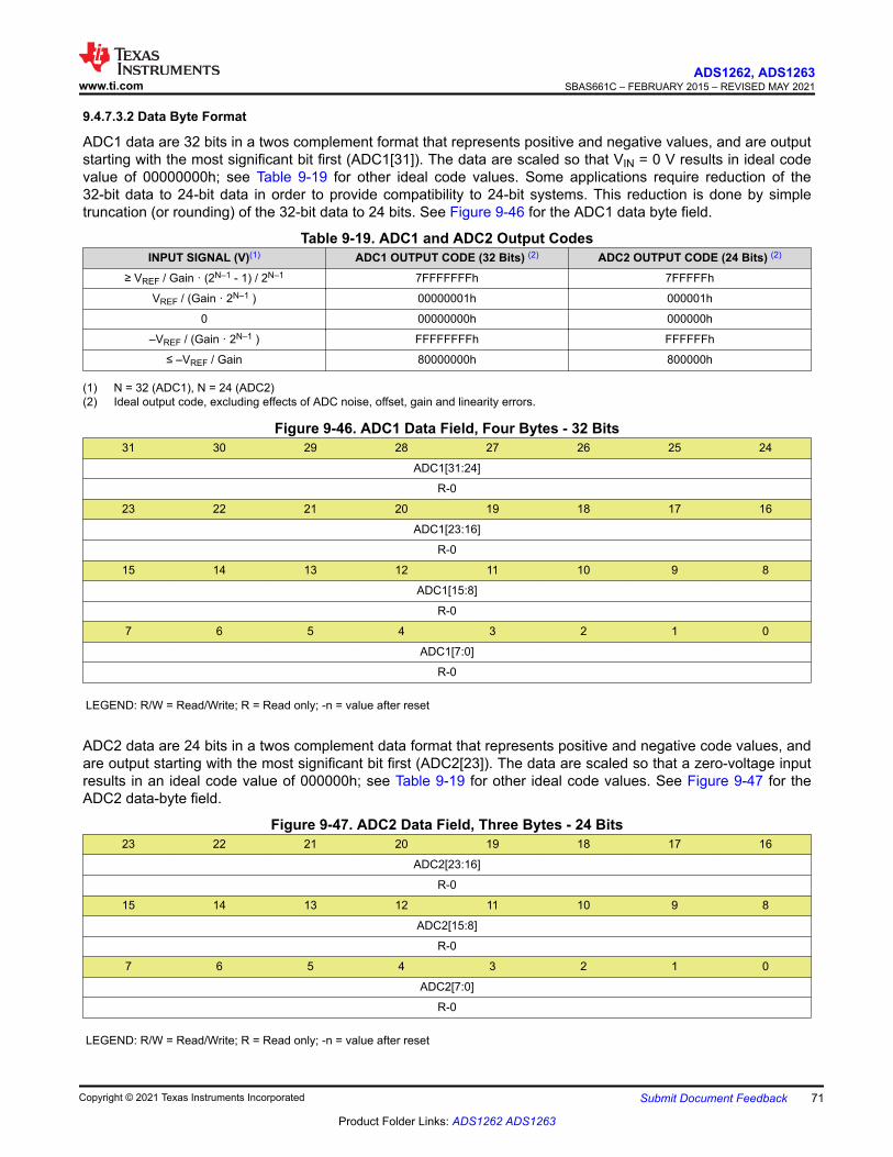
9.4.7.3.2 Data Byte Format
ADC1 data are 32 bits in a twos complement format that represents positive and negative values, and are outputstarting with the most significant bit first (ADC1[31]). The data are scaled so that VIN = 0 V results in ideal codevalue of 00000000h; see Table 9-19 for other ideal code values. Some applications require reduction of the32-bit data to 24-bit data in order to provide compatibility to 24-bit systems. This reduction is done by simpletruncation (or rounding) of the 32-bit data to 24 bits. See Figure 9-46 for the ADC1 data byte field.
Table 9-19. ADC1 and ADC2 Output CodesINPUT SIGNAL (V)(1) ADC1 OUTPUT CODE (32 Bits) (2) ADC2 OUTPUT CODE (24 Bits) (2)
≥ VREF / Gain · (2N–1 - 1) / 2N–1 7FFFFFFFh 7FFFFFh
VREF / (Gain · 2N–1 ) 00000001h 000001h
0 00000000h 000000h
–VREF / (Gain · 2N–1 ) FFFFFFFFh FFFFFFh
≤ –VREF / Gain 80000000h 800000h
(1) N = 32 (ADC1), N = 24 (ADC2)(2) Ideal output code, excluding effects of ADC noise, offset, gain and linearity errors.
Figure 9-46. ADC1 Data Field, Four Bytes - 32 Bits31 30 29 28 27 26 25 24
ADC1[31:24]
R-0
23 22 21 20 19 18 17 16
ADC1[23:16]
R-0
15 14 13 12 11 10 9 8
ADC1[15:8]
R-0
7 6 5 4 3 2 1 0
ADC1[7:0]
R-0
LEGEND: R/W = Read/Write; R = Read only; -n = value after reset
ADC2 data are 24 bits in a twos complement data format that represents positive and negative code values, andare output starting with the most significant bit first (ADC2[23]). The data are scaled so that a zero-voltage inputresults in an ideal code value of 000000h; see Table 9-19 for other ideal code values. See Figure 9-47 for theADC2 data-byte field.
Figure 9-47. ADC2 Data Field, Three Bytes - 24 Bits23 22 21 20 19 18 17 16
ADC2[23:16]
R-0
15 14 13 12 11 10 9 8
ADC2[15:8]
R-0
7 6 5 4 3 2 1 0
ADC2[7:0]
R-0
LEGEND: R/W = Read/Write; R = Read only; -n = value after reset
www.ti.comADS1262, ADS1263
SBAS661C – FEBRUARY 2015 – REVISED MAY 2021
Copyright © 2021 Texas Instruments Incorporated Submit Document Feedback 71
Product Folder Links: ADS1262 ADS1263
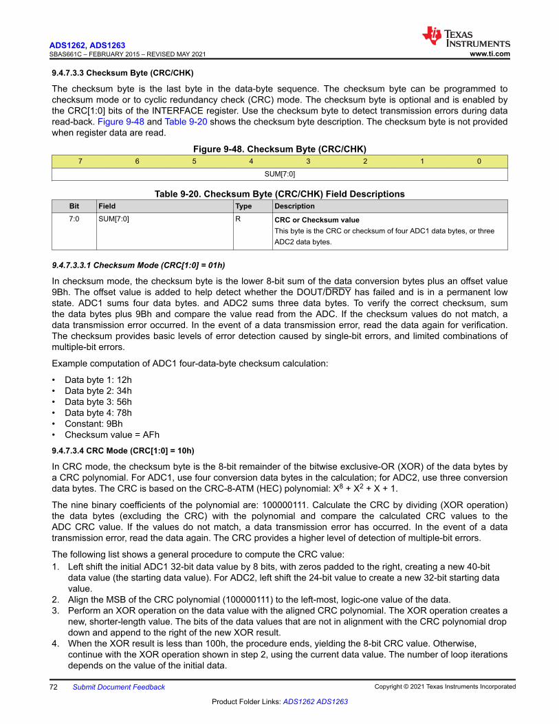
9.4.7.3.3 Checksum Byte (CRC/CHK)
The checksum byte is the last byte in the data-byte sequence. The checksum byte can be programmed tochecksum mode or to cyclic redundancy check (CRC) mode. The checksum byte is optional and is enabled bythe CRC[1:0] bits of the INTERFACE register. Use the checksum byte to detect transmission errors during dataread-back. Figure 9-48 and Table 9-20 shows the checksum byte description. The checksum byte is not providedwhen register data are read.
Figure 9-48. Checksum Byte (CRC/CHK)7 6 5 4 3 2 1 0
SUM[7:0]
Table 9-20. Checksum Byte (CRC/CHK) Field DescriptionsBit Field Type Description7:0 SUM[7:0] R CRC or Checksum value
This byte is the CRC or checksum of four ADC1 data bytes, or threeADC2 data bytes.
9.4.7.3.3.1 Checksum Mode (CRC[1:0] = 01h)
In checksum mode, the checksum byte is the lower 8-bit sum of the data conversion bytes plus an offset value9Bh. The offset value is added to help detect whether the DOUT/DRDY has failed and is in a permanent lowstate. ADC1 sums four data bytes. and ADC2 sums three data bytes. To verify the correct checksum, sumthe data bytes plus 9Bh and compare the value read from the ADC. If the checksum values do not match, adata transmission error occurred. In the event of a data transmission error, read the data again for verification.The checksum provides basic levels of error detection caused by single-bit errors, and limited combinations ofmultiple-bit errors.
Example computation of ADC1 four-data-byte checksum calculation:
• Data byte 1: 12h• Data byte 2: 34h• Data byte 3: 56h• Data byte 4: 78h• Constant: 9Bh• Checksum value = AFh
9.4.7.3.4 CRC Mode (CRC[1:0] = 10h)
In CRC mode, the checksum byte is the 8-bit remainder of the bitwise exclusive-OR (XOR) of the data bytes bya CRC polynomial. For ADC1, use four conversion data bytes in the calculation; for ADC2, use three conversiondata bytes. The CRC is based on the CRC-8-ATM (HEC) polynomial: X8 + X2 + X + 1.
The nine binary coefficients of the polynomial are: 100000111. Calculate the CRC by dividing (XOR operation)the data bytes (excluding the CRC) with the polynomial and compare the calculated CRC values to theADC CRC value. If the values do not match, a data transmission error has occurred. In the event of a datatransmission error, read the data again. The CRC provides a higher level of detection of multiple-bit errors.
The following list shows a general procedure to compute the CRC value:1. Left shift the initial ADC1 32-bit data value by 8 bits, with zeros padded to the right, creating a new 40-bit
data value (the starting data value). For ADC2, left shift the 24-bit value to create a new 32-bit starting datavalue.
2. Align the MSB of the CRC polynomial (100000111) to the left-most, logic-one value of the data.3. Perform an XOR operation on the data value with the aligned CRC polynomial. The XOR operation creates a
new, shorter-length value. The bits of the data values that are not in alignment with the CRC polynomial dropdown and append to the right of the new XOR result.
4. When the XOR result is less than 100h, the procedure ends, yielding the 8-bit CRC value. Otherwise,continue with the XOR operation shown in step 2, using the current data value. The number of loop iterationsdepends on the value of the initial data.
ADS1262, ADS1263SBAS661C – FEBRUARY 2015 – REVISED MAY 2021 www.ti.com
72 Submit Document Feedback Copyright © 2021 Texas Instruments Incorporated
Product Folder Links: ADS1262 ADS1263
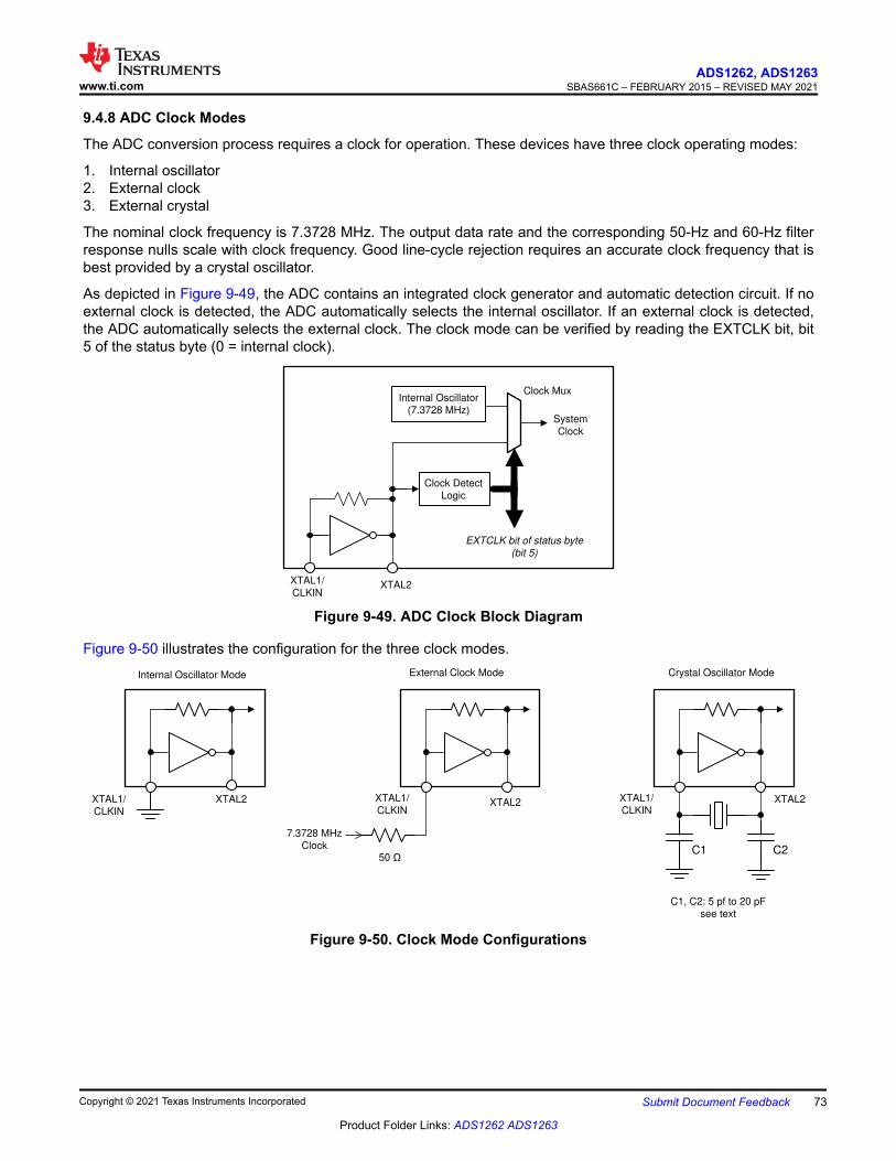
9.4.8 ADC Clock Modes
The ADC conversion process requires a clock for operation. These devices have three clock operating modes:
1. Internal oscillator2. External clock3. External crystal
The nominal clock frequency is 7.3728 MHz. The output data rate and the corresponding 50-Hz and 60-Hz filterresponse nulls scale with clock frequency. Good line-cycle rejection requires an accurate clock frequency that isbest provided by a crystal oscillator.
As depicted in Figure 9-49, the ADC contains an integrated clock generator and automatic detection circuit. If noexternal clock is detected, the ADC automatically selects the internal oscillator. If an external clock is detected,the ADC automatically selects the external clock. The clock mode can be verified by reading the EXTCLK bit, bit5 of the status byte (0 = internal clock).
XTAL1/
CLKINXTAL2
Clock Detect
Logic
Internal Oscillator
(7.3728 MHz)System
Clock
EXTCLK bit of status byte
(bit 5)
Clock Mux
Figure 9-49. ADC Clock Block Diagram
Figure 9-50 illustrates the configuration for the three clock modes.
XTAL1/
CLKIN
XTAL2
Internal Oscillator Mode
XTAL1/
CLKINXTAL2
External Clock Mode
7.3728 MHz
Clock
XTAL1/
CLKINXTAL2
Crystal Oscillator Mode
C1 C2
C1, C2: 5 pf to 20 pF
see text
50 ��
Figure 9-50. Clock Mode Configurations
www.ti.comADS1262, ADS1263
SBAS661C – FEBRUARY 2015 – REVISED MAY 2021
Copyright © 2021 Texas Instruments Incorporated Submit Document Feedback 73
Product Folder Links: ADS1262 ADS1263
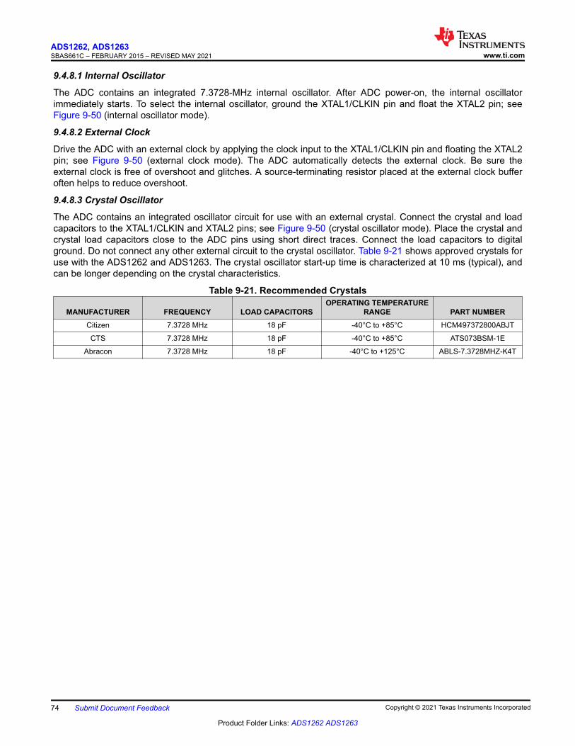
9.4.8.1 Internal Oscillator
The ADC contains an integrated 7.3728-MHz internal oscillator. After ADC power-on, the internal oscillatorimmediately starts. To select the internal oscillator, ground the XTAL1/CLKIN pin and float the XTAL2 pin; seeFigure 9-50 (internal oscillator mode).
9.4.8.2 External Clock
Drive the ADC with an external clock by applying the clock input to the XTAL1/CLKIN pin and floating the XTAL2pin; see Figure 9-50 (external clock mode). The ADC automatically detects the external clock. Be sure theexternal clock is free of overshoot and glitches. A source-terminating resistor placed at the external clock bufferoften helps to reduce overshoot.
9.4.8.3 Crystal Oscillator
The ADC contains an integrated oscillator circuit for use with an external crystal. Connect the crystal and loadcapacitors to the XTAL1/CLKIN and XTAL2 pins; see Figure 9-50 (crystal oscillator mode). Place the crystal andcrystal load capacitors close to the ADC pins using short direct traces. Connect the load capacitors to digitalground. Do not connect any other external circuit to the crystal oscillator. Table 9-21 shows approved crystals foruse with the ADS1262 and ADS1263. The crystal oscillator start-up time is characterized at 10 ms (typical), andcan be longer depending on the crystal characteristics.
Table 9-21. Recommended Crystals
MANUFACTURER FREQUENCY LOAD CAPACITORSOPERATING TEMPERATURE
RANGE PART NUMBERCitizen 7.3728 MHz 18 pF -40°C to +85°C HCM497372800ABJT
CTS 7.3728 MHz 18 pF -40°C to +85°C ATS073BSM-1E
Abracon 7.3728 MHz 18 pF -40°C to +125°C ABLS-7.3728MHZ-K4T
ADS1262, ADS1263SBAS661C – FEBRUARY 2015 – REVISED MAY 2021 www.ti.com
74 Submit Document Feedback Copyright © 2021 Texas Instruments Incorporated
Product Folder Links: ADS1262 ADS1263
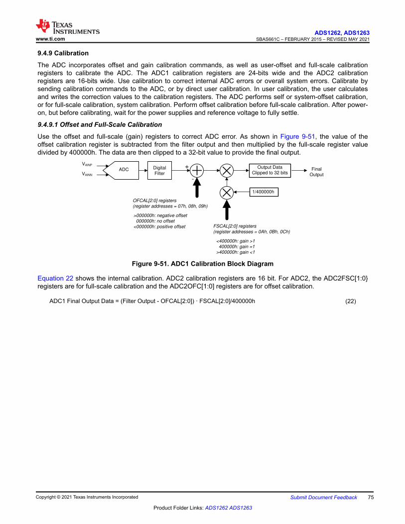
9.4.9 Calibration
The ADC incorporates offset and gain calibration commands, as well as user-offset and full-scale calibrationregisters to calibrate the ADC. The ADC1 calibration registers are 24-bits wide and the ADC2 calibrationregisters are 16-bits wide. Use calibration to correct internal ADC errors or overall system errors. Calibrate bysending calibration commands to the ADC, or by direct user calibration. In user calibration, the user calculatesand writes the correction values to the calibration registers. The ADC performs self or system-offset calibration,or for full-scale calibration, system calibration. Perform offset calibration before full-scale calibration. After power-on, but before calibrating, wait for the power supplies and reference voltage to fully settle.
9.4.9.1 Offset and Full-Scale Calibration
Use the offset and full-scale (gain) registers to correct ADC error. As shown in Figure 9-51, the value of theoffset calibration register is subtracted from the filter output and then multiplied by the full-scale register valuedivided by 400000h. The data are then clipped to a 32-bit value to provide the final output.
+
OFCAL[2:0] registers
(register addresses = 07h, 08h, 09h)
VAINP
1/400000h
FSCAL[2:0] registers
(register addresses = 0Ah, 0Bh, 0Ch)
-
Digital
Filter
ADC
ADCOutput Data
Clipped to 32 bitsFinal
OutputVAINN
>000000h: negative offset
000000h: no offset
<000000h: positive offset
<400000h: gain >1
400000h: gain =1
>400000h: gain <1
Figure 9-51. ADC1 Calibration Block Diagram
Equation 22 shows the internal calibration. ADC2 calibration registers are 16 bit. For ADC2, the ADC2FSC[1:0}registers are for full-scale calibration and the ADC2OFC[1:0] registers are for offset calibration.
ADC1 Final Output Data = (Filter Output - OFCAL[2:0]) · FSCAL[2:0]/400000h (22)
www.ti.comADS1262, ADS1263
SBAS661C – FEBRUARY 2015 – REVISED MAY 2021
Copyright © 2021 Texas Instruments Incorporated Submit Document Feedback 75
Product Folder Links: ADS1262 ADS1263
9.4.9.1.1 Offset Calibration Registers
The ADC1 offset calibration word is 24 bits, consisting of three 8-bit registers, as shown in Table 9-22. The offsetvalue is twos complement format with a maximum positive value equal to 7FFFFFh (for negative offset), anda maximum negative value equal to 800000h (for positive offset). The 24-bit register is internally left-shifted toalign with the 32-bit data before subtraction occurs. A register value equal to 000000h has no offset correction.Although the offset calibration register allows a wide range of offset values, the input signal cannot exceed±106% of the precalibrated range in order to prevent ADC overrange. If chop mode is enabled, the offsetcalibration register is disabled. Table 9-23 shows example settings of the offset register.
Table 9-22. ADC1 Offset Calibration Registers
REGISTERBYTE
ORDER ADDRESS BIT ORDEROFCAL0 LSB 07h B7 B6 B5 B4 B3 B2 B1 B0 (LSB)
OFCAL1 MID 08h B15 B14 B13 B12 B11 B10 B9 B8
OFCAL2 MSB 09h B23 (MSB) B22 B21 B20 B19 B18 B17 B16
Table 9-23. ADC1 Offset Calibration Register ValuesOFCAL[2:0] REGISTER VALUE OFFSET CALIBRATED 32-BIT OUTPUT CODE(1)
000001h FFFFFF00h
000000h 00000000h
FFFFFFh 00000100h
(1) Ideal output code with shorted input, excluding ADC noise and offset voltage error.
The ADC2 offset calibration word is 16 bits, consisting of two 8-bit registers, as shown in Table 9-24. The16-bit calibration value is internally aligned with the 24-bit ADC2 conversion result. The offset calibration value issubtracted from the conversion data.
Table 9-24. ADC2 Offset Calibration Registers
REGISTERBYTE
ORDER ADDRESS BIT ORDERADC2OFC0 LSB 17h B7 B6 B5 B4 B3 B2 B1 B0 (LSB)
ADC2OFC1 MSB 18h B15 B14 B13 B12 B11 B10 B9 B8
ADS1262, ADS1263SBAS661C – FEBRUARY 2015 – REVISED MAY 2021 www.ti.com
76 Submit Document Feedback Copyright © 2021 Texas Instruments Incorporated
Product Folder Links: ADS1262 ADS1263
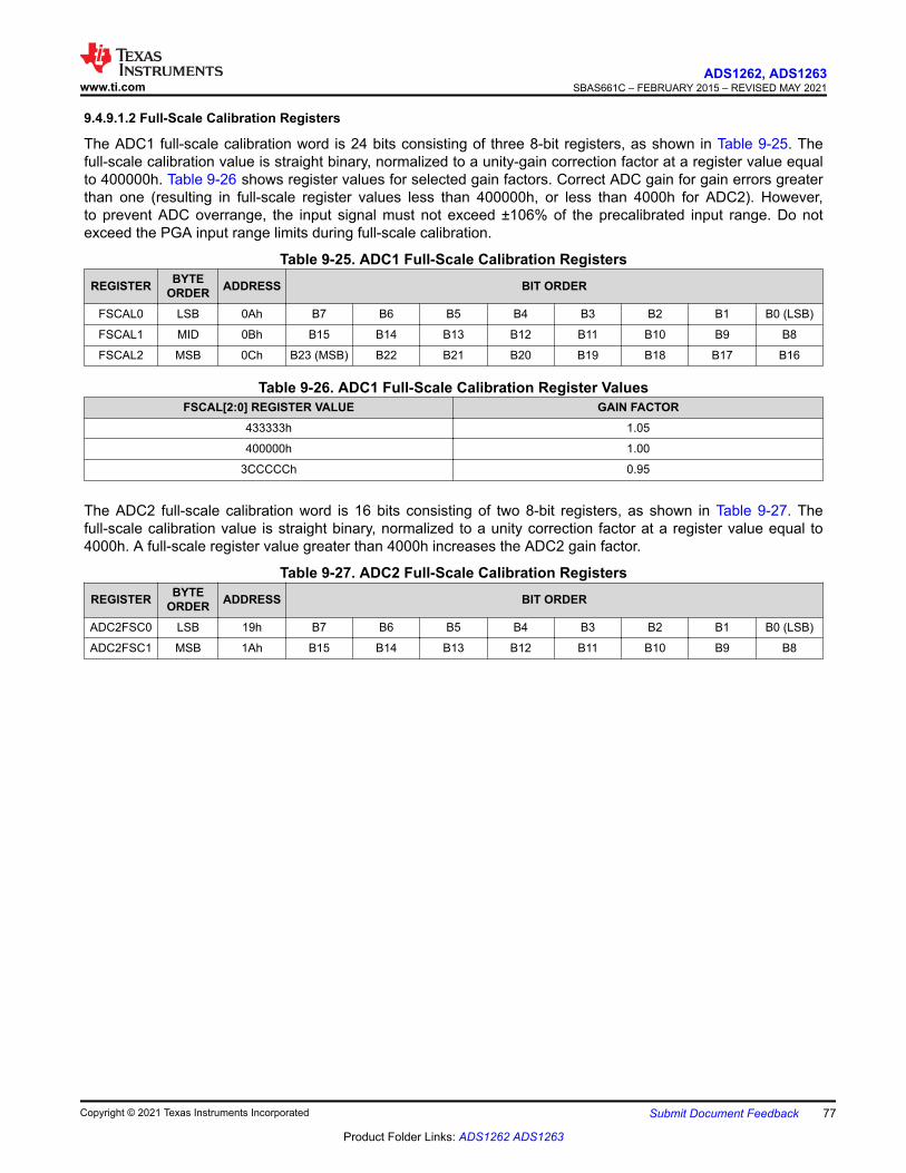
9.4.9.1.2 Full-Scale Calibration Registers
The ADC1 full-scale calibration word is 24 bits consisting of three 8-bit registers, as shown in Table 9-25. Thefull-scale calibration value is straight binary, normalized to a unity-gain correction factor at a register value equalto 400000h. Table 9-26 shows register values for selected gain factors. Correct ADC gain for gain errors greaterthan one (resulting in full-scale register values less than 400000h, or less than 4000h for ADC2). However,to prevent ADC overrange, the input signal must not exceed ±106% of the precalibrated input range. Do notexceed the PGA input range limits during full-scale calibration.
Table 9-25. ADC1 Full-Scale Calibration RegistersREGISTER BYTE
ORDER ADDRESS BIT ORDER
FSCAL0 LSB 0Ah B7 B6 B5 B4 B3 B2 B1 B0 (LSB)
FSCAL1 MID 0Bh B15 B14 B13 B12 B11 B10 B9 B8
FSCAL2 MSB 0Ch B23 (MSB) B22 B21 B20 B19 B18 B17 B16
Table 9-26. ADC1 Full-Scale Calibration Register ValuesFSCAL[2:0] REGISTER VALUE GAIN FACTOR
433333h 1.05
400000h 1.00
3CCCCCh 0.95
The ADC2 full-scale calibration word is 16 bits consisting of two 8-bit registers, as shown in Table 9-27. Thefull-scale calibration value is straight binary, normalized to a unity correction factor at a register value equal to4000h. A full-scale register value greater than 4000h increases the ADC2 gain factor.
Table 9-27. ADC2 Full-Scale Calibration RegistersREGISTER BYTE
ORDER ADDRESS BIT ORDER
ADC2FSC0 LSB 19h B7 B6 B5 B4 B3 B2 B1 B0 (LSB)
ADC2FSC1 MSB 1Ah B15 B14 B13 B12 B11 B10 B9 B8
www.ti.comADS1262, ADS1263
SBAS661C – FEBRUARY 2015 – REVISED MAY 2021
Copyright © 2021 Texas Instruments Incorporated Submit Document Feedback 77
Product Folder Links: ADS1262 ADS1263
9.4.9.2 ADC1 Offset Self-Calibration (SFOCAL1)
The offset self-calibration command corrects internal ADC1 offset error. Program the ADC1 input multiplexerregister (INPMUX) to FFh to force open all input connections before sending the command. When the SFOCAL1self-calibration command is sent, the ADC shorts together the internal PGA inputs, then averages 16 readingsto reduce the conversion noise for an accurate calibration. When calibration is complete, the calibration resultis written to the 24-bit offset calibration register (OFCAL[2:0]). After calibration, set the input multiplexer to thedesired measurement channel. The offset calibration register is disabled in chop mode.
9.4.9.3 ADC1 Offset System Calibration (SYOCAL1)
The offset system-calibration command corrects ADC1 system offset error. For this type of calibration, externallyshort the system inputs before the command. When the SYSOCAL1 command is sent, the ADC averages16 readings to reduce conversion noise for an accurate calibration. When calibration is complete, the offsetcalibration result is written to the 24-bit offset calibration register (OFCAL[2:0]). The offset calibration register isdisabled in chop mode.
9.4.9.4 ADC2 Offset Self-Calibration ADC2 (SFOCAL2)
The offset self-calibration command corrects internal ADC2 offset error. Program the ADC2 input multiplexerregister (ADC2MUX) to FFh to force open all input connections before sending the command. When theSFOCAL2 self-calibration command is sent, the ADC shorts together the internal PGA inputs of ADC2, thenaverages 16 readings to reduce conversion noise for an accurate calibration. When calibration is complete, theoffset calibration result is written to the 16-bit ADC2 offset calibration register ADC2OFC[1:0]. After calibration,set the input multiplexer to the desired channel.
9.4.9.5 ADC2 Offset System Calibration ADC2 (SYOCAL2)
The offset system-calibration command corrects ADC2 system offset error. For this offset calibration, externallyshort the ADC2 inputs before sending the command. When the SYOCAL2 command is sent, the ADC averages16 readings to reduce conversion noise for an accurate calibration. When calibration is complete, the calibrationresult is written to the 16-bit ADC2 offset calibration register (ADC2OFC[1:0)].
9.4.9.6 ADC1 Full-Scale System Calibration (SYGCAL1)
The full-scale calibration command corrects ADC1 system gain error. To calibrate, apply a positive full-scaledc signal to the ADC, wait until the signal is fully settled, and then send the command. When the SYGCAL1command is sent, the ADC averages 16 readings to reduce conversion noise for an accurate calibration. Whencalibration completes, the ADC computes a full-scale calibration where the applied voltage calibrates to apositive full-scale code value. The computed result is written to the 24-bit offset calibration register (FSCAL[2:0]).The precalibrated ADC overrange limitation is 106% FSR.
9.4.9.7 ADC2 Full-Scale System Calibration ADC2 (SYGCAL2)
The full-scale system calibration command corrects ADC2 system gain error. To calibrate, apply a positive full-scale dc signal to ADC2, wait until the signal is fully settled, and then send the command. When the SYGCAL2command is sent, the ADC averages 16 readings to reduce conversion noise for an accurate calibration. Whencalibration is complete, the full-scale calibration is computed so that applied voltage calibrates to positive fullscale. The computed result is written to the ADC2 16-bit, full-scale calibration register (ADC2FSC[1:0]). Theprecalibrated ADC overrange limitation is 106% FSR.
ADS1262, ADS1263SBAS661C – FEBRUARY 2015 – REVISED MAY 2021 www.ti.com
78 Submit Document Feedback Copyright © 2021 Texas Instruments Incorporated
Product Folder Links: ADS1262 ADS1263
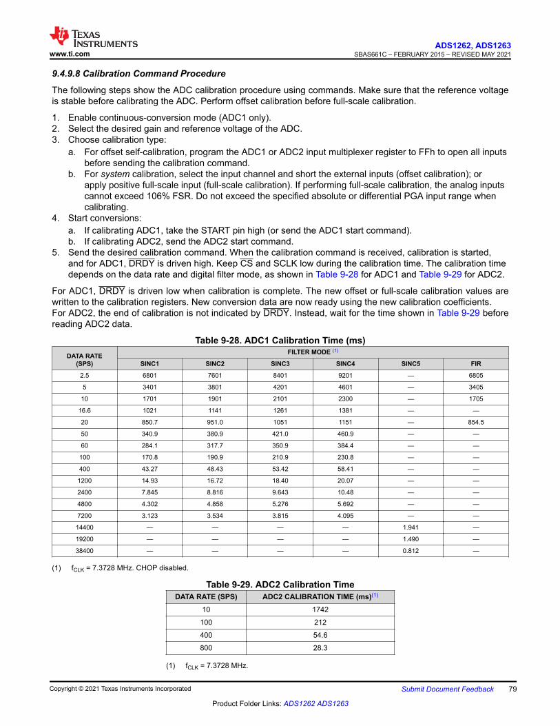
9.4.9.8 Calibration Command Procedure
The following steps show the ADC calibration procedure using commands. Make sure that the reference voltageis stable before calibrating the ADC. Perform offset calibration before full-scale calibration.
1. Enable continuous-conversion mode (ADC1 only).2. Select the desired gain and reference voltage of the ADC.3. Choose calibration type:
a. For offset self-calibration, program the ADC1 or ADC2 input multiplexer register to FFh to open all inputsbefore sending the calibration command.
b. For system calibration, select the input channel and short the external inputs (offset calibration); orapply positive full-scale input (full-scale calibration). If performing full-scale calibration, the analog inputscannot exceed 106% FSR. Do not exceed the specified absolute or differential PGA input range whencalibrating.
4. Start conversions:a. If calibrating ADC1, take the START pin high (or send the ADC1 start command).b. If calibrating ADC2, send the ADC2 start command.
5. Send the desired calibration command. When the calibration command is received, calibration is started,and for ADC1, DRDY is driven high. Keep CS and SCLK low during the calibration time. The calibration timedepends on the data rate and digital filter mode, as shown in Table 9-28 for ADC1 and Table 9-29 for ADC2.
For ADC1, DRDY is driven low when calibration is complete. The new offset or full-scale calibration values arewritten to the calibration registers. New conversion data are now ready using the new calibration coefficients.For ADC2, the end of calibration is not indicated by DRDY. Instead, wait for the time shown in Table 9-29 beforereading ADC2 data.
Table 9-28. ADC1 Calibration Time (ms)DATA RATE
(SPS)
FILTER MODE (1)
SINC1 SINC2 SINC3 SINC4 SINC5 FIR
2.5 6801 7601 8401 9201 — 6805
5 3401 3801 4201 4601 — 3405
10 1701 1901 2101 2300 — 1705
16.6 1021 1141 1261 1381 — —
20 850.7 951.0 1051 1151 — 854.5
50 340.9 380.9 421.0 460.9 — —
60 284.1 317.7 350.9 384.4 — —
100 170.8 190.9 210.9 230.8 — —
400 43.27 48.43 53.42 58.41 — —
1200 14.93 16.72 18.40 20.07 — —
2400 7.845 8.816 9.643 10.48 — —
4800 4.302 4.858 5.276 5.692 — —
7200 3.123 3.534 3.815 4.095 — —
14400 — — — — 1.941 —
19200 — — — — 1.490 —
38400 — — — — 0.812 —
(1) fCLK = 7.3728 MHz. CHOP disabled.
Table 9-29. ADC2 Calibration TimeDATA RATE (SPS) ADC2 CALIBRATION TIME (ms)(1)
10 1742
100 212
400 54.6
800 28.3
(1) fCLK = 7.3728 MHz.
www.ti.comADS1262, ADS1263
SBAS661C – FEBRUARY 2015 – REVISED MAY 2021
Copyright © 2021 Texas Instruments Incorporated Submit Document Feedback 79
Product Folder Links: ADS1262 ADS1263
9.4.9.9 User Calibration Procedure
The user calibration procedure is similar to the calibration command procedure, except the user computes thecalibration coefficients and writes the corresponding values to the calibration registers. Before starting usercalibration, preset the ADC1 offset and full-scale registers to 000000h and 400000h, respectively.
For ADC2, preset the offset and full-scale registers to 0000h and 4000h, respectively.
For offset calibration, short the ADC inputs or system inputs and average the conversions (averaging reducesnoise for a more accurate calibration). Write the average value to the offset calibration registers. The ADCsubtracts the value from the conversion result.
For full-scale calibration, apply a dc calibration voltage that is less than positive full scale to avoid clipped codes(VIN < +FSR), and average the conversions to reduce noise for a more accurate calibration. Full-scale calibrationis computed as shown in Equation 23:
Full-Scale Calibration = (Expected Code Value / Actual Code Value) × NF (23)
where
• NF = Normalization Factor = 400000h for ADC1, or 4000h for ADC2
If the actual code is higher than the expected value, the calculated calibration value is less than 400000h(4000h) and the ADC gain is subsequently reduced. Write the calibration value to the full-scale register.
ADS1262, ADS1263SBAS661C – FEBRUARY 2015 – REVISED MAY 2021 www.ti.com
80 Submit Document Feedback Copyright © 2021 Texas Instruments Incorporated
Product Folder Links: ADS1262 ADS1263
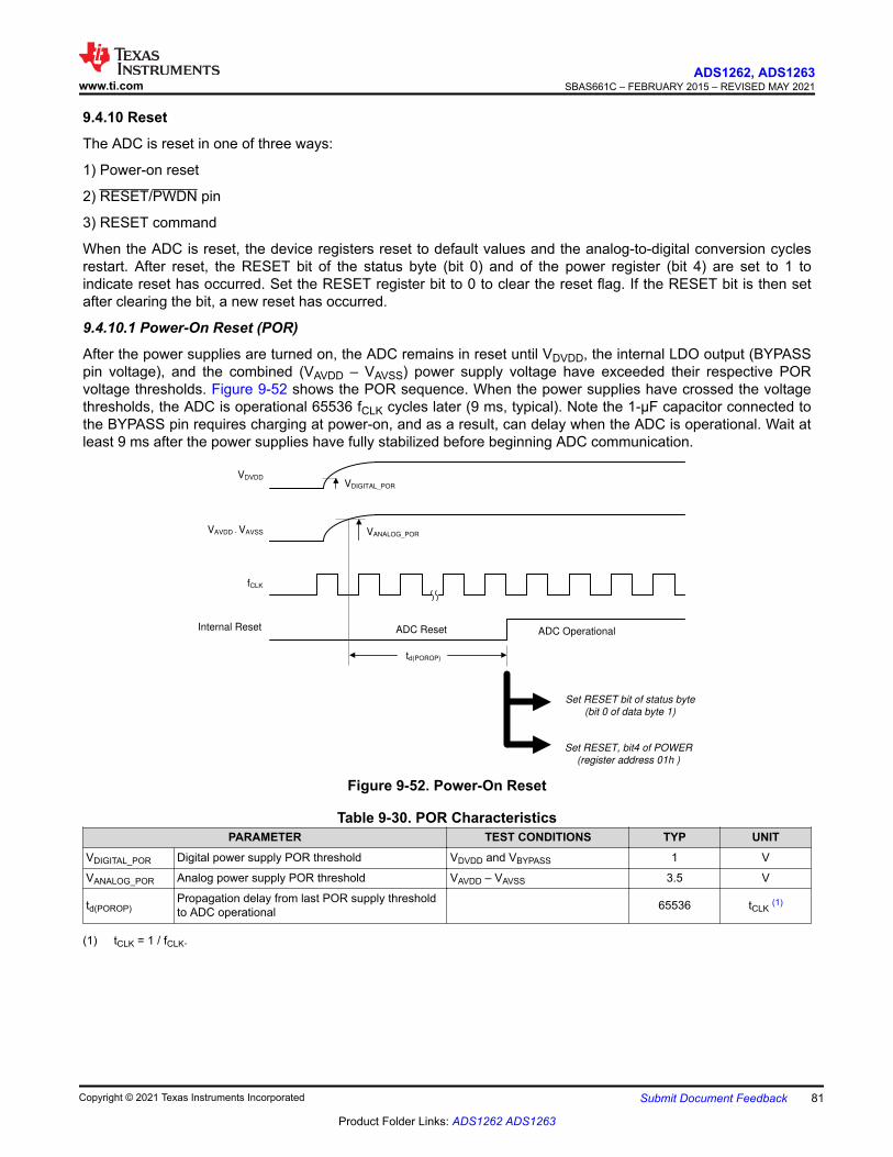
9.4.10 Reset
The ADC is reset in one of three ways:
1) Power-on reset
2) RESET/PWDN pin
3) RESET command
When the ADC is reset, the device registers reset to default values and the analog-to-digital conversion cyclesrestart. After reset, the RESET bit of the status byte (bit 0) and of the power register (bit 4) are set to 1 toindicate reset has occurred. Set the RESET register bit to 0 to clear the reset flag. If the RESET bit is then setafter clearing the bit, a new reset has occurred.
9.4.10.1 Power-On Reset (POR)
After the power supplies are turned on, the ADC remains in reset until VDVDD, the internal LDO output (BYPASSpin voltage), and the combined (VAVDD – VAVSS) power supply voltage have exceeded their respective PORvoltage thresholds. Figure 9-52 shows the POR sequence. When the power supplies have crossed the voltagethresholds, the ADC is operational 65536 fCLK cycles later (9 ms, typical). Note the 1-µF capacitor connected tothe BYPASS pin requires charging at power-on, and as a result, can delay when the ADC is operational. Wait atleast 9 ms after the power supplies have fully stabilized before beginning ADC communication.
fCLK
VDVDD
VAVDD - VAVSS
VDIGITAL_POR
VANALOG_POR
Internal Reset
td(POROP)
ADC OperationalADC Reset
Set RESET, bit4 of POWER
(register address 01h )
Set RESET bit of status byte
(bit 0 of data byte 1)
Figure 9-52. Power-On Reset
Table 9-30. POR CharacteristicsPARAMETER TEST CONDITIONS TYP UNIT
VDIGITAL_POR Digital power supply POR threshold VDVDD and VBYPASS 1 V
VANALOG_POR Analog power supply POR threshold VAVDD – VAVSS 3.5 V
td(POROP)Propagation delay from last POR supply thresholdto ADC operational 65536 tCLK (1)
(1) tCLK = 1 / fCLK.
www.ti.comADS1262, ADS1263
SBAS661C – FEBRUARY 2015 – REVISED MAY 2021
Copyright © 2021 Texas Instruments Incorporated Submit Document Feedback 81
Product Folder Links: ADS1262 ADS1263
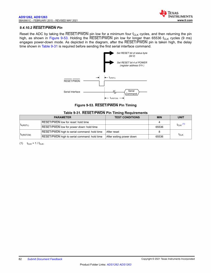
9.4.10.2 RESET/PWDN Pin
Reset the ADC by taking the RESET/PWDN pin low for a minimum four fCLK cycles, and then returning the pinhigh, as shown in Figure 9-53. Holding the RESET/PWDN pin low for longer than 65536 fCLK cycles (9 ms)engages power-down mode. As depicted in the diagram, after the RESET/PWDN pin is taken high, the delaytime shown in Table 9-31 is required before sending the first serial interface command.
RESET/PWDN
th(RSTL)
Serial
CommandSerial Interface
th(RSTCM)
Set RESET bit 4 of POWER
(register address 01h )
Set RESET bit of status byte
(bit 0)
Figure 9-53. RESET/PWDN Pin Timing
Table 9-31. RESET/PWDN Pin Timing RequirementsPARAMETER TEST CONDITIONS MIN UNIT
th(RSTL)RESET/PWDN low for reset: hold time 4
tCLK (1)RESET/PWDN low for power down: hold time 65536
th(RSTCM)RESET/PWDN high to serial command: hold time After reset 8
tCLKRESET/PWDN high to serial command: hold time After exiting power down 65536
(1) tCLK = 1 / fCLK.
ADS1262, ADS1263SBAS661C – FEBRUARY 2015 – REVISED MAY 2021 www.ti.com
82 Submit Document Feedback Copyright © 2021 Texas Instruments Incorporated
Product Folder Links: ADS1262 ADS1263
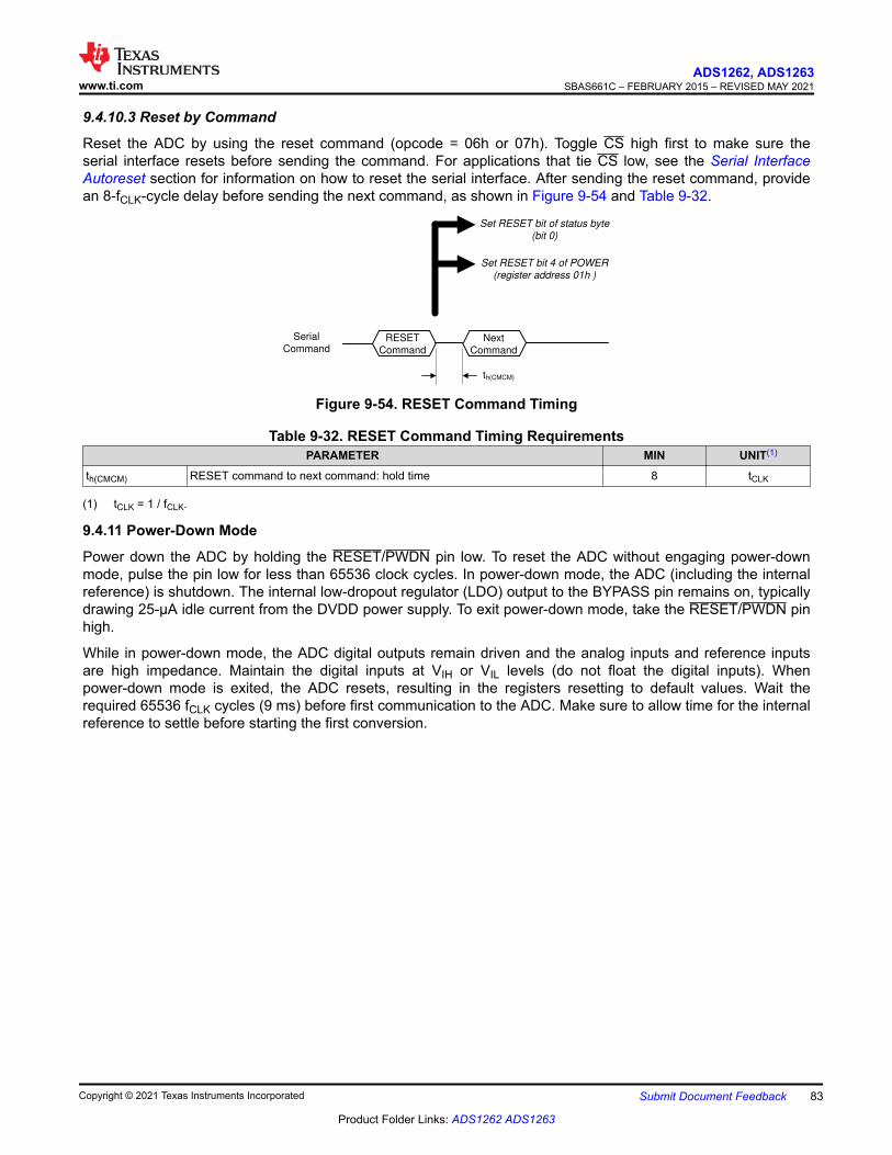
9.4.10.3 Reset by Command
Reset the ADC by using the reset command (opcode = 06h or 07h). Toggle CS high first to make sure theserial interface resets before sending the command. For applications that tie CS low, see the Serial InterfaceAutoreset section for information on how to reset the serial interface. After sending the reset command, providean 8-fCLK-cycle delay before sending the next command, as shown in Figure 9-54 and Table 9-32.
Serial
CommandRESET
Command
Next
Command
th(CMCM)
Set RESET bit 4 of POWER
(register address 01h )
Set RESET bit of status byte
(bit 0)
Figure 9-54. RESET Command Timing
Table 9-32. RESET Command Timing RequirementsPARAMETER MIN UNIT(1)
th(CMCM) RESET command to next command: hold time 8 tCLK
(1) tCLK = 1 / fCLK.
9.4.11 Power-Down Mode
Power down the ADC by holding the RESET/PWDN pin low. To reset the ADC without engaging power-downmode, pulse the pin low for less than 65536 clock cycles. In power-down mode, the ADC (including the internalreference) is shutdown. The internal low-dropout regulator (LDO) output to the BYPASS pin remains on, typicallydrawing 25-µA idle current from the DVDD power supply. To exit power-down mode, take the RESET/PWDN pinhigh.
While in power-down mode, the ADC digital outputs remain driven and the analog inputs and reference inputsare high impedance. Maintain the digital inputs at VIH or VIL levels (do not float the digital inputs). Whenpower-down mode is exited, the ADC resets, resulting in the registers resetting to default values. Wait therequired 65536 fCLK cycles (9 ms) before first communication to the ADC. Make sure to allow time for the internalreference to settle before starting the first conversion.
www.ti.comADS1262, ADS1263
SBAS661C – FEBRUARY 2015 – REVISED MAY 2021
Copyright © 2021 Texas Instruments Incorporated Submit Document Feedback 83
Product Folder Links: ADS1262 ADS1263
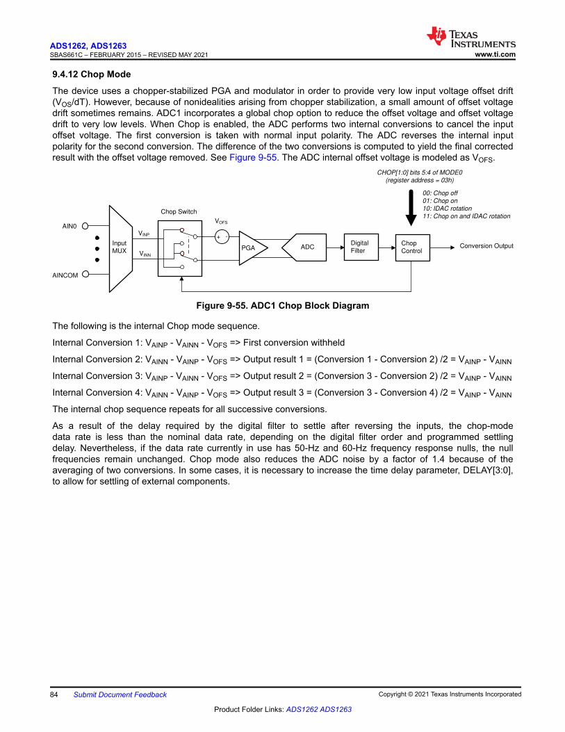
9.4.12 Chop Mode
The device uses a chopper-stabilized PGA and modulator in order to provide very low input voltage offset drift(VOS/dT). However, because of nonidealities arising from chopper stabilization, a small amount of offset voltagedrift sometimes remains. ADC1 incorporates a global chop option to reduce the offset voltage and offset voltagedrift to very low levels. When Chop is enabled, the ADC performs two internal conversions to cancel the inputoffset voltage. The first conversion is taken with normal input polarity. The ADC reverses the internal inputpolarity for the second conversion. The difference of the two conversions is computed to yield the final correctedresult with the offset voltage removed. See Figure 9-55. The ADC internal offset voltage is modeled as VOFS.
VOFS
ADC
PGA ADCDigital
Filter
+ -Chop
ControlConversion OutputInput
MUX
Chop Switch
CHOP[1:0] bits 5:4 of MODE0
(register address = 03h)
VINP
VINN
00: Chop off
01: Chop on
10: IDAC rotation
11: Chop on and IDAC rotation
AIN0
AINCOM
Figure 9-55. ADC1 Chop Block Diagram
The following is the internal Chop mode sequence.
Internal Conversion 1: VAINP - VAINN - VOFS => First conversion withheld
Internal Conversion 2: VAINN - VAINP - VOFS => Output result 1 = (Conversion 1 - Conversion 2) /2 = VAINP - VAINN
Internal Conversion 3: VAINP - VAINN - VOFS => Output result 2 = (Conversion 3 - Conversion 2) /2 = VAINP - VAINN
Internal Conversion 4: VAINN - VAINP - VOFS => Output result 3 = (Conversion 3 - Conversion 4) /2 = VAINP - VAINN
The internal chop sequence repeats for all successive conversions.
As a result of the delay required by the digital filter to settle after reversing the inputs, the chop-modedata rate is less than the nominal data rate, depending on the digital filter order and programmed settlingdelay. Nevertheless, if the data rate currently in use has 50-Hz and 60-Hz frequency response nulls, the nullfrequencies remain unchanged. Chop mode also reduces the ADC noise by a factor of 1.4 because of theaveraging of two conversions. In some cases, it is necessary to increase the time delay parameter, DELAY[3:0],to allow for settling of external components.
ADS1262, ADS1263SBAS661C – FEBRUARY 2015 – REVISED MAY 2021 www.ti.com
84 Submit Document Feedback Copyright © 2021 Texas Instruments Incorporated
Product Folder Links: ADS1262 ADS1263
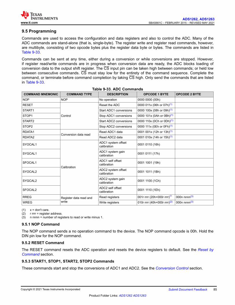
9.5 ProgrammingCommands are used to access the configuration and data registers and also to control the ADC. Many of theADC commands are stand-alone (that is, single-byte). The register write and register read commands, however,are multibyte, consisting of two opcode bytes plus the register data byte or bytes. The commands are listed inTable 9-33.
Commands can be sent at any time, either during a conversion or while conversions are stopped. However,if register read/write commands are in progress when conversion data are ready, the ADC blocks loading ofconversion data to the output shift register. The CS input pin can be taken high between commands; or held lowbetween consecutive commands. CS must stay low for the entirety of the command sequence. Complete thecommand, or terminate before command completion by taking CS high. Only send the commands that are listedin Table 9-33.
Table 9-33. ADC CommandsCOMMAND MNEMONIC COMMAND TYPE DESCRIPTION OPCODE 1 BYTE OPCODE 2 BYTE
NOP NOP No operation 0000 0000 (00h)
RESET
Control
Reset the ADC 0000 011x (06h or 07h)(1)
START1 Start ADC1 conversions 0000 100x (08h or 09h)(1)
STOP1 Stop ADC1 conversions 0000 101x (0Ah or 0Bh)(1)
START2 Start ADC2 conversions 0000 110x (0Ch or 0Dh)(1)
STOP2 Stop ADC2 conversions 0000 111x (0Eh or 0Fh)(1)
RDATA1Conversion data read
Read ADC1 data 0001 001x (12h or 13h)(1)
RDATA2 Read ADC2 data 0001 010x (14h or 15h)(1)
SYOCAL1
Calibration
ADC1 system offsetcalibration 0001 0110 (16h)
SYGCAL1 ADC1 system gaincalibration 0001 0111 (17h)
SFOCAL1 ADC1 self offsetcalibration 0001 1001 (19h)
SYOCAL2 ADC2 system offsetcalibration 0001 1011 (1Bh)
SYGCAL2 ADC2 system gaincalibration 0001 1100 (1Ch)
SFOCAL2 ADC2 self offsetcalibration 0001 1110 (1Eh)
RREG Register data read andwrite
Read registers 001r rrrr (20h+000r rrrr)(2) 000n nnnn(3)
WREG Write registers 010r rrrr (40h+000r rrrr)(2) 000n nnnn(3)
(1) x = don't care.(2) r rrrr = register address.(3) n nnnn = number of registers to read or write minus 1.
9.5.1 NOP Command
The NOP command sends a no operation command to the device. The NOP command opcode is 00h. Hold theDIN pin low for the NOP command.
9.5.2 RESET Command
The RESET command resets the ADC operation and resets the device registers to default. See the Reset byCommand section.
9.5.3 START1, STOP1, START2, STOP2 Commands
These commands start and stop the conversions of ADC1 and ADC2. See the Conversion Control section.
www.ti.comADS1262, ADS1263
SBAS661C – FEBRUARY 2015 – REVISED MAY 2021
Copyright © 2021 Texas Instruments Incorporated Submit Document Feedback 85
Product Folder Links: ADS1262 ADS1263
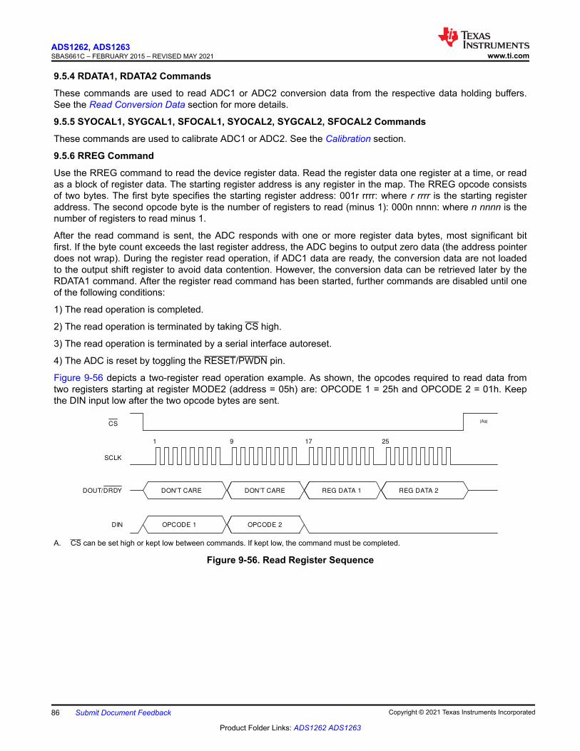
9.5.4 RDATA1, RDATA2 Commands
These commands are used to read ADC1 or ADC2 conversion data from the respective data holding buffers.See the Read Conversion Data section for more details.
9.5.5 SYOCAL1, SYGCAL1, SFOCAL1, SYOCAL2, SYGCAL2, SFOCAL2 Commands
These commands are used to calibrate ADC1 or ADC2. See the Calibration section.
9.5.6 RREG Command
Use the RREG command to read the device register data. Read the register data one register at a time, or readas a block of register data. The starting register address is any register in the map. The RREG opcode consistsof two bytes. The first byte specifies the starting register address: 001r rrrr: where r rrrr is the starting registeraddress. The second opcode byte is the number of registers to read (minus 1): 000n nnnn: where n nnnn is thenumber of registers to read minus 1.
After the read command is sent, the ADC responds with one or more register data bytes, most significant bitfirst. If the byte count exceeds the last register address, the ADC begins to output zero data (the address pointerdoes not wrap). During the register read operation, if ADC1 data are ready, the conversion data are not loadedto the output shift register to avoid data contention. However, the conversion data can be retrieved later by theRDATA1 command. After the register read command has been started, further commands are disabled until oneof the following conditions:
1) The read operation is completed.
2) The read operation is terminated by taking CS high.
3) The read operation is terminated by a serial interface autoreset.
4) The ADC is reset by toggling the RESET/PWDN pin.
Figure 9-56 depicts a two-register read operation example. As shown, the opcodes required to read data fromtwo registers starting at register MODE2 (address = 05h) are: OPCODE 1 = 25h and OPCODE 2 = 01h. Keepthe DIN input low after the two opcode bytes are sent.
CS
1
SCLK
9 17 25
DOUT/DRDY
DIN OPCODE 1 OPCODE 2
REG DATA 1 REG DATA 2DON¶T CARE DON¶T CARE
(Aa)
A. CS can be set high or kept low between commands. If kept low, the command must be completed.
Figure 9-56. Read Register Sequence
ADS1262, ADS1263SBAS661C – FEBRUARY 2015 – REVISED MAY 2021 www.ti.com
86 Submit Document Feedback Copyright © 2021 Texas Instruments Incorporated
Product Folder Links: ADS1262 ADS1263

9.5.7 WREG Command
Use the WREG command to write the device register data. The register data are written one register at a time oras a block of register data. The starting register address is any register in the map.
The WREG opcode consists of two bytes. The first byte specifies the starting register address: 010r rrrr, where rrrrr is the starting register address The second opcode byte is the number of registers to write (minus one): 000nnnnn, where n nnnn is the number of registers to write minus one. The following byte (or bytes) is the registerdata, most significant bit first. If the byte count exceeds the last register address, the ADC ignores the data(the address pointer does not wrap). Writing new data to certain registers results in a reset of ADC1 or ADC2conversions, as specified in the ADC restart column in the Register Maps. The previous conversion data arecleared at restart; therefore, read the data before the register write operation. After the register write commandhas been started, further commands are disabled until one of these conditions occur:
1) The write operation is completed.
2) The write operation is terminated by taking CS high.
3) The write operation is terminated by a serial interface auto-reset
4) The ADC is reset by toggling the RESET/PWDN pin.
Figure 9-57 depicts a two-register write operation example. As shown, the required opcodes to write data to tworegisters starting at register MODE2 (address = 05h) are: OPCODE 1 = 45h and OPCODE 2 = 01h.
CS
1
SCLK
9 17 25
DOUT/DRDY
DIN OPCODE 1 OPCODE 2
DON¶T CARE DON¶T CARE
(A)
DON¶T CARE DON¶T CARE
REG DATA 1 REG DATA 2
A. Between commands, either set CS high or keep CS low. If CS is kept low, the command must be completed.
Figure 9-57. Write Register Sequence
The MODE2 and INPMUX registers are modified. Typically, register changes take effect immediately after thedata are written. However, if the registers are part of a group, then the data are written only after all data for thegrouped registers in the write block have been sent. In this example, data for MODE2 and INPMUX are writtenonly after the data for INPMUX are sent. See the Register Maps section for those registers that are groupedwhen writing register data.
www.ti.comADS1262, ADS1263
SBAS661C – FEBRUARY 2015 – REVISED MAY 2021
Copyright © 2021 Texas Instruments Incorporated Submit Document Feedback 87
Product Folder Links: ADS1262 ADS1263
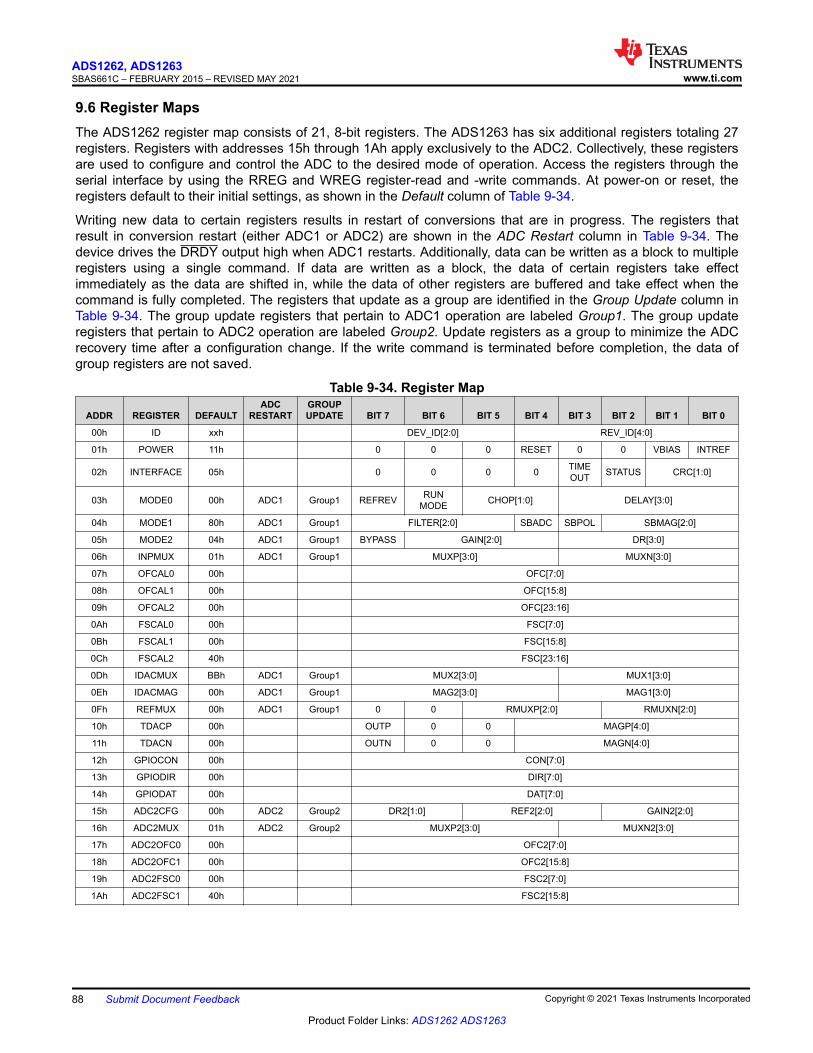
9.6 Register MapsThe ADS1262 register map consists of 21, 8-bit registers. The ADS1263 has six additional registers totaling 27registers. Registers with addresses 15h through 1Ah apply exclusively to the ADC2. Collectively, these registersare used to configure and control the ADC to the desired mode of operation. Access the registers through theserial interface by using the RREG and WREG register-read and -write commands. At power-on or reset, theregisters default to their initial settings, as shown in the Default column of Table 9-34.
Writing new data to certain registers results in restart of conversions that are in progress. The registers thatresult in conversion restart (either ADC1 or ADC2) are shown in the ADC Restart column in Table 9-34. Thedevice drives the DRDY output high when ADC1 restarts. Additionally, data can be written as a block to multipleregisters using a single command. If data are written as a block, the data of certain registers take effectimmediately as the data are shifted in, while the data of other registers are buffered and take effect when thecommand is fully completed. The registers that update as a group are identified in the Group Update column inTable 9-34. The group update registers that pertain to ADC1 operation are labeled Group1. The group updateregisters that pertain to ADC2 operation are labeled Group2. Update registers as a group to minimize the ADCrecovery time after a configuration change. If the write command is terminated before completion, the data ofgroup registers are not saved.
Table 9-34. Register Map
ADDR REGISTER DEFAULTADC
RESTARTGROUPUPDATE BIT 7 BIT 6 BIT 5 BIT 4 BIT 3 BIT 2 BIT 1 BIT 0
00h ID xxh DEV_ID[2:0] REV_ID[4:0]
01h POWER 11h 0 0 0 RESET 0 0 VBIAS INTREF
02h INTERFACE 05h 0 0 0 0 TIMEOUT STATUS CRC[1:0]
03h MODE0 00h ADC1 Group1 REFREV RUNMODE CHOP[1:0] DELAY[3:0]
04h MODE1 80h ADC1 Group1 FILTER[2:0] SBADC SBPOL SBMAG[2:0]
05h MODE2 04h ADC1 Group1 BYPASS GAIN[2:0] DR[3:0]
06h INPMUX 01h ADC1 Group1 MUXP[3:0] MUXN[3:0]
07h OFCAL0 00h OFC[7:0]
08h OFCAL1 00h OFC[15:8]
09h OFCAL2 00h OFC[23:16]
0Ah FSCAL0 00h FSC[7:0]
0Bh FSCAL1 00h FSC[15:8]
0Ch FSCAL2 40h FSC[23:16]
0Dh IDACMUX BBh ADC1 Group1 MUX2[3:0] MUX1[3:0]
0Eh IDACMAG 00h ADC1 Group1 MAG2[3:0] MAG1[3:0]
0Fh REFMUX 00h ADC1 Group1 0 0 RMUXP[2:0] RMUXN[2:0]
10h TDACP 00h OUTP 0 0 MAGP[4:0]
11h TDACN 00h OUTN 0 0 MAGN[4:0]
12h GPIOCON 00h CON[7:0]
13h GPIODIR 00h DIR[7:0]
14h GPIODAT 00h DAT[7:0]
15h ADC2CFG 00h ADC2 Group2 DR2[1:0] REF2[2:0] GAIN2[2:0]
16h ADC2MUX 01h ADC2 Group2 MUXP2[3:0] MUXN2[3:0]
17h ADC2OFC0 00h OFC2[7:0]
18h ADC2OFC1 00h OFC2[15:8]
19h ADC2FSC0 00h FSC2[7:0]
1Ah ADC2FSC1 40h FSC2[15:8]
ADS1262, ADS1263SBAS661C – FEBRUARY 2015 – REVISED MAY 2021 www.ti.com
88 Submit Document Feedback Copyright © 2021 Texas Instruments Incorporated
Product Folder Links: ADS1262 ADS1263

9.6.1 Device Identification Register (address = 00h) [reset = x]
Figure 9-58. Device Identification Register (ID)7 6 5 4 3 2 1 0
DEV_ID[2:0] REV_ID[4:0]
NOTE: Reset values are device dependent
Table 9-35. Device Identification Register (ID) Field DescriptionsBit Field Type Reset Description7:5 DEV_ID[2:0] R x Device ID.
000: ADS1262001: ADS1263
4:0 REV_ID[4:0] R x Revision IDNote: the chip revision ID can change without notification
9.6.2 Power Register (address = 01h) [reset = 11h]
Figure 9-59. Power Register (POWER)7 6 5 4 3 2 1 0
RESERVED RESET RESERVED VBIAS INTREF
R-0h R/W-1h R-0h R/W-0h R/W-1h
LEGEND: R/W = Read/Write; R = Read only; -n = value after reset
Table 9-36. Power Register (POWER) Field DescriptionsBit Field Type Reset Description7:5 RESERVED R 0h Reserved
Always write 000
4 RESET R/W 1h Reset IndicatorIndicates ADC reset has occurred. Clear this bit to detect thenext device reset.0: No new reset occurred1: New reset has occurred (default)
3:2 RESERVED R 0h ReservedAlways write 00
1 VBIAS R/W 0h Level Shift Voltage EnableEnables the internal level shift voltage to the AINCOM pin.VBIAS = (VAVDD + VAVSS)/20: Disabled (default)1: VBIAS enabled
0 INTREF R/W 1h Internal Reference EnableEnables the 2.5 V internal voltage reference. Note the IDAC andtemperature sensor require the internal voltage reference.0: Disabled1: Internal reference enabled (default)
www.ti.comADS1262, ADS1263
SBAS661C – FEBRUARY 2015 – REVISED MAY 2021
Copyright © 2021 Texas Instruments Incorporated Submit Document Feedback 89
Product Folder Links: ADS1262 ADS1263
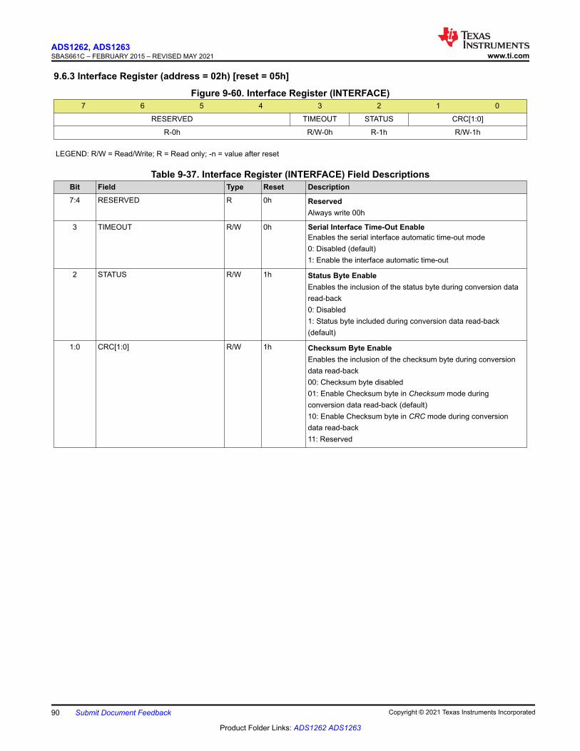
9.6.3 Interface Register (address = 02h) [reset = 05h]
Figure 9-60. Interface Register (INTERFACE)7 6 5 4 3 2 1 0
RESERVED TIMEOUT STATUS CRC[1:0]
R-0h R/W-0h R-1h R/W-1h
LEGEND: R/W = Read/Write; R = Read only; -n = value after reset
Table 9-37. Interface Register (INTERFACE) Field DescriptionsBit Field Type Reset Description7:4 RESERVED R 0h Reserved
Always write 00h
3 TIMEOUT R/W 0h Serial Interface Time-Out EnableEnables the serial interface automatic time-out mode0: Disabled (default)1: Enable the interface automatic time-out
2 STATUS R/W 1h Status Byte EnableEnables the inclusion of the status byte during conversion dataread-back0: Disabled1: Status byte included during conversion data read-back(default)
1:0 CRC[1:0] R/W 1h Checksum Byte EnableEnables the inclusion of the checksum byte during conversiondata read-back00: Checksum byte disabled01: Enable Checksum byte in Checksum mode duringconversion data read-back (default)10: Enable Checksum byte in CRC mode during conversiondata read-back11: Reserved
ADS1262, ADS1263SBAS661C – FEBRUARY 2015 – REVISED MAY 2021 www.ti.com
90 Submit Document Feedback Copyright © 2021 Texas Instruments Incorporated
Product Folder Links: ADS1262 ADS1263
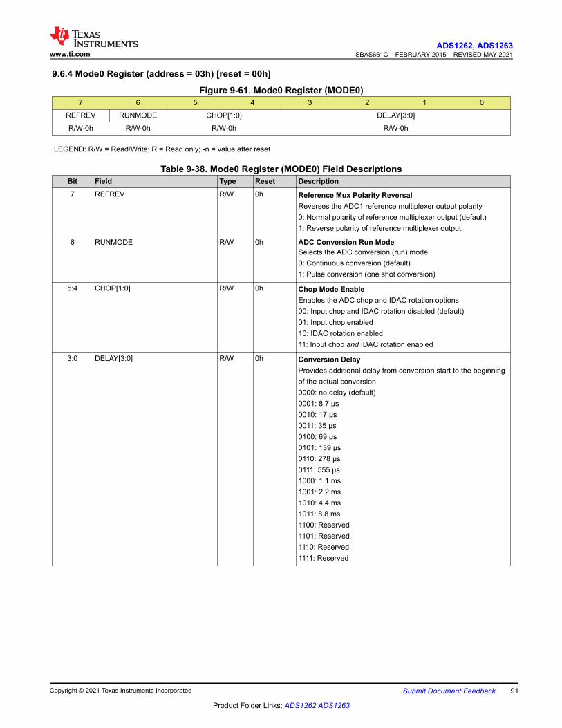
9.6.4 Mode0 Register (address = 03h) [reset = 00h]
Figure 9-61. Mode0 Register (MODE0)7 6 5 4 3 2 1 0
REFREV RUNMODE CHOP[1:0] DELAY[3:0]
R/W-0h R/W-0h R/W-0h R/W-0h
LEGEND: R/W = Read/Write; R = Read only; -n = value after reset
Table 9-38. Mode0 Register (MODE0) Field DescriptionsBit Field Type Reset Description7 REFREV R/W 0h Reference Mux Polarity Reversal
Reverses the ADC1 reference multiplexer output polarity0: Normal polarity of reference multiplexer output (default)1: Reverse polarity of reference multiplexer output
6 RUNMODE R/W 0h ADC Conversion Run ModeSelects the ADC conversion (run) mode0: Continuous conversion (default)1: Pulse conversion (one shot conversion)
5:4 CHOP[1:0] R/W 0h Chop Mode EnableEnables the ADC chop and IDAC rotation options00: Input chop and IDAC rotation disabled (default)01: Input chop enabled10: IDAC rotation enabled11: Input chop and IDAC rotation enabled
3:0 DELAY[3:0] R/W 0h Conversion DelayProvides additional delay from conversion start to the beginningof the actual conversion0000: no delay (default)0001: 8.7 µs0010: 17 µs0011: 35 µs0100: 69 µs0101: 139 µs0110: 278 µs0111: 555 µs1000: 1.1 ms1001: 2.2 ms1010: 4.4 ms1011: 8.8 ms1100: Reserved1101: Reserved1110: Reserved1111: Reserved
www.ti.comADS1262, ADS1263
SBAS661C – FEBRUARY 2015 – REVISED MAY 2021
Copyright © 2021 Texas Instruments Incorporated Submit Document Feedback 91
Product Folder Links: ADS1262 ADS1263
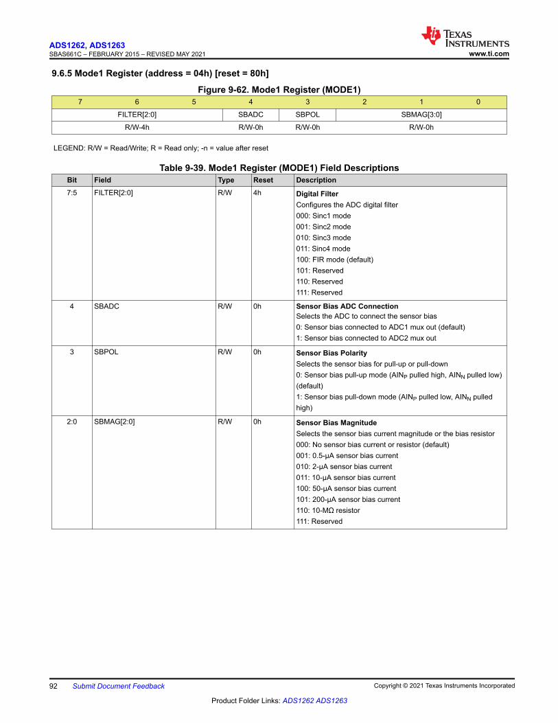
9.6.5 Mode1 Register (address = 04h) [reset = 80h]
Figure 9-62. Mode1 Register (MODE1)7 6 5 4 3 2 1 0
FILTER[2:0] SBADC SBPOL SBMAG[3:0]
R/W-4h R/W-0h R/W-0h R/W-0h
LEGEND: R/W = Read/Write; R = Read only; -n = value after reset
Table 9-39. Mode1 Register (MODE1) Field DescriptionsBit Field Type Reset Description7:5 FILTER[2:0] R/W 4h Digital Filter
Configures the ADC digital filter000: Sinc1 mode001: Sinc2 mode010: Sinc3 mode011: Sinc4 mode100: FIR mode (default)101: Reserved110: Reserved111: Reserved
4 SBADC R/W 0h Sensor Bias ADC ConnectionSelects the ADC to connect the sensor bias0: Sensor bias connected to ADC1 mux out (default)1: Sensor bias connected to ADC2 mux out
3 SBPOL R/W 0h Sensor Bias PolaritySelects the sensor bias for pull-up or pull-down0: Sensor bias pull-up mode (AINP pulled high, AINN pulled low)(default)1: Sensor bias pull-down mode (AINP pulled low, AINN pulledhigh)
2:0 SBMAG[2:0] R/W 0h Sensor Bias MagnitudeSelects the sensor bias current magnitude or the bias resistor000: No sensor bias current or resistor (default)001: 0.5-µA sensor bias current010: 2-µA sensor bias current011: 10-µA sensor bias current100: 50-µA sensor bias current101: 200-µA sensor bias current110: 10-MΩ resistor111: Reserved
ADS1262, ADS1263SBAS661C – FEBRUARY 2015 – REVISED MAY 2021 www.ti.com
92 Submit Document Feedback Copyright © 2021 Texas Instruments Incorporated
Product Folder Links: ADS1262 ADS1263
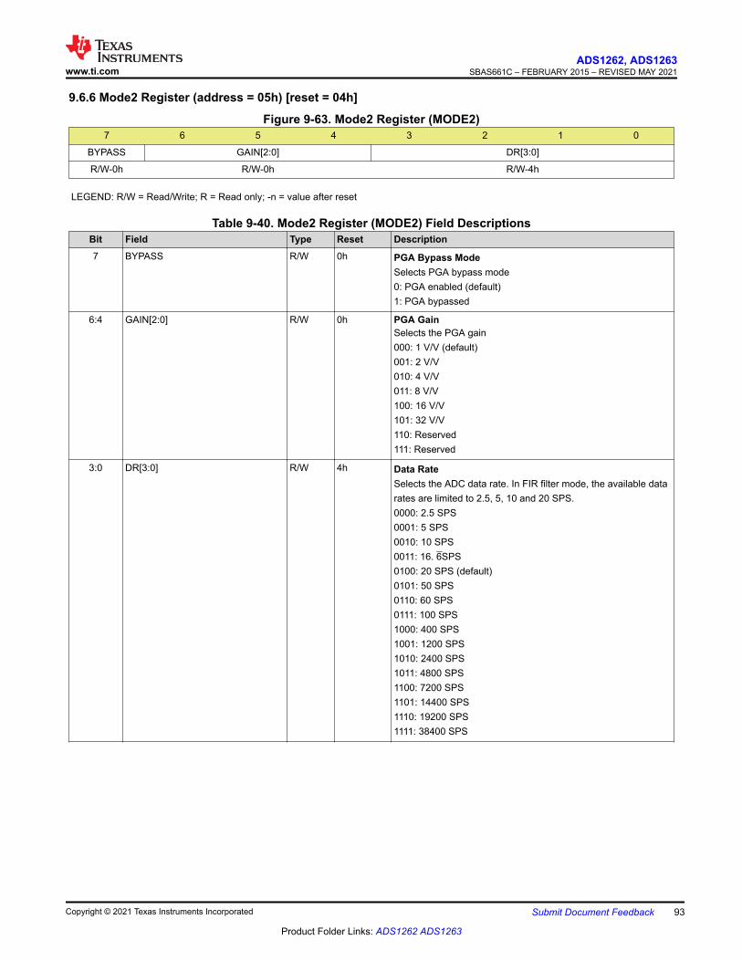
9.6.6 Mode2 Register (address = 05h) [reset = 04h]
Figure 9-63. Mode2 Register (MODE2)7 6 5 4 3 2 1 0
BYPASS GAIN[2:0] DR[3:0]
R/W-0h R/W-0h R/W-4h
LEGEND: R/W = Read/Write; R = Read only; -n = value after reset
Table 9-40. Mode2 Register (MODE2) Field DescriptionsBit Field Type Reset Description7 BYPASS R/W 0h PGA Bypass Mode
Selects PGA bypass mode0: PGA enabled (default)1: PGA bypassed
6:4 GAIN[2:0] R/W 0h PGA GainSelects the PGA gain000: 1 V/V (default)001: 2 V/V010: 4 V/V011: 8 V/V100: 16 V/V101: 32 V/V110: Reserved111: Reserved
3:0 DR[3:0] R/W 4h Data RateSelects the ADC data rate. In FIR filter mode, the available datarates are limited to 2.5, 5, 10 and 20 SPS.0000: 2.5 SPS0001: 5 SPS0010: 10 SPS0011: 16. 6SPS0100: 20 SPS (default)0101: 50 SPS0110: 60 SPS0111: 100 SPS1000: 400 SPS1001: 1200 SPS1010: 2400 SPS1011: 4800 SPS1100: 7200 SPS1101: 14400 SPS1110: 19200 SPS1111: 38400 SPS
www.ti.comADS1262, ADS1263
SBAS661C – FEBRUARY 2015 – REVISED MAY 2021
Copyright © 2021 Texas Instruments Incorporated Submit Document Feedback 93
Product Folder Links: ADS1262 ADS1263
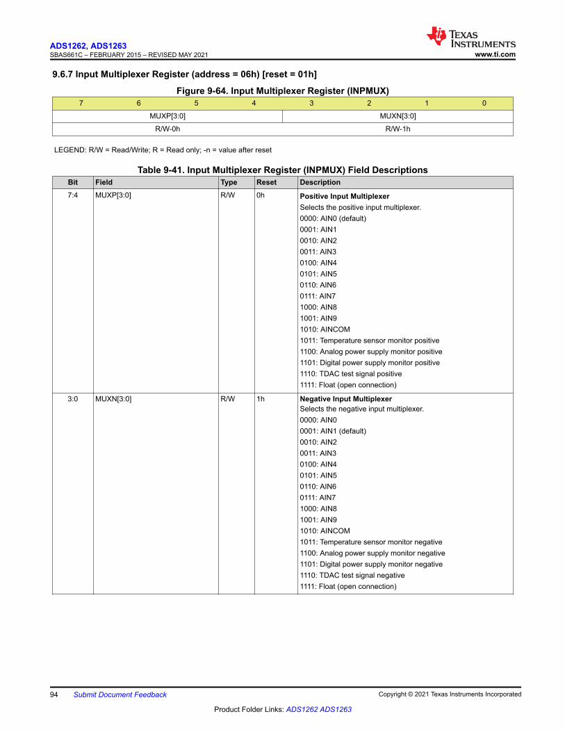
9.6.7 Input Multiplexer Register (address = 06h) [reset = 01h]
Figure 9-64. Input Multiplexer Register (INPMUX)7 6 5 4 3 2 1 0
MUXP[3:0] MUXN[3:0]
R/W-0h R/W-1h
LEGEND: R/W = Read/Write; R = Read only; -n = value after reset
Table 9-41. Input Multiplexer Register (INPMUX) Field DescriptionsBit Field Type Reset Description7:4 MUXP[3:0] R/W 0h Positive Input Multiplexer
Selects the positive input multiplexer.0000: AIN0 (default)0001: AIN10010: AIN20011: AIN30100: AIN40101: AIN50110: AIN60111: AIN71000: AIN81001: AIN91010: AINCOM1011: Temperature sensor monitor positive1100: Analog power supply monitor positive1101: Digital power supply monitor positive1110: TDAC test signal positive1111: Float (open connection)
3:0 MUXN[3:0] R/W 1h Negative Input MultiplexerSelects the negative input multiplexer.0000: AIN00001: AIN1 (default)0010: AIN20011: AIN30100: AIN40101: AIN50110: AIN60111: AIN71000: AIN81001: AIN91010: AINCOM1011: Temperature sensor monitor negative1100: Analog power supply monitor negative1101: Digital power supply monitor negative1110: TDAC test signal negative1111: Float (open connection)
ADS1262, ADS1263SBAS661C – FEBRUARY 2015 – REVISED MAY 2021 www.ti.com
94 Submit Document Feedback Copyright © 2021 Texas Instruments Incorporated
Product Folder Links: ADS1262 ADS1263
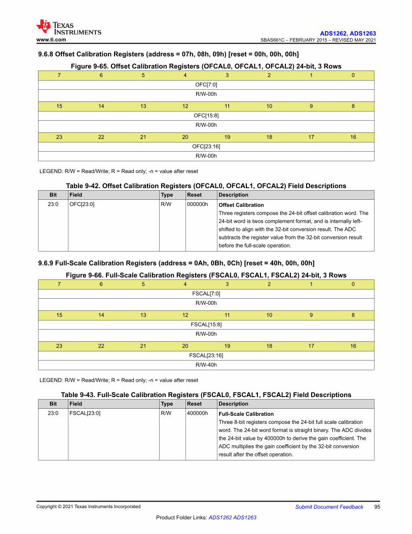
9.6.8 Offset Calibration Registers (address = 07h, 08h, 09h) [reset = 00h, 00h, 00h]
Figure 9-65. Offset Calibration Registers (OFCAL0, OFCAL1, OFCAL2) 24-bit, 3 Rows7 6 5 4 3 2 1 0
OFC[7:0]
R/W-00h
15 14 13 12 11 10 9 8
OFC[15:8]
R/W-00h
23 22 21 20 19 18 17 16
OFC[23:16]
R/W-00h
LEGEND: R/W = Read/Write; R = Read only; -n = value after reset
Table 9-42. Offset Calibration Registers (OFCAL0, OFCAL1, OFCAL2) Field DescriptionsBit Field Type Reset Description
23:0 OFC[23:0] R/W 000000h Offset CalibrationThree registers compose the 24-bit offset calibration word. The24-bit word is twos complement format, and is internally left-shifted to align with the 32-bit conversion result. The ADCsubtracts the register value from the 32-bit conversion resultbefore the full-scale operation.
9.6.9 Full-Scale Calibration Registers (address = 0Ah, 0Bh, 0Ch) [reset = 40h, 00h, 00h]
Figure 9-66. Full-Scale Calibration Registers (FSCAL0, FSCAL1, FSCAL2) 24-bit, 3 Rows7 6 5 4 3 2 1 0
FSCAL[7:0]
R/W-00h
15 14 13 12 11 10 9 8
FSCAL[15:8]
R/W-00h
23 22 21 20 19 18 17 16
FSCAL[23:16]
R/W-40h
LEGEND: R/W = Read/Write; R = Read only; -n = value after reset
Table 9-43. Full-Scale Calibration Registers (FSCAL0, FSCAL1, FSCAL2) Field DescriptionsBit Field Type Reset Description
23:0 FSCAL[23:0] R/W 400000h Full-Scale CalibrationThree 8-bit registers compose the 24-bit full scale calibrationword. The 24-bit word format is straight binary. The ADC dividesthe 24-bit value by 400000h to derive the gain coefficient. TheADC multiplies the gain coefficient by the 32-bit conversionresult after the offset operation.
www.ti.comADS1262, ADS1263
SBAS661C – FEBRUARY 2015 – REVISED MAY 2021
Copyright © 2021 Texas Instruments Incorporated Submit Document Feedback 95
Product Folder Links: ADS1262 ADS1263
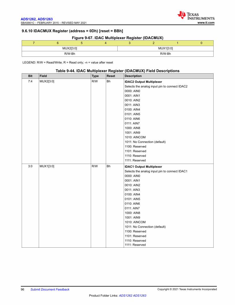
9.6.10 IDACMUX Register (address = 0Dh) [reset = BBh]
Figure 9-67. IDAC Multiplexer Register (IDACMUX)7 6 5 4 3 2 1 0
MUX2[3:0] MUX1[3:0]
R/W-Bh R/W-Bh
LEGEND: R/W = Read/Write; R = Read only; -n = value after reset
Table 9-44. IDAC Multiplexer Register (IDACMUX) Field DescriptionsBit Field Type Reset Description7:4 MUX2[3:0] R/W Bh IDAC2 Output Multiplexer
Selects the analog input pin to connect IDAC20000: AIN00001: AIN10010: AIN20011: AIN30100: AIN40101: AIN50110: AIN60111: AIN71000: AIN81001: AIN91010: AINCOM1011: No Connection (default)1100: Reserved1101: Reserved1110: Reserved1111: Reserved
3:0 MUX1[3:0] R/W Bh IDAC1 Output MultiplexerSelects the analog input pin to connect IDAC10000: AIN00001: AIN10010: AIN20011: AIN30100: AIN40101: AIN50110: AIN60111: AIN71000: AIN81001: AIN91010: AINCOM1011: No Connection (default)1100: Reserved1101: Reserved1110: Reserved1111: Reserved
ADS1262, ADS1263SBAS661C – FEBRUARY 2015 – REVISED MAY 2021 www.ti.com
96 Submit Document Feedback Copyright © 2021 Texas Instruments Incorporated
Product Folder Links: ADS1262 ADS1263
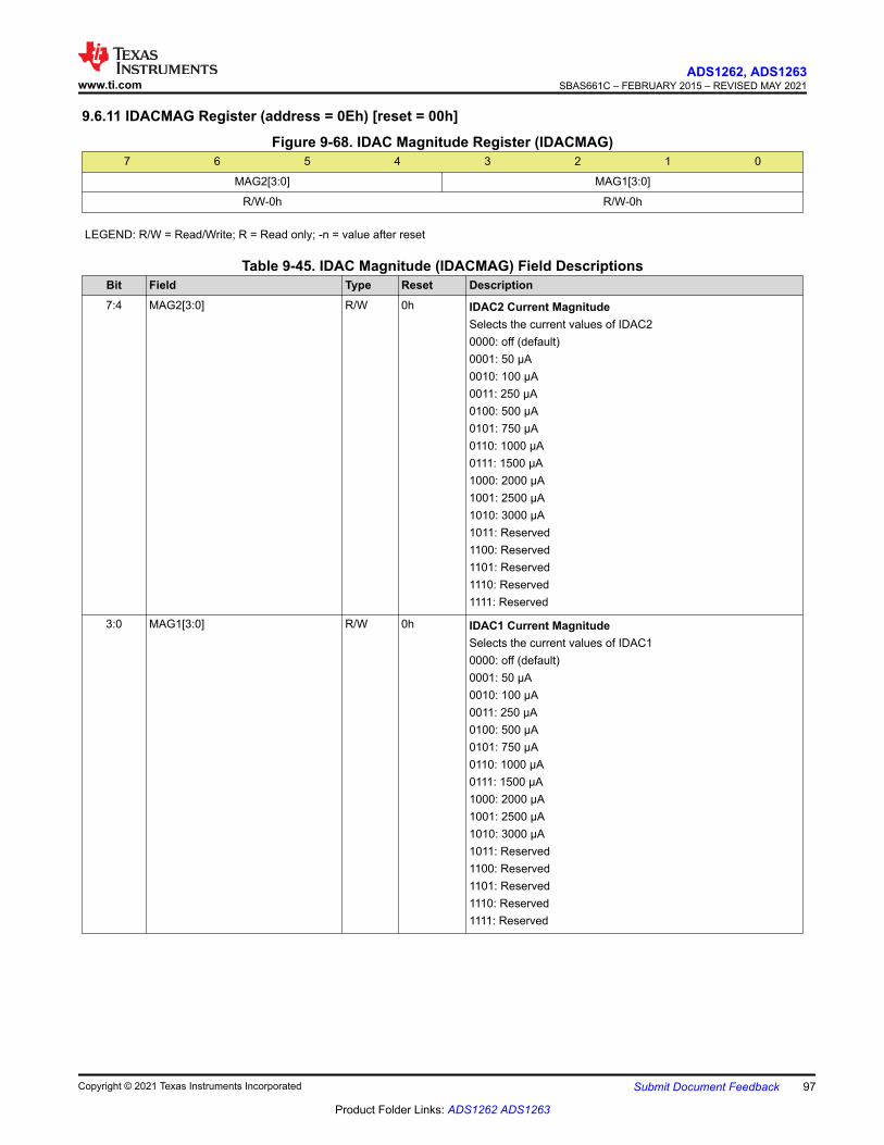
9.6.11 IDACMAG Register (address = 0Eh) [reset = 00h]
Figure 9-68. IDAC Magnitude Register (IDACMAG)7 6 5 4 3 2 1 0
MAG2[3:0] MAG1[3:0]
R/W-0h R/W-0h
LEGEND: R/W = Read/Write; R = Read only; -n = value after reset
Table 9-45. IDAC Magnitude (IDACMAG) Field DescriptionsBit Field Type Reset Description7:4 MAG2[3:0] R/W 0h IDAC2 Current Magnitude
Selects the current values of IDAC20000: off (default)0001: 50 µA0010: 100 µA0011: 250 µA0100: 500 µA0101: 750 µA0110: 1000 µA0111: 1500 µA1000: 2000 µA1001: 2500 µA1010: 3000 µA1011: Reserved1100: Reserved1101: Reserved1110: Reserved1111: Reserved
3:0 MAG1[3:0] R/W 0h IDAC1 Current MagnitudeSelects the current values of IDAC10000: off (default)0001: 50 µA0010: 100 µA0011: 250 µA0100: 500 µA0101: 750 µA0110: 1000 µA0111: 1500 µA1000: 2000 µA1001: 2500 µA1010: 3000 µA1011: Reserved1100: Reserved1101: Reserved1110: Reserved1111: Reserved
www.ti.comADS1262, ADS1263
SBAS661C – FEBRUARY 2015 – REVISED MAY 2021
Copyright © 2021 Texas Instruments Incorporated Submit Document Feedback 97
Product Folder Links: ADS1262 ADS1263

9.6.12 REFMUX Register (address = 0Fh) [reset = 00h]
Figure 9-69. Reference Multiplexer Register (REFMUX)7 6 5 4 3 2 1 0
RESERVED RMUXP[2:0] RMUXN[2:0]
R/W-0h R/W-0h R/W-0h
LEGEND: R/W = Read/Write; R = Read only; -n = value after reset
Table 9-46. Reference Multiplexer Register (REFMUX) Field DescriptionsBit Field Type Reset Description7:6 Reserved R 0h Reserved
Always write 0h
5:3 RMUXP[2:0] R/W 0h Reference Positive InputSelects the positive reference input000: Internal 2.5 V reference - P (default)001: External AIN0010: External AIN2011: External AIN4100: Internal analog supply (VAVDD )101: Reserved110: Reserved111: Reserved
2:0 RMUXN[2:0] R/W 0h Reference Negative InputSelects the negative reference input000: Internal 2.5 V reference - N (default)001: External AIN1010: External AIN3011: External AIN5100: Internal analog supply (VAVSS)101: Reserved110: Reserved111: Reserved
ADS1262, ADS1263SBAS661C – FEBRUARY 2015 – REVISED MAY 2021 www.ti.com
98 Submit Document Feedback Copyright © 2021 Texas Instruments Incorporated
Product Folder Links: ADS1262 ADS1263
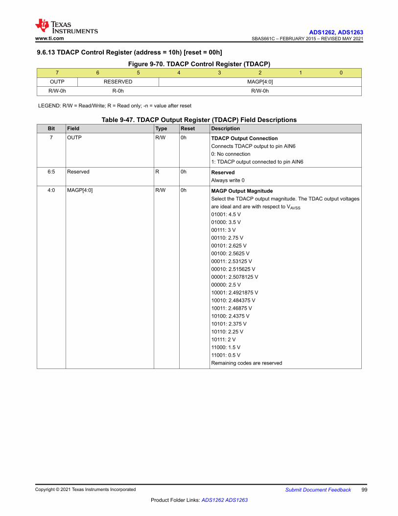
9.6.13 TDACP Control Register (address = 10h) [reset = 00h]
Figure 9-70. TDACP Control Register (TDACP)7 6 5 4 3 2 1 0
OUTP RESERVED MAGP[4:0]
R/W-0h R-0h R/W-0h
LEGEND: R/W = Read/Write; R = Read only; -n = value after reset
Table 9-47. TDACP Output Register (TDACP) Field DescriptionsBit Field Type Reset Description7 OUTP R/W 0h TDACP Output Connection
Connects TDACP output to pin AIN60: No connection1: TDACP output connected to pin AIN6
6:5 Reserved R 0h ReservedAlways write 0
4:0 MAGP[4:0] R/W 0h MAGP Output MagnitudeSelect the TDACP output magnitude. The TDAC output voltagesare ideal and are with respect to VAVSS
01001: 4.5 V01000: 3.5 V00111: 3 V00110: 2.75 V00101: 2.625 V00100: 2.5625 V00011: 2.53125 V00010: 2.515625 V00001: 2.5078125 V00000: 2.5 V10001: 2.4921875 V10010: 2.484375 V10011: 2.46875 V10100: 2.4375 V10101: 2.375 V10110: 2.25 V10111: 2 V11000: 1.5 V11001: 0.5 VRemaining codes are reserved
www.ti.comADS1262, ADS1263
SBAS661C – FEBRUARY 2015 – REVISED MAY 2021
Copyright © 2021 Texas Instruments Incorporated Submit Document Feedback 99
Product Folder Links: ADS1262 ADS1263
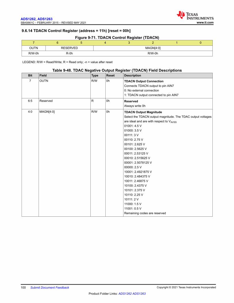
9.6.14 TDACN Control Register (address = 11h) [reset = 00h]
Figure 9-71. TDACN Control Register (TDACN)7 6 5 4 3 2 1 0
OUTN RESERVED MAGN[4:0]
R/W-0h R-0h R/W-0h
LEGEND: R/W = Read/Write; R = Read only; -n = value after reset
Table 9-48. TDAC Negative Output Register (TDACN) Field DescriptionsBit Field Type Reset Description7 OUTN R/W 0h TDACN Output Connection
Connects TDACN output to pin AIN70: No external connection1: TDACN output connected to pin AIN7
6:5 Reserved R 0h ReservedAlways write 0h
4:0 MAGN[4:0] R/W 0h TDACN Output MagnitudeSelect the TDACN output magnitude. The TDAC output voltagesare ideal and are with respect to VAVSS
01001: 4.5 V01000: 3.5 V00111: 3 V00110: 2.75 V00101: 2.625 V00100: 2.5625 V00011: 2.53125 V00010: 2.515625 V00001: 2.5078125 V00000: 2.5 V10001: 2.4921875 V10010: 2.484375 V10011: 2.46875 V10100: 2.4375 V10101: 2.375 V10110: 2.25 V10111: 2 V11000: 1.5 V11001: 0.5 VRemaining codes are reserved
ADS1262, ADS1263SBAS661C – FEBRUARY 2015 – REVISED MAY 2021 www.ti.com
100 Submit Document Feedback Copyright © 2021 Texas Instruments Incorporated
Product Folder Links: ADS1262 ADS1263
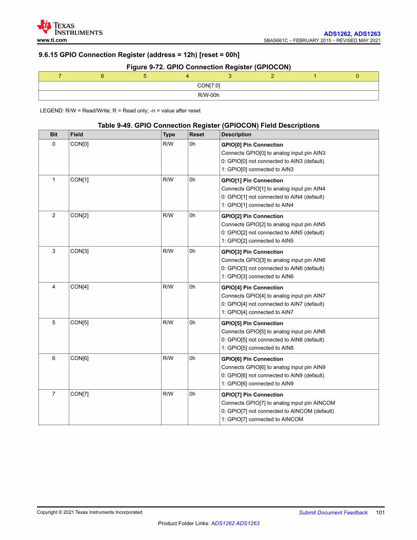
9.6.15 GPIO Connection Register (address = 12h) [reset = 00h]
Figure 9-72. GPIO Connection Register (GPIOCON)7 6 5 4 3 2 1 0
CON[7:0]
R/W-00h
LEGEND: R/W = Read/Write; R = Read only; -n = value after reset
Table 9-49. GPIO Connection Register (GPIOCON) Field DescriptionsBit Field Type Reset Description0 CON[0] R/W 0h GPIO[0] Pin Connection
Connects GPIO[0] to analog input pin AIN30: GPIO[0] not connected to AIN3 (default)1: GPIO[0] connected to AIN3
1 CON[1] R/W 0h GPIO[1] Pin ConnectionConnects GPIO[1] to analog input pin AIN40: GPIO[1] not connected to AIN4 (default)1: GPIO[1] connected to AIN4
2 CON[2] R/W 0h GPIO[2] Pin ConnectionConnects GPIO[2] to analog input pin AIN50: GPIO[2] not connected to AIN5 (default)1: GPIO[2] connected to AIN5
3 CON[3] R/W 0h GPIO[3] Pin ConnectionConnects GPIO[3] to analog input pin AIN60: GPIO[3] not connected to AIN6 (default)1: GPIO[3] connected to AIN6
4 CON[4] R/W 0h GPIO[4] Pin ConnectionConnects GPIO[4] to analog input pin AIN70: GPIO[4] not connected to AIN7 (default)1: GPIO[4] connected to AIN7
5 CON[5] R/W 0h GPIO[5] Pin ConnectionConnects GPIO[5] to analog input pin AIN80: GPIO[5] not connected to AIN8 (default)1: GPIO[5] connected to AIN8
6 CON[6] R/W 0h GPIO[6] Pin ConnectionConnects GPIO[6] to analog input pin AIN90: GPIO[6] not connected to AIN9 (default)1: GPIO[6] connected to AIN9
7 CON[7] R/W 0h GPIO[7] Pin ConnectionConnects GPIO[7] to analog input pin AINCOM0: GPIO[7] not connected to AINCOM (default)1: GPIO[7] connected to AINCOM
www.ti.comADS1262, ADS1263
SBAS661C – FEBRUARY 2015 – REVISED MAY 2021
Copyright © 2021 Texas Instruments Incorporated Submit Document Feedback 101
Product Folder Links: ADS1262 ADS1263
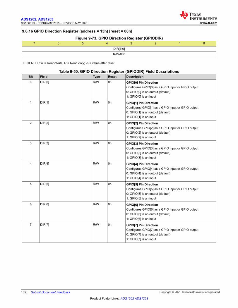
9.6.16 GPIO Direction Register (address = 13h) [reset = 00h]
Figure 9-73. GPIO Direction Register (GPIODIR)7 6 5 4 3 2 1 0
DIR[7:0]
R/W-00h
LEGEND: R/W = Read/Write; R = Read only; -n = value after reset
Table 9-50. GPIO Direction Register (GPIODIR) Field DescriptionsBit Field Type Reset Description0 DIR[0] R/W 0h GPIO[0] Pin Direction
Configures GPIO[0] as a GPIO input or GPIO output0: GPIO[0] is an output (default)1: GPIO[0] is an input
1 DIR[1] R/W 0h GPIO[1] Pin DirectionConfigures GPIO[1] as a GPIO input or GPIO output0: GPIO[1] is an output (default)1: GPIO[1] is an input
2 DIR[2] R/W 0h GPIO[2] Pin DirectionConfigures GPIO[2] as a GPIO input or GPIO output0: GPIO[2] is an output (default)1: GPIO[2] is an input
3 DIR[3] R/W 0h GPIO[3] Pin DirectionConfigures GPIO[3] as a GPIO input or GPIO output0: GPIO[3] is an output (default)1: GPIO[3] is an input
4 DIR[4] R/W 0h GPIO[4] Pin DirectionConfigures GPIO[4] as a GPIO input or GPIO output0: GPIO[4] is an output (default)1: GPIO[4] is an input
5 DIR[5] R/W 0h GPIO[5] Pin DirectionConfigures GPIO[5] as a GPIO input or GPIO output0: GPIO[5] is an output (default)1: GPIO[5] is an input
6 DIR[6] R/W 0h GPIO[6] Pin DirectionConfigures GPIO[6] as a GPIO input or GPIO output0: GPIO[6] is an output (default)1: GPIO[6] is an input
7 DIR[7] R/W 0h GPIO[7] Pin DirectionConfigures GPIO[7] as a GPIO input or GPIO output0: GPIO[7] is an output (default)1: GPIO[7] is an input
ADS1262, ADS1263SBAS661C – FEBRUARY 2015 – REVISED MAY 2021 www.ti.com
102 Submit Document Feedback Copyright © 2021 Texas Instruments Incorporated
Product Folder Links: ADS1262 ADS1263
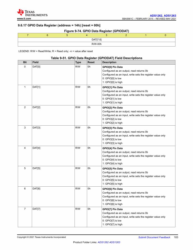
9.6.17 GPIO Data Register (address = 14h) [reset = 00h]
Figure 9-74. GPIO Data Register (GPIODAT)7 6 5 4 3 2 1 0
DAT[7:0]
R/W-00h
LEGEND: R/W = Read/Write; R = Read only; -n = value after reset
Table 9-51. GPIO Data Register (GPIODAT) Field DescriptionsBit Field Type Reset Description0 DAT[0] R/W 0h GPIO[0] Pin Data
Configured as an output, read returns 0bConfigured as an input, write sets the register value only0: GPIO[0] is low1: GPIO[0] is high
1 DAT[1] R/W 0h GPIO[1] Pin DataConfigured as an output, read returns 0bConfigured as an input, write sets the register value only0: GPIO[1] is low1: GPIO[1] is high
2 DAT[2] R/W 0h GPIO[2] Pin DataConfigured as an output, read returns 0bConfigured as an input, write sets the register value only0: GPIO[2] is low1: GPIO[2] is high
3 DAT[3] R/W 0h GPIO[3] Pin DataConfigured as an output, read returns 0bConfigured as an input, write sets the register value only0: GPIO[3] is low1: GPIO[3] is high
4 DAT[4] R/W 0h GPIO[4] Pin DataConfigured as an output, read returns 0bConfigured as an input, write sets the register value only0: GPIO[4] is low1: GPIO[4] is high
5 DAT[5] R/W 0h GPIO[5] Pin DataConfigured as an output, read returns 0bConfigured as an input, write sets the register value only0: GPIO[5] is low1: GPIO[5] is high
6 DAT[6] R/W 0h GPIO[6] Pin DataConfigured as an output, read returns 0bConfigured as an input, write sets the register value only0: GPIO[6] is low1: GPIO[6] is high
7 DAT[7] R/W 0h GPIO[7] Pin DataConfigured as an output, read returns 0bConfigured as an input, write sets the register value only0: GPIO[7] is low1: GPIO[7] is high
www.ti.comADS1262, ADS1263
SBAS661C – FEBRUARY 2015 – REVISED MAY 2021
Copyright © 2021 Texas Instruments Incorporated Submit Document Feedback 103
Product Folder Links: ADS1262 ADS1263
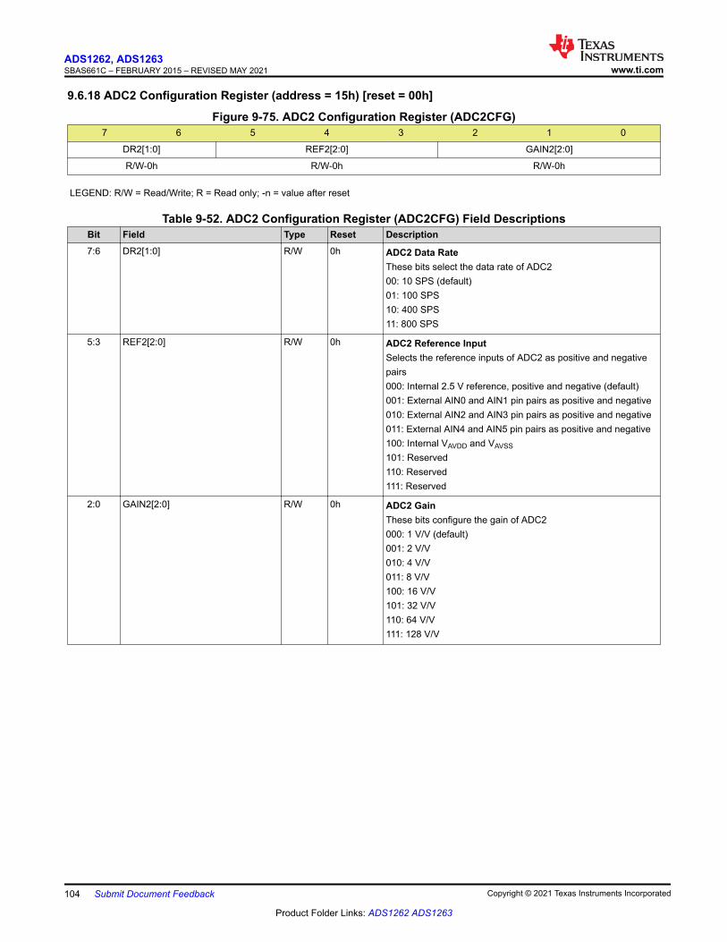
9.6.18 ADC2 Configuration Register (address = 15h) [reset = 00h]
Figure 9-75. ADC2 Configuration Register (ADC2CFG)7 6 5 4 3 2 1 0
DR2[1:0] REF2[2:0] GAIN2[2:0]
R/W-0h R/W-0h R/W-0h
LEGEND: R/W = Read/Write; R = Read only; -n = value after reset
Table 9-52. ADC2 Configuration Register (ADC2CFG) Field DescriptionsBit Field Type Reset Description7:6 DR2[1:0] R/W 0h ADC2 Data Rate
These bits select the data rate of ADC200: 10 SPS (default)01: 100 SPS10: 400 SPS11: 800 SPS
5:3 REF2[2:0] R/W 0h ADC2 Reference InputSelects the reference inputs of ADC2 as positive and negativepairs000: Internal 2.5 V reference, positive and negative (default)001: External AIN0 and AIN1 pin pairs as positive and negative010: External AIN2 and AIN3 pin pairs as positive and negative011: External AIN4 and AIN5 pin pairs as positive and negative100: Internal VAVDD and VAVSS
101: Reserved110: Reserved111: Reserved
2:0 GAIN2[2:0] R/W 0h ADC2 GainThese bits configure the gain of ADC2000: 1 V/V (default)001: 2 V/V010: 4 V/V011: 8 V/V100: 16 V/V101: 32 V/V110: 64 V/V111: 128 V/V
ADS1262, ADS1263SBAS661C – FEBRUARY 2015 – REVISED MAY 2021 www.ti.com
104 Submit Document Feedback Copyright © 2021 Texas Instruments Incorporated
Product Folder Links: ADS1262 ADS1263
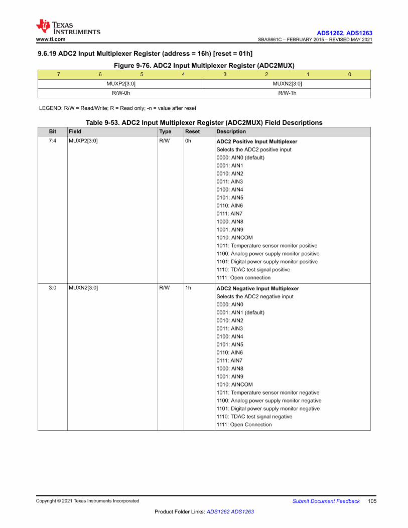
9.6.19 ADC2 Input Multiplexer Register (address = 16h) [reset = 01h]
Figure 9-76. ADC2 Input Multiplexer Register (ADC2MUX)7 6 5 4 3 2 1 0
MUXP2[3:0] MUXN2[3:0]
R/W-0h R/W-1h
LEGEND: R/W = Read/Write; R = Read only; -n = value after reset
Table 9-53. ADC2 Input Multiplexer Register (ADC2MUX) Field DescriptionsBit Field Type Reset Description7:4 MUXP2[3:0] R/W 0h ADC2 Positive Input Multiplexer
Selects the ADC2 positive input0000: AIN0 (default)0001: AIN10010: AIN20011: AIN30100: AIN40101: AIN50110: AIN60111: AIN71000: AIN81001: AIN91010: AINCOM1011: Temperature sensor monitor positive1100: Analog power supply monitor positive1101: Digital power supply monitor positive1110: TDAC test signal positive1111: Open connection
3:0 MUXN2[3:0] R/W 1h ADC2 Negative Input MultiplexerSelects the ADC2 negative input0000: AIN00001: AIN1 (default)0010: AIN20011: AIN30100: AIN40101: AIN50110: AIN60111: AIN71000: AIN81001: AIN91010: AINCOM1011: Temperature sensor monitor negative1100: Analog power supply monitor negative1101: Digital power supply monitor negative1110: TDAC test signal negative1111: Open Connection
www.ti.comADS1262, ADS1263
SBAS661C – FEBRUARY 2015 – REVISED MAY 2021
Copyright © 2021 Texas Instruments Incorporated Submit Document Feedback 105
Product Folder Links: ADS1262 ADS1263
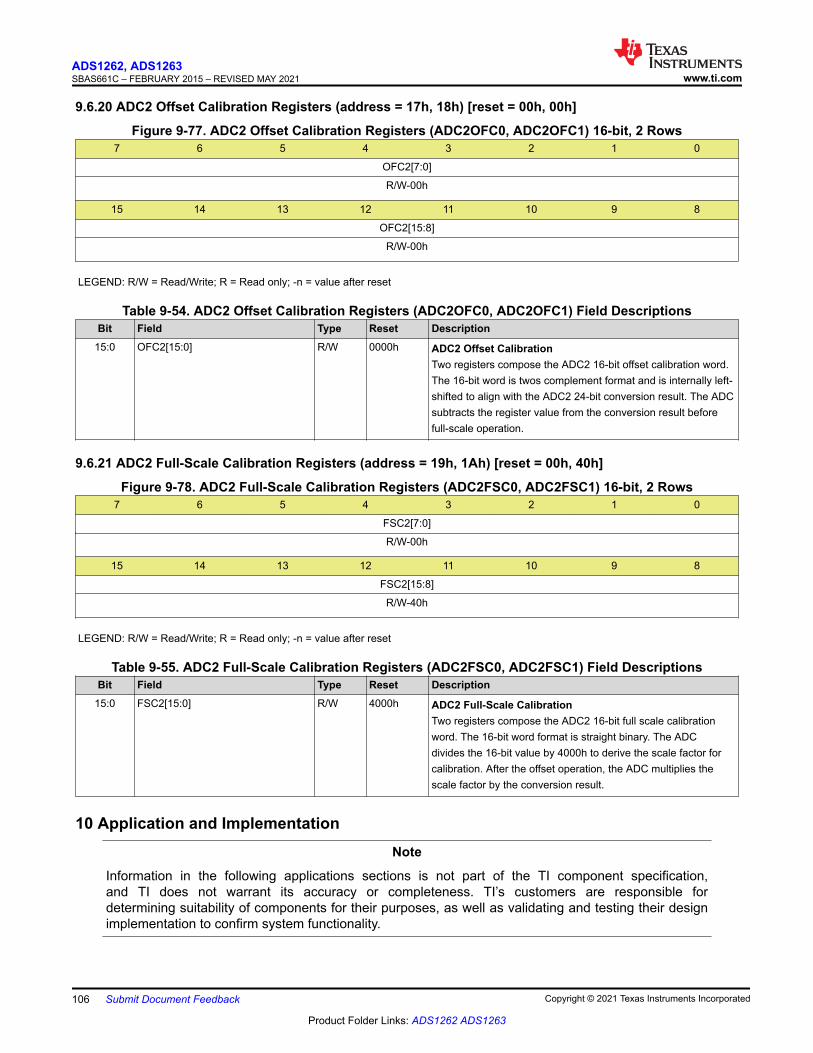
9.6.20 ADC2 Offset Calibration Registers (address = 17h, 18h) [reset = 00h, 00h]
Figure 9-77. ADC2 Offset Calibration Registers (ADC2OFC0, ADC2OFC1) 16-bit, 2 Rows7 6 5 4 3 2 1 0
OFC2[7:0]
R/W-00h
15 14 13 12 11 10 9 8
OFC2[15:8]
R/W-00h
LEGEND: R/W = Read/Write; R = Read only; -n = value after reset
Table 9-54. ADC2 Offset Calibration Registers (ADC2OFC0, ADC2OFC1) Field DescriptionsBit Field Type Reset Description
15:0 OFC2[15:0] R/W 0000h ADC2 Offset CalibrationTwo registers compose the ADC2 16-bit offset calibration word.The 16-bit word is twos complement format and is internally left-shifted to align with the ADC2 24-bit conversion result. The ADCsubtracts the register value from the conversion result beforefull-scale operation.
9.6.21 ADC2 Full-Scale Calibration Registers (address = 19h, 1Ah) [reset = 00h, 40h]
Figure 9-78. ADC2 Full-Scale Calibration Registers (ADC2FSC0, ADC2FSC1) 16-bit, 2 Rows7 6 5 4 3 2 1 0
FSC2[7:0]
R/W-00h
15 14 13 12 11 10 9 8
FSC2[15:8]
R/W-40h
LEGEND: R/W = Read/Write; R = Read only; -n = value after reset
Table 9-55. ADC2 Full-Scale Calibration Registers (ADC2FSC0, ADC2FSC1) Field DescriptionsBit Field Type Reset Description
15:0 FSC2[15:0] R/W 4000h ADC2 Full-Scale CalibrationTwo registers compose the ADC2 16-bit full scale calibrationword. The 16-bit word format is straight binary. The ADCdivides the 16-bit value by 4000h to derive the scale factor forcalibration. After the offset operation, the ADC multiplies thescale factor by the conversion result.
10 Application and ImplementationNote
Information in the following applications sections is not part of the TI component specification,and TI does not warrant its accuracy or completeness. TI’s customers are responsible fordetermining suitability of components for their purposes, as well as validating and testing their designimplementation to confirm system functionality.
ADS1262, ADS1263SBAS661C – FEBRUARY 2015 – REVISED MAY 2021 www.ti.com
106 Submit Document Feedback Copyright © 2021 Texas Instruments Incorporated
Product Folder Links: ADS1262 ADS1263
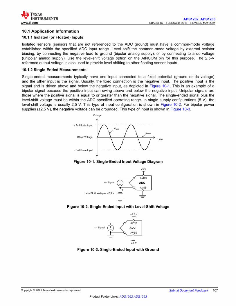
10.1 Application Information10.1.1 Isolated (or Floated) Inputs
Isolated sensors (sensors that are not referenced to the ADC ground) must have a common-mode voltageestablished within the specified ADC input range. Level shift the common-mode voltage by external resistorbiasing, by connecting the negative lead to ground (bipolar analog supply), or by connecting to a dc voltage(unipolar analog supply). Use the level-shift voltage option on the AINCOM pin for this purpose. The 2.5-Vreference output voltage is also used to provide level shifting to other floating sensor inputs.
10.1.2 Single-Ended Measurements
Single-ended measurements typically have one input connected to a fixed potential (ground or dc voltage)and the other input is the signal. Usually, the fixed connection is the negative input. The positive input is thesignal and is driven above and below the negative input, as depicted in Figure 10-1. This is an example of abipolar signal because the positive input can swing above and below the negative input. Unipolar signals arethose where the positive signal is equal to or greater than the negative signal. The single-ended signal plus thelevel-shift voltage must be within the ADC specified operating range. In single supply configurations (5 V), thelevel-shift voltage is usually 2.5 V. This type of input configuration is shown in Figure 10-2. For bipolar powersupplies (±2.5 V), the negative voltage can be grounded. This type of input is shown in Figure 10-3.
Offset Voltage
+ Full Scale Input
- Full Scale Input
Time
Voltage
VAINP
VAINN
Figure 10-1. Single-Ended Input Voltage Diagram
ADC+/- Signal
Level Shift Voltage= +2.5 V
AVDD
AVSS
+5 V
+±
+
Figure 10-2. Single-Ended Input with Level-Shift Voltage
ADC+/- Signal
AVDD
AVSS
+2.5 V
+±
-2.5 V
Figure 10-3. Single-Ended Input with Ground
www.ti.comADS1262, ADS1263
SBAS661C – FEBRUARY 2015 – REVISED MAY 2021
Copyright © 2021 Texas Instruments Incorporated Submit Document Feedback 107
Product Folder Links: ADS1262 ADS1263
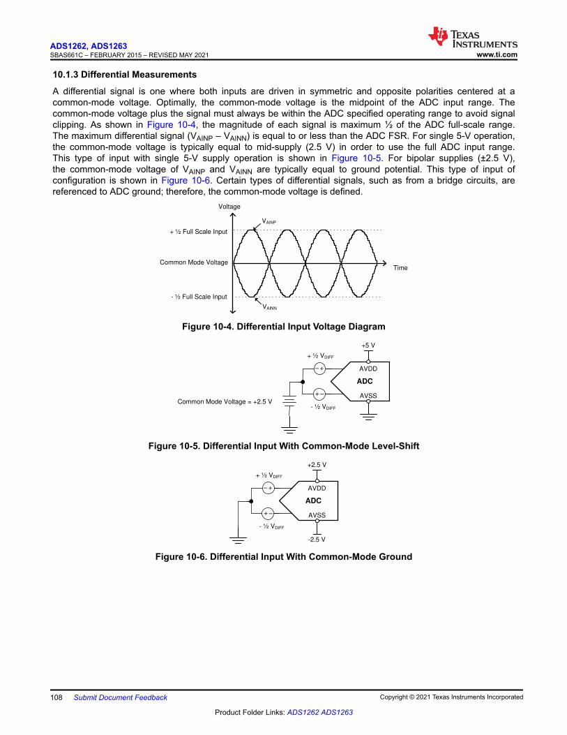
10.1.3 Differential Measurements
A differential signal is one where both inputs are driven in symmetric and opposite polarities centered at acommon-mode voltage. Optimally, the common-mode voltage is the midpoint of the ADC input range. Thecommon-mode voltage plus the signal must always be within the ADC specified operating range to avoid signalclipping. As shown in Figure 10-4, the magnitude of each signal is maximum ½ of the ADC full-scale range.The maximum differential signal (VAINP – VAINN) is equal to or less than the ADC FSR. For single 5-V operation,the common-mode voltage is typically equal to mid-supply (2.5 V) in order to use the full ADC input range.This type of input with single 5-V supply operation is shown in Figure 10-5. For bipolar supplies (±2.5 V),the common-mode voltage of VAINP and VAINN are typically equal to ground potential. This type of input ofconfiguration is shown in Figure 10-6. Certain types of differential signals, such as from a bridge circuits, arereferenced to ADC ground; therefore, the common-mode voltage is defined.
VAINP
+ ½ Full Scale Input
- ½ Full Scale Input
Time
Voltage
Common Mode Voltage
VAINN
Figure 10-4. Differential Input Voltage Diagram
ADC
Common Mode Voltage = +2.5 V
AVDD
AVSS
+5 V
- ½ VDIFF
+
±
+
±
+ ½ VDIFF
Figure 10-5. Differential Input With Common-Mode Level-Shift
ADC
AVDD
AVSS
+2.5 V
- ½ VDIFF
+
±
+
±
+ ½ VDIFF
-2.5 V
Figure 10-6. Differential Input With Common-Mode Ground
ADS1262, ADS1263SBAS661C – FEBRUARY 2015 – REVISED MAY 2021 www.ti.com
108 Submit Document Feedback Copyright © 2021 Texas Instruments Incorporated
Product Folder Links: ADS1262 ADS1263
10.1.4 Input Range
For proper operation of ADC1, the PGA absolute input voltages, VINP and VINN, must always remain within thevalid PGA input range, as shown in Equation 12.
The following example uses Equation 12 to determine the input-range requirement. For this example, use athermocouple (60 mV, maximum differential output) with the negative lead connected to the internal level-shiftvoltage (2.5 V). Use a PGA gain of 32 and operate the ADC with a single 5-V power supply. To verify the PGAinput-range requirement, the conditions are:
• VINN = Negative absolute input voltage = 2.5 V• VINP = Positive absolute input voltage = 2.56 V• VIN = Differential input voltage = 0.06 V• VAVDD = 4.75 V (worst-case minimum)• VAVSS = 0 V• Gain = 32
Filling in Equation 12 with the values shown gives:
VAVSS + 0.3 + |VIN| · (Gain – 1) / 2 < VINP and VINN < VAVDD – 0.3 – |VIN| · (Gain – 1) / 2
= 0 + 0.3 + 0.06 · (32 – 1) / 2 < 2.5 and 2.56 < 4.75 – 0.3 – 0.06 · (32 – 1) / 2
= 1.23 V < 2.5 V and 2.56 V < 3.52 V
The inequality is satisfied, therefore the VINN and VINP absolute input voltages are within the required PGA inputrange. Alternatively, measure the PGA output voltages (pins CAPP and CAPN) with a voltmeter to verify thateach PGA output voltage is < VAVDD – 0.3 V and > VAVSS – 0.3 V under the expected minimum and maximuminput conditions, respectively.
The input range requirement of ADC2 is verified in the same way as ADC1. See Equation 15 for the ADC2 inputrange requirements.
10.1.5 Input Filtering
Analog input filtering serves two purposes: first, to limit the effect of aliasing during the sampling process; andsecond, to reduce external noise that affects the measurement.
10.1.5.1 Aliasing
As with all ADCs, out-of-band input signals can fold back or alias if not band-limited. Aliasing describes theeffect of input frequencies greater than ½ the sample rate folding back to the bandwidth of interest. An antialiasfilter placed at the ADC inputs reduces the magnitude of the aliased frequencies. The ADS1262 and ADS1263incorporate analog and digital antialiasing filters to attenuate the aliased frequencies. There are two ranges ofaliased frequencies: frequencies greater than ½ of the down-sampled output data rate (Nyquist frequency) andfrequencies occurring at multiples of the modulator sample rate.
Aliasing can occur at frequencies greater than ½ the ADC output data rate. For example, at data rate of 50 SPS,aliasing occurs at frequencies greater than 25 Hz. The ADC digital filter rejects the aliased frequencies as inputfrequency increases. The amount of aliased frequency rejection is given by the filter type and order. Figure 10-7illustrates the frequency response of the sinc filter. Note the sinc4 filter provides the best rejection of aliasedfrequencies.
www.ti.comADS1262, ADS1263
SBAS661C – FEBRUARY 2015 – REVISED MAY 2021
Copyright © 2021 Texas Instruments Incorporated Submit Document Feedback 109
Product Folder Links: ADS1262 ADS1263
Frequency (Hz)
Am
plit
ude (
dB
)
0 50 100 150 200 250 300 350 400 450 500 550 600-160
-140
-120
-100
-80
-60
-40
-20
0
D005
sinc1sinc2sinc3sinc4
Figure 10-7. Frequency Response (50 SPS)
The second band of aliased frequencies occur at the ADC modulator sample rate multiples (fMOD = fCLK / 8 =921.6 kHz, multiples = 1843.2 kHz and so on). Figure 10-8 shows the 38400 SPS frequency response plottedto 1.2 MHz. The response near dc is the signal bandwidth of interest. Observe how the digital filter responserepeats on the sides of the modulator sample rate (921.6 kHz). Figure 10-9 shows the repeated response atthe modulator frequency multiples = N · fMOD ± fDR, where N = multiples of fMOD starting at 1, and fDR = datarate frequency. The digital filter attenuates signal or noise up to where the response repeats. However, signal ornoise occurring at the modulator sample rate is not attenuated by the digital filter and therefore, is aliased to thepassband.
Frequency (kHz)
Am
plit
ude (
dB
)
0 200 400 600 800 1000 1200-160
-140
-120
-100
-80
-60
-40
-20
0
D014
Figure 10-8. Frequency Response to 1.2 MHz(38400 SPS)
Frequency (MHz)
Am
plit
ude (
dB
)
0 1 2 3 4 5 6 7 8-160
-140
-120
-100
-80
-60
-40
-20
0
D015
Figure 10-9. Frequency Response to 8 MHz(38400 SPS)
Figure 10-10 illustrates how the frequencies alias near the modulator sample rate frequency. The final figureshows the aliased frequency rejection provided by an antialias filter. The ADC incorporates an analog antialiasfilter with a cutoff frequency of 60 kHz that rejects the aliased frequencies.
ADS1262, ADS1263SBAS661C – FEBRUARY 2015 – REVISED MAY 2021 www.ti.com
110 Submit Document Feedback Copyright © 2021 Texas Instruments Incorporated
Product Folder Links: ADS1262 ADS1263
Magnitude
fMOD / 2 fMODOutput
Data Rate
Frequency
External
Antialiasing Filter
Roll-Off
Magnitude
fMOD / 2 fMODOutput
Data Rate
Frequency
Digital Filter
Magnitude
fMOD / 2 fMODOutput
Data Rate
Frequency
Sensor
Signal
Unwanted
Signals
Unwanted
Signals
Aliasing of Unwanted
Signals
Figure 10-10. Alias Effect
Many sensor signals are inherently band-limited; for example, the output of a thermocouple has a limited rate ofchange. In this case, the sensor signal does not alias back into the pass band when using a ΔΣ ADC. However,any noise picked up along the sensor wiring or the application circuitry can potentially alias into the pass band.Power line-cycle frequency and harmonics are one common noise source. External noise is also generated fromelectromagnetic interference (EMI) or radio frequency interference (RFI) sources, such as nearby motors andcellular phones. Another noise source exists on the printed circuit board (PCB) in the form of clocks and otherdigital signals. Analog input filtering helps remove unwanted signals from affecting the measurement result. TheADC incorporates a low-pass, antialias filter with a corner frequency of 60 kHz to reduce the aliased frequencies.The filter consists of the external 4.7-nF PGA output capacitor (CAPP and CAPN pins) and internal 280-Ωresistors.
Use an input filter to provide increased rejection of aliased noise frequencies and further attenuate possiblestrong high-frequency interference signals. For best performance, filter strong interference frequencies at the
www.ti.comADS1262, ADS1263
SBAS661C – FEBRUARY 2015 – REVISED MAY 2021
Copyright © 2021 Texas Instruments Incorporated Submit Document Feedback 111
Product Folder Links: ADS1262 ADS1263
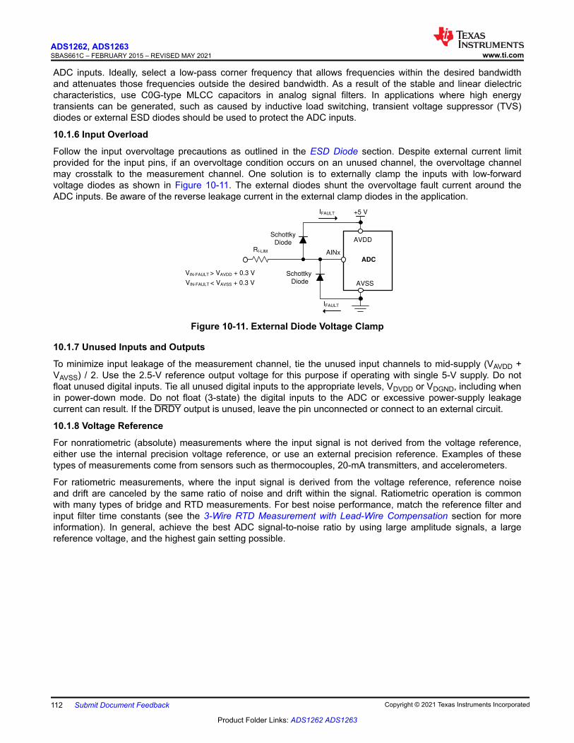
ADC inputs. Ideally, select a low-pass corner frequency that allows frequencies within the desired bandwidthand attenuates those frequencies outside the desired bandwidth. As a result of the stable and linear dielectriccharacteristics, use C0G-type MLCC capacitors in analog signal filters. In applications where high energytransients can be generated, such as caused by inductive load switching, transient voltage suppressor (TVS)diodes or external ESD diodes should be used to protect the ADC inputs.
10.1.6 Input Overload
Follow the input overvoltage precautions as outlined in the ESD Diode section. Despite external current limitprovided for the input pins, if an overvoltage condition occurs on an unused channel, the overvoltage channelmay crosstalk to the measurement channel. One solution is to externally clamp the inputs with low-forwardvoltage diodes as shown in Figure 10-11. The external diodes shunt the overvoltage fault current around theADC inputs. Be aware of the reverse leakage current in the external clamp diodes in the application.
AVDDSchottky
Diode
AINx
AVSS
IFAULT
Schottky
Diode
IFAULT
+5 V
VIN-FAULT > VAVDD + 0.3 V
ADC
RI-LIM
VIN-FAULT < VAVSS + 0.3 V
Figure 10-11. External Diode Voltage Clamp
10.1.7 Unused Inputs and Outputs
To minimize input leakage of the measurement channel, tie the unused input channels to mid-supply (VAVDD +VAVSS) / 2. Use the 2.5-V reference output voltage for this purpose if operating with single 5-V supply. Do notfloat unused digital inputs. Tie all unused digital inputs to the appropriate levels, VDVDD or VDGND, including whenin power-down mode. Do not float (3-state) the digital inputs to the ADC or excessive power-supply leakagecurrent can result. If the DRDY output is unused, leave the pin unconnected or connect to an external circuit.
10.1.8 Voltage Reference
For nonratiometric (absolute) measurements where the input signal is not derived from the voltage reference,either use the internal precision voltage reference, or use an external precision reference. Examples of thesetypes of measurements come from sensors such as thermocouples, 20-mA transmitters, and accelerometers.
For ratiometric measurements, where the input signal is derived from the voltage reference, reference noiseand drift are canceled by the same ratio of noise and drift within the signal. Ratiometric operation is commonwith many types of bridge and RTD measurements. For best noise performance, match the reference filter andinput filter time constants (see the 3-Wire RTD Measurement with Lead-Wire Compensation section for moreinformation). In general, achieve the best ADC signal-to-noise ratio by using large amplitude signals, a largereference voltage, and the highest gain setting possible.
ADS1262, ADS1263SBAS661C – FEBRUARY 2015 – REVISED MAY 2021 www.ti.com
112 Submit Document Feedback Copyright © 2021 Texas Instruments Incorporated
Product Folder Links: ADS1262 ADS1263
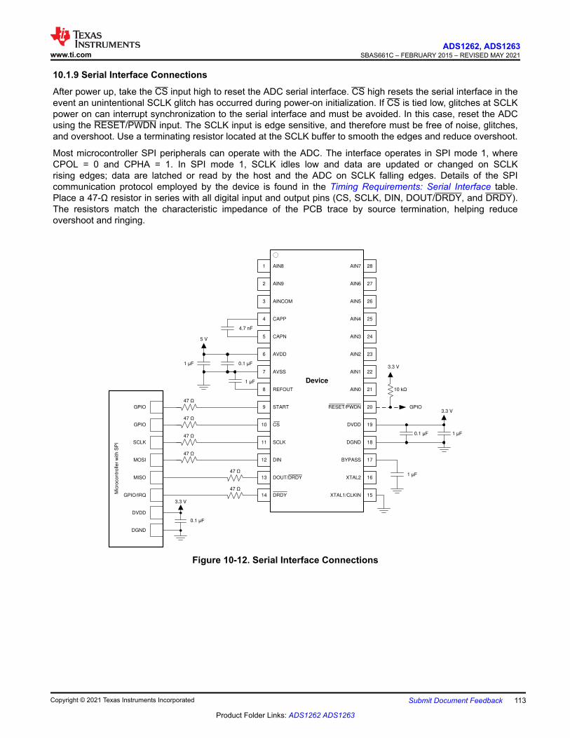
10.1.9 Serial Interface Connections
After power up, take the CS input high to reset the ADC serial interface. CS high resets the serial interface in theevent an unintentional SCLK glitch has occurred during power-on initialization. If CS is tied low, glitches at SCLKpower on can interrupt synchronization to the serial interface and must be avoided. In this case, reset the ADCusing the RESET/PWDN input. The SCLK input is edge sensitive, and therefore must be free of noise, glitches,and overshoot. Use a terminating resistor located at the SCLK buffer to smooth the edges and reduce overshoot.
Most microcontroller SPI peripherals can operate with the ADC. The interface operates in SPI mode 1, whereCPOL = 0 and CPHA = 1. In SPI mode 1, SCLK idles low and data are updated or changed on SCLKrising edges; data are latched or read by the host and the ADC on SCLK falling edges. Details of the SPIcommunication protocol employed by the device is found in the Timing Requirements: Serial Interface table.Place a 47-Ω resistor in series with all digital input and output pins (CS, SCLK, DIN, DOUT/DRDY, and DRDY).The resistors match the characteristic impedance of the PCB trace by source termination, helping reduceovershoot and ringing.
28
27
26
25
24
23
22
21
1
2
3
4
5
6
7
8
AINCOM
CAPP
CAPN
AVDD
AVSS
REFOUT AIN0
AIN1
AIN2
AIN3
AIN4
AIN5
AIN6
AIN7AIN8
AIN9
9
10
11
12
13
14
SCLK
DIN
DOUT/DRDY
START
CS
20
19
18
17
16
15XTAL1/CLKIN
XTAL2
BYPASS
DGND
DVDD
RESET/PWDN
Device
DRDY
4.7 nF
0.1 �F
0.1 �F 1 �F
1 �F
5 V
1 �F
1 �F
GPIO
SCLK
MOSI
MISO
47
47
47
GPIO/IRQ
0.1 �F
DVDD
DGND
47
47
Mic
roco
ntr
olle
r w
ith
SP
I
GPIO
47
3.3 V
3.3 VGPIO
3.3 V
10 k
Figure 10-12. Serial Interface Connections
www.ti.comADS1262, ADS1263
SBAS661C – FEBRUARY 2015 – REVISED MAY 2021
Copyright © 2021 Texas Instruments Incorporated Submit Document Feedback 113
Product Folder Links: ADS1262 ADS1263
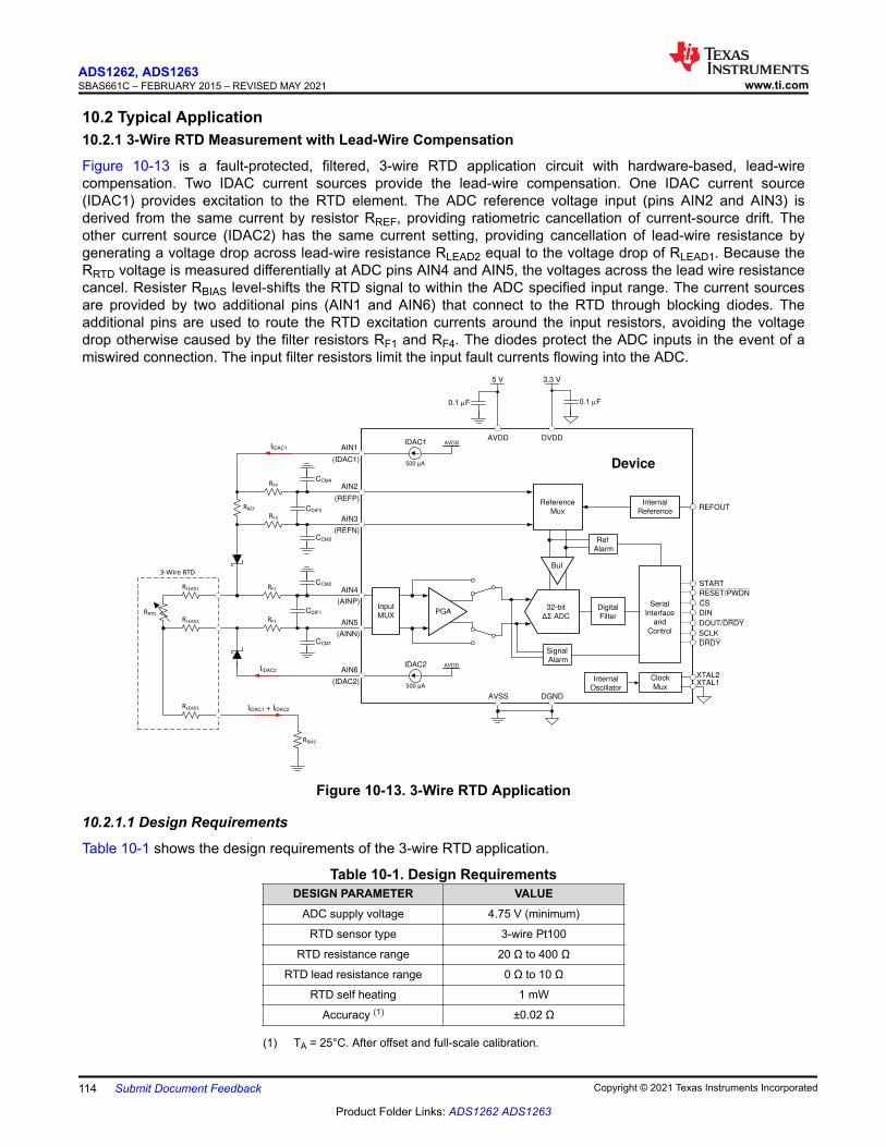
10.2 Typical Application10.2.1 3-Wire RTD Measurement with Lead-Wire Compensation
Figure 10-13 is a fault-protected, filtered, 3-wire RTD application circuit with hardware-based, lead-wirecompensation. Two IDAC current sources provide the lead-wire compensation. One IDAC current source(IDAC1) provides excitation to the RTD element. The ADC reference voltage input (pins AIN2 and AIN3) isderived from the same current by resistor RREF, providing ratiometric cancellation of current-source drift. Theother current source (IDAC2) has the same current setting, providing cancellation of lead-wire resistance bygenerating a voltage drop across lead-wire resistance RLEAD2 equal to the voltage drop of RLEAD1. Because theRRTD voltage is measured differentially at ADC pins AIN4 and AIN5, the voltages across the lead wire resistancecancel. Resister RBIAS level-shifts the RTD signal to within the ADC specified input range. The current sourcesare provided by two additional pins (AIN1 and AIN6) that connect to the RTD through blocking diodes. Theadditional pins are used to route the RTD excitation currents around the input resistors, avoiding the voltagedrop otherwise caused by the filter resistors RF1 and RF4. The diodes protect the ADC inputs in the event of amiswired connection. The input filter resistors limit the input fault currents flowing into the ADC.
DOUT/DRDY
RESET/PWDN
DIN
AIN4
AIN5
AIN6
CDIF1
CCM1
CCM2RF2
RF1RLEAD2
RLEAD1
RRTD
(IDAC2)
(REFP)
IIDAC1 + IIDAC2
Clock
Mux
XTAL2XTAL1
CDIF2
CCM3
CCM4RF4
RF3
AIN2
AIN3
AIN1
5 V
0.1 PF
Device
32-bit
û��ADCPGA
RLEAD3
500 �A
IDAC2
3-Wire RTD
IIDAC2
IIDAC1
RREF
RBIAS
500 �A
IDAC1
(REFN)
(IDAC1)
(AINP)
(AINN)
AVDD
AVDDAVDD DVDD
AVSS DGND
Internal
Reference
Digital
Filter
Serial
Interface
and
Control
CS
SCLK
DRDY
START
Ref
Alarm
Signal
Alarm
Buf
Reference
Mux
3.3 V
0.1 PF
REFOUT
Internal
Oscillator
Input
MUX
Figure 10-13. 3-Wire RTD Application
10.2.1.1 Design Requirements
Table 10-1 shows the design requirements of the 3-wire RTD application.
Table 10-1. Design RequirementsDESIGN PARAMETER VALUE
ADC supply voltage 4.75 V (minimum)
RTD sensor type 3-wire Pt100
RTD resistance range 20 Ω to 400 Ω
RTD lead resistance range 0 Ω to 10 Ω
RTD self heating 1 mW
Accuracy (1) ±0.02 Ω
(1) TA = 25°C. After offset and full-scale calibration.
ADS1262, ADS1263SBAS661C – FEBRUARY 2015 – REVISED MAY 2021 www.ti.com
114 Submit Document Feedback Copyright © 2021 Texas Instruments Incorporated
Product Folder Links: ADS1262 ADS1263
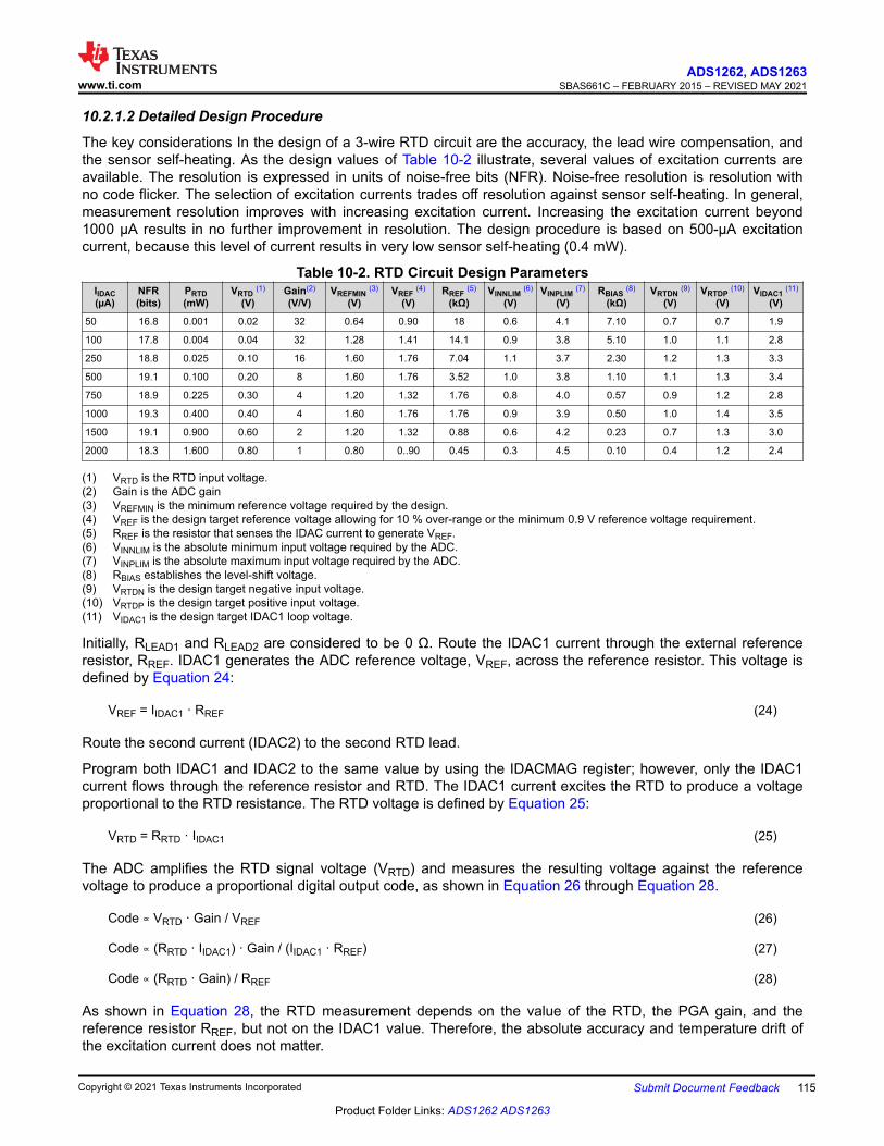
10.2.1.2 Detailed Design Procedure
The key considerations In the design of a 3-wire RTD circuit are the accuracy, the lead wire compensation, andthe sensor self-heating. As the design values of Table 10-2 illustrate, several values of excitation currents areavailable. The resolution is expressed in units of noise-free bits (NFR). Noise-free resolution is resolution withno code flicker. The selection of excitation currents trades off resolution against sensor self-heating. In general,measurement resolution improves with increasing excitation current. Increasing the excitation current beyond1000 µA results in no further improvement in resolution. The design procedure is based on 500-µA excitationcurrent, because this level of current results in very low sensor self-heating (0.4 mW).
Table 10-2. RTD Circuit Design ParametersIIDAC(µA)
NFR(bits)
PRTD(mW)
VRTD (1)
(V)Gain(2)
(V/V)VREFMIN (3)
(V)VREF (4)
(V)RREF (5)
(kΩ)VINNLIM (6)
(V)VINPLIM (7)
(V)RBIAS (8)
(kΩ)VRTDN (9)
(V)VRTDP (10)
(V)VIDAC1 (11)
(V)
50 16.8 0.001 0.02 32 0.64 0.90 18 0.6 4.1 7.10 0.7 0.7 1.9
100 17.8 0.004 0.04 32 1.28 1.41 14.1 0.9 3.8 5.10 1.0 1.1 2.8
250 18.8 0.025 0.10 16 1.60 1.76 7.04 1.1 3.7 2.30 1.2 1.3 3.3
500 19.1 0.100 0.20 8 1.60 1.76 3.52 1.0 3.8 1.10 1.1 1.3 3.4
750 18.9 0.225 0.30 4 1.20 1.32 1.76 0.8 4.0 0.57 0.9 1.2 2.8
1000 19.3 0.400 0.40 4 1.60 1.76 1.76 0.9 3.9 0.50 1.0 1.4 3.5
1500 19.1 0.900 0.60 2 1.20 1.32 0.88 0.6 4.2 0.23 0.7 1.3 3.0
2000 18.3 1.600 0.80 1 0.80 0..90 0.45 0.3 4.5 0.10 0.4 1.2 2.4
(1) VRTD is the RTD input voltage.(2) Gain is the ADC gain(3) VREFMIN is the minimum reference voltage required by the design.(4) VREF is the design target reference voltage allowing for 10 % over-range or the minimum 0.9 V reference voltage requirement.(5) RREF is the resistor that senses the IDAC current to generate VREF.(6) VINNLIM is the absolute minimum input voltage required by the ADC.(7) VINPLIM is the absolute maximum input voltage required by the ADC.(8) RBIAS establishes the level-shift voltage.(9) VRTDN is the design target negative input voltage.(10) VRTDP is the design target positive input voltage.(11) VIDAC1 is the design target IDAC1 loop voltage.
Initially, RLEAD1 and RLEAD2 are considered to be 0 Ω. Route the IDAC1 current through the external referenceresistor, RREF. IDAC1 generates the ADC reference voltage, VREF, across the reference resistor. This voltage isdefined by Equation 24:
VREF = IIDAC1 · RREF (24)
Route the second current (IDAC2) to the second RTD lead.
Program both IDAC1 and IDAC2 to the same value by using the IDACMAG register; however, only the IDAC1current flows through the reference resistor and RTD. The IDAC1 current excites the RTD to produce a voltageproportional to the RTD resistance. The RTD voltage is defined by Equation 25:
VRTD = RRTD · IIDAC1 (25)
The ADC amplifies the RTD signal voltage (VRTD) and measures the resulting voltage against the referencevoltage to produce a proportional digital output code, as shown in Equation 26 through Equation 28.
Code ∝ VRTD · Gain / VREF (26)
Code ∝ (RRTD · IIDAC1) · Gain / (IIDAC1 · RREF) (27)
Code ∝ (RRTD · Gain) / RREF (28)
As shown in Equation 28, the RTD measurement depends on the value of the RTD, the PGA gain, and thereference resistor RREF, but not on the IDAC1 value. Therefore, the absolute accuracy and temperature drift ofthe excitation current does not matter.
www.ti.comADS1262, ADS1263
SBAS661C – FEBRUARY 2015 – REVISED MAY 2021
Copyright © 2021 Texas Instruments Incorporated Submit Document Feedback 115
Product Folder Links: ADS1262 ADS1263
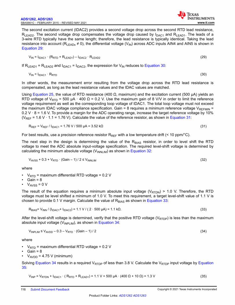
The second excitation current (IDAC2) provides a second voltage drop across the second RTD lead resistance,RLEAD2. The second voltage drop compensates the voltage drop caused by IDAC1 and RLEAD1. The leads of a3-wire RTD typically have the same length; therefore, the lead resistance is typically identical. Taking the leadresistance into account (RLEADx ≠ 0), the differential voltage (VIN) across ADC inputs AIN4 and AIN5 is shown inEquation 29:
VIN = IIDAC1 · (RRTD + RLEAD1) – IIDAC2 · RLEAD2 (29)
If RLEAD1 = RLEAD2 and IIDAC1 = IIDAC2, the expression for VIN reduces to Equation 30:
VIN = IIDAC1 · RRTD (30)
In other words, the measurement error resulting from the voltage drop across the RTD lead resistance iscompensated, as long as the lead resistance values and the IDAC values are matched.
Using Equation 25, the value of RTD resistance (400 Ω, maximum) and the excitation current (500 μA) yields anRTD voltage of VRTD = 500 μA · 400 Ω = 0.2 V. Use the maximum gain of 8 V/V in order to limit the referencevoltage requirement as well as the corresponding loop voltage of IDAC1. The total loop voltage must not exceedthe maximum IDAC voltage compliance specification. Gain = 8 requires a minimum reference voltage VREFMIN =0.2 V · 8 = 1.6 V. To provide a margin for the ADC operating range, increase the target reference voltage by 10%(VREF = 1.6 V · 1.1 = 1.76 V). Calculate the value of the reference resistor, as shown in Equation 31:
RREF = VREF / IIDAC1 = 1.76 V / 500 μA = 3.52 kΩ (31)
For best results, use a precision reference resistor RREF with a low temperature drift (< 10 ppm/°C).
The next step in the design is determining the value of the RBIAS resistor, in order to level shift the RTDvoltage to meet the ADC absolute input-voltage specification. The required level-shift voltage is determined bycalculating the minimum absolute voltage (VINNLIM) as shown in Equation 32:
VAVSS + 0.3 + VRTD · (Gain – 1) / 2 ≤ VINNLIM (32)
where
• VRTD = maximum differential RTD voltage = 0.2 V• Gain = 8• VAVSS = 0 V
The result of the equation requires a minimum absolute input voltage (VRTDN) > 1.0 V. Therefore, the RTDvoltage must be level shifted a minimum of 1.0 V. To meet this requirement, a target level-shift value of 1.1 V ischosen to provide 0.1 V margin. Calculate the value of RBIAS as shown in Equation 33:
RBIAS= VINN / (IIDAC1+ IIDAC2) = 1.1 V / ( 2 · 500 μA) = 1.1 kΩ. (33)
After the level-shift voltage is determined, verify that the positive RTD voltage (VRTDP) is less than the maximumabsolute input voltage (VINPLIM), as shown in Equation 34:
VINPLIM ≤ VAVDD – 0.3 – VRTD · (Gain – 1) / 2 (34)
where
• VRTD = maximum differential RTD voltage = 0.2 V• Gain = 8• VAVDD = 4.75 V (minimum)
Solving Equation 34 results in a required VRTDP of less than 3.8 V. Calculate the VRTDP input voltage by Equation35:
VINP = VRTDN + IIDAC1 · ( RRTD + RLEAD1) = 1.1 V + 500 μA · (400 Ω + 10 Ω) = 1.3 V (35)
ADS1262, ADS1263SBAS661C – FEBRUARY 2015 – REVISED MAY 2021 www.ti.com
116 Submit Document Feedback Copyright © 2021 Texas Instruments Incorporated
Product Folder Links: ADS1262 ADS1263
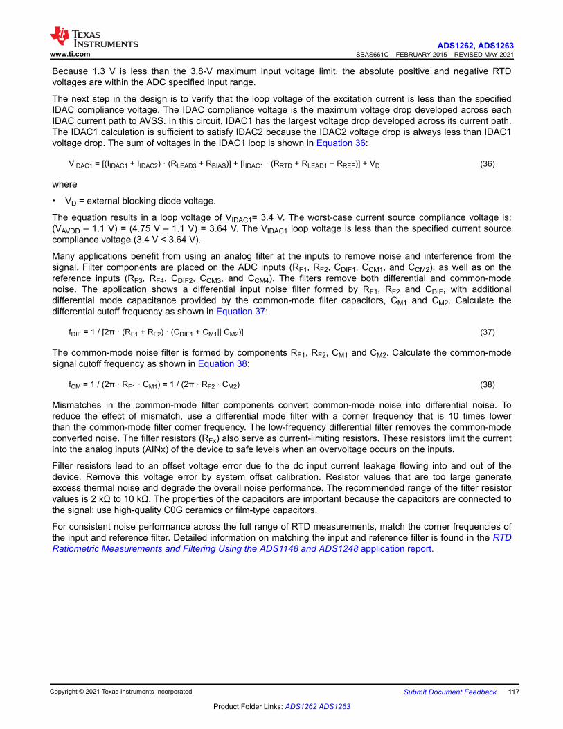
Because 1.3 V is less than the 3.8-V maximum input voltage limit, the absolute positive and negative RTDvoltages are within the ADC specified input range.
The next step in the design is to verify that the loop voltage of the excitation current is less than the specifiedIDAC compliance voltage. The IDAC compliance voltage is the maximum voltage drop developed across eachIDAC current path to AVSS. In this circuit, IDAC1 has the largest voltage drop developed across its current path.The IDAC1 calculation is sufficient to satisfy IDAC2 because the IDAC2 voltage drop is always less than IDAC1voltage drop. The sum of voltages in the IDAC1 loop is shown in Equation 36:
VIDAC1 = [(IIDAC1 + IIDAC2) · (RLEAD3 + RBIAS)] + [IIDAC1 · (RRTD + RLEAD1 + RREF)] + VD (36)
where
• VD = external blocking diode voltage.
The equation results in a loop voltage of VIDAC1= 3.4 V. The worst-case current source compliance voltage is:(VAVDD – 1.1 V) = (4.75 V – 1.1 V) = 3.64 V. The VIDAC1 loop voltage is less than the specified current sourcecompliance voltage (3.4 V < 3.64 V).
Many applications benefit from using an analog filter at the inputs to remove noise and interference from thesignal. Filter components are placed on the ADC inputs (RF1, RF2, CDIF1, CCM1, and CCM2), as well as on thereference inputs (RF3, RF4, CDIF2, CCM3, and CCM4). The filters remove both differential and common-modenoise. The application shows a differential input noise filter formed by RF1, RF2 and CDIF, with additionaldifferential mode capacitance provided by the common-mode filter capacitors, CM1 and CM2. Calculate thedifferential cutoff frequency as shown in Equation 37:
fDIF = 1 / [2π · (RF1 + RF2) · (CDIF1 + CM1|| CM2)] (37)
The common-mode noise filter is formed by components RF1, RF2, CM1 and CM2. Calculate the common-modesignal cutoff frequency as shown in Equation 38:
fCM = 1 / (2π · RF1 · CM1) = 1 / (2π · RF2 · CM2) (38)
Mismatches in the common-mode filter components convert common-mode noise into differential noise. Toreduce the effect of mismatch, use a differential mode filter with a corner frequency that is 10 times lowerthan the common-mode filter corner frequency. The low-frequency differential filter removes the common-modeconverted noise. The filter resistors (RFx) also serve as current-limiting resistors. These resistors limit the currentinto the analog inputs (AINx) of the device to safe levels when an overvoltage occurs on the inputs.
Filter resistors lead to an offset voltage error due to the dc input current leakage flowing into and out of thedevice. Remove this voltage error by system offset calibration. Resistor values that are too large generateexcess thermal noise and degrade the overall noise performance. The recommended range of the filter resistorvalues is 2 kΩ to 10 kΩ. The properties of the capacitors are important because the capacitors are connected tothe signal; use high-quality C0G ceramics or film-type capacitors.
For consistent noise performance across the full range of RTD measurements, match the corner frequencies ofthe input and reference filter. Detailed information on matching the input and reference filter is found in the RTDRatiometric Measurements and Filtering Using the ADS1148 and ADS1248 application report.
www.ti.comADS1262, ADS1263
SBAS661C – FEBRUARY 2015 – REVISED MAY 2021
Copyright © 2021 Texas Instruments Incorporated Submit Document Feedback 117
Product Folder Links: ADS1262 ADS1263
10.2.1.3 Application Curve
Figure 10-14 shows the resistance measurement results. The measurements are taken at TA = 25°C. A systemoffset calibration is performed using shorted inputs. A system gain calibration is performed using a 390-Ωprecision resistor. The data are taken using a precision resistor simulator with a 3-wire connection in place of a3-wire RTD. Note that the measurement data are in ohms and do not include the error of the RTD sensor itself.The measured resistance error is < ±0.02 Ω over the 20-Ω to 400-Ω range.
RTD Value (:)
Me
as
ure
me
nt
Err
or
(:)
0 50 100 150 200 250 300 350 400
-0.1
-0.05
0
0.05
0.1
Figure 10-14. Resistance Measurement Error
ADS1262, ADS1263SBAS661C – FEBRUARY 2015 – REVISED MAY 2021 www.ti.com
118 Submit Document Feedback Copyright © 2021 Texas Instruments Incorporated
Product Folder Links: ADS1262 ADS1263

10.3 What To Do and What Not To Do• Do partition the analog, digital, and power supply circuitry into separate sections on the PCB.• Do use a single ground plane for analog and digital grounds.• Do place the analog components close to the ADC pins using short, direct connections.• Do keep the SCLK pin free of glitches and noise.• Do verify that the analog input voltages are within the specified PGA input voltage range under all input
conditions.• Do tie unused analog input pins to midsupply to minimize input leakage current.• Do provide current limiting to the analog inputs in case overvoltage faults occur.• Do use an LDO regulator to reduce ripple voltage generated by switch-mode power supplies.• Don't route digital clock traces in the vicinity of the CAPP and CAPN pins.• Don't cross digital signals over analog signals.• Don't allow the analog and digital power supply voltages to exceed 7 V under all conditions, including during
power-up and power-down.
Figure 10-15 shows Do's and Don'ts of ADC circuit connections.
AINP
AINN
32-bit
û��ADCPGA
AVSS
Device
5 V
AVDD
0 V
0 V
CORRECTINCORRECT
AINP
AINN
32-bit
û��ADCPGA
AVSS
Device
5 V
AVDD
0 V
0 V
AINP
AINN
32-bit
û��ADCPGA
AVSS
Device
5 V
AVDD
0 V
2.5 V
CORRECT
AINP
AINN
32-bit
û��ADCPGA
AVSS
Device
2.5 V
AVDD
-2.5 V
0 V
PGA enabled
CORRECT
Single-ended input, PGA enabled Single-ended input, PGA bypassed
Single-ended input, PGA enabled Single-ended input, PGA enabled
INCORRECT
Inductive supply or ground connections
CORRECT
Low impedance AGND/DGND connection
CORRECT
Low impedance AGND/DGND connection
INCORRECT
AGND/DGND isolation
32-bit
û��ADCPGA
Device DVDD
5 V
AVDD
3.3 V
AVSS DGND
32-bit
û��ADCPGA
Device DVDD
5 V
AVDD
3.3 V
AVSS DGND
32-bit
û��ADCPGA
Device DVDD
5 V
AVDD
3.3 V
AVSS DGND
32-bit
û��ADCPGA
Device DVDD
2.5 V
AVDD
3.3 V
AVSS DGND
-2.5 V
Figure 10-15. Dos and Don'ts Circuit Connections
www.ti.comADS1262, ADS1263
SBAS661C – FEBRUARY 2015 – REVISED MAY 2021
Copyright © 2021 Texas Instruments Incorporated Submit Document Feedback 119
Product Folder Links: ADS1262 ADS1263
10.4 Initialization SetupFigure 10-16 is a general procedure that shows a typical ADS1262 configuration and measurement sequence.
Wait 216 clock cycles
Apply Power
/* The ADC is internally held in reset for 216 clocks after power-on
Set RESET/PWDN High /* This pin must be high for operation
START High?
N
Y /* If START pin is high, conversions are free-running
If START pin is low, conversions are stopped
Issue Write Register
command to configure the
ADC
External clock?Apply clock to XTAL1
Y/* ADC automatically detects external clock
(external clock can be applied at power-on)
N
Issue Read Register
command to verify registers
Wait for reference
voltage to settle
Set START pin high
or START1 command
/* Readings are suspended until Write Register command completes
(If conversions are active, changes to certain registers result in ADC restart)
/* Readings are suspended until Read Register command completes
/* The internal reference require time to settle after power-on
/* Start or restart new ADC conversion
Set START low or
STOP1 command
DRDY low ?N
Y
Read Data
Change ADC
Settings ?
N
Y
/* Read data at a rate faster than
the data rate to avoid dropping data
/* By Direct or
Command method
/* For simplicity, stop conversions before register configuration
Hardware DRDY?
Y
Read Data using
RDATA1 command
ADC1 Status bit = 1 ?
N
N
Y
New ADC1 data
DRDY not pulsing
DRDY pulses at 20 Hz
Figure 10-16. ADS1262 Configuration and Measurement Procedure
ADS1262, ADS1263SBAS661C – FEBRUARY 2015 – REVISED MAY 2021 www.ti.com
120 Submit Document Feedback Copyright © 2021 Texas Instruments Incorporated
Product Folder Links: ADS1262 ADS1263
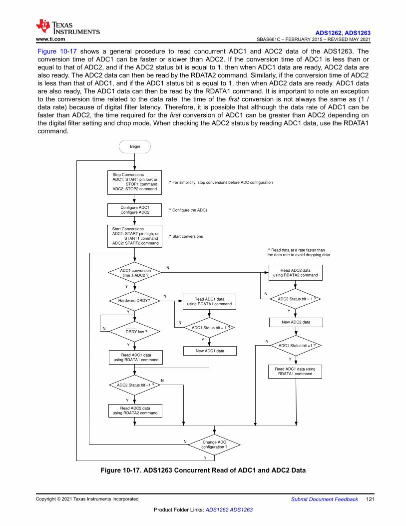
Figure 10-17 shows a general procedure to read concurrent ADC1 and ADC2 data of the ADS1263. Theconversion time of ADC1 can be faster or slower than ADC2. If the conversion time of ADC1 is less than orequal to that of ADC2, and if the ADC2 status bit is equal to 1, then when ADC1 data are ready, ADC2 data arealso ready. The ADC2 data can then be read by the RDATA2 command. Similarly, if the conversion time of ADC2is less than that of ADC1, and if the ADC1 status bit is equal to 1, then when ADC2 data are ready. ADC1 dataare also ready, The ADC1 data can then be read by the RDATA1 command. It is important to note an exceptionto the conversion time related to the data rate: the time of the first conversion is not always the same as (1 /data rate) because of digital filter latency. Therefore, it is possible that although the data rate of ADC1 can befaster than ADC2, the time required for the first conversion of ADC1 can be greater than ADC2 depending onthe digital filter setting and chop mode. When checking the ADC2 status by reading ADC1 data, use the RDATA1command.
Start Conversions
ADC1: START pin high; or
START1 command
ADC2: START2 command
/* Start conversions
ADC1 conversion
WLPH���$'&2 ?
N
Y
DRDY low ?N
Y
Read ADC1 data
using RDATA1 command
Change ADC
configuration ?
N
/* Read data at a rate faster than
the data rate to avoid dropping data
Hardware DRDY?
Y
Read ADC1 data
using RDATA1 command
ADC1 Status bit = 1 ?
N
N
Y
New ADC1 data
Read ADC2 data
using RDATA2 command
Configure ADC1
Configure ADC2
Stop Conversions
ADC1: START pin low; or
STOP1 command
ADC2: STOP2 command
/* For simplicity, stop conversions before ADC configuration
/* Configure the ADCs
Y
Y
Read ADC2 data
using RDATA2 command
ADC2 Status bit = 1 ?
N
New ADC2 data
Read ADC1 data using
RDATA1 command
Begin
ADC1 Status bit =1 ?
Y
ADC2 Status bit =1 ?
Y
N
N
Figure 10-17. ADS1263 Concurrent Read of ADC1 and ADC2 Data
www.ti.comADS1262, ADS1263
SBAS661C – FEBRUARY 2015 – REVISED MAY 2021
Copyright © 2021 Texas Instruments Incorporated Submit Document Feedback 121
Product Folder Links: ADS1262 ADS1263
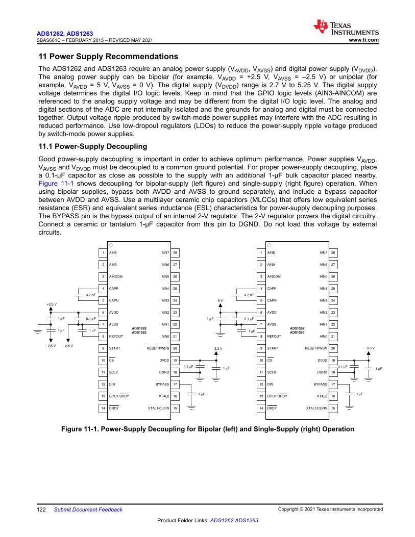
11 Power Supply RecommendationsThe ADS1262 and ADS1263 require an analog power supply (VAVDD, VAVSS) and digital power supply (VDVDD).The analog power supply can be bipolar (for example, VAVDD = +2.5 V, VAVSS = –2.5 V) or unipolar (forexample, VAVDD = 5 V, VAVSS = 0 V). The digital supply (VDVDD) range is 2.7 V to 5.25 V. The digital supplyvoltage determines the digital I/O logic levels. Keep in mind that the GPIO logic levels (AIN3-AINCOM) arereferenced to the analog supply voltage and may be different from the digital I/O logic level. The analog anddigital sections of the ADC are not internally isolated and the grounds for analog and digital must be connectedtogether. Output voltage ripple produced by switch-mode power supplies may interfere with the ADC resulting inreduced performance. Use low-dropout regulators (LDOs) to reduce the power-supply ripple voltage producedby switch-mode power supplies.
11.1 Power-Supply DecouplingGood power-supply decoupling is important in order to achieve optimum performance. Power supplies VAVDD,VAVSS and VDVDD must be decoupled to a common ground potential. For proper power-supply decoupling, placea 0.1-µF capacitor as close as possible to the supply with an additional 1-µF bulk capacitor placed nearby.Figure 11-1 shows decoupling for bipolar-supply (left figure) and single-supply (right figure) operation. Whenusing bipolar supplies, bypass both AVDD and AVSS to ground separately, and include a bypass capacitorbetween AVDD and AVSS. Use a multilayer ceramic chip capacitors (MLCCs) that offers low equivalent seriesresistance (ESR) and equivalent series inductance (ESL) characteristics for power-supply decoupling purposes.The BYPASS pin is the bypass output of an internal 2-V regulator. The 2-V regulator powers the digital circuitry.Connect a ceramic or tantalum 1-µF capacitor from this pin to DGND. Do not load this voltage by externalcircuits.
28
27
26
25
24
23
22
21
1
2
3
4
5
6
7
8
AINCOM
CAPP
CAPN
AVDD
AVSS
REFOUT AIN0
AIN1
AIN2
AIN3
AIN4
AIN5
AIN6
AIN7AIN8
AIN9
9
10
11
12
13
14
SCLK
DIN
DOUT/DRDY
START
CS
20
19
18
17
16
15XTAL1/CLKIN
XTAL2
BYPASS
DGND
DVDD
RESET/PWDN
ADS1262
ADS1263
DRDY
4.7 nF
0.1 PF
0.1 PF1 PF
1 PF
5 V
3.3 V
1 PF
1 PF
28
27
26
25
24
23
22
21
1
2
3
4
5
6
7
8
AINCOM
CAPP
CAPN
AVDD
AVSS
REFOUT AIN0
AIN1
AIN2
AIN3
AIN4
AIN5
AIN6
AIN7AIN8
AIN9
9
10
11
12
13
14
SCLK
DIN
DOUT/DRDY
START
CS
20
19
18
17
16
15XTAL1/CLKIN
XTAL2
BYPASS
DGND
DVDD
RESET/PWDN
ADS1262
ADS1263
DRDY
4.7 nF
0.1 PF
0.1 PF1 PF
1 PF
+2.5 V
3.3 V±2.5 V
1 PF
1 PF
1 PF
±2.5 V
Figure 11-1. Power-Supply Decoupling for Bipolar (left) and Single-Supply (right) Operation
ADS1262, ADS1263SBAS661C – FEBRUARY 2015 – REVISED MAY 2021 www.ti.com
122 Submit Document Feedback Copyright © 2021 Texas Instruments Incorporated
Product Folder Links: ADS1262 ADS1263
11.2 Analog Power-Supply ClampIt is important to evaluate circumstances when an input signal is present while the ADC is powered andunpowered. When the input signal exceeds the power-supply voltage, it is possible to back drive the analogpower-supply voltage with the input signal through a conduction path of the internal ESD diodes. Back drivingthe ADC power supply can also occur when the power-supply voltage is on. The back-drive, fault-current pathis shown in Figure 11-2. Depending on the external power-supply components, it is possible that the maximumrating of the ADC power-supply voltage can be exceeded if back-driven. ADC power supply overvoltage must beprevented in all cases. One solution is to clamp the AVDD to AVSS voltage with an external 6-V Zener diode.
AVDD
ESD DiodeAINx
+±
Input Voltage
ESD Diode
RLIMIT
+5 V Reg
AVSS
Optional
6-V Zener Diode
IFAULT
IFAULT
ADC supply On or Off
+V
AINx
IFAULT
ADC
Figure 11-2. Analog Power-Supply Clamp
11.3 Power-Supply SequencingSequence the power supplies in any order, but never allow and analog or digital inputs to exceed the respectiveanalog or digital power-supplies without limiting the input fault current. The ADC remains in reset until bothanalog and digital power supplies exceed the respective power-on reset (POR) thresholds. Figure 9-52 showsthe power-on reset sequence. After the power supplies have crossed the reset levels (including the internal 2-VLDO), the ADC resets (POR) and is ready for communication 65536 clock periods later (nominally 9 ms).
Delay communication for 50 ms after the power supplies have stabilized within the specified range to make surethe ADC is operational. In addition to POR, make sure that the reference voltage has fully settled before startingthe conversions. When using a 1-µF reference capacitor allow a minimum of 50 ms for the internal reference tosettle. External references may require additional settling time.
12 LayoutGood layout practices are crucial to realize the full-performance of the ADS1262 and ADS1263. Poor groundingcan quickly degrade the noise performance of the main 32-bit ADC and auxiliary 24-bit ADC. The followinglayout recommendations are given to help provide best results.
12.1 Layout GuidelinesGround must be a low impedance connection for return currents to flow undisturbed back to their respectivesources. Keep connections to the ground plane as short and direct as possible. When using vias to connect tothe ground layer, use multiple vias in parallel to reduce impedance to ground.
A mixed-signal layout sometimes incorporates separate analog and digital ground planes that are tied togetherat one location; however, separating the ground planes is not necessary when analog, digital, and power supplycomponents are properly placed. Proper placement of components partitions the analog, digital, and powersupply circuitry into different PCB regions to prevent digital return currents from coupling into sensitive analogcircuitry.
www.ti.comADS1262, ADS1263
SBAS661C – FEBRUARY 2015 – REVISED MAY 2021
Copyright © 2021 Texas Instruments Incorporated Submit Document Feedback 123
Product Folder Links: ADS1262 ADS1263
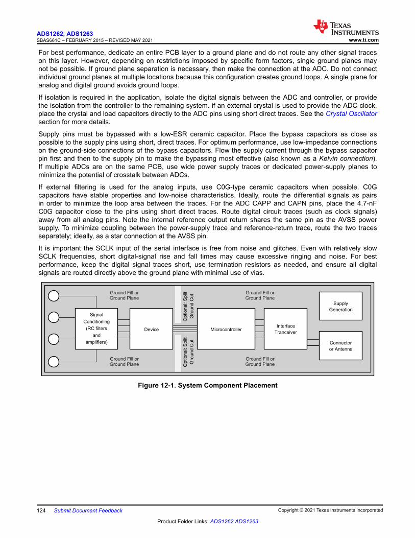
For best performance, dedicate an entire PCB layer to a ground plane and do not route any other signal traceson this layer. However, depending on restrictions imposed by specific form factors, single ground planes maynot be possible. If ground plane separation is necessary, then make the connection at the ADC. Do not connectindividual ground planes at multiple locations because this configuration creates ground loops. A single plane foranalog and digital ground avoids ground loops.
If isolation is required in the application, isolate the digital signals between the ADC and controller, or providethe isolation from the controller to the remaining system. if an external crystal is used to provide the ADC clock,place the crystal and load capacitors directly to the ADC pins using short direct traces. See the Crystal Oscillatorsection for more details.
Supply pins must be bypassed with a low-ESR ceramic capacitor. Place the bypass capacitors as close aspossible to the supply pins using short, direct traces. For optimum performance, use low-impedance connectionson the ground-side connections of the bypass capacitors. Flow the supply current through the bypass capacitorpin first and then to the supply pin to make the bypassing most effective (also known as a Kelvin connection).If multiple ADCs are on the same PCB, use wide power supply traces or dedicated power-supply planes tominimize the potential of crosstalk between ADCs.
If external filtering is used for the analog inputs, use C0G-type ceramic capacitors when possible. C0Gcapacitors have stable properties and low-noise characteristics. Ideally, route the differential signals as pairsin order to minimize the loop area between the traces. For the ADC CAPP and CAPN pins, place the 4.7-nFC0G capacitor close to the pins using short direct traces. Route digital circuit traces (such as clock signals)away from all analog pins. Note the internal reference output return shares the same pin as the AVSS powersupply. To minimize coupling between the power-supply trace and reference-return trace, route the two tracesseparately; ideally, as a star connection at the AVSS pin.
It is important the SCLK input of the serial interface is free from noise and glitches. Even with relatively slowSCLK frequencies, short digital-signal rise and fall times may cause excessive ringing and noise. For bestperformance, keep the digital signal traces short, use termination resistors as needed, and ensure all digitalsignals are routed directly above the ground plane with minimal use of vias.
MicrocontrollerInterface
Tranceiver
Signal
Conditioning
(RC filters
and
amplifiers)
Supply
Generation
Connector
or Antenna
Optional: S
plit
Gro
und
Cut
Optional: S
plit
Gro
und C
ut
Ground Fill orGround Plane
Ground Fill orGround Plane
Ground Fill orGround Plane
Ground Fill orGround Plane
Device
Figure 12-1. System Component Placement
ADS1262, ADS1263SBAS661C – FEBRUARY 2015 – REVISED MAY 2021 www.ti.com
124 Submit Document Feedback Copyright © 2021 Texas Instruments Incorporated
Product Folder Links: ADS1262 ADS1263
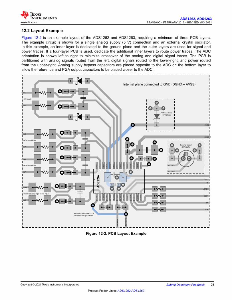
12.2 Layout ExampleFigure 12-2 is an example layout of the ADS1262 and ADS1263, requiring a minimum of three PCB layers.The example circuit is shown for a single analog supply (5 V) connection and an external crystal oscillator.In this example, an inner layer is dedicated to the ground plane and the outer layers are used for signal andpower traces. If a four-layer PCB is used, dedicate the additional inner layers to route power traces. The ADCorientation is shown left to right to minimize crossover of the analog and digital signal traces. The PCB ispartitioned with analog signals routed from the left, digital signals routed to the lower-right, and power routedfrom the upper-right. Analog supply bypass capacitors are placed opposite to the ADC on the bottom layer toallow the reference and PGA output capacitors to be placed closer to the ADC.
Internal plane connected to GND (DGND = AVSS)
DOUT
/DRDY
SCLK
/CS
START
AVDD
DIN
DVDD
/RESET/PWDN
IN7
IN6
IN7
IN6
IN2
IN1
IN9
COM
6V Zener Diode
(OPTIONAL)
External Crystal
(OPTIONAL)
(TO XTAL1)
(TO XTAL2)
(RE
FN
OU
T)
(RE
FP
OU
T)
Tie unused inputs to REFOUT
for lowest leakage current
Thermocouple/single-ended input
Differential input
RTD input
Differential input
28: A
IN7
27: A
IN6
26: A
IN5
25: A
IN4
24: A
IN3
23: A
IN2
22: A
IN1
21: A
IN0
20: /R
ST
/PD
19: D
VD
D
18: D
GN
D
17: B
YP
AS
S
16: X
TA
L2
15: X
TA
L1
1
: A
IN8
2
: A
IN9
3
: A
INC
OM
4
: C
AP
P
5
: C
AP
N
6
: A
VD
D
7
: A
VS
S
8
: R
EF
OU
T
9
: S
TA
RT
1
0: /C
S
1
1: S
CLK
1
2: D
IN
1
3: D
OU
T
1
4: /D
RD
Y
ADS126x
Figure 12-2. PCB Layout Example
www.ti.comADS1262, ADS1263
SBAS661C – FEBRUARY 2015 – REVISED MAY 2021
Copyright © 2021 Texas Instruments Incorporated Submit Document Feedback 125
Product Folder Links: ADS1262 ADS1263
13 Device and Documentation Support13.1 Receiving Notification of Documentation UpdatesTo receive notification of documentation updates, navigate to the device product folder on ti.com. Click onSubscribe to updates to register and receive a weekly digest of any product information that has changed. Forchange details, review the revision history included in any revised document.
13.2 Support ResourcesTI E2E™ support forums are an engineer's go-to source for fast, verified answers and design help — straightfrom the experts. Search existing answers or ask your own question to get the quick design help you need.
Linked content is provided "AS IS" by the respective contributors. They do not constitute TI specifications and donot necessarily reflect TI's views; see TI's Terms of Use.
13.3 TrademarksSPI™ is a trademark of Motorola Inc.TI E2E™ is a trademark of Texas Instruments.All trademarks are the property of their respective owners.13.4 Electrostatic Discharge Caution
This integrated circuit can be damaged by ESD. Texas Instruments recommends that all integrated circuits be handledwith appropriate precautions. Failure to observe proper handling and installation procedures can cause damage.ESD damage can range from subtle performance degradation to complete device failure. Precision integrated circuits maybe more susceptible to damage because very small parametric changes could cause the device not to meet its publishedspecifications.
13.5 GlossaryTI Glossary This glossary lists and explains terms, acronyms, and definitions.
Mechanical, Packaging, and Orderable InformationThe following pages include mechanical packaging and orderable information. This information is the mostcurrent data available for the designated devices. This data is subject to change without notice and revision ofthis document. For browser-based versions of this data sheet, refer to the left-hand navigation.
ADS1262, ADS1263SBAS661C – FEBRUARY 2015 – REVISED MAY 2021 www.ti.com
126 Submit Document Feedback Copyright © 2021 Texas Instruments Incorporated
Product Folder Links: ADS1262 ADS1263
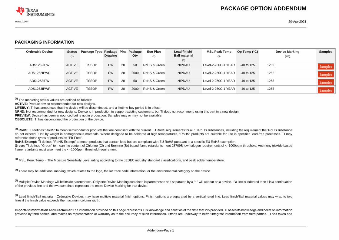
PACKAGE OPTION ADDENDUM
www.ti.com 20-Apr-2021
Addendum-Page 1
PACKAGING INFORMATION
Orderable Device Status(1)
Package Type PackageDrawing
Pins PackageQty
Eco Plan(2)
Lead finish/Ball material
(6)
MSL Peak Temp(3)
Op Temp (°C) Device Marking(4/5)
Samples
ADS1262IPW ACTIVE TSSOP PW 28 50 RoHS & Green NIPDAU Level-2-260C-1 YEAR -40 to 125 1262
ADS1262IPWR ACTIVE TSSOP PW 28 2000 RoHS & Green NIPDAU Level-2-260C-1 YEAR -40 to 125 1262
ADS1263IPW ACTIVE TSSOP PW 28 50 RoHS & Green NIPDAU Level-2-260C-1 YEAR -40 to 125 1263
ADS1263IPWR ACTIVE TSSOP PW 28 2000 RoHS & Green NIPDAU Level-2-260C-1 YEAR -40 to 125 1263
(1) The marketing status values are defined as follows:ACTIVE: Product device recommended for new designs.LIFEBUY: TI has announced that the device will be discontinued, and a lifetime-buy period is in effect.NRND: Not recommended for new designs. Device is in production to support existing customers, but TI does not recommend using this part in a new design.PREVIEW: Device has been announced but is not in production. Samples may or may not be available.OBSOLETE: TI has discontinued the production of the device.
(2) RoHS: TI defines "RoHS" to mean semiconductor products that are compliant with the current EU RoHS requirements for all 10 RoHS substances, including the requirement that RoHS substancedo not exceed 0.1% by weight in homogeneous materials. Where designed to be soldered at high temperatures, "RoHS" products are suitable for use in specified lead-free processes. TI mayreference these types of products as "Pb-Free".RoHS Exempt: TI defines "RoHS Exempt" to mean products that contain lead but are compliant with EU RoHS pursuant to a specific EU RoHS exemption.Green: TI defines "Green" to mean the content of Chlorine (Cl) and Bromine (Br) based flame retardants meet JS709B low halogen requirements of <=1000ppm threshold. Antimony trioxide basedflame retardants must also meet the <=1000ppm threshold requirement.
(3) MSL, Peak Temp. - The Moisture Sensitivity Level rating according to the JEDEC industry standard classifications, and peak solder temperature.
(4) There may be additional marking, which relates to the logo, the lot trace code information, or the environmental category on the device.
(5) Multiple Device Markings will be inside parentheses. Only one Device Marking contained in parentheses and separated by a "~" will appear on a device. If a line is indented then it is a continuationof the previous line and the two combined represent the entire Device Marking for that device.
(6) Lead finish/Ball material - Orderable Devices may have multiple material finish options. Finish options are separated by a vertical ruled line. Lead finish/Ball material values may wrap to twolines if the finish value exceeds the maximum column width.
Important Information and Disclaimer:The information provided on this page represents TI's knowledge and belief as of the date that it is provided. TI bases its knowledge and belief on informationprovided by third parties, and makes no representation or warranty as to the accuracy of such information. Efforts are underway to better integrate information from third parties. TI has taken and
PACKAGE OPTION ADDENDUM
www.ti.com 20-Apr-2021
Addendum-Page 2
continues to take reasonable steps to provide representative and accurate information but may not have conducted destructive testing or chemical analysis on incoming materials and chemicals.TI and TI suppliers consider certain information to be proprietary, and thus CAS numbers and other limited information may not be available for release.
In no event shall TI's liability arising out of such information exceed the total purchase price of the TI part(s) at issue in this document sold by TI to Customer on an annual basis.
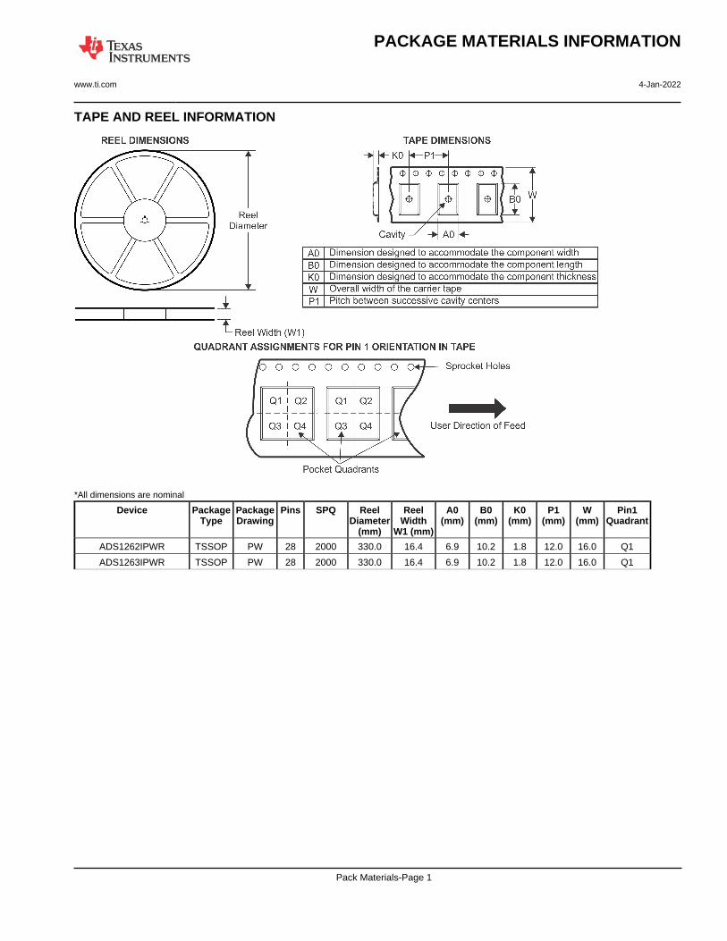
TAPE AND REEL INFORMATION
*All dimensions are nominal
Device PackageType
PackageDrawing
Pins SPQ ReelDiameter
(mm)
ReelWidth
W1 (mm)
A0(mm)
B0(mm)
K0(mm)
P1(mm)
W(mm)
Pin1Quadrant
ADS1262IPWR TSSOP PW 28 2000 330.0 16.4 6.9 10.2 1.8 12.0 16.0 Q1
ADS1263IPWR TSSOP PW 28 2000 330.0 16.4 6.9 10.2 1.8 12.0 16.0 Q1
PACKAGE MATERIALS INFORMATION
www.ti.com 4-Jan-2022
Pack Materials-Page 1
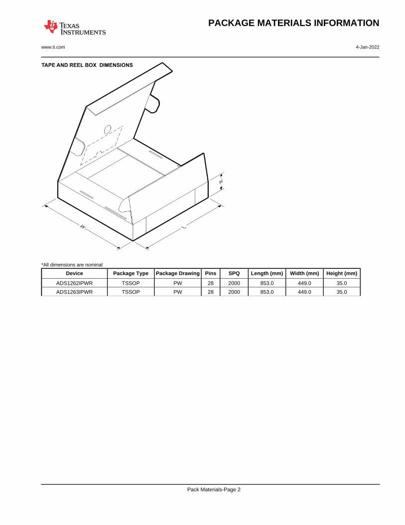
*All dimensions are nominal
Device Package Type Package Drawing Pins SPQ Length (mm) Width (mm) Height (mm)
ADS1262IPWR TSSOP PW 28 2000 853.0 449.0 35.0
ADS1263IPWR TSSOP PW 28 2000 853.0 449.0 35.0
PACKAGE MATERIALS INFORMATION
www.ti.com 4-Jan-2022
Pack Materials-Page 2
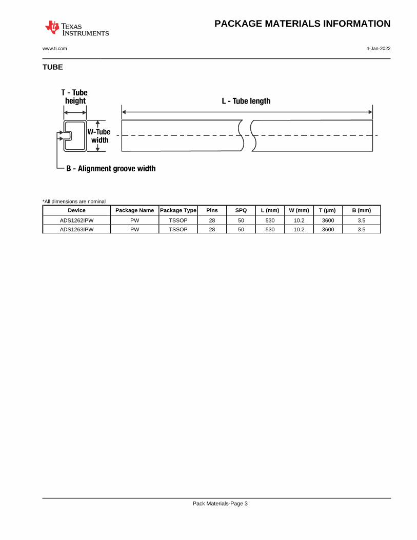
TUBE
*All dimensions are nominal
Device Package Name Package Type Pins SPQ L (mm) W (mm) T (µm) B (mm)
ADS1262IPW PW TSSOP 28 50 530 10.2 3600 3.5
ADS1263IPW PW TSSOP 28 50 530 10.2 3600 3.5
PACKAGE MATERIALS INFORMATION
www.ti.com 4-Jan-2022
Pack Materials-Page 3
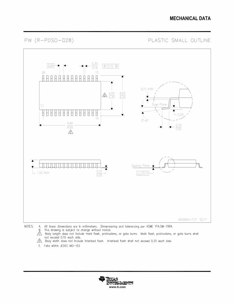

IMPORTANT NOTICE AND DISCLAIMERTI PROVIDES TECHNICAL AND RELIABILITY DATA (INCLUDING DATA SHEETS), DESIGN RESOURCES (INCLUDING REFERENCE DESIGNS), APPLICATION OR OTHER DESIGN ADVICE, WEB TOOLS, SAFETY INFORMATION, AND OTHER RESOURCES “AS IS” AND WITH ALL FAULTS, AND DISCLAIMS ALL WARRANTIES, EXPRESS AND IMPLIED, INCLUDING WITHOUT LIMITATION ANY IMPLIED WARRANTIES OF MERCHANTABILITY, FITNESS FOR A PARTICULAR PURPOSE OR NON-INFRINGEMENT OF THIRD PARTY INTELLECTUAL PROPERTY RIGHTS.These resources are intended for skilled developers designing with TI products. You are solely responsible for (1) selecting the appropriate TI products for your application, (2) designing, validating and testing your application, and (3) ensuring your application meets applicable standards, and any other safety, security, regulatory or other requirements.These resources are subject to change without notice. TI grants you permission to use these resources only for development of an application that uses the TI products described in the resource. Other reproduction and display of these resources is prohibited. No license is granted to any other TI intellectual property right or to any third party intellectual property right. TI disclaims responsibility for, and you will fully indemnify TI and its representatives against, any claims, damages, costs, losses, and liabilities arising out of your use of these resources.TI’s products are provided subject to TI’s Terms of Sale or other applicable terms available either on ti.com or provided in conjunction with such TI products. TI’s provision of these resources does not expand or otherwise alter TI’s applicable warranties or warranty disclaimers for TI products.TI objects to and rejects any additional or different terms you may have proposed. IMPORTANT NOTICE
Mailing Address: Texas Instruments, Post Office Box 655303, Dallas, Texas 75265Copyright © 2022, Texas Instruments Incorporated