ADNS-3000 - Low Power Optical Mouse Sensor - EPS Global
10
ADNS-3000 Low Power Optical Mouse Sensor Data Sheet Description The PixArt Imaging ADNS-3000 is a low power, small form factor optical mouse sensor. It has a new low-power architecture and automatic power management modes, making it ideal for battery, power-sensitive applications – such as cordless input devices. The ADNS-3000 is capable of high-speed motion detec- tion – up to 30 ips and 20 g. In addition, it has an on-chip oscillator and requires an external resistor to set the LED current. The ADNS-3000 along with the ADNS-5110-001 lens, or ADNS-5120-002 trim lens and HSDL-4261 IR LED or HLMP-EG3E-xxxxx Red LED form a complete and compact mouse tracking system. There are no moving parts and this translates to high reliability and less maintenance for the end user. In addition, precision optical alignment is not required, facilitating high volume assembly. The sensor is programmed via registers through a four- wire serial port. It is housed in an 8-pin staggered dual in-line package (DIP). Features Low Power Architecture Small Form Factor Programmable Periods / Response Times and Downshift Times from one mode to another for the Power-saving Modes High Speed Motion Detection up to 30 ips and 20 g External Interrupt Output for Motion Detection Internal Oscillator – no clock input needed Selectable Resolution of up to 2000 cpi Operating Voltage: as low as 1.7 V Four-wire Serial Port Interface Applications Optical mice and optical trackballs Integrated input devices Battery-powered input devices All rights strictly reserved any portion in this paper shall not be reproduced, copied or transformed to any other forms without permission. PixArt Imaging Inc. E-mail: [email protected] 1
-
Upload
khangminh22 -
Category
Documents
-
view
2 -
download
0
Transcript of ADNS-3000 - Low Power Optical Mouse Sensor - EPS Global

ADNS-3000
Low Power Optical Mouse Sensor
Data Sheet
Description
The PixArt Imaging ADNS-3000 is a low power, small form factor optical mouse sensor. It has a new low-power architecture and automatic power management modes, making it ideal for battery, power-sensitive applications – such as cordless input devices.
The ADNS-3000 is capable of high-speed motion detec-tion – up to 30 ips and 20 g. In addition, it has an on-chip oscillator and requires an external resistor to set the LED current.
The ADNS-3000 along with the ADNS-5110-001 lens, or ADNS-5120-002 trim lens and HSDL-4261 IR LED orHLMP-EG3E-xxxxx Red LED form a complete and compact mouse tracking system.There are no moving parts and this translates to high reliability and less maintenance for the end user. In addition, precision optical alignment is not required, facilitating high volume assembly.
The sensor is programmed via registers through a four-wire serial port. It is housed in an 8-pin staggered dual in-line package (DIP).
Features
Low Power Architecture
Small Form Factor
Programmable Periods / Response Times and Downshift Times from one mode to another for the Power-saving Modes
High Speed Motion Detection up to 30 ips and 20 g
External Interrupt Output for Motion Detection
Internal Oscillator – no clock input needed
Selectable Resolution of up to 2000 cpi
Operating Voltage: as low as 1.7 V
Four-wire Serial Port Interface
Applications
Optical mice and optical trackballs
Integrated input devices
Battery-powered input devices
All rights strictly reserved any portion in this paper shall not be reproduced, copied or transformed to any other forms without permission. PixArt Imaging Inc. E-mail: [email protected]

2
Pinout of ADNS-3000 Optical Mouse Sensor
Pin Name
Input/
Output Description
1 MISO O Serial Data Output (Master In/Slave Out)
2 LED I LED Illumination
3 MOTION O Motion Interrupt Output (Default active low, edge triggered)
4 NCS I Chip Select (Active low input)
5 SCLK I Serial Clock
6 GND I Ground
7 VDD I Supply Voltage
8 MOSI I Serial Data Input(Master Out/Slave In)
Figure 1. Package Outline Drawing (Top View)
Theory of Operation
The ADNS-3000 is based on Optical Navigation Technol-ogy, which measures changes in position by optically acquiring sequential surface images (frames) and math-ematically determining the direction and magnitude of movement.
The ADNS-3000 contains an Image Acquisition System (IAS), a Digital Signal Processor (DSP), and a four wire serial port.
The IAS acquires microscopic surface images via the lens and illumination system. These images are processed by the DSP to determine the direction and distance of motion. The DSP calculates the Dx and Dy relative dis-placement values
An external microcontroller reads and translates the Dx and Dy informa tion from the sensor serial port into PS2, USB, or RF signals before sending them to the host PC.
Item Marking Remarks
Product Number A3000
Date Code XYYWWZ X = Subcon CodeYYWW = Date CodeZ = Sensor Die Source
Lot Code VVV Numeric
All rights strictly reserved any portion in this paper shall not be reproduced, copied or transformed to any other forms without permission. PixArt Imaging Inc. E-mail: [email protected]
PixArt Imaging Inc.
ADNS-3000 Low Power Optical Mouse Sensor

3
Figure 2. Package Outline Drawing
CAUTION: It is advised that normal static precautions be taken in handling and assembling of this component to prevent damage and/or degradation which may be induced by ESD.
All rights strictly reserved any portion in this paper shall not be reproduced, copied or transformed to any other forms without permission.
PixArt Imaging Inc. E-mail: [email protected]
PixArt Imaging Inc.
ADNS-3000 Low Power Optical Mouse Sensor
siti_ramli
Typewritten Text
siti_ramli
Typewritten Text
siti_ramli
Typewritten Text
siti_ramli
Typewritten Text
siti_ramli
Typewritten Text
siti_ramli
Typewritten Text
siti_ramli
Typewritten Text
siti_ramli
Typewritten Text

4
Overview of Optical Mouse Sensor Assembly
PixArt Imaging provides an IGES fi le drawing de scribing the base plate molding features for lens and PCB align-ment. The ADNS-3000 sensor is designed for mounting on a through-hole PCB, looking down. There is an aperture stop and features on the package that align to the lens. The ADNS-5110-001 and ADNS-5120-002 lens provides optics for the imaging of the surface as well as the illumination of the surface at the optimum angle. Features on the lens align, base it to the sensor plate, and clip with the LED. The LED clip holds the LED in relation to the lens. The LED must be inserted into the clip and the LED’s leads formed prior to loading on the PCB. The LEDs recommended for illumination include, HSDL-4261 IR LED HLMP-EG3E-xxxxx Red LED.
Figure 3. Recommended PCB Mechanical Cutouts and Spacing
All rights strictly reserved any portion in this paper shall not be reproduced, copied or transformed to any other forms without permission. PixArt Imaging Inc. E-mail: [email protected]
PixArt Imaging Inc.
ADNS-3000 Low Power Optical Mouse Sensor

2x AA Battery
1.9V Regulator Block
Z-Encoder
+CPI
Left Button
Right Button
Middle Button
1
3 2
CO
M
NC
NO
SW
2
1
3 2
CO
M
NC
NO
SW
3
1
3 2
CO
M
NC
NO
SW
4
COM
3B
2A
1
Q1
Z-E
NC
OD
ER
_3
P
12
34
SW
5
TA
CT
_S
W
VDD_RF
RF Voltage Selection
VCC_DC1
JTAG CONNECTOR
CO
M
ZA
ZB
R1
4
1M
R1
3
1M
VDD_RF
S1
S4
S3
S3
R1
B+
ON
OFF
VBAT
1
2
3S
W1
SL
IDE
SW
SP
DT
1 2
P1
B-
BT
1
2A
A B
AT
TE
RY
VDD_LED
LED Voltage Selection
P4
P5
VCC_DC1
VDD_SENSOR
Sensor Voltage Selection
P1
8P
19
VCC_DC1
VBAT
VCC_DC1
Voltage Measuremen
VB
AT
GN
D
VDD_LED
VD
D_
LE
D
1P1
2
1P1
3
1P1
4
1P1
1
P1
0P
9+
1
+3
+5
+7
+9
+2
+4
+6
+8
+10
CO
N1
PC
B_
SK
T_
SM
D_
1.2
7/2
X5
PR
OG
S2
R2
S1
R1
RF MODULE
RE
SE
T
RE
SE
TP
RO
G
MS
CK
COM
MOTION
R1
R2
S1
S2
S3
S4
R0
MISO
MOSI
ZA
ZB
VDD_RF
RF Module PCB
RESET
19
P1.4
18
P1.3
17
P1.216
P1.014
P0.612
P0.713
P0.511
PROG
6
P0.3
7
P0.1
1
P0.2
5
P0.410
P1.115
P1.528
P1.629
GND1
GND2
GND3
GND4
GND5
GND6
GND7
GND8
GND9
VDD
P2
0
No
te:
R1
= 1
M3
, R
2 =
45
3k
VC
C_
DC
1 =
1.9
V
D5
LE
D
Sensor Block
VDD_LED
C1
11
00
nF
R1
7
0R
+
C9
2.2
uF
/16
V
VDD_SENSOR
R5
39
R
R1
0
1M
R1
1
1M
R1
2
1M
7
GND6
5
8
XY_LED
2
14
MOTION
3
U5
AD
NS
-3000
MO
SI
CS
MIS
O
MS
CK
MO
TIO
N
VDD_SENSOR
P2
5
VCC_DC1
VDD_SENSOR
R6
1M
VDD_SENSOR
R0
VC
C_
DC
1
VOUT
4
FB
2VIN
1
EN
6
GND
3
L5
U1
TP
S6
12
20
1 2 3
P2
4
C5
10
uF
/50
V
C1
10
0n
F
VBAT
L1
4.7
uH
VBAT
R1
1M
3
R2
45
3k
1 2
P1
6
VCC_DC1
C6
10
0n
F
C8
4.7
uF
/10
V
C1
0
4.7
uF
/10
V
SCLK
MISO
VDD
NCS
MOSI
t
R7
1M
VDD_SENSOR
P0.032
RE
SE
TP
RO
G
MS
CK
COM
MOTION
R1
R2
S1
S2
S3
S4
R0
CS
ZA
ZB
5
kian-ming_chin
Typewritten Text
kian-ming_chin
Typewritten Text
siti_ramli
Typewritten Text
siti_ramli
Typewritten Text
Figure 8a.Schematic diagram of the mouse cordless application.
siti_ramli
Typewritten Text
siti_ramli
Typewritten Text
siti_ramli
Typewritten Text
siti_ramli
Typewritten Text
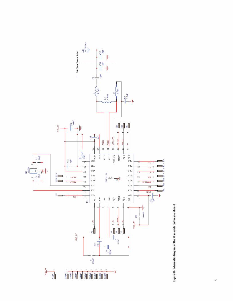
6Figu
re 8
b. S
chem
atic
dia
gram
of t
he
RF
mod
ule
on
th
e m
ain
boar
d
U1
NR
F24
LE
1
C1
100n
F
C3
100n
F
C4
33nF
C5
100n
F
X1
16M
Hz
C6
22pF
C7
22pF
R1
22K
C2
100n
F
L2
6.8n
H
L1
4.7n
H
L3
6.8n
H
C8
1.5p
F
C9
2.2n
F
C11
1pF
C12
1.8p
F
AT
1A
NT
EN
NA
RE
SE
T
AN
T1
AN
T2
VD
D_P
A
PR
OG
MSC
K
COM
MOTION
R1
R2
S1
S2
S3
S4
R0
CS
MISO
MOSI
ZA
ZB
P1
P5
P6
P7
P10
P11
P12
P13
P14
P15
P16
P17
P18
P19
P28
P29
P32
VD
D
GN
D1
GN
D2
1G
ND
3
GN
D4
GN
D5
GN
D6
GN
D7
GN
D8
GN
D9
C13
5pF
C14 5p
F
C15 5pF
C16
5pF

7Figu
re 8
C. S
chem
atic
dia
gram
of t
he
don
gle
X1
16M
Hz
C12
10uF
nRF
24L
U1+
U1
J1 US
B T
ype
A
Ant
enna
PR
OG
SC
KM
OSI
MIS
OC
SN
L4
3.9n
H04
02R
322
RR
422
R
R6
10R
R7
10k
R5
10k
R2
22k
C8
10nF
C11
100n
F
C7
10nF
C1
22pF
C2
22pF
C10
33nF
C9
33nF
C3
2.2n
FC
44.
7pFC
61.
0pF
C13
2.2p
F
C5
1.0p
F
L3
6.8n
H
L1
5.6n
H L2
6.8n
H
J2 Hea
der
5

Table 1. Absolute Maximum Ratings
Parameter Symbol Minimum Maximum Units Notes
Storage Temperature TS -40 85 C
Operating Temperature TA -15 55 C
Lead Solder Temperature VO 260 C For 10 seconds, 1.6 mm below seating plane.
Supply Voltage VDD -0.5 2.2 V
ESD 2 kV All pins, human body model JESD22-A114
Input Voltage VIN -0.5 2.1 V All I/O pins
Table 2. Recommended Operating Condition
Parameter Symbol Min Typ. Max Units Notes
Operating Temperature TA 0 40 C
Power Supply Voltage VDD 1.7 1.8 2.1 V
Power Supply Rise Time TRT 0.15 20 ms 0 to VDD min
Supply Noise (Sinusoidal) VNA 100 mVp-p 10 kHz –50 MHz
Serial Port Clock Frequency fSCLK 1 MHz 50% duty cycle
Distance from Lens Reference Plane to Tracking Surface (Z)
Z 2.3 2.4 2.5 mm
Speed 1 S 0 30 ips At default frame rate
Acceleration a 20 g At run mode
Load Capacitance Cout 100 pF MISO and MOTION
Note:1. For higher than 500 dpi setting, use 12-bit motion reporting to achieve the maximum speed
Design Considerations for Improved ESD Performance
For improved electrostatic discharge performance, typical creepage and clearance distance are shown in the table below. Assumption: base plate construction is as per the PixArt Imaging supplied IGES fi le and ADNS-5110-001or ADNS-5120-002 lens. Note that the lens material ispolycarbonate or polysty rene HH30. Therefore, cyanoacrylate based adhesives or other adhesives that may damage the lens should NOT be used.
Typical Distance (mm)
Creepage 16.0Clearance 2.0
Regulatory Requirements
Passes FCC B and worldwide analogous emission limits when assembled into a mouse with shielded cable and following PixArt Imaging recommendations.
UL fl ammability level UL94 V-0.
All rights strictly reserved any portion in this paper shall not be reproduced, copied or transformed to any other forms without permission.
PixArt Imaging Inc. E-mail: [email protected]
PixArt Imaging Inc.
ADNS-3000 Low Power Optical Mouse Sensor
8

9
Table 4. DC Electrical Specifi cations
Electrical characteristics over recommended operating conditions. Typical values at 25° C, VDD = 1.9 V, VDDLED = 1.9 V, IRLED HSDL-4261, ILED DC = 5mA
Parameter Symbol Min Typ. Max Units Notes
DC Supply Current in Various Mode
IDD_AVG 1.44 mA Average sensor current at max frame rate. No load on MISO
Average LED current at max frame rate. No load on MISO
IDD_REST1 108 A
IDD_REST2 28 A
IDD_REST3 12 A
IDDLED_AVG 0.3 mA
IDDLED_REST1 62 A
IDDLED_REST2 15 A
IDDLED_REST3 4 A
Power Down Current 10 A
Input Low Voltage VIL 0.3* VDD V SCLK, MOSI, NCS
Input High Voltage VIH 0.7* VDD V SCLK, MOSI, NCS
Input Hysteresis VI_HYS 200 mV SCLK, MOSI, NCS
Input Leakage Current Ileak +/-1 +/-10 A Vin = VDD or 0 V
Output Low Voltage VOL 0.45 V Iout = 1 mA, MISO, MOTION
Output High Voltage VOH VDD -0.45 V Iout = -1 mA, MISO, MOTION
Input Capacitance Cin 50 pF MOSI, NCS, SCLK
All rights strictly reserved any portion in this paper shall not be reproduced, copied or transformed to any other forms without permission.
PixArt Imaging Inc. E-mail: [email protected]
PixArt Imaging Inc.
ADNS-3000 Low Power Optical Mouse Sensor

10
Registers
The ADNS-3000 registers are accessible via the serial port. The registers are used to read motion data and status as well as to set the device confi guration.
Address Register Name Register Description Read/Write Default Value
0x00 PROD_ID Product ID R 0x2A
0x01 REV_ID Revision ID R 0x00
0x02 MOTION_ST Motion Status R 0x00
0x03 DELTA_X Lower byte of Delta_X R 0x00
0x04 DELTA_Y Lower byte of Delta_Y R 0x00
0x05 SQUAL Squal Quality R 0x00
0x06 SHUT_HI Shutter Open Time (Upper 8-bit) R 0x00
0x07 SHUT_LO Shutter Open Time (Lower 8-bit) R 0x64
0x08 PIX_MAX Maximum Pixel Value R 0xD0
0x09 PIX_ACCUM Average Pixel Value R 0x80
0x0a PIX_MIN Minimum Pixel Value R 0x00
0x0b PIX_GRAB Pixel Grabber R/W 0x00
0x0c DELTA_XY_HIGH Upper 4 bits of Delta X and Y displacement R 0x00
0x0d MOUSE_CTRL Mouse Control R/W 0x01
0x0e RUN_DOWNSHIFT Run to Rest1 Time R/W 0x08
0x0f REST1_PERIOD Rest1 Period R/W 0x01
0x10 REST1_DOWNSHIFT Rest1 to Rest2 Time R/W 0x1f
0x11 REST2_PERIOD Rest2 Period R/W 0x09
0x12 REST2_DOWNSHIFT Rest2 to Rest3 Time R/W 0x2f
0x13 REST3_PERIOD Rest3 Period R/W 0x31
0x22 PERFORMANCE Performance R/W 0x00
0x3a RESET Reset W 0x00
0x3f NOT_REV_ID Inverted Revision ID R 0xff
0x40 LED_CTRL LED Control R/W 0x00
0x41 MOTION_CTRL Motion Control R/W 0x40
0x42 BURST_READ_FIRST Burst Read Starting Register R/W 0x03
0x45 REST_MODE_CONFIG Rest Mode Confi guration R/W 0x00
0x63 MOTION_BURST Burst Read R 0x00
All rights strictly reserved any portion in this paper shall not be reproduced, copied or transformed to any other forms without permission.
PixArt Imaging Inc. E-mail: [email protected]
PixArt Imaging Inc.
ADNS-3000 Low Power Optical Mouse Sensor