
ADE7978/ADE7933/ADE7932/ADE7923 (Rev. D) - Analog ...
125
Isolated Energy Metering Chipset for Polyphase Shunt Meters Data Sheet ADE7978/ADE7933/ADE7932/ADE7923 Rev. D Document Feedback Information furnished by Analog Devices is believed to be accurate and reliable. However, no responsibility is assumed by Analog Devices for its use, nor for any infringements of patents or other rights of third parties that may result from its use. Specifications subject to change without notice. No license is granted by implication or otherwise under any patent or patent rights of Analog Devices. Trademarks and registered trademarks are the property of their respective owners. One Technology Way, P.O. Box 9106, Norwood, MA 02062-9106, U.S.A. Tel: 781.329.4700 ©2013–2018 Analog Devices, Inc. All rights reserved. Technical Support www.analog.com FEATURES Enables shunt current sensors in polyphase energy meters Immune to magnetic tampering Highly accurate; supports EN 50470-1, EN 50470-3, IEC 62053-21, IEC 62053-22, IEC 62053-23, ANSI C12.20, and IEEE 1459 standards Compatible with 3-phase, 3- or 4-wire (delta or wye) meters and other 3-phase services Computes active, reactive, and apparent energy on each phase and on the overall system Less than 0.2% error in active and reactive energy over a dynamic range of 2000 to 1 at T A = 25°C Less than 0.1% error in voltage rms over a dynamic range of 500 to 1 at T A = 25°C Less than 0.25% error in current rms over a dynamic range of 500 to 1 at T A = 25°C Power quality measurements including total harmonic distortion (THD) Single 3.3 V supply Operating temperature: −40°C to +85°C Flexible I 2 C, SPI, and HSDC serial interfaces Safety and regulatory approvals UL recognition 5000 V rms for 1 minute per UL 1577 CSA Component Acceptance Notice 5A IEC 61010-1: 300 V rms maximum working voltage VDE certificate of conformity DIN V VDE V 0884-10 (VDE V 0884-10):2006-12 V IORM = 846 V peak Optional isolated (ADE7933/ADE7932) or nonisolated (ADE7923) neutral APPLICATIONS Shunt-based polyphase meters Power quality monitoring Solar inverters Process monitoring Protective devices Isolated sensor interfaces Industrial PLCs TYPICAL APPLICATION CIRCUIT NEUTRAL PHASE C ISOLATION BARRIER LOAD PHASE A PHASE B DIGITAL INTERFACE PHASE A ADE7932/ ADE7933 IP IM V1P VM V2P GND MCU GND ISO_A 3.3V PHASE B ADE7932/ ADE7933 IP IM V1P VM V2P GND MCU GND ISO_B 3.3V PHASE C ADE7932/ ADE7933 IP IM V1P VM V2P GND MCU GND ISO_C 3.3V NEUTRAL LINE ADE7923 (OPTIONAL, NONISOLATED) IP IM V1P VM V2P GND MCU 3.3V ADE7978 ENERGY METERING IC GND MCU 3.3V 3.3V SYSTEM MICROCONTROLLER GND MCU I 2 C/HSDC OR SPI IRQ0, IRQ1 11116-001 Figure 1. 3-Phase, 4-Wire Meter with Three ADE7933/ADE7932 Devices, One ADE7923, and One ADE7978 1 Protected by U.S. Patents 5,952,849; 6,873,065; 7,075,329; 6,262,600; 7,489,526; 7,558,080; and 8,892,933. Other patents are pending.
-
Upload
khangminh22 -
Category
Documents
-
view
0 -
download
0
Transcript of ADE7978/ADE7933/ADE7932/ADE7923 (Rev. D) - Analog ...

Isolated Energy Metering Chipset for Polyphase Shunt Meters
Data Sheet ADE7978/ADE7933/ADE7932/ADE7923
Rev. D Document Feedback Information furnished by Analog Devices is believed to be accurate and reliable. However, no responsibility is assumed by Analog Devices for its use, nor for any infringements of patents or other rights of third parties that may result from its use. Specifications subject to change without notice. No license is granted by implication or otherwise under any patent or patent rights of Analog Devices. Trademarks and registered trademarks are the property of their respective owners.
One Technology Way, P.O. Box 9106, Norwood, MA 02062-9106, U.S.A. Tel: 781.329.4700 ©2013–2018 Analog Devices, Inc. All rights reserved. Technical Support www.analog.com
FEATURES Enables shunt current sensors in polyphase energy meters Immune to magnetic tampering Highly accurate; supports EN 50470-1, EN 50470-3,
IEC 62053-21, IEC 62053-22, IEC 62053-23, ANSI C12.20, and IEEE 1459 standards
Compatible with 3-phase, 3- or 4-wire (delta or wye) meters and other 3-phase services
Computes active, reactive, and apparent energy on each phase and on the overall system
Less than 0.2% error in active and reactive energy over a dynamic range of 2000 to 1 at TA = 25°C
Less than 0.1% error in voltage rms over a dynamic range of 500 to 1 at TA = 25°C
Less than 0.25% error in current rms over a dynamic range of 500 to 1 at TA = 25°C
Power quality measurements including total harmonic distortion (THD)
Single 3.3 V supply Operating temperature: −40°C to +85°C
Flexible I2C, SPI, and HSDC serial interfaces Safety and regulatory approvals
UL recognition 5000 V rms for 1 minute per UL 1577
CSA Component Acceptance Notice 5A IEC 61010-1: 300 V rms maximum working voltage
VDE certificate of conformity DIN V VDE V 0884-10 (VDE V 0884-10):2006-12 VIORM = 846 V peak
Optional isolated (ADE7933/ADE7932) or nonisolated (ADE7923) neutral
APPLICATIONS Shunt-based polyphase meters Power quality monitoring Solar inverters Process monitoring Protective devices Isolated sensor interfaces Industrial PLCs
TYPICAL APPLICATION CIRCUIT
NEUTRALPHASE
CISOLATIONBARRIER
LOAD
PHASEA
PHASEB
DIG
ITA
L IN
TER
FAC
E
PHASE AADE7932/ADE7933IP
IM
V1PVM
V2P
GNDMCUGNDISO_A
3.3V
PHASE BADE7932/ADE7933IP
IM
V1PVM
V2P
GNDMCUGNDISO_B
3.3V
PHASE CADE7932/ADE7933IP
IM
V1PVM
V2P
GNDMCUGNDISO_C
3.3V
NEUTRALLINE
ADE7923(OPTIONAL,
NONISOLATED)IP
IM
V1PVM
V2P
GNDMCU
3.3V
ADE7978ENERGY
METERINGIC
GNDMCU
3.3V 3.3V
SYST
EMM
ICR
OC
ON
TRO
LLER
GNDMCU
I2C/HSDC OR SPI
IRQ0, IRQ1
1111
6-00
1
Figure 1. 3-Phase, 4-Wire Meter with Three ADE7933/ADE7932 Devices, One ADE7923, and One ADE7978
1 Protected by U.S. Patents 5,952,849; 6,873,065; 7,075,329; 6,262,600; 7,489,526; 7,558,080; and 8,892,933. Other patents are pending.
ADE7978/ADE7933/ADE7932/ADE7923 Data Sheet
Rev. D | Page 2 of 125
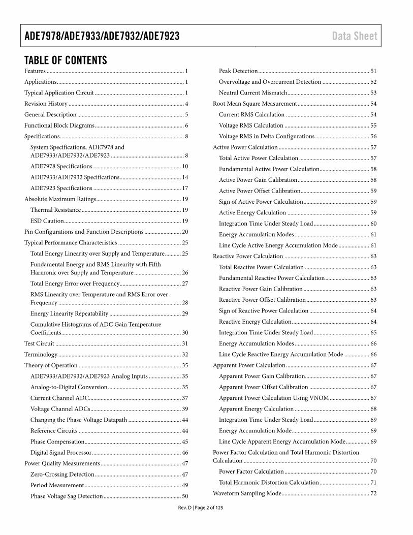
TABLE OF CONTENTS Features .............................................................................................. 1 Applications ....................................................................................... 1 Typical Application Circuit ............................................................. 1 Revision History ............................................................................... 4 General Description ......................................................................... 5 Functional Block Diagrams ............................................................. 6 Specifications ..................................................................................... 8
System Specifications, ADE7978 and ADE7933/ADE7932/ADE7923 .................................................. 8 ADE7978 Specifications ............................................................ 10 ADE7933/ADE7932 Specifications .......................................... 14 ADE7923 Specifications ............................................................ 17
Absolute Maximum Ratings .......................................................... 19 Thermal Resistance .................................................................... 19 ESD Caution ................................................................................ 19
Pin Configurations and Function Descriptions ......................... 20 Typical Performance Characteristics ........................................... 25
Total Energy Linearity over Supply and Temperature ........... 25 Fundamental Energy and RMS Linearity with Fifth Harmonic over Supply and Temperature ................................ 26 Total Energy Error over Frequency .......................................... 27 RMS Linearity over Temperature and RMS Error over Frequency .................................................................................... 28 Energy Linearity Repeatability ................................................. 29 Cumulative Histograms of ADC Gain Temperature Coefficients.................................................................................. 30
Test Circuit ...................................................................................... 31 Terminology .................................................................................... 32 Theory of Operation ...................................................................... 35
ADE7933/ADE7932/ADE7923 Analog Inputs ...................... 35 Analog-to-Digital Conversion .................................................. 35 Current Channel ADC............................................................... 37 Voltage Channel ADCs .............................................................. 39 Changing the Phase Voltage Datapath .................................... 44 Reference Circuits ...................................................................... 44 Phase Compensation .................................................................. 45 Digital Signal Processor ............................................................. 46
Power Quality Measurements ....................................................... 47 Zero-Crossing Detection ........................................................... 47 Period Measurement .................................................................. 49 Phase Voltage Sag Detection ..................................................... 50
Peak Detection ............................................................................ 51 Overvoltage and Overcurrent Detection ................................ 52 Neutral Current Mismatch ........................................................ 53
Root Mean Square Measurement ................................................. 54 Current RMS Calculation ......................................................... 54 Voltage RMS Calculation .......................................................... 55 Voltage RMS in Delta Configurations ..................................... 56
Active Power Calculation .............................................................. 57 Total Active Power Calculation ................................................ 57 Fundamental Active Power Calculation .................................. 58 Active Power Gain Calibration ................................................. 58 Active Power Offset Calibration ............................................... 59 Sign of Active Power Calculation ............................................. 59 Active Energy Calculation ........................................................ 59 Integration Time Under Steady Load ...................................... 60 Energy Accumulation Modes ................................................... 61 Line Cycle Active Energy Accumulation Mode ..................... 61
Reactive Power Calculation .......................................................... 63 Total Reactive Power Calculation ............................................ 63 Fundamental Reactive Power Calculation .............................. 63 Reactive Power Gain Calibration ............................................. 63 Reactive Power Offset Calibration ........................................... 63 Sign of Reactive Power Calculation ......................................... 64 Reactive Energy Calculation ..................................................... 64 Integration Time Under Steady Load ...................................... 65 Energy Accumulation Modes ................................................... 66 Line Cycle Reactive Energy Accumulation Mode ................. 66
Apparent Power Calculation ......................................................... 67 Apparent Power Gain Calibration............................................ 67 Apparent Power Offset Calibration ......................................... 67 Apparent Power Calculation Using VNOM ........................... 67 Apparent Energy Calculation ................................................... 68 Integration Time Under Steady Load ...................................... 69 Energy Accumulation Mode ..................................................... 69 Line Cycle Apparent Energy Accumulation Mode ................ 69
Power Factor Calculation and Total Harmonic Distortion Calculation ...................................................................................... 70
Power Factor Calculation .......................................................... 70 Total Harmonic Distortion Calculation .................................. 71
Waveform Sampling Mode ............................................................ 72
Data Sheet ADE7978/ADE7933/ADE7932/ADE7923
Rev. D | Page 3 of 125
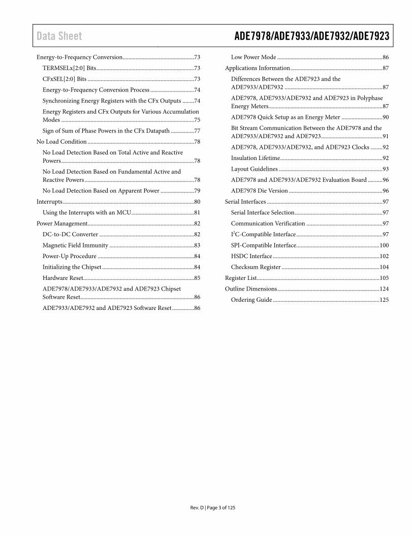
Energy-to-Frequency Conversion................................................. 73 TERMSELx[2:0] Bits ................................................................... 73 CFxSEL[2:0] Bits ......................................................................... 73 Energy-to-Frequency Conversion Process .............................. 74 Synchronizing Energy Registers with the CFx Outputs ........ 74 Energy Registers and CFx Outputs for Various Accumulation Modes ........................................................................................... 75 Sign of Sum of Phase Powers in the CFx Datapath ................ 77
No Load Condition ......................................................................... 78 No Load Detection Based on Total Active and Reactive Powers ........................................................................................... 78 No Load Detection Based on Fundamental Active and Reactive Powers ........................................................................... 78 No Load Detection Based on Apparent Power ....................... 79
Interrupts .......................................................................................... 80 Using the Interrupts with an MCU ........................................... 81
Power Management......................................................................... 82 DC-to-DC Converter ................................................................. 82 Magnetic Field Immunity .......................................................... 83 Power-Up Procedure .................................................................. 84 Initializing the Chipset ............................................................... 84 Hardware Reset............................................................................ 85 ADE7978/ADE7933/ADE7932 and ADE7923 Chipset Software Reset.............................................................................. 86 ADE7933/ADE7932 and ADE7923 Software Reset ............... 86
Low Power Mode ........................................................................ 86 Applications Information ............................................................... 87
Differences Between the ADE7923 and the ADE7933/ADE7932 ................................................................... 87 ADE7978, ADE7933/ADE7932 and ADE7923 in Polyphase Energy Meters .............................................................................. 87 ADE7978 Quick Setup as an Energy Meter ............................ 90 Bit Stream Communication Between the ADE7978 and the ADE7933/ADE7932 and ADE7923 .......................................... 91 ADE7978, ADE7933/ADE7932, and ADE7923 Clocks ........ 92 Insulation Lifetime ...................................................................... 92 Layout Guidelines ....................................................................... 93 ADE7978 and ADE7933/ADE7932 Evaluation Board .......... 96 ADE7978 Die Version ................................................................ 96
Serial Interfaces ............................................................................... 97 Serial Interface Selection ............................................................ 97 Communication Verification .................................................... 97 I2C-Compatible Interface ........................................................... 97 SPI-Compatible Interface......................................................... 100 HSDC Interface ......................................................................... 102 Checksum Register ................................................................... 104
Register List .................................................................................... 105 Outline Dimensions ...................................................................... 124
Ordering Guide ......................................................................... 125
ADE7978/ADE7933/ADE7932/ADE7923 Data Sheet
Rev. D | Page 4 of 125
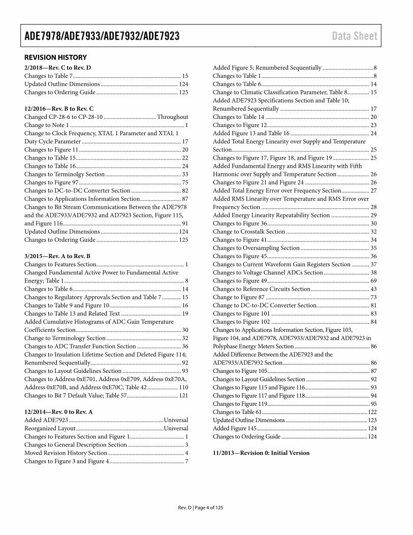
REVISION HISTORY 2/2018—Rev. C to Rev. D Changes to Table 7 .......................................................................... 15 Updated Outline Dimensions ..................................................... 124 Changes to Ordering Guide ........................................................ 125 12/2016—Rev. B to Rev. C Changed CP-28-6 to CP-28-10 .................................... Throughout Change to Note 1 .............................................................................. 1 Change to Clock Frequency, XTAL 1 Parameter and XTAL 1 Duty Cycle Parameter .................................................................... 17 Changes to Figure 11 ...................................................................... 20 Changes to Table 15 ........................................................................ 22 Changes to Table 16 ........................................................................ 24 Changes to Terminolgy Section .................................................... 33 Changes to Figure 97 ...................................................................... 75 Changes to DC-to-DC Converter Section .................................. 82 Changes to Applications Information Section ............................ 87 Changes to Bit Stream Communications Between the ADE7978 and the ADE7933/ADE7932 and AD7923 Section, Figure 115, and Figure 116 ................................................................................. 91 Updated Outline Dimensions ..................................................... 124 Changes to Ordering Guide ........................................................ 125 3/2015—Rev. A to Rev. B Changes to Features Section............................................................ 1 Changed Fundamental Active Power to Fundamental Active Energy; Table 1 .................................................................................. 8 Changes to Table 6 .......................................................................... 14 Changes to Regulatory Approvals Section and Table 7 ............. 15 Changes to Table 9 and Figure 10 ................................................. 16 Changes to Table 13 and Related Text ......................................... 19 Added Cumulative Histograms of ADC Gain Temperature Coefficients Section ........................................................................ 30 Change to Terminology Section ................................................... 32 Changes to ADC Transfer Function Section .............................. 36 Changes to Insulation Lifetime Section and Deleted Figure 114; Renumbered Sequentially .............................................................. 92 Changes to Layout Guidelines Section ........................................ 93 Changes to Address 0xE701, Address 0xE709, Address 0xE70A, Address 0xE70B, and Address 0xE70C; Table 42 ..................... 110 Changes to Bit 7 Default Value; Table 57 ................................... 121 12/2014—Rev. 0 to Rev. A Added ADE7923 ................................................................. Universal Reorganized Layout ............................................................ Universal Changes to Features Section and Figure 1..................................... 1 Changes to General Description Section ...................................... 3 Moved Revision History Section .................................................... 4 Changes to Figure 3 and Figure 4 ................................................... 7
Added Figure 5; Renumbered Sequentially ................................... 8 Changes to Table 1 ............................................................................. 8 Changes to Table 6 .......................................................................... 14 Change to Climatic Classification Parameter, Table 8 ............... 15 Added ADE7923 Specifications Section and Table 10; Renumbered Sequentially ............................................................. 17 Changes to Table 14 ....................................................................... 20 Changes to Figure 12 ...................................................................... 23 Added Figure 13 and Table 16 ...................................................... 24 Added Total Energy Linearity over Supply and Temperature Section .............................................................................................. 25 Changes to Figure 17, Figure 18, and Figure 19 ......................... 25 Added Fundamental Energy and RMS Linearity with Fifth Harmonic over Supply and Temperature Section ...................... 26 Changes to Figure 21 and Figure 24 ............................................ 26 Added Total Energy Error over Frequency Section ................... 27 Added RMS Linearity over Temperature and RMS Error over Frequency Section .......................................................................... 28 Added Energy Linearity Repeatability Section .......................... 29 Changes to Figure 36 ...................................................................... 30 Change to Crosstalk Section ......................................................... 32 Changes to Figure 41 ...................................................................... 34 Changes to Oversampling Section ............................................... 35 Changes to Figure 45 ...................................................................... 36 Changes to Current Waveform Gain Registers Section ............ 37 Changes to Voltage Channel ADCs Section ............................... 38 Changes to Figure 49 ...................................................................... 69 Changes to Reference Circuits Section ........................................ 43 Change to Figure 87 ....................................................................... 73 Change to DC-to-DC Converter Section .................................... 81 Changes to Figure 101 ................................................................... 83 Changes to Figure 102 ................................................................... 84 Changes to Applications Information Section, Figure 103, Figure 104, and ADE7978, ADE7933/ADE7932 and ADE7923 in Polyphase Energy Meters Section .......................................................... 86 Added Difference Between the ADE7923 and the ADE7933/ADE7932 Section ................................................................... 86 Changes to Figure 105............................................................................... 87 Changes to Layout Guidelines Section ................................................. 92 Changes to Figure 115 and Figure 116.................................................. 93 Changes to Figure 117 and Figure 118.................................................. 94 Changes to Figure 119............................................................................... 95 Changes to Table 61 ................................................................................. 122 Updated Outline Dimensions ............................................................... 123 Added Figure 145 ..................................................................................... 124 Changes to Ordering Guide .................................................................. 124 11/2013—Revision 0: Initial Version
Data Sheet ADE7978/ADE7933/ADE7932/ADE7923
Rev. D | Page 5 of 125
GENERAL DESCRIPTION The ADE7978, the ADE7933/ADE7932, and ADE7923 form a chipset dedicated to measuring 3-phase electrical energy using shunts as current sensors.
The ADE7933/ADE7932 are isolated, 3-channel sigma-delta analog-to-digital converters (Σ-Δ ADCs) for polyphase energy metering applications that use shunt current sensors. The ADE7923 is a nonisolated, 3-channel Σ-Δ ADC for the neutral line that uses a shunt current sensor. The ADE7932 features two ADCs, and the ADE7933 and ADE7923 feature three ADCs.
One channel is dedicated to measuring the voltage across the shunt when a shunt is used for current sensing. This channel provides a signal-to-noise ratio (SNR) of 67 dB over a 3.3 kHz signal bandwidth. Up to two additional channels are dedicated to measuring voltages, which are usually sensed using resistor dividers.
The unused voltage channels on the neutral ADE7923 can be used for auxiliary voltage measurements. These channels provide an SNR of 75 dB over a 3.3 kHz signal bandwidth. One voltage channel can be used to measure the temperature of the die via an internal sensor.
The ADE7933 and ADE7923 include three channels: one current channel and two voltage channels. The ADE7932 includes one current channel and one voltage channel, but is otherwise identical to the ADE7933.
The ADE7933/ADE7932 include isoPower®, an integrated, isolated dc-to-dc converter. Based on the Analog Devices, Inc., iCoupler® technology, the dc-to-dc converter provides the regulated power required by the first stage of the ADCs at a 3.3 V input supply. The ADE7933/ADE7932 eliminate the need for an external dc-to-dc isolation block. The iCoupler chip scale transformer technology is used to isolate the logic signals between the first and second stages of the ADC. The result is a small form factor, total isolation solution. The ADE7923 is the nonisolated version of the ADE7933 that can be used for neutral current measurement when isolation from the neutral line is not required.
The ADE7933/ADE7932 and ADE7923 contain a digital interface that is specially designed to interface with the ADE7978. Using this interface, the ADE7978 accesses the ADC outputs and configuration settings of the ADE7933/ADE7932 and ADE7923.
The ADE7933/ADE7932 are available in a 20-lead, Pb-free, wide-body SOIC package with increased creepage. The ADE7923 is available in a similar 20-lead, Pb-free, wide-body SOIC package without the increased creepage.
The ADE7978 is a high accuracy, 3-phase electrical energy measurement IC with serial interfaces and three flexible pulse outputs. The ADE7978 can interface with up to four ADE7933/ ADE7932 and ADE7923 devices. The ADE7978 incorporates all the signal processing required to perform total (fundamental and harmonic) active, reactive, and apparent energy measurement and rms calculations, as well as fundamental-only active and reactive energy measurement and rms calculations. A fixed function digital signal processor (DSP) executes this signal processing.
The ADE7978 measures the active, reactive, and apparent energy in various 3-phase configurations, such as wye or delta services, with both three and four wires. The ADE7978 provides system calibration features for each phase, gain calibration, and optional offset correction. Phase compensation is also available, but it is not necessary because the currents are sensed using shunts. The CF1, CF2, and CF3 logic outputs provide a wide selection of power information: total active, reactive, and apparent powers; the sum of the current rms values; and fundamental active and reactive powers.
The ADE7978 incorporates power quality measurements, such as short duration low or high voltage detection, short duration high current variations, line voltage period measurement, and angles between phase voltages and currents. Two serial interfaces, SPI and I2C, can be used to communicate with the ADE7978. A dedicated high speed interface—the high speed data capture (HSDC) port—can be used in conjunction with I2C to provide access to the ADC outputs and real-time power information. The ADE7978 also has two interrupt request pins, IRQ0 and IRQ1, to indicate that an enabled interrupt event has occurred. The ADE7978 is available in a 28-lead, Pb-free LFCSP package.
Note that throughout this data sheet, multifunction pins, such as SCLK/SCL, are referred to by the entire pin name or by a single function of the pin, for example, SCLK, when only that function is relevant.
ADE7978/ADE7933/ADE7932/ADE7923 Data Sheet
Rev. D | Page 6 of 125
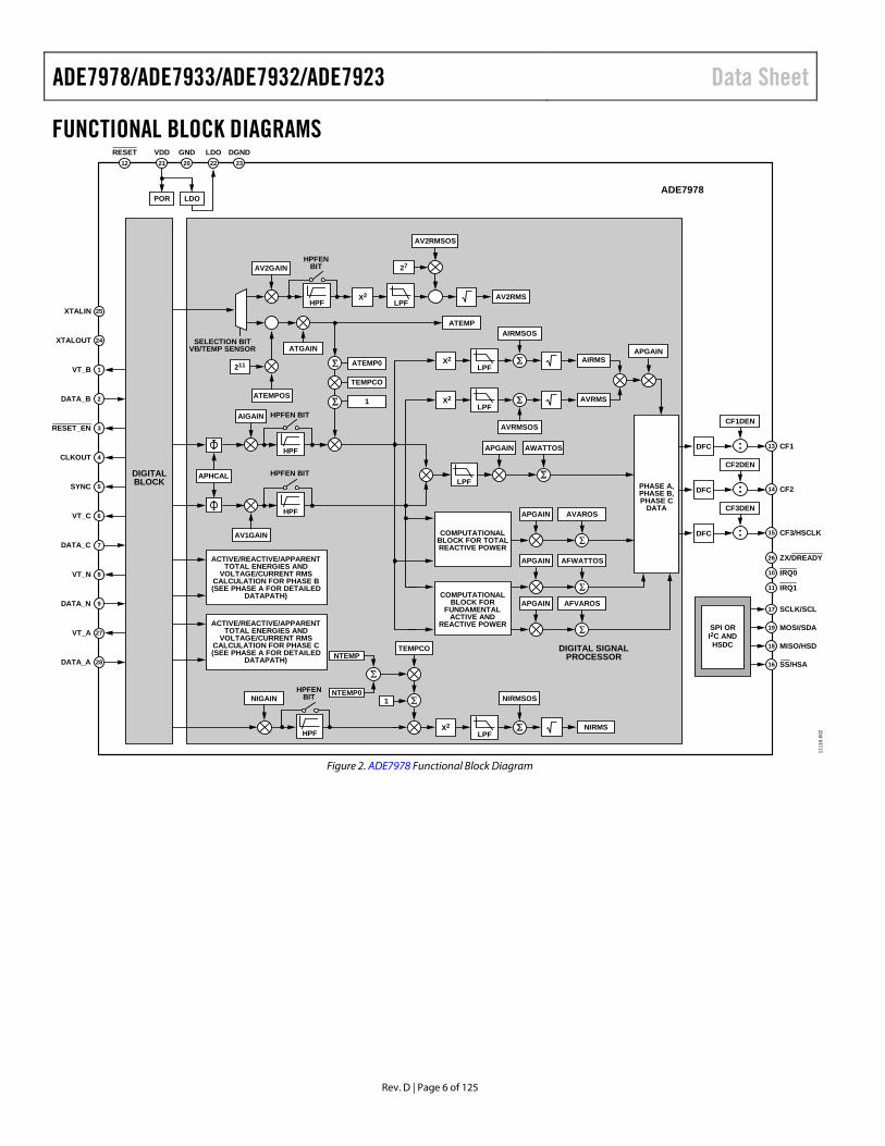
FUNCTIONAL BLOCK DIAGRAMS
HPFENBIT
HPFX2
211
LPF
APGAIN
AV1GAIN
APHCAL
HPF
AIGAIN HPFEN BIT
HPFEN BIT
HPF
COMPUTATIONALBLOCK FOR TOTALREACTIVE POWER
APGAIN AVAROS
COMPUTATIONALBLOCK FOR
FUNDAMENTALACTIVE AND
REACTIVE POWER
APGAIN AFWATTOS
APGAIN AFVAROS
PHASE A,PHASE B,PHASE C
DATA
DFC
CF1DEN
:
DFC
CF2DEN
:
DFC
CF3DEN
: 15
14
13 CF1
CF2
CF3/HSCLK
POR LDO
2221 20VDD GND LDO
23DGND
12RESET
AV2GAIN
ATEMP
AV2RMS
ATGAIN
ATEMPOS
SELECTION BITVB/TEMP SENSOR
27
AV2RMSOS
ATEMP0
TEMPCO
1
AIRMSOS
X2 AVRMSLPF
X2 AIRMSLPF
AVRMSOS
APGAIN AWATTOS
LPF
ACTIVE/REACTIVE/APPARENTTOTAL ENERGIES AND
VOLTAGE/CURRENT RMSCALCULATION FOR PHASE B(SEE PHASE A FOR DETAILED
DATAPATH)
ACTIVE/REACTIVE/APPARENTTOTAL ENERGIES AND
VOLTAGE/CURRENT RMSCALCULATION FOR PHASE C(SEE PHASE A FOR DETAILED
DATAPATH)DIGITAL SIGNAL
PROCESSOR
SPI ORI2C ANDHSDC
17 SCLK/SCL
19 MOSI/SDA
18 MISO/HSD
16 SS/HSA
11 IRQ1
10 IRQ0
26 ZX/DREADY
25XTALIN
24XTALOUT
1VT_B
2DATA_B
4CLKOUT
5SYNC
6VT_C
7DATA_C
8VT_N
9DATA_N
27VT_A
28DATA_A
3RESET_EN
DIGITALBLOCK
X2LPF
HPFENBIT
HPF
NIGAIN
NIRMS
TEMPCO
NIRMSOS
NTEMP
NTEMP01
ADE7978
1111
6-00
2
Figure 2. ADE7978 Functional Block Diagram
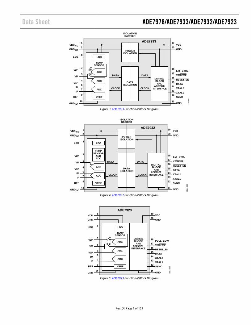
Data Sheet ADE7978/ADE7933/ADE7932/ADE7923
Rev. D | Page 7 of 125
DATA
SYNC
EMI_CTRL
V2/TEMPADC
CLOCK
LDO
IMV1P
V2P
VM
REF
ADC
LDO
IP
GNDISO
DIGITALBLOCK
ANDADE7978
INTERFACE XTAL2XTAL1
GND
VDDISO
GNDISO POWERISOLATION
VDD
GND
DATA DATA
CLOCK
1
2
8
3
4
5
67
10
9
19
20
12
18
1716
15
1413
11
ADC
ISOLATIONBARRIER
TEMPSENSOR
VREF
RESET_ENDATA
ISOLATION
1111
6-00
3
ADE7933
Figure 3. ADE7933 Functional Block Diagram
DATA
SYNC
EMI_CTRL
V2/TEMP
CLOCK
LDO
IMV1P
V2P
VM
REF
ADC
LDO
IP
GNDISO
DIGITALBLOCK
ANDADE7978
INTERFACE XTAL2XTAL1
GND
VDDISO
GNDISO POWERISOLATION
VDD
GND
DATA DATA
CLOCK
12
8
3
4
5
67
10
9
19
20
12
18
1716
15
1413
11
ADC
ISOLATIONBARRIER
TEMPSENSOR
ANDADC
VREF
RESET_ENDATA
ISOLATION
ADE7932
1111
6-00
4
Figure 4. ADE7932 Functional Block Diagram
DATA
SYNC
PULL_LOW
V2/TEMP
LDO
IMV1P
V2P
VM
REF
LDO
IP
GND
DIGITALBLOCK
ANDADE7978
INTERFACE
XTAL2XTAL1
GND
VDDGND
VDD
GND
1
2
8
3
4
5
6
7
10
9
19
20
12
18
1716
15
1413
11
ADC
TEMPSENSOR
VREF
RESET_EN
ADE7923
1111
6-20
5
ADC
ADC
Figure 5. ADE7923 Functional Block Diagram

ADE7978/ADE7933/ADE7932/ADE7923 Data Sheet
Rev. D | Page 8 of 125
SPECIFICATIONS SYSTEM SPECIFICATIONS, ADE7978 AND ADE7933/ADE7932/ADE7923 VDD = 3.3 V ± 10%, GND = DGND = 0 V, ADE7978 XTALIN = 16.384 MHz, TMIN to TMAX = −40°C to +85°C, TTYP = 25°C.
Table 1. Parameter1, 2 Min Typ Max Unit Test Conditions/Comments ACTIVE ENERGY MEASUREMENT
Measurement Error (per Phase) Total Active Energy 0.1 % Over a dynamic range of 500 to 1, power factor
(PF) = 1, gain compensation only 0.2 % Over a dynamic range of 2000 to 1, PF = 1
Fundamental Active Energy 0.1 % Over a dynamic range of 500 to 1, PF = 1, gain compensation only
0.2 % Over a dynamic range of 2000 to 1, PF = 1 AC Power Supply Rejection VDD = 3.3 V + 120 mV rms at 50 Hz/100 Hz,
IP = 6.25 mV rms, V1P = V2P = 100 mV rms Output Frequency Variation 0.01 %
DC Power Supply Rejection VDD = 3.3 V ± 330 mV dc, IP = 6.25 mV rms, V1P = V2P = 100 mV rms
Output Frequency Variation 0.01 % Total Active Energy Measurement
Bandwidth 3.3 kHz
REACTIVE ENERGY MEASUREMENT Measurement Error (per Phase)
Total Reactive Power 0.1 % Over a dynamic range of 500 to 1, PF = 0, gain compensation only
0.2 % Over a dynamic range of 2000 to 1, PF = 0 Fundamental Reactive Power 0.1 % Over a dynamic range of 500 to 1, PF = 0,
gain compensation only 0.2 % Over a dynamic range of 2000 to 1, PF = 0 AC Power Supply Rejection VDD = 3.3 V + 120 mV rms at 50 Hz/100 Hz,
IP = 6.25 mV rms, V1P = V2P = 100 mV rms Output Frequency Variation 0.01 %
DC Power Supply Rejection VDD = 3.3 V ± 330 mV dc, IP = 6.25 mV rms, V1P = V2P = 100 mV rms
Output Frequency Variation 0.01 % Total Reactive Energy Measurement
Bandwidth 3.3 kHz
RMS MEASUREMENTS Measurement Bandwidth 3.3 kHz I rms and V rms Voltage (V) rms Measurement Error 0.1 % Over a dynamic range of 500 to 1 Current (I) rms Measurement Error 0.25 % Over a dynamic range of 500 to 1 Fundamental V rms Measurement Error 0.1 % Over a dynamic range of 500 to 1 Fundamental I rms Measurement Error 0.25 % Over a dynamic range of 500 to 1
WAVEFORM SAMPLING Sampling CLKIN/2048 (16.384 MHz/2048 = 8 kSPS)
Current Channels See the Waveform Sampling Mode section Signal-to-Noise Ratio (SNR) 67 dB Signal-to-Noise-and-Distortion
(SINAD) Ratio 67 dB
Total Harmonic Distortion (THD) −85 dB Spurious-Free Dynamic Range (SFDR) 88 dBFS
Data Sheet ADE7978/ADE7933/ADE7932/ADE7923
Rev. D | Page 9 of 125
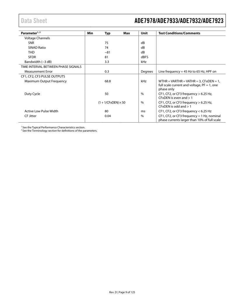
Parameter1, 2 Min Typ Max Unit Test Conditions/Comments Voltage Channels
SNR 75 dB SINAD Ratio 74 dB THD −81 dB SFDR 81 dBFS
Bandwidth (−3 dB) 3.3 kHz TIME INTERVAL BETWEEN PHASE SIGNALS
Measurement Error 0.3 Degrees Line frequency = 45 Hz to 65 Hz, HPF on CF1, CF2, CF3 PULSE OUTPUTS
Maximum Output Frequency 68.8 kHz WTHR = VARTHR = VATHR = 3, CFxDEN = 1, full scale current and voltage, PF = 1, one phase only
Duty Cycle 50 % CF1, CF2, or CF3 frequency > 6.25 Hz, CFxDEN is even and > 1
(1 + 1/CFxDEN) × 50 % CF1, CF2, or CF3 frequency > 6.25 Hz, CFxDEN is odd and > 1
Active Low Pulse Width 80 ms CF1, CF2, or CF3 frequency < 6.25 Hz CF Jitter 0.04 % CF1, CF2, or CF3 frequency = 1 Hz, nominal
phase currents larger than 10% of full scale 1 See the Typical Performance Characteristics section. 2 See the Terminology section for definitions of the parameters.
ADE7978/ADE7933/ADE7932/ADE7923 Data Sheet
Rev. D | Page 10 of 125
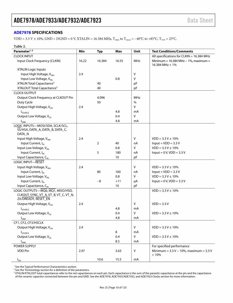
ADE7978 SPECIFICATIONS VDD = 3.3 V ± 10%, GND = DGND = 0 V, XTALIN = 16.384 MHz, TMIN to TMAX = −40°C to +85°C, TTYP = 25°C.
Table 2. Parameter1, 2 Min Typ Max Unit Test Conditions/Comments CLOCK INPUT All specifications for CLKIN = 16.384 MHz
Input Clock Frequency (CLKIN) 16.22 16.384 16.55 MHz Minimum = 16.384 MHz − 1%, maximum = 16.384 MHz + 1%
XTALIN Logic Inputs Input High Voltage, VINH 2.4 V Input Low Voltage, VINL 0.8 V
XTALIN Total Capacitance3 40 pF XTALOUT Total Capacitance3 40 pF
CLOCK OUTPUT Output Clock Frequency at CLKOUT Pin 4.096 MHz Duty Cycle 50 % Output High Voltage, VOH 2.4 V
ISOURCE 4.8 mA Output Low Voltage, VOL 0.4 V
ISINK 4.8 mA LOGIC INPUTS—MOSI/SDA, SCLK/SCL,
SS/HSA, DATA_A, DATA_B, DATA_C, DATA_N
Input High Voltage, VINH 2.4 V VDD = 3.3 V ± 10% Input Current, IIN 2 40 nA Input = VDD = 3.3 V
Input Low Voltage, VINL 0.8 V VDD = 3.3 V ± 10% Input Current, IIN 5 180 nA Input = 0 V, VDD = 3.3 V
Input Capacitance, CIN 10 pF LOGIC INPUT—RESET
Input High Voltage, VINH 2.4 V VDD = 3.3 V ± 10% Input Current, IIN 80 160 nA Input = VDD = 3.3 V
Input Low Voltage, VINL 0.8 V VDD = 3.3 V ± 10% Input Current, IIN −8 +11 µA Input = 0 V, VDD = 3.3 V
Input Capacitance, CIN 10 pF LOGIC OUTPUTS—IRQ0, IRQ1, MISO/HSD,
CLKOUT, SYNC, VT_A, VT_B, VT_C, VT_N, ZX/DREADY, RESET_EN
VDD = 3.3 V ± 10%
Output High Voltage, VOH 2.4 V VDD = 3.3 V ISOURCE 4.8 mA
Output Low Voltage, VOL 0.4 V VDD = 3.3 V ± 10% ISINK 4.8 mA
CF1, CF2, CF3/HSCLK Output High Voltage, VOH 2.4 V VDD = 3.3 V ± 10%
ISOURCE 8 mA Output Low Voltage, VOL 0.4 V VDD = 3.3 V ± 10%
ISINK 8.5 mA POWER SUPPLY For specified performance
VDD Pin 2.97 3.63 V Minimum = 3.3 V − 10%, maximum = 3.3 V + 10%
IDD 10.6 15.5 mA 1 See the Typical Performance Characteristics section. 2 See the Terminology section for a definition of the parameters. 3 XTALIN/XTALOUT total capacitances refer to the net capacitances on each pin. Each capacitance is the sum of the parasitic capacitance at the pin and the capacitance
of the ceramic capacitor connected between the pin and GND. See the ADE7978, ADE7933/ADE7932, and ADE7923 Clocks section for more information.

Data Sheet ADE7978/ADE7933/ADE7932/ADE7923
Rev. D | Page 11 of 125
I2C Interface Timing Parameters
VDD = 3.3 V ± 10%, GND = DGND = 0 V, XTALIN = 16.384 MHz, TMIN to TMAX = −40°C to +85°C.
Table 3. Standard Mode Fast Mode Parameter Symbol Min Max Min Max Unit SCL Clock Frequency fSCL 0 100 0 400 kHz Hold Time for Start and Repeated Start Conditions tHD;STA 4.0 0.6 µs Low Period of SCL Clock tLOW 4.7 1.3 µs High Period of SCL Clock tHIGH 4.0 0.6 µs Setup Time for Repeated Start Condition tSU;STA 4.7 0.6 µs Data Hold Time tHD;DAT 0 3.45 0 0.9 µs Data Setup Time tSU;DAT 250 100 ns Rise Time of SDA and SCL Signals tR 1000 20 300 ns Fall Time of SDA and SCL Signals tF 300 20 300 ns Setup Time for Stop Condition tSU;STO 4.0 0.6 µs Bus Free Time Between a Stop and Start Condition tBUF 4.7 1.3 µs Pulse Width of Suppressed Spikes tSP N/A1 50 ns 1 N/A means not applicable.
tF
tR
tHD;DATtHD;STA
tHIGHtSU;STA
tSU;DAT
tF
tHD;STA tSP
tSU;STO
trtBUF
tLOW
SDA
SCL
STARTCONDITION
REPEATED STARTCONDITION
STOPCONDITION
STARTCONDITION 11
116-
005
Figure 6. I2C Interface Timing

ADE7978/ADE7933/ADE7932/ADE7923 Data Sheet
Rev. D | Page 12 of 125
SPI Interface Timing Parameters
VDD = 3.3 V ± 10%, GND = DGND = 0 V, XTALIN = 16.384 MHz, TMIN to TMAX = −40°C to +85°C.
Table 4. Parameter Symbol Min Max Unit SS to SCLK Edge tSS 50 ns
SCLK Period 0.4 40001 µs SCLK Low Pulse Width tSL 175 ns SCLK High Pulse Width tSH 175 ns Data Output Valid After SCLK Edge tDAV 130 ns Data Input Setup Time Before SCLK Edge tDSU 100 ns Data Input Hold Time After SCLK Edge tDHD 50 ns Data Output Fall Time tDF 20 ns Data Output Rise Time tDR 20 ns SCLK Rise Time tSR 20 ns SCLK Fall Time tSF 20 ns MISO Disable After SS Rising Edge tDIS 1 µs
SS High After SCLK Edge tSFS 100 ns 1 Guaranteed by design.
MSB LSB
LSB IN
INTERMEDIATE BITS
INTERMEDIATE BITS
tSFS
tDIS
tSS
tSL
tDF
tSH
tDHD
tDAV
tDSU
tSRtSF
tDR
MSB INMOSI
MISO
SCLK
SS
1111
6-00
6
Figure 7. SPI Interface Timing
Data Sheet ADE7978/ADE7933/ADE7932/ADE7923
Rev. D | Page 13 of 125
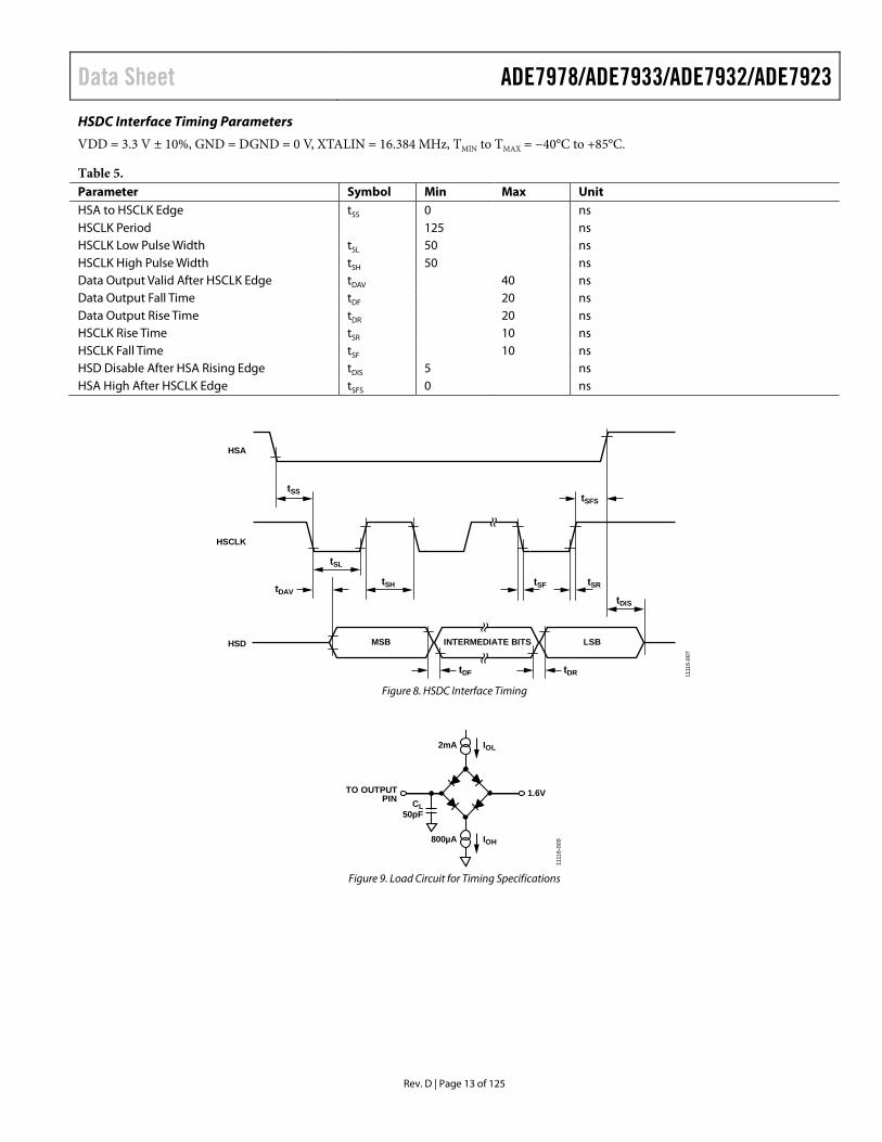
HSDC Interface Timing Parameters
VDD = 3.3 V ± 10%, GND = DGND = 0 V, XTALIN = 16.384 MHz, TMIN to TMAX = −40°C to +85°C.
Table 5. Parameter Symbol Min Max Unit HSA to HSCLK Edge tSS 0 ns HSCLK Period 125 ns HSCLK Low Pulse Width tSL 50 ns HSCLK High Pulse Width tSH 50 ns Data Output Valid After HSCLK Edge tDAV 40 ns Data Output Fall Time tDF 20 ns Data Output Rise Time tDR 20 ns HSCLK Rise Time tSR 10 ns HSCLK Fall Time tSF 10 ns HSD Disable After HSA Rising Edge tDIS 5 ns HSA High After HSCLK Edge tSFS 0 ns
MSB LSBINTERMEDIATE BITS
tSFS
tDIS
tSS
tSL
tDF
tSHtDAVtSRtSF
tDR
HSD
HSCLK
HSA
1111
6-00
7
Figure 8. HSDC Interface Timing
2mA IOL
800µA IOH
1.6VTO OUTPUTPIN CL
50pF
1111
6-00
9
Figure 9. Load Circuit for Timing Specifications

ADE7978/ADE7933/ADE7932/ADE7923 Data Sheet
Rev. D | Page 14 of 125
ADE7933/ADE7932 SPECIFICATIONS VDD = 3.3 V ± 10%, GND = 0 V, on-chip reference, XTAL1 = 4.096 MHz, TMIN to TMAX = −40°C to +85°C, TTYP = 25°C.
Table 6. Parameter1 Min Typ Max Unit Test Conditions/Comments ANALOG INPUTS
Pseudo Differential Signal Voltage Range Between IP and IM Pins −31.25 +31.25 mV peak IM pin connected to GNDISO Between V1P and VM Pins and
Between V2P and VM Pins −500 +500 mV peak Pseudo differential inputs between V1P
and VM pins and between V2P and VM pins, VM pin connected to GNDISO
Maximum VM and IM Voltage −25 +25 mV Crosstalk −90 dB IP and IM inputs set to 0 V (GNDISO), V1P and
V2P inputs at full scale −105 dB V2P or V1P and VM inputs set to 0 V (GNDISO),
IP and V1P or V2P inputs at full scale Input Impedance to GNDISO (DC)
IP, IM, V1P, and V2P Pins 480 kΩ VM Pin 280 kΩ
Current Channel ADC Offset Error −2 mV Voltage Channel ADC Offset Error −35 mV V2 channel applies to the ADE7933 only ADC Offset Drift over Temperature ±200 ppm/°C V1 channel only Gain Error −4 +4 % Gain Drift over Temperature −135 +135 ppm/°C Current channel −85 +85 ppm/°C V1 and V2 channels AC Power Supply Rejection −90 dB VDD = 3.3 V + 120 mV rms at 50 Hz/100 Hz,
IP = V1P = V2P = GNDISO DC Power Supply Rejection −80 dB VDD = 3.3 V ± 330 mV dc, IP = 6.25 mV rms,
V1P = V2P = 100 mV rms TEMPERATURE SENSOR
Accuracy ±5 °C CLOCK INPUT All specifications for XTAL1 = 4.096 MHz
Input Clock Frequency, XTAL1 3.6 4.096 4.21 MHz Nominal value provided by the ADE7978, minimum and maximum values apply when the ADE7933/ADE7932 are used without the ADE7978
XTAL1 Duty Cycle 45 50 55 % Values apply when the ADE7933/ADE7932 are used without the ADE7978
XTAL1 Logic Inputs Input High Voltage, VINH 2.4 V Input Low Voltage, VINL 0.8 V
XTAL1 Total Capacitance2 40 pF XTAL2 Total Capacitance2 40 pF
LOGIC INPUTS—SYNC, V2/TEMP, RESET_EN, EMI_CTRL
Input High Voltage, VINH 2.4 V Input Low Voltage, VINL 0.8 V
Input Current, IIN 0.015 1 μA Input Capacitance, CIN 10 pF
LOGIC OUTPUTS—DATA Output High Voltage, VOH 2.5 V ISOURCE = 800 µA Output Low Voltage, VOL 0.4 V ISINK = 2 mA
Data Sheet ADE7978/ADE7933/ADE7932/ADE7923
Rev. D | Page 15 of 125
Parameter1 Min Typ Max Unit Test Conditions/Comments POWER SUPPLY For specified performance
VDD Pin 2.97 3.63 V Minimum = 3.3 V − 10%; maximum = 3.3 V + 10%
IDD 12.5 19 mA 50 µA Bit 6 (CLKOUT_DIS) and Bit 7 (ADE7933_
SWRST) in the CONFIG3 register set to 1 1 See the Terminology section for definitions of the parameters. 2 XTAL1/XTAL2 total capacitances refer to the net capacitances on each pin. Each capacitance is the sum of the parasitic capacitance at the pin and the capacitance of
the ceramic capacitor connected between the pin and GND. See the ADE7978, ADE7933/ADE7932, and ADE7923 Clocks section for more information.
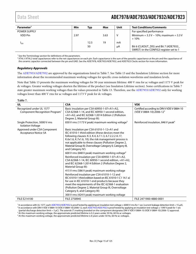
Regulatory Approvals
The ADE7933/ADE7932 are approved by the organizations listed in Table 7. See Table 13 and the Insulation Lifetime section for more information about the recommended maximum working voltages for specific cross-isolation waveforms and insulation levels.
Note that Table 13 presents the maximum working voltages for 50-year minimum lifetime: 400 V rms for ac voltages and 1173 V peak for dc voltages. Greater working voltages shorten the lifetime of the product (see Insulation Lifetime section). Some certifications in Table 7 state greater maximum working voltages than the values presented in Table 13. Therefore, use the ADE7933/ADE7932 only for working voltages lower than 400 V rms for ac voltages and 1173 V peak for dc voltages.
Table 7. UL CSA VDE Recognized under UL 1577
Component Recognition Program1 Basic insulation per CSA 60950-1-07+A1+A2, CSA 62368-1-14, and IEC 60950-1 second edition, +A1+A2, and IEC 62368-1:2014 Edition 2 (Pollution Degree 2, Material Group III):
Certified according to DIN V VDE V 0884-10 (VDE V 0884-10):2006-122
Single Protection, 5000 V rms Isolation Voltage
830 V rms (1173 V peak) maximum working voltage3 Reinforced insulation, 846 V peak4
Approved under CSA Component Acceptance Notice 5A
Basic insulation per CSA 61010-1-12+A1 and IEC 61010-1 third edition (these devices meet the following clauses: K.3, K.4, 6.7.1.3, 6.7.2.2.2 A.17, K.6x1.6, K.7x1.6, 10); the risk management process is not applicable to these clauses (Pollution Degree 2, Material Group III, Overvoltage Category II, Category III, and Category IV):
600 V rms (848 V peak) maximum working voltage4 Reinforced insulation per CSA 60950-1-07+A1+A2,
CSA 62368-1-14, IEC 60950-1 second edition, +A1+A2, and IEC 62368-1:2014 Edition 2 (Pollution Degree 2, Material Group III):
415 V rms (586 V peak) maximum working voltage Reinforced insulation per CSA 61010-1-12 and
IEC 61010-1 third edition based on IEC 61010-1 C1 14.1 a) for use in IEC 61010-1 end products because they meet the requirements of the IEC 62368-1 evaluation (Pollution Degree 2, Material Group III, Overvoltage Category II, and Category III):
300 V rms (424 V peak) maximum working voltage FILE E214100 FILE 2758945 FILE 2471900-4880-0001 1 In accordance with UL 1577, each ADE7933/ADE7932 is proof tested by applying an insulation test voltage ≥ 6000 V rms for 1 sec (current leakage detection limit = 15 µA). 2 In accordance with DIN V VDE V 0884-10 (VDE V 0884-10):2006-12, each ADE7933/ADE7932 is proof tested by applying an insulation test voltage ≥ 1590 V peak for 1 sec
(partial discharge detection limit = 5 pC). The asterisk (*) marking branded on the component designates DIN V VDE V 0884-10 (VDE V 0884-10):2006-12 approval. 3 At this maximum working voltage, the approximate predicted lifetime is 0.2 years under 50 Hz, 60 Hz ac voltages. 4 At this maximum working voltage, the approximate predicted lifetime is 8 years under 50 Hz, 60 Hz ac voltages.

ADE7978/ADE7933/ADE7932/ADE7923 Data Sheet
Rev. D | Page 16 of 125
Insulation and Safety Related Specifications
Table 8. Critical Safety Related Dimensions and Material Properties Parameter Symbol Value Unit Test Conditions/Comments Rated Dielectric Insulation Voltage 5000 V rms 1-minute duration Minimum External Air Gap (Clearance) L(I01) 8.3 mm Measured from input terminals to output terminals,
shortest distance through air along the PCB mounting plane, as an aid to PCB layout
Minimum External Tracking (Creepage) L(I02) 8.3 mm Measured from input terminals to output terminals, shortest distance path along body
Minimum Internal Gap (Internal Clearance) 0.017 min mm Insulation distance through insulation Tracking Resistance (Comparative Tracking Index) CTI 400 V IEC 60112 Isolation Group II Material Group DIN VDE 0110, 1/89, Table 1
DIN V VDE V 0884-10 (VDE V 0884-10):2006-12 Insulation Characteristics
The ADE7933/ADE7932 are suitable for reinforced electrical isolation only within the safety limit data. Maintenance of the safety data is ensured by the protective circuits.
Table 9. Description Test Conditions/Comments Symbol Characteristic Unit Installation Classification per DIN VDE 0110
For Rated Mains Voltage ≤ 150 V rms I to IV For Rated Mains Voltage ≤ 300 V rms I to IV For Rated Mains Voltage ≤ 400 V rms I to III
Climatic Classification 40/085/21 Pollution Degree per DIN VDE 0110, Table 1 2 Maximum Working Insulation Voltage VIORM 846 V peak Input-to-Output Test Voltage, Method b1 VIORM × 1.875 = Vpd(m), 100% production test,
tini = tm = 1 sec, partial discharge < 5 pC Vpd(m) 1592 V peak
Input-to-Output Test Voltage, Method a Vpd(m) After Environmental Tests Subgroup 1 VIORM × 1.5 = Vpd(m), tini = 60 sec, tm = 10 sec, partial
discharge < 5 pC 1273 V peak
After Input and/or Safety Tests Subgroup 2 and Subgroup 3
VIORM × 1.2 = Vpd(m), tini = 60 sec, tm = 10 sec, partial discharge < 5 pC
1018 V peak
Highest Allowable Overvoltage VIOTM 6000 V peak Surge Isolation Voltage VPEAK = 10 kV, 1.2 µs rise time, 50 µs, 50% fall time VIOSM 6250 V peak Safety Limiting Values Maximum value allowed in the event of a failure
(see Figure 10)
Maximum Junction Temperature TS 150 °C Total Power Dissipation at 25°C PS 2.78 W
Insulation Resistance at TS VIO = 500 V RS >109 Ω
1111
6-25
8
SAFE
LIM
ITIN
G P
OW
ER (W
)
AMBIENT TEMPERATURE (°C)
3.5
3.0
2.5
2.0
1.5
1.0
0.5
00 50 100 150 200
Figure 10. Thermal Derating Curve, Dependence of Safety Limiting Values on Case Temperature, per DIN EN 60747-5-2

Data Sheet ADE7978/ADE7933/ADE7932/ADE7923
Rev. D | Page 17 of 125
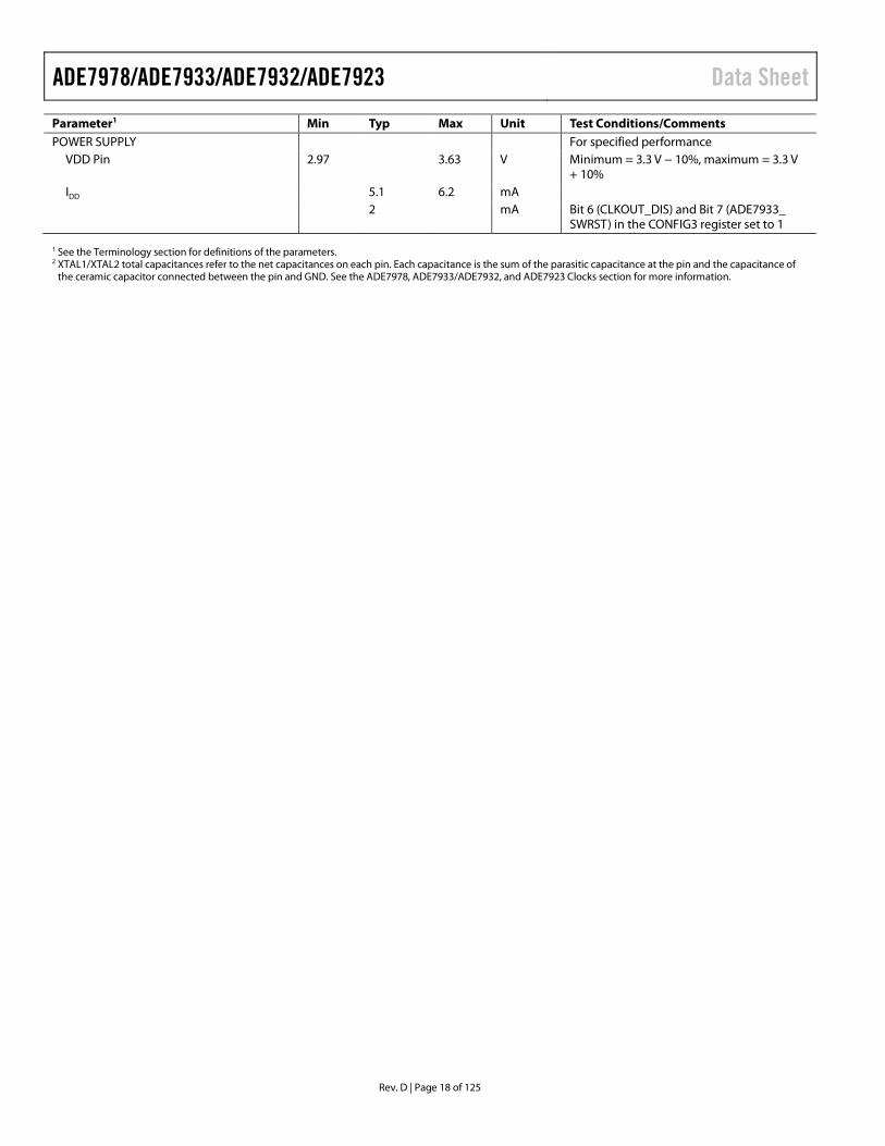
ADE7923 SPECIFICATIONS VDD = 3.3 V ± 10%, GND = 0 V, on-chip reference, XTAL1 = 4.096 MHz, TMIN to TMAX = −40°C to +85°C, TTYP = 25°C.
Table 10. Parameter1 Min Typ Max Unit Test Conditions/Comments ANALOG INPUTS
Pseudo Differential Signal Voltage Range Between IP and IM Pins −31.25 +31.25 mV peak IM pin connected to GNDISO Between V1P and VM Pins and
Between V2P and VM Pins −500 +500 mV peak Pseudo differential inputs between V1P
and VM pins and between V2P and VM pins, VM pin connected to GNDISO
Maximum VM and IM Voltage −25 +25 mV Crosstalk −90 dB IP and IM inputs set to 0 V (GNDISO), V1P and
V2P inputs at full scale −105 dB V2P or V1P and VM inputs set to 0 V (GNDISO),
IP and V1P or V2P inputs at full scale Input Impedance to GNDISO (DC)
IP, IM, V1P, and V2P Pins 480 kΩ VM Pin 280 kΩ
Current Channel ADC Offset Error −2 mV Voltage Channel ADC Offset Error −35 mV V1 and V2 channels ADC Offset Drift over Temperature ±200 ppm/°C V1 channel only Gain Error −4 +4 % Gain Drift over Temperature −135 +135 ppm/°C Current channel −85 +85 ppm/°C V1 and V2 channels AC Power Supply Rejection −90 dB VDD = 3.3 V + 120 mV rms at 50 Hz/100 Hz,
IP = V1P = V2P = GNDISO DC Power Supply Rejection −80 dB VDD = 3.3 V ± 330 mV dc, IP = 6.25 mV rms,
V1P = V2P = 100 mV rms TEMPERATURE SENSOR
Accuracy ±5 °C CLOCK INPUT All specifications for XTAL1 = 4.096 MHz
Input Clock Frequency, XTAL1 3.6 4.096 4.21 MHz Nominal value provided by the ADE7978, minimum and maximum values apply when the AD7923 are used without the ADE7978
XTAL1 Duty Cycle 45 50 55 % Values apply when the AD7923 are used without the ADE7978
XTAL1 Logic Inputs Input High Voltage, VINH 2.4 V Input Low Voltage, VINL 0.8 V
XTAL1 Total Capacitance2 40 pF XTAL2 Total Capacitance2 40 pF
LOGIC INPUTS—SYNC, V2/TEMP, RESET_EN
Input High Voltage, VINH 2.4 V Input Low Voltage, VINL 0.8 V
Input Current, IIN 0.015 1 µA Input Capacitance, CIN 10 pF
LOGIC OUTPUTS—DATA Output High Voltage, VOH 2.5 V ISOURCE = 800 µA Output Low Voltage, VOL 0.4 V ISINK = 2 mA
ADE7978/ADE7933/ADE7932/ADE7923 Data Sheet
Rev. D | Page 18 of 125
Parameter1 Min Typ Max Unit Test Conditions/Comments POWER SUPPLY For specified performance
VDD Pin 2.97 3.63 V Minimum = 3.3 V − 10%, maximum = 3.3 V + 10%
IDD 5.1 6.2 mA 2 mA Bit 6 (CLKOUT_DIS) and Bit 7 (ADE7933_
SWRST) in the CONFIG3 register set to 1 1 See the Terminology section for definitions of the parameters. 2 XTAL1/XTAL2 total capacitances refer to the net capacitances on each pin. Each capacitance is the sum of the parasitic capacitance at the pin and the capacitance of
the ceramic capacitor connected between the pin and GND. See the ADE7978, ADE7933/ADE7932, and ADE7923 Clocks section for more information.

Data Sheet ADE7978/ADE7933/ADE7932/ADE7923
Rev. D | Page 19 of 125
ABSOLUTE MAXIMUM RATINGS TA = 25°C, unless otherwise noted.
Table 11. Parameter Rating ADE7978
VDD to GND −0.3 V to +3.7 V Digital Input Voltage to DGND −0.3 V to VDD + 0.3 V Digital Output Voltage to DGND −0.3 V to VDD + 0.3 V
ADE7933/ADE7932 and ADE7923 VDD to GND −0.3 V to +3.7 V Analog Input Voltage to GNDISO,
IP, IM, V1P, V2P, VM −2 V to +2 V
Reference Input Voltage to GNDISO −0.3 V to VDD + 0.3 V Digital Input Voltage to GND −0.3 V to VDD + 0.3 V Digital Output Voltage to GND −0.3 V to VDD + 0.3 V Common-Mode Transients1 −100 kV/µs to +100 kV/µs
Operating Temperature Industrial Range −40°C to +85°C Storage Temperature Range −65°C to +150°C
Lead Temperature (Soldering, 10 sec)2 ADE7978 300°C ADE7933/ADE7932 and ADE7923 260°C
1 Refers to common-mode transients across the insulation barrier. Common-mode transients exceeding the absolute maximum ratings may cause latch-up or permanent damage.
2 Analog Devices recommends that reflow profiles used in soldering RoHS compliant parts conform to JEDEC J-STD 20. For the latest revision of this standard, refer to JEDEC.
Stresses at or above those listed under Absolute Maximum Ratings may cause permanent damage to the product. This is a stress rating only; functional operation of the product at these or any other conditions above those indicated in the operational section of this specification is not implied. Operation beyond the maximum operating conditions for extended periods may affect product reliability.
THERMAL RESISTANCE θJA and θJC are specified for the worst-case conditions, that is, a device soldered in a circuit board for surface-mount packages.
Table 12. Thermal Resistance Package Type θJA θJC Unit 28-Lead LFCSP (ADE7978) 29.3 1.8 °C/W 20-Lead SOIC (ADE7933/ADE7932) 48.0 6.2 °C/W 20-Lead SOIC (ADE7923) 79.0 24.7 °C/W
ESD CAUTION
Table 13. ADE7933/ADE7932 Maximum Continuous Working Voltage Supporting a 50-Year Minimum Lifetime1 Parameter Max Unit AC Voltage, Bipolar Waveform 400 V rms DC Voltage
Basic Insulation 1173 V peak 1 Refers to the continuous voltage magnitude imposed across the isolation barrier. For more information, see the Insulation Lifetime section.
Note that greater working voltages than the values presented in Table 13 shorten the lifetime of the product (see Insulation Lifetime section). Therefore, although some certifications in Table 7 state bigger maximum working voltages, use the ADE7933/ADE7932 only for working voltages lower than the values presented in this table.
ADE7978/ADE7933/ADE7932/ADE7923 Data Sheet
Rev. D | Page 20 of 125
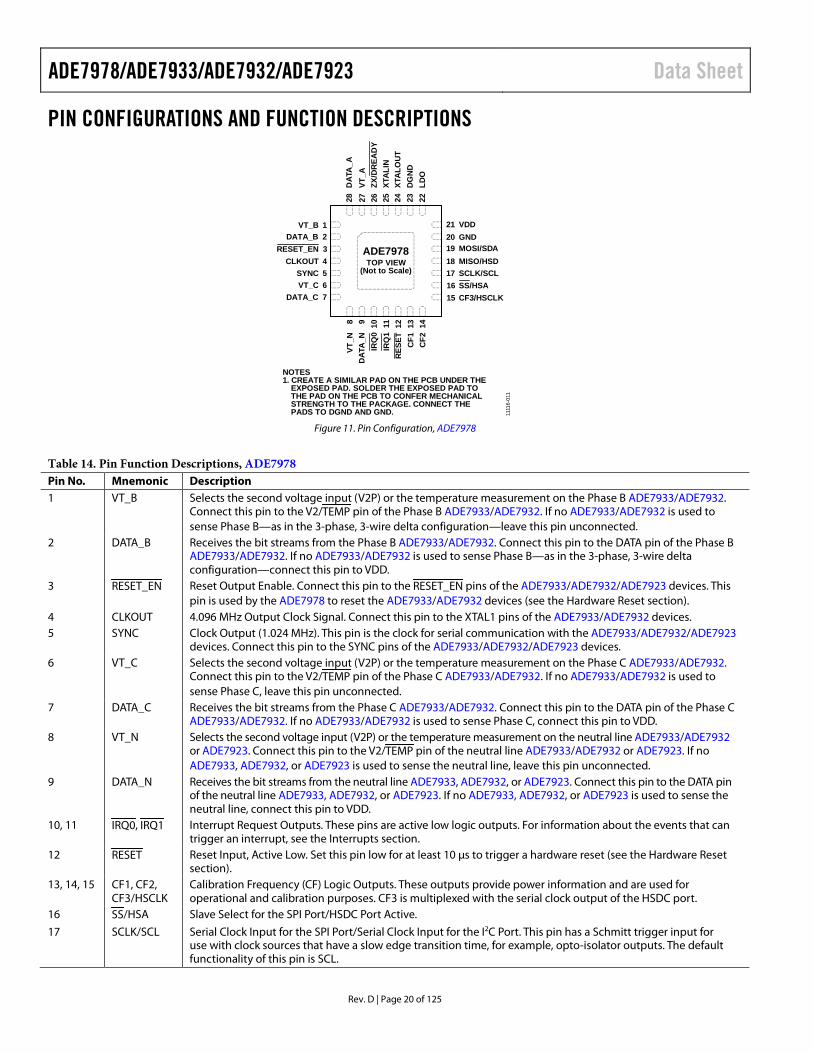
PIN CONFIGURATIONS AND FUNCTION DESCRIPTIONS
1VT_B2DATA_B3RESET_EN4CLKOUT5SYNC6VT_C7DATA_C
17 SCLK/SCL18 MISO/HSD19 MOSI/SDA20 GND21 VDD
16 SS/HSA15 CF3/HSCLK
8VT
_N9
DAT
A_N
10IR
Q0
11IR
Q1
12R
ESET
13C
F114
CF2
24XT
ALO
UT
25XT
ALI
N26
ZX/D
REA
DY
27VT
_A28
DAT
A_A
23D
GN
D22
LDO
ADE7978TOP VIEW
(Not to Scale)
NOTES1. CREATE A SIMILAR PAD ON THE PCB UNDER THE
EXPOSED PAD. SOLDER THE EXPOSED PAD TOTHE PAD ON THE PCB TO CONFER MECHANICALSTRENGTH TO THE PACKAGE. CONNECT THEPADS TO DGND AND GND. 11
116-
011
Figure 11. Pin Configuration, ADE7978
Table 14. Pin Function Descriptions, ADE7978 Pin No. Mnemonic Description 1 VT_B Selects the second voltage input (V2P) or the temperature measurement on the Phase B ADE7933/ADE7932.
Connect this pin to the V2/TEMP pin of the Phase B ADE7933/ADE7932. If no ADE7933/ADE7932 is used to sense Phase B—as in the 3-phase, 3-wire delta configuration—leave this pin unconnected.
2 DATA_B Receives the bit streams from the Phase B ADE7933/ADE7932. Connect this pin to the DATA pin of the Phase B ADE7933/ADE7932. If no ADE7933/ADE7932 is used to sense Phase B—as in the 3-phase, 3-wire delta configuration—connect this pin to VDD.
3 RESET_EN Reset Output Enable. Connect this pin to the RESET_EN pins of the ADE7933/ADE7932/ADE7923 devices. This pin is used by the ADE7978 to reset the ADE7933/ADE7932 devices (see the Hardware Reset section).
4 CLKOUT 4.096 MHz Output Clock Signal. Connect this pin to the XTAL1 pins of the ADE7933/ADE7932 devices. 5 SYNC Clock Output (1.024 MHz). This pin is the clock for serial communication with the ADE7933/ADE7932/ADE7923
devices. Connect this pin to the SYNC pins of the ADE7933/ADE7932/ADE7923 devices. 6 VT_C Selects the second voltage input (V2P) or the temperature measurement on the Phase C ADE7933/ADE7932.
Connect this pin to the V2/TEMP pin of the Phase C ADE7933/ADE7932. If no ADE7933/ADE7932 is used to sense Phase C, leave this pin unconnected.
7 DATA_C Receives the bit streams from the Phase C ADE7933/ADE7932. Connect this pin to the DATA pin of the Phase C ADE7933/ADE7932. If no ADE7933/ADE7932 is used to sense Phase C, connect this pin to VDD.
8 VT_N Selects the second voltage input (V2P) or the temperature measurement on the neutral line ADE7933/ADE7932 or ADE7923. Connect this pin to the V2/TEMP pin of the neutral line ADE7933/ADE7932 or ADE7923. If no ADE7933, ADE7932, or ADE7923 is used to sense the neutral line, leave this pin unconnected.
9 DATA_N Receives the bit streams from the neutral line ADE7933, ADE7932, or ADE7923. Connect this pin to the DATA pin of the neutral line ADE7933, ADE7932, or ADE7923. If no ADE7933, ADE7932, or ADE7923 is used to sense the neutral line, connect this pin to VDD.
10, 11 IRQ0, IRQ1 Interrupt Request Outputs. These pins are active low logic outputs. For information about the events that can trigger an interrupt, see the Interrupts section.
12 RESET Reset Input, Active Low. Set this pin low for at least 10 µs to trigger a hardware reset (see the Hardware Reset section).
13, 14, 15 CF1, CF2, CF3/HSCLK
Calibration Frequency (CF) Logic Outputs. These outputs provide power information and are used for operational and calibration purposes. CF3 is multiplexed with the serial clock output of the HSDC port.
16 SS/HSA Slave Select for the SPI Port/HSDC Port Active.
17 SCLK/SCL Serial Clock Input for the SPI Port/Serial Clock Input for the I2C Port. This pin has a Schmitt trigger input for use with clock sources that have a slow edge transition time, for example, opto-isolator outputs. The default functionality of this pin is SCL.

Data Sheet ADE7978/ADE7933/ADE7932/ADE7923
Rev. D | Page 21 of 125
Pin No. Mnemonic Description 18 MISO/HSD Data Output for the SPI Port/Data Output for the HSDC Port. 19 MOSI/SDA Data Input for the SPI Port/Data Output for the I2C Port. The default functionality of this pin is SDA. 20 GND Ground Reference for the Input Circuitry. 21 VDD Supply Voltage. This pin provides the supply voltage. For specified operation, maintain the supply voltage at
3.3 V ± 10%. Decouple this pin to GND with a 10 µF capacitor in parallel with a ceramic 100 nF capacitor. 22 LDO 1.8 V Output of the Digital Low Dropout (LDO) Regulator. Decouple this pin with a 4.7 µF capacitor in parallel
with a ceramic 100 nF capacitor. Do not connect active external circuitry to this pin. 23 DGND Ground Reference for the Digital Circuitry. 24 XTALOUT A crystal with a maximum drive level of 0.5 mW and an equivalent series resistance (ESR) of 20 Ω can be
connected across this pin and the XTALIN pin to provide a clock source for the ADE7978. 25 XTALIN Master Clock. An external clock can be provided at this logic input. Alternatively, a crystal with a maximum
drive level of 0.5 mW and an ESR of 20 Ω can be connected across XTALIN and XTALOUT to provide a clock source for the ADE7978. The clock frequency for specified operation is 16.384 MHz. For more information, see the ADE7978, ADE7933/ADE7932, and ADE7923 Clocks section.
26 ZX/DREADY Zero-Crossing (ZX) Output Pin. The ZX pin goes high on the positive-going edge of the selected phase voltage zero crossing; the pin goes low on the negative-going edge of the zero crossing (see the Zero-Crossing Detection section for more information). DREADY is an active low signal that is generated approximately 70 ns after Bit 17 (DREADY) in the STATUS0 register is set to 1. This pin has a frequency of 8 kHz and stays low for 10 µs every period. The default functionality of this pin is DREADY.
27 VT_A Selects the second voltage input (V2P) or the temperature measurement on the Phase A ADE7933/ADE7932. Connect this pin to the V2/TEMP pin of the Phase A ADE7933/ADE7932. If no ADE7933/ADE7932 is used to sense Phase A, leave this pin unconnected.
28 DATA_A Receives the bit streams from the Phase A ADE7933/ADE7932. Connect this pin to the DATA pin of the Phase A ADE7933/ADE7932. If no ADE7933/ADE7932 is used to sense Phase A, connect this pin to VDD.
EP Exposed Pad. Create a similar pad on the PCB under the exposed pad. Solder the exposed pad to the pad on the PCB to confer mechanical strength to the package. Connect the pads to DGND and GND.
ADE7978/ADE7933/ADE7932/ADE7923 Data Sheet
Rev. D | Page 22 of 125
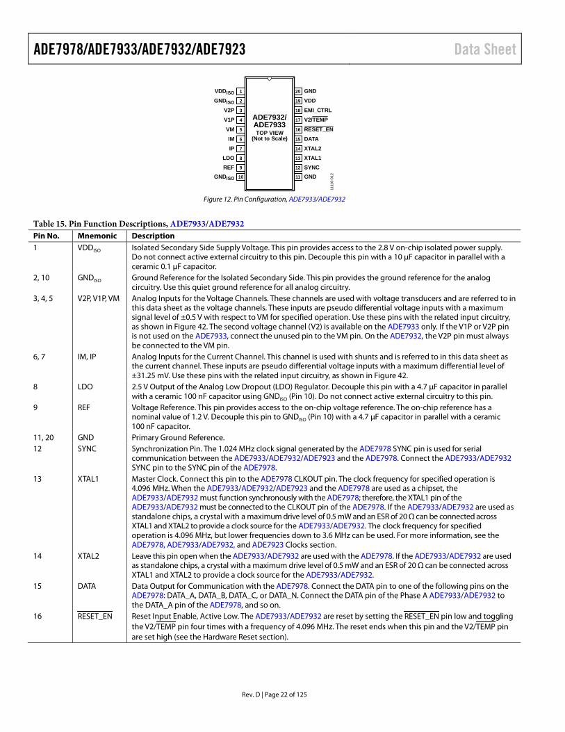
ADE7932/ADE7933TOP VIEW
(Not to Scale)
VDDISO 1
GNDISO 2
V2P 3
V1P 4
GND20
VDD19
EMI_CTRL18
V2/TEMP17
VM 5 RESET_EN16
IM 6 DATA15
IP 7 XTAL214
LDO 8 XTAL113
REF 9 SYNC12
GNDISO 10 GND11
1111
6-01
2
Figure 12. Pin Configuration, ADE7933/ADE7932
Table 15. Pin Function Descriptions, ADE7933/ADE7932 Pin No. Mnemonic Description 1 VDDISO Isolated Secondary Side Supply Voltage. This pin provides access to the 2.8 V on-chip isolated power supply.
Do not connect active external circuitry to this pin. Decouple this pin with a 10 µF capacitor in parallel with a ceramic 0.1 µF capacitor.
2, 10 GNDISO Ground Reference for the Isolated Secondary Side. This pin provides the ground reference for the analog circuitry. Use this quiet ground reference for all analog circuitry.
3, 4, 5 V2P, V1P, VM Analog Inputs for the Voltage Channels. These channels are used with voltage transducers and are referred to in this data sheet as the voltage channels. These inputs are pseudo differential voltage inputs with a maximum signal level of ±0.5 V with respect to VM for specified operation. Use these pins with the related input circuitry, as shown in Figure 42. The second voltage channel (V2) is available on the ADE7933 only. If the V1P or V2P pin is not used on the ADE7933, connect the unused pin to the VM pin. On the ADE7932, the V2P pin must always be connected to the VM pin.
6, 7 IM, IP Analog Inputs for the Current Channel. This channel is used with shunts and is referred to in this data sheet as the current channel. These inputs are pseudo differential voltage inputs with a maximum differential level of ±31.25 mV. Use these pins with the related input circuitry, as shown in Figure 42.
8 LDO 2.5 V Output of the Analog Low Dropout (LDO) Regulator. Decouple this pin with a 4.7 µF capacitor in parallel with a ceramic 100 nF capacitor using GNDISO (Pin 10). Do not connect active external circuitry to this pin.
9 REF Voltage Reference. This pin provides access to the on-chip voltage reference. The on-chip reference has a nominal value of 1.2 V. Decouple this pin to GNDISO (Pin 10) with a 4.7 µF capacitor in parallel with a ceramic 100 nF capacitor.
11, 20 GND Primary Ground Reference. 12 SYNC Synchronization Pin. The 1.024 MHz clock signal generated by the ADE7978 SYNC pin is used for serial
communication between the ADE7933/ADE7932/ADE7923 and the ADE7978. Connect the ADE7933/ADE7932 SYNC pin to the SYNC pin of the ADE7978.
13 XTAL1 Master Clock. Connect this pin to the ADE7978 CLKOUT pin. The clock frequency for specified operation is 4.096 MHz. When the ADE7933/ADE7932/ADE7923 and the ADE7978 are used as a chipset, the ADE7933/ADE7932 must function synchronously with the ADE7978; therefore, the XTAL1 pin of the ADE7933/ADE7932 must be connected to the CLKOUT pin of the ADE7978. If the ADE7933/ADE7932 are used as standalone chips, a crystal with a maximum drive level of 0.5 mW and an ESR of 20 Ω can be connected across XTAL1 and XTAL2 to provide a clock source for the ADE7933/ADE7932. The clock frequency for specified operation is 4.096 MHz, but lower frequencies down to 3.6 MHz can be used. For more information, see the ADE7978, ADE7933/ADE7932, and ADE7923 Clocks section.
14 XTAL2 Leave this pin open when the ADE7933/ADE7932 are used with the ADE7978. If the ADE7933/ADE7932 are used as standalone chips, a crystal with a maximum drive level of 0.5 mW and an ESR of 20 Ω can be connected across XTAL1 and XTAL2 to provide a clock source for the ADE7933/ADE7932.
15 DATA Data Output for Communication with the ADE7978. Connect the DATA pin to one of the following pins on the ADE7978: DATA_A, DATA_B, DATA_C, or DATA_N. Connect the DATA pin of the Phase A ADE7933/ADE7932 to the DATA_A pin of the ADE7978, and so on.
16 RESET_EN Reset Input Enable, Active Low. The ADE7933/ADE7932 are reset by setting the RESET_EN pin low and toggling the V2/TEMP pin four times with a frequency of 4.096 MHz. The reset ends when this pin and the V2/TEMP pin are set high (see the Hardware Reset section).
Data Sheet ADE7978/ADE7933/ADE7932/ADE7923
Rev. D | Page 23 of 125
Pin No. Mnemonic Description 17 V2/TEMP This input pin selects the signal that is converted at the second voltage channel of the ADE7933. (In the
ADE7932, the temperature sensor is always converted by the second voltage channel.) When this pin is high, the voltage input V2P is sensed; when this pin is low, the temperature sensor is measured. The V2/TEMP pin is also used during the ADE7933/ADE7932 reset procedure. For both the ADE7933 and ADE7932, the V2/TEMP pin must always be connected to one of the following pins on the ADE7978: VT_A, VT_B, VT_C, or VT_N. Connect the V2/TEMP pin of the Phase A ADE7933/ADE7932 to the VT_A pin of the ADE7978, and so on. For more information, see the Second Voltage Channel and Temperature Measurement section.
18 EMI_CTRL Emissions Control Pin. This pin manages the emissions of the ADE7933/ADE7932. When the pin is connected to GND, the PWM control block of the dc-to-dc converter generates pulses during Slot 0, Slot 2, Slot 4, and Slot 6. When the pin is connected to VDD, the PWM control block of the dc-to-dc converter generates pulses during Slot 1, Slot 3, Slot 5, and Slot 7. (For more information, see the DC-to-DC Converter section.) Do not leave this pin floating.
19 VDD Primary Supply Voltage. This pin provides the supply voltage for the ADE7933/ADE7932. For specified operation, maintain the supply voltage at 3.3 V ± 10%. Decouple this pin to GND with a 10 µF capacitor in parallel with a ceramic 100 nF capacitor.
ADE7978/ADE7933/ADE7932/ADE7923 Data Sheet
Rev. D | Page 24 of 125
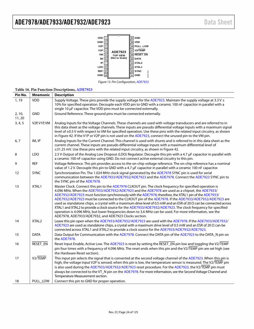
ADE7923TOP VIEW
(Not to Scale)
VDD 1
GND 2
V2P 3
V1P 4
GND20
VDD19
PULL_LOW18
V2/TEMP17
VM 5 RESET_EN16
IM 6 DATA15
IP 7 XTAL214
LDO 8 XTAL113
REF 9 SYNC12
GND 10 GND11
1111
6-01
3
Figure 13. Pin Configuration, ADE7923
Table 16. Pin Function Descriptions, ADE7923 Pin No. Mnemonic Description 1, 19 VDD Supply Voltage. These pins provide the supply voltage for the ADE7923. Maintain the supply voltage at 3.3 V ±
10% for specified operation. Decouple each VDD pin to GND with a ceramic 100 nF capacitor in parallel with a single 10 µF capacitor. The VDD pins must be connected externally.
2, 10, 11, 20
GND Ground Reference. These ground pins must be connected externally.
3, 4, 5 V2P, V1P, VM Analog Inputs for the Voltage Channels. These channels are used with voltage transducers and are referred to in this data sheet as the voltage channels. These inputs are pseudo differential voltage inputs with a maximum signal level of ±0.5 V with respect to VM for specified operation. Use these pins with the related input circuitry, as shown in Figure 42. If the V1P or V2P pin is not used on the ADE7923, connect the unused pin to the VM pin.
6, 7 IM, IP Analog Inputs for the Current Channel. This channel is used with shunts and is referred to in this data sheet as the current channel. These inputs are pseudo differential voltage inputs with a maximum differential level of ±31.25 mV. Use these pins with the related input circuitry, as shown in Figure 42.
8 LDO 2.5 V Output of the Analog Low Dropout (LDO) Regulator. Decouple this pin with a 4.7 µF capacitor in parallel with a ceramic 100 nF capacitor using GND. Do not connect active external circuitry to this pin.
9 REF Voltage Reference. This pin provides access to the on-chip voltage reference. The on-chip reference has a nominal value of 1.2 V. Decouple this pin to GND with a 4.7 µF capacitor in parallel with a ceramic 100 nF capacitor.
12 SYNC Synchronization Pin. The 1.024 MHz clock signal generated by the ADE7978 SYNC pin is used for serial communication between the ADE7933/ADE7932/ADE7923 and the ADE7978. Connect the ADE7923 SYNC pin to the SYNC pin of the ADE7978.
13 XTAL1 Master Clock. Connect this pin to the ADE7978 CLKOUT pin. The clock frequency for specified operation is 4.096 MHz. When the ADE7933/ADE7932/ADE7923 and the ADE7978 are used as a chipset, the ADE7933/ ADE7932/ADE7923 must function synchronously with the ADE7978; therefore, the XTAL1 pin of the ADE7933/ ADE7932/ADE7923 must be connected to the CLKOUT pin of the ADE7978. If the ADE7933/ADE7932/ADE7923 are used as standalone chips, a crystal with a maximum drive level of 0.5 mW and an ESR of 20 Ω can be connected across XTAL1 and XTAL2 to provide a clock source for the ADE7933/ADE7932/ADE7923. The clock frequency for specified operation is 4.096 MHz, but lower frequencies down to 3.6 MHz can be used. For more information, see the ADE7978, ADE7933/ADE7932, and ADE7923 Clocks section.
14 XTAL2 Leave this pin open when the ADE7933/ADE7932/ADE7923 are used with the ADE7978. If the ADE7933/ADE7932/ ADE7923 are used as standalone chips, a crystal with a maximum drive level of 0.5 mW and an ESR of 20 Ω can be connected across XTAL1 and XTAL2 to provide a clock source for the ADE7933/ADE7932/ADE7923.
15 DATA Data Output for Communication with the ADE7978. Connect the DATA pin of the ADE7923 to the DATA_N pin on the ADE7978.
16 RESET_EN Reset Input Enable, Active Low. The ADE7923 is reset by setting the RESET_EN pin low and toggling the V2/TEMP pin four times with a frequency of 4.096 MHz. The reset ends when this pin and the V2/TEMP pin are set high (see the Hardware Reset section).
17 V2/TEMP This input pin selects the signal that is converted at the second voltage channel of the ADE7923. When this pin is high, the voltage input V2P is sensed; when this pin is low, the temperature sensor is measured. The V2/TEMP pin is also used during the ADE7933/ADE7932/ADE7923 reset procedure. For the ADE7923, the V2/TEMP pin must always be connected to the VT_N pin on the ADE7978. For more information, see the Second Voltage Channel and Temperature Measurement section.
18 PULL_LOW Connect this pin to GND for proper operation.
Data Sheet ADE7978/ADE7933/ADE7932/ADE7923
Rev. D | Page 25 of 125
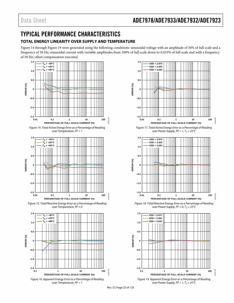
TYPICAL PERFORMANCE CHARACTERISTICS TOTAL ENERGY LINEARITY OVER SUPPLY AND TEMPERATURE Figure 14 through Figure 19 were generated using the following conditions: sinusoidal voltage with an amplitude of 50% of full scale and a frequency of 50 Hz; sinusoidal current with variable amplitudes from 100% of full scale down to 0.033% of full scale and with a frequency of 50 Hz; offset compensation executed.
1.5
–1.5
–1.0
–0.5
0
0.5
1.0
0.01 0.1 1 10 100
ERR
OR
(%)
PERCENTAGE OF FULL-SCALE CURRENT (%)
TA = –40°CTA = +25°CTA = +85°C
1111
6-11
3
Figure 14. Total Active Energy Error as a Percentage of Reading
over Temperature, PF = 1
1.5
–1.5
–1.0
–0.5
0
0.5
1.0
0.01 0.1 1 10 100
ERR
OR
(%)
PERCENTAGE OF FULL-SCALE CURRENT (%)
TA = –40°CTA = +25°CTA = +85°C
1111
6-11
4
Figure 15. Total Reactive Energy Error as a Percentage of Reading
over Temperature, PF = 0
1.5
–1.5
–1.0
–0.5
0
0.5
1.0
0.1 1 10 100
ERR
OR
(%)
PERCENTAGE OF FULL-SCALE CURRENT (%)
TA = –40°CTA = +25°CTA = +85°C
1111
6-11
5
Figure 16. Apparent Energy Error as a Percentage of Reading
over Temperature, PF = 1
1.5
–1.5
–1.0
–0.5
0
0.5
1.0
0.01 0.1 1 10 100
ERR
OR
(%)
PERCENTAGE OF FULL-SCALE CURRENT (%)
VDD = 2.97VVDD = 3.30VVDD = 3.63V
1111
6-12
0
Figure 17. Total Active Energy Error as a Percentage of Reading
over Power Supply, PF = 1, TA = 25°C
1.5
–1.5
–1.0
–0.5
0
0.5
1.0
0.01 0.1 1 10 100
ERR
OR
(%)
PERCENTAGE OF FULL-SCALE CURRENT (%)
VDD = 2.97VVDD = 3.30VVDD = 3.63V
1111
6-12
1
Figure 18. Total Reactive Energy Error as a Percentage of Reading
over Power Supply, PF = 0, TA = 25°C
1.5
–1.5
–1.0
–0.5
0
0.5
1.0
0.1 1 10 100
ERR
OR
(%)
PERCENTAGE OF FULL-SCALE CURRENT (%)
VDD = 2.97VVDD = 3.30VVDD = 3.63V
1111
6-12
2
Figure 19. Apparent Energy Error as a Percentage of Reading
over Power Supply, PF = 1, TA = 25°C

ADE7978/ADE7933/ADE7932/ADE7923 Data Sheet
Rev. D | Page 26 of 125
FUNDAMENTAL ENERGY AND RMS LINEARITY WITH FIFTH HARMONIC OVER SUPPLY AND TEMPERATURE Figure 20 through Figure 25 were generated using the following conditions: fundamental voltage component in phase with fifth harmonic; current with a 50 Hz component that has variable amplitudes from 100% of full scale down to 0.033% of full scale and a fifth harmonic with a constant amplitude of 17% of full scale; power factor equal to 1 or 0 on the fundamental and fifth harmonic. Figure 20, Figure 21, Figure 23, and Figure 24 were generated using a voltage with a 50 Hz component that has an amplitude of 50% of full scale and a fifth harmonic with an amplitude of 5% of full scale. Figure 22 and Figure 25 were generated using a voltage with a 50 Hz component that has variable amplitudes from 100% of full scale down to 0.033% of full scale and a fifth harmonic with an amplitude of 5% of full scale.
1.5
–1.5
–1.0
–0.5
0
0.5
1.0
0.01 0.1 1 10 100
ERR
OR
(%)
PERCENTAGE OF FULL-SCALE CURRENT (%)
TA = –40°CTA = +25°CTA = +85°C
1111
6-11
6
Figure 20. Fundamental Active Energy Error as a Percentage of Reading
over Temperature, PF = 1
1.5
–1.5
–1.0
–0.5
0
0.5
1.0
0.01 0.1 1 10 100
ERRO
R (%
)
PERCENTAGE OF FULL-SCALE CURRENT (%)
VDD = 2.97VVDD = 3.30VVDD = 3.63V
1111
6-12
3
Figure 21. Fundamental Active Energy Error as a Percentage of Reading over Power Supply, PF = 1, TA = 25°C
1.5
–1.5
–1.0
–0.5
0
0.5
1.0
0.1 1 10 100
ERR
OR
(%)
PERCENTAGE OF FULL-SCALE CURRENT (%)
TA = –40°CTA = +25°CTA = +85°C
1111
6-12
7
Figure 22. Fundamental Current RMS Error as a Percentage of Reading over
Temperature, PF = 1
1.5
–1.5
–1.0
–0.5
0
0.5
1.0
0.01 0.1 1 10 100ER
RO
R (%
)PERCENTAGE OF FULL-SCALE CURRENT (%)
TA = –40°CTA = +25°CTA = +85°C
1111
6-11
7
Figure 23. Fundamental Reactive Energy Error as a Percentage of Reading
over Temperature, PF = 0
1.5
–1.5
–1.0
–0.5
0
0.5
1.0
0.01 0.1 1 10 100
ERRO
R (%
)
PERCENTAGE OF FULL-SCALE CURRENT (%)
VDD = 2.97VVDD = 3.30VVDD = 3.63V
1111
6-12
4
Figure 24. Fundamental Reactive Energy Error as a Percentage of Reading
over Power Supply, PF = 0, TA = 25°C
1.5
–1.5
–1.0
–0.5
0
0.5
1.0
0.1 1 10 100
ERR
OR
(%)
PERCENTAGE OF FULL-SCALE VOLTAGE (%)
TA = –40°CTA = +25°CTA = +85°C
1111
6-12
8
Figure 25. Fundamental Voltage RMS Error as a Percentage of Reading
over Temperature, PF = 1
Data Sheet ADE7978/ADE7933/ADE7932/ADE7923
Rev. D | Page 27 of 125
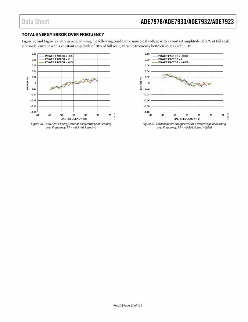
TOTAL ENERGY ERROR OVER FREQUENCY Figure 26 and Figure 27 were generated using the following conditions: sinusoidal voltage with a constant amplitude of 50% of full scale; sinusoidal current with a constant amplitude of 10% of full scale; variable frequency between 45 Hz and 65 Hz.
0.10
–0.10
–0.08
–0.06
–0.04
–0.02
0
0.02
0.04
0.06
0.08
40 706560555045
ERR
OR
(%)
LINE FREQUENCY (Hz)
POWER FACTOR = –0.5POWER FACTOR = +1POWER FACTOR = +0.5
1111
6-11
8
Figure 26. Total Active Energy Error as a Percentage of Reading
over Frequency, PF = −0.5, +0.5, and +1
0.10
–0.10
–0.08
–0.06
–0.04
–0.02
0
0.02
0.04
0.06
0.08
40 706560555045
ERR
OR
(%)
LINE FREQUENCY (Hz)
POWER FACTOR = –0.866POWER FACTOR = 0POWER FACTOR = +0.866
1111
6-11
9
Figure 27. Total Reactive Energy Error as a Percentage of Reading
over Frequency, PF = −0.866, 0, and +0.866

ADE7978/ADE7933/ADE7932/ADE7923 Data Sheet
Rev. D | Page 28 of 125
RMS LINEARITY OVER TEMPERATURE AND RMS ERROR OVER FREQUENCY Figure 28 through Figure 31 were generated using the following conditions: sinusoidal current and voltage with variable amplitudes from 100% of full scale down to 0.033% of full scale. Figure 28 and Figure 30 were obtained using a frequency of 50 Hz; Figure 29 and Figure 31 were obtained using a variable frequency between 45 Hz and 65 Hz.
1.5
–1.5
–1.0
–0.5
0
0.5
1.0
0.1 1 10 100
ERR
OR
(%)
PERCENTAGE OF FULL-SCALE CURRENT (%)
TA = –40°CTA = +25°CTA = +85°C
1111
6-12
5
Figure 28. Current RMS Error as a Percentage of Reading
over Temperature
0.10
–0.10
–0.08
–0.06
–0.04
–0.02
0
0.02
0.04
0.06
0.08
40 706560555045
ERR
OR
(%)
LINE FREQUENCY (Hz) 1111
6-12
9
Figure 29. Current RMS Error as a Percentage of Reading
over Frequency
1.5
–1.5
–1.0
–0.5
0
0.5
1.0
0.1 1 10 100
ERR
OR
(%)
PERCENTAGE OF FULL-SCALE VOLTAGE (%)
TA = –40°CTA = +25°CTA = +85°C
1111
6-12
6
Figure 30. Voltage RMS Error as a Percentage of Reading
over Temperature
0.10
–0.10
–0.08
–0.06
–0.04
–0.02
0
0.02
0.04
0.06
0.08
40 706560555045
ERR
OR
(%)
LINE FREQUENCY (Hz) 1111
6-13
0
Figure 31. Voltage RMS Error as a Percentage of Reading
over Frequency

Data Sheet ADE7978/ADE7933/ADE7932/ADE7923
Rev. D | Page 29 of 125
ENERGY LINEARITY REPEATABILITY Figure 32 through Figure 35 were generated using the following conditions: sinusoidal voltage with an amplitude of 50% of full scale and a frequency of 50 Hz; sinusoidal current with variable amplitudes from 100% of full scale down to 0.033% of full scale and with a frequency of 50 Hz; offset compensation executed. For Figure 33 and Figure 35, besides the fundamental component, the voltage contained a fifth harmonic with a constant amplitude of 5% of full scale, and the current contained a fifth harmonic with a constant amplitude of 17% of full scale. Measurements at 25°C were repeated 30 times.
1.5
–1.5
–1.0
–0.5
0
0.5
1.0
0.01 0.1 1 10 100
ERR
OR
(%)
PERCENTAGE OF FULL-SCALE CURRENT (%) 1111
6-13
1
Figure 32. Total Active Energy Error as a Percentage of Reading, PF = 1
(Standard Deviation σ = 0.06% at 0.2% of Full-Scale Current and σ = 0.12% at 0.05% of Full-Scale Current)
1.5
–1.5
–1.0
–0.5
0
0.5
1.0
0.01 0.1 1 10 100
ERR
OR
(%)
PERCENTAGE OF FULL-SCALE CURRENT (%) 1111
6-13
2
Figure 33. Fundamental Active Energy Error as a Percentage of Reading, PF = 1
(Standard Deviation σ = 0.06% at 0.2% of Full-Scale Current and σ = 0.11% at 0.05% of Full-Scale Current)
1.5
–1.5
–1.0
–0.5
0
0.5
1.0
0.01 0.1 1 10 100
ERR
OR
(%)
PERCENTAGE OF FULL-SCALE CURRENT (%) 1111
6-13
3
Figure 34. Total Reactive Energy Error as a Percentage of Reading, PF = 0
(Standard Deviation σ = 0.09% at 0.2% of Full-Scale Current and σ = 0.13% at 0.05% of Full-Scale Current)
1.5
–1.5
–1.0
–0.5
0
0.5
1.0
0.01 0.1 1 10 100
ERR
OR
(%)
PERCENTAGE OF FULL-SCALE CURRENT (%) 1111
6-13
4
Figure 35. Fundamental Reactive Energy Error as a Percentage of Reading, PF = 0
(Standard Deviation σ = 0.06% at 0.2% of Full-Scale Current and σ = 0.13% at 0.05% of Full-Scale Current)
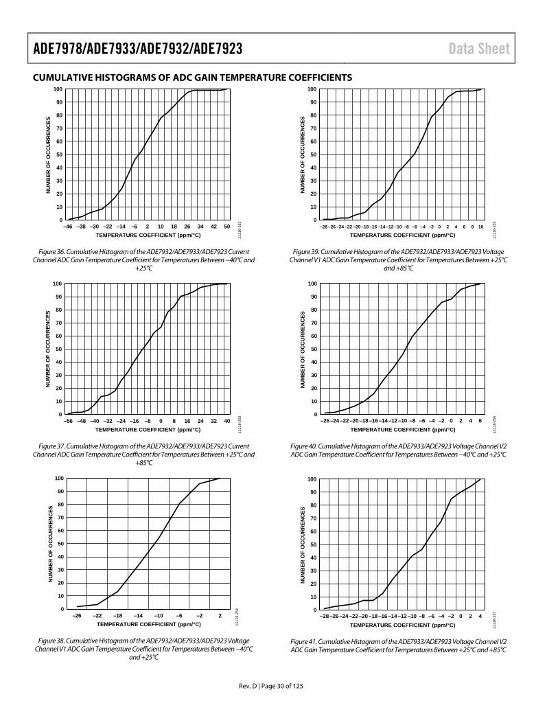
ADE7978/ADE7933/ADE7932/ADE7923 Data Sheet
Rev. D | Page 30 of 125
CUMULATIVE HISTOGRAMS OF ADC GAIN TEMPERATURE COEFFICIENTS 100
0
10
20
30
40
50
60
70
80
90
1111
6-25
2
NU
MB
ER O
F O
CC
UR
REN
CES
TEMPERATURE COEFFICIENT (ppm/°C)–46 –38 –30 –22 –14 –6 2 10 18 26 34 42 50
Figure 36. Cumulative Histogram of the ADE7932/ADE7933/ADE7923 Current Channel ADC Gain Temperature Coefficient for Temperatures Between −40°C and
+25°C
100
0
10
20
30
40
50
60
70
80
90
1111
6-25
3
NU
MB
ER O
F O
CC
UR
REN
CES
TEMPERATURE COEFFICIENT (ppm/°C)–56 –48 –40 –32 –24 –16 –8 0 8 16 24 32 40
Figure 37. Cumulative Histogram of the ADE7932/ADE7933/ADE7923 Current Channel ADC Gain Temperature Coefficient for Temperatures Between +25°C and
+85°C
100
0
10
20
30
40
50
60
70
80
90
1111
6-25
4
NU
MB
ER O
F O
CC
UR
REN
CES
TEMPERATURE COEFFICIENT (ppm/°C)–26 –22 –18 –14 –10 –6 –2 2
Figure 38. Cumulative Histogram of the ADE7932/ADE7933/ADE7923 Voltage Channel V1 ADC Gain Temperature Coefficient for Temperatures Between −40°C
and +25°C
100
0
10
20
30
40
50
60
70
80
90
1111
6-25
5
NU
MB
ER O
F O
CC
UR
REN
CES
TEMPERATURE COEFFICIENT (ppm/°C)–28 –26 –24 –22 –20 –18 –16 –14 –12 –10 –8 –6 –4 –2 0 2 4 6 8 10
Figure 39. Cumulative Histogram of the ADE7932/ADE7933/ADE7923 Voltage Channel V1 ADC Gain Temperature Coefficient for Temperatures Between +25°C
and +85°C
100
0
10
20
30
40
50
60
70
80
90
1111
6-25
6
NU
MB
ER O
F O
CC
UR
REN
CES
TEMPERATURE COEFFICIENT (ppm/°C)–26–24–22–20–18–16–14–12–10 –8 –6 –4 –2 0 2 4 6
Figure 40. Cumulative Histogram of the ADE7933/ADE7923 Voltage Channel V2 ADC Gain Temperature Coefficient for Temperatures Between −40°C and +25°C
100
0
10
20
30
40
50
60
70
80
9011
116-
257
NU
MB
ER O
F O
CC
UR
REN
CES
TEMPERATURE COEFFICIENT (ppm/°C)–28–26–24–22–20–18–16–14–12–10 –8 –6 –4 –2 0 2 4
Figure 41. Cumulative Histogram of the ADE7933/ADE7923 Voltage Channel V2 ADC Gain Temperature Coefficient for Temperatures Between +25°C and +85°C

Data Sheet ADE7978/ADE7933/ADE7932/ADE7923
Rev. D | Page 31 of 125
TEST CIRCUIT
11
10
12
19
PHASE AADE7933
PHASE BADE7933
PHASE CADE7933
PHASE NADE7923
XTAL1XTAL2
VDD 19
XTAL1
XTAL2
VDD
XTAL1
XTAL2
DATA
SYNC
EMI_CTRL
1413
17
16
15
18
12
14
13
17
16
15
18
14
13
19
17
16
15
18
12
GND
GND
11
20
GND
GND
1120
GND 11
20
TS4148
TS4148TS4148
TS4148TS4148
150ΩFERRITE
150ΩFERRITE
150ΩFERRITE
150ΩFERRITE
IP
IM
33nF
33nF
33nF
100nF4.7µF
4.7µF
V1P
VM
V2P
7
6
4
5
3
GNDISO
VDDISO2
1
GNDISO
LDO10
8
9 REF
GND
VDD
SAME AS INPHASE AADE7933
SAME AS INPHASE AADE7933
SAME AS INPHASE AADE7933
SAME AS INPHASE AADE7933
SAME AS INPHASE AADE7933
SAME AS INPHASE AADE7933
VDDISO
GNDISO
V2P
V1P
VM
IM
IP
LDO
REF
GNDISO
1
2
3
4
5
6
7
8
9
10
VDDISO
GNDISO
V2P
V1P
VM
IM
IP
LDO
REF
GNDISO
1
2
3
4
5
6
7
8
9
10
V1PIN_A
V2PIN_A RESET_EN
V2/TEMP
SYNC
EMI_CTRL
DATA
RESET_EN
V2/TEMP
SYNC
EMI_CTRL
DATA
RESET_EN
V2/TEMP
XTAL1
XTAL2
PULL_LOW 18
14
13
17
16
15
19
12
GND
GND
20
11
VDD
GND
V2P
V1P
VM
IM
IP
LDO
REF
GND
1
2
3
4
5
6
7
8
9
10
SYNC
VDD
DATA
RESET_EN
V2/TEMP
ADE7978
28DATA_A
27VT_A
5 SYNC3 RESET_EN
CLKOUT
DATA_B
4
2524
2
VT_B1
DATA_C7
VT_C6
VT_N8
DATA_N9
IRQ0
IRQ1
RESET
CF1
CF2
CF3/HSCLK
SCLK/SCL
MISO/HSD
MOSI/SDAGND
VDD
LDO
DGND
XTALINXTALOUT
ZX/DREADY
21
20
22
23
20pF20pF
16.384MHz
10kΩ10kΩ
10kΩ
80.6Ω
10kΩ
SAME ASCF1
TO MCU
TO MCU
12
13
14
SS/HSA
15 TO MCU16 TO MCU17 TO MCU18 TO MCU19 TO MCU26 TO MCU
3.3V
3.3V
3.3V
3.3V
1µF
4.7µF
10nΩ10µF100nF
330kΩ 330kΩ 330kΩ
1kΩ
1kΩ
1kΩ33nF1kΩ
10µF 100nF
3.3V3.3V
IPIN_A
GND_A
IMIN_A
100nF
1111
6-23
6
330kΩ 330kΩ 330kΩ
33nF1kΩ
100nF
10µF 100nF
3.3V
100nF
Figure 42. Test Circuit

ADE7978/ADE7933/ADE7932/ADE7923 Data Sheet
Rev. D | Page 32 of 125
TERMINOLOGY Energy Measurement Error The accuracy of the energy measurement is assessed as follows:
1. The voltage channel is supplied with a sinusoidal signal that has peak values equal to ±250 mV. This value represents half of the full scale.
2. The current channel is supplied with sinusoidal signals that have peak values equal to ±31.25 mV (full scale), ±3.125 mV (1/10 of full scale), ±312.5 µV (1/100 of full scale), ±31.25 µV (1/1000 of full scale), and ±15.625 µV (1/2000 of full scale).
3. The energy is accumulated in line cycle accumulation mode, and the accumulation time varies with the current channel signal level.
The energy calculated for current peaks equal to ±3.125 mV (1/10 of full scale) is considered the reference. The energy measurement error is computed relative to a straight line that passes through this point, as follows:
( )
( )%1001
)(
)(
×
−
××
=ε1/10
x
1/10
x
1/10x
IEnergy
I
I
IAccTime
IAccTimeIEnergy
(1)
where: Energy(Ix) is the energy measurement when the current is Ix. Energy(I1/10) is the energy measurement when the current is I1/100, which is the reference measurement. AccTime(I1/10) is the accumulation time used to measure Energy(I1/10). AccTime(Ix) is the accumulation time used to measure Energy(Ix).
I rms and V rms Measurement Error The accuracy of the rms measurement is assessed as follows:
1. The voltage and current channels are supplied with sinusoidal signals of various peaks, starting with the full-scale signals (±500 mV for the voltage channel and ±31.25 mV for the current channel) and ending with ±1 mV and ±62.5 µV, respectively.
2. The rms registers are read at least once per line cycle over 1 sec and averaged.
The measurement performed when the input signal has peaks equal to 1/10 of full scale is considered the reference. The rms measurement error is computed relative to a straight line that passes through this point, as follows:
( )
( ) %1001 ×
−×
=ε1/10
x
1/10x
I IrmsII
IIrmsI
(2)
( )
( ) %1001 ×
−×
=ε1/10
x
1/10x
V VrmsVV
VVrmsV
(3)
where: I rms(Ix) is the current rms measurement when the current is Ix. I rms(I1/10) is the current rms measurement when the current is I1/10, which is the reference measurement. V rms(Vx) is the voltage rms measurement when the voltage is Vx. V rms(V1/10) is the voltage rms measurement when the voltage is V1/10, which is the reference measurement.
Signal-to-Noise Ratio (SNR) SNR is the ratio of the rms value of the actual input signal to the rms sum of all other spectral components below the Nyquist frequency, excluding harmonics and dc. The waveform samples are acquired over 1 sec and then a Hanning window is applied. The value for SNR is expressed in decibels.
Signal-to-Noise-and-Distortion (SINAD) Ratio SINAD is the ratio of the rms value of the actual input signal to the rms sum of all other spectral components below the Nyquist frequency, including harmonics but excluding dc. The waveform samples are acquired over 1 sec and then a Hanning window is applied. The value for SINAD is expressed in decibels.
Total Harmonic Distortion (THD) THD is the ratio of the rms sum of all harmonics (excluding the noise components) to the rms value of the fundamental. The waveform samples are acquired over 1 sec and then a Hanning window is applied. The value for THD is expressed in decibels.
Spurious-Free Dynamic Range (SFDR) SFDR is the ratio of the rms value of the actual input signal to the rms value of the peak spurious component over the measurement bandwidth of the waveform samples. The waveform samples are acquired over 1 sec and then a Hanning window is applied. The value of SFDR is expressed in decibels relative to full scale, dBFS.
CF Jitter The period of pulses at one of the CF1, CF2, or CF3 pins is continuously measured. The maximum, minimum, and average values of four consecutive pulses are computed as follows:
Maximum = max(Period0, Period1, Period2, Period3)
Minimum = min(Period0, Period1, Period2, Period3)
Average = 4
3210 PeriodPeriodPeriodPeriod +++
The CF jitter is then computed as follows:
%100×−
=Average
MinimumMaximumCFJITTER (4)
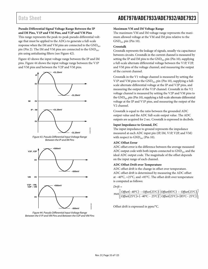
Data Sheet ADE7978/ADE7933/ADE7932/ADE7923
Rev. D | Page 33 of 125
Pseudo Differential Signal Voltage Range Between the IP and IM Pins, V1P and VM Pins, and V2P and VM Pins This range represents the peak-to-peak pseudo differential volt-age that must be applied to the ADCs to generate a full-scale response when the IM and VM pins are connected to the GNDISO pin (Pin 2). The IM and VM pins are connected to the GNDISO pin using antialiasing filters (see Figure 42).
Figure 43 shows the input voltage range between the IP and IM pins. Figure 44 shows the input voltage range between the V1P and VM pins and between the V2P and VM pins.
IP
IM
IP – IM
0V
0V
0V
+31.25mV
–31.25mV
+31.25mV
–31.25mV 1111
6-01
5
Figure 43. Pseudo Differential Input Voltage Range
Between the IP and IM Pins
+500mV
–500mV
+500mV
–500mV
V1P, V2P
V1P – VM,V2P – VM
VM
0V
0V
0V
1111
6-01
6
Figure 44. Pseudo Differential Input Voltage Range
Between the V1P and VM Pins and Between the V2P and VM Pins
Maximum VM and IM Voltage Range The maximum VM and IM voltage range represents the maxi-mum allowed voltage at the VM and IM pins relative to the GNDISO pin (Pin 10).
Crosstalk Crosstalk represents the leakage of signals, usually via capacitance between circuits. Crosstalk in the current channel is measured by setting the IP and IM pins to the GNDISO pin (Pin 10), supplying a full-scale alternate differential voltage between the V1P, V2P, and VM pins of the voltage channel, and measuring the output of the current channel.
Crosstalk in the V1 voltage channel is measured by setting the V1P and VM pins to the GNDISO pin (Pin 10), supplying a full-scale alternate differential voltage at the IP and V2P pins, and measuring the output of the V1P channel. Crosstalk in the V2 voltage channel is measured by setting the V2P and VM pins to the GNDISO pin (Pin 10), supplying a full-scale alternate differential voltage at the IP and V1P pins, and measuring the output of the V2 channel.
Crosstalk is equal to the ratio between the grounded ADC output value and the ADC full-scale output value. The ADC outputs are acquired for 2 sec. Crosstalk is expressed in decibels.
Input Impedance to Ground, DC The input impedance to ground represents the impedance measured at each ADC input pin (IP, IM, V1P, V2P, and VM) with respect to GNDISO (Pin 10).
ADC Offset Error ADC offset error is the difference between the average measured ADC output code with both inputs connected to GNDISO and the ideal ADC output code. The magnitude of the offset depends on the input range of each channel.
ADC Offset Drift over Temperature ADC offset drift is the change in offset over temperature. ADC offset drift is determined by measuring the ADC offset at −40°C, +25°C, and +85°C. The offset drift over temperature is computed as follows:
Drift = ( ) ( )( ) ( )
( ) ( )( ) ( )
°−°×°°−°
°−°−×°°−°−
C25C85C25C25C85,
C25C40C25C25C40max
OffsetOffsetOffset
OffsetOffsetOffset
Offset drift is expressed in ppm/°C.
ADE7978/ADE7933/ADE7932/ADE7923 Data Sheet
Rev. D | Page 34 of 125
Gain Error Gain error in the ADE7933/ADE7932 and ADE7923 represents the difference between the measured ADC output code (minus the offset) and the ideal output code (see the Current Channel ADC and Voltage Channel ADCs sections). The difference is expressed as a percentage of the ideal code and represents the overall gain error of one current or voltage channel.
Gain Drift over Temperature Gain drift is the change in gain over temperature. The gain temperature coefficient includes the temperature variation of the ADC gain and of the internal voltage reference. Gain drift over temperature represents the overall temperature coefficient of one current or voltage channel. With the internal voltage reference in use, the ADC gain is measured at −40°C, +25°C, and +85°C. The temperature coefficient is computed as follows:
Drift = ( ) ( )( ) ( )
( ) ( )( ) ( )
°−°×°°−°
°−°−×°°−°−
C25C85C25C25C85,
C25C40C25C25C40max
GainGainGain
GainGainGain
Gain drift is measured in ppm of FS/°C.
Power Supply Rejection (PSR) PSR quantifies the ADE7978 and ADE7933/ADE7932/ ADE7923 chipset measurement error as a percentage of reading when the power supplies are varied. For the ac PSR measurement, a reading at nominal supplies (3.3 V) is taken when the voltage at the input pins is 0 V. A second reading is obtained with the same input signal levels when an ac signal (120 mV rms at 50 Hz or 100 Hz) is introduced onto the supplies. Any error introduced by this ac signal is expressed as a percentage of reading (power supply rejection ratio, PSRR). PSR = 20 log10 (PSRR).
For the dc PSR measurement, a reading at nominal supplies (3.3 V) is taken when the voltage between the IP and IM pins is 6.25 mV rms, and the voltages between the V1P, V2P, and VM pins are 100 mV rms. A second reading is obtained with the same input signal levels when the power supplies are varied by ±10%. Any error introduced is expressed as a percentage of the reading (PSRR). PSR = 20 log10 (PSRR).

Data Sheet ADE7978/ADE7933/ADE7932/ADE7923
Rev. D | Page 35 of 125
THEORY OF OPERATION ADE7933/ADE7932/ADE7923 ANALOG INPUTS The ADE7933/ADE7932 and ADE7923 have three analog input channels: one current channel and two voltage channels. The ADE7932 does not include the second voltage channel. The current channel has two fully differential voltage input pins, IP and IM, that accept a maximum differential signal of ±31.25 mV.
The maximum differential signal level on the IP and IM pins with respect to GNDISO is also ±31.25 mV. However, the maxi-mum signal allowed at the IM input is ±25 mV. Figure 45 shows a schematic of the current channel input and its relation to the maximum IM pin voltage.
IP
IMVIM
VIP+31.25mV
0V
VIPVIP = ±31.25mV MAX PEAK
VIM = ±25mV MAX
–31.25mV
1111
6-03
1
Figure 45. Maximum Input Level, Current Channel
The current channel is used to sense the voltage across a shunt. In this case, one pole of the shunt becomes the ground of the meter (see Figure 109) and, therefore, the current channel is used in a pseudo differential configuration, similar to the voltage channel configuration (see Figure 46).
The voltage channels have two pseudo differential, single-ended voltage input pins: V1P and V2P. These single-ended voltage inputs have a maximum input voltage of ±500 mV with respect to VM. The maximum signal allowed at the VM input is ±25 mV. Figure 46 shows a schematic of the voltage channel inputs and their relation to the maximum VM pin voltage.
V1P ORV2P
VMVM
V1+500mV
0V
V1V1 = ±500mV MAX PEAK
VM = ±25mV MAX
–500mV
1111
6-03
2
Figure 46. Maximum Input Level, Voltage Channels
ANALOG-TO-DIGITAL CONVERSION The ADE7933/ADE7932 and ADE7923 have three second-order Σ-Δ ADCs. For simplicity, the block diagram in Figure 47 shows a first-order Σ-Δ ADC. The converter is composed of the Σ-Δ modulator and the digital low-pass filter, separated by the digital isolation block. The ADE7923 has the same converter configuration without the digital isolation.
A Σ-Δ modulator converts the input signal into a continuous serial stream of 1s and 0s at a rate determined by the sampling clock. In the ADE7933/ADE7932 and ADE7923, the sampling clock is equal to 1.024 MHz (CLKIN/16). The 1-bit DAC in the feedback loop is driven by the serial data stream. The DAC output is subtracted from the input signal. If the loop gain is high enough, the average value of the DAC output (and, therefore, the bit stream) can approach that of the input signal level.
For any given input value in a single sampling interval, the data from the 1-bit ADC is virtually meaningless. A meaningful result is obtained only when a large number of samples is averaged. This averaging is carried out in the second part of the ADC, the digital low-pass filter, after the data is passed through the digital isolators. By averaging a large number of bits from the modulator, the low-pass filter can produce 24-bit data-words that are proportional to the input signal level.
The Σ-∆ converter uses two techniques—oversampling and noise shaping—to achieve high resolution from what is essentially a 1-bit conversion technique.
24
DIGITALLOW-PASS
FILTER
ADE7978
R
C+
CLKIN/4
INTEGRATOR
VREF
1-BIT DAC
LATCHEDCOMPARATOR
ANALOGLOW-PASS
FILTER
.....10100101.....
+–
–DIGITAL
ISOLATION
ISOLATION BARRIER(ADE7932/ADE7933 ONLY)
ADE7933/ADE7932/ADE7923
1111
6-04
1
Figure 47. First-Order Σ-∆ ADC
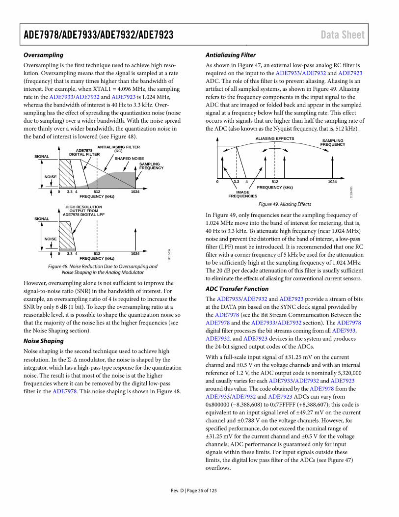
ADE7978/ADE7933/ADE7932/ADE7923 Data Sheet
Rev. D | Page 36 of 125
Oversampling
Oversampling is the first technique used to achieve high reso-lution. Oversampling means that the signal is sampled at a rate (frequency) that is many times higher than the bandwidth of interest. For example, when XTAL1 = 4.096 MHz, the sampling rate in the ADE7933/ADE7932 and ADE7923 is 1.024 MHz, whereas the bandwidth of interest is 40 Hz to 3.3 kHz. Over-sampling has the effect of spreading the quantization noise (noise due to sampling) over a wider bandwidth. With the noise spread more thinly over a wider bandwidth, the quantization noise in the band of interest is lowered (see Figure 48).
NOISE
SIGNAL
NOISE
SIGNAL
0 3.3 4 512FREQUENCY (kHz)
HIGH RESOLUTIONOUTPUT FROM
ADE7978 DIGITAL LPF
1024
0 3.3 4 512FREQUENCY (kHz)
1024
ADE7978DIGITAL FILTER
SHAPED NOISE
ANTIALIASING FILTER(RC)
SAMPLINGFREQUENCY
1111
6-03
4
Figure 48. Noise Reduction Due to Oversampling and
Noise Shaping in the Analog Modulator
However, oversampling alone is not sufficient to improve the signal-to-noise ratio (SNR) in the bandwidth of interest. For example, an oversampling ratio of 4 is required to increase the SNR by only 6 dB (1 bit). To keep the oversampling ratio at a reasonable level, it is possible to shape the quantization noise so that the majority of the noise lies at the higher frequencies (see the Noise Shaping section).
Noise Shaping
Noise shaping is the second technique used to achieve high resolution. In the Σ-∆ modulator, the noise is shaped by the integrator, which has a high-pass type response for the quantization noise. The result is that most of the noise is at the higher frequencies where it can be removed by the digital low-pass filter in the ADE7978. This noise shaping is shown in Figure 48.
Antialiasing Filter
As shown in Figure 47, an external low-pass analog RC filter is required on the input to the ADE7933/ADE7932 and ADE7923 ADC. The role of this filter is to prevent aliasing. Aliasing is an artifact of all sampled systems, as shown in Figure 49. Aliasing refers to the frequency components in the input signal to the ADC that are imaged or folded back and appear in the sampled signal at a frequency below half the sampling rate. This effect occurs with signals that are higher than half the sampling rate of the ADC (also known as the Nyquist frequency, that is, 512 kHz).
ALIASING EFFECTS SAMPLINGFREQUENCY
IMAGEFREQUENCIES
0 3.3 4 512FREQUENCY (kHz)
1024
1111
6-03
5
Figure 49. Aliasing Effects
In Figure 49, only frequencies near the sampling frequency of 1.024 MHz move into the band of interest for metering, that is, 40 Hz to 3.3 kHz. To attenuate high frequency (near 1.024 MHz) noise and prevent the distortion of the band of interest, a low-pass filter (LPF) must be introduced. It is recommended that one RC filter with a corner frequency of 5 kHz be used for the attenuation to be sufficiently high at the sampling frequency of 1.024 MHz. The 20 dB per decade attenuation of this filter is usually sufficient to eliminate the effects of aliasing for conventional current sensors.
ADC Transfer Function
The ADE7933/ADE7932 and ADE7923 provide a stream of bits at the DATA pin based on the SYNC clock signal provided by the ADE7978 (see the Bit Stream Communication Between the ADE7978 and the ADE7933/ADE7932 section). The ADE7978 digital filter processes the bit streams coming from all ADE7933, ADE7932, and ADE7923 devices in the system and produces the 24-bit signed output codes of the ADCs.
With a full-scale input signal of ±31.25 mV on the current channel and ±0.5 V on the voltage channels and with an internal reference of 1.2 V, the ADC output code is nominally 5,320,000 and usually varies for each ADE7933/ADE7932 and ADE7923 around this value. The code obtained by the ADE7978 from the ADE7933/ADE7932 and ADE7923 ADCs can vary from 0x800000 (−8,388,608) to 0x7FFFFF (+8,388,607); this code is equivalent to an input signal level of ±49.27 mV on the current channel and ±0.788 V on the voltage channels. However, for specified performance, do not exceed the nominal range of ±31.25 mV for the current channel and ±0.5 V for the voltage channels; ADC performance is guaranteed only for input signals within these limits. For input signals outside these limits, the digital low pass filter of the ADCs (see Figure 47) overflows.
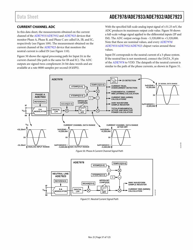
Data Sheet ADE7978/ADE7933/ADE7932/ADE7923
Rev. D | Page 37 of 125
CURRENT CHANNEL ADC In this data sheet, the measurements obtained on the current channel of the ADE7933/ADE7932 and ADE7923 devices that monitor Phase A, Phase B, and Phase C are called IA, IB, and IC, respectively (see Figure 109). The measurement obtained on the current channel of the ADE7923 device that monitors the neutral current is called IN (see Figure 110).
Figure 50 shows the signal processing path for Input IA in the current channel (the path is the same for IB and IC). The ADC outputs are signed twos complement 24-bit data-words and are available at a rate 8000 samples per second (8 kSPS).
With the specified full-scale analog input signal of ±31.25 mV, the ADC produces its maximum output code value. Figure 50 shows a full-scale voltage signal applied to the differential inputs (IP and IM). The ADC output swings from −5,320,000 to +5,320,000. Note that these are nominal values, and every ADE7978/ ADE7933/ADE7932/ADE7923 chipset varies around these values.
Input IN corresponds to the neutral current of a 3-phase system. If the neutral line is not monitored, connect the DATA_N pin of the ADE7978 to VDD. The datapath of the neutral current is similar to the path of the phase currents, as shown in Figure 51.
AIGAIN[23:0]HPFEN BITCONFIG[4]
HPF
+31.25mV
ANALOG INPUT RANGE
0V
–31.25mV
0x512D40 =+5,320,000
CURRENT CHANNEL DATA RANGE
ADC OUTPUT RANGE
0V
0xFFAED2C0 =–5,320,000
0x512D40 =+5,320,000
CURRENT CHANNEL DATA RANGEAFTER HPF
0V
0xFFAED2C0 =–5,320,000
TOTAL/FUNDAMENTALACTIVE AND REACTIVEPOWER CALCULATION
CURRENT PEAK,OVERCURRENT DETECTION
FUNDAMENTAL CURRENTRMS (AFIRMS) CALCULATION
CURRENT RMS (AIRMS)CALCULATIONS
IAWV WAVEFORMSAMPLE REGISTER
ZX DETECTIONLPF1
REFERENCE
PHASE AADE7933
Σ-ΔMODULATOR
IP
VIN
VIN
IM
DIGITALLPF
ATEMP[23:0]
ATEMP0[23:0]
TEMPCO[23:0]
1
ADE7978
0x512D40 =+5,320,000
ZX SIGNAL DATA RANGE
0V
0xFFAED2C0 =–5,320,000
1111
6-03
6
Figure 50. Phase A Current Channel Signal Path
NIGAIN[23:0]HPFEN BITCONFIG[4]
HPFCURRENT RMS (NIRMS)CALCULATION
INWV WAVEFORMSAMPLE REGISTER
REFERENCE
NEUTRAL LINEADE7923
Σ-ΔMODULATOR
IP
VIN
IM
DIGITALLPF
NTEMP[23:0]
NTEMP0[23:0]
TEMPCO[23:0]
1
ADE7978
1111
6-24
5
Figure 51. Neutral Current Signal Path
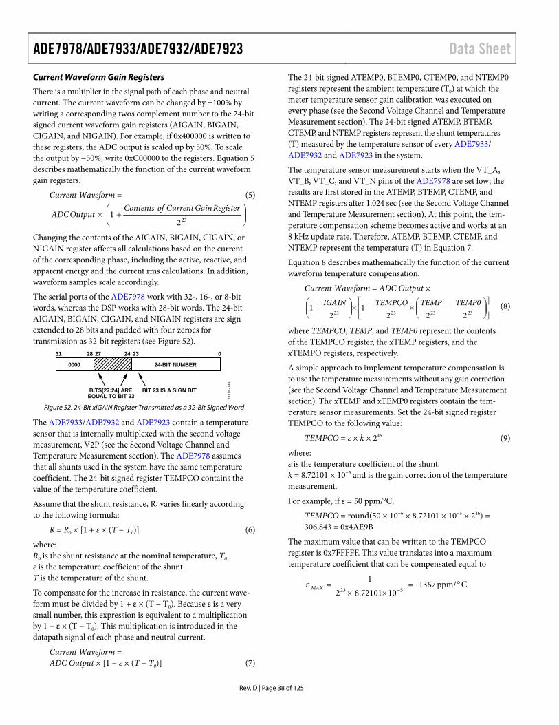
ADE7978/ADE7933/ADE7932/ADE7923 Data Sheet
Rev. D | Page 38 of 125
Current Waveform Gain Registers
There is a multiplier in the signal path of each phase and neutral current. The current waveform can be changed by ±100% by writing a corresponding twos complement number to the 24-bit signed current waveform gain registers (AIGAIN, BIGAIN, CIGAIN, and NIGAIN). For example, if 0x400000 is written to these registers, the ADC output is scaled up by 50%. To scale the output by −50%, write 0xC00000 to the registers. Equation 5 describes mathematically the function of the current waveform gain registers.
Current Waveform = (5)
+×
2321
RegisterGainCurrentofContentsOutputADC
Changing the contents of the AIGAIN, BIGAIN, CIGAIN, or NIGAIN register affects all calculations based on the current of the corresponding phase, including the active, reactive, and apparent energy and the current rms calculations. In addition, waveform samples scale accordingly.
The serial ports of the ADE7978 work with 32-, 16-, or 8-bit words, whereas the DSP works with 28-bit words. The 24-bit AIGAIN, BIGAIN, CIGAIN, and NIGAIN registers are sign extended to 28 bits and padded with four zeroes for transmission as 32-bit registers (see Figure 52).
31 28 27 24 23 0
24-BIT NUMBER0000
BITS[27:24] AREEQUAL TO BIT 23
BIT 23 IS A SIGN BIT
1111
6-03
8
Figure 52. 24-Bit xIGAIN Register Transmitted as a 32-Bit Signed Word
The ADE7933/ADE7932 and ADE7923 contain a temperature sensor that is internally multiplexed with the second voltage measurement, V2P (see the Second Voltage Channel and Temperature Measurement section). The ADE7978 assumes that all shunts used in the system have the same temperature coefficient. The 24-bit signed register TEMPCO contains the value of the temperature coefficient.
Assume that the shunt resistance, R, varies linearly according to the following formula:
R = R0 × [1 + ε × (T − T0)] (6)
where: R0 is the shunt resistance at the nominal temperature, T0. ε is the temperature coefficient of the shunt. T is the temperature of the shunt.
To compensate for the increase in resistance, the current wave-form must be divided by 1 + ε × (T − T0). Because ε is a very small number, this expression is equivalent to a multiplication by 1 − ε × (T − T0). This multiplication is introduced in the datapath signal of each phase and neutral current.
Current Waveform = ADC Output × [1 − ε × (T − T0)] (7)
The 24-bit signed ATEMP0, BTEMP0, CTEMP0, and NTEMP0 registers represent the ambient temperature (T0) at which the meter temperature sensor gain calibration was executed on every phase (see the Second Voltage Channel and Temperature Measurement section). The 24-bit signed ATEMP, BTEMP, CTEMP, and NTEMP registers represent the shunt temperatures (T) measured by the temperature sensor of every ADE7933/ ADE7932 and ADE7923 in the system.
The temperature sensor measurement starts when the VT_A, VT_B, VT_C, and VT_N pins of the ADE7978 are set low; the results are first stored in the ATEMP, BTEMP, CTEMP, and NTEMP registers after 1.024 sec (see the Second Voltage Channel and Temperature Measurement section). At this point, the tem-perature compensation scheme becomes active and works at an 8 kHz update rate. Therefore, ATEMP, BTEMP, CTEMP, and NTEMP represent the temperature (T) in Equation 7.
Equation 8 describes mathematically the function of the current waveform temperature compensation.
Current Waveform = ADC Output ×
−×−×
+
23232323 2221
21 TEMP0TEMPTEMPCOIGAIN (8)
where TEMPCO, TEMP, and TEMP0 represent the contents of the TEMPCO register, the xTEMP registers, and the xTEMPO registers, respectively.
A simple approach to implement temperature compensation is to use the temperature measurements without any gain correction (see the Second Voltage Channel and Temperature Measurement section). The xTEMP and xTEMP0 registers contain the tem-perature sensor measurements. Set the 24-bit signed register TEMPCO to the following value:
TEMPCO = ε × k × 246 (9)
where: ε is the temperature coefficient of the shunt. k = 8.72101 × 10⁻⁵ and is the gain correction of the temperature measurement.
For example, if ε = 50 ppm/°C,
TEMPCO = round(50 × 10−6 × 8.72101 × 10−5 × 246) = 306,843 = 0x4AE9B
The maximum value that can be written to the TEMPCO register is 0x7FFFFF. This value translates into a maximum temperature coefficient that can be compensated equal to
Cppm/13671072101.82
1523
°=××
=ε−MAX
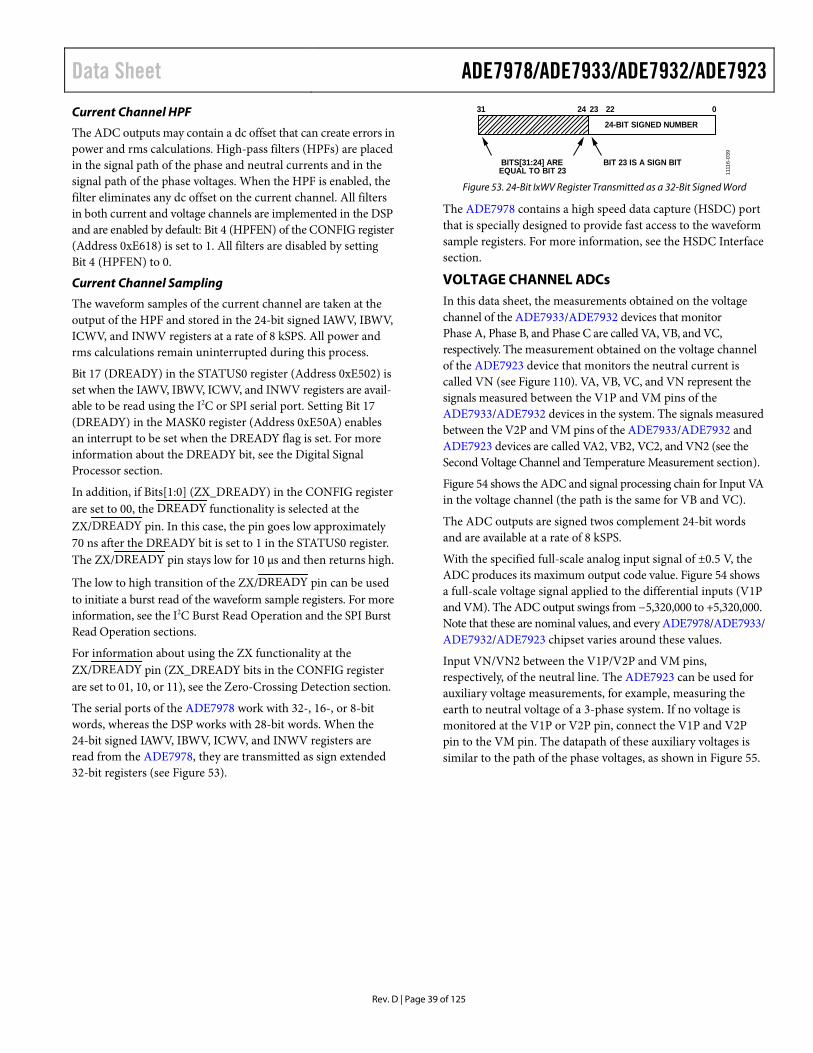
Data Sheet ADE7978/ADE7933/ADE7932/ADE7923
Rev. D | Page 39 of 125
Current Channel HPF
The ADC outputs may contain a dc offset that can create errors in power and rms calculations. High-pass filters (HPFs) are placed in the signal path of the phase and neutral currents and in the signal path of the phase voltages. When the HPF is enabled, the filter eliminates any dc offset on the current channel. All filters in both current and voltage channels are implemented in the DSP and are enabled by default: Bit 4 (HPFEN) of the CONFIG register (Address 0xE618) is set to 1. All filters are disabled by setting Bit 4 (HPFEN) to 0.
Current Channel Sampling
The waveform samples of the current channel are taken at the output of the HPF and stored in the 24-bit signed IAWV, IBWV, ICWV, and INWV registers at a rate of 8 kSPS. All power and rms calculations remain uninterrupted during this process.
Bit 17 (DREADY) in the STATUS0 register (Address 0xE502) is set when the IAWV, IBWV, ICWV, and INWV registers are avail-able to be read using the I2C or SPI serial port. Setting Bit 17 (DREADY) in the MASK0 register (Address 0xE50A) enables an interrupt to be set when the DREADY flag is set. For more information about the DREADY bit, see the Digital Signal Processor section.
In addition, if Bits[1:0] (ZX_DREADY) in the CONFIG register are set to 00, the DREADY functionality is selected at the ZX/DREADY pin. In this case, the pin goes low approximately 70 ns after the DREADY bit is set to 1 in the STATUS0 register. The ZX/DREADY pin stays low for 10 µs and then returns high.
The low to high transition of the ZX/DREADY pin can be used to initiate a burst read of the waveform sample registers. For more information, see the I2C Burst Read Operation and the SPI Burst Read Operation sections.
For information about using the ZX functionality at the ZX/DREADY pin (ZX_DREADY bits in the CONFIG register are set to 01, 10, or 11), see the Zero-Crossing Detection section.
The serial ports of the ADE7978 work with 32-, 16-, or 8-bit words, whereas the DSP works with 28-bit words. When the 24-bit signed IAWV, IBWV, ICWV, and INWV registers are read from the ADE7978, they are transmitted as sign extended 32-bit registers (see Figure 53).
31 24 23 22 0
24-BIT SIGNED NUMBER
BITS[31:24] AREEQUAL TO BIT 23
BIT 23 IS A SIGN BIT
1111
6-03
9
Figure 53. 24-Bit IxWV Register Transmitted as a 32-Bit Signed Word
The ADE7978 contains a high speed data capture (HSDC) port that is specially designed to provide fast access to the waveform sample registers. For more information, see the HSDC Interface section.
VOLTAGE CHANNEL ADCs In this data sheet, the measurements obtained on the voltage channel of the ADE7933/ADE7932 devices that monitor Phase A, Phase B, and Phase C are called VA, VB, and VC, respectively. The measurement obtained on the voltage channel of the ADE7923 device that monitors the neutral current is called VN (see Figure 110). VA, VB, VC, and VN represent the signals measured between the V1P and VM pins of the ADE7933/ADE7932 devices in the system. The signals measured between the V2P and VM pins of the ADE7933/ADE7932 and ADE7923 devices are called VA2, VB2, VC2, and VN2 (see the Second Voltage Channel and Temperature Measurement section).
Figure 54 shows the ADC and signal processing chain for Input VA in the voltage channel (the path is the same for VB and VC).
The ADC outputs are signed twos complement 24-bit words and are available at a rate of 8 kSPS.
With the specified full-scale analog input signal of ±0.5 V, the ADC produces its maximum output code value. Figure 54 shows a full-scale voltage signal applied to the differential inputs (V1P and VM). The ADC output swings from −5,320,000 to +5,320,000. Note that these are nominal values, and every ADE7978/ADE7933/ ADE7932/ADE7923 chipset varies around these values.
Input VN/VN2 between the V1P/V2P and VM pins, respectively, of the neutral line. The ADE7923 can be used for auxiliary voltage measurements, for example, measuring the earth to neutral voltage of a 3-phase system. If no voltage is monitored at the V1P or V2P pin, connect the V1P and V2P pin to the VM pin. The datapath of these auxiliary voltages is similar to the path of the phase voltages, as shown in Figure 55.
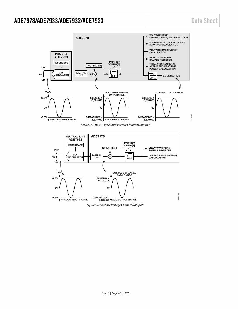
ADE7978/ADE7933/ADE7932/ADE7923 Data Sheet
Rev. D | Page 40 of 125
AVGAIN[23:0]HPFEN BITCONFIG[4]
HPF
+0.5V
ANALOG INPUT RANGE
0V
–0.5V
0x512D40 =+5,320,000
VOLTAGE CHANNELDATA RANGE
ADC OUTPUT RANGE
0V
0xFFAED2C0 =–5,320,000
0x512D40 =+5,320,000
ZX SIGNAL DATA RANGE
0V
0xFFAED2C0 =–5,320,000
TOTAL/FUNDAMENTALACTIVE AND REACTIVEPOWER CALCULATION
FUNDAMENTAL VOLTAGE RMS(AFVRMS) CALCULATION
VOLTAGE RMS (AVRMS)CALCULATION
VAWV WAVEFORMSAMPLE REGISTER
VOLTAGE PEAK,OVERVOLTAGE, SAG DETECTION
ZX DETECTIONLPF1
REFERENCE
PHASE AADE7933
Σ-ΔMODULATOR
V1P
VIN
VM
DIGITALLPF
ADE7978
1111
6-04
0
VIN
Figure 54. Phase A to Neutral Voltage Channel Datapath
NVGAIN[23:0]
HPFEN BITCONFIG[4]
HPF
+0.5V
ANALOG INPUT RANGE
0V
–0.5V
0x512D40 =+5,320,000
VOLTAGE CHANNELDATA RANGE
ADC OUTPUT RANGE 1111
6-24
9
0V
0xFFAED2C0 =–5,320,000
VOLTAGE RMS (NVRMS)CALCULATION
VNWV WAVEFORMSAMPLE REGISTER
REFERENCE
NEUTRAL LINEADE7923
Σ-ΔMODULATOR
V1P
VIN
VM
DIGITALLPF
ADE7978
VIN
Figure 55. Auxiliary Voltage Channel Datapath
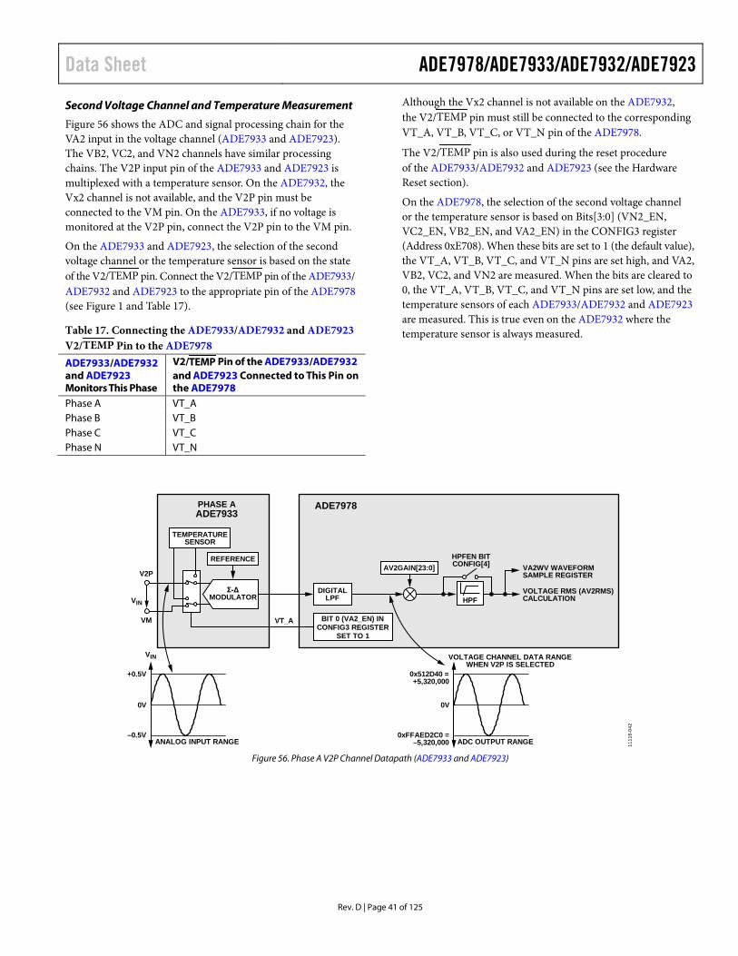
Data Sheet ADE7978/ADE7933/ADE7932/ADE7923
Rev. D | Page 41 of 125
Second Voltage Channel and Temperature Measurement
Figure 56 shows the ADC and signal processing chain for the VA2 input in the voltage channel (ADE7933 and ADE7923). The VB2, VC2, and VN2 channels have similar processing chains. The V2P input pin of the ADE7933 and ADE7923 is multiplexed with a temperature sensor. On the ADE7932, the Vx2 channel is not available, and the V2P pin must be connected to the VM pin. On the ADE7933, if no voltage is monitored at the V2P pin, connect the V2P pin to the VM pin.
On the ADE7933 and ADE7923, the selection of the second voltage channel or the temperature sensor is based on the state of the V2/TEMP pin. Connect the V2/TEMP pin of the ADE7933/ ADE7932 and ADE7923 to the appropriate pin of the ADE7978 (see Figure 1 and Table 17).
Table 17. Connecting the ADE7933/ADE7932 and ADE7923 V2/TEMP Pin to the ADE7978 ADE7933/ADE7932 and ADE7923 Monitors This Phase
V2/TEMP Pin of the ADE7933/ADE7932 and ADE7923 Connected to This Pin on the ADE7978
Phase A VT_A Phase B VT_B Phase C VT_C Phase N VT_N
Although the Vx2 channel is not available on the ADE7932, the V2/TEMP pin must still be connected to the corresponding VT_A, VT_B, VT_C, or VT_N pin of the ADE7978.
The V2/TEMP pin is also used during the reset procedure of the ADE7933/ADE7932 and ADE7923 (see the Hardware Reset section).
On the ADE7978, the selection of the second voltage channel or the temperature sensor is based on Bits[3:0] (VN2_EN, VC2_EN, VB2_EN, and VA2_EN) in the CONFIG3 register (Address 0xE708). When these bits are set to 1 (the default value), the VT_A, VT_B, VT_C, and VT_N pins are set high, and VA2, VB2, VC2, and VN2 are measured. When the bits are cleared to 0, the VT_A, VT_B, VT_C, and VT_N pins are set low, and the temperature sensors of each ADE7933/ADE7932 and ADE7923 are measured. This is true even on the ADE7932 where the temperature sensor is always measured.
+0.5V
ANALOG INPUT RANGE
0V
–0.5V
0x512D40 =+5,320,000
VOLTAGE CHANNEL DATA RANGEWHEN V2P IS SELECTED
ADC OUTPUT RANGE
0V
0xFFAED2C0 =–5,320,000
AV2GAIN[23:0]HPFEN BITCONFIG[4]
HPFVOLTAGE RMS (AV2RMS)CALCULATION
VA2WV WAVEFORMSAMPLE REGISTER
REFERENCE
PHASE AADE7933
Σ-ΔMODULATOR
V2P
VIN
VM
DIGITALLPF
BIT 0 (VA2_EN) INCONFIG3 REGISTER
SET TO 1
ADE7978
TEMPERATURESENSOR
VT_A11
116-
042
VIN
Figure 56. Phase A V2P Channel Datapath (ADE7933 and ADE7923)

ADE7978/ADE7933/ADE7932/ADE7923 Data Sheet
Rev. D | Page 42 of 125
Figure 57 shows the ADC and signal processing chain for the temperature sensor when the ADE7933/ADE7932 monitor Phase A. The temperature measurement is characterized by offset and gain errors. The offset information is calculated during the manufacturing process and is stored with a sign opposite of the calculated sign into the ADE7933/ADE7932 and ADE7923.
The ADE7978 reads the offset information using the bit stream communication (see the Bit Stream Communication Between the ADE7978 and the ADE7933/ADE7932 section for more information). The ADE7978 then stores this information in the 8-bit signed ATEMPOS, BTEMPOS, CTEMPOS, and NTEMPOS registers. The offset information is shifted left by 11 bits before it is added to the temperature datapath.
The 24-bit signed temperature gain registers (ATGAIN, BTGAIN, CTGAIN, and NTGAIN) can be used for gain compensation to change the temperature waveform by ±100%. For example, if 0x400000 is written to these registers, the ADC output is scaled up by 50%. To scale the output by −50%, write 0xC00000 to the registers. Equation 10 describes mathematically the function of the temperature waveform gain registers.
Temperature Waveform = (10)
ADC Output ×
+
2321
Register GainTemp of Contents
The temperature measurements are also used in the current channel datapath for the temperature compensation of the current gain (see the Current Waveform Gain Registers section). A simple approach to implement the temperature measurement is to leave the temperature gain registers at their default values so that the temperature compensation path uses the temperature measurements without any gain correction.
The temperature measurement results are stored in the 24-bit signed ATEMP, BTEMP, CTEMP, and NTEMP registers 1.024 sec after the temperature sensor measurement is started by setting the VT_A, VT_B, VT_C, and VT_N pins low. These registers are updated at an 8 kSPS rate. The VT_A, VT_B, VT_C, and VT_N pins must be kept low for at least 1.024 sec for the temperature measurement results to be stored in the ATEMP, BTEMP, CTEMP, and NTEMP registers.
The microcontroller can obtain the temperature measurements expressed in °C units by applying the following formula:
Temperature(°C) = 8.72101 × 10⁻⁵ × TEMP − 306.47 (11)
The serial ports of the ADE7978 work with 32-, 16-, or 8-bit words, whereas the DSP works with 28-bit words. Like the SAGLVL register shown in Figure 69, the 24-bit signed ATEMP, BTEMP, CTEMP, and NTEMP registers are transmitted as 32-bit registers with the eight MSBs padded with zeroes.
AIGAIN TEMPERATURECOMPENSATION
ATEMP TEMPERATURERANGE
DIGITALLPF
DIGITAL LPFWITH 10HzCORNER
BIT 0 (VA2_EN) INCONFIG3 REGISTER
CLEARED TO 0
ADE7978
VT_A
0V
+0.2472V
VIN
TEMPERATURE SENSOR CHARACTERISTIC
+0.3672V
+0.3098V
+25°C +85°C–40°C0V
3,055,500
4,488,800
3,800,800
VOLTAGE CHANNEL DATA RANGEWHEN TEMPERATURE SENSOR IS SELECTED
+25°C +85°C–40°C
ATEMPOS[7:0]
211
ATGAIN[23:0]
1111
6-04
3
REFERENCE
PHASE AADE7933
Σ-ΔMODULATOR
V2P
VIN
VM
TEMPERATURESENSOR
Figure 57. Temperature Measurement Datapath
Data Sheet ADE7978/ADE7933/ADE7932/ADE7923
Rev. D | Page 43 of 125
Voltage Waveform Gain Registers
There is a multiplier in the signal path of each phase voltage. The voltage waveform can be changed by ±100% by writing a corresponding twos complement number to the 24-bit signed voltage waveform gain registers (AVGAIN, AV2GAIN, BVGAIN, BV2GAIN, CVGAIN, CV2GAIN, NVGAIN, and NV2GAIN). For example, if 0x400000 is written to these registers, the ADC output is scaled up by 50%. To scale the output by −50%, write 0xC00000 to the registers. Equation 12 describes mathematically the function of the voltage waveform gain registers.
Voltage Waveform = ADC Output ×
+
2321
Register GainVoltage of Contents (12)
Changing the contents of the AVGAIN, AV2GAIN, BVGAIN, BV2GAIN, CVGAIN, CV2GAIN, NVGAIN, or NV2GAIN register affects all calculations based on the voltage of the corresponding phase, including the active, reactive, and apparent energy and the voltage rms calculations. In addition, waveform samples scale accordingly.
The serial ports of the ADE7978 work with 32-, 16-, or 8-bit words, whereas the DSP works with 28-bit words. Like the xIGAIN registers shown in Figure 52, the AVGAIN, AV2GAIN, BVGAIN, BV2GAIN, CVGAIN, CV2GAIN, NVGAIN, and NV2GAIN registers are sign extended to 28 bits and padded with four 0s for transmission as 32-bit registers.
Voltage Channel HPF
The ADC outputs may contain a dc offset that can create errors in power and rms calculations. High-pass filters (HPFs) are placed in the signal path of the phase voltages and the phase and neutral currents. When the HPF is enabled, the filter eliminates any dc offset on the voltage channel. All filters in both voltage and current channels are implemented in the DSP and are enabled by default: Bit 4 (HPFEN) of the CONFIG register (Address 0xE618) is set to 1. All filters are disabled by setting Bit 4 (HPFEN) to 0.
Voltage Channel Sampling
The waveform samples of the voltage channels are taken at the output of the HPF and are stored in the 24-bit signed VAWV, VA2WV, VBWV, VB2WV, VCWV, VC2WV, VNWV, and VN2WV registers at a rate of 8 kSPS. All power and rms calculations remain uninterrupted during this process.
Bit 17 (DREADY) in the STATUS0 register (Address 0xE502) is set when the VAWV, VA2WV, VBWV, VB2WV, VCWV, VC2WV, VNWV, and VN2WV registers are available to be read using the I2C or SPI serial port. Setting Bit 17 (DREADY) in the MASK0 register (Address 0xE50A) enables an interrupt to be set when the DREADY flag is set. For more information about the DREADY bit, see the Digital Signal Processor section.
In addition, if Bits[1:0] (ZX_DREADY) in the CONFIG register are set to 00, the DREADY functionality is selected at the ZX/DREADY pin. In this case, the pin goes low approximately 70 ns after the DREADY bit is set to 1 in the STATUS0 register. The ZX/DREADY pin stays low for 10 µs and then returns high.
The low to high transition of the ZX/DREADY pin can be used to initiate a burst read of the waveform sample registers. For more information, see the I2C Burst Read Operation and the SPI Burst Read Operation sections.
For information about using the ZX functionality at the ZX/DREADY pin (ZX_DREADY bits in the CONFIG register are set to 01, 10, or 11), see the Zero-Crossing Detection section.
The serial ports of the ADE7978 work with 32-, 16-, or 8-bit words, whereas the DSP works with 28-bit words. Like the IxWV registers shown in Figure 53, the 24-bit signed VAWV, VA2WV, VBWV, VB2WV, VCWV, VC2WV, VNWV, and VN2WV registers are transmitted as sign extended 32-bit registers.
The ADE7978 contains a high speed data capture (HSDC) port that is specially designed to provide fast access to the waveform sample registers. For more information, see the HSDC Interface section.

ADE7978/ADE7933/ADE7932/ADE7923 Data Sheet
Rev. D | Page 44 of 125
CHANGING THE PHASE VOLTAGE DATAPATH The ADE7978 can direct one phase voltage input to the compu-tational datapath of another phase. For example, the Phase A voltage can be introduced into the Phase B computational data-path, which means that all powers computed by the ADE7978 in Phase B are based on the Phase A voltage and the Phase B current. Table 18 lists the settings of the VTOIA[1:0] bits and the configured phase voltage directed to the Phase A computational datapath.
Table 18. VTOIA[1:0] Bit Settings (CONFIG Register, Bits[9:8])
VTOIA[1:0] Bits Voltage Directed to the Phase A Computational Datapath
00 (Default) Phase A voltage 01 Phase B voltage 10 Phase C voltage 11 Phase A voltage
Table 19 lists the settings of the VTOIB[1:0] bits and the configured phase voltage directed to the Phase B computational datapath.
Table 19. VTOIB[1:0] Bit Settings (CONFIG Register, Bits[11:10])
VTOIB[1:0] Bits Voltage Directed to the Phase B Computational Datapath
00 (Default) Phase B voltage 01 Phase C voltage 10 Phase A voltage 11 Phase B voltage
Table 20 lists the settings of the VTOIC[1:0] bits and the con-figured phase voltage directed to the Phase C computational datapath.
Table 20. VTOIC[1:0] Bit Settings (CONFIG Register, Bits[13:12])
VTOIC[1:0] Bits Voltage Directed to the Phase C Computational Datapath
00 (Default) Phase C voltage 01 Phase A voltage 10 Phase B voltage 11 Phase C voltage
Figure 58 shows the Phase A voltage used in the Phase B data-path, the Phase B voltage used in the Phase C datapath, and the Phase C voltage used in the Phase A datapath.
IA
VA
IB
VB
IC
VC
PHASE ACOMPUTATIONAL
DATAPATH
PHASE BCOMPUTATIONAL
DATAPATH
PHASE CCOMPUTATIONAL
DATAPATH
VTOIA[1:0] = 10,PHASE C VOLTAGE
DIRECTEDTO PHASE A
VTOIB[1:0] = 10,PHASE A VOLTAGE
DIRECTEDTO PHASE B
VTOIC[1:0] = 10,PHASE B VOLTAGE
DIRECTEDTO PHASE CCPHCAL
BPHCAL
APHCAL
1111
6-04
4
Figure 58. Phase Voltages Used in Different Datapaths
REFERENCE CIRCUITS The nominal reference voltage at the REF pin of the ADE7933/ ADE7932 and ADE7923 is 1.2 V. This reference voltage is used for the ADCs. Because the on-chip dc-to-dc converter in the ADE7933/ADE7932 cannot supply external loads, the REF pin cannot be overdriven by a standalone external voltage reference. The ADE7923 does not have an on-chip dc-to-dc converter.
The voltage of the ADE7933/ADE7932 and ADE7923 reference drifts slightly with temperature. Table 6 and Table 10 specify the gain drift over temperature for each ADC channel. The gain drift includes the temperature variation of the ADC gain, together with the temperature variation of the internal voltage reference. The value of the gain temperature drift varies from device to device.
Because the energy calculation uses two ADC channels, one for the current and one for the voltage, any x% drift in the gain results in a 2x% deviation of the meter accuracy. The reference drift resulting from temperature changes is usually very small and is typically much smaller than the drift of other components on a meter. As an alternative, the meter can be calibrated at multiple temperatures.
The VA2, VB2, VC2, and VN2 voltages and the temperature sensor use the third ADC of the ADE7933/ADE7932 and ADE7923, so any x% drift in the gain results in an x% deviation of these measurements.

Data Sheet ADE7978/ADE7933/ADE7932/ADE7923
Rev. D | Page 45 of 125
PHASE COMPENSATION Typically, phase compensation is not needed in the ADE7978/ ADE7933/ADE7932 and ADE7923 chipset. As described in the Current Channel ADC section and the Voltage Channel ADC section, the same datapath is used for the phase current and phase voltages; therefore, no phase error exists between the phase current and voltage signals introduced by the ADE7978. In addition, shunts are used with the ADE7933/ADE7932 and ADE7923 devices to sense the phase currents, eliminating the need for phase compensation.
The ADE7978 provides a means of digitally calibrating eventual phase mismatch errors. The ADE7978 allows a small time delay or time advance to be introduced into the signal processing chain to compensate for the small phase errors.
The 10-bit phase calibration registers (APHCAL, BPHCAL, and CPHCAL) can vary the time advance in the voltage channel signal path from −374.0 µs to +374.0 µs. Negative values written to the xPHCAL registers represent a time advance, whereas positive values represent a time delay. One LSB is equivalent to 0.976 µs of time delay or time advance (assuming a clock rate of 1.024 MHz). With a line frequency of 60 Hz, this calibration gives a phase reso-lution of 0.0211° (360° × 60 Hz/1.024 MHz) at the fundamental and corresponds to a total correction range of −8.079° to +8.079° at 60 Hz. With a line frequency of 50 Hz, the correction range is −6.732° to +6.732°, and the resolution is 0.0176° (360° × 50 Hz/1.024 MHz).
Given a phase error of x degrees, measured using the phase voltage as the reference, the corresponding LSBs are computed by dividing x by the phase resolution (0.0211°/LSB for 60 Hz
and 0.0176°/LSB for 50 Hz). Only results from −383 to +383 are allowed; values outside this range are not allowed.
If the current leads the voltage, the result is negative, and the absolute value is written to the xPHCAL registers. If the current lags the voltage, the result is positive and 512 is added to the result before it is written to the xPHCAL registers.
APHCAL, BPHCAL, or CHPCAL = (13)
>+
≤
0,512
0,
xResolutionPhase
x
xResolutionPhase
x
Figure 60 illustrates the use of phase compensation to remove an x = −1° phase lead in IA of the current channel from the external current transducer (equivalent of 55.5 µs for 50 Hz systems). To cancel the lead (1°) in the current channel of Phase A, a phase lead must be introduced into the corresponding voltage channel. Using Equation 13, APHCAL is 57 LSBs, rounded up from 56.8. The phase lead is achieved by introducing a time delay of 55.73 µs into the Phase A current.
The serial ports of the ADE7978 work with 32-, 16-, or 8-bit words, whereas the DSP works with 28-bit words. As shown in Figure 59, the 10-bit APHCAL, BPHCAL, and CPHCAL registers are accessed as 16-bit registers with the six MSBs padded with 0s.
0000 00
15 10 9 0
xPHCAL
1111
6-05
8
Figure 59. 10-Bit xPHCAL Register Transmitted as a 16-Bit Word
1111
6-05
9
PHASE COMPENSATIONACHIEVED DELAYINGIA BY 56µs
50Hz
1°
VA
IA
VA
IA
Σ-ΔMODULATOR
IP
IM
IA
Σ-ΔMODULATOR
V1P
VM
VA
PHASE AADE7933 ADE7978
PHASECALIBRATIONAPHCAL = 57
Figure 60. Phase Calibration Process
ADE7978/ADE7933/ADE7932/ADE7923 Data Sheet
Rev. D | Page 46 of 125
DIGITAL SIGNAL PROCESSOR The ADE7978 contains a fixed function digital signal processor (DSP) that computes all powers and rms values. The DSP contains program memory ROM and data memory RAM.
Program memory ROM stores the program used for the power and rms computations; the processor executes the program every 8 kHz. The end of the computations is signaled by setting Bit 17 (DREADY) to 1 in the STATUS0 register (Address 0xE502). An interrupt attached to this flag can be enabled by setting Bit 17 (DREADY) in the MASK0 register (Address 0xE50A).
When the interrupt is enabled, the IRQ0 pin is set low and the DREADY status bit is set to 1 at the end of the computations. The status bit is cleared and the IRQ0 pin returns high when a 1 is written to Bit 17 (DREADY) in the STATUS0 register.
In addition, when Bits[1:0] (ZX_DREADY) in the CONFIG register (Address 0xE618) are set to 00, the DREADY functionality is selected at the ZX/DREADY pin. In this case, the ZX/DREADY pin goes low approximately 70 ns after the DREADY bit is set to 1 in the STATUS0 register. The ZX/DREADY pin stays low for 10 µs and then returns high.
The low to high transition of the ZX/DREADY pin can be used to initiate a burst read of the waveform sample registers. For more information, see the I2C Burst Read Operation and the SPI Burst Read Operation sections. For information about using the ZX functionality at the ZX/DREADY pin (ZX_DREADY bits in the CONFIG register are set to 01, 10, or 11), see the Zero-Crossing Detection section.
The registers used as inputs by the DSP are located in the data memory RAM at addresses from 0x4380 to 0x43BF. The width of this memory is 28 bits. Within the DSP core, the DSP contains a two-stage pipeline. This means that when a single register must be initialized, two more writes are required to ensure that the value is written into RAM, and if two or more registers must be initialized, the last register must be written two more times to ensure that the values are written into RAM.
At power-up or after a hardware or software reset, the DSP is in idle mode. No instruction is executed. All registers located in the data memory RAM are initialized to 0, their default values, and they can be read or written without any restriction. The run register (Address 0xE228), which is used to start and stop the DSP, is cleared to 0x0000.
The run register must be written with 0x0001 for the DSP to start code execution. Before writing 0x0001 to the run register, it is recommended that all ADE7978 registers located in the data memory RAM be initialized to their desired values. Next, write the last register in the queue two additional times to flush the pipeline, and then write 0x0001 to the run register. In this way, the DSP starts the computations from a desired configuration.
To protect the integrity of the data stored in the data memory RAM of the DSP (addresses from 0x4380 to 0x43BF), a write protection mechanism is available. By default, the protection is disabled and registers located from Address 0x4380 to Address 0x43BF can be written without restriction. When the protection is enabled, no writes to these registers are allowed. Registers can always be read without restriction, independent of the write protection state.
To enable the protection, write 0xAD to the internal 8-bit register located at Address 0xE7FE, followed by a write of 0x80 to the internal 8-bit register located at Address 0xE7E3.
It is recommended that the write protection be enabled after the registers are initialized. If any data memory RAM-based register must be changed, disable the protection, change the value, and then reenable the protection. There is no need to stop the DSP to change these registers.
To disable the protection, write 0xAD to the internal 8-bit register located at Address 0xE7FE, followed by a write of 0x00 to the internal 8-bit register located at Address 0xE7E3.
The recommended procedure for initializing the registers located in the data memory RAM at power-up is described in the Initializing the Chipset section.
In the unlikely event that one or more registers are not initialized correctly, disable the protection by writing 0xAD to the internal 8-bit register located at Address 0xE7FE, followed by a write of 0x00 to the internal 8-bit register located at Address 0xE7E3. Reinitialize the registers, writing the last register in the queue three times. Enable the write protection by writing 0xAD to the internal 8-bit register located at Address 0xE7FE, followed by a write of 0x80 to the internal 8-bit register located at Address 0xE7E3.
There is no obvious reason to stop the DSP. All ADE7978 registers, including the registers located in the data memory RAM, can be modified without stopping the DSP. However, to stop the DSP, 0x0000 must be written to the run register. To restart the DSP, one of the following procedures must be followed:
• If the ADE7978 registers located in the data memory RAM have not been modified, write 0x0001 to the run register to start the DSP.
• If the ADE7978 registers located in the data memory RAM must be modified, execute a software or a hardware reset, initialize all ADE7978 registers at the desired values, enable the write protection, and then write 0x0001 into the run register to start the DSP.
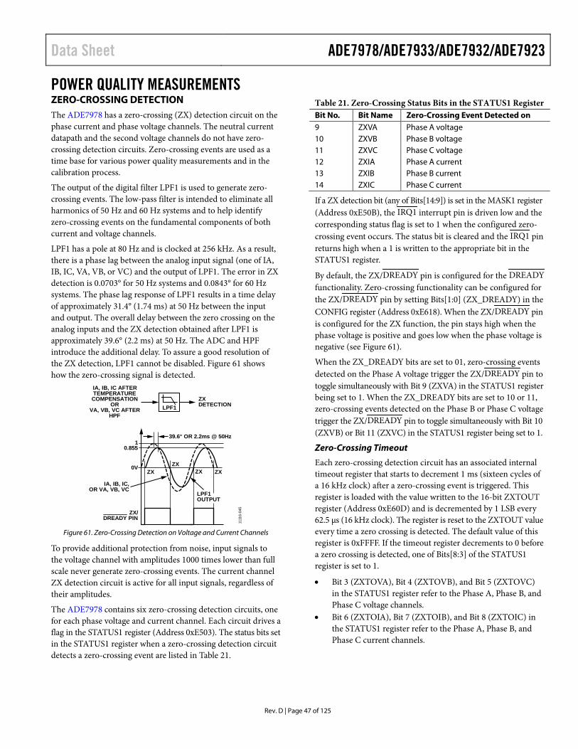
Data Sheet ADE7978/ADE7933/ADE7932/ADE7923
Rev. D | Page 47 of 125
POWER QUALITY MEASUREMENTS ZERO-CROSSING DETECTION The ADE7978 has a zero-crossing (ZX) detection circuit on the phase current and phase voltage channels. The neutral current datapath and the second voltage channels do not have zero-crossing detection circuits. Zero-crossing events are used as a time base for various power quality measurements and in the calibration process.
The output of the digital filter LPF1 is used to generate zero-crossing events. The low-pass filter is intended to eliminate all harmonics of 50 Hz and 60 Hz systems and to help identify zero-crossing events on the fundamental components of both current and voltage channels.
LPF1 has a pole at 80 Hz and is clocked at 256 kHz. As a result, there is a phase lag between the analog input signal (one of IA, IB, IC, VA, VB, or VC) and the output of LPF1. The error in ZX detection is 0.0703° for 50 Hz systems and 0.0843° for 60 Hz systems. The phase lag response of LPF1 results in a time delay of approximately 31.4° (1.74 ms) at 50 Hz between the input and output. The overall delay between the zero crossing on the analog inputs and the ZX detection obtained after LPF1 is approximately 39.6° (2.2 ms) at 50 Hz. The ADC and HPF introduce the additional delay. To assure a good resolution of the ZX detection, LPF1 cannot be disabled. Figure 61 shows how the zero-crossing signal is detected.
IA, IB, IC AFTERTEMPERATURECOMPENSATION
ORVA, VB, VC AFTER
HPF
ZXDETECTIONLPF1
IA, IB, IC,OR VA, VB, VC
39.6° OR 2.2ms @ 50Hz1
0.855
ZX/DREADY PIN
0VZX ZX
ZXZX
LPF1OUTPUT
1111
6-04
5
Figure 61. Zero-Crossing Detection on Voltage and Current Channels
To provide additional protection from noise, input signals to the voltage channel with amplitudes 1000 times lower than full scale never generate zero-crossing events. The current channel ZX detection circuit is active for all input signals, regardless of their amplitudes.
The ADE7978 contains six zero-crossing detection circuits, one for each phase voltage and current channel. Each circuit drives a flag in the STATUS1 register (Address 0xE503). The status bits set in the STATUS1 register when a zero-crossing detection circuit detects a zero-crossing event are listed in Table 21.
Table 21. Zero-Crossing Status Bits in the STATUS1 Register Bit No. Bit Name Zero-Crossing Event Detected on 9 ZXVA Phase A voltage 10 ZXVB Phase B voltage 11 ZXVC Phase C voltage 12 ZXIA Phase A current 13 ZXIB Phase B current 14 ZXIC Phase C current
If a ZX detection bit (any of Bits[14:9]) is set in the MASK1 register (Address 0xE50B), the IRQ1 interrupt pin is driven low and the corresponding status flag is set to 1 when the configured zero-crossing event occurs. The status bit is cleared and the IRQ1 pin returns high when a 1 is written to the appropriate bit in the STATUS1 register.
By default, the ZX/DREADY pin is configured for the DREADY functionality. Zero-crossing functionality can be configured for the ZX/DREADY pin by setting Bits[1:0] (ZX_DREADY) in the CONFIG register (Address 0xE618). When the ZX/DREADY pin is configured for the ZX function, the pin stays high when the phase voltage is positive and goes low when the phase voltage is negative (see Figure 61).
When the ZX_DREADY bits are set to 01, zero-crossing events detected on the Phase A voltage trigger the ZX/DREADY pin to toggle simultaneously with Bit 9 (ZXVA) in the STATUS1 register being set to 1. When the ZX_DREADY bits are set to 10 or 11, zero-crossing events detected on the Phase B or Phase C voltage trigger the ZX/DREADY pin to toggle simultaneously with Bit 10 (ZXVB) or Bit 11 (ZXVC) in the STATUS1 register being set to 1.
Zero-Crossing Timeout
Each zero-crossing detection circuit has an associated internal timeout register that starts to decrement 1 ms (sixteen cycles of a 16 kHz clock) after a zero-crossing event is triggered. This register is loaded with the value written to the 16-bit ZXTOUT register (Address 0xE60D) and is decremented by 1 LSB every 62.5 µs (16 kHz clock). The register is reset to the ZXTOUT value every time a zero crossing is detected. The default value of this register is 0xFFFF. If the timeout register decrements to 0 before a zero crossing is detected, one of Bits[8:3] of the STATUS1 register is set to 1.
• Bit 3 (ZXTOVA), Bit 4 (ZXTOVB), and Bit 5 (ZXTOVC) in the STATUS1 register refer to the Phase A, Phase B, and Phase C voltage channels.
• Bit 6 (ZXTOIA), Bit 7 (ZXTOIB), and Bit 8 (ZXTOIC) in the STATUS1 register refer to the Phase A, Phase B, and Phase C current channels.
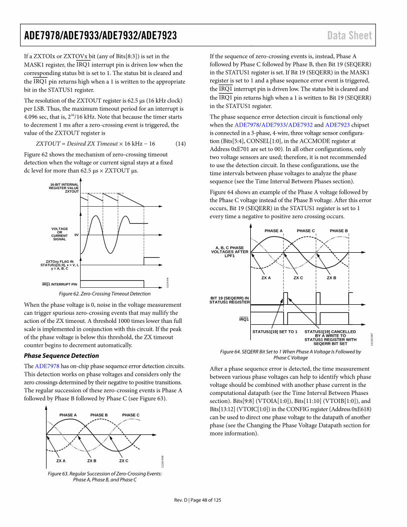
ADE7978/ADE7933/ADE7932/ADE7923 Data Sheet
Rev. D | Page 48 of 125
If a ZXTOIx or ZXTOVx bit (any of Bits[8:3]) is set in the MASK1 register, the IRQ1 interrupt pin is driven low when the corresponding status bit is set to 1. The status bit is cleared and the IRQ1 pin returns high when a 1 is written to the appropriate bit in the STATUS1 register.
The resolution of the ZXTOUT register is 62.5 µs (16 kHz clock) per LSB. Thus, the maximum timeout period for an interrupt is 4.096 sec, that is, 216/16 kHz. Note that because the timer starts to decrement 1 ms after a zero-crossing event is triggered, the value of the ZXTOUT register is
ZXTOUT = Desired ZX Timeout × 16 kHz − 16 (14)
Figure 62 shows the mechanism of zero-crossing timeout detection when the voltage or current signal stays at a fixed dc level for more than 62.5 µs × ZXTOUT µs.
16-BIT INTERNALREGISTER VALUE
ZXTOUT
VOLTAGEOR
CURRENTSIGNAL
IRQ1 INTERRUPT PIN
ZXTOxy FLAG INSTATUS1[31:0], x = V, I,
y = A, B, C
0V
1111
6-04
6
Figure 62. Zero-Crossing Timeout Detection
When the phase voltage is 0, noise in the voltage measurement can trigger spurious zero-crossing events that may nullify the action of the ZX timeout. A threshold 1000 times lower than full scale is implemented in conjunction with this circuit. If the peak of the phase voltage is below this threshold, the ZX timeout counter begins to decrement automatically.
Phase Sequence Detection
The ADE7978 has on-chip phase sequence error detection circuits. This detection works on phase voltages and considers only the zero crossings determined by their negative to positive transitions. The regular succession of these zero-crossing events is Phase A followed by Phase B followed by Phase C (see Figure 63).
ZX CZX B
PHASE B PHASE CPHASE A
ZX A
1111
6-04
8
Figure 63. Regular Succession of Zero-Crossing Events:
Phase A, Phase B, and Phase C
If the sequence of zero-crossing events is, instead, Phase A followed by Phase C followed by Phase B, then Bit 19 (SEQERR) in the STATUS1 register is set. If Bit 19 (SEQERR) in the MASK1 register is set to 1 and a phase sequence error event is triggered, the IRQ1 interrupt pin is driven low. The status bit is cleared and the IRQ1 pin returns high when a 1 is written to Bit 19 (SEQERR) in the STATUS1 register.
The phase sequence error detection circuit is functional only when the ADE7978/ADE7933/ADE7932 and ADE7923 chipset is connected in a 3-phase, 4-wire, three voltage sensor configura-tion (Bits[5:4], CONSEL[1:0], in the ACCMODE register at Address 0xE701 are set to 00). In all other configurations, only two voltage sensors are used; therefore, it is not recommended to use the detection circuit. In these configurations, use the time intervals between phase voltages to analyze the phase sequence (see the Time Interval Between Phases section).
Figure 64 shows an example of the Phase A voltage followed by the Phase C voltage instead of the Phase B voltage. After this error occurs, Bit 19 (SEQERR) in the STATUS1 register is set to 1 every time a negative to positive zero crossing occurs.
ZX BZX C
PHASE C PHASE BPHASE A
A, B, C PHASEVOLTAGES AFTER
LPF1
BIT 19 (SEQERR) INSTATUS1 REGISTER
IRQ1
ZX A
STATUS1[19] SET TO 1 STATUS1[19] CANCELLEDBY A WRITE TO
STATUS1 REGISTER WITHSEQERR BIT SET 11
116-
047
Figure 64. SEQERR Bit Set to 1 When Phase A Voltage Is Followed by
Phase C Voltage
After a phase sequence error is detected, the time measurement between various phase voltages can help to identify which phase voltage should be combined with another phase current in the computational datapath (see the Time Interval Between Phases section). Bits[9:8] (VTOIA[1:0]), Bits[11:10] (VTOIB[1:0]), and Bits[13:12] (VTOIC[1:0]) in the CONFIG register (Address 0xE618) can be used to direct one phase voltage to the datapath of another phase (see the Changing the Phase Voltage Datapath section for more information).
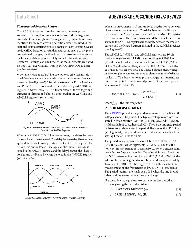
Data Sheet ADE7978/ADE7933/ADE7932/ADE7923
Rev. D | Page 49 of 125
Time Interval Between Phases
The ADE7978 can measure the time delay between phase voltages, between phase currents, or between the voltages and currents of the same phase. The negative to positive transitions identified by the zero-crossing detection circuit are used as the start and stop measuring points. Because the zero-crossing events are identified based on the fundamental components of the phase currents and voltages, the time interval measurements relate to the fundamental components. Only one set of time delay meas-urements is available at one time; these measurements are based on Bits[10:9] (ANGLESEL[1:0]) in the COMPMODE register (Address 0xE60E).
When the ANGLESEL[1:0] bits are set to 00 (the default value), the delays between voltages and currents on the same phase are measured (see Figure 65). The delay between the Phase A voltage and Phase A current is stored in the 16-bit unsigned ANGLE0 register (Address 0xE601). The delays between the voltages and currents of Phase B and Phase C are stored in the ANGLE1 and ANGLE2 registers, respectively.
PHASE ACURRENT
ANGLE0
PHASE AVOLTAGE
1111
6-04
9
Figure 65. Delay Between Phase A Voltage and Phase A Current Is
Stored in the ANGLE0 Register
When the ANGLESEL[1:0] bits are set to 01, the delays between phase voltages are measured. The delay between the Phase A volt-age and the Phase C voltage is stored in the ANGLE0 register. The delay between the Phase B voltage and the Phase C voltage is stored in the ANGLE1 register, and the delay between the Phase A voltage and the Phase B voltage is stored in the ANGLE2 register (see Figure 66).
PHASE B PHASE CPHASE A
ANGLE2
ANGLE0
ANGLE1
1111
6-05
0
Figure 66. Delays Between Phase Voltages or Phase Currents
When the ANGLESEL[1:0] bits are set to 10, the delays between phase currents are measured. The delay between the Phase A current and the Phase C current is stored in the ANGLE0 register, the delay between the Phase B current and the Phase C current is stored in the ANGLE1 register, and the delay between the Phase A current and the Phase B current is stored in the ANGLE2 register (see Figure 66).
The ANGLE0, ANGLE1, and ANGLE2 registers are 16-bit unsigned registers with 1 LSB corresponding to 3.90625 µs (256 kHz clock), which means a resolution of 0.0703° (360° × 50 Hz/256 kHz) for 50 Hz systems and 0.0843° (360° × 60 Hz/ 256 kHz) for 60 Hz systems. The delays between phase voltages or between phase currents are used to characterize how balanced the load is. The delays between phase voltages and currents are used to compute the fundamental power factor on each phase, as shown in Equation 15.
cosφx = cos
××
kHz256
360 LINEfANGLEx
(15)
where fLINE is the line frequency.
PERIOD MEASUREMENT The ADE7978 provides the period measurement of the line in the voltage channel. The period of each phase voltage is measured and stored in three registers: APERIOD, BPERIOD, and CPERIOD (Address 0xE905 to Address 0xE907). The 16-bit unsigned period registers are updated every line period. Because of the LPF1 filter (see Figure 61), the period measurement becomes stable after a settling time of 30 ms to 40 ms.
The period measurement has a resolution of 3.90625 µs/LSB (256 kHz clock), which represents 0.0195% (50 Hz/256 kHz) when the line frequency is 50 Hz and 0.0234% (60 Hz/256 kHz) when the line frequency is 60 Hz. The value of the period registers for 50 Hz networks is approximately 5120 (256 kHz/50 Hz); the value of the period registers for 60 Hz networks is approximately 4267 (256 kHz/60 Hz). The length of the registers enables the measurement of line frequencies as low as 3.9 Hz (256 kHz/216). The period registers are stable at ±1 LSB when the line is estab-lished and the measurement does not change.
Use the following equations to compute the line period and frequency using the period registers:
TL = xPERIOD[15:0]/256E3 (sec) (16)
fL = 256E3/xPERIOD[15:0] (Hz) (17)
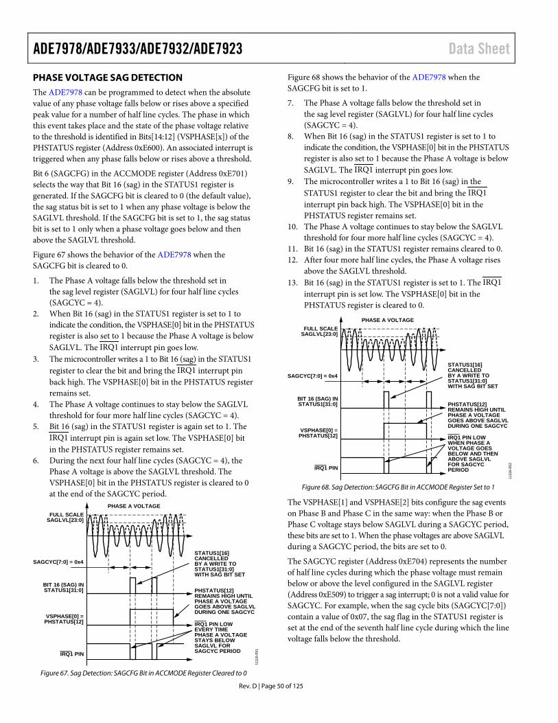
ADE7978/ADE7933/ADE7932/ADE7923 Data Sheet
Rev. D | Page 50 of 125
PHASE VOLTAGE SAG DETECTION The ADE7978 can be programmed to detect when the absolute value of any phase voltage falls below or rises above a specified peak value for a number of half line cycles. The phase in which this event takes place and the state of the phase voltage relative to the threshold is identified in Bits[14:12] (VSPHASE[x]) of the PHSTATUS register (Address 0xE600). An associated interrupt is triggered when any phase falls below or rises above a threshold.
Bit 6 (SAGCFG) in the ACCMODE register (Address 0xE701) selects the way that Bit 16 (sag) in the STATUS1 register is generated. If the SAGCFG bit is cleared to 0 (the default value), the sag status bit is set to 1 when any phase voltage is below the SAGLVL threshold. If the SAGCFG bit is set to 1, the sag status bit is set to 1 only when a phase voltage goes below and then above the SAGLVL threshold.
Figure 67 shows the behavior of the ADE7978 when the SAGCFG bit is cleared to 0.
1. The Phase A voltage falls below the threshold set in the sag level register (SAGLVL) for four half line cycles (SAGCYC = 4).
2. When Bit 16 (sag) in the STATUS1 register is set to 1 to indicate the condition, the VSPHASE[0] bit in the PHSTATUS register is also set to 1 because the Phase A voltage is below SAGLVL. The IRQ1 interrupt pin goes low.
3. The microcontroller writes a 1 to Bit 16 (sag) in the STATUS1 register to clear the bit and bring the IRQ1 interrupt pin back high. The VSPHASE[0] bit in the PHSTATUS register remains set.
4. The Phase A voltage continues to stay below the SAGLVL threshold for four more half line cycles (SAGCYC = 4).
5. Bit 16 (sag) in the STATUS1 register is again set to 1. The IRQ1 interrupt pin is again set low. The VSPHASE[0] bit in the PHSTATUS register remains set.
6. During the next four half line cycles (SAGCYC = 4), the Phase A voltage is above the SAGLVL threshold. The VSPHASE[0] bit in the PHSTATUS register is cleared to 0 at the end of the SAGCYC period.
PHASE A VOLTAGEFULL SCALE
SAGLVL[23:0]
SAGCYC[7:0] = 0x4
BIT 16 (SAG) INSTATUS1[31:0]
VSPHASE[0] =PHSTATUS[12]
IRQ1 PIN
STATUS1[16]CANCELLEDBY A WRITE TOSTATUS1[31:0]WITH SAG BIT SET
PHSTATUS[12]REMAINS HIGH UNTILPHASE A VOLTAGEGOES ABOVE SAGLVLDURING ONE SAGCYC
IRQ1 PIN LOWEVERY TIMEPHASE A VOLTAGESTAYS BELOWSAGLVL FORSAGCYC PERIOD
1111
6-05
1
Figure 67. Sag Detection: SAGCFG Bit in ACCMODE Register Cleared to 0
Figure 68 shows the behavior of the ADE7978 when the SAGCFG bit is set to 1.
7. The Phase A voltage falls below the threshold set in the sag level register (SAGLVL) for four half line cycles (SAGCYC = 4).
8. When Bit 16 (sag) in the STATUS1 register is set to 1 to indicate the condition, the VSPHASE[0] bit in the PHSTATUS register is also set to 1 because the Phase A voltage is below SAGLVL. The IRQ1 interrupt pin goes low.
9. The microcontroller writes a 1 to Bit 16 (sag) in the STATUS1 register to clear the bit and bring the IRQ1 interrupt pin back high. The VSPHASE[0] bit in the PHSTATUS register remains set.
10. The Phase A voltage continues to stay below the SAGLVL threshold for four more half line cycles (SAGCYC = 4).
11. Bit 16 (sag) in the STATUS1 register remains cleared to 0. 12. After four more half line cycles, the Phase A voltage rises
above the SAGLVL threshold. 13. Bit 16 (sag) in the STATUS1 register is set to 1. The IRQ1
interrupt pin is set low. The VSPHASE[0] bit in the PHSTATUS register is cleared to 0.
PHASE A VOLTAGEFULL SCALE
SAGLVL[23:0]
SAGCYC[7:0] = 0x4
BIT 16 (SAG) INSTATUS1[31:0]
VSPHASE[0] =PHSTATUS[12]
IRQ1 PIN
STATUS1[16]CANCELLEDBY A WRITE TOSTATUS1[31:0]WITH SAG BIT SET
PHSTATUS[12]REMAINS HIGH UNTILPHASE A VOLTAGEGOES ABOVE SAGLVLDURING ONE SAGCYC
IRQ1 PIN LOWWHEN PHASE AVOLTAGE GOESBELOW AND THENABOVE SAGLVLFOR SAGCYCPERIOD
1111
6-05
2
Figure 68. Sag Detection: SAGCFG Bit in ACCMODE Register Set to 1
The VSPHASE[1] and VSPHASE[2] bits configure the sag events on Phase B and Phase C in the same way: when the Phase B or Phase C voltage stays below SAGLVL during a SAGCYC period, these bits are set to 1. When the phase voltages are above SAGLVL during a SAGCYC period, the bits are set to 0.
The SAGCYC register (Address 0xE704) represents the number of half line cycles during which the phase voltage must remain below or above the level configured in the SAGLVL register (Address 0xE509) to trigger a sag interrupt; 0 is not a valid value for SAGCYC. For example, when the sag cycle bits (SAGCYC[7:0]) contain a value of 0x07, the sag flag in the STATUS1 register is set at the end of the seventh half line cycle during which the line voltage falls below the threshold.
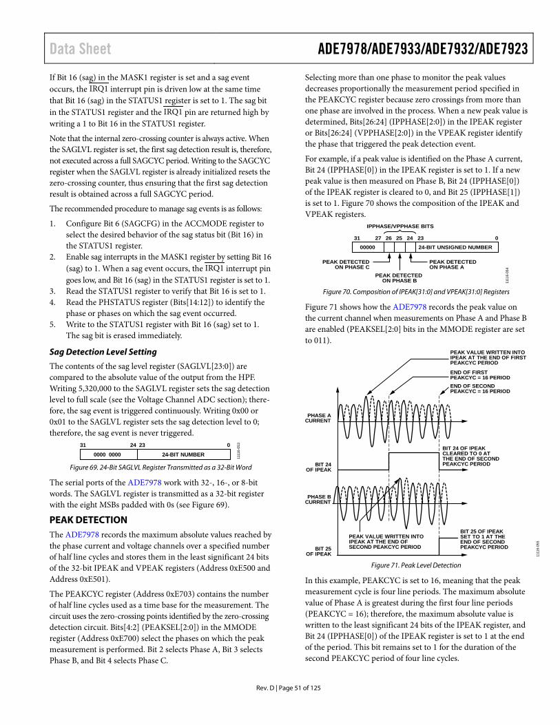
Data Sheet ADE7978/ADE7933/ADE7932/ADE7923
Rev. D | Page 51 of 125
If Bit 16 (sag) in the MASK1 register is set and a sag event occurs, the IRQ1 interrupt pin is driven low at the same time that Bit 16 (sag) in the STATUS1 register is set to 1. The sag bit in the STATUS1 register and the IRQ1 pin are returned high by writing a 1 to Bit 16 in the STATUS1 register.
Note that the internal zero-crossing counter is always active. When the SAGLVL register is set, the first sag detection result is, therefore, not executed across a full SAGCYC period. Writing to the SAGCYC register when the SAGLVL register is already initialized resets the zero-crossing counter, thus ensuring that the first sag detection result is obtained across a full SAGCYC period.
The recommended procedure to manage sag events is as follows:
1. Configure Bit 6 (SAGCFG) in the ACCMODE register to select the desired behavior of the sag status bit (Bit 16) in the STATUS1 register.
2. Enable sag interrupts in the MASK1 register by setting Bit 16 (sag) to 1. When a sag event occurs, the IRQ1 interrupt pin goes low, and Bit 16 (sag) in the STATUS1 register is set to 1.
3. Read the STATUS1 register to verify that Bit 16 is set to 1. 4. Read the PHSTATUS register (Bits[14:12]) to identify the
phase or phases on which the sag event occurred. 5. Write to the STATUS1 register with Bit 16 (sag) set to 1.
The sag bit is erased immediately.
Sag Detection Level Setting
The contents of the sag level register (SAGLVL[23:0]) are compared to the absolute value of the output from the HPF. Writing 5,320,000 to the SAGLVL register sets the sag detection level to full scale (see the Voltage Channel ADC section); there-fore, the sag event is triggered continuously. Writing 0x00 or 0x01 to the SAGLVL register sets the sag detection level to 0; therefore, the sag event is never triggered.
0000 0000 24-BIT NUMBER
31 24 23 0
1111
6-05
3
Figure 69. 24-Bit SAGLVL Register Transmitted as a 32-Bit Word
The serial ports of the ADE7978 work with 32-, 16-, or 8-bit words. The SAGLVL register is transmitted as a 32-bit register with the eight MSBs padded with 0s (see Figure 69).
PEAK DETECTION The ADE7978 records the maximum absolute values reached by the phase current and voltage channels over a specified number of half line cycles and stores them in the least significant 24 bits of the 32-bit IPEAK and VPEAK registers (Address 0xE500 and Address 0xE501).
The PEAKCYC register (Address 0xE703) contains the number of half line cycles used as a time base for the measurement. The circuit uses the zero-crossing points identified by the zero-crossing detection circuit. Bits[4:2] (PEAKSEL[2:0]) in the MMODE register (Address 0xE700) select the phases on which the peak measurement is performed. Bit 2 selects Phase A, Bit 3 selects Phase B, and Bit 4 selects Phase C.
Selecting more than one phase to monitor the peak values decreases proportionally the measurement period specified in the PEAKCYC register because zero crossings from more than one phase are involved in the process. When a new peak value is determined, Bits[26:24] (IPPHASE[2:0]) in the IPEAK register or Bits[26:24] (VPPHASE[2:0]) in the VPEAK register identify the phase that triggered the peak detection event.
For example, if a peak value is identified on the Phase A current, Bit 24 (IPPHASE[0]) in the IPEAK register is set to 1. If a new peak value is then measured on Phase B, Bit 24 (IPPHASE[0]) of the IPEAK register is cleared to 0, and Bit 25 (IPPHASE[1]) is set to 1. Figure 70 shows the composition of the IPEAK and VPEAK registers.
PEAK DETECTEDON PHASE C
00000
31 27 26 25 24 23 0
24-BIT UNSIGNED NUMBER
PEAK DETECTEDON PHASE A
IPPHASE/VPPHASE BITS
PEAK DETECTEDON PHASE B 11
116-
054
Figure 70. Composition of IPEAK[31:0] and VPEAK[31:0] Registers
Figure 71 shows how the ADE7978 records the peak value on the current channel when measurements on Phase A and Phase B are enabled (PEAKSEL[2:0] bits in the MMODE register are set to 011).
PHASE ACURRENT
PHASE BCURRENT
BIT 24OF IPEAK
BIT 25OF IPEAK
PEAK VALUE WRITTEN INTOIPEAK AT THE END OF FIRSTPEAKCYC PERIOD
END OF FIRSTPEAKCYC = 16 PERIOD
BIT 24 OF IPEAKCLEARED TO 0 ATTHE END OF SECONDPEAKCYC PERIOD
BIT 25 OF IPEAKSET TO 1 AT THEEND OF SECONDPEAKCYC PERIOD
END OF SECONDPEAKCYC = 16 PERIOD
PEAK VALUE WRITTEN INTOIPEAK AT THE END OFSECOND PEAKCYC PERIOD
1111
6-05
5
Figure 71. Peak Level Detection
In this example, PEAKCYC is set to 16, meaning that the peak measurement cycle is four line periods. The maximum absolute value of Phase A is greatest during the first four line periods (PEAKCYC = 16); therefore, the maximum absolute value is written to the least significant 24 bits of the IPEAK register, and Bit 24 (IPPHASE[0]) of the IPEAK register is set to 1 at the end of the period. This bit remains set to 1 for the duration of the second PEAKCYC period of four line cycles.

ADE7978/ADE7933/ADE7932/ADE7923 Data Sheet
Rev. D | Page 52 of 125
The maximum absolute value of Phase B is greatest during the second PEAKCYC period; therefore, the maximum absolute value is written to the least significant 24 bits of the IPEAK register, and Bit 25 (IPPHASE[1]) in the IPEAK register is set to 1 at the end of the period.
At the end of the peak detection period in the current channel, Bit 23 (PKI) in the STATUS1 register is set to 1; if Bit 23 (PKI) in the MASK1 register is set, the IRQ1 interrupt pin is driven low at the end of the PEAKCYC period. In a similar way, at the end of the peak detection period in the voltage channel, Bit 24 (PKV) in the STATUS1 register is set to 1; if Bit 24 (PKV) in the MASK1 register is set, the IRQ1 interrupt pin is driven low at the end of the PEAKCYC period. To identify the phase that triggered the interrupt, the IPEAK or VPEAK register is read immediately after reading the STATUS1 register. After identifying the phase that triggered the interrupt, the status bits are cleared and the IRQ1 pin is returned high by writing a 1 to Bit 23 (PKI) or Bit 24 (PKV) in the STATUS1 register.
Note that the internal zero-crossing counter is always active. When Bits[4:2] (PEAKSEL[2:0]) are set in the MMODE register, the first peak detection result is, therefore, not executed across a full PEAKCYC period. Writing to the PEAKCYC register when the PEAKSEL[2:0] bits are already initialized resets the zero-crossing counter, thereby ensuring that the first peak detection result is obtained across a full PEAKCYC period.
OVERVOLTAGE AND OVERCURRENT DETECTION The ADE7978 detects when the instantaneous absolute value measured on the phase voltage and current channels becomes greater than the thresholds set in the 24-bit unsigned OVLVL and OILVL registers (Address 0xE508 and Address 0xE507).
Overvoltage Detection
If Bit 18 (OV) in the MASK1 register is set, the IRQ1 interrupt pin is driven low if an overvoltage event occurs. Two status flags are set when an overvoltage event occurs: Bit 18 (OV) in the STATUS1 register and one of Bits[11:9] (OVPHASE[2:0]) in the PHSTATUS register (Address 0xE600). The OVPHASE[2:0] bits identify the phase that generated the overvoltage. Bit 18 (OV) in the STATUS1 register and Bits[11:9] (OVPHASE[2:0]) in the PHSTATUS register are cleared and the IRQ1 pin is set high by writing a 1 to Bit 18 (OV) in the STATUS1 register.
Figure 72 shows overvoltage detection in the Phase A voltage. When the absolute instantaneous value of the voltage goes above the threshold set in the OVLVL register, Bit 18 (OV) in the STATUS1 register and Bit 9 (OVPHASE[0]) in the PHSTATUS register are set to 1. Bit 18 (OV) of the STATUS1 register and Bit 9 (OVPHASE[0]) in the PHSTATUS register are cleared when a 1 is written to Bit 18 (OV) in the STATUS1 register.
OVLVL[23:0]
BIT 18 (OV) OFSTATUS1
BIT 9 (OVPHASE)OF PHSTATUS
PHASE AVOLTAGE CHANNEL
OVERVOLTAGEDETECTED
STATUS1[18] ANDPHSTATUS[9]CANCELLED BY AWRITE OF STATUS1WITH OV BIT SET.
1111
6-05
6
Figure 72. Overvoltage Detection
The recommended procedure to manage overvoltage events is as follows:
1. Enable overvoltage interrupts in the MASK1 register by setting Bit 18 (OV) to 1.
2. When an overvoltage event occurs, the IRQ1 interrupt pin goes low and Bit 18 (OV) in the STATUS1 register is set to 1.
3. Read the STATUS1 register to verify that Bit 18 is set to 1. 4. Read the PHSTATUS register (Bits[11:9]) to identify the
phase or phases on which the overvoltage event occurred. 5. Write a 1 to Bit 18 (OV) in the STATUS1 register to clear
Bit 18 and Bits[11:9] (OVPHASE[2:0]) of the PHSTATUS register. The IRQ1 interrupt pin returns high.
Overcurrent Detection
If Bit 17 (OI) in the MASK1 register is set, the IRQ1 interrupt pin is driven low when an overcurrent event occurs. Two status flags are set when an overcurrent event occurs: Bit 17 (OI) in the STATUS1 register and one of Bits[5:3] (OIPHASE[2:0]) in the PHSTATUS register. The OIPHASE[2:0] bits identify the phase that generated the overcurrent. The recommended procedure to manage overcurrent events is as follows:
1. Enable overcurrent interrupts in the MASK1 register by setting Bit 17 (OI) to 1.
2. When an overcurrent event occurs, the IRQ1 interrupt pin goes low and Bit 17 (OI) in the STATUS1 register is set to 1.
3. Read the STATUS1 register to verify that Bit 17 is set to 1. 4. Read the PHSTATUS register (Bits[5:3]) to identify the
phase or phases on which the overcurrent event occurred. 5. Write a 1 to Bit 17 (OI) in the STATUS1 register to clear
Bit 17 and Bits[5:3] (OIPHASE[2:0]) of the PHSTATUS register. The IRQ1 interrupt pin returns high.
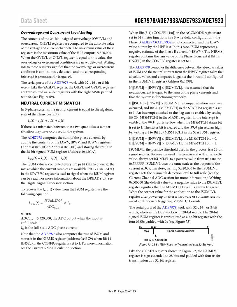
Data Sheet ADE7978/ADE7933/ADE7932/ADE7923
Rev. D | Page 53 of 125
Overvoltage and Overcurrent Level Setting
The contents of the 24-bit unsigned overvoltage (OVLVL) and overcurrent (OILVL) registers are compared to the absolute value of the voltage and current channels. The maximum value of these registers is the maximum value of the HPF outputs: 5,320,000. When the OVLVL or OILVL register is equal to this value, the overvoltage or overcurrent conditions are never detected. Writing 0x0 to these registers signifies that the overvoltage or overcurrent condition is continuously detected, and the corresponding interrupt is permanently triggered.
The serial ports of the ADE7978 work with 32-, 16-, or 8-bit words. Like the SAGLVL register, the OILVL and OVLVL registers are transmitted as 32-bit registers with the eight MSBs padded with 0s (see Figure 69).
NEUTRAL CURRENT MISMATCH In 3-phase systems, the neutral current is equal to the algebraic sum of the phase currents.
IN(t) = IA(t) + IB(t) + IC(t)
If there is a mismatch between these two quantities, a tamper situation may have occurred in the system.
The ADE7978 computes the sum of the phase currents by adding the contents of the IAWV, IBWV, and ICWV registers (Address 0xE50C to Address 0xE50E) and storing the result in the 28-bit signed ISUM register (Address 0x43CA).
ISUM(t) = IA(t) + IB(t) + IC(t)
The ISUM value is computed every 125 µs (8 kHz frequency), the rate at which the current samples are available. Bit 17 (DREADY) in the STATUS0 register is used to signal when the ISUM register can be read. For more information about the DREADY bit, see the Digital Signal Processor section.
To recover the ISUM(t) value from the ISUM register, use the following equation:
FSMAX
SUM IADC
ISUM[27:0]tI ×=)(
where: ADCMAX = 5,320,000, the ADC output when the input is at full scale. IFS is the full-scale ADC phase current.
Note that the ADE7978 also computes the rms of ISUM and stores it in the NIRMS register (Address 0x43C9) when Bit 14 (INSEL) in the CONFIG register is set to 1. For more information, see the Current RMS Calculation section.
When Bits[5:4] (CONSEL[1:0]) in the ACCMODE register are set to 01 (meter functions in a 3-wire delta configuration), the Phase B ADE7933/ADE7932 is not connected, and the IBWV value output by the HPF is 0. In this case, ISUM represents a negative estimate of the Phase B current (−IBWV). The NIRMS register contains the rms value of the Phase B current if Bit 14 (INSEL) in the CONFIG register is set to 1.
The ADE7978 computes the difference between the absolute values of ISUM and the neutral current from the INWV register, takes the absolute value, and compares it against the threshold configured in the ISUMLVL register (Address 0x4398).
If ||ISUM| − |INWV|| ≤ |ISUMLVL|, it is assumed that the neutral current is equal to the sum of the phase currents and that the system is functioning properly.
If ||ISUM| − |INWV|| > |ISUMLVL|, a tamper situation may have occurred, and Bit 20 (MISMTCH) in the STATUS1 register is set to 1. An interrupt attached to the flag can be enabled by setting Bit 20 (MISMTCH) in the MASK1 register. If the interrupt is enabled, the IRQ1 pin is set low when the MISMTCH status bit is set to 1. The status bit is cleared and the IRQ1 pin returns high by writing a 1 to Bit 20 (MISMTCH) in the STATUS1 register.
If ||ISUM| − |INWV|| ≤ |ISUMLVL|, the MISMTCH bit = 0. If ||ISUM| − |INWV|| > |ISUMLVL|, the MISMTCH bit = 1.
ISUMLVL, the positive threshold used in the process, is a 24-bit signed register. Because it is used in a comparison with an absolute value, always set ISUMLVL to a positive value from 0x00000 to 0x7FFFFF. ISUMLVL uses the same scale as the outputs of the current ADCs; therefore, writing 5,320,000 to the ISUMLVL register sets the mismatch detection level to full scale (see the Current Channel ADC section for more information). Writing 0x000000 (the default value) or a negative value to the ISUMLVL register signifies that the MISMTCH event is always triggered. Write the correct value for the application to the ISUMLVL register after power-up or after a hardware or software reset to avoid continuously triggering MISMTCH events.
The serial ports of the ADE7978 work with 32-, 16-, or 8-bit words, whereas the DSP works with 28-bit words. The 28-bit signed ISUM register is transmitted as a 32-bit register with the four MSBs padded with 0s (see Figure 73).
31 28 27
BIT 27 IS A SIGN BIT
0
28-BIT SIGNED NUMBER0000
1111
6-05
7
Figure 73. 28-Bit ISUM Register Transmitted as a 32-Bit Word
Like the xIGAIN registers shown in Figure 52, the ISUMLVL register is sign extended to 28 bits and padded with four 0s for transmission as a 32-bit register.
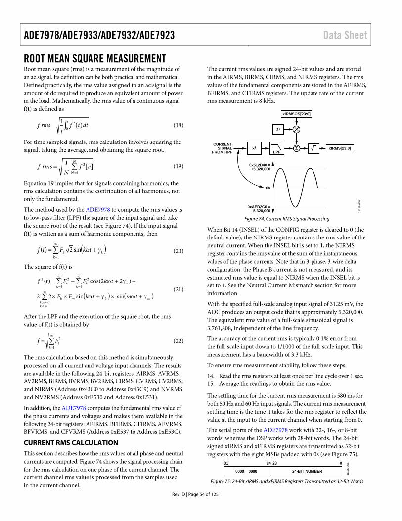
ADE7978/ADE7933/ADE7932/ADE7923 Data Sheet
Rev. D | Page 54 of 125
ROOT MEAN SQUARE MEASUREMENT Root mean square (rms) is a measurement of the magnitude of an ac signal. Its definition can be both practical and mathematical. Defined practically, the rms value assigned to an ac signal is the amount of dc required to produce an equivalent amount of power in the load. Mathematically, the rms value of a continuous signal f(t) is defined as
( )dttft
rmsf ∫=t
021 (18)
For time sampled signals, rms calculation involves squaring the signal, taking the average, and obtaining the square root.
[ ]∑=
=N
Nnf
Nrmsf
1
21 (19)
Equation 19 implies that for signals containing harmonics, the rms calculation contains the contribution of all harmonics, not only the fundamental.
The method used by the ADE7978 to compute the rms values is to low-pass filter (LPF) the square of the input signal and take the square root of the result (see Figure 74). If the input signal f(t) is written as a sum of harmonic components, then
( )kk
k γtωkFtf += ∑∞
=sin2)(
1 (20)
The square of f(t) is
( ) ( )∑
∑∑∞
≠=
∞
=
∞
=
γ+ω×γ+ω××
+γ+ω−=
mkmk
mkmk
kkk
kk
tmtkFF
tkFFtf
1,
1
2
1
22
sinsin22
)22cos()( (21)
After the LPF and the execution of the square root, the rms value of f(t) is obtained by
∑∞
==
1
2
kkFf (22)
The rms calculation based on this method is simultaneously processed on all current and voltage input channels. The results are available in the following 24-bit registers: AIRMS, AVRMS, AV2RMS, BIRMS, BVRMS, BV2RMS, CIRMS, CVRMS, CV2RMS, and NIRMS (Address 0x43C0 to Address 0x43C9) and NVRMS and NV2RMS (Address 0xE530 and Address 0xE531).
In addition, the ADE7978 computes the fundamental rms value of the phase currents and voltages and makes them available in the following 24-bit registers: AFIRMS, BFIRMS, CFIRMS, AFVRMS, BFVRMS, and CFVRMS (Address 0xE537 to Address 0xE53C).
CURRENT RMS CALCULATION This section describes how the rms values of all phase and neutral currents are computed. Figure 74 shows the signal processing chain for the rms calculation on one phase of the current channel. The current channel rms value is processed from the samples used in the current channel.
The current rms values are signed 24-bit values and are stored in the AIRMS, BIRMS, CIRMS, and NIRMS registers. The rms values of the fundamental components are stored in the AFIRMS, BFIRMS, and CFIRMS registers. The update rate of the current rms measurement is 8 kHz.
0xAED2C0 =–5,320,000
0x512D40 =+5,320,000
0V
CURRENTSIGNAL
FROM HPF LPFx2
27
xIRMSOS[23:0]
xIRMS[23:0]
1111
6-06
0
Figure 74. Current RMS Signal Processing
When Bit 14 (INSEL) of the CONFIG register is cleared to 0 (the default value), the NIRMS register contains the rms value of the neutral current. When the INSEL bit is set to 1, the NIRMS register contains the rms value of the sum of the instantaneous values of the phase currents. Note that in 3-phase, 3-wire delta configuration, the Phase B current is not measured, and its estimated rms value is equal to NIRMS when the INSEL bit is set to 1. See the Neutral Current Mismatch section for more information.
With the specified full-scale analog input signal of 31.25 mV, the ADC produces an output code that is approximately 5,320,000. The equivalent rms value of a full-scale sinusoidal signal is 3,761,808, independent of the line frequency.
The accuracy of the current rms is typically 0.1% error from the full-scale input down to 1/1000 of the full-scale input. This measurement has a bandwidth of 3.3 kHz.
To ensure rms measurement stability, follow these steps:
14. Read the rms registers at least once per line cycle over 1 sec. 15. Average the readings to obtain the rms value.
The settling time for the current rms measurement is 580 ms for both 50 Hz and 60 Hz input signals. The current rms measurement settling time is the time it takes for the rms register to reflect the value at the input to the current channel when starting from 0.
The serial ports of the ADE7978 work with 32-, 16-, or 8-bit words, whereas the DSP works with 28-bit words. The 24-bit signed xIRMS and xFIRMS registers are transmitted as 32-bit registers with the eight MSBs padded with 0s (see Figure 75).
31 24 23 0
24-BIT NUMBER0000 0000
1111
6-06
1
Figure 75. 24-Bit xIRMS and xFIRMS Registers Transmitted as 32-Bit Words
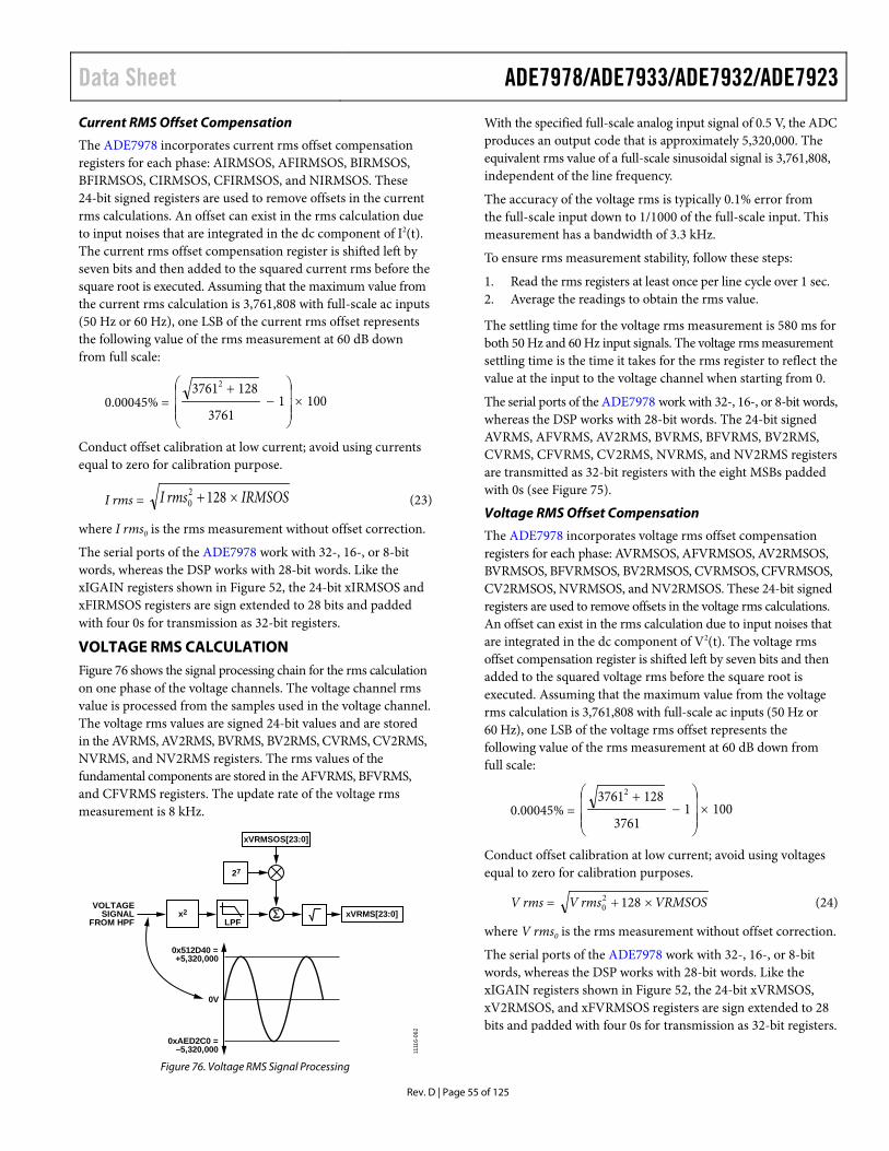
Data Sheet ADE7978/ADE7933/ADE7932/ADE7923
Rev. D | Page 55 of 125
Current RMS Offset Compensation
The ADE7978 incorporates current rms offset compensation registers for each phase: AIRMSOS, AFIRMSOS, BIRMSOS, BFIRMSOS, CIRMSOS, CFIRMSOS, and NIRMSOS. These 24-bit signed registers are used to remove offsets in the current rms calculations. An offset can exist in the rms calculation due to input noises that are integrated in the dc component of I2(t). The current rms offset compensation register is shifted left by seven bits and then added to the squared current rms before the square root is executed. Assuming that the maximum value from the current rms calculation is 3,761,808 with full-scale ac inputs (50 Hz or 60 Hz), one LSB of the current rms offset represents the following value of the rms measurement at 60 dB down from full scale:
0.00045% = 10013761
12837612
×
−
+
Conduct offset calibration at low current; avoid using currents equal to zero for calibration purpose.
I rms = IRMSOSrmsI ×+12820 (23)
where I rms0 is the rms measurement without offset correction.
The serial ports of the ADE7978 work with 32-, 16-, or 8-bit words, whereas the DSP works with 28-bit words. Like the xIGAIN registers shown in Figure 52, the 24-bit xIRMSOS and xFIRMSOS registers are sign extended to 28 bits and padded with four 0s for transmission as 32-bit registers.
VOLTAGE RMS CALCULATION Figure 76 shows the signal processing chain for the rms calculation on one phase of the voltage channels. The voltage channel rms value is processed from the samples used in the voltage channel. The voltage rms values are signed 24-bit values and are stored in the AVRMS, AV2RMS, BVRMS, BV2RMS, CVRMS, CV2RMS, NVRMS, and NV2RMS registers. The rms values of the fundamental components are stored in the AFVRMS, BFVRMS, and CFVRMS registers. The update rate of the voltage rms measurement is 8 kHz.
0xAED2C0 =–5,320,000
0x512D40 =+5,320,000
0V
VOLTAGESIGNAL
FROM HPF LPFx2
27
xVRMSOS[23:0]
xVRMS[23:0]
1111
6-06
2
Figure 76. Voltage RMS Signal Processing
With the specified full-scale analog input signal of 0.5 V, the ADC produces an output code that is approximately 5,320,000. The equivalent rms value of a full-scale sinusoidal signal is 3,761,808, independent of the line frequency.
The accuracy of the voltage rms is typically 0.1% error from the full-scale input down to 1/1000 of the full-scale input. This measurement has a bandwidth of 3.3 kHz.
To ensure rms measurement stability, follow these steps:
1. Read the rms registers at least once per line cycle over 1 sec.2. Average the readings to obtain the rms value.
The settling time for the voltage rms measurement is 580 ms for both 50 Hz and 60 Hz input signals. The voltage rms measurement settling time is the time it takes for the rms register to reflect the value at the input to the voltage channel when starting from 0.
The serial ports of the ADE7978 work with 32-, 16-, or 8-bit words, whereas the DSP works with 28-bit words. The 24-bit signed AVRMS, AFVRMS, AV2RMS, BVRMS, BFVRMS, BV2RMS, CVRMS, CFVRMS, CV2RMS, NVRMS, and NV2RMS registers are transmitted as 32-bit registers with the eight MSBs padded with 0s (see Figure 75).
Voltage RMS Offset Compensation
The ADE7978 incorporates voltage rms offset compensation registers for each phase: AVRMSOS, AFVRMSOS, AV2RMSOS, BVRMSOS, BFVRMSOS, BV2RMSOS, CVRMSOS, CFVRMSOS, CV2RMSOS, NVRMSOS, and NV2RMSOS. These 24-bit signed registers are used to remove offsets in the voltage rms calculations. An offset can exist in the rms calculation due to input noises that are integrated in the dc component of V2(t). The voltage rms offset compensation register is shifted left by seven bits and then added to the squared voltage rms before the square root is executed. Assuming that the maximum value from the voltage rms calculation is 3,761,808 with full-scale ac inputs (50 Hz or 60 Hz), one LSB of the voltage rms offset represents the following value of the rms measurement at 60 dB down from full scale:
0.00045% = 10013761
12837612
×
−
+
Conduct offset calibration at low current; avoid using voltages equal to zero for calibration purposes.
V rms = VRMSOSrmsV ×+ 12820 (24)
where V rms0 is the rms measurement without offset correction.
The serial ports of the ADE7978 work with 32-, 16-, or 8-bit words, whereas the DSP works with 28-bit words. Like the xIGAIN registers shown in Figure 52, the 24-bit xVRMSOS, xV2RMSOS, and xFVRMSOS registers are sign extended to 28 bits and padded with four 0s for transmission as 32-bit registers.
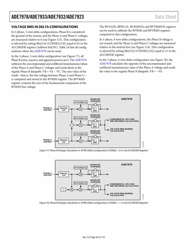
ADE7978/ADE7933/ADE7932/ADE7923 Data Sheet
Rev. D | Page 56 of 125
VOLTAGE RMS IN DELTA CONFIGURATIONS In 3-phase, 3-wire delta configurations, Phase B is considered the ground of the system, and the Phase A and Phase C voltages are measured relative to it (see Figure 113). This configuration is selected by setting Bits[5:4] (CONSEL[1:0]) equal to 01 in the ACCMODE register (Address 0xE701). Table 24 lists all config-urations where the ADE7978 can be used.
In the 3-phase, 3-wire delta configuration (see Figure 77), all Phase B active, reactive, and apparent powers are 0. The ADE7978 subtracts the uncompensated and unfiltered instantaneous values of the Phase A and Phase C voltages and sends them to the regular Phase B datapath: VB = VA − VC. The rms value of the result—that is, the line voltage between Phase A and Phase C—is computed and stored in the BVRMS register. The BFVRMS register contains the rms of the fundamental component of the BVRMS line voltage.
The BVGAIN, BPHCAL, BVRMSOS, and BFVRMSOS registers can be used to calibrate the BVRMS and BFVRMS registers computed in this configuration.
In 3-phase, 4-wire delta configurations, the Phase B voltage is not sensed, and the Phase A and Phase C voltages are measured relative to the neutral line (see Figure 114). This configuration is selected by setting Bits[5:4] (CONSEL[1:0]) equal to 11 in the ACCMODE register.
In the 3-phase, 4-wire delta configuration (see Figure 78), the ADE7978 calculates the opposite of the uncompensated and unfiltered instantaneous value of the Phase A voltage and sends the value to the regular Phase B datapath: VB = −VA.
PHASE AADE7933
PHASE CADE7933
ADE7978AVGAIN[23:0]
HPFEN BITCONFIG[4]
HPFDIGITAL
LPF
BVGAIN[23:0]HPFEN BITCONFIG[4]
HPF
CVGAIN[23:0]HPFEN BITCONFIG[4]
HPFDIGITAL
LPF
FUNDAMENTAL VOLTAGERMS (BFVRMS) CALCULATION
VOLTAGE RMS (BVRMS)CALCULATION
1111
6-06
3
Figure 77. Phase B Voltage Calculation in 3P3W Delta Configuration (CONSEL = 01 in the ACCMODE Register)
PHASE AADE7933
ADE7978AVGAIN[23:0]
HPFEN BITCONFIG[4]
HPFDIGITAL
LPF
BVGAIN[23:0]HPFEN BITCONFIG[4]
HPF
FUNDAMENTAL VOLTAGERMS (BFVRMS) CALCULATION
VOLTAGE RMS (BVRMS)CALCULATION
1111
6-06
4
–1
Figure 78. Phase B Voltage Calculation in 3P4W Delta Configuration (CONSEL = 11 in the ACCMODE Register)
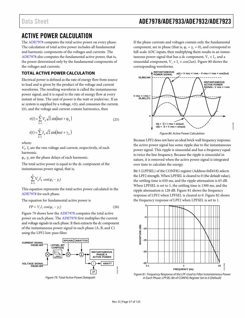
Data Sheet ADE7978/ADE7933/ADE7932/ADE7923
Rev. D | Page 57 of 125
ACTIVE POWER CALCULATION The ADE7978 computes the total active power on every phase. The calculation of total active power includes all fundamental and harmonic components of the voltages and currents. The ADE7978 also computes the fundamental active power, that is, the power determined only by the fundamental components of the voltages and currents.
TOTAL ACTIVE POWER CALCULATION Electrical power is defined as the rate of energy flow from source to load and is given by the product of the voltage and current waveforms. The resulting waveform is called the instantaneous power signal, and it is equal to the rate of energy flow at every instant of time. The unit of power is the watt or joules/sec. If an ac system is supplied by a voltage, v(t), and consumes the current, i(t), and the voltage and current contain harmonics, then
( )kk
k tkVtv ϕ+ω=∑∞
=sin2)(
1 (25)
( )kk
k tkIti γ+ω=∑∞
=sin2)(
1
where: Vk, Ik are the rms voltage and current, respectively, of each harmonic. φk, γk are the phase delays of each harmonic.
The total active power is equal to the dc component of the instantaneous power signal, that is,
∑∞
=1kkk IV cos(φk − γk)
This equation represents the total active power calculated in the ADE7978 for each phase.
The equation for fundamental active power is
FP = V1I1 cos(φ1 − y1) (26)
Figure 79 shows how the ADE7978 computes the total active power on each phase. The ADE7978 first multiplies the current and voltage signals in each phase. It then extracts the dc component of the instantaneous power signal in each phase (A, B, and C) using the LPF2 low-pass filter.
INSTANTANEOUSPHASE A
ACTIVE POWER
CURRENT SIGNALFROM HPF
VOLTAGE SIGNALFROM HPF
LPFSEL BITCONFIG[5]
LPF2
APGAIN AWATTOS
24
AWATT:
1111
6-06
5
Figure 79. Total Active Power Datapath
If the phase currents and voltages contain only the fundamental component, are in phase (that is, φ1 = γ1 = 0), and correspond to full-scale ADC inputs, then multiplying them results in an instan-taneous power signal that has a dc component, V1 × I1, and a sinusoidal component, V1 × I1 × cos(2ωt). Figure 80 shows the corresponding waveforms.
INSTANTANEOUSPOWER SIGNAL
INSTANTANEOUSACTIVE POWERSIGNAL: V rms × I rms
p(t) = V rms × I rms – V rms × I rms × cos(2ωt)53,982,544
V rms × I rms =26,991,271
0
i(t) = √2 × I rms × sin(ωt)v(t) = √2 × V rms × sin(ωt)
1111
6-06
6
Figure 80. Active Power Calculation
Because LPF2 does not have an ideal brick wall frequency response, the active power signal has some ripple due to the instantaneous power signal. This ripple is sinusoidal and has a frequency equal to twice the line frequency. Because the ripple is sinusoidal in nature, it is removed when the active power signal is integrated over time to calculate the energy.
Bit 5 (LPFSEL) of the CONFIG register (Address 0xE618) selects the LPF2 strength. When LPFSEL is cleared to 0 (the default value), the settling time is 650 ms, and the ripple attenuation is 65 dB. When LPFSEL is set to 1, the settling time is 1300 ms, and the ripple attenuation is 128 dB. Figure 81 shows the frequency response of LPF2 when LPFSEL is cleared to 0. Figure 82 shows the frequency response of LPF2 when LPFSEL is set to 1.
0
–5
–10
–15
–20
–250.1 1 10
FREQUENCY (Hz)
MA
GN
ITU
DE
(dB
)
1111
6-06
8
Figure 81. Frequency Response of the LPF Used to Filter Instantaneous Power
in Each Phase: LPFSEL Bit of CONFIG Register Set to 0 (Default)

ADE7978/ADE7933/ADE7932/ADE7923 Data Sheet
Rev. D | Page 58 of 125
0
–10
–20
–30
–400.1 1 10
FREQUENCY (Hz)
MA
GN
ITU
DE
(dB
)
1111
6-06
9
Figure 82. Frequency Response of the LPF Used to Filter Instantaneous Power
in Each Phase: LPFSEL Bit of CONFIG Register Set to 1
The ADE7978 stores the instantaneous total phase active powers in the 24-bit AWATT, BWATT, and CWATT registers (Address 0xE518 to Address 0xE51A). To calculate the value of these registers, use the following equation:
∑∞
=
××=1k FS
k
FS
k
II
VV
xWATT cos(φk − γk) × PMAX × 421
(27)
where: VFS and IFS are the rms values of the phase voltage and current when the ADC inputs are at full scale. PMAX = 26,991,271, the instantaneous power computed when the ADC inputs are at full scale and in phase.
The xWATT[23:0] waveform registers can be accessed using any of the serial port interfaces. For more information, see the Waveform Sampling Mode section.
FUNDAMENTAL ACTIVE POWER CALCULATION The ADE7978 computes the fundamental active power using a proprietary algorithm that requires initialization of the network frequency and of the nominal voltage measured in the voltage channel. Bit 14 (SELFREQ) in the COMPMODE register (Address 0xE60E) must be set according to the frequency of the network in which the ADE7978 is connected. If the network frequency is 50 Hz, clear this bit to 0 (the default value). If the network frequency is 60 Hz, set this bit to 1.
To initialize the nominal voltage measured in the voltage channel, configure the 28-bit signed VLEVEL register (Address 0x43A2) with a positive value based on the following equation:
6104 ××=n
FS
V
VVLEVEL (28)
where: VFS is the rms value of the phase voltages when the ADC inputs are at full scale. Vn is the rms nominal value of the phase voltage.
Table 22 provides the settling time for the fundamental active power measurement. The settling time is the time required for the power to reflect the value at the input of the ADE7978.
Table 22. Settling Time for Fundamental Active Power Input Signal Settling Time (ms) 63% PMAX 375 100% PMAX 875
The serial ports of the ADE7978 work with 32-, 16-, or 8-bit words, whereas the DSP works with 28-bit words. The 28-bit signed VLEVEL register is transmitted as a 32-bit register with the four most significant bits padded with 0s (see Figure 83).
31 28 27 0
28-BIT NUMBER0000
1111
6-06
7
Figure 83. 28-Bit VLEVEL Register Transmitted as a 32-Bit Word
ACTIVE POWER GAIN CALIBRATION The average active power result from the LPF2 output in each phase can be scaled by ±100% by writing to the 24-bit watt gain register for each phase: APGAIN, BPGAIN, or CPGAIN (Address 0x4399 to Address 0x439B). Because all power datapaths have identical overall gains, the xPGAIN registers are used with the datapaths of all powers computed by the ADE7978: total active and reactive powers, fundamental active and reactive powers, and apparent powers. Therefore, to compensate the gain errors in the datapaths of various powers, it is sufficient to analyze only one power datapath (for example, the total active power) and calculate the corresponding APGAIN, BPGAIN, and CPGAIN register values.
The power gain registers are twos complement signed registers with a resolution of 2−23/LSB. Equation 29 describes mathematically the function of the power gain registers.
Average Power Data = (29)
+×
2321
Register Gain Power Output LPF2
The output is decreased by 50% by writing 0xC00000 to the watt gain registers; the output is increased by 50% by writing 0x400000 to the watt gain registers. These registers are used to calibrate the active, reactive, and apparent power (or energy) calculation for each phase.
The serial ports of the ADE7978 work with 32-, 16-, or 8-bit words, whereas the DSP works with 28-bit words. Like the xIGAIN registers shown in Figure 52, the 24-bit APGAIN, BPGAIN, and CPGAIN registers are sign extended to 28 bits and padded with four 0s for transmission as 32-bit registers.

Data Sheet ADE7978/ADE7933/ADE7932/ADE7923
Rev. D | Page 59 of 125
ACTIVE POWER OFFSET CALIBRATION The ADE7978 includes a 24-bit watt offset register for each phase and each active power. The AWATTOS, BWATTOS, and CWATTOS registers (Address 0x439C to Address 0x439E) compensate offsets in the total active power calculations. The AFWATTOS, BFWATTOS, and CFWATTOS registers (Address 0x43A3 to Address 0x43A5) compensate offsets in the fundamental active power calculations. These signed twos complement registers are used to remove offsets in the active power calculations.
An offset can exist in the power calculation due to crosstalk between channels on the PCB or in the chip itself. One LSB in the active power offset register is equivalent to 1 LSB in the active power multiplier output. With full-scale current and voltage inputs, the LPF2 output is PMAX = 26,991,271. At −80 dB down from full scale (active power scaled down 104 times), one LSB of the active power offset register represents 0.037% of PMAX.
The serial ports of the ADE7978 work with 32-, 16-, or 8-bit words, whereas the DSP works with 28-bit words. Like the xIGAIN registers shown in Figure 52, the 24-bit xWATTOS and xFWATTOS registers are sign extended to 28 bits and padded with four 0s for transmission as 32-bit registers.
SIGN OF ACTIVE POWER CALCULATION The average active power is a signed calculation. If the phase difference between the current and voltage waveforms is more than 90°, the average power becomes negative. Negative power indicates that energy is being injected back onto the grid. The ADE7978 has sign detection circuitry for active power calcula-tions; this circuitry can monitor the total active powers or the fundamental active powers.
As described in the Active Energy Calculation section, the active energy accumulation is performed in two stages. Each time a sign change is detected in the energy accumulation at the end of the first stage—that is, after the energy accumulated in the internal accumulator reaches the WTHR register threshold—a dedicated interrupt is triggered. The sign of each phase active power can be read in the PHSIGN register (Address 0xE617).
Bit 0 (REVAPSEL) in the MMODE register (Address 0xE700) specifies the type of active power that is monitored. When REVAPSEL is cleared to 0 (the default value), the total active power is monitored. When REVAPSEL is set to 1, the fundamental active power is monitored.
Bits[8:6] (REVAPC, REVAPB, and REVAPA) in the STATUS0 register (Address 0xE502) are set when a sign change occurs in the power selected by Bit 0 (REVAPSEL) in the MMODE register.
Bits[2:0] (CWSIGN, BWSIGN, and AWSIGN) in the PHSIGN register are set simultaneously with the REVAPC, REVAPB, and REVAPA bits in the STATUS0 register. The xWSIGN bits indicate the sign of the power. When these bits are set to 0, the corresponding power is positive. When the bits are set to 1, the corresponding power is negative.
The REVAPx bits in the STATUS0 register and the xWSIGN bits in the PHSIGN register refer to the total active power of Phase x and the power type selected by Bit 0 (REVAPSEL) in the MMODE register.
Interrupts attached to Bits[8:6] (REVAPC, REVAPB, and REVAPA) in the STATUS0 register can be enabled by setting Bits[8:6] in the MASK0 register. When enabled, the IRQ0 pin goes low and the status bit is set to 1 when a change of sign occurs. To identify the phase that triggered the interrupt, read the PHSIGN register immediately after reading the STATUS0 register. The status bit is cleared and the IRQ0 pin is returned high by writing a 1 to the appropriate bits in the STATUS0 register.
ACTIVE ENERGY CALCULATION Active energy is defined as the integral of active power.
Energy = ∫ dt p(t) (30)
The ADE7978 achieves the integration of the active power signal in two stages (see Figure 84). The process is identical for total active power and fundamental active power.
The first stage accumulates the instantaneous phase total or fundamental active power at 1.024 MHz (the DSP computes these values at an 8 kHz rate). Each time a threshold is reached, a pulse is generated, and the threshold is subtracted from the internal register. The sign of the energy at this moment is considered the sign of the active power (see the Sign of Active Power Calculation section for more information).
INTERNALACCUMULATOR
WATTACC BITS INACCMODE[7:0]
THRESHOLD
WTHR34 27 26 0
0
32-BIT REGISTER
AWATTHR[31:0]
REVAPA BIT INSTATUS0[31:0]
INSTANTANEOUSPHASE A ACTIVE POWER
COMPUTED IN DIGITALSIGNAL PROCESSOR
1111
6-07
0
Figure 84. Total Active Energy Accumulation
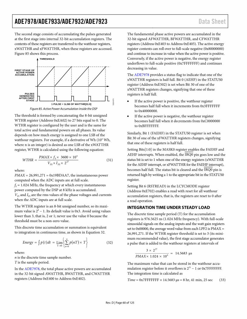
ADE7978/ADE7933/ADE7932/ADE7923 Data Sheet
Rev. D | Page 60 of 125
The second stage consists of accumulating the pulses generated at the first stage into internal 32-bit accumulation registers. The contents of these registers are transferred to the watthour registers, xWATTHR and xFWATTHR, when these registers are accessed. Figure 85 shows this process.
THRESHOLD
1 PULSE = 1LSB OF WATTHR[31:0]
FIRST STAGE OFACTIVE POWER
ACCUMULATION
PULSESGENERATEDAFTER FIRST
STAGE
1111
6-07
1
Figure 85. Active Power Accumulation Inside the DSP
The threshold is formed by concatenating the 8-bit unsigned WTHR register (Address 0xEA02) to 27 bits equal to 0. The WTHR register is configured by the user and is the same for total active and fundamental powers on all phases. Its value depends on how much energy is assigned to one LSB of the watthour registers. For example, if a derivative of Wh (10n Wh, where n is an integer) is desired as one LSB of the xWATTHR register, WTHR is calculated using the following equation:
272103600
×××××
=FSFS
nS
IVfPMAX
WTHR (31)
where: PMAX = 26,991,271 = 0x19BDAA7, the instantaneous power computed when the ADC inputs are at full scale. fS = 1.024 MHz, the frequency at which every instantaneous power computed by the DSP at 8 kHz is accumulated. VFS and IFS are the rms values of the phase voltages and currents when the ADC inputs are at full scale.
The WTHR register is an 8-bit unsigned number, so its maxi-mum value is 28 − 1. Its default value is 0x3. Avoid using values lower than 3, that is, 2 or 1; never use the value 0 because the threshold must be a non-zero value.
This discrete time accumulation or summation is equivalent to integration in continuous time, as shown in Equation 32.
( ) ( )
×== ∑∫
∞
=→ 00TLim
nTnTpdttpEnergy (32)
where: n is the discrete time sample number. T is the sample period.
In the ADE7978, the total phase active powers are accumulated in the 32-bit signed AWATTHR, BWATTHR, and CWATTHR registers (Address 0xE400 to Address 0xE402).
The fundamental phase active powers are accumulated in the 32-bit signed AFWATTHR, BFWATTHR, and CFWATTHR registers (Address 0xE403 to Address 0xE405). The active energy register contents can roll over to full-scale negative (0x80000000) and continue to increase in value when the active power is positive. Conversely, if the active power is negative, the energy register underflows to full-scale positive (0x7FFFFFFF) and continues decreasing in value.
The ADE7978 provides a status flag to indicate that one of the xWATTHR registers is half full. Bit 0 (AEHF) in the STATUS0 register (Address 0xE502) is set when Bit 30 of one of the xWATTHR registers changes, signifying that one of these registers is half full.
• If the active power is positive, the watthour register becomes half full when it increments from 0x3FFFFFFF to 0x40000000.
• If the active power is negative, the watthour register becomes half full when it decrements from 0xC0000000 to 0xBFFFFFFF.
Similarly, Bit 1 (FAEHF) in the STATUS0 register is set when Bit 30 of one of the xFWATTHR registers changes, signifying that one of these registers is half full.
Setting Bits[1:0] in the MASK0 register enables the FAEHF and AEHF interrupts. When enabled, the IRQ0 pin goes low and the status bit is set to 1 when one of the energy registers (xWATTHR for the AEHF interrupt, or xFWATTHR for the FAEHF interrupt), becomes half full. The status bit is cleared and the IRQ0 pin is returned high by writing a 1 to the appropriate bit in the STATUS0 register.
Setting Bit 6 (RSTREAD) in the LCYCMODE register (Address 0xE702) enables a read with reset for all watthour accumulation registers, that is, the registers are reset to 0 after a read operation.
INTEGRATION TIME UNDER STEADY LOAD The discrete time sample period (T) for the accumulation registers is 976.5625 ns (1.024 MHz frequency). With full-scale sinusoidal signals on the analog inputs and the watt gain registers set to 0x00000, the average word value from each LPF2 is PMAX = 26,991,271. If the WTHR register threshold is set to 3 (its mini-mum recommended value), the first stage accumulator generates a pulse that is added to the watthour registers at intervals of
sμ5683.1410024.1
236
27
=××
×
PMAX
The maximum value that can be stored in the watthour accu-mulation register before it overflows is 231 − 1 or 0x7FFFFFFF. The integration time is calculated as
Time = 0x7FFFFFFF × 14.5683 µs = 8 hr, 41 min, 25 sec (33)

Data Sheet ADE7978/ADE7933/ADE7932/ADE7923
Rev. D | Page 61 of 125
ENERGY ACCUMULATION MODES The active power is accumulated in each 32-bit watthour accumulation register (AWATTHR, BWATTHR, CWATTHR, AFWATTHR, BFWATTHR, and CFWATTHR) according to the configuration of Bits[5:4] (CONSEL[1:0] bits) in the ACCMODE register (see Table 23).
Table 23. Inputs to Watthour Accumulation Registers
CONSEL[1:0] AWATTHR AFWATTHR
BWATTHR BFWATTHR
CWATTHR CFWATTHR
00 VA × IA VB × IB VC × IC 01 VA × IA VB × IB VC × IC VB = VA − VC1 10 Reserved 11 VA × IA VB × IB VC × IC VB = −VA 1 See the BWATTHR and BFWATTHR Accumulation Register in 3-Phase, 3-Wire
Configurations section.
Depending on the polyphase meter service, choose the appropriate formula to calculate the active energy. The ANSI C12.10 standard defines the different configurations of the meter. Table 24 describes which mode to choose in these various configurations.
Table 24. Meter Form Configuration ANSI Meter Form Configuration
CONSEL[1:0] Bits Figure
5S/13S 3-wire delta 01 Figure 113 8S/15S 4-wire delta 11 Figure 114 9S/16S 4-wire wye 00 Figure 111
Bits[1:0] (WATTACC[1:0]) in the ACCMODE register determine how the active power is accumulated in the watthour registers and how the CF frequency output can be generated as a function of the total and fundamental active powers. For more information, see the Energy-to-Frequency Conversion section.
BWATTHR and BFWATTHR Accumulation Register in 3-Phase, 3-Wire Configurations
In a 3-phase, 3-wire configuration (CONSEL[1:0] = 01), the ADE7978 computes the rms value of the line voltage between Phase A and Phase C and stores the result in the BVRMS register (see the Voltage RMS in Delta Configurations section). The Phase B current value provided after the HPF is 0; therefore, the powers associated with Phase B are 0.
To avoid any errors in the frequency output pins (CF1, CF2, or CF3) related to the powers associated with Phase B, disable the contribution of Phase B to the energy-to-frequency converters by setting the TERMSEL1[1], TERMSEL2[1], or TERMSEL3[1] bit to 0 in the COMPMODE register (Address 0xE60E). For more information, see the Energy-to-Frequency Conversion section.
LINE CYCLE ACTIVE ENERGY ACCUMULATION MODE In line cycle energy accumulation mode, the energy accumulation is synchronized to the voltage channel zero crossings such that active energy is accumulated over an integral number of half line cycles. The advantage of summing the active energy over an integer number of line cycles is that the sinusoidal component in the active energy is reduced to 0. This eliminates any ripple in the energy calculation and allows the energy to be accumulated accurately over a shorter time. The line cycle energy accumulation mode greatly simplifies the energy calibration and significantly reduces the time required to calibrate the meter.
In line cycle energy accumulation mode, the ADE7978 transfers the active energy accumulated in the 32-bit internal accumulation registers to the xWATTHR or xFWATTHR registers after an integral number of line cycles (see Figure 86). The number of half line cycles is specified in the LINECYC register (Address 0xE60C).
ZERO-CROSSINGDETECTION(PHASE A)
ZERO-CROSSINGDETECTION(PHASE B)
CALIBRATIONCONTROL
ZERO-CROSSINGDETECTION(PHASE C)
LINECYC[15:0]
AWATTHR[31:0]
ZXSEL[0] INLCYCMODE[7:0]
ZXSEL[1] INLCYCMODE[7:0]
ZXSEL[2] INLCYCMODE[7:0]
OUTPUTFROMLPF2
APGAIN AWATTOS
INTERNALACCUMULATOR
THRESHOLD
32-BITREGISTER
WTHR34 27 26 0
0
1111
6-07
2
Figure 86. Line Cycle Active Energy Accumulation Mode
The line cycle active energy accumulation mode is activated by set-ting Bit 0 (LWATT) in the LCYCMODE register (Address 0xE702). The total active energy accumulated over an integer number of half line cycles (or zero crossings) is written to the watthour accu-mulation registers after the number of half line cycles specified by the LINECYC register is detected. When using the line cycle accumulation mode, set Bit 6 (RSTREAD) of the LCYCMODE register to Logic 0 because a read with reset of the watthour registers outside the LINECYC period resets the energy accumulation.
ADE7978/ADE7933/ADE7932/ADE7923 Data Sheet
Rev. D | Page 62 of 125
Phase A, Phase B, and Phase C zero crossings are included when counting the number of half line cycles by setting Bits[5:3] (ZXSEL[x]) in the LCYCMODE register. Any combi-nation of zero crossings from all three phases can be used to count the zero crossings. Select only one phase at a time for inclusion in the count of zero crossings during calibration.
The number of zero crossings is specified by the 16-bit unsigned LINECYC register. The ADE7978 can accumulate active power for up to 65,535 combined zero crossings. Note that the internal zero-crossing counter is always active. By setting Bit 0 (LWATT) in the LCYCMODE register, the first energy accumulation result is, therefore, incorrect. Writing to the LINECYC register when the LWATT bit is set resets the zero-crossing counter, thus ensuring that the first energy accumulation result is accurate.
At the end of an energy calibration cycle, Bit 5 (LENERGY) in the STATUS0 register is set. When the corresponding mask bit in the MASK0 register is enabled, the IRQ0 pin is set low. The status bit is cleared and the IRQ0 pin is returned high by writing a 1 to Bit 5 (LENERGY) in the STATUS0 register.
Because the active power is integrated on an integer number of half line cycles in line cycle accumulation mode, the sinusoidal components are reduced to 0, eliminating any ripple in the energy calculation. Therefore, total energy accumulated using the line cycle accumulation mode is
1kkk
nTt
t
IVnTdttpe cos(φk − γk) (34)
where nT is the accumulation time.
Note that line cycle active energy accumulation uses the same signal path as active energy accumulation. The LSB size of these two methods is equivalent.
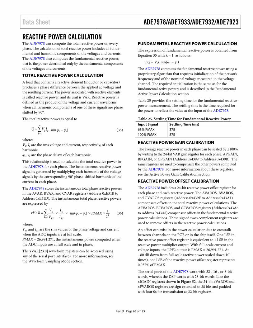
Data Sheet ADE7978/ADE7933/ADE7932/ADE7923
Rev. D | Page 63 of 125
REACTIVE POWER CALCULATION The ADE7978 can compute the total reactive power on every phase. The calculation of total reactive power includes all funda-mental and harmonic components of the voltages and currents. The ADE7978 also computes the fundamental reactive power, that is, the power determined only by the fundamental components of the voltages and currents.
TOTAL REACTIVE POWER CALCULATION A load that contains a reactive element (inductor or capacitor) produces a phase difference between the applied ac voltage and the resulting current. The power associated with reactive elements is called reactive power, and its unit is VAR. Reactive power is defined as the product of the voltage and current waveforms when all harmonic components of one of these signals are phase shifted by 90°.
The total reactive power is equal to
∑∞
==
1kkk IVQ sin(φk − γk) (35)
where: Vk, Ik are the rms voltage and current, respectively, of each harmonic. φk, γk are the phase delays of each harmonic.
This relationship is used to calculate the total reactive power in the ADE7978 for each phase. The instantaneous reactive power signal is generated by multiplying each harmonic of the voltage signals by the corresponding 90° phase-shifted harmonic of the current in each phase.
The ADE7978 stores the instantaneous total phase reactive powers in the AVAR, BVAR, and CVAR registers (Address 0xE51B to Address 0xE51D). The instantaneous total phase reactive powers are expressed by
∑∞
=××=
1k FS
k
FS
k
I
I
V
VxVAR sin(φk − γk) × PMAX × 42
1 (36)
where: VFS and IFS are the rms values of the phase voltage and current when the ADC inputs are at full scale. PMAX = 26,991,271, the instantaneous power computed when the ADC inputs are at full scale and in phase.
The xVAR[23:0] waveform registers can be accessed using any of the serial port interfaces. For more information, see the Waveform Sampling Mode section.
FUNDAMENTAL REACTIVE POWER CALCULATION The expression of fundamental reactive power is obtained from Equation 35 with k = 1, as follows:
FQ = V1I1 sin(φ1 − γ1)
The ADE7978 computes the fundamental reactive power using a proprietary algorithm that requires initialization of the network frequency and of the nominal voltage measured in the voltage channel. The required initialization is the same as for the fundamental active powers and is described in the Fundamental Active Power Calculation section.
Table 25 provides the settling time for the fundamental reactive power measurement. The settling time is the time required for the power to reflect the value at the input of the ADE7978.
Table 25. Settling Time for Fundamental Reactive Power Input Signal Settling Time (ms) 63% PMAX 375 100% PMAX 875
REACTIVE POWER GAIN CALIBRATION The average reactive power in each phase can be scaled by ±100% by writing to the 24-bit VAR gain register for each phase: APGAIN, BPGAIN, or CPGAIN (Address 0x4399 to Address 0x439B). The same registers are used to compensate the other powers computed by the ADE7978. For more information about these registers, see the Active Power Gain Calibration section.
REACTIVE POWER OFFSET CALIBRATION The ADE7978 includes a 24-bit reactive power offset register for each phase and each reactive power. The AVAROS, BVAROS, and CVAROS registers (Address 0x439F to Address 0x43A1) compensate offsets in the total reactive power calculations. The AFVAROS, BFVAROS, and CFVAROS registers (Address 0x43A6 to Address 0x43A8) compensate offsets in the fundamental reactive power calculations. These signed twos complement registers are used to remove offsets in the reactive power calculations.
An offset can exist in the power calculation due to crosstalk between channels on the PCB or in the chip itself. One LSB in the reactive power offset register is equivalent to 1 LSB in the reactive power multiplier output. With full-scale current and voltage inputs, the LPF2 output is PMAX = 26,991,271. At −80 dB down from full scale (active power scaled down 104 times), one LSB of the reactive power offset register represents 0.037% of PMAX.
The serial ports of the ADE7978 work with 32-, 16-, or 8-bit words, whereas the DSP works with 28-bit words. Like the xIGAIN registers shown in Figure 52, the 24-bit xVAROS and xFVAROS registers are sign extended to 28 bits and padded with four 0s for transmission as 32-bit registers.
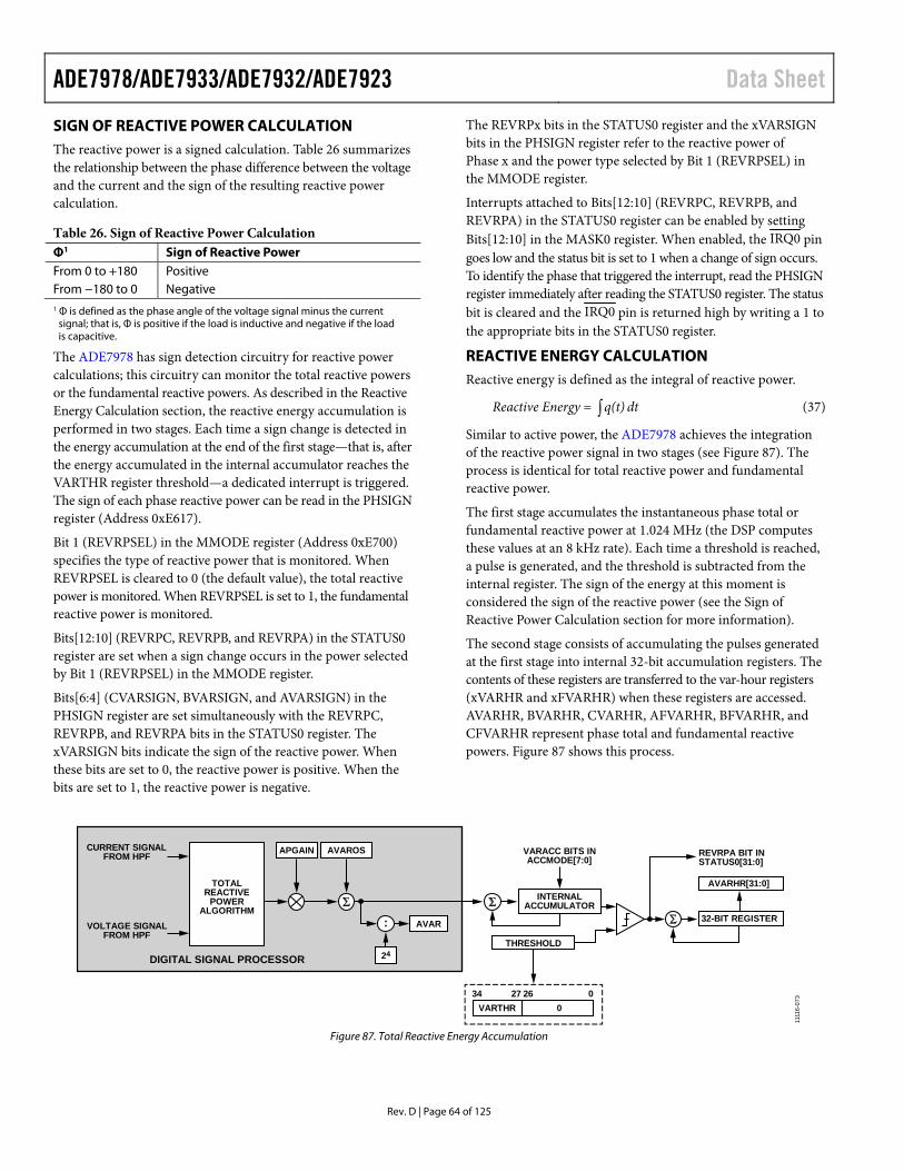
ADE7978/ADE7933/ADE7932/ADE7923 Data Sheet
Rev. D | Page 64 of 125
SIGN OF REACTIVE POWER CALCULATION The reactive power is a signed calculation. Table 26 summarizes the relationship between the phase difference between the voltage and the current and the sign of the resulting reactive power calculation.
Table 26. Sign of Reactive Power Calculation Φ1 Sign of Reactive Power From 0 to +180 Positive From −180 to 0 Negative 1 Φ is defined as the phase angle of the voltage signal minus the current
signal; that is, Φ is positive if the load is inductive and negative if the load is capacitive.
The ADE7978 has sign detection circuitry for reactive power calculations; this circuitry can monitor the total reactive powers or the fundamental reactive powers. As described in the Reactive Energy Calculation section, the reactive energy accumulation is performed in two stages. Each time a sign change is detected in the energy accumulation at the end of the first stage—that is, after the energy accumulated in the internal accumulator reaches the VARTHR register threshold—a dedicated interrupt is triggered. The sign of each phase reactive power can be read in the PHSIGN register (Address 0xE617).
Bit 1 (REVRPSEL) in the MMODE register (Address 0xE700) specifies the type of reactive power that is monitored. When REVRPSEL is cleared to 0 (the default value), the total reactive power is monitored. When REVRPSEL is set to 1, the fundamental reactive power is monitored.
Bits[12:10] (REVRPC, REVRPB, and REVRPA) in the STATUS0 register are set when a sign change occurs in the power selected by Bit 1 (REVRPSEL) in the MMODE register.
Bits[6:4] (CVARSIGN, BVARSIGN, and AVARSIGN) in the PHSIGN register are set simultaneously with the REVRPC, REVRPB, and REVRPA bits in the STATUS0 register. The xVARSIGN bits indicate the sign of the reactive power. When these bits are set to 0, the reactive power is positive. When the bits are set to 1, the reactive power is negative.
The REVRPx bits in the STATUS0 register and the xVARSIGN bits in the PHSIGN register refer to the reactive power of Phase x and the power type selected by Bit 1 (REVRPSEL) in the MMODE register.
Interrupts attached to Bits[12:10] (REVRPC, REVRPB, and REVRPA) in the STATUS0 register can be enabled by setting Bits[12:10] in the MASK0 register. When enabled, the IRQ0 pin goes low and the status bit is set to 1 when a change of sign occurs. To identify the phase that triggered the interrupt, read the PHSIGN register immediately after reading the STATUS0 register. The status bit is cleared and the IRQ0 pin is returned high by writing a 1 to the appropriate bits in the STATUS0 register.
REACTIVE ENERGY CALCULATION Reactive energy is defined as the integral of reactive power.
Reactive Energy = dt q(t) (37)
Similar to active power, the ADE7978 achieves the integration of the reactive power signal in two stages (see Figure 87). The process is identical for total reactive power and fundamental reactive power.
The first stage accumulates the instantaneous phase total or fundamental reactive power at 1.024 MHz (the DSP computes these values at an 8 kHz rate). Each time a threshold is reached, a pulse is generated, and the threshold is subtracted from the internal register. The sign of the energy at this moment is considered the sign of the reactive power (see the Sign of Reactive Power Calculation section for more information).
The second stage consists of accumulating the pulses generated at the first stage into internal 32-bit accumulation registers. The contents of these registers are transferred to the var-hour registers (xVARHR and xFVARHR) when these registers are accessed. AVARHR, BVARHR, CVARHR, AFVARHR, BFVARHR, and CFVARHR represent phase total and fundamental reactive powers. Figure 87 shows this process.
INTERNALACCUMULATOR
VARACC BITS INACCMODE[7:0]
THRESHOLD
DIGITAL SIGNAL PROCESSOR
TOTALREACTIVE
POWERALGORITHM
APGAIN AVAROS
24
AVAR:
VARTHR34 27 26 0
0
32-BIT REGISTER
AVARHR[31:0]
REVRPA BIT INSTATUS0[31:0]
CURRENT SIGNALFROM HPF
VOLTAGE SIGNALFROM HPF
1111
6-07
3
Figure 87. Total Reactive Energy Accumulation
Data Sheet ADE7978/ADE7933/ADE7932/ADE7923
Rev. D | Page 65 of 125
The threshold is formed by concatenating the 8-bit unsigned VARTHR register (Address 0xEA03) to 27 bits equal to 0. The VARTHR register is configured by the user and is the same for the total reactive and fundamental powers on all phases. Its value depends on how much energy is assigned to one LSB of the var-hour registers. For example, if a derivative of a volt ampere reactive hour, varh (10n varh, where n is an integer) is desired as one LSB of the xVARHR register, the VARTHR register is calculated using the following equation:
272
103600
××
×××=
FSFS
ns
IV
fPMAXVARTHR (38)
where: PMAX = 26,991,271 = 0x19BDAA7, the instantaneous power computed when the ADC inputs are at full scale. fS = 1.024 MHz, the frequency at which every instantaneous power computed by the DSP at 8 kHz is accumulated. VFS and IFS are the rms values of the phase voltages and currents when the ADC inputs are at full scale.
The VARTHR register is an 8-bit unsigned number, so its maxi-mum value is 28 − 1. Its default value is 0x3. Avoid using values lower than 3, that is, 2 or 1; never use the value 0 because the threshold must be a non-zero value.
This discrete time accumulation or summation is equivalent to integration in continuous time, as shown in Equation 39:
Reactive Energy =
×= ∑∫∞
=→ 00Lim
nTTq(nT)q(t)dt (39)
where: n is the discrete time sample number. T is the sample period.
In the ADE7978, the total phase reactive powers are accumulated in the 32-bit signed registers AVARHR, BVARHR, and CVARHR (Address 0xE406 to Address 0xE408). The fundamental phase reactive powers are accumulated in the 32-bit signed registers AFVARHR, BFVARHR, and CFVARHR (Address 0xE409 to Address 0xE40B). The reactive energy register contents can roll over to full-scale negative (0x80000000) and continue to increase in value when the reactive power is positive. Conversely, if the reactive power is negative, the energy register underflows to full-scale positive (0x7FFFFFFF) and continues to decrease in value.
The ADE7978 provides a status flag to indicate that one of the xVARHR registers is half full. Bit 2 (REHF) in the STATUS0 register (Address 0xE502) is set when Bit 30 of one of the xVARHR registers changes, signifying that one of these registers is half full.
• If the reactive power is positive, the var-hour register becomes half full when it increments from 0x3FFFFFFF to 0x40000000.
• If the reactive power is negative, the var-hour register becomes half full when it decrements from 0xC0000000 to 0xBFFFFFFF.
Similarly, Bit 3 (FREHF) in the STATUS0 register is set when Bit 30 of one of the xFVARHR registers changes, signifying that one of these registers is half full.
Setting Bits[3:2] in the MASK0 register enables the FREHF and REHF interrupts. When enabled, the IRQ0 pin goes low and the status bit is set to 1 when one of the energy registers (xVARHR for the REHF interrupt or xFVARHR for the FREHF interrupt), becomes half full. The status bit is cleared and the IRQ0 pin is returned high by writing a 1 to the appropriate bit in the STATUS0 register.
Setting Bit 6 (RSTREAD) in the LCYCMODE register (Address 0xE702) enables a read with reset for all var-hour accumulation registers, that is, the registers are reset to 0 after a read operation.
INTEGRATION TIME UNDER STEADY LOAD The discrete time sample period (T) for the accumulation registers is 976.5625 ns (1.024 MHz frequency). With full-scale sinusoidal signals on the analog inputs and a 90° phase difference between the voltage and current signals (the largest possible reactive power), the average word value representing the reactive power is PMAX = 26,991,271. If the VARTHR register threshold is set to 3 (its minimum recommended value), the first stage accumulator generates a pulse that is added to the var-hour registers at intervals of
sμ5683.1410024.1
236
27
=××
×
PMAX
The maximum value that can be stored in the var-hour accumu-lation register before it overflows is 231 − 1 or 0x7FFFFFFF. The integration time is calculated as
Time = 0x7FFFFFFF × 14.5683 µs = 8 hr, 41 min, 25 sec (40)
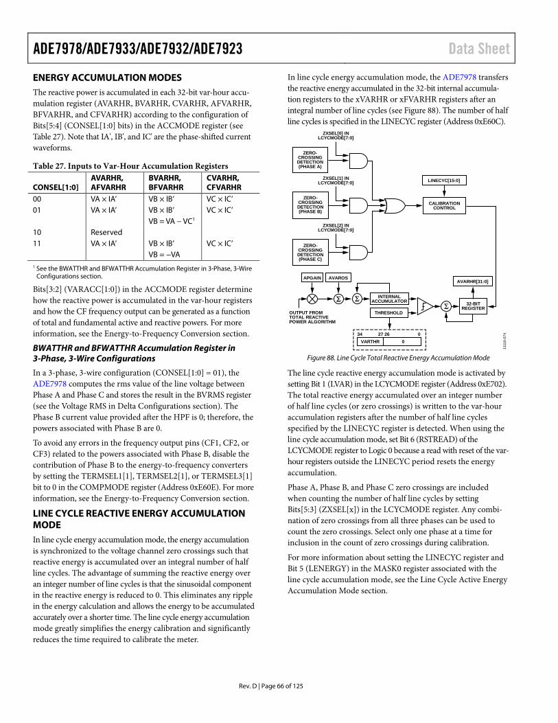
ADE7978/ADE7933/ADE7932/ADE7923 Data Sheet
Rev. D | Page 66 of 125
ENERGY ACCUMULATION MODES The reactive power is accumulated in each 32-bit var-hour accu-mulation register (AVARHR, BVARHR, CVARHR, AFVARHR, BFVARHR, and CFVARHR) according to the configuration of Bits[5:4] (CONSEL[1:0] bits) in the ACCMODE register (see Table 27). Note that IA', IB', and IC' are the phase-shifted current waveforms.
Table 27. Inputs to Var-Hour Accumulation Registers
CONSEL[1:0] AVARHR, AFVARHR
BVARHR, BFVARHR
CVARHR, CFVARHR
00 VA × IA’ VB × IB’ VC × IC’ 01 VA × IA’ VB × IB’ VC × IC’ VB = VA − VC1 10 Reserved 11 VA × IA’ VB × IB’ VC × IC’ VB = −VA 1 See the BWATTHR and BFWATTHR Accumulation Register in 3-Phase, 3-Wire
Configurations section.
Bits[3:2] (VARACC[1:0]) in the ACCMODE register determine how the reactive power is accumulated in the var-hour registers and how the CF frequency output can be generated as a function of total and fundamental active and reactive powers. For more information, see the Energy-to-Frequency Conversion section.
BWATTHR and BFWATTHR Accumulation Register in 3-Phase, 3-Wire Configurations
In a 3-phase, 3-wire configuration (CONSEL[1:0] = 01), the ADE7978 computes the rms value of the line voltage between Phase A and Phase C and stores the result in the BVRMS register (see the Voltage RMS in Delta Configurations section). The Phase B current value provided after the HPF is 0; therefore, the powers associated with Phase B are 0.
To avoid any errors in the frequency output pins (CF1, CF2, or CF3) related to the powers associated with Phase B, disable the contribution of Phase B to the energy-to-frequency converters by setting the TERMSEL1[1], TERMSEL2[1], or TERMSEL3[1] bit to 0 in the COMPMODE register (Address 0xE60E). For more information, see the Energy-to-Frequency Conversion section.
LINE CYCLE REACTIVE ENERGY ACCUMULATION MODE In line cycle energy accumulation mode, the energy accumulation is synchronized to the voltage channel zero crossings such that reactive energy is accumulated over an integral number of half line cycles. The advantage of summing the reactive energy over an integer number of line cycles is that the sinusoidal component in the reactive energy is reduced to 0. This eliminates any ripple in the energy calculation and allows the energy to be accumulated accurately over a shorter time. The line cycle energy accumulation mode greatly simplifies the energy calibration and significantly reduces the time required to calibrate the meter.
In line cycle energy accumulation mode, the ADE7978 transfers the reactive energy accumulated in the 32-bit internal accumula-tion registers to the xVARHR or xFVARHR registers after an integral number of line cycles (see Figure 88). The number of half line cycles is specified in the LINECYC register (Address 0xE60C).
ZERO-CROSSINGDETECTION(PHASE A)
ZERO-CROSSINGDETECTION(PHASE B)
CALIBRATIONCONTROL
ZERO-CROSSINGDETECTION(PHASE C)
LINECYC[15:0]
AVARHR[31:0]
ZXSEL[0] INLCYCMODE[7:0]
ZXSEL[1] INLCYCMODE[7:0]
ZXSEL[2] INLCYCMODE[7:0]
OUTPUT FROMTOTAL REACTIVEPOWER ALGORITHM
APGAIN AVAROS
INTERNALACCUMULATOR
THRESHOLD
32-BITREGISTER
VARTHR34 27 26 0
0
1111
6-07
4
Figure 88. Line Cycle Total Reactive Energy Accumulation Mode
The line cycle reactive energy accumulation mode is activated by setting Bit 1 (LVAR) in the LCYCMODE register (Address 0xE702). The total reactive energy accumulated over an integer number of half line cycles (or zero crossings) is written to the var-hour accumulation registers after the number of half line cycles specified by the LINECYC register is detected. When using the line cycle accumulation mode, set Bit 6 (RSTREAD) of the LCYCMODE register to Logic 0 because a read with reset of the var-hour registers outside the LINECYC period resets the energy accumulation.
Phase A, Phase B, and Phase C zero crossings are included when counting the number of half line cycles by setting Bits[5:3] (ZXSEL[x]) in the LCYCMODE register. Any combi-nation of zero crossings from all three phases can be used to count the zero crossings. Select only one phase at a time for inclusion in the count of zero crossings during calibration.
For more information about setting the LINECYC register and Bit 5 (LENERGY) in the MASK0 register associated with the line cycle accumulation mode, see the Line Cycle Active Energy Accumulation Mode section.

Data Sheet ADE7978/ADE7933/ADE7932/ADE7923
Rev. D | Page 67 of 125
APPARENT POWER CALCULATION Apparent power is defined as the maximum active power that can be delivered to a load. One way to obtain the apparent power is by multiplying the voltage rms value by the current rms value (also called the arithmetic apparent power).
S = V rms × I rms (41)
where: S is the apparent power. V rms and I rms are the rms voltage and current, respectively.
The ADE7978 computes the arithmetic apparent power on each phase. Figure 89 illustrates the signal processing in each phase for the calculation of the apparent power in the ADE7978. Because V rms and I rms contain all harmonic information, the apparent power computed by the ADE7978 is total apparent power. The ADE7978 does not compute fundamental apparent power.
The ADE7978 stores the instantaneous phase apparent powers in the AVA, BVA, and CVA registers (Address 0xE51E to Address 0xE520). The equation for apparent power is
42
1×××= PMAX
I
I
V
VxVAFSFS
(42)
where: V and I are the rms values of the phase voltage and current. VFS and IFS are the rms values of the phase voltage and current when the ADC inputs are at full scale. PMAX = 26,991,271, the instantaneous power computed when the ADC inputs are at full scale and in phase.
The xVA[23:0] waveform registers can be accessed using any of the serial port interfaces. For more information, see the Waveform Sampling Mode section.
The ADE7978 can also compute the apparent power by multi-plying the phase rms current by an rms voltage that is introduced externally. For more information, see the Apparent Power Calculation Using VNOM section.
APPARENT POWER GAIN CALIBRATION The average apparent power in each phase can be scaled by ±100% by writing to the appropriate 24-bit phase gain registers: APGAIN, BPGAIN, or CPGAIN (Address 0x4399 to Address 0x439B). The same registers are used to compensate the other powers computed by the ADE7978. For more information about these registers, see the Active Power Gain Calibration section.
APPARENT POWER OFFSET CALIBRATION Each rms measurement includes an offset compensation register to calibrate and eliminate the dc component in the rms value (see the Root Mean Square Measurement section). The voltage and current rms values are multiplied together in the apparent power signal processing. Because no additional offsets are created in the multiplication of the rms values, there is no specific offset compensation for the apparent power signal processing. The offset compensation of the apparent power measurement in each phase is accomplished by calibrating each individual rms measurement.
APPARENT POWER CALCULATION USING VNOM The ADE7978 can compute the apparent power by multiplying the phase rms current by an rms voltage introduced externally in the 24-bit signed VNOM register (Address 0xE533).
When one of Bits[13:11] (VNOMCEN, VNOMBEN, or VNOMAEN) in the COMPMODE register (Address 0xE60E) is set to 1, the apparent power in the specified phase (Phase x for VNOMxEN) is computed in this way. When the VNOMxEN bits are cleared to 0 (the default value), the arithmetic apparent power is computed.
The VNOM register value can be calculated as follows:
VNOM = V/VFS × 3,761,808 (43)
where: V is the nominal phase rms voltage. VFS is the rms value of the phase voltage when the ADC inputs are at full scale.
The serial ports of the ADE7978 work with 32-, 16-, or 8-bit words, whereas the DSP works with 28-bit words. Like the SAGLVL register, the VNOM register is transmitted as a 32-bit register with the eight MSBs padded with 0s (see Figure 69).
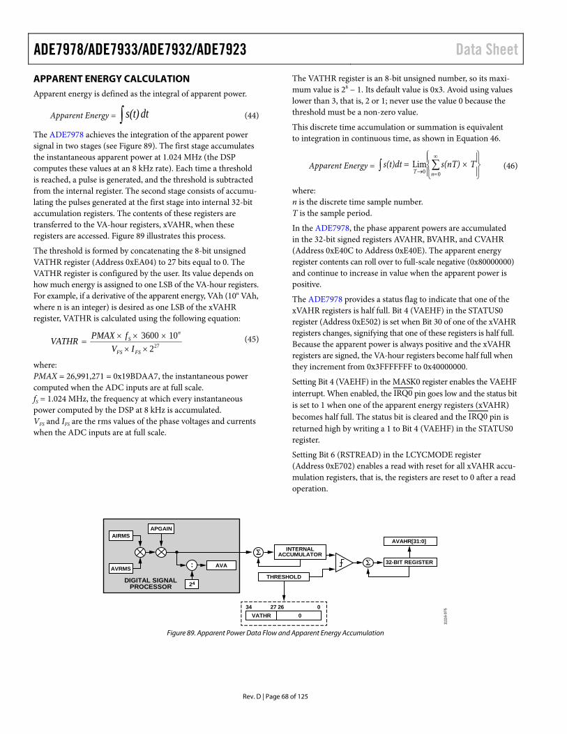
ADE7978/ADE7933/ADE7932/ADE7923 Data Sheet
Rev. D | Page 68 of 125
APPARENT ENERGY CALCULATION Apparent energy is defined as the integral of apparent power.
Apparent Energy = ∫ dt s(t) (44)
The ADE7978 achieves the integration of the apparent power signal in two stages (see Figure 89). The first stage accumulates the instantaneous apparent power at 1.024 MHz (the DSP computes these values at an 8 kHz rate). Each time a threshold is reached, a pulse is generated, and the threshold is subtracted from the internal register. The second stage consists of accumu-lating the pulses generated at the first stage into internal 32-bit accumulation registers. The contents of these registers are transferred to the VA-hour registers, xVAHR, when these registers are accessed. Figure 89 illustrates this process.
The threshold is formed by concatenating the 8-bit unsigned VATHR register (Address 0xEA04) to 27 bits equal to 0. The VATHR register is configured by the user. Its value depends on how much energy is assigned to one LSB of the VA-hour registers. For example, if a derivative of the apparent energy, VAh (10n VAh, where n is an integer) is desired as one LSB of the xVAHR register, VATHR is calculated using the following equation:
272103600
×××××
=FSFS
nS
IVfPMAXVATHR (45)
where: PMAX = 26,991,271 = 0x19BDAA7, the instantaneous power computed when the ADC inputs are at full scale. fS = 1.024 MHz, the frequency at which every instantaneous power computed by the DSP at 8 kHz is accumulated. VFS and IFS are the rms values of the phase voltages and currents when the ADC inputs are at full scale.
The VATHR register is an 8-bit unsigned number, so its maxi-mum value is 28 − 1. Its default value is 0x3. Avoid using values lower than 3, that is, 2 or 1; never use the value 0 because the threshold must be a non-zero value.
This discrete time accumulation or summation is equivalent to integration in continuous time, as shown in Equation 46.
Apparent Energy =
×= ∑∫∞
=→ 00Lim
nTTs(nT)s(t)dt (46)
where: n is the discrete time sample number. T is the sample period.
In the ADE7978, the phase apparent powers are accumulated in the 32-bit signed registers AVAHR, BVAHR, and CVAHR (Address 0xE40C to Address 0xE40E). The apparent energy register contents can roll over to full-scale negative (0x80000000) and continue to increase in value when the apparent power is positive.
The ADE7978 provides a status flag to indicate that one of the xVAHR registers is half full. Bit 4 (VAEHF) in the STATUS0 register (Address 0xE502) is set when Bit 30 of one of the xVAHR registers changes, signifying that one of these registers is half full. Because the apparent power is always positive and the xVAHR registers are signed, the VA-hour registers become half full when they increment from 0x3FFFFFFF to 0x40000000.
Setting Bit 4 (VAEHF) in the MASK0 register enables the VAEHF interrupt. When enabled, the IRQ0 pin goes low and the status bit is set to 1 when one of the apparent energy registers (xVAHR) becomes half full. The status bit is cleared and the IRQ0 pin is returned high by writing a 1 to Bit 4 (VAEHF) in the STATUS0 register.
Setting Bit 6 (RSTREAD) in the LCYCMODE register (Address 0xE702) enables a read with reset for all xVAHR accu-mulation registers, that is, the registers are reset to 0 after a read operation.
INTERNALACCUMULATOR
THRESHOLDDIGITAL SIGNALPROCESSOR
APGAIN
24
AVA:
VATHR34 27 26 0
0
32-BIT REGISTER
AVAHR[31:0]AIRMS
AVRMS
1111
6-07
5
Figure 89. Apparent Power Data Flow and Apparent Energy Accumulation
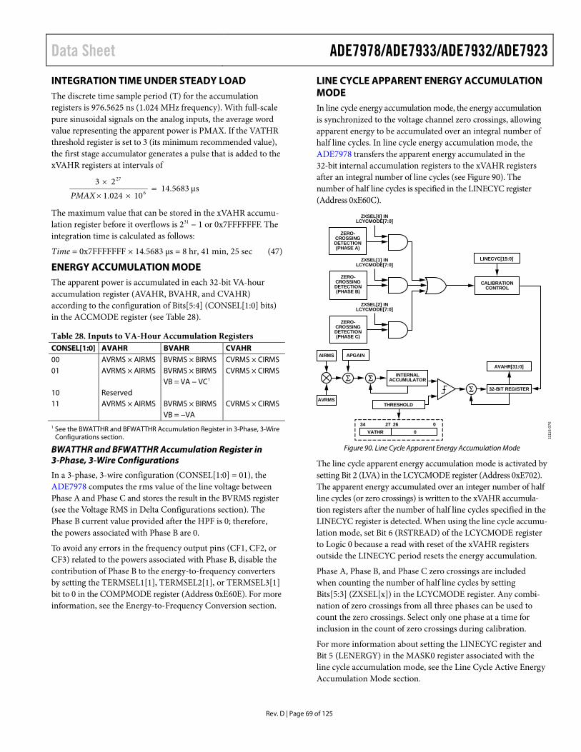
Data Sheet ADE7978/ADE7933/ADE7932/ADE7923
Rev. D | Page 69 of 125
INTEGRATION TIME UNDER STEADY LOAD The discrete time sample period (T) for the accumulation registers is 976.5625 ns (1.024 MHz frequency). With full-scale pure sinusoidal signals on the analog inputs, the average word value representing the apparent power is PMAX. If the VATHR threshold register is set to 3 (its minimum recommended value), the first stage accumulator generates a pulse that is added to the xVAHR registers at intervals of
sμ5683.1410024.1
236
27
=××
×
PMAX
The maximum value that can be stored in the xVAHR accumu-lation register before it overflows is 231 − 1 or 0x7FFFFFFF. The integration time is calculated as follows:
Time = 0x7FFFFFFF × 14.5683 µs = 8 hr, 41 min, 25 sec (47)
ENERGY ACCUMULATION MODE The apparent power is accumulated in each 32-bit VA-hour accumulation register (AVAHR, BVAHR, and CVAHR) according to the configuration of Bits[5:4] (CONSEL[1:0] bits) in the ACCMODE register (see Table 28).
Table 28. Inputs to VA-Hour Accumulation Registers CONSEL[1:0] AVAHR BVAHR CVAHR 00 AVRMS × AIRMS BVRMS × BIRMS CVRMS × CIRMS 01 AVRMS × AIRMS BVRMS × BIRMS CVRMS × CIRMS VB = VA − VC1 10 Reserved 11 AVRMS × AIRMS BVRMS × BIRMS CVRMS × CIRMS VB = −VA 1 See the BWATTHR and BFWATTHR Accumulation Register in 3-Phase, 3-Wire
Configurations section.
BWATTHR and BFWATTHR Accumulation Register in 3-Phase, 3-Wire Configurations
In a 3-phase, 3-wire configuration (CONSEL[1:0] = 01), the ADE7978 computes the rms value of the line voltage between Phase A and Phase C and stores the result in the BVRMS register (see the Voltage RMS in Delta Configurations section). The Phase B current value provided after the HPF is 0; therefore, the powers associated with Phase B are 0.
To avoid any errors in the frequency output pins (CF1, CF2, or CF3) related to the powers associated with Phase B, disable the contribution of Phase B to the energy-to-frequency converters by setting the TERMSEL1[1], TERMSEL2[1], or TERMSEL3[1] bit to 0 in the COMPMODE register (Address 0xE60E). For more information, see the Energy-to-Frequency Conversion section.
LINE CYCLE APPARENT ENERGY ACCUMULATION MODE In line cycle energy accumulation mode, the energy accumulation is synchronized to the voltage channel zero crossings, allowing apparent energy to be accumulated over an integral number of half line cycles. In line cycle energy accumulation mode, the ADE7978 transfers the apparent energy accumulated in the 32-bit internal accumulation registers to the xVAHR registers after an integral number of line cycles (see Figure 90). The number of half line cycles is specified in the LINECYC register (Address 0xE60C).
ZERO-CROSSINGDETECTION(PHASE A)
ZERO-CROSSINGDETECTION(PHASE B)
CALIBRATIONCONTROL
ZERO-CROSSINGDETECTION(PHASE C)
LINECYC[15:0]
ZXSEL[0] INLCYCMODE[7:0]
ZXSEL[1] INLCYCMODE[7:0]
ZXSEL[2] INLCYCMODE[7:0]
INTERNALACCUMULATOR
THRESHOLD
APGAIN
VATHR34 27 26 0
0
32-BIT REGISTER
AVAHR[31:0]
AIRMS
AVRMS
1111
6-07
6
Figure 90. Line Cycle Apparent Energy Accumulation Mode
The line cycle apparent energy accumulation mode is activated by setting Bit 2 (LVA) in the LCYCMODE register (Address 0xE702). The apparent energy accumulated over an integer number of half line cycles (or zero crossings) is written to the xVAHR accumula-tion registers after the number of half line cycles specified in the LINECYC register is detected. When using the line cycle accumu-lation mode, set Bit 6 (RSTREAD) of the LCYCMODE register to Logic 0 because a read with reset of the xVAHR registers outside the LINECYC period resets the energy accumulation.
Phase A, Phase B, and Phase C zero crossings are included when counting the number of half line cycles by setting Bits[5:3] (ZXSEL[x]) in the LCYCMODE register. Any combi-nation of zero crossings from all three phases can be used to count the zero crossings. Select only one phase at a time for inclusion in the count of zero crossings during calibration.
For more information about setting the LINECYC register and Bit 5 (LENERGY) in the MASK0 register associated with the line cycle accumulation mode, see the Line Cycle Active Energy Accumulation Mode section.

ADE7978/ADE7933/ADE7932/ADE7923 Data Sheet
Rev. D | Page 70 of 125
POWER FACTOR CALCULATION AND TOTAL HARMONIC DISTORTION CALCULATION POWER FACTOR CALCULATION The ADE7978 provides a direct power factor measurement simultaneously on all phases. Power factor in an ac circuit is defined as the ratio of the total active power flowing to the load to the apparent power. The absolute power factor measurement is defined in terms of leading or lagging, referring to whether the current waveform is leading or lagging the voltage waveform. When the current waveform is leading the voltage waveform, the load is capacitive and is defined as a negative power factor. When the current waveform is lagging the voltage waveform, the load is inductive and is defined as a positive power factor. Figure 91 illustrates the relationship of the current waveform to the voltage waveform.
V
I
ACTIVE (–)REACTIVE (–)PF (+)
CAPACITIVE:CURRENT LEADSVOLTAGE
INDUCTIVE:CURRENT LAGSVOLTAGE
ACTIVE (+)REACTIVE (–)
PF (–)
ACTIVE (–)REACTIVE (+)PF (–)
ACTIVE (+)REACTIVE (+)
PF (+)
θ = +60° PF = –0.5
θ = –60° PF = +0.5
1111
6-07
7
Figure 91. Capacitive and Inductive Loads
As shown in Figure 91, the reactive power measurement is negative when the load is capacitive and positive when the load is inductive. The sign of the reactive power can therefore be used to reflect the sign of the power factor. The ADE7978 uses the sign of the total reactive power as the sign of the absolute power factor. If the total reactive power is in a no load state, the sign of the power factor is the sign of the total active power.
Equation 48 shows the mathematical definition of power factor.
Power Factor = (Sign Total Reactive Power) × (48)
Power Apparent
Power ActiveTotal
The ADE7978 provides a power factor measurement on all phases simultaneously. These readings are stored in three 16-bit signed twos complement registers: APF (Address 0xE902) for Phase A, BPF (Address 0xE903) for Phase B, and CPF (Address 0xE904) for Phase C. The MSB of these registers indicates the polarity of the power factor. Each LSB of the APF, BPF, and CPF registers equates to a weight of 2−15. Therefore, the maximum register value of 0x7FFF equates to a power factor value of 1, and the minimum register value of 0x8000 corresponds to a power factor of −1. If the power factor is outside the −1 to +1 range (because of offset and gain calibrations), the result is set to −1 or +1, depending on the sign of the fundamental reactive power.
By default, the instantaneous total phase active and apparent powers are used to calculate the power factor; the registers are updated at a rate of 8 kHz. The sign bit is taken from the instantaneous total phase reactive energy measurement on each phase.
If a power factor measurement with more averaging is required, the ADE7978 can use the line cycle accumulation measurement on the active and apparent energies to determine the power factor. This option provides a more stable power factor reading.
To use the line cycle accumulation mode to determine the power factor, the ADE7978 must be configured as follows:
• Set the PFMODE bit (Bit 7) to 1 in the LCYCMODE register (Address 0xE702).
• Enable line cycle accumulation mode on both the active and apparent energies by setting the LWATT and LVA bits to 1 in the LCYCMODE register. The update rate of the power factor measurement is now an integral number of half line cycles that can be programmed in the LINECYC register (Address 0xE60C).
For complete information about configuring line cycle accumulation mode, see the Line Cycle Active Energy Accumulation Mode and Line Cycle Apparent Energy Accumulation Mode sections.
Note that the power factor measurement is affected by the no load condition if no load detection is enabled (see the No Load Condition section). If the apparent energy no load condition is true, the power factor measurement is set to 1. If the no load condition based on total active and reactive energies is true, the power factor measurement is set to 0.

Data Sheet ADE7978/ADE7933/ADE7932/ADE7923
Rev. D | Page 71 of 125
TOTAL HARMONIC DISTORTION CALCULATION The ADE7978 computes the total harmonic distortion (THD) on all phase currents and voltages. The THD expressions are shown in the following equations:
1
1I I
IITHD
22 −= (49)
1
1V V
VVTHD
22 −=
where: I and V are the rms values of the phase currents and voltages stored in the AIRMS, AVRMS, BIRMS, BVRMS, CIRMS, and CVRMS registers. I1 and V1 are the fundamental rms values stored in the AFIRMS, AFVRMS, BFIRMS, BFVRMS, CFIRMS, and CFVRMS registers.
The THD calculations are stored in the AVTHD, AITHD, BVTHD, BITHD, CVTHD, and CITHD registers (Address 0xE521 to Address 0xE526). These registers are 24-bit registers in 3.21 signed format. This means the ratios are limited to +3.9999 and all greater results are clamped to it.
Like the xIRMS and xFIRMS registers, the 24-bit signed xITHD and xVTHD registers are transmitted as 32-bit registers with the eight MSBs padded with 0s (see Figure 75).

ADE7978/ADE7933/ADE7932/ADE7923 Data Sheet
Rev. D | Page 72 of 125
WAVEFORM SAMPLING MODE The current and voltage waveform samples, as well as the active, reactive, and apparent power outputs and the total harmonic distortion values, are stored every 125 µs (8 kHz rate) in 24-bit signed registers that can be accessed using any of the serial port interfaces of the ADE7978. Table 29 lists these registers.
Bit 17 (DREADY) in the STATUS0 register (Address 0xE502) can be used to signal when the registers listed in Table 29 can be read using the I2C or SPI serial port. An interrupt attached to the flag can be enabled by setting Bit 17 (DREADY) in the MASK0 register (Address 0xE50A). For more information about the DREADY bit, see the Digital Signal Processor section.
In addition, if Bits[1:0] (ZX_DREADY) in the CONFIG register (Address 0xE618) are set to 00, the DREADY functionality is selected at the ZX/DREADY pin. In this case, the ZX/DREADY pin goes low approximately 70 ns after the DREADY bit is set to 1 in the STATUS0 register. The ZX/DREADY pin stays low for 10 µs and then returns high. The low to high transition of the ZX/DREADY pin can be used to initiate a burst read of the wave-form sample registers. For more information, see the I2C Burst Read Operation and the SPI Burst Read Operation sections.
The ADE7978 includes a high speed data capture (HSDC) port that is specially designed to provide fast access to the following waveform sample registers: IAWV, IBWV, ICWV, INWV, VAWV, VBWV, VCWV, AWATT, BWATT, CWATT, AVAR, BVAR, CVAR, AVA, BVA, and CVA. For more information about the HSDC interface, see the HSDC Interface section.
The serial ports of the ADE7978 work with 32-, 16-, or 8-bit words, whereas the DSP works with 28-bit words. Like the xIGAIN registers shown in Figure 52, the registers listed in Table 29 are sign extended to 28 bits and padded with four 0s for transmission as 32-bit registers.
Table 29. Waveform Sample Registers Register Description IAWV Phase A current IBWV Phase B current ICWV Phase C current INWV Neutral current VAWV Phase A voltage VBWV Phase B voltage VCWV Phase C voltage VA2WV Phase A auxiliary voltage VB2WV Phase B auxiliary voltage VC2WV Phase C auxiliary voltage VNWV Neutral line voltage VN2WV Neutral line auxiliary voltage AVA Phase A apparent power BVA Phase B apparent power CVA Phase C apparent power AWATT Phase A total active power BWATT Phase B total active power CWATT Phase C total active power AVAR Phase A total reactive power BVAR Phase B total reactive power CVAR Phase C total reactive power AVTHD Phase A voltage total harmonic distortion AITHD Phase A current total harmonic distortion BVTHD Phase B voltage total harmonic distortion BITHD Phase B current total harmonic distortion CVTHD Phase C voltage total harmonic distortion CITHD Phase C current total harmonic distortion

Data Sheet ADE7978/ADE7933/ADE7932/ADE7923
Rev. D | Page 73 of 125
ENERGY-TO-FREQUENCY CONVERSION The ADE7978 provides three frequency output pins: CF1, CF2, and CF3. The CF3 pin is multiplexed with the HSCLK pin of the HSDC interface. When HSDC is enabled, the CF3 functionality is disabled at the pin. The CF1 and CF2 pins are always available.
After initial calibration at manufacturing, the manufacturer or end customer verifies the energy meter calibration. One convenient way to verify the meter calibration is to provide an output frequency proportional to the active, reactive, or apparent power under steady load conditions. This output frequency can provide a simple, single-wire, optically isolated interface to external calibration equipment. Figure 92 illustrates the energy-to-frequency conversion in the ADE7978.
The DSP computes the instantaneous values of all phase powers: total active, fundamental active, total reactive, fundamental reactive, and apparent. For information about how the energy is sign accumulated in the xWATTHR, xFWATTHR, xVARHR, xFVARHR, and xVAHR registers, see the Active Energy Calculation, Reactive Energy Calculation, and Apparent Energy Calculation sections.
In the energy-to-frequency conversion process, the instantaneous powers generate signals at the frequency output pins (CF1, CF2, and CF3). One energy-to-frequency converter is used for every CFx pin. Each converter sums certain phase powers and generates a signal proportional to the sum.
Two sets of bits specify the powers that are converted on the CFx pins: the TERMSELx[2:0] bits and the CFxSEL[2:0] bits.
TERMSELx[2:0] BITS Bits[2:0] (TERMSEL1[2:0]), Bits[5:3] (TERMSEL2[2:0]), and Bits[8:6] (TERMSEL3[2:0]) of the COMPMODE register (Address 0xE60E) specify which phases are summed in the energy-to-frequency conversion.
• The TERMSEL1[2:0] bits configure the CF1 pin. • The TERMSEL2[2:0] bits configure the CF2 pin. • The TERMSEL3[2:0] bits configure the CF3 pin.
The TERMSELx[0] bits manage Phase A. When these bits are set to 1, Phase A power is included in the sum of powers at the CFx converter; when these bits are cleared to 0, Phase A power is not included in the sum of powers. The TERMSELx[1] bits manage Phase B, and the TERMSELx[2] bits manage Phase C.
Setting all TERMSELx[2:0] bits to 1 means that the powers from all three phases are added at the CFx converter. Clearing all TERMSELx[2:0] bits to 0 means that no phase power is added at the CFx converter and no CF pulse is generated.
CFxSEL[2:0] BITS Bits[2:0] (CF1SEL[2:0]), Bits[5:3] (CF2SEL[2:0]), and Bits[8:6] (CF3SEL[2:0]) in the CFMODE register (Address 0xE610) specify what type of power is used at the inputs of the CF1, CF2, and CF3 converters, respectively (see Table 30).
VA
WATT
VAR
FVAR
FWATT
CFxSEL BITS INCFMODEINSTANTANEOUS
PHASE AACTIVE POWER
DIGITAL SIGNALPROCESSOR
INSTANTANEOUSPHASE B
ACTIVE POWER
INSTANTANEOUSPHASE C
ACTIVE POWER
TERMSELx BITS INCOMPMODE
27
INTERNALACCUMULATOR
27
THRESHOLD
FREQUENCYDIVIDER
CFx PULSEOUTPUT
CFxDEN
WTHR34 27 26 0
0
REVPSUMx BIT OFSTATUS0[31:0]
1111
6-07
8
Figure 92. Energy-to-Frequency Conversion
Table 30. Description of the CFxSEL[2:0] Bits in the CFMODE Register CFxSEL[2:0] CFx Signal Proportional to the Sum of Registers Latched When CFxLATCH = 1 000 Total phase active powers AWATTHR, BWATTHR, CWATTHR 001 Total phase reactive powers AVARHR, BVARHR, CVARHR 010 Phase apparent powers AVAHR, BVAHR, CVAHR 011 Fundamental phase active powers AFWATTHR, BFWATTHR, CFWATTHR 100 Fundamental phase reactive powers AFVARHR, BFVARHR, CFVARHR 101 to 111 Reserved

ADE7978/ADE7933/ADE7932/ADE7923 Data Sheet
Rev. D | Page 74 of 125
By default, the TERMSELx[2:0] bits are set to 1, the CF1SEL[2:0] bits are set to 000, the CF2SEL[2:0] bits are set to 001, and the CF3SEL[2:0] bits are set to 010. Therefore, the default configuration for the energy-to-frequency converters is as follows:
• The CF1 converter produces signals proportional to the sum of the total active powers on all three phases.
• The CF2 converter produces signals proportional to the sum of the total reactive powers on all three phases.
• The CF3 converter produces signals proportional to the sum of the apparent powers on all three phases.
ENERGY-TO-FREQUENCY CONVERSION PROCESS The energy-to-frequency conversion is accomplished in two stages. The first stage is the same as for the energy accumulation processes described in the Active Energy Calculation, Reactive Energy Calculation, and Apparent Energy Calculation sections.
The second stage uses the frequency divider implemented by the 16-bit unsigned registers CF1DEN, CF2DEN, and CF3DEN (Address 0xE611 to Address 0xE613). The values of the CFxDEN registers depend on the meter constant (MC), measured in impulses/kWh, and how much energy is assigned to one LSB of the various energy registers (xWATTHR, xVARHR, and so on). For example, if a derivative of Wh (10n Wh, where n is an integer) is desired as one LSB of the xWATTHR register, CFxDEN is calculated using the following equation:
nMCCFxDEN
10]hWimpulses/k[103
×= (50)
The derivative of Wh must be selected to obtain a CFxDEN register value greater than 1. If CFxDEN = 1, the CFx pin stays active low for only 1 µs. For this reason, do not set the CFxDEN register to 1. The frequency converter cannot accommodate fractional results; the result of the division must be rounded to the nearest integer. If CFxDEN is set equal to 0, the ADE7978 considers it to be equal to 1.
The CFx pulse output stays low for 80 ms if the pulse period is greater than 160 ms (6.25 Hz). If the pulse period is less than 160 ms and CFxDEN is an even number, the duty cycle of the pulse output is exactly 50%. If the pulse period is less than 160 ms and CFxDEN is an odd number, the duty cycle of the pulse output is
(1 + 1/CFxDEN) × 50%
The maximum pulse frequency at the CF1, CF2 or CF3 pins is 68.8 kHz and is obtained on one phase under the following conditions:
• WTHR, VARTHR, and VATHR registers are set to 3. • CF1DEN, CF2DEN, and CF3DEN registers are set to 1. • Phase is supplied with in-phase full-scale currents and
voltages.
The CFx pulse output is active low. It is recommended that the pin be connected to an LED, as shown in Figure 93. No transistor is required to supplement the drive strength of the CFx pin.
VDD
CFx 1111
6-07
9
Figure 93. CFx Pin Recommended Connection
Bits[11:9] (CF3DIS, CF2DIS, and CF1DIS) of the CFMODE register (Address 0xE610) specify whether the frequency converter output is generated at the CF3, CF2, or CF1 pin. When Bit CFxDIS is set to 1 (the default value), the CFx pin is disabled and the pin stays high. When Bit CFxDIS is cleared to 0, the corresponding CFx pin output generates an active low signal.
Bits[16:14] (CF3, CF2, and CF1) in the MASK0 register (Address 0xE50A) manage the CF3, CF2, and CF1 interrupts. If the CFx bits are set and a high to low transition at the corresponding frequency converter output occurs, the IRQ0 interrupt is triggered and the appropriate bit in the STATUS0 register is set to 1. The interrupts are available even if the CFx outputs are not enabled by the CFxDIS bits in the CFMODE register.
SYNCHRONIZING ENERGY REGISTERS WITH THE CFx OUTPUTS The ADE7978 allows the contents of the phase energy accumulation registers to be synchronized with the generation of a CFx pulse. When a high to low transition at one frequency converter output occurs, the contents of all internal phase energy registers that relate to the power being output at the CFx pin are latched into the hour registers and then reset to 0. See Table 30 for the list of registers that are latched based on the CFxSEL[2:0] bits in the CFMODE register. All three phase registers are latched independent of the setting of the TERMSELx[2:0] bits of the COMPMODE register. Figure 94 shows this process for CF1SEL[2:0] = 010 (apparent powers contribute at the CF1 pin) and CFCYC = 2.
CFCYC = 2
AVAHR, BVAHR,CVAHR LATCHED
ENERGY REGISTERSRESET
AVAHR, BVAHR,CVAHR LATCHED
ENERGY REGISTERSRESET
CF1 PULSEBASED ON
PHASE A ANDPHASE B
APPARENTPOWERS
1111
6-08
0
Figure 94. Synchronizing AVAHR and BVAHR with CF1
The 8-bit unsigned CFCYC register (Address 0xE705) contains the number of high to low transitions at the frequency converter output between two consecutive latches. Avoid writing a new value to the CFCYC register during a high to low transition at any CFx pin.
Bits[14:12] (CF3LATCH, CF2LATCH, and CF1LATCH) of the CFMODE register enable the latching of the phase energy accumulation registers when the bits are set to 1. When these bits are cleared to 0 (the default state), no latching occurs. The latching process can be used even if the CFx outputs are not enabled by the CFxDIS bits in the CFMODE register.
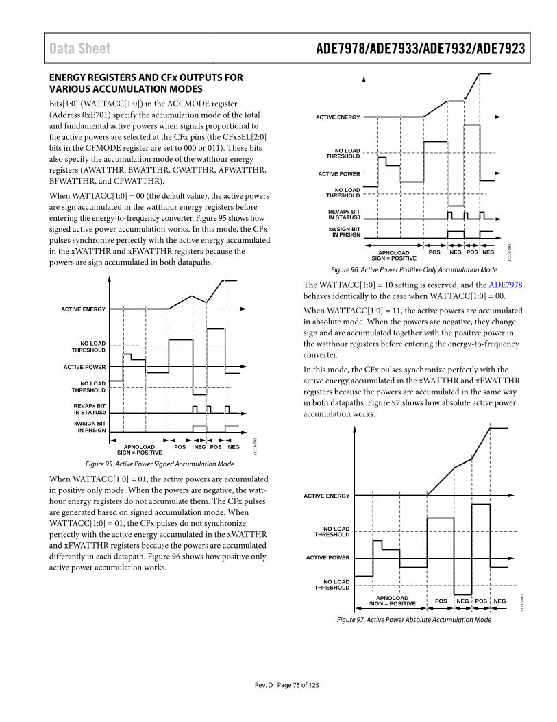
Data Sheet ADE7978/ADE7933/ADE7932/ADE7923
Rev. D | Page 75 of 125
ENERGY REGISTERS AND CFx OUTPUTS FOR VARIOUS ACCUMULATION MODES Bits[1:0] (WATTACC[1:0]) in the ACCMODE register (Address 0xE701) specify the accumulation mode of the total and fundamental active powers when signals proportional to the active powers are selected at the CFx pins (the CFxSEL[2:0] bits in the CFMODE register are set to 000 or 011). These bits also specify the accumulation mode of the watthour energy registers (AWATTHR, BWATTHR, CWATTHR, AFWATTHR, BFWATTHR, and CFWATTHR).
When WATTACC[1:0] = 00 (the default value), the active powers are sign accumulated in the watthour energy registers before entering the energy-to-frequency converter. Figure 95 shows how signed active power accumulation works. In this mode, the CFx pulses synchronize perfectly with the active energy accumulated in the xWATTHR and xFWATTHR registers because the powers are sign accumulated in both datapaths.
NEGPOSPOSAPNOLOADSIGN = POSITIVE
NEG
NO LOADTHRESHOLD
ACTIVE POWER
NO LOADTHRESHOLD
ACTIVE ENERGY
REVAPx BITIN STATUS0
xWSIGN BITIN PHSIGN
1111
6-08
1
Figure 95. Active Power Signed Accumulation Mode
When WATTACC[1:0] = 01, the active powers are accumulated in positive only mode. When the powers are negative, the watt-hour energy registers do not accumulate them. The CFx pulses are generated based on signed accumulation mode. When WATTACC[1:0] = 01, the CFx pulses do not synchronize perfectly with the active energy accumulated in the xWATTHR and xFWATTHR registers because the powers are accumulated differently in each datapath. Figure 96 shows how positive only active power accumulation works.
NEGPOSPOSAPNOLOADSIGN = POSITIVE
NEG
NO LOADTHRESHOLD
ACTIVE POWER
NO LOADTHRESHOLD
ACTIVE ENERGY
REVAPx BITIN STATUS0
xWSIGN BITIN PHSIGN
1111
6-08
2
Figure 96. Active Power Positive Only Accumulation Mode
The WATTACC[1:0] = 10 setting is reserved, and the ADE7978 behaves identically to the case when WATTACC[1:0] = 00.
When WATTACC[1:0] = 11, the active powers are accumulated in absolute mode. When the powers are negative, they change sign and are accumulated together with the positive power in the watthour registers before entering the energy-to-frequency converter.
In this mode, the CFx pulses synchronize perfectly with the active energy accumulated in the xWATTHR and xFWATTHR registers because the powers are accumulated in the same way in both datapaths. Figure 97 shows how absolute active power accumulation works.
NO LOADTHRESHOLD
ACTIVE POWER
NO LOADTHRESHOLD
ACTIVE ENERGY
1111
6-08
3
APNOLOADSIGN = POSITIVE POS NEG POS NEG
Figure 97. Active Power Absolute Accumulation Mode

ADE7978/ADE7933/ADE7932/ADE7923 Data Sheet
Rev. D | Page 76 of 125
Bits[3:2] (VARACC[1:0]) in the ACCMODE register specify the accumulation mode of the total and fundamental reactive powers when signals proportional to the reactive powers are selected at the CFx pins (the CFxSEL[2:0] bits in the CFMODE register are set to 001 or 100). These bits also specify the accumulation mode of the var-hour energy registers (AVARHR, BVARHR, CVARHR, AFVARHR, BFVARHR, and CFVARHR).
When VARACC[1:0] = 00 (the default value), the reactive powers are sign accumulated in the var-hour energy registers before entering the energy-to-frequency converter. Figure 98 shows how signed reactive power accumulation works. In this mode, the CFx pulses synchronize perfectly with the reactive energy accumulated in the xVARHR and xFVARHR registers because the powers are sign accumulated in both datapaths.
NEGPOSPOSVARNOLOADSIGN = POSITIVE
NEG
NO LOADTHRESHOLD
REACTIVEPOWER
NO LOADTHRESHOLD
REACTIVEENERGY
REVRPx BITIN STATUS0
xVARSIGN BITIN PHSIGN
1111
6-08
4
Figure 98. Reactive Power Signed Accumulation Mode
The VARACC[1:0] = 01 setting is reserved, and the ADE7978 behaves identically to the case when VARACC[1:0] = 00.
When VARACC[1:0] = 10, the reactive powers are accumulated depending on the sign of the corresponding active power in the var-hour energy registers before entering the energy-to-frequency converter. If the active power is positive or considered 0 when lower than the no load threshold APNOLOAD, the reactive power is accumulated as is. If the active power is negative, the sign of the reactive power is changed for accumulation.
Figure 99 shows how the sign adjusted reactive power accumulation mode works. In this mode, the CFx pulses synchronize perfectly with the reactive energy accumulated in the xVARHR and xFVARHR registers because the powers are accumulated in the same way in both datapaths.
POSPOSVARNOLOADSIGN = POSITIVE
NEG
NO LOADTHRESHOLD
NO LOADTHRESHOLD
NO LOADTHRESHOLD
REACTIVEPOWER
ACTIVEPOWER
REACTIVEENERGY
REVRPx BITIN STATUS0
xVARSIGN BITIN PHSIGN
1111
6-08
5
Figure 99. Reactive Power Sign Adjusted Mode
When VARACC[1:0] = 11, the reactive powers are accumulated in absolute mode. When the powers are negative, they change sign and are accumulated together with the positive power in the var-hour registers before entering the energy-to-frequency converter. In this mode, the CFx pulses synchronize perfectly with the reactive energy accumulated in the xVARHR and xFVARHR registers. Figure 100 shows how absolute reactive power accumulation works.
NEGPOSPOSVARNOLOADSIGN = POSITIVE
NEG
NO LOADTHRESHOLD
REACTIVE POWER
NO LOADTHRESHOLD
REACTIVE ENERGY
REVRPx BITIN STATUS0
xVARSIGN BITIN PHSIGN
1111
6-08
6
Figure 100. Reactive Power Absolute Accumulation Mode
Data Sheet ADE7978/ADE7933/ADE7932/ADE7923
Rev. D | Page 77 of 125
SIGN OF SUM OF PHASE POWERS IN THE CFx DATAPATH The ADE7978 has sign detection circuitry for the sum of phase powers that are used in the CFx datapath. As described in the Energy-to-Frequency Conversion Process section, the energy accumulation in the CFx datapath is executed in two stages. Each time a sign change is detected in the energy accumulation at the end of the first stage—that is, after the energy accumulated in the accumulator reaches one of the WTHR, VARTHR, or VATHR thresholds—a dedicated interrupt can be triggered synchronously with the corresponding CFx pulse. The sign of each sum can be read in the PHSIGN register (Address 0xE617).
Bit 18, Bit 13, and Bit 9 (REVPSUM3, REVPSUM2, and REVPSUM1, respectively) of the STATUS0 register are set to 1 when a sign change of the sum of powers in the CF3, CF2, or CF1 datapaths occurs. To correlate these events with the pulses gener-ated at the CFx pins after a sign change occurs, the REVPSUM3, REVPSUM2, or REVPSUM1 bit is set when a high to low transition occurs at the CF3, CF2, or CF1 pin, respectively.
Bit 8, Bit 7, and Bit 3 (SUM3SIGN, SUM2SIGN, and SUM1SIGN, respectively) of the PHSIGN register are set to 1 when the REVPSUM3, REVPSUM2, and REVPSUM1 bits are set to 1. The SUMxSIGN bits indicate the sign of the sum of phase powers. When these bits are cleared to 0, the sum is positive. When the bits are set to 1, the sum is negative.
Interrupts attached to Bit 18, Bit 13, and Bit 9 (REVPSUM3, REVPSUM2, and REVPSUM1, respectively) in the STATUS0 register are enabled by setting Bit 18, Bit 13, and Bit 9 in the MASK0 register. If enabled, the IRQ0 pin is set low and the status bit is set to 1 when a change of sign occurs. To identify the phase that triggered the interrupt, read the PHSIGN register immediately after reading the STATUS0 register. Then clear the status bit by writing a 1 to the appropriate bit in the STATUS0 register; the IRQ0 pin is set high again.

ADE7978/ADE7933/ADE7932/ADE7923 Data Sheet
Rev. D | Page 78 of 125
NO LOAD CONDITION The no load condition is defined in metering equipment standards as a condition where voltage is applied to the meter but no current flows in the current circuit. To eliminate any creep effects in the meter, the ADE7978 contains three separate no load detection circuits: one related to the total active and reactive powers, one related to the fundamental active and reactive powers, and one related to the apparent power.
NO LOAD DETECTION BASED ON TOTAL ACTIVE AND REACTIVE POWERS The no load condition based on the total active and reactive powers is triggered when no LSBs are accumulated in the total active and reactive energy registers on one phase (xWATTHR and xVARHR, x = A, B, or C) for the time specified in the APNOLOAD and VARNOLOAD registers. In the no load condition, the total active and reactive energies of the phase are not accumulated, and no CFx pulses are generated based on these energies.
The equations used to compute the values of the 16-bit unsigned registers APNOLOAD and VARNOLOAD are as follows:
PMAX
WTHRYAPNOLOAD
1716 2
12××
−−= (51)
PMAX
VARTHRYVARNOLOAD
1716 2
12××
−−=
where: Y is the required no load current threshold computed relative to full scale. For example, if the no load threshold current is set 10,000 times lower than the full-scale value, Y = 10,000. WTHR and VARTHR are the values stored in the WTHR and VARTHR registers. These values are used as the thresholds in the first stage energy accumulators for active and reactive energy, respectively (see the Active Energy Calculation and Reactive Energy Calculation sections). PMAX = 26,991,271, the instantaneous active power computed when the ADC inputs are at full scale.
The VARNOLOAD register (Address 0xE909) usually contains the same value as the APNOLOAD register (Address 0xE908). When both the APNOLOAD and VARNOLOAD registers are set to 0x0, the no load detection circuit is disabled. If the APNOLOAD or VARNOLOAD threshold is set to 0 and the other threshold is set to a non-zero value, the no load circuit is disabled, and the total active and reactive powers are accumulated without any restriction.
Bit 0 (NLOAD) in the STATUS1 register (Address 0xE503) is set when a no load condition based on the total active or reactive power is detected on one of the three phases. Bits[2:0] (NLPHASE[2:0]) in the PHNOLOAD register (Address 0xE608) indicate the state of all phases relative to a no load condition and are set simultaneously with the NLOAD bit in the STATUS1 register.
NLPHASE[0] indicates the state of Phase A, NLPHASE[1] indicates the state of Phase B, and NLPHASE[2] indicates the state of Phase C. When the NLPHASE[x] bit is cleared to 0, Phase x is not in a no load condition. When the bit is set to 1, Phase x is in a no load condition.
An interrupt attached to Bit 0 (NLOAD) in the STATUS1 register can be enabled by setting Bit 0 in the MASK1 register (Address 0xE50B). When enabled, the IRQ1 pin goes low and the status bit is set to 1 when any of the three phases enters or exits the no load condition. To identify the phase that triggered the interrupt, read the PHNOLOAD register immediately after reading the STATUS1 register. The status bit is cleared and the IRQ1 pin is returned high by writing a 1 to Bit 0 in the STATUS1 register.
NO LOAD DETECTION BASED ON FUNDAMENTAL ACTIVE AND REACTIVE POWERS The no load condition based on the fundamental active and reactive powers is triggered when no LSBs are accumulated in the fundamental active and reactive energy registers on one phase (xFWATTHR and xFVARHR, x = A, B, or C) for the time specified in the 16-bit unsigned APNOLOAD and VARNOLOAD registers. In the no load condition, the fundamental active and reactive energies of the phase are not accumulated, and no CFx pulses are generated based on these energies.
APNOLOAD and VARNOLOAD are the same no load thresholds set for the total active and reactive energies. When both the APNOLOAD and VARNOLOAD registers are set to 0x0, the no load detection circuit is disabled. If the APNOLOAD or VARNOLOAD threshold is set to 0 and the other threshold is set to a non-zero value, the no load circuit is disabled, and the fundamental active and reactive powers are accumulated without any restriction.
Bit 1 (FNLOAD) in the STATUS1 register is set when a no load condition based on the fundamental active or reactive power is detected on one of the three phases. Bits[5:3] (FNLPHASE[2:0]) in the PHNOLOAD register indicate the state of all phases relative to a no load condition and are set simultaneously with the FNLOAD bit in the STATUS1 register.
FNLPHASE[0] indicates the state of Phase A, FNLPHASE[1] indicates the state of Phase B, and FNLPHASE[2] indicates the state of Phase C. When the FNLPHASE[x] bit is cleared to 0, Phase x is not in a no load condition. When the bit is set to 1, Phase x is in a no load condition.
An interrupt attached to Bit 1 (FNLOAD) in the STATUS1 register can be enabled by setting Bit 1 in the MASK1 register. When enabled, the IRQ1 pin goes low and the status bit is set to 1 when any of the three phases enters or exits the no load condition. To identify the phase that triggered the interrupt, read the PHNOLOAD register immediately after reading the STATUS1 register. The status bit is cleared and the IRQ1 pin is returned high by writing a 1 to Bit 1 in the STATUS1 register.
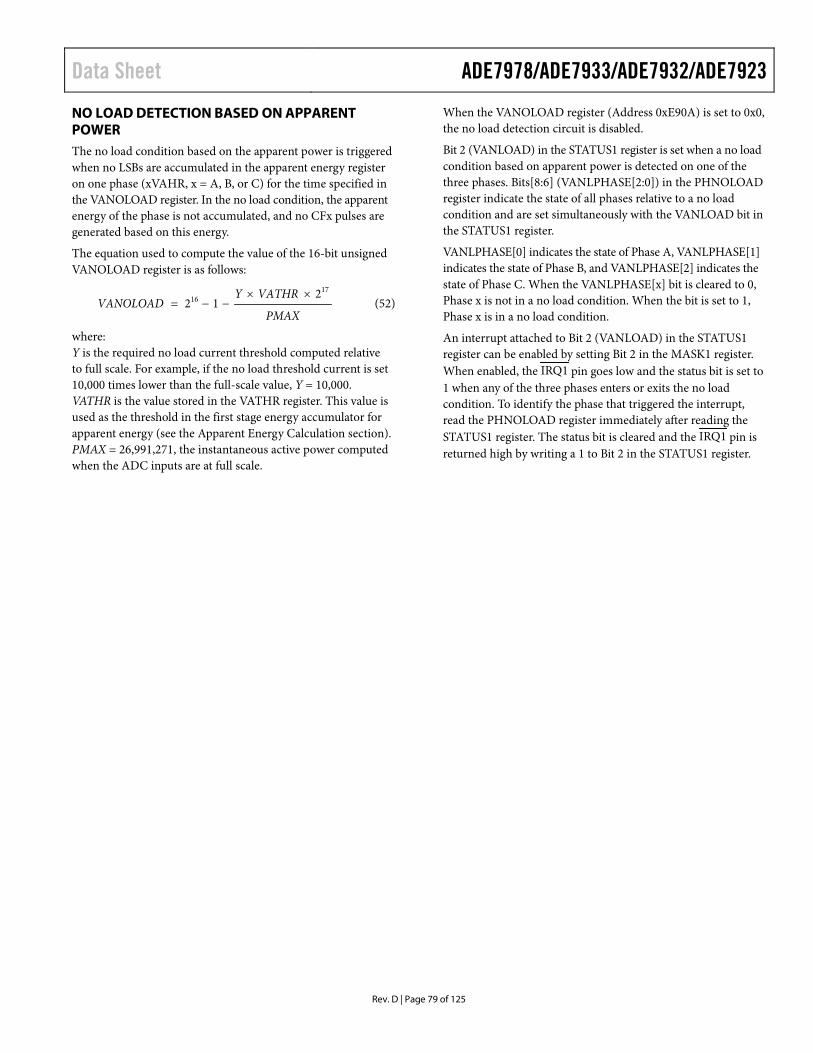
Data Sheet ADE7978/ADE7933/ADE7932/ADE7923
Rev. D | Page 79 of 125
NO LOAD DETECTION BASED ON APPARENT POWER The no load condition based on the apparent power is triggered when no LSBs are accumulated in the apparent energy register on one phase (xVAHR, x = A, B, or C) for the time specified in the VANOLOAD register. In the no load condition, the apparent energy of the phase is not accumulated, and no CFx pulses are generated based on this energy.
The equation used to compute the value of the 16-bit unsigned VANOLOAD register is as follows:
PMAX
VATHRYVANOLOAD
1716 2
12××
−−= (52)
where: Y is the required no load current threshold computed relative to full scale. For example, if the no load threshold current is set 10,000 times lower than the full-scale value, Y = 10,000. VATHR is the value stored in the VATHR register. This value is used as the threshold in the first stage energy accumulator for apparent energy (see the Apparent Energy Calculation section). PMAX = 26,991,271, the instantaneous active power computed when the ADC inputs are at full scale.
When the VANOLOAD register (Address 0xE90A) is set to 0x0, the no load detection circuit is disabled.
Bit 2 (VANLOAD) in the STATUS1 register is set when a no load condition based on apparent power is detected on one of the three phases. Bits[8:6] (VANLPHASE[2:0]) in the PHNOLOAD register indicate the state of all phases relative to a no load condition and are set simultaneously with the VANLOAD bit in the STATUS1 register.
VANLPHASE[0] indicates the state of Phase A, VANLPHASE[1] indicates the state of Phase B, and VANLPHASE[2] indicates the state of Phase C. When the VANLPHASE[x] bit is cleared to 0, Phase x is not in a no load condition. When the bit is set to 1, Phase x is in a no load condition.
An interrupt attached to Bit 2 (VANLOAD) in the STATUS1 register can be enabled by setting Bit 2 in the MASK1 register. When enabled, the IRQ1 pin goes low and the status bit is set to 1 when any of the three phases enters or exits the no load condition. To identify the phase that triggered the interrupt, read the PHNOLOAD register immediately after reading the STATUS1 register. The status bit is cleared and the IRQ1 pin is returned high by writing a 1 to Bit 2 in the STATUS1 register.

ADE7978/ADE7933/ADE7932/ADE7923 Data Sheet
Rev. D | Page 80 of 125
INTERRUPTS The ADE7978 has two interrupt pins, IRQ0 and IRQ1. Each pin is managed by a 32-bit interrupt mask register, MASK0 (Address 0xE50A) and MASK1 (Address 0xE50B), respectively. To enable an interrupt, the appropriate bit in the MASKx register must be set to 1. To disable an interrupt, the bit must be cleared to 0. Two 32-bit status registers, STATUS0 (Address 0xE502) and STATUS1 (Address 0xE503), are associated with the interrupts.
When an interrupt event occurs in the ADE7978, the correspond-ing flag in the status register is set to Logic 1 (see Table 45 and Table 46). If the mask bit for the interrupt in the interrupt mask register is Logic 1, the IRQx output goes active low. The flag bits in the status registers are set regardless of the state of the mask bits.
To determine the source of the interrupt, the microcontroller (MCU) reads the corresponding STATUSx register to identify which bit is set to 1. To clear the flag in the status register, the MCU writes back to the STATUSx register with the flag set to 1.
After an interrupt pin goes low, the status register is read and the source of the interrupt is identified. A 1 is written back to the status register to clear the status flag to 0. The IRQx pin remains low until the status flag is cleared.
By default, all interrupts are disabled with the exception of the RSTDONE interrupt. This interrupt cannot be disabled (masked) and, therefore, Bit 15 (RSTDONE) in the MASK1 register has no function. The IRQ1 pin always goes low and Bit 15 (RSTDONE) in the STATUS1 register is always set to 1 when a power-up or a hardware/software reset ends. To cancel the status flag, the STATUS1 register must be written with Bit 15 (RSTDONE) set to 1.
Certain interrupts are used in conjunction with other status registers. When the STATUSx register is read and one of the bits listed in Table 31 to Table 35 is set to 1, the status register asso-ciated with the bit is immediately read to identify the phase that triggered the interrupt. Only after reading the associated status register can the STATUSx register be written back with the bit set to 1.
Table 31 lists the bits in the MASK0 register that work with bits in the PHSIGN register (Address 0xE617).
Table 31. MASK0 Register Bits and PHSIGN Register Bits MASK0 Register (Address 0xE50A)
PHSIGN Register (Address 0xE617)
Bits Bit Name Bits Bit Name [8:6] REVAPx [2:0] xWSIGN[2:0] [12:10] REVRPx [6:4] xVARSIGN[2:0] 9 REVPSUM1 3 SUM1SIGN 13 REVPSUM2 7 SUM2SIGN 18 REVPSUM3 8 SUM3SIGN
Table 32 lists the bits in the MASK1 register that work with bits in the PHNOLOAD register (Address 0xE608).
Table 32. MASK1 Register Bits and PHNOLOAD Register Bits MASK1 Register (Address 0xE50B)
PHNOLOAD Register (Address 0xE608)
Bits Bit Name Bits Bit Name 0 NLOAD [2:0] NLPHASE[2:0] 1 FNLOAD [5:3] FNLPHASE[2:0] 2 VANLOAD [8:6] VANLPHASE[2:0]
Table 33 lists the bits in the MASK1 register that work with bits in the PHSTATUS register (Address 0xE600).
Table 33. MASK1 Register Bits and PHSTATUS Register Bits MASK1 Register (Address 0xE50B)
PHSTATUS Register (Address 0xE600)
Bits Bit Name Bits Bit Name 16 Sag [14:12] VSPHASE[2:0] 17 OI [5:3] OIPHASE[2:0] 18 OV [11:9] OVPHASE[2:0]
Table 34 and Table 35 list the bits in the MASK1 register that work with bits in the IPEAK register (Address 0xE500) and the VPEAK register (Address 0xE501).
Table 34. MASK1 Register Bits and IPEAK Register Bits MASK1 Register (Address 0xE50B)
IPEAK Register (Address 0xE500)
Bits Bit Name Bits Bit Name 23 PKI [26:24] IPPHASE[2:0]
Table 35. MASK1 Register Bits and VPEAK Register Bits MASK1 Register (Address 0xE50B)
VPEAK Register (Address 0xE501)
Bits Bit Name Bits Bit Name 24 PKV [26:24] VPPHASE[2:0]
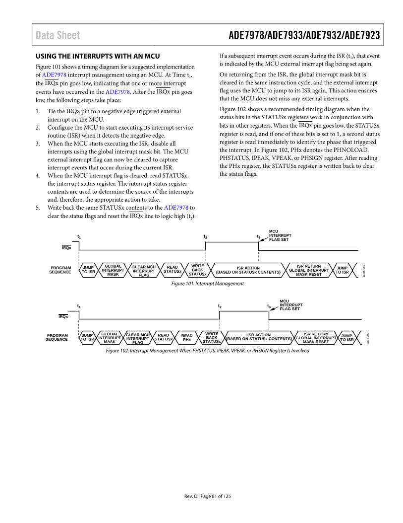
Data Sheet ADE7978/ADE7933/ADE7932/ADE7923
Rev. D | Page 81 of 125
USING THE INTERRUPTS WITH AN MCU Figure 101 shows a timing diagram for a suggested implementation of ADE7978 interrupt management using an MCU. At Time t1, the IRQx pin goes low, indicating that one or more interrupt events have occurred in the ADE7978. After the IRQx pin goes low, the following steps take place:
1. Tie the IRQx pin to a negative edge triggered external interrupt on the MCU.
2. Configure the MCU to start executing its interrupt service routine (ISR) when it detects the negative edge.
3. When the MCU starts executing the ISR, disable all interrupts using the global interrupt mask bit. The MCU external interrupt flag can now be cleared to capture interrupt events that occur during the current ISR.
4. When the MCU interrupt flag is cleared, read STATUSx, the interrupt status register. The interrupt status register contents are used to determine the source of the interrupts and, therefore, the appropriate action to take.
5. Write back the same STATUSx contents to the ADE7978 to clear the status flags and reset the IRQx line to logic high (t2).
If a subsequent interrupt event occurs during the ISR (t3), that event is indicated by the MCU external interrupt flag being set again.
On returning from the ISR, the global interrupt mask bit is cleared in the same instruction cycle, and the external interrupt flag uses the MCU to jump to its ISR again. This action ensures that the MCU does not miss any external interrupts.
Figure 102 shows a recommended timing diagram when the status bits in the STATUSx registers work in conjunction with bits in other registers. When the IRQx pin goes low, the STATUSx register is read, and if one of these bits is set to 1, a second status register is read immediately to identify the phase that triggered the interrupt. In Figure 102, PHx denotes the PHNOLOAD, PHSTATUS, IPEAK, VPEAK, or PHSIGN register. After reading the PHx register, the STATUSx register is written back to clear the status flags.
JUMPTO ISR
GLOBALINTERRUPT
MASK
CLEAR MCUINTERRUPT
FLAG
READSTATUSx
JUMPTO ISR
WRITEBACK
STATUSxISR ACTION
(BASED ON STATUSx CONTENTS)ISR RETURN
GLOBAL INTERRUPTMASK RESET
MCUINTERRUPTFLAG SET
PROGRAMSEQUENCE
t2t1 t3
IRQx
1111
6-08
9
Figure 101. Interrupt Management
PROGRAMSEQUENCE
IRQx
JUMPTO ISR
GLOBALINTERRUPT
MASK
CLEAR MCUINTERRUPT
FLAG
READSTATUSx
READPHx
JUMPTO ISR
WRITEBACK
STATUSxISR ACTION
(BASED ON STATUSx CONTENTS)ISR RETURN
GLOBAL INTERRUPTMASK RESET
MCUINTERRUPTFLAG SET
t2t1 t3
1111
6-09
0
Figure 102. Interrupt Management When PHSTATUS, IPEAK, VPEAK, or PHSIGN Register Is Involved
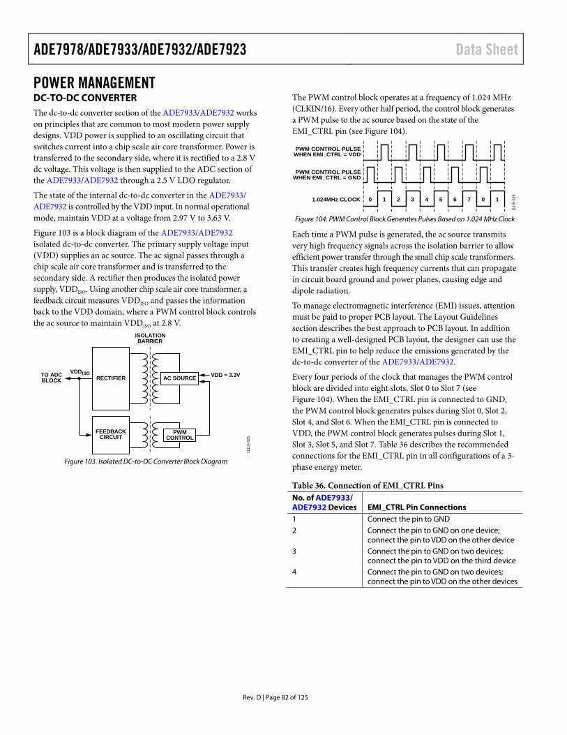
ADE7978/ADE7933/ADE7932/ADE7923 Data Sheet
Rev. D | Page 82 of 125
POWER MANAGEMENT DC-TO-DC CONVERTER The dc-to-dc converter section of the ADE7933/ADE7932 works on principles that are common to most modern power supply designs. VDD power is supplied to an oscillating circuit that switches current into a chip scale air core transformer. Power is transferred to the secondary side, where it is rectified to a 2.8 V dc voltage. This voltage is then supplied to the ADC section of the ADE7933/ADE7932 through a 2.5 V LDO regulator.
The state of the internal dc-to-dc converter in the ADE7933/ ADE7932 is controlled by the VDD input. In normal operational mode, maintain VDD at a voltage from 2.97 V to 3.63 V.
Figure 103 is a block diagram of the ADE7933/ADE7932 isolated dc-to-dc converter. The primary supply voltage input (VDD) supplies an ac source. The ac signal passes through a chip scale air core transformer and is transferred to the secondary side. A rectifier then produces the isolated power supply, VDDISO. Using another chip scale air core transformer, a feedback circuit measures VDDISO and passes the information back to the VDD domain, where a PWM control block controls the ac source to maintain VDDISO at 2.8 V.
AC SOURCE
ISOLATIONBARRIER
RECTIFIERVDDISO
FEEDBACKCIRCUIT
PWMCONTROL
TO ADCBLOCK
VDD = 3.3V
1111
6-02
5
Figure 103. Isolated DC-to-DC Converter Block Diagram
The PWM control block operates at a frequency of 1.024 MHz (CLKIN/16). Every other half period, the control block generates a PWM pulse to the ac source based on the state of the EMI_CTRL pin (see Figure 104).
0 1 2 3 4 5 6 7 0 1
PWM CONTROL PULSEWHEN EMI_CTRL = GND
PWM CONTROL PULSEWHEN EMI_CTRL = VDD
1.024MHz CLOCK
1111
6-02
6
Figure 104. PWM Control Block Generates Pulses Based on 1.024 MHz Clock
Each time a PWM pulse is generated, the ac source transmits very high frequency signals across the isolation barrier to allow efficient power transfer through the small chip scale transformers. This transfer creates high frequency currents that can propagate in circuit board ground and power planes, causing edge and dipole radiation.
To manage electromagnetic interference (EMI) issues, attention must be paid to proper PCB layout. The Layout Guidelines section describes the best approach to PCB layout. In addition to creating a well-designed PCB layout, the designer can use the EMI_CTRL pin to help reduce the emissions generated by the dc-to-dc converter of the ADE7933/ADE7932.
Every four periods of the clock that manages the PWM control block are divided into eight slots, Slot 0 to Slot 7 (see Figure 104). When the EMI_CTRL pin is connected to GND, the PWM control block generates pulses during Slot 0, Slot 2, Slot 4, and Slot 6. When the EMI_CTRL pin is connected to VDD, the PWM control block generates pulses during Slot 1, Slot 3, Slot 5, and Slot 7. Table 36 describes the recommended connections for the EMI_CTRL pin in all configurations of a 3-phase energy meter.
Table 36. Connection of EMI_CTRL Pins No. of ADE7933/ ADE7932 Devices EMI_CTRL Pin Connections 1 Connect the pin to GND 2 Connect the pin to GND on one device;
connect the pin to VDD on the other device 3 Connect the pin to GND on two devices;
connect the pin to VDD on the third device 4 Connect the pin to GND on two devices;
connect the pin to VDD on the other devices
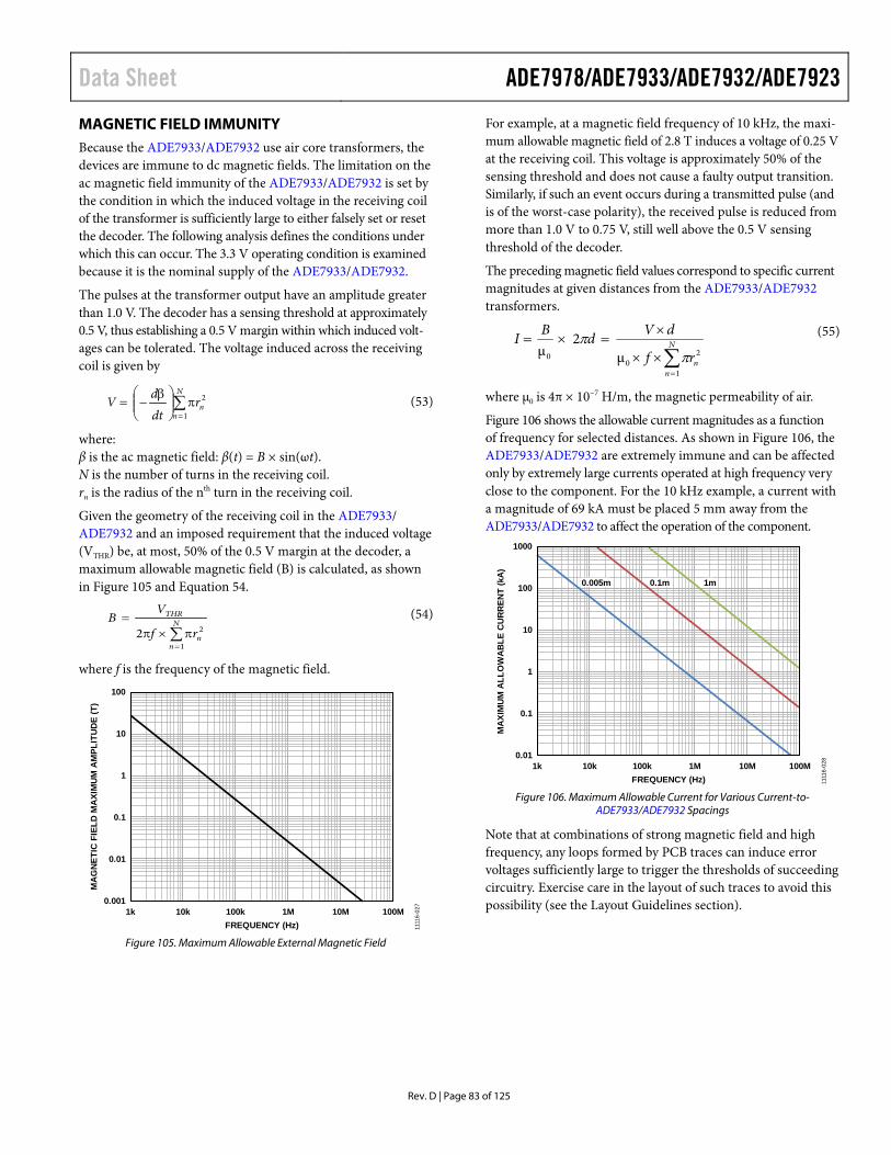
Data Sheet ADE7978/ADE7933/ADE7932/ADE7923
Rev. D | Page 83 of 125
MAGNETIC FIELD IMMUNITY Because the ADE7933/ADE7932 use air core transformers, the devices are immune to dc magnetic fields. The limitation on the ac magnetic field immunity of the ADE7933/ADE7932 is set by the condition in which the induced voltage in the receiving coil of the transformer is sufficiently large to either falsely set or reset the decoder. The following analysis defines the conditions under which this can occur. The 3.3 V operating condition is examined because it is the nominal supply of the ADE7933/ADE7932.
The pulses at the transformer output have an amplitude greater than 1.0 V. The decoder has a sensing threshold at approximately 0.5 V, thus establishing a 0.5 V margin within which induced volt-ages can be tolerated. The voltage induced across the receiving coil is given by
∑=π
β−=
N
nnr
dt
dV1
2 (53)
where: β is the ac magnetic field: β(t) = B × sin(ωt). N is the number of turns in the receiving coil. rn is the radius of the nth turn in the receiving coil.
Given the geometry of the receiving coil in the ADE7933/ ADE7932 and an imposed requirement that the induced voltage (VTHR) be, at most, 50% of the 0.5 V margin at the decoder, a maximum allowable magnetic field (B) is calculated, as shown in Figure 105 and Equation 54.
∑=π×π
= N
nn
THR
rf
VB
1
22 (54)
where f is the frequency of the magnetic field. 100
10
1
0.1
0.01
0.0011k 10k 100k 1M 10M 100M
MA
GN
ETIC
FIE
LD M
AXI
MU
M A
MPL
ITU
DE
(T)
FREQUENCY (Hz) 1111
6-02
7
Figure 105. Maximum Allowable External Magnetic Field
For example, at a magnetic field frequency of 10 kHz, the maxi-mum allowable magnetic field of 2.8 T induces a voltage of 0.25 V at the receiving coil. This voltage is approximately 50% of the sensing threshold and does not cause a faulty output transition. Similarly, if such an event occurs during a transmitted pulse (and is of the worst-case polarity), the received pulse is reduced from more than 1.0 V to 0.75 V, still well above the 0.5 V sensing threshold of the decoder.
The preceding magnetic field values correspond to specific current magnitudes at given distances from the ADE7933/ADE7932 transformers.
∑=
××
×=×= N
nnrf
dVdBI
1
20
0 μ2
μ ππ (55)
where µ0 is 4π × 10−7 H/m, the magnetic permeability of air.
Figure 106 shows the allowable current magnitudes as a function of frequency for selected distances. As shown in Figure 106, the ADE7933/ADE7932 are extremely immune and can be affected only by extremely large currents operated at high frequency very close to the component. For the 10 kHz example, a current with a magnitude of 69 kA must be placed 5 mm away from the ADE7933/ADE7932 to affect the operation of the component.
1000
100
10
1
0.1
0.011k 10k 100k 1M 10M 100M
MA
XIM
UM
ALL
OW
AB
LE C
UR
REN
T (k
A)
FREQUENCY (Hz)
0.005m 1m0.1m
1111
6-02
8
Figure 106. Maximum Allowable Current for Various Current-to-
ADE7933/ADE7932 Spacings
Note that at combinations of strong magnetic field and high frequency, any loops formed by PCB traces can induce error voltages sufficiently large to trigger the thresholds of succeeding circuitry. Exercise care in the layout of such traces to avoid this possibility (see the Layout Guidelines section).
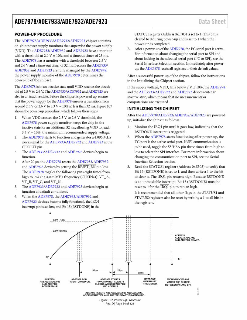
ADE7978/ADE7933/ADE7932/ADE7923 Data Sheet
Rev. D | Page 84 of 125
POWER-UP PROCEDURE The ADE7978/ADE7933/ADE7932/ADE7923 chipset contains on-chip power supply monitors that supervise the power supply (VDD). The ADE7933/ADE7932 and ADE7923 have a monitor with a threshold at 2.0 V ± 10% and a timeout timer of 23 ms. The ADE7978 has a monitor with a threshold between 2.5 V and 2.6 V and a time-out timer of 32 ms. Because the ADE7933/ ADE7932 and ADE7923 are fully managed by the ADE7978, the power supply monitor of the ADE7978 determines the power-up of the chipset.
The ADE7978 is in an inactive state until VDD reaches the thresh-old of 2.5 V to 2.6 V. The ADE7933/ADE7932 and ADE7923 are also in an inactive state. Before the chipset is powered up, ensure that the power supply for the ADE7978 ensures a transition from around 2.5 V or 2.6 V to 3.3 V − 10% in less than 32 ms. Figure 107 shows the power-up procedure, which follows these steps:
1. When VDD crosses the 2.5 V to 2.6 V threshold, the ADE7978 power supply monitor keeps the chip in the inactive state for an additional 32 ms, allowing VDD to reach 3.3 V − 10%, the minimum recommended supply voltage.
2. The ADE7978 starts to function and generates a 4.096 MHz clock signal for the ADE7933/ADE7932 and ADE7923 at the CLKOUT pin.
3. The ADE7933/ADE7932 and ADE7923 devices begin to function.
4. After 20 µs, the ADE7978 resets the ADE7933/ADE7932 and ADE7923 devices by setting the RESET_EN pin low. The ADE7978 toggles the following pins eight times from high to low at a 4.096 MHz frequency (CLKIN/4): VT_A, VT_B, VT_C, and VT_N.
5. The ADE7933/ADE7932 and ADE7923 devices begin to function at default conditions.
6. When the ADE7978, the ADE7933/ADE7932 and ADE7923 devices become fully functional, the IRQ1 interrupt pin is set low, and Bit 15 (RSTDONE) in the
STATUS1 register (Address 0xE503) is set to 1. This bit is cleared to 0 during power-up and is set to 1 when the power-up is completed.
7. After a power-up of the ADE7978, the I2C serial port is active. For information about changing the serial port to SPI and about locking in the selected serial port (I2C or SPI), see the Serial Interface Selection section. Immediately after power-up, the ADE7978 resets all registers to their default values.
After a successful power-up of the chipset, follow the instructions in the Initializing the Chipset section.
If the supply voltage, VDD, falls below 2 V ± 10%, the ADE7978 and the ADE7933/ADE7932 and ADE7923 devices enter an inactive state, which means that no measurements or computations are executed.
INITIALIZING THE CHIPSET After the ADE7978/ADE7933/ADE7932/ADE7923 are powered up, initialize the chipset as follows.
1. Monitor the IRQ1 pin until it goes low, indicating that the RSTDONE interrupt is triggered.
2. When the ADE7978 starts functioning after power-up, the I2C port is the active serial port. If SPI communication is to be used, toggle the SS/HSA pin three times from high to low to select the SPI interface. For more information about changing the communication port to SPI, see the Serial Interface Selection section.
3. Read the STATUS1 register (Address 0xE503) to verify that Bit 15 (RSTDONE) is set to 1, and then write a 1 to the bit to clear it. The IRQ1 pin returns high. Because RSTDONE is an unmaskable interrupt, Bit 15 (RSTDONE) must be reset to 0 for the IRQ1 pin to return high. It is recommended that all other flags in the STATUS1 and STATUS0 registers also be reset by writing a 1 to all bits in the registers.
20µs
ADE7978,ADE7933/ADE7932
AND ADE7923POWERED UP.
3.3V – 10%
2.5V TO 2.6V
ADE7978 STARTSFUNCTIONING. ADE7978
CLOCKS ADE7933/ADE7932AND ADE7923.
0V
32ms
ADE7978 PORTIMER TURNED ON.
RSTDONEINTERRUPTTRIGGERED.
ADE7978,ADE7933/ADE7932AND ADE7923 READY.
50ms
1111
6-20
1
MICROPROCESSORMAKES THE CHOICE
BETWEEN I2C AND SPI.
ADE7978 RESETS ADE7933/ADE7932 AND ADE7923.ADE7933/ADE7932 AND ADE7923 START FUNCTIONING.
Figure 107. Power-Up Procedure
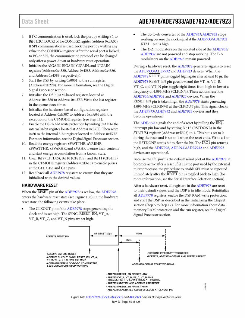
Data Sheet ADE7978/ADE7933/ADE7932/ADE7923
Rev. D | Page 85 of 125
4. If I2C communication is used, lock the port by writing a 1 to Bit 0 (I2C_LOCK) of the CONFIG2 register (Address 0xEA00). If SPI communication is used, lock the port by writing any value to the CONFIG2 register. After the serial port is locked to I2C or SPI, the communication protocol can be changed only after a power-down or hardware reset operation.
5. Initialize the AIGAIN, BIGAIN, CIGAIN, and NIGAIN registers (Address 0x4380, Address 0x4383, Address 0x4386, and Address 0x4389, respectively).
6. Start the DSP by writing 0x0001 to the run register (Address 0xE228). For more information, see the Digital Signal Processor section.
7. Initialize the DSP RAM-based registers located at Address 0x4380 to Address 0x43BF. Write the last register in the queue three times.
8. Initialize the hardware-based configuration registers located at Address 0xE507 to Address 0xEA04 with the exception of the CFMODE register (see Step 11).
9. Enable the DSP RAM write protection by writing 0xAD to the internal 8-bit register located at Address 0xE7FE. Then write 0x80 to the internal 8-bit register located at Address 0xE7E3. For more information, see the Digital Signal Processor section.
10. Read the energy registers xWATTHR, xVARHR, xFWATTHR, xFVARHR, and xVAHR to erase their contents and start energy accumulation from a known state.
11. Clear Bit 9 (CF1DIS), Bit 10 (CF2DIS), and Bit 11 (CF3DIS) in the CFMODE register (Address 0xE610) to enable pulses at the CF1, CF2, and CF3 pins.
12. Read back all ADE7978 registers to ensure that they are initialized with the desired values.
HARDWARE RESET
When the RESET pin of the ADE7978 is set low, the ADE7978 enters the hardware reset state (see Figure 108). In the hardware reset state, the following events take place:
• The CLKOUT pin of the ADE7978 stops generating the clock and is set high. The SYNC, RESET_EN, VT_A, VT_B, VT_C, and VT_N pins are set high.
• The dc-to-dc converter of the ADE7933/ADE7932 stops working because the clock signal at the ADE7933/ADE7932 XTAL1 pin is high.
• The Σ-Δ modulators on the isolated side of the ADE7933/ ADE7932 are not powered and stop working. The Σ-Δ modulators on the ADE7923 remain powered.
During a hardware reset, the ADE7978 generates signals to reset the ADE7933/ADE7932 and ADE7923 devices. When the ADE7978 RESET pin is toggled high again after at least 10 µs, the ADE7978 RESET_EN pin goes low, and the VT_A, VT_B, VT_C, and VT_N pins toggle eight times from high to low at a frequency of 4.096 MHz (CLKIN/4). These actions reset the ADE7933/ADE7932 and ADE7923 devices. When the RESET_EN pin is taken high, the ADE7978 starts generating 4.096 MHz (CLKIN/4) at the CLKOUT pin. This signal clocks the ADE7933/ADE7932 and ADE7923 devices and they become operational.
The ADE7978 signals the end of a reset by pulling the IRQ1 interrupt pin low and by setting Bit 15 (RSTDONE) in the STATUS1 register (Address 0xE503) to 1. This bit is set to 0 during the reset and is set to 1 when the reset ends. Write a 1 to the RSTDONE status bit to clear the bit. The IRQ1 pin returns high, and the ADE7978, ADE7933/ADE7932 and ADE7923 devices are operational.
Because the I2C port is the default serial port of the ADE7978, it becomes active after a reset. If SPI is the port used by the external microprocessor, the procedure to enable SPI must be repeated immediately after the RESET pin is toggled back to high (for more information, see the Serial Interface Selection section).
After a hardware reset, all registers in the ADE7978 are reset to their default values, and the DSP is in idle mode. Reinitialize all ADE7978 registers, enable the DSP RAM write protection, and start the DSP, as described in the Initializing the Chipset section (Step 5 to Step 12). For more information about data memory RAM protection and the run register, see the Digital Signal Processor section.
ADE7933/ADE7932 AND ADE7923 ARE RESET
1111
6-10
2
ADE7978 RESET PIN
•ADE7978 ENTERS RESET•ADE7978 CLKOUT, SYNC, RESET_EN, VT_A,VT_B, VT_C, VT_N PINS SET HIGH
•ADE7933/ADE7932 DC-TO-DC CONVERTERS,Σ-Δ MODULATORS STOP WORKING
•ADE7978 RESET_EN PIN SET LOW•ADE7978 VT_A, VT_B, VT_C, VT_N PINSTOGGLE HIGH TO LOW 8 TIMES AT 4.096MHZ
••ADE7978 RESET_EN PIN SET HIGH•ADE7978 GENERATES 4.096MHZ CLOCK AT CLKOUT PIN
AT LEAST 10µs
•RSTDONE INTERRUPT TRIGGERED•ADE7978, ADE7933/ADE7932 AND ADE7923 READY
ADE7933/ADE7932 START WORKING
50ms
10ms
Figure 108. ADE7978/ADE7933/ADE7932 and ADE7923 Chipset During Hardware Reset
ADE7978/ADE7933/ADE7932/ADE7923 Data Sheet
Rev. D | Page 86 of 125
ADE7978/ADE7933/ADE7932 AND ADE7923 CHIPSET SOFTWARE RESET Bit 7 (SWRST) in the CONFIG register (Address 0xE618) manages the software reset functionality of the ADE7978, ADE7933/ ADE7932, and ADE7923 devices. The default value of this bit is 0. If this bit is set to 1, the ADE7978, ADE7933/ADE7932, and ADE7923 devices enter the software reset state. In this state, all internal registers are reset to their default values. However, the serial port selection, I2C or SPI, remains unchanged if the lock-in procedure was executed before the reset (see the Serial Interface Selection section for more information).
The ADE7978 signals the end of the reset by pulling the IRQ1 interrupt pin low and setting Bit 15 (RSTDONE) in the STATUS1 register (Address 0xE503) to 1. This bit is set to 0 during the reset and is set to 1 when the reset ends. Write a 1 to the RSTDONE status bit to clear the bit; the IRQ1 pin returns high.
After a software reset, all registers in the ADE7978 are reset to their default values, the DSP is in idle mode, and Bit 7 (SWRST) is cleared to 0. Reinitialize all ADE7978 registers, enable the DSP RAM write protection, and start the DSP, as described in the Initializing the Chipset section (Step 5 to Step 12). For more information about data memory RAM protection and the run register, see the Digital Signal Processor section.
During a software reset of the ADE7978, the ADE7978 resets the ADE7933/ADE7932 and ADE7923 devices while continuing to generate the clock at the CLKOUT pin. The ADE7978 RESET_EN pin goes low, and the VT_A, VT_B, VT_C, and VT_N pins toggle eight times from high to low at a frequency of 4.096 MHz (CLKIN/4). The RESET_EN, VT_A, VT_B, VT_C, and VT_N pins are then taken high, and the reset ends.
ADE7933/ADE7932 AND ADE7923 SOFTWARE RESET To reset only the ADE7933/ADE7932 and ADE7923 devices without resetting the ADE7978, use Bit 7 (ADE7933_SWRST) in the CONFIG3 register (Address 0xE708). This bit resets the ADE7933/ADE7932 and ADE7923 devices by setting the RESET_EN pin low and toggling the VT_A, VT_B, VT_C, and VT_N pins from high to low eight times at 4.096 MHz (CLKIN/4). When the reset ends, the ADE7933_SWRST bit is cleared to 0.
The recommended procedure to perform a software reset of the ADE7933/ADE7932 and ADE7923 devices only is as follows:
1. Write to the CONFIG3 register with Bit 7 (ADE7933_ SWRST) set to 1.
2. Read back the CONFIG3 register until Bit 7 reads as 0, indicating that the reset has ended.
LOW POWER MODE Under certain conditions, it may be desirable to lower the current consumption of the chipset; in this case, the ADE7978, ADE7933/ADE7932, and ADE7923 can be set to a low power mode.
To enter low power mode, set Bit 6 (CLKOUT_DIS) and Bit 7 (ADE7933_SWRST) in the CONFIG3 register (Address 0xE708) to 1. The ADE7978 stops generating the clock to the ADE7933/ ADE7932 and ADE7923 devices and places them in the reset state.
To exit the low power mode, clear Bit 6 (CLKOUT_DIS) and Bit 7 (ADE7933_SWRST) in the CONFIG3 register to 0. During low power mode, the ADE7978 registers maintain their configurations, so they do not need to be reinitialized.

Data Sheet ADE7978/ADE7933/ADE7932/ADE7923
Rev. D | Page 87 of 125
APPLICATIONS INFORMATION The ADE7978, ADE7933/ADE7932 and ADE7923 chipset was designed for use in 3-phase energy metering systems in which one master device, usually a microcontroller, manages the ADE7978 through an I2C or SPI interface. The ADE7978 then manages two, three, or four ADE7933/ADE7932 and ADE7923 devices. The ADE7978, ADE7933/ADE7932 and ADE7923 chipset can be used in in 3-phase 4-wire and 3-phase 3-wire networks in a direct connection architecture. They cannot be used in 3-phase networks that require an indirect connection through current or voltage transformers as these require physical separation of the current and voltage sensing circuits.
The ADE7978 is not the only chip capable of managing multiple ADE7933/ADE7932 devices. Any microcontroller that conforms to the ADE7933/ADE7932 and ADE7923 serial interface can manage the devices correctly. (For more information, see the Bit Stream Communication Between the ADE7978 and the ADE7933/ADE7932 and ADE7923 section). However, similar devices, such as the ADE7913/ADE7912 3-channel, isolated, Σ-Δ ADCs with an SPI interface and ADE7903 3-channel Σ-Δ ADCs with an SPI interface, may be more suitable for direct interfacing with a microcontroller. For more information about the ADE7913/ADE7912 and ADE7903 ADCs, see the product pages for these devices.
Figure 109 shows Phase A of a 3-phase energy meter. The Phase A current, IA, is sensed with a shunt. A pole of the shunt is connected to the IM pin of the ADE7933/ADE7932 and becomes the ground of the isolated side of the ADE7933/ADE7932, GNDISO. The Phase A to neutral voltage, VAN, is sensed with a resistor divider, and the VM pin is also connected to the IM and GNDISO pins. Note that the voltages measured by the ADCs of the ADE7933/ ADE7932 are opposite to VAN and IA, a classic approach in single-phase metering. The other ADE7933/ADE7932 devices, which monitor Phase B and Phase C, are connected in a similar way.
NEUTRAL PHASE A PHASE AADE7932/ADE7933
IP
IMGNDISO
V1P
VM
IA
VAN
1111
6-01
7
Figure 109. Phase A ADE7933/ADE7932 Current and Voltage Sensing
Figure 110 shows how to connect the ADE7923 inputs when the neutral line of a 3-phase system is monitored. The neutral current is sensed using a shunt, and the voltage across the shunt is measured at the fully differential inputs IP and IM.
The neutral to earth voltage or any voltage referenced to ground can be sensed with a voltage divider at the single-ended inputs, V1P and VM.
NEUTRALNEUTRAL LINE
ADE7923
IP
IM
V1PVM
GNDISO
IN
1111
6-10
4
Figure 110. Neutral Line and Auxiliary Voltage Monitoring
with the ADE7923
DIFFERENCES BETWEEN THE ADE7923 AND THE ADE7933/ADE7932 The ADE7923 is a nonisolated Σ-Δ ADC similar to the ADE7933. The performance of both the ADE7923 and ADE7933/ADE7932 is identical, with the only differences caused by the absence of an isolation barrier. The dynamic range and accuracy of the ADE7923 is equal to that of the ADE7933/ADE7932. The ADE7923 has two voltage channel inputs, V1P and V2P, and one current channel input, IP. This nonisolated ADC is useful when neutral current monitoring is needed but there is no requirement for isolation from the neutral line. It is important to note that the system is grounded on the neutral line with this configuration.
The current channel is used for measuring neutral current whereas the two voltage channels can be used for auxiliary voltage measurements such as measuring a battery or any other voltage measurement that is referenced to ground.
The ADE7923 is pin-to-pin-compatible with the ADE7933/ ADE7932 isolated ADCs and has the same footprint; therefore, the ADE7923 and ADE7933/ADE7932 are direct swap-compatible.
ADE7978, ADE7933/ADE7932 AND ADE7923 IN POLYPHASE ENERGY METERS A polyphase energy meter must manage three phases and an optional neutral line. Figure 111 shows an example of a 3-phase meter built for a 4-wire wye configuration. Three ADE7933/ ADE7932 devices read the phase currents and voltages. An ADE7923 manages the neutral line measurements. However, if isolation is required, an ADE7933/ADE7932 can be used for the neutral line to isolate it similarly to the other phases. If the neutral line measurements are not required, only three ADE7933/ADE7932 devices are used (see Figure 112); in this configuration, the DATA_N pin of the ADE7978 is connected to VDD.

ADE7978/ADE7933/ADE7932/ADE7923 Data Sheet
Rev. D | Page 88 of 125
NEU
TRA
L
PHA
SE C
ISOLATIONBARRIER
LOAD
PHA
SE A
PHA
SE B
PHASE BADE7932/ADE7933IP
IM
V1PVM
V2P
GNDMCUGNDISO_B
3.3V
PHASE CADE7932/ADE7933IP
IM
V1PVM
V2P
GNDMCUGNDISO_C
3.3V
IP
IM
V1PVM
V2P
GNDMCU
3.3V
ADE7978
GNDMCU
3.3V
3.3V
SYST
EMM
ICR
OC
ON
TRO
LLER
I2C/HSDC OR SPI
IRQ0, IRQ1
PHASE AADE7932/ADE7933
NEUTRAL LINEADE7923
IP
IM
V1PVM
V2P
GNDMCUGNDISO_A
3.3V
SYNC
CLKOUTRESET_EN
DATA_AVT_A
DATA_BVT_B
DATA_CVT_C
DATA_NVT_N
DATA
SYNC
XTAL1
V2/TEMP
RESET_EN
DATA
SYNC
XTAL1
V2/TEMP
RESET_EN
DATA
SYNC
XTAL1
V2/TEMP
RESET_EN
DATA
SYNC
XTAL1
V2/TEMP
RESET_EN
1111
6-10
5
Figure 111. 3-Phase, 4-Wire Wye Meter with One ADE7978, Three ADE7933/ADE7932 Devices, and One ADE7923
NEU
TRA
L
PHA
SE C
ISOLATIONBARRIER
PHA
SE A
PHA
SE B
PHASE BADE7932/ADE7933IP
IM
V1PVM
V2P
GNDMCUGNDISO_B
3.3V
PHASE CADE7932/ADE7933IP
IM
V1PVM
V2P
GNDMCUGNDISO_C
3.3V
ADE7978
GNDMCU
3.3V
3.3V
SYST
EMM
ICR
OC
ON
TRO
LLER
I2C/HSDC OR SPI
IRQ0, IRQ1
PHASE AADE7932/ADE7933IP
IM
V1PVM
V2P
GNDMCUGNDISO_A
3.3V
SYNC
CLKOUT
DATA_N
RESET_EN
DATA_AVT_A
DATA_BVT_B
DATA_CVT_C
DATA
SYNC
XTAL1
V2/TEMP
RESET_EN
DATA
SYNC
XTAL1
V2/TEMP
RESET_EN
DATA
SYNC
XTAL1
V2/TEMP
RESET_EN
3.3V
LOAD
1111
6-02
0
Figure 112. 3-Phase, 4-Wire Wye Meter with One ADE7978 and Three ADE7933/ADE7932 Devices
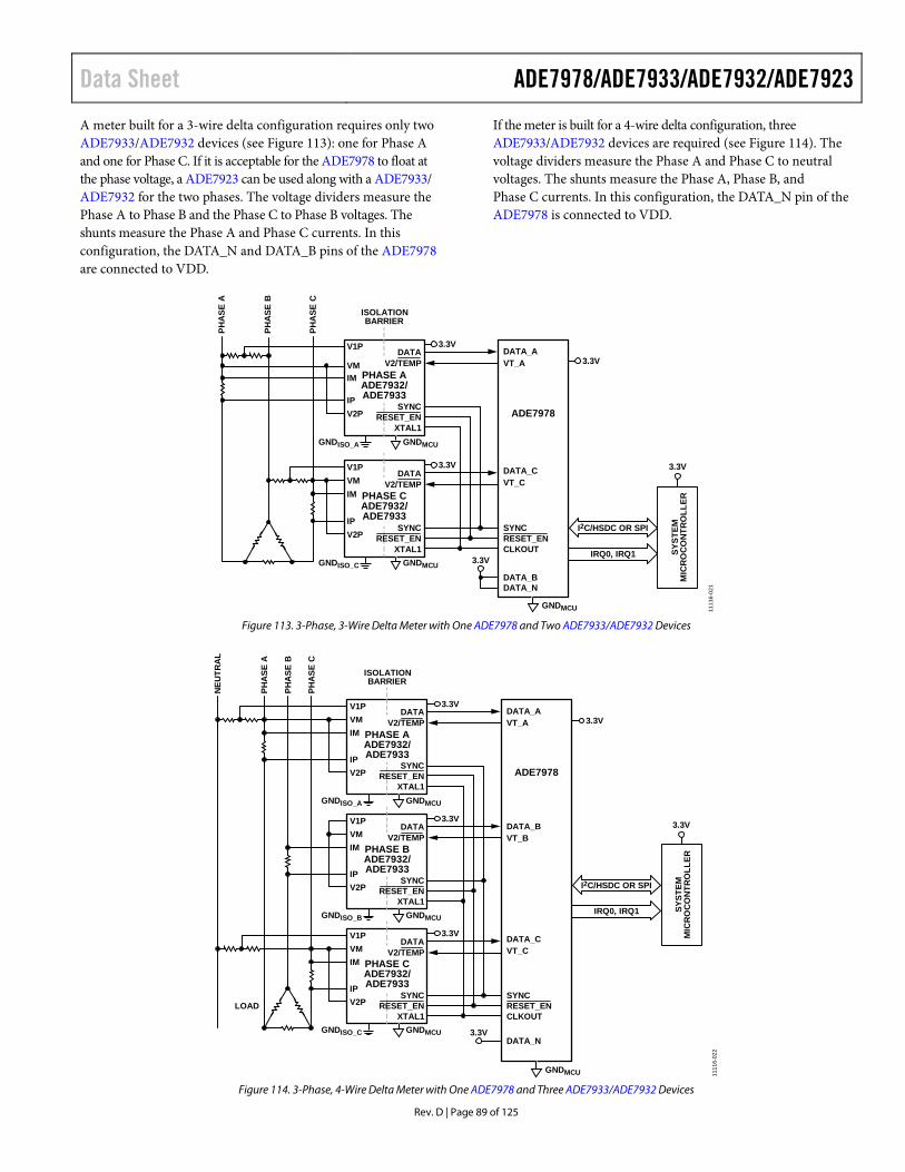
Data Sheet ADE7978/ADE7933/ADE7932/ADE7923
Rev. D | Page 89 of 125
A meter built for a 3-wire delta configuration requires only two ADE7933/ADE7932 devices (see Figure 113): one for Phase A and one for Phase C. If it is acceptable for the ADE7978 to float at the phase voltage, a ADE7923 can be used along with a ADE7933/ ADE7932 for the two phases. The voltage dividers measure the Phase A to Phase B and the Phase C to Phase B voltages. The shunts measure the Phase A and Phase C currents. In this configuration, the DATA_N and DATA_B pins of the ADE7978 are connected to VDD.
If the meter is built for a 4-wire delta configuration, three ADE7933/ADE7932 devices are required (see Figure 114). The voltage dividers measure the Phase A and Phase C to neutral voltages. The shunts measure the Phase A, Phase B, and Phase C currents. In this configuration, the DATA_N pin of the ADE7978 is connected to VDD.
PHA
SE C
ISOLATIONBARRIER
PHA
SE A
PHA
SE B
PHASE CADE7932/ADE7933IP
IM
V1PVM
V2P
GNDMCUGNDISO_C
3.3V
ADE7978
GNDMCU
3.3V
3.3V
SYST
EMM
ICR
OC
ON
TRO
LLER
I2C/HSDC OR SPI
IRQ0, IRQ1
PHASE AADE7932/ADE7933IP
IM
V1P
VM
V2P
GNDMCUGNDISO_A
3.3V
SYNC
CLKOUT
DATA_B
RESET_EN
DATA_AVT_A
DATA_CVT_C
DATA
SYNC
XTAL1
V2/TEMP
RESET_EN
DATA
SYNC
XTAL1
V2/TEMP
RESET_EN
3.3V
DATA_N
1111
6-02
1
Figure 113. 3-Phase, 3-Wire Delta Meter with One ADE7978 and Two ADE7933/ADE7932 Devices
NEU
TRA
L
PHA
SE C
ISOLATIONBARRIER
PHA
SE A
PHA
SE B
PHASE BADE7932/ADE7933IP
IM
V1PVM
V2P
GNDMCUGNDISO_B
3.3V
PHASE CADE7932/ADE7933IP
IM
V1PVM
V2P
GNDMCUGNDISO_C
3.3V
ADE7978
GNDMCU
3.3V
3.3V
SYST
EMM
ICR
OC
ON
TRO
LLER
I2C/HSDC OR SPI
IRQ0, IRQ1
PHASE AADE7932/ADE7933IP
IM
V1PVM
V2P
GNDMCUGNDISO_A
3.3V
SYNC
CLKOUT
DATA_N
RESET_EN
DATA_AVT_A
DATA_BVT_B
DATA_CVT_C
DATA
SYNC
XTAL1
V2/TEMP
RESET_EN
DATA
SYNC
XTAL1
V2/TEMP
RESET_EN
DATA
SYNC
XTAL1
V2/TEMP
RESET_EN
3.3V
LOAD
1111
6-02
2
Figure 114. 3-Phase, 4-Wire Delta Meter with One ADE7978 and Three ADE7933/ADE7932 Devices

ADE7978/ADE7933/ADE7932/ADE7923 Data Sheet
Rev. D | Page 90 of 125
If only two or three ADE7933/ADE7932/ADE7923 devices are used, the DATA_B and/or DATA_N pins are connected to VDD. The waveform samples computed by the ADE7978 that correspond to these unconnected ADE7933/ADE7932 devices are set to full scale. After passing through the high-pass filter, the waveform samples are set to 0, and all quantities computed by the ADE7978 using these samples are 0.
Bits[5:4] (CONSEL[1:0]) in the ACCMODE register (Address 0xE701) determine the way that the phase powers are computed in the ADE7978, based on the meter configuration. For more information, see the Energy Accumulation Modes section.
The ADE7933/ADE7932/ADE7923 receive a 4.096 MHz clock at the XTAL1 pin from the ADE7978 CLKOUT pin; the XTAL2 pins of the ADE7933/ADE7932 and ADE7923 are left open. Do not clock the ADE7933/ADE7932 or ADE7923 using a crystal connected between the XTAL1 and XTAL2 pins because the ADE7933/ADE7932/ADE7923 devices must function synchro-nously with the ADE7978; using the CLKOUT clock of the ADE7978 ensures this synchronization.
The ADE7978 RESET_EN pin is connected to the RESET_ENpins of all ADE7933/ADE7932 and ADE7923 devices in the system. The ADE7978 VT_A, VT_B, VT_C, and VT_N pins are connected to the corresponding V2/TEMP pin of each ADE7933/ ADE7932/ADE7923 in the system. For example, the VT_A pin of the ADE7978 is connected to the V2/TEMP pin of the ADE7933/ADE7932 that monitors Phase A. If the schematic does not monitor certain phases, leave the corresponding VT_x pin of the ADE7978 unconnected. For example, the meter in the configuration shown in Figure 113 does not monitor Phase B or the neutral current. Therefore, the VT_B and VT_N pins are left open.
When the RESET pin of the ADE7978 is set low for at least 10 µs and then brought high again, the RESET_EN pin is set low, and the VT_A, VT_B, VT_C, and VT_N pins toggle eight times from high to low at a frequency of 4.096 MHz, resetting the ADE7933/ADE7932/ADE7923 devices. When the RESET_EN, VT_A, VT_B, VT_C, and VT_N pins are set high again, the reset of the ADE7933/ADE7932 and ADE7923 devices ends (see the Hardware Reset section for more information).
The VT_A, VT_B, VT_C, and VT_N pins of the ADE7978 select the signal measured by the V2 voltage ADC of the ADE7933 and ADE7923: either the second voltage input or the internal temperature sensor. (The ADE7932 always measures the internal temperature sensor.) If the VT_x signal is low, the ADC measures the input signal at the V2P pin. If the VT_x signal is high, the ADC measures the internal temperature sensor.
The ADE7978 reads the outputs of the ADE7933/ADE7932 and ADE7923 using a bit stream communication composed of two signals, SYNC and DATA. The SYNC pin of the ADE7978 is connected to the SYNC pin of each ADE7933/ADE7932 and ADE7923 device. The DATA pin of each ADE7933/ADE7932 and ADE7923 is connected to the corresponding DATA_x pin of
the ADE7978 (x = A, B, C, or N). For example, the DATA pin of the Phase A ADE7933/ADE7932 is connected to the DATA_A pin of the ADE7978.
If the schematic does not monitor certain phases, connect the corresponding DATA_x pin of the ADE7978 to VDD. For example, the meter in the configuration shown in Figure 113 does not monitor Phase B or the neutral current. Therefore, the DATA_B and DATA_N pins of the ADE7978 are tied to VDD.
The SYNC pin of the ADE7978 generates a 1.024 MHz serial clock to the ADE7933/ADE7932 and ADE7923 slaves. Each ADE7933/ADE7932 and ADE7923 responds with a bit stream generated by the first stage of the ADE7933/ADE7932 and ADE7923 ADCs (see the Bit Stream Communication Between the ADE7978 and the ADE7933/ADE7932 and ADE7923 section).
ADE7978 QUICK SETUP AS AN ENERGY METER An energy meter is usually characterized by the nominal current (In), nominal voltage (Vn), nominal frequency (fn), and the meter constant (MC). To quickly set up the ADE7978, follow these steps:
1. If fn = 60 Hz, set Bit 14 (SELFREQ) to 1 in the COMPMODE register (Address 0xE60E). If fn = 50 Hz, leave the SELFREQ bit at 0, the default value.
2. Initialize the CF1DEN, CF2DEN, and CF3DEN registers (Address 0xE611 to Address 0xE613) based on the following equation:
nMCCFxDEN
10]imp/kwh[
103
×=
For more information, see the Energy-to-Frequency Conversion section.
3. Initialize the WTHR, VARTHR, and VATHR registers (Address 0xEA02 to Address 0xEA04) based on the following equation:
WTHR, VARTHR, and VATHR =
272103600
×××××
FSFS
nS
IVfPMAX
For more information, see the Active Energy Calculation section, the Reactive Energy Calculation, and the Apparent Energy Calculation section.
4. Initialize the VLEVEL register (Address 0x43A2) based on the following equation:
VLEVEL = VFS/Vn × 4 × 10⁶
For more information, see the Fundamental Active Power Calculation section.
5. Initialize the VNOM register based on the following equation:
VNOM = V/VFS × 3,761,808 For more information, see the Apparent Power Calculation Using VNOM section.

Data Sheet ADE7978/ADE7933/ADE7932/ADE7923
Rev. D | Page 91 of 125
6. Enable the data memory RAM protection by writing 0xAD to the internal 8-bit register located at Address 0xE7FE, followed by a write of 0x80 to the internal 8-bit register located at Address 0xE7E3.
7. Start the DSP by writing 0x0001 to the run register (Address 0xE228).
BIT STREAM COMMUNICATION BETWEEN THE ADE7978 AND THE ADE7933/ADE7932 AND ADE7923 The ADE7978 extracts information from the ADE7933/ ADE7932 and ADE7923 devices of the system using the bit stream communication shown in Figure 115. The ADE7978 generates a 1.024 MHz clock signal at the SYNC pin. This clock signal is equal to 1/16 of the ADE7978 internal clock, CLKIN (CLKIN/16 = 1.024 MHz for XTALIN = 16.384 MHz) and one-fourth of the ADE7933/ADE7932 and ADE7923 XTAL1 clock (CLKIN/4). The duty cycle of this clock is 25%.
The low to high transition of SYNC is generated one-fourth of a cycle before a high to low transition of the CLKIN/4 clock. SYNC stays high for one CLKIN/4 cycle and stays low for the rest of the period.
After the first high to low transition of SYNC, the ADE7978 CLKIN/4 transitions from high to low four times. At each high
to low transition of CLKIN/4, the ADE7933/ADE7932 and ADE7923 devices place these bits on the DATA pin: the bits coming from the first stage of the ADCs and the bits of the temperature offset stored in the ADE7933/ADE7932 and ADE7923 devices. The order of the bits on the Phase A ADE7933/ADE7932 is VA bit, VA2 bit, temperature offset bit, and IA bit. The other ADE7933/ADE7932 and ADE7923 devices follow the same pattern. The ADE7978 receives these bits at its DATA_A, DATA_B, DATA_C, and DATA_N pins. The process is repeated when a new high to low transition takes place on SYNC. The delimiters identifying the 8-bit signed number representing the temperature offset are shown in Figure 116. Within the frame, the temperature offset is sent out by the ADE7933/ADE7932 and ADE7923 with the less significant bit first.
The delimiters identifying the 8-bit signed number representing the temperature offset are shown in Figure 116. Within the frame, the temperature offset is sent out by the ADE7933/ADE7932 and ADE7923 with the less significant bit first.
Any master device that can generate a 1.024 MHz SYNC signal like the one shown in Figure 115 and can filter the bit streams coming from the DATA pins of the ADE7933/ADE7932 and ADE7923 devices can replace the ADE7978.
ADE7978CLKIN/4
SYNC
DATA_A
DATA_B
DATA_C
DATA_N
1111
6-02
3
VA BIT VA2 BIT TEMPOFFSET
VB BIT VB2 BIT TEMPOFFSET
VC BIT VC2 BIT TEMPOFFSET
VN1 BIT VN2 BIT TEMPOFFSET
IA BIT
IB BIT
IC BIT
IN BIT
VA BIT
VB BIT
VC BIT
VN1 BIT
Figure 115. Bit Stream Communication Between the ADE7978 and the ADE7933/ADE7932 Devices
1111
6-22
0
BIT7BIT6BIT5BIT4
4 LEAST SIGNIFICANTBITS OF TEMPERATURE
OFFSET
11 BIT3BIT2BIT1BIT0
4 MOST SIGNIFICANTBITS OF TEMPERATURE
OFFSET
1 00000
EARLIEST BIT OFTHE FRAME
LAST BIT OFTHE FRAME
Figure 116. Temperature Offset Bit Stream Communication

ADE7978/ADE7933/ADE7932/ADE7923 Data Sheet
Rev. D | Page 92 of 125
ADE7978, ADE7933/ADE7932, AND ADE7923 CLOCKS Provide a digital clock signal at the XTALIN pin to clock the ADE7978. The ADE7978 is clocked at the frequency provided at this pin; this frequency is referred to as CLKIN throughout this data sheet. The ADE7978 is specified for a CLKIN value of 16.384 MHz, but frequencies of 16.384 MHz ± 1% are acceptable.
Alternatively, a 16.384 MHz crystal with a typical drive level of 0.5 mW and equivalent series resistance (ESR) of 20 Ω can be connected across the XTALIN and XTALOUT pins to provide a clock source for the ADE7978 (see Figure 117).
ADE7978
XTALIN
XTALOUT
C1
C2
CP1
CP2
TC
TC
1111
6-02
4
Figure 117. ADE7978 Crystal Circuitry
The total capacitance (TC) at the XTALIN and XTALOUT pins is as follows:
TC = C1 + CP1 = C2 + CP2
where: C1 and C2 are the ceramic capacitors between the XTALIN and GND pins and between the XTALOUT and GND pins (C1 = C2). CP1 and CP2 are the parasitic capacitors of the wires connect-ing the crystal to the ADE7978 (CP1 = CP2).
The load capacitance (LC) of the crystal is equal to half the total capacitance TC because it is the capacitance of the series circuit composed by C1 + CP1 and C2 + CP2.
222
TCCP2C2CP1C1LC
Therefore, the value of Capacitors C1 and C2 as a function of the load capacitance of the crystal is
C1 = C2 = 2 × LC − CP1 = 2 × LC − CP2
For the ADE7978, the typical total capacitance TC of the XTALIN and XTALOUT pins is 40 pF (see Table 2).
Select a crystal with a load capacitance of
LC = TC/2 = 20 pF
For example, if the parasitic capacitances of CP1 and CP2 are equal to 20 pF, select Capacitors C1 and C2 equal to 20 pF.
The ADE7933/ADE7932 and ADE7923 clock circuit does not need a crystal when it is used in conjunction with the ADE7978 because the ADE7978 generates the 4.096 MHz clock used by the ADE7933/ADE7932 and ADE7923. However, if the ADE7933/ ADE7932 and ADE7923 are used as standalone chips, a 4.096 MHz crystal with a typical drive level of 0.5 mW and ESR of 20 Ω can be connected across the ADE7933/ADE7932 and ADE7923 XTAL1 and XTAL2 pins to provide a clock source. The values of the ceramic capacitors (C1 and C2) are calculated in the same way as for the clock circuitry of the ADE7978.
INSULATION LIFETIME All insulation structures eventually break down when subjected to voltage stress over a sufficiently long period. The rate of insulation degradation is dependent on the characteristics of the voltage waveform applied across the insulation. In addition to the testing performed by the regulatory agencies, Analog Devices carries out an extensive set of evaluations to determine the lifetime of the insulation structure within the ADE7933/ADE7932 devices. Analog Devices performs accelerated life testing using voltage levels higher than the rated continuous working voltage. Acceleration factors for several operating conditions are determined. These factors allow calculation of the time to failure at the actual working voltage.
The values shown in Table 13 summarize the peak voltage for 50 years of service life for a bipolar ac operating condition. In many cases, the approved working voltage is higher than the 50-year service life voltage. Operation at these high working voltages can lead to shortened insulation life in some cases.
The insulation lifetime of the ADE7933/ADE7932 devices depends on the voltage waveform type imposed across the isolation barrier. The iCoupler insulation structure degrades at different rates depending on whether the waveform is bipolar ac or dc. Figure 118, and Figure 119 illustrate these different isolation voltage waveforms.
RATED PEAK VOLTAGE
0V
1111
6-25
0
Figure 118. Bipolar AC Waveform
RATED PEAK VOLTAGE
0V 1111
6-10
4
Figure 119. DC Waveform
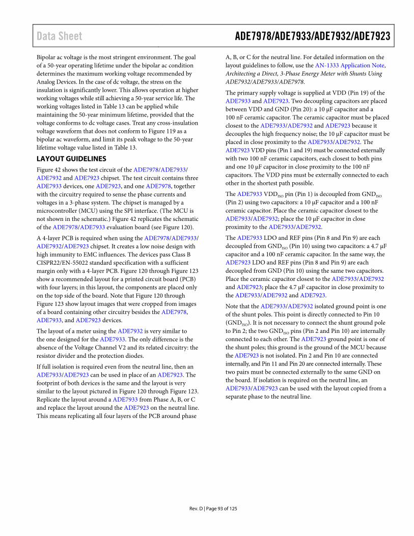
Data Sheet ADE7978/ADE7933/ADE7932/ADE7923
Rev. D | Page 93 of 125
Bipolar ac voltage is the most stringent environment. The goal of a 50-year operating lifetime under the bipolar ac condition determines the maximum working voltage recommended by Analog Devices. In the case of dc voltage, the stress on the insulation is significantly lower. This allows operation at higher working voltages while still achieving a 50-year service life. The working voltages listed in Table 13 can be applied while maintaining the 50-year minimum lifetime, provided that the voltage conforms to dc voltage cases. Treat any cross-insulation voltage waveform that does not conform to Figure 119 as a bipolar ac waveform, and limit its peak voltage to the 50-year lifetime voltage value listed in Table 13.
LAYOUT GUIDELINES Figure 42 shows the test circuit of the ADE7978/ADE7933/ ADE7932 and ADE7923 chipset. The test circuit contains three ADE7933 devices, one ADE7923, and one ADE7978, together with the circuitry required to sense the phase currents and voltages in a 3-phase system. The chipset is managed by a microcontroller (MCU) using the SPI interface. (The MCU is not shown in the schematic.) Figure 42 replicates the schematic of the ADE7978/ADE7933 evaluation board (see Figure 120).
A 4-layer PCB is required when using the ADE7978/ADE7933/ ADE7932/ADE7923 chipset. It creates a low noise design with high immunity to EMC influences. The devices pass Class B CISPR22/EN-55022 standard specification with a sufficient margin only with a 4-layer PCB. Figure 120 through Figure 123 show a recommended layout for a printed circuit board (PCB) with four layers; in this layout, the components are placed only on the top side of the board. Note that Figure 120 through Figure 123 show layout images that were cropped from images of a board containing other circuitry besides the ADE7978, ADE7933, and ADE7923 devices.
The layout of a meter using the ADE7932 is very similar to the one designed for the ADE7933. The only difference is the absence of the Voltage Channel V2 and its related circuitry: the resistor divider and the protection diodes.
If full isolation is required even from the neutral line, then an ADE7933/ADE7923 can be used in place of an ADE7923. The footprint of both devices is the same and the layout is very similar to the layout pictured in Figure 120 through Figure 123. Replicate the layout around a ADE7933 from Phase A, B, or C and replace the layout around the ADE7923 on the neutral line. This means replicating all four layers of the PCB around phase
A, B, or C for the neutral line. For detailed information on the layout guidelines to follow, use the AN-1333 Application Note, Architecting a Direct, 3-Phase Energy Meter with Shunts Using ADE7932/ADE7933/ADE7978.
The primary supply voltage is supplied at VDD (Pin 19) of the ADE7933 and ADE7923. Two decoupling capacitors are placed between VDD and GND (Pin 20): a 10 µF capacitor and a 100 nF ceramic capacitor. The ceramic capacitor must be placed closest to the ADE7933/ADE7932 and ADE7923 because it decouples the high frequency noise; the 10 µF capacitor must be placed in close proximity to the ADE7933/ADE7932. The ADE7923 VDD pins (Pin 1 and 19) must be connected externally with two 100 nF ceramic capacitors, each closest to both pins and one 10 µF capacitor in close proximity to the 100 nF capacitors. The VDD pins must be externally connected to each other in the shortest path possible.
The ADE7933 VDDISO pin (Pin 1) is decoupled from GNDISO (Pin 2) using two capacitors: a 10 µF capacitor and a 100 nF ceramic capacitor. Place the ceramic capacitor closest to the ADE7933/ADE7932; place the 10 µF capacitor in close proximity to the ADE7933/ADE7932.
The ADE7933 LDO and REF pins (Pin 8 and Pin 9) are each decoupled from GNDISO (Pin 10) using two capacitors: a 4.7 µF capacitor and a 100 nF ceramic capacitor. In the same way, the ADE7923 LDO and REF pins (Pin 8 and Pin 9) are each decoupled from GND (Pin 10) using the same two capacitors. Place the ceramic capacitor closest to the ADE7933/ADE7932 and ADE7923; place the 4.7 µF capacitor in close proximity to the ADE7933/ADE7932 and ADE7923.
Note that the ADE7933/ADE7932 isolated ground point is one of the shunt poles. This point is directly connected to Pin 10 (GNDISO). It is not necessary to connect the shunt ground pole to Pin 2; the two GNDISO pins (Pin 2 and Pin 10) are internally connected to each other. The ADE7923 ground point is one of the shunt poles; this ground is the ground of the MCU because the ADE7923 is not isolated. Pin 2 and Pin 10 are connected internally, and Pin 11 and Pin 20 are connected internally. These two pairs must be connected externally to the same GND on the board. If isolation is required on the neutral line, an ADE7933/ADE7923 can be used with the layout copied from a separate phase to the neutral line.
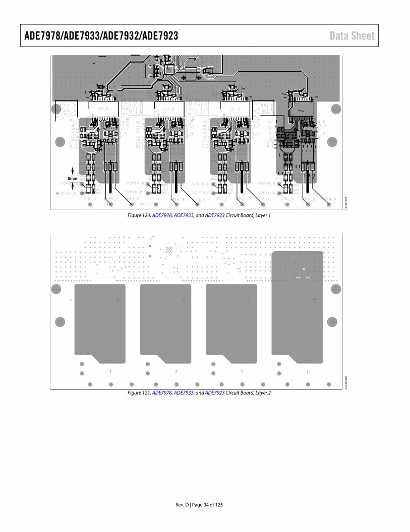
ADE7978/ADE7933/ADE7932/ADE7923 Data Sheet
Rev. D | Page 94 of 125
8mm
1111
6-21
5
Figure 120. ADE7978, ADE7933, and ADE7923 Circuit Board, Layer 1
1111
6-21
6
Figure 121. ADE7978, ADE7933, and ADE7923 Circuit Board, Layer 2
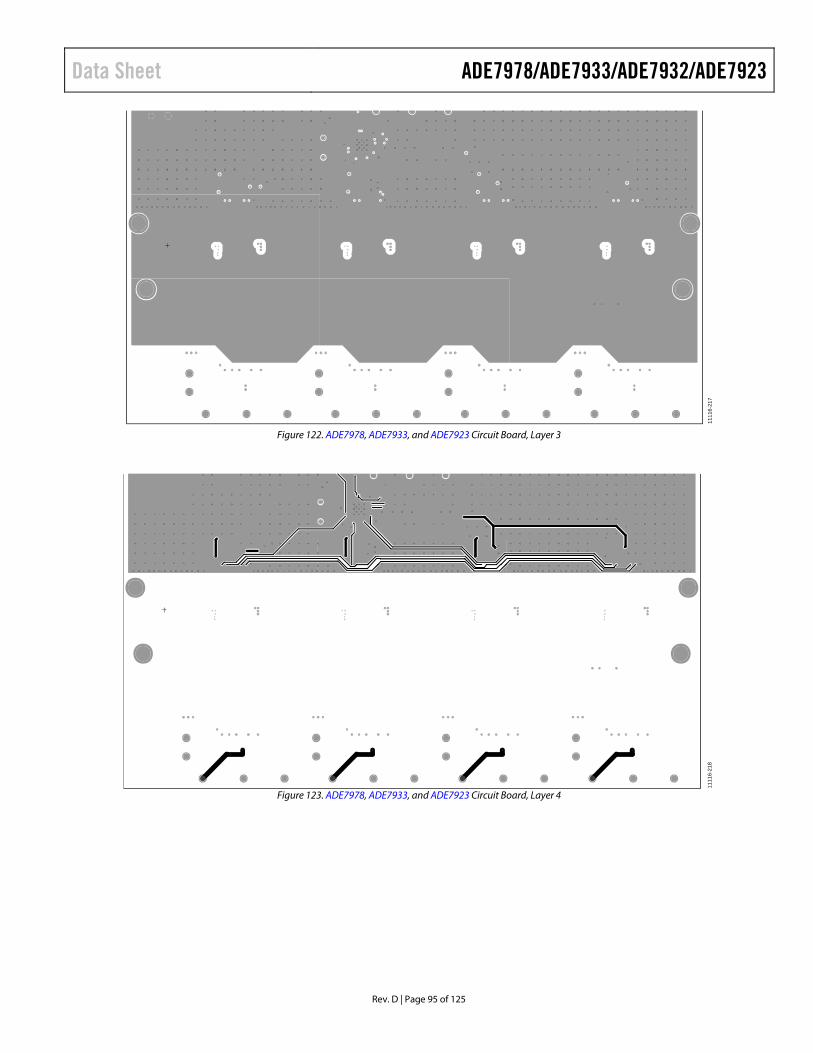
Data Sheet ADE7978/ADE7933/ADE7932/ADE7923
Rev. D | Page 95 of 125
1111
6-21
7
Figure 122. ADE7978, ADE7933, and ADE7923 Circuit Board, Layer 3
1111
6-21
8
Figure 123. ADE7978, ADE7933, and ADE7923 Circuit Board, Layer 4

ADE7978/ADE7933/ADE7932/ADE7923 Data Sheet
Rev. D | Page 96 of 125
Because a 4-layer PCB is used, a stitching capacitor is created between Layer 2 and Layer 3.
Note that the first layer components placed on the isolated secondary side of the ADE7933 are surrounded by a ground plane connected to GNDISO. The second layer also has the same ground plane on the secondary side of the PCB. The third layer extends the ground of the primary side below the ADE7933 and the related circuitry, creating a stitching capacitor. This capacitance has an important role in reducing the emissions generated by the dc-to-dc converter of the ADE7933/ADE7932. Note that a distance of at least 8 mm is maintained on both sides between the input pins on the board and the ground planes. Layer 4 has the ground plane on the primary side of the ADE7933.
Figure 124 shows the structure of the stitching capacitor created by a 4-layer PCB. The isolated ground plane of the second layer creates a capacitor (C23) with approximately an 1100 mm2 area and 100 pF capacitance, including the device, with the primary side ground plane placed on Layer 3.
This capacitance plays an important role in reducing the emissions generated by the ADE7933/ADE7932 dc-to-dc converter.
ADE7978 AND ADE7933/ADE7932 EVALUATION BOARD An evaluation board built upon the ADE7978 and ADE7933 chipset configuration is available (see the Ordering Guide). This board is used in conjunction with the system demonstration platform (EVAL-SDP-CB1Z). Order both the ADE7978/ ADE7933 evaluation board and the system demonstration platform to evaluate the ADE7978 and ADE7933. For more information, see the ADE7978 product page.
ADE7978 DIE VERSION The version register identifies the version of the ADE7978 die. This 8-bit, read-only register is located at Address 0xE707.
ADE7932/ADE7933PRIMARY SIDE GROUNDPLANE ON TOP LAYER
ISOLATED SIDE GROUNDPLANE ON TOP LAYER
PRIMARY SIDE GROUNDPLANE ON LAYER THREE
ISOLATED SIDE GROUNDPLANE ON LAYER TWO
PRIMARY SIDE GROUNDPLANE ON BOTTOM LAYER
20MILS = 0.508mm MINC23
8mm
50MILS = 1.27mm
62MILS ± 10% =1.574mm NOMINAL
1111
6-21
9
Figure 124. Stitching Capacitors Created by 4-Layer PCB

Data Sheet ADE7978/ADE7933/ADE7932/ADE7923
Rev. D | Page 97 of 125
SERIAL INTERFACES The ADE7978 has three serial port interfaces: one fully licensed I2C interface, one serial peripheral interface (SPI), and one high speed data capture (HSDC) port. The SPI pins are multiplexed with pins for the I2C and HSDC ports; therefore, the ADE7978 accepts two configurations: one using the SPI port only and one using the I2C port in conjunction with the HSDC port.
SERIAL INTERFACE SELECTION After a reset of the ADE7978, the HSDC port is always disabled. After power-up or after a hardware reset, select the I2C or SPI port by manipulating the SS/HSA pin (Pin 16).
• If the SS/HSA pin is pulled high, the ADE7978 uses the I2C port until another hardware reset is executed.
• If the SS/HSA pin is toggled high to low three times, the ADE7978 uses the SPI port until another hardware reset is executed.
The manipulation of the SS/HSA pin can be accomplished in two ways.
• Use the SS pin of the master device (that is, the micro-controller) as a regular I/O pin and toggle it three times.
• Execute three SPI write operations to a location in the address space that is not allocated to a specific ADE7978 register (for example, Address 0xEBFF, where writes to 8-bit registers can be executed). These writes cause the SS/HSA pin to toggle three times. For more information about the write protocol involved, see the SPI Write Operation section.
After the serial port selection is completed, the selection must be locked. In this way, the active port remains enabled until a hardware reset or a power-down operation is performed. If the active serial port is I2C, Bit 0 (I2C_LOCK) of the CONFIG2 register (Address 0xEA00) must be set to 1 to lock it in. After the write to this bit is done, the ADE7978 ignores spurious toggling of the SS/HSA pin, and a switch to the SPI port is no longer possible. If the active serial port is SPI, any write to the CONFIG2 register locks the port. After this write, a switch to the I2C port is no longer possible.
The functionality of the ADE7978 is configurable via several on-chip registers. The contents of these registers can be updated or read using the I2C or SPI interface. The HSDC port provides the state of up to 16 registers that contain the instantaneous values of phase voltages and neutral currents, as well as active, reactive, and apparent powers.
COMMUNICATION VERIFICATION The ADE7978 includes a set of three registers that allow any communication via I2C or SPI to be verified. The LAST_OP (Address 0xEA01), LAST_ADD (Address 0xE9FE), and LAST_ RWDATA registers record the nature, address, and data of the last successful communication, respectively. The LAST_RWDATA register has three separate addresses depending on the length of the successful communication (see Table 37).
Table 37. LAST_RWDATA Register Locations Communication Type Address 8-Bit Read/Write 0xE7FD 16-Bit Read/Write 0xE9FF 32-Bit Read/Write 0xE5FF
After each successful communication with the ADE7978, the address of the register that was last accessed is stored in the 16-bit LAST_ADD register (Address 0xE9FE). This read-only register stores the value until the next successful read or write operation is completed.
The LAST_OP register (Address 0xEA01) stores the nature of the operation; that is, it indicates whether a read or a write was performed. If the last operation was a write, the LAST_OP register stores the value 0xCA. If the last operation was a read, the LAST_OP register stores the value 0x35. The LAST_RWDATA register stores the data that was written to or read from the register. An unsuccessful read or write operation is not stored in these registers.
When the LAST_OP, LAST_ADD, and LAST_RWDATA registers are read, their values remain unchanged.
I2C-COMPATIBLE INTERFACE The ADE7978 supports a fully licensed I2C interface. The I2C interface is implemented as a full hardware slave. The maximum serial clock frequency supported by the I2C interface is 400 kHz.
SDA is the data I/O pin, and SCL is the serial clock. These two pins are shared with the MOSI and SCLK pins of the on-chip SPI interface. The SDA and SCL pins are configured in a wire-AND format that allows arbitration in a multimaster system.
The transfer sequence of an I2C system consists of a master device initiating a transfer by generating a start condition while the bus is idle. The master transmits the address of the slave device and the direction of the data transfer in the initial address transfer. If the slave acknowledges the master, the data transfer is initiated. Data transfer continues until the master issues a stop condition, and the bus becomes idle.

ADE7978/ADE7933/ADE7932/ADE7923 Data Sheet
Rev. D | Page 98 of 125
I2C Write Operation
A write operation using the I2C interface of the ADE7978 is initiated when the master generates a start condition, which consists of one byte representing the slave address of the ADE7978 followed by the 16-bit address of the target register and by the value of the register (see Figure 125). The addresses and the register contents are sent with the most significant bit first.
The most significant seven bits of the address byte contain the address of the ADE7978, which is equal to 0111000. Bit 0 of the address byte is the read/write bit. For a write operation, Bit 0 must be cleared to 0; therefore, the first byte of the write operation is 0x70. The ADE7978 acknowledges each byte received. Registers can have 8, 16, or 32 bits; after the last bit of the register is trans-mitted and the ADE7978 acknowledges the transfer, the master generates a stop condition.
I2C Read Operation
A read operation using the I2C interface of the ADE7978 is accomplished in two stages. The first stage sets the pointer to the address of the register. The second stage reads the contents of the register.
As shown in Figure 126, the first stage begins when the master generates a start condition, which consists of one byte representing the slave address of the ADE7978 followed by the 16-bit address of the target register. The ADE7978 acknowledges each byte received. The address byte is similar to the address byte for a write operation and is equal to 0x70 (see the I2C Write Operation section).
After the last byte of the register address is sent and acknowledged by the ADE7978, the second stage begins with the master generat-ing a new start condition followed by the address byte. The most significant seven bits of this address byte contain the address of the ADE7978, which is equal to 0111000. Bit 0 of the address byte is the read/write bit. For a read operation, Bit 0 must be set to 1; therefore, the first byte of the read operation is 0x71. After this byte is received, the ADE7978 generates an acknowledge. The ADE7978 then sends the value of the register, and, after each byte is received, the master generates an acknowledge. All bytes are sent with the most significant bit first. Registers can have 8, 16, or 32 bits; after the last bit of the register is received, the master does not acknowledge the transfer but generates a stop condition.
ACK GENERATEDBY ADE7978
STA
RT
AC
K
AC
K
AC
K
AC
K
AC
K
AC
K
AC
KST
OP
S S0
15
SLAVE ADDRESS MOST SIGNIFICANT8 BITS OF REGISTER
ADDRESS
LEAST SIGNIFICANT8 BITS OF REGISTER
ADDRESS
BYTE 3 (MOSTSIGNIFICANT)OF REGISTER
BYTE 2 OF REGISTER BYTE 1 OF REGISTER BYTE 0 (LEASTSIGNIFICANT) OF
REGISTER
8 7 0 31 24 23 16 15 8 07
1 1 1 0 0 0 0
1111
6-09
1
Figure 125. I2C Write Operation of a 32-Bit Register
ACK GENERATEDBY ADE7978
ACKGENERATED BY
MASTER
STA
RT
S 0
15
SLAVE ADDRESS MOST SIGNIFICANT 8 BITS OF REGISTER
ADDRESS
LEAST SIGNIFICANT8 BITS OF REGISTER
ADDRESS
8 7 0
1 1 1 0 0 0 0
STA
RT
STO
PN
O A
CK
S S0
SLAVE ADDRESS BYTE 3(MOST SIGNIFICANT)
OF REGISTER
BYTE 2 OFREGISTER
BYTE 1 OFREGISTER
BYTE 0(LEAST SIGNIFICANT)
OF REGISTER
31 24 23 16 15 8 07
1 1 1 0 0 0 1
ACK GENERATEDBY ADE7978
AC
K
AC
K
AC
K
AC
K
AC
K
AC
K
AC
K
1111
6-09
2
Figure 126. I2C Read Operation of a 32-Bit Register
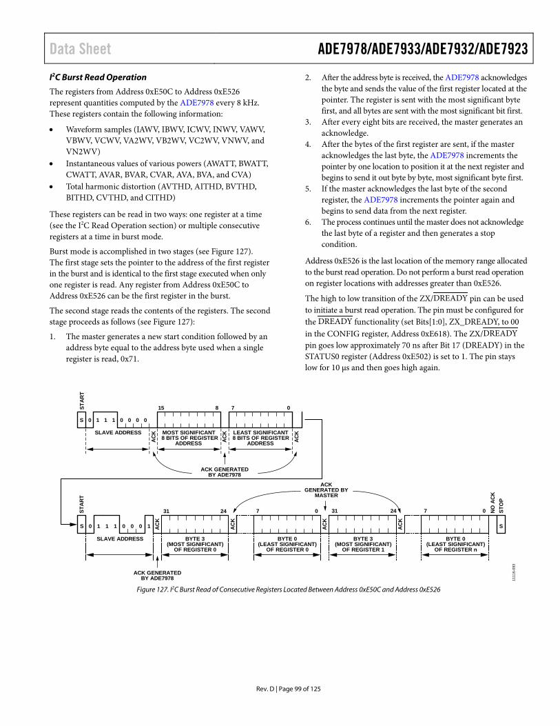
Data Sheet ADE7978/ADE7933/ADE7932/ADE7923
Rev. D | Page 99 of 125
I2C Burst Read Operation
The registers from Address 0xE50C to Address 0xE526 represent quantities computed by the ADE7978 every 8 kHz. These registers contain the following information:
• Waveform samples (IAWV, IBWV, ICWV, INWV, VAWV, VBWV, VCWV, VA2WV, VB2WV, VC2WV, VNWV, and VN2WV)
• Instantaneous values of various powers (AWATT, BWATT, CWATT, AVAR, BVAR, CVAR, AVA, BVA, and CVA)
• Total harmonic distortion (AVTHD, AITHD, BVTHD, BITHD, CVTHD, and CITHD)
These registers can be read in two ways: one register at a time (see the I2C Read Operation section) or multiple consecutive registers at a time in burst mode.
Burst mode is accomplished in two stages (see Figure 127). The first stage sets the pointer to the address of the first register in the burst and is identical to the first stage executed when only one register is read. Any register from Address 0xE50C to Address 0xE526 can be the first register in the burst.
The second stage reads the contents of the registers. The second stage proceeds as follows (see Figure 127):
1. The master generates a new start condition followed by an address byte equal to the address byte used when a single register is read, 0x71.
2. After the address byte is received, the ADE7978 acknowledges the byte and sends the value of the first register located at the pointer. The register is sent with the most significant byte first, and all bytes are sent with the most significant bit first.
3. After every eight bits are received, the master generates an acknowledge.
4. After the bytes of the first register are sent, if the master acknowledges the last byte, the ADE7978 increments the pointer by one location to position it at the next register and begins to send it out byte by byte, most significant byte first.
5. If the master acknowledges the last byte of the second register, the ADE7978 increments the pointer again and begins to send data from the next register.
6. The process continues until the master does not acknowledge the last byte of a register and then generates a stop condition.
Address 0xE526 is the last location of the memory range allocated to the burst read operation. Do not perform a burst read operation on register locations with addresses greater than 0xE526.
The high to low transition of the ZX/DREADY pin can be used to initiate a burst read operation. The pin must be configured for the DREADY functionality (set Bits[1:0], ZX_DREADY, to 00 in the CONFIG register, Address 0xE618). The ZX/DREADY pin goes low approximately 70 ns after Bit 17 (DREADY) in the STATUS0 register (Address 0xE502) is set to 1. The pin stays low for 10 µs and then goes high again.
ACK GENERATEDBY ADE7978
ACKGENERATED BY
MASTER
STAR
TST
ART
NO A
CKST
OP
S 0
15
SLAVE ADDRESS MOST SIGNIFICANT 8 BITS OF REGISTER
ADDRESS
LEAST SIGNIFICANT8 BITS OF REGISTER
ADDRESS
8 7 0
1 1 1 0 0 0 0
BYTE 3(MOST SIGNIFICANT)
OF REGISTER 0
BYTE 0(LEAST SIGNIFICANT)
OF REGISTER 0
BYTE 3(MOST SIGNIFICANT)
OF REGISTER 1
BYTE 0(LEAST SIGNIFICANT)
OF REGISTER n
ACK
ACK
ACK
ACK
ACK
ACK
ACK
S 0 1 1 1 0 0 0
SLAVE ADDRESS
S
31 24
1
7 0 31 24 7 0
ACK GENERATEDBY ADE7978 11
116-
093
Figure 127. I2C Burst Read of Consecutive Registers Located Between Address 0xE50C and Address 0xE526
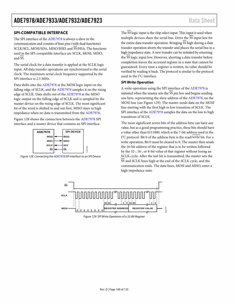
ADE7978/ADE7933/ADE7932/ADE7923 Data Sheet
Rev. D | Page 100 of 125
SPI-COMPATIBLE INTERFACE The SPI interface of the ADE7978 is always a slave in the communication and consists of four pins (with dual functions): SCLK/SCL, MOSI/SDA, MISO/HSD, and SS/HSA. The functions used in the SPI-compatible interface are SCLK, MOSI, MISO, and SS.
The serial clock for a data transfer is applied at the SCLK logic input. All data transfer operations are synchronized to the serial clock. The maximum serial clock frequency supported by the SPI interface is 2.5 MHz.
Data shifts into the ADE7978 at the MOSI logic input on the falling edge of SCLK, and the ADE7978 samples it on the rising edge of SCLK. Data shifts out of the ADE7978 at the MISO logic output on the falling edge of SCLK and is sampled by the master device on the rising edge of SCLK. The most significant bit of the word is shifted in and out first. MISO stays in high impedance when no data is transmitted from the ADE7978.
Figure 128 shows the connection between the ADE7978 SPI interface and a master device that contains an SPI interface.
MOSI
MISO
SCLK
ADE7978MOSI
MISO
SCK
SPI DEVICE
SS SS
1111
6-09
4
Figure 128. Connecting the ADE7978 SPI Interface to an SPI Device
The SS logic input is the chip select input. This input is used when multiple devices share the serial bus. Drive the SS input low for the entire data transfer operation. Bringing SS high during a data transfer operation aborts the transfer and places the serial bus in a high impedance state. A new transfer can be initiated by returning the SS logic input low. However, aborting a data transfer before completion leaves the accessed register in a state that cannot be guaranteed. Every time a register is written, its value should be verified by reading it back. The protocol is similar to the protocol used in the I2C interface.
SPI Write Operation
A write operation using the SPI interface of the ADE7978 is initiated when the master sets the SS pin low and begins sending one byte, representing the slave address of the ADE7978, on the MOSI line (see Figure 129). The master sends data on the MOSI line starting with the first high to low transition of SCLK. The SPI interface of the ADE7978 samples the data on the low to high transitions of SCLK.
The most significant seven bits of the address byte can have any value, but as a good programming practice, these bits should have a value other than 0111000, which is the 7-bit address used in the I2C protocol. Bit 0 of the address byte is the read/write bit. For a write operation, Bit 0 must be cleared to 0. The master then sends the 16-bit address of the register that is to be written followed by the 32-, 16-, or 8-bit value of that register without losing an SCLK cycle. After the last bit is transmitted, the master sets the SS and SCLK lines high at the end of the SCLK cycle, and the communication ends. The data lines, MOSI and MISO, enter a high impedance state.
0
15 14
SCLK
MOSI
1 0 31 30 1 0
00 0 0 0 0 0REGISTER ADDRESS REGISTER VALUE
SS
1111
6-09
7
Figure 129. SPI Write Operation of a 32-Bit Register

Data Sheet ADE7978/ADE7933/ADE7932/ADE7923
Rev. D | Page 101 of 125
SPI Read Operation
A read operation using the SPI interface of the ADE7978 is initiated when the master sets the SS pin low and begins sending one byte, representing the address of the ADE7978, on the MOSI line (see Figure 130). The master sends data on the MOSI line starting with the first high to low transition of SCLK. The SPI interface of the ADE7978 samples the data on the low to high transitions of SCLK.
The most significant seven bits of the address byte can have any value, but as a good programming practice, these bits should have a value other than 0111000, which is the 7-bit address used in the I2C protocol. Bit 0 of the address byte is the read/write bit. For a read operation, Bit 0 must be set to 1. The master then sends the 16-bit address of the register that is to be read. After the ADE7978 receives the last bit of the register address on a low to high transition of SCLK, it begins to transmit the register contents on the MISO line when the next SCLK high to low transition occurs; the master samples the data on a low to high SCLK transition.
After the master receives the last bit, it sets the SS and SCLK lines high, and the communication ends. The data lines, MOSI and MISO, enter a high impedance state.
SPI Burst Read Operation
The registers from Address 0xE50C to Address 0xE526 represent quantities computed by the ADE7978 every 8 kHz (see the I2C Burst Read Operation section for the list of registers).
These registers can be read in two ways: one register at a time (see the SPI Read Operation section) or multiple consecutive registers at a time in a burst mode.
Burst mode is initiated when the master sets the SS pin low and begins sending one byte, representing the address of the ADE7978, on the MOSI line (see Figure 131). The address is the same address byte used for reading a single register. The master sends data on the MOSI line starting with the first high to low transition of SCLK. The SPI interface of the ADE7978 samples data on the low to high transitions of SCLK.
The master sends the 16-bit address of the first register in the burst to be read. Any register from Address 0xE50C to Address 0xE526 can be the first register in the burst. After the ADE7978 receives the last bit of the register address on a low to high transition of SCLK, it begins to transmit the register contents on the MISO line when the next SCLK high to low transition occurs; the master samples the data on a low to high SCLK transition.
After the master receives the last bit of the first register, the ADE7978 sends the contents of the register placed at the next location. This process is repeated until the master sets the SS and SCLK lines high and the communication ends. The data lines, MOSI and MISO, enter a high impedance state.
Address 0xE526 is the last location of the memory range allocated to the burst read operation. Do not perform a burst read operation on register locations with addresses greater than 0xE526.
The high to low transition of the ZX/DREADY pin can be used to initiate a burst read operation. The pin must be configured for the DREADY functionality (set Bits[1:0], ZX_DREADY, to 00 in the CONFIG register, Address 0xE618). The ZX/DREADY pin goes low approximately 70 ns after Bit 17 (DREADY) in the STATUS0 register (Address 0xE502) is set to 1. The pin stays low for 10 µs and then goes high again.
10
15 14
SCLK
MOSI
MISO
1 0
31 30 1 0
00 0 0 0 0
REGISTER VALUE
REGISTER ADDRESS
SS
1111
6-09
5
Figure 130. SPI Read Operation of a 32-Bit Register
0
SCLK
MOSI
MISO
00 0 0 0 0 1
SS
REGISTERADDRESS
REGISTER 0VALUE
31 0
REGISTER nVALUE
31 0
1111
6-09
6
Figure 131. SPI Burst Read of Consecutive Registers Located Between Address 0xE50C and Address 0xE526
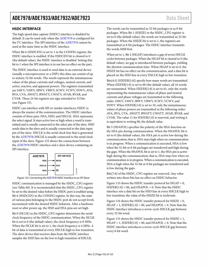
ADE7978/ADE7933/ADE7932/ADE7923 Data Sheet
Rev. D | Page 102 of 125
HSDC INTERFACE The high speed data capture (HSDC) interface is disabled by default. It can be used only when the ADE7978 is configured for the I2C interface. The SPI interface of the ADE7978 cannot be used at the same time as the HSDC interface.
When Bit 6 (HSDCEN) is set to 1 in the CONFIG register, the HSDC interface is enabled. If the HSDCEN bit is cleared to 0 (the default value), the HSDC interface is disabled. Setting this bit to 1 when the SPI interface is in use has no effect on the part.
The HSDC interface is used to send data to an external device (usually a microprocessor or a DSP); this data can consist of up to sixteen 32-bit words. The words represent the instantaneous values of the phase currents and voltages, neutral current, and active, reactive, and apparent powers. The registers transmitted are IAWV, VAWV, IBWV, VBWV, ICWV, VCWV, INWV, AVA, BVA, CVA, AWATT, BWATT, CWATT, AVAR, BVAR, and CVAR. These 24-bit registers are sign extended to 32 bits (see Figure 53).
HSDC can interface with SPI or similar interfaces; HSDC is always the master of the communication. The HSDC interface consists of three pins: HSA, HSD, and HSCLK. HSA represents the select signal. It stays active low or high when a word is trans-mitted and is usually connected to the select pin of the slave. HSD sends data to the slave and is usually connected to the data input pin of the slave. HSCLK is the serial clock line that is generated by the ADE7978; HSCLK is usually connected to the serial clock input of the slave. Figure 132 shows the connections between the ADE7978 HSDC interface and a slave device containing an SPI interface.
ADE7978HSD MOSI
HSCLK SCK
HSA SS
SPI DEVICE
1111
6-09
8
Figure 132. Connecting the ADE7978 HSDC Interface to an SPI Slave
HSDC communication is managed by the HSDC_CFG register (see Table 60). It is recommended that the HSDC_CFG register be set to the desired value before the HSDC port is enabled using Bit 6 (HSDCEN) in the CONFIG register. In this way, the state of various pins belonging to the HSDC port do not accept levels inconsistent with the desired HSDC behavior. After a hardware reset or after power-up, the HSD and HSA pins are set high.
Bit 0 (HCLK) in the HSDC_CFG register determines the serial clock frequency of the HSDC communication. When the HCLK bit is set to 0 (the default value), the clock frequency is 8 MHz. When the HCLK bit is set to 1, the clock frequency is 4 MHz. A bit of data is transmitted at every HSCLK high to low transition. The slave device that receives data from the HSDC interface samples the HSD line on the low to high transition of HSCLK.
The words can be transmitted as 32-bit packages or as 8-bit packages. When Bit 1 (HSIZE) in the HSDC_CFG register is set to 0 (the default value), the words are transmitted as 32-bit packages. When the HSIZE bit is set to 1, the registers are transmitted as 8-bit packages. The HSDC interface transmits the words MSB first.
When set to 1, Bit 2 (HGAP) introduces a gap of seven HSCLK cycles between packages. When the HGAP bit is cleared to 0 (the default value), no gap is introduced between packages, yielding the shortest communication time. When HGAP is set to 0, the HSIZE bit has no effect on the communication, and a data bit is placed on the HSD line at every HSCLK high to low transition.
Bits[4:3] (HXFER[1:0]) specify how many words are transmitted. When HXFER[1:0] is set to 00 (the default value), all 16 words are transmitted. When HXFER[1:0] is set to 01, only the words representing the instantaneous values of phase and neutral currents and phase voltages are transmitted in the following order: IAWV, VAWV, IBWV, VBWV, ICWV, VCWV, and INWV. When HXFER[1:0] is set to 10, only the instantaneous values of phase powers are transmitted in the following order: AVA, BVA, CVA, AWATT, BWATT, CWATT, AVAR, BVAR, and CVAR. The value 11 for HXFER[1:0] is reserved, and writing it is equivalent to writing 00, the default value.
Bit 5 (HSAPOL) specifies the polarity of the HSA function on the HSA pin during communication. When the HSAPOL bit is set to 0 (the default value), the HSA pin is active low during the communication; that is, HSA stays high when no communication is in progress. When a communication is executed, HSA is low when the 32-bit or 8-bit packages are transferred and high during the gaps. When the HSAPOL bit is set to 1, the HSA pin is active high during the communication; that is, HSA stays low when no communication is in progress. When a communication is executed, HSA is high when the 32-bit or 8-bit packages are transferred and is low during the gaps.
Bits[7:6] of the HSDC_CFG register are reserved. Any value written into these bits has no effect on HSDC behavior.
Figure 133 shows the HSDC transfer protocol for HGAP = 0, HXFER[1:0] = 00, and HSAPOL = 0. Note that the HSDC interface sets a data bit on the HSD line at every HSCLK high to low transition; the value of the HSIZE bit is irrelevant.
Figure 134 shows the HSDC transfer protocol for HSIZE = 0, HGAP = 1, HXFER[1:0] = 00, and HSAPOL = 0. Note that the HSDC interface introduces a seven-cycle HSCLK gap between every 32-bit word.
Figure 135 shows the HSDC transfer protocol for HSIZE = 1, HGAP = 1, HXFER[1:0] = 00, and HSAPOL = 0. Note that the HSDC interface introduces a seven-cycle HSCLK gap between every 8-bit word.
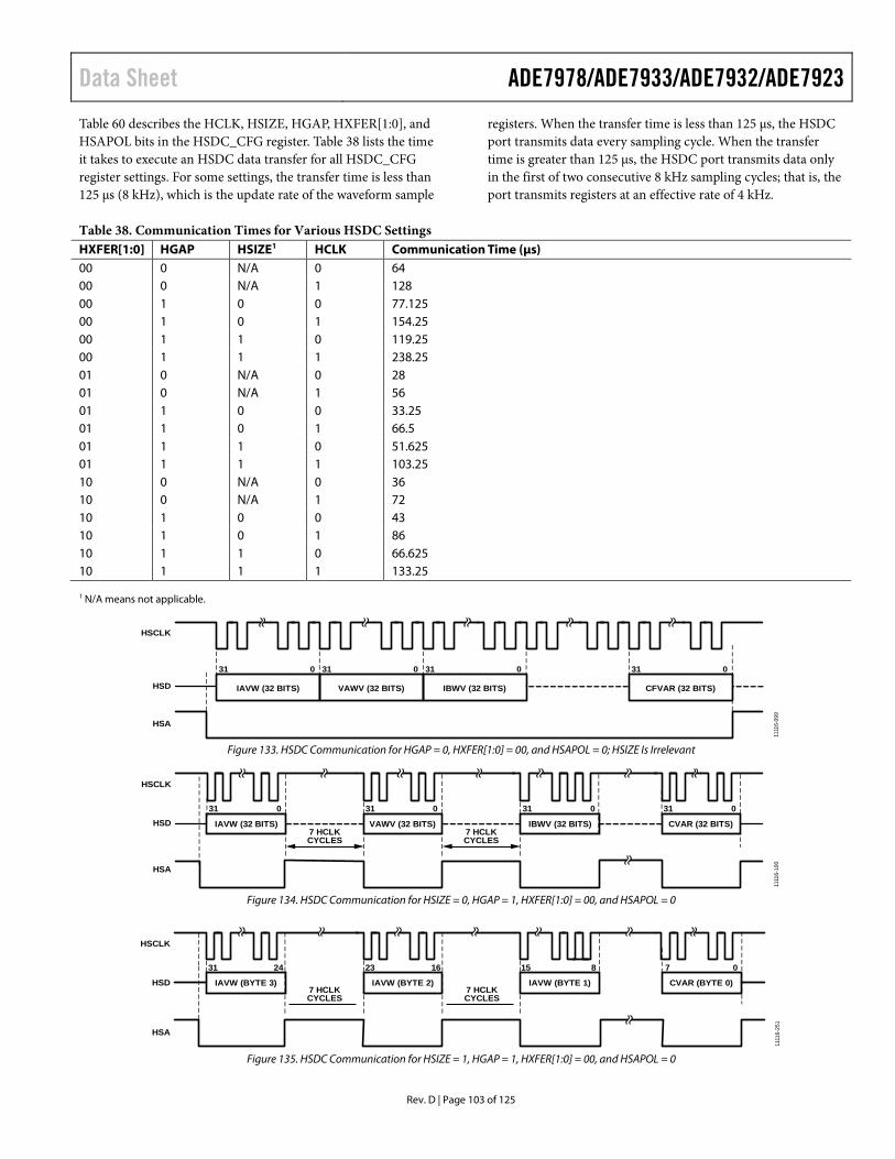
Data Sheet ADE7978/ADE7933/ADE7932/ADE7923
Rev. D | Page 103 of 125
Table 60 describes the HCLK, HSIZE, HGAP, HXFER[1:0], and HSAPOL bits in the HSDC_CFG register. Table 38 lists the time it takes to execute an HSDC data transfer for all HSDC_CFG register settings. For some settings, the transfer time is less than 125 µs (8 kHz), which is the update rate of the waveform sample
registers. When the transfer time is less than 125 µs, the HSDC port transmits data every sampling cycle. When the transfer time is greater than 125 µs, the HSDC port transmits data only in the first of two consecutive 8 kHz sampling cycles; that is, the port transmits registers at an effective rate of 4 kHz.
Table 38. Communication Times for Various HSDC Settings HXFER[1:0] HGAP HSIZE1 HCLK Communication Time (µs) 00 0 N/A 0 64 00 0 N/A 1 128 00 1 0 0 77.125 00 1 0 1 154.25 00 1 1 0 119.25 00 1 1 1 238.25 01 0 N/A 0 28 01 0 N/A 1 56 01 1 0 0 33.25 01 1 0 1 66.5 01 1 1 0 51.625 01 1 1 1 103.25 10 0 N/A 0 36 10 0 N/A 1 72 10 1 0 0 43 10 1 0 1 86 10 1 1 0 66.625 10 1 1 1 133.25 1 N/A means not applicable.
HSCLK
HSD
HSA
IAVW (32 BITS)
31 0
VAWV (32 BITS)
31 0
IBWV (32 BITS)
31 0
CFVAR (32 BITS)
31 0
1111
6-09
9
Figure 133. HSDC Communication for HGAP = 0, HXFER[1:0] = 00, and HSAPOL = 0; HSIZE Is Irrelevant
HSCLK
HSD
HSA
IAVW (32 BITS)
31 0
VAWV (32 BITS)
31 0
IBWV (32 BITS)
31 0
CVAR (32 BITS)
31 0
7 HCLKCYCLES
7 HCLKCYCLES
1111
6-10
0
Figure 134. HSDC Communication for HSIZE = 0, HGAP = 1, HXFER[1:0] = 00, and HSAPOL = 0
1111
6-25
1
HSCLK
HSD
HSA
IAVW (BYTE 3)
31 24
IAVW (BYTE 2)
23 16
IAVW (BYTE 1)
15 8
CVAR (BYTE 0)
7 0
7 HCLKCYCLES
7 HCLKCYCLES
Figure 135. HSDC Communication for HSIZE = 1, HGAP = 1, HXFER[1:0] = 00, and HSAPOL = 0
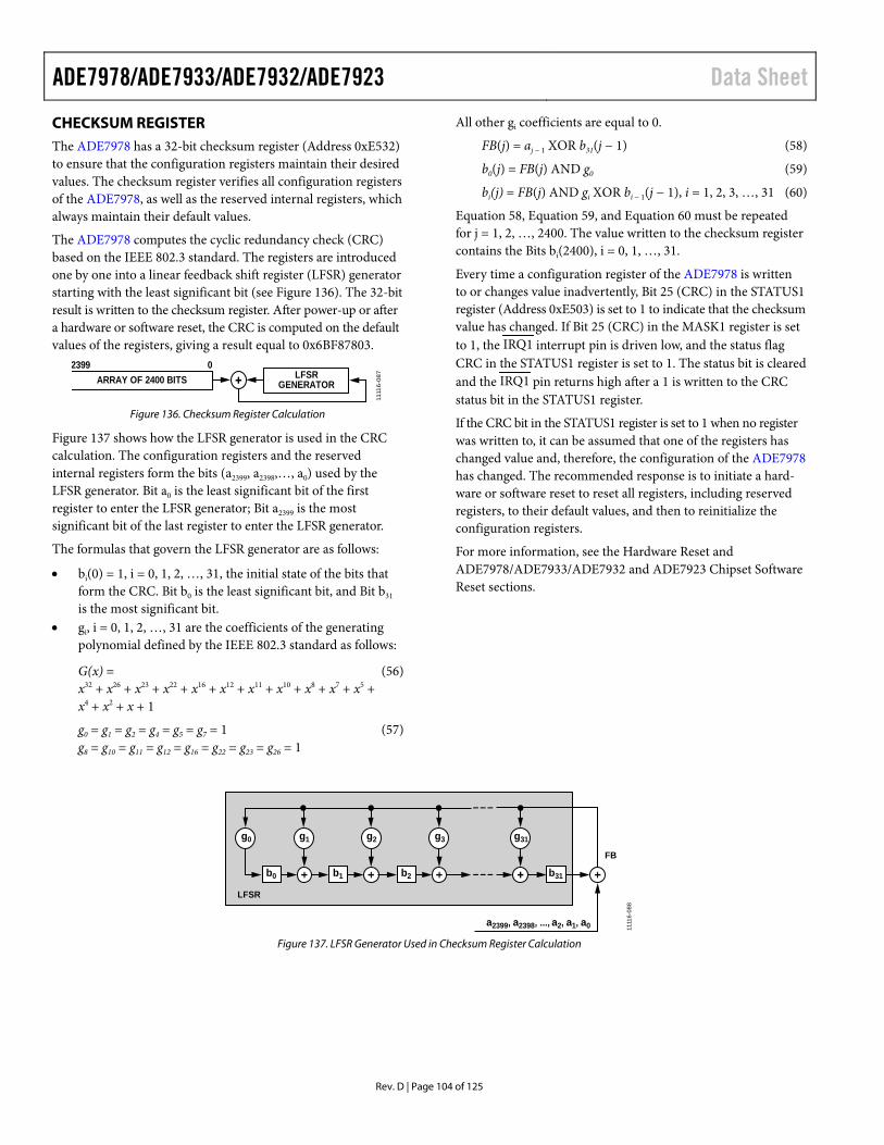
ADE7978/ADE7933/ADE7932/ADE7923 Data Sheet
Rev. D | Page 104 of 125
CHECKSUM REGISTER The ADE7978 has a 32-bit checksum register (Address 0xE532) to ensure that the configuration registers maintain their desired values. The checksum register verifies all configuration registers of the ADE7978, as well as the reserved internal registers, which always maintain their default values.
The ADE7978 computes the cyclic redundancy check (CRC) based on the IEEE 802.3 standard. The registers are introduced one by one into a linear feedback shift register (LFSR) generator starting with the least significant bit (see Figure 136). The 32-bit result is written to the checksum register. After power-up or after a hardware or software reset, the CRC is computed on the default values of the registers, giving a result equal to 0x6BF87803.
2399 0LFSR
GENERATORARRAY OF 2400 BITS11
116-
087
Figure 136. Checksum Register Calculation
Figure 137 shows how the LFSR generator is used in the CRC calculation. The configuration registers and the reserved internal registers form the bits (a2399, a2398,…, a0) used by the LFSR generator. Bit a0 is the least significant bit of the first register to enter the LFSR generator; Bit a2399 is the most significant bit of the last register to enter the LFSR generator.
The formulas that govern the LFSR generator are as follows:
• bi(0) = 1, i = 0, 1, 2, …, 31, the initial state of the bits that form the CRC. Bit b0 is the least significant bit, and Bit b31 is the most significant bit.
• gi, i = 0, 1, 2, …, 31 are the coefficients of the generating polynomial defined by the IEEE 802.3 standard as follows:
G(x) = (56) x32 + x26 + x23 + x22 + x16 + x12 + x11 + x10 + x8 + x7 + x5 + x4 + x2 + x + 1
g0 = g1 = g2 = g4 = g5 = g7 = 1 (57) g8 = g10 = g11 = g12 = g16 = g22 = g23 = g26 = 1
All other gi coefficients are equal to 0.
FB(j) = aj − 1 XOR b31(j − 1) (58)
b0(j) = FB(j) AND g0 (59)
bi(j) = FB(j) AND gi XOR bi − 1(j − 1), i = 1, 2, 3, …, 31 (60)
Equation 58, Equation 59, and Equation 60 must be repeated for j = 1, 2, …, 2400. The value written to the checksum register contains the Bits bi(2400), i = 0, 1, …, 31.
Every time a configuration register of the ADE7978 is written to or changes value inadvertently, Bit 25 (CRC) in the STATUS1 register (Address 0xE503) is set to 1 to indicate that the checksum value has changed. If Bit 25 (CRC) in the MASK1 register is set to 1, the IRQ1 interrupt pin is driven low, and the status flag CRC in the STATUS1 register is set to 1. The status bit is cleared and the IRQ1 pin returns high after a 1 is written to the CRC status bit in the STATUS1 register.
If the CRC bit in the STATUS1 register is set to 1 when no register was written to, it can be assumed that one of the registers has changed value and, therefore, the configuration of the ADE7978 has changed. The recommended response is to initiate a hard-ware or software reset to reset all registers, including reserved registers, to their default values, and then to reinitialize the configuration registers.
For more information, see the Hardware Reset and ADE7978/ADE7933/ADE7932 and ADE7923 Chipset Software Reset sections.
b0
LFSR
FB
g0 g1 g2 g31
b1
g3
b2 b31
a2399, a2398, ..., a2, a1, a0 1111
6-08
8
Figure 137. LFSR Generator Used in Checksum Register Calculation
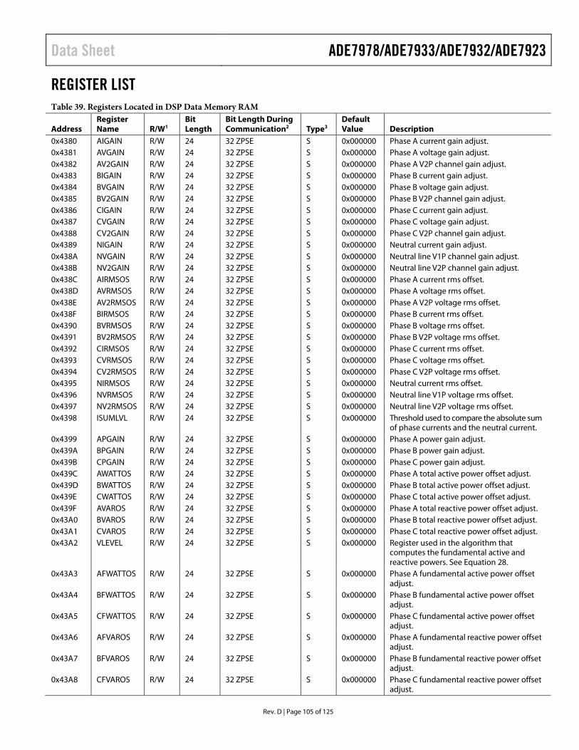
Data Sheet ADE7978/ADE7933/ADE7932/ADE7923
Rev. D | Page 105 of 125
REGISTER LIST Table 39. Registers Located in DSP Data Memory RAM
Address Register Name R/W1
Bit Length
Bit Length During Communication2 Type3
Default Value Description
0x4380 AIGAIN R/W 24 32 ZPSE S 0x000000 Phase A current gain adjust. 0x4381 AVGAIN R/W 24 32 ZPSE S 0x000000 Phase A voltage gain adjust. 0x4382 AV2GAIN R/W 24 32 ZPSE S 0x000000 Phase A V2P channel gain adjust. 0x4383 BIGAIN R/W 24 32 ZPSE S 0x000000 Phase B current gain adjust. 0x4384 BVGAIN R/W 24 32 ZPSE S 0x000000 Phase B voltage gain adjust. 0x4385 BV2GAIN R/W 24 32 ZPSE S 0x000000 Phase B V2P channel gain adjust. 0x4386 CIGAIN R/W 24 32 ZPSE S 0x000000 Phase C current gain adjust. 0x4387 CVGAIN R/W 24 32 ZPSE S 0x000000 Phase C voltage gain adjust. 0x4388 CV2GAIN R/W 24 32 ZPSE S 0x000000 Phase C V2P channel gain adjust. 0x4389 NIGAIN R/W 24 32 ZPSE S 0x000000 Neutral current gain adjust. 0x438A NVGAIN R/W 24 32 ZPSE S 0x000000 Neutral line V1P channel gain adjust. 0x438B NV2GAIN R/W 24 32 ZPSE S 0x000000 Neutral line V2P channel gain adjust. 0x438C AIRMSOS R/W 24 32 ZPSE S 0x000000 Phase A current rms offset. 0x438D AVRMSOS R/W 24 32 ZPSE S 0x000000 Phase A voltage rms offset. 0x438E AV2RMSOS R/W 24 32 ZPSE S 0x000000 Phase A V2P voltage rms offset. 0x438F BIRMSOS R/W 24 32 ZPSE S 0x000000 Phase B current rms offset. 0x4390 BVRMSOS R/W 24 32 ZPSE S 0x000000 Phase B voltage rms offset. 0x4391 BV2RMSOS R/W 24 32 ZPSE S 0x000000 Phase B V2P voltage rms offset. 0x4392 CIRMSOS R/W 24 32 ZPSE S 0x000000 Phase C current rms offset. 0x4393 CVRMSOS R/W 24 32 ZPSE S 0x000000 Phase C voltage rms offset. 0x4394 CV2RMSOS R/W 24 32 ZPSE S 0x000000 Phase C V2P voltage rms offset. 0x4395 NIRMSOS R/W 24 32 ZPSE S 0x000000 Neutral current rms offset. 0x4396 NVRMSOS R/W 24 32 ZPSE S 0x000000 Neutral line V1P voltage rms offset. 0x4397 NV2RMSOS R/W 24 32 ZPSE S 0x000000 Neutral line V2P voltage rms offset. 0x4398 ISUMLVL R/W 24 32 ZPSE S 0x000000 Threshold used to compare the absolute sum
of phase currents and the neutral current. 0x4399 APGAIN R/W 24 32 ZPSE S 0x000000 Phase A power gain adjust. 0x439A BPGAIN R/W 24 32 ZPSE S 0x000000 Phase B power gain adjust. 0x439B CPGAIN R/W 24 32 ZPSE S 0x000000 Phase C power gain adjust. 0x439C AWATTOS R/W 24 32 ZPSE S 0x000000 Phase A total active power offset adjust. 0x439D BWATTOS R/W 24 32 ZPSE S 0x000000 Phase B total active power offset adjust. 0x439E CWATTOS R/W 24 32 ZPSE S 0x000000 Phase C total active power offset adjust. 0x439F AVAROS R/W 24 32 ZPSE S 0x000000 Phase A total reactive power offset adjust. 0x43A0 BVAROS R/W 24 32 ZPSE S 0x000000 Phase B total reactive power offset adjust. 0x43A1 CVAROS R/W 24 32 ZPSE S 0x000000 Phase C total reactive power offset adjust. 0x43A2 VLEVEL R/W 24 32 ZPSE S 0x000000 Register used in the algorithm that
computes the fundamental active and reactive powers. See Equation 28.
0x43A3 AFWATTOS R/W 24 32 ZPSE S 0x000000 Phase A fundamental active power offset adjust.
0x43A4 BFWATTOS R/W 24 32 ZPSE S 0x000000 Phase B fundamental active power offset adjust.
0x43A5 CFWATTOS R/W 24 32 ZPSE S 0x000000 Phase C fundamental active power offset adjust.
0x43A6 AFVAROS R/W 24 32 ZPSE S 0x000000 Phase A fundamental reactive power offset adjust.
0x43A7 BFVAROS R/W 24 32 ZPSE S 0x000000 Phase B fundamental reactive power offset adjust.
0x43A8 CFVAROS R/W 24 32 ZPSE S 0x000000 Phase C fundamental reactive power offset adjust.

ADE7978/ADE7933/ADE7932/ADE7923 Data Sheet
Rev. D | Page 106 of 125
Address Register Name R/W1
Bit Length
Bit Length During Communication2 Type3
Default Value Description
0x43A9 AFIRMSOS R/W 24 32 ZPSE S 0x000000 Phase A fundamental current rms offset. 0x43AA BFIRMSOS R/W 24 32 ZPSE S 0x000000 Phase B fundamental current rms offset. 0x43AB CFIRMSOS R/W 24 32 ZPSE S 0x000000 Phase C fundamental current rms offset. 0x43AC AFVRMSOS R/W 24 32 ZPSE S 0x000000 Phase A fundamental voltage rms offset. 0x43AD BFVRMSOS R/W 24 32 ZPSE S 0x000000 Phase B fundamental voltage rms offset. 0x43AE CFVRMSOS R/W 24 32 ZPSE S 0x000000 Phase C fundamental voltage rms offset. 0x43AF TEMPCO R/W 24 32 ZPSE S 0x000000 Temperature coefficient of the shunt. 0x43B0 ATEMP0 R/W 24 32 ZPSE S 0x000000 Phase A ADE7933/ADE7932 ambient
temperature at calibration. 0x43B1 BTEMP0 R/W 24 32 ZPSE S 0x000000 Phase B ADE7933/ADE7932 ambient
temperature at calibration. 0x43B2 CTEMP0 R/W 24 32 ZPSE S 0x000000 Phase C ADE7933/ADE7932 ambient
temperature at calibration. 0x43B3 NTEMP0 R/W 24 32 ZPSE S 0x000000 Neutral line ADE7923 or ADE7933/ADE7932
ambient temperature at calibration. 0x43B4 ATGAIN R/W 24 32 ZPSE S 0x000000 Phase A temperature gain adjust. 0x43B5 BTGAIN R/W 24 32 ZPSE S 0x000000 Phase B temperature gain adjust. 0x43B6 CTGAIN R/W 24 32 ZPSE S 0x000000 Phase C temperature gain adjust. 0x43B7 NTGAIN R/W 24 32 ZPSE S 0x000000 Neutral line temperature gain adjust. 0x43B8 to 0x43BF
Reserved N/A N/A N/A N/A 0x000000 These memory locations should be kept at 0x000000 for proper operation.
0x43C0 AIRMS R 24 32 ZP S N/A Phase A current rms value. 0x43C1 AVRMS R 24 32 ZP S N/A Phase A voltage rms value. 0x43C2 AV2RMS R 24 32 ZP S N/A Phase A V2P voltage rms value. 0x43C3 BIRMS R 24 32 ZP S N/A Phase B current rms value. 0x43C4 BVRMS R 24 32 ZP S N/A Phase B voltage rms value. 0x43C5 BV2RMS R 24 32 ZP S N/A Phase B V2P voltage rms value. 0x43C6 CIRMS R 24 32 ZP S N/A Phase C current rms value. 0x43C7 CVRMS R 24 32 ZP S N/A Phase C voltage rms value. 0x43C8 CV2RMS R 24 32 ZP S N/A Phase C V2P voltage rms value. 0x43C9 NIRMS R 24 32 ZP S N/A Neutral current rms value. 0x43CA ISUM R 28 32 ZP S N/A Sum of IAWV, IBWV, and ICWV registers. 0x43CB ATEMP R 24 32 ZP S N/A Phase A ADE7933/ADE7932 temperature. 0x43CC BTEMP R 24 32 ZP S N/A Phase B ADE7933/ADE7932 temperature. 0x43CD CTEMP R 24 32 ZP S N/A Phase C ADE7933/ADE7932 temperature. 0x43CE NTEMP R 24 32 ZP S N/A Neutral line ADE7923 or ADE7933/ADE7932
temperature. 0x43CF to 0x43FF
Reserved N/A N/A N/A N/A 0x000000 These memory locations should be kept at 0x000000 for proper operation.
1 R = read only; R/W = read and write; N/A = not applicable. 2 32 ZPSE = 24-bit signed register that is transmitted as a 32-bit word with four MSBs padded with 0s and sign extended to 28 bits. 32 ZP = 28- or 24-bit signed or
unsigned register that is transmitted as a 32-bit word with four MSBs or eight MSBs, respectively, padded with 0s. 3 S = signed register in twos complement format.
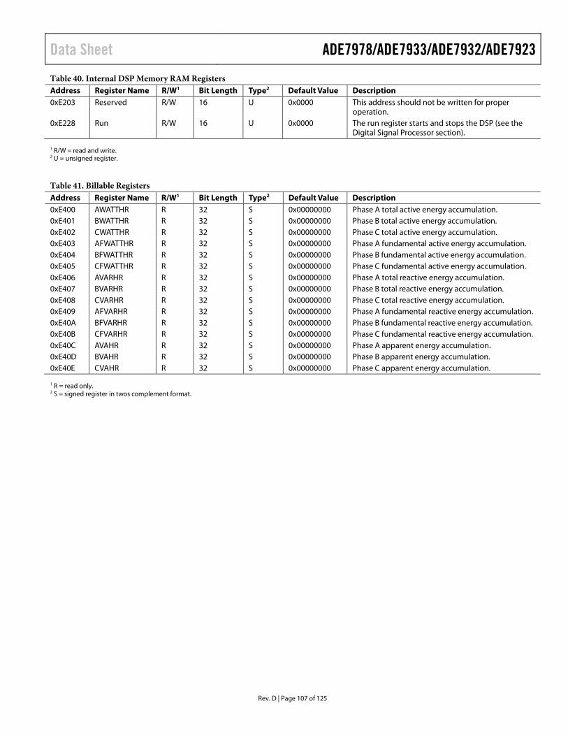
Data Sheet ADE7978/ADE7933/ADE7932/ADE7923
Rev. D | Page 107 of 125
Table 40. Internal DSP Memory RAM Registers Address Register Name R/W1 Bit Length Type2 Default Value Description 0xE203 Reserved R/W 16 U 0x0000 This address should not be written for proper
operation. 0xE228 Run R/W 16 U 0x0000 The run register starts and stops the DSP (see the
Digital Signal Processor section). 1 R/W = read and write. 2 U = unsigned register.
Table 41. Billable Registers Address Register Name R/W1 Bit Length Type2 Default Value Description 0xE400 AWATTHR R 32 S 0x00000000 Phase A total active energy accumulation. 0xE401 BWATTHR R 32 S 0x00000000 Phase B total active energy accumulation. 0xE402 CWATTHR R 32 S 0x00000000 Phase C total active energy accumulation. 0xE403 AFWATTHR R 32 S 0x00000000 Phase A fundamental active energy accumulation. 0xE404 BFWATTHR R 32 S 0x00000000 Phase B fundamental active energy accumulation. 0xE405 CFWATTHR R 32 S 0x00000000 Phase C fundamental active energy accumulation. 0xE406 AVARHR R 32 S 0x00000000 Phase A total reactive energy accumulation. 0xE407 BVARHR R 32 S 0x00000000 Phase B total reactive energy accumulation. 0xE408 CVARHR R 32 S 0x00000000 Phase C total reactive energy accumulation. 0xE409 AFVARHR R 32 S 0x00000000 Phase A fundamental reactive energy accumulation. 0xE40A BFVARHR R 32 S 0x00000000 Phase B fundamental reactive energy accumulation. 0xE40B CFVARHR R 32 S 0x00000000 Phase C fundamental reactive energy accumulation. 0xE40C AVAHR R 32 S 0x00000000 Phase A apparent energy accumulation. 0xE40D BVAHR R 32 S 0x00000000 Phase B apparent energy accumulation. 0xE40E CVAHR R 32 S 0x00000000 Phase C apparent energy accumulation. 1 R = read only. 2 S = signed register in twos complement format.

ADE7978/ADE7933/ADE7932/ADE7923 Data Sheet
Rev. D | Page 108 of 125
Table 42. Configuration and Power Quality Registers
Address Register Name R/W1
Bit Length
Bit Length During Communication2 Type3
Default Value4 Description
0xE500 IPEAK R 32 32 U N/A Current peak register (see Figure 70 and Table 43 for more information).
0xE501 VPEAK R 32 32 U N/A Voltage peak register (see Figure 70 and Table 44 for more information).
0xE502 STATUS0 R/W 32 32 U N/A Interrupt Status Register 0 (see Table 45). 0xE503 STATUS1 R/W 32 32 U N/A Interrupt Status Register 1 (see Table 46). 0xE504 to 0xE506
Reserved These addresses should not be written for proper operation.
0xE507 OILVL R/W 24 32 ZP U 0xFFFFFF Overcurrent threshold. 0xE508 OVLVL R/W 24 32 ZP U 0xFFFFFF Overvoltage threshold. 0xE509 SAGLVL R/W 24 32 ZP U 0x000000 Voltage sag level threshold. 0xE50A MASK0 R/W 32 32 U 0x00000000 Interrupt Enable Register 0 (see Table 47). 0xE50B MASK1 R/W 32 32 U 0x00000000 Interrupt Enable Register 1 (see Table 48). 0xE50C IAWV R 24 32 SE S N/A Instantaneous value of Phase A current. 0xE50D IBWV R 24 32 SE S N/A Instantaneous value of Phase B current. 0xE50E ICWV R 24 32 SE S N/A Instantaneous value of Phase C current. 0xE50F INWV R 24 32 SE S N/A Instantaneous value of neutral current. 0xE510 VAWV R 24 32 SE S N/A Instantaneous value of Phase A voltage. 0xE511 VBWV R 24 32 SE S N/A Instantaneous value of Phase B voltage. 0xE512 VCWV R 24 32 SE S N/A Instantaneous value of Phase C voltage. 0xE513 VA2WV R 24 32 SE S N/A Instantaneous value of Phase A V2P voltage. 0xE514 VB2WV R 24 32 SE S N/A Instantaneous value of Phase B V2P voltage. 0xE515 VC2WV R 24 32 SE S N/A Instantaneous value of Phase C V2P voltage. 0xE516 VNWV R 24 32 SE S N/A Instantaneous value of neutral line V1P
voltage. 0xE517 VN2WV R 24 32 SE S N/A Instantaneous value of neutral line V2P
voltage. 0xE518 AWATT R 24 32 SE S N/A Instantaneous value of Phase A total active
power. 0xE519 BWATT R 24 32 SE S N/A Instantaneous value of Phase B total active
power. 0xE51A CWATT R 24 32 SE S N/A Instantaneous value of Phase C total active
power. 0xE51B AVAR R 24 32 SE S N/A Instantaneous value of Phase A total
reactive power. 0xE51C BVAR R 24 32 SE S N/A Instantaneous value of Phase B total
reactive power. 0xE51D CVAR R 24 32 SE S N/A Instantaneous value of Phase C total
reactive power. 0xE51E AVA R 24 32 SE S N/A Instantaneous value of Phase A apparent
power. 0xE51F BVA R 24 32 SE S N/A Instantaneous value of Phase B apparent
power. 0xE520 CVA R 24 32 SE S N/A Instantaneous value of Phase C apparent
power. 0xE521 AVTHD R 24 32 ZP S N/A Total harmonic distortion of Phase A voltage. 0xE522 AITHD R 24 32 ZP S N/A Total harmonic distortion of Phase A current. 0xE523 BVTHD R 24 32 ZP S N/A Total harmonic distortion of Phase B voltage. 0xE524 BITHD R 24 32 ZP S N/A Total harmonic distortion of Phase B current. 0xE525 CVTHD R 24 32 ZP S N/A Total harmonic distortion of Phase C voltage. 0xE526 CITHD R 24 32 ZP S N/A Total harmonic distortion of Phase C current.
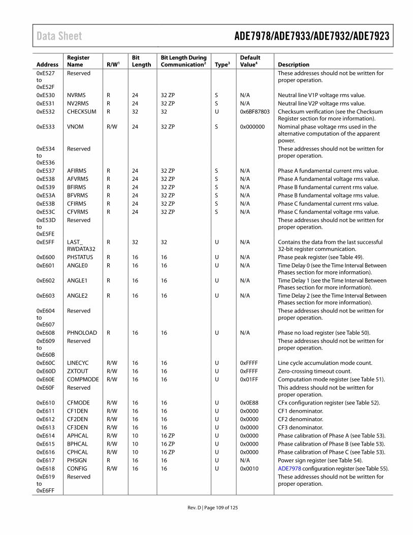
Data Sheet ADE7978/ADE7933/ADE7932/ADE7923
Rev. D | Page 109 of 125
Address Register Name R/W1
Bit Length
Bit Length During Communication2 Type3
Default Value4 Description
0xE527 to 0xE52F
Reserved These addresses should not be written for proper operation.
0xE530 NVRMS R 24 32 ZP S N/A Neutral line V1P voltage rms value. 0xE531 NV2RMS R 24 32 ZP S N/A Neutral line V2P voltage rms value. 0xE532 CHECKSUM R 32 32 U 0x6BF87803 Checksum verification (see the Checksum
Register section for more information). 0xE533 VNOM R/W 24 32 ZP S 0x000000 Nominal phase voltage rms used in the
alternative computation of the apparent power.
0xE534 to 0xE536
Reserved These addresses should not be written for proper operation.
0xE537 AFIRMS R 24 32 ZP S N/A Phase A fundamental current rms value. 0xE538 AFVRMS R 24 32 ZP S N/A Phase A fundamental voltage rms value. 0xE539 BFIRMS R 24 32 ZP S N/A Phase B fundamental current rms value. 0xE53A BFVRMS R 24 32 ZP S N/A Phase B fundamental voltage rms value. 0xE53B CFIRMS R 24 32 ZP S N/A Phase C fundamental current rms value. 0xE53C CFVRMS R 24 32 ZP S N/A Phase C fundamental voltage rms value. 0xE53D to 0xE5FE
Reserved These addresses should not be written for proper operation.
0xE5FF LAST_ RWDATA32
R 32 32 U N/A Contains the data from the last successful 32-bit register communication.
0xE600 PHSTATUS R 16 16 U N/A Phase peak register (see Table 49). 0xE601 ANGLE0 R 16 16 U N/A Time Delay 0 (see the Time Interval Between
Phases section for more information). 0xE602 ANGLE1 R 16 16 U N/A Time Delay 1 (see the Time Interval Between
Phases section for more information). 0xE603 ANGLE2 R 16 16 U N/A Time Delay 2 (see the Time Interval Between
Phases section for more information). 0xE604 to 0xE607
Reserved These addresses should not be written for proper operation.
0xE608 PHNOLOAD R 16 16 U N/A Phase no load register (see Table 50). 0xE609 to 0xE60B
Reserved These addresses should not be written for proper operation.
0xE60C LINECYC R/W 16 16 U 0xFFFF Line cycle accumulation mode count. 0xE60D ZXTOUT R/W 16 16 U 0xFFFF Zero-crossing timeout count. 0xE60E COMPMODE R/W 16 16 U 0x01FF Computation mode register (see Table 51). 0xE60F Reserved This address should not be written for
proper operation. 0xE610 CFMODE R/W 16 16 U 0x0E88 CFx configuration register (see Table 52). 0xE611 CF1DEN R/W 16 16 U 0x0000 CF1 denominator. 0xE612 CF2DEN R/W 16 16 U 0x0000 CF2 denominator. 0xE613 CF3DEN R/W 16 16 U 0x0000 CF3 denominator. 0xE614 APHCAL R/W 10 16 ZP U 0x0000 Phase calibration of Phase A (see Table 53). 0xE615 BPHCAL R/W 10 16 ZP U 0x0000 Phase calibration of Phase B (see Table 53). 0xE616 CPHCAL R/W 10 16 ZP U 0x0000 Phase calibration of Phase C (see Table 53). 0xE617 PHSIGN R 16 16 U N/A Power sign register (see Table 54). 0xE618 CONFIG R/W 16 16 U 0x0010 ADE7978 configuration register (see Table 55). 0xE619 to 0xE6FF
Reserved These addresses should not be written for proper operation.
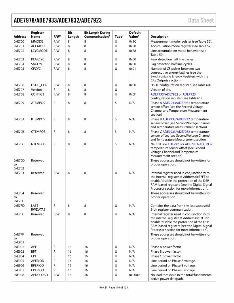
ADE7978/ADE7933/ADE7932/ADE7923 Data Sheet
Rev. D | Page 110 of 125
Address Register Name R/W1
Bit Length
Bit Length During Communication2 Type3
Default Value4 Description
0xE700 MMODE R/W 8 8 U 0x1C Measurement mode register (see Table 56). 0xE701 ACCMODE R/W 8 8 U 0x80 Accumulation mode register (see Table 57). 0xE702 LCYCMODE R/W 8 8 U 0x78 Line accumulation mode behavior (see
Table 59). 0xE703 PEAKCYC R/W 8 8 U 0x00 Peak detection half line cycles. 0xE704 SAGCYC R/W 8 8 U 0x00 Sag detection half line cycles. 0xE705 CFCYC R/W 8 8 U 0x01 Number of CF pulses between two
consecutive energy latches (see the Synchronizing Energy Registers with the CFx Outputs section).
0xE706 HSDC_CFG R/W 8 8 U 0x00 HSDC configuration register (see Table 60). 0xE707 Version R 8 8 U Version of die. 0xE708 CONFIG3 R/W 8 8 U 0x0F ADE7933/ADE7932 or ADE7923
configuration register (see Table 61). 0xE709 ATEMPOS R 8 8 S N/A Phase A ADE7933/ADE7932 temperature
sensor offset (see the Second Voltage Channel and Temperature Measurement section)
0xE70A BTEMPOS R 8 8 S N/A Phase B ADE7933/ADE7932 temperature sensor offset (see Second Voltage Channel and Temperature Measurement section)
0xE70B CTEMPOS R 8 8 S N/A Phase C ADE7933/ADE7932 temperature sensor offset (see Second Voltage Channel and Temperature Measurement section
0xE70C NTEMPOS R 8 8 S N/A Neutral line ADE7923 or ADE7933/ADE7932 temperature sensor offset (see Second Voltage Channel and Temperature Measurement section)
0xE70D to 0xE7E2
Reserved These addresses should not be written for proper operation.
0xE7E3 Reserved R/W 8 8 U N/A Internal register used in conjunction with the internal register at Address 0xE7FE to enable/disable the protection of the DSP RAM-based registers (see the Digital Signal Processor section for more information).
0xE7E4 to 0xE7FC
Reserved These addresses should not be written for proper operation.
0xE7FD LAST_ RWDATA8
R 8 8 U N/A Contains the data from the last successful 8-bit register communication.
0xE7FE Reserved R/W 8 8 U N/A Internal register used in conjunction with the internal register at Address 0xE7E3 to enable/disable the protection of the DSP RAM-based registers (see the Digital Signal Processor section for more information).
0xE7FF to 0xE901
Reserved These addresses should not be written for proper operation.
0xE902 APF R 16 16 U N/A Phase A power factor. 0xE903 BPF R 16 16 U N/A Phase B power factor. 0xE904 CPF R 16 16 U N/A Phase C power factor. 0xE905 APERIOD R 16 16 U N/A Line period on Phase A voltage. 0xE906 BPERIOD R 16 16 U N/A Line period on Phase B voltage. 0xE907 CPERIOD R 16 16 U N/A Line period on Phase C voltage. 0xE908 APNOLOAD R/W 16 16 U 0x0000 No load threshold in the total/fundamental
active power datapath.
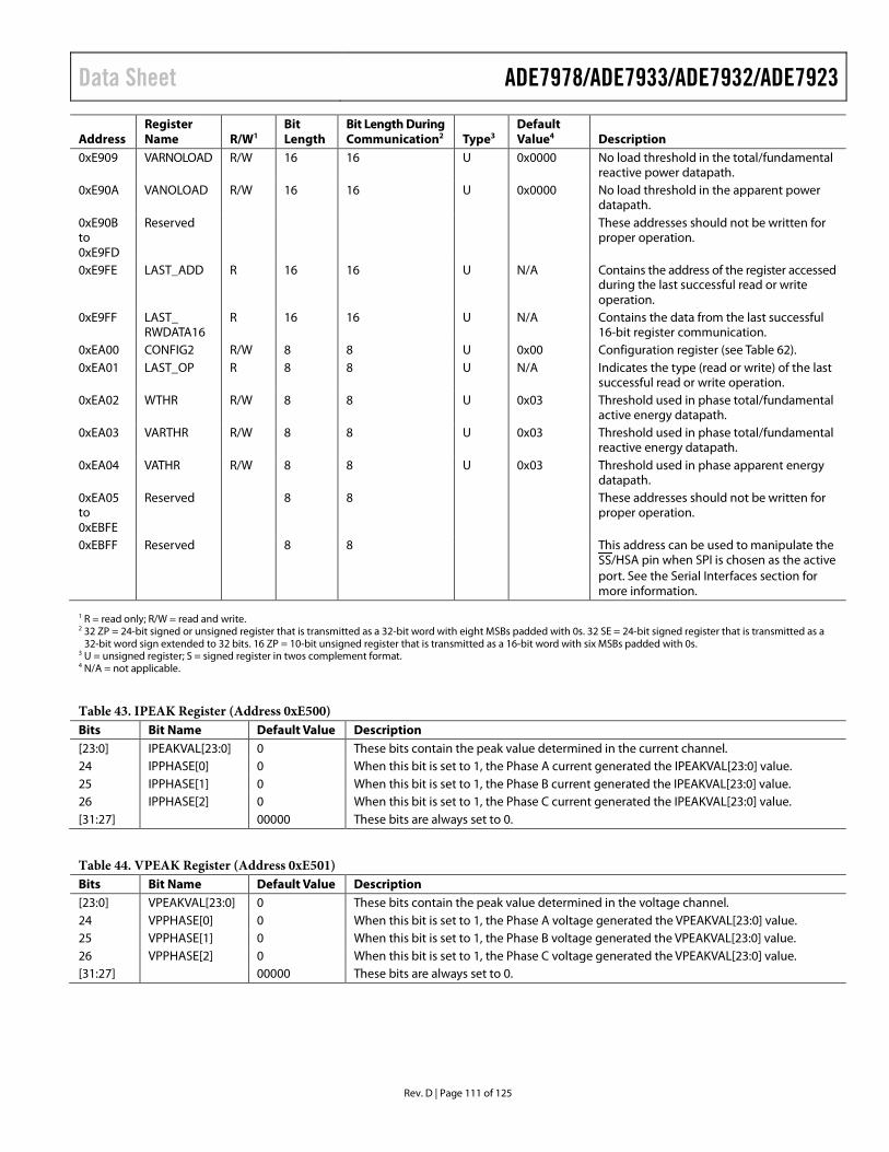
Data Sheet ADE7978/ADE7933/ADE7932/ADE7923
Rev. D | Page 111 of 125
Address Register Name R/W1
Bit Length
Bit Length During Communication2 Type3
Default Value4 Description
0xE909 VARNOLOAD R/W 16 16 U 0x0000 No load threshold in the total/fundamental reactive power datapath.
0xE90A VANOLOAD R/W 16 16 U 0x0000 No load threshold in the apparent power datapath.
0xE90B to 0xE9FD
Reserved These addresses should not be written for proper operation.
0xE9FE LAST_ADD R 16 16 U N/A Contains the address of the register accessed during the last successful read or write operation.
0xE9FF LAST_ RWDATA16
R 16 16 U N/A Contains the data from the last successful 16-bit register communication.
0xEA00 CONFIG2 R/W 8 8 U 0x00 Configuration register (see Table 62). 0xEA01 LAST_OP R 8 8 U N/A Indicates the type (read or write) of the last
successful read or write operation. 0xEA02 WTHR R/W 8 8 U 0x03 Threshold used in phase total/fundamental
active energy datapath. 0xEA03 VARTHR R/W 8 8 U 0x03 Threshold used in phase total/fundamental
reactive energy datapath. 0xEA04 VATHR R/W 8 8 U 0x03 Threshold used in phase apparent energy
datapath. 0xEA05 to 0xEBFE
Reserved 8 8 These addresses should not be written for proper operation.
0xEBFF Reserved 8 8 This address can be used to manipulate the SS/HSA pin when SPI is chosen as the active port. See the Serial Interfaces section for more information.
1 R = read only; R/W = read and write. 2 32 ZP = 24-bit signed or unsigned register that is transmitted as a 32-bit word with eight MSBs padded with 0s. 32 SE = 24-bit signed register that is transmitted as a
32-bit word sign extended to 32 bits. 16 ZP = 10-bit unsigned register that is transmitted as a 16-bit word with six MSBs padded with 0s. 3 U = unsigned register; S = signed register in twos complement format. 4 N/A = not applicable.
Table 43. IPEAK Register (Address 0xE500) Bits Bit Name Default Value Description [23:0] IPEAKVAL[23:0] 0 These bits contain the peak value determined in the current channel. 24 IPPHASE[0] 0 When this bit is set to 1, the Phase A current generated the IPEAKVAL[23:0] value. 25 IPPHASE[1] 0 When this bit is set to 1, the Phase B current generated the IPEAKVAL[23:0] value. 26 IPPHASE[2] 0 When this bit is set to 1, the Phase C current generated the IPEAKVAL[23:0] value. [31:27] 00000 These bits are always set to 0.
Table 44. VPEAK Register (Address 0xE501) Bits Bit Name Default Value Description [23:0] VPEAKVAL[23:0] 0 These bits contain the peak value determined in the voltage channel. 24 VPPHASE[0] 0 When this bit is set to 1, the Phase A voltage generated the VPEAKVAL[23:0] value. 25 VPPHASE[1] 0 When this bit is set to 1, the Phase B voltage generated the VPEAKVAL[23:0] value. 26 VPPHASE[2] 0 When this bit is set to 1, the Phase C voltage generated the VPEAKVAL[23:0] value. [31:27] 00000 These bits are always set to 0.
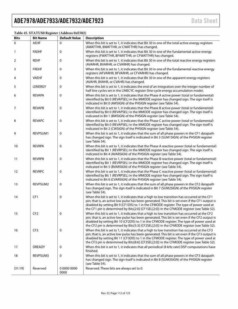
ADE7978/ADE7933/ADE7932/ADE7923 Data Sheet
Rev. D | Page 112 of 125
Table 45. STATUS0 Register (Address 0xE502) Bits Bit Name Default Value Description 0 AEHF 0 When this bit is set to 1, it indicates that Bit 30 in one of the total active energy registers
(AWATTHR, BWATTHR, or CWATTHR) has changed. 1 FAEHF 0 When this bit is set to 1, it indicates that Bit 30 in one of the fundamental active energy
registers (FWATTHR, BFWATTHR, or CFWATTHR) has changed. 2 REHF 0 When this bit is set to 1, it indicates that Bit 30 in one of the total reactive energy registers
(AVARHR, BVARHR, or CVARHR) has changed. 3 FREHF 0 When this bit is set to 1, it indicates that Bit 30 in one of the fundamental reactive energy
registers (AFVARHR, BFVARHR, or CFVARHR) has changed. 4 VAEHF 0 When this bit is set to 1, it indicates that Bit 30 in one of the apparent energy registers
(AVAHR, BVAHR, or CVAHR) has changed. 5 LENERGY 0 When this bit is set to 1, it indicates the end of an integration over the integer number of
half line cycles set in the LINECYC register (line cycle energy accumulation mode). 6 REVAPA 0 When this bit is set to 1, it indicates that the Phase A active power (total or fundamental)
identified by Bit 0 (REVAPSEL) in the MMODE register has changed sign. The sign itself is indicated in Bit 0 (AWSIGN) of the PHSIGN register (see Table 54).
7 REVAPB 0 When this bit is set to 1, it indicates that the Phase B active power (total or fundamental) identified by Bit 0 (REVAPSEL) in the MMODE register has changed sign. The sign itself is indicated in Bit 1 (BWSIGN) of the PHSIGN register (see Table 54).
8 REVAPC 0 When this bit is set to 1, it indicates that the Phase C active power (total or fundamental) identified by Bit 0 (REVAPSEL) in the MMODE register has changed sign. The sign itself is indicated in Bit 2 (CWSIGN) of the PHSIGN register (see Table 54).
9 REVPSUM1 0 When this bit is set to 1, it indicates that the sum of all phase powers in the CF1 datapath has changed sign. The sign itself is indicated in Bit 3 (SUM1SIGN) of the PHSIGN register (see Table 54).
10 REVRPA 0 When this bit is set to 1, it indicates that the Phase A reactive power (total or fundamental) identified by Bit 1 (REVRPSEL) in the MMODE register has changed sign. The sign itself is indicated in Bit 4 (AVARSIGN) of the PHSIGN register (see Table 54).
11 REVRPB 0 When this bit is set to 1, it indicates that the Phase B reactive power (total or fundamental) identified by Bit 1 (REVRPSEL) in the MMODE register has changed sign. The sign itself is indicated in Bit 5 (BVARSIGN) of the PHSIGN register (see Table 54).
12 REVRPC 0 When this bit is set to 1, it indicates that the Phase C reactive power (total or fundamental) identified by Bit 1 (REVRPSEL) in the MMODE register has changed sign. The sign itself is indicated in Bit 6 (CVARSIGN) of the PHSIGN register (see Table 54).
13 REVPSUM2 0 When this bit is set to 1, it indicates that the sum of all phase powers in the CF2 datapath has changed sign. The sign itself is indicated in Bit 7 (SUM2SIGN) of the PHSIGN register (see Table 54).
14 CF1 0 When this bit is set to 1, it indicates that a high to low transition has occurred at the CF1 pin; that is, an active low pulse has been generated. This bit is set even if the CF1 output is disabled by setting Bit 9 (CF1DIS) to 1 in the CFMODE register. The type of power used at the CF1 pin is determined by Bits[2:0] (CF1SEL[2:0]) in the CFMODE register (see Table 52).
15 CF2 0 When this bit is set to 1, it indicates that a high to low transition has occurred at the CF2 pin; that is, an active low pulse has been generated. This bit is set even if the CF2 output is disabled by setting Bit 10 (CF2DIS) to 1 in the CFMODE register. The type of power used at the CF2 pin is determined by Bits[5:3] (CF2SEL[2:0]) in the CFMODE register (see Table 52).
16 CF3 0 When this bit is set to 1, it indicates that a high to low transition has occurred at the CF3 pin; that is, an active low pulse has been generated. This bit is set even if the CF3 output is disabled by setting Bit 11 (CF3DIS) to 1 in the CFMODE register. The type of power used at the CF3 pin is determined by Bits[8:6] (CF3SEL[2:0]) in the CFMODE register (see Table 52).
17 DREADY 0 When this bit is set to 1, it indicates that all periodical (8 kHz rate) DSP computations have finished.
18 REVPSUM3 0 When this bit is set to 1, it indicates that the sum of all phase powers in the CF3 datapath has changed sign. The sign itself is indicated in Bit 8 (SUM3SIGN) of the PHSIGN register (see Table 54).
[31:19] Reserved 0 0000 0000 0000
Reserved. These bits are always set to 0.

Data Sheet ADE7978/ADE7933/ADE7932/ADE7923
Rev. D | Page 113 of 125
Table 46. STATUS1 Register (Address 0xE503) Bits Bit Name Default Value Description 0 NLOAD 0 When this bit is set to 1, it indicates that at least one phase entered or exited the no load
condition based on the total active and reactive powers. The phase is indicated in Bits[2:0] (NLPHASE[x]) in the PHNOLOAD register (see Table 50).
1 FNLOAD 0 When this bit is set to 1, it indicates that at least one phase entered or exited the no load condition based on the fundamental active and reactive powers. The phase is indicated in Bits[5:3] (FNLPHASE[x]) in the PHNOLOAD register (see Table 50).
2 VANLOAD 0 When this bit is set to 1, it indicates that at least one phase entered or exited the no load condition based on the apparent power. The phase is indicated in Bits[8:6] (VANLPHASE[x]) in the PHNOLOAD register (see Table 50).
3 ZXTOVA 0 When this bit is set to 1, it indicates that a zero crossing on the Phase A voltage is missing. 4 ZXTOVB 0 When this bit is set to 1, it indicates that a zero crossing on the Phase B voltage is missing. 5 ZXTOVC 0 When this bit is set to 1, it indicates that a zero crossing on the Phase C voltage is missing. 6 ZXTOIA 0 When this bit is set to 1, it indicates that a zero crossing on the Phase A current is missing. 7 ZXTOIB 0 When this bit is set to 1, it indicates that a zero crossing on the Phase B current is missing. 8 ZXTOIC 0 When this bit is set to 1, it indicates that a zero crossing on the Phase C current is missing. 9 ZXVA 0 When this bit is set to 1, it indicates that a zero crossing was detected on the Phase A voltage. 10 ZXVB 0 When this bit is set to 1, it indicates that a zero crossing was detected on the Phase B voltage. 11 ZXVC 0 When this bit is set to 1, it indicates that a zero crossing was detected on the Phase C voltage. 12 ZXIA 0 When this bit is set to 1, it indicates that a zero crossing was detected on the Phase A current. 13 ZXIB 0 When this bit is set to 1, it indicates that a zero crossing was detected on the Phase B current. 14 ZXIC 0 When this bit is set to 1, it indicates that a zero crossing was detected on the Phase C current. 15 RSTDONE 1 At the end of a hardware or software reset, this bit is set to 1, and the IRQ1 pin goes low.
To clear this interrupt and return the IRQ1 pin high, write a 1 to this bit. The RSTDONE interrupt cannot be masked; therefore, this bit must always be reset to 0 for the IRQ1 pin to return high.
16 Sag 0 When this bit is set to 1, it indicates that a sag event occurred on the phase indicated by Bits[14:12] (VSPHASE[x]) in the PHSTATUS register (see Table 49).
17 OI 0 When this bit is set to 1, it indicates that an overcurrent event occurred on the phase indicated by Bits[5:3] (OIPHASE[x]) in the PHSTATUS register (see Table 49).
18 OV 0 When this bit is set to 1, it indicates that an overvoltage event occurred on the phase indicated by Bits[11:9] (OVPHASE[x]) in the PHSTATUS register (see Table 49).
19 SEQERR 0 When this bit is set to 1, it indicates that a negative to positive zero crossing on the Phase A voltage was followed by a negative to positive zero crossing on the Phase C voltage instead of on the Phase B voltage.
20 MISMTCH 0 When this bit is set to 1, it indicates that ||ISUM| − |INWV|| > |ISUMLVL|, where ISUMLVL is the value of the ISUMLVL register (Address 0x4398). For more information, see the Neutral Current Mismatch section.
21 Reserved 1 Reserved. This bit is always set to 1. 22 Reserved 0 Reserved. This bit is always set to 0. 23 PKI 0 When this bit is set to 1, it indicates that the period used to detect the peak value in the
current channel has ended. The IPEAK register contains the peak value and the phase where the peak was detected (see Table 43).
24 PKV 0 When this bit is set to 1, it indicates that the period used to detect the peak value in the voltage channel has ended. The VPEAK register contains the peak value and the phase where the peak was detected (see Table 44).
25 CRC 0 When this bit is set to 1, it indicates that the ADE7978 has computed a checksum value that is different from the checksum value computed when the run register was set to 1.
[31:26] Reserved 00 0000 Reserved. These bits are always set to 0.
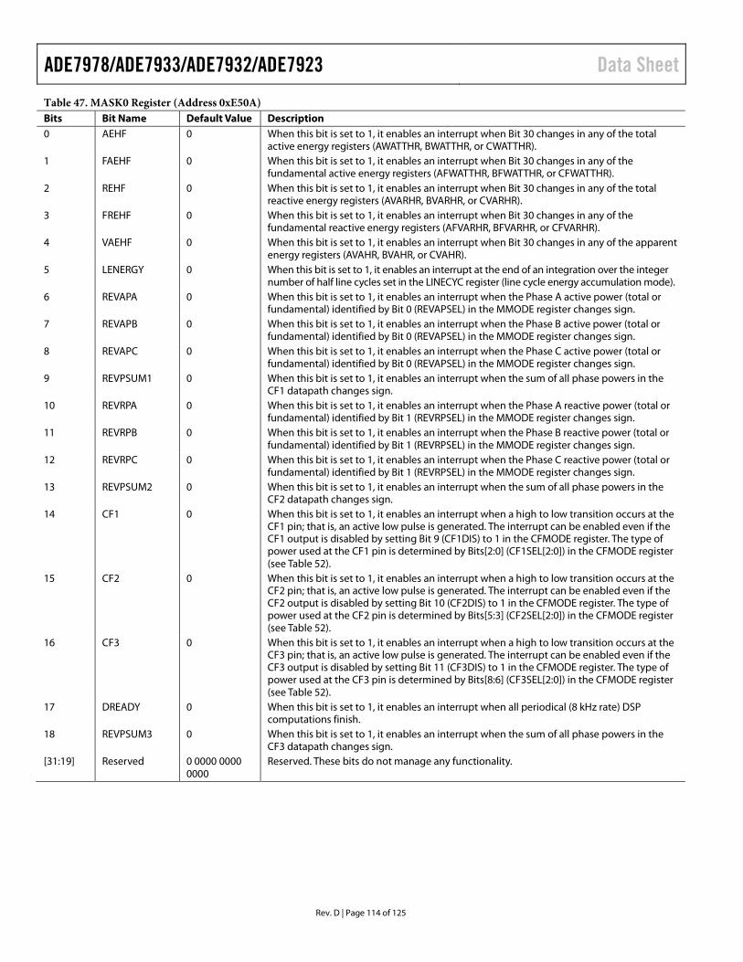
ADE7978/ADE7933/ADE7932/ADE7923 Data Sheet
Rev. D | Page 114 of 125
Table 47. MASK0 Register (Address 0xE50A) Bits Bit Name Default Value Description 0 AEHF 0 When this bit is set to 1, it enables an interrupt when Bit 30 changes in any of the total
active energy registers (AWATTHR, BWATTHR, or CWATTHR). 1 FAEHF 0 When this bit is set to 1, it enables an interrupt when Bit 30 changes in any of the
fundamental active energy registers (AFWATTHR, BFWATTHR, or CFWATTHR). 2 REHF 0 When this bit is set to 1, it enables an interrupt when Bit 30 changes in any of the total
reactive energy registers (AVARHR, BVARHR, or CVARHR). 3 FREHF 0 When this bit is set to 1, it enables an interrupt when Bit 30 changes in any of the
fundamental reactive energy registers (AFVARHR, BFVARHR, or CFVARHR). 4 VAEHF 0 When this bit is set to 1, it enables an interrupt when Bit 30 changes in any of the apparent
energy registers (AVAHR, BVAHR, or CVAHR). 5 LENERGY 0 When this bit is set to 1, it enables an interrupt at the end of an integration over the integer
number of half line cycles set in the LINECYC register (line cycle energy accumulation mode). 6 REVAPA 0 When this bit is set to 1, it enables an interrupt when the Phase A active power (total or
fundamental) identified by Bit 0 (REVAPSEL) in the MMODE register changes sign. 7 REVAPB 0 When this bit is set to 1, it enables an interrupt when the Phase B active power (total or
fundamental) identified by Bit 0 (REVAPSEL) in the MMODE register changes sign. 8 REVAPC 0 When this bit is set to 1, it enables an interrupt when the Phase C active power (total or
fundamental) identified by Bit 0 (REVAPSEL) in the MMODE register changes sign. 9 REVPSUM1 0 When this bit is set to 1, it enables an interrupt when the sum of all phase powers in the
CF1 datapath changes sign. 10 REVRPA 0 When this bit is set to 1, it enables an interrupt when the Phase A reactive power (total or
fundamental) identified by Bit 1 (REVRPSEL) in the MMODE register changes sign. 11 REVRPB 0 When this bit is set to 1, it enables an interrupt when the Phase B reactive power (total or
fundamental) identified by Bit 1 (REVRPSEL) in the MMODE register changes sign. 12 REVRPC 0 When this bit is set to 1, it enables an interrupt when the Phase C reactive power (total or
fundamental) identified by Bit 1 (REVRPSEL) in the MMODE register changes sign. 13 REVPSUM2 0 When this bit is set to 1, it enables an interrupt when the sum of all phase powers in the
CF2 datapath changes sign. 14 CF1 0 When this bit is set to 1, it enables an interrupt when a high to low transition occurs at the
CF1 pin; that is, an active low pulse is generated. The interrupt can be enabled even if the CF1 output is disabled by setting Bit 9 (CF1DIS) to 1 in the CFMODE register. The type of power used at the CF1 pin is determined by Bits[2:0] (CF1SEL[2:0]) in the CFMODE register (see Table 52).
15 CF2 0 When this bit is set to 1, it enables an interrupt when a high to low transition occurs at the CF2 pin; that is, an active low pulse is generated. The interrupt can be enabled even if the CF2 output is disabled by setting Bit 10 (CF2DIS) to 1 in the CFMODE register. The type of power used at the CF2 pin is determined by Bits[5:3] (CF2SEL[2:0]) in the CFMODE register (see Table 52).
16 CF3 0 When this bit is set to 1, it enables an interrupt when a high to low transition occurs at the CF3 pin; that is, an active low pulse is generated. The interrupt can be enabled even if the CF3 output is disabled by setting Bit 11 (CF3DIS) to 1 in the CFMODE register. The type of power used at the CF3 pin is determined by Bits[8:6] (CF3SEL[2:0]) in the CFMODE register (see Table 52).
17 DREADY 0 When this bit is set to 1, it enables an interrupt when all periodical (8 kHz rate) DSP computations finish.
18 REVPSUM3 0 When this bit is set to 1, it enables an interrupt when the sum of all phase powers in the CF3 datapath changes sign.
[31:19] Reserved 0 0000 0000 0000
Reserved. These bits do not manage any functionality.
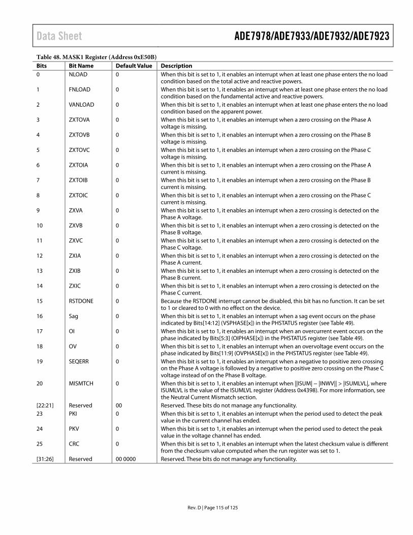
Data Sheet ADE7978/ADE7933/ADE7932/ADE7923
Rev. D | Page 115 of 125
Table 48. MASK1 Register (Address 0xE50B) Bits Bit Name Default Value Description 0 NLOAD 0 When this bit is set to 1, it enables an interrupt when at least one phase enters the no load
condition based on the total active and reactive powers. 1 FNLOAD 0 When this bit is set to 1, it enables an interrupt when at least one phase enters the no load
condition based on the fundamental active and reactive powers. 2 VANLOAD 0 When this bit is set to 1, it enables an interrupt when at least one phase enters the no load
condition based on the apparent power. 3 ZXTOVA 0 When this bit is set to 1, it enables an interrupt when a zero crossing on the Phase A
voltage is missing. 4 ZXTOVB 0 When this bit is set to 1, it enables an interrupt when a zero crossing on the Phase B
voltage is missing. 5 ZXTOVC 0 When this bit is set to 1, it enables an interrupt when a zero crossing on the Phase C
voltage is missing. 6 ZXTOIA 0 When this bit is set to 1, it enables an interrupt when a zero crossing on the Phase A
current is missing. 7 ZXTOIB 0 When this bit is set to 1, it enables an interrupt when a zero crossing on the Phase B
current is missing. 8 ZXTOIC 0 When this bit is set to 1, it enables an interrupt when a zero crossing on the Phase C
current is missing. 9 ZXVA 0 When this bit is set to 1, it enables an interrupt when a zero crossing is detected on the
Phase A voltage. 10 ZXVB 0 When this bit is set to 1, it enables an interrupt when a zero crossing is detected on the
Phase B voltage. 11 ZXVC 0 When this bit is set to 1, it enables an interrupt when a zero crossing is detected on the
Phase C voltage. 12 ZXIA 0 When this bit is set to 1, it enables an interrupt when a zero crossing is detected on the
Phase A current. 13 ZXIB 0 When this bit is set to 1, it enables an interrupt when a zero crossing is detected on the
Phase B current. 14 ZXIC 0 When this bit is set to 1, it enables an interrupt when a zero crossing is detected on the
Phase C current. 15 RSTDONE 0 Because the RSTDONE interrupt cannot be disabled, this bit has no function. It can be set
to 1 or cleared to 0 with no effect on the device. 16 Sag 0 When this bit is set to 1, it enables an interrupt when a sag event occurs on the phase
indicated by Bits[14:12] (VSPHASE[x]) in the PHSTATUS register (see Table 49). 17 OI 0 When this bit is set to 1, it enables an interrupt when an overcurrent event occurs on the
phase indicated by Bits[5:3] (OIPHASE[x]) in the PHSTATUS register (see Table 49). 18 OV 0 When this bit is set to 1, it enables an interrupt when an overvoltage event occurs on the
phase indicated by Bits[11:9] (OVPHASE[x]) in the PHSTATUS register (see Table 49). 19 SEQERR 0 When this bit is set to 1, it enables an interrupt when a negative to positive zero crossing
on the Phase A voltage is followed by a negative to positive zero crossing on the Phase C voltage instead of on the Phase B voltage.
20 MISMTCH 0 When this bit is set to 1, it enables an interrupt when ||ISUM| − |INWV|| > |ISUMLVL|, where ISUMLVL is the value of the ISUMLVL register (Address 0x4398). For more information, see the Neutral Current Mismatch section.
[22:21] Reserved 00 Reserved. These bits do not manage any functionality. 23 PKI 0 When this bit is set to 1, it enables an interrupt when the period used to detect the peak
value in the current channel has ended. 24 PKV 0 When this bit is set to 1, it enables an interrupt when the period used to detect the peak
value in the voltage channel has ended. 25 CRC 0 When this bit is set to 1, it enables an interrupt when the latest checksum value is different
from the checksum value computed when the run register was set to 1. [31:26] Reserved 00 0000 Reserved. These bits do not manage any functionality.
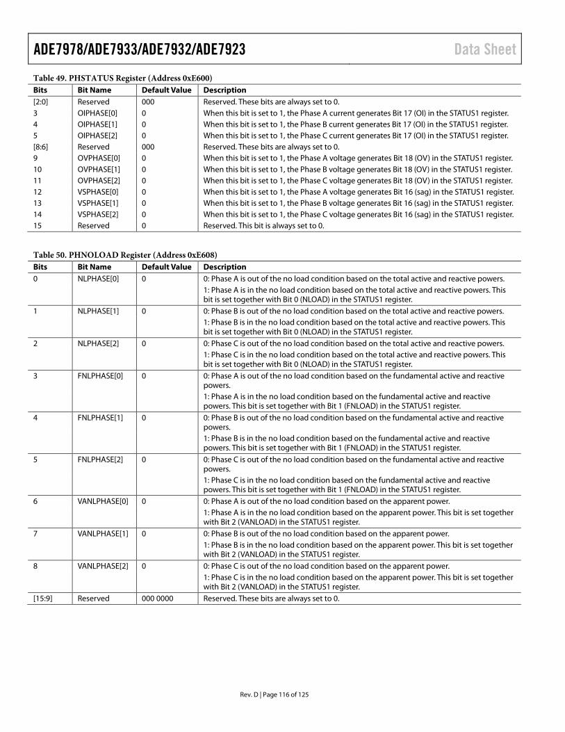
ADE7978/ADE7933/ADE7932/ADE7923 Data Sheet
Rev. D | Page 116 of 125
Table 49. PHSTATUS Register (Address 0xE600) Bits Bit Name Default Value Description [2:0] Reserved 000 Reserved. These bits are always set to 0. 3 OIPHASE[0] 0 When this bit is set to 1, the Phase A current generates Bit 17 (OI) in the STATUS1 register. 4 OIPHASE[1] 0 When this bit is set to 1, the Phase B current generates Bit 17 (OI) in the STATUS1 register. 5 OIPHASE[2] 0 When this bit is set to 1, the Phase C current generates Bit 17 (OI) in the STATUS1 register. [8:6] Reserved 000 Reserved. These bits are always set to 0. 9 OVPHASE[0] 0 When this bit is set to 1, the Phase A voltage generates Bit 18 (OV) in the STATUS1 register. 10 OVPHASE[1] 0 When this bit is set to 1, the Phase B voltage generates Bit 18 (OV) in the STATUS1 register. 11 OVPHASE[2] 0 When this bit is set to 1, the Phase C voltage generates Bit 18 (OV) in the STATUS1 register. 12 VSPHASE[0] 0 When this bit is set to 1, the Phase A voltage generates Bit 16 (sag) in the STATUS1 register. 13 VSPHASE[1] 0 When this bit is set to 1, the Phase B voltage generates Bit 16 (sag) in the STATUS1 register. 14 VSPHASE[2] 0 When this bit is set to 1, the Phase C voltage generates Bit 16 (sag) in the STATUS1 register. 15 Reserved 0 Reserved. This bit is always set to 0.
Table 50. PHNOLOAD Register (Address 0xE608) Bits Bit Name Default Value Description 0 NLPHASE[0] 0 0: Phase A is out of the no load condition based on the total active and reactive powers. 1: Phase A is in the no load condition based on the total active and reactive powers. This
bit is set together with Bit 0 (NLOAD) in the STATUS1 register. 1 NLPHASE[1] 0 0: Phase B is out of the no load condition based on the total active and reactive powers. 1: Phase B is in the no load condition based on the total active and reactive powers. This
bit is set together with Bit 0 (NLOAD) in the STATUS1 register. 2 NLPHASE[2] 0 0: Phase C is out of the no load condition based on the total active and reactive powers. 1: Phase C is in the no load condition based on the total active and reactive powers. This
bit is set together with Bit 0 (NLOAD) in the STATUS1 register. 3 FNLPHASE[0] 0 0: Phase A is out of the no load condition based on the fundamental active and reactive
powers. 1: Phase A is in the no load condition based on the fundamental active and reactive
powers. This bit is set together with Bit 1 (FNLOAD) in the STATUS1 register. 4 FNLPHASE[1] 0 0: Phase B is out of the no load condition based on the fundamental active and reactive
powers. 1: Phase B is in the no load condition based on the fundamental active and reactive
powers. This bit is set together with Bit 1 (FNLOAD) in the STATUS1 register. 5 FNLPHASE[2] 0 0: Phase C is out of the no load condition based on the fundamental active and reactive
powers. 1: Phase C is in the no load condition based on the fundamental active and reactive
powers. This bit is set together with Bit 1 (FNLOAD) in the STATUS1 register. 6 VANLPHASE[0] 0 0: Phase A is out of the no load condition based on the apparent power. 1: Phase A is in the no load condition based on the apparent power. This bit is set together
with Bit 2 (VANLOAD) in the STATUS1 register. 7 VANLPHASE[1] 0 0: Phase B is out of the no load condition based on the apparent power. 1: Phase B is in the no load condition based on the apparent power. This bit is set together
with Bit 2 (VANLOAD) in the STATUS1 register. 8 VANLPHASE[2] 0 0: Phase C is out of the no load condition based on the apparent power. 1: Phase C is in the no load condition based on the apparent power. This bit is set together
with Bit 2 (VANLOAD) in the STATUS1 register. [15:9] Reserved 000 0000 Reserved. These bits are always set to 0.

Data Sheet ADE7978/ADE7933/ADE7932/ADE7923
Rev. D | Page 117 of 125
Table 51. COMPMODE Register (Address 0xE60E) Bits Bit Name Default Value Description 0 TERMSEL1[0] 1 0: Phase A is not included in the CF1 output calculations. 1: Phase A is included in the CF1 output calculations. Setting the TERMSEL1[2:0] bits to 111
specifies that the sum of all three phases is included in the CF1 output. 1 TERMSEL1[1] 1 0: Phase B is not included in the CF1 output calculations. 1: Phase B is included in the CF1 output calculations. Setting the TERMSEL1[2:0] bits to 111
specifies that the sum of all three phases is included in the CF1 output. 2 TERMSEL1[2] 1 0: Phase C is not included in the CF1 output calculations. 1: Phase C is included in the CF1 output calculations. Setting the TERMSEL1[2:0] bits to 111
specifies that the sum of all three phases is included in the CF1 output. 3 TERMSEL2[0] 1 0: Phase A is not included in the CF2 output calculations. 1: Phase A is included in the CF2 output calculations. Setting the TERMSEL2[2:0] bits to 111
specifies that the sum of all three phases is included in the CF2 output. 4 TERMSEL2[1] 1 0: Phase B is not included in the CF2 output calculations. 1: Phase B is included in the CF2 output calculations. Setting the TERMSEL2[2:0] bits to 111
specifies that the sum of all three phases is included in the CF2 output. 5 TERMSEL2[2] 1 0: Phase C is not included in the CF2 output calculations. 1: Phase C is included in the CF2 output calculations. Setting the TERMSEL2[2:0] bits to 111
specifies that the sum of all three phases is included in the CF2 output. 6 TERMSEL3[0] 1 0: Phase A is not included in the CF3 output calculations. 1: Phase A is included in the CF3 output calculations. Setting the TERMSEL3[2:0] bits to 111
specifies that the sum of all three phases is included in the CF3 output. 7 TERMSEL3[1] 1 0: Phase B is not included in the CF3 output calculations. 1: Phase B is included in the CF3 output calculations. Setting the TERMSEL3[2:0] bits to 111
specifies that the sum of all three phases is included in the CF3 output. 8 TERMSEL3[2] 1 0: Phase C is not included in the CF3 output calculations. 1: Phase C is included in the CF3 output calculations. Setting the TERMSEL3[2:0] bits to 111
specifies that the sum of all three phases is included in the CF3 output. [10:9] ANGLESEL[1:0] 00 00: delays between the voltages and currents of the same phase are measured. 01: delays between the phase voltages are measured. 10: delays between the phase currents are measured. 11: no delays are measured. 11 VNOMAEN 0 0: the apparent power on Phase A is computed normally by multiplying the voltage rms
value by the current rms value. 1: the apparent power on Phase A is computed by multiplying the phase rms current by an
rms voltage written to the VNOM register (Address 0xE533). 12 VNOMBEN 0 0: the apparent power on Phase B is computed normally by multiplying the voltage rms
value by the current rms value. 1: the apparent power on Phase B is computed by multiplying the phase rms current by an
rms voltage written to the VNOM register (Address 0xE533). 13 VNOMCEN 0 0: the apparent power on Phase C is computed normally by multiplying the voltage rms
value by the current rms value. 1: the apparent power on Phase C is computed by multiplying the phase rms current by an
rms voltage written to the VNOM register (Address 0xE533). 14 SELFREQ 0 0: ADE7978 is connected to a 50 Hz network. 1: ADE7978 is connected to a 60 Hz network. 15 Reserved 0 This bit is set to 0 by default and does not manage any functionality.

ADE7978/ADE7933/ADE7932/ADE7923 Data Sheet
Rev. D | Page 118 of 125
Table 52. CFMODE Register (Address 0xE610) Bits Bit Name Default Value Description [2:0] CF1SEL[2:0] 000 000: CF1 frequency is proportional to the sum of the total active powers on each phase
identified by Bits[2:0] (TERMSEL1[x]) in the COMPMODE register. 001: CF1 frequency is proportional to the sum of the total reactive powers on each phase identified by Bits[2:0] (TERMSEL1[x]) in the COMPMODE register. 010: CF1 frequency is proportional to the sum of the apparent powers on each phase identified by Bits[2:0] (TERMSEL1[x]) in the COMPMODE register. 011: CF1 frequency is proportional to the sum of the fundamental active powers on each phase identified by Bits[2:0] (TERMSEL1[x]) in the COMPMODE register. 100: CF1 frequency is proportional to the sum of the fundamental reactive powers on each phase identified by Bits[2:0] (TERMSEL1[x]) in the COMPMODE register. 101, 110, 111: reserved. The CF1 signal is not generated.
[5:3] CF2SEL[2:0] 001 000: CF2 frequency is proportional to the sum of the total active powers on each phase identified by Bits[5:3] (TERMSEL2[x]) in the COMPMODE register. 001: CF2 frequency is proportional to the sum of the total reactive powers on each phase identified by Bits[5:3] (TERMSEL2[x]) in the COMPMODE register. 010: CF2 frequency is proportional to the sum of the apparent powers on each phase identified by Bits[5:3] (TERMSEL2[x]) in the COMPMODE register. 011: CF2 frequency is proportional to the sum of the fundamental active powers on each phase identified by Bits[5:3] (TERMSEL2[x]) in the COMPMODE register. 100: CF2 frequency is proportional to the sum of the fundamental reactive powers on each phase identified by Bits[5:3] (TERMSEL2[x]) in the COMPMODE register. 101, 110, 111: reserved. The CF2 signal is not generated.
[8:6] CF3SEL[2:0] 010 000: CF3 frequency is proportional to the sum of the total active powers on each phase identified by Bits[8:6] (TERMSEL3[x]) in the COMPMODE register. 001: CF3 frequency is proportional to the sum of the total reactive powers on each phase identified by Bits[8:6] (TERMSEL3[x]) in the COMPMODE register. 010: CF3 frequency is proportional to the sum of the apparent powers on each phase identified by Bits[8:6] (TERMSEL3[x]) in the COMPMODE register. 011: CF3 frequency is proportional to the sum of the fundamental active powers on each phase identified by Bits[8:6] (TERMSEL3[x]) in the COMPMODE register. 100: CF3 frequency is proportional to the sum of the fundamental reactive powers on each phase identified by Bits[8:6] (TERMSEL3[x]) in the COMPMODE register. 101, 110, 111: reserved. The CF3 signal is not generated.
9 CF1DIS 1 0: CF1 output is enabled. 1: CF1 output is disabled. The energy-to-frequency converter remains enabled. 10 CF2DIS 1 0: CF2 output is enabled. 1: CF2 output is disabled. The energy-to-frequency converter remains enabled. 11 CF3DIS 1 0: CF3 output is enabled. 1: CF3 output is disabled. The energy-to-frequency converter remains enabled. 12 CF1LATCH 0 0: no latching of energy registers occurs when a CF1 pulse is generated. 1: the contents of the corresponding energy registers are latched when a CF1 pulse
is generated. See the Synchronizing Energy Registers with the CFx Outputs section. 13 CF2LATCH 0 0: no latching of energy registers occurs when a CF2 pulse is generated. 1: the contents of the corresponding energy registers are latched when a CF2 pulse is
generated. See the Synchronizing Energy Registers with the CFx Outputs section. 14 CF3LATCH 0 0: no latching of energy registers occurs when a CF3 pulse is generated. 1: the contents of the corresponding energy registers are latched when a CF3 pulse is
generated. See the Synchronizing Energy Registers with the CFx Outputs section. 15 Reserved 0 Reserved. This bit does not manage any functionality.
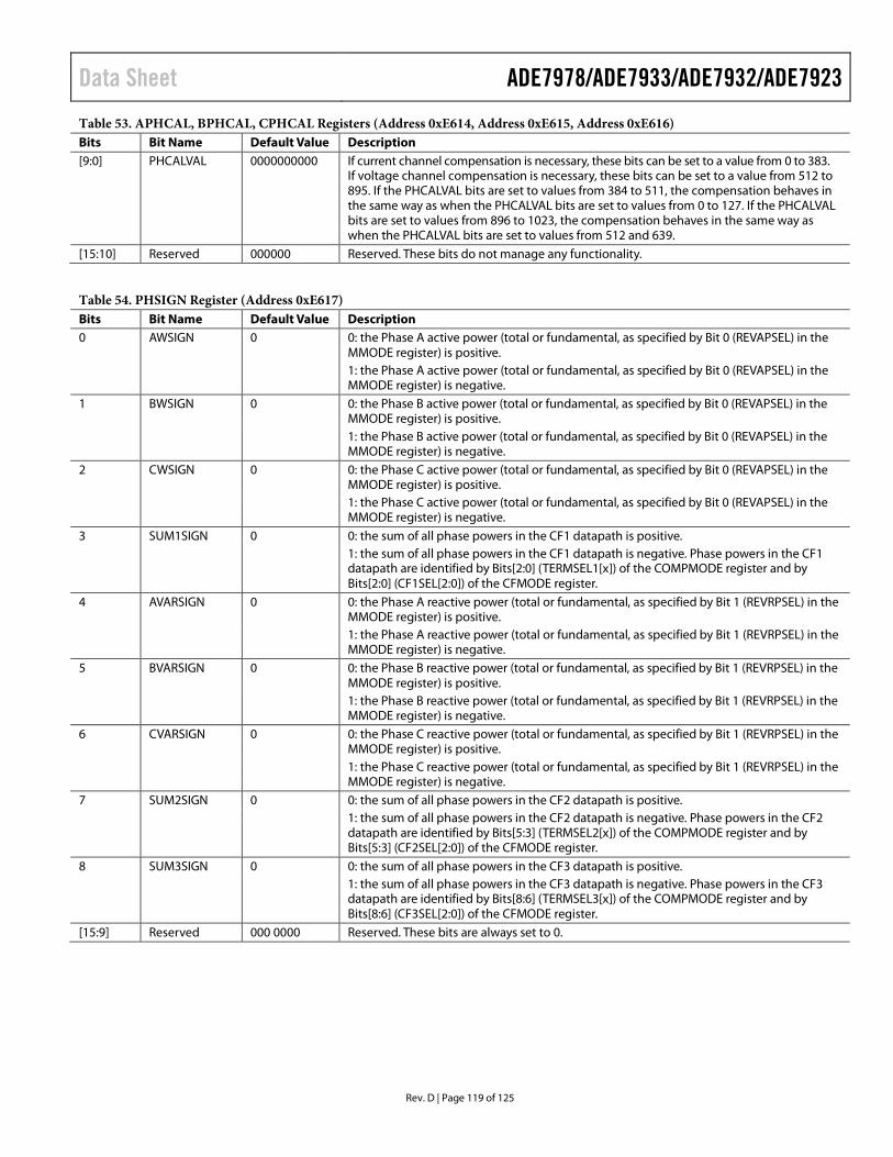
Data Sheet ADE7978/ADE7933/ADE7932/ADE7923
Rev. D | Page 119 of 125
Table 53. APHCAL, BPHCAL, CPHCAL Registers (Address 0xE614, Address 0xE615, Address 0xE616) Bits Bit Name Default Value Description [9:0] PHCALVAL 0000000000 If current channel compensation is necessary, these bits can be set to a value from 0 to 383.
If voltage channel compensation is necessary, these bits can be set to a value from 512 to 895. If the PHCALVAL bits are set to values from 384 to 511, the compensation behaves in the same way as when the PHCALVAL bits are set to values from 0 to 127. If the PHCALVAL bits are set to values from 896 to 1023, the compensation behaves in the same way as when the PHCALVAL bits are set to values from 512 and 639.
[15:10] Reserved 000000 Reserved. These bits do not manage any functionality.
Table 54. PHSIGN Register (Address 0xE617) Bits Bit Name Default Value Description 0 AWSIGN 0 0: the Phase A active power (total or fundamental, as specified by Bit 0 (REVAPSEL) in the
MMODE register) is positive. 1: the Phase A active power (total or fundamental, as specified by Bit 0 (REVAPSEL) in the MMODE register) is negative.
1 BWSIGN 0 0: the Phase B active power (total or fundamental, as specified by Bit 0 (REVAPSEL) in the MMODE register) is positive.
1: the Phase B active power (total or fundamental, as specified by Bit 0 (REVAPSEL) in the MMODE register) is negative.
2 CWSIGN 0 0: the Phase C active power (total or fundamental, as specified by Bit 0 (REVAPSEL) in the MMODE register) is positive.
1: the Phase C active power (total or fundamental, as specified by Bit 0 (REVAPSEL) in the MMODE register) is negative.
3 SUM1SIGN 0 0: the sum of all phase powers in the CF1 datapath is positive. 1: the sum of all phase powers in the CF1 datapath is negative. Phase powers in the CF1
datapath are identified by Bits[2:0] (TERMSEL1[x]) of the COMPMODE register and by Bits[2:0] (CF1SEL[2:0]) of the CFMODE register.
4 AVARSIGN 0 0: the Phase A reactive power (total or fundamental, as specified by Bit 1 (REVRPSEL) in the MMODE register) is positive.
1: the Phase A reactive power (total or fundamental, as specified by Bit 1 (REVRPSEL) in the MMODE register) is negative.
5 BVARSIGN 0 0: the Phase B reactive power (total or fundamental, as specified by Bit 1 (REVRPSEL) in the MMODE register) is positive.
1: the Phase B reactive power (total or fundamental, as specified by Bit 1 (REVRPSEL) in the MMODE register) is negative.
6 CVARSIGN 0 0: the Phase C reactive power (total or fundamental, as specified by Bit 1 (REVRPSEL) in the MMODE register) is positive.
1: the Phase C reactive power (total or fundamental, as specified by Bit 1 (REVRPSEL) in the MMODE register) is negative.
7 SUM2SIGN 0 0: the sum of all phase powers in the CF2 datapath is positive. 1: the sum of all phase powers in the CF2 datapath is negative. Phase powers in the CF2
datapath are identified by Bits[5:3] (TERMSEL2[x]) of the COMPMODE register and by Bits[5:3] (CF2SEL[2:0]) of the CFMODE register.
8 SUM3SIGN 0 0: the sum of all phase powers in the CF3 datapath is positive. 1: the sum of all phase powers in the CF3 datapath is negative. Phase powers in the CF3
datapath are identified by Bits[8:6] (TERMSEL3[x]) of the COMPMODE register and by Bits[8:6] (CF3SEL[2:0]) of the CFMODE register.
[15:9] Reserved 000 0000 Reserved. These bits are always set to 0.

ADE7978/ADE7933/ADE7932/ADE7923 Data Sheet
Rev. D | Page 120 of 125
Table 55. CONFIG Register (Address 0xE618) Bits Bit Name Default Value Description [1:0] ZX_DREADY 00 This bit manages the output signal at the ZX/DREADY pin. For more information about the
zero-crossing function, see the Zero-Crossing Detection section. 00: DREADY functionality is enabled (see the Digital Signal Processor section).
01: ZX functionality is generated by the Phase A voltage. 10: ZX functionality is generated by the Phase B voltage. 11: ZX functionality is generated by the Phase C voltage. 2 Reserved 0 Reserved. This bit is always set to 0. 3 Swap 0 1: the voltage channel outputs VA, VB, VC, and VN are swapped with the current channel
outputs IA, IB, IC, and IN, respectively. Thus, the current channel information is present in the phase voltage channel registers and vice versa.
4 HPFEN 1 0: all high-pass filters in the voltage and current channels are disabled. 1: all high-pass filters in the voltage and current channels are enabled. 5 LPFSEL 0 This bit specifies the settling time introduced by the low-pass filter in the total active
power datapath. 0: settling time = 650 ms. 1: settling time = 1300 ms. 6 HSDCEN 0 0: HSDC serial port is disabled and CF3 functionality is configured on the CF3/HSCLK pin. 1: HSDC serial port is enabled and HSCLK functionality is configured on the CF3/HSCLK pin. 7 SWRST 0 When this bit is set to 1, a software reset is initiated. [9:8] VTOIA[1:0] 00 These bits select the phase voltage that is considered together with the Phase A current in
the power path. 00: Phase A voltage. 01: Phase B voltage. 10: Phase C voltage. 11: reserved (same as VTOIA[1:0] = 00).
[11:10] VTOIB[1:0] 00 These bits select the phase voltage that is considered together with the Phase B current in the power path. 00: Phase B voltage. 01: Phase C voltage. 10: Phase A voltage. 11: reserved (same as VTOIB[1:0] = 00).
[13:12] VTOIC[1:0] 00 These bits select the phase voltage that is considered together with the Phase C current in the power path. 00: Phase C voltage. 01: Phase A voltage. 10: Phase B voltage. 11: reserved (same as VTOIC[1:0] = 00).
14 INSEL 0 0: the NIRMS register (Address 0x43C9) contains the rms value of the neutral current. 1: the NIRMS register contains the rms value of ISUM, the instantaneous value of the sum
of all three phase currents, IA, IB, and IC. 15 Reserved 0 Reserved. This bit does not manage any functionality.
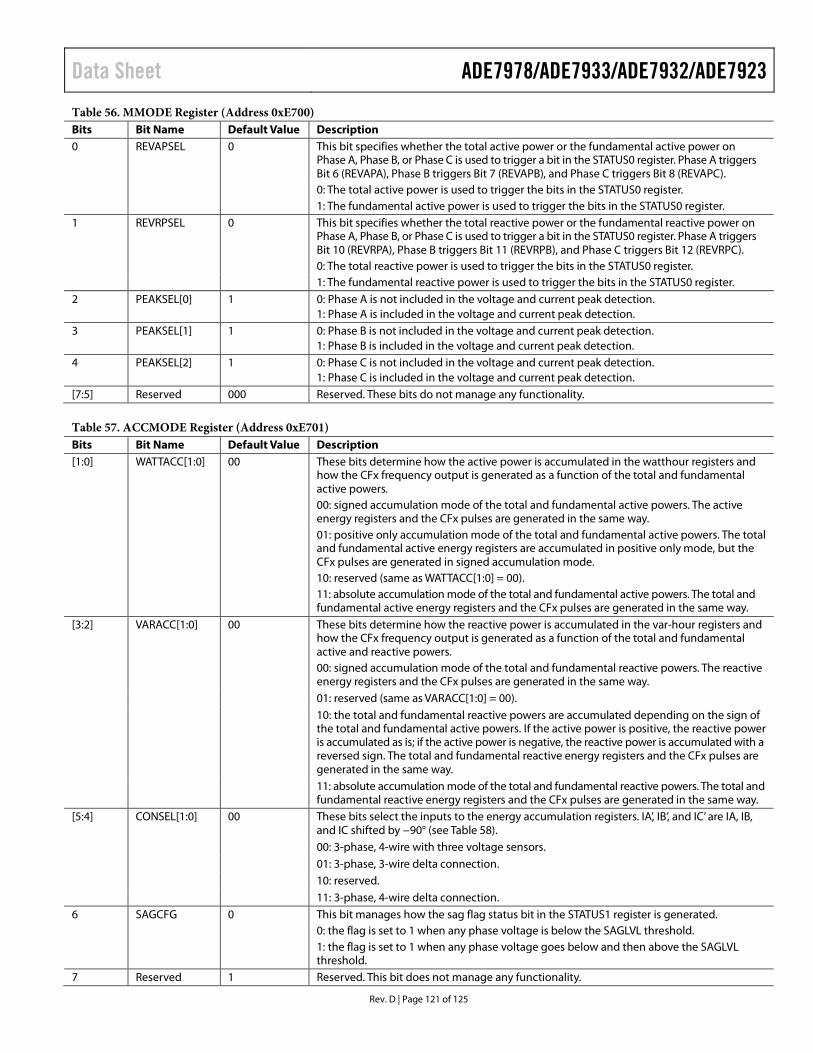
Data Sheet ADE7978/ADE7933/ADE7932/ADE7923
Rev. D | Page 121 of 125
Table 56. MMODE Register (Address 0xE700) Bits Bit Name Default Value Description 0 REVAPSEL 0 This bit specifies whether the total active power or the fundamental active power on
Phase A, Phase B, or Phase C is used to trigger a bit in the STATUS0 register. Phase A triggers Bit 6 (REVAPA), Phase B triggers Bit 7 (REVAPB), and Phase C triggers Bit 8 (REVAPC).
0: The total active power is used to trigger the bits in the STATUS0 register. 1: The fundamental active power is used to trigger the bits in the STATUS0 register. 1 REVRPSEL 0 This bit specifies whether the total reactive power or the fundamental reactive power on
Phase A, Phase B, or Phase C is used to trigger a bit in the STATUS0 register. Phase A triggers Bit 10 (REVRPA), Phase B triggers Bit 11 (REVRPB), and Phase C triggers Bit 12 (REVRPC).
0: The total reactive power is used to trigger the bits in the STATUS0 register. 1: The fundamental reactive power is used to trigger the bits in the STATUS0 register. 2 PEAKSEL[0] 1 0: Phase A is not included in the voltage and current peak detection.
1: Phase A is included in the voltage and current peak detection. 3 PEAKSEL[1] 1 0: Phase B is not included in the voltage and current peak detection.
1: Phase B is included in the voltage and current peak detection. 4 PEAKSEL[2] 1 0: Phase C is not included in the voltage and current peak detection.
1: Phase C is included in the voltage and current peak detection. [7:5] Reserved 000 Reserved. These bits do not manage any functionality.
Table 57. ACCMODE Register (Address 0xE701) Bits Bit Name Default Value Description [1:0] WATTACC[1:0] 00 These bits determine how the active power is accumulated in the watthour registers and
how the CFx frequency output is generated as a function of the total and fundamental active powers.
00: signed accumulation mode of the total and fundamental active powers. The active energy registers and the CFx pulses are generated in the same way. 01: positive only accumulation mode of the total and fundamental active powers. The total and fundamental active energy registers are accumulated in positive only mode, but the CFx pulses are generated in signed accumulation mode. 10: reserved (same as WATTACC[1:0] = 00). 11: absolute accumulation mode of the total and fundamental active powers. The total and fundamental active energy registers and the CFx pulses are generated in the same way.
[3:2] VARACC[1:0] 00 These bits determine how the reactive power is accumulated in the var-hour registers and how the CFx frequency output is generated as a function of the total and fundamental active and reactive powers.
00: signed accumulation mode of the total and fundamental reactive powers. The reactive energy registers and the CFx pulses are generated in the same way. 01: reserved (same as VARACC[1:0] = 00). 10: the total and fundamental reactive powers are accumulated depending on the sign of the total and fundamental active powers. If the active power is positive, the reactive power is accumulated as is; if the active power is negative, the reactive power is accumulated with a reversed sign. The total and fundamental reactive energy registers and the CFx pulses are generated in the same way. 11: absolute accumulation mode of the total and fundamental reactive powers. The total and fundamental reactive energy registers and the CFx pulses are generated in the same way.
[5:4] CONSEL[1:0] 00 These bits select the inputs to the energy accumulation registers. IA’, IB’, and IC’ are IA, IB, and IC shifted by −90° (see Table 58). 00: 3-phase, 4-wire with three voltage sensors. 01: 3-phase, 3-wire delta connection. 10: reserved. 11: 3-phase, 4-wire delta connection.
6 SAGCFG 0 This bit manages how the sag flag status bit in the STATUS1 register is generated. 0: the flag is set to 1 when any phase voltage is below the SAGLVL threshold. 1: the flag is set to 1 when any phase voltage goes below and then above the SAGLVL
threshold. 7 Reserved 1 Reserved. This bit does not manage any functionality.

ADE7978/ADE7933/ADE7932/ADE7923 Data Sheet
Rev. D | Page 122 of 125
Table 58. CONSEL[1:0] Bits in Energy Registers1 Energy Registers CONSEL[1:0] = 00 CONSEL[1:0] = 01 CONSEL[1:0] = 11 AWATTHR, AFWATTHR VA × IA VA × IA VA × IA BWATTHR, BFWATTHR VB × IB VB = VA − VC VB = −VA VB × IB1 VB × IB CWATTHR, CFWATTHR VC × IC VC × IC VC × IC AVARHR, AFVARHR VA × IA’ VA × IA’ VA × IA’ BVARHR, BFVARHR VB × IB’ VB = VA − VC VB = −VA VB × IB’1 VB × IB’ CVARHR, CFVARHR VC × IC’ VC × IC’ VC × IC’ AVAHR VA rms × IA rms VA rms × IA rms VA rms × IA rms BVAHR VB rms × IB rms VB rms × IB rms1 VB rms × IB rms VB = VA − VC VB = −VA CVAHR VC rms × IC rms VC rms × IC rms VC rms × IC rms 1 In a 3-phase, 3-wire configuration (CONSEL[1:0] = 01), the ADE7978 computes the rms value of the line voltage between Phase A and Phase C and stores the result in
the BVRMS register (see the Voltage RMS in Delta Configurations section). The Phase B current value provided after the HPF is 0. Consequently, the powers associated with Phase B are 0. To avoid any errors in the frequency output pins (CF1, CF2, or CF3) related to the powers associated with Phase B, disable the contribution of Phase B to the energy-to-frequency converters by setting the TERMSEL1[1], TERMSEL2[1], or TERMSEL3[1] bit to 0 in the COMPMODE register. For more information, see the Energy-to-Frequency Conversion section.
Table 59. LCYCMODE Register (Address 0xE702) Bits Bit Name Default Value Description 0 LWATT 0 0: the watthour accumulation registers (AWATTHR, BWATTHR, CWATTHR, AFWATTHR,
BFWATTHR, and CFWATTHR) are configured for regular accumulation mode. 1: the watthour accumulation registers (AWATTHR, BWATTHR, CWATTHR, AFWATTHR,
BFWATTHR, and CFWATTHR) are configured for line cycle accumulation mode. 1 LVAR 0 0: the var-hour accumulation registers (AVARHR, BVARHR, CVARHR, AFVARHR, BFVARHR,
and CFVARHR) are configured for regular accumulation mode. 1: the var-hour accumulation registers (AVARHR, BVARHR, CVARHR, AFVARHR, BFVARHR,
and CFVARHR) are configured for line cycle accumulation mode. 2 LVA 0 0: the VA-hour accumulation registers (AVAHR, BVAHR, and CVAHR) are configured for
regular accumulation mode. 1: the VA-hour accumulation registers (AVAHR, BVAHR, and CVAHR) are configured for line
cycle accumulation mode. 3 ZXSEL[0] 1 0: Phase A is not selected for zero-crossing counts in line cycle accumulation mode. 1: Phase A is selected for zero-crossing counts in line cycle accumulation mode. If more
than one phase is selected for zero-crossing detection, the accumulation time is shortened accordingly.
4 ZXSEL[1] 1 0: Phase B is not selected for zero-crossing counts in line cycle accumulation mode. 1: Phase B is selected for zero-crossing counts in line cycle accumulation mode. If more
than one phase is selected for zero-crossing detection, the accumulation time is shortened accordingly.
5 ZXSEL[2] 1 0: Phase C is not selected for zero-crossing counts in line cycle accumulation mode. 1: Phase C is selected for zero-crossing counts in line cycle accumulation mode. If more
than one phase is selected for zero-crossing detection, the accumulation time is shortened accordingly.
6 RSTREAD 1 0: disables read with reset of all xWATTHR, xVARHR, xVAHR, xFWATTHR, and xFVARHR registers. Clear this bit to 0 when Bits[2:0] (LVA, LVAR, and LWATT) are set to 1.
1: enables read with reset of all xWATTHR, xVARHR, xVAHR, xFWATTHR, and xFVARHR registers. When this bit is set to 1, a read of these registers resets them to 0.
7 PFMODE 0 0: power factor calculation uses instantaneous values of various phase powers used in its expression.
1: power factor calculation uses phase energy values calculated using line cycle accumulation mode. The LWATT and LVA bits (Bit 0 and Bit 2) must be enabled for the power factors to be computed correctly. The update rate of the power factor measurement is the integral number of half line cycles that is programmed in the LINECYC register.

Data Sheet ADE7978/ADE7933/ADE7932/ADE7923
Rev. D | Page 123 of 125
Table 60. HSDC_CFG Register (Address 0xE706) Bits Bit Name Default Value Description 0 HCLK 0 0: HSCLK is 8 MHz. 1: HSCLK is 4 MHz. 1 HSIZE 0 0: HSDC transmits the 32-bit registers in 32-bit packages, most significant bit first. 1: HSDC transmits the 32-bit registers in 8-bit packages, most significant bit first. 2 HGAP 0 0: no gap is introduced between packages. 1: a gap of seven HCLK cycles is introduced between packages. [4:3] HXFER[1:0] 00 00: HSDC transmits sixteen 32-bit words in the following order: IAWV, VAWV, IBWV, VBWV, ICWV,
VCWV, INWV, AVA, BVA, CVA, AWATT, BWATT, CWATT, AVAR, BVAR, and CVAR. 01: HSDC transmits seven instantaneous values of currents and voltages in the following order:
IAWV, VAWV, IBWV, VBWV, ICWV, VCWV, and INWV. 10: HSDC transmits nine instantaneous values of phase powers in the following order:
AVA, BVA, CVA, AWATT, BWATT, CWATT, AVAR, BVAR, and CVAR. 11: reserved (same as HXFER[1:0] = 00). 5 HSAPOL 0 0: SS/HSA output pin is active low.
1: SS/HSA output pin is active high.
[7:6] Reserved 00 Reserved. These bits do not manage any functionality.
Table 61. CONFIG3 Register (Address 0xE708) Bits Bit Name Default Value Description 0 VA2_EN 1 This bit configures the V2 channel or temperature measurement on the Phase A ADE7933/ADE7932. 0: temperature sensor is measured on the second voltage channel of the Phase A ADE7933/ADE7932.
On the ADE7932, the temperature sensor is always sensed by the second voltage channel, but this bit must still be cleared to 0 to enable the temperature measurement.
1: V2P input is sensed on the second voltage channel of the Phase A ADE7933. 1 VB2_EN 1 This bit configures the V2 channel or temperature measurement on the Phase B ADE7933/ADE7932. 0: temperature sensor is measured on the second voltage channel of the Phase B ADE7933/ADE7932.
On the ADE7932, the temperature sensor is always sensed by the second voltage channel, but this bit must still be cleared to 0 to enable the temperature measurement.
1: V2P input is sensed on the second voltage channel of the Phase B ADE7933. 2 VC2_EN 1 This bit configures the V2 channel or temperature measurement on the Phase C ADE7933/ADE7932. 0: temperature sensor is measured on the second voltage channel of the Phase C ADE7933/ADE7932.
On the ADE7932, the temperature sensor is always sensed by the second voltage channel, but this bit must still be cleared to 0 to enable the temperature measurement.
1: V2P input is sensed on the second voltage channel of the Phase C ADE7933. 3 VN2_EN 1 This bit configures the V2 channel or temperature measurement on the neutral line ADE7923 or
ADE7933/ADE7932. 0: temperature sensor is measured on the second voltage channel of the neutral line ADE7933/
ADE7932 and ADE7923. On the ADE7932, the temperature sensor is always sensed by the second voltage channel, but this bit must still be cleared to 0 to enable the temperature measurement.
1: V2P input is sensed on the second voltage channel of the neutral line ADE7933 and ADE7923. [5:4] Reserved 00 Reserved. These bits do not manage any functionality. 6 CLKOUT_DIS 0 0: ADE7933/ADE7932 and ADE7923 CLKOUT pins are enabled. 1: ADE7933/ADE7932 and ADE7923 CLKOUT pins are set high and no clock is generated. 7 ADE7933_
SWRST 0 When this bit is set to 1, a software reset of the ADE7933/ADE7932 and ADE7923 devices is initiated.
See the ADE7933/ADE7932 and ADE7923 Software Reset section for more information.
Table 62. CONFIG2 Register (Address 0xEA00) Bits Bit Name Default Value Description 0 I2C_LOCK 0 When this bit is set to 0, the SS/HSA pin can be toggled three times to activate the SPI serial port. If
I2C is the selected serial port, set this bit to 1 to lock the selection. After a 1 is written to this bit, the ADE7978 ignores spurious toggling of the SS/HSA pin. If SPI is the selected serial port, any write to the CONFIG2 register locks the selection. The communication protocol can be changed only after a power-down or hardware reset operation.
[7:1] Reserved 000 0000 Reserved. These bits do not manage any functionality.
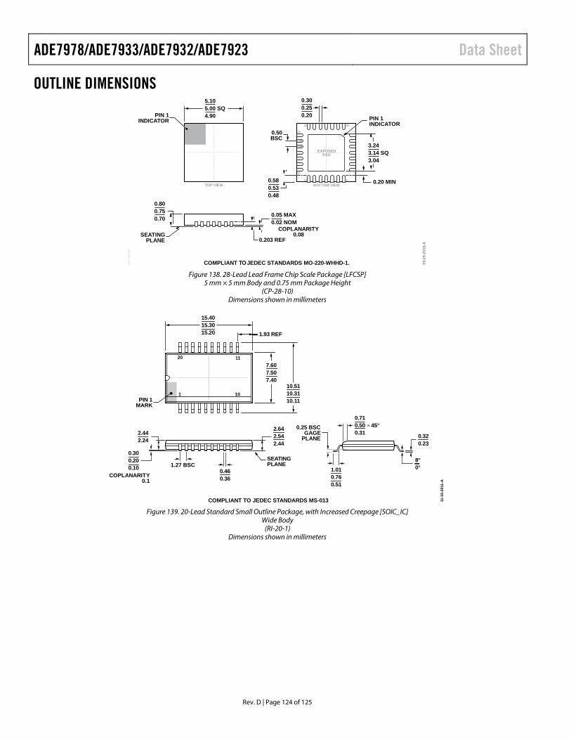
ADE7978/ADE7933/ADE7932/ADE7923 Data Sheet
Rev. D | Page 124 of 125
OUTLINE DIMENSIONS
3.243.14 SQ3.04
0.800.750.70
TOP VIEW BOTTOM VIEW
PKG
-005
090
1
28
814
15
21
22
7
PIN 1INDICATOR
0.580.530.48
SEATINGPLANE
0.05 MAX0.02 NOM
0.203 REF
COPLANARITY0.08
PIN 1INDICATOR
0.300.250.20
COMPLIANT TOJEDEC STANDARDS MO-220-WHHD-1.
5.105.00 SQ4.90
03-2
9-20
16-A
0.20 MIN
EXPOSEDPAD
0.50BSC
Figure 138. 28-Lead Lead Frame Chip Scale Package [LFCSP]
5 mm × 5 mm Body and 0.75 mm Package Height (CP-28-10)
Dimensions shown in millimeters
11-1
5-20
11-A
20 11
101
SEATINGPLANE
COPLANARITY0.1
1.27 BSC
15.4015.3015.20
7.607.507.40
2.642.542.44
1.010.760.51
0.300.200.10
10.5110.3110.11
0.460.36
2.442.24
PIN 1MARK
1.93 REF
8°0°
0.320.23
0.710.500.31
45°0.25 BSC GAGEPLANE
COMPLIANT TO JEDEC STANDARDS MS-013 Figure 139. 20-Lead Standard Small Outline Package, with Increased Creepage [SOIC_IC]
Wide Body (RI-20-1)
Dimensions shown in millimeters
Data Sheet ADE7978/ADE7933/ADE7932/ADE7923
Rev. D | Page 125 of 125
CONTROLLING DIMENSIONS ARE IN MILLIMETERS; INCH DIMENSIONS(IN PARENTHESES) ARE ROUNDED-OFF MILLIMETER EQUIVALENTS FORREFERENCE ONLY AND ARE NOT APPROPRIATE FOR USE IN DESIGN.
COMPLIANT TO JEDEC STANDARDS MS-013-AC
13.00 (0.5118)12.60 (0.4961)
0.30 (0.0118)0.10 (0.0039)
2.65 (0.1043)2.35 (0.0925)
10.65 (0.4193)10.00 (0.3937)
7.60 (0.2992)7.40 (0.2913)
0.75 (0.0295)0.25 (0.0098) 45°
1.27 (0.0500)0.40 (0.0157)
COPLANARITY0.10 0.33 (0.0130)
0.20 (0.0079)0.51 (0.0201)0.31 (0.0122)
SEATINGPLANE
8°0°
20 11
101
1.27(0.0500)
BSC
06-0
7-20
06-A
Figure 140. 20-Lead Standard Small Outline Package, [SOIC_W]
Wide Body (RW-20)
Dimensions shown in millimeters (and inches)
ORDERING GUIDE Model1, 2, 3 Temperature Range Package Description Package Option ADE7978ACPZ −40°C to +85°C 28-Lead LFCSP CP-28-10 ADE7978ACPZ-RL −40°C to +85°C 28-Lead LFCSP, 13” Tape and Reel CP-28-10 ADE7933ARIZ −40°C to +85°C 20-Lead SOIC_IC RI-20-1 ADE7933ARIZ-RL −40°C to +85°C 20-Lead SOIC_IC, 13” Tape and Reel RI-20-1 ADE7932ARIZ −40°C to +85°C 20-Lead SOIC_IC RI-20-1 ADE7932ARIZ-RL −40°C to +85°C 20-Lead SOIC_IC, 13” Tape and Reel RI-20-1 ADE7923ARWZ −40°C to +85°C 20-Lead SOIC_W RW-20 ADE7923ARWZ-RL −40°C to +85°C 20-Lead SOIC_W, 13” Tape and Reel RW-20 EVAL-ADE7978EBZ Evaluation Board EVAL-SDP-CB1Z Evaluation System Controller Board 1 Z = RoHS Compliant Part. 2 The EVAL-SDP-CB1Z is the controller board that manages the EVAL-ADE7978EBZ evaluation board. Both boards must be ordered together. 3 The EVAL-ADE7978EBZ is used to test the ADE7923, ADE7932, and the ADE7933.
I2C refers to a communications protocol originally developed by Philips Semiconductors (now NXP Semiconductors).
©2013–2018 Analog Devices, Inc. All rights reserved. Trademarks and registered trademarks are the property of their respective owners. D11116-0-2/18(D)