A temperature stabilized CMOS VCO - University of Pretoria
9
A temperature stabilized CMOS VCO Johny Sebastian • Saurabh Sinha Abstract The established method of frequency drift compensation in voltage controlled oscillators (VCOs) resulting from temperature variance involves modulation of control voltage using a non-linear voltage internally generated. An innovative frequency drift compensation scheme for a VCO, based on amplitude control, is descri- bed in this paper. Two peak detectors are used to generate voltages representing positive and negative peaks of the sinusoidal driving an error amplifier. The amplifier output controls the delivery of transconductance accessible to the oscillator, thereby keeping the oscillation amplitude steady. Frequency stability has improved to 16 ppm/°C from an uncompensated value of 189 ppm/°C and is applicable where frequency stability requirements are not stringent, such as HS-USB and S-ATA. The temperature stabilized VCO at 2.4 GHz center frequency is prototyped using CMOS technology from ams AG (formerly austriamicro- systems AG). The result obtained from this study indicates that better frequency stability may be achievable if the traditional compensation scheme is preceded by amplitude control. Keywords RF CMOS integrated circuits VCO Temperature dependence Automatic amplitude control Abbreviations AAC Automatic amplitude control OTA Operational transconductance amplifier ppm Parts per million PSS Periodic steady state PVT Process, voltage and temperature VCO Voltage controlled oscillator ZTC Zero temperature coefficient 1 Introduction Frequency drift in voltage controlled oscillators (VCOs) resulting from temperature variance is a critical design problem for radio frequency applications such as trans- ceiver circuits in communication networks, data link pro- tocols, medical sensor networks and micromechanical resonators used in silicon. A popular method of frequency compensation is that of modulating the control voltage terminal of the VCO using an appropriately generated control voltage (V CNTRL ) as summarized in Table 1, selected from recently published articles on temperature compensation applicable to oscillators in general. The oscillation frequency of an LC VCO may be represented as [1] x TðÞ¼ ffiffiffiffiffiffiffiffiffiffiffiffiffiffiffiffiffiffiffiffiffiffiffiffiffiffiffiffiffiffiffiffiffiffiffiffiffiffiffiffiffiffiffiffiffiffiffiffiffiffiffiffiffiffiffiffiffiffiffiffiffiffiffiffiffiffiffiffiffiffiffiffiffiffiffiffiffiffiffiffiffiffiffiffiffiffiffiffiffiffiffiffiffiffiffiffiffiffiffiffiffiffiffiffi 1 LC f þ C v V CNTRL ð Þ 1 C f R 2 L ðTÞþ C v V CNTRL ð Þ R 2 L L s ð1Þ where L is the inductor, C f , the fixed capacitance in the tank circuit, C v the variable capacitance of a varactor controlled J. Sebastian (Correspondence) S. Sinha Department of Electrical, Electronic and Computer Engineering, School of Engineering, Faculty of Engineering, Built Environment & Information Technology, University of Pretoria, Pretoria, South Africa e-mail: [email protected] S. Sinha e-mail: [email protected] S. Sinha Faculty of Engineering and the Built Environment, University of Johannesburg, Auckland Park 2006, South Africa
-
Upload
khangminh22 -
Category
Documents
-
view
1 -
download
0
Transcript of A temperature stabilized CMOS VCO - University of Pretoria
A temperature stabilized CMOS VCO
Johny Sebastian • Saurabh Sinha
Abstract The established method of frequency drift compensation in voltage controlled oscillators (VCOs) resulting from temperature variance involves modulation of control voltage using a non-linear voltage internally generated. An innovative frequency drift compensation scheme for a VCO, based on amplitude control, is descri-
bed in this paper. Two peak detectors are used to generate voltages representing positive and negative peaks of the sinusoidal driving an error amplifier. The amplifier output controls the delivery of transconductance accessible to the oscillator, thereby keeping the oscillation amplitude steady. Frequency stability has improved to 16 ppm/�C from an uncompensated value of 189 ppm/�C and is applicable where frequency stability requirements are not stringent, such as HS-USB and S-ATA. The temperature stabilized VCO at 2.4 GHz center frequency is prototyped using CMOS technology from ams AG (formerly austriamicro-
systems AG). The result obtained from this study indicates that better frequency stability may be achievable if the traditional compensation scheme is preceded by amplitude control.
Keywords RF � CMOS integrated circuits � VCO � Temperature dependence � Automatic amplitude control
AbbreviationsAAC Automatic amplitude control
OTA Operational transconductance amplifier ppm Parts per million
PSS Periodic steady state
PVT Process, voltage and temperature VCO Voltage controlled oscillator
ZTC Zero temperature coefficient
1 Introduction
Frequency drift in voltage controlled oscillators (VCOs) resulting from temperature variance is a critical design problem for radio frequency applications such as trans-
ceiver circuits in communication networks, data link pro-
tocols, medical sensor networks and micromechanical resonators used in silicon. A popular method of frequency compensation is that of modulating the control voltage terminal of the VCO using an appropriately generated control voltage (VCNTRL) as summarized in Table 1, selected from recently published articles on temperature compensation applicable to oscillators in general. The oscillation frequency of an LC VCO may be represented as [1]
x Tð Þ ¼
ffiffiffiffiffiffiffiffiffiffiffiffiffiffiffiffiffiffiffiffiffiffiffiffiffiffiffiffiffiffiffiffiffiffiffiffiffiffiffiffiffiffiffiffiffiffiffiffiffiffiffiffiffiffiffiffiffiffiffiffiffiffiffiffiffiffiffiffiffiffiffiffiffiffiffiffiffiffiffiffiffiffiffiffiffiffiffiffiffiffiffiffiffiffiffiffiffiffiffiffiffiffiffiffi
1
L C f þ Cv VCNTRLð Þ� � 1 �
Cf R2
LðTÞ þ Cv
VCNTRLð Þ R2L L
� �
s
ð1Þ where L is the inductor, Cf, the fixed capacitance in the tank circuit, Cv the variable capacitance of a varactor controlled
J. Sebastian (Correspondence) � S. SinhaDepartment of Electrical, Electronic and Computer Engineering, School of Engineering, Faculty of Engineering, Built Environment & Information Technology, University of Pretoria, Pretoria, South Africa
e-mail: [email protected]
S. Sinha
e-mail: [email protected]
S. Sinha
Faculty of Engineering and the Built Environment, University of Johannesburg, Auckland Park 2006, South Africa
by a voltage VCNTRL, and RL the losses in the inductor. As the temperature is increased, VCNTRL(T) increases in a corresponding manner such that the resulting change in Cv
compensates for the frequency drift.
To the best knowledge of the authors, the current body of knowledge concentrates on generated error voltage as a means to compensate for frequency drift. However, the use of amplitude control as a technique for improving immu-
nity against process, voltage and temperature (PVT) vari-
ations is widely reported [1], [5–7].
This paper presents the design of a temperature com-
pensated VCO based on an amplitude control mechanism for frequency drift compensation. The principle is validated through prototyping using the 0.35 lm CMOS technology (ams AG). The remainder of this paper is organised as follows: Sect. 2 critically evaluates the origins of frequency drift as a result of temperature variance noted in recent journals. Implementation of amplitude control to reduce the temperature dependency is illustrated in Sect. 3, fol-
lowed by circuit design in Sect. 4. Results and the dis-
cussion involving the prototyped IC are presented in Sect.
5. Conclusions are drawn in Sect. 6.
2 Origins of frequency drift over temperature
The threshold voltage of MOS devices reduce in relation to increase in temperature [8]. A negative increment in Vth
causes increased transconductance in the VCO core that results in a higher oscillation amplitude. It has also been established that an increment in oscillation amplitude translates into a negative shift in frequency [9].
The expression for drain current in an n-channel MOS, derived for long channel operation, is [8]
ID ¼lnCox
2
W
LVGS � Vthð Þ 2 ð2Þ
Equation (2) contains the mobility term ln and the threshold voltage Vth; both depend on temperature and both variables have a negative temperature coefficient (TC)[10]. Therefore it is possible to achieve a zero temperature
coefficient (ZTC) bias point, where any variation in tem-
perature should not affect the bias current.
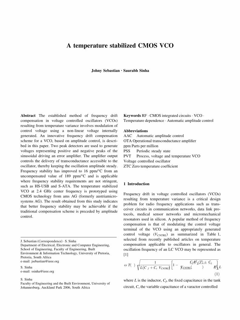
A generalized schematic of a negative transconductance (gm) oscillator is provided in Fig. 1 [9]. The parasitic ele-
ment is represented by RL and RC of the inductor and capacitors respectively. The natural resonant frequency of the resonator is
xo ¼ffiffiffiffiffiffiffiffiffiffiffi
1=LCp
ð3Þ
Temperature and bias conditions affect the oscillation frequency in a predictable manner in an LC oscillator [1, 9].
The parasitic losses in the tank are overcome by the transconductance amplifier. From Fig. 1 the expression for oscillation frequency may be modified as
x1 ¼ x0
ffiffiffiffiffiffiffiffiffiffiffiffiffiffiffiffiffiffi
L � CR2L
L � CR2C
s
ð4Þ
Assuming the losses in the integrated capacitor are negligible compared to that of the integrated inductor, the oscillation frequency could be modified as
x1�xo
ffiffiffiffiffiffiffiffiffiffiffiffiffiffiffiffiffi
1 � CR2L
L
r
ð5Þ
As the substrate resistance shows a positive TC, from (5) it is evident that an LC oscillator biased at ZTC still demonstrates a linear negative TC.
Furthermore, in a VCO, an increment in tail current, a power supply spike, or change in temperature leads to an injection of a current i(t) with high harmonic content into the tank. Consequently, generated harmonics in the LC network are reconciled by reducing the frequency of oscillation. Equation (6) enables the prediction of oscilla-
tion frequency as a function of bias conditions [1, 9].
x ¼ x1 1 �1 X
1
2Q2 n¼2
n2
n2 � 1 h2iðnÞ
!
ð6Þ
where Q ¼ xoL= RL þ RCð Þ and hi n ð Þ ¼ In=I1where In is the nth Fourier coefficient of i(t).
Equations (5) and (6) confirm the argument that a positive increment in tail current results in a substantial
Table 1 Comparison of temperature compensation based on modi-fication of VCNTRL, selected from recent journal articles
[1] 2009 [2] 2007 [3] 2012 [4] 2010
0.25 lm 0.6 lm 90 nm 0.18 lmTechnology node Frequency (MHz) 800 5.5 1,400 14
D f ¼ of �106
D T�f r(ppm/�C)
1.689 0.39 51.43 11.52
Oscillator
architecture
LC FBAR
resonator
Ring
VCO
RCFig. 1 A generalized schematic of negative gm LC oscillator
2

reduction of the oscillation frequency. An illustration of this effect is provided in [9]. Any further increment in bias current results in saturation. LC oscillators operated at this bias current demonstrate better frequency stability. Improved frequency stability is however in trade off with phase noise penalty [9].
From (3) it is clear that the effective inductance and the capacitance of the tank primarily determine the oscillation frequency. The current that passes through the inductor causes an image current in the substrate, which reduces the effective inductance. As the temperature increases, the substrate resistance increases. This increment in resistance reduces the image current and increases the effective inductance. In a spiral inductor, conductors are placed in close proximity to one another. Each segment induces eddy currents in other segments that cause series resistance to increase [11]. This phenomenon causes a further reduction in frequency according to (5). Effective capacitance con-
stitutes the capacitance of the resonator as well as parasitic contributions from all reverse biased junctions shunting the inductor. However, the capacitance of the resonator dis-
plays a lower temperature dependency.
From this discussion it is evident that if an LC oscillator is operated at ZTC bias, negative frequency drift originates through modulation of net tank inductance L, or capaci-
tance C, or net losses in the tank RL, RC, or harmonic content of bias current i(t). Therefore it is concluded that the negative frequency drift resulting from a positive increment in temperature could be reduced, if the injection of harmonic content of bias current into the oscillator tank circuit is held constant. For a temperature induced fre-
quency drift compensation the negative transconductor is biased using temperature independent current source. In this method to compensate for the coil loss induced drift, reactive compensation is suggested [9].
3 Temperature compensation using amplitude control
For LC VCOs, the amplitude of oscillation varies with the frequency of oscillation [6]. This implies that harmonic contents of the bias current or losses in the inductor induce a negative frequency drift resulting in a modified amplitude of oscillation. Therefore in order to prevent the frequency drift, this paper proposes to track down the amplitude of oscillation accurately, which is subsequently used for fre-
quency compensation. An automatic amplitude control (AAC) is used for this purpose. Conventional AAC circuits utilize a single reference voltage; however for better noise and harmonic performance a dual AAC that generates two DC representing positive and negative peaks is proposed.
An AAC circuit generates two voltages, V? and V-, representing the negative and positive peaks of the
oscillating waveform. Any harmonic component present in the peaks is suppressed by envelope detection. The oper-
ational transconductance amplifier (OTA) output controls the amount of transconductance available to the oscillator by limiting the bias current. As the frequency drift is captured from peak detection of the oscillating waveform, the presence of higher harmonics must be further sup-
pressed. A band limited OTA with high common mode rejection must be utilized. The complete system design is illustrated in Fig. 2.
In the AAC circuit, V? is set higher than V- to ensure the availability of bias current for the oscillator at start-up. Once the amplitude of oscillations is picked up, the OTAOUT responds to the differential input voltage VID = (V? - V-) at the input. Thus closed loop action will force the V? and V- to be closer, as the oscillations are established and a state of equilibrium is achieved. When any of the variables causes perturbations in the amplitude, the AAC output initiates the compensatory action by modifying VID, in turn controlling the conductivity of MCNTRL.
4 Circuit design and layout
4.1 LC oscillator based VCO
In order to experimentally validate the key contribution of this paper, i.e. the amplitude control principle, a negative gm architecture is chosen from the existing literature [6]. A differential cross-coupled LC oscillator topology such as Fig. 3 is selected since it is less sensitive to PVT, as well as to common-mode noise interferences [12, 13].
Fig. 2 Temperature compensated VCO using AAC
3

An equal amount of bias is provided for both gates of the transistors. The ZTC bias current is selected for the oscil-
lator design. A plot of transistor current density, ID/W, against VGS is depicted in Fig. 4.
In Fig. 4, the ZTC bias for NMOS transistors is observed when ID/W = 25 and is chosen for designing the oscillator. In order to assist in further designing gm/ID
versus ID/W plots are derived using Cadence Virtuoso�
employing Spectre Simulator. Transistors of minimum channel length are selected, as they deliver better unity gain frequency (ft). All the simulations are performed using
transistors of W = 10 lm and L = 0.35 lm. Transistors with different widths and lengths are found to be over-
lapping, as reported in [14]. Resulting plots are shown in Fig. 5.
In order to vary the frequency of the oscillator, a var-
actor is to be included. The two different types of varactors available in the process are junction varactors and MOS varactors operated in the accumulation mode. It was observed that the accumulation mode MOS varactor offers performance much superior to junction varactors in terms of power consumption, phase noise and tuning range [15, 16]. An accumulation mode MOS varactor known as CVAR in the ams AG process is used in this work. There are four rows, and 12 columns are used to provide the required amount of capacitance.
4.2 Aac
From the sinusoidal generated by the oscillator, two volt-
ages that represent the average positive peak (V-) and the average negative peak (V?) are formed by the AAC. Peak detectors are implemented differentially to improve noise rejection. Figure 6 shows the complete circuit diagram of the AAC. Transistors M0 and M1 conduct alternately at the corresponding positive peak of the sinusoidal, and charge the capacitor C0. M2 acts as the current source. The voltage across C0 is then level shifted to V- using transistor M3. Similarly a negative peak detector is implemented using PMOS devices M5, M 6, M 7 and a capacitor C1. A positive increment in oscillation amplitude causes a rise in potential for V- and a drop in potential for V?. This action of the AAC results in reduced differential output voltage V? -V- = VID, in response to an increase in oscillation ampli-tude. Similarly the AAC responds to a drop in oscillation amplitude by increasing the VID, forcing the MCNTRL to increase the delivery of additional transconductance.
Fig. 3 Schematic of the LC VCO
Fig. 4 Illustration of ZTC bias point
Fig. 5 A plot of gm/ID versus ID/W for NMOS and PMOS transistors
4

The set value of VID directly influences the amount of amplitude control achieved over the temperature range. Therefore it is imperative that AAC be characterized for different values of VID. Tighter amplitude control is expected to provide better temperature compensation but the effect of process variations needs to be accounted for. For a given oscillation amplitude (VCO? - VCO-) = Vp-p = 1 V, the aspect ratio of level shifter M5 is varied such that VID = 0.7 V, 0.8 V and 0.9 V. The resulting periodic steady state (PSS) simulation is performed at temperatures 0–125 �C in six steps. This simulation is again repeated at nine process corners containing combi-
nations of typical mean (TM), worst case power (WP)—
(fast NMOS– slow PMOS), worst case speed (WS)—(slow NMOS, fast PMOS) for transistors and capacitors. Further corners are identified for inductors in the form of ‘high Q factor’, and ‘low Q factor’ (LQ). Frequency drift in ppm/ �C versus process corners is plotted in Fig. 7.
The best frequency compensation is observed for
VID = 0.7 V, which at process corner zero (all TM corners)
is 9 ppm/�C, but offers very high frequency drift of
200 ppm/�C at corner six (WS, WP, LQ for transistors,
capacitors, inductors respectively). The worst result at a
typical mean corner is observed for VID = 0.9 V, but
provides a reduced maximum drift of 120 ppm/�C at corner
eight. The best performance in a typical mean corner is
always the best choice for any design, but as a design trade-
off VID = 0.8 V is selected for this design.
4.3 Ota
An OTA is used as the error amplifier because of its high gain, reasonably large output signal swing and input dynamic range. One of the factors that could affect the gain of an op-amp is the short channel effect. This effect in turn modifies the square-law transfer characteristics in the sat-
uration region to a more linear response. One of the short channel effects that contribute adversely to the gain of the op-amp is the reduced output impedance. Therefore, a longer channel length must be used. However, such lengths consume additional space on the silicon wafer. As a design compromise, a channel length of 1 lm is chosen. An OTA using folded cascode topology such as in Fig. 8, with a gain of 56 dB and the first pole at 300 kHz is designed.
The sub-systems that constitute a temperature compen-
sated VCO are: an oscillator operated at ZTC; an AAC that
generates two voltages, which represent the positive and
negative peaks of the oscillation; an OTA that acts as an error
amplifier, regulating the bias current to the oscillator; a bias
voltage reference using MOS transistors as well as an output
buffer designed in schematic and layout. The completed
design is thereafter integrated in a single integrated circuit
and subsequently prototyped in silicon at ams AG.
Figure 9 illustrates the layout of the temperature stabi-
lized VCO and occupies an area of 675 lm 9 1225 lm in
Fig. 6 AAC circuit schematic
Fig. 7 Frequency drift versus process corners for different VID
Fig. 8 Folded cascode OTA topology used
5

the multi project wafer. The chip microphotograph is depicted in Fig. 10.
5 Results and discussion
In order to generate comparisons, an open loop VCO is
simulated in PSS analysis available in Cadence Virtuoso.
PSS simulations were first performed on an oscillator
directly supplied by a 3.3 V power supply, and then the
same VCO was connected in a temperature stabilised loop such as in Fig. 2. The results of the PSS analysis with temperature as the parametric sweep variable at an interval of every 25 �C are presented in Fig. 11.
In Fig. 11(a) the frequency spread is 56.65 MHz for a temperature sweep of 0� C to 125� C. From Fig. 10(a) it may be observed that the frequency drift is in a negative direction in all temperature intervals. However, in Fig. 10(b) frequency spread has reduced to 4.82 MHz. The frequency drift is in a negative direction between the
Fig. 9 Temperature stabilized
VCO layout
6
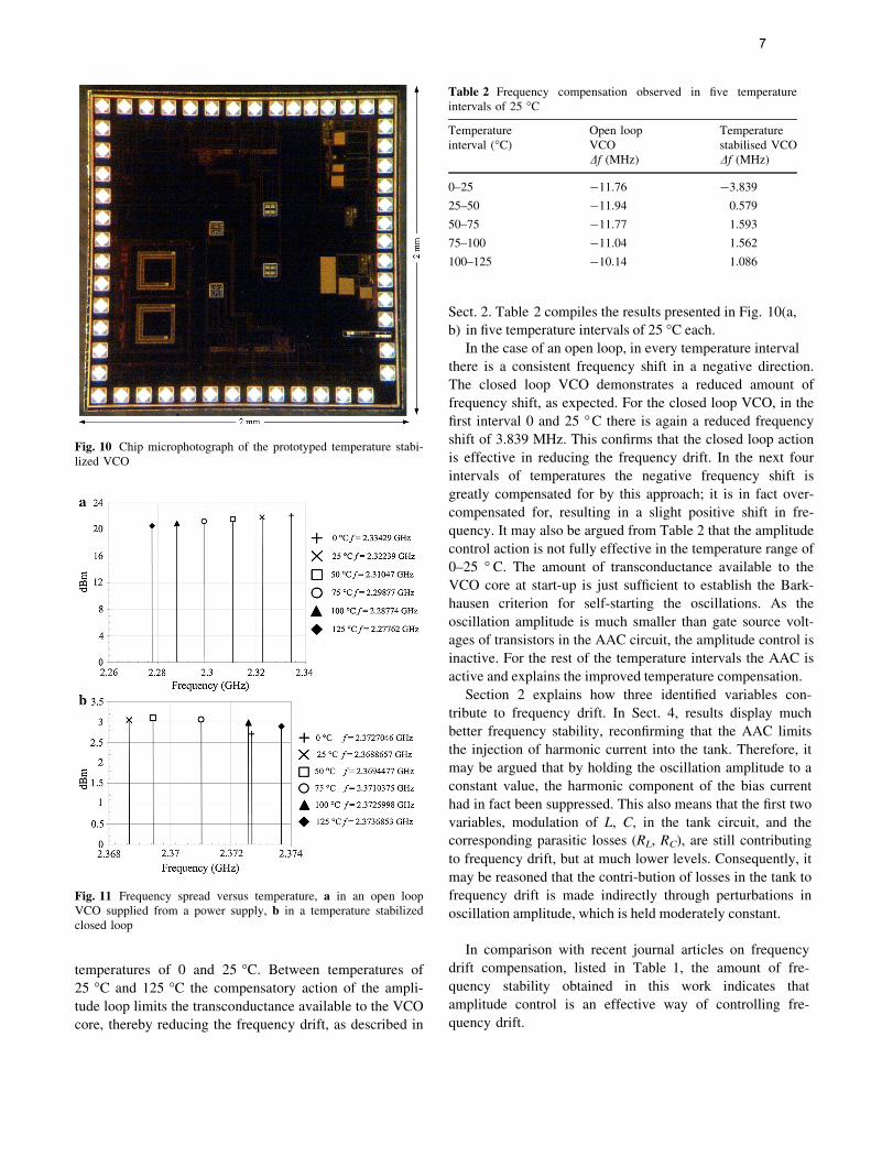
temperatures of 0 and 25 �C. Between temperatures of
25 �C and 125 �C the compensatory action of the ampli-
tude loop limits the transconductance available to the VCO
core, thereby reducing the frequency drift, as described in
Sect. 2. Table 2 compiles the results presented in Fig. 10(a,
b) in five temperature intervals of 25 �C each.
In the case of an open loop, in every temperature interval
there is a consistent frequency shift in a negative direction. The closed loop VCO demonstrates a reduced amount of frequency shift, as expected. For the closed loop VCO, in the first interval 0 and 25 �C there is again a reduced frequency shift of 3.839 MHz. This confirms that the closed loop action is effective in reducing the frequency drift. In the next four intervals of temperatures the negative frequency shift is greatly compensated for by this approach; it is in fact over-
compensated for, resulting in a slight positive shift in fre-
quency. It may also be argued from Table 2 that the amplitude control action is not fully effective in the temperature range of 0–25 � C. The amount of transconductance available to the VCO core at start-up is just sufficient to establish the Bark-
hausen criterion for self-starting the oscillations. As the oscillation amplitude is much smaller than gate source volt-
ages of transistors in the AAC circuit, the amplitude control is inactive. For the rest of the temperature intervals the AAC is active and explains the improved temperature compensation.
Section 2 explains how three identified variables con-
tribute to frequency drift. In Sect. 4, results display much better frequency stability, reconfirming that the AAC limits the injection of harmonic current into the tank. Therefore, it may be argued that by holding the oscillation amplitude to a constant value, the harmonic component of the bias current had in fact been suppressed. This also means that the first two variables, modulation of L, C, in the tank circuit, and the corresponding parasitic losses (RL, RC), are still contributing to frequency drift, but at much lower levels. Consequently, it may be reasoned that the contri-bution of losses in the tank to frequency drift is made indirectly through perturbations in oscillation amplitude, which is held moderately constant.
In comparison with recent journal articles on frequency drift compensation, listed in Table 1, the amount of fre-
quency stability obtained in this work indicates that amplitude control is an effective way of controlling fre-
quency drift.
Fig. 10 Chip microphotograph of the prototyped temperature stabi-
lized VCO
Fig. 11 Frequency spread versus temperature, a in an open loop
VCO supplied from a power supply, b in a temperature stabilized
closed loop
Table 2 Frequency compensation observed in five temperature
intervals of 25 �C
Temperature
interval (�C)
Open loop
VCO
Temperature
stabilised VCO
Df (MHz) Df (MHz)
0–25 -11.76 -3.839
25–50 -11.94 0.579
50–75 -11.77 1.593
75–100 -11.04 1.562
100–125 -10.14 1.086
7

Improved frequency compensation presented here is based on reducing the injection of higher harmonic content rather than operating the oscillator at a much higher bias current that results in saturated operation as mentioned in [9]. However some phase noise penalty exists, as additional noise sources are present in the AAC circuit [17]. Phase noise reduction is however outside the scope of this paper.
6 Conclusion
A new and simpler approach for improving the frequency
stability of an LC VCO based on amplitude control is
described in this paper. The temperature stabilized VCO is
implemented in a standard CMOS process. Simulation
results indicate that frequency stability over temperature
has improved to 16 ppm/�C using a combination of ZTC
bias and amplitude control. It could thus be concluded and
generalised that improved temperature compensation might
be obtained if any compensation scheme should be pre-
ceded by amplitude control.
References
1. McCorquodale, M. S., Carichner, D. A., O’ Day, J. D., Pernia, S.
M., Kubba, S., Marsman, E. D., et al. (2009). A 25 MHz self-
referenced solid-state frequency source suitable for XO-replace-
ment. IEEE Transactions Circuits and Systems I: Regular
Papers, 56(5), 943–956.
2. Sundaresan, K., Ho, G. H., Pourkamali, S., & Ayazi, F. (2007).
Electronically temperature compensated silicon bulk acoustic
resonator reference oscillators. IEEE Journal of Solid-State Cir-
cuits, 42(6), 1425–1433.
3. Hwang, In-C. (2012). A 0.236 mm2, 3.99 mW fully integrated
90 nm CMOS L1/L5 GPS frequency synthesizer using a regu-
lated ring VCO. IEEE Microwave and Wireless Components
Letters, 22(6), 324–326.
4. Tokunaga, Y., Sakiyama, S., Matsumoto, A., & Dosho, S. (2010).
An on-chip CMOS relaxation oscillator with voltage averaging
feedback. IEEE Journal of Solid-State Circuits, 45(6),
1150–1158.
5. Garimella, A., Kalyani-Garimella, L. M., Ramırez-Angulo, J., &
Lopez-Martin, A. J. (2009). Versatile multi-decade CMOS volt-
age-controlled oscillator with accurate amplitude and pulse width
control. Analog Integrated Circuits and Signal Processing, 60(8),
83–92.
6. Marquart, C. A., Zourntos, T., Magierowski, S., & Mathai, N. J.
(2007). Sliding-mode amplitude control techniques for harmonic
oscillators. IEEE Transactions Circuits and Systems II: Express
Briefs, 54(11), 1014–1018.
7. Park, J.-S., Kim, S., Pu, Y., & Lee, K.-Y. (2011). A 84% tuning
range, 4.3-GHz VCO with two-step negative-Gm tuning and
amplitude calibration loop. Analog Integrated Circuits and Signal
Processing, 66(1), 441–447.
8. Gray, P. R., Hurst, P. J., Lewis, S. H., & Meyer, R. G. (2010).
Analysis and design of analog integrated circuits (5th ed.). New
York: John Wiley & Sons Inc.
9. McCorquodale, M. S., O’ Dey, J. D., Pernia, S. M., Carichner, G.
A., Kubba, S., & Brown, R. B. (2007). A monolithic and self-
referenced RF LC clock generator compliant with USB. IEEE
Journal of Solid-State Circuits, 42(2), 385–399.
10. de Beaupre, V. C., Rahajandraibe, W., & Zaid, L. (2006). 2.45-
GHz-CMOS temperature compensated multi-controlled oscillator
for IEEE 802.15 wireless PAN. Analog Integrated Circuits and
Signal Processing, 49(9), 257–266.
11. Yue, C. P., & Wong, S. S. (2000). Physical modeling of spiral
inductors on silicon. IEEE Transactions Electron Devices, 47(3),
560–568.
12. Vijayaraghavan, R., Zhu, K., & Islam, S. K. (2012). A 2.4-GHz
frequency synthesizer based on process and temperature com-
pensated ring ILFD. Analog Integrated Circuits and Signal
Processing, 74(11), 163–173.
13. Casha, O., Grech, I., Micallef, J., & Gatt, E. (2008). CMOS
implementation of a 1.6 GHz low voltage low phase noise
quadrature output frequency synthesizer with automatic ampli-
tude control. Analog Integrated Circuits and Signal Processing,
55(2), 3–19.
14. Silveira, F., Flandre, D., & Jespers, P. G. A. (1996). A gm/ID based
methodology for the design of CMOS analog circuits and its
application to the synthesis of a silicon-on-insulator micropower
OTA. IEEE Journal of Solid-State Circuits, 31(9), 1314–1319.
15. Yang, D., Ding, Y., & Huang, S. (2010). A 65-nm high-frequency
low-noise CMOS-based RF SoC technology. IEEE Transactions
Electron Devices, 57(1), 328–335.
16. Chan, Y.-J., Huang, C.-F., Wu, C–. C., Chen, C.-H., & Chao, C.-
P. (2007). Performance consideration of MOS and junction
diodes for varactor application. IEEE Transactions Electron
Devices, 54(9), 2570–2573.
17. Hajimiri, A., & Lee, T. H. (1999). Design issues in CMOS dif-
ferential LC oscillators. IEEE Journal of Solid-State Circuits,
34(5), 717–724.
Johny Sebastian is working
towards his M.Eng (Microelec-
tronic Engineering) degree from
the University of Pretoria, South
Africa. He obtained his B.Eng
(Electronics and Communica-
tion) degree from the Mangalore
University, India in 1990, and
his B.Eng (Hons) (Microelec-
tronic Engineering) from the
University of Pretoria in 2006.
He worked as a support engi-
neer at Daystar Computers,
Bangalore from 1991 to 1992.
Since 1994 he has been serving
as a lecturer in the Department of Electrical Engineering, Faculty of
Engineering and the Built Environment, Tshwane University of
Technology (formerly known as Technikon Northern Gauteng), Pre-
toria, South Africa.
8

Saurabh Sinha obtained his
B.Eng, M.Eng and Ph.D.
degrees in Electronic Engineer-
ing from University of Pretoria
(UP). He achieved both his
B.Eng and M.Eng with distinc-
tion. As a published researcher,
he has authored over 70 publi-
cations in peer-reviewed jour-
nals and at international
conferences. In addition, he is
the Managing Editor of the
South African Institute of Elec-
trical Engineers (SAIEE) Africa
Research Journal. Prof Sinha
served UP for over a decade with his last service as Director of the
Carl and Emily Fuchs Institute for Microelectronics, Department of
Electrical, Electronic and Computer Engineering. Together with his
research group, he conducted teaching at undergraduate and post-
graduate levels, researched and performed extensive management
tasks. To allow for continuation of postgraduate leadership, he was
also appointed as Extraordinary Professor at UP. On 1 October 2013,
Prof Sinha was appointed as Executive Dean of the Faculty of
Engineering and the Built at Environment (FEBE) at University of
Johannesburg (UJ). Beyond his academic contributions, Prof Sinha is
an active member of several professional societies and was recently
elected as the 2014 Institute for Electric and Electronic Engineering
(IEEE) Board of Director & Vice President: Educational Activi-
ties. Prof Sinha is recognised for his progressive approach as an
electrical engineer, researcher and educator. He is also the recipient of
the 2007 SAIEE Engineer of the Year Award, 2010 University of
Pretoria (UP) Laureate Award and 2013 TW Kambule NRF-NSTF
Award as an emerging researcher for an outstanding contribution to
Science, Engineering, Technology and Innovation (SETI) through
research and its outputs. Beyond his academic contributions, he
served as an industrial consultant for Business Enterprises at the
University of Pretoria (Pty) Ltd. Prof Sinha currently serves on
committees of international, national, regional and professional
societies, including the Engineering Council of South Africa (ECSA).
9