A Technique to Mitigate Impact of Process, Voltage and Temperature Variations on Design Metrics of...
7
A technique to mitigate impact of process, voltage and temperature variations on design metrics of SRAM Cell A. Islam a,⇑ , Mohd. Hasan b a Dept. of ECE, Birla Institute of Technology (Deemed University), Mesra, Ranchi, Jharkhand, India b Electronics Engineering Department, Aligarh Muslim University, Aligarh, Uttar Pradesh, India article info Article history: Received 18 June 2011 Received in revised form 30 September 2011 Accepted 30 September 2011 Available online 27 October 2011 abstract This paper presents a technique for designing a variability aware SRAM cell. The architecture of the pro- posed cell is similar to the standard 6T SRAM cell with the exception that the access pass gates are replaced with full transmission gates. The paper studies the impact of V t (threshold voltage) variation on most of the design metrics of SRAM cell. The proposed design achieves 1.4 narrower spread in I READ at the expense 1.2 lower I READ at nominal V DD . It offers 1.3 improvements in T RA (read access time) dis- tribution at the expense of 1.2 penalty in read delay. The proposed bitcell offers 1.1 tighter spread in T WA (write access time) incurring 1.3 longer write delay. It shows 180 mV of SNM (static noise margin) and is equally stable in hold mode. It offers 1.3 higher RSNM (100 mV) compared to 6T (75 mV). It exhibits improved SINM (static current noise margin) distribution at the expense of 1.6 lower WTI (write trip current). It offers 1.05 narrower spread in standby power. Thus, comparative analysis based on Monte Carlo simulation exhibits that the proposed design is capable of mitigating impact of V t varia- tion to a large extent. Ó 2011 Elsevier Ltd. All rights reserved. 1. Introduction Due to severe increase in V t (threshold voltage) fluctuation caused by global and local process variations in ultrashort-channel devices, 6T SRAM cell and its variants cannot be operated at further scaled supply voltages without parametric and functional failure causing yield loss. Single-ended 6T SRAM cell [1] suffers from write delay. Low power 6T SRAM cell [2] could reduce access delay and write power but could not improve stability. None of the previous works has investigated the improvement of variability in SRAM cell at the circuit level in deep submicron. Therefore, robust and varia- tion tolerant SRAM cell design technique capable of absorbing V t shift due to RDF (random dopant fluctuation), and variation in other device and process parameters (such as length, width, oxide thickness, sub-wavelength-lithography, etching, and annealing) and still be able to perform expected functions need to be investi- gated. Trade-off must generally be made in terms of area to achieve this goal. To solve the read/write stability problems in the face of severe V t variation in ultrashort-channel devices at aggressively scaled technology node such as 16 nm, this paper proposes a trans- mission gate (TG)-based 8T SRAM cell (hereafter called TG8T) and compares its performance with standard 6T SRAM cell at iso-de- vice area. To verify the proposed technique, extensive simulations on HSPICE using 16 nm Predictive Technology Model (PTM) [3] are carried out. The rest of the paper is organized as follows. Section 2 presents the proposed design and its read/write current analysis. Simulation results are discussed and compared in Section 3. Finally, the con- cluding remarks are provided in Section 4. 2. Proposed transmission gate based 8T SRAM cell This section describes device sizing strategy and read/write cur- rent analysis of the proposed design. 2.1. Device sizing of proposed design The primary motivation behind aggressive device scaling is to achieve improved performance and increased integration. These improvements come at the cost of increased sensitivity to PVT (process, voltage and temperature) variations and standby leak- age, particularly in area-constrained circuit such as SRAM that employs minimum-geometry devices. An attempt is made in this work to mitigate these problems in traditional 6T SRAM cell by incurring minimum area penalty and retaining its fully differen- tial architecture. This paper proposes a TG-based fully differential 8T SRAM bitcell (Fig. 1). And its design metrics are assessed and compared with its differential counterpart standard 6T (Fig. 2). As RDF induced V t shift exhibits an inverse dependence on square root of device area (and is given by r vt a EOT/ p (W L), where 0026-2714/$ - see front matter Ó 2011 Elsevier Ltd. All rights reserved. doi:10.1016/j.microrel.2011.09.034 ⇑ Corresponding author. Tel./fax: +91 651 2275231; mobile: +91 9471559180. E-mail address: [email protected] (A. Islam). Microelectronics Reliability 52 (2012) 405–411 Contents lists available at SciVerse ScienceDirect Microelectronics Reliability journal homepage: www.elsevier.com/locate/microrel
-
Upload
independent -
Category
Documents
-
view
3 -
download
0
Transcript of A Technique to Mitigate Impact of Process, Voltage and Temperature Variations on Design Metrics of...
Microelectronics Reliability 52 (2012) 405–411
Contents lists available at SciVerse ScienceDirect
Microelectronics Reliability
journal homepage: www.elsevier .com/locate /microrel
A technique to mitigate impact of process, voltage and temperature variations ondesign metrics of SRAM Cell
A. Islam a,⇑, Mohd. Hasan b
a Dept. of ECE, Birla Institute of Technology (Deemed University), Mesra, Ranchi, Jharkhand, Indiab Electronics Engineering Department, Aligarh Muslim University, Aligarh, Uttar Pradesh, India
a r t i c l e i n f o a b s t r a c t
Article history:Received 18 June 2011Received in revised form 30 September2011Accepted 30 September 2011Available online 27 October 2011
0026-2714/$ - see front matter � 2011 Elsevier Ltd. Adoi:10.1016/j.microrel.2011.09.034
⇑ Corresponding author. Tel./fax: +91 651 2275231E-mail address: [email protected] (A. Is
This paper presents a technique for designing a variability aware SRAM cell. The architecture of the pro-posed cell is similar to the standard 6T SRAM cell with the exception that the access pass gates arereplaced with full transmission gates. The paper studies the impact of Vt (threshold voltage) variationon most of the design metrics of SRAM cell. The proposed design achieves 1.4� narrower spread in IREAD
at the expense 1.2� lower IREAD at nominal VDD. It offers 1.3� improvements in TRA (read access time) dis-tribution at the expense of 1.2� penalty in read delay. The proposed bitcell offers 1.1� tighter spread inTWA (write access time) incurring 1.3� longer write delay. It shows 180 mV of SNM (static noise margin)and is equally stable in hold mode. It offers 1.3� higher RSNM (100 mV) compared to 6T (75 mV). Itexhibits improved SINM (static current noise margin) distribution at the expense of 1.6� lower WTI(write trip current). It offers 1.05� narrower spread in standby power. Thus, comparative analysis basedon Monte Carlo simulation exhibits that the proposed design is capable of mitigating impact of Vt varia-tion to a large extent.
� 2011 Elsevier Ltd. All rights reserved.
1. Introduction
Due to severe increase in Vt (threshold voltage) fluctuationcaused by global and local process variations in ultrashort-channeldevices, 6T SRAM cell and its variants cannot be operated at furtherscaled supply voltages without parametric and functional failurecausing yield loss. Single-ended 6T SRAM cell [1] suffers from writedelay. Low power 6T SRAM cell [2] could reduce access delay andwrite power but could not improve stability. None of the previousworks has investigated the improvement of variability in SRAM cellat the circuit level in deep submicron. Therefore, robust and varia-tion tolerant SRAM cell design technique capable of absorbing Vt
shift due to RDF (random dopant fluctuation), and variation inother device and process parameters (such as length, width, oxidethickness, sub-wavelength-lithography, etching, and annealing)and still be able to perform expected functions need to be investi-gated. Trade-off must generally be made in terms of area to achievethis goal. To solve the read/write stability problems in the face ofsevere Vt variation in ultrashort-channel devices at aggressivelyscaled technology node such as 16 nm, this paper proposes a trans-mission gate (TG)-based 8T SRAM cell (hereafter called TG8T) andcompares its performance with standard 6T SRAM cell at iso-de-vice area. To verify the proposed technique, extensive simulations
ll rights reserved.
; mobile: +91 9471559180.lam).
on HSPICE using 16 nm Predictive Technology Model (PTM) [3] arecarried out.
The rest of the paper is organized as follows. Section 2 presentsthe proposed design and its read/write current analysis. Simulationresults are discussed and compared in Section 3. Finally, the con-cluding remarks are provided in Section 4.
2. Proposed transmission gate based 8T SRAM cell
This section describes device sizing strategy and read/write cur-rent analysis of the proposed design.
2.1. Device sizing of proposed design
The primary motivation behind aggressive device scaling is toachieve improved performance and increased integration. Theseimprovements come at the cost of increased sensitivity to PVT(process, voltage and temperature) variations and standby leak-age, particularly in area-constrained circuit such as SRAM thatemploys minimum-geometry devices. An attempt is made in thiswork to mitigate these problems in traditional 6T SRAM cell byincurring minimum area penalty and retaining its fully differen-tial architecture. This paper proposes a TG-based fully differential8T SRAM bitcell (Fig. 1). And its design metrics are assessed andcompared with its differential counterpart standard 6T (Fig. 2). AsRDF induced Vt shift exhibits an inverse dependence on squareroot of device area (and is given by rvt a EOT/
p(W � L), where
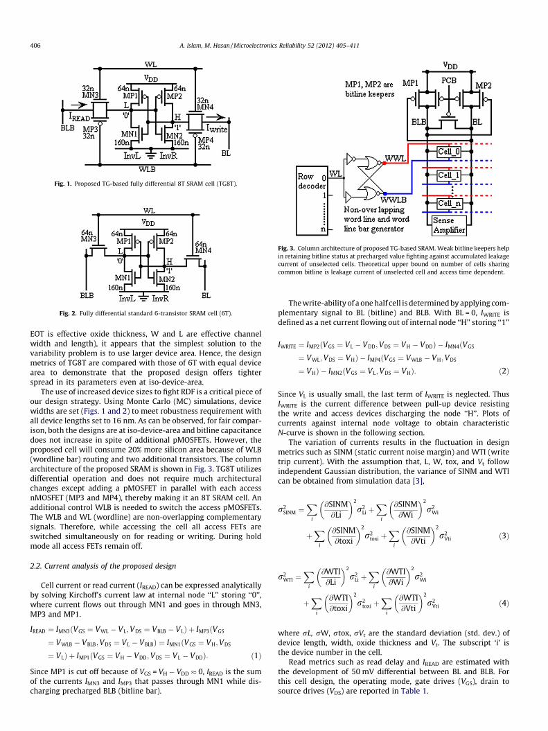
Fig. 1. Proposed TG-based fully differential 8T SRAM cell (TG8T).
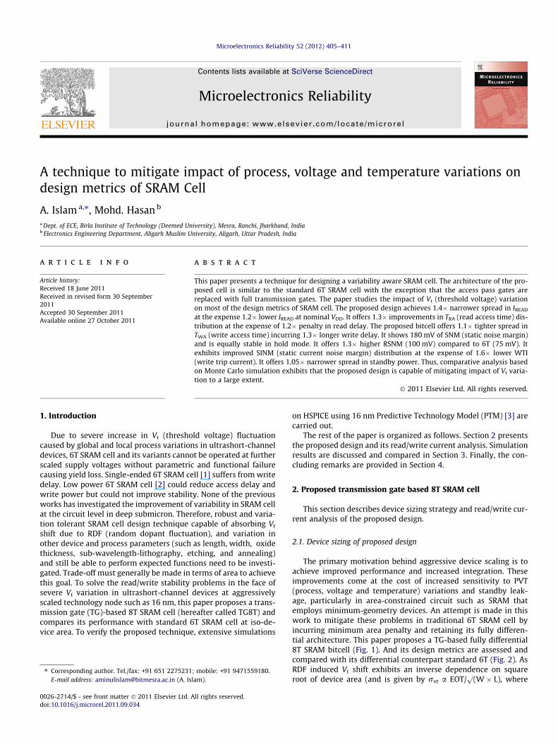
Fig. 2. Fully differential standard 6-transistor SRAM cell (6T).
Fig. 3. Column architecture of proposed TG-based SRAM. Weak bitline keepers helpin retaining bitline status at precharged value fighting against accumulated leakagecurrent of unselected cells. Theoretical upper bound on number of cells sharingcommon bitline is leakage current of unselected cell and access time dependent.
406 A. Islam, M. Hasan / Microelectronics Reliability 52 (2012) 405–411
EOT is effective oxide thickness, W and L are effective channelwidth and length), it appears that the simplest solution to thevariability problem is to use larger device area. Hence, the designmetrics of TG8T are compared with those of 6T with equal devicearea to demonstrate that the proposed design offers tighterspread in its parameters even at iso-device-area.
The use of increased device sizes to fight RDF is a critical piece ofour design strategy. Using Monte Carlo (MC) simulations, devicewidths are set (Figs. 1 and 2) to meet robustness requirement withall device lengths set to 16 nm. As can be observed, for fair compar-ison, both the designs are at iso-device-area and bitline capacitancedoes not increase in spite of additional pMOSFETs. However, theproposed cell will consume 20% more silicon area because of WLB(wordline bar) routing and two additional transistors. The columnarchitecture of the proposed SRAM is shown in Fig. 3. TG8T utilizesdifferential operation and does not require much architecturalchanges except adding a pMOSFET in parallel with each accessnMOSFET (MP3 and MP4), thereby making it an 8T SRAM cell. Anadditional control WLB is needed to switch the access pMOSFETs.The WLB and WL (wordline) are non-overlapping complementarysignals. Therefore, while accessing the cell all access FETs areswitched simultaneously on for reading or writing. During holdmode all access FETs remain off.
2.2. Current analysis of the proposed design
Cell current or read current (IREAD) can be expressed analyticallyby solving Kirchoff’s current law at internal node ‘‘L’’ storing ‘‘0’’,where current flows out through MN1 and goes in through MN3,MP3 and MP1.
IREAD ¼ IMN3ðVGS ¼ VWL � VL;VDS ¼ VBLB � VLÞ þ IMP3ðVGS
¼ VWLB � VBLB;VDS ¼ VL � VBLBÞ ¼ IMN1ðVGS ¼ VH;VDS
¼ VLÞ þ IMP1ðVGS ¼ VH � VDD;VDS ¼ VL � VDDÞ: ð1Þ
Since MP1 is cut off because of VGS = VH � VDD � 0, IREAD is the sumof the currents IMN3 and IMP3 that passes through MN1 while dis-charging precharged BLB (bitline bar).
The write-ability of a one half cell is determined by applying com-plementary signal to BL (bitline) and BLB. With BL = 0, IWRITE isdefined as a net current flowing out of internal node ‘‘H’’ storing ‘‘1’’
IWRITE ¼ IMP2ðVGS ¼ VL � VDD;VDS ¼ VH � VDDÞ � IMN4ðVGS
¼ VWL;VDS ¼ VHÞ � IMP4ðVGS ¼ VWLB � VH;VDS
¼ VHÞ � IMN2ðVGS ¼ VL;VDS ¼ VHÞ: ð2Þ
Since VL is usually small, the last term of IWRITE is neglected. ThusIWRITE is the current difference between pull-up device resistingthe write and access devices discharging the node ‘‘H’’. Plots ofcurrents against internal node voltage to obtain characteristicN-curve is shown in the following section.
The variation of currents results in the fluctuation in designmetrics such as SINM (static current noise margin) and WTI (writetrip current). With the assumption that, L, W, tox, and Vt followindependent Gaussian distribution, the variance of SINM and WTIcan be obtained from simulation data [3],
r2SINM ¼
Xi
@SINM@Li
� �2
r2Li þ
Xi
@SINM@Wi
� �2
r2Wi
þX
i
@SINM@toxi
� �2
r2toxi þ
Xi
@SINM@Vti
� �2
r2Vti ð3Þ
r2WTI ¼
Xi
@WTI@Li
� �2
r2Li þ
Xi
@WTI@Wi
� �2
r2Wi
þX
i
@WTI@toxi
� �2
r2toxi þ
Xi
@WTI@Vti
� �2
r2Vti ð4Þ
where rL, rW, rtox, rVt are the standard deviation (std. dev.) ofdevice length, width, oxide thickness and Vt. The subscript ‘i’ isthe device number in the cell.
Read metrics such as read delay and IREAD are estimated withthe development of 50 mV differential between BL and BLB. Forthis cell design, the operating mode, gate drives (VGS), drain tosource drives (VDS) are reported in Table 1.
Table 1Values at the end point of read operation when voltage differential of 50 mV is developed between BL and BLB.
Device VDS VGS Operating mode
MN1 VL = 70 mV VH = 700 mV LinearMN2 VH = 700 mV VL = 70 mV Cut offMN3 VBLB � VL = VDD � 50 mV � VL = 580 mV VWL � VL = 630 mV Velocity saturationMN4 VBL � VH = 0 VWL � VDD = 0 Cut offMP1 VL � VDD = 630 mV VH � VDD = 0 Cut offMP2 VH � VDD = 0 VL � VDD = �630 mV LinearMP3 VL � VBLB = VL � (VDD � 50 mV) = �580 mV VWLB � VBLB = 0 – 650 mV = �650 mV Velocity saturationMP4 VBL � VH = 0 VWLB � VBL = �700 mV Linear
Fig. 4. Read current distribution of standard 6T.
A. Islam, M. Hasan / Microelectronics Reliability 52 (2012) 405–411 407
3. Simulation results and discussion
The focus of this work is on the challenges faced in designingmemory circuit in nanoscale technology, where variations occurdue to process and environmental parameters such as operatingvoltage and temperature. The root causes of variations are scaling.The problem of variability (defined as standard deviation (r) tomean (l) ratio of a design metric) becomes even more acute withgreater miniaturization and hence it is imperative that these prob-lems are addressed. The solutions involve the invention of newdesign techniques. This paper attempts to mitigate impact of PVTvariations on design metrics of SRAM cell.
3.1. Simulation setup
This section presents comparison of various design metricswhich are estimated during MC simulation using 16 nm CMOSPredictive Technology Model [3]. The threshold voltage (Vt) is as-sumed to have independent Gaussian distributions with 3r varia-tion of 30% [4]. Authors in [5] showed that the variation in Cox
(gate oxide capacitance) due to variations in L (channel length),W (width), and tox (oxide thickness) is negligibly small. Moreover,it is to be noted that the effect of all parameter variations can betranslated into an effective variation in threshold voltage [6]. There-fore, only 30% Vt variation is applied here.
ITRS 2009 anticipates temperature variation within the rangefrom �55 �C to 155 �C. Therefore, temperature is randomly variedwithin this range in addition to Vt. As per ITRS 2009, expected var-iation in VDD is 10% in the future technology generations such as16 nm [7]. Hence, most of the design metrics are measured by vary-ing the supply voltage by ±10% around the nominal VDD of 0.7 V.
The sample size of 2000 ensures a lower than 4% inaccuracy inthe estimation of standard deviation [5]. Design metrics in thiswork are estimated with 5000 MC run [8] to achieve even higheraccuracy. Unless specified otherwise, all parameters are estimatedunder the above variation/simulation setup.
3.2. Read current and its variability
The read current (IREAD), is the summation of two currentsnamely IDn and IDp flowing through nMOSFET (MN3) and pMOSFET(MP3) transistors of a transmission gate (TG) respectively (Fig. 1).This summation of current over two different transistors in parallelis primarily responsible for the lower value of variability in case ofTG8T. This averaging is impossible in case of 6T due to the existenceof only one access transistor. Moreover, it can also be deduced thatthe current through MP3 of TG varies so as to stabilize the total readcurrent in case current through MN3 of TG varies due to RDF in-duced Vt shift and vice versa.
This can be understood by assuming that only the Vt of MN3 ofTG goes down due to RDF whereas the Vt of MP3 remains un-changed. This increases the current through MN3 and the total cur-rent IREAD through TG and hence VL (VH) rises quickly and VBLB (VBL)
falls rapidly. This rapid rise of VL (VH) and fall of VBLB (VBL) increasesVts of MN3 (MN4) and MP3 (MP4) due to body effect respectively,thereby, reducing the current through both MN3 (MN4) and MP3(MP4). This helps in reducing (stabilizing) the total current IREAD.
Similarly, if the Vt of MN3 (MN4) increases due to RDF, the cur-rent through MN3 (MN4) and also the total current IREAD decreaseand hence, VL (VH) rises slowly and VBLB (VBL) reduces gradually. Thisresults in lower value of threshold voltages for both MN3 (MN4)and MP3 (MP4) due to less pronounced body effect compared withthe first case. The lower value of threshold voltage increases thecurrent through both MN3 (MN4) and MP3 (MP4), thereby, stabiliz-ing the total current IREAD.
The same explanation can be given in case the threshold voltageof MP3 (MP4) varies due to RDF. Therefore, it can be concluded thatIREAD with TG is much more stable compared to IREAD with nMOSFETpass transistor. This is evident from the simulation results whichshows that TG8T achieves 1.4� lower spread in IREAD at the expense1.2� lower IREAD at nominal VDD (Figs. 4 and 5). TG8T offers tighterspread in IREAD at all considered VDD (Fig. 6). This improved variabil-ity in IREAD offers narrower spread in other design metrics (SINMand TRA (read access time)) of the proposed design.
The 6T shows higher read current because drive current ofnMOSFET is higher than pMOSFET (�1.5 �with W/L = 32 nm/16 nm). Therefore, though the width of MN3/MN4 (32 nm) andMP3/MP4 (32 nm) in TG8T taken together is equal to that ofMN3/MN4 (64 nm) in 6T, their drive strength is not equal. However,TG8T achieves improved IREAD variability due to averaging effect ofTG (Figs. 4–6).
3.3. Read access time and its variability
The TRA (read access time or read delay) is estimated from thepoint when WL (WLB) reaches to its 50% point from its initiallow (high) level to the point when BL/BLB is discharged by50 mV from its initial high level [8]. The 50 mV differential be-tween BL and BLB is good enough to be detected by sense amplifier,thereby avoiding misread [8,9]. The TG8T offers 1.3� improve-ments in TRA distribution at the expense of 1.2� penalty in read de-lay (Fig. 7 and Table 2 (normalized values are reported in bracket)).
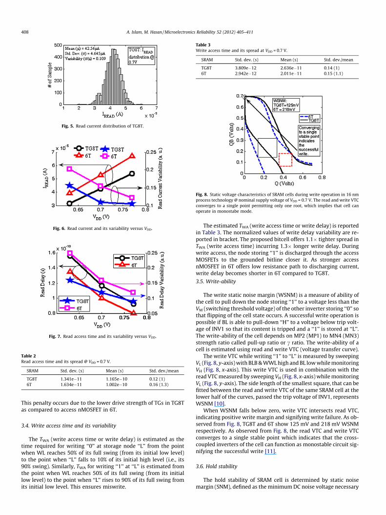
Fig. 5. Read current distribution of TG8T.
Fig. 6. Read current and its variability versus VDD.
Fig. 7. Read access time and its variability versus VDD.
Table 2Read access time and its spread @ VDD = 0.7 V.
SRAM Std. dev. (s) Mean (s) Std. dev./mean
TG8T 1.341e�11 1.165e�10 0.12 (1)6T 1.634e�11 1.002e�10 0.16 (1.3)
Table 3Write access time and its spread at VDD = 0.7 V.
SRAM Std. dev. (s) Mean (s) Std. dev./mean
TG8T 3.809e�12 2.636e�11 0.14 (1)6T 2.942e�12 2.011e�11 0.15 (1.1)
Fig. 8. Static voltage characteristics of SRAM cells during write operation in 16 nmprocess technology @ nominal supply voltage of VDD = 0.7 V. The read and write VTCconverges to a single point permitting only one root, which implies that cell canoperate in monostabe mode.
408 A. Islam, M. Hasan / Microelectronics Reliability 52 (2012) 405–411
This penalty occurs due to the lower drive strength of TGs in TG8Tas compared to access nMOSFET in 6T.
3.4. Write access time and its variability
The TWA (write access time or write delay) is estimated as thetime required for writing ‘‘0’’ at storage node ‘‘L’’ from the pointwhen WL reaches 50% of its full swing (from its initial low level)to the point when ‘‘L’’ falls to 10% of its initial high level (i.e., its90% swing). Similarly, TWA for writing ‘‘1’’ at ‘‘L’’ is estimated fromthe point when WL reaches 50% of its full swing (from its initiallow level) to the point when ‘‘L’’ rises to 90% of its full swing fromits initial low level. This ensures miswrite.
The estimated TWA (write access time or write delay) is reportedin Table 3. The normalized values of write delay variability are re-ported in bracket. The proposed bitcell offers 1.1� tighter spread inTWA (write access time) incurring 1.3� longer write delay. Duringwrite access, the node storing ‘‘1’’ is discharged through the accessMOSFETs to the grounded bitline closer it. As stronger accessnMOSFET in 6T offers low resistance path to discharging current,write delay becomes shorter in 6T compared to TG8T.
3.5. Write-ability
The write static noise margin (WSNM) is a measure of ability ofthe cell to pull down the node storing ‘‘1’’ to a voltage less than theVM (switching threshold voltage) of the other inverter storing ‘‘0’’ sothat flipping of the cell state occurs. A successful write operation ispossible if BL is able to pull-down ‘‘H’’ to a voltage below trip volt-age of INV1 so that its content is tripped and a ‘‘1’’ is stored at ‘‘L’’.The write-ability of the cell depends on MP2 (MP1) to MN4 (MN3)strength ratio called pull-up ratio or c ratio. The write-ability of acell is estimated using read and write VTC (voltage transfer curve).
The write VTC while writing ‘‘1’’ to ‘‘L’’ is measured by sweepingVL (Fig. 8, y-axis) with BLB & WWL high and BL low while monitoringVH (Fig. 8, x-axis). This write VTC is used in combination with theread VTC measured by sweeping VH (Fig. 8, x-axis) while monitoringVL (Fig. 8, y-axis). The side length of the smallest square, that can befitted between the read and write VTC of the same SRAM cell at thelower half of the curves, passed the trip voltage of INV1, representsWSNM [10].
When WSNM falls below zero, write VTC intersects read VTC,indicating positive write margin and signifying write failure. As ob-served from Fig. 8, TG8T and 6T show 125 mV and 218 mV WSNMrespectively. As observed from Fig. 8, the read VTC and write VTCconverges to a single stable point which indicates that the cross-coupled inverters of the cell can function as monostable circuit sig-nifying the successful write [11].
3.6. Hold stability
The hold stability of SRAM cell is determined by static noisemargin (SNM), defined as the minimum DC noise voltage necessary
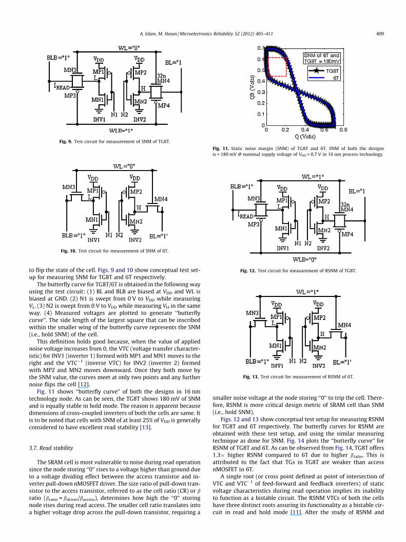
Fig. 9. Test circuit for measurement of SNM of TG8T.
Fig. 10. Test circuit for measurement of SNM of 6T.
Fig. 11. Static noise margin (SNM) of TG8T and 6T. SNM of both the designsis = 180 mV @ nominal supply voltage of VDD = 0.7 V in 16 nm process technology.
Fig. 12. Test circuit for measurement of RSNM of TG8T.
Fig. 13. Test circuit for measurement of RSNM of 6T.
A. Islam, M. Hasan / Microelectronics Reliability 52 (2012) 405–411 409
to flip the state of the cell. Figs. 9 and 10 show conceptual test set-up for measuring SNM for TG8T and 6T respectively.
The butterfly curve for TG8T/6T is obtained in the following wayusing the test circuit: (1) BL and BLB are biased at VDD and WL isbiased at GND. (2) N1 is swept from 0 V to VDD while measuringVL. (3) N2 is swept from 0 V to VDD while measuring VH in the sameway. (4) Measured voltages are plotted to generate ‘‘butterflycurve’’. The side length of the largest square that can be inscribedwithin the smaller wing of the butterfly curve represents the SNM(i.e., hold SNM) of the cell.
This definition holds good because, when the value of appliednoise voltage increases from 0, the VTC (voltage transfer character-istic) for INV1 (inverter 1) formed with MP1 and MN1 moves to theright and the VTC�1 (inverse VTC) for INV2 (inverter 2) formedwith MP2 and MN2 moves downward. Once they both move bythe SNM value, the curves meet at only two points and any furthernoise flips the cell [12].
Fig. 11 shows ‘‘butterfly curve’’ of both the designs in 16 nmtechnology node. As can be seen, the TG8T shows 180 mV of SNMand is equally stable in hold mode. The reason is apparent becausedimensions of cross-coupled inverters of both the cells are same. Itis to be noted that cells with SNM of at least 25% of VDD is generallyconsidered to have excellent read stability [13].
3.7. Read stability
The SRAM cell is most vulnerable to noise during read operationsince the node storing ‘‘0’’ rises to a voltage higher than ground dueto a voltage dividing effect between the access transistor and in-verter pull-down nMOSFET driver. The size ratio of pull-down tran-sistor to the access transistor, referred to as the cell ratio (CR) or bratio (bratio = bdriver/baccess), determines how high the ‘‘0’’ storingnode rises during read access. The smaller cell ratio translates intoa higher voltage drop across the pull-down transistor, requiring a
smaller noise voltage at the node storing ‘‘0’’ to trip the cell. There-fore, RSNM is more critical design metric of SRAM cell than SNM(i.e., hold SNM).
Figs. 12 and 13 show conceptual test setup for measuring RSNMfor TG8T and 6T respectively. The butterfly curves for RSNM areobtained with these test setup, and using the similar measuringtechnique as done for SNM. Fig. 14 plots the ‘‘butterfly curve’’ forRSNM of TG8T and 6T. As can be observed from Fig. 14, TG8T offers1.3� higher RSNM compared to 6T due to higher bratio. This isattributed to the fact that TGs in TG8T are weaker than accessnMOSFET in 6T.
A single root (or cross point defined as point of intersection ofVTC and VTC�1 of feed-forward and feedback inverters) of staticvoltage characteristics during read operation implies its inabilityto function as a bistable circuit. The RSNM VTCs of both the cellshave three distinct roots assuring its functionality as a bistable cir-cuit in read and hold mode [11]. After the study of RSNM and
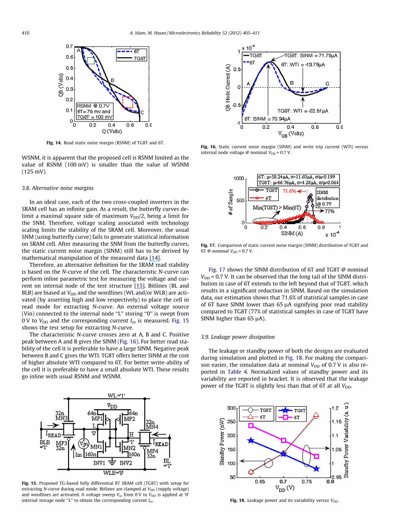
Fig. 14. Read static noise margin (RSNM) of TG8T and 6T.Fig. 16. Static current noise margin (SINM) and write trip current (WTI) versusinternal node voltage @ nominal VDD = 0.7 V.
410 A. Islam, M. Hasan / Microelectronics Reliability 52 (2012) 405–411
WSNM, it is apparent that the proposed cell is RSNM limited as thevalue of RSNM (100 mV) is smaller than the value of WSNM(125 mV).
Fig. 17. Comparison of static current noise margin (SINM) distribution of TG8T and6T @ nominal VDD = 0.7 V.
3.8. Alternative noise margins
In an ideal case, each of the two cross-coupled inverters in theSRAM cell has an infinite gain. As a result, the butterfly curves de-limit a maximal square side of maximum VDD/2, being a limit forthe SNM. Therefore, voltage scaling associated with technologyscaling limits the stability of the SRAM cell. Moreover, the usualSNM (using butterfly curve) fails to generate statistical informationon SRAM cell. After measuring the SNM from the butterfly curves,the static current noise margin (SINM) still has to be derived bymathematical manipulation of the measured data [14].
Therefore, an alternative definition for the SRAM read stabilityis based on the N-curve of the cell. The characteristic N-curve canperform inline parametric test for measuring the voltage and cur-rent on internal node of the test structure [15]. Bitlines (BL andBLB) are biased at VDD and the wordlines (WL and/or WLB) are acti-vated (by asserting high and low respectively) to place the cell inread mode for extracting N-curve. An external voltage source(Vin) connected to the internal node ‘‘L’’ storing ‘‘0’’ is swept from0 V to VDD and the corresponding current Iin is measured. Fig. 15shows the test setup for extracting N-curve.
The characteristic N-curve crosses zero at A, B and C. Positivepeak between A and B gives the SINM (Fig. 16). For better read sta-bility of the cell it is preferable to have a large SINM. Negative peakbetween B and C gives the WTI. TG8T offers better SINM at the costof higher absolute WTI compared to 6T. For better write-ability ofthe cell it is preferable to have a small absolute WTI. These resultsgo inline with usual RSNM and WSNM.
Fig. 15. Proposed TG-based fully differential 8T SRAM cell (TG8T) with setup forextracting N-curve during read mode. Bitlines are clamped at VDD (supply voltage)and wordlines are activated. A voltage sweep Vin from 0 V to VDD is applied at ‘0’internal storage node ‘‘L’’ to obtain the corresponding current Iin.
Fig. 17 shows the SINM distribution of 6T and TG8T @ nominalVDD = 0.7 V. It can be observed that the long tail of the SINM distri-bution in case of 6T extends to the left beyond that of TG8T, whichresults in a significant reduction in SINM. Based on the simulationdata, our estimation shows that 71.6% of statistical samples in caseof 6T have SINM lower than 65 lA signifying poor read stabilitycompared to TG8T (77% of statistical samples in case of TG8T haveSINM higher than 65 lA).
3.9. Leakage power dissipation
The leakage or standby power of both the designs are evaluatedduring simulation and plotted in Fig. 18. For making the compari-son easier, the simulation data at nominal VDD of 0.7 V is also re-ported in Table 4. Normalized values of standby power and itsvariability are reported in bracket. It is observed that the leakagepower of the TG8T is slightly less than that of 6T at all VDD.
Fig. 18. Leakage power and its variability versus VDD.
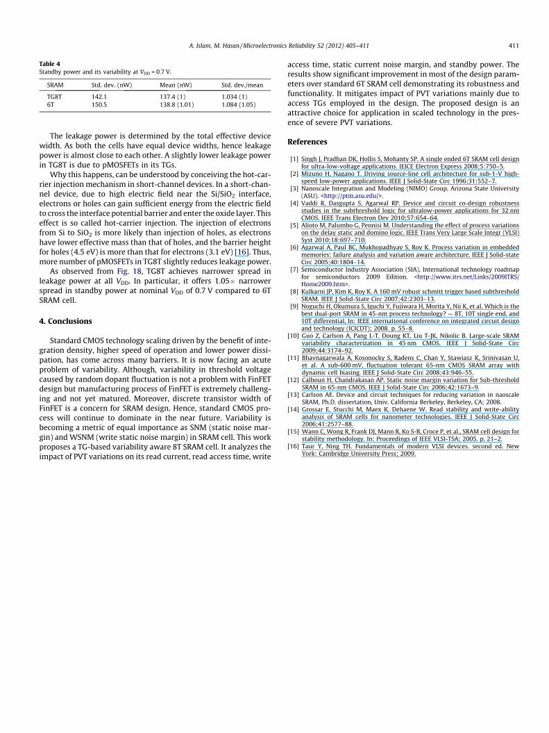
Table 4Standby power and its variability at VDD = 0.7 V.
SRAM Std. dev. (nW) Mean (nW) Std. dev./mean
TG8T 142.1 137.4 (1) 1.034 (1)6T 150.5 138.8 (1.01) 1.084 (1.05)
A. Islam, M. Hasan / Microelectronics Reliability 52 (2012) 405–411 411
The leakage power is determined by the total effective devicewidth. As both the cells have equal device widths, hence leakagepower is almost close to each other. A slightly lower leakage powerin TG8T is due to pMOSFETs in its TGs.
Why this happens, can be understood by conceiving the hot-car-rier injection mechanism in short-channel devices. In a short-chan-nel device, due to high electric field near the Si/SiO2 interface,electrons or holes can gain sufficient energy from the electric fieldto cross the interface potential barrier and enter the oxide layer. Thiseffect is so called hot-carrier injection. The injection of electronsfrom Si to SiO2 is more likely than injection of holes, as electronshave lower effective mass than that of holes, and the barrier heightfor holes (4.5 eV) is more than that for electrons (3.1 eV) [16]. Thus,more number of pMOSFETs in TG8T slightly reduces leakage power.
As observed from Fig. 18, TG8T achieves narrower spread inleakage power at all VDD. In particular, it offers 1.05� narrowerspread in standby power at nominal VDD of 0.7 V compared to 6TSRAM cell.
4. Conclusions
Standard CMOS technology scaling driven by the benefit of inte-gration density, higher speed of operation and lower power dissi-pation, has come across many barriers. It is now facing an acuteproblem of variability. Although, variability in threshold voltagecaused by random dopant fluctuation is not a problem with FinFETdesign but manufacturing process of FinFET is extremely challeng-ing and not yet matured. Moreover, discrete transistor width ofFinFET is a concern for SRAM design. Hence, standard CMOS pro-cess will continue to dominate in the near future. Variability isbecoming a metric of equal importance as SNM (static noise mar-gin) and WSNM (write static noise margin) in SRAM cell. This workproposes a TG-based variability aware 8T SRAM cell. It analyzes theimpact of PVT variations on its read current, read access time, write
access time, static current noise margin, and standby power. Theresults show significant improvement in most of the design param-eters over standard 6T SRAM cell demonstrating its robustness andfunctionality. It mitigates impact of PVT variations mainly due toaccess TGs employed in the design. The proposed design is anattractive choice for application in scaled technology in the pres-ence of severe PVT variations.
References
[1] Singh J, Pradhan DK, Hollis S, Mohanty SP. A single ended 6T SRAM cell designfor ultra-low-voltage applications. IEICE Electron Express 2008;5:750–5.
[2] Mizuno H, Nagano T. Driving source-line cell architecture for sub-1-V high-speed low-power applications. IEEE J Solid-State Circ 1996;31:552–7.
[3] Nanoscale Integration and Modeling (NIMO) Group, Arizona State University(ASU). <http://ptm.asu.edu/>.
[4] Vaddi R, Dasgupta S, Agarwal RP. Device and circuit co-design robustnessstudies in the subthreshold logic for ultralow-power applications for 32 nmCMOS. IEEE Trans Electron Dev 2010;57:654–64.
[5] Alioto M, Palumbo G, Pennisi M. Understanding the effect of process variationson the delay static and domino logic. IEEE Trans Very Large Scale Integr (VLSI)Syst 2010;18:697–710.
[6] Agarwal A, Paul BC, Mukhopadhyay S, Roy K. Process variation in embeddedmemories: failure analysis and variation aware architecture. IEEE J Solid-stateCirc 2005;40:1804–14.
[7] Semiconductor Industry Association (SIA), International technology roadmapfor semiconductors 2009 Edition. <http://www.itrs.net/Links/2009ITRS/Home2009.htm>.
[8] Kulkarni JP, Kim K, Roy K. A 160 mV robust schmitt trigger based subthresholdSRAM. IEEE J Solid-State Circ 2007;42:2303–13.
[9] Noguchi H, Okumura S, Iguchi Y, Fujiwara H, Morita Y, Nii K, et al. Which is thebest dual-port SRAM in 45-nm process technology? — 8T, 10T single end, and10T differential, In: IEEE international conference on integrated circuit designand technology (ICICDT); 2008. p. 55–8.
[10] Guo Z, Carlson A, Pang L-T, Doung KT, Liu T-JK, Nikolic B. Large-scale SRAMvariability characterization in 45 nm CMOS. IEEE J Solid-State Circ2009;44:3174–92.
[11] Bhavnagarwala A, Kosonocky S, Radens C, Chan Y, Stawiasz K, Srinivasan U,et al. A sub-600 mV, fluctuation tolerant 65-nm CMOS SRAM array withdynamic cell biasing. IEEE J Solid-State Circ 2008;43:946–55.
[12] Calhoun H, Chandrakasan AP. Static noise margin variation for Sub-thresholdSRAM in 65-nm CMOS. IEEE J Solid-State Circ 2006;42:1673–9.
[13] Carlson AE. Device and circuit techniques for reducing variation in naoscaleSRAM, Ph.D. dissertation, Univ. California Berkeley, Berkeley, CA; 2008.
[14] Grossar E, Stucchi M, Maex K, Dehaene W. Read stability and write-abilityanalysis of SRAM cells for nanometer technologies. IEEE J Solid-State Circ2006;41:2577–88.
[15] Wann C, Wong R, Frank DJ, Mann R, Ko S-B, Croce P, et al., SRAM cell design forstability methodology. In: Proceedings of IEEE VLSI-TSA; 2005. p. 21–2.
[16] Taur Y, Ning TH. Fundamentals of modern VLSI devices. second ed. NewYork: Cambridge University Press; 2009.