A synthesis of fuzzy control surfaces in CMOS technology
6
A Synthesis of Fuzzy Control Surfaces in CMOS Technology Jose Matas, Luis Garcia de Vicufia and Mtiguel Castilla Escola Universithria Politecnica de Vilanova i la Geltni (Universidad Politecnica de Cataluiia) Avda. Victor Balaguer s/n, 08800. Vilanova i la Geltn3 (Spain). E-mail: [email protected] Abstract .- A new design of a monolithic CMOS analog function synthesizer based on current-mode techniques is presented together with its application to fuzzy logic controllers. The system fuzzy control strategy has previously been simulated, thus obtaining the control surface which is then approximated by planes. The integrated circuit realizes the implicit equation of each plane whose coeficients are previously introduced in a static RAM memory. The approximated control surface allows us to obtain the control action directly. This controller is specially adequate to control systems where the fast response in control loop is necessary. The simulation shows that the maximum propagation delay from a step change in the inputs) is 200 nsec. To illustrate the use of this circuit, this controller is applied to control a dc-dc switching regulator. 1. Introduction The motivation of this work was the search for efficient solutions to substitute in a practical way the linear control employed in switching regulators for fuzzy logic controllers. The main difficulties that the analysis and control of switchmg regulators present are due to the highly non- linear nature of dc-dc converter systems. To solve this problem. Merent linearizing techmques were proposed in the past [1][2], their validity limits being located in a small neighbourhood of the steady-state operating point. However, the analysis and control becomes more difficult beyond these limits when a large-signal phenomenon appears in the system. There are two possible options to solve this problem : 1) To develop more accurate non-linear models on which high-performance controller designs can be based [?I. 2) To use fuzzy logic control. The first option leads to very complicated controllers that are not suitable for practical implementation. The second has given rise to numerous theoretical works [4][5][6],but the practical implementation must be realized by a fast fuzzy controller, since the switching frequency can be 100 khz and the time constants involved in the power stage are a few miliseconds. In previousi papers [7][8], fuzzy controllers were developed for dc-dc converters using digital signal processors and analog solutions in voltage mode. Both solutions show the possibility of applying fuzzy control methods in converter real-practical control, but the controllers use many and expensive integrated circuits. For this reason,, in spite of the excellent robustness and dynamical response, these alternatives can hardly motiva- te the designer to substitute the traditional linear control. In this work, we present a monolithic fuzzy controller based on the approximation by planes of the control surface created by the interaction of rules with fuzz): sets. The control surface elicits a system response from a set of input values. The main design idea is to substitute the circuits blocks, which implement the membership functions, the fuzzy inference and the defuzzification strategy for CMOS circuits in current mode which implement the implicit equation in a plane. The fuzzy controller is programmable for whichever application with two inputs and a single output, which is the usual case for the control of dc-dc switching regulators. 2. Fundamentals of the fuzzy controller Figure 1 shows the block diagram of the fuzzy controller scheme for dc-dc converters. The inputs of the fuzzy controller are the error, e, and the change of error: ce: where e is defined as Vo - Vre. and ce = ek - ek-1 at the kth sampling instant. The output of fuzzy controller is the duty cycle a'; at the kth sampling time, and is defined as : d,k = dk-l+ q. 6dk (1) Where Sdk is the inferred change of duty cycle for the fuzzy controller at kth sampling time, and q is the gain factor of the :hzzy controller. By adjusting q , the effective gain of'the controller can be changed. 0-7803-3796-4/97/$10.0001997IEEE 64 1
-
Upload
independent -
Category
Documents
-
view
0 -
download
0
Transcript of A synthesis of fuzzy control surfaces in CMOS technology
A Synthesis of Fuzzy Control Surfaces in CMOS Technology
Jose Matas, Luis Garcia de Vicufia and Mtiguel Castilla Escola Universithria Politecnica de Vilanova i la Geltni (Universidad Politecnica de Cataluiia)
Avda. Victor Balaguer s/n, 08800. Vilanova i la Geltn3 (Spain). E-mail: [email protected]
Abstract .- A new design of a monolithic CMOS analog function synthesizer based on current-mode techniques is presented together with its application to fuzzy logic controllers. The system fuzzy control strategy has previously been simulated, thus obtaining the control surface which is then approximated by planes. The integrated circuit realizes the implicit equation of each plane whose coeficients are previously introduced in a static RAM memory. The approximated control surface allows us to obtain the control action directly. This controller is specially adequate to control systems where the fast response in control loop is necessary. The simulation shows that the maximum propagation delay from a step change in the inputs) is 200 nsec. To illustrate the use of this circuit, this controller is applied to control a dc-dc switching regulator.
1. Introduction
The motivation of this work was the search for efficient solutions to substitute in a practical way the linear control employed in switching regulators for fuzzy logic controllers.
The main difficulties that the analysis and control of switchmg regulators present are due to the highly non- linear nature of dc-dc converter systems. To solve this problem. Merent linearizing techmques were proposed in the past [1][2], their validity limits being located in a small neighbourhood of the steady-state operating point. However, the analysis and control becomes more difficult beyond these limits when a large-signal phenomenon appears in the system. There are two possible options to solve this problem :
1) To develop more accurate non-linear models on which high-performance controller designs can be based [?I.
2) To use fuzzy logic control. The first option leads to very complicated controllers
that are not suitable for practical implementation. The second has given rise to numerous theoretical works [4][5][6],but the practical implementation must be
realized by a fast fuzzy controller, since the switching frequency can be 100 khz and the time constants involved in the power stage are a few miliseconds.
In previousi papers [7][8], fuzzy controllers were developed for dc-dc converters using digital signal processors and analog solutions in voltage mode. Both solutions show the possibility of applying fuzzy control methods in converter real-practical control, but the controllers use many and expensive integrated circuits. For this reason,, in spite of the excellent robustness and dynamical response, these alternatives can hardly motiva- te the designer to substitute the traditional linear control.
In this work, we present a monolithic fuzzy controller based on the approximation by planes of the control surface created by the interaction of rules with fuzz): sets. The control surface elicits a system response from a set of input values.
The main design idea is to substitute the circuits blocks, which implement the membership functions, the fuzzy inference and the defuzzification strategy for CMOS circuits in current mode which implement the implicit equation in a plane. The fuzzy controller is programmable for whichever application with two inputs and a single output, which is the usual case for the control of dc-dc switching regulators.
2. Fundamentals of the fuzzy controller
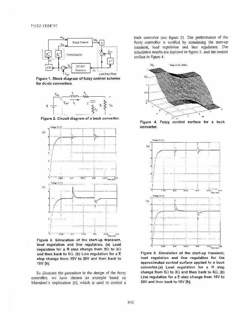
Figure 1 shows the block diagram of the fuzzy controller scheme for dc-dc converters. The inputs of the fuzzy controller are the error, e, and the change of error: ce: where e is defined as Vo - Vre. and ce = ek - ek-1 at
the kth sampling instant. The output of fuzzy controller is the duty cycle a'; at the kth sampling time, and is defined as :
d,k = dk-l+ q. 6dk (1)
Where Sdk is the inferred change of duty cycle for the fuzzy controller at kth sampling time, and q is the gain factor of the :hzzy controller. By adjusting q , the effective gain of'the controller can be changed.
0-7803-3796-4/97/$10.0001997IEEE 64 1
FUZZ-IEEE’97
...
...
Low-Pass Filter
Figure 1. Block diagram of fuzzy control scheme for d c d c converters.
I I I I _
Figure 2. Circuit diagram of a buck converter.
V O l l q C vo (V) ........................
: l , , j 1
Time ( r ~ c 3 ~ ’ ‘0 0005 001 0015 002 0025
VOltaPI vo 174
5 t c-
buck converter (see figure 2). The performance of the fuzzy controller is verified by simulating the start-up transient, load regulation and line regulation. The simulation results are depicted in figure 3, and the control surface in figure 4.
2
2 -2
Figure 4. Fuzzy control surface for a buck converter.
........................................................................................... ’ti ( 1 ..................................................................... + 1 Ot
0005 001 0015 0 0 2 0 025 003 Tim (SGC)
Voltagr v o (V) ............. .,. ............................ , .............. , .............. ,
...... ; ............ . . . . . . . . . . i . . .
3 ...l......... ............... : .................. ..: . . . . . . . . . . . . . . .
. . . . . . . . . 2 i i ..I ; , 1
.............. I ............ ; .............. L ............. I ............. 1 .............. I 0 0005 0.01 0015 0.C2 0025 003
Time (sec)
Figure 3, Simulation of the start-up transient, load regulation and line regulation. (a) Load regulation for a R step change from 552 to 3R and then back to 5Q. (b) Line regulation for a E step change from 15V to 20V and then back to 15V [6].
To illustrate the procedure in the design of the fuzzy controller, we have chosen an example based on Mamdani’s implication [6], which is used to control a
0 O m S 0 0 1 0015 0 0 2 0025 Om
Timr ( s e 0
Figure 5. Simulation of the start-up transient, load regulation and line regulation for the approximated control surface applied to a buck converter.(a) Load regulation for a R step change from 5R to 3 0 and then back to 5 0 . (b) Line regulation for a E step change from 15V to 20V and then back to 15V [6].
642
FUZZ-I EEE’9 7
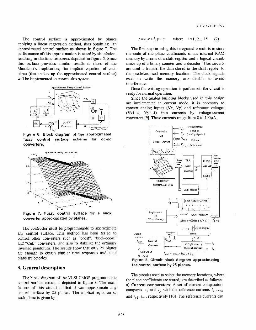
The control surface is approximated by planes applying a linear regression method, thus obtaining an approximated control surface as shown in figure 7. The performance of this approximation is tested by simulation, resulting in the time responses depicted in figure 5. Since this surface provides similar results to those of the Mamdani’s implication, the implicit equation of each plane (that makes up the approximated control surface) will be implemented to control this system.
Appromated Fuzzy Control Surface
...
Figure 6. Block diagram of the approximated fuzzy control surface scheme for dc-dc converters.
npproxlmated Fum/ Control Surface adk
Figure 7. Fuzzy control surface for a buck converter approximated by planes.
The controller must be programmable to approximate any control surface. This method has been tested to zontrol other converters such as “boost”, “buck-boost” and “Cuk” converters, and also to stabilize the ordinary inverted pendulum. The results show that only 25 planes are enough to obtain similar time responses and state plane trajectories.
3. General description
The block diagram of the VLSI-CMOS programmable control surface circuit is depicted in figure 8. The main feature of this circuit is that it can approximate any control surface by 25 planes. The implicit equation of Each plane is given by :
z =aix+biy+ci where I =I, 2....25 (2)
The first step in using this integrated circuit is to store the code of the: plane coefficients in an internal RAM memory by means of a shift register and a logical circuit, made up of a binary counter and a decoder. This circuits are used to transfer the data stored in the shift register to the predetermined memory location. The clock signals used to write the memory are disable to avoid interference.
Once the writing operation is performed, the circuit is ready for normal operation.
Since the analog building blocks used in this design are implemented in current mode, it is necessary to convert analog inputs (Vx, Vy) and reference voltages (Vxl..4* Vy1..4) into currents by voltage-current converters [9]. These currents range from 0 to 100pA.
Voltage lnputs
vx e andce “Y ( analog Slgnals )
Voltage 1 ‘Voltage-Current i vy,.,, References
Output
Output pad I,, = a , i x + b i I y + I c ~ 1 IOLT
Figure 8. Circuit block diagram approximating the control surface by 25 planes.
The circuits used to select the memory locations, where the plane coefficients are stored, are described as follows: a) Current Comparators: A set of current comparators compares i, and i, with the reference currents ixl..zx4
and iyl..iy4, respectively [ 101. The reference currents can
643
FUZZ-IEEE’97
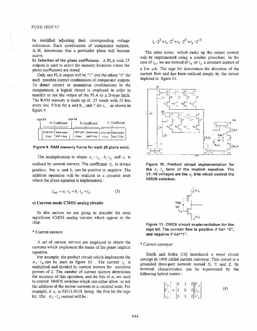
be moMed adjusting their corresponding voltage references. Each combination of comparator outputs, A..H, determines that a particular plane will become active. b) Selection of the plane coefficients : A PLA with 25 outputs is used to select the memory locations where the plane coefficients are stored.
Only one PLA output will be “1” and the others “0” for each possible correct combination of comparator outputs. To detect correct or anomalous combinations in the comparators, a logical circuit is employed in order to transfer or not the output of the PLA to a D-type latch. The RAM memory is made up of 25 words with 25 bits every one, 9 bits for a, and b, , and 7 for c, , as shown in figure 9.
Figure 9. RAM memory frame for each 25 plane word.
The multiplication to obtain ai . i, , bi .iy and ci is
realized by current mirrors. The coefficient ci is always positive, but ai and bi can be positive or negative. The addition operation will be realized in a circuital node where the plane equation is implemented :
iout = a, ix + b, - ir + i,, (3)
c) Current mode CMOS analog circuits
In this section we are going to describe the most signifcant CMOS analog circuits which appear in the chip.
* Current mirrors
A set of current mirrors are employed to obtain the currents which implement the terms of the plane implicit equation.
For example, the product circuit which implements the ai . i, can be seen in figure 10 . The current i, is multiplied and divided by current mirrors for succesive powers of 2. The number of current mirrors detennines the accuracy of this operation, and the bits of ai are used to control NMOS switches which can either allow or not the addition of the mirror currents in a circuital node. For example, if a; is 01011,0010, being the first bit the sign bit. The ai * i, current will be :
i, +i, 2 l + i, .2* + i, .r3
The other terms whch make up the output current will be implemented using a similar procedure. In the case of i,,, we use instead of i, or iy a constant current of a few PA. The sign bit determines the direction of the current flow and has been realized simply by the circuit depicted in figure 11.
Figure I O . Product circuit implementation for the a, .i, term of the implicit equation. The VI..V8 voltages are the a, bits which control the NMOS switches.
Figure 11. CMOS circuit implementation for the sign bit. The current flow is positive if Va= “0”, and negative if Va=“l”.
* Current conveyor
Smith and Sedra [ll] introduced a novel circuit concept in 1968 called current conveyor. Ths circuit is a grounded three-port network named X, Y and Z. Its terminal characteristics can be represented by the following hybrid matrix :
644

The simple combination of current mirrors shown in figure 12.a realizes a current conveyor. By symmetry with the Vdd/2 terminal, a virtual Vdd2 Y node, is obtained where incoming currents can be summed without changing the node potential. The sum Iout is avai.lable as an output current source.
bit I/ . .- Id/ I t - - I our
- l 2 - -
b) Figure 12. (a) Current conveyor. (b) Application of current conveyor to implement lout.
These characteristics are very convenient to obtain a virtual short circuit in the node where the addition of current mirrors is realized. Thus imposing a Vdd2 voltage which allows positive and negative current flows, which are conveyed between the two ports at extremely different impedance levels (see figure 12.b).
4. Circuit programming and testing
Figure 13. shows the scheme of the main building blocks and signals used both for programming the static RAM memory and for adjusting the reference input voltages, by measuring of the corresponding reference currents in an external pad called ITEST. This pad is used at the same time to see the most important currents, such as ix, i,, U , . i, , 6, -iy and ic,. The state signal
P / O N shows if the circuit is in programming or in normal operation.
As it can be seen in figure 13, a shift register, a binary counter and a binary decoder are used to write a word in the memory. The remaining output lines can be used to select the reference currents to be adjusted.
-
FUZZ-IEEE'97
E
R
Figure Ill. Block circuit scheme for programming the FWM memory, for adjusting the reference input voltages and for seeing the most important currents.
5. Final resullts
To test the (circuit behaviour, a set of input current values (ix and i,,) has been introduced in the chip and HSPICE simulations have been realized, obtaining the control surface depicted in figure 14.
2 ou1
100
Figure 14. Control surface obtained with HSPICE simulation.
Figure 15 shows current comparators and the planes used to implement the approximated input surface.
The exact decimal value and the corresponding approximated value in binary code, and the quantified
645
FUZZ-IEEE’97
22,23,24 25 to75 75 to 100 I -1.3 0 I 97.5 1 1111.01
25 75to100 75to100 0 0 0 0000.00 -
error of each coefficient are depicted in table 1 and table 2.
a; orb; value
I
-1.3 1 -0.7
Figure 15. Current comparators and planes.
quantizied value
quantization error
1 6,1;:16 ~ Oto25 1 25to75 1 ~ -1; 1 1;; 1 0010,Ol 1 10,15,20 75 to 100 25 to 75 -0.7 52.5 0100,Ol
0 to 25 75 to 100 1010.00
7,8,9,12,13, 25 to 75 25 to 75 -1.3 -0.7 0111,10 14,17,18,19
-1.375 -0.75
0.075 0.05
Table 1. Coefficients ai, bi and ci for the approximated surface by 25 planes, and the ci binary codes.
Table 2. ai and bi coefficients and their binary code and quantization error.
6. Conclusions
design provides a simple solution to control problems requiring hgh speed and low cost which can be solved by the fuzzy approach.
References
[ l ] R. D. Middlebrook and S.Cuk. A General Unified Approach to Modelling Switching -Converter Power Stages. IEEE Power Electronics Specialists Conference Record, pp. 1 8- 34, 1976.
[2 ] A.F. Witulski. Buck Converter Small-Signal Models and Dynamics: Comparison of Quasi-Resonant and Pulsewidth Modulated Switches. Trans. on Power Electronics; Vol. 6, n04, pp. 727-738, 1991.
[3] L. Garcia de Vicuiia, A. Poveda, L. Martinez, F. Guinjoan and J. Majo. Computer-Aided Discrete-Time Large-Sipal Analysis of Switching Regulators. IEEE Trans. on Power Electronics; Vol. 7.Jan. 1992.p~. 75-82.
[4] Fumio Ueno, Takah~ro Inone, Ichiron Oata and Mamoru Sakaki. Regulation of Cuk Converters Using Fuzz)i Controllers. WTELEC’91, pp. 261-267.
[5] W.C.So, C.K. Tse and Y.S. Lee. A Fuzzy Controller for DC-DC Converters. IEEE Power Electronics Specialists Conference Record, pp. 31 5-320, 1994.
[6] Bor-Ren Lin. Analysis of Fuzzy Control Method Applied to DC-DC Converters. E E E Power Electronics Specialists Conference Record, pp. 22-28, 1993.
[7] Wing-Chi So, Chi K. Tse and Yim-Shu Lee. Development of a Fuzzy Logic Controller for DCDC Converters: Design, Computer Simulation and Experimental Evaluation, pp 24- 32, January 1996.
[8] F.H.F. Leung, L.K. Wong, P.K.S. Tamand and H.K. Lam., Application of Fuzzy Logic Control to Regulated Switchmg Converters. Proceedings of the 7th International Power and Motion Control Conference; Vol. 2, pp. 154-158, 1996.
[9] K. Bulk and H.Wallinga. A Class of Analog CMOS Circuits Based on the Square-Law characteristics of an MOS Transistor in Saturation. E E E Journal of Solid-state Circuits; Vol. 22, No. 3, pp. 357-365, June 1987.
[ 101 D.G. Nairn and C.A.T. Salama. Current-Mode Algorithmic Analog-to-Digital Converters. IEEE Journal of Solid-State Circuits; Vol. 25, No. 4, pp. 997-1003, 1990.
[ l l ] K.C. Smith and A. Sedra. The Current Conveyor: A New Circuit Building Block. Proc. IEEE, pp. 1368-1369, 1968.
In this paper we have presented a design of fuzzy logic controller which implements an accurate approximation of control surface. The design uses CMOS technology and can be integrated into a single chip. The proposed circuit
646