A HIGHLY RELIABLE NON-VOLATILE FILE SYSTEM FOR ...
100
University of Kentucky University of Kentucky UKnowledge UKnowledge University of Kentucky Master's Theses Graduate School 2008 A HIGHLY RELIABLE NON-VOLATILE FILE SYSTEM FOR SMALL A HIGHLY RELIABLE NON-VOLATILE FILE SYSTEM FOR SMALL SATELLITES SATELLITES Rama Krishna Nimmagadda University of Kentucky, [email protected] Right click to open a feedback form in a new tab to let us know how this document benefits you. Right click to open a feedback form in a new tab to let us know how this document benefits you. Recommended Citation Recommended Citation Nimmagadda, Rama Krishna, "A HIGHLY RELIABLE NON-VOLATILE FILE SYSTEM FOR SMALL SATELLITES" (2008). University of Kentucky Master's Theses. 571. https://uknowledge.uky.edu/gradschool_theses/571 This Thesis is brought to you for free and open access by the Graduate School at UKnowledge. It has been accepted for inclusion in University of Kentucky Master's Theses by an authorized administrator of UKnowledge. For more information, please contact [email protected].
-
Upload
khangminh22 -
Category
Documents
-
view
1 -
download
0
Transcript of A HIGHLY RELIABLE NON-VOLATILE FILE SYSTEM FOR ...
University of Kentucky University of Kentucky
UKnowledge UKnowledge
University of Kentucky Master's Theses Graduate School
2008
A HIGHLY RELIABLE NON-VOLATILE FILE SYSTEM FOR SMALL A HIGHLY RELIABLE NON-VOLATILE FILE SYSTEM FOR SMALL
SATELLITES SATELLITES
Rama Krishna Nimmagadda University of Kentucky, [email protected]
Right click to open a feedback form in a new tab to let us know how this document benefits you. Right click to open a feedback form in a new tab to let us know how this document benefits you.
Recommended Citation Recommended Citation Nimmagadda, Rama Krishna, "A HIGHLY RELIABLE NON-VOLATILE FILE SYSTEM FOR SMALL SATELLITES" (2008). University of Kentucky Master's Theses. 571. https://uknowledge.uky.edu/gradschool_theses/571
This Thesis is brought to you for free and open access by the Graduate School at UKnowledge. It has been accepted for inclusion in University of Kentucky Master's Theses by an authorized administrator of UKnowledge. For more information, please contact [email protected].
ABSTRACT OF THESIS
A HIGHLY RELIABLE NON-VOLATILE FILE SYSTEM FOR SMALL
SATELLITES
Recent Advancements in Solid State Memories have resulted in packing several Giga Bytes (GB) of memory into tiny postage stamp size Memory Cards. Of late, Secure Digital (SD) cards have become a de-facto standard for all portable handheld devices. They have found growing presence in almost all embedded applications, where huge volumes of data need to be handled and stored. For the very same reason SD cards are being widely used in space applications also. Using these SD Cards in space applications requires robust radiation hardened SD cards and Highly Reliable Fault Tolerant File Systems to handle them. The present work is focused on developing a Highly Reliable Fault Tolerant SD card based FAT16 File System for space applications. KEYWORDS: Secure Digital (SD), Multi Media Card (MMC), Fault Tolerant, File System, File Allocation Table (FAT)
Rama Krishna Nimmagadda
11/11/2008
A HIGHLY RELIABLE NON-VOLATILE FILE SYSTEM FOR SMALL
SATELLITES
By
Rama Krishna Nimmagadda
Dr. James E Lumpp Jr. Director of Thesis
Dr. Yu Ming Zhang Director Graduate Studies
11/11/2008
RULES FOR THE USE OF THESIS
Unpublished theses submitted for the Master’s degree and deposited in the University of
Kentucky Library are as a rule open for inspection, but are to be used only with due
regard to the rights of the authors. Bibliographical references may be noted, but
quotations or summaries of parts may be published only with the usual scholarly
acknowledgements.
Extensive copying or publication of the dissertation in whole or in part also requires the
consent of the Dean of the Graduate School of the University of Kentucky.
A library that borrows this project for use by its patrons is expected to secure the
signature of each user.
Name Date ________________________________________________________________________ ________________________________________________________________________ ________________________________________________________________________ ________________________________________________________________________ ________________________________________________________________________ ________________________________________________________________________ ________________________________________________________________________
THESIS
Rama Krishna Nimmagadda
The Graduate School
University of Kentucky
2008
A HIGHLY RELIABLE NON-VOLATILE FILE SYSTEM FOR SMALL SATELLITES
THESIS
A thesis submitted in partial fulfillment of the requirements for the degree of Master of
Science in Electrical Engineering in the College of Engineering
at the University of Kentucky
By
Rama Krishna Nimmagadda
Lexington, KY
Director: Dr. James E. Lumpp Jr., Professor of Electrical Engineering
Lexington, KY
2008

Acknowledgements
First of all I would like to thank my advisor, Dr. James E. Lumpp, Jr., for his valuable
mentoring and guidance throughout this work and for allowing me to be a part of the
Space Systems Lab (SSL). The active research carried in this lab provided me a very
good platform to do my thesis research. The knowledge and experience I gained while
working with SSL will be invaluable. I would like to thank Dr. Henry G. (Hank) Dietz
and Dr. J. Robert Heath for being a part of my graduate thesis committee and providing
their views on my research work.
My thanks to Silicon Laboratories Inc for their application note on USB Mass Storage
Reference Design. Also my special thanks to Samuel Hishmeh for his critiques and inputs
which kept my thesis research going. Thanks to Chandan Gaddikoppula for his help in
proof reading my thesis write up.
I would like to thank Krishna Kumar Sugumaran and Chandan for helping me with the
required paper work for my thesis defense. My special thanks to my parents and friends
for providing me the moral support which helped me in doing my thesis research.
iii
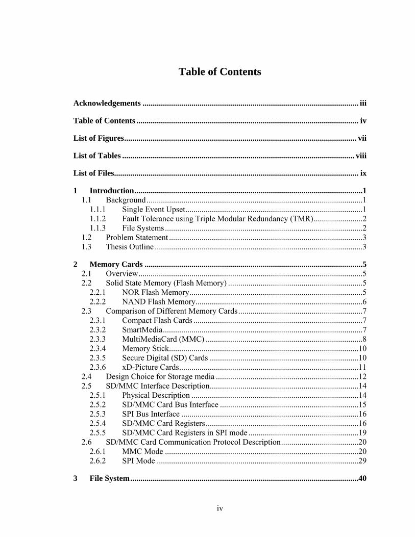
Table of Contents
Acknowledgements .......................................................................................................... iii
Table of Contents ............................................................................................................. iv
List of Figures.................................................................................................................. vii
List of Tables .................................................................................................................. viii
List of Files........................................................................................................................ ix
1 Introduction................................................................................................................1 1.1 Background..........................................................................................................1
1.1.1 Single Event Upset.......................................................................................1 1.1.2 Fault Tolerance using Triple Modular Redundancy (TMR)........................2 1.1.3 File Systems .................................................................................................2
1.2 Problem Statement ...............................................................................................3 1.3 Thesis Outline ......................................................................................................3
2 Memory Cards ...........................................................................................................5 2.1 Overview..............................................................................................................5 2.2 Solid State Memory (Flash Memory) ..................................................................5
2.2.1 NOR Flash Memory.....................................................................................5 2.2.2 NAND Flash Memory..................................................................................6
2.3 Comparison of Different Memory Cards.............................................................7 2.3.1 Compact Flash Cards ...................................................................................7 2.3.2 SmartMedia..................................................................................................7 2.3.3 MultiMediaCard (MMC) .............................................................................8 2.3.4 Memory Stick.............................................................................................10 2.3.5 Secure Digital (SD) Cards .........................................................................10 2.3.6 xD-Picture Cards........................................................................................11
2.4 Design Choice for Storage media ......................................................................12 2.5 SD/MMC Interface Description.........................................................................14
2.5.1 Physical Description ..................................................................................14 2.5.2 SD/MMC Card Bus Interface ....................................................................15 2.5.3 SPI Bus Interface .......................................................................................16 2.5.4 SD/MMC Card Registers...........................................................................16 2.5.5 SD/MMC Card Registers in SPI mode ......................................................19
2.6 SD/MMC Card Communication Protocol Description......................................20 2.6.1 MMC Mode ...............................................................................................20 2.6.2 SPI Mode ...................................................................................................29
3 File System................................................................................................................40
iv
3.1 Introduction........................................................................................................40 3.2 FAT (File Allocation Table) File System ..........................................................40
3.2.1 Introduction to FAT ...................................................................................40 3.2.2 Basic Terminologies ..................................................................................41 3.2.3 Comparison of Different FAT File Systems..............................................42
3.3 Understanding FAT16 .......................................................................................43 3.3.1 Boot Sector.................................................................................................44 3.3.2 File Allocation Tables (FAT).....................................................................45 3.3.3 Root Directory ...........................................................................................46 3.3.4 Data Region ...............................................................................................48
4 SD Card Based FAT16 Design for KySat ..............................................................49 4.1 Introduction........................................................................................................49 4.2 KySat..................................................................................................................49
4.2.1 Development Board ...................................................................................50 4.2.2 Integrated Development Environment.......................................................51
4.3 Software Design.................................................................................................51 4.4 File System Layers.............................................................................................53
4.4.1 SPI Layer ..................................................................................................54 4.4.2 SD/MMC Layer .........................................................................................55 4.4.3 Sector Server Layer....................................................................................58 4.4.4 File System Layer ......................................................................................60 4.4.5 Application (API) Layer ............................................................................62
5 Triple Modular Redundancy (TMR) Implementation.........................................65 5.1 Introduction........................................................................................................65 5.2 TMR for Data Read and Write...........................................................................65
5.2.1 Hidden FAT Chain Implementation ..........................................................66 5.2.2 Starting Clusters for Hidden FAT Chain ...................................................68
5.3 TMR for Sub Directories ...................................................................................69 5.4 TMR for MBR, BR, FAT Tables and Root Directory.......................................69
5.4.1 TMR for MBR and BR ..............................................................................70 5.4.2 TMR for FAT Tables .................................................................................70 5.4.3 TMR for Root Directory ............................................................................72
5.5 Deleting Hidden Chains and Files .....................................................................72 5.6 Additional Functions Written to Implement TMR ............................................72 5.7 Modularity..........................................................................................................74 5.8 Performance Overhead for Implementing TMR................................................74
5.8.1 Increase in Code Space ..............................................................................74 5.8.2 Increase in data Space................................................................................74 5.8.3 Increase in Response Time ........................................................................75
6 Testing.......................................................................................................................76 6.1 Introduction........................................................................................................76 6.2 Beagle SPI Sniffer..............................................................................................76 6.3 Testing Procedure ..............................................................................................79
6.3.1 Bandwidth Tests.........................................................................................79
v
6.3.2 Performance Tests......................................................................................80 6.3.3 Acceptance Tests .......................................................................................81 6.3.4 TMR Reliability Tests................................................................................81
6.4 Summary ............................................................................................................82
7 Conclusion ................................................................................................................83 7.1 Summary ............................................................................................................83 7.2 Future Directions ...............................................................................................83
References.........................................................................................................................85
Vita ....................................................................................................................................87
vi
List of Figures Figure 1: Compact Flash Cards........................................................................................... 7 Figure 2: SmartMedia Memory Card.................................................................................. 8 Figure 3: MultiMediaCard .................................................................................................. 8 Figure 4: Reduced Size MultiMediaCard (RS-MMC)........................................................ 9 Figure 5: MMC Plus Card with 13 pin interface ................................................................ 9 Figure 6: From Left to Right: Memory Stick, Memory Stick Duo with adapter, Memory Stick Micro with adapter................................................................................................... 10 Figure 7: SD Card, minSD Card and microSD card......................................................... 11 Figure 8: Olympus xD-Picture Card................................................................................. 12 Figure 9: SD/MMC Pin order ........................................................................................... 14 Figure 10: SD/MMC Card Block Diagram....................................................................... 15 Figure 11: R1 Response Format ....................................................................................... 37 Figure 12: Disk Structure.................................................................................................. 41 Figure 13: Visual Layout of a Typical FAT16 File System (Not to Scale)...................... 43 Figure 14: FAT Chain....................................................................................................... 46 Figure 15: Development Board and Flight Module.......................................................... 50 Figure 16: USB Mass Storage Reference Design Architecture ........................................ 52 Figure 17: File System Layers .......................................................................................... 53 Figure 18: File System Layers – Pie diagram comparing code space .............................. 53 Figure 19: USART Master and External slave in SPI mode [24]..................................... 54 Figure 20: Triple Modular Redundancy (TMR) Block diagram [3]................................. 65 Figure 21: FAT Chain....................................................................................................... 66 Figure 22: TMR Implementation using Hidden FAT Chain ............................................ 67 Figure 23: Visual Layout of a typical TMR FAT16 File System (Not to Scale).............. 71 Figure 24: Beagle SPI Sniffer settings.............................................................................. 76 Figure 25: Beagle Transaction window with Timing tab selected ................................... 77 Figure 26: Beagle MOSI/MISO Transaction tab .............................................................. 78 Figure 27: Beagle SPI Sniffer – Development Board interface........................................ 79 Figure 28: Change in Response Time with Varying SPI Clock Rate ............................... 80
vii
List of Tables Table 1: Comparison between NOR Flash memory and NAND Flash memory.................6 Table 2: Sandisk MultiMediaCards Environmental Specifications [11] ...........................12 Table 3: Pin Assignments for the SD/MMC......................................................................14 Table 4: SD/MMC Card Bus Description..........................................................................16 Table 5: SPI Bus Description.............................................................................................16 Table 6: Operating Conditions Register ............................................................................17 Table 7: Card Identification Register.................................................................................17 Table 8: Status Register Description..................................................................................18 Table 9: SD/MMC Card Registers in SPI mode................................................................20 Table 10: MMC Bus Command Definition .......................................................................20 Table 11: MMC Bus Command Definition .......................................................................20 Table 12: MMC Bus Command Descriptions [11]............................................................21 Table 13: Response R1 ......................................................................................................28 Table 14: Response R2 ......................................................................................................28 Table 15: Response R3 ......................................................................................................29 Table 16: SPI Bus Command Descriptions [11]................................................................30 Table 17: R1 Response ......................................................................................................37 Table 18: R2 Response ......................................................................................................38 Table 19: Boot Sector Structure.........................................................................................44 Table 20: FAT Table Entries .............................................................................................45 Table 21: Directory Entry ..................................................................................................47 Table 22: File Attribute......................................................................................................47 Table 23: BUS Pin Out for SPI Channel ...........................................................................50 Table 24: SPI Layer Functions Description.......................................................................55 Table 25: Sector Server Layer Functions Description.......................................................59 Table 26: File System Layer Functions Description..........................................................60 Table 27: Directory Entry for a File ..................................................................................68 Table 28: Comparison of increase in code space...............................................................74 Table 29: Comparison of increase in data space................................................................75
viii

ix
List of Files NVFSSL.pdf ............................................................................................................. 1.4 MB
1 Introduction
1.1 Background
Advancement in Flash Memories has resulted in packing several Giga Bytes of memory
into tiny memory cards. These memory Cards have small form factor, very light weight,
and consume less power. Hence most of the portable electronic devices use these Cards
as preferred storage media. Secure Digital (SD) Cards are used for storing images on
cameras, and audio files on hand held mp3 players.
Using SD cards for space applications is an attractive option, because of their light
weight and low power consumption. A typical satellite requires extended memory for the
storage of images and audio files along with other safety critical information. It is always
convenient to use Commercial Off the Shelf (COTS) Memory Cards for these kind of
applications. But outer space is a harsh environment for electronics and Commercial SD
Cards are not space-rated.
Extensive research is being carried out to study the effects of radiation on electronics [1].
Radiation effects in space may induce errors in electronic devices and circuits that can
lead to abnormalities in critical space craft modules. Such effects have been observed in
the past like in Voyager – 1 and Hubble Space Telescope [2]. Radiation in space can arise
from sources such as cosmic rays, the Van Allen radiation belts, solar phenomena etc.
1.1.1 Single Event Upset
Radiation effect on electronics result in a phenomenon called Single Event Upset (SEU),
identified as a change in state occurring when a high energy particle collides against a
sensitive node of an electronic device [3]. These changes in voltage levels can result in
potentially destructive events such as latch-ups. As the density of electronic chips
increases, their susceptibility to SEUs increases.
The industry solution for SEUs is radiation hardening. These radiation hardened devices
are usually derived from similar commercial versions with underlying difference
1
primarily in the manufacturing technology or in the implementation of redundant
hardware to counter SEUs. The disadvantages of using such radiation-hardened devices
are increase in power consumption and reduced effective chip density. Most importantly
these radiation-hardened devices are more expensive compared to their commercial
counterpart.
The application of this work is in determining the feasibility of using COTS SD Cards for
space applications. Although the associated benefits of COTS SD Cards make them an
attractive option their susceptibility to SEUs requires implementing Fault recovery
mechanisms to make them reliable.
1.1.2 Fault Tolerance using Triple Modular Redundancy (TMR)
Fault Tolerance is the property that enables a system to continue operating properly in the
event of a failure in some of its components. Fault Tolerant software ensures system
reliability by using protective redundancy at the software level. There are different ways
of implementing Fault Tolerance for system.
Triple Modular Redundancy (TMR) is one simple way of implementing Fault Tolerance
using redundancy [4]. A TMR system consists of three redundant copies of information.
A voter module compares the three copies and the select the value of majority. The TMR
system is therefore designed to tolerate the failure of any single copy by only producing
output on which at least two modules agree.
1.1.3 File Systems
File Systems are required to organize data on a storage media. They provide an easy
means to save, organize and retrieve data in the form of Files. Also File Systems hide the
underlying hardware from the user and provide easy to use Application Programming
Interface (API) to access the physical media.
There are different types of File Systems developed over time. Most Operating Systems
come with their own File System. Commercial File Systems used for embedded
applications tend to comply by one of these standard File Systems for easy portability [5].
2
This enables the files Created using the embedded File System to be viewed in other
Operating Systems which comply by this standard File System and vice versa. Microsoft
FAT16 is one such File System popularly used for storage media of size less than 2GB.
The present work is intended to develop a FAT16 compliant File System for space
applications to use with COTS SD Cards. As the COTS SD Cards are susceptible to
SEUs the proposed File System should be Highly Reliable and Fault Tolerant. It should
be able to detect a fault and should have redundancy mechanisms to correct the faults in
case of any anomaly. The File System should be able to maintain three redundant copies
of all the data on the SD Card and should be able to vote on the best two copies in case of
any accidental fault. Also, the proposed File System should be layered and well
structured to provide a level of abstraction from the user.
1.2 Problem Statement
It is possible to develop a Fault Tolerant File System with Triple Modular Redundancy to
use it with the COTS SD Cards. The objective of such a File System should be to provide
all the features of a normal File System along with making it Reliable to accidental bit
flips. It will have features to detect an accidental bit flip, and will be able to self correct
any such anomaly.
The present work is focused on implementing such a Highly Reliable, Fault Tolerant,
FAT16 compliant SD Card based File System for space applications to use with small
satellites.
1.3 Thesis Outline
Chapter 2 of this thesis compares different Storage media and explains the reason for
choosing the SD Card as the preferred storage media for the present work. Also the
underlying communication protocol is explained. Chapter 3 gives a brief introduction to a
general File System, followed by a detailed description of Microsoft FAT16 based File
System. Chapter 4 gives a brief introduction to KySat, the development board and the
3
IDE used for the present work. Later section of the chapter explains the implementation
details of the SD Card based FAT16 File System for KySat, different software layers in
the FAT16 File System are explained. Chapter 5 describes the Reliability and Fault
Tolerant features implemented in the proposed FAT16 File System. The testing
methodology and results are explained in Chapter 6. Finally Chapter 7 summarizes the
thesis along with suggestions for future improvements.
4
2 Memory Cards
2.1 Overview
The first few sections of this chapter are intended to give basic introduction to different
types of Solid State Memories and Memory Cards. The later part of the chapter deals
more with the SD and MultiMediaCards (MMC) in detail, their interface standards and
communication protocols. Special emphasis is given on SD/MMC based SPI mode of
communication as it is the Communication Protocol used in the present work.
2.2 Solid State Memory (Flash Memory)
Flash memory is a type of non-volatile memory, i.e., it can retain stored information even
when it is not powered. This ability to retain stored information is key for its usage as
portable storage media. Flash memory can be electrically programmed and erased. Flash
memory was invented by Dr. Fujio Masuoka while working for Toshiba in 1984 [6].
Flash memory has emerged as a compact, cost-effective, and reliable form of storage
media in everyday consumer electronics and portable devices. There are two types of
Flash memory, the NOR Flash memory and the NAND Flash memory.
2.2.1 NOR Flash Memory
NOR is named after the specific data mapping technology (Not OR) used in its
implementation. The individual memory cells in NOR memory are connected in parallel
which provides high speed random access capability, i.e. being able to read from specific
locations in the memory with out having to access in the sequential mode. Unlike NAND
Flash NOR Flash can access data as small as a single Byte [7].
Because of the random access feature, NOR Flash is ideal for low density, high speed
random read applications like to store BIOS programs in personal computers, in cellular
phones to store the phones operating system etc.
5
2.2.2 NAND Flash Memory
NAND technology is invented after NOR and is named after the specific data mapping
technology used (Not AND) similar to NOR. NAND Flash is developed as an alternative
for high density storage media, forgoing the random access feature as a tradeoff to give
way for smaller chip size and lower cost per bit. The NAND memory is implemented by
connecting an array of eight memory transistors in series [8].
The NAND Flash’s high density and smaller cell size, enables faster write and erase in
blocks. Hence NAND memory is ideal for low cost, high density, high speed
program/erase applications like data storage applications. NAND memory is used in
almost all types of MultiMediaCards, USB Flash storage devices etc.
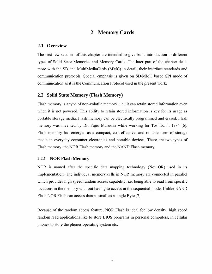
Table 1: Comparison between NOR Flash memory and NAND Flash memory
Design Characteristics NOR Memory NAND Memory
Cost Per Bit High Low
Random Byte Level Access Yes No
Page Mode Access No Yes
Active Power Medium Low
Standby Power Low Medium
Memory Density Low High
Read Speed High Medium
Write Speed Low High
Erase Speed Low High
Code Execution Easy Hard
File Storage Hard Easy
Typical uses
Cell Phones, BIOS
Storage, Code
memory etc
Digital Cameras, MP3
Players, Multimedia
Applications
6
2.3 Comparison of Different Memory Cards
There are a variety of Flash memory based Memory Cards available in the market with
different form factors and interface standards. Most of them are backed by various
associations with industry players as Board of Members. The next sections of this topic
are to do a quick study of different Memory Cards available in the market.
2.3.1 Compact Flash Cards
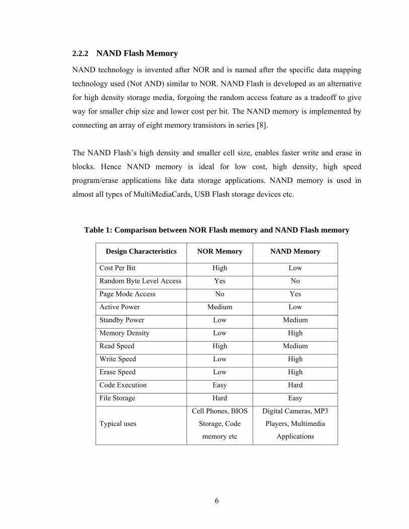
Compact Flash Cards are promoted by the Compact Flash Association (CFA) established
in October, 1995 [9]. The Board of Members for this association are Cannon, Lexar
Media, Sandisk, and Socket Communications.
Figure 1: Compact Flash Cards
There are two types of Compact Flash Cards, Type I and Type II, with dimensions of
43x36x3.3mm and 43x36x5mm respectively. Compact Flash Cards are thicker compared
to other memory cards because of the PCMCIA type interface used.
2.3.2 SmartMedia
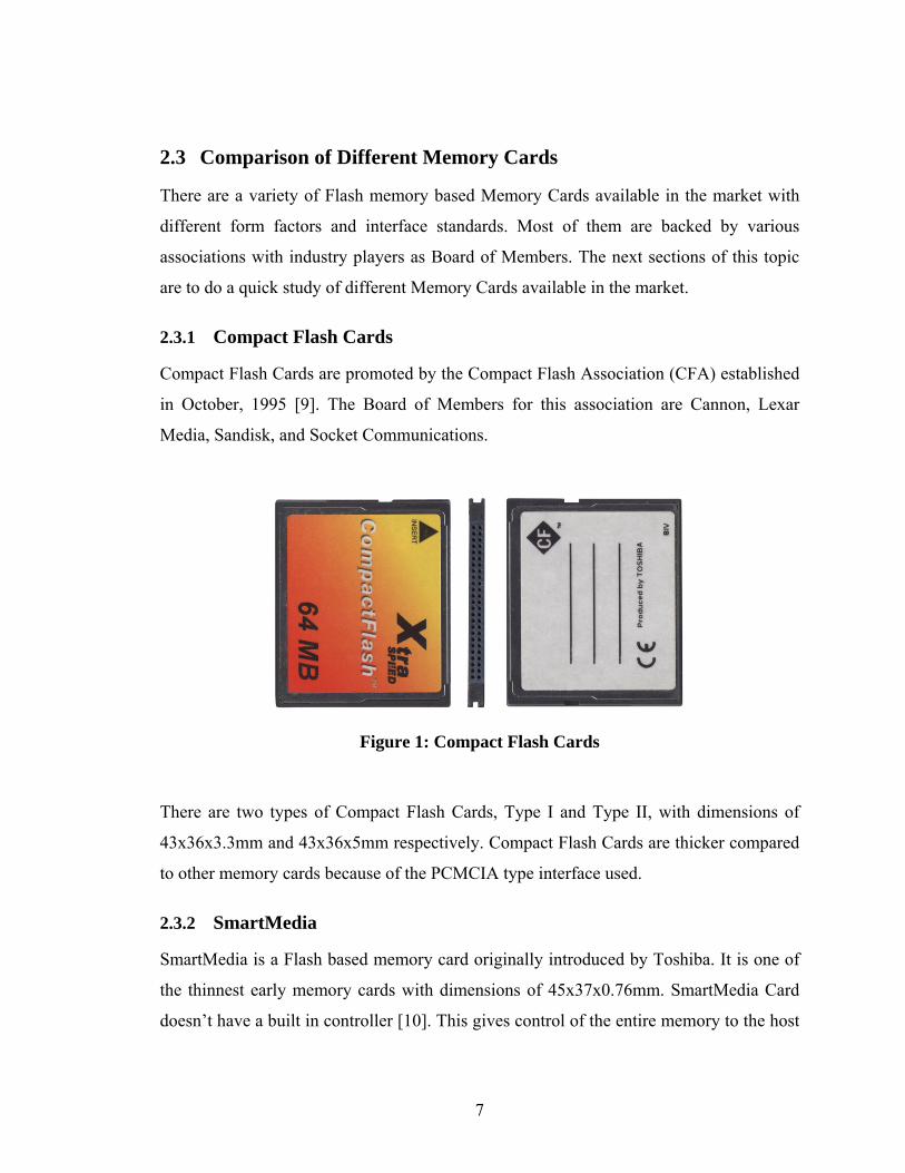
SmartMedia is a Flash based memory card originally introduced by Toshiba. It is one of
the thinnest early memory cards with dimensions of 45x37x0.76mm. SmartMedia Card
doesn’t have a built in controller [10]. This gives control of the entire memory to the host
7
firmware without having a proprietary interface layer. But the drawback of this is that
premature wear out of sectors can’t be avoided (wear-levelling).
Figure 2: SmartMedia Memory Card
2.3.3 MultiMediaCard (MMC)
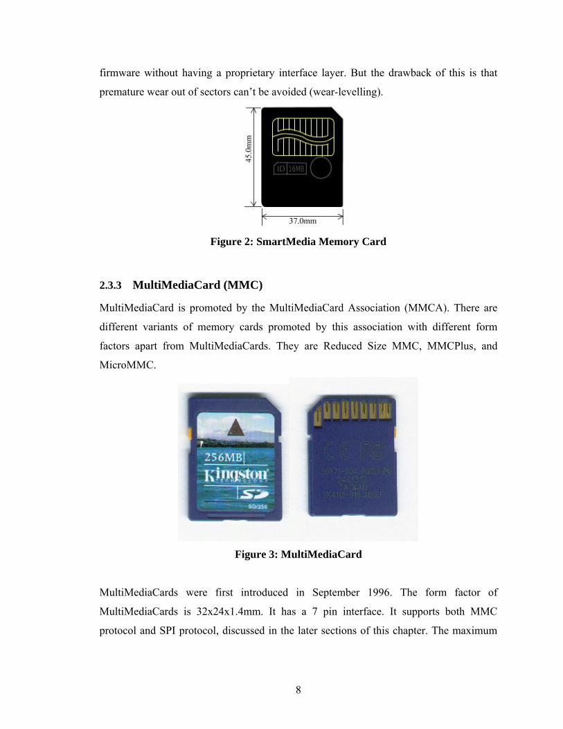
MultiMediaCard is promoted by the MultiMediaCard Association (MMCA). There are
different variants of memory cards promoted by this association with different form
factors apart from MultiMediaCards. They are Reduced Size MMC, MMCPlus, and
MicroMMC.
Figure 3: MultiMediaCard
MultiMediaCards were first introduced in September 1996. The form factor of
MultiMediaCards is 32x24x1.4mm. It has a 7 pin interface. It supports both MMC
protocol and SPI protocol, discussed in the later sections of this chapter. The maximum
8
speed supported by this MultiMediaCards is 20Mbits/Sec [11]. MultiMediaCards can be
used in Secured Digital (SD) slots also.
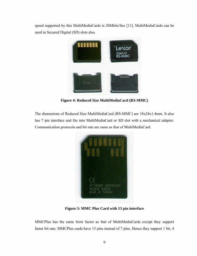
Figure 4: Reduced Size MultiMediaCard (RS-MMC)
The dimensions of Reduced Size MultiMediaCard (RS-MMC) are 18x24x1.4mm. It also
has 7 pin interface and fits into MultiMediaCard or SD slot with a mechanical adapter.
Communication protocols and bit rate are same as that of MultiMediaCard.
Figure 5: MMC Plus Card with 13 pin interface
MMCPlus has the same form factor as that of MultiMediaCards except they support
faster bit rate. MMCPlus cards have 13 pins instead of 7 pins. Hence they support 1 bit, 4
9
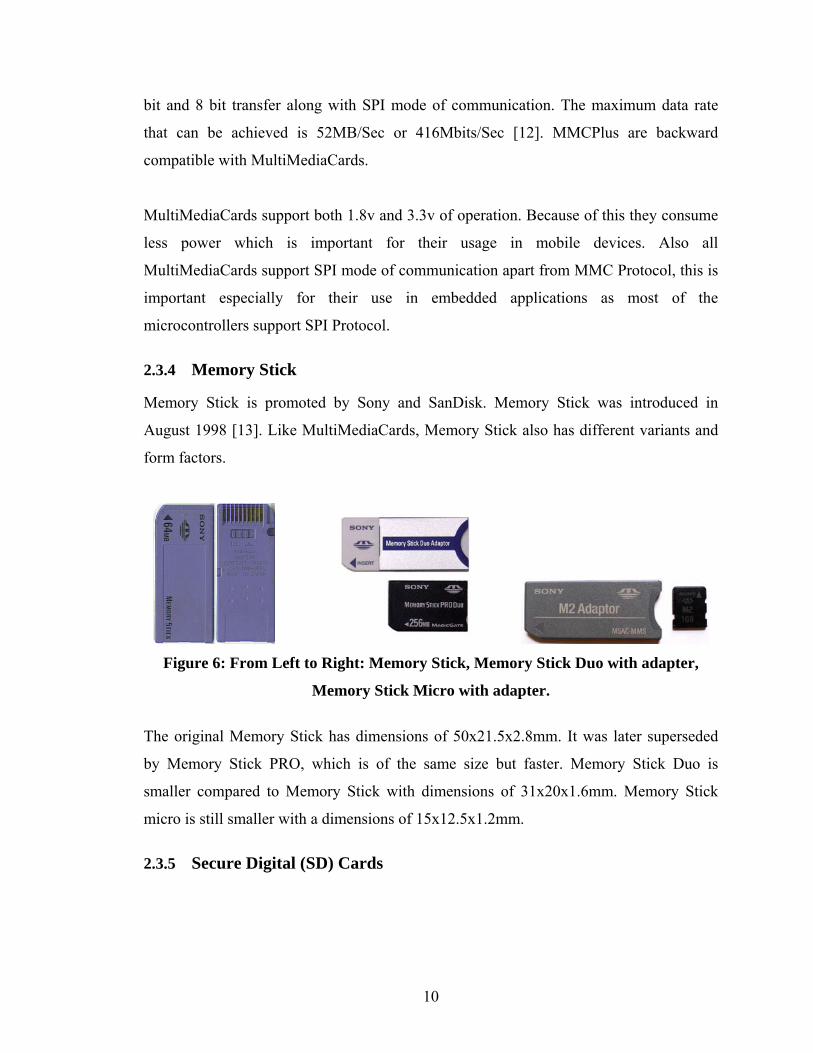
bit and 8 bit transfer along with SPI mode of communication. The maximum data rate
that can be achieved is 52MB/Sec or 416Mbits/Sec [12]. MMCPlus are backward
compatible with MultiMediaCards.
MultiMediaCards support both 1.8v and 3.3v of operation. Because of this they consume
less power which is important for their usage in mobile devices. Also all
MultiMediaCards support SPI mode of communication apart from MMC Protocol, this is
important especially for their use in embedded applications as most of the
microcontrollers support SPI Protocol.
2.3.4 Memory Stick
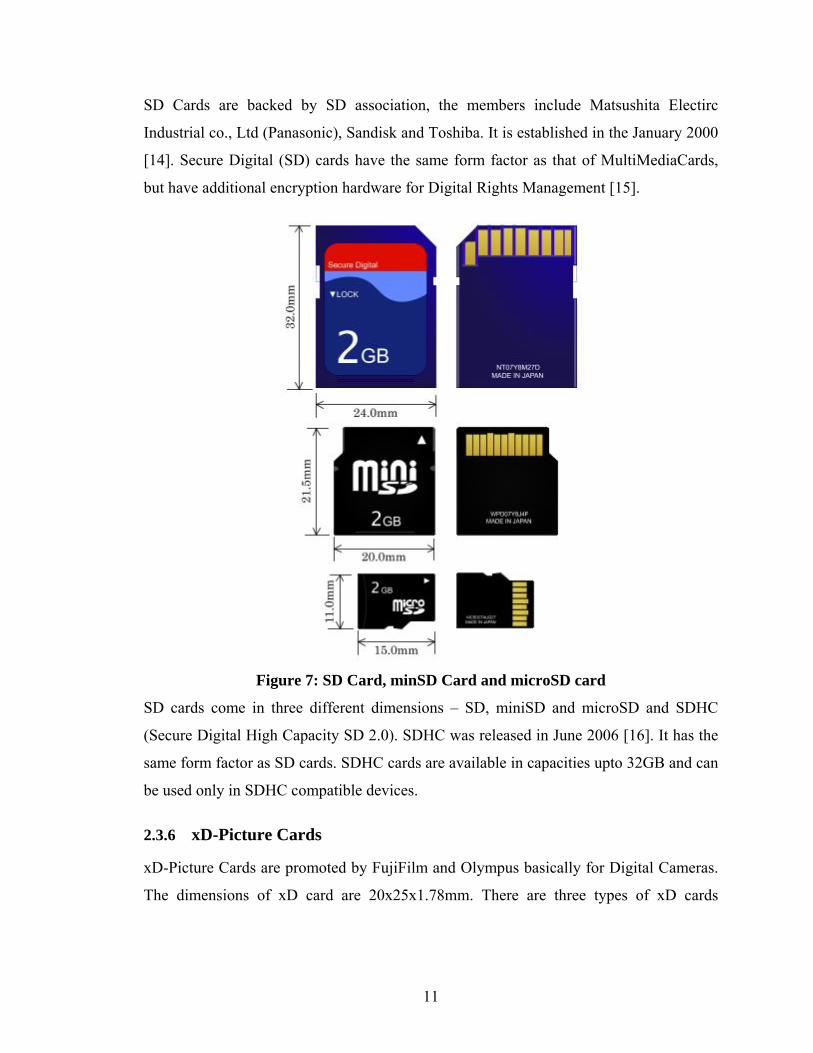
Memory Stick is promoted by Sony and SanDisk. Memory Stick was introduced in
August 1998 [13]. Like MultiMediaCards, Memory Stick also has different variants and
form factors.
Figure 6: From Left to Right: Memory Stick, Memory Stick Duo with adapter,
Memory Stick Micro with adapter.
The original Memory Stick has dimensions of 50x21.5x2.8mm. It was later superseded
by Memory Stick PRO, which is of the same size but faster. Memory Stick Duo is
smaller compared to Memory Stick with dimensions of 31x20x1.6mm. Memory Stick
micro is still smaller with a dimensions of 15x12.5x1.2mm.
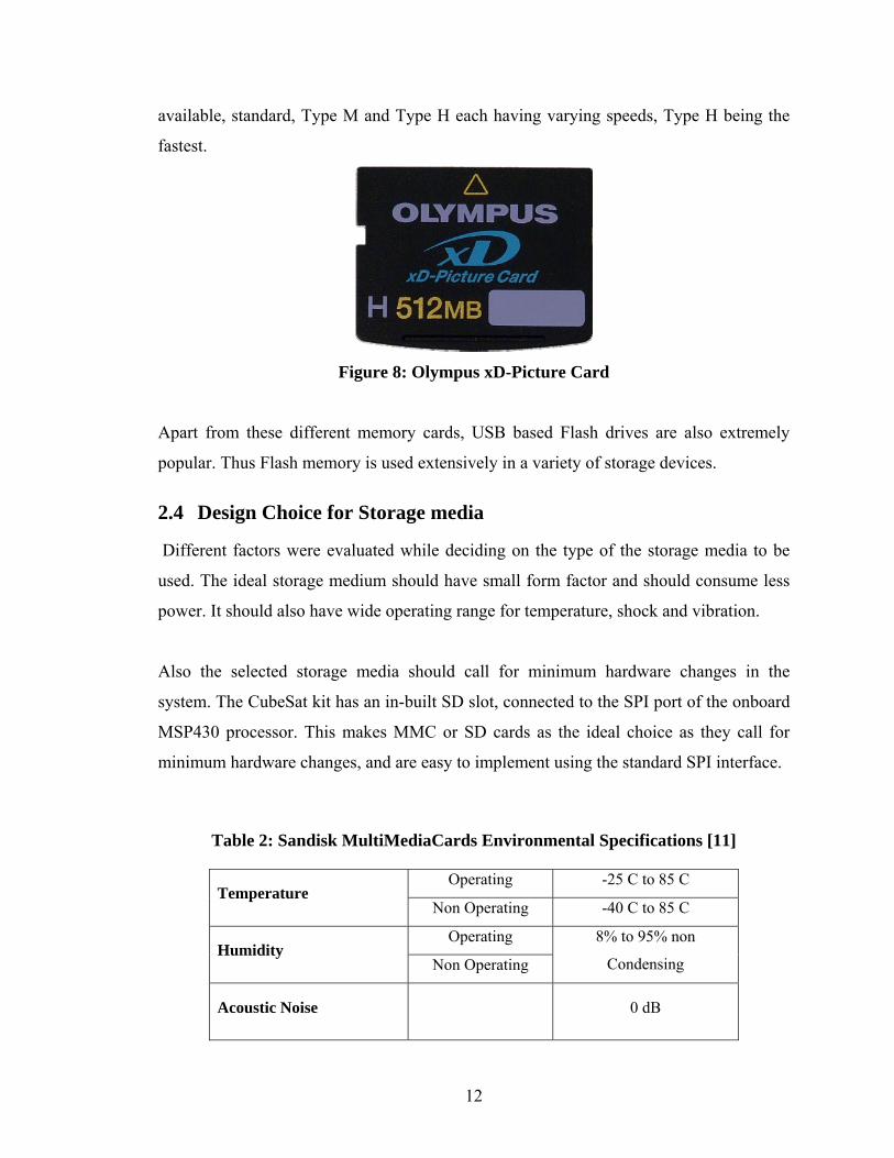
2.3.5 Secure Digital (SD) Cards
10
SD Cards are backed by SD association, the members include Matsushita Electirc
Industrial co., Ltd (Panasonic), Sandisk and Toshiba. It is established in the January 2000
[14]. Secure Digital (SD) cards have the same form factor as that of MultiMediaCards,
but have additional encryption hardware for Digital Rights Management [15].
Figure 7: SD Card, minSD Card and microSD card
SD cards come in three different dimensions – SD, miniSD and microSD and SDHC
(Secure Digital High Capacity SD 2.0). SDHC was released in June 2006 [16]. It has the
same form factor as SD cards. SDHC cards are available in capacities upto 32GB and can
be used only in SDHC compatible devices.
2.3.6 xD-Picture Cards
xD-Picture Cards are promoted by FujiFilm and Olympus basically for Digital Cameras.
The dimensions of xD card are 20x25x1.78mm. There are three types of xD cards
11
available, standard, Type M and Type H each having varying speeds, Type H being the
fastest.
Figure 8: Olympus xD-Picture Card
Apart from these different memory cards, USB based Flash drives are also extremely
popular. Thus Flash memory is used extensively in a variety of storage devices.
2.4 Design Choice for Storage media
Different factors were evaluated while deciding on the type of the storage media to be
used. The ideal storage medium should have small form factor and should consume less
power. It should also have wide operating range for temperature, shock and vibration.
Also the selected storage media should call for minimum hardware changes in the
system. The CubeSat kit has an in-built SD slot, connected to the SPI port of the onboard
MSP430 processor. This makes MMC or SD cards as the ideal choice as they call for
minimum hardware changes, and are easy to implement using the standard SPI interface.
Table 2: Sandisk MultiMediaCards Environmental Specifications [11]
Operating -25 C to 85 C Temperature
Non Operating -40 C to 85 C
Operating Humidity
Non Operating
8% to 95% non
Condensing
Acoustic Noise 0 dB
12
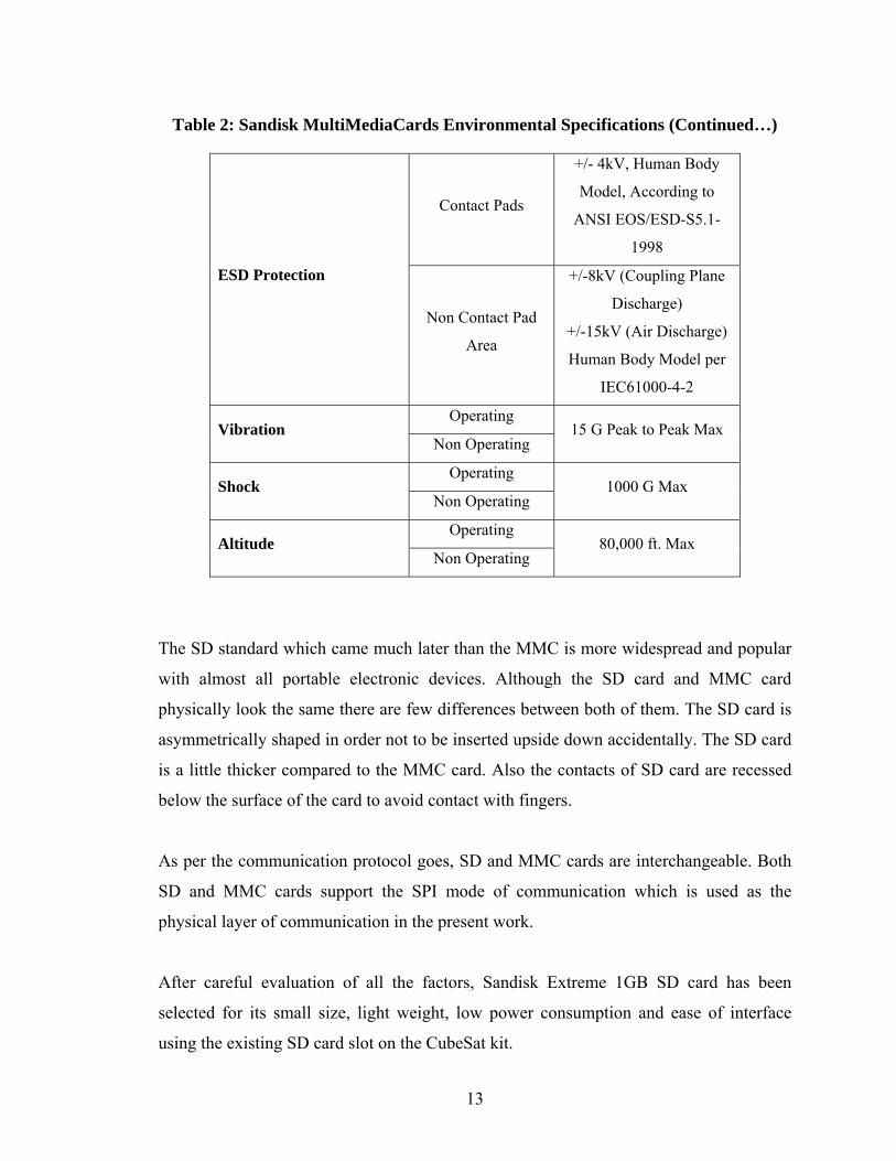
Table 2: Sandisk MultiMediaCards Environmental Specifications (Continued…)
Contact Pads
+/- 4kV, Human Body
Model, According to
ANSI EOS/ESD-S5.1-
1998
ESD Protection
Non Contact Pad
Area
+/-8kV (Coupling Plane
Discharge)
+/-15kV (Air Discharge)
Human Body Model per
IEC61000-4-2
Operating Vibration
Non Operating 15 G Peak to Peak Max
Operating Shock
Non Operating 1000 G Max
Operating Altitude
Non Operating 80,000 ft. Max
The SD standard which came much later than the MMC is more widespread and popular
with almost all portable electronic devices. Although the SD card and MMC card
physically look the same there are few differences between both of them. The SD card is
asymmetrically shaped in order not to be inserted upside down accidentally. The SD card
is a little thicker compared to the MMC card. Also the contacts of SD card are recessed
below the surface of the card to avoid contact with fingers.
As per the communication protocol goes, SD and MMC cards are interchangeable. Both
SD and MMC cards support the SPI mode of communication which is used as the
physical layer of communication in the present work.
After careful evaluation of all the factors, Sandisk Extreme 1GB SD card has been
selected for its small size, light weight, low power consumption and ease of interface
using the existing SD card slot on the CubeSat kit.
13
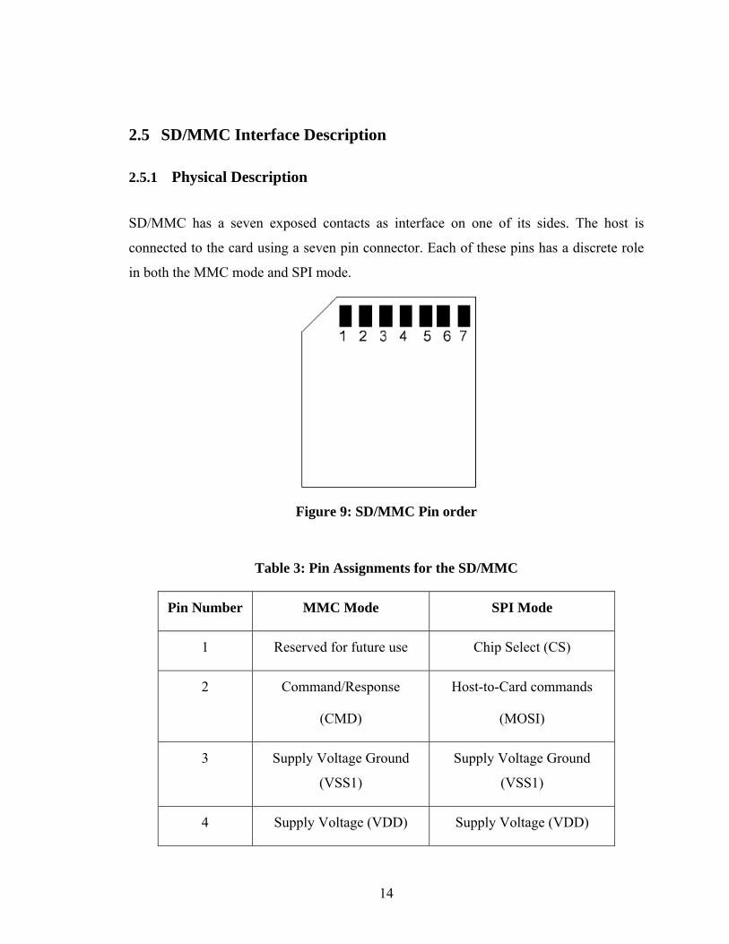
2.5 SD/MMC Interface Description
2.5.1 Physical Description
SD/MMC has a seven exposed contacts as interface on one of its sides. The host is
connected to the card using a seven pin connector. Each of these pins has a discrete role
in both the MMC mode and SPI mode.
Figure 9: SD/MMC Pin order
Table 3: Pin Assignments for the SD/MMC
Pin Number MMC Mode SPI Mode
1 Reserved for future use Chip Select (CS)
2 Command/Response
(CMD)
Host-to-Card commands
(MOSI)
3 Supply Voltage Ground
(VSS1)
Supply Voltage Ground
(VSS1)
4 Supply Voltage (VDD) Supply Voltage (VDD)
14
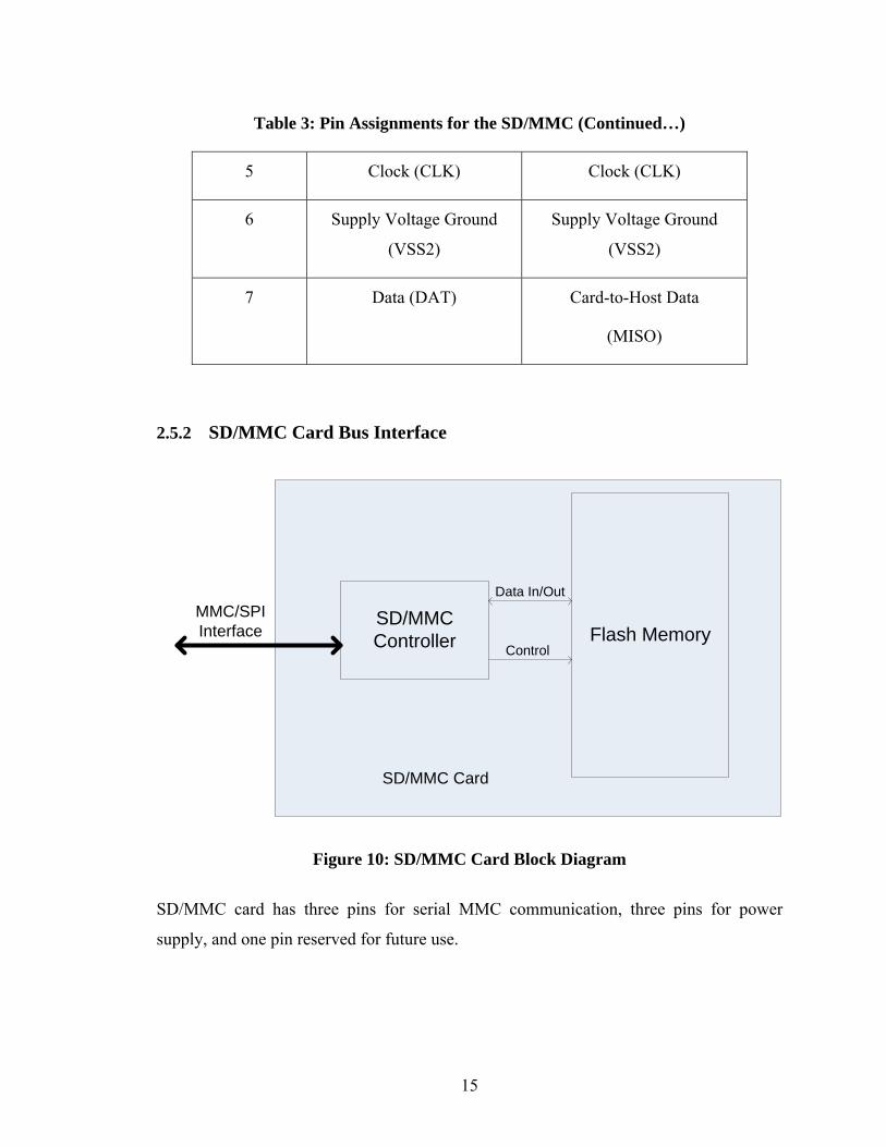
Table 3: Pin Assignments for the SD/MMC (Continued…)
5 Clock (CLK) Clock (CLK)
6 Supply Voltage Ground
(VSS2)
Supply Voltage Ground
(VSS2)
7 Data (DAT) Card-to-Host Data
(MISO)
2.5.2 SD/MMC Card Bus Interface
SD/MMCController Flash Memory
Data In/Out
Control
SD/MMC Card
MMC/SPI Interface
Figure 10: SD/MMC Card Block Diagram
SD/MMC card has three pins for serial MMC communication, three pins for power
supply, and one pin reserved for future use.
15
Table 4: SD/MMC Card Bus Description
Name Pin number Description
CMD 2 Command line, bi-directional signal.
DAT 7 Data line, bi-directional signal.
CLK 5 Clock line, host to card signal.
VDD 4 Power supply line
VSS 3,6 Supply Ground line
In MMC mode the SD/MMC Card works with a wide section of commands which are
explained in detail in the later sections of the chapter.
2.5.3 SPI Bus Interface
SD/MMC Card also supports SPI communication protocol compatible with SPI
supporting hosts. SPI (Serial Peripheral Interface) is a four line communication protocol.
Table 5: SPI Bus Description
Name Pin number Description
CS 1 Chip Select, Host to Card
CLK 5 Clock Signal, Host to Card
MOSI 2 SPI Master Out Slave In
MISO 7 SPI Master In Slave Out
In SPI mode, the card uses a subset of SD/MMC Card protocol and command subset,
discussed in the later sections of the chapter.
2.5.4 SD/MMC Card Registers
The SD/MMC Card has six set of Card Specific Registers. The Operating Conditions
Register (OCR), Card Identification Register (CIR), Card Specific Data Register (CSD)
carries the card configuration information. The Relative Card Address Register (RCA)
holds the card relative communication address for the current session.
Operating Conditions Register (OCR)
16
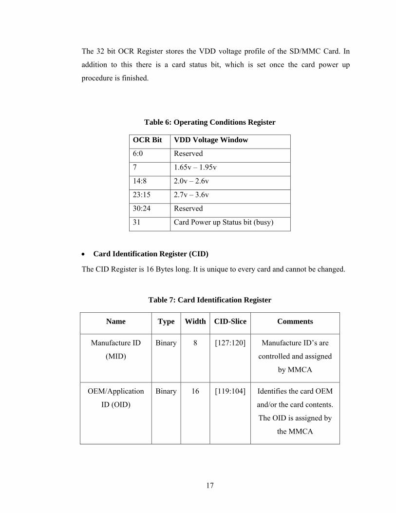
The 32 bit OCR Register stores the VDD voltage profile of the SD/MMC Card. In
addition to this there is a card status bit, which is set once the card power up
procedure is finished.
Table 6: Operating Conditions Register
OCR Bit VDD Voltage Window
6:0 Reserved
7 1.65v – 1.95v
14:8 2.0v – 2.6v
23:15 2.7v – 3.6v
30:24 Reserved
31 Card Power up Status bit (busy)
Card Identification Register (CID)
The CID Register is 16 Bytes long. It is unique to every card and cannot be changed.
Table 7: Card Identification Register
Name Type Width CID-Slice Comments
Manufacture ID
(MID)
Binary 8 [127:120] Manufacture ID’s are
controlled and assigned
by MMCA
OEM/Application
ID (OID)
Binary 16 [119:104] Identifies the card OEM
and/or the card contents.
The OID is assigned by
the MMCA
17
Table 7: Card Identification Register (Continued…)
Product Name
(PNM)
String 48 [103:56] Six ASCII characters long
Product Revision BCD 8 [55:48 Two binary coded
Serial Number
(PSN)
Binary 32 [47:16] 32-bit unsigned integer
Manufacturing date
code (MDT)
BCD 8 [15:8] Manufactured date
mm/yy
CRC7
checksum(CRC)
Binary 7 [7:1] Calculated
Not used, always
“1”
--- 1 [0:0] ---
Card Specific Data (CSD) Register
The CSD Register configuration information is required to access the card data. It
contains information about the card operating conditions. It is also 16 Bytes wide.
Status Register
The Status Register is 32-bit wide. It is used to represent status or error bits resulting
because of commands sent to the card.
Table 8: Status Register Description
Bit Description
31 Command argument out of range
30 Misaligned address
29 Transferred block length is not allowed for the card
28 Error in the sequence of erase commands occurred
18
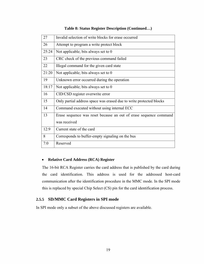
Table 8: Status Register Description (Continued…)
27 Invalid selection of write blocks for erase occurred
26 Attempt to program a write protect block
25:24 Not applicable; bits always set to 0
23 CRC check of the previous command failed
22 Illegal command for the given card state
21:20 Not applicable; bits always set to 0
19 Unknown error occurred during the operation
18:17 Not applicable; bits always set to 0
16 CID/CSD register overwrite error
15 Only partial address space was erased due to write protected blocks
14 Command executed without using internal ECC
13 Erase sequence was reset because an out of erase sequence command
was received
12:9 Current state of the card
8 Corresponds to buffer-empty signaling on the bus
7:0 Reserved
Relative Card Address (RCA) Register
The 16-bit RCA Register carries the card address that is published by the card during
the card identification. This address is used for the addressed host-card
communication after the identification procedure in the MMC mode. In the SPI mode
this is replaced by special Chip Select (CS) pin for the card identification process.
2.5.5 SD/MMC Card Registers in SPI mode
In SPI mode only a subset of the above discussed registers are available.
19
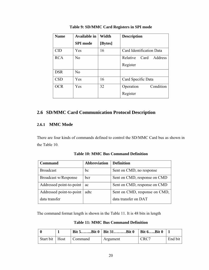
Table 9: SD/MMC Card Registers in SPI mode
Name Available in
SPI mode
Width
[Bytes]
Description
CID Yes 16 Card Identification Data
RCA No Relative Card Address
Register
DSR No
CSD Yes 16 Card Specific Data
OCR Yes 32 Operation Condition
Register
2.6 SD/MMC Card Communication Protocol Description
2.6.1 MMC Mode
There are four kinds of commands defined to control the SD/MMC Card bus as shown in
the Table 10.
Table 10: MMC Bus Command Definition
Command Abbreviation Definition
Broadcast bc Sent on CMD, no response
Broadcast w/Response bcr Sent on CMD, response on CMD
Addressed point-to-point ac Sent on CMD, response on CMD
Addressed point-to-point
data transfer
adtc Sent on CMD, response on CMD,
data transfer on DAT
The command format length is shown in the Table 11. It is 48 bits in length
Table 11: MMC Bus Command Definition
0 1 Bit 5……..Bit 0 Bit 31………Bit 0 Bit 6…..Bit 0 1
Start bit Host Command Argument CRC7 End bit
20
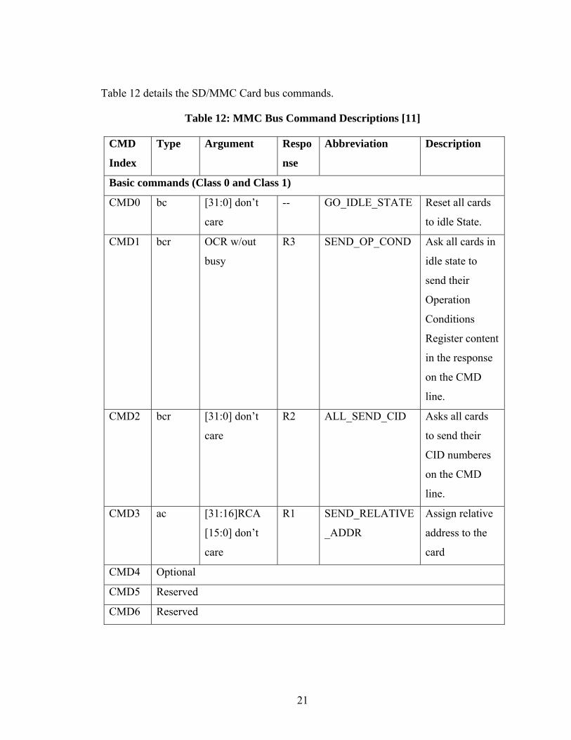
Table 12 details the SD/MMC Card bus commands.
Table 12: MMC Bus Command Descriptions [11]
CMD
Index
Type Argument Respo
nse
Abbreviation Description
Basic commands (Class 0 and Class 1)
CMD0 bc [31:0] don’t
care
-- GO_IDLE_STATE Reset all cards
to idle State.
CMD1 bcr OCR w/out
busy
R3 SEND_OP_COND Ask all cards in
idle state to
send their
Operation
Conditions
Register content
in the response
on the CMD
line.
CMD2 bcr [31:0] don’t
care
R2 ALL_SEND_CID Asks all cards
to send their
CID numberes
on the CMD
line.
CMD3 ac [31:16]RCA
[15:0] don’t
care
R1 SEND_RELATIVE
_ADDR
Assign relative
address to the
card
CMD4 Optional
CMD5 Reserved
CMD6 Reserved
21
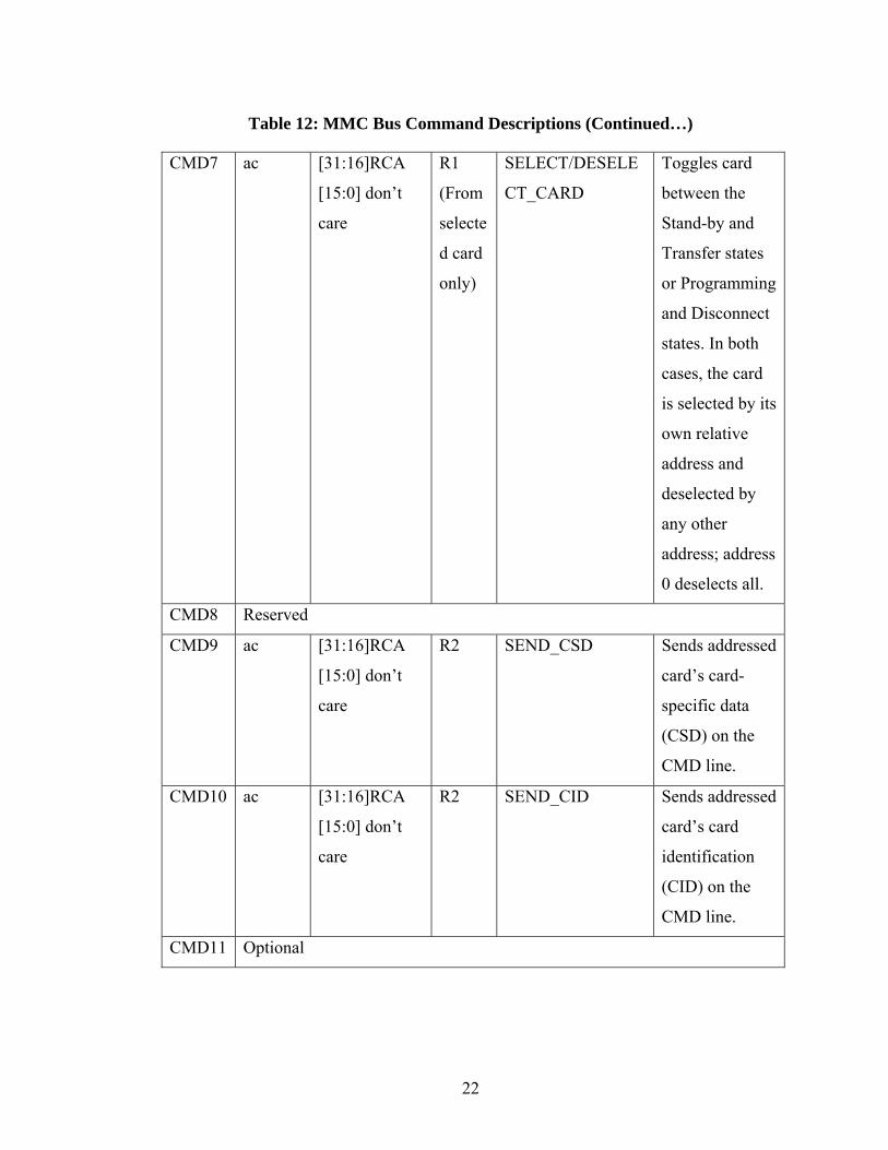
Table 12: MMC Bus Command Descriptions (Continued…)
CMD7 ac [31:16]RCA
[15:0] don’t
care
R1
(From
selecte
d card
only)
SELECT/DESELE
CT_CARD
Toggles card
between the
Stand-by and
Transfer states
or Programming
and Disconnect
states. In both
cases, the card
is selected by its
own relative
address and
deselected by
any other
address; address
0 deselects all.
CMD8 Reserved
CMD9 ac [31:16]RCA
[15:0] don’t
care
R2 SEND_CSD Sends addressed
card’s card-
specific data
(CSD) on the
CMD line.
CMD10 ac [31:16]RCA
[15:0] don’t
care
R2 SEND_CID Sends addressed
card’s card
identification
(CID) on the
CMD line.
CMD11 Optional
22
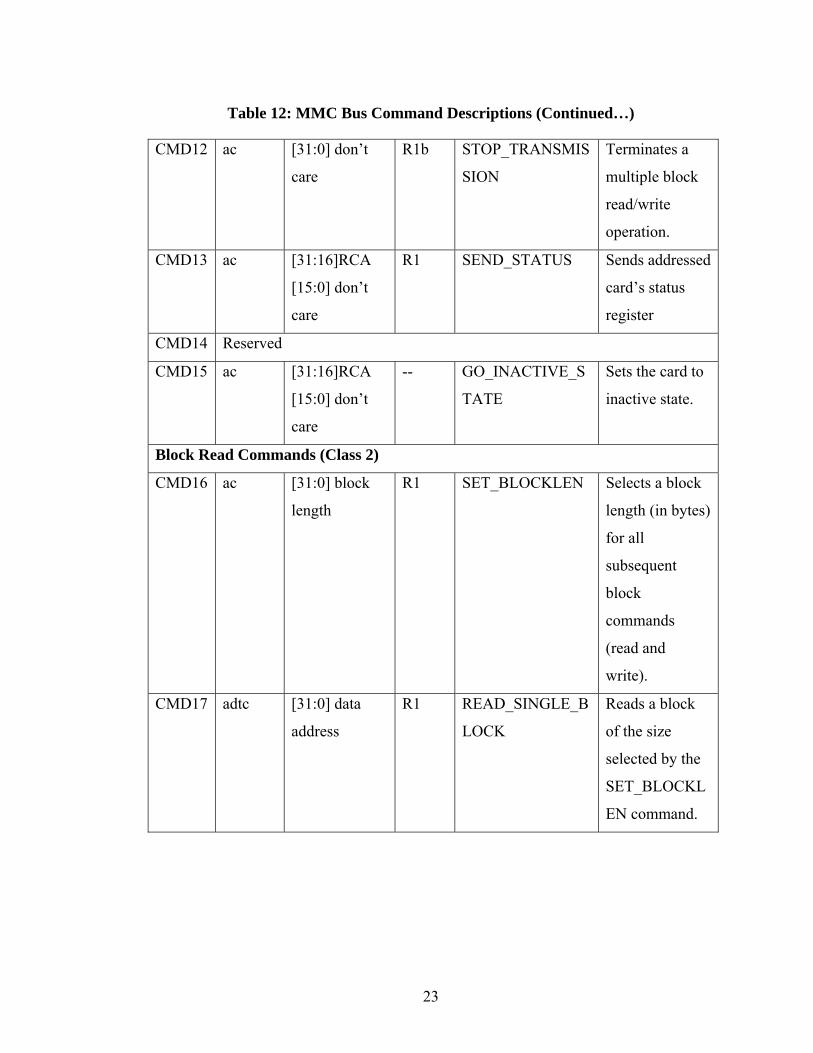
Table 12: MMC Bus Command Descriptions (Continued…)
CMD12 ac [31:0] don’t
care
R1b STOP_TRANSMIS
SION
Terminates a
multiple block
read/write
operation.
CMD13 ac [31:16]RCA
[15:0] don’t
care
R1 SEND_STATUS Sends addressed
card’s status
register
CMD14 Reserved
CMD15 ac [31:16]RCA
[15:0] don’t
care
-- GO_INACTIVE_S
TATE
Sets the card to
inactive state.
Block Read Commands (Class 2)
CMD16 ac [31:0] block
length
R1 SET_BLOCKLEN Selects a block
length (in bytes)
for all
subsequent
block
commands
(read and
write).
CMD17 adtc [31:0] data
address
R1 READ_SINGLE_B
LOCK
Reads a block
of the size
selected by the
SET_BLOCKL
EN command.
23
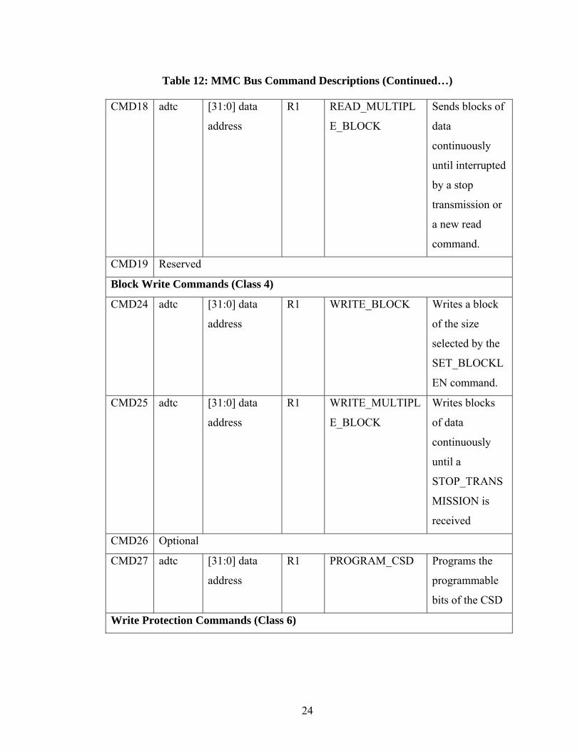
Table 12: MMC Bus Command Descriptions (Continued…)
CMD18 adtc [31:0] data
address
R1 READ_MULTIPL
E_BLOCK
Sends blocks of
data
continuously
until interrupted
by a stop
transmission or
a new read
command.
CMD19 Reserved
Block Write Commands (Class 4)
CMD24 adtc [31:0] data
address
R1 WRITE_BLOCK Writes a block
of the size
selected by the
SET_BLOCKL
EN command.
CMD25 adtc [31:0] data
address
R1 WRITE_MULTIPL
E_BLOCK
Writes blocks
of data
continuously
until a
STOP_TRANS
MISSION is
received
CMD26 Optional
CMD27 adtc [31:0] data
address
R1 PROGRAM_CSD Programs the
programmable
bits of the CSD
Write Protection Commands (Class 6)
24
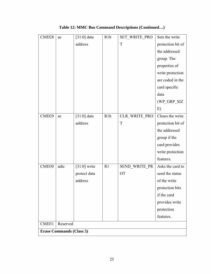
Table 12: MMC Bus Command Descriptions (Continued…)
CMD28 ac [31:0] data
address
R1b SET_WRITE_PRO
T
Sets the write
protection bit of
the addressed
group. The
properties of
write protection
are coded in the
card specific
data
(WP_GRP_SIZ
E)
CMD29 ac [31:0] data
address
R1b CLR_WRITE_PRO
T
Clears the write
protection bit of
the addressed
group if the
card provides
write protection
features.
CMD30 adtc [31:0] write
protect data
address
R1 SEND_WRITE_PR
OT
Asks the card to
send the status
of the write
protection bits
if the card
provides write
protection
features.
CMD31 Reserved
Erase Commands (Class 5)
25
Table 12: MMC Bus Command Descriptions (Continued…)
CMD32 ac [31:0] data
address
R1 TAG_SECTOR_ST
RAT
Sets the first
sectors address
of the erase
group
CMD33 ac [31:0] data
address
R1 TAG_SECTOR_E
ND
Sets the address
of the last sector
in a continuous
range within the
selected erase
group, or the
address of a
single sector to
be selected for
erase.
CMD34 ac [31:0] data
address
R1 UNTAG_SECTOR Removes one
previously
selected sector
from the erase
selection.
CMD35 ac [31:0] data
address
R1 TAG_ERASE_GR
OUP_START
Sets the address
of the last erase
group within a
range to be
selected for
erase.
26
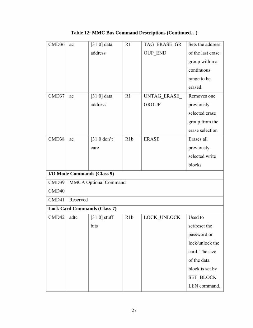
Table 12: MMC Bus Command Descriptions (Continued…)
CMD36 ac [31:0] data
address
R1 TAG_ERASE_GR
OUP_END
Sets the address
of the last erase
group within a
continuous
range to be
erased.
CMD37 ac [31:0] data
address
R1 UNTAG_ERASE_
GROUP
Removes one
previously
selected erase
group from the
erase selection
CMD38 ac [31:0 don’t
care
R1b ERASE Erases all
previously
selected write
blocks
I/O Mode Commands (Class 9)
CMD39
CMD40
MMCA Optional Command
CMD41 Reserved
Lock Card Commands (Class 7)
CMD42 adtc [31:0] stuff
bits
R1b LOCK_UNLOCK Used to
set/reset the
password or
lock/unlock the
card. The size
of the data
block is set by
SET_BLOCK_
LEN command.
27
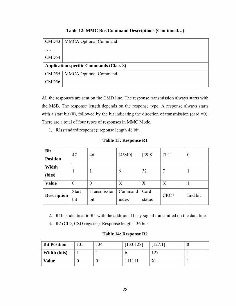
Table 12: MMC Bus Command Descriptions (Continued…)
CMD43
….
CMD54
MMCA Optional Command
Application specific Commands (Class 8)
CMD55
CMD56
MMCA Optional Command
All the responses are sent on the CMD line. The response transmission always starts with
the MSB. The response length depends on the response type. A response always starts
with a start bit (0), followed by the bit indicating the direction of transmission (card =0).
There are a total of four types of responses in MMC Mode.
1. R1(standard response): reponse length 48 bit.
Table 13: Response R1
Bit
Position 47 46 [45:40] [39:8] [7:1] 0
Width
(bits) 1 1 6 32 7 1
Value 0 0 X X X 1
Description Start
bit
Transmission
bit
Command
index
Card
status CRC7 End bit
2. R1b is identical to R1 with the additional busy signal transmitted on the data line.
3. R2 (CID, CSD register): Response length 136 bits
Table 14: Response R2
Bit Position 135 134 [133:128] [127:1] 0
Width (bits) 1 1 6 127 1
Value 0 0 111111 X 1
28
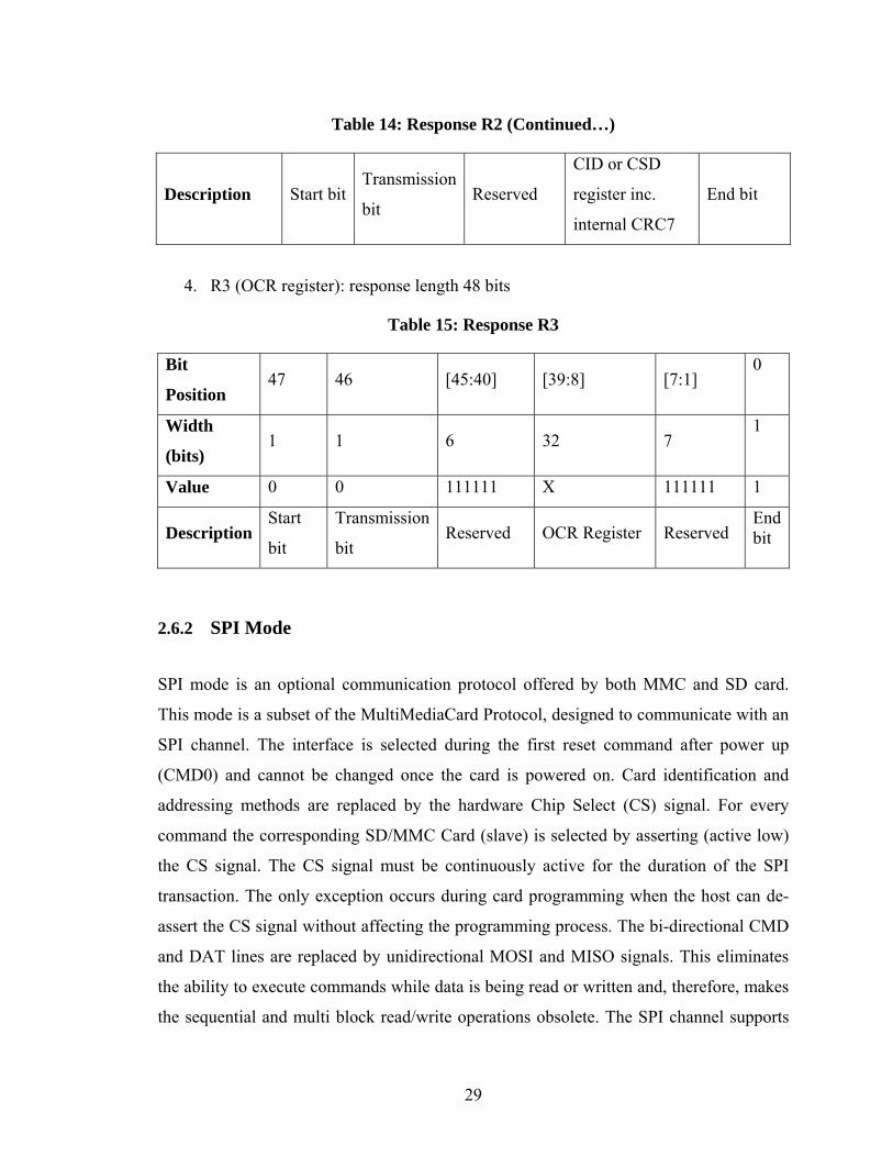
Table 14: Response R2 (Continued…)
Description Start bit Transmission
bit Reserved
CID or CSD
register inc.
internal CRC7
End bit
4. R3 (OCR register): response length 48 bits
Table 15: Response R3
Bit
Position 47 46 [45:40] [39:8] [7:1]
0
Width
(bits) 1 1 6 32 7
1
Value 0 0 111111 X 111111 1
Description Start
bit
Transmission
bit Reserved OCR Register Reserved
End bit
2.6.2 SPI Mode
SPI mode is an optional communication protocol offered by both MMC and SD card.
This mode is a subset of the MultiMediaCard Protocol, designed to communicate with an
SPI channel. The interface is selected during the first reset command after power up
(CMD0) and cannot be changed once the card is powered on. Card identification and
addressing methods are replaced by the hardware Chip Select (CS) signal. For every
command the corresponding SD/MMC Card (slave) is selected by asserting (active low)
the CS signal. The CS signal must be continuously active for the duration of the SPI
transaction. The only exception occurs during card programming when the host can de-
assert the CS signal without affecting the programming process. The bi-directional CMD
and DAT lines are replaced by unidirectional MOSI and MISO signals. This eliminates
the ability to execute commands while data is being read or written and, therefore, makes
the sequential and multi block read/write operations obsolete. The SPI channel supports
29
single block read/write commands only. The SPI interface uses the same seven signals as
the standard SD/MMC Card bus.
The advantage of the SPI mode is the capability of using an off-the-shelf host with SPI
channel, hence reducing the design effort to a minimum. The disadvantage is the loss of
performance with SPI mode as compared to MMC mode (lower data transfer rate, fewer
cards, hardware chip select per card, etc.) [11]
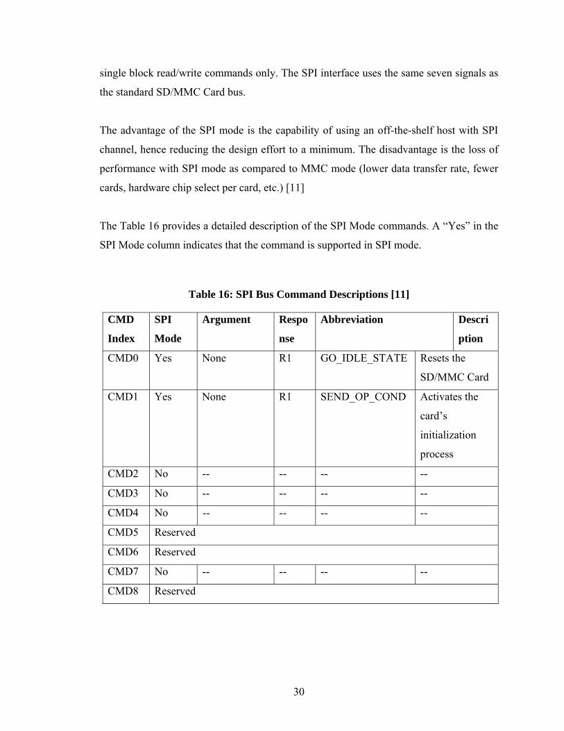
The Table 16 provides a detailed description of the SPI Mode commands. A “Yes” in the
SPI Mode column indicates that the command is supported in SPI mode.
Table 16: SPI Bus Command Descriptions [11]
CMD
Index
SPI
Mode
Argument Respo
nse
Abbreviation Descri
ption
CMD0 Yes None R1 GO_IDLE_STATE Resets the
SD/MMC Card
CMD1 Yes None R1 SEND_OP_COND Activates the
card’s
initialization
process
CMD2 No -- -- -- --
CMD3 No -- -- -- --
CMD4 No -- -- -- --
CMD5 Reserved
CMD6 Reserved
CMD7 No -- -- -- --
CMD8 Reserved
30
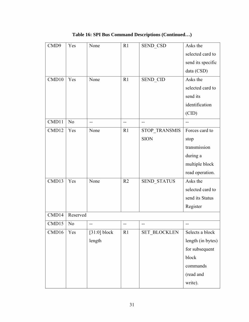
Table 16: SPI Bus Command Descriptions (Continued…)
CMD9 Yes None R1 SEND_CSD Asks the
selected card to
send its specific
data (CSD)
CMD10 Yes None R1 SEND_CID Asks the
selected card to
send its
identification
(CID)
CMD11 No -- -- -- --
CMD12 Yes None R1 STOP_TRANSMIS
SION
Forces card to
stop
transmission
during a
multiple block
read operation.
CMD13 Yes None R2 SEND_STATUS Asks the
selected card to
send its Status
Register
CMD14 Reserved
CMD15 No -- -- -- --
CMD16 Yes [31:0] block
length
R1 SET_BLOCKLEN Selects a block
length (in bytes)
for subsequent
block
commands
(read and
write).
31
Table 16: SPI Bus Command Descriptions (Continued…)
CMD17 Yes [31:0] data
address
R1 READ_SINGLE_B
LOCK
Reads a block
of the size
selected by the
SET_BLOCKL
EN command.
CMD18 Yes [31:0] data
address
R1 READ_MULTIPL
E_BLOCK
Sends blocks of
data
continuously
until interrupted
by a stop
transmission or
the requested
number of data
blocks
transmitted.
CMD19 Reserved
CMD24 Yes [31:0] data
address
R1 WRITE_BLOCK Writes a block
of the size
selected by the
SET_BLOCKL
EN command.
32
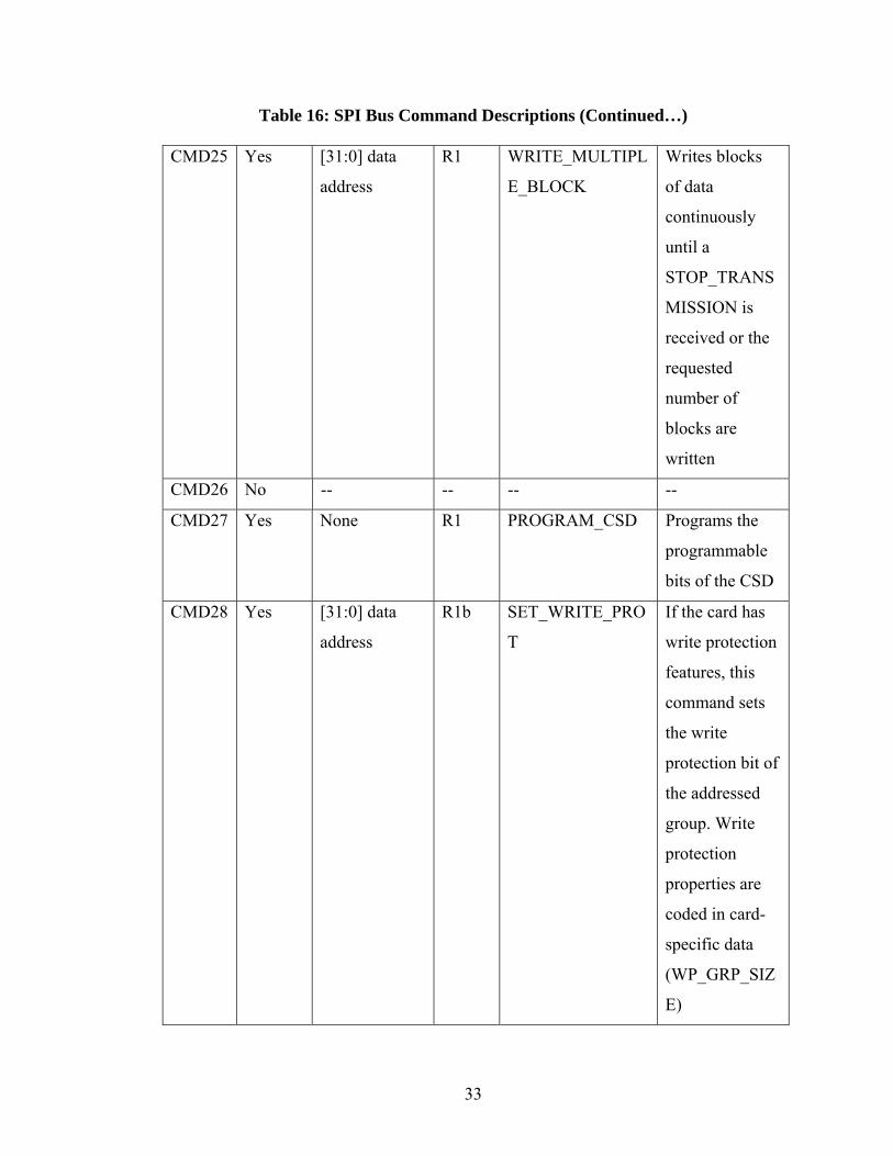
Table 16: SPI Bus Command Descriptions (Continued…)
CMD25 Yes [31:0] data
address
R1 WRITE_MULTIPL
E_BLOCK
Writes blocks
of data
continuously
until a
STOP_TRANS
MISSION is
received or the
requested
number of
blocks are
written
CMD26 No -- -- -- --
CMD27 Yes None R1 PROGRAM_CSD Programs the
programmable
bits of the CSD
CMD28 Yes [31:0] data
address
R1b SET_WRITE_PRO
T
If the card has
write protection
features, this
command sets
the write
protection bit of
the addressed
group. Write
protection
properties are
coded in card-
specific data
(WP_GRP_SIZ
E)
33
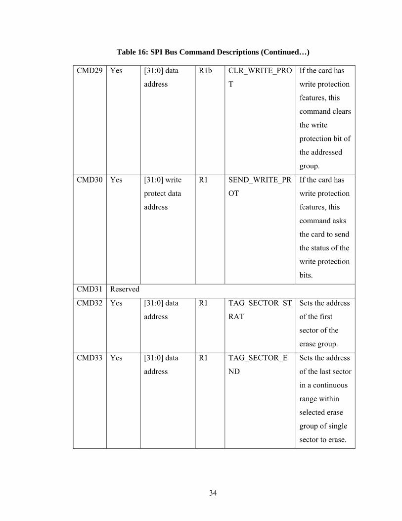
Table 16: SPI Bus Command Descriptions (Continued…)
CMD29 Yes [31:0] data
address
R1b CLR_WRITE_PRO
T
If the card has
write protection
features, this
command clears
the write
protection bit of
the addressed
group.
CMD30 Yes [31:0] write
protect data
address
R1 SEND_WRITE_PR
OT
If the card has
write protection
features, this
command asks
the card to send
the status of the
write protection
bits.
CMD31 Reserved
CMD32 Yes [31:0] data
address
R1 TAG_SECTOR_ST
RAT
Sets the address
of the first
sector of the
erase group.
CMD33 Yes [31:0] data
address
R1 TAG_SECTOR_E
ND
Sets the address
of the last sector
in a continuous
range within
selected erase
group of single
sector to erase.
34
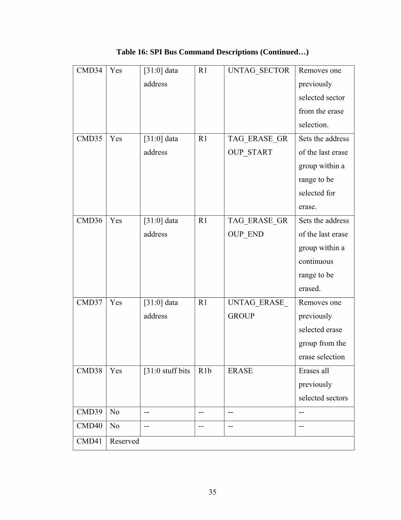
Table 16: SPI Bus Command Descriptions (Continued…)
CMD34 Yes [31:0] data
address
R1 UNTAG_SECTOR Removes one
previously
selected sector
from the erase
selection.
CMD35 Yes [31:0] data
address
R1 TAG_ERASE_GR
OUP_START
Sets the address
of the last erase
group within a
range to be
selected for
erase.
CMD36 Yes [31:0] data
address
R1 TAG_ERASE_GR
OUP_END
Sets the address
of the last erase
group within a
continuous
range to be
erased.
CMD37 Yes [31:0] data
address
R1 UNTAG_ERASE_
GROUP
Removes one
previously
selected erase
group from the
erase selection
CMD38 Yes [31:0 stuff bits R1b ERASE Erases all
previously
selected sectors
CMD39 No -- -- -- --
CMD40 No -- -- -- --
CMD41 Reserved
35
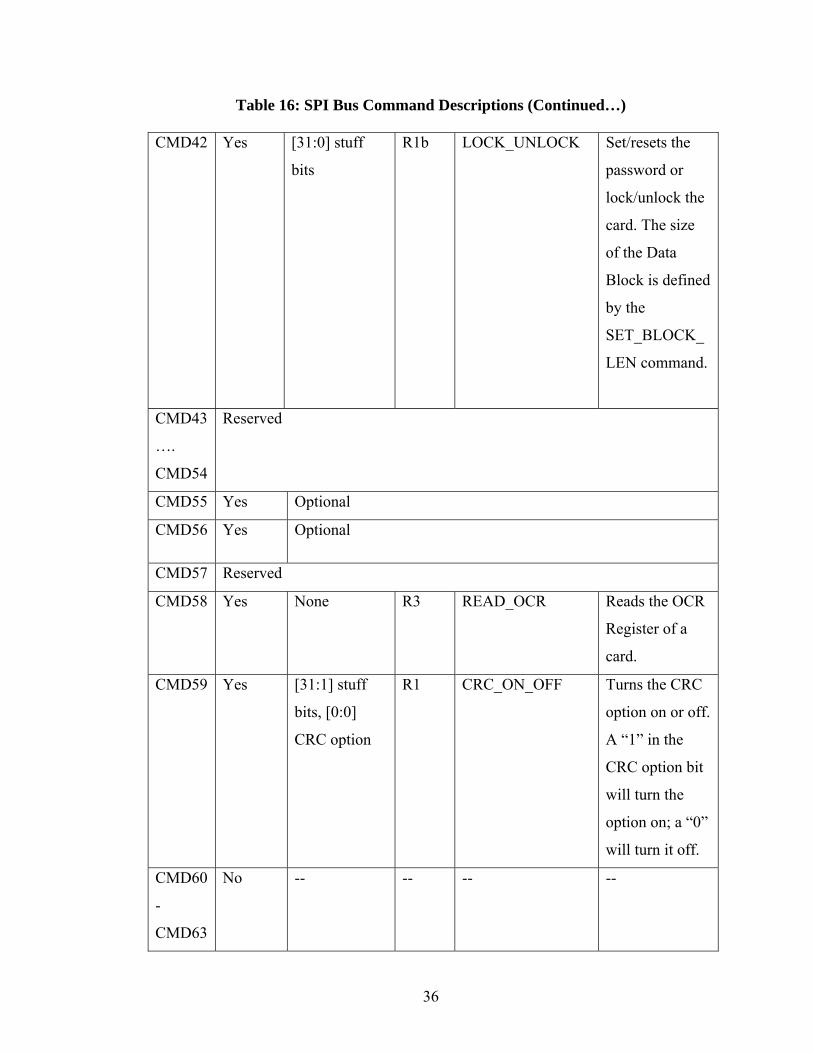
Table 16: SPI Bus Command Descriptions (Continued…)
CMD42 Yes [31:0] stuff
bits
R1b LOCK_UNLOCK Set/resets the
password or
lock/unlock the
card. The size
of the Data
Block is defined
by the
SET_BLOCK_
LEN command.
CMD43
….
CMD54
Reserved
CMD55 Yes Optional
CMD56 Yes Optional
CMD57 Reserved
CMD58 Yes None R3 READ_OCR Reads the OCR
Register of a
card.
CMD59 Yes [31:1] stuff
bits, [0:0]
CRC option
R1 CRC_ON_OFF Turns the CRC
option on or off.
A “1” in the
CRC option bit
will turn the
option on; a “0”
will turn it off.
CMD60
-
CMD63
No -- -- -- --
36
There are four types of response tokens and all the responses are transmitted MSB first.
The following section describes each type in detail:
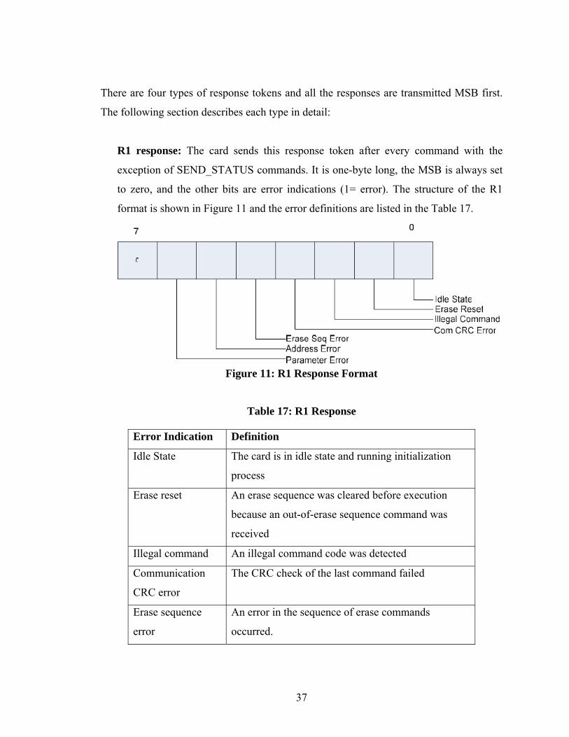
R1 response: The card sends this response token after every command with the
exception of SEND_STATUS commands. It is one-byte long, the MSB is always set
to zero, and the other bits are error indications (1= error). The structure of the R1
format is shown in Figure 11 and the error definitions are listed in the Table 17.
Figure 11: R1 Response Format
Table 17: R1 Response
Error Indication Definition
Idle State The card is in idle state and running initialization
process
Erase reset An erase sequence was cleared before execution
because an out-of-erase sequence command was
received
Illegal command An illegal command code was detected
Communication
CRC error
The CRC check of the last command failed
Erase sequence
error
An error in the sequence of erase commands
occurred.
37
Table 17: R1 Response (Continued…)
Address error A misaligned address that did not match the block
length was used in the command
Parameter error The command’s argument (e.g. address, block
length) was out of the allowed range for this card.
R1b format: This response token is identical to R1 format with the optional addition
of the busy signal. The busy signal token can be any number of bytes. A zero value
indicates card is busy. A non-zero value indicates card is ready for the next command.
R2 Format: The card sends the two-byte-long response token a response to the
SEND_STATUS command. The first byte is identical to response R1. The content of
the second byte is defined in Table 18.
Table 18: R2 Response
Bit
position
Error indication Definition
7 Out of range/CSD
overwrite
This status bit has two functions. It is set if
the command argument was out of its valid
range, or if the host is trying to change the
ROM section or reverse the copy bit (set as
original) or permanent WP bit (un-protect)
of the CSD register.
6 Erase parameter
An invalid selection, sectors, or groups for
erase.
5 Write protect
violation
The command tried to write to a write-
protected block.
4 Card ECC failed The card’s internal ECC was applied but
failed to correct the data.
38
Table 18: R2 Response (Continued…)
3 CC Error Internal card controller error
2 Error A general or an unknown error occurred
during the operation.
1 Write protect
erase skip
This status bit has two functions. It is set
when the host attempts to erase a write-
protected sector or if a sequence or
password error occurred during a card
lock/unlock operation.
0 Card is locked
This bit is set when the user locks the card.
It is reset when it is unlocked.
R3 Format: The card sends this response token when a READ_OCR command is
received. The response length is five bytes. The structure of the first byte (MSB) is
identical to response type R1. The other four bytes contain the OCR Register.
39
3 File System
This chapter explains about File System and briefly discusses the different types of File
Systems. The later section of the chapter explains FAT File System in detail. Evolution of
FAT File Systems is discussed. FAT16 File System layout, associated terminologies and
implementation are also explained.
3.1 Introduction
File System is a method for storing and organizing files and data to make it easy to find
and access them. Most file systems make use of an underlying data storage device that
offers access to an array of fixed-size blocks, sometimes called "sectors" (Explained in
the later section of the chapter). The file system software is responsible for organizing
these sectors into files and directories, and keeping track of which sectors belong to
which file and which sectors are not being used. Most file systems address data in fixed-
sized units called "clusters" (Explained in the later section of the Chapter) which contain
a certain number of sectors. This is the smallest logical amount of disk space that can be
allocated to hold a file.
Most operating systems provide file system along with them. Examples of File Systems
include FAT((File Allocation Table, FAT12, FAT16, FAT32) and NTFS(New
Technology File System) developed by Microsoft, HFS (Hierarchical File System) and
HFS+ developed by Apple, ext2, ext3 for Linux among others.
3.2 FAT (File Allocation Table) File System
3.2.1 Introduction to FAT
The FAT (File Allocation Table) file system has its origins in the late 1970s and
early1980s and was the file system supported by the Microsoft® MS-DOS® operating
system. It was originally developed as a simple file system suitable for floppy disk drives
less than 500K in size. Over time it has been enhanced to support larger and larger media.
Currently there are three FAT file system types: FAT12, FAT16 and FAT32. The basic
difference in these FAT sub types, and the reason for the names is the size in bits of the
40
entries in the actual FAT structure on the disk. There are 12 bits in a FAT12 FAT entry,
16 bits in a FAT16 FAT entry and 32 bits in a FAT32 FAT entry [17].
3.2.2 Basic Terminologies
There are a few basic terminologies which the reader needs to be familiar before
discussing in detail about the FAT File System. FAT File System was originally designed
to be a disk based File System. However it can be used for Flash based memories also by
emulating or grouping memory blocks as if it was a disk based memory. The following
section describes the basic terminologies referred to while discussing about a disk based
File System.
Cluster
Geometrical Sector
Sector
Track
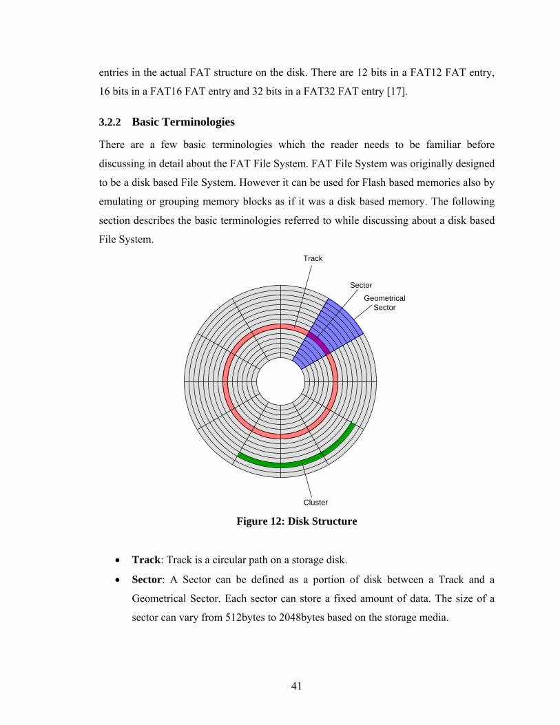
Figure 12: Disk Structure
Track: Track is a circular path on a storage disk.
Sector: A Sector can be defined as a portion of disk between a Track and a
Geometrical Sector. Each sector can store a fixed amount of data. The size of a
sector can vary from 512bytes to 2048bytes based on the storage media.
41
Cluster: A Cluster can be defined as a group of Sectors. In a File System with a
Sector size of 512bytes, a Cluster of 4KB has 8 Sectors. A Cluster is the
minimum storage space allocated for a file. Hence storing small files on a File
System with larger Cluster size will result in wastage of memory. For example if
cluster size is 4KB and to store a file of size 1KB, the File System allocates all the
4KB leaving 3KB unused.
3.2.3 Comparison of Different FAT File Systems
This section compares different FAT File Systems. FAT File Systems are named based
on the number of bits used to represent the Cluster number in the FAT Table. Each
cluster has one entry in the FAT, and these entries are used to hold the cluster number of
the next cluster used by the file [18].
FAT12: This the oldest type of FAT, it uses a 12-bit binary number to hold the
cluster number. A volume formatted using FAT12 can hold a maximum of 4,077
clusters, which is 2^12 minus 19 (to allow for reserved values to be used in the
FAT). FAT12 is therefore most suitable for very small volumes, and is used on
floppy disks smaller than about 16 MB.
FAT16: This FAT File System has evolved after FAT12 File System. It uses a
16-bit value to store the cluster number. Hence it can support 65,517 Clusters,
which is 2^16 minus 19. It is the most common File System used in removable
storage media like Flash drives and memory cards. It can support up to 2GB with
a 32KB Cluster size.
FAT32: This the newest FAT type, supported by newer versions of Windows.
FAT32 uses a 28-bit binary cluster number, because 4 of the 32 bits are
"reserved"[17]. A 28 bit numbers is still enough to index over 268 million
clusters, and can support drives up to 2 TB in size. FAT32 File System is used in
hard disks and other volumes which are relatively huge in size.
42
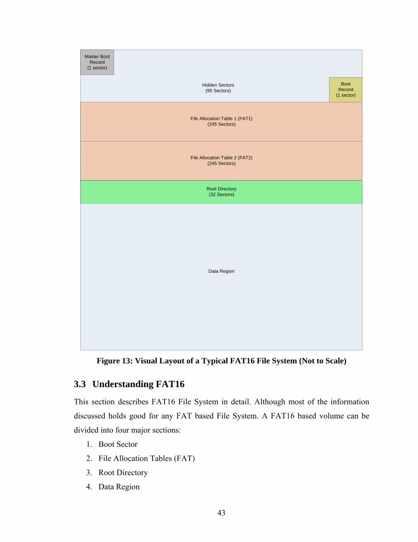
Master Boot Record
(1 sector)
Boot Record
(1 sector)
File Allocation Table 1 (FAT1)(245 Sectors)
Hidden Sectors(95 Sectors)
Root Directory(32 Sectors)
File Allocation Table 2 (FAT2)(245 Sectors)
Data Region
Figure 13: Visual Layout of a Typical FAT16 File System (Not to Scale)
3.3 Understanding FAT16
This section describes FAT16 File System in detail. Although most of the information
discussed holds good for any FAT based File System. A FAT16 based volume can be
divided into four major sections:
1. Boot Sector
2. File Allocation Tables (FAT)
3. Root Directory
4. Data Region
43
Each of these sections is located in the order mentioned above. Boot Sector and the File
Allocation Tables are separated by some optional number of unused sectors. A visual
layout of a FAT16 File System is shown in Figure 13. Each of the four major sections is
described below.
3.3.1 Boot Sector
The first sector of a FAT16 drive is the Master Boot Record (MBR). It contains
information, i.e. if the volume is a bootable drive and if any partitions are present in the
drive. It is followed by sectors 1 to 62 generally left empty, both inclusive. This is
followed by Boot Sector [19]. Boot Sector contains important information about the
volume like the number of bytes per sector, number of sectors per cluster, among others.
Table 19 shows the information present in the Boot Sector.
Table 19: Boot Sector Structure
Byte
Offset
Length
(Bytes)
Description
0x00 3 Jump instruction. This is executed if it is a boot partition
0x03 8 OEM name Eg: MSDOS5.0
0x0b 2 Bytes per Sector
0x0d 1 Sectors per Cluster
0x0e 2 Reserved Sectors
0x10 1 Number of File Allocation Tables, typically its 2
0x11 2 Maximum number of Root Directory Entires
0x13 2 Total number of sectors (If zero use 4 byte value at offset
0x20)
0x15 1 Media description
0x16 2 Sectors per File Allocation Table
0x18 2 Sectors per track (unused in a Flash based File System)
0x1a 2 Number of heads (unused in a Flash based File System)
0x1c 4 Hidden sectors
44
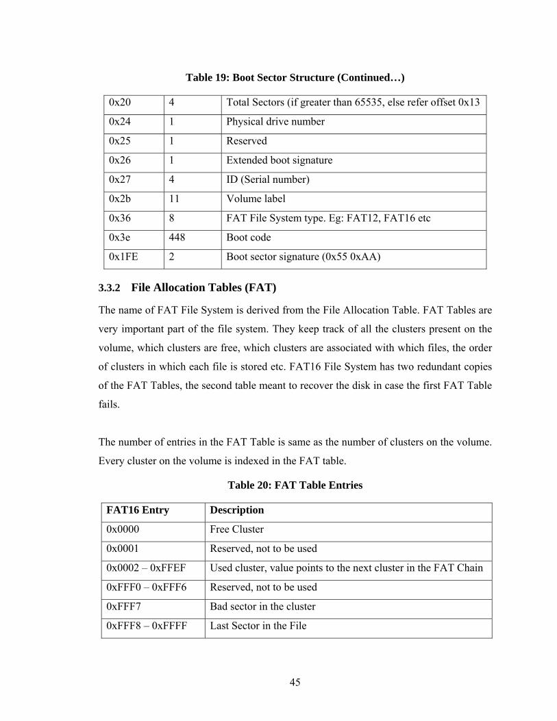
Table 19: Boot Sector Structure (Continued…)
0x20 4 Total Sectors (if greater than 65535, else refer offset 0x13
0x24 1 Physical drive number
0x25 1 Reserved
0x26 1 Extended boot signature
0x27 4 ID (Serial number)
0x2b 11 Volume label
0x36 8 FAT File System type. Eg: FAT12, FAT16 etc
0x3e 448 Boot code
0x1FE 2 Boot sector signature (0x55 0xAA)
3.3.2 File Allocation Tables (FAT)
The name of FAT File System is derived from the File Allocation Table. FAT Tables are
very important part of the file system. They keep track of all the clusters present on the
volume, which clusters are free, which clusters are associated with which files, the order
of clusters in which each file is stored etc. FAT16 File System has two redundant copies
of the FAT Tables, the second table meant to recover the disk in case the first FAT Table
fails.
The number of entries in the FAT Table is same as the number of clusters on the volume.
Every cluster on the volume is indexed in the FAT table.
Table 20: FAT Table Entries
FAT16 Entry Description
0x0000 Free Cluster
0x0001 Reserved, not to be used
0x0002 – 0xFFEF Used cluster, value points to the next cluster in the FAT Chain
0xFFF0 – 0xFFF6 Reserved, not to be used
0xFFF7 Bad sector in the cluster
0xFFF8 – 0xFFFF Last Sector in the File
45
Any file stored on the FAT File system will be a chain of clusters. FAT Table allocates
the next available free cluster to a file and the cluster number of the next cluster in the
chain is stored in the FAT table. If one knows the starting cluster of a file, using the FAT
chain the file can be traversed.
DATA 0 DATA 1 DATA 2 DATA 3
0
1
2
3
4
5
6
7
8
0x0005
0x0007
0x0008
0xFFFF
CLUSTER 3 CLUSTER 5 CLUSTER 7 CLUSTER 8
FAT TABLE
LOCATION DATA
Figure 14: FAT Chain
This FAT Chain implementation can be better explained with the help of an example as
shown in Figure 14. Consider a file, long enough to be stored in four Clusters. Let the
four parts be named DATA0 to DATA3 respectively. Let the starting cluster of the file
which stores DATA0 is CLUSTER 3. The next part of the file DATA1 is stored in the
CLUSTER 5, so location 3 in the FAT TABLE has an entry of 0x0005 to point to the
next Cluster in the FAT Chain. The DATA 2 part is stored in the CLUSTER 7, hence the
location 5 in the FAT TABLE has entry 0x0007 corresponding to it. Similarly the
location 7 in the FAT TABLE has 0x0008 as its entry to represent the CLUSTER 8
occupied by the last part of the file, DATA 3. Since this is the last Cluster in the FAT
Chain, location 8 doesn’t point to any other cluster, hence the FAT TABLE entry to this
location is made as 0xFFFF to denote the end of FAT Chain.
3.3.3 Root Directory
46
Root Directory is located immediately after the FAT Tables. Each entry in the Root
Directory is 32 Byte long, called the Directory Entry. Every file or Subdirectory in the
FAT file system has a Root Directory entry. In a FAT16 file system the number of
possible entries in the Root Directory is fixed, which is mentioned in the Boot Record.
The information present in the Directory Entry is described in the Table 21.
Table 21: Directory Entry
Byte Offset Length Description
0x00 8 File name
0x08 3 File extension
0x0B 1 File attribute
0x0C 10 Miscellaneous
0x16 2 Last modified time
0x18 2 Last modified date
0x1A 2 Starting Cluster
0x1C 4 File Size
The first eight bytes in the Directory Entry is the file name followed by file extension.
File names in the FAT16 file system are stored in “8.3” format. The next Byte in the
Directory Entry is File attribute. Subdirectory in a FAT file system is just like a file with
special attributes, the data part of it being directory entries of files inside it.
Table 22: File Attribute
Bit Value Description
0 0x01 Read Only
1 0x02 Hidden
2 0x04 System
3 0x08 Volume label
4 0x10 Subdirectory
47
Table 22: File Attribute (Continued…)
5 0x20 Archive
6 0x40 Device
7 0x80 Unused
Also the root directory stores the information about the file like, the starting Cluster, last
modified date and time and Size of the file.
3.3.4 Data Region
The Data Region follows the Root Directory and extends till the end of the card. This
region stores the files and Subdirectories. Data region is divided into Clusters and each
Cluster is allocated to a file on the first available basis. This is taken care of by the FAT
tables. So a File need not be stored in contiguous Clusters in the Data region physically.
48
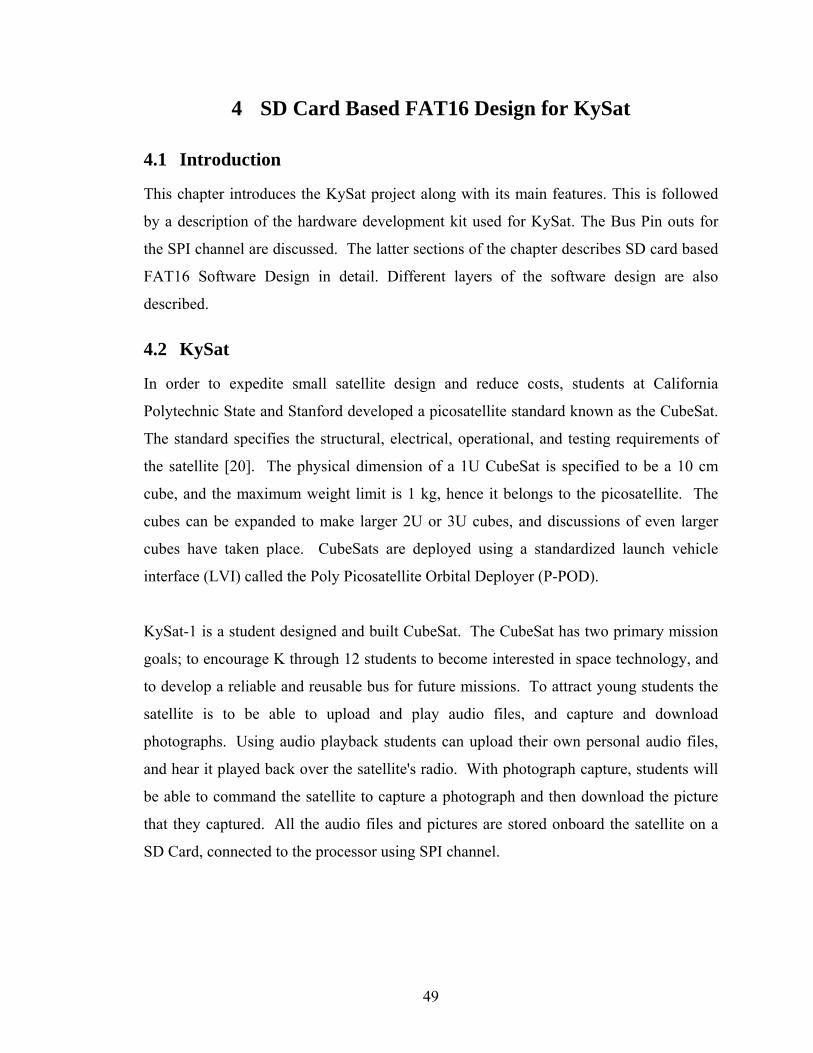
4 SD Card Based FAT16 Design for KySat
4.1 Introduction
This chapter introduces the KySat project along with its main features. This is followed
by a description of the hardware development kit used for KySat. The Bus Pin outs for
the SPI channel are discussed. The latter sections of the chapter describes SD card based
FAT16 Software Design in detail. Different layers of the software design are also
described.
4.2 KySat
In order to expedite small satellite design and reduce costs, students at California
Polytechnic State and Stanford developed a picosatellite standard known as the CubeSat.
The standard specifies the structural, electrical, operational, and testing requirements of
the satellite [20]. The physical dimension of a 1U CubeSat is specified to be a 10 cm
cube, and the maximum weight limit is 1 kg, hence it belongs to the picosatellite. The
cubes can be expanded to make larger 2U or 3U cubes, and discussions of even larger
cubes have taken place. CubeSats are deployed using a standardized launch vehicle
interface (LVI) called the Poly Picosatellite Orbital Deployer (P-POD).
KySat-1 is a student designed and built CubeSat. The CubeSat has two primary mission
goals; to encourage K through 12 students to become interested in space technology, and
to develop a reliable and reusable bus for future missions. To attract young students the
satellite is to be able to upload and play audio files, and capture and download
photographs. Using audio playback students can upload their own personal audio files,
and hear it played back over the satellite's radio. With photograph capture, students will
be able to command the satellite to capture a photograph and then download the picture
that they captured. All the audio files and pictures are stored onboard the satellite on a
SD Card, connected to the processor using SPI channel.
49
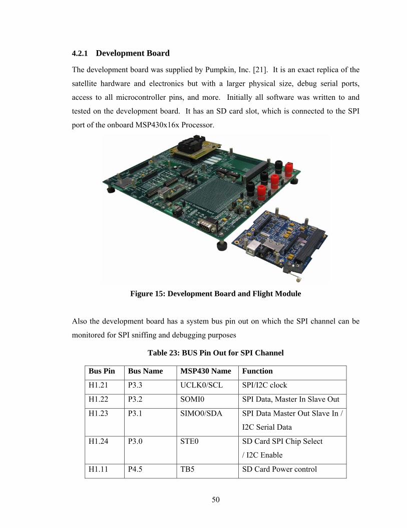
4.2.1 Development Board
The development board was supplied by Pumpkin, Inc. [21]. It is an exact replica of the
satellite hardware and electronics but with a larger physical size, debug serial ports,
access to all microcontroller pins, and more. Initially all software was written to and
tested on the development board. It has an SD card slot, which is connected to the SPI
port of the onboard MSP430x16x Processor.
Figure 15: Development Board and Flight Module
Also the development board has a system bus pin out on which the SPI channel can be
monitored for SPI sniffing and debugging purposes
Table 23: BUS Pin Out for SPI Channel
Bus Pin Bus Name MSP430 Name Function
H1.21 P3.3 UCLK0/SCL SPI/I2C clock
H1.22 P3.2 SOMI0 SPI Data, Master In Slave Out
H1.23 P3.1 SIMO0/SDA
SPI Data Master Out Slave In /
I2C Serial Data
H1.24 P3.0 STE0 SD Card SPI Chip Select
/ I2C Enable
H1.11 P4.5 TB5 SD Card Power control
50
4.2.2 Integrated Development Environment
The Integrated Development Environment (IDE) chosen for the KySat Project is
CrossWorks from Rowley Associates Limited [22]. It has a powerful debugger, with
multiple breakpoints. Customizable watch windows, along with other options to compile,
link and download code on to the development board. The IDE itself is very user
friendly. The debugger can be used to inject any value into a variable via the watch
windows, this feature proved to be very helpful during the development process.
Breakpoints and watch variables can be added any time during the debugging process and
real-time values can be read on the fly. Also the IDE displays the amount of code space
and data space used by the current project.
The present work to develop a FAT16 File System for KySat flight Software uses the
same KySat flight hardware and IDE for better compatibility and future reuse.
4.3 Software Design
The file system developed in the current thesis work is based on Re-Engineering the
application note “USB Mass Storage Reference Design” [23]. The USB Mass Storage
Reference Design application note includes a FAT16 file system for MMC and Compact
Flash card on a SiLabs C8051F340 MCU. In addition it has a method to interface the
mass storage device to a PC via USB interface.
The already existing application has provided a reliable platform to start with. The
system architecture of the application note is described in Figure 16. The colored portion
of the block diagram represents the code reused in the present work. Most of the sector
server layer in the application is used as is with some minor modifications. Media Access
layer in the application note has libraries to access both Compact Flash Card and
MultiMediaCard. The unnecessary libraries from the Media Access layer have been
removed. File System API’s are modified to suite the requirements of the current KySat
project [5]. Apart from this, the SPI level drivers are written exclusively for the selected
processor. The major task involved in using the application note includes porting the
software for the MSP430x16x processor, using the selected IDE as compiler.
51
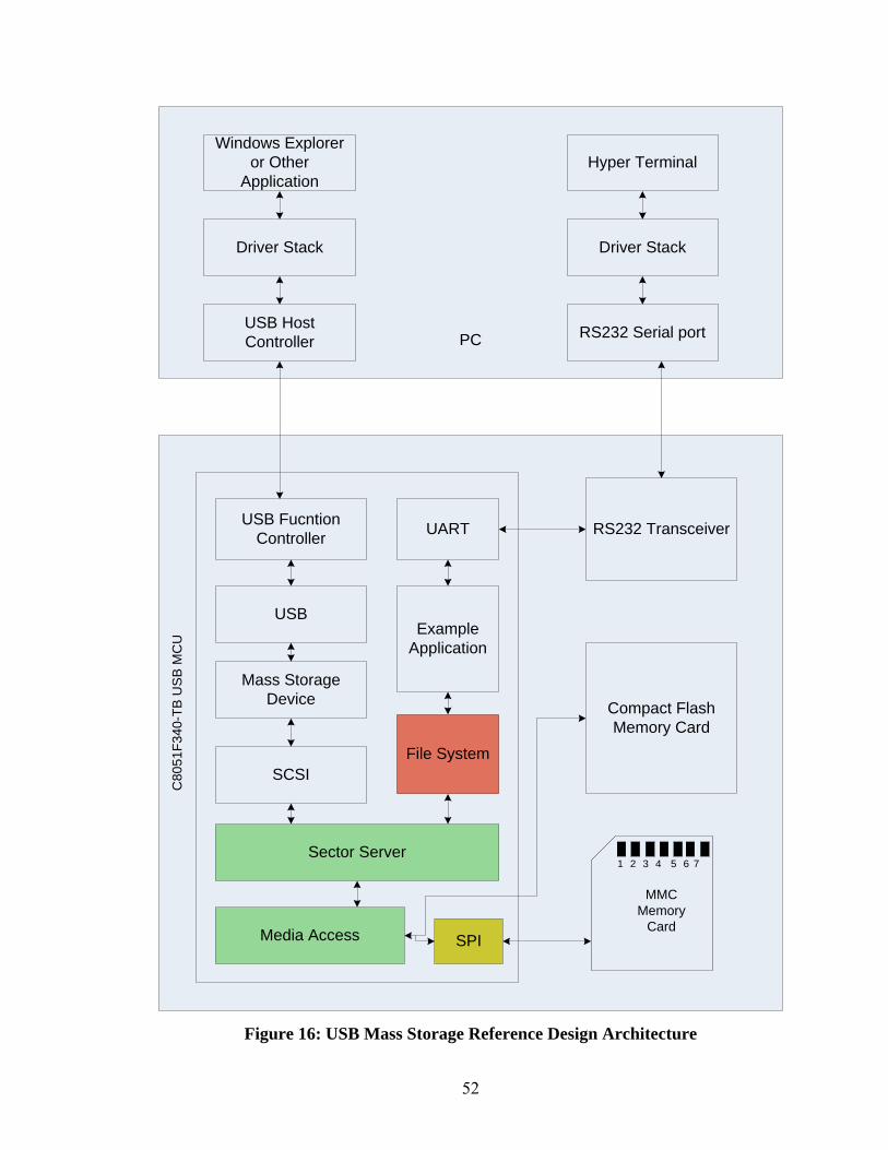
PC
RS232 Transceiver
Compact Flash Memory Card
1 2 3 4 5 6 7
USB Fucntion Controller
USB
Mass Storage Device
SCSI
Sector Server
Media Access SPI
UART
Example Application
File System
MMC Memory
Card
Windows Explorer or Other
Application
Driver Stack
USB Host Controller
Hyper Terminal
Driver Stack
RS232 Serial port
C80
51F
340-
TB
US
B M
CU
Figure 16: USB Mass Storage Reference Design Architecture
52
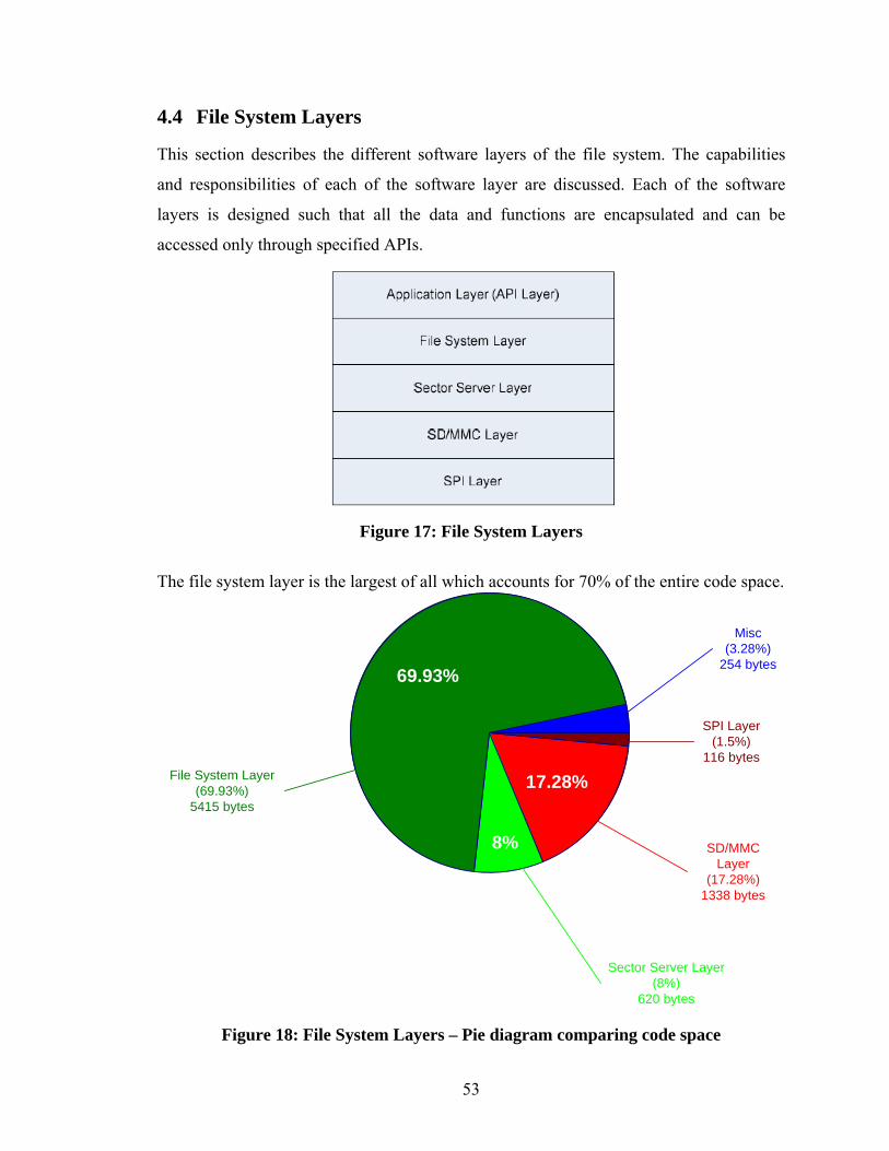
4.4 File System Layers
This section describes the different software layers of the file system. The capabilities
and responsibilities of each of the software layer are discussed. Each of the software
layers is designed such that all the data and functions are encapsulated and can be
accessed only through specified APIs.
Figure 17: File System Layers
The file system layer is the largest of all which accounts for 70% of the entire code space.
17.28%
8%
69.93%
3.28%SPI Layer (1.5%)
SPI Layer (1.5%)
116 bytes
Misc(3.28%)
254 bytes
SD/MMC Layer
(17.28%)1338 bytes
Sector Server Layer(8%)
620 bytes
File System Layer(69.93%)
5415 bytes
Figure 18: File System Layers – Pie diagram comparing code space
53
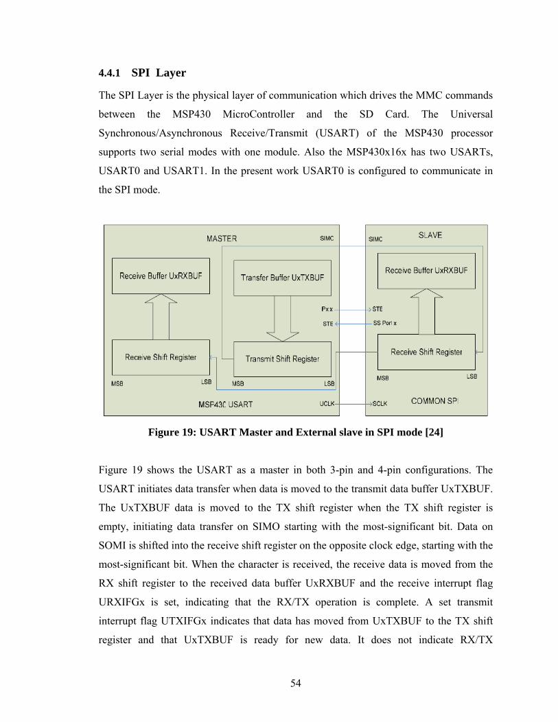
4.4.1 SPI Layer
The SPI Layer is the physical layer of communication which drives the MMC commands
between the MSP430 MicroController and the SD Card. The Universal
Synchronous/Asynchronous Receive/Transmit (USART) of the MSP430 processor
supports two serial modes with one module. Also the MSP430x16x has two USARTs,
USART0 and USART1. In the present work USART0 is configured to communicate in
the SPI mode.
Figure 19: USART Master and External slave in SPI mode [24]
Figure 19 shows the USART as a master in both 3-pin and 4-pin configurations. The
USART initiates data transfer when data is moved to the transmit data buffer UxTXBUF.
The UxTXBUF data is moved to the TX shift register when the TX shift register is
empty, initiating data transfer on SIMO starting with the most-significant bit. Data on
SOMI is shifted into the receive shift register on the opposite clock edge, starting with the
most-significant bit. When the character is received, the receive data is moved from the
RX shift register to the received data buffer UxRXBUF and the receive interrupt flag
URXIFGx is set, indicating that the RX/TX operation is complete. A set transmit
interrupt flag UTXIFGx indicates that data has moved from UxTXBUF to the TX shift
register and that UxTXBUF is ready for new data. It does not indicate RX/TX
54
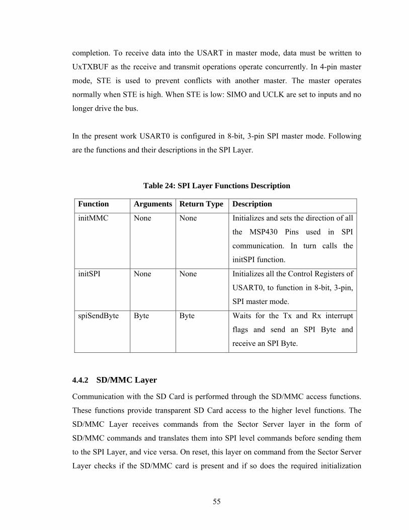
completion. To receive data into the USART in master mode, data must be written to
UxTXBUF as the receive and transmit operations operate concurrently. In 4-pin master
mode, STE is used to prevent conflicts with another master. The master operates
normally when STE is high. When STE is low: SIMO and UCLK are set to inputs and no
longer drive the bus.
In the present work USART0 is configured in 8-bit, 3-pin SPI master mode. Following
are the functions and their descriptions in the SPI Layer.
Table 24: SPI Layer Functions Description
Function Arguments Return Type Description
initMMC None None Initializes and sets the direction of all
the MSP430 Pins used in SPI
communication. In turn calls the
initSPI function.
initSPI None None Initializes all the Control Registers of
USART0, to function in 8-bit, 3-pin,
SPI master mode.
spiSendByte Byte Byte Waits for the Tx and Rx interrupt
flags and send an SPI Byte and
receive an SPI Byte.
4.4.2 SD/MMC Layer
Communication with the SD Card is performed through the SD/MMC access functions.
These functions provide transparent SD Card access to the higher level functions. The
SD/MMC Layer receives commands from the Sector Server layer in the form of
SD/MMC commands and translates them into SPI level commands before sending them
to the SPI Layer, and vice versa. On reset, this layer on command from the Sector Server
Layer checks if the SD/MMC card is present and if so does the required initialization
55
process to start the SD/MMC card in SPI mode. Typically none of these functions need to
be called at the application level as the Sector Server Layer encapsulates them. Each of
the functions in this layer are described below.
MMC_FLASH_Init
Arguments: None
Description:
This function initializes the flash card, configures it to operate in SPI mode, and
reads the operating conditions register to ensure that the device has initialized
correctly. It also determines the size of the card by reading the Card Specific
Data Register (CSD).
Return Value: None
MMC_Command_Exec
This function generates the necessary SPI traffic for all SD/MMC SPI commands.
Arguments:
1. Cmd: This parameter is used to index into the command table and read the
desired command. The Command Table Index Constants allow the caller
to use a meaningful constant name in the Cmd parameter instead of a
simple index number. For example, instead of calling
MMC_Command_Exec (0, argument, pchar) to send the SD/MMC into
idle state, the user can call
MMC_Command_Exec (GO_IDLE_STATE, argument, pchar)
2. argument: This parameter is used for SD/MMC commands that require an
argument. SD/MMC arguments are 32-bits long and can be values such as
an address, a block length setting, or register settings for the SD/MMC. If
the SD/MMC command dosen’t have any argument then the value of this
parameter will be EMPTY (0)
3. pchar: This parameter is a pointer to the local data location for SD/MMC
data operations. When a read or write occurs, data will be stored or
retrieved from the location pointed to by pchar.
56
Description:
The MMC_Command_Exec function indexes the command table using the Cmd
parameter. It reads the command table entry into memory and uses information
from that entry to determine how to proceed.
Return Value:
Returns 0 if the command is executed successfully. Else, returns the 16-bit card
response value.
MMC_FLASH_Block_Read
Arguments:
1. Address: Starting address of the 512 Byte block to be read
2. Pchar: Pointer to the memory location where the data is to be copied
Description:
This function Reads a 512-byte block from the SD/MMC card starting at the
location specified by Address. The block is copied to the memory location
pointed to by pchar.
Return Value:
Returns 0 if the command is executed successfully. Else, returns the 16-bit card
response value.
MMC_FLASH_Block_Write
Arguments:
1. Address: Starting address of the 512 Byte block to be Written
2. wdata: Pointer to the memory location where the data is to be written is
present
Description:
This function Writes a 512-byte block to the SD/MMC card starting at the
location specified by Address. The block is copied to the memory location
pointed to by wdata.
Return Value:
57
Returns 0 if the command is executed successfully. Else, returns the 16-bit card
response value.
READ_BYTES
Arguments:
1. pchar: Buffer into which the SPI Bytes are to be copied
2. len: Number of SPI Bytes to be Read
Description:
Reads the specified number of SPI Bytes and copies them to the pchar buffer
Return Value: None.
WRITE_BYTES
Arguments:
1. pchar: Buffer from which the SPI Bytes are to be sent out
2. len: Number of SPI Bytes to be sent out
Description:
Sends out the specified number of SPI Bytes from the ‘pchar’ buffer on to the SPI
channel.
Return Value: None.
4.4.3 Sector Server Layer
The Sector Server Layer encapsulates the lower-level media access functions so that
those functions need not be called from application level firmware. This layer detects and
initializes the memory card on startup. It reads and validates the Boot Record and Master
Boot Record and checks if it is a valid FAT16 File System. It checks for a boot signature
of 0xAA55. It stores a global copy of the details about the FAT media like, number of
FAT copies, number of entries in the root directory, number of sectors present in the
SD/MMC card, size of each FAT table. It also maintains a 512 Byte scratch buffer that is
used by the entire file system to read or write blocks of data. Sector Server Layer also
58
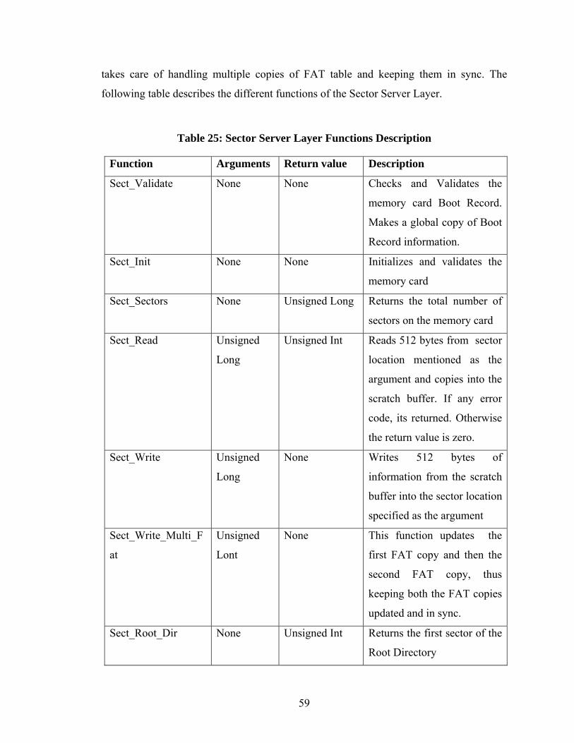
takes care of handling multiple copies of FAT table and keeping them in sync. The
following table describes the different functions of the Sector Server Layer.
Table 25: Sector Server Layer Functions Description
Function Arguments Return value Description
Sect_Validate None None Checks and Validates the
memory card Boot Record.
Makes a global copy of Boot
Record information.
Sect_Init None None Initializes and validates the
memory card
Sect_Sectors None Unsigned Long Returns the total number of
sectors on the memory card
Sect_Read Unsigned
Long
Unsigned Int Reads 512 bytes from sector
location mentioned as the
argument and copies into the
scratch buffer. If any error
code, its returned. Otherwise
the return value is zero.
Sect_Write Unsigned
Long
None Writes 512 bytes of
information from the scratch
buffer into the sector location
specified as the argument
Sect_Write_Multi_F
at
Unsigned
Lont
None This function updates the
first FAT copy and then the
second FAT copy, thus
keeping both the FAT copies
updated and in sync.
Sect_Root_Dir None Unsigned Int Returns the first sector of the
Root Directory
59
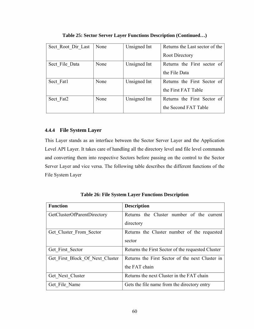
Table 25: Sector Server Layer Functions Description (Continued…)
Sect_Root_Dir_Last None Unsigned Int Returns the Last sector of the
Root Directory
Sect_File_Data None Unsigned Int Returns the First sector of
the File Data
Sect_Fat1 None Unsigned Int Returns the First Sector of
the First FAT Table
Sect_Fat2 None Unsigned Int Returns the First Sector of
the Second FAT Table
4.4.4 File System Layer
This Layer stands as an interface between the Sector Server Layer and the Application
Level API Layer. It takes care of handling all the directory level and file level commands
and converting them into respective Sectors before passing on the control to the Sector
Server Layer and vice versa. The following table describes the different functions of the
File System Layer
Table 26: File System Layer Functions Description
Function Description
GetClusterOfParentDirectory Returns the Cluster number of the current
directory
Get_Cluster_From_Sector Returns the Cluster number of the requested
sector
Get_First_Sector Returns the First Sector of the requested Cluster
Get_First_Block_Of_Next_Cluster Returns the First Sector of the next Cluster in
the FAT chain
Get_Next_Cluster Returns the next Cluster in the FAT chain
Get_File_Name Gets the file name from the directory entry
60
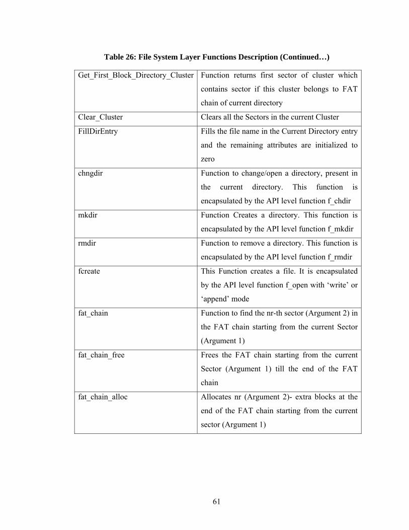
Table 26: File System Layer Functions Description (Continued…)
Get_First_Block_Directory_Cluster Function returns first sector of cluster which
contains sector if this cluster belongs to FAT
chain of current directory
Clear_Cluster Clears all the Sectors in the current Cluster
FillDirEntry Fills the file name in the Current Directory entry
and the remaining attributes are initialized to
zero
chngdir Function to change/open a directory, present in
the current directory. This function is
encapsulated by the API level function f_chdir
mkdir Function Creates a directory. This function is
encapsulated by the API level function f_mkdir
rmdir Function to remove a directory. This function is
encapsulated by the API level function f_rmdir
fcreate This Function creates a file. It is encapsulated
by the API level function f_open with ‘write’ or
‘append’ mode
fat_chain Function to find the nr-th sector (Argument 2) in
the FAT chain starting from the current Sector
(Argument 1)
fat_chain_free Frees the FAT chain starting from the current
Sector (Argument 1) till the end of the FAT
chain
fat_chain_alloc Allocates nr (Argument 2)- extra blocks at the
end of the FAT chain starting from the current
sector (Argument 1)
61
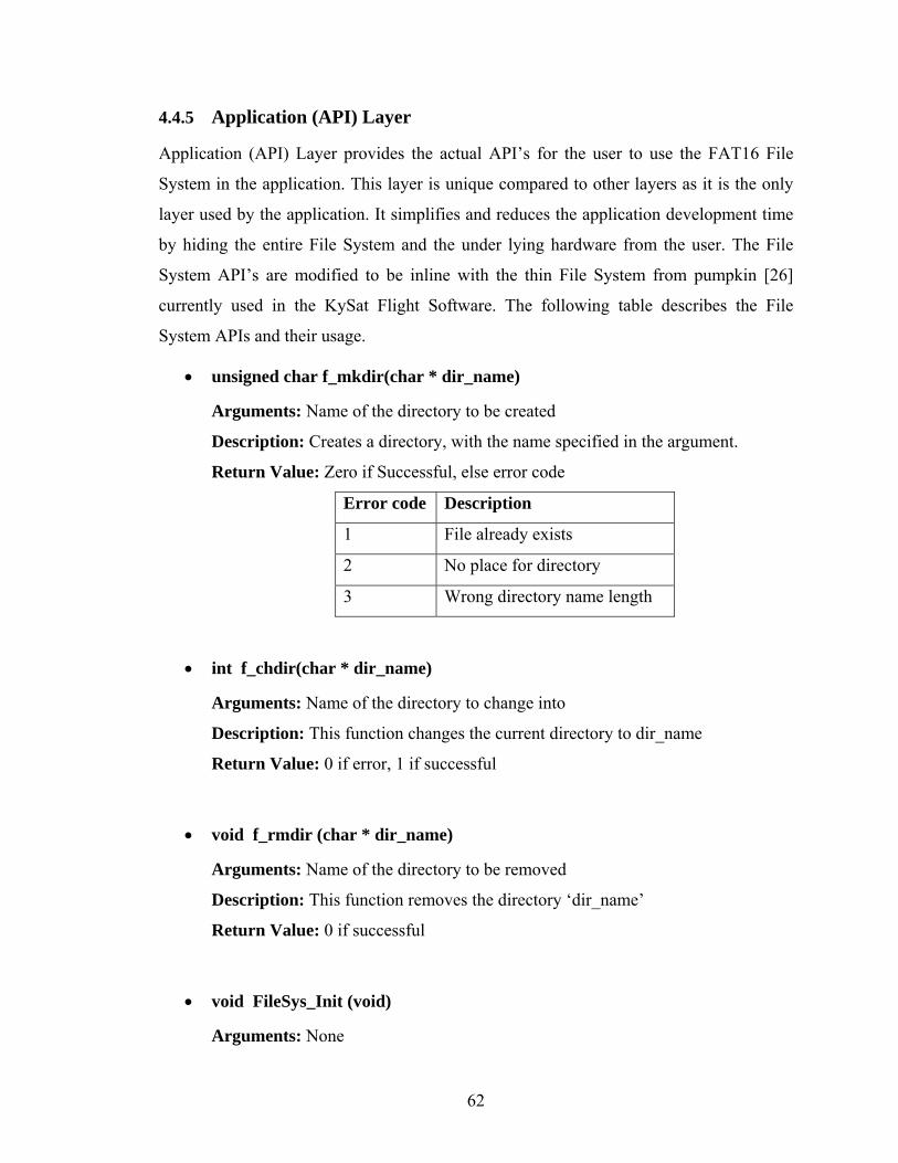
4.4.5 Application (API) Layer
Application (API) Layer provides the actual API’s for the user to use the FAT16 File
System in the application. This layer is unique compared to other layers as it is the only
layer used by the application. It simplifies and reduces the application development time
by hiding the entire File System and the under lying hardware from the user. The File
System API’s are modified to be inline with the thin File System from pumpkin [26]
currently used in the KySat Flight Software. The following table describes the File
System APIs and their usage.
unsigned char f_mkdir(char * dir_name)
Arguments: Name of the directory to be created
Description: Creates a directory, with the name specified in the argument.
Return Value: Zero if Successful, else error code
Error code Description
1 File already exists
2 No place for directory
3 Wrong directory name length
int f_chdir(char * dir_name)
Arguments: Name of the directory to change into
Description: This function changes the current directory to dir_name
Return Value: 0 if error, 1 if successful
void f_rmdir (char * dir_name)
Arguments: Name of the directory to be removed
Description: This function removes the directory ‘dir_name’
Return Value: 0 if successful
void FileSys_Init (void)
Arguments: None
62
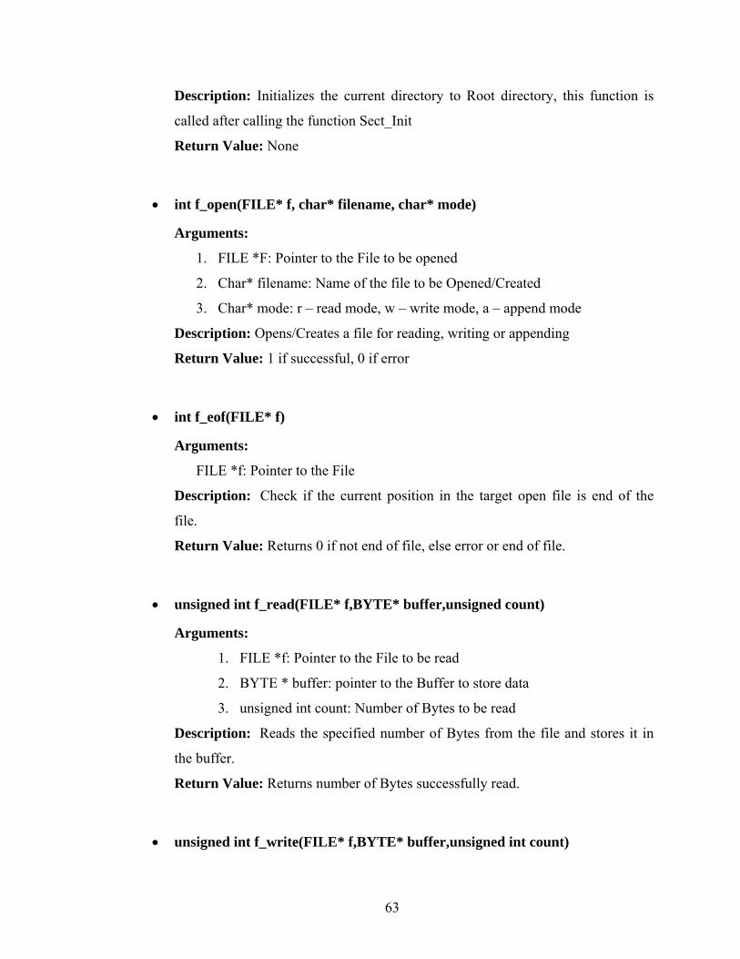
Description: Initializes the current directory to Root directory, this function is
called after calling the function Sect_Init
Return Value: None
int f_open(FILE* f, char* filename, char* mode)
Arguments:
1. FILE *F: Pointer to the File to be opened
2. Char* filename: Name of the file to be Opened/Created
3. Char* mode: r – read mode, w – write mode, a – append mode
Description: Opens/Creates a file for reading, writing or appending
Return Value: 1 if successful, 0 if error
int f_eof(FILE* f)
Arguments:
FILE *f: Pointer to the File
Description: Check if the current position in the target open file is end of the
file.
Return Value: Returns 0 if not end of file, else error or end of file.
unsigned int f_read(FILE* f,BYTE* buffer,unsigned count)
Arguments:
1. FILE *f: Pointer to the File to be read
2. BYTE * buffer: pointer to the Buffer to store data
3. unsigned int count: Number of Bytes to be read
Description: Reads the specified number of Bytes from the file and stores it in
the buffer.
Return Value: Returns number of Bytes successfully read.
unsigned int f_write(FILE* f,BYTE* buffer,unsigned int count)
63
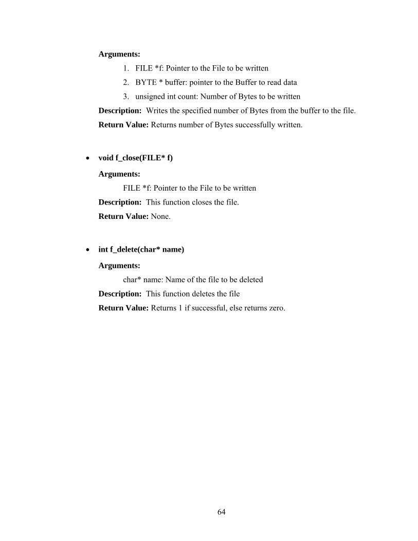
Arguments:
1. FILE *f: Pointer to the File to be written
2. BYTE * buffer: pointer to the Buffer to read data
3. unsigned int count: Number of Bytes to be written
Description: Writes the specified number of Bytes from the buffer to the file.
Return Value: Returns number of Bytes successfully written.
void f_close(FILE* f)
Arguments:
FILE *f: Pointer to the File to be written
Description: This function closes the file.
Return Value: None.
int f_delete(char* name)
Arguments:
char* name: Name of the file to be deleted
Description: This function deletes the file
Return Value: Returns 1 if successful, else returns zero.
64
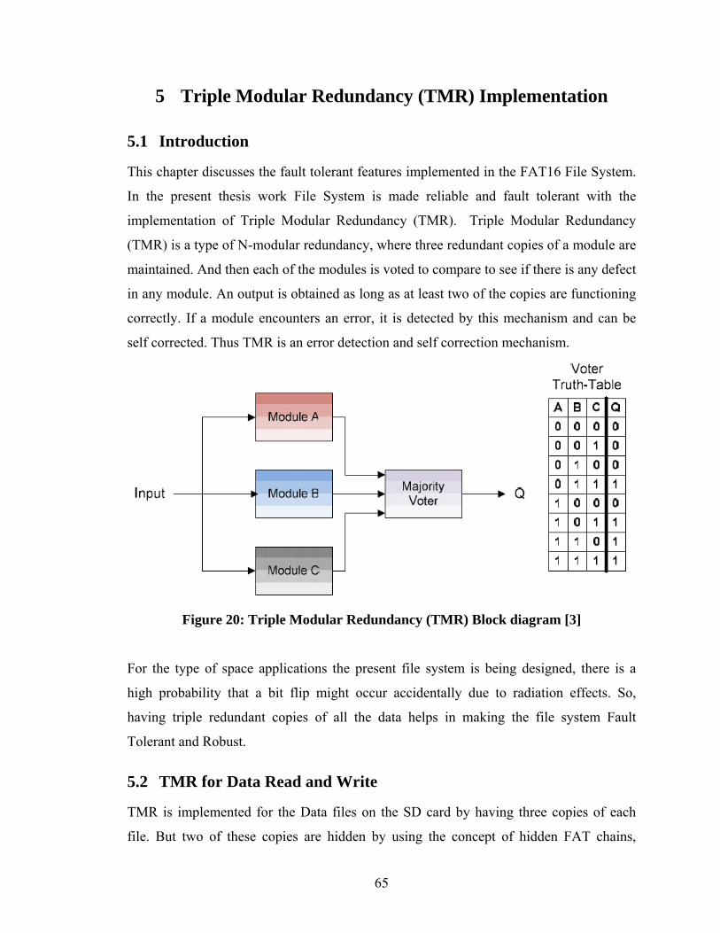
5 Triple Modular Redundancy (TMR) Implementation
5.1 Introduction
This chapter discusses the fault tolerant features implemented in the FAT16 File System.
In the present thesis work File System is made reliable and fault tolerant with the
implementation of Triple Modular Redundancy (TMR). Triple Modular Redundancy
(TMR) is a type of N-modular redundancy, where three redundant copies of a module are
maintained. And then each of the modules is voted to compare to see if there is any defect
in any module. An output is obtained as long as at least two of the copies are functioning
correctly. If a module encounters an error, it is detected by this mechanism and can be
self corrected. Thus TMR is an error detection and self correction mechanism.
Figure 20: Triple Modular Redundancy (TMR) Block diagram [3]
For the type of space applications the present file system is being designed, there is a
high probability that a bit flip might occur accidentally due to radiation effects. So,
having triple redundant copies of all the data helps in making the file system Fault
Tolerant and Robust.
5.2 TMR for Data Read and Write
TMR is implemented for the Data files on the SD card by having three copies of each
file. But two of these copies are hidden by using the concept of hidden FAT chains,
65
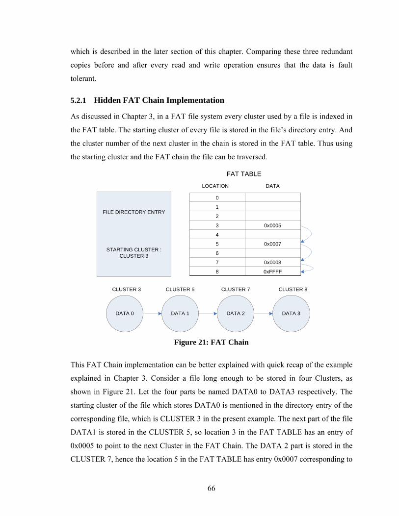
which is described in the later section of this chapter. Comparing these three redundant
copies before and after every read and write operation ensures that the data is fault
tolerant.
5.2.1 Hidden FAT Chain Implementation
As discussed in Chapter 3, in a FAT file system every cluster used by a file is indexed in
the FAT table. The starting cluster of every file is stored in the file’s directory entry. And
the cluster number of the next cluster in the chain is stored in the FAT table. Thus using
the starting cluster and the FAT chain the file can be traversed.
DATA 0 DATA 1 DATA 2 DATA 3
0
1
2
3
4
5
6
7
8
0x0005
0x0007
0x0008
0xFFFF
CLUSTER 3 CLUSTER 5 CLUSTER 7 CLUSTER 8
FAT TABLE
LOCATION DATA
FILE DIRECTORY ENTRY
STARTING CLUSTER : CLUSTER 3
Figure 21: FAT Chain
This FAT Chain implementation can be better explained with quick recap of the example
explained in Chapter 3. Consider a file long enough to be stored in four Clusters, as
shown in Figure 21. Let the four parts be named DATA0 to DATA3 respectively. The
starting cluster of the file which stores DATA0 is mentioned in the directory entry of the
corresponding file, which is CLUSTER 3 in the present example. The next part of the file
DATA1 is stored in the CLUSTER 5, so location 3 in the FAT TABLE has an entry of
0x0005 to point to the next Cluster in the FAT Chain. The DATA 2 part is stored in the
CLUSTER 7, hence the location 5 in the FAT TABLE has entry 0x0007 corresponding to
66
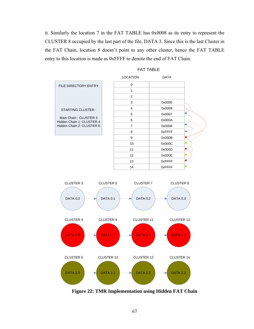
it. Similarly the location 7 in the FAT TABLE has 0x0008 as its entry to represent the
CLUSTER 8 occupied by the last part of the file, DATA 3. Since this is the last Cluster in
the FAT Chain, location 8 doesn’t point to any other cluster, hence the FAT TABLE
entry to this location is made as 0xFFFF to denote the end of FAT Chain.
DATA 0.0 DATA 0.1 DATA 0.2 DATA 0.3
0
1
2
3
4
5
6
7
8
9
10
11
12
13
14
0x0005
0x0009
0x0007
0x000A
0x0008
0xFFFF
0x000B
0x000C
0x000D
0x000E
0xFFFF
0xFFFF
CLUSTER 3 CLUSTER 5 CLUSTER 7 CLUSTER 8
FAT TABLE
LOCATION DATA
FILE DIRECTORY ENTRY
STARTING CLUSTER :
Main Chain : CLUSTER 3Hidden Chain 1: CLUSTER 4Hidden Chain 2: CLUSTER 6
DATA 1.0 DATA 1.1 DATA 1.2 DATA 1.3
CLUSTER 4 CLUSTER 9 CLUSTER 11 CLUSTER 13
DATA 2.0 DATA 2.1 DATA 2.2 DATA 2.3
CLUSTER 6 CLUSTER 10 CLUSTER 12 CLUSTER 14
Figure 22: TMR Implementation using Hidden FAT Chain
67
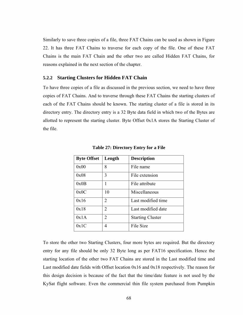
Similarly to save three copies of a file, three FAT Chains can be used as shown in Figure
22. It has three FAT Chains to traverse for each copy of the file. One of these FAT
Chains is the main FAT Chain and the other two are called Hidden FAT Chains, for
reasons explained in the next section of the chapter.
5.2.2 Starting Clusters for Hidden FAT Chain
To have three copies of a file as discussed in the previous section, we need to have three
copies of FAT Chains. And to traverse through these FAT Chains the starting clusters of
each of the FAT Chains should be known. The starting cluster of a file is stored in its
directory entry. The directory entry is a 32 Byte data field in which two of the Bytes are
allotted to represent the starting cluster. Byte Offset 0x1A stores the Starting Cluster of
the file.
Table 27: Directory Entry for a File
Byte Offset Length Description
0x00 8 File name
0x08 3 File extension
0x0B 1 File attribute
0x0C 10 Miscellaneous
0x16 2 Last modified time
0x18 2 Last modified date
0x1A 2 Starting Cluster
0x1C 4 File Size
To store the other two Starting Clusters, four more bytes are required. But the directory
entry for any file should be only 32 Byte long as per FAT16 specification. Hence the
starting location of the other two FAT Chains are stored in the Last modified time and
Last modified date fields with Offset location 0x16 and 0x18 respectively. The reason for
this design decision is because of the fact that the time/date feature is not used by the
KySat flight software. Even the commercial thin file system purchased from Pumpkin
68
doesn’t support date/time feature. In such case the date/time fields are normally left zero.
Also one more reason for not using the date/time feature is because the name of every file
in the KySat is encoded based on the time stamp when it is created.
Hence by using these four free bytes the Starting Clusters of the other two FAT chains
can be stored in the directory entry. As it is not known to other FAT16 file systems that
we are using the date/time fields as the starting clusters, these FAT Chains are hidden for
them. And hence, when the SD card is connected to a normal windows computer we can
see only one copy of that file, whereas two more copies of the same file are hidden some
where in the card. Also an interesting point to note here is that accidental writing into
these hidden FAT chain Clusters by a non TMR FAT16 file system is not possible
because these Clusters are already marked in the FAT table, and hence they are no longer
free clusters, only that they are not visible to a non TMR FAT16 file system.
5.3 TMR for Sub Directories
Sub Directory in a FAT16 file system is also a file, only with special attributes. The data
part being the directory entry of the files inside this Sub Directory. Similar to having
three copies for every file to implement Triple Modular Redundancy, three copies of Sub
Directories are also required. The major challenge in implementing TMR for Sub
Directories is that the current Directory for all the three copies needs to be tracked. Also a
‘.’ and ‘..’ directory needs to be created for every copy of the Sub Directory and should
point to the respective root directories. Every file created in these Sub Directories should
in fact have a copy of the file in each of the Sub Directories. Thus TMR is implemented
for Sub Directories.
5.4 TMR for MBR, BR, FAT Tables and Root Directory
For the file system to be entirely Redundant and Fault Tolerant, just having triple
redundant copies of the Files and Sub Directories is not just enough. FAT16 file system
heavily relies on FAT Tables, hence these FAT Tables should be redundant and fool
proof. Also there should be redundant copies of Boot Record (BR), Master Boot Record
(MBR) and Root Directory for that matter. The present section of the chapter describes
69
how these are made redundant to make Triple Modular Redundancy possible for the
entire file system.
5.4.1 TMR for MBR and BR
As explained in Chapter 3, Figure 13, the Master Boot Record (MBR) resides in sector
location 0, followed by few unused sectors. That is followed by a Boot Record (BR),
which is also one sector in size. So to create Triple Redundant copies of MBR and BR the
unused sectors between the MBR and BR are used. Two copies of MBR are stored in
sector locations one and two. And two more copies of BR in sector locations three and
four. Thus Triple Redundant copies of MBR and BR are created. The visual layout of a
Triple Modular Redundant File System is shown in Figure 23.
5.4.2 TMR for FAT Tables
FAT Tables are key for the File System, as they take care of indexing the FAT chains,
allotting the free available Clusters etc. FAT16 File System is designed to make the FAT
tables redundant by having two copies of FAT Tables, FAT1 and FAT2. They are located
between the Boot Record and the Root Directory. To create Triple Modular Redundant
FAT tables, one more copy of the FAT Table is required. The size of the FAT Table
varies depending on the size of the card. This information is stored in the Boot Record.
For a typical example shown here with a 256MB card, the FAT Table occupies 245
Sectors.
The bigger the card size, more are the number of Sectors required for FAT Table. So the
design choice to find the necessary number of free sectors for the FAT Table is, to use the
data region. The Data region is free to be used by normal files and sub directories. Hence
some clusters in the data region are to be secured before being used for the Triple
Redundant Copy of the FAT Table. Hence for this reason, after the Root Directory
region, 254 Clusters are left unused for the data region and then onwards the required
number of clusters are allocated for the FAT3. In order to make these clusters secure, the
entry for these clusters in the FAT Tables is marked as 0xFFFF so that these clusters
cannot be used by any other Files or Sub Directories.
70
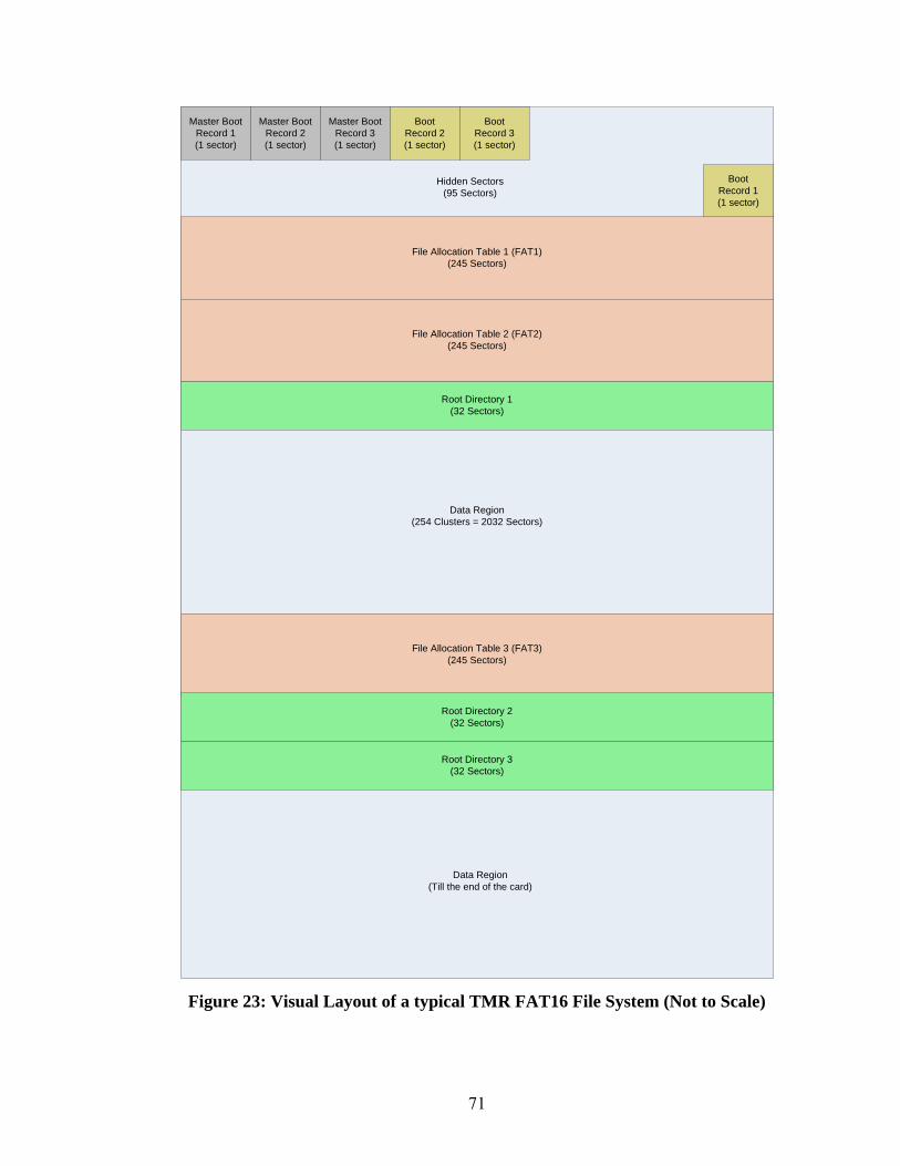
Master Boot Record 1(1 sector)
Master Boot Record 2(1 sector)
Master Boot Record 3(1 sector)
Boot Record 2(1 sector)
Boot Record 3(1 sector)
Boot Record 1(1 sector)
File Allocation Table 1 (FAT1)(245 Sectors)
Hidden Sectors(95 Sectors)
Root Directory 1(32 Sectors)
Data Region(254 Clusters = 2032 Sectors)
File Allocation Table 2 (FAT2)(245 Sectors)
File Allocation Table 3 (FAT3)(245 Sectors)
Root Directory 2(32 Sectors)
Root Directory 3(32 Sectors)
Data Region(Till the end of the card)
Figure 23: Visual Layout of a typical TMR FAT16 File System (Not to Scale)
71
5.4.3 TMR for Root Directory
Similar to FAT Tables, Triple Redundant copies of Root Directory are created by using
the data region. The clusters immediately following the FAT3 are used to create two
copies of Root Directory. These clusters are also secured in the FAT Tables so that they
cannot be used by any other Files/Sub Directories. The region following the Root
Directories is again the data region.
The visual layout of a typical TMR FAT16 File System is shown in Figure 23. It shows
where the MBR, BR, FAT Tables, Root Directories and data regions are stored in a
typical Triple Modular Redundant FAT16 File System.
5.5 Deleting Hidden Chains and Files
As explained in the previous sections Triple Modular Copies of all Files can be stored.
But if a file needs to be deleted, sufficient care needs to be taken that all the three copies
of the file are deleted. This includes deleting all the hidden chains, and freeing all the
clusters used by the three copies of the file. To perform these tasks, the corresponding
functions are modified accordingly.
5.6 Additional Functions Written to Implement TMR
The following additional functions are written at different layers of the software to
implement the TMR, apart from extensively modifying most of the existing functions.
The newly created functions and their description is given below.
void TMR_Format(void)
Arguments: None
Description: This function formats the SD card such that the Triple Redundant
copies of Boot Record, Master Boot Record, FAT Tables and Root Directories are
created. This function needs to be called to format the SD before using with the
TMR FAT16 File System
Return Value: None.
72
unsigned Sect_Root_Dir_1 (void)
Arguments: None
Description: Returns the first sector of the second copy of the Root Directory
unsigned Sect_Root_Dir_2 (void)
Arguments: None
Description: Returns the first sector of the third copy of the Root Directory
unsigned Sect_Fat3 (void)
Arguments: None
Description: Returns the first sector of the third copy of the FAT Table
char TMR_cmp (ubyte *buf1, ubyte *buf2, ubyte *buf3, unsigned int count)
Arguments:
1. ubyte * buf1: Pointer to the buffer1
2. ubyte * buf2: Pointer to the buffer3
3. ubyte * buf3: Pointer to the buffer3
4. unsigned int count: Number of bytes to compare
Description: Compares the specified number of bytes (count) in the buffer1,
buffer2 and buffer3 for consistency, byte by byte. If any one of the buffers is not
consistent, it auto corrects the source based on TMR poling. If none of the buffers
are consistent, then it returns the appropriate error code indicating that TMR has
failed
Return Value:
a. Returns 0 if all the three copies are consistent
b. Returns 1 if buffer3 is not consistent, but self corrected
c. Returns 2 if buffer1 is not consistent, but self corrected
d. Returns 3 if buffer2 is not consistent, but self corrected
e. Returns 4 if all the three bytes don’t match, TMR has failed
73
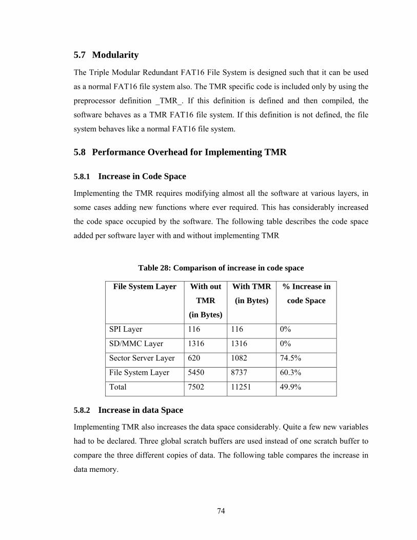
5.7 Modularity
The Triple Modular Redundant FAT16 File System is designed such that it can be used
as a normal FAT16 file system also. The TMR specific code is included only by using the
preprocessor definition _TMR_. If this definition is defined and then compiled, the
software behaves as a TMR FAT16 file system. If this definition is not defined, the file
system behaves like a normal FAT16 file system.
5.8 Performance Overhead for Implementing TMR
5.8.1 Increase in Code Space
Implementing the TMR requires modifying almost all the software at various layers, in
some cases adding new functions where ever required. This has considerably increased
the code space occupied by the software. The following table describes the code space
added per software layer with and without implementing TMR
Table 28: Comparison of increase in code space
File System Layer With out
TMR
(in Bytes)
With TMR
(in Bytes)
% Increase in
code Space
SPI Layer 116 116 0%
SD/MMC Layer 1316 1316 0%
Sector Server Layer 620 1082 74.5%
File System Layer 5450 8737 60.3%
Total 7502 11251 49.9%
5.8.2 Increase in data Space
Implementing TMR also increases the data space considerably. Quite a few new variables
had to be declared. Three global scratch buffers are used instead of one scratch buffer to
compare the three different copies of data. The following table compares the increase in
data memory.
74
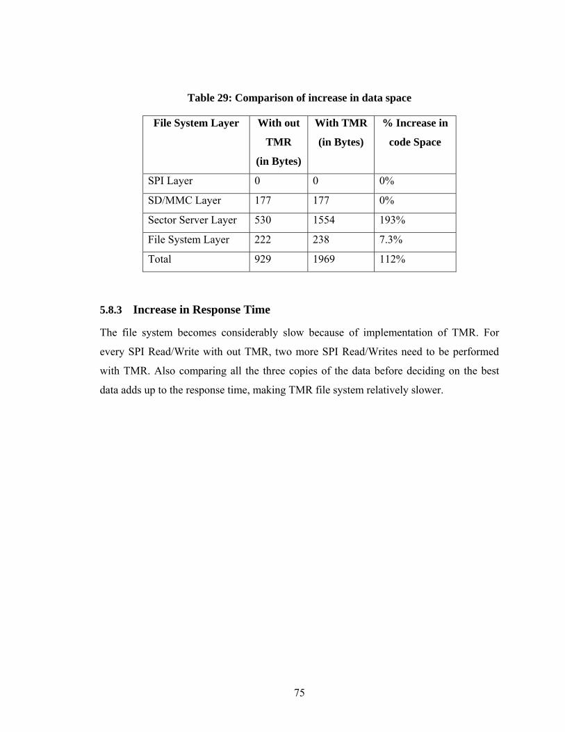
Table 29: Comparison of increase in data space
File System Layer With out
TMR
(in Bytes)
With TMR
(in Bytes)
% Increase in
code Space
SPI Layer 0 0 0%
SD/MMC Layer 177 177 0%
Sector Server Layer 530 1554 193%
File System Layer 222 238 7.3%
Total 929 1969 112%
5.8.3 Increase in Response Time
The file system becomes considerably slow because of implementation of TMR. For
every SPI Read/Write with out TMR, two more SPI Read/Writes need to be performed
with TMR. Also comparing all the three copies of the data before deciding on the best
data adds up to the response time, making TMR file system relatively slower.
75
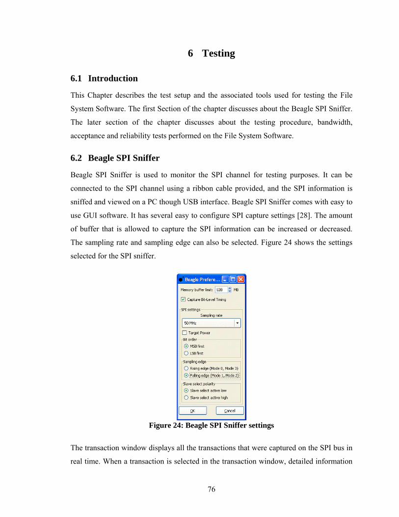
6 Testing
6.1 Introduction
This Chapter describes the test setup and the associated tools used for testing the File
System Software. The first Section of the chapter discusses about the Beagle SPI Sniffer.
The later section of the chapter discusses about the testing procedure, bandwidth,
acceptance and reliability tests performed on the File System Software.
6.2 Beagle SPI Sniffer
Beagle SPI Sniffer is used to monitor the SPI channel for testing purposes. It can be
connected to the SPI channel using a ribbon cable provided, and the SPI information is
sniffed and viewed on a PC though USB interface. Beagle SPI Sniffer comes with easy to
use GUI software. It has several easy to configure SPI capture settings [28]. The amount
of buffer that is allowed to capture the SPI information can be increased or decreased.
The sampling rate and sampling edge can also be selected. Figure 24 shows the settings
selected for the SPI sniffer.
Figure 24: Beagle SPI Sniffer settings
The transaction window displays all the transactions that were captured on the SPI bus in
real time. When a transaction is selected in the transaction window, detailed information
76
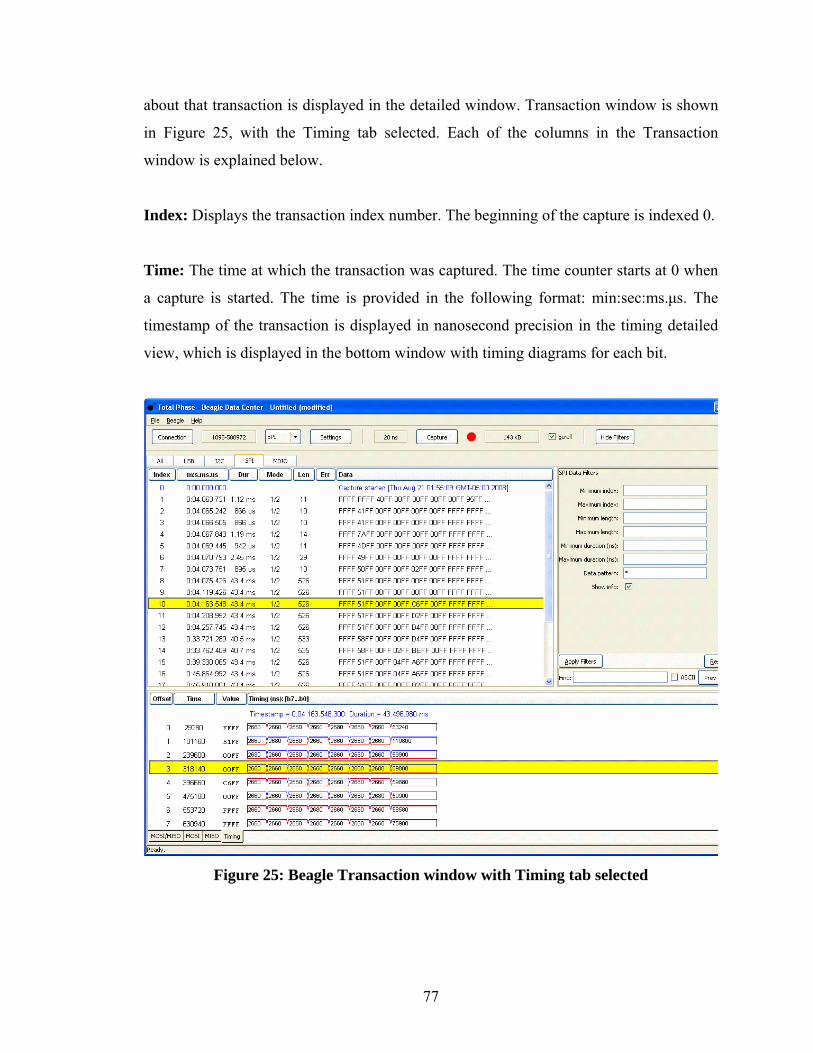
about that transaction is displayed in the detailed window. Transaction window is shown
in Figure 25, with the Timing tab selected. Each of the columns in the Transaction
window is explained below.
Index: Displays the transaction index number. The beginning of the capture is indexed 0.
Time: The time at which the transaction was captured. The time counter starts at 0 when
a capture is started. The time is provided in the following format: min:sec:ms.μs. The
timestamp of the transaction is displayed in nanosecond precision in the timing detailed
view, which is displayed in the bottom window with timing diagrams for each bit.
Figure 25: Beagle Transaction window with Timing tab selected
77
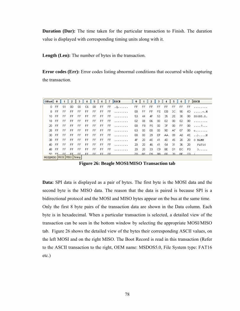
Duration (Dur): The time taken for the particular transaction to Finish. The duration
value is displayed with corresponding timing units along with it.
Length (Len): The number of bytes in the transaction.
Error codes (Err): Error codes listing abnormal conditions that occurred while capturing
the transaction.
Figure 26: Beagle MOSI/MISO Transaction tab
Data: SPI data is displayed as a pair of bytes. The first byte is the MOSI data and the
second byte is the MISO data. The reason that the data is paired is because SPI is a
bidirectional protocol and the MOSI and MISO bytes appear on the bus at the same time.
Only the first 8 byte pairs of the transaction data are shown in the Data column. Each
byte is in hexadecimal. When a particular transaction is selected, a detailed view of the
transaction can be seen in the bottom window by selecting the appropriate MOSI/MISO
tab. Figure 26 shows the detailed view of the bytes their corresponding ASCII values, on
the left MOSI and on the right MISO. The Boot Record is read in this transaction (Refer
to the ASCII transaction to the right, OEM name: MSDOS5.0, File System type: FAT16
etc.)
78
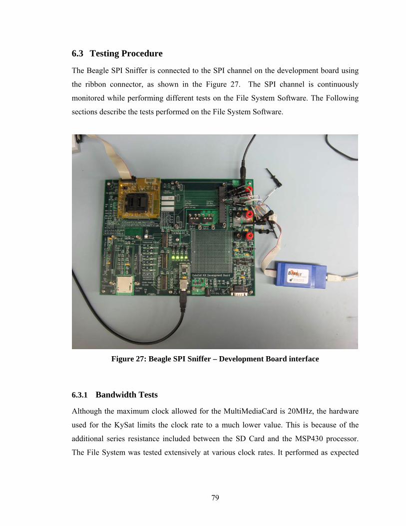
6.3 Testing Procedure
The Beagle SPI Sniffer is connected to the SPI channel on the development board using
the ribbon connector, as shown in the Figure 27. The SPI channel is continuously
monitored while performing different tests on the File System Software. The Following
sections describe the tests performed on the File System Software.
Figure 27: Beagle SPI Sniffer – Development Board interface
6.3.1 Bandwidth Tests
Although the maximum clock allowed for the MultiMediaCard is 20MHz, the hardware
used for the KySat limits the clock rate to a much lower value. This is because of the
additional series resistance included between the SD Card and the MSP430 processor.
The File System was tested extensively at various clock rates. It performed as expected
79
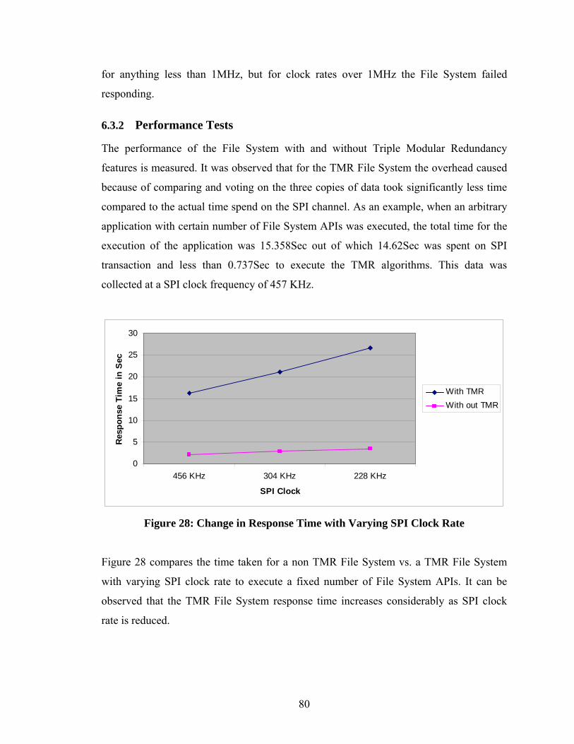
for anything less than 1MHz, but for clock rates over 1MHz the File System failed
responding.
6.3.2 Performance Tests
The performance of the File System with and without Triple Modular Redundancy
features is measured. It was observed that for the TMR File System the overhead caused
because of comparing and voting on the three copies of data took significantly less time
compared to the actual time spend on the SPI channel. As an example, when an arbitrary
application with certain number of File System APIs was executed, the total time for the
execution of the application was 15.358Sec out of which 14.62Sec was spent on SPI
transaction and less than 0.737Sec to execute the TMR algorithms. This data was
collected at a SPI clock frequency of 457 KHz.
0
5
10
15
20
25
30
456 KHz 304 KHz 228 KHz
SPI Clock
Res
po
nse
Tim
e in
Sec
With TMR
With out TMR
Figure 28: Change in Response Time with Varying SPI Clock Rate
Figure 28 compares the time taken for a non TMR File System vs. a TMR File System
with varying SPI clock rate to execute a fixed number of File System APIs. It can be
observed that the TMR File System response time increases considerably as SPI clock
rate is reduced.
80
6.3.3 Acceptance Tests
Several Acceptance Tests have been performed on the File System Software to simulate
various possible scenarios and make sure that the File System Software is working fine.
Some of them include, but not limited to:
1. Creating very big Files which spread over multiple Clusters to make sure that the
FAT chain is working properly
2. Creating nested Subdirectories with multiple files in each directory, and
traversing through directories to make sure that the Subdirectory feature is
implemented correctly.
3. Testing using various SD Cards, with various storage capacities ranging from
256MB to 2GB
4. Opening the Files using read(r), write(w) and append(a) mode to make sure the
file handle is behaving as expected.
5. Making sure that the File System complies to the “8.3” file name standard
specified by FAT16
6. Testing to make sure that the files created are really FAT16 compatible across
platforms (Opening the volume on a Windows PC).
6.3.4 TMR Reliability Tests
Triple Modular Redundancy has been extensively tested to make sure the Software is
Reliable and Fault Tolerant. Some of the Triple Modular Redundancy Reliability Tests
include:
1. Faults were introduced into a copy of TMR at various levels and tested to make
sure that the File System is Fault Tolerant, and self corrects even if one of the
copy is erroneous.
2. Testing to make sure that the Clusters used for the FAT3, and two copies of Root
Directory are properly secured by having relevant entries in the FAT Tables.
3. Testing the TMR File System with SD Cards of different volume size, 256MB till
2GB
4. Extensive testing to make sure that the TMR is implemented at File and
Subdirectory level, and the hidden FAT chains performance is also tested
81
5. Testing to make sure that the Triple Redundant copies of Master Boot Record,
Boot Record, FAT Tables and Root Directories are created.
6. Testing the TMR File System across platforms to make sure that the Files created
in TMR File System also works fine in a non TMR FAT16 File System.
7. Testing to make sure that the clusters of the hidden FAT Chains used for the TMR
copies are freed when a TMR File is deleted.
6.4 Summary
The File System was tested extensively to make sure it is Reliable and Fault Tolerant.
The operating SPI clock speed can be increased to a much higher value theoretically to
achieve higher bandwidths, but the hardware used for the KySat limits it to close to
1MHz. The Triple Modular Redundancy feature is extensively tested to make sure that
the system works fine and self corrects itself for accidental bit flips.
82
7 Conclusion
7.1 Summary
Chapter 1 described the motivation and the necessity to have a Reliable Fault Tolerant
File System for space applications. The design requirements for such a File System are
discussed. Chapter 2 gave a brief introduction to Solid State Memories, and different
types of memory cards. The SD Card used as storage device for the present work is
discussed in detail. Chapter 3 explained in general about File Systems and in detail about
the FAT16 File System. SD Card based FAT16 File System software development is
explained in the Chapter 4. Different layers in the File System software and their
implementation details are discussed. Implementation of Fault Tolerant features using
Triple Modular Redundancy is explained in Chapter 5. Chapter 6 discussed about the test
setup and various acceptance and reliability tests performed on the File System Software.
The Triple Modular Redundant File System developed has proved to meet the design
requirements. It has the features a typical embedded File System is expected to have. It is
made highly reliable and Fault Tolerant to any accidental bit flips. Not only just the data
stored on the SD Card, but all the File System related components on the SD Card
(Master Boot Record, Boot Record, FAT Tables, and the Root Directory) are triplicated
to make the File System robust. Sufficient care is taken to make sure that the Triple
Redundant data stored on the SD Card complies by FAT16 specifications so that the
drive can be opened on a normal FAT16 File System, only one copy of the data is seen.
7.2 Future Directions
There is vast scope for continuing further research on the present TMR File System.
There are certain limitations in the present File System implementation which can be
taken forward as directions for future implementation. Some of them are discussed here.
Firstly, the files created on a volume using normal File System cannot be opened on the
present TMR File System. This is because the TMR File System checks for three copies
83
of the file, since two copies are missing the File System will give out a TMR error. The
File System can be made intelligent to recognize if a file has three copies or not before
executing the TMR algorithms. This can be achieved by using a special markup field in
the file’s Root Directory, telling if a file is triple copied or not. But since the Root
Directory is limited to 32 Bytes further analysis has to be carried out as to which field can
be used for this purpose without of significantly effecting FAT16 implementation.
The present TMR File System can be used to create, open, read, write or delete any file as
any normal embedded File System is expected to do. But there can be situations where
the user wants to copy multiple triple redundant files on to the volume before using it
onboard with the Flight Software. Normal windows PC cannot be used as it cannot make
triple copies of a file as implemented in TMR File System. There is scope to implement a
GUI based tool which can work as normal windows explorer, but can create TMR File
System compatible files. Most of the TMR File System software can be reused for such a
work.
One more limitation of the TMR File System is that the volume after formatting it as
FAT16 needs to be TMR Formatted before using with the TMR File System. Also it is
observed that, when the SD Card is opened on normal windows based computer certain
sections of the Root Directory are getting modified for reasons unknown. Hence the
volume need to TMR Formatted before using with the TMR File System. But this should
not be a problem as TMR Format will not delete any data on the volume. It just makes
sure that all the three copies of Master Boot Record, Boot Record, FAT Tables and Root
Directory are consistent. But further research can carried out in this direction.
84
References
[1] Martin Dentan, “Radiation Effects on Electronic Components And Circuits”,
European Organization for Nuclear Research CERN Training, April 2000
[2] K. Bedingfield, R. Leach and M. Alexander, “Spacecraft System Failures and
Anomalies Attributed to the Natural Space Environment”, NASA Reference Publication
1390, Marshall Space Flight Center, Aug 1996
[3] Shadab G Ambat, “Single Event Upset Detection in field Programmable Gate
Arrays”, Master’s Thesis, University of Kentucky, Feb 2008
[4] Goutam Kumar Saha, “Software Implemented Fault Tolerance – the ESVP
Approach”, Ubiquity, Volume 7, Issue 31, Aug 15, 2006 – Aug 22, 2006
[5] HCC-Embedded Kft., “Embedded Flash File System FAT12/16/32 Implementation
Guide”, version 2.62, 2003
[6] IEEE, “IEEE Morris N.Liebmann Memorial Award Recipients”,
http://www.ieee.org/ portal/pages/about/awards/pr/liebpr.html, 2008
[7] Kingston Technology Company Inc., “Flash Memory Guide”, http://www.
kingston.com/ products/DMTechGuide.pdf, 17600 Newhope Street, Fountain Valley,
CA, 2006
[8]Toshiba America Electronic Components, Inc., “NAND vs. NOR Flash Memory
Technology Overview” http://www.toshiba.com/taec/components/Generic
/Memory_Resources/NANDvsNOR.pdf, 19900 Macarthur Boulevard, Suite 400, Irvine,
CA
[9] CFA, “Compact Flash Association Information” http://www.compactflash.org
/info/cfainfo.htm, April 28, 2007
[10] Samsung Electronics, “SmartMedia Format Introduction”, http://www.win.tue.nl/
~aeb/linux/smartmedia/SmartMedia_Format.pdf, Memory Product & Technology
Division, 13 July, 1999
[11] Sandisk Corporation, “SanDisk MultiMediaCard and Reduced-Size
MultiMediaCard”, http://www.sandisk.com/Assets/File/OEM/Manuals/ProdManRS-
MMCv1.3.pdf, Product Manual, Version 1.3, April 2005
85
[12] MultiMediaCard Association, “MMCA: Home” http://www.mmca.org/
technology/about/, 2007
[13] Sony Corporation, “Sony Press Release, July 30, 1998”, http://www.sony.net/
SonyInfo/News/Press_Archive/199807/98-067/, July 30, 1998
[14] SD Association, “About SD Association”, http://www.sdcard.org/about/, 2008
[15] Toshiba Corporation, “Toshiba Press Releases 17 July, 2003”, http://www.toshiba.
co.jp/about/press/2003_07/pr1701.htm, 17 July, 2003
[16] DRAMeXchange, “A Look Into How SDHC Will Affect the Future Nand Flash
Market”, http://www.dramexchange.com/WeeklyResearch/Post/1/492.aspx, Dec 5, 2006
[17] Microsoft Corporation, “FAT: General Overview of On-Disk Format”,
http://download.microsoft.com/download/1/6/1/161ba512-40e2-4cc9-843a-
923143f3456c/fatgen103.doc, Version 1.03, December 6, 2000
[18] PC Guide, “FAT Sizes: FAT12, FAT16 and FAT32”, http://www.pcguide.com/
ref/hdd/file/partSizes-c.html, Version 2.2.0, April 17, 2007
[19]Clark, “File Allocation Table – 16bit”, http://www.beginningtoseethelight.org/
fat16/, [email protected]
[20] G. Chandler, D. McClure, S. Hishmeh, J. Lumpp, Jr., J. Carter, B. Malphrus et al.,
“Development of an Off-the-Shelf Bus for Small Satellites”, IEEE Aerospace Conference,
Mar 2007.
[21] Adrew E. Kalman, Pumpkin Inc., Interfacing MSP430 Flash Emulation Tools to the
CubeSat Kit”, http://www.pumpkininc.com/content/doc/appnote/an-34.pdf, 744 Naples
Street, San Fransisco, CA, Jun 2, 2006
[22] Rowley Associates Ltd., “CrossWorks for MSP430”, http://www.rowley.co.uk/
msp430/msp430_manual.pdf, User Guide
[23] Silicon Laboratories Inc., “USB Mass Storage Reference Design”,
https://www.silabs.com/Support%20Documents/TechnicalDocs/AN282.pdf, Rev. 0.1,
4635 Boston Lane, Austin, TX
[24] Texas Insturments Inc., “MSP430x1xx Family”, http://focus.ti.com/
lit/ug/slau049f/slau049f.pdf, Users Guide, Dallas, Tx
[25] Total Phase, “Beagle Data Center, Software Manual”, http://www.totalphase.com/
download/pdf/data-center-v2.20.pdf v2.20, July 18, 2008
86
87
Vita
Rama Krishna Nimmagadda was born on June 04, 1983 in Nizamabad, India. After
completing Bachelor of Technology in Electronics and Communication Engineering from
Sri Ventakeshwara University College of Engineering, Tirupati, India, in 2004, he
worked as Embedded Software Engineer for two years. He enrolled for Masters Degree
in Electrical Engineering at the University of Kentucky in Fall 2006. During his Masters
Program he worked for the Space Systems Laboratory at University of Kentucky in
developing Fault Tolerant Embedded Software for Space Applications.