Sensitive Awareness and Spurious Feeling: Lawrence the Reviser and Lady Chatterley's Lover
[Wang, 3(9): September, 2014] ISSN: 2277-9655 Scientific Journal Impact Factor: 3.449
(ISRA), Impact Factor: 2.114
http: // www.ijesrt.com (C)International Journal of Engineering Sciences & Research Technology [358]
IJESRT INTERNATIONAL JOURNAL OF ENGINEERING SCIENCES & RESEARCH
TECHNOLOGY
A FPGA-Based Numerically Controlled Oscillator without Spurious Component
Guoping Wang Department of Engineering, Indiana University Purdue University Fort Wayne, Fort Wayne, Indiana
Abstracts Direct digital synthesizers (DDS), or numerically controlled oscillators (NCO), are important components in
many digital communication systems, such as digital radios and modems, software-defined radios, digital down/up
converters for cellular and PCS base stations, etc. A common method for digitally generating a complex or real valued
sinusoid employs a lookup table scheme. In this paper, a variable system clock technique and variable module counter
based on current FPGA clock management technology is proposed for NCO implementation. The proposed design is
implemented on Xilinx Virtex 5 FPGA and the simulation result demonstrates significant improvement in reducing
the Spurious Free Dynamic Range (SFDR).
Keyword: Direct Digital Synthesizer, SFDR, FPGA, Clock Management Module.
Introduction
Direct digital synthesizers (DDS), or
numerically controlled oscillators (NCO), are
important components in many digital communication
systems, such as digital radios and modems, software-
defined radios (SDR), digital down/up converters for
cellular and PCS base stations, etc. Quadrature
synthesizers are used for constructing digital down and
up converters, demodulators, and implementing
various types of modulation schemes, including PSK
(phase shift keying), FSK frequency shift keying), and
MSK (minimum shift keying). A common method for
digitally generating a complex or real valued sinusoid
employs a lookup table scheme. The lookup table
stores samples of a sinusoid. A digital integrator is
used to generate a suitable phase argument that is
mapped by the lookup table to the desired output
waveform. For example, in a FM radio with digital IF
system as shown in Figure 1, the RF received signal
from antenna is converted into digital signal and then
it is modulated and converted into Intermediate
Frequency by mixing with the sinusoid and cosine
digital signals from an NCO. The IF signal can be
processed in the band of intermediate frequency.
Figure 1. FM Radio with Digital IF
Some advantages of an DDS advantages are:
Micro-Hertz tuning resolution of the output
frequency and sub-degree phase tuning
capability, all under complete digital control.
Extremely fast hopping speed in tuning
output frequency (or phase), phase-
continuous frequency hops with no
over/undershoot or analog-related loop
settling time anomalies.
The DDS digital architecture eliminates the
need for the manual system tuning and
tweaking associated with component aging
and temperature drift in analog synthesizer
solutions.
The digital control interface of the DDS
architecture facilitates an environment where
systems can be remotely controlled, and
minutely optimized, under processor control.
[Wang, 3(9): September, 2014] ISSN: 2277-9655 Scientific Journal Impact Factor: 3.449
(ISRA), Impact Factor: 2.114
http: // www.ijesrt.com (C)International Journal of Engineering Sciences & Research Technology [359]
When utilized as a quadrature synthesizer,
DDS afford unparalleled matching and
control of I and Q synthesized outputs.
For the direct digital frequency synthesis, two types of
architecture have been developed in the past: ROM
based and ROM-less. The ROM-based DDFS uses a
look-up table to convert the phase information into the
sinusoid and cosine magnitude. It was first proposed
in 1987 [1], and some of the modified architectures [2]
are modified Sunderland architecture, modified
Nicholas architecture, Taylor series expansion, and
CORDIC-based algorithm.
ROM-based DDFS has a simple structure and generate
fast frequency signal output. It uses a ROM to convert
the phase accumulation information into an amplitude
value such as sinusoid and cosine values. It usually can
achieve very high-speed output signals. ROM-less
architectures manage to remove completely the ROM
and the phase-to-amplitude conversion is conducted
using interpolation algorithms [3]. These ROM-less
architectures can achieve a good performance when
the synthesized frequency is relatively low compared
to the sampling frequency.
In this paper, a ROM-based DDFS architecture with
an improvement of SFDR is proposed using the
current FPGA technology. This paper is organized as
follows, in Section II, the basic ROM-based DDFS is
described and the main challenges of DDFS design are
discussed. In Section III, the proposed DDFS
architecture is presented. Implementation and
simulation results on Xilinx FPGAs are also discussed
by comparing with other approaches. Finally, Section
IV concludes this paper with a summary.
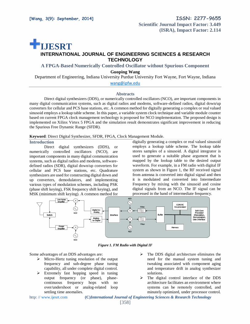
Overview of ROM-based DDFS A. DDFS Architecture
Direct digital synthesis is a technique for using digital
logic blocks to generate an output signal, such as
sinusoid and cosine with various frequency with
reference to a fixed-frequency clock source, that is, the
reference clock frequency is scaled down to a
programmable frequency signal. The output signal
waveform can be any kind of waveform, while
sinusoid and cosine are the most popular ones. The
implementation of DDFS is divided into two distinct
parts as shown in Figure 2: a discrete-time phase
accumulator and a phase-to-amplitude converter
outputting the desired sinusoid and cosine signal. In
the ROM-based architecture, the conversion is done
by a look-up-table (LUT). The D/A converter and
filter can be skipped in a pure-digital NCO
environment such as software-defined radio.
Figure 2. Simplified Diagram of Direct Digital Synthesis
Assuming that the LUT has nN 2 entries, when n is
the number of address bits generated by the phase
accumulator. The precision of the LUT is L bits and
this parameter is completely independent of n . The
step size, , determines how quickly the phase
address is accumulated, and hence the frequency of the
generated sinusoid/cosine wave. The step size, , can
be derived from Equation (1),
Let
N : the number of entries of the LUT
sf : the system sampling frequency
df : the desired frequency of generated sine
waveform
[Wang, 3(9): September, 2014] ISSN: 2277-9655 Scientific Journal Impact Factor: 3.449
(ISRA), Impact Factor: 2.114
http: // www.ijesrt.com (C)International Journal of Engineering Sciences & Research Technology [360]
then, we have
d
s
fN
f (1)
For example, giving the LUT size of 2 256nN
, the sampling frequency 2 256nN and the
desired frequency is 2.4MHz , the resulting phase
accumulator step size is
2.4256 61.44
10
Mhz
Mhz .
The phase accumulator includes a fractional part,
which is not used when referencing the LUT, but
which allows frequency control to be achieved. In that
case, the step size is a fixed-point number, comprising
n whole bits to address the LUT and B fractional bits,
as shown in Figure 2.
According to Equation (2), if the step size quantization
is too coarse (i.e., large ), the frequency which is
actually realized may suffer a large frequency error.
The number of fractional bits in the accumulator
should therefore be chosen according to the maximum
acceptable frequency error, the frequency resolution
af is derived as described in Equation (2).
2
s sa b
f ff
N N (2)
B. Quantization Effects
Quantization occurs on both the phase accumulation
and on the LUT amplitude quantization.
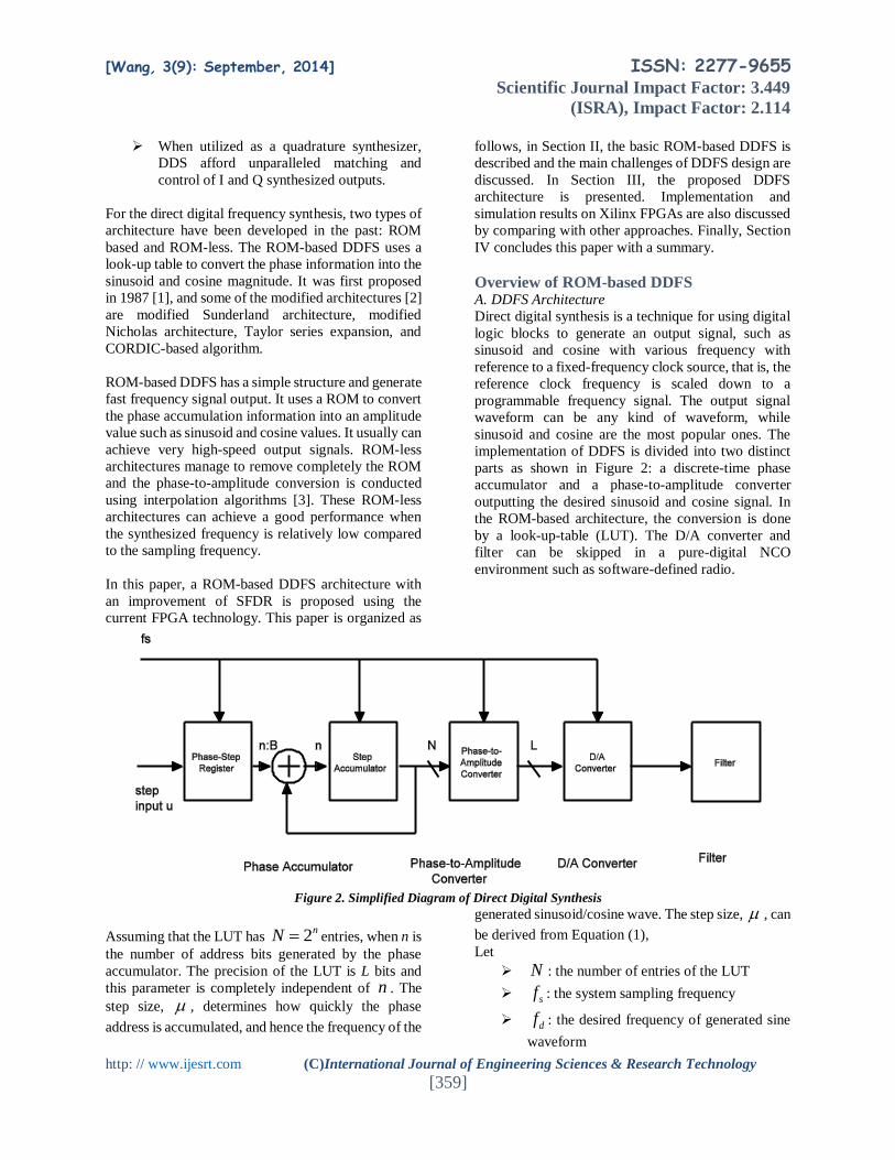
C. Phase Quantization
The phase accumulator is increased by step size
with n whole bits and b fractional bits, however, to
keep a relatively small size ROM, the b fractional bits
are not used with only n whole bits are used to index
the LUT. Unfortunately, this phase truncation
introduces a phase noise and produces unwanted
spurious spectral component in the DDFS output
signals, and thus degrades the spectral purity of the
synthesized sine waveform, one example as shown in
Figure 3. The Spurious Free Dynamic Range (SFDR)
is the difference between the spectral peak and the
highest spur, as it can be approximated by [4].
6.02 3.92 SFDR n dB
(3)
Figure 3. A Sample of Output Spectrum with SFDR
SFDR is an important consideration when designing
radio systems. If the oscillator signal contains
significant spurious frequencies , these unwanted
components can contaminate the signal being mixed.
They may be difficult to subsequently remove,
especially when close to the center frequency.
D. Amplitude Quantization
The output of the phase-to-amplitude LUT has limited
precision, L bits. This amplitude quantization results
in a signal-to-noise ratio, usually approximated [5] by:
6.02 1.76SNR L (4)
This SNR limits the performance of the output signal,
as its spectrum has a noise floor due to rounding error
of the LUT table. This causes a further degradation to
the ideal sine wave output, which can be observed in
both the time domain and the frequency domain. LUT
resolution and depth are therefore the key factors
influencing unwanted spectral components. From the
results in [4], we can now mainly focus on the SFDR
[Wang, 3(9): September, 2014] ISSN: 2277-9655 Scientific Journal Impact Factor: 3.449
(ISRA), Impact Factor: 2.114
http: // www.ijesrt.com (C)International Journal of Engineering Sciences & Research Technology [361]
instead of SNR of a DDFS to improve the output
spectrum purity.
E. SFDR Improving
One way to improve SFDR is to increase the phase
accumulator whole bits n, and hence the size of the
LUT table. However, for higher values of n, the
memory size become impractical. Some approaches
are investigated to compress the ROM-size [2], which
we will not discuss in further details in this paper.
Many techniques can be used to improve SFDR of an
DDFS. In this section, we describe mainly two popular
methods 1) phase-dithering, 2) Taylor series
approximation. Both techniques are used in the latest
Xilinx FPGA DDS logic box [6].
F. Phase Dithering
Dithering is a technique often used in digital audio
whereby a very low level of noise is added to a signal
in order to improve the psychoacoustically perceived
sound by decorrelating the quantized signal and the
quantization noise. The addition of dithering noise to
a signal actually reduces the SNR (more noise is being
added to the original signal). The overall signal
reproduction is likely to be (psychoacoustically)
improved by breaking up the correlation between the
various signal components and quantization error.
Without dithering the quantization noise will be
perceived as harmonic or tonal distortion [7].
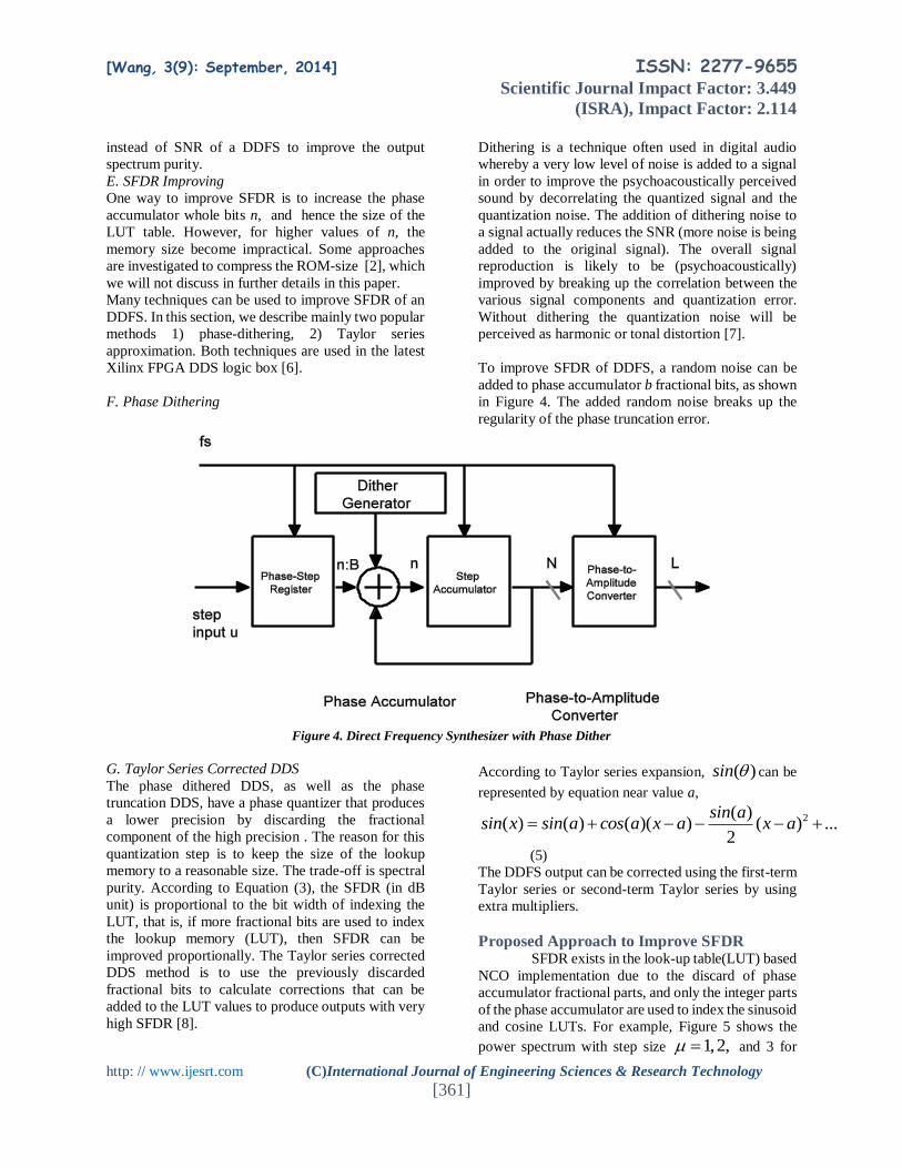
To improve SFDR of DDFS, a random noise can be
added to phase accumulator b fractional bits, as shown
in Figure 4. The added random noise breaks up the
regularity of the phase truncation error.
Figure 4. Direct Frequency Synthesizer with Phase Dither
G. Taylor Series Corrected DDS
The phase dithered DDS, as well as the phase
truncation DDS, have a phase quantizer that produces
a lower precision by discarding the fractional
component of the high precision . The reason for this
quantization step is to keep the size of the lookup
memory to a reasonable size. The trade-off is spectral
purity. According to Equation (3), the SFDR (in dB
unit) is proportional to the bit width of indexing the
LUT, that is, if more fractional bits are used to index
the lookup memory (LUT), then SFDR can be
improved proportionally. The Taylor series corrected
DDS method is to use the previously discarded
fractional bits to calculate corrections that can be
added to the LUT values to produce outputs with very
high SFDR [8].
According to Taylor series expansion, ( )sin can be
represented by equation near value a,
2( )( ) ( ) ( )( ) ( ) ...
2
sin asin x sin a cos a x a x a
(5)
The DDFS output can be corrected using the first-term
Taylor series or second-term Taylor series by using
extra multipliers.
Proposed Approach to Improve SFDR SFDR exists in the look-up table(LUT) based
NCO implementation due to the discard of phase
accumulator fractional parts, and only the integer parts
of the phase accumulator are used to index the sinusoid
and cosine LUTs. For example, Figure 5 shows the
power spectrum with step size 1,2, and 3 for
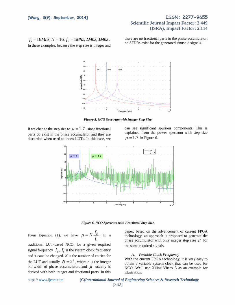
[Wang, 3(9): September, 2014] ISSN: 2277-9655 Scientific Journal Impact Factor: 3.449
(ISRA), Impact Factor: 2.114
http: // www.ijesrt.com (C)International Journal of Engineering Sciences & Research Technology [362]
16 , 16, 1 ,2 ,3s af Mhz N f Mhz Mhz Mhz .
In these examples, because the step size is integer and
there are no fractional parts in the phase accumulator,
no SFDRs exist for the generated sinusoid signals.
Figure 5. NCO Spectrum with Integer Step Size
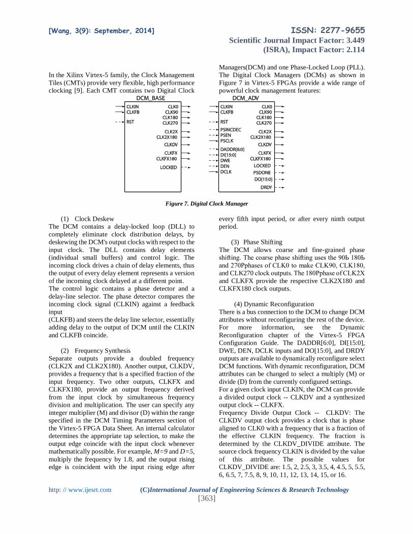
If we change the step size to 1.7 , since fractional
parts do exist in the phase accumulator and they are
discarded when used to index LUTs. In this case, we
can see significant spurious components. This is
explained from the power spectrum with step size
1.7 in Figure 6.
Figure 6. NCO Spectrum with Fractional Step Size
From Equation (1), we have d
s
fN
f . In a
traditional LUT-based NCO, for a given required
signal frequency ,d sf f is the system clock frequency
and it can't be changed. N is the number of entries for
the LUT and usually 2nN , where n is the integer
bit width of phase accumulator, and usually is
derived with both integer and fractional parts. In this
paper, based on the advancement of current FPGA
technology, an approach is proposed to generate the
phase accumulator with only integer step size for
the some required signals.
A. Variable Clock Frequency
With the current FPGA technology, it is very easy to
obtain a variable system clock that can be used for
NCO. We'll use Xilinx Virtex 5 as an example for
illustration.
[Wang, 3(9): September, 2014] ISSN: 2277-9655 Scientific Journal Impact Factor: 3.449
(ISRA), Impact Factor: 2.114
http: // www.ijesrt.com (C)International Journal of Engineering Sciences & Research Technology [363]
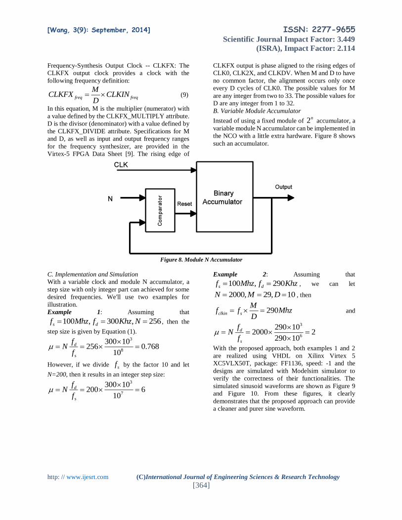
In the Xilinx Virtex-5 family, the Clock Management
Tiles (CMTs) provide very flexible, high performance
clocking [9]. Each CMT contains two Digital Clock
Managers(DCM) and one Phase-Locked Loop (PLL).
The Digital Clock Managers (DCMs) as shown in
Figure 7 in Virtex-5 FPGAs provide a wide range of
powerful clock management features:
Figure 7. Digital Clock Manager
(1) Clock Deskew
The DCM contains a delay-locked loop (DLL) to
completely eliminate clock distribution delays, by
deskewing the DCM's output clocks with respect to the
input clock. The DLL contains delay elements
(individual small buffers) and control logic. The
incoming clock drives a chain of delay elements, thus
the output of every delay element represents a version
of the incoming clock delayed at a different point.
The control logic contains a phase detector and a
delay-line selector. The phase detector compares the
incoming clock signal (CLKIN) against a feedback
input
(CLKFB) and steers the delay line selector, essentially
adding delay to the output of DCM until the CLKIN
and CLKFB coincide.
(2) Frequency Synthesis
Separate outputs provide a doubled frequency
(CLK2X and CLK2X180). Another output, CLKDV,
provides a frequency that is a specified fraction of the
input frequency. Two other outputs, CLKFX and
CLKFX180, provide an output frequency derived
from the input clock by simultaneous frequency
division and multiplication. The user can specify any
integer multiplier (M) and divisor (D) within the range
specified in the DCM Timing Parameters section of
the Virtex-5 FPGA Data Sheet. An internal calculator
determines the appropriate tap selection, to make the
output edge coincide with the input clock whenever
mathematically possible. For example, M=9 and D=5,
multiply the frequency by 1.8, and the output rising
edge is coincident with the input rising edge after
every fifth input period, or after every ninth output
period.
(3) Phase Shifting
The DCM allows coarse and fine-grained phase
shifting. The coarse phase shifting uses the 90Ь 180Ь
and 270Рphases of CLK0 to make CLK90, CLK180,
and CLK270 clock outputs. The 180Рphase of CLK2X
and CLKFX provide the respective CLK2X180 and
CLKFX180 clock outputs.
(4) Dynamic Reconfiguration
There is a bus connection to the DCM to change DCM
attributes without reconfiguring the rest of the device.
For more information, see the Dynamic
Reconfiguration chapter of the Virtex-5 FPGA
Configuration Guide. The DADDR[6:0], DI[15:0],
DWE, DEN, DCLK inputs and DO[15:0], and DRDY
outputs are available to dynamically reconfigure select
DCM functions. With dynamic reconfiguration, DCM
attributes can be changed to select a multiply (M) or
divide (D) from the currently configured settings.
For a given clock input CLKIN, the DCM can provide
a divided output clock -- CLKDV and a synthesized
output clock -- CLKFX.
Frequency Divide Output Clock -- CLKDV: The
CLKDV output clock provides a clock that is phase
aligned to CLK0 with a frequency that is a fraction of
the effective CLKIN frequency. The fraction is
determined by the CLKDV_DIVIDE attribute. The
source clock frequency CLKIN is divided by the value
of this attribute. The possible values for
CLKDV_DIVIDE are: 1.5, 2, 2.5, 3, 3.5, 4, 4.5, 5, 5.5,
6, 6.5, 7, 7.5, 8, 9, 10, 11, 12, 13, 14, 15, or 16.
[Wang, 3(9): September, 2014] ISSN: 2277-9655 Scientific Journal Impact Factor: 3.449
(ISRA), Impact Factor: 2.114
http: // www.ijesrt.com (C)International Journal of Engineering Sciences & Research Technology [364]
Frequency-Synthesis Output Clock -- CLKFX: The
CLKFX output clock provides a clock with the
following frequency definition:
freq freq
MCLKFX CLKIN
D (9)
In this equation, M is the multiplier (numerator) with
a value defined by the CLKFX_MULTIPLY attribute.
D is the divisor (denominator) with a value defined by
the CLKFX_DIVIDE attribute. Specifications for M
and D, as well as input and output frequency ranges
for the frequency synthesizer, are provided in the
Virtex-5 FPGA Data Sheet [9]. The rising edge of
CLKFX output is phase aligned to the rising edges of
CLK0, CLK2X, and CLKDV. When M and D to have
no common factor, the alignment occurs only once
every D cycles of CLK0. The possible values for M
are any integer from two to 33. The possible values for
D are any integer from 1 to 32.
B. Variable Module Accumulator
Instead of using a fixed module of 2n accumulator, a
variable module N accumulator can be implemented in
the NCO with a little extra hardware. Figure 8 shows
such an accumulator.
Figure 8. Module N Accumulator
C. Implementation and Simulation
With a variable clock and module N accumulator, a
step size with only integer part can achieved for some
desired frequencies. We'll use two examples for
illustration.
Example 1: Assuming that
100 , 300 , 256s df Mhz f Khz N , then the
step size is given by Equation (1). 3
8
300 10256 0.768
10
d
s
fN
f
However, if we divide sf by the factor 10 and let
N=200, then it results in an integer step size: 3
7
300 10200 6
10
d
s
fN
f
Example 2: Assuming that
100 , 290s df Mhz f Khz , we can let
2000, 29, 10N M D , then
290clkin s
Mf f Mhz
D and
3
6
290 102000 2
290 10
d
s
fN
f
With the proposed approach, both examples 1 and 2
are realized using VHDL on Xilinx Virtex 5
XC5VLX50T, package: FF1136, speed: -1 and the
designs are simulated with Modelsim simulator to
verify the correctness of their functionalities. The
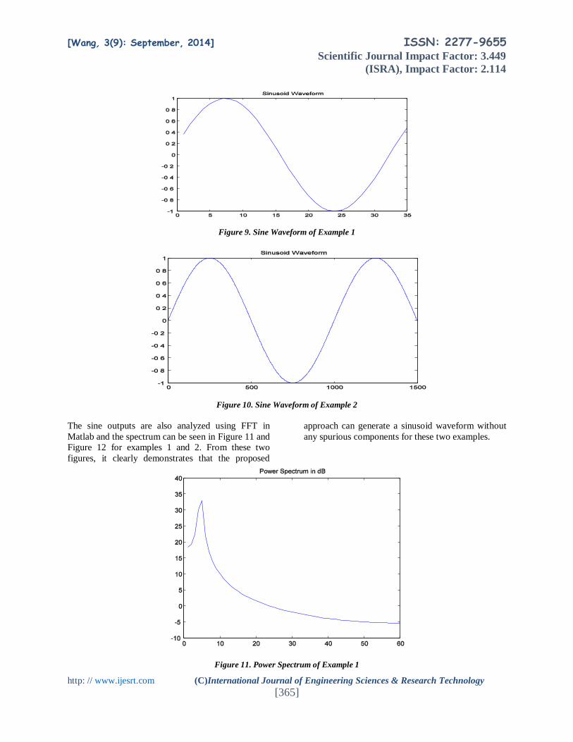
simulated sinusoid waveforms are shown as Figure 9
and Figure 10. From these figures, it clearly
demonstrates that the proposed approach can provide
a cleaner and purer sine waveform.
[Wang, 3(9): September, 2014] ISSN: 2277-9655 Scientific Journal Impact Factor: 3.449
(ISRA), Impact Factor: 2.114
http: // www.ijesrt.com (C)International Journal of Engineering Sciences & Research Technology [365]
Figure 9. Sine Waveform of Example 1
Figure 10. Sine Waveform of Example 2
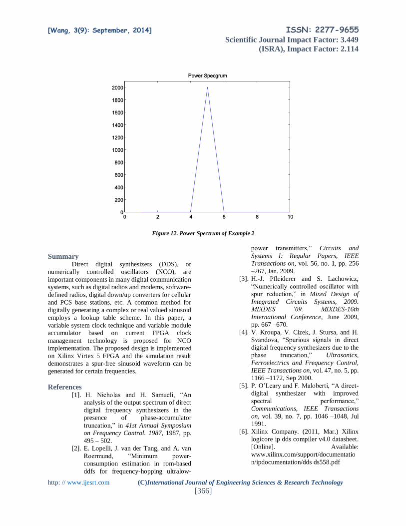
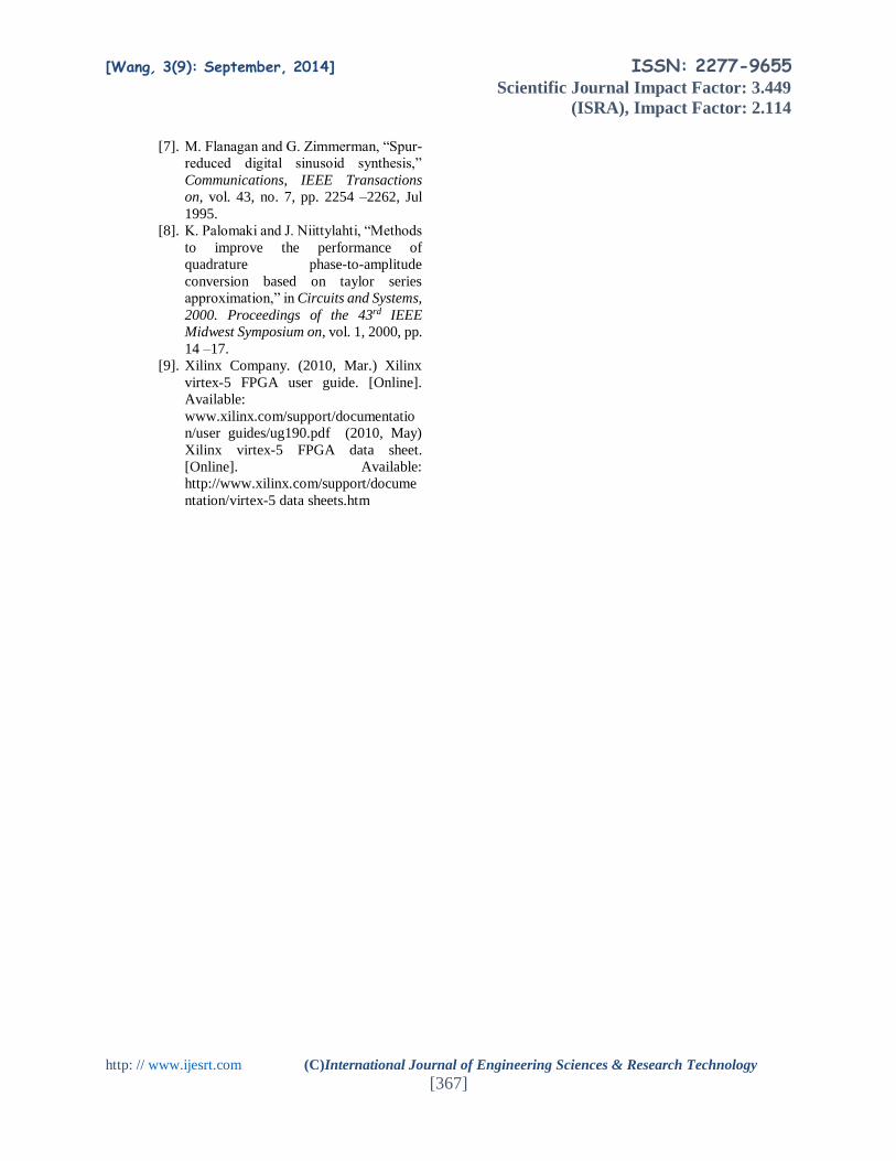
The sine outputs are also analyzed using FFT in
Matlab and the spectrum can be seen in Figure 11 and
Figure 12 for examples 1 and 2. From these two
figures, it clearly demonstrates that the proposed
approach can generate a sinusoid waveform without
any spurious components for these two examples.
Figure 11. Power Spectrum of Example 1
[Wang, 3(9): September, 2014] ISSN: 2277-9655 Scientific Journal Impact Factor: 3.449
(ISRA), Impact Factor: 2.114
http: // www.ijesrt.com (C)International Journal of Engineering Sciences & Research Technology [366]
Figure 12. Power Spectrum of Example 2
Summary Direct digital synthesizers (DDS), or
numerically controlled oscillators (NCO), are
important components in many digital communication
systems, such as digital radios and modems, software-
defined radios, digital down/up converters for cellular
and PCS base stations, etc. A common method for
digitally generating a complex or real valued sinusoid
employs a lookup table scheme. In this paper, a
variable system clock technique and variable module
accumulator based on current FPGA clock
management technology is proposed for NCO
implementation. The proposed design is implemented
on Xilinx Virtex 5 FPGA and the simulation result
demonstrates a spur-free sinusoid waveform can be
generated for certain frequencies.
References [1]. H. Nicholas and H. Samueli, “An
analysis of the output spectrum of direct
digital frequency synthesizers in the
presence of phase-accumulator
truncation,” in 41st Annual Symposium
on Frequency Control. 1987, 1987, pp.
495 – 502.
[2]. E. Lopelli, J. van der Tang, and A. van
Roermund, “Minimum power-
consumption estimation in rom-based
ddfs for frequency-hopping ultralow-
power transmitters,” Circuits and
Systems I: Regular Papers, IEEE
Transactions on, vol. 56, no. 1, pp. 256
–267, Jan. 2009.
[3]. H.-J. Pfleiderer and S. Lachowicz,
“Numerically controlled oscillator with
spur reduction,” in Mixed Design of
Integrated Circuits Systems, 2009.
MIXDES ’09. MIXDES-16th
International Conference, June 2009,
pp. 667 –670.
[4]. V. Kroupa, V. Cizek, J. Stursa, and H.
Svandova, “Spurious signals in direct
digital frequency synthesizers due to the
phase truncation,” Ultrasonics,
Ferroelectrics and Frequency Control,
IEEE Transactions on, vol. 47, no. 5, pp.
1166 –1172, Sep 2000.
[5]. P. O’Leary and F. Maloberti, “A direct-
digital synthesizer with improved
spectral performance,”
Communications, IEEE Transactions
on, vol. 39, no. 7, pp. 1046 –1048, Jul
1991.
[6]. Xilinx Company. (2011, Mar.) Xilinx
logicore ip dds compiler v4.0 datasheet.
[Online]. Available:
www.xilinx.com/support/documentatio
n/ipdocumentation/dds ds558.pdf
[Wang, 3(9): September, 2014] ISSN: 2277-9655 Scientific Journal Impact Factor: 3.449
(ISRA), Impact Factor: 2.114
http: // www.ijesrt.com (C)International Journal of Engineering Sciences & Research Technology [367]
[7]. M. Flanagan and G. Zimmerman, “Spur-
reduced digital sinusoid synthesis,”
Communications, IEEE Transactions
on, vol. 43, no. 7, pp. 2254 –2262, Jul
1995.
[8]. K. Palomaki and J. Niittylahti, “Methods
to improve the performance of
quadrature phase-to-amplitude
conversion based on taylor series
approximation,” in Circuits and Systems,
2000. Proceedings of the 43rd IEEE
Midwest Symposium on, vol. 1, 2000, pp.
14 –17.
[9]. Xilinx Company. (2010, Mar.) Xilinx
virtex-5 FPGA user guide. [Online].
Available:
www.xilinx.com/support/documentatio
n/user guides/ug190.pdf (2010, May)
Xilinx virtex-5 FPGA data sheet.
[Online]. Available:
http://www.xilinx.com/support/docume
ntation/virtex-5 data sheets.htm
Copyright © 2022 FDOKUMEN