A Educational Films
25
A Educational Films High-Field Domain and Current Channel Kinetics In semiconductors, most interesting effects are of nonlinear form and caused by field and current inhomogeneities. Only in their rudimentary form these are dealt with by physical principals and their application to semiconduc- tors. These may be the excitation and recombination processes of elementary particles such as electrons, photons, or phonons, space charges created by redistribution of carriers over defect centers, influenced by boundaries such as inhomogeneous doping, or electrodes. Others are caused by inhomogeneous heating, magnetic and electric fields, optical excitation and their mutual inter- action. The result of these is a host of most interesting devices, from simple diodes to transistors to solar cells to luminescent diodes and semiconducting lasers and much more. And in modern technology, many of these devices are miniaturized, with millions of transistors and diodes in only a cubic millime- ter, or others, like thin film solar cells may extend over many square meters, but the actual device performance is dictated by a minuscule sheet of only a few angstroms extending over the entire sheet. Most of what is causing all of the performance enhancement, only a few of us are now beginning to under- stand. While the technicians at the bench have managed, often by trial and error to optimize such devices to impressive performance. As often in life, the best way to see things that otherwise can only be antic- ipated is to “look into it,” literarily, like the doctor looks under certain circumstances into a patient with X-rays, there is a way to look into a semi- conductor, “literarily” with electro-optical effects. These are the tools which we found almost six decades ago that let us see the actual distribution of A.1 High-Field Domain Analysis A.1.1 Electro-Optical Tools
-
Upload
khangminh22 -
Category
Documents
-
view
1 -
download
0
Transcript of A Educational Films
A
Educational Films
High-Field Domain and Current Channel Kinetics
In semiconductors, most interesting effects are of nonlinear form and causedby field and current inhomogeneities. Only in their rudimentary form theseare dealt with by physical principals and their application to semiconduc-tors. These may be the excitation and recombination processes of elementaryparticles such as electrons, photons, or phonons, space charges created byredistribution of carriers over defect centers, influenced by boundaries suchas inhomogeneous doping, or electrodes. Others are caused by inhomogeneousheating, magnetic and electric fields, optical excitation and their mutual inter-action. The result of these is a host of most interesting devices, from simplediodes to transistors to solar cells to luminescent diodes and semiconductinglasers and much more. And in modern technology, many of these devices areminiaturized, with millions of transistors and diodes in only a cubic millime-ter, or others, like thin film solar cells may extend over many square meters,but the actual device performance is dictated by a minuscule sheet of only afew angstroms extending over the entire sheet. Most of what is causing all ofthe performance enhancement, only a few of us are now beginning to under-stand. While the technicians at the bench have managed, often by trial anderror to optimize such devices to impressive performance.
As often in life, the best way to see things that otherwise can only be antic-ipated is to “look into it,” literarily, like the doctor looks under certaincircumstances into a patient with X-rays, there is a way to look into a semi-conductor, “literarily” with electro-optical effects. These are the tools whichwe found almost six decades ago that let us see the actual distribution of
A.1 High-Field Domain Analysis
A.1.1 Electro-Optical Tools
100 A Educational Films
fields and currents inside a semiconductors, verify, what we theoretically pre-dicted, and finding many new effects that we would never have come acrosswith our previous analytical tools that were simply too course or too slow.This book describes in great detail the connection between what was observedwith these new electro-optical tools and the theory that then became oftenmore transparent.
But these descriptions, even in the best of books, necessarily are lacking ofthe dramatic experience when one sees the dynamics of developing such fieldand current inhomogeneities, and their kinetic behavior under the influenceof changing external parameters. This was captured in the film.
Though the film was taken only 3 years after we developed first theseelectro-optical tools, it presents a widely diversified group of effects that arestill the basics for today’s understanding. Much of what was developed at thattime was forgotten in the meantime or never seen since it was not felt relevantfor the devices in development. It was not directly “applicable.” So it seemed.The reason to show this film now is that we believe otherwise and we will saywhy.
Like in industry, models are often essential to help us designing bettermachines or merchandize. An example is the automobile for which we usemodels in a wind tunnel to find out the best aerodynamic form to simultane-ously provide the least air resistance while giving the most pleasing estheticalappearance and comfort for passengers and space for the engine and luggage.And so are models used in a large variety in almost all parts of the industry toimprove design and make products more competitive. The originals are eithertoo expensive to experiment with or not practical to use.
This is not much different for semiconductor devices. Most of our modelsare now produced inside of computers, they are the theoretical models. Butas these mathematical models are enormously helpful, they are often mislead-ing, as they have to be fed with a number of adjustable parameters. Andhere begin the dangers: since the parameters are adjusted so that the out-come of the mathematical model fits the experimental results, one needs toask whether such parameter combination is unique and whether the modelis sufficient to indeed explain the experiment or just simulates a result thatwithin experimental errors copies what is found in nature. This can and hascaused extremely costly development mistakes in the semiconductor or pho-tocell industry, where in the latter much effort was wasted to chase downimagined series resistances that were derived from a simple computer modelof a network of resistors and diodes and comparing these with the experimentalresults of current–voltage characteristics. The reasons were laying much deeperin the physics of the space charge behavior causing field inhomogeneities thatwere simply unexpected and could only be influenced by changing the dopingdistribution in those solar cells.
A.1.2 Model Semiconductor Cadmium Sulfide
A.3 The Film 101
Some of the more sophisticated problems have only recently surfaced. Forinstance, when it became clear that a thin layer of CdS between the electrodeand a thin film p-type semiconductor could enhance significantly the solarcell performance Boer 2009. Here, again a simple model of an adjustment ofthe reduction of reflection losses by the CdS interlayer were insufficient andgrossly misleading.
This brings up to a much more actual level, in how for the results obtainedso much earlier could one now obtain a better understanding of the physics ofsome of the device performances. Here, the CdS is helpful for another reason:it could act as a model semiconductor for many other materials.
Cadmium sulfide has a number of advantages, it is easy to grow as crystalsand also as thin single crystal platelets; it is easy to change its electrical con-ductivity as a photoconductor, and a number of other effects at high electricalloads that were described in the book and helped creating a large variety offield and current distributions that are shown in the film. The CdS also has itsabsorption edge in the visible part of the spectrum that makes direct observa-tion of electro-optical effects easy. And it provides by changing its temperaturea means to shift kinetic effects into the range where direct cinematographicregistration became easy.
With this, CdS became an ideal model substance, where many effects couldbe studied directly at macroscopic crystal platelets, while at different dopingconditions and crystal dimensions similar effects occur that can no longer beobserved visually.
With all this said, we feel encouraged to show this first documentary thatwas also designed to teach early students some of the intricacies of electronicbehavior in solids.
This is a copy of parts of a DEFA film that was created in 1961 at the Hum-boldt University in Berlin to explain the state of the art of analyzing thefield and current distributions in cadmium sulfide, and the development ofelectro-optical methods to make these distributions directly visible. The filmwas reorganized in 2009 and explained with English voiceover.
This fist part of the film describes the different methods to obtain the fielddistribution in semiconductors and it shows a large variety of kinetic effectsas observed inside the CdS by using the Franz Keldysh effect.
This second part of the film deals with the development and kinetics of currentchannels in the pre-breakdown range, made visible by the thermal shift of the
A.2 The Film
A.2.1 Field Inhomogeneities
A.2.2 Current Distributions
102 A Educational Films
1
2 3 4 5 6 7
8
9
10
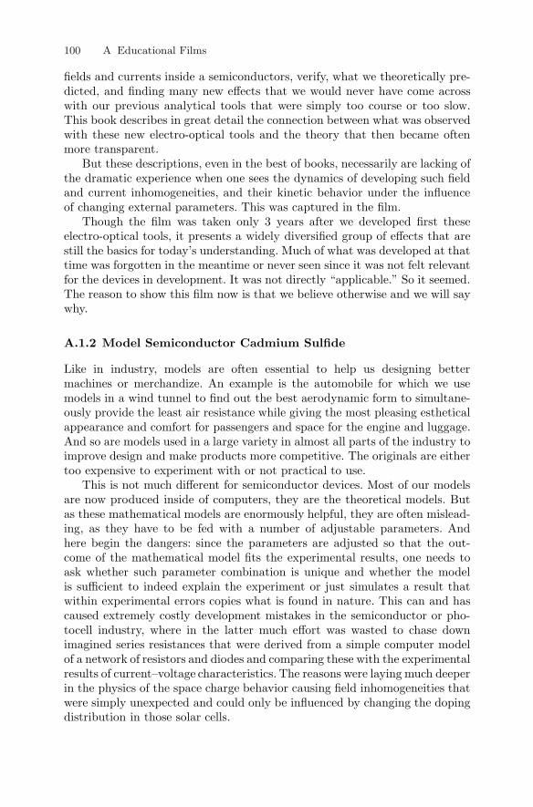
Fig. A.1. Experimental setup to film moving high-field domains and their internalkinetics. It also shows the blending-in of a projected volt and current meter at thebottom and top of some of the film scenes
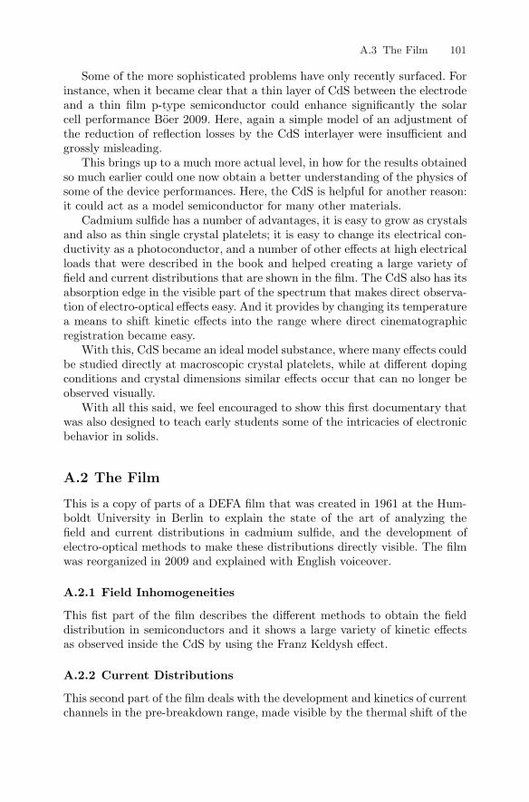
Fig. A.2. Frame from film with volt- and ammeter mirrored into t. Shown is acurrent channel as darkened part between the two electrodes
optical absorption edge. It provides a large sample of evidences to explain thephysical processes occurring before thermal breakdown.

A.3 The Film 103
Fig. A.3. Celebration of the completion of the film with most of the involved peoplepresent. (Left Prof. K.W. Boer, middle Prof. right D. Palme)
Acknowledgments
Normally at the end of films, all important people are mentioned. Since this isnot the case in conventional educational films, I will take this opportunity tothank a large number of professionals who were involved in making this film,from my colleagues, listed in the fore span, Drs. U. Kummel, H.-J Hansch,H. Lange, W. Wilhelm, and D. Palme, to the many not listed technicians andprofessionals at the DEFA film studio, helping in the mechanics of the filmset-up, the animation, the tone, cutting and assembling of this film.
The film shown here with English voiceover is taken from parts of theoriginal films that received first awards at an International Educational FilmFestival in 1961 and 1962. The original films can be viewed at IWF-Wissenund Medien GmbH, D-37075 Gottingen, Nonnensteig 72 Tel: 49-551 5024-260.
References
Abraham E, Anderson PW, Licciardello DC, Ranakrishnan TV (1979) Phys RevLett 42:673
Adler D et al (1980) Handbook of semiconductors, vol 1. North-Holland, Amsterdam,p 805
Albrecht S, Reining L, Sole RD, Onida G (1998) Phys Rev Lett 80:4510Amann A, Wacker A, Bonilla LL, Scholl E (2001) Phys Rev E 63:066207Amann A, Peters K, Parlitz U, Wacker A, Scholl E (2003) Phys Rev Lett 91:066601Amann A, Scholl E (2005) J Stat Phys 119:1069Amann A, Scholl E (2005) Phys Rev B 72:165319Andersen OK (1973) Solid State Commun 13:133–136Anderson PW (1958) Phys Rev 109:1492Ao R, Kuemmerl L, Haarer D (1993) Jpn J Appl Phys 32:5248Aoki K, Yamamoto K (1983) Phys Lett A98:72Aoki K, Yamamoto K, Mugibayashi N, Scholl E (1989) Solid State Electron 32:1149Aoki K, Fukui S (1998) J Phys Soc Jpn 67:1106Aoki K (2000) Solid State Commun 117:21Aoki K (2000) Nonlinear dynamics and chaos in semiconductors, Institute of Physics
Publishing, BristolAulbur WG, Jonsson L, Wilkins JW (2000) Solid state physics, vol 54. Academic,
New YorkAydinli A, Gasanly NM, Yilmaz I, Serpenguzel A (1999) Semiconductor science and
technology, vol 14, p 657Baba N, Amann A, Scholl E, Just W (2002) Phys Rev Lett 89:074101Balkan N, Ridley B (1989) Superlattices Microstruct 5:539Banghard EK (1988) In: Proceedings of the 20th IEEE Photovoltaic Specialists
Conference, Las Vegas, p 717Baumann H, Symanczyk R, Radehaus C, Pulwins H, Jager D (1957) Phys Lett
A123:421Baylac B, Marie X, Amand T, Brusseau M, Barrau J, Shekun Y (1995) Surf Sci
326:161Bergman MJ, Teitsworth SW, Bonilla LL, Cantalapiera IR (1996) Phys Rev
B53:1327
106 References
Bimberg D, Grundmann M, Ledenstov NN (1999) Quantum dot heterostructures,Wiley, UK
Boer KW, Borchard W (1954) Z Phys Chem 203:145Boer KW, Hansch HJ, Kummel U (1958) Naturwissenschaften 45:460Boer KW, Hansch HJ, Kummel U (1959) Z Phys 155:170Boer KW (1959) Z Physik 156:184Boer KW (1960) Festkorperprobleme, Friedr. Vieweg & Sohn, Braunschweig, vol 1,
p 38Boer KW (1961) J Chem Solids 22:123Boer KW, Hansch HJ, Kummel U, Lange H, Nebauer E (1961) Phys Stat Sol 1:19Boer KW, Wilhelm W (1963) Phys Stat Sol 3:1704Boer KW, Wilhelm W (1964) Phys Stat Sol 4:237Boer KW (1964) Res Film 5:47Boer KW (1965) Phys Rev 139 A:1949Boer KW, Dussel GA (1967) Phys Rev 154:292Boer KW, Bogus K (1968) Phys Rev 176:899Boer KW, Ward JJ (1967) Phys Rev 154:757Boer KW, Voss P (1968) Phys Rev 171:899Boer KW, Dohler G, Dussel GA, Voss P (1968) Phys Rev 169, 700, 170:703Boer KW, Dohler G (1969) Phys Stae Sol 36:679; Phys Rev 186:793Boer KW, Dussel GA, Voss P (1969) Phys Rev 179:703Boer KW, Dussel GA (1970) Phys Stat Sol 30, 375, 391Boer KW, Ovshinsky SR (1970) J Appl Phys 41:2675Boer KW (1971) Phys Stat Sol A 4:571Boer KW, Stirn RJ, Dussel GA (1973) Phys Rev B 1433, 1443Boer KW (1976) Phys Rev B 13:5373Boer KW (1976) Phys Stat Sol (a) 49:13Boer KW (1977) Phys Stat Sol (a) 40:355Boer KS (1979) J Appl Phys 50:5356Boer KW (1981) J Appl Phys 51:4518Boer KW (1985) Ann Physik 42:371Boer KW (1990) Survey of semiconductor physics, vol I, 1st edn. Van Nostrand
Reihold, New YorkBoer KW (2001) Phys Stat Sol 184:201Boer KW (2000) Survey of semiconductor physics, vol II, 2nd edn. Wiley, New YorkBoer KW, Gunnar T (2004) J Solar Energy 6:412Boer KW (2009) Phys Stat Sol A 206:2665Bonnet D (ed.) (1992) Thin Film Solar Cells, Int J Solar Energy 12(1–4).Bonch-Bruevich VL, Zvyagin IP, Mironov AG (1975) Domain electrical instabilities
in semiconuctors. Consultants Bureau, New YorkBonilla LL, Cantalapiedra IR, Bergmann MJ, Teitsworth SWS (1994) Semic Sci
Technol 9:599Bonilla LL, Galan J, Cuesta JA, Martinez FC, Molera JM (1994) Phys Rev 50:8644Bonilla LL, Bulaschenko OM, Gerlan J, Kindellan M, Moscoso M (1996) Sol State
Elect 40:161Bonilla LL, Cantalapiera IR, Gomila G, Rubi JM (1997) Phys Rev E 56:1500Bonilla LL, Hernando PJ, Herero MA, Kindelan M, Velazquez JJL (1997) Physica
B Amsterdam 108:168Bonilla LL, Kindelan M, Hernando PJ (1998) Phys Rev B58:7046
References 107
Borse PH, Deshmuk N, Shinde RF, Date SK, Kulkarni SK (1999) J Mater Sci34:6087
Borisov VE, Sablikov VA, Chmil AI, Borisova IV (1999) Semiconductors 33:60Bose S, Wacker A, Scholl E (1994) Phys Lett A195:144Bose S, Rodin P, Scholl E (2000) Phys Rev E62:1778Bosnell JR, Thomas CB (1972) Solid State Electron 15:1261Bouhelal A, Albert JP (1989) Solid State Commun 69:713Bouhelal A, Albert JP (1993) Physica B: Condensed Matter 6:255Bradley AL, Doran JP, Hegarty J, Stanley RP, Oesterle U, Houdre R, Ilegems M
(2000) J Luminescence 85:261Branchu S, Pailloux E, Garem H, Rabier J, Demenet JL (1999) Phys Stat Sol (A)
171:59Brandl A, Geisel T, Prettl W (1987) Europhys Lett 3:401Brandl A, Kroninger W, Prettl W, Obermeier G (1990) Phys Rev Lett 64:212Brandl A, Volcker M, Prettl W (1989) Appl Phys Lett 55:238Briggs D, Seah MP (1990) Practical surface analysis, vol 1, 2nd edn. Auger and
x-ray Photoelectron Spectroscopy, Wiley, ChichesterBrochard S, Rabier J, Grilhe J (1998) EPJ Appl Phys 2:99Broser I (1967) Physics and chemsitry of II–VI compounds. In: Aven M, Prener JS
(eds), North-Holland, AmsterdamBroser I, Herfort L, Kallmann H, Martius U (1948) Z Naturf 3a:6Bube RH (1992) Electronic properties of semiconductors, Cambridge University
Press, Cambridge, UKBulashenko OM, Bonilla LL (1995) Phys Rev B 52:7849Bulaschenko OM, Garcia MC, Bonilla LL (1995) Phys Rev 52:7849; 53:10008Bulaschenko OM, Luo KJ, Grahn HT, Ploog K, Bonilla LL (1999) Phys Rev
B60:5694Butcher PN (1965) Phys Lett 19:546Buttiker M, Thomas H (1977) Phys Rev Lett 38:78Buttiker M, Thomas H (1978) Solid-State Electron 21:95Buttiker M, Thomas H (1979) Z Phys B 34:301Buttiker M, Thomas H (1999) Z Physik B34:301Cantalapiedra IR, Bonilla LL, Bergmann MJ, Teitsworth SW (1993) Phys Rev
B48:12278Cao JC, Lei XL (1999) Pys Rev B59:2199Cardona M, Ley L (eds) Topics in applied physics, vol 26. Springer, BerlinChakraborty PK, Biswas JC (1997) J Appl Physics 82:3328Cheianov V, Rodin P, Scholl E (2000) Phys Rev B 62:9966Chemla DS (1999) Semiconductors and Semimetals, ch 3, vol 58. Academic,
New YorkChen R (1969) J Appl Phys 40:570Chen TP, Chen LJ, Huang TS, Guo YD (1992) Semiconductor Science and
Technology 7:300Choi KK, Levine BF, Malik RJ, Walker J, Bethea CG (1987) Phys Rev 35:4172Clark RJH, Hester RE (eds) (1998) Spectroscopy for surface science. Wiley,
Chichester, New YorkColeman PD, Freeman J, Morkoc H, Hess K, Streetman BG, Keever M (1982) Appl
Phys Lett 40:493Datsko B (1997) Semiconductors 31:146
108 References
Conwell EM (1967) High-field transport in semiconductors. Academic, New YorkDavidov VYu, Subashiev AV, Cheng TS, Foxon CT, Goncharuk LN, Smirnov AN,
Zolotareva RN (1998) Mater Sci Forum 264–268:1371Davydov VYu, Subashiev AV, Cheng TS, Foxon CT, Goncharuk IN, Smirnov AN,
Solotareva RV, Ludyn WV (1998) Material Science Forum 264:1371Di Bartolo B (1984) Energy transfer processes in condensed matter. Plenum,
New YorkDong J, Drabold DA (1998) Phys Rev Letters 80:1928Dottling R, Scholl E (1992) Phys Rev B45:1935Dottling R, Scholl E (1993) Physica D, Amsterdam 67:418Dottling R, Scholl E (1994) Solid State Electron 37:685Drabold DA (1996) In: Thorpe MF, Mitkova MI (eds) Amorphous insulators and
semiconductors, NATO ASI Series, vol 23, p 405Drabold DA, Nakhmanson S, Zhang X (2001) In: Thorpe MF, Tichy L (eds)
Properties and applications of amorphous materials. Kluwer, Dordech, p 221Dussel GA, Boer KW (1970) Phys Stat Sol 39:375, 391Dussel GA, Boer KW, Stirn RJ (1973) Phys Rev 7:1443Eberle W, Hirchinger J, Margull U, Prettl W, Novak V, Kostial K (1996) Appl Phys
Lett 68:3329Ebert W, Vescan A, Borst TH, Kohn E (1994) IEEE Electron Device Lett 15:289Efros AL, Rodina AV (1989) Solid State Commun 72:645Esaki W, Chang LL (1974) Phys Rev Lett 33:495Esser AE, Runge R, Zimmermann H, Langbein W (2000) Phys Stat Sol A 178:489Fahrenbruch AL, Bube RH (1983) Fundamentals of solar cells. Academic, New YorkFeng S (1990) Scattering and localization of classical waves in random media. World
Scientific, SingaporeFeng PK (1999) Surface Science 429:L469Fock W (1927) Arch Electrotechn 19:71Franceschetti A, Zunger A (1997) Phys Rev Letters 78:915Franceschini G, Bose S, Scholl E (1999) Phys Rev E60:5426Franz W (1958) Z Naturforsch 13A:484Frenkel JI (1938) Phys Rev 54:647Fricke Ch, Hetiz R, Lummer B, Kutzer V, Hoffmann A, Broser A, Taud W,
Heuken M (1994) J Crystal Growth 138:815Fritzsche H, Ovshinsky SR (1960) J Noncryst Solids 4:464Fritzsche H, (1997) Materials Res Soc Symposium Proc 467:19Gaa M, Kunz RE, Scholl E (1996) Phys Rev B53:15971Garcia-Cristobal A, Cantarero A, Trallero-Giner C, Cardona M (1998) Physica B:
Condensed Matter 263:809Geisz JF et al (2008) Appl Phys Lett 93:123505Glavin B, Kochelap V, Mitin V (1997) Phys Rev B56:13346Goldman VJ, Tsui DC, Cunningham JE (1987) Phys Rev Lett 58:1256Gorbatyuk AV, Rodin PB (1990) Sovj Tech Phys Lett 16:529Gorbatyuk AV, Rodin PB (1992) Sol Stat Electron 35:1359Gorbatyuk AV, Rodin PB (1997) Z Physik B104:145Grahn HT, Haug RJ, Muller W, Ploog K (1991) Phys Rev Lett 67:1618Grahn HT, von Klitzing K, Ploog K, Dohler G (1991) Phys Rev B43:12094Grahn HT, Castrup J, Ploog K, Bonilla LL, Garlan J, Kindelan M, Moscoso M
(1995) Jpn J Appl Phys 34:4526
References 109
Gray PE (1967) Physics of electronics and circuit models. Wiley, New YorkGray JL, Schwartz RJ, Lundstrom MS, Nasby RD (1982) Proceedings of the 16th
IEEE Photovoltaic Specialists Conference, San Diego, CA, p 437Gray JL, Schwartz RJ (1984) Proceedings of the 17th IEEE Photovoltaic Specialists
Conference, Kissimee, FL, p 1297Green MA (1982) Solar cells. Prentice-Hall, Englewood Cliffs, NJGreen MA (1997) Proceedings of the 26th IEEE Photovoltaic Specialists Conference,
Las Vegas, p 717Green MA, Emery K, Hishikawa Y, Warta W (2009) Progr Photovolt: Res Appl
17:85Grenzer J, Schomburg E, Lingott I, Ignatov AA, Renk KF, Pietsch U, Zeimer U,
Melzer BJ, Ivanov S, Schaposchnikov S, Kop”ev PS, Pavel’ev DG, Koschurinov Y(1998) Semicon Sci Technol 13:733
Greulich-Weber S (1997) Phys Stat Sol (A) 162:95Gribnikov ZS, Mel’nikov MI (1973) Sovj Phys Sol State 7:2364Gross EF, Permogor SA, Reznitz AN, Usarov EN (1974) Sovj Physics Semiconduc-
tors USSR 7:844Guissi S, Bindi R, Iacconi P, Jeambrun D, Lapraz D (1998) J Phys D: Appl Phys
31:137Gunn JB (1963) Sol State Commun 1:88Gunn JB (1964) IBM J Res Devel 8:141Gurevich SV, Bodeker HU, Moskalenko AS, Liehr AW, Purwins H-G (2004) Physica
D 199:115Gutsche E, Lange H (1964) Proceedings of the VII International Conference on
Semiconductor Physics, Paris, p 129Kalt H (1996) Optical properties of III-V semiconductors. The influence of multi-
valley band structure. Springer, BerlinKastrup J, et al. (1995) Phys Rev B 52:13761Kastrup J, et al. (1997) Phys Rev B 55:2476Hadley HC, Tyagi RC, Voss P, Boer KW (1972) Phys Stat Sol (a) 11, 523 and K
145Heidemann G, Bode M, Purwins H (1993) Phys Lett A977:225Hamakawa Y (1999) Appl Surf Sci 142:215Hofbeck K, et al. (1996) Phys Lett A 218:349Scholl E, Schuster HG (eds) (2008) Handbook of chaos control. Wiley-VCH,
Weinheim, second completely revised and enlarged editionHao M, Sugahara T, Sato H, Morishima Y, Naoi Y, Romano LT, Sakai S (1998) Jpn
J Appl Phys (2) 37:L291Helm M, England P, Colas E, Derosa F, Allen Jr SJ (1989) Phys Rev Lett 63:74Helgesen P, Finstad TG (1990) Proceedings of the 14th Nord Semiconductor Meeting
U, Aarhus, p 323Hendriks P, Zwaal EAE, DuBois JGA, Blom FF, Wolter JH (1991) J Appl Phys
69:302Henisch HK (1984) Semiconductor contacts. Clarendon, Oxford, UKHenry CH, Logan RA, Merrit FR (1978) J Appl Phys 49:3530Hess K, Morkoc H, Shichijo H, Streetman BG (1979) Appl Phys Lett 35:469Hilsum C (1962) Proc IRE 50:185Higuera FJ, Bonilla LL (1992) Phys D, Amsterdam 57:161Hirsch R, Kittel E, Flatgen G, Hubener RP, Parisi J (1994) Phys Lett A186:157
110 References
Hirschinger J, Eberle W, Prettl W, Niedernostheide FJ, Kostial H (1997) Phy LettA236:249
Hizanidis J, Balanov AG, Amann A, Scholl E (2006) Int J Bifur Chaos 16:1701Hizanidis J, Balanov AG, Amann A, Scholl E (2006) Phys Rev Lett 96:244104Hizanidis J, Aust R, Scholl E (2008) Int J Bifur Chaos 18:1759Hizanidis J, Aust R, Scholl E (2008) Phys Rev E 78:066205Hopfbeck K, Grenzer J, Schomburg E, Ignatov AA, Renk KF, Pavel’ev DJ, Koschuri-
nov Y, Melzer E, Ivanov S, Schaposchnilov S, Kop’ev PS (1996) Phys LettA218:349
Hupper G, Pyragas K, Scholl E Phys Rev B47:15515; B48:17633Hybertson MS, Loui SG (1985) Phys Rev Lett 55:1418Ibach H (1991) Electron energy loss spectrometer: The technology of high perfor-
mance. Springer Verlag, BerlinJacobini C, Canali C, Ottoviani G, Cluaraula AA (1977) Sol State Electron 20:71Jackson JD (1999) Classical electrodynamics, 2nd edn. Wiley, New YorkJager D, Baumann H, Simanczyk R (1986) Phys Rev A117:141Jappsen AK, Amann A, Wacker A, Scholl E, Schomburg E (2002) J Appl Phys
92:3137Kahn AM, Mar DJ, Westervelt RM (1991) Phys Rev B43:9740Kahn AM, Mar DJ, Westervelt RM (1992) Phys Rev Lett 46:369; Phys Rev B45:8342Kamieniecki E (1990) Proc Electrochem Soc 90:1856Kastrup J, et al. (1995) Phys Rev B 52:13761Kastrup J, et al. (1997) Phys Rev B 55:2476Kawamura Y, Wakita K, Asahi H, Kurumada K (1986) Jap J Appl Phys 25:L298Keever M, Shichigo H, Hess K, Barnajee S, Witkovski L, Morkoc H (1981) Appl
Phys Lett 38:36Kehrer B, Quade W, Scholl E (1995) Phys Rev B51:7725Kehrt M, Hovel P, Flunkert V, Dahlem MA, Rodin P, Scholl E (2009) Eur Phys J
B 7:58Keldysh LV (1958) Sov Phys JETP (Engl Transl) 4:665Kerner BS, Osipov VV (1976) Sovj Phys 44:807Kerner BS, Osipov VV (1994) Autosolitons. Kluwer, DordrechtKlemens PG (1966) Phys Rev 148:845Knight BM, Peterson GA (1967) Phys Rev 155:393Kobayashi Y, Kouzo K, Kamimuro H (1999) Sol State Commun 109:583Kogan ShM (1968) Sovj Phys 27:656Kohno M, Matsubara H, Okada H, Hirae S, Sakai T (1998) Jpn J Appl Phys (1)
37:5800Kolev PV, Deen MJ, Kierstead J, Citterio M (1999) IEEE Trans Electron Devices
46:204Kono S, Nagasawa N (1999) Sol State Commun 110:159Korotov AN, Averin DV, Likharev KK (1993) Appl Phys Lett 62:3282Kostial H, Asche M, Hey R, Ploog K, Kehra B, Quade W, Scholl E (1995) Semicond
Sci Technol 10:775Kroemer H (1964) Proc IEEE 52:1736Kudlek GH, Pohl UW, Fricke Ch, Heitz R, Hoffmann A, Gutowski J, Broser I (1993)
Physica B: Condensed Matter 185:325Kuhn T, Hupper G, Quade W, Rein A, Scholl E, Varani L, Reggiani L (1993) Phys
Rev B48:1478
References 111
Kung P, Zhang X, Walker D, Saxler A, Piotrowski J, Rogalski A, Razeghi M (1995)Appl Phys Lett 67:3792
Kunihiro K, Gaa M, Scholl E (1997) Phys Rev B55:2207Kunz RE, Scholl E (1992) Z Phys B89:289Kunz RE, Scholl E, Gajewski H, Nurnberg R (1996) Sol State Electron 39:1155Kukuk B, Reil F, Niedernorttheide FJ, Purwins HG (1996) Self-organization in
activator-inhibitor systems, Wissenschaft und Technik Verlag, Berlin, p. 52Kuo L-H, Salamanca-Riba L, Hofler GE, Wu B-J, Haase MA (1994) Proc SPIE
2228:144Kwok SH, Grahn HT, Ramsteiner M, Ploog K, Prengl F, Wacker R, Scholl E,
Murugkar S, Merlin R (1995) Phys Rev 51:8843Lampert MA (1956) Phys Rev 903:1648Larson P, Mahanti SD, Kanatzidis MG, (2000) Phys Rev B61:8162Liou JJ, Wong WW, Juan JS (1990) Sol State Electron 33:845Liu QZ, Lau SS (1998) Sol State Electron 42:677Lueder H, Spenke E (1953) Z Techn Physik 16:53Lundstrom MS, Schwartz RJ, Gray JL (1981) Sol State Electron 24:159Luo KJ, Grahn HT, Ploog K, Bonilla lL (1998) Phys Rev Lett 81:1290Milnes AG, Feucht DL (1972) Heterojunctions and metal–semiconductor junctions.
Academic Press, New YorkMaes W, De Meyer K, van Overstraeten R (1990) Sol State Electron 33:705Magonov SN (1996) Surface analysis with STM and AFM: experimental and
theoretical aspect of image analysis, VCH. Weinheim, New YorkMajer N, Scholl E (2009) Phys Rev E 79:011109Malpuech G, Kavokin A, Langbein W, Hvam JM (2000) Phys Rev Lett 85:650Malyshkin V, McGurn AR, Leskova TA, Maradudin AA, Nieto-Vesperinas M (1997)
Waves in Random Media 7:479Marder MP (1998) Condensed Matter Physics. Wiley Interscience, New YorkMayer K, Gross R, Parisi J, Peinke J, Huebener R (1987) Sol State Commun 63:55Mayer K, Parisi J, Huebener H (1988) Z Physik B71:171McGurn AR (1999) Phys Lett A 251:322; Phys Lett A 260:314McGurn AR (2000) Phys Rev B 61:13235McKeever SWS (1985) Thermoluminescence of solids. Cambridge University Press,
CambridgeMeixner M, Bose S, Scholl E (1997) Physica D Amsterdam 109:928; Phys Rev
B55:6690Meixner M, Rodin P, Scholl E (1998) Phys Rev E58:2796; 5586Meixner M, Rodin P, Scholl E, Wacker A (2000) Eur Phys J B13:157Mel’nikov D, Podlivaev A (1998) Semicond 32:236Miller D, Laikhtman B (1994) Phys Rev 50:18426Mioc SL, Garland JW, Bennett BR (1996) Semicond Sci Technology 11:521Mityagin YA, Murzin VN, Efimov YA, Rasulova GC (1997) Appl Phys Lett 70:3008Mosekilde E, Feldberg R, Knudsen C, Hindsolm M (1990) Phys Rev 41:2298Mosekilde E, Thomson JS, Knudson C, Feldbarg R (1993) Physica D Amsterdam
66:143Morgenstern M, Wittneven C, Dombrowski R, Wiesendanger A (2000) Phys Rev
Letter 84:5588Mott NF, Gurney RW (1940) Electronic processes in ionic crystals. Oxford
University Press, New York
112 References
Mott NF (1999) Metal–insulator transitions. Taylor and Francis, LondonMousseau N, Barkema GT (2000) Phys Rev B 40:1898Murawski J, Schwarz G, Novak V, Prettl W, Scholl E (2005) J Appl Math Mech
(ZAMM) 85:823Nag BR (1980) Electron transport in compound semiconductors. Springer, BerlinNakamura K (1989) Phys Lett A138:396Nataka H, Uddin A, Otsuka E (1992) Semiconductor Science and Technology 7:1266Neudeck GW (1983) The pn-junction diode. Addison Wesley, Reading, MANeugroschel A, Sah CT (1996) Electron. Lett. 32:2280Niedernostheide FJ, Arps M, Dohmen R, Willebrand K, Purwins HG (1992) Phys
Stat Sol B 172:249; Phys Rev B46:7559Niedernostheide FJ, Kreimer M, Schulze HJ, Purwins HG (1993) Phys Lett A180:113Niedernostheide FJ, Artdes M, Or-Guil M, Purwins HG (1994) Phys Rev B49:7370Niedernostheide FJ (1995) Non-linear dynamics and pattern formation in semicon-
ductors and devices. Springer, BerlinNiedernostheide FJ, Brillert C, Kukuk B, Purwins HG, Schulze HJ (1996) Phys Rev
B54:14012; E54:1253Niedernostheide FJ, Or-Guil M, Kleinkes M, Purwins HG (1997) Phys Rev E55:4107Northrup D et al. (1964) Solid-State Electron 7:17Nostrup DC, Thornton PR, Tresize KE (1964) Sol State Electron 7:17Novak V, Wimmer C, Prettl W (1995) Phys Rev B52:9023Nunoya N, Nakamura M, Yasamoto H, Tamura S, Arai S (2000) Jpn J Appl Phys
39:3410Ovshinsky SR (1968) Phys Rev Lett 21:1450Patra M, Schwarz G, Scholl E (1998) Phys Rev B57:1824Peinke J, Parisi J, Rossler O, Stoop R (1992) Encounter with chaos. Springer, BerlinPetersen KE, Adler D (1976) J Appl Phys 47:256Piazza F, Christianen PCM, Maan JC (1977) Phys Rev B55:15591Pines AS (1982) In: Cardona M (ed) Light scattering in solids. Springer, BerlinPolezhaev VJ (1984) Crystals, growth, properties, and applications, vol 10. Springer,
BerlinPoole HH (1921) Philos Mag 42:488Poole CP, Farach HA (1994) Data sources, vol 1. In: Handbook of electron spin
resonance, Poole CP, Farach HA (eds), vol I. American Institute of PhysicsPress, New York
Prengel F, Wacker E, Scholl E (1994) Phys Rev 50:1705Prince MB (1955) J Appl Phys 26:534Pritchard J (1979) In: Roberts MW, Thomas JM (eds) Chemical physics of solids,
vol 7. Chemical Society, p 166, New YorkPurwins HG, Klempt G, Berkemeier J (1987) Festkorperprobleme 27:27Quade W, Hupper G, Scholl E, Kuhn T (1994) Phys Rev B49:13408Racko J, Donoval D, Barus M, Nagel V, Grmanova A (1992) Sol State Electron
35:913Rau U, Clauss W, Kittel A, Lehr M, Bayerbach M, Parisi J, Peinke J, Huebener R
(1991) Phys Rev B43:2255Redfield D, Bube R (1995) Mater Sci Symp Proc 325:335Repins I, Contreras MA, Egaas B, DeHart C, Scharf J, Perkins CL, To B, Noufi R
(2008) Prog Photovoltaics: Res Appl 16:235Ridley BK (1961) Proc Phys Soc 78:293
References 113
Ridley BK, Wattkins TB (1961) Proc Phys Soc Lond 78:293Ridley BK (1963) Proc Phys Soc 81:996Ridley BK (1997) Electrons and phonons in semiconductor multilayers, Cambridge
University Press, Cambridge, UKRiviere JC, Myhra S (eds) (1998) Handbook of surface and interface analysis:
methods of problem solving, Marcel Dekker, New YorkRockett A, Birkmire RW (1991) J Appl Phys 70:81Rodin P, Scholl E (2003) J Appl Phys 93:6347Rodin P (2005), Phys Rev B 71:085309Rogozia M, Teitsworth SW, Grahn HT, Ploog KH (2002) Phys Rev B 65:205303Rose A (1978) Concepts in photoconductivity and allied problems. Rober E. Krieger,
Huntington, New YorkSah CT, Noyce RN, Shockley W (1957) Proc. IRE 45:1228Sahyun MRV, Sharma DK, Serpone N (1995) J Imag Sci Technol 39:377Sakurai T, Sakai A, Pickering HW (1989) Atom probe field ion microscopy and its
applications. Academic, New YorkSamuil VA (1995) Nonlinear dynamics and pattern formation in semiconductors and
devices. Springer, BerlinSankin VI, Stolichnov IA (1994) JETP Lett 59:744Schappe RS, Walker T, Anderson LW, Lin CC (1996) Phys Rev Lett 76:4328Schenk CP, Or-Guill M, Bode M, Purwins HG (1997) Phys Rev Lett 78:3781Schimansky L, Zulicke C, Scholl E (1991) Z Phys B84:433Schlesner J, Amann A, Janson NB, Just W, Scholl E (2003) Phys Rev E 68:066208Schottky W (1939) Z Phys 113:367Schmidt KH, Linder N, Doehler GH, Grahn HT, Ploog K, Schneider H (1994) Phys
Rev Letters 72:2769Schmidt TM, Fazzio A, Caldas MJ (1995) Material Schience Forum 196:273Schmitt OM, Banyai L, Haug H (2000) J Luminescence 87:168Schmitt-Rink S, Chemla DS, Miller DAB (1989) Adv Phys 38:89Scholl E (1982) Z Phys B46:23; B48:153Scholl E (1986) Sol State Electron 29:687Scholl E (1987) Non-equilibrium phase transitions in semiconductors. Springer,
BerlinScholl E, Schwarz G, Wacker A (1998) Physica, Amsterdam 249–251:961Scholl E, Landsberg P (1988) Z Phys B72:515Scholl E, Niedernostheide FJ, Parisi J, Prettl W, Purwins H (1998) Evolution
of spontaneous structures in dissipative continuous systems. Springer, Berlin,p 446
Scholl E, Aoki K (1991) Appl Phys Lett 58:1277Scholl E, Drasdo D (1990) Z Physik B81:183Scholl E (1992) Handbook on semiconductors, vol 1. North-Holland, AmsterdamScholl E, Schwarz G, Wacker A (1998) Physica B Amsterdam 249–251:961Scholl E (2001) Non-linear spatio-temporal dynamics and chaos in semiconductors.
Cambridge University Press, CambridgeScholl E (2002) In: Boer KW (ed) Survey of semiconductor physics, Ch 33. Wiley,
New YorkScholl E, Hizanidis J, Hovel P, Stegemann G (2007) In: Schimansky-Geier L, Fiedler
B, Kurths J, Scholl E (eds) Analysis and control of complex nonlinear processesin physics, chemistry and biology. World Scientific, Singapore, pp 135–183
114 References
Scholl E, Majer N, Stegemann G (2008) Phys Stat Sol (c) 5:194Scholl E (2009) In: Radons G, Rumpf B, Schuster HG (eds) Nonlinear dynamics of
nanosystems. Wiley-VCH, WeinheimScholl E, Amann A, Rudolf M, Unkelbach J (2002) Physica B 314:113Schomburg E, et al. (1998) Appl Phys Lett 72:1498Schomburg E, et al. (1999) Appl Phys Lett 74:2179Schomburg E, Hofbeck K, Scheuerer R, Haeussler M, Renk KF, Jappsen AK,
Amann A, Wacker A, Scholl E, Pavel’ev DG, Koschurinov Y (2002) Phys RevB 65:155320
Schrepel C, Scherz U, Ulrici W, Thonke K (1997) Mater Sci Forum 258:1075Schultheis L, Honold A, Kuhl J, Kohler K, Tu CW (1986) Phys Rev B 34:9027Schultheis L, Honold A, Kuhl J, Kohler K, Tu CW (1986) Superlattices Microstruct
2:441Schultz O, Glunz SW, Willeke GP (2004) Progr Photovolt: Res. Appl 12:553Schumacher JO, Altermatt PP, Heiser G, Aberle AG (2000) Solar Energy Mater
Solar Cells 65:95Seeger K (1999) Semiconductor physics, Springer Series on Solid State Science, 6th
edn. Springer, BerlinSchwartz RJ (1982) Solar Cells 6:17Schwarz G, Scholl E (1996) Phys Stat Sol B 1:351Schwarz G, Prengel F, Scholl E, Kastrup J, Grahn HT, Hey R (1996) Appl Phys
Lett 69:626 and Semicon Sci Technol 11:475Schwarz G, Scholl E (1997) Acta Tech CSAV 42:669Schwarz G, Patra M, Prengel F, Scholl E (1998) Superlattices Micro Struct 23:1353Schwarz G, Lehmann C, Reimann A, Scholl E, Hirschinger J, Prettl W, Novak V
(2000) Semicond Sci Technol 15:593, Phys Rev B61:10194Schwarz G, Lehmann C, Scholl E (2000) Phys Rev B61:10194Segev M, Collings B, Abraham D (1996) Phys Rev Lett 76:3798Seitz F (1940) The modern theory of solids. McGraw-Hill, New York, LondonShaw MP, Grubin HL, Solomon P (1979) The gunn hilsum effect. Academic,
New YorkShaw MP, Mitin VV, Scholl E, Grubin HL (1992) Physics of instabilities in solid
state electron devices. Plenum, New YorkShah J (1996c) Ultrafast spectroscopy of semiconductors and semiconductor nanos-
tructures, Ch 2. Springer, BerlinSheng (1990) Scattering and localization of classical waves in random media. World
Scientific, SingaporeShionoya S (1991) Metals Forum 15:132Shockley W (1950) Electrons and holes in semiconductors. Van Nostrasnt, Princeton,
NJSilver M, Pautmeier L, Baessler H (1989) Sol State Commun 72:177Skanavi GI (1958) Phizika Dielectrikov. Fizmatgiz, MoscowSmith GC (1994) Surface analysis by electron spectroscopy. Plenum, New YorkSoares EA, de Carvalho VE, Nascimento VB (1999) Surf Sci 431:74Spaeth J-M, Meise W, Song KS (1994) J Phys Condensed Mat 6:3999Spangler J, Finger B, Wimmer C, Eberle W, Prettl W (1994) Semicond Sci/Technol
9:373Spenke E (1969) Electronic semiconductors. McGraw-Hill, New YorkSrivastava GP (2000) Vacuum 57:121

References 115
Stegemann G, Balanov AG, Scholl E (2005) Phys Rev E 71:016221Stegemann G, Balanov AG, Scholl E (2006) Phys Rev E 73:016203Stegemann G, Scholl E (2007) New J Phys 9:55Stensgaard I (1992) Rep Prog Phys P55:989Steuer H, Wacker A, Scholl E (1999) Physica B Amsterdam 272:202Steuer H et al. (2000) Appl Phys Lett 76:2059Stier O, Bimberg D (1997) Phys Rev B 55:9740Stirn K, Boer W, Dussel GA (1973) Phys Rev B 7.4:1433Stratton R (1969) J Appl Phys 40:4582Street RA, Mott NF (1975) Phys Rev Lett 35:1293Stroscio J, Kaiser W (1992) Scanning tunneling microscopy. Academic, New YorkSturge MD (1982) Excitons, Rashba ET, Sturge MD (eds). North-Holland,
AmsterdamSwistacz B (1995) J Electrost 36:175Symanczyk R, Jager D, Scholl E (1991) Appl Phys Lett 59:105Sze SM (1981) Physics of semiconductor devices. Wiley, New YorkSze SM (1985) Semiconductor devices. Wiley, New YorkTanaka K (1998) Jpn J Appl Phys, Part 1 37:1747Tanaka K, Nakayama SI (1999) Jpn J Appl Phys, Part 1 38:3986Tani T (1989) Fuji Film, Res Develop 34:37Tani T (1991) Fuji Film, Res Develop 36:14Tani T (1995) J Imaging Sci Technol. 39:386Teitsworth SW, Westervelt RM, Haller EE (1983) Phys Rev Lett 51:825Tathan MS (1992) Semiconduct Sci Technol 7:B116Thomas DE, Hopefield JJ, Augustyniak WN (1965) Phys Rev 140:A202Tolk NH, Traum MM, Tully JC, Madey TE (eds) (1983) Desorption induced by
electronic transitions, DIET I. Springer, BerlinUnkelbach J, Amann A, Just W, Scholl E (2003) Phys Rev E 68:026204Volkl J (1994) Stress in the cooling crystal. In: Hurle (ed) Handbook of crystal
growth. North-Holland, AmsterdamValle F, Bogani F (1991) Phys Rev B 43:12049Van de Walle CO, Neugebauer J (1996) Mater Res Soc Symp Proc 449:861Vanderbilt D (1990) Phys Rev B41:7893Varlamov IV, Osipov VV (1970) Sovj Phys Semicond 3:803Varshneya AK, Seeram AN, Swiler DR (1993) Phys Chem solids 34:179Vickerman JC (ed) (1997) Surface analysis: the principal techniques. Wiley,
Chichester, New YorkVickers AJ, Straw A, Roberts JS (1989) Semicond Sci Technol 4:743Vinogradov EA, Leskova TA, Ryabov AP (1994) Optics Spectrosc 76:278Volkov AF, Kogan SM (1967) Sov Phys JETP 25:1095Volkov AF, Kogan SM (1969) Sov Phys-Usp 11:881Wacker A, Jauho A-P (1998) Phys Rev Lett 80:369Wacker A, Scholl E (1994) Z Phys B 93:431Wacker A, Schwarz G, Prengel F, Scholl E, Kastrup J, Grahn HT (1995) Phys Rev
B52:13788Wacker A, Scholl E (1994) Z Physik B93:431Wacker A, Scholl E (1995) J Appl Phys 78:7352Wacker A, Scholl E (1997) J Appl Phys 78:7352
116 References
Wacker A (1998) Theory of transport properties of semiconductor nanostructures,Ch 10. Chapman & Hall, London
Wacker A (2002) Phys Rep 357:1Wagner KW (1926) J Inst Elect Eng 41:1034Wang CW, Wu CH (1992) Sol State Electron 35:1771Wang ZL (1996) Reflection electron microscopy and spectroscopy for surface
analysis. Cambridge University Press, CambridgeWard AJ (1999) Contemporary Phys 40:117Weber D, Petri W, Woggon U (1997) Phys Rev, B1 55:12 848Weber MJ, Monchamp J (1973) J Appl Phys 44:5495Wierschem A, Niedernostheide FJ, Gorbatyuk A, Purwins HG (1995) Scanning
17:106Weiss S, Mycek MA, Bigot J-Y, Schmitt-Rink S, Chemla DS (1992) Phys Rev Lett
69:2685Whitehead S (1939) Philos Mag 37:276; Whitehead S (1951) Dielectric breakdown
of solids. Clarendon, Oxford, UKWilliams F (1977) J Electrochem Soc 124:C107Williams F, Karteuser E, Evrard R (1980) Phys Rev B 21:648Williamson D (1999) Proc Mat Res Soc 557:251Wolf EL (1975) Sol State Phys 30:712Wolf T, Ulrici W, Cote D, Clerjaud B, Bimberg D (1993) Mater Sci Forum
143:317Woodruff DP, Delchar TA (1994) Modern techniques of surface science. Cambridge
University Press, CambridgeWooten F, Weaire D (1991) In: Ehrenreich H, Turnbull D (eds) Sol State Phys, vol
40. Academic, New York, p 2Xu H, Amann A, Scholl E, Teitsworth SW (2009) Phys Rev E arXiv:0901.1672Yamaguchi M, Morifuji M, Kubo H, Taniguchi K, Hamaguchi C, Gmachl C, Gornik
E (1994) Sol State Electron 37:839Yang J, Guha S (1999) Proc Mat Res Soc 557:239Yarykin N, Cho CR, Zuhr R, Rozgonyi G (1999) Physica B: Condensed Matter
273:485Yeh P (1988) Optical waves in layered media. Wiley, New YorkYi J, Wallace R, Palmer J, Anderson WA (1994) Solar Energy Mater Solar Cells
33:145Yu PY, Cardona M (1999) Fundamentals of semiconductors: physics and material
properties. Springer, BerlinZangwill A (1988) Physics at surfaces. Cambridge University Press, CambridgeZhang Y, Yang X, Liu W, Zhang P, Giang D (1994) Appl Phys Lett 65:1148Zhang Y, Castrup J, Klann R, Ploog K, Grahn HT (1996) Phys Rev Lett
77:3001Zhao GY, Ishakawa H, Jiang H, Egawa T, Jimbo T, Umeno M (1999) Jpn J Appl
Phys, Part 2 38:L993Zimmermann H, Boyn R, Lehr MU, Schulz H-J, Rudolph P, Kornack J-Th (1994)
Semiconductor Sci Technol 9:1598Zongfu J, Benkum M (1991) Phys Rev 44:11072Zoorob MF, Chariton MDB, Parker GJ, Baunberg JJ, Netti MC (2000) Nature
404:740Zou J, Cockayne DJH (1995) Mater Sci Forum 189:279

References 117
te Nijenhuis J, van der Wel PJ, van Eck ERH, Giling LJ (1996)J Phys, D: ApplPhys 29:2961
van der Veen JF (1985) Surf Sci Rep 5:199Zhao J, Wang A, Green MA (1999) Prog Photovolt 7:471Zhou X (1994) Sol State Electron 37:1888
Index
ac driving bias, 70activator-inhibitor systems, 89amorphous chalcogenide films, 91anode-adjacent domain, 11, 14, 16, 22autocatalytic generation-recombination,
91autonomous system of differential
equations, 8, 43auxiliary curves, 9auxiliary functions, 44avalanche-like, 92
background charge density, 62band-edge shift, 2, 16, 74barrier lowering, Frenkel–Poole, 25barrier width fluctuations, 66Bessel functions, 85bifurcation of moving field domains, 63bifurcation of spatial patterns, 83bifurcation of stable current filaments,
85bistable systems, 85, 90blocking electrode, 74blocking metals, 27boundary conditions, 39, 60, 61boundary density, 13Bragg scattering in superlattices, 69breathing filaments, 92
carrier density, decreasing with field, 5carrier density, mobility, field,
unambiguously, 15carrier depletion within the domain, 48carrier injection, 7
cathode-adjacent high-field domain, 14,16, 22
CdS copper-doped, 3
CdS, anisotropic, 3CdS, photoconducting, 4
CdS, shadow picture, domains, 17
change of space charges near the edgesof the domain, 44
channel formation, 74
channel modeling, 78
chaotic dynamics, 65chaotic spiking, 89
chaotically breathing, 60
chaotically moving domains, 70
characteristic velocities, 45charge fluctuation, 61
charge neutrality curve, 56
circle the point II, 47
closed saddle-to-saddle-loops, 87
closed solutions, 47co dimension-two bifurcation, 89
coexistence field, 87
coexistence of multiple filaments, 97
composite field of directions diagram,20
conductivity decreases stronger thanlinearly, 5, 7
conductivity decreases with field, 50
conductivity, electron density, electricfield, 10
contact is insufficiently blocking, 31
copper doping, 22Corbino disk, 95

120 Index
Coulomb funnel, 25
Coulomb-attractive hole traps, 22critical field for field-quenching, 35crystal defects, 1, 35crystal platelets, 1
current channel, 3, 73, 74current channel, initiation, 74current channel, magnetic field,
influence, 77current channel, modeling, 78current channels, devices, dielectrics, 76
current density distributions, 94current distribution, 1, 3current filament, 84, 91
current filamentation, 84current filaments in CdS, 82current filaments in n-GaAs, 92current filaments, Corbino disk,
simulated, 96current filaments, simulated, 94current oscillations, 2, 5, 58
current oscillations in a strongly coupledsuperlattice, 66
current saturation, 5
current tends to low value, 58current trace is non-sinusoidal, 70current, time traces, moving domains,
p-Ge, 72current–voltage characteristics, 81, 82current-controlled instabilities, 59
curved maximum field, 49curving of the filament, 95cylinder, S-shape analysis, 5cylindrical current filaments, 87
cylindrical geometry, 85
dark stripes, 92Debye lengths, 11, 15, 44
decrease mobility with field, 53deep hole traps, 13degenerate bifurcations, 90
descending or ascending branch, 39development of a current filament, 74dielectric breakdown, 76
dielectric relaxation time, 63diffusion–neutrality curve, 9, 47, 56dipole layer, 27directional external cooling, 77
discovered moving high-field domains inCdS single crystals, 69
dispersion relation, 85displacement current, drift, and
diffusion, 62distribution of photoluminescence, 92domain as region of increased
absorption, 15domain formation in doped or undoped,
photo excited GaAs/AlAssuperlattices, 65
domain formation results, 62domain instability, 37, 61domain must move, 33domain region is fully quenched, 33domain separates, 31domain velocity, 47, 56, 63domain width, 16, 17domain-like and filamentary
instabilities, 83domains become unstable, 39domains of various degree of field
quenching, 39domains, calculated in p-Ge, 71domains, measured p-Ge, 71domains, stationary and moving,
examples, 69double trace oscilloscope picture, 42drift current curve, 9, 10, 16, 20, 44, 53drift current saturates, 54drift instability, 59drift velocity saturation, 19
effective work function, 26electric field can then be decomposed,
86electric field fluctuation, 83electric field-, carrier density-profile,
Gunn domain, 61electro-optical detection by the
Franz–Keldysh effect, 76electro-optical effect, 2electro-thermal balance, 76electro-thermal channel formation, 76electro-thermo-optical method, 91electro-thermo-optical method to
observe current channels, 77electron density, drift velocity, field
dependent, 59
Index 121
electron depletion, 32electron heating, 65electron temperature, 84emerges from the anode and broadens,
16enhanced recombination, 24equal area rule, 64, 86, 87equal areas above and below v0, 57equi-potential lines, 1exciton luminescence, 92excluding tunneling, 26expanding domain, 31expanding radius of the domain, 31experimentally confirmed before electric
breakdown, 15external circuit, 60
fast recombination centers, 24field and current profiles, 1field constant within domain, stationary,
15field dependence of electron tunneling,
66field dependent parameters, 49field distribution, 1field domains, 70field excitation, 10field is multivalued, 60field of directions, 7, 8, 11, 13, 15, 19,
43, 53, 56, 64field quenching, 10, 22, 27, 33field quenching simulation, 47field within the domain, 62field-dependent carrier density, 51field-dependent recombination
coefficient, 47field-inhomogeneities, 73field-of-direction, composite n(F), jV,
domains, 14field-of-direction, corrected n2, 19field-of-direction, domain solution, 55field-of-direction, drift velocity, field
dependent, domain velocity, 57field-of-direction, equal area, drift
velocity, 57field-of-direction, mobility field
dependent, 53field-of-direction, n1 and n2, 12field-of-direction, three dimensional, 13
filament becomes unstable, 84, 94filament modeling, 73filament pattern, 95filamentary profiles, 86filaments grow in width, 97filaments, photoluminescence, quenched,
experiment, 94, 96first direct observation of current
filaments, 91five high-field domains were created
sequentially, 33fixed points, singular points, 8flat field top region, 49fluctuations can grow, 83fluctuations of the homogeneous steady
state, 83Franz–Keldysh effect, 15, 41, 49, 51, 74,
77franz–Keldysh effect, 3Franz–Keldysh effect, first experimental
evidence, 69Franz–Keldysh effect, set-up for
observing domains, 16free moving domain, 48Frenkel Poole excitation, 24
GaAs negative differential conductivity,mobility, 53
GaAs, effective mass, 53Gauss’ law, 93generation of additional filaments, 97generation-recombination instability,
59, 83global coupling as imposed by the load
resistance, 96governing nonlinear transport equation,
62gray filters for creating the shadow, 39Gunn domains, 53, 64Gunn effect, 53, 55, 61, 63, 69Gunn-domains, field-of-direction
analysis, 55
Hall electrodes, 18Hall electrodes, field domains,
experiment, 18Hall mobility, field-dependent, 16heat flux density, 80heteroclinic orbits, 87
122 Index
high-conductivity state embedded in alow-conductivity state, 85
high-field domain travels, 58high-field domain widens, 13, 50high-field domains, 3, 5, 13, 14, 21, 50,
51, 53, 70, 77high-field domains directly visible, 16high-field transport in GaAs/AlAs
super lattices, 64higher domain velocity, 42history high-field domains, 1homoclinic orbits, 87homogeneity of the crystal doping, 35Hopf bifurcation, 89hot channel, 73hot electron diode, 84
I(V) relation, global, 60image force lowering, 27image potential, 26impact ionization, 92impurity breakdown, n-GaAs, 91impurity impact ionization breakdown,
83incomplete drift saturation, 19increasing copper doping, 24increasing the field in the domain, 62inhibition acting on different time and
space scales, 90inhomogeneous field, 7inhomogeneous fluctuations, 85initiate field quenching, 13initiation of next domain, 58injecting contact, 11, 15instabilities, 4instabilities in the hole assemble, 42instability occurs, 85instability, voltage or current controlled,
60internal degree of freedom, 84internal system dynamics, 89intervalley transfer, 69
j(F) characteristics, local, 60j(t) and photoluminescence, oscillations,
67j(V) GaAs/AlAs, superlattice, light,
dark, 66Joule heating, 76
jV S-shaped, 87jV, computed, S-shaped, 81jV, measured, current channels
observed, 83jV-characteristics, 14, 87jV-characteristics, global, 60
kinetics current channel, film frames, 75kink-shaped profile, 86
limited solubility of copper, 25linear expansion close to the singular
point, 45Lipschitz conditions, 8load line, 76, 88long solution, stationary, prohibited, 54low and high amplitude circling
solutions, 48low-temperature impurity breakdown in
n-GaAs and p-Ge, 91low-temperature impurity breakdown in
p-Ge, 70lower saturation current, 41lowering of the Coulomb barrier, 24lowering of the work function, 27luminescence images, 95
magnetic field applied, 95magnetic field influence, 78maximum bias point, 82menagery of complex spatiotemporal
instabilities, 88metal/semiconductor interface, 11, 19,
26metal/semiconductor work function, 26metals with different work functions, 22microscopic dynamics, 93miniband transport, 65miniband width, 65minimum entropy condition, 58minimum entropy production, 32, 49minimum model, 44mobility, decreasing with field, 5mobility, field dependent, schematics,
56mobility-induced negative differential
conductivity, 53Monte Carlo (MC) simulations, 93moving domain instability, 35, 63
Index 123
moving domain, solutions, 56moving domains, larger field, 40moving high-field domains, 22, 31moving rings, 2multi filamentary patterns, 97
n(t) position dependent, j(t), 67nascence of current filaments, 92negative differential carrier
concentration, 59negative differential conductance, 60, 94negative differential conductivity, 3, 10,
53, 59–61, 84, 85, 87, 89negative differential conductivity,
mobility, 53negative differential conductivity, two
classes of, 59negative differential mobility, 59, 61, 70negative differential resistance branch,
81, 82negative resistance S-shaped, 4negative resistance, N-shaped, 4negative space charge, 32neutrality condition, 10neutrality curve, 44Newton’s cooling law, 79NNDC, SNDC instabilities, 69node, 44node, spiral or vortex, 45non stationary solution, 55non-sinusoidal oscillations, 66nonlinear generation–recombination
kinetics, 69nonlinear reaction-diffusion equation,
84nonlinear transport equations, 89nucleation phenomena, 88null isocline, 8
observe domains directly, Franz-Keldysheffect, 15
Ohmic boundary condition, 70, 74Ohmic range, 62optical excitation, intermediate, 4orthogonal trajectories, 1oscillatory instability of the uniform
state, 89overcompensation avoided, 13Ovonic threshold switch, jV, 76
p-type within the quenched sub-domain,42
pattern formation in gas discharge, 91peak field, 64periodic solutions, 57phase portrait analysis, 7, 64, 87photo refractive Gunn effect, 69photochemical reactions, 77photoconducting CdS, 10physically meaningful solution, 11piezo effect, 2platelets, N-shape analysis, 5point for point probing, 1Poisson equation, 7positive space charge, 32potential distribution along the surface,
2potential drop across one superlattice
period, 65potential probe measurements, 91pre-filamentary state, 96process repeats periodically, 58propagation of an undeformed domain,
43propagation velocity, 45proximity of singular point II, 46pseudo cathode, shadow band, domain,
bias, 19pseudo-cathode, 22, 25, 31pseudo-cathode close to the anode, 39pseudo-cathode in photoconductors, 20pseudo-cathode method, 32pseudo-cathode, domains observed,
light intensity, position, 23pseudo-cathode, solution curves,
field-of-direction, 19pseudo-electrode, 51
quantum confined Stark effect, 66quantum well, 84quasi-cathode, 20quasi-neutrality curve, 9, 10, 19, 53quasi-steady state, 44quenched photoluminescence, 91
range of domain splitting and currentoscillations, 39
reaction kinetic model, 22, 43reaction kinetics, 8
124 Index
recombination domains, 64recombination instabilities in CdS and
p-Ge, 70recombination instability, 69relaxation time for electrons in donors,
44repopulation of bands with different
effective masses, 53resonant tunneling, 70resonant tunneling between adjacent
quantum wells, 64Richardson–Dushmann emission, 27rings around cathode, 2rms-velocity, 18rudimentary filaments, 96runaway thermal breakdown, 73
S- and N-type instabilities, 65S-shaped and N-shaped NDC, 59S-shaped characteristic, 73, 84saddle point, 11, 20, 44, 45, 56saddle-to-saddle separatrices, 87satellite valley, 53saturation current, 32saturation of drift velocity, 18sawtooth current-voltage
characteristics, 64scanning capacitive probe technique, 55scanning electron microscopy, 91scanning laser microscopy, 91scattering width, 65Schottky barrier, 1, 7, 11, 13, 15, 20, 31,
55Schottky barrier, field-of-direction, 11Schottky contact, 15second bifurcation from one filament, 97secondary bifurcation, 60self-generated GHz oscillations, 65self-generated oscillations, 92self-organized, 7self-organized spatial pattern, 60self-organized straight filament, 95self-sustained current oscillations, 64self-sustained domains, width, 35self-sustained oscillation, 60semiconductor platelet, 15sequential tunneling, 65series load resistance, 89shadow band, 20, 21, 32
shadow with reduced illumination, 39shape and the width of the filament, 95Si samples, 16similarity between current filamentation
in semiconductors and plasmadischarge, 91
simplified reaction kinetic model, 47simulated current trace, 70single-valued curve, 8singular point, 11, 47singular point analysis, 44singular point I, 11singular point II, 14, 45, 46singular point III, 14singular points, fixed points, 8slope depends on doping, 25slow copper recombination centers
(acceptors), 24slow motion of the domain, 33solid-state turbulence, 60solution curve n(F), 8sophisticated modeling of current
filamentation, 92space charge is reduced to zero, 13space charge layer, 7, 32space-charge-free semiconductor, 10spatially homogeneous steady state, 86,
94spatially uniform oscillations, 70spatio-temporal chaos, 60spatio-temporal instabilities, 92spatiotemporal dynamics, 89spatiotemporal dynamics, filaments, 88spiking filaments, 90spiral point, 44spiraling toward II, 47split of the characteristic, 39stability criteria for domains, 42Stark effect, 2static domain walls, 66stationary and oscillating domains, 70stationary domains attached to a
cathode, 31stationary filament, 89stationary high-field domains, 7, 65stationary luminescence, 97steady state, 24step approximation, 15step like solution, 13
Index 125
straight current path, 78strongly coupled superlattices, 64sub-domains move in the opposite
direction, 42symbolized field of directions, 9
temperature dependence of the workfunction, 27
temperature distribution, 81temperature distribution in cylinder,
electric load, 81temperature profile, 82temporal current oscillations, 66temporally resolved photoluminescence,
66thermal balance equation, 78thermal breakdown, 76thermal breakdown, run-away, 5thermal shift of the optical absorption
edge, 91thermo-optical observation of
temperature distribution, 82thick device, stationary solution, 11
three-component activator–inhibitormodels, 90
three-dimensional transport model, 84thyristors, 84, 91time dependence of transport equations,
42transit time, 63transition coefficients, 24transport and Poisson equation, 42
transport equations, 5transport, Poisson, and continuity
equations, 8transversally traveling filaments, 88trap-controlled kinetics, 43traveling domain, 64, 66, 70traveling domains in superlattices, 70triangular shape of the Gunn domain,
64two-component activator–inhibitor
systems, 90two-dimensional representation for the
transport equation, 43
undeformed domains, 56, 58undeformed domains moving, 40, 46uniform limit-cycle oscillations, 89unstable domains, 40unstable node, 45
voltage controlled instability, 59vortex, 44, 46
Wannier–Stark hopping, 65weakly coupled superlattices, 65work function, domain width, light
intensity, temperature, 27work function, various, 20work function-dependence on light, 26,
27work-function, 51
Z-shaped bistability, 89