
A Dual Mode Redundant Approach for Microprocessor Soft Error Hardness
8
3018 IEEE TRANSACTIONS ON NUCLEAR SCIENCE, VOL. 58, NO. 6, DECEMBER 2011 A Dual Mode Redundant Approach for Microprocessor Soft Error Hardness Lawrence T. Clark, Senior Member, IEEE, Dan W. Patterson, Nathan D. Hindman, Student Member, IEEE, Keith E. Holbert, Senior Member, IEEE, Satendra Maurya, Student Member, IEEE, and Steven M. Guertin, Member, IEEE Abstract—A dual mode redundant (DMR) logic data path with instruction restart that detects errors at register file (RF) write-back is presented. The DMR RF allows SEU correction using parity to detect RF entry nibbles that are correct in one copy but not the other. Detection and backing out incorrect write data are also described. The radiation hardened by design (RHBD) circuits are implemented in 90 nm CMOS. The DMR microarchitecture is described, including pipelining, error handling, and the associated hardware. Heavy ion and proton testing validate the approach. Experimentally measured cross sections and examples of errors due to pipeline SET or RF SEU are shown. Critical node spacing and the mitigation of multiple node collection are also described. Index Terms—Dual mode redundancy, error correction, radia- tion hardening, register files, sequential logic circuits, single event effects, soft errors, total ionizing dose. I. INTRODUCTION R ADIATION hardening is increasingly important for both commercial terrestrial systems and those aimed at harsh environments, e.g., space electronics. A. Single Event Effects Soft errors due to radiation induced charge collection have long been a major concern for memories. It is of increasing con- cern in scaled VLSI circuits, due to reduced current drive and capacitance at both logic and storage nodes, and relatively con- stant charge deposition and collection. These factors combine to create longer single event transients (SETs) and greater likeli- hood of single event upset (SEU) at storage node latches [1]–[5]. Soft errors have become increasingly problematic for terres- trial processing, and remain a severe issue for space based elec- tronics. Error detection and correction (EDAC) has been used to protect large memories, e.g., microprocessor caches for many Manuscript received July 22, 2011; revised September 10, 2011; accepted September 11, 2011. Date of publication November 18, 2011; date of current version December 14, 2011. This work was supported by the U.S. Air Force Research Labs in Albuquerque, NM. S. Guertin’s research was carried out at the Jet Propulsion Laboratory, California Institute of Technology, under a contract with the National Aeronautics and Space Administration and supported through the Director’s Research and Development Fund. L. T. Clark, D. W. Patterson, N. D. Hindman, K. E. Holbert, and S. Maurya are with the School of Electrical, Computer and Energy Engineering, Arizona State University, Tempe, AZ 85287 USA (e-mail: [email protected]; dan. [email protected]; [email protected]; [email protected]). S. M. Guertin is with NASA Jet Propulsion Laboratories, Pasadena, CA 91109 USA (e-mail: [email protected]). Color versions of one or more of the figures in this paper are available online at http://ieeexplore.ieee.org. Digital Object Identifier 10.1109/TNS.2011.2168828 years, but is ineffective for protecting data path logic pipelines. Additionally, SETs can affect control logic, essentially changing the circuit operation from the specified behavior, which may cause inadvertent data or operations in a microprocessor. The two primary methods for hardening logic are redundancy in time (temporal approaches) and redundancy in space (dual- modular and triple-modular redundancy, DMR and TMR, re- spectively). Temporal approaches are straightforward, but have the drawback of placing large delays in the timing critical path, essentially increasing the setup time for the circuit, whether ac- complished by special process (usually resistor and capacitor) elements [6] or by radiation hardening by design (RHBD) [7], [8]. The delay must exceed the worst-case single event transient (SET) duration, which for bulk CMOS processes has been mea- sured to exceed 1 ns [2]–[4]. Finally, besides the performance impact, many schemes are still susceptible to clock or control logic errors [9], [10]. TMR has been implemented at multiple granularities, with checking ranging from the sequential element [11] to the board level [12], [13]. Both DMR and TMR can achieve clock rates similar to commercial microcircuits, but at the cost of die area and increased power. DMR has a 33% power and area advan- tage over TMR, but unlike TMR where majority voting can be used for correction, the correct data or control signals cannot be determined readily. B. Register Files Register files (RFs) are key components in high performance circuits, and especially, microprocessors. RFs are differentiated from standard SRAM in that the readout is usually single ended, and they have as few as two to dozens of read ports. Moreover, their size is much smaller, commonly ranging from 32 to 256 entries. In a microprocessor the RF resides in the key critical timing paths of the ALU/bypass loop, where operands must be read from the RF, modified by the ALU, and subsequently used in one clock cycle. The Alpha 21264 microprocessor used two RFs, each sup- porting decoupled superscalar data paths [14]. Breaking the RF into two units allowed four (fully differential) readout ports for each data path. Write back operations in the two RFs were in- dependent, with an extra clock for bypassing results from one register file to another, and no soft error checking mechanism was supported. The addition of parity to the 90-nm Itanium RF illustrates the increasing importance of mitigating soft errors in terrestrial ICs, particularly servers [15]. This design adds a serial parity calculation to each register, with four clocks of latency after a 0018-9499/$26.00 © 2011 IEEE
Transcript of A Dual Mode Redundant Approach for Microprocessor Soft Error Hardness
3018 IEEE TRANSACTIONS ON NUCLEAR SCIENCE, VOL. 58, NO. 6, DECEMBER 2011
A Dual Mode Redundant Approach forMicroprocessor Soft Error Hardness
Lawrence T. Clark, Senior Member, IEEE, Dan W. Patterson, Nathan D. Hindman, Student Member, IEEE,Keith E. Holbert, Senior Member, IEEE, Satendra Maurya, Student Member, IEEE, and
Steven M. Guertin, Member, IEEE
Abstract—A dual mode redundant (DMR) logic data pathwith instruction restart that detects errors at register file (RF)write-back is presented. The DMR RF allows SEU correction usingparity to detect RF entry nibbles that are correct in one copy butnot the other. Detection and backing out incorrect write data arealso described. The radiation hardened by design (RHBD) circuitsare implemented in 90 nm CMOS. The DMR microarchitecture isdescribed, including pipelining, error handling, and the associatedhardware. Heavy ion and proton testing validate the approach.Experimentally measured cross sections and examples of errorsdue to pipeline SET or RF SEU are shown. Critical node spacingand the mitigation of multiple node collection are also described.
Index Terms—Dual mode redundancy, error correction, radia-tion hardening, register files, sequential logic circuits, single eventeffects, soft errors, total ionizing dose.
I. INTRODUCTION
R ADIATION hardening is increasingly important for bothcommercial terrestrial systems and those aimed at harsh
environments, e.g., space electronics.
A. Single Event Effects
Soft errors due to radiation induced charge collection havelong been a major concern for memories. It is of increasing con-cern in scaled VLSI circuits, due to reduced current drive andcapacitance at both logic and storage nodes, and relatively con-stant charge deposition and collection. These factors combine tocreate longer single event transients (SETs) and greater likeli-hood of single event upset (SEU) at storage node latches [1]–[5].Soft errors have become increasingly problematic for terres-trial processing, and remain a severe issue for space based elec-tronics. Error detection and correction (EDAC) has been usedto protect large memories, e.g., microprocessor caches for many
Manuscript received July 22, 2011; revised September 10, 2011; acceptedSeptember 11, 2011. Date of publication November 18, 2011; date of currentversion December 14, 2011. This work was supported by the U.S. Air ForceResearch Labs in Albuquerque, NM. S. Guertin’s research was carried out at theJet Propulsion Laboratory, California Institute of Technology, under a contractwith the National Aeronautics and Space Administration and supported throughthe Director’s Research and Development Fund.
L. T. Clark, D. W. Patterson, N. D. Hindman, K. E. Holbert, and S. Mauryaare with the School of Electrical, Computer and Energy Engineering, ArizonaState University, Tempe, AZ 85287 USA (e-mail: [email protected]; [email protected]; [email protected]; [email protected]).
S. M. Guertin is with NASA Jet Propulsion Laboratories, Pasadena, CA91109 USA (e-mail: [email protected]).
Color versions of one or more of the figures in this paper are available onlineat http://ieeexplore.ieee.org.
Digital Object Identifier 10.1109/TNS.2011.2168828
years, but is ineffective for protecting data path logic pipelines.Additionally, SETs can affect control logic, essentially changingthe circuit operation from the specified behavior, which maycause inadvertent data or operations in a microprocessor.
The two primary methods for hardening logic are redundancyin time (temporal approaches) and redundancy in space (dual-modular and triple-modular redundancy, DMR and TMR, re-spectively). Temporal approaches are straightforward, but havethe drawback of placing large delays in the timing critical path,essentially increasing the setup time for the circuit, whether ac-complished by special process (usually resistor and capacitor)elements [6] or by radiation hardening by design (RHBD) [7],[8]. The delay must exceed the worst-case single event transient(SET) duration, which for bulk CMOS processes has been mea-sured to exceed 1 ns [2]–[4]. Finally, besides the performanceimpact, many schemes are still susceptible to clock or controllogic errors [9], [10].
TMR has been implemented at multiple granularities, withchecking ranging from the sequential element [11] to the boardlevel [12], [13]. Both DMR and TMR can achieve clock ratessimilar to commercial microcircuits, but at the cost of die areaand increased power. DMR has a 33% power and area advan-tage over TMR, but unlike TMR where majority voting can beused for correction, the correct data or control signals cannot bedetermined readily.
B. Register Files
Register files (RFs) are key components in high performancecircuits, and especially, microprocessors. RFs are differentiatedfrom standard SRAM in that the readout is usually single ended,and they have as few as two to dozens of read ports. Moreover,their size is much smaller, commonly ranging from 32 to 256entries. In a microprocessor the RF resides in the key criticaltiming paths of the ALU/bypass loop, where operands must beread from the RF, modified by the ALU, and subsequently usedin one clock cycle.
The Alpha 21264 microprocessor used two RFs, each sup-porting decoupled superscalar data paths [14]. Breaking the RFinto two units allowed four (fully differential) readout ports foreach data path. Write back operations in the two RFs were in-dependent, with an extra clock for bypassing results from oneregister file to another, and no soft error checking mechanismwas supported.
The addition of parity to the 90-nm Itanium RF illustratesthe increasing importance of mitigating soft errors in terrestrialICs, particularly servers [15]. This design adds a serial paritycalculation to each register, with four clocks of latency after a
0018-9499/$26.00 © 2011 IEEE
CLARK et al.: A DUAL MODE REDUNDANT APPROACH FOR MICROPROCESSOR SOFT ERROR HARDNESS 3019
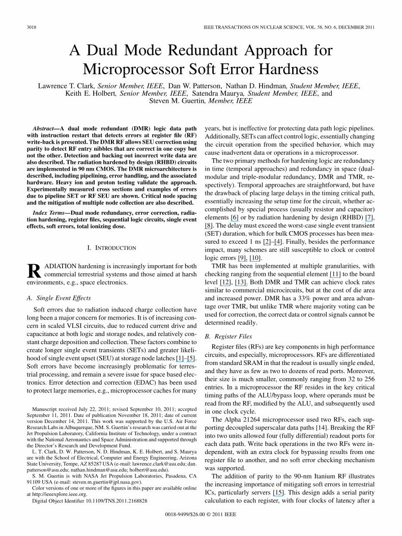
Fig. 1. DMR RF configuration showing read and write port connections, in-cluding feedback to the Rt/Rd write port for error correction using data in thecopy with good parity to overwrite data in the other copy with a parity error.Correction is by nibble, so bits in both RF entries can be upset so long as bothcopies of any nibble are not. Mismatches in the A and B WB data are caughton the input to the RF, stalling the processor to restart with clean architecturalstate.
write, during which time the register is unprotected. Checkingis static, but no repair mechanism is provided. RF errors are thusdetectable but not correctable.
C. Register File Soft Error Mitigation
A key problem in RF soft error protection is the lack of timein the pipeline, i.e., critical timing paths, for EDAC calculationin the stages leading to and from the RF. EDAC also requiresa 62.5% increase in storage capacity for byte level correction[16], which is closer to DMR than no redundancy. Wider pro-tection requires deeper parity circuits, adding two to four inver-sions to the critical timing path. Consequently, RFs more com-monly use parity protection, which is fast to generate, but canonly allow error detection. Mohr presented a sufficiently fast XYparity based EDAC scheme to allow its use in RFs [17]. How-ever, EDAC does not protect against erroneous data or opera-tions caused by SETs, either in the RF or in the ALU/bypass cir-cuitry that produces and consumes data residing in the RF. Anal-ysis of synthesized RFs on a 130 nm CMOS process showed thatTMR had similar area impact as adding EDAC, while the latterapproximately doubled the access time [18]. FPGA synthesizedRF analysis shows greater TMR area and performance impact,but better hardness [19].
D. Application and Contribution of This Work
The designs and experimental data presented here cover logicintended for an embedded five pipeline stage microprocessorimplemented primarily in DMR logic. The RF is also imple-mented using DMR, which allows data path results checking atthe write back (WB) stage as shown in Fig. 1. The data pathresults can be erroneous due to SEUs in the DMR register file
stored data, or SETs in the RF readout path or DMR data pathlogic. Using DMR error detection is easy, but DMR is difficultto implement, since the logic cannot discern which of the re-dundant copies is incorrect. SEUs in the RF are repaired on anibble basis, by copying correct contents from one DMR copyto the other, based on which has correct parity. Background RFscrubbing is also supported.
Fortunately, in a microprocessor, pipeline state not committedto architectural state is speculative and can be discarded. Theapproach used in the DMR circuits presented in this paper isto restart the operation from a known good architectural state.The key is error detection before the machine speculative stateis committed to become architectural state. The test chip usedin this work to validate the approach employs a DMR data paththat includes an ALU/bypass path suitable for a high-speed mi-croprocessor and a DMR RF for the same embedded CPU. TheALU/bypass logic and RF are controlled by a test engine imple-mented completely in TMR on the test die.
Studies of basic DMR approaches have been published, cf.[13], but do not include experimental or comprehensive sim-ulation results. Additionally, the scheme only allows a clockcycle time similar to that for circuits protected by temporal tech-niques. For the first time, this paper describes a complete ap-proach to DMR processor ALU/bypass and RF data path errorchecking and recovery. DMR checking is performed only at thecommit to architectural state, i.e., at the RF write back stage,which minimizes the checking circuitry required and reducesboundary cases, by only restarting instructions from one point.The microarchitectural and circuit changes allow both SET andSEU protection at high speed, which is demonstrated by bothproton and heavy ion broad beam testing.
E. Paper Organization
Section I summarizes the prior hardening approaches, reg-ister file requirements, and contribution of this work. Section IIdescribes the RF circuit design and how hardness to inadver-tent SET writes and MBUs is obtained. Section II describes theALU bypass logic, circuits and layout to avoid MBUs, includingthe checking WB interface. Experimentally measured results,which demonstrate both SEU and SET induced error mitigation,are described in Section III. Section IV concludes and summa-rizes the results.
II. REGISTER FILE CIRCUITS AND MICROARCHITECTURE
The RF design here combines multiple microarchitecturaland circuit level approaches, starting with DMR for compat-ibility with the data path. DMR decoders generate redundantread and write word line signals. Full SEE protection is pro-vided by DMR combined with large critical node separationthrough bit interleaving and parity. Parity provides error de-tection; DMR allows one copy to provide clean data for SEUcorrections; interleaving prevents multi-cell upsets (MCUs)from causing uncorrectable errors; inadvertent operations areprevented by circuit approaches. The parity protection is nibblebased. This allows the greatest possible critical node spacing,albeit at the expense of twice the parity storage, but with theadvantage of one less XOR gate in the parity generation andchecking paths.

3020 IEEE TRANSACTIONS ON NUCLEAR SCIENCE, VOL. 58, NO. 6, DECEMBER 2011
A standard load-store CPU would have two read ports and onewrite port, supporting the ALU operands and results, respec-tively. Referring to Fig. 1, this design adds a third, i.e., the Rt/Rdread port used to read a copy of the destination register contentsabout to be overwritten in the next cycle WB stage. Thus, theoverwritten RF data can be restored if the overwriting RF store iscancelled due to a detected data path error (SEU or SET) whichcan be detected as the WB is in progress. Since DMR does notindicate which copy is in error, the original data are returnedto the RF and then the instruction with non-matching results isrestarted from the beginning of the pipeline.
Finally, since the RF state is unknown at power up, the pro-cessor control logic tracks whether a cell has been written, i.e.,if the parity is valid. This TMR logic validates parity checkingon an entry by entry basis.
A. Error Detection and Operation
As mentioned, in the target microprocessor, all data path ac-tions that update the RF check the DMR data at the RF. The WBoccurs, and in the event that the A and B copy data do not match,a detected SEE results in an exception in the actual processor.Note that there is insufficient time to avoid a write, but the ma-chine is stalled to keep the incorrect state from propagating fur-ther into the architectural state—the erroneously written valueis backed out.
To allow this, a specific exception type, i.e., the SEE excep-tion, is added for detected soft errors. An added instruction,which when executed (within the SEE exception handler) re-places the values that may have been corrupted, is the back upregister file (BURF) instruction. The BURF instruction replacesthe RF entry that was last written with the value previously readout of the Rt/Rd port. Many different types of soft errors mayresult in a soft error exception, and since the replacement op-eration should only occur if the last instruction wrote the RF,a processor flag is set on each WB and reset on each non-WBoperation. This flag gates the BURF execution. In the test chipused for experimental validation, the RF backup is handled byan equivalent TMR test engine instruction, but the action is thesame.
In Fig. 1, the checking circuits are evident in the block la-beled ‘A vs. B data comparison’, which checks that the WB datamatch and thus is not in error. The same WB checking mecha-nism is used to detect write word line (WWL) mismatch errorsthat occur when one of the two WWL copies is asserted, but notthe other. Also, the saved value read from the Rt/Rd port is im-plemented with fine grained self-correcting logic, like the testengine.
For example, when the detector circuit determines only oneWWL is asserted on a write operation, the write also fails. Thepipeline is then stalled to avoid propagating incorrect state. Thenthe prior value in the register entry intended to be written is re-stored—this restores the correct prior RF architectural state. Theoperation where the error was detected is subsequently restartedwith correct data. Key recovery state is stored in self-correctingTMR circuits [11]. Similarly, if one of the WWLs is truncated,which may partially write both copies, the entire operation isstarted over from the previously correct architectural state. Ad-ditionally, in the case where the A and B data do not match,
the corruption could have been from any control or data pathlogic SET or latch SEU. Restarting these operations protectsthis logic. Soft errors manifest as read word line (RWL) errors,if they affect the data read, are corrected similarly.
B. Register File SEU Recovery
The RF circuits support new processor instructions whereparity groups in RF copy A with correct parity overwrite theversion in copy B, and vice versa, in two clock cycles. In thetarget processor, an added processor instruction activates thishardware, i.e., repair general purpose register (RGPR), undersoftware control. To keep the hardware simple, no hardwareinterlocks are implemented—NOP instructions are required toprovide a second cycle for the repair. In this manner, potentiallySEU corrupted RF state can be repaired in 64 clock cycles (thetime to read each register and then write it back) when an erroris detected. The control logic is very simple—only when theA parity is incorrect is the A copy overwritten, otherwise theB copy is. Only accumulated errors affecting the same paritygroup in both copies result in an uncorrectable error, but dueto large physical separation between cells in the same paritynibble these are likely due to multiple ionizing radiation par-ticle strikes. These are in turn, mitigated by background scruboperations. Since in a microprocessor, specific registers are usedfor specific tasks, e.g., are reserved for the stack pointer, etc.,some are infrequently used, inviting defeat of parity by accumu-lating upsets from multiple impinging radiation particles. Accu-mulated errors affecting both A and B RF copies are avoided byallowing frequent scrubbing. Besides allowing potentially in-correct data to be backed out when a mismatch between the Aand B data copies is detected, the Rt/Rd read port also allowsopportunistic scrubbing.
When an instruction in the pipeline stage prior to the WBstage will not write to the register file in the next pipeline stage(e.g., a store instruction), the Rt/Rd read port is used to read aregister, which is automatically checked for errors by the paritychecking circuitry. Thus, all registers are sequentially read ina rotating fashion in parallel with normal operations, and arechecked for errors (by the usual parity check mechanisms). Thishardware scrubbing mechanism minimizes the probability ofaccumulated strikes causing irrevocable errors. The scrubs op-portunistically use the Rt/Rd port, when it is not required by aninstruction writing back to the RF.
C. Circuit Design and Timing
The RF cell design differs from that in a conventional dy-namic RF in that a write operation requires simultaneous asser-tion of two WWLs—this mitigates the possibility of inadvertentwrites to RF locations due to control logic SETs (see Fig. 2(a)).One write word line, WWLA, is controlled by the A pipelinecopy, while WWLB is controlled by B pipeline circuits. Con-sequently, a SEE manifest as a control error that propagates tothe RF cannot affect the architectural state in the RF. Read outis conventional, discharging the dynamic read bit line (RBL) ifthe cell state is a logic ‘1’. Two of the read ports are connectedto one side of the cell, and one to the other, to increase the min-imum storage node capacitance, which would dominate the cellSEU hardness.

CLARK et al.: A DUAL MODE REDUNDANT APPROACH FOR MICROPROCESSOR SOFT ERROR HARDNESS 3021
Fig. 2. RF cell circuit showing dual WWL transistors to block SET inducedwrites (a). Cell layout showing annular NMOS transistors and guard rings forTID immunity; adjacent non-rectangular cells share an N-well (b). The insidenodes of the annular transistors are sensitive to SEE, externally at � . Verylittle of the storage cell area collects charge to cause SEU (c). The conventionaltwo-edge PMOS pull up transistors and N-well are evident.
Fig. 3. Simulated waveforms, using fully extracted layout netlists, showing theRF operation and speed. The first clock cycle shows a correct write. The secondclock cycle is a read. The next clock cycle shows WL error detection. The re-dundant WWL checkers detect a short or missing WL assertion, an incorrectWL assertion to one copy, even due to a missing clock. The error propagatesand is detected in time to stall the pipeline at the next clock edge for recovery.
Set-dominant latches conclude the readout path, presenting astatic time-borrowing output to the surrounding circuitry. Whilefast, the domino RBL nodes are susceptible to SETs, as evi-denced in radiation tests (see Section III). Simulated RF oper-ational waveforms, using a netlist with full extracted parasiticsare shown in Fig. 3. The parasitic extraction flow uses a pro-prietary Calibre flow that correctly models the transistor neckMiller and gate capacitance. Effective channel length and widthare calculated as derived from [20]. Circuit speed is comparableto a commercial design, except for greater WL loading for theDMR design due to longer routes through the array because ofthe interleaved DMR. Correct write and read operations showthe timing in the first two clock cycles of Fig. 3. In the third clock
Fig. 4. Redundant write WL checking circuit is essentially two domino (one’scatching) NOR gates. The full keepers allow pseudo-static behavior and thedelay generators (ovals) delay the checking to allow both versions to settle. Theoutput is qualified with RF write operations. Redundant versions are neededsince failure to assert AClk or BClk due to a control SET will also fail to assertthe controlled write WL.
cycle, an erroneous single WWL assertion on WWLB, withoutthe corresponding WWLA assertion is shown. The subsequenterror detection results in signal WLError rising, as shown.
Incorrect WB data and redundant WWL assertions are de-tected by a one’s catching domino circuit (see Fig. 4) similarto that used in our prior RHBD cache [21]. Clock chop circuitsdelay the turn on edge to allow the checked state to settle afterthe rising clock edge controlling such state transitions (cf., Fig.1). The same delays are used to generate a pulsed pre-charge,which eliminates the need for a dynamic to static converter latch.The D2 domino ERRA and ERRB signals are discharged for anytransient mismatch between the checked inputs. The full keeperholds the state even if the mismatch transient is short.
D. Register File Layout
The fully TID protected RF cell layout is shown in Fig. 2(b).Unlike the RF cells in [17] which used a pre-discharge PMOSbased cell to minimize RHBD size at the cost of speed, thiscell uses conventional NMOS transistors. The greater size ofthe NMOS transistor dominated layout increases storage nodeseparation. To effectively use the cell width, the PMOS transis-tors share a short N-well with the adjacent cell as shown. Theread pull down transistors are tapered for maximum speed andminimum RBL capacitance. All key NMOS nodes are drivenby the diffusion enclosed by the annular devices, minimizingcharge collection area and minimizing capacitive loading andthus power dissipation, e.g., the RF cell storage nodes in Fig.2(c).
The entire RF layout showing the bit interleaving is shown inFig. 5. The decoders are spatially separated, as shown, to preventa SEE from corrupting both copies simultaneously, since it is

3022 IEEE TRANSACTIONS ON NUCLEAR SCIENCE, VOL. 58, NO. 6, DECEMBER 2011
Fig. 5. Thirty-two entry 40-bit RHBD DMR RF layout with parity group in-terleaving (color coded) and one parity group’s A and B copy bits are outlinedin black over the layout to show critical node separation of 15 cells (67.2 �m).The similarly spaced DMR (A and B copy) WL decoders are also evident.
imperative that the WWLs not be mis-asserted the same way. Inthe same manner, two incorrect RWL assertions that were iden-tical would send the same incorrect data through both copies ofthe ALU, and would not be detected as an error at WB.
E. Test Chip Design
Fig. 6 shows the essential test chip pipeline with emphasison the RF ALU/bypass loop that occupies the E-stage of thepipeline. The primary differences between the test chip circuitsand an actual processor are that the latter includes a shifter andlogic unit. The ALU and RF are controlled by a programmablebuilt-in test engine implemented entirely in TMR logic withfine-grained correction [11].
The test chip is implemented on a trusted foundry 90 nm bulkCMOS fabrication process. The test chip photomicrograph withthe test circuits overlaid comprises Fig. 7. The TMR test en-gine has four pipeline stages and is controlled by a 64 entry40-bit instruction memory, a 32 entry 40-bit address memory,and a 32 entry 36-bit data memory. All of these memories areimplemented as register files with fine-grained local error cor-rection. The test engine limits the circuit speed to about 250MHz. Clocks are generated by a foundry supplied unhardenedPLL.
III. SEE TESTING RESULTS
A. SEE Testing
Broad beam ion tests comprised two basic types, static RFand dynamic RF/ALU/bypass tests. The former exercise the RFmemory statically, i.e., without the data path in operation, to de-termine the RF SEU and SET characteristics. The device undertest (DUT) is on a daughter card, attached to and controlled byan FPGA main board. The latter records errors at test speed.The FPGA communicates with a PC via a USB connector, e.g.,sending error logs under user command.
In the static tests the RF is written with all 0’s, all 1’s or acheckerboard pattern. The RF is then read continuously by the
Fig. 6. The test chip pipeline matches the processor pipeline around the RF,ALU/bypass loop. The circuits are controlled and checked by a test engine usingfull TMR with local correction at each pipeline stage.
Fig. 7. Test die photomicrograph with test chip layout overlaid; the RF andALU/bypass circuits are outlined and labeled. The die is 3.75 mm/side.
test engine. In the event of an error, the upset stored data arecorrected and the test continues at the next location. An SET,presumably in the RF dynamic read bit line circuits, address, ordecoding, is detected if the initially read data is incorrect, butis correct on a subsequent read. Both copies are read in thesetests, which reflect the actual DMR processor operation, whereeach redundant data path/control copy receives unchecked anduncorrected data words from the RF. However, only one readport is used.
The dynamic tests utilize the RF WB checking circuits tocharacterize the data path checking functionality. In these tests,

CLARK et al.: A DUAL MODE REDUNDANT APPROACH FOR MICROPROCESSOR SOFT ERROR HARDNESS 3023
Fig. 8. Representative measured error upset types as logged in the tests: Onebit RF SEUs in the all 0’s test (a) and SETs in the all 1’s test, which we assumeto be dynamic BL discharges (b). Multi-bit upset of one of the DMR copies,while running the ALU/RF bypass loop due to ALU SET (c). A multi-bit errorto one copy, demonstrating an error that can be fixed using the SEU repair mech-anism-the B copy of entry 23 has no errors (d). A ‘.’ indicates 1 to 0, and a ‘*’denotes 0 to 1 errors, respectively. (a) SEU RF errors, (b) SET RF errors, (c)Multi-bit upset, (d) Multiple cell errors in one RF copy that can be repaired.
a DMR Kogge-Stone adder, complete with input and output by-pass paths as would appear in a standard microprocessor per-forms arithmetic operations on the RF data. As a side effect,the types of errors generated by the data path can be exam-ined. Thus, these tests allow SETs to dramatically corrupt onecopy, due to transients on the adder prefix circuitry corruptingthe MSBs due to propagating carry errors, or incorrect func-tions or bypassing due to control SETs in one DMR pipelinecopy. When an error is detected in these tests, which have paritychecking turned off to propagate more errors into the data path,the check type is logged. These are either ‘WB error’ indicatingthe A and B WB data mismatched, or WL error, which indicatesthat the WWL checker found a WWL assertion discrepancy. Atthis point, the test engine is re-loaded to dump the RF contents.This allows accumulated RF SEUs to be examined. Then, theRF is repaired and the dynamic test resumed.
Examples of the test logs are shown in Fig. 8. The output dataare decompressed and decoded at the PC, allowing the bit loca-tions, and corresponding entry to be mapped (Fig. 8(a)). All bits,including the parity bits, are treated as data in the static tests. AMCU can be determined as well, since each test pass has an 8-bittime stamp. Fig. 8(b) shows the map of SET failures recorded inone test. An example SET upset, affecting many bits in the dy-namic testing, is shown in Fig. 8(c). Here, since the mismatchesare confined to the word most significant bits, we speculate thatthe adder prefix circuitry propagated an SET, although a latch
Fig. 9. Measured RF bit cell heavy ion cross section as determined by statictesting, constantly reading the RF locations and writing back erroneous valuesat � � ��� V.
SEU may have been the culprit. Regardless, the potential im-pact of an error propagating through the combinational logic isevident. An MCU, detected in the full speed testing comprisesFig. 8(d). Since the stored bits are not adjacent, this is presumedto originate in the A data path DMR copy. This is correctableby the RF parity based repair mechanism, although this write isredacted after the A and B mismatch is detected.
B. Heavy Ion Testing
Heavy ion testing was performed at the Lawrence BerkeleyLabs 88 SEE testing facility. Boron, oxygen, neon, argon,and copper ions with nominal (normal incidence) linear energytransfer (LET) of 0.89, 2.19, 3.49, 9.74, and 21.17 MeV-cm /mgat angles ranging from 0 (normal) to 70 were used. Testing wasprimarily performed at 100 MHz and 200 MHz at V = 1,1.2, and 1.4 V. At angles, the beam was aimed in the directionfor which MBUs would be most likely (across the words). ThePLL was shielded during ion testing. Fluence was 2(10 ) to10 and flux was 10 to 10 ions/cm /s in most of these tests.
The experimentally measured RF bit cross section vs. effec-tive LET (LET ) is shown in Fig. 9. Since near minimumPMOS transistors are used in the storage latches, the thresholdLET is low. It is however, larger than for RHBD SRAM cellson the same process [21], which is attributable to the high loadcapacitance of the transistors driving the read ports. MCU ex-tent was one bit for over 90% of the recorded SEUs. The longestextent was two bits.
The chip level cross sections, for argon ions with nominal(normal incidence) LET = 12.89 MeV-cm /mg, is shown inFig. 10. The bar labeled “WB error” indicates that an A/B copymismatch detection triggered an RF dump. The SEU bars in-dicate only RF errors that were not the original cause of thedetected error, i.e., accumulated upsets. WB error MBUs areshown, and as expected are relatively common, since this is howSETs in the data path are detected. The ‘MBU’ column showsupsets of multiple cells, where 2-bit upsets predominated, as inthe static tests.

3024 IEEE TRANSACTIONS ON NUCLEAR SCIENCE, VOL. 58, NO. 6, DECEMBER 2011
Fig. 10. Measured RF and ALU/bypass circuit heavy ion cross sectionfrom dynamic testing exercising both at � � ��� V and ��� � �����
MeV-cm /mg (40 angle). WB error and WL error refer to how the initial errorwas detected; SEU refers to other errors inside the RF when the contents weredumped; scrubbing was not run, but writes naturally update some RF contents.
C. Proton Testing
Proton beam energies of 49.3 and 13.5 MeV were used. Whiletests with the PLL were performed, most of the testing was per-formed at 60 MHz using the PLL bypass mode, since PLL upsetscan cause test chip malfunctions due to bad clocks and the PLLis difficult to shield from proton strikes. Tests were run with thePLL on at speeds up to 250 MHz, but a number of (presumablyclock upset) induced gross failures were recorded with the PLLon.
For most RF tests the total fluence was 5 pro-tons/cm . Flux was 2.3 to 8.9 protons/cm /s. Forthe 49.3 MeV proton energy, the measured cell (per bit) crosssections for static SEU testing of the RF were 3.71(10 ) cm ,2.68(10 ) cm and 1.12 cm at and
V, respectively. Similar response was measured for all 0’sand all 1’s patterns. This was expected, since the RF may be hiton either side and cell capacitance is relatively balanced. SETswere observed only for the read all 1’s case but only in one testand thus with a very low cross section.
For the 13.5 MeV proton beam energy, the measuredcell cross sections for static SEU testing of the RF were1.07(10 ) cm , 8.98(10 ) cm and 1.72(10 ) cm atV = 1, 1.2 and 1.4 V, respectively. MCUs were rare andthe longest upset extent was two bits. Cross sections from thedynamic tests are shown in Fig. 11 at different V supplyvoltages and proton energies. A slight decrease with supplyvoltage, and reduced cross section at lower energy are evident.
D. Analysis
Only one RF port is used in the static tests, and thus the RBLcan only upset when the data would have retained the RBL high.Consequently, in ion testing over 98% of the SETs were de-tected with logic ‘1’ stored, leading us to conclude that the dy-namic RBLs dominate the RF SET cross section (see Fig. 8(b)).
Fig. 11. Measured RF and ALU/bypass circuit proton cross section from dy-namic testing exercising both at multiple proton energies and VDD. WB errorand WL error refer to how the initial error was detected; Accumulated SEUrefers to other (SEU) errors inside the RF when the contents were dumped.
In proton testing SETs were only detected with logic ‘1’ in thecell. The time to dump the RF state after a dynamic error wasdetected was 13.7 s. This may have also allowed some addi-tional error accumulation (reported as SEU in Figs. 10 and 11).
The data confirm that the proposed DMR hardening tech-niques will be effective. SEU MCU extent was far below thecritical node spacing. While many bit errors (representing a po-tentially large equivalent MCU extent) were detected in the dy-namic tests, the many bit errors occurred only in one, e.g., theA but not B, copy. Regardless, these operations are restarted.Uncorrectable errors were noted in some proton tests at highflux. Similar errors were produced in heavy ion testing whenthe PLL was not shielded, but not with the PLL shield prop-erly positioned, and were thus attributed to clock upsets, whichcause setup time failures. We relied on the non-redundant by-pass mechanism within the foundry IP PLL, so could not deter-mine if the errors were due to clock SETs or error accumulation.
IV. SUMMARY AND CONCLUSIONS
This paper has described a DMR approach to microprocessordata path and RF hardening that is capable of commercial mi-croprocessor speeds. Error detection is simple as applied onlyat RF write back and during scrub operations prior to WB, andis capable of mitigating any data path SETs, including those oncontrol logic.
While the design presented here has both DMR data path andRF logic, duplicating only the latter is applicable to commercialdesigns. Lack of DMR data path and control signals removes theSET protection, but provides the SEU protection when joined tothe parity based repair mechanism, with minimal timing impact.
ACKNOWLEDGMENT
The authors would like to thank David Pettit andRahul Shringarpure for their invaluable contributions tothe RF implementation.

CLARK et al.: A DUAL MODE REDUNDANT APPROACH FOR MICROPROCESSOR SOFT ERROR HARDNESS 3025
REFERENCES
[1] P. Dodd, M. R. Shaneyfelt, J. A. Felix, and J. R. Schwank, “Productionand propagation of single-event transients in high-speed digital logicICs,” IEEE Trans. Nucl. Sci., vol. 51, no. 6, pp. 3278–3284, Dec. 2004.
[2] M. Gadlage, R. D. Schrimpf, J. M. Benedetto, P. H. Eaton, D. G. Mavis,M. Sibley, K. Avery, and T. L. Turflinger, “Single event transient pulsewidths in digital microcircuits,” IEEE Trans. Nucl. Sci., vol. 51, no. 6,pp. 3285–3290, Dec. 2004.
[3] J. M. Benedetto, P. H. Eaton, D. G. Mavis, M. Gadlage, and T.Turflinger, “Digital single event transient trends with technology nodescaling,” IEEE Trans. Nucl. Sci., vol. 53, no. 6, pp. 3462–3465, Dec.2006.
[4] P. Dodd and F. Sexton, “Critical charge concepts for CMOS SRAMs,”IEEE Trans. Nucl. Sci., vol. 42, no. 6, pp. 1764–1771, Dec. 1995.
[5] T. Hoang, J. Ross, S. Doyle, D. Rea, E. Chan, W. Neiderer, and A.Bumgarner, “A radiation hardened 16-Mb SRAM for space applica-tions,” in Proc. IEEE Aerospace Conf., 2007, pp. 1–6.
[6] G. Anelli, M. Campbell, M. Delmastro, F. Faccio, S. Floria, A. Gi-raldo, E. Heijne, P. Jarron, K. Kloukinas, A. Marchioro, P. Moreira,and W. Snoeys, “Radiation tolerant VLSI circuits in standard deep sub-micron CMOS technologies for the LHC experiments: practical designaspects,” IEEE Trans. Nucl. Sci., vol. 46, no. 6, pp. 1690–1696, Dec.1999.
[7] R. Lacoe, J. V. Osborn, R. Koga, S. Brown, and D. C. Mayer, “Appli-cation of hardness-by-design methodology to radiation-tolerant ASICtechnologies,” IEEE Trans. Nucl. Sci., vol. 47, no. 6, pp. 2334–2341,Dec. 2000.
[8] K. Warren, A. L. Sternberg, J. D. Black, R. A. Weller, R. A. Reed,M. H. Mendenhall, R. D. Schrimpf, and L. W. Massengill, “Heavy iontesting and single event upset rate prediction considerations for a DICEflip-flop,” IEEE Trans. Nucl. Sci., vol. 56, no. 6, pp. 3130–3137, Dec.2009.
[9] D. Hansen et al., “Clock, flip-flop, and combinatorial logic contribu-tions to the SEU cross section in 90 nm ASIC technology,” IEEE Trans.Nucl. Sci., vol. 56, no. 6, pp. 3542–3550, Dec. 2009.
[10] B. Narasimham, O. A. Amusan, B. L. Bhuva, R. D. Schrimpf, and W.T. Holman, “Extended SET pulses in sequential circuits leading to in-creased SE vulnerability,” IEEE Trans. Nucl. Sci., vol. 55, no. 6, pp.3077–3081, Dec. 2008.
[11] N. D. Hindman, D. E. Pettit, D. W. Patterson, K. E. Nielsen, X. Yao,K. E. Holbert, and L. T. Clark, “High speed redundant self-correctingcircuits for radiation hardened by design logic,” Proc. RADECS Conf.,pp. 465–472, 2009.
[12] B. Peters, A. Wardrop, D. Lahti, H. Herzog, T. O’Connor, and R. De-Coursey, “Flight SEU performance of the single board computer (SBC)utilizing hardware voted commercial PowerPC processors on-board theCALIPSO satellite,” in Proc. IEEE Radiation Effects Workshop, 2007,pp. 16–25.
[13] J. Teifel, “Self-voting dual-modular-redundancy circuits for singleevent transient mitigation,” IEEE Trans. Nucl. Sci., vol. 55, no. 6, pp.3435–3439, Dec. 2008.
[14] B. Gieseke et al., “A 600 MHz superscalar RISC microprocessor without-of-order execution,” in Proc. IEEE Int. Solid-State Circuits Conf.Tech. Dig., 1997, pp. 176–177.
[15] E. Fetzer, D. Dahle, C. Little, and K. Safford, “The parity protected,multithreaded register files on the 90-nm itanium microprocessor,”IEEE J. Solid-State Circuits, vol. 41, no. 1, pp. 246–255, Jan. 2006.
[16] M. Hsiao, “A class of optimal minimum odd-weight-column SEC-DECcodes,” IBM J. Res. Develop., vol. 14, no. 4, pp. 395–401, Jul. 1970.
[17] K. Mohr, G. Samson, and L. T. Clark, “A radiation hardened by designregister file with low latency and area cost error detection and correc-tion,” IEEE Trans. Nucl. Sci., vol. 54, no. 4, pp. 1335–1342, Aug. 2007.
[18] R. Naseer, R. Bhatt, and J. Draper, “Analysis of soft error mitigationtechniques for register files in IBM Cu-08 90nm technology,” in Proc.IEEE Int. Midwest Symp. Circuits and Systems, 2006, pp. 515–519.
[19] R. Hentschke, F. Marques, F. Lima, L. Carro, A. Susin, and R. Reis,“Analyzing area and performance penalty of protecting different digitalmodules with Hamming code and triple modular redundancy,” in Proc.Symp. Int. Circuits and Systems Design, 2002, pp. 95–100.
[20] A. Giraldo, A. Paccagnella, and A. Minzoni, “Aspect ratio calculationin n-channel MOSFETs with a gate-enclosed layout,” Solid State Elec-tron., vol. 44, pp. 981–989, Jun. 2000.
[21] X. Yao, D. Patterson, K. Holbert, and L. Clark, “A 90 nm bulk CMOSradiation hardened by design cache memory,” IEEE Trans. Nucl. Sci.,vol. 57, no. 4, pp. 2089–2097, Aug. 2010.