A Differential Sample and Hold Technique that Rejects Offset ...
54
University of Central Florida University of Central Florida STARS STARS Retrospective Theses and Dissertations 1976 A Differential Sample and Hold Technique that Rejects Offset A Differential Sample and Hold Technique that Rejects Offset Voltages Voltages John Adams Davis University of Central Florida Part of the Engineering Commons Find similar works at: https://stars.library.ucf.edu/rtd University of Central Florida Libraries http://library.ucf.edu This Masters Thesis (Open Access) is brought to you for free and open access by STARS. It has been accepted for inclusion in Retrospective Theses and Dissertations by an authorized administrator of STARS. For more information, please contact [email protected]. STARS Citation STARS Citation Davis, John Adams, "A Differential Sample and Hold Technique that Rejects Offset Voltages" (1976). Retrospective Theses and Dissertations. 208. https://stars.library.ucf.edu/rtd/208
-
Upload
khangminh22 -
Category
Documents
-
view
2 -
download
0
Transcript of A Differential Sample and Hold Technique that Rejects Offset ...
University of Central Florida University of Central Florida
STARS STARS
Retrospective Theses and Dissertations
1976
A Differential Sample and Hold Technique that Rejects Offset A Differential Sample and Hold Technique that Rejects Offset
Voltages Voltages
John Adams Davis University of Central Florida
Part of the Engineering Commons
Find similar works at: https://stars.library.ucf.edu/rtd
University of Central Florida Libraries http://library.ucf.edu
This Masters Thesis (Open Access) is brought to you for free and open access by STARS. It has been accepted for
inclusion in Retrospective Theses and Dissertations by an authorized administrator of STARS. For more information,
please contact [email protected].
STARS Citation STARS Citation Davis, John Adams, "A Differential Sample and Hold Technique that Rejects Offset Voltages" (1976). Retrospective Theses and Dissertations. 208. https://stars.library.ucf.edu/rtd/208

* . A DIFFERENTXU SAMPLE AND HOLD TECHNIQUE
1 THAT REJECTS OFFSET VOLTAGES
JOHN ADAMS DAVIS, JR. B.S~.E.E.,'North Carolina State University, 1971
. .
RESEARCH REPORT
Submitted in partial fulfillment of the requirements for the degree of Master of Engineering
. in the Graduate Studies Program of I Florida Technological University, 1976
Orlando, Florida

ABSTRACT
*A DIFFERENTIAL SAMPLE AND HOLD TECHNIQUE THAT REJECTS OFFSET VOLTAGES
BY
JOHN ADAMS DAVIS, JR.
This research z'eport discusses modern sample. and
hoLd theory and techniques and then uses them to
develop a new- differential sampling concept to solve
a real engineering problem, involving the synchronous
demodulation of three amplitude modulated direction
cosine signals in an unusual noise environment. The
problem is discussed in detail and a detailed circuit
design solution given. Additionally, the results of
a breadboard test of the concept is given that shows
the,oircuit to have a 60dB offset voltage rejection
ratio.
iii
ACKNOWLEDGMENTS
The author wishes to express his sincere gratitude
to his advisor and committee chairman, Dr. Richard C.
Harden, for his help and guidance not only during the
preparation of this research report, but also at every
step of the long post-graduate studies road. He is
also thankful to Mrs. Marie Farmer for the many hours -
she spent in typing this report.
This research report is dedicated to the author's
wonderful wife, Sharon, without whose encouragement,
love and patience this paper would not have been written,
nor would any post-graduate studies have been possible.

TABLE OF CONTENTS
.................................... . ACKNOWLEDGMENTS iii
INTRODUCTION ........................................ 1 CHAPTER I SAMPLE AND HOLD THEORY AND TECHNIQUES ... 5 CHAPTER If: THE PROBLEM TO BE SOLVED .............. A 4
The System ...................m...m... 14
.............. The ~nterface Subsystem 16 .................. The Error Budget 17 ................. The Input Signals 20 The Synchronous Demodulator - ................ Our .Design Problem 22
...................... CHAPTER . 1x1 THE CIRCUIT DESIGN 26
...................... The Input Stage 28
............ The Sample and Hold Stage 31
The Error Total ..........me.m........ 42
The Breadboard Circuit ...............8 4
Conclusions . . . . . . . . . . . . . . . . . . .em.. . .m 46

INTRODUCTION
An airborne fire control system (machine aid for
accurate weapon delivery) has been designed, built
and flight tested against ground targets, This sys-
tem searches out and "locks on" to coded pulses of ,
1
light that reflect from laser designated (illuminated)
targets (the laser designator apparatus is operated
from either the ground or another aircraft). Once
"lock on' is effected, the system continually informs
an on board digital computer of the precise angular
target location with respect to the airframe co-ordin-
ates. The computer, in turn, generates steering
commands and computes the optimum weapons (bombs,
rockets or gunfire) release or firing position/time
to facilitate the accurate delivery of ordnance on
the target. The accuracies involved in this system
are such that, in most cases, it will no longer be
necessary to utilize unconventional and expensive
weaponry such as "smart" bombs or homing rockets to'
facilitate precise weapon delivery.
The system consists of an external (mounted out-
side of the aircraft skin) pod with a gimbaled seeker
machaniem, an aircraft interface unit (AIU), and an

on board digital computer. When "lock on1' occurs,
the seeker mechanism "looks" (points) in the direc-
tion of the target. The gimbal angular positions
with respect to the airframes structural co-ordin-
ates are precisely determined and electrical repre-
sentations of the angles are output as amplitude
modulated A.C. signals (resolver position signals).
The AIU converts these analog signals to digital
angular representations in a format acceptable for
use by the digital airborne computer. The computer
uses the angular information to generate steering
commands to be used by the pilot or an automatic
flight control system. It also computes the optimum
point and time at which to release/fire the-selected
weapons.
The system flight tests were very successful
for one important problem. was discovered
that the output from the external pod had an unusual
noise added to the analog signals that contain the
angular target location information. This noise was
not being rejected by the AIU., and, when present,
would cause errors in the signals that were much
greater than those allowed by the system specifica-
tions.
The subject of this paper, then, is a new noise

rejection scheme and the design of the necessary AIU
circuitry to implement it. This new design must not
only meet the system specifications but also make no
unnecessary conceptual changes and should utilize as
much of the existing design and components as possi-
ble to reduce cost and facilitate the easiest customer
approval of the system. With this in mind, it was
decided to re-deeign only the analog input demodula-
tion (sample and hold) circuitry in the AIU.
To help the reader not familiar with sample and
hold (S&H) circuitry to understand this report, Chap-
ter I contains a review of basic S&H theory and tech-
niques. Chapter I1 contains an in depth discussion
of the problem to be solved. The design and the de- ,
sign process are presented in Chapter 111 along with
the results of testing the new scheme using a bread-
board model of the design.
Certain abbreviations are used in the text of
this research report. They are:
FET
meaning sample and hold circuit(s)
meaning resistance or resistor
meaning capacitance or capacitor
meaning field effect transistor
OP AMP meaning operational amplifier
V meaning volts - steady state

meaning volts - instantaneous meaning amperes/current - steady state meaning amperes/current - instantaneous meaning time (in seconds unless otherwise specified) \
SFEEC meaning scale factor error equivalence cancellation
meaning analog to digital (converter circuit)
meaning the root of the sum of the squares
exp(x) meaning the quantity 2.71828 raised to the exponent x
ln(x) meaning the natural log of the quantity(x)
Subscripts such, as %BT-OFF are used to differen-
tiate between these abbreviations, to clarify them or
just to add supplementary information.

SAMPLE AND HOLD THEORY AND TECHNIQUES
S&H circuits are used to sample (detect) the
value of a signal at.a given point in time and hold
(remember) that value indefinitely until
desired that the signal value be sampled and held
again at another point in time. The basic scheme
for S&H circuits is shown in Figure 1-1. The memory
device follows the input signal (samples) until the
switch is changed from the ample to the hold posi-
tion at which time the memory device causes'the signal
at the S&H output to remain (hold) at the last known
(memorized) value before the switch was opened.
switch
memory device
Figure 1-1. Basic ShH Scheme

There are many techniques for implementing this
scheme using real hardware. However, the most common
one used today is shown in Figure 1-2.
FET switch
Figure I-2. Common S & H Circuit
The utilization of real world components intro-
duces some complications. The electronic field effect
transistor (PET) switch has finite ON (in the sample
condition) and OFF (in the hold condition) resistances
associated with it and a reaction time (time to turn
ON/QFF 0nce.a command signal is received). Also, the
capacitor memory device has a leakage current (loss
of signal while in hold condition) and an acquisition
time (time it takes for the capacitor memory device.to
fully charge up to - or sample - the signal level) associated with it. The reaction time of the elec-
tronic FET switch causes an error in the hold signal
known aa aperture error and the ON resistance of the

FET causes the capacitor memory device to takea
finite time to charge up to the signal level. If
the freq-uency components of the signal are too high,
or the sample period too short, excessive.~e~rtrrsc~may re-
sult. The capacitor leakage and the finite OFF re-
sistance of the FET cause the memorized (held) signal
value to droop or fall off with time. Figure I-3
exhibits these'problems graphically. b
Since we are considering 'the real world, we
should note that the signal source will also have some
impedance associated with it and must be added to the ( I
FET1s ON resistance when computing the acquisition
time of the capacitor. Also, the place (s) to which
the output signal goes will have a finite input re-
sistance and/or a bias current associated with it that
will make the leakage (output signal droop) of signal
more pronounced while in the hold mode.
Often the signal source impedance, the output
load impedance, and the required bias currents
change as the signal level or other circuit conditions
change. This causes the S&H output signal to be some-
what unpredictable. Several steps can be taken to
minimize the effect of this unpredictability. A re-
sistance that is very large with respect to the FET's
ON resistance, plus the signal source impedance, is


often placed in the input signal path, while on the
output, a buffer amplifier with a known impedance and
bias current is used as a load. This amplifier, in
turn, outputs the S&H signal to the unpredictable loads.
Figure 1-4 shows the complete basic modern S&H circuit.
signal to be sampled
timing signal
S & H output signal
Figure 1-4. Complete, Modern, Basic S&H Circuit
We have now improved the predictability of the
circuit, but, have made the charging time of the capac-
itor longer:
CHARGE^^% = 4 605 x C x (RADDED+RsOURCE+~ET ON)
t ~ ~ ~ ~ ~ ~ 9 9 . 9 % = 6.91 x C x (combined R 1 s ) .
The droop of the S&H output is now
where RT is the parallel combination of %ET OFF with
R~~~~~~~ INPUT and, i~~ is the capacitor leakage
current p l u ~ the amplifier bias current (we have assumed

that the amplifier gain is unity) . Typical values of RFET O~ are 30n to 200nwhile
are 10*n to 'EoL3n This typical values of SET OFF ,
indicates that a typical added in resistor should be
. 30Ch to 2Kn just to make the SET ON insignificant
(signal source impedances vary considerably and will
also add to the necessary value of RADDED ) . From
the above w e can see that the choice of C must be
large enough to keep the output droop acceptable but
small enough to allow charging to an acceptable per-
centage of the desired value in the necessary time.
Several variations of our modern basic sample
and hold circuit are often used. One of these uses
the capacitance as a feedback element (Figure I-5a).
This has the advantage that the S&H can have gain
(RF/RN ) but, the S&H output is the inverse of the
signal sample. Figure I-5b shows a variation that
all but eliminates the effects of bias currents on
output droop in the hold mode. In this design only
offset currents (the difference between the inverting
and non-inverting input bias currents) can affect droop.
Figure I-5c shows a scheme1 for making the acquisition
time very short by adding a high capacitor charging
current capability.
' ~ ~ 9 8 mberge t . Operational Amplifiers Theory and Practice, (New York: John Wiley c Sons, Inc., 19751,
, 457.

Many unusual.' circuits' .have been- designed to accomplish
special tasks - one of these is shown in Figure 1-6. .It is an S&H with no droop (infinite holding capa-
bility) that uses an analog to digital conversion
circuit with a digital to analog circuit in the feed-
back loop as the memory device. This design was dis-
closed by Burr Brown Corp. during a seminar on their
conversion products held at Martin Marietta Aerospace
in Orlando, Florida on September 17, 1975.
Using the theory and techniques presented in
this chapter, a real signal processing problem was
solved by designing an original, differential sample
and hold circuit. The problem alluded to is presented
in Chapter I1 and the circuit design is presented in
Chapter 111.

sisnal Rl
S & H output
signal v in 0 lQl
S&H output
S&H output
Figure 1-5. Showing Some Variations of Modern S & H Circuits


T E PROBLEM TO BE SOLVED
In a system that requires an analog to digital
linterface, three amplitude modulated direction cosine
signals representing angular target-location informa-
tion and a reference signal are to be synchronously
demodulated in an unusual noise environment, and pre-
sented to analog to digital (A/D) conversion circuitry
with a very high degree of aocuracy.
The system is an airborne fire control system
that. searches for (scans ground areas in front of the .
aircraft) , identifies, " locks on", and tracks ground
targets. The target's angular location with respect
to the aircraft (airframe) co-ordinates is transformed
and the information is presented to an on board digital
computer. This computer in turn generates steering
commands, and computes optimum weapon release/fire times
for the selected ordnance. This, of course, facilitates
very accurate, automatic airborne-tactical-weapons de-
livery.
The system consists of three major sub-systems:
the on board computer, the search and tracking unit
(a pod mounted under the aircraft), and an aircraft
interface unit (AIU). The AIU's purpose is to inter-
face the pod's analog circuitry with the aircraft's
digital computer.
In operation the pod (tracking unit) detects
coded light pulses reflecting from a target (the light
is actually coded pulses'of laser light that is focused
onto the target by a ground observer or another forward-
air-control aircraft) and decodes it for identification
purposes. If it is the proper code the "lock on" will
occur and the light detector apparatus (gimbal mounted
in the pod) will remain pointed directly (track) at'
the target. Then, gimbal position information that
precisely defines the target line of sight co-ordinates
is output as electronic analog signals.
The AIU transforms the electronic analog signals
from the pod to digital ones with a format acceptable
to the on board computer. This is where our problem
exists as will be discussed later in detail.
The manner in which the computer interprets the
three direction cosine signals is of great importance,
since it will materially affect our- design problem.
The azimuth and elevatibn'angles are the ones used for

16
steering and weapons release coamrands and are cosmputed
as follows:
Y azimuth = Arctan - X
elevation = Arctan z4
3 x 2 + y2
As this indicates, scale factor (gain) errors are
meaningless when the scale factor errors are identical.
to each other'in all three (X, Y & Z) direction cosine
signals, i. e.
Arctan KZ = Arctan Z * &+ 7 x z + YZ
This will serve to relax... the design criteria such
that we can allow identioal ecaLe factor errors on all
signals simultaneously. We will term this condition
scale factor error equivalence cancellation and will
abbreviate it SFEEC.
The Interface Subsystem
The aircraft interface unit converts tne analog
direction cosine signals to a format acceptable to the
digital computer. This is accomplished by synchronously
demodulating the three direction cosine signals (resol-
ver outputs) and a reference signal (the resolvers exit-
ation voltage) then doing a classical analog to digital
(A/D) conversion on the resultant demodulated voltage
levels. The A/D conversions are done by one A/D con-

17
version circuit in a time multiplex fashion. This
A/D circuit accepts the demodulated reference voltage '
such that the resultant digital output representation
will be
input signal amplitude reference amplitude
Thus, a full scale positive (input = reference) signal
reoults in a positive full male output (+1) representa-
tion, and a full scale negative (input = -reference)
results in a negative full scale output (-1), while no
input (input = 0.W) results in a zero output (0)
representation.
The Error Budget
The interface subsystem must meet a rather tight
error specification. The input to output, one sigma,
error allowed is 1.5 milliradians (mr)-of spherical
pointing vector error. The one sigma specification
means that 68.268% of the data points to be transmitted
in all of the units we will manufacture must not. have
greater than this error. In other words, we must be
able to show mathematically that our design will, in
general ,. meet the 1.5 kr requirement. However, since
we must be content to.test only a single trial unit
before production begins on the units to be delivered,
we may accept absolute maximum three sigma (4.5 m r )

error measurements, as long as the average measured
error is still within one sigma limits.
This 1.5 mr error specification has meaning in
voltage only if the pointing vector has been precisely
specified. However, for the case where the errors are
similar - but opposite in sign - in all three direction cosines (our most common case) , the vector defined by 450 azimuth and 45@ elevation is a worst case condition.
We must, therefore, determine the voltage error equiva-
lent of 1.5 m r at 450 azimuth and 45Q eleva'tion.
Now, 1.5 mr of spatial error is equivalent to
, 1.0607 mr of worst cake planar angle error. We can,
therefore, conservatively allow 1.06 mr of error in
azimuth and/or elevation. Or, to,. be more specific,
we will allow errors in the digital representation 9
equivalent to 0.060733 degrees at 45O (45.060733O and
44.939267°). From this we can easily compute that the
equivalent percentage errors for the X and Y.signals
are 0.212%. But only 0.106% for the Z direction cosine
signal. Since our system is based on 10V (sin 90° = 10V)
this is equivalent to a 7.5 mV :(at' 4 5 9 ) errar'in' the Z
direction cosine signal. Because any error introduced
into one signal is likely to be introduced into any (or
both) of the other signals, conservative design practice
dictates that our error budget allow no more than'7.5 mV

equivalent error on any signal from input to output.
~ n i s must be the maximum statistically predictable
errar due to all causes.
Since non-related and independent error sources
may tend to be additive or cancel, the predicted error
due to n of these sources will be
d e r r o r # 1 1 2 + (error # 212 + . + (error B n12.
This is the root of the sum of the squares (RSS) of
the possible errors. It is the way that all of the
predicted errors in the whole system are computed '(a
contractual requirement). . .
The A/D converter has a specified max$mum error
o f plus or minus one least significant bit (LSB) It
is a 12 bit A/D with one b i t being uaed as a,sign hie.
Thus, one LSB is equivalent to
-4. full scale , full scale = 4.. 88X10.1 full scale 2048 211
. .. . ,- '
. This indicates that the maximum error introduced by the
A/D will be 0.000488 times full scale. Now, in this
system 10 volts is full scale. Therefore, the error
budget for the remaining demodulator ( S & H ) portion will
have to be 1/ (7. - (4.88~10-~) or '5.695mv. This is 0.0739% of our critical voltage (10 sin 45O
= 7.071V) and is the maximum allowable demodulator
error due to all sources (keep in mind that error here

means only scale factor differences or inequalities
between the signals - not absolute magnitude errors). Note that this must also take into account the end
I
of life (3 years) tolerance on all the components.
The A/D reference signal is to be derived from
the reference signal such that any error in this
derivation shall be translated into scale factor
error and shall be caused to be equal in magnitude
and sign to like errors imposed on all three of the
direction cosine signals. This will allow.accurate
scale factor conversion since. the reference scale
factor error will-be (by definition) equal to the
signal scale factor errors. The A/D output will then
be
sianal x (scale factor error reference x (scale factor error
which is equivalent to
signa.1 with. no error reference with no error
since the scale factor errors are exactly equal.
It is, therefore, our responsibility to make it so;
anything less than this must be considered as a
source of error.
The Input Signals
Three analog direction cosine signals .(X, Y & 2 )
containing target (gimbal) line of' sight information are

present at the output of the pod. These signals are
10V peak, 1800Hz, sinusoidal, amplitude modulated
reeolver outputs. The resolver exitation voltage is
also supplied as a reference .(REF) such that positive
and negative signals may be defined as indicated in
Figure 11-1.
amplitude
negative signal (180° phase) '->
positive signal ,
(IN phase) +-> - ,
Figure 11-1. Indicating How Sign Is Defined
It will be necessary to make the positive/nega-
tive datemination and cause a sign bit to be set'or
re-set in the digital word format to the computer that
will represent the direction cosine signals.
The direction cosine signals and the reference
signal are supplied on two. lines, signal high and
I I ~m I . I >--time 1-1 I i
I I
I . I
signal low (signal low is a central ground point in

the pod). ~ h e s e signals are to be differentially
received withaat least 10K ohms differential im-
pedance, 10K ohms impedance to ground, and no more
that 20pF of capacitance to ground.
Electrical power is also supplied on three lines:
1. 5vf18, 2% ripple (p-p) , 0.5 amperes
2. 15v*0.5%, 1% ripple (p-p) , 0.2 amperes
3. 15v&0.5%, 1% ripple (p-p), 0.2 amperes
The Synchronous Demodulator - Our Design Problem
One attempt to implement the necessary syn-
chronous demodulation of the signals has been only
semi-successfully accomplished. The essence of that
design is as shown in Figure 11-2. This is included
here because part of ourtask will be to utilize as
much existing circuitry as possible -in order to mini-
mize the number of added parts and also to standardize
parts.
There was an unforeseen problem that kept the
first design from being entirely successful. A pulse
of current is intermittently coupled into the 1800Hz
signal (but not the reference) lines from nearby
torque motor power control lines. This pulse is of
sufficient amplitude to result in a ' 1V maximum offset
shift in the average or DC value of the direction
cosine signals. , Also, the amount of offset shift' is

not th for all three signals nor does it have
anything to do with the magnitude of any of the sig-
nals. Therefore, we cannot count on scale factor
equivalence cancellation (SFEEC) to help us out here.
The duration of the offset shift varies from approxi-
mately one to five cycles of the 1800Hz signals.
This "noise" signal, therefore, can be neither filter-
ed nor blockecl out. The first design could not reject
this "noisew because each sample of the direction
cosine signals included the noise offsets and there
was no subsequeni way to subtract them out of the
samples.
Our task, then, is to design a set of circuits
that will synchronausly demcdulate three, 1077 peak, > \
1800Hz, amplitude modulated, .sine wave, direction
cosine signals having as much as 1V of DC offset and
that will present accurately scaled representations
of these signals along with a similarly scaled re-
presentation of an 1800Hz reference signal to an ana-
log to digital conversion circuit. These circuits
may not introduce errors such that any one signal
shall vary more than 0.075% of full sca1.e (7.5mV),
one sigma, from absolutely accurate. However, scale
factor errors, of any magnitude, such that

Y OUT
= (SF) (Y 1 IN
REF OUT
= (SF) (REF ) IN
where SF is equal in all three, may be allowed. Scale
factor differences, from 0n.e direction cosine signal
to the next, muat be treated as all other errore. In
other words, the resulting output voltage error-due
to unequal scale factors must be considered just like
the errors from all other sources when determining the
total input to output signal error in any one signal.

CHAPTER 111
THE CIRCUIT DESIGN
This chapter presents an original design solu-
tion to the problem discussed in Chapter 11. It also
includes the results of a breadboard test of the noise
rejection scheme concept used.
In order to accomplish the design task (and the
circuit rework) as simply as possible, with the fewest
added parts and with no unnecessary conceptual changes,
the new design will be, as much as possible, an exten-
sion of the old one. This mans that the demodulation
technique will remain the same, i.e. sample and hold.
This will result in the fewest added part types. Also,
most of the necessary timing signals are already present
in the existing interface subsystem design. This will
also automatically take care of the positi~e/negative
sign determination in the A/D circuitry.
The Noise Rejection Scheme
Several schemes for synchronous demodulation exist
that will re~ect 1.5V offsets, however, a literature.
search revealed none that were S & H circuits. Therefore, I

in order to meet our requirements, an original method
was devised. This new scheme involves sampling twice
on the same cycle (at positive and negative values),
then determining the difference between the two samples
(being careful to observe signal polarity) and multi-
plying the result by an appropriate scale factor as
follows :
The 120. and 240° @ample points were chosen to elimi-
nate possible problems with third harmonic distortion
(a common problem in resolver outputs). This is repre-
sented graphically in Figure 111-1.
the difference is a constant independent of any offset
amplitude <
Figure 111-1. Graphic Representation of Scheme- To Reject Offset Conditions

The Input Stage
The input stage of the original design could be
retained exactly as it is (Figure 111-2a) since its
output goes to other circuitry besides ours and it
could easily meet our requirements. However, the
LM108 op amp used here is expensive and the 2N2222A
transistor is necessary only because of the LM108's
limited output current capacity. This original cir-
cuit was 'designed to have a minimum offset with very
large (100k) input impedance characteristics - neither of which is now necessary (the signal source character-
istics have changed). We will, therefore, use a 741
op amp (already used in the subsystem) with reduced
input and feedback resistor values but keep the same
(0.64) first stage gain. (See Figure 111-2b).
In order to avoid non-linearities our maximum
signal amplitude (including the expected offsets)
should not exceed 10V. The input buffer stage in the
existing design has a gain of 0.64 which will leave
room for a 3.6V offset if necessary. Since changing
the gain of this stage would also create a require-
ment to make changes in the A/D circuit, it will
remain the same.

hi signal
lo circuit
6.4K
0 to S & H circuit
- -
Figure 111-2. The Input Stage (a) Old, (b) New

This circuit configuration is capable of adding
several millivolts of offset error, however, since
this kind of error is exactly what the new S&H cir-
cuitry will be designed to eliminate or reject, this
should not impact the error budget at all. It can
be shown1 that this offset will be roughly 81nv maxi-
mum. Also, this offset will not cause any problems in
the other circuitry to which the output goes. In addi-
tion, since the common mode rejection ratio is 70dB
( m i n ) and the large signal voltage gain is 87dB (min),
any non-linearities or oopamon mode problems should be
negligible.
The input and the fae&hek c.e'sfi~boss have a
tolerance of 0.005% with SOppls end of life tolerance
and +ppm/oc tracking over temperature2 (absolute is
not important here since we are working with ratios).
The tracking over time is 22ppm (again absolute is '
not important). Assuming all of these to be additive,
the total resistor tolerance over temperature and end
of life is 0.0125%. From this, we can calculate that
L Linear Snte raged C*rguits (Santa.. Clara, Cali- fornia: , Dlationa -T---- ~em~conauctor Corporation, .1975)., pp.' '2-229 'k~i1-2;230..
L $gegiriqnResistors. Catalog,- .(Malvern, Pann- '
sylvania ., . . r r ~ ~ e h a ~ - ~ e s ~ i ~ s ~ e Sy sterns Group , . n . d, ). .' - - 3 - . .

J A
the maximum possible gain error in the first stage is
The Sample and Hold Staqe
The old S&H circuit schematic is shown in Figure
111-3 and the new S & H circuit schematic is shown in
Figure 111-4. The new circuit will accomplish the
necessary differential arithmetic operation in that
the output voltage will be the voltage at B' (sin 120°)
minus the voltage at A' (sin 2 4 0 ~ ) multiplied by *the
gain, 1/:(2 s i n .6.0a) . .'. From, these: schemat-ics, it may. - ,
be, seen that very few parts and only one new part type
(LH0052) have been added. Several of the resistor and
capacitor values have changed but the same part types
are already in use in the subsystem. We could have j u s t
doubled .the--,old design and added a .differential . . ampli-
fier but this would have resulted in too many parts, too
much PC board "real estate" being used, and too much cost.
The'existing timing signals from the old design will
be utilized in s o far as possible. These signals are
illustrated in a timing diagram in Figure 111-5. The
last signal in this timing diagram will be generated by
new circuitry. The new (added)timing signal is generated
from a single monostable rnultivibrator (5N54121W) :


as- shown1 in Figure III-6. Note that a new (already
in use in the subsystem elsewhere) FET switch driver
circuit, siliconix ~ 1 2 9 ~ is also shown here. This
new timing signal is to control the sample and hold
times of the 240° sample. It is designed to cause the
240' sample to begin sampling at the first negative
zero crossing after the 120' hold has begun, and, to
sample for 93 rnicrolaec: (approximately ' 6 0 ° ) , then, to hold until another 120° sample has been taken. (The
end of the discharge capacitor signal is derived from
the 120' sample signal and occurs approximately 35micro-
sec. later than the zero crossing signal; thus a mis-
trigger situation is avoided). The exact timing of
this signal is not critical since any error here creates
equal scale factor errors in all channels (SFEEC again).
The output stage of this design will multiply the differ-
ence between the 120° sample and the 240° sample by the
appropriate scale factor - 1/(2sin'60°) - to make the output voltage represent 10V (actually 10V peaw. To
determine the ratio of the output stage feedback resis-
tor to the non-inverting input resistor we calculate as
follows: (see Figure 111-3b).
'1ntegrated Circuits Cataloq - for Design Engineers (Dallas, Texas: .Texas Instruments,Inc., Components Group., n.d.),.pp. 6.72 - 6.78.
'~iiiconix Inc. , Siliconix Integrated Circuit? - Data- book -ISanta Clara, California: Silicon$x Inc. 1975), pp. 2.5-6.
I


" 2
a, ria
k
ria

values of resistance in the input paths to the op amp.
A 10K ohm resistor results in a 2400 capacitor voltage
of +3.143 volts that ideally should be -5.54256V. This
of course, will never do. An increase in resistance to
lOOK ohms results in a hold voltage of +1.886 volts - still not enough. Another decade increase to 1M ohm
results in -4.031 volts or a 27% error. Another in-
crease to 10M ohme r e a u l f e in -5.41251 volta being held
after 1.9microsec. This is an error of 2.966%.
Now the voltage remaining on the 120° holding
capacitor using 10M resistors is +5.46004v. This is
an error of 1.8821%. Together these errors result in
a differential output error from the S&H circuit of .
2.424% (6.2302464~ versuar the ideal *of 6.3850291~). t
This still seems to be unacceptable to the casual ob-
server. However, we know that errors of equal scale
factor magnitudes and shgns on all the signals will not
be interpreted as errors by the system. Since the per-
cent of error generated is always the same no matter
what the signal amplitude or sign may be, SFEEC will
occur :

V '-I V x constant OUT IN
Therefore,
'OUT x constant
- = V~~ - - 'IN
any droop in hold voltage due to this cause
is not a source of error. Also, since the A/D refer-
ence voltage is processed exactly the same way, we
don't even nesd to ohange the output stage gain (from
this we see that standard resistor values can be used
without adverse effects).' However, a difference in
droop from one signal channel to another can occur
here with changes in time-constant due to differences
in hold capacitance and/or the resistor in the inverting
input line to the op amp. The maximum possible error
here, assuming the resistor and capacitors of one channel
to be maximum while another .channel is minimum, is
0.00247%, which is small but not negligible.
We cannot obtain the 0.005% Vishay resistors in
these high ohmic values. We can, however, safely assume
that resistors with these values can be procured at
less than twice the tolerance of those we used in the
first stage. We can have, therefore, a gain error of
as much as 0.05%.
If we consider the effects of the op amp bias
currents on droop, we find that only the differences

in bias currents between the inverting and non-in-
verting inputs (offset bias currents) can cause
error. To see this, we must realize that bias
currents are either all into the amplifier or all
out of the arnplif ier (not both) on both inputs.
This either raises or lowers the voltage held on
the capacitors equally:
Thus, the difference between the two remains the
same no matter how large the bias currents happen
to be. In our case, the LH0052 has a maximum
offset bias current (over temperature and time) -.
of 152x10 -12 amps. Therefore, we can calculate
the maximum difference between X, Y and Z signal
outputs due to offset bias currents to be 0.572mV.
At 45O equivalent voltage levels, this turns out
to be a 0.013% error.
Now the variations i n output voltage due to
the op amps internal offeets are, according to
1 the LEI0052 specification , 1.3rnV over temperature and time. This results in an error (at 45*) of
0.028%.
l ~ i n e a r Integrated Circuits- (Santa .Clara, - - California: National Semiconductor-Corporation, '

In considering the capacitor voltage droop due
to capacitor leakage and the reverse bias leakage of
the FET switches, we see that once again only the
differences in leakage between channels and between
the 240° side and the 120° side of any single channel
can result in errors. We will, therefore, assume that
the differences in leakage in the capacitors to be &
of the maximum leakage (4.0 x loL7 mperae) -an& '
the leakage in the FET switches to be % of the maxi-
mum leakage ( 0 . 2 x 1 0 - ~ a r n ~ ) . At 45O equivalent voltage
levels, this results in capacitor voltage changes of:
where iL represents the combined leakage current
components. This represents an output. error of
0.001%' at 45O equivalent voltage levels.
Another error we can have is an error that
comes from different acquisition time time-con-
stants due to variations in resistor (0.01%) and
1 capacitor (0.1%) tolerances . Using
1. Telephone interviews-with D a V e Xellerman, -
Companent Research :~orporation, L o s Angeles, C!alif&nia,'12 September 1975.

Vc (t) VIN Ll- exp ( - ~ / R C )J
it can be shown that the maximum voltage error here
is 3 x 1 0 ~ ~ ~ or 0.00000074% (this is negligible) . Aperture error can -occur here if one of the FET
switches is slower to turn off than the other FET
switches in the system. T h e maximum turn off time 1
of a 2N5434 FET is 36%10-~seconds~. some tracking
must occur, ra we will rmume a Molowneea" o f )r opeed
(18xl0'9seconds) for one FET. T h i s results in
0.0059% (0.266mV) output error at 4S0 equivalent
voltage levels.
The Error Total
All of the erroxs are shown in Table 111-$6
ERROR SOURCE
First Stage
S&H Stage
Output Gain
Hold Droop
ERROR
0.025%
Offset Bias cutrent
offset Voltage
0.013%
0.028%
Capacitor/F~T Leakage 0.001%
Aperture Error 0.006%
Table 111-1. Indicating Computed Errors
'~ransistors. Cataloq. (Santa Clara, California: National Semiconductor Corporation, 1975), p. 47.

As discussed in Chapter 11, the total statis-
tically predictable error due to independent error
sources is the RSS of all the errors. Therefore,
the maximum error we can predict in the new demodu-
lator portion is
d0.025%)2 + (0.050%)~ + (0.002%)~ + (0.013%)21
or 0.064187%. Since the allowable error was
0.739% we find that we are well within a margin
of safety. In addition, we have assumed many differ-
ences in device parameters from channel to channel
that probably will never be as large as assumed.
Even the resistor1 and capacitor2 values tend to
track over temperature and end of life'much more +
closely than indicated herein. Also, in at least
one calculation, error sources have been treated as
independent, where, they actually tended to cancel
each other (i.e., the output stage gain and the hold
droop). In order to increase our accuracies signifi-
cantly, we could monitor and test (temperature cycle,
reverse bias burn in, etc.) components to 'pick those
that track best. Thus, this design is assured of meet-
'~nterview with Kurt Gonzenbach, Martin Marietta Aerospace, Orlando, Florida, 5 August 1975.
*~nterview with Edward Hierholzer, Martin Marietta Aerospace, Orlando, Florida, 14 August 1975.

ing its contractual operational criteria.
The Breadbo'ard Circuit
Building a complete system, even without an
A/D converter, would be quite expensive. Also, the
necessary parts are long lead time items since they
have special characteristics (0.005% resistors, etc.).
Therefore, testing of the circuitry and concepts in
this *research report will be limited to t e s t i n g ' t h e
concept of differential sampling to reject offset
errors. It is felt that the worst case analysis for
error sources is sufficient to .show that the system
can process the signals within the error budget with-
out having to do a full scale pre-production bread-
board test. To test the concept the circuit shown
in Figure 111-7 will be used.
In place of the very expensive LH0052 op amp
and' the high value resistors, buffer inverters (741's)
are used to help reduce hold mode droop. Also, to
facilitate testing and reduce the timing circuit com-
plexity, the discharge FET switches are omitted.
In order to test the concept, offsets of 4.000V
will be added to an 1800Hz sinusoidal waveform and
the offsets measured at test points A and B and the
S&H output. The test results are shown in Table 111-2.
As can be seen from these test results, a plus
or minus 4V offset in the signal results in only a
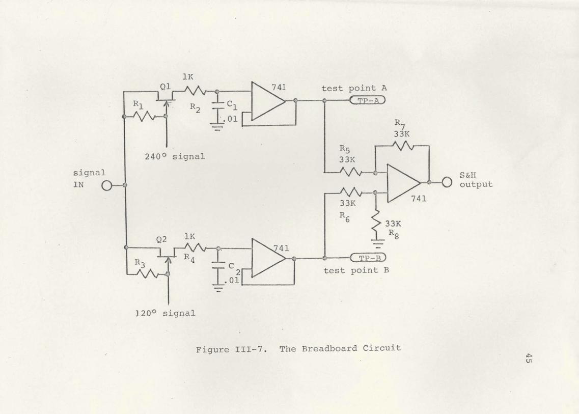

minus or plus (respectively) 4mV offset in the
S&H output signal. This is a 60dB rejection ratio
and is proof that the concept is a valid one.
\ .
Table 111-2
O F F S E T S i
C O N C L U S I O N S
The ve ry careful (and conservative) worst case
L
I N P U T
0.OOOV
-4. O O O V
+4. OOOV I r
analysis in conjunction with the breadboard test
results assures a technically feasible design. Our
T P - B
+ 8mV -3.962V
+3.976V
T P - A
- 17mV -3.987V
+3.952V
careful attention to minimizing added parts and part
OUTPUT
+23mV
+27mV
+19rnV
types, and the fact t h a t no last minute adjustments
or "tweakings" are required in this design assures
a design well suited t o high volume production. In
short, this design will indeed perform the function
for which it is intended. One word of caution is in
order, however. In the event that a level change in
the input offset voltage occurs between t h e 120° sam-
ple point and the 240° sample point during the particu-
lar waveform cycle being sampled,.an error (equal to
t h e step amplitude) would be passed through t o t h e A/D

. c i rcu i t ry . This condition will not occur often and
when it does it will result in no more error than
would be present with the old design.

~Liifornia: Fairchild Semiconductor, 1969.
Burlingame, B.G.; Kesner, D.; and Botos, R.A. The~Control Enqineers Guide to IC Applica- tions. Application Note 552. Phoenix, Arizona: Motorola Semiconductor Products Inc., 1971.
~nalish. M.J. An Improved Sample-and-Hold --- a----- - - -
circuit Using ihe ~ A 7 4 0. Application Brief 165. Mountain Vieii, California: Fairchild Semiconductor, 1971.
na: Motorola Semiconductor Producte, Tnc., 1970.
Frater, R.H. "Synchsonous Integrator and Demodu- lator". The of Scientific .. Instruments, . 36 (May
Gonzenbach, Kurt. Martin Marietta Aerospace, Orlando, 6
, , . ' -Florida, Intemiew,. 9 August 1975. I
KierQolzer , Edward. B&+gtigz -Baarirjttrr Aaro~gpace, Orlando, FZor iQB>&~%emfew, 14 A w s t 1975.
Kellerman , Dave. ~o+nen'+ Research Corporation. L o s Angeles,. California, Telephone interview, 12 September 1975.
Clara, California: oration, 1975.
<
Eb. {Ca&q&~g. mlvern, Pennsylvania: - . .
' . "Vish3;pr . *i t i . r , m s t i v e W@t&pr a975 . i-. "
Renachler,.Edward. Analog to Digital Conversion Techniques. Application Note 471. Phoenix, -na:~otorola Semiconductor Products Inc., 1971.
RCA Solid State ' 7 4 Data Book. Sornerville, New Jersey: RCA Corporation, 1973.
Roberge, James K. Operational Amplifiers Theory and Practice. New York: John Wiley & Sons, Inc., 1975.
S v . Santa Clara, California: Siliconix Inc., 1975.
Tobey, G.E.; Graeme, J.G.; and Huelsrnan, L.P., I -
eds. Operational Amplifiers, Design and A~~licati~ns. New York: McGraw Bill Book L I
Company, 1971.
Transistors. CataLog. Santa Clara, California: National Semiconductor Corporation, 1975.