Pulse Detection a Pulse Detection and Transmission System ...
Upload
khangminh22Category
view
1download
0
Progress In Electromagnetics Research C, Vol. 7, 25–35, 2009
A 802.11a PULSE-SWALLOW INTEGER-N FREQUENCYSYNTHESIZER
C.-C. Tien
National Chiao-Tung UniversityTaiwan, R.O.C.
T.-M. Tien
National Cheng-Kung UniversityTaiwan, R.O.C.
C. F. Jou
National Chiao-Tung UniversityTaiwan, R.O.C.
Abstract—This article presents the complete design of a 802.11apulse-swallow integer-N frequency synthesizer. Except for the loopfilter, the entire circuit is designed on the chip. The reference frequencyis set to 10 MHz and a pulse-swallow counter is designed for the purposeof controlling the dual-modulus divider (÷8/9). The frequency tuningrange varies from 4.98 GHz to 5.73 GHz meanwhile the output powerof the voltage-controlled oscillator is −13.5 dBm, and the phase noisemeasured at 1 MHz is −126 dBc/Hz. The settling time of the closedloop is about 20 µs, the total power dissipation is 26.35 mW with 1.8 Vsupply voltage. The chip size is 1.15mm × 1.06 mm and fabricatedunder TSMC CMOS 0.18 µm.
1. INTRODUCTION
The two most popular structures of RF frequency synthesizers arethe fractional-N frequency synthesizer and the integer-N frequencysynthesizer. Although fractional-N synthesizer owns a greatperformance in frequency resolution and settling time, its divisionnumber depends on accumulator carrier which may lead to spur
Corresponding author: C.-C. Tien ([email protected]).
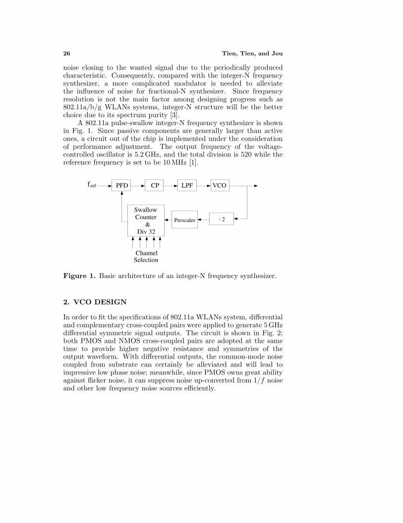
26 Tien, Tien, and Jou
noise closing to the wanted signal due to the periodically producedcharacteristic. Consequently, compared with the integer-N frequencysynthesizer, a more complicated modulator is needed to alleviatethe influence of noise for fractional-N synthesizer. Since frequencyresolution is not the main factor among designing progress such as802.11a/b/g WLANs systems, integer-N structure will be the betterchoice due to its spectrum purity [3].
A 802.11a pulse-swallow integer-N frequency synthesizer is shownin Fig. 1. Since passive components are generally larger than activeones, a circuit out of the chip is implemented under the considerationof performance adjustment. The output frequency of the voltage-controlled oscillator is 5.2 GHz, and the total division is 520 while thereference frequency is set to be 10 MHz [1].
fref PFD CP LPF VCO
SwallowCounter
&Div 32
Prescaler 2
ChannelSelection
Figure 1. Basic architecture of an integer-N frequency synthesizer.
2. VCO DESIGN
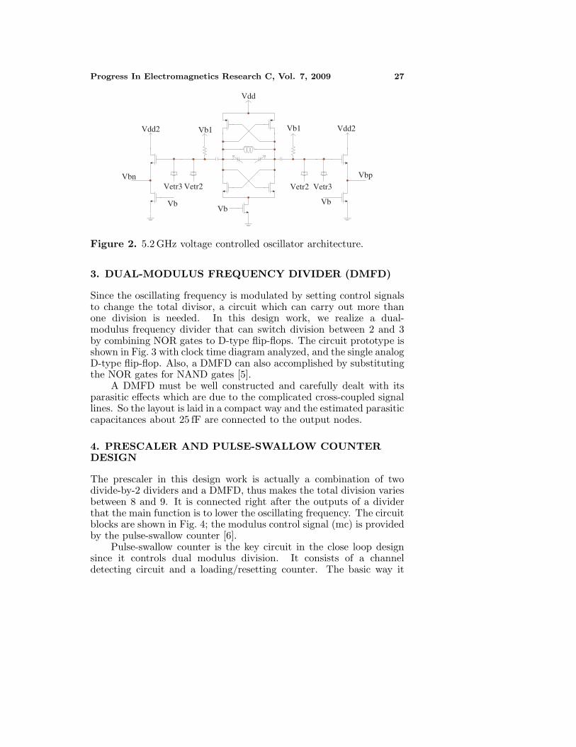
In order to fit the specifications of 802.11a WLANs system, differentialand complementary cross-coupled pairs were applied to generate 5GHzdifferential symmetric signal outputs. The circuit is shown in Fig. 2;both PMOS and NMOS cross-coupled pairs are adopted at the sametime to provide higher negative resistance and symmetries of theoutput waveform. With differential outputs, the common-mode noisecoupled from substrate can certainly be alleviated and will lead toimpressive low phase noise; meanwhile, since PMOS owns great abilityagainst flicker noise, it can suppress noise up-converted from 1/f noiseand other low frequency noise sources efficiently.
Progress In Electromagnetics Research C, Vol. 7, 2009 27
Vbn
Vdd2 Vb1
Vb
Vetr3 Vetr2
Vb
Vdd
Vdd2
Vb
Vetr3Vetr2
Vb1
Vbp
Figure 2. 5.2 GHz voltage controlled oscillator architecture.
3. DUAL-MODULUS FREQUENCY DIVIDER (DMFD)
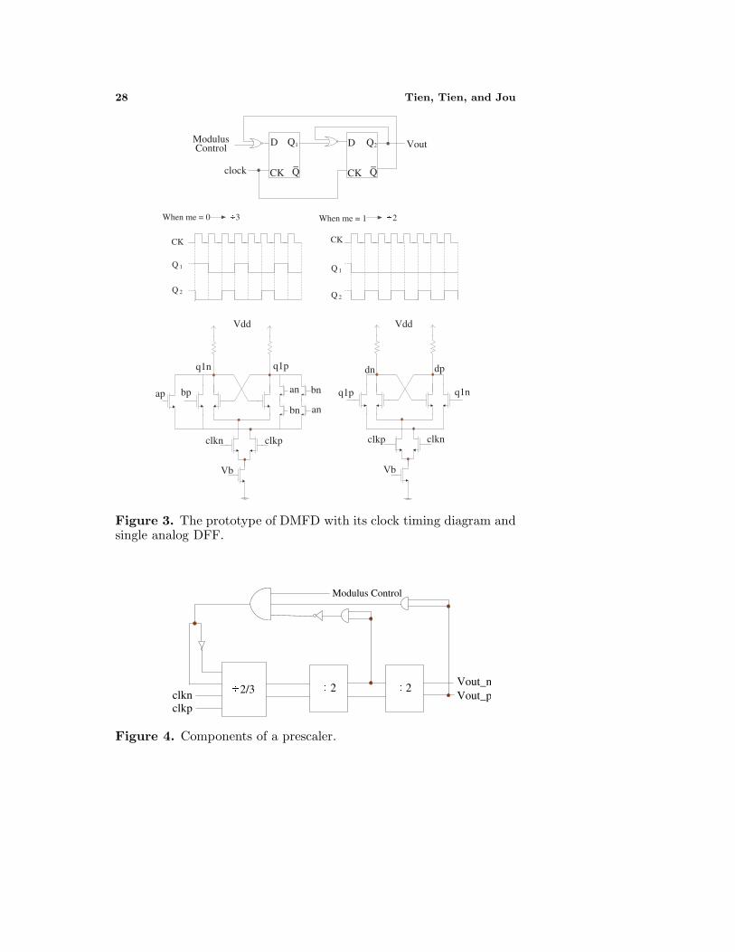
Since the oscillating frequency is modulated by setting control signalsto change the total divisor, a circuit which can carry out more thanone division is needed. In this design work, we realize a dual-modulus frequency divider that can switch division between 2 and 3by combining NOR gates to D-type flip-flops. The circuit prototype isshown in Fig. 3 with clock time diagram analyzed, and the single analogD-type flip-flop. Also, a DMFD can also accomplished by substitutingthe NOR gates for NAND gates [5].
A DMFD must be well constructed and carefully dealt with itsparasitic effects which are due to the complicated cross-coupled signallines. So the layout is laid in a compact way and the estimated parasiticcapacitances about 25 fF are connected to the output nodes.
4. PRESCALER AND PULSE-SWALLOW COUNTERDESIGN
The prescaler in this design work is actually a combination of twodivide-by-2 dividers and a DMFD, thus makes the total division variesbetween 8 and 9. It is connected right after the outputs of a dividerthat the main function is to lower the oscillating frequency. The circuitblocks are shown in Fig. 4; the modulus control signal (mc) is providedby the pulse-swallow counter [6].
Pulse-swallow counter is the key circuit in the close loop designsince it controls dual modulus division. It consists of a channeldetecting circuit and a loading/resetting counter. The basic way it
28 Tien, Tien, and Jou
ModulusControl
clock
When me = 0 3
CK
Q 1
Q 2
Q1D Q2D
CK Q_
CK Q_
Vout
When me = 1
CK
Q 1
Q 2
2
Vdd
q1n q1p
ap bp an
bn
bn
an
clkn clkp
Vb
clknclkp
Vb
q1p q1n
dn dp
Vdd
Figure 3. The prototype of DMFD with its clock timing diagram andsingle analog DFF.
Modulus Control
clknclkp
2/3 2 2 Vout_nVout_p
Figure 4. Components of a prescaler.
Progress In Electromagnetics Research C, Vol. 7, 2009 29
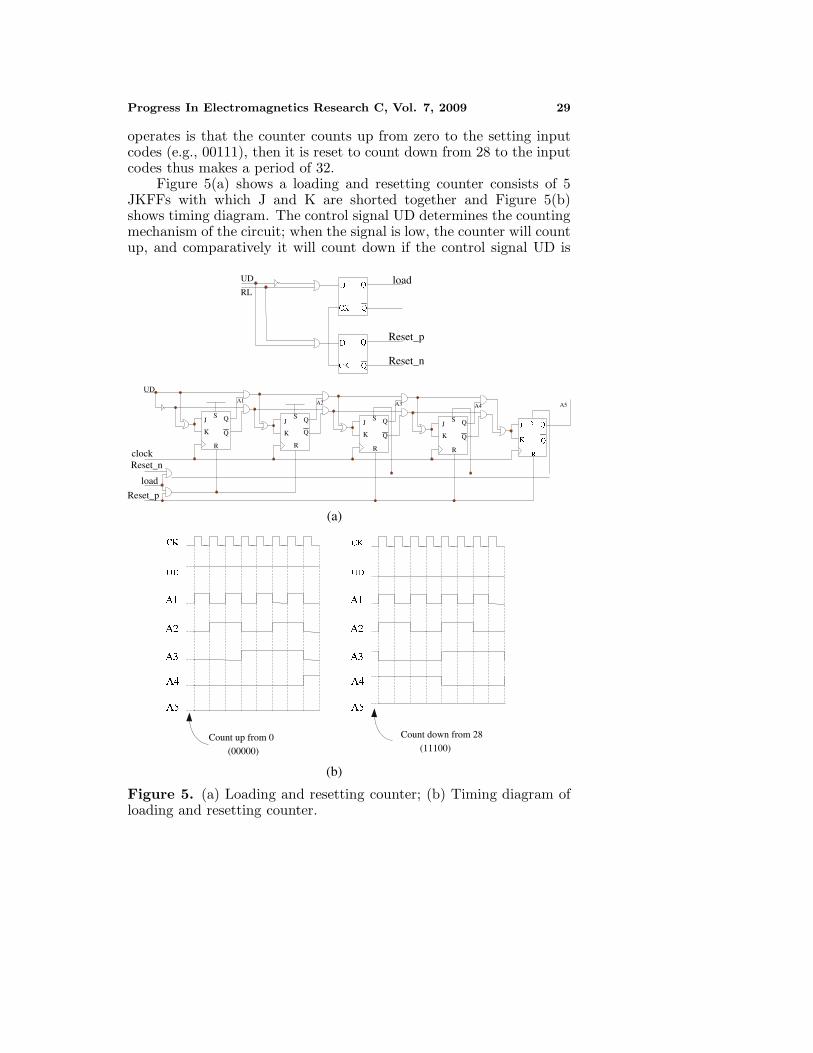
operates is that the counter counts up from zero to the setting inputcodes (e.g., 00111), then it is reset to count down from 28 to the inputcodes thus makes a period of 32.
Figure 5(a) shows a loading and resetting counter consists of 5JKFFs with which J and K are shorted together and Figure 5(b)shows timing diagram. The control signal UD determines the countingmechanism of the circuit; when the signal is low, the counter will countup, and comparatively it will count down if the control signal UD is
(a)
(b)
UD
clockReset_n
load
Reset_p
A1 A2
UD
RL
Reset_n
Reset_p
load
A3 A4
Count up from 0
(00000)
Count down from 28
(11100)
A5
SJ Q
K Q
R
SJ Q
K Q
R
SJ Q
K Q
R
SJ Q
K Q
R
Figure 5. (a) Loading and resetting counter; (b) Timing diagram ofloading and resetting counter.
30 Tien, Tien, and Jou
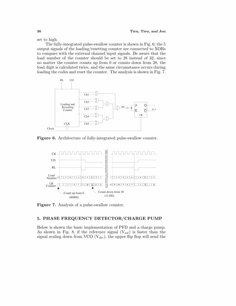
set to high.The fully-integrated pulse-swallow counter is shown in Fig. 6; the 5
output signals of the loading/resetting counter are connected to XORsto compare with the external channel input signals. Be aware that theload number of the counter should be set to 28 instead of 32, sinceno matter the counter counts up from 0 or counts down from 28, theload digit is calculated twice, and the same circumstance occurs duringloading the codes and reset the counter. The analysis is shown in Fig. 7.
Clock
Loading andReserttingCounter
CLK Ch5
Ch4
Ch3
Ch2
Ch1
RL UD
Figure 6. Architecture of fully-integrated pulse-swallow counter.
CK
UD
RL
LoadNumber
LRCounter
Count up from 0(00000)
Count down from 28(11100)
Figure 7. Analysis of a pulse-swallow counter.
5. PHASE FREQUENCY DETECTOR/CHARGE PUMP
Below is shown the basic implementation of PFD and a charge pump.As shown in Fig. 8, if the reference signal (Vref) is faster than thesignal scaling down from VCO (Vdiv), the upper flip flop will send the

Progress In Electromagnetics Research C, Vol. 7, 2009 31
(b)
(a)
Figure 8. (a) Phase/frequency detector; (b) Time diagramcomparison between Vref and Vdiv.
output high and this is maintained until the first rising edge occurs onVdiv, till then the NAND gate will generate a low signal back to resetboth flip flops. In a practical system this means that the output whichinput to the VCO is driven higher forcing the oscillating frequency tocatch up with the reference signal, vice versa.
Figure 9 is the architecture of a charge pump which functions asa transforming mechanism turn the phase mismatch detected by PFDinto a charging current. In this project the charge pump works witha fixed reference current, and in order to obtain high voltage outputrange, the transistor size of the current mirror transistors (M1 ∼M11)must be designed considerably.
Furthermore, since the mismatched current produced at the timethe two input signals are out of phase which will cause interferencewith adjacent channel and spurious tones in RF receiver, two extraimplement transistors (M12, M14) will be implemented in the circuitto solve the problem. Those two NMOS guarantee that M13 and M15
sources are already pre-charged when switching takes place. Also anaccurate layout of the circuit can improve the matching among the

32 Tien, Tien, and Jou
Figure 9. Schematic of charge pump.
positive and negative currents to reduce undesired spectral emission inRF transmitter.
6. LOOP FILTER
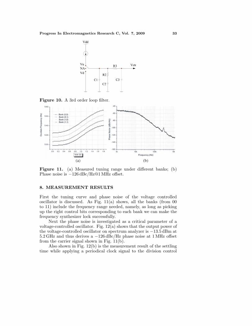
Since it is an extremely critical key point in designing a frequencysynthesizer, a 3rd order RC loop filter used in this work is shownin Fig. 10. Output of a loop filter is a dc voltage and directlyconnected to VCO, so a well considered circuit not only can degradehigh frequency noise but also can prevent the disturbance producedwhile PFD and charge pump switching states from influencing VCO,while the synthesizer stabilizes. The loop bandwidth of the filter affectsthe synthesizer settling time, so the filter was excluded from the chipto modulate the response of the circuit.
7. SIMULATION AND LAYOUT CONSIDERATION
It is important to simulate the entire circuit and make sure the functionof it is correct before and after layout. Matlab is used in the beginningto ensure that the detail design concepts and the circuit parametersare accurate, and electromagnetic simulating tools used in post-layoutto guarantee the critical signal paths are not influenced by parasiticeffects. By doing so, a higher performance of the design can beachieved.
Progress In Electromagnetics Research C, Vol. 7, 2009 33
Figure 10. A 3rd order loop filter.
(a) (b)
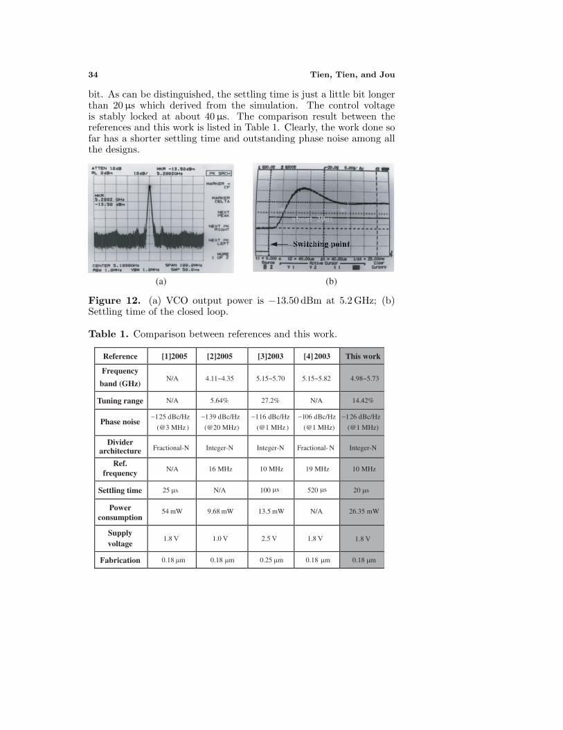
Figure 11. (a) Measured tuning range under different banks; (b)Phase noise is −126 dBc/Hz@1 MHz offset.
8. MEASUREMENT RESULTS
First the tuning curve and phase noise of the voltage controlledoscillator is discussed. As Fig. 11(a) shows, all the banks (from 00to 11) include the frequency range needed, namely, as long as pickingup the right control bits corresponding to each bank we can make thefrequency synthesizer lock successfully.
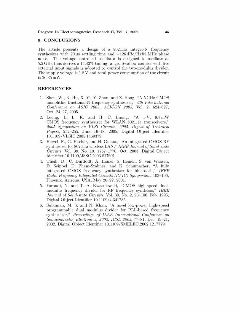
Next the phase noise is investigated as a critical parameter of avoltage-controlled oscillator. Fig. 12(a) shows that the output power ofthe voltage-controlled oscillator on spectrum analyzer is −13.5 dBm at5.2 GHz and thus derives a −126 dBc/Hz phase noise at 1 MHz offsetfrom the carrier signal shown in Fig. 11(b).
Also shown in Fig. 12(b) is the measurement result of the settlingtime while applying a periodical clock signal to the division control
34 Tien, Tien, and Jou
bit. As can be distinguished, the settling time is just a little bit longerthan 20 µs which derived from the simulation. The control voltageis stably locked at about 40 µs. The comparison result between thereferences and this work is listed in Table 1. Clearly, the work done sofar has a shorter settling time and outstanding phase noise among allthe designs.
(a) (b)
Figure 12. (a) VCO output power is −13.50 dBm at 5.2 GHz; (b)Settling time of the closed loop.
Table 1. Comparison between references and this work.
Reference [1]2005 [2]2005 [3]2003 [4]2003 This work
Frequency
band (GHz) N/A 4.11~4.35 5.15~5.70 5.15~5.82 4.98~5.73
Tuning range N/A 5.64% 27.2% N/A 14.42%
Phase noise −125 dBc/Hz
(@3 MHz )
−139 dBc/Hz
(@20 MHz)
−116 dBc/Hz
(@1 MHz )
−106 dBc/Hz
(@1 MHz)
−126 dBc/Hz
(@1 MHz)
Divider architecture Fractional-N Integer-N Integer-N Fractional- N Integer-N
Ref. frequency N/A 16 MHz 10 MHz 19 MHz 10 MHz
Settling time 25 µs N/A 100 520 20 µs
Powerconsumption
54 mW 9.68 mW 13.5 mW N/A 26.35 mW
Supply voltage
1.8 V 1.0 V 2.5 V 1.8 V
Fabrication 0.18 µm 0.18 µm 0.25 µm 0.18 µm 0.18 µm
µsµs
1.8 V
Progress In Electromagnetics Research C, Vol. 7, 2009 35
9. CONCLUSIONS
The article presents a design of a 802.11a integer-N frequencysynthesizer with 20 µs settling time and −126 dBc/Hz@1 MHz phasenoise. The voltage-controlled oscillator is designed to oscillate at5.2 GHz thus derives a 14.42% tuning range. Swallow counter with fiveexternal input signals is adopted to control the two-modulus divider.The supply voltage is 1.8 V and total power consumption of the circuitis 26.35 mW.
REFERENCES
1. Shen, W., K. Hu, X. Yi, Y. Zhou, and Z. Hong, “A 5 GHz CMOSmonolithic fractional-N frequency synthesizer,” 6th InternationalConference on ASIC 2005, ASICON 2005, Vol. 2, 624–627,Oct. 24–27, 2005.
2. Leung, L. L. K. and H. C. Luong, “A 1-V, 9.7 mWCMOS frequency synthesizer for WLAN 802.11a transceivers,”2005 Symposium on VLSI Circuits, 2005. Digest of TechnicalPapers, 252–255, June 16–18, 2005, Digital Object Identifier10.1109/VLSIC.2005.1469379.
3. Herzel, F., G. Fischer, and H. Gustat, “An integrated CMOS RFsynthesizer for 802.11a wireless LAN,” IEEE Journal of Solid-stateCircuits, Vol. 38, No. 10, 1767–1770, Oct. 2003, Digital ObjectIdentifier 10.1109/JSSC.2003.817601.
4. Theill, D., C. Durdodt, A. Hanke, S. Heinen, S. van Waasen,D. Seippel, D. Pham-Stabner, and K. Schumacher, “A fullyintegrated CMOS frequency synthesizer for bluetooth,” IEEERadio Frequency Integrated Circuits (RFIC) Symposium, 103–106,Phoenix, Arizona, USA, May 20–22, 2001.
5. Foroudi, N. and T. A. Kwasniewski, “CMOS high-speed dual-modulus frequency divider for RF frequency synthesis,” IEEEJournal of Solid-state Circuits, Vol. 30, No. 2, 93–100, Feb. 1995,Digital Object Identifier 10.1109/4.341735.
6. Sulaiman, M. S. and N. Khan, “A novel low-power high-speedprogrammable dual modulus divider for PLL-based frequencysynthesizer,” Proceedings of IEEE International Conference onSemiconductor Electronics, 2002, ICSE 2002, 77–81, Dec. 19–21,2002, Digital Object Identifier 10.1109/SMELEC.2002.1217779.
Copyright © 2022 FDOKUMEN