A 128Channel 6 mW Wireless Neural Recording IC With Spike Feature Extraction and UWB Transmitter
10
312 IEEE TRANSACTIONS ON NEURAL SYSTEMS AND REHABILITATION ENGINEERING, VOL. 17, NO. 4, AUGUST 2009 A 128-Channel 6 mW Wireless Neural Recording IC With Spike Feature Extraction and UWB Transmitter Moo Sung Chae, Zhi Yang, Mehmet R. Yuce, Linh Hoang, and Wentai Liu, Senior Member, IEEE Abstract—This paper reports a 128-channel neural recording integrated circuit (IC) with on-the-fly spike feature extraction and wireless telemetry. The chip consists of eight 16-channel front-end recording blocks, spike detection and feature extraction digital signal processor (DSP), ultra wideband (UWB) transmitter, and on-chip bias generators. Each recording channel has amplifiers with programmable gain and bandwidth to accommodate dif- ferent types of biological signals. An analog-to-digital converter (ADC) shared by 16 amplifiers through time-multiplexing results in a balanced trade-off between the power consumption and chip area. A nonlinear energy operator (NEO) based spike detector is implemented for identifying spikes, which are further processed by a digital frequency-shaping filter. The computationally effi- cient spike detection and feature extraction algorithms attribute to an auspicious DSP implementation on-chip. UWB telemetry is designed to wirelessly transfer raw data from 128 recording channels at a data rate of 90 Mbit/s. The chip is realized in 0.35 complementary metal–oxide–semiconductor (CMOS) process with an area of 8.8 7.2 mm and consumes 6 mW by employing a sequential turn-on architecture that selectively powers off idle analog circuit blocks. The chip has been tested for electrical specifications and verified in an ex vivo biological environment. Index Terms—Digital signal processing (DSP), integrated circuit (IC), low-noise amplifier, neural recording system, ultra-wideband (UWB). I. INTRODUCTION M ULTICHANNEL neural recording systems are used in neuroscience experiments to study complex neural net- works of freely behaving animals [1]. It is also a critical com- ponent in brain–computer interface used for cortical-controlled neural prosthetics, which has a wide range of applications such as upper and lower limb prostheses [2]–[5], bladder and bowel movement control for spinal cord injury (SCI) patients [6], [7], respiration control for SCI patients [8], and hand grasping func- tion restoration [9]. To support these applications, a neural recording system has to meet challenging requirements imposed by the environment. Manuscript received October 02, 2008; revised January 16, 2009; accepted March 10, 2009. First published May 08, 2009; current version published Au- gust 07, 2009. This work was supported in part by the Defense Advanced Re- search Projects Agency (DARPA), in part by UC-MICRO, and in part by Na- tional Semiconductor. M. S. Chae, Z. Yang, L. Hoang, and W. Liu are with the Electrical En- gineering Department, University of California–Santa Cruz, Santa Cruz, CA 95064 USA (e-mail: [email protected]; [email protected]; [email protected]; [email protected]). M. R. Yuce is with the Electrical Engineering and Computer Science De- partment, University of Newcastle, Callaghan, NSW 2308 Australia (e-mail: [email protected]). Digital Object Identifier 10.1109/TNSRE.2009.2021607 First, it should be able to record a large number of channels si- multaneously; and high density recording can advance funda- mental neuroscience studies and has the potential to improve the performance of neural prosthetic devices. Second, a wire- less telemetry that transmits recorded neural data is preferable, because tethering wires impose significant restrictions on the subjects and inhibit free movement in their natural environment. Third, on-the-fly processing of neural data is necessary to enable prosthetic devices functioning in a real-time. In addition, a fast processing capability removes the necessity of storing the large amount of raw data. Fourth, the specifications of the recording system should be designed with programmability and versatility that accommodate a wide range of bio-potentials in different ap- plications. Finally, power consumption and chip area have to be optimized due to the limited space available at the recording site and the system should be powered wirelessly or operated on rechargeable battery. Several neural recording ICs previously reported in literature can support simultaneous multichannel recording [10]–[12], wireless data telemetry (spike information for 100 channels and raw data for one channel) [13], and on-chip spike detection [13], [14]. However, one of the major limitations of previous systems in the literature is that it allows recording from only a subset of the electrodes to be recorded simultaneously and transmitted to the outside mainly due to the limited bandwidth of the wireless telemetry. Many systems are not optimized and have unnecessary increase in power consumption and chip area. Although there have been several systems equipped with integrated functions of recording, processing (spike detection or spike feature extraction), and wireless telemetry using multiple integrated circuits (ICs) [15], [16], a single IC with simultaneous recording, on-chip spike detection and feature extraction, and low power wireless telemetry that can support raw data from more than 100 channels is advantageous at the miniaturization and versatility point of view. This paper presents a low-power IC that can record, process, and wirelessly transmit neural signals in real-time. The chip, which supports two different modes of recording and feature ex- traction, is able to simultaneously record and transmit raw data from 128 channels [17] wirelessly, and serves as the core hard- ware for applications mentioned above when combined with ad- ditional components. The paper is organized as follows. Section II describes the chip architecture of the proposed multichannel neural recording system and its operations. Section III discusses the circuits of front-end blocks in detail. Section IV introduces on-the-fly spike feature extraction and its hardware implementation. Section V 1534-4320/$26.00 © 2009 IEEE Authorized licensed use limited to: Univ of Calif Santa Cruz. Downloaded on August 25, 2009 at 01:50 from IEEE Xplore. Restrictions apply.
-
Upload
independent -
Category
Documents
-
view
1 -
download
0
Transcript of A 128Channel 6 mW Wireless Neural Recording IC With Spike Feature Extraction and UWB Transmitter

312 IEEE TRANSACTIONS ON NEURAL SYSTEMS AND REHABILITATION ENGINEERING, VOL. 17, NO. 4, AUGUST 2009
A 128-Channel 6 mW Wireless Neural Recording ICWith Spike Feature Extraction and UWB Transmitter
Moo Sung Chae, Zhi Yang, Mehmet R. Yuce, Linh Hoang, and Wentai Liu, Senior Member, IEEE
Abstract—This paper reports a 128-channel neural recordingintegrated circuit (IC) with on-the-fly spike feature extraction andwireless telemetry. The chip consists of eight 16-channel front-endrecording blocks, spike detection and feature extraction digitalsignal processor (DSP), ultra wideband (UWB) transmitter, andon-chip bias generators. Each recording channel has amplifierswith programmable gain and bandwidth to accommodate dif-ferent types of biological signals. An analog-to-digital converter(ADC) shared by 16 amplifiers through time-multiplexing resultsin a balanced trade-off between the power consumption and chiparea. A nonlinear energy operator (NEO) based spike detector isimplemented for identifying spikes, which are further processedby a digital frequency-shaping filter. The computationally effi-cient spike detection and feature extraction algorithms attributeto an auspicious DSP implementation on-chip. UWB telemetryis designed to wirelessly transfer raw data from 128 recordingchannels at a data rate of 90 Mbit/s. The chip is realized in 0.35� complementary metal–oxide–semiconductor (CMOS) process
with an area of 8.8 7.2 mm� and consumes 6 mW by employinga sequential turn-on architecture that selectively powers off idleanalog circuit blocks. The chip has been tested for electricalspecifications and verified in an ex vivo biological environment.
Index Terms—Digital signal processing (DSP), integrated circuit(IC), low-noise amplifier, neural recording system, ultra-wideband(UWB).
I. INTRODUCTION
M ULTICHANNEL neural recording systems are used inneuroscience experiments to study complex neural net-
works of freely behaving animals [1]. It is also a critical com-ponent in brain–computer interface used for cortical-controlledneural prosthetics, which has a wide range of applications suchas upper and lower limb prostheses [2]–[5], bladder and bowelmovement control for spinal cord injury (SCI) patients [6], [7],respiration control for SCI patients [8], and hand grasping func-tion restoration [9].
To support these applications, a neural recording system hasto meet challenging requirements imposed by the environment.
Manuscript received October 02, 2008; revised January 16, 2009; acceptedMarch 10, 2009. First published May 08, 2009; current version published Au-gust 07, 2009. This work was supported in part by the Defense Advanced Re-search Projects Agency (DARPA), in part by UC-MICRO, and in part by Na-tional Semiconductor.
M. S. Chae, Z. Yang, L. Hoang, and W. Liu are with the Electrical En-gineering Department, University of California–Santa Cruz, Santa Cruz,CA 95064 USA (e-mail: [email protected]; [email protected];[email protected]; [email protected]).
M. R. Yuce is with the Electrical Engineering and Computer Science De-partment, University of Newcastle, Callaghan, NSW 2308 Australia (e-mail:[email protected]).
Digital Object Identifier 10.1109/TNSRE.2009.2021607
First, it should be able to record a large number of channels si-multaneously; and high density recording can advance funda-mental neuroscience studies and has the potential to improvethe performance of neural prosthetic devices. Second, a wire-less telemetry that transmits recorded neural data is preferable,because tethering wires impose significant restrictions on thesubjects and inhibit free movement in their natural environment.Third, on-the-fly processing of neural data is necessary to enableprosthetic devices functioning in a real-time. In addition, a fastprocessing capability removes the necessity of storing the largeamount of raw data. Fourth, the specifications of the recordingsystem should be designed with programmability and versatilitythat accommodate a wide range of bio-potentials in different ap-plications. Finally, power consumption and chip area have to beoptimized due to the limited space available at the recordingsite and the system should be powered wirelessly or operatedon rechargeable battery.
Several neural recording ICs previously reported in literaturecan support simultaneous multichannel recording [10]–[12],wireless data telemetry (spike information for 100 channelsand raw data for one channel) [13], and on-chip spike detection[13], [14]. However, one of the major limitations of previoussystems in the literature is that it allows recording from onlya subset of the electrodes to be recorded simultaneously andtransmitted to the outside mainly due to the limited bandwidthof the wireless telemetry. Many systems are not optimizedand have unnecessary increase in power consumption and chiparea. Although there have been several systems equipped withintegrated functions of recording, processing (spike detectionor spike feature extraction), and wireless telemetry usingmultiple integrated circuits (ICs) [15], [16], a single IC withsimultaneous recording, on-chip spike detection and featureextraction, and low power wireless telemetry that can supportraw data from more than 100 channels is advantageous at theminiaturization and versatility point of view.
This paper presents a low-power IC that can record, process,and wirelessly transmit neural signals in real-time. The chip,which supports two different modes of recording and feature ex-traction, is able to simultaneously record and transmit raw datafrom 128 channels [17] wirelessly, and serves as the core hard-ware for applications mentioned above when combined with ad-ditional components.
The paper is organized as follows. Section II describes thechip architecture of the proposed multichannel neural recordingsystem and its operations. Section III discusses the circuits offront-end blocks in detail. Section IV introduces on-the-fly spikefeature extraction and its hardware implementation. Section V
1534-4320/$26.00 © 2009 IEEE
Authorized licensed use limited to: Univ of Calif Santa Cruz. Downloaded on August 25, 2009 at 01:50 from IEEE Xplore. Restrictions apply.
CHAE et al.: A 128-CHANNEL 6 MW WIRELESS NEURAL RECORDING IC WITH SPIKE FEATURE EXTRACTION AND UWB TRANSMITTER 313
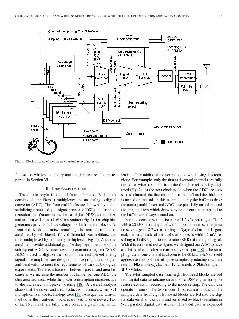
Fig. 1. Block diagram of the integrated neural recording system.
focuses on wireless telemetry and the chip test results are re-ported in Section VI.
II. CHIP ARCHITECTURE
The chip has eight 16-channel front-end blocks. Each blockconsists of amplifiers, a multiplexer and an analog-to-digitalconverter (ADC). The front-end blocks are followed by a dataserializing circuit, a digital signal processor (DSP) unit for spikedetection and feature extraction, a digital MUX, an encoder,and an ultra wideband (UWB) transmitter (Fig. 1). On-chip biasgenerators provide dc bias voltages to the front-end blocks. Atfront-end, weak and noisy neural signals from electrodes areamplified by self-biased, fully differential preamplifiers, andtime-multiplexed by an analog multiplexer (Fig. 2). A secondamplifier provides additional gain for the proper operation of thesubsequent ADC. A successive-approximation-register (SAR)ADC is used to digitize the 16-to-1 time multiplexed analogsignal. The amplifiers are designed to have programmable gainand bandwidth to meet the requirements of various biologicalexperiments. There is a trade-off between power and area be-cause as we increase the number of channel per one ADC, thechip area decreases while the power consumption increases dueto the increased multiplexer loading [18]. A careful analysisshows that the power and area product is minimized when 16:1multiplexer is in the technology used [18]. A sequential turn-onmethod in the front-end blocks is utilized to save power. Twoof the 16 channels are fully turned on at any given time, which
leads to 71% additional power reduction when using this tech-nique. For example, only the first and second channels are fullyturned on when a sample from the first channel is being digi-tized (Fig. 2). At the next clock cycle, when the ADC accessessecond channel, the first channel is turned off and the third oneis turned on instead. In this technique, only the buffer to drivethe analog multiplexer and ADC is sequentially turned on, andthe preamplifiers which draw very small current compared tothe buffers are always turned on.
For an electrode with resistance of 1 operating at 27with a 20 kHz recording bandwidth, the root mean square (rms)noise voltage is 18.2 according to Nyquist’s formula. In gen-eral, the magnitude of extracellular spikes is within 1 mV, re-sulting a 35 dB signal-to-noise ratio (SNR) of the input signal.With this estimated noise figure, we designed our ADC to havea 9-bit resolution after a conservative margin [18]. The sam-pling rate of one channel is chosen to be 40 ksample/s to avoidaggressive interpolation of spike samples, producing raw datarate of ksample s channel channels bits/sample
Mbit/s.The 9-bit sampled data from eight front-end blocks are fed
into digital data serializing circuits or a DSP engine for spikefeature extraction according to the mode setting. The chip canoperate in one of the two modes. In streaming mode, all thesampled data from eight front-end blocks are fed into the dig-ital data serializing circuits and serialized by blocks resulting in9-bit parallel digital data stream. This 9-bit data is expanded
Authorized licensed use limited to: Univ of Calif Santa Cruz. Downloaded on August 25, 2009 at 01:50 from IEEE Xplore. Restrictions apply.

314 IEEE TRANSACTIONS ON NEURAL SYSTEMS AND REHABILITATION ENGINEERING, VOL. 17, NO. 4, AUGUST 2009
Fig. 2. Schematic of 16-channel front-end blocks (sequential turn-on scheme is used to reduce the power consumption).
Fig. 3. Schematic of preamplifier and OTA used.
to 16-bit data to include 7-bit filler data for channel separa-tion purpose at the receiver side and serialized again in the en-coder. This final serialized data at the rate of 81.92 Mbps is thenManchester coded at the UWB transmitter to generate UWBpulses, which are transmitted through an off-chip UWB antenna.A pulse shaping filter is used to ensure that the emitted powerspectrum of the UWB pulses is under the FCC regulation mask.When operating in DSP mode, a selected channel is connectedto the on-the-fly spike feature extraction block and the featuresare transmitted wirelessly for further processing.
The clock signal of 81.92 MHz is applied to the chip exter-nally and the on-chip internal clock generation circuit providesappropriate clock signals for each circuit blocks as shown in
Fig. 1. In this design we chose to use an off-chip crystal oscil-lator that can supply the required clock signal with a sufficientaccuracy. The physical dimension of the commercial availablecrystal oscillator is small enough to be integrated with this chipin a hermetic sealing to form a higher-level system.
III. FRONT-END BLOCK CIRCUIT DESIGN
The preamplifier (Fig. 3) uses ac-coupling at the input to re-ject the large dc offset occurring at the electrode-tissue inter-face [13]. The gain of the preamplifier is 40 dB, which is set bythe ratio of feedback capacitances . The second amplifierwith a non-inverting resistive negative feedback provides an ad-ditional gain of 17–20 dB according to external controls. and
Authorized licensed use limited to: Univ of Calif Santa Cruz. Downloaded on August 25, 2009 at 01:50 from IEEE Xplore. Restrictions apply.

CHAE et al.: A 128-CHANNEL 6 MW WIRELESS NEURAL RECORDING IC WITH SPIKE FEATURE EXTRACTION AND UWB TRANSMITTER 315
Fig. 4. Schematic of fully-differential SAR-ADC and comparator used.
were chosen to be 20 pF and 200 fF resulting in differentialinput impedance of 16 at 1 kHz. The high-frequency roll-offof the preamplifier is configurable from 2 to 20 kHz in 16 stepsby varying the load capacitance . The low frequency roll-offis tunable from 0.1 to 200 Hz by changing the gate voltage ofthe NMOS used as bias resistors. The gate voltage provided bythe bias generator is adjustable from 600 mV to 1 V by 50 mVsteps. The adjusting range and the step size of are designedto achieve the target programmability of low frequency roll-offin the presence of the process variations.
Operational transconductance amplifiers (OTA) have criticaleffects on the overall performance of the preamplifier. A highcommon-mode rejection ratio (CMRR) is preferred to suppressthe 60 Hz power interference in the neural recordings [19],which makes the preamplifiers saturated and disables signalprocessing at the later stages of the system. A proposed fullydifferential self-biased OTA [20] shown in Fig. 3 enables a90 dB CMRR and a 80 dB power supply rejection ratio (PSRR)with 4.9 input referred noise integrated from 0.1 Hz to20 kHz. To improve the common mode noise rejection a fullydifferential output signaling was chosen. A common modefeedback (CMFB) circuit is not required because the outputcommon voltage level is self-biased by the negative feedbackleading to low power and small area of the preamplifier.
Each preamplifier and buffer draws 2 and 20.3 , respec-tively, to drive the analog multiplexer when it is turned on by thesequential turn-on control signals, leading to an average currentof 2.54 . The second amplifier draws 40.6 to drive 10 pFinput sampling capacitance of the SAR ADC.
Care was taken to minimize the coupling noise from adja-cent channels. All input signal lines that connect the inputsof the preamplifiers to bonding pads were shielded by quietground lines. In addition, the space between input signal lineand shielding line was determined so that the metal parasiticcapacitance is small enough not to affect the input impedanceof the preamplifiers.
SAR ADC is well suited for low-power and small-area appli-cations because it requires minimal amount of analog circuitry[21]. The resolution of the ADC can be adjusted from 6 to 9 bitsby external control signals. The total sampling capacitance ofthe SAR ADC is 10 pF and the power consumption is 14 ,which is very small compared to other analog circuits. To rejectcommon mode noise, the ADC is designed to digitize differen-tial signal directly. The block diagram of the SAR ADC is givenin Fig. 4. The reference voltages are supplied by the on-chip DCvoltage generators and the voltage levels controlled by the ex-ternal control signals are variable from 100 to 500 mV by 50 mVsteps. The comparator of the ADC is based on track-and-latchcomparator and its schematic is also shown in Fig. 4. The sizesof the transistors N1, N2, N3, N4, P1, and P2 can directly affectthe offset of the ADC and therefore are chosen large enough toguarantee that offset is only a few least significant bits (LSBs)when minimum reference voltage is applied.
IV. ON-THE-FLY SPIKE FEATURE EXTRACTION
The recorded neural signals by a single electrode may con-tain spikes from multiple firing neurons. Spike sorting is theprocedure to attribute spikes to individual neurons and recover
Authorized licensed use limited to: Univ of Calif Santa Cruz. Downloaded on August 25, 2009 at 01:50 from IEEE Xplore. Restrictions apply.

316 IEEE TRANSACTIONS ON NEURAL SYSTEMS AND REHABILITATION ENGINEERING, VOL. 17, NO. 4, AUGUST 2009
Fig. 5. Proposed spike sorting algorithm.
the encoded information in the neural signals. Spike sortingis challenging due to several factors, such as the presence ofunresolved neuronal activity, and similarity in recorded shapes.Training may be required when the electrodes move, and thiscould be frequent in certain applications [22]. The frequenttraining over a large amount of recording channels significantlyincreases the computational power and memory required [23].Thus, for an implantable neural recording system where thehardware needs to be integrated and miniaturized, power andarea efficient algorithms are advantageous.
Fig. 5 shows the overview of the algorithm that enableson-chip spike feature extraction. The 9-bit ADC output con-taining the time multiplexed neural signals are fed to the spikedetector. A quantitative evaluation of different spike detectionwas reported in [24] using synthesized spikes. The resultsindicated that all the surveyed detection algorithms performedcomparably, except an implementation of template marchingis coasty. In this work, we chose a nonlinear energy operator(NEO) [27], [28] due to its efficiency in separating spikesfrom background activities, which was reported to exhibit alow frequency fashion through power spectrum measurementof data from in vivo experiments [25], [26]. Realization ofNEO using analog circuit was also reported [29], however, theinvolved design complexity and circuit size exceed those ofdigital implementation.
According to [25], a derivative based frequency-shaping filtersignificantly attenuates the low frequency noise and help differ-entiating similar spikes from different neurons. As a comple-mentary approach to principle component analysis, spike fea-ture extraction algorithm based on informative sample set wasfirst reported in [26] to identify uncorrelated local features. Thisconcept requires only a subset of samples containing the nec-essary information to cluster the data. Intuitively, a sample isconsidered to be informative if the superimposed spikes can beclassified into multiple clusters by evaluating the sample alone.Combining derivative operation and sample selection, improvedsorting results were demonstrated in [26]. As a preliminary im-plementation to our feature extraction algorithm [30], the peaks
of the original spike waveforms and maximum and minimumvalues of its first derivatives are used as the features to classifyspikes. The choice of this simplified sample set for implemen-tation is based on three reasons. First, it requires small com-putation and little memory requirement [30]. Second, samplesduring the fast transition period frequently exhibit high infor-mation score [26]. Third, obtaining these three features requiresno training.
Fig. 6 shows the block diagram of the proposed on-the-flyspike detection and feature extraction engine. The 9-bit serialADC output containing the multiplexed neural signals is fed tothe spike detection and sorting hardware units. The serial outputdata after the sorting consist of 64 bits of three features andtime information of the spikes. Each spike is processed, encodedand transmitted on-the-fly within 41 cycles (1.025 ms). Afterthe system reset, the coefficients register array is loaded with32 9-bit filter coefficients and a 16-bit threshold value beforethe recording procedure. These values are derived by off-chipcomputation based on few seconds of initial test recordings.If a spike is recognized, the feature scores are calculated bythe min–max detector, and then sent to the wireless telemetrymodule through coder/packer. These operations, including de-tection, filtering, feature extraction, and coding, are performedin parallel to meet the real-time requirement.
V. UWB TELEMETRY
Although there are several communication standards forbiomedical applications, most of them cannot provide enoughbandwidth for simultaneous recording from more than 100channels. For example, MICS band, which is allocated for theunlicensed use of implantable devices, allows only 300 kHz fordata transmission. Other wireless technologies such as Wi-Fiand Bluetooth cannot be used directly due to the power andarea constraint of the implanted device. Therefore, there is aneed for higher-bandwidth data transmission telemetry thatconsumes low-power and occupies less physical area.
UWB is recently formed wireless technology that is usedfor low/high data rate wireless personal area network (WPAN)
Authorized licensed use limited to: Univ of Calif Santa Cruz. Downloaded on August 25, 2009 at 01:50 from IEEE Xplore. Restrictions apply.

CHAE et al.: A 128-CHANNEL 6 MW WIRELESS NEURAL RECORDING IC WITH SPIKE FEATURE EXTRACTION AND UWB TRANSMITTER 317
Fig. 6. Block diagram of an online spike sorting engine.
Fig. 7. Block diagram of on-chip UWB Tx, and UWB Rx with photograph of its implementation using off-the-shelf components.
and short-range applications. It has the widest bandwidth(3.1–10.6 GHz) among all technologies and the smallestemission power density dBm/MHz , providing anopportunity for a wideband wireless telemetry for neuralrecording systems. Although the reported receiver designs ofUWB systems have been consuming more power than thoseof narrow band communications [31], in our neural recordingapplications the implanted device requires only a transmitterand the receiver is outside the body, unlike the other short rangeapplications. Hence the transmitter power consumption andcomplexity have been traded off with that of the receiver as thereceiver is located outside and its power consumption and sizeare not crucial. This greatly simplifies the complexity of theimplanted telemetry design leading to reduction in power andarea.
In this system, impulse radio based UWB (IR-UWB) is em-ployed as the targeted application does not require a multipleaccess communication, which requires complex transmittersconsuming high power [32], [33]. In IR-UWB, short pulsesare generated for sending data, and both the center frequencyand bandwidth of the pulse do not have to be very accu-rate. Such a process is simple to design in complementarymetal–oxide–semiconductor (CMOS) technology resulting ina very simple, small-area, and low-power transmitter designwhile providing enough data bandwidth because of its wide-band nature.
Fig. 7 shows the block diagram of the UWB transmitter. Thesampled and serialized data is Manchester encoded first and theneither on-off keying (OOK) or pulse-position modulation (PPM)is employed to generate short pulses. The redundant fillers are
Authorized licensed use limited to: Univ of Calif Santa Cruz. Downloaded on August 25, 2009 at 01:50 from IEEE Xplore. Restrictions apply.

318 IEEE TRANSACTIONS ON NEURAL SYSTEMS AND REHABILITATION ENGINEERING, VOL. 17, NO. 4, AUGUST 2009
Fig. 8. Data format of the UWB transmitter.
Fig. 9. A high-speed, USB2.0, data acquisition system designed to support 80 Mbit/s neural recording. Trace 4 depicts original serial data stream containing longlogic-lows as separators and short transition bits as recorded samples. A packet marker monitors this serial data stream and generates markers for the start and endof a data sample as depicted by Trace 2 and 3, respectively. Trace 1 presents decoded bits streams.
set to all “1” for channel , and all “0” for other channels incase of PPM, and the fillers for channel are set to 7-bit “logiclow” of Manchester coding in case of OOK (Fig. 8). Therefore,the final maximum pulse repetition rate at the UWB transmitteroutput is twice the output data rate, 163.84 Mpulses/s in case ofusing PPM and the same as the output data rate, 81.92 Mpulses/sfor OOK. A short pulse generator is based on a simple edgedetector [34] and the circuit implementation is shown in Fig. 7.The pulse width can be controlled from 180 to 980 ps by anexternal control voltage for adjusting the transmitting power.The generated short pulses are then passed through a high passfilter to remove low frequency component of the pulses and forthe transmitting power to fit under the FCC emission mask. Thefiltered pulses are finally fed into the off-chip UWB antenna.Because of the high-frequency nature of the UWB, the size ofthe antenna is small enough to be implantable or to be carriedby the animals.
The UWB receiver was built from off-the-shelf components(Fig. 7) since it is outside the biological objects. The signal re-ceived by an UWB antenna is passed through 1 GHz band-passfilter (BPF), whose center frequency is 4 GHz, to remove the in-terfering signals from other narrowband wireless devices. Thesignal is then amplified by the low-noise amplifier (LNA) stages,
which plays a critical role in determining the maximum distancebetween the implanted transmitter and receiver outside the bi-ological subject. A RF diode and a low-pass filter (LPF) downconverts the UWB signal to low frequency one by performingenvelope detection and the digital data is finally recovered byFGPA (Fig. 7).
Since the maximum data rate of the recording exceeds80 Mbit/s, an interface between the receiver and a PC mustbe able to support that bandwidth. Among several standardinput/output interface buses for PCs, USB2.0 and FireWire(IEEE 1394) are the two most popular buses that can supportthe required bandwidth. Fig. 9 shows a block diagram of the PCinterface realized to support USB 2.0. The interface consists ofphase-locked loop (PLL) for clock recovery, an FPGA for de-coding and deserializing, and USB2.0 chips to store recordingdata into a standard personal computer.
VI. TEST RESULTS
The IC was fabricated in a 0.35 4 M2 P CMOS processand the chip size is 8.8 7.2 mm (Fig. 10). The 8 front-endblocks consume 50% of the total power. The UWB transmitter
Authorized licensed use limited to: Univ of Calif Santa Cruz. Downloaded on August 25, 2009 at 01:50 from IEEE Xplore. Restrictions apply.

CHAE et al.: A 128-CHANNEL 6 MW WIRELESS NEURAL RECORDING IC WITH SPIKE FEATURE EXTRACTION AND UWB TRANSMITTER 319
Fig. 10. Chip photograph of fabricated IC.
TABLE ISUMMARY OF CHIP PERFORMANCE
circuitry consumes 1.6 mW with PPM. The power consump-tion of the DSP block is only 0.1 mW and the power consump-tion caused by leakage current is negligible in 0.35 CMOSprocess. Test bench was first performed with multiple signalgenerators connected to the inputs of the front-end blocks toevaluate and characterize the performance of each circuit blocksand is summarized in Table I.
Extracellular recordings were made from a dissected snailbrain to verify the functionality of the entire system in a realrecording environment. An intact circumesophageal ring wasextracted from H. aspersa and placed in a glass dish filled withRinger’s solution. A concentric bipolar electrode with 25platinum tip was placed close to circumesophageal ring by mi-cromanipulators. The biological experimental setup for ex vivotest is shown in Fig. 11. The measured impedance of the elec-trode in solution was 190 at 1 kHz. The gain of the amplifier
was set to its maximum value because the amplitude of the extra-cellular action potential from the dissected snail brain was lessthan 200 due to a small value of the seal resistance, whichdetermines how closely the neuron is attached to the measuringelectrode. Because most of the signal energy of the extracellularaction potential is concentrated between 100 Hz and 10 kHz, thehigh-frequency roll-off was set to 10 kHz. The low-frequencyroll-off is set to 100 Hz eliminating the 60 Hz interference fromthe power line. Fig. 11 also shows the obtained waveforms atthe output of amplifier, spike sorting DSP, UWB transmitter,and UWB receiver. The physical dimension of the UWB an-tenna used in the experiment is 10 10 0.8 mm . The powerspectral density (PSD) of the transmitted UWB pulses was mea-sured with spectrum analyzer and the result shows that the PSDis within the FCC mask regulations.
VII. CONCLUSION
A low-power fully integrated single chip neural recordingsystem is presented in this paper for wireless recording of 128channels simultaneously. The on-the-fly spike detection andfeature extraction for one selected channel is implementedon this chip. Simultaneous processing for 128 channels withmore functionalities of neural classification and decoding willbe integrated in the future. The sequential turn-on method isused to minimize the power consumption of front-end blocks,which are the most power consuming circuitries. The wire-less transmission of high data rate was achieved through alow-power implantable UWB wireless transmitter. The totalpower consumption is only 6 mW even when transmitting rawdata from all 128 channels. The front-end has been designedto have amplifiers with programmable gain and bandwidth tooffer flexibility in recording various bio-potentials. The benchtest was carried out to evaluate the performance of the chip, andex vivo extracellular recording was done to verify the properoperation of the system in a real environment.
Authorized licensed use limited to: Univ of Calif Santa Cruz. Downloaded on August 25, 2009 at 01:50 from IEEE Xplore. Restrictions apply.

320 IEEE TRANSACTIONS ON NEURAL SYSTEMS AND REHABILITATION ENGINEERING, VOL. 17, NO. 4, AUGUST 2009
Fig. 11. Photograph of experimental setup ex vivo and measurement results of the IC with neural signal from a snail brain.
ACKNOWLEDGMENT
The authors thank E. Basham for his help in snail dissectionfor testing setup of the chip ex vivo and, T. Chen for layoutsynthesis, J. Kim for help in circuit design, and B. Liang forhelp in bench top test.
REFERENCES
[1] G. Santhanam, M. D. Linderman, V. Gilja, A. Afshar, S. I. Ryu, T.Meng, and K. Shenoy, “HermesB: A continuous neural recordingsystem for freely behaving primates,” IEEE Trans. Biomed. Eng., vol.54, no. 11, pp. 2037–2050, Nov. 2007.
[2] A. B. Schwartz, “Cortical neural prosthetics,” Annu. Rev. Neurosci.,vol. 27, pp. 487–501, Jul. 2004.
[3] J. F. Borisoff, L. T. McPhail, J. T. W. Saunders, G. E. Birch, and M.S. Ramer, “Detection and classification of sensory information fromacute spinal cord recordings,” IEEE Trans. Biomed. Eng., vol. 53, no.8, pp. 1715–1719, Aug. 2006.
[4] A. Jackson, C. T. Moritz, J. Mavoori, T. H. Lucas, and E. E. Fetz, “Theneurochip BCI: Towards a neural prosthesis for upper limb function,”IEEE Trans. Neural Syst. Rehabil. Eng., vol. 14, no. 2, pp. 187–190,Jun. 2006.
[5] K. D. Strange and J. A. Hoffer, “Restoration of use of paralyzed limbmuscles using sensory nerve signals for state control of FES-assistedwalking,” IEEE Trans. Rehabil. Eng., vol. 7, no. 3, pp. 289–300, Sep.1999.
[6] B. J. Wenzel, J. W. Boggs, K. J. Gustafson, and W. M. Grill, “Detectingthe onset of hyper-reflexive bladder contractions from the electrical ac-tivity of the pudendal nerve,” IEEE Trans. Neural Syst. Rehabil. Eng.,vol. 13, no. 3, pp. 428–435, Sep. 2005.
[7] J. Hansen, A. Borau, A. Rodriguez, J. Vidal, T. Sinkjaer, and N. J. M.Rijkhoff, “Urethral sphincter EMG as event detector for neurogenicdetrusor overactivity,” IEEE Trans. Biomed. Eng., vol. 54, no. 7, pp.1212–1219, Jul. 2007.
[8] A. F. DiMarco, “Neural prostheses in the respiratory system,” J. Re-habil. Res. Dev., vol. 38, no. 6, pp. 601–607, Nov. 2001.
[9] S. Mangold, T. Keller, A. Curt, and V. Dietz, “Transcutaneous func-tional electrical stimulation for grasping in subjects with cervical spinalcord injury,” Spinal Cord, pp. 1–13, 2005.
[10] J. N. Y. Aziz, R. Genov, B. L. Bardakjian, M. Derchansky, and P.L. Carlen, “Brain-Silicon interface for high-resolution in vitro neuralrecording,” IEEE Trans. Biomed. Circuit Syst., vol. 1, no. 1, pp. 56–62,Mar. 2007.
[11] Y. Perelman and R. Ginosar, “An integrated system for multichannelneuronal recording with spike/LFP separation, integrated a/D conver-sion and threshold detection,” IEEE Trans. Biomed. Eng., vol. 54, no.1, pp. 130–137, Jan. 2007.
[12] D. Cheney, A. Goh, J. Xu, K. Gugel, J. G. Harris, J. C. Sanchez, andJ. C. Principe, “Wireless, in vivo neural recording using a custom in-tegrated bioamplifier and the pico system,” in Proc. IEEE EMBS 3rdAnnu. Int. Conf. Neural Eng., May 2007, pp. 19–22.
[13] R. R. Harrison, P. T. Watkins, R. J. Kier, R. O. Lovejoy, D. J. Black,B. Greger, and F. Solzbacher, “A low-power integrated circuit for awireless 100-Electrode neural recording system,” IEEE J. Solid-StateCircuits, vol. 42, no. 1, pp. 123–133, Jan. 2007.
[14] A. M. Sodagar, K. D. Wise, and K. Najafi, “A fully integratedmixed-signal neural processor for implantable multichannel corticalrecording,” IEEE Trans. Biomed. Eng., vol. 54, no. 6, pp. 1075–1088,Jun. 2007.
[15] R. H. Olsson, III and K. D. Wise, “A three-dimensional neuralrecording microsystem with implantable data compression circuitry,”IEEE J. Solid-State Circuits, vol. 40, no. 12, pp. 2796–2804, Dec.2005.
[16] B. Gosselin, A. E. Ayoub, and M. Sawan, “A mixed-signal multi-chipneural recording interface with bandwidth reduction,” in Proc. IEEEBiomed. Circuits Syst. Conf., Nov. 2007, pp. 49–52.
[17] M. Chae, W. Liu, Z. Yang, T. Chen, J. Kim, M. Sivaprakasam, andM. Yuce, “A 128-Channel 6 mW wireless neural recording IC withon-the-fly spike sorting and UWB transmitter,” in Dig. Tech. PapersIEEE Int. Solid-State Circuits Conf., Feb. 2008, pp. 146–147.
[18] M. S. Chae, W. Liu, and M. Sivaprakasam, “Design optimization forintegrated neural recording systems,” IEEE J. Solid-State Circuits, vol.43, no. 9, pp. 1931–1939, Sep. 2008.
[19] M. F. Chimeno and R. Pallas-Areny, “A comprehensive model forpower line interference in biopotential measurements,” IEEE Trans. In-strum. Meas., vol. 49, no. 3, pp. 535–540, Jun. 2000.
Authorized licensed use limited to: Univ of Calif Santa Cruz. Downloaded on August 25, 2009 at 01:50 from IEEE Xplore. Restrictions apply.

CHAE et al.: A 128-CHANNEL 6 MW WIRELESS NEURAL RECORDING IC WITH SPIKE FEATURE EXTRACTION AND UWB TRANSMITTER 321
[20] M. Chae, J. Kim, and W. Liu, “Fully-differential self-biased bio-po-tential amplifier,” Electron. Lett., vol. 44, no. 24, pp. 1390–1391, Nov.2008.
[21] M. D. Scott, B. E. Boser, and S. J. Pister, “An ultralow-energy ADCfor smart dust,” IEEE J. Solid-State Circuits, vol. 38, pp. 1123–1129,Jul. 2003.
[22] M. D. Linderman, V. Gilja, G. Santhanam, A. Afshar, S. I. Ryu, T.H. Meng, and K. V. Shenoy, “Neural recording stability of chronicelectrode,” in Proc. IEEE EMBS 28th Annu. Int. Conf., 2006, pp.4387–4391.
[23] L. Hazan, M. Zugaro, and G. Buzsaki, “Klusters, neuroscope, NDMan-ager: A free software suite for neurophysiological data processing andvisualization,” J. Neurosci. Methods, vol. 155, pp. 207–216, Sep. 2006.
[24] I. Obeid and P. D. Wolf, “Evaluation of spike-detection algorithms fora brain-machine interface application,” IEEE Trans. Biomed. Eng., vol.51, no. 6, pp. 905–911, Jun. 2004.
[25] Z. Yang, T. Chen, and W. Liu, “Neuron signature based spike featureextraction algorithm for on-chip implementation,” in Proc. IEEE EMBS30th Annu. Int. Conf., Aug. 2008, pp. 1716–1719.
[26] Z. Yang, Q. Zhao, and W. Liu, “Spike feature extraction using informa-tive samples,” in Advances in Neural Information Processing Systems(NIPS). Cambridge, MA: MIT Press, 2008.
[27] P. Maragos, J. F. Kaiser, and T. F. Quatieri, “On amplitude andfrequency demodulation using energy operators,” IEEE. Trans. SignalProcess., vol. 41, no. 4, pp. 1532–1550, Apr. 1993.
[28] K. H. Kim and J. K. Kim, “Neural spike sorting under nearly 0-dbsignal-to-noise ratio usingnonlinear energy operator and artificialneural-network classifier,” IEEE Trans. Biomed. Eng., vol. 47, no. 10,pp. 1406–1411, Oct. 2000.
[29] B. Gosselin and M. Sawan, “An ultra low-power CMOS actionpotential detector,” in Prof. IEEE Int. Symp. Circuits Syst., 2008, pp.2733–2736.
[30] T. Chen, Z. Yang, W. Liu, and L. Chen, “NEUSORT2.0: a multiple-channel neural signal processor with systolic array buffer and channel-interleaving processing schedule,” in Proc. IEEE EMBS 30th Annu. Int.Conf., Aug. 2008, pp. 5029–5032.
[31] R. Gharpurey and P. Kinget, Ultra Wideband : Circuits, Transceiversand Systems. New York: Springer, 2008.
[32] M. R. Yuce, W. Liu, M. S. Chae, and J. S. Kim, “A wideband telemetryunit for multi-channel neural recording systems,” in IEEE Int. Conf.Ultra-Wideband, Sep. 2007, pp. 612–617.
[33] C. Charles, “An implantable I-UWB transceiver architecture withpower carrier synchronization,” in Prof. IEEE Int. Symp. Circuits Syst.,2008, pp. 1970–1973.
[34] B. Jung, Y. H. Tseng, J. Harvey, and R. Harjani, “Pulse generator de-sign for UWB IR communication systems,” in Prof. IEEE Int. Symp.Circuits Syst., May 2005, pp. 4381–4384.
Moo Sung Chae received the B.S. and M.S. degrees in electrical engineeringfrom Seoul National University, Seoul, Korea, in 1998 and 2000, respectively.He is currently working toward the Ph.D. degree at the University of California,Santa Cruz.
In 2000, he joined Samsung Electronics, Korea, where he had been workingon circuit design of high-speed DRAMs. His research interests are integratedneural recording systems, neural prosthetic devices, and retinal prostheses.
Zhi Yang received the B.S. degree in electrical engineering from Zhejiang Uni-versity, China, in 2004. He received the M.S. degree in electrical engineeringin 2007 from the University of California, Santa Cruz, where he is currentlyworking toward the Ph.D. degree.
His research interests are mathematic modeling, analog circuit design, dataanalysis, and neuroprosthetic devices.
Mehmet R. Yuce received the B.S. degree in electronics engineering fromAnkara University, Ankara, Turkey, in 1997, the M.S. degree in electrical andcomputer engineering from the University of Florida, Gainesville, in 2001, andthe Ph.D. degree in electrical and computer engineering from North CarolinaState University (NCSU), Raleigh, in 2004.
Currently, he holds senior lecturer position in the School of Electrical En-gineering and Computer Science, University of Newcastle, New South Wales,Australia. Between August 2001 and October 2004, he has served as a Re-search Assistant with the Department of Electrical and Computer Engineeringat NCSU. He was a Postdoctoral Researcher in the Electrical Engineering De-partment at the University of California, Santa Cruz, in 2005. His research in-terests include analog/digital mixed signal VLSI for biomedical and RF appli-cations, wireless implantable telemetry, wireless sensor network for medicalmonitoring, wireless body area network (WBAN), low-power VLSI circuits foremerging technologies in wireless communications, CMOS transceiver design,and system designs for wireless communications.
Linh Hoang received the B.S. degree in computer engineering and the M.S.degree electrical engineering, in 2003 and 2007, respectively, from University ofCalifornia, Santa Cruz, where he is currently working toward the Ph.D. degree.
He interned at Center for Adaptive Optics working on algorithms and actua-tors for the California Extremely Large Telescope in 2004. His research inter-ests are biosignals processing, embedded system, real-time OS, system-on-a-chip, and integrated circuits for implantable electronics, prosthetic devices andbrain–machine interfaces.
Wentai Liu (S’78–M’81–SM’93) received the B.S. degree from NationalChiao-Tung University, Taiwan, the M.S. degree from National Taiwan Uni-versity, and the Ph.D. degree from the University of Michigan.
In 1983, he joined North Carolina State University, where he held the AlcoaChair Professorship in the Department of Electrical and Computer Engineering.Since 2003, he has been a Professor in the electrical engineering Departmentat the University of California, Santa Cruz, where he is Campus Director ofthe NSF Engineering Research Center on Biomimetic Microelectronic Systems.His research interests include visual prosthesis, implantable electronics, high-speed transceiver design (wired and wireless), molecular electronics, microelec-tronic sensors, timing/clock optimization, on-chip interconnects and computervision/image processing. Since its early stages, he has been leading the en-gineering efforts of the retinal prosthesis to restore vision, finally leading tosuccessful preliminary implant tests in blind patients. He has published morethan 180 technical papers and is a co-author of Wave Pipelining: Theory andCMOS Implementation (Kluwer Academic Publishers, 1994) and EmergingTechnologies: Designing Low Power Digital Systems (IEEE Press, 1996). He isa University System of Taiwan Master Lecturer and Chair Professor of NationalChiao-Tung University.
Dr. Liu received an IEEE Outstanding Paper Award, Alcoa Foundation’s Dis-tinguished Engineering Research Award and Outstanding Alumnus Award fromNational Chiao-Tung University.
Authorized licensed use limited to: Univ of Calif Santa Cruz. Downloaded on August 25, 2009 at 01:50 from IEEE Xplore. Restrictions apply.