A 0.22mm2 7.25mW per-channel audio stereo-DAC with 97dB-DR and 39dB SNRout
8
IEEE JOURNAL OF SOLID-STATE CIRCUITS, VOL. 40, NO. 7, JULY 2005 1491 A 0.22-mm 7.25-mW per-Channel Audio Stereo-DAC With 97-dB DR and 39-dB SNR Vittorio Colonna, Marzia Annovazzi, Gianluigi Boarin, Gabriele Gandolfi, Fabrizio Stefani, and Andrea Baschirotto, Senior Member, IEEE Abstract—In the stereo audio DAC here presented, the tradeoff between area–power consumption–SNR -dynamic range is opti- mized for the case of a 96 –dB audio system. Using a single-opamp switched-capacitor structure for the reconstruction filter, a hybrid FIR/IIR transfer function allows to reject out-of-band noise. This circuit solution strongly reduces area and power consumption. In a 0.13- m CMOS technology, the stereo DAC achieves a 97-dB dynamic range and a 39-dB SNR with a 0.22-mm area and 7.25-mW power consumption per channel. Index Terms—Digital-to-analog converters, low power, sigma- delta modulation, switched-capacitor filters. I. INTRODUCTION A UDIO digital-to-analog converters (DACs) have been recently the target of several important developments [1]–[6], [9]. In [1] the signal DAC is merged with the output power stage while achieving a significant 100-dB dynamic range (DR), at the cost of dedicated technology and large die size. On the other hand, several audio signal proces- sors based on a digital kernel and with a number of input analog-to-digital converters (ADCs) and output DACs are under development. Fig. 1 shows a possible scheme of one of these systems-on-a-chip (SoCs), in which the DACs are one of the most stringent blocks, since they have to satisfy a number of constraints in tradeoff between themselves. In particular, the power consumption and the area occupation appear to be crucial parameters to be minimized for embedding a number of DACs in complex SoCs. Fig. 2 shows the evo- lution of the layout in several DACs realized in this research activity. They refer to different designs (named cST1, cST2 [6] and cST3 here presented) realized with different technologies (0.35 m, 0.18 m, and 0.13 m). Table I summarizes the area and power consumption for the different designs. It can be seen that technology scaling allows a reduction of the digital area (and, as a consequence, of the digital power consumption). On the other hand only the design effort (from cST2 to cST3) gives a significant reduction of analog area and power consumption. This is because while the digital part takes full advantage of the technology scaling, the analog part continues to use the 3.3-V 0.35- m devices (always available) to achieve the target 96-dB Manuscript received November 8, 2004; revised January 27, 2005. V. Colonna, M. Annovazzi, G. Boarin, G. Gandolfi, and F. Stefani are with the STMicroelectronics, 20010 Cornaredo (MI), Italy (e-mail: vit- [email protected]). A. Baschirotto is with the University of Lecce, Department of Innovation Engineering, 73100 Lecce, Italy (e-mail: [email protected]). Digital Object Identifier 10.1109/JSSC.2005.847486 DR, and this disables any power or area improvement obtained with scaled-down technologies. An additional parameter for qualifying an audio DAC is the out-of-band signal-to-noise ratio SNR , defined as the ratio of the full scale signal and the total out-of-band noise. The SNR corresponds to the amount of out-of-band filtering implemented in the reconstruction filter. A small value of SNR corresponds to a significant amount of high-frequency energy, which may be dangerous for the coupling with the neighbor blocks and for the following output drivers. The value of SNR can then be improved increasing the filter complexity at the cost of additional area and power. Notice that due to technology shrink, this area-and-power requirement regards mainly the analog part of the DAC, i.e., the reconstruction filter. For this block, current mode solutions [5] are very attractive for area reduction, but they strongly suffer from the clock jitter, which in SoC can be extremely large, and they require a high-performance current-to-voltage converter at the output. Therefore, the switched-capacitor (SC) technique has been here preferred and particular care has been given to develop a suitable structure, which minimizes area-and-power. The developed structure uses a single opamp topology, and implements a hybrid FIR/IIR transfer function to optimize, at the same time, the SNR . This SC structure is particularly convenient also because it intrinsically supplies a single-ended output without DR loss and without additional circuitry (in alternative high-performance solutions the single-ended output is obtained with a dedicated differential-to-single ended con- verter). The proposed DAC achieves in a single-ended voltage output a 97-dB DR (A-weighted) in the band [20 Hz–20 kHz]. The area for the stereo DAC (two-channels) is 0.44 mm and the power consumption is 14.5 mW. The SNR is about 39 dB. This paper is organized as follows. After the introduction of Section I, Section II describes the DAC architecture; Section III deals with the DAC SC reconstruction filter. Section IV pro- poses the experimental results, and Section V concludes the paper. II. PROPOSED DAC ARCHITECTURE The proposed DAC adopts the architecture shown in Fig. 3. The DAC processes an input 24 b word at 44.1 kHz, which is interpolated by a factor 128 . The resulting signal (24 b) is passed through a digital modulator , whose output bitstream is processed by the analog filter. A key choice for the overall performance is the definition of the characteristics of the , on which the performance of 0018-9200/$20.00 © 2005 IEEE
-
Upload
independent -
Category
Documents
-
view
0 -
download
0
Transcript of A 0.22mm2 7.25mW per-channel audio stereo-DAC with 97dB-DR and 39dB SNRout
IEEE JOURNAL OF SOLID-STATE CIRCUITS, VOL. 40, NO. 7, JULY 2005 1491
A 0.22-mm2 7.25-mW per-Channel AudioStereo-DAC With 97-dB DR and 39-dB SNRout
Vittorio Colonna, Marzia Annovazzi, Gianluigi Boarin, Gabriele Gandolfi, Fabrizio Stefani, andAndrea Baschirotto, Senior Member, IEEE
Abstract—In the stereo audio DAC here presented, the tradeoffbetween area–power consumption–SNRout-dynamic range is opti-mized for the case of a 96 –dB audio system. Using a single-opampswitched-capacitor structure for the reconstruction filter, a hybridFIR/IIR transfer function allows to reject out-of-band noise. Thiscircuit solution strongly reduces area and power consumption. Ina 0.13- m CMOS technology, the stereo DAC achieves a 97-dBdynamic range and a 39-dB SNRout with a 0.22-mm2 area and7.25-mW power consumption per channel.
Index Terms—Digital-to-analog converters, low power, sigma-delta modulation, switched-capacitor filters.
I. INTRODUCTION
AUDIO digital-to-analog converters (DACs) have beenrecently the target of several important developments
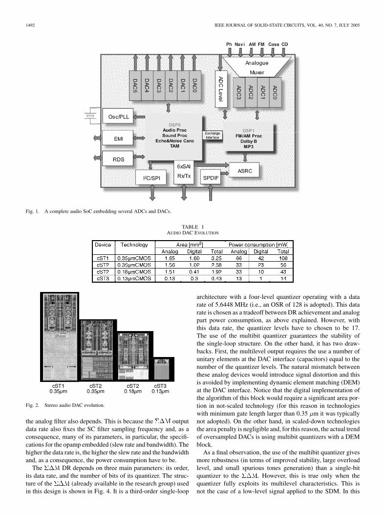
[1]–[6], [9]. In [1] the signal DAC is merged with the outputpower stage while achieving a significant 100-dB dynamicrange (DR), at the cost of dedicated technology and largedie size. On the other hand, several audio signal proces-sors based on a digital kernel and with a number of inputanalog-to-digital converters (ADCs) and output DACs areunder development. Fig. 1 shows a possible scheme of one ofthese systems-on-a-chip (SoCs), in which the DACs areone of the most stringent blocks, since they have to satisfya number of constraints in tradeoff between themselves. Inparticular, the power consumption and the area occupationappear to be crucial parameters to be minimized for embeddinga number of DACs in complex SoCs. Fig. 2 shows the evo-lution of the layout in several DACs realized in this researchactivity. They refer to different designs (named cST1, cST2 [6]and cST3 here presented) realized with different technologies(0.35 m, 0.18 m, and 0.13 m). Table I summarizes the areaand power consumption for the different designs. It can be seenthat technology scaling allows a reduction of the digital area(and, as a consequence, of the digital power consumption). Onthe other hand only the design effort (from cST2 to cST3) givesa significant reduction of analog area and power consumption.This is because while the digital part takes full advantage of thetechnology scaling, the analog part continues to use the 3.3-V0.35- m devices (always available) to achieve the target 96-dB
Manuscript received November 8, 2004; revised January 27, 2005.V. Colonna, M. Annovazzi, G. Boarin, G. Gandolfi, and F. Stefani are
with the STMicroelectronics, 20010 Cornaredo (MI), Italy (e-mail: [email protected]).
A. Baschirotto is with the University of Lecce, Department of InnovationEngineering, 73100 Lecce, Italy (e-mail: [email protected]).
Digital Object Identifier 10.1109/JSSC.2005.847486
DR, and this disables any power or area improvement obtainedwith scaled-down technologies. An additional parameter forqualifying an audio DAC is the out-of-band signal-to-noise ratioSNR , defined as the ratio of the full scale signal and the
total out-of-band noise. The SNR corresponds to the amountof out-of-band filtering implemented in the reconstruction filter.A small value of SNR corresponds to a significant amountof high-frequency energy, which may be dangerous for thecoupling with the neighbor blocks and for the following outputdrivers. The value of SNR can then be improved increasingthe filter complexity at the cost of additional area and power.Notice that due to technology shrink, this area-and-powerrequirement regards mainly the analog part of the DAC, i.e., thereconstruction filter. For this block, current mode solutions [5]are very attractive for area reduction, but they strongly sufferfrom the clock jitter, which in SoC can be extremely large, andthey require a high-performance current-to-voltage converterat the output. Therefore, the switched-capacitor (SC) techniquehas been here preferred and particular care has been given todevelop a suitable structure, which minimizes area-and-power.The developed structure uses a single opamp topology, andimplements a hybrid FIR/IIR transfer function to optimize, atthe same time, the SNR . This SC structure is particularlyconvenient also because it intrinsically supplies a single-endedoutput without DR loss and without additional circuitry (inalternative high-performance solutions the single-ended outputis obtained with a dedicated differential-to-single ended con-verter). The proposed DAC achieves in a single-ended voltageoutput a 97-dB DR (A-weighted) in the band [20 Hz–20 kHz].The area for the stereo DAC (two-channels) is 0.44 mm andthe power consumption is 14.5 mW. The SNR is about39 dB.
This paper is organized as follows. After the introduction ofSection I, Section II describes the DAC architecture; Section IIIdeals with the DAC SC reconstruction filter. Section IV pro-poses the experimental results, and Section V concludes thepaper.
II. PROPOSED DAC ARCHITECTURE
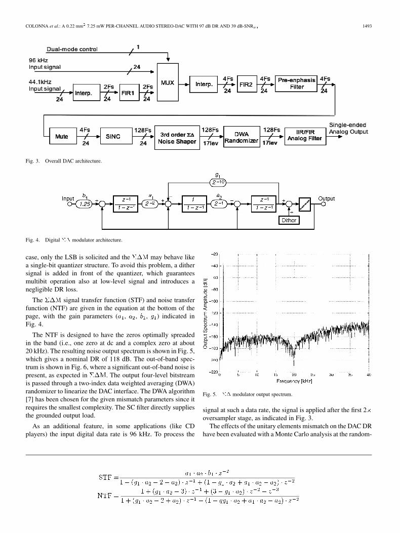
The proposed DAC adopts the architecture shown in Fig. 3.The DAC processes an input 24 b word at 44.1 kHz, which isinterpolated by a factor 128 . The resulting signal (24 b) ispassed through a digital modulator , whose outputbitstream is processed by the analog filter.
A key choice for the overall performance is the definition ofthe characteristics of the , on which the performance of
0018-9200/$20.00 © 2005 IEEE
1492 IEEE JOURNAL OF SOLID-STATE CIRCUITS, VOL. 40, NO. 7, JULY 2005
Fig. 1. A complete audio SoC embedding several ADCs and DACs.
TABLE IAUDIO DAC EVOLUTION
Fig. 2. Stereo audio DAC evolution.
the analog filter also depends. This is because the outputdata rate also fixes the SC filter sampling frequency and, as aconsequence, many of its parameters, in particular, the specifi-cations for the opamp embedded (slew rate and bandwidth). Thehigher the data rate is, the higher the slew rate and the bandwidthand, as a consequence, the power consumption have to be.
The DR depends on three main parameters: its order,its data rate, and the number of bits of its quantizer. The struc-ture of the (already available in the research group) usedin this design is shown in Fig. 4. It is a third-order single-loop
architecture with a four-level quantizer operating with a datarate of 5.6448 MHz (i.e., an OSR of 128 is adopted). This datarate is chosen as a tradeoff between DR achievement and analogpart power consumption, as above explained. However, withthis data rate, the quantizer levels have to chosen to be 17.The use of the multibit quantizer guarantees the stability ofthe single-loop structure. On the other hand, it has two draw-backs. First, the multilevel output requires the use a number ofunitary elements at the DAC interface (capacitors) equal to thenumber of the quantizer levels. The natural mismatch betweenthese analog devices would introduce signal distortion and thisis avoided by implementing dynamic element matching (DEM)at the DAC interface. Notice that the digital implementation ofthe algorithm of this block would require a significant area por-tion in not-scaled technology (for this reason in technologieswith minimum gate length larger than 0.35 m it was typicallynot adopted). On the other hand, in scaled-down technologiesthe area penalty is negligible and, for this reason, the actual trendof oversampled DACs is using multibit quantizers with a DEMblock.
As a final observation, the use of the multibit quantizer givesmore robustness (in terms of improved stability, large overloadlevel, and small spurious tones generation) than a single-bitquantizer to the . However, this is true only when thequantizer fully exploits its multilevel characteristics. This isnot the case of a low-level signal applied to the SDM. In this
COLONNA et al.: A 0.22 mm 7.25 mW PER-CHANNEL AUDIO STEREO-DAC WITH 97 dB DR AND 39 dB-SNR 1493
Fig. 3. Overall DAC architecture.
Fig. 4. Digital �� modulator architecture.
case, only the LSB is solicited and the may behave likea single-bit quantizer structure. To avoid this problem, a dithersignal is added in front of the quantizer, which guaranteesmultibit operation also at low-level signal and introduces anegligible DR loss.
The signal transfer function (STF) and noise transferfunction (NTF) are given in the equation at the bottom of thepage, with the gain parameters ( , , , ) indicated inFig. 4.
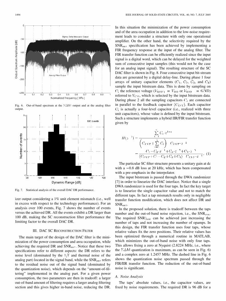
The NTF is designed to have the zeros optimally spreadedin the band (i.e., one zero at dc and a complex zero at about20 kHz). The resulting noise output spectrum is shown in Fig. 5,which gives a nominal DR of 118 dB. The out-of-band spec-trum is shown in Fig. 6, where a significant out-of-band noise ispresent, as expected in . The output four-level bitstreamis passed through a two-index data weighted averaging (DWA)randomizer to linearize the DAC interface. The DWA algorithm[7] has been chosen for the given mismatch parameters since itrequires the smallest complexity. The SC filter directly suppliesthe grounded output load.
As an additional feature, in some applications (like CDplayers) the input digital data rate is 96 kHz. To process the
Fig. 5. �� modulator output spectrum.
signal at such a data rate, the signal is applied after the first 2oversampler stage, as indicated in Fig. 3.
The effects of the unitary elements mismatch on the DAC DRhave been evaluated with a Monte Carlo analysis at the random-
1494 IEEE JOURNAL OF SOLID-STATE CIRCUITS, VOL. 40, NO. 7, JULY 2005
Fig. 6. Out-of-band spectrum at the ��M output and at the analog filteroutput.
Fig. 7. Statistical analysis of the overall DAC DR performance.
izer output considering a 1% unit element mismatch (i.e., wellin excess with respect to the technology performance). For ananalysis over 100 events, Fig. 7 shows the number of eventsversus the achieved DR. All the events exhibit a DR larger than100 dB, making the SC reconstruction filter performance thelimiting factor to the overall DAC DR.
III. DAC SC RECONSTRUCTION FILTER
The main target of the design of the DAC filter is the mini-mization of the power consumption and area occupation, whileachieving the required DR and SNR . Notice that these twospecifications refer to different aspects: the DR refers to thenoise level (dominated by the and thermal noise of theanalog part) located in the signal band, while the SNR refersto the residual noise out of the signal band (dominated bythe quantization noise), which depends on the “amount-of-fil-tering” implemented in the analog part. For a given powerconsumption, the two parameters are then in tradeoff: a largerout-of-band amount of filtering requires a larger analog filteringsection and this gives higher in-band noise, reducing the DR.
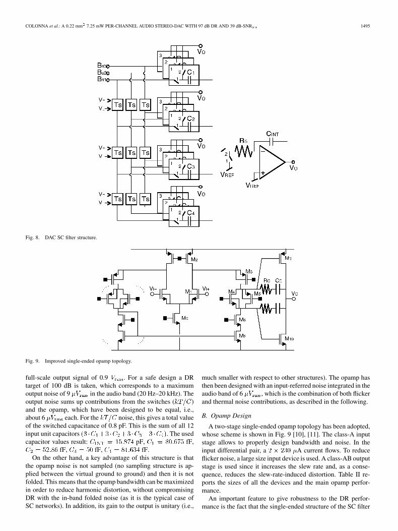
In this situation the minimization of the power consumptionand of the area occupation in addition to the low-noise require-ment leads to consider a structure with only one operationalamplifier. On the other hand, the selectivity required by theSNR specification has been achieved by implementing aFIR frequency response at the input of the analog filter. TheFIR transfer function can be efficiently realized since the inputsignal is a digital word, which can be delayed for the weightedsum of consecutive input samples (this would not be the casefor an analog input signal). The resulting structure of the SCDAC filter is shown in Fig. 8. Four consecutive input bit-streamdata are generated by a digital delay-line. During phase 1 fourarrays of unitary capacitor elements ( , , , and )sample the input bitstream data. This is done by sampling on
the reference voltage ( or )referred to , which is selected by the input bitstream data.During phase 2 all the sampling capacitors are connectedin parallel to the feedback capacitor . Each capacitor
is actually a four-level capacitor (i.e., realized with threeunit capacitors), whose value is defined by the input bitstream.Such a structure implements a hybrid IIR/FIR transfer functiongiven by
(1)
The particular SC filter structure presents a unitary gain at dcwith a 0.8 dB loss at 20 kHz, which has been compensatedwith a pre-emphasis in the interpolator.
The input bitstream is passed through the DWA randomizer[7] in order to linearize the DAC interface. Notice that a singleDWA randomizer is used for the four taps. In fact the key targetis to linearize the single capacitor value and not to match thedifferent taps. In fact a tap mismatch results only in negligibletransfer function modification, which does not affect DR andSNR .
In the proposed solution, there is tradeoff between the tapsnumber and the out-of-band noise rejection, i.e., the SNR .The required SNR can be achieved just increasing thenumber of taps and not increasing the number of opamps. Inthis design, the FIR transfer function uses four taps, whoserelative values fix the zero positions. Their relative values hasbeen optimized through a numerical routine in MATLAB,which minimizes the out-of-band noise with only four taps.This allows fixing a zero at Nyquist (2.8224 MHz, i.e., wherethe quantization is maximum, as can be seen in Fig. 6)and a complex zero at 1.2457 MHz. The dashed line in Fig. 6shows the quantization noise spectrum passed through theFIR/IIR transfer function. The reduction of the out-of-bandnoise is significant.
A. Noise Analysis
The taps’ absolute values, i.e., the capacitor values, arefixed by noise requirements. The required DR is 96 dB for a
COLONNA et al.: A 0.22 mm 7.25 mW PER-CHANNEL AUDIO STEREO-DAC WITH 97 dB DR AND 39 dB-SNR 1495
Fig. 8. DAC SC filter structure.
Fig. 9. Improved single-ended opamp topology.
full-scale output signal of 0.9 . For a safe design a DRtarget of 100 dB is taken, which corresponds to a maximumoutput noise of 9 in the audio band (20 Hz–20 kHz). Theoutput noise sums up contributions from the switches ( )and the opamp, which have been designed to be equal, i.e.,about 6 each. For the noise, this gives a total valueof the switched capacitance of 0.8 pF. This is the sum of all 12input unit capacitors . The usedcapacitor values result: pF, fF,
fF, fF, fF.On the other hand, a key advantage of this structure is that
the opamp noise is not sampled (no sampling structure is ap-plied between the virtual ground to ground) and then it is notfolded. This means that the opamp bandwidth can be maximizedin order to reduce harmonic distortion, without compromisingDR with the in-band folded noise (as it is the typical case ofSC networks). In addition, its gain to the output is unitary (i.e.,
much smaller with respect to other structures). The opamp hasthen been designed with an input-referred noise integrated in theaudio band of 6 , which is the combination of both flickerand thermal noise contributions, as described in the following.
B. Opamp Design
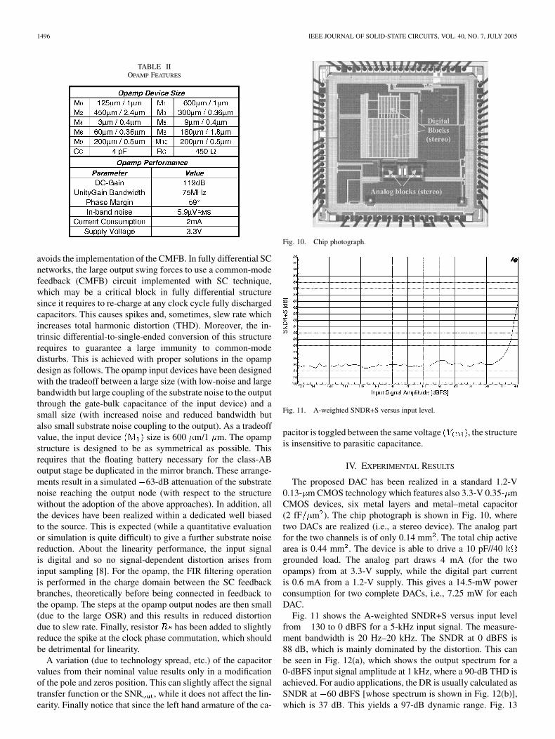
A two-stage single-ended opamp topology has been adopted,whose scheme is shown in Fig. 9 [10], [11]. The class-A inputstage allows to properly design bandwidth and noise. In theinput differential pair, a A current flows. To reduceflicker noise, a large size input device is used. A class-AB outputstage is used since it increases the slew rate and, as a conse-quence, reduces the slew-rate-induced distortion. Table II re-ports the sizes of all the devices and the main opamp perfor-mance.
An important feature to give robustness to the DR perfor-mance is the fact that the single-ended structure of the SC filter
1496 IEEE JOURNAL OF SOLID-STATE CIRCUITS, VOL. 40, NO. 7, JULY 2005
TABLE IIOPAMP FEATURES
avoids the implementation of the CMFB. In fully differential SCnetworks, the large output swing forces to use a common-modefeedback (CMFB) circuit implemented with SC technique,which may be a critical block in fully differential structuresince it requires to re-charge at any clock cycle fully dischargedcapacitors. This causes spikes and, sometimes, slew rate whichincreases total harmonic distortion (THD). Moreover, the in-trinsic differential-to-single-ended conversion of this structurerequires to guarantee a large immunity to common-modedisturbs. This is achieved with proper solutions in the opampdesign as follows. The opamp input devices have been designedwith the tradeoff between a large size (with low-noise and largebandwidth but large coupling of the substrate noise to the outputthrough the gate-bulk capacitance of the input device) and asmall size (with increased noise and reduced bandwidth butalso small substrate noise coupling to the output). As a tradeoffvalue, the input device size is 600 m/1 m. The opampstructure is designed to be as symmetrical as possible. Thisrequires that the floating battery necessary for the class-ABoutput stage be duplicated in the mirror branch. These arrange-ments result in a simulated 63-dB attenuation of the substratenoise reaching the output node (with respect to the structurewithout the adoption of the above approaches). In addition, allthe devices have been realized within a dedicated well biasedto the source. This is expected (while a quantitative evaluationor simulation is quite difficult) to give a further substrate noisereduction. About the linearity performance, the input signalis digital and so no signal-dependent distortion arises frominput sampling [8]. For the opamp, the FIR filtering operationis performed in the charge domain between the SC feedbackbranches, theoretically before being connected in feedback tothe opamp. The steps at the opamp output nodes are then small(due to the large OSR) and this results in reduced distortiondue to slew rate. Finally, resistor has been added to slightlyreduce the spike at the clock phase commutation, which shouldbe detrimental for linearity.
A variation (due to technology spread, etc.) of the capacitorvalues from their nominal value results only in a modificationof the pole and zeros position. This can slightly affect the signaltransfer function or the SNR , while it does not affect the lin-earity. Finally notice that since the left hand armature of the ca-
Fig. 10. Chip photograph.
Fig. 11. A-weighted SNDR+S versus input level.
pacitor is toggled between the same voltage , the structureis insensitive to parasitic capacitance.
IV. EXPERIMENTAL RESULTS
The proposed DAC has been realized in a standard 1.2-V0.13- m CMOS technology which features also 3.3-V 0.35- mCMOS devices, six metal layers and metal–metal capacitor(2 fF m ). The chip photograph is shown in Fig. 10, wheretwo DACs are realized (i.e., a stereo device). The analog partfor the two channels is of only 0.14 mm . The total chip activearea is 0.44 mm . The device is able to drive a 10 pF//40grounded load. The analog part draws 4 mA (for the twoopamps) from at 3.3-V supply, while the digital part currentis 0.6 mA from a 1.2-V supply. This gives a 14.5-mW powerconsumption for two complete DACs, i.e., 7.25 mW for eachDAC.
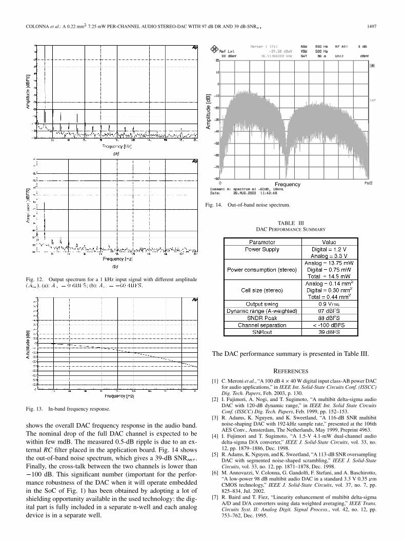
Fig. 11 shows the A-weighted SNDR+S versus input levelfrom 130 to 0 dBFS for a 5-kHz input signal. The measure-ment bandwidth is 20 Hz–20 kHz. The SNDR at 0 dBFS is88 dB, which is mainly dominated by the distortion. This canbe seen in Fig. 12(a), which shows the output spectrum for a0-dBFS input signal amplitude at 1 kHz, where a 90-dB THD isachieved. For audio applications, the DR is usually calculated asSNDR at 60 dBFS [whose spectrum is shown in Fig. 12(b)],which is 37 dB. This yields a 97-dB dynamic range. Fig. 13
COLONNA et al.: A 0.22 mm 7.25 mW PER-CHANNEL AUDIO STEREO-DAC WITH 97 dB DR AND 39 dB-SNR 1497
Fig. 12. Output spectrum for a 1 kHz input signal with different amplitude(A ). (a): A = 0 dBFS; (b): A = �60 dBFS.
Fig. 13. In-band frequency response.
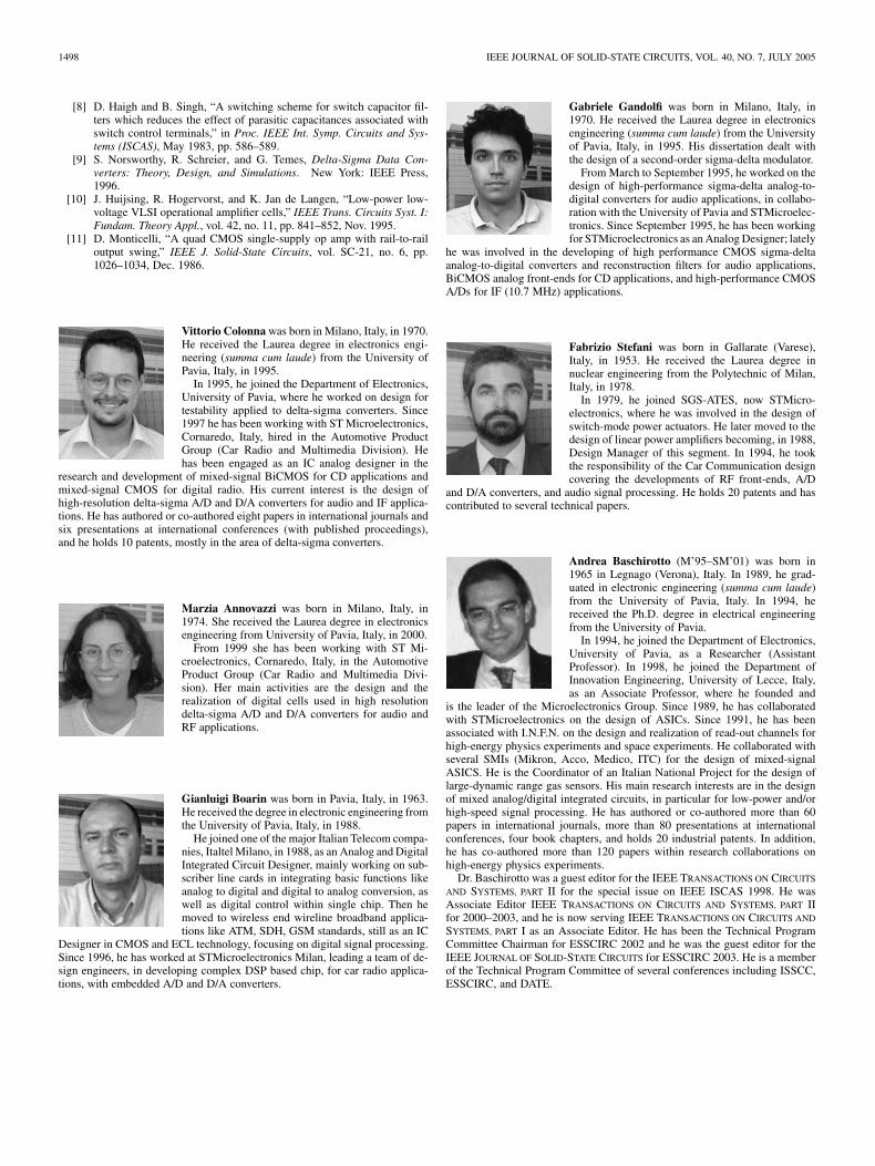
shows the overall DAC frequency response in the audio band.The nominal drop of the full DAC channel is expected to bewithin few mdB. The measured 0.5-dB ripple is due to an ex-ternal RC filter placed in the application board. Fig. 14 showsthe out-of-band noise spectrum, which gives a 39-dB SNR .Finally, the cross-talk between the two channels is lower than
100 dB. This significant number (important for the perfor-mance robustness of the DAC when it will operate embeddedin the SoC of Fig. 1) has been obtained by adopting a lot ofshielding opportunity available in the used technology: the dig-ital part is fully included in a separate n-well and each analogdevice is in a separate well.
Fig. 14. Out-of-band noise spectrum.
TABLE IIIDAC PERFORMANCE SUMMARY
The DAC performance summary is presented in Table III.
REFERENCES
[1] C. Meroni et al., “A 100 dB 4� 40 W digital input class-AB power DACfor audio applications,” in IEEE Int. Solid-State Circuits Conf. (ISSCC)Dig. Tech. Papers, Feb. 2003, p. 130.
[2] I. Fujimori, A. Nogi, and T. Sugimoto, “A multibit delta-sigma audioDAC with 120-dB dynamic range,” in IEEE Int. Solid State CircuitsConf. (ISSCC) Dig. Tech. Papers, Feb. 1999, pp. 152–153.
[3] R. Adams, K. Nguyen, and K. Sweetland, “A 116-dB SNR multibitnoise-shaping DAC with 192-kHz sample rate,” presented at the 106thAES Conv., Amsterdam, The Netherlands, May 1999, Preprint 4963.
[4] I. Fujimori and T. Sugimoto, “A 1.5-V 4.1-mW dual-channel audiodelta-sigma D/A converter,” IEEE J. Solid-State Circuits, vol. 33, no.12, pp. 1879–1886, Dec. 1998.
[5] R. Adams, K. Nguyen, and K. Sweetland, “A 113-dB SNR oversamplingDAC with segmented noise-shaped scrambling,” IEEE J. Solid-StateCircuits, vol. 33, no. 12, pp. 1871–1878, Dec. 1998.
[6] M. Annovazzi, V. Colonna, G. Gandolfi, F. Stefani, and A. Baschirotto,“A low-power 98 dB multibit audio DAC in a standard 3.3 V 0.35 �mCMOS technology,” IEEE J. Solid-State Circuits, vol. 37, no. 7, pp.825–834, Jul. 2002.
[7] R. Baird and T. Fiez, “Linearity enhancement of multibit delta-sigmaA/D and D/A converters using data weighted averaging,” IEEE Trans.Circuits Syst. II: Analog Digit. Signal Process., vol. 42, no. 12, pp.753–762, Dec. 1995.
1498 IEEE JOURNAL OF SOLID-STATE CIRCUITS, VOL. 40, NO. 7, JULY 2005
[8] D. Haigh and B. Singh, “A switching scheme for switch capacitor fil-ters which reduces the effect of parasitic capacitances associated withswitch control terminals,” in Proc. IEEE Int. Symp. Circuits and Sys-tems (ISCAS), May 1983, pp. 586–589.
[9] S. Norsworthy, R. Schreier, and G. Temes, Delta-Sigma Data Con-verters: Theory, Design, and Simulations. New York: IEEE Press,1996.
[10] J. Huijsing, R. Hogervorst, and K. Jan de Langen, “Low-power low-voltage VLSI operational amplifier cells,” IEEE Trans. Circuits Syst. I:Fundam. Theory Appl., vol. 42, no. 11, pp. 841–852, Nov. 1995.
[11] D. Monticelli, “A quad CMOS single-supply op amp with rail-to-railoutput swing,” IEEE J. Solid-State Circuits, vol. SC-21, no. 6, pp.1026–1034, Dec. 1986.
Vittorio Colonna was born in Milano, Italy, in 1970.He received the Laurea degree in electronics engi-neering (summa cum laude) from the University ofPavia, Italy, in 1995.
In 1995, he joined the Department of Electronics,University of Pavia, where he worked on design fortestability applied to delta-sigma converters. Since1997 he has been working with ST Microelectronics,Cornaredo, Italy, hired in the Automotive ProductGroup (Car Radio and Multimedia Division). Hehas been engaged as an IC analog designer in the
research and development of mixed-signal BiCMOS for CD applications andmixed-signal CMOS for digital radio. His current interest is the design ofhigh-resolution delta-sigma A/D and D/A converters for audio and IF applica-tions. He has authored or co-authored eight papers in international journals andsix presentations at international conferences (with published proceedings),and he holds 10 patents, mostly in the area of delta-sigma converters.
Marzia Annovazzi was born in Milano, Italy, in1974. She received the Laurea degree in electronicsengineering from University of Pavia, Italy, in 2000.
From 1999 she has been working with ST Mi-croelectronics, Cornaredo, Italy, in the AutomotiveProduct Group (Car Radio and Multimedia Divi-sion). Her main activities are the design and therealization of digital cells used in high resolutiondelta-sigma A/D and D/A converters for audio andRF applications.
Gianluigi Boarin was born in Pavia, Italy, in 1963.He received the degree in electronic engineering fromthe University of Pavia, Italy, in 1988.
He joined one of the major Italian Telecom compa-nies, Italtel Milano, in 1988, as an Analog and DigitalIntegrated Circuit Designer, mainly working on sub-scriber line cards in integrating basic functions likeanalog to digital and digital to analog conversion, aswell as digital control within single chip. Then hemoved to wireless end wireline broadband applica-tions like ATM, SDH, GSM standards, still as an IC
Designer in CMOS and ECL technology, focusing on digital signal processing.Since 1996, he has worked at STMicroelectronics Milan, leading a team of de-sign engineers, in developing complex DSP based chip, for car radio applica-tions, with embedded A/D and D/A converters.
Gabriele Gandolfi was born in Milano, Italy, in1970. He received the Laurea degree in electronicsengineering (summa cum laude) from the Universityof Pavia, Italy, in 1995. His dissertation dealt withthe design of a second-order sigma-delta modulator.
From March to September 1995, he worked on thedesign of high-performance sigma-delta analog-to-digital converters for audio applications, in collabo-ration with the University of Pavia and STMicroelec-tronics. Since September 1995, he has been workingfor STMicroelectronics as an Analog Designer; lately
he was involved in the developing of high performance CMOS sigma-deltaanalog-to-digital converters and reconstruction filters for audio applications,BiCMOS analog front-ends for CD applications, and high-performance CMOSA/Ds for IF (10.7 MHz) applications.
Fabrizio Stefani was born in Gallarate (Varese),Italy, in 1953. He received the Laurea degree innuclear engineering from the Polytechnic of Milan,Italy, in 1978.
In 1979, he joined SGS-ATES, now STMicro-electronics, where he was involved in the design ofswitch-mode power actuators. He later moved to thedesign of linear power amplifiers becoming, in 1988,Design Manager of this segment. In 1994, he tookthe responsibility of the Car Communication designcovering the developments of RF front-ends, A/D
and D/A converters, and audio signal processing. He holds 20 patents and hascontributed to several technical papers.
Andrea Baschirotto (M’95–SM’01) was born in1965 in Legnago (Verona), Italy. In 1989, he grad-uated in electronic engineering (summa cum laude)from the University of Pavia, Italy. In 1994, hereceived the Ph.D. degree in electrical engineeringfrom the University of Pavia.
In 1994, he joined the Department of Electronics,University of Pavia, as a Researcher (AssistantProfessor). In 1998, he joined the Department ofInnovation Engineering, University of Lecce, Italy,as an Associate Professor, where he founded and
is the leader of the Microelectronics Group. Since 1989, he has collaboratedwith STMicroelectronics on the design of ASICs. Since 1991, he has beenassociated with I.N.F.N. on the design and realization of read-out channels forhigh-energy physics experiments and space experiments. He collaborated withseveral SMIs (Mikron, Acco, Medico, ITC) for the design of mixed-signalASICS. He is the Coordinator of an Italian National Project for the design oflarge-dynamic range gas sensors. His main research interests are in the designof mixed analog/digital integrated circuits, in particular for low-power and/orhigh-speed signal processing. He has authored or co-authored more than 60papers in international journals, more than 80 presentations at internationalconferences, four book chapters, and holds 20 industrial patents. In addition,he has co-authored more than 120 papers within research collaborations onhigh-energy physics experiments.
Dr. Baschirotto was a guest editor for the IEEE TRANSACTIONS ON CIRCUITS
AND SYSTEMS, PART II for the special issue on IEEE ISCAS 1998. He wasAssociate Editor IEEE TRANSACTIONS ON CIRCUITS AND SYSTEMS, PART IIfor 2000–2003, and he is now serving IEEE TRANSACTIONS ON CIRCUITS AND
SYSTEMS, PART I as an Associate Editor. He has been the Technical ProgramCommittee Chairman for ESSCIRC 2002 and he was the guest editor for theIEEE JOURNAL OF SOLID-STATE CIRCUITS for ESSCIRC 2003. He is a memberof the Technical Program Committee of several conferences including ISSCC,ESSCIRC, and DATE.