
3D Nanostar Dimers with a Sub-10-nm Gap for Single-/ Few-Molecule Surface-Enhanced Raman Scattering
6
© 2014 WILEY-VCH Verlag GmbH & Co. KGaA, Weinheim 1 www.advmat.de www.MaterialsViews.com wileyonlinelibrary.com COMMUNICATION 3D Nanostar Dimers with a Sub-10-nm Gap for Single-/ Few-Molecule Surface-Enhanced Raman Scattering Manohar Chirumamilla, Andrea Toma,* Anisha Gopalakrishnan, Gobind Das, Remo Proietti Zaccaria, Roman Krahne, Eliana Rondanina, Marco Leoncini, Carlo Liberale, Francesco De Angelis, and Enzo Di Fabrizio Dr. M. Chirumamilla, Dr. A. Toma, A. Gopalakrishnan, Dr. G. Das, Dr. R. P. Zaccaria, Dr. R. Krahne, E. Rondanina, M. Leoncini, Dr. C. Liberale, Dr. F. De Angelis Nanostructures, Istituto Italiano di Tecnologia via Morego 30, Genova, 16163, Italy E-mail: [email protected] Prof. E. Di Fabrizio King Abdullah University of Science and Technology (KAUST) PSE and BESE Divisions Thuwal, 23955-6900, Kingdom of Saudi Arabia Prof. E. Di Fabrizio BioNEM Lab Dipartimento di Medicina Sperimentale e Clinica Università Magna Graecia di Catanzaro Catanzaro, 88100, Italy DOI: 10.1002/adma.201304553 The fabrication of nanostructures for extremely large electric- field enhancement has become increasingly important over the last few years with the aim to detect molecules in highly diluted liquids, and/or to record the Raman spectra of a single or a few molecules located at a “hot spot”. One popular and cost-effective approach involves surfaces with a random distri- bution of hot spots, which can be obtained, for example, by the deposition of plasmonic nanoparticles on substrates or via post-deposition treatment of metal films. [1] A complementary strategy relies on the controlled engineering of hot spots [2] and their fabrication via top–down methods. The advantages of the top–down methods include i) the reproducibility of the fab- rication, ii) the uniformity in the field enhancement, and iii) the high controllability of the position, size, and shape of the hot spots. The trade-offs, however, are high fabrication costs and the small number of hot spots, as a result of the fact that electron- or ion-beam techniques are typically employed in the fabrication. Nevertheless, engineered structures for surface- enhanced Raman spectroscopy (SERS) are highly appropriate for single-/few-molecule detection because they enable detec- tion at a well-defined spot—for example, on a scanning probe tip, or at a position to which the molecules can be directed, as demonstrated by engineered defects on superhydrophobic substrates. [3] Towards single-/few-molecule detection, some general constraints in the experimental conditions must be satis- fied, [4] irrespective of the nanostructures that are used for field enhancement. In particular, spatially isolated nanostructures do not provide sufficient enhancement for single-molecule detection, for which a SERS enhancement on the order of 10 7 is required. [5] Therefore, it is necessary to move towards the fabrication of strongly coupled nanosystems in order to achieve a giant field confinement in a highly localized nanoscale volume. [6] In fact, theoretical calculations reveal that the strong coupling of nanostructures, such as dimers, can enhance Raman scattering in the range of 10 5 –10 6 in addition to the enhancement originating from the comprising individual nanostructures. [7] This large electric-field enhancement shows potential for applications in nonlinear optics, light-harvesting, optical rectification, and overall single-/few-molecule SERS. [8] Herein, we introduce novel complex 3D star-shaped metallic (Au) nanostructures, endowed with multiple tips that are decoupled from the substrate by means of standing silicon pillars—termed “nanostar on silicon pillar” (NOSP). One advantage of the star shape over other geometries is that the multiple branches ensure narrow tips in the dimer (i.e., strong field confinement), while the voids between the branches allow the achievement of a large undercut in the dry-etching fabrica- tion process. Furthermore, the elevated geometry enables the reproducible fabrication of nanostar dimers with an interpar- ticle spacing (IPS) below 10 nm. Using these structures, we report on the Raman signal originating from different kinds of biomolecules at very low concentrations (~1 p M), in order to statistically ensure only a single molecule or a few mol- ecules per hot-spot. Single-/few-molecule SERS was observed for adenine (DNA base), showing the ability of NOSP dimers to detect nonresonant molecules (with respect to the excitation source), employing low excitation power and short acquisi- tion times. These results demonstrate how NOSP devices are highly capable of locally enhancing the electric field, leading to a noticeable Raman signal even for very low molecule density. Metal nanostructures with an IPS in the 10-nm range and below have been fabricated by different techniques, e.g., edge lithography, directional deposition from tilted angles, and on- wire lithography. [9,10] However, the fabrication of SERS nano- structures with sub-10-nm gaps—and with a homogeneity and reproducibility over large areas that allows detection of few molecules—is still challenging. In the present work, we chose a top–down approach, using electron-beam lithography (EBL) followed by reactive-ion etching (RIE), in order to fabricate strongly coupled, free-standing, 3D nanostructures with excel- lent control on their geometry. We show that NOSP dimers are capable of localizing the electric field in the IPS region and thereby facilitate their application in the detection of a single or a few molecules. The geometry of the dimer structures, with respect to IPS and pillar height, was optimized for high field Adv. Mater. 2014, DOI: 10.1002/adma.201304553
Transcript of 3D Nanostar Dimers with a Sub-10-nm Gap for Single-/ Few-Molecule Surface-Enhanced Raman Scattering
© 2014 WILEY-VCH Verlag GmbH & Co. KGaA, Weinheim 1
www.advmat.dewww.MaterialsViews.com
wileyonlinelibrary.com
CO
MM
UN
ICATIO
N
3D Nanostar Dimers with a Sub-10-nm Gap for Single-/Few-Molecule Surface-Enhanced Raman Scattering
Manohar Chirumamilla , Andrea Toma , * Anisha Gopalakrishnan , Gobind Das , Remo Proietti Zaccaria , Roman Krahne , Eliana Rondanina , Marco Leoncini , Carlo Liberale , Francesco De Angelis , and Enzo Di Fabrizio
Dr. M. Chirumamilla, Dr. A. Toma, A. Gopalakrishnan, Dr. G. Das, Dr. R. P. Zaccaria, Dr. R. Krahne, E. Rondanina, M. Leoncini, Dr. C. Liberale, Dr. F. De Angelis Nanostructures, Istituto Italiano di Tecnologia via Morego 30, Genova, 16163 , Italy E-mail: [email protected] Prof. E. Di Fabrizio King Abdullah University of Science and Technology (KAUST) PSE and BESE Divisions Thuwal, 23955-6900 , Kingdom of Saudi Arabia Prof. E. Di Fabrizio BioNEM Lab Dipartimento di Medicina Sperimentale e Clinica Università Magna Graecia di Catanzaro Catanzaro, 88100 , Italy
DOI: 10.1002/adma.201304553
The fabrication of nanostructures for extremely large electric-fi eld enhancement has become increasingly important over the last few years with the aim to detect molecules in highly diluted liquids, and/or to record the Raman spectra of a single or a few molecules located at a “hot spot”. One popular and cost-effective approach involves surfaces with a random distri-bution of hot spots, which can be obtained, for example, by the deposition of plasmonic nanoparticles on substrates or via post-deposition treatment of metal fi lms. [ 1 ] A complementary strategy relies on the controlled engineering of hot spots [ 2 ] and their fabrication via top–down methods. The advantages of the top–down methods include i) the reproducibility of the fab-rication, ii) the uniformity in the fi eld enhancement, and iii) the high controllability of the position, size, and shape of the hot spots. The trade-offs, however, are high fabrication costs and the small number of hot spots, as a result of the fact that electron- or ion-beam techniques are typically employed in the fabrication. Nevertheless, engineered structures for surface-enhanced Raman spectroscopy (SERS) are highly appropriate for single-/few-molecule detection because they enable detec-tion at a well-defi ned spot—for example, on a scanning probe tip, or at a position to which the molecules can be directed, as demonstrated by engineered defects on superhydrophobic substrates. [ 3 ]
Towards single-/few-molecule detection, some general constraints in the experimental conditions must be satis-fi ed, [ 4 ] irrespective of the nanostructures that are used for fi eld enhancement. In particular, spatially isolated nanostructures do not provide suffi cient enhancement for single-molecule
detection, for which a SERS enhancement on the order of 10 7 is required. [ 5 ] Therefore, it is necessary to move towards the fabrication of strongly coupled nanosystems in order to achieve a giant fi eld confi nement in a highly localized nanoscale volume. [ 6 ] In fact, theoretical calculations reveal that the strong coupling of nanostructures, such as dimers, can enhance Raman scattering in the range of 10 5 –10 6 in addition to the enhancement originating from the comprising individual nanostructures. [ 7 ] This large electric-fi eld enhancement shows potential for applications in nonlinear optics, light-harvesting, optical rectifi cation, and overall single-/few-molecule SERS. [ 8 ]
Herein, we introduce novel complex 3D star-shaped metallic (Au) nanostructures, endowed with multiple tips that are decoupled from the substrate by means of standing silicon pillars—termed “nanostar on silicon pillar” (NOSP). One advantage of the star shape over other geometries is that the multiple branches ensure narrow tips in the dimer (i.e., strong fi eld confi nement), while the voids between the branches allow the achievement of a large undercut in the dry-etching fabrica-tion process. Furthermore, the elevated geometry enables the reproducible fabrication of nanostar dimers with an interpar-ticle spacing (IPS) below 10 nm. Using these structures, we report on the Raman signal originating from different kinds of biomolecules at very low concentrations (~1 p M), in order to statistically ensure only a single molecule or a few mol-ecules per hot-spot. Single-/few-molecule SERS was observed for adenine (DNA base), showing the ability of NOSP dimers to detect nonresonant molecules (with respect to the excitation source), employing low excitation power and short acquisi-tion times. These results demonstrate how NOSP devices are highly capable of locally enhancing the electric fi eld, leading to a noticeable Raman signal even for very low molecule density.
Metal nanostructures with an IPS in the 10-nm range and below have been fabricated by different techniques, e.g., edge lithography, directional deposition from tilted angles, and on-wire lithography. [ 9,10 ] However, the fabrication of SERS nano-structures with sub-10-nm gaps—and with a homogeneity and reproducibility over large areas that allows detection of few molecules—is still challenging. In the present work, we chose a top–down approach, using electron-beam lithography (EBL) followed by reactive-ion etching (RIE), in order to fabricate strongly coupled, free-standing, 3D nanostructures with excel-lent control on their geometry. We show that NOSP dimers are capable of localizing the electric fi eld in the IPS region and thereby facilitate their application in the detection of a single or a few molecules. The geometry of the dimer structures, with respect to IPS and pillar height, was optimized for high fi eld
Adv. Mater. 2014, DOI: 10.1002/adma.201304553
2
www.advmat.dewww.MaterialsViews.com
wileyonlinelibrary.com © 2014 WILEY-VCH Verlag GmbH & Co. KGaA, Weinheim
CO
MM
UN
ICATI
ON
enhancement with the help of theoretical calculations. p -Mer-captoaniline ( p -MA), a nonfl uorescent molecule, was used to characterize the NOSP structures in terms of SERS signals.
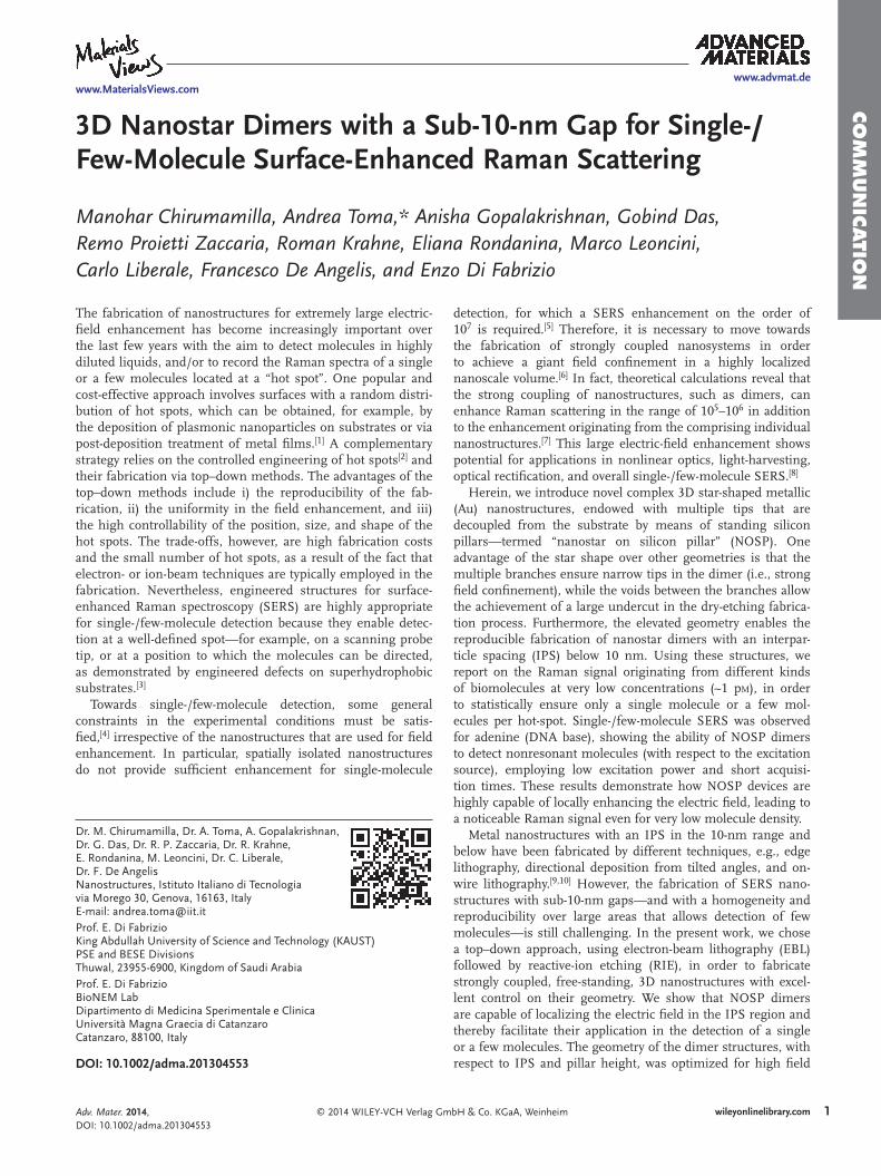
A schematic diagram of the SERS working principle for a 3D starlike dimer is illustrated in Figure 1 a. Figure 1 b,c show representative scanning electron microscopy (SEM) images of NOSP dimer arrays, demonstrating the excellent homogeneity and uniformity of the nanostar-dimer fabrication. The SERS signal from a single or a few adenine molecules, deposited on a NOSP device by chemisorption from a 1-p M solution, is reported in Figure 1 d. The signal, obtained with excitation laser power of 14 mW and acquisition time of 2 s, shows several prominent Raman modes including the clearly distinguishable adenine-ring breathing mode at 736 cm −1 .
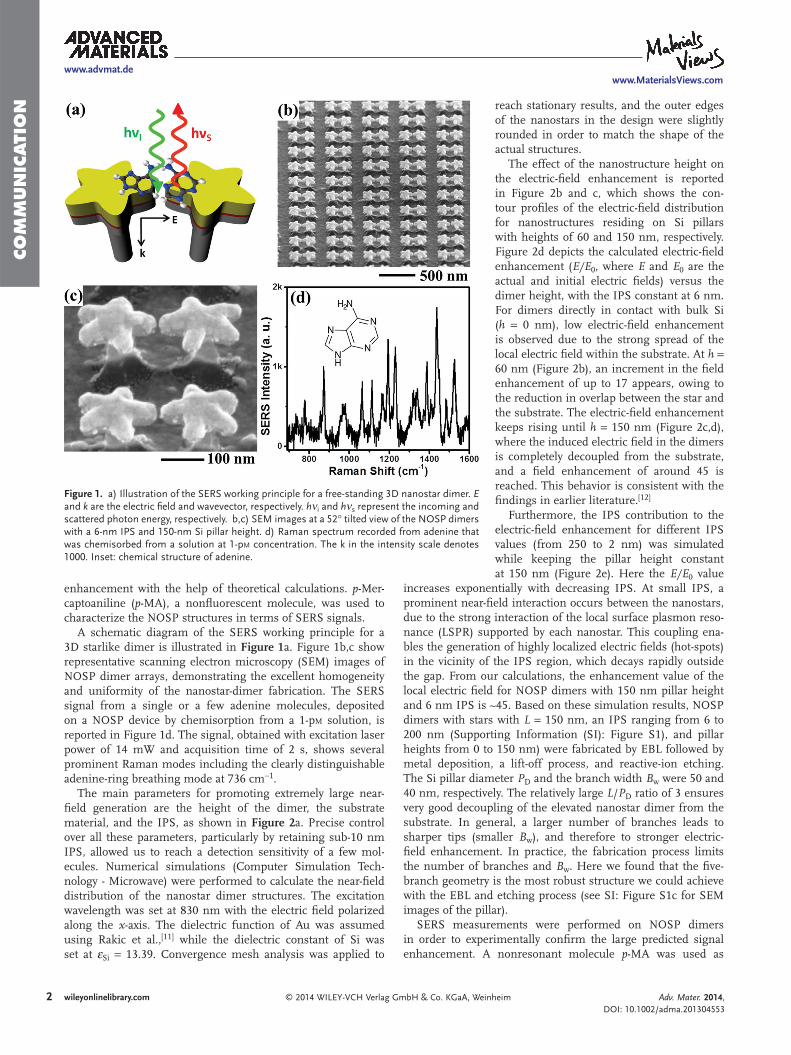
The main parameters for promoting extremely large near-fi eld generation are the height of the dimer, the substrate material, and the IPS, as shown in Figure 2 a. Precise control over all these parameters, particularly by retaining sub-10 nm IPS, allowed us to reach a detection sensitivity of a few mol-ecules. Numerical simulations (Computer Simulation Tech-nology - Microwave) were performed to calculate the near-fi eld distribution of the nanostar dimer structures. The excitation wavelength was set at 830 nm with the electric fi eld polarized along the x -axis. The dielectric function of Au was assumed using Rakic et al., [ 11 ] while the dielectric constant of Si was set at ε Si = 13.39. Convergence mesh analysis was applied to
reach stationary results, and the outer edges of the nanostars in the design were slightly rounded in order to match the shape of the actual structures.
The effect of the nanostructure height on the electric-fi eld enhancement is reported in Figure 2 b and c, which shows the con-tour profi les of the electric-fi eld distribution for nanostructures residing on Si pillars with heights of 60 and 150 nm, respectively. Figure 2 d depicts the calculated electric-fi eld enhancement ( E/E 0 , where E and E 0 are the actual and initial electric fi elds) versus the dimer height, with the IPS constant at 6 nm. For dimers directly in contact with bulk Si ( h = 0 nm), low electric-fi eld enhancement is observed due to the strong spread of the local electric fi eld within the substrate. At h = 60 nm (Figure 2 b), an increment in the fi eld enhancement of up to 17 appears, owing to the reduction in overlap between the star and the substrate. The electric-fi eld enhancement keeps rising until h = 150 nm (Figure 2 c,d), where the induced electric fi eld in the dimers is completely decoupled from the substrate, and a fi eld enhancement of around 45 is reached. This behavior is consistent with the fi ndings in earlier literature. [ 12 ]
Furthermore, the IPS contribution to the electric-fi eld enhancement for different IPS values (from 250 to 2 nm) was simulated while keeping the pillar height constant at 150 nm (Figure 2 e). Here the E/E 0 value
increases exponentially with decreasing IPS. At small IPS, a prominent near-fi eld interaction occurs between the nanostars, due to the strong interaction of the local surface plasmon reso-nance (LSPR) supported by each nanostar. This coupling ena-bles the generation of highly localized electric fi elds (hot-spots) in the vicinity of the IPS region, which decays rapidly outside the gap. From our calculations, the enhancement value of the local electric fi eld for NOSP dimers with 150 nm pillar height and 6 nm IPS is ~45. Based on these simulation results, NOSP dimers with stars with L = 150 nm, an IPS ranging from 6 to 200 nm (Supporting Information (SI): Figure S1), and pillar heights from 0 to 150 nm) were fabricated by EBL followed by metal deposition, a lift-off process, and reactive-ion etching. The Si pillar diameter P D and the branch width B w were 50 and 40 nm, respectively. The relatively large L / P D ratio of 3 ensures very good decoupling of the elevated nanostar dimer from the substrate. In general, a larger number of branches leads to sharper tips (smaller B w ), and therefore to stronger electric-fi eld enhancement. In practice, the fabrication process limits the number of branches and B w . Here we found that the fi ve-branch geometry is the most robust structure we could achieve with the EBL and etching process (see SI: Figure S1c for SEM images of the pillar).
SERS measurements were performed on NOSP dimers in order to experimentally confi rm the large predicted signal enhancement. A nonresonant molecule p -MA was used as
Figure 1. a) Illustration of the SERS working principle for a free-standing 3D nanostar dimer. E and k are the electric fi eld and wavevector, respectively. hν i and hν s represent the incoming and scattered photon energy, respectively. b,c) SEM images at a 52° tilted view of the NOSP dimers with a 6-nm IPS and 150-nm Si pillar height. d) Raman spectrum recorded from adenine that was chemisorbed from a solution at 1-p M concentration. The k in the intensity scale denotes 1000. Inset: chemical structure of adenine.
Adv. Mater. 2014, DOI: 10.1002/adma.201304553

3
www.advmat.dewww.MaterialsViews.com
wileyonlinelibrary.com© 2014 WILEY-VCH Verlag GmbH & Co. KGaA, Weinheim
CO
MM
UN
ICATIO
N
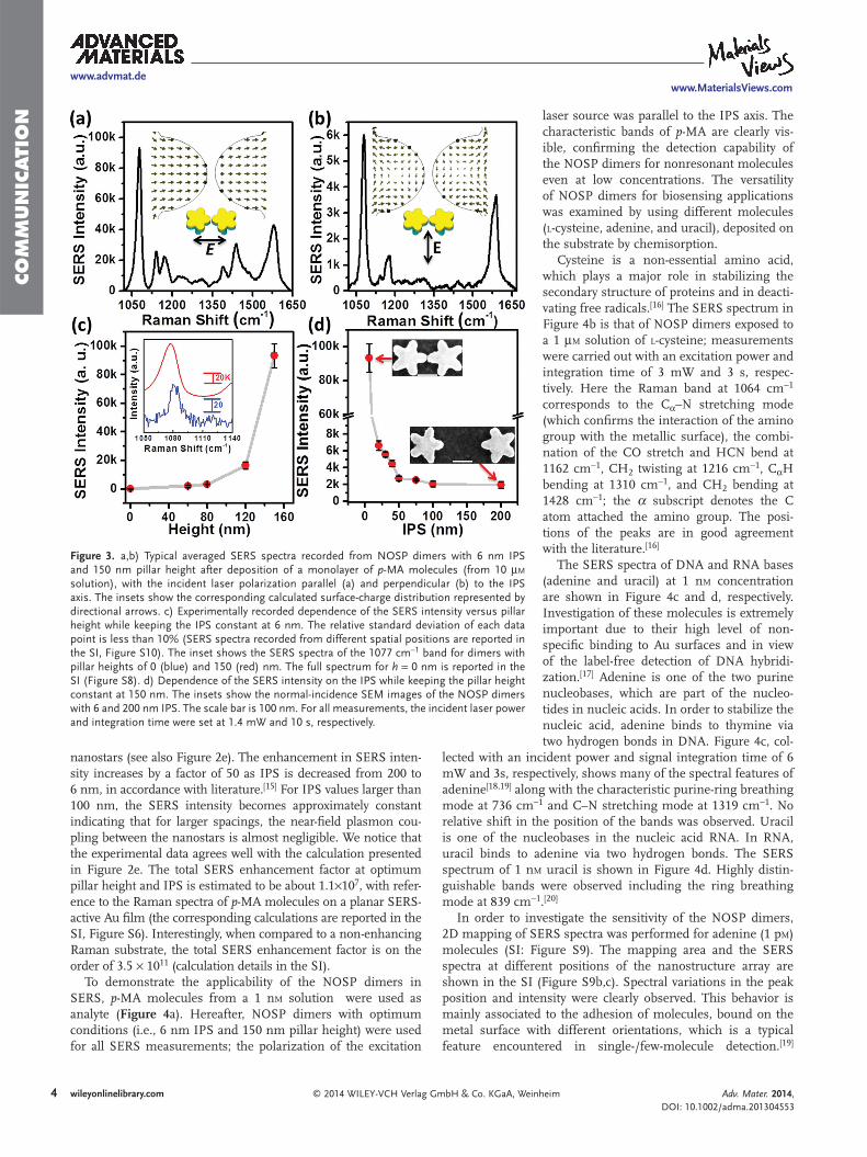
with the morphological characterization of the Au fi lm (Figure S4). The low signal of the Raman bands at 1077 and 1590 cm −1 in the reference spectra, only slightly above the noise level, highlights the enhance-ment resulting from our NOSP dimers. The SERS enhancement depends signifi cantly on the polarization of the incident light with respect to the dimer structure. To illustrate this behavior, the SERS spectrum of p -MA molecules on NOSP dimers with the excita-tion source polarized perpendicularly to the IPS axis is shown in Figure 3 b. A discern-ible decrease in SERS intensity is observed, and many features are also absent in the spectrum. The disappearance of the bands at 1140, 1390, and 1438 cm −1 is characteristic of a polarization dependence, highlighting the polarization-sensitivity of the NOSP dimers. The insets of Figure 3 a,b show a vector rep-resentation of the calculated surface-charge distribution in the NOSP dimers with 6 nm IPS and 150 nm pillar height, with polariza-tion parallel or perpendicular to the IPS axis. Here local surface charges are represented by directional arrows. When the incident light is polarized parallel to the IPS axis, a dipolar distribution is aligned along the IPS axis, and in-phase dipole moments guarantee a strong coupling of the NOSP dimers, resulting in an intense electric-fi eld (hot-spot) generation in the IPS region. In contrast, for perpendicular polarization, the effective dipoles are aligned across the IPS axis and thus a less intense
induced electric fi eld is observed in the gap region. The SI (Figure S5b,c) provides further insights with the contour pro-fi les of the electric-fi eld distribution in the IPS region.
The dependence of the SERS intensities on the Si pillars height was investigated experimentally using NOSP dimer structures with different pillar heights (0–150 nm) and IPS values at 6 or 10 nm for pillar heights larger or equal to zero, respectively. The 10 nm IPS at zero pillar height is due to the practical limitations in obtaining reproducible sub-10-nm gaps in the case of planar nanostar dimers. In the SERS measure-ments of Figure 3 c, we plot the intensity of the strong peak at 1077 cm −1 as a function of the pillar height. The polarization was parallel to the IPS axis. Each experimental data point was obtained by averaging 10 spectra with the relative standard deviation being less than 10%. We observed a dramatic increase of the SERS intensity with increasing pillar height, reaching an intensity of 94000 counts at 150 nm, which is also manifested in the signal-to-noise ratio in the Raman spectra as demon-strated in the inset.
In order to illustrate the impact of the gap size, we show in Figure 3 d the SERS intensity of p -MA molecules (10 μ M ) for different IPS values at a fi xed pillar height of 150 nm for the 1077 cm −1 Raman band. An almost exponential rise in SERS intensity is observed by decreasing the IPS from 200 to 6 nm, which is related to the electric-fi eld coupling between the
the analyte because of its capability of forming a self-assem-bled monolayer on Au surfaces. [ 13 ] Figure 3 a shows a typical averaged SERS spectrum of p -MA molecules in the range of 1000–1650 cm −1 , recorded from a self-assembled monolayer of p -MA molecules, which were deposited over NOSP dimer structures with 6 nm IPS and 150 nm pillar height by means of chemisorption (from a 10 μ M solution; see Experimental Section for additional details). The incident laser wavelength, power, and accumulation time were set to 830 nm, 1.4 mW, and 10 s, respectively, while the polarization of the incident light was parallel to the IPS axis. Distinct features of p -MA were clearly identifi ed: strong bands centered at 1077 and 1590 cm −1 , and many other low-intensity bands at 390, 456, 645, 783, 1140, 1179, 1390, and 1438 cm −1 can be observed in the spec-trum (see also SI: Figure S2). [ 14 ] We used the C–S stretch at 1077 cm −1 to calculate the enhancement factor, and we empha-size that we found similar SERS intensities recorded for dif-ferent NOSP dimers with the same geometry, thus confi rming the homogeneity in device fabrication as well as the uniform deposition of the molecules over the substrate by chemisorp-tion. Raman spectra recorded prior to chemisorption of p -MA on NOSP dimers did not show any signifi cant Raman signal (SI: Figure S3a), indicating the absence of surface contamina-tion. The reference Raman spectrum recorded from p -MA on an unpatterned Au fi lm is shown in the SI (Figure S3b), along
Figure 2. a) Sketch of a single NOSP dimer structure, illustrating the geometric parameters: pillar height h and diameter P D , star diameter L , and branch width B w . b,c) Calculated electric-fi eld distribution of a NOSP dimer with h = 60 and 150 nm, respectively, where the excitation at λ = 830 nm was set in the x -direction. d,e) Calculated E/E 0 as a function of pillar height with a 6 nm IPS (d) and as a function of IPS for a 150 nm pillar height (e). The open black star data-point in (d) corresponds to the electric-fi eld enhancement of 2D ( h = 0 nm) nanostar dimers on a Si surface without a Au backplane.
Adv. Mater. 2014, DOI: 10.1002/adma.201304553
4
www.advmat.dewww.MaterialsViews.com
wileyonlinelibrary.com © 2014 WILEY-VCH Verlag GmbH & Co. KGaA, Weinheim
CO
MM
UN
ICATI
ON laser source was parallel to the IPS axis. The
characteristic bands of p -MA are clearly vis-ible, confi rming the detection capability of the NOSP dimers for nonresonant molecules even at low concentrations. The versatility of NOSP dimers for biosensing applications was examined by using different molecules ( L -cysteine, adenine, and uracil), deposited on the substrate by chemisorption.
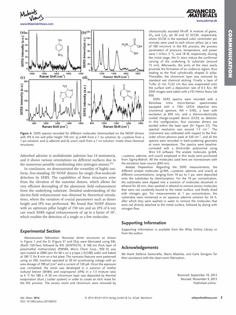
Cysteine is a non-essential amino acid, which plays a major role in stabilizing the secondary structure of proteins and in deacti-vating free radicals. [ 16 ] The SERS spectrum in Figure 4 b is that of NOSP dimers exposed to a 1 μ M solution of L -cysteine; measurements were carried out with an excitation power and integration time of 3 mW and 3 s, respec-tively. Here the Raman band at 1064 cm −1 corresponds to the C α –N stretching mode (which confi rms the interaction of the amino group with the metallic surface), the combi-nation of the CO stretch and HCN bend at 1162 cm −1 , CH 2 twisting at 1216 cm −1 , C α H bending at 1310 cm −1 , and CH 2 bending at 1428 cm −1 ; the α subscript denotes the C atom attached the amino group. The posi-tions of the peaks are in good agreement with the literature. [ 16 ]
The SERS spectra of DNA and RNA bases (adenine and uracil) at 1 n M concentration are shown in Figure 4 c and d, respectively. Investigation of these molecules is extremely important due to their high level of non-specifi c binding to Au surfaces and in view of the label-free detection of DNA hybridi-zation. [ 17 ] Adenine is one of the two purine nucleobases, which are part of the nucleo-tides in nucleic acids. In order to stabilize the nucleic acid, adenine binds to thymine via two hydrogen bonds in DNA. Figure 4 c, col-
lected with an incident power and signal integration time of 6 mW and 3s, respectively, shows many of the spectral features of adenine [ 18,19 ] along with the characteristic purine-ring breathing mode at 736 cm −1 and C–N stretching mode at 1319 cm −1 . No relative shift in the position of the bands was observed. Uracil is one of the nucleobases in the nucleic acid RNA. In RNA, uracil binds to adenine via two hydrogen bonds. The SERS spectrum of 1 n M uracil is shown in Figure 4 d. Highly distin-guishable bands were observed including the ring breathing mode at 839 cm −1 . [ 20 ]
In order to investigate the sensitivity of the NOSP dimers, 2D mapping of SERS spectra was performed for adenine (1 p M ) molecules (SI: Figure S9). The mapping area and the SERS spectra at different positions of the nanostructure array are shown in the SI (Figure S9b,c). Spectral variations in the peak position and intensity were clearly observed. This behavior is mainly associated to the adhesion of molecules, bound on the metal surface with different orientations, which is a typical feature encountered in single-/few-molecule detection. [ 19 ]
nanostars (see also Figure 2 e). The enhancement in SERS inten-sity increases by a factor of 50 as IPS is decreased from 200 to 6 nm, in accordance with literature. [ 15 ] For IPS values larger than 100 nm, the SERS intensity becomes approximately constant indicating that for larger spacings, the near-fi eld plasmon cou-pling between the nanostars is almost negligible. We notice that the experimental data agrees well with the calculation presented in Figure 2 e. The total SERS enhancement factor at optimum pillar height and IPS is estimated to be about 1.1×10 7 , with refer-ence to the Raman spectra of p -MA molecules on a planar SERS-active Au fi lm (the corresponding calculations are reported in the SI, Figure S6). Interestingly, when compared to a non-enhancing Raman substrate, the total SERS enhancement factor is on the order of 3.5 × 10 11 (calculation details in the SI).
To demonstrate the applicability of the NOSP dimers in SERS, p -MA molecules from a 1 n M solution were used as analyte ( Figure 4 a). Hereafter, NOSP dimers with optimum conditions (i.e., 6 nm IPS and 150 nm pillar height) were used for all SERS measurements; the polarization of the excitation
Figure 3. a,b) Typical averaged SERS spectra recorded from NOSP dimers with 6 nm IPS and 150 nm pillar height after deposition of a monolayer of p -MA molecules (from 10 μ M solution), with the incident laser polarization parallel (a) and perpendicular (b) to the IPS axis. The insets show the corresponding calculated surface-charge distribution represented by directional arrows. c) Experimentally recorded dependence of the SERS intensity versus pillar height while keeping the IPS constant at 6 nm. The relative standard deviation of each data point is less than 10% (SERS spectra recorded from different spatial positions are reported in the SI, Figure S10). The inset shows the SERS spectra of the 1077 cm −1 band for dimers with pillar heights of 0 (blue) and 150 (red) nm. The full spectrum for h = 0 nm is reported in the SI (Figure S8). d) Dependence of the SERS intensity on the IPS while keeping the pillar height constant at 150 nm. The insets show the normal-incidence SEM images of the NOSP dimers with 6 and 200 nm IPS. The scale bar is 100 nm. For all measurements, the incident laser power and integration time were set at 1.4 mW and 10 s, respectively.
Adv. Mater. 2014, DOI: 10.1002/adma.201304553
5
www.advmat.dewww.MaterialsViews.com
wileyonlinelibrary.com© 2014 WILEY-VCH Verlag GmbH & Co. KGaA, Weinheim
CO
MM
UN
ICATIO
N
ultrasonically assisted lift-off. A mixture of gases, SF 6 and C 4 F 8 (at 30 and 32 SCCM, respectively, where SCCM is the standard cubic centimeter per minute) were used to etch silicon pillars (at a rate of 100 nm/min) in the RIE process; the process parameters of pressure, temperature, and power were 1 mTorr, 5 °C, and 18 W, respectively. During the initial stage, the Cr stars induce the conformal carving of the underlying Si substrate (around 15 nm). Afterwards, the arms of the stars easily promote the formation of an undercut region, thus leading to the fi nal cylindrically shaped Si pillar. Thereafter, the chromium layer was removed by standard wet chemical etching. Finally, a layer of Ti/Au (3 nm Ti/22 nm Au) was evaporated onto the surface with a deposition rate of 0.3 Å/s. All SEM images were taken with a FEI Helios Nano lab 650.
SERS : SERS spectra were recorded with a Renishaw inVia micro-Raman spectrometer equipped with a 150× LEICA objective lens (numerical aperture, NA = 0.95), a laser with excitation at 830 nm, and a thermo-electrically cooled charge-coupled device (CCD) as detector. In this confi guration, four nanostar dimers are excited within the laser spot (SI: Figure S7). The spectral resolution was around 1.5 cm −1 . The instrument was calibrated with respect to the fi rst-order silicon phonon peak at 520 cm −1 , and all the spectra were recorded in back-scattering geometry at room temperature. The spectra were baseline-corrected with a third-order polynomial using Wire 3.0 software. The analyte molecules ( p -MA,
L -cysteine, adenine, and uracil) employed in this study were purchased from Sigma-Aldrich. All the molecules used here are nonresonant with the excitation laser source (830 nm).
Analyte Preparation : Regarding the SERS measurements, the different analyte molecules ( p -MA, L -cysteine, adenine, and uracil) at different concentrations, ranging from 10 μ M to 1 p M, were deposited onto the substrates by chemisorption. For the 10 μ M concentration, the substrates were dipped into a solution of molecules dissolved in ethanol for 20 min, then washed in ethanol to remove excess molecules that were not covalently bound to the metal surface, and fi nally dried with nitrogen gas. For measurements at 1 p M concentration, the substrates were immersed in an aqueous adenine solution for 24 h, after which they were washed in water to remove the molecules that were not directly attached to the metal surface, followed by drying with nitrogen fl ow.
Supporting Information Supporting Information is available from the Wiley Online Library or from the author.
Acknowledgements We thank Stefania Santoriello, Mario Malerba, and Carla Dorigoni for their assistance with the clean-room fabrication.
Adsorbed adenine is multidentate (adenine has 14 tautomers), and it shows various orientations on different surfaces due to the numerous possible coordinating sites (nitrogen atoms). [ 21 ]
In conclusion, we demonstrated the versatility of highly uni-form, free-standing 3D NOSP dimers for single-/few-molecule detection by SERS. The capabilities of these structures arise from the elevation of the nanostar dimers, which allows for very effi cient decoupling of the plasmonic fi eld enhancement from the underlying substrate. Detailed understanding of the electric-fi eld enhancement was obtained by theoretical simula-tions, where the variation of crucial parameters such as dimer height and IPS was performed. We found that NOSP dimers with an optimum pillar height of 150 nm and an IPS of 6 nm can reach SERS signal enhancements of up to a factor of 10 7 , which enables the detection of a single or a few molecules.
Experimental Section Nanostructure Fabrication : Nanostar dimer structures as shown
in Figure 1 and the SI (Figure S1 and S5a) were fabricated using EBL (Raith 150-Two) followed by RIE (SENTECH). A 160 nm thick layer of poly(methyl methacrylate) (PMMA, Micro Chem Corp., 950 K) was spin-coated at 2000 rpm for 60 s on a p-type c-Si(100) wafer and baked at 180 °C for 8 min on a hot plate. The nanostar features were patterned using an EBL machine operated at 30 kV accelerating voltage with an area dosage of 700 μC/cm 2 and a current of 120 pA. Once the exposure was completed, the resist was developed in a solution of methyl isobutyl ketone (MIBK) and isopropanol (IPA) in a 1:3 mixture ratio at 4 °C for 180 s. A 50 nm chromium layer was deposited by thermal evaporation (Kurt J Lesker system) in order to create an etch mask for the RIE process. The excess resist and chromium were removed by
Figure 4. SERS spectra recorded for different molecules chemisorbed on the NOSP dimers with IPS 6 nm and pillar height 150 nm: a) p -MA from a 1 n M solution; b) L -cysteine from a 1 μ M solution; and c) adenine and d) uracil, each from a 1 n M solution. Insets show chemical structures.
Received: September 10, 2013 Revised: November 9, 2013
Published online:
Adv. Mater. 2014, DOI: 10.1002/adma.201304553

6
www.advmat.dewww.MaterialsViews.com
wileyonlinelibrary.com © 2014 WILEY-VCH Verlag GmbH & Co. KGaA, Weinheim
CO
MM
UN
ICATI
ON A. Gopalakrishnan , R. Proietti Zaccaria , A. Toma , S. Thorat ,
E. Di Fabrizio , A. Diaspro , M. Salerno , Analyst 2012 , 137 , 1785 . [10] N. A. Hatab , C.-H. Hsueh , A. L. Gaddis , S. T. Retterer , J.-H. Li ,
G. Eres , Z. Zhang , B. Gu , Nano Lett. 2010 , 10 , 4952 . [11] A. D. Rakic , A. B. Djurišic , J. M. Elazar , M. L. Majewski , Appl. Opt.
1998 , 37 , 5271 . [12] a) W.-D. Li , F. Ding , J. Hu , S. Y. Chou , Opt. Express 2011 , 19 , 3925 ;
b) A. Dmitriev , C. Hägglund , S. Chen , H. Fredriksson , T. Pakizeh , M. Käll , D. S. Sutherland , Nano Lett. 2008 , 8 , 3893 ; c) W. Zhang , F. Ding , S. Y. Chou , Adv. Mater. 2012 , 24 , OP236 .
[13] N. Mohri , S. Matsushita , M. Inoue , K. Yoshikawa , Langmuir 1998 , 14 , 2343 .
[14] J. B. Jackson , N. J. Halas , Proc. Nat. Acad. Sci. USA 2004 , 101 , 17930 .
[15] C.-Y. Tsai , J.-W. Lin , C.-Y. Wu , P.-T. Lin , T.-W. Lu , P.-T. Lee , Nano Lett. 2012 , 12 , 1648 .
[16] C. Jing , Y. Fang , Chem. Phys. 2007 , 332 , 27 . [17] a) K. Kerman , Y. Morita , Y. Takamura , M. Ozsoz , E. Tamiya , Electro-
analysis 2004 , 16 , 1667 ; b) A. Barhoumi , N. J. Halas , J. Am. Chem. Soc 2010 , 132 , 12792 ; c) S.-J. Park , A. A. Lazarides , J. J. Storhoff , L. Pesce , C. A. Mirkin , J. Phys. Chem. B 2004 , 108 , 12375 .
[18] a) A. Otto , J. Raman Spectrosc. 2002 , 33 , 593 ; b) Y.-J. Oh , K.-H. Jeong , Adv. Mater. 2012 , 24 , 2234 ; c) H. Im , K. C. Bantz , S. H. Lee , T. W. Johnson , C. L. Haynes , S.-H. Oh , Adv. Mater. 2013 , 25 , 2678 .
[19] a) H. Xu , E. J. Bjerneld , M. Käll , L. Börjesson , Phys. Rev. Lett. 1999 , 83 , 4357 ; b) H. Liu , L. Zhang , X. Lang , Y. Yamaguchi , H. Iwasaki , Y. Inouye , Q. Xue , M. Chen , Sci. Rep. 2011 , 1 , 112 .
[20] a) Y. Badr , M. A. Mahmoud , Spectrochim. Acta A 2006 , 63 , 639 ; b) K.-H. Cho , J. Choo , S.-W. Joo , Spectrochim. Acta A 2005 , 61 , 1141 ; c) S. Gao , H. Wang , B. Zhang , Y. Lin , J. Mol. Struc. 2013 , 1038 , 95.
[21] E. Papadopoulou , S. E. J. Bell , J. Phys. Chem. C 2010 , 114 , 22644 .
[1] N. J. Borys , E. Shafran , J. M. Lupton , Sci. Rep. 2013 , 3 , 2090 . [2] L. Gunnarsson , E. J. Bjerneld , H. Xu , S. Petronis , B. Kasemo ,
M. Kall , Appl. Phys. Lett. 2001 , 78 , 802 . [3] F. De Angelis , F. Gentile , F. Mecarini , G. Das , M. Moretti ,
P. Candeloro , M. L. Coluccio , G. Cojoc , A. Accardo , C. Liberale , R. P. Zaccaria , G. Perozziello , L. Tirinato , A. Toma , G. Cuda , R. Cingolani , E. Di Fabrizio , Nat. Photonics 2011 , 5 , 682 .
[4] N. P. W. Pieczonka , R. F. Aroca , Chem. Soc. Rev. 2008 , 37 , 946 . [5] A. Otto , J. Raman Spectrosc. 2006 , 37 , 937 . [6] H. Xu , J. Aizpurua , M. Käll , P. Apell , Phys. Rev. E 2000 , 62 , 4318 . [7] a) F. J. García-Vidal , J. B. Pendry , Phys. Rev. Lett. 1996 , 77 , 1163 ;
b) Z. Zhu , T. Zhu , Z. Liu , Nanotechnology 2004 , 15 , 357 ; c) Z. Yang , J. Aizpurua , H. Xu , J. Raman Spectrosc. 2009 , 40 , 1343 .
[8] a) S. Kim , J. Jin , Y.-J. Kim , I.-Y. Park , Y. Kim , S.-W. Kim , Nature 2008 , 453 , 757 ; b) H. A. Atwater , A. Polman , Nat. Mater. 2010 , 9 , 205 ; c) D. R. Ward , F. Hüser , F. Pauly , J. C. Cuevas , D. Natelson , Nat. Nanotechnol. 2010 , 5 , 732 ; d) F. De Angelis , G. Das , P. Candeloro , M. Patrini , M. Galli , A. Bek , M. Lazzarino , I. Maksymov , C. Liberale , L. C. Andreani , E. Di Fabrizio , Nat. Nanotechnol. 2010 , 5 , 67 ; e) S. Nie , S. R. Emory , Science 1997 , 275 , 1102 ; f) K. Kneipp , Y. Wang , H. Kneipp , L. T. Perelman , I. Itzkan , R. R. Dasari , M. S. Feld , Phys. Rev. Lett. 1997 , 78 , 1667 .
[9] a) H. Im , K. C. Bantz , N. C. Lindquist , C. L. Haynes , S-H. Oh , Nano Lett. 2010 , 10 , 2231 ; b) J. Theiss , P. Pavaskar , P. M. Echternach , R. E. Muller , S. B. Cronin , Nano Lett. 2010 , 10 , 2749 ; c) L. Qin , S. Park , L. Huang , C. A. Mirkin , Science 2005 , 309 , 113 ; d) D. Wang , W. Zhu , Y. Chu , K. B. Crozier , Adv. Mater. 2012 , 24 , 4376 ; e) X. Xu , K. Kim , H. Li , D. L. Fan , Adv. Mater. 2012 , 24 , 5457 ; f) M. S. Schmidt , J. Hübner , A. Boisen , Adv. Mater. 2012 , 24 , OP11 ; g) F. Neubrech , D. Weber , J. Katzmann , C. Huck , A. Toma , E. Di Fabrizio , A. Pucci , T. Härtling , ACS Nano 2012 , 6 , 7326 ; h) G. Das , N. Patra ,
Adv. Mater. 2014, DOI: 10.1002/adma.201304553