2B-SSD: The Case for Dual, Byte- and Block-Addressable ...
22
2B-SSD: The Case for Dual, Byte- and Block-Addressable Solid-State Drives Duck-Ho Bae, Insoon Jo, Youra Adel Choi, Joo-Young Hwang, Sangyeun Cho, Dong-Gi Lee, Jaeheon Jeong Memory Business, Samsung Electronics NVRAMOS 2018
-
Upload
khangminh22 -
Category
Documents
-
view
0 -
download
0
Transcript of 2B-SSD: The Case for Dual, Byte- and Block-Addressable ...

2B-SSD: The Case for Dual, Byte- and Block-Addressable
Solid-State Drives
Duck-Ho Bae, Insoon Jo, Youra Adel Choi, Joo-Young Hwang,
Sangyeun Cho, Dong-Gi Lee, Jaeheon Jeong
Memory Business, Samsung Electronics
NVRAMOS 2018

Memory Hierarchies
HDD / SSD
DRAM
Block I/F
Conventional Two-level Hierarchy
PM
DRAM
Memory I/F
Persistent Memory
Store
SSD
DRAM PM
Heterogeneous Memory
(DRAM + PM)
SSD
DRAM
PM
Hybrid Store (PM in SSD)
2/21
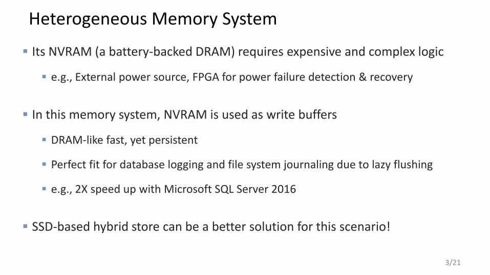
Heterogeneous Memory System
Its NVRAM (a battery-backed DRAM) requires expensive and complex logic
e.g., External power source, FPGA for power failure detection & recovery
In this memory system, NVRAM is used as write buffers
DRAM-like fast, yet persistent
Perfect fit for database logging and file system journaling due to lazy flushing
e.g., 2X speed up with Microsoft SQL Server 2016
SSD-based hybrid store can be a better solution for this scenario!
3/21

SSD-based Hybrid Store
Why? NVMe SSDs already have right ingredients to realize persistent memory
Memory interface: PCIe interconnect
Persistent memory (PM): a portion of internal DRAM plus additional capacitors
(No external power source!)
Power failure handling: Added logic to SSD controller (No newly added FPGA!)
Moreover, an internal datapath between PM and NAND flash can be built
Typically, logs and journals are written as bytes, but read by large chunk later
4/21
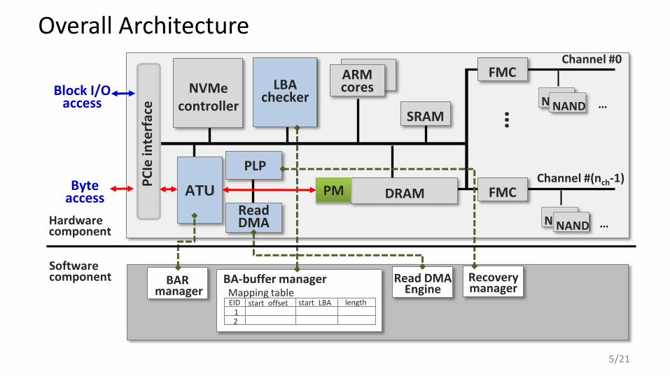
Overall Architecture
SRAM
Channel #0
NAND
…
Channel #(nch-1)
NAND
… NAND
… NAND
Byte access
Block I/O access
PC
Ie in
terf
ace
DRAM PM
NVMe controller
ATU
FMC
FMC
ARM cores LBA
checker
Read DMA
PLP
BAR manager
Read DMA Engine
Recovery manager
BA-buffer manager Mapping table
start_LBA EID length 1 2
start_offset
Hardware component
Software component
5/21

BAR Manager
NAND
DRAM Buffer
NAND NAND
Application
Host Virtual Address
Host System
BAR1
NAND
NVMe I/F
LOAD/STORE (BYTE)
Read/Write (PAGE)
1. Opens up a memory space
visible to CPU
BAR manager enables an additional
BAR (BAR1) for byte granule file access
BAR: “How the device advertise the
amount of address range it needs”
2. Redirects memory accesses from CPU into internal DRAM • The device is responsible for mapping
internal resources to the host-visible memory ranges
• BAR manager employs an address translation unit (ATU)
6/21

BAR Manager (contd.)
NAND
DRAM Buffer
NAND NAND
Application
Host Virtual Address
Host System
BAR1
NAND
NVMe I/F
LOAD/STORE (BYTE)
Read/Write (PAGE)
3. Exploits write combining (WC) mode of the underlying CPU • Individual writes are combined into a larger
burst in CPU’s WC buffer • 64 bytes in size in current x86 CPUs
• It leads to a significant reduction of memory accesses
Register store
store
store WC buffer
7/21

BA-buffer Manager
NAND
DRAM Buffer
NAND NAND
Application
Host Virtual Address
Host System
BAR1
NAND
NVMe I/F
LOAD/STORE (BYTE)
Read/Write (PAGE)
Maintains a memory hierarchy of DRAM and NAND • BA-buffer logic runs on an ARM core
within 2B-SSD
• The BA-buffer management APIs are designed to enable applications to allocate memory on the BA-buffer, and read and write files using them
• The mapping table stores information between DRAM addresses and NAND data
• (1) entry_id, (2) start_offset in the BA-buffer, (3) start_LBA of a given file, and (4) length
8/21
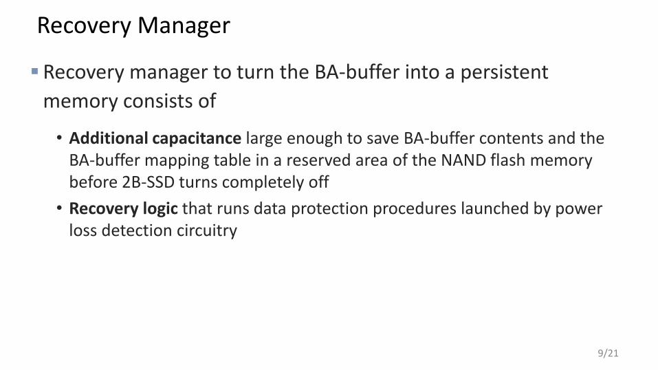
Recovery Manager
Recovery manager to turn the BA-buffer into a persistent
memory consists of
• Additional capacitance large enough to save BA-buffer contents and the BA-buffer mapping table in a reserved area of the NAND flash memory before 2B-SSD turns completely off
• Recovery logic that runs data protection procedures launched by power loss detection circuitry
9/21

Usage and Durability Guarantee
Two steps for ensuring ordering and durability of writes
WC buffer → Root Complex
Root Complex → BA-buffer
CPU
BA-Buffer Root
Complex
Caches
WC Buffer PCIe
② clflush() & mfence() ③ BA-SYNC()
NAND Flash
① BA-PIN()
④ BA-FLUSH()
10/21

2B-SSD API
BA_PIN(EID, offset, LBA, length)
BA_FLUSH(EID)
BA_SYNC(EID)
BA_GET_ENTRY_INFO(EID)
BA_READ_DMA(EID, dst, length)
11/21
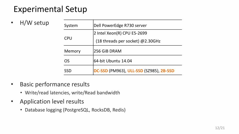
Experimental Setup
• H/W setup
• Basic performance results • Write/read latencies, write/Read bandwidth
• Application level results • Database logging (PostgreSQL, RocksDB, Redis)
System Dell PowerEdge R730 server
CPU 2 Intel Xeon(R) CPU E5-2699
(18 threads per socket) @2.30GHz
Memory 256 GiB DRAM
OS 64-bit Ubuntu 14.04
SSD DC-SSD (PM963), ULL-SSD (SZ985), 2B-SSD
12/21

2B-SSD
Write Latency (QD1, 4KB random write)
6.6X 13.2 μs
Z-SSD (SZ985)
4KB
2B-SSD prototype implemented on Samsung Z-SSD
4KB
2 μs
8B
630 ns
1KB
930 ns
2B-SSD
Z-SSD (SZ985) performance
• 4KB Random Read Latency ~13us
• 4KB Random Write Latency ~10us
Electrolytic capacitor
Z-NAND flash memory
DRAM
PCIe interface
Z-NAND flash
memory 2B-SSD Ctrl
Item Description
Host interface PCIe Gen.3 x4 (3.2GB/s), NVMe 1.2
Device density 800 GB
Storage medium Samsung Z-NAND flash memory
Capacitance of capacitors 270 uF x3
BA-buffer size 8 MB
Max entries of BA-buffer 8
13/21
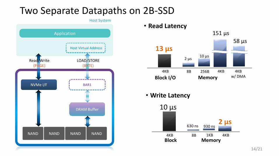
Two Separate Datapaths on 2B-SSD
NAND
DRAM Buffer
NAND NAND
Application
Host Virtual Address
Host System
BAR1
NAND
NVMe I/F
LOAD/STORE (BYTE)
Read/Write (PAGE)
• Write Latency
4KB
2 μs
10 μs
Block 8B
630 ns
1KB
930 ns
Memory 4KB
• Read Latency
4KB
151 μs
13 μs
Block I/O 8B
2 μs
256B
10 μs
Memory 4KB 4KB
w/ DMA
58 μs
14/21

Write Latency
MMIO < ULL-SSD (630ns vs. 13.2us) MMIO < MMIO + BA_SYNC
(2us vs. 4us)
15/21

Write Bandwidth
ULL-SSD > 2B-SSD
• Latest NVMe SSDs exploit hardware-automated datapath for optimized block I/O
• Internal datapath between BA-buffer and NAND flash are excluded from this automation
2B-SSD > DC-SSD
16/21

Read Latency
MMIO < ULL-SSD
150us
13.2us
PCIe Read is non-posted (sync) transaction
MMIO < DC-SSD
17/21

Read Latency
ULL-SSD < Read DMA (13us vs. 58us)
The read DMA engine helps
accelerate slow memory read.
Reading by DMA is faster than
MMIO, but still slower than
block I/O.
Non-DMA > DMA
18/21
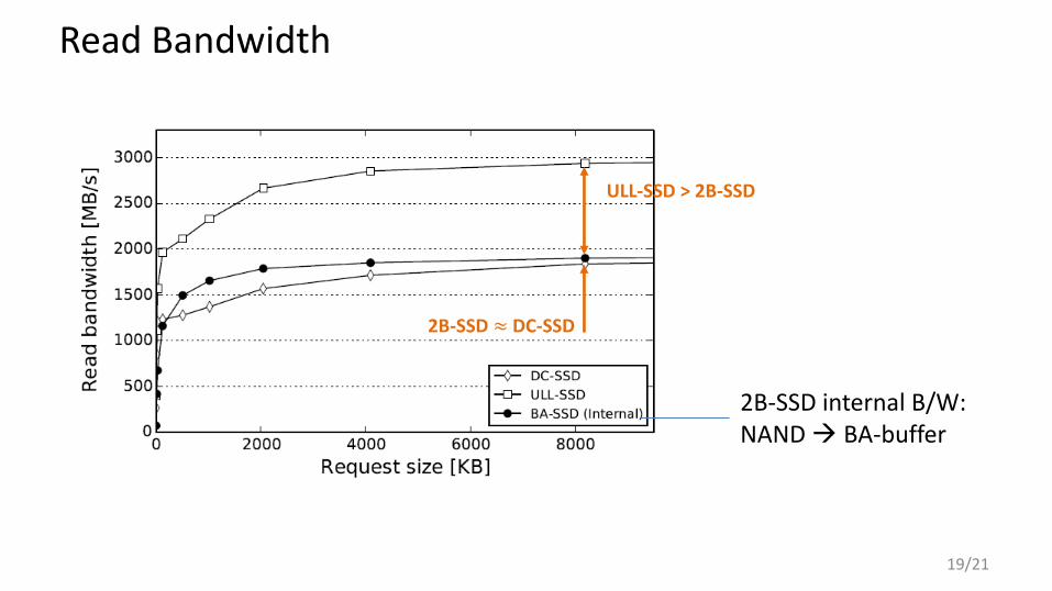
Read Bandwidth
ULL-SSD > 2B-SSD
2B-SSD ≈ DC-SSD
2B-SSD internal B/W: NAND BA-buffer
19/21
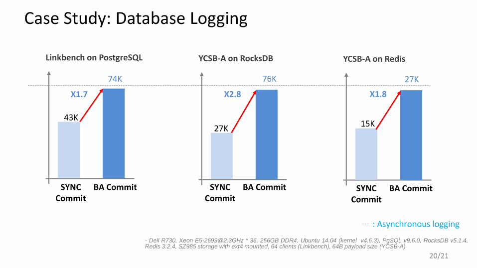
Case Study: Database Logging
- Dell R730, Xeon [email protected] * 36, 256GB DDR4, Ubuntu 14.04 (kernel v4.6.3), PgSQL v9.6.0, RocksDB v5.1.4, Redis 3.2.4, SZ985 storage with ext4 mounted, 64 clients (Linkbench), 64B payload size (YCSB-A)
: Asynchronous logging
Linkbench on PostgreSQL
SYNC Commit
BA Commit
X1.7
43K
74K
YCSB-A on RocksDB
X2.8
27K
76K
YCSB-A on Redis
X1.8
15K
27K
SYNC Commit
BA Commit SYNC Commit
BA Commit
20/21

Conclusions
• This paper described the motivation, design, and implementation of a byte- and block-addressable solid-state drive.
• Through 2B-SSD APIs, applications can write and read any number of bytes on it without forcing the data being buffered in the host memory.
• We demonstrate the results where major database engines can see a throughput gain of up to 2.8X without the risk of data loss.
21/21

Thank You